KR20210025216A - Micro led repair device and manufacturing of micor led display using the same - Google Patents
Micro led repair device and manufacturing of micor led display using the sameDownload PDFInfo
- Publication number
- KR20210025216A KR20210025216AKR1020190104904AKR20190104904AKR20210025216AKR 20210025216 AKR20210025216 AKR 20210025216AKR 1020190104904 AKR1020190104904 AKR 1020190104904AKR 20190104904 AKR20190104904 AKR 20190104904AKR 20210025216 AKR20210025216 AKR 20210025216A
- Authority
- KR
- South Korea
- Prior art keywords
- micro led
- defective
- repair device
- laser
- unit
- Prior art date
- Legal status (The legal status is an assumption and is not a legal conclusion. Google has not performed a legal analysis and makes no representation as to the accuracy of the status listed.)
- Withdrawn
Links
Images


Classifications
- H—ELECTRICITY
- H01—ELECTRIC ELEMENTS
- H01L—SEMICONDUCTOR DEVICES NOT COVERED BY CLASS H10
- H01L21/00—Processes or apparatus adapted for the manufacture or treatment of semiconductor or solid state devices or of parts thereof
- H01L21/67—Apparatus specially adapted for handling semiconductor or electric solid state devices during manufacture or treatment thereof; Apparatus specially adapted for handling wafers during manufacture or treatment of semiconductor or electric solid state devices or components ; Apparatus not specifically provided for elsewhere
- H01L21/67005—Apparatus not specifically provided for elsewhere
- H01L21/67011—Apparatus for manufacture or treatment
- H01L21/67144—Apparatus for mounting on conductive members, e.g. leadframes or conductors on insulating substrates
- B—PERFORMING OPERATIONS; TRANSPORTING
- B23—MACHINE TOOLS; METAL-WORKING NOT OTHERWISE PROVIDED FOR
- B23K—SOLDERING OR UNSOLDERING; WELDING; CLADDING OR PLATING BY SOLDERING OR WELDING; CUTTING BY APPLYING HEAT LOCALLY, e.g. FLAME CUTTING; WORKING BY LASER BEAM
- B23K26/00—Working by laser beam, e.g. welding, cutting or boring
- B23K26/34—Laser welding for purposes other than joining
- H—ELECTRICITY
- H01—ELECTRIC ELEMENTS
- H01L—SEMICONDUCTOR DEVICES NOT COVERED BY CLASS H10
- H01L21/00—Processes or apparatus adapted for the manufacture or treatment of semiconductor or solid state devices or of parts thereof
- H01L21/02—Manufacture or treatment of semiconductor devices or of parts thereof
- H01L21/04—Manufacture or treatment of semiconductor devices or of parts thereof the devices having potential barriers, e.g. a PN junction, depletion layer or carrier concentration layer
- H01L21/50—Assembly of semiconductor devices using processes or apparatus not provided for in a single one of the groups H01L21/18 - H01L21/326 or H10D48/04 - H10D48/07 e.g. sealing of a cap to a base of a container
- H01L21/52—Mounting semiconductor bodies in containers
- H—ELECTRICITY
- H01—ELECTRIC ELEMENTS
- H01L—SEMICONDUCTOR DEVICES NOT COVERED BY CLASS H10
- H01L24/00—Arrangements for connecting or disconnecting semiconductor or solid-state bodies; Methods or apparatus related thereto
- H01L24/74—Apparatus for manufacturing arrangements for connecting or disconnecting semiconductor or solid-state bodies
- H—ELECTRICITY
- H01—ELECTRIC ELEMENTS
- H01L—SEMICONDUCTOR DEVICES NOT COVERED BY CLASS H10
- H01L24/00—Arrangements for connecting or disconnecting semiconductor or solid-state bodies; Methods or apparatus related thereto
- H01L24/80—Methods for connecting semiconductor or other solid state bodies using means for bonding being attached to, or being formed on, the surface to be connected
- H—ELECTRICITY
- H01—ELECTRIC ELEMENTS
- H01L—SEMICONDUCTOR DEVICES NOT COVERED BY CLASS H10
- H01L25/00—Assemblies consisting of a plurality of semiconductor or other solid state devices
- H01L25/03—Assemblies consisting of a plurality of semiconductor or other solid state devices all the devices being of a type provided for in a single subclass of subclasses H10B, H10D, H10F, H10H, H10K or H10N, e.g. assemblies of rectifier diodes
- H01L25/04—Assemblies consisting of a plurality of semiconductor or other solid state devices all the devices being of a type provided for in a single subclass of subclasses H10B, H10D, H10F, H10H, H10K or H10N, e.g. assemblies of rectifier diodes the devices not having separate containers
- H01L25/075—Assemblies consisting of a plurality of semiconductor or other solid state devices all the devices being of a type provided for in a single subclass of subclasses H10B, H10D, H10F, H10H, H10K or H10N, e.g. assemblies of rectifier diodes the devices not having separate containers the devices being of a type provided for in group H10H20/00
- H01L25/0753—Assemblies consisting of a plurality of semiconductor or other solid state devices all the devices being of a type provided for in a single subclass of subclasses H10B, H10D, H10F, H10H, H10K or H10N, e.g. assemblies of rectifier diodes the devices not having separate containers the devices being of a type provided for in group H10H20/00 the devices being arranged next to each other
Landscapes
- Engineering & Computer Science (AREA)
- Microelectronics & Electronic Packaging (AREA)
- Power Engineering (AREA)
- Computer Hardware Design (AREA)
- Physics & Mathematics (AREA)
- Manufacturing & Machinery (AREA)
- Condensed Matter Physics & Semiconductors (AREA)
- General Physics & Mathematics (AREA)
- Optics & Photonics (AREA)
- Plasma & Fusion (AREA)
- Mechanical Engineering (AREA)
- Devices For Indicating Variable Information By Combining Individual Elements (AREA)
Abstract
Translated fromKorean
Description
Translated fromKorean본 발명은 불량 마이크로 LED를 양품 마이크로 LED로 교체하는 마이크로 LED 리페어 장치 및 이를 이용한 마이크로 LED 디스플레이 제조방법에 관한 것이다.The present invention relates to a micro LED repair device for replacing a defective micro LED with a good micro LED, and a method of manufacturing a micro LED display using the same.
현재 디스플레이 시장은 아직은 LCD가 주류를 이루고 있는 가운데 OLED가 LCD를 빠르게 대체하며 주류로 부상하고 있는 상황이다. 디스플레이 업체들의 OLED 시장 참여가 러시를 이루고 있는 상황에서 최근 Micro LED(이하,'마이크로 LED'라 함) 디스플레이가 또 하나의 차세대 디스플레이로 부상하고 있다. 마이크로 LED는, 성형한 수지 등으로 덮인 패키지 타입의 것이 아닌, 결정 성장에 이용한 웨이퍼에서 잘라낸 상태의 것을 의미한다. LCD와 OLED의 핵심소재가 각각 액정(Liquid Crystal), 유기재료인데 반해 마이크로 LED 디스플레이는 1~100마이크로미터(㎛) 단위의 LED 칩 자체를 발광재료로 사용하는 디스플레이다.In the current display market, while LCD is still mainstream, OLED is rapidly replacing LCD and emerging as mainstream. With display companies' participation in the OLED market in a rush, Micro LED (hereinafter referred to as'micro LED') displays are emerging as another next-generation display. The micro LED is not of a package type covered with a molded resin or the like, but a state cut from a wafer used for crystal growth. While the core materials of LCD and OLED are liquid crystal and organic materials, respectively, micro LED display is a display that uses the LED chip itself in units of 1 to 100 micrometers (㎛) as a light emitting material.
Cree사가 1999년에 "광 적출을 향상시킨 마이크로-발광 다이오드 어레이"에 관한 특허를 출원하면서(등록특허공보 등록번호 제0731673호), 마이크로 LED 라는 용어가 등장한 이래 관련 연구 논문들이 잇달아 발표되면서 연구개발이 이루어지고 있다. 마이크로 LED를 디스플레이에 응용하기 위해 해결해야 할 과제로 마이크로 LED 소자를 Flexible 소재/소자를 기반으로 하는 맞춤형 마이크로 칩 개발이 필요하고, 마이크로 미터 사이즈의 LED 칩의 전사(transfer)와 디스플레이 픽셀 전극에 정확한 실장(Mounting)을 위한 기술이 필요하다.When Cree applied for a patent for "Micro-light-emitting diode array with improved light extraction" in 1999 (Registration Patent Publication No. 0731673), research and development have been conducted since the term micro LED appeared one after another. This is being done. As a task to be solved in order to apply micro LED to a display, it is necessary to develop customized microchips based on flexible materials/devices for micro LED devices. Skills for mounting are required.
특히, 마이크로 LED 소자를 표시 기판에 이송하는 전사(transfer)와 관련하여, LED 크기가 1~100 마이크로미터(㎛) 단위까지 작아짐에 따라 기존의 픽앤플레이스(pick & place) 장비를 사용할 수 없고, 보다 고정밀도로 이송하는 전사 헤드기술이 필요하게 되었다. 이러한 전사 헤드 기술과 관련하여, 이하에서 살펴보는 바와 같은 몇가지의 구조들이 제안되고 있다.In particular, with regard to the transfer of micro LED devices to the display substrate, the existing pick & place equipment cannot be used as the size of the LED is reduced to 1 to 100 micrometers (㎛). A transfer head technology that transfers with higher precision is required. In connection with this transfer head technology, several structures as described below have been proposed.
미국의 Luxvue사는 정전헤드(electrostatic head)를 이용하여 마이크로 LED를 전사하는 방법을 제안하였다(공개특허공보 공개번호 제2014-0112486호, 이하 '선행발명1'이라 함).Luxvue of the United States proposed a method of transferring a micro LED using an electrostatic head (Public Patent Publication No. 2014-0112486, hereinafter referred to as'prior invention 1').
미국의 X-Celeprint사는 전사 헤드를 탄성이 있는 고분자 물질로 적용하여 웨이퍼 상의 마이크로 LED를 원하는 기판에 이송시키는 방법을 제안하였다(공개특허공보 공개번호 제2017-0019415호, 이하 '선행발명2'라 함).X-Celeprint of the United States has proposed a method of transferring micro LEDs on a wafer to a desired substrate by applying a transfer head with an elastic polymer material (Public Patent Publication No. 2017-0019415, hereinafter referred to as'Prior Invention 2'. box).
한국광기술원은 섬모 접착구조 헤드를 이용하여 마이크로 LED를 전사하는 방법을 제안하였다(등록특허공보 등록번호 제1754528호, 이하 '선행발명3'이라 함).The Korea Institute of Photonics and Technology proposed a method of transferring a micro LED using a ciliated adhesive structure head (Registration Patent Publication No. 1754528, hereinafter referred to as'prior invention 3').
한국기계연구원은 롤러에 접착제를 코팅하여 마이크로 LED를 전사하는 방법을 제안하였다(등록특허공보 등록번호 제1757404호, 이하 '선행발명4'라 함).The Korea Institute of Machinery and Materials proposed a method of transferring micro LEDs by coating an adhesive on a roller (Registration Patent Publication No. 1757404, hereinafter referred to as'Prior Invention 4').
삼성디스플레이는 어레이 기판이 용액에 담겨 있는 상태에서 어레이 기판의 제1,2전극에 마이너스 전압을 인가하여 정전기 유도 현상에 의해 마이크로 LED를 어레이 기판에 전사하는 방법을 제안하였다(공개특허공보 제10-2017-0026959호, 이하 '선행발명5'라 함).Samsung Display proposed a method of transferring micro LEDs to the array substrate by static electricity induction by applying negative voltages to the first and second electrodes of the array substrate while the array substrate is immersed in a solution (Patent Publication No. 10- 2017-0026959, hereinafter referred to as'prior invention 5').
엘지전자는 헤드홀더를 복수의 픽업헤드들과 기판 사이에 배치하고 복수의 픽업 헤드의 움직임에 의해 그 형상이 변형되어 복수의 픽업 헤드들에게 자유도를 제공하는 방법을 제안하였다(공개특허공보 제10-2017-0024906호, 이하 '선행발명6'이라 함).LG Electronics proposed a method of arranging a head holder between a plurality of pickup heads and a substrate, and providing a degree of freedom to a plurality of pickup heads by deforming the shape by the movement of the plurality of pickup heads (Patent Publication No. 10). -2017-0024906, hereinafter referred to as'prior invention 6').
위와 같은 선행 발명들에 의해 마이크로 LED는 성장기판에서 성장된 후 개별화된 마이크로 LED를 표시기판으로 전사하였다. 이때, 표시기판에 실장된 마이크로 LED 중 불량, 즉, 발광하지 않는 마이크로 LED가 간헐적으로 발생되었고, 이는 성장기판이 아닌 표시기판에 전사하였을 때 마이크로 LED의 불량 여부를 파악할 수 있었다.According to the above-described prior inventions, micro LEDs were grown on a growth substrate and then individualized micro LEDs were transferred to a display substrate. At this time, among the micro LEDs mounted on the display substrate, defects, that is, micro LEDs that do not emit light were intermittently generated, and it was possible to determine whether the micro LED was defective when transferred to the display substrate rather than the growth substrate.
따라서, 표시기판에 전사된 마이크로 LED 중 불량 마이크로 LED를 교체하는 기술이 필요하게 되었고 이에 대한 기술로는 한국공개특허 제10-2018-0087896호(이하, '선행발명 7'이라 함)에 기재된 것이 공지되어 있다.Therefore, a technology for replacing defective micro LEDs among the micro LEDs transferred to the display substrate is required, and the technology for this is described in Korean Patent Publication No. 10-2018-0087896 (hereinafter referred to as'prior invention 7'). It is known.
선행발명 7은 점착필름의 점착력을 이용하여 기판에 부착된 불량 마이크로 LED를 제거하고 있다.Prior Invention 7 removes the defective micro LED attached to the substrate by using the adhesive force of the adhesive film.
하지만, 선행발명 7의 구성에 따르면 불량 마이크로 LED의 리페어 속도를 향상시키는데 한계가 있다.However, according to the configuration of Prior Invention 7, there is a limit to improving the repair speed of defective micro LEDs.
이에 본 발명은 불량 마이크로 LED를 효과적으로 제거할 수 있는 마이크로 LED 리페어 장치 및 이를 이용한 마이크로 LED 디스플레이 제조방법을 제공하는 것을 목적으로 한다.Accordingly, an object of the present invention is to provide a micro LED repair device capable of effectively removing defective micro LEDs and a method of manufacturing a micro LED display using the same.
본 발명의 바람직한 실시 예에 따른 마이크로 LED 디스플레이 제조방법은, 불량 마이크로 LED를 색출하는 검사단계;상기 불량 마이크로 LED에 레이저를 조사하는 제1조사단계; 레이저가 조사된 상기 불량 마이크로 LED를 본딩 패드로부터 제거하는 제거단계; 상기 불량 마이크로 LED가 제거된 상기 본딩 패드에 레이저를 조사하는 제2조사단계; 및 상기 불량 마이크로 LED가 제거된 위치에 양품 마이크로 LED를 실장 시키는 실장단계;를 포함하는 것을 특징으로 한다.A method of manufacturing a micro LED display according to a preferred embodiment of the present invention includes an inspection step of detecting a defective micro LED; a first irradiation step of irradiating a laser to the defective micro LED; A removing step of removing the defective micro LED irradiated with a laser from the bonding pad; A second irradiation step of irradiating a laser onto the bonding pad from which the defective micro LED has been removed; And a mounting step of mounting a good micro LED at a location from which the defective micro LED has been removed.
또한, 상기 제거단계는, 상기 불량 마이크로 LED를 개별로 제거하는 것을 특징으로 한다.In addition, in the removing step, the defective micro LED is individually removed.
또한, 상기 제거단계는, 상기 불량 마이크로 LED를 일괄로 제거하는 것을 특징으로 한다.In addition, the removing step is characterized in that the defective micro-LEDs are removed at a time.
또한, 상기 제거단계는, 상기 불량 마이크로 LED를 흡입하여 제거하는 것을 특징으로 한다.In addition, in the removing step, the defective micro LED is sucked and removed.
또한, 상기 제거단계는, 상기 불량 마이크로 LED를 흡착하여 제거하는 것을 특징으로 한다.In addition, the removing step is characterized in that the defective micro-LED is adsorbed and removed.
본 발명의 바람직한 실시 예에 따른 마이크로 LED 리페어 장치는, 불량 마이크로 LED와 본딩 패드 사이의 접착력을 형성 또는 상실시키는 레이저부; 상기 불량 마이크로 LED를 본딩 패드로부터 제거하는 석션부; 상기 레이저부에서 발진된 레이저의 조사통로; 및 상기 석션부에서 발생된 에어가 유동하는 흐름통로;를 포함한다.Micro LED repair device according to a preferred embodiment of the present invention, a laser unit for forming or losing the adhesive force between the defective micro LED and the bonding pad; A suction unit for removing the defective micro LED from the bonding pad; An irradiation path of the laser oscillated by the laser unit; And a flow path through which the air generated from the suction unit flows.
또한, 상기 조사통로의 일단에 설치되는 흡착패드를 포함한다.In addition, it includes an adsorption pad installed at one end of the irradiation passage.
또한, 상기 흡착패드는 다공성 재질로 이루어지는 것을 특징으로 한다.In addition, the adsorption pad is characterized in that it is made of a porous material.
또한, 상기 흐름통로 및 상기 조사통로는 통로의 일부분을 공유하는 것을 특징으로 한다.In addition, the flow passage and the irradiation passage are characterized in that they share a portion of the passage.
본 발명의 바람직한 실시 예에 따른 마이크로 LED 리페어 장치는, 바디부; 상기 바디부 상부에 형성되고 불량 마이크로 LED와 본딩 패드 사이의 접착력을 형성 또는 상실시키는 레이저부; 상기 바디부 측면에서 후드 형태로 형성되며 상기 레이저부에 의해 접착력을 상실한 상기 불량 마이크로 LED를 제거하는 불량 마이크로 LED 제거부; 및 복수개의 양품 마이크로 LED가 흡착되어 있는 양품 마이크로 LED 교체부;를 포함하고, 상기 불량 마이크로 LED 제거부는 일괄로 상기 불량 마이크로 LED를 제거하는 것을 특징으로 한다.Micro LED repair device according to an embodiment of the present invention, the body portion; A laser unit formed on the body portion and forming or losing adhesive force between the defective micro LED and the bonding pad; A defective micro LED removal unit formed in the shape of a hood on the side of the body and removing the defective micro LED having lost adhesion by the laser unit; And a good micro LED replacement unit in which a plurality of good micro LEDs are adsorbed, wherein the defective micro LED removing unit removes the defective micro LED at a time.
본 발명의 바람직한 실시 예에 따른 마이크로 LED 리페어 장치는, 바디부; 상기 바디부 중심에 형성되고 불량 마이크로 LED와 본딩 패드 사이의 접착력을 형성 또는 상실시키는 레이저부; 상기 바디부 외면에 형성되고 상기 레이저부에 의해 접착력을 상실한 상기 불량 마이크로 LED를 제거하는 제거부; 및 상기 바디부 외면에 형성되고 양품 마이크로 LED가 흡착되어 있는 교체부;를 포함하고, 상기 제거부 및 상기 교체부는 상기 바디부의 원주방향을 따라 교대로 형성되는 것을 특징으로 한다.Micro LED repair device according to an embodiment of the present invention, the body portion; A laser unit formed at the center of the body unit and forming or losing adhesive force between the defective micro LED and the bonding pad; A removal unit formed on an outer surface of the body unit and removing the defective micro LED having lost adhesion by the laser unit; And a replacement part formed on an outer surface of the body part and adsorbed with a good-quality micro LED, wherein the removal part and the replacement part are formed alternately along the circumferential direction of the body part.
또한, 상기 바디부는 투명재질로 이루어지는 것을 특징으로 한다.In addition, the body portion is characterized in that made of a transparent material.
이상에서 설명한 바와 같은 본 발명의 바람직한 실시 예에 따른 마이크로 LED 리페어 장치는 불량 마이크로 LED를 색출한 후 마이크로 LED 리페어 장치의 흡입력을 이용하여 불량 마이크로 LED를 제거함으로써 주변에 실장된 마이크로 LED에 영향을 주지 않고 불량 마이크로 LED만을 손쉽게 제거할 수 있다는 효과가 있다.As described above, the micro LED repair device according to the preferred embodiment of the present invention detects the defective micro LED and removes the defective micro LED using the suction power of the micro LED repair device, thereby not affecting the micro LED mounted around the micro LED. It has the effect of being able to easily remove only defective micro LEDs.
또한, 하나의 마이크로 LED 리페어 장치를 이용하여 불량 마이크로 LED를 제거함과 함께 양품 마이크로 LED를 교체하도록 함으로써, 전체 장비의 구조를 단순화 할 수 있다.In addition, by using one micro LED repair device to remove defective micro LEDs and to replace good micro LEDs, it is possible to simplify the structure of the entire equipment.
또한, 별도로 구비된 2개의 리페어 장치를 이용하여 어느 하나의 리페어 장치가 불량 마이크로 LED를 제거하면, 다른 하나의 리페어 장치로 신속하게 불량 위치에 양품 마이크로 LED를 실장 함으로써 리페어 속도를 향상시킬 수 있다.In addition, if one repair device removes the defective micro LED by using two separately provided repair devices, the repair speed can be improved by quickly mounting the good micro LED in the defective location with the other repair device.
또한, 불량 마이크로 LED를 양품 마이크로 LED로 교체함으로써 임시기판 및 표시기판에 실장된 마이크로 LED의 불량률을 낮출 수 있는 효과가 있다. In addition, by replacing defective micro LEDs with good micro LEDs, there is an effect of lowering the defect rate of micro LEDs mounted on temporary substrates and display substrates.
또한, 불량 마이크로 LED를 흡착패드 등에 흡착시키지 않고 공기 흐름을 따라 마이크로 LED 리페어 장치 내부로 흘러 들어가게 흡입하여 제거함으로써 보다 쉽게 불량 마이크로 LED를 제거할 수 있다는 효과가 있다.In addition, there is an effect that the defective micro LED can be more easily removed by suctioning and removing the defective micro LED by flowing into the inside of the micro LED repair device along the air flow without adsorbing the defective micro LED.
또한, 복수개의 불량 마이크로 LED를 일괄로 제거 후 복수개의 양품 마이크로 LED를 일괄로 교체함으로써, 불량 마이크로 LED를 양품 마이크로 LED로 교체하는 작업 시간을 단축시킬 수 있는 효과가 있다.In addition, by removing a plurality of defective micro LEDs at once and then replacing a plurality of good micro LEDs at once, there is an effect of shortening the work time of replacing defective micro LEDs with good micro LEDs.
또한, 마이크로 LED 리페어 장치는 좌우 동선을 최소화하여 짧은 동선으로 불량 마이크로 LED를 양품 마이크로 LED로 교체 가능하다는 효과가 있다.In addition, the micro LED repair device has the effect that it is possible to replace the defective micro LED with a good micro LED with a short copper line by minimizing the left and right copper lines.
도 1은 본 발명의 실시예의 전사 대상이 되는 마이크로 LED를 도시한 도면.
도 2는 본 발명의 실시예에 의해 표시기판에 이송되어 실장된 마이크로 LED 구조체의 도면.
도 3은 표시기판에 마이크로 LED가 실장된 모습을 나타낸 도.
도 4(a)는 본 발명의 일 실시 예에 따른 마이크로 LED 리페어 장치의 레이저부에서 레이저가 조사되는 모습을 나타낸 도.
도 4(b)는 본 발명의 일 실시 예에 따른 마이크로 LED 리페어 장치에 불량 마이크로 LED가 흡착되어 제거되는 모습을 나타낸 도.
도 5(a)는 본 발명의 일 실시 예에 따른 마이크로 LED 리페어 장치(10)에 양품 마이크로 LED가 흡착된 모습을 나타낸 도.
도 5(b)는 양품 마이크로 LED가 실장되는 모습을 나타낸 도.
도 6은 본 발병의 바람직한 실시 예에 따른 마이크로 LED 디스플레이 제조방법에 관한 도.
도 7(a)는 본 발명의 바람직한 제2실시예에 따른 마이크로 LED 리페어 장치의 레이저부에서 레이저가 조사되는 모습을 나타내는 도.
도 7(b)는 본 발명의 바람직한 제2실시 예에 따른 마이크로 LED 리페어 장치에 불량 마이크로 LED가 흡입되는 모습을 나타낸 도.
도 8은 본 발명의 바람직한 제3실시 예에 따른 마이크로 LED 리페어 장치가 레이저를 조사하는 도.
도 9는 본 발명의 바람직한 제3실시 예에 따른 마이크로 LED 리페어 장치의 제거부가 불량 마이크로 LED를 흡입하는 모습을 나타낸 도.
도 10은 본 발명의 바람직한 제3실시 예에 따른 마이크로 LED 리페어 장치가 양품 마이크로 LED를 실장하는 모습을 나타낸 도.
도 11(a)는 본 발명의 바람직한 제4실시 예에 따른 마이크로 LED 리페어 장치가 레이저를 조사하는 모습을 나타낸 도.
도 11(b)는 본 발명의 바람직한 제4실시 예에 따른 마이크로 LED 리페어 장치의 제거부와 불량 마이크로 LED가 맞닿는 모습을 나타낸 도.
도 12(a)는 본 발명의 바람직한 제4실시 예에 따른 마이크로 LED 리페어 장치가 불량 마이크로 LED를 제거하는 모습을 나타낸 도.
도 12(b)는 본 발명의 바람직한 제4실시 예에 따른 마이크로 LED 리페어 장치가 레이저를 조사하는 모습을 나타낸 도.
도 13(a)는 본 발명의 바람직한 제4실시 예에 따른 마이크로 LED 리페어 장치의 교체부에 흡착된 양품 마이크로 LED를 실장하는 모습을 나타낸 도.
도 13(b)는 본 발명의 바람직한 제4실시 예에 따른 마이크로 LED 리페어 장치가 불량 마이크로 LED를 양품 마이크로 LED로 교체완료한 모습을 나타낸 도.1 is a diagram showing a micro LED to be transferred in an embodiment of the present invention.
2 is a diagram of a micro LED structure transported and mounted on a display substrate according to an embodiment of the present invention.
3 is a diagram showing a state in which a micro LED is mounted on a display substrate.
4(a) is a view showing a state in which a laser is irradiated from a laser unit of a micro LED repair device according to an embodiment of the present invention.
4(b) is a diagram showing a state in which a defective micro LED is adsorbed and removed from a micro LED repair device according to an embodiment of the present invention.
Figure 5 (a) is a view showing a state in which good micro LED is adsorbed to the micro
5(b) is a diagram showing a state in which a good micro LED is mounted.
6 is a diagram illustrating a method of manufacturing a micro LED display according to a preferred embodiment of the present disease.
7(a) is a view showing a state in which a laser is irradiated from a laser unit of a micro LED repair device according to a second exemplary embodiment of the present invention.
7(b) is a diagram showing a state in which a defective micro LED is sucked into a micro LED repair device according to a second exemplary embodiment of the present invention.
8 is a view in which a micro LED repair device according to a third embodiment of the present invention irradiates a laser.
9 is a view showing a state in which the removal unit of the micro LED repair device according to a third embodiment of the present invention sucks a defective micro LED.
10 is a view showing a state in which a micro LED repair device according to a third preferred embodiment of the present invention mounts a good micro LED.
11(a) is a view showing a state in which a micro LED repair device according to a fourth embodiment of the present invention irradiates a laser.
11(b) is a view showing a state in which the removal unit of the micro LED repair device and the defective micro LED contact each other according to a fourth exemplary embodiment of the present invention.
12(a) is a diagram showing a state in which a micro LED repair device according to a fourth embodiment of the present invention removes a defective micro LED.
12(b) is a view showing a state in which a micro LED repair device according to a fourth embodiment of the present invention irradiates a laser.
13(a) is a view showing a state in which a good micro LED adsorbed to a replacement part of a micro LED repair device according to a fourth embodiment of the present invention is mounted.
13(b) is a diagram showing a state in which a micro LED repair device according to a fourth embodiment of the present invention has completed replacing a defective micro LED with a good micro LED.
이하의 내용은 단지 발명의 원리를 예시한다. 그러므로 당업자는 비록 본 명세서에 명확히 설명되거나 도시되지 않았지만 발명의 원리를 구현하고 발명의 개념과 범위에 포함된 다양한 장치를 발명할 수 있는 것이다. 또한, 본 명세서에 열거된 모든 조건부 용어 및 실시 예들은 원칙적으로, 발명의 개념이 이해되도록 하기 위한 목적으로만 명백히 의도되고, 이와 같이 특별히 열거된 실시 예들 및 상태들에 제한적이지 않는 것으로 이해되어야 한다.The following content merely exemplifies the principles of the invention. Therefore, those skilled in the art can implement the principles of the invention and invent various devices included in the concept and scope of the invention, although not clearly described or illustrated herein. In addition, it should be understood that all conditional terms and examples listed in the present specification are, in principle, clearly intended only for the purpose of understanding the concept of the invention, and are not limited to the embodiments and states specifically listed as described above. .
상술한 목적, 특징 및 장점은 첨부된 도면과 관련한 다음의 상세한 설명을 통하여 보다 분명해질 것이며, 그에 따라 발명이 속하는 기술분야에서 통상의 지식을 가진 자가 발명의 기술적 사상을 용이하게 실시할 수 있을 것이다.The above-described objects, features, and advantages will become more apparent through the following detailed description in connection with the accompanying drawings, and accordingly, a person of ordinary skill in the technical field to which the invention pertains will be able to easily implement the technical idea of the invention. .
본 명세서에서 기술하는 실시 예들은 본 발명의 이상적인 예시 도인 단면도 및/또는 사시도들을 참고하여 설명될 것이다. 이러한 도면들에 도시된 막 및 영역들의 두께 및 구멍들의 지름 등은 기술적 내용의 효과적인 설명을 위해 과장된 것이다. 제조 기술 및/또는 허용 오차 등에 의해 예시도의 형태가 변형될 수 있다. 또한 도면에 도시된 마이크로 LED의 개수는 예시적으로 일부만을 도면에 도시한 것이다. 따라서, 본 발명의 실시 예들은 도시된 특정 형태로 제한되는 것이 아니라 제조 공정에 따라 생성되는 형태의 변화도 포함하는 것이다.Embodiments described in the present specification will be described with reference to sectional views and/or perspective views that are ideal examples of the present invention. The thicknesses and diameters of holes and the like of the films and regions shown in these drawings are exaggerated for effective explanation of the technical content. The shape of the exemplary diagram may be modified by manufacturing technology and/or tolerance. In addition, the number of micro LEDs shown in the drawings is only partially shown in the drawings by way of example. Accordingly, embodiments of the present invention are not limited to the specific form shown, but also include a change in form generated according to a manufacturing process.
다양한 실시예들을 설명함에 있어서, 동일한 기능을 수행하는 구성 요소에 대해서는 실시예가 다르더라도 편의상 동일한 명칭 및 동일한 참조번호를 부여하기로 한다. 또한, 이미 다른 실시예에서 설명된 구성 및 작동에 대해서는 편의상 생략하기로 한다.In describing various embodiments, components that perform the same function will be given the same name and the same reference number for convenience even though the embodiments are different. In addition, configurations and operations that have already been described in other embodiments will be omitted for convenience.
이하, 첨부된 도면을 참조하여 본 발명의 바람직한 실시 예들을 설명하기에 앞서, 마이크로 소자는 마이크로 LED를 포함할 수 있다. 마이크로 LED는 성형한 수지 등으로 패키징 되지 않으면서 결정 성장에 이용한 웨이퍼에서 잘라낸 상태의 것으로, 학술적으로 1~100㎛ 단위의 크기의 것을 지칭한다. 그러나 본 명세서에 기재된 마이크로 LED는 그 크기(1개의 변 길이)가 1~100㎛ 단위인 것으로 한정되는 것은 아니며 100㎛ 이상의 크기를 갖거나 1㎛ 미만의 크기를 갖는 것도 포함한다.Hereinafter, before describing preferred embodiments of the present invention with reference to the accompanying drawings, the micro device may include a micro LED. Micro LED is a state cut out of a wafer used for crystal growth without being packaged with a molded resin, etc., and refers to a size of 1 to 100 μm in academic terms. However, the micro LED described in the present specification is not limited to having a size (one side length) of 1 to 100 μm, and includes those having a size of 100 μm or more or less than 1 μm.
또한, 이하에서 설명하는 본 발명의 바람직한 실시예의 구성들은 각 실시예들의 기술적 사상의 변경없이 적용될 수 있는 미소 소자들의 전사에도 적용될 수 있다.In addition, the configurations of the preferred embodiments of the present invention described below can be applied to transfer of microelements that can be applied without changing the technical idea of each of the embodiments.
이하, 본 발명의 바람직한 실시예를 첨부 도면을 참조하여 상세히 설명하면 다음과 같다.Hereinafter, preferred embodiments of the present invention will be described in detail with reference to the accompanying drawings.
도 1은 본 발명의 바람직한 실시예에 따른 마이크로 LED를 도시한 도면이다.1 is a view showing a micro LED according to a preferred embodiment of the present invention.
마이크로 LED(ML)는 제1 기판(101) 상에 제작되어 위치한다. 이때, 제1 기판(101)은 성장 기판으로 제공될 수 있다.The micro LED (ML) is manufactured and positioned on the
제1 기판(101)은 전도성 기판 또는 절연성 기판으로 이루어질 수 있다. 예를 들어, 제1 기판(101)은 사파이어, SiC, Si, GaAs, GaN, ZnO, Si, GaP, InP, Ge, 및 Ga203 중 적어도 어느 하나로 형성될 수 있다. 본 실시예에서는 제1 기판(101)이 사파이어로 형성된 성장 기판이고, 테두리의 적어도 일부에 곡률을 포함하는 것을 예로 설명하겠다.The
마이크로 LED(ML)는 제1 반도체층(102), 제2 반도체층(104), 제1 반도체층(102)과 제2 반도체층(104) 사이에 형성된 활성층(103), 제1 컨택전극(106) 및 제2 컨택전극(107)을 포함할 수 있다.The micro LED (ML) includes a
제1 반도체층(102), 활성층(103), 및 제2 반도체층(104)은 유기금속 화학 증착법(MOCVD; Metal Organic Chemical Vapor Deposition), 화학 증착법(CVD; Chemical Vapor Deposition), 플라즈마 화학 증착법(PECVD; Plasma-Enhanced Chemical Vapor Deposition), 분자선 성장법(MBE; Molecular Beam Epitaxy), 수소화물 기상 성장법(HVPE; Hydride Vapor Phase Epitaxy) 등의 방법을 이용하여 형성할 수 있다.The
제1 반도체층(102)은 예를 들어, p형 반도체층으로 구현될 수 있다. p형 반도체층은 InxAlyGa1-x-yN (0≤x≤1, 0≤y≤1, 0≤x+y≤1)의 조성식을 갖는 반도체 재료, 예를 들어 GaN, AlN, AlGaN, InGaN, InN, InAlGaN, AlInN 등에서 선택될 수 있으며, Mg, Zn, Ca, Sr, Ba 등의 p형 도펀트가 도핑될 수 있다.The
제2 반도체층(104)은 예를 들어, n형 반도체층을 포함하여 형성될 수 있다. n형 반도체층은 InxAlyGa1-x-yN (0≤x≤1, 0≤y≤1, 0≤x+y≤1)의 조성식을 갖는 반도체 재료, 예를 들어 GaN, AlN, AlGaN, InGaN, InN, InAlGaN, AlInN 등에서 선택될 수 있으며, Si, Ge, Sn 등의 n형 도펀트가 도핑될 수 있다.The
다만, 본 발명은 이에 한하지 않으며, 제1 반도체층(102)이 n형 반도체층을 포함하고, 제2 반도체층(104)이 p형 반도체층을 포함할 수도 있다.However, the present invention is not limited thereto, and the
활성층(103)은 전자와 정공이 재결합되는 영역으로, 전자와 정공이 재결합함에 따라 낮은 에너지 준위로 천이하며, 그에 상응하는 파장을 가지는 빛을 생성할 수 있다. 활성층(103)은 예를 들어, InxAlyGa1-x-yN (0≤x≤1, 0≤y≤1, 0≤x+y≤1)의 조성식을 가지는 반도체 재료를 포함하여 형성할 수 있으며, 단일 양자 우물 구조 또는 다중 양자 우물 구조(MQW: Multi Quantum Well)로 형성될 수 있다.The
또한, 양자선(Quantum wire)구조 또는 양자점(Quantum dot)구조를 포함할 수도 있다. 제1 반도체층(102)에는 제1 컨택전극(106)이 형성되고, 제2 반도체층(104)에는 제2 컨택전극(107)이 형성될 수 있다. 제1 컨택 전극(106) 및/또는 제2 컨택 전극(107)은 하나 이상의 층을 포함할 수 있으며, 금속, 전도성 산화물 및 전도성 중합체들을 포함한 다양한 전도성 재료로 형성될 수 있다.In addition, it may include a quantum wire structure or a quantum dot structure. A
제1 기판(101) 위에 형성된 복수의 마이크로 LED(ML)를 커팅 라인을 따라 레이저 등을 이용하여 커팅하거나 에칭 공정을 통해 낱개로 분리하고, 레이저 리프트 오프 공정으로 복수의 마이크로 LED(ML)를 제1 기판(101)으로부터 분리 가능한 상태가 되도록 할 수 있다.A plurality of micro LEDs (ML) formed on the
도 1에서 'P'는 마이크로 LED(ML)간의 피치간격을 의미하고, 'S'는 마이크로 LED(ML)간의 이격 거리를 의미하며, 'W'는 마이크로 LED(ML)의 폭을 의미한다. 도 1에는 마이크로 LED(ML)의 단면 형상이 테두리 일부에 곡률을 형성한 원형인 것을 예시하고 있으나, 마이크로 LED(ML)의 단면 형상은 이에 한정되지 않고 사각 단면 등과 같이 제1 기판(101)에서 제작되는 방법에 따라 원형 단면이 아닌 다른 단면 형상을 가질 수 있다.In FIG. 1,'P' means a pitch interval between micro LEDs (ML),'S' means a separation distance between micro LEDs (ML), and'W' means a width of micro LEDs (ML). 1 illustrates that the cross-sectional shape of the micro LED (ML) is a circular shape in which a curvature is formed on a part of the edge, but the cross-sectional shape of the micro LED (ML) is not limited thereto, and the
도 2는 회로 기판에 실장된 마이크로 LED 구조체를 보여주는 도면이다.2 is a diagram showing a micro LED structure mounted on a circuit board.
도 2을 참조하면, 제3 기판(301)은 다양한 소재를 포함할 수 있다. 예를 들어, 제3 기판(301)은 회로 기판으로서, SiO2를 주성분으로 하는 투명한 유리 재질로 이루어질 수 있다. 그러나, 제3 기판(301)은 반드시 이에 한정되는 것은 아니며, 투명한 플라스틱 재질로 형성되어 가용성을 가질 수 있다. 플라스틱 재질은 절연성 유기물인 폴리에테르술폰(PES, polyethersulphone), 폴리아크릴레이트(PAR, polyacrylate), 폴리에테르 이미드(PEI, polyetherimide), 폴리에틸렌 나프탈레이트(PEN, polyethylenenaphthalate), 폴리에틸렌 테레프탈레이트(PET, polyethylene terephthalate), 폴리페닐렌 설파이드(polyphenylene sulfide: PPS), 폴리아릴레이트(polyarylate), 폴리이미드(polyimide), 폴리카보네이트(PC), 셀룰로오스 트리 아세테이트(TAC), 셀룰로오스 아세테이트 프로피오네이트(cellulose acetate propionate: CAP)로 이루어진 그룹으로부터 선택되는 유기물일 수 있다.Referring to FIG. 2, the
화상이 제3 기판(301) 방향으로 구현되는 배면 발광형인 경우에 제3 기판(301)은 투명한 재질로 형성되야 한다. 그러나 화상이 제3 기판(301)의 반대 방향으로 구현되는 전면 발광형인 경우에는 제3 기판(301)이 반드시 투명한 재질로 형성될 필요는 없다. 이 경우, 제3 기판(301)은 금속으로 제공될 수 있다.When the image is a bottom emission type implemented in the direction of the
금속으로 회로 기판(301)을 형성할 경우 회로 기판(301)은 철, 크롬, 망간, 니켈, 티타늄, 몰리브덴, 스테인레스 스틸(SUS), Invar 합금, Inconel 합금 및 Kovar 합금으로 이루어진 군으로부터 선택된 하나 이상을 포함할 수 있으나, 이에 한정되는 것은 아니다.When the
제3 기판(301)은 버퍼층(311)을 포함할 수 있다. 버퍼층(311)은 평탄면을 제공할 수 있고, 이물 또는 습기가 침투하는 것을 차단할 수 있다. 예를 들어, 버퍼층(311)은 실리콘 옥사이드, 실리콘 나이트라이드, 실리콘 옥시나이트라이드, 알루미늄옥사이드, 알루미늄나이트라이드, 티타늄옥사이드 또는 티타늄나이트라이드 등의 무기물이나, 폴리이미드, 폴리에스테르, 아크릴 등의 유기물을 함유할 수 있고, 예시한 재료들 중 복수의 적층체로 형성될 수 있다.The
박막 트랜지스터(TFT)는 활성층(310), 게이트 전극(320), 소스 전극(330a) 및 드레인 전극(330b)을 포함할 수 있다.The thin film transistor TFT may include an
이하에서는 박막 트랜지스터(TFT)가 활성층(310), 게이트 전극(320), 소스 전극(330a) 및 드레인 전극(330b)이 순차적으로 형성된 탑 게이트 타입(top gate type)인 경우를 설명한다. 그러나 본 실시예는 이에 한정되지 않고 바텀 게이트 타입(bottom gate type) 등 다양한 타입의 박막 트랜지스터(TFT)가 채용될 수 있다.Hereinafter, a case in which the thin film transistor (TFT) is a top gate type in which the
활성층(310)은 반도체 물질, 예컨대 비정질 실리콘(amorphous silicon) 또는 다결정 실리콘(poly crystalline silicon)을 포함할 수 있다. 그러나 본 실시예는 이에 한정되지 않고 활성층(310)은 다양한 물질을 함유할 수 있다. 선택적 실시예로서 활성층(310)은 유기 반도체 물질 등을 함유할 수 있다.The
또 다른 선택적 실시예로서, 활성층(310)은 산화물 반도체 물질을 함유할 수 있다. 예컨대, 활성층(310)은 아연(Zn), 인듐(In), 갈륨(Ga), 주석(Sn), 카드뮴(Cd), 게르마늄(Ge) 등과 같은 12, 13, 14족 금속 원소 및 이들의 조합에서 선택된 물질의 산화물을 포함할 수 있다.As another alternative embodiment, the
게이트 절연막(313, gate insulating layer)은 활성층(310) 상에 형성된다. 게이트 절연막(313)은 활성층(310)과 게이트 전극(320)을 절연하는 역할을 한다. 게이트 절연막(313)은 실리콘산화물 및/또는 실리콘질화물 등의 무기 물질로 이루어진 막이 다층 또는 단층으로 형성될 수 있다.A
게이트 전극(320)은 게이트 절연막(313)의 상부에 형성된다. 게이트 전극(320)은 박막 트랜지스터(TFT)에 온/오프 신호를 인가하는 게이트 라인(미도시)과 연결될 수 있다.The
게이트 전극(320)은 저저항 금속 물질로 이루어질 수 있다. 게이트 전극(320)은 인접층과의 밀착성, 적층되는 층의 표면 평탄성 그리고 가공성 등을 고려하여, 예컨대 알루미늄(Al), 백금(Pt), 팔라듐(Pd), 은(Ag), 마그네슘(Mg), 금(Au), 니켈(Ni), 네오디뮴(Nd), 이리듐(Ir), 크롬(Cr), 리튬(Li), 칼슘(Ca), 몰리브덴(Mo), 티타늄(Ti), 텅스텐(W), 구리(Cu) 중 하나 이상의 물질로 단층 또는 다층으로 형성될 수 있다.The
게이트 전극(320) 상에는 층간 절연막(315)이 형성된다. 층간 절연막(315)은 소스 전극(330a) 및 드레인 전극(330b)과 게이트 전극(320)을 절연한다.An interlayer insulating
층간 절연막(315)은 무기 물질로 이루어진 막이 다층 또는 단층으로 형성될 수 있다. 예컨대 무기 물질은 금속 산화물 또는 금속 질화물일 수 있으며, 구체적으로 무기 물질은 실리콘 산화물(SiO2), 실리콘질화물(SiNx), 실리콘산질화물(SiON), 알루미늄산화물(Al2O3), 티타늄산화물(TiO2), 탄탈산화물(Ta2O5), 하프늄산화물(HfO2), 또는 아연산화물(ZrO2) 등을 포함할 수 있다.The interlayer insulating
층간 절연막(315) 상에 소스 전극(330a) 및 드레인 전극(330b)이 형성된다. 소스 전극(330a) 및 드레인 전극(330b)은 알루미늄(Al), 백금(Pt), 팔라듐(Pd), 은(Ag), 마그네슘(Mg), 금(Au), 니켈(Ni), 네오디뮴(Nd), 이리듐(Ir), 크롬(Cr), 리튬(Li), 칼슘(Ca), 몰리브덴(Mo), 티타늄(Ti), 텅스텐(W), 구리(Cu) 중 하나 이상의 물질로 단층 또는 다층으로 형성될 수 있다. 소스 전극(330a) 및 드레인전극(330b)은 활성층(310)의 소스 영역과 드레인 영역에 각각 전기적으로 연결된다.A
평탄화층(317)은 박막 트랜지스터(TFT) 상에 형성된다. 평탄화층(317)은 박막 트랜지스터(TFT)를 덮도록 형성되어, 박막 트랜지스터(TFT)로부터 비롯된 단차를 해소하고 상면을 평탄하게 한다. 평탄화층(317)은 유기 물질로 이루어진 막이 단층 또는 다층으로 형성될 수 있다. 유기 물질은 Polymethylmethacrylate(PMMA)나, Polystylene(PS)과 같은 일반 범용고분자, 페놀계 그룹을 갖는 고분자 유도체, 아크릴계 고분자, 이미드계 고분자, 아릴에테르계 고분자, 아마이드계 고분자, 불소계고분자, p-자일렌계 고분자, 비닐알콜계 고분자 및 이들의 블렌드 등을 포함할 수 있다. 또한, 평탄화층(317)은 무기 절연막과 유기절연막의 복합 적층체로 형성될 수도 있다.The
평탄화층(317)상에는 제1 전극(510)이 위치한다. 제1 전극(510)은 박막 트랜지스터(TFT)와 전기적으로 연결될 수 있다. 구체적으로, 제1 전극(510)은 평탄화층(317)에 형성된 컨택홀을 통하여 드레인 전극(330b)과 전기적으로 연결될 수 있다. 제1 전극(510)은 다양한 형태를 가질 수 있는데, 예를 들면 아일랜드 형태로 패터닝되어 형성될 수 있다. 평탄화층(317) 상에는 픽셀 영역을 정의하는 뱅크층(400)이 배치될 수 있다. 뱅크층(400)은 마이크로 LED(ML)가 수용될 수용 오목부를 포함할 수 있다. 뱅크층(400)은 일 예로, 수용 오목부를 형성하는 제1 뱅크층(410)를 포함할 수 있다. 제1 뱅크층(410)의 높이는 마이크로 LED(ML)의 높이 및 시야각에 의해 결정될 수 있다. 수용 오목부의 크기(폭)는 표시 장치의 해상도, 픽셀 밀도 등에 의해 결정될 수 있다. 일 실시예에서, 제1 뱅크층(410)의 높이보다 마이크로 LED(ML)의 높이가 더 클 수 있다. 수용 오목부는 사각 단면 형상일 수 있으나, 본 발명의 실시예들은 이에 한정되지 않고, 수용 오목부는 다각형, 직사각형, 원형, 원뿔형, 타원형, 삼각형 등 다양한 단면 형상을 가질 수 있다.A
뱅크층(400)은 제1 뱅크층(410) 상부의 제2 뱅크층(420)를 더 포함할 수 있다. 제1 뱅크층(410)와 제2 뱅크층(420)는 단차를 가지며, 제2 뱅크층(420)의 폭이 제1 뱅크층(410)의 폭보다 작을 수 있다. 제2 뱅크층(420)의 상부에는 전도층(550)이 배치될 수 있다. 전도층(550)은 데이터선 또는 스캔선과 평행한 방향으로 배치될 수 있고, 제2 전극(530)과 전기적으로 연결된다. 다만, 본 발명은 이에 한정되지 않으며, 제2 뱅크층(420)는 생략되고, 제1 뱅크층(410) 상에 전도층(550)이 배치될 수 있다. 또는, 제2 뱅크층(420) 및 전도층(500)을 생략하고, 제2 전극(530)을 픽셀(P)들에 공통인 공통전극으로서 기판(301) 전체에 형성할 수도 있다. 제1 뱅크층(410) 및 제2 뱅크층(420)는 광의 적어도 일부를 흡수하는 물질, 또는 광 반사 물질, 또는 광 산란물질을 포함할 수 있다. 제1 뱅크층(410) 및 제2 뱅크층(420)는 가시광(예를 들어, 380nm 내지 750nm 파장 범위의 광)에 대해 반투명 또는 불투명한 절연 물질을 포함할 수 있다.The
일 예로, 제1 뱅크층(410) 및 제2 뱅크층(420)는 폴리카보네이트(PC), 폴리에틸렌테레프탈레이트(PET), 폴리에테르설폰, 폴리비닐부티랄, 폴리페닐렌에테르, 폴리아미드, 폴리에테르이미드, 노보넨계(norbornene system) 수지, 메타크릴 수지, 환상 폴리올레핀계 등의 열가소성 수지, 에폭시 수지, 페놀 수지, 우레탄 수지, 아크릴수지, 비닐 에스테르 수지, 이미드계 수지, 우레탄계 수지, 우레아(urea)수지, 멜라민(melamine) 수지 등의 열경화성 수지, 혹은 폴리스티렌, 폴리아크릴로니트릴, 폴리카보네이트 등의 유기 절연 물질로 형성될 수 있으나, 이에 한정되는 것은 아니다.For example, the
다른 예로, 제1 뱅크층(410) 및 제2 뱅크층(420)는 SiOx, SiNx, SiNxOy, AlOx, TiOx, TaOx, ZnOx 등의 무기산화물, 무기질화물 등의 무기 절연 물질로 형성될 수 있으나, 이에 한정되는 것은 아니다. 일 실시예에서, 제1뱅크층(410) 및 제2 뱅크층(420)는 블랙 매트릭스(black matrix) 재료와 같은 불투명 재료로 형성될 수 있다. 절연성 블랙 매트릭스 재료로는 유기 수지, 글래스 페이스트(glass paste) 및 흑색 안료를 포함하는 수지 또는 페이스트, 금속 입자, 예컨대 니켈, 알루미늄, 몰리브덴 및 그의 합금, 금속 산화물 입자(예를 들어, 크롬 산화물), 또는 금속 질화물 입자(예를 들어, 크롬 질화물) 등을 포함할 수 있다. 변형례에서 제1 뱅크층(410) 및 제2 뱅크층(420)는 고반사율을 갖는 분산된 브래그 반사체(DBR) 또는 금속으로 형성된 미러 반사체일 수 있다.As another example, the
수용 오목부에는 마이크로 LED(ML)가 배치된다. 마이크로 LED(ML)는 수용 오목부에서 제1 전극(510)과 전기적으로 연결될 수 있다.Micro LEDs (ML) are arranged in the receiving recess. The micro LED ML may be electrically connected to the
마이크로 LED(ML)는 적색, 녹색, 청색, 백색 등의 파장을 가지는 빛을 방출하며, 형광 물질을 이용하거나 색을 조합함으로써 백색광도 구현이 가능하다. 마이크로 LED(ML)는 개별적으로 또는 복수 개가 본 발명의 실시예에 따른 전사 헤드(미도시)에 의해 제1 기판(101) 상에서 픽업(pick up)되어 제3 기판(301)에 전사됨으로써 회로 기판(301)의 수용 오목부에 수용될 수 있다.Micro LED (ML) emits light having wavelengths such as red, green, blue, and white, and white light can also be realized by using a fluorescent material or by combining colors. Micro LEDs (ML) are individually or in plurality are picked up on the
마이크로 LED(ML)는 p-n 다이오드, p-n 다이오드의 일측에 배치된 제1 컨택 전극(106) 및 제1 컨택 전극(106)과 반대측에 위치한 제2 컨택 전극(107)을 포함한다. 제1 컨택 전극(106)은 제1 전극(510)과 접속하고, 제2 컨택 전극(107)은 제2 전극(530)과 접속할 수 있다.The micro LED ML includes a p-n diode, a
제1 전극(510)은 Ag, Mg, Al, Pt, Pd, Au, Ni, Nd, Ir, Cr 및 이들의 화합물 등으로 형성된 반사막과, 반사막상에 형성된 투명 또는 반투명 전극층을 구비할 수 있다. 투명 또는 반투명 전극층은 인듐틴옥사이드(ITO; indium tin oxide), 인듐징크옥사이드(IZO; indium zinc oxide), 징크옥사이드(ZnO; zinc oxide), 인듐옥사이드(In2O3; indium oxide), 인듐갈륨옥사이드(IGO; indium gallium oxide) 및 알루미늄징크옥사이드(AZO;aluminum zinc oxide)를 포함하는 그룹에서 선택된 적어도 하나 이상을 구비할 수 있다.The
패시베이션층(520)은 수용 오목부 내의 마이크로 LED(ML)를 둘러싼다. 패시베이션층(520)은 뱅크층(400)과 마이크로 LED(ML) 사이의 공간을 채움으로써, 수용 오목부 및 제1 전극(510)을 커버한다. 패시베이션층(520)은 유기 절연물질로 형성될 수 있다. 예를 들어, 패시베이션층(520)은 아크릴, 폴리(메틸 메타크릴레이트)(PMMA), 벤조사이클로부텐(BCB), 폴리이미드, 아크릴레이트, 에폭시 및 폴리에스테르 등으로 형성될 수 있으나, 이에 한정되는 것은 아니다.The
패시베이션층(520)은 마이크로 LED(ML)의 상부, 예컨대 제2 컨택 전극(107)은 커버하지 않는 높이로 형성되어, 제2 컨택 전극(107)은 노출된다. 패시베이션층(520) 상부에는 마이크로 LED(ML)의 노출된 제2 컨택 전극(107)과 전기적으로 연결되는 제2 전극(530)이 형성될 수 있다.The
제2 전극(530)은 마이크로 LED(ML)와 패시베이션층(520)상에 배치될 수 다. 제2 전극(530)은 ITO, IZO, ZnO 또는 In2O3 등의 투명 전도성 물질로 형성될 수 있다.The
앞선 설명에서는 제1, 2 컨택 전극(106, 107)이 마이크로 LED(ML)의 상, 하면에 각각 구비되는 수직형 마이크로 LED(ML)를 예시하여 설명하였으나, 본 발명의 바람직한 실시 예들은 제1, 2 컨택 전극(106, 107)이 마이크로 LED(ML)의 상, 하면 중 어느 한 면에 모두 구비되는 플립(flip)형 또는 레터럴(lateral)형 마이크로 LED(ML)일 수 있고, 이 경우에는 제1, 2전극(510, 530)역시 적절하게 구비될 수 있다.In the foregoing description, the first and
본 발명의 바람직한 제1실시 예에 따른 마이크로 LEDMicro LED according to the first preferred embodiment of the present
이하, 도 3 내지 도 6를 참고하여 본 발명의 바람직한 제1실시 예에 따른 마이크로 LED 리페어 장치에 대해 설명한다.Hereinafter, a micro LED repair device according to a first embodiment of the present invention will be described with reference to FIGS. 3 to 6.
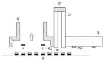
본 발명의 바람직한 제1실시 예에 따른 마이크로 LED 리페어 장치(10)는, 불량 마이크로 LED(ML1)와 본딩 패드(50) 사이의 접착력을 형성 또는 상실시키는 레이저부(20), 불량 마이크로 LED(ML1)를 본딩 패드(50)로부터 제거하는 석션부(30), 레이저부(20)에서 발진된 레이저의 조사통로(21), 석션부에서 발생된 에어가 유동하는 흐름통로(31) 및 조사통로(21)의 일단에 설치되는 흡착패드(40)를 포함하며 구성될 수 있다.The micro
도 3은 표시기판에 마이크로 LED가 실장된 모습을 나타낸 도이고, 도 4(a)는 본 발명의 일 실시 예에 따른 마이크로 LED 리페어 장치의 레이저부에서 레이저가 조사되는 모습을 나타낸 도이고, 도 4(b)는 본 발명의 일 실시 예에 따른 마이크로 LED 리페어 장치에 불량 마이크로 LED가 흡착되어 제거되는 모습을 나타낸 도이고, 도 5(a)는 본 발명의 일 실시 예에 따른 마이크로 LED 리페어 장치(10)에 양품 마이크로 LED가 흡착된 모습을 나타낸 도이고, 도 5(b)는 양품 마이크로 LED가 실장되는 모습을 나타낸 도이고, 도 6은 본 발병의 바람직한 실시 예에 따른 마이크로 LED 디스플레이 제조방법에 관한 도이다.3 is a diagram illustrating a state in which a micro LED is mounted on a display substrate, and FIG. 4(a) is a diagram illustrating a state in which a laser is irradiated from a laser unit of a micro LED repair device according to an embodiment of the present invention, and FIG. 4(b) is a diagram showing a state in which a defective micro LED is adsorbed and removed from a micro LED repair device according to an embodiment of the present invention, and FIG. 5(a) is a micro LED repair device according to an embodiment of the present invention (10) is a diagram showing a state in which a good micro LED is adsorbed, Fig. 5(b) is a diagram showing a state in which a good micro LED is mounted, and Fig. 6 is a method of manufacturing a micro LED display according to a preferred embodiment of the present disease It is also about.
본 발명의 바람직한 제1실시 예에 따른 마이크로 LED 리페어 장치(10)는 레이저부(20) 및 석션부(30)를 포함하며 구성될 수 있다. 레이저부(20)는 불량 마이크로 LED(ML1)와 본딩 패드(50) 사이의 접착력을 형성 또는 상실시키는 구성이다. 레이저부(20)는 본딩 패드(50)에 실장되어 있는 불량 마이크로 LED(ML1)에 레이저를 조사함으로써 불량 마이크로 LED(ML1)를 본딩 패드(50)로부터 분리 가능하게 할 수 있다. 또한, 불량 마이크로 LED(ML1)가 분리된 본딩 패드(50)에 레이저를 조사함으로써 양품 마이크로 LED(ML2)가 본딩 패드(50)에 부착 가능하게 할 수 있는 것이다.The micro
석션부(30)는 마이크로 LED 리페어 장치(10) 내에 공기 흐름을 형성함으로써 레이저가 조사된 불량 마이크로 LED(ML1)를 본딩 패드(50)로부터 제거하는 구성이다. 석션부(30)는 마이크로 LED 리페어 장치(10) 내에 공기 흐름을 만들어 흡입력을 발생시킬 수 있다. 마이크로 LED 리페어 장치(10)는 석션부(30)를 이용하여 불량 마이크로 LED(ML1)를 본딩 패드(50)로부터 제거할 수 있는 것이다.The
조사통로(21)는 레이저부(20)에서 발진된 레이저가 이동하는 경로를 말한다. 조사통로(21)는 일측에 레이저부(20)가 형성될 수 있고, 타측에는 흡착패드(40)가 형성될 수 있다.The
흐름통로(31)는 석션부(30)에 의해 형성된 에어가 유동하는 통로를 말한다. 흐름통로(31)는 일측에 석션부(30)가 형성될 수 있고, 타측에는 흡착패드(40)가 형성될 수 있다.The
조사통로(21)와 흐름통로(31)는 통로 일부를 공유하며 형성될 수 있다. 일례로, 도 4 내지 도 6에 도시된 바와 같이, 조사통로(21) 및 흐름통로(31)는 일측에는 각각 레이저부(20) 및 석션부(30)가 형성되되 타측은 하나의 흡착패드(40)가 형성될 수 있다. 즉, 조사통로(21) 및 흐름통로(31)의 시작점은 다르지만 각각의 통로가 합류하여 하나의 통로로 흡착패드(40)와 연결될 수 있는 것이다. 따라서, 마이크로 LED 리페어 장치(10)는 불량 마이크로 LED(ML1)에 레이저를 조사한 후 별도의 이동없이 석션부(30)를 작동시켜 불량 마이크로 LED(ML1)를 흡착패드(40)에 흡착시킬 수 있는 것이다.The
흡착패드(40)는 조사통로(21) 및 흐름통로(31)의 공통통로의 단부에 형성될 수 있다. 흡착패드(40)는 다공성 재질로 이루어질 수 있다.The
이하, 도 3 내지 도 6를 참고하여 본 발명의 바람직한 제1실시 예에 따른 마이크로 LED 디스플레이 제조방법에 대해 설명한다.Hereinafter, a method of manufacturing a micro LED display according to a first exemplary embodiment of the present invention will be described with reference to FIGS. 3 to 6.
마이크로 LED 디스플레이 제조방법은 도 6에 도시된 바와 같이, 불량 마이크로 LED(ML1)를 색출하는 검사단계(S1), 불량 마이크로 LED(ML1)에 레이저를 조사하는 제1조사단계(S2), 레이저가 조사된 불량 마이크로 LED(ML1)를 본딩 패드(50)로부터 제거하는 제거단계(S3), 불량 마이크로 LED(ML1)가 제거된 본딩 패드(50)에 레이저를 조사하는 제2조사단계(S4) 및 불량 마이크로 LED(ML1)가 제거된 위치에 양품 마이크로 LED(ML2)를 실장 시키는 실장단계(S5)를 포함하며 구성될 수 있다.As shown in FIG. 6, the method of manufacturing a micro LED display includes an inspection step (S1) of detecting a defective micro LED (ML1), a first irradiation step (S2) of irradiating a laser to the defective micro LED (ML1), and the laser is A removal step (S3) of removing the irradiated defective micro LED (ML1) from the bonding pad 50 (S3), a second irradiation step (S4) of irradiating a laser to the
검사단계(S1)는 임시기판 또는 표시기판에 실장 된 마이크로 LED(ML)의 불량을 색출하는 단계이다. 검사단계(S1)는 임시기판 또는 표시기판에 실장 된 마이크로 LED(ML)에 전기를 인가함으로써 불량 마이크로 LED(ML1)의 개수 및 위치 등을 파악할 수 있다.The inspection step (S1) is a step of detecting defects of the micro LED (ML) mounted on the temporary substrate or the display substrate. In the inspection step S1, electricity is applied to the micro LEDs ML mounted on the temporary substrate or the display substrate, so that the number and location of the defective micro LEDs ML1 can be identified.
불량 마이크로 LED(ML1)의 위치가 파악되면 레이저부(20)를 이용하여 레이저를 조사하는 제1조사단계(S2)가 실행될 수 있다.When the location of the defective micro LED ML1 is determined, a first irradiation step S2 of irradiating a laser using the
제1조사단계(S2)는 불량 마이크로 LED(ML1)에 레이저를 조사하는 단계이다. 제1조사단계(S2)는 마이크로 LED 리페어 장치(10)에 설치된 레이저부(20)를 이용하여 불량 마이크로 LED(ML1)에 레이저를 조사하게 된다.The first irradiation step (S2) is a step of irradiating a laser to the defective micro LED (ML1). In the first irradiation step (S2), a laser is irradiated to the defective micro LED (ML1) using the
구체적으로, 도 4(a)에 도시된 바와 같이, 마이크로 LED(ML)가 불량 마이크로 LED(ML1)라 판단되면, 마이크로 LED 리페어 장치(10)는 불량 마이크로 LED(ML1) 상부로 이동하게 된다. 불량 마이크로 LED(ML1) 상부로 이동된 마이크로 LED 리페어 장치(10)는 불량 마이크로 LED(ML1)의 상부에 안착할 수 있다. 마이크로 LED 리페어 장치(10)가 불량 마이크로 LED(ML1)의 상부에 안착하면, 흡착패드(40)와 불량 마이크로 LED(ML1)는 맞닿게 된다. 흡착패드(40)의 하면과 불량 마이크로 LED(ML1)의 상면이 맞닿게 되는 것이다.Specifically, as shown in FIG. 4(a), when it is determined that the micro LED ML is a defective micro LED ML1, the micro
물론 이와는 다르게 흡착패드(40)의 하면이 불량 마이크로 LED(ML1)의 상면과 이격된 상태로 마이크로 LED 리페어 장치(10)를 위치시켜도 무관하다.Of course, unlike this, it is also irrelevant to position the micro
흡착패드(40)와 맞닿은 마이크로 LED 리페어 장치(10)는 레이저부(20)를 이용하여 불량 마이크로 LED(ML1)에 레이저를 조사할 수 있다. 구체적으로, 레이저는 불량 마이크로 LED(ML1)와 본딩 패드(50)의 접착력이 상실될 수 있는 위치로 조사된다. 이때, 레이저부(20)에서 발진된 레이저는 마이크로 LED 리페어 장치(10)에 형성된 조사통로(21)를 통해 조사될 수 있다. 조사통로(21)는 레이저가 조사되는 경로가 되는 것이다.The micro
도면에서는 레이저부(20)가 흡착패드(40)의 수직선상에 위치하는 것으로 도시하였으나, 반사경을 이용할 경우에는 수직선상 이외의 위치에 레이저부(20)가 구비될 수 있다.In the drawings, the
레이저가 조사된 불량 마이크로 LED(ML1)는 본딩 패드(50)와의 접착력을 상실하게 된다. 불량 마이크로 LED(ML1)가 접착력을 상실하면 불량 마이크로 LED(ML1)를 본딩 패드(50)로부터 제거하는 제거단계가 실행될 수 있다. 이때, 마이크로 LED 리페어 장치(10)는 흡착패드(40)와 맞닿은 상태를 유지할 수 있다. 제1조사단계(S2)와 제거단계(S3)는 마이크로 LED 리페어 장치(10)가 흡착패드(40)와 맞닿은 상태로 실행될 수 있는 것이다.The defective micro LED (ML1) irradiated with the laser loses adhesive strength with the
구체적으로, 도 4(b)에 도시된 바와 같이, 불량 마이크로 LED(ML1)를 본딩 패드(50)로부터 제거하기 위하여, 마이크로 LED 리페어 장치(10)에 설치된 석션부(30)가 작동될 수 있다. 석션부(30)는 마이크로 LED 리페어 장치(10) 내에 공기 흐름을 발생시키는 역할을 한다. 석션부(30)가 작동되면 마이크로 LED 리페어 장치(10)의 내부에는 흡입력이 발생하고, 불량 마이크로 LED(ML1)는 흡입력에 의해 흡착패드(40)에 흡착됨으로써 본딩 패드(50)로부터 제거될 수 있는 것이다. 석션부(30)에 의해 발생되는 공기 흐름은 마이크로 LED 리페어 장치(10) 내에 형성된 흐름통로(31)를 따라 형성될 수 있다. 즉, 흐름통로(31)는 공기 흐름의 경로가 되는 것이다.Specifically, as shown in FIG. 4(b), in order to remove the defective micro LED ML1 from the
불량 마이크로 LED(ML1)가 흡입력 또는 진공력에 의해 흡착패드(40)에 흡착하게 되면 마이크로 LED 리페어 장치(10)는 불량 마이크로 LED(ML1)를 본딩 패드(50)로부터 제거할 수 있다. 이때, 마이크로 LED 리페어 장치(10)는 불량 마이크로 LED(ML1)를 개별로 제거할 수 있다.When the defective micro LED ML1 is adsorbed on the
마이크로 LED 리페어 장치(10)는 불량 마이크로 LED(ML1)를 제거한 후 준비된 양품 마이크로 LED(ML2)를 흡착하게 된다. 흡착된 양품 마이크로 LED(ML2)는 불량 마이크로 LED(ML1)가 제거된 본딩 패드(50)로 운송될 수 있다.The micro
이 경우, 양품 마이크로 LED(ML2)를 운송하는 리페어 장치는 불량 마이크로 LED(ML1)를 제거하기 위해 사용된 리페어 장치(10)일 수 있고, 이와는 다르게 별도의 리페어 장치(10)일 수 있다. 다만 이하에서는 하나의 리페어 장치(10)가 제거 및 교체를 수행하는 것으로 설명한다.In this case, the repair device for transporting the good micro LED ML2 may be the
양품 마이크로 LED(ML2)가 본딩 패드(50)로 운송되면, 양품 마이크로 LED(ML2)를 실장하기 위한 제2조사단계(S4) 및 실장단계(S5)가 실행될 수 있다.When the good micro LED (ML2) is transported to the
도 5(a)에 도시된 바와 같이, 양품 마이크로 LED(ML2)는 흡착패드(40)에 흡착하여 운송될 수 있다. 이때, 마이크로 LED 리페어 장치(10)는 석션부(30)가 작동함으로써 내부에 공기흐름, 즉, 흡입력이 발생될 수 있다.As shown in Figure 5 (a), the good micro LED (ML2) can be transported by adsorption on the
흡착패드(40)에 흡착된 양품 마이크로 LED(ML2)가 본딩 패드(50)로 운송되면, 본딩 패드(50)에 레이저를 조사하는 제2조사단계(S4)가 실행될 수 있다. 제2조사단계(S4)는 본딩 패드(50)에 레이저를 조사함으로써 본딩 패드(50) 상부에 접착력을 형성시키는 단계이다. 따라서, 제2레이저부(20)는 본딩 패드(50)에 접착력을 형성하기 위하여 레이저를 조사하게 된다.When the good micro LED (ML2) adsorbed on the
레이저가 조사되면, 양품 마이크로 LED(ML2)를 본딩 패드(50)에 실장하는 실장단계(S5)가 실행될 수 있다. 양품 마이크로 LED(ML2)는 마이크로 LED 리페어 장치(10)가 하강함으로써 레이저가 조사된 본딩 패드(50)에 안착함으로써 본딩 패드(50)에 실장될 수 있는 것이다.When the laser is irradiated, a mounting step (S5) of mounting the good micro LED (ML2) on the
본 발명의 바람직한 실시 예에 따른 마이크로 LED 리페어 장치(10)는 불량 마이크로 LED(ML1)를 색출한 후 마이크로 LED 리페어 장치(10)의 흡입력을 이용하여 불량 마이크로 LED(ML1)를 제거함으로써 주변에 실장된 마이크로 LED(ML)에 영향을 주지 않고 불량 마이크로 LED(ML1)만을 손쉽게 제거할 수 있다는 효과가 있다. 또한, 불량 마이크로 LED(ML1)를 양품 마이크로 LED(ML2)로 교체함으로써 임시기판 및 표시기판에 실장된 마이크로 LED(ML)의 불량률을 낮출 수 있는 효과가 있다.The micro
또한, 하나의 마이크로 LED 리페어 장치(10)를 이용하여 불량 마이크로 LED(ML1)를 제거함과 함께 양품 마이크로 LED(ML2)를 교체하도록 함으로써, 전체 장비의 구조를 단순화 할 수 있다.In addition, by using one micro
또한, 별도로 구비된 2개의 리페어 장치(10)를 이용하여 어느 하나의 리페어 장치(10)가 불량 마이크로 LED(ML1)를 제거하면, 다른 하나의 리페어 장치(10)로 신속하게 불량 위치에 양품 마이크로 LED(ML2)를 실장 함으로써 리페어 속도를 향상시킬 수 있다.In addition, when one
본 발명의 바람직한 제2실시 예에 따른 마이크로 LEDMicro LED according to a second preferred embodiment of the present invention리페어repair 장치(10') 및 마이크로 LED 디스플레이 제조방법 Device 10' and method for manufacturing micro LED display
이하, 도 7을 참고항여 본 발명의 바람직한 제2실시 예에 따른 마이크로 LED 리페어 장치(10') 및 마이크로 LED 디스플레이 제조방법에 대해 설명한다.Hereinafter, referring to FIG. 7, a method of manufacturing a micro
본 발명의 바람직한 제2실시 예에 따른 마이크로 LED 리페어 장치(10')는 본 발명의 바람직한 제1실시 예에 따른 마이크로 LED 리페어 장치(10')에 흡착패드(40)만 제거되어 구성된다. 따라서, 동일한 구성요소는 전술한 설명으로 대체될 수 있으며, 중복되는 설명은 생략한다.The micro LED repair device 10' according to the second preferred embodiment of the present invention is configured by removing only the
도 7(a)는 본 발명의 바람직한 제2실시예에 따른 마이크로 LED 리페어 장치의 레이저부에서 레이저가 조사되는 모습을 나타내는 도이고, 도 7(b)는 본 발명의 바람직한 제2실시 예에 따른 마이크로 LED 리페어 장치에 불량 마이크로 LED가 흡입되는 모습을 나타낸 도이다.7(a) is a diagram showing a state in which a laser is irradiated from a laser part of a micro LED repair device according to a second exemplary embodiment of the present invention, and FIG. 7(b) is a second exemplary embodiment of the present invention. It is a diagram showing a state in which a defective micro LED is sucked into a micro LED repair device.
도 7에 도시된 바와 같이, 본 발명의 바람직한 제2실시 예에 따른 마이크로 LED 리페어 장치(10')는 불량 마이크로 LED와 본딩 패드 사이의 접착력을 형성 또는 상실시키는 레이저부(20'), 불량 마이크로 LED를 본딩 패드(50)로부터 제거하는 석션부(30'), 레이저부에서 발진된 레이저의 조사통로(21') 및석션부(30')에서 발생된 에어가 유동하는 흐름통로(30')를 포함하며 구성될 수 있다.As shown in FIG. 7, the micro
조사통로(21')의 일측은 레이저부(20')가 형성되고, 조사통로(21')의 타측은 개구되어 형성될 수 있다. 또한, 흐름통로(30')의 일측은 석션부(30')가 형성될 수 있고, 타측은 개구되어 형성될 수 있다.One side of the
이하, 본 발명의 바람직한 제2실시 예에 따른 마이크로 LED 디스플레이 제조방법의 제거단계(S3)에 대해 설명한다.Hereinafter, a removal step (S3) of the method for manufacturing a micro LED display according to a second embodiment of the present invention will be described.
제거단계(S3)는 불량 마이크로 LED(ML1)에 레이저가 조사된 후 실행될 수 있다. 불량 마이크로 LED(ML1)에 레이저가 조사되면, 불량 마이크로 LED(ML1)를 제거하기 위하여 석션부(30')가 실행될 수 있다. 이때, 불량 마이크로 LED(ML1)는 일측이 개구된 흐름통로(30')로 흡입되어 제거될 수 있다.The removal step S3 may be performed after the laser is irradiated on the defective micro LED ML1. When the laser is irradiated to the defective micro LED ML1, the
구체적으로, 도 7에 도시된 바와 같이, 마이크로 LED 리페어 장치(10')는 흡착패드(40)가 설치되지 않고 흐름통로(30')의 일측이 개구되어 형성될 수 있다. 따라서, 석션부(30')가 작동되면 마이크로 LED 리페어 장치(10') 내부에는 흡입력이 발생되고, 접착력을 상실한 불량 마이크로 LED(ML1)는 흡입력에 의해 마이크로 LED 리페어 장치(10') 내부로 흡입되어 제거될 수 있는 것이다.Specifically, as shown in FIG. 7, the micro
이와 같이, 본 발명의 바람직한 제2실시 예에 따른 마이크로 LED 리페어 장치(10')는 불량 마이크로 LED(ML1)를 흡착패드(40) 등에 흡착시키지 않고 공기 흐름을 따라 마이크로 LED 리페어 장치(10') 내부로 흘러 들어가게 흡입하여 제거함으로써 보다 쉽게 불량 마이크로 LED(ML1)를 제거할 수 있다는 효과가 있다.As described above, the micro
본 발명의 바람직한 제3실시 예에 따른 마이크로 LEDMicro LED according to a third preferred embodiment of the present
이하, 도 8 내지 도 10을 참고하여 본 발명의 바람직한 제3실시 예에 따른 마이크로 LED 리페어 장치(10") 및 마이크로 LED 디스플레이 제조방법에 대해 설명한다.Hereinafter, a method of manufacturing a micro
본 발명의 바람직한 제3실시 에에 따른 마이크로 LED 리페어 장치(10")는 불량 마이크로 LED 제거부(60) 및 양품 마이크로 LED 교체부(70)의 형상만 다르게 형성될 뿐 나머지 구성요소는 본 발명의 바람직한 제1실시 예에 따른 마이크로 LED 리페어 장치(10")와 동일하게 형성될 수 있다. 따라서, 동일한 구성요소는 전술한 설명으로 대체될 수 있으며, 중복되는 설명은 생략한다.In the micro
도 8은 본 발명의 바람직한 제3실시 예에 따른 마이크로 LED 리페어 장치가 레이저를 조사하는 도이고, 도 9는 본 발명의 바람직한 제3실시 예에 따른 마이크로 LED 리페어 장치의 제거부가 불량 마이크로 LED를 흡입하는 모습을 나타낸 도이고, 도 10은 본 발명의 바람직한 제3실시 예에 따른 마이크로 LED 리페어 장치가 양품 마이크로 LED를 실장하는 모습을 나타낸 도이다.FIG. 8 is a diagram in which a micro LED repair device according to a third embodiment of the present invention irradiates a laser, and FIG. 9 is a diagram in which a removal unit of the micro LED repair device according to a third embodiment of the present invention sucks a defective micro LED. Fig. 10 is a diagram showing a state in which a micro LED repair device according to a third embodiment of the present invention mounts a good micro LED.
도 8 내지 도 10에 도시된 바와 같이, 본 발명의 바람직한 제3실시 예에 따른 마이크로 LED 리페어 장치(10")는 바디부(22), 바디부(22) 상부에 형성되고 불량 마이크로 LED(ML1)와 본딩 패드(50) 사이의 접착력을 형성 또는 상실시키는 레이저부(20"), 바디부(22) 측면에서 후드 형태로 형성되며 레이저부(20")에 의해 접착력을 상실한 불량 마이크로 LED(ML1)를 제거하는 불량 마이크로 LED 제거부(60) 및 복수개의 양품 마이크로 LED(ML2)가 흡착되어 있는 양품 마이크로 LED 교체부(70)를 포함하며 구성될 수 있다.8 to 10, the micro
도 8에 도시된 바와 같이, 불량 마이크로 LED 제거부(60)는 바디부(22)의 일측면에 형성될 수 있다. 양품 마이크로 LED 교체부(70)는 바디부(22)의 타측면에 형성될 수 있다. 즉, 바디부(22)의 일측면에는 불량 마이크로 LED 제거부(60)가 형성되고, 타측면에는 양품 마이크로 LED 교체부(70)가 형성될 수 있는 것이다.As shown in FIG. 8, the defective micro
불량 마이크로 LED 제거부(60)는 후드 형태로 형성될 수 있으며, 접착력을 상실한 복수의 불량 마이크로 LED(ML1)를 일괄로 제거하는 역할을 한다.The defective micro
양품 마이크로 LED 교체부(70)는 복수개의 양품 마이크로 LED(ML2)를 흡착하여 운송 및 실장하는 역할을 한다. 이때, 복수개의 양품 마이크로 LED(ML2)는 본딩 패드(50)에 동시에 실장될 수 있다.The good micro
여기서, 양품 마이크로 LED 제거부(70)가 양품 마이크로 LED(ML2)를 흡착하는 흡착력, 에어 흡입력, 반데르발스력, 자기력, 점착력 등 다양한 물리력을 포함한다.Here, the good micro
이하, 본 발명의 바람직한 제3실시 예에 따른 마이크로 LED 디스플레이 제조방법에 대해 설명한다.Hereinafter, a method of manufacturing a micro LED display according to a third exemplary embodiment of the present invention will be described.
제1조사단계(S2)는 불량 마이크로 LED(ML1)에 레이저를 조사하는 단계이다. 이때, 검사단계(S1)에서 파악된 모든 불량 마이크로 LED(ML1)에 순차적으로 레이저를 조사하게 된다.The first irradiation step (S2) is a step of irradiating a laser to the defective micro LED (ML1). At this time, the laser is sequentially irradiated to all the defective micro LEDs ML1 identified in the inspection step S1.
모든 불량 마이크로 LED(ML1)에 레이저가 조사되면 바디부(22) 일측면에 형성되어 있는 불량 마이크로 LED 제거부(60)를 통해 불량 마이크로 LED(ML1)를 흡입하게 된다. 이때, 불량 마이크로 LED 제거부(60)는 복수개의 불량 마이크로 LED(ML1)를 흡입하게 된다.When the laser is irradiated to all the defective micro LEDs ML1, the defective micro LED ML1 is sucked through the defective micro
구체적으로, 도 8에 도시된 바와 같이, 바디부(22) 상부에 형성된 레이저부(20")를 이용하여 임시기판 또는 표시기판에 실장된 마이크로 LED(ML) 중 불량 마이크로 LED(ML1)에 레이저를 조사하게 된다. 이때, 모든 불량 마이크로 LED(ML1)에 레이저를 조사함으로써 불량 마이크로 LED(ML1)와 본딩 패드(50) 사이의 접착력을 상실시켜준다.Specifically, as shown in FIG. 8, a laser unit is applied to a defective micro LED (ML1) among micro LEDs (ML) mounted on a temporary or display substrate by using a laser unit (20") formed on the
불량 마이크로 LED(ML1)에 레이저가 조사되면, 불량 마이크로 LED 제거부(60)를 이용하여 불량 마이크로 LED(ML1)를 제거하게 된다. 도 9에 도시된 바와 같이, 불량 마이크로 LED 제거부(60)는 후드의 형태로 형성됨으로써 넓은 범위로 분포되어 있는 불량 마이크로 LED(ML1)를 일괄적으로 흡입하여 제거할 수 있다. 즉, 불량 마이크로 LED(ML1)간의 피치 간격이 크더라도 후드의 형태로 형성된 불량 마이크로 LED 제거부(60)를 통해 일괄로 제거될 수 있는 것이다.When the laser is irradiated on the defective micro LED (ML1), the defective micro LED (ML1) is removed by using the defective micro
불량 마이크로 LED(ML1)가 제거되면 제2조사단계(S4)가 이루어진다. 제2조사단계(S4)는 레이저부(20")를 이용하여 불량 마이크로 LED(ML1)가 제거된 본딩 패드(50)에 레이저를 조사하는 단계이다. 불량 마이크로 LED(ML1)가 제거된 모든 본딩 패드(50)에 레이저를 순차적으로 조사하게 된다.When the defective micro LED (ML1) is removed, a second irradiation step (S4) is performed. The second irradiation step (S4) is a step of irradiating a laser to the
제2조사단계(S4)가 완료되면, 본딩 패드(50)에 양품 마이크로 LED(ML2)를 실장하는 실장단계(S5)가 실행될 수 있다.When the second irradiation step S4 is completed, a mounting step S5 of mounting the good micro LED ML2 on the
실장단계(S5)는 양품 마이크로 LED 교체부(70)에 흡착되어 있는 양품 마이크로 LED(ML2)를 본딩 패드에 실장하는 단계이다. 이때, 양품 마이크로 LED 교체부(70)는 불량 마이크로 LED(ML1)와 같은 피치 간격을 가진 양품 마이크로 LED(ML2)를 흡착하여 운송 및 실장할 수 있다.The mounting step (S5) is a step of mounting the good micro LED (ML2) adsorbed on the good micro
도 10에 도시된 바와 같이, 양품 마이크로 LED 교체부(70)는 양품 마이크로 LED(ML2)를 흡착하여 운송하게 된다. 이때, 양품 마이크로 LED 교체부(70)는 검사단계(S1)에서 파악된 불량 마이크로 LED(ML1)의 피치간격과 동일한 간격으로 복수개의 양품 마이크로 LED(ML2)를 흡착하게 된다. 따라서, 양품 마이크로 LED 교체부(70)는 불량 마이크로 LED(ML1)가 제거된 위치에 양품 마이크로 LED(ML2)를 일괄적으로 실장할 수 있다.As shown in Figure 10, the good micro
본 발명의 바람직한 제3실시 예에 따른 마이크로 LED 리페어 장치(10")는 복수개의 불량 마이크로 LED(ML1)를 일괄로 제거 후 복수개의 양품 마이크로 LED(ML2)를 일괄로 교체함으로써, 불량 마이크로 LED(ML1)를 양품 마이크로 LED(ML2)로 교체하는 작업 시간을 단축시킬 수 있는 효과가 있다.The micro
본 발명의 바람직한 제4실시 예에 따른 마이크로 LEDMicro LED according to a fourth preferred embodiment of the present invention리페어repair 장치(10"') 및 마이크로 LED 디스플레이 제조방법 Apparatus (10"') and method of manufacturing a micro LED display
이하, 도 11 내지 도 13를 참고하여 본 발명의 바람직한 제4실시 예에 따른 마이크로 LED 리페어 장치(10"') 및 마이크로 LED 디스플레이 제조방법에 대해 설명한다.Hereinafter, a micro
본 발명의 바람직한 제4실시 예에 따른 마이크로 LED 리페어 장치(10"')는 바디부(22'), 바디부(22') 중심에 형성되고 불량 마이크로 LED(ML1)와 본딩 패드(50) 사이의 접착력을 형성 또는 상실시키는 레이저부(20"'), 바디부(22') 외면에 형성되고 레이저부(20"')에 의해 접착력을 상실한 불량 마이크로 LED(ML1)를 제거하는 제거부(60') 및 바디부(22') 외면에 형성되고 양품 마이크로 LED(ML2)가 흡착되어 있는 교체부(70')를 포함하여 형성될 수 있다.The micro
도 11(a)는 본 발명의 바람직한 제4실시 예에 따른 마이크로 LED 리페어 장치가 레이저를 조사하는 모습을 나타낸 도이고, 도 11(b)는 본 발명의 바람직한 제4실시 예에 따른 마이크로 LED 리페어 장치의 제거부와 불량 마이크로 LED가 맞닿는 모습을 나타낸 도이고, 도 12(a)는 본 발명의 바람직한 제4실시 예에 따른 마이크로 LED 리페어 장치가 불량 마이크로 LED를 제거하는 모습을 나타낸 도이고, 도 12(b)는 본 발명의 바람직한 제4실시 예에 따른 마이크로 LED 리페어 장치가 레이저를 조사하는 모습을 나타낸 도이고, 도 13(a)는 본 발명의 바람직한 제4실시 예에 따른 마이크로 LED 리페어 장치의 교체부에 흡착된 양품 마이크로 LED를 실장하는 모습을 나타낸 도 이고, 도 13(b)는 본 발명의 바람직한 제4실시 예에 따른 마이크로 LED 리페어 장치가 불량 마이크로 LED를 양품 마이크로 LED로 교체완료한 모습을 나타낸 도이다.11(a) is a diagram showing a state in which a micro LED repair device according to a fourth exemplary embodiment of the present invention irradiates a laser, and FIG. 11(b) is a micro LED repair according to a fourth exemplary embodiment of the present invention. Fig. 12(a) is a diagram showing a state in which the removal unit of the device and the defective micro LED contact each other, and FIG. 12(a) is a diagram showing a state in which the micro LED repair device according to a fourth embodiment of the present invention removes the defective micro LED, and FIG. 12(b) is a diagram showing a state in which a micro LED repair device according to a fourth embodiment of the present invention irradiates a laser, and FIG. 13(a) is a micro LED repair device according to a fourth embodiment of the present invention Fig. 13(b) is a diagram showing a state of mounting a good micro LED adsorbed to the replacement part of the present invention. It is a diagram showing the appearance.
도 11에 도시된 바와 같이, 바디부(22')는 원형의 형상으로 형성될 수 있고, 바디부(22')는 투명한 재질로 이루어질 수 있으나 이러한 형상 및 재질로 한정짓는 것은 아니다. 바디부(22')는 구형태, 원기둥 형태, 원형 띠 형태, 다각형의 형태 등 다양한 형태로 구성될 수 있다.As shown in FIG. 11, the
바디부(22')는 회전할 수 있으며 바디부(22')가 회전함에 따라 레이저부(20"'), 제거부(60') 및 교체부(70) 순으로 기판과 대응될 수 있다.The
레이저부(20"')는 바디부(22')의 중심에 형성될 수 있으며 불량 마이크로 LED(ML1)의 접착력을 형성 또는 상실시키는 역할을 한다. 레이저부(20"')는 레이저를 투명한 재질의 바디부(22')를 통해 불량 마이크로 LED(ML1)에 조사할 수 있다.The
제거부(60') 및 교체부(70')는 바디부(22') 외면에 형성될 수 있으며, 제거부(60') 및 교체부(70')는 바디부(22')의 외면에서 원주방향을 따라 교대로 형성될 수 있다.The
제거부(60')는 불량 마이크로 LED(ML1)를 제거하는 역할을 하며, 제거부(60')에 에어 흡입력, 자기력, 점착력, 반데르발스력 등을 발생시켜 불량 마이크로 LED(ML1)를 흡착시킬 수 있다.The removal unit 60' serves to remove the defective micro LED (ML1), and generates air suction force, magnetic force, adhesion, van der Waals force, etc. to the removal unit 60' to adsorb the defective micro LED (ML1). I can make it.
교체부(70')는 양품 마이크로 LED(ML2)를 흡착하여 운송 및 실장 시키는 역할을 한다. 교체부(70')는 에어 흡입력, 자기력, 점착력, 반데르발스력 등을 이용하여 양품 마이크로 LED(ML2)를 교체부(70')에 흡착시켜 운송 시킬 수 있다.The replacement part 70' serves to transport and mount by adsorbing the good micro LED (ML2). The
이하, 본 발명의 바람직한 제4실시 예에 따른 마이크로 LED 디스플레이 제조방법에 대해 설명한다.Hereinafter, a method of manufacturing a micro LED display according to a fourth embodiment of the present invention will be described.
전술한 실시 예에서의 구성과 동일한 구성요소는 전술한 설명으로 대체될 수 있으며, 중복되는 설명은 생략한다.Components that are the same as those in the above-described embodiment may be replaced with the above description, and redundant descriptions will be omitted.
제1조사단계(S2)는 불량 마이크로 LED(ML1)에 레이저를 조사하는 단계이다. 도 11(a)에 도시된 바와 같이, 레이저부(20"')가 레이저를 조사할 때 레이저는 제거부(60')와 교체부(70') 사이로 조사될 수 있다. 레이저부(20"')는 본딩 패드(50)와 대응되는 위치에 위치하여 레이저를 조사하게 되는 것이다.The first irradiation step (S2) is a step of irradiating a laser to the defective micro LED (ML1). As shown in Fig. 11(a), when the
레이저가 조사되면 도 11(b)에 도시된 바와 같이, 바디부(22')는 제거부(60')와 불량 마이크로 LED(ML1)가 대응되는 위치까지 회전하게 되고, 불량 마이크로 LED(ML1)를 제거하는 제거단계(S3)가 실행될 수 있다.When the laser is irradiated, as shown in FIG. 11(b), the
바디부(22')가 제거부(60')와 불량 마이크로 LED(ML1)가 대응되는 위치까지 회전하면 마이크로 LED 리페어 장치(10"')는 하강하게 되고, 제거부(60')와 불량 마이크로 LED(ML1)가 맞닿게 된다. 제거부(60')와 불량 마이크로 LED(ML1)가 맞닿으면 제거부(60')에 불량 마이크로 LED(ML1)를 흡착하는 힘이 발생하고, 불량 마이크로 LED(ML1)가 제거부(60')에 흡착하게 된다.When the
도 12(a)에 도시된 바와 같이, 불량 마이크로 LED(ML1)가 교체부(70')에 흡착하게 되면 마이크로 LED 리페어 장치(10"')가 상승하면서 불량 마이크로 LED(ML1)를 본딩 패드(50)로부터 제거하게 된다.As shown in Fig. 12(a), when the defective micro LED ML1 is adsorbed on the replacement part 70', the micro
불량 마이크로 LED(ML1)가 제거되면, 도 12(b)에 도시된 바와 같이, 바디부(22')는 레이저부(20"')와 본딩 패드(50)가 대응되는 위치까지 회전하게 되고, 본딩 패드(50)에 레이저를 조사하는 제2조사단계(S4)가 실행된다. 제2조사단계(S4)는 불량 마이크로 LED(ML1)가 제거된 본딩 패드(50)에 레이저를 조사함으로써 양품 마이크로 LED(ML2)가 실장될 수 있도록 접착력을 형성시키는 단계이다.When the defective micro LED ML1 is removed, as shown in FIG. 12(b), the body part 22' rotates to a position where the
레이저 조사가 완료되면 바디부(22')는 양품 마이크로 LED(ML2)가 흡착되어 있는 교체부(70')와 본딩 패드(50)가 대응되는 위치까지 회전하게 된다. When laser irradiation is completed, the
도 13(a)에 도시된 바와 같이, 양품 마이크로 LED(ML2)와 본딩 패드(50)가 대응되면, 마이크로 LED 리페어 장치(10"')는 하강하게 되고, 양품 마이크로 LED(ML2)와 본딩 패드(50)가 맞닿게 된다. 이때, 본딩 패드(50)에 형성된 접착력에 의해 양품 마이크로 LED(ML2)는 본딩 패드(50)에 안착함으로써 양품 마이크로 LED(ML2)가 본딩 패드(50)에 실장되는 것이다.As shown in Fig. 13(a), when the good micro LED ML2 and the
양품 마이크로 LED(ML2)가 본딩 패드(50)에 실장되면 마이크로 LED 리페어 장치(10"')는 상승하게 되고 불량 마이크로 LED(ML1)를 양품 마이크로 LED(ML2)로 교체하는 작업이 완료된다.When the good micro LED (ML2) is mounted on the
본 발명의 바람직한 제4실시 예에 따른 마이크로 LED 리페어 장치(10"')는 짧은 동선으로 불량 마이크로 LED(ML1)를 양품 마이크로 LED(ML2)로 교체 가능하다.In the micro
불량 마이크로 LED(ML1)를 양품 마이크로 LED(ML2)로 교체하기 위해서는 불량 마이크로 LED(ML1)를 본딩 패드(50)로부터 제거한 후 임시기판 및 표시기판의 영역 밖으로 이동하여 양품 마이크로 LED(ML2)를 운송해오는 동선을 필요로 한다.In order to replace the defective micro LED (ML1) with a good micro LED (ML2), remove the defective micro LED (ML1) from the
하지만 본 발명의 바람직한 제4실시 예에 따른 마이크로 LED 리페어 장치(10"')는 불량 마이크로 LED(ML1)가 실장된 위치에서 회전 및 상하의 움직임 만으로 불량 마이크로 LED(ML1)를 양품 마이크로 LED(ML2)로 교체 가능하다.However, in the micro
구체적으로, 바디부(22')의 원주 방향을 따라 교대로 제거부(60') 및 교체부(70')가 형성되고, 교체부(70')에 새로 실장 될 양품 마이크로 LED(ML2)를 사전에 흡착하여 불량 마이크로 LED(ML1)가 실장된 위치로 이동하게 된다. 바디부(22')는 불량 마이크로 LED(ML1)가 실장된 위치에서 회전하면서 레이저조사, 불량 마이크로 LED(ML1) 제거 및 양품 마이크로 LED(ML2)를 실장함으로써 마이크로 LED 리페어 장치(10"')의 좌우 동선을 최소화할 수 있는 것이다.Specifically, the removal part 60' and the replacement part 70' are alternately formed along the circumferential direction of the body part 22', and a good-quality micro LED ML2 to be newly mounted on the replacement part 70' It is adsorbed in advance and moves to the position where the defective micro LED (ML1) is mounted. The body part 22' rotates at the position where the defective micro LED (ML1) is mounted, while laser irradiation, removing the defective micro LED (ML1), and mounting the good micro LED (ML2), It is possible to minimize the left and right movement lines.
따라서, 마이크로 LED 리페어 장치(10"')는 좌우 동선을 최소화하여 짧은 동선으로 불량 마이크로 LED(ML1)를 양품 마이크로 LED(ML2)로 교체 가능한 것이다.Accordingly, the micro
전술한 바와 같이, 본 발명의 바람직한 실시 예를 참조하여 설명하였지만, 해당 기술분야의 통상의 기술자는 하기의 특허 청구범위에 기재된 본 발명의 사상 및 영역으로부터 벗어나지 않는 범위 내에서 본 발명을 다양하게 수정 또는 변형하여 실시할 수 있다.As described above, although it has been described with reference to a preferred embodiment of the present invention, those skilled in the art will variously modify the present invention within the scope not departing from the spirit and scope of the present invention described in the following claims. Or it can be implemented by modification.
ML: 마이크로 LED ML1: 불량 마이크로 LED
ML2: 양품 마이크로 LED
10, 10', 10", 10"': 마이크로 LED 리페어 장치
20, 20', 20", 20"': 레이저부21, 21': 조사통로
22, 22': 바디부30, 30': 석션부
31, 31': 흐름통로40: 흡착패드
50: 본딩 패드60, 60': 제거부
70, 70': 교체부
S1: 검사단계S2: 제1조사단계
S3: 제거단계S4: 제2조사단계
S5: 실장단계ML: Micro LED ML1: Bad Micro LED
ML2: Good Micro LED
10, 10', 10", 10"': Micro LED repair device
20, 20', 20", 20"':
22, 22':
31, 31': flow passage 40: adsorption pad
50:
70, 70': replacement
S1: Inspection step S2: First investigation step
S3: Removal step S4: Second investigation step
S5: Mounting stage
Claims (12)
Translated fromKorean상기 불량 마이크로 LED에 레이저를 조사하는 제1조사단계;
레이저가 조사된 상기 불량 마이크로 LED를 본딩 패드로부터 제거하는 제거단계;
상기 불량 마이크로 LED가 제거된 상기 본딩 패드에 레이저를 조사하는 제2조사단계; 및
상기 불량 마이크로 LED가 제거된 위치에 양품 마이크로 LED를 실장 시키는 실장단계;를 포함하는 것을 특징으로 하는 마이크로 LED 디스플레이 제조방법.
An inspection step of finding a defective micro LED;
A first irradiation step of irradiating a laser to the defective micro LED;
A removing step of removing the defective micro LED irradiated with a laser from the bonding pad;
A second irradiation step of irradiating a laser onto the bonding pad from which the defective micro LED has been removed; And
A method of manufacturing a micro LED display comprising a; mounting step of mounting a good micro LED at a location from which the defective micro LED has been removed.
상기 제거단계는,
상기 불량 마이크로 LED를 개별로 제거하는 것을 특징으로 하는 마이크로 LED 디스플레이 제조방법.
The method of claim 1,
The removing step,
Micro LED display manufacturing method, characterized in that to individually remove the defective micro LED.
상기 제거단계는,
상기 불량 마이크로 LED를 일괄로 제거하는 것을 특징으로 하는 마이크로 LED 디스플레이 제조방법.
The method of claim 1,
The removing step,
Micro LED display manufacturing method, characterized in that removing the defective micro LED in a batch.
상기 제거단계는,
상기 불량 마이크로 LED를 흡입하여 제거하는 것을 특징으로 하는 마이크로 LED 디스플레이 제조방법.
The method of claim 1,
The removing step,
Micro LED display manufacturing method, characterized in that removing by sucking the defective micro LED.
상기 제거단계는,
상기 불량 마이크로 LED를 흡착하여 제거하는 것을 특징으로 하는 마이크로 LED 디스플레이 제조방법.
The method of claim 1,
The removing step,
Micro LED display manufacturing method, characterized in that the adsorption and removal of the defective micro LED.
상기 불량 마이크로 LED를 본딩 패드로부터 제거하는 석션부;
상기 레이저부에서 발진된 레이저의 조사통로; 및
상기 석션부에서 발생된 에어가 유동하는 흐름통로;를 포함하는 마이크로 LED 리페어 장치.
A laser unit for forming or losing adhesion between the defective micro LED and the bonding pad;
A suction unit for removing the defective micro LED from the bonding pad;
An irradiation path of the laser oscillated by the laser unit; And
Micro LED repair device comprising a; flow path through which the air generated from the suction unit flows.
상기 조사통로의 일단에 설치되는 흡착패드를 포함하는 마이크로 LED 리페어 장치.
The method of claim 6,
Micro LED repair device comprising an adsorption pad installed at one end of the irradiation passage.
상기 흡착패드는 다공성 재질로 이루어지는 것을 특징으로 하는 마이크로 LED 리페어 장치.
The method of claim 7,
Micro LED repair device, characterized in that the adsorption pad is made of a porous material.
상기 흐름통로 및 상기 조사통로는 통로의 일부분을 공유하는 것을 특징으로 하는 마이크로 LED 리페어 장치.
The method of claim 6,
Micro LED repair device, characterized in that the flow passage and the irradiation passage share a portion of the passage.
상기 바디부 상부에 형성되고 불량 마이크로 LED와 본딩 패드 사이의 접착력을 형성 또는 상실시키는 레이저부;
상기 바디부 측면에서 후드 형태로 형성되며 상기 레이저부에 의해 접착력을 상실한 상기 불량 마이크로 LED를 제거하는 불량 마이크로 LED 제거부; 및
복수개의 양품 마이크로 LED가 흡착되어 있는 양품 마이크로 LED 교체부;를 포함하고
상기 불량 마이크로 LED 제거부는 일괄로 상기 불량 마이크로 LED를 제거하는 것을 특징으로 하는 마이크로 LED 리페어 장치.
Body part;
A laser unit formed on the body portion and forming or losing adhesive force between the defective micro LED and the bonding pad;
A defective micro LED removal unit formed in the shape of a hood on the side of the body and removing the defective micro LED having lost adhesion by the laser unit; And
Including; a good-quality micro LED replacement unit in which a plurality of good-quality micro LEDs are adsorbed
The micro LED repair device, characterized in that the defective micro LED removing unit removes the defective micro LED at a time.
상기 바디부 중심에 형성되고 불량 마이크로 LED와 본딩 패드 사이의 접착력을 형성 또는 상실시키는 레이저부;
상기 바디부 외면에 형성되고 상기 레이저부에 의해 접착력을 상실한 상기 불량 마이크로 LED를 제거하는 제거부; 및
상기 바디부 외면에 형성되고 양품 마이크로 LED가 흡착되어 있는 교체부;를 포함하고
상기 제거부 및 상기 교체부는 상기 바디부의 원주방향을 따라 교대로 형성되는 것을 특징으로 하는 마이크로 LED 리페어 장치.
Body part;
A laser unit formed at the center of the body unit and forming or losing adhesive force between the defective micro LED and the bonding pad;
A removal unit formed on an outer surface of the body unit and removing the defective micro LED having lost adhesion by the laser unit; And
Including; a replacement portion formed on the outer surface of the body portion and adsorbed good micro LED
The removal unit and the replacement unit micro LED repair device, characterized in that formed alternately along the circumferential direction of the body portion.
상기 바디부는 투명재질로 이루어지는 것을 특징으로 하는 마이크로 LED 리페어 장치.
The method of claim 11,
Micro LED repair device, characterized in that the body is made of a transparent material.
Priority Applications (1)
| Application Number | Priority Date | Filing Date | Title |
|---|---|---|---|
| KR1020190104904AKR20210025216A (en) | 2019-08-27 | 2019-08-27 | Micro led repair device and manufacturing of micor led display using the same |
Applications Claiming Priority (1)
| Application Number | Priority Date | Filing Date | Title |
|---|---|---|---|
| KR1020190104904AKR20210025216A (en) | 2019-08-27 | 2019-08-27 | Micro led repair device and manufacturing of micor led display using the same |
Publications (1)
| Publication Number | Publication Date |
|---|---|
| KR20210025216Atrue KR20210025216A (en) | 2021-03-09 |
Family
ID=75179759
Family Applications (1)
| Application Number | Title | Priority Date | Filing Date |
|---|---|---|---|
| KR1020190104904AWithdrawnKR20210025216A (en) | 2019-08-27 | 2019-08-27 | Micro led repair device and manufacturing of micor led display using the same |
Country Status (1)
| Country | Link |
|---|---|
| KR (1) | KR20210025216A (en) |
Cited By (5)
| Publication number | Priority date | Publication date | Assignee | Title |
|---|---|---|---|---|
| KR20220129829A (en)* | 2021-03-17 | 2022-09-26 | 레이저쎌 주식회사 | Defective pixel inspection method of mini LED array for backlight unit |
| CN115156654A (en)* | 2021-11-15 | 2022-10-11 | 武汉帝尔激光科技股份有限公司 | Method and device for repairing MINI LED chip |
| KR20230037372A (en)* | 2021-09-09 | 2023-03-16 | 주식회사 이안하이텍 | Apparatus and method for repairing bad micro light-emitting diode of display panel |
| KR20240003120A (en)* | 2022-06-30 | 2024-01-08 | 주식회사 에스에프에이 | Chip removal device and method the same |
| US12396307B2 (en) | 2021-04-30 | 2025-08-19 | Samsung Display Co., Ltd. | Display device |
Citations (8)
| Publication number | Priority date | Publication date | Assignee | Title |
|---|---|---|---|---|
| KR100731673B1 (en) | 1999-12-03 | 2007-06-25 | 크리, 인코포레이티드 | Micro-light-emitting diode array with improved light extraction |
| KR20140112486A (en) | 2011-11-18 | 2014-09-23 | 럭스뷰 테크놀로지 코포레이션 | Method of forming a micro led structure and array of micro led structures with an electrically insulating layer |
| KR20170019415A (en) | 2014-06-18 | 2017-02-21 | 엑스-셀레프린트 리미티드 | Systems and methods for controlling release of transferable semiconductor structures |
| KR20170024906A (en) | 2015-08-26 | 2017-03-08 | 엘지전자 주식회사 | Transfer unit for micro device |
| KR20170026959A (en) | 2015-08-31 | 2017-03-09 | 삼성디스플레이 주식회사 | Diplay apparatus and manufacturing method for the same |
| KR101754528B1 (en) | 2016-03-23 | 2017-07-06 | 한국광기술원 | Transfer assembly with dry adhesion structure and method for transferring led structure assembly using the same and led structure assembly |
| KR101757404B1 (en) | 2015-07-24 | 2017-07-12 | 한국기계연구원 | Selective continuous transferring apparatus based on adhesion-controlled film |
| KR20180087896A (en) | 2017-01-25 | 2018-08-03 | 한국기계연구원 | Apparatus and method for repairing bad elements |
- 2019
- 2019-08-27KRKR1020190104904Apatent/KR20210025216A/ennot_activeWithdrawn
Patent Citations (8)
| Publication number | Priority date | Publication date | Assignee | Title |
|---|---|---|---|---|
| KR100731673B1 (en) | 1999-12-03 | 2007-06-25 | 크리, 인코포레이티드 | Micro-light-emitting diode array with improved light extraction |
| KR20140112486A (en) | 2011-11-18 | 2014-09-23 | 럭스뷰 테크놀로지 코포레이션 | Method of forming a micro led structure and array of micro led structures with an electrically insulating layer |
| KR20170019415A (en) | 2014-06-18 | 2017-02-21 | 엑스-셀레프린트 리미티드 | Systems and methods for controlling release of transferable semiconductor structures |
| KR101757404B1 (en) | 2015-07-24 | 2017-07-12 | 한국기계연구원 | Selective continuous transferring apparatus based on adhesion-controlled film |
| KR20170024906A (en) | 2015-08-26 | 2017-03-08 | 엘지전자 주식회사 | Transfer unit for micro device |
| KR20170026959A (en) | 2015-08-31 | 2017-03-09 | 삼성디스플레이 주식회사 | Diplay apparatus and manufacturing method for the same |
| KR101754528B1 (en) | 2016-03-23 | 2017-07-06 | 한국광기술원 | Transfer assembly with dry adhesion structure and method for transferring led structure assembly using the same and led structure assembly |
| KR20180087896A (en) | 2017-01-25 | 2018-08-03 | 한국기계연구원 | Apparatus and method for repairing bad elements |
Cited By (5)
| Publication number | Priority date | Publication date | Assignee | Title |
|---|---|---|---|---|
| KR20220129829A (en)* | 2021-03-17 | 2022-09-26 | 레이저쎌 주식회사 | Defective pixel inspection method of mini LED array for backlight unit |
| US12396307B2 (en) | 2021-04-30 | 2025-08-19 | Samsung Display Co., Ltd. | Display device |
| KR20230037372A (en)* | 2021-09-09 | 2023-03-16 | 주식회사 이안하이텍 | Apparatus and method for repairing bad micro light-emitting diode of display panel |
| CN115156654A (en)* | 2021-11-15 | 2022-10-11 | 武汉帝尔激光科技股份有限公司 | Method and device for repairing MINI LED chip |
| KR20240003120A (en)* | 2022-06-30 | 2024-01-08 | 주식회사 에스에프에이 | Chip removal device and method the same |
Similar Documents
| Publication | Publication Date | Title |
|---|---|---|
| KR102464618B1 (en) | Trnasfer head for micro led | |
| KR20210025216A (en) | Micro led repair device and manufacturing of micor led display using the same | |
| KR20190114372A (en) | Transfer system for micro led | |
| KR102517784B1 (en) | Micro led adsorption body | |
| CN110323172A (en) | Micro- light emitting diode transfer printing head | |
| KR102457191B1 (en) | Micro led transfer system | |
| CN110335831A (en) | Inspection method of micro light emitting diode | |
| CN110875350A (en) | Transfer head | |
| KR20190131311A (en) | Micro led adsorption body | |
| KR20200095909A (en) | Transfer head for micro led | |
| KR20210040684A (en) | Micro led display manufacturing device and method of manufacturing micro led display | |
| KR102527138B1 (en) | Micro led transfer system | |
| CN110349899A (en) | Micro- light emitting diode adsorbent | |
| KR20220021173A (en) | Micro device transfer apparatus and micro device transfer system comprising the same and manufacturing method for micro device mounted on electronic products | |
| KR102481434B1 (en) | Transfer head and adsorbing method for micro led using the same | |
| KR102498112B1 (en) | Micro led transfer head | |
| KR20200020208A (en) | Micro led transfer system | |
| KR20200001323A (en) | Transfer head for micro led | |
| KR102643764B1 (en) | Transfer head for micro led | |
| KR102498109B1 (en) | Micro led transfer system | |
| KR20210025217A (en) | Micro led transfer head and manufacturing method of micro led display using the same | |
| KR102471585B1 (en) | Micro led adsorption body and micro led inspection system using the same | |
| KR102471583B1 (en) | Micro led transfer system including micro led adsorption body | |
| KR20190135858A (en) | Transfer head for micro led and micro led transfer system using the same | |
| KR20190117180A (en) | Micro led adsorption body and micro led inspection system using the same |
Legal Events
| Date | Code | Title | Description |
|---|---|---|---|
| PA0109 | Patent application | Patent event code:PA01091R01D Comment text:Patent Application Patent event date:20190827 | |
| PG1501 | Laying open of application | ||
| PC1203 | Withdrawal of no request for examination |