KR20210022206A - Organic light emitting diode display device and manufacturing method thereof - Google Patents
Organic light emitting diode display device and manufacturing method thereofDownload PDFInfo
- Publication number
- KR20210022206A KR20210022206AKR1020190101063AKR20190101063AKR20210022206AKR 20210022206 AKR20210022206 AKR 20210022206AKR 1020190101063 AKR1020190101063 AKR 1020190101063AKR 20190101063 AKR20190101063 AKR 20190101063AKR 20210022206 AKR20210022206 AKR 20210022206A
- Authority
- KR
- South Korea
- Prior art keywords
- layer
- pixel electrode
- partition wall
- etching
- electrode
- Prior art date
- Legal status (The legal status is an assumption and is not a legal conclusion. Google has not performed a legal analysis and makes no representation as to the accuracy of the status listed.)
- Pending
Links
Images


Classifications
- H—ELECTRICITY
- H10—SEMICONDUCTOR DEVICES; ELECTRIC SOLID-STATE DEVICES NOT OTHERWISE PROVIDED FOR
- H10K—ORGANIC ELECTRIC SOLID-STATE DEVICES
- H10K59/00—Integrated devices, or assemblies of multiple devices, comprising at least one organic light-emitting element covered by group H10K50/00
- H10K59/80—Constructional details
- H10K59/87—Passivation; Containers; Encapsulations
- H01L51/5237—
- H—ELECTRICITY
- H10—SEMICONDUCTOR DEVICES; ELECTRIC SOLID-STATE DEVICES NOT OTHERWISE PROVIDED FOR
- H10K—ORGANIC ELECTRIC SOLID-STATE DEVICES
- H10K59/00—Integrated devices, or assemblies of multiple devices, comprising at least one organic light-emitting element covered by group H10K50/00
- H10K59/10—OLED displays
- H10K59/12—Active-matrix OLED [AMOLED] displays
- H10K59/122—Pixel-defining structures or layers, e.g. banks
- H01L27/3244—
- H01L51/0017—
- H01L51/56—
- H—ELECTRICITY
- H10—SEMICONDUCTOR DEVICES; ELECTRIC SOLID-STATE DEVICES NOT OTHERWISE PROVIDED FOR
- H10K—ORGANIC ELECTRIC SOLID-STATE DEVICES
- H10K50/00—Organic light-emitting devices
- H10K50/80—Constructional details
- H10K50/805—Electrodes
- H10K50/81—Anodes
- H—ELECTRICITY
- H10—SEMICONDUCTOR DEVICES; ELECTRIC SOLID-STATE DEVICES NOT OTHERWISE PROVIDED FOR
- H10K—ORGANIC ELECTRIC SOLID-STATE DEVICES
- H10K50/00—Organic light-emitting devices
- H10K50/80—Constructional details
- H10K50/805—Electrodes
- H10K50/82—Cathodes
- H—ELECTRICITY
- H10—SEMICONDUCTOR DEVICES; ELECTRIC SOLID-STATE DEVICES NOT OTHERWISE PROVIDED FOR
- H10K—ORGANIC ELECTRIC SOLID-STATE DEVICES
- H10K59/00—Integrated devices, or assemblies of multiple devices, comprising at least one organic light-emitting element covered by group H10K50/00
- H10K59/10—OLED displays
- H10K59/12—Active-matrix OLED [AMOLED] displays
- H10K59/121—Active-matrix OLED [AMOLED] displays characterised by the geometry or disposition of pixel elements
- H10K59/1213—Active-matrix OLED [AMOLED] displays characterised by the geometry or disposition of pixel elements the pixel elements being TFTs
- H—ELECTRICITY
- H10—SEMICONDUCTOR DEVICES; ELECTRIC SOLID-STATE DEVICES NOT OTHERWISE PROVIDED FOR
- H10K—ORGANIC ELECTRIC SOLID-STATE DEVICES
- H10K59/00—Integrated devices, or assemblies of multiple devices, comprising at least one organic light-emitting element covered by group H10K50/00
- H10K59/10—OLED displays
- H10K59/12—Active-matrix OLED [AMOLED] displays
- H10K59/123—Connection of the pixel electrodes to the thin film transistors [TFT]
- H—ELECTRICITY
- H10—SEMICONDUCTOR DEVICES; ELECTRIC SOLID-STATE DEVICES NOT OTHERWISE PROVIDED FOR
- H10K—ORGANIC ELECTRIC SOLID-STATE DEVICES
- H10K59/00—Integrated devices, or assemblies of multiple devices, comprising at least one organic light-emitting element covered by group H10K50/00
- H10K59/10—OLED displays
- H10K59/12—Active-matrix OLED [AMOLED] displays
- H10K59/126—Shielding, e.g. light-blocking means over the TFTs
- H—ELECTRICITY
- H10—SEMICONDUCTOR DEVICES; ELECTRIC SOLID-STATE DEVICES NOT OTHERWISE PROVIDED FOR
- H10K—ORGANIC ELECTRIC SOLID-STATE DEVICES
- H10K59/00—Integrated devices, or assemblies of multiple devices, comprising at least one organic light-emitting element covered by group H10K50/00
- H10K59/10—OLED displays
- H10K59/12—Active-matrix OLED [AMOLED] displays
- H10K59/131—Interconnections, e.g. wiring lines or terminals
- H—ELECTRICITY
- H10—SEMICONDUCTOR DEVICES; ELECTRIC SOLID-STATE DEVICES NOT OTHERWISE PROVIDED FOR
- H10K—ORGANIC ELECTRIC SOLID-STATE DEVICES
- H10K59/00—Integrated devices, or assemblies of multiple devices, comprising at least one organic light-emitting element covered by group H10K50/00
- H10K59/80—Constructional details
- H10K59/805—Electrodes
- H10K59/8051—Anodes
- H10K59/80518—Reflective anodes, e.g. ITO combined with thick metallic layers
- H—ELECTRICITY
- H10—SEMICONDUCTOR DEVICES; ELECTRIC SOLID-STATE DEVICES NOT OTHERWISE PROVIDED FOR
- H10K—ORGANIC ELECTRIC SOLID-STATE DEVICES
- H10K71/00—Manufacture or treatment specially adapted for the organic devices covered by this subclass
- H—ELECTRICITY
- H10—SEMICONDUCTOR DEVICES; ELECTRIC SOLID-STATE DEVICES NOT OTHERWISE PROVIDED FOR
- H10K—ORGANIC ELECTRIC SOLID-STATE DEVICES
- H10K71/00—Manufacture or treatment specially adapted for the organic devices covered by this subclass
- H10K71/20—Changing the shape of the active layer in the devices, e.g. patterning
- H10K71/231—Changing the shape of the active layer in the devices, e.g. patterning by etching of existing layers
- H01L2251/301—
- H—ELECTRICITY
- H10—SEMICONDUCTOR DEVICES; ELECTRIC SOLID-STATE DEVICES NOT OTHERWISE PROVIDED FOR
- H10K—ORGANIC ELECTRIC SOLID-STATE DEVICES
- H10K2102/00—Constructional details relating to the organic devices covered by this subclass
- H—ELECTRICITY
- H10—SEMICONDUCTOR DEVICES; ELECTRIC SOLID-STATE DEVICES NOT OTHERWISE PROVIDED FOR
- H10K—ORGANIC ELECTRIC SOLID-STATE DEVICES
- H10K2102/00—Constructional details relating to the organic devices covered by this subclass
- H10K2102/10—Transparent electrodes, e.g. using graphene
- H10K2102/101—Transparent electrodes, e.g. using graphene comprising transparent conductive oxides [TCO]
- H10K2102/103—Transparent electrodes, e.g. using graphene comprising transparent conductive oxides [TCO] comprising indium oxides, e.g. ITO
- H—ELECTRICITY
- H10—SEMICONDUCTOR DEVICES; ELECTRIC SOLID-STATE DEVICES NOT OTHERWISE PROVIDED FOR
- H10K—ORGANIC ELECTRIC SOLID-STATE DEVICES
- H10K59/00—Integrated devices, or assemblies of multiple devices, comprising at least one organic light-emitting element covered by group H10K50/00
- H10K59/10—OLED displays
- H10K59/12—Active-matrix OLED [AMOLED] displays
- H10K59/1201—Manufacture or treatment
- H—ELECTRICITY
- H10—SEMICONDUCTOR DEVICES; ELECTRIC SOLID-STATE DEVICES NOT OTHERWISE PROVIDED FOR
- H10K—ORGANIC ELECTRIC SOLID-STATE DEVICES
- H10K59/00—Integrated devices, or assemblies of multiple devices, comprising at least one organic light-emitting element covered by group H10K50/00
- H10K59/80—Constructional details
- H10K59/87—Passivation; Containers; Encapsulations
- H10K59/873—Encapsulations
- H—ELECTRICITY
- H10—SEMICONDUCTOR DEVICES; ELECTRIC SOLID-STATE DEVICES NOT OTHERWISE PROVIDED FOR
- H10K—ORGANIC ELECTRIC SOLID-STATE DEVICES
- H10K71/00—Manufacture or treatment specially adapted for the organic devices covered by this subclass
- H10K71/60—Forming conductive regions or layers, e.g. electrodes
Landscapes
- Engineering & Computer Science (AREA)
- Microelectronics & Electronic Packaging (AREA)
- Manufacturing & Machinery (AREA)
- Physics & Mathematics (AREA)
- Optics & Photonics (AREA)
- Geometry (AREA)
- Electroluminescent Light Sources (AREA)
Abstract
Translated fromKoreanDescription
Translated fromKorean본 개시는 유기 발광 표시 장치 및 그 제조 방법에 관한 것으로, 보다 구체적으로 무기 물질로 이루어진 격벽을 포함하는 유기 발광 표시 장치 및 그 제조 방법에 관한 것이다.The present disclosure relates to an organic light emitting display device and a method of manufacturing the same, and more particularly, to an organic light emitting display device including a partition wall made of an inorganic material and a method of manufacturing the same.
표시 장치는 이미지를 표시하는 장치로서, 최근 유기 발광 표시 장치(organic light emitting diode display)가 주목 받고 있다.A display device is a device that displays an image, and recently, an organic light emitting diode display is drawing attention.
유기 발광 표시 장치는 자체 발광 특성을 가지며, 액정 표시 장치(liquid crystal display device)와 달리 별도의 광원을 필요로 하지 않으므로 두께와 무게를 줄일 수 있다. 또한, 유기 발광 표시 장치는 낮은 소비 전력, 높은 휘도 및 높은 반응 속도 등의 고품위 특성을 나타낸다.The organic light-emitting display device has a self-emission characteristic, and unlike a liquid crystal display device, it does not require a separate light source, so that the thickness and weight can be reduced. In addition, the OLED display exhibits high quality characteristics such as low power consumption, high luminance, and high reaction speed.
유기 발광 표시 장치에서 하나의 화소는 박막 트랜지스터 및 유기 발광 소자로 구성되는데, 박막 트랜지스터는 평탄화층에 의해 보호될 수 있고, 유기 발광 소자는 격벽에 의해 하나의 화소로 구획될 수 있다. 통상적으로 평탄화층 및 격벽은 폴리 이미드, 폴리아마이드 등과 같은 유기 물질로 이루어진다.In the organic light emitting diode display, one pixel is composed of a thin film transistor and an organic light emitting element, and the thin film transistor may be protected by a planarization layer, and the organic light emitting element may be divided into one pixel by a partition wall. Typically, the planarization layer and the partition wall are made of an organic material such as polyimide or polyamide.
그러나, 유기 물질이 장시간 태양광에 노출되는 경우, 유기 물질에서 탄소, 산소 등의 가스를 발생시켜, 유기 발광 소자를 열화시키는 경우가 발생한다.However, when the organic material is exposed to sunlight for a long time, gas such as carbon and oxygen is generated from the organic material, and the organic light emitting device is deteriorated.
실시예들은 유기 발광 소자가 열화되고, 유기 발광 표시 장치의 특성이 저하되는 것을 방지하기 위한 것이다.The embodiments are for preventing deterioration of the organic light emitting device and deterioration of characteristics of the organic light emitting display device.
일 실시예에 따른 유기 발광 표시 장치는 기판; 상기 기판 위에 위치하는 박막 트랜지스터; 상기 박막 트랜지스터 위에 위치하는 평탄화층; 상기 평탄화층 위에 위치하며, 투명 전도성 산화물을 포함하는 상부층 및 하부층, 그리고 은(Ag)을 포함하는 중간층으로 이루어진 화소 전극; 상기 화소 전극 위에서, 상기 화소 전극의 상면의 일부가 노출되도록 위치하는 에칭 방지층; 상기 화소 전극의 상면이 노출되도록 상기 에칭 방지층 위에 위치하는 격벽; 상기 격벽에 의해 노출된 상기 화소 전극의 상면에 위치하는 유기 발광층; 및 상기 유기 발광층 및 상기 격벽 위에 위치하는 공통 전극을 포함하고, 상기 에칭 방지층은 상기 화소 전극의 가장자리 및 측면을 덮는다.An organic light emitting diode display according to an embodiment includes a substrate; A thin film transistor positioned on the substrate; A planarization layer on the thin film transistor; A pixel electrode positioned on the planarization layer and including an upper layer and a lower layer containing a transparent conductive oxide, and an intermediate layer containing silver (Ag); An etching prevention layer positioned on the pixel electrode to expose a portion of an upper surface of the pixel electrode; A partition wall positioned on the etching prevention layer so that the upper surface of the pixel electrode is exposed; An organic emission layer positioned on the upper surface of the pixel electrode exposed by the partition wall; And a common electrode disposed on the organic emission layer and the partition wall, wherein the etching prevention layer covers edges and side surfaces of the pixel electrode.
상기 격벽은 무기 물질을 포함할 수 있다.The partition wall may include an inorganic material.
상기 상부층 및 상기 하부층은 폴리(poly)-ITO(Indium Tin Oxide) 또는 ITO(Indium Tin Oxide)를 포함할 수 있다.The upper layer and the lower layer may include poly-ITO (Indium Tin Oxide) or ITO (Indium Tin Oxide).
상기 상부층의 두께는 70Å 내지 120 Å일 수 있다.The thickness of the upper layer may be 70 Å to 120 Å.
상기 에칭 방지층은 불소(F)계 가스와 반응성이 낮은 화합물을 포함할 수 있다.The etching prevention layer may include a compound having low reactivity with a fluorine (F)-based gas.
상기 에칭 방지층은 IZO(Indium Gallium Zinc Oxide)를 포함할 수 있다.The etching prevention layer may include Indium Gallium Zinc Oxide (IZO).
상기 평탄화층은 폴리이미드, 폴리아마이드, 아크릴 수지, 벤조사이클로부텐 및 페놀 수지로 이루어진 군에서 선택되는 하나 이상의 물질을 포함할 수 있다.The planarization layer may include one or more materials selected from the group consisting of polyimide, polyamide, acrylic resin, benzocyclobutene, and phenol resin.
상기 박막 트랜지스터는 반도체층, 게이트 전극, 소스 전극 및 드레인 전극을 포함하고, 상기 드레인 전극은 상기 화소 전극과 전기적으로 연결되어 있을 수 있다.The thin film transistor may include a semiconductor layer, a gate electrode, a source electrode, and a drain electrode, and the drain electrode may be electrically connected to the pixel electrode.
다른 실시예에 따른 유기 발광 표시 장치는 기판; 상기 기판 위에 위치하는 박막 트랜지스터; 상기 박막 트랜지스터 위에 위치하는 평탄화층; 상기 평탄화층 위에 위치하며, 상부층, 중간층 및 하부층을 포함하는 삼중층으로 이루어진 화소 전극; 상기 화소 전극 위에서, 상기 화소 전극의 상면의 일부가 노출되도록 위치하는 에칭 방지층; 상기 화소 전극의 상면이 노출되도록 상기 에칭 방지층 위에 위치하는 격벽; 상기 격벽에 의해 노출된 상기 화소 전극의 상면에 위치하는 유기 발광층; 및 상기 유기 발광층 및 상기 격벽 위에 위치하는 공통 전극을 포함하고, 상기 화소 전극의 중간층은 은(Ag)을 포함하며, 상기 에칭 방지층은 상기 화소 전극의 상면의 일부가 노출된 부분을 제외한 상기 화소 전극의 가장자리에 위치한다.An organic light emitting diode display according to another exemplary embodiment includes a substrate; A thin film transistor positioned on the substrate; A planarization layer on the thin film transistor; A pixel electrode positioned on the planarization layer and formed of a triple layer including an upper layer, an intermediate layer, and a lower layer; An etching prevention layer positioned on the pixel electrode to expose a portion of an upper surface of the pixel electrode; A partition wall positioned on the etching prevention layer so that the upper surface of the pixel electrode is exposed; An organic emission layer positioned on the upper surface of the pixel electrode exposed by the partition wall; And a common electrode disposed on the organic emission layer and the partition wall, the intermediate layer of the pixel electrode includes silver (Ag), and the etching prevention layer is the pixel electrode excluding a portion of the upper surface of the pixel electrode is exposed. It is located on the edge of.
상기 상부층 및 상기 하부층은 폴리(poly)-ITO(Indium Tin Oxide) 또는 ITO(Indium Tin Oxide)를 포함할 수 있다.The upper layer and the lower layer may include poly-ITO (Indium Tin Oxide) or ITO (Indium Tin Oxide).
상기 격벽은 무기 물질을 포함할 수 있다.The partition wall may include an inorganic material.
상기 에칭 방지층은 불소(F)계 가스와 반응성이 낮은 화합물을 포함할 수 있다.The etching prevention layer may include a compound having low reactivity with a fluorine (F)-based gas.
상기 에칭 방지층은 상기 화소 전극 보다 식각비가 높은 물질을 포함할 수 있다.The etching prevention layer may include a material having an etching ratio higher than that of the pixel electrode.
상기 박막 트랜지스터는 반도체층, 게이트 전극, 소스 전극 및 드레인 전극을 포함하고, 상기 드레인 전극은 상기 화소 전극과 전기적으로 연결될 수 있다.The thin film transistor may include a semiconductor layer, a gate electrode, a source electrode, and a drain electrode, and the drain electrode may be electrically connected to the pixel electrode.
다른 실시예에 따른 유기 발광 표시 장치 제조 방법은 박막 트랜지스터 및 상기 박막 트랜지스터 위에 평탄화층이 형성된 기판을 제공하는 단계; 상기 평탄화층 위에 상부 물질층, 은(Ag)을 포함하는 중간 물질층 및 하부 물질층을 포함하는 화소 전극 물질층 및 상기 상부 물질층 위에 불소(F)계 가스와 반응성이 낮은 화합물을 포함하는 에칭 방지 물질층을 형성하는 단계; 상기 에칭 방지 물질층을 1차 패터닝하여 에칭 방지층을 형성하는 단계; 상기 화소 전극 물질층을 패터닝하여 상부층, 중간층 및 하부층을 포함하는 화소 전극을 형성하는 단계; 상기 에칭 방지층 위에 격벽용 무기 물질층을 형성하는 단계; 상기 격벽용 무기 물질층을 패터닝하여 상기 에칭 방지층의 상면 일부가 노출되도록 격벽을 형성하는 단계; 상기 에칭 방지층을 2차 패터닝하여 상기 화소 전극의 상면 일부가 노출되도록 상기 에칭 방지층을 형성하는 단계; 및 노출된 상기 화소 전극의 상면 일부에 유기 발광층을 형성하고, 상기 유기 발광층 및 상기 격벽 위에 공통 전극을 형성하는 단계를 포함한다.According to another exemplary embodiment, a method of manufacturing an organic light emitting display device includes: providing a thin film transistor and a substrate having a planarization layer formed on the thin film transistor; Etching containing an upper material layer, an intermediate material layer including silver (Ag), and a pixel electrode material layer including a lower material layer on the planarization layer, and a compound having low reactivity with a fluorine (F)-based gas on the upper material layer Forming a layer of prevention material; Forming an etch-prevention layer by first patterning the etch-prevention material layer; Forming a pixel electrode including an upper layer, an intermediate layer, and a lower layer by patterning the pixel electrode material layer; Forming an inorganic material layer for a partition wall on the etching prevention layer; Forming a partition wall such that a portion of the upper surface of the etching prevention layer is exposed by patterning the inorganic material layer for the partition wall; Forming the etch-stop layer to expose a portion of the upper surface of the pixel electrode by secondary patterning the etch-stop layer; And forming an organic emission layer on a portion of the exposed upper surface of the pixel electrode, and forming a common electrode on the organic emission layer and the partition wall.
상기 상부층 및 상기 하부층은 폴리(poly)-ITO(Indium Tin Oxide) 또는 ITO(Indium Tin Oxide)를 포함할 수 있다.The upper layer and the lower layer may include poly-ITO (Indium Tin Oxide) or ITO (Indium Tin Oxide).
상기 격벽을 형성하는 단계는 건식 식각을 이용할 수 있다.Dry etching may be used to form the partition wall.
상기 에칭 방지층은 상기 화소 전극의 상면의 일부가 노출된 부분을 제외한 상기 화소 전극의 가장자리에 형성될 수 있다.The etching prevention layer may be formed on an edge of the pixel electrode except for a portion of the pixel electrode where the upper surface of the pixel electrode is exposed.
상기 에칭 방지층을 형성하는 단계는 습식 식각을 이용할 수 있다.Forming the etch stop layer may use wet etching.
상기 에칭 방지 물질층은 상기 화소 전극 보다 식각비가 높은 물질을 포함할 수 있다.The etching prevention material layer may include a material having an etching ratio higher than that of the pixel electrode.
실시예들에 따르면, 격벽은 무기 물질을 포함함으로써, 표시 장치가 장시간 태양광에 노출되더라도 유기 물질로 이루어진 평탄화층에서 발생되는 가스가 유기 발광층으로 유입됨에 따라, 유기 발광 소자가 열화되는 것을 방지할 수 있다.According to embodiments, the partition wall includes an inorganic material, so that even when the display device is exposed to sunlight for a long time, gas generated from the planarization layer made of an organic material flows into the organic emission layer, thereby preventing deterioration of the organic light emitting element. I can.
또한, 에칭 방지층을 포함함으로써, 격벽을 형성하는 건식 식각 공정에서 화소 전극에 손상이 발생하는 것을 방지하고, 유기 발광 표시 장치의 특성이 저하되는 것을 방지할 수 있다.In addition, by including the etching prevention layer, it is possible to prevent damage to the pixel electrode in the dry etching process of forming the partition wall, and to prevent deterioration of the characteristics of the organic light emitting display device.
도 1은 일 실시예에 따른 유기 발광 표시 장치의 개략적인 단면도이다.
도 2 내지 도 8은 일 실시예에 따른 유기 발광 표시 장치의 제조 방법을 설명하기 위한 단면도이다.
도 9는 다른 실시예에 따른 유기 발광 표시 장치의 개략적인 단면도이다.
도 10 내지 도 17은 다른 실시예에 따른 유기 발광 표시 장치의 제조 방법을 설명하기 위한 단면도이다.1 is a schematic cross-sectional view of an organic light emitting display device according to an exemplary embodiment.
2 to 8 are cross-sectional views illustrating a method of manufacturing an organic light emitting display device according to an exemplary embodiment.
9 is a schematic cross-sectional view of an organic light emitting diode display according to another exemplary embodiment.
10 to 17 are cross-sectional views illustrating a method of manufacturing an organic light emitting display device according to another exemplary embodiment.
이하, 첨부한 도면을 참고로 하여 본 발명의 여러 실시예들에 대하여 본 발명이 속하는 기술 분야에서 통상의 지식을 가진 자가 용이하게 실시할 수 있도록 상세히 설명한다. 본 발명은 여러 가지 상이한 형태로 구현될 수 있으며 여기에서 설명하는 실시예들에 한정되지 않는다.Hereinafter, various embodiments of the present invention will be described in detail with reference to the accompanying drawings so that those of ordinary skill in the art may easily implement the present invention. The present invention may be implemented in various different forms and is not limited to the embodiments described herein.
본 발명을 명확하게 설명하기 위해서 설명과 관계없는 부분은 생략하였으며, 명세서 전체를 통하여 동일 또는 유사한 구성요소에 대해서는 동일한 참조 부호를 붙이도록 한다.In order to clearly describe the present invention, parts irrelevant to the description have been omitted, and the same reference numerals are attached to the same or similar components throughout the specification.
또한, 도면에서 나타난 각 구성의 크기 및 두께는 설명의 편의를 위해 임의로 나타내었으므로, 본 발명이 반드시 도시된 바에 한정되지 않는다. 도면에서 여러 층 및 영역을 명확하게 표현하기 위하여 두께를 확대하여 나타내었다. 그리고 도면에서, 설명의 편의를 위해, 일부 층 및 영역의 두께를 과장되게 나타내었다.In addition, the size and thickness of each component shown in the drawings are arbitrarily shown for convenience of description, so the present invention is not necessarily limited to the illustrated bar. In the drawings, the thicknesses are enlarged in order to clearly express various layers and regions. In addition, in the drawings, for convenience of description, the thicknesses of some layers and regions are exaggerated.
또한, 층, 막, 영역, 판 등의 부분이 다른 부분 "위에" 또는 "상에" 있다고 할 때, 이는 다른 부분 "바로 위에" 있는 경우뿐 아니라 그 중간에 또 다른 부분이 있는 경우도 포함한다. 반대로 어떤 부분이 다른 부분 "바로 위에" 있다고 할 때에는 중간에 다른 부분이 없는 것을 뜻한다. 또한, 기준이 되는 부분 "위에" 또는 "상에" 있다고 하는 것은 기준이 되는 부분의 위 또는 아래에 위치하는 것이고, 반드시 중력 반대 방향 쪽으로 "위에" 또는 "상에" 위치하는 것을 의미하는 것은 아니다.In addition, when a part such as a layer, film, region, plate, etc. is said to be "on" or "on" another part, this includes not only the case where the other part is "directly above", but also the case where there is another part in the middle. . Conversely, when one part is "directly above" another part, it means that there is no other part in the middle. In addition, to be "on" or "on" the reference part means that it is located above or below the reference part, and does not necessarily mean that it is located "above" or "on" in the direction opposite to the gravitational force. .
또한, 명세서 전체에서, 어떤 부분이 어떤 구성요소를 "포함" 한다고 할 때, 이는 특별히 반대되는 기재가 없는 한 다른 구성요소를 제외하는 것이 아니라 다른 구성요소를 더 포함할 수 있는 것을 의미한다.In addition, throughout the specification, when a certain part "includes" a certain component, it means that other components may be further included rather than excluding other components unless otherwise stated.
또한, 명세서 전체에서, "평면상"이라 할 때, 이는 대상 부분을 위에서 보았을 때를 의미하며, "단면상"이라 할 때, 이는 대상 부분을 수직으로 자른 단면을 옆에서 보았을 때를 의미한다.In addition, throughout the specification, when referred to as "on a plane", it means when the object portion is viewed from above, and when referred to as "on a cross-section", it means when the object portion is viewed from the side when a vertically cut cross-section is viewed from the side.
이하에서는 도 1을 참고하여 일 실시예에 따른 유기 발광 표시 장치에 대해 설명한다.Hereinafter, an organic light emitting display device according to an exemplary embodiment will be described with reference to FIG. 1.
도 1은 일 실시예에 따른 유기 발광 표시 장치의 개략적인 단면도이다.1 is a schematic cross-sectional view of an organic light emitting display device according to an exemplary embodiment.
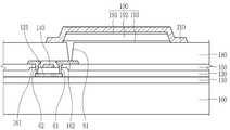
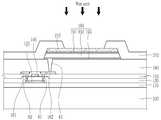
도 1을 참고하면, 일 실시예에 따른 유기 발광 표시 장치는 기판(100), 버퍼층(110), 반도체층(121), 게이트 절연막(130), 게이트 전극(140), 층간 절연막(150), 소스 전극(161), 드레인 전극(162), 평탄화층(180), 화소 전극(190), 에칭 방지층(210), 유기 발광층(350), 격벽(370) 및 공통 전극(270)을 포함한다. 여기서, 화소 전극(190), 유기 발광층(350) 및 공통 전극(270)은 유기 발광 다이오드(OLED)를 구성한다.Referring to FIG. 1, an organic light emitting display device according to an exemplary embodiment includes a
기판(100)은 유리 또는 플라스틱이나 폴리 이미드(PI)로 이루어질 수 있다.The
버퍼층(110)은 기판(100) 상에 위치한다. 버퍼층(110)은 기판(100)의 표면을 평탄하게 하고 불순 원소의 침투를 차단하기 위한 것으로, 산질화 규소(SiOx) 또는 질화 규소(SiNx) 등을 포함할 수 있다.The
버퍼층(110) 위에는 반도체층(121)이 위치한다. 반도체층(121)은 산화물 반도체로 형성될 수 있으며, 불순물이 도핑되지 여부에 따라 구분되는 채널 영역, 소스 영역 및 드레인 영역을 포함한다. 채널 영역은 불순물이 도핑되지 않는 영역이고, 소스 영역 및 드레인 영역은 붕소(B) 또는 인(P)의 불순물이 도핑되는 영역이다.A
게이트 절연막(130)은 반도체층(121) 및 버퍼층(110)을 덮도록 기판(100) 상에 형성되어 있다. 게이트 절연막(130)은 무기 절연막으로 형성되며, 산질화 규소(SiOx) 또는 질화 규소(SiNx) 등을 포함할 수 있다.The
게이트 절연막(130) 위에는 게이트 전극(140)이 위치한다. 게이트 전극(140)은 금속 물질로 형성되며, 알루미늄(Al), 몰리브덴(Mo), 구리(Cu) 등을 포함할 수 있다.A
층간 절연막(150)은 게이트 전극(140) 및 게이트 절연막(130)을 덮도록 기판(100) 상에 형성되어 있다. 층간 절연막(150)은 산질화 규소(SiOx) 또는 질화 규소(SiNx)을 포함하는 무기 절연막으로 이루어질 수 있다.The
층간 절연막(150) 및 게이트 절연막(130)에는 반도체층(121)의 소스 영역 및 드레인 영역을 노출시키는 오프닝(61, 62)이 형성되어 있다. 층간 절연막(150) 위에 위치하는 소스 전극(161) 및 드레인 전극(162)은 상기 오프닝(61, 62)에 의해 반도체층(121)의 소스 영역 및 드레인 영역에 각각 연결되어 있다. 이에 따라, 전술한 반도체층(121), 게이트 전극(140), 소스 전극(161) 및 드레인 전극(162)은 하나의 박막 트랜지스터(TFT: Thin Film Transistor)를 구성한다.
소스 전극(161) 및 드레인 전극(162) 위에는 평탄화층(180)이 위치한다. 평탄화층(180)은 소스 전극(161), 드레인 전극(162) 및 층간 절연막(150)을 덮도록 기판(100) 상에 형성되어 있다. 평탄화층(180)은 박막 트랜지스터가 구비된 기판(100)의 표면을 평탄화하기 위한 것으로, 평탄화층(180)은 폴리이미드, 폴리아마이드, 아크릴 수지, 벤조사이클로부텐 및 페놀 수지로 이루어진 군에서 선택되는 하나 이상의 물질을 포함하는 유기 절연막으로 이루어질 수 있다.A
평탄화층(180) 위에는 화소 전극(190)이 위치한다. 화소 전극(190)은 투명 전도성 산화막, 금속 물질 및 투명 전도성 산화막으로 이루어진 다중층 구조를 포함한다.A
본 실시예에 따른 화소 전극(190)은 투명 전도성 산화막으로 이루어진 상부층(191) 및 하부층(193), 금속 물질로 이루어진 중간층(192)을 포함한다. 상부층(191)은 투명 전도성 물질로써, 유기 발광 소자(OLED)에서 발생한 빛을 투과시키고, 중간층(192) 및 하부층(193)은 반사막 역할을 할 수 있다. 상부층(191)의 두께는 100Å 이하로 형성되고, 중간층(192)의 두께는 700Å 내지 1000Å 으로 형성되며, 하부층(193)의 두께는 70 Å 내지 100Å 으로 형성될 수 있다.The
투명 전도성 산화막은 ITO(Indium Tin Oxide), 폴리(poly)-ITO, IZO(Indium Zinc Oxide), IGZO(Indium Gallium Zinc Oxide) 및 ITZO(Indium Tin Zinc Oxide) 등을 포함할 수 있고, 금속 물질은 은(Ag), 몰리브덴(Mo), 구리(Cu), 금(Au) 및 알루미늄(Al) 등을 포함할 수 있다. 본 실시예에 따른 화소 전극(190)의 상부층(191)은 ITO 또는 폴리(poly)-ITO를 포함하고, 중간층(192)은 은(Ag)을 포함하며, 하부층(193)은 ITO 또는 폴리(poly)-ITO를 포함하나, 실시예에 따라 상부층(191), 하부층(193)은 다양한 투명 전도성 산화물을 포함할 수 있고, 중간층(192)은 다양한 금속 물질을 포함할 수 있다.The transparent conductive oxide film may include Indium Tin Oxide (ITO), poly-ITO, Indium Zinc Oxide (IZO), Indium Gallium Zinc Oxide (IGZO), Indium Tin Zinc Oxide (ITZO), and the like, and the metal material is Silver (Ag), molybdenum (Mo), copper (Cu), gold (Au), aluminum (Al), and the like may be included. The
평탄화층(180)에는 드레인 전극(162)을 노출시키는 오프닝(81)이 형성되어 있고, 오프닝(81)을 통해 드레인 전극(162)과 화소 전극(190)이 연결되어 있다. 구체적으로, 화소 전극(190)의 하부층(193)은 오프닝(81)을 통해 드레인 전극(162)에 연결되어 있다.An
에칭 방지층(210)은 화소 전극(190) 및 평탄화층(180) 위에 위치하고, 구체적으로 화소 전극(190)의 상면 일부가 노출되도록 화소 전극(190)의 가장자리 및 측면을 덮도록 위치한다. 에칭 방지층(210)의 두께는 400Å 내지 800Å 로 형성될 수 있다.The
에칭 방지층(210)은 화소 전극(190)의 가장자리 및 측면을 덮도록 형성됨으로써, 건식 식각 가스가 화소 전극(190)의 은(Ag)과 반응하는 것을 방지하고, 화소 전극(190)을 보호할 수 있다. 에칭 방지층(210)의 특징은 후술하는 도 6 및 도 14에서 격벽을 형성하는 건식 식각 공정에서 상세히 살펴본다.The
에칭 방지층(210)은 불소(F)계 가스와 반응성이 낮은 화합물을 포함할 수 있다. 구체적으로, 에칭 방지층(210)은 IZO(Indium Zinc Oxide), ZrCl4, ZrBr4, HfCl4, HfBr4, HgCl2, HgBr2, Al2Cl6, Al2Br6, (GaCl3))2, GaBr3, Ybr2, FeBr6, Li, Na, Ka, Rb, Cs, Be, Mg, Ca, Sr, Ba, Sc, La, Mn, Co, Rh, Ni, Cu, Ag, Au, Zn, Cd, In, Ti, Bi 등의 화합물을 포함할 수 있다.The
에칭 방지층(210) 위에는 격벽(370)이 위치한다. 격벽(370)은 화소 전극(190)의 상면 일부가 노출되도록 에칭 방지층(210)의 가장자리 및 측면을 덮고, 평탄화층(180)을 덮도록 위치한다. 격벽(370)은 화소 전극(190)의 상면 일부가 노출된 부분에 유기 발광층(350)이 형성될 수 있도록, 유기 발광층(350) 형성 위치를 구획할 수 있다.A
본 실시예에 따른 격벽(370)은 질화 규소(SiNx) 등을 포함하는 무기 물질로 이루어진다. 격벽(370)은 무기 물질로 이루어짐으로써, 표시 장치가 태양광에 장시간 노출됨에 따라 유기 물질로 이루어진 평탄화층(180)에서 발생되는 가스(예를 들면, 탄소(C), 산소(O2), 일산화 탄소(CO))가 유기 발광층(350)에 유입되는 경로를 차단한다. 이에 따라, 무기 물질로 이루어진 격벽(370)은 유기 발광 소자가 열화되는 것을 방지할 수 있다.The
유기 발광층(350)은 격벽(370)에 의하여 구획된 개구부 내에 위치한다. 도 1에서는 유기 발광층(350)을 단일층과 같이 도시하고 있지만, 실제로는 유기 발광층(350)의 상하에 전자 주입층, 전자 전달층, 정공 전달층, 및 정공 주입층과 같은 보조층도 포함될 수 있다.The
격벽(370) 및 유기 발광층(350) 위에는 공통 전극(270)이 위치한다. 공통 전극(270)은 ITO(Indium Tin Oxide), IZO(Indium Zinc Oxide), IGZO(Indium Gallium Zinc Oxide) 및 ITZO(Indium Tin Zinc Oxide) 등을 포함하여, 투명 도전층으로 형성될 수 있다.A
이하에서는, 도 2 내지 도 8을 참고하여 일 실시예에 따른 유기 발광 표시 장치의 제조 방법을 살펴본다.Hereinafter, a method of manufacturing an organic light emitting display device according to an exemplary embodiment will be described with reference to FIGS. 2 to 8.
도 2 내지 도 8은 일 실시예에 따른 유기 발광 표시 장치의 제조 방법을 설명하기 위한 단면도이다.2 to 8 are cross-sectional views illustrating a method of manufacturing an organic light emitting display device according to an exemplary embodiment.
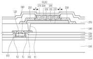
도 2를 참고하면, 기판(100) 위에 박막 트랜지스터, 평탄화층(180) 및 삼중층(191, 192, 193)으로 이루어진 화소 전극(190)이 형성되어 있고, 화소 전극(190) 및 평탄화층(180) 위에는 에칭 방지 물질층(210')이 형성되어 있다.Referring to FIG. 2, a
화소 전극(190)의 상부층(191)은 ITO 또는 폴리(poly)-ITO를 포함하고, 중간층(192)은 은(Ag)을 포함하며, 하부층(193)은 ITO 또는 폴리(poly)-ITO를 포함하도록 형성되어 있다. 실시예에 따라 상부층(191), 하부층(193)은 다양한 투명 전도성 산화물로 형성될 수 있고, 중간층(192)은 다양한 금속 물질로 형성될 수 있다.The
에칭 방지 물질층(210')은 불소(F)계 가스와 반응성이 낮은 화합물, 즉, IZO(Indium Zinc Oxide), ZrCl4, ZrBr4, HfCl4, HfBr4, HgCl2, HgBr2, Al2Cl6, Al2Br6, (GaCl3))2, GaBr3, Ybr2, FeBr6, Li, Na, Ka, Rb, Cs, Be, Mg, Ca, Sr, Ba, Sc, La, Mn, Co, Rh, Ni, Cu, Ag, Au, Zn, Cd, In, Ti, Bi 등의 화합물을 포함하도록 형성되어 있다. 에칭 방지 물질층(210')은 이후 식각 과정에 의해 에칭 방지층(210)으로 형성될 수 있다.The etching
도 3을 참고하면, 에칭 방지 물질층(210') 위에 포토 레지스트(PR) 패턴이 형성되어 있다.Referring to FIG. 3, a photoresist (PR) pattern is formed on the etching
포토 레지스트(PR) 패턴은 기판(100)에 수직인 방향으로 볼 때, 화소 전극(190)과 중첩하는 영역 보다 넓은 영역에 걸쳐 형성되어 있으며, 포토 리소그래피 공정 등에 의해 에칭 방지 물질층(210')을 1차 패터닝한다. 1차 패터닝은 습식 식각(Wet etch) 공정에 의해, 에칭 방지 물질층의 양 단을 패터닝하는 것이다.The photoresist (PR) pattern is formed over a wider area than the area overlapping the
도 4를 참고하면, 포토 레지스트(PR) 패턴이 제거되고, 화소 전극(190)의 상면 및 측면을 모두 덮도록 에칭 방지층(210)이 형성되어 있다.Referring to FIG. 4, a photoresist (PR) pattern is removed, and an
화소 전극(190)의 하부층(193)은 평탄화층(180)의 상면과 접촉하고 있다. 이후 형성된 유기 발광 표시 장치에서, 화소 전극(190) 및 평탄화층(180)이 접촉하는 부분은 유기 발광 표시 장치의 전기적 특성 및 발광 특성에 영향을 미칠 수 있다. 이를 방지 하기 위해, 본 실시예에서는 에칭 방지층(210)을 1차로 패터닝 한 후, 열처리 공정을 하여 화소 전극(190)의 상부층 및 하부층을 폴리(poly)-ITO로 변형시키고, 평탄화층(180) 및 화소 전극(190)이 접촉하는 부분의 접합 특성을 향상시킬 수 있다.The
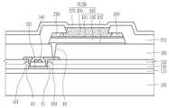
도 5를 참고하면, 에칭 방지층(210) 및 평탄화층(180) 위에는 격벽용 무기 물질층(370')이 형성되어 있다.Referring to FIG. 5, an
무기 물질층(370')은 질화 규소(SiNx) 등으로 이루어질 수 있다. 이후 형성되는 격벽(370)은 무기 물질을 포함함으로써, 유기 물질로 이루어진 평탄화층(180)에서 발생되는 가스(예를 들어, 산소(O2), 탄소(C), 일산화 탄소(CO) 등)가 유기 발광층(350)으로 유입됨에 따라, 유기 발광 소자가 열화되는 것을 방지할 수 있다.The
도 6을 참고하면, 격벽용 무기 물질층(370') 위에 포토 레지스트(PR) 패턴이 형성되어 있다. 포토 레지스트(PR) 패턴은 에칭 방지층(210)의 가장자리 부분과 중첩하는 위치에 형성되어 있다.Referring to FIG. 6, a photoresist (PR) pattern is formed on the
격벽(370)은 포토 레지스트(PR) 패턴에 따라 격벽용 무기 물질층(370')을 건식 식각(Dry etch)하여 형성된다. 건식 식각 공정은 진공 챔버 내에서 수행될 수 있으며, 육불화황(SF6), 삼불화질소(NF3) 또는 아르곤(Ar)등 식각용 가스를 사용할 수 있다.The
에칭 방지층을 포함하지 않는 비교예에 따른 유기 발광 표시 장치에서, 화소 전극의 상부층의 두께는 70Å 내지 120 Å으로 얇게 형성되므로, 상부층에는 파티클 또는 미세한 틈이 생길 수 있다. 이 때, 파티클 등이 건식 식각용 가스에 노출되면, 중간층의 은(Ag)과 식각용 가스는 반응하여 산화은(Ag20) 또는 플루오르화은(AgF) 등을 형성하고, 화소 전극의 중간층에는 산화은(Ag20) 또는 플루오르화은(AgF) 등이 포함되게 된다. 따라서, 비교예에 따른 유기 발광 표시 장치는 전기적 특성 및 발광 특성이 저하되게 된다.In the organic light emitting diode display according to the comparative example not including the etch stop layer, the upper layer of the pixel electrode has a thickness of 70 Å to 120 Å, and thus particles or fine gaps may be formed in the upper layer. At this time, when particles are exposed to the dry etching gas, silver (Ag) in the intermediate layer and the etching gas react to form silver oxide (Ag2 O) or silver fluoride (AgF), and silver oxide is formed in the intermediate layer of the pixel electrode. (Ag2 0) or silver fluoride (AgF) will be included. Accordingly, the organic light emitting display device according to the comparative example has deteriorated electrical characteristics and light-emitting characteristics.
그러나, 본 실시예에 따른 화소 전극(190)은 에칭 방지층(210)에 의해 덮여 있으므로, 식각용 가스에 영향을 받지 않는다. 또한, 에칭 방지층(210)은 식각용 가스와 반응성이 낮은 화합물로 이루어져 있으므로, 건식 식각 공정에 의한 영향을 받지 않는다.However, since the
따라서, 본 실시예에서는 에칭 방지층(210)을 포함함으로써, 건식 식각 공정에서 화소 전극(190)에 손상이 발생하는 것을 방지하고, 유기 발광 표시 장치의 특성이 저하되는 것을 방지할 수 있다.Accordingly, in the present exemplary embodiment, by including the
도 7을 참고하면, 일 실시예에 따른 유기 발광 표시 장치에는 에칭 방지층(210) 상면의 일부가 노출되도록 격벽(370)이 형성되어 있다.Referring to FIG. 7, in the organic light emitting diode display according to an exemplary embodiment, a
이후, 에칭 방지층(210)을 2차 패터닝 하기 위하여 습식 식각(Wet etch) 공정을 한다. 에칭 방지층(210)은 화소 전극(190)의 상면 일부가 노출되도록 패터닝 된다. 에칭 방지층(210)은 화소 전극(190)보다 식각 선택비가 높은 물질을 포함함으로써, 식각액(Ehant)에 의해 에칭 방지층(210) 상면 일부만 식각될 수 있다. 또한, 전술한 도 4 단계 이후, 열처리 공정에 의해 폴리(poly)-ITO를 포함하는 화소 전극(190)도 에칭 방지층(210)보다 식각 선택비가 낮은 물질로 형성되므로, 습식 식각 공정에 의해 에칭 방지층(210)만 식각된다.Thereafter, a wet etch process is performed to secondly pattern the
습식 식각 공정에서 화소 전극(190)이 식각되지 않음은 하기의 표 1을 통해 확인할 수 있다.It can be confirmed from Table 1 below that the
하기의 표 1은 45℃ 에서 금속 물질의 식각비를 나타낸 것이다.Table 1 below shows the etching ratio of metal materials at 45°C.
(A/sec)Ag
(A/sec)
표 1을 참고하면, A 식각액을 이용하여, 45℃에서 이루어지는 습식 식각 공정에서, IGZO, IZO, 비정질(a-ITO)는 일부 식각되나, 폴리(poly)-ITO, Ag는 식각률이 0으로 유지된다. 즉, 본 실시예에 따른 화소 전극은 상부층 및 하부층에 폴리(poly)-ITO을 포함하고, 중간층에 은(Ag)을 포함함으로써, 식각액에 의해 식각되지 않음을 확인할 수 있다.Referring to Table 1, IGZO, IZO, and amorphous (a-ITO) are partially etched in the wet etching process performed at 45°C using etching solution A, but the etch rate of poly-ITO and Ag is maintained at 0. do. That is, since the pixel electrode according to the present exemplary embodiment contains poly(poly)-ITO in the upper and lower layers and silver (Ag) in the intermediate layer, it can be confirmed that the pixel electrode is not etched by the etchant.
도 8을 참고하면, 에칭 방지층(210)이 식각됨에 따라 노출된 화소 전극(190)의 상면에 유기 발광층(350)이 형성되어 있고, 유기 발광층(350) 및 격벽(370) 위에 공통 전극(270)이 형성되어 있다.Referring to FIG. 8, the
도 7의 에칭 방지층(210)이 식각되는 과정에서, 격벽(370)의 가장자리는 에칭 방지층(210) 보다 돌출되도록 식각된다. 격벽(370)의 가장자리 일 단과 에칭 방지층(210)의 일 단의 거리(d)는 0.2μm 로 형성될 수 있다. 이는, 격벽(370)의 가장자리가 에칭 방지층(210) 보다 돌출되도록 형성될 때, 유기 발광층(350)이 평탄하게 증착될 수 있기 때문이다.In the process of etching the
이하에서는, 도 9를 참고하여 다른 실시예에 따른 유기 발광 표시 장치를 살펴본다.Hereinafter, an organic light emitting display device according to another exemplary embodiment will be described with reference to FIG. 9.
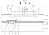
도 9는 다른 실시예에 따른 유기 발광 표시 장치의 개략적인 단면도이다.9 is a schematic cross-sectional view of an organic light emitting diode display according to another exemplary embodiment.
도 9를 참고하면, 다른 실시예에 따른 유기 발광 표시 장치는 기판(100), 버퍼층(110), 반도체층(121), 게이트 절연막(130), 게이트 전극(140), 층간 절연막(150), 소스 전극(161), 드레인 전극(162), 평탄화층(180), 화소 전극(190), 에칭 방지층(210), 유기 발광층(350), 격벽(370) 및 공통 전극(270)을 포함한다. 여기서, 화소 전극(190), 유기 발광층(350) 및 공통 전극(270)은 유기 발광 다이오드(OLED)를 구성한다.Referring to FIG. 9, an organic light emitting diode display according to another exemplary embodiment includes a
도 9에 도시된 다른 실시예에 따른 표시 장치는 도 1에 도시된 일 실시예에 따른 표시 장치와 대부분의 구성이 유사하고, 에칭 방지층(210)의 형성 위치만 상이한바, 이하에서는 에칭 방지층(210)을 중심으로 살펴본다.The display device according to the other exemplary embodiment illustrated in FIG. 9 is similar in most configurations to the display device according to the exemplary embodiment illustrated in FIG. 1, and differs only in the formation position of the
에칭 방지층(210)은 화소 전극(190)의 상면 일부가 노출된 부분을 제외한 화소 전극(190)의 가장자리 위에 위치한다. 즉, 화소 전극(190)의 일 단과 에칭 방지층(210)의 일 단은 동일한 면에 위치할 수 있다. 에칭 방지층(210)의 두께는 400Å 내지 800Å 로 형성될 수 있다.The
에칭 방지층(210)의 식각면은 화소 전극(190)의 상부층(191), 중간층(192), 및 하부층(193)의 식각면과 경계가 일치하도록 형성될 수 있고, 에칭 방지층(210)의 식각면은 화소 전극(190)의 식각면의 경계 보다 내측에 위치하도록 되도록 형성될 수도 있다.The etch surface of the
에칭 방지층(210)은 불소(F)계 가스와 반응성이 낮은 화합물을 포함할 수 있다. 구체적으로, 에칭 방지층(210)은 IZO(Indium Zinc Oxide), ZrCl4, ZrBr4, HfCl4, HfBr4, HgCl2, HgBr2, Al2Cl6, Al2Br6, (GaCl3))2, GaBr3, Ybr2, FeBr6, Li, Na, Ka, Rb, Cs, Be, Mg, Ca, Sr, Ba, Sc, La, Mn, Co, Rh, Ni, Cu, Ag, Au, Zn, Cd, In, Ti, Bi 등의 화합물을 포함할 수 있다.The
따라서, 에칭 방지층(210)은 화소 전극(190)의 가장자리에 위치하고, 불소(F)계 가스와 반응성이 낮은 화합물을 포함함으로써, 건식 식각 공정에서 식각용 가스가 화소 전극(190)의 은(Ag)과 반응하는 것을 방지하고, 화소 전극(190)을 보호할 수 있다.Therefore, the
이하에서는, 도 10 내지 도 17을 참고하여 다른 실시예에 따른 유기 발광 표시 장치의 제조 방법을 살펴본다.Hereinafter, a method of manufacturing an organic light emitting display device according to another exemplary embodiment will be described with reference to FIGS. 10 to 17.
도 10 내지 도 17은 다른 실시예에 따른 유기 발광 표시 장치의 제조 방법을 설명하기 위한 단면도이다.10 to 17 are cross-sectional views illustrating a method of manufacturing an organic light emitting display device according to another exemplary embodiment.
도 10을 참고하면, 기판(100) 위에 박막 트랜지스터, 평탄화층(180)이 형성되어 있고, 평탄화층(180) 위에는 화소 전극 물질층(190') 및 에칭 방지 물질층(210')이 형성되어 있다.Referring to FIG. 10, a thin film transistor and a
화소 전극 물질층(190')의 상부 물질층(191')은 ITO 또는 폴리(poly)-ITO를 포함하고, 중간 물질층(192')은 은(Ag)을 포함하며, 하부 물질층(193')은 ITO 또는 폴리(poly)-ITO를 포함하도록 형성되어 있다. 실시예에 따라, 상부 물질층(191'), 하부 물질층(193')은 다양한 투명 전도성 산화물로 형성될 수 있고, 중간 물질층(192')은 다양한 금속 물질로 형성될 수 있다.The
에칭 방지 물질층(210')은 불소(F)계 가스와 반응성이 낮은 화합물, 즉, IZO(Indium Zinc Oxide), ZrCl4, ZrBr4, HfCl4, HfBr4, HgCl2, HgBr2, Al2Cl6, Al2Br6, (GaCl3))2, GaBr3, Ybr2, FeBr6, Li, Na, Ka, Rb, Cs, Be, Mg, Ca, Sr, Ba, Sc, La, Mn, Co, Rh, Ni, Cu, Ag, Au, Zn, Cd, In, Ti, Bi 등의 화합물을 포함하도록 형성되어 있다. 에칭 방지 물질층(210')은 이후 식각 과정에 의해 에칭 방지층(210)으로 형성될 수 있다.The etching
상부 물질층(191'), 중간 물질층(192') 및 하부 물질층(193')은 이후 식각 과정에 의해 하나의 화소 전극(190)으로 구현될 수 있고, 에칭 방지 물질층(210')은 이후 식각 과정에 의해 에칭 방지층(210)으로 구현될 수 있다.The
도 11을 참고하면, 에칭 방지 물질층(210')은 패터닝 되어 에칭 방지층(210)으로 형성되어 있고, 에칭 방지층(210) 위에는 화소 전극(190)을 패터닝 하기 위한 포토 레지스트(PR) 패턴이 형성되어 있다.Referring to FIG. 11, the etching
도 11에 도시되지 않았으나, 에칭 방지층(210)은 에칭 방지 물질층(210') 상에 포토 레지스트(PR) 패턴이 형성되고, 습식 식각 공정에 의해 형성될 수 있다.Although not shown in FIG. 11, the
도 12를 참고하면, 포토 레지스트(PR) 패턴에 의해 화소 전극(190)이 패터닝 되어 있다. 이에 따라, 화소 전극(190)의 상부층(191)은 ITO(Indium Tin Oxide)을 포함하고, 중간층(192)은 은(Ag)을 포함하며, 하부층(193)은 ITO(Indium Tin Oxide)을 포함하도록 형성될 수 있다.Referring to FIG. 12, the
실시예에 따라, 상부층(191), 중간층(192) 및 하부층(193)을 동시에 식각하는 경우에는, 각 층 식각면의 경계가 일치하도록 형성될 수 있다. 어느 하나의 층이 더 많이 식각되는 경우에는, 식각면에 언더컷(under cut)이 형성될 수 있으나, 각 층의 식각 정도는 차이가 크지 않으므로, 최종적으로 화소 전극(190)은 거의 비슷한 식각면의 경계를 갖도록 형성될 수 있다. 즉, 각 층의 식각면의 경계(가장자리)간의 거리는 인접하여 위치할 수 있다.According to an exemplary embodiment, when the
또한, 에칭 방지층(210)의 식각면은 화소 전극(190)의 상부층(191), 중간층(192), 및 하부층(193)의 식각면과 경계가 일치하도록 형성될 수 있고, 에칭 방지층(210)의 식각면은 화소 전극(190)의 식각면의 경계 보다 내측에 위치하도록 되도록 형성될 수도 있다.In addition, the etching surface of the
도 13을 참고하면, 포토 레지스트 패턴이 제거되고, 평탄화층(180) 위에 패터닝된 화소 전극(190) 및 에칭 방지층(210)이 위치하고 있다.Referring to FIG. 13, the photoresist pattern is removed, and the patterned
에칭 방지층(210)은 화소 전극(190)과 동일한 크기 및 면적으로 중첩되도록 형성되어 있으며, 에칭 방지층(210)의 일 단은 화소 전극(190)의 일 단과 동일한 면에 위치하도록 형성되어 있다.The
화소 전극(190)의 하부층(193)은 평탄화층(180)의 상면과 접촉하고 있다. 이후 유기 발광 표시 장치에서, 화소 전극(190) 및 평탄화층(180)이 접촉하는 부분은 유기 발광 표시 장치의 전기적 특성 및 발광 특성에 영향을 미칠 수 있다. 이를 방지 하기 위해, 본 실시예에서는 에칭 방지층(210)을 1차로 패터닝 한 후, 열처리 공정을 하여 화소 전극(190)의 상부층 및 하부층을 폴리(poly)-ITO로 변형시키고, 평탄화층(180) 및 화소 전극(190)이 접촉하는 부분의 접합 특성을 향상시킬 수 있다.The
도 14를 참고하면, 에칭 방지층(210) 및 평탄화층(180) 위에는 격벽용 무기 물질층(370')이 형성되고, 격벽용 무기 물질층(370') 위에는 포토 레지스트(PR) 패턴이 형성되어 있다. 포토 레지스트(PR) 패턴은 에칭 방지층(210)의 가장자리 부분과 중첩하는 위치에 형성되어 있다.Referring to FIG. 14, an inorganic material layer 370' for partition walls is formed on the
격벽(370)은 포토 레지스트 패턴에 따라 격벽용 무기 물질층(370')을 건식 식각(Dry etch)하여 형성된다. 건식 식각 공정은 진공 챔버 내에서 수행될 수 있으며, 육불화황(SF6), 삼불화질소(NF3) 또는 아르곤(Ar)등 식각용 가스를 사용할 수 있다.The
에칭 방지층(210)을 포함하지 않는 비교예에 따른 유기 발광 표시 장치에서, 화소 전극(190)의 상부층의 두께는 70Å 내지 120 Å으로 얇게 형성되므로, 상부층에는 파티클 또는 미세한 틈이 생길 수 있다. 이 때, 파티클 등이 건식 식각용 가스에 노출되면, 중간층의 은(Ag)과 식각용 가스는 반응하여 산화은(Ag20), 플루오르화은(AgF) 등을 형성하고, 화소 전극(190)의 중간층에는 산화은(Ag20), 플루오르화은(AgF) 등이 포함되게 된다. 따라서, 비교예에 따른 유기 발광 표시 장치는 전기적 특성 및 발광 특성이 저하되게 된다.In the organic light emitting diode display according to the comparative example not including the
그러나, 본 실시예에 따른 화소 전극(190)은 에칭 방지층(210)이 가장자리 상부에 위치함으로 의해, 식각용 가스에 영향을 받지 않는다. 또한, 에칭 방지층(210)은 식각용 가스와 반응성이 낮은 화합물로 이루어져 있으므로, 건식 식각 공정에 의한 영향을 받지 않는다.However, the
따라서, 본 실시예에서는 에칭 방지층(210)을 포함함으로써, 건식 식각 공정에서 화소 전극(190)에 손상이 발생하는 것을 방지하고, 유기 발광 표시 장치의 특성이 저하되는 것을 방지할 수 있다.Accordingly, in the present exemplary embodiment, by including the
도 15를 참고하면, 다른 실시예에 따른 유기 발광 표시 장치에는 에칭 방지층(210) 상면의 일부가 노출되도록 격벽(370)이 형성되어 있다. 이후, 에칭 방지층(210)을 패터닝 하기 위하여 습식 식각(Wet etch) 공정을 한다.Referring to FIG. 15, in an organic light emitting diode display according to another exemplary embodiment, a
도 16을 참고하면, 에칭 방지층(210)은 습식 식각 공정에 의해 화소 전극(190)의 상면 일부가 노출되도록 패터닝 된다.Referring to FIG. 16, the
에칭 방지층(210)은 화소 전극(190)보다 식각 선택비가 높은 물질을 포함함으로써, 식각액(Ehant)에 의해 에칭 방지층(210) 상면 일부만 식각될 수 있다. 또한, 전술한 도 13에서 살펴본 바와 같이, 열처리 공정에 의해 폴리(poly)-ITO를 포함하는 화소 전극(190)도 에칭 방지층(210)보다 식각 선택비가 낮은 물질로 형성되므로, 습식 식각 공정에 의해 에칭 방지층(210)만 식각된다.Since the
또한, 격벽(370)의 가장자리는 에칭 방지층(210) 보다 돌출되도록 식각되어 있다. 격벽(370)의 가장자리 일 단과 에칭 방지층(210)의 일 단의 거리(d)는 0.2μm 로 형성될 수 있다. 이는, 격벽(370)의 가장자리가 에칭 방지층(210) 보다 돌출되도록 형성될 때, 유기 발광층(350)이 평탄하게 증착될 수 있기 때문이다.In addition, the edge of the
도 17을 참고하면, 에칭 방지층(210)이 식각됨에 따라 노출된 화소 전극(190)의 상면에 유기 발광층(350)이 형성되어 있고, 유기 발광층(350) 및 격벽(370) 위에 공통 전극(270)이 형성되어 있다.Referring to FIG. 17, the
따라서, 본 실시예에서는 에칭 방지층(210)을 포함함으로써, 건식 식각 공정에서 화소 전극(190)에 손상이 발생하는 것을 방지하고, 유기 발광 표시 장치의 특성이 저하되는 것을 방지할 수 있다.Accordingly, in the present exemplary embodiment, by including the
이상에서 본 발명의 실시예에 대하여 상세하게 설명하였지만 본 발명의 권리범위는 이에 한정되는 것은 아니고 다음의 청구범위에서 정의하고 있는 본 발명의 기본 개념을 이용한 당업자의 여러 변형 및 개량 형태 또한 본 발명의 권리범위에 속하는 것이다.Although the embodiments of the present invention have been described in detail above, the scope of the present invention is not limited thereto, and various modifications and improvements by those skilled in the art using the basic concept of the present invention defined in the following claims are also provided. It belongs to the scope of rights.
100: 기판110: 버퍼층
121: 반도체층130: 게이트 절연막
140: 게이트 전극150: 층간 절연막
161: 소스 전극162: 드레인 전극
180: 평탄화층190: 화소 전극
360: 유기 발광층210: 에칭 방지층
370: 격벽270: 공통 전극100: substrate 110: buffer layer
121: semiconductor layer 130: gate insulating film
140: gate electrode 150: interlayer insulating film
161: source electrode 162: drain electrode
180: planarization layer 190: pixel electrode
360: organic light emitting layer 210: anti-etching layer
370: partition wall 270: common electrode
Claims (20)
Translated fromKorean상기 기판 위에 위치하는 박막 트랜지스터;
상기 박막 트랜지스터 위에 위치하는 평탄화층;
상기 평탄화층 위에 위치하며, 투명 전도성 산화물을 포함하는 상부층 및 하부층, 그리고 은(Ag)을 포함하는 중간층으로 이루어진 화소 전극;
상기 화소 전극 위에서, 상기 화소 전극의 상면의 일부가 노출되도록 위치하는 에칭 방지층;
상기 화소 전극의 상면이 노출되도록 상기 에칭 방지층 위에 위치하는 격벽;
상기 격벽에 의해 노출된 상기 화소 전극의 상면에 위치하는 유기 발광층; 및
상기 유기 발광층 및 상기 격벽 위에 위치하는 공통 전극을 포함하고,
상기 에칭 방지층은 상기 화소 전극의 가장자리 및 측면을 덮는 유기 발광 표시 장치.Board;
A thin film transistor positioned on the substrate;
A planarization layer on the thin film transistor;
A pixel electrode positioned on the planarization layer and including an upper layer and a lower layer containing a transparent conductive oxide, and an intermediate layer containing silver (Ag);
An etching prevention layer positioned on the pixel electrode to expose a portion of an upper surface of the pixel electrode;
A partition wall positioned on the etching prevention layer so that the upper surface of the pixel electrode is exposed;
An organic emission layer positioned on the upper surface of the pixel electrode exposed by the partition wall; And
And a common electrode positioned on the organic emission layer and the partition wall,
The etch stop layer covers edges and side surfaces of the pixel electrode.
상기 격벽은 무기 물질을 포함하는 유기 발광 표시 장치.The method of claim 1,
The partition wall includes an inorganic material.
상기 상부층 및 상기 하부층은 폴리(poly)-ITO(Indium Tin Oxide) 또는 ITO(Indium Tin Oxide)를 포함하는 유기 발광 표시 장치.The method of claim 1,
The upper and lower layers include poly-ITO (Indium Tin Oxide) or ITO (Indium Tin Oxide).
상기 상부층의 두께는 70Å 내지 120 Å인 유기 발광 표시 장치.The method of claim 1,
The organic light emitting diode display device has a thickness of the upper layer of 70 Å to 120 Å.
상기 에칭 방지층은 불소(F)계 가스와 반응성이 낮은 화합물을 포함하는 유기 발광 표시 장치.The method of claim 1,
The etching prevention layer includes a compound having low reactivity with a fluorine (F)-based gas.
상기 에칭 방지층은 IZO(Indium Gallium Zinc Oxide)를 포함하는 유기 발광 표시 장치.The method of claim 5,
The organic light emitting diode display device includes the etch stop layer including Indium Gallium Zinc Oxide (IZO).
상기 평탄화층은 폴리이미드, 폴리아마이드, 아크릴 수지, 벤조사이클로부텐 및 페놀 수지로 이루어진 군에서 선택되는 하나 이상의 물질을 포함하는 유기 발광 표시 장치.The method of claim 1,
The planarization layer includes at least one material selected from the group consisting of polyimide, polyamide, acrylic resin, benzocyclobutene, and phenol resin.
상기 박막 트랜지스터는 반도체층, 게이트 전극, 소스 전극 및 드레인 전극을 포함하고,
상기 드레인 전극은 상기 화소 전극과 전기적으로 연결되어 있는 유기 발광 표시 장치.The method of claim 1,
The thin film transistor includes a semiconductor layer, a gate electrode, a source electrode and a drain electrode,
The drain electrode is electrically connected to the pixel electrode.
상기 기판 위에 위치하는 박막 트랜지스터;
상기 박막 트랜지스터 위에 위치하는 평탄화층;
상기 평탄화층 위에 위치하며, 상부층, 중간층 및 하부층을 포함하는 삼중층으로 이루어진 화소 전극;
상기 화소 전극 위에서, 상기 화소 전극의 상면의 일부가 노출되도록 위치하는 에칭 방지층;
상기 화소 전극의 상면이 노출되도록 상기 에칭 방지층 위에 위치하는 격벽;
상기 격벽에 의해 노출된 상기 화소 전극의 상면에 위치하는 유기 발광층; 및
상기 유기 발광층 및 상기 격벽 위에 위치하는 공통 전극을 포함하고,
상기 화소 전극의 중간층은 은(Ag)을 포함하며,
상기 에칭 방지층은 상기 화소 전극의 상면의 일부가 노출된 부분을 제외한 상기 화소 전극의 가장자리에 위치하는 유기 발광 표시 장치.Board;
A thin film transistor positioned on the substrate;
A planarization layer on the thin film transistor;
A pixel electrode positioned on the planarization layer and formed of a triple layer including an upper layer, an intermediate layer, and a lower layer;
An etching prevention layer positioned on the pixel electrode to expose a portion of an upper surface of the pixel electrode;
A partition wall positioned on the etching prevention layer so that the upper surface of the pixel electrode is exposed;
An organic emission layer positioned on the upper surface of the pixel electrode exposed by the partition wall; And
And a common electrode positioned on the organic emission layer and the partition wall,
The intermediate layer of the pixel electrode contains silver (Ag),
The etch stop layer is disposed on an edge of the pixel electrode except for a portion of the pixel electrode where a portion of the upper surface of the pixel electrode is exposed.
상기 상부층 및 상기 하부층은 폴리(poly)-ITO(Indium Tin Oxide) 또는 ITO(Indium Tin Oxide)를 포함하는 유기 발광 표시 장치.The method of claim 9,
The upper and lower layers include poly-ITO (Indium Tin Oxide) or ITO (Indium Tin Oxide).
상기 격벽은 무기 물질을 포함하는 유기 발광 표시 장치.The method of claim 9,
The partition wall includes an inorganic material.
상기 에칭 방지층은 불소(F)계 가스와 반응성이 낮은 화합물을 포함하는 유기 발광 표시 장치.The method of claim 9,
The etching prevention layer includes a compound having low reactivity with a fluorine (F)-based gas.
상기 에칭 방지층은 상기 화소 전극 보다 식각비가 높은 물질을 포함하는 유기 발광 표시 장치.The method of claim 9,
The organic light emitting diode display includes a material having an etching ratio higher than that of the pixel electrode in the etch stop layer.
상기 박막 트랜지스터는 반도체층, 게이트 전극, 소스 전극 및 드레인 전극을 포함하고,
상기 드레인 전극은 상기 화소 전극과 전기적으로 연결되어 있는 유기 발광 표시 장치.The method of claim 9,
The thin film transistor includes a semiconductor layer, a gate electrode, a source electrode and a drain electrode,
The drain electrode is electrically connected to the pixel electrode.
상기 평탄화층 위에 상부 물질층, 은(Ag)을 포함하는 중간 물질층 및 하부 물질층을 포함하는 화소 전극 물질층 및 상기 상부 물질층 위에 불소(F)계 가스와 반응성이 낮은 화합물을 포함하는 에칭 방지 물질층을 형성하는 단계;
상기 에칭 방지 물질층을 1차 패터닝하여 에칭 방지층을 형성하는 단계;
상기 화소 전극 물질층을 패터닝하여 상부층, 중간층 및 하부층을 포함하는 화소 전극을 형성하는 단계;
상기 에칭 방지층 위에 격벽용 무기 물질층을 형성하는 단계;
상기 격벽용 무기 물질층을 패터닝하여 상기 에칭 방지층의 상면 일부가 노출되도록 격벽을 형성하는 단계;
상기 에칭 방지층을 2차 패터닝하여 상기 화소 전극의 상면 일부가 노출되도록 상기 에칭 방지층을 형성하는 단계; 및
노출된 상기 화소 전극의 상면 일부에 유기 발광층을 형성하고, 상기 유기 발광층 및 상기 격벽 위에 공통 전극을 형성하는 단계를 포함하는 유기 발광 표시 장치 제조 방법.Providing a thin film transistor and a substrate on which a planarization layer is formed on the thin film transistor;
Etching containing an upper material layer, an intermediate material layer including silver (Ag), and a pixel electrode material layer including a lower material layer on the planarization layer, and a compound having low reactivity with a fluorine (F)-based gas on the upper material layer Forming a layer of prevention material;
Forming an etch-prevention layer by first patterning the etch-prevention material layer;
Forming a pixel electrode including an upper layer, an intermediate layer, and a lower layer by patterning the pixel electrode material layer;
Forming an inorganic material layer for a partition wall on the etching prevention layer;
Forming a partition wall such that a portion of the upper surface of the etching prevention layer is exposed by patterning the inorganic material layer for the partition wall;
Forming the etch-stop layer to expose a portion of the upper surface of the pixel electrode by secondary patterning the etch-stop layer; And
And forming an organic emission layer on a portion of the exposed upper surface of the pixel electrode, and forming a common electrode on the organic emission layer and the partition wall.
상기 상부층 및 상기 하부층은 폴리(poly)-ITO(Indium Tin Oxide) 또는 ITO(Indium Tin Oxide)를 포함하는 유기 발광 표시 제조 방법.In paragraph 15,
The upper layer and the lower layer include poly-ITO (Indium Tin Oxide) or ITO (Indium Tin Oxide).
상기 격벽을 형성하는 단계는 건식 식각을 이용하는 유기 발광 표시 장치 제조 방법.In paragraph 15,
The forming of the partition wall is a method of manufacturing an organic light emitting diode display using dry etching.
상기 에칭 방지층은 상기 화소 전극의 상면의 일부가 노출된 부분을 제외한 상기 화소 전극의 가장자리에 형성되는 유기 발광 표시 장치 제조 방법.In paragraph 17,
The method of manufacturing an organic light emitting diode display, wherein the etching prevention layer is formed on an edge of the pixel electrode excluding a portion of the pixel electrode where the upper surface of the pixel electrode is exposed.
상기 에칭 방지층을 형성하는 단계는 습식 식각을 이용하는 유기 발광 표시 장치 제조 방법.In paragraph 15,
The forming of the etch stop layer is a method of manufacturing an organic light emitting diode display using wet etching.
상기 에칭 방지 물질층은 상기 화소 전극 보다 식각비가 높은 물질을 포함하는 유기 발광 표시 장치 제조 방법.In paragraph 19,
The method of manufacturing an organic light emitting diode display, wherein the etch prevention material layer includes a material having an etching ratio higher than that of the pixel electrode.
Priority Applications (4)
| Application Number | Priority Date | Filing Date | Title |
|---|---|---|---|
| KR1020190101063AKR20210022206A (en) | 2019-08-19 | 2019-08-19 | Organic light emitting diode display device and manufacturing method thereof |
| US16/894,953US11342404B2 (en) | 2019-08-19 | 2020-06-08 | Organic light emitting diode display device including etch stop layer |
| CN202010811987.0ACN112397555B (en) | 2019-08-19 | 2020-08-13 | Organic Light Emitting Diode Display |
| US17/732,797US11889730B2 (en) | 2019-08-19 | 2022-04-29 | Manufacturing method of an organic light emitting diode display device including an etch stop layer |
Applications Claiming Priority (1)
| Application Number | Priority Date | Filing Date | Title |
|---|---|---|---|
| KR1020190101063AKR20210022206A (en) | 2019-08-19 | 2019-08-19 | Organic light emitting diode display device and manufacturing method thereof |
Publications (1)
| Publication Number | Publication Date |
|---|---|
| KR20210022206Atrue KR20210022206A (en) | 2021-03-03 |
Family
ID=74596514
Family Applications (1)
| Application Number | Title | Priority Date | Filing Date |
|---|---|---|---|
| KR1020190101063APendingKR20210022206A (en) | 2019-08-19 | 2019-08-19 | Organic light emitting diode display device and manufacturing method thereof |
Country Status (3)
| Country | Link |
|---|---|
| US (2) | US11342404B2 (en) |
| KR (1) | KR20210022206A (en) |
| CN (1) | CN112397555B (en) |
Cited By (4)
| Publication number | Priority date | Publication date | Assignee | Title |
|---|---|---|---|---|
| KR102734652B1 (en)* | 2023-11-29 | 2024-11-28 | 삼성디스플레이 주식회사 | Display device and manufacturing methode thereof |
| KR102734653B1 (en)* | 2023-11-29 | 2024-11-28 | 삼성디스플레이 주식회사 | Display device and manufacturing methode thereof |
| US12232367B2 (en) | 2021-08-23 | 2025-02-18 | Samsung Display Co., Ltd. | Display device including swelling prevention layer |
| WO2025116404A1 (en)* | 2023-11-29 | 2025-06-05 | 삼성디스플레이주식회사 | Display device and manufacturing method therefor |
Families Citing this family (6)
| Publication number | Priority date | Publication date | Assignee | Title |
|---|---|---|---|---|
| KR20210022206A (en) | 2019-08-19 | 2021-03-03 | 삼성디스플레이 주식회사 | Organic light emitting diode display device and manufacturing method thereof |
| DE102020120751A1 (en)* | 2019-09-23 | 2021-03-25 | Taiwan Semiconductor Manufacturing Co., Ltd. | DISPLAY DEVICE AND METHOD OF MANUFACTURING IT |
| WO2022054761A1 (en)* | 2020-09-08 | 2022-03-17 | ソニーセミコンダクタソリューションズ株式会社 | Display device, light emitting device, and electronic apparatus |
| CN114975519A (en)* | 2021-02-26 | 2022-08-30 | 深圳市柔宇科技股份有限公司 | Thin film transistor device and manufacturing method thereof |
| JP7693338B2 (en)* | 2021-03-09 | 2025-06-17 | JDI Design and Development 合同会社 | display device |
| WO2023019531A1 (en)* | 2021-08-19 | 2023-02-23 | 京东方科技集团股份有限公司 | Display device, and display panel and manufacturing method therefor |
Family Cites Families (36)
| Publication number | Priority date | Publication date | Assignee | Title |
|---|---|---|---|---|
| US7060153B2 (en)* | 2000-01-17 | 2006-06-13 | Semiconductor Energy Laboratory Co., Ltd. | Display device and method of manufacturing the same |
| KR100495702B1 (en)* | 2001-04-13 | 2005-06-14 | 삼성에스디아이 주식회사 | Organic electroluminescence device and method for fabricating the same |
| JP2004192935A (en) | 2002-12-11 | 2004-07-08 | Hitachi Displays Ltd | Organic EL display |
| JP3979395B2 (en)* | 2004-02-24 | 2007-09-19 | セイコーエプソン株式会社 | Method for manufacturing organic electroluminescent device, organic electroluminescent device, substrate for organic electroluminescent device, and electronic device |
| KR100635066B1 (en)* | 2004-06-03 | 2006-10-16 | 삼성에스디아이 주식회사 | Organic electroluminescent display and manufacturing method thereof |
| KR100659757B1 (en) | 2004-08-25 | 2006-12-19 | 삼성에스디아이 주식회사 | Organic electroluminescent device and manufacturing method thereof |
| KR20060026776A (en) | 2004-09-21 | 2006-03-24 | 삼성에스디아이 주식회사 | Organic electroluminescent device and manufacturing method thereof |
| KR100699998B1 (en) | 2004-09-23 | 2007-03-26 | 삼성에스디아이 주식회사 | Organic electroluminescent device and manufacturing method thereof |
| KR101373435B1 (en) | 2007-03-22 | 2014-03-14 | 엘지디스플레이 주식회사 | Display substrate, organic emitting diode display device having the same and method of manufacturing thereof |
| KR101432110B1 (en)* | 2007-09-11 | 2014-08-21 | 삼성디스플레이 주식회사 | Organic light emitting display and method for manufacturing the same |
| JP2009211904A (en)* | 2008-03-04 | 2009-09-17 | Seiko Epson Corp | Electro-optical device and electronic apparatus |
| KR101499235B1 (en)* | 2008-06-23 | 2015-03-06 | 삼성디스플레이 주식회사 | Organic light emitting display and manufacturing method thereof |
| KR101193196B1 (en) | 2010-07-07 | 2012-10-19 | 삼성디스플레이 주식회사 | Organic light emitting display apparatus and the manufacturing method thereof |
| KR20120032904A (en) | 2010-09-29 | 2012-04-06 | 삼성모바일디스플레이주식회사 | Organic light emitting display apparatus and method of manufacturing thereof |
| KR101813492B1 (en)* | 2011-01-05 | 2018-01-02 | 삼성디스플레이 주식회사 | Organic light emitting display device and method for manufacturing the same |
| TWI471949B (en)* | 2012-11-16 | 2015-02-01 | Innocom Tech Shenzhen Co Ltd | Thin film transistor substrate and display |
| KR102148850B1 (en)* | 2013-01-21 | 2020-08-28 | 삼성디스플레이 주식회사 | Thin film transistor and display device having the same |
| KR102054369B1 (en)* | 2013-05-30 | 2019-12-11 | 삼성디스플레이 주식회사 | Organic light emitting diode display |
| KR20150046963A (en)* | 2013-10-23 | 2015-05-04 | 삼성디스플레이 주식회사 | Flexible display device and method of manufacturing the flexible display device |
| JP6232277B2 (en)* | 2013-12-18 | 2017-11-15 | 東京エレクトロン株式会社 | ORGANIC EL ELEMENT STRUCTURE, ITS MANUFACTURING METHOD, AND LIGHT EMITTING PANEL |
| KR102159149B1 (en)* | 2013-12-23 | 2020-09-24 | 삼성디스플레이 주식회사 | Mother substrate for organic light emitting display apparatus and manufacturing method of organic light emitting display apparatus |
| JP2015128003A (en)* | 2013-12-27 | 2015-07-09 | ソニー株式会社 | Display device and electronic apparatus |
| KR20150090635A (en) | 2014-01-29 | 2015-08-06 | 삼성디스플레이 주식회사 | Organic light-emitting display apparatus and method for manufacturing the same |
| KR102181238B1 (en)* | 2014-02-12 | 2020-11-23 | 삼성디스플레이 주식회사 | Organic light emitting display apparatus and method for manufacturing the same |
| KR102194823B1 (en)* | 2014-03-06 | 2020-12-24 | 삼성디스플레이 주식회사 | Thin film transistor, thin film transistor substrate, display apparatus and method for manufacturing thin film transistor |
| CN104867942B (en)* | 2015-04-29 | 2018-03-06 | 深圳市华星光电技术有限公司 | The preparation method and its structure of TFT substrate |
| US20170090246A1 (en)* | 2015-09-25 | 2017-03-30 | Semiconductor Energy Laboratory Co., Ltd. | Display device and manufacturing method thereof |
| CN105449127B (en)* | 2016-01-04 | 2018-04-20 | 京东方科技集团股份有限公司 | Diode displaying substrate and preparation method thereof, display device |
| CN105810719B (en)* | 2016-05-27 | 2019-08-06 | 京东方科技集团股份有限公司 | A pixel unit and its preparation method, array substrate and display device |
| JP6822796B2 (en)* | 2016-07-22 | 2021-01-27 | 株式会社半導体エネルギー研究所 | Display device |
| CN106206672A (en)* | 2016-09-09 | 2016-12-07 | 深圳市华星光电技术有限公司 | AMOLED device and preparation method thereof |
| CN106252383B (en)* | 2016-09-30 | 2019-01-01 | 京东方科技集团股份有限公司 | Double face display panel and preparation method thereof, display device |
| KR102639567B1 (en) | 2018-05-14 | 2024-02-23 | 삼성디스플레이 주식회사 | Display device |
| KR102650273B1 (en) | 2018-07-31 | 2024-03-22 | 삼성디스플레이 주식회사 | Organic light emitting diode display device and method for manufacturing the same |
| CN109935599B (en)* | 2019-03-29 | 2021-10-26 | 上海天马微电子有限公司 | Display panel, display device and manufacturing method of display panel |
| KR20210022206A (en) | 2019-08-19 | 2021-03-03 | 삼성디스플레이 주식회사 | Organic light emitting diode display device and manufacturing method thereof |
- 2019
- 2019-08-19KRKR1020190101063Apatent/KR20210022206A/enactivePending
- 2020
- 2020-06-08USUS16/894,953patent/US11342404B2/enactiveActive
- 2020-08-13CNCN202010811987.0Apatent/CN112397555B/enactiveActive
- 2022
- 2022-04-29USUS17/732,797patent/US11889730B2/enactiveActive
Cited By (4)
| Publication number | Priority date | Publication date | Assignee | Title |
|---|---|---|---|---|
| US12232367B2 (en) | 2021-08-23 | 2025-02-18 | Samsung Display Co., Ltd. | Display device including swelling prevention layer |
| KR102734652B1 (en)* | 2023-11-29 | 2024-11-28 | 삼성디스플레이 주식회사 | Display device and manufacturing methode thereof |
| KR102734653B1 (en)* | 2023-11-29 | 2024-11-28 | 삼성디스플레이 주식회사 | Display device and manufacturing methode thereof |
| WO2025116404A1 (en)* | 2023-11-29 | 2025-06-05 | 삼성디스플레이주식회사 | Display device and manufacturing method therefor |
Also Published As
| Publication number | Publication date |
|---|---|
| US11342404B2 (en) | 2022-05-24 |
| US11889730B2 (en) | 2024-01-30 |
| US20220254863A1 (en) | 2022-08-11 |
| CN112397555A (en) | 2021-02-23 |
| CN112397555B (en) | 2025-03-25 |
| US20210057504A1 (en) | 2021-02-25 |
Similar Documents
| Publication | Publication Date | Title |
|---|---|---|
| US11342404B2 (en) | Organic light emitting diode display device including etch stop layer | |
| JP6204517B2 (en) | Display board | |
| US20200168638A1 (en) | Display Device | |
| KR102416742B1 (en) | Transparent display devices | |
| US7663302B2 (en) | Organic light emitting display (OLED) and its method of fabrication | |
| CN103000823B (en) | Method for forming inclined structure, organic light-emitting display device and manufacturing method thereof | |
| KR102130516B1 (en) | Oxide thin film transitor and method of fabricating the same | |
| US7928431B2 (en) | Organic light emitting display apparatus | |
| JP6827270B2 (en) | Manufacturing method of semiconductor device | |
| KR102141082B1 (en) | Organic light emitting diode display device and method of fabricating the same | |
| US20170179164A1 (en) | Method of manufacturing thin-film transistor, thin-film transistor substrate, and flat panel display apparatus | |
| KR101470798B1 (en) | Display device | |
| KR20200023573A (en) | Display device and method for manufacturing the same | |
| US20200373335A1 (en) | Thin film transistor array panel and manufacturing method thereof | |
| KR102148850B1 (en) | Thin film transistor and display device having the same | |
| KR102471021B1 (en) | Thin film transistor array panel and manufacturing method thereof | |
| KR102567713B1 (en) | Thin film transistor array panel and manufacturing method thereof | |
| KR102276146B1 (en) | Thin film transistor substrate and method of manufacturing the same | |
| KR102763624B1 (en) | Organic light emitting display device | |
| US11037958B2 (en) | Array substrate and manufacturing method thereof | |
| KR102494732B1 (en) | Thin film transistor array panel and method for manufacturing the same | |
| KR20210004795A (en) | Display apparatus having an oxide semiconductor pattern | |
| KR102254311B1 (en) | Display substrates, methods of manufacturing the same and display devices including the same | |
| KR20100118838A (en) | Thin film transistor substrate and method of fabricating thereof | |
| CN114175271A (en) | Thin film transistor, semiconductor substrate and X-ray flat panel detector |
Legal Events
| Date | Code | Title | Description |
|---|---|---|---|
| PA0109 | Patent application | St.27 status event code:A-0-1-A10-A12-nap-PA0109 | |
| PG1501 | Laying open of application | St.27 status event code:A-1-1-Q10-Q12-nap-PG1501 | |
| P11-X000 | Amendment of application requested | St.27 status event code:A-2-2-P10-P11-nap-X000 | |
| P13-X000 | Application amended | St.27 status event code:A-2-2-P10-P13-nap-X000 | |
| PA0201 | Request for examination | St.27 status event code:A-1-2-D10-D11-exm-PA0201 | |
| P22-X000 | Classification modified | St.27 status event code:A-2-2-P10-P22-nap-X000 | |
| P22-X000 | Classification modified | St.27 status event code:A-2-2-P10-P22-nap-X000 | |
| E902 | Notification of reason for refusal | ||
| PE0902 | Notice of grounds for rejection | St.27 status event code:A-1-2-D10-D21-exm-PE0902 | |
| E13-X000 | Pre-grant limitation requested | St.27 status event code:A-2-3-E10-E13-lim-X000 | |
| P11-X000 | Amendment of application requested | St.27 status event code:A-2-2-P10-P11-nap-X000 | |
| P22-X000 | Classification modified | St.27 status event code:A-2-2-P10-P22-nap-X000 | |
| PE0701 | Decision of registration | St.27 status event code:A-1-2-D10-D22-exm-PE0701 |