KR20210019575A - How to Program a Split Gate Flash Memory Cell with Erase Gate - Google Patents
How to Program a Split Gate Flash Memory Cell with Erase GateDownload PDFInfo
- Publication number
- KR20210019575A KR20210019575AKR1020217003797AKR20217003797AKR20210019575AKR 20210019575 AKR20210019575 AKR 20210019575AKR 1020217003797 AKR1020217003797 AKR 1020217003797AKR 20217003797 AKR20217003797 AKR 20217003797AKR 20210019575 AKR20210019575 AKR 20210019575A
- Authority
- KR
- South Korea
- Prior art keywords
- gate
- erase
- control
- voltage
- erase gate
- Prior art date
- Legal status (The legal status is an assumption and is not a legal conclusion. Google has not performed a legal analysis and makes no representation as to the accuracy of the status listed.)
- Granted
Links
Images


Classifications
- G—PHYSICS
- G11—INFORMATION STORAGE
- G11C—STATIC STORES
- G11C16/00—Erasable programmable read-only memories
- G11C16/02—Erasable programmable read-only memories electrically programmable
- G11C16/04—Erasable programmable read-only memories electrically programmable using variable threshold transistors, e.g. FAMOS
- G11C16/0408—Erasable programmable read-only memories electrically programmable using variable threshold transistors, e.g. FAMOS comprising cells containing floating gate transistors
- G11C16/0425—Erasable programmable read-only memories electrically programmable using variable threshold transistors, e.g. FAMOS comprising cells containing floating gate transistors comprising cells containing a merged floating gate and select transistor
- G—PHYSICS
- G11—INFORMATION STORAGE
- G11C—STATIC STORES
- G11C16/00—Erasable programmable read-only memories
- G11C16/02—Erasable programmable read-only memories electrically programmable
- G11C16/04—Erasable programmable read-only memories electrically programmable using variable threshold transistors, e.g. FAMOS
- G11C16/0408—Erasable programmable read-only memories electrically programmable using variable threshold transistors, e.g. FAMOS comprising cells containing floating gate transistors
- G—PHYSICS
- G11—INFORMATION STORAGE
- G11C—STATIC STORES
- G11C16/00—Erasable programmable read-only memories
- G11C16/02—Erasable programmable read-only memories electrically programmable
- G11C16/06—Auxiliary circuits, e.g. for writing into memory
- G11C16/10—Programming or data input circuits
- H01L27/11521—
- H01L29/42328—
- H01L29/7885—
- H—ELECTRICITY
- H10—SEMICONDUCTOR DEVICES; ELECTRIC SOLID-STATE DEVICES NOT OTHERWISE PROVIDED FOR
- H10B—ELECTRONIC MEMORY DEVICES
- H10B41/00—Electrically erasable-and-programmable ROM [EEPROM] devices comprising floating gates
- H10B41/30—Electrically erasable-and-programmable ROM [EEPROM] devices comprising floating gates characterised by the memory core region
- H—ELECTRICITY
- H10—SEMICONDUCTOR DEVICES; ELECTRIC SOLID-STATE DEVICES NOT OTHERWISE PROVIDED FOR
- H10D—INORGANIC ELECTRIC SEMICONDUCTOR DEVICES
- H10D30/00—Field-effect transistors [FET]
- H10D30/60—Insulated-gate field-effect transistors [IGFET]
- H10D30/68—Floating-gate IGFETs
- H10D30/681—Floating-gate IGFETs having only two programming levels
- H10D30/684—Floating-gate IGFETs having only two programming levels programmed by hot carrier injection
- H10D30/685—Floating-gate IGFETs having only two programming levels programmed by hot carrier injection from the channel
- H—ELECTRICITY
- H10—SEMICONDUCTOR DEVICES; ELECTRIC SOLID-STATE DEVICES NOT OTHERWISE PROVIDED FOR
- H10D—INORGANIC ELECTRIC SEMICONDUCTOR DEVICES
- H10D30/00—Field-effect transistors [FET]
- H10D30/60—Insulated-gate field-effect transistors [IGFET]
- H10D30/68—Floating-gate IGFETs
- H10D30/6891—Floating-gate IGFETs characterised by the shapes, relative sizes or dispositions of the floating gate electrode
- H10D30/6892—Floating-gate IGFETs characterised by the shapes, relative sizes or dispositions of the floating gate electrode having at least one additional gate other than the floating gate and the control gate, e.g. program gate, erase gate or select gate
- G—PHYSICS
- G11—INFORMATION STORAGE
- G11C—STATIC STORES
- G11C2216/00—Indexing scheme relating to G11C16/00 and subgroups, for features not directly covered by these groups
- G11C2216/02—Structural aspects of erasable programmable read-only memories
- G11C2216/04—Nonvolatile memory cell provided with a separate control gate for erasing the cells, i.e. erase gate, independent of the normal read control gate
Landscapes
- Engineering & Computer Science (AREA)
- Microelectronics & Electronic Packaging (AREA)
- Non-Volatile Memory (AREA)
- Semiconductor Memories (AREA)
- Read Only Memory (AREA)
Abstract
Translated fromKoreanDescription
Translated fromKorean본 출원은 2018년 8월 23일자로 출원된 미국 가출원 제62/722,107호, 및 2018년 12월 4일자로 출원된 미국 특허 출원 제16/209,515호의 이익을 주장한다.This application claims the benefit of U.S. Provisional Application No. 62/722,107, filed August 23, 2018, and U.S. Patent Application No. 16/209,515, filed December 4, 2018.
기술분야Technical field
본 발명은 비휘발성 메모리 어레이들에 관한 것이다.The present invention relates to nonvolatile memory arrays.
분리형 게이트 비휘발성 메모리 셀들, 및 그러한 셀들의 어레이들이 잘 알려져 있다. 예를 들어, 미국 특허 제5,029,130호("'130 특허")는 분리형 게이트 비휘발성 메모리 셀들의 어레이를 개시하고 있으며, 모든 목적을 위해 본 명세서에 참고로 포함된다. 메모리 셀이 도 1에 도시되어 있다. 각각의 메모리 셀(10)은 반도체 기판(12) 내에 형성된 소스 및 드레인 영역들(14/16)을 포함하며, 채널 영역(18)이 그들 사이에 있다. 플로팅 게이트(20)가 드레인 영역(16)의 일부분 위에, 그리고 채널 영역(18)의 제1 부분 위에 형성되고 그로부터 절연된다(그리고 그의 전도율을 제어한다). 제어 게이트(22)는 채널 영역(18)의 제2 부분 위에 배치되고 그로부터 절연되는(그리고 그의 전도율을 제어하는) 제1 부분(22a), 및 플로팅 게이트(20) 위에서 그리고 위쪽으로 연장되는 제2 부분(22b)을 갖는다. 플로팅 게이트(20) 및 제어 게이트(22)는 게이트 산화물(26)에 의해 기판(12)으로부터 절연된다. 메모리 셀은 분리형 게이트로 지칭되는데, 그 이유는 2개의 상이한 게이트들(플로팅 게이트(20) 및 제어 게이트(22))이 동일한 채널 영역(18)의 2개의 상이한 부분들의 전도율을 개별적으로 제어하기 때문이다. 따라서, 채널 영역(18)은 그의 부분들 둘 모두가 플로팅 및 제어 게이트들(20/22)에 의해 턴 온되는 경우에만 소스 및 드레인 영역들(14/16) 사이에 전류를 전도할 수 있다.Separate gate nonvolatile memory cells, and arrays of such cells are well known. For example, US Patent No. 5,029,130 (“'130 Patent”) discloses an array of split gate nonvolatile memory cells, which is incorporated herein by reference for all purposes. A memory cell is shown in FIG. 1. Each
메모리 셀은 제어 게이트(22) 상에 높은 포지티브 전압을 배치함으로써 소거되는데(여기서 전자들이 플로팅 게이트로부터 제거됨), 이는 플로팅 게이트(20) 상의 전자들이 파울러-노드하임 터널링(Fowler-Nordheim tunneling)의 잘 알려진 기법을 통해 중간 절연체(24)를 통과하여 플로팅 게이트(20)로부터 제어 게이트(22)로 터널링하게 한다. 개재하는 절연체를 통한 하나의 전도성 게이트로부터 다른 전도성 게이트로의 전자들의 터널링은 잘 알려져 있으며, 추가로 기술되지 않는다.The memory cell is erased by placing a high positive voltage on the control gate 22 (where electrons are removed from the floating gate), which means that the electrons on the
메모리 셀은 제어 게이트(22) 상에 포지티브 전압을, 그리고 드레인(16) 상에 포지티브 전압을 배치함으로써 프로그래밍된다(여기서 전자들이 플로팅 게이트(20) 상에 배치됨). 제어 게이트(22) 아래의 채널 영역(18)의 부분은 제어 게이트(22) 상의 포지티브 전압에 의해 턴 온된다(전도성으로 됨). 플로팅 게이트(20) 아래의 채널 영역(18)의 부분은, 플로팅 게이트(20)에 용량성 커플링되는 제어 게이트(22) 및 드레인 영역(16) 상의 포지티브 전압들에 의해 턴 온된다(전도성으로 됨). 제어 게이트(22) 아래의 채널 영역(18)의 부분에서 소스(14)로부터 시작하여 드레인(16)을 향해 전자 전류가 흐를 것이다. 전자들은 그들이 제어 게이트(22)와 플로팅 게이트(20) 사이의 갭에 도달할 때 가속되고 가열될 것이다. 가열된 전자들 중 일부는 플로팅 게이트(20)로부터의 정전 인력으로 인해 게이트 산화물(26)을 통과하여 플로팅 게이트(20) 상으로 주입될 것이다. 이러한 프로그래밍 기법은 열전자 주입(hot-electron injection)으로 잘 알려져 있고, 특히 분리형 게이트 메모리 셀들에 대해 흔히 사용된다.The memory cell is programmed by placing a positive voltage on the
메모리 셀(10)은 드레인 영역(16) 및 제어 게이트(22) 상에 포지티브 판독 전압들을 배치함(이는 제어 게이트(22) 아래의 채널 영역(18)의 부분을 턴 온시킴)으로써 판독된다. 플로팅 게이트(20)가 포지티브로 대전되면(즉, 전자들이 소거되면), 플로팅 게이트(20) 아래의 채널 영역의 부분이 또한 턴 온되고(플로팅 게이트(20) 상의 포지티브 전압들의 용량성 커플링 때문임), 전류가 채널 영역(18)을 가로질러 흐를 것이며, 이는 소거 또는 "1" 상태로 감지된다. 플로팅 게이트(20)가 네거티브로 대전되면(즉, 전자들로 프로그래밍되면), 플로팅 게이트(20) 아래의 채널 영역의 부분은 대부분 또는 완전히 턴 오프되고(이는, 포지티브 전압들의 용량성 커플링이 플로팅 게이트(20) 상의 네거티브 전하를 극복할 수 없기 때문임), 전류가 채널 영역(18)을 가로질러 흐르지 않을 것이며(또는 흐름이 거의 없을 것이며), 이는 프로그래밍된 또는 "0" 상태로 감지된다. 당업자는, 소스와 드레인이라는 용어들이 상호 교환가능할 수 있으며, 여기서 플로팅 게이트(20)가 도 2에 도시된 바와 같이 드레인(16) 대신에 소스(14) 위에서 부분적으로 연장될 수 있다는 것을 이해한다.The
2개 초과의 게이트들을 갖는 분리형 게이트 메모리 셀들이 또한 알려져 있다. 예를 들어, 본 명세서에 참고로 포함되어 있는, 미국 특허 제8,711,636호("'636 특허")가, 플로팅 게이트에 대한 더 양호한 용량성 커플링을 위해, 소스 영역 위에 배치되고 그로부터 절연된 추가 커플링 게이트를 갖는 분리형 게이트 메모리 셀을 개시한다. 예를 들어, 소스 영역(14) 위에 배치된 커플링 게이트(24)를 갖는 분리형 게이트 메모리 셀을 도시하는 도 3을 참조한다.Separate gate memory cells having more than two gates are also known. For example, US Pat. No. 8,711,636 (“'636 Patent”), incorporated herein by reference, provides an additional couple placed over and insulated from the source region for better capacitive coupling to the floating gate. Disclosed is a split gate memory cell having a ring gate. See, for example, FIG. 3 which shows a split gate memory cell having a
4개의 게이트들을 갖는 분리형 게이트 메모리 셀이 본 명세서에 참고로 포함되는 미국 특허 제6,747,310호 및 제7,868,375호에 개시되어 있다. 예를 들어, 도 4에 도시된 바와 같이, 4-게이트 메모리 셀(10)은 소스 영역(14), 드레인 영역(16), 채널 영역(18)의 제1 부분 위의 플로팅 게이트(20), 채널 영역(18)의 제2 부분 위의 선택 게이트(28)(워드 라인 게이트로도 지칭됨), 플로팅 게이트(20) 위의 제어 게이트(22), 및 소스 영역(14) 위의 소거 게이트(30)를 갖는다. 도 4에서, 소거는 소거 게이트(30) 상에 높은 포지티브 전압을 배치함으로써 전자들이 플로팅 게이트(20)로부터 소거 게이트(30)로 터널링하는 것에 의해 나타난다. 도 4에서, 프로그래밍은 채널 영역(18)으로부터의 가열된 전자들이 열전자 주입에 의해 플로팅 게이트(20) 상으로 자신들을 주입하는 것에 의해 나타난다. 아래의 표 1에는 메모리 셀들을 프로그래밍하는 데 사용될 수 있는 예시적인 전압들 및 전류가 있다:Separate gated memory cells having four gates are disclosed in US Pat. Nos. 6,747,310 and 7,868,375, which are incorporated herein by reference. For example, as shown in FIG. 4, the 4-gate
[표 1][Table 1]

열전자 주입 프로그래밍이 갖는 하나의 문제는, 그것이 구현할 각각의 메모리 셀에 대해 상당한 양의 전류를 필요로 한다는 것이다. 그러나, 프로그래밍은 종종 바이트 단위인데, 이는 메모리 디바이스가 다수의 메모리 셀들의 동시적 프로그래밍을 위해 필요한 전압들 및 전류들을 제공하기에 충분히 큰 전압원 및 전류원을 포함해야 한다는 것을 의미한다. 하나 이상의 내부 전하 펌프들을 사용하는 대량(mass) 프로그래밍은 열전자 주입의 높은 프로그래밍 전류 요건들 때문에 어렵다. 프로그래밍에서의 일부 병렬화(parallelization)는 외부 전압원(들)을 사용하여 달성될 수 있다. 그러나, 대량 프로그래밍은, 소스 라인 전압 강하와 같은 다른 인자들에 더하여, 요구되는 높은 전류를 고려하면 대부분의 응용들에 대해 단순히 효과적이지 않다. 열전자 주입 프로그래밍이 갖는 다른 문제는, 드레인 영역(16)으로부터 소스 영역(14)으로 이동하는 전자들 중 일부만이 결국 플로팅 게이트(20) 상으로 주입되는 것을 고려하면, 완료되는 데 비교적 긴 시간이 걸린다는 것이다. 나머지는 플로팅 게이트(20) 상으로 주입되지 않고서 소스 영역(14)으로의 그들의 주행을 완료한다. 따라서, 그러한 관점에서 그의 효율은 비교적 낮다.One problem with hot electron injection programming is that it requires a significant amount of current for each memory cell to be implemented. However, programming is often byte-wise, which means that the memory device must include a voltage source and current source large enough to provide the voltages and currents required for simultaneous programming of multiple memory cells. Mass programming using one or more internal charge pumps is difficult due to the high programming current requirements of hot electron injection. Some parallelization in programming can be achieved using external voltage source(s). However, bulk programming is simply not effective for most applications, given the high current required, in addition to other factors such as source line voltage drop. Another problem with hot electron injection programming is that it takes a relatively long time to complete, considering that only some of the electrons moving from the
4개의 게이트들을 갖는 분리형 게이트 메모리 셀들을 프로그래밍하는 더 효율적인 기법이 필요하다.There is a need for a more efficient technique for programming split-gate memory cells with four gates.
전술된 문제들 및 요구들은 반도체 기판, 메모리 셀 및 제어 회로부를 포함하는 메모리 디바이스에 의해 해결된다. 메모리 셀은, 기판 내에 형성된 소스 영역 및 드레인 영역 - 기판의 채널 영역이 소스 영역과 드레인 영역 사이에서 연장됨 -, 채널 영역의 제1 부분의 전도율을 제어하기 위해, 채널 영역의 제1 부분 위에 배치되고 그로부터 절연되는 플로팅 게이트, 채널 영역의 제2 부분의 전도율을 제어하기 위해, 채널 영역의 제2 부분 위에 배치되고 그로부터 절연되는 선택 게이트, 플로팅 게이트 위에 배치되고 그로부터 절연되는 제어 게이트, 및 소스 영역 위에 배치되고 그로부터 절연되며, 플로팅 게이트에 인접하게 배치되고 그로부터 절연되는 소거 게이트를 포함한다. 제어 회로부는, 소거 게이트에 네거티브 전압을 인가하여 전자들이 소거 게이트로부터 플로팅 게이트로 터널링하게 함으로써 프로그래밍 동작을 수행하도록, 그리고 소거 게이트에 포지티브 전압을 인가하여 전자들이 플로팅 게이트로부터 소거 게이트로 터널링하게 함으로써 소거 동작을 수행하도록 구성된다.The above-described problems and needs are solved by a memory device comprising a semiconductor substrate, a memory cell and a control circuit portion. The memory cell is disposed over the first portion of the channel region, in order to control the conductivity of the first portion of the channel region, a source region and a drain region formed in the substrate-the channel region of the substrate extends between the source region and the drain region A floating gate insulated therefrom, a select gate disposed over and insulated from the second part of the channel region, a control gate disposed over and insulated from the floating gate, and over the source region to control the conductivity of the second part of the channel region And an erase gate disposed adjacent to and insulated from the floating gate and insulated therefrom. The control circuitry performs a programming operation by applying a negative voltage to the erase gate to allow electrons to tunnel from the erase gate to the floating gate, and to erase by applying a positive voltage to the erase gate to allow electrons to tunnel from the floating gate to the erase gate. It is configured to perform an action.
메모리 셀을 갖는 메모리 디바이스를 동작시키는 방법으로서, 메모리 셀은, 반도체 기판 내에 형성된 소스 영역 및 드레인 영역 - 기판의 채널 영역이 소스 영역과 드레인 영역 사이에서 연장됨 -, 채널 영역의 제1 부분의 전도율을 제어하기 위해, 채널 영역의 제1 부분 위에 배치되고 그로부터 절연되는 플로팅 게이트, 채널 영역의 제2 부분의 전도율을 제어하기 위해, 채널 영역의 제2 부분 위에 배치되고 그로부터 절연되는 선택 게이트, 플로팅 게이트 위에 배치되고 그로부터 절연되는 제어 게이트, 및 소스 영역 위에 배치되고 그로부터 절연되며, 플로팅 게이트에 인접하게 배치되고 그로부터 절연되는 소거 게이트를 포함한다. 본 방법은, 소거 게이트에 네거티브 전압을 인가하여 전자들이 소거 게이트로부터 플로팅 게이트로 터널링하게 함으로써 프로그래밍 동작을 수행하는 단계, 및 소거 게이트에 포지티브 전압을 인가하여 전자들이 플로팅 게이트로부터 소거 게이트로 터널링하게 함으로써 소거 동작을 수행하는 단계를 포함한다.A method of operating a memory device having a memory cell, the memory cell comprising: a source region and a drain region formed in a semiconductor substrate-a channel region of the substrate extends between the source region and the drain region -, and the conductivity of a first portion of the channel region To control, a floating gate disposed over and insulated from the first portion of the channel region, a selection gate disposed over and insulated from the second portion of the channel region, to control the conductivity of the second portion of the channel region, on the floating gate A control gate disposed and insulated therefrom, and an erase gate disposed over and insulated from the source region and disposed adjacent to and insulated from the floating gate. The method includes performing a programming operation by applying a negative voltage to the erase gate to allow electrons to tunnel from the erase gate to the floating gate, and by applying a positive voltage to the erase gate to allow electrons to tunnel from the floating gate to the erase gate. And performing an erase operation.
본 발명의 다른 목적들 및 특징들이 명세서, 청구범위 및 첨부 도면의 검토에 의해 명백해질 것이다.Other objects and features of the present invention will become apparent upon review of the specification, claims and accompanying drawings.
도 1은 종래의 2-게이트 메모리 셀의 제1 실시예의 단면도이다.
도 2는 종래의 2-게이트 메모리 셀의 제2 실시예의 단면도이다.
도 3은 종래의 3-게이트 메모리 셀의 단면도이다.
도 4는 종래의 4-게이트 메모리 셀의 단면도이다.
도 5는 소거 게이트 프로그래밍을 이용하는 4-게이트 메모리 셀의 단면도이다.
도 6은 본 발명의 예시적인 메모리 디바이스의 아키텍처를 도시하는 평면도이다.1 is a cross-sectional view of a conventional two-gate memory cell according to a first embodiment.
2 is a cross-sectional view of a second embodiment of a conventional two-gate memory cell.
3 is a cross-sectional view of a conventional 3-gate memory cell.
4 is a cross-sectional view of a conventional 4-gate memory cell.
5 is a cross-sectional view of a 4-gate memory cell using erase gate programming.
6 is a plan view showing the architecture of an exemplary memory device of the present invention.
본 발명은 4개의 게이트들을 갖는 분리형 게이트 메모리 셀들을 프로그래밍하기 위한 새로운 기법을 수반한다. 구체적으로, 메모리 셀(32)이 도 5에 도시되어 있고, 반도체 기판(34) 내에 형성된 소스 영역(36) 및 드레인 영역(38)을 포함하며, 이때 기판(34)의 채널 영역(40)이 소스 영역(36)과 드레인 영역(38) 사이에서 연장된다. 플로팅 게이트(42)가 채널 영역(40)의 제1 부분 위에 배치되고 그로부터 절연된다. 선택 게이트(44)(워드 라인 게이트로도 지칭됨)가 채널 영역(40)의 제2 부분 위에 배치되고 그로부터 절연된다. 제어 게이트(46)가 플로팅 게이트(42) 위에 배치되고 그로부터 절연된다. 소거 게이트(48)가 소스 영역(36) 위에 배치되고 그로부터 절연되며, 플로팅 게이트(42)에 인접하게 배치되고 그로부터 절연된다. 메모리 셀(32)은 분리형 게이트 메모리 셀인데, 그 이유는 2개의 상이한 게이트들(플로팅 게이트(42) 및 선택 게이트(44))이 동일한 채널 영역(40)의 2개의 상이한 부분들의 전도율을 개별적으로 제어하기 때문이다. 메모리 셀들은 바람직하게는 쌍들로 형성되고, 여기서 2개의 인접한 메모리 셀들은 도 5에 도시된 바와 같이, 동일한 소거 게이트(48) 및 소스 영역(36)을 공유한다. 2개의 인접한 메모리 셀 쌍들은 동일한 드레인 영역(38)을 공유할 수 있다.The present invention involves a new technique for programming split-gate memory cells having four gates. Specifically, the
아래의 표 2는 전자들을 이용하여 플로팅 게이트(42)를 프로그래밍하기 위해 인가되는 전압들을 보여준다.Table 2 below shows the voltages applied to program the floating
[표 2][Table 2]

나머지 요소들(선택 게이트(44), 드레인 영역(38), 소스 영역(36) 및 제어 게이트(46))에 0 전압(즉, 접지)이 인가되어 있는 상태에서, 소거 게이트(48)에 충분한 크기의 네거티브 전압을 인가함으로써, 전자들은 도 5에 그래픽으로 도시된 바와 같이, 소거 게이트(48)로부터 플로팅 게이트(42)로 터널링할 것이다.With zero voltage (i.e., ground) applied to the remaining elements (
소거 게이트(48)를 사용한 플로팅 게이트(42)의 프로그래밍은 매우 효율적인데, 이는 소거 게이트(48) 상의 네거티브 전압에 의해 생성되는 전류 내의 전자들의 사실상 전부가 플로팅 게이트(42)에 도달할 것이기 때문이다. 따라서, 이러한 소거 게이트 프로그래밍 기법을 사용하여 분리형 게이트 메모리 셀을 프로그래밍하는 데 필요한 전류는 열전자 주입 기법을 사용하는 데 필요한 것보다 훨씬 더 낮다. 이는 더 많은 분리형 게이트 메모리 셀들이, 그렇지 않은 경우 요구될 더 크고 더 강력한 전압원 및 전류원을 요구하지 않고서 동시에 프로그래밍될 수 있게 하고, 따라서 메모리 디바이스의 비용 및 크기를 감소시킨다. 이러한 프로그래밍 기법은 또한, 분리형 게이트 메모리 셀들을 프로그래밍하는 종래 기술의 열전자 주입 프로그래밍 기법보다 더 빠르다. 분리형 게이트 메모리 셀(32)의 플로팅 게이트(42)의 딥 프로그래밍(deep programming)이 요망되는 것(즉, 플로팅 게이트(42) 상에 비교적 많은 수의 전자들을 배치하는 것)이 또한 이러한 응용들에 대해 이상적이다.Programming of the floating
메모리 셀(32)은 전술된 바와 같이 소거되는데, 즉 소거 게이트(48) 상에 포지티브 10 내지 12 볼트와 같은 충분히 높은 포지티브 전압을 인가하여, 플로팅 게이트(42) 상의 전자들이 개재하는 절연체를 통해 소거 게이트(48) 상으로 터널링하게 한다. 바람직하게는, 소거 동작 동안에 선택 게이트(44), 드레인 영역(38), 소스 영역(36) 및 제어 게이트(46)에 0 전압이 인가된다. 대안적으로, 소거 동작 동안에 네거티브 전압이 또한 제어 게이트(46)에 인가되면 그러한 소거 터널링을 유도하기 위해 더 낮은 포지티브 전압이 소거 게이트(48) 상에 사용될 수 있다. 예를 들어, 소거 게이트(48) 상의 6 내지 8 볼트의 포지티브 전압 및 제어 게이트(46) 상의 -6 내지 -8 볼트의 네거티브 전압이 플로팅 게이트(42)를 소거하는 데 사용될 수 있다.The
아래의 표 3은 대안적인 실시예에서 전자들을 이용하여 플로팅 게이트(42)를 프로그래밍하기 위해 인가되는 전압들을 보여준다. 구체적으로, 소거 게이트(48) 상의 네거티브 전압과 동시에 포지티브 전압이 제어 게이트(46)에 인가된다.Table 3 below shows the voltages applied to program the floating
[표 3][Table 3]

제어 게이트(46) 상의 포지티브 전압은 플로팅 게이트(42)에 커플링되고, 그에 의해 소거 게이트(48) 상의 전자들을 더 잘 끌어당겨서 플로팅 게이트(42)로 터널링하게 한다. 포지티브 전압을 제어 게이트(46) 상에 인가함으로써, 소거 게이트(48) 상의 네거티브 전압의 크기는 감소될 수 있고, 그에 의해 디바이스에 의해 사용되는 네거티브 전압원의 크기 및 비용을 더 감소시킬 수 있다.The positive voltage on the
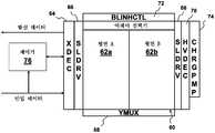
메모리 셀들(32)을 갖는 예시적인 메모리 디바이스의 아키텍처가 도 6에 예시되어 있다. 메모리 디바이스는 2개의 별개의 평면들(평면 A(62a) 및 평면 B(62b))로 분리될 수 있는, 비휘발성 메모리 셀들(32)의 어레이(60)를 포함한다. 메모리 셀들(32)은 바람직하게는, 반도체 기판(34)에서 복수의 로우(row)들 및 컬럼(column)들로 배열된 단일 칩 상에 형성된다. 비휘발성 메모리 셀들의 어레이에 어드레스 디코더들(예컨대, XDEC(64)(워드 라인들을 구동하는 로우 디코더), SLDRV(66)(소스 라인들을 구동하기 위한 소스 라인 드라이버), YMUX(68)(비트 라인들을 구동하는 컬럼 디코더), HVDEC(70)(고 전압 디코더) 및 비트 라인 제어기(BLINHCTL)(72))이 인접해 있는데, 이들은 선택된 메모리 셀들에 대한 판독, 프로그래밍, 및 소거 동작들 동안 어드레스들을 디코딩하고 다양한 전압들을 다양한 메모리 셀 게이트들 및 영역들에 공급하는 데 사용된다. 제어기(76)(제어 회로부를 포함함)는 타깃 메모리 셀들(32) 상에서 각각의 동작(프로그래밍, 소거, 판독)을 구현하도록(즉, 상기 논의된 소거 게이트 네거티브 전압을 사용하여 플로팅 게이트(42)를 프로그래밍하는 데 사용되는 전압들을 포함한, 메모리 셀들(32)을 동작시키기 위해 전압들 및 전류들을 직접적으로 또는 간접적으로 제공하도록) 다양한 디바이스 요소들을 제어한다. 전하 펌프(CHRGPMP)(74)가 제어기(76)의 제어 하에 메모리 셀들을 판독, 프로그래밍 및 소거하는 데 사용되는 다양한 전압들을 제공한다.The architecture of an exemplary memory device with
본 발명은 전술되고 본 명세서에 예시된 실시예(들)로 제한되는 것이 아니라, 임의의 청구항들의 범주 내에 속하는 임의의 그리고 모든 변형들을 포괄한다는 것이 이해되어야 한다. 예를 들어, 본 명세서에서 본 발명에 대한 언급은 임의의 청구항 또는 청구항 용어의 범주를 제한하는 것이 아니라, 대신에 단지 청구항들 중 하나 이상에 의해 커버될 수 있는 하나 이상의 특징들에 대해 언급하는 것으로 의도된다. 전술된 재료들, 프로세스들, 및 수치 예들은 단지 예시적인 것일 뿐이며, 청구항들을 제한하는 것으로 간주되어서는 안된다. 또한, 청구범위 및 명세서로부터 명백한 바와 같이, 모든 방법 단계들이 예시되거나 청구된 정확한 순서로 수행될 필요는 없으며, 오히려 본 발명의 메모리 디바이스의 적절한 형성을 가능하게 하는 임의의 순서로 수행되면 된다. 마지막으로, 재료의 단일 층들이 그러한 또는 유사한 재료들의 다수의 층들로서 형성될 수 있고, 그 반대도 마찬가지이다.It is to be understood that the invention is not limited to the embodiment(s) described above and illustrated herein, but encompasses any and all modifications falling within the scope of any claims. For example, reference to the invention in this specification does not limit the scope of any claim or claim term, but instead merely refers to one or more features that may be covered by one or more of the claims. Is intended. The materials, processes, and numerical examples described above are illustrative only and should not be considered limiting of the claims. Further, as will be apparent from the claims and specification, not all method steps need to be performed in the exact order illustrated or claimed, but rather may be performed in any order that allows proper formation of the memory device of the present invention. Finally, single layers of material can be formed as multiple layers of such or similar materials, and vice versa.
본 명세서에 사용된 바와 같이, 용어들 "~ 위에" 및 "~ 상에" 둘 모두는 "직접적으로 ~ 상에"(어떠한 중간 재료들, 요소들 또는 공간도 사이에 배치되지 않음)와 "간접적으로~ 상에"(중간 재료들, 요소들 또는 공간이 사이에 배치됨)를 포괄적으로 포함한다는 것에 유의하여야 한다. 마찬가지로, 용어 "인접한"은 "직접적으로 인접한"(어떠한 중간 재료들, 요소들 또는 공간도 사이에 배치되지 않음)과 "간접적으로 인접한"(중간 재료들, 요소들 또는 공간이 사이에 배치됨)을 포함하고, "~에 실장되는"은 "직접적으로 ~에 실장되는"(어떠한 중간 재료들, 요소들 또는 공간도 사이에 배치되지 않음)과 "간접적으로 ~에 실장되는"(중간 재료들, 요소들 또는 공간이 사이에 배치됨)을 포함하고, "전기적으로 커플링되는"은 "직접적으로 ~에 전기적으로 커플링되는"(요소들을 함께 전기적으로 접속시키는 어떠한 중간 재료들 또는 요소들도 사이에 없음)과 "간접적으로 ~에 전기적으로 커플링되는"(요소들을 함께 전기적으로 접속시키는 중간 재료들 또는 요소들이 사이에 있음)을 포함한다. 예를 들어, "기판 위에" 요소를 형성하는 것은 어떠한 중간 재료들/요소들도 사이에 갖지 않고서 직접적으로 기판 상에 요소를 형성하는 것뿐만 아니라, 하나 이상의 중간 재료들/요소들을 사이에 갖고서 간접적으로 기판 상에 요소를 형성하는 것을 포함할 수 있다.As used herein, the terms “on” and “on” both refer to “directly on” (not disposed between any intermediate materials, elements or space diagrams) and “indirectly It should be noted that it encompasses "within" (intermediate materials, elements or spaces disposed between). Likewise, the term “adjacent” refers to “directly adjacent” (no intermediate materials, elements or spaces disposed between) and “indirectly adjacent” (intermediate materials, elements or spaces disposed between). And “mounted on” means “directly mounted on” (not placed between any intermediate materials, elements or space diagrams) and “indirectly mounted on” (intermediate materials, elements And "electrically coupled" means "directly electrically coupled to" (no intermediate materials or elements electrically connecting the elements together) ) And "indirectly electrically coupled to" (intermediate materials or elements between them that electrically connect the elements together). For example, forming an element “on the substrate” is not only directly forming the element on the substrate without having any intermediate materials/elements in between, but also indirectly with one or more intermediate materials/elements in between. It may include forming an element on the substrate.
Claims (18)
Translated fromKorean반도체 기판;
메모리 셀 - 상기 메모리 셀은,
상기 기판 내에 형성된 소스 영역 및 드레인 영역 - 상기 소스 영역과 상기 드레인 영역 사이에 상기 기판의 채널 영역이 연장됨 -,
상기 채널 영역의 제1 부분의 전도율을 제어하기 위해, 상기 채널 영역의 상기 제1 부분 위에 배치되고 그로부터 절연되는 플로팅 게이트,
상기 채널 영역의 제2 부분의 전도율을 제어하기 위해, 상기 채널 영역의 상기 제2 부분 위에 배치되고 그로부터 절연되는 선택 게이트,
상기 플로팅 게이트 위에 배치되고 그로부터 절연되는 제어 게이트, 및
상기 소스 영역 위에 배치되고 그로부터 절연되며, 상기 플로팅 게이트에 인접하게 배치되고 그로부터 절연되는 소거 게이트를 포함함 -; 및
제어 회로부를 포함하고,
상기 제어 회로부는,
상기 소거 게이트에 네거티브 전압을 인가하여 전자들이 상기 소거 게이트로부터 상기 플로팅 게이트로 터널링하게 함으로써 프로그래밍 동작을 수행하도록, 그리고
상기 소거 게이트에 포지티브 전압을 인가하여 전자들이 상기 플로팅 게이트로부터 상기 소거 게이트로 터널링하게 함으로써 소거 동작을 수행하도록 구성되는, 메모리 디바이스.As a memory device,
A semiconductor substrate;
Memory cell-the memory cell,
A source region and a drain region formed in the substrate-a channel region of the substrate is extended between the source region and the drain region -,
A floating gate disposed over and insulated from the first portion of the channel region, to control the conductivity of the first portion of the channel region,
A selection gate disposed over and insulated from the second portion of the channel region, to control the conductivity of the second portion of the channel region,
A control gate disposed over and insulated from the floating gate, and
An erase gate disposed over and insulated from the source region and disposed adjacent to and insulated from the floating gate; And
It includes a control circuit part,
The control circuit unit,
To perform a programming operation by applying a negative voltage to the erase gate to allow electrons to tunnel from the erase gate to the floating gate, and
And configured to perform an erase operation by applying a positive voltage to the erase gate to cause electrons to tunnel from the floating gate to the erase gate.
반도체 기판 내에 형성된 소스 영역 및 드레인 영역 - 상기 소스 영역과 상기 드레인 영역 사이에 상기 기판의 채널 영역이 연장됨 -,
상기 채널 영역의 제1 부분의 전도율을 제어하기 위해, 상기 채널 영역의 상기 제1 부분 위에 배치되고 그로부터 절연되는 플로팅 게이트,
상기 채널 영역의 제2 부분의 전도율을 제어하기 위해, 상기 채널 영역의 상기 제2 부분 위에 배치되고 그로부터 절연되는 선택 게이트,
상기 플로팅 게이트 위에 배치되고 그로부터 절연되는 제어 게이트, 및
상기 소스 영역 위에 배치되고 그로부터 절연되며, 상기 플로팅 게이트에 인접하게 배치되고 그로부터 절연되는 소거 게이트를 갖고,
상기 방법은,
상기 소거 게이트에 네거티브 전압을 인가하여 전자들이 상기 소거 게이트로부터 상기 플로팅 게이트로 터널링하게 함으로써 프로그래밍 동작을 수행하는 단계, 및
상기 소거 게이트에 포지티브 전압을 인가하여 전자들이 상기 플로팅 게이트로부터 상기 소거 게이트로 터널링하게 함으로써 소거 동작을 수행하는 단계를 포함하는, 방법.A method of operating a memory device comprising a memory cell, the memory cell comprising:
A source region and a drain region formed in a semiconductor substrate-a channel region of the substrate is extended between the source region and the drain region -,
A floating gate disposed over and insulated from the first portion of the channel region, to control the conductivity of the first portion of the channel region,
A selection gate disposed over and insulated from the second portion of the channel region, to control the conductivity of the second portion of the channel region,
A control gate disposed over and insulated from the floating gate, and
An erase gate disposed over and insulated from the source region and disposed adjacent to and insulated from the floating gate,
The above method,
Performing a programming operation by applying a negative voltage to the erase gate to allow electrons to tunnel from the erase gate to the floating gate, and
And performing an erase operation by applying a positive voltage to the erase gate to cause electrons to tunnel from the floating gate to the erase gate.
상기 소거 게이트에 상기 네거티브 전압이 인가되는 동안 상기 제어 게이트에 0 전압을 인가하는 단계를 추가로 포함하는, 방법.The method of claim 10,
And applying a zero voltage to the control gate while the negative voltage is applied to the erase gate.
상기 소거 게이트에 상기 네거티브 전압이 인가되는 동안 상기 선택 게이트, 상기 소스 영역 및 상기 드레인 영역 각각에 0 전압을 인가하는 단계를 추가로 포함하는, 방법.The method of claim 11,
And applying a zero voltage to each of the select gate, the source region, and the drain region while the negative voltage is applied to the erase gate.
상기 소거 게이트에 상기 네거티브 전압이 인가되는 동안 상기 제어 게이트에 포지티브 전압을 인가하는 단계를 추가로 포함하는, 방법.The method of claim 10,
And applying a positive voltage to the control gate while the negative voltage is applied to the erase gate.
상기 소거 게이트에 상기 네거티브 전압이 인가되는 동안 상기 선택 게이트, 상기 소스 영역 및 상기 드레인 영역 각각에 0 전압을 인가하는 단계를 추가로 포함하는, 방법.The method of claim 13,
And applying a zero voltage to each of the select gate, the source region, and the drain region while the negative voltage is applied to the erase gate.
상기 소거 게이트에 상기 포지티브 전압이 인가되는 동안 상기 제어 게이트에 0 전압을 인가하는 단계를 추가로 포함하는, 방법.The method of claim 10,
And applying a zero voltage to the control gate while the positive voltage is applied to the erase gate.
상기 소거 게이트에 상기 포지티브 전압이 인가되는 동안 상기 선택 게이트, 상기 소스 영역 및 상기 드레인 영역 각각에 0 전압을 인가하는 단계를 추가로 포함하는, 방법.The method of claim 15,
And applying a zero voltage to each of the select gate, the source region, and the drain region while the positive voltage is applied to the erase gate.
상기 소거 게이트에 상기 포지티브 전압이 인가되는 동안 상기 제어 게이트에 네거티브 전압을 인가하는 단계를 추가로 포함하는, 방법.The method of claim 10,
And applying a negative voltage to the control gate while the positive voltage is applied to the erase gate.
상기 소거 게이트에 상기 포지티브 전압이 인가되는 동안 상기 선택 게이트, 상기 소스 영역 및 상기 드레인 영역 각각에 0 전압을 인가하는 단계를 추가로 포함하는, 방법.The method of claim 17,
And applying a zero voltage to each of the select gate, the source region, and the drain region while the positive voltage is applied to the erase gate.
Applications Claiming Priority (5)
| Application Number | Priority Date | Filing Date | Title |
|---|---|---|---|
| US201862722107P | 2018-08-23 | 2018-08-23 | |
| US62/722,107 | 2018-08-23 | ||
| US16/209,515 | 2018-12-04 | ||
| US16/209,515US10714489B2 (en) | 2018-08-23 | 2018-12-04 | Method of programming a split-gate flash memory cell with erase gate |
| PCT/US2019/041080WO2020040894A1 (en) | 2018-08-23 | 2019-07-09 | Method of programming a split-gate flash memory cell with erase gate |
Publications (2)
| Publication Number | Publication Date |
|---|---|
| KR20210019575Atrue KR20210019575A (en) | 2021-02-22 |
| KR102290104B1 KR102290104B1 (en) | 2021-08-17 |
Family
ID=69583741
Family Applications (1)
| Application Number | Title | Priority Date | Filing Date |
|---|---|---|---|
| KR1020217003797AActiveKR102290104B1 (en) | 2018-08-23 | 2019-07-09 | How to Program a Removable Gate Flash Memory Cell With an Erase Gate |
Country Status (7)
| Country | Link |
|---|---|
| US (1) | US10714489B2 (en) |
| EP (1) | EP3841581B1 (en) |
| JP (1) | JP7116844B2 (en) |
| KR (1) | KR102290104B1 (en) |
| CN (1) | CN112585680B (en) |
| TW (1) | TWI757625B (en) |
| WO (1) | WO2020040894A1 (en) |
Families Citing this family (3)
| Publication number | Priority date | Publication date | Assignee | Title |
|---|---|---|---|---|
| CN114335186B (en)* | 2020-09-30 | 2025-02-07 | 硅存储技术股份有限公司 | Split gate non-volatile memory cell with erase gate disposed above word line gate and method of making the same |
| US11545220B2 (en)* | 2020-12-29 | 2023-01-03 | Micron Technology, Inc. | Split-gate memory cells |
| CN114743976B (en)* | 2022-05-10 | 2025-09-23 | 杭州知存算力科技有限公司 | Semiconductor device and method for manufacturing the same |
Citations (4)
| Publication number | Priority date | Publication date | Assignee | Title |
|---|---|---|---|---|
| US5029130A (en)* | 1990-01-22 | 1991-07-02 | Silicon Storage Technology, Inc. | Single transistor non-valatile electrically alterable semiconductor memory device |
| US5386132A (en)* | 1992-11-02 | 1995-01-31 | Wong; Chun C. D. | Multimedia storage system with highly compact memory device |
| US20050269622A1 (en)* | 2004-06-07 | 2005-12-08 | Pavel Klinger | Semiconductor memory array of floating gate memory cells with program/erase and select gates, and methods of making and operating same |
| US20170110194A1 (en)* | 2015-10-19 | 2017-04-20 | Silicon Storage Technology, Inc. | Power Driven Optimization For Flash Memory |
Family Cites Families (8)
| Publication number | Priority date | Publication date | Assignee | Title |
|---|---|---|---|---|
| KR100232235B1 (en) | 1996-11-15 | 1999-12-01 | 김영환 | Nonvolatile memory device |
| JP4647175B2 (en) | 2002-04-18 | 2011-03-09 | ルネサスエレクトロニクス株式会社 | Semiconductor integrated circuit device |
| US6747310B2 (en) | 2002-10-07 | 2004-06-08 | Actrans System Inc. | Flash memory cells with separated self-aligned select and erase gates, and process of fabrication |
| US20090039410A1 (en) | 2007-08-06 | 2009-02-12 | Xian Liu | Split Gate Non-Volatile Flash Memory Cell Having A Floating Gate, Control Gate, Select Gate And An Erase Gate With An Overhang Over The Floating Gate, Array And Method Of Manufacturing |
| JP2009301703A (en) | 2009-09-24 | 2009-12-24 | Renesas Technology Corp | Semiconductor device |
| US8711636B2 (en) | 2011-05-13 | 2014-04-29 | Silicon Storage Technology, Inc. | Method of operating a split gate flash memory cell with coupling gate |
| US8576648B2 (en) | 2011-11-09 | 2013-11-05 | Silicon Storage Technology, Inc. | Method of testing data retention of a non-volatile memory cell having a floating gate |
| CN105609131A (en) | 2014-07-22 | 2016-05-25 | 硅存储技术公司 | System and method for inhibiting erasing of part of splitting gate flash memory unit sector |
- 2018
- 2018-12-04USUS16/209,515patent/US10714489B2/enactiveActive
- 2019
- 2019-07-09EPEP19790338.8Apatent/EP3841581B1/enactiveActive
- 2019-07-09KRKR1020217003797Apatent/KR102290104B1/enactiveActive
- 2019-07-09WOPCT/US2019/041080patent/WO2020040894A1/ennot_activeCeased
- 2019-07-09CNCN201980054482.XApatent/CN112585680B/enactiveActive
- 2019-07-09JPJP2021510104Apatent/JP7116844B2/enactiveActive
- 2019-08-13TWTW108128769Apatent/TWI757625B/enactive
Patent Citations (4)
| Publication number | Priority date | Publication date | Assignee | Title |
|---|---|---|---|---|
| US5029130A (en)* | 1990-01-22 | 1991-07-02 | Silicon Storage Technology, Inc. | Single transistor non-valatile electrically alterable semiconductor memory device |
| US5386132A (en)* | 1992-11-02 | 1995-01-31 | Wong; Chun C. D. | Multimedia storage system with highly compact memory device |
| US20050269622A1 (en)* | 2004-06-07 | 2005-12-08 | Pavel Klinger | Semiconductor memory array of floating gate memory cells with program/erase and select gates, and methods of making and operating same |
| US20170110194A1 (en)* | 2015-10-19 | 2017-04-20 | Silicon Storage Technology, Inc. | Power Driven Optimization For Flash Memory |
Also Published As
| Publication number | Publication date |
|---|---|
| TW202025160A (en) | 2020-07-01 |
| WO2020040894A1 (en) | 2020-02-27 |
| EP3841581A1 (en) | 2021-06-30 |
| JP2021535531A (en) | 2021-12-16 |
| JP7116844B2 (en) | 2022-08-10 |
| US20200066738A1 (en) | 2020-02-27 |
| US10714489B2 (en) | 2020-07-14 |
| CN112585680A (en) | 2021-03-30 |
| KR102290104B1 (en) | 2021-08-17 |
| CN112585680B (en) | 2021-12-14 |
| EP3841581B1 (en) | 2022-06-15 |
| TWI757625B (en) | 2022-03-11 |
Similar Documents
| Publication | Publication Date | Title |
|---|---|---|
| JP6980699B2 (en) | Flash memory array with individual memory cell reads, programs and erases | |
| JP6716022B2 (en) | 3-gate flash memory cell array in which individual memory cells are read, programmed and erased | |
| EP4046158B1 (en) | Four gate, split-gate flash memory array with byte erase operation | |
| KR102431098B1 (en) | Removable Gate Flash Memory Array with Byte Erase Operation | |
| KR102290104B1 (en) | How to Program a Removable Gate Flash Memory Cell With an Erase Gate | |
| CN112639977B (en) | Programming of memory cells having gates capacitively coupled to floating gates | |
| CN111492352A (en) | System and method for minimizing floating gate to floating gate coupling effects during programming in flash memory | |
| CN109328385B (en) | Memory cell array with individual memory cell reading, programming and erasing |
Legal Events
| Date | Code | Title | Description |
|---|---|---|---|
| A302 | Request for accelerated examination | ||
| PA0105 | International application | St.27 status event code:A-0-1-A10-A15-nap-PA0105 | |
| PA0201 | Request for examination | St.27 status event code:A-1-2-D10-D11-exm-PA0201 | |
| PA0302 | Request for accelerated examination | St.27 status event code:A-1-2-D10-D17-exm-PA0302 St.27 status event code:A-1-2-D10-D16-exm-PA0302 | |
| PG1501 | Laying open of application | St.27 status event code:A-1-1-Q10-Q12-nap-PG1501 | |
| E701 | Decision to grant or registration of patent right | ||
| PE0701 | Decision of registration | St.27 status event code:A-1-2-D10-D22-exm-PE0701 | |
| GRNT | Written decision to grant | ||
| PR0701 | Registration of establishment | St.27 status event code:A-2-4-F10-F11-exm-PR0701 | |
| PR1002 | Payment of registration fee | St.27 status event code:A-2-2-U10-U12-oth-PR1002 Fee payment year number:1 | |
| PG1601 | Publication of registration | St.27 status event code:A-4-4-Q10-Q13-nap-PG1601 | |
| P22-X000 | Classification modified | St.27 status event code:A-4-4-P10-P22-nap-X000 | |
| P22-X000 | Classification modified | St.27 status event code:A-4-4-P10-P22-nap-X000 | |
| PR1001 | Payment of annual fee | St.27 status event code:A-4-4-U10-U11-oth-PR1001 Fee payment year number:4 | |
| P22-X000 | Classification modified | St.27 status event code:A-4-4-P10-P22-nap-X000 | |
| PR1001 | Payment of annual fee | St.27 status event code:A-4-4-U10-U11-oth-PR1001 Fee payment year number:5 |