KR20210014815A - Display device and method of fabricating the same - Google Patents
Display device and method of fabricating the sameDownload PDFInfo
- Publication number
- KR20210014815A KR20210014815AKR1020190092495AKR20190092495AKR20210014815AKR 20210014815 AKR20210014815 AKR 20210014815AKR 1020190092495 AKR1020190092495 AKR 1020190092495AKR 20190092495 AKR20190092495 AKR 20190092495AKR 20210014815 AKR20210014815 AKR 20210014815A
- Authority
- KR
- South Korea
- Prior art keywords
- transistor
- region
- driving transistor
- driving
- layer
- Prior art date
- Legal status (The legal status is an assumption and is not a legal conclusion. Google has not performed a legal analysis and makes no representation as to the accuracy of the status listed.)
- Ceased
Links
- 238000004519manufacturing processMethods0.000titleclaimsdescription24
- 239000004065semiconductorSubstances0.000claimsdescription81
- 239000000463materialSubstances0.000claimsdescription30
- 238000000034methodMethods0.000claimsdescription30
- 239000011810insulating materialSubstances0.000claimsdescription19
- 239000012535impuritySubstances0.000claimsdescription10
- 239000010410layerSubstances0.000description284
- 239000003990capacitorSubstances0.000description15
- 238000003860storageMethods0.000description11
- 239000011241protective layerSubstances0.000description8
- 239000002356single layerSubstances0.000description8
- 229910021417amorphous siliconInorganic materials0.000description7
- 239000010408filmSubstances0.000description6
- 230000007423decreaseEffects0.000description4
- 238000005538encapsulationMethods0.000description4
- 239000000758substrateSubstances0.000description4
- 239000010409thin filmSubstances0.000description4
- 230000015572biosynthetic processEffects0.000description3
- 230000000052comparative effectEffects0.000description3
- 230000009977dual effectEffects0.000description3
- 230000014509gene expressionEffects0.000description3
- 238000000059patterningMethods0.000description3
- 230000000149penetrating effectEffects0.000description3
- 230000000704physical effectEffects0.000description3
- 238000005070samplingMethods0.000description3
- 230000035945sensitivityEffects0.000description3
- ZOXJGFHDIHLPTG-UHFFFAOYSA-NBoronChemical compound[B]ZOXJGFHDIHLPTG-UHFFFAOYSA-N0.000description2
- VYPSYNLAJGMNEJ-UHFFFAOYSA-NSilicium dioxideChemical compoundO=[Si]=OVYPSYNLAJGMNEJ-UHFFFAOYSA-N0.000description2
- 229910052796boronInorganic materials0.000description2
- 238000005229chemical vapour depositionMethods0.000description2
- 238000002425crystallisationMethods0.000description2
- 230000008025crystallizationEffects0.000description2
- 238000000151depositionMethods0.000description2
- 238000002347injectionMethods0.000description2
- 239000007924injectionSubstances0.000description2
- 239000011229interlayerSubstances0.000description2
- 230000001678irradiating effectEffects0.000description2
- 238000012986modificationMethods0.000description2
- 230000004048modificationEffects0.000description2
- 230000003071parasitic effectEffects0.000description2
- 238000002161passivationMethods0.000description2
- 229910021420polycrystalline siliconInorganic materials0.000description2
- 229910052814silicon oxideInorganic materials0.000description2
- 229910052581Si3N4Inorganic materials0.000description1
- 229910004205SiNXInorganic materials0.000description1
- 230000000903blocking effectEffects0.000description1
- 238000009792diffusion processMethods0.000description1
- 239000006185dispersionSubstances0.000description1
- 239000011521glassSubstances0.000description1
- 230000005525hole transportEffects0.000description1
- 150000002500ionsChemical class0.000description1
- 239000002184metalSubstances0.000description1
- 239000012044organic layerSubstances0.000description1
- 238000005192partitionMethods0.000description1
- 238000007517polishing processMethods0.000description1
- HQVNEWCFYHHQES-UHFFFAOYSA-Nsilicon nitrideChemical compoundN12[Si]34N5[Si]62N3[Si]51N64HQVNEWCFYHHQES-UHFFFAOYSA-N0.000description1
- 239000000126substanceSubstances0.000description1
- 239000005341toughened glassSubstances0.000description1
Images


Classifications
- G—PHYSICS
- G09—EDUCATION; CRYPTOGRAPHY; DISPLAY; ADVERTISING; SEALS
- G09G—ARRANGEMENTS OR CIRCUITS FOR CONTROL OF INDICATING DEVICES USING STATIC MEANS TO PRESENT VARIABLE INFORMATION
- G09G3/00—Control arrangements or circuits, of interest only in connection with visual indicators other than cathode-ray tubes
- G09G3/20—Control arrangements or circuits, of interest only in connection with visual indicators other than cathode-ray tubes for presentation of an assembly of a number of characters, e.g. a page, by composing the assembly by combination of individual elements arranged in a matrix no fixed position being assigned to or needed to be assigned to the individual characters or partial characters
- G09G3/22—Control arrangements or circuits, of interest only in connection with visual indicators other than cathode-ray tubes for presentation of an assembly of a number of characters, e.g. a page, by composing the assembly by combination of individual elements arranged in a matrix no fixed position being assigned to or needed to be assigned to the individual characters or partial characters using controlled light sources
- G09G3/30—Control arrangements or circuits, of interest only in connection with visual indicators other than cathode-ray tubes for presentation of an assembly of a number of characters, e.g. a page, by composing the assembly by combination of individual elements arranged in a matrix no fixed position being assigned to or needed to be assigned to the individual characters or partial characters using controlled light sources using electroluminescent panels
- G09G3/32—Control arrangements or circuits, of interest only in connection with visual indicators other than cathode-ray tubes for presentation of an assembly of a number of characters, e.g. a page, by composing the assembly by combination of individual elements arranged in a matrix no fixed position being assigned to or needed to be assigned to the individual characters or partial characters using controlled light sources using electroluminescent panels semiconductive, e.g. using light-emitting diodes [LED]
- G09G3/3208—Control arrangements or circuits, of interest only in connection with visual indicators other than cathode-ray tubes for presentation of an assembly of a number of characters, e.g. a page, by composing the assembly by combination of individual elements arranged in a matrix no fixed position being assigned to or needed to be assigned to the individual characters or partial characters using controlled light sources using electroluminescent panels semiconductive, e.g. using light-emitting diodes [LED] organic, e.g. using organic light-emitting diodes [OLED]
- G09G3/3225—Control arrangements or circuits, of interest only in connection with visual indicators other than cathode-ray tubes for presentation of an assembly of a number of characters, e.g. a page, by composing the assembly by combination of individual elements arranged in a matrix no fixed position being assigned to or needed to be assigned to the individual characters or partial characters using controlled light sources using electroluminescent panels semiconductive, e.g. using light-emitting diodes [LED] organic, e.g. using organic light-emitting diodes [OLED] using an active matrix
- G09G3/3233—Control arrangements or circuits, of interest only in connection with visual indicators other than cathode-ray tubes for presentation of an assembly of a number of characters, e.g. a page, by composing the assembly by combination of individual elements arranged in a matrix no fixed position being assigned to or needed to be assigned to the individual characters or partial characters using controlled light sources using electroluminescent panels semiconductive, e.g. using light-emitting diodes [LED] organic, e.g. using organic light-emitting diodes [OLED] using an active matrix with pixel circuitry controlling the current through the light-emitting element
- H—ELECTRICITY
- H10—SEMICONDUCTOR DEVICES; ELECTRIC SOLID-STATE DEVICES NOT OTHERWISE PROVIDED FOR
- H10K—ORGANIC ELECTRIC SOLID-STATE DEVICES
- H10K59/00—Integrated devices, or assemblies of multiple devices, comprising at least one organic light-emitting element covered by group H10K50/00
- H10K59/10—OLED displays
- H10K59/12—Active-matrix OLED [AMOLED] displays
- H10K59/121—Active-matrix OLED [AMOLED] displays characterised by the geometry or disposition of pixel elements
- H10K59/1213—Active-matrix OLED [AMOLED] displays characterised by the geometry or disposition of pixel elements the pixel elements being TFTs
- H01L27/3262—
- H01L27/1214—
- H01L29/786—
- H—ELECTRICITY
- H10—SEMICONDUCTOR DEVICES; ELECTRIC SOLID-STATE DEVICES NOT OTHERWISE PROVIDED FOR
- H10D—INORGANIC ELECTRIC SEMICONDUCTOR DEVICES
- H10D30/00—Field-effect transistors [FET]
- H10D30/60—Insulated-gate field-effect transistors [IGFET]
- H10D30/67—Thin-film transistors [TFT]
- H—ELECTRICITY
- H10—SEMICONDUCTOR DEVICES; ELECTRIC SOLID-STATE DEVICES NOT OTHERWISE PROVIDED FOR
- H10D—INORGANIC ELECTRIC SEMICONDUCTOR DEVICES
- H10D86/00—Integrated devices formed in or on insulating or conducting substrates, e.g. formed in silicon-on-insulator [SOI] substrates or on stainless steel or glass substrates
- H10D86/40—Integrated devices formed in or on insulating or conducting substrates, e.g. formed in silicon-on-insulator [SOI] substrates or on stainless steel or glass substrates characterised by multiple TFTs
- H10D86/431—Integrated devices formed in or on insulating or conducting substrates, e.g. formed in silicon-on-insulator [SOI] substrates or on stainless steel or glass substrates characterised by multiple TFTs having different compositions, shapes, layouts or thicknesses of gate insulators in different TFTs
- H—ELECTRICITY
- H10—SEMICONDUCTOR DEVICES; ELECTRIC SOLID-STATE DEVICES NOT OTHERWISE PROVIDED FOR
- H10D—INORGANIC ELECTRIC SEMICONDUCTOR DEVICES
- H10D86/00—Integrated devices formed in or on insulating or conducting substrates, e.g. formed in silicon-on-insulator [SOI] substrates or on stainless steel or glass substrates
- H10D86/40—Integrated devices formed in or on insulating or conducting substrates, e.g. formed in silicon-on-insulator [SOI] substrates or on stainless steel or glass substrates characterised by multiple TFTs
- H10D86/481—Integrated devices formed in or on insulating or conducting substrates, e.g. formed in silicon-on-insulator [SOI] substrates or on stainless steel or glass substrates characterised by multiple TFTs integrated with passive devices, e.g. auxiliary capacitors
- H—ELECTRICITY
- H10—SEMICONDUCTOR DEVICES; ELECTRIC SOLID-STATE DEVICES NOT OTHERWISE PROVIDED FOR
- H10K—ORGANIC ELECTRIC SOLID-STATE DEVICES
- H10K59/00—Integrated devices, or assemblies of multiple devices, comprising at least one organic light-emitting element covered by group H10K50/00
- H10K59/10—OLED displays
- H10K59/12—Active-matrix OLED [AMOLED] displays
- H10K59/123—Connection of the pixel electrodes to the thin film transistors [TFT]
- G—PHYSICS
- G09—EDUCATION; CRYPTOGRAPHY; DISPLAY; ADVERTISING; SEALS
- G09G—ARRANGEMENTS OR CIRCUITS FOR CONTROL OF INDICATING DEVICES USING STATIC MEANS TO PRESENT VARIABLE INFORMATION
- G09G2300/00—Aspects of the constitution of display devices
- G09G2300/04—Structural and physical details of display devices
- G09G2300/0421—Structural details of the set of electrodes
- G09G2300/0426—Layout of electrodes and connections
- G—PHYSICS
- G09—EDUCATION; CRYPTOGRAPHY; DISPLAY; ADVERTISING; SEALS
- G09G—ARRANGEMENTS OR CIRCUITS FOR CONTROL OF INDICATING DEVICES USING STATIC MEANS TO PRESENT VARIABLE INFORMATION
- G09G2300/00—Aspects of the constitution of display devices
- G09G2300/08—Active matrix structure, i.e. with use of active elements, inclusive of non-linear two terminal elements, in the pixels together with light emitting or modulating elements
- G09G2300/0809—Several active elements per pixel in active matrix panels
- G09G2300/0819—Several active elements per pixel in active matrix panels used for counteracting undesired variations, e.g. feedback or autozeroing
- G—PHYSICS
- G09—EDUCATION; CRYPTOGRAPHY; DISPLAY; ADVERTISING; SEALS
- G09G—ARRANGEMENTS OR CIRCUITS FOR CONTROL OF INDICATING DEVICES USING STATIC MEANS TO PRESENT VARIABLE INFORMATION
- G09G2300/00—Aspects of the constitution of display devices
- G09G2300/08—Active matrix structure, i.e. with use of active elements, inclusive of non-linear two terminal elements, in the pixels together with light emitting or modulating elements
- G09G2300/0809—Several active elements per pixel in active matrix panels
- G09G2300/0842—Several active elements per pixel in active matrix panels forming a memory circuit, e.g. a dynamic memory with one capacitor
- G09G2300/0861—Several active elements per pixel in active matrix panels forming a memory circuit, e.g. a dynamic memory with one capacitor with additional control of the display period without amending the charge stored in a pixel memory, e.g. by means of additional select electrodes
- G—PHYSICS
- G09—EDUCATION; CRYPTOGRAPHY; DISPLAY; ADVERTISING; SEALS
- G09G—ARRANGEMENTS OR CIRCUITS FOR CONTROL OF INDICATING DEVICES USING STATIC MEANS TO PRESENT VARIABLE INFORMATION
- G09G2310/00—Command of the display device
- G09G2310/02—Addressing, scanning or driving the display screen or processing steps related thereto
- G09G2310/0243—Details of the generation of driving signals
- G09G2310/0251—Precharge or discharge of pixel before applying new pixel voltage
- G—PHYSICS
- G09—EDUCATION; CRYPTOGRAPHY; DISPLAY; ADVERTISING; SEALS
- G09G—ARRANGEMENTS OR CIRCUITS FOR CONTROL OF INDICATING DEVICES USING STATIC MEANS TO PRESENT VARIABLE INFORMATION
- G09G2310/00—Command of the display device
- G09G2310/02—Addressing, scanning or driving the display screen or processing steps related thereto
- G09G2310/0262—The addressing of the pixel, in a display other than an active matrix LCD, involving the control of two or more scan electrodes or two or more data electrodes, e.g. pixel voltage dependent on signals of two data electrodes
- H—ELECTRICITY
- H10—SEMICONDUCTOR DEVICES; ELECTRIC SOLID-STATE DEVICES NOT OTHERWISE PROVIDED FOR
- H10D—INORGANIC ELECTRIC SEMICONDUCTOR DEVICES
- H10D86/00—Integrated devices formed in or on insulating or conducting substrates, e.g. formed in silicon-on-insulator [SOI] substrates or on stainless steel or glass substrates
- H10D86/01—Manufacture or treatment
- H10D86/021—Manufacture or treatment of multiple TFTs
- H10D86/0221—Manufacture or treatment of multiple TFTs comprising manufacture, treatment or patterning of TFT semiconductor bodies
- H10D86/0223—Manufacture or treatment of multiple TFTs comprising manufacture, treatment or patterning of TFT semiconductor bodies comprising crystallisation of amorphous, microcrystalline or polycrystalline semiconductor materials
- H—ELECTRICITY
- H10—SEMICONDUCTOR DEVICES; ELECTRIC SOLID-STATE DEVICES NOT OTHERWISE PROVIDED FOR
- H10D—INORGANIC ELECTRIC SEMICONDUCTOR DEVICES
- H10D86/00—Integrated devices formed in or on insulating or conducting substrates, e.g. formed in silicon-on-insulator [SOI] substrates or on stainless steel or glass substrates
- H10D86/01—Manufacture or treatment
- H10D86/021—Manufacture or treatment of multiple TFTs
- H10D86/0231—Manufacture or treatment of multiple TFTs using masks, e.g. half-tone masks
- H—ELECTRICITY
- H10—SEMICONDUCTOR DEVICES; ELECTRIC SOLID-STATE DEVICES NOT OTHERWISE PROVIDED FOR
- H10D—INORGANIC ELECTRIC SEMICONDUCTOR DEVICES
- H10D86/00—Integrated devices formed in or on insulating or conducting substrates, e.g. formed in silicon-on-insulator [SOI] substrates or on stainless steel or glass substrates
- H10D86/40—Integrated devices formed in or on insulating or conducting substrates, e.g. formed in silicon-on-insulator [SOI] substrates or on stainless steel or glass substrates characterised by multiple TFTs
- H10D86/421—Integrated devices formed in or on insulating or conducting substrates, e.g. formed in silicon-on-insulator [SOI] substrates or on stainless steel or glass substrates characterised by multiple TFTs having a particular composition, shape or crystalline structure of the active layer
- H10D86/427—Integrated devices formed in or on insulating or conducting substrates, e.g. formed in silicon-on-insulator [SOI] substrates or on stainless steel or glass substrates characterised by multiple TFTs having a particular composition, shape or crystalline structure of the active layer having different thicknesses of the semiconductor bodies in different TFTs
- H—ELECTRICITY
- H10—SEMICONDUCTOR DEVICES; ELECTRIC SOLID-STATE DEVICES NOT OTHERWISE PROVIDED FOR
- H10D—INORGANIC ELECTRIC SEMICONDUCTOR DEVICES
- H10D86/00—Integrated devices formed in or on insulating or conducting substrates, e.g. formed in silicon-on-insulator [SOI] substrates or on stainless steel or glass substrates
- H10D86/40—Integrated devices formed in or on insulating or conducting substrates, e.g. formed in silicon-on-insulator [SOI] substrates or on stainless steel or glass substrates characterised by multiple TFTs
- H10D86/471—Integrated devices formed in or on insulating or conducting substrates, e.g. formed in silicon-on-insulator [SOI] substrates or on stainless steel or glass substrates characterised by multiple TFTs having different architectures, e.g. having both top-gate and bottom-gate TFTs
- H—ELECTRICITY
- H10—SEMICONDUCTOR DEVICES; ELECTRIC SOLID-STATE DEVICES NOT OTHERWISE PROVIDED FOR
- H10D—INORGANIC ELECTRIC SEMICONDUCTOR DEVICES
- H10D86/00—Integrated devices formed in or on insulating or conducting substrates, e.g. formed in silicon-on-insulator [SOI] substrates or on stainless steel or glass substrates
- H10D86/40—Integrated devices formed in or on insulating or conducting substrates, e.g. formed in silicon-on-insulator [SOI] substrates or on stainless steel or glass substrates characterised by multiple TFTs
- H10D86/60—Integrated devices formed in or on insulating or conducting substrates, e.g. formed in silicon-on-insulator [SOI] substrates or on stainless steel or glass substrates characterised by multiple TFTs wherein the TFTs are in active matrices
- H—ELECTRICITY
- H10—SEMICONDUCTOR DEVICES; ELECTRIC SOLID-STATE DEVICES NOT OTHERWISE PROVIDED FOR
- H10K—ORGANIC ELECTRIC SOLID-STATE DEVICES
- H10K59/00—Integrated devices, or assemblies of multiple devices, comprising at least one organic light-emitting element covered by group H10K50/00
- H10K59/10—OLED displays
- H10K59/12—Active-matrix OLED [AMOLED] displays
- H10K59/1201—Manufacture or treatment
Landscapes
- Engineering & Computer Science (AREA)
- Physics & Mathematics (AREA)
- Microelectronics & Electronic Packaging (AREA)
- Geometry (AREA)
- Computer Hardware Design (AREA)
- General Physics & Mathematics (AREA)
- Theoretical Computer Science (AREA)
- Electroluminescent Light Sources (AREA)
- Control Of El Displays (AREA)
Abstract
Translated fromKoreanDescription
Translated fromKorean본 발명의 실시예는 표시 장치 및 그의 제조 방법에 관한 것이다.Embodiments of the present invention relate to a display device and a method of manufacturing the same.
표시 장치는 표시 영역에 배치된 화소들을 이용하여 영상을 표시한다. 화소들은 각각의 주사선 및 데이터선에 연결되며, 복수의 트랜지스터들을 포함할 수 있다. 일 예로, 능동형 발광 표시 장치의 화소는, 발광 소자, 구동 트랜지스터 및 적어도 하나의 스위칭 트랜지스터를 포함할 수 있다.The display device displays an image using pixels arranged in the display area. The pixels are connected to respective scan lines and data lines, and may include a plurality of transistors. As an example, a pixel of an active light emitting display device may include a light emitting element, a driving transistor, and at least one switching transistor.
이러한 화소의 휘도는 발광 소자에 흐르는 구동 전류의 크기에 따라 달라질 수 있는 것으로서, 상기 구동 전류는 구동 트랜지스터에 의해 제어된다. 각각의 계조에 대응하여 화소의 휘도를 균일하게 제어하고, 보다 세밀하게 계조를 표현하기 위해서는 구동 트랜지스터의 구동 범위(driving range)를 충분히 확보하여야 한다.The luminance of such a pixel may vary depending on the magnitude of a driving current flowing through the light emitting device, and the driving current is controlled by a driving transistor. In order to uniformly control the luminance of a pixel corresponding to each gray level and to express the gray level more precisely, a driving range of the driving transistor must be sufficiently secured.
본 발명이 이루고자 하는 기술적 과제는, 구동 트랜지스터의 구동 범위를 충분히 확보하면서도 상기 구동 트랜지스터가 차지하는 면적을 축소할 수 있도록 한 표시 장치 및 그의 제조 방법을 제공하는 것이다.The technical problem to be achieved by the present invention is to provide a display device and a method of manufacturing the same so that the area occupied by the driving transistor can be reduced while sufficiently securing a driving range of the driving transistor.
본 발명의 일 실시예에 의한 표시 장치는, 표시 영역에 배치된 화소를 구비한다. 상기 화소는, 제1 전원과 제2 전원의 사이에 연결된 발광 소자와, 상기 제1 전원과 상기 발광 소자의 사이에 연결되며 제1 노드의 전압에 대응하여 상기 발광 소자에 흐르는 구동 전류를 제어하는 제1 트랜지스터를 포함한다. 상기 제1 트랜지스터는, 상기 제1 전원과 상기 발광 소자의 사이에 직렬로 연결되며 서로 비대칭적인 단면 구조를 가지는 제1 구동 트랜지스터 및 제2 구동 트랜지스터를 포함한 복수의 트랜지스터들로 구성된다.A display device according to an exemplary embodiment of the present invention includes pixels disposed in the display area. The pixel may include a light emitting device connected between a first power source and a second power source, and connected between the first power source and the light emitting device, and controlling a driving current flowing through the light emitting device in response to a voltage of a first node. And a first transistor. The first transistor includes a plurality of transistors connected in series between the first power source and the light emitting device and including a first driving transistor and a second driving transistor having an asymmetric cross-sectional structure.
일 실시예에서, 상기 제1 구동 트랜지스터 및 상기 제2 구동 트랜지스터는, 채널 영역의 두께 및 게이트 절연막의 두께 중 적어도 하나가 상이할 수 있다.In an embodiment, at least one of a thickness of a channel region and a thickness of a gate insulating layer may be different between the first driving transistor and the second driving transistor.
일 실시예에서, 상기 제1 트랜지스터는, 제1 채널 영역과, 상기 제1 채널 영역의 양측에 배치된 제1 전도성 영역 및 제2 전도성 영역과, 상기 제2 전도성 영역을 사이에 개재하고 상기 제1 채널 영역으로부터 이격된 제2 채널 영역과, 상기 제2 채널 영역을 사이에 개재하고 상기 제2 전도성 영역으로부터 이격된 제3 전도성 영역과, 제1 절연막을 사이에 개재하고 상기 제1 채널 영역과 중첩되는 제1 게이트 전극과, 상기 제1 절연막을 사이에 개재하고 상기 제2 채널 영역과 중첩되는 제2 게이트 전극을 포함할 수 있다.In an embodiment, the first transistor includes a first channel region, a first conductive region and a second conductive region disposed on both sides of the first channel region, and the second conductive region interposed therebetween, A second channel region spaced apart from the first channel region, a third conductive region spaced apart from the second conductive region and the second channel region interposed therebetween, a first insulating layer interposed therebetween, and the first channel region It may include a first gate electrode overlapping, and a second gate electrode interposed between the first insulating layer and overlapping the second channel region.
일 실시예에서, 상기 제1 구동 트랜지스터는, 상기 제1 전원과 상기 제2 구동 트랜지스터의 사이에 연결되며, 상기 제1 채널 영역, 상기 제1 전도성 영역 및 상기 제2 전도성 영역을 포함한 제1 활성층 패턴을 포함할 수 있다. 또한, 상기 제2 구동 트랜지스터는, 상기 제1 구동 트랜지스터와 상기 발광 소자의 사이에 연결되며, 상기 제2 채널 영역, 상기 제2 전도성 영역 및 상기 제3 전도성 영역을 포함한 제2 활성층 패턴을 포함할 수 있다.In one embodiment, the first driving transistor is connected between the first power source and the second driving transistor, the first active layer including the first channel region, the first conductive region and the second conductive region It can contain patterns. In addition, the second driving transistor is connected between the first driving transistor and the light emitting element, and includes a second active layer pattern including the second channel region, the second conductive region, and the third conductive region. I can.
일 실시예에서, 상기 제1 절연막은, 상기 제1 채널 영역과 상기 제1 게이트 전극의 사이에서 제1 두께를 가지고, 상기 제2 채널 영역과 상기 제2 게이트 전극의 사이에서 상기 제1 두께보다 작은 제2 두께를 가질 수 있다.In one embodiment, the first insulating layer has a first thickness between the first channel region and the first gate electrode, and is greater than the first thickness between the second channel region and the second gate electrode. It can have a small second thickness.
일 실시예에서, 상기 제1 채널 영역은 상기 제2 채널 영역보다 큰 두께를 가질 수 있다.In an embodiment, the first channel region may have a thickness greater than that of the second channel region.
일 실시예에서, 상기 제1 채널 영역은 상기 제2 채널 영역보다 긴 길이를 가질 수 있다.In one embodiment, the first channel region may have a length longer than that of the second channel region.
일 실시예에서, 상기 제1 활성층 패턴과 상기 제2 활성층 패턴은 상기 제2 전도성 영역을 통해 서로 일체로 연결될 수 있다.In one embodiment, the first active layer pattern and the second active layer pattern may be integrally connected to each other through the second conductive region.
일 실시예에서, 상기 제1 게이트 전극 및 상기 제2 게이트 전극은 상기 제1 노드에 공통으로 연결될 수 있다.In an embodiment, the first gate electrode and the second gate electrode may be commonly connected to the first node.
일 실시예에서, 상기 제1 트랜지스터는, 상기 제1 전도성 영역에 연결되는 제1 전극과, 상기 제3 전도성 영역에 연결되는 제2 전극을 더 포함할 수 있다.In an embodiment, the first transistor may further include a first electrode connected to the first conductive region and a second electrode connected to the third conductive region.
일 실시예에서, 상기 화소는, 상기 제1 노드로 데이터 신호 또는 초기화 전원의 전압을 전달하기 위한 적어도 하나의 스위칭 트랜지스터를 더 포함할 수 있다.In an embodiment, the pixel may further include at least one switching transistor for transmitting a data signal or a voltage of an initialization power to the first node.
일 실시예에서, 상기 스위칭 트랜지스터는, 서로 직렬로 연결된 복수의 트랜지스터들로 구성될 수 있다.In one embodiment, the switching transistor may be composed of a plurality of transistors connected in series with each other.
본 발명의 일 실시예에 의한 표시 장치는, 서로 직렬로 연결된 제1 구동 트랜지스터 및 제2 구동 트랜지스터를 포함한 화소를 구비한다. 상기 표시 장치의 제조 방법은, 베이스 층 상에 반도체 패턴을 형성하는 단계와, 상기 반도체 패턴 상에 제1 절연막을 형성하는 단계와, 상기 반도체 패턴의 서로 다른 일 영역과 중첩되도록 상기 제1 절연막 상에 제1 게이트 전극 및 제2 게이트 전극을 형성하는 단계를 포함하며, 상기 제1 및 제2 구동 트랜지스터들을 서로 비대칭적인 단면 구조를 가지도록 형성함을 특징으로 한다.A display device according to an exemplary embodiment of the present invention includes a pixel including a first driving transistor and a second driving transistor connected in series with each other. The method of manufacturing the display device includes forming a semiconductor pattern on a base layer, forming a first insulating layer on the semiconductor pattern, and forming a first insulating layer on the first insulating layer so as to overlap with different regions of the semiconductor pattern. And forming a first gate electrode and a second gate electrode, wherein the first and second driving transistors are formed to have an asymmetric cross-sectional structure.
일 실시예에서, 상기 제1 구동 트랜지스터가 형성될 영역과 상기 제2 구동 트랜지스터가 형성될 영역에 대응하여, 상기 반도체 패턴 및 상기 제1 절연막 중 적어도 하나를 영역별로 상이한 두께로 형성할 수 있다.In an embodiment, at least one of the semiconductor pattern and the first insulating layer may be formed to have different thicknesses for each region, corresponding to a region in which the first driving transistor is to be formed and a region in which the second driving transistor is to be formed.
일 실시예에서, 상기 제1 절연막을 형성하는 단계는, 상기 반도체 패턴을 커버하도록 절연 물질을 일차적으로 도포하여 절연 물질층을 형성하는 단계와, 상기 절연 물질층 상에 마스크를 배치하여 상기 제1 구동 트랜지스터가 형성될 영역을 선택적으로 노출하고, 상기 제1 구동 트랜지스터가 형성될 영역에 대응하는 상기 반도체 패턴의 일 영역 상에 상기 절연 물질을 추가적으로 도포하는 단계를 포함할 수 있다.In one embodiment, the forming of the first insulating layer includes forming an insulating material layer by first applying an insulating material to cover the semiconductor pattern, and disposing a mask on the insulating material layer to form the first insulating layer. And selectively exposing a region in which a driving transistor is to be formed, and additionally applying the insulating material on a region of the semiconductor pattern corresponding to a region in which the first driving transistor is to be formed.
일 실시예에서, 상기 반도체 패턴을 형성하는 단계는, 상기 제1 및 제2 구동 트랜지스터들이 형성될 영역에 반도체 물질을 일차적으로 도포하여 반도체 물질층을 형성하는 단계와, 상기 반도체 물질층 상에 마스크를 배치하여 상기 제1 구동 트랜지스터가 형성될 영역을 선택적으로 노출하고, 상기 제1 구동 트랜지스터가 형성될 영역 상에 상기 반도체 물질을 추가적으로 도포하는 단계를 포함할 수 있다.In an embodiment, the forming of the semiconductor pattern includes forming a semiconductor material layer by first applying a semiconductor material to a region where the first and second driving transistors are to be formed, and forming a semiconductor material layer on the semiconductor material layer. And selectively exposing a region in which the first driving transistor is to be formed, and additionally applying the semiconductor material on the region in which the first driving transistor is to be formed.
일 실시예에서, 상기 표시 장치의 제조 방법은, 상기 반도체 패턴을 결정화하는 단계와, 상기 반도체 패턴의 일 영역에 선택적으로 불순물을 도핑하는 단계를 더 포함할 수 있다.In an exemplary embodiment, the method of manufacturing the display device may further include crystallizing the semiconductor pattern, and selectively doping an impurity into a region of the semiconductor pattern.
본 발명의 일 실시예에 의한 표시 장치 및 그의 제조 방법에 따르면, 각 화소에 구비되는 구동 트랜지스터의 구동 범위를 충분히 확보하면서도 상기 구동 트랜지스터가 차지하는 면적을 축소할 수 있다. 또한, 상기 구동 트랜지스터를 구성하는 복수의 트랜지스터들의 소자 특성을 개별적으로 조절하여, 상기 구동 트랜지스터의 구동 특성을 최적화할 수 있다.According to the display device and its manufacturing method according to an exemplary embodiment of the present invention, while sufficiently securing a driving range of a driving transistor provided in each pixel, an area occupied by the driving transistor can be reduced. In addition, device characteristics of a plurality of transistors constituting the driving transistor may be individually adjusted to optimize driving characteristics of the driving transistor.
도 1은 본 발명의 일 실시예에 의한 표시 장치를 나타낸다.
도 2 및 도 3은 각각 본 발명의 일 실시예에 의한 화소를 나타낸다.
도 4 및 도 5는 각각 본 발명의 일 실시예에 의한 제1 트랜지스터의 단면 구조를 나타낸다.
도 6은 본 발명의 일 실시예에 의한 제1 트랜지스터의 구동 범위를 나타낸다.
도 7 및 도 8은 각각 본 발명의 일 실시예에 의한 제1 트랜지스터를 포함한 화소의 단면 구조를 나타낸다.
도 9a 내지 도 9j는 본 발명의 일 실시예에 의한 표시 장치의 제조 방법을 나타낸다.
도 10a 내지 도 10j는 본 발명의 일 실시예에 의한 표시 장치의 제조 방법을 나타낸다.1 illustrates a display device according to an exemplary embodiment of the present invention.
2 and 3 each show a pixel according to an exemplary embodiment of the present invention.
4 and 5 each show a cross-sectional structure of a first transistor according to an embodiment of the present invention.
6 shows a driving range of a first transistor according to an embodiment of the present invention.
7 and 8 each show a cross-sectional structure of a pixel including a first transistor according to an exemplary embodiment of the present invention.
9A to 9J illustrate a method of manufacturing a display device according to an exemplary embodiment of the present invention.
10A to 10J illustrate a method of manufacturing a display device according to an exemplary embodiment of the present invention.
본 발명은 다양한 변경을 가할 수 있고 여러 가지 형태를 가질 수 있는 바, 특정 실시예를 도면에 예시하고 본문에 상세하게 설명하고자 한다. 다만, 본 발명은 이하에서 개시되는 실시예에 한정되지는 않으며, 다양한 형태로 변경되어 실시될 수 있을 것이다. 또한, 아래의 설명에서, 단수의 표현은 문맥상 명백하게 단수만을 포함하지 않는 한, 복수의 표현도 포함한다.In the present invention, various modifications can be made and various forms can be applied, and specific embodiments will be illustrated in the drawings and described in detail in the text. However, the present invention is not limited to the embodiments disclosed below, and may be changed in various forms and implemented. In addition, in the description below, expressions in the singular also include expressions in the plural unless the context clearly includes only the singular.
도면에서 본 발명의 특징과 직접적으로 관계되지 않은 일부 구성 요소는 본 발명을 명확하게 나타내기 위하여 생략되었을 수 있다. 또한, 도면 상의 일부 구성 요소는 그 크기나 비율 등이 다소 과장되어 도시되었을 수 있다. 도면 전반에서 동일 또는 유사한 구성 요소들에 대해서는 비록 다른 도면 상에 표시되더라도 가능한 한 동일한 참조 번호 및 부호를 부여하고, 중복되는 설명은 생략하기로 한다.In the drawings, some elements not directly related to the features of the present invention may be omitted to clearly illustrate the present invention. In addition, some of the components in the drawings may have their size or ratio somewhat exaggerated. Throughout the drawings, the same or similar components are assigned the same reference numerals and reference numerals as much as possible even though they are displayed on different drawings, and redundant descriptions will be omitted.
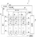
도 1은 본 발명의 일 실시예에 의한 표시 장치(1)를 나타낸다. 도 1에서는 표시 장치(1)의 일 예로서 발광 소자들을 구비한 발광 표시 장치를 도시하였으나, 본 발명에 의한 표시 장치(1)가 이에 한정되지는 않는다.1 shows a
도 1을 참조하면, 본 발명의 일 실시예에 의한 표시 장치(1)는, 화소들(PXL)이 배치된 표시 영역(10)과, 상기 화소들(PXL)을 구동하기 위한 주사 구동부(20), 발광 제어 구동부(30), 데이터 구동부(40) 및 타이밍 제어부(50)를 구비한다.Referring to FIG. 1, a
표시 영역(10)은, 주사선들(S1~Sn), 발광 제어선들(E1~En) 및 데이터선들(D1~Dm)에 연결된 화소들(PXL)을 구비한다. 본 발명의 실시예를 설명함에 있어, "연결"이라 함은, 전기적 및/또는 물리적인 연결을 포괄적으로 의미할 수 있다. 예를 들어, 화소들(PXL)은 주사선들(S1~Sn), 발광 제어선들(E1~En) 및 데이터선들(D1~Dm)에 전기적으로 연결될 수 있다.The
한편, 실시예에 따라서는 발광 제어선들(E1~En)이 생략될 수도 있다. 예를 들어, 발광 제어선들(E1~En)은 화소들(PXL)의 구조 및/또는 구동 방식 등에 따라 선택적으로 구비될 수 있는 것으로서, 일 예로 본 발명의 다른 실시예에서는 발광 제어선들(E1~En)이 생략될 수도 있다. 이 경우, 표시 장치(1)는 발광 제어 구동부(30)를 구비하지 않을 수 있다.Meanwhile, in some embodiments, the emission control lines E1 to En may be omitted. For example, the emission control lines E1 to En may be selectively provided according to the structure and/or driving method of the pixels PXL. For example, in another embodiment of the present invention, the emission control lines E1 to En En) may be omitted. In this case, the
또한, 실시예에 따라서는, 화소들(PXL)이 도시되지 않은 적어도 하나의 다른 제어선에 더 연결될 수도 있다. 이 경우, 화소들(PXL)은 상기 제어선으로부터 공급되는 제어신호에 의해 그 동작이 제어될 수 있다.In addition, depending on the embodiment, the pixels PXL may be further connected to at least one other control line, not shown. In this case, the operation of the pixels PXL may be controlled by a control signal supplied from the control line.
화소들(PXL)은 주사선들(S1~Sn), 발광 제어선들(E1~En) 및 데이터선들(D1~Dm)로부터 각각의 주사 신호, 발광 제어 신호 및 데이터 신호를 공급받는다. 또한, 화소들(PXL)은 제1 전원(ELVDD) 및 제2 전원(ELVSS)에 연결되어, 동작 전원을 공급받을 수 있다. 추가적으로, 화소들(PXL)은 그 구조 및/또는 구동 방식 등에 따라서는 그 외의 다른 전원(일 예로, 초기화 전원)에 더 연결될 수도 있다.The pixels PXL receive respective scan signals, emission control signals, and data signals from the scan lines S1 to Sn, the emission control lines E1 to En, and the data lines D1 to Dm. Further, the pixels PXL may be connected to the first power ELVDD and the second power ELVSS to receive operation power. Additionally, the pixels PXL may be further connected to other power sources (eg, initialization power) depending on their structure and/or driving method.
이와 같은 화소들(PXL)은 주사선들(S1~Sn)로부터 각각의 주사 신호가 공급될 때 데이터선들(D1~Dm)로부터 각각의 데이터 신호를 공급받고, 상기 데이터 신호에 대응하는 휘도로 발광한다. 이에 따라, 표시 영역(10)에서 각 프레임의 데이터 신호에 대응하는 영상이 표시된다.When each scan signal is supplied from the scan lines S1 to Sn, such pixels PXL receive respective data signals from the data lines D1 to Dm, and emit light with a luminance corresponding to the data signal. . Accordingly, an image corresponding to the data signal of each frame is displayed in the
각각의 화소(PXL)는, 발광 소자와, 상기 발광 소자를 구동하기 위한 화소 회로를 포함할 수 있다. 화소 회로는, 데이터 신호에 대응하여 제1 전원(ELVDD)으로부터 발광 소자를 경유하여 제2 전원(ELVSS)으로 흐르는 구동 전류를 제어한다. 이를 위해, 화소 회로는, 구동 트랜지스터와 적어도 하나의 스위칭 트랜지스터를 포함할 수 있다.Each pixel PXL may include a light-emitting element and a pixel circuit for driving the light-emitting element. The pixel circuit controls a driving current flowing from the first power supply ELVDD to the second power supply ELVSS through the light emitting element in response to the data signal. To this end, the pixel circuit may include a driving transistor and at least one switching transistor.
주사 구동부(20)는 타이밍 제어부(50)로부터 주사 구동 제어 신호(SCS)를 공급받고, 상기 주사 구동 제어 신호(SCS)에 대응하여 주사선들(S1~Sn)로 주사 신호를 공급한다. 일 예로, 주사 구동부(20)는 주사 구동 제어 신호(SCS)에 대응하여 주사선들(S1~Sn)로 순차적으로 주사 신호를 공급할 수 있다. 주사선들(S1~Sn)로 각각의 주사 신호가 공급되면, 상기 주사 신호에 의해 각각의 주사선에 연결된 화소들(PXL)이 선택된다.The
실시예에 따라, 주사 신호는 수평 라인 단위로 화소들(PXL)을 선택하기 위하여 이용될 수 있다. 예를 들어, 주사 신호는 데이터선들(D1~Dm)에 연결된 각 화소(PXL)의 트랜지스터(일 예로, 적어도 하나의 스위칭 트랜지스터)가 턴-온될 수 있는 게이트-온 전압(일 예로, 로우 전압)을 가질 수 있으며, 각각의 수평 기간에 대응하는 수평 라인의 화소들(PXL)로 공급될 수 있다. 주사 신호를 공급받는 화소들(PXL)은, 상기 주사 신호가 공급되는 기간 동안 데이터선들(D1~Dm)에 연결되어 각각의 데이터 신호를 공급받을 수 있다.Depending on the embodiment, the scan signal may be used to select the pixels PXL in units of horizontal lines. For example, the scan signal is a gate-on voltage (for example, a low voltage) at which a transistor (for example, at least one switching transistor) of each pixel PXL connected to the data lines D1 to Dm can be turned on. And may be supplied to pixels PXL of a horizontal line corresponding to each horizontal period. The pixels PXL receiving the scan signal may be connected to the data lines D1 to Dm during the period in which the scan signal is supplied to receive respective data signals.
발광 제어 구동부(30)는 타이밍 제어부(50)로부터 발광 구동 제어 신호(ECS)를 공급받고, 상기 발광 구동 제어 신호(ECS)에 대응하여 발광 제어선들(E1~En)로 발광 제어 신호를 공급한다. 일 예로, 발광 제어 구동부(30)는 발광 구동 제어 신호(ECS)에 대응하여 발광 제어선들(E1~En)로 순차적으로 발광 제어 신호를 공급할 수 있다. 한편, 발광 제어 구동부(30)는 화소들(PXL)의 구조 및/또는 구동 방식 등에 따라 선택적으로 구비될 수 있는 것으로서, 실시예에 따라서는 생략될 수도 있다.The light
발광 제어 신호는 화소들(PXL)의 발광 기간(일 예로, 발광 시점 및/또는 발광 지속 시간)을 제어하기 위하여 이용될 수 있다. 예를 들어, 발광 제어 신호는 화소들(PXL) 각각의 전류 패스 상에 위치한 적어도 하나의 스위칭 트랜지스터가 턴-오프될 수 있는 게이트-오프 전압(일 예로, 하이 전압)을 가질 수 있다. 이 경우, 발광 제어 신호를 공급받은 화소(PXL)는, 상기 발광 제어 신호가 공급되는 기간 동안 비발광 상태로 설정되고, 그 외의 기간 동안 발광 상태로 설정될 수 있다. 한편, 적어도 하나의 화소(PXL)로 블랙 계조에 대응하는 데이터 신호가 공급될 경우, 상기 화소(PXL)는 게이트-오프 전압의 발광 제어 신호가 공급되지 않더라도 상기 데이터 신호에 대응하여 해당 프레임 기간 동안 비발광 상태를 유지할 수 있다.The emission control signal may be used to control the emission period (eg, emission timing and/or emission duration) of the pixels PXL. For example, the emission control signal may have a gate-off voltage (for example, a high voltage) at which at least one switching transistor located on a current path of each of the pixels PXL is turned off. In this case, the pixel PXL receiving the emission control signal may be set to a non-emission state during the period in which the emission control signal is supplied, and may be set to a light emission state during other periods. On the other hand, when a data signal corresponding to a black gradation is supplied to at least one pixel PXL, the pixel PXL corresponds to the data signal during a corresponding frame period even if the emission control signal of the gate-off voltage is not supplied. It can maintain a non-luminous state.
데이터 구동부(40)는 타이밍 제어부(50)로부터 데이터 구동 제어 신호(DCS) 및 영상 데이터(RGB)를 공급받고, 상기 데이터 구동 제어 신호(DCS) 및 영상 데이터(RGB)에 대응하여 데이터선들(D1~Dm)로 데이터 신호를 공급한다. 데이터선들(D1~Dm)로 공급된 데이터 신호는 각각의 주사 신호에 의해 선택된 화소들(PXL)로 공급된다.The
타이밍 제어부(50)는 외부(일 예로, 호스트 프로세서)로부터 각종 타이밍 제어 신호들(일 예로, 수직/수평 동기신호, 메인 클럭신호 등)을 공급받고, 상기 타이밍 제어 신호들에 대응하여 주사 구동 제어 신호(SCS), 발광 구동 제어 신호(ECS) 및 데이터 구동 제어 신호(DCS)를 생성한다. 상기 주사 구동 제어 신호(SCS), 발광 구동 제어 신호(ECS) 및 데이터 구동 제어 신호(DCS)는, 각각 주사 구동부(20), 발광 제어 구동부(30) 및 데이터 구동부(40)로 공급된다.The
주사 구동 제어 신호(SCS)는 제1 스타트 펄스(일 예로, 주사 스타트 펄스) 및 제1 클럭 신호(일 예로, 적어도 하나의 주사 클럭 신호)를 포함한다. 제1 스타트 펄스는 첫 번째 주사 신호(일 예로, 제1 주사선(S1)으로 공급되는 주사 신호)의 출력 타이밍을 제어하고, 제1 클럭 신호는 제1 스타트 펄스를 순차적으로 쉬프트시키기 위하여 사용된다.The scan driving control signal SCS includes a first start pulse (for example, a scan start pulse) and a first clock signal (for example, at least one scan clock signal). The first start pulse controls an output timing of the first scan signal (eg, a scan signal supplied to the first scan line S1), and the first clock signal is used to sequentially shift the first start pulse.
발광 구동 제어 신호(ECS)는 제2 스타트 펄스(일 예로, 발광 스타트 펄스) 및 제2 클럭 신호(일 예로, 적어도 하나의 발광 클럭 신호)를 포함한다. 제2 스타트 펄스는 첫 번째 발광 제어 신호(일 예로, 제1 발광 제어선(E1)으로 공급되는 발광 제어 신호)의 출력 타이밍을 제어하고, 제2 클럭 신호는 제2 스타트 펄스를 순차적으로 쉬프트시키기 위하여 사용된다.The emission driving control signal ECS includes a second start pulse (eg, an emission start pulse) and a second clock signal (eg, at least one emission clock signal). The second start pulse controls the output timing of the first emission control signal (eg, the emission control signal supplied to the first emission control line E1), and the second clock signal sequentially shifts the second start pulse. Is used for
데이터 구동 제어 신호(DCS)는 소스 샘플링 펄스, 소스 샘플링 클럭 및 소스 출력 인에이블 신호를 포함한다. 이러한 데이터 구동 제어 신호(DCS)에 의해 데이터의 샘플링 동작이 제어된다.The data driving control signal DCS includes a source sampling pulse, a source sampling clock, and a source output enable signal. The data sampling operation is controlled by the data driving control signal DCS.
또한, 타이밍 제어부(50)는 외부로부터 입력 영상 데이터를 공급받고, 상기 입력 영상 데이터를 재정렬하여 영상 데이터(RGB)를 생성한다. 일 예로, 타이밍 제어부(50)는 외부로부터의 입력 영상 데이터를 데이터 구동부(40)의 사양에 맞춰 재정렬하고, 재정렬된 영상 데이터(RGB)를 데이터 구동부(40)로 공급할 수 있다. 데이터 구동부(40)로 공급된 영상 데이터(RGB)는 데이터 신호의 생성에 이용된다.In addition, the
도 2 및 도 3은 각각 본 발명의 일 실시예에 의한 화소(PXL)를 나타낸다. 예를 들어, 도 2는 도 1의 표시 영역(10)에 배치될 수 있는 화소(PXL)의 일 실시예를 나타내고, 도 3은 도 2의 실시예에 의한 화소(PXL)의 변경 실시예를 나타낸다. 일 예로, 도 3은 도 2의 제1 트랜지스터(T1)를 구성하는 복수의 트랜지스터들이, 서로 다른 채널 길이를 가지는 실시예를 도시한 것이다.2 and 3 each show a pixel PXL according to an exemplary embodiment of the present invention. For example, FIG. 2 shows an embodiment of a pixel PXL that may be disposed in the
편의상, 도 2 및 도 3에서는, 표시 영역(10)의 i(i는 자연수)번째 화소 행(일 예로, i번째 수평 라인) 및 j(j는 자연수)번째 화소 열(일 예로, j번째 수직 라인)에 배치된 임의의 화소(PXL)를 도시하기로 한다. 실시예에 따라, 표시 영역(10)에 배치되는 화소들(PXL)은 실질적으로 서로 동일한 구조를 가질 수 있다.For convenience, in FIGS. 2 and 3, the i (i is a natural number)-th pixel row (eg, i-th horizontal line) and j (j is a natural number)-th pixel column (eg, j-th vertical) of the display area 10 A pixel PXL arranged on the line) will be shown. Depending on the embodiment, the pixels PXL disposed in the
일 실시예에서, 상기 화소(PXL)는, 제i 주사선(Si), 제i 발광 제어선(Ei) 및 제j 데이터선(Dj)에 연결될 수 있다. 또한, 상기 화소(PXL)는 적어도 하나의 다른 제어선에 선택적으로 더 연결될 수 있다. 일 예로, 상기 화소(PXL)는 i번째 제1 제어선(CL1i) 및 i번째 제2 제어선(CL2i)에 더 연결될 수 있다. 설명의 편의를 위하여, 이하에서는 "제i 주사선(Si)", "제i 발광 제어선(Ei)" 및 "제j 데이터선(Dj)"을, 각각 "주사선(Si)", "발광 제어선(Ei)" 및 "데이터선(Dj)"이라 하고, i번째 제1 제어선(CL1i) 및 i번째 제2 제어선(CL2i)을 각각 "제1 제어선(CL1i)" 및 "제2 제어선(CL2i)"이라 하기로 한다.In an embodiment, the pixel PXL may be connected to the i-th scan line Si, the i-th emission control line Ei, and the j-th data line Dj. Further, the pixel PXL may be selectively further connected to at least one other control line. For example, the pixel PXL may be further connected to the i-th first control line CL1i and the i-th second control line CL2i. For convenience of explanation, hereinafter, “i-th scanning line (Si)”, “i-th emission control line (Ei)” and “j-th data line (Dj)” are respectively referred to as “scanning line (Si)” and “emission control. Line Ei" and "data line Dj", and the i-th first control line CL1i and i-th second control line CL2i are respectively referred to as "first control line CL1i" and "second It will be referred to as "control line CL2i".
도 2 및 도 3을 참조하면, 본 발명의 일 실시예에 의한 화소(PXL)는, 발광 소자(EL)와, 상기 발광 소자(EL)를 구동하기 위한 화소 회로(PXC)를 구비한다. 일 실시예에서, 발광 소자(EL)는 화소 회로(PXC)와 제2 전원(ELVSS)의 사이에 연결될 수 있으나, 발광 소자(EL)의 위치가 이에 한정되지는 않는다. 예를 들어, 다른 실시예에서, 발광 소자(EL)는 제1 전원(ELVDD)과 화소 회로(PXC)의 사이에 연결될 수도 있다.2 and 3, a pixel PXL according to an exemplary embodiment of the present invention includes a light emitting element EL and a pixel circuit PXC for driving the light emitting element EL. In an exemplary embodiment, the light emitting device EL may be connected between the pixel circuit PXC and the second power supply ELVSS, but the location of the light emitting device EL is not limited thereto. For example, in another embodiment, the light emitting element EL may be connected between the first power ELVDD and the pixel circuit PXC.
발광 소자(EL)는 제1 전원(ELVDD)과 제2 전원(ELVSS)의 사이에 연결된다. 예를 들어, 발광 소자(EL)의 애노드 전극은 화소 회로(PXC)를 경유하여 제1 전원(ELVDD)에 연결되고, 상기 발광 소자(EL)의 캐소드 전극은 제2 전원(ELVSS)에 연결될 수 있다. 이와 같은 발광 소자(EL)는 제1 트랜지스터(T1)로부터 구동 전류가 공급될 때, 상기 구동 전류에 대응하는 휘도의 빛을 생성한다.The light emitting element EL is connected between the first power ELVDD and the second power ELVSS. For example, the anode electrode of the light emitting device EL may be connected to the first power ELVDD via the pixel circuit PXC, and the cathode electrode of the light emitting device EL may be connected to the second power ELVSS. have. When a driving current is supplied from the first transistor T1, the light emitting element EL generates light having a luminance corresponding to the driving current.
일 실시예에서, 발광 소자(EL)는 유기 발광층을 포함한 유기 발광 다이오드(organic light emitting diode, OLED)일 수 있으나, 이에 한정되지는 않는다. 예를 들어, 다른 실시예에서는, 나노 스케일 내지 마이크로 스케일 정도로 작은 초소형의 무기 발광 소자들이 각 화소(PXL)의 광원을 구성할 수도 있다.In one embodiment, the light emitting device EL may be an organic light emitting diode (OLED) including an organic light emitting layer, but is not limited thereto. For example, in another embodiment, ultra-small inorganic light emitting devices as small as nanoscale to microscale may constitute the light source of each pixel PXL.
제1 전원(ELVDD)과 제2 전원(ELVSS)은 발광 소자(EL)가 발광할 수 있도록 하는 전위 차를 가질 수 있다. 예를 들어, 제1 전원(ELVDD)은 고전위 화소 전원일 수 있고, 제2 전원(ELVSS)은 제1 전원(ELVDD)보다 발광 소자(EL)의 문턱 전압 이상 낮은 전위를 가지는 저전위 화소 전원일 수 있다.The first power ELVDD and the second power ELVSS may have a potential difference that allows the light emitting element EL to emit light. For example, the first power supply ELVDD may be a high-potential pixel power supply, and the second power supply ELVSS is a low-potential pixel power supply having a potential lower than the first power supply ELVDD by at least a threshold voltage of the light-emitting element EL. Can be
화소 회로(PXC)는, 구동 트랜지스터, 적어도 하나의 스위칭 트랜지스터 및 스토리지 커패시터(Cst)를 구비한다. 예를 들어, 화소 회로(PXC)는, 구동 트랜지스터로서 제1 노드(N1)의 전압에 대응하여 구동 전류를 제어하는 제1 트랜지스터(T1), 상기 제1 노드(N1)로 데이터 신호 또는 초기화 전원의 전압을 전달하기 위한 적어도 하나의 스위칭 트랜지스터(일 예로, 제2 트랜지스터(T2), 제3 트랜지스터(T3) 및/또는 제4 트랜지스터(T4)) 및 스토리지 커패시터(Cst)를 구비할 수 있다. 또한, 실시예에 따라, 화소 회로(PXC)는, 화소(PXL)의 발광 기간을 제어하기 위한 적어도 하나의 스위칭 트랜지스터(일 예로, 제5 트랜지스터(T5) 및/또는 제6 트랜지스터(T6))와, 발광 소자(EL)의 일 전극으로 초기화 전원(Vint)의 전압을 전달하기 위한 스위칭 트랜지스터(일 예로, 제7 트랜지스터(T7))를 선택적으로 더 포함할 수 있다.The pixel circuit PXC includes a driving transistor, at least one switching transistor, and a storage capacitor Cst. For example, the pixel circuit PXC includes a first transistor T1 that controls a driving current in response to a voltage of the first node N1 as a driving transistor, and a data signal or an initialization power supply to the first node N1 At least one switching transistor (for example, a second transistor T2, a third transistor T3, and/or a fourth transistor T4) and a storage capacitor Cst for transmitting a voltage of may be provided. Further, according to the embodiment, the pixel circuit PXC includes at least one switching transistor (for example, a fifth transistor T5 and/or a sixth transistor T6) for controlling the light emission period of the pixel PXL. And, a switching transistor (for example, a seventh transistor T7) for transmitting the voltage of the initialization power Vint to one electrode of the light emitting element EL may be selectively further included.
한편, 화소 회로(PXC)의 구조는 실시예에 따라 다양하게 변경될 수 있다. 예를 들어, 화소(PXL)는 현재 공지된 다양한 구조 및/또는 구동 방식의 화소 회로(PXC)를 구비할 수 있다.Meanwhile, the structure of the pixel circuit PXC may be variously changed according to exemplary embodiments. For example, the pixel PXL may include a pixel circuit PXC of various structures and/or driving methods known at present.
일 실시예에서, 제1 내지 제7 트랜지스터들(T1~T7)은 각각 P 타입의 트랜지스터일 수 있다. 다만, 본 발명이 이에 한정되지는 않는다. 예를 들어, 다른 실시예에서는 제1 내지 제7 트랜지스터들(T1~T7)이 각각 N 타입의 트랜지스터일 수도 있다. 또는, 또 다른 실시예에서는 상기 제1 내지 제7 트랜지스터들(T1~T7) 중 일부는 P 타입의 트랜지스터이고, 다른 일부는 N 타입의 트랜지스터일 수도 있다. 이 경우, 상기 N 타입의 트랜지스터를 턴-온시키기 위한 게이트-온 전압은 하이 전압일 수 있다.In an embodiment, each of the first to seventh transistors T1 to T7 may be a P-type transistor. However, the present invention is not limited thereto. For example, in another embodiment, each of the first to seventh transistors T1 to T7 may be an N-type transistor. Alternatively, in another embodiment, some of the first to seventh transistors T1 to T7 may be P-type transistors, and other part may be N-type transistors. In this case, a gate-on voltage for turning on the N-type transistor may be a high voltage.
또한, 제1 트랜지스터(T1)의 타입에 따라 데이터 신호의 전압이 결정될 수 있다. 예를 들어, 제1 트랜지스터(T1)가 P 타입의 트랜지스터인 경우, 표현하고자 하는 계조가 높을수록 각각의 화소(PXL)로 보다 낮은 전압의 데이터 신호를 공급하고, 상기 제1 트랜지스터(T1)가 N 타입의 트랜지스터인 경우, 표현하고자 하는 계조가 높을수록 각각의 화소(PXL)로 보다 높은 전압의 데이터 신호를 공급할 수 있다.Also, the voltage of the data signal may be determined according to the type of the first transistor T1. For example, when the first transistor T1 is a P-type transistor, a lower voltage data signal is supplied to each pixel PXL as the gradation to be expressed increases, and the first transistor T1 In the case of the N-type transistor, the higher the gray level to be expressed, the higher the data signal of the higher voltage can be supplied to each pixel PXL.
즉, 본 발명에서 화소(PXL)를 구성하는 트랜지스터들의 종류 및 이를 제어하기 위한 각종 제어 신호들(일 예로, 주사 신호, 데이터 신호, 제1 제어 신호, 제2 제어 신호 및/또는 발광 제어 신호)의 전압 레벨은 실시예에 따라 다양하게 변경될 수 있다.That is, the types of transistors constituting the pixel PXL in the present invention and various control signals for controlling them (for example, a scanning signal, a data signal, a first control signal, a second control signal, and/or a light emission control signal) The voltage level of may be variously changed according to embodiments.
제1 트랜지스터(T1)는 구동 전류의 전류 패스 상에 위치하도록 제1 전원(ELVDD)과 제2 전원(ELVSS)의 사이에 연결된다. 일 예로, 제1 트랜지스터(T1)는 제1 전원(ELVDD)과 발광 소자(EL)의 사이에 연결될 수 있다. 예를 들어, 제1 트랜지스터(T1)의 제1 전극(일 예로, 소스 전극)은 제5 트랜지스터(T5)를 경유하여 제1 전원(ELVDD)에 연결되고, 상기 제1 트랜지스터(T1)의 제2 전극(일 예로, 드레인 전극)은 제6 트랜지스터(T6)를 경유하여 발광 소자(EL)에 연결될 수 있다. 상기 제1 트랜지스터(T1)의 게이트 전극은 제1 노드(N1)에 연결된다.The first transistor T1 is connected between the first power ELVDD and the second power ELVSS so as to be positioned on the current path of the driving current. As an example, the first transistor T1 may be connected between the first power ELVDD and the light emitting element EL. For example, a first electrode (for example, a source electrode) of the first transistor T1 is connected to the first power ELVDD via the fifth transistor T5, and the first electrode of the first transistor T1 The second electrode (for example, a drain electrode) may be connected to the light emitting device EL via the sixth transistor T6. The gate electrode of the first transistor T1 is connected to the first node N1.
이와 같은 제1 트랜지스터(T1)는 게이트 전압, 즉 제1 노드(N1)의 전압에 대응하여 발광 소자(EL)에 흐르는 구동 전류를 제어하는 구동 트랜지스터일 수 있다. 예를 들어, 제1 트랜지스터(T1)는, 각 프레임의 발광 기간 동안, 제1 노드(N1)의 전압에 대응하여 제1 전원(ELVDD)으로부터 발광 소자(EL)를 경유하여 제2 전원(ELVSS)으로 흐르는 구동 전류를 제어할 수 있다.The first transistor T1 may be a driving transistor that controls a driving current flowing through the light emitting element EL in response to the gate voltage, that is, the voltage of the first node N1. For example, during the light emission period of each frame, the first transistor T1 is configured to generate the second power ELVSS from the first power ELVDD through the light emitting element EL in response to the voltage of the first node N1. It is possible to control the driving current flowing through ).
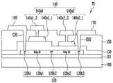
본 발명의 실시예에서, 제1 트랜지스터(T1)는, 서로 직렬로 연결된 복수의 트랜지스터들을 포함할 수 있다. 예를 들어, 제1 트랜지스터(T1)는, 제1 전원(ELVDD)과 발광 소자(EL)의 사이에 서로 직렬로 연결된 제1_1 트랜지스터(T1_1)(이하, "제1 구동 트랜지스터"라 함) 및 제1_2 트랜지스터(T1_2)(이하, "제2 구동 트랜지스터"라 함)를 포함한 복수의 트랜지스터들로 구성된, 듀얼 또는 그 이상의 다중 트랜지스터일 수 있다. 상기 제1 트랜지스터(T1)를 구성하는 복수의 트랜지스터들, 일 예로 제1 구동 트랜지스터(T1_1) 및 제2 구동 트랜지스터(T1_2)의 게이트 전극은 동일한 노드에 연결될 수 있다. 예를 들어, 제1 구동 트랜지스터(T1_1) 및 제2 구동 트랜지스터(T1_2)의 게이트 전극은 제1 노드(N1)에 공통으로 연결될 수 있다. 이에 따라, 제1 구동 트랜지스터(T1_1) 및 제2 구동 트랜지스터(T1_2)는, 제1 노드(N1)에 전압에 따라 동시에 턴-온 또는 턴-오프될 수 있다.In an embodiment of the present invention, the first transistor T1 may include a plurality of transistors connected in series with each other. For example, the first transistor T1 may include a first transistor T1_1 (hereinafter referred to as “first driving transistor”) connected in series between the first power supply ELVDD and the light emitting element EL, and It may be a dual or higher multi-transistor composed of a plurality of transistors including the 1_2 transistor T1_2 (hereinafter, referred to as a “second driving transistor”). A plurality of transistors constituting the first transistor T1, for example, a gate electrode of the first driving transistor T1_1 and the second driving transistor T1_2, may be connected to the same node. For example, gate electrodes of the first driving transistor T1_1 and the second driving transistor T1_2 may be commonly connected to the first node N1. Accordingly, the first driving transistor T1_1 and the second driving transistor T1_2 may be simultaneously turned on or turned off according to the voltage at the first node N1.
이와 같이, 서로 직렬로 연결된 복수의 트랜지스터들로 제1 트랜지스터(T1)를 형성하게 되면, 제1 트랜지스터(T1)의 구동 범위(일 예로, 다수의 계조들을 표현하기 위한 동작 전압 범위)를 충분히 확보하면서도 상기 제1 트랜지스터(T1)가 차지하는 면적을 축소할 수 있다. 예를 들어, 제1 트랜지스터(T1)를 직렬 연결된 두 개의 트랜지스터들, 일 예로 제1 및 제2 구동 트랜지스터들(T1_1, T1_2)로 구성한 구조에서 소정의 구동 범위를 확보하기 위해 필요한 상기 제1 및 제2 구동 트랜지스터들(T1_1, T1_2)의 채널 길이의 합은, 상기 제1 트랜지스터(T1)를 동일한 폭의 채널을 가지는 단일의 트랜지스터로 구성한 구조에서 동일한 구동 범위를 확보하기 위해 필요한 단일 트랜지스터의 채널 길이보다 현저히 작은 값일 수 있다.In this way, when the first transistor T1 is formed from a plurality of transistors connected in series, the driving range of the first transistor T1 (for example, an operating voltage range for expressing a plurality of gray levels) is sufficiently secured. Meanwhile, the area occupied by the first transistor T1 may be reduced. For example, in a structure comprising two transistors connected in series with the first transistor T1, for example, the first and second driving transistors T1_1 and T1_2, the first and second transistors required to secure a predetermined driving range The sum of the channel lengths of the second driving transistors T1_1 and T1_2 is the channel of a single transistor required to secure the same driving range in a structure in which the first transistor T1 is a single transistor having the same width. It can be a value significantly smaller than the length.
즉, 제1 트랜지스터(T1)를 적어도 제1 및 제2 구동 트랜지스터들(T1_1, T1_2)을 포함한 복수의 트랜지스터들로 구성할 경우, 각각의 화소 영역에서 제1 트랜지스터(T1)가 차지하는 면적을 축소하면서도 상기 제1 트랜지스터(T1)의 구동 범위를 충분히 확보할 수 있게 된다. 이에 따라, 한정된 화소 영역을 효율적으로 활용하면서 표시 장치(1)의 화질을 향상시킬 수 있다. 이러한 본 발명의 실시예는 고해상도의 표시 장치를 비롯한 다양한 종류 및/또는 구조의 표시 장치에 유용하게 적용될 수 있을 것이다.That is, when the first transistor T1 is composed of a plurality of transistors including at least the first and second driving transistors T1_1 and T1_2, the area occupied by the first transistor T1 in each pixel region is reduced. Yet, it is possible to sufficiently secure the driving range of the first transistor T1. Accordingly, the image quality of the
일 실시예에서, 제1 구동 트랜지스터(T1_1) 및 제2 구동 트랜지스터(T1_2)는 도 2에 도시된 실시예와 같이 서로 동일한 채널 길이(채널 영역의 길이)를 가질 수 있다. 다른 실시예에서, 제1 구동 트랜지스터(T1_1) 및 제2 구동 트랜지스터(T1_2)는 도 3에 도시된 실시예와 같이 서로 다른 채널 길이를 가질 수 있다. 일 예로, 제1 트랜지스터(T1)의 구동 범위를 결정하는 제1 구동 트랜지스터(T1_1)의 채널 영역은, 제2 구동 트랜지스터(T1_2)의 채널 영역에 비해 긴 길이를 가질 수 있다. 이에 따라, 제1 트랜지스터(T1)의 구동 범위를 충분히 확보할 수 있다. 한편, 제2 구동 트랜지스터(T1_2)의 경우에는 상대적으로 짧은 채널 영역을 가지는 숏-채널 트랜지스터로 형성함으로써, 제1 트랜지스터(T1)의 소자 특성(일 예로, 신뢰성)을 확보할 수 있다.In an embodiment, the first driving transistor T1_1 and the second driving transistor T1_2 may have the same channel length (length of the channel region) as in the embodiment illustrated in FIG. 2. In another embodiment, the first driving transistor T1_1 and the second driving transistor T1_2 may have different channel lengths as in the embodiment illustrated in FIG. 3. For example, the channel region of the first driving transistor T1_1, which determines the driving range of the first transistor T1, may have a longer length than the channel region of the second driving transistor T1_2. Accordingly, the driving range of the first transistor T1 can be sufficiently secured. Meanwhile, in the case of the second driving transistor T1_2, by forming a short-channel transistor having a relatively short channel region, device characteristics (eg, reliability) of the first transistor T1 can be secured.
실시예에 따라, 제2 내지 제7 트랜지스터들(T2~T7)은 화소(PXL)의 스위칭 트랜지스터들로 동작하며, 각각 숏-채널 트랜지스터로 형성될 수 있다. 일 예로, 제2 내지 제7 트랜지스터들(T2~T7) 각각은, 제1 트랜지스터(T1)보다 짧은 채널 길이를 가질 수 있다. 이와 같이, 각각의 스위칭 트랜지스터를 숏-채널 트랜지스터로 형성하게 되면, 제한된 화소 영역을 효율적으로 활용하면서 스위칭 트랜지스터들의 동작 속도(일 예로, 스위칭 속도)를 향상시킬 수 있다.Depending on the embodiment, the second to seventh transistors T2 to T7 operate as switching transistors of the pixel PXL, and each may be formed as a short-channel transistor. As an example, each of the second to seventh transistors T2 to T7 may have a channel length shorter than that of the first transistor T1. In this way, when each of the switching transistors is formed as a short-channel transistor, the operating speed of the switching transistors (eg, switching speed) can be improved while efficiently utilizing a limited pixel area.
제2 트랜지스터(T2)는 데이터선(Dj)과 제1 트랜지스터(T1)의 제1 전극의 사이에 연결된다. 그리고, 제2 트랜지스터(T2)의 게이트 전극은 주사선(Si)에 연결된다.The second transistor T2 is connected between the data line Dj and the first electrode of the first transistor T1. In addition, the gate electrode of the second transistor T2 is connected to the scan line Si.
이와 같은 제2 트랜지스터(T2)는 주사선(Si)으로 게이트-온 전압(일 예로, 로우 전압)의 주사 신호가 공급될 때 턴-온되어, 데이터선(Dj)과 제1 트랜지스터(T1)의 제1 전극을 연결한다. 따라서, 제2 트랜지스터(T2)가 턴-온되면, 데이터선(Dj)으로부터의 데이터 신호가 제1 트랜지스터(T1)의 제1 전극으로 전달된다. 한편, 제2 트랜지스터(T2)가 주사 신호에 의해 턴-온되는 기간 동안 상기 주사 신호에 의해 제3 트랜지스터(T3)도 턴-온되고, 상기 제3 트랜지스터(T3)에 의해 제1 트랜지스터(T1)가 다이오드 연결되는 형태로 턴-온된다. 이에 따라, 데이터선(Dj)으로부터의 데이터 신호가 제2 트랜지스터(T2), 제1 트랜지스터(T1) 및 제3 트랜지스터(T3)를 경유하여 제1 노드(N1)로 전달될 수 있다. 그러면, 스토리지 커패시터(Cst)는 데이터 신호 및 제1 트랜지스터(T1)의 문턱 전압에 대응하는 전압을 충전한다.The second transistor T2 is turned on when a scan signal of a gate-on voltage (for example, a low voltage) is supplied to the scan line Si, and thus the data line Dj and the first transistor T1 are turned on. Connect the first electrode. Accordingly, when the second transistor T2 is turned on, the data signal from the data line Dj is transferred to the first electrode of the first transistor T1. Meanwhile, while the second transistor T2 is turned on by the scan signal, the third transistor T3 is also turned on by the scan signal, and the first transistor T1 is turned on by the third transistor T3. ) Is turned on in the form of diode connection. Accordingly, the data signal from the data line Dj may be transmitted to the first node N1 via the second transistor T2, the first transistor T1, and the third transistor T3. Then, the storage capacitor Cst charges the data signal and a voltage corresponding to the threshold voltage of the first transistor T1.
제3 트랜지스터(T3)는 제1 트랜지스터(T1)의 제2 전극과 제1 노드(N1)의 사이에 연결된다. 그리고, 제3 트랜지스터(T3)의 게이트 전극은 주사선(Si)에 연결된다. 이와 같은 제3 트랜지스터(T3)는 주사선(Si)으로 게이트-온 전압의 주사 신호가 공급될 때 턴-온되어, 제1 트랜지스터(T1)의 제2 전극과 제1 노드(N1)를 연결한다. 따라서, 제3 트랜지스터(T3)가 턴-온되면, 제1 트랜지스터(T1)가 다이오드 형태로 연결된다.The third transistor T3 is connected between the second electrode of the first transistor T1 and the first node N1. In addition, the gate electrode of the third transistor T3 is connected to the scan line Si. The third transistor T3 is turned on when a scan signal having a gate-on voltage is supplied to the scan line Si, and connects the second electrode of the first transistor T1 and the first node N1. . Accordingly, when the third transistor T3 is turned on, the first transistor T1 is connected in a diode shape.
일 실시예에서, 제3 트랜지스터(T3)는 누설전류를 저감하기 위하여 서로 직렬로 연결된 복수의 트랜지스터들로 구성될 수 있다. 예를 들어, 제3 트랜지스터(T3)는 제1 노드(N1)와 제1 트랜지스터(T1)의 제2 전극의 사이에 서로 직렬로 연결된 제3_1 트랜지스터(T3_1) 및 제3_2 트랜지스터(T3_2)를 포함할 수 있다. 상기 제3_1 트랜지스터(T3_1) 및 제3_2 트랜지스터(T3_2)의 게이트 전극들은 주사선(Si)에 공통으로 연결될 수 있다. 이에 따라, 제3_1 트랜지스터(T3_1) 및 제3_2 트랜지스터(T3_2)는 주사신호에 대응하여 동시에 턴-온 또는 턴-오프될 수 있다.In an embodiment, the third transistor T3 may include a plurality of transistors connected in series with each other to reduce leakage current. For example, the third transistor T3 includes a 3_1 transistor T3_1 and a 3_2 transistor T3_2 connected in series between the first node N1 and the second electrode of the first transistor T1. can do. Gate electrodes of the 3_1 transistor T3_1 and the 3_2 transistor T3_2 may be commonly connected to the scan line Si. Accordingly, the 3_1 transistor T3_1 and the 3_2 transistor T3_2 may be simultaneously turned on or turned off in response to the scan signal.
제4 트랜지스터(T4)는 제1 노드(N1)와 초기화 전원(Vint)의 사이에 연결된다. 그리고, 제4 트랜지스터(T4)의 게이트 전극은 제1 제어선(CL1i)에 연결된다. 실시예에 따라, 제1 제어선(CL1i)은 i번째 수평 라인의 화소들(PXL)을 초기화하기 위한 초기화 제어선일 수 있으며, 각각의 주사선(Si)으로 게이트-온 전압의 주사 신호가 공급되기 이전의 초기화 기간 동안 게이트-온 전압의 초기화 제어 신호를 공급받을 수 있다.The fourth transistor T4 is connected between the first node N1 and the initialization power Vint. In addition, the gate electrode of the fourth transistor T4 is connected to the first control line CL1i. Depending on the embodiment, the first control line CL1i may be an initialization control line for initializing the pixels PXL of the i-th horizontal line, and a scan signal of a gate-on voltage is supplied to each scan line Si. During the previous initialization period, an initialization control signal of the gate-on voltage may be supplied.
일 실시예에서, 제1 제어선(CL1i)은 이전 수평 라인들의 화소들(PXL)을 선택하기 위한 이전 주사선들 중 어느 하나의 주사선, 일 예로 직전 수평 라인의 화소들(PXL)을 선택하기 위한 제i-1 주사선(Si-1)일 수 있다. 이 경우, 제1 제어선(CL1i)으로 공급되는 초기화 제어 신호는 제i-1 주사선(Si-1)으로 공급되는 제i-1 주사 신호일 수 있다. 다른 실시예에서, 제1 제어선(CL1i)은 화소들(PXL)의 주사선들(S1~Sn)과는 별개로 형성된 제어선일 수도 있다.In an embodiment, the first control line CL1i is for selecting any one of previous scan lines for selecting the pixels PXL of previous horizontal lines, for example, for selecting the pixels PXL of the immediately preceding horizontal line. It may be an i-1th scan line Si-1. In this case, the initialization control signal supplied to the first control line CL1i may be an i-1th scan signal supplied to the i-1th scan line Si-1. In another embodiment, the first control line CL1i may be a control line formed separately from the scan lines S1 to Sn of the pixels PXL.
이와 같은 제4 트랜지스터(T4)는 제1 제어선(CL1i)으로 게이트-온 전압의 제1 제어 신호가 공급될 때 턴-온된다. 제4 트랜지스터(T4)가 턴-온되면 제1 노드(N1)로 초기화 전원(Vint)의 전압이 전달되고, 이에 따라 상기 제1 노드(N1)의 전압이 초기화 전원(Vint)의 전압으로 초기화된다.The fourth transistor T4 is turned on when the first control signal of the gate-on voltage is supplied to the first control line CL1i. When the fourth transistor T4 is turned on, the voltage of the initialization power Vint is transmitted to the first node N1, and accordingly, the voltage of the first node N1 is initialized to the voltage of the initialization power Vint. do.
실시예에 따라, 초기화 전원(Vint)의 전압은 데이터 신호의 전압 이하의 전압으로 설정될 수 있다. 예를 들어, 초기화 전원(Vint)의 전압은 데이터 신호의 최저 전압 이하로 설정될 수 있다. 각각의 화소(PXL)로 현재 프레임의 데이터 신호를 전달하기에 앞서 제1 노드(N1)의 전압을 초기화 전원(Vint)의 전압으로 초기화하게 되면, 이전 프레임의 데이터 신호와 무관하게 각 수평 라인의 주사 기간(즉, 각각의 주사선(Si)으로 주사 신호가 공급되는 기간) 동안 제1 트랜지스터(T1)가 순방향으로 다이오드 연결된다. 이에 따라, 이전 프레임의 데이터 신호와 무관하게, 현재 프레임의 데이터 신호를 제1 노드(N1)로 안정적으로 전달할 수 있다.According to an embodiment, the voltage of the initialization power Vint may be set to a voltage equal to or less than the voltage of the data signal. For example, the voltage of the initialization power Vint may be set to be less than or equal to the lowest voltage of the data signal. If the voltage of the first node N1 is initialized to the voltage of the initializing power supply Vint prior to transmitting the data signal of the current frame to each pixel PXL, the horizontal line is irrespective of the data signal of the previous frame. The first transistor T1 is diode-connected in the forward direction during the scanning period (that is, the period in which the scanning signal is supplied to each scanning line Si). Accordingly, regardless of the data signal of the previous frame, the data signal of the current frame can be stably transmitted to the first node N1.
일 실시예에서, 제4 트랜지스터(T4)는 누설전류를 저감하기 위하여 서로 직렬로 연결된 복수의 트랜지스터들로 구성될 수 있다. 예를 들어, 제4 트랜지스터(T4)는 제1 노드(N1)와 초기화 전원(Vint)의 사이에 서로 직렬로 연결된 제4_1 트랜지스터(T4_1) 및 제4_2 트랜지스터(T4_2)를 포함할 수 있다. 상기 제4_1 트랜지스터(T4_1) 및 제4_2 트랜지스터(T4_2)의 게이트 전극들은 제1 제어선(CL1i)에 공통으로 연결될 수 있다. 이에 따라, 제4_1 트랜지스터(T4_1) 및 제4_2 트랜지스터(T4_2)는 제1 제어 신호(일 예로, 이전 주사신호)에 대응하여 동시에 턴-온 또는 턴-오프될 수 있다.In an embodiment, the fourth transistor T4 may include a plurality of transistors connected in series with each other to reduce leakage current. For example, the fourth transistor T4 may include a 4_1 transistor T4_1 and a 4_2 transistor T4_2 connected in series between the first node N1 and the initialization power Vint. Gate electrodes of the 4_1 transistor T4_1 and the 4_2 transistor T4_2 may be commonly connected to the first control line CL1i. Accordingly, the 4_1 transistor T4_1 and the 4_2 transistor T4_2 may be simultaneously turned on or turned off in response to the first control signal (eg, a previous scan signal).
제3 트랜지스터(T3) 및 제4 트랜지스터(T4)를 적어도 듀얼 구조의 다중 트랜지스터로 구성할 경우, 제3 트랜지스터(T3) 및 제4 트랜지스터(T4) 각각의 누설전류가 감소 또는 방지될 수 있다. 이에 따라, 각 프레임의 발광 기간 동안 오프 상태의 제3 트랜지스터(T3) 및 제4 트랜지스터(T4)를 통한 누설전류를 저감 또는 방지함으로써, 제1 노드(N1)의 전압을 안정적으로 유지할 수 있다. 이에 따라, 화소(PXL)의 계조 표현력을 높이고, 표시 장치(1)의 화질을 향상시킬 수 있다.When the third transistor T3 and the fourth transistor T4 are configured as at least a dual-structure multi-transistor, leakage currents of the third and fourth transistors T3 and T4 may be reduced or prevented. Accordingly, the voltage of the first node N1 can be stably maintained by reducing or preventing leakage current through the third transistor T3 and the fourth transistor T4 in the off state during the light emission period of each frame. Accordingly, it is possible to increase the gray scale expression power of the pixel PXL and improve the image quality of the
한편, 도 2 및 도 3에서는 제3 및 제4 트랜지스터들(T3, T4) 각각을 듀얼 구조의 트랜지스터로 구성하는 실시예를 개시하였으나, 본 발명이 이에 한정되지는 않는다. 예를 들어, 다른 실시예에서는 제3 트랜지스터(T3) 및 제4 트랜지스터(T4) 중 어느 하나의 트랜지스터(일 예로, 제3 트랜지스터(T3))만을 다중 트랜지스터로 형성하고, 다른 하나의 트랜지스터(일 예로, 제4 트랜지스터(T4))는 단일 트랜지스터로 형성할 수도 있다. 또 다른 실시예에서는 제3 트랜지스터(T3) 및 제4 트랜지스터(T4) 이외의 다른 스위칭 트랜지스터, 일 예로, 제2 트랜지스터(T2)와 제5 내지 제7 트랜지스터들(T5~T7) 중 적어도 하나의 트랜지스터(일 예로, 제2 트랜지스터(T2))를, 서로 직렬로 연결된 복수의 트랜지스터들을 포함한 다중 트랜지스터로 형성할 수도 있을 것이다.Meanwhile, in FIGS. 2 and 3, an embodiment in which each of the third and fourth transistors T3 and T4 is configured as a dual-structure transistor is disclosed, but the present invention is not limited thereto. For example, in another embodiment, only one of the third transistor T3 and the fourth transistor T4 (for example, the third transistor T3) is formed as a multi-transistor, and the other transistor (one For example, the fourth transistor T4 may be formed as a single transistor. In another embodiment, switching transistors other than the third transistor T3 and the fourth transistor T4, for example, at least one of the second transistor T2 and the fifth to seventh transistors T5 to T7 A transistor (for example, the second transistor T2) may be formed as a multi-transistor including a plurality of transistors connected in series with each other.
제5 트랜지스터(T5)는 제1 전원(ELVDD)과 제1 트랜지스터(T1)의 사이에 연결된다. 그리고, 제5 트랜지스터(T5)의 게이트 전극은 발광 제어선(Ei)에 연결된다. 이와 같은 제5 트랜지스터(T5)는 발광 제어선(Ei)으로 게이트-오프 전압(일 예로, 하이 전압)의 발광 제어 신호가 공급될 때 턴-오프되고, 그 외의 경우에 턴-온된다.The fifth transistor T5 is connected between the first power ELVDD and the first transistor T1. In addition, the gate electrode of the fifth transistor T5 is connected to the emission control line Ei. The fifth transistor T5 is turned off when a light emission control signal having a gate-off voltage (for example, a high voltage) is supplied to the light emission control line Ei, and is turned on in other cases.
제6 트랜지스터(T6)는 제1 트랜지스터(T1)와 발광 소자(EL)의 사이에 연결된다. 그리고, 제6 트랜지스터(T6)의 게이트 전극은 발광 제어선(Ei)에 연결된다. 이와 같은 제6 트랜지스터(T6)는 발광 제어선(Ei)으로 게이트-오프 전압의 발광 제어 신호가 공급될 때 턴-오프되고, 그 외의 경우에 턴-온된다.The sixth transistor T6 is connected between the first transistor T1 and the light emitting element EL. In addition, the gate electrode of the sixth transistor T6 is connected to the emission control line Ei. The sixth transistor T6 is turned off when the light emission control signal of the gate-off voltage is supplied to the light emission control line Ei, and is turned on in other cases.
즉, 제5 및 제6 트랜지스터들(T5, T6)은 발광 제어 신호에 의해 동시에 턴-온 또는 턴-오프되어, 화소들(PXL)의 발광 기간을 제어할 수 있다. 제5 및 제6 트랜지스터들(T5, T6)이 턴-온되면, 화소(PXL)에 구동 전류가 흐를 수 있는 전류 패스가 형성된다. 이에 따라, 화소(PXL)가 제1 노드(N1)의 전압에 대응하는 휘도로 발광할 수 있게 된다. 반대로, 제5 및 제6 트랜지스터들(T5, T6)이 턴-오프되면, 상기 전류 패스가 차단되면서 화소(PXL)가 비발광하게 된다.That is, the fifth and sixth transistors T5 and T6 are simultaneously turned on or off by the emission control signal to control the emission period of the pixels PXL. When the fifth and sixth transistors T5 and T6 are turned on, a current path through which a driving current can flow through the pixel PXL is formed. Accordingly, the pixel PXL can emit light with a luminance corresponding to the voltage of the first node N1. Conversely, when the fifth and sixth transistors T5 and T6 are turned off, the current path is blocked and the pixel PXL does not emit light.
실시예에 따라, 발광 제어 신호는 화소(PXL)의 초기화 기간 및 데이터 프로그래밍 기간(일 예로, 주사 기간) 동안 제5 및 제6 트랜지스터들(T5, T6)을 턴-오프시킬 수 있도록 게이트-오프 전압으로 공급될 수 있다. 일 예로, 게이트-오프 전압의 발광 제어 신호는 주사 신호, 제1 제어 신호 및 제2 제어 신호 각각이 게이트-온 전압을 가지는 기간 동안, 상기 주사 신호, 제1 제어 신호 및 제2 제어 신호와 중첩되도록 공급될 수 있다. 그리고, 주사 신호, 제1 제어 신호 및 제2 제어 신호의 전압이 게이트-오프 전압으로 변경된 이후, 발광 제어 신호의 전압이 게이트-온 전압이 변경되면서 각 프레임의 발광 기간이 시작될 수 있다. 발광 제어 신호를 이용해 화소(PXL)의 발광 기간을 제어하게 되면, 화소(PXL)의 내부에 안정적으로 데이터 신호를 저장한 이후에, 상기 데이터 신호에 대응하는 휘도로 화소(PXL)를 발광시킬 수 있다.Depending on the embodiment, the light emission control signal is gate-off to turn off the fifth and sixth transistors T5 and T6 during an initialization period and a data programming period (eg, a scanning period) of the pixel PXL. It can be supplied by voltage. As an example, the emission control signal of the gate-off voltage overlaps the scan signal, the first control signal, and the second control signal during a period in which each of the scan signal, the first control signal, and the second control signal has a gate-on voltage. It can be supplied as much as possible. In addition, after the voltages of the scan signal, the first control signal, and the second control signal are changed to the gate-off voltage, the light emission period of each frame may start as the voltage of the emission control signal is changed to the gate-on voltage. When the emission period of the pixel PXL is controlled using the emission control signal, after stably storing the data signal inside the pixel PXL, the pixel PXL can be emitted with a luminance corresponding to the data signal. have.
제7 트랜지스터(T7)는 초기화 전원(Vint)과 발광 소자(EL)의 일 전극(일 예로, 애노드 전극) 사이에 연결된다. 그리고, 제7 트랜지스터(T7)의 게이트 전극은 제2 제어선(CL2i)에 연결된다. 실시예에 따라, 제2 제어선(CL2i)은 i번째 수평 라인에 위치한 화소들(PXL)의 발광 소자(EL)에 형성된 유기 커패시터(발광 소자(EL)의 구조상 발생하는 기생 커패시터)에 충전된 전압을 초기화하기 위한 바이패스 제어선일 수 있으며, 각각의 발광 기간에 앞서 게이트-온 전압의 바이패스 제어 신호를 공급받을 수 있다.The seventh transistor T7 is connected between the initialization power Vint and one electrode (for example, an anode electrode) of the light emitting element EL. In addition, the gate electrode of the seventh transistor T7 is connected to the second control line CL2i. According to an exemplary embodiment, the second control line CL2i is charged in an organic capacitor (a parasitic capacitor occurring in the structure of the light emitting device EL) formed in the light emitting device EL of the pixels PXL located on the i-th horizontal line It may be a bypass control line for initializing the voltage, and may receive a bypass control signal of the gate-on voltage prior to each light emission period.
일 실시예에서, 제2 제어선(CL2i)은 다음 수평 라인들의 화소들(PXL)을 선택하기 위한 다음 주사선들 중 어느 하나의 주사선, 일 예로 제i+1 수평 라인의 화소들(PXL)을 선택하기 위한 제i+1 주사선(Si+1)일 수 있으나, 이에 한정되지는 않는다. 예를 들어, 다른 실시예에서, 제2 제어선(CL2i)은 각 화소(PXL)의 현재 주사선(즉, 주사선(Si))이거나, 화소들(PXL)의 주사선들(S1~Sn)과는 별개로 형성된 제어선일 수도 있다.In an embodiment, the second control line CL2i includes any one of the following scan lines for selecting the pixels PXL of the next horizontal lines, for example, the pixels PXL of the i+1th horizontal line. It may be an i+1th scan line (Si+1) for selection, but is not limited thereto. For example, in another embodiment, the second control line CL2i is a current scan line (ie, a scan line Si) of each pixel PXL, or is different from the scan lines S1 to Sn of the pixels PXL. It may be a separately formed control line.
제7 트랜지스터(T7)는 각 프레임의 발광 기간에 앞서, 제2 제어선(CL2i)으로 게이트-온 전압의 제2 제어 신호가 공급될 때 턴-온된다. 제7 트랜지스터(T7)가 턴-온되면, 발광 소자(EL)의 일 전극에 초기화 전원(Vint)의 전압이 전달된다. 이에 따라, 발광 소자(EL)에 형성된 기생 커패시터에 충전된 전하가 균일하게 초기화되면서, 각 프레임의 발광 기간 동안 화소(PXL)가 각각의 데이터 신호에 대응하여 보다 균일한 휘도 특성을 나타낼 수 있다.The seventh transistor T7 is turned on when the second control signal of the gate-on voltage is supplied to the second control line CL2i prior to the light emission period of each frame. When the seventh transistor T7 is turned on, the voltage of the initialization power Vint is transmitted to one electrode of the light emitting element EL. Accordingly, charges charged in the parasitic capacitor formed in the light-emitting element EL are uniformly initialized, and during the light-emitting period of each frame, the pixel PXL may exhibit more uniform luminance characteristics corresponding to each data signal.
스토리지 커패시터(Cst)는 제1 전원(ELVDD)과 제1 노드(N1)의 사이에 연결된다. 이와 같은 스토리지 커패시터(Cst)는 데이터 신호 및 제1 트랜지스터(T1)의 문턱 전압에 대응하는 전압을 충전한다.The storage capacitor Cst is connected between the first power ELVDD and the first node N1. The storage capacitor Cst charges a data signal and a voltage corresponding to the threshold voltage of the first transistor T1.
상술한 실시예들에 의한 화소(PXL) 및 이를 구비한 표시 장치(1)에 의하면, 화소(PXL)의 구동 트랜지스터로 동작하는 제1 트랜지스터(T1)를, 제1 및 제2 구동 트랜지스터들(T1_1, T1_2)을 포함한 다중 트랜지스터로 구성한다. 이에 따라, 제1 트랜지스터(T1)의 구동 범위를 충분히 확보하면서도 상기 제1 트랜지스터(T1)가 차지하는 면적을 축소할 수 있다.According to the pixel PXL and the
또한, 상술한 실시예들에 의한 화소(PXL) 및 이를 구비한 표시 장치(1)에서는, 제1 및 제2 구동 트랜지스터들(T1_1, T1_2)의 소자 특성을 개별적으로 제어할 수 있다. 이에 따라, 제1 트랜지스터(T1)의 구동 특성을 최적화할 수 있다.In addition, in the pixel PXL and the
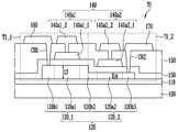
예를 들어, 제1 구동 트랜지스터(T1_1) 및 제2 구동 트랜지스터(T1_2)는 서로 비대칭적인 단면 구조를 가질 수 있다. 일 예로, 제1 구동 트랜지스터(T1_1) 및 제2 구동 트랜지스터(T1_2)는, 확보하고자 하는 각각의 소자 특성에 따라 채널 영역의 두께 및 절연막의 두께 중 적어도 하나가 서로 다르게 형성되고, 이에 따라 서로 비대칭적 단면 구조를 가질 수 있다.For example, the first driving transistor T1_1 and the second driving transistor T1_2 may have an asymmetric cross-sectional structure. For example, the first driving transistor T1_1 and the second driving transistor T1_2 have at least one of the thickness of the channel region and the thickness of the insulating layer different from each other according to the respective device characteristics to be secured, and thus, asymmetrical It can have a red cross-sectional structure.
도 4 및 도 5는 각각 본 발명의 일 실시예에 의한 제1 트랜지스터(T1)의 단면 구조를 나타낸다. 예를 들어, 도 4 및 도 5는 도 2 및 도 3의 화소(PXL)에 구비될 수 있는 제1 트랜지스터(T1)의 단면 구조에 대한 서로 다른 실시예를 나타낸다. 한편, 본 발명에서 도 4 및 도 5의 실시예들에 의한 제1 트랜지스터(T1)의 구조가 도 2 및 도 3의 실시예들에 의한 화소(PXL)에만 적용되는 것으로 한정되지는 않는다. 예를 들어, 다양한 구조의 화소(PXL)에서, 각각의 구동 트랜지스터는 도 4 및/또는 도 5의 실시예들에 의한 제1 트랜지스터(T1)의 구조로 형성될 수 있다.4 and 5 each show a cross-sectional structure of a first transistor T1 according to an embodiment of the present invention. For example, FIGS. 4 and 5 illustrate different embodiments of a cross-sectional structure of a first transistor T1 that may be provided in the pixel PXL of FIGS. 2 and 3. Meanwhile, in the present invention, the structure of the first transistor T1 according to the embodiments of FIGS. 4 and 5 is not limited to being applied only to the pixel PXL according to the embodiments of FIGS. 2 and 3. For example, in the pixel PXL having various structures, each driving transistor may be formed in the structure of the first transistor T1 according to the embodiments of FIGS. 4 and/or 5.
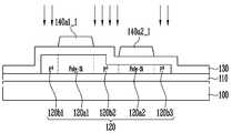
먼저 도 4를 참조하면, 본 발명의 일 실시예에 의한 제1 트랜지스터(T1)는, 버퍼층(110)이 형성된 베이스 층(100)의 일면 상에 배치된 활성층 패턴(120), 제1 절연막(130)을 사이에 개재하고 활성층 패턴(120)의 일 영역과 중첩되는 게이트 전극(140), 제1 절연막(130) 및 제2 절연막(150)을 사이에 개재하고 활성층 패턴(120)과 이격되며 상기 활성층 패턴(120)의 서로 다른 일 영역에 연결되는 제1 전극(160) 및 제2 전극(170)을 포함할 수 있다.First, referring to FIG. 4, a first transistor T1 according to an embodiment of the present invention includes an
실시예에 따라, 제1 트랜지스터(T1)는 서로 직렬로 연결된 제1 구동 트랜지스터(T1_1) 및 제2 구동 트랜지스터(T1_2)를 포함할 수 있다. 예를 들어, 제1 구동 트랜지스터(T1_1) 및 제2 구동 트랜지스터(T1_2)는, 도 2 또는 도 3에 도시된 제1 및 제2 구동 트랜지스터들(T1_1, T1_2)일 수 있다. 일 예로, 제1 구동 트랜지스터(T1_1)는 제1 전원(ELVDD)과 제2 구동 트랜지스터(T1_2)의 사이에 연결되고, 제2 구동 트랜지스터(T1_2)는 제1 구동 트랜지스터(T1_1)와 발광 소자(EL)의 사이에 연결될 수 있다.Depending on the embodiment, the first transistor T1 may include a first driving transistor T1_1 and a second driving transistor T1_2 connected in series with each other. For example, the first driving transistor T1_1 and the second driving transistor T1_2 may be the first and second driving transistors T1_1 and T1_2 shown in FIG. 2 or 3. As an example, the first driving transistor T1_1 is connected between the first power ELVDD and the second driving transistor T1_2, and the second driving transistor T1_2 includes the first driving transistor T1_1 and the light emitting element ( EL) can be connected between.
이 경우, 제1 트랜지스터(T1)는 복수의 채널 영역들을 포함할 수 있다. 일 예로, 제1 트랜지스터(T1)는, 제1 구동 트랜지스터(T1_1)의 채널을 형성하는 제1 채널 영역(120a1) 및 제2 구동 트랜지스터(T1_2)의 채널을 형성하는 제2 채널 영역(120a2)을 포함할 수 있다. 일 실시예에서, 제1 채널 영역(120a1) 및 제2 채널 영역(120a2)의 길이는 실질적으로 동일할 수 있다. 다른 실시예에서, 제1 채널 영역(120a1) 및 제2 채널 영역(120a2)의 길이는 상이할 수 있다. 일 예로, 제1 채널 영역(120a1)의 길이는 제2 채널 영역(120a2)의 길이보다 클 수 있다. 제1 채널 영역(120a1) 및 제2 채널 영역(120a2) 각각의 양측에는 전도성 영역이 배치될 수 있다.In this case, the first transistor T1 may include a plurality of channel regions. As an example, the first transistor T1 is a first channel region 120a1 forming a channel of the first driving transistor T1_1 and a second channel region 120a2 forming a channel of the second driving transistor T1_2 It may include. In an embodiment, the lengths of the first channel region 120a1 and the second channel region 120a2 may be substantially the same. In another embodiment, the lengths of the first channel region 120a1 and the second channel region 120a2 may be different. For example, the length of the first channel region 120a1 may be greater than the length of the second channel region 120a2. Conductive regions may be disposed on both sides of each of the first channel region 120a1 and the second channel region 120a2.
예를 들어, 제1 채널 영역(120a1)의 양측에는 각각 제1 전도성 영역(120b1) 및 제2 전도성 영역(120b2)이 배치될 수 있다. 상기 제1 및 제2 전도성 영역들(120b1, 120b2)은 제1 채널 영역(120a1)과 함께 제1 구동 트랜지스터(T1_1)의 활성층 패턴(이하, "제1 활성층 패턴"이라 함)(120_1)을 구성할 수 있다. 즉, 제1 구동 트랜지스터(T1_1)는, 제1 채널 영역(120a1), 제1 전도성 영역(120b1) 및 제2 전도성 영역(120b2)을 포함한 제1 활성층 패턴(120_1)을 포함할 수 있다.For example, a first conductive region 120b1 and a second conductive region 120b2 may be disposed on both sides of the first channel region 120a1, respectively. The first and second conductive regions 120b1 and 120b2 form an active layer pattern (hereinafter referred to as “first active layer pattern”) 120_1 of the first driving transistor T1_1 together with the first channel region 120a1. Configurable. That is, the first driving transistor T1_1 may include the first active layer pattern 120_1 including the first channel region 120a1, the first conductive region 120b1, and the second conductive region 120b2.
제1 전도성 영역(120b1) 및 제2 전도성 영역(120b2) 중 어느 하나는 제1 구동 트랜지스터(T1_1)의 소스 영역일 수 있고, 다른 하나는 상기 제1 구동 트랜지스터(T1_1)의 드레인 영역일 수 있다. 일 예로, 제1 전도성 영역(120b1)이 제1 구동 트랜지스터(T1_1)의 소스 영역이면, 제2 전도성 영역(120b2)은 상기 제1 구동 트랜지스터(T1_1)의 드레인 영역일 수 있다. 반대로, 제1 전도성 영역(120b1)이 제1 구동 트랜지스터(T1_1)의 드레인 영역이면, 제2 전도성 영역(120b2)은 상기 제1 구동 트랜지스터(T1_1)의 소스 영역일 수 있다. 이는, 제1 구동 트랜지스터(T1_1)의 캐리어 타입(일 예로, N 타입 또는 P 타입) 및 전류의 방향 등에 따라 달라질 수 있다.One of the first conductive region 120b1 and the second conductive region 120b2 may be a source region of the first driving transistor T1_1, and the other may be a drain region of the first driving transistor T1_1. . For example, if the first conductive region 120b1 is a source region of the first driving transistor T1_1, the second conductive region 120b2 may be a drain region of the first driving transistor T1_1. Conversely, if the first conductive region 120b1 is a drain region of the first driving transistor T1_1, the second conductive region 120b2 may be a source region of the first driving transistor T1_1. This may vary depending on the carrier type (eg, N type or P type) of the first driving transistor T1_1 and the direction of current.
제2 채널 영역(120a2)은, 적어도 하나의 전도성 영역을 사이에 개재하고, 제1 채널 영역(120a1)으로부터 이격될 수 있다. 일 예로, 제2 채널 영역(120a2)은, 제2 전도성 영역(120b2)을 사이에 개재하고, 제1 채널 영역(120a1)으로부터 이격될 수 있다.The second channel region 120a2 may be spaced apart from the first channel region 120a1 with at least one conductive region interposed therebetween. For example, the second channel region 120a2 may be spaced apart from the first channel region 120a1 with the second conductive region 120b2 interposed therebetween.
제2 채널 영역(120a2)의 양측에는 각각 제2 전도성 영역(120b2) 및 제3 전도성 영역(120b3)이 배치될 수 있다. 일 예로, 제3 전도성 영역(120b3)은 제2 채널 영역(120a2)을 사이에 개재하고 제2 전도성 영역(120b2)으로부터 이격될 수 있다. 상기 제2 및 제3 전도성 영역들(120b2, 120b3)은 제2 채널 영역(120a2)과 함께 제2 구동 트랜지스터(T1_2)의 활성층 패턴(이하, "제2 활성층 패턴"이라 함) (120_2)을 구성할 수 있다. 즉, 제2 구동 트랜지스터(T1_2)는, 제2 채널 영역(120a2), 제2 전도성 영역(120b2) 및 제3 전도성 영역(120b3)을 포함한, 제2 활성층 패턴(120_2)을 포함할 수 있다.A second conductive region 120b2 and a third conductive region 120b3 may be disposed on both sides of the second channel region 120a2, respectively. For example, the third conductive region 120b3 may be spaced apart from the second conductive region 120b2 with the second channel region 120a2 interposed therebetween. The second and third conductive regions 120b2 and 120b3 include the active layer pattern (hereinafter referred to as “second active layer pattern”) 120_2 of the second driving transistor T1_2 together with the second channel region 120a2. Configurable. That is, the second driving transistor T1_2 may include the second active layer pattern 120_2 including the second channel region 120a2, the second conductive region 120b2, and the third conductive region 120b3.
제2 전도성 영역(120b2) 및 제3 전도성 영역(120b3) 중 어느 하나는 제2 구동 트랜지스터(T1_2)의 소스 영역일 수 있고, 다른 하나는 상기 제2 구동 트랜지스터(T1_2)의 드레인 영역일 수 있다. 일 예로, 제2 전도성 영역(120b2)이 제2 구동 트랜지스터(T1_2)의 소스 영역이면, 제3 전도성 영역(120b3)은 상기 제2 구동 트랜지스터(T1_2)의 드레인 영역일 수 있다. 반대로, 제2 전도성 영역(120b2)이 제2 구동 트랜지스터(T1_2)의 드레인 영역이면, 제3 전도성 영역(120b3)은 상기 제2 구동 트랜지스터(T1_2)의 소스 영역일 수 있다. 이는, 제2 구동 트랜지스터(T1_2)의 캐리어 타입(일 예로, N 타입 또는 P 타입) 및 전류의 방향 등에 따라 달라질 수 있다.One of the second conductive region 120b2 and the third conductive region 120b3 may be a source region of the second driving transistor T1_2, and the other may be a drain region of the second driving transistor T1_2. . For example, if the second conductive region 120b2 is a source region of the second driving transistor T1_2, the third conductive region 120b3 may be a drain region of the second driving transistor T1_2. Conversely, if the second conductive region 120b2 is a drain region of the second driving transistor T1_2, the third conductive region 120b3 may be a source region of the second driving transistor T1_2. This may vary depending on the carrier type (eg, N type or P type) of the second driving transistor T1_2 and the direction of current.
일 실시예에서, 제1 구동 트랜지스터(T1_1) 및 제2 구동 트랜지스터(T1_2)는 어느 하나의 전도성 영역을 공유할 수 있다. 예를 들어, 제1 구동 트랜지스터(T1_1) 및 제2 구동 트랜지스터(T1_2)는 제2 전도성 영역(120b2)을 공유할 수 있다.In an embodiment, the first driving transistor T1_1 and the second driving transistor T1_2 may share any one conductive region. For example, the first driving transistor T1_1 and the second driving transistor T1_2 may share the second conductive region 120b2.
이 경우, 제2 전도성 영역(120b2)은 제1 구동 트랜지스터(T1_1) 및 제2 구동 트랜지스터(T1_2) 사이의 공통 전극을 구성할 수 있다. 일 예로, 제2 전도성 영역(120b2)은 제1 구동 트랜지스터(T1_1)의 드레인 전극이자 제2 구동 트랜지스터(T1_2)의 소스 전극일 수 있으며, 상기 제2 전도성 영역(120b2)을 통해 제1 구동 트랜지스터(T1_1)와 제2 구동 트랜지스터(T1_2)가 서로 연결될 수 있다.In this case, the second conductive region 120b2 may form a common electrode between the first driving transistor T1_1 and the second driving transistor T1_2. As an example, the second conductive region 120b2 may be a drain electrode of the first driving transistor T1_1 and a source electrode of the second driving transistor T1_2, and the first driving transistor through the second conductive region 120b2 The T1_1 and the second driving transistor T1_2 may be connected to each other.
실시예에 따라, 제1 활성층 패턴(120_1)과 제2 활성층 패턴(120_2)은 서로 일체로 연결될 수 있다. 예를 들어, 제1 활성층 패턴(120_1)과 제2 활성층 패턴(120_2)은 제2 전도성 영역(120b2)을 통해 서로 일체로 연결될 수 있다.Depending on the embodiment, the first active layer pattern 120_1 and the second active layer pattern 120_2 may be integrally connected to each other. For example, the first active layer pattern 120_1 and the second active layer pattern 120_2 may be integrally connected to each other through the second conductive region 120b2.
다만, 본 발명이 이에 한정되지는 않는다. 예를 들어, 다른 실시예에서는 제1 구동 트랜지스터(T1_1) 및 제2 구동 트랜지스터(T1_2)의 전도성 영역들이 서로 분리된 패턴으로 형성되되, 상기 제1 및 제2 구동 트랜지스터들(T1_1, T1_2) 각각의 어느 한 전도성 영역들(일 예로, 제1 구동 트랜지스터(T1_1)의 드레인 영역 및 제2 구동 트랜지스터(T1_2)의 소스 영역)이 서로 전기적으로 연결될 수도 있다.However, the present invention is not limited thereto. For example, in another embodiment, conductive regions of the first driving transistor T1_1 and the second driving transistor T1_2 are formed in separate patterns, and the first and second driving transistors T1_1 and T1_2 are each Any one of the conductive regions (for example, the drain region of the first driving transistor T1_1 and the source region of the second driving transistor T1_2) may be electrically connected to each other.
제1 트랜지스터(T1)가 다중 트랜지스터(일 예로, 듀얼 트랜지스터)인 경우, 상기 제1 트랜지스터(T1)는 다중 게이트 전극(140)(일 예로, 듀얼 게이트 전극)을 구비할 수 있다. 예를 들어, 제1 트랜지스터(T1)는, 제1 절연막(130)을 사이에 개재하고 제1 채널 영역(120a1)과 중첩되는 제1 게이트 전극(140a1)과, 상기 제1 절연막(130)을 사이에 개재하고 제2 채널 영역(120a2)과 중첩되는 제2 게이트 전극(140a2)을 포함할 수 있다. 유사하게, 제1 트랜지스터(T1)가 세 개 이상의 트랜지스터들로 구성되는 다중 구조의 트랜지스터인 경우, 상기 제1 트랜지스터(T1)는 세 개 이상의 채널 영역들과, 각각의 채널 영역과 중첩되는 세 개 이상의 게이트 전극들을 포함할 수 있다.When the first transistor T1 is a multi-transistor (for example, a dual transistor), the first transistor T1 may include a multi-gate electrode 140 (for example, a dual gate electrode). For example, the first transistor T1 includes a first gate electrode 140a1 overlapping the first channel region 120a1 with a first insulating
일 실시예에서, 게이트 전극(140)은 다중층으로 이루어질 수 있다. 예를 들어, 제1 게이트 전극(140a1)은, 제1 절연막(130)과 제2 절연막(150)의 사이에 배치된 하부 전극(140a1_1)과, 상기 하부 전극(140a1_1)에 연결되며 제2 절연막(150) 상에 배치된 상부 전극(140a1_2)을 포함한 다중층으로 이루어질 수 있다. 유사하게, 제2 게이트 전극(140a2)은, 제1 절연막(130)과 제2 절연막(150)의 사이에 배치된 하부 전극(140a2_1)과, 상기 하부 전극(140a2_1)에 연결되며 제2 절연막(150) 상에 배치된 상부 전극(140a2_2)을 포함한 다중층으로 이루어질 수 있다. 게이트 전극(140)이 다중층으로 이루어지면, 상기 게이트 전극(140) 및 이에 연결되는 게이트 노드(일 예로, 제1 노드(N1))의 저항을 낮출 수 있다.In one embodiment, the
다만, 본 발명이 이에 한정되지는 않는다. 예를 들어, 다른 실시예에서는 제1 게이트 전극(140a1) 및 제2 게이트 전극(140a2) 중 어느 하나는 다중층으로 이루어지고, 다른 하나는 단일층으로 이루어질 수 있다. 또 다른 실시예에서는, 제1 게이트 전극(140a1) 및 제2 게이트 전극(140a2) 각각이 단일층으로 이루어지며, 상기 제1 게이트 전극(140a1) 및 제2 게이트 전극(140a2)이 서로 동일 또는 상이한 층에 배치될 수도 있다. 일 예로, 제1 게이트 전극(140a1) 및 제2 게이트 전극(140a2) 각각이, 제1 절연막(130)과 제2 절연막(150)의 사이에 위치한 하부 전극들(140a1_1, 140a2_1)만으로 구성될 수도 있다.However, the present invention is not limited thereto. For example, in another embodiment, one of the first gate electrode 140a1 and the second gate electrode 140a2 may be formed of a multilayer, and the other may be formed of a single layer. In another embodiment, each of the first gate electrode 140a1 and the second gate electrode 140a2 is formed of a single layer, and the first gate electrode 140a1 and the second gate electrode 140a2 are the same or different from each other. It can also be placed on the floor. As an example, each of the first gate electrode 140a1 and the second gate electrode 140a2 may be formed of only lower electrodes 140a1_1 and 140a2_1 positioned between the first insulating
제1 게이트 전극(140a1) 및 제2 게이트 전극(140a2)은 서로 전기적으로 연결된다. 예를 들어, 제1 게이트 전극(140a1) 및 제2 게이트 전극(140a2)은 도 2 및 도 3의 실시예들에서와 같이 제1 노드(N1)에 공통으로 연결될 수 있다.The first gate electrode 140a1 and the second gate electrode 140a2 are electrically connected to each other. For example, the first gate electrode 140a1 and the second gate electrode 140a2 may be commonly connected to the first node N1 as in the embodiments of FIGS. 2 and 3.
제1 전극(160) 및 제2 전극(170)은 제2 절연막(150) 상에 배치되어 활성층 패턴(120)의 서로 다른 일 영역에 연결될 수 있다. 예를 들어, 제1 전극(160)은 제1 및 제2 절연막들(130, 150)을 관통하는 제1 컨택홀(CH1)을 통해 제1 전도성 영역(120b1)에 연결되고, 제2 전극(170)은 상기 제1 및 제2 절연막들(130, 150)을 관통하는 제2 컨택홀(CH2)을 통해 제3 전도성 영역(120b3)에 연결될 수 있다.The
실시예에 따라, 제1 전극(160)은 제1 트랜지스터(T1)의 소스 전극 및 드레인 전극 중 어느 하나의 전극일 수 있고, 제2 전극(170)은 다른 하나의 전극일 수 있다. 예를 들어, 제1 전극(160)이 제1 트랜지스터(T1)(또는, 제1 구동 트랜지스터(T1_1))의 소스 전극이면, 제2 전극(170)은 제1 트랜지스터(T1)(또는, 제2 구동 트랜지스터(T1_2))의 드레인 전극일 수 있다. 반대로, 제1 전극(160)이 제1 트랜지스터(T1)(또는, 제1 구동 트랜지스터(T1_1))의 드레인 전극이면, 제2 전극(170)은 제1 트랜지스터(T1)(또는, 제2 구동 트랜지스터(T1_2))의 소스 전극일 수 있다.According to an embodiment, the
한편, 본 발명에서 제1 전극(160) 및 제2 전극(170)의 위치가 특별히 한정되지는 않으며, 이는 실시예에 따라 다양하게 변경될 수 있다. 또한, 실시예에 따라서는 제1 전극(160) 및 제2 전극(170) 중 적어도 하나의 전극이 생략될 수도 있다.Meanwhile, in the present invention, the positions of the
예를 들어, 제1 트랜지스터(T1)가 제1 전도성 영역(120b1)을 통해 다른 회로 소자(일 예로, 적어도 하나의 다른 트랜지스터 및/또는 커패시터 등)에 바로 연결될 경우, 제1 전극(160)이 생략될 수 있다. 그리고, 제1 전도성 영역(120b1)이 상기 제1 트랜지스터(T1)의 소스 또는 드레인 전극이 될 수 있다. 유사하게, 제1 트랜지스터(T1)가 제3 전도성 영역(120b3)을 통해 다른 회로 소자에 바로 연결되는 경우, 제2 전극(170)이 생략될 수 있다. 그리고, 제3 전도성 영역(120b3)이 상기 제1 트랜지스터(T1)의 소스 또는 드레인 전극이 될 수도 있다. 또는, 관점에 따라서는 제1 및/또는 제3 전도성 영역들(120b1, 120b3)을 제1 트랜지스터(T1)의 소스 및/또는 드레인 전극들로 간주하고, 제1 및/또는 제2 전극들(160, 170)을 상기 제1 트랜지스터(T1)의 일 전극에 연결되는 배선들 또는 다른 회로 소자의 전극들로 간주할 수도 있다.For example, when the first transistor T1 is directly connected to another circuit device (eg, at least one other transistor and/or capacitor, etc.) through the first conductive region 120b1, the
도 4의 실시예에 의한 제1 트랜지스터(T1)에 있어서, 게이트 절연막의 두께는 영역별로 달라질 수 있다. 예를 들어, 제1 트랜지스터(T1)의 활성층 패턴(120)과 게이트 전극(140)의 사이에 구비되는 제1 절연막(130)은 상기 제1 트랜지스터(T1)의 게이트 절연막(일 예로, 제1 게이트 절연막)을 구성하며, 제1 구동 트랜지스터(T1_1)가 형성되는 영역과 제2 구동 트랜지스터(T1_2)가 형성되는 영역에서 상이한 두께를 가질 수 있다.In the first transistor T1 according to the embodiment of FIG. 4, the thickness of the gate insulating layer may vary for each region. For example, the first insulating
일 예로, 제1 절연막(130)은 제1 구동 트랜지스터(T1_1)가 형성되는 영역의 적어도 일 영역, 특히 제1 채널 영역(120a1)과 제1 게이트 전극(140a1)의 사이에서는 나머지 영역에 비해 상대적으로 큰 제1 두께(t1)를 가질 수 있다. 또한, 상기 제1 절연막(130)은 제2 구동 트랜지스터(T1_2)가 형성되는 영역의 적어도 일 영역, 특히 제2 채널 영역(120a2)과 제2 게이트 전극(140a2)의 사이에서는 제1 두께(t1)보다 작은 제2 두께(t2)를 가질 수 있다. 즉, 제1 절연막(130)은, 제1 구동 트랜지스터(T1_1)가 형성되는 영역에서 국부적으로 증가된 두께를 가질 수 있다.As an example, the first insulating
제1 구동 트랜지스터(T1_1)가 형성되는 영역에서 제1 절연막(130)의 두께가 증가하게 되면, 상기 제1 구동 트랜지스터(T1_1)의 민감도는 낮아지게 된다. 이에 따라, 제1 구동 트랜지스터(T1_1)의 게이트-소스 간 전압(Vgs)의 변화에 따른 드레인 전류("소스 전류"라고도 함)(Ids)의 변화도가 감소하면서, 최저 계조 전압과 최고 계조 전압 사이의 동작 전압 범위에 대응하는 제1 트랜지스터(T1)의 구동 범위가 확장된다.When the thickness of the first insulating
도 5를 참조하면, 본 발명의 다른 실시예에서 제1 트랜지스터(T1)의 활성층 패턴(120)은 영역별로 상이한 두께를 가질 수 있다. 예를 들어, 상기 활성층 패턴(120)은 제1 구동 트랜지스터(T1_1)가 형성되는 영역과 제2 구동 트랜지스터(T1_2)가 형성되는 영역에서 상이한 두께를 가질 수 있다.Referring to FIG. 5, in another embodiment of the present invention, the
일 예로, 상기 활성층 패턴(120)은 제1 구동 트랜지스터(T1_1)의 활성층 패턴(즉, 제1 활성층 패턴(120_1))을 구성하는 영역, 일 예로 적어도 제1 채널 영역(120a1)에서 국부적으로 증가된 제3 두께(t3)를 가질 수 있다. 또한, 상기 활성층 패턴(120)은, 제2 구동 트랜지스터(T1_2)의 활성층 패턴(즉, 제2 활성층 패턴(120_2))을 구성하는 영역에서는 제3 두께(t3)보다 작은 제4 두께(t4)를 가질 수 있다. 또한, 실시예에 따라, 화소(PXL)의 나머지 트랜지스터들, 일 예로 스위칭 트랜지스터들 각각의 활성층 패턴들은, 제2 활성층 패턴(120_2)과 실질적으로 동일한 두께(즉, 제4 두께(t4))를 가질 수 있다. 즉, 제1 구동 트랜지스터(T1_1)는, 화소(PXL)의 다른 트랜지스터들에 비해 상대적으로 큰 두께를 가지는 제1 채널 영역(120a1)을 포함할 수 있다.For example, the
제1 채널 영역(120a1)의 두께가 증가하게 되면, 게이트-소스 간 전압(Vgs)의 변화에 따른 제1 구동 트랜지스터(T1_1)의 민감도는 낮아지게 된다. 이에 따라, 제1 구동 트랜지스터(T1_1)의 게이트-소스 간 전압(Vgs)의 변화에 따른 드레인 전류(Ids)의 변화량이 감소하면서, 제1 트랜지스터(T1)의 구동 범위가 확장된다.When the thickness of the first channel region 120a1 increases, the sensitivity of the first driving transistor T1_1 according to a change in the gate-source voltage Vgs decreases. Accordingly, the amount of change in the drain current Ids according to the change in the gate-source voltage Vgs of the first driving transistor T1_1 decreases, and the driving range of the first transistor T1 is extended.
한편, 본 발명에서, 각 실시예는 단독으로 실시되거나, 또는 적어도 두 개의 실시예들이 복합적으로 실시될 수 있다. 예를 들어, 일 실시예에서는, 도 4 및 도 5의 실시예들에서와 같이 각각 제1 및 제2 구동 트랜지스터들(T1_1, T1_2)의 게이트 절연막의 두께 및 채널 영역의 두께 중 어느 하나만이 차등적으로 형성될 수 있다. 또한, 다른 실시예에서는, 제1 및 제2 구동 트랜지스터들(T1_1, T1_2)의 게이트 절연막의 두께 및 채널 영역의 두께 모두가 차등적으로 형성될 수도 있다.On the other hand, in the present invention, each embodiment may be carried out alone, or at least two embodiments may be implemented in combination. For example, in one embodiment, as in the embodiments of FIGS. 4 and 5, only one of the thickness of the gate insulating layer and the thickness of the channel region of the first and second driving transistors T1_1 and T1_2, respectively, is different. It can be formed as an enemy. Further, in another embodiment, both the thickness of the gate insulating layer and the thickness of the channel region of the first and second driving transistors T1_1 and T1_2 may be formed differentially.
도 4 및 도 5의 실시예들에 의하면, 제1 트랜지스터(T1)의 구동 범위를 결정하는 제1 구동 트랜지스터(T1_1)에 대해서는, 게이트 절연막(즉, 제1 절연막(130))의 두께를 증가시키거나, 채널 영역(즉, 제1 채널 영역(120a1))의 두께를 증가시킴으로써, 상기 제1 트랜지스터(T1)의 구동 범위를 확장할 수 있다. 그리고, 제2 구동 트랜지스터(T1_2)에 대해서는, 게이트 전압에 따른 제1 트랜지스터(T1)의 제어력을 강화하고 상기 제1 트랜지스터(T1)의 소자 특성의 산포를 감소시킬 수 있도록, 제1 구동 트랜지스터(T1_1)에 비해 작은 두께로 게이트 절연막 및/또는 채널 영역을 형성할 수 있다. 일 예로, 제2 구동 트랜지스터(T1_2)는, 제1 구동 트랜지스터(T1_1)보다 게이트-소스 간 전압(Vgs)에 보다 고속으로 민감하게 반응할 수 있도록 형성함으로써, 제1 트랜지스터(T1)를 용이하게 제어할 수 있다.4 and 5, for the first driving transistor T1_1 that determines the driving range of the first transistor T1, the thickness of the gate insulating layer (ie, the first insulating layer 130) is increased. Or, by increasing the thickness of the channel region (ie, the first channel region 120a1), the driving range of the first transistor T1 may be extended. In addition, with respect to the second driving transistor T1_2, the first driving transistor (T1_2) can be used to enhance the control power of the first transistor T1 according to the gate voltage and to reduce the dispersion of device characteristics of the first transistor T1 The gate insulating layer and/or the channel region may be formed with a thickness smaller than that of T1_1). For example, by forming the second driving transistor T1_2 to react more sensitively to the gate-source voltage Vgs than the first driving transistor T1_1, the first transistor T1 is easily Can be controlled.
즉, 상술한 실시예들에서는 제1 트랜지스터(T1)를 제1 및 제2 구동 트랜지스터들(T1_1, T1_2)을 포함한 복수의 트랜지스터들로 구성하고, 상기 복수의 트랜지스터들 각각의 소자 특성을 개별적으로 조절한다. 이에 따라, 제1 트랜지스터(T1)의 구동 특성을 최적화할 수 있다.That is, in the above-described embodiments, the first transistor T1 is composed of a plurality of transistors including the first and second driving transistors T1_1 and T1_2, and device characteristics of each of the plurality of transistors are individually Adjust. Accordingly, it is possible to optimize the driving characteristics of the first transistor T1.
도 6은 본 발명의 일 실시예에 의한 제1 트랜지스터(T1)의 구동 범위를 나타낸다. 예를 들어, 도 6은 도 4 및 도 5의 실시예들 중 적어도 하나의 실시예를 적용함에 따른, 제1 트랜지스터(T1)의 구동 범위를 나타낸다.6 shows a driving range of the first transistor T1 according to an embodiment of the present invention. For example, FIG. 6 shows a driving range of the first transistor T1 according to applying at least one of the embodiments of FIGS. 4 and 5.
도 4 내지 도 6을 참조하면, 제1 구동 트랜지스터(T1_1)가 형성되는 영역에서 제1 절연막(130)의 두께 및/또는 제1 활성층 패턴(120_1)의 두께를 증가시킴으로써, 제1 트랜지스터(T1)의 게이트-소스 간 전압(Vgs)에 따른 드레인 전류(Ids)의 변화도를 둔화시킬 수 있다. 즉, 본 발명의 일 실시예를 적용하여 게이트-소스 간 전압(Vgs)에 따른 제1 구동 트랜지스터(T1_1)의 민감도를 낮추게 되면, 제1 트랜지스터(T1)의 게이트-소스 간 전압(Vgs)에 따른 드레인 전류(Ids)의 기울기가 보다 완만해질 수 있다. 이러한 본 발명의 실시예에 따르면, 제1 트랜지스터(T1)의 구동 범위를 확장할 수 있다.4 to 6, by increasing the thickness of the first insulating
예를 들어, 비교 예에서는, 단일의 구동 트랜지스터를 구성하고, 상기 구동 트랜지스터의 게이트 절연막 및 활성층 패턴의 두께를 나머지 트랜지스터들의 게이트 절연막 및 활성층 패턴들의 두께(일 예로, 각각 제2 두께(t2) 및 제4 두께(t4))와 동일하게 형성하였다고 가정하기로 한다. 이러한 비교 예에 따른 제1 트랜지스터(T1)는, 게이트-소스 간 전압(Vgs)이 변화될 때, 본 발명의 실시예에 의한 제1 트랜지스터(T1)와 비교하여 보다 큰 폭으로 드레인 전류(Ids)가 변화된다. 반면, 본 발명의 실시예에 의한 제1 트랜지스터(T1)는, 게이트-소스 간 전압(Vgs)에 따른 드레인 전류(Ids)의 변화 폭이 상대적으로 미세해진다. 따라서, 본 발명의 실시예에 따르면, 특정 범위의 드레인 전류(Ids)에 대응하는 제1 구동 트랜지스터(T1)의 동작 전압의 범위, 즉 제1 구동 트랜지스터(T1)의 구동 범위를 확장할 수 있다. 예를 들어, 소정 범위의 드레인 전류(Ids)에 대하여, 비교 예에 의한 구동 트랜지스터가 기존 구동 범위(DR_old)를 가진다고 할 때, 본 발명에 의한 제1 트랜지스터(T1)는 상기 기존 구동 범위(DR_old)보다 넓은, 개선된 구동 범위(DR_new)를 가질 수 있다.For example, in the comparative example, a single driving transistor is configured, and the thickness of the gate insulating layer and the active layer pattern of the driving transistor is determined by the thickness of the gate insulating layer and active layer patterns of the remaining transistors (for example, the second thickness t2 and It is assumed that it is formed the same as the fourth thickness t4). When the voltage Vgs between the gate and the source is changed, the first transistor T1 according to this comparative example has a larger drain current Ids than the first transistor T1 according to the embodiment of the present invention. ) Is changed. On the other hand, in the first transistor T1 according to the embodiment of the present invention, the width of the change of the drain current Ids according to the gate-source voltage Vgs is relatively fine. Accordingly, according to the exemplary embodiment of the present invention, the range of the operating voltage of the first driving transistor T1 corresponding to the drain current Ids of a specific range, that is, the driving range of the first driving transistor T1 can be extended. . For example, when it is assumed that the driving transistor according to the comparative example has an existing driving range DR_old for a predetermined range of drain current Ids, the first transistor T1 according to the present invention is the conventional driving range DR_old. ), it may have an improved driving range DR_new.
도 7 및 도 8은 각각 본 발명의 일 실시예에 의한 제1 트랜지스터(T1)를 포함한 화소(PXL)의 단면 구조를 나타낸다. 예를 들어, 도 7 및 도 8은 각각 도 4 및 도 5의 실시예에 의한 제1 트랜지스터(T1)를 포함한 화소(PXL)의 일 영역에 대한 단면을 나타낸다. 도 7 및 도 8의 실시예들에서, 도 4 및 도 5의 실시예들과 유사 또는 동일한 구성(일 예로, 제1 트랜지스터(T1)의 구성 등)에 대해서는 동일 부호를 부여하고, 이에 대한 상세한 설명은 생략하기로 한다.7 and 8 each show a cross-sectional structure of a pixel PXL including the first transistor T1 according to an exemplary embodiment of the present invention. For example, FIGS. 7 and 8 show cross-sections of a region of the pixel PXL including the first transistor T1 according to the embodiment of FIGS. 4 and 5, respectively. In the embodiments of FIGS. 7 and 8, the same reference numerals are assigned to configurations similar or identical to those of the embodiments of FIGS. 4 and 5 (for example, the configuration of the first transistor T1, etc.), and detailed Description will be omitted.
도 7 및 도 8을 참조하면, 화소(PXL)는 제1 트랜지스터(T1) 및 스토리지 커패시터(Cst)를 비롯한 다양한 회로 소자들과, 발광 소자(EL)를 포함한다. 예를 들어, 상기 화소(PXL) 및 이를 포함하는 표시 패널은, 각 화소(PXL)의 회로 소자들 및 이에 연결되는 배선들이 배치되는 백플레인층(BPL)("회로 소자층" 또는 "회로층"이라고도 함)과, 상기 백플레인층(BPL) 상에 배치되며 각 화소(PXL)의 발광 소자(EL)가 배치되는 표시 소자층(DPL)을 포함할 수 있다.7 and 8, the pixel PXL includes various circuit elements including a first transistor T1 and a storage capacitor Cst, and a light emitting element EL. For example, the pixel PXL and the display panel including the same may include a backplane layer BPL (“circuit element layer” or “circuit layer”) on which circuit elements of each pixel PXL and wirings connected thereto are disposed. ), and a display device layer DPL disposed on the backplane layer BPL and in which the light emitting device EL of each pixel PXL is disposed.
실시예에 따라, 스토리지 커패시터(Cst)는, 각각 제1 트랜지스터(T1)의 어느 일 전극과 동일 또는 상이한 층에 배치되는 하부 전극(142) 및 상부 전극(144)을 포함할 수 있다. 일 예로, 스토리지 커패시터(Cst)의 하부 전극(142)은 제1 및 제2 게이트 전극들(140a1, 140a2)의 하부 전극들(140a1_1, 140a2_1)과 함께 제1 절연막(130) 상에 배치될 수 있고, 상기 스토리지 커패시터(Cst)의 상부 전극(144)은 제1 트랜지스터(T1)의 전극들과는 상이한 층에 배치될 수 있다.According to an embodiment, the storage capacitor Cst may include a
예를 들어, 제2 절연막(150)은 하부 절연막(150_1)과 상부 절연막(150_2)을 포함한 다중층 구조로 형성될 수 있다. 그리고, 스토리지 커패시터(Cst)의 상부 전극(144)은, 제2 절연막(150)의 하부 절연막(150_1) 및 상부 절연막(150_2)의 사이에 배치될 수 있다.For example, the second insulating
일 실시예에서, 제1 및 제2 게이트 전극들(140a1, 140a2)의 상부 전극들(140a1_2, 140a2_2)은, 제1 및 제2 전극들(160, 170)과 함께 제2 절연막(150) 상에 배치될 수 있으나, 이에 한정되지는 않는다. 예를 들어, 다른 실시예에서, 제1 및 제2 게이트 전극들(140a1, 140a2)의 상부 전극들(140a1_2, 140a2_2)은, 스토리지 커패시터(Cst)의 상부 전극(144)과 함께, 제2 절연막(150)의 하부 절연막(150_1) 및 상부 절연막(150_2)의 사이에 배치될 수 있다. 또 다른 실시예에서, 제1 및 제2 게이트 전극들(140a1, 140a2)은 제1 절연막(130) 상에 형성된 하부 전극들(140a1_1, 140a2_1)만을 포함한 단일층의 전극들로 형성될 수도 있다.In an embodiment, the upper electrodes 140a1_2 and 140a2_2 of the first and second gate electrodes 140a1 and 140a2 are formed on the second insulating
즉, 백플레인층(BPL)에 형성되는 각종 회로 소자들, 배선들 및 절연막들의 구조 및 위치 등은 실시예에 따라 다양하게 변경될 수 있다. 이러한 회로 소자들 및 배선들 상에는 제3 절연막(180)이 배치될 수 있다.That is, structures and locations of various circuit elements, wirings, and insulating layers formed on the backplane layer BPL may be variously changed according to exemplary embodiments. A third insulating
제3 절연막(180)은 단일층 또는 다중층으로 구성될 수 있다. 제3 절연막(180)이 다중층으로 제공될 경우, 각 층은 동일한 재료로 형성되거나 또는 서로 다른 재료로 형성될 수 있다. 일 예로, 제3 절연막(180)은, 적어도 한 층의 무기 절연막으로 구성된 제1 패시베이션층과, 적어도 한 층의 유기 절연막으로 구성된 제2 패시베이션층을 포함한 다중층으로 구성될 수 있다. 제3 절연막(180)이 적어도 한 층의 유기 절연막을 포함할 경우, 백플레인층(BPL)의 표면이 실질적으로 평탄해질 수 있다.The third
표시 소자층(DPL)은, 발광 소자(EL)를 포함하며, 각각의 발광 소자(EL)가 배치되는 발광 영역(일 예로, 각 화소(PXL)의 발광 영역)을 규정하기 위한 뱅크 구조물, 일 예로, 화소 정의막(240) 등을 더 포함할 수 있다. 또한, 발광 소자(EL) 및 화소 정의막(240) 상에는 보호층(250)이 배치될 수 있다.The display element layer DPL includes a light-emitting element EL, and includes a bank structure for defining a light-emitting area (eg, a light-emitting area of each pixel PXL) in which each light-emitting element EL is disposed, For example, a
발광 소자(EL)는, 제3 절연막(180) 상에 순차적으로 적층되는 제1 전극(210), 발광층(220) 및 제2 전극(230)을 포함한다. 실시예에 따라, 발광 소자(EL)의 제1 및 제2 전극들(210, 230) 중 어느 하나는 애노드 전극이고, 다른 하나는 캐소드 전극일 수 있다. 예를 들어, 제1 전극(210)이 애노드 전극이면, 제2 전극(230)은 캐소드 전극일 수 있다.The light emitting device EL includes a
발광 소자(EL)의 제1 전극(210)은 제3 절연막(180) 상에 배치되며, 도시되지 않은 컨택홀 등을 통해 각각의 화소 회로(PXC)를 구성하는 적어도 하나의 회로 소자에 연결될 수 있다. 일 예로, 제1 전극(210)은, 제3 절연막(180)을 관통하는 컨택홀 또는 비아홀을 통해 제6 및 제7 트랜지스터들(T6, T7)의 일 전극에 연결될 수 있다.The
상기 제1 전극(210)이 형성된 각각의 화소 영역에는, 해당 화소(PXL)의 발광 영역을 구획하는 화소 정의막(240)이 형성될 수 있다. 화소 정의막(240)은, 화소들(PXL)의 발광 영역들 사이에 배치되며, 각 화소(PXL)의 발광 영역에서 제1 전극(210)을 노출하는 개구부를 가질 수 있다. 예를 들어, 화소 정의막(240)은 각 화소(PXL)의 발광 영역의 외곽 둘레를 따라, 제1 전극(210) 등이 형성된 베이스 층(100)의 일면으로부터 상부 방향으로 돌출될 수 있다.In each pixel area in which the
화소 정의막(240)에 의해 둘러싸인 각각의 발광 영역에는 발광층(220)이 형성될 수 있다. 일 예로, 발광층(220)은 제1 전극(210)의 노출된 표면 상에 배치될 수 있다. 발광층(220)은 적어도 광 생성층(light generation layer)을 포함하며, 상기 광 생성층 외에 적어도 하나의 공통층을 선택적으로 더 포함할 수 있다. 일 예로, 발광층(220)은 광 생성층을 포함하는 다층 박막 구조를 가질 수 있다.A
예를 들어, 발광층(220)은, 소정 색상의 광을 방출하는 광 생성층, 상기 광 생성층과 제1 전극(210)의 사이에 배치된 제1 공통층, 및 상기 광 생성층과 제2 전극(230)의 사이에 배치된 제2 공통층을 포함할 수 있다. 실시예에 따라, 제1 공통층은 정공 주입층(hole injection layer) 및 정공 수송층(hole transport layer) 중 적어도 하나를 포함할 수 있다. 실시예에 따라, 제2 공통층은, 정공 억제층(hole blocking layer), 전자 수송층(electron transport layer) 및 전자 주입층(electron injection layer) 중 적어도 하나를 포함할 수 있다. 실시예에 따라, 광 생성층은 각각의 발광 영역에 대응하여 개별적으로 패터닝될 수 있다. 그리고, 제1 공통층 및 제2 공통층은, 화소들(PXL)이 배치된 표시 영역(10) 상에 전면적으로 형성될 수 있다.For example, the
발광층(220) 상에는 발광 소자(EL)의 제2 전극(230)이 형성될 수 있다. 실시예에 따라, 상기 제2 전극(230)은 표시 영역(10) 상에 전면적으로 형성될 수 있으나, 이에 한정되지는 않는다.The
발광 소자(EL) 상에는, 상기 발광 소자(EL)의 제2 전극(230)을 커버하는 보호층(250)이 형성될 수 있다. 실시예에 따라, 보호층(250)은 화소들(PXL)이 배치되는 표시 패널의 일 영역(예를 들어, 적어도 표시 영역(10)) 상에 배치되어 상기 화소들(PXL)을 밀봉하는 봉지층 또는 봉지기판을 포함할 수 있다. 일 예로, 보호층(250)은, 박막 봉지층(TFE: thin film encapsulation layer)을 포함할 수 있다. 박막 봉지층을 형성하여 표시 영역(10)을 밀봉할 경우, 화소들(PXL)을 보호하면서도 표시 패널의 두께를 저감하고 유연성을 확보할 수 있다.On the light-emitting element EL, a
실시예에 따라, 보호층(250)은 단일층 또는 다중층 구조로 이루어질 수 있다. 일 예로, 보호층(250)은 서로 중첩되는 적어도 두 개의 무기막들과, 상기 무기막들의 사이에 개재되는 적어도 하나의 유기막을 포함한 다층막으로 구성될 수 있다. 다만, 보호층(250)의 구조 및 재료 등은 실시예에 따라 다양하게 변경될 수 있다.Depending on the embodiment, the
한편, 본 발명에서 화소(PXL) 및 이를 구비하는 표시 패널의 구조가 도 7 및 도 8에 도시된 실시예들에 한정되지는 않으며, 이는 각각의 실시예에 따라 다양하게 변경될 수 있다. 예를 들어, 화소(PXL) 및 이를 구비하는 표시 패널은, 현재 공지된 다양한 구조로 형성될 수 있다.Meanwhile, in the present invention, the structure of the pixel PXL and the display panel including the same is not limited to the exemplary embodiments illustrated in FIGS. 7 and 8, and may be variously changed according to each exemplary embodiment. For example, the pixel PXL and the display panel including the same may be formed in various currently known structures.
도 9a 내지 도 9j는 본 발명의 일 실시예에 의한 표시 장치(1)의 제조 방법을 나타낸다. 예를 들어, 도 9a 내지 도 9j는 도 4의 실시예에 의한 제1 트랜지스터(T1), 즉 서로 직렬로 연결된 제1 구동 트랜지스터(T1_1) 및 제2 구동 트랜지스터(T1_2)를 포함한 화소(PXL)를 구비하는 표시 장치(1)의 제조 단계들 중, 상기 제1 트랜지스터(T1)의 제조 단계들을 순차적으로 나타낸다. 즉, 도 9a 내지 도 9j에서는 화소(PXL)의 구동 트랜지스터로 동작하는 제1 트랜지스터(T1)의 제조 방법을 중심으로 표시 장치(1)의 제조 방법을 설명하기로 한다. 다만, 실시예에 따라 상기 제1 트랜지스터(T1)를 포함한 백플레인층(BPL)의 형성 이후에는, 도 7의 실시예 등에 의한 표시 소자층(DPL)의 형성 공정이 후속될 수 있다.9A to 9J illustrate a method of manufacturing the
도 4 및 도 9a를 참조하면, 먼저 베이스 층(100) 상에 버퍼층(110)을 형성한 이후, 상기 버퍼층(110) 상의 각 트랜지스터 영역(일 예로, 제1 트랜지스터(T1)가 배치될 구동 트랜지스터 영역 등)에 반도체 패턴(SCP)을 형성할 수 있다. 한편, 실시예에 따라서는 버퍼층(110)이 생략될 수도 있고, 이 경우 반도체 패턴(SCP)은 베이스 층(100)의 일면 상에 바로 형성될 수 있다.4 and 9A, after first forming the
베이스 층(100)은 표시 장치(1)을 패널을 형성하기 위한 베이스 부재일 수 있다. 실시예에 따라, 베이스 층(100)은, 경성 또는 연성의 기판이나 필름일 수 있으며, 그 재료나 물성이 특별히 한정되지는 않는다. 일 예로, 베이스 층(100)은 유리 또는 강화 유리로 이루어진 경성 기판, 플라스틱 또는 금속 재질의 연성 기판(또는, 박막 필름), 또는 적어도 한 층의 절연막일 수 있으며, 그 재료 및/또는 물성이 특별히 한정되지는 않는다. 또한, 베이스 층(100)은 투명할 수 있으나, 이에 한정되지는 않는다. 일 예로, 베이스 층(100)은 투명, 반투명, 불투명, 또는 반사성의 베이스 부재로 형성될 수 있다.The
버퍼층(110)은 베이스 층(100)의 일면 상에 선택적으로 형성될 수 있는 것으로서, 상기 버퍼층(110)을 형성함에 의해 그 상부에 형성될 회로 소자에 불순물이 확산되는 것을 방지할 수 있다. 이러한 버퍼층(110)은 단일층으로 구성될 수 있으나, 적어도 2중층 이상의 다중층으로 구성될 수도 있다. 버퍼층(110)이 다중층으로 제공될 경우, 각 층은 동일한 재료로 형성되거나 또는 서로 다른 재료로 형성될 수 있다. 일 예로, 버퍼층(110)은 실리콘 질화막(SiNx) 및 실리콘 산화막(SiOx)을 포함한 다중층으로 형성될 수 있다.The
반도체 패턴(SCP)은 각 트랜지스터의 활성층 패턴(일 예로, 제1 트랜지스터(T1)의 활성층 패턴(120))을 형성하기 위한 것으로서, 버퍼층(110)이 형성된 베이스 층(100)의 일면 상에 형성될 수 있다. 예를 들어, 버퍼층(110) 상에 반도체 물질을 증착하여 반도체 물질층을 형성한 이후, 상기 반도체 물질층을 패터닝함에 의해 각각의 반도체 패턴(SCP)을 형성할 수 있다.The semiconductor pattern SCP is for forming an active layer pattern (for example, the
실시예에 따라, 반도체 패턴(SCP)은 비정질 실리콘(a-Si)으로 형성될 수 있다. 예를 들어, 화학기상증착법 등의 다양한 방식을 통해 베이스 층(100) 상에 버퍼층(110) 및 비정질 실리콘막을 순차적으로 형성한 이후, 각각의 트랜지스터가 형성될 영역에 대응하여 상기 비정질 실리콘막을 패터닝함에 의해 각각의 반도체 패턴(SCP)을 형성할 수 있다.Depending on the embodiment, the semiconductor pattern SCP may be formed of amorphous silicon (a-Si). For example, after sequentially forming a
도 9b 및 도 9c를 참조하면, 반도체 패턴(SCP)의 형성 이후, 상기 반도체 패턴(SCP)을 결정화하기 위한 결정화 공정이 진행될 수 있다. 예를 들어, 반도체 패턴(SCP)이 형성된 베이스 층(100) 상에 레이저 조사 장치(일 예로, 레이저 바)(200)를 배치하고, 상기 레이저 조사 장치(200)를 일 방향(일 예로, 제1 방향(DR1))을 따라 이동시키면서 레이저(201)를 조사함에 의해, 각각의 반도체 패턴(SCP)을 결정화할 수 있다. 이에 따라, 폴리 실리콘(Poly-Si) 등을 포함한 결정질의 반도체 패턴(SCP)을 형성할 수 있다.9B and 9C, after formation of the semiconductor pattern SCP, a crystallization process for crystallizing the semiconductor pattern SCP may be performed. For example, a laser irradiation device (for example, a laser bar) 200 is disposed on the
도 9d 내지 도 9f를 참조하면, 반도체 패턴(SCP) 상에 제1 절연막(130)을 형성한다. 실시예에 따라, 제1 절연막(130)은 영역별로 상이한 두께를 가질 수 있으며, 특히 제1 구동 트랜지스터(T1_1)가 형성될 영역과 제2 구동 트랜지스터(T1_2)가 형성될 영역에서 상이한 두께를 가지도록 형성될 수 있다.9D to 9F, a first insulating
예를 들어, 제1 절연막(130)을 형성하기 위하여, 먼저 도 9d에 도시된 바와 같이 반도체 패턴(SCP)을 커버하도록 절연 물질(일 예로, 제1 절연막(130)의 형성을 위해 선택된 적어도 한 종류의 유기 및/또는 무기 절연 물질)을 일차적으로 도포하여 절연 물질층(130a)을 형성할 수 있다. 실시예에 따라, 절연 물질층(130a)은 화학기상증착법 등을 비롯한 다양한 방식으로 반도체 패턴(SCP)이 형성된 베이스 층(110) 상에 소정의 절연 물질을 증착함으로써 형성될 수 있다.For example, in order to form the first insulating
이후, 도 9e에 도시된 바와 같이 절연 물질층(130a)이 형성된 베이스 층(100) 상에 마스크(300)를 배치하여 제1 구동 트랜지스터(T1_1)가 형성될 영역을 선택적으로 노출하고, 상기 제1 구동 트랜지스터(T1_1)가 형성될 영역에 대응하는 반도체 패턴(SCP)의 일 영역 상에 상기 절연 물질을 추가적으로 도포할 수 있다. 예를 들어, 베이스 층(100) 상에 마스크(300)를 배치한 상태에서, 절연 물질층(130a)을 구성하는 절연 물질과 동일한 절연 물질을 추가적으로 증착할 수 있다.Thereafter, as shown in FIG. 9E, a
이에 따라, 도 9f에 도시된 바와 같이 반도체 패턴(SCP) 상에서 영역별로 상이한 두께를 가지는 제1 절연막(130)을 형성할 수 있다. 예를 들어, 제1 절연막(130)은, 제1 구동 트랜지스터(T1_1)의 활성층 패턴(일 예로, 도 4의 제1 활성층 패턴(120_1))에 대응하는 영역에서 제1 두께(t1)를 가지고, 제2 구동 트랜지스터(T1_2)의 활성층 패턴(일 예로, 도 4의 제2 활성층 패턴(120_2))에 대응하는 영역에서 제2 두께(t2)를 가질 수 있다.Accordingly, as illustrated in FIG. 9F, a first insulating
도 9g를 참조하면, 반도체 패턴(SCP)의 일 영역과 중첩되도록 제1 절연막(130) 상에 게이트 전극(140)을 형성한다. 예를 들어, 반도체 패턴(SCP)의 서로 다른 일 영역과 중첩되도록 제1 절연막(130) 상에 제1 게이트 전극(140a1) 및 제2 게이트 전극(140a2)(일 예로, 상기 제1 및 제2 게이트 전극들(140a1, 140a2)의 하부 전극들(140a1_1, 140a2_1))을 형성할 수 있다.Referring to FIG. 9G, a
도 9h를 참조하면, 반도체 패턴(SCP)의 일 영역에 선택적으로 불순물을 도핑하는 도핑 공정을 실시하여, 제1, 제2 및 제3 전도성 영역들(120b1, 120b2, 120b3)을 형성한다. 일 예로, 제1 및 제2 게이트 전극들(140a1, 140a2)(일 예로, 상기 제1 및 제2 게이트 전극들(140a1, 140a2)의 하부 전극들(140a1_1, 140a2_1))을 마스크로 이용하여, 상기 제1 및 제2 게이트 전극들(140a1, 140a2)과 중첩되는 영역을 제외한 나머지 영역에 대하여 반도체 패턴(SCP)을 불순물로 도핑할 수 있다. 이에 따라, 제1 및 제2 채널 영역들(120a1, 120a2)과 제1, 제2 및 제3 전도성 영역들(120b1, 120b2, 120b3)을 구분하고, 상기 제1 및 제2 채널 영역들(120a1, 120a2)과 제1, 제2 및 제3 전도성 영역들(120b1, 120b2, 120b3)을 포함하는 활성층 패턴(120)을 형성할 수 있다.Referring to FIG. 9H, first, second, and third conductive regions 120b1, 120b2, and 120b3 are formed by performing a doping process of selectively doping impurities in one region of the semiconductor pattern SCP. As an example, using the first and second gate electrodes 140a1 and 140a2 (for example, the lower electrodes 140a1_1 and 140a2_1 of the first and second gate electrodes 140a1 and 140a2) as a mask, The semiconductor pattern SCP may be doped with an impurity in the remaining regions except for the region overlapping the first and second gate electrodes 140a1 and 140a2. Accordingly, the first and second channel regions 120a1 and 120a2 and the first, second and third conductive regions 120b1, 120b2 and 120b3 are separated, and the first and second channel regions 120a1 The
실시예에 따라, 불순물은 보론(B) 등을 포함하는 P 타입의 불순물일 수 있다. 일 예로, 보론(B) 이온을 도우즈량 0.1E12/㎠ ~ 7E12/㎠ 정도로 하여 반도체 패턴(SCP)에 이온 주입할 수 있다. 다만, 본 발명에서 불순물의 종류 및 도핑 농도 등이 특별히 한정되지는 않으며, 이는 제1 트랜지스터(T1)의 타입이나 특성 등에 따라 다양하게 변경될 수 있다. 일 예로, 다른 실시예에서 제1 트랜지스터(T1)를 N 타입으로 형성하고자 할 경우에는, 제1, 제2 및 제3 전도성 영역들(120b1, 120b2, 120b3)에 N 타입의 불순물을 도핑할 수 있다.Depending on the embodiment, the impurity may be a P-type impurity including boron (B) or the like. For example, boron (B) ions can be implanted into the semiconductor pattern SCP with a dose of 0.1E12/cm2 to 7E12/cm2. However, in the present invention, the type of impurity and the doping concentration are not particularly limited, and this may be variously changed according to the type or characteristic of the first transistor T1. For example, in the case of forming the first transistor T1 in an N-type in another embodiment, an N-type impurity may be doped into the first, second, and third conductive regions 120b1, 120b2, and 120b3. have.
도 9i를 참조하면, 각각의 게이트 전극, 일 예로 제1 및 제2 게이트 전극들(140a1, 140a2)의 하부 전극들(140a1_1, 140a2_1)이 형성된 베이스 층(100) 상에 제2 절연막(150)을 형성한다. 실시예에 따라, 제2 절연막(150)은 제2 게이트 절연막 또는 층간 절연막일 수 있으며, 적어도 한 층의 유기 절연막 및/또는 무기 절연막의 성막 공정을 통해 단일층 또는 다중층으로 형성될 수 있다. 상기 제2 절연막(150)의 재료 및/또는 물성이 특별히 한정되지는 않으며, 이는 실시예에 따라 다양하게 변경될 수 있다. 한편, 실시예에 따라서는 제2 절연막(150)의 형성 공정 이후, 화학적 기계 연마(chemical mechanical polishing) 공정 등을 통해 상기 제2 절연막(150)을 적어도 부분적으로 평탄화하는 공정이 더 실시될 수도 있다.Referring to FIG. 9I, a second insulating
도 9j를 참조하면, 제2 절연막(150) 상에, 각각 제1 전도성 영역(120b1) 및 제3 전도성 영역(120b3)에 연결되는 제1 전극(160) 및 제2 전극(170)을 형성한다. 또한, 각각의 게이트 전극, 일 예로 제1 및 제2 게이트 전극들(140a1, 140a2)이 다중층 구조를 가지는 경우, 제1 전극(160) 및 제2 전극(170)을 형성하는 공정 등에서 상기 제1 및 제2 게이트 전극들(140a1, 140a2)의 상부 전극들(140a1_2, 140a2_2)을 함께 형성할 수 있다.Referring to FIG. 9J, a
도 4 및 도 9a 내지 도 9j의 실시예에 따르면, 제1 구동 트랜지스터(T1_1)가 형성될 영역과 제2 구동 트랜지스터(T1_2)가 형성될 영역에 대응하여, 제1 절연막(130)을 영역별로 상이한 두께로 형성한다. 이에 따라, 제1 구동 트랜지스터(T1_1)와 제2 구동 트랜지스터(T1_2)가 서로 비대칭적인 단면 구조를 가지도록 형성할 수 있다. 특히, 본 실시예에서는 제1 트랜지스터(T1)의 구동 범위를 결정하는 제1 구동 트랜지스터(T1_1)에 대하여, 게이트 절연막으로 기능하는 제1 절연막(130)의 두께를 증가시킴으로써, 제1 트랜지스터(T1)의 구동 범위를 넓힐 수 있다.According to the embodiments of FIGS. 4 and 9A to 9J, the first insulating
도 10a 내지 도 10j는 본 발명의 일 실시예에 의한 표시 장치(1)의 제조 방법을 나타낸다. 예를 들어, 도 10a 내지 도 10j는 도 5의 실시예에 의한 제1 트랜지스터(T1)를 포함한 화소(PXL)를 구비하는 표시 장치(1)의 제조 단계들 중, 상기 제1 트랜지스터(T1)의 제조 단계들을 순차적으로 나타낸다. 즉, 도 10a 내지 도 10j에서는 제1 트랜지스터(T1)의 제조 방법을 중심으로 표시 장치(1)의 제조 방법을 설명하기로 한다. 다만, 실시예에 따라 상기 제1 트랜지스터(T1)를 포함한 백플레인층(BPL)의 형성 이후에는, 도 8의 실시예 등에 의한 표시 소자층(DPL)의 형성 공정이 후속될 수 있다. 도 10a 내지 도 10j의 실시예를 설명함에 있어, 앞서 설명한 실시예(일 예로, 도 9a 내지 도 9j의 실시예)와 유사 또는 동일한 구성에 대해서는 대해서는 동일 부호를 부여하고, 이에 대한 상세한 설명은 생략하기로 한다.10A to 10J illustrate a method of manufacturing the
도 10a 내지 도 10c를 참조하면, 먼저 베이스 층(100) 상에 버퍼층(110)을 형성한 이후, 상기 버퍼층(110) 상의 각 트랜지스터 영역(일 예로, 제1 트랜지스터(T1)가 배치될 구동 트랜지스터 영역 등)에 반도체 패턴(SCP)을 형성한다. 한편, 버퍼층(110)이 생략될 경우에는, 베이스 층(100)의 일면 상에 반도체 패턴(SCP)을 바로 형성할 수도 있다.Referring to FIGS. 10A to 10C, after first forming the
실시예에 따라, 반도체 패턴(SCP)은 영역별로 상이한 두께를 가질 수 있다. 구체적으로, 상기 반도체 패턴(SCP)은 제1 구동 트랜지스터(T1_1)가 형성될 영역과 제2 구동 트랜지스터(T1_2)가 형성될 영역에서 상이한 두께를 가지도록 형성될 수 있다.Depending on the embodiment, the semiconductor pattern SCP may have a different thickness for each region. Specifically, the semiconductor pattern SCP may be formed to have different thicknesses in a region where the first driving transistor T1_1 is to be formed and a region where the second driving transistor T1_2 is to be formed.
예를 들어, 반도체 패턴(SCP)을 형성하기 위하여 먼저 도 10a에 도시된 바와 같이 제1 및 제2 구동 트랜지스터들(T1_1, T1_2)이 형성될 영역에 반도체 물질(일 예로, 비정질 실리콘(a-Si))을 일차적으로 도포하여 반도체 물질층(SCPa)을 형성할 수 있다. 일 예로, 베이스 층(100) 상에 버퍼층(110) 및 비정질 실리콘막을 순차적으로 형성한 이후, 상기 비정질 실리콘막을 패터닝함에 의해 각각의 반도체 물질층(SCPa)을 형성할 수 있다.For example, in order to form the semiconductor pattern SCP, first, as shown in FIG. 10A, a semiconductor material (for example, amorphous silicon (a-)) is formed in a region where the first and second driving transistors T1_1 and T1_2 are to be formed. Si)) may be first applied to form a semiconductor material layer (SCPa). For example, after sequentially forming a
이후, 도 10b에 도시된 바와 같이 반도체 물질층(SCPa)이 형성된 베이스 층(100) 상에 마스크(300)를 배치하여 제1 구동 트랜지스터(T1_1)가 형성될 영역을 선택적으로 노출하고, 상기 제1 구동 트랜지스터(T1_1)가 형성될 영역에 대응하는 반도체 물질층(SCPa)의 일 영역 상에 상기 반도체 물질을 추가적으로 도포할 수 있다. 예를 들어, 베이스 층(100) 상에 마스크(300)를 배치한 상태에서, 반도체 물질층(SCPa)을 구성하는 반도체 물질과 동일한 반도체 물질을 추가적으로 증착할 수 있다.Thereafter, as shown in FIG. 10B, a
이에 따라, 도 10b 및 도 10c에 도시된 바와 같이 영역별로 상이한 두께를 가지는 반도체 패턴(SCP)을 형성할 수 있다. 예를 들어, 반도체 패턴(SCP)은, 제1 구동 트랜지스터(T1_1)의 활성층 패턴(즉, 제1 활성층 패턴(120_1))이 형성될 영역에서 제3 두께(t3)를 가지고, 제2 구동 트랜지스터(T1_2)의 활성층 패턴(즉, 제2 활성층 패턴(120_2))이 형성될 영역에서 제4 두께(t4)를 가질 수 있다.Accordingly, as illustrated in FIGS. 10B and 10C, a semiconductor pattern SCP having a different thickness for each region may be formed. For example, the semiconductor pattern SCP has a third thickness t3 in a region where the active layer pattern (that is, the first active layer pattern 120_1) of the first driving transistor T1_1 is to be formed, and the second driving transistor A region in which the active layer pattern of (T1_2) (that is, the second active layer pattern 120_2) is to be formed may have a fourth thickness t4.
도 10d 및 도 10e를 참조하면, 반도체 패턴(SCP)의 형성 이후, 상기 반도체 패턴(SCP)을 결정화하기 위한 결정화 공정이 진행될 수 있다. 예를 들어, 레이저 조사 장치(일 예로, 레이저 바)(200)를 이용하여 반도체 패턴(SCP)에 레이저(201)를 조사함에 의해, 반도체 패턴(SCP)을 결정화할 수 있다. 이에 따라, 폴리 실리콘(Poly-Si) 등을 포함한 결정질의 반도체 패턴(SCP)을 형성할 수 있다.Referring to FIGS. 10D and 10E, after the semiconductor pattern SCP is formed, a crystallization process for crystallizing the semiconductor pattern SCP may be performed. For example, the semiconductor pattern SCP may be crystallized by irradiating the
도 10f를 참조하면, 반도체 패턴(SCP) 상에 제1 절연막(130)을 형성한다. 일 실시예에서, 제1 절연막(130)은 균일한 두께를 가질 수 있다. 다만, 본 발명이 이에 한정되지는 않는다. 예를 들어, 다른 실시예에서는 제1 구동 트랜지스터(T1_1)의 활성층 패턴(일 예로, 도 5의 제1 활성층 패턴(120_1))이 형성될 영역과 제2 구동 트랜지스터(T1_2)의 활성층 패턴(일 예로, 도 5의 제2 활성층 패턴(120_2))이 형성될 영역에 대응하여, 반도체 패턴(SCP) 및 제1 절연막(130) 각각의 두께를 차등화할 수도 있다.Referring to FIG. 10F, a first insulating
실시예에 따라, 제1 절연막(130)은 적어도 하나의 무기 절연막으로 구성될 수 있다. 이 경우, 상기 제1 절연막(130)은 활성층 패턴(SCP)의 표면 프로파일에 대응하는 표면 프로파일을 가질 수 있다.Depending on the embodiment, the first insulating
도 10g를 참조하면, 반도체 패턴(SCP)의 일 영역과 중첩되도록 제1 절연막(130) 상에 게이트 전극(140)을 형성한다. 예를 들어, 반도체 패턴(SCP)의 서로 다른 일 영역과 중첩되도록 제1 절연막(130) 상에 제1 게이트 전극(140a1) 및 제2 게이트 전극(140a2)(일 예로, 상기 제1 및 제2 게이트 전극들(140a1, 140a2)의 하부 전극들(140a1_1, 140a2_1))을 형성할 수 있다.Referring to FIG. 10G, a
도 10h를 참조하면, 반도체 패턴(SCP)의 일 영역에 선택적으로 불순물을 도핑함에 의해, 제1, 제2 및 제3 전도성 영역들(120b1, 120b2, 120b3)을 형성한다. 이에 따라, 제1 및 제2 채널 영역들(120a1, 120a2)과 제1, 제2 및 제3 전도성 영역들(120b1, 120b2, 120b3)을 구분하고, 상기 제1 및 제2 채널 영역들(120a1, 120a2)과 제1, 제2 및 제3 전도성 영역들(120b1, 120b2, 120b3)을 포함하는 활성층 패턴(120)을 형성할 수 있다.Referring to FIG. 10H, first, second, and third conductive regions 120b1, 120b2, and 120b3 are formed by selectively doping an impurity in one region of the semiconductor pattern SCP. Accordingly, the first and second channel regions 120a1 and 120a2 and the first, second and third conductive regions 120b1, 120b2 and 120b3 are separated, and the first and second channel regions 120a1 The
도 10i를 참조하면, 각각의 게이트 전극, 일 예로 제1 및 제2 게이트 전극들(140a1, 140a2)의 하부 전극들(140a1_1, 140a2_1)이 형성된 베이스 층(100) 상에 제2 절연막(150)을 형성한다. 실시예에 따라, 제2 절연막(150)은 제2 게이트 절연막 또는 층간 절연막일 수 있으며, 적어도 한 층의 유기 절연막 및/또는 무기 절연막의 성막 공정을 통해 단일층 또는 다중층으로 형성될 수 있다.Referring to FIG. 10I, a second insulating
도 10j를 참조하면, 제2 절연막(150) 상에, 제1 전극(160) 및 제2 전극(170)을 형성한다. 또한, 각각의 게이트 전극, 일 예로 제1 및 제2 게이트 전극들(140a1, 140a2)이 다중층 구조를 가지는 경우, 제1 전극(160) 및 제2 전극(170)을 형성하는 공정 등에서 상기 제1 및 제2 게이트 전극들(140a1, 140a2)의 상부 전극들(140a1_2, 140a2_2)을 함께 형성할 수 있다.Referring to FIG. 10J, a
도 5 및 도 10a 내지 도 10j의 실시예에 따르면, 제1 구동 트랜지스터(T1_1)가 형성될 영역과 제2 구동 트랜지스터(T1_2)가 형성될 영역에 대응하여, 반도체 패턴(SCP)을 영역별로 상이한 두께로 형성한다. 이에 따라, 제1 구동 트랜지스터(T1_1)와 제2 구동 트랜지스터(T1_2)가 서로 비대칭적인 단면 구조를 가지도록 형성할 수 있다. 특히, 제1 활성층 패턴(120_1)이 형성될 영역에 대하여 반도체 패턴(SCP)의 두께를 증가시킴으로써, 제1 트랜지스터(T1)의 구동 범위를 넓힐 수 있다.According to the embodiments of FIGS. 5 and 10A to 10J, the semiconductor pattern SCP is different for each region, corresponding to a region where the first driving transistor T1_1 is to be formed and a region where the second driving transistor T1_2 is to be formed. It is formed in thickness. Accordingly, the first driving transistor T1_1 and the second driving transistor T1_2 may be formed to have an asymmetric cross-sectional structure. In particular, by increasing the thickness of the semiconductor pattern SCP with respect to the region where the first active layer pattern 120_1 is to be formed, the driving range of the first transistor T1 may be widened.
본 발명의 기술 사상은 전술한 실시예에 따라 구체적으로 기술되었으나, 상기 실시예는 그 설명을 위한 것이며 그 제한을 위한 것이 아님을 주의하여야 한다. 또한, 본 발명의 기술 분야의 통상의 지식을 가진 자라면 본 발명의 기술 사상의 범위 내에서 다양한 변형 예가 가능함을 이해할 수 있을 것이다.Although the technical idea of the present invention has been described in detail according to the above-described embodiment, it should be noted that the above embodiment is for the purpose of explanation and not for the limitation thereof. In addition, those of ordinary skill in the technical field of the present invention will appreciate that various modifications are possible within the scope of the technical idea of the present invention.
본 발명의 범위는 명세서의 상세한 설명에 기재된 내용으로 한정되는 것이 아니라, 특허 청구범위에 의해 정해져야만 할 것이다. 또한, 특허 청구범위의 의미 및 범위, 그리고 그 균등 개념으로부터 도출되는 모든 변경 또는 변형된 형태가 본 발명의 범위에 포함되는 것으로 해석되어야 할 것이다.The scope of the present invention is not limited to the content described in the detailed description of the specification, but should be defined by the claims. In addition, the meaning and scope of the claims, and all changes or modified forms derived from the concept of equivalents thereof should be construed as being included in the scope of the present invention.
1: 표시 장치 10: 표시 영역
20: 주사 구동부 30: 발광 제어 구동부
40: 데이터 구동부 50: 타이밍 제어부
100: 베이스 층 110: 버퍼층
120: 활성층 패턴 120_1: 제1 활성층 패턴
120_2: 제2 활성층 패턴 120a1: 제1 채널 영역
120a2: 제2 채널 영역 120b1: 제1 전도성 영역
120b2: 제2 전도성 영역 120b3: 제3 전도성 영역
130: 제1 절연막 130a: 절연 물질층
140: 게이트 전극 140a1: 제1 게이트 전극
140a2: 제2 게이트 전극 150: 제2 절연막
160: 제1 전극 170: 제2 전극
180: 제3 절연막 200: 레이저 조사 장치
240: 화소 정의막 250: 보호층
300: 마스크 BPL: 백플레인층
DPL: 표시 소자층 EL: 발광 소자
PXC: 화소 회로 PXL: 화소
SCP: 반도체 패턴 SCPa: 반도체 물질층
T1~T7: 제1~제7 트랜지스터 T1_1: 제1 구동 트랜지스터
T1_2: 제2 구동 트랜지스터1: display device 10: display area
20: scan driver 30: light emission control driver
40: data driving unit 50: timing control unit
100: base layer 110: buffer layer
120: active layer pattern 120_1: first active layer pattern
120_2: second active layer pattern 120a1: first channel region
120a2: second channel region 120b1: first conductive region
120b2: second conductive region 120b3: third conductive region
130: first insulating
140: gate electrode 140a1: first gate electrode
140a2: second gate electrode 150: second insulating film
160: first electrode 170: second electrode
180: third insulating film 200: laser irradiation device
240: pixel defining layer 250: protective layer
300: mask BPL: backplane layer
DPL: display element layer EL: light-emitting element
PXC: pixel circuit PXL: pixel
SCP: semiconductor pattern SCPa: layer of semiconductor material
T1 to T7: first to seventh transistors T1_1: first driving transistor
T1_2: second driving transistor
Claims (17)
Translated fromKorean상기 화소는,
제1 전원과 제2 전원의 사이에 연결된 발광 소자; 및
상기 제1 전원과 상기 발광 소자의 사이에 연결되며, 제1 노드의 전압에 대응하여 상기 발광 소자에 흐르는 구동 전류를 제어하는 제1 트랜지스터를 포함하며,
상기 제1 트랜지스터는, 상기 제1 전원과 상기 발광 소자의 사이에 직렬로 연결되며 서로 비대칭적인 단면 구조를 가지는 제1 구동 트랜지스터 및 제2 구동 트랜지스터를 포함한 복수의 트랜지스터들로 구성됨을 특징으로 하는, 표시 장치.Comprising pixels arranged in the display area,
The pixel,
A light emitting device connected between the first power source and the second power source; And
A first transistor connected between the first power source and the light emitting device and controlling a driving current flowing through the light emitting device in response to a voltage of a first node,
The first transistor is configured of a plurality of transistors including a first driving transistor and a second driving transistor connected in series between the first power source and the light emitting device and having an asymmetric cross-sectional structure. Display device.
상기 제1 구동 트랜지스터 및 상기 제2 구동 트랜지스터는, 채널 영역의 두께 및 게이트 절연막의 두께 중 적어도 하나가 상이한, 표시 장치.The method of claim 1,
The first driving transistor and the second driving transistor are different in at least one of a thickness of a channel region and a thickness of a gate insulating film.
상기 제1 트랜지스터는,
제1 채널 영역;
상기 제1 채널 영역의 양측에 배치된 제1 전도성 영역 및 제2 전도성 영역;
상기 제2 전도성 영역을 사이에 개재하고 상기 제1 채널 영역으로부터 이격된 제2 채널 영역;
상기 제2 채널 영역을 사이에 개재하고 상기 제2 전도성 영역으로부터 이격된 제3 전도성 영역;
제1 절연막을 사이에 개재하고 상기 제1 채널 영역과 중첩되는 제1 게이트 전극; 및
상기 제1 절연막을 사이에 개재하고 상기 제2 채널 영역과 중첩되는 제2 게이트 전극을 포함하는, 표시 장치.The method of claim 1,
The first transistor,
A first channel region;
A first conductive region and a second conductive region disposed on both sides of the first channel region;
A second channel region interposed between the second conductive region and spaced apart from the first channel region;
A third conductive region interposed between the second channel region and spaced apart from the second conductive region;
A first gate electrode with a first insulating layer interposed therebetween and overlapping the first channel region; And
And a second gate electrode overlapping the second channel region with the first insulating layer interposed therebetween.
상기 제1 구동 트랜지스터는, 상기 제1 전원과 상기 제2 구동 트랜지스터의 사이에 연결되며, 상기 제1 채널 영역, 상기 제1 전도성 영역 및 상기 제2 전도성 영역을 포함한 제1 활성층 패턴을 포함하고,
상기 제2 구동 트랜지스터는, 상기 제1 구동 트랜지스터와 상기 발광 소자의 사이에 연결되며, 상기 제2 채널 영역, 상기 제2 전도성 영역 및 상기 제3 전도성 영역을 포함한 제2 활성층 패턴을 포함하는, 표시 장치.The method of claim 3,
The first driving transistor is connected between the first power source and the second driving transistor and includes a first active layer pattern including the first channel region, the first conductive region, and the second conductive region,
The second driving transistor is connected between the first driving transistor and the light emitting device and includes a second active layer pattern including the second channel region, the second conductive region, and the third conductive region. Device.
상기 제1 절연막은,
상기 제1 채널 영역과 상기 제1 게이트 전극의 사이에서 제1 두께를 가지고,
상기 제2 채널 영역과 상기 제2 게이트 전극의 사이에서 상기 제1 두께보다 작은 제2 두께를 가지는, 표시 장치.The method of claim 4,
The first insulating film,
Has a first thickness between the first channel region and the first gate electrode,
A display device having a second thickness smaller than the first thickness between the second channel region and the second gate electrode.
상기 제1 채널 영역은 상기 제2 채널 영역보다 큰 두께를 가지는, 표시 장치.The method of claim 4,
The first channel region has a thickness greater than that of the second channel region.
상기 제1 채널 영역은 상기 제2 채널 영역보다 긴 길이를 가지는, 표시 장치.The method of claim 4,
The first channel region has a length longer than that of the second channel region.
상기 제1 활성층 패턴과 상기 제2 활성층 패턴은 상기 제2 전도성 영역을 통해 서로 일체로 연결되는, 표시 장치.The method of claim 4,
The first active layer pattern and the second active layer pattern are integrally connected to each other through the second conductive region.
상기 제1 게이트 전극 및 상기 제2 게이트 전극은 상기 제1 노드에 공통으로 연결되는, 표시 장치.The method of claim 3,
The first gate electrode and the second gate electrode are commonly connected to the first node.
상기 제1 트랜지스터는,
상기 제1 전도성 영역에 연결되는 제1 전극; 및
상기 제3 전도성 영역에 연결되는 제2 전극을 더 포함하는, 표시 장치.The method of claim 3,
The first transistor,
A first electrode connected to the first conductive region; And
The display device further comprising a second electrode connected to the third conductive region.
상기 화소는, 상기 제1 노드로 데이터 신호 또는 초기화 전원의 전압을 전달하기 위한 적어도 하나의 스위칭 트랜지스터를 더 포함하는, 표시 장치.The method of claim 1,
The pixel further includes at least one switching transistor for transmitting a data signal or a voltage of an initialization power to the first node.
상기 스위칭 트랜지스터는, 서로 직렬로 연결된 복수의 트랜지스터들로 구성되는, 표시 장치.The method of claim 11,
The switching transistor is configured of a plurality of transistors connected in series with each other.
베이스 층 상에 반도체 패턴을 형성하는 단계;
상기 반도체 패턴 상에 제1 절연막을 형성하는 단계; 및
상기 반도체 패턴의 서로 다른 일 영역과 중첩되도록 상기 제1 절연막 상에 제1 게이트 전극 및 제2 게이트 전극을 형성하는 단계를 포함하며,
상기 제1 및 제2 구동 트랜지스터들을 서로 비대칭적인 단면 구조를 가지도록 형성함을 특징으로 하는, 표시 장치의 제조 방법.In a method of manufacturing a display device including pixels including a first driving transistor and a second driving transistor connected in series with each other,
Forming a semiconductor pattern on the base layer;
Forming a first insulating layer on the semiconductor pattern; And
Forming a first gate electrode and a second gate electrode on the first insulating layer so as to overlap with different regions of the semiconductor pattern,
A method of manufacturing a display device, comprising forming the first and second driving transistors to have an asymmetric cross-sectional structure.
상기 제1 구동 트랜지스터가 형성될 영역과 상기 제2 구동 트랜지스터가 형성될 영역에 대응하여, 상기 반도체 패턴 및 상기 제1 절연막 중 적어도 하나를 영역별로 상이한 두께로 형성함을 특징으로 하는, 표시 장치의 제조 방법.The method of claim 13,
The display device, characterized in that at least one of the semiconductor pattern and the first insulating layer is formed to have a different thickness for each region, corresponding to a region in which the first driving transistor is to be formed and a region where the second driving transistor is to be formed Manufacturing method.
상기 제1 절연막을 형성하는 단계는,
상기 반도체 패턴을 커버하도록 절연 물질을 일차적으로 도포하여 절연 물질층을 형성하는 단계; 및
상기 절연 물질층 상에 마스크를 배치하여 상기 제1 구동 트랜지스터가 형성될 영역을 선택적으로 노출하고, 상기 제1 구동 트랜지스터가 형성될 영역에 대응하는 상기 반도체 패턴의 일 영역 상에 상기 절연 물질을 추가적으로 도포하는 단계를 포함하는, 표시 장치의 제조 방법.The method of claim 13,
Forming the first insulating layer,
Forming an insulating material layer by first applying an insulating material to cover the semiconductor pattern; And
A mask is disposed on the insulating material layer to selectively expose a region in which the first driving transistor is to be formed, and the insulating material is additionally applied on a region of the semiconductor pattern corresponding to a region in which the first driving transistor is to be formed. A method of manufacturing a display device comprising applying.
상기 반도체 패턴을 형성하는 단계는,
상기 제1 및 제2 구동 트랜지스터들이 형성될 영역에 반도체 물질을 일차적으로 도포하여 반도체 물질층을 형성하는 단계; 및
상기 반도체 물질층 상에 마스크를 배치하여 상기 제1 구동 트랜지스터가 형성될 영역을 선택적으로 노출하고, 상기 제1 구동 트랜지스터가 형성될 영역 상에 상기 반도체 물질을 추가적으로 도포하는 단계를 포함하는, 표시 장치의 제조 방법.The method of claim 13,
The step of forming the semiconductor pattern,
Forming a semiconductor material layer by first applying a semiconductor material to a region where the first and second driving transistors are to be formed; And
Disposing a mask on the semiconductor material layer to selectively expose a region in which the first driving transistor is to be formed, and additionally applying the semiconductor material on the region in which the first driving transistor is to be formed Manufacturing method.
상기 반도체 패턴을 결정화하는 단계; 및
상기 반도체 패턴의 일 영역에 선택적으로 불순물을 도핑하는 단계를 더 포함하는, 표시 장치의 제조 방법.The method of claim 13,
Crystallizing the semiconductor pattern; And
The method of manufacturing a display device further comprising the step of selectively doping an impurity into a region of the semiconductor pattern.
Priority Applications (2)
| Application Number | Priority Date | Filing Date | Title |
|---|---|---|---|
| KR1020190092495AKR20210014815A (en) | 2019-07-30 | 2019-07-30 | Display device and method of fabricating the same |
| US16/838,931US11309373B2 (en) | 2019-07-30 | 2020-04-02 | Display device and method of manufacturing the same |
Applications Claiming Priority (1)
| Application Number | Priority Date | Filing Date | Title |
|---|---|---|---|
| KR1020190092495AKR20210014815A (en) | 2019-07-30 | 2019-07-30 | Display device and method of fabricating the same |
Publications (1)
| Publication Number | Publication Date |
|---|---|
| KR20210014815Atrue KR20210014815A (en) | 2021-02-10 |
Family
ID=74259783
Family Applications (1)
| Application Number | Title | Priority Date | Filing Date |
|---|---|---|---|
| KR1020190092495ACeasedKR20210014815A (en) | 2019-07-30 | 2019-07-30 | Display device and method of fabricating the same |
Country Status (2)
| Country | Link |
|---|---|
| US (1) | US11309373B2 (en) |
| KR (1) | KR20210014815A (en) |
Cited By (1)
| Publication number | Priority date | Publication date | Assignee | Title |
|---|---|---|---|---|
| US12406620B2 (en) | 2021-12-23 | 2025-09-02 | Samsung Display Co., Ltd. | Display device |
Families Citing this family (4)
| Publication number | Priority date | Publication date | Assignee | Title |
|---|---|---|---|---|
| CN111179859B (en)* | 2020-03-16 | 2021-03-02 | 京东方科技集团股份有限公司 | Pixel circuit, display panel and display device |
| KR102767579B1 (en) | 2020-06-15 | 2025-02-17 | 삼성디스플레이 주식회사 | Display device |
| CN117975879A (en)* | 2020-10-20 | 2024-05-03 | 厦门天马微电子有限公司 | Display panel, driving method and display device |
| KR20240139114A (en)* | 2023-03-09 | 2024-09-23 | 삼성디스플레이 주식회사 | display device AND MEthod for fabricating the same |
Family Cites Families (10)
| Publication number | Priority date | Publication date | Assignee | Title |
|---|---|---|---|---|
| US6822629B2 (en)* | 2000-08-18 | 2004-11-23 | Semiconductor Energy Laboratory Co., Ltd. | Light emitting device |
| SG148032A1 (en)* | 2001-07-16 | 2008-12-31 | Semiconductor Energy Lab | Light emitting device |
| JP2004126106A (en) | 2002-10-01 | 2004-04-22 | Sanyo Electric Co Ltd | Electroluminescence display device |
| JP2004361424A (en)* | 2003-03-19 | 2004-12-24 | Semiconductor Energy Lab Co Ltd | Element substrate, light emitting device, and driving method of light emitting device |
| KR101142994B1 (en)* | 2004-05-20 | 2012-05-08 | 삼성전자주식회사 | Display device and driving method thereof |
| US7863612B2 (en)* | 2006-07-21 | 2011-01-04 | Semiconductor Energy Laboratory Co., Ltd. | Display device and semiconductor device |
| KR101458911B1 (en) | 2008-05-07 | 2014-11-12 | 삼성디스플레이 주식회사 | Display device |
| JP2011112723A (en) | 2009-11-24 | 2011-06-09 | Sony Corp | Display device, method of driving the same and electronic equipment |
| KR20170020571A (en) | 2015-08-12 | 2017-02-23 | 삼성디스플레이 주식회사 | Display device |
| KR102566551B1 (en) | 2016-12-05 | 2023-08-14 | 삼성디스플레이주식회사 | Display device and method for driving the same |
- 2019
- 2019-07-30KRKR1020190092495Apatent/KR20210014815A/ennot_activeCeased
- 2020
- 2020-04-02USUS16/838,931patent/US11309373B2/enactiveActive
Cited By (1)
| Publication number | Priority date | Publication date | Assignee | Title |
|---|---|---|---|---|
| US12406620B2 (en) | 2021-12-23 | 2025-09-02 | Samsung Display Co., Ltd. | Display device |
Also Published As
| Publication number | Publication date |
|---|---|
| US20210036079A1 (en) | 2021-02-04 |
| US11309373B2 (en) | 2022-04-19 |
Similar Documents
| Publication | Publication Date | Title |
|---|---|---|
| KR102693264B1 (en) | Pixel and display device including the same | |
| KR102698949B1 (en) | Organic light emitting diode display device | |
| US9954047B2 (en) | Organic light emitting display apparatus and method of manufacturing the same | |
| KR101152120B1 (en) | Display device and driving method thereof | |
| KR100906964B1 (en) | Organic electroluminescent drive device and organic electroluminescent display panel having same | |
| KR102518726B1 (en) | Organic light emitting diode display apparatus | |
| KR101980757B1 (en) | Organic light-emitting diode display device | |
| US11081594B2 (en) | Thin film transistor and display panel using the same | |
| KR20210014815A (en) | Display device and method of fabricating the same | |
| JP4150012B2 (en) | Organic electroluminescence display panel | |
| KR102822240B1 (en) | Display device and method of fabricating the same | |
| US11563067B2 (en) | Display device with improved aperture ratio and transmissivity | |
| CN100367325C (en) | Transistor, method of manufacturing same, and light-emitting display including same | |
| KR102651001B1 (en) | Display Device And Fabricating Method Of The Same | |
| KR100482328B1 (en) | Active Matrix Organic Electro-Luminescence Display Panel And Method Of Fabricating The Same | |
| KR102790625B1 (en) | Display panel and display device using the same | |
| KR20150077169A (en) | Organic light emitting diode device and method of fabricating the same | |
| KR102523400B1 (en) | Display device | |
| JP2008180785A (en) | Pixel circuit and display device | |
| KR102388241B1 (en) | Display panel and display panel including the same and driving method thereof | |
| KR100637457B1 (en) | Organic light emitting display panel | |
| KR102594291B1 (en) | Organic light emitting diode display device and driving method the same | |
| KR20240095971A (en) | Display apparatus | |
| CN117153095A (en) | Pixel circuit and display device including pixel circuit |
Legal Events
| Date | Code | Title | Description |
|---|---|---|---|
| PA0109 | Patent application | Patent event code:PA01091R01D Comment text:Patent Application Patent event date:20190730 | |
| PG1501 | Laying open of application | ||
| A201 | Request for examination | ||
| PA0201 | Request for examination | Patent event code:PA02012R01D Patent event date:20220627 Comment text:Request for Examination of Application Patent event code:PA02011R01I Patent event date:20190730 Comment text:Patent Application | |
| E902 | Notification of reason for refusal | ||
| PE0902 | Notice of grounds for rejection | Comment text:Notification of reason for refusal Patent event date:20240808 Patent event code:PE09021S01D | |
| E601 | Decision to refuse application | ||
| PE0601 | Decision on rejection of patent | Patent event date:20250407 Comment text:Decision to Refuse Application Patent event code:PE06012S01D |