KR20210010463A - Deformation control of optoelectronic devices - Google Patents
Deformation control of optoelectronic devicesDownload PDFInfo
- Publication number
- KR20210010463A KR20210010463AKR1020207032943AKR20207032943AKR20210010463AKR 20210010463 AKR20210010463 AKR 20210010463AKR 1020207032943 AKR1020207032943 AKR 1020207032943AKR 20207032943 AKR20207032943 AKR 20207032943AKR 20210010463 AKR20210010463 AKR 20210010463A
- Authority
- KR
- South Korea
- Prior art keywords
- semiconductor
- semiconductor material
- semiconductor device
- film
- coefficient
- Prior art date
- Legal status (The legal status is an assumption and is not a legal conclusion. Google has not performed a legal analysis and makes no representation as to the accuracy of the status listed.)
- Pending
Links
Images

Classifications
- H—ELECTRICITY
- H10—SEMICONDUCTOR DEVICES; ELECTRIC SOLID-STATE DEVICES NOT OTHERWISE PROVIDED FOR
- H10H—INORGANIC LIGHT-EMITTING SEMICONDUCTOR DEVICES HAVING POTENTIAL BARRIERS
- H10H20/00—Individual inorganic light-emitting semiconductor devices having potential barriers, e.g. light-emitting diodes [LED]
- H10H20/80—Constructional details
- H10H20/81—Bodies
- H10H20/815—Bodies having stress relaxation structures, e.g. buffer layers
- H—ELECTRICITY
- H01—ELECTRIC ELEMENTS
- H01S—DEVICES USING THE PROCESS OF LIGHT AMPLIFICATION BY STIMULATED EMISSION OF RADIATION [LASER] TO AMPLIFY OR GENERATE LIGHT; DEVICES USING STIMULATED EMISSION OF ELECTROMAGNETIC RADIATION IN WAVE RANGES OTHER THAN OPTICAL
- H01S5/00—Semiconductor lasers
- H01S5/06—Arrangements for controlling the laser output parameters, e.g. by operating on the active medium
- H01S5/0607—Arrangements for controlling the laser output parameters, e.g. by operating on the active medium by varying physical parameters other than the potential of the electrodes, e.g. by an electric or magnetic field, mechanical deformation, pressure, light, temperature
- H01S5/0612—Arrangements for controlling the laser output parameters, e.g. by operating on the active medium by varying physical parameters other than the potential of the electrodes, e.g. by an electric or magnetic field, mechanical deformation, pressure, light, temperature controlled by temperature
- H—ELECTRICITY
- H01—ELECTRIC ELEMENTS
- H01L—SEMICONDUCTOR DEVICES NOT COVERED BY CLASS H10
- H01L21/00—Processes or apparatus adapted for the manufacture or treatment of semiconductor or solid state devices or of parts thereof
- H01L21/67—Apparatus specially adapted for handling semiconductor or electric solid state devices during manufacture or treatment thereof; Apparatus specially adapted for handling wafers during manufacture or treatment of semiconductor or electric solid state devices or components ; Apparatus not specifically provided for elsewhere
- H01L21/67005—Apparatus not specifically provided for elsewhere
- H01L21/67011—Apparatus for manufacture or treatment
- H01L21/67098—Apparatus for thermal treatment
- H—ELECTRICITY
- H01—ELECTRIC ELEMENTS
- H01L—SEMICONDUCTOR DEVICES NOT COVERED BY CLASS H10
- H01L21/00—Processes or apparatus adapted for the manufacture or treatment of semiconductor or solid state devices or of parts thereof
- H01L21/02—Manufacture or treatment of semiconductor devices or of parts thereof
- H01L21/04—Manufacture or treatment of semiconductor devices or of parts thereof the devices having potential barriers, e.g. a PN junction, depletion layer or carrier concentration layer
- H01L21/18—Manufacture or treatment of semiconductor devices or of parts thereof the devices having potential barriers, e.g. a PN junction, depletion layer or carrier concentration layer the devices having semiconductor bodies comprising elements of Group IV of the Periodic Table or AIIIBV compounds with or without impurities, e.g. doping materials
- H01L21/30—Treatment of semiconductor bodies using processes or apparatus not provided for in groups H01L21/20 - H01L21/26
- H01L21/324—Thermal treatment for modifying the properties of semiconductor bodies, e.g. annealing, sintering
- H—ELECTRICITY
- H01—ELECTRIC ELEMENTS
- H01L—SEMICONDUCTOR DEVICES NOT COVERED BY CLASS H10
- H01L21/00—Processes or apparatus adapted for the manufacture or treatment of semiconductor or solid state devices or of parts thereof
- H01L21/67—Apparatus specially adapted for handling semiconductor or electric solid state devices during manufacture or treatment thereof; Apparatus specially adapted for handling wafers during manufacture or treatment of semiconductor or electric solid state devices or components ; Apparatus not specifically provided for elsewhere
- H01L21/67005—Apparatus not specifically provided for elsewhere
- H01L21/67242—Apparatus for monitoring, sorting or marking
- H01L21/67248—Temperature monitoring
- H01L27/0814—
- H01L27/15—
- H01L29/861—
- H01L33/00—
- H—ELECTRICITY
- H01—ELECTRIC ELEMENTS
- H01S—DEVICES USING THE PROCESS OF LIGHT AMPLIFICATION BY STIMULATED EMISSION OF RADIATION [LASER] TO AMPLIFY OR GENERATE LIGHT; DEVICES USING STIMULATED EMISSION OF ELECTROMAGNETIC RADIATION IN WAVE RANGES OTHER THAN OPTICAL
- H01S5/00—Semiconductor lasers
- H01S5/02—Structural details or components not essential to laser action
- H01S5/028—Coatings ; Treatment of the laser facets, e.g. etching, passivation layers or reflecting layers
- H—ELECTRICITY
- H01—ELECTRIC ELEMENTS
- H01S—DEVICES USING THE PROCESS OF LIGHT AMPLIFICATION BY STIMULATED EMISSION OF RADIATION [LASER] TO AMPLIFY OR GENERATE LIGHT; DEVICES USING STIMULATED EMISSION OF ELECTROMAGNETIC RADIATION IN WAVE RANGES OTHER THAN OPTICAL
- H01S5/00—Semiconductor lasers
- H01S5/06—Arrangements for controlling the laser output parameters, e.g. by operating on the active medium
- H01S5/0607—Arrangements for controlling the laser output parameters, e.g. by operating on the active medium by varying physical parameters other than the potential of the electrodes, e.g. by an electric or magnetic field, mechanical deformation, pressure, light, temperature
- H—ELECTRICITY
- H10—SEMICONDUCTOR DEVICES; ELECTRIC SOLID-STATE DEVICES NOT OTHERWISE PROVIDED FOR
- H10D—INORGANIC ELECTRIC SEMICONDUCTOR DEVICES
- H10D8/00—Diodes
- H—ELECTRICITY
- H10—SEMICONDUCTOR DEVICES; ELECTRIC SOLID-STATE DEVICES NOT OTHERWISE PROVIDED FOR
- H10D—INORGANIC ELECTRIC SEMICONDUCTOR DEVICES
- H10D84/00—Integrated devices formed in or on semiconductor substrates that comprise only semiconducting layers, e.g. on Si wafers or on GaAs-on-Si wafers
- H10D84/201—Integrated devices formed in or on semiconductor substrates that comprise only semiconducting layers, e.g. on Si wafers or on GaAs-on-Si wafers characterised by the integration of only components covered by H10D1/00 or H10D8/00, e.g. RLC circuits
- H10D84/204—Integrated devices formed in or on semiconductor substrates that comprise only semiconducting layers, e.g. on Si wafers or on GaAs-on-Si wafers characterised by the integration of only components covered by H10D1/00 or H10D8/00, e.g. RLC circuits of combinations of diodes or capacitors or resistors
- H10D84/221—Integrated devices formed in or on semiconductor substrates that comprise only semiconducting layers, e.g. on Si wafers or on GaAs-on-Si wafers characterised by the integration of only components covered by H10D1/00 or H10D8/00, e.g. RLC circuits of combinations of diodes or capacitors or resistors of only diodes
- H—ELECTRICITY
- H10—SEMICONDUCTOR DEVICES; ELECTRIC SOLID-STATE DEVICES NOT OTHERWISE PROVIDED FOR
- H10H—INORGANIC LIGHT-EMITTING SEMICONDUCTOR DEVICES HAVING POTENTIAL BARRIERS
- H10H20/00—Individual inorganic light-emitting semiconductor devices having potential barriers, e.g. light-emitting diodes [LED]
- H10H20/80—Constructional details
- H10H20/81—Bodies
- H10H20/817—Bodies characterised by the crystal structures or orientations, e.g. polycrystalline, amorphous or porous
- H10H20/818—Bodies characterised by the crystal structures or orientations, e.g. polycrystalline, amorphous or porous within the light-emitting regions
- H—ELECTRICITY
- H10—SEMICONDUCTOR DEVICES; ELECTRIC SOLID-STATE DEVICES NOT OTHERWISE PROVIDED FOR
- H10H—INORGANIC LIGHT-EMITTING SEMICONDUCTOR DEVICES HAVING POTENTIAL BARRIERS
- H10H20/00—Individual inorganic light-emitting semiconductor devices having potential barriers, e.g. light-emitting diodes [LED]
- H10H20/80—Constructional details
- H10H20/85—Packages
- H10H20/858—Means for heat extraction or cooling
- H10H20/8581—Means for heat extraction or cooling characterised by their material
- H—ELECTRICITY
- H10—SEMICONDUCTOR DEVICES; ELECTRIC SOLID-STATE DEVICES NOT OTHERWISE PROVIDED FOR
- H10H—INORGANIC LIGHT-EMITTING SEMICONDUCTOR DEVICES HAVING POTENTIAL BARRIERS
- H10H20/00—Individual inorganic light-emitting semiconductor devices having potential barriers, e.g. light-emitting diodes [LED]
- H10H20/80—Constructional details
- H10H20/85—Packages
- H10H20/858—Means for heat extraction or cooling
- H10H20/8582—Means for heat extraction or cooling characterised by their shape
- H—ELECTRICITY
- H10—SEMICONDUCTOR DEVICES; ELECTRIC SOLID-STATE DEVICES NOT OTHERWISE PROVIDED FOR
- H10H—INORGANIC LIGHT-EMITTING SEMICONDUCTOR DEVICES HAVING POTENTIAL BARRIERS
- H10H29/00—Integrated devices, or assemblies of multiple devices, comprising at least one light-emitting semiconductor element covered by group H10H20/00
- H10H29/10—Integrated devices comprising at least one light-emitting semiconductor component covered by group H10H20/00
- H—ELECTRICITY
- H01—ELECTRIC ELEMENTS
- H01S—DEVICES USING THE PROCESS OF LIGHT AMPLIFICATION BY STIMULATED EMISSION OF RADIATION [LASER] TO AMPLIFY OR GENERATE LIGHT; DEVICES USING STIMULATED EMISSION OF ELECTROMAGNETIC RADIATION IN WAVE RANGES OTHER THAN OPTICAL
- H01S2301/00—Functional characteristics
- H01S2301/17—Semiconductor lasers comprising special layers
- H—ELECTRICITY
- H01—ELECTRIC ELEMENTS
- H01S—DEVICES USING THE PROCESS OF LIGHT AMPLIFICATION BY STIMULATED EMISSION OF RADIATION [LASER] TO AMPLIFY OR GENERATE LIGHT; DEVICES USING STIMULATED EMISSION OF ELECTROMAGNETIC RADIATION IN WAVE RANGES OTHER THAN OPTICAL
- H01S5/00—Semiconductor lasers
- H01S5/30—Structure or shape of the active region; Materials used for the active region
- H01S5/34—Structure or shape of the active region; Materials used for the active region comprising quantum well or superlattice structures, e.g. single quantum well [SQW] lasers, multiple quantum well [MQW] lasers or graded index separate confinement heterostructure [GRINSCH] lasers
- H—ELECTRICITY
- H01—ELECTRIC ELEMENTS
- H01S—DEVICES USING THE PROCESS OF LIGHT AMPLIFICATION BY STIMULATED EMISSION OF RADIATION [LASER] TO AMPLIFY OR GENERATE LIGHT; DEVICES USING STIMULATED EMISSION OF ELECTROMAGNETIC RADIATION IN WAVE RANGES OTHER THAN OPTICAL
- H01S5/00—Semiconductor lasers
- H01S5/40—Arrangement of two or more semiconductor lasers, not provided for in groups H01S5/02 - H01S5/30
- H01S5/42—Arrays of surface emitting lasers
- H01S5/423—Arrays of surface emitting lasers having a vertical cavity
Landscapes
- Physics & Mathematics (AREA)
- Condensed Matter Physics & Semiconductors (AREA)
- General Physics & Mathematics (AREA)
- Engineering & Computer Science (AREA)
- Electromagnetism (AREA)
- Optics & Photonics (AREA)
- Manufacturing & Machinery (AREA)
- Computer Hardware Design (AREA)
- Microelectronics & Electronic Packaging (AREA)
- Power Engineering (AREA)
- Semiconductor Lasers (AREA)
- Led Devices (AREA)
Abstract
Translated fromKorean
Description
Translated fromKorean관련 출원에 대한 상호 참조Cross-reference to related applications
본 출원은 2018 년 6 월 13 일에 출원되고 "온도 의존 파장 광전자 장치의 변형 제어"라는 제목으로 출원된 미국 가출원 번호 62/684,720의 우선권과 이점을 주장하며, 이 출원은 여기에 참조로 포함된다.This application claims the priority and advantages of U.S. Provisional Application No. 62/684,720, filed on June 13, 2018 and filed under the title "Distortion Control of Temperature Dependent Wavelength Optoelectronic Devices", the application of which is incorporated herein by reference. .
연방 지원 연구 및 개발에 따라 작성된 응용 프로그램에 대한 권리에 관한 진술Statement of rights to applications created under federally funded research and development
미국 정부는 Lawrence Livermore National Laboratory의 운영을 위해 미국 에너지부와 Lawrence Livermore National Security, LLC 간의 계약 번호 DE-AC52-07NA27344에 따라 이 신청서에 대한 권리를 보유한다.The U.S. government reserves the right to this application under contract number DE-AC52-07NA27344 between the U.S. Department of Energy and Lawrence Livermore National Security, LLC for the operation of the Lawrence Livermore National Laboratory.
본 기술은 광전자 장치에 관한 것으로, 더욱 상세하게는, 발광 소자의 온도에 대한 방출 파장 응답을 제어하는 기술에 관한 것이다.TECHNICAL FIELD The present technology relates to optoelectronic devices, and more particularly, to a technology for controlling an emission wavelength response to temperature of a light emitting element.
발광 다이오드(LEDs) 및 레이저 다이오드(LDs)와 같은 광전자 장치의 광 방출 파장은 발광 재료 시스템의 밴드갭과 해당 재료의 전자 및 홀의 에너지 분포에 의해 결정된다. 밴드갭은 결정 격자(crystal lattice)의 함수이며, 온도와 변형의 함수로 알려져 있다. 전자와 홀의 에너지 분포는 재료 파라미터(유효 질량), 재료 기하구조(예를 들어 양자 우물 두께(quantum well thickness)), 및 온도(Fermi-Dirac 통계)에 따라 다르다. 온도와 변형은 모두 다이오드 레이저의 방출 파장에 약간의 조정기능(tenability)를 도입하기 위해 이용되었다. 예를 들어 조정가능한(tunable) 레이저 다이오드는 레이저 다이오드의 온도 제어를 도입하여 생산된다. 하지만, 발광다이오드/레이저 다이오드에서 파장이 온도 에 따라 변하는 속도(dλ/dT)는 발광 반도체 재료의 물리적 특성과 밀접한 관련이 있기 때문에 직접 엔지니어링 할 수 없다.The light emission wavelength of optoelectronic devices such as light-emitting diodes (LEDs) and laser diodes (LDs) is determined by the bandgap of the light-emitting material system and the energy distribution of electrons and holes in the material. Bandgap is a function of the crystal lattice and is known as a function of temperature and strain. The energy distribution of electrons and holes depends on material parameters (effective mass), material geometry (eg quantum well thickness), and temperature (Fermi-Dirac statistics). Both temperature and strain were used to introduce some tenability to the emission wavelength of the diode laser. Tunable laser diodes, for example, are produced by introducing temperature control of the laser diode. However, in a light emitting diode/laser diode, the speed at which the wavelength changes with temperature (dλ/dT) cannot be directly engineered because it is closely related to the physical properties of the light emitting semiconductor material.
일부 적용에서 온도 조정이 이용되었지만, 많은 다른 적용에서는 바람직하지 않다. 특히, 특정 파장에서 작동해야하는 고전력 다이오드의 경우, 이는 상당한 온도 제어 및 냉각 요구 사항을 도입하여 복잡성, 비용, 크기, 및 전력 요구사항을 증가시킨다.Although temperature adjustment has been used in some applications, it is not desirable in many other applications. In particular, for high power diodes that must operate at specific wavelengths, this introduces significant temperature control and cooling requirements, increasing complexity, cost, size, and power requirements.
변형은 주로 효율을 개선시키기 위해 모든 레이저 다이오드에서 사용되지만, 원하는 방출 파장을 달성하기 위해 유효 밴드갭(effective bandgap energy) 에너지를 이동하는 방법으로도 사용된다. 변형은 일반적으로 에피택셜(epitaxial) 성장 중에 도입되며, 다양한 구성의 레이어 간의 격자 불일치(lattice mismatch)로 인해 발생한다. 이것은 경계면에서 이완되어 균열이 발생할 수 있으므로 달성할 수 있는 변형 정도를 제한하는 효과가 있다. 또한, 변형은 레이저 효율을 향상시키기 위해 신중하게 제어된다.Modification is mainly used in all laser diodes to improve efficiency, but it is also used as a way to transfer the effective bandgap energy energy to achieve the desired emission wavelength. Deformation is generally introduced during epitaxial growth and occurs due to lattice mismatch between layers of various configurations. This has the effect of limiting the degree of deformation that can be achieved because it can loosen at the interface and cause cracking. In addition, the deformation is carefully controlled to improve the laser efficiency.
본 기술은 발광 소자의 온도에 대한 방출 파장의 제어를 용이하게 한다. 발광 다이오드(LEDs) 및 레이저 다이오드(LDs)는 외부 환경 및 자체 발열로 인한 온도 변화로 인해 고유한 파장 변화를 보인다. 온도가 증가하거나 감소함에 따라, 전자 및 홀의 에너지 분포 및 밴드 갭 에너지 모두의 변화로 인해 방출 파장이 이에 따라 감소하거나 증가한다. 방출 파장의 온도 무감도가 매우 바람직한 여러 응용분야가 있기에, 그러나 LED 또는 LD의 파장-온도 계수(dλ/dT)를 직접 엔지니어링 하는 것은 이러한 장치를 만드는데 사용되는 재료의 고유한 물리적 특성에서 발생하기 때문에 어렵다. 현재 기술은 엔지니어링 된 dλ/dT를 용이하게 하는 접근 방식을 제공한다. 이 접근법은 열팽창 계수가 불일치하는 코팅을 기본 LED 또는 LD칩에 적용하여 장치의 온도가 변함에 따라 다양한 수준의 변형이 기본 LED 또는 LD 에 도입된다. 변형은 또한 장치의 유효 밴드 갭(및 방출 파장)을 조정할 수 있기 때문에, 외부 변형 유도 코팅은 온도로 인한 파장 이동을 보상하거나 (결과적으로 dλ/dT가 감소됨) 또는 이를 강조(결과적으로 dλ/dT가 증가됨)하는 역할을 할 수 있다. 코팅 재료와 형상을 적절히 선택하면 dλ/dT를 완벽하게 제어할 수 있다.The present technology facilitates control of the emission wavelength with respect to the temperature of the light emitting device. Light-emitting diodes (LEDs) and laser diodes (LDs) exhibit unique wavelength changes due to temperature changes due to external environment and self-heating. As the temperature increases or decreases, the emission wavelength decreases or increases accordingly due to changes in both the energy distribution of electrons and holes and the band gap energy. There are many applications where the temperature insensitivity of the emission wavelength is very desirable, but directly engineering the wavelength-temperature coefficient (dλ/dT) of an LED or LD arises from the inherent physical properties of the materials used to make these devices. It is difficult. Current technology offers an approach that facilitates engineered dλ/dT. This approach applies a coating with a mismatched coefficient of thermal expansion to the base LED or LD chip so that as the temperature of the device changes, various levels of deformation are introduced into the base LED or LD. Since the strain can also adjust the effective bandgap (and emission wavelength) of the device, the external strain-inducing coating compensates for the wavelength shift due to temperature (consequently dλ/dT is reduced) or emphasizes it (consequently dλ/dT Is increased). With the right choice of coating material and shape, dλ/dT can be completely controlled.
본 개시 내용에 통합되고 그 일부를 형성하는 첨부 도면은 기술의 실시예를 예시하고 설명과 함께 기술의 원리를 설명하는데 도움이 된다.
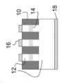
도 1은 반도체 재료의 기둥 사이의 불일치된 CTE 코팅을 도시한다.
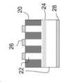
도 2는 반도체 재료의 기둥 사이의 불일치된 CTE 코팅을 도시하며, 기둥 아래의 반도체 재료 내 위치한 양자 우물(quantum well)을 추가로 도시한다.
도 3은 반도체 재료 위의 불일치된 CTE 코팅을 나타내고 반도체 재료 내에 위치된 양자 우물을 추가로 도시한다.The accompanying drawings, which are incorporated into and form a part of the present disclosure, illustrate embodiments of the technology and, together with the description, serve to explain the principles of the technology.
1 shows the mismatched CTE coating between pillars of semiconductor material.
Figure 2 shows the mismatched CTE coating between the pillars of the semiconductor material and further shows the quantum wells located in the semiconductor material below the pillars.
3 shows the mismatched CTE coating over the semiconductor material and further shows the quantum wells located within the semiconductor material.
현재 기술은 미국 특허 No 9,490,318dp 설명된 Lawrence Livermore national Laboratory (LLNL)에서 개발한 변경 미세구조 기술을 활용한다. 이 특허에서는 반도체가 미세 구조로 패턴화된 다음 유전체와 같은 다른 층으로 코팅되는 설명이 제공된다. 이 층은 높은 고유 변형률(high intrinsic strain)을 갖도록 설계되어 반도체로 전달된다. 반도체의 3D 구조는 대량의 반도체 또는 매립층에서 제어된 방식으로 높은 변형률을 적용할 수 있으며, 반도체 재료의 방출 파장을 이동할 수 있는 것으로 나타났다(voss etal Appl Phys Lett. 103, 212104(2013)).The current technology utilizes a modified microstructure technology developed by Lawrence Livermore National Laboratory (LLNL) described in US Patent No. 9,490,318dp. In this patent, a description is provided in which a semiconductor is patterned into a microstructure and then coated with another layer, such as a dielectric. This layer is designed to have a high intrinsic strain and transferred to the semiconductor. It has been shown that the 3D structure of a semiconductor can apply a high strain rate in a controlled manner in a large amount of semiconductor or buried layer, and can shift the emission wavelength of the semiconductor material (voss et al Appl Phys Lett. 103, 212104 (2013)).
본 기술은 대체 방법을 제공한다. 높은 변형률을 위해 코팅을 설계하는 대신에, 코팅 층은 기본 반도체와 열팽창 계수가 일치하지 않도록 선택된다. 따라서, 제작된 LED 또는 LD는 (의도적으로 또는 의도하지 않게) 가열되거나 냉각될 때, 변형이 밴드갭에 대한 온도의 영향을 상쇄하거나 보완하는 역할을 할 수 있다. 이것은, 파장-온도(dλ/dT)관계를 제어하는 추가적인 방법을 가능하게 한다. 적절한 기하 구조(geometry) 및 CTE 불일치로, dλ/dT가 제어된 LD 및 LED 는 생성될 수 있다.This technique provides an alternative method. Instead of designing the coating for high strain, the coating layer is chosen so that the coefficient of thermal expansion does not match with the underlying semiconductor. Thus, when a fabricated LED or LD is heated or cooled (intentionally or unintentionally), the deformation can serve to offset or compensate for the effect of temperature on the bandgap. This enables an additional method of controlling the wavelength-temperature (dλ/dT) relationship. With proper geometry and CTE mismatch, LDs and LEDs with controlled dλ/dT can be produced.
이것은 제로 온도 의존성(zero temperature dependence), 향상된 의존성, 및 심지어 음의 온도 의존성을 가진 LD 및 LED로 이어진다. 이 기술은 음의 열팽창 계수를 가지는 재료를 사용하며 3차원 구조에 국한되지 않는다. 이러한 모든 영역에서 새로운 LD 및 LED에 대한 수많은 잠재적인 응용이 있다. 이러한 구조는 수직 캐비티 표면 레이저(vertical cavity surf ace emitting lasers: VCSELs) 및 에지 방출 디자인(edge emitting designs)과 같은 일반적인 레이저 유형에 적합하다. 따라서, 미국 특허 9,490,318호에 기술된 실시예는 변형 층을 활용하는 것보다 하부 반도체와 열팽창 계수가 일치하지 않는 코팅층이 제공되도록 본 기술에 따라 변경될 수 있다. 이러한 실시예는 예시적이지만 제한되지 않는다. 본 기술뿐만 아니라 고유의 변형 층을 포함하는 실시예를 제 공하는 것이 가능하다.This leads to LDs and LEDs with zero temperature dependence, improved dependence, and even negative temperature dependence. This technique uses a material with a negative coefficient of thermal expansion and is not limited to three-dimensional structures. There are numerous potential applications for new LDs and LEDs in all of these areas. This structure is suitable for common laser types such as vertical cavity surf ace emitting lasers (VCSELs) and edge emitting designs. Accordingly, the embodiment described in U.S. Patent No. 9,490,318 can be modified according to the present technology so that a coating layer whose coefficient of thermal expansion does not match with the underlying semiconductor is provided rather than utilizing a strain layer. This embodiment is illustrative but not limiting. It is possible to provide embodiments including the present technology as well as its own modified layer.
다이오드가 비효율적(inefficient)이게 되기 전에 온도를 높일 수 있기 때문에 온도에 따른 레이저 다이오드의 조정가능성은 제한적이다. 따라서, 향상된 조정 가능성은 더 유연한 레이저 다이오드를 생성한다. 제로 온도 의존성은 냉각 요구사항을 상당히 감소시키거나 제거하여, 크기, 무게, 및 전력(Size, Weight, and Power: SWaP)를 줄인다.Since the temperature can be raised before the diode becomes inefficient, the tunability of the laser diode with temperature is limited. Thus, the improved adjustability produces a more flexible laser diode. Zero temperature dependence significantly reduces or eliminates cooling requirements, reducing Size, Weight, and Power (SWaP).
외부 변형 접근법(External strain approach)는 단순한 에피택셜(epitaxial) 성장 수단을 통해 가능한 것보다 더 많은 변형을 유도하는 방법을 제공한다 (즉, 양자 우물은 재료 구성 조정에 의해 제공되는 내장 변형으로 가능한 것보다 외부에서 적용된 필름에서 더 많은 양의 변형을 수용할 수 있다). 즉, 이는, 차례로 장치의 게인(gain)을 증가시켜 임계값을 줄이고 장치 효율성을 향상시키는데 도움이 된다.The external strain approach provides a way to induce more strain than is possible through simple epitaxial growth means (i.e. quantum wells are possible with visceral strains provided by material composition adjustments). A larger amount of deformation can be accommodated in an externally applied film). That is, this, in turn, helps to increase the gain of the device, thereby reducing the threshold and improving the device efficiency.
기술의 일 실시예는 제 2 필름으로 코팅된 레이저 다이오드 또는 발광 다이오드와 같은 마이크로구조 반도체 장치이다. 제 2 필름에 사용할 수 있는 예시적인 재료는 유전체 또는 금속을 포함하지만 다른 재료도 가능하다. 제 2 필름은 반도체 재료의 열팽창 계수와 다른 열팽창 계수 (CTE)를 가지고 있다. 반도체의 방출 파장이 정상 조건에서와 온도에 따라 다른 거동을 가지도록 미세 구조 기하구조와 제 2 필름은 CTE 불일치로 인해 가열 및 냉각 중에 반도체가 변형되도록 선택된다. 즉, 제 2 열팽창 계수를 갖는 필름이 반도체 재료에 고정적으로 부착되지 않은 경우, 반도체의 방출 파장은 미세 구조 반도체 장치에서 나타나는 것과 다른 온도 대 다른 거동을 가지고 있다. 이에, 전체 장치(반도체, 미세 구조, 제 2 필름)를 설계하여 원하는 dλ/dT 동작을 생성할 수 있다.One embodiment of the technology is a microstructured semiconductor device such as a laser diode or light emitting diode coated with a second film. Exemplary materials that can be used in the second film include dielectrics or metals, but other materials are possible. The second film has a coefficient of thermal expansion (CTE) different from that of the semiconductor material. The microstructure geometry and the second film are chosen to deform the semiconductor during heating and cooling due to CTE mismatch so that the emission wavelength of the semiconductor has a different behavior under normal conditions and with temperature. That is, when the film having the second coefficient of thermal expansion is not fixedly attached to the semiconductor material, the emission wavelength of the semiconductor has a different behavior versus a temperature different from that seen in the microstructured semiconductor device. Accordingly, a desired dλ/dT operation can be generated by designing the entire device (semiconductor, microstructure, and second film).
도 1 내지 도 3의 개략도는 본 기술의 원리에 따른 레이저 다이오드 실시예를 도시한다. 도 1은 반도체 재료(12)의 기둥 사이의 불일치된 CTE 코팅(10)을 도시한다. 양자 우물(14)은 각각의 기둥의 반도체 재료 내에 위치하고, 전극(16)은 각 기둥의 상부에 위치하고 전극(18)은 반도체 재료(12)의 바닥에 위치한다.The schematic diagrams of Figures 1 to 3 show a laser diode embodiment according to the principles of the present technology. 1 shows a
도 2는 반도체 재료(22)의 기둥 사이의 불일치된 CTE 코팅(20)을 도시한다. 양자 우물(24)은 기둥 아래의 반도체 재료(22)내에 위치한다. 전극(26)은 각 기둥의 상부에 위치하고 전극(28)은 반도체 재료(22)의 하부에 위치한다.2 shows the
도 3은 반도체 재료(32) 위의 불일치된 CTE 코팅(30)을 도시한다. 양자 우물(34)은 반도체 재료(32) 내에 위치한다. 전극(36)은 불일치된 CTE 코팅(30)의 상부에 위치하고, 전극(38)은 반도체 재료(32)의 하부에 위치한다.3 shows an inconsistent CTE coating 30 on semiconductor material 32. Quantum well 34 is located within semiconductor material 32. The
광범위하게, 이 연구는 적어도 후술하는 바를 개시한다.Broadly, this study discloses at least what is described below.
장치의 온도가 변함에 따라 다양한 수준의 변형 기본 LED 또는 LD 에 도입되도록, 불일치된 열팽창 계수를 가지는 코팅이 기본 발광 다이오드(LED) 또는 레이저 다이오드(LD)에 적용된다. 변형은 장치의 유효 밴드갭 에너지( 및 방출 파장)을 조정할 수 있기 때문에, 외부 변형 유도 코팅은 온도로 인한 파장 이동을 보상하거나 (결과적으로 dλ/dT가 감소함) 이를 강조(dλ/dT가 증가 함)하도록 작용할 수 있다. 코팅 재료와 형상을 적절히 선택하면 dλ/dT를 완벽하게 제어할 수 있다.Coatings with mismatched coefficients of thermal expansion are applied to the base light-emitting diode (LED) or laser diode (LD) so that varying levels of deformation are introduced into the base LED or LD as the temperature of the device changes. Since the strain can adjust the device's effective bandgap energy (and emission wavelength), the external strain-inducing coating compensates for the wavelength shift due to temperature (consequently dλ/dT decreases) or emphasizes it (dλ/dT increases). Can act to do. With the right choice of coating material and shape, dλ/dT can be completely controlled.
이 연구는 후술하는 컨셉을 적어도 제시한다.This study at least suggests a concept to be described later.
컨셉(들):Concept(s):
1. 장치에 있어서,1. In the device,
제 1 열팽창 계수(coefficient of thermal expansion: CTE)를 갖는 반도체 재료; 및A semiconductor material having a first coefficient of thermal expansion (CTE); And
제 2 열팽창 계수를 갖는 필름을 포함하고, 상기 필름은 상기 반도체 재료에 고정적으로 부착되고, 상기 제 2 열팽창 계수는 상기 장치의 가열 및 냉각 동안 상기 반도체 재료의 쉐이밍(shaming)을 초래하는 CTE의 불일치(mismatch)를 생성하기 위해 상기 제 1 열팽창 계수와 상이한 장치.A film having a second coefficient of thermal expansion, wherein the film is fixedly attached to the semiconductor material, and the second coefficient of thermal expansion is of a CTE resulting in shaming of the semiconductor material during heating and cooling of the device. A device different from the first coefficient of thermal expansion to create a mismatch.
2. 컨셉 1 및 3-10의 장치에 있어서, 상기 반도체 재료는 미세구조화된 (microstructured) 반도체 장치를 포함하는, 장치.2. The device of concepts 1 and 3-10, wherein the semiconductor material comprises a microstructured semiconductor device.
3. 컨셉 1, 2 및 4-10의 장치에 있어서, 상기 반도체 재료는 레이저 다이오드 및 발광 다이오드로 구성된 그룹으로부터 선택된 미세구조화된 반도체 장치를 포함하는, 장치.3. The device of concepts 1, 2 and 4-10, wherein the semiconductor material comprises a microstructured semiconductor device selected from the group consisting of laser diodes and light emitting diodes.
4. 컨셉 1-3 및 5-10의 장치에 있어서, 상기 제 2 팽창계수를 갖는 필름이 상기 반도체 재료에 고정적으로 부착되지 않은 경우, 상기 반도체 재료는 상기 미세구조화된 반도체 장치가 나타내는 것과 상이한 온도에 따라 방출 파장을 생성하는 미세구조화된 반도체 장치를 포함하는, 장치.4. In the devices of Concepts 1-3 and 5-10, when the film having the second coefficient of expansion is not fixedly attached to the semiconductor material, the semiconductor material has a temperature different from that indicated by the microstructured semiconductor device. A device comprising a microstructured semiconductor device that generates an emission wavelength according to.
5. 컨셉 1-4 및 6-10의 장치에 있어서, 상기 반도체 재료는 원하는 dλ/dT 거동을 야기하도록 설계된 미세구조화된 반도체 장치를 포함하는, 장치5. The device of concepts 1-4 and 6-10, wherein the semiconductor material comprises a microstructured semiconductor device designed to cause the desired dλ/dT behavior.
6. 컨셉 1-5 및 7-10의 장치에 있어서, 상기 필름은 유전체 및 금속으로 구성된 그룹에서 선택된 재료를 포함하는, 장치.6. The device of concepts 1-5 and 7-10, wherein the film comprises a material selected from the group consisting of dielectrics and metals.
7. 컨셉 1-6 및 8-10의 장치에 있어서, 상기 반도체 재료는 미세구조화된 반도체 장치를 포함하고,7. In the device of concepts 1-6 and 8-10, the semiconductor material comprises a microstructured semiconductor device,
상기 미세구조화된 반도체 장치는 미세구조의 기하구조(microstructural geometry)를 포함하고,The microstructured semiconductor device includes a microstructural geometry,
상기 반도체의 상기 방출 파장이 만일 상기 제 2 열팽창 계수가 상기 반도체 재료에 고정적으로 부착되지 않은 경우를 나타내는 것과는 상이한 거동 대 온도를 갖도록 상기 미세구조의 기하구조 및 상기 필름은 상기 열팽창계수의 불일치가 가열 및 냉각 동안 상기 반도체 장치의 변형을 야기하도록 선택되는, 장치.The geometry of the microstructure and the film are heated so that the emission wavelength of the semiconductor has a behavior versus temperature different from that indicating if the second coefficient of thermal expansion is not fixedly attached to the semiconductor material. And causing deformation of the semiconductor device during cooling.
8. 컨셉 1-7 및 9-10의 장치에 있어서, 상기 반도체 재료는 2차원 반도체 장치를 포함하는 장치.8. The device of concepts 1-7 and 9-10, wherein the semiconductor material comprises a two-dimensional semiconductor device.
9. 컨셉 1-8 및 9-10의 장치에 있어서, 상기 반도체 재료는 3차원 반도체 장치를 포함하는 장치.9. The device of concepts 1-8 and 9-10, wherein the semiconductor material comprises a three-dimensional semiconductor device.
10. 컨셉 1-9의 장치에 있어서, 상기 반도체 재료는 레이저 다이오드 및 발광 다이오드로 구성된 그룹에서 선택된 반도체 장치를 포함하는 장치.10. The device of concept 1-9, wherein the semiconductor material comprises a semiconductor device selected from the group consisting of laser diodes and light emitting diodes.
11. 방법에 있어서,11. In the method,
제 1 열팽창계수(CTE)를 가지는 반도체 재료를 제공하는 단계; 및Providing a semiconductor material having a first coefficient of thermal expansion (CTE); And
제 2 열팽창 계수를 갖는 상기 반도체 재료에 필름을 부착하는 단계;를 포함하고,Including; attaching a film to the semiconductor material having a second coefficient of thermal expansion,
상기 제 2 열팽창 계수는 상기 반도체 물질 및 상기 필름 중 적어도 하나의 가열 및 냉각 동안 상기 반도체 물질의 변형을 초래하는 CTE 불일치를 생성하도록 상기 제 1 열팽창 계수와 상이한, 방법.Wherein the second coefficient of thermal expansion is different from the first coefficient of thermal expansion to create a CTE mismatch resulting in deformation of the semiconductor material during heating and cooling of at least one of the semiconductor material and the film.
12. 컨셉 11 및 13-20의 방법에 있어서, 상기 반도체 재료는 미세구조화된 (microstructured) 반도체 장치를 포함하는, 장치.12. The apparatus of concepts 11 and 13-20, wherein the semiconductor material comprises a microstructured semiconductor device.
13. 컨셉 11, 12 및 14-20의 방법에 있어서, 상기 반도체 재료는 레이저 다이오드 및 발광 다이오드로 구성된 그룹으로부터 선택된 미세구조화된 반도체 장치를 포함하는, 장치.13. The method of
14. 컨셉 11-13 및 15-20의 방법에 있어서, 상기 반도체 재료는 상기 제 2 팽창계수를 갖는 필름이 상기 반도체 재료에 고정적으로 부착되지 않은 경우, 상기 반도체 재료는 상기 미세구조화된 반도체 장치가 나타내는 것과 상이한 온도에 따라 방출 파장을 생성하는 미세구조화된 반도체 장치를 포함하는, 방법.14. In the methods of concepts 11-13 and 15-20, the semiconductor material is the microstructured semiconductor device when the film having the second expansion coefficient is not fixedly attached to the semiconductor material. A method comprising a microstructured semiconductor device that produces an emission wavelength according to a temperature different from that exhibited.
15. 컨셉 11-14 및 16-20의 방법에 있어서, 상기 반도체 재료는 원하는 dλ/dT 거동을 야기하도록 설계된 미세구조화된 반도체 장치를 포함하는, 방법15. The method of concepts 11-14 and 16-20, wherein the semiconductor material comprises a microstructured semiconductor device designed to cause the desired dλ/dT behavior.
16. 컨셉 11-15 및 17-20의 방법에 있어서, 상기 필름은 유전체 및 금속으로 구성된 그룹에서 선택된 재료를 포함하는, 방법.16. The method of concepts 11-15 and 17-20, wherein the film comprises a material selected from the group consisting of dielectrics and metals.
17. 컨셉 11-16 및 18-20의 방법에 있어서, 상기 반도체 재료는 미세구조화된 반도체 장치를 포함하고,17. The method of concepts 11-16 and 18-20, wherein the semiconductor material comprises a microstructured semiconductor device,
상기 미세구조화된 반도체 장치는 미세구조의 기하구조(microstructural geometry)를 포함하고,The microstructured semiconductor device includes a microstructural geometry,
상기 반도체의 상기 방출 파장이 만일 상기 제 2 열팽창 계수가 상기 반도체 재료에 고정적으로 부착되지 않은 경우를 나타내는 것과는 상이한 거동 대 온도를 갖도록 상기 미세구조의 기하구조 및 상기 필름은 상기 열팽창계수의 불일치가 가열 및 냉각 동안 상기 반도체 장치의 변형을 야기하도록 선택되는, 방법.The geometry of the microstructure and the film are heated in such a way that the emission wavelength of the semiconductor has a behavior versus temperature different from that indicating if the second coefficient of thermal expansion is not fixedly attached to the semiconductor material. And causing deformation of the semiconductor device during cooling.
18. 컨셉 11-17 및 19-20의 방법에 있어서, 상기 반도체 재료는 2차원 반도체 장치를 포함하는 방법.18. The method of concepts 11-17 and 19-20, wherein the semiconductor material comprises a two-dimensional semiconductor device.
19. 컨셉 11-18 및 20의 방법에 있어서, 상기 반도체 재료는 3차원 반도체 장치를 포함하는 방법.19. The method of concepts 11-18 and 20, wherein the semiconductor material comprises a three-dimensional semiconductor device.
20. 컨셉 11-19의 방법에 있어서, 상기 반도체 재료는 레이저 다이오드 및 발광 다이오드로 구성된 그룹에서 선택된 반도체 장치를 포함하는 방법.20. The method of concept 11-19, wherein the semiconductor material comprises a semiconductor device selected from the group consisting of laser diodes and light emitting diodes.
21. 장치에 있어서,21. In the device,
기판;Board;
상기 기판 위에 위치한 3차원 반도체 구조의 어레이에 있어서, 상기 3차원 구조는 바닥 표면, 상부 표면, 및 상기 바닥 표면과 상기 상부 표면을 연결하는 적어도 하나의 측면 표면을 포함하고;An array of three-dimensional semiconductor structures positioned over the substrate, the three-dimensional structure comprising a bottom surface, a top surface, and at least one side surface connecting the bottom surface and the top surface;
각각의 상기 3차원 구조 사이의 캐비티 영역(cavity region);A cavity region between each of the three-dimensional structures;
상기 3차원 반도체 구조의 것과 상이한 CTE를 포함하는, 각각의 캐비티 영역에 위치하고, 각각의 3차원 구조의 각 측면을 둘러싸는 필름;을 포함하는 장치.And a film located in each cavity region and surrounding each side of each three-dimensional structure, including a CTE different from that of the three-dimensional semiconductor structure.
22. 방법에 있어서,22. In the method,
기판을 제공하는 단계;Providing a substrate;
상기 기판 위에 및 기판에 3차원 반도체 구조의 어레이를 고정적으로 위치하는 단계에 있어서, 상기 3차원 구조는 바닥 표면, 상부 표면, 및 상기 바닥 표면과 상기 상부 표면을 연결하는 적어도 하나의 측면 표면을 포함하고;Fixedly positioning an array of three-dimensional semiconductor structures on and on the substrate, the three-dimensional structure comprising a bottom surface, an upper surface, and at least one side surface connecting the bottom surface and the top surface and;
각각의 상기 3차원 구조 사이의 캐비티 영역(cavity region)을 형성하는 단계에 있어서,In the step of forming a cavity region between each of the three-dimensional structures,
상기 필름은 상기 3차원 반도체 구조의 것과 상이한 CTE를 포함하며, 각각의 캐비티 영역에 필름을 고정적으로 위치시키고 각각의 3차원 구조의 각 측면을 둘러싸는 단계;를 포함하는, 방법.Wherein the film comprises a CTE different from that of the three-dimensional semiconductor structure, the step of fixing the film in each cavity region and surrounding each side of each three-dimensional structure.
본 명세서에 설명된 모든 요소, 부분 및 단계가 바람직하게 포함된다. 이들 요소, 부분 및 단계 중 임의의 것은 다른 요소, 부분 및 단계로 대체 될 수 있거나, 당업자에게 명백한 바와 같이 모두 삭제될 수 있음을 이해해야 한다.All elements, parts and steps described herein are preferably included. It is to be understood that any of these elements, parts and steps may be replaced with other elements, parts and steps, or all may be deleted as will be apparent to those skilled in the art.
기술에 대한 전술한 설명은 예시 및 설명의 목적으로 제시되었으며, 포괄적이거나 기술을 개시된 정확한 형태로 제한하려는 의도가 아니다. 위의 가르침에 비추어 많은 수정 및 변형이 가능하다. 개시된 실시예는 기술의 원리 및 그 실제 적용을 설명하기 위한 것일 뿐이며, 이에 따라 당업자가 고려되는 특정 사용에 적합한 다양한 수정으로 다양한 실시예에서 기술을 가장 잘 사용할 수 있다. 기술의 범위는 다음 청구 범위에 의해 정의된다.The foregoing description of the technology has been presented for purposes of illustration and description, and is not intended to be exhaustive or to limit the technology to the precise form disclosed. Many modifications and variations are possible in light of the above teaching. The disclosed embodiments are only for describing the principle of the technology and its practical application, and accordingly, a person skilled in the art can best use the technology in various embodiments with various modifications suitable for a specific use considered. The scope of the technology is defined by the following claims.
Claims (22)
Translated fromKorean제 1 열팽창 계수(coefficient of thermal expansion: CTE)를 갖는 반도체 재료; 및
제 2 열팽창 계수를 갖는 필름을 포함하고, 상기 필름은 상기 반도체 재료에 고정적으로 부착되고, 상기 제 2 열팽창 계수는 상기 장치의 가열 및 냉각 동안 상기 반도체 재료의 쉐이밍(shaming)을 초래하는 CTE의 불일치(mismatch)를 생성하기 위해 상기 제 1 열팽창 계수와 상이한 장치.In the device,
A semiconductor material having a first coefficient of thermal expansion (CTE); And
A film having a second coefficient of thermal expansion, wherein the film is fixedly attached to the semiconductor material, and the second coefficient of thermal expansion is of a CTE resulting in shaming of the semiconductor material during heating and cooling of the device. A device different from the first coefficient of thermal expansion to create a mismatch.
상기 미세구조화된 반도체 장치는 미세구조의 기하구조(microstructural geometry)를 포함하고,
상기 반도체의 상기 방출 파장이 만일 상기 제 2 열팽창 계수가 상기 반도체 재료에 고정적으로 부착되지 않은 경우를 나타내는 것과는 상이한 거동 대 온도를 갖도록 상기 미세구조의 기하구조 및 상기 필름은 상기 열팽창계수의 불일치가 가열 및 냉각 동안 상기 반도체 장치의 변형을 야기하도록 선택되는, 장치.The method of claim 1, wherein the semiconductor material comprises a microstructured semiconductor device,
The microstructured semiconductor device includes a microstructural geometry,
The geometry of the microstructure and the film are heated so that the emission wavelength of the semiconductor has a behavior versus temperature different from that indicating if the second coefficient of thermal expansion is not fixedly attached to the semiconductor material. And causing deformation of the semiconductor device during cooling.
제 1 열팽창계수(CTE)를 가지는 반도체 재료를 제공하는 단계; 및
제 2 열팽창 계수를 갖는 상기 반도체 재료에 필름을 부착하는 단계;를 포함하고,
상기 제 2 열팽창 계수는 상기 반도체 물질 및 상기 필름 중 적어도 하나의 가열 및 냉각 동안 상기 반도체 물질의 변형을 초래하는 CTE 불일치를 생성하도록 상기 제 1 열팽창 계수와 상이한, 방법.In the way,
Providing a semiconductor material having a first coefficient of thermal expansion (CTE); And
Including; attaching a film to the semiconductor material having a second coefficient of thermal expansion,
Wherein the second coefficient of thermal expansion is different from the first coefficient of thermal expansion to create a CTE mismatch resulting in deformation of the semiconductor material during heating and cooling of at least one of the semiconductor material and the film.
상기 반도체 재료는 미세구조화된 반도체 장치를 포함하고,
상기 미세구조화된 반도체 장치는 미세구조의 기하구조(microstructural geometry)를 포함하고,
상기 반도체의 상기 방출 파장이 만일 상기 제 2 열팽창 계수가 상기 반도체 재료에 고정적으로 부착되지 않은 경우를 나타내는 것과는 상이한 거동 대 온도를 갖도록 상기 미세구조의 기하구조 및 상기 필름은 상기 열팽창계수의 불일치가 가열 및 냉각 동안 상기 반도체 장치의 변형을 야기하도록 선택되는, 방법.The method of claim 11,
The semiconductor material comprises a microstructured semiconductor device,
The microstructured semiconductor device includes a microstructural geometry,
The geometry of the microstructure and the film are heated so that the emission wavelength of the semiconductor has a behavior versus temperature different from that indicating if the second coefficient of thermal expansion is not fixedly attached to the semiconductor material. And causing deformation of the semiconductor device during cooling.
기판;
상기 기판 위에 위치한 3차원 반도체 구조의 어레이에 있어서, 상기 3차원 구조는 바닥 표면, 상부 표면, 및 상기 바닥 표면과 상기 상부 표면을 연결하는 적어도 하나의 측면 표면을 포함하고;
각각의 상기 3차원 구조 사이의 캐비티 영역(cavity region);
상기 3차원 반도체 구조의 것과 상이한 CTE를 포함하는, 각각의 캐비티 영역에 위치하고, 각각의 3차원 구조의 각 측면을 둘러싸는 필름;을 포함하는 장치.In the device,
Board;
An array of three-dimensional semiconductor structures positioned over the substrate, the three-dimensional structure comprising a bottom surface, a top surface, and at least one side surface connecting the bottom surface and the top surface;
A cavity region between each of the three-dimensional structures;
And a film positioned in each cavity region and surrounding each side of each three-dimensional structure, including a CTE different from that of the three-dimensional semiconductor structure.
기판을 제공하는 단계;
상기 기판 위에 및 기판에 3차원 반도체 구조의 어레이를 고정적으로 위치하는 단계에 있어서, 상기 3차원 구조는 바닥 표면, 상부 표면, 및 상기 바닥 표면과 상기 상부 표면을 연결하는 적어도 하나의 측면 표면을 포함하고;
각각의 상기 3차원 구조 사이의 캐비티 영역(cavity region)을 형성하는 단계에 있어서,
상기 필름은 상기 3차원 반도체 구조의 것과 상이한 CTE를 포함하며, 각각의 캐비티 영역에 필름을 고정적으로 위치시키고 각각의 3차원 구조의 각 측면을 둘러싸는 단계;를 포함하는, 방법.
In the way,
Providing a substrate;
Fixedly positioning an array of three-dimensional semiconductor structures on and on the substrate, the three-dimensional structure comprising a bottom surface, an upper surface, and at least one side surface connecting the bottom surface and the top surface and;
In the step of forming a cavity region between each of the three-dimensional structures,
Wherein the film comprises a CTE different from that of the three-dimensional semiconductor structure, the step of fixing the film in each cavity region and surrounding each side of each three-dimensional structure.
Applications Claiming Priority (3)
| Application Number | Priority Date | Filing Date | Title |
|---|---|---|---|
| US201862684720P | 2018-06-13 | 2018-06-13 | |
| US62/684,720 | 2018-06-13 | ||
| PCT/US2019/036174WO2019241082A1 (en) | 2018-06-13 | 2019-06-07 | Strain control in optoelectronic devices |
Publications (1)
| Publication Number | Publication Date |
|---|---|
| KR20210010463Atrue KR20210010463A (en) | 2021-01-27 |
Family
ID=68840425
Family Applications (1)
| Application Number | Title | Priority Date | Filing Date |
|---|---|---|---|
| KR1020207032943APendingKR20210010463A (en) | 2018-06-13 | 2019-06-07 | Deformation control of optoelectronic devices |
Country Status (5)
| Country | Link |
|---|---|
| US (1) | US10992105B2 (en) |
| EP (1) | EP3807925A4 (en) |
| JP (1) | JP2021527944A (en) |
| KR (1) | KR20210010463A (en) |
| WO (1) | WO2019241082A1 (en) |
Families Citing this family (1)
| Publication number | Priority date | Publication date | Assignee | Title |
|---|---|---|---|---|
| CN112467514B (en)* | 2020-11-10 | 2022-04-12 | 华中科技大学 | A Distributed Feedback Semiconductor Laser with Wide Operating Temperature Range |
Family Cites Families (13)
| Publication number | Priority date | Publication date | Assignee | Title |
|---|---|---|---|---|
| US5787104A (en)* | 1995-01-19 | 1998-07-28 | Matsushita Electric Industrial Co., Ltd. | Semiconductor light emitting element and method for fabricating the same |
| GB2310316A (en)* | 1996-02-15 | 1997-08-20 | Sharp Kk | Semiconductor laser |
| MY145695A (en)* | 2001-01-24 | 2012-03-30 | Nichia Corp | Light emitting diode, optical semiconductor device, epoxy resin composition suited for optical semiconductor device, and method for manufacturing the same |
| DE10245631B4 (en)* | 2002-09-30 | 2022-01-20 | OSRAM Opto Semiconductors Gesellschaft mit beschränkter Haftung | semiconductor device |
| JP4160000B2 (en)* | 2004-02-13 | 2008-10-01 | ドンゴク ユニバーシティ インダストリー アカデミック コーポレイション ファウンデイション | Light emitting diode and manufacturing method thereof |
| US7875522B2 (en)* | 2007-03-30 | 2011-01-25 | The Board Of Trustees Of The Leland Stanford Junior University | Silicon compatible integrated light communicator |
| JP4978478B2 (en)* | 2008-01-11 | 2012-07-18 | ソニー株式会社 | Electromagnetic wave suppressing heat radiation sheet and electronic device |
| JP4575471B2 (en)* | 2008-03-28 | 2010-11-04 | 株式会社東芝 | Semiconductor device and manufacturing method of semiconductor device |
| JP5479765B2 (en)* | 2009-03-27 | 2014-04-23 | 古河電気工業株式会社 | One-dimensional array element manufacturing method and one-dimensional array element |
| US9065253B2 (en)* | 2009-05-13 | 2015-06-23 | University Of Washington Through Its Center For Commercialization | Strain modulated nanostructures for optoelectronic devices and associated systems and methods |
| JP5121783B2 (en)* | 2009-06-30 | 2013-01-16 | 株式会社日立ハイテクノロジーズ | LED light source, manufacturing method thereof, exposure apparatus using LED light source, and exposure method |
| US9490318B2 (en)* | 2012-06-15 | 2016-11-08 | Lawrence Livermore National Security, Llc | Three dimensional strained semiconductors |
| CN106098697B (en)* | 2016-06-15 | 2019-04-02 | 深圳市华星光电技术有限公司 | Micro- LED display panel and preparation method thereof |
- 2019
- 2019-06-07JPJP2020564399Apatent/JP2021527944A/enactivePending
- 2019-06-07USUS16/434,236patent/US10992105B2/enactiveActive
- 2019-06-07WOPCT/US2019/036174patent/WO2019241082A1/ennot_activeCeased
- 2019-06-07KRKR1020207032943Apatent/KR20210010463A/enactivePending
- 2019-06-07EPEP19819919.2Apatent/EP3807925A4/enactivePending
Also Published As
| Publication number | Publication date |
|---|---|
| US10992105B2 (en) | 2021-04-27 |
| EP3807925A4 (en) | 2022-03-02 |
| EP3807925A1 (en) | 2021-04-21 |
| JP2021527944A (en) | 2021-10-14 |
| WO2019241082A1 (en) | 2019-12-19 |
| US20190386462A1 (en) | 2019-12-19 |
Similar Documents
| Publication | Publication Date | Title |
|---|---|---|
| US9691680B2 (en) | Structured substrate | |
| US20170005224A1 (en) | Substrate Structure Removal | |
| Liao et al. | Monolithically integrated electrically pumped continuous-wave III-V quantum dot light sources on silicon | |
| US8633493B2 (en) | Large area thin freestanding nitride layers and their use as circuit layers | |
| KR20120071322A (en) | Process for cleaving a substrate | |
| KR20210010463A (en) | Deformation control of optoelectronic devices | |
| Humayun et al. | Effect of lattice constant on band-gap energy and optimization and stabilization of high-temperature In x Ga1− x N quantum-dot lasers | |
| JP5582617B2 (en) | Relaxation of strained layer | |
| JP5366149B2 (en) | Semiconductor laser equipment | |
| WO2006111601A1 (en) | A saturable absorber structure | |
| Li et al. | Fabrication of patterned sapphire substrate and effect of light emission pattern on package efficiency | |
| CN105119143A (en) | Chip structure for reducing packaging stress of semiconductor laser and method of reducing packaging stress | |
| Marmalyuk et al. | Laser diode bars based on strain-compensated AlGaPAs/GaAs heterostructures | |
| US9373747B2 (en) | Method for producing an optoelectronic component | |
| Amann et al. | Focus on advanced semiconductor heterostructures for optoelectronics | |
| Voss et al. | Strain control in optoelectronic devices | |
| Humayun et al. | Design of quantum dot based laser with ultra-low threshold current density | |
| JP2012004344A (en) | Manufacturing method of semiconductor film | |
| KR102158788B1 (en) | Laser diode bar module | |
| KR102638845B1 (en) | Doped diamond semiconductor and method of manufacture using laser abalation | |
| JP2010073962A (en) | Semiconductor light emitting element | |
| Kudsieh et al. | Transient thermal analysis of lnGaN/GaN laser diodes | |
| JPH0362985A (en) | Distribution feedback type semiconductor and its manufacture method | |
| KR101211015B1 (en) | Device of using Quantum Dots and Method of manufacturing the same | |
| Nadir | Characterization of GaN-based quantum dots within vertical-cavity surface-emitting lasers for realizing green lasers by simulations |
Legal Events
| Date | Code | Title | Description |
|---|---|---|---|
| PA0105 | International application | St.27 status event code:A-0-1-A10-A15-nap-PA0105 | |
| P11-X000 | Amendment of application requested | St.27 status event code:A-2-2-P10-P11-nap-X000 | |
| P13-X000 | Application amended | St.27 status event code:A-2-2-P10-P13-nap-X000 | |
| PG1501 | Laying open of application | St.27 status event code:A-1-1-Q10-Q12-nap-PG1501 | |
| P11-X000 | Amendment of application requested | St.27 status event code:A-2-2-P10-P11-nap-X000 | |
| P13-X000 | Application amended | St.27 status event code:A-2-2-P10-P13-nap-X000 | |
| PA0201 | Request for examination | St.27 status event code:A-1-2-D10-D11-exm-PA0201 | |
| E902 | Notification of reason for refusal | ||
| PE0902 | Notice of grounds for rejection | St.27 status event code:A-1-2-D10-D21-exm-PE0902 | |
| E13-X000 | Pre-grant limitation requested | St.27 status event code:A-2-3-E10-E13-lim-X000 | |
| P11-X000 | Amendment of application requested | St.27 status event code:A-2-2-P10-P11-nap-X000 | |
| P13-X000 | Application amended | St.27 status event code:A-2-2-P10-P13-nap-X000 | |
| E601 | Decision to refuse application | ||
| P22-X000 | Classification modified | St.27 status event code:A-2-2-P10-P22-nap-X000 | |
| PE0601 | Decision on rejection of patent | St.27 status event code:N-2-6-B10-B15-exm-PE0601 | |
| T11-X000 | Administrative time limit extension requested | St.27 status event code:U-3-3-T10-T11-oth-X000 | |
| T13-X000 | Administrative time limit extension granted | St.27 status event code:U-3-3-T10-T13-oth-X000 | |
| T13-X000 | Administrative time limit extension granted | St.27 status event code:U-3-3-T10-T13-oth-X000 | |
| E13-X000 | Pre-grant limitation requested | St.27 status event code:A-2-3-E10-E13-lim-X000 | |
| P11-X000 | Amendment of application requested | St.27 status event code:A-2-2-P10-P11-nap-X000 | |
| PX0701 | Decision of registration after re-examination | St.27 status event code:A-3-4-F10-F13-rex-PX0701 |