KR20210008931A - Process chamber process kit with protective coating - Google Patents
Process chamber process kit with protective coatingDownload PDFInfo
- Publication number
- KR20210008931A KR20210008931AKR1020217001257AKR20217001257AKR20210008931AKR 20210008931 AKR20210008931 AKR 20210008931AKR 1020217001257 AKR1020217001257 AKR 1020217001257AKR 20217001257 AKR20217001257 AKR 20217001257AKR 20210008931 AKR20210008931 AKR 20210008931A
- Authority
- KR
- South Korea
- Prior art keywords
- chamber
- plasma
- chamber component
- base material
- metallic base
- Prior art date
- Legal status (The legal status is an assumption and is not a legal conclusion. Google has not performed a legal analysis and makes no representation as to the accuracy of the status listed.)
- Granted
Links
Images


Classifications
- H—ELECTRICITY
- H01—ELECTRIC ELEMENTS
- H01J—ELECTRIC DISCHARGE TUBES OR DISCHARGE LAMPS
- H01J37/00—Discharge tubes with provision for introducing objects or material to be exposed to the discharge, e.g. for the purpose of examination or processing thereof
- H01J37/32—Gas-filled discharge tubes
- H01J37/32431—Constructional details of the reactor
- H01J37/32458—Vessel
- H01J37/32477—Vessel characterised by the means for protecting vessels or internal parts, e.g. coatings
- H01J37/32495—Means for protecting the vessel against plasma
- C—CHEMISTRY; METALLURGY
- C23—COATING METALLIC MATERIAL; COATING MATERIAL WITH METALLIC MATERIAL; CHEMICAL SURFACE TREATMENT; DIFFUSION TREATMENT OF METALLIC MATERIAL; COATING BY VACUUM EVAPORATION, BY SPUTTERING, BY ION IMPLANTATION OR BY CHEMICAL VAPOUR DEPOSITION, IN GENERAL; INHIBITING CORROSION OF METALLIC MATERIAL OR INCRUSTATION IN GENERAL
- C23C—COATING METALLIC MATERIAL; COATING MATERIAL WITH METALLIC MATERIAL; SURFACE TREATMENT OF METALLIC MATERIAL BY DIFFUSION INTO THE SURFACE, BY CHEMICAL CONVERSION OR SUBSTITUTION; COATING BY VACUUM EVAPORATION, BY SPUTTERING, BY ION IMPLANTATION OR BY CHEMICAL VAPOUR DEPOSITION, IN GENERAL
- C23C24/00—Coating starting from inorganic powder
- C23C24/08—Coating starting from inorganic powder by application of heat or pressure and heat
- C23C24/082—Coating starting from inorganic powder by application of heat or pressure and heat without intermediate formation of a liquid in the layer
- C23C24/085—Coating with metallic material, i.e. metals or metal alloys, optionally comprising hard particles, e.g. oxides, carbides or nitrides
- H—ELECTRICITY
- H01—ELECTRIC ELEMENTS
- H01J—ELECTRIC DISCHARGE TUBES OR DISCHARGE LAMPS
- H01J37/00—Discharge tubes with provision for introducing objects or material to be exposed to the discharge, e.g. for the purpose of examination or processing thereof
- H01J37/32—Gas-filled discharge tubes
- H01J37/32431—Constructional details of the reactor
- H01J37/3244—Gas supply means
- H—ELECTRICITY
- H01—ELECTRIC ELEMENTS
- H01J—ELECTRIC DISCHARGE TUBES OR DISCHARGE LAMPS
- H01J37/00—Discharge tubes with provision for introducing objects or material to be exposed to the discharge, e.g. for the purpose of examination or processing thereof
- H01J37/32—Gas-filled discharge tubes
- H01J37/32431—Constructional details of the reactor
- H01J37/32458—Vessel
- H01J37/32477—Vessel characterised by the means for protecting vessels or internal parts, e.g. coatings
- H—ELECTRICITY
- H01—ELECTRIC ELEMENTS
- H01L—SEMICONDUCTOR DEVICES NOT COVERED BY CLASS H10
- H01L21/00—Processes or apparatus adapted for the manufacture or treatment of semiconductor or solid state devices or of parts thereof
- H01L21/02—Manufacture or treatment of semiconductor devices or of parts thereof
- H01L21/02104—Forming layers
- H01L21/02107—Forming insulating materials on a substrate
- H01L21/02225—Forming insulating materials on a substrate characterised by the process for the formation of the insulating layer
- H01L21/0226—Forming insulating materials on a substrate characterised by the process for the formation of the insulating layer formation by a deposition process
- H01L21/02263—Forming insulating materials on a substrate characterised by the process for the formation of the insulating layer formation by a deposition process deposition from the gas or vapour phase
- H01L21/02271—Forming insulating materials on a substrate characterised by the process for the formation of the insulating layer formation by a deposition process deposition from the gas or vapour phase deposition by decomposition or reaction of gaseous or vapour phase compounds, i.e. chemical vapour deposition
- H01L21/02274—Forming insulating materials on a substrate characterised by the process for the formation of the insulating layer formation by a deposition process deposition from the gas or vapour phase deposition by decomposition or reaction of gaseous or vapour phase compounds, i.e. chemical vapour deposition in the presence of a plasma [PECVD]
- H—ELECTRICITY
- H01—ELECTRIC ELEMENTS
- H01L—SEMICONDUCTOR DEVICES NOT COVERED BY CLASS H10
- H01L21/00—Processes or apparatus adapted for the manufacture or treatment of semiconductor or solid state devices or of parts thereof
- H01L21/02—Manufacture or treatment of semiconductor devices or of parts thereof
- H01L21/04—Manufacture or treatment of semiconductor devices or of parts thereof the devices having potential barriers, e.g. a PN junction, depletion layer or carrier concentration layer
- H01L21/50—Assembly of semiconductor devices using processes or apparatus not provided for in a single one of the groups H01L21/18 - H01L21/326 or H10D48/04 - H10D48/07 e.g. sealing of a cap to a base of a container
- H01L21/56—Encapsulations, e.g. encapsulation layers, coatings
- H—ELECTRICITY
- H01—ELECTRIC ELEMENTS
- H01L—SEMICONDUCTOR DEVICES NOT COVERED BY CLASS H10
- H01L21/00—Processes or apparatus adapted for the manufacture or treatment of semiconductor or solid state devices or of parts thereof
- H01L21/67—Apparatus specially adapted for handling semiconductor or electric solid state devices during manufacture or treatment thereof; Apparatus specially adapted for handling wafers during manufacture or treatment of semiconductor or electric solid state devices or components ; Apparatus not specifically provided for elsewhere
- H01L21/67005—Apparatus not specifically provided for elsewhere
- H01L21/67011—Apparatus for manufacture or treatment
- H01L21/67017—Apparatus for fluid treatment
- H01L21/67063—Apparatus for fluid treatment for etching
- H01L21/67069—Apparatus for fluid treatment for etching for drying etching
Landscapes
- Engineering & Computer Science (AREA)
- Chemical & Material Sciences (AREA)
- Physics & Mathematics (AREA)
- Plasma & Fusion (AREA)
- Analytical Chemistry (AREA)
- Power Engineering (AREA)
- General Physics & Mathematics (AREA)
- Microelectronics & Electronic Packaging (AREA)
- Computer Hardware Design (AREA)
- Manufacturing & Machinery (AREA)
- Condensed Matter Physics & Semiconductors (AREA)
- Chemical Kinetics & Catalysis (AREA)
- Materials Engineering (AREA)
- Mechanical Engineering (AREA)
- Metallurgy (AREA)
- Organic Chemistry (AREA)
- Drying Of Semiconductors (AREA)
- Plasma Technology (AREA)
- Chemical Or Physical Treatment Of Fibers (AREA)
- Treatment Of Fiber Materials (AREA)
- Chemical Vapour Deposition (AREA)
Abstract
Translated fromKoreanDescription
Translated fromKorean본 개시내용은 일반적으로, 플라즈마 처리 챔버 장치에서 사용하기 위한 툴들 및 구성요소들에 관한 것이다. 더 구체적으로, 본 개시내용은 부식성 플라즈마 환경에 대해 저항성인 플라즈마 처리 챔버 구성요소를 제조하기 위한 방법에 관한 것이다.TECHNICAL FIELD This disclosure generally relates to tools and components for use in a plasma processing chamber apparatus. More specifically, the present disclosure relates to a method for manufacturing a plasma processing chamber component that is resistant to corrosive plasma environments.
반도체 처리는 다수의 상이한 화학적 및 물리적 프로세스들을 수반하며, 이로써 미세한 집적 회로들이 기판 상에 생성된다. 집적 회로를 구성하는 물질들의 층들은 화학 기상 증착, 물리 기상 증착, 에피택셜 성장 등에 의해 생성된다. 물질의 층들 중 일부는 포토레지스트 마스크들 및 습식 또는 건식 식각 기법들을 사용하여 패터닝된다. 집적 회로들을 형성하는 데 활용되는 기판은 규소, 비화갈륨, 인화인듐, 유리, 또는 다른 적절한 물질일 수 있다.Semiconductor processing involves a number of different chemical and physical processes, whereby microscopic integrated circuits are created on a substrate. Layers of materials that make up an integrated circuit are produced by chemical vapor deposition, physical vapor deposition, epitaxial growth, or the like. Some of the layers of material are patterned using photoresist masks and wet or dry etching techniques. The substrate utilized to form the integrated circuits may be silicon, gallium arsenide, indium phosphide, glass, or other suitable material.
전형적인 반도체 처리 챔버는 프로세스 구역을 한정하는 챔버 몸체, 가스 공급부로부터 프로세스 구역 내로 가스를 공급하도록 적응된 가스 분배 조립체, 기판 지지 조립체 상에 위치된 기판을 처리하기 위해 프로세스 가스에 에너지를 공급하는 데 활용되는 가스 에너지 공급기, 예를 들어 플라즈마 생성기, 및 가스 배기부를 포함한다. 플라즈마 처리 동안, 에너지 공급된 가스는 종종, 처리 챔버 구성요소들의 노출된 부분들, 예를 들어, 처리 동안 기판을 유지하는 정전 척을 식각하고 침식시키는 고반응성 종들 및 이온들로 구성된다. 추가적으로, 처리 부산물들이 종종, 전형적으로 고반응성 플루오린으로 주기적으로 세정되는 챔버 구성요소들 상에 증착된다. 챔버 몸체 내로부터 처리 부산물들을 제거하는 데 사용되는 인-시튜 세정 절차들은 처리 챔버 구성요소들의 무결성을 더 침식시킬 수 있다. 처리 및 세정 동안 반응성 종들로부터의 공격은 챔버 구성요소들의 수명을 감소시키고 서비스 빈도를 증가시킨다. 추가적으로, 챔버 구성요소들의 침식된 부분들로부터의 박편들은 기판 처리 동안 미립자 오염의 원인이 될 수 있다. 또한, 챔버 구성요소의 기재 물질로부터의 미량 금속들이 챔버 구성요소로부터 침출되어 기판을 오염시킬 수 있다. 이로써, 챔버 구성요소들은 일반적으로, 다수의 프로세스 주기들 후에 그리고 챔버 구성요소들이 기판 처리 동안 일관되지 않거나 바람직하지 않은 특성들을 제공하기 전에 교체된다. 그러나, 챔버 구성요소들의 빈번한 교체는 처리 챔버의 서비스 수명을 감소시키고, 챔버 비가동시간을 증가시키고, 유지보수 빈도를 증가시키고, 기판 수율들을 감소시킨다.A typical semiconductor processing chamber is a chamber body defining a process zone, a gas distribution assembly adapted to supply gas from a gas supply into the process zone, and utilized to supply energy to the process gas to process a substrate placed on the substrate support assembly. And a gas energy supplier, for example a plasma generator, and a gas exhaust. During plasma processing, the energized gas is often composed of highly reactive species and ions that etch and erode exposed portions of the processing chamber components, such as the electrostatic chuck holding the substrate during processing. Additionally, treatment by-products are often deposited on chamber components that are periodically cleaned with highly reactive fluorine, typically. In-situ cleaning procedures used to remove process byproducts from within the chamber body can further erode the integrity of the process chamber components. Attacks from reactive species during processing and cleaning reduce the lifetime of the chamber components and increase the frequency of service. Additionally, flakes from eroded portions of the chamber components can contribute to particulate contamination during substrate processing. In addition, trace metals from the substrate material of the chamber component can leach from the chamber component and contaminate the substrate. As such, the chamber components are generally replaced after multiple process cycles and before the chamber components provide inconsistent or undesirable properties during substrate processing. However, frequent replacement of chamber components reduces the service life of the processing chamber, increases chamber downtime, increases maintenance frequency, and reduces substrate yields.
그러므로, 플라즈마 처리 챔버 환경에 대해 더 저항성인 챔버 구성요소들을 형성하기 위한 개선된 방법이 필요하다.Therefore, there is a need for an improved method for forming chamber components that are more resistant to plasma processing chamber environments.
본원에 설명된 실시예들은 일반적으로, 플라즈마 프로세스 챔버를 위한 챔버 구성요소를 제조하기 위한 방법 및 장치에 관한 것이다. 일 실시예에서, 플라즈마 처리 챔버 내에 사용되는 챔버 구성요소가 제공되고, 챔버 구성요소는 조면화된 비평탄 제1 표면을 구성하는 금속성 기재 물질 ― 조면화된 비평탄 표면은 4 마이크로인치 내지 80 마이크로인치의 Ra 표면 거칠기를 가짐 ―, 조면화된 비평탄 표면 위에 형성된 평탄한 실리카 코팅 ― 평탄한 실리카 코팅은 조면화된 비평탄 표면의 Ra 표면 거칠기 미만인 Ra 표면 거칠기를 갖는 표면, 약 0.2 미크론 내지 약 10 미크론의 두께, 1 체적% 미만의 공극률을 갖고, 2E12 원자/제곱센티미터 미만의 알루미늄을 함유함 ― 을 포함한다.The embodiments described herein generally relate to a method and apparatus for manufacturing a chamber component for a plasma process chamber. In one embodiment, a chamber component for use in a plasma processing chamber is provided, wherein the chamber component is a metallic base material constituting a roughened, non-planar first surface, wherein the roughened non-planar surface is between 4 microinches and 80 microns. Having an Ra surface roughness of inches -, a flat silica coating formed over the roughened, non-planar surface-The smooth silica coating is a surface having an Ra surface roughness less than the Ra surface roughness of the roughened, non-planar surface, from about 0.2 microns to about 10 microns. The thickness of, has a porosity of less than 1% by volume, and contains 2E less than12 atoms/square centimeter of aluminum.
본 개시내용의 위에서 언급된 특징들이 상세히 이해될 수 있도록, 위에 간략히 요약된 본 개시내용의 더 구체적인 설명이 실시예들을 참조하여 이루어질 수 있으며, 이들 중 일부는 첨부 도면들에 예시되어 있다. 그러나, 본 개시내용은 동등한 효과의 다른 실시예들을 허용할 수 있기 때문에, 첨부 도면들은 본 개시내용의 전형적인 실시예들만을 예시하고 그러므로 본 개시내용의 범위를 제한하는 것으로 간주되어서는 안 된다는 점에 주목해야 한다.
도 1a는 처리 챔버 내에서 사용될 수 있는 플라즈마 처리 챔버 구성요소의 일 실시예의 단면도를 예시한다.
도 1b는 도 1a의 플라즈마 처리 챔버 구성요소의 확대도이다.
도 2는 플라즈마 처리 시스템을 개략적으로 예시한다.
도 3은 본원에 설명되는 바와 같은 챔버 구성요소 상의 플라즈마 저항성 코팅의 시험을 나타내는 데이터 시트이다.
이해를 용이하게 하기 위해, 가능한 경우, 도면들에 공통된 동일한 요소들을 지시하는 데에 동일한 참조 번호들이 사용되었다. 일 실시예의 요소들 및 특징들이 추가의 언급 없이 다른 실시예들에 유익하게 통합될 수 있다는 것이 고려된다.In order that the above-mentioned features of the present disclosure may be understood in detail, a more detailed description of the present disclosure briefly summarized above may be made with reference to embodiments, some of which are illustrated in the accompanying drawings. However, since the present disclosure may allow other embodiments of equal effect, it is noted that the accompanying drawings illustrate only typical embodiments of the present disclosure and are therefore not to be regarded as limiting the scope of the disclosure. It should be noted.
1A illustrates a cross-sectional view of one embodiment of a plasma processing chamber component that may be used within a processing chamber.
1B is an enlarged view of the components of the plasma processing chamber of FIG. 1A.
2 schematically illustrates a plasma processing system.
3 is a data sheet showing testing of a plasma resistant coating on a chamber component as described herein.
In order to facilitate understanding, where possible, the same reference numerals have been used to designate the same elements common to the drawings. It is contemplated that elements and features of one embodiment may be advantageously incorporated into other embodiments without further recitation.
도 1a는 처리 챔버 내에서 사용될 수 있는 플라즈마 처리 챔버 구성요소(100)의 일 실시예의 단면도를 예시한다. 도 1b는 도 1a의 플라즈마 처리 챔버 구성요소(100)의 확대도이다. 챔버 구성요소(100)가 직사각형 단면을 갖는 것으로 도 1a에 도시되지만, 논의의 목적들을 위해, 챔버 구성요소(100)는 챔버 몸체, 챔버 몸체 상부 라이너, 챔버 몸체 하부 라이너, 챔버 몸체 플라즈마 도어, 캐소드 라이너, 챔버 덮개 가스 링, 스로틀링 게이트 밸브 스풀, 플라즈마 스크린, 페디스털, 기판 지지 조립체, 샤워헤드, 가스 노즐 등을 포함하지만 이에 제한되지 않는 임의의 챔버 부품의 형태를 취할 수 있다는 것을 이해한다.1A illustrates a cross-sectional view of one embodiment of a plasma
챔버 구성요소(100)는 사용 중일 때 처리 챔버 내의 플라즈마 환경에 노출되는 적어도 하나의 노출된 표면(114)을 갖는다. 챔버 구성요소(100)는 몸체(102)의 비평탄(조면화된) 표면(106)의 외측 표면(112) 상에 배치된 플라즈마 저항성 코팅(104)을 갖는 몸체(102)를 포함한다. 플라즈마 저항성 코팅(104)은, 비평탄 표면(106)보다 훨씬 더 매끄러운 표면을 생성하기 위해, 비평탄 표면(106)의 피트들 및 밸리들을 채운다(예를 들어, 비평탄 표면(106)을 평탄화한다).The
챔버 구성요소(100)의 몸체(102)는 금속성 물질, 예컨대, 알루미늄, 스테인리스 강뿐만 아니라 이들의 합금들, 또는 세라믹 물질이다. 플라즈마 저항성 코팅(104)은 완전히 결정화된 실리카 물질(예를 들어, 이산화규소(SiO2)) 물질이다. 플라즈마 저항성 코팅(104)의 두께(116)는 약 0.2 미크론(㎛) 내지 약 10 ㎛, 또는 그 초과이다. 플라즈마 저항성 코팅(104)은 약 1 체적% 미만의 공극률을 갖는다. 외측 표면(112)은 약 4 마이크로인치(μ”) 내지 약 80 μ”의 평균 표면 거칠기(Ra)로 마감된다. 그러나, 플라즈마 저항성 코팅(104)은 외측 표면(112)의 Ra 미만의 Ra를 갖는다.The
플라즈마 저항성 코팅(104)은 외측 표면(112)을 실리카 물질로 페인팅하거나, 펴바르거나, 분무하는 것과 같은 기법들을 사용하여 도포된다. 그 다음, 플라즈마 저항성 코팅(104)은 코팅된 챔버 구성요소(100)를 노에 배치함으로써 어닐링된다. 가열은 플라즈마 저항성 코팅(104)에서의 표면 장력을 완화시키며, 이는 플라즈마 저항성 코팅(104)을 등각으로 또는 평평하게 할 뿐만 아니라 매끄럽게 만든다. 가열은 섭씨 약 200 도 이하의 온도에서일 수 있다. 가열은 약 1시간 동안 수행될 수 있다.The plasma
도 2는 플라즈마 처리 시스템(200)을 개략적으로 예시한다. 플라즈마 처리 시스템(200)은 처리 체적(241)을 한정하는 챔버 몸체(225)를 포함한다. 챔버 몸체(225)는, 기판(201)의 처리 체적(241)으로의 진입 및 그로부터의 진출을 허용하기 위해, 밀봉가능한 슬릿 밸브 터널(224)을 포함한다. 챔버 몸체(225)는 측벽들(226) 및 덮개(243)를 포함한다. 측벽들(226) 및 덮개(243)는 금속들 또는 세라믹 물질들로 제조될 수 있고, 본원에 설명된 바와 같은 플라즈마 저항성 코팅(104)을 포함할 수 있다. 플라즈마 처리 시스템(200)은 챔버 몸체(225)의 덮개(243) 위에 배치된 안테나 조립체(270)를 더 포함한다. 무선 주파수(RF) 전원(215) 및 정합 네트워크(217)는 플라즈마 생성을 위한 에너지를 제공하기 위해 안테나 조립체(270)에 결합된다.2 schematically illustrates a plasma processing system 200. The plasma processing system 200 includes a chamber body 225 defining a processing volume 241. The chamber body 225 includes a sealable slit valve tunnel 224 to allow entry and exit of the substrate 201 into and out of the processing volume 241. The chamber body 225 includes side walls 226 and a cover 243. The sidewalls 226 and lid 243 may be made of metals or ceramic materials and may include a plasma
안테나 조립체(270)는 플라즈마 처리 시스템(200)의 대칭 축(273)(예를 들어, 길이방향 축)과 동축으로 배치된 하나 이상의 코일 안테나를 포함한다. 도 2에 도시된 바와 같이, 플라즈마 처리 시스템(200)은 덮개(243) 위에 배치된 외측 코일 안테나(271) 및 내측 코일 안테나(272)를 포함한다. 일 실시예에서, 코일 안테나들(271, 272)은 독립적으로 제어될 수 있다. 플라즈마 처리 시스템(200)에서 2개의 동축 안테나들이 설명되지만, 다른 구성들, 예컨대, 하나의 코일 안테나, 3개 이상의 코일 안테나 구성들이 고려될 수 있다는 점을 주목해야 한다.The antenna assembly 270 includes one or more coil antennas disposed coaxially with an axis of symmetry 273 (eg, a longitudinal axis) of the plasma processing system 200. As shown in FIG. 2, the plasma processing system 200 includes an outer coil antenna 271 and an inner coil antenna 272 disposed over a cover 243. In one embodiment, the coil antennas 271 and 272 may be independently controlled. Although two coaxial antennas are described in the plasma processing system 200, it should be noted that other configurations may be considered, such as one coil antenna, three or more coil antenna configurations.
내측 코일 안테나(272)는 작은 피치를 갖는 와선형으로 권취되어 내측 안테나 체적(274)을 형성하는 하나 이상의 전기 전도체를 포함한다. 전류가 하나 이상의 전기 전도체를 통과할 때, 내측 코일 안테나(272)의 내측 안테나 체적(274)에 자기장이 확립된다. 아래에 논의되는 바와 같이, 본 개시내용의 실시예들은 내측 안테나 체적(274)의 자기장을 사용하여 플라즈마를 생성하기 위해 내측 코일 안테나(272)의 내측 안테나 체적(274) 내에 챔버 확장 체적을 제공한다.The inner coil antenna 272 includes one or more electrical conductors that are wound in a spiral shape with a small pitch to form the inner antenna volume 274. When a current passes through one or more electrical conductors, a magnetic field is established in the inner antenna volume 274 of the inner coil antenna 272. As discussed below, embodiments of the present disclosure provide a chamber expansion volume within the inner antenna volume 274 of the inner coil antenna 272 to generate a plasma using the magnetic field of the inner antenna volume 274. .
내측 코일 안테나(272) 및 외측 코일 안테나(271)는, 예를 들어, 챔버 벽의 특정 형상에 일치하거나 챔버 몸체(225) 내에서 대칭 또는 비대칭을 달성하기 위해 응용에 따라 다른 형상들을 가질 수 있다는 점을 주목해야 한다. 일 실시예에서, 내측 코일 안테나(272) 및 외측 코일 안테나(271)는 하이퍼-직사각형의 형상으로 내측 안테나 체적들을 형성할 수 있다.The inner coil antenna 272 and the outer coil antenna 271 may, for example, have different shapes depending on the application to match a specific shape of the chamber wall or achieve symmetry or asymmetry within the chamber body 225. It should be noted that. In one embodiment, the inner coil antenna 272 and the outer coil antenna 271 may form inner antenna volumes in a hyper-rectangular shape.
플라즈마 처리 시스템(200)은 처리 체적(241)에 배치된 기판 지지부(240)를 더 포함한다. 기판 지지부(240)는 처리 동안 기판(201)을 지지한다. 일 실시예에서, 기판 지지부(240)는 정전 척이다. 바이어스 전원(220) 및 정합 네트워크(221)가 기판 지지부(240)에 연결될 수 있다. 바이어스 전원(220)은 처리 체적(241)에 생성된 플라즈마에 바이어스 전위를 제공한다.The plasma processing system 200 further includes a substrate support 240 disposed in the processing volume 241. The substrate support 240 supports the substrate 201 during processing. In one embodiment, the substrate support 240 is an electrostatic chuck. The bias power supply 220 and the matching network 221 may be connected to the substrate support part 240. The bias power supply 220 provides a bias potential to the plasma generated in the processing volume 241.
도시된 실시예에서, 기판 지지부(240)는 링 형상의 캐소드 라이너(256)에 의해 둘러싸인다. 플라즈마 격납 스크린 또는 배플(252)은 캐소드 라이너(256)의 최상부를 커버하고 기판 지지부(240)의 주변 부분을 커버한다. 기판 지지부(240)는 부식성 플라즈마 처리 환경에 양립가능하지 않거나 취약한 물질들을 함유할 수 있고, 캐소드 라이너(256) 및 배플(252)은 각각, 기판 지지부(240)를 플라즈마로부터 격리시키고 처리 체적(241) 내에 플라즈마를 함유한다. 일 실시예에서, 캐소드 라이너(256) 및 배플들(252)은 처리 체적(241) 내에 함유된 플라즈마에 저항성인 고순도 플라즈마 저항성 코팅(104)을 포함할 수 있다. 위에 설명된 바와 같은 캐소드 라이너(256) 및 배플들(252) 상의 플라즈마 저항성 코팅(104)은 캐소드 라이너(256) 및 배플들(252)의 서비스 수명을 개선한다.In the illustrated embodiment, the substrate support 240 is surrounded by a ring-shaped cathode liner 256. The plasma containment screen or baffle 252 covers the top of the cathode liner 256 and the peripheral portion of the substrate support 240. The substrate support part 240 may contain materials that are incompatible or vulnerable to a corrosive plasma treatment environment, and the cathode liner 256 and the baffle 252 isolate the substrate support part 240 from the plasma and process the volume 241. ) Contains plasma. In one embodiment, cathode liner 256 and baffles 252 may include a high purity plasma
플라즈마 스크린(250)은 기판(201)의 표면에 걸친 플라즈마의 대전된 및 중성 종들의 공간적 분포를 제어하기 위해 기판 지지부(240)의 최상부 상에 배치된다. 일 실시예에서, 플라즈마 스크린(250)은 챔버 벽들로부터 전기적으로 격리된 실질적으로 평평한 부재를 포함하고, 평평한 부재를 통해 수직으로 연장되는 복수의 애퍼쳐들을 포함한다. 플라즈마 스크린(250)은, 처리 체적(241) 내의 프로세스 환경에 저항하는, 위에서 설명된 바와 같은 고순도 플라즈마 저항성 코팅(104)을 포함할 수 있다.Plasma screen 250 is disposed on top of substrate support 240 to control the spatial distribution of the charged and neutral species of plasma over the surface of substrate 201. In one embodiment, the plasma screen 250 includes a substantially flat member electrically isolated from the chamber walls, and includes a plurality of apertures extending vertically through the flat member. The plasma screen 250 may include a high purity plasma
덮개(243)는 하나 이상의 처리 가스의 진입을 허용하기 위한 개구부(244)를 갖는다. 일 실시예에서, 개구부(244)는, 처리 중인 기판(201)의 중심에 대응하는, 플라즈마 처리 시스템(200)의 중심 축 근처에 배치될 수 있다.The lid 243 has an opening 244 to allow entry of one or more process gases. In one embodiment, the opening 244 may be disposed near a central axis of the plasma processing system 200, corresponding to the center of the substrate 201 being processed.
플라즈마 처리 시스템(200)은 개구부(244)를 커버하는 덮개(243) 위에 배치된 챔버 연장부(251)를 포함한다. 일 실시예에서, 챔버 연장부(251)는 안테나 조립체(270)의 코일 안테나 내부에 배치된다. 챔버 연장부(251)는 개구부(244)를 통해 처리 체적(241)과 유체 연통하는 연장 체적(242)을 한정한다.The plasma processing system 200 includes a chamber extension 251 disposed over a lid 243 covering an opening 244. In one embodiment, the chamber extension 251 is disposed inside the coil antenna of the antenna assembly 270. The chamber extension 251 defines an extension volume 242 in fluid communication with the treatment volume 241 through the opening 244.
플라즈마 처리 시스템(200)은 처리 체적(241) 및 연장 체적(242)의 개구부(244)에 인접하여 배치된 배플 노즐 조립체(255)로서 도시된 가스 분배 샤워헤드를 포함한다. 배플 노즐 조립체(255)는 하나 이상의 처리 가스를 연장 체적(242)을 통해 처리 체적(241) 내로 지향시킨다. 일 실시예에서, 배플 노즐 조립체(255)는, 처리 가스가 연장 체적(242)을 통과하지 않고 처리 체적(241)에 진입하는 것을 허용하는 우회 경로를 갖는다. 배플 노즐 조립체(255)는 알루미늄으로 제조될 수 있고, 위에서 설명된 바와 같은 플라즈마 저항성 코팅(104)을 포함할 수 있다.The plasma processing system 200 includes a gas distribution showerhead, shown as a baffle nozzle assembly 255 disposed adjacent to an opening 244 of a treatment volume 241 and an extension volume 242. The baffle nozzle assembly 255 directs one or more process gases through the extension volume 242 and into the process volume 241. In one embodiment, the baffle nozzle assembly 255 has a bypass path that allows the process gas to enter the process volume 241 without passing through the extended volume 242. The baffle nozzle assembly 255 may be made of aluminum and may include a plasma
연장 체적(242)이 내측 안테나 체적(274) 내에 있기 때문에, 연장 체적(242)의 처리 가스는 처리 체적(241)에 진입하기 전에 내측 코일 안테나(272)의 자기장에 노출된다. 연장 체적(242)의 사용은 내측 코일 안테나(272) 또는 외측 코일 안테나(271)에 인가되는 전력의 증가 없이 처리 체적(241) 내의 플라즈마 강도를 증가시킨다.Since the extended volume 242 is within the inner antenna volume 274, the process gas in the extended volume 242 is exposed to the magnetic field of the inner coil antenna 272 before entering the process volume 241. The use of the extended volume 242 increases the plasma intensity in the processing volume 241 without increasing the power applied to the inner coil antenna 272 or the outer coil antenna 271.
플라즈마 처리 시스템(200)은, 처리 체적(241)에 진공을 제공하고 처리 체적을 배기하기 위해, 펌프(230) 및 스로틀 밸브(235)를 포함한다. 스로틀 밸브(235)는 게이트 밸브 스풀(254)을 포함할 수 있다. 게이트 밸브 스풀(254)은 알루미늄으로 제조될 수 있다. 플라즈마 처리 시스템(200)은 플라즈마 처리 시스템(200)의 온도를 제어하기 위해 냉각기(245)를 더 포함한다. 스로틀 밸브(235)는 펌프(230)와 챔버 몸체(225) 사이에 배치될 수 있고, 챔버 몸체(225) 내의 압력을 제어하도록 작동가능할 수 있다.The plasma processing system 200 includes a pump 230 and a throttle valve 235 to provide vacuum to the processing volume 241 and evacuate the processing volume. The throttle valve 235 may include a gate valve spool 254. The gate valve spool 254 may be made of aluminum. The plasma processing system 200 further includes a cooler 245 to control the temperature of the plasma processing system 200. The throttle valve 235 may be disposed between the pump 230 and the chamber body 225 and may be operable to control the pressure in the chamber body 225.
플라즈마 처리 시스템(200)은 또한, 하나 이상의 처리 가스를 처리 체적(241)에 제공하기 위해 가스 전달 시스템(202)을 포함한다. 가스 전달 시스템(202)은 챔버 몸체(225)에 바로 인접하여, 예컨대, 챔버 몸체(225) 아래에 배치된 하우징(205)에 위치된다. 가스 전달 시스템(202)은, 챔버 몸체(225)에 프로세스 가스들을 제공하기 위해, 하나 이상의 가스 패널(204)에 위치된 하나 이상의 가스 공급원을 배플 노즐 조립체(255)에 선택적으로 결합시킨다. 가스 전달 시스템(202)은 가스들을 처리 체적(241)에 제공하기 위해 배플 노즐 조립체(255)에 연결된다. 하우징(205)은 가스들을 변경할 때 가스 전이 시간을 감소시키고, 가스 사용을 최소화하고, 가스 낭비를 최소화하기 위해 챔버 몸체(225)에 매우 근접하여 위치된다.The plasma processing system 200 also includes a gas delivery system 202 to provide one or more processing gases to the processing volume 241. The gas delivery system 202 is located in a housing 205 disposed directly adjacent to the chamber body 225, eg, below the chamber body 225. The gas delivery system 202 selectively couples one or more gas sources located in the one or more gas panels 204 to the baffle nozzle assembly 255 to provide process gases to the chamber body 225. The gas delivery system 202 is connected to the baffle nozzle assembly 255 to provide gases to the process volume 241. The housing 205 is positioned very close to the chamber body 225 to reduce gas transition time when changing gases, minimize gas usage, and minimize gas waste.
플라즈마 처리 시스템(200)은 챔버 몸체(225)에서 기판(201)을 지지하는 기판 지지부(240)를 상승 및 하강시키기 위한 리프트 시스템(227)을 더 포함한다.The plasma processing system 200 further includes a lift system 227 for raising and lowering the substrate support 240 supporting the substrate 201 in the chamber body 225.
도시된 실시예에서, 챔버 몸체(225)는, 위에서 설명된 바와 같이, 알루미늄일 수 있고 플라즈마 저항성 코팅(104)을 포함할 수 있는 하부 라이너(222) 및 상부 라이너(223)에 의해 보호된다.In the illustrated embodiment, the chamber body 225 is protected by a lower liner 222 and an upper liner 223, which may be aluminum and may include a plasma
가스 전달 시스템(202)은 아래에 더 설명되는 바와 같이 순간적인 속도로 챔버 몸체(225)에 적어도 2개의 상이한 가스 혼합물들을 공급하는 데 사용될 수 있다. 선택적 실시예에서, 플라즈마 처리 시스템(200)은, 챔버 몸체(225)에 트렌치가 형성되고 있을 때, 식각된 트렌치의 깊이 및 증착된 막 두께를 측정하도록 작동가능한 스펙트럼 모니터를 포함할 수 있고, 반응기의 상태를 결정하기 위해 다른 스펙트럼 피쳐들을 사용하는 능력을 갖는다. 플라즈마 처리 시스템(200)은 다양한 기판 크기들, 예를 들어, 최대 약 300 mm 이상의 기판 직경을 수용할 수 있다.The gas delivery system 202 may be used to supply at least two different gas mixtures to the chamber body 225 at an instantaneous rate as described further below. In an alternative embodiment, the plasma processing system 200 may include a spectrum monitor operable to measure the depth of the etched trench and the deposited film thickness when the trench is being formed in the chamber body 225, and the reactor Has the ability to use different spectral features to determine the state of. The plasma processing system 200 may accommodate a variety of substrate sizes, for example, a substrate diameter of up to about 300 mm or more.
위에서 설명된 처리 시스템(200)의 다양한 챔버 구성요소들은 위에서 설명된 바와 같이 플라즈마 저항성 코팅(104)을 사용하여 제조될 수 있다. 이러한 챔버 구성요소들은 플라즈마 처리 환경에 빈번하게 노출된다. 예를 들어, 플라즈마 저항성 코팅(104)은 챔버 몸체(225), 챔버 몸체 상부 라이너(223), 챔버 몸체 하부 라이너(222), 챔버 몸체 플라즈마 도어(224), 캐소드 라이너(256), 챔버 덮개 가스 링, 스로틀링 게이트 밸브 스풀(254), 플라즈마 스크린(250), 배플 노즐 조립체(255), 배플들(252), 및 페디스털 또는 기판 지지부(240)에 도포될 수 있다.The various chamber components of the processing system 200 described above can be fabricated using the plasma
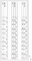
도 3은 챔버 구성요소(100) 상의 플라즈마 저항성 코팅(104)의 시험을 나타내는 데이터 시트(300)이다. 플라즈마 저항성 코팅(104)의 시험은 플라즈마 저항성 코팅(104)에 또는 저항성 코팅 상에 낮은 수준들의 미량 금속들을 보여주었다. 이는 플라즈마 저항성 코팅(104)이 챔버 구성요소(100)의 몸체(102)로부터의 금속 원자들이 코팅(104) 내로 침출하는 것을 효과적으로 차단한다는 것을 입증한다. 예를 들어, 플라즈마 저항성 코팅(104)의 알루미늄 농도는 약 2E12 원자/제곱센티미터(원자/cm2) 미만이었다. 많은 다른 미량 금속들이 플라즈마 저항성 코팅(104)에 또는 저항성 코팅 상에 존재했지만 임계 수준들 미만이었다.3 is a
개시된 프로세스 챔버 및 그의 구성요소들은 하나 이상의 기판 처리 작동에서 사용될 수 있다. 아래의 설명은 하나의 그러한 예시적인 프로세스를 제공하지만, 다른 프로세스들이 고려된다.The disclosed process chamber and components thereof may be used in one or more substrate processing operations. The description below provides one such example process, but other processes are contemplated.
일 예에서, 프로세스 챔버, 예컨대, 챔버 몸체(225)는 기판이 챔버 몸체에 배치되지 않고 H2 플라즈마로 처리된다. 기판을 챔버에 도입하기 전의 챔버 몸체(225)의 플라즈마 처리는 모든 웨이퍼간 플라즈마(PEW)로 지칭될 수 있다. 프로세스 챔버의 플라즈마 처리, 또는 PEW는 하나 이상의 가스, 예컨대, O2, N2, NH3, Ar, H2, He 또는 이들의 조합들을 챔버 몸체(225) 내로 도입하는 단계, 및 플라즈마를 형성하기 위해 하나 이상의 가스에 에너지를 공급하는 단계를 포함할 수 있다. 대안적으로, PEW는 산소, 질소, 수소, 암모니아, 수산화물, 또는 이들의 조합의 이온들 및/또는 라디칼들을 함유하는 플라즈마를 챔버 몸체(225) 내로 도입하는 단계를 포함할 수 있고, 플라즈마는 챔버 몸체(225) 외부의 원격 플라즈마 공급원에 형성된다.In one example, the process chamber, eg, chamber body 225, is treated with H2 plasma without the substrate being placed in the chamber body. The plasma treatment of the chamber body 225 before introducing the substrate into the chamber may be referred to as all inter-wafer plasma (PEW). Plasma treatment of the process chamber, or PEW, introducing one or more gases, such as O2 , N2 , NH3 , Ar, H2 , He, or combinations thereof, into the chamber body 225, and forming a plasma. And supplying energy to one or more gases for the purpose. Alternatively, the PEW may include introducing a plasma containing ions and/or radicals of oxygen, nitrogen, hydrogen, ammonia, hydroxide, or a combination thereof into the chamber body 225, wherein the plasma is It is formed in a remote plasma source outside the body 225.
일 실시예에서, NH3 및 Ar 가스들이 챔버 몸체(225) 내에 도입된다. 다른 실시예에서, O2 및 H2 가스들이 챔버 몸체(225) 내에 도입된다. 다른 실시예에서, O2 및 Ar 가스들이 챔버 몸체(225) 내에 도입된다. 다른 실시예에서, O2 가스가 챔버 몸체(225) 내에 도입된다. 또 다른 실시예에서, N2 가스가 챔버 몸체(225) 내에 도입된다. 전형적으로, 기판을 도입하기 전의 챔버 몸체(225)의 플라즈마 처리는 산소 또는 질소를 함유하는 플라즈마를 프로세스 챔버에 형성하거나 도입하는 단계를 수반한다.In one embodiment, NH3 and Ar gases are introduced into the chamber body 225. In another embodiment, O2 and H2 gases are introduced into the chamber body 225. In another embodiment, O2 and Ar gases are introduced into the chamber body 225. In another embodiment, O2 gas is introduced into the chamber body 225. In another embodiment, N2 gas is introduced into the chamber body 225. Typically, plasma treatment of the chamber body 225 prior to introducing the substrate involves forming or introducing a plasma containing oxygen or nitrogen into the process chamber.
일부 실시예들에서, 하나 이상의 가스는 RF 전원에 의해 에너지를 공급받는다. RF 전력은 2% 내지 70% 듀티 사이클로 펄싱될 수 있고, 약 100 W 내지 약 2500 W 범위일 수 있다. RF 전력은 약 100 W 내지 약 2500 W 범위의 연속파일 수 있다. 챔버 몸체(225)는 챔버 몸체(225)의 플라즈마 처리 동안 약 10 밀리토르(mT) 내지 약 200 mT 범위의 챔버 압력을 가질 수 있다. 기판 지지 페디스털, 예컨대, 기판 지지부(240)의 온도일 수 있는 프로세스 온도는 20 ℃ 내지 약 500 ℃ 범위일 수 있다.In some embodiments, one or more gases are energized by an RF power source. The RF power can be pulsed with a 2% to 70% duty cycle, and can range from about 100 W to about 2500 W. The RF power can be continuous in the range of about 100 W to about 2500 W. The chamber body 225 may have a chamber pressure in the range of about 10 millitorr (mT) to about 200 mT during plasma treatment of the chamber body 225. The process temperature, which may be the temperature of the substrate support pedestal, such as the substrate support 240, may range from 20°C to about 500°C.
그 후, 선택적으로 기판 상에 게이트 스택을 갖는 기판이, 챔버 몸체(225) 내의 수소 함유 플라즈마에 의해 처리된다. 기판의 수소 함유 플라즈마 처리는, 수소 함유 플라즈마를 형성하기 위해, 수소 함유 가스, 예컨대, H2 가스, 또는 수소 함유 가스 및 불활성 가스, 예컨대, Ar 가스를 챔버 몸체(225) 내에 도입하는 단계, 및 H2 가스 또는 H2/Ar 가스들에 에너지를 공급하는 단계를 포함할 수 있다. Ar 가스는 챔버 몸체(225)의 서비스 수명을 개선하기 위해(추가로, 수소 함유 플라즈마가 챔버 몸체(225) 내부의 구성요소들을 공격하는 것을 완화시킴), 그리고 H* 라디칼 농도들을 조절하기 위해, H2 가스에 추가될 수 있다. 일부 실시예들에서, H2 가스 또는 H2/Ar 가스들은 RF 전원, 예컨대, RF 전원(215)에 의해 에너지를 공급받는다. RF 전력은 2% 내지 60% 듀티 사이클로 펄싱될 수 있고, 약 100 W 내지 약 2500 W 범위일 수 있다. RF 전력은 약 100 W 내지 약 2500 W 범위의 연속파일 수 있다. 챔버 몸체(225)는 기판의 수소 함유 플라즈마 처리 동안 약 10 mT 내지 약 200 mT 범위의 챔버 압력을 가질 수 있다. 기판 지지부의 온도일 수 있는 프로세스 온도는 20 ℃ 내지 약 500 ℃ 범위일 수 있다. 기판은 약 10 내지 360 초 동안 수소 함유 플라즈마에 의해 처리될 수 있다. 일 실시예에서, 챔버 압력은 약 100 mT이고, H2 가스는 분당 약 25 표준 입방 센티미터(sccm)로 챔버 몸체(225) 내로 유동되고, Ar 가스는 약 975 sccm으로 챔버 몸체(225) 내로 유동되고, RF 전력은 약 500 W이고, 프로세스 온도는 약 400 ℃이고, 기판은 약 30 내지 90 초 동안 수소 함유 플라즈마에 의해 처리된다. 기판이 수소 함유 플라즈마로 처리된 후에, 기판은 챔버 몸체(225)로부터 제거될 수 있다.Thereafter, the substrate, optionally having the gate stack on the substrate, is treated by a hydrogen containing plasma in the chamber body 225. The hydrogen-containing plasma treatment of the substrate includes introducing a hydrogen-containing gas, such as H2 gas, or a hydrogen-containing gas and an inert gas, such as Ar gas, into the chamber body 225 to form a hydrogen-containing plasma, and It may include supplying energy to H2 gas or H2 /Ar gases. Ar gas is used to improve the service life of the chamber body 225 (additionally, to mitigate the hydrogen-containing plasma attacking the components inside the chamber body 225), and to adjust H* radical concentrations, Can be added to the H2 gas. In some embodiments, H2 gas or H2 /Ar gases are energized by an RF power source, eg, RF power source 215. RF power can be pulsed with a 2% to 60% duty cycle, and can range from about 100 W to about 2500 W. The RF power can be continuous in the range of about 100 W to about 2500 W. Chamber body 225 may have a chamber pressure ranging from about 10 mT to about 200 mT during hydrogen-containing plasma treatment of the substrate. The process temperature, which may be the temperature of the substrate support, may range from 20°C to about 500°C. The substrate can be treated with a hydrogen containing plasma for about 10 to 360 seconds. In one embodiment, the chamber pressure is about 100 mT, the H2 gas flows into the chamber body 225 at about 25 standard cubic centimeters per minute (sccm), and the Ar gas flows into the chamber body 225 at about 975 sccm. And the RF power is about 500 W, the process temperature is about 400° C., and the substrate is treated by the hydrogen containing plasma for about 30 to 90 seconds. After the substrate has been treated with a hydrogen containing plasma, the substrate can be removed from the chamber body 225.
다른 그리고 추가의 프로세스들이 챔버 몸체(225) 내에서 수행될 수 있음이 고려된다. 더욱이, 코팅된 챔버 구성요소들이 다른 및 추가적인 프로세스들과 함께 활용될 수 있음이 고려된다.It is contemplated that other and additional processes may be performed within the chamber body 225. Moreover, it is contemplated that coated chamber components may be utilized with other and additional processes.
상기 예 및 설명들로, 본 개시내용의 실시예들의 특징들 및 사상들이 설명된다. 관련 기술분야의 통상의 기술자는 다수의 수정들 및 변경들이 이루어질 수 있음을 쉽게 알 것이다. 이에 따라, 상기 개시내용은 첨부된 청구항들의 경계 및 범위에 의해서만 제한되는 것으로 해석되어야 한다.With the above examples and descriptions, features and ideas of embodiments of the present disclosure are described. One of ordinary skill in the art will readily appreciate that many modifications and changes may be made. Accordingly, the above disclosure should be construed as limited only by the bounds and scope of the appended claims.
Claims (15)
Translated fromKorean조면화된 비평탄 표면을 구성하는 금속성 기재 물질 ― 상기 조면화된 비평탄 표면은 4 마이크로인치 내지 80 마이크로인치의 평균 표면 거칠기(Ra)를 가짐 ―; 및
상기 조면화된 비평탄 표면 위에 형성된 평탄한 실리카 코팅을 포함하고, 상기 평탄한 실리카 코팅은:
상기 조면화된 비평탄 표면의 Ra 미만인 Ra를 갖는 표면,
약 0.2 미크론 내지 약 10 미크론의 두께,
1 체적% 미만의 공극률을 갖고,
2E12 원자/제곱센티미터 미만의 알루미늄을 함유하는, 챔버 구성요소.As a chamber component used within a plasma processing chamber,
A metallic base material constituting the roughened uneven surface, the roughened uneven surface having an average surface roughness (Ra) of 4 microinches to 80 microinches; And
And a flat silica coating formed over the roughened non-planar surface, wherein the flat silica coating comprises:
A surface having an Ra less than Ra of the roughened uneven surface,
A thickness of about 0.2 microns to about 10 microns,
Has a porosity of less than 1% by volume,
2E A chamber component containing less than12 atoms/square centimeter of aluminum.
상기 금속성 기재 물질은 알루미늄을 포함하는, 챔버 구성요소.The method of claim 1,
The chamber component, wherein the metallic base material comprises aluminum.
상기 금속성 기재 물질은 가스 분배 샤워헤드를 구성하는, 챔버 구성요소.The method of claim 1,
The metallic base material constitutes a gas distribution showerhead.
상기 금속성 기재 물질은 노즐 조립체를 구성하는, 챔버 구성요소.The method of claim 1,
Wherein the metallic base material constitutes a nozzle assembly.
상기 금속성 기재 물질은 배플을 구성하는, 챔버 구성요소.The method of claim 1,
Wherein the metallic base material constitutes a baffle.
상기 금속성 기재 물질은 라이너를 구성하는, 챔버 구성요소.The method of claim 1,
The chamber component, wherein the metallic base material constitutes a liner.
상기 라이너는 캐소드 라이너를 포함하는, 챔버 구성요소.The method of claim 6,
Wherein the liner comprises a cathode liner.
금속 물질로부터 상기 챔버 구성요소의 몸체를 형성하는 단계;
상기 몸체 상에 실리카의 층을 증착시키는 단계; 및
상기 금속 물질 및 상기 실리카의 층을 가열하는 단계를 포함하고, 상기 실리카의 층은:
조면화된 비평탄 표면의 Ra 표면 거칠기 미만인 Ra 표면 거칠기를 갖는 표면,
약 0.2 미크론 내지 약 10 미크론의 두께,
1 체적% 미만의 공극률을 갖고,
2E12 원자/제곱센티미터 미만의 알루미늄을 함유하는, 챔버 구성요소를 제조하기 위한 방법.A method for manufacturing a chamber component for use in a plasma processing environment, comprising:
Forming a body of the chamber component from a metallic material;
Depositing a layer of silica on the body; And
Heating the layer of the metallic material and the silica, the layer of silica comprising:
A surface having an Ra surface roughness less than the Ra surface roughness of the roughened uneven surface,
A thickness of about 0.2 microns to about 10 microns,
Has a porosity of less than 1% by volume,
2E A method for manufacturing a chamber component containing less than12 atoms/square centimeter of aluminum.
상기 금속성 기재 물질은 알루미늄을 포함하는, 챔버 구성요소를 제조하기 위한 방법.The method of claim 8,
The method for manufacturing a chamber component, wherein the metallic base material comprises aluminum.
상기 금속성 기재 물질은 가스 분배 샤워헤드를 구성하는, 챔버 구성요소를 제조하기 위한 방법.The method of claim 8,
The method for manufacturing a chamber component, wherein the metallic base material constitutes a gas distribution showerhead.
상기 금속성 기재 물질은 노즐 조립체를 구성하는, 챔버 구성요소를 제조하기 위한 방법.The method of claim 8,
The method for manufacturing a chamber component, wherein the metallic base material constitutes a nozzle assembly.
상기 금속성 기재 물질은 배플을 구성하는, 챔버 구성요소를 제조하기 위한 방법.The method of claim 8,
The method for manufacturing a chamber component, wherein the metallic base material constitutes a baffle.
상기 금속성 기재 물질은 라이너를 구성하는, 챔버 구성요소를 제조하기 위한 방법.The method of claim 8,
The method for manufacturing a chamber component, wherein the metallic base material constitutes a liner.
상기 라이너는 캐소드 라이너를 포함하는, 챔버 구성요소를 제조하기 위한 방법.The method of claim 13,
The method for manufacturing a chamber component, wherein the liner comprises a cathode liner.
질소 또는 산소를 함유하는 플라즈마로 프로세스 챔버를 플라즈마 처리하는 단계 ― 상기 프로세스 챔버는:
조면화된 비평탄 표면을 구성하는 금속성 기재 물질 ― 상기 조면화된 비평탄 표면은 4 마이크로인치 내지 80 마이크로인치의 평균 표면 거칠기(Ra)를 가짐 ―;
상기 조면화된 비평탄 표면 위에 형성된 평탄한 실리카 코팅 ― 상기 평탄한 실리카 코팅은 상기 조면화된 비평탄 표면의 Ra 미만인 Ra를 갖는 표면, 약 0.2 미크론 내지 약 10 미크론의 두께, 1 체적% 미만의 공극률을 갖고, 2E12 원자/제곱센티미터 미만의 알루미늄을 함유함 ― 을 포함하는 상기 챔버 구성요소를 포함함 ―;
기판을 상기 프로세스 챔버 내에 배치하는 단계 ― 스택은 상기 기판 상에 배치됨 ―; 및
상기 기판 상에 배치된 상기 스택을 플라즈마 처리하는 단계를 포함하는, 방법.As a method,
Plasma treating the process chamber with a plasma containing nitrogen or oxygen, the process chamber comprising:
A metallic base material constituting the roughened uneven surface, the roughened uneven surface having an average surface roughness (Ra) of 4 microinches to 80 microinches;
A flat silica coating formed on the roughened non-planar surface, wherein the flat silica coating has a surface having an Ra less than Ra of the roughened non-planar surface, a thickness of about 0.2 microns to about 10 microns, a porosity of less than 1% by volume. And contains 2E less than12 atoms/square centimeter of aluminum, including the chamber component comprising;
Placing a substrate into the process chamber, wherein a stack is disposed on the substrate; And
Plasma treating the stack disposed on the substrate.
Priority Applications (1)
| Application Number | Priority Date | Filing Date | Title |
|---|---|---|---|
| KR1020257021611AKR20250107284A (en) | 2018-06-14 | 2019-05-21 | Process chamber process kit with protective coating |
Applications Claiming Priority (3)
| Application Number | Priority Date | Filing Date | Title |
|---|---|---|---|
| US201862685098P | 2018-06-14 | 2018-06-14 | |
| US62/685,098 | 2018-06-14 | ||
| PCT/US2019/033259WO2019240915A1 (en) | 2018-06-14 | 2019-05-21 | Process chamber process kit with protective coating |
Related Child Applications (1)
| Application Number | Title | Priority Date | Filing Date |
|---|---|---|---|
| KR1020257021611ADivisionKR20250107284A (en) | 2018-06-14 | 2019-05-21 | Process chamber process kit with protective coating |
Publications (2)
| Publication Number | Publication Date |
|---|---|
| KR20210008931Atrue KR20210008931A (en) | 2021-01-25 |
| KR102828235B1 KR102828235B1 (en) | 2025-07-03 |
Family
ID=68840245
Family Applications (2)
| Application Number | Title | Priority Date | Filing Date |
|---|---|---|---|
| KR1020217001257AActiveKR102828235B1 (en) | 2018-06-14 | 2019-05-21 | Process chamber process kit with protective coating |
| KR1020257021611APendingKR20250107284A (en) | 2018-06-14 | 2019-05-21 | Process chamber process kit with protective coating |
Family Applications After (1)
| Application Number | Title | Priority Date | Filing Date |
|---|---|---|---|
| KR1020257021611APendingKR20250107284A (en) | 2018-06-14 | 2019-05-21 | Process chamber process kit with protective coating |
Country Status (6)
| Country | Link |
|---|---|
| US (2) | US12354843B2 (en) |
| JP (2) | JP7405776B2 (en) |
| KR (2) | KR102828235B1 (en) |
| CN (2) | CN119890023A (en) |
| TW (2) | TWI828704B (en) |
| WO (1) | WO2019240915A1 (en) |
Families Citing this family (5)
| Publication number | Priority date | Publication date | Assignee | Title |
|---|---|---|---|---|
| US11664247B2 (en) | 2020-10-16 | 2023-05-30 | Applied Materials, Inc. | Dynamic interface for providing a symmetric radio frequency return path |
| US20230064070A1 (en)* | 2021-08-30 | 2023-03-02 | Auo Crystal Corporation | Semiconductor processing equipment part and method for making the same |
| US20230215702A1 (en)* | 2021-12-30 | 2023-07-06 | Applied Materials, Inc. | Uniformity control for plasma processing using wall recombination |
| WO2024097505A1 (en)* | 2022-10-31 | 2024-05-10 | Lam Research Corporation | Component with a dual layer hermetic atomic layer deposition coatings for a semiconductor processing chamber |
| US20250201527A1 (en)* | 2023-12-19 | 2025-06-19 | Applied Materials, Inc. | High Conformal Coating on Textured Surface of Processing Chamber Component |
Citations (3)
| Publication number | Priority date | Publication date | Assignee | Title |
|---|---|---|---|---|
| JPH11238722A (en)* | 1997-12-17 | 1999-08-31 | Matsushita Electron Corp | Apparatus and method for plasma processing |
| KR20160034298A (en)* | 2013-07-19 | 2016-03-29 | 어플라이드 머티어리얼스, 인코포레이티드 | Ion assisted deposition for rare-earth oxide based thin film coatings on process rings |
| KR20180041073A (en)* | 2016-10-13 | 2018-04-23 | 어플라이드 머티어리얼스, 인코포레이티드 | Chemical conversion of yttria into yttrium fluoride and yttrium oxyfluoride to develop pre-seasoned corossion resistive coating for plasma components |
Family Cites Families (32)
| Publication number | Priority date | Publication date | Assignee | Title |
|---|---|---|---|---|
| JP3362552B2 (en)* | 1995-03-10 | 2003-01-07 | 東京エレクトロン株式会社 | Film processing equipment |
| US6251216B1 (en)* | 1997-12-17 | 2001-06-26 | Matsushita Electronics Corporation | Apparatus and method for plasma processing |
| US6863926B2 (en) | 2002-01-15 | 2005-03-08 | David Mark Lynn | Corrosive-resistant coating over aluminum substrates for use in plasma deposition and etch environments |
| US6780787B2 (en)* | 2002-03-21 | 2004-08-24 | Lam Research Corporation | Low contamination components for semiconductor processing apparatus and methods for making components |
| US7311797B2 (en)* | 2002-06-27 | 2007-12-25 | Lam Research Corporation | Productivity enhancing thermal sprayed yttria-containing coating for plasma reactor |
| US20040033361A1 (en)* | 2002-08-06 | 2004-02-19 | Kabushiki Kaisha Kobe Seiko Sho(Kobe Steel, Ltd.) | Component of glass-like carbon for CVD apparatus and process for production thereof |
| US7250114B2 (en)* | 2003-05-30 | 2007-07-31 | Lam Research Corporation | Methods of finishing quartz glass surfaces and components made by the methods |
| JP4606121B2 (en)* | 2004-01-29 | 2011-01-05 | 京セラ株式会社 | Corrosion-resistant film laminated corrosion-resistant member and manufacturing method thereof |
| JP2006128370A (en)* | 2004-10-28 | 2006-05-18 | Tokyo Electron Ltd | Film forming apparatus, film forming method, program, and recording medium |
| CN101010448B (en)* | 2005-06-23 | 2010-09-29 | 东京毅力科创株式会社 | Constitutional member for semiconductor processing apparatus and method for producing same |
| US20060292310A1 (en)* | 2005-06-27 | 2006-12-28 | Applied Materials, Inc. | Process kit design to reduce particle generation |
| US7541094B1 (en)* | 2006-03-03 | 2009-06-02 | Quantum Global Technologies, Llc | Firepolished quartz parts for use in semiconductor processing |
| US20080063798A1 (en)* | 2006-08-30 | 2008-03-13 | Kher Shreyas S | Precursors and hardware for cvd and ald |
| US8097105B2 (en) | 2007-01-11 | 2012-01-17 | Lam Research Corporation | Extending lifetime of yttrium oxide as a plasma chamber material |
| AT504482B1 (en) | 2007-03-01 | 2008-06-15 | Ruebig Gmbh & Co Kg | Producing optionally-doped coating of amorphous silicon, germanium or their oxides on metallic substrate, subjects area to oxidation before coating deposition |
| JP5475261B2 (en) | 2008-03-31 | 2014-04-16 | 東京エレクトロン株式会社 | Plasma processing equipment |
| CN102272344A (en)* | 2008-11-04 | 2011-12-07 | 普莱克斯技术有限公司 | Thermal spray coatings for semiconductor applications |
| US8206829B2 (en)* | 2008-11-10 | 2012-06-26 | Applied Materials, Inc. | Plasma resistant coatings for plasma chamber components |
| KR101992702B1 (en) | 2010-10-28 | 2019-06-25 | 어플라이드 머티어리얼스, 인코포레이티드 | High purity aluminum coating hard anodization |
| JP2014158009A (en)* | 2012-07-03 | 2014-08-28 | Hitachi High-Technologies Corp | Heat treatment apparatus |
| US9337002B2 (en)* | 2013-03-12 | 2016-05-10 | Lam Research Corporation | Corrosion resistant aluminum coating on plasma chamber components |
| GB2513575B (en)* | 2013-04-29 | 2017-05-31 | Keronite Int Ltd | Corrosion and erosion-resistant mixed oxide coatings for the protection of chemical and plasma process chamber components |
| US9583369B2 (en)* | 2013-07-20 | 2017-02-28 | Applied Materials, Inc. | Ion assisted deposition for rare-earth oxide based coatings on lids and nozzles |
| WO2015108276A1 (en) | 2014-01-17 | 2015-07-23 | 아이원스 주식회사 | Method for forming coating having composite coating particle size and coating formed thereby |
| CN106104775B (en)* | 2014-01-31 | 2019-05-21 | 应用材料公司 | Chamber coating |
| US9869013B2 (en) | 2014-04-25 | 2018-01-16 | Applied Materials, Inc. | Ion assisted deposition top coat of rare-earth oxide |
| US9790581B2 (en)* | 2014-06-25 | 2017-10-17 | Fm Industries, Inc. | Emissivity controlled coatings for semiconductor chamber components |
| US20160258064A1 (en) | 2015-03-06 | 2016-09-08 | Applied Materials, Inc. | Barrier anodization methods to develop aluminum oxide layer for plasma equipment components |
| EP3165629A1 (en) | 2015-11-06 | 2017-05-10 | Rolls-Royce Corporation | Plasma spray physical vapor deposition deposited environmental barrier coating |
| US20170291856A1 (en)* | 2016-04-06 | 2017-10-12 | Applied Materials, Inc. | Solution precursor plasma spray of ceramic coating for semiconductor chamber applications |
| US10262839B2 (en)* | 2016-06-14 | 2019-04-16 | Taiwan Semiconductor Manufacturing Co., Ltd. | Aluminum apparatus with aluminum oxide layer and method for forming the same |
| US20180016678A1 (en) | 2016-07-15 | 2018-01-18 | Applied Materials, Inc. | Multi-layer coating with diffusion barrier layer and erosion resistant layer |
- 2019
- 2019-05-21KRKR1020217001257Apatent/KR102828235B1/enactiveActive
- 2019-05-21WOPCT/US2019/033259patent/WO2019240915A1/ennot_activeCeased
- 2019-05-21USUS16/418,274patent/US12354843B2/enactiveActive
- 2019-05-21CNCN202411905565.4Apatent/CN119890023A/enactivePending
- 2019-05-21JPJP2020568515Apatent/JP7405776B2/enactiveActive
- 2019-05-21CNCN201980037849.7Apatent/CN112236839B/enactiveActive
- 2019-05-21KRKR1020257021611Apatent/KR20250107284A/enactivePending
- 2019-06-12TWTW108120249Apatent/TWI828704B/enactive
- 2019-06-12TWTW112148937Apatent/TWI880527B/enactive
- 2023
- 2023-04-05USUS18/131,306patent/US20230245863A1/enactivePending
- 2023-12-14JPJP2023210900Apatent/JP2024037895A/enactivePending
Patent Citations (3)
| Publication number | Priority date | Publication date | Assignee | Title |
|---|---|---|---|---|
| JPH11238722A (en)* | 1997-12-17 | 1999-08-31 | Matsushita Electron Corp | Apparatus and method for plasma processing |
| KR20160034298A (en)* | 2013-07-19 | 2016-03-29 | 어플라이드 머티어리얼스, 인코포레이티드 | Ion assisted deposition for rare-earth oxide based thin film coatings on process rings |
| KR20180041073A (en)* | 2016-10-13 | 2018-04-23 | 어플라이드 머티어리얼스, 인코포레이티드 | Chemical conversion of yttria into yttrium fluoride and yttrium oxyfluoride to develop pre-seasoned corossion resistive coating for plasma components |
Also Published As
| Publication number | Publication date |
|---|---|
| JP2024037895A (en) | 2024-03-19 |
| JP7405776B2 (en) | 2023-12-26 |
| TWI828704B (en) | 2024-01-11 |
| WO2019240915A1 (en) | 2019-12-19 |
| US12354843B2 (en) | 2025-07-08 |
| US20230245863A1 (en) | 2023-08-03 |
| JP2021527328A (en) | 2021-10-11 |
| US20190385825A1 (en) | 2019-12-19 |
| CN119890023A (en) | 2025-04-25 |
| TWI880527B (en) | 2025-04-11 |
| KR20250107284A (en) | 2025-07-11 |
| CN112236839A (en) | 2021-01-15 |
| TW202418348A (en) | 2024-05-01 |
| TW202013426A (en) | 2020-04-01 |
| CN112236839B (en) | 2025-01-03 |
| KR102828235B1 (en) | 2025-07-03 |
Similar Documents
| Publication | Publication Date | Title |
|---|---|---|
| KR102828235B1 (en) | Process chamber process kit with protective coating | |
| US11637002B2 (en) | Methods and systems to enhance process uniformity | |
| TWI576914B (en) | Pattern forming method and substrate processing system | |
| JP5279656B2 (en) | Plasma processing equipment | |
| KR102311575B1 (en) | Workpiece processing method | |
| KR20210044906A (en) | Semiconductor substrate supports with built-in RF shields | |
| JP6854600B2 (en) | Plasma etching method, plasma etching equipment, and substrate mount | |
| US10276364B2 (en) | Bevel etch profile control | |
| US10577689B2 (en) | Sputtering showerhead | |
| CN104299929A (en) | Systems and methods for in-situ wafer edge and backside plasma cleaning | |
| KR100564168B1 (en) | Plasma processing apparatus and plasma processing method | |
| TWI621732B (en) | Method for forming sealing film and device for manufacturing sealing film | |
| KR100887271B1 (en) | Plasma processing apparatus | |
| JP2015211156A (en) | Dry cleaning method and plasma processing apparatus | |
| US6863926B2 (en) | Corrosive-resistant coating over aluminum substrates for use in plasma deposition and etch environments | |
| KR20180018824A (en) | Adjustable remote dissociation | |
| KR20140132688A (en) | Plasma etching method | |
| KR101559874B1 (en) | Substrate treating apparatus and chamber producing method | |
| TW202437434A (en) | Semiconductor chamber components with advanced coating techniques | |
| KR20240111104A (en) | Plasma processing apparatus and method for fabricating semiconductor device using the same | |
| KR20210103596A (en) | Method for recovering surface of silicon structure and apparatus for treating substrate |
Legal Events
| Date | Code | Title | Description |
|---|---|---|---|
| PA0105 | International application | Patent event date:20210114 Patent event code:PA01051R01D Comment text:International Patent Application | |
| PG1501 | Laying open of application | ||
| PA0201 | Request for examination | Patent event code:PA02012R01D Patent event date:20220217 Comment text:Request for Examination of Application | |
| PE0902 | Notice of grounds for rejection | Comment text:Notification of reason for refusal Patent event date:20240704 Patent event code:PE09021S01D | |
| E701 | Decision to grant or registration of patent right | ||
| PE0701 | Decision of registration | Patent event code:PE07011S01D Comment text:Decision to Grant Registration Patent event date:20250327 | |
| PG1601 | Publication of registration |