KR20200142709A - Semiconductor memory device and method for fabricating the same - Google Patents
Semiconductor memory device and method for fabricating the sameDownload PDFInfo
- Publication number
- KR20200142709A KR20200142709AKR1020190069847AKR20190069847AKR20200142709AKR 20200142709 AKR20200142709 AKR 20200142709AKR 1020190069847 AKR1020190069847 AKR 1020190069847AKR 20190069847 AKR20190069847 AKR 20190069847AKR 20200142709 AKR20200142709 AKR 20200142709A
- Authority
- KR
- South Korea
- Prior art keywords
- charge storage
- insulating
- insulating pattern
- pattern
- layer
- Prior art date
- Legal status (The legal status is an assumption and is not a legal conclusion. Google has not performed a legal analysis and makes no representation as to the accuracy of the status listed.)
- Granted
Links
Images


Classifications
- H01L27/11568—
- H—ELECTRICITY
- H10—SEMICONDUCTOR DEVICES; ELECTRIC SOLID-STATE DEVICES NOT OTHERWISE PROVIDED FOR
- H10B—ELECTRONIC MEMORY DEVICES
- H10B43/00—EEPROM devices comprising charge-trapping gate insulators
- H10B43/30—EEPROM devices comprising charge-trapping gate insulators characterised by the memory core region
- H—ELECTRICITY
- H10—SEMICONDUCTOR DEVICES; ELECTRIC SOLID-STATE DEVICES NOT OTHERWISE PROVIDED FOR
- H10D—INORGANIC ELECTRIC SEMICONDUCTOR DEVICES
- H10D64/00—Electrodes of devices having potential barriers
- H10D64/01—Manufacture or treatment
- H10D64/031—Manufacture or treatment of data-storage electrodes
- H10D64/037—Manufacture or treatment of data-storage electrodes comprising charge-trapping insulators
- H01L27/11565—
- H01L27/11582—
- H01L29/792—
- H—ELECTRICITY
- H10—SEMICONDUCTOR DEVICES; ELECTRIC SOLID-STATE DEVICES NOT OTHERWISE PROVIDED FOR
- H10B—ELECTRONIC MEMORY DEVICES
- H10B43/00—EEPROM devices comprising charge-trapping gate insulators
- H10B43/10—EEPROM devices comprising charge-trapping gate insulators characterised by the top-view layout
- H—ELECTRICITY
- H10—SEMICONDUCTOR DEVICES; ELECTRIC SOLID-STATE DEVICES NOT OTHERWISE PROVIDED FOR
- H10B—ELECTRONIC MEMORY DEVICES
- H10B43/00—EEPROM devices comprising charge-trapping gate insulators
- H10B43/20—EEPROM devices comprising charge-trapping gate insulators characterised by three-dimensional arrangements, e.g. with cells on different height levels
- H10B43/23—EEPROM devices comprising charge-trapping gate insulators characterised by three-dimensional arrangements, e.g. with cells on different height levels with source and drain on different levels, e.g. with sloping channels
- H10B43/27—EEPROM devices comprising charge-trapping gate insulators characterised by three-dimensional arrangements, e.g. with cells on different height levels with source and drain on different levels, e.g. with sloping channels the channels comprising vertical portions, e.g. U-shaped channels
- H—ELECTRICITY
- H10—SEMICONDUCTOR DEVICES; ELECTRIC SOLID-STATE DEVICES NOT OTHERWISE PROVIDED FOR
- H10B—ELECTRONIC MEMORY DEVICES
- H10B43/00—EEPROM devices comprising charge-trapping gate insulators
- H10B43/30—EEPROM devices comprising charge-trapping gate insulators characterised by the memory core region
- H10B43/35—EEPROM devices comprising charge-trapping gate insulators characterised by the memory core region with cell select transistors, e.g. NAND
- H—ELECTRICITY
- H10—SEMICONDUCTOR DEVICES; ELECTRIC SOLID-STATE DEVICES NOT OTHERWISE PROVIDED FOR
- H10B—ELECTRONIC MEMORY DEVICES
- H10B43/00—EEPROM devices comprising charge-trapping gate insulators
- H10B43/50—EEPROM devices comprising charge-trapping gate insulators characterised by the boundary region between the core and peripheral circuit regions
- H—ELECTRICITY
- H10—SEMICONDUCTOR DEVICES; ELECTRIC SOLID-STATE DEVICES NOT OTHERWISE PROVIDED FOR
- H10D—INORGANIC ELECTRIC SEMICONDUCTOR DEVICES
- H10D30/00—Field-effect transistors [FET]
- H10D30/60—Insulated-gate field-effect transistors [IGFET]
- H10D30/69—IGFETs having charge trapping gate insulators, e.g. MNOS transistors
- H10D30/693—Vertical IGFETs having charge trapping gate insulators
Landscapes
- Non-Volatile Memory (AREA)
- Semiconductor Memories (AREA)
Abstract
Translated fromKoreanDescription
Translated fromKorean본 발명은 반도체 메모리 장치 및 그 제조 방법에 관한 것이다. 보다 구체적으로, 본 발명은 게이트 전극으로부터 돌출되어, 전하 저장막들 사이에 위치하는 절연 패턴을 포함하는 반도체 메모리 장치 및 그 제조 방법에 관한 것이다.The present invention relates to a semiconductor memory device and a method of manufacturing the same. More specifically, the present invention relates to a semiconductor memory device including an insulating pattern protruding from a gate electrode and positioned between charge storage layers, and a method of manufacturing the same.
소비자가 요구하는 우수한 성능 및 저렴한 가격을 만족시키기 위해, 비휘발성 메모리 장치의 집적도가 증가하고 있다. 그런데, 2차원 또는 평면형 메모리 장치의 경우, 단위 메모리 셀이 점유하는 면적에 의해서 집적도가 결정되어 집적도 증가가 점점 어렵게 된다. 따라서, 최근에는 점유 면적의 증가 없이 집적도를 증가시키는 방법으로 단위 메모리 셀을 수직으로 배치하는 3차원 메모리 장치가 개발되고 있다. In order to meet the excellent performance and low price demanded by consumers, the degree of integration of nonvolatile memory devices is increasing. However, in the case of a two-dimensional or planar memory device, the degree of integration is determined by the area occupied by the unit memory cells, making it increasingly difficult to increase the degree of integration. Accordingly, recently, a three-dimensional memory device in which unit memory cells are vertically disposed has been developed as a method of increasing the degree of integration without increasing the occupied area.
본 발명이 해결하고자 하는 기술적 과제는 게이트 전극으로부터 돌출되고, 전하 저장막들 사이에 위치하는 절연 패턴을 통해 신뢰성이 향상된 반도체 메모리 장치반도체 메모리 장치를 제공하는 것이다.The technical problem to be solved by the present invention is to provide a semiconductor memory device with improved reliability through an insulating pattern protruding from a gate electrode and positioned between charge storage layers.
본 발명이 해결하고자 하는 다른 기술적 과제는 게이트 전극으로부터 돌출되고, 전하 저장막들 사이에 위치하는 절연 패턴을 포함하는 반도체 메모리 장치반도체 메모리 장치의 제조 방법을 제공하는 것이다.Another technical problem to be solved by the present invention is to provide a method of manufacturing a semiconductor memory device including an insulating pattern protruding from a gate electrode and positioned between charge storage layers.
본 발명의 기술적 과제들은 이상에서 언급한 기술적 과제로 제한되지 않으며, 언급되지 않은 또 다른 기술적 과제들은 아래의 기재로부터 당업자에게 명확하게 이해될 수 있을 것이다.The technical problems of the present invention are not limited to the technical problems mentioned above, and other technical problems that are not mentioned will be clearly understood by those skilled in the art from the following description.
상기 기술적 과제를 달성하기 위한 본 발명의 몇몇 실시예에 따른 반도체 메모리 장치반도체 메모리 장치는, 기판과 수직한 제1 방향으로 이격된 제1 절연 패턴 및 제2 절연 패턴으로, 제1 절연 패턴의 하면과, 제2 절연 패턴의 상면은 서로 마주보는 제1 절연 패턴 및 제2 절연 패턴, 제1 절연 패턴의 하면 및 제2 절연 패턴의 상면 사이에 배치되고, 제1 절연 패턴의 하면 및 제2 절연 패턴의 상면 사이로 연장되는 제1 측면을 포함하는 게이트 전극, 및 게이트 전극의 제1 측면으로부터 제1 방향과 다른 제2 방향으로 제1 너비만큼 돌출된 절연 패턴을 포함한다.A semiconductor memory device according to some embodiments of the present invention for achieving the above technical problem includes a first insulating pattern and a second insulating pattern spaced apart in a first direction perpendicular to a substrate, and the lower surface of the first insulating pattern And, the upper surface of the second insulating pattern is disposed between the first and second insulating patterns facing each other, the lower surface of the first insulating pattern and the upper surface of the second insulating pattern, and the lower surface of the first insulating pattern and the second insulating pattern And a gate electrode including a first side surface extending between upper surfaces of the pattern, and an insulating pattern protruding from the first side surface of the gate electrode by a first width in a second direction different from the first direction.
상기 기술적 과제를 달성하기 위한 본 발명의 몇몇 실시예에 따른 반도체 메모리 장치반도체 메모리 장치는, 기판과 수직한 제1 방향으로 연장된 반도체 패턴, 반도체 패턴 상의 터널 절연막, 터널 절연막 상에, 제1 방향으로 이격된 제1 전하 저장막 및 제2 전하 저장막, 터널 절연막 상에, 제1 전하 저장막 및 제2 전하 저장막을 따라 연장되는 블로킹 절연막, 제1 전하 저장막 및 제2 전하 저장막 사이에 위치하고, 블로킹 절연막 내에 정의된 리세스, 리세스를 채우는 절연 패턴, 및 절연 패턴 및 블로킹 절연막 상의 게이트 전극을 포함한다.A semiconductor memory device according to some embodiments of the present invention for achieving the above technical problem is a semiconductor pattern extending in a first direction perpendicular to a substrate, a tunnel insulating layer on the semiconductor pattern, a tunnel insulating layer, and a first direction. On the first and second charge storage layers and the tunnel insulating layer spaced apart from each other, between the blocking insulating layer extending along the first and second charge storage layers, the first charge storage layer, and the second charge storage layer And a recess defined in the blocking insulating layer, an insulating pattern filling the recess, and a gate electrode on the insulating pattern and the blocking insulating layer.
상기 기술적 과제를 달성하기 위한 본 발명의 몇몇 실시예에 따른 반도체 메모리 장치반도체 메모리 장치는, 기판과 수직한 제1 방향으로 연장된 블로킹 절연막, 블로킹 절연막의 일면 내에 정의되고, 제1 방향으로 서로 이격된 제1 리세스 및 제2 리세스, 블로킹 절연막의 일면과 대향하는 다른 일면 내에 정의되고, 제1 리세스 및 제2 리세스 사이에 위치하는 제3 리세스, 제1 리세스 및 제2 리세스를 각각 채우는 제1 전하 저장막 및 제2 전하 저장막, 제3 리세스를 채우는 절연 패턴, 및 절연 패턴 및 블로킹 절연막을 따라 연장되는 게이트 전극을 포함한다.A semiconductor memory device according to some embodiments of the present invention for achieving the above technical problem is a blocking insulating film extending in a first direction perpendicular to the substrate, defined in one surface of the blocking insulating film, and spaced apart from each other in the first direction. A third recess, a first recess, and a second recess defined in the first recess and the second recess, which are defined in the other side opposite to the one side of the blocking insulating film, and are positioned between the first and second recesses And a first charge storage layer and a second charge storage layer respectively filling the recesses, an insulating pattern filling the third recess, and a gate electrode extending along the insulating pattern and the blocking insulating layer.
기타 실시예들의 구체적인 사항들은 상세한 설명 및 도면들에 포함되어 있다.Details of other embodiments are included in the detailed description and drawings.
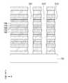
도 1은 몇몇 실시예에 따른 반도체 메모리 장치반도체 메모리 장치를 설명하기 위한 개략적인 회로도이다.
도 2는 몇몇 실시예에 따른 반도체 메모리 장치를 설명하기 위한 예시적인 단면도이다.
도 3은 몇몇 실시예에 따른 도 2의 반도체 메모리 장치의 P1 영역을 확대하여 설명하기 위한 예시적인 확대도이다.
도 4는 도 3의 R1 영역을 설명하기 위한 확대도이다.
도 5는 도 3의 A-A'를 절단한 단면도이다.
도 6은 도 3의 B-B'를 절단한 단면도이다.
도 7 내지 도 18은 몇몇 실시예에 따른 도 2의 반도체 메모리 장치의 제조 방법을 설명하기 위한 중간 단계 도면들이다.
도 19는 몇몇 실시예에 따른 도 18의 반도체 메모리 장치의 P2 영역을 확대하여 설명하기 위한 예시적인 확대도이다.
도 20은 도 19의 R2 영역을 설명하기 위한 확대도이다.
도 21 내지 도 24는 몇몇 실시예에 따른 도 18의 반도체 메모리 장치의 제조 방법을 설명하기 위한 중간 단계 도면들이다.1 is a schematic circuit diagram illustrating a semiconductor memory device according to some embodiments.
2 is an exemplary cross-sectional view illustrating a semiconductor memory device according to some embodiments.
3 is an exemplary enlarged view illustrating an enlarged area P1 of the semiconductor memory device of FIG. 2 according to some embodiments.
FIG. 4 is an enlarged view illustrating an area R1 of FIG. 3.
5 is a cross-sectional view taken along line A-A' of FIG. 3.
6 is a cross-sectional view taken along line B-B' of FIG. 3.
7 through 18 are diagrams of intermediate steps for describing a method of manufacturing the semiconductor memory device of FIG. 2, according to some embodiments.
19 is an exemplary enlarged view illustrating an enlarged area P2 of the semiconductor memory device of FIG. 18, according to some embodiments.
FIG. 20 is an enlarged view illustrating an area R2 of FIG. 19.
21 to 24 are diagrams of intermediate steps for describing a method of manufacturing the semiconductor memory device of FIG. 18, according to some embodiments.
도 1은 몇몇 실시예에 따른 반도체 메모리 장치반도체 메모리 장치를 설명하기 위한 개략적인 회로도이다.1 is a schematic circuit diagram illustrating a semiconductor memory device according to some embodiments.
도 1을 참조하면, 몇몇 실시예에 따른 반도체 메모리 장치반도체 메모리 장치는 공통 소오스 라인(CSL), 복수의 비트 라인들(BL1 내지 BL3) 및 복수의 셀 스트링(CSTR)들을 포함할 수 있다.Referring to FIG. 1, a semiconductor memory device according to some embodiments may include a common source line CSL, a plurality of bit lines BL1 to BL3, and a plurality of cell strings CSTR.
복수의 비트 라인(BL1 내지 BL3)들은 2차원적으로 배열될 수 있다. 예를 들어, 각각의 비트 라인들(BL1 내지 BL3)은 서로 이격되어 x 방향으로 각각 연장될 수 있다. 각각의 비트 라인들(BL1 내지 BL3)에는 복수의 셀 스트링(CSTR)들이 병렬로 연결될 수 있다. 셀 스트링(CSTR)들은 공통 소오스 라인(CSL)에 공통으로 연결될 수 있다. 즉, 복수의 비트 라인(BL1 내지 BL3)들과 공통 소오스 라인(CSL) 사이에 복수의 셀 스트링(CSTR)들이 배치될 수 있다.The plurality of bit lines BL1 to BL3 may be arranged two-dimensionally. For example, each of the bit lines BL1 to BL3 may be spaced apart from each other and extend in the x direction. A plurality of cell strings CSTRs may be connected in parallel to each of the bit lines BL1 to BL3. The cell strings CSTR may be connected in common to the common source line CSL. That is, a plurality of cell strings CSTR may be disposed between the plurality of bit lines BL1 to BL3 and the common source line CSL.
몇몇 실시예에서, 복수의 비트 라인들(BL1 내지 BL3)의 개수는 이에 제한되지 않는다.In some embodiments, the number of the plurality of bit lines BL1 to BL3 is not limited thereto.
몇몇 실시예에서, 복수의 공통 소오스 라인(CSL)들이 2차원적으로 배열될 수 있다. 예를 들어, 각각의 공통 소오스 라인(CSL)들은 서로 이격되어 제2 방향(Y)으로 각각 연장될 수 있다. 공통 소오스 라인(CSL)들에는 전기적으로 동일한 전압이 인가될 수도 있고, 또는 서로 다른 전압이 인가되어 별개로 제어될 수도 있다.In some embodiments, a plurality of common source lines CSL may be two-dimensionally arranged. For example, each of the common source lines CSL may be spaced apart from each other and may respectively extend in the second direction Y. The same voltage may be electrically applied to the common source lines CSL, or different voltages may be applied and controlled separately.
각각의 셀 스트링(CSTR)은 공통 소오스 라인(CSL)에 접속되는 그라운드 선택 트랜지스터(GST), 각각의 비트 라인(BL1 내지 BL3)에 접속되는 스트링 선택 트랜지스터(SST), 및 그라운드 선택 트랜지스터(GST)와 스트링 선택 트랜지스터들(SST) 사이에 배치되는 복수의 메모리 셀 트랜지스터들(MCT)을 포함할 수 있다. 메모리 셀 트랜지스터들(MCT) 각각은 데이터 저장 소자(data storage element)를 포함할 수 있다. 그라운드 선택 트랜지스터(GST), 스트링 선택 트랜지스터(SST) 및 메모리 셀 트랜지스터들(MCT)은 직렬로 연결될 수 있다.Each cell string CSTR includes a ground select transistor GST connected to the common source line CSL, a string select transistor SST connected to each bit line BL1 to BL3, and a ground select transistor GST. And a plurality of memory cell transistors MCT disposed between the and string select transistors SST. Each of the memory cell transistors MCT may include a data storage element. The ground select transistor GST, the string select transistor SST, and the memory cell transistors MCT may be connected in series.
공통 소오스 라인(CSL)은 그라운드 선택 트랜지스터들(GST)의 소오스들에 공통으로 연결될 수 있다. 또한, 공통 소오스 라인(CSL)과 각각의 비트 라인들(BL1 내지 BL3) 사이에는 그라운드 선택 라인(GSL), 복수의 워드 라인들(WL0-WLn) 및 스트링 선택 라인(SSL)이 배치될 수 있다. 그라운드 선택 라인(GSL)들은 그라운드 선택 트랜지스터(GST)의 게이트 전극으로 사용될 수 있고, 복수의 워드 라인들(WL0-WLn)은 메모리 셀 트랜지스터들(MCT)의 게이트 전극으로 사용될 수 있고, 스트링 선택 라인(SSL)은 스트링 선택 트랜지스터(SST)의 게이트 전극으로 사용될 수 있다.The common source line CSL may be commonly connected to sources of the ground select transistors GST. In addition, a ground selection line GSL, a plurality of word lines WL0-WLn, and a string selection line SSL may be disposed between the common source line CSL and each of the bit lines BL1 to BL3. . The ground selection lines GSL may be used as gate electrodes of the ground selection transistor GST, and the plurality of word lines WL0-WLn may be used as gate electrodes of the memory cell transistors MCT, and the string selection line SSL may be used as a gate electrode of the string selection transistor SST.
도 2는 몇몇 실시예에 따른 반도체 메모리 장치를 설명하기 위한 예시적인 단면도이다.2 is an exemplary cross-sectional view illustrating a semiconductor memory device according to some embodiments.
도 2를 참조하면, 복수의 게이트 전극들(GSL, WL0 내지 WLn, SSL)은 서로 동일한 두께를 갖는 것으로 도시되었으나, 이는 예시적인 것일 뿐이다. 예를 들어, 복수의 게이트 전극들(GSL, WL0 내지 WLn, SSL)은 서로 다른 두께를 가질 수도 있다.Referring to FIG. 2, a plurality of gate electrodes GSL, WL0 to WLn, and SSL are illustrated to have the same thickness, but this is only exemplary. For example, the plurality of gate electrodes GSL, WL0 to WLn, and SSL may have different thicknesses.
참고적으로, 설명의 편의를 위해 도면 상에는 복수의 비트 라인들(BL1 내지 BL3)을 비트 라인(BL)로 통칭하여 도시되었다.For reference, for convenience of description, a plurality of bit lines BL1 to BL3 are collectively referred to as a bit line BL in the drawing.
몇몇 실시예에서, 복수의 게이트 전극들(GSL, WL0 내지 WLn, SSL, 150)은 그라운드 선택 라인(GSL), 복수의 워드 라인들(WL0 내지 WLn) 및 스트링 선택 라인(SSL)을 포함할 수 있다. 그라운드 선택 라인(GSL), 복수의 워드 라인들(WL0 내지 WLn)들 및 스트링 선택 라인(SSL)은 기판(100) 상에 순차적으로 적층될 수 있다.In some embodiments, the plurality of gate electrodes GSL, WL0 to WLn, and
도 2에서, 그라운드 선택 라인(GSL)과 스트링 선택 라인(SSL) 사이에 4개의 워드 라인만을 간략하게 도시하였으나, 이는 설명의 편의를 위한 것일 뿐이다. 예를 들어, 그라운드 선택 라인(GSL)과 스트링 선택 라인(SSL) 사이에 8개, 16개, 32개, 64개 또는 그 이상의 워드 라인들이 적층될 수 있음은 물론이다.In FIG. 2, only four word lines between the ground selection line GSL and the string selection line SSL are illustrated briefly, but this is only for convenience of description. For example, it goes without saying that 8, 16, 32, 64 or more word lines may be stacked between the ground selection line GSL and the string selection line SSL.
각각의 게이트 전극들(GSL, WL0 내지 WLn, SSL, 150)은 도전성 물질을 포함할 수 있다. 예를 들어, 각각의 게이트 전극들(GSL, WL0 내지 WLn, SSL, 150)은 텅스텐(W), 코발트(Co), 니켈(Ni) 등의 금속이나 실리콘과 같은 반도체 물질을 포함할 수 있으나, 이에 제한되는 것은 아니다.Each of the gate electrodes GSL, WL0 to WLn, SSL, 150 may include a conductive material. For example, each of the gate electrodes (GSL, WL0 to WLn, SSL, 150) may include a metal such as tungsten (W), cobalt (Co), nickel (Ni), or a semiconductor material such as silicon, It is not limited thereto.
각각의 절연 패턴들(162, 164, 166)은 절연성 물질을 포함할 수 있다. 예를 들어, 각각의 절연 패턴들(162, 164, 166)은 실리콘 산화물을 포함할 수 있으나, 이에 제한되는 것은 아니다.Each of the
몇몇 실시예에서, 각각의 게이트 전극들(GSL, WL0 내지 WLn, SSL, 150)과 각각의 절연 패턴들(162, 164, 166)은 워드 라인 절단 영역(WLC)에 의해 분리될 수 있다. 예를 들어, 워드 라인 절단 영역(WLC)은 y 방향으로 연장되어 각각의 게이트 전극들(GSL, WL0 내지 WLn, SSL, 150)과 각각의 절연 패턴들(162, 164, 166)을 절단할 수 있다.In some embodiments, each of the gate electrodes GSL, WL0 to WLn, and
몇몇 실시예에서, 워드 라인 절단 영역(WLC) 내에 분리 구조체(300)가 형성될 수 있다. 도 2에 도시된 것처럼, 분리 구조체(300)는 각각의 게이트 전극들(GSL, WL0 내지 WLn, SSL, 150)과 각각의 절연 패턴들(162, 164, 166)을 관통하여 기판(100)까지 연장될 수 있다. 몇몇 실시예에서, 분리 구조체(300)는 플로그 패턴(302) 및 스페이서(304)를 포함할 수 있다.In some embodiments, the
플러그 패턴(302)은 각각의 게이트 전극들(GSL, WL0 내지 WLn, SSL, 150)과 각각의 절연 패턴들(162, 164, 166)를 관통하여 기판(100)과 접속될 수 있다. 몇몇 실시예에서, 플러그 패턴(302)은 몇몇 실시예에 따른 반도체 메모리 장치의 공통 소오스 라인(예를 들어, 도 1의 CSL)으로 제공될 수 있다. 예를 들어, 플러그 패턴(302)은 도전성 물질을 포함할 수 있다. 또한, 플러그 패턴(302)은 기판(100) 내의 불순물 영역(105)과 접속될 수 있다. 불순물 영역(105)은 예를 들어, y 방향으로 연장될 수 있다.The
스페이서(304)는 플러그 패턴(302)과 각각의 게이트 전극들(GSL, WL0 내지 WLn, SSL, 150)과 각각의 절연 패턴들(162, 164, 166) 사이에 개재될 수 있다. 예를 들어, 스페이서(304)는 플러그 패턴(302)의 측면을 따라 연장될 수 있다. 스페이서(304)는 절연성 물질을 포함할 수 있다. 즉, 스페이서(304)는 각각의 게이트 전극들(GSL, WL0 내지 WLn, SSL, 150)과 각각의 절연 패턴들(162, 164, 166)의 복수의 게이트 전극들(GSL, WL0 내지 WLn, SSL, 150)로부터 플러그 패턴(302)을 전기적으로 이격시킬 수 있다.The
복수의 채널 구조체들(CS1 내지 CS3)은 각각의 게이트 전극들(GSL, WL0 내지 WLn, SSL, 150)과 각각의 절연 패턴들(162, 164, 166)을 관통하여 기판(100)과 접속될 수 있다. 또한, 복수의 채널 구조체들(CS1 내지 CS3)은 각각의 게이트 전극들(GSL, WL0 내지 WLn, SSL, 150)과 각각의 절연 패턴들(162, 164, 166)과 교차하는 z 방향으로 연장될 수 있다. 예를 들어, 각각의 채널 구조체들(CS1 내지 CS3)은 z 방향으로 연장되는 필러(pillar) 형상일 수 있다. 각각의 채널 구조체들(CS1 내지 CS3)은 반도체 패턴(106) 및 복수의 전하 저장막(110a 및 110b)을 포함할 수 있다.The plurality of channel structures CS1 to CS3 pass through each of the gate electrodes GSL, WL0 to WLn, SSL, 150 and each of the insulating
반도체 패턴(106)은 각각의 게이트 전극들(GSL, WL0 내지 WLn, SSL, 150)과 각각의 절연 패턴들(162, 164, 166)을 관통하여 기판(100)과 접속될 수 있다. 예를 들어, 반도체 패턴(106)은 z 방향으로 연장되어 기판(100)과 접속될 수 있다. 도 2에서 반도체 패턴(106)은 컵(cup) 형상인 것으로 도시되었으나, 이는 예시적인 것일 뿐이다. 예를 들어, 반도체 패턴(106)은 원통 형상, 사각통 형상, 속이 찬 필러 형상 등 다양한 형상을 가질 수도 있다.The
반도체 패턴(106)은 예를 들어, 단결정 실리콘, 다결정 실리콘, 유기 반도체물 및 탄소 나노 구조체 등의 반도체 물질을 포함할 수 있으나, 이에 제한되는 것은 아니다.The
복수의 전하 저장막(110a 및 110b)은 반도체 패턴(106)과 각각의 게이트 전극들(GSL, WL0 내지 WLn, SSL, 150) 사이에 개재될 수 있다. 복수의 전하 저장막(110a 및 110b)은 예를 들어, 실리콘 산화물, 실리콘 질화물, 실리콘 산질화물 및 실리콘 산화물보다 유전율이 큰 고유전율 물질 중 적어도 하나를 포함할 수 있다. 상기 고유전율 물질은 예를 들어, 알루미늄 산화물(aluminum oxide), 하프늄 산화물(hafnium oxide), 란타늄 산화물(lanthanum oxide), 탄탈륨 산화물(tantalum oxide), 티타늄 산화물(titanium oxide), 란타늄 하프늄 산화물(lanthanum hafnium oxide), 란타늄 알루미늄 산화물(lanthanum aluminum oxide), 디스프로슘 스칸듐 산화물(dysprosium scandium oxide) 및 이들의 조합 중 적어도 하나를 포함할 수 있다.The plurality of
몇몇 실시예에서, 복수의 전하 저장막(110a 및 110b)은 복수의 막 사이에 개재될 수 있다. 예를 들어, 복수의 전하 저장막(110a 및 110b)은 반도체 패턴(106) 상에 적층되는 터널 절연막(104) 상에 개재될 수 있다. 그리고 블로킹 절연막(102)이 터널 절연막(104)과 복수의 전하 저장막(110a 및 110b) 상에 컨포멀하게 형성될 수 있다. 터널 절연막(104)은 예를 들어, 실리콘 산화물 또는 실리콘 산화물보다 높은 유전율을 갖는 고유전율 물질(예를 들어, 알루미늄 산화물(Al2O3), 하프늄 산화물(HfO2))을 포함할 수 있다. 전하 저장막(144A, 144B)은 예를 들어, 실리콘 질화물을 포함할 수 있다. 블로킹 절연막(102)은 예를 들어, 실리콘 산화물 또는 실리콘 산화물보다 높은 유전율을 갖는 고유전율 물질(예를 들어, 알루미늄 산화물(Al2O3), 하프늄 산화물(HfO2))을 포함할 수 있다.In some embodiments, the plurality of
각각의 채널 구조체들(CS1 내지 CS3)은 충진 절연 패턴(108)을 더 포함할 수 있다. 충진 절연 패턴(108)은 컵 형상인 반도체 패턴(106)의 내부를 채우도록 형성될 수 있다. 예를 들어, 반도체 패턴(106)은 충진 절연 패턴(108)의 측면 및 바닥면을 따라 컨포멀하게 연장될 수 있다. 충진 절연 패턴(108)은 예를 들어, 실리콘 산화물을 포함할 수 있으나, 이에 제한되는 것은 아니다.Each of the channel structures CS1 to CS3 may further include a filling insulating
몇몇 실시예에서, 각각의 채널 구조체들(CS1 내지 CS3)은 채널 패드(160)를 더 포함할 수 있다. 채널 패드(160)는 블로킹 절연막(102), 터널 절연막(104), 반도체 패턴(106), 및 충진 절연 패턴(108)의 상부와 접속되도록 형성될 수 있다. 예를 들어, 채널 패드(160)는 제1 층간 절연막(210) 내에 형성될 수 있다. 채널 패드(160)는 이에 제한되지 않고, 반도체 패턴(106)이 채널 패드(160)의 측면을 따라 연장되도록 형성될 수도 있다. 채널 패드(160)는 예를 들어, 불순물이 도핑된 폴리 실리콘을 포함할 수 있으나, 이에 제한되는 것은 아니다.In some embodiments, each of the channel structures CS1 to CS3 may further include a
복수의 비트 라인들(BL1 내지 BL3)은 복수의 채널 구조체(CS1 내지 CS3)들과 접속될 수 있다. 예를 들어, 각각의 비트 라인들(BL1 내지 BL3)은 비트 라인 컨택(320)을 통해 각각의 채널 구조체들(CS1 내지 CS3)과 접속될 수 있다. 비트 라인 컨택(320)은 예를 들어, 비트 라인 컨택(320)은 제2 층간 절연막(310)을 관통하여 각각의 채널 구조체들(CS1 내지 CS3)과 각각의 비트 라인들(BL1 내지 BL3)을 전기적으로 연결할 수 있다.The plurality of bit lines BL1 to BL3 may be connected to the plurality of channel structures CS1 to CS3. For example, each of the bit lines BL1 to BL3 may be connected to each of the channel structures CS1 to CS3 through the
메모리 셀 역할을 수행하는 P1 영역을 예를 들면, 하나의 메모리 셀을 하나의 게이트 전극(150)이 제어할 수 있다. 즉, 하나의 메모리 셀 안에 제1 전하 저장막(110a) 및 제2 전하 저장막(110b)을 형성하여, 원하는 전하 저장막에 전하를 저장하여, 구조상으로는 하나의 메모리 셀이나, 동작 상으로는 두 개의 메모리 셀 역할을 수행할 수 있어 셀 집적도를 높일 수 있다. 즉, P1 영역의 워드 라인을 3번째 워드 라인(WL3)이라 가정하면, 제3 워드 라인(WL3)을 하나의 게이트 전극(150)을 통해 두 개의 메모리 셀이 포함된 것과 같은 효과를 가져올 수 있다. 이에 대한 자세한 효과, 공정, 및 작동을 이하에서 설명한다.For example, in the region P1 serving as a memory cell, one
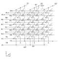
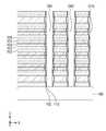
도 3은 몇몇 실시예에 따른 도 2의 반도체 메모리 장치의 P1 영역을 확대하여 설명하기 위한 예시적인 확대도이다.3 is an exemplary enlarged view illustrating an enlarged area P1 of the semiconductor memory device of FIG. 2 according to some embodiments.
도 3을 참조하면, 몇몇 실시예에 따른 반도체 메모리 장치는 제1 절연 패턴(162), 제2 절연 패턴(164), 제3 절연 패턴(166), 제1 채널 구조체(CS1), 제2 채널 구조체(CS2), 제3 채널 구조체(CS3),게이트 전극(150)을 포함한다. 이하에서, 제1 절연 패턴(162), 제2 절연 패턴(164), 및 제3 절연 패턴(166)들을 복수의 절연 패턴들(162, 164, 및 166)로 통칭할 수 있으며, 제1 채널 구조체(CS1), 제2 채널 구조체(CS2), 및 제3 채널 구조체(CS3)들을 복수의 채널 구조체들(CS1, CS2, 및 CS3)로 통칭할 수 있다.Referring to FIG. 3, the semiconductor memory device according to some embodiments includes a first
제1 절연 패턴(162), 게이트 전극(150), 및 제3 절연 패턴(166)은 기판으로부터 수직한 제1 방향(z 방향)으로 적층될 수 있다. 제2 절연 패턴(164)은 게이트 전극(150)으로부터 기판과 평행한 제2 방향(y 방향)으로 돌출되어 형성될 수 있다. 또한, 복수의 절연 패턴들(162, 164, 및 166), 및 게이트 전극(150)은 기판과 평행한 제2 방향(y 방향)으로 길게 연장될 수 있다.The first
복수의 절연 패턴들(162, 164, 및 166)은 예를 들어, BSG(borosilicate Glass), PSG(phosphoSilicate Glass), BPSG(boroPhosphoSilicate Glass), USG(Undoped Silicate Glass), TEOS(TetraEthylOrthoSilicate Glass), 또는 HDP-CVD(High Density Plasma-CVD) 등과 같은 실리콘 산화물을 포함할 수 있으나, 이에 제한되는 것은 아니다.The plurality of insulating
몇몇 실시예에 따른 반도체 메모리 장치 내에는 슬릿 영역(190)이 형성될 수 있다. 슬릿 영역(190)은 적층된 복수의 구조체들 사이를 나눌 수 있다.A
도시되지 않았으나, 기판은 예를 들어, 실리콘 기판, 게르마늄 기판 혹은 실리콘-게르마늄 기판 등과 같은 반도체 기판을 포함할 수 있다. 또는, 기판은 실리콘-온-인슐레이터(Silicon-On-Insulator: SOI) 기판 혹은 게르마늄-온-인슐레이터(Germanium-On-Insulator: GOI) 기판 등을 포함할 수도 있다.Although not shown, the substrate may include, for example, a semiconductor substrate such as a silicon substrate, a germanium substrate, or a silicon-germanium substrate. Alternatively, the substrate may include a silicon-on-insulator (SOI) substrate or a germanium-on-insulator (GOI) substrate.
제1 절연 패턴(162) 및 제3 절연 패턴(166)은 서로 동일한 두께를 갖는 것으로 도시되었으나, 이에 제한되지 않고, 제1 절연 패턴(162) 및 제3 절연 패턴(166)은 서로 다른 두께를 가질 수도 있다.The first
게이트 전극(150)은 제1 절연 패턴(162) 및 제3 절연 패턴(166)의 사이에 위치할 수 있으며, 게이트 전극(150)으로부터 제2 방향(y 방향)으로 돌출된 제2 절연 패턴(164)을 포함할 수 있다.The
본 도면에서는 복수의 게이트 전극 중 하나의 게이트 전극에 대해서만 도시하였다. 즉, 게이트 전극(150)은 복수 개로 제공될 수 있다. 따라서, 몇몇 실시예에서, 최하부의 게이트 전극(150)은 도 1의 그라운드 선택 라인(GSL)으로 제공될 수 있다. 또한, 몇몇 실시예에서, 최상부의 게이트 전극(150), 도 1의 스트링 선택 라인(GSL)으로 제공될 수 있다. 그리고, 몇몇 실시예에서, 최하부 및 최상부의 제1 방향(z 방향) 사이의 게이트 전극(150)은 그라운드 선택 라인(GSL)과 스트링 선택 라인(SSL) 사이의 게이트 전극들(WL0~WLn)로 제공될 수 있으며, 이는 도 1의 워드 라인들(WL0~WLn)으로 제공될 수 있다.In this drawing, only one of the plurality of gate electrodes is illustrated. That is, a plurality of
게이트 전극(150)은 도전성 물질을 포함할 수 있다. 게이트 전극(150)은 예를 들어, 텅스텐(W), 코발트(Co), 니켈(Ni) 등의 금속이나 실리콘과 같은 반도체 물질을 포함할 수 있으나, 이에 제한되는 것은 아니다.The
복수의 절연 패턴들(162, 164, 및 166)은 절연성 물질을 포함할 수 있다. 복수의 절연 패턴들(162, 164, 및 166)은 예를 들어, 실리콘 산화물을 포함할 수 있으나, 이에 제한되는 것은 아니다.The plurality of insulating
복수의 채널 구조체들(CS1, CS2, 및 CS3)은 복수의 절연 패턴들(162, 164, 및 166) 및 게이트 전극을 관통하여 제1 방향(z 방향)으로 연장될 수 있다. 예를 들어, 복수의 채널 구조체들(CS1, CS2, 및 CS3)은 기판상에 필러(pillar) 형상으로 형성되어, 복수의 절연 패턴들(162, 164, 및 166) 및 게이트 전극을 관통할 수 있다. 이에 따라, 게이트 전극(150)은 복수의 채널 구조체들(CS1, CS2, 및 CS3)과 교차할 수 있다.The plurality of channel structures CS1, CS2, and CS3 may pass through the plurality of insulating
복수의 채널 구조체들(CS1, CS2, 및 CS3) 각각은 반도체 패턴(106)을 포함할 수 있다. 반도체 패턴(106)은 복수의 절연 패턴들(162, 164, 및 166), 및 게이트 전극(150)을 관통하여 기판과 접속될 수 있다. 예를 들어, 반도체 패턴(106)은 제1 방향(z 방향)으로 연장될 수 있다. 반도체 패턴(106)은 예를 들어, 컵 형상으로 형성될 수 있다. 예를 들어, 복수의 채널 구조체들(CS1, CS2, 및 CS3) 각각은 필러(pillar) 형상의 충진 절연 패턴(108)과, 충진 절연 패턴(108)의 바닥면 및 측벽을 따라 컨포멀하게(conformally) 연장되는 반도체 패턴(106)을 포함할 수 있다. 충진 절연 패턴(108)은 예를 들어, 실리콘 산화물을 포함할 수 있다. 그러나, 본 발명의 기술적 사상이 이에 제한되는 것은 아니고, 반도체 패턴(106)은 원통 형상, 사각통 형상, 속이 찬 필러 형상 등 다양한 형상을 가질 수도 있다.Each of the plurality of channel structures CS1, CS2, and CS3 may include a
반도체 패턴(106)은 예를 들어, 단결정 실리콘 등의 반도체 물질을 포함할 수 있으나, 이에 제한되는 것은 아니다.The
복수의 채널 구조체들(CS1, CS2, 및 CS3) 각각은 터널 절연막(104)을 포함할 수 있다. 터널 절연막(104)은 예를 들어, 실리콘 산화물 또는 실리콘 산질화물을 포함할 수 있다. 또는, 예를 들어, 터널 절연막(104)은 실리콘 산화막과 실리콘 질화막의 이중층 등으로 형성될 수도 있다. 설명의 편의를 위해, 이하에서 터널 절연막(104)은 실리콘 산화물을 포함하는 것으로 설명한다.Each of the plurality of channel structures CS1, CS2, and CS3 may include a
복수의 채널 구조체들(CS1, CS2, 및 CS3) 각각은 제1 전하 저장막(110a) 및 제2 전하 저장막(110b)을 포함할 수 있다. 이하에서, 제1 전하 저장막(110a) 및 제2 전하 저장막(110b)은 복수의 전하 저장막들(110a 및 110b)로 통칭될 수 있다.Each of the plurality of channel structures CS1, CS2, and CS3 may include a first
복수의 전하 저장막들(110a 및 110b)은 터널 절연막(104)의 측벽상에 형성될 수 있다. 이에 따라, 터널 절연막(104)은 반도체 패턴(106)과 복수의 전하 저장막들(110a 및 110b) 사이에 형성될 수 있다. 또한, 복수의 전하 저장막들(110a 및 110b) 각각은 +x 방향으로 연장될 수 있다.The plurality of
제1 전하 저장막(110a)과 제2 전하 저장막(110b) 사이에 제2 절연 패턴(164)이 형성될 수 있으며, 제2 절연 패턴(164)은 게이트 전극(150)으로부터 제2 방향(y 방향)으로 돌출되되, x 방향으로 연장되어 형성될 수 있다.A second
복수의 전하 저장막들(110a 및 110b)은 예를 들어, 실리콘 질화물, 실리콘 산질화물, 실리콘 풍부형 질화물(Si-rich nitride) 및 나노 크리스탈 실리콘(nanocrystalline Si) 중 적어도 하나를 포함할 수 있다. 설명의 편의를 위해, 이하에서 복수의 전하 저장막들(110a 및 110b)은 실리콘 질화물을 포함하는 것으로 설명한다.The plurality of
복수의 채널 구조체들(CS1, CS2, 및 CS3) 각각은 블로킹 절연막(102)을 포함할 수 있다. 블로킹 절연막(102)은, 복수의 전하 저장막들(110a 및 110b)과 터널 절연막(104)을 따라 제1 방향(z 방향)으로 연장되어 형성될 수 있다.Each of the plurality of channel structures CS1, CS2, and CS3 may include a blocking insulating
즉, 블로킹 절연막(102)의 일면에 형성된 제1 리세스(118a) 및 제2 리세스(118b) 각각에 실리콘 질화물(물질은 이에 제한되지 않는다.)을 채워 각각의 제1 전하 저장막(110a) 및 제2 전하 저장막(110b)을 형성할 수 있다.That is, silicon nitride (a material is not limited thereto) is filled in each of the first and
또한, 블로킹 절연막(102)의 다른 일면에 형성된 제3 리세스(168)에 절연 물질을 채워 제2 절연 패턴(164)을 형성할 수 있다.In addition, the second
블로킹 절연막(102)은 복수의 전하 저장막들(110a 및 110b)의 측벽, 상면, 및 하면 상에 형성될 수 있다. 즉, 블로킹 절연막(102)은 게이트 전극(150)과 복수의 전하 저장막들(110a 및 110b) 사이에 형성될 수 있다.The blocking insulating
블로킹 절연막(102)은 도시된 것에 제한되지 않고, 게이트 전극(150)을 둘러싸도록 형성될 수 있다. 예를 들어, 블로킹 절연막(102)은 게이트 전극(150)의 바닥면, 측벽 및 상면을 따라 연장될 수 있다. 이에 따라, 블로킹 절연막(102)의 하부는 게이트 전극(150)과 제1 절연 패턴(162) 사이에 형성될 수 있고, 블로킹 절연막(102)의 측부는 게이트 전극(150)과 복수의 전하 저장막들(110a 및 110b) 사이에 형성될 수 있고, 블로킹 절연막(102)의 상부는 게이트 전극(150)과 제3 절연 패턴(166) 사이에 형성될 수 있다.The blocking insulating
블로킹 절연막(102)은 예를 들어, 실리콘 산화물 또는 실리콘 산화물보다 유전 상수가 큰 고유전율 물질을 포함할 수 있다. 상기 고유전율 물질은 예를 들어, 알루미늄 산화물(aluminum oxide), 하프늄 산화물(hafnium oxide), 란타늄 산화물(lanthanum oxide), 탄탈륨 산화물(tantalum oxide), 티타늄 산화물(titanium oxide), 란타늄 하프늄 산화물(lanthanum hafnium oxide), 란타늄 알루미늄 산화물(lanthanum aluminum oxide), 디스프로슘 스칸듐 산화물(dysprosium scandium oxide) 및 이들의 조합 중 적어도 하나를 포함할 수 있다. 설명의 편의를 위해, 이하에서 블로킹 절연막(102)은 실리콘 산화물을 포함하는 것으로 설명한다.The blocking insulating
몇몇 실시예에 따른 반도체 메모리 장치에서, 하나의 게이트 전극(150)을 통해 제1 전하 저장막(110a) 및 제2 전하 저장막(110b)을 제어할 수 있다. 즉, 1 개의 셀에 2 개의 트랜지스터를 형성함으로써, 반도체 메모리 장치의 집적도를 증가시킬 수 있다.In the semiconductor memory device according to some embodiments, the first
몇몇 실시예에 따른 반도체 메모리 장치에서, 반도체 패턴(106) 내의 전자가 터널 절연막(104)을 거쳐 제1 전하 저장막(110a) 및/또는 제2 전하 저장막(110b)에 주입될 때, 파울러-노던하임 터널링(fowler-nordheim tunneling)을 통해 주입되는 것이 아니라, Hot Carrier Injection을 통해 주입될 수 있다.In the semiconductor memory device according to some embodiments, when electrons in the
즉, 반도체 메모리 장치 내부에 강한 전위차를 형성시켜 반도체 패턴(106) 내의 전자를 가속시켜, 전자가 높은 운동에너지(Kinetic Energy)를 갖게 하고, 높은 운동 에너지를 가진 전자들(즉, Hot Carrier)이 제1 전하 저장막(110a) 및/또는 제2 전하 저장막(110b)에 트랩될 수 있다.That is, by forming a strong potential difference inside the semiconductor memory device, electrons in the
몇몇 실시예에 따른 반도체 메모리 장치에서 예를 들어, 제1 채널 구조체(CS1)의 제1 전하 저장막(110a)에 전자를 주입하는 경우, 제1 채널 구조체(CS1)의 상부 및 게이트 전극(150)에 +V의 전압을 가하고, 제1 채널 구조체(CS1)의 하부에 0 혹은 +V보다 낮은 전압을 가한다. 제1 채널 구조체(CS1)의 상부와 게이트 전극(150)에 의한 전압과 제1 채널 구조체(CS1)의 하부에 가해지는 전압의 차이는 제1 전하 저장막(110a)이 제2 전하 저장막(110b)보다 더 크다. 즉, 반도체 패턴(106)의 전자는 제1 전하 저장막(110a)에 트랩될 수 있다.In the semiconductor memory device according to some embodiments, for example, when electrons are injected into the first
몇몇 실시예에 따른 반도체 메모리 장치에서 예를 들어, 제1 채널 구조체(CS1)의 제2 전하 저장막(110b)에 전자를 주입하는 경우, 제1 채널 구조체(CS1)의 하부 및 게이트 전극(150)에 +V의 전압을 가하고, 제1 채널 구조체(CS1)의 상부에 0 혹은 +V보다 낮은 전압을 가한다. 제1 채널 구조체(CS1)의 하부와 게이트 전극(150)에 의한 전압과, 제1 채널 구조체(CS1)의 상부에 가해지는 전압의 차이는 제2 전하 저장막(110b)이 제1 전하 저장막(110a)보다 더 크다. 즉, 반도체 패턴(106)의 전자는 제2 전하 저장막(110b)에 트랩될 수 있다.In the semiconductor memory device according to some embodiments, when electrons are injected into the second
몇몇 실시예에 따른 반도체 메모리 장치에서, 게이트 전극(150)을 통해 제1 전하 저장막(110a) 및 제2 전하 저장막(110b) 각각을 별개의 트랜지스터로 제어하기 위해, 제1 전하 저장막(110a)과 제2 전하 저장막(110b) 사이에 게이트 전극(150)으로부터 제2 방향(y 방향)으로 돌출된 제2 절연 패턴(164)이 형성될 수 있다.In the semiconductor memory device according to some embodiments, in order to control each of the first
즉, 제2 절연 패턴(164)을 통해 제1 전하 저장막(110a)으로 트랩되는 전하가 제2 전하 저장막(110b)에 트랩되지 않게 할 수 있다. 반대로, 제2 절연 패턴(164)을 통해 제2 전하 저장막(110b)으로 트랩되는 전하가 제1 전하 저장막(110a)에 트랩되지 않게 할 수 있다. 이를 통해, 반도체 메모리 장치의 집적도를 늘리면서 동시에 반도체 메모리 장치의 성능을 향상시킬 수 있다.That is, electric charges trapped in the first
이하에서, 도 4를 통해 몇몇 실시예에 따른 반도체 메모리 장치의 내부를 자세히 설명한다.Hereinafter, the interior of a semiconductor memory device according to some embodiments will be described in detail with reference to FIG. 4.
도 4는 도 3의 R1 영역을 설명하기 위한 확대도이다.FIG. 4 is an enlarged view illustrating an area R1 of FIG. 3.
도 4를 참조하면, 게이트 전극(150)은 제1 절연 패턴(162)의 상면(G2) 및 제3 절연 패턴(166)의 하면(G1)사이에 형성될 수 있다. 제1 절연 패턴(162)은 제2 방향(y 방향)으로 제1 너비(W1)를 가질 수 있고, 제3 절연 패턴(166)은 제2 방향(y 방향)으로 제3 너비(W3)를 가질 수 있다.Referring to FIG. 4, the
게이트 전극(150)은 제1 절연 패턴(162) 및 제3 절연 패턴(166) 사이로 연장되는 제1 측면(M1) 및 제2 측면을 포함한다. 또한 게이트 전극(150)은 제2 방향(y 방향)으로 제6 너비(W6)를 가질 수 있다.The
제2 절연 패턴(164)은 게이트 전극(150)으로부터 제2 방향(y 방향)으로 제2 너비(W2)를 가질 수 있다. 또한, 제2 절연 패턴(164)은 제1 방향(z 방향)으로 제3 길이(L3)를 가질 수 있다. 또한, 제2 절연 패턴(164)은 게이트 전극(150)과 만나는 제6 측면(M6) 및 블로킹 절연막(102)과 만나는 제5 측면(M5)을 포함할 수 있다.The second
제2 절연 패턴(164)을 사이에 두고, 제2 절연 패턴(164)의 제1 방향(z 방향)의 상부에 제1 전하 저장막(110a)이 형성될 수 있으며, 제2 절연 패턴(164)의 제1 방향(z 방향)의 하부에 제2 전하 저장막(110b)이 형성될 수 있다. 제1 전하 저장막(110a)은 제1 방향(z 방향)으로 제1 길이(L1)를 가질 수 있다. 또한, 제1 전하 저장막(110a)은 제2 방향(y 방향)으로 제7 너비(W7)를 가질 수 있다. 제2 전하 저장막(110b)은 제1 방향(z 방향)으로 제2 길이(L2)를 가질 수 있다. 또한, 제2 전하 저장막(110b)은 제2 방향(y 방향)으로 제8 너비(W8)를 가질 수 있다.A first
몇몇 실시예에 따른 반도체 메모리 장치의, 제2 절연 패턴(164)의 제3 길이(L3)는 제1 길이(L1) 및/또는 제2 길이(L2)보다 작을 수 있으나, 본 도면에 제한되지 않고 제1 길이(L1) 및/또는 제2 길이(L2)의 1/2보다 클 수도 있다. 제2 절연 패턴(164)의 제3 길이(L3)가 길어지면, 제1 전하 저장막(110a) 및/또는 제2 전하 저장막(110b) 사이에 트랩되는 전하들을 효율적으로 분리시킬 수 있다.In the semiconductor memory device according to some embodiments, the third length L3 of the second
제1 전하 저장막(110a)의 제1 길이(L1)와 제2 전하 저장막(110b)의 제2 길이(L2)는 서로 같은 것으로 도시되었으나, 이에 제한되지 않고 서로 다를 수 있다.The first length L1 of the first
제1 전하 저장막(110a)은 제1 측면(M1)으로부터 제4 너비(W4)만큼 떨어져서 형성될 수 있다. 제2 전하 저장막(110b)은 제1 측면(M1)으로부터 제5 너비(W5)만큼 떨어져서 형성될 수 있다. 제4 너비(W4)와 제5 너비(W5)는 동일한 것으로 도시되었으나, 이에 제한되지 않고, 제4 너비(W4)와 제5 너비(W5)는 서로 다를 수 있다. 그리고, 제1 전하 저장막(110a)은 블로킹 절연막(102)과 만나는 제3 측면(M3)을 포함하고, 제2 전하 저장막(110b)은 블로킹 절연막(102)과 만나는 제4 측면(M4)을 포함한다.The first
블로킹 절연막(102)은 복수의 절연 패턴들(162, 164, 및 166), 게이트 전극(150), 복수의 전하 저장막들(110a 및 110b), 및 터널 절연막(104)을 따라 제1 방향(z 방향)으로 컨포멀하게 연장될 수 있다.The blocking insulating
복수의 전하 저장막들(110a 및 110b)은 블로킹 절연막(102)의 일면에 형성된 제1 리세스(118a) 및 제2 리세스(118b)에 예를 들면, 실리콘 질화막이 채워진 형태로 제1 전하 저장막(110a) 및 제2 전하 저장막(110b)이 형성될 수 있다. 또한, 제2 절연 패턴(164)은 블로킹 절연막(102)의 일면에 대향하는 다른 일면에 형성된 제3 리세스(168)에 절연 물질이 채워진 형태로 제2 절연 패턴(164)이 형성될 수 있다.The plurality of
제1 절연 패턴(162)의 제1 너비(W1)와 제3 절연 패턴(166)의 제3 너비(W3)가 같은 것으로 도시되었으나, 이에 제한되지 않는다. 제1 측면(M1)으로부터 제2 측면(M2)까지의 거리 즉, 게이트 전극(150)의 제2 방향(y 방향)으로의 제6 너비(W6)는 제1 너비(W1) 및/또는 제3 너비(W3)보다 작을 수 있다.Although the first width W1 of the first
제2 측면(M2)으로부터 제5 측면(M5)까지의 길이는 제6 너비(W6) 및 제2 너비(W2)의 합과 같다. 제2 측면(M2)으로부터 제3 측면(M3)까지의 길이는 제6 너비(W6) 및 제4 너비(W4)의 합과 같다. 제2 측면(M2)으로부터 제4 측면(M4)까지의 길이는 제6 너비(W6) 및 제5 너비(W5)의 합과 같다.The length from the second side (M2) to the fifth side (M5) is equal to the sum of the sixth width (W6) and the second width (W2). The length from the second side (M2) to the third side (M3) is equal to the sum of the sixth width (W6) and the fourth width (W4). The length from the second side (M2) to the fourth side (M4) is equal to the sum of the sixth width (W6) and the fifth width (W5).
도시된 바와 같이, 제6 너비(W6) 및 제4 너비(W4)의 합과 제6 너비(W6) 및 제5 너비(W5)의 합은 같을 수 있으나 이에 제한되지 않고 다를 수 있다.As illustrated, the sum of the sixth width W6 and the fourth width W4 and the sum of the sixth width W6 and the fifth width W5 may be the same, but are not limited thereto and may be different.
몇몇 실시예에 따른 반도체 메모리 장치에서, 제6 너비(W6) 및 제2 너비(W2)의 합은 제6 너비(W6) 및 제4 너비(W4)의 합보다 클 수 있다. 또한 제6 너비(W6) 및 제2 너비(W2)의 합은 제6 너비(W6) 및 제5 너비(W5)의 합보다 클 수 있다.In the semiconductor memory device according to some embodiments, the sum of the sixth width W6 and the second width W2 may be greater than the sum of the sixth width W6 and the fourth width W4. In addition, the sum of the sixth width W6 and the second width W2 may be greater than the sum of the sixth width W6 and the fifth width W5.
상술한 바와 같이, 몇몇 실시예에 따른 반도체 메모리 장치는, 하나의 게이트 전극(150)을 통해 각각의 제1 전하 저장막(110a) 및 제2 전하 저장막(110b)에 독립적으로 전하를 저장할 수 있다.As described above, in the semiconductor memory device according to some embodiments, charge can be independently stored in each of the first and second
예를 들어, 도 4의 D2 방향에 따른 2점 쇄선 화살표 방향을 참조하면, 게이트 전극(150)에 게이트 전압(VG)가 인가될 수 있다. 게이트 전압(VG)는 예를 들어, 양의 전압일 수 있다. 또한, 반도체 패턴(106)의 상부에 제1 전압(V1)이 인가될 수 있고, 반도체 패턴(106)의 하부에 제1 전압(V1)과는 다른 제2 전압(V2)이 인가될 수 있다. 일례로, 제1 전압(V1)은 그라운드 전압일 수 있고, 제2 전압(V2)은 양의 전압일 수 있다. 이러한 경우에, 반도체 패턴(106)의 상부로부터 제공되는 전하(전자)는 제2 전하 저장막(110b)에 선택적으로 트랩될 수 있다.For example, referring to the direction of the dashed-dotted line arrow along the direction D2 of FIG. 4, the gate voltage VG may be applied to the
또다른 예를 들어, 도 4의 D1 방향에 따른 2점 쇄선 화살표 방향을 참조하면, 게이트 전극(150)에 게이트 전압(VG)가 인가될 수 있다. 게이트 전압(VG)는 예를 들어, 양의 전압일 수 있다. 또한, 반도체 패턴(106)의 상부에 제1 전압(V1)이 인가될 수 있고, 반도체 패턴(106)의 하부에 제1 전압(V1)과는 다른 제2 전압(V2)이 인가될 수 있다. 일례로, 제1 전압(V1)은 양의 전압일 수 있고, 제2 전압(V2)은 그라운드 전압일 수 있다. 이러한 경우에, 반도체 패턴(106)의 하부로부터 제공되는 전하(전자)는 제1 전하 저장막(110a)에 선택적으로 트랩될 수 있다.For another example, referring to the direction of the dashed-dotted line arrow along the direction D1 of FIG. 4, the gate voltage VG may be applied to the
이에 따라, 몇몇 실시예에 따른 반도체 메모리 장치는 각각의 게이트 전극(150) 당 2개의 데이터 저장 소자(data storage element)를 구현할 수 있다. 이에 따라, 집적도가 향상된 반도체 메모리 장치가 제공될 수 있다.Accordingly, the semiconductor memory device according to some embodiments may implement two data storage elements for each
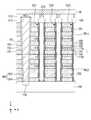
도 5는 도 3의 A-A'를 절단한 단면도이다.5 is a cross-sectional view taken along line A-A' of FIG. 3.
도 5를 참조하면, 몇몇 실시예에 따른 반도체 메모리 장치는 슬릿 영역(190)을 통해 이격될 수 있다. 또한, 몇몇 실시예에 따른 반도체 메모리 장치는 게이트 전극(150)과 연결된 제1 채널 구조체(CS1), 제2 채널 구조체(CS2), 제3 채널 구조체(CS3), 제4 채널 구조체(CS4), 및 제5 채널 구조체(CS5)를 포함한다. 제1 내지 제5 채널 구조체들(CS1, CS2, CS3, CS4, 및 CS5) 각각은 충진 절연 패턴(108), 반도체 패턴(106), 터널 절연막(104), 제1 전하 저장막(110a), 및 블로킹 절연막(102)이 순서대로 형성될 수 있다.Referring to FIG. 5, the semiconductor memory device according to some embodiments may be spaced apart through the
이하에서 도 6를 통해, 몇몇 실시예에 따른 반도체 메모리 장치에서 제1 전하 저장막 및 제2 전하 저장막 사이의 절연 패턴에 의해 형성되는 단면을 설명한다.Hereinafter, a cross section formed by an insulating pattern between a first charge storage layer and a second charge storage layer in a semiconductor memory device according to some embodiments will be described with reference to FIG. 6.
도 6은 도 3의 B-B'를 절단한 단면도이다.6 is a cross-sectional view taken along line B-B' of FIG. 3.
도 6을 참조하면, 몇몇 실시예에 따른 반도체 메모리 장치는 슬릿 영역(190)을 통해 이격될 수 있다. 또한, 몇몇 실시예에 따른 반도체 메모리 장치는 제2 절연 패턴(164)을 통해 절연된 제1 채널 구조체(CS1), 제2 채널 구조체(CS2), 제3 채널 구조체(CS3), 제4 채널 구조체(CS4), 및 제5 채널 구조체(CS5)를 포함한다. 제1 내지 제5 채널 구조체들(CS1, CS2, CS3, CS4, 및 CS5) 각각은 충진 절연 패턴(108), 반도체 패턴(106), 터널 절연막(104), 및 블로킹 절연막(102)이 순서대로 형성될 수 있다.Referring to FIG. 6, the semiconductor memory device according to some embodiments may be spaced apart through the
몇몇 실시예에 따른 반도체 메모리 장치에서는 제2 절연 패턴(164)에 의해 제1 전하 저장막(110a)이 도 3의 제2 전하 저장막(110b)과 격리되어 서로 간의 전하 트랩 간섭을 막을 수 있다.In the semiconductor memory device according to some embodiments, the first
도 7 내지 도 18은 몇몇 실시예에 따른 도 2의 반도체 메모리 장치의 제조 방법을 설명하기 위한 중간 단계 도면들이다.7 through 18 are diagrams of intermediate steps for describing a method of manufacturing the semiconductor memory device of FIG. 2, according to some embodiments.
도 7을 참조하면, 기판(100) 상에 제1 절연 패턴(162), 제1 희생막(152), 제2 절연 패턴(164), 제2 희생막(154), 및 제3 절연 패턴(166)을 순서대로 적층한다.Referring to FIG. 7, a first
제1 희생막(152)과 제2 희생막(154)이 서로 동일한 두께를 갖는 것으로 도시되었으나, 이는 설명의 편의를 위한 것일 뿐이고, 본 발명의 기술적 사상이 이에 제한되는 것은 아니다. 예를 들어, 제1 희생막(152)과 제2 희생막(154)은 서로 다른 두께를 가질 수도 있다.Although the first
제1 희생막(152)과 제2 희생막(154)은 예를 들어, 실리콘 질화물, 실리콘 산질화물, 실리콘 풍부형 질화물(Si-rich nitride) 및 나노크리스탈 실리콘(nanocrystalline Si) 중 적어도 하나를 포함할 수 있다. 설명의 편의를 위해, 이하에서 제1 희생막(152) 및 제2 희생막(154)은 실리콘 질화물을 포함하는 것으로 설명한다. 제1 희생막(152) 및 제2 희생막(154)은 전술한 게이트 전극이 형성되는 영역을 정의할 수 있다.The first
도 8을 참조하면, 적층된 제1 절연 패턴(162), 제1 희생막(152), 제2 절연 패턴(164), 제2 희생막(154), 및 제3 절연 패턴(166) 내에 제1 채널 홀(CH1), 제2 채널 홀(CH2), 및 제3 채널 홀(CH3)을 형성한다.Referring to FIG. 8, the first
이하에서는 제1 채널 홀(CH1)을 예를 들어 설명한다. 적층된 제1 절연 패턴(162), 제1 희생막(152), 제2 절연 패턴(164), 제2 희생막(154), 및 제3 절연 패턴(166)을 식각하여, 적층된 제1 절연 패턴(162), 제1 희생막(152), 제2 절연 패턴(164), 제2 희생막(154), 및 제3 절연 패턴(166)을 관통하는 제1 채널 홀(CH1)이 형성될 수 있다. 제1 채널 홀(CH1)은 적층된 제1 절연 패턴(162), 제1 희생막(152), 제2 절연 패턴(164), 제2 희생막(154), 및 제3 절연 패턴(166)을 관통하여 기판의 일부를 노출시키도록 형성될 수 있다. 몇몇 실시예에서, 제1 채널 홀(CH1)을 형성하는 것은, 기판의 상부의 일부를 식각하는 것을 포함할 수 있다.Hereinafter, the first channel hole CH1 will be described as an example. The stacked first
몇몇 실시예에서, 제1 채널 홀(CH1)은 테이퍼진(tapered) 모양을 가질 수 있다. 예를 들어, 제1 채널 홀(CH1)의 폭은 제1 방향의 하부로 갈수록 좁아질 수 있다. 이러한 제1 채널 홀(CH1)의 형상은 제1 채널 홀(CH1)을 형성하기 위한 식각 공정의 특성에 기인할 수 있으나, 이에 제한되는 것은 아니다.In some embodiments, the first channel hole CH1 may have a tapered shape. For example, the width of the first channel hole CH1 may decrease toward a lower portion in the first direction. The shape of the first channel hole CH1 may be due to a characteristic of an etching process for forming the first channel hole CH1, but is not limited thereto.
도 9를 참조하면, 제1 채널 홀(CH1), 제2 채널 홀(CH2), 및 제3 채널 홀(CH3)에 의해 노출된 제1 희생막(152) 및 제2 희생막(154)의 일부를 제거한다.9, the first and second
예를 들어, 제1 희생막(152) 및 제2 희생막(154)에 대한 에치백(etchback) 공정이 수행되어, 제1 희생막(152) 및 제2 희생막(154)에 리세스가 형성될 수 있다.For example, by performing an etchback process for the first
도 10을 참조하면, 각각의 채널 홀들(CH1 내지 CH3) 내에 블로킹 절연막(102) 및 예비 전하 저장막(110)을 차례로 형성한다. 이하에서는 제1 채널 홀(CH1)을 예시적으로 설명한다.Referring to FIG. 10, a blocking insulating
먼저, 제1 채널 홀(CH1)의 프로파일을 따라 연장되는 블로킹 절연막(102)이 형성될 수 있다. 블로킹 절연막(102)은 제1 희생막(152), 제2 희생막(154), 제1 절연 패턴(162), 제2 절연 패턴(164), 및 제3 절연 패턴(166)의 측면을 따라 연장될 수 있다.First, a blocking insulating
이어서, 블로킹 절연막(102) 상에 예비 전하 저장막(110)이 형성될 수 있다. 예비 전하 저장막(110)은 블로킹 절연막(102)의 프로파일을 따라 연장될 수 있다.Subsequently, a preliminary
도 11을 참조하면, 예비 전하 저장막(110)에 대한 에치백 공정을 수행할 수 있다. 몇몇 실시예에 따른 에치백 공정은 습식 식각을 통해 수행될 수 있다.Referring to FIG. 11, an etch back process may be performed on the preliminary
몇몇 실시예에서, 에치백 공정은 블로킹 절연막(102)의 측면이 노출될 때까지 수행될 수 있다. 이에 따라, 각각의 절연 패턴들(162, 164, 및 166) 사이에 서로 이격되는 2개의 전하 저장막(예를 들어, 제1 전하 저장막(110a) 및 제2 전하 저장막(110b))이 형성될 수 있다.In some embodiments, the etch-back process may be performed until the side surface of the blocking insulating
또한, 2개의 전하 저장막들(110a 및 110b)은 각각의 희생막들(154, 152)에 매립되는 형태로 형성될 수 있다. 예를 들어, 제1 전하 저장막(110a)은 제2 희생막(154)에 형성된 제1 리세스(118a)의 적어도 일부를 채울 수 있고, 제2 전하 저장막(110b)은 제1 희생막(152)에 형성된 제2 리세스(118b)의 적어도 일부를 채울 수 있다.In addition, the two
제1 전하 저장막(110a)의 폭 및 제2 전하 저장막(110b)의 폭은 서로 동일한 것으로 도시되었으나, 본 발명의 기술적 사상이 이에 제한되는 것은 아니다. 또한, 제1 전하 저장막(110a)의 깊이 및 제2 전하 저장막(110b)의 깊이는 서로 동일한 것으로 도시되었으나, 본 발명의 기술적 사상이 이에 제한되는 것은 아니다.Although the width of the first
도 12를 참조하면, 복수의 채널 구조체들(CS1 내지 CS3) 상에 제1 층간 절연막(210) 및 채널 패드(160)가 형성될 수 있다.Referring to FIG. 12, a first
도 13을 참조하면, 복수의 절연 패턴들(162, 164, 및 166) 및 복수의 희생막들(152, 154) 내에 슬릿 영역(190)이 형성될 수 있다.Referring to FIG. 13, a
슬릿 영역(190)은 복수의 절연 패턴들(162, 164, 및 166) 및 복수의 희생막들(152, 154)을 관통하여 기판(100)을 노출시키도록 형성될 수 있다. 이에 따라, 슬릿 영역(190)은 복수의 절연 패턴들(162, 164, 및 166) 및 복수의 희생막들(152, 154)을 절단할 수 있다.The
몇몇 실시예에서, 슬릿 영역(190)은 y 방향으로 연장되도록 형성될 수 있다. 몇몇 실시예에서, 슬릿 영역(190)에 의해 노출되는 기판(100) 내에 불순물 영역(105)이 형성될 수 있다.In some embodiments, the
도 14를 참조하면, 슬릿 영역(190)에 의해 노출된 복수의 절연 패턴들(162, 164, 및 166)들을 제거할 수 있다.Referring to FIG. 14, a plurality of insulating
도 15를 참조하면, 슬릿 영역(190)에 의해 노출된 복수의 희생막들을 제거할 수 있다.Referring to FIG. 15, a plurality of sacrificial layers exposed by the
복수의 희생막들을 제거하는 것은, 예를 들어, 이방성 식각 공정에 의해 수행될 수 있다. 이에 따라, 몇몇 실시예에서, 블로킹 절연막(102)의 측면의 일부가 노출될 수 있다.Removing the plurality of sacrificial layers may be performed by, for example, an anisotropic etching process. Accordingly, in some embodiments, a part of the side surface of the blocking insulating
도 16을 참조하면, 복수의 희생막들을 제거된 영역에 도전 물질을 채워 게이트 전극(150)을 형성할 수 있다.Referring to FIG. 16, a
도 17을 참조하면, 슬릿 영역 내에 분리 구조체(300)를 형성하여 워드 라인 절단 영역(WLC)을 형성할 수 있다.Referring to FIG. 17, the word line cutting area WLC may be formed by forming the
예를 들어, 워드 라인 절단 영역(WLC)의 프로파일을 따라 연장되는 스페이서(304)가 형성될 수 있다. 이어서, 스페이서(304) 상에, 워드 라인 절단 영역(WLC)을 채우는 플러그 패턴(302)이 형성될 수 있다.For example, a
워드 라인 절단 영역(WLC), 제1 층간 절연막(210), 채널 패드(160) 상에 제2 층간 절연막(310)을 형성하고, 층간 절연막(310) 내부에 채널 패드(160)와 접촉하는 비트 라인 컨택(320)을 형성하고, 비트 라인 컨택(320)과 제2 층간 절연막(310) 상에 비트 라인(BL)을 형성하여 몇몇 실시예에 따른 도 2의 반도체 메모리 장치를 형성할 수 있다.A bit that forms a second
도 18은 몇몇 실시예에 따른 반도체 메모리 장치를 설명하기 위한 예시적인 단면도이다. 이하에서는 도 2와 중복된 설명은 생략하고 차이점을 중심으로 설명한다.18 is an exemplary cross-sectional view illustrating a semiconductor memory device according to some embodiments. Hereinafter, descriptions overlapped with those of FIG. 2 will be omitted, and differences will be mainly described.
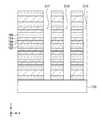
도 18을 참조하면, 도 2와는 달리, 제2 절연 패턴(164)이 복수의 워드 라인들(WL0 내지 WLn)에서 게이트 전극(150) 내부에 x 방향으로 더 침투한 점이 다르다.Referring to FIG. 18, unlike FIG. 2, the second
메모리 셀 역할을 수행하는 P2 영역을 예를 들면, 하나의 메모리 셀을 하나의 게이트 전극(150)이 제어할 수 있다. 즉, 하나의 메모리 셀 안에 제1 전하 저장막(110a) 및 제2 전하 저장막(110b)을 형성하여, 원하는 전하 저장막에 전하를 저장하여, 구조상으로는 하나의 메모리 셀이나, 동작 상으로는 두 개의 메모리 셀 역할을 수행할 수 있어 셀 집적도를 높일 수 있다. 즉, P2 영역의 워드 라인을 3번째 워드 라인(WL3)이라 가정하면, 제3 워드 라인(WL3)을 하나의 게이트 전극(150)을 통해 두 개의 메모리 셀이 포함된 것과 같은 효과를 가져올 수 있다. 이에 대한 자세한 효과, 공정, 및 작동을 이하에서 설명한다.For example, in the region P2 serving as a memory cell, one
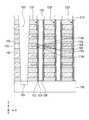
도 19는 몇몇 실시예에 따른 도 18의 반도체 메모리 장치의 P2 영역을 확대하여 설명하기 위한 예시적인 확대도이다. 이하에서는 도 3과 중복되는 부분을 제외하고 설명한다.19 is an exemplary enlarged view illustrating an enlarged area P2 of the semiconductor memory device of FIG. 18, according to some embodiments. Hereinafter, a description will be made excluding parts that overlap with FIG. 3.
도 19를 참조하면, 제2 절연 패턴(164)의 적어도 일부는 게이트 전극(150) 내에 형성될 수 있다.Referring to FIG. 19, at least a portion of the second
몇몇 실시예에 따른 반도체 메모리 장치에서, 하나의 게이트 전극(150)을 통해 제1 전하 저장막(110a) 및 제2 전하 저장막(110b)을 제어할 수 있다. 즉, 1 개의 셀에 2 개의 트랜지스터를 형성함으로써, 반도체 메모리 장치의 집적도를 증가시킬 수 있다.In the semiconductor memory device according to some embodiments, the first
몇몇 실시예에 따른 반도체 메모리 장치에서, 반도체 패턴(106) 내의 전자가 터널 절연막(104)을 거쳐 제1 전하 저장막(110a) 및/또는 제2 전하 저장막(110b)에 주입될 때, 파울러-노던하임 터널링(fowler-nordheim tunneling)을 통해 주입되는 것이 아니라, Hot Carrier Injection을 통해 주입될 수 있다.In the semiconductor memory device according to some embodiments, when electrons in the
즉, 반도체 메모리 장치 내부에 강한 전위차를 형성시켜 반도체 패턴(106) 내의 전자를 가속시켜, 전자가 높은 운동에너지(Kinetic Energy)를 갖게 하고, 높은 운동 에너지를 가진 전자들(즉, Hot Carrier)이 제1 전하 저장막(110a) 및/또는 제2 전하 저장막(110b)에 트랩될 수 있다.That is, by forming a strong potential difference inside the semiconductor memory device, electrons in the
몇몇 실시예에 따른 반도체 메모리 장치에서 예를 들어, 제1 채널 구조체(CS1)의 제1 전하 저장막(110a)에 전자를 주입하는 경우, 제1 채널 구조체(CS1)의 상부 및 게이트 전극(150)에 +V의 전압을 가하고, 제1 채널 구조체(CS1)의 하부에 0 혹은 +V보다 낮은 전압을 가한다. 제1 채널 구조체(CS1)의 상부와 게이트 전극(150)에 의한 전압과 제1 채널 구조체(CS1)의 하부에 가해지는 전압의 차이는 제1 전하 저장막(110a)이 제2 전하 저장막(110b)보다 더 크다. 즉, 반도체 패턴(106)의 전자는 제1 전하 저장막(110a)에 트랩될 수 있다.In the semiconductor memory device according to some embodiments, for example, when electrons are injected into the first
몇몇 실시예에 따른 반도체 메모리 장치에서 예를 들어, 제1 채널 구조체(CS1)의 제2 전하 저장막(110b)에 전자를 주입하는 경우, 제1 채널 구조체(CS1)의 하부 및 게이트 전극(150)에 +V의 전압을 가하고, 제1 채널 구조체(CS1)의 상부에 0 혹은 +V보다 낮은 전압을 가한다. 제1 채널 구조체(CS1)의 하부와 게이트 전극(150)에 의한 전압과, 제1 채널 구조체(CS1)의 상부에 가해지는 전압의 차이는 제2 전하 저장막(110b)이 제1 전하 저장막(110a)보다 더 크다. 즉, 반도체 패턴(106)의 전자는 제2 전하 저장막(110b)에 트랩될 수 있다.In the semiconductor memory device according to some embodiments, when electrons are injected into the second
몇몇 실시예에 따른 반도체 메모리 장치에서, 게이트 전극(150)을 통해 제1 전하 저장막(110a) 및 제2 전하 저장막(110b) 각각을 별개의 트랜지스터로 제어하기 위해, 제1 전하 저장막(110a)과 제2 전하 저장막(110b) 사이에 게이트 전극(150) 내부로부터 제2 방향(y 방향)으로 연장된 제2 절연 패턴(164)이 형성될 수 있다.In the semiconductor memory device according to some embodiments, in order to control each of the first
즉, 제2 절연 패턴(164)을 통해 제1 전하 저장막(110a)으로 트랩되는 전하가 제2 전하 저장막(110b)에 트랩되지 않게 할 수 있다. 반대로, 제2 절연 패턴(164)을 통해 제2 전하 저장막(110b)으로 트랩되는 전하가 제1 전하 저장막(110a)에 트랩되지 않게 할 수 있다. 이를 통해, 반도체 메모리 장치의 집적도를 늘리면서 동시에 반도체 메모리 장치의 성능을 향상시킬 수 있다.That is, electric charges trapped in the first
또한, 제1 전하 저장막(110a)의 제2 방향(y 방향)의 연장선에 위치한 게이트 전극(150)에 의한 전압이 제2 전하 저장막(110b)에 미치지 않도록 하고, 제2 전하 저장막(110b)의 제2 방향(y 방향)의 연장선에 위치한 게이트 전극(150)에 의한 전압이 제1 전하 저장막(110a)에 미치지 않도록 할 수 있다. 즉, 하나의 게이트 전극(150)을 통해 제1 전하 저장막(110a) 및 제2 전하 저장막(110b)을 별개의 트랜지스터와 같이 제어함으로써 반도체 메모리 장치의 집적도를 늘리면서 동시에 반도체 메모리 장치의 성능을 향상시킬 수 있다.In addition, the voltage by the
도 20은 도 19의 R2 영역을 설명하기 위한 확대도이다. 참고적으로, 도 4와 중복되는 설명은 생략하고 차이점을 중심으로 설명한다.FIG. 20 is an enlarged view illustrating an area R2 of FIG. 19. For reference, descriptions overlapping with those of FIG. 4 will be omitted, and differences will be mainly described.
도 20을 참조하면, 제2 절연 패턴(164)의 적어도 일부는 게이트 전극(150) 내부에 형성될 수 있다.Referring to FIG. 20, at least a portion of the second
몇몇 실시예에 따른 반도체 메모리 장치의, 제2 절연 패턴(164)의 제3 길이(L3)는 제1 길이(L1) 및/또는 제2 길이(L2)보다 작을 수 있으나, 본 도면에 제한되지 않고 제1 길이(L1) 및/또는 제2 길이(L2)의 1/2보다 클 수도 있다. 제2 절연 패턴(164)의 제3 길이(L3)가 길어지면, 제1 전하 저장막(110a) 및/또는 제2 전하 저장막(110b) 사이에 트랩되는 전하들을 효율적으로 분리시킬 수 있다.In the semiconductor memory device according to some embodiments, the third length L3 of the second
제1 전하 저장막(110a)의 제1 길이(L1)와 제2 전하 저장막(110b)의 제2 길이(L2)는 서로 같은 것으로 도시되었으나, 이에 제한되지 않고 서로 다를 수 있다. 제4 너비(W4)와 제5 너비(W5)는 동일한 것으로 도시되었으나, 이에 제한되지 않고, 제4 너비(W4)와 제5 너비(W5)는 서로 다를 수 있다.The first length L1 of the first
제1 절연 패턴(162)의 제1 너비(W1)와 제3 절연 패턴(166)의 제3 너비(W3)가 같은 것으로 도시되었으나, 이에 제한되지 않는다. 제1 측면(M1)으로부터 제2 측면(M2)까지의 거리 즉, 게이트 전극(150)의 제2 방향(y 방향)으로의 제6 너비(W6)는 제1 너비(W1) 및/또는 제3 너비(W3)보다 작을 수 있다.Although the first width W1 of the first
제2 측면(M2)으로부터 제5 측면(M5)까지의 길이는 제6 너비(W6) 및 제2 너비(W2)의 합과 같다. 제2 측면(M2)으로부터 제3 측면(M3)까지의 길이는 제6 너비(W6) 및 제4 너비(W4)의 합과 같다. 제2 측면(M2)으로부터 제4 측면(M4)까지의 길이는 제6 너비(W6) 및 제2 절연 패턴(164)의 제1 측면(M1)으로부터 제2 방향(y 방향)으로 돌출된 길이의 합과 같다.The length from the second side (M2) to the fifth side (M5) is equal to the sum of the sixth width (W6) and the second width (W2). The length from the second side (M2) to the third side (M3) is equal to the sum of the sixth width (W6) and the fourth width (W4). The length from the second side (M2) to the fourth side (M4) is the sixth width (W6) and the length protruding from the first side (M1) of the second
도시된 바와 같이, 제6 너비(W6) 및 제4 너비(W4)의 합과 제6 너비(W6) 및 제5 너비(W5)의 합은 같을 수 있으나 이에 제한되지 않고 다를 수 있다.As illustrated, the sum of the sixth width W6 and the fourth width W4 and the sum of the sixth width W6 and the fifth width W5 may be the same, but are not limited thereto and may be different.
몇몇 실시예에 따른 반도체 메모리 장치에서, 제2 측면(M2)으로부터 제5 측면(M5)까지의 길이는 제6 너비(W6) 및 제4 너비(W4)의 합보다 클 수 있다. 또한 제2 측면(M2)으로부터 제5 측면(M5)까지의 길이는 제6 너비(W6) 및 제5 너비(W5)의 합보다 클 수 있다.In the semiconductor memory device according to some embodiments, a length from the second side M2 to the fifth side M5 may be greater than a sum of the sixth width W6 and the fourth width W4. In addition, the length from the second side M2 to the fifth side M5 may be greater than the sum of the sixth width W6 and the fifth width W5.
상술한 바와 같이, 몇몇 실시예에 따른 반도체 메모리 장치는, 하나의 게이트 전극(150)을 통해 각각의 제1 전하 저장막(110a) 및 제2 전하 저장막(110b)에 독립적으로 전하를 저장할 수 있다.As described above, in the semiconductor memory device according to some embodiments, charge can be independently stored in each of the first and second
예를 들어, 도 20의 D2 방향에 따른 2점 쇄선 화살표 방향을 참조하면, 게이트 전극(150)에 게이트 전압(VG)가 인가될 수 있다. 게이트 전압(VG)는 예를 들어, 양의 전압일 수 있다. 또한, 반도체 패턴(106)의 상부에 제1 전압(V1)이 인가될 수 있고, 반도체 패턴(106)의 하부에 제1 전압(V1)과는 다른 제2 전압(V2)이 인가될 수 있다. 일례로, 제1 전압(V1)은 그라운드 전압일 수 있고, 제2 전압(V2)은 양의 전압일 수 있다. 이러한 경우에, 반도체 패턴(106)의 상부로부터 제공되는 전하(전자)는 제2 전하 저장막(110b)에 선택적으로 트랩될 수 있다.For example, referring to the direction of the dashed-dotted line arrow along the direction D2 of FIG. 20, the gate voltage VG may be applied to the
또다른 예를 들어, 도 20의 D1 방향에 따른 2점 쇄선 화살표 방향을 참조하면, 게이트 전극(150)에 게이트 전압(VG)가 인가될 수 있다. 게이트 전압(VG)는 예를 들어, 양의 전압일 수 있다. 또한, 반도체 패턴(106)의 상부에 제1 전압(V1)이 인가될 수 있고, 반도체 패턴(106)의 하부에 제1 전압(V1)과는 다른 제2 전압(V2)이 인가될 수 있다. 일례로, 제1 전압(V1)은 양의 전압일 수 있고, 제2 전압(V2)은 그라운드 전압일 수 있다. 이러한 경우에, 반도체 패턴(106)의 하부로부터 제공되는 전하(전자)는 제1 전하 저장막(110a)에 선택적으로 트랩될 수 있다.For another example, referring to the direction of the dashed-dotted line arrow along the direction D1 of FIG. 20, the gate voltage VG may be applied to the
이에 따라, 몇몇 실시예에 따른 반도체 메모리 장치는 각각의 게이트 전극(150) 당 2개의 데이터 저장 소자(data storage element)를 구현할 수 있다. 이에 따라, 집적도가 향상된 반도체 메모리 장치가 제공될 수 있다.Accordingly, the semiconductor memory device according to some embodiments may implement two data storage elements for each
몇몇 실시예에 따른 도 20의 반도체 메모리 장치는 몇몇 실시예에 따른 다른 도 4의 반도체 메모리 장치와는 달리 제2 절연 패턴(164)이 게이트 전극(150) 내로 더 침투하여 형성되어, 게이트 전극(150)의 제어에 의해 제1 전하 저장막(110a)과 제2 전하 저장막(110b)이 서로 분리되어 제어되도록 절연시킬 수 있다. 즉, 제2 절연 패턴(164)이 게이트 전극(150) 내부로 더욱 돌출되어 형성함으로써, 제1 전하 저장막(110a)과 제2 전하 저장막(110b) 각각에 가해지는 제어 전압을 효율적으로 분리할 수 있다.In the semiconductor memory device of FIG. 20 according to some embodiments, unlike the semiconductor memory device of FIG. 4, according to some embodiments, the second
도 21 내지 도 24는 몇몇 실시예에 따른 도 18의 반도체 메모리 장치의 제조 방법을 설명하기 위한 중간 단계 도면들이다. 도 7 내지 도 13까지의 제조 과정은 동일하므로, 그 이후의 단계부터 설명한다. 아울러 도 14 내지 도 17과 중복되는 설명은 제외하고 차이점을 중심으로 설명한다.21 to 24 are diagrams of intermediate steps for describing a method of manufacturing the semiconductor memory device of FIG. 18 according to some embodiments. Since the manufacturing process of FIGS. 7 to 13 is the same, the subsequent steps will be described. In addition, a description will be made focusing on the differences except for the description overlapping with FIGS. 14 to 17.
도 21을 참조하면, 슬릿 영역(190)에 의해 노출된 제1 절연 패턴(162), 제2 절연 패턴(164), 및 제3 절연 패턴(166)의 일부를 식각할 수 있다.Referring to FIG. 21, a portion of the first
이때, 제1 절연 패턴(162) 및 제3 절연 패턴(166)이 식각되는 속도와, 제2 절연 패턴(164)이 식각되는 속도는 다를 수 있다. 즉, 제2 절연 패턴(164)이 식각되는 속도가 제1 절연 패턴(162) 및 제3 절연 패턴(166)이 식각되는 속도보다 더 빠를 수 있다.In this case, a rate at which the first and
몇몇 실시예에 따른 반도체 메모리 장치의 제조 방법에서, 제2 절연 패턴(164)의 적어도 일부는 제1 희생막(152) 및 제2 희생막(154) 사이에 남아있을 수 있다.In a method of manufacturing a semiconductor memory device according to some embodiments, at least a portion of the second
도 22를 참조하면, 슬릿 영역(190)에 의해 노출된 제1 희생막(152) 및 제2 희생막(154)을 제거한다. 제1 희생막(152) 및 제2 희생막(154)을 제거하기 위해 제1 절연 패턴(162), 제2 절연 패턴(164), 및 제3 절연 패턴(166)과의 식각 선택비를 이용한 습식 식각 공정을 수행할 수 있다. 제1 희생막(152) 및 제2 희생막(154)의 제거는 이에 제한되지 않는다.Referring to FIG. 22, the first
몇몇 실시예에 따른 반도체 메모리 장치의 제조 방법에서, 제2 절연 패턴(164)은 블로킹 절연막(102)으로부터 제2 방향(y 방향)으로 연장되어 블로킹 절연막(102)의 측면으로부터 제2 방향의 반대 방향(-y)으로 돌출될 수 있다.In the method of manufacturing a semiconductor memory device according to some embodiments, the second
도 23을 참조하면, 도 22의 제1 희생막(152) 및 제2 희생막(154)이 제거된 공간을 매립하도록 게이트 전극(150)을 형성할 수 있다. 게이트 전극(150)은 금속과 같은 도전 물질을 원자층 증착(Atomic Layer Deposition; ALD) 또는 화학적 기상 증착(Cheminal Vapor Deposition; CVD) 방식으로 증착하여 형성할 수 있다. 하지만, 이에 제한되지 않고 예를 들어 텅스텐(W) 핵을 생성한 후 벌크 텅스텐을 증착하여 형성할 수도 있다.Referring to FIG. 23, a
도 24를 참조하면, 슬릿 영역 내에 분리 구조체(300)를 형성하여 워드 라인 절단 영역(WLC)을 형성할 수 있다.Referring to FIG. 24, a word line cutting area WLC may be formed by forming the
예를 들어, 워드 라인 절단 영역(WLC)의 프로파일을 따라 연장되는 스페이서(304)가 형성될 수 있다. 이어서, 스페이서(304) 상에, 워드 라인 절단 영역(WLC)을 채우는 플러그 패턴(302)이 형성될 수 있다.For example, a
워드 라인 절단 영역(WLC), 제1 층간 절연막(210), 채널 패드(160) 상에 제2 층간 절연막(310)을 형성하고, 층간 절연막(310) 내부에 채널 패드(160)와 접촉하는 비트 라인 컨택(320)을 형성하고, 비트 라인 컨택(320)과 제2 층간 절연막(310) 상에 비트 라인(BL)을 형성하여 몇몇 실시예에 따른 도 18의 반도체 메모리 장치를 형성할 수 있다.A bit that forms a second
이상 첨부된 도면을 참조하여 본 발명의 실시예들을 설명하였으나, 본 발명은 상기 실시예들에 한정되는 것이 아니라 서로 다른 다양한 형태로 제조될 수 있으며, 본 발명이 속하는 기술분야에서 통상의 지식을 가진 자는 본 발명의 기술적 사상이나 필수적인 특징을 변경하지 않고서 다른 구체적인 형태로 실시될 수 있다는 것을 이해할 수 있을 것이다. 그러므로 이상에서 기술한 실시예들은 모든 면에서 예시적인 것이며 한정적이 아닌 것으로 이해해야만 한다.The embodiments of the present invention have been described above with reference to the accompanying drawings, but the present invention is not limited to the above embodiments, but may be manufactured in various different forms, and those skilled in the art It will be understood that the present invention can be implemented in other specific forms without changing the technical spirit or essential features of the present invention. Therefore, it should be understood that the embodiments described above are illustrative in all respects and not limiting.
102: 블로킹 절연막104: 터널 절연막106: 반도체 패턴108: 충진 절연 패턴110a: 제1 전하 저장막110b: 제2 전하 저장막118a: 제1 리세스118b: 제2 리세스150: 게이트 전극162: 제1 절연 패턴164: 제2 절연 패턴166: 제3 절연 패턴168: 제3 리세스190: 슬릿 영역102: blocking insulating film104: tunnel insulating film106: semiconductor pattern108: filling
Claims (10)
Translated fromKorean상기 제1 절연 패턴의 하면 및 제2 절연 패턴의 상면 사이에 배치되고, 상기 제1 절연 패턴의 하면 및 제2 절연 패턴의 상면 사이로 연장되는 제1 측면을 포함하는 게이트 전극; 및
상기 게이트 전극의 상기 제1 측면으로부터 상기 제1 방향과 다른 제2 방향으로 제1 너비만큼 돌출된 제3 절연 패턴을 포함하는 반도체 메모리 장치.A first insulating pattern and a second insulating pattern spaced apart in a first direction perpendicular to the substrate, wherein a lower surface of the first insulating pattern and an upper surface of the second insulating pattern face each other. ;
A gate electrode disposed between a lower surface of the first insulating pattern and an upper surface of the second insulating pattern and including a first side surface extending between the lower surface of the first insulating pattern and the upper surface of the second insulating pattern; And
And a third insulating pattern protruding from the first side of the gate electrode by a first width in a second direction different from the first direction.
상기 제3 절연 패턴의 적어도 일부는 상기 게이트 전극 내에 형성되는 반도체 메모리 장치.The method of claim 1,
At least a portion of the third insulating pattern is formed in the gate electrode.
상기 제1 절연 패턴은 상기 제2 방향으로 제1 너비를 포함하고,
상기 제2 절연 패턴은 상기 제2 방향으로 제2 너비를 포함하며,
상기 게이트 전극의 상기 제2 방향으로의 제3 너비는 상기 제1 너비 및 상기 제2 너비보다 작은 반도체 메모리 장치.The method of claim 1,
The first insulating pattern includes a first width in the second direction,
The second insulating pattern includes a second width in the second direction,
A semiconductor memory device in which a third width of the gate electrode in the second direction is smaller than the first width and the second width.
상기 제1 절연 패턴, 상기 제2 절연 패턴, 및 상기 게이트 전극 상에, 상기 제3 절연 패턴을 따라 연장되는 블로킹 절연막을 더 포함하고,
상기 블로킹 절연막은 상기 제1 방향으로 이격된 제1 전하 저장막 및 제2 전하 저장막을 포함하는 반도체 메모리 장치.The method of claim 1,
A blocking insulating layer extending along the third insulating pattern is further included on the first insulating pattern, the second insulating pattern, and the gate electrode,
The blocking insulating layer includes a first charge storage layer and a second charge storage layer spaced apart in the first direction.
상기 반도체 패턴 상의 터널 절연막;
상기 터널 절연막 상에, 상기 제1 방향으로 이격된 제1 전하 저장막 및 제2 전하 저장막;
상기 터널 절연막 상에, 상기 제1 전하 저장막 및 상기 제2 전하 저장막을 따라 연장되는 블로킹 절연막;
상기 제1 전하 저장막 및 상기 제2 전하 저장막 사이에 위치하고, 상기 블로킹 절연막 내에 정의된 리세스;
상기 리세스를 채우는 절연 패턴; 및
상기 절연 패턴 및 상기 블로킹 절연막 상의 게이트 전극을 포함하는 반도체 메모리 장치.A semiconductor pattern extending in a first direction perpendicular to the substrate;
A tunnel insulating layer on the semiconductor pattern;
A first charge storage layer and a second charge storage layer spaced apart from each other in the first direction on the tunnel insulating layer;
A blocking insulating layer extending along the first charge storage layer and the second charge storage layer on the tunnel insulating layer;
A recess positioned between the first charge storage layer and the second charge storage layer and defined in the blocking insulating layer;
An insulating pattern filling the recess; And
A semiconductor memory device including the insulating pattern and a gate electrode on the blocking insulating layer.
상기 제1 전하 저장막 및 상기 제2 전하 저장막은 각각 상기 제1 방향으로 제1 길이 및 제2 길이를 가지며,
상기 제1 길이와 상기 제2 길이는 같은 반도체 메모리 장치.The method of claim 5,
The first charge storage layer and the second charge storage layer each have a first length and a second length in the first direction,
The first length and the second length are the same.
상기 절연 패턴은 상기 게이트 전극 내로 연장된 반도체 메모리 장치.The method of claim 5,
The insulating pattern extends into the gate electrode.
상기 블로킹 절연막의 일면 내에 정의되고, 상기 제1 방향으로 서로 이격된 제1 리세스 및 제2 리세스;
상기 블로킹 절연막의 상기 일면과 대향하는 다른 일면 내에 정의되고, 상기 제1 리세스 및 상기 제2 리세스 사이에 위치하는 제3 리세스;
상기 제1 리세스 및 상기 제2 리세스를 각각 채우는 제1 전하 저장막 및 제2 전하 저장막;
상기 제3 리세스를 채우는 절연 패턴; 및
상기 절연 패턴 및 상기 블로킹 절연막을 따라 연장되는 게이트 전극을 포함하는 반도체 메모리 장치.A blocking insulating layer extending in a first direction perpendicular to the substrate;
First and second recesses defined in one surface of the blocking insulating layer and spaced apart from each other in the first direction;
A third recess defined in the other surface of the blocking insulating layer opposite to the one surface, and positioned between the first and second recesses;
A first charge storage layer and a second charge storage layer filling the first and second recesses, respectively;
An insulating pattern filling the third recess; And
A semiconductor memory device including a gate electrode extending along the insulating pattern and the blocking insulating layer.
상기 절연 패턴은 상기 게이트 전극 내로 연장된 반도체 메모리 장치.The method of claim 8,
The insulating pattern extends into the gate electrode.
상기 제1 전하 저장막 및 상기 제2 전하 저장막은 각각 상기 제1 방향으로 제1 길이 및 제2 길이를 가지며,
상기 제1 길이와 상기 제2 길이는 같고,
상기 절연 패턴은 상기 제1 방향으로 제3 길이를 가지며,
상기 제3 길이는 상기 제1 길이 및 상기 제2 길이보다 작은 반도체 메모리 장치.
The method of claim 8,
The first charge storage layer and the second charge storage layer each have a first length and a second length in the first direction,
The first length and the second length are the same,
The insulating pattern has a third length in the first direction,
The third length is smaller than the first length and the second length.
Priority Applications (4)
| Application Number | Priority Date | Filing Date | Title |
|---|---|---|---|
| KR1020190069847AKR102710523B1 (en) | 2019-06-13 | 2019-06-13 | Semiconductor memory device and method for fabricating the same |
| US16/739,392US11227870B2 (en) | 2019-06-13 | 2020-01-10 | Semiconductor memory device and method for fabricating the same |
| CN202010423499.2ACN112086461A (en) | 2019-06-13 | 2020-05-19 | Semiconductor memory device with a memory cell having a plurality of memory cells |
| US17/575,947US11974433B2 (en) | 2019-06-13 | 2022-01-14 | Method of fabricating semiconductor device |
Applications Claiming Priority (1)
| Application Number | Priority Date | Filing Date | Title |
|---|---|---|---|
| KR1020190069847AKR102710523B1 (en) | 2019-06-13 | 2019-06-13 | Semiconductor memory device and method for fabricating the same |
Publications (2)
| Publication Number | Publication Date |
|---|---|
| KR20200142709Atrue KR20200142709A (en) | 2020-12-23 |
| KR102710523B1 KR102710523B1 (en) | 2024-09-25 |
Family
ID=73734957
Family Applications (1)
| Application Number | Title | Priority Date | Filing Date |
|---|---|---|---|
| KR1020190069847AActiveKR102710523B1 (en) | 2019-06-13 | 2019-06-13 | Semiconductor memory device and method for fabricating the same |
Country Status (3)
| Country | Link |
|---|---|
| US (2) | US11227870B2 (en) |
| KR (1) | KR102710523B1 (en) |
| CN (1) | CN112086461A (en) |
Citations (3)
| Publication number | Priority date | Publication date | Assignee | Title |
|---|---|---|---|---|
| KR20130072911A (en)* | 2011-12-22 | 2013-07-02 | 에스케이하이닉스 주식회사 | Nonvolatile memory device and method for fabricating the same |
| KR20180012640A (en)* | 2016-07-27 | 2018-02-06 | 삼성전자주식회사 | Vertical memory device and method of manufacturing the same |
| US9960180B1 (en)* | 2017-03-27 | 2018-05-01 | Sandisk Technologies Llc | Three-dimensional memory device with partially discrete charge storage regions and method of making thereof |
Family Cites Families (11)
| Publication number | Priority date | Publication date | Assignee | Title |
|---|---|---|---|---|
| JP2011023586A (en) | 2009-07-16 | 2011-02-03 | Toshiba Corp | Semiconductor memory device and method of manufacturing the same |
| KR20110078167A (en)* | 2009-12-30 | 2011-07-07 | 주식회사 동부하이텍 | Semiconductor device and manufacturing method thereof |
| KR20130024303A (en)* | 2011-08-31 | 2013-03-08 | 에스케이하이닉스 주식회사 | Semiconductor device and method of manufacturing the same |
| KR20140134178A (en) | 2013-05-13 | 2014-11-21 | 에스케이하이닉스 주식회사 | Semiconductor device |
| KR20150091918A (en) | 2014-02-04 | 2015-08-12 | 삼성전자주식회사 | Storage device and operating method thereof |
| KR102175763B1 (en) | 2014-04-09 | 2020-11-09 | 삼성전자주식회사 | Semiconductor Memory Device And Method Of Fabricating The Same |
| US9627391B2 (en) | 2014-07-10 | 2017-04-18 | Kabushiki Kaisha Toshiba | Non-volatile memory device |
| US9793124B2 (en) | 2014-10-07 | 2017-10-17 | Micron Technology, Inc. | Semiconductor structures |
| KR102300122B1 (en)* | 2015-02-17 | 2021-09-09 | 에스케이하이닉스 주식회사 | Charge trapping non-volatile memory device and method of fabricating the same, and method of operating the charge trapping non-volatile memory device |
| KR102339740B1 (en)* | 2015-03-10 | 2021-12-15 | 삼성전자주식회사 | Vertical memory devices |
| KR102505240B1 (en)* | 2017-11-09 | 2023-03-06 | 삼성전자주식회사 | Three dimensional semiconductor device |
- 2019
- 2019-06-13KRKR1020190069847Apatent/KR102710523B1/enactiveActive
- 2020
- 2020-01-10USUS16/739,392patent/US11227870B2/enactiveActive
- 2020-05-19CNCN202010423499.2Apatent/CN112086461A/enactivePending
- 2022
- 2022-01-14USUS17/575,947patent/US11974433B2/enactiveActive
Patent Citations (4)
| Publication number | Priority date | Publication date | Assignee | Title |
|---|---|---|---|---|
| KR20130072911A (en)* | 2011-12-22 | 2013-07-02 | 에스케이하이닉스 주식회사 | Nonvolatile memory device and method for fabricating the same |
| US20150099339A1 (en)* | 2011-12-22 | 2015-04-09 | SK Hynix Inc. | Non-volatile memory device and method for fabricating the same |
| KR20180012640A (en)* | 2016-07-27 | 2018-02-06 | 삼성전자주식회사 | Vertical memory device and method of manufacturing the same |
| US9960180B1 (en)* | 2017-03-27 | 2018-05-01 | Sandisk Technologies Llc | Three-dimensional memory device with partially discrete charge storage regions and method of making thereof |
Also Published As
| Publication number | Publication date |
|---|---|
| KR102710523B1 (en) | 2024-09-25 |
| US20200395377A1 (en) | 2020-12-17 |
| CN112086461A (en) | 2020-12-15 |
| US11974433B2 (en) | 2024-04-30 |
| US20220139954A1 (en) | 2022-05-05 |
| US11227870B2 (en) | 2022-01-18 |
Similar Documents
| Publication | Publication Date | Title |
|---|---|---|
| KR102631939B1 (en) | Three-dimensional semiconductor devices | |
| US11424259B2 (en) | Three-dimensional semiconductor memory devices and methods of fabricating the same | |
| KR102634947B1 (en) | Vertical memory devices and method of manufacturing the same | |
| KR102505240B1 (en) | Three dimensional semiconductor device | |
| KR102589594B1 (en) | Semiconductor memory device | |
| US10367000B2 (en) | Semiconductor device and method for manufacturing same | |
| US10177164B2 (en) | Semiconductor device | |
| US10892278B2 (en) | Three-dimensional semiconductor devices | |
| KR102681114B1 (en) | Semiconductor memory device | |
| KR102414511B1 (en) | Three-dimensional semiconductor devices | |
| US11778825B2 (en) | Method of fabricating a vertical semiconductor device | |
| KR20200141117A (en) | Semiconductor device and method for fabricating the same | |
| KR20170026924A (en) | Semiconductor memory device | |
| KR20170083187A (en) | Semiconductor memory device | |
| KR102532427B1 (en) | Semiconductor memory device | |
| EP3189548A1 (en) | 3d semicircular vertical nand string with self aligned floating gate or charge trap cell memory cells and methods of fabricating and operating the same | |
| CN107871749B (en) | Method for manufacturing semiconductor device | |
| KR20190025795A (en) | Three-dimensional semiconductor devices and method for fabricating the same | |
| KR102664686B1 (en) | Nonvolatile memory device and method for fabricating the same | |
| KR20210059072A (en) | Semiconductor devices | |
| KR102532490B1 (en) | Semiconductor device and method for manufacturing the same | |
| KR102710523B1 (en) | Semiconductor memory device and method for fabricating the same |
Legal Events
| Date | Code | Title | Description |
|---|---|---|---|
| PA0109 | Patent application | Patent event code:PA01091R01D Comment text:Patent Application Patent event date:20190613 | |
| PG1501 | Laying open of application | ||
| A201 | Request for examination | ||
| PA0201 | Request for examination | Patent event code:PA02012R01D Patent event date:20220607 Comment text:Request for Examination of Application Patent event code:PA02011R01I Patent event date:20190613 Comment text:Patent Application | |
| E902 | Notification of reason for refusal | ||
| PE0902 | Notice of grounds for rejection | Comment text:Notification of reason for refusal Patent event date:20231130 Patent event code:PE09021S01D | |
| E701 | Decision to grant or registration of patent right | ||
| PE0701 | Decision of registration | Patent event code:PE07011S01D Comment text:Decision to Grant Registration Patent event date:20240812 | |
| GRNT | Written decision to grant | ||
| PR0701 | Registration of establishment | Comment text:Registration of Establishment Patent event date:20240923 Patent event code:PR07011E01D | |
| PR1002 | Payment of registration fee | Payment date:20240923 End annual number:3 Start annual number:1 | |
| PG1601 | Publication of registration |