KR20200101150A - High-permittivity transistor and manufacturing method thereof - Google Patents
High-permittivity transistor and manufacturing method thereofDownload PDFInfo
- Publication number
- KR20200101150A KR20200101150AKR1020190019423AKR20190019423AKR20200101150AKR 20200101150 AKR20200101150 AKR 20200101150AKR 1020190019423 AKR1020190019423 AKR 1020190019423AKR 20190019423 AKR20190019423 AKR 20190019423AKR 20200101150 AKR20200101150 AKR 20200101150A
- Authority
- KR
- South Korea
- Prior art keywords
- gate insulating
- insulating layer
- transistor
- precursor
- gate
- Prior art date
- Legal status (The legal status is an assumption and is not a legal conclusion. Google has not performed a legal analysis and makes no representation as to the accuracy of the status listed.)
- Granted
Links
Images


Classifications
- H—ELECTRICITY
- H10—SEMICONDUCTOR DEVICES; ELECTRIC SOLID-STATE DEVICES NOT OTHERWISE PROVIDED FOR
- H10D—INORGANIC ELECTRIC SEMICONDUCTOR DEVICES
- H10D84/00—Integrated devices formed in or on semiconductor substrates that comprise only semiconducting layers, e.g. on Si wafers or on GaAs-on-Si wafers
- H10D84/01—Manufacture or treatment
- H10D84/0123—Integrating together multiple components covered by H10D12/00 or H10D30/00, e.g. integrating multiple IGBTs
- H10D84/0126—Integrating together multiple components covered by H10D12/00 or H10D30/00, e.g. integrating multiple IGBTs the components including insulated gates, e.g. IGFETs
- H10D84/0144—Manufacturing their gate insulating layers
- H01L21/823462—
- H—ELECTRICITY
- H01—ELECTRIC ELEMENTS
- H01L—SEMICONDUCTOR DEVICES NOT COVERED BY CLASS H10
- H01L21/00—Processes or apparatus adapted for the manufacture or treatment of semiconductor or solid state devices or of parts thereof
- H01L21/02—Manufacture or treatment of semiconductor devices or of parts thereof
- H01L21/02104—Forming layers
- H01L21/02107—Forming insulating materials on a substrate
- H01L21/02109—Forming insulating materials on a substrate characterised by the type of layer, e.g. type of material, porous/non-porous, pre-cursors, mixtures or laminates
- H01L21/02112—Forming insulating materials on a substrate characterised by the type of layer, e.g. type of material, porous/non-porous, pre-cursors, mixtures or laminates characterised by the material of the layer
- H01L21/02123—Forming insulating materials on a substrate characterised by the type of layer, e.g. type of material, porous/non-porous, pre-cursors, mixtures or laminates characterised by the material of the layer the material containing silicon
- H01L21/02164—Forming insulating materials on a substrate characterised by the type of layer, e.g. type of material, porous/non-porous, pre-cursors, mixtures or laminates characterised by the material of the layer the material containing silicon the material being a silicon oxide, e.g. SiO2
- H—ELECTRICITY
- H01—ELECTRIC ELEMENTS
- H01L—SEMICONDUCTOR DEVICES NOT COVERED BY CLASS H10
- H01L21/00—Processes or apparatus adapted for the manufacture or treatment of semiconductor or solid state devices or of parts thereof
- H01L21/02—Manufacture or treatment of semiconductor devices or of parts thereof
- H01L21/02104—Forming layers
- H01L21/02107—Forming insulating materials on a substrate
- H01L21/02109—Forming insulating materials on a substrate characterised by the type of layer, e.g. type of material, porous/non-porous, pre-cursors, mixtures or laminates
- H01L21/02112—Forming insulating materials on a substrate characterised by the type of layer, e.g. type of material, porous/non-porous, pre-cursors, mixtures or laminates characterised by the material of the layer
- H01L21/02172—Forming insulating materials on a substrate characterised by the type of layer, e.g. type of material, porous/non-porous, pre-cursors, mixtures or laminates characterised by the material of the layer the material containing at least one metal element, e.g. metal oxides, metal nitrides, metal oxynitrides or metal carbides
- H01L21/02175—Forming insulating materials on a substrate characterised by the type of layer, e.g. type of material, porous/non-porous, pre-cursors, mixtures or laminates characterised by the material of the layer the material containing at least one metal element, e.g. metal oxides, metal nitrides, metal oxynitrides or metal carbides characterised by the metal
- H01L21/02181—Forming insulating materials on a substrate characterised by the type of layer, e.g. type of material, porous/non-porous, pre-cursors, mixtures or laminates characterised by the material of the layer the material containing at least one metal element, e.g. metal oxides, metal nitrides, metal oxynitrides or metal carbides characterised by the metal the material containing hafnium, e.g. HfO2
- H—ELECTRICITY
- H01—ELECTRIC ELEMENTS
- H01L—SEMICONDUCTOR DEVICES NOT COVERED BY CLASS H10
- H01L21/00—Processes or apparatus adapted for the manufacture or treatment of semiconductor or solid state devices or of parts thereof
- H01L21/02—Manufacture or treatment of semiconductor devices or of parts thereof
- H01L21/02104—Forming layers
- H01L21/02107—Forming insulating materials on a substrate
- H01L21/02109—Forming insulating materials on a substrate characterised by the type of layer, e.g. type of material, porous/non-porous, pre-cursors, mixtures or laminates
- H01L21/02112—Forming insulating materials on a substrate characterised by the type of layer, e.g. type of material, porous/non-porous, pre-cursors, mixtures or laminates characterised by the material of the layer
- H01L21/02172—Forming insulating materials on a substrate characterised by the type of layer, e.g. type of material, porous/non-porous, pre-cursors, mixtures or laminates characterised by the material of the layer the material containing at least one metal element, e.g. metal oxides, metal nitrides, metal oxynitrides or metal carbides
- H01L21/02175—Forming insulating materials on a substrate characterised by the type of layer, e.g. type of material, porous/non-porous, pre-cursors, mixtures or laminates characterised by the material of the layer the material containing at least one metal element, e.g. metal oxides, metal nitrides, metal oxynitrides or metal carbides characterised by the metal
- H01L21/02189—Forming insulating materials on a substrate characterised by the type of layer, e.g. type of material, porous/non-porous, pre-cursors, mixtures or laminates characterised by the material of the layer the material containing at least one metal element, e.g. metal oxides, metal nitrides, metal oxynitrides or metal carbides characterised by the metal the material containing zirconium, e.g. ZrO2
- H—ELECTRICITY
- H01—ELECTRIC ELEMENTS
- H01L—SEMICONDUCTOR DEVICES NOT COVERED BY CLASS H10
- H01L21/00—Processes or apparatus adapted for the manufacture or treatment of semiconductor or solid state devices or of parts thereof
- H01L21/02—Manufacture or treatment of semiconductor devices or of parts thereof
- H01L21/02104—Forming layers
- H01L21/02107—Forming insulating materials on a substrate
- H01L21/02109—Forming insulating materials on a substrate characterised by the type of layer, e.g. type of material, porous/non-porous, pre-cursors, mixtures or laminates
- H01L21/02205—Forming insulating materials on a substrate characterised by the type of layer, e.g. type of material, porous/non-porous, pre-cursors, mixtures or laminates the layer being characterised by the precursor material for deposition
- H01L21/02208—Forming insulating materials on a substrate characterised by the type of layer, e.g. type of material, porous/non-porous, pre-cursors, mixtures or laminates the layer being characterised by the precursor material for deposition the precursor containing a compound comprising Si
- H—ELECTRICITY
- H01—ELECTRIC ELEMENTS
- H01L—SEMICONDUCTOR DEVICES NOT COVERED BY CLASS H10
- H01L21/00—Processes or apparatus adapted for the manufacture or treatment of semiconductor or solid state devices or of parts thereof
- H01L21/02—Manufacture or treatment of semiconductor devices or of parts thereof
- H01L21/02104—Forming layers
- H01L21/02107—Forming insulating materials on a substrate
- H01L21/02225—Forming insulating materials on a substrate characterised by the process for the formation of the insulating layer
- H01L21/0226—Forming insulating materials on a substrate characterised by the process for the formation of the insulating layer formation by a deposition process
- H01L21/02263—Forming insulating materials on a substrate characterised by the process for the formation of the insulating layer formation by a deposition process deposition from the gas or vapour phase
- H01L21/02271—Forming insulating materials on a substrate characterised by the process for the formation of the insulating layer formation by a deposition process deposition from the gas or vapour phase deposition by decomposition or reaction of gaseous or vapour phase compounds, i.e. chemical vapour deposition
- H01L21/0228—Forming insulating materials on a substrate characterised by the process for the formation of the insulating layer formation by a deposition process deposition from the gas or vapour phase deposition by decomposition or reaction of gaseous or vapour phase compounds, i.e. chemical vapour deposition deposition by cyclic CVD, e.g. ALD, ALE, pulsed CVD
- H—ELECTRICITY
- H01—ELECTRIC ELEMENTS
- H01L—SEMICONDUCTOR DEVICES NOT COVERED BY CLASS H10
- H01L21/00—Processes or apparatus adapted for the manufacture or treatment of semiconductor or solid state devices or of parts thereof
- H01L21/02—Manufacture or treatment of semiconductor devices or of parts thereof
- H01L21/02104—Forming layers
- H01L21/02107—Forming insulating materials on a substrate
- H01L21/02296—Forming insulating materials on a substrate characterised by the treatment performed before or after the formation of the layer
- H01L21/02318—Forming insulating materials on a substrate characterised by the treatment performed before or after the formation of the layer post-treatment
- H01L21/02356—Forming insulating materials on a substrate characterised by the treatment performed before or after the formation of the layer post-treatment treatment to change the morphology of the insulating layer, e.g. transformation of an amorphous layer into a crystalline layer
- H01L21/823418—
- H01L21/823437—
- H01L29/66045—
- H01L29/772—
- H—ELECTRICITY
- H10—SEMICONDUCTOR DEVICES; ELECTRIC SOLID-STATE DEVICES NOT OTHERWISE PROVIDED FOR
- H10D—INORGANIC ELECTRIC SEMICONDUCTOR DEVICES
- H10D30/00—Field-effect transistors [FET]
- H—ELECTRICITY
- H10—SEMICONDUCTOR DEVICES; ELECTRIC SOLID-STATE DEVICES NOT OTHERWISE PROVIDED FOR
- H10D—INORGANIC ELECTRIC SEMICONDUCTOR DEVICES
- H10D30/00—Field-effect transistors [FET]
- H10D30/01—Manufacture or treatment
- H—ELECTRICITY
- H10—SEMICONDUCTOR DEVICES; ELECTRIC SOLID-STATE DEVICES NOT OTHERWISE PROVIDED FOR
- H10D—INORGANIC ELECTRIC SEMICONDUCTOR DEVICES
- H10D84/00—Integrated devices formed in or on semiconductor substrates that comprise only semiconducting layers, e.g. on Si wafers or on GaAs-on-Si wafers
- H10D84/01—Manufacture or treatment
- H10D84/0123—Integrating together multiple components covered by H10D12/00 or H10D30/00, e.g. integrating multiple IGBTs
- H10D84/0126—Integrating together multiple components covered by H10D12/00 or H10D30/00, e.g. integrating multiple IGBTs the components including insulated gates, e.g. IGFETs
- H10D84/013—Manufacturing their source or drain regions, e.g. silicided source or drain regions
- H—ELECTRICITY
- H10—SEMICONDUCTOR DEVICES; ELECTRIC SOLID-STATE DEVICES NOT OTHERWISE PROVIDED FOR
- H10D—INORGANIC ELECTRIC SEMICONDUCTOR DEVICES
- H10D84/00—Integrated devices formed in or on semiconductor substrates that comprise only semiconducting layers, e.g. on Si wafers or on GaAs-on-Si wafers
- H10D84/01—Manufacture or treatment
- H10D84/0123—Integrating together multiple components covered by H10D12/00 or H10D30/00, e.g. integrating multiple IGBTs
- H10D84/0126—Integrating together multiple components covered by H10D12/00 or H10D30/00, e.g. integrating multiple IGBTs the components including insulated gates, e.g. IGFETs
- H10D84/0135—Manufacturing their gate conductors
Landscapes
- Engineering & Computer Science (AREA)
- Physics & Mathematics (AREA)
- Condensed Matter Physics & Semiconductors (AREA)
- General Physics & Mathematics (AREA)
- Manufacturing & Machinery (AREA)
- Computer Hardware Design (AREA)
- Microelectronics & Electronic Packaging (AREA)
- Power Engineering (AREA)
- Chemical & Material Sciences (AREA)
- Chemical Kinetics & Catalysis (AREA)
- Crystallography & Structural Chemistry (AREA)
- Thin Film Transistor (AREA)
Abstract
Description
Translated fromKorean본 발명은 고유전율 트랜지스터 및 그 제조방법에 관한 것으로서, 보다 구체적으로는 ALD 공정을 통해 고유전율의 게이트 절연막이 형성된 고유전율 트랜지스터 및 그 제조방법에 관련된 것이다.The present invention relates to a high-k transistor and a method of manufacturing the same, and more particularly, to a high-k transistor and a method of manufacturing the high-k transistor having a high-k gate insulating film formed through an ALD process.
최근에, 반도체 기술의 급속한 진보에 의하여 각종 전자 장치의 저전압화 및 저전력화와 함께 전자 기기의 소형화, 박형화 및 경량화의 추세에 따라 새로운 환경에 적합한 전자 표시 장치로서 평판 패널형 표시 장치에 대한 요구가 급격히 증대되고 있다. 이에 따라 액정 표시 장치(LCD), 플라즈마 표시 장치(PDP), 유기 이엘 표시 장치 (OELD) 등과 같은 평판 패널형 표시 장치가 개발되고 있으며, 이러한 평판 패널형 표시 장치 중에서 소형화, 경량화 및 박형화가 용이하며, 낮은 소비 전력 및 낮은 구동 전압을 갖는 액정 표시 장치가 특히 주목 받고 있다. 액정 표시 장치는 공통 전극, 컬러 필터, 블랙 매트릭스 등이 형성되어 있는 상부 투명 절연 기판과 스위칭 소자, 화소 전극 등이 형성되어 있는 하부 투명 절연 기판 사이에 이방성 유전율을 갖는 액정 물질을 주입해 놓고, 화소 전극과 공통 전극에 서로 다른 전위를 인가함으로써 액정 물질에 형성되는 전계의 세기를 조정하여 액정 물질의 분자 배열을 변경시키고, 이를 통하여 투명 절연 기판에 투과되는 빛의 양을 조절함으로써 원하는 화상을 표현하는 표시 장치이다.In recent years, due to the rapid progress of semiconductor technology, a demand for a flat panel type display device as an electronic display device suitable for a new environment has been raised in accordance with the trend of low voltage and low power consumption of various electronic devices, as well as miniaturization, thinness and weight reduction of electronic devices. It is increasing rapidly. Accordingly, flat panel display devices such as a liquid crystal display device (LCD), a plasma display device (PDP), and an organic EL display device (OELD) have been developed, and among these flat panel display devices, it is easy to reduce size, weight, and thickness. In particular, a liquid crystal display device having a low power consumption and a low driving voltage is attracting attention. In a liquid crystal display, a liquid crystal material having anisotropic dielectric constant is injected between an upper transparent insulating substrate on which a common electrode, a color filter, a black matrix, etc. are formed, and a lower transparent insulating substrate on which a switching element and pixel electrode are formed, and the pixel By applying different potentials to the electrode and the common electrode, the intensity of the electric field formed in the liquid crystal material is adjusted to change the molecular arrangement of the liquid crystal material, and through this, the amount of light transmitted through the transparent insulating substrate is adjusted to express a desired image. It is a display device.
이러한 액정 표시 장치는 박막 트랜지스터(Thin Film Transistor; TFT) 소자를 스위칭 소자로 이용하는 박막 트랜지스터 액정 표시 장치(TFT LCD)가 주로 사용되고 있다. 박막 트랜지스터(Organic Thin Film Transistor; OTFT)는 일반적으로 기판, 게이트 전극, 게이트 절연층, 소스 /드레인 전극, 반도체층을 포함하여 구성된다. 한편, 높은 전하이동도 등의 전기적 특성이 우수한 박막 트랜지스터를 제조하기 위해서는 고유전율 절연물질로 게이트 절연층을 형성하는 것이 요구되고 있다. 그러나, 고유전율 절연물질로 게이트 절연층을 형성할 경우, 박막 트랜지스터의 누설전류 또한 증가하는 경향이 나타나게 되어 박막 트랜지스터의 성능저하를 가져오는 문제점이 있다. 이에 따라, 고유전율 게이트 절연층을 갖는 트랜지스터에 대한 다양한 연구가 진행되고 있다.As such a liquid crystal display, a thin film transistor liquid crystal display (TFT LCD) using a thin film transistor (TFT) element as a switching element is mainly used. An organic thin film transistor (OTFT) generally includes a substrate, a gate electrode, a gate insulating layer, a source/drain electrode, and a semiconductor layer. Meanwhile, in order to manufacture a thin film transistor having excellent electrical properties such as high charge mobility, it is required to form a gate insulating layer with a high dielectric constant insulating material. However, when the gate insulating layer is formed of a high dielectric constant insulating material, the leakage current of the thin film transistor also tends to increase, resulting in deterioration of the thin film transistor performance. Accordingly, various studies on a transistor having a high-k gate insulating layer are being conducted.
예를 들어, 대한민국 특허 등록 번호 10-1160489(출원번호: 10-2006-0031712, 출원인: 엘지디스플레이 주식회사)에는, 기판과, 기판 상에 구성된 게이트 전극과, 상기 게이트 전극을 덮으며 구성되고, 무기물질로 구성된 나노입자(nano-particle)를 포함하는 고유전율의 유 기 절연막층인 게이트 절연막과, 상기 게이트 전극에 대응하는 게이트 절연막의 상부에 구성된 액티브층과, 상기 액티브층의 상부에 이격되어 구성된 오믹 콘택층과, 상기 오믹 콘택층의 상부에 이격되어 구성된 소스 전극과 드레인 전극과, 상기 소스 및 드레인 전극을 덮으며, 상기 드레인 전극의 일부를 노출하는 보호막과, 상기 드레인 전극과 접촉하는 화소 전극 을 포함하는 박막트랜지스터 어레이기판이 개시되어 있다.For example, Korean Patent Registration No. 10-1160489 (application number: 10-2006-0031712, applicant: LG Display Co., Ltd.) includes a substrate, a gate electrode formed on the substrate, and covering the gate electrode, and A gate insulating layer, which is an organic insulating layer of high dielectric constant including nano-particles made of a material, an active layer formed on the gate insulating layer corresponding to the gate electrode, and spaced apart from the top of the active layer. An ohmic contact layer, a source electrode and a drain electrode configured to be spaced apart from the ohmic contact layer, a protective layer covering the source and drain electrodes and exposing a portion of the drain electrode, and a pixel electrode in contact with the drain electrode A thin film transistor array substrate comprising a is disclosed.
본 발명이 해결하고자 하는 일 기술적 과제는, 전기적 특성이 향상된 고유전율 트랜지스터 및 그 제조방법을 제공하는 데 있다.One technical problem to be solved by the present invention is to provide a high-k transistor with improved electrical characteristics and a method of manufacturing the same.
본 발명이 해결하고자 하는 다른 기술적 과제는, 저전압 구동이 가능한 고유전율 트랜지스터 및 그 제조방법을 제공하는 데 있다.Another technical problem to be solved by the present invention is to provide a high dielectric constant transistor capable of low voltage driving and a method of manufacturing the same.
본 발명이 해결하고자 하는 또 다른 기술적 과제는, 고신뢰성의 고유전율 트랜지스터 및 그 제조방법을 제공하는 데 있다.Another technical problem to be solved by the present invention is to provide a highly reliable high-k transistor and a method of manufacturing the same.
본 발명이 해결하고자 하는 기술적 과제는 상술된 것에 제한되지 않는다.The technical problem to be solved by the present invention is not limited to the above.
상술된 기술적 과제들을 해결하기 위해 본 발명은 고유전율 트랜지스터의 제조방법을 제공한다.In order to solve the above technical problems, the present invention provides a method of manufacturing a high-k transistor.
일 실시 예에 따르면, 상기 고유전율 트랜지스터의 제조방법은, 게이트 전극 및 활성층 사이에 게이트 절연막을 형성하는 단계를 포함하되, 상기 게이트 절연막을 형성하는 단계는, 금속을 포함하는 제1 전구체 및 산소를 포함하는 제2 전구체를 제공하여, 상기 제1 및 제2 전구체가 반응된 결정질(crystalline)의 제1 게이트 절연막을 형성하는 단계, 및 실리콘을 포함하는 제3 전구체 및 산소를 포함하는 제4 전구체를 제공하여, 상기 제3 및 제4 전구체가 반응된 비정질(amorphous)의 제2 게이트 절연막을 형성하는 단계를 포함할 수 있다.According to an embodiment, the method of manufacturing the high-k transistor includes forming a gate insulating layer between the gate electrode and the active layer, wherein the forming of the gate insulating layer includes a first precursor containing a metal and oxygen. Providing a second precursor comprising, forming a first gate insulating film of the crystalline (crystalline) in which the first and second precursors are reacted, and a third precursor comprising silicon and a fourth precursor comprising oxygen And forming an amorphous second gate insulating layer in which the third and fourth precursors are reacted.
일 실시 예에 따르면, 상기 제1 게이트 절연막 형성 단계, 및 상기 제2 게이트 절연막 형성 단계는 in-situ 공정으로 수행되는 것을 포함할 수 있다.According to an embodiment, the step of forming the first gate insulating layer and the step of forming the second gate insulating layer may include performing an in-situ process.
일 실시 예에 따르면, 상기 금속은, 지르코늄(Zr) 또는 하프늄(Hf)을 포함할 수 있다.According to an embodiment, the metal may include zirconium (Zr) or hafnium (Hf).
일 실시 예에 따르면, 상기 제2 및 제4 전구체는, O2 플라즈마, 또는 O3 중 어느 하나를 포함할 수 있다.According to an embodiment, the second and fourth precursors may include any one of O2 plasma or O3 .
일 실시 예에 따르면, 상기 제2 및 제4 전구체는 서로 다른 것을 포함할 수 있다.According to an embodiment, the second and fourth precursors may include different ones.
일 실시 예에 따르면, 상기 제2 게이트 절연막 형성 단계는, 상기 제1 게이트 절연막 형상 단계보다 낮은 온도에서 수행되는 것을 포함할 수 있다.According to an embodiment, the forming of the second gate insulating layer may include performing at a lower temperature than the forming of the first gate insulating layer.
다른 실시 예에 따르면, 상기 고유전율 트랜지스터의 제조방법은 금속을 포함하는 제1 전구체, 및 산소를 포함하는 제2 전구체를 제1 온도범위에서 제공하여, 메조-크리스탈(meso-crystalline) 구조를 갖는 게이트 절연막을 형성하는 단계를 포함하되, 상기 게이트 절연막은 게이트 전극 및 활성층 사이에 형성되는 것을 포함할 수 있다.According to another embodiment, the method of manufacturing the high dielectric constant transistor provides a first precursor containing a metal and a second precursor containing oxygen in a first temperature range, thereby having a meso-crystalline structure. Forming a gate insulating layer, wherein the gate insulating layer may include forming between the gate electrode and the active layer.
다른 실시 예에 따르면, 상기 제1 온도범위는 200℃ 초과 300℃ 미만인 것을 포함할 수 있다.According to another embodiment, the first temperature range may include those in excess of 200°C and less than 300°C.
다른 실시 예에 따르면, 상기 메조-크리스탈(meso-crystalline) 구조는, 결정질(crystalline)의 결정화도 보다 낮고 비정질(amorphous)의 결정화도 보다 높은 것을 포함할 수 있다.According to another embodiment, the meso-crystalline structure may include a crystallinity lower than a crystalline crystallinity and higher than an amorphous crystallinity.
상술된 기술적 과제들을 해결하기 위해 본 발명은 고유전율 트랜지스터를 제공한다.In order to solve the above technical problems, the present invention provides a high-k transistor.
일 실시 예에 따르면, 상기 고유전율 트랜지스터는 기판, 상기 기판 상에 배치되는 게이트 전극, 상기 기판 상에 배치되고, 상기 게이트 전극과 이격된 활성층, 상기 활성층을 사이에 두고 서로 이격되어 배치되는 소스 및 드레인 전극, 상기 게이트 전극 및 상기 활성층 사이의 게이트 절연막을 포함하되, 상기 게이트 절연막은, 결정질(crystalline) 금속 산화물을 포함하는 제1 게이트 절연, 및 비정질(amorphous) 실리콘 산화물을 포함하는 제2 게이트 절연막을 포함하고, 상기 제2 게이트 절연막이 상기 제1 게이트 절연막 및 상기 활성층 사이에 배치되는 것을 포함할 수 있다.According to an embodiment, the high-k transistor includes a substrate, a gate electrode disposed on the substrate, an active layer disposed on the substrate and spaced apart from the gate electrode, a source disposed spaced apart from each other with the active layer interposed therebetween, and Including a drain electrode, a gate insulating layer between the gate electrode and the active layer, wherein the gate insulating layer includes a first gate insulating layer including a crystalline metal oxide, and a second gate insulating layer including an amorphous silicon oxide And the second gate insulating layer disposed between the first gate insulating layer and the active layer.
일 실시 예에 따르면, 상기 결정질 금속 산화물은, ZrO2, HfO2, TiO2, SrOx(x>0), TaOx(x>0), 또는 Y2O3 중 어느 하나를 포함할 수 있다.According to an embodiment, the crystalline metal oxide may include any one of ZrO2 , HfO2 , TiO2 , SrOx (x>0), TaOx (x>0), or Y2 O3 .
일 실시 예에 따르면, 상기 비정질 실리콘 산화물은, SiO2를 포함할 수 있다.According to an embodiment, the amorphous silicon oxide may include SiO2 .
일 실시 예에 따르면, 상기 제2 게이트 절연막의 두께는 6 nm 이상 10 nm 이하인 것을 포함할 수 있다.According to an embodiment, the thickness of the second gate insulating layer may be 6 nm or more and 10 nm or less.
일 실시 예에 따르면, 상기 제2 게이트 절연막의 두께는, 상기 제1 게이트 절연막의 두께보다 얇은 것을 포함할 수 있다.According to an embodiment, the thickness of the second gate insulating layer may be thinner than that of the first gate insulating layer.
본 발명의 실시 예에 따른 고유전율 트랜지스터의 제조방법은, 게이트 전극, 및 활성층 사이에 게이트 절연막을 형성하는 단계를 포함하되, 상기 게이트 절연막을 형성하는 단계는, 금속을 포함하는 제1 전구체 및 산소를 포함하는 제2 전구체를 제공하여, 상기 제1 및 제2 전구체가 반응된 결정질(crystalline)의 제1 게이트 절연막을 형성하는 단계, 및 실리콘을 포함하는 제3 전구체 및 산소를 포함하되 상기 제2 전구체와 다른 제4 전구체를 제공하여, 상기 제3 및 제4 전구체가 반응된 비정질(amorphous)의 제2 게이트 절연막을 형성하는 단계를 포함할 수 있다. 이에 따라, 고유전율 특성뿐만 아니라, 전자의 이동도 또한 향상된 트랜지스터의 제조방법이 제공될 수 있다.A method of manufacturing a high-k transistor according to an embodiment of the present invention includes forming a gate insulating layer between a gate electrode and an active layer, wherein the forming of the gate insulating layer includes: a first precursor containing a metal and oxygen Providing a second precursor comprising a, forming a crystalline first gate insulating film in which the first and second precursors are reacted, and a third precursor including silicon and oxygen, but the second Providing a fourth precursor different from the precursor, and forming an amorphous second gate insulating layer in which the third and fourth precursors are reacted. Accordingly, a method of manufacturing a transistor with improved electron mobility as well as high dielectric constant characteristics can be provided.
또한, 상기 제1 및 제2 게이트 절연막이 ALD 공정을 통해 in-situ 방식으로 형성됨에 따라, 상기 제1 및 제2 게이트 절연막의 두께가 용이하게 제어될 수 있다. 상기 제2 게이트 절연막의 두께가 제어되는 경우, 활성층 내의 채널을 따라 흐르는 전자의 이동도가 향상될 수 있다. 결과적으로, 상기 제2 게이트 절연막의 두께를 제어하는 간단한 방법으로, 전기적 특성이 향상된 트랜지스터가 제조될 수 있다.In addition, since the first and second gate insulating layers are formed in-situ through an ALD process, the thicknesses of the first and second gate insulating layers can be easily controlled. When the thickness of the second gate insulating layer is controlled, mobility of electrons flowing along a channel in the active layer may be improved. As a result, as a simple method of controlling the thickness of the second gate insulating layer, a transistor having improved electrical characteristics can be manufactured.
도 1은 본 발명의 제1 실시 예에 따른 고유전율 트랜지스터의 제조방법을 설명하는 순서도이다.
도 2 내지 도 5는 본 발명의 제1 실시 예에 따른 고유전율 트랜지스터의 제조공정을 나타내는 도면이다.
도 6은 본 발명의 제1 실시 예의 변형 예에 따른 고유전율 트랜지스터를 나타내는 도면이다.
도 7은 본 발명의 제2 실시 예에 따른 고유전율 트랜지스터의 제조방법을 설명하는 순서도이다.
도 8은 본 발명의 제2 실시 예에 따른 고유전율 트랜지스터를 나타내는 도면이다.
도 9는 본 발명의 제2 실시 예의 변형 예에 따른 고유전율 트랜지스터를 나타내는 도면이다.
도 10은 본 발명의 비교 예 1 및 2에 따른 트랜지스터가 포함하는 게이트 절연막의 표면 특성을 나타내는 도면이다.
도 11 내지 도 13은 본 발명의 실시 예 1 및 비교 예들에 따른 트랜지스터의 전기적 특성을 나타내는 도면이다.
도 14 및 도 15는 본 발명의 본 발명의 실시 예 1 및 비교 예들에 따른 트랜지스터의 구동 특성을 나타내는 도면이다.
도 16 및 도 17은 본 발명의 본 발명의 실시 예 1 및 비교 예들에 따른 트랜지스터의 신뢰성을 나타내는 도면이다.
도 18 및 도 19는 본 발명의 비교 예 1에 따른 게이트 절연막의 제조공정에 사용되는 소스에 따른 특성을 비교하는 그래프이다.
도 20은 본 발명의 실시 예 2에 따른 트랜지스터가 포함하는 게이트 절연막의 표면 특성을 나타내는 도면이다.
도 21은 본 발명의 실시 예 2에 따른 트랜지스터가 포함하는 게이트 절연막의 Capacitance를 비교하는 그래프이다.
도 22는 본 발명의 실시 예 2에 따른 트랜지스터가 포함하는 게이트 절연막의 누설전류를 비교하는 그래프이다.
도 23은 본 발명의 실시 예 2에 따른 트랜지스터가 포함하는 게이트 절연막의 구조를 비교하는 그래프이다.
도 24는 본 발명의 실시 예 2에 따른 트랜지스터의 전기적 특성을 나타내는 그래프이다.
도 25 및 도 26은 본 발명의 실시 예 2에 따른 트랜지스터의 신뢰성을 나타내는 도면이다.
도 27 및 도 28은 본 발명의 실시 예 2 및 비교 예 2에 따른 트랜지스터의 전자 이동도를 나타내는 그래프이다.
도 29는 본 발명의 실시 예들에 따른 트랜지스터를 포함하는 표시 장치의 블록도이다.
도 30은 본 발명의 실시 예들에 따른 트랜지스터를 포함하는 표시 장치에 포함된 화소 셀을 나타내는 회로도이다.1 is a flowchart illustrating a method of manufacturing a high-k transistor according to a first embodiment of the present invention.
2 to 5 are diagrams illustrating a manufacturing process of a high-k transistor according to the first embodiment of the present invention.
6 is a diagram illustrating a high-k transistor according to a modified example of the first embodiment of the present invention.
7 is a flowchart illustrating a method of manufacturing a high-k transistor according to a second exemplary embodiment of the present invention.
8 is a diagram illustrating a high-k transistor according to a second embodiment of the present invention.
9 is a diagram illustrating a high-k transistor according to a modified example of the second embodiment of the present invention.
10 is a diagram showing surface characteristics of a gate insulating film included in a transistor according to Comparative Examples 1 and 2 of the present invention.
11 to 13 are diagrams showing electrical characteristics of transistors according to Example 1 and Comparative Examples of the present invention.
14 and 15 are diagrams showing driving characteristics of a transistor according to Example 1 and Comparative Examples of the present invention.
16 and 17 are diagrams showing the reliability of a transistor according to Example 1 and Comparative Examples of the present invention.
18 and 19 are graphs for comparing characteristics according to sources used in a manufacturing process of a gate insulating layer according to Comparative Example 1 of the present invention.
20 is a diagram illustrating surface characteristics of a gate insulating layer included in a transistor according to a second embodiment of the present invention.
21 is a graph comparing capacitance of a gate insulating layer included in a transistor according to the second embodiment of the present invention.
22 is a graph comparing leakage currents of a gate insulating layer included in a transistor according to the second embodiment of the present invention.
23 is a graph comparing the structure of a gate insulating layer included in the transistor according to the second embodiment of the present invention.
24 is a graph showing electrical characteristics of a transistor according to a second embodiment of the present invention.
25 and 26 are diagrams showing the reliability of a transistor according to the second embodiment of the present invention.
27 and 28 are graphs showing electron mobility of transistors according to Example 2 and Comparative Example 2 of the present invention.
29 is a block diagram of a display device including transistors according to example embodiments.
30 is a circuit diagram illustrating a pixel cell included in a display device including a transistor according to example embodiments.
이하, 첨부된 도면들을 참조하여 본 발명의 바람직한 실시 예를 상세히 설명할 것이다. 그러나 본 발명의 기술적 사상은 여기서 설명되는 실시 예에 한정되지 않고 다른 형태로 구체화 될 수도 있다. 오히려, 여기서 소개되는 실시 예는 개시된 내용이 철저하고 완전해질 수 있도록 그리고 당업자에게 본 발명의 사상이 충분히 전달될 수 있도록 하기 위해 제공되는 것이다.Hereinafter, exemplary embodiments of the present invention will be described in detail with reference to the accompanying drawings. However, the technical idea of the present invention is not limited to the embodiments described herein and may be embodied in other forms. Rather, the embodiments introduced herein are provided so that the disclosed content may be thorough and complete, and the spirit of the present invention may be sufficiently conveyed to those skilled in the art.
본 명세서에서, 어떤 구성요소가 다른 구성요소 상에 있다고 언급되는 경우에 그것은 다른 구성요소 상에 직접 형성될 수 있거나 또는 그들 사이에 제 3의 구성요소가 개재될 수도 있다는 것을 의미한다. 또한, 도면들에 있어서, 막 및 영역들의 두께는 기술적 내용의 효과적인 설명을 위해 과장된 것이다.In the present specification, when a component is referred to as being on another component, it means that it may be formed directly on the other component or that a third component may be interposed between them. In addition, in the drawings, thicknesses of films and regions are exaggerated for effective description of technical content.
또한, 본 명세서의 다양한 실시 예 들에서 제1, 제2, 제3 등의 용어가 다양한 구성요소들을 기술하기 위해서 사용되었지만, 이들 구성요소들이 이 같은 용어들에 의해서 한정되어서는 안 된다. 이들 용어들은 단지 어느 구성요소를 다른 구성요소와 구별시키기 위해서 사용되었을 뿐이다. 따라서, 어느 한 실시 예에 제 1 구성요소로 언급된 것이 다른 실시 예에서는 제 2 구성요소로 언급될 수도 있다. 여기에 설명되고 예시되는 각 실시 예는 그것의 상보적인 실시 예도 포함한다. 또한, 본 명세서에서 '및/또는'은 전후에 나열한 구성요소들 중 적어도 하나를 포함하는 의미로 사용되었다.In addition, in various embodiments of the present specification, terms such as first, second, and third are used to describe various components, but these components should not be limited by these terms. These terms are only used to distinguish one component from another component. Accordingly, what is referred to as a first component in one embodiment may be referred to as a second component in another embodiment. Each embodiment described and illustrated herein also includes its complementary embodiment. In addition, in the present specification,'and/or' is used to mean including at least one of the elements listed before and after.
명세서에서 단수의 표현은 문맥상 명백하게 다르게 뜻하지 않는 한 복수의 표현을 포함한다. 또한, "포함하다" 또는 "가지다" 등의 용어는 명세서상에 기재된 특징, 숫자, 단계, 구성요소 또는 이들을 조합한 것이 존재함을 지정하려는 것이지, 하나 또는 그 이상의 다른 특징이나 숫자, 단계, 구성요소 또는 이들을 조합한 것들의 존재 또는 부가 가능성을 배제하는 것으로 이해되어서는 안 된다. 또한, 본 명세서에서 "연결"은 복수의 구성 요소를 간접적으로 연결하는 것, 및 직접적으로 연결하는 것을 모두 포함하는 의미로 사용된다.In the specification, expressions in the singular include plural expressions unless the context clearly indicates otherwise. In addition, terms such as "include" or "have" are intended to designate the presence of features, numbers, steps, elements, or a combination of the features described in the specification, and one or more other features, numbers, steps, and configuration It is not to be understood as excluding the possibility of the presence or addition of elements or combinations thereof. In addition, in the present specification, "connection" is used to include both indirectly connecting a plurality of constituent elements and direct connecting.
또한, 하기에서 본 발명을 설명함에 있어 관련된 공지 기능 또는 구성에 대한 구체적인 설명이 본 발명의 요지를 불필요하게 흐릴 수 있다고 판단되는 경우에는 그 상세한 설명은 생략할 것이다.Further, in the following description of the present invention, when it is determined that a detailed description of a related known function or configuration may unnecessarily obscure the subject matter of the present invention, a detailed description thereof will be omitted.
도 1은 본 발명의 제1 실시 예에 따른 고유전율 트랜지스터의 제조방법을 설명하는 순서도이고, 도 2 내지 도 5는 본 발명의 제1 실시 예에 따른 고유전율 트랜지스터의 제조공정을 나타내는 도면들이고, 도 6은 본 발명의 제1 실시 예의 변형 예에 따른 고유전율 트랜지스터를 나타내는 도면이다.1 is a flowchart illustrating a method of manufacturing a high-k transistor according to a first embodiment of the present invention, and FIGS. 2 to 5 are diagrams showing a manufacturing process of a high-k transistor according to a first embodiment of the present invention, 6 is a diagram illustrating a high-k transistor according to a modified example of the first embodiment of the present invention.
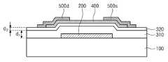
이하, 상기 제1 실시 예 및 변형 예에 따른 고유전율 트랜지스터의 제조방법을 설명함에 있어, 기판(100), 게이트 전극(200), 제1 게이트 절연막(310), 제2 게이트 절연막(320), 활성층(400), 및 소스드레인(500s, 500d)전극이 순차적으로 형성되는 것을 예시하지만, 트랜지스터의 각 구성들의 형성 순서가 이에 한정되는 것은 아니다. 또한, 상기 실시 예에 따른 고유전율 트랜지스터는 Bottom Gate 구조, 및 Top Gate 구조 모두에 적용될 수 있다. 도 1 내지 도 5를 참조하여, 상기 제1 실시 예에 따른 고유전율 트랜지스터의 Bottom Gate 구조가 설명되고, 도 6을 참조하여, 상기 제1 실시 예의 변형 예에 따른 고유전율 트랜지스터의 Top Gate 구조가 설명된다. Hereinafter, in describing a method of manufacturing a high-k transistor according to the first and modified examples, the
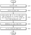
도 1 및 도 2를 참조하면, 기판(100)이 준비된다(S110). 일 실시 예에 따르면, 상기 기판(100)은 실리콘 반도체 기판, 화합물 반도체 기판, 금속 기판, 유리 기판, 또는 플라스틱 기판 등일 수 있다. 상기 기판(100) 상에 게이트 전극(200)이 형성될 수 있다(S120). 예를 들어, 상기 게이트 전극(200)은 P++Si를 포함할 수 있다.1 and 2, a
도 1, 도 3, 및 도 4의 (a)를 참조하면, 상기 게이트 전극(200) 상에 제1 게이트 절연막(310)이 형성될 수 있다(S130). 일 실시 예에 따르면, 상기 제1 게이트 절연막(310)의 형성 단계는, 제1 전구체 제공 단계(S132), 제1 퍼지 단계(S134), 제2 전구체 제공 단계(S136), 및 제2 퍼지 단계(S138)를 포함할 수 있다. 즉, 상기 제1 게이트 절연막(310)은 ALD(Atomic layer deposition) 공정을 통해, 상기 제1 전구체 및 제2 전구체가 반응되어 형성될 수 있다. 이하, 각 단계에 대해 보다 구체적으로 설명된다.1, 3, and 4A, a first
상기 제1 전구체 제공 단계(S132)는, 상기 제1 전구체가 상기 게이트 전극(200)이 형성된 상기 기판(100) 상에 제공될 수 있다. 일 실시 예에 따르면, 상기 제1 전구체는 금속을 포함할 수 있다. 상기 금속은 지르코늄(Zr), 하프늄(Hf), 티타늄(Ti), 스트론튬(Sr), 탄탈럼(Ta), 또는 이트륨(Y) 중 어느 하나를 포함할 수 있다. 예를 들어, 상기 금속이 지르코늄(Zr)을 포함하는 경우, 상기 제1 전구체는 TEMAZ(tetrakis(ethylmethylamino)zirconium)일 수 있다. 일 실시 예에 따르면, 상기 제1 전구체는, 상기 게이트 전극(200)이 형성된 상기 기판(100) 상에 1초의 시간 동안 제공될 수 있다.In the step S132 of providing the first precursor, the first precursor may be provided on the
상기 제1 퍼지 단계(S134)는, 상기 제1 전구체가 제공된 상기 기판(100) 상에 불활성 기체가 제공될 수 있다. 예를 들어, 상기 불활성 기체는 N2 가스일 수 있다. 일 실시 예에 따르면, 상기 제1 퍼지 단계에서, 상기 불활성 기체는 20초의 시간 동안 제공될 수 있다.In the first purge step (S134 ), an inert gas may be provided on the
상기 제2 전구체 제공 단계(S136)는, 상기 제1 퍼지 단계가 수행된 상기 기판(100) 상에 상기 제2 전구체가 제공될 수 있다. 일 실시 예에 따르면, 상기 제2 전구체는 산소를 포함할 수 있다. 예를 들어, 상기 제2 전구체는 O2 plasma, 또는 O3 일 수 있다. 구체적으로, 상기 제2 전구체 제공 단계는, 상기 제1 퍼지 단계가 수행된 상기 기판(100) 상에, 산소(O2)를 4초의 시간 동안 제공한 후, 2초의 시간 동안 plasma를 on 시키는 방법으로 수행될 수 있다.In the step of providing the second precursor (S136 ), the second precursor may be provided on the
상기 제2 퍼지 단계(S138)는, 상기 제2 전구체가 제공된 상기 기판(100) 상에 불활성 기체가 제공될 수 있다. 예를 들어, 상기 불활성 기체는 N2가스일 수 있다. 일 실시 예에 따르면, 상기 제2 퍼지 단계에서, 상기 불활성 기체는 10초의 시간 동안 제공될 수 있다.In the second purge step (S138 ), an inert gas may be provided on the
결과적으로, 상기 제1 게이트 절연막(310)은 금속 산화물을 포함할 수 있다. 예를 들어, 상기 금속 산화물은 ZrO2, HfO2, TiO2, SrOx(x>0), TaOx(x>0), 또는 Y2O3 중 어느 하나를 포함할 수 있다.As a result, the first
일 실시 예에 따르면, 상기 제2 전구체로 O2 plasma가 사용되는 경우, 상기 제1 게이트 절연막(310)은 결정질(crystalline) 구조를 가질 수 있다. 이에 따라, 상기 제1 게이트 절연막(310)은 고유전율(high permittivity) 특성을 나타낼 수 있다. 이와 달리, 상기 제2 전구체로 O3가 사용되어 형성된 상기 제1 게이트 절연막(310)은, 상기 제2 전구체로 O2 plasma가 사용되어 형성된 상기 제1 게이트 절연막(310)과 비교하여, 결정화도가 감소될 수 있다. 이 경우, 상기 제1 게이트 절연막(310)의 유전율 특성이 저하되는 문제점이 발생될 수 있다.According to an embodiment, when O2 plasma is used as the second precursor, the first
다시 말해, 상기 제1 게이트 절연막(310)은, 금속을 포함하는 상기 제1 전구체 및 O2를 포함하는 상기 제2 전구체가 반응되어 형성될 수 있다. 이에 따라, 상기 제1 게이트 절연막(310)은 결정질(crystalline) 구조를 나타내어, 고유전율 특성을 가질 수 있다.In other words, the first
도 1, 도 3, 및 도 4의 (b)를 참조하면, 상기 제1 게이트 절연막(310) 상에 제2 게이트 절연막(320)이 형성될 수 있다(S140). 상기 제1 게이트 절연막(310) 형성 단계 및 상기 제2 게이트 절연막(320) 형성 단계는 in-situ 공정으로 수행될 수 있다. 즉, 상기 제1 및 제2 게이트 절연막(310, 320)은 하나의 챔버(chamber) 내에서 동일한 공정을 통해 순차적으로 형성될 수 있다.Referring to FIGS. 1, 3, and 4B, a second
일 실시 예에 따르면, 상기 제2 게이트 절연막(320)의 형성 단계는, 제3 전구체 제공 단계(S142), 제3 퍼지 단계(S144), 제4 전구체 제공 단계(S146), 및 제4 퍼지 단계(S148)를 포함할 수 있다. 즉, 상기 제2 게이트 절연막(320) 또한 ALD 공정을 통해, 상기 제3 전구체 및 제4 전구체가 반응되어 형성될 수 있다. 이하, 각 단계에 대해 보다 구체적으로 설명된다.According to an embodiment, the forming of the second
상기 제3 전구체 제공 단계(S142)는, 상기 제3 전구체가 상기 제1 게이트 절연막(310)이 형성된 상기 기판(100) 상에 제공될 수 있다. 일 실시 예에 따르면, 상기 제3 전구체는 실리콘(Si)을 포함할 수 있다. 다른 실시 예에 따르면, 상기 제3 전구체는 알루미늄(Al)을 포함할 수 있다. 예를 들어, 상기 제3 전구체는 DIPAS(Di-isopropylamino Silane)일 수 있다. 일 실시 예에 따르면, 상기 제3 전구체는, 상기 제1 게이트 절연막(310)이 형성된 상기 기판(100) 상에 0.2초의 시간 동안 제공될 수 있다.In the providing of the third precursor (S142 ), the third precursor may be provided on the
상기 제3 퍼지 단계(S144)는, 상기 제3 전구체가 제공된 상기 기판(100) 상에 불활성 기체가 제공될 수 있다. 예를 들어, 상기 불활성 기체는 N2 가스일 수 있다. 일 실시 예에 따르면, 상기 제3 퍼지 단계에서, 상기 불활성 기체는 20초의 시간 동안 제공될 수 있다.In the third purge step (S144 ), an inert gas may be provided on the
상기 제4 전구체 제공 단계(S146)는, 상기 제3 퍼지 단계가 수행된 상기 기판(100) 상에 상기 제4 전구체가 제공될 수 있다. 일 실시 예에 따르면, 상기 제4 전구체는 산소를 포함할 수 있다. 예를 들어, 상기 제4 전구체는 O2 plasma, 또는 O3 일 수 있다. 구체적으로, 상기 제4 전구체 제공 단계는, 상기 제1 퍼지 단계가 수행된 상기 기판(100) 상에, 산소(O2)를 4초의 시간 동안 제공한 후, 2초의 시간 동안 plasma를 on 시키는 방법으로 수행될 수 있다.In the step of providing the fourth precursor (S146 ), the fourth precursor may be provided on the
상기 제4 퍼지 단계(S148)는, 상기 제4 전구체가 제공된 상기 기판(100) 상에 불활성 기체가 제공될 수 있다. 예를 들어, 상기 불활성 기체는 N2가스일 수 있다. 일 실시 예에 따르면, 상기 제4 퍼지 단계에서, 상기 불활성 기체는 10초의 시간 동안 제공될 수 있다.In the fourth purge step (S148 ), an inert gas may be provided on the
결과적으로, 상기 제2 게이트 절연막(320)은 실리콘 산화물, 또는 알루미늄 산화물을 포함할 수 있다. 구체적으로, 상기 제3 전구체가 실리콘을 포함하는 경우, 상기 제2 게이트 절연막(320)은 SiO2를 포함할 수 있다. 이와 달리, 상기 제3 전구체가 알루미늄을 포함하는 경우, 상기 제2 게이트 절연막(320)은 Al2O3를 포함할 수 있다.As a result, the second
일 실시 예에 따르면, 상기 제4 전구체로 O3가 사용되는 경우, 상기 제2 게이트 절연막(320)은 비정질(amorphous) 구조를 가질 수 있다. 이에 따라, 상기 제2 게이트 절연막(320)과 인접한, 후술되는 활성층(400)의 일 영역에 형성되는 채널(channel)을 따라 흐르는, 전자의 이동도가 향상될 수 있다. 즉, 비정질 구조의 상기 제2 게이트 절연막(320)은, 높은 밴드갭 및 낮은 표면 거칠기를 가짐에 따라, 상기 채널에서 흐르는 전자의 이동을 방해하는 요소가 감소되어, 전자의 이동도가 향상될 수 있다. 또한, 상기 제2 게이트 절연막(320)의 두께를 제어하여 전자의 이동도를 향상시킬 수 있다. 구체적으로, 상기 제2 게이트 절연막(320)의 두께가 6 nm 이상 10 nm 이하로 제어되는 경우, 전자의 이동도가 향상될 수 있다.According to an embodiment, when O3 is used as the fourth precursor, the second
일 실시 예에 따르면, 상기 제1 게이트 절연막(310) 형성 단계와 상기 제2 게이트 절연막(320) 형성 단계는 서로 다른 온도에서 수행될 수 있다. 구체적으로, 상기 제2 게이트 절연막(320) 형성 단계는, 상기 제1 게이트 절연막(310) 형성 단계보다 낮은 온도에서 수행될 수 있다. 이에 따라, 상기 제1 게이트 절연막(310)은 결정질 특성이 향상되고, 상기 제2 게이트 절연막(320)은 비정질 특성이 향상될 수 있다.According to an embodiment, the forming of the first
또한, 상기 제1 게이트 절연막(310) 형성 단계와 상기 제2 게이트 절연막(320) 형성 단계는 서로 다른 시간 동안 수행될 수 있다. 구체적으로, 상기 제1 게이트 절연막(310) 형성 단계는, 상기 제2 게이트 절연막(320) 형성 단계보다 긴 시간 동안 수행될 수 있다. 다시 말해, 상기 제1 게이트 절연막(310) 형성 단계는, 상기 제1 게이트 절연막(310)이 결정화 되기까지 소요되는 소정의 시간 보다 오랜 시간 수행될 수 있다. 반면, 상기 제2 게이트 절연막(320) 형성 단계는, 상기 제2 게이트 절연막(320)이 결정화 되기까지 소요되는 소정의 시간 보다 짧은 시간 수행될 수 있다. 이에 따라, 상기 제1 게이트 절연막(310)은 결정질 특성이 향상되고, 상기 제2 게이트 절연막(320)은 비정질 특성이 향상될 수 있다.In addition, the step of forming the first
도 1 및 도 5를 참조하면, 상기 제2 게이트 절연막(320) 상에 활성층(active layer, 400)이 형성될 수 있다(S150). 예를 들어, 상기 활성층(400)은 ITZO(Indium-Tin-Zinc oxid)를 포함할 수 있다. 상기 활성층(400)이 형성된 이후, 상기 제2 게이트 절연막(320) 상에 소스 전극(500s), 및 드레인 전극(500d)이 형성될 수 있다(S160). 상기 소스 전극 및 드레인 전극(500s, 500d)은, 상기 제2 게이트 절연막(320) 상에 배치되되, 상기 활성층(400)을 사이에 두고, 서로 이격되어 배치될 수 있다.1 and 5, an
결과적으로, 상기 제1 실시 예에 따른 고유전율 트랜지스터는, 상기 기판(100), 상기 게이트 전극(200), 상기 제1 게이트 절연막(310), 상기 제2 게이트 절연막(320), 및 상기 활성층(400)이 순차적으로 적층되고, 상기 활성층(400)을 사이에 두고 상기 소스 전극(500s), 및 드레인 전극(500d)이 서로 이격되어 배치된 Bottom Gate 구조를 가질 수 있다.As a result, the high-k transistor according to the first embodiment includes the
즉, 상기 제1 실시 예에 따른 고유전율 트랜지스터는, 결정질의 상기 제1 게이트 절연막(310), 및 비정질의 상기 제2 게이트 절연막(320)을 포함하고, 비정질의 상기 제2 게이트 절연막(320)이 상기 활성층(400)과 접촉될 수 있다. 이에 따라, 고유전율 특성뿐만 아니라 활성층(400)의 채널(channel)을 따라 흐르는 전자의 이동도 또한 향상될 수 있다.That is, the high-k transistor according to the first embodiment includes the crystalline first
이와 달리, 단일의 ZrO2 고유전율 게이트 절연막이 사용된 기존의 트랜지스터의 경우, 게이트 절연막의 표면 거칠기가 높아, 게이트 절연막과 인접한 활성층 내의 채널을 따라 흐르는 전자의 이동도가 저하되는 문제점이 발생할 수 있다. 즉, 단일의 ZrO2 고유전율 게이트 절연막의 경우, 결정화에 따른 grain boundary가 leakage path로 작용하여 게이트 절연막과 활성층 사이에 발생하는 누설전류가 증가할 수 있다. 이에 따라, 채널에 컬럼브 산란이 발생되어 전자의 이동도가 저하되는 문제점이 발생할 수 있다. 또한, 표면 거칠기를 낮춰 전자의 이동도를 향상시킨 단일의 SiO2 게이트 절연막이 사용된 기존의 트랜지스터의 경우, 유전율이 낮은 문제점이 발생할 수 있다.In contrast, in the case of a conventional transistor in which a single ZrO2 high dielectric constant gate insulating layer is used, the surface roughness of the gate insulating layer is high, and thus the mobility of electrons flowing along the channel in the active layer adjacent to the gate insulating layer may decrease. . That is, in the case of a single ZrO2 high dielectric constant gate insulating layer, a grain boundary caused by crystallization may act as a leakage path, and thus a leakage current generated between the gate insulating layer and the active layer may increase. Accordingly, there may be a problem in that the mobility of electrons decreases due to the occurrence of columnar scattering in the channel. In addition, in the case of a conventional transistor in which a single SiO2 gate insulating film having improved electron mobility by lowering surface roughness is used, a problem of low dielectric constant may occur.
본 발명의 제1 실시 예에 따른 고유전율 트랜지스터의 제조방법은, 상기 게이트 전극(200), 및 상기 활성층(400) 사이에 게이트 절연막을 형성하는 단계를 포함하되, 상기 게이트 절연막을 형성하는 단계는, 금속을 포함하는 상기 제1 전구체 및 산소를 포함하는 제2 전구체를 제공하여, 상기 제1 및 제2 전구체가 반응된 결정질(crystalline)의 상기 제1 게이트 절연막(310)을 형성하는 단계, 및 실리콘을 포함하는 상기 제3 전구체 및 산소를 포함하되 상기 제2 전구체와 다른 제4 전구체를 제공하여, 상기 제3 및 제4 전구체가 반응된 비정질(amorphous)의 상기 제2 게이트 절연막(320)을 형성하는 단계를 포함할 수 있다. 또한, 상기 제1 게이트 절연막(310) 형성 단계, 및 상기 제2 게이트 절연막(320) 형성 단계는 in-situ 공정으로 수행되는 것을 포함할 수 있다. 이에 따라, 고유전율 특성뿐만 아니라, 전자의 이동도 또한 향상된 트랜지스터의 제조방법이 제공될 수 있다.The method of manufacturing a high-k transistor according to the first embodiment of the present invention includes forming a gate insulating layer between the
또한, 상기 제1 및 제2 게이트 절연막(310, 320)이 ALD 공정을 통해 in-situ 방식으로 형성됨에 따라, 상기 제1 및 제2 게이트 절연막(310, 320)의 두께가 용이하게 제어될 수 있다. 상기 제2 게이트 절연막(320)의 두께가 제어되는 경우, 상술된 바와 같이, 상기 채널을 따라 흐르는 전자의 이동도가 향상될 수 있다. 결과적으로, 상기 제2 게이트 절연막(320)의 두께를 제어하는 간단한 방법으로, 전기적 특성이 향상된 트랜지스터가 제조될 수 있다.In addition, as the first and second
이상, 도 1 내지 도 5를 참조하여 Bottom Gate 구조의 상기 제1 실시 예에 따른 고유전율 트랜지스터 및 그 제조방법이 설명되었다. 이하, 도 6을 참조하여 Top Gate 구조의 상기 제1 실시 예의 변형 예에 따른 고유전율 트랜지스터가 설명된다.In the above, the high-k transistor according to the first embodiment of the bottom gate structure and a method of manufacturing the same have been described with reference to FIGS. Hereinafter, a high-k transistor according to a modified example of the first embodiment of the top gate structure will be described with reference to FIG. 6.
도 6을 참조하면, 상기 제1 실시 예의 변형 예에 따른 고유전율 트랜지스터는, 기판(100), 상기 기판(100) 상에 배치되는 활성층(400), 상기 기판(100) 상에 배치되되, 상기 활성층(400)을 사이에 두고 서로 이격되어 배치되는 소스 전극(500s), 및 드레인 전극(500d), 상기 기판(100), 상기 활성층(400), 상기 소스 전극(500s), 및 상기 드레인 전극(500d)을 덮고 실리콘 산화물을 포함하는 비정질의 제2 게이트 절연막(320), 상기 제2 게이트 절연막(320) 상에 배치되고 금속 산화물을 포함하는 결정질의 제1 게이트 절연막(310), 및 상기 제1 게이트 절연막(310) 상에 배치되는 게이트 전극(200)을 포함할 수 있다. 이와 달리, 제조 방법에 따라, 상기 제1 실시 예의 변형 예에 따른 고유전율 트랜지스터는 다양한 배치 구조를 가질 수 있다. 상기 제1 실시 예의 변형 예에 따른 고유전율 트랜지스터가 포함하는 각 구성의 배치 구조는 제한되지 않는다.Referring to FIG. 6, a high-k transistor according to a modified example of the first embodiment includes a
다만, 상기 제1 실시 예의 변형 예에 따른 고유전율 트랜지스터 역시, 상기 제1 실시 예에 따른 고유전율 트랜지스터와 같이, 상기 제2 게이트 절연막(320)이 상기 제1 게이트 절연막(310) 및 상기 활성층(400) 사이에 배치될 수 있다. 이에 따라, 고유전율 특성뿐만 아니라, 게이트 절연막과 인접한 활성층의 일 영역에 형성되는 채널(channel)을 따라 흐르는 전자의 이동도 또한 향상될 수 있다.However, in the high-k transistor according to the modified example of the first embodiment, like the high-k transistor according to the first embodiment, the second
이상, 도 1 내지 도 6을 참조하여 본 발명의 제1 실시 예에 따른 고유전율 트랜지스터가 설명되었다. 이하, 단일층의 게이트 절연막을 포함하는 본 발명의 제2 실시 예에 따른 고유전율 트랜지스터가 도 7 내지 도 9를 참조하여 설명된다.In the above, the high-k transistor according to the first embodiment of the present invention has been described with reference to FIGS. 1 to 6. Hereinafter, a high-k transistor according to a second embodiment of the present invention including a single-layered gate insulating layer will be described with reference to FIGS. 7 to 9.
도 7은 본 발명의 제2 실시 예에 따른 고유전율 트랜지스터의 제조방법을 설명하는 순서도이고, 도 8은 본 발명의 제2 실시 예에 따른 고유전율 트랜지스터를 나타내는 도면이고, 도 9는 본 발명의 제2 실시 예의 변형 예에 따른 고유전율 트랜지스터를 나타내는 도면이다.7 is a flowchart illustrating a method of manufacturing a high-k transistor according to a second embodiment of the present invention, FIG. 8 is a diagram showing a high-k transistor according to a second embodiment of the present invention, and FIG. A diagram showing a high-k transistor according to a modified example of the second embodiment.
이하, 상기 제2 실시 예에 및 변형 예에 따른 고유전율 트랜지스터의 제조방법을 설명함에 있어, 기판(100), 게이트 전극(200), 게이트 절연막(300), 활성층(400), 및 소스드레인(500s, 500d)전극이 순차적으로 형성되는 것을 예시하지만, 트랜지스터의 각 구성들의 형성 순서가 이에 한정되는 것은 아니다. 또한, 상기 실시 예에 따른 고유전율 트랜지스터는 Bottom Gate 구조, 및 Top Gate 구조 모두에 적용될 수 있다. 도 7 및 도 8을 참조하여, 상기 제2 실시 예에 따른 고유전율 트랜지스터의 Bottom Gate 구조가 설명되고, 도 9를 참조하여, 상기 제2 실시 예의 변형 예에 따른 고유전율 트랜지스터의 Top Gate 구조가 설명된다.Hereinafter, in describing a method of manufacturing a high-k transistor according to the second and modified examples, the
도 7 및 도 8을 참조하면, 기판(100)이 준비된다(S210). 일 실시 예에 따르면, 상기 기판(100)은 실리콘 반도체 기판, 화합물 반도체 기판, 금속 기판, 유리 기판, 또는 플라스틱 기판 등일 수 있다. 상기 기판(100) 상에 게이트 전극(200)이 형성될 수 있다(S220). 예를 들어, 상기 게이트 전극(200)은 P++Si를 포함할 수 있다.7 and 8, a
상기 게이트 전극(200)이 형성된 상기 기판(100) 상에, 상기 게이트 절연막(300)이 형성될 수 있다(S230). 일 실시 예에 따르면, 상기 게이트 절연막(300)의 형성 단계는, 제1 전구체 제공 단계, 제1 퍼지 단계, 제2 전구체 제공 단계, 및 제2 퍼지 단계를 포함할 수 있다. 즉, 상기 게이트 절연막(300)은 ALD(Atomic layer deposition) 공정을 통해, 상기 제1 및 제2 전구체가 반응되어 형성될 수 있다. 이하, 각 단계에 대해 보다 구체적으로 설명된다.The
상기 제1 전구체 제공 단계는, 상기 제1 전구체가 상기 게이트 전극(200)이 형성된 상기 기판(100) 상에 제공될 수 있다. 일 실시 예에 따르면, 상기 제1 전구체는 금속을 포함할 수 있다. 상기 금속은 지르코늄(Zr), 하프늄(Hf), 티타늄(Ti), 스트론튬(Sr), 탄탈럼(Ta), 또는 이트륨(Y) 중 어느 하나를 포함할 수 있다. 예를 들어, 상기 금속이 지르코늄(Zr)을 포함하는 경우, 상기 제1 전구체는 TEMAZ(tetrakis(ethylmethylamino)zirconium)일 수 있다. 일 실시 예에 따르면, 상기 제1 전구체는, 상기 게이트 전극(200)이 형성된 상기 기판(100) 상에 1초의 시간 동안 제공될 수 있다.In the providing of the first precursor, the first precursor may be provided on the
상기 제1 퍼지 단계는, 상기 제1 전구체가 제공된 상기 기판(100) 상에 불활성 기체가 제공될 수 있다. 예를 들어, 상기 불활성 기체는 N2 가스일 수 있다. 일 실시 예에 따르면, 상기 제1 퍼지 단계에서, 상기 불활성 기체는 20초의 시간 동안 제공될 수 있다.In the first purge step, an inert gas may be provided on the
상기 제2 전구체 제공 단계는, 상기 제1 퍼지 단계가 수행된 상기 기판(100) 상에 상기 제2 전구체가 제공될 수 있다. 일 실시 예에 따르면, 상기 제2 전구체는 산소를 포함할 수 있다. 예를 들어, 상기 제2 전구체는 O2 plasma, 또는 O3 일 수 있다. 구체적으로, 상기 제2 전구체 제공 단계는, 상기 제1 퍼지 단계가 수행된 상기 기판(100) 상에, 산소(O2)를 4초의 시간 동안 제공한 후, 2초의 시간 동안 plasma를 on 시키는 방법으로 수행될 수 있다.In the providing of the second precursor, the second precursor may be provided on the
상기 제2 퍼지 단계는, 상기 제2 전구체가 제공된 상기 기판(100) 상에 불활성 기체가 제공될 수 있다. 예를 들어, 상기 불활성 기체는 N2가스일 수 있다. 일 실시 예에 따르면, 상기 제2 퍼지 단계에서, 상기 불활성 기체는 10초의 시간 동안 제공될 수 있다.In the second purge step, an inert gas may be provided on the
결과적으로, 상기 게이트 절연막(300)은 금속 산화물을 포함할 수 있다. 예를 들어, 상기 금속 산화물은 ZrO2, HfO2, TiO2, SrOx(x>0), TaOx(x>0), 또는 Y2O3 중 어느 하나를 포함할 수 있다.As a result, the
상기 게이트 절연막(300) 상에 활성층(active layer, 400)이 형성될 수 있다(S240). 예를 들어, 상기 활성층(400)은 ITZO(Indium-Tin-Zinc oxid)를 포함할 수 있다. 상기 활성층(400)이 형성된 이후, 상기 제2 게이트 절연막(320) 상에 소스 전극(500s), 및 드레인 전극(500d)이 형성될 수 있다(S250). 상기 소스 전극 및 드레인 전극(500s, 500d)은, 상기 제2 게이트 절연막(320) 상에 배치되되, 상기 활성층(400)을 사이에 두고, 서로 이격되어 배치될 수 있다.An
일 실시 예에 따르면, 상기 제2 실시 예에 따른 고유전율 트랜지스터의 제조방법은, 상기 게이트 절연막(300) 형성 단계의 수행 온도를 제어하여, 상기 게이트 절연막(300)과 인접한, 상기 활성층(400) 내의 일 영역에 형성되는 채널(channel)을 따라 흐르는 전자의 이동도를 향상시킬 수 있다. 즉, 상기 제1 전구체 및 제2 전구체를 제공하는 온도의 범위를 제어하여, 상기 활성층(400) 내의 전자의 이동도를 향상시킬 수 있다.According to an embodiment, in the method of manufacturing the high-k transistor according to the second embodiment, the
구체적으로, 상기 게이트 절연막(300) 형성 단계의 수행 온도가 250℃ 초과 300℃ 미만으로 제어되는 경우, 상기 게이트 절연막(300)은 메조-크리스탈(meso-crystalline) 구조를 가질 수 있다. 본 명세서에서 '메조-크리스탈'이란 용어는, 결정질(crystalline)의 결정화도 보다 낮고 비정질(amorphous)의 결정화도 보다 높은 것을 의미할 수 있다. 또한, '메조-크리스탈'이란 용어는, XRD(X-ray diffraction) 상에서 broad한 peak를 갖는 것을 의미할 수 있다.Specifically, when the performing temperature of the forming step of the
상기 게이트 절연막(300)이 메조-크리스탈 구조를 갖는 경우, 상기 활성층(400)내의 채널과 상기 게이트 절연막(300) 사이에 발생하는 누설전류가 감소되어, 채널을 따라 흐르는 전자의 이동도가 향상될 수 있다.When the
이와 달리, 상기 게이트 절연막(300)이 결정화(crystalline) 구조를 갖는 경우, 결정상에서의 grain boundary가 leakage path로 작용할 수 있다. 이에 따라, 상기 성층(400) 내의 채널과 상기 게이트 절연막(300) 사이에 발생하는 누설전류가 증가하여, 채널을 따라 흐르는 전자의 이동도가 감소될 수 있다. 반면, 상기 게이트 절연막(300)이 비정질(amorphous) 구조를 갖는 경우, 상기 게이트 절연막(300)의 유전율이 저하되는 문제점이 발생될 수 있다.In contrast, when the
즉, 본 발명의 제2 실시 예에 따른 고유전율 트랜지스터의 제조방법은 금속을 포함하는 상기 제1 전구체, 및 산소를 포함하는 상기 제2 전구체를 제1 온도 범위에서 제공하여, 메조-크리스탈(meso-crystalline) 구조를 갖는 상기 게이트 절연막(300)을 형성하는 단계를 포함하되, 상기 게이트 절연막(300)은 상기 게이트 전극(200) 및 상기 활성층(400) 사이에 형성되는 것을 포함할 수 있다. 이에 따라, 고유전율 특성뿐만 아니라, 전자의 이동도 또한 향상된 트랜지스터의 제조방법이 제공될 수 있다.That is, the method of manufacturing a high-k transistor according to the second embodiment of the present invention provides the first precursor containing a metal and the second precursor containing oxygen in a first temperature range, thereby providing a meso-crystal (meso-crystal). Forming the
도 9를 참조하면, 상기 제2 실시 예의 변형 예에 따른 고유전율 트랜지스터는, 기판(100), 상기 기판(100) 상에 배치되는 활성층(400), 상기 기판(100) 상에 배치되되, 상기 활성층(400)을 사이에 두고 서로 이격되어 배치되는 소스 전극(500s), 및 드레인 전극(500d), 상기 기판(100), 상기 활성층(400), 상기 소스 전극(500s), 및 상기 드레인 전극(500d)을 덮고 실리콘 산화물을 포함하며 메조-크리스탈(meso-crystalline) 구조를 갖는 게이트 절연막(300), 및 상기 게이트 절연막(300) 상에 배치되는 게이트 전극(200)을 포함할 수 있다. 이와 달리, 제조 방법에 따라, 상기 제2 실시 예의 변형 예에 따른 고유전율 트랜지스터는 다양한 배치 구조를 가질 수 있다. 상기 제2 실시 예의 변현 예에 따른 고유전율 트랜지스터가 포함하는 각 구성의 배치 구조는 제한되지 않는다.Referring to FIG. 9, the high-k transistor according to the modified example of the second embodiment includes a
이상, 본 발명의 제2 실시 예에 따른 고유전율 트랜지스터의 제조방법이 설명되었다. 이하, 본 발명의 제1 및 제2 실시 예에 따른 고유전율 트랜지스터 및 그 제조방법의 구체적인 실험 예 및 특성 평가 결과가 설명된다.In the above, a method of manufacturing a high-k transistor according to the second embodiment of the present invention has been described. Hereinafter, specific experimental examples and characteristic evaluation results of the high-k transistor and manufacturing method according to the first and second embodiments of the present invention are described.
실시 예 1에 따른According to Example 1고유전율High dielectric constant 트랜지스터의 제조 Fabrication of transistors
P++Si 게이트 전극이 형성된 기판이 준비된다. 상기 게이트 전극이 형성된 기판 상에 TEMAZ를 1초 동안 제공한 후 N2 불활성 가스를 20초 동안 제공하여 퍼지(purge)하고, O2 를 4초 동안 제공한 후 2초 동안 plasma를 on 시켰다. 이후, N2 불활성 가스를 10초 동안 제공하여 다시 퍼지(purge)하여, 게이트 전극이 형성된 기판 상에 ZrO2 절연막을 형성시켰다.A substrate on which a P++ Si gate electrode is formed is prepared. After providing TEMAZ on the substrate on which the gate electrode was formed for 1 second, N2 inert gas was supplied for 20 seconds to purge, and O2 was provided for 4 seconds, and then plasma was turned on for 2 seconds. Thereafter, N2 inert gas was supplied for 10 seconds to purge again, thereby forming a ZrO2 insulating film on the substrate on which the gate electrode was formed.
이후, ZrO2 절연막이 형성된 기판 상에 DIPAS를 0.2초 동안 제공한 후 N2 불활성 가스를 20초 동안 제공하여 퍼지(purge)하고, O3를 제공한 후 N2 불활성 가스를 10초 동안 제공하여, ZrO2 절연막 상에 SiO2 절연막을 형성시켰다. 계속해서, SiO2 절연막 상에 ITZO(Indium-Tin-Zinc oxid) 활성층 및 소스드레인 전극을 형성시켜, 상기 실시 예 1에 따른 고유전율 트랜지스터를 제조하였다.Thereafter, DIPAS was provided on the substrate on which the ZrO2 insulating film was formed for 0.2 seconds, and then N2 inert gas was provided for 20 seconds to purge, and after O3 was provided, N2 inert gas was provided for 10 seconds. , A SiO2 insulating film was formed on the ZrO2 insulating film. Subsequently, an Indium-Tin-Zinc Oxid (ITZO) active layer and a source drain electrode were formed on the SiO2 insulating layer, thereby manufacturing a high-k transistor according to the first embodiment.
또한, 상기 실시 예 1에 따른 고유전율 트랜지스터의 제조 과정에서, SiO2 절연막의 두께를 2 nm, 4 nm, 6 nm, 8 nm, 10 nm, 및 20 nm로 제어하여 각각, 실시 예 1-1, 1-2, 1-3, 1-4, 1-5, 및 1-6에 따른 고유전율 트랜지스터를 제조하였다.In addition, in the manufacturing process of the high-k transistor according to Example 1, the thickness of the SiO2 insulating film was controlled to 2 nm, 4 nm, 6 nm, 8 nm, 10 nm, and 20 nm, respectively, in Example 1-1. High-k transistors according to, 1-2, 1-3, 1-4, 1-5, and 1-6 were manufactured.
비교 예 1에 따른 트랜지스터 준비Preparing the transistor according to Comparative Example 1
상기 실시 예 1에 따른 트랜지스터와 같되, 게이트 절연막으로 ZrO2 단층이 적용된 비교 예 1에 따른 트랜지스터가 준비된다.The same as the transistor according to the first embodiment, but the transistor according to Comparative Example 1 to which a single layer of ZrO2 is applied as a gate insulating layer is prepared.
비교 예 2에 따른 트랜지스터 준비Transistor preparation according to Comparative Example 2
상기 실시 예 1에 따른 트랜지스터와 같되, 게이트 절연막으로 SiO2 단층이 적용된 비교 예 2에 따른 트랜지스터가 준비된다.The same as the transistor according to the first embodiment, but a transistor according to Comparative Example 2 in which a single layer of SiO2 is applied as a gate insulating layer is prepared.
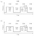
도 10은 본 발명의 비교 예 1 및 2에 따른 트랜지스터가 포함하는 게이트 절연막의 표면 특성을 나타내는 도면이다.10 is a diagram showing surface characteristics of a gate insulating film included in a transistor according to Comparative Examples 1 and 2 of the present invention.
도 10을 참조하면, 상기 비교 예 1 및 비교 예 2에 따른 트랜지스터가 포함하는 ZrO2 게이트 절연막 및 SiO2 게이트 절연막의 AFM(Atomic force microscopy) morphology를 각각 도 10의 (b) 및 도 10의 (a)에 나타내었다. 도 10의 (a) 및 (b)에서 확인할 수 있듯이, SiO2 게이트 절연막의 경우, 낮은 표면 거칠기를 갖는 반면, ZrO2 게이트 절연막의 경우, 높은 표면 거칠기를 갖는 것을 확인할 수 있었다.Referring to FIG. 10, the atomic force microscopy (AFM) morphology of the ZrO2 gate insulating layer and the SiO2 gate insulating layer included in the transistors according to Comparative Example 1 and Comparative Example 2 are respectively described in FIGS. 10B and 10 It is shown in a). As can be seen in FIGS. 10A and 10B, it was confirmed that the SiO2 gate insulating film had a low surface roughness, whereas the ZrO2 gate insulating film had a high surface roughness.
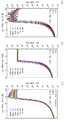
도 11 내지 도 13은 본 발명의 실시 예 1 및 비교 예들에 따른 트랜지스터의 전기적 특성을 나타내는 도면이다.11 to 13 are diagrams showing electrical characteristics of transistors according to Example 1 and Comparative Examples of the present invention.
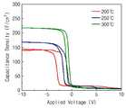
도 11을 참조하면, 상기 실시 예 1-1 내지 실시 예 1-6(ZS2, ZS4, ZS6, ZS8, ZS10, ZS20), 비교 예1(ZrO2), 및 비교 예 2(SiO2)에 따른 트랜지스터의 Applied Voltage(V)에 따른 Capacitance Density(F/cm2)를 측정하여 나타내었다. 도 11에서 확인할 수 있듯이, 상기 비교 예 1, 실시 예 1-1, 실시 예 1-2에 따른 트랜지스터는 Capacitance Density의 변화 폭이 다소 크게 나타나는 반면, 상기 비교 예 2에 따른 트랜지스터는 Capacitance Density의 변화가 실질적으로 발생하지 않는 것을 확인할 수 있었다.Referring to FIG. 11, according to Examples 1-1 to 1-6 (ZS2, ZS4, ZS6, ZS8, ZS10, ZS20), Comparative Example 1 (ZrO2 ), and Comparative Example 2 (SiO2 ). It was shown by measuring the capacitance density (F/cm2 ) according to the applied voltage (V) of the transistor. As can be seen in FIG. 11, the transistors according to Comparative Example 1, Example 1-1, and Example 1-2 showed a slightly larger variation in capacitance density, whereas the transistor according to Comparative Example 2 showed a change in capacitance density. It could be confirmed that is not substantially occurring.
도 12를 참조하면, 상기 실시 예 1-1 내지 실시 예 1-6(2n, 4nm, 6nm, 8nm, 10nm, 20nm), 비교 예1(ZrO2), 및 비교 예 2(SiO2)에 따른 트랜지스터의 Electric Field(MV/cm)에 따른 Current Density(A/cm2)를 측정하여 나타내었다. 도 12에서 확인할 수 있듯이, 상기 비교 예 1, 실시 예 1-1, 실시 예 1-2에 따른 트랜지스터는 Current Density의 변화 폭이 다소 크게 나타나는 반면, 상기 비교 예 2에 따른 트랜지스터는 Current Density의 변화가 실질적으로 발생하지 않는 것을 확인할 수 있었다.12, according to Examples 1-1 to 1-6 (2n, 4nm, 6nm, 8nm, 10nm, 20nm), Comparative Example 1 (ZrO2 ), and Comparative Example 2 (SiO2 ) The current density (A/cm2 ) according to the electric field (MV/cm) of the transistor was measured and shown. As can be seen in FIG. 12, the transistors according to Comparative Example 1, Example 1-1, and Example 1-2 showed a slightly larger change in current density, whereas the transistor according to Comparative Example 2 showed a change in current density. It could be confirmed that is not substantially occurring.
도 11 및 도 12를 통해 확인할 수 있듯이, SiO2 단일 박막이 게이트 절연막으로 사용된 비교 예 2에 따른 트랜지스터는 낮은 유전률을 갖는다는 것을 알 수 있다. 반면, ZrO2 단일 박막이 게이트 절연막으로 사용된 비교 예 1에 따른 트랜지스터 및, ZrO2-SiO2 적층 박막이 게이트 절연막으로 사용된 실시 예 1에 따른 트랜지스터의 경우, 높은 유전율을 갖는 것을 갖는다는 것을 알 수 있다.As can be seen through FIGS. 11 and 12, it can be seen that the transistor according to Comparative Example 2 in which a single SiO2 thin film is used as the gate insulating film has a low dielectric constant. On the other hand, in the case of the transistor according to Comparative Example 1 in which a single ZrO2 thin film is used as the gate insulating film, and the transistor according to Example 1 in which the ZrO2 -SiO2 stacked thin film is used as the gate insulating film, it has a high dielectric constant. Able to know.
도 13을 참조하면, 상기 실시 예 1-1 내지 실시 예 1-6(ZS2, ZS4, ZS6, ZS8, ZS10, ZS20), 비교 예1(ZrO2), 및 비교 예 2(SiO2)에 따른 트랜지스터의 유전율(Dielectric Constant), 및 게이트 절연막과 활성층 사이에서의 누설전류(Ileakage at 1 MV/cm)를 측정하여 나타내었다.13, according to Examples 1-1 to 1-6 (ZS2, ZS4, ZS6, ZS8, ZS10, ZS20), Comparative Example 1 (ZrO2 ), and Comparative Example 2 (SiO2 ) The dielectric constant of the transistor and the leakage current between the gate insulating layer and the active layer (Ileakage at 1 MV/cm) were measured and shown.
도 13에서 확인할 수 있듯이, SiO2 단일 박막이 게이트 절연막으로 사용된 비교 예 2에 따른 트랜지스터는 낮은 유전률을 갖는 반면, ZrO2 단일 박막이 게이트 절연막으로 사용된 비교 예 1에 따른 트랜지스터, 및 ZrO2-SiO2 적층 박막이 게이트 절연막으로 사용된 실시 예 1에 따른 트랜지스터는 높은 유전율을 갖는 것을 확인할 수 있었다.As can be seen in FIG. 13, the transistor according to Comparative Example 2 in which a single SiO2 thin film is used as the gate insulating film has a low dielectric constant, whereas the transistor according to Comparative Example 1 in which a single ZrO2 thin film is used as the gate insulating film, and ZrO2 It was confirmed that the transistor according to Example 1 in which the -SiO2 laminated thin film was used as the gate insulating film had a high dielectric constant.
한편, 상기 비교 예 1에 따른 트랜지스터, 및 실시 예 1-1, 및 실시 예 1-2에 따른 트랜지스터의 경우, 유전율이 높게 나타나지만, 누설전류 또한 높게 나타나는 것을 확인할 수 있었다. 이에 따라, 상기 실시 예에 따른 고유전율 트랜지스터를 제조하는 경우, ZrO2-SiO2 적층 게이트 절연막에서, SiO2의 두께를 6 nm 이상으로 제조해야 하는 것을 알 수 있다.Meanwhile, in the case of the transistor according to Comparative Example 1, and the transistors according to Example 1-1 and Example 1-2, it was confirmed that the dielectric constant was high, but the leakage current was also high. Accordingly, in the case of manufacturing the high-k transistor according to the above embodiment, it can be seen that in the ZrO2 -SiO2 stacked gate insulating layer, the thickness of SiO2 should be manufactured to be 6 nm or more.
도 14 및 도 15는 본 발명의 본 발명의 실시 예 1 및 비교 예들에 따른 트랜지스터의 구동 특성을 나타내는 도면이다.14 and 15 are diagrams showing driving characteristics of a transistor according to Example 1 and Comparative Examples of the present invention.
도 14를 참조하면, 상기 비교 예 1(ZrO2)에 따른 트랜지스터, 및 상기 실시 예 1-1 내지 1-3(ZS2, ZS4, ZS6)에 따른 트랜지스터의 Gate Voltage(V)에 따른 Current(A)를 측정하여 도 14의 (a) 내지 (d)에 각각 나타내었고, 도 15를 참조하면, 상기 실시 예 1-4 내지 1-6(ZS8, ZS10, ZS20), 및 비교 예 2(SiO2)에 따른 트랜지스터의 Gate Voltage(V)에 따른 Current(A)를 측정하여 도 15의 (a) 내지 (d)에 각각 나타내었다.Referring to FIG. 14, a current (A) according to a gate voltage (V) of a transistor according to Comparative Example 1 (ZrO2 ) and a transistor according to Examples 1-1 to 1-3 (ZS2, ZS4, ZS6). ) Was measured and shown in FIGS. 14A to 14D, respectively, and referring to FIG. 15, Examples 1-4 to 1-6 (ZS8, ZS10, ZS20), and Comparative Example 2 (SiO2 The current (A) according to the gate voltage (V) of the transistor according to) is measured and shown in FIGS. 15A to 15D, respectively.
도 14의 (a), (b), (c), 및 도 15의 (c), (d)에서 확인할 수 있듯이, 상기 실시 예 1-1, 1-2, 1-6, 및 비교 예 1, 비교 예 2에 따른 트랜지스터의 경우, 소자의 구동에 제대로 이루어지지 않는 것을 확인할 수 있었다. 반면, 도 14의 (d), 및 도 15의 (a), (b)에서 확인할 수 있듯이, 상기 실시 예 1-3, 1-4, 1-5에 따른 트랜지스터의 경우, 확연한 트랜스퍼 커브가 나타나고 있어, 소자의 구동이 용이하게 이루어 졌음을 확인할 수 있었다.As can be seen in Figures 14 (a), (b), (c), and Figure 15 (c), (d), Examples 1-1, 1-2, 1-6, and Comparative Example 1 , In the case of the transistor according to Comparative Example 2, it was confirmed that the device was not properly driven. On the other hand, as can be seen in (d) of FIG. 14 and (a) and (b) of FIG. 15, in the case of the transistors according to Examples 1-3, 1-4, and 1-5, a distinct transfer curve appears. As a result, it was confirmed that the device was easily driven.
도 16 및 도 17은 본 발명의 본 발명의 실시 예 1 및 비교 예들에 따른 트랜지스터의 신뢰성을 나타내는 도면이다.16 and 17 are diagrams showing the reliability of a transistor according to Example 1 and Comparative Examples of the present invention.
도 16의 (a) 내지 (c)를 참조하면, 상기 비교 예 1(ZrO2), 비교 예 2(SiO2), 및 실시 예 1-6(ZS 20nm)에 따른 트랜지스터를 Vg=10V 및 T=60℃의 조건에서 1 시간 동안 구동시키고, Gate Voltage(V)에 따른 Current(A)를 나타내어 PBTS(Positive Bias Temperature Stress) 신뢰성을 비교하였다. 도 17의 (a) 내지 (c)를 참조하면, 상기 실시 예 1-3(ZS 6nm), 실시 예 1-4(ZS 8nm), 및 실시 예 1-5(ZS10 nm)에 따른 트랜지스터를 Vg=10V 및 T=60℃의 조건에서 1 시간 동안 구동시키고, Gate Voltage(V)에 따른 Current(A)를 나타내어 PBTS(Positive Bias Temperature Stress) 신뢰성을 비교하였다.Referring to FIGS. 16A to 16C, the transistors according to Comparative Example 1 (ZrO2 ), Comparative Example 2 (SiO2 ), and Examples 1-6 (ZS 20nm) were Vg =10V and It was driven for 1 hour under the condition of T=60°C, and the current (A) according to the gate voltage (V) was displayed to compare the reliability of PBTS (Positive Bias Temperature Stress). Referring to FIGS. 17A to 17C, the transistors according to Examples 1-3 (ZS 6nm), Examples 1-4 (ZS 8nm), and Examples 1-5 (ZS10 nm) are VIt was driven for 1 hour under the conditions ofg =10V and T=60℃, and the current (A) according to the gate voltage (V) was displayed to compare the reliability of PBTS (Positive Bias Temperature Stress).
도 16 및 도 17에서 확인할 수 있듯이, 상기 비교 예 1(ZrO2), 비교 예 2(SiO2), 및 실시 예 1-6(ZS 20nm)에 따른 트랜지스터의 경우 낮은 신뢰성을 나타내는 반면, 상기 실시 예 1-3(ZS 6nm), 실시 예 1-4(ZS 8nm), 및 실시 예 1-5(ZS10 nm)에 따른 트랜지스터는 우수한 신뢰성을 나타내는 것을 확인할 수 있었다.As can be seen in FIGS. 16 and 17, the transistors according to Comparative Example 1 (ZrO2 ), Comparative Example 2 (SiO2 ), and Examples 1-6 (
도 18 및 도 19는 본 발명의 비교 예 1에 따른 게이트 절연막의 제조공정에 사용되는 소스에 따른 특성을 비교하는 그래프이다.18 and 19 are graphs for comparing characteristics according to sources used in a manufacturing process of a gate insulating layer according to Comparative Example 1 of the present invention.
도 18 및 도 19를 참조하면, 산소(O2) 플라즈마를 사용하여 ZrO2 게이트 절연막이 제조된 트랜지스터, 및 오존(O3)을 사용하여 ZrO2 게이트 절연막이 제조된 트랜지스터 각각에 대해 XRD(X-ray diffraction) 패턴을 분석하여 나타내었다. 도 18 및 도 19에서 확인할 수 있듯이, 산소(O2) 플라즈마를 사용하여 제조된 ZrO2 게이트 절연막의 경우 다수의 피크(peak)가 나타나는 것으로 보아 결정성이 높은 것을 확인할 수 있고, 오존(O3)을 사용하여 제조된 ZrO2 게이트 절연막의 경우 하나의 피크(peak)가 나타나는 것으로 보아 결정성이 낮은 것을 확인할 수 있었다. 즉, 상기 실시 예에 따른 고유전율 트랜지스터를 제조하는 경우, 결정질의 ZrO2 게이트 절연막을 제조하기 위해, ALD 공정 중 산소(O2) 플라즈마를 사용해야 하는 것을 알 수 있다.When Figs. 18 and 19, oxygen (O2) of using a plasma ZrO2 gate insulating film is produced transistor, and ozone (O3) for use in ZrO2 gate insulating film XRD (X for the manufacture transistors, respectively -ray diffraction) pattern was analyzed and shown. As can be seen in FIGS. 18 and 19, in the case of the ZrO2 gate insulating film manufactured using oxygen (O2 ) plasma, it can be confirmed that crystallinity is high as a number of peaks appear, and ozone (O3) In the case of the ZrO2 gate insulating film manufactured using ), it was confirmed that crystallinity was low as one peak appeared. That is, when manufacturing the high-k transistor according to the above embodiment, it can be seen that oxygen (O2 ) plasma must be used during the ALD process in order to manufacture a crystalline ZrO2 gate insulating layer.
도 10 내지 도 19를 통해 알 수 있듯이, 전기적 특성이 향상되고 높은 신뢰성을 갖는 트랜지스터를 제조하기 위해, ZrO2층 및 SiO2층이 적층된 게이트 절연막이 사용될 뿐만 아니라, SiO2층의 두께가 6 nm 이상 10 nm 이하로 제어되어야 하는 것을 알 수 있다.As can be seen from FIGS. 10 to 19, in order to manufacture a transistor having improved electrical properties and high reliability, a gate insulating film in which a ZrO2 layer and a SiO2 layer are stacked is used, and the thickness of the SiO2 layer is 6 It can be seen that it should be controlled from nm to 10 nm.
실시 예 2에 따른According to Example 2고유전율High dielectric constant 트랜지스터의 제조 Fabrication of transistors
P++Si 게이트 전극이 형성된 기판이 준비된다. 상기 게이트 전극이 형성된 기판 상에 TEMAZ를 1초 동안 제공한 후 N2 불활성 가스를 20초 동안 제공하여 퍼지(purge)하고, O2 를 4초 동안 제공한 후 2초 동안 plasma를 on 시켰다. 이후, N2 불활성 가스를 10초 동안 제공하여 다시 퍼지(purge)하여, 게이트 전극이 형성된 기판 상에 ZrO2 절연막을 형성시켰다. 계속해서, ZrO2 절연막 상에 ITZO(Indium-Tin-Zinc oxid) 활성층 및 소스드레인 전극을 형성시켜, 상기 실시 예 2에 따른 고유전율 트랜지스터를 제조하였다.A substrate on which a P++ Si gate electrode is formed is prepared. After providing TEMAZ on the substrate on which the gate electrode was formed for 1 second, N2 inert gas was supplied for 20 seconds to purge, and O2 was provided for 4 seconds, and then plasma was turned on for 2 seconds. Thereafter, N2 inert gas was supplied for 10 seconds to purge again, thereby forming a ZrO2 insulating film on the substrate on which the gate electrode was formed. Subsequently, an Indium-Tin-Zinc Oxid (ITZO) active layer and a source drain electrode were formed on the ZrO2 insulating film, thereby manufacturing a high-k transistor according to the second embodiment.
또한, 상기 실시 예 2에 따른 고유전율 트랜지스터의 제조 과정에서, ZrO2 절연막의 제조 온도를 200℃, 250℃, 및 300℃로 제어하여 각각, 실시 예 2-1, 2-2, 및 2-3에 따른 고유전율 트랜지스터를 제조하였다.In addition, in the manufacturing process of the high dielectric constant transistor according to the second embodiment, the manufacturing temperature of the ZrO2 insulating layer was controlled to 200°C, 250°C, and 300°C, respectively, and Examples 2-1, 2-2, and 2-3 were respectively. A high-k transistor according to was manufactured.
도 20은 본 발명의 실시 예 2에 따른 트랜지스터가 포함하는 게이트 절연막의 표면 특성을 나타내는 도면이다.20 is a diagram illustrating surface characteristics of a gate insulating layer included in a transistor according to a second embodiment of the present invention.
도 20을 참조하면, 상기 실시 예 2-1, 2-2, 및 2-3에 따른 트랜지스터가 포함하는 ZrO2 게이트 절연막의 AFM(Atomic force microscopy) morphology를 각각 도 20의 (a) 내지 (c)에 나타내었다. 도 20의 (a) 내지 (c)에서 알 수 있듯이, ZrO2 게이트 절연막의 제조 온도가 200℃, 250℃, 및 300℃로 증가함에 따라, RMS(root mean square) 값이 0.35 nm, 1.75 nm, 및 3.12 nm로 증가하는 것을 확인할 수 있었다. 이에 따라, 300℃의 온도에서 제조된 ZrO2 게이트 절연막의 경우 결정화가 일어난 것을 알 수 있고, 250℃의 온도에서 제조된 ZrO2 게이트 절연막의 경우 메조-크리스탈(meso-crystalline) 구조를 갖는 것을 알 수 있다.Referring to FIG. 20, the atomic force microscopy (AFM) morphology of the ZrO2 gate insulating layer included in the transistors according to Examples 2-1, 2-2, and 2-3 is shown in FIGS. 20A to 20C, respectively. ). As can be seen from (a) to (c) of Fig. 20, as the manufacturing temperature of the ZrO2 gate insulating layer increases to 200°C, 250°C, and 300°C, the RMS (root mean square) value is 0.35 nm, 1.75 nm. , And it was confirmed that it increases to 3.12 nm. Accordingly, in the case of ZrO2 gate insulating film is prepared at a temperature of 300 ℃ can be seen that crystallization has occurred, in the case of ZrO2 gate insulating film is prepared at a temperature of 250 ℃ meso-seen that the crystal (meso-crystalline) structure I can.
도 21은 본 발명의 실시 예 2에 따른 트랜지스터가 포함하는 게이트 절연막의 Capacitance를 비교하는 그래프이다.21 is a graph comparing capacitance of a gate insulating layer included in a transistor according to the second embodiment of the present invention.
도 21을 참조하면, 상기 실시 예 2-1, 2-2, 및 2-3에 따른 트랜지스터가 포함하는 ZrO2 게이트 절연막의 Apllied Voltage(V)에 따른 Capacitance Density(F/cm2)를 측정하여 나타내었다. 도 21에서 확인할 수 있듯이, ZrO2 게이트 절연막의 제조 온도가 200℃, 250℃, 및 300℃로 증가함에 따라, capacitance 값이 증가하며, hysteresis는 작아지는 것을 확인할 수 있었다.Referring to FIG. 21, by measuring the Capacitance Density (F/cm2 ) according to the Apllied Voltage (V) of the ZrO2 gate insulating film included in the transistors according to Examples 2-1, 2-2, and 2-3. Indicated. As can be seen from FIG. 21, it was confirmed that as the manufacturing temperature of the ZrO2 gate insulating layer increased to 200°C, 250°C, and 300°C, the capacitance value increased and the hysteresis decreased.
도 22는 본 발명의 실시 예 2에 따른 트랜지스터가 포함하는 게이트 절연막의 누설전류를 비교하는 그래프이다.22 is a graph comparing leakage currents of a gate insulating layer included in a transistor according to the second embodiment of the present invention.
도 22를 참조하면, 상기 실시 예 2-1, 2-2, 및 2-3에 따른 트랜지스터가 포함하는 ZrO2 게이트 절연막의 Electric Field(MV/cm)에 따른 Current Density(A/cm2)를 측정하여 나타내었다. 도 22에서 확인할 수 있듯이, ZrO2 게이트 절연막의 제조 온도가 250℃인 경우, 가장 낮은 누설 전류 값을 갖는 것을 확인할 수 있었다.Referring to FIG. 22, the current density (A/cm2 ) according to the electric field (MV/cm) of the ZrO2 gate insulating film included in the transistors according to Examples 2-1, 2-2, and 2-3 It was measured and shown. As can be seen in FIG. 22, when the manufacturing temperature of the ZrO2 gate insulating layer is 250° C., it was confirmed that the ZrO2 gate insulating layer had the lowest leakage current value.
도 23은 본 발명의 실시 예 2에 따른 트랜지스터가 포함하는 게이트 절연막의 구조를 비교하는 그래프이다.23 is a graph comparing the structure of a gate insulating layer included in the transistor according to the second embodiment of the present invention.
도 23을 참조하면, 상기 실시 예 2-1, 2-2, 및 2-3에 따른 트랜지스터가 포함하는 ZrO2 게이트 절연막, 및 열처리를 하지 않은(bare) ZrO2 게이트 절연막 각각에 대해, 2theta(degree)에 따른 Intensity(A.U.)를 측정하여, XRD(X-ray diffraction) 패턴을 나타내었다. 도 23에서 확인할 수 있듯이, 300℃의 온도에서 제조된 ZrO2 게이트 절연막의 경우, Tetragonal 결정성이 크게 나타나는 것을 확인할 수 있었다. 이러한 Tetragonal 결정성의 Boundary들은 누설전류의 경로가 됨에 따라, 300℃의 온도에서 제조된 ZrO2 게이트 절연막은 누설전류가 크게 발생할 것으로 예상될 수 있다. 또한, 200℃의 온도에서 제조된 ZrO2 게이트 절연막의 경우, 결정성이 낮게 나타나는 것을 확인할 수 있었다. 하지만, 낮은 결정성을 나타내는 경우 높은 hysteresis를 나타내고, 이는 누설전류의 경로가 됨에 따라, 200℃의 온도에서 제조된 ZrO2 게이트 절연막 역시 누설전류가 크게 발생할 것으로 예상될 수 있다.Referring to FIG. 23, for each of the ZrO2 gate insulating film and the bare ZrO2 gate insulating film included in the transistors according to Examples 2-1, 2-2, and 2-3, 2theta( Intensity (AU) according to degree) was measured, and an X-ray diffraction (XRD) pattern was shown. As can be seen from FIG. 23, in the case of the ZrO2 gate insulating film manufactured at a temperature of 300° C., it was confirmed that Tetragonal crystallinity was large. As these tetragonal crystalline boundaries become a path for leakage current, it can be expected that a large leakage current occurs in the ZrO2 gate insulating film manufactured at a temperature of 300°C. In addition, in the case of the ZrO2 gate insulating film manufactured at a temperature of 200°C, it was confirmed that crystallinity was low. However, when exhibiting low crystallinity, high hysteresis is indicated, and as this becomes a path of a leakage current, a large leakage current may be expected to occur in a ZrO2 gate insulating film manufactured at a temperature of 200°C.
도 24는 본 발명의 실시 예 2에 따른 트랜지스터의 전기적 특성을 나타내는 그래프이다.24 is a graph showing electrical characteristics of a transistor according to a second embodiment of the present invention.
도 24의 (a) 내지 (c)를 참조하면, 상기 실시 예 2-1, 2-2, 및 2-3에 따른 트랜지스터의 전기적 특성을 측정하여 나타내었다. 도 24의 (a) 내지 (c)를 통해 측정된 전기적 특성은 아래 <표 1>을 통해 정리된다.Referring to FIGS. 24A to 24C, electrical characteristics of transistors according to Examples 2-1, 2-2, and 2-3 were measured and shown. The electrical properties measured through (a) to (c) of FIG. 24 are summarized through <Table 1> below.
[200℃]Example 2-1
[200℃]
[250℃]Example 2-2
[250℃]
[300℃]Example 2-3
[300℃]
도 24 및 <표 1>을 통해 알 수 있듯이, 250℃의 온도에서 ZrO2 게이트 절연막이 제조된 실시 예 2-2의 트랜지스터가 가장 큰 Slope 값과 가장 큰 On/Off Ratio를 갖는 것을 확인할 수 있었다. 이에 따라, 상기 실시 예 2-2에 따른 트랜지스터는 저전압에서도 용이하게 구동할 수 있음을 알 수 있었다.As can be seen from FIG. 24 and <Table 1>, it was confirmed that the transistor of Example 2-2 in which the ZrO2 gate insulating layer was manufactured at a temperature of 250°C had the largest slope value and the largest On/Off ratio. . Accordingly, it can be seen that the transistor according to the second embodiment can be easily driven even at a low voltage.
도 25 및 도 26은 본 발명의 실시 예 2에 따른 트랜지스터의 신뢰성을 나타내는 도면이다.25 and 26 are diagrams showing the reliability of a transistor according to the second embodiment of the present invention.
도 25의 (a) 내지 (c)를 참조하면, 상기 실시 예 2-1, 2-2, 및 2-3에 따른 트랜지스터를 Vg=-5V 및 T=60℃의 조건에서 1 시간 동안 구동시키고, Gate Voltage(V)에 따른 Current(A)를 나타내어 NBTS(Negative Bias Temperature Stress) 신뢰성을 비교하였다. 도 26을 참조하면, 상기 실시 예 2-1, 2-2, 및 2-3에 따른 트랜지스터를 Vg=5V 및 T=60℃의 조건에서 1 시간 동안 구동시키고, Gate Voltage(V)에 따른 Current(A)를 나타내어 PBTS(Positive Bias Temperature Stress) 신뢰성을 비교하였다. 도 25 및 도 26에서 확인할 수 있듯이, 250℃의 온도에서 ZrO2 게이트 절연막이 제조된 실시 예 2-2에 따른 트랜지스터의 Vth 이동 값이 가장 작게 나타나는 것을 확인할 수 있었다. 이에 따라, 상기 실시 예 2-2에 따른 트랜지스터의 신뢰성이 가장 높다는 것을 알 수 있었다.Referring to FIGS. 25A to 25C, the transistors according to Examples 2-1, 2-2, and 2-3 are driven for 1 hour under conditions of Vg =-5V and T = 60°C. And, by showing the current (A) according to the gate voltage (V), NBTS (Negative Bias Temperature Stress) reliability was compared. Referring to FIG. 26, the transistors according to Examples 2-1, 2-2, and 2-3 were driven for 1 hour under conditions of Vg =5V and T=60°C, and according to the Gate Voltage (V). Current (A) was shown to compare the reliability of PBTS (Positive Bias Temperature Stress). As can be seen in FIGS. 25 and 26, it was confirmed that the Vth shift value of the transistor according to Example 2-2 in which the ZrO2 gate insulating layer was manufactured at a temperature of 250° C. was the smallest. Accordingly, it was found that the reliability of the transistor according to Example 2-2 was the highest.
도 27 및 도 28은 본 발명의 실시 예 2 및 비교 예 2에 따른 트랜지스터의 전자 이동도를 나타내는 그래프이다.27 and 28 are graphs showing electron mobility of transistors according to Example 2 and Comparative Example 2 of the present invention.
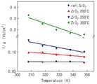
도 27을 참조하면, 상기 실시 예 2-1(ZrO2 200℃), 2-2(ZrO2 250℃), 2-3(ZrO2 300℃), 및 비교 예 2(SiO2)에 따른 트랜지스터의 온도(Temperature, K)에 따른 전자 이동도(1/μ(Vs/cm2))를 측정하여 나타내었고, 도 28을 참조하면, 도 27 에 나타난 그래프의 기울기(slope) 및 각 트랜지스터의 유전상수(Dielectric constant)를 측정하여 나타내었다. 도 27 및 도 28에서 확인할 수 있듯이, ZrO2 게이트 절연막의 제조 온도가 200℃, 250℃, 및 300℃로 증가함에 따라, 유전상수가 능가하는 것을 확인할 수 있었다. 유전상수가 높게 나타나는 것은 트랜지스터의 활성층 채널에서 Coulomb 산란이 높게 나타나는 것을 의미하고, 이는 채널에서의 전자 이동도가 감소되는 것을 의미하므로, ZrO2 게이트 절연막의 제조 온도가 증가함에 따라 전자 이동도가 감소되는 것을 알 수 있다.Referring to FIG. 27, transistors according to Examples 2-1 (
도 20 내지 도 28을 통해 알 수 있듯이, ZrO2 단일층이 게이트 절연막으로 사용된 트랜지스터의 경우, 전기적 특성을 향상시키고 높은 신뢰성을 갖기 위해, 게이트 절연막의 제조 과정에서 온도를 200℃ 초과 300℃ 미만으로 제어하여, ZrO2 층이 메조-크리스탈(meso-crystalline) 구조를 가져야 하는 것을 알 수 있다.As can be seen from FIGS. 20 to 28, in the case of a transistor in which a single layer of ZrO2 is used as a gate insulating film, in order to improve electrical characteristics and have high reliability, the temperature in the process of manufacturing the gate insulating film is increased to more than 200°C and less than 300°C. By controlling it, it can be seen that the ZrO2 layer should have a meso-crystalline structure.
도 29는 본 발명의 실시 예들에 따른 트랜지스터를 포함하는 표시 장치의 블록도이고, 도 30은 본 발명의 실시 예들에 따른 트랜지스터를 포함하는 표시 장치에 포함된 화소 셀을 나타내는 회로도이다.FIG. 29 is a block diagram of a display device including transistors according to example embodiments, and FIG. 30 is a circuit diagram illustrating a pixel cell included in a display device including transistors according to example embodiments.
도 29 및 도 30을 참조하면, 본 발명의 실시 예들에 따른 트랜지스터를 포함하는 표시 장치는 표시부(300), 타이밍 컨트롤러(310), 게이트 구동부(330), 데이터 구동부(340), 및 전원부(350)를 포함한다.Referring to FIGS. 29 and 30, a display device including a transistor according to embodiments of the present invention includes a
상기 표시부(100)는, 게이트 라인(GL), 상기 게이트 라인(GL)과 교차하여 형성된 데이터 라인(DL), 상기 게이트라인(GL)과 상기 데이터 라인(DL)이 교차하여 정의하는 영역에 형성된 상기 화소 셀(P), 및 상기 화소 셀(P)에 전원을 공급하는 전원공급라인(CL)을 포함할 수 있다.The
여기서, 상기 화소셀(P)은 도 30에 도시된 바와 같이 유기 발광다이오드(OLED), 상기 유기 발광다이오드(OLED)를 제어하는 제1 및 제2 트랜지스터(TR1, TR2), 상기 제1 트랜지스터(TR1)로 공급된 데이터 전압을 충전하는 스토리지 커패시터(Cst)를 포함할 수 있다. 상기 제1 트랜지스터(TR1) 및 상기 제2 트랜지스터(TR2) 중에서 적어도 어느 하나는, 상술된 본 발명의 실시 예에 따른 트랜지스터일 수 있다.Here, the pixel cell P is an organic light emitting diode (OLED), first and second transistors (TR1, TR2) for controlling the organic light emitting diode (OLED), and the first transistor ( A storage capacitor Cst for charging the data voltage supplied to TR1) may be included. At least one of the first transistor TR1 and the second transistor TR2 may be a transistor according to the embodiment of the present invention described above.
상기 게이트 라인(GL)은 상기 게이트 구동부(330)로부터 공급된 게이트 신호(GS)를 상기 화소 셀(P)에 공급한다. 상기 제1 트랜지스터(TR1)의 게이트 전극은 상기 게이트 라인(GL)과 접속되어 상기 게이트 신호(GS)에 응답하여 턴온(turn-on)된다. 상기 데이터 라인(DL)은 상기 데이터 구동부(340)로부터 공급된 표시 데이터 전압(DDV)을 제1 트랜지스터(TR1)에 공급한다.The gate line GL supplies the gate signal GS supplied from the
상기 게이트 신호(GS)에 응답하여 상기 제1 트랜지스터(TR1)가 턴온되면, 상기 데이터 라인(DL)으로부터 공급된 상기 표시 데이터 전압(DDV)은 상기 제1 트랜지스터(TR1)를 통해 제1 노드(N1)로 공급된다. 상기 스토리지 커패시터(Cst)는 상기 제1 노드(N1)에 공급된 상기 표시 데이터 전압(DDV)을 충전한다. 여기서, 상기 제1 트랜지스터(TR1)가 턴오프(turn off)되면 상기 스토리지 커패시터(Cst)에 충전된 상기 표시 데이터 전압(DDV)이 상기 제2 트랜지스터(TR2)의 게이트 전극에 공급되어 상기 제2 트랜지스터(TR2)가 턴온된다.When the first transistor TR1 is turned on in response to the gate signal GS, the display data voltage DDV supplied from the data line DL passes through the first transistor TR1 to a first node ( N1). The storage capacitor Cst charges the display data voltage DDV supplied to the first node N1. Here, when the first transistor TR1 is turned off, the display data voltage DDV charged in the storage capacitor Cst is supplied to the gate electrode of the second transistor TR2 and the second transistor TR1 is turned off. Transistor TR2 is turned on.
상기 제2 트랜지스터(TR2)는 상기 스토리지 커패시터(Cst)에 충전된 데이터 전압이 모두 방전될 때까지 턴온되어 상기 전원공급라인(CL)으로 공급된 구동전압(VDD)을 상기 유기발광 다이오드(OLED)에 공급한다. 여기서, 상기 제1 및 제2 트랜지스터(TR1, TR2)는 NMOS 또는 PMOS로 형성될 수 있다.The second transistor TR2 is turned on until all the data voltages charged in the storage capacitor Cst are discharged, and the driving voltage VDD supplied to the power supply line CL is applied to the organic light emitting diode OLED. To supply. Here, the first and second transistors TR1 and TR2 may be formed of NMOS or PMOS.
상기 유기발광 다이오드(OLED)의 애노드 전극은 상기 제2 트랜지스터(TR2)의 출력단에 연결되며, 캐소드 전극은 접지 또는 상기 애노드 전극에 공급되는 전압보다 낮은 공통전압(Vcom)이 공급된다. 상기 유기발광 다이오드(OLED)는 상기 제2 트랜지스터(TR2)에서 제어되는 전류(Ic)에 의해 구동된다.The anode electrode of the organic light emitting diode OLED is connected to the output terminal of the second transistor TR2, and a common voltage Vcom lower than the ground or a voltage supplied to the anode electrode is supplied to the cathode electrode. The organic light emitting diode OLED is driven by a current Ic controlled by the second transistor TR2.
상기 타이밍 컨트롤러(310)는 외부로부터 데이터 신호(I-data)를 입력받아서 상기 데이터 구동부(340)로 공급하고, 외부로부터 공급된 신호에 근거하여 게이트 제어신호(GCS) 및 데이터 제어신호(DCS)를 각각 상기 게이트 구동부(330)와 상기 데이터 구동부(340)로 제공한다.The
상기 전원부(350)는 상기 게이트 구동부(330)에 게이트 온 전압(VON)/게이트 오프 전압(VOFF)을 공급하고, 상기 데이터 구동부(340)에 아날로그 구동전압(AVDD)을 공급하며, 상기 표시부(100)에 구동전압(VDD) 및 공통전압(Vcom)을 공급한다.The
일 실시 예에 따르면, 상기 제1 트랜지스터(TR1) 및 상기 제2 트랜지스터(TR2) 중 적어도 어느 하나의 게이트 절연막은, 상술된 본 발명의 실시 예에 따른 결정질 금속 산화물을 포함하는 제1 게이트 절연막 및 비정질 실리콘 산화물을 포함하는 제2 게이트 절연막을 포함할 수 있다. 또한, 상기 게이트 절연막을 형성하는 단계에서, 상기 스토리지 커패시터(Cst)의 유전층이 제공 및 형성될 수 있다. 다시 말하면, 상기 게이트 절연막의 상기 제1 게이트 절연막 및 상기 제2 게이트 절연막이 상기 스토리지 커패시터(Cst)의 유전층으로 제공될 수 있다. 이에 따라, 고해상도의 표시 장치에서, 상기 제1 트랜지스터(TR1) 및 상기 제2 트랜지스터(TR2)의 턴 온 및 턴 오프 동작이 빨라질 수 있고, 이와 동시에, 상기 스토리지 커패시터(Cst)로 공급되는 데이터 전압의 충전 속도 및 효율이 향상될 수 있다.According to an embodiment, at least one gate insulating layer of the first transistor TR1 and the second transistor TR2 includes a first gate insulating layer including a crystalline metal oxide according to an exemplary embodiment of the present invention and A second gate insulating layer including amorphous silicon oxide may be included. Also, in the forming of the gate insulating layer, a dielectric layer of the storage capacitor Cst may be provided and formed. In other words, the first gate insulating layer and the second gate insulating layer of the gate insulating layer may be provided as a dielectric layer of the storage capacitor Cst. Accordingly, in a high-resolution display device, the first transistor TR1 and the second transistor TR2 can be turned on and off faster, and at the same time, the data voltage supplied to the storage capacitor Cst The charging speed and efficiency of the can be improved.
도 30을 참조하여 설명된 화소 셀에 두 개의 트랜지스터와 하나의 커패신터를 구비하는 2Tr-1Cap 구조의 능동 구동(active matrix, AM)형 유기 발광 표시 장치를 도시하였지만, 본 발명이 이에 한정되는 것은 아니다. 유기 발광 표시 장치는 하나의 화소 셀에 셋 이상의 트랜지스터와 둘 이상의 커패시터를 포함할 수 있다.Although an active matrix (AM) type organic light emitting display device having a 2Tr-1Cap structure including two transistors and one capacitor in the pixel cell described with reference to FIG. 30 is illustrated, the present invention is limited thereto. no. The organic light emitting diode display may include three or more transistors and two or more capacitors in one pixel cell.
이상, 본 발명을 바람직한 실시 예를 사용하여 상세히 설명하였으나, 본 발명의 범위는 특정 실시 예에 한정되는 것은 아니며, 첨부된 특허청구범위에 의하여 해석되어야 할 것이다. 또한, 이 기술분야에서 통상의 지식을 습득한 자라면, 본 발명의 범위에서 벗어나지 않으면서도 많은 수정과 변형이 가능함을 이해하여야 할 것이다.In the above, the present invention has been described in detail using preferred embodiments, but the scope of the present invention is not limited to specific embodiments, and should be interpreted by the appended claims. In addition, those who have acquired ordinary knowledge in this technical field should understand that many modifications and variations can be made without departing from the scope of the present invention.
100: 기판
200: 게이트 전극
300: 게이트 절연막
310, 320: 제1 게이트 절연막, 제2 게이트 절연막
400: 활성층
500s: 소스 전극
500d: 드레인 전극100: substrate
200: gate electrode
300: gate insulating film
310, 320: first gate insulating film, second gate insulating film
400: active layer
500s: source electrode
500d: drain electrode
Claims (14)
Translated fromKorean상기 게이트 절연막을 형성하는 단계는,
금속을 포함하는 제1 전구체 및 산소를 포함하는 제2 전구체를 제공하여, 상기 제1 및 제2 전구체가 반응된 결정질(crystalline)의 제1 게이트 절연막을 형성하는 단계; 및
실리콘을 포함하는 제3 전구체 및 산소를 포함하는 제4 전구체를 제공하여, 상기 제3 및 제4 전구체가 반응된 비정질(amorphous)의 제2 게이트 절연막을 형성하는 단계를 포함하는 고유전율 트랜지스터의 제조방법.
Including the step of forming a gate insulating film between the gate electrode and the active layer,
The step of forming the gate insulating layer,
Providing a first precursor including a metal and a second precursor including oxygen to form a crystalline first gate insulating layer in which the first and second precursors are reacted; And
Manufacture of a high-k transistor comprising the step of forming an amorphous second gate insulating layer in which the third and fourth precursors are reacted by providing a third precursor containing silicon and a fourth precursor containing oxygen Way.
상기 제1 게이트 절연막 형성 단계, 및 상기 제2 게이트 절연막 형성 단계는 in-situ 공정으로 수행되는 것을 포함하는 고유전율 트랜지스터의 제조방법.
The method of claim 1,
And forming the first gate insulating layer and forming the second gate insulating layer in an in-situ process.
상기 금속은, 지르코늄(Zr) 또는 하프늄(Hf)을 포함하는 고유전율 트랜지스터의 제조방법.
The method of claim 1,
The metal is a method of manufacturing a high-k transistor comprising zirconium (Zr) or hafnium (Hf).
상기 금속은, 지르코늄(Zr) 또는 하프늄(Hf)을 포함하는 고유전율 트랜지스터의 제조방법.
The method of claim 1,
The metal is a method of manufacturing a high-k transistor comprising zirconium (Zr) or hafnium (Hf).
상기 제2 및 제4 전구체는 서로 다른 것을 포함하는 고유전율 트랜지스터의 제조방법.
The method of claim 1,
The second and fourth precursors are different from each other.
상기 제2 게이트 절연막 형성 단계는, 상기 제1 게이트 절연막 형상 단계보다 낮은 온도에서 수행되는 것을 포함하는 고유전율 트랜지스터의 제조방법.
The method of claim 1,
The forming of the second gate insulating layer is performed at a lower temperature than the forming of the first gate insulating layer.
상기 기판 상에 배치되는 게이트 전극;
상기 기판 상에 배치되고, 상기 게이트 전극과 이격된 활성층;
상기 활성층을 사이에 두고 서로 이격되어 배치되는 소스 및 드레인 전극
상기 게이트 전극 및 상기 활성층 사이의 게이트 절연막을 포함하되,
상기 게이트 절연막은,
결정질(crystalline) 금속 산화물을 포함하는 제1 게이트 절연막; 및
비정질(amorphous) 실리콘 산화물을 포함하는 제2 게이트 절연막을 포함하고,
상기 제2 게이트 절연막이 상기 제1 게이트 절연막 및 상기 활성층 사이에 배치되는 것을 포함하는 고유전율 트랜지스터.
Board;
A gate electrode disposed on the substrate;
An active layer disposed on the substrate and spaced apart from the gate electrode;
Source and drain electrodes spaced apart from each other with the active layer therebetween
Including a gate insulating layer between the gate electrode and the active layer,
The gate insulating film,
A first gate insulating film including a crystalline metal oxide; And
Including a second gate insulating layer containing amorphous silicon oxide,
And the second gate insulating layer is disposed between the first gate insulating layer and the active layer.
상기 결정질 금속 산화물은, ZrO2, HfO2, TiO2, SrOx(x>0), TaOx(x>0), 또는 Y2O3 중 어느 하나를 포함하는 고유전율 트랜지스터.
The method of claim 7,
The crystalline metal oxide, ZrO2 , HfO2 , TiO2 , SrOx (x>0), TaOx (x>0), or Y2 O3 High- k transistor comprising any one of.
상기 비정질 실리콘 산화물은, SiO2를 포함하는 고유전율 트랜지스터.
The method of claim 7,
The amorphous silicon oxide is a high-k transistor containing SiO2 .
상기 제2 게이트 절연막의 두께는 6 nm 이상 10 nm 이하인 것을 포함하는 고유전율 트랜지스터.
The method of claim 7,
The high dielectric constant transistor comprising a thickness of the second gate insulating layer is 6 nm or more and 10 nm or less.
상기 제2 게이트 절연막의 두께는, 상기 제1 게이트 절연막의 두께보다 얇은 것을 포함하는 고유전율 트랜지스터.
The method of claim 7,
A high dielectric constant transistor including a thickness of the second gate insulating layer being thinner than that of the first gate insulating layer.
상기 게이트 절연막은 게이트 전극 및 활성층 사이에 형성되는 것을 포함하는 고유전율 트랜지스터의 제조방법.
Including the step of forming a gate insulating film having a meso-crystalline structure by providing a first precursor containing a metal and a second precursor containing oxygen in a first temperature range,
The method of manufacturing a high-k transistor comprising the gate insulating layer formed between the gate electrode and the active layer.
상기 제1 온도범위는 200℃ 초과 300℃ 미만인 것을 포함하는 고유전율 트랜지스터의 제조방법.
The method of claim 12,
The method of manufacturing a high-k transistor comprising the first temperature range is more than 200 ℃ and less than 300 ℃.
상기 메조-크리스탈(meso-crystalline) 구조는, 결정질(crystalline)의 결정화도 보다 낮고 비정질(amorphous)의 결정화도 보다 높은 것을 포함하는 고유전율 트랜지스터의 제조방법.
The method of claim 12,
The meso-crystalline structure, a method of manufacturing a high-k transistor comprising a crystallinity lower than the crystallinity of the crystalline (crystalline) and higher than the crystallinity of the amorphous (amorphous).
Priority Applications (1)
| Application Number | Priority Date | Filing Date | Title |
|---|---|---|---|
| KR1020190019423AKR102180242B1 (en) | 2019-02-19 | 2019-02-19 | High-permittivity transistor and manufacturing method thereof |
Applications Claiming Priority (1)
| Application Number | Priority Date | Filing Date | Title |
|---|---|---|---|
| KR1020190019423AKR102180242B1 (en) | 2019-02-19 | 2019-02-19 | High-permittivity transistor and manufacturing method thereof |
Publications (2)
| Publication Number | Publication Date |
|---|---|
| KR20200101150Atrue KR20200101150A (en) | 2020-08-27 |
| KR102180242B1 KR102180242B1 (en) | 2020-11-18 |
Family
ID=72237643
Family Applications (1)
| Application Number | Title | Priority Date | Filing Date |
|---|---|---|---|
| KR1020190019423AActiveKR102180242B1 (en) | 2019-02-19 | 2019-02-19 | High-permittivity transistor and manufacturing method thereof |
Country Status (1)
| Country | Link |
|---|---|
| KR (1) | KR102180242B1 (en) |
Cited By (2)
| Publication number | Priority date | Publication date | Assignee | Title |
|---|---|---|---|---|
| KR20210128128A (en)* | 2020-04-16 | 2021-10-26 | 주식회사 한솔케미칼 | A Semiconductor layer, a method of manufacturing the same, and a transistor comprising the same |
| KR102690226B1 (en)* | 2022-06-16 | 2024-08-05 | 한국생산기술연구원 | Thin film transistor and manufacturing method thereof |
Citations (5)
| Publication number | Priority date | Publication date | Assignee | Title |
|---|---|---|---|---|
| KR20060079958A (en)* | 2005-01-04 | 2006-07-07 | 삼성전자주식회사 | Silicon Thin Film Transistor |
| KR20070085828A (en)* | 2004-11-10 | 2007-08-27 | 캐논 가부시끼가이샤 | Field Effect Transistors Using Amorphous Oxides |
| JP2010531059A (en)* | 2007-06-19 | 2010-09-16 | サムスン エレクトロニクス カンパニー リミテッド | Oxide semiconductor and thin film transistor including the same |
| US20110207283A1 (en)* | 2010-02-22 | 2011-08-25 | Suvi Haukka | High temperature atomic layer deposition of dielectric oxides |
| KR101160489B1 (en) | 2006-04-07 | 2012-06-26 | 엘지디스플레이 주식회사 | TFT array substrate and method for fabricating of the same |
- 2019
- 2019-02-19KRKR1020190019423Apatent/KR102180242B1/enactiveActive
Patent Citations (5)
| Publication number | Priority date | Publication date | Assignee | Title |
|---|---|---|---|---|
| KR20070085828A (en)* | 2004-11-10 | 2007-08-27 | 캐논 가부시끼가이샤 | Field Effect Transistors Using Amorphous Oxides |
| KR20060079958A (en)* | 2005-01-04 | 2006-07-07 | 삼성전자주식회사 | Silicon Thin Film Transistor |
| KR101160489B1 (en) | 2006-04-07 | 2012-06-26 | 엘지디스플레이 주식회사 | TFT array substrate and method for fabricating of the same |
| JP2010531059A (en)* | 2007-06-19 | 2010-09-16 | サムスン エレクトロニクス カンパニー リミテッド | Oxide semiconductor and thin film transistor including the same |
| US20110207283A1 (en)* | 2010-02-22 | 2011-08-25 | Suvi Haukka | High temperature atomic layer deposition of dielectric oxides |
Non-Patent Citations (2)
| Title |
|---|
| ACS APPL. MATER. INTERFACES 2016, 8, 22751-22755* |
| J. VAC. SCI. TECHNOL. A 37(2), MAR/APR 2019* |
Cited By (2)
| Publication number | Priority date | Publication date | Assignee | Title |
|---|---|---|---|---|
| KR20210128128A (en)* | 2020-04-16 | 2021-10-26 | 주식회사 한솔케미칼 | A Semiconductor layer, a method of manufacturing the same, and a transistor comprising the same |
| KR102690226B1 (en)* | 2022-06-16 | 2024-08-05 | 한국생산기술연구원 | Thin film transistor and manufacturing method thereof |
Also Published As
| Publication number | Publication date |
|---|---|
| KR102180242B1 (en) | 2020-11-18 |
Similar Documents
| Publication | Publication Date | Title |
|---|---|---|
| JP7630598B2 (en) | Semiconductor Device | |
| JP6246307B2 (en) | Semiconductor device | |
| KR102072244B1 (en) | Semiconductor device and method for manufacturing the same | |
| CN107683531B (en) | Semiconductor device and display device including the same | |
| KR20240147637A (en) | Semiconductor device | |
| CN102097486B (en) | Thin film transistor, method of manufacturing the same, and organic electroluminescent device | |
| CN102648490B (en) | Liquid crystal display device, method for driving the liquid crystal display device, and electronic device including the liquid crystal display device | |
| US8476106B2 (en) | Transparent nonvolatile memory thin film transistor and method of manufacturing the same | |
| CN111554737B (en) | Ultra-low power consumption thin film transistor and preparation method thereof | |
| US7508649B2 (en) | Multi-layered dielectric film of microelectronic device and method of manufacturing the same | |
| US10957237B2 (en) | Circuit, semiconductor device, display device, electronic device, and driving method of circuit | |
| TWI543371B (en) | Semiconductor device and method of manufacturing same | |
| CN104094386B (en) | Semiconductor device and its manufacture method | |
| KR20140029248A (en) | Semiconductor device | |
| KR20160065005A (en) | Semiconductor device and display device including the same | |
| CN113345795B (en) | Ferroelectric thin film structure and electronic device including the ferroelectric thin film structure | |
| JP2014006515A (en) | Light-emitting device | |
| JP2014007739A (en) | Pulse signal output circuit and shift register | |
| EP2323167A1 (en) | Transistors, electronic devices including a transistor and methods of manufacturing the same | |
| KR102180242B1 (en) | High-permittivity transistor and manufacturing method thereof | |
| CN101154588A (en) | Composition for dielectric film, metal oxide dielectric film using same, and manufacturing method | |
| JP7289850B2 (en) | Semiconductor equipment, electronic equipment | |
| KR20140000538A (en) | A transparent and flexible non-volatile memory cell with common oxide semiconductor channel and manufacturing method for the same | |
| KR101657345B1 (en) | Thin film transistor, method of fabricating the same, and display device having the same | |
| TW202535183A (en) | Semiconductor device |
Legal Events
| Date | Code | Title | Description |
|---|---|---|---|
| PA0109 | Patent application | St.27 status event code:A-0-1-A10-A12-nap-PA0109 | |
| PA0201 | Request for examination | St.27 status event code:A-1-2-D10-D11-exm-PA0201 | |
| R18-X000 | Changes to party contact information recorded | St.27 status event code:A-3-3-R10-R18-oth-X000 | |
| R18-X000 | Changes to party contact information recorded | St.27 status event code:A-3-3-R10-R18-oth-X000 | |
| D13-X000 | Search requested | St.27 status event code:A-1-2-D10-D13-srh-X000 | |
| D14-X000 | Search report completed | St.27 status event code:A-1-2-D10-D14-srh-X000 | |
| PE0902 | Notice of grounds for rejection | St.27 status event code:A-1-2-D10-D21-exm-PE0902 | |
| E13-X000 | Pre-grant limitation requested | St.27 status event code:A-2-3-E10-E13-lim-X000 | |
| P11-X000 | Amendment of application requested | St.27 status event code:A-2-2-P10-P11-nap-X000 | |
| P13-X000 | Application amended | St.27 status event code:A-2-2-P10-P13-nap-X000 | |
| E701 | Decision to grant or registration of patent right | ||
| PE0701 | Decision of registration | St.27 status event code:A-1-2-D10-D22-exm-PE0701 | |
| PG1501 | Laying open of application | St.27 status event code:A-1-1-Q10-Q12-nap-PG1501 | |
| GRNT | Written decision to grant | ||
| PR0701 | Registration of establishment | St.27 status event code:A-2-4-F10-F11-exm-PR0701 | |
| PR1002 | Payment of registration fee | St.27 status event code:A-2-2-U10-U11-oth-PR1002 Fee payment year number:1 | |
| PG1601 | Publication of registration | St.27 status event code:A-4-4-Q10-Q13-nap-PG1601 | |
| PR1001 | Payment of annual fee | St.27 status event code:A-4-4-U10-U11-oth-PR1001 Fee payment year number:4 | |
| PR1001 | Payment of annual fee | St.27 status event code:A-4-4-U10-U11-oth-PR1001 Fee payment year number:5 | |
| P22-X000 | Classification modified | St.27 status event code:A-4-4-P10-P22-nap-X000 | |
| PR1001 | Payment of annual fee | St.27 status event code:A-4-4-U10-U11-oth-PR1001 Fee payment year number:6 |