KR20200099954A - Composite charged particle beam apparatus and control method thereof - Google Patents
Composite charged particle beam apparatus and control method thereofDownload PDFInfo
- Publication number
- KR20200099954A KR20200099954AKR1020190137409AKR20190137409AKR20200099954AKR 20200099954 AKR20200099954 AKR 20200099954AKR 1020190137409 AKR1020190137409 AKR 1020190137409AKR 20190137409 AKR20190137409 AKR 20190137409AKR 20200099954 AKR20200099954 AKR 20200099954A
- Authority
- KR
- South Korea
- Prior art keywords
- ion beam
- unit
- voltage
- booster
- acceleration voltage
- Prior art date
- Legal status (The legal status is an assumption and is not a legal conclusion. Google has not performed a legal analysis and makes no representation as to the accuracy of the status listed.)
- Granted
Links
Images


Classifications
- H—ELECTRICITY
- H01—ELECTRIC ELEMENTS
- H01J—ELECTRIC DISCHARGE TUBES OR DISCHARGE LAMPS
- H01J37/00—Discharge tubes with provision for introducing objects or material to be exposed to the discharge, e.g. for the purpose of examination or processing thereof
- H01J37/02—Details
- H01J37/248—Components associated with high voltage supply
- H—ELECTRICITY
- H01—ELECTRIC ELEMENTS
- H01J—ELECTRIC DISCHARGE TUBES OR DISCHARGE LAMPS
- H01J37/00—Discharge tubes with provision for introducing objects or material to be exposed to the discharge, e.g. for the purpose of examination or processing thereof
- H01J37/30—Electron-beam or ion-beam tubes for localised treatment of objects
- H01J37/302—Controlling tubes by external information, e.g. programme control
- H01J37/3023—Programme control
- H—ELECTRICITY
- H01—ELECTRIC ELEMENTS
- H01J—ELECTRIC DISCHARGE TUBES OR DISCHARGE LAMPS
- H01J37/00—Discharge tubes with provision for introducing objects or material to be exposed to the discharge, e.g. for the purpose of examination or processing thereof
- H01J37/02—Details
- H01J37/24—Circuit arrangements not adapted to a particular application of the tube and not otherwise provided for
- H01J37/241—High voltage power supply or regulation circuits
- H—ELECTRICITY
- H01—ELECTRIC ELEMENTS
- H01J—ELECTRIC DISCHARGE TUBES OR DISCHARGE LAMPS
- H01J37/00—Discharge tubes with provision for introducing objects or material to be exposed to the discharge, e.g. for the purpose of examination or processing thereof
- H01J37/02—Details
- H01J37/04—Arrangements of electrodes and associated parts for generating or controlling the discharge, e.g. electron-optical arrangement or ion-optical arrangement
- H01J37/08—Ion sources; Ion guns
- H—ELECTRICITY
- H01—ELECTRIC ELEMENTS
- H01J—ELECTRIC DISCHARGE TUBES OR DISCHARGE LAMPS
- H01J37/00—Discharge tubes with provision for introducing objects or material to be exposed to the discharge, e.g. for the purpose of examination or processing thereof
- H01J37/02—Details
- H01J37/04—Arrangements of electrodes and associated parts for generating or controlling the discharge, e.g. electron-optical arrangement or ion-optical arrangement
- H01J37/147—Arrangements for directing or deflecting the discharge along a desired path
- H—ELECTRICITY
- H01—ELECTRIC ELEMENTS
- H01J—ELECTRIC DISCHARGE TUBES OR DISCHARGE LAMPS
- H01J37/00—Discharge tubes with provision for introducing objects or material to be exposed to the discharge, e.g. for the purpose of examination or processing thereof
- H01J37/02—Details
- H01J37/21—Means for adjusting the focus
- H—ELECTRICITY
- H01—ELECTRIC ELEMENTS
- H01J—ELECTRIC DISCHARGE TUBES OR DISCHARGE LAMPS
- H01J37/00—Discharge tubes with provision for introducing objects or material to be exposed to the discharge, e.g. for the purpose of examination or processing thereof
- H01J37/02—Details
- H01J37/24—Circuit arrangements not adapted to a particular application of the tube and not otherwise provided for
- H01J37/243—Beam current control or regulation circuits
- H—ELECTRICITY
- H01—ELECTRIC ELEMENTS
- H01J—ELECTRIC DISCHARGE TUBES OR DISCHARGE LAMPS
- H01J37/00—Discharge tubes with provision for introducing objects or material to be exposed to the discharge, e.g. for the purpose of examination or processing thereof
- H01J37/26—Electron or ion microscopes; Electron or ion diffraction tubes
- H01J37/28—Electron or ion microscopes; Electron or ion diffraction tubes with scanning beams
- H—ELECTRICITY
- H01—ELECTRIC ELEMENTS
- H01J—ELECTRIC DISCHARGE TUBES OR DISCHARGE LAMPS
- H01J37/00—Discharge tubes with provision for introducing objects or material to be exposed to the discharge, e.g. for the purpose of examination or processing thereof
- H01J37/30—Electron-beam or ion-beam tubes for localised treatment of objects
- H01J37/305—Electron-beam or ion-beam tubes for localised treatment of objects for casting, melting, evaporating, or etching
- H01J37/3053—Electron-beam or ion-beam tubes for localised treatment of objects for casting, melting, evaporating, or etching for evaporating or etching
- H01J37/3056—Electron-beam or ion-beam tubes for localised treatment of objects for casting, melting, evaporating, or etching for evaporating or etching for microworking, e. g. etching of gratings or trimming of electrical components
- H—ELECTRICITY
- H01—ELECTRIC ELEMENTS
- H01J—ELECTRIC DISCHARGE TUBES OR DISCHARGE LAMPS
- H01J2237/00—Discharge tubes exposing object to beam, e.g. for analysis treatment, etching, imaging
- H01J2237/04—Means for controlling the discharge
- H01J2237/047—Changing particle velocity
- H01J2237/0473—Changing particle velocity accelerating
- H—ELECTRICITY
- H01—ELECTRIC ELEMENTS
- H01J—ELECTRIC DISCHARGE TUBES OR DISCHARGE LAMPS
- H01J2237/00—Discharge tubes exposing object to beam, e.g. for analysis treatment, etching, imaging
- H01J2237/30—Electron or ion beam tubes for processing objects
- H01J2237/317—Processing objects on a microscale
- H01J2237/31749—Focused ion beam
Landscapes
- Chemical & Material Sciences (AREA)
- Analytical Chemistry (AREA)
- Physics & Mathematics (AREA)
- Engineering & Computer Science (AREA)
- Plasma & Fusion (AREA)
- Analysing Materials By The Use Of Radiation (AREA)
- Electron Sources, Ion Sources (AREA)
Abstract
Description
Translated fromKorean본 발명은, 복합 하전 입자 빔 장치, 및 제어 방법에 관한 것이다.The present invention relates to a composite charged particle beam device and a control method.
전자 빔(EB: Electron Beam)과 집속 이온 빔(FIB: Focused Ion Beam)을 구비하는 복합 하전 입자 빔 장치를 사용한 투과 전자 현미경(TEM: Transmission Electron Microscope) 시료 제작으로 대표되는 시료 형상의 가공에 있어서는, 이온 빔 조사에 의한 시료에 대한 대미지를 최소한으로 억제하고 싶다고 하는 요구가 있다. 그 때문에, 복합 하전 입자 빔 장치를 사용한 가공에 있어서는, 이온 빔의 가속 에너지를 수 keV 이하로 내려 시료를 가공하고 있다.In the processing of a sample shape typified by the production of a transmission electron microscope (TEM) sample using a complex charged particle beam device having an electron beam (EB) and a focused ion beam (FIB), , There is a demand to minimize the damage to the sample by ion beam irradiation. Therefore, in the processing using the composite charged particle beam device, the acceleration energy of the ion beam is reduced to several keV or less, and the sample is processed.
예를 들면, 조가공(粗加工)을 30keV에서 행하고, 마무리 가공을 10keV에서 행하는 집속 이온 빔을 이용한 TEM 시료의 작성 방법이 알려져 있다(특허문헌 1). 또한, 마무리 가공에 사용하는 이온 빔의 에너지를 낮게 함과 더불어, 시료에 대한 입사 각도를 당해 시료의 형상에 맞추어 최적화함으로써 효과적으로 대미지층을 제거하는 가공 방법이 알려져 있다(특허문헌 2). 또한, 대미지층을 줄이기 위해서는, 집속 이온 빔 장치의 가속 전압을 낮게 할 필요가 있는 것이 알려져 있다(특허문헌 3). 이와 같이, 집속 이온 빔 장치를 이용한 가공에 있어서 가속 전압을 낮게 하는 것은 주지의 사실로 되어 있다.For example, a method for preparing a TEM sample using a focused ion beam in which rough processing is performed at 30 keV and finishing is performed at 10 keV is known (Patent Document 1). In addition, there is known a processing method of effectively removing a damaged layer by lowering the energy of an ion beam used for finishing processing and optimizing the angle of incidence to the sample according to the shape of the sample (Patent Document 2). Further, in order to reduce the damage layer, it is known that it is necessary to lower the acceleration voltage of the focused ion beam device (Patent Document 3). As described above, it is a known fact to lower the acceleration voltage in processing using a focused ion beam device.
그러나, 집속 이온 빔의 가속 전압을 낮게 하면, 색 수차에 의한 빔 블러(beam blur)량의 증대나 쿨롬 상호 작용에 의한 빔 프로파일의 확산이 현저해진다. 빔 블러량의 증대나 빔 프로파일의 확산에 대한 대책으로서 빔 부스터 기술이 이용되고 있다(특허문헌 4, 비특허문헌 1). 빔 부스터 기술에서는, 광학계의 중간부의 포텐셜 에너지를 올린 후, 대물렌즈에 의하여 당해 포텐셜 에너지를 저하시킨다.However, when the accelerating voltage of the focused ion beam is lowered, the amount of beam blur due to chromatic aberration increases and the beam profile is remarkably diffused by the coulomb interaction. As a countermeasure against increasing the amount of beam blur or spreading the beam profile, a beam booster technology is used (
또한, 전자 빔에 있어서도 빔 부스터를 사용하는 것은 주지되어 있다(특허문헌 5).In addition, it is well known that a beam booster is used also in an electron beam (Patent Document 5).
전자 빔과 집속 이온 빔이 시료 상의 동일점에 조사되는 복합 하전 입자 빔 장치가 알려져 있다(특허문헌 6). 복합 하전 입자 빔 장치에서는, 전자 빔과 집속 이온 빔을 시료 상의 동일점에 조사하고, 또한 전자 빔의 초점과 집속 이온 빔의 초점이 상기 시료 상의 동일점에 맞춰질 것이 요구된다. 이 전자 빔과 집속 이온 빔이 조사되는 시료 상의 동일점을 코인시던스 포인트(Coincidence Point: CP)라고 정의한다.A composite charged particle beam device in which an electron beam and a focused ion beam are irradiated to the same point on a sample is known (Patent Document 6). In the composite charged particle beam apparatus, it is required that the electron beam and the focused ion beam are irradiated to the same point on the sample, and the focus of the electron beam and the focused ion beam are adjusted to the same point on the sample. The same point on the sample to which the electron beam and the focused ion beam are irradiated is defined as a coincidence point (CP).
집속 이온 빔의 제어 방법으로서, 이온 빔의 전류량에 대응하여 렌즈의 설정, 비점 보정값, 애퍼처 직경, 빔 얼라인먼트에 대한 인가 전압, 및 대물렌즈에 대한 인가 전압 등의 이온 빔 광학 조건과, 복수 개의 가공 내용을 컴퓨터에 기억시켜 두고, 가공 내용에 따라서 광학 조건을 선택, 설정하여 복수 개의 가공을 행하는 것이 개시되어 있다(특허문헌 7).A method for controlling a focused ion beam, comprising: an ion beam optical condition such as a lens setting, a boiling point correction value, an aperture diameter, an applied voltage for beam alignment, and an applied voltage to an objective lens, corresponding to the amount of current of the ion beam, and a plurality of It is disclosed that the processing contents of two are stored in a computer, and optical conditions are selected and set according to the processing contents to perform a plurality of processing (Patent Document 7).
집속 이온 빔의 렌즈의 제어로서, 집속 전압 테이블을 작성하고, 이 집속 전압 테이블에 의거하여 집속 전압을 설정함으로써 빔 전륫값을 기준값 또는 임의값에 맞추는 것이 개시되어 있다(특허문헌 8).As the control of the lens of the focused ion beam, it is disclosed to create a focused voltage table and set the focused voltage based on the focused voltage table to set the beam power value to a reference value or an arbitrary value (Patent Document 8).
그러나, 집속 이온 빔 장치에 빔 부스터를 사용한 경우, 빔 부스터 전압에 의하여 집속 이온 빔의 초점 거리가 제한된다. 이 제한에 의하여, 집속 이온 빔의 초점이 시료의 상방에만 맞춰지고, 따라서 CP에 초점을 맞출 수 없는 상황이 발생한다.However, when a beam booster is used in the focused ion beam device, the focal length of the focused ion beam is limited by the beam booster voltage. Due to this limitation, the focus of the focused ion beam is focused only above the sample, and thus a situation arises in which it is impossible to focus on the CP.
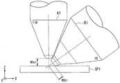
여기에서 도 10을 참조하여, 집속 이온 빔의 초점을 CP에 맞출 수 없는 상황에 대하여 설명한다. 도 10은, 종래의 복합 하전 입자 빔 장치에 있어서의 빔 궤도의 일례를 나타내는 도면이다. 도 10에서는, 집속 이온 빔 경통(A0)으로부터 집속 이온 빔이 시료(SP0)에 조사됨과 더불어, 전자 빔 경통(B0)으로부터 전자 빔이 시료(SP0)에 조사되고 있다.Here, with reference to FIG. 10, a situation where the focus of the focused ion beam cannot be focused on the CP will be described. 10 is a diagram showing an example of a beam trajectory in a conventional composite charged particle beam device. In Fig. 10, the focused ion beam is irradiated to the sample SP0 from the focused ion beam barrel A0, and the electron beam is irradiated to the sample SP0 from the electron beam barrel B0.
빔 궤도 T1은, 빔 부스터 전압이 인가되지 않은 경우의 집속 이온 빔의 궤도이다. 빔 궤도 T2는, 빔 부스터 전압이 인가된 경우의 집속 이온 빔의 궤도이다. 빔 궤도 T3은, 전자 빔의 궤도이다.The beam trajectory T1 is the trajectory of the focused ion beam when the beam booster voltage is not applied. The beam trajectory T2 is a trajectory of a focused ion beam when a beam booster voltage is applied. The beam trajectory T3 is the trajectory of the electron beam.
빔 부스터 전압이 인가되지 않는 경우에는, 빔 궤도 T1은 시료(SP0)의 표면 상의 점(FP1)에 초점을 맺는다. 여기에서 점(FP1)은 CP이며, 전자 빔의 초점이기도 하다. 한편, 빔 부스터 전압이 인가된 경우, 집속 이온 빔의 초점은 점(FP1)에는 맞춰지지 않고, 빔 궤도 T1은 시료(SP0)의 상방의 점(FP0)에 초점을 맺는 경우가 있다. 즉, 집속 이온 빔에 빔 부스터 전압이 인가된 경우에는, 집속 이온 빔의 초점을 CP에 맞출 수 없는 상황이 발생한다.When the beam booster voltage is not applied, the beam trajectory T1 focuses on the point FP1 on the surface of the specimen SP0. Here, the point FP1 is CP and is also the focus of the electron beam. On the other hand, when the beam booster voltage is applied, the focus of the focused ion beam is not aligned with the point FP1, and the beam trajectory T1 is sometimes focused on the point FP0 above the sample SP0. That is, when a beam booster voltage is applied to the focused ion beam, a situation occurs in which the focused ion beam cannot be focused on the CP.
상술한 집속 이온 빔에 빔 부스터를 사용한 경우에 발생하는 초점 맞춤 가능한 범위의 제한은, 가속 전압에 의하여 변화한다. 또 빔 부스터를 사용한 경우에 발생하는 초점 맞춤 가능한 범위의 제한은, 빔 부스터의 전압에 의해서도 변화한다. 그 때문에, 빔 부스터의 전압의 범위에 따라서는, 집속 이온 빔의 초점 거리를, CP로 설정할 수 없는 경우가 있다. 집속 이온 빔의 초점 거리를, CP로 설정할 수 없는 빔 부스터의 전압을 사용한 조건에서는, 집속 이온 빔 장치의 대물렌즈의 인가 전압을 조정하고, 렌즈 강도를 조정해도 CP에 초점을 맞추는 것은 곤란하다.The limit of the focusable range that occurs when the beam booster is used for the above-described focused ion beam varies with the acceleration voltage. In addition, the limit of the focusable range that occurs when the beam booster is used changes also with the voltage of the beam booster. Therefore, depending on the range of the voltage of the beam booster, the focal length of the focused ion beam may not be set to CP in some cases. Under the condition of using the voltage of a beam booster that cannot set the focal length of the focused ion beam to CP, it is difficult to focus on the CP even if the applied voltage of the objective lens of the focused ion beam device is adjusted and the lens intensity is adjusted.
상술한 바와 같이 본 과제는, 전자 빔과 집속 이온 빔으로 구성되는 복합 하전 입자 빔 장치에 있어서, 집속 이온 빔 경통에 빔 부스터가 탑재되어 있는 경우 또한 집속 이온 빔의 작동 거리가 전자 빔의 작동 거리보다 긴 경우에 발생하고, 전자 빔과 집속 이온 빔을 시료 상의 동일점에 조사하며, 또한 전자 빔의 초점과 집속 이온 빔의 초점을 상기 시료 상의 동일점에 맞출 수 없는 상황이 발생하는 것이다.As described above, the present subject is, in a complex charged particle beam device consisting of an electron beam and a focused ion beam, when a beam booster is mounted in the focused ion beam barrel, the operating distance of the focused ion beam is the same as the operating distance of the electron beam. This occurs in a longer case, and the electron beam and the focused ion beam are irradiated to the same point on the sample, and the focus of the electron beam and the focused ion beam cannot be adjusted to the same point on the sample.
본 과제에 특허문헌 7에 기재된 방법을 적용해도 해결책이 되지 않는다. 특허문헌 7에는 집속 이온 빔의 빔 부스터의 기재가 없고, 또한 복합 하전 입자 빔에 대한 기재도 없으며, CP가 존재하지 않는다. 그 때문에 어떻게 과제가 발생하고, 어떻게 빔 부스터 전압을 설정하면 좋을지를 유추할 수 없다.Even if the method described in
또한, 본 과제의 특허문헌 8에 기재된 방법을 적용해도 해결책이 되지 않는다. 특허문헌 8에 있어서의 제어 대상은 집속 렌즈의 집속 전압이며, 특허문헌 8에서는 집속 전압을 설정함으로써 빔 전류를 조정하는 것을 목적으로 하고 있다. 특허문헌 8에는 집속 이온 빔의 빔 부스터의 기재가 없고, 또한 복합 하전 입자 빔에 대한 기재도 없으며, CP가 존재하지 않는다. 그 때문에 어떻게 과제가 발생하고, 어떻게 빔 부스터 전압을 설정하면 좋을지를 유추할 수 없다.Further, even if the method described in
그래서 복합 하전 입자 빔 장치에 있어서, 집속 이온 빔 경통에 빔 부스터가 탑재되어 있는 경우, 집속 이온 빔의 원하는 가속 전압에 따라 빔 부스터의 전압을 설정할 수 있을 것이 요구되고 있다.Therefore, in the composite charged particle beam apparatus, when a beam booster is mounted on the focused ion beam barrel, it is required to be able to set the voltage of the beam booster according to the desired acceleration voltage of the focused ion beam.
본 발명은 상기의 점을 감안하여 이루어진 것이고, 집속 이온 빔의 원하는 가속 전압에 따라 빔 부스터의 전압의 값을 설정할 수 있는 복합 하전 입자 빔 장치, 및 제어 방법을 제공한다.The present invention has been made in view of the above points, and provides a complex charged particle beam device and a control method capable of setting a voltage value of a beam booster according to a desired acceleration voltage of a focused ion beam.
상기 과제를 해결하여 이러한 목적을 달성하기 위하여, 본 발명은 이하의 양태를 채용했다.In order to solve the above problems and achieve these objects, the present invention adopts the following aspects.
(1) 본 발명의 일 양태에 따른 복합 하전 입자 빔 장치는, 이온 빔을 공급하는 이온 공급부와, 상기 이온 공급부가 공급하는 상기 이온 빔에 가속 전압을 인가함으로써 가속시키는 가속 전압 인가부와, 상기 가속 전압 인가부가 가속시킨 상기 이온 빔을 집속시키는 제1 집속부와, 상기 제1 집속부가 집속시킨 상기 이온 빔에 빔 부스터 전압을 인가하는 빔 부스터 전압 인가부와, 상기 빔 부스터 전압 인가부가 상기 빔 부스터 전압을 인가한 상기 이온 빔을 집속시켜 시료에 조사시키는 제2 집속부와, 전자 빔을 상기 시료에 조사하는 전자 빔 조사부와, 상기 빔 부스터 전압 인가부가 상기 이온 빔에 인가하는 상기 빔 부스터 전압의 값을, 상기 가속 전압 인가부가 상기 이온 빔에 인가하는 상기 가속 전압의 값과, 집속시킨 상기 이온 빔의 초점 거리에 따라 미리 결정된 설정값에 의거하여 설정하는 제어부를 구비한다.(1) A composite charged particle beam device according to an aspect of the present invention includes an ion supply unit for supplying an ion beam, an acceleration voltage application unit for accelerating by applying an acceleration voltage to the ion beam supplied by the ion supply unit, and the A first focusing unit for focusing the ion beam accelerated by an acceleration voltage application unit, a beam booster voltage application unit for applying a beam booster voltage to the ion beam focused by the first focusing unit, and the beam booster voltage applying unit for the beam A second focusing unit configured to focus the ion beam to which a booster voltage is applied to irradiate the sample, an electron beam irradiating unit configured to irradiate the sample with an electron beam, and the beam booster voltage applied by the beam booster voltage applying unit to the ion beam And a controller configured to set a value of A based on a predetermined set value according to a value of the acceleration voltage applied by the acceleration voltage application unit to the ion beam and a focal length of the focused ion beam.
상기 (1)에 기재된 양태에 따른 복합 하전 입자 빔 장치에서는, 집속한 상기 이온 빔의 조사점 및 초점과, 상기 전자 빔의 조사점은 상기 시료 상의 동일한 점이다.In the composite charged particle beam device according to the aspect described in (1) above, the irradiation point and focus of the focused ion beam and the irradiation point of the electron beam are the same points on the sample.
(2) 상기 (1)에 기재된 복합 하전 입자 빔 장치에서는, 상기 집속 이온 빔의 초점이 CP에 맞춰진다.(2) In the composite charged particle beam device according to (1) above, the focus of the focused ion beam is focused on CP.
상기 (2)에 기재된 양태에 따른 복합 하전 입자 빔 장치에서는, 전자 빔에 의한 관찰이 가능한 시료의 범위에서, 집속 이온 빔을 소정의 전압보다 낮은 가속 전압에 있어서 가속시킨 경우의 이온 빔의 확산을 빔 부스터에 의하여 억제할 수 있고, 미세한 이온 프로브를 형성하여 가공 및 관찰이 가능해진다. 상기 (2)에 기재된 양태에 따른 복합 하전 입자 빔 장치에서는, 시료의 동일 개소를 시료 스테이지의 위치 조정을 하지 않고, 전자 빔에 의한 관찰과, 빔 부스터 기능을 구비한 집속 이온 빔에 의한 가공 및 관찰이 가능해진다.In the composite charged particle beam device according to the aspect described in (2) above, diffusion of the ion beam when the focused ion beam is accelerated at an acceleration voltage lower than a predetermined voltage within a range of a sample that can be observed by an electron beam It can be suppressed by a beam booster, and processing and observation are made possible by forming a fine ion probe. In the composite charged particle beam device according to the aspect described in (2) above, observation by an electron beam, processing by a focused ion beam equipped with a beam booster function, and the same location of the sample without adjusting the position of the sample stage, and Observation becomes possible.
(3) 상기 (1) 또는 (2)에 기재된 복합 하전 입자 빔 장치에서는, 상기 제어부는, 상기 가속 전압의 값과 상기 설정값의 세트를 기억하는 기억부로부터 읽어 낸 상기 세트에 의거하여, 상기 빔 부스터 전압의 값을 상기 설정값으로 설정한다.(3) In the composite charged particle beam device according to (1) or (2) above, the control unit comprises the set read from a storage unit storing the set of the acceleration voltage and the set value, The value of the beam booster voltage is set to the set value.
상기 (3)에 기재된 양태에 따른 복합 하전 입자 빔 장치에서는, 가속 전압의 값과, 빔 부스터 전압의 값의 세트를 기억부로부터 읽어 내고, 집속 이온 빔의 원하는 가속 전압에 따라 빔 부스터의 전압의 값을 제한하여, 상기 제한의 범위 내에서 설정할 수 있다.In the composite charged particle beam device according to the aspect described in (3) above, the set of values of the acceleration voltage and the value of the beam booster voltage are read from the storage unit, and the voltage of the beam booster is determined according to the desired acceleration voltage of the focused ion beam. By limiting the value, it can be set within the range of the above limit.
(4) 본 발명의 일 양태에 따른 제어 방법은, 이온 빔을 공급하는 이온 공급부와, 상기 이온 공급부가 공급하는 상기 이온 빔에 가속 전압을 인가함으로써 가속시키는 가속 전압 인가부와, 상기 가속 전압 인가부가 가속시킨 상기 이온 빔을 집속시키는 제1 집속부와, 상기 제1 집속부가 집속시킨 상기 이온 빔에 빔 부스터 전압을 인가하는 빔 부스터 전압 인가부와, 상기 빔 부스터 전압 인가부가 상기 빔 부스터 전압을 인가한 상기 이온 빔을 집속시켜 시료에 조사시키는 제2 집속부와, 전자 빔을 상기 시료에 조사하는 전자 빔 조사부를 구비하는 복합 하전 입자 빔 장치에 있어서의 제어 방법에 있어서, 상기 빔 부스터 전압 인가부가 상기 이온 빔에 인가하는 상기 빔 부스터 전압의 값을, 상기 가속 전압 인가부가 상기 이온 빔에 인가하는 상기 가속 전압의 값과, 집속시킨 상기 이온 빔의 초점 거리에 따라 미리 결정된 설정값에 의거하여 설정하는 제어 과정을 갖는다.(4) A control method according to an aspect of the present invention includes an ion supply unit for supplying an ion beam, an acceleration voltage application unit for accelerating by applying an acceleration voltage to the ion beam supplied by the ion supply unit, and an acceleration voltage application A first focusing unit for focusing the ion beam accelerated by addition, a beam booster voltage applying unit for applying a beam booster voltage to the ion beam focused by the first focusing unit, and the beam booster voltage applying unit for applying the beam booster voltage In a control method in a composite charged particle beam device comprising a second focusing unit that focuses the applied ion beam and irradiates the sample, and an electron beam irradiation unit that irradiates the electron beam to the sample, wherein the beam booster voltage is applied The value of the beam booster voltage applied to the additional ion beam is determined in advance based on a value of the acceleration voltage applied by the acceleration voltage applying unit to the ion beam and a predetermined set value according to a focal length of the focused ion beam. It has a control process to set.
본 발명에 의하면, 집속 이온 빔의 원하는 가속 전압에 따라 집속 이온 빔의 빔 부스터의 전압의 값을 설정할 수 있다.According to the present invention, the voltage of the beam booster of the focused ion beam can be set according to the desired acceleration voltage of the focused ion beam.
도 1은 본 발명의 실시 형태에 따른 복합 하전 입자 빔 장치의 구성의 일례를 나타내는 도면이다.
도 2는 본 발명의 실시 형태에 따른 주사계의 절연의 일례를 나타내는 도면이다.
도 3은 본 발명의 실시 형태에 따른 제어부의 구성의 일례를 나타내는 도면이다.
도 4는 본 발명의 실시 형태에 따른 가속 전압값에 대한 빔 부스터 전압값의 범위의 일례를 나타내는 도면이다.
도 5는 본 발명의 실시 형태에 따른 FIB 작동 거리와 SEM 작동 거리의 일례를 나타내는 도면이다.
도 6은 본 발명의 실시 형태에 따른 FIB 작동 거리와 빔 부스터 전압의 관계의 일례를 나타내는 도면이다.
도 7은 본 발명의 실시 형태에 따른 빔 부스터 전압값의 설정 처리의 일례를 나타내는 도면이다.
도 8은 본 발명의 실시 형태의 변형예에 따른 집속 이온 빔 경통, 및 전자 빔 경통의 배치의 제1 예를 나타내는 도면이다.
도 9는 본 발명의 실시 형태의 변형예에 따른 집속 이온 빔 경통, 및 전자 빔 경통의 배치의 제2 예를 나타내는 도면이다.
도 10은 종래의 복합 하전 입자 빔 장치에 있어서의 빔 궤도의 일례를 나타내는 도면이다.1 is a diagram showing an example of a configuration of a composite charged particle beam device according to an embodiment of the present invention.
2 is a diagram showing an example of insulation of a scanning system according to an embodiment of the present invention.
3 is a diagram showing an example of a configuration of a control unit according to an embodiment of the present invention.
4 is a diagram showing an example of a range of a beam booster voltage value to an acceleration voltage value according to an embodiment of the present invention.
5 is a diagram showing an example of an FIB working distance and an SEM working distance according to an embodiment of the present invention.
6 is a diagram showing an example of a relationship between an FIB operating distance and a beam booster voltage according to an embodiment of the present invention.
7 is a diagram showing an example of processing for setting a beam booster voltage value according to an embodiment of the present invention.
8 is a diagram showing a first example of the arrangement of a focused ion beam barrel and an electron beam barrel according to a modification of the embodiment of the present invention.
9 is a view showing a second example of the arrangement of the focused ion beam barrel and the electron beam barrel according to a modification of the embodiment of the present invention.
10 is a diagram showing an example of a beam trajectory in a conventional composite charged particle beam device.
(실시 형태)(Embodiment)
이하, 도면을 참조하면서 본 발명의 실시 형태에 대하여 상세하게 설명한다. 도 1은, 본 실시 형태에 따른 복합 하전 입자 빔 장치(D)의 구성의 일례를 나타내는 도면이다.Hereinafter, embodiments of the present invention will be described in detail with reference to the drawings. 1 is a diagram showing an example of a configuration of a composite charged particle beam device D according to the present embodiment.
복합 하전 입자 빔 장치(D)는, 집속 이온 빔 장치(D1)와, 빔 부스터 제어부(6)와, 빔 부스터 전원부(7)와, 렌즈 전원부(8)와, 제어부(9)와, 탱크 제어 모듈(12)과, 호스트 PB부(13)와, 진공 제어부(14)와, 스테이지 제어부(15)와, 스캔 보드(16)와, 퍼스널 컴퓨터(PC: Personal Computer)(17)와, 주사형 전자 현미경(D2)(도시하지 않음)을 구비한다.The complex charged particle beam device (D) includes a focused ion beam device (D1), a beam
집속 이온 빔 장치(D1)는, 이온원 제어부(1)와, 이온 이미터(E)와, 인출 전극(2)과, 콘덴서 렌즈(3)와, 빔 부스터(4)와, 대물렌즈(5)를 구비한다. 집속 이온 빔 장치(D1)는, 이온 빔(B)에, 가속 전압(Vacc)을 인가한 후, 콘덴서 렌즈(3), 빔 부스터(4), 및 대물렌즈(5)에 의하여 집속시켜, 시료(SP1)에 조사한다. 시료(SP1)는, 접지된 상태에 있어서 배치된다.The focused ion beam device D1 includes an ion
이온원 제어부(1)(이온 공급부의 일례)는, 하전 입자 빔으로서 이온 빔(B)의 방출을 제어한다. 이온원 제어부(1)는, 인출 전원(11)과, 가속 전원(10)을 구비한다. 이온 이미터(E)는, 예리한 선단을 갖는 금속을 갖고, 이 금속의 선단을, 예를 들면 액체 금속 갈륨으로 적신 액체 금속 이온원으로 한다. 혹은 액체 금속 대신에 헬륨, 네온, 산소, 질소, 수소 등의 가스를 공급하여 가스 전계 전리형 이온원으로 해도 된다. 또는, 하전 입자 공급부로서 유도 결합 플라즈마 이온원이나 전자 사이클로트론 공명 플라즈마 이온원을 이용할 수도 있다.The ion source control unit 1 (an example of the ion supply unit) controls the emission of the ion beam B as a charged particle beam. The ion
인출 전원(11)은, 이온 이미터(E)의 선단과, 인출 전극(2)의 사이에 인출 전압(Vext)을 인가함으로써, 당해 선단으로부터 하전 입자로서 갈륨 이온을 인출한다.The
가속 전원(10)(가속 전압 인가부의 일례)은, 이온원 제어부(1)가 공급하는 이온 빔(B)에 가속 전압(Vacc)을 인가함으로써 가속시킨다. 가속 전압은 일례로서, 최대 30kV이지만, 이온 빔 조사에 의한 시료에 대한 대미지를 최소한으로 억제하기 위해서는, 집속 이온 빔의 가공 단계마다 가속 전압을 설정하여 사용한다. 예를 들면 조가공에서는 가속 전압을 30kV로 설정하고, 마무리 가공에서는 가속 전압을 1kV, 0.5kV로 낮은 값으로 설정하여 가공을 행한다.The acceleration power supply 10 (an example of an acceleration voltage application unit) accelerates by applying an acceleration voltage Vacc to the ion beam B supplied by the ion
콘덴서 렌즈(3)(제1 집속부의 일례)는, 가속 전원(10)이 가속시킨 이온 빔(B)을 집속시킨다. 여기에서 콘덴서 렌즈(3)는, 렌즈 전원부(8)의 콘덴서 렌즈 전원(80)에 의하여 콘덴서 렌즈 전압(Vcl)이 인가되어 형성되는 전기장에 의하여, 통과하는 이온 빔(B)을 집속시킨다.The condenser lens 3 (an example of the first focusing unit) focuses the ion beam B accelerated by the
빔 부스터(4)(빔 부스터 전압 인가부의 일례)는, 콘덴서 렌즈(3)가 집속시킨 이온 빔(B)에 빔 부스터 전압(Vb)을 인가한다. 빔 부스터(4)는, 콘덴서 렌즈(3)와, 대물렌즈(5)의 사이에 구비된다. 빔 부스터(4)는, 콘덴서 렌즈(3)를 통과한 이온 빔(B)의 포텐셜 에너지를 올림으로써, 색 수차에 의한 빔의 블러량의 증대나, 쿨롬 상호 작용에 의한 빔 프로파일의 확산을 억제한다. 빔 부스터(4)는, 얼라인먼트 전극(41)과, 스티그마 전극(42)과, 블랭킹 전극(43)과, 디플렉션 전극(44)을 구비한다.The beam booster 4 (an example of a beam booster voltage application unit) applies a beam booster voltage Vb to the ion beam B focused by the
얼라인먼트 전극(41)은, 빔 부스터 제어부(6)의 얼라인먼트 전원(61)과, 접속되어, 이온 빔(B)에 전압을 인가함으로써, 통과하는 이온 빔(B)의 광축의 어긋남을 수정한다.The
스티그마 전극(42)은, 빔 부스터 제어부(6)의 스티그마 전원(62)과 접속되어, 이온 빔(B)에 전압을 인가함으로써, 통과하는 이온 빔(B)을 단면 형상의 변형을 보정하여, 진원(眞圓)으로 형성한다.The
블랭킹 전극(43)은, 빔 부스터 제어부(6)의 블랭킹 전원(63)과 접속되어, 이온 빔(B)에 전압을 인가함으로써, 통과하는 이온 빔(B)을 시료(SP1)에 조사되지 않도록 편향시킨다.The blanking
디플렉션 전극(44)은, 빔 부스터 제어부(6)의 디플렉션 전원(64)과 접속되어, 이온 빔(B)에 전압을 인가함으로써, 통과하는 이온 빔(B)을 시료(SP1) 상에 주사한다.The
대물렌즈(5)(제2 집속부의 일례)는, 빔 부스터(4)가 빔 부스터 전압(Vb)을 인가한 이온 빔(B)을 집속시켜 시료(SP1)에 조사시킨다. 여기에서 대물렌즈(5)는, 렌즈 전원부(8)의 대물렌즈 전원(81)에 의하여 대물렌즈 전압(Vol)이 인가되어 형성되는 전기장에 의하여, 통과하는 이온 빔(B)을 집속시킨다. 또한, 대물렌즈(5)는, 가속 전압(Vacc)과, 대물렌즈 전압(Vol)의 전위차에 의하여 이온 빔(B)을 감속시킨다.The objective lens 5 (an example of the second focusing unit) focuses the ion beam B to which the
빔 부스터 제어부(6)는, 빔 부스터(4)를 제어한다. 빔 부스터 제어부(6)는, MCU(60)와, 얼라인먼트 전원(61)과, 스티그마 전원(62)과, 블랭킹 전원(63)과, 디플렉션 전원(64)과, 고압 플로팅부(66)를 구비한다.The beam
메모리 컨트롤 유닛(MCU: Memory Control Unit)(60)은, 빔 부스터 전원부(7)에 의하여 설정되는 빔 부스터 전압(Vb)에 의거하여, 얼라인먼트 전원(61)과, 스티그마 전원(62)과, 블랭킹 전원(63)과, 디플렉션 전원(64)를 제어한다.The memory control unit (MCU) 60 is based on the beam booster voltage Vb set by the beam booster
얼라인먼트 전원(61)은, 얼라인먼트 전극(41)에 전압을 인가한다. 스티그마 전원(62)은, 스티그마 전극(42)에 전압을 인가한다. 블랭킹 전원(63)은, 블랭킹 전극(43)에 전압을 인가한다. 디플렉션 전원(64)은, 디플렉션 전극(44)의 전압, 및 주사 전극(45)에 전압을 인가한다.The
고압 플로팅부(66)는, 스캔 보드(16)에 의하여 제어되어 주사 신호를 디플렉션 전원(64)에 공급한다. 당해 주사 신호는, 이온 빔(B)의 시료(SP1)에 조사되는 위치를 조정하기 위한 신호이다. 고압 플로팅부(66)는, 스캔 보드(16)와 더불어 주사계(SS)를 구성한다. 주사계(SS)의 상세에 대해서는 후술한다.The high
빔 부스터 전원부(7)는, 제어부(9)에 제어되어 빔 부스터 전압(Vb)을 설정한다.The beam booster
렌즈 전원부(8)는, 콘덴서 렌즈 전원(80)과, 대물렌즈 전원(81)을 구비한다. 콘덴서 렌즈 전원(80)은, 콘덴서 렌즈(3)에 전압을 인가한다. 대물렌즈 전원(81)은, 대물렌즈(5)에 전압을 인가한다.The lens
제어부(9)는, PC(17)로부터 공급되는 가속 전압값(Eacc)에 의거하여 빔 부스터 전원부(7)을 제어한다. 여기에서 가속 전압값(Eacc)은, PC(17)로부터 호스트 PB(13)를 통하여 제어부(9)에 공급된다. 제어부(9)의 상세에 대해서는 후술한다.The
PC(17)는, 복합 하전 입자 빔 장치(D)의 사용자로부터의 각종 조작을 받아들인다. PC(17)는, 탱크 제어 모듈(12)을 통하여 이온원 제어부(1)에 조작 신호를 공급한다. PC(17)는, 호스트 PB(13)를 통하여 빔 부스터 제어부(6) 및 제어부(9)에 조작 신호를 공급한다. 여기에서 조작 신호에는, 예를 들면, 가속 전압(Vacc)의 값인 가속 전압값(Eacc)을 나타내는 정보가 포함된다. 또한, PC(17)는, 복합 하전 입자 빔 장치(D)의 진공 상태를 제어하는 진공 제어부(14), 및 시료(SP1)가 재치(載置)되는 스테이지를 제어하는 스테이지 제어부(15)를 제어한다.The
주사형 전자 현미경(D2)(도시하지 않음, 전자 빔 조사부의 일례)은, 전자 빔을 시료(SP1)에 조사하고, 시료(SP1)로부터 방출되는 2차 전자나 반사 전자를 검출함으로써 시료(SP1)의 표면이나 단면을 관찰한다.The scanning electron microscope D2 (not shown, an example of an electron beam irradiation unit) irradiates the sample SP1 with an electron beam, and detects secondary electrons or reflected electrons emitted from the sample SP1. Observe the surface or cross section of ).
여기에서 도 2를 참조하여, 주사계의 절연에 대하여 설명한다. 도 2는, 본 실시 형태에 따른 주사계(SS)의 절연의 일례를 나타내는 도면이다. 주사계(SS)는, 스캔 보드(16)와, 고압 플로팅부(66)와, 광 절연(P)을 구비한다.Here, with reference to Fig. 2, the insulation of the scanning system will be described. 2 is a diagram showing an example of insulation of the scanning system SS according to the present embodiment. The scanning system SS is provided with the
스캔 보드(16)는 스캔 제어부(160)를 구비한다. 스캔 제어부(160)는, 디지털 주사 신호인 X 디지털 주사 신호(1S), Y 디지털 주사 신호(2S), 및 CLK 신호(3S)를 고압 플로팅부(66)에 공급한다. 여기에서 CLK 신호(3S)는, X 디지털 주사 신호(1S)와 Y 디지털 주사 신호(2S)의 동기(同期), 및 D/A 변환의 동기에 이용된다. X 디지털 주사 신호(1S), Y 디지털 주사 신호(2S), 및 CLK 신호는, 광 절연(P)에 의하여 절연되어 고압 플로팅부(66)에 공급된다. 광 절연(P)은, 일례로서, 포토커플러이며, 스캔 보드(16)와 고압 플로팅부(66)의 사이에 구비된다.The
고압 플로팅부(66)의 전위는, 빔 부스터 전압(Vb)에 대응하는 고압인 빔 부스터 전위와 동일하다. 고압 플로팅부(66)는, D/A 변환부(67)를 구비한다. D/A 변환부(67)는, CLK 신호(3S)에 동기시켜 X 디지털 주사 신호(1S)를 X 아날로그 주사 신호(4S)로 변환하고, Y 디지털 주사 신호(2S)를 Y 아날로그 주사 신호(5S)로 변환한다.The potential of the high-
또한, 광 절연(P)은, 스캔 보드(16)와 고압 플로팅부(66)의 사이에 구비되는 대신에, 고압 플로팅부(66) 내에 구비되고, D/A 변환부(67)에 의하여 변환된 X 아날로그 주사 신호(4S) 및 Y 아날로그 주사 신호(5S)를 절연 앰프 등을 이용하여 절연해도 된다.In addition, the optical insulation (P) is provided in the high-
다음으로 도 3을 참조하여, 제어부(9)의 구성의 상세에 대하여 설명한다. 도 3은, 본 실시 형태에 따른 제어부(9)의 구성의 일례를 나타내는 도면이다. 제어부(9)는, 처리부(90)와, 기억부(91)를 구비한다.Next, with reference to Fig. 3, details of the configuration of the
처리부(90)는, PC(17)로부터 공급되는 가속 전압값(Eacc)과, 기억부(91)로부터 읽어 내는 전압 테이블(T)에 의거하여 빔 부스터 전압(Vb)의 값인 빔 부스터 전압값(Eb)을 산출한다. 처리부(90)는, 산출한 빔 부스터 전압값(Eb)을 빔 부스터 전원부(7)에 공급한다.The
여기에서 전압 테이블(T)은, 가속 전압값(Eacc)과, 원하는 초점 거리에 따라 미리 산출된 빔 부스터 전압 설정값(TEb)의 세트를 나타내는 테이블이다. 이온 빔(B)에 빔 부스터(4)를 사용한 경우에 발생하는 이온 빔(B)의 초점 거리(FB)의 제한 범위는, 가속 전압값(Eacc)에 의하여 변화한다. 또 이온 빔(B)의 초점 맞춤 가능한 범위는 빔 부스터 전압값(Eb)에 의해서도 변화한다.Here, the voltage table T is a table indicating a set of the acceleration voltage value Eacc and the beam booster voltage setting value TEb calculated in advance according to the desired focal length. The limiting range of the focal length FB of the ion beam B generated when the
복합 하전 입자 빔 장치(D)에서는, 전압 테이블(T)은, 가속 전압값(Eacc)과, 가속 전압값(Eacc)에 있어서 전자 빔과 집속 이온 빔이 조사되는 시료 상의 동일점 즉 CP에 초점 맞춤 가능한 빔 부스터 전압 설정값(TEb)의 조합이 미리 구해진 테이블이다. 복합 하전 입자 빔 장치(D)에서는, 전압 테이블(T)에 의거하여 빔 부스터 전압 설정값(TEb)이 설정됨으로써, 이온 빔(B)의 조사점 및 초점과, 전자 빔의 조사점은 시료(SP1) 상의 동일한 점이 된다.In the composite charged particle beam device D, the voltage table T focuses on the same point on the sample to which the electron beam and the focused ion beam are irradiated, i.e., CP at the acceleration voltage value Eacc and the acceleration voltage value Eacc. This is a table in which a combination of customizable beam booster voltage settings (TEb) is obtained in advance. In the composite charged particle beam device D, the beam booster voltage set value TEb is set based on the voltage table T, so that the irradiation point and focus of the ion beam B and the irradiation point of the electron beam are sample ( It becomes the same point on SP1).
기억부(91)는, 전압 테이블(T)을 기억한다. 즉, 기억부(91)는, 가속 전압값(Eacc)과, 빔 부스터 전압 설정값(TEb)의 세트를 기억한다. 본 실시 형태에서는, 기억부(91)는, 가속 전압값(Eacc)과, 빔 부스터 전압 설정값(TEb)의 복수의 세트를 전압 테이블(T)로서 기억한다.The
여기에서 도 4를 참조하여, 초점 맞춤 가능한 빔 부스터 전압(Vb)의 범위에 대하여 설명한다. 도 4는, 본 실시 형태에 따른 가속 전압값(Eacc)에 대한 빔 부스터 전압값(Eb)의 범위의 일례를 나타내는 도면이다.Here, the range of the beam booster voltage Vb that can be focused will be described with reference to FIG. 4. 4 is a diagram showing an example of the range of the beam booster voltage value Eb to the acceleration voltage value Eacc according to the present embodiment.
처리부(90)는, 가속 전압(Vacc)의 변환 시에는, 전압 테이블(T)이 나타내는 빔 부스터 전압 설정값(TEb)보다 동일하거나 낮은 전압값으로, 빔 부스터 전압값(Eb)을 변화시킨다. 즉 전압 테이블(T)에는 빔 부스터 전압(Vb)의 상한을 부여하는 빔 부스터 전압 설정값(TEb)이 기억되어 있다. 빔 부스터 전압값(Eb)을 설정한 후에는, 전압 테이블(T)에는 가속 전압값(Eacc)과 설정한 빔 부스터 전압값(Eb)의 세트가 기억되어도 된다. 다음 회 빔 부스터 전압(Vb)을 설정할 때에는, 처리부(90)는, 가속 전압값(Eacc)에 대응하는 기억된 빔 부스터 전압값(Eb)을 사용해도 된다.When converting the acceleration voltage Vacc, the
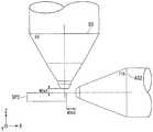
여기에서 도 5 및 도 6을 참조하여, 집속 이온 빔 장치(D1)의 작동 거리인 FIB 작동 거리(WDa1)와, 빔 부스터 전압(Vb)의 관계에 대하여 설명한다. 도 5는, 본 실시 형태에 따른 FIB 작동 거리(WDa1)와, SEM 작동 거리(WDb1)의 일례를 나타내는 도면이다.Here, the relationship between the FIB working distance WDa1, which is the working distance of the focused ion beam device D1, and the beam booster voltage Vb, will be described with reference to FIGS. 5 and 6. 5 is a diagram showing an example of the FIB working distance WDa1 and the SEM working distance WDb1 according to the present embodiment.
X축 및 Y축은 수평면에 평행이고 또한 서로 직교하며, Z축은 X축 및 Y축과 직교하는 연직 방향을 나타낸다. 도 5에서는, 집속 이온 빔 장치(D1)에 구비되는 집속 이온 빔 경통(A1)은, Z축과 평행, 즉 연직 방향으로 구비된다. 이온 빔(B)은, 집속 이온 빔 경통(A1)으로부터 Z축의 부(負)의 방향으로 시료(SP1)에 조사된다.The X-axis and Y-axis are parallel to the horizontal plane and are orthogonal to each other, and the Z-axis represents a vertical direction orthogonal to the X-axis and Y-axis. In Fig. 5, the focused ion beam barrel A1 provided in the focused ion beam device D1 is provided in parallel with the Z axis, that is, in a vertical direction. The ion beam B is irradiated to the sample SP1 from the focused ion beam barrel A1 in the negative direction of the Z axis.
한편, 주사형 전자 현미경(D2)에 구비되는 전자 빔 경통(B1)은, Z축으로부터 소정의 각도만큼 기울어져 구비된다. 전자 빔(EB)은, 전자 빔 경통(B1)으로부터 당해 소정의 각도만큼 기울어져 시료(SP1)에 조사된다. 당해 소정의 각도는, 예를 들면 수평면으로부터 30~60°의 범위에서 설정된다.On the other hand, the electron beam barrel B1 provided in the scanning electron microscope D2 is provided inclined by a predetermined angle from the Z axis. The electron beam EB is inclined by the predetermined angle from the electron beam barrel B1 and irradiated to the sample SP1. The predetermined angle is set in the range of 30 to 60° from the horizontal plane, for example.
여기에서 FIB 작동 거리(WDa1)는, 집속 이온 빔 경통(A1)의 선단과, 시료(SP1)의 표면 사이의 거리이다. SEM 작동 거리(WDb1)는, 주사형 전자 현미경(D2)의 작동 거리이며, 전자 빔 경통(B1)의 선단과, 시료(SP1)의 표면 사이의 거리이다.Here, the FIB working distance WDa1 is the distance between the tip of the focused ion beam barrel A1 and the surface of the sample SP1. The SEM working distance WDb1 is the working distance of the scanning electron microscope D2, and is the distance between the tip of the electron beam barrel B1 and the surface of the sample SP1.
주사형 전자 현미경(D2)의 상분해능을 확보하기 위하여, FIB 작동 거리(WDa1) 쪽이 SEM 작동 거리(WDb1)보다 길다. FIB 작동 거리(WDa1)는, 예를 들면 8~16mm의 범위에서 설정된다. SEM 작동 거리(WDb1)는, 예를 들면 2~7mm의 범위에서 설정된다.In order to secure the phase resolution of the scanning electron microscope (D2), the FIB working distance (WDa1) is longer than the SEM working distance (WDb1). The FIB working distance WDa1 is set in a range of 8 to 16 mm, for example. The SEM working distance WDb1 is set in the range of 2 to 7 mm, for example.
도 6은, 본 실시 형태에 따른 FIB 작동 거리(WDa1)와 빔 부스터 전압(Vb)의 관계의 일례를 나타내는 도면이다. 그래프(G)는, 가속 전압이 1kV인 경우에, 빔 부스터 전압(Vb)의 값(빔 부스터 전압값(Eb))에 대한 CP에 초점 맞춤 가능한 FIB 작동 거리(WDa1)를 나타내는 그래프이다. 그래프(G)의 좌상의 영역은 초점 맞춤 불가능한 FIB 작동 거리(WDa1)에 대응하고, 그래프(G)의 우하의 영역은 초점 맞춤 가능한 FIB 작동 거리(WDa1)에 대응한다. 즉 그래프(G)는 CP에 초점 맞춤 가능한지 불가능한지의 경계를 나타내고 있다. 그래프(G)에 의하면, 빔 부스터 전압(Vb)의 절댓값이 커질수록, 초점 맞춤 가능한 FIB 작동 거리(WDa1)는 짧아지는 경향이 있다.6 is a diagram showing an example of the relationship between the FIB operating distance WDa1 and the beam booster voltage Vb according to the present embodiment. The graph G is a graph showing the FIB working distance WDa1 that can be focused on CP with respect to the value of the beam booster voltage Vb (beam booster voltage value Eb) when the acceleration voltage is 1 kV. The upper left area of the graph G corresponds to the non-focusable FIB working distance WDa1, and the lower right area of the graph G corresponds to the focusable FIB working distance WDa1. That is, the graph G represents the boundary between whether or not the CP can be focused. According to the graph G, as the absolute value of the beam booster voltage Vb increases, the focusable FIB operating distance WDa1 tends to decrease.
예를 들면, 점 P1에 주목하면, FIB 작동 거리(WDa1)가 16mm인 경우에는, 초점 맞춤 가능하기 위해서는, 빔 부스터 전압(Vb)의 값의 절댓값을 6kV 이하로 할 필요가 있는 것을 알 수 있다.For example, paying attention to the point P1, it can be seen that when the FIB working distance WDa1 is 16 mm, the absolute value of the beam booster voltage Vb needs to be 6 kV or less in order to be able to focus. .
여기에서 도 7을 참조하여, 제어부(9)가 빔 부스터 전압값(Eb)을 설정하는 처리에 대하여 설명한다. 도 7은, 본 실시 형태에 따른 빔 부스터 전압값(Eb)의 설정 처리의 일례를 나타내는 도면이다.Here, with reference to FIG. 7, a process in which the
단계 S10: 처리부(90)는, PC(17)로부터 가속 전압값(Eacc)을 취득한다.Step S10: The processing
단계 S20: 처리부(90)는, 기억부(91)로부터 전압 테이블(T)을 읽어 낸다.Step S20: The processing
단계 S30: 처리부(90)는, 읽어 낸 전압 테이블(T)에 의거하여, 가속 전압값(Eacc)에 따른 빔 부스터 전압값(Eb)을 설정한다. 여기에서 처리부(90)는, 빔 부스터 전압값(Eb)으로서, 전압 테이블(T)에 의거하여 가속 전압값(Eacc)에 대응하는 빔 부스터 전압 설정값(TEb)과 동일하거나 소정의 값만큼 낮은 빔 부스터 전압값(Eb)을 산출한다. 처리부(90)는, 산출한 빔 부스터 전압값(Eb)을 빔 부스터 전원부(7)에 공급함으로써, 빔 부스터 전압값(Eb)을 설정한다.Step S30: The processing
따라서, 제어부(9)는, 가속 전원(10)이 이온 빔(B)에 인가하는 가속 전압(Vacc)의 값인 가속 전압값(Eacc)과, 빔 부스터(4)가 이온 빔(B)에 인가하는 빔 부스터 전압(Vb)의 값인 빔 부스터 전압값(Eb)을, 이온 빔(B)의 초점 거리(FB)에 따라 미리 결정된 설정값인 빔 부스터 전압 설정값(TEb)에 의거하여 설정한다.Accordingly, the
여기에서, 전압 테이블(T)이란, 가속 전압값(Eacc)과 빔 부스터 전압 설정값(TEb)의 세트이다. 따라서, 제어부(9)는, 가속 전압값(Eacc)과 빔 부스터 전압 설정값(TEb)의 세트를 기억하는 기억부(91)로부터 읽어 낸 세트에 의거하여, 빔 부스터 전압값(Eb)을 빔 부스터 전압 설정값(TEb)으로 설정한다.Here, the voltage table T is a set of an acceleration voltage value Eacc and a beam booster voltage setting value TEb. Accordingly, the
또한, 본 실시 형태에서는, 제어부(9)가 기억부(91)를 구비하는 경우에 대하여 설명했지만, 이것에 한정되지 않는다. 기억부(91)는, 복합 하전 입자 빔 장치(D)의 외부에 구비되어도 된다. 기억부(91)가 복합 하전 입자 빔 장치(D)의 외부에 구비되는 경우, 예를 들면, 기억부(91)는, 외부 기억 장치나, 클라우드 서버로서 구비된다.In addition, in this embodiment, although the case where the
또 기억부(91)가 전압 테이블(T)을 기억하는 대신에, 기억부(91)가 가속 전압값(Eacc)으로부터 빔 부스터 전압값(Eb)을 산출하는 연산식을 기억하고, 제어부(9)는 이 연산식에 의거하여 빔 부스터 전압값(Eb)을 산출하여 설정해도 된다.Further, instead of the
또한, 본 실시 형태에서는, 집속 이온 빔 경통(A1)이 연직 방향으로 구비되고, 전자 빔 경통(B1)이 연직 방향으로부터 소정의 각도만큼 기울어져 구비되는 경우에 대하여 설명했지만, 이것에 한정되지 않는다.In addition, in this embodiment, the case where the focused ion beam barrel A1 is provided in a vertical direction and the electron beam barrel B1 is provided inclined by a predetermined angle from the vertical direction has been described, but the present invention is not limited thereto. .
여기에서 도 8 및 도 9를 참조하여, 집속 이온 빔 경통(A1), 및 전자 빔 경통(B1)의 배치의 변형예에 대하여 설명한다.Here, a modified example of the arrangement of the focused ion beam barrel A1 and the electron beam barrel B1 will be described with reference to FIGS. 8 and 9.
도 8은, 본 실시 형태의 변형예에 따른 집속 이온 빔 경통(A2), 및 전자 빔 경통(B2)의 배치의 제1 예를 나타내는 도면이다. 도 8에서는, 집속 이온 빔 경통(A2)은, Z축으로부터 소정의 각도만큼 기울어져 구비된다. 이온 빔(B)은, 집속 이온 빔 경통(A2)으로부터 당해 소정의 각도만큼 기울어져 시료(SP2)에 조사된다.8 is a diagram showing a first example of the arrangement of the focused ion beam barrel A2 and the electron beam barrel B2 according to a modification of the present embodiment. In Fig. 8, the focused ion beam barrel A2 is provided so as to be inclined by a predetermined angle from the Z axis. The ion beam B is inclined by the predetermined angle from the focused ion beam barrel A2 and irradiated onto the sample SP2.
한편, 전자 빔 경통(B2)은, Z축과 평행, 즉 연직 방향으로 구비된다. 전자 빔(EB)은, 전자 빔 경통(B2)으로부터 Z축의 부의 방향으로 시료(SP2)에 조사된다.On the other hand, the electron beam barrel B2 is provided in parallel with the Z axis, that is, in the vertical direction. The electron beam EB is irradiated to the sample SP2 in the negative direction of the Z-axis from the electron beam barrel B2.
FIB 작동 거리(WDa2) 쪽이 SEM 작동 거리(WDb2)보다 길다.The FIB working distance (WDa2) is longer than the SEM working distance (WDb2).
도 9는, 본 실시 형태의 변형예에 따른 집속 이온 빔 경통(A3), 및 전자 빔 경통(B3)의 배치의 제2 예를 나타내는 도면이다. 도 9에서는, 집속 이온 빔 경통(A3)은, X축과 평행, 즉 수평 방향으로 구비된다. 이온 빔(B)은, 집속 이온 빔 경통(A2)으로부터 X축의 부의 방향으로 시료(SP3)에 조사된다.9 is a view showing a second example of the arrangement of the focused ion beam barrel A3 and the electron beam barrel B3 according to a modification of the present embodiment. In Fig. 9, the focused ion beam barrel A3 is provided in parallel with the X axis, that is, in the horizontal direction. The ion beam B is irradiated to the sample SP3 in the negative direction of the X-axis from the focused ion beam barrel A2.
한편, 전자 빔 경통(B3)은, Z축과 평행, 즉 연직 방향으로 구비된다. 전자 빔(EB)은, 전자 빔 경통(B3)으로부터 Z축의 부의 방향으로 시료(SP3)에 조사된다.On the other hand, the electron beam barrel B3 is provided in parallel with the Z axis, that is, in the vertical direction. The electron beam EB is irradiated to the sample SP3 in the negative direction of the Z axis from the electron beam barrel B3.
FIB 작동 거리(WDa3)가 SEM 작동 거리(WDb3)보다 길다.The FIB working distance (WDa3) is longer than the SEM working distance (WDb3).
이상에서 설명한 바와 같이, 본 실시 형태에 따른 복합 하전 입자 빔 장치(D)에서는, 하전 입자 빔(이온 빔(B))의 원하는 가속 전압에 따라 집속 이온 빔을 CP에 초점 맞춤 가능한 빔 부스터(4)의 빔 부스터 전압(Vb)의 값(빔 부스터 전압값(Eb))을 설정할 수 있다.As described above, in the composite charged particle beam device D according to the present embodiment, the
본 발명의 효과를, Ga(갈륨) 집속 이온 빔에 의한 투과 전자 현미경용 박편 시료 제작을 예로 설명한다. 가공은 이하의 3단계로 실시한다.The effect of the present invention will be described by taking the production of a thin sample for a transmission electron microscope using a Ga (gallium) focused ion beam as an example. Processing is carried out in the following three steps.
(1) 조가공(1) rough processing
집속 이온 빔의 가속 전압을 30kV, 빔 전류를 10nA로 하여 박편의 주변부의 가공을 행한다. 박편의 주변부를 고가속 전압, 및 대전류에 의하여 가공 레이트가 큰 조건으로 가공을 행하는 것은 공지이다(특허문헌 1). 가속 전압 30kV에서는 색 수차나 쿨롬 상호 작용에 의한 빔 블러는 현저하지는 않기 때문에, 빔 부스터의 설정 전압은 0V로 한다. 본 조가공에 의하여 박편의 폭을 0.7μm까지 깎아 들어간다. 박편의 폭은, 박편 가공부와 동일점에 조사되고 있는 전자 빔에 의한 주사 전자 현미경상에 의하여, 가공의 진행 상황을 대략 실시간으로 관찰함으로써 확인한다. 단 가속 전압이 30kV이기 때문에, Si층에 있어서는 Ga 주입 및 원자 간의 충돌 캐스케이드에 의하여 25nm의 깊이의 대미지층이 형성된다. 박편의 양면에 각각 표면으로부터 25nm의 깊이의 대미지층이 형성된다.Processing of the periphery of the flake is performed with an acceleration voltage of 30 kV and a beam current of 10 nA of the focused ion beam. It is known to process the periphery of a thin piece under conditions of a high processing rate by a high acceleration voltage and a large current (Patent Document 1). At an acceleration voltage of 30 kV, the beam blur due to chromatic aberration or coulomb interaction is not significant, so the set voltage of the beam booster is set to 0 V. By this rough processing, the width of the flake is cut to 0.7 μm. The width of the flake is confirmed by observing the progress of processing substantially in real time with a scanning electron microscope image using an electron beam irradiated at the same point as the flake processing unit. However, since the acceleration voltage is 30 kV, a damage layer having a depth of 25 nm is formed in the Si layer by Ga implantation and collision cascade between atoms. Damage layers with a depth of 25 nm from the surface are formed on both sides of the flake.
(2) 중간 가공(2) intermediate processing
집속 이온 빔의 가속 전압을 1kV, 빔 전류를 200pA로 하여, 상술한 조가공으로 형성된 대미지층을 에칭한다. 그때에 새롭게 형성되는 대미지층의 두께를 최대한 얇게 하기 위하여, 가속 전압을 내려 가공을 행한다. 가속 전압 1kV에서는 색 수차나 쿨롬 상호 작용에 의한 빔 블러는 현저해지기 때문에, 빔 부스터의 설정 전압은 도 4를 참조하여 -7kV로 설정한다. 본 중간 가공에 의하여 박편의 폭을 0.3μm까지 깎아 들어간다. 박편의 폭은, 조가공과 동일하게, 박편 가공부와 동일점에 조사되고 있는 전자 빔에 의한 주사 전자 현미경상에 의하여, 가공의 진행 상황을 대략 실시간으로 관찰함으로써 확인한다. 단 가속 전압이 1kV이기 때문에, Si층에 있어서는 Ga 주입 및 원자 간의 충돌 캐스케이드에 의하여 3nm의 대미지층이 형성된다. 박편의 양면에 각각 표면으로부터 3nm의 깊이의 대미지층이 형성된다.With the acceleration voltage of the focused ion beam being 1 kV and the beam current being 200 pA, the damage layer formed by the coarse processing described above is etched. At that time, in order to make the thickness of the damage layer newly formed as thin as possible, processing is performed by lowering the acceleration voltage. At an acceleration voltage of 1 kV, since the beam blur due to chromatic aberration and coulomb interaction becomes remarkable, the set voltage of the beam booster is set to -7 kV with reference to FIG. 4. By this intermediate processing, the width of the flake is cut to 0.3 μm. The width of the flake is confirmed by observing the progress of the processing in approximately real time by means of a scanning electron microscope image by an electron beam irradiated to the same point as the flake processing unit, similarly to the coarse processing. However, since the acceleration voltage is 1 kV, a damage layer of 3 nm is formed in the Si layer by Ga implantation and collision cascade between atoms. Damage layers with a depth of 3 nm from the surface are formed on both sides of the flake.
(3) 마무리 가공(3) finishing
집속 이온 빔의 가속 전압을 0.5kV, 빔 전류를 50pA로 하여, 상술한 중간 가공에서 형성된 대미지층을 에칭하여 대미지층을 얇게 하면서, 박편의 두께도 얇게 마무리한다. 그때에 새롭게 형성되는 대미지층의 두께를 최대한 얇게 하기 위하여, 가속 전압을 더 내려 가공을 행한다. 가속 전압 0.5kV에서는 색 수차나 쿨롬 상호 작용에 의한 빔 블러는 더 현저해지기 때문에, 빔 부스터의 설정 전압은 도 4를 참조하여 -4kV로 설정한다. 이때, 본 발명에 의한 빔 부스터의 설정 방법을 사용하지 않는 경우, 예를 들면 상술한 중간 마무리의 조건인 빔 부스터의 설정 전압과 동일한 -7kV로 설정하면, 집속 이온 빔의 초점을 박편 시료에 맞출 수 없다. 본 마무리 가공에 의하여 박편의 폭을 0.1μm(=100nm)까지 깎아 들어간다. 박편의 폭은, 상술한 가공과 동일하게, 박편 가공부와 동일점에 조사되고 있는 전자 빔에 의한 주사 전자 현미경상에 의하여, 가공의 진행 상황을 대략 실시간으로 관찰함으로써 확인한다. 단 가속 전압이 0.5kV이기 때문에, Si층에 있어서는 Ga 주입 및 원자 간의 충돌 캐스케이드에 의하여 2nm의 대미지층이 형성된다. 박편의 양면에 각각 표면으로부터 2nm의 깊이의 대미지층이 형성된다.With the acceleration voltage of the focused ion beam being 0.5 kV and the beam current being 50 pA, the damage layer formed in the above-described intermediate processing is etched to make the damage layer thin, and the thickness of the flake is also thinned. At that time, in order to make the thickness of the newly formed damage layer as thin as possible, the acceleration voltage is further lowered to perform processing. At an acceleration voltage of 0.5 kV, since the beam blur due to chromatic aberration or coulomb interaction becomes more pronounced, the set voltage of the beam booster is set to -4 kV with reference to FIG. 4. At this time, when the method of setting the beam booster according to the present invention is not used, for example, if the setting voltage is set to -7 kV, which is the same as the setting voltage of the beam booster, which is the condition for intermediate finishing, the focus of the focused ion beam is focused on the thin sample. Can't. By this finishing process, the width of the flake is cut to 0.1 μm (=100 nm). The width of the flake is confirmed by observing the progress of processing substantially in real time by means of a scanning electron microscope image by an electron beam irradiated to the same point as the flake processing unit, similarly to the above-described processing. However, since the acceleration voltage is 0.5 kV, a damage layer of 2 nm is formed in the Si layer by Ga implantation and collision cascade between atoms. Damage layers with a depth of 2 nm from the surface are formed on both sides of the flake.
이상의 절차에 의하여 두께 0.1μm(=100nm), 박막 표면의 대미지층 4nm(2nm×2)의 박편을 얻는다. 박편 두께에 대한 대미지층의 두께는 4/100(=4%)이며, 고품위의 박편 가공이 가능하다.By the above procedure, a thin piece having a thickness of 0.1 μm (=100 nm) and a damage layer of 4 nm (2 nm×2) on the surface of the thin film is obtained. The thickness of the damage layer relative to the flake thickness is 4/100 (=4%), and high-quality flake processing is possible.
상술한 바와 같이 일반적으로 복합 하전 입자 빔 장치에서는, 집속 이온 빔의 초점이 CP에 맞춰질 것이 요구된다. 본 실시 형태에 따른 복합 하전 입자 빔 장치(D)에서는, 전압 테이블(T)은, CP에 초점 맞춤 가능한 가속 전압값(Eacc)과 빔 부스터 전압 설정값(TEb)의 조합이 미리 구해진 테이블이며, 집속 이온 빔의 원하는 가속 전압에 따라 CP에 초점 맞춤 가능한 빔 부스터 전압(Vb)의 값(빔 부스터 전압값(Eb))을 설정할 수 있다.In general, as described above, in a composite charged particle beam device, the focus of the focused ion beam is required to be focused on the CP. In the composite charged particle beam device D according to the present embodiment, the voltage table T is a table in which a combination of an acceleration voltage value Eacc that can be focused on CP and a beam booster voltage set value TEb is obtained in advance, A value of the beam booster voltage Vb (beam booster voltage value Eb) capable of focusing on the CP can be set according to the desired acceleration voltage of the focused ion beam.
또한, 빔 부스터를 탑재한 주사형 전자 현미경에 있어서도, 전자 빔의 초점 위치가 부스터 전압의 인가에 의하여 제한되는 과제가 발생하지만, 전자 빔에서는 작동 거리가 짧기 때문에 이 과제는 표면화되어 있지 않다. 집속 이온 빔에 있어서도, 집속 이온 빔의 작동 거리를 짧게 하면 이 과제는 표면화되지 않지만, 주사형 전자 현미경과의 배치의 관계상, 집속 이온 빔의 작동 거리가 전자 빔의 작동 거리에 비하여 길어진다. 상술한 바와 같이, 이것은 주사형 전자 현미경의 상분해능을 확보하기 위해서이다.Further, even in a scanning electron microscope equipped with a beam booster, a problem arises in which the focal position of the electron beam is limited by the application of a booster voltage, but this problem is not surfaced because the working distance is short in the electron beam. Even in the focused ion beam, if the working distance of the focused ion beam is shortened, this problem does not surface, but the working distance of the focused ion beam becomes longer than the working distance of the electron beam due to the arrangement with the scanning electron microscope. As described above, this is to ensure the phase resolution of the scanning electron microscope.
상술한 실시 형태에 있어서의 복합 하전 입자 빔 장치(D)는 집속 이온 빔과 전자 빔의 2개의 하전 입자 빔을 구비하는 것이다. 복합 하전 입자 빔 장치(D)에 추가로 아르곤 이온 빔 등의 제3 하전 입자 빔을 설치한 경우, 3개의 하전 입자 빔이 시료 상의 동일점에 조사 가능한 구성으로 되어 있으면, 상술과 동일한 방법으로 집속 이온 빔의 부스터 전압을 제어함으로써, 집속 이온 빔의 원하는 가속 전압에 따라 CP에 초점 맞춤 가능한 빔 부스터 전압(Vb)의 값(빔 부스터 전압값(Eb))을 설정할 수 있다.The composite charged particle beam device (D) in the above-described embodiment is provided with two charged particle beams, a focused ion beam and an electron beam. When a third charged particle beam such as an argon ion beam is additionally installed in the complex charged particle beam device (D), if the three charged particle beams are configured to be irradiated to the same point on the sample, the beam is focused in the same manner as described above. By controlling the booster voltage of the ion beam, it is possible to set a value of the beam booster voltage Vb (beam booster voltage value Eb) capable of focusing on the CP according to the desired acceleration voltage of the focused ion beam.
3개의 하전 입자 빔이 시료 상의 동일점에 조사할 수 없는 경우, 예를 들면 집속 이온 빔과 전자 빔의 시료 상의 동일 조사점(CP1)과, 집속 이온 빔과 아르곤 이온 빔의 시료 상의 동일 조사점(CP2)을 정의하고, 각각에 대응하는 전압 테이블 T-1 및 T-2를 준비하여 집속 이온 빔의 빔 부스터 전압(Vb)을 설정한다. 시료에 집속 이온 빔과 전자 빔의 조사를 행하는 프로세스에서는 전압 테이블 T-1을 사용하여 집속 이온 빔의 빔 부스터 전압(Vb)을 설정하고, 시료에 집속 이온 빔과 아르곤 이온 빔의 조사를 행하는 프로세스에서는 전압 테이블 T-2를 사용하여 집속 이온 빔의 빔 부스터 전압(Vb)을 설정한다.When three charged particle beams cannot irradiate the same point on the sample, for example, the same point of irradiation on the sample of the focused ion beam and the electron beam (CP1), and the same point of irradiation of the focused ion beam and the argon ion beam on the sample. (CP2) is defined, and voltage tables T-1 and T-2 corresponding to each are prepared to set the beam booster voltage Vb of the focused ion beam. In the process of irradiating a sample with a focused ion beam and an electron beam, the beam booster voltage (Vb) of the focused ion beam is set using the voltage table T-1, and the sample is irradiated with a focused ion beam and an argon ion beam. In FIG. 2, the beam booster voltage Vb of the focused ion beam is set using the voltage table T-2.
또한 하전 입자 빔이 증가한 경우는 상기의 방법을 확장시켜, 대응하는 전압 테이블 T-n을 준비함으로써, CPn에 초점 맞춤 가능한 빔 부스터 전압(Vb)의 값(빔 부스터 전압값(Eb))을 설정할 수 있다.In addition, when the charged particle beam is increased, the above method is extended and a corresponding voltage table Tn is prepared, so that the value of the beam booster voltage Vb (beam booster voltage value Eb) that can be focused on CPn can be set. .
또한, 상술한 실시 형태에 있어서의 복합 하전 입자 빔 장치(D)의 일부, 예를 들면, 제어부(9)를 컴퓨터로 실현하도록 해도 된다. 그 경우, 이 제어 기능을 실현하기 위한 프로그램을 컴퓨터 판독 가능한 기록 매체에 기록하고, 이 기록 매체에 기록된 프로그램을 컴퓨터 시스템에 읽어 들여, 실행함으로써 실현해도 된다. 또한, 여기에서 말하는 「컴퓨터 시스템」이란, 복합 하전 입자 빔 장치(D)에 내장된 컴퓨터 시스템이며, OS나 주변 기기 등의 하드웨어를 포함하는 것으로 한다. 또한, 「컴퓨터 판독 가능한 기록 매체」란, 플렉서블 디스크, 광학 자기 디스크, ROM, CD-ROM 등의 휴대용 매체, 컴퓨터 시스템에 내장되는 하드 디스크 등의 기억 장치를 말한다. 또한 「컴퓨터 판독 가능한 기록 매체」란, 인터넷 등의 네트워크나 전화 회선 등의 통신 회선을 통하여 프로그램을 송신하는 경우의 통신선과 같이, 단시간, 동적으로 프로그램을 유지하는 것, 그 경우의 서버나 클라이언트가 되는 컴퓨터 시스템 내부의 휘발성 메모리와 같이, 일정 시간 프로그램을 유지하고 있는 것도 포함해도 된다. 또한 상기 프로그램은, 상술한 기능의 일부를 실현하기 위한 것이어도 되고, 또한 상술한 기능을 컴퓨터 시스템에 이미 기록되어 있는 프로그램과의 조합으로 실현할 수 있는 것이어도 된다.In addition, a part of the complex charged particle beam device D in the above-described embodiment, for example, the
또한, 상술한 실시 형태에 있어서의 제어부(9)의 일부, 또는 전부를, LSI(Large Scale Integration) 등의 집적 회로로 하여 실현해도 된다. 제어부(9)의 각 기능 블록은 개별적으로 프로세서화해도 되고, 일부, 또는 전부를 집적하여 프로세서화해도 된다. 또한, 집적 회로화의 수법은 LSI에 한정되지 않고 전용 회로, 또는 범용 프로세서로 실현해도 된다. 또한, 반도체 기술의 진보에 의하여 LSI를 대체하는 집적 회로화의 기술이 출현한 경우, 당해 기술에 의한 집적 회로를 이용해도 된다.Further, part or all of the
이상, 도면을 참조하여 이 발명의 일 실시 형태에 대하여 상세하게 설명해 왔지만, 구체적인 구성은 상술한 것에 한정되는 것은 아니고, 이 발명의 요지를 벗어나지 않는 범위 내에 있어서 다양한 설계 변경 등을 하는 것이 가능하다.As described above, one embodiment of the present invention has been described in detail with reference to the drawings, but the specific configuration is not limited to that described above, and various design changes and the like can be made within the scope not departing from the gist of the present invention.
D 복합 하전 입자 빔 장치
D1 집속 이온 빔 장치
D2 주사형 전자 현미경
1 이온원 제어부
10 가속 전원
3 콘덴서 렌즈
4 빔 부스터
5 대물렌즈
9 제어부
91 기억부
T 전압 테이블
Eb 빔 부스터 전압값
TEb 빔 부스터 전압 설정값
Eacc 가속 전압값D composite charged particle beam device
D1 focused ion beam device
D2 scanning electron microscope
1 Ion source control unit
10 acceleration power
3 condenser lens
4 beam booster
5 objective lens
9 control unit
91 memory
T voltage table
Eb beam booster voltage value
TEb beam booster voltage setpoint
Eacc acceleration voltage value
Claims (4)
Translated fromKorean상기 이온 공급부가 공급하는 상기 이온 빔에 가속 전압을 인가함으로써 가속시키는 가속 전압 인가부와,
상기 가속 전압 인가부가 가속시킨 상기 이온 빔을 집속시키는 제1 집속부와,
상기 제1 집속부가 집속시킨 상기 이온 빔에 빔 부스터 전압을 인가하는 빔 부스터 전압 인가부와,
상기 빔 부스터 전압 인가부가 상기 빔 부스터 전압을 인가한 상기 이온 빔을 집속시켜 시료에 조사시키는 제2 집속부와,
전자 빔을 상기 시료에 조사하는 전자 빔 조사부와,
상기 빔 부스터 전압 인가부가 상기 이온 빔에 인가하는 상기 빔 부스터 전압의 값을, 상기 가속 전압 인가부가 상기 이온 빔에 인가하는 상기 가속 전압의 값과, 집속시킨 상기 이온 빔의 초점 거리에 따라 미리 결정된 설정값에 의거하여 설정하는 제어부를 구비하는 복합 하전 입자 빔 장치.An ion supply unit for supplying an ion beam,
An acceleration voltage applying unit that accelerates by applying an acceleration voltage to the ion beam supplied by the ion supply unit,
A first focusing unit for focusing the ion beam accelerated by the acceleration voltage applying unit,
A beam booster voltage application unit for applying a beam booster voltage to the ion beam focused by the first focusing unit;
A second focusing unit for focusing the ion beam to which the beam booster voltage application unit has applied the beam booster voltage and irradiating the sample,
An electron beam irradiation unit for irradiating an electron beam onto the sample,
A value of the beam booster voltage applied by the beam booster voltage applying unit to the ion beam is determined in advance according to a value of the acceleration voltage applied by the acceleration voltage applying unit to the ion beam and a focal length of the focused ion beam. A complex charged particle beam device comprising a control unit that is set based on a set value.
집속한 상기 이온 빔의 조사점 및 초점과, 상기 전자 빔의 조사점은 상기 시료 상의 동일한 점인 복합 하전 입자 빔 장치.The method according to claim 1,
An irradiation point and a focal point of the focused ion beam and an irradiation point of the electron beam are the same points on the sample.
상기 제어부는, 상기 가속 전압의 값과 상기 설정값의 세트를 기억하는 기억부로부터 읽어 낸 상기 세트에 의거하여, 상기 빔 부스터 전압의 값을 상기 설정값으로 설정하는 복합 하전 입자 빔 장치.The method according to claim 1 or 2,
The control unit sets the value of the beam booster voltage to the set value based on the set read from a storage unit storing the set of the acceleration voltage and the set value.
상기 이온 공급부가 공급하는 상기 이온 빔에 가속 전압을 인가함으로써 가속시키는 가속 전압 인가부와,
상기 가속 전압 인가부가 가속시킨 상기 이온 빔을 집속시키는 제1 집속부와,
상기 제1 집속부가 집속시킨 상기 이온 빔에 빔 부스터 전압을 인가하는 빔 부스터 전압 인가부와,
상기 빔 부스터 전압 인가부가 상기 빔 부스터 전압을 인가한 상기 이온 빔을 집속시켜 시료에 조사시키는 제2 집속부와,
전자 빔을 상기 시료에 조사하는 전자 빔 조사부를 구비하는 복합 하전 입자 빔 장치에 있어서의 제어 방법에 있어서,
상기 빔 부스터 전압 인가부가 상기 이온 빔에 인가하는 상기 빔 부스터 전압의 값을, 상기 가속 전압 인가부가 상기 이온 빔에 인가하는 상기 가속 전압의 값과, 집속시킨 상기 이온 빔의 초점 거리에 따라 미리 결정된 설정값에 의거하여 설정하는 제어 과정을 갖는 제어 방법.An ion supply unit for supplying an ion beam,
An acceleration voltage applying unit that accelerates by applying an acceleration voltage to the ion beam supplied by the ion supply unit,
A first focusing unit for focusing the ion beam accelerated by the acceleration voltage applying unit,
A beam booster voltage application unit for applying a beam booster voltage to the ion beam focused by the first focusing unit;
A second focusing unit for focusing the ion beam to which the beam booster voltage application unit has applied the beam booster voltage and irradiating the sample,
In the control method in a composite charged particle beam device including an electron beam irradiation unit for irradiating an electron beam to the sample,
A value of the beam booster voltage applied by the beam booster voltage applying unit to the ion beam is determined in advance according to a value of the acceleration voltage applied by the acceleration voltage applying unit to the ion beam and a focal length of the focused ion beam. A control method having a control process that is set based on a set value.
Applications Claiming Priority (2)
| Application Number | Priority Date | Filing Date | Title |
|---|---|---|---|
| JPJP-P-2019-025928 | 2019-02-15 | ||
| JP2019025928AJP7154593B2 (en) | 2019-02-15 | 2019-02-15 | COMPOSITE CHARGED PARTICLE BEAM DEVICE AND CONTROL METHOD |
Publications (2)
| Publication Number | Publication Date |
|---|---|
| KR20200099954Atrue KR20200099954A (en) | 2020-08-25 |
| KR102713097B1 KR102713097B1 (en) | 2024-10-04 |
Family
ID=72043678
Family Applications (1)
| Application Number | Title | Priority Date | Filing Date |
|---|---|---|---|
| KR1020190137409AActiveKR102713097B1 (en) | 2019-02-15 | 2019-10-31 | Composite charged particle beam apparatus and control method thereof |
Country Status (5)
| Country | Link |
|---|---|
| US (1) | US11017982B2 (en) |
| JP (1) | JP7154593B2 (en) |
| KR (1) | KR102713097B1 (en) |
| CN (1) | CN111584335B (en) |
| TW (1) | TWI841663B (en) |
Families Citing this family (2)
| Publication number | Priority date | Publication date | Assignee | Title |
|---|---|---|---|---|
| EP4075476A1 (en)* | 2021-04-15 | 2022-10-19 | ASML Netherlands B.V. | Electron-optical device |
| CN114236364B (en)* | 2022-02-24 | 2022-05-31 | 上海聚跃检测技术有限公司 | Failure analysis method and system for integrated circuit chip |
Citations (10)
| Publication number | Priority date | Publication date | Assignee | Title |
|---|---|---|---|---|
| JPH10106474A (en) | 1996-09-30 | 1998-04-24 | Seiko Instr Inc | Work device by ion beam |
| JPH11223588A (en) | 1998-02-09 | 1999-08-17 | Hitachi Ltd | Preparation of thin section sample for transmission electron microscope |
| JP2000173520A (en) | 1998-11-30 | 2000-06-23 | Advantest Corp | Particle beam device |
| JP2006236836A (en) | 2005-02-25 | 2006-09-07 | Sii Nanotechnology Inc | Sample height adjustment method, sample observation method, sample processing method, and charged particle beam apparatus |
| JP2007103108A (en) | 2005-10-03 | 2007-04-19 | Sii Nanotechnology Inc | Processing method using focused ion beam |
| JP2007193977A (en) | 2006-01-17 | 2007-08-02 | Hitachi High-Technologies Corp | Charged beam apparatus and charged beam processing method |
| JP2009272293A (en) | 2008-04-11 | 2009-11-19 | Hitachi High-Technologies Corp | Focused ion beam apparatus |
| JP2013125583A (en)* | 2011-12-13 | 2013-06-24 | Hitachi High-Technologies Corp | Scanning electron beam device and dimension measuring method using the same |
| JP2013196826A (en) | 2012-03-16 | 2013-09-30 | Honda Motor Co Ltd | Battery module |
| JP2016146237A (en)* | 2015-02-06 | 2016-08-12 | 株式会社日立ハイテクノロジーズ | Compound charged particle beam system |
Family Cites Families (9)
| Publication number | Priority date | Publication date | Assignee | Title |
|---|---|---|---|---|
| WO2001054163A1 (en)* | 2000-01-21 | 2001-07-26 | Koninklijke Philips Electronics N.V. | Shaped and low density focused ion beams |
| JP4789260B2 (en)* | 2006-08-23 | 2011-10-12 | エスアイアイ・ナノテクノロジー株式会社 | Charged particle beam apparatus and aperture axis adjusting method |
| JP5044813B2 (en)* | 2007-02-19 | 2012-10-10 | エスアイアイ・ナノテクノロジー株式会社 | Focused ion beam apparatus and charged particle optical system adjustment method |
| US8742361B2 (en)* | 2012-06-07 | 2014-06-03 | Fei Company | Focused charged particle column for operation at different beam energies at a target |
| US8933414B2 (en)* | 2013-02-27 | 2015-01-13 | Fei Company | Focused ion beam low kV enhancement |
| TWI685012B (en)* | 2014-12-22 | 2020-02-11 | 美商卡爾蔡司顯微鏡有限責任公司 | Charged particle beam system, method of processing a sample, method of manufacturing a josephson junction and method of creating a plurality josephson junctions |
| JP6554288B2 (en)* | 2015-01-26 | 2019-07-31 | 株式会社日立ハイテクノロジーズ | Charged particle beam equipment |
| CN105668514B (en)* | 2016-01-25 | 2019-04-23 | 北京航空航天大学 | A method for controllable micro-nano processing of focused ion beam-electron beam dual-beam fusion |
| JP6906786B2 (en)* | 2017-03-27 | 2021-07-21 | 株式会社日立ハイテクサイエンス | Sample holders, member mounting devices, and charged particle beam devices |
- 2019
- 2019-02-15JPJP2019025928Apatent/JP7154593B2/enactiveActive
- 2019-10-31KRKR1020190137409Apatent/KR102713097B1/enactiveActive
- 2020
- 2020-01-16TWTW109101467Apatent/TWI841663B/enactive
- 2020-01-20CNCN202010064843.3Apatent/CN111584335B/enactiveActive
- 2020-02-07USUS16/785,362patent/US11017982B2/enactiveActive
Patent Citations (10)
| Publication number | Priority date | Publication date | Assignee | Title |
|---|---|---|---|---|
| JPH10106474A (en) | 1996-09-30 | 1998-04-24 | Seiko Instr Inc | Work device by ion beam |
| JPH11223588A (en) | 1998-02-09 | 1999-08-17 | Hitachi Ltd | Preparation of thin section sample for transmission electron microscope |
| JP2000173520A (en) | 1998-11-30 | 2000-06-23 | Advantest Corp | Particle beam device |
| JP2006236836A (en) | 2005-02-25 | 2006-09-07 | Sii Nanotechnology Inc | Sample height adjustment method, sample observation method, sample processing method, and charged particle beam apparatus |
| JP2007103108A (en) | 2005-10-03 | 2007-04-19 | Sii Nanotechnology Inc | Processing method using focused ion beam |
| JP2007193977A (en) | 2006-01-17 | 2007-08-02 | Hitachi High-Technologies Corp | Charged beam apparatus and charged beam processing method |
| JP2009272293A (en) | 2008-04-11 | 2009-11-19 | Hitachi High-Technologies Corp | Focused ion beam apparatus |
| JP2013125583A (en)* | 2011-12-13 | 2013-06-24 | Hitachi High-Technologies Corp | Scanning electron beam device and dimension measuring method using the same |
| JP2013196826A (en) | 2012-03-16 | 2013-09-30 | Honda Motor Co Ltd | Battery module |
| JP2016146237A (en)* | 2015-02-06 | 2016-08-12 | 株式会社日立ハイテクノロジーズ | Compound charged particle beam system |
Non-Patent Citations (1)
| Title |
|---|
| Michael Rauscher and Erich Plies, 「Low Energy focused ion beam system design」, Journal of Vacuum Science & Technology A, American Vacuum Society, 2006, 24(4), p. 1055-1066 |
Also Published As
| Publication number | Publication date |
|---|---|
| JP2020136002A (en) | 2020-08-31 |
| TWI841663B (en) | 2024-05-11 |
| TW202109598A (en) | 2021-03-01 |
| US20200266029A1 (en) | 2020-08-20 |
| CN111584335A (en) | 2020-08-25 |
| CN111584335B (en) | 2023-09-19 |
| KR102713097B1 (en) | 2024-10-04 |
| US11017982B2 (en) | 2021-05-25 |
| JP7154593B2 (en) | 2022-10-18 |
Similar Documents
| Publication | Publication Date | Title |
|---|---|---|
| JP5792509B2 (en) | Charged particle beam apparatus and sample processing method | |
| US9053899B2 (en) | Method for imaging a sample in a charged particle apparatus | |
| US6949756B2 (en) | Shaped and low density focused ion beams | |
| TWI803572B (en) | Charged particle beam device, sample processing and observation method | |
| US10636615B2 (en) | Composite beam apparatus | |
| WO2009089499A4 (en) | Multibeam system | |
| JPWO2019224895A1 (en) | Charged particle beam device and its axis adjustment method | |
| IL237738A (en) | Dual-lens-gun electron beam apparatus and methods for high-resolution imaging with both high and low beam currents | |
| KR102713097B1 (en) | Composite charged particle beam apparatus and control method thereof | |
| KR20180109687A (en) | Charged particle beam apparatus | |
| US9761407B2 (en) | Ion beam device and emitter tip adjustment method | |
| JP2006179504A (en) | Electron beam device with aberration corrector | |
| KR102815204B1 (en) | Charged particle beam apparatus, composite charged particle beam apparatus, and control method for charged particle beam apparatus | |
| WO2023032078A1 (en) | Focused ion beam device | |
| JP7090902B2 (en) | Control method of focused ion beam device and focused ion beam device | |
| US11257655B2 (en) | Focused ion beam apparatus, and control method for focused ion beam apparatus | |
| US8390152B2 (en) | Device and method for generating a stable high voltage | |
| JP7627791B2 (en) | Charged particle beam device and beam deflection method in the charged particle beam device | |
| JP2001351561A (en) | Focused ion beam equipment | |
| Rauscher et al. | Optimum mode of operation for a low energy focused ion beam system | |
| WO2025203456A1 (en) | Combined beam device |
Legal Events
| Date | Code | Title | Description |
|---|---|---|---|
| PA0109 | Patent application | Patent event code:PA01091R01D Comment text:Patent Application Patent event date:20191031 | |
| PG1501 | Laying open of application | ||
| A201 | Request for examination | ||
| PA0201 | Request for examination | Patent event code:PA02012R01D Patent event date:20220822 Comment text:Request for Examination of Application Patent event code:PA02011R01I Patent event date:20191031 Comment text:Patent Application | |
| GRNT | Written decision to grant | ||
| PR0701 | Registration of establishment | Comment text:Registration of Establishment Patent event date:20240927 Patent event code:PR07011E01D | |
| PR1002 | Payment of registration fee | Payment date:20240930 End annual number:3 Start annual number:1 | |
| PG1601 | Publication of registration |