KR20200096734A - Radio frequency power source and plasma processing apparatus - Google Patents
Radio frequency power source and plasma processing apparatusDownload PDFInfo
- Publication number
- KR20200096734A KR20200096734AKR1020200008820AKR20200008820AKR20200096734AKR 20200096734 AKR20200096734 AKR 20200096734AKR 1020200008820 AKR1020200008820 AKR 1020200008820AKR 20200008820 AKR20200008820 AKR 20200008820AKR 20200096734 AKR20200096734 AKR 20200096734A
- Authority
- KR
- South Korea
- Prior art keywords
- high frequency
- power
- frequency power
- generate
- frequency
- Prior art date
- Legal status (The legal status is an assumption and is not a legal conclusion. Google has not performed a legal analysis and makes no representation as to the accuracy of the status listed.)
- Pending
Links
- 239000000758substrateSubstances0.000claimsdescription36
- 150000002500ionsChemical class0.000claimsdescription13
- 238000000034methodMethods0.000claimsdescription10
- 239000002131composite materialSubstances0.000claimsdescription9
- 238000013139quantizationMethods0.000claimsdescription6
- 238000010586diagramMethods0.000description29
- 238000001228spectrumMethods0.000description9
- XAGFODPZIPBFFR-UHFFFAOYSA-NaluminiumChemical compound[Al]XAGFODPZIPBFFR-UHFFFAOYSA-N0.000description6
- 229910052782aluminiumInorganic materials0.000description6
- 238000005260corrosionMethods0.000description6
- 230000007797corrosionEffects0.000description6
- 239000004020conductorSubstances0.000description4
- 239000000919ceramicSubstances0.000description3
- 230000007423decreaseEffects0.000description3
- 238000009792diffusion processMethods0.000description3
- 238000009616inductively coupled plasmaMethods0.000description3
- SIWVEOZUMHYXCS-UHFFFAOYSA-Noxo(oxoyttriooxy)yttriumChemical compoundO=[Y]O[Y]=OSIWVEOZUMHYXCS-UHFFFAOYSA-N0.000description3
- 238000006243chemical reactionMethods0.000description2
- 230000007274generation of a signal involved in cell-cell signalingEffects0.000description2
- 239000011810insulating materialSubstances0.000description2
- 230000001360synchronised effectEffects0.000description2
- 238000007792additionMethods0.000description1
- 239000006227byproductSubstances0.000description1
- 230000001276controlling effectEffects0.000description1
- 239000002826coolantSubstances0.000description1
- 239000003989dielectric materialSubstances0.000description1
- 238000005530etchingMethods0.000description1
- TWNQGVIAIRXVLR-UHFFFAOYSA-Noxo(oxoalumanyloxy)alumaneChemical compoundO=[Al]O[Al]=OTWNQGVIAIRXVLR-UHFFFAOYSA-N0.000description1
- 230000002093peripheral effectEffects0.000description1
- 238000009832plasma treatmentMethods0.000description1
- 239000010453quartzSubstances0.000description1
- 230000001105regulatory effectEffects0.000description1
- 239000004065semiconductorSubstances0.000description1
- 229910052710siliconInorganic materials0.000description1
- 239000010703siliconSubstances0.000description1
- HBMJWWWQQXIZIP-UHFFFAOYSA-Nsilicon carbideChemical compound[Si+]#[C-]HBMJWWWQQXIZIP-UHFFFAOYSA-N0.000description1
- 229910010271silicon carbideInorganic materials0.000description1
- VYPSYNLAJGMNEJ-UHFFFAOYSA-Nsilicon dioxideInorganic materialsO=[Si]=OVYPSYNLAJGMNEJ-UHFFFAOYSA-N0.000description1
- 238000006467substitution reactionMethods0.000description1
Images


Classifications
- H—ELECTRICITY
- H01—ELECTRIC ELEMENTS
- H01J—ELECTRIC DISCHARGE TUBES OR DISCHARGE LAMPS
- H01J37/00—Discharge tubes with provision for introducing objects or material to be exposed to the discharge, e.g. for the purpose of examination or processing thereof
- H01J37/32—Gas-filled discharge tubes
- H01J37/32009—Arrangements for generation of plasma specially adapted for examination or treatment of objects, e.g. plasma sources
- H01J37/32082—Radio frequency generated discharge
- H01J37/32137—Radio frequency generated discharge controlling of the discharge by modulation of energy
- H01J37/32155—Frequency modulation
- H01J37/32165—Plural frequencies
- H—ELECTRICITY
- H01—ELECTRIC ELEMENTS
- H01J—ELECTRIC DISCHARGE TUBES OR DISCHARGE LAMPS
- H01J37/00—Discharge tubes with provision for introducing objects or material to be exposed to the discharge, e.g. for the purpose of examination or processing thereof
- H01J37/32—Gas-filled discharge tubes
- H01J37/32009—Arrangements for generation of plasma specially adapted for examination or treatment of objects, e.g. plasma sources
- H01J37/32082—Radio frequency generated discharge
- H01J37/32174—Circuits specially adapted for controlling the RF discharge
- H—ELECTRICITY
- H01—ELECTRIC ELEMENTS
- H01J—ELECTRIC DISCHARGE TUBES OR DISCHARGE LAMPS
- H01J37/00—Discharge tubes with provision for introducing objects or material to be exposed to the discharge, e.g. for the purpose of examination or processing thereof
- H01J37/32—Gas-filled discharge tubes
- H01J37/32009—Arrangements for generation of plasma specially adapted for examination or treatment of objects, e.g. plasma sources
- H01J37/32082—Radio frequency generated discharge
- H01J37/32128—Radio frequency generated discharge using particular waveforms, e.g. polarised waves
- H—ELECTRICITY
- H01—ELECTRIC ELEMENTS
- H01J—ELECTRIC DISCHARGE TUBES OR DISCHARGE LAMPS
- H01J37/00—Discharge tubes with provision for introducing objects or material to be exposed to the discharge, e.g. for the purpose of examination or processing thereof
- H01J37/32—Gas-filled discharge tubes
- H01J37/32009—Arrangements for generation of plasma specially adapted for examination or treatment of objects, e.g. plasma sources
- H01J37/32082—Radio frequency generated discharge
- H01J37/32137—Radio frequency generated discharge controlling of the discharge by modulation of energy
- H01J37/32146—Amplitude modulation, includes pulsing
- H—ELECTRICITY
- H01—ELECTRIC ELEMENTS
- H01J—ELECTRIC DISCHARGE TUBES OR DISCHARGE LAMPS
- H01J37/00—Discharge tubes with provision for introducing objects or material to be exposed to the discharge, e.g. for the purpose of examination or processing thereof
- H01J37/32—Gas-filled discharge tubes
- H01J37/32009—Arrangements for generation of plasma specially adapted for examination or treatment of objects, e.g. plasma sources
- H01J37/32082—Radio frequency generated discharge
- H01J37/32174—Circuits specially adapted for controlling the RF discharge
- H01J37/32183—Matching circuits
- H—ELECTRICITY
- H01—ELECTRIC ELEMENTS
- H01J—ELECTRIC DISCHARGE TUBES OR DISCHARGE LAMPS
- H01J37/00—Discharge tubes with provision for introducing objects or material to be exposed to the discharge, e.g. for the purpose of examination or processing thereof
- H01J37/32—Gas-filled discharge tubes
- H01J37/32431—Constructional details of the reactor
- H01J37/32532—Electrodes
- H—ELECTRICITY
- H03—ELECTRONIC CIRCUITRY
- H03F—AMPLIFIERS
- H03F2200/00—Indexing scheme relating to amplifiers
- H03F2200/451—Indexing scheme relating to amplifiers the amplifier being a radio frequency amplifier
Landscapes
- Physics & Mathematics (AREA)
- Engineering & Computer Science (AREA)
- Plasma & Fusion (AREA)
- Chemical & Material Sciences (AREA)
- Analytical Chemistry (AREA)
- Plasma Technology (AREA)
- Drying Of Semiconductors (AREA)
Abstract
Translated fromKorean
Description
Translated fromKorean본 개시의 예시적 실시형태는, 고주파 전원 및 플라즈마 처리 장치에 관한 것이다.An exemplary embodiment of the present disclosure relates to a high frequency power supply and a plasma processing apparatus.
플라즈마 처리 장치가, 기판에 대한 플라즈마 처리에 있어서 이용되고 있다. 플라즈마 처리 장치는, 챔버 및 고주파 전원을 구비한다. 기판은, 챔버 내에 수용된다. 플라즈마 처리를 위하여, 가스가 챔버 내로 공급된다. 가스로부터 플라즈마를 생성하기 위하여, 고주파 전력이 고주파 전원에 의하여 공급된다. 일본 특허공개공보 2013-135159호에 기재되어 있는 바와 같이, 고주파 전력은, 펄스상(pulse狀)의 고주파 전력으로서 주기적으로 공급되는 경우가 있다. 이 문헌에 기재된 플라즈마 처리 장치에서는, 고주파 전력은, 직사각형 펄스로서 주기적으로 공급되고 있다.Plasma processing apparatuses are used in plasma processing of substrates. The plasma processing apparatus includes a chamber and a high frequency power supply. The substrate is accommodated in the chamber. For plasma processing, gas is supplied into the chamber. In order to generate plasma from the gas, high-frequency power is supplied by a high-frequency power source. As disclosed in Japanese Unexamined Patent Application Publication No. 2013-135159, the high frequency power is periodically supplied as pulsed high frequency power in some cases. In the plasma processing apparatus described in this document, high-frequency power is periodically supplied as rectangular pulses.
본 개시는, 주기적으로 공급되는 펄스상의 고주파 전력에 대한 반사파를 억제하기 위하여, 주기적으로 생성되는 펄스상의 고주파 전력의 대역을 좁히는 기술을 제공한다.The present disclosure provides a technique for narrowing the band of pulsed high-frequency power that is periodically generated in order to suppress a reflected wave for pulsed high-frequency power that is periodically supplied.
하나의 예시적 실시형태에 있어서, 플라즈마 처리 장치용 고주파 전원이 제공된다. 고주파 전원은, 전력 발생기 및 출력부를 구비한다. 전력 발생기는, 고주파 전력을 발생시키도록 구성되어 있다. 출력부는, 전력 발생기에 의하여 생성된 고주파 전력을 출력하도록 구성되어 있다. 고주파 전력은, 복수의 전력 성분을 포함한다. 복수의 전력 성분은, 소정 주파수의 간격으로 기본 주파수에 대하여 대칭으로 설정된 복수의 주파수를 각각 갖는다. 고주파 전력의 포락선(包絡線)은, 소정 주파수 또는 그 소정 주파수의 2배 이상의 배수의 주파수로 규정되는 시간 간격으로 주기적으로 출현하는 피크를 갖는다. 고주파 전력의 파워 레벨은, 피크의 각각의 출현 시점 직전의 포락선의 제로 크로스 영역과 그 출현 시점 직후의 포락선의 제로 크로스 영역 사이의 기간을 제외한 기간에서 제로이도록 설정되어 있다.In one exemplary embodiment, a high frequency power supply for a plasma processing apparatus is provided. The high frequency power supply includes a power generator and an output unit. The power generator is configured to generate high-frequency power. The output unit is configured to output high frequency power generated by the power generator. The high-frequency power includes a plurality of power components. The plurality of power components each have a plurality of frequencies set symmetrically with respect to the fundamental frequency at intervals of a predetermined frequency. The envelope of the high-frequency power has a peak that periodically appears at a time interval defined at a predetermined frequency or a frequency that is a multiple of two or more times the predetermined frequency. The power level of the high frequency power is set to be zero in a period excluding a period between the zero cross region of the envelope immediately before each occurrence of the peak and the zero cross region of the envelope immediately after the appearance of the peak.
하나의 예시적 실시형태에 의하면, 주기적으로 생성되는 펄스상의 고주파 전력의 대역을 좁히는 것이 가능해진다.According to one exemplary embodiment, it becomes possible to narrow the band of pulsed high-frequency power that is periodically generated.
도 1은, 하나의 예시적 실시형태에 관한 플라즈마 처리 장치를 개략적으로 나타내는 도이다.
도 2는, 하나의 예시적 실시형태에 관한 고주파 전원의 구성을 나타내는 도이다.
도 3의 (a)는 복수의 전력 성분의 합성 전력의 파형의 일례를 나타내는 도이고, 도 3의 (b)는 도 3의 (a)에 나타내는 합성 전력의 파워 스펙트럼을 나타내는 도이며, 도 3의 (c)는 일례의 고주파 전력(HF)의 파형을 나타내는 도이다.
도 4의 (a)는, 도 3의 (c)에 나타낸 일례의 고주파 전력(HF)의 파형과 함께 일례의 고주파 바이어스 전력(LF)의 파형을 나타내는 도이며, 도 4의 (b)는, 일례의 고주파 전력(HF)의 파워 스펙트럼을 나타내는 도이다.
도 5의 (a)는, 참고예의 고주파 전력의 파형과 함께 일례의 고주파 바이어스 전력(LF)의 파형을 나타내는 도이며, 도 5의 (b)는, 참고예의 고주파 전력의 파워 스펙트럼을 나타내는 도이다.
도 6의 (a)는 복수의 전력 성분의 합성 전력의 파형의 다른 예를 나타내는 도이고, 도 6의 (b)는 도 6의 (a)에 나타내는 합성 전력의 파워 스펙트럼을 나타내는 도이며, 도 6의 (c)는 다른 예의 고주파 전력(HF)의 파형을 나타내는 도이다.
도 7의 (a)는 복수의 전력 성분의 합성 전력의 파형의 또 다른 예를 나타내는 도이고, 도 7의 (b)는 도 7의 (a)에 나타내는 합성 전력의 파워 스펙트럼을 나타내는 도이며, 도 7의 (c)는 또 다른 예의 고주파 전력(HF)의 파형을 나타내는 도이다.
도 8의 (a)는 복수의 전력 성분의 합성 전력의 파형의 또 다른 예를 나타내는 도이고, 도 8의 (b)는 도 8의 (a)에 나타내는 합성 전력의 파워 스펙트럼을 나타내는 도이며, 도 8의 (c)는 또 다른 예의 고주파 전력(HF)의 파형을 나타내는 도이다.
도 9는, 일례의 고주파 전력(HF)의 파형과 함께 다른 예의 바이어스 전력의 전압 파형을 나타내는 도이다.
도 10은, 다른 예시적 실시형태에 관한 고주파 전원의 구성을 나타내는 도이다.1 is a diagram schematically showing a plasma processing apparatus according to an exemplary embodiment.
Fig. 2 is a diagram showing a configuration of a high-frequency power supply according to an exemplary embodiment.
Fig. 3(a) is a diagram showing an example of the waveform of the synthesized power of a plurality of power components, Fig. 3(b) is a diagram showing the power spectrum of the synthesized power shown in Fig. 3(a), and Fig. 3 (C) is a diagram showing a waveform of the high-frequency power HF as an example.
4A is a diagram showing a waveform of an exemplary high frequency bias power LF together with a waveform of an exemplary high frequency power HF shown in FIG. 3C, and FIG. 4B is a It is a figure which shows the power spectrum of an example high-frequency power HF.
5A is a diagram showing a waveform of a high frequency bias power LF as an example together with a waveform of the high frequency power of a reference example, and FIG. 5B is a diagram showing a power spectrum of the high frequency power of a reference example. .
FIG. 6A is a diagram showing another example of the waveform of the synthesized power of a plurality of power components, FIG. 6B is a diagram showing the power spectrum of the synthesized power shown in FIG. 6A, and FIG. 6C is a diagram showing a waveform of the high frequency power HF according to another example.
Fig. 7(a) is a diagram showing another example of the waveform of the synthesized power of a plurality of power components, and Fig. 7(b) is a diagram showing the power spectrum of the synthesized power shown in Fig. 7(a), 7C is a diagram showing a waveform of the high frequency power HF according to another example.
Fig. 8(a) is a diagram showing another example of the waveform of the synthesized power of a plurality of power components, and Fig. 8(b) is a diagram showing the power spectrum of the synthesized power shown in Fig. 8(a), 8C is a diagram showing a waveform of the high frequency power HF according to another example.
9 is a diagram showing a waveform of a high frequency power HF as an example and a voltage waveform of a bias power according to another example.
Fig. 10 is a diagram showing a configuration of a high frequency power supply according to another exemplary embodiment.
이하, 다양한 예시적 실시형태에 대하여 설명한다.Hereinafter, various exemplary embodiments will be described.
하나의 예시적 실시형태에 있어서, 플라즈마 처리 장치용 고주파 전원이 제공된다. 고주파 전원은, 전력 발생기 및 출력부를 구비한다. 전력 발생기는, 고주파 전력을 발생시키도록 구성되어 있다. 출력부는, 전력 발생기에 의하여 생성된 고주파 전력을 출력하도록 구성되어 있다. 고주파 전력은, 복수의 전력 성분을 포함한다. 복수의 전력 성분은, 소정 주파수의 간격으로 기본 주파수에 대하여 대칭으로 설정된 복수의 주파수를 각각 갖는다. 고주파 전력의 포락선은, 소정 주파수 또는 그 소정 주파수의 2배 이상의 배수의 주파수로 규정되는 시간 간격으로 주기적으로 출현하는 피크를 갖는다. 고주파 전력의 파워 레벨은, 피크의 각각의 출현 시점 직전의 포락선의 제로 크로스 영역과 그 출현 시점 직후의 포락선의 제로 크로스 영역 사이의 기간을 제외한 기간에서 제로이도록 설정되어 있다.In one exemplary embodiment, a high frequency power supply for a plasma processing apparatus is provided. The high frequency power supply includes a power generator and an output unit. The power generator is configured to generate high-frequency power. The output unit is configured to output high frequency power generated by the power generator. The high-frequency power includes a plurality of power components. The plurality of power components each have a plurality of frequencies set symmetrically with respect to the fundamental frequency at intervals of a predetermined frequency. The envelope of the high frequency power has a peak that periodically appears at a time interval defined at a predetermined frequency or a frequency that is a multiple of two or more times the predetermined frequency. The power level of the high frequency power is set to be zero in a period excluding the period between the zero cross region of the envelope immediately before each occurrence of the peak and the zero cross region of the envelope immediately after the appearance of the peak.
상기 실시형태에 있어서, 고주파 전력은, 펄스상의 고주파 전력으로서 주기적으로 생성된다. 즉, 고주파 전력은, 상기 시간 간격으로 주기적으로 출현하는 펄스를 포함한다. 각 펄스는, 그 피크까지 서서히 증가하는 파워 레벨을 갖는다. 또, 각 펄스는, 그 피크로부터 서서히 감소하는 파워 레벨을 갖는다. 또, 각 펄스의 직전의 제로 크로스 영역과 직후의 제로 크로스 영역 사이의 기간을 제외한 기간, 즉 각 펄스의 지속 기간을 제외한 기간에서는, 고주파 전력의 파워 레벨은 제로로 설정된다. 또한, 제로 크로스 영역은, 고주파 전력의 포락선의 진폭이 실질적으로 제로라고 간주할 수 있는 값을 갖는 시점일 수 있다. 따라서, 상기 실시형태에 의하면, 주기적으로 생성되는 펄스상의 고주파 전력의 대역폭을 좁히는 것이 가능해진다.In the above embodiment, the high frequency power is periodically generated as pulsed high frequency power. That is, the high frequency power includes pulses that appear periodically at the time intervals. Each pulse has a power level that gradually increases to its peak. In addition, each pulse has a power level that gradually decreases from its peak. Further, in the period excluding the period between the zero cross region immediately before each pulse and the zero cross region immediately after each pulse, that is, the period excluding the duration of each pulse, the power level of the high frequency power is set to zero. Further, the zero cross region may be a time point in which the amplitude of the envelope of the high frequency power has a value that can be regarded as substantially zero. Therefore, according to the above embodiment, it becomes possible to narrow the bandwidth of the pulsed high-frequency power that is periodically generated.
하나의 예시적 실시형태에 있어서, 전력 발생기는, 파형 데이터 생성부, 양자화(量子化)부, 역푸리에 변환부, 및 변조부를 갖고 있어도 된다. 양자화부는, 파형 데이터 생성부에 의하여 생성된 파형 데이터를 양자화하여, 양자화 데이터를 생성하도록 구성되어 있다. 역푸리에 변환부는, 양자화 데이터에 역푸리에 변환을 적용하여, I데이터 및 Q데이터를 생성하도록 구성되어 있다. 변조부는, 그들의 위상이 서로 90° 다른 2개의 기준 고주파 신호를 I데이터 및 Q데이터를 이용하여 변조하여, 변조 고주파 신호를 생성하도록 구성되어 있다. 이 실시형태에 있어서, 전력 발생기는, 변조 고주파 신호로부터 고주파 전력을 생성하도록 구성되어 있다.In one exemplary embodiment, the power generator may have a waveform data generation unit, a quantization unit, an inverse Fourier transform unit, and a modulation unit. The quantization unit is configured to quantize the waveform data generated by the waveform data generation unit to generate quantized data. The inverse Fourier transform unit is configured to generate I data and Q data by applying an inverse Fourier transform to quantized data. The modulator is configured to modulate two reference high-frequency signals whose phases are different from each other by 90° using I data and Q data to generate a modulated high-frequency signal. In this embodiment, the power generator is configured to generate high frequency power from a modulated high frequency signal.
하나의 예시적 실시형태에 있어서, 전력 발생기는, 변조 고주파 신호를 증폭시켜 고주파 전력을 생성하도록 구성된 증폭기를 더 갖고 있어도 된다.In one exemplary embodiment, the power generator may further have an amplifier configured to amplify a modulated high frequency signal to generate high frequency power.
하나의 예시적 실시형태에 있어서, 전력 발생기는, 복수의 신호 발생기, 가산기, 및 스위칭 회로를 갖고 있어도 된다. 복수의 신호 발생기는, 복수의 고주파 신호를 각각 발생하도록 구성되어 있다. 복수의 고주파 신호는, 각각 상기 복수의 주파수를 갖는다. 가산기는, 복수의 고주파 신호를 가산하여 합성 신호를 생성하도록 구성되어 있다. 합성 신호의 포락선은, 상기 시간 간격으로 주기적으로 출현하는 피크를 갖는다. 스위칭 회로는, 변조 고주파 신호를 합성 신호로부터 생성하도록 구성되어 있다. 변조 고주파 신호는, 그 진폭 레벨이, 합성 신호의 포락선의 피크의 각각의 출현 시점 직전의 합성 신호의 포락선의 제로 크로스 영역과 그 출현 시점 직후의 합성 신호의 포락선의 제로 크로스 영역 사이의 기간을 제외한 기간에서 제로이도록 설정된다. 이 실시형태에 있어서, 전력 발생기는, 스위칭 회로에 의하여 생성된 변조 고주파 신호로부터 고주파 전력을 생성하도록 구성되어 있다.In one exemplary embodiment, the power generator may have a plurality of signal generators, adders, and switching circuits. The plurality of signal generators are configured to respectively generate a plurality of high-frequency signals. Each of the plurality of high-frequency signals has the plurality of frequencies. The adder is configured to add a plurality of high-frequency signals to generate a synthesized signal. The envelope of the synthesized signal has peaks that appear periodically at the time interval. The switching circuit is configured to generate a modulated high-frequency signal from a synthesized signal. In the modulated high-frequency signal, the amplitude level is excluding the period between the zero-cross region of the envelope of the composite signal immediately before each occurrence of the peaks of the envelope of the composite signal and the zero-cross region of the envelope of the composite signal immediately after the appearance of the composite signal. It is set to be zero in the period. In this embodiment, the power generator is configured to generate high frequency power from a modulated high frequency signal generated by the switching circuit.
하나의 예시적 실시형태에 있어서, 전력 발생기는, 스위칭 회로에 의하여 생성된 변조 고주파 신호를 증폭시켜 고주파 전력을 생성하도록 구성된 증폭기를 더 구비하고 있어도 된다.In one exemplary embodiment, the power generator may further include an amplifier configured to amplify the modulated high frequency signal generated by the switching circuit to generate high frequency power.
다른 예시적 실시형태에 있어서는, 플라즈마 처리 장치가 제공된다. 플라즈마 처리 장치는, 챔버, 기판 지지기, 및 고주파 전원을 구비한다. 기판 지지기는, 하부 전극을 갖는다. 기판 지지기는, 챔버 내에서 기판을 지지하도록 구성되어 있다. 고주파 전원은, 챔버 내에서 가스로부터 플라즈마를 생성하기 위하여 고주파 전력을 발생시키도록 구성되어 있다. 고주파 전원은, 상술한 다양한 예시적 실시형태 중 어느 하나의 고주파 전원이다.In another exemplary embodiment, a plasma processing apparatus is provided. The plasma processing apparatus includes a chamber, a substrate support, and a high-frequency power supply. The substrate supporter has a lower electrode. The substrate supporter is configured to support the substrate in the chamber. The high-frequency power source is configured to generate high-frequency power in order to generate plasma from a gas in a chamber. The high frequency power supply is any one of the above-described various exemplary embodiments.
하나의 예시적 실시형태에 있어서, 플라즈마 처리 장치는, 바이어스 전원을 더 구비하고 있어도 된다. 바이어스 전원은, 하부 전극에 전기적으로 접속되어 있으며, 기판 지지기에 이온을 인입하기 위하여 고주파 바이어스 전력을 생성하도록 구성되어 있다. 고주파 바이어스 전력의 주파수는, 상술한 소정 주파수이다. 이 실시형태에서는, 고주파 바이어스 전력의 주기 내에 있어서의 펄스상의 고주파 전력의 공급 기간을 설정함으로써, 기판에 공급되는 이온의 에너지를 조정하는 것이 가능하다.In one exemplary embodiment, the plasma processing apparatus may further include a bias power supply. The bias power supply is electrically connected to the lower electrode and is configured to generate a high frequency bias power in order to introduce ions into the substrate support. The frequency of the high frequency bias power is the predetermined frequency described above. In this embodiment, it is possible to adjust the energy of ions supplied to the substrate by setting the period of supplying the pulsed high-frequency power in the period of the high-frequency bias power.
하나의 예시적 실시형태에 있어서, 플라즈마 처리 장치는, 고주파 전력과 고주파 바이어스 전력 사이의 위상차를 설정하도록 구성된 제어부를 더 구비하고 있어도 된다.In one exemplary embodiment, the plasma processing apparatus may further include a control unit configured to set a phase difference between the high frequency power and the high frequency bias power.
하나의 예시적 실시형태에 있어서, 플라즈마 처리 장치는, 바이어스 전원을 더 구비하고 있어도 된다. 바이어스 전원은, 하부 전극에 전기적으로 접속되어 있으며, 기판 지지기에 이온을 인입하기 위하여 펄스상의 직류 전압을 반복하여 발생시키도록 구성되어 있다. 펄스상의 직류 전압의 반복 주파수는, 상술한 소정 주파수이다. 이 실시형태에서는, 소정 주파수로 규정되는 주기 내에 있어서의 펄스상의 고주파 전력의 공급 기간을 설정함으로써, 기판에 공급되는 이온의 에너지를 조정하는 것이 가능하다.In one exemplary embodiment, the plasma processing apparatus may further include a bias power supply. The bias power supply is electrically connected to the lower electrode and is configured to repeatedly generate a pulsed DC voltage in order to introduce ions into the substrate support. The repetition frequency of the pulsed DC voltage is the predetermined frequency described above. In this embodiment, it is possible to adjust the energy of ions supplied to the substrate by setting the period of supplying pulsed high-frequency power within a period defined at a predetermined frequency.
하나의 예시적 실시형태에 있어서, 플라즈마 처리 장치는, 고주파 전력과 펄스상의 직류 전압 사이의 위상차를 설정하도록 구성된 제어부를 더 구비하고 있어도 된다.In one exemplary embodiment, the plasma processing apparatus may further include a control unit configured to set a phase difference between the high frequency power and the pulsed DC voltage.
이하, 도면을 참조하여 다양한 예시적 실시형태에 대하여 상세하게 설명한다. 또한, 각 도면에 있어서 동일 또는 상당한 부분에 대해서는 동일한 부호를 붙이는 것으로 한다.Hereinafter, various exemplary embodiments will be described in detail with reference to the drawings. In addition, the same reference numerals are assigned to the same or equivalent parts in each drawing.
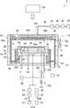
도 1은, 하나의 예시적 실시형태에 관한 플라즈마 처리 장치를 개략적으로 나타내는 도이다. 도 1에 나타내는 플라즈마 처리 장치(1)는, 용량 결합형 플라즈마 처리 장치이다. 플라즈마 처리 장치(1)는, 챔버(10)를 구비하고 있다. 챔버(10)는, 그 안에 내부 공간(10s)을 제공하고 있다.1 is a diagram schematically showing a plasma processing apparatus according to an exemplary embodiment. The
챔버(10)는, 챔버 본체(12)를 포함하고 있다. 챔버 본체(12)는, 대략 원통 형상을 갖고 있다. 내부 공간(10s)은, 챔버 본체(12)의 내측에 제공되어 있다. 챔버 본체(12)는, 예를 들면 알루미늄으로 형성되어 있다. 챔버 본체(12)의 내벽면 상에는, 내(耐)부식성을 갖는 막이 마련되어 있다. 내부식성을 갖는 막은, 산화 알루미늄, 산화 이트륨과 같은 세라믹으로 형성된 막일 수 있다.The
챔버 본체(12)의 측벽에는, 통로(12p)가 형성되어 있다. 기판(W)은, 내부 공간(10s)과 챔버(10)의 외부와의 사이에서 반송될 때, 통로(12p)를 통과한다. 통로(12p)는, 게이트 밸브(12g)에 의하여 개폐 가능하게 되어 있다. 게이트 밸브(12g)는, 챔버 본체(12)의 측벽을 따라 마련되어 있다.A
챔버 본체(12)의 바닥부 상에는, 지지부(13)가 마련되어 있다. 지지부(13)는, 절연 재료로 형성되어 있다. 지지부(13)는, 대략 원통 형상을 갖고 있다. 지지부(13)는, 내부 공간(10s) 내에서, 챔버 본체(12)의 바닥부로부터 상방으로 뻗어 있다. 지지부(13)는, 기판 지지기(14)를 지지하고 있다. 기판 지지기(14)는, 내부 공간(10s) 내에서 기판(W)을 지지하도록 구성되어 있다.On the bottom portion of the chamber
기판 지지기(14)는, 하부 전극(18) 및 정전 척(20)을 갖고 있다. 기판 지지기(14)는, 전극 플레이트(16)를 더 가질 수 있다. 전극 플레이트(16), 하부 전극(18), 및 정전 척(20)은, 챔버(10) 내에 마련되어 있다. 전극 플레이트(16)는, 예를 들면 알루미늄과 같은 도체로 형성되어 있으며, 대략 원반 형상을 갖고 있다. 하부 전극(18)은, 전극 플레이트(16) 상에 마련되어 있다. 하부 전극(18)은, 예를 들면 알루미늄과 같은 도체로 형성되어 있으며, 대략 원반 형상을 갖고 있다. 하부 전극(18)은, 전극 플레이트(16)에 전기적으로 접속되어 있다.The substrate supporter 14 has a
정전 척(20)은, 하부 전극(18) 상에 마련되어 있다. 정전 척(20)의 상면의 위에는, 기판(W)이 재치된다. 정전 척(20)은, 본체 및 전극을 갖는다. 정전 척(20)의 본체는, 대략 원반 형상을 갖고, 유전체로 형성되어 있다. 정전 척(20)의 전극은, 막형상의 전극이며, 정전 척(20)의 본체 내에 마련되어 있다. 정전 척(20)의 전극은, 스위치(20s)를 통하여 직류 전원(20p)에 접속되어 있다. 정전 척(20)의 전극에 직류 전원(20p)으로부터의 전압이 인가되면, 정전 척(20)과 기판(W)의 사이에 정전 인력이 발생한다. 발생한 정전 인력에 의하여, 기판(W)은, 정전 척(20)에 끌어당겨져, 정전 척(20)에 의하여 유지된다.The
기판 지지기(14)의 주연(周緣)부 상에는, 포커스링(FR)이 탑재된다. 포커스링(FR)은, 기판(W)에 대한 플라즈마 처리의 면내(面內) 균일성을 향상시키기 위하여 마련되어 있다. 포커스링(FR)은, 대략 판상 또는 환상을 이루고 있다. 포커스링(FR)은, 한정되는 것은 아니지만, 실리콘, 탄화 실리콘, 또는 석영으로 형성될 수 있다. 기판(W)은, 정전 척(20) 상이고, 또한, 포커스링(FR)에 의하여 둘러싸인 영역 내에 배치된다.On the peripheral portion of the substrate support 14, the focus ring FR is mounted. The focus ring FR is provided in order to improve the in-plane uniformity of the plasma treatment with respect to the substrate W. The focus ring FR has a substantially plate shape or an annular shape. The focus ring FR is not limited, but may be formed of silicon, silicon carbide, or quartz. The substrate W is disposed on the
하부 전극(18)의 내부에는, 유로(18f)가 마련되어 있다. 유로(18f)에는, 챔버(10)의 외부에 마련되어 있는 칠러 유닛(22)으로부터 배관(22a)을 통하여 열교환 매체(예를 들면 냉매)가 공급된다. 유로(18f)에 공급된 열교환 매체는, 배관(22b)을 통하여 칠러 유닛(22)으로 되돌려진다. 플라즈마 처리 장치(1)에서는, 정전 척(20) 상에 재치된 기판(W)의 온도가, 열교환 매체와 하부 전극(18)의 열교환에 의하여 조정된다.Inside the
플라즈마 처리 장치(1)에는, 가스 공급 라인(24)이 마련되어 있다. 가스 공급 라인(24)은, 전열 가스 공급 기구로부터의 전열 가스(예를 들면 He 가스)를, 정전 척(20)의 상면과 기판(W)의 이면과의 사이의 간극에 공급한다.The
플라즈마 처리 장치(1)는, 상부 전극(30)을 더 구비하고 있다. 상부 전극(30)은, 기판 지지기(14)의 상방에 마련되어 있다. 상부 전극(30)은, 부재(32)를 통하여, 챔버 본체(12)의 상부에 지지되어 있다. 부재(32)는, 절연성을 갖는 재료로 형성되어 있다. 상부 전극(30)과 부재(32)는, 챔버 본체(12)의 상부 개구를 폐쇄하고 있다.The
상부 전극(30)은, 천판(天板)(34) 및 지지체(36)를 포함할 수 있다. 천판(34)의 하면은, 내부 공간(10s) 측의 하면이며, 내부 공간(10s)을 구획 형성하고 있다. 천판(34)은, 줄(Joule)열이 적은 저(低)저항의 도전체 또는 반도체로 형성될 수 있다. 천판(34)에는, 복수의 가스 토출 구멍(34a)이 형성되어 있다. 복수의 가스 토출 구멍(34a)은, 천판(34)을 그 판두께 방향으로 관통하고 있다.The
지지체(36)는, 천판(34)을 착탈 가능하게 지지한다. 지지체(36)는, 알루미늄과 같은 도전성 재료로 형성된다. 지지체(36)의 내부에는, 가스 확산실(36a)이 마련되어 있다. 지지체(36)에는, 복수의 가스 구멍(36b)이 형성되어 있다. 복수의 가스 구멍(36b)은, 가스 확산실(36a)로부터 하방으로 뻗어 있다. 복수의 가스 구멍(36b)은, 복수의 가스 토출 구멍(34a)에 각각 연통하고 있다. 지지체(36)에는, 가스 도입구(36c)가 형성되어 있다. 가스 도입구(36c)는, 가스 확산실(36a)에 접속되어 있다. 가스 도입구(36c)에는, 가스 공급관(38)이 접속되어 있다.The
가스 공급관(38)에는, 밸브군(41), 유량 제어기군(42), 및 밸브군(43)을 통하여, 가스 소스군(40)이 접속되어 있다. 가스 소스군(40)은, 복수의 가스 소스를 포함하고 있다. 밸브군(41) 및 밸브군(43)의 각각은, 복수의 개폐 밸브를 포함하고 있다. 유량 제어기군(42)은, 복수의 유량 제어기를 포함하고 있다. 유량 제어기군(42)의 복수의 유량 제어기의 각각은, 매스 플로 컨트롤러 또는 압력 제어식의 유량 제어기이다. 가스 소스군(40)의 복수의 가스 소스의 각각은, 밸브군(41) 대응의 개폐 밸브, 유량 제어기군(42) 대응의 유량 제어기, 및 밸브군(43) 대응의 개폐 밸브를 통하여, 가스 공급관(38)에 접속되어 있다.A
플라즈마 처리 장치(1)에서는, 챔버 본체(12)의 내벽면을 따라, 실드(46)가 착탈 가능하게 마련되어 있다. 실드(46)는, 지지부(13)의 외주(外周)에도 마련되어 있다. 실드(46)는, 챔버 본체(12)에 에칭 부생물이 부착하는 것을 방지한다. 실드(46)는, 예를 들면 알루미늄으로 형성된 부재의 표면에 내부식성을 갖는 막을 형성함으로써 구성된다. 내부식성을 갖는 막은, 산화 이트륨과 같은 세라믹으로 형성된 막일 수 있다.In the
지지부(13)와 챔버 본체(12)의 측벽과의 사이에는, 배플 플레이트(48)가 마련되어 있다. 배플 플레이트(48)는, 예를 들면 알루미늄으로 형성된 부재의 표면에 내부식성을 갖는 막을 형성함으로써 구성된다. 내부식성을 갖는 막은, 산화 이트륨과 같은 세라믹으로 형성된 막일 수 있다. 배플 플레이트(48)에는, 복수의 관통 구멍이 형성되어 있다. 배플 플레이트(48)의 하방이며, 또한, 챔버 본체(12)의 바닥부에는, 배기구(12e)가 마련되어 있다. 배기구(12e)에는, 배기관(52)을 통하여 배기 장치(50)가 접속되어 있다. 배기 장치(50)는, 압력 조정 밸브 및 터보 분자 펌프와 같은 진공 펌프를 갖고 있다.A
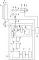
플라즈마 처리 장치(1)는, 고주파 전원(61)을 더 구비하고 있다. 도 2는, 하나의 예시적 실시형태에 관한 고주파 전원의 구성을 나타내는 도이다. 고주파 전원(61)은, 전력 발생기(61g) 및 출력부(61a)를 갖고 있다. 전력 발생기(61g)는, 고주파 전력(HF)을 발생시키도록 구성되어 있다. 출력부(61a)는, 전력 발생기(61g)에 의하여 발생된 고주파 전력(HF)을 출력하도록 구성되어 있다. 고주파 전원(61)은, 챔버(10) 내의 가스로부터 플라즈마를 생성하기 위하여 고주파 전력(HF)을 공급한다. 고주파 전원(61)의 출력부(61a)는, 정합기(62)를 통하여 하부 전극(18)에 전기적으로 접속되어 있다. 정합기(62)는, 정합 회로를 갖고 있다. 정합기(62)의 정합 회로는, 고주파 전원(61)의 부하 측(하부 전극 측)의 임피던스를, 고주파 전원(61)의 출력 임피던스에 정합시키도록 구성되어 있다. 정합기(62)와 하부 전극(18)의 사이에는 필터(63)가 마련되어 있어도 된다. 필터(63)는, 고주파 전력(HF)을 통과시키고, 고주파 전원(61)으로 향하는 다른 신호를 저감시키거나, 차단하도록 구성되어 있다. 또한, 다른 실시형태에서는, 고주파 전원(61)은, 정합기(62)를 통하여 상부 전극(30)에 전기적으로 접속되어 있어도 된다.The
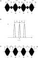
도 3의 (a)는 복수의 전력 성분의 합성 전력의 파형의 일례를 나타내는 도이고, 도 3의 (b)는 도 3의 (a)에 나타내는 합성 전력의 파워 스펙트럼을 나타내는 도이며, 도 3의 (c)는 일례의 고주파 전력(HF)의 파형을 나타내는 도이다. 도 3의 (c)에 나타내는 바와 같이, 고주파 전력(HF)은, 주기적으로 공급되는 펄스상의 고주파 전력이다. 즉, 고주파 전력(HF)은, 주기적으로 출현하는 펄스를 포함한다.Fig. 3(a) is a diagram showing an example of the waveform of the synthesized power of a plurality of power components, Fig. 3(b) is a diagram showing the power spectrum of the synthesized power shown in Fig. 3(a), and Fig. 3 (C) is a diagram showing a waveform of the high-frequency power HF as an example. As shown in Fig. 3C, the high frequency power HF is a pulsed high frequency power that is periodically supplied. That is, the high-frequency power HF includes pulses that appear periodically.
고주파 전력(HF)은, 복수의 전력 성분을 포함한다. 복수의 전력 성분은, 복수의 주파수를 각각 갖는다. 도 3의 (b)에 나타내는 바와 같이, 복수의 주파수는, 기본 주파수 f0에 대하여 대칭으로 설정되어 있다. 기본 주파수 f0은, 예를 들면 27MHz~100MHz의 범위 내의 주파수이다. 일례에서는, 기본 주파수 f0은, 40.68MHz이다. 또, 도 3의 (b)에 나타내는 바와 같이, 복수의 주파수는, 소정 주파수 fP의 간격으로 설정되어 있다. 도 3의 (b)에 나타내는 예에서는, 복수의 전력 성분의 각각의 주파수는, f0-fP, f0, f0+fP이다.The high frequency electric power HF contains a plurality of electric power components. The plurality of power components each have a plurality of frequencies. As shown in Fig. 3B, a plurality of frequencies are set symmetrically with respect to the fundamental frequency f0 . The fundamental frequency f0 is a frequency within the range of 27 MHz to 100 MHz, for example. In one example, the fundamental frequency f0 is 40.68 MHz. Further, a plurality of frequencies, is set to an interval of a predetermined frequency fP as shown in FIG. 3 (b). In the example shown in FIG. 3B, the frequencies of the plurality of power components are f0 -fP , f0 , and f0 +fP.
복수의 전력 성분 중 합성 전력의 포락선은, 도 3의 (a)에 나타내는 바와 같이, 복수의 피크군을 포함한다. 복수의 피크군의 각각은, 주기적으로 출현하는 복수의 피크를 포함한다. 복수의 피크군의 각각에 포함되는 복수의 피크는, 시간 간격 TP로 주기적으로 출현한다. 시간 간격 TP는, 주파수 fP의 역수(逆數)이다.The envelope of the synthesized power among the plurality of power components includes a plurality of peak groups, as shown in Fig. 3A. Each of the plurality of peak groups includes a plurality of peaks that appear periodically. A plurality of peaks included in each of the plurality of peak groups appear periodically at a time interval TP. The time interval TP is the reciprocal of the frequency fP.
도 3의 (c)에 나타내는 바와 같이, 고주파 전력(HF)의 포락선은, 시간 간격 TP로 출현하는 피크를 갖는다. 일 실시형태에서는, 고주파 전력(HF)은, 복수의 피크군 중 최대 파워 레벨을 갖는 피크 PM을 포함하는 피크군으로 구성된다. 도 3의 (c)에 나타내는 바와 같이, 고주파 전력(HF)은, 그 파워 레벨이, 기간 PA에서 제로이도록 설정되어 있다. 기간 PA는, 기간 PP를 제외한 기간이다. 기간 PP는, 고주파 전력(HF)의 포락선의 피크가 각각 출현하는 기간이다. 일 실시형태에서는, 기간 PP는, 피크 PM이 각각 출현하는 기간이다. 기간 PP의 각각은, 고주파 전력(HF)의 포락선 대응의 피크의 출현 시점 직전의 포락선의 제로 크로스 영역 ZA와 당해 출현 시점 직후의 포락선의 제로 크로스 영역 ZB와의 사이의 기간이다. 제로 크로스 영역 ZA 및 제로 크로스 영역 ZB는, 고주파 전력(HF)의 포락선의 진폭이 실질적으로 제로라고 간주할 수 있는 값을 갖는 시점일 수 있다. 예를 들면, 제로 크로스 영역 ZA 및 제로 크로스 영역 ZB의 각각은, 고주파 전력(HF)의 포락선의 피크의 파워 레벨에 대하여 30% 이하 또는 10% 이하의 파워 레벨을, 당해 포락선의 파워 레벨이 갖는 시점이어도 된다.As shown in (c) of Figure 3, the envelope of the high-frequency power (HF) is, has a peak which appears in the time interval TP. In one embodiment, the high-frequency power HF is constituted by a peak group including a peak PM having a maximum power level among a plurality of peak groups. As shown in Fig. 3C, the high frequency power HF is set so that its power level is zero in the period PA. Period PA is a period excluding period PP. The period PP is a period in which the peaks of the envelope of the high frequency power HF appear respectively. In one embodiment, the period PP is a period in which each peak PM appears. Each of the periods PP is a period between the zero cross region ZA of the envelope immediately before the appearance of the peak corresponding to the envelope of the high frequency power HF and the zero cross region ZB of the envelope immediately after the appearance time point. The zero cross region ZA and the zero cross region ZB may be times when the amplitude of the envelope of the high frequency power HF has a value that can be regarded as substantially zero. For example, each of the zero cross region ZA and the zero cross region ZB has a power level of 30% or less or 10% or less with respect to the power level of the peak of the envelope of the high frequency power HF, and the power level of the envelope. It may be a viewpoint to have this.
이하, 도 1과 함께 도 2를 참조한다. 일 실시형태에 있어서, 전력 발생기(61g)는, 도 2에 나타내는 바와 같이, 변조 신호 발생부(64)를 가질 수 있다. 일 실시형태에 있어서, 전력 발생기(61g)는, 증폭기(65)를 더 갖고 있어도 된다. 변조 신호 발생부(64)는, 변조 고주파 신호를 생성한다. 고주파 전력(HF)은, 변조 신호 발생부(64)에 의하여 생성되는 변조 고주파 신호여도 된다. 이 경우에는, 증폭기(65)는 불필요하다. 혹은, 고주파 전력(HF)은, 변조 고주파 신호가 증폭기(65)에 의하여 증폭됨으로써, 생성되어도 된다.Hereinafter, referring to FIG. 2 together with FIG. 1. In one embodiment, the
일 실시형태에 있어서는, 변조 신호 발생부(64)는, 파형 데이터 생성부(71), 양자화부(72), 역푸리에 변환부(73), 및 변조부(74)를 갖고 있다. 일 실시형태에 있어서, 변조 신호 발생부(64)는, D/A 변환부(75, 76), 및 로 패스 필터(77, 78)를 더 갖고 있어도 된다. 변조 신호 발생부(64)는, 예를 들면 FPGA(Field-Programmable Gate Array)로 구성될 수 있다. 혹은, 변조 신호 발생부(64)는, 몇개의 회로로 형성되어 있어도 된다.In one embodiment, the modulated
파형 데이터 생성부(71)는, 변조 고주파 신호에 대응하는 파형 데이터를 생성한다. 파형 데이터 생성부(71)는, 입력 장치로부터 파형 데이터를 생성하기 위한 파라미터(예를 들면, 주파수 및 위상 등)를 취득하고, 취득한 파라미터를 이용하여 파형 데이터를 생성하도록 구성되어 있다. 파형 데이터 생성부(71)는, 생성한 파형 데이터를 양자화부(72)에 출력한다.The waveform
양자화부(72)는, 파형 데이터 생성부(71)에 의하여 생성된 파형 데이터를 양자화하여, 양자화 데이터를 생성하도록 구성되어 있다. 역푸리에 변환부(73)는, 양자화 데이터에 역푸리에 변환을 적용하여, I데이터(동일 상성분) 및 Q데이터(직교 위상 성분)를 생성하도록 구성되어 있다. I데이터 및 Q데이터는 각각, D/A 변환부(75, 76), 로 패스 필터(77, 78)를 경유하여, 변조부(74)에 입력된다.The
변조부(74)는, 그들의 위상이 서로 90° 다른 2개의 기준 고주파 신호를, 입력된 I데이터 및 Q데이터를 이용하여 각각 변조하여, 변조 고주파 신호를 생성하도록 구성되어 있다.The
일 실시형태에 있어서, 변조부(74)는, PLL 발진기(74a)(Phase Locked Loop 발진기), 이상기(移相器)(74b), 믹서(74c, 74d), 및 합성기(74e)를 갖는다.In one embodiment, the
PLL 발진기(74a)는, 기준 고주파 신호를 생성하도록 구성되어 있다. 기준 고주파 신호는, 믹서(74c)에 입력된다. 또, 기준 고주파 신호는, 이상기(74b)에 입력된다. 이상기(74b)는, 믹서(74c)에 입력되는 기준 고주파 신호에 대하여 90° 다른 위상을 갖는 기준 고주파 신호를 생성하도록 구성되어 있다. 구체적으로, 이상기(74b)는, 입력된 기준 고주파 신호의 위상을 90° 시프트시키도록 구성되어 있다. 이상기(74b)에 의하여 생성된 기준 고주파 신호는, 믹서(74d)에 입력된다.The
믹서(74c)는, 입력된 기준 고주파 신호와 I데이터와의 승산(乘算)을 행하도록 구성되어 있다. 믹서(74c)의 승산에 의하여 생성된 신호는, 합성기(74e)에 입력된다. 믹서(74d)는, 입력된 기준 고주파 신호와 Q데이터와의 승산을 행하도록 구성되어 있다. 믹서(74d)의 승산에 의하여 생성된 신호는, 합성기(74e)에 입력된다. 합성기(74e)는, 믹서(74c)와 믹서(74d)의 각각으로부터 입력된 신호의 가산을 행하여, 변조 고주파 신호를 생성하도록 구성되어 있다.The
일 실시형태에 있어서, 플라즈마 처리 장치(1)는, 바이어스 전원(81)을 더 구비하고 있어도 된다. 바이어스 전원(81)은, 하부 전극(18)에 전기적으로 접속되어 있다. 일 실시형태에서는, 바이어스 전원(81)은, 기판 지지기(14)에 이온을 인입하기 위하여 바이어스 전력(BP)을 발생시키도록 구성되어 있다. 바이어스 전력(BP)은, 하부 전극(18)에 공급된다.In one embodiment, the
일 실시형태에 있어서, 바이어스 전원(81)은, 바이어스 전력(BP)으로서, 고주파 바이어스 전력(LF)을 발생시키도록 구성되어 있어도 된다. 고주파 바이어스 전력(LF)의 주파수는, 기본 주파수 f0보다 낮다. 고주파 바이어스 전력(LF)의 주파수는, 예를 들면 100kHz~13.56MHz의 범위 내의 주파수이다. 일례에서는, 고주파 바이어스 전력(LF)의 주파수는, 400kHz이다. 일 실시형태에 있어서, 고주파 바이어스 전력(LF)의 주파수는, 상술한 주파수 fP일 수 있다.In one embodiment, the
일 실시형태에 있어서, 바이어스 전원(81)은, 신호 발생기(81a) 및 증폭기(81b)를 갖고 있어도 된다. 신호 발생기(81a)는, 고주파 바이어스 전력(LF)의 주파수와 동일한 주파수를 갖는 고주파 신호를 발생하도록 구성되어 있다. 신호 발생기(81a)에 의하여 생성된 고주파 신호는, 증폭기(81b)에 입력된다. 증폭기(81b)는, 입력된 고주파 신호를 증폭하여, 고주파 바이어스 전력(LF)을 생성하도록 구성되어 있다.In one embodiment, the
바이어스 전원(81)은, 정합기(82)를 통하여 하부 전극(18)에 전기적으로 접속되어 있다. 정합기(82)는, 정합 회로를 갖고 있다. 정합기(82)의 정합 회로는, 바이어스 전원(81)의 부하 측(하부 전극 측)의 임피던스를, 바이어스 전원(81)의 출력 임피던스에 정합시키도록 구성되어 있다. 정합기(82)와 하부 전극(18)의 사이에는 필터(83)가 마련되어 있어도 된다. 필터(83)는, 바이어스 전력(BP)을 통과시키고, 바이어스 전원(81)으로 향하는 다른 신호를 저감시키거나 차단하도록 구성되어 있다.The
일 실시형태에 있어서, 플라즈마 처리 장치(1)는, 제어부(80)를 더 구비할 수 있다. 제어부(80)는, 프로세서, 메모리와 같은 기억부, 입력 장치, 표시 장치, 신호의 입출력 인터페이스 등을 구비하는 컴퓨터일 수 있다. 제어부(80)는, 플라즈마 처리 장치(1)의 각 부를 제어한다. 제어부(80)에서는, 입력 장치를 이용하여, 오퍼레이터가 플라즈마 처리 장치(1)를 관리하기 위하여 커맨드의 입력 조작 등을 행할 수 있다. 또, 제어부(80)에서는, 표시 장치에 의하여, 플라즈마 처리 장치(1)의 가동 상황을 가시화하여 표시할 수 있다. 또한, 제어부(80)의 기억부에는, 제어 프로그램 및 레시피 데이터가 저장되어 있다. 제어 프로그램은, 플라즈마 처리 장치(1)로 각종 처리를 실행하기 위하여, 제어부(80)의 프로세서에 의하여 실행된다. 제어부(80)의 프로세서가, 제어 프로그램을 실행하고, 레시피 데이터에 따라 플라즈마 처리 장치(1)의 각 부를 제어함으로써, 플라즈마 처리 장치(1)에 있어서 플라즈마 처리가 실행된다.In one embodiment, the
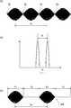
도 4의 (a)는, 도 3의 (c)에 나타낸 일례의 고주파 전력(HF)의 파형과 함께 일례의 고주파 바이어스 전력(LF)의 파형을 나타내는 도이며, 도 4의 (b)는, 일례의 고주파 전력(HF)의 파워 스펙트럼을 나타내는 도이다. 도 4의 (a)에 나타내는 고주파 전력(HF)의 기본 주파수 f0은 40.68MHz이고, 주파수 fp는 400kHz이다. 도 5의 (a)는, 참고예의 고주파 전력의 파형과 함께 일례의 고주파 바이어스 전력(LF)의 파형을 나타내는 도이며, 도 5의 (b)는, 참고예의 고주파 전력의 파워 스펙트럼을 나타내는 도이다. 도 5의 (a)에 나타내는, 참고예의 고주파 전력(C-HF)은, 40.68MHz의 기본 주파수를 갖는 고주파 전력이며, 400kHz의 반복 주파수로 출현하는 직사각형 펄스로서 생성되어 있다.4A is a diagram showing a waveform of an exemplary high frequency bias power LF together with a waveform of an exemplary high frequency power HF shown in FIG. 3C, and FIG. 4B is a It is a figure which shows the power spectrum of an example high-frequency power HF. The fundamental frequency f0 of the high frequency power HF shown in Fig. 4A is 40.68 MHz, and the frequency fp is 400 kHz. 5A is a diagram showing a waveform of a high frequency bias power LF as an example together with a waveform of the high frequency power of a reference example, and FIG. 5B is a diagram showing a power spectrum of the high frequency power of a reference example. . The high-frequency power (C-HF) of the reference example shown in Fig. 5A is a high-frequency power having a fundamental frequency of 40.68 MHz, and is generated as a rectangular pulse appearing at a repetition frequency of 400 kHz.
도 5의 (b)에 나타내는 바와 같이, 직사각형 펄스로서 공급되는 고주파 전력(C-HF)의 대역은 넓다. 따라서, 이와 같은 고주파 전력(C-HF)을 이용하는 플라즈마 처리 장치에서는, 정합 회로가 임피던스 정합을 행하는 주파수 범위가 좁으면, 반사파의 전력이 커진다.As shown in Fig. 5B, the band of high frequency power (C-HF) supplied as a rectangular pulse is wide. Accordingly, in a plasma processing apparatus using such high-frequency power (C-HF), when the frequency range in which the matching circuit performs impedance matching is narrow, the power of the reflected wave increases.
한편, 플라즈마 처리 장치(1)에서는, 챔버(10) 내에 가스가 공급되어, 챔버(10) 내의 가스를 여기시켜 플라즈마를 생성하기 위하여, 고주파 전력(HF)이 공급된다. 고주파 전력(HF)은, 펄스상의 고주파 전력으로서 주기적으로 생성된다. 즉, 고주파 전력(HF)은, 시간 간격 TP로 주기적으로 출현하는 펄스를 포함한다. 각 펄스는, 그 피크까지 서서히 증가하는 파워 레벨을 갖는다. 또, 각 펄스는, 그 피크로부터 서서히 감소하는 파워 레벨을 갖는다. 각 펄스의 직전의 제로 크로스 영역 ZA와 직후의 제로 크로스 영역 ZB와의 사이의 기간 PP를 제외한 기간 PA, 즉 각 펄스의 지속 기간을 제외한 기간에서는, 고주파 전력(HF)의 파워 레벨은 제로로 설정된다. 이러한 고주파 전력(HF)의 대역폭은, 도 4의 (b)에 나타내는 바와 같이 좁다. 따라서, 고주파 전원(61)에 의하면, 주기적으로 생성되는 펄스상의 고주파 전력(HF)의 대역폭을 좁히는 것이 가능해진다. 따라서, 플라즈마 처리 장치(1)에 의하면, 정합 회로가 임피던스 정합을 행하는 주파수 범위가 좁아도, 고주파 전력(HF)에 대한 반사파를 억제하는 것이 가능해진다.On the other hand, in the
일 실시형태에 있어서, 주파수 fP는, 고주파 바이어스 전력(LF)의 주파수이다. 이 실시형태에 있어서, 제어부(80)는, 고주파 바이어스 전력(LF)의 주기 내에 있어서의 펄스상의 고주파 전력(HF)의 공급 기간(기간 PP)을 설정해도 된다. 구체적으로는, 제어부(80) 또는 다른 컨트롤러로부터 부여되는 클록 신호에 의하여, 고주파 전원(61)과 바이어스 전원(81)은 서로 동기되어 있다. 제어부(80) 또는 다른 컨트롤러는, 고주파 전력(HF)과 고주파 바이어스 전력(LF)의 사이의 위상차를 설정하기 위하여, 바이어스 전원(81)에 대하여 고주파 바이어스 전력(LF)의 위상을 설정하는 신호를 부여한다. 바이어스 전원(81)은, 부여된 위상으로 고주파 바이어스 전력(LF)을 출력한다. 이로써, 고주파 바이어스 전력(LF)의 주기 내에 있어서의 펄스상의 고주파 전력(HF)의 공급 기간(기간 PP)이 설정될 수 있다. 또한, 제어부(80)는 고주파 바이어스 전력(LF)이 아니라 고주파 전력(HF)의 위상을 설정하도록, 위상을 설정하는 신호를 고주파 전원(61)에 부여해도 된다.In one embodiment, the frequency fP is the frequency of the high frequency bias power LF. In this embodiment, the
플라즈마 처리 장치(1)에서는, 고주파 바이어스 전력(LF)의 주기 내에 있어서의 펄스상의 고주파 전력(HF)의 공급 기간을 조정함으로써, 기판(W)에 공급되는 이온의 에너지를 조정하는 것이 가능하다. 예를 들면, 바이어스 전원(81)으로부터 출력되는 고주파 바이어스 전력(LF)이 양의 전압을 갖는 기간에 있어서 펄스상의 고주파 전력(HF)이 공급되면, 기판(W)에 공급되는 이온의 에너지는 낮아진다. 한편, 바이어스 전원(81)으로부터 출력되는 고주파 바이어스 전력(LF)이 음의 전압을 갖는 기간에 있어서 펄스상의 고주파 전력(HF)이 공급되면, 기판(W)에 공급되는 이온의 에너지는 높아진다.In the
이하, 도 6의 (a), 도 6의 (b), 및 도 6의 (c)를 참조한다. 다른 예에 있어서는, 도 6의 (b)에 나타내는 바와 같이, 고주파 전력(HF)의 복수의 전력 성분의 주파수는, f0-fP/2, f0+fP/2이다. 이 예에서는, 도 6의 (a) 및 도 6의 (c)에 나타내는 바와 같이, 시간 간격 TP는, 주파수 fP의 2배의 주파수로 규정된다. 즉, 시간 간격 TP는, 주파수 fP의 2배의 주파수의 역수여도 된다. 또한, 시간 간격 TP는, 주파수 fP의 2배 이상의 정수배의 주파수의 역수여도 된다.Hereinafter, reference will be made to FIGS. 6A, 6B, and 6C. In another example, as shown in Fig. 6B, the frequencies of the plurality of power components of the high frequency power HF are f0 -fP /2 and f0 +fP /2. In this example, as shown in Figs. 6A and 6C, the time interval TP is defined as a frequency twice the frequency fP. That is, the time interval TP may be an inverse number of a frequency twice the frequency fP. Further, the time interval TP may be an inverse number of a frequency of an integer multiple of 2 or more times the frequency fP.
이하, 도 7의 (a), 도 7의 (b), 및 도 7의 (c)를 참조한다. 다른 예에 있어서는, 도 7의 (b)에 나타내는 바와 같이, 고주파 전력(HF)의 복수의 전력 성분의 주파수는, f0-(3/2)×fP, f0-fP/2, f0+fP/2, f0+(3/2)×fP이다. 이 예에서는, 도 7의 (a)에 나타내는 바와 같이, 복수의 전력 성분 중 합성 전력의 포락선은, 3개의 피크군을 포함한다. 이 예에서는, 도 7의 (c)에 나타내는 바와 같이, 고주파 전력(HF)은, 3개의 피크군 중, 최대 피크를 포함하는 피크군으로 구성되어 있다.Hereinafter, reference is made to FIGS. 7A, 7B, and 7C. In another example, as shown in Fig. 7B, the frequencies of the plurality of power components of the high frequency power HF are f0 -(3/2) × fP , f0 -fP /2, f0 +fP /2, f0 +(3/2)×fP. In this example, as shown in Fig. 7A, the envelope of the synthesized power among the plurality of power components includes three peak groups. In this example, as shown in Fig. 7C, the high frequency power HF is composed of a peak group including the maximum peak among three peak groups.
이하, 도 8의 (a), 도 8의 (b), 및 도 8의 (c)를 참조한다. 다른 예에 있어서는, 도 8의 (b)에 나타내는 바와 같이, 고주파 전력(HF)의 복수의 전력 성분의 주파수는, f0-2×fP, f0-fP, f0, f0+fP, f0+2×fP이다. 이 예에서는, 도 8의 (a)에 나타내는 바와 같이, 복수의 전력 성분 중 합성 전력의 포락선은, 4개의 피크군을 포함한다. 이 예에서는, 도 8의 (c)에 나타내는 바와 같이, 고주파 전력(HF)은, 4개의 피크군 중, 최대 피크를 포함하는 피크군으로 구성되어 있다.Hereinafter, reference will be made to FIGS. 8A, 8B, and 8C. In another example, as shown in Fig. 8B, the frequencies of the plurality of power components of the high frequency power HF are f0 -2 × fP , f0 -fP , f0 , f0 + fP , f0 +2 × fP. In this example, as shown in Fig. 8A, the envelope of the synthesized power among the plurality of power components includes four peak groups. In this example, as shown in Fig. 8C, the high frequency power HF is composed of a peak group including the maximum peak among four peak groups.
이상 설명한 바와 같이, 고주파 전력(HF)은, 2개 이상의 전력 성분으로 구성되어 있어도 된다. 2개 이상의 전력 성분 각각의 주파수는, 기본 주파수 f0에 대하여 대칭으로 설정되어 있으며, 또한, 소정 주파수 fP로 규정되는 간격으로 설정된다.As described above, the high frequency power HF may be composed of two or more power components. The frequencies of each of the two or more power components are set symmetrically with respect to the fundamental frequency f0 , and are set at intervals defined by a predetermined frequency fP.
이하, 도 9를 참조한다. 도 9는, 일례의 고주파 전력(HF)의 파형과 함께 다른 예의 바이어스 전력의 전압 파형을 나타내는 도이다. 다른 실시형태에 있어서, 바이어스 전원(81)은, 바이어스 전력(BP)으로서, 펄스상의 음극성 직류 전압(BV)을 반복하여 발생하도록 구성된 직류 전원이어도 된다.Hereinafter, referring to FIG. 9. 9 is a diagram showing a waveform of a high frequency power HF as an example and a voltage waveform of a bias power according to another example. In another embodiment, the
펄스상의 음극성 직류 전압(BV)의 반복 주파수는, 예를 들면 1kHz~800kHz의 범위 내의 주파수이다. 일 실시형태에서는, 펄스상의 음극성 직류 전압(BV)의 반복 주파수는, 주파수 fP이다. 이 실시형태에 있어서, 제어부(80)는, 직류 전압(BV)의 주기 내에 있어서의 펄스상의 고주파 전력(HF)의 공급 기간(기간 PP)을 설정해도 된다. 구체적으로는, 제어부(80) 또는 다른 컨트롤러로부터 부여되는 클록 신호에 의하여, 고주파 전원(61)과 바이어스 전원(81)은 서로 동기되어 있다. 제어부(80) 또는 다른 컨트롤러는, 고주파 전력(HF)과 펄스상의 음극성 직류 전압(BV)의 사이의 위상차를 설정하기 위하여, 바이어스 전원(81)에 대하여 펄스상의 음극성 직류 전압(BV)의 위상을 설정하는 신호를 부여한다. 바이어스 전원(81)은, 부여된 위상으로 펄스상의 음극성 직류 전압(BV)을 출력한다. 이로써, 펄스상의 음극성 직류 전압(BV)의 주기 내에 있어서의 펄스상의 고주파 전력(HF)의 공급 기간(기간 PP)이 설정될 수 있다. 또한, 제어부(80)는 펄스상의 음극성 직류 전압(BV)이 아니라 고주파 전력(HF)의 위상을 설정하도록, 위상을 설정하는 신호를 고주파 전원(61)에 부여해도 된다.The repetition frequency of the pulsed negative direct current voltage (BV) is, for example, a frequency within the range of 1 kHz to 800 kHz. In one embodiment, the repetition frequency of the negative polarity direct voltage (BV) on the pulse, the frequency fP. In this embodiment, the
플라즈마 처리 장치(1)에서는, 펄스상의 음극성 직류 전압(BV)의 주기 내에 있어서의 펄스상의 고주파 전력(HF)의 공급 기간을 조정함으로써, 기판(W)에 공급되는 이온의 에너지를 조정하는 것이 가능하다. 예를 들면, 펄스상의 음극성 직류 전압(BV)이 하부 전극(18)에 인가되고 있지 않은 기간에 있어서 펄스상의 고주파 전력(HF)이 공급되면, 기판(W)에 공급되는 이온의 에너지는 낮아진다. 한편, 펄스상의 음극성 직류 전압(BV)이 하부 전극(18)에 인가되고 있는 기간에 있어서 펄스상의 고주파 전력(HF)이 공급되면, 기판(W)에 공급되는 이온의 에너지는 높아진다.In the
이하, 도 10을 참조한다. 도 10은, 다른 예시적 실시형태에 관한 고주파 전원의 구성을 나타내는 도이다. 도 10에 나타내는 바와 같이, 플라즈마 처리 장치(1)는, 고주파 전원(61) 대신에, 고주파 전원(61B)을 구비하고 있어도 된다. 고주파 전원(61B)은, 전력 발생기(61Bg) 및 출력부(61a)를 갖고 있다. 전력 발생기(61Bg)는, 고주파 전력(HF)을 발생시키도록 구성되어 있다. 고주파 전원(61B)에 있어서, 출력부(61a)는, 전력 발생기(61Bg)에 의하여 생성된 고주파 전력(HF)을 출력하도록 구성되어 있다.Hereinafter, referring to FIG. 10. Fig. 10 is a diagram showing a configuration of a high frequency power supply according to another exemplary embodiment. As shown in FIG. 10, the
전력 발생기(61Bg)는, 변조 신호 발생부(64B)를 갖고 있다. 전력 발생기(61Bg)는, 증폭기(65)를 더 갖고 있어도 된다. 변조 신호 발생부(64B)는, 변조 고주파 신호를 생성한다. 고주파 전력(HF)은, 변조 신호 발생부(64B)에 의하여 생성되는 변조 고주파 신호여도 된다. 이 경우에는, 증폭기(65)는 불필요하다. 혹은, 고주파 전력(HF)은, 변조 고주파 신호가 증폭기(65)에 의하여 증폭됨으로써, 생성되어도 된다.The power generator 61Bg has a modulated
변조 신호 발생부(64B)는, 복수의 신호 발생기(911~91N), 가산기(92), 및 스위칭 회로(93)를 가질 수 있다. 여기서, "N"은, 2 이상의 정수이다. 복수의 신호 발생기(911~91N)는, 복수의 고주파 신호를 각각 발생하도록 구성되어 있다. 복수의 고주파 신호 각각의 주파수는, 기본 주파수 f0에 대하여 대칭으로 설정되어 있다. 복수의 고주파 신호 각각의 주파수는, 소정 주파수 fP의 간격으로 설정되어 있다.The modulated
가산기(92)는, 복수의 신호 발생기(911~91N)로부터의 복수의 고주파 신호를 가산하여 합성 신호를 생성하도록 구성되어 있다. 합성 신호의 포락선은, 시간 간격 TP로 주기적으로 출현하는 피크를 갖는다. 스위칭 회로(93)는, 변조 고주파 신호를 합성 신호로부터 생성하도록 구성되어 있다. 변조 고주파 신호는, 그 진폭 레벨이, 합성 신호의 포락선의 피크의 각각의 출현 시점 직전의 당해 포락선의 제로 크로스 영역 ZA와 그 출현 시점 직후의 당해 포락선의 제로 크로스 영역 ZB와의 사이의 기간 PP를 제외한 기간 PA에서 제로이도록 설정된다. 이러한 고주파 전원(61B)도, 고주파 전원(61)과 동일하게 고주파 전력(HF)을 생성하는 것이 가능하다.The
이상, 다양한 예시적 실시형태에 대하여 설명해 왔지만, 상술한 예시적 실시형태로 한정되지 않으며, 다양한 추가, 생략, 치환, 및 변경이 이루어져도 된다. 또, 다른 실시형태에 있어서의 요소를 조합하여 다른 실시형태를 형성하는 것이 가능하다.As described above, various exemplary embodiments have been described, but they are not limited to the above-described exemplary embodiments, and various additions, omissions, substitutions, and changes may be made. Moreover, it is possible to form another embodiment by combining elements in another embodiment.
다른 실시형태에 있어서, 플라즈마 처리 장치는, 유도 결합형의 플라즈마 처리 장치와 같은 다른 타입의 플라즈마 처리 장치여도 된다. 유도 결합형의 플라즈마 처리 장치에서는, 고주파 전력(HF)은, 유도 결합 플라즈마를 생성하기 위한 안테나에 공급된다.In another embodiment, the plasma processing apparatus may be another type of plasma processing apparatus such as an inductively coupled plasma processing apparatus. In the inductively coupled plasma processing apparatus, high frequency power HF is supplied to an antenna for generating inductively coupled plasma.
이상의 설명으로부터, 본 개시의 다양한 실시형태는, 설명의 목적으로 본 명세서에서 설명되어 있으며, 본 개시의 범위 및 취지에서 벗어나지 않고 다양한 변경을 할 수 있는 것이 이해될 것이다. 따라서, 본 명세서에 개시한 다양한 실시형태는 한정하는 것을 의도하고 있지 않으며, 진정한 범위와 취지는, 첨부한 특허청구의 범위에 의하여 나타난다.From the above description, it will be understood that various embodiments of the present disclosure have been described herein for purposes of explanation, and that various changes can be made without departing from the scope and spirit of the present disclosure. Accordingly, the various embodiments disclosed in this specification are not intended to be limiting, and the true scope and intent are indicated by the scope of the appended claims.
Claims (10)
Translated fromKorean소정 주파수의 간격으로 기본 주파수에 대하여 대칭으로 설정된 복수의 주파수를 각각 갖는 복수의 전력 성분을 포함하는 고주파 전력으로서, 그 포락선이, 상기 소정 주파수 또는 상기 소정 주파수의 2배 이상의 배수의 주파수로 규정되는 시간 간격으로 주기적으로 출현하는 피크를 가지며, 그 파워 레벨이, 상기 피크의 각각의 출현 시점 직전의 상기 포락선의 제로 크로스 영역과 상기 출현 시점 직후의 상기 포락선의 제로 크로스 영역 사이의 기간을 제외한 기간에서 제로이도록 설정된, 상기 고주파 전력을 발생시키도록 구성된 전력 발생기와,
상기 전력 발생기에 의하여 발생된 상기 고주파 전력을 출력하도록 구성된 출력부를 구비하는, 고주파 전원.As a high frequency power supply for a plasma processing device,
A high-frequency power comprising a plurality of power components each having a plurality of frequencies set symmetrically with respect to a fundamental frequency at intervals of a predetermined frequency, the envelope of which is defined as a frequency of the predetermined frequency or a multiple of two or more times the predetermined frequency It has a peak that appears periodically at time intervals, and its power level is in a period excluding a period between the zero cross region of the envelope immediately before each occurrence of the peak and the zero cross region of the envelope immediately after the appearance time of the peak. A power generator configured to generate the high-frequency power, set to be zero,
And an output unit configured to output the high frequency power generated by the power generator.
상기 전력 발생기는,
파형 데이터 생성부와,
상기 파형 데이터 생성부에 의하여 생성된 파형 데이터를 양자화하여, 양자화 데이터를 생성하도록 구성된 양자화부와,
상기 양자화 데이터에 역푸리에 변환을 적용하여, I데이터 및 Q데이터를 생성하도록 구성된 역푸리에 변환부와,
그들의 위상이 서로 90° 다른 2개의 기준 고주파 신호를 상기 I데이터 및 상기 Q데이터를 이용하여 변조하여, 변조 고주파 신호를 생성하도록 구성된 변조부를 갖고, 상기 변조 고주파 신호로부터 상기 고주파 전력을 생성하도록 구성되어 있는, 고주파 전원.The method according to claim 1,
The power generator,
A waveform data generation unit,
A quantization unit configured to quantize the waveform data generated by the waveform data generation unit to generate quantized data,
An inverse Fourier transform unit configured to generate I data and Q data by applying an inverse Fourier transform to the quantized data,
It has a modulator configured to generate a modulated high frequency signal by modulating two reference high frequency signals whose phases are different from each other by 90° using the I data and the Q data, and is configured to generate the high frequency power from the modulated high frequency signal. That, high frequency power.
상기 전력 발생기는, 상기 변조 고주파 신호를 증폭시켜 상기 고주파 전력을 생성하도록 구성된 증폭기를 더 갖는, 고주파 전원.The method according to claim 2,
The power generator further has an amplifier configured to amplify the modulated high frequency signal to generate the high frequency power.
상기 전력 발생기는,
복수의 고주파 신호를 각각 발생시키도록 구성된 복수의 신호 발생기로서, 상기 복수의 고주파 신호는 각각 상기 복수의 주파수를 갖는, 상기 복수의 신호 발생기와,
상기 복수의 고주파 신호를 가산하여, 그 포락선이 상기 시간 간격으로 주기적으로 출현하는 피크를 갖는 합성 신호를 생성하도록 구성된 가산기와,
그 진폭 레벨이, 상기 합성 신호의 상기 포락선의 상기 피크의 각각의 출현 시점 직전의 상기 합성 신호의 상기 포락선의 제로 크로스 영역과 상기 출현 시점 직후의 상기 합성 신호의 상기 포락선의 제로 크로스 영역 사이의 기간을 제외한 기간에서 제로이도록 설정된 변조 고주파 신호를, 상기 합성 신호로부터 생성하도록 구성된 스위칭 회로를 갖고, 상기 스위칭 회로에 의하여 생성된 상기 변조 고주파 신호로부터 상기 고주파 전력을 생성하도록 구성되어 있는, 고주파 전원.The method according to claim 1,
The power generator,
A plurality of signal generators configured to respectively generate a plurality of high frequency signals, wherein the plurality of high frequency signals each have the plurality of frequencies, the plurality of signal generators,
An adder configured to add the plurality of high-frequency signals to generate a synthesized signal having a peak whose envelope periodically appears at the time interval,
The amplitude level is a period between a zero cross region of the envelope of the composite signal immediately before each occurrence of the peak of the envelope of the composite signal and a zero cross region of the envelope of the composite signal immediately after the appearance time of the composite signal A high frequency power supply comprising a switching circuit configured to generate a modulated high frequency signal set to be zero from the synthesized signal in a period except for the high frequency power, and configured to generate the high frequency power from the modulated high frequency signal generated by the switching circuit.
상기 전력 발생기는, 상기 스위칭 회로에 의하여 생성된 상기 변조 고주파 신호를 증폭시켜 상기 고주파 전력을 생성하도록 구성된 증폭기를 더 갖는, 고주파 전원.The method of claim 4,
The power generator further has an amplifier configured to amplify the modulated high frequency signal generated by the switching circuit to generate the high frequency power.
하부 전극을 갖고, 상기 챔버 내에서 기판을 지지하도록 구성된 기판 지지기와,
상기 챔버 내에서 가스로부터 플라즈마를 생성하기 위하여 고주파 전력을 발생시키도록 구성된, 청구항 1 내지 청구항 5 중 어느 한 항에 기재된 고주파 전원을 구비하는 플라즈마 처리 장치.Chamber,
A substrate support having a lower electrode and configured to support a substrate in the chamber,
A plasma processing apparatus comprising the high-frequency power source according to any one of claims 1 to 5, configured to generate high-frequency power to generate plasma from gas in the chamber.
상기 하부 전극에 전기적으로 접속되어 있으며, 상기 기판 지지기에 이온을 인입하기 위하여 고주파 바이어스 전력을 생성하도록 구성된 바이어스 전원을 더 구비하고,
상기 고주파 바이어스 전력의 주파수는, 상기 소정 주파수인, 플라즈마 처리 장치.The method of claim 6,
Further comprising a bias power supply electrically connected to the lower electrode and configured to generate a high frequency bias power to introduce ions into the substrate support,
The plasma processing apparatus, wherein the frequency of the high frequency bias power is the predetermined frequency.
상기 고주파 전력과 상기 고주파 바이어스 전력 사이의 위상차를 설정하도록 구성된 제어부를 더 구비하는, 플라즈마 처리 장치.The method of claim 7,
And a control unit configured to set a phase difference between the high frequency power and the high frequency bias power.
상기 하부 전극에 전기적으로 접속되어 있으며, 상기 기판 지지기에 이온을 인입하기 위하여 펄스상의 직류 전압을 반복하여 발생시키도록 구성된 바이어스 전원을 더 구비하고,
상기 펄스상의 직류 전압의 반복 주파수는, 상기 소정 주파수인, 플라즈마 처리 장치.The method of claim 6,
Further comprising a bias power supply electrically connected to the lower electrode and configured to repeatedly generate a pulsed DC voltage in order to introduce ions into the substrate support,
The plasma processing apparatus, wherein the repetition frequency of the pulsed DC voltage is the predetermined frequency.
상기 고주파 전력과 상기 펄스상의 직류 전압 사이의 위상차를 설정하도록 구성된 제어부를 더 구비하는, 플라즈마 처리 장치.The method of claim 9,
And a control unit configured to set a phase difference between the high frequency power and the pulsed DC voltage.
Applications Claiming Priority (2)
| Application Number | Priority Date | Filing Date | Title |
|---|---|---|---|
| JPJP-P-2019-018831 | 2019-02-05 | ||
| JP2019018831AJP7122268B2 (en) | 2019-02-05 | 2019-02-05 | Plasma processing equipment |
Publications (1)
| Publication Number | Publication Date |
|---|---|
| KR20200096734Atrue KR20200096734A (en) | 2020-08-13 |
Family
ID=71837027
Family Applications (1)
| Application Number | Title | Priority Date | Filing Date |
|---|---|---|---|
| KR1020200008820APendingKR20200096734A (en) | 2019-02-05 | 2020-01-22 | Radio frequency power source and plasma processing apparatus |
Country Status (4)
| Country | Link |
|---|---|
| US (1) | US11087960B2 (en) |
| JP (1) | JP7122268B2 (en) |
| KR (1) | KR20200096734A (en) |
| CN (1) | CN111524781B (en) |
Cited By (1)
| Publication number | Priority date | Publication date | Assignee | Title |
|---|---|---|---|---|
| KR20230119423A (en) | 2022-02-07 | 2023-08-16 | 주식회사 뉴파워 프라즈마 | Rf generator system and its operating method |
Families Citing this family (5)
| Publication number | Priority date | Publication date | Assignee | Title |
|---|---|---|---|---|
| JP6846387B2 (en)* | 2018-06-22 | 2021-03-24 | 東京エレクトロン株式会社 | Plasma processing method and plasma processing equipment |
| JP7122268B2 (en)* | 2019-02-05 | 2022-08-19 | 東京エレクトロン株式会社 | Plasma processing equipment |
| WO2022044216A1 (en)* | 2020-08-27 | 2022-03-03 | 株式会社日立ハイテク | Plasma treatment device |
| TW202226319A (en)* | 2020-08-31 | 2022-07-01 | 日商東京威力科創股份有限公司 | Plasma processing apparatus and plasma processing method |
| JP2022159653A (en)* | 2021-04-05 | 2022-10-18 | 東京エレクトロン株式会社 | Etching method and etching device |
Family Cites Families (34)
| Publication number | Priority date | Publication date | Assignee | Title |
|---|---|---|---|---|
| JPS6214754Y2 (en)* | 1978-04-25 | 1987-04-15 | ||
| US10361802B1 (en)* | 1999-02-01 | 2019-07-23 | Blanding Hovenweep, Llc | Adaptive pattern recognition based control system and method |
| US6400996B1 (en)* | 1999-02-01 | 2002-06-04 | Steven M. Hoffberg | Adaptive pattern recognition based control system and method |
| US6794301B2 (en) | 1995-10-13 | 2004-09-21 | Mattson Technology, Inc. | Pulsed plasma processing of semiconductor substrates |
| KR0183844B1 (en)* | 1996-04-30 | 1999-05-15 | 김광호 | Rf generator and pulse plasma using it |
| US7904187B2 (en)* | 1999-02-01 | 2011-03-08 | Hoffberg Steven M | Internet appliance system and method |
| JP3839352B2 (en)* | 2002-05-22 | 2006-11-01 | 株式会社日立製作所 | Information recording medium and information reproducing method and apparatus |
| US7860189B2 (en)* | 2004-08-19 | 2010-12-28 | Intrinsix Corporation | Hybrid heterodyne transmitters and receivers |
| US9582981B2 (en)* | 2014-10-08 | 2017-02-28 | Rfmicron, Inc. | Radio frequency identification (RFID) moisture tag(s) and sensors with extended sensing via capillaries |
| US9123509B2 (en) | 2007-06-29 | 2015-09-01 | Varian Semiconductor Equipment Associates, Inc. | Techniques for plasma processing a substrate |
| JP5808012B2 (en)* | 2011-12-27 | 2015-11-10 | 東京エレクトロン株式会社 | Plasma processing equipment |
| JP2012109605A (en)* | 2012-02-13 | 2012-06-07 | Ulvac Japan Ltd | Plasma cvd apparatus |
| US9209840B2 (en)* | 2012-07-30 | 2015-12-08 | Photonic Systems, Inc. | Same-aperture any-frequency simultaneous transmit and receive communication system |
| US20150364300A1 (en)* | 2014-06-16 | 2015-12-17 | Lam Research Corporation | Determining presence of conductive film on dielectric surface of reaction chamber |
| US10049857B2 (en)* | 2014-12-04 | 2018-08-14 | Mks Instruments, Inc. | Adaptive periodic waveform controller |
| TWI739335B (en)* | 2015-05-12 | 2021-09-11 | 日商東京威力科創股份有限公司 | Plasma processing device and plasma processing method |
| WO2017014210A1 (en)* | 2015-07-21 | 2017-01-26 | 東京エレクトロン株式会社 | Plasma processing device and plasma processing method |
| KR20170024922A (en)* | 2015-08-26 | 2017-03-08 | 삼성전자주식회사 | Plasma generating apparatus |
| US9947514B2 (en)* | 2015-09-01 | 2018-04-17 | Mks Instruments, Inc. | Plasma RF bias cancellation system |
| JP6643034B2 (en)* | 2015-10-09 | 2020-02-12 | 東京エレクトロン株式会社 | Plasma processing equipment |
| US11255663B2 (en)* | 2016-03-04 | 2022-02-22 | May Patents Ltd. | Method and apparatus for cooperative usage of multiple distance meters |
| JP6817889B2 (en) | 2016-05-10 | 2021-01-20 | 東京エレクトロン株式会社 | Plasma processing equipment and plasma processing method |
| JP6541623B2 (en)* | 2016-06-20 | 2019-07-10 | 東京エレクトロン株式会社 | Plasma processing apparatus and waveform correction method |
| JP6770868B2 (en)* | 2016-10-26 | 2020-10-21 | 東京エレクトロン株式会社 | Method for impedance matching of plasma processing equipment |
| JP6793019B2 (en)* | 2016-11-28 | 2020-12-02 | 東京エレクトロン株式会社 | Plasma processing equipment |
| JP6858095B2 (en)* | 2017-08-18 | 2021-04-14 | 東京エレクトロン株式会社 | Microwave output device and plasma processing device |
| JP2020534723A (en)* | 2017-09-18 | 2020-11-26 | インテル コーポレイション | Time-encoded data communication protocols, devices and methods for generating and receiving data signals |
| JP2019091526A (en)* | 2017-11-10 | 2019-06-13 | 東京エレクトロン株式会社 | Pulse monitor device and plasma processing device |
| JP6910320B2 (en)* | 2018-05-01 | 2021-07-28 | 東京エレクトロン株式会社 | Microwave output device and plasma processing device |
| US11432369B2 (en)* | 2018-06-19 | 2022-08-30 | Apple Inc. | Reference signal and control information processing in 5G-NR wireless systems |
| JP2020016592A (en)* | 2018-07-27 | 2020-01-30 | 東京エレクトロン株式会社 | Detection device, microwave output device and plasma processing device |
| CN116844934A (en)* | 2019-02-05 | 2023-10-03 | 东京毅力科创株式会社 | Plasma processing apparatus |
| JP6797273B2 (en) | 2019-02-05 | 2020-12-09 | 東京エレクトロン株式会社 | Plasma processing equipment |
| JP7122268B2 (en)* | 2019-02-05 | 2022-08-19 | 東京エレクトロン株式会社 | Plasma processing equipment |
- 2019
- 2019-02-05JPJP2019018831Apatent/JP7122268B2/enactiveActive
- 2020
- 2020-01-21CNCN202010070264.XApatent/CN111524781B/enactiveActive
- 2020-01-22KRKR1020200008820Apatent/KR20200096734A/enactivePending
- 2020-01-27USUS16/773,800patent/US11087960B2/enactiveActive
Cited By (1)
| Publication number | Priority date | Publication date | Assignee | Title |
|---|---|---|---|---|
| KR20230119423A (en) | 2022-02-07 | 2023-08-16 | 주식회사 뉴파워 프라즈마 | Rf generator system and its operating method |
Also Published As
| Publication number | Publication date |
|---|---|
| US20200251308A1 (en) | 2020-08-06 |
| US11087960B2 (en) | 2021-08-10 |
| JP2020126776A (en) | 2020-08-20 |
| CN111524781B (en) | 2024-06-14 |
| CN111524781A (en) | 2020-08-11 |
| JP7122268B2 (en) | 2022-08-19 |
Similar Documents
| Publication | Publication Date | Title |
|---|---|---|
| KR102580453B1 (en) | Plasma processing apparatus | |
| KR20200096734A (en) | Radio frequency power source and plasma processing apparatus | |
| JP2025098142A (en) | Plasma processing apparatus, power supply system, control method, and program | |
| JP7395645B2 (en) | plasma processing equipment | |
| JP7000521B2 (en) | Plasma processing equipment and control method | |
| CN110416075A (en) | Plasma processing method and plasma processing apparatus | |
| JP7374362B2 (en) | Plasma treatment method and plasma treatment device | |
| KR20190131616A (en) | A plasma processing method and a plasma processing appratus | |
| KR102341913B1 (en) | Plasma processing apparatus and plasma processing method | |
| CN107535043A (en) | Plasma processing device and plasma processing method | |
| JP6180890B2 (en) | Plasma processing method | |
| CN115513030A (en) | Plasma processing method and plasma processing apparatus | |
| CN117597767A (en) | Plasma processing method and plasma processing apparatus |
Legal Events
| Date | Code | Title | Description |
|---|---|---|---|
| PA0109 | Patent application | Patent event code:PA01091R01D Comment text:Patent Application Patent event date:20200122 | |
| PG1501 | Laying open of application | ||
| A201 | Request for examination | ||
| PA0201 | Request for examination | Patent event code:PA02012R01D Patent event date:20221024 Comment text:Request for Examination of Application Patent event code:PA02011R01I Patent event date:20200122 Comment text:Patent Application | |
| E902 | Notification of reason for refusal | ||
| PE0902 | Notice of grounds for rejection | Comment text:Notification of reason for refusal Patent event date:20250206 Patent event code:PE09021S01D |