KR20200081040A - Display panel and display device - Google Patents
Display panel and display deviceDownload PDFInfo
- Publication number
- KR20200081040A KR20200081040AKR1020180171127AKR20180171127AKR20200081040AKR 20200081040 AKR20200081040 AKR 20200081040AKR 1020180171127 AKR1020180171127 AKR 1020180171127AKR 20180171127 AKR20180171127 AKR 20180171127AKR 20200081040 AKR20200081040 AKR 20200081040A
- Authority
- KR
- South Korea
- Prior art keywords
- lens
- optical sheet
- plane wave
- display panel
- spatial light
- Prior art date
- Legal status (The legal status is an assumption and is not a legal conclusion. Google has not performed a legal analysis and makes no representation as to the accuracy of the status listed.)
- Granted
Links
Images


Classifications
- G—PHYSICS
- G02—OPTICS
- G02B—OPTICAL ELEMENTS, SYSTEMS OR APPARATUS
- G02B30/00—Optical systems or apparatus for producing three-dimensional [3D] effects, e.g. stereoscopic images
- G—PHYSICS
- G02—OPTICS
- G02B—OPTICAL ELEMENTS, SYSTEMS OR APPARATUS
- G02B27/00—Optical systems or apparatus not provided for by any of the groups G02B1/00 - G02B26/00, G02B30/00
- G02B27/30—Collimators
- G—PHYSICS
- G02—OPTICS
- G02B—OPTICAL ELEMENTS, SYSTEMS OR APPARATUS
- G02B5/00—Optical elements other than lenses
- G02B5/20—Filters
- G—PHYSICS
- G02—OPTICS
- G02B—OPTICAL ELEMENTS, SYSTEMS OR APPARATUS
- G02B5/00—Optical elements other than lenses
- G02B5/32—Holograms used as optical elements
- G—PHYSICS
- G02—OPTICS
- G02B—OPTICAL ELEMENTS, SYSTEMS OR APPARATUS
- G02B7/00—Mountings, adjusting means, or light-tight connections, for optical elements
- G02B7/02—Mountings, adjusting means, or light-tight connections, for optical elements for lenses
- G02B7/021—Mountings, adjusting means, or light-tight connections, for optical elements for lenses for more than one lens
Landscapes
- Physics & Mathematics (AREA)
- General Physics & Mathematics (AREA)
- Optics & Photonics (AREA)
- Holo Graphy (AREA)
Abstract
Translated fromKoreanDescription
Translated fromKorean본 발명은 표시패널 및 표시장치에 관한 것이다.The present invention relates to a display panel and a display device.
최근 3차원 (3D; Three Dimension) 영상과 영상 재생 기술에 대한 연구들이 활발히 이루어지고 있다. 3차원 입체 영상을 재생하기 위한 방법으로는, 안경방식(stereoscopy), 무안경 방식(Auto-stereoscopy), 체적형 방식(Volumetric), 홀로그래피(holography) 및 집적영상(Integral imaging) 등의 방법들이 있다.Recently, studies on three-dimensional (3D) images and image reproduction technologies have been actively conducted. Methods for reproducing a 3D stereoscopic image include methods such as stereoscopy, auto-stereoscopy, volumetric, holography, and integral imaging. .
홀로그래피 방식은, 레이저를 이용한 홀로그램 관측시 특수 안경을 장착하지 않고도 실물과 가장 유사하게 입체감을 느낄 수 있으며, 관측자가 피로감 없이 입체 영상을 느낄 수 있다는 장점이 있다.The holography method has an advantage in that when observing a hologram using a laser, a three-dimensional effect can be felt most similar to the real thing without wearing special glasses, and an observer can feel a three-dimensional image without fatigue.
홀로그래피 방식은 물체에서 반사된 빛(물체파)과 간섭성이 있는 빛(기준파)을 간섭시켜 얻어지는 간섭신호를 기록하고, 이를 재생하는 원리를 이용한다. 종래의 아날로그 방식의 홀로그래피는, 간섭신호를 필름에 기록한 후, 상기 필름에 기준파를 조사해 필름에 기록된 간섭신호를 재생하여 홀로그램을 형성한다.The holography method uses a principle of recording and reproducing an interference signal obtained by interfering light reflected from an object (object wave) and coherent light (reference wave). In the conventional analog type holography, after recording an interference signal on a film, a reference wave is irradiated onto the film to reproduce the interference signal recorded on the film to form a hologram.
최근에는 홀로그램의 저장, 전송 및 영상처리를 컴퓨터에 의해 수행하는, 컴퓨터 생성 홀로그램(CGH: Computer Generated Hologram)이 개발되었다. 컴퓨터 생성 홀로그램은 컴퓨터를 이용해 직접 홀로그램에 저장되는 간섭무늬를 만드는 것으로, 간섭 무늬 이미지를 컴퓨터로 계산하여 생성한 후, 공간 광 변조기(SLM, Spatial Light Modulator)에 전송하고, 이 SLM에 참조광을 조사하여 홀로그램을 복원/재생한다.Recently, a computer generated hologram (CGH) has been developed, which performs computer storage, transmission, and image processing by a computer. The computer-generated hologram is an interference fringe that is directly stored in the hologram using a computer. After calculating and generating the interference fringe image with a computer, it is transmitted to a spatial light modulator (SLM) and irradiated with reference light to the SLM. To restore/regenerate the hologram.
공간 광 변조기(SLM)는, 조사되는 기준광으로부터 홀로그램을 복원/재생하기 위하여 조사되는 기준광의 진폭이나 위상을 변조하기 위한 광학부재가 포함된다. 상기 광학부재로는, 전계에 의한 배열 변화가 가능한 액정층이 사용될 수 있다. 그러나, 액정층을 이용한 공간 광 변조기(SLM)의 경우에는, 액정층에 포함된 액정을 구동하기 위한 트랜지스터 및 전기배선 등에 의해 빛이 투과할 수 없는 영역이 존재하는 비개구부를 포함하고 있어, 상기 비개구부를 제외한 개구부를 통해서만 광이 전달되어 휘도가 저하되는 문제가 있다.The spatial light modulator (SLM) includes an optical member for modulating the amplitude or phase of the irradiated reference light to restore/regenerate the hologram from the irradiated reference light. As the optical member, a liquid crystal layer capable of changing an arrangement by an electric field may be used. However, in the case of a spatial light modulator (SLM) using a liquid crystal layer, the transistor for driving the liquid crystal included in the liquid crystal layer and a non-opening portion in which an area where light cannot be transmitted by electric wiring or the like is included. There is a problem that the light is transmitted only through the opening excluding the non-opening portion, and the luminance is lowered.
본 발명의 실시예들의 목적은, 2인 시청이 가능한 입체영상을 표시할 수 있는 배리어 패널, 표시패널 및 표시장치를 제공하는 데 있다.An object of the embodiments of the present invention is to provide a barrier panel, a display panel, and a display device capable of displaying a stereoscopic image that can be viewed by two people.
본 발명의 표시패널은, 개구부와 비개구부를 포함하는 공간 광 변조 패널, 광원부, 제1 광학시트 및 제2 광학시트를 포함할 수 있다.The display panel of the present invention may include a spatial light modulation panel including an opening portion and a non-opening portion, a light source portion, a first optical sheet, and a second optical sheet.
광원부는 레이저 광원을 포함하고, 공간 광 변조 패널을 향해 제1 평면파를 방출할 수 있다.The light source unit may include a laser light source and emit a first plane wave toward the spatial light modulation panel.
제1 광학시트는 공간 광 변조 패널과 대향되어 위치하고, 광원부와 공간 광 변조 패널 사이에 위치할 수 있다.The first optical sheet is positioned to face the spatial light modulation panel, and may be positioned between the light source unit and the spatial light modulation panel.
제1 광학시트는 복수의 제1 렌즈로 구성된 제1 렌즈 어레이를 포함할 수 있다.The first optical sheet may include a first lens array composed of a plurality of first lenses.
제1 렌즈는 임의의 점으로 광을 집중시키는 집광 렌즈일 수 있다.The first lens may be a condensing lens that focuses light at any point.
제2 광학시트는 제1 광학 시트와 공간 광 변조 패널 사이에 위치할 수 있다.The second optical sheet can be positioned between the first optical sheet and the spatial light modulating panel.
제2 광학시트는 복수의 제2 렌즈로 구성된 제2 렌즈 어레이를 포함할 수 있다.The second optical sheet may include a second lens array composed of a plurality of second lenses.
제2 렌즈는 제2 렌즈에 입사한 광을 제2 평면파로 변환하는 렌즈일 수 있다. The second lens may be a lens that converts light incident on the second lens into a second plane wave.
제2 렌즈는 제1 렌즈가 집광한 광을 제2 평면파로 변환하는 콜리메이션 렌즈일 수 있다.The second lens may be a collimation lens that converts light collected by the first lens into a second plane wave.
제2 평면파의 조사영역은 공간 광 변조 패널의 개구부에 대응될 수 있다.The irradiation area of the second plane wave may correspond to the opening of the spatial light modulation panel.
제1 평면파와 제2 평면파는 서로 대응되는 위상을 가질 수 있다.The first plane wave and the second plane wave may have phases corresponding to each other.
본 발명의 실시예들에 따른 표시장치는, 표시패널 및 표시패널을 구동하는 구동회로를 포함할 수 있다.The display device according to embodiments of the present invention may include a display panel and a driving circuit for driving the display panel.
본 발명의 실시예들에 따르면, 제1 광학시트 및 제2 광학시트를 포함하여 휘도가 향상된 홀로그램 표시패널 및 이를 포함하는 홀로그램 표시장치를 제공할 수 있다.According to embodiments of the present invention, it is possible to provide a hologram display panel having an improved luminance and a hologram display device including the first optical sheet and the second optical sheet.
도 1은 본 발명의 실시예들에 따른 표시패널을 개략적으로 설명하기 위한 도면이다.
도 2는 본 발명의 실시예들에 따른 광원부가 공간 광 변조 패널(SLM)을 향해 제1 평면파를 방출하는 것을 설명하는 도면이다.
도 3은 광원부에서 방출된 광이 본 발명의 표시패널의 각 구성요소를 통과하는 과정을 설명하기 위한 도면이다.
도 4는 제1 광학시트와 제2 광학시트를 포함하지 않은 비교예의 표시패널에 대한 도면이다.
도 5는 본 발명의 실시예들에 따른 표시패널에 있어서, 제1 광학시트와 제2 광학시트의 위치를 설명하기 위한 도면이다.
도 6은, 본 발명의 실시예들에 따른 표시패널에 있어서, 제1 광학시트와 제2 광학시트의 위치를 설명하기 위한 도면이다.
도 7은 본 발명의 실시예들에 따른 표시패널에 있어서, 광원부에서 방출된 빛의 진행경로를 나타낸 도면이다.
도 8은 본 발명의 비교예에 따른 표시패널에 있어서, 광원부(LSP)에서 방출된 빛의 진행경로를 나타낸 도면이다.
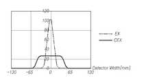
도 9는, 도 7 및 도 8의 감지기에서 측정한 빛의 세기를 나타내는 자료이다.
도 10은, 도 7 및 도 8의 감지기에서 촬영된 빛을 나타내는 도면이다.1 is a view schematically illustrating a display panel according to embodiments of the present invention.
2 is a view for explaining that the light source unit emits a first plane wave toward the spatial light modulation panel (SLM) according to embodiments of the present invention.
FIG. 3 is a view for explaining a process in which light emitted from the light source passes through each component of the display panel of the present invention.
4 is a view of a display panel of a comparative example not including the first optical sheet and the second optical sheet.
5 is a view for explaining positions of a first optical sheet and a second optical sheet in a display panel according to embodiments of the present invention.
6 is a view for explaining positions of a first optical sheet and a second optical sheet in a display panel according to embodiments of the present invention.
7 is a view illustrating a path of light emitted from a light source unit in a display panel according to embodiments of the present invention.
8 is a view showing a path of light emitted from a light source unit LSP in a display panel according to a comparative example of the present invention.
9 is data showing the intensity of light measured by the sensors of FIGS. 7 and 8.
10 is a view showing light taken by the sensors of FIGS. 7 and 8.
본 발명의 이점 및 특징, 그리고 그것들을 달성하는 방법은 첨부되는 도면과 함께 상세하게 후술되어 있는 실시예들을 참조하면 명확해질 것이다. 그러나 본 발명은 이하에서 개시되는 실시예들에 한정되는 것이 아니라 서로 다른 다양한 형태로 구현될 것이며, 단지 본 실시예들은 본 발명의 개시가 완전하도록 하며, 본 발명이 속하는 기술분야에서 통상의 지식을 가진 자에게 발명의 범주를 완전하게 알려주기 위해 제공되는 것이며, 본 발명은 청구항의 범주에 의해 정의될 뿐이다.Advantages and features of the present invention, and methods for achieving them will be clarified with reference to embodiments described below in detail together with the accompanying drawings. However, the present invention is not limited to the embodiments disclosed below, but will be implemented in various different forms, and only the present embodiments allow the disclosure of the present invention to be complete, and the general knowledge in the technical field to which the present invention pertains. It is provided to fully inform the holder of the scope of the invention, and the invention is only defined by the scope of the claims.
또한, 본 발명의 실시예들을 설명하기 위한 도면에 개시된 형상, 크기, 비율, 각도, 개수 등은 예시적인 것이므로 본 발명이 도시된 사항에 한정되는 것은 아니다. 명세서 전체에 걸쳐 동일 참조 부호는 동일 구성 요소를 지칭한다. 또한, 본 발명을 설명함에 있어서, 관련된 공지 기술에 대한 구체적인 설명이 본 발명의 요지를 불필요하게 흐릴 수 있다고 판단되는 경우 그 상세한 설명은 생략한다. 본 명세서 상에서 언급된 '포함한다', '갖는다', '이루어진다' 등이 사용되는 경우 '~만'이 사용되지 않는 이상 다른 부분이 추가될 수 있다. 구성 요소를 단수로 표현한 경우에 특별히 명시적인 기재 사항이 없는 한 복수를 포함하는 경우를 포함할 수 있다.In addition, the shapes, sizes, ratios, angles, numbers, etc. disclosed in the drawings for explaining embodiments of the present invention are exemplary, and the present invention is not limited to the illustrated matters. The same reference numerals refer to the same components throughout the specification. In addition, in the description of the present invention, when it is determined that detailed descriptions of related known technologies may unnecessarily obscure the subject matter of the present invention, detailed descriptions thereof will be omitted. When'include','have','consist of', etc. mentioned in this specification are used, other parts may be added unless'~man' is used. When a component is expressed in singular, it may include a case in which plural is included unless specifically stated.
또한, 본 발명의 실시예들에서의 구성 요소들을 해석함에 있어서, 별도의 명시적 기재가 없더라도 오차 범위를 포함하는 것으로 해석되어야 할 것이다.In addition, in interpreting the components in the embodiments of the present invention, it should be interpreted as including an error range even if there is no explicit description.
또한, 본 발명의 구성 요소를 설명하는 데 있어서, 제 1, 제 2, A, B, (a), (b) 등의 용어를 사용할 수 있다. 이러한 용어는 그 구성 요소를 다른 구성 요소와 구별하기 위한 것일 뿐, 그 용어에 의해 해당 구성 요소의 본질, 차례, 순서 또는 개수 등이 한정되지 않는다. 어떤 구성 요소가 다른 구성 요소에 "연결", "결합" 또는 "접속"된다고 기재된 경우, 그 구성 요소는 그 다른 구성 요소에 직접적으로 연결되거나 또는 접속될 수 있지만, 각 구성 요소 사이에 다른 구성 요소가 "개재"되거나, 각 구성 요소가 다른 구성 요소를 통해 "연결", "결합" 또는 "접속"될 수도 있다고 이해되어야 할 것이다. 위치 관계에 대한 설명일 경우, 예를 들어, '~상에', '~상부에', '~하부에', '~옆에' 등으로 두 부분의 위치 관계가 설명되는 경우, '바로' 또는 '직접'이 사용되지 않는 이상 두 부분 사이에 하나 이상의 다른 부분이 위치할 수도 있다.In addition, in describing the components of the present invention, terms such as first, second, A, B, (a), and (b) may be used. These terms are only for distinguishing the component from other components, and the essence, order, order, or number of the component is not limited by the term. When a component is described as being "connected", "coupled" or "connected" to another component, the component may be directly connected to or connected to the other component, but different components between each component It should be understood that the "intervenes" may be, or each component may be "connected", "coupled" or "connected" through other components. In the case of the description of the positional relationship, for example, when the positional relationship of two parts is described as'~top','~upper','~bottom','~side', etc.,'right' Alternatively, one or more other parts may be located between the two parts unless'direct' is used.
또한, 본 발명의 실시예들에서의 구성 요소들은 이들 용어에 의해 제한되지 않는다. 이들 용어들은 단지 하나의 구성 요소를 다른 구성 요소와 구별하기 위하여 사용하는 것일 뿐이다. 따라서, 이하에서 언급되는 제1 구성 요소는 본 발명의 기술적 사상 내에서 제2 구성 요소일 수도 있다.In addition, components in the embodiments of the present invention are not limited by these terms. These terms are only used to distinguish one component from another component. Therefore, the first component mentioned below may be the second component within the technical spirit of the present invention.
또한, 본 발명의 실시예들에서의 특징들(구성들)이 부분적으로 또는 전체적으로 서로 결합 또는 조합 또는 분리 가능하고, 기술적으로 다양한 연동 및 구동이 가능하며, 각 실시예는 서로에 대하여 독립적으로 실시 가능할 수도 있고 연관 관계로 함께 실시 가능할 수도 있다.In addition, the features (configurations) in the embodiments of the present invention may be partially or wholly combined with each other or combined or separated, and technically various interlocking and driving are possible, and each embodiment is independently performed with respect to each other. It may be possible or it may be implemented together in an association relationship.
이하에서는, 본 발명의 실시예들을 첨부된 도면을 참조하여 상세히 설명한다.Hereinafter, embodiments of the present invention will be described in detail with reference to the accompanying drawings.
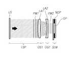
도 1은 본 발명의 실시예들에 따른 표시패널을 개략적으로 설명하기 위한 도면이다.1 is a view schematically illustrating a display panel according to embodiments of the present invention.
도 1을 참조하면, 본 발명의 실시예들에 따른 표시패널은, 공간 광 변조 패널(SLM), 광원부(LS), 제1 광학시트(OS1), 제2 광학시트(OS2)를 포함할 수 있다.Referring to FIG. 1, a display panel according to embodiments of the present invention may include a spatial light modulation panel (SLM), a light source unit LS, a first optical sheet OS1, and a second optical sheet OS2. have.
공간 광 변조 패널(SLM)은 개구부(OP)와 비개구부(NOP)를 포함할 수 있다. 비개구부(NOP)는, 트랜지스터, 캐패시터, 배선 등 공간 광 변조 패널에 포함되는 전기회로 요소에 의하여 광이 투과될 수 없는 영역을 의미한다. 개구부(OP)는 광이 투과될 수 있는 영역을 의미하며, 진폭 및/또는 위상이 변조된 광을 출사할 수 있다.The spatial light modulation panel SLM may include an opening OP and a non-opening part NOP. The non-opening part (NOP) refers to an area in which light cannot be transmitted by an electric circuit element included in a spatial light modulation panel such as a transistor, a capacitor, or a wiring. The opening OP refers to an area through which light can be transmitted, and may emit light whose amplitude and/or phase is modulated.
공간 광 변조 패널(SLM)은 진폭 변조용 광 변조기 및 위상 변조용 광 변조기를 포함할 수 있다. 공간 광 변조 패널(SLM)을 박형화하기 위하여, 공간 광 변조 패널(SLM)은 액정층을 포함하는 투과형 액정표시 패널일 수 있다.The spatial light modulation panel (SLM) may include an optical modulator for amplitude modulation and an optical modulator for phase modulation. In order to thin the spatial light modulation panel (SLM), the spatial light modulation panel (SLM) may be a transmissive liquid crystal display panel including a liquid crystal layer.
진폭 변조용 광 변조기는, 대향 배치된 두 개의 투명 기판 사이에 액정층이 위치하는 액정표시패널일 수 있다. 액정표시패널은 수평 전계 방식인 IPS(In Plane Switching) 모드일 수 있으나, 수직 전계 방식 또는 프린지 필드를 이용하는 다른 수평 전계 방식일 수도 있다.The optical modulator for amplitude modulation may be a liquid crystal display panel in which a liquid crystal layer is positioned between two opposing transparent substrates. The liquid crystal display panel may be an in-plane switching (IPS) mode that is a horizontal electric field method, but may also be a vertical electric field method or another horizontal electric field method using a fringe field.
진폭 변조용 광 변조기는 컴퓨터 혹은 비디오 처리 장치로부터 간섭 무늬 패턴 데이터를 입력받아 간섭 무늬를 표시할 수 있다. 진폭 변조용 광 변조기를 구성하는 액정표시패널은, 액정층을 구동하기 위한 박막 트랜지스터, 화소 전극 및 공통 전극 등이 형성되고, 상기 구성요소들은 비개구부를 구성할 수 있다.The optical modulator for amplitude modulation may receive interference fringe pattern data from a computer or video processing device and display the interference fringe pattern. In the liquid crystal display panel constituting the optical modulator for amplitude modulation, a thin film transistor, a pixel electrode, and a common electrode for driving the liquid crystal layer are formed, and the components may constitute a non-opening portion.
진폭 변조용 광 변조기는, 예를 들면 IPS 모드를 갖는 진폭 변조용 액정층을 포함할 수 있다. 또한, 컬러를 구현하기 위한 컬러 필터를 포함할 수 있다.The optical modulator for amplitude modulation may include, for example, a liquid crystal layer for amplitude modulation having an IPS mode. Also, a color filter for realizing color may be included.
위상 변조용 광 변조기는, 대향 배치된 두 개의 투명 기판 사이에 액정층이 위치하는 액정표시패널일 수 있다. 액정표시패널은 ECB 모드(Electrically controlled birefringence) 액정층을 포함할 수 있다. 위상 변조용 광 변조기는 컴퓨터 혹은 비디오 처리 장치로부터 간섭 무늬 패턴 데이터를 입력받아 간섭 무늬를 표시한다. 위상 변조용 광 변조기를 구성하는 액정표시패널은, 액정층을 구동하기 위한 박막 트랜지스터, 화소 전극 및 공통 전극 등이 형성되고, 상기 구성요소들은 비개구부를 구성할 수 있다.The optical modulator for phase modulation may be a liquid crystal display panel in which a liquid crystal layer is positioned between two opposing transparent substrates. The liquid crystal display panel may include an electrically controlled birefringence (ECB) liquid crystal layer. The phase modulating optical modulator receives interference fringe pattern data from a computer or video processing device and displays the interference fringe. In the liquid crystal display panel constituting the optical modulator for phase modulation, a thin film transistor, a pixel electrode, and a common electrode for driving the liquid crystal layer are formed, and the components may constitute a non-opening portion.
위상 변조용 광 변조기는 빛의 위상을 변조하는 기능을 담당하며, 예를 들면, ECB 모드를 갖는 위상 변조용 액정층은 액정층을 통과하는 빛에 대하여 위상 변화를 0에서 2π까지 변조할 수 있도록 제어될 수 있다.The phase modulating optical modulator is responsible for modulating the phase of light. For example, the liquid crystal layer for phase modulation having an ECB mode can modulate the phase change from 0 to 2π with respect to light passing through the liquid crystal layer. Can be controlled.
광 변조기(SLM)는 선 편광된 레이저 광을 이용하여 진폭 및 위상을 변조함으로써 입체 영상을 표현할 수 있다. 예를 들어, 노멀리 화이트(Normally White) 조건을 적용한 IPS 모드로 진폭 변조용 광 변조기를 구현할 경우, 진폭 변조용 광 변조기는 광 투과축이 서로 평행한 두 장의 편광 필름 사이에 배치할 수 있다.The optical modulator (SLM) may express a stereoscopic image by modulating amplitude and phase using linearly polarized laser light. For example, when the optical modulator for amplitude modulation is implemented in the IPS mode to which the Normally White condition is applied, the optical modulator for amplitude modulation can be disposed between two polarizing films having parallel axes of light transmission.
다른 예로, 노멀리 블랙(Normally Black) 조건을 적용한 IPS 모드로 진폭 변조용 광 변조기를 구현할 경우, 진폭 변조용 광 변조기는 광 투과축이 서로 직교하는 두 장의 편광 필름 사이에 배치하는 것이 바람직하다.As another example, when an optical modulator for amplitude modulation is implemented in an IPS mode to which a normally black condition is applied, the optical modulator for amplitude modulation is preferably disposed between two polarizing films having orthogonal optical transmission axes.
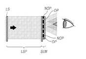
광원부(LSP)는 레이저 광원(LS)을 포함할 수 있다. 홀로그래피에 있어서, 홀로그램을 복원 또는 재생하기 위해서는, 코히런트(Coherent)한 광을 사용해야 한다. 본 발명의 실시예들에 따른 표시패널은, 코히런트(Coherent)한 광을 이용하기 위하여, 레이저 광원을 사용할 수 있다.The light source unit LSP may include a laser light source LS. In holography, in order to restore or reproduce a hologram, coherent light must be used. The display panel according to embodiments of the present invention may use a laser light source in order to use coherent light.
광원부(LSP)는 공간 광 변조 패널(SLM)을 향해 제1 평면파(PW1)를 방출할 수 있다.The light source unit LSP may emit the first plane wave PW1 toward the spatial light modulation panel SLM.
도 2는 본 발명의 실시예들에 따른 광원부(LSP)가 공간 광 변조 패널(SLM)을 향해 제1 평면파(PW1)를 방출하는 것을 설명하는 도면이다.2 is a view for explaining that the light source unit LSP according to embodiments of the present invention emits the first plane wave PW1 toward the spatial light modulation panel SLM.
도 2(A)에 도시한 것처럼, 광원부(LSP)는 평면파를 방출하는 레이저 광원(LS)을 포함할 수 있다. 또는, 구면파를 방출하는 레이저 광원(LS)을 포함하고, 상기 레이저 광원(LS)에서 방출된 구면파를 평면파로 변환하는 광학부재(OE)를 추가로 포함할 수 있다. 광학부재(OE)는, 예를 들면, 렌즈일 수 있다.As shown in FIG. 2(A), the light source unit LSP may include a laser light source LS emitting a plane wave. Alternatively, a laser light source LS that emits a spherical wave may be included, and an optical member OE that converts the spherical wave emitted from the laser light source LS into a plane wave may be further included. The optical member OE may be, for example, a lens.
본 발명에서 평면파는, 코히런트한 광으로서, 공간 광 변조 패널과 평행하게 진행하는 광을 의미할 수 있다.In the present invention, the plane wave is coherent light, and may mean light traveling in parallel with the spatial light modulation panel.
광원부(LSP)는, 레이저 광원(LS) 및 광섬유를 포함할 수 있다. 레이저 광원(LS)은, 적색 레이저 다이오드, 녹색 레이저 다이오드 및 청색 레이저 다이오드들을 포함하는 레이저 다이오드를 포함하거나, 적색, 녹색 및 청색 콜리메이티드 발광 다이오드들을 포함할 수 있다. 레이저 광원(LS)은 적색, 녹색 및 청색이 조합된 R,G,B 광원이거나, 상기 색상 외에 다른 색상들을 조합한 광원일 수 있다.The light source unit LSP may include a laser light source LS and an optical fiber. The laser light source LS may include a laser diode including a red laser diode, a green laser diode, and blue laser diodes, or may include red, green, and blue collimated light emitting diodes. The laser light source LS may be a red, green, and blue combined R, G, or B light source, or a combination of colors other than the above.
광원에서 출사된 광이 평면파로 출사되도록, 광원부(LSP)는 광 섬유를 포함할 수 있다. 레이저 다이오드들이 백 라이트 유닛의 일측면에 배치되고, 광 섬유가 레이저 다이오드에서 출사된 레이저 광이 확대 출사되도록 유도할 수 있다. 광 섬유는 광 변조기(SLM)의 전면에 대응하도록 배치될 수 있다.The light source unit LSP may include an optical fiber so that light emitted from the light source is emitted as a plane wave. The laser diodes are disposed on one side of the backlight unit, and the optical fiber may induce the laser light emitted from the laser diode to be expanded and emitted. The optical fiber may be arranged to correspond to the front side of the optical modulator (SLM).
레이저 광원(LS)에서 출사된 광은 선 편광될 수 있다. 레이저 광원(LS)의 편광 방향은 진폭 변조용 액정층의 초기 배열 방향과 평행한 방향으로 선 편광이 되도록 공간 광 변조 패널(SLM)을 향해 평행 직진하도록 출사될 수 있다.The light emitted from the laser light source LS may be linearly polarized. The polarization direction of the laser light source LS may be emitted so as to go straight parallel to the spatial light modulation panel SLM so as to be linearly polarized in a direction parallel to the initial arrangement direction of the liquid crystal layer for amplitude modulation.
제1 광학시트(OS1)는 복수의 제1 렌즈로 구성된 제1 렌즈 어레이(LA1)를 포함할 수 있다. 제1 렌즈 어레이(LA1)를 구성하는 복수의 제1 렌즈는 서로 이격되어 위치할 수도 있고, 소정의 굴절률을 가지는 물질에 형성된 패턴일 수도 있다.The first optical sheet OS1 may include a first lens array LA1 composed of a plurality of first lenses. The plurality of first lenses constituting the first lens array LA1 may be positioned spaced apart from each other, or may be a pattern formed on a material having a predetermined refractive index.
제1 광학시트(OS1)는 공간 광 변조 패널(SLM)과 대향되어 위치할 수 있다.The first optical sheet OS1 may be positioned to face the spatial light modulation panel SLM.
제1 광학시트(OS1)가 공간 광 변조 패널(SLM)과 대향되어 위치한다는 것은, 예를 들어 공간 광 변조 패널(SLM)과 제1 광학시트(OS1)가 모두 판 형상일 경우, 광 변조 패널(SLM)의 면과 제1 광학시트(OS1)의 면이 서로 마주하도록 위치하는 것을 의미할 수 있다.The first optical sheet OS1 is positioned to face the spatial light modulation panel SLM, for example, when both the spatial light modulation panel SLM and the first optical sheet OS1 are plate-shaped, the optical modulation panel It may mean that the surface of the (SLM) and the surface of the first optical sheet OS1 face each other.
제1 광학시트(OS1)는 광원부(LSP)와 공간 광 변조 패널(SLM) 사이에 위치할 수 있다.The first optical sheet OS1 may be positioned between the light source unit LSP and the spatial light modulation panel SLM.
제1 광학시트(OS1)가 광원부(LSP)와 공간 광 변조 패널(SLM) 사이에 위치함으로서, 광원부(LSP)로부터 공간 광 변조 패널(SLM)을 향해 방출된 제1 평면파(PW1)가 제1 광학시트(OS1)를 통과할 수 있다.Since the first optical sheet OS1 is positioned between the light source unit LSP and the spatial light modulation panel SLM, the first plane wave PW1 emitted from the light source unit LSP toward the spatial light modulation panel SLM is the first. It can pass through the optical sheet (OS1).
제2 광학시트(OS2)는 복수의 제2 렌즈로 구성된 제2 렌즈 어레이(LA2)를 포함할 수 있다. 제2 렌즈 어레이(LA2)를 구성하는 복수의 제2 렌즈는 서로 이격되어 위치할 수도 있고, 소정의 굴절률을 가지는 물질에 형성된 패턴일 수도 있다.The second optical sheet OS2 may include a second lens array LA2 composed of a plurality of second lenses. The plurality of second lenses constituting the second lens array LA2 may be positioned spaced apart from each other, or may be a pattern formed on a material having a predetermined refractive index.
제2 광학시트(OS2)는 제1 광학시트(OS1)와 공간 광 변조 패널(SLM) 사이에 위치할 수 있다. 따라서, 광원부(LSP)에서 공간 광 변조 패널(SLM)을 향해 방출된 제1 평면파(PW1)는, 제1 광학시트(OS1), 제2 광학시트(OS2) 및 공간 광 변조 패널(SLM)을 순차로 통과할 수 있다.The second optical sheet OS2 may be positioned between the first optical sheet OS1 and the spatial light modulation panel SLM. Accordingly, the first plane wave PW1 emitted from the light source unit LSP toward the spatial light modulation panel SLM includes the first optical sheet OS1, the second optical sheet OS2, and the spatial light modulation panel SLM. You can pass sequentially.
제2 광학시트(OS2)는, 공간 광 변조 패널(SLM)과 대향되어 위치할 수 있다.The second optical sheet OS2 may be positioned to face the spatial light modulation panel SLM.
제1 광학시트(OS1)의 제1 렌즈 어레이(LA1)를 구성하는 제1 렌즈는 임의의 점으로 광을 집중시키는 집광 렌즈이고, 제2 광학시트(OS2)의 제2 렌즈 어레이(LA2)를 구성하는 제2 렌즈는 제2 렌즈에 입사한 광을 제2 평면파로 변환하는 렌즈일 수 있다.The first lens constituting the first lens array LA1 of the first optical sheet OS1 is a condensing lens that focuses light at an arbitrary point, and the second lens array LA2 of the second optical sheet OS2 is The second lens may be a lens that converts light incident on the second lens into a second plane wave.
도 3은 광원부(LSP)에서 방출된 광이 본 발명의 표시패널의 각 구성요소를 통과하는 과정을 설명하기 위한 도면이다.FIG. 3 is a view for explaining a process in which light emitted from the light source unit LSP passes through each component of the display panel of the present invention.
도 3을 참조하면, 광원부(LSP)에서 방출된 제1 평면파(PW1)는 제1 광학시트(OS1)의 제1 렌즈 어레이(LA1)에 도달한다. 제1 렌즈 어레이(LA1)는 집광 렌즈인 제1 렌즈로 구성되므로, 제1 평면파(PW1)는 굴절되어 제2 광학시트(OS2)에 입사한다. 제2 광학시트(OS2)는, 입사한 광을 제2 평면파(PW2)로 변환하는 제2 렌즈로 구성되는 제2 렌즈 어레이(LA2)를 포함하므로, 제2 광학시트(OS2)에 입사한 광은 제2 평면파(PW2)로 변환된다.Referring to FIG. 3, the first plane wave PW1 emitted from the light source unit LSP reaches the first lens array LA1 of the first optical sheet OS1. Since the first lens array LA1 is composed of a first lens that is a condensing lens, the first plane wave PW1 is refracted and enters the second optical sheet OS2. Since the second optical sheet OS2 includes a second lens array LA2 composed of a second lens that converts incident light into a second plane wave (PW2), light incident on the second optical sheet OS2 Is converted to the second plane wave (PW2).
제1 렌즈 어레이(LA1)와 제2 렌즈 어레이(LA2)는 공간 광 변조 패널(SLM)의 개구부(OP)과 비개구부(MOP)의 분포를 고려하여, 제2 평면파(PW2)의 조사영역이 공간 광 변조 패널의 개구부(OP)에 대응되도록 선택될 수 있다. 따라서, 광원부(LSP)에서 방출되는 제1 평면파(PW1)가 제1 광학시트(OS1) 및 제2 광학시트(OS2)에 의해 비개구부(NOP)을 향하지 않도록 굴절되므로, 본 발명의 표시패널은 우수한 휘도를 가질 수 있다.The first lens array LA1 and the second lens array LA2 have an irradiation area of the second plane wave PW2 in consideration of the distribution of the opening OP and the non-opening part MOP of the spatial light modulation panel SLM. It may be selected to correspond to the opening OP of the spatial light modulation panel. Accordingly, since the first plane wave PW1 emitted from the light source unit LSP is refracted so as not to face the non-opening portion NOP by the first optical sheet OS1 and the second optical sheet OS2, the display panel of the present invention It can have excellent brightness.
도 4는 제1 광학시트(OS1)와 제2 광학시트(OS2)를 포함하지 않은 비교예의 표시패널에 대한 도면이다.4 is a view of a display panel of a comparative example not including the first optical sheet OS1 and the second optical sheet OS2.
도 4를 참조하면, 광원부(LSP)에서 방출된 평면파가 공간 광 변조 패널(SLM)에 도달하나, 공간 광 변조 패널(SLM)의 개구부(OP) 뿐만 아니라 비개구부(NOP)에도 도달하는 것을 알 수 있다. 따라서, 비개구부(NOP)에 도달하는 빛은 표시패널 외부로 추출되지 않으므로, 공간 광 변조 패널(SLM)에 존재하는 비개구부(NOP)는 휘도 저하의 원인으로 작용한다.Referring to FIG. 4, it is understood that the plane wave emitted from the light source unit LSP reaches the spatial light modulation panel SLM, but also reaches the opening OP as well as the non-opening part NOP of the spatial light modulation panel SLM. Can. Therefore, since the light reaching the non-opening part NOP is not extracted outside the display panel, the non-opening part NOP present in the spatial light modulation panel SLM acts as a cause of deterioration in luminance.
그러나, 본 발명의 실시예들에 따른 표시패널은 제1 광학시트(OS1) 및 제2 광학시트(OS2)가 제1 평면파(PW1)가 비개구부(NOP)에 도달하는 것을 예방하므로, 우수한 휘도를 가질 수 있다.However, in the display panel according to embodiments of the present invention, since the first optical sheet OS1 and the second optical sheet OS2 prevent the first plane wave PW1 from reaching the non-opening part NOP, excellent luminance Can have
도 3을 참조하면, 제2 광학시트(OS2)를 통과한 제2 평면파(PW2)의 조사영역은 공간 광 변조 패널(SLM)의 개구부(OP)에 대응될 수 있다. 본 발명에서, 제2 평면파(PW2)의 조사영역이 개구부(OP)에 대응된다는 것은, 제2 광학시트(OS2)에서 출사된 제2 평면파(PW2)의 조사영역이 개구부(OP)의 영역과 대응하는 것을 의미할 수도 있고, 제2 광학시트(OS2)에서 출사된 제2 평면파(PW2)가 개구QN(OP)에 도달하기 전에 통과하는 매질들을 통과한 이후의 조사영역이 개구부(OP) 영역에 대응된다는 것을 의미할 수도 있다. 또한, 조사영역이 개구부(OP) 영역에 대응된다는 것은, 조사영역의 면적과 개구부(OP) 영역의 면적이 서로 동일하다고 볼 수 있을 정도로 유사한 것을 의미할 수 있다.Referring to FIG. 3, the irradiation area of the second plane wave PW2 passing through the second optical sheet OS2 may correspond to the opening OP of the spatial light modulation panel SLM. In the present invention, the irradiation area of the second plane wave (PW2) corresponds to the opening (OP), the irradiation area of the second plane wave (PW2) emitted from the second optical sheet (OS2) is the area of the opening (OP) It may mean corresponding, and the irradiation area after the second plane wave (PW2) emitted from the second optical sheet (OS2) passes through the medium passing before reaching the opening QN (OP) is the opening (OP) area It may mean that it corresponds to. In addition, when the irradiation area corresponds to the opening OP area, it may mean that the area of the irradiation area and the area of the opening OP area are similar to each other.
제2 렌즈는 제1 렌즈가 집광한 광을 제2 평면파(PW2)로 변환하는 콜리메이션 렌즈일 수 있다.The second lens may be a collimation lens that converts light collected by the first lens into a second plane wave (PW2).
도 3을 참조하면, 광원부(LSP)에서 방출된 제1 평면파(PW1)는, 집광 렌즈인 제1 렌즈로 구성되는 제1 렌즈 어레이(LA1)로 인해 굴절되어 제2 렌즈 어레이(LA2)에 입사하고, 제2 렌즈 어레이(LA2)는 입사된 광을 제2 평면파(PW2)로 변환하는 것을 알 수 있다. 제2 렌즈로 콜리메이션 렌즈를 사용할 경우, 도 3에 도시한 것처럼 제2 렌즈 어레이(LA2)가 집광렌즈인 제1 렌즈로 구성되는 제1 렌즈 어레이(LA1)를 통과한 빛을 평면파로 변환시킬 수 있다.Referring to FIG. 3, the first plane wave PW1 emitted from the light source unit LSP is refracted due to the first lens array LA1 composed of the first lens that is the condensing lens and enters the second lens array LA2 Then, it can be seen that the second lens array LA2 converts the incident light to the second plane wave PW2. When a collimation lens is used as the second lens, as shown in FIG. 3, the light passing through the first lens array LA1 composed of the first lens, which is the second lens array LA2, is converted into a plane wave. Can.
제1 평면파(PW1)와 제2 평면파(PW2)는 서로 대응되는 위상을 가질 수 있다. 따라서, 제1 평면파(PW1)의 위상을 변조하여 홀로그램을 재생하기 위한 공간 광 변조 패널(SLM)에 제2 평면파(PW2)가 입사할 경우, 제2 평면파(PW2)는 제1 평면파(PW1)와 위상이 동일하므로, 제2 평면파(PW2)가 공간 광 변조 패널(SLM)에 입사되면 제1 평면파(PW1)가 입사된 것과 동일한 홀로그램이 재생될 수 있다.The first plane wave PW1 and the second plane wave PW2 may have phases corresponding to each other. Accordingly, when the second plane wave PW2 is incident on the spatial light modulation panel SLM for modulating the phase of the first plane wave PW1 to reproduce the hologram, the second plane wave PW2 is the first plane wave PW1 Since and phases are the same, when the second plane wave PW2 is incident on the spatial light modulation panel SLM, the same hologram as the first plane wave PW1 is incident may be reproduced.
본 발명의 실시예들에 따른 표시패널에 있어서, 제1 광학시트(OS1)와 제2 광학시트(OS2)의 위치는, 도 1에 도시한 것에 한정되지 않는다.In the display panel according to embodiments of the present invention, the positions of the first optical sheet OS1 and the second optical sheet OS2 are not limited to those illustrated in FIG. 1.
도 5는 본 발명의 실시예들에 따른 표시패널에 있어서, 제1 광학시트(OS1)와 제2 광학시트(OS2)의 위치를 설명하기 위한 도면이다.5 is a view for explaining the positions of the first optical sheet OS1 and the second optical sheet OS2 in the display panel according to embodiments of the present invention.
도 5를 참조하면, 본 발명의 실시예들에 따른 표시패널에 있어서, 제1 광학시트(OS1)와 제2 광학시트(OS2)는, 도 1에 도시한 표시패널과 달리 공간 광 변조 패널(SLM) 측에 인접하여 배치되지 않고, 광원부(LSP)에 인접하여 배치될 수 있다. 제1 광학시트(OS1)와 제2 광학시트(OS2)가 도 5와 같이 배치될 경우, 제2 광학시트(OS2)와 공간 광 변조 패널(SLM) 사이에는 다른 광학 부재가 위치할 수 있을 것이다.Referring to FIG. 5, in the display panel according to embodiments of the present invention, the first optical sheet OS1 and the second optical sheet OS2, unlike the display panel illustrated in FIG. 1, are spatial light modulation panels ( SLM) may not be disposed adjacent to the side, but may be disposed adjacent to the light source unit LSP. When the first optical sheet OS1 and the second optical sheet OS2 are arranged as shown in FIG. 5, another optical member may be positioned between the second optical sheet OS2 and the spatial light modulation panel SLM. .
도 6은, 본 발명의 실시예들에 따른 표시패널에 있어서, 제1 광학시트(OS1)와 제2 광학시트(OS2)의 위치를 설명하기 위한 도면이다.6 is a view for explaining the positions of the first optical sheet OS1 and the second optical sheet OS2 in the display panel according to embodiments of the present invention.
도 6을 참조하면, 본 발명의 실시예들에 따른 표시패널에 있어서, 제1 광학시트(OS1)는 광원부(LSP)에 인접하여 위치하고, 제2 광학시트(OS2)는 공간 광 변조 패널(SLM)에 인접하여 위치할 수 있다. 제1 광학시트(OS1)와 제2 광학시트(OS2)가 도 6과 같이 배치될 경우, 제1 광학시트(OS1)와 제2 광학시트(OS2) 사이에는 다른 광학 부재가 위치할 수 있을 것이다.Referring to FIG. 6, in the display panel according to embodiments of the present invention, the first optical sheet OS1 is located adjacent to the light source unit LSP, and the second optical sheet OS2 is the spatial light modulation panel SLM ). When the first optical sheet OS1 and the second optical sheet OS2 are arranged as shown in FIG. 6, another optical member may be positioned between the first optical sheet OS1 and the second optical sheet OS2. .
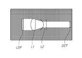
도 7은 본 발명의 실시예들에 따른 표시패널에 있어서, 광원부(LSP)에서 방출된 빛의 진행경로를 나타낸 도면이다.7 is a view illustrating a path of light emitted from a light source unit LSP in a display panel according to embodiments of the present invention.
도 7을 참조하면, 광원부(LSP)에서 방출된 빛이 제1 렌즈(L1) 및 제2 렌즈(L2)를 거쳐, 감지기(DET)에 도달하는 것을 알 수 있다. 감지기(DET)에서 감지된 빛의 세기는, 도 9 및 도 10에 도시하였다.Referring to FIG. 7, it can be seen that light emitted from the light source unit LSP reaches the detector DET through the first lens L1 and the second lens L2. The intensity of light sensed by the detector DET is illustrated in FIGS. 9 and 10.
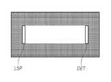
도 8은 본 발명의 비교예에 따른 표시패널에 있어서, 광원부(LSP)에서 방출된 빛의 진행경로를 나타낸 도면이다.8 is a view showing a path of light emitted from a light source unit LSP in a display panel according to a comparative example of the present invention.
도 8에 도시한 표시패널은, 도 7에 도시한 표시패널과 달리 제1 광학시트(OS1)와 제2 광학시트(OS2)를 포함하지 않는다. 따라서, 도 8을 참조하면 광원부(LSP)에서 방출된 빛이 감지기(DET)에 그대로 도달하는 것을 알 수 있다. 감지기(DET)에서 감지된 빛의 세기는, 도 9 및 도 10에 도시하였다.Unlike the display panel illustrated in FIG. 7, the display panel illustrated in FIG. 8 does not include the first optical sheet OS1 and the second optical sheet OS2. Therefore, referring to FIG. 8, it can be seen that the light emitted from the light source unit LSP reaches the detector DET as it is. The intensity of light sensed by the detector DET is illustrated in FIGS. 9 and 10.
도 7 및 도 8에 도시한 시뮬레이션은, 하기 표 1과 같은 조건에서 진행하였다.The simulations shown in FIGS. 7 and 8 were performed under the conditions shown in Table 1 below.
도 8에 도시한 비교예는, 제1 렌즈(L1) 및 제2 렌즈(L2)를 사용하지 않았다는 점을 제외하고 실시예와 동일한 조건에서 시뮬레이션을 진행하였다.In the comparative example shown in FIG. 8, simulation was performed under the same conditions as in Example, except that the first lens L1 and the second lens L2 were not used.
도 9는, 도 7 및 도 8의 감지기에서 측정한 빛의 세기를 나타내는 자료이다.9 is data showing the intensity of light measured by the sensors of FIGS. 7 and 8.
도 9를 참조하면, 실시예(EX)의 경우, 비교예(CEX)보다 빛이 더 좁은 폭에 집중되어 도달하는 것을 알 수 있다. 실시예(EX)에 해당하는 그래프는, 비교예(CEX)에 해당하는 그래프보다 좁은 폭에 걸쳐 빛이 감지되고, 좁은 영역에서 더 높은 강도를 기록하고 있기 때문이다.Referring to FIG. 9, it can be seen that in the case of the example EX, the light reaches and concentrates at a narrower width than the comparative example CEX. This is because the graph corresponding to the example (EX) detects light over a narrower width than the graph corresponding to the comparative example (CEX) and records a higher intensity in a narrow area.
도 10은, 도 7 및 도 8의 감지기에서 촬영된 빛을 나타내는 도면이다. 도 10(A)는 실시예에 해당하며, 도 10(B)는 비교예에 해당한다.10 is a view showing light taken by the sensors of FIGS. 7 and 8. 10(A) corresponds to an embodiment, and FIG. 10(B) corresponds to a comparative example.
도 10을 참조하면, 실시예에서는 비교예보다 더 좁은 범위에 빛이 감지되는 것을 알 수 있다. 따라서, 제1 광학시트(OS1)와 제2 광학시트(OS2)를 포함하는 실시예는, 비개구부에 빛이 도달하지 않도록 더 좁은 영역에 빛이 도달하게 하여 비개구부에 의한 휘도 저하를 예방할 수 있다.Referring to FIG. 10, it can be seen that in the embodiment, light is detected in a narrower range than the comparative example. Therefore, in the embodiment including the first optical sheet OS1 and the second optical sheet OS2, it is possible to prevent the light from reaching the narrower region so that light does not reach the non-opening portion, thereby preventing luminance degradation due to the non-opening portion. have.
다른 측면에서, 본 발명에 실시예들은 표시장치를 제공할 수 있다.In another aspect, embodiments of the present invention can provide a display device.
본 발명의 실시예들에 따른 표시장치는, 표시패널 및 구동회로를 포함할 수 있다.The display device according to embodiments of the present invention may include a display panel and a driving circuit.
본 발명의 실시예들에 따른 표시장치에 있어서, 표시패널에 관한 사항은 앞서 설명한 본 발명의 실시예들에 따른 표시패널에 대해 설명한 것과 동일하므로, 생략하기로 한다.In the display device according to the embodiments of the present invention, the matters related to the display panel are the same as those described for the display panel according to the embodiments of the present invention described above, and thus will be omitted.
구동회로는, 본 발명의 표시패널에 포함된 공간 광 변조 패널(SLM)과 광원부(LSP)를 구동할 수 있다.The driving circuit can drive the spatial light modulation panel (SLM) and the light source unit (LSP) included in the display panel of the present invention.
예를 들면, 공간 광 변조 패널(SLM)은 전극 및 액정을 포함하는 액정층을 포함할 수 있다. 상기 예시에서, 구동회로는 전극에 전압이 인가되게 하여 액정층에 포함된 액정의 배열을 제어할 수 있으며, 액정의 배열을 달리하여 공간 광 변조 패널(SLM)에 입사된 광의 진폭 및/또는 위상을 변조하여 홀로그램을 재생할 수 있다.For example, the spatial light modulation panel (SLM) may include a liquid crystal layer including an electrode and liquid crystal. In the above example, the driving circuit may control the arrangement of the liquid crystal included in the liquid crystal layer by applying a voltage to the electrode, and the amplitude and/or phase of light incident on the spatial light modulation panel (SLM) by varying the arrangement of the liquid crystal. You can reproduce the hologram by modulating.
이상의 설명은 본 발명의 기술 사상을 예시적으로 설명한 것에 불과한 것으로서, 본 발명이 속하는 기술 분야에서 통상의 지식을 가진 자라면 본 발명의 본질적인 특성에서 벗어나지 않는 범위에서 다양한 수정 및 변형이 가능할 것이다. 또한, 본 발명에 개시된 실시예들은 본 발명의 기술 사상을 한정하기 위한 것이 아니라 설명하기 위한 것이므로 이러한 실시예에 의하여 본 발명의 기술 사상의 범위가 한정되는 것은 아니다. 본 발명의 보호 범위는 아래의 청구범위에 의하여 해석되어야 하며, 그와 동등한 범위 내에 있는 모든 기술 사상은 본 발명의 권리 범위에 포함되는 것으로 해석되어야 할 것이다.The above description is merely illustrative of the technical idea of the present invention, and those skilled in the art to which the present invention pertains may make various modifications and variations without departing from the essential characteristics of the present invention. In addition, the embodiments disclosed in the present invention are not intended to limit the technical spirit of the present invention, but to explain the scope of the technical spirit of the present invention. The scope of protection of the present invention should be interpreted by the claims below, and all technical spirits within the equivalent range should be interpreted as being included in the scope of the present invention.
LS: 레이저 광원LA1: 제1 렌즈 어레이
LA2: 제2 렌즈 어레이OP: 개구부
NOP: 비개구부LSP: 광원부
OS1: 제1 광학시트OS2: 제2 광학시트
SLM: 공간 광 변조 패널OE: 광학부재
PW1: 제1 평면파PW2: 제2 평면파LS: laser light source LA1: first lens array
LA2: second lens array OP: opening
NOP: Non-opening part LSP: Light source part
OS1: 1st optical sheet OS2: 2nd optical sheet
SLM: Spatial light modulation panel OE: Optical member
PW1: first plane wave PW2: second plane wave
Claims (6)
Translated fromKorean레이저 광원을 포함하고, 상기 공간 광 변조 패널을 향해 제1 평면파를 방출하는 광원부;
복수의 제1 렌즈로 구성된 제1 렌즈 어레이를 포함하고, 상기 공간 광 변조 패널과 대향되어 위치하고, 상기 광원부와 상기 공간 광 변조 패널 사이에 위치하는 제1 광학시트; 및
복수의 제2 렌즈로 구성된 제2 렌즈 어레이를 포함하고, 상기 제1 광학 시트와 상기 공간 광 변조 패널 사이에 위치하는 제2 광학시트를 포함하고,
상기 제1 렌즈는 임의의 점으로 광을 집중시키는 집광 렌즈이며,
상기 제2 렌즈는 상기 제2 렌즈에 입사한 광을 제2 평면파로 변환하는 렌즈인 표시패널.A spatial light modulation panel including an opening and a non-opening portion;
A light source unit including a laser light source and emitting a first plane wave toward the spatial light modulation panel;
A first optical sheet including a first lens array composed of a plurality of first lenses, positioned opposite the spatial light modulation panel, and positioned between the light source unit and the spatial light modulation panel; And
And a second lens array comprising a plurality of second lenses, the second optical sheet being located between the first optical sheet and the spatial light modulating panel,
The first lens is a condensing lens that focuses light at an arbitrary point,
The second lens is a display panel that converts light incident on the second lens into a second plane wave.
상기 제2 평면파의 조사영역은 상기 공간 광 변조 패널의 상기 개구부에 대응되는 표시패널.According to claim 1,
The display area of the second plane wave corresponds to the opening of the spatial light modulation panel.
상기 제1 평면파와 상기 제2 평면파는 서로 대응되는 위상을 가지는 표시패널.According to claim 1,
The display panel having a phase in which the first plane wave and the second plane wave correspond to each other.
상기 제2 렌즈는 상기 제1 렌즈가 집광한 광을 제2 평면파로 변환하는 콜리메이션 렌즈인 표시패널.According to claim 1,
The second lens is a display panel that is a collimation lens that converts light collected by the first lens into a second plane wave.
상기 표시패널을 구동하는 구동회로를 포함하고,
상기 표시패널은,
레이저 광원을 포함하고, 상기 공간 광 변조 패널을 향해 제1 평면파를 방출하는 광원부;
복수의 제1 렌즈로 구성된 제1 렌즈 어레이를 포함하고, 상기 공간 광 변조 패널과 대향되어 위치하고, 상기 광원부와 상기 공간 광 변조 패널 사이에 위치하는 제1 광학시트; 및
복수의 제2 렌즈로 구성된 제2 렌즈 어레이를 포함하고, 상기 제1 광학 시트와 상기 공간 광 변조 패널 사이에 위치하는 제2 광학시트를 포함하고,
상기 제1 렌즈는 임의의 점으로 광을 집중시키는 집광 렌즈이며,
상기 제2 렌즈는 상기 제2 렌즈에 입사한 광을 제2 평면파로 변환하는 렌즈인 표시장치.Display panel; And
It includes a driving circuit for driving the display panel,
The display panel,
A light source unit including a laser light source and emitting a first plane wave toward the spatial light modulation panel;
A first optical sheet including a first lens array composed of a plurality of first lenses, positioned opposite the spatial light modulation panel, and positioned between the light source unit and the spatial light modulation panel; And
And a second lens array comprising a plurality of second lenses, the second optical sheet being located between the first optical sheet and the spatial light modulating panel,
The first lens is a condensing lens that focuses light at an arbitrary point,
The second lens is a display device that converts light incident on the second lens into a second plane wave.
상기 제2 렌즈는 상기 제1 렌즈가 집광한 광을 제2 평면파로 변환하는 콜리메이션 렌즈인 표시장치.The method of claim 5,
The second lens is a display device that is a collimation lens that converts light collected by the first lens into a second plane wave.
Priority Applications (1)
| Application Number | Priority Date | Filing Date | Title |
|---|---|---|---|
| KR1020180171127AKR102662217B1 (en) | 2018-12-27 | 2018-12-27 | Display panel and display device |
Applications Claiming Priority (1)
| Application Number | Priority Date | Filing Date | Title |
|---|---|---|---|
| KR1020180171127AKR102662217B1 (en) | 2018-12-27 | 2018-12-27 | Display panel and display device |
Publications (2)
| Publication Number | Publication Date |
|---|---|
| KR20200081040Atrue KR20200081040A (en) | 2020-07-07 |
| KR102662217B1 KR102662217B1 (en) | 2024-05-02 |
Family
ID=71603366
Family Applications (1)
| Application Number | Title | Priority Date | Filing Date |
|---|---|---|---|
| KR1020180171127AActiveKR102662217B1 (en) | 2018-12-27 | 2018-12-27 | Display panel and display device |
Country Status (1)
| Country | Link |
|---|---|
| KR (1) | KR102662217B1 (en) |
Citations (2)
| Publication number | Priority date | Publication date | Assignee | Title |
|---|---|---|---|---|
| JPH11271650A (en)* | 1998-03-24 | 1999-10-08 | Fuji Photo Film Co Ltd | Array type exposure element and plane type display |
| KR101653716B1 (en)* | 2014-09-05 | 2016-09-05 | 전자부품연구원 | 3D Image System and Display Method using the Hologram and Multiview Image |
- 2018
- 2018-12-27KRKR1020180171127Apatent/KR102662217B1/enactiveActive
Patent Citations (2)
| Publication number | Priority date | Publication date | Assignee | Title |
|---|---|---|---|---|
| JPH11271650A (en)* | 1998-03-24 | 1999-10-08 | Fuji Photo Film Co Ltd | Array type exposure element and plane type display |
| KR101653716B1 (en)* | 2014-09-05 | 2016-09-05 | 전자부품연구원 | 3D Image System and Display Method using the Hologram and Multiview Image |
Also Published As
| Publication number | Publication date |
|---|---|
| KR102662217B1 (en) | 2024-05-02 |
Similar Documents
| Publication | Publication Date | Title |
|---|---|---|
| US9720375B2 (en) | Spatial light modulating panel using transmittive liquid crystal display panel and 3D display device using the same | |
| US10551795B2 (en) | Spatial light modulator providing improved image quality and holographic display apparatus including the same | |
| US9442460B2 (en) | Digital hologram display device | |
| KR20140114651A (en) | Holographic 3D Display apparatus and illumination unit for holographic 3D Display apparatus | |
| KR101524336B1 (en) | Thin Flat Type Converge Lens | |
| CN111158078B (en) | Backlight unit and holographic display device including the same | |
| US10816932B2 (en) | Apparatus for displaying a hologram | |
| KR102512479B1 (en) | Hologram Display | |
| KR20130106723A (en) | Spatial light modulator using transparent type liquid crystal display panel based on thin film and 3d display device using the same | |
| KR20180050453A (en) | Spatial Light Modulator And 3D Display Device Using The Same | |
| KR101857818B1 (en) | Beam Combining Panel Using Patterned Halfwave Retarder And Method For Manufacturing The Same | |
| KR102040657B1 (en) | Spatial Light Modulating Panel And Holography 3D Display Using The Same | |
| KR102662217B1 (en) | Display panel and display device | |
| KR102099142B1 (en) | Spatial Light Modulating Panel and 3D Display Device Using The same | |
| EP4002001A1 (en) | Beam deflection apparatus and holographic display apparatus including the same | |
| KR101855258B1 (en) | Dynamic Thin Flat Type Light-Beam Deflector | |
| KR102268291B1 (en) | Video display apparatus | |
| KR101980353B1 (en) | Thin Flat Type Converge Lens | |
| KR20220071083A (en) | Beam deflection apparatus and holographic display apparatus including the same | |
| CN115705006A (en) | A holographic display device and display method thereof | |
| JPH02205816A (en) | Method for displaying dynamic three-dimensional image |
Legal Events
| Date | Code | Title | Description |
|---|---|---|---|
| PA0109 | Patent application | St.27 status event code:A-0-1-A10-A12-nap-PA0109 | |
| P22-X000 | Classification modified | St.27 status event code:A-2-2-P10-P22-nap-X000 | |
| P22-X000 | Classification modified | St.27 status event code:A-2-2-P10-P22-nap-X000 | |
| PG1501 | Laying open of application | St.27 status event code:A-1-1-Q10-Q12-nap-PG1501 | |
| A201 | Request for examination | ||
| PA0201 | Request for examination | St.27 status event code:A-1-2-D10-D11-exm-PA0201 | |
| P22-X000 | Classification modified | St.27 status event code:A-2-2-P10-P22-nap-X000 | |
| D13-X000 | Search requested | St.27 status event code:A-1-2-D10-D13-srh-X000 | |
| D14-X000 | Search report completed | St.27 status event code:A-1-2-D10-D14-srh-X000 | |
| E902 | Notification of reason for refusal | ||
| PE0902 | Notice of grounds for rejection | St.27 status event code:A-1-2-D10-D21-exm-PE0902 | |
| T11-X000 | Administrative time limit extension requested | St.27 status event code:U-3-3-T10-T11-oth-X000 | |
| T11-X000 | Administrative time limit extension requested | St.27 status event code:U-3-3-T10-T11-oth-X000 | |
| P11-X000 | Amendment of application requested | St.27 status event code:A-2-2-P10-P11-nap-X000 | |
| P13-X000 | Application amended | St.27 status event code:A-2-2-P10-P13-nap-X000 | |
| E701 | Decision to grant or registration of patent right | ||
| PE0701 | Decision of registration | St.27 status event code:A-1-2-D10-D22-exm-PE0701 | |
| PR0701 | Registration of establishment | St.27 status event code:A-2-4-F10-F11-exm-PR0701 | |
| PR1002 | Payment of registration fee | St.27 status event code:A-2-2-U10-U11-oth-PR1002 Fee payment year number:1 | |
| PG1601 | Publication of registration | St.27 status event code:A-4-4-Q10-Q13-nap-PG1601 |