KR20200074895A - Manufacturing method of power transistor and power transistor manufactured according to the manufacturing method - Google Patents
Manufacturing method of power transistor and power transistor manufactured according to the manufacturing methodDownload PDFInfo
- Publication number
- KR20200074895A KR20200074895AKR1020190168241AKR20190168241AKR20200074895AKR 20200074895 AKR20200074895 AKR 20200074895AKR 1020190168241 AKR1020190168241 AKR 1020190168241AKR 20190168241 AKR20190168241 AKR 20190168241AKR 20200074895 AKR20200074895 AKR 20200074895A
- Authority
- KR
- South Korea
- Prior art keywords
- layer
- gan
- semiconductor substrate
- power transistor
- algan
- Prior art date
- Legal status (The legal status is an assumption and is not a legal conclusion. Google has not performed a legal analysis and makes no representation as to the accuracy of the status listed.)
- Granted
Links
- 238000004519manufacturing processMethods0.000titleclaimsabstractdescription37
- 239000000758substrateSubstances0.000claimsabstractdescription233
- 239000004065semiconductorSubstances0.000claimsabstractdescription183
- 229910002704AlGaNInorganic materials0.000claimsabstractdescription138
- 238000000034methodMethods0.000claimsabstractdescription104
- 238000005498polishingMethods0.000claimsabstractdescription31
- 230000007547defectEffects0.000description24
- 239000013078crystalSubstances0.000description23
- 238000005530etchingMethods0.000description17
- QGZKDVFQNNGYKY-UHFFFAOYSA-NAmmoniaChemical compoundNQGZKDVFQNNGYKY-UHFFFAOYSA-N0.000description16
- 238000005229chemical vapour depositionMethods0.000description16
- 230000035882stressEffects0.000description16
- 238000000206photolithographyMethods0.000description14
- XCZXGTMEAKBVPV-UHFFFAOYSA-NtrimethylgalliumChemical compoundC[Ga](C)CXCZXGTMEAKBVPV-UHFFFAOYSA-N0.000description14
- 235000012431wafersNutrition0.000description13
- 239000007789gasSubstances0.000description10
- 238000000151depositionMethods0.000description8
- 230000008021depositionEffects0.000description8
- 230000000694effectsEffects0.000description8
- JLTRXTDYQLMHGR-UHFFFAOYSA-NtrimethylaluminiumChemical compoundC[Al](C)CJLTRXTDYQLMHGR-UHFFFAOYSA-N0.000description8
- QGZKDVFQNNGYKY-UHFFFAOYSA-OAmmoniumChemical compound[NH4+]QGZKDVFQNNGYKY-UHFFFAOYSA-O0.000description7
- 230000015572biosynthetic processEffects0.000description6
- 238000004518low pressure chemical vapour depositionMethods0.000description6
- 229910000069nitrogen hydrideInorganic materials0.000description5
- 239000012495reaction gasSubstances0.000description5
- 125000002496methyl groupChemical group[H]C([H])([H])*0.000description4
- 229910021529ammoniaInorganic materials0.000description3
- 238000005452bendingMethods0.000description3
- 238000002488metal-organic chemical vapour depositionMethods0.000description3
- 239000000376reactantSubstances0.000description3
- 229910003828SiH3Inorganic materials0.000description2
- 238000005520cutting processMethods0.000description2
- 239000001307heliumSubstances0.000description2
- 229910052734heliumInorganic materials0.000description2
- SWQJXJOGLNCZEY-UHFFFAOYSA-Nhelium atomChemical compound[He]SWQJXJOGLNCZEY-UHFFFAOYSA-N0.000description2
- 238000007517polishing processMethods0.000description2
- OLRJXMHANKMLTD-UHFFFAOYSA-NsilylChemical compound[SiH3]OLRJXMHANKMLTD-UHFFFAOYSA-N0.000description2
- 230000032683agingEffects0.000description1
- 230000015556catabolic processEffects0.000description1
- 230000001186cumulative effectEffects0.000description1
- 230000006866deteriorationEffects0.000description1
- 238000000407epitaxyMethods0.000description1
- 239000000463materialSubstances0.000description1
- 229910052751metalInorganic materials0.000description1
- 239000002184metalSubstances0.000description1
- 150000004767nitridesChemical class0.000description1
- 229910052594sapphireInorganic materials0.000description1
- 239000010980sapphireSubstances0.000description1
- 230000005533two-dimensional electron gasEffects0.000description1
Images


Classifications
- H01L29/66462—
- H—ELECTRICITY
- H10—SEMICONDUCTOR DEVICES; ELECTRIC SOLID-STATE DEVICES NOT OTHERWISE PROVIDED FOR
- H10D—INORGANIC ELECTRIC SEMICONDUCTOR DEVICES
- H10D30/00—Field-effect transistors [FET]
- H10D30/01—Manufacture or treatment
- H10D30/015—Manufacture or treatment of FETs having heterojunction interface channels or heterojunction gate electrodes, e.g. HEMT
- H—ELECTRICITY
- H01—ELECTRIC ELEMENTS
- H01L—SEMICONDUCTOR DEVICES NOT COVERED BY CLASS H10
- H01L21/00—Processes or apparatus adapted for the manufacture or treatment of semiconductor or solid state devices or of parts thereof
- H01L21/02—Manufacture or treatment of semiconductor devices or of parts thereof
- H01L21/04—Manufacture or treatment of semiconductor devices or of parts thereof the devices having potential barriers, e.g. a PN junction, depletion layer or carrier concentration layer
- H01L21/18—Manufacture or treatment of semiconductor devices or of parts thereof the devices having potential barriers, e.g. a PN junction, depletion layer or carrier concentration layer the devices having semiconductor bodies comprising elements of Group IV of the Periodic Table or AIIIBV compounds with or without impurities, e.g. doping materials
- H01L21/30—Treatment of semiconductor bodies using processes or apparatus not provided for in groups H01L21/20 - H01L21/26
- H01L21/302—Treatment of semiconductor bodies using processes or apparatus not provided for in groups H01L21/20 - H01L21/26 to change their surface-physical characteristics or shape, e.g. etching, polishing, cutting
- H01L21/304—Mechanical treatment, e.g. grinding, polishing, cutting
- H01L21/3043—Making grooves, e.g. cutting
- H—ELECTRICITY
- H01—ELECTRIC ELEMENTS
- H01L—SEMICONDUCTOR DEVICES NOT COVERED BY CLASS H10
- H01L21/00—Processes or apparatus adapted for the manufacture or treatment of semiconductor or solid state devices or of parts thereof
- H01L21/70—Manufacture or treatment of devices consisting of a plurality of solid state components formed in or on a common substrate or of parts thereof; Manufacture of integrated circuit devices or of parts thereof
- H01L21/77—Manufacture or treatment of devices consisting of a plurality of solid state components or integrated circuits formed in, or on, a common substrate
- H01L21/78—Manufacture or treatment of devices consisting of a plurality of solid state components or integrated circuits formed in, or on, a common substrate with subsequent division of the substrate into plural individual devices
- H01L29/2003—
- H01L29/7783—
- H—ELECTRICITY
- H10—SEMICONDUCTOR DEVICES; ELECTRIC SOLID-STATE DEVICES NOT OTHERWISE PROVIDED FOR
- H10D—INORGANIC ELECTRIC SEMICONDUCTOR DEVICES
- H10D30/00—Field-effect transistors [FET]
- H10D30/40—FETs having zero-dimensional [0D], one-dimensional [1D] or two-dimensional [2D] charge carrier gas channels
- H10D30/47—FETs having zero-dimensional [0D], one-dimensional [1D] or two-dimensional [2D] charge carrier gas channels having 2D charge carrier gas channels, e.g. nanoribbon FETs or high electron mobility transistors [HEMT]
- H10D30/471—High electron mobility transistors [HEMT] or high hole mobility transistors [HHMT]
- H10D30/473—High electron mobility transistors [HEMT] or high hole mobility transistors [HHMT] having confinement of carriers by multiple heterojunctions, e.g. quantum well HEMT
- H10D30/4732—High electron mobility transistors [HEMT] or high hole mobility transistors [HHMT] having confinement of carriers by multiple heterojunctions, e.g. quantum well HEMT using Group III-V semiconductor material
- H—ELECTRICITY
- H10—SEMICONDUCTOR DEVICES; ELECTRIC SOLID-STATE DEVICES NOT OTHERWISE PROVIDED FOR
- H10D—INORGANIC ELECTRIC SEMICONDUCTOR DEVICES
- H10D62/00—Semiconductor bodies, or regions thereof, of devices having potential barriers
- H10D62/80—Semiconductor bodies, or regions thereof, of devices having potential barriers characterised by the materials
- H10D62/85—Semiconductor bodies, or regions thereof, of devices having potential barriers characterised by the materials being Group III-V materials, e.g. GaAs
- H10D62/8503—Nitride Group III-V materials, e.g. AlN or GaN
Landscapes
- Engineering & Computer Science (AREA)
- Physics & Mathematics (AREA)
- Condensed Matter Physics & Semiconductors (AREA)
- General Physics & Mathematics (AREA)
- Manufacturing & Machinery (AREA)
- Computer Hardware Design (AREA)
- Microelectronics & Electronic Packaging (AREA)
- Power Engineering (AREA)
- Junction Field-Effect Transistors (AREA)
- Chemical & Material Sciences (AREA)
- Materials Engineering (AREA)
- Recrystallisation Techniques (AREA)
Abstract
Translated fromKorean
Description
Translated fromKorean본 발명은 반도체 기판을 사용한 파워 트랜지스터의 제조 방법에 관한 것이다. 구체적으로는 Si 기판을 사용하여 III 족 반도체를 제조하는 방법 및 그 제조 방법에 따라 제조되는 트랜지스터 장치에 관한 것이다.The present invention relates to a method for manufacturing a power transistor using a semiconductor substrate. Specifically, it relates to a method for manufacturing a group III semiconductor using a Si substrate and a transistor device manufactured according to the manufacturing method.
현재, 일본 특허 공개 2014-3301호 공보에서와 같이 SiC 기판 또는 사파이어(Sapphire) 기판, 기타 Si 기판 등을 사용하여 III족 질화물 파워 트랜지스터가 사용되고 있다. 또는, 비특허문헌 1 및 2에 나타난 바와 같이 제조원가 절감 및 Si 공정을 이용할 수 있는, Si 기판을 이용한 GaN 파워 트랜지스터가 연구 및 이용되기 시작했다. Si 기판을 사용하는 경우에는, GaN의 결정성을 양호하게 하기 위해 GaN 버퍼층이 사용되고 있다.Currently, a group III nitride power transistor is used using a SiC substrate, a sapphire substrate, or other Si substrate as in Japanese Patent Laid-Open No. 2014-3301. Alternatively, as shown in Non-Patent
종래의 Si 기판을 가지는 파워 트랜지스터에서는 GaN의 결정성을 개선하기 위해서, Si 기판의 표면에만 먼저 GaN 버퍼층을 8 ~ 17㎛로 매우 두껍게 형성하고, 그 위에 GaN 에피택셜층을 형성시킨다. 그리고 그 위에 2차원 전자가스를 발생시켜 i-GaN(intrinsic-GaN, 혹은 non-doped-GaN) 및 i-AlGaN을 형성하고, 그 위에 게이트 전극을 형성하여 파워 트랜지스터를 완성하는 방법을 사용하였다. 기판 표면에 형성한 GaN 에피택셜층의 결정성을 향상시키기 위해, 그 아래에 있는 GaN 버퍼층은 두께가 두껍게 형성되어, GaN 버퍼층의 스트레스에 의해, 웨이퍼가 크게 휘어지는 문제가 발생하고, 그 결과 파워 트랜지스터의 에피택셜층에 결정 결함이 발생하는 문제가 있다.In a conventional power transistor having a Si substrate, in order to improve the crystallinity of GaN, a GaN buffer layer is formed very thickly at 8 to 17 µm only on the surface of the Si substrate, and a GaN epitaxial layer is formed thereon. Then, a two-dimensional electron gas was generated thereon to form i-GaN (intrinsic-GaN, or non-doped-GaN) and i-AlGaN, and a gate electrode was formed thereon to complete the power transistor. In order to improve the crystallinity of the GaN epitaxial layer formed on the substrate surface, the GaN buffer layer underneath is formed to have a thick thickness, resulting in a problem that the wafer is greatly warped due to the stress of the GaN buffer layer, resulting in a power transistor There is a problem in that crystal defects occur in the epitaxial layer.
따라서, 본 발명의 해결 방법 및 그 과제는 Si 기판상에 트랜지스터를 제조하는 방법에서, Si 기판의 변형을 최소화하고, Si 기판의 휘어짐에 의한 GaN 에피택셜층의 결정 결함을 줄이기 위한 것이다.Therefore, the solution of the present invention and its object are to minimize the deformation of the Si substrate and reduce the crystal defect of the GaN epitaxial layer due to the bending of the Si substrate in the method of manufacturing the transistor on the Si substrate.
본 출원의 청구항 1에 기재되어 있는 제조 방법은, 반도체 기판의 양면에 SiC 층 및 GaN 버퍼층을 순서대로 형성하여 상기 반도체 기판의 휨을 적게 하는 공정, 상기 반도체 기판의 표면에 GaN 에피택셜층과 AlGaN 에피택셜층을 형성하는 공정, 상기에 반도체 기판 표면의 SiC 층 및 상기 GaN 버퍼층에 파워 트랜지스터를 형성하는 공정, 상기 반도체 기판의 표면의 파워 트랜지스터를 분리하는 공정, 파워 트랜지스터 칩을 분리해서 배면을 연마하는 공정을 통해 파워 트랜지스터의 제조 방법을 제공하여 상기 과제를 해결할 수 있다.The manufacturing method described in
본 출원 청구항 1에 기재된 파워 트랜지스터의 제조 방법은, 반도체 기판의 표면에 파워 트랜지스터를 형성하는 것을 가능하게 한다. 도 1과 같이 반도체 기판을 준비하고 도 2와 같이 상기 반도체 기판의 양면에 Si와 GaN의 중간 영역의 격자 상수를 가지고 GaN 버퍼층의 결정성을 개선하기 위한 SiC 층(또는 반도체 층)과, GaN 에피택셜층의 결정성을 개선하기 위한 GaN 버퍼층을 형성한다. 상기 반도체 기판의 양면에 상기 SiC 층 및 상기 GaN 버퍼층을 형성하는 이유는, 반도체 기판의 휘어짐을 줄이기 위함이다. 또한, 상기 반도체 기판은 여러 가지 에피택셜층을 이용하여 소자를 형성하는 것도 가능하다. 즉 값이 싼 소재를 선택할 수 있다.The manufacturing method of the power transistor of
도 3과 같이 반도체 기판의 표면에 2차원 가스를 형성하기 위한 GaN 에피택셜층(i-GaN 층)과 AlGaN 에피택셜층(i-AlGaN 층)을 형성하고, 도 4와 같이 파워 트랜지스터를 제조하는 경우에, 배면에 상기 SiC 층 및 두꺼운 GaN 버퍼층이 존재하기 때문에, 상기 설명한 바와 같이 반도체 기판의 휘어짐을 매우 작게 할 수 있기 때문이다. 이로써 종래에 두껍게 GaN 버퍼층을 형성하는 것에 의해 반도체 기판이 크게 휘게 되어 GaN 에피택셜층에 결정 결함을 발생시키는 문제를 해결할 수 있다. 기존에는 반도체 기판의 표면에만 GaN 버퍼층과 GaN 에피택셜층을 형성하여, 웨이퍼가 크게 휘기 때문에 GaN 에피택셜층에 결정 결함이 생기기 쉽다.3, a GaN epitaxial layer (i-GaN layer) and an AlGaN epitaxial layer (i-AlGaN layer) for forming a two-dimensional gas on the surface of a semiconductor substrate are formed, and a power transistor is manufactured as shown in FIG. In this case, since the SiC layer and the thick GaN buffer layer are present on the back surface, it is because the warpage of the semiconductor substrate can be made very small as described above. As a result, the problem of generating crystal defects in the GaN epitaxial layer can be solved because the semiconductor substrate is greatly warped by forming a thick GaN buffer layer. Conventionally, since the GaN buffer layer and the GaN epitaxial layer are formed only on the surface of the semiconductor substrate, the wafer is greatly warped and crystal defects are likely to occur in the GaN epitaxial layer.
본 발명은 도 4와 같이 파워 트랜지스터를 형성하고, 그 위에 도 5와 같이 파워 트랜지스터를 분리하고, 표면을 연삭하여 표면 GaN 버퍼층 및 SiC 층의 스트레스 영향을 줄인 후, 도 7에 따라 배면을 연마한다. 도 24(a)에 따라 배면을 연마하고 칩을 절단한다.The present invention forms a power transistor as shown in FIG. 4, separates the power transistor as shown in FIG. 5, and grinds the surface to reduce the stress effect of the surface GaN buffer layer and SiC layer, and then polishes the back surface according to FIG. . The back surface is polished and the chip is cut according to Fig. 24(a).
이와 같이, 스트레스가 작은 기판을 사용하여 결정 결함이 적은 파워 트랜지스터를 만들 수 있는 장점이 있다.As described above, there is an advantage that a power transistor with less crystal defects can be made using a substrate having a small stress.
본 출원 청구항 2에 기재된 제품의 제조 방법은 기판의 양면에 SiC 층과 GaN 버퍼층 및 GaN 에피택셜층과 AlGaN 층을 순서대로 형성하여, 상기 반도체 기판의 휨이 거의 없게 하는 공정, 상기 반도체 기판 표면의 상기 SiC 층 및 상기 GaN 버퍼층에 파워 트랜지스터를 형성하는 공정, 상기 반도체 기판의 표면의 파워 트랜지스터를 분리하는 공정, 파워 트랜지스터 칩을 절단해서 배면을 연마하는 공정을 이용하여 파워 트랜지스터의 제조 방법을 제공하여, 상기에서 언급한 문제를 해결할 수 있다.The method for manufacturing a product according to
본원 청구항 2에 기재되어있는 파워 트랜지스터의 제조 방법은, 반도체 기판의 표면에 파워 트랜지스터를 형성하는 것이 가능하다. 도 1과 같이 반도체 기판을 준비하고 도 8과 같이, 양면에 Si와 GaN 사이에 중간의 격자상수 크기를 가지고 GaN 버퍼층의 결정성을 향상시키는 SiC 층과, GaN 에피택셜층의 결정성을 향상시킬 수 있다. 상기 반도체 기판의 양면에 상기 SiC 층과 GaN 버퍼층, 그리고 GaN 에피택셜층(i-GaN 층), AlGaN 에피택셜층(i-AlGaN 층)을 형성하여 상기 반도체 기판의 휨을 거의 없게 할 수 있다. 도 8과 같이 2차원 가스를 형성하는 데 필요한 GaN 에피택셜층(i-GaN 층)과 AlGaN 에피택셜층(i-AlGaN 층)을 형성하고, 도 9와 같이 파워 트랜지스터를 제조할 경우에, SiC 층과 GaN 버퍼층, 그리고 GaN 에피택셜층 (i-GaN 층), AlGaN 에피택셜층 (i-AlGaN 층)이 존재한다. 이로써 반도체 기판의 휨을 적게 할 수 있다. 이렇게 하여 종래의 두껍게 GaN 버퍼층을 형성하는 것에 의해 반도체 기판이 크게 휘는 원인이 되고, GaN 에피택셜층에 결정 결함을 발생시키는 문제를 해결할 수 있다. 종래에는 반도체 기판의 표면에만 GaN 버퍼층과 GaN 에피택셜층을 형성하여, GaN 에피택셜층에 결정 결함이 발생하였다. 본 발명은 도 9와 같이 기판을 형성하고, 그 위에 도 10과 같이, 파워 트랜지스터를 분리하고, 표면을 연삭하여 SiC 층의 스트레스의 영향을 줄인다. 그 후 도 12와 같이 배면을 연마할 수 있다. 따라서, 도 24(a)와 같이 배면을 연마하여 칩을 절단할 수가 있다.The method for manufacturing a power transistor described in
이러한 방식을 통해, 휨이 적게 된 공정을 사용하여 결정 결함이 적은 파워 트랜지스터를 제작할 수 있는 잇점이 있다.Through this method, there is an advantage that a power transistor with less crystal defects can be manufactured using a process with less warpage.
본 출원 청구항 3에 기재되어있는 파워 트랜지스터 제조 방법은, 반도체 기판의 양면에 GaN 버퍼층을 형성하여 상기 반도체 기판의 휨이 적게 하는 공정, 반도체 기판의 표면에 GaN 에피택셜층을 형성하는 공정, 상기 반도체 기판 표면에 상기 GaN 버퍼층 위에 파워 트랜지스터를 형성하는 공정, 상기 반도체 기판의 표면의 파워 트랜지스터를 분리하는 공정, 파워 트랜지스터 칩을 절단하여 배면을 연마하는 공정을 이용하여 파워 트랜지스터를 제조하는 방법을 이용하여, 상기에 언급한 문제를 해결할 수 있다.In the power transistor manufacturing method described in
본 출원 청구항 3에 기재된 파워 트랜지스터의 제조방법은 반도체 기판의 표면에 파워 트랜지스터 형성을 가능하게 한다. 도 1과 같이 반도체 기판을 준비하고 도 13과 같이 기판의 양면에 GaN 에피택셜층의 결정성을 개량하기 위한 GaN 버퍼층을 형성할 수 있다. 상기 반도체 기판의 양면에 GaN 버퍼층을 형성하는 이유는, 상기 반도체 기판의 휨을 줄이기 위함이다. 도 14와 같이 반도체 기판의 표면에 2차원 가스를 형성하여 GaN 에피택셜층(i-GaN 층)과 AlGaN 에피택셜층(i-AlGaN 층)을 형성하고, 도 15과 같이 파워 트랜지스터를 제조하는 경우에는, 배면에 두꺼운 상기 GaN 버퍼층이 존재하여, 상기 반도체 기판의 휘어짐을 적게 할 수 있고, 반도체 기판의 결함이 매우 적다. 따라서, 종래의 두꺼운 GaN 버퍼층의 형성에 의한 반도체 기판의 크게 휘는 원인으로 GaN 에피택셜층의 결정 결함을 발생시키는 것의 문제를 해결할 수 있다. 종래에는 반도체 기판의 표면에만 GaN 버퍼층과 GaN 에피택셜층을 형성하여, 웨이퍼가 크게 휘어서 GaN 에피택셜층에 결정 결함이 발생하는 문제가 있었다. 본 발명은 도 15와 같이 파워 트랜지스터를 형성한 후, 그 위에 도 16과 같이 파워 트랜지스터를 분리하여 표면을 연삭할 때 GaN 버퍼층의 스트레스 영향을 줄일 수 있고, 다음에 도 7과 같이 배면을 연마 가능하고 도 24(b)와 같이 배면을 연마한 칩을 절단해서 완성한다.The method of manufacturing a power transistor according to
이런 방법으로, 휨이 적은 기판을 사용하고, 결정 결함이 적은 파워 트랜지스터를 제작할 수 있는 잇점이 있다.In this way, there is an advantage that a substrate having low warpage and a power transistor with less crystal defects can be manufactured.
본 출원의 청구항 4에 기재된 파워 트랜지스터의 제조 방법은 반도체 기판의 양면에 GaN 버퍼층과 GaN 에피택셜층을 순차적으로 형성시켜 상기 반도체 기판의 휨을 적게 하는 공정, 상기 반도체 기판 표면의 상기 GaN 버퍼층 위에 파워 트랜지스터를 형성하는 공정, 상기 반도체 기판의 표면의 파워 트랜지스터를 분리하는 공정, 파워 트랜지스터 칩을 분리하고 배면을 연마하는 공정을 이용하여 파워 트랜지스터의 제조방법을 제공하여 상기 과제를 해결할 수 있다.The manufacturing method of the power transistor according to
본출원 청구항 4 에 기재된 파워 트랜지스터 제조방법은 반도체 기판의 표면에 파워 트랜지스터를 형성할 수 있다. 도 1과 같이 반도체 기판을 준비하고, 도 19와 같이 상기 반도체 기판 양면에 GaN 에피택셜층의 결정성을 향상시키기 위한 GaN 버퍼층과 GaN 에피택셜층을 형성할 수 있다. 상기 반도체 기판의 양면에 상기 설명한 GaN 버퍼층과 GaN 에피택셜층(i-GaN 층)과 AlGaN 에피택셜층(i-AlGaN층)을 형성하는 이유는, 상기 반도체 기판의 휘어짐을 적게 하기 위함이다.The power transistor manufacturing method according to
도 19와 같이 2차원 가스를 형성하기 위한 GaN 에피택셜층(i-GaN 층)과 AlGaN 에피택셜층(i-AlGaN 층)을 형성하여 도 20과 같이 파워 트랜지스터를 제조하는 경우, 배면에 두꺼운 상기 (i-GaN 층)과 AlGaN 에피택셜층 (i-AlGaN 층)이 존재하며, 상기와 같이 반도체 기판의 휘어짐 영향을 적게 할 수 있다.When a power transistor is manufactured as shown in FIG. 20 by forming a GaN epitaxial layer (i-GaN layer) and an AlGaN epitaxial layer (i-AlGaN layer) for forming a two-dimensional gas as shown in FIG. (i-GaN layer) and AlGaN epitaxial layer (i-AlGaN layer) are present, and as described above, the bending effect of the semiconductor substrate can be reduced.
종래의 두꺼운 GaN 버퍼층의 형성으로 반도체 기판에 크게 영향을 끼치는 원인이 되는 GaN 에피택셜층의 결정 결함을 유발시키는 문제를 해결할 수 있다. 종래는 반도체 기판의 표면에만 GaN 버퍼층과 GaN 에피택셜층을 형성하여, 웨이퍼가 커다란 휘어짐을 일으켜 GaN 에피택셜층에 결정 결함이 생기기 쉽다. 본 발명은 도 20와 같이 파워 트랜지스터를 형성한 후 그 위에 도 21과 같이 파워 트랜지스터를 분리하고, 표면을 연삭하여, 배면의 GaN 버퍼층과 SiC 층의 스트레스 영향을 줄일 수 있다. 그 후, 도 23과 같이 배면을 연마하고, 도 24(a)와 같이 배면을 연마한 칩을 절단할 수 있다.The formation of a conventional thick GaN buffer layer can solve the problem of causing crystal defects in the GaN epitaxial layer that significantly affects the semiconductor substrate. Conventionally, a GaN buffer layer and a GaN epitaxial layer are formed only on the surface of a semiconductor substrate, so that the wafer is greatly warped and crystal defects are likely to occur in the GaN epitaxial layer. The present invention can form a power transistor as shown in FIG. 20, and then separate the power transistor as shown in FIG. 21 and grind the surface to reduce the stress effect of the back GaN buffer layer and the SiC layer. Thereafter, the back surface can be polished as shown in FIG. 23, and the chip with the back surface polished as shown in FIG. 24(a) can be cut.
이렇게 하여 영향과 휨이 적게 하는 기판을 사용하여, 결정 결함이 적은 파워 트랜지스터를 형성할 수 있는 유리한 점이 있다.In this way, there is an advantage in that a power transistor with less crystal defects can be formed using a substrate having less influence and warpage.
본출원 청구항 5에 기재된 파워 트랜지스터의 제조 방법은, 상기 반도체 기판으로 Si 기판을 채택할 수 있고, 청구항 1에서 4까지 중 어느 하나에 기재된 파워 트랜지스터의 제조 방법을 각각 제공하여 상기에 언급된 문제를 해결할 수 있다.The manufacturing method of the power transistor according to
Si 기판은 반도체 공정에서 광범위하게 사용되는 것으로서, 발광 소자의 공정에서 사용하는 포토리소그래피(Photolithography) 공정, 연마 공정, 에칭(Etching) 공정을 쉽게 수행할 수 있으며, 파워 트랜지스터를 쉽게 형성할 수 있다.The Si substrate is widely used in a semiconductor process, and can easily perform a photolithography process, a polishing process, and an etching process used in the process of a light emitting device, and can easily form a power transistor.
본 출원 청구항 6에 기재되어있는 내용은 청구항 1에서 4까지 중 어느 하나에 기재되어 있는 파워 트랜지스터의 제조 방법에 의해 제조될 수 있는 파워 트랜지스터를 제공하기 때문에 상기 과제를 해결할 수 있다.The content described in
본 출원 청구항 6에 기재된 파워 트랜지스터는 청구항 1에서 4까지 중 어느 하나에 기재되어있는 파워 트랜지스터의 제조 방법에 의해 제조된 파워 트랜지스터는 결정 결함이 적은 파워 트랜지스터로써 충족되는 내전압 특성 FET(Field Effective Transister)의 특성을 얻을 수 있다.The power transistor described in
본 발명은 반도체 기판의 양면에 대하여 각각의 SiC 층과 GaN 버퍼층, SiC 층과 GaN 버퍼층 및 GaN 에피택셜층, GaN 버퍼층, GaN 버퍼층과 GaN 에피택셜층을 형성하는 공정들에서 누적된 휨 작용을 감소하기 위해 파워 트랜지스터를 형성하는 GaN 에피택셜층의 스트레스에 의한 결정 결함을 낮추고, 결정 결함이 있는 파워 트랜지스터의 특성의 열화(Break Down: 소자가 노화되어 작동이 되지 않는 것)를 줄이는 것이 가능하다.The present invention reduces the cumulative bending action in the processes of forming the respective SiC layer and GaN buffer layer, SiC layer and GaN buffer layer and GaN epitaxial layer, GaN buffer layer, GaN buffer layer and GaN epitaxial layer on both sides of the semiconductor substrate. In order to do so, it is possible to reduce crystal defects due to stress of the GaN epitaxial layer forming the power transistor, and to reduce deterioration of properties of the power transistor having crystal defects (breakdown: the device is aging and inoperative).
이렇게 스트레스에 의한 결정 결함을 줄일 수 있기 때문에, GaN 버퍼층의 두께가 그보다 더 얇게 할 수 있다.Since the crystal defects due to stress can be reduced in this way, the thickness of the GaN buffer layer can be made thinner than that.
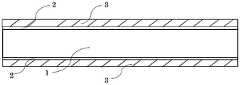
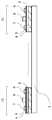
도 1은 Si 기판을 준비하는 공정을 나타낸다.
도 2는 파워 트랜지스터를 형성하기 위해, Si 기판의 양면에 SiC 층과 GaN 버퍼층을 형성하는 공정 후의 상태를 나타낸다.
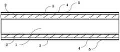
도 3은 파워 트랜지스터를 형성하기 위해 Si 기판의 양면에 SiC 층과 GaN 버퍼층을 형성한 후, 표면에만 GaN 에피택셜층(i-GaN 층)과 AlGaN 에피택셜층(i-AlGaN 층)을 형성하는 공정 후의 상태를 나타낸다.
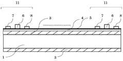
도 4는 파워 트랜지스터를 형성하기 위해, Si 기판 표면의 AlGaN 층 (i-GaN 층) 위에, 게이트(Gate), 소스(Source), 드레인(Drain)를 형성하여 파워 트랜지스터를 제조한 공정 후의 상태를 나타낸다.
도 5는 Si 기판 표면에서 파워 트랜지스터를 분리하는 공정 후의 상태를 나타낸다.
도 6은 Si 기판의 표면에서 파워 트랜지스터를 분리한 공정 후, 배면의 GaN 층과 SiC 층, Si 기판을 연마하는 공정을 나타낸다. 점선으로 둘러싼 영역이 연마 영역이다.
도 7은 Si 기판의 표면에서 파워 트랜지스터를 분리한 공정 후, 배면의 GaN 층, SiC 층, Si 기판을 연마하는 공정 후의 상태를 나타낸다.
도 8은 파워 트랜지스터를 형성하기 위해, Si 기판 양면에 SiC 층과 GaN 버퍼층, GaN 에피택셜층 (i-GaN 층), AlGaN 에피택셜층(i-AlGaN 층)을 형성하는 공정 후 상태를 나타낸다.
도 9는 파워 트랜지스터를 형성하기 위해, Si 기판의 표면에 AlGaN 에피택셜층 (i-AlGaN 층) 위에, 게이트, 소스, 드레인을 형성하여 파워 트랜지스터를 제조한 공정 후 상태를 나타낸다.
도 10은 Si 기판 표면에서 파워 트랜지스터를 분리하는 공정의 상태를 나타낸다.
도 11은 Si 기판 표면에서 파워 트랜지스터를 분리한 공정 후, 배면의 AlGaN 에피택셜층(i- AlGaN 층), GaN 에피택셜층(i-GaN 층)과 GaN 층 및 SiC 층과 Si 기판을 연마하는 공정을 나타내고 있고, 점선으로 둘러싸인 영역이 연마할 수 있는 영역이다.
도 12는 Si 기판 표면에 파워 트랜지스터를 분리하는 공정 후에, 배면에 AlGaN 에피택셜층(i-AlGaN 층), GaN 에피택셜층 (i-GaN 층), GaN 버퍼층과 SiC 층, Si 기판을 연마하는 공정 후 상태를 나타낸다.
도 13은 파워 트랜지스터를 형성하기 위해, Si 기판의 양면에 GaN 버퍼층을 형성하는 공정 후 상태를 나타낸다.
도 14는 파워 트랜지스터를 형성하기 위해, Si 기판 양면에 GaN 버퍼층을 형성한 후, 표면에 GaN 에피택셜층(i-GaN 층)과 AlGaN 에피택셜층(i-AlGaN 층)을 형성시킨 후 상태를 나타낸다.
도 15는 파워 트랜지스터를 형성하기 위해, Si 기판 양면에 AlGaN 에피택셜층 (i-GaN 층) 위에, 게이트, 소스, 드레인을 형성하여 파워 트랜지스터를 제조한 공정 후 상태를 나타낸다.
도 16은 Si 기판 표면에서 파워 트랜지스터를 분리하는 공정의 상태를 나타낸다.
도 17은 Si 기판의 표면에서 파워 트랜지스터를 분리한 후, 배면의 GaN 버퍼층, Si 기판을 연마하는 공정을 나타낸다.
도 18은 Si 기판의 표면에서 파워 트랜지스터를 분리한 후, 배면의 GaN 버퍼층, Si 기판을 연마한 공정 후 상태를 나타낸다.
도 19는 파워 트랜지스터를 형성하기 위해, Si 기판의 양면에 GaN 버퍼층과 GaN 에피택셜층(i-GaN 층), 그리고 AlGaN 층(i-AlGaN 층)을 형성하는 공정의 상태를 나타낸다.
도 20은 파워 트랜지스터를 형성하기 위해, Si 기판의 표면에 AlGaN 에피택셜층(i-GaN 층) 위에 게이트와 소스 및 드레인을 형성하여 파워 트랜지스터를 제조한 공정 후 상태를 나타낸다.
도 21은 Si 기판 표면에서 파워 트랜지스터를 분리한 공정 후 상태를 나타낸다.
도 22는 Si 기판 표면에서 파워 트랜지스터를 분리한 공정 후 배면에 AlGaN 에피택셜층(i-AlGaN 층)과 GaN 에피택셜층 (i-GaN 층), GaN 버퍼층, Si 기판을 연마한 후 공정을 나타내며, 점선의 범위가 연마된 영역이다.
도 23은 Si 기판 표면에서 파워 트랜지스터를 분리한 공정 후, 배면의 AlGaN 에피택셜층(i-AlGaN 층)과 GaN 에피택셜층(i-GaN 층)과 GaN 버퍼층 및 Si 기판을 연마 공정 후 상태를 나타낸다.
도 24는 파워 트랜지스터를 단면으로 절단한 구조를 나타낸다. 도 24(a)는 SiC 막이 있는 경우의 구조이고, 도 24(b)는 SiC 막이 없는 구조이다.1 shows a process for preparing a Si substrate.
2 shows a state after the process of forming a SiC layer and a GaN buffer layer on both sides of a Si substrate to form a power transistor.
3, after forming a SiC layer and a GaN buffer layer on both sides of a Si substrate to form a power transistor, a GaN epitaxial layer (i-GaN layer) and an AlGaN epitaxial layer (i-AlGaN layer) are formed only on the surface. It shows the state after the process.
FIG. 4 shows a state after a process of manufacturing a power transistor by forming a gate, a source, and a drain on an AlGaN layer (i-GaN layer) on the surface of a Si substrate to form a power transistor. Shows.
5 shows a state after the process of separating the power transistor from the Si substrate surface.
6 shows a process of polishing the Si substrate and the GaN layer, SiC layer on the back surface after the process of separating the power transistor from the surface of the Si substrate. The area surrounded by the dotted line is the polishing area.
7 shows a state after the process of separating the power transistor from the surface of the Si substrate, and after the process of polishing the GaN layer, SiC layer, and Si substrate on the back surface.
8 shows a state after the process of forming a SiC layer, a GaN buffer layer, a GaN epitaxial layer (i-GaN layer), and an AlGaN epitaxial layer (i-AlGaN layer) on both surfaces of the Si substrate to form a power transistor.
9 shows a state after a process of manufacturing a power transistor by forming a gate, a source, and a drain on an AlGaN epitaxial layer (i-AlGaN layer) on the surface of a Si substrate to form a power transistor.
10 shows the state of the process of separating the power transistor from the Si substrate surface.
11 is a process of separating the power transistor from the surface of the Si substrate, after the AlGaN epitaxial layer (i-AlGaN layer), GaN epitaxial layer (i-GaN layer) and GaN layer and polishing the SiC layer and Si substrate The process is shown, and the area surrounded by the dotted line is an area that can be polished.
FIG. 12 shows an AlGaN epitaxial layer (i-AlGaN layer), a GaN epitaxial layer (i-GaN layer), a GaN buffer layer, a SiC layer, and a Si substrate after the process of separating the power transistor on the surface of the Si substrate. It shows the state after the process.
13 shows a state after the process of forming a GaN buffer layer on both sides of a Si substrate to form a power transistor.
14 shows a state after forming a GaN buffer layer on both surfaces of a Si substrate to form a power transistor, and then forming a GaN epitaxial layer (i-GaN layer) and an AlGaN epitaxial layer (i-AlGaN layer) on the surface. Shows.
15 shows a state after a process of manufacturing a power transistor by forming a gate, a source, and a drain on an AlGaN epitaxial layer (i-GaN layer) on both surfaces of a Si substrate to form a power transistor.
16 shows the state of the process of separating the power transistor from the Si substrate surface.
Fig. 17 shows a process of polishing the Si substrate after removing the power transistor from the surface of the Si substrate and the GaN buffer layer on the back.
Fig. 18 shows a state after the process of polishing the SiN substrate and the GaN buffer layer on the back surface after separating the power transistor from the surface of the Si substrate.
19 shows a state of a process of forming a GaN buffer layer, a GaN epitaxial layer (i-GaN layer), and an AlGaN layer (i-AlGaN layer) on both surfaces of a Si substrate to form a power transistor.
20 shows a state after a process of manufacturing a power transistor by forming a gate, a source, and a drain on an AlGaN epitaxial layer (i-GaN layer) on the surface of a Si substrate to form a power transistor.
21 shows the state after the process of separating the power transistor from the surface of the Si substrate.
FIG. 22 shows the process after polishing the AlGaN epitaxial layer (i-AlGaN layer), GaN epitaxial layer (i-GaN layer), GaN buffer layer, and Si substrate on the back surface after the process of separating the power transistor from the Si substrate surface. , The range of the dotted line is the polished area.
FIG. 23 shows the state of the AlGaN epitaxial layer (i-AlGaN layer), GaN epitaxial layer (i-GaN layer), GaN buffer layer, and Si substrate after polishing after separating the power transistor from the Si substrate surface. Shows.
24 shows a structure in which the power transistor is cut in cross section. Fig. 24(a) is a structure in the case of having a SiC film, and Fig. 24(b) is a structure without a SiC film.
이하, 본 발명의 실시형태에 관해 도면을 참조하여 설명한다. 각 도면에서 동일 부분은 동일 부호를 사용하고있다.EMBODIMENT OF THE INVENTION Hereinafter, embodiment of this invention is described with reference to drawings. The same parts in each drawing are denoted by the same reference numerals.
(실시 형태 1)(Embodiment 1)
이 실시 형태는, 반도체 기판 1의 양면에 SiC 층과 GaN 버퍼층을 형성하여, 두꺼운 버퍼층을 사용한 것에 비해 웨이퍼 공정비용이 저렴하고, 여기에 반도체 기판 1 위에 형성된 GaN 에피택셜층 (i-GaN 층)와 AlGaN 에피택셜층(i-AlGaN 층)을 형성하여 이 에피택셜층으로 파워 트랜지스터를 형성할 수 있는 것으로, 배면에 SiC 막과 GaN 버퍼층을 형성하지 않는 경우에 비해 웨이퍼로부터 유발되는 결정 결함을 저감시킬 수 있다.In this embodiment, the SiC layer and the GaN buffer layer are formed on both surfaces of the
도 1과 같이 반도체 기판 1을 준비하고, 도 2와 같이 저압 CVD(Chemical Vapor Deposition, 미도시) 법에 의해 반도체 기판 1의 양면에 50 ~ 200nm의 SiC 층 2를 형성하고, 그 위에 5 ~ 20μm의 GaN 버퍼층 3을 형성하고, 그림 3과 같이 반도체 기판의 표면에 0.3 ~ 2μm의 GaN 에피택셜층 4, 1 ~ 100nm의 AlGaN 에피택셜층 5를 형성하여, 파워 트랜지스터를 형성하기 전에 반도체 기판 1의 휨을 줄인 구조를 형성하는 공정을 나타내고, 반도체 기판 1의 표면에 에피택셜층을 형성하는 것은 현재 존재하는 장비의 에피택시 장치(현재 판매되고 있는 MOCVD, 즉 Metal Organic Chemical Vapor Deposition 장치)를 이용하는 것을 고려하였다.A
도 4는 포토리소그래피 장치, CVD 장치, 증착 장치, 에칭 장치 등(미도시)에 의해 AlGaN 에피택셜층 (i-AlGaN 층) 5 위에 게이트 6, 소스 전극 7, 드레인 전극 8을 형성하고, 파워 트랜지스터 10을 형성한다.FIG. 4 shows a
도 5는 배면의 GaN 버퍼층 3과 SiC 층 2와 반도체 기판 1의 배면을 그라인더(Grinder, 연마기)에 의해 연마하기 전에, 포토리소그래피 장치와 에칭 장치(미도시)로 SiC 층까지 에칭하고 파워 트랜지스터 10을 분리하는 공정 후 상태를 나타낸다. 이 공정은 배면을 연마하여 제거함으로써 트랜지스터 10의 GaN 버퍼층과 SiC 층의 스트레스의 영향을 저감하기 위한 것이다.FIG. 5 shows a photolithography apparatus and an etching apparatus (not shown) to etch the SiC layer and polish the
도 6은 배면의 GaN 버퍼층 3, SiC 층 2, 그리고 반도체 기판 1의 배면을 그라인더로 연마하고, 반도체 기판 1의 잔류 두께를 50~300㎛로 한 공정을 나타낸다. 도 6에서는 배면의 GaN 버퍼층 3, SiC 층 2, 반도체 기판 1의 배면을 그라인더로 연마하여, 반도체 기판 1의 나머지 부분은 50 ~ 300μm의 두께가 되게 하는 연마 공정 후 상태를 나타낸다.FIG. 6 shows a process in which the back side of the
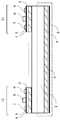
도 20(a)는 반도체 기판 1의 표면 SiC 층 2와 GaN 버퍼층 3과 GaN 에피택셜층 (i-GaN 층) 4, AlGaN 에피택셜층 (i-AlGaN 층) 5로부터 오는 구조에서 형성한 파워 트랜지스터 10의 단면을 절단한 구조를 나타낸다. 파워 트랜지스터는 단독으로 또는 타 소자와의 조합으로도 사용할 수 있다.FIG. 20(a) is a power transistor formed from a structure coming from the
(실시 형태 2)(Embodiment 2)
이 실시 형태는 반도체 기판 1의 양면에 SiC 층과 GaN 버퍼층을 형성하는 실시 형태 1과 상이하고, 반도체 기판 1의 양면에 SiC 층과 GaN 버퍼층, 그 위에 GaN 에피택셜층 (i-GaN 층) AlGaN 에피택셜층(i-AlGaN 층)을 형성하는 점이 다른 것이다.This embodiment is different from the first embodiment in which the SiC layer and the GaN buffer layer are formed on both surfaces of the
반도체 기판 1의 양면에 SiC 층 및 GaN 버퍼층과, 그 위에 GaN 에피택셜층(i-GaN 층)과, AlGaN 에피택셜층(i-AlGaN 층)을 형성하고, 두꺼운 버퍼층은 웨이퍼의 휨을 낮출 수 있고, 그 위에 반도체 기판 1의 위로 형성한 에피택셜층에 파워 트랜지스터를 형성할 수 있고, 배면에 SiC 층과 GaN 버퍼층을 형성하지 않는 경우에 비해 기판의 휨에 의한 에피택셜층의 결정 결함을 극도로 저감시킬 수 있다.A SiC layer and a GaN buffer layer on both sides of the
도 1과 같이 반도체 기판 1을 준비하여 도 8과 같이 저압 CVD 법에 의해 반도체 기판 1의 양면에 50 ~ 200nm의 SiC 층 2를 형성하고, 그 위에 5 ~ 20μm의 GaN 층 3을 형성하고, 그 위에 0.3 ~ 2μm의 GaN 에피택셜층 (i-GaN 층) 4, 1 ~ 100nm의 AlGaN 에피택셜층 (i-AlGaN 층) 5를 형성하여 파워 트랜지스터를 형성하기 전에 반도체 기판 1의 휨을 저감한 구조를 형성하는 과정을 나타낸다.Prepare a
도 9는 포토리소그래피 장치, CVD 장치, 증착 장치, 에칭 장치 등(미도시)을 이용하여, AlGaN 에피택셜층 (i-AlGaN 층) 5 위에 게이트 6, 소스전극 7, 드레인 전극 8을 형성하여 파워 트랜지스터 10을 형성한다.9 is a photolithography apparatus, a CVD apparatus, a deposition apparatus, an etching apparatus, etc. (not shown), the
도 10은 배면의 AlGaN 에피택셜층 (i-AlGaN 층) 5와, GaN 에피택셜층 (i-GaN 층) 4과, GaN 층 3과, SiC 층 2과, 반도체 기판 1의 배면을 그라인더에 의해 연마하기 전에, 포토리소그래피 장치와 에칭 장치(미도시)를 이용하여 파워 트랜지스터 10을 분리하는 공정 후의 상태를 나타낸 것이다. 이 공정은 배면을 연마하여 제거할 때 파워 트랜지스터 10의 배면의 GaN 버퍼층과 SiC 층의 스트레스의 영향을 저감하기 위한 것이다.FIG. 10 shows the back surface of the AlGaN epitaxial layer (i-AlGaN layer) 5, the GaN epitaxial layer (i-GaN layer) 4, the
도 11은 배면의 AlGaN 에피택셜층 (i-AlGaN 층) 5와, GaN 에피택셜층 (i-GaN 층) 4와, GaN 층 3과, SiC 층 2와, 반도체 기판 1의 배면을 그라인더에 의해 연마한 후에 도 12는 반도체 기판 1의 나머지 부분은 50 ~ 300μm의 두께로 되는 상태를 나타낸다.Fig. 11 shows the back surface of the AlGaN epitaxial layer (i-AlGaN layer) 5, the GaN epitaxial layer (i-GaN layer) 4, the
도 24 (a)는 반도체 기판 1의 표면 SiC 층 2와 GaN 버퍼층 3과 GaN 에피택셜층(i-GaN 층) 4, AlGaN 에피택셜층(i-AlGaN 층) 5의 구조를 갖는 파워 트랜지스터를 나타내고, 이러한 트랜지스터는 단일품 자체로 혹은 타 소자와 조합으로도 사용할 수 있다.24(a) shows a power transistor having a structure of a
(실시 형태 3)(Embodiment 3)
이 실시 형태는, 반도체 기판 1의 양면에 SiC 층과 GaN 버퍼층을 형성하는 실시 형태 1과 다르게 반도체 기판 1의 양면에 GaN 버퍼층만을 형성하는 점이 다르다.This embodiment differs from the first embodiment in which the SiC layer and the GaN buffer layer are formed on both surfaces of the
반도체 기판 1의 양면에 GaN 버퍼층을 형성하고, 두꺼운 버퍼층은 웨이퍼의 휨을 저감시키며, 반도체 기판 1 위에 GaN 에피택셜층(i-GaN 층)과 AlGaN 에피택셜층(i- AlGaN 층)을 형성하고, 이 에피택셜층에 파워 트랜지스터를 형성하며, 배면에 GaN 버퍼층을 형성하지 않는 경우에 비해, 웨이퍼의 휨으로 인한 에피택셜층의 결정 결함을 대폭으로 감소시킬 수 있다.A GaN buffer layer is formed on both surfaces of the
도 1과 같이 반도체 기판 1을 준비하고 도 13과 같이 저압 CVD 법(미도시)에 의해 반도체 기판의 양면에 5 ~ 20μm의 GaN 버퍼층 3을 형성하고, 도 14와 같이 반도체 기판 1의 표면에 0.3~2μm의 GaN 에피택셜층 4와 1 ~ 100nm의 AlGaN 에피택셜층 5를 형성하고, 파워 트랜지스터의 형성 이전에 반도체 기판 1의 휨이 저감되는 구조를 형성하는 공정을 나타내고 있다. 반도체 기판 1의 표면에 에피택셜층을 형성하는 것은 시판되는 에피택시 장치를 이용하는 것을 고려한 사항이다.A
도 15는 포토리소그래피 장치, CVD 장치, 증착 장치, 에칭 장치 등(미도시)을 이용하여, AlGaN 에피택셜층 (i-AlGaN 층) 5 위에 게이트 6, 소스 전극 7, 드레인 전극 8을 형성하여 파워 트랜지스터 11을 형성하는 것을 나타낸다.FIG. 15 shows the power by forming the
도 16은 배면의 GaN 버퍼층 3과, SiC 층 2과, 반도체 기판 1의 배면을 그라인더에 의해 연마하기 전에, 포토리소그래피 장치와 에칭 장치(미도시)를 이용하여 파워 트랜지스터 11을 분리하는 공정 후의 상태를 나타낸 것이다. 이 공정은 배면을 연마하여 제거할 때 파워 트랜지스터 11의 배면의 GaN 버퍼층과 SiC 층의 스트레스의 영향을 저감하기 위한 것이다.FIG. 16 is a state after the process of separating the
도 17은, 배면의 GaN 버퍼층 3과 반도체 기판 1의 배면을 그라인더로 연마하여, 반도체 기판 1의 나머지 두께는 50 ~ 300㎛이 되는 공정을 나타낸다. 도 18은, 반도체 기판 1의 배면의 GaN 버퍼층 3과, 반도체 기판 1을 그라인더에 의해 연마하여, 반도체 기판 1의 잔여 두께를 50 ~ 300㎛로 하는 것으로 연마하는 공정을 나타낸다.FIG. 17 shows a process in which the
도 24 (b)는 반도체 기판 1의 표면 위에 GaN 버퍼층 3과 GaN 에피택셜층 (i-GaN 층) 4, AlGaN 에피택셜층 (i-AlGaN 층) 5로 구성된 구조로 형성된 파워 트랜지스터 11을 단면으로 절단한 구조를 나타낸다. 파워 트랜지스터는 단일품 자체로도 혹은 타 소자와 조합으로도 사용할 수 있다.FIG. 24(b) is a cross-sectional view of a
(실시 형태 4)(Embodiment 4)
이 실시 형태는 반도체 기판 1과 양면에 SiC 층과 GaN 버퍼층을 형성하는 실시 형태 1과 달리, 반도체 기판 1의 양면에 GaN 버퍼층과 GaN 에피택셜층(i-GaN 층)과 AlGaN 에피택셜층(i-AlGaN 층)을 형성하는 점이 다르다.This embodiment is different from the first embodiment in which the SiC layer and the GaN buffer layer are formed on both sides of the
반도체 기판 1의 양면에 GaN 버퍼층과 GaN 에피택셜층(i-GaN 층), 그리고 AlGaN 에피택셜층(i-AlGaN 층)을 형성시키면 두꺼운 버퍼층이 웨이퍼에 휨을 줄이고, 반도체 기판 1의 표면에 에피택셜층으로 파워 트랜지스터를 형성할 수 있고, ㅂ반도체 기판의 배면에 GaN 버퍼층과, GaN 에피택셜층 (i-GaN 층), 그리고 AlGaN 에피택셜층 (i-AlGaN 층)를 형성하지 않는 경우와 비교하면, 웨이퍼에 휨으로 인한 에피택셜층의 결정 결함이 매우 저감될 수 있다.When the GaN buffer layer, the GaN epitaxial layer (i-GaN layer), and the AlGaN epitaxial layer (i-AlGaN layer) are formed on both surfaces of the
반도체 기판 1의 양면에 GaN 버퍼층과 GaN 에피택셜층(i-GaN 층), 그리고 AlGaN 에피택셜층(i-AlGaN 층)을 형성시키면 두꺼운 버퍼층만큼 웨이퍼의 휨이 낮아지고, 반도체 기판 1의 표면에 이 에피택셜층으로 파워 트랜지스터를 형성할 수 있다. GaN 에피택셜층(i-GaN 층), 그리고 AlGaN 에피택셜층(i-AlGaN 층)를 형성하지 않는 경우와 비교하면, 웨이퍼에 휨으로 인한 에피택셜층의 결정 결함이 매우 저감될 수 있다.When the GaN buffer layer, the GaN epitaxial layer (i-GaN layer), and the AlGaN epitaxial layer (i-AlGaN layer) are formed on both surfaces of the
도 1과 같이 반도체 기판 1을 준비하고 도 19와 같이 저압 CVD 법에 의해 반도체 기판 1의 양면에 5 ~ 20μm의 GaN 버퍼층 3을 형성하고, 그 위에 0.3 ~ 2μm의 GaN 에피택셜층 (i-GaN 층) 4, 1 ~ 100nm의 AlGaN 에피택셜층 (i-AlGaN 층) 5를 형성하여, 파워 트랜지스터를 형성하기 전에, 반도체 기판 1의 휨이 줄어드는 구조를 형성하는 공정을 나타낸다.A
도 20은 포토리소그래피 장치와 CVD 장치, 증착 장치, 에칭 장치 (미도시)에 의해 AlGaN 에피택셜층 (i-AlGaN 층) 5 위에 게이트 6, 소스 전극 7, 드레인 전극 8을 형성하여 파워 트랜지스터 11을 형성할 수 있다.FIG. 20 shows a
도 21은 배면의 AlGaN 에피택셜층 (i-AlGaN 층) 5, GaN 에피택셜층 (i-GaN 층) 4, GaN 버퍼층 3, 그리고 반도체 기판 1의 배면을 그라인더에 의해 연마하기 전, 포토리소그래피 장치와 에칭 장치(미도시)를 사용하여 파워 트랜지스터 11을 분리하는 공정 후의 상태를 나타낸다. 이 공정은 배면을 연마하여 제거하여, 파워 트랜지스터 11에서의 GaN 버퍼층과 SiC 층의 스트레스의 영향을 저감할 수 있다.FIG. 21 is a photolithographic apparatus before polishing the back surface of the AlGaN epitaxial layer (i-AlGaN layer) 5, the GaN epitaxial layer (i-GaN layer) 4, the
도 22는 AlGaN 에피택셜층 (i-AlGaN 층) 5와 GaN 에피택셜층 (i-GaN 층) 4와 GaN 버퍼층 3, 반도체 기판 1의 배면을 그라인더에 의해 연마하고, 반도체 기판 1의 잔류 두께가 50 ~ 300μm가 되는 공정을 나타낸다. 점선 부분이 연마된 부분이다. 도 23은 배면의 AlGaN 에피택셜층 (i-AlGaN 층)과 GaN 에피택셜층 (i-GaN 층) 4와 GaN 버퍼층 3, 그리고 반도체 기판 1의 배면을 그라인더에 의해 연마하여, 반도체 기판 1의 잔류 두께가 50 ~ 300μm 되도록 하는 공정의 상태를 나타낸다.FIG. 22 shows the back surfaces of the AlGaN epitaxial layer (i-AlGaN layer) 5, the GaN epitaxial layer (i-GaN layer) 4, the
도 24 (b)는 반도체 기판 1의 표면상에 GaN 버퍼층 3과 GaN 에피택셜층 (i-GaN 층) 4, AlGaN 에피택셜층 (i-AlGaN 층) 5의 구조를 형성한 파워 트랜지스터 11을 단면 절단한 구조를 나타낸다. 파워 트랜지스터는 단일품 자체로도 혹은 타 소자와 조합으로도 사용할 수 있다.FIG. 24(b) is a cross-section of a
(실시 예 1)(Example 1)
도 1에 보이는 것처럼 8인치의 반도체 기판 1을 준비하고, 도 2와 같이 저압 CVD 법(미도시)으로 반응 가스로 메틸 사이렌(SiH3(CH3))과 헬륨(He)을 사용하여, 850℃, 0.3Torr에서 반도체 기판 1의 양면에 100nm의 SiC 층 2를 형성하고, 그 위에 감압 CVD를 사용하여, 반응 가스로써 트리메틸 갈륨(TMG)과 암모니아(NH3)를 이용하여, 850℃, 1Torr에서 12μm의 GaN 버퍼층 3을 형성하고, 도 3과 같이 MOCVD 장치를 사용해서, 반응 가스로서 TMG와 NH3를 사용하여 1050℃, 760Torr에서 반도체 기판 1의 표면에 1μm의 GaN 에피택셜층 (i-GaN 층) 4와 반응 가스로서 트리메틸 알루미늄(TMA)과 암모니아(NH3)를 사용하여 30nm의 AlGaN 에피택셜층(i-AlGaN 층) 5를 형성하고, 파워 트랜지스터의 형성 전에 반도체 기판 1의 휨을 저감한 구조를 형성한 공정을 나타낸다. 반도체 기판 1의 표면에 에피택셜층을 형성하는 장치는 시판되는 에피택시 장치를 이용하는 것을 고려한 것이다.As shown in FIG. 1, an 8-
도 4는 포토리소그래피 장치와 CVD 장치, 증착 장치, 에칭 장치 (미도시) 를 이용하여 AlGaN 에피택셜층 (i-AlGaN 층) 5 위에 게이트 6, 소스 전극 7, 드레인 전극 8을 형성하여 파워 트랜지스터 10을 형성했다.FIG. 4 shows a
도 5는 GaN 버퍼층 3과, SiC 층 2와, 반도체 기판 1의 배면을 그라인더에 의해 연마하기 전에 포토리소그래피 장치와 에칭 장치(미도시)에 의해 파워 트랜지스터 10을 분리한 상태를 나타낸다. 이 공정은 배면을 연마함으로써 파워 트랜지스터 10의 표면에 GaN 버퍼층과 SiC 층의 스트레스의 영향을 줄이기 위한 것이다.5 shows a state in which the
도 6은 배면의 GaN 버퍼층 3과, SiC 층 2와, 반도체 기판 1의 배면을 그라인더로 연마하여 반도체 기판 1의 잔류 두께가 250㎛가 되게 하는 공정을 나타낸다. 점선 부분이 연마될 영역이다. 도 7은, 배면의 GaN 버퍼층 3, SiC 층 2, 반도체 기판 1의 배면을 그라인더로 연마하고, 반도체 기판 1의 잔류 두께가 250㎛가 되게 하는 공정 후의 상태를 나타낸다.FIG. 6 shows a process of polishing the rear
도 24 (a)는 반도체 기판 1의 표면 SiC 층 2와 GaN 버퍼층 3과 GaN 에피택셜층(i-GaN 층) 4, AlGaN 에피택셜층(i-AlGaN 층) 5로 구성된 구조로 형성된 파워 트랜지스터 10을 단면으로 절단한 구조를 나타낸다. 패키지 구조는 단일품으로도, 조합으로도 사용할 수 있다. 파워 트랜지스터는 단일품 단체로도 혹은 타 소자와 조합으로도 사용할 수 있다.FIG. 24(a) is a
(실시 예 2)(Example 2)
이 실시 예는 반도체 기판 1의 양면에 SiC 층과 GaN 버퍼층을 형성한 실시 예 1과 상이하며, 반도체 기판 1의 양면에 SiC 층과 GaN 버퍼층, 그 위에 GaN 에피택셜층 (i-GaN 층) 과 AlGaN 에피택셜층(i-AlGaN 층)을 형성하고 있는 점이 다르다.This embodiment is different from Example 1 in which SiC layers and GaN buffer layers are formed on both sides of the
도 1과 같이 반도체 기판 1을 준비하고 도 8과 같이 저압 CVD 법(미도시)으로 반도체 기판 양면에 반응가스 메틸 사이렌(SiH3(CH3))과 헬륨(He)을 850℃, 0.3Torr에서 반도체 기판 1의 양면에 100nm의 SiC 층 2를 형성하고, 그 위에 감압 CVD를 사용하여 반응 가스로 TMG와 NH3를 사용하여 850℃, 1Torr에서 12μm GaN 버퍼층 3을 형성하고, 그 위에 감압 CVD를 사용하여, 반응 가스로 트리메틸 갈륨(TMG)과 암모늄을(NH3) 사용하여 1050℃, 1Torr에서 반도체 기판 1의 표면에 1μm의 GaN 에피택셜층 4와, 반응 가스로 트리메틸 알루미늄(TMA)과 암모늄을(NH3) 사용하여 30nm의 AlGaN 에피택셜층 (i-AlGaN 층) 5를 형성하여, 파워 트랜지스터의 형성 전에 반도체 기판 1의 휨을 저감하는 구조를 형성하는 공정을 나타낸다.Prepare
도 9는 포토리소그래피 장치와 CVD 장치, 증착 장치, 에칭 장치 (미도시) 를 이용하여 AlGaN 에피택셜층 (i-AlGaN 층) 5 위에 게이트 6, 소스 전극 7, 드레인 전극 8을 형성하여 파워 트랜지스터 10을 형성한다.FIG. 9 shows a
도 10은 배면의 AlGaN 에피택셜층 (i-AlGaN 층) 5와, GaN 에피택셜층 (i-GaN 층) 4와, GaN 버퍼층 3과 SiC 층 2과, 반도체 기판 1의 배면을 그라인더로 연마하기 전에, 포토리소그래피 장치와 에칭 장치(미도시)를 이용하여, 파워 트랜지스터 10을 분리한 공정의 상태를 나타낸다. 이 과정은 태양 전지판에 있는 GaN 버퍼층과 SiC 층의 스트레스의 영향을 줄이기 위한 것이다. 이는 트랜지스터 형성 전에 반도체 기판 1의 휨을 저감하는 구조를 형성하는 공정을 나타낸다.FIG. 10 is a grinder polishing the rear AlGaN epitaxial layer (i-AlGaN layer) 5, the GaN epitaxial layer (i-GaN layer) 4, the
도 11은 배면의 AlGaN 에피택셜층 (i-AlGaN 층) 5과 GaN 에피택셜층 (i-GaN 층) 4와 GaN 버퍼 층 3과 SiC 층 2와 반도체 기판 1의 배면을 그라인더로 연마하여 반도체 기판 1의 나머지 부분은 250μm의 두께로 하는 공정을 나타낸다. 점선 부분이 연마될 영역이다. 도 12는 배면의 AlGaN 에피택셜층 (i-AlGaN 층) 5, GaN 에피택셜층 (i-GaN 층) 4, GaN 버퍼층 3, SiC 층 2, 반도체 기판 1의 배면을 그라인더로 연마하여, 반도체 기판 1의 나머지 부분은 250μm의 두께로 연마한 공정 후 상태를 나타낸다.FIG. 11 shows a semiconductor substrate by polishing the rear surfaces of the AlGaN epitaxial layer (i-AlGaN layer) 5 and GaN epitaxial layer (i-GaN layer) 4,
도 24 (a)는 반도체 기판 1의 표면 SiC 층 2와 GaN 버퍼층 3과 GaN 에피택셜층 (i-GaN 층) 4, AlGaN 에피택셜층 (i-AlGaN 층) 5로 구성된 구조의 파워 트랜지스터 단면을 절단한 구조를 나타낸다. 파워 트랜지스터는 단일품 자체로도 혹은 타 소자와 조합으로도 사용할 수 있다.FIG. 24(a) is a cross-section of a power transistor having a structure consisting of a
(실시 예 3)(Example 3)
이 실시 예는, 반도체 기판 1의 양면에 SiC 층과 GaN 버퍼층을 형성한 실시 예 1과 상이하며, 반도체 기판 1의 양면에 GaN 버퍼층을 형성한다.This embodiment is different from Example 1 in which a SiC layer and a GaN buffer layer are formed on both surfaces of the
도 1과 같이 반도체 기판 1을 준비하고, 도 13과 같이 감압 CVD를 사용하여 반응 가스로서 트리메틸 갈륨(TMG)와 암모니움(NH3)로 850℃, 1Torr에서 12μm의 GaN 버퍼층 3을 형성한다. 도 14에서와 같이 MOCVD 장치로 트리메틸 갈륨(TMG)와 암모니움(NH3)를 사용하여 1050℃, 760Torr에서 반도체 기판 1의 표면에 1μm의 GaN 에피택셜층 (i-GaN 층) 4와 반응 가스로 트리메틸 알루미늄(TMA)과 암모늄을(NH3) 사용하여 30nm의 AlGaN 에피택셜층 (i-AlGaN 층) 5을 형성하고, 파워 트랜지스터 형성 이전에 반도체 기판 1의 휨을 저감한 구조를 형성한 공정을 나타낸다. 반도체 기판 1의 표면에 에피택셜층을 형성하는 장치는 시판되는 에피택시 장치를 이용하는 것으로 고려했다.A
도 15는 포토리소그래피 장치와 CVD 장치, 증착 장치, 에칭 장치 (미도시) 를 이용하여 AlGaN 에피택셜층 (i-AlGaN 층) 5 위에 게이트 6, 소스 전극 7, 드레인 전극 8을 형성하여 파워 트랜지스터 11을 형성했다.FIG. 15 shows a
도 16은 배면에 GaN 에피택셜층 (i-AlGaN 층) 5, GaN 에피택셜층 (i-GaN 층) 4, GaN 버퍼층 3, 반도체 기판 1의 배면을 그라인더로 연마하기 전, 포토리소그래피 장치와 에칭 장치(미도시)로 파워 트랜지스터 11을 분리하는 공정 후 상태를 나타낸다. 이 공정은 배면을 연마하여 제거하여 파워 트랜지스터 표면의 GaN 버퍼층과 SiC 층의 스트레스의 영향을 저감할 수 있다.FIG. 16 is a photolithographic apparatus and etching before polishing the back surface of a GaN epitaxial layer (i-AlGaN layer) 5, GaN epitaxial layer (i-GaN layer) 4,
도 17은 배면의 GaN 버퍼층 3과, 반도체 기판 1의 배면을 그라인더로 연마하여 반도체 기판 1의 나머지 두께가 250㎛로 되도록 하는 공정을 나타낸다. 점선 부분이 연마될 영역이다. 도 18 배면의 GaN 버퍼층 3, 반도체 기판의 배면을 그라인더로 연마하여 반도체 기판 1의 나머지 두께를 250μm로 연마한 공정 후 상태를 나타낸다.FIG. 17 shows a process in which the
도 24 (b)는 반도체 기판 1의 표면 위에 GaN 버퍼층 3과 GaN 에피택셜층 (i-GaN 층) 4, AlGaN 에피택셜층 (i-AlGaN 층) 5로 구성된 구조의 파워 트랜지스터 11을 단면으로 절단한 구조를 나타낸다. 파워 트랜지스터는 단일품 자체로도 혹은 타 소자와 조합으로도 사용할 수 있다.FIG. 24(b) is a cross section of a
(실시 예 4)(Example 4)
이 실시 예는, 반도체 기판 1의 양면에 SiC 층과 GaN 버퍼층을 형성한 실시 예 1과 상이한데, 반도체 기판 1의 양면에 GaN 버퍼층과 GaN 에피택셜층(i-GaN 층)과 AlGaN 에피택셜층(i-AlGaN 층)을 형성했다는 점이 다르다.This embodiment is different from Example 1 in which a SiC layer and a GaN buffer layer are formed on both surfaces of the
도 1과 같이 반도체 기판 1을 준비하고, 도 19와 같이 감압 CVD를 사용하고, 반응 가스로서 트리메틸 갈륨(TMG)와 암모니움(NH3)로 850℃, 1Torr에서 12μm의 GaN 버퍼층 3을 형성한다. 그 위에 감압 CVD 장치를 사용하여, 트리메틸 갈륨(TMG)와 암모니움(NH3)을 사용하여 1050℃, 1Torr에서 반도체 기판 1의 양면에 1μm의 GaN 에피택셜층(i-GaN 층) 4를 형성하고, 연이어 반응 가스로서 트리메틸 알루미움(TMA)와 암모니움(NH3)으로 30nm의 AlGaN 에피택셜층(i-AlGaN 층) 5를 형성하고, 파워 트랜지스터를 형성하기 전에 반도체 기판 1의 휨을 저감시킨 구조를 형성한 상태의 공정을 나타낸다.A
도 20은 포토리소그래피 장치와 CVD 장치, 증착 장치, 에칭 장치(미도시) 를 이용하여 AlGaN 에피택셜층 (i-AlGaN 층) 5 위에 게이트 6, 소스 전극 7, 드레인 전극 8을 형성하여 파워 트랜지스터 11을 형성했다.FIG. 20 shows a
도 21은 배면에 AlGaN 에피택셜층 (i-AlGaN 층) 5, GaN 에피택셜층 (i-GaN 층) 4, GaN 버퍼층 3, 반도체 기판 1의 배면을 그라인더로 연마하기 전, 포토리소그래피 장치와 에칭 장치 (미도시)을 사용하여 파워 트랜지스터 11을 분리한 공정 후 상태를 나타내고 있다. 이 공정은 배면을 연마로 제거하여 트랜지스터 11의 표면의 GaN 버퍼층과 SiC 층의 스트레스의 영향을 저감할 수 있다.FIG. 21 is a photolithographic apparatus and etching before polishing the AlGaN epitaxial layer (i-AlGaN layer) 5, GaN epitaxial layer (i-GaN layer) 4,
도 22는 배면의 AlGaN 에피택셜층(i-AlGaN 층) 5와 GaN 에피택셜층(i-GaN 층) 4와 GaN 버퍼층 3, 반도체 기판 1의 배면을 그라인더로 연마하여, 반도체 기판 1의 나머지 두께가 250μm로 되는 공정을 나타낸다. 점선 부분이 연마될 영역이다. 도 23은 배면의 AlGaN 에피택셜층 (i-AlGaN 층) 5와, GaN 에피택셜층 (i-GaN 층) 4와, GaN 버퍼층 3, 반도체 기판 1의 배면을 그라인더로 연마하여, 반도체 기판 1의 나머지 두께가 250μm로 연마한 공정의 상태를 나타낸다.FIG. 22 shows the remaining AlGaN epitaxial layer (i-AlGaN layer) 5, GaN epitaxial layer (i-GaN layer) 4,
도 24(b)는 반도체 기판 1의 표면 위에 GaN 버퍼층 3과 GaN 에피택셜층 (i-GaN 층) 4, AlGaN 에피택셜층 (i-AlGaN 층) 5로 구성된 구조의 파워 트랜지스터 11을 단면으로 절단한 구조를 나타낸다. 파워 트랜지스터는 단일품 자체로 혹은 타 소자와 조합으로도 사용할 수 있다.FIG. 24(b) is a cross section of a
1 반도체 기판
2 SiC 층
3 GaN 버퍼층
4 GaN 에피택셜층 (i-GaN 층)
5 AlGaN 에피택셜층 (i-AlGaN 층)
6 파워 트랜지스터의 게이트
7 파워 트랜지스터의 소스
8 파워 트랜지스터의 드레인
10, 11 파워 트랜지스터1 semiconductor substrate
2 SiC layer
3 GaN buffer layer
4 GaN epitaxial layer (i-GaN layer)
5 AlGaN epitaxial layer (i-AlGaN layer)
6 Gate of power transistor
7 Source of power transistor
8 drain of power transistor
10 and 11 power transistors
Claims (6)
Translated fromKorean상기 반도체 기판의 표면에 GaN 에피택셜층과 AlGaN 에피택셜층을 형성하는 공정,
상기 반도체 기판의 표면의 상기 SiC 층 및 상기 GaN 버퍼층에 파워 트랜지스터를 형성하는 공정,
상기 반도체 기판의 표면의 파워 트랜지스터를 분리하는 공정; 및
상기 파워 트랜지스터의 칩을 만들기 위해 배면을 연마하는 공정을 포함하는 파워 트랜지스터의 제조 방법.
A step of sequentially forming a SiC layer and a GaN buffer layer on both sides of the semiconductor substrate to reduce warpage of the semiconductor substrate,
Forming a GaN epitaxial layer and an AlGaN epitaxial layer on the surface of the semiconductor substrate,
Forming a power transistor in the SiC layer and the GaN buffer layer on the surface of the semiconductor substrate,
Separating a power transistor on the surface of the semiconductor substrate; And
A method of manufacturing a power transistor, comprising a step of polishing the back surface to make a chip of the power transistor.
상기 반도체 기판의 표면에 상기 SiC 층 및 상기 GaN 버퍼층에 파워 트랜지스터를 형성하는 공정;
상기 반도체 기판의 표면의 파워 트랜지스터를 분리하는 공정; 및
상기 파워 트랜지스터의 칩을 만들기 위해 배면을 연마하는 공정을 포함하는 파워 트랜지스터의 제조 방법.
A step of sequentially forming a SiC layer, a GaN buffer layer, a GaN epitaxial layer and an AlGaN epitaxial layer on both surfaces of the semiconductor substrate to reduce warpage of the semiconductor substrate,
Forming a power transistor on the SiC layer and the GaN buffer layer on the surface of the semiconductor substrate;
Separating a power transistor on the surface of the semiconductor substrate; And
A method of manufacturing a power transistor comprising a step of polishing the back surface to make a chip of the power transistor.
상기 반도체 기판의 표면에 GaN 에피택셜층과 AlGaN 에피택셜층을 형성하는 공정;
상기 반도체 기판의 표면의 상기 GaN 버퍼층에 파워 트랜지스터를 형성하는 공정;
상기 반도체 기판의 표면의 파워 트랜지스터를 분리하는 공정; 및
상기 파워 트랜지스터의 칩을 만들기 위해 배면을 연마하는 공정을 포함하는 파워 트랜지스터의 제조 방법.
A step of forming a GaN buffer layer on both sides of the semiconductor substrate to reduce warpage of the semiconductor substrate,
Forming a GaN epitaxial layer and an AlGaN epitaxial layer on the surface of the semiconductor substrate;
Forming a power transistor in the GaN buffer layer on the surface of the semiconductor substrate;
Separating a power transistor on the surface of the semiconductor substrate; And
A method of manufacturing a power transistor, comprising a step of polishing the back surface to make a chip of the power transistor.
상기 반도체 기판의 표면의 상기 GaN 버퍼층에 파워 트랜지스터를 형성하는 공정;
상기 반도체 기판의 표면의 파워 트랜지스터를 분리하는 공정; 및
상기 파워 트랜지스터의 칩을 만들기 위해 배면을 연마하는 공정을 포함하는 파워 트랜지스터의 제조 방법.
A step of sequentially forming a GaN buffer layer, a GaN epitaxial layer and an AlGaN epitaxial layer on both surfaces of the semiconductor substrate to reduce warpage of the semiconductor substrate,
Forming a power transistor in the GaN buffer layer on the surface of the semiconductor substrate;
Separating a power transistor on the surface of the semiconductor substrate; And
A method of manufacturing a power transistor comprising a step of polishing the back surface to make a chip of the power transistor.
상기 반도체 기판은 Si 기판인 파워 트랜지스터의 제조 방법.
The method according to any one of claims 1 to 4,
The semiconductor substrate is a method of manufacturing a power transistor that is a Si substrate.
A power transistor manufactured by the method for manufacturing a power transistor according to any one of claims 1 to 4.
Applications Claiming Priority (2)
| Application Number | Priority Date | Filing Date | Title |
|---|---|---|---|
| JPJP-P-2018-235509 | 2018-12-17 | ||
| JP2018235509AJP2020098829A (en) | 2018-12-17 | 2018-12-17 | Manufacturing method of power device and power device manufactured by them |
Publications (2)
| Publication Number | Publication Date |
|---|---|
| KR20200074895Atrue KR20200074895A (en) | 2020-06-25 |
| KR102668632B1 KR102668632B1 (en) | 2024-05-24 |
Family
ID=71106645
Family Applications (1)
| Application Number | Title | Priority Date | Filing Date |
|---|---|---|---|
| KR1020190168241AActiveKR102668632B1 (en) | 2018-12-17 | 2019-12-16 | Manufacturing method of power transistor and power transistor manufactured according to the manufacturing method |
Country Status (2)
| Country | Link |
|---|---|
| JP (1) | JP2020098829A (en) |
| KR (1) | KR102668632B1 (en) |
Cited By (1)
| Publication number | Priority date | Publication date | Assignee | Title |
|---|---|---|---|---|
| KR20230152545A (en)* | 2022-04-27 | 2023-11-03 | 나노마테리얼 레버러토리 코., 엘티디. | Power device |
Citations (7)
| Publication number | Priority date | Publication date | Assignee | Title |
|---|---|---|---|---|
| KR20010098142A (en)* | 2000-04-28 | 2001-11-08 | 구자홍 | Nitride Semiconductor and Growing Method for the same |
| KR20030075749A (en)* | 2002-03-20 | 2003-09-26 | 학교법인 포항공과대학교 | HFET device and semiconductor device having iridium-containing gate electrode and methods for manufacturing the same |
| KR20090045067A (en)* | 2007-10-31 | 2009-05-07 | 가부시끼가이샤 도시바 | Semiconductor devices |
| US20110262773A1 (en)* | 2008-09-11 | 2011-10-27 | Soraa, Inc | Ammonothermal Method for Growth of Bulk Gallium Nitride |
| KR20120048414A (en)* | 2010-11-05 | 2012-05-15 | 삼성전자주식회사 | Method of manufacturing the semiconductor chip |
| JP2014003301A (en) | 2005-07-20 | 2014-01-09 | Cree Inc | Nitride-based transistor and manufacturing method using etch stop layer |
| KR20170122267A (en)* | 2015-03-09 | 2017-11-03 | 에어 워터 가부시키가이샤 | Compound semiconductor substrate |
- 2018
- 2018-12-17JPJP2018235509Apatent/JP2020098829A/enactivePending
- 2019
- 2019-12-16KRKR1020190168241Apatent/KR102668632B1/enactiveActive
Patent Citations (7)
| Publication number | Priority date | Publication date | Assignee | Title |
|---|---|---|---|---|
| KR20010098142A (en)* | 2000-04-28 | 2001-11-08 | 구자홍 | Nitride Semiconductor and Growing Method for the same |
| KR20030075749A (en)* | 2002-03-20 | 2003-09-26 | 학교법인 포항공과대학교 | HFET device and semiconductor device having iridium-containing gate electrode and methods for manufacturing the same |
| JP2014003301A (en) | 2005-07-20 | 2014-01-09 | Cree Inc | Nitride-based transistor and manufacturing method using etch stop layer |
| KR20090045067A (en)* | 2007-10-31 | 2009-05-07 | 가부시끼가이샤 도시바 | Semiconductor devices |
| US20110262773A1 (en)* | 2008-09-11 | 2011-10-27 | Soraa, Inc | Ammonothermal Method for Growth of Bulk Gallium Nitride |
| KR20120048414A (en)* | 2010-11-05 | 2012-05-15 | 삼성전자주식회사 | Method of manufacturing the semiconductor chip |
| KR20170122267A (en)* | 2015-03-09 | 2017-11-03 | 에어 워터 가부시키가이샤 | Compound semiconductor substrate |
Non-Patent Citations (2)
| Title |
|---|
| J. Vac. Soc. Japan Vol.54, No.6, 2011 |
| Panasonic Technical Journal Vol/55 No.2 Jul. 2009 |
Cited By (1)
| Publication number | Priority date | Publication date | Assignee | Title |
|---|---|---|---|---|
| KR20230152545A (en)* | 2022-04-27 | 2023-11-03 | 나노마테리얼 레버러토리 코., 엘티디. | Power device |
Also Published As
| Publication number | Publication date |
|---|---|
| JP2020098829A (en) | 2020-06-25 |
| KR102668632B1 (en) | 2024-05-24 |
Similar Documents
| Publication | Publication Date | Title |
|---|---|---|
| CN100468770C (en) | Nitride-based transistor with protective layer and low loss recess and method of fabricating the same | |
| US20090085065A1 (en) | Method to fabricate iii-n semiconductor devices on the n-face of layers which are grown in the iii-face direction using wafer bonding and substrate removal | |
| JP5946771B2 (en) | Stress compensation for large area gallium nitride or other nitride-based structures on semiconductor substrates | |
| US9966311B2 (en) | Semiconductor device manufacturing method | |
| KR101932327B1 (en) | Semiconductor wafer and method | |
| US20210057561A1 (en) | High electron mobility transistor device and methods for forming the same | |
| US11114555B2 (en) | High electron mobility transistor device and methods for forming the same | |
| CN103094335A (en) | High electron mobility transistor and method of forming the same | |
| US10056251B2 (en) | Hetero-integration of III-N material on silicon | |
| US11049943B2 (en) | Method for forming III-nitride semiconductor device and the III-nitride semiconductor device | |
| CN104051504A (en) | Semiconductor wafer and its forming process | |
| JP7068676B2 (en) | Non-etched gas-cooled epitaxial stack for group IIIA-N devices | |
| CN103296077A (en) | Semiconductor structure and forming method thereof | |
| CN112242435A (en) | Semiconductor epitaxial structure and method of forming the same | |
| TWI713221B (en) | High electron mobility transistor and methods for forming the same | |
| JP2016171196A (en) | Semiconductor device manufacturing method | |
| CN103050511A (en) | Semiconductor structure and method of forming the same | |
| KR102668632B1 (en) | Manufacturing method of power transistor and power transistor manufactured according to the manufacturing method | |
| US9947530B2 (en) | Method of manufacturing nitride semiconductor substrate | |
| US20140284660A1 (en) | Method for manufacturing semiconductor wafer, and semiconductor wafer | |
| US20230031662A1 (en) | Iii nitride semiconductor wafers | |
| US12199175B2 (en) | Manufacturing method for forminginsulating structure of high electron mobility transistor | |
| TWI855589B (en) | Semiconductor wafer and method of manufacturing the same | |
| TW201740567A (en) | Semiconductor structure and method of manufacturing same | |
| US20220384632A1 (en) | Nitride semiconductor device and manufacturing method thereof |
Legal Events
| Date | Code | Title | Description |
|---|---|---|---|
| PA0109 | Patent application | Patent event code:PA01091R01D Comment text:Patent Application Patent event date:20191216 | |
| PG1501 | Laying open of application | ||
| PA0201 | Request for examination | Patent event code:PA02012R01D Patent event date:20221007 Comment text:Request for Examination of Application Patent event code:PA02011R01I Patent event date:20191216 Comment text:Patent Application | |
| E902 | Notification of reason for refusal | ||
| PE0902 | Notice of grounds for rejection | Comment text:Notification of reason for refusal Patent event date:20231128 Patent event code:PE09021S01D | |
| E701 | Decision to grant or registration of patent right | ||
| PE0701 | Decision of registration | Patent event code:PE07011S01D Comment text:Decision to Grant Registration Patent event date:20240226 | |
| GRNT | Written decision to grant | ||
| PR0701 | Registration of establishment | Comment text:Registration of Establishment Patent event date:20240520 Patent event code:PR07011E01D | |
| PR1002 | Payment of registration fee | Payment date:20240521 End annual number:3 Start annual number:1 | |
| PG1601 | Publication of registration |