KR20200072081A - Memory system and operating method thereof - Google Patents
Memory system and operating method thereofDownload PDFInfo
- Publication number
- KR20200072081A KR20200072081AKR1020180159842AKR20180159842AKR20200072081AKR 20200072081 AKR20200072081 AKR 20200072081AKR 1020180159842 AKR1020180159842 AKR 1020180159842AKR 20180159842 AKR20180159842 AKR 20180159842AKR 20200072081 AKR20200072081 AKR 20200072081A
- Authority
- KR
- South Korea
- Prior art keywords
- memory
- dies
- identification information
- information
- checkpoint
- Prior art date
- Legal status (The legal status is an assumption and is not a legal conclusion. Google has not performed a legal analysis and makes no representation as to the accuracy of the status listed.)
- Granted
Links
Images


Classifications
- G—PHYSICS
- G06—COMPUTING OR CALCULATING; COUNTING
- G06F—ELECTRIC DIGITAL DATA PROCESSING
- G06F11/00—Error detection; Error correction; Monitoring
- G06F11/07—Responding to the occurrence of a fault, e.g. fault tolerance
- G06F11/14—Error detection or correction of the data by redundancy in operation
- G06F11/1402—Saving, restoring, recovering or retrying
- G06F11/1446—Point-in-time backing up or restoration of persistent data
- G06F11/1458—Management of the backup or restore process
- G06F11/1469—Backup restoration techniques
- G—PHYSICS
- G06—COMPUTING OR CALCULATING; COUNTING
- G06F—ELECTRIC DIGITAL DATA PROCESSING
- G06F3/00—Input arrangements for transferring data to be processed into a form capable of being handled by the computer; Output arrangements for transferring data from processing unit to output unit, e.g. interface arrangements
- G06F3/06—Digital input from, or digital output to, record carriers, e.g. RAID, emulated record carriers or networked record carriers
- G06F3/0601—Interfaces specially adapted for storage systems
- G06F3/0602—Interfaces specially adapted for storage systems specifically adapted to achieve a particular effect
- G06F3/061—Improving I/O performance
- G06F3/0611—Improving I/O performance in relation to response time
- G—PHYSICS
- G06—COMPUTING OR CALCULATING; COUNTING
- G06F—ELECTRIC DIGITAL DATA PROCESSING
- G06F11/00—Error detection; Error correction; Monitoring
- G06F11/07—Responding to the occurrence of a fault, e.g. fault tolerance
- G06F11/14—Error detection or correction of the data by redundancy in operation
- G06F11/1402—Saving, restoring, recovering or retrying
- G06F11/1446—Point-in-time backing up or restoration of persistent data
- G06F11/1448—Management of the data involved in backup or backup restore
- G—PHYSICS
- G06—COMPUTING OR CALCULATING; COUNTING
- G06F—ELECTRIC DIGITAL DATA PROCESSING
- G06F11/00—Error detection; Error correction; Monitoring
- G06F11/07—Responding to the occurrence of a fault, e.g. fault tolerance
- G06F11/14—Error detection or correction of the data by redundancy in operation
- G06F11/1402—Saving, restoring, recovering or retrying
- G06F11/1446—Point-in-time backing up or restoration of persistent data
- G06F11/1458—Management of the backup or restore process
- G—PHYSICS
- G06—COMPUTING OR CALCULATING; COUNTING
- G06F—ELECTRIC DIGITAL DATA PROCESSING
- G06F3/00—Input arrangements for transferring data to be processed into a form capable of being handled by the computer; Output arrangements for transferring data from processing unit to output unit, e.g. interface arrangements
- G06F3/06—Digital input from, or digital output to, record carriers, e.g. RAID, emulated record carriers or networked record carriers
- G06F3/0601—Interfaces specially adapted for storage systems
- G06F3/0602—Interfaces specially adapted for storage systems specifically adapted to achieve a particular effect
- G06F3/0614—Improving the reliability of storage systems
- G06F3/0619—Improving the reliability of storage systems in relation to data integrity, e.g. data losses, bit errors
- G—PHYSICS
- G06—COMPUTING OR CALCULATING; COUNTING
- G06F—ELECTRIC DIGITAL DATA PROCESSING
- G06F3/00—Input arrangements for transferring data to be processed into a form capable of being handled by the computer; Output arrangements for transferring data from processing unit to output unit, e.g. interface arrangements
- G06F3/06—Digital input from, or digital output to, record carriers, e.g. RAID, emulated record carriers or networked record carriers
- G06F3/0601—Interfaces specially adapted for storage systems
- G06F3/0628—Interfaces specially adapted for storage systems making use of a particular technique
- G06F3/0638—Organizing or formatting or addressing of data
- G06F3/064—Management of blocks
- G—PHYSICS
- G06—COMPUTING OR CALCULATING; COUNTING
- G06F—ELECTRIC DIGITAL DATA PROCESSING
- G06F3/00—Input arrangements for transferring data to be processed into a form capable of being handled by the computer; Output arrangements for transferring data from processing unit to output unit, e.g. interface arrangements
- G06F3/06—Digital input from, or digital output to, record carriers, e.g. RAID, emulated record carriers or networked record carriers
- G06F3/0601—Interfaces specially adapted for storage systems
- G06F3/0628—Interfaces specially adapted for storage systems making use of a particular technique
- G06F3/0653—Monitoring storage devices or systems
- G—PHYSICS
- G06—COMPUTING OR CALCULATING; COUNTING
- G06F—ELECTRIC DIGITAL DATA PROCESSING
- G06F3/00—Input arrangements for transferring data to be processed into a form capable of being handled by the computer; Output arrangements for transferring data from processing unit to output unit, e.g. interface arrangements
- G06F3/06—Digital input from, or digital output to, record carriers, e.g. RAID, emulated record carriers or networked record carriers
- G06F3/0601—Interfaces specially adapted for storage systems
- G06F3/0628—Interfaces specially adapted for storage systems making use of a particular technique
- G06F3/0655—Vertical data movement, i.e. input-output transfer; data movement between one or more hosts and one or more storage devices
- G06F3/0658—Controller construction arrangements
- G—PHYSICS
- G06—COMPUTING OR CALCULATING; COUNTING
- G06F—ELECTRIC DIGITAL DATA PROCESSING
- G06F2201/00—Indexing scheme relating to error detection, to error correction, and to monitoring
- G06F2201/82—Solving problems relating to consistency
- G—PHYSICS
- G06—COMPUTING OR CALCULATING; COUNTING
- G06F—ELECTRIC DIGITAL DATA PROCESSING
- G06F2201/00—Indexing scheme relating to error detection, to error correction, and to monitoring
- G06F2201/84—Using snapshots, i.e. a logical point-in-time copy of the data
Landscapes
- Engineering & Computer Science (AREA)
- Theoretical Computer Science (AREA)
- Physics & Mathematics (AREA)
- General Engineering & Computer Science (AREA)
- General Physics & Mathematics (AREA)
- Human Computer Interaction (AREA)
- Quality & Reliability (AREA)
- Computer Security & Cryptography (AREA)
- Techniques For Improving Reliability Of Storages (AREA)
- Information Retrieval, Db Structures And Fs Structures Therefor (AREA)
- Retry When Errors Occur (AREA)
Abstract
Translated fromKorean
Description
Translated fromKorean본 발명은 반도체 장치에 관한 것으로서, 구체적으로 메모리 시스템 및 메모리 시스템의 동작 방법에 관한 것이다.The present invention relates to a semiconductor device, and specifically to a memory system and a method of operating the memory system.
최근 컴퓨터 환경에 대한 패러다임(paradigm)이 언제, 어디서나 컴퓨터 시스템을 사용할 수 있도록 하는 유비쿼터스 컴퓨팅(ubiquitous computing)으로 전환되고 있다. 이로 인해 휴대폰, 디지털 카메라, 노트북 컴퓨터 등과 같은 휴대용 전자 장치의 사용이 급증하고 있다. 이와 같은 휴대용 전자 장치는 일반적으로 메모리 장치를 이용하는 메모리 시스템, 다시 말해 데이터 저장 장치를 사용한다. 데이터 저장 장치는 휴대용 전자 장치의 주 기억 장치 또는 보조 기억 장치로 사용된다.Recently, the paradigm of the computer environment has been shifted to ubiquitous computing, which enables computer systems to be used anytime, anywhere. As a result, the use of portable electronic devices such as mobile phones, digital cameras, and notebook computers is rapidly increasing. Such portable electronic devices generally use a memory system using a memory device, that is, a data storage device. The data storage device is used as a primary storage device or a secondary storage device of a portable electronic device.
메모리 장치를 이용한 데이터 저장 장치는 기계적인 구동부가 없어서 안정성 및 내구성이 뛰어나며, 또한 정보의 액세스 속도가 매우 빠르고 전력 소모가 적다는 장점이 있다. 이러한 장점을 갖는 메모리 시스템의 일 예로 데이터 저장 장치는, USB(Universal Serial Bus) 메모리 장치, 다양한 인터페이스를 갖는 메모리 카드, 솔리드 스테이트 드라이브(SSD: Solid State Drive) 등을 포함한다.The data storage device using the memory device has an advantage of being excellent in stability and durability because there is no mechanical driving unit, and also has a very fast access speed of information and low power consumption. An example of a memory system having such an advantage includes a data storage device, a Universal Serial Bus (USB) memory device, a memory card having various interfaces, a solid state drive (SSD), and the like.
본 발명의 실시예는 복수의 다이들의 인터리빙 동작 성능을 향상시킬 수 있는 메모리 시스템 및 메모리 시스템의 동작 방법을 제공한다.An embodiment of the present invention provides a memory system and a method of operating a memory system capable of improving interleaving performance of a plurality of dies.
본 발명의 실시예에 따른 메모리 시스템은 복수의 메모리 블록을 포함하는 제1영역 및 체크포인트정보를 저장하는 복수의 메모리 블록을 포함하는 제2영역을 포함하는 복수의 다이; 및 체크포인트정보를 포함하는 메모리 및 프로세서를 제어하는 컨트롤러를 포함하는 메모리시스템에 있어서,상기 프로세서는, 상기 메모리에 저장된 복수의 체크포인트의 크기에 따라 상기 복수의 메모리 다이에 포함된 상기 메모리블록에 체크포인팅동작을 수행하여 식별정보 및 체크포인트정보를 프로그램하는 체크포인트관리자; 서든 파워 오프(Sudden Power Off, SPO)가 발생하면, 상기 복수의 각 다이에 포함된 메모리블록에서 마지막으로 프로그램된 식별정보 및 체크포인트정보를 이용하여 상기 서든-파워-오프로 인해 중단된 동작을 재개하는 리커버리관리자를 포함할 수 있다.A memory system according to an embodiment of the present invention includes a plurality of dies including a first area including a plurality of memory blocks and a second area including a plurality of memory blocks storing checkpoint information; And a controller for controlling a processor and a memory including checkpoint information, wherein the processor is in the memory block included in the plurality of memory dies according to the size of a plurality of checkpoints stored in the memory. A checkpoint manager that programs identification information and checkpoint information by performing a checkpointing operation; When a Sudden Power Off (SPO) occurs, an operation interrupted by the Sudden-Power-Off is performed using the last programmed identification information and checkpoint information in the memory blocks included in each of the plurality of dies. And a recovery manager to resume.
본 발명의 실시예에 따른 메모리 시스템 동작 방법은, 메모리 및 프로세서를 포함하는 컨트롤러와 복수의 메모리블록을 포함하는 복수의 다이를 포함하는 메모리 시스템 동작 방법에 있어서, 상기 메모리에 저장된 체크포인트정보의 크기에 따라 제1체크포인팅동작을 수행하기 위한 하나 이상의 타겟 다이 개수를 산출하는 단계; 상기 산출된 타겟 다이 개수에 따라, 순차적으로 하나 이상의 다이에 포함된 메모리블록에 제1체크포인팅동작을 수행하여 필수체크포인트정보 및 이에 대응하는 식별정보를 프로그램하는 단계; 상기 산출된 타겟 다이 개수가 상기 복수의 다이 개수와 일치하는지 확인하는 단계; 및 확인 결과, 상기 산출된 타겟 다이 개수와 상기 복수의 다이 개수가 일치하지 않는 경우, 상기 복수의 다이 중 상기 타겟 다이를 제외한 나머지 타겟 다이에 제2체크포인팅 동작을 수행하여 더미체크포인트정보 및 이에 대응하는 식별정보를 프로그램하는 단계를 포함할 수 있다.A memory system operating method according to an embodiment of the present invention includes a controller including a memory and a processor, and a memory system operating method including a plurality of dies including a plurality of memory blocks, the size of checkpoint information stored in the memory Calculating the number of one or more target dies for performing the first check pointing operation according to the first step; Programming essential checkpoint information and identification information corresponding thereto by sequentially performing a first check pointing operation on a memory block included in one or more dies according to the calculated number of target dies; Checking whether the calculated number of target dies matches the number of the plurality of dies; And if the number of the calculated target dies and the number of the plurality of dies do not match, a second check pointing operation is performed on the remaining target dies except the target die among the plurality of dies to generate dummy checkpoint information and the same. And programming the corresponding identification information.
본 기술은 복수의 다이에 배리어 동작을 수행하지 않고 체크포인팅동작을 수행함으로써, 라이트 동작과 체크포인팅동작 사이에 아이들 타임을 줄일 수 있으며, 이에 따라 인터리빙 성능을 향상시킬 수 있다.According to the present technology, by performing a check pointing operation without performing a barrier operation on a plurality of dies, the idle time between the write operation and the check pointing operation can be reduced, thereby improving interleaving performance.
또한, 본 기술은 복수의 다이에 복수의 체크포인팅동작을 수행 시, 상기 복수의 체크포인팅동작 각각에 대응하는 복수의 식별자를 생성함으로써, 서든파워오프(Sudden Power OFF, SPO) 발생 시, 상기 복수의 체크포인트의 식별자를 이용하여 효과적으로 데이터를 복구할 수 있다.In addition, the present technology generates a plurality of identifiers corresponding to each of the plurality of check pointing operations when performing a plurality of check pointing operations on a plurality of dies, thereby generating a plurality of identifiers when a sudden power off (SPO) occurs. Data can be effectively recovered using the identifier of the checkpoint.
도 1은 본 발명의 실시 예에 따른 메모리 시스템을 포함하는 데이터 처리 시스템의 일 예를 개략적으로 도시한 도면.
도 2는 본 발명의 실시 예에 따른 메모리 시스템에서 메모리 장치에 데이터 처리 동작의 일 예를 개략적으로 설명하기 위한 도면.
도 3은 본 발명의 실시예에 따른 메모리 시스템에서 사용되는 슈퍼 메모리블록의 개념을 설명하기 위해 도시한 도면.
도 4a 및 도 4b는 일반적인 체크포인트팅 동작을 설명하기 위한 도면.
도 5는 본 발명의 일 실시예에 따라 메모리 시스템 동작을 설명하기 위한 도면.
도 6 및 도 7은 본 발명의 일실시예에 따른 메모리 시스템의 제1 및 제2체크포인팅동작을 설명하기 위한 흐름도.
도 8은 본 발명의 일실시예에 따른 메모리 시스템의 리커버리 동작을 설명하기 위한 흐름도.
도 9 내지 도 17은 본 발명의 실시 예에 따른 메모리 시스템을 포함하는 데이터 처리 시스템의 다른 일 예들을 개략적으로 도시한 도면.1 is a diagram schematically showing an example of a data processing system including a memory system according to an embodiment of the present invention.
FIG. 2 is a diagram schematically illustrating an example of a data processing operation on a memory device in a memory system according to an embodiment of the present invention.
3 is a diagram illustrating a concept of a super memory block used in a memory system according to an embodiment of the present invention.
4A and 4B are diagrams for explaining a general checkpointing operation.
5 is a diagram for describing a memory system operation according to an embodiment of the present invention.
6 and 7 are flow charts illustrating first and second check pointing operations of a memory system according to an embodiment of the present invention.
8 is a flowchart illustrating a recovery operation of a memory system according to an embodiment of the present invention.
9 to 17 are diagrams schematically showing other examples of a data processing system including a memory system according to an embodiment of the present invention.
이하, 첨부된 도면을 참조하여 본 발명의 바람직한 실시예를 설명하기로 한다. 그러나, 본 발명은 이하에서 개시되는 실시예에 한정되는 것이 아니라 서로 다른 다양한 형태로 구성될 수 있으며, 단지 본 실시예는 본 발명의 개시가 완전하도록하며 통상의 지식을 가진자에게 본 발명의 범주를 완전하게 알려주기 위해 제공되는 것이다.Hereinafter, preferred embodiments of the present invention will be described with reference to the accompanying drawings. However, the present invention is not limited to the embodiments disclosed below, but may be configured in various different forms, and only the present embodiments allow the disclosure of the present invention to be complete and to those of ordinary skill in the scope of the present invention. It is provided to inform you completely.
도 1은 본 발명의 실시 예에 따른 메모리 시스템을 포함하는 데이터 처리 시스템의 일 예를 도시한 도면이다.1 is a diagram illustrating an example of a data processing system including a memory system according to an embodiment of the present invention.
도 1을 참조하면, 데이터 처리 시스템(100)은, 호스트(Host)(102) 및 메모리 시스템(110)을 포함한다. 그리고, 호스트(102)는, 전자 장치, 예컨대 휴대폰, MP3 플레이어, 랩탑 컴퓨터 등과 같은 휴대용 전자 장치들, 또는 데스크탑 컴퓨터, 게임기, TV, 프로젝터 등과 같은 전자 장치들을 포함, 즉 유무선 전자 장치들을 포함한다.Referring to FIG. 1, the data processing system 100 includes a
또한, 호스트(102)는, 적어도 하나의 운영 시스템(OS: operating system)를 포함하며, 운영 시스템은, 호스트(102)의 기능 및 동작을 전반적으로 관리 및 제어하고, 데이터 처리 시스템(100) 또는 메모리 시스템(110)을 사용하는 사용자와 호스트(102) 간에 상호 동작을 제공한다. 여기서, 운영 시스템은, 사용자의 사용 목적 및 용도에 상응한 기능 및 동작을 지원하며, 예컨대, 호스트(102)의 이동성(mobility)에 따라 일반 운영 시스템과 모바일 운용 시스템으로 구분할 수 있다. 또한, 운영 시스템에서의 일반 운영 시스템 시스템은, 사용자의 사용 환경에 따라 개인용 운영 시스템과 기업용 운영 시스템으로 구분할 수 있으며, 일 예로, 개인용 운영 시스템은, 일반 사용자를 위한 서비스 제공 기능을 지원하도록 특성화된 시스템으로, 윈도우(windows) 및 크롬(chrome) 등을 포함하고, 기업용 운영 시스템은, 고성능을 확보 및 지원하도록 특성화된 시스템으로, 윈도 서버(windows server), 리눅스(linux) 및 유닉스(unix) 등을 포함할 수 있다. 아울러, 운영 시스템에서의 모바일 운영 시스템은, 사용자들에게 이동성 서비스 제공 기능 및 시스템의 절전 기능을 지원하도록 특성화된 시스템으로, 안드로이드(android), iOS, 윈도 모바일(windows mobile) 등을 포함할 수 있다. 이때, 호스트(102)는, 복수의 운영 시스템들을 포함할 수 있으며, 또한 사용자 요청(user request)에 상응한 메모리 시스템(110)과의 동작 수행을 위해 운영 시스템을 실행한다, 여기서, 호스트(102)는, 사용자 요청에 해당하는 복수의 커맨드들을 메모리 시스템(110)으로 전송하며, 그에 따라 메모리 시스템(110)에서는 커맨드들에 해당하는 동작들, 즉 사용자 요청에 상응하는 동작들을 수행한다.In addition, the
또한, 메모리 시스템(110)은, 호스트(102)의 요청에 응답하여 동작하며, 특히 호스트(102)에 의해서 액세스되는 데이터를 저장한다. 다시 말해, 메모리 시스템(110)은, 호스트(102)의 주 기억 장치 또는 보조 기억 장치로 사용될 수 있다. 여기서, 메모리 시스템(110)은 호스트(102)와 연결되는 호스트 인터페이스 프로토콜에 따라, 다양한 종류의 저장 장치들 중 어느 하나로 구현될 수 있다. 예를 들면, 메모리 시스템(110)은, 솔리드 스테이트 드라이브(SSD: Solid State Drive), MMC, eMMC(embedded MMC), RS-MMC(Reduced Size MMC), micro-MMC 형태의 멀티 미디어 카드(MMC: Multi Media Card), SD, mini-SD, micro-SD 형태의 시큐어 디지털(SD: Secure Digital) 카드, USB(Universal Storage Bus) 저장 장치, UFS(Universal Flash Storage) 장치, CF(Compact Flash) 카드, 스마트 미디어(Smart Media) 카드, 메모리 스틱(Memory Stick) 등과 같은 다양한 종류의 저장 장치들 중 어느 하나로 구현될 수 있다.In addition, the
아울러, 메모리 시스템(110)을 구현하는 저장 장치들은, DRAM(Dynamic Random Access Memory), SRAM(Static RAM) 등과 같은 휘발성 메모리 장치와, ROM(Read Only Memory), MROM(Mask ROM), PROM(Programmable ROM), EPROM(Erasable ROM), EEPROM(Electrically Erasable ROM), FRAM(Ferromagnetic ROM), PRAM(Phase change RAM), MRAM(Magnetic RAM), RRAM(Resistive RAM), 플래시 메모리 등과 같은 비휘발성 메모리 장치로 구현될 수 있다.In addition, storage devices implementing the
그리고, 메모리 시스템(110)은, 호스트(102)에 의해서 액세스되는 데이터를 저장하는 메모리 장치(150), 및 메모리 장치(150)로의 데이터 저장을 제어하는 컨트롤러(130)를 포함한다.In addition, the
여기서, 컨트롤러(130) 및 메모리 장치(150)는 하나의 반도체 장치로 집적될 수 있다. 일 예로, 컨트롤러(130) 및 메모리 장치(150)는 하나의 반도체 장치로 집적되어 SSD를 구성할 수 있다. 메모리 시스템(110)이 SSD로 이용되는 경우, 메모리 시스템(110)에 연결되는 호스트(102)의 동작 속도는 보다 개선될 수 있다. 아울러, 컨트롤러(130) 및 메모리 장치(150)는, 하나의 반도체 장치로 집적되어 메모리 카드를 구성할 수도 있으며, 일 예로 PC 카드(PCMCIA: Personal Computer Memory Card International Association), 컴팩트 플래시 카드(CF), 스마트 미디어 카드(SM, SMC), 메모리 스틱, 멀티미디어 카드(MMC, RS-MMC, MMCmicro), SD 카드(SD, miniSD, microSD, SDHC), 유니버설 플래시 기억 장치(UFS) 등과 같은 메모리 카드를 구성할 수 있다.Here, the
또한, 다른 일 예로, 메모리 시스템(110)은, 컴퓨터, UMPC(Ultra Mobile PC), 워크스테이션, 넷북(net-book), PDA(Personal Digital Assistants), 포터블(portable) 컴퓨터, 웹 타블렛(web tablet), 태블릿 컴퓨터(tablet computer), 무선 전화기(wireless phone), 모바일 폰(mobile phone), 스마트폰(smart phone), e-북(e-book), PMP(portable multimedia player), 휴대용 게임기, 네비게이션(navigation) 장치, 블랙박스(black box), 디지털 카메라(digital camera), DMB(Digital Multimedia Broadcasting) 재생기, 3차원 텔레비전(3-dimensional television), 스마트 텔레비전(smart television), 디지털 음성 녹음기(digital audio recorder), 디지털 음성 재생기(digital audio player), 디지털 영상 녹화기(digital picture recorder), 디지털 영상 재생기(digital picture player), 디지털 동영상 녹화기(digital video recorder), 디지털 동영상 재생기(digital video player), 데이터 센터를 구성하는 스토리지, 정보를 무선 환경에서 송수신할 수 있는 장치, 홈 네트워크를 구성하는 다양한 전자 장치들 중 하나, 컴퓨터 네트워크를 구성하는 다양한 전자 장치들 중 하나, 텔레매틱스 네트워크를 구성하는 다양한 전자 장치들 중 하나, RFID(radio frequency identification) 장치, 또는 컴퓨팅 시스템을 구성하는 다양한 구성 요소들 중 하나 등을 구성할 수 있다.Also, as another example, the
한편, 메모리 시스템(110)에서의 메모리 장치(150)는, 전원이 공급되지 않아도 저장된 데이터를 유지할 수 있으며, 특히 라이트(write) 동작을 통해 호스트(102)로부터 제공된 데이터를 저장하고, 리드(read) 동작을 통해 저장된 데이터를 호스트(102)로 제공한다. 상기 메모리 장치(150)는 복수의 다이(1501~150n)들을 포함할 수 있다. 상기 복수의 다이(1501~150n)들 각각은 복수의 메모리블록들(BLK1~BLKz)을 포함할 수 있다. 각각의 메모리블록들(BLK1~BLKz)은, 복수의 페이지들(pages)을 포함하며, 또한 각각의 페이지들은, 복수의 워드라인(WL: Word Line)들이 연결된 복수의 메모리 셀들을 포함한다. 또한, 메모리 장치(150)는, 복수의 메모리블록들(BLK1~BLKz)이 각각 포함된 복수의 플래인들(plane)을 포함하며, 특히 복수의 플래인들이 각각 포함된 복수의 메모리 다이(memory die)들을 포함할 수 있다. 아울러, 메모리 장치(150)는, 비휘발성 메모리 장치, 일 예로 플래시 메모리가 될 수 있으며, 이때 플래시 메모리는 3차원(dimension) 입체 스택(stack) 구조가 될 수 있다.On the other hand, the
여기서, 메모리 장치(150)의 구조 및 메모리 장치(150)의 3차원 입체 스택 구조에 대해서는, 이하 도 2 내지 도 3에서 보다 구체적으로 설명하도록 하겠다.Here, the structure of the
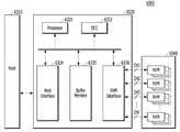
그리고, 메모리 시스템(110)에서의 컨트롤러(130)는, 호스트(102)로부터의 요청에 응답하여 메모리 장치(150)를 제어한다. 예컨대, 컨트롤러(130)는, 메모리 장치(150)로부터 리드된 데이터를 호스트(102)로 제공하고, 호스트(102)로부터 제공된 데이터를 메모리 장치(150)에 저장하며, 이를 위해 컨트롤러(130)는, 메모리 장치(150)의 리드, 라이트, 프로그램(program), 이레이즈(erase) 등의 동작을 제어한다.Then, the
보다 구체적으로 설명하면, 컨트롤러(130)는, 호스트 인터페이스(Host I/F) 유닛(132), 프로세서(Processor)(134), 메모리 인터페이스(Memory I/F) 유닛(142) 및 메모리(Memory)(144)를 포함할 수 있다.More specifically, the
호스트 인터페이스 유닛(132)은, 호스트(102)의 커맨드(command) 및 데이터를 처리하며, USB(Universal Serial Bus), MMC(Multi-Media Card), PCI-E(Peripheral Component Interconnect-Express), SAS(Serial-attached SCSI), SATA(Serial Advanced Technology Attachment), PATA(Parallel Advanced Technology Attachment), SCSI(Small Computer System Interface), ESDI(Enhanced Small Disk Interface), IDE(Integrated Drive Electronics), MIPI(Mobile Industry Processor Interface) 등과 같은 다양한 인터페이스 프로토콜들 중 적어도 하나를 통해 호스트(102)와 통신하도록 구성될 수 있다. 여기서, 호스트 인터페이스 유닛(132)은, 호스트(102)와 데이터를 주고받는 영역으로 호스트 인터페이스 계층(HIL: Host Interface Layer, 이하 'HIL'이라 칭하기로 함)이라 불리는 펌웨어(firmware)를 통해 구동될 수 있다.The
메모리 인터페이스 유닛(142)은, 컨트롤러(130)가 호스트(102)로부터의 요청에 응답하여 메모리 장치(150)를 제어하기 위해, 컨트롤러(130)와 메모리 장치(150) 간의 인터페이싱을 수행하는 메모리/스토리지(storage) 인터페이스가 된다. 여기서, 메모리 인터페이스 유닛(142)은, 메모리 장치(150)가 플래시 메모리, 특히 일 예로 메모리 장치(150)가 NAND 플래시 메모리일 경우에 NAND 플래시 컨트롤러(NFC: NAND Flash Controller)로서, 프로세서(134)의 제어에 따라, 메모리 장치(150)의 제어 신호를 생성하고 데이터를 처리한다. 그리고, 메모리 인터페이스 유닛(142)은, 컨트롤러(130)와 메모리 장치(150) 간의 커맨드 및 데이터를 처리하는 인터페이스, 일 예로 NAND 플래시 인터페이스의 동작, 특히 컨트롤러(130)와 메모리 장치(150) 간 데이터 입출력을 지원하며, 메모리 장치(150)와 데이터를 주고받는 영역으로 플래시 인터페이스 계층(FIL: Flash Interface Layer, 이하 'FIL'이라 칭하기로 함)이라 불리는 펌웨어(firmware)를 통해 구동될 수 있다.The
아울러, 메모리(144)는, 메모리 시스템(110) 및 컨트롤러(130)의 동작 메모리로서, 메모리 시스템(110) 및 컨트롤러(130)의 구동을 위한 데이터를 저장한다. 보다 구체적으로 설명하면, 메모리(144)는, 컨트롤러(130)가 호스트(102)로부터의 요청에 응답하여 메모리 장치(150)를 제어, 예컨대 컨트롤러(130)가, 메모리 장치(150)로부터 리드된 데이터를 호스트(102)로 제공하고, 호스트(102)로부터 제공된 데이터를 메모리 장치(150)에 저장하며, 이를 위해 컨트롤러(130)가, 메모리 장치(150)의 리드, 라이트, 프로그램, 이레이즈(erase) 등의 동작을 제어할 경우, 이러한 동작을 메모리 시스템(110), 즉 컨트롤러(130)와 메모리 장치(150) 간이 수행하기 위해 필요한 데이터를 저장한다.In addition, the
여기서, 메모리(144)는, 휘발성 메모리로 구현될 수 있으며, 예컨대 정적 랜덤 액세스 메모리(SRAM: Static Random Access Memory), 또는 동적 랜덤 액세스 메모리(DRAM: Dynamic Random Access Memory) 등으로 구현될 수 있다. 아울러, 메모리(144)는, 도 1에서 도시한 바와 같이, 컨트롤러(130)의 내부에 존재하거나, 또는 컨트롤러(130)의 외부에 존재할 수 있으며, 이때 메모리 인터페이스를 통해 컨트롤러(130)로부터 데이터가 입출력되는 외부 휘발성 메모리로 구현될 수도 있다.Here, the
또한, 메모리(144)는, 전술한 바와 같이, 호스트(102)와 메모리 장치(150) 간 데이터 라이트 및 리드 등의 동작을 수행하기 위해 필요한 데이터, 및 데이터 라이트 및 리드 등의 동작 수행 시의 데이터를 저장하며, 이러한 데이터 저장을 위해, 프로그램 메모리, 데이터 메모리, 라이트 버퍼(buffer)/캐시(cache), 리드 버퍼/캐시, 데이터 버퍼/캐시, 맵(map) 버퍼/캐시 등을 포함한다.In addition, the
그리고, 프로세서(134)는, 메모리 시스템(110)의 전체적인 동작을 제어하며, 특히 호스트(102)로부터의 라이트 요청 또는 리드 요청에 응답하여, 메모리 장치(150)에 대한 프로그램 동작 또는 리드 동작을 제어한다. 여기서, 프로세서(134)는, 메모리 시스템(110)의 제반 동작을 제어하기 위해 플래시 변환 계층(FTL: Flash Translation Layer, 이하 'FTL'이라 칭하기로 함)이라 불리는 펌웨어(firmware)를 구동한다. 또한, 프로세서(134)는, 마이크로프로세서 또는 중앙 처리 장치(CPU) 등으로 구현될 수 있다.Then, the
일례로, 컨트롤러(130)는, 마이크로프로세서 또는 중앙 처리 장치(CPU) 등으로 구현된 프로세서(134)를 통해, 호스트(102)로부터 요청된 동작을 메모리 장치(150)에서 수행, 다시 말해 호스트(102)로부터 수신된 커맨드에 해당하는 커맨드 동작을, 메모리 장치(150)와 수행한다. 여기서, 컨트롤러(130)는, 호스트(102)로부터 수신된 커맨드에 해당하는 커맨드 동작으로 포그라운드(foreground) 동작을 수행, 예컨대 라이트 커맨드에 해당하는 프로그램 동작, 리드 커맨드에 해당하는 리드 동작, 이레이즈 커맨드(erase command)에 해당하는 이레이즈 동작, 셋 커맨드(set command)로 셋 파라미터 커맨드(set parameter command) 또는 셋 픽쳐 커맨드(set feature command)에 해당하는 파라미터 셋 동작 등을 수행할 수 있다.In one example, the
또한, 상기 프로세서(134)는 체크포인트관리자(135) 및 리커버리관리자(136)를 구동할 수 있다. 즉, 상기 체크포인트관리자(135) 및 리커버리관리자(136)는 상기 프로세서(134)에 의해 구동될 수 있다.Further, the
상기 체크포인트관리자(135)는 상기 체크포인팅 수행 조건에 의해 체크포인팅 수행 시점이 도래할 때마다, 상기 메모리(144)에 저장된 체크포인트정보를 상기 복수의 다이 각각에 프로그램 할 수 있다. 여기서, 상기 체크포인트정보는 필수체크포인트정보 및 더미 체크포인트정보를 포함할 수 있다. 상기 필수체크포인트정보는 상기 메모리(144)에 저장된 맵 세그먼트에 저장된 맵 정보를 포함할 수 있으며, 상기 더미 체크포인트정보는 더미 데이터를 이용하여 생성된 정보를 포함할 수 있다. 구체적으로 설명하면, 상기 체크포인트관리자(135)는 상기 체크포인팅 수행 조건에 의해 체크포인팅 수행 시점이 도래할 경우, 상기 메모리(144)에 저장된 필수 체크포인트정보의 크기, 즉, 맵 세그먼트의 크기에 따라 필수 체크포인트정보를 프로그램할 수 있는 하나 이상의 다이의 개수를 확인한다. 그리고, 상기 확인된 개수만큼 하나 이상의 다이에 포함된 메모리블록에 필수 체크포인트정보를 프로그램한다. 여기서, 상기 체크포인트관리자(135)는 상기 복수의 다이 중 상기 필수 체크포인트정보를 저장한 다이를 제외한 나머지 다이가 존재하는지 확인한다. 확인결과, 나머지 다이가 존재하는 경우, 상기 체크포인트관리자(135)는 상기 나머지 다이에 체크포인팅동작을 수행하여 더미 체크포인트정보를 프로그램할 수 있다. 이와 같이, 복수의 다이에 체크포인팅동작을 수행하여 프로그램할 때, 상기 체크포인트정보를 구별할 수 있는 복수의 식별정보를 함께 저장할 수 있다. 이와 같이, 상기 컨트롤러는 복수의 각 다이에 프로그램 동작이 완료된 후 배리어 동작을 수행하지 않고, 복수의 각 다이마다 프로그램 동작이 완료되는 경우, 바로 체크포인팅동작을 수행함으로써 인터리빙 동작의 성능이 향상될 수 있다.The
리커버리 관리자(136)는 상기 복수의 메모리 장치에 프로그램 동작 중에, 상기 메모리 시스템에 서든 파워 오프 발생(Sudden Power Off, SPO)한 경우, 상기 체크포인트정보 및 상기 체크포인트정보에 대응하는 식별정보를 이용하여 상기 복수의 메모리 장치에 프로그램 된 데이터의 손실을 복구한다. 즉, 서든-파워-오프가 발생할 경우 휘발성 메모리인 메모리(144)에 저장된 체크포인트정보는 전원이 공급된 이후 상기 메모리(144)에 잔존하지 아니하는 반면, 비휘발성 메모리인 메모리블록에 저장된 체크포인트정보는 전원이 공급된 이후에도 상기 메모리블록에 잔존할 수 있다. 이때, 상기 리커버리 관리자(136)는 상기 복수의 각 다이의 메모리블록에 저장된 식별 정보 중 가장 마지막에 저장된 식별 정보를 검색하여 이에 대응하는 체크포인트정보를 이용하여 서든-파워-오프(SPO)로 인해 중단된 동작을 재개하도록 제어할 수 있다.The
이와 관련하여, 상기 체크포인트관리자(135) 및 리커버리 관리자(136)에 대해 도 5를 통해 상세히 설명하기로 한다.In this regard, the
한편, 실시예에 따라, 호스트와 연동하며, 적어도 하나의 프로세서 및 프로그램 명령을 포함하는 적어도 하나의 저장 장치를 포함하는 메모리 시스템을 제공한다. 예를 들어, 적어도 하나의 프로세서 및 프로그램 명령을 포함하는 적어도 하나의 저장 장치는 컨트롤러(130)에 포함된 메모리(144) 및 프로세서(134)로 구현될 수 있다.Meanwhile, according to an embodiment, a memory system including at least one processor and at least one storage device including program instructions is provided in conjunction with a host. For example, at least one storage device including at least one processor and program instructions may be implemented with a
도 2는 본 발명의 실시 예에 따른 메모리 시스템에서 메모리 장치에 데이터 처리 동작의 일 예를 개략적으로 설명하기 위한 도면이다.2 is a diagram schematically illustrating an example of a data processing operation on a memory device in a memory system according to an embodiment of the present invention.
도 2를 참조하면, 컨트롤러(130)는, 호스트(102)로부터 프로그램 커맨드(program command) 및 프로그램 데이터(program data), 그리고 논리주소(logical address)를 수신할 수 있다. 이때, 컨트롤러(130)는, 프로그램 커맨드(program command)에 응답하여 프로그램 데이터(program data)를 메모리 장치(150)의 메모리블록들(BLK1 내지 BLKz)에 포함된 다수의 페이지들에 프로그램하여 저장한다.Referring to FIG. 2, the
그리고, 컨트롤러(130)는, 프로그램 데이터에 대한 메타(meta) 데이터를 생성 및 업데이트한 후, 메모리 장치(150)의 메모리블록들(BLK1 내지 BLKz)에 프로그램하여 저장한다. 이때, 메타 데이터에는 메모리블록들(BLK1 내지 BLKz)에 저장된 프로그램 데이터에 대한 논리적/물리적(L2P: Logical to Physical) 정보 및 물리적/논리적(P2L: Physical to Logical) 정보가 포함된다. 또한, 메타 데이터에는 호스트(102)로부터 수신된 커맨드에 해당하는 커맨드 데이터에 대한 정보, 커맨드에 해당하는 커맨드 동작에 대한 정보, 커맨드 동작이 수행되는 메모리 장치(150)의 메모리블록들에 대한 정보, 및 커맨드 동작에 상응한 맵 데이터 등에 대한 정보가 포함될 수 있다. 다시 말해, 메타 데이터에는 호스트(102)로부터 수신된 커맨드에 해당하는 프로그램 데이터를 제외한 나머지 모든 정보들 및 데이터가 포함될 수 있다.Then, the
여기서, 논리적/물리적(L2P: Logical to Physical) 정보 및 물리적/논리적(P2L: Physical to Logical) 정보는, 컨트롤러(130)에서 프로그램 커맨드에 응답하여 논리주소(logical address)에 대응하는 물리주소(physical address)를 맵핑(mapping)한 정보를 의미한다. 이때, 물리주소(physical address)는 호스트(102)로부터 수신한 프로그램 데이터를 저장할 메모리 장치(150)의 물리적 저장 공간에 대응하는 주소일 수 있다.Here, the logical/physical (L2P: Logical to Physical) information and the physical/logical (P2L: Physical to Logical) information correspond to a program command in the
컨트롤러(130)는, 상술한 논리주소(logical address)와 물리주소(physical address) 간의 맵핑(mapping) 정보, 다시 말해 논리적/물리적(L2P: Logical to Physical) 정보 및 물리적/논리적(P2L: Physical to Logical)를 메모리 장치(150)의 메모리블록들(BLK1 내지 BLKz) 중 적어도 하나 이상의 메모리블록에 저장할 수 있다. 이때 논리적/물리적(L2P: Logical to Physical) 정보 및 물리적/논리적(P2L: Physical to Logical)를 저장한 적어도 하나 이상의 메모리블록을 시스템 메모리블록(system block)이라고 부를 수 있다.The
예를 들어 설명하면, 컨트롤러(130)는, 호스트(102)로부터 수신된 프로그램 커맨드에 해당하는 프로그램 데이터를 컨트롤러(130)의 메모리(144)에 포함된 제1 버퍼(510)에 캐싱 및 버퍼링, 즉 사용자 데이터의 데이터 세그먼트들(512)을 데이터 버퍼/캐시인 제1버퍼(510)에 저장한다. 이후, 컨트롤러(130)는, 제1 버퍼(510)에 저장된 데이터 세그먼트들(512)을, 메모리 장치(150)의 메모리블록들(BLK1 내지 BLKz)에 포함된 페이지들에 프로그램하여 저장한다.For example, the
그리고, 컨트롤러(130)는, 프로그램 데이터의 데이터 세그먼트들(512)이 메모리 장치(150)의 메모리블록들(BLK1 내지 BLKz)에 포함된 페이지들에 프로그램되어 저장됨에 따라, 메타 데이터인 L2P세그먼트들(522)과 P2L세그먼트(524)들을 생성한 후, 컨트롤러(130)의 메모리(144)에 포함된 제2 버퍼(520)에 저장한다. 여기서, 컨트롤러(130)의 메모리(144)에서 제2 버퍼(520)에는, L2P세그먼트들(522)과 P2L세그먼트들(524)이 리스트 형태로 저장될 수 있다. 이후, 컨트롤러(130)는, 맵 플러시(map flush) 동작을 통해 제2 버퍼(520)에 저장된 L2P세그먼트들(522)과 P2L세그먼트들(524)을 메모리 장치(150)의 메모리블록들(BLK1 내지 BLKz)에 포함된 페이지들에 프로그램하여 저장할 수 있다.Then, the
그리고, 컨트롤러(130)는, 호스트(102)로부터 리드 커맨드(read command) 및 논리주소(logical address)를 수신할 수 있다. 이때, 컨트롤러(130)는, 리드 커맨드에 응답하여 호스트(102)의 논리주소에 대응하는 L2P 세그먼트들(522)과 P2L 세그먼트들(524)을 메모리 장치(150)로부터 리드하여 제2버퍼(520)에 로딩(loading)할 수 있다. 이후, 컨트롤러(130)는, 제2버퍼(520)에 로딩된 L2P 세그먼트들(522)과 P2L 세그먼트들(524)로부터 호스트(102)의 논리주소에 대응하는 메모리 장치(150)의 물리주소를 확인하고, 확인을 통해 알 수 있는 저장위치, 즉, 메모리블록들(BLK1 내지 BLKz) 중 특정 메모리블록의 특정 페이지로부터 사용자 데이터의 데이터 세그먼트들(512)을 리드하여 제1 버퍼(510)에 저장한 후, 호스트(102)로 제공한다.Then, the
컨트롤러(130)는, 전술한 바와 같이 호스트(102)로부터 리드 커맨드 및 논리주소가 수신될 때마다 호스트(102)의 논리주소에 대응하는 L2P 세그먼트들(522)과 P2L 세그먼트들(524)를 리드하여 제2버퍼(520)에 로딩할 수 있다. 이와 같은 L2P 세그먼트들(522)과 P2L 세그먼트들(524)을 로딩하는 동작은 빈번하게 반복될 수록 메모리 시스템(110)의 리드 성능을 저하시키는 원인이 될 수 있다.As described above, the
이때, 컨트롤러(130)는, 제2버퍼부(520)의 공간을 많이 확보할수록 메모리 장치(150)로부터 한번에 더 많은 L2P 세그먼트들(522)과 P2L 세그먼트들(524)을 로딩할 수 있고, 그 결과 L2P 세그먼트들(522)과 P2L 세그먼트들(524)에 대한 한번의 로딩 동작으로도 다수의 리드 커맨드들에 대응할 수 있다. 이를 통해 메모리 시스템(110)의 리드 성능이 향상될 수 있다.In this case, the
한편, L2P 세그먼트들(522)은, 특정한 논리주소에 대응하는 물리주소를 검색하는데 최적화될 수 있고, 그 결과 리드 동작시 호스트(102)로부터 입력된 논리주소에 맵핑되는 물리주소를 검색하는데 효율적일 수 있다.Meanwhile, the
또한, P2L 세그먼트들(524)은, 프로그램 동작을 위해 최적화될 수 있다. 컨트롤러(130)는, 호스트(102)로부터 프로그램 커맨드와 프로그램 데이터 및 논리주소를 수신할 때, 프로그램 데이터를 저장할 메모리 장치(150) 내 저장 공간을 빠르게 할당할 필요가 있다. 이때, 컨트롤러(130)는, 제2버퍼부(520)에 새롭게 할당 가능한 메모리 장치(150) 내 저장 공간에 대응하는 물리주소들의 리스트를 미리 로딩할 수 있다. 따라서, 컨트롤러(130)는, 호스트(102)로부터 프로그램 커맨드와 프로그램 데이터 및 논리주소가 수신된 시점에서, 제2버퍼부(520)에 로딩되어 있는 물리주소들의 리스트를 빠르게 검색하여 프로그램 데이터를 저장할 수 있는 저장 공간에 대응하는 물리주소를 논리주소와 맵핑한 후, 물리주소에 대응하는 저장 공간에 프로그램 데이터를 저장할 수 있다. 이때, P2L 세그먼트들(524)이 생성되어 제2버퍼부(520)에 일시 저장될 수 있고, 제2버퍼부(520)에 저장된 P2L 세그먼트들(524)는, 맵 플러시(map flush) 동작을 통해 메모리 장치(150)에 저장될 수 있다.In addition,
도 3은 본 발명의 실시예에 따른 메모리 시스템에서 사용되는 슈퍼 메모리블록의 개념을 설명하기 위해 도시한 도면이다.3 is a diagram illustrating a concept of a super memory block used in a memory system according to an embodiment of the present invention.
도 3을 참조하면, 도 1을 참조하여 본 발명의 실시예에 따른 메모리 시스템(110)의 구성요소 중 메모리 장치(150)에 포함된 복수의 메모리 다이(1501~150n)의 구성요소가 구체적으로 도시된 것을 알 수 있다. 일례로, 상기 메모리 장치(150)는 제1메모리 다이(1501) 및 제2메모리 다이(1502)를 포함할 수 있다.Referring to FIG. 3, among the components of the
상기 제1 및 제2메모리 다이(1501 및 1502)는 복수의 플래인을 포함할 수 있다. 일례로, 상기 제1메모리 다이(1501)는 제1플래인(PLANE00) 및 제2플래인(PLANE01)을 포함할 수 있으며, 상기 제2메모리 다이(1502)는 제3플래인(PLANE10) 및 제4플래인(PLANE11)을 포함할 수 있다. 그리고, 상기 복수의 플래인은 복수의 메모리블록들을 포함할 수 있다. 일례로, 상기 제1플래인(PLANE00)은 제1메모리블록 내지 제N메모리블록(BLOCK000, BLOCK001, BLOCK002, ..., BLCOK00N)을 포함할 수 있으며, 상기 제2플래인(PLANE01)은 제1메모리블록 내지 제N메모리블록(BLOCK010, BLOCK011, BLOCK012, ..., BLCOK01N)을 포함할 수 있다. 제3플래인(PLANE10)은 제1메모리블록 내지 제N메모리블록(BLOCK100, BLOCK101, BLOCK102, ..., BLCOK10N)을 포함할 수 있으며, 제4플래인(PLANE11)은 제1메모리블록 내지 제N메모리블록(BLOCK110, BLOCK111, BLOCK112, ..., BLCOK11N)을 포함할 수 있다.The first and second memory dies 1501 and 1502 may include a plurality of planes. For example, the first memory die 1501 may include a first plane (PLANE00) and a second plane (PLANE01), and the second memory die (1502) may include a third plane (PLANE10) and It may include a fourth plane (PLANE11). In addition, the plurality of planes may include a plurality of memory blocks. For example, the first plane (PLANE00) may include a first memory block to an Nth memory block (BLOCK000, BLOCK001, BLOCK002, ..., BLCOK00N), and the second plane (PLANE01) is a first memory block. It may include 1 memory block to an Nth memory block (BLOCK010, BLOCK011, BLOCK012, ..., BLCOK01N). The third plane (PLANE10) may include a first memory block to an Nth memory block (BLOCK100, BLOCK101, BLOCK102, ..., BLCOK10N), and the fourth plane (PLANE11) is a first memory block to a first memory block. It may include N memory blocks (BLOCK110, BLOCK111, BLOCK112, ..., BLCOK11N).
메모리 장치(150)는, 제0 채널(CH0)을 통해 데이터를 입/출력할 수 있는 제1메모리 다이(1501)과 제1 채널(CH1)을 통해 데이터를 입/출력할 수 있는 제2메모리 다이(1502)를 포함한다. 이때, 제0 채널(CH0)과 제1 채널(CH1)은, 인터리빙(interleaving) 방식으로 데이터를 입/출력할 수 있다.The
또한, 제1메모리 다이(1501)는, 제0 채널(CH0)을 공유하여 인터리빙 방식으로 데이터를 입/출력할 수 있는 복수의 경로(WAY0, WAY1)들에 각각 대응하는 복수의 플래인(PLANE00, PLANE01)들을 포함한다.Further, the first memory die 1501 shares a plurality of planes (PLANE00) corresponding to a plurality of paths (WAY0, WAY1) that can input/output data in an interleaving manner by sharing the 0th channel (CH0). , PLANE01).
또한, 제2메모리 다이(1502)는, 제1 채널(CH1)을 공유하여 인터리빙 방식으로 데이터를 입/출력할 수 있는 복수의 경로(WAY2, WAY3)들에 각각 대응하는 복수의 플래인(PLANE10, PLANE11)들을 포함한다.In addition, the second memory die 1502 shares a plurality of planes (PLANE10) corresponding to a plurality of paths (WAY2, WAY3) that can input/output data in an interleaving manner by sharing the first channel (CH1). , PLANE11).
이와 같이. 메모리 장치(150)에 포함된 복수의 메모리블록들(BLOCK000, BLOCK001, BLOCK002, ..., BLCOK00N, BLOCK010, BLOCK011, BLOCK012, ..., BLCOK01N, BLOCK100, BLOCK101, BLOCK102, ..., BLCOK10N, BLOCK110, BLOCK111, BLOCK112, ..., BLCOK11N)은, 같은 경로 또는 같은 채널을 사용하는 것과 같은 '물리적인 위치'에 따라 구분될 수 있다.like this. A plurality of memory blocks included in the memory device 150 (BLOCK000, BLOCK001, BLOCK002, ..., BLCOK00N, BLOCK010, BLOCK011, BLOCK012, ..., BLCOK01N, BLOCK100, BLOCK101, BLOCK102, ..., BLCOK10N, BLOCK110, BLOCK111, BLOCK112, ..., BLCOK11N) may be classified according to a'physical location' such as using the same path or the same channel.
그리고, 설계자의 선택에 따라 메모리 장치(150)에 2개보다 더 많거나 더 적은 개수의 메모리 다이가 포함될 수 있고, 각각의 메모리 다이에도 2개보다 더 많거나 더 적은 개수의 플래인이 포함될 수 있다. 물론, 각각의 플래인에 포함되는 메모리블록의 개수인 '예정된 개수'도 설계자의 선택에 따라 얼마든지 조정가능하다.Further, more or less than two memory dies may be included in the
한편, 컨트롤러(130)는, '물리적인 위치'의 구분방식을 통해 서로 다른 다이 또는 서로 다른 플래인으로 구분되었던 복수의 메모리블록들을 동시에 선택 가능한 메모리블록들끼리 그룹화하여 슈퍼 메모리블록(super memory block)들로 구분하여 관리할 수 있다.On the other hand, the
이렇게, 컨트롤러(130)에서 복수의 메모리블록들(BLOCK000, BLOCK001, BLOCK002, ..., BLCOK00N, BLOCK010, BLOCK011, BLOCK012, ..., BLCOK01N, BLOCK100, BLOCK101, BLOCK102, ..., BLCOK10N, BLOCK110, BLOCK111, BLOCK112, ..., BLCOK11N)을 슈퍼 메모리블록들로 구분하여 관리하는 방식은, 설계자의 선택에 따라 여러 가지 방식이 존재할 수 있는데, 여기에서는 세 가지 방식을 예시하도록 하겠다.In this way, a plurality of memory blocks (BLOCK000, BLOCK001, BLOCK002, ..., BLCOK00N, BLOCK010, BLOCK011, BLOCK012, ..., BLCOK01N, BLOCK100, BLOCK101, BLOCK102, ..., BLCOK10N, BLOCK110 in the controller 130) , BLOCK111, BLOCK112, ..., BLCOK11N) can be divided into super memory blocks and managed in various ways depending on the designer's choice. Here, three methods will be illustrated.
첫 번째 방식은, 컨트롤러(130)에서 메모리 장치(150)에 포함된 복수의 메모리 다이들(1501, 1502) 중 제1메모리 다이(1501)의 제1플래인(PLANE00)에서 임의의 하나의 메모리블록(BLOCK000)과, 제2플래인(PLANE01)에서 임의의 하나의 메모리블록(BLOCK010)을 그룹화하여 하나의 슈퍼 메모리블록(A1)으로 관리하는 방식이다. 첫 번째 방식을 메모리 장치(150)에 포함된 복수의 메모리 다이들(1501, 1502) 중 제2메모리 다이(1502)에 적용하면, 컨트롤러(130)는, 제2메모리 다이(1502)의 제1플래인(PLANE10)에서 임의의 하나의 메모리블록(BLOCK100)과, 제2플래인(PLANE11)에서 임의의 하나의 메모리블록(BLOCK110)을 그룹화하여 하나의 슈퍼 메모리블록(A2)으로 관리할 수 있다.In the first method, any one memory in the first plane (PLANE00) of the first memory die 1501 among the plurality of memory dies 1501 and 1502 included in the
두 번째 방식은, 컨트롤러(130)에서 메모리 장치(150)에 포함된 복수의 메모리 다이들(1501, 1502) 중 제1메모리 다이(1501)의 제1플래인(PLANE00)에 포함된 임의의 하나의 메모리블록(BLOCK002)과, 제2메모리 다이(1502)의 제1플래인(PLANE10)에 포함된 임의의 하나의 메모리블록(BLOCK102)를 그룹화하여 하나의 슈퍼 메모리블록(B1)으로 관리하는 방식이다. 두 번째 방식을 다시 적용하면, 컨트롤러(130)는, 메모리 장치(150)에 포함된 복수의 메모리 다이들(1501, 1502) 중 제1메모리 다이(1501)의 제2플래인(PLANE01)에 포함된 임의의 하나의 메모리블록(BLOCK012)과, 제2메모리 다이(1502)의 제2플래인(PLANE11)에 포함된 임의의 하나의 메모리블록(BLOCK112)를 그룹화하여 하나의 슈퍼 메모리블록(B2)으로 관리할 수 있다.In the second method, any one of the plurality of memory dies 1501 and 1502 included in the
세 번째 방식은, 컨트롤러(130)에서 메모리 장치(150)에 포함된 복수의 메모리 다이들(1501, 1502) 중 제1메모리 다이(1501)의 제1플래인(PLANE00)에 포함된 임의의 하나의 메모리블록(BLOCK001)과, 제1메모리 다이(1501)의 제2플래인(PLANE01)에 포함된 임의의 하나의 메모리블록(BLOCK011)과, 제2메모리 다이(1502)의 제1플래인(PLANE10)에 포함된 임의의 하나의 메모리블록(BLOCK101), 및 제2메모리 다이(1502)의 제2플래인(PLANE11)에 포함된 임의의 하나의 메모리블록(BLOCK111)을 그룹화하여 하나의 슈퍼 메모리블록(C)으로 관리하는 방식이다.In a third method, the
참고로, 슈퍼 메모리블록에 포함되는 동시에 선택 가능한 메모리블록들은, 인터리빙 방식, 예컨대, 채널 인터리빙(channel interleaving) 방식 또는 메모리 다이 인터리빙(memory die interleaving) 방식 또는 메모리 칩 인터리빙(memory chip interleaving) 방식 또는 경로 인터리빙(way interleaving) 방식 등을 통해 실질적으로 동시에 선택될 수 있다.For reference, the memory blocks included in the super memory block and selectable at the same time may be interleaved, for example, channel interleaving or memory die interleaving or memory chip interleaving or path. It may be selected at substantially the same time through a way of interleaving.
도 4a 및 도 4b는 일반적인 체크포인팅동작을 설명하기 위한 도면이다.4A and 4B are diagrams for explaining a general check pointing operation.
도 4a를 참조하면, 일반적으로, 상기 컨트롤러(130)는 주기적으로 메모리(144)에 저장된 체크포인트정보를 상기 메모리 장치(150)에 포함된 복수의 메모리블록(BLK1 내지 BLKz) 중 어느 하나의 메모리블록(BLKz)에 프로그램하는 체크포인팅동작을 수행할 수 있다. 상기 체크포인트정보는 앞서 도 1을 참조하여 설명한 백그라운드 동작 또는 호스트(102)의 요청에 따른 동작을 수행하기 위해 필요한 데이터일 수 있다. 상기 체크포인팅동작 수행은, 상기 컨트롤러(130)의 제어에 따라 상기 복수의 각 다이(1501 내지 150n)에 포함된 복수의 메모리블록, 즉, 오픈블록에 인터리빙 방식으로 데이터 세그먼트 또는 맵 세그먼트 단위로 업데이트가 수행되는 경우, 상기 체크포인팅동작이 수행될 수 있다. 여기서, 상기 컨트롤러(130)는 상기 복수의 오픈블록에 상기 체크포인팅동작 수행 전후로 배리어(barrier) 동작이 수행될 수 있다. 상기 배리어 동작은 복수의 다이들(1501 내지 150n)들의 인터리빙 동작이 브레이크 됨을 나타내는 동작이다. 즉, 상기 배리어 동작을 수행하는 이유는, 체크포인팅동작 수행 이전까지 상기 복수의 메모리 다이(1501 내지 150n)에 포함된 메모리블록에 저장된 데이터들을 보장하기 위해 수행하는 것이다.Referring to FIG. 4A, in general, the
도 4b의 타이밍도를 참조하면, 상기 컨트롤러(130)는 상기 제1다이 내지 제4다이(1501 내지 1504)에 제1프로그램 동작(tProgram_1) 내지 제4프로그램 동작(tProgram_4)을 수행할 수 있다. 이때, 상기 컨트롤러(130)는 제1메모리 다이 내지 제4메모리 다이(1501 내지 1504) 각각에 수행되는 제1프로그램 동작(tProgram_1) 내지 제4프로그램 동작(tProgram_4)이 모두 완료되면, 제1배리어 동작(B1)을 수행한다. 그리고, 상기 컨트롤러(130)는 제1다이 내지 제4다이(1501 내지 1504) 각각에 제1체크포인팅동작(tCheck Point_1) 내지 제4체크포인팅동작(tCheck Point_4)을 수행할 수 있다. 그리고 상기 컨트롤러(130)는 상기 제1체크포인팅동작(tCheck Point_4) 내지 제4체크포인팅동작(tCheck Point_4)이 완료되면 제2배리어 동작(B2)을 수행할 수 있다. 이와 같이, 상기 컨트롤러(130)가 프로그램 동작이 완료된 후 체크포인팅동작을 수행하기 이전까지 아이들 타임이 발생하게 되어 복수의 다이의 인터리빙 동작 성능이 저하될 수 있다. 또한, 상기 컨트롤러(130)가 제1 내지 제4다이에 프로그램 동작이 완료되 후에 상기와 같이 배리어 동작 및 체크포인트 동작을 수행하게 되면, 상기 제1 내지 제4 다이에 프로그램 동작을 수행하고 있는 도중에 서든-파워-오프(SPO)가 발생하게 되면 이전에 프로그램 동작이 완료된 데이터들은 손실되어 복구하는데 문제점이 발생할 수 있다. 이를 해결하기 위해, 도 5 내지 도 8을 통해 상세히 설명하기로 한다.Referring to the timing diagram of FIG. 4B, the
도 5는 본 발명의 일 실시예에 따라 메모리 시스템 동작을 설명하기 위한 도면이다. 도 5는 도 1의 데이터 처리 시스템(100)에서 본 발명과 관련된 구성만을 간략히 도시하고 있다.5 is a diagram for describing a memory system operation according to an embodiment of the present invention. FIG. 5 briefly shows only the configuration related to the present invention in the data processing system 100 of FIG. 1.
도 5를 참조하면, 메모리 시스템(110)은 메모리 장치(150) 및 컨트롤러(130)를 포함할 수 있다.Referring to FIG. 5, the
먼저, 상기 메모리 장치(150)는 제1 내지 4메모리 다이(1501 내지 1504)를 포함할 수 있다. 상기 제1 내지 4메모리 다이(1501 내지 1504)는 제1영역(미도시)과 제2영역(도시)을 포함할 수 있다. 상기 제1영역은 상기 호스트로부터 전달받은 커맨드에 대응하는 커맨드 동작을 수행할 수 있는 복수의 메모리블록을 포함할 수 있으며, 상기 제2영역은 체크포인트 동작에 따른 체크포인트정보를 저장할 수 있는 복수의 메모리블록을 포함할 수 있다. 본 발명에서는 설명의 편의를 위해 제2영역만 도시하여 설명하기로 한다. 일례로, 상기 복수의 다이의 상기 제2영역에는 하나의 메모리블록(BLK1)을 포함하며, 상기 메모리블록은 5개의 페이지를 포함할 수 있다. 그리고, 도면에 직접적으로 도시하지 않았지만, 상기 컨트롤러(130)는 각 다이에 포함된 메모리블록마다 데이터를 프로그램할 때에는 원샷 프로그램 방식을 사용할 수 있다. 상기 원샷 프로그램은 복수의 비트데이터를 한번의 프로그램 동작을 통해 멀티레벨 셀에 프로그램하는 동작을 의미한다. 이때, 원샷 프로그램의 기준이 되는 데이터 크기를 '설정된 크기'라고 정의할 수 있다. 즉, 복수의 다이의 제1메모리블록에 포함된 어느 하나의 페이지(미도시)에 더미데이터 없이 원샷 프로그램을 진행하기 위해 필요한 데이터의 크기를 '설정된 크기'로 정의할 수 있다. 일례로, 상기 각각의 제1메모리블록의 페이지마다 '설정된 크기'는 '32KB'의 크기로 갖을 수 있으며, 인터리빙방식으로 4개의 다이에 '128KB'크기까지 데이터를 프로그램할 수 있다. 이는 어디까지나 하나의 실시예일 뿐이며, 설계자의 선택에 따라 얼마든지 상기 설정된 크기보다 크거나 또는 더 작은 크기로 설정될 수 있다.First, the
상기 컨트롤러(130)는 메모리(144) 및 프로세서(134)를 포함할 수 있다.The
상기 메모리(144)는 상기 컨트롤러(130)의 제어에 따라 주기적으로 체크포인트정보가 저장된 체크포인트정보 리스트(CP_LIST)를 포함할 수 있다. 상기 체크포인트정보 리스트(CP_LIST)에 저장된 체크포인트 정보는 백그라운드 동작 또는 호스트(102)의 요청에 따른 동작을 수행하기 위해 필요한 데이터일 수 있다.The
상기 프로세서(134)는 체크포인트관리자(135) 및 리커버리관리자(136)를 포함할 수 있다.The
상기 체크포인트관리자(135)는 수행시점판단부(1351) 및 수행부(1352)를 포함할 수 있다. 상기 체크포인트관리자(135)는 수행시점판단부(1351)를 통해 주기적으로 제1체크포인팅 수행 시점을 확인하며, 제1체크포인팅 수행 시점이 확인되면 상기 수행부(1352)를 통해 상기 메모리 장치(150)에 제1체크포인팅동작을 수행할 수 있다. 이와 관련하여 후술에 의해 상세히 설명하기로 한다.The
먼저, 상기 수행시점판단부(1351)는 상기 제1체크포인팅동작 수행 시점을 주기적으로 확인하여 제1체크포인팅 수행 동작 여부를 판단할 수 있다. 상기 제1체크포인팅 수행 시점은 상기 제1 내지 제4다이(1501 내지 1504)에 포함된 복수의 메모리블록 중 타겟블록이 제1오픈블록에서 제2오픈블록으로 변경된 경우 또는 상기 제1 내지 제4다이(1501 내지 1504)에 일정 크기만큼 프로그램 동작이 수행된 경우 중 어느 하나를 선택하여 제1체크포인팅 수행 시점으로 설정할 수 있다. 본 발명에서는 상기 제1 내지 제4다이(1501 내지 1504)의 제1영역에 포함된 복수의 메모리 블록 중 타겟블록이 제1오픈블록에서 제2오픈블록으로 변경될 때마다 제1체크포인팅동작을 수행하는 시점으로 설정하여 설명하기로 한다. 이는 어디까지나 실시예일 뿐이며, 상기 제1체크포인팅 수행 시점은 설계자의 선택에 따라 여러가지 방식이 존재할 수 있다.First, the execution
상기 수행시점판단부(1351)는 상기 컨트롤러가 상기 호스트로부터 복수의 라이트 커맨드들을 전달받을 경우, 상기 제1 내지 제4다이(1501 내지 1504)의 제1영역에 포함된 복수의 메모리블록 중 오픈블록이 소스블록으로 변경되는지 확인한다. 즉, 상기 수행시점판단부(1351)는 상기 오픈블록이 다른 오픈블록으로 변경되었는지 확인한다. 확인 결과, 상기 제1 내지 제4다이(1501 내지 1504)에 포함된 메모리블록 중 오픈블록이 소스블록으로 변경된 경우가 아닌 경우, 상기 컨트롤러(130)는 상기 호스트(102)로부터 수신된 복수의 라이트 커맨드들에 해당하는 라이트 커맨드 동작들을 인터리빙 방식으로 상기 복수의 다이에 포함된 상기 오픈블록에 수행할 수 있다. 반면에, 확인 결과, 상기 제1 내지 제4다이(1501 내지 1504)의 제1영역에 포함된 메모리블록 중 오픈블록이 소스블록으로 변경되는 경우, 상기 수행시점판단부(1351)는 제1체크포인팅동작을 수행할 수 있는 시점이라 판단한다.When the controller receives a plurality of write commands from the host, the execution
상기 수행부(1352)는 상기 메모리(144)의 체크포인트리스트에 저장된 체크포인트정보의 크기를 통해 상기 제1체크포인팅동작을 수행하기 위한 다이 개수(N)를 산출한다. 상기 수행부(1352)는 상기 체크포인트정보 크기 및 복수의 각 다이마다 설정된 크기를 이용하여 타겟 다이 개수(N)를 산출할 수 있다. 상기 수행부(1352)는 상기 타겟 다이 개수(N)만큼 상기 제1체크포인팅동작을 수행할 수 있다. 그리고, 상기 수행부(1352)는 전체 다이 개수(A)와 상기 타겟 다이 개수(N)와 동일한지 확인하여 동일하지 않은 경우, 상기 전체 다이 개수(A)에서 상기 타겟 다이 개수(N)를 제외한 나머지 다이에 제2체크포인팅동작을 수행하여 더미체크포인트정보 및 이에 대응하는 식별정보를 저장할 수 있다.The
먼저, 상기 수행부(1352)가 제1체크포인팅동작만 수행되는 경우에 대해 설명하면, 일례로, 상기 메모리(144)의 체크포인트정보리스트에 저장된 체크포인트정보의 크기가 100KB인 경우, 상기 복수의 각 다이마다 프로그램을 수행할 수 있는 설정된 크기가 '32KB'이기 때문에 총 4개의 다이에 제1체크포인팅동작을 수행할 수 있다. 즉, 상기 수행부(1352)는 상기 제1 내지 제4다이에 포함된 제1메모리블록에 상기 제1체크포인트정보(CP1) 내지 제4체크포인트정보(CP4) 및 이에 대응하는 제1식별 정보 내지 제4식별정보를 순차적으로 프로그램할 수 있다. 즉, 상기 수행부(1352)는 제1다이의 제1메모리블록에 상기 제1체크포인트정보 및 제1식별정보(T1), 제2다이의 제1메모리블록에 상기 제2체크포인트정보 및 제2식별정보(T2), 제3다이의 제1메모리블록에 상기 제3체크포인트정보 및 제3식별정보(T3) 및 제4다이의 제1메모리블록에 상기 제4체크포인트정보 및 제4식별정보(T4)를 순차적으로 프로그램할 수 있다.First, when a case where only the first check pointing operation is performed by the
다음으로, 상기 수행부(1352)가 제1 및 제2체크포인팅동작을 수행하는 경우에 대해 설명하면, 상기 메모리(144)의 체크포인트정보리스트에 저장된 체크포인트정보의 크기가 64KB인 경우에, 총 2개의 타겟 다이에 제1체크포인팅동작을 수행하여 체크포인트정보 및 이에 대응하는 식별정보를 저장할 수 있다. 일례로, 상기 수행부(1352)는 제1다이의 제1메모리블록에 상기 제5체크포인트정보 및 제5식별정보(T5), 제2다이의 제1메모리블록에 상기 제6체크포인트정보 및 제6식별정보(T6)를 저장할 수 있다. 그리고, 상기 수행부(1352)는 상기 전체 다이 개수(A)와 상기 타겟 다이 개수(N)가 동일한지 확인 후, 동일하지 않는 경우, 상기 전체 다이 개수(A)에서 상기 타겟 다이 개수(N)를 제외한 나머지 타겟 다이(M)에 제2체크포인팅동작을 수행하여 더미체크포인트정보 및 이에 대응하는 식별정보를 프로그램할 수 있다. 일례로, 상기 컨트롤러(130)는 제3다이의 제1메모리블록에 상기 제1더미체크포인트정보 및 제7식별정보(T7) 및 제4다이의 제1메모리블록에 상기 제2더미체크포인트정보 및 제8식별정보(T8)를 순차적으로 프로그램할 수 있다. 반면에, 상기 수행부(1352)는 상기 전체 다이 개수(A)와 상기 타겟 다이 개수(N)가 동일한 경우 체크포인팅 동작 수행을 종료할 수 있다.Next, when the
리커버리관리자(136)는 상기 복수의 다이에 프로그램 동작 중에, 상기 메모리 시스템에 서든 파워 오프(Sudden Power Off, SPO)가 발생한 경우, 상기 체크포인트정보 및 식별정보를 이용하여 상기 제1 내지 제4다이(1501 내지 1504)에 프로그램 된 데이터의 손실을 복구한다. 즉, 상기 리커버리관리자(136)는 상기 호스트 요청에 따른 커맨드 동작 수행 중에, 상기 메모리 시스템에 서든 파워 오프(SPO)가 발생한 경우, 제1 내지 제4다이(1501 내지 1504) 각각에 포함된 체크포인트 정보가 저장된 메모리블록에서 마지막으로 저장된 식별정보를 확인한다. 일례로, 상기 제1 내지 제4다이(1501 내지 1504)의 메모리블록에서 마지막으로 저장된 식별정보는 제1다이의 메모리블록에서는 제5식별정보(T5)이고, 제2다이의 메모리블록에서는 제6식별정보(T6)이고, 제3다이의 메모리블록에서는 제7식별정보(T7)이며, 제4다이의 메모리블록에서는 제8식별정보(T8)이다. 그리고, 상기 리커버리관리자(136)는 상기 확인된 복수의 식별정보가 연속적인 패턴을 가지고 있는지 확인한다. 확인 결과, 상기 복수의 식별정보가 제5식별정보(T5)-> 제6식별정보(T6)-> 제7식별정보(T7)-> 제8식별정보(T8) 순으로써, 연속적인 패턴임을 확인할 수 있다. 이와 같이, 상기 리커버리관리자(136)는 상기 복수의 식별정보가 연속적인 패턴인 경우 상기 복수의 식별정보에 대응하는 체크포인트정보를 이용하여 데이터 복구 동작을 수행할 수 있다. 일례로, 상기 리커버리관리자(136)는 상기 제5식별정보(T5)에 대응하는 제5체크포인트정보(CP_5), 제6식별정보(T6)에 대응하는 제6체크포인트정보(CP_6), 제7식별정보(T7)에 대응하는 제1더미체크포인트정보(D_CP_1) 및 제8식별정보(T8)에 대응하는 제2더미체크포인트정보(D_CP_2)를 이용하여 데이터를 복구할 수 있다.The
반면에, 상기 제1 내지 제4다이(1501 내지 1504)의 메모리블록에서 확인된 식별정보의 패턴이 연속적이지 않다면, 상기 리커버리관리자(136)는 상기 확인된 식별정보의 이전 식별정보의 위치를 확인하여 복수의 이전식별정보의 패턴이 연속적인지 확인한다. 그리고, 상기 복수의 이전 식별정보의 패턴이 연속적인 경우, 상기 복수의 이전식별정보에 대응하는 복수의 체크포인트정보를 이용하여 데이터 복구 동작을 수행할 수 있다.On the other hand, if the pattern of the identification information identified in the memory blocks of the first to fourth dies 1501 to 1504 is not continuous, the
도 6 및 도7은 본 발명의 일실시예에 따른 메모리 시스템의 제1 및 제2체크포인팅동작을 설명하기 위한 흐름도이다.6 and 7 are flowcharts illustrating first and second check pointing operations of a memory system according to an embodiment of the present invention.
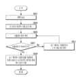
도 6을 참조하면, 상기 컨트롤러(130)는 상기 제1체크포인팅동작 수행 시점을 주기적으로 확인하여 제1체크포인팅 수행 동작 여부를 판단할 수 있다. 상기 제1체크포인팅 수행 시점은 상기 제1 내지 제4다이(1501 내지 1504)의 제1영역(미도시)에 포함된 복수의 메모리블록 중 타겟 블록인 제1오픈블록이 제2오픈블록으로 변경되는 경우 또는 상기 제1 내지 제4다이(1501 내지 1504)에 일정 크기만큼 프로그램 동작이 수행된 경우 중 어느 하나를 선택하여 제1체크포인팅 수행 시점으로 설정할 수 있다. 본 발명에서는 상기 제1 내지 제4다이(1501 내지 1504)의 제1영역에 포함된 복수의 메모리블록 중 타겟블록인 제1오픈블록이 제2오픈블록으로 변경되는 경우를 일례로 하여 설명하기로 한다. 이는 어디까지나 실시예일 뿐이며, 상기 제1체크포인팅 수행 시점은 설계자의 선택에 따라 여러가지 방식이 존재할 수 있다.Referring to FIG. 6, the
S601단계에서, 상기 컨트롤러(130)는 상기 호스트(102)로부터 복수의 라이트 커맨드들을 전달받는다. 이때 S603단계 및 S605단계에서, 상기 제1 내지 제4다이(1501 내지 1504)의 제1영역에 포함된 복수의 메모리블록 중 타겟블록인 제1오픈블록이 소스블록으로 변경되어 제2오픈블록이 타겟 블록으로 변경되었는지 확인한다. 확인 결과, 상기 제1오픈블록에 프리(Free) 페이지 공간이 남아있는 경우(N0), 상기 컨트롤러(130)는 제1체크포인팅동작을 수행할 수 있는 시점이 아니라고 판단하여, S607단계에서, 상기 컨트롤러(130)는 상기 복수의 다이 각각에 포함된 제1오픈블록에 상기 라이트 커맨드 동작들을 수행할 수 있다. 반면에, 확인 결과, 상기 제1 내지 제4다이(1501 내지 1504)의 제1오픈블록에 프리 페이지 공간이 없어 타겟 블록이 제2오픈블록으로 변경되는 경우, 상기 컨트롤러(130)는 상기 제1체크포인팅동작을 수행할 수 있는 시점이라고 판단한다(YES).In step S601, the
S609단계에서, 상기 컨트롤러(130)는 제1체크포인팅동작을 수행하기 위한 타겟 다이 개수(N)를 산출한다. 여기서, 도 7을 통해 상기 제1체크포인팅동작을 수행하기 위한 타겟 다이 개수(N)를 산출하는 방법에 대해 자세히 설명하기로 한다. 도 7을 살펴보면, S701단계에서, 상기 컨트롤러(130)는 상기 메모리(144)의 체크포인트리스트에 저장된 체크포인트정보 크기를 확인한다. 다음으로, S703단계에서, 상기 컨트롤러(130)는 상기 확인된 체크포인트정보의 크기 및 상기 복수의 다이마다 설정된 크기를 이용하여 타겟 다이 개수(N)를 산출할 수 있다. 일례로, 상기 복수의 다이마다 설정된 크기가 32KB이고, 상기 체크포인트정보의 크기가 64KB인 경우, 타겟 다이의 개수(N)는 2개임을 알 수 있다.In step S609, the
다시 도 6으로 돌아와서, S611단계 및 S613단계에서, 상기 컨트롤러(130)는 상기 산출된 타겟 다이 개수(N)만큼 상기 제1체크포인팅동작을 수행하여 하나 이상의 체크포인트정보 및 이에 대응하는 식별정보를 저장할 수 있다. 일례로, 상기 컨트롤러(130)는 상기 제1다이의 메모리블록에 제1체크포인트정보(CP_1) 및 제1식별정보(T1)을, 상기 제2다이의 메모리블록에 제2체크포인트정보(CP_2) 및 제2식별정보(T2)를 저장할 수 있다.Returning to FIG. 6 again, in steps S611 and S613, the
S615단계에서, 상기 컨트롤러(130)는 상기 전체 다이개수(A)와 상기 타겟 다이 개수(N)가 일치하는지 확인한다. 확인결과, 상기 전체 다이개수(A)와 상기 타겟 다이 개수(N)가 일치하지 않는다면(no), S617단계에서, 상기 컨트롤러(130)는 상기 복수의 다이 중 제1체크포인팅동작이 수행되지 않은 나머지 타겟 다이 개수(M)를 확인한다. S619단계 및 S621에서, 상기 컨트롤러(130)는 상기 나머지 타겟 다이 개수(M)에 해당되는 하나 이상의 나머지 타겟 다이(M)에 상기 제2체크포인팅동작을 수행하여 더미체크포인트정보 및 이에 대응하는 식별정보를 저장할 수 있다. 일례로, 상기 컨트롤러(130)는 상기 제1 내지 제4다이 중 제1 및 제2다이의 메모리블록에 제1 및 제2체크포인트정보 및 제1 및 제2식별정보가 저장되어 있기 때문에, 제3다이의 메모리블록에 제1더미체크포인트정보(D_CP_1) 및 제7식별정보(T7)를 저장하고, 제4다이에 제2더미체크포인트정보(D_CP_2) 및 제8식별정보(T8)를 순차적으로 저장할 수 있다.In step S615, the
반면에, S615 단계에 대해 확인결과, 상기 전체 다이개수(A)와 상기 타겟 다이 개수(N)가 일치한 경우(yes), 체크포인팅동작 수행을 종료한다.On the other hand, as a result of checking with respect to step S615, when the total number of dies A and the number of target dies N match (yes), the checkpointing operation is ended.
도 8은 본 발명의 일실시예에 따른 메모리 시스템의 리커버리 동작을 설명하기 위한 흐름도이다.8 is a flowchart illustrating a recovery operation of a memory system according to an embodiment of the present invention.
도 8을 참조하면, S801단계에서, 상기 컨트롤러(130)는 서든-파워-오프를 감지할 수 있다. 상기 서든-파워-오프가 발생할 경우 휘발성 메모리인 메모리(144)에 저장된 체크포인팅정보는 전원이 공급된 이후 상기 메모리(144)에 잔존하지 아니하는 반면, 비휘발성 메모리인 메모리블록에 저장된 체크포인팅정보는 전원이 공급된 이후에도 상기 메모리블록에 잔존할 수 있다.Referring to FIG. 8, in step S801, the
S803단계에서, 상기 컨트롤러(130)는 상기 복수의 다이에 프로그램 동작 중에, 상기 메모리 시스템에 서든 파워 오프(Sudden Power Off, SPO)가 발생한 경우, 제1 내지 제4다이 각각에 포함된 제1메모리블록에서 마지막으로 저장된 식별정보를 확인한다. 일례로, 상기 제1 내지 제4다이(1501 내지 1504)의 제1메모리블록에서 마지막으로 저장된 식별정보는 제1다이의 제1메모리블록에서는 제5식별정보(T5)이고, 제2다이의 제1메모리블록에서는 제6식별정보(T6)이고, 제3다이의 제1메모리블록에서는 제7식별정보(T7)이며, 제4다이의 제1메모리블록에서는 제8식별정보(T8)이다.In step S803, the
S805단계 및 S807단계에서, 상기 컨트롤러(130)는 상기 확인된 복수의 식별정보가 연속적인 패턴을 가지고 있는지 확인한다. 확인 결과, 상기 복수의 식별정보가 연속적인 패턴인 경우(yes), S809단계에서, 상기 복수의 식별정보에 대응하는 체크포인트정보를 이용하여 데이터 복구 동작을 수행할 수 있다. 일례로, 상기 복수의 식별정보가 제5식별정보(T5)-> 제6식별정보(T6)-> 제7식별정보(T7)-> 제8식별정보(T8) 순으로써, 상기 복수의 식별정보가 연속적인 패턴임을 알 수 있다. 따라서, 상기 컨트롤러(130)는 상기 제5식별정보(T5)에 대응하는 제5체크포인트정보, 제6식별정보(T6)에 대응하는 제6체크포인트정보, 제7식별정보(T7)에 대응하는 제1더미체크포인트정보 및 제8식별정보(T8)에 대응하는 제2더미체크포인트정보를 이용하여 데이터 복구 동작을 수행할 수 있다.In steps S805 and S807, the
반면에, 확인 결과, 상기 복수의 식별정보가 연속적인 패턴이 아닌 경우(no), 상기 컨트롤러(130)는 상기 확인된 복수의 식별정보의 이전 복수의 식별정보를 확인하여, S805단계부터 재수행할 수 있다.On the other hand, as a result of the check, if the plurality of identification information is not a continuous pattern (no), the
그러면 이하에서는, 도9 내지 도 17을 참조하여, 본 발명의 실시 예에 따라 도 1 내지 도 3에서 설명한 메모리 장치(30) 및 컨트롤러(130)를 포함하는 메모리 시스템(110)이 적용된 데이터 처리 시스템 및 전자 기기들에 대해서 보다 구체적으로 설명하기로 한다.Then, with reference to FIGS. 9 to 17, a data processing system to which the
도 9는 본 발명의 실시 예에 따른 메모리 시스템을 포함하는 데이터 처리 시스템의 다른 일 예를 개략적으로 도시한 도면이다. 여기서, 도 9는 본 발명의 실시 예에 따른 메모리 시스템이 적용된 메모리 카드 시스템을 개략적으로 도시한 도면이다.9 is a diagram schematically showing another example of a data processing system including a memory system according to an embodiment of the present invention. Here, FIG. 9 is a diagram schematically showing a memory card system to which a memory system according to an embodiment of the present invention is applied.
도 9를 참조하면, 메모리 카드 시스템(6100)은, 메모리 컨트롤러(6120), 메모리 장치(6130), 및 커넥터(6110)를 포함한다.Referring to FIG. 9, the
보다 구체적으로 설명하면, 메모리 컨트롤러(6120)는, 비휘발성 메모리로 구현된 메모리 장치(6130)와 연결되며, 메모리 장치(6130)를 액세스하도록 구현된다. 예컨대, 메모리 컨트롤러(6120)는, 메모리 장치(6130)의 리드, 라이트, 이레이즈, 및 백그라운드(background) 동작 등을 제어하도록 구현된다. 그리고, 메모리 컨트롤러(6120)는, 메모리 장치(6130) 및 호스트(Host) 사이에 인터페이스를 제공하도록 구현되며, 메모리 장치(6130)를 제어하기 위한 펌웨어(firmware)를 구동하도록 구현된다. 즉, 메모리 컨트롤러(6120)는, 도 1에서 설명한 메모리 시스템(110)에서의 컨트롤러(130)에 대응되며, 메모리 장치(6130)는, 도 1에서 설명한 메모리 시스템(110)에서의 메모리 장치(30)에 대응될 수 있다.More specifically, the
그에 따라, 메모리 컨트롤러(6120)는, 램(RAM: Random Access Memory), 프로세싱 유닛(processing unit), 호스트 인터페이스(host interface), 메모리 인터페이스(memory interface), 에러 정정부와 같은 구성 요소들을 포함할 수 있다.Accordingly, the
아울러, 메모리 컨트롤러(6120)는, 커넥터(6110)를 통해 외부 장치, 예컨대 도 1에서 설명한 호스트(102)와 통신할 수 있다. 예컨대, 메모리 컨트롤러(6120)는, 도 1에서 설명한 바와 같이, USB(Universal Serial Bus), MMC(multimedia card), eMMC(embeded MMC), PCI(peripheral component interconnection), PCIe(PCI express), ATA(Advanced Technology Attachment), Serial-ATA, Parallel-ATA, SCSI(small computer small interface), ESDI(enhanced small disk interface), IDE(Integrated Drive Electronics), 파이어와이어(Firewire), UFS(Universal Flash Storage), WIFI, Bluetooth 등과 같은 다양한 통신 규격들 중 적어도 하나를 통해 외부 장치와 통신하도록 구성될 수 있으며, 그에 따라 유선/무선 전자 기기들, 특히 모바일 전자 기기 등에 본 발명의 실시 예에 따른 메모리 시스템 및 데이터 처리 시스템이 적용될 수 있다.In addition, the
그리고, 메모리 장치(6130)는, 비휘발성 메모리로 구현, 예컨대 EPROM(Electrically Erasable and Programmable ROM), 낸드 플래시 메모리, 노어 플래시 메모리, PRAM(Phase-change RAM), ReRAM(Resistive RAM), FRAM(Ferroelectric RAM), STT-MRAM(Spin-Torque Magnetic RAM) 등과 같은 다양한 비휘발성 메모리들로 구현될 수 있다.In addition, the
아울러, 메모리 컨트롤러(6120) 및 메모리 장치(6130)는, 하나의 반도체 장치로 집적될 수 있으며, 일 예로 하나의 반도체 장치로 집적되어 솔리드 스테이트 드라이브(SSD: Solid State Drive)를 구성할 수 있으며, PC 카드(PCMCIA), 컴팩트 플래시 카드(CF), 스마트 미디어 카드(SM, SMC), 메모리 스틱, 멀티미디어 카드(MMC, RS-MMC, MMCmicro, eMMC), SD 카드(SD, miniSD, microSD, SDHC), 유니버설 플래시 기억장치(UFS) 등과 같은 메모리 카드를 구성할 수 있다.In addition, the
도 10은 본 발명의 실시 예에 따른 메모리 시스템을 포함하는 데이터 처리 시스템의 다른 일 예를 개략적으로 도시한 도면이다.10 is a diagram schematically showing another example of a data processing system including a memory system according to an embodiment of the present invention.
도 10을 참조하면, 데이터 처리 시스템(6200)은, 적어도 하나의 비휘발성 메모리로 구현된 메모리 장치(6230), 및 메모리 장치(6230)를 제어하는 메모리 컨트롤러(6220)를 포함한다. 여기서, 도 11에 도시한 데이터 처리 시스템(6200)은, 도 1에서 설명한 바와 같이, 메모리 카드(CF, SD, microSD, 등), USB 저장 장치 등과 같은 저장 매체가 될 수 있으며, 메모리 장치(6230)는, 도 1에서 설명한 메모리 시스템(110)에서의 메모리 장치(30)에 대응되고, 메모리 컨트롤러(6220)는, 도 1에서 설명한 메모리 시스템(110)에서의 컨트롤러(130)에 대응될 수 있다.Referring to FIG. 10, the
그리고, 메모리 컨트롤러(6220)는, 호스트(6210)의 요청에 응답하여 메모리 장치(6230)에 대한 리드, 라이트, 이레이즈 동작 등을 제어하며, 메모리 컨트롤러(6220)는 적어도 하나의 CPU(6221), 버퍼 메모리, 예컨대 RAM(6222), ECC 회로(6223), 호스트 인터페이스(6224), 및 메모리 인터페이스, 예컨대 NVM 인터페이스(6225)를 포함한다.In addition, the
여기서, CPU(6221)는, 메모리 장치(6230)에 대한 전반적인 동작, 예컨대 읽기, 쓰기, 파일 시스템 관리, 배드 페이지 관리 등)을 제어할 수 있다. 그리고, RAM(6222)는, CPU(6221)의 제어에 따라 동작하며, 워크 메모리(work memory), 버퍼 메모리(buffer memory), 캐시 메모리(cache memory) 등으로 사용될 수 있다. 여기서, RAM(6222)이 워크 메모리로 사용되는 경우에, CPU(6221)에서 처리된 데이터가 임시 저장되며, RAM(6222)이 버퍼 메모리로 사용되는 경우에는, 호스트(6210)에서 메모리 장치(6230)로 또는 메모리 장치(6230)에서 호스트(6210)로 전송되는 데이터의 버퍼링을 위해 사용되며, RAM(6222)이 캐시 메모리로 사용되는 경우에는 저속의 메모리 장치(6230)가 고속으로 동작하도록 사용될 수 있다.Here, the
아울러, ECC 회로(6223)는, 도 1에서 설명한 컨트롤러(130)의 ECC 유닛(138)에 대응하며, 도 1에서 설명한 바와 같이, 메모리 장치(6230)로부터 수신된 데이터의 페일 비트(fail bit) 또는 에러 비트(error bit)를 정정하기 위한 에러 정정 코드(ECC: Error Correction Code)를 생성한다. 또한, ECC 회로(6223)는, 메모리 장치(6230)로 제공되는 데이터의 에러 정정 인코딩을 수행하여, 패리티(parity) 비트가 부가된 데이터를 형성한다. 여기서, 패리티 비트는, 메모리 장치(6230)에 저장될 수 있다. 또한, ECC 회로(6223)는, 메모리 장치(6230)로부터 출력된 데이터에 대하여 에러 정정 디코딩을 수행할 수 있으며, 이때 ECC 회로(6223)는 패리티(parity)를 사용하여 에러를 정정할 수 있다. 예컨대, ECC 회로(6223)는, 도 1에서 설명한 바와 같이, LDPC code, BCH code, turbo code, 리드-솔로몬 코드, convolution code, RSC, TCM, BCM 등의 다양한 코디드 모듈레이션(coded modulation)을 사용하여 에러를 정정할 수 있다.In addition, the ECC circuit 6263 corresponds to the ECC unit 138 of the
그리고, 메모리 컨트롤러(6220)는, 호스트 인터페이스(6224)를 통해 호스트(6210)와 데이터 등을 송수신하며, NVM 인터페이스(6225)를 통해 메모리 장치(6230)와 데이터 등을 송수신한다. 여기서, 호스트 인터페이스(6224)는, PATA 버스, SATA 버스, SCSI, USB, PCIe, 낸드 인터페이스 등을 통해 호스트(6210)와 연결될 수 있다. 또한, 메모리 컨트롤러(6220)는, 무선 통신 기능, 모바일 통신 규격으로 WiFi 또는 LTE(Long Term Evolution) 등이 구현되어, 외부 장치, 예컨대 호스트(6210) 또는 호스트(6210) 이외의 다른 외부 장치와 연결된 후, 데이터 등을 송수신할 수 있으며, 특히 다양한 통신 규격들 중 적어도 하나를 통해 외부 장치와 통신하도록 구성됨에 따라, 유선/무선 전자 기기들, 특히 모바일 전자 기기 등에 본 발명의 실시 예에 따른 메모리 시스템 및 데이터 처리 시스템이 적용될 수 있다.Then, the
도 11은 본 발명의 실시 예에 따른 메모리 시스템을 포함하는 데이터 처리 시스템의 다른 일 예를 개략적으로 도시한 도면이다. 여기서, 도 12는 본 발명의 실시 예에 따른 메모리 시스템이 적용된 솔리드 스테이트 드라이브(SSD: Solid State Drive)를 개략적으로 도시한 도면이다.11 is a diagram schematically showing another example of a data processing system including a memory system according to an embodiment of the present invention. Here, FIG. 12 is a diagram schematically showing a solid state drive (SSD) to which a memory system according to an embodiment of the present invention is applied.
도 11을 참조하면, SSD(6300)는, 복수의 비휘발성 메모리들을 포함하는 메모리 장치(6340) 및 컨트롤러(6320)를 포함한다. 여기서, 컨트롤러(6320)는, 도 1에서 설명한 메모리 시스템(110)에서의 컨트롤러(130)에 대응되며, 메모리 장치(6340)는, 도 1에서 설명한 메모리 시스템(110)에서의 메모리 장치(30)에 대응될 수 있다.Referring to FIG. 11, the
보다 구체적으로 설명하면, 컨트롤러(6320)는, 복수의 채널들(CH1, CH2, CH3, ??, CHi)을 통해 메모리 장치(6340)와 연결된다. 그리고, 컨트롤러(6320)는, 적어도 하나의 프로세서(6321), 버퍼 메모리(6325), ECC 회로(6322), 호스트 인터페이스(6324), 및 메모리 인터페이스, 예컨대 비휘발성 메모리 인터페이스(6326)를 포함한다.More specifically, the
여기서, 버퍼 메모리(6325)는, 호스트(6310)로부터 수신된 데이터 또는 메모리 장치(6340)에 포함된 복수의 플래시 메모리들(NVMs)로부터 수신된 데이터를 임시 저장하거나, 복수의 플래시 메모리들(NVMs)의 메타 데이터, 예컨대 매핑테이블을 포함하는 맵 데이터를 임시 저장한다. 또한, 버퍼 메모리(6325)는, DRAM, SDRAM, DDR SDRAM, LPDDR SDRAM, GRAM 등과 같은 휘발성 메모리 또는 FRAM, ReRAM, STT-MRAM, PRAM 등과 같은 비휘발성 메모리들로 구현될 수 있으며, 도 13에서는 설명의 편의를 위해 컨트롤러(6320) 내부에 존재하지만, 컨트롤러(6320) 외부에도 존재할 수 있다.Here, the
그리고, ECC 회로(6322)는, 프로그램 동작에서 메모리 장치(6340)로 프로그램될 데이터의 에러 정정 코드 값을 계산하고, 리드 동작에서 메모리 장치(6340)로부터 리드된 데이터를 에러 정정 코드 값에 근거로 하여 에러 정정 동작을 수행하며, 페일된 데이터의 복구 동작에서 메모리 장치(6340)로부터 복구된 데이터의 에러 정정 동작을 수행한다.Then, the
또한, 호스트 인터페이스(6324)는, 외부의 장치, 예컨대 호스트(6310)와 인터페이스 기능을 제공하며, 비휘발성 메모리 인터페이스(6326)는, 복수의 채널들을 통해 연결된 메모리 장치(6340)와 인터페이스 기능을 제공한다.In addition, the
아울러, 도 1에서 설명한 메모리 시스템(110)이 적용된 SSD(6300)는, 복수개가 적용되어 데이터 처리 시스템, 예컨대 RAID(Redundant Array of Independent Disks) 시스템을 구현할 수 있으며, 이때 RAID 시스템에는, 복수의 SSD(6300)들과, 복수의 SSD(6300)들을 제어하는 RAID 컨트롤러가 포함될 수 있다. 여기서, RAID 컨트롤러는, 호스트(6310)로부터 라이트 커맨드를 수신하여, 프로그램 동작을 수행할 경우, 라이트 커맨드에 해당하는 데이터를, 복수의 RAID 레벨들, 즉 복수의 SSD(6300)들에서 호스트(6310)로부터 수신된 라이트 커맨드의 RAID 레벨 정보에 상응하여, 적어도 하나의 메모리 시스템, 다시 말해 SSD(6300)을 선택한 후, 선택한 SSD(6300)로 출력할 수 있다. 또한, RAID 컨트롤러는, 호스트(6310)로부터 리드 커맨드를 수신하여 리드 동작을 수행할 경우, 복수의 RAID 레벨들, 즉 복수의 SSD(6300)들에서 호스트(6310)로부터 수신된 리드 커맨드의 RAID 레벨 정보에 상응하여, 적어도 하나의 메모리 시스템, 다시 말해 SSD(6300)을 선택한 후, 선택한 SSD(6300)로부터 데이터를 호스트(6310)로 제공할 수 있다.In addition, a plurality of
도 12은 본 발명의 실시 예에 따른 메모리 시스템을 포함하는 데이터 처리 시스템의 다른 일 예를 개략적으로 도시한 도면이다. 여기서, 도 12는 본 발명의 실시 예에 따른 메모리 시스템이 적용된 eMMC(embedded multimedia card)를 개략적으로 도시한 도면이다.12 is a diagram schematically showing another example of a data processing system including a memory system according to an embodiment of the present invention. Here, FIG. 12 is a diagram schematically showing an embedded multimedia card (eMMC) to which a memory system according to an embodiment of the present invention is applied.
도 12를 참조하면, eMMC(6400)는, 적어도 하나의 낸드 플래시 메모리로 구현된 메모리 장치(6440), 및 컨트롤러(6430)를 포함한다. 여기서, 컨트롤러(6430)는, 도 1에서 설명한 메모리 시스템(110)에서의 컨트롤러(130)에 대응되며, 메모리 장치(6440)는, 도 1에서 설명한 메모리 시스템(110)에서의 메모리 장치(30)에 대응될 수 있다.Referring to FIG. 12, the
보다 구체적으로 설명하면, 컨트롤러(6430)는, 복수의 채널들을 통해, 메모리 장치(2100)와 연결된다. 그리고, 컨트롤러(6430)는, 적어도 하나의 코어(6432), 호스트 인터페이스(6431), 및 메모리 인터페이스, 예컨대 낸드 인터페이스(6433)를 포함한다.In more detail, the
여기서, 코어(6432)는, eMMC(6400)의 전반적인 동작을 제어하며, 호스트 인터페이스(6431)는, 컨트롤러(6430)와 호스트(6410) 간의 인터페이스 기능을 제공하며, 낸드 인터페이스(6433)는, 메모리 장치(6440)와 컨트롤러(6430) 간의 인터페이스 기능을 제공한다. 예컨대, 호스트 인터페이스(6431)는, 도 1에서 설명한 바와 같이, 병렬 인터페이스, 일 예로 MMC 인터페이스가 될 수 있으며, 아울러 직렬 인터페이스, 일 예로 UHS((Ultra High Speed)-Ⅰ/UHS-Ⅱ?, UFS 인터페이스가 될 수 있다.Here, the
도 13 내지 도 16는 본 발명의 실시 예에 따른 메모리 시스템을 포함하는 데이터 처리 시스템의 다른 일 예를 개략적으로 도시한 도면이다. 여기서, 도 13 내지 도 16은 본 발명의 실시 예에 따른 메모리 시스템이 적용된 UFS(Universal Flash Storage)를 개략적으로 도시한 도면이다.13 to 16 are views schematically showing another example of a data processing system including a memory system according to an embodiment of the present invention. Here, FIGS. 13 to 16 are views schematically showing Universal Flash Storage (UFS) to which a memory system according to an embodiment of the present invention is applied.
각각의 UFS 시스템들(6500,6600,6700,6800)은, 호스트들(6510,6610,6710,6810), UFS 장치들(6520,6620,6720,6820), 및 UFS 카드들(6530,6630,6730,6830)을 각각 포함할 수 있다. 여기서, 각각의 호스트(6510,6610,6710,6810)은, 유선/무선 전자 기기들, 특히 모바일 전자 기기 등의 어플리케이션 프로세서가 될 수 있으며, 또한 각각의 UFS 장치들(6520,6620,6720,6820)은, 임베디드 UFS(Embedded UFS) 장치들이 되고, 아울러 각각의 UFS 카드들(6530,6630,6730,6830)은, 외부 임베디드 UFS(External Embedded UFS) 장치 또는 리무벌 UFS 카드(Removable UFS Card)가 될 수 있다.Each of the
또한, 각 UFS 시스템들(6500,6600,6700,6800)에서, 각각의 호스트들(6510,6610,6710,6810), UFS 장치들(6520,6620,6720,6820), 및 UFS 카드들(6530,6630,6730,6830) 간은, 각각 UFS 프로토콜을 통해 외부의 장치들, 예컨대 유선/무선 전자 기기들, 특히 모바일 전자 기기 등과 통신할 수 있으며, UFS 장치들(6520,6620,6720,6820)과 UFS 카드들(6530,6630,6730,6830)은, 도 1에서 설명한 메모리 시스템(110)으로 구현될 수 있다. 아울러, 각 UFS 시스템들(6500,6600,6700,6800)에서, 각각의 호스트들(6510,6610,6710,6810), UFS 장치들(6520,6620,6720,6820), 및 UFS 카드들(6530,6630,6730,6830) 간은, UFS(Universal Flash Storage) 인터페이스, 예컨대 MIPI(Mobile Industry Processor Interface)에서의 MIPI M-PHY 및 MIPI UniPro(Unified Protocol)을 통해 통신을 수행할 수 있으며, 아울러 UFS 장치들(6520,6620,6720,6820)과 UFS 카드들(6530,6630,6730,6830) 간은, UFS 프로토콜이 아닌 다른 프로토콜을 통해 통신할 수 있으며, 예컨대 다양한 카드 프로토콜, 일 예로 UFDs, MMC, SD(secure digital), mini SD, Micro SD 등을 통해 통신할 수 있다.Also, on each
그리고, 도 13에 도시한 UFS 시스템(6500)에서, 호스트(6510), UFS 장치(6520), 및 UFS 카드(6530)에는, UniPro이 각각 존재하며, 호스트(6510)는, UFS 장치(6520) 및 UFS 카드(6530)와 각각 통신을 수행하기 위해, 스위칭(swtiching) 동작을 수행하며, 특히 호스트(6510)는, UniPro에서의 링크 레이어(Link Layer) 스위칭, 예컨대 L3 스위칭을 통해, UFS 장치(6520)와 통신을 수행하거나 또는 UFS 카드(6530)와 통신을 수행한다. 이때, UFS 장치(6520)와 UFS 카드(6530) 간은, 호스트(6510)의 UniPro에서 링크 레이어 스위칭을 통해, 통신을 수행할 수도 있다. 여기서, 본 발명의 실시 예에서는, 설명의 편의를 위해, 호스트(6510)에 각각 하나의 UFS 장치(6520) 및 UFS 카드(6530)가 연결되는 것을 일 예로 하여 설명하였지만, 복수의 UFS 장치들과 UFS 카드들이, 호스트(6410)에 병렬 형태 또는 스타 형태로 연결될 수도 있으며, 또한 복수의 UFS 카드들이, UFS 장치(6520)에, 병렬 형태 또는 스타 형태로 연결되거나 직렬 형태 또는 체인 형태로 연결될 수도 있다.In the
또한, 도 14에 도시한 UFS 시스템(6600)에서, 호스트(6610), UFS 장치(6620), 및 UFS 카드(6630)에는, UniPro이 각각 존재하며, 스위칭 동작을 수행하는 스위칭 모듈(6640), 특히 UniPro에서의 링크 레이어 스위칭, 예컨대 L3 스위칭 동작을 수행하는 스위칭 모듈(6640)을 통해, 호스트(6610)는, UFS 장치(6620)와 통신을 수행하거나 또는 UFS 카드(6630)와 통신을 수행한다. 이때, UFS 장치(6520)와 UFS 카드(6530) 간은, 스위칭 모듈(6640)의 UniPro에서 링크 레이어 스위칭을 통해, 통신을 수행할 수도 있다. 여기서, 본 발명의 실시 예에서는, 설명의 편의를 위해, 스위칭 모듈(6640)에 각각 하나의 UFS 장치(6620) 및 UFS 카드(6630)가 연결되는 것을 일 예로 하여 설명하였지만, 복수의 UFS 장치들과 UFS 카드들이, 스위칭 모듈(6640)에 병렬 형태 또는 스타 형태로 연결될 수도 있으며, 또한 복수의 UFS 카드들이, UFS 장치(6620)에, 병렬 형태 또는 스타 형태로 연결되거나 직렬 형태 또는 체인 형태로 연결될 수도 있다.In addition, in the
아울러, 도 15에 도시한 UFS 시스템(6700)에서, 호스트(6710), UFS 장치(6720), 및 UFS 카드(6730)에는, UniPro이 각각 존재하며, 스위칭 동작을 수행하는 스위칭 모듈(6740), 특히 UniPro에서의 링크 레이어 스위칭, 예컨대 L3 스위칭 동작을 수행하는 스위칭 모듈(6740)을 통해, 호스트(6710)는, UFS 장치(6720)와 통신을 수행하거나 또는 UFS 카드(6730)와 통신을 수행한다. 이때, UFS 장치(6720)와 UFS 카드(6730) 간은, 스위칭 모듈(6740)의 UniPro에서 링크 레이어 스위칭을 통해, 통신을 수행할 수도 있으며, 스위칭 모듈(6740)은, UFS 장치(6720)의 내부 또는 외부에서 UFS 장치(6720)와 하나의 모듈로 구현될 수 있다. 여기서, 본 발명의 실시 예에서는, 설명의 편의를 위해, 스위칭 모듈(6740)에 각각 하나의 UFS 장치(6620) 및 UFS 카드(6630)가 연결되는 것을 일 예로 하여 설명하였지만, 스위칭 모듈(6740)과 UFS 장치(6720)가 각각 구현된 복수의 모듈들이, 호스트(6710)에 병렬 형태 또는 스타 형태로 연결되거나, 각각의 모듈들 간이 직렬 형태 또는 체인 형태로 연결될 수도 있으며, 또한 복수의 UFS 카드들이 스위칭 모듈(6740)에 병렬 형태 또는 스타 형태로 연결될 수도 있다.In addition, in the
그리고, 도 16에 도시한 UFS 시스템(6800)에서, 호스트(6810), UFS 장치(6820), 및 UFS 카드(6830)에는, M-PHY 및 UniPro이 각각 존재하며, UFS 장치(6820)는, 호스트(6810) 및 UFS 카드(6830)와 각각 통신을 수행하기 위해, 스위칭 동작을 수행하며, 특히 UFS 장치(6820)는, 호스트(6810)와의 통신을 위한 M-PHY 및 UniPro 모듈과, UFS 카드(6830)와의 통신을 위한 M-PHY 및 UniPro 모듈 간, 스위칭, 예컨대 타겟(Target) ID(identifier) 스위칭을 통해, 호스트(6810)와 통신을 수행하거나 또는 UFS 카드(6830)와 통신을 수행한다. 이때, 호스트(6810)와 UFS 카드(6530) 간은, UFS 장치(6820)의 M-PHY 및 UniPro 모듈 간 타겟 ID 스위칭을 통해, 통신을 수행할 수도 있다. 여기서, 본 발명의 실시 예에서는, 설명의 편의를 위해, 호스트(6810)에 하나의 UFS 장치(6820)가 연결되고, 또한 하나의 UFS 장치(6820)에 하나의 UFS 카드(6830)가 연결되는 것을 일 예로 하여 설명하였지만, 호스트(6810)에 복수의 UFS 장치들이 병렬 형태 또는 스타 형태로 연결되거나 직렬 형태 또는 체인 형태로 연결될 수도 있으며, 하나의 UFS 장치(6820)에 복수의 UFS 카드들이 병렬 형태 또는 스타 형태로 연결되거나 직렬 형태 또는 체인 형태로 연결될 수도 있다.In addition, in the
도 17은 본 발명의 실시 예에 따른 메모리 시스템을 포함하는 데이터 처리 시스템의 또 다른 일 예를 개략적으로 도시한 도면이다. 여기서, 도 17은 본 발명에 따른 메모리 시스템이 적용된 사용자 시스템을 개략적으로 도시한 도면이다.17 is a diagram schematically showing another example of a data processing system including a memory system according to an embodiment of the present invention. Here, FIG. 17 is a diagram schematically showing a user system to which a memory system according to the present invention is applied.
도 17을 참조하면, 사용자 시스템(6900)은, 애플리케이션 프로세서(6930), 메모리 모듈(6920), 네트워크 모듈(6940), 스토리지 모듈(6950), 및 사용자 인터페이스(6910)를 포함한다.Referring to FIG. 17, the
보다 구체적으로 설명하면, 애플리케이션 프로세서(6930)는, 사용자 시스템(6900)에 포함된 구성 요소들, 운영 시스템(OS: Operating System)을 구동시키며, 일 예로 사용자 시스템(6900)에 포함된 구성 요소들을 제어하는 컨트롤러들, 인터페이스들, 그래픽 엔진 등을 포함할 수 있다. 여기서, 애플리케이션 프로세서(6930)는 시스템-온-칩(SoC: System-on-Chip)으로 제공될 수 있다.More specifically, the
그리고, 메모리 모듈(6920)은, 사용자 시스템(6900)의 메인 메모리, 동작 메모리, 버퍼 메모리, 또는 캐시 메모리로 동작할 수 있다. 여기서, 메모리 모듈(6920)은, DRAM, SDRAM, DDR SDRAM, DDR2 SDRAM, DDR3 SDRAM, LPDDR SDARM, LPDDR3 SDRAM, LPDDR3 SDRAM 등과 같은 휘발성 랜덤 액세스 메모리 또는 PRAM, ReRAM, MRAM, FRAM 등과 같은 비휘발성 랜덤 액세스 메모리를 포함할 수 있다. 예컨대, 애플리케이션 프로세서(6930) 및 메모리 모듈(6920)은, POP(Package on Package)를 기반으로 패키지화되어 실장될 수 있다.Also, the
또한, 네트워크 모듈(6940)은, 외부 장치들과 통신을 수행할 수 있다. 예를 들어, 네트워크 모듈(6940)은, 유선 통신을 지원할뿐만 아니라, CDMA(Code Division Multiple Access), GSM(Global System for Mobile communication), WCDMA(wideband CDMA), CDMA-2000, TDMA(Time Dvision Multiple Access), LTE(Long Term Evolution), Wimax, WLAN, UWB, 블루투스, WI-DI 등과 같은 다양한 무선 통신을 지원함으로써, 유선/무선 전자 기기들, 특히 모바일 전자 기기 등과 통신을 수행할 수 있으며, 그에 따라 본 발명의 실시 예에 따른 메모리 시스템 및 데이터 처리 시스템이 유선/무선 전자 기기들에 적용될 수 있다. 여기서, 네트워크 모듈(6940)은, 애플리케이션 프로세서(6930)에 포함될 수 있다.Also, the
아울러, 스토리지 모듈(6950)은, 데이터를 저장, 예컨대 애플리케이션 프로세서(6930)로부터 수신한 데이터를 저장한 후, 스토리지 모듈(6950)에 저장된 데이터를 애플리케이션 프로세서(6930)로 전송할 수 있다. 여기서, 스토리지 모듈(6950)은, PRAM(Phasechange RAM), MRAM(Magnetic RAM), RRAM(Resistive RAM), NAND flash, NOR flash, 3차원 구조의 NAND 플래시 등과 같은 비휘발성 메모리 등으로 구현될 수 있으며, 또한 사용자 시스템(6900)의 메모리 카드, 외장형 드라이브 등과 같은 탈착식 저장 매체(removable drive)로 제공될 수 있다. 즉, 스토리지 모듈(6950)은, 도 1에서 설명한 메모리 시스템(110)에 대응될 수 있으며, 아울러 도 11 내지 도 16에서 설명한 SSD, eMMC, UFS로 구현될 수도 있다.In addition, the
그리고, 사용자 인터페이스(6910)는, 애플리케이션 프로세서(6930)에 데이터 또는 명령어를 입력하거나 또는 외부 장치로 데이터를 출력하는 인터페이스들을 포함할 수 있다. 예컨대, 사용자 인터페이스(6910)는, 키보드, 키패드, 버튼, 터치 패널, 터치 스크린, 터치 패드, 터치 볼, 카메라, 마이크, 자이로스코프 센서, 진동 센서, 압전 소자 등과 같은 사용자 입력 인터페이스들을 포함할 수 있으며, 아울러 LCD(Liquid Crystal Display), OLED(Organic Light Emitting Diode) 표시 장치, AMOLED(Active Matrix OLED) 표시 장치, LED, 스피커, 모터 등과 같은 사용자 출력 인터페이스들을 포함할 수 있다.In addition, the
또한, 본 발명의 실시 예에 따라 도 1에서 설명한 메모리 시스템(110)이, 사용자 시스템(6900)의 모바일 전자 기기에 적용될 경우, 어플리케이션 프로세서(6930)는, 모바일 전자 기기의 전반적인 동작을 제어하며, 네트워크 모듈(6940)은, 통신 모듈로서, 전술한 바와 같이 외부 장치와의 유선/무선 통신을 제어한다. 아울러, 사용자 인터페이스(6910)는, 모바일 전자 기기의 디스플레이/터치 모듈로 어플리케이션 프로세서(6930)에서 처리된 데이터를 디스플레이하거나, 터치 패널로부터 데이터를 입력 받도록 지원한다.In addition, when the
한편, 본 발명의 상세한 설명에서는 구체적인 실시 예에 관해 설명하였으나, 본 발명의 범위에서 벗어나지 않는 한도 내에서 여러 가지 변형이 가능함은 물론이다. 그러므로, 본 발명의 범위는 설명된 실시 예에 국한되어 정해져서는 안되며 후술하는 특허청구의 범위뿐만 아니라 이 특허청구의 범위와 균등한 것들에 의해 정해져야 한다.Meanwhile, in the detailed description of the present invention, specific embodiments have been described. However, various modifications are possible without departing from the scope of the present invention. Therefore, the scope of the present invention should not be limited to the described embodiments, but should be determined not only by the scope of claims to be described later, but also by the scope and equivalents of the claims.
Claims (18)
Translated fromKorean체크포인트정보를 포함하는 메모리 및 프로세서를 제어하는 컨트롤러를 포함하는 메모리시스템에 있어서,
상기 프로세서는,
상기 메모리에 저장된 복수의 체크포인트의 크기에 따라 상기 복수의 메모리 다이에 포함된 상기 메모리블록에 체크포인팅동작을 수행하여 식별정보 및 체크포인트정보를 프로그램하는 체크포인트관리자;
서든 파워 오프(Sudden Power Off, SPO)가 발생하면, 상기 복수의 각 다이에 포함된 메모리블록에서 마지막으로 프로그램된 식별정보 및 체크포인트정보를 이용하여 상기 서든-파워-오프로 인해 중단된 동작을 재개하는 리커버리관리자
를 포함하는 메모리시스템.
A plurality of dies including a first area including a plurality of memory blocks and a second area including a plurality of memory blocks for storing checkpoint information; And
In the memory system including a controller for controlling a processor and a memory containing checkpoint information,
The processor,
A checkpoint manager configured to program identification information and checkpoint information by performing a check pointing operation on the memory blocks included in the plurality of memory dies according to the size of the plurality of checkpoints stored in the memory;
When a Sudden Power Off (SPO) occurs, an operation interrupted by the Sudden-Power-Off is performed using the last programmed identification information and checkpoint information in the memory blocks included in each of the plurality of dies. Recovery manager to resume
Memory system comprising a.
제1항에 있어서,
상기 체크포인팅 동작은,
제1체크포인팅 동작 및 제2체크포인팅동작을 포함할 수 있으며, 상기 제1체크포인팅 동작은 상기 메모리에 저장된 체크포인트 정보를 기반으로 상기 복수의 다이에 포함된 메모리 블록에 상기 체크포인트 정보 및 식별정보를 프로그램하는 동작이며, 상기 제2체크포인팅동작은 상기 제1체크포인팅 동작이 수행되지 않은 나머지 하나 이상의 다이에 포함된 메모리 블록에 더미체크포인트 정보 및 식별정보를 프로그램하는 동작을 포함하는 메모리 시스템.
According to claim 1,
According to claim 1,
The check pointing operation,
A first checkpointing operation and a second checkpointing operation may be included, and the first checkpointing operation may include the checkpoint information and identification in a memory block included in the plurality of dies based on the checkpoint information stored in the memory. An operation of programming information, wherein the second checkpointing operation includes an operation of programming dummy checkpoint information and identification information in a memory block included in the remaining one or more dies in which the first checkpointing operation is not performed. .
상기 체크포인트정보는,
백그라운드 동작 또는 호스트의 요청에 따른 동작을 수행하기 위해 필요한 정보이며,
필수체크포인트정보 및 더미체크포인트정보를 포함하는 메모리 시스템.
According to claim 1,
The checkpoint information,
Information required to perform the background operation or the operation according to the request of the host.
A memory system including essential checkpoint information and dummy checkpoint information.
상기 체크포인트관리자는,
상기 제1체크포인팅동작 수행 시점을 주기적으로 확인하여 제1체크포인팅 수행 동작 여부를 판단하는 수행시점 판단부; 및
상기 메모리에 저장된 체크포인트정보의 크기에 따라, 제1체크포인팅 동작 또는 제1및 제2체크포인팅 동작을 수행하는 수행부
를 포함하는 메모리 시스템.
According to claim 1,
The checkpoint manager,
An execution time determination unit to periodically check the execution time of the first check pointing operation to determine whether or not to perform the first check pointing operation; And
According to the size of the checkpoint information stored in the memory, a performer performing a first checkpointing operation or first and second checkpointing operations
Memory system comprising a.
상기 제1체크포인팅동작 수행 시점은,
복수의 다이의 제1영역에 포함된 메모리블록이 클로즈 블록으로 변경되는 경우 또는 상기 복수의 다이의 제1영역에 포함된 메모리 블록에 임의로 설정된 크기만큼 프로그램 동작이 수행된 경우 중 어느 하나를 포함하는 메모리 시스템.
According to claim 4,
When the first check pointing operation is performed,
The memory block included in the first area of the plurality of dies is changed to a closed block, or a program operation is performed in a randomly set size in the memory block included in the first area of the plurality of dies. Memory system.
상기 수행부는,
상기 메모리에 저장된 체크포인트정보의 크기를 확인하며, 상기 확인된 체크포인트정보의 크기 및 복수의 각 다이마다 임의로 설정된 크기를 이용하여 제1체크포인팅동작을 수행하기 위한 타겟 다이 개수를 확인하는 메모리 시스템.
According to claim 4,
The performing unit,
A memory system that checks the size of the checkpoint information stored in the memory and checks the number of target dies for performing the first checkpointing operation by using the size of the checked checkpoint information and a size arbitrarily set for each die. .
상기 수행부는,
상기 확인된 타겟 다이 개수만큼 인터리빙 방식으로 상기 하나 이상의 다이에 상기 제1체크포인팅동작을 수행하여 필수체크포인트정보 및 식별정보를 프로그램하는 메모리 시스템.
The method of claim 6,
The performing unit,
A memory system for programming essential checkpoint information and identification information by performing the first checkpointing operation on the one or more dies in an interleaving manner as many as the identified number of target dies.
상기 수행부는,
상기 제1체크포인팅동작 수행 후, 상기 타겟 다이 개수가 상기 복수의 다이 개수와 동일한지 확인하며, 동일하지 않은 경우, 상기 복수의 다이 중 제1체크포인팅 동작이 수행된 타겟 다이 개수를 제외한 하나 이상의 나머지 타켓 다이에 제2체크포인팅 동작을 수행하여 더미체크포인트정보 및 이에 대응하는 식별정보를 프로그램하는 메모리 시스템.
The method of claim 7,
The performing unit,
After performing the first check pointing operation, check whether the number of target dies is the same as the number of the plurality of dies, and if not, at least one of the plurality of dies except for the number of target dies where the first check pointing operation is performed A memory system that performs dummy checkpoint information and identification information corresponding thereto by performing a second checkpointing operation on the remaining target die.
상기 리커버리관리자는,
상기 서든-파워-오프가 발생하면, 각 메모리 블록마다 마지막으로 저장된 체크포인트정보에 대응하는 식별정보를 확인 후, 상기 확인된 식별정보의 패턴이 연속적인지 판단하는 메모리 시스템.
According to claim 1,
The recovery manager,
When the sudden-power-off occurs, after checking identification information corresponding to the last stored checkpoint information for each memory block, a memory system that determines whether the pattern of the identified identification information is continuous.
상기 리커버리관리자는,
상기 확인된 식별정보의 패턴이 연속적인 경우, 상기 확인된 식별정보 및 이에 대응하는 체크포인트정보를 이용하여 상기 서든 파워 오프로 인해 중단되 동작을 재개하며,
반면에, 상기 확인된 식별정보의 패턴이 랜덤인 경우, 상기 확인된 식별정보의 이전 식별정보를 확인하여 다시 식별정보 패턴을 확인하는 메모리 시스템.
The method of claim 9,
The recovery manager,
When the pattern of the identified identification information is continuous, the operation is stopped due to the sudden power-off using the identified identification information and the corresponding checkpoint information, and operation is resumed.
On the other hand, when the pattern of the identified identification information is random, the memory system confirms the identification information pattern again by checking the previous identification information of the identified identification information.
상기 메모리에 저장된 체크포인트정보의 크기에 따라 제1체크포인팅동작을 수행하기 위한 하나 이상의 타겟 다이 개수를 산출하는 단계;
상기 산출된 타겟 다이 개수에 따라, 순차적으로 하나 이상의 다이에 포함된 메모리블록에 제1체크포인팅동작을 수행하여 필수체크포인트정보 및 이에 대응하는 식별정보를 프로그램하는 단계;
상기 산출된 타겟 다이 개수가 상기 복수의 다이 개수와 일치하는지 확인하는 단계; 및
확인 결과, 상기 산출된 타겟 다이 개수와 상기 복수의 다이 개수가 일치하지 않는 경우, 상기 복수의 다이 중 상기 타겟 다이를 제외한 나머지 타겟 다이에 제2체크포인팅 동작을 수행하여 더미체크포인트정보 및 이에 대응하는 식별정보를 프로그램하는 단계
를 포함하는 메모리 시스템 동작 방법.
A method of operating a memory system including a controller including a memory and a processor and a plurality of dies including a plurality of memory blocks,
Calculating the number of one or more target dies for performing a first check pointing operation according to the size of the checkpoint information stored in the memory;
Programming essential checkpoint information and identification information corresponding thereto by sequentially performing a first check pointing operation on a memory block included in one or more dies according to the calculated number of target dies;
Checking whether the calculated number of target dies matches the number of the plurality of dies; And
As a result of checking, if the calculated number of target dies and the number of the plurality of dies do not match, a second check pointing operation is performed on the remaining target dies other than the target die among the plurality of dies to correspond to the dummy check point information and corresponding data. Step to program identification information
Method of operating a memory system comprising a.
서든 파워 오프(Sudden Power Off, SPO)가 발생하면, 상기 복수의 각 다이에 포함된 메모리블록에서 마지막으로 프로그램된 식별정보 및 필수/더미체크포인트정보를 이용하여 상기 서든-파워-오프로 인해 중단된 동작을 재개하는 단계를 더 포함하는 메모리 시스템 동작 방법.
The method of claim 11,
When Sudden Power Off (SPO) occurs, it is interrupted by the Sudden-Power-Off using the last programmed identification information and essential/dummy checkpoint information in the memory blocks included in each of the dies. And resuming the old operation.
상기 제1 및 제2 체크포인트정보는,
백그라운드 동작 또는 호스트의 요청에 따른 동작을 수행하기 위해 필요한 정보를 포함하는 메모리 시스템 동작 방법.
The method of claim 11,
The first and second checkpoint information,
A method of operating a memory system including information necessary to perform a background operation or an operation according to a request of a host.
상기 제1체크포인팅동작을 수행하기 이전에,
상기 제1체크포인팅동작 수행 시점을 주기적으로 확인하여 제1체크포인팅 수행 동작 여부를 판단하는
메모리 시스템 동작 방법.
The method of claim 11,
Before performing the first check pointing operation,
Determining whether to perform the first check pointing by periodically checking the time when the first check pointing operation is performed
How the memory system works.
상기 제1체크포인팅동작 수행 시점은,
복수의 다이의 제1영역에 포함된 메모리블록이 클로즈 블록으로 변경되는 경우 또는 상기 복수의 다이의 제1영역에 포함된 메모리 블록에 임의로 설정된 크기만큼 프로그램 동작이 수행된 경우 중 어느 하나를 포함하는 메모리 시스템.
The method of claim 14,
When the first check pointing operation is performed,
The memory block included in the first area of the plurality of dies is changed to a closed block, or a program operation is performed in a randomly set size in the memory block included in the first area of the plurality of dies. Memory system.
상기 제1체크포인팅동작을 수행하기 위한 타겟 다이 개수를 확인하는 단계에 있어서,
상기 메모리에 저장된 체크포인트정보의 크기를 확인하며, 상기 확인된 체크포인트정보의 크기 및 복수의 각 다이마다 임의로 설정된 크기를 이용하여 제1체크포인팅동작을 수행하기 위한 타겟 다이 개수를 확인하는 메모리 시스템 동작 방법.
The method of claim 11,
In the step of checking the number of target die for performing the first check pointing operation,
A memory system that checks the size of the checkpoint information stored in the memory and checks the number of target dies for performing the first checkpointing operation by using the size of the checked checkpoint information and a size arbitrarily set for each die. How it works.
상기 서든-파워-오프가 발생하면, 각 메모리 블록마다 마지막으로 저장된 체크포인트정보에 대응하는 식별정보를 확인 후, 상기 확인된 식별정보의 패턴이 연속패턴인지 판단하는 메모리 시스템 동작 방법.
The method of claim 12,
When the sudden-power-off occurs, the memory system operation method of determining whether the pattern of the identified identification information is a continuous pattern after checking identification information corresponding to the last stored checkpoint information for each memory block.
상기 확인된 식별정보의 패턴이 연속적인 경우, 상기 확인된 식별정보 및 이에 대응하는 체크포인트정보를 이용하여 상기 서든 파워 오프로 인해 중단되 동작을 재개하며,
반면에, 상기 확인된 식별정보의 패턴이 랜덤인 경우, 상기 확인된 식별정보의 이전 식별정보를 확인하여 다시 식별정보 패턴을 확인하는 메모리 시스템 동작 방법.
The method of claim 17,
When the pattern of the identified identification information is continuous, the operation is stopped due to the sudden power-off using the identified identification information and the corresponding checkpoint information, and operation is resumed.
On the other hand, if the pattern of the identified identification information is random, the memory system operation method of checking the identification information pattern again by checking the previous identification information of the identified identification information.
Priority Applications (4)
| Application Number | Priority Date | Filing Date | Title |
|---|---|---|---|
| KR1020180159842AKR102675371B1 (en) | 2018-12-12 | 2018-12-12 | Memory system and operating method thereof |
| US16/550,536US11144406B2 (en) | 2018-12-12 | 2019-08-26 | Memory system performing check pointing operation and operating method thereof |
| CN201911023429.1ACN111309518B (en) | 2018-12-12 | 2019-10-25 | Memory system and operating method of memory system |
| DE102019129561.0ADE102019129561A1 (en) | 2018-12-12 | 2019-11-01 | STORAGE SYSTEM AND OPERATING METHOD THEREFOR |
Applications Claiming Priority (1)
| Application Number | Priority Date | Filing Date | Title |
|---|---|---|---|
| KR1020180159842AKR102675371B1 (en) | 2018-12-12 | 2018-12-12 | Memory system and operating method thereof |
Publications (2)
| Publication Number | Publication Date |
|---|---|
| KR20200072081Atrue KR20200072081A (en) | 2020-06-22 |
| KR102675371B1 KR102675371B1 (en) | 2024-06-17 |
Family
ID=70859112
Family Applications (1)
| Application Number | Title | Priority Date | Filing Date |
|---|---|---|---|
| KR1020180159842AActiveKR102675371B1 (en) | 2018-12-12 | 2018-12-12 | Memory system and operating method thereof |
Country Status (4)
| Country | Link |
|---|---|
| US (1) | US11144406B2 (en) |
| KR (1) | KR102675371B1 (en) |
| CN (1) | CN111309518B (en) |
| DE (1) | DE102019129561A1 (en) |
Cited By (1)
| Publication number | Priority date | Publication date | Assignee | Title |
|---|---|---|---|---|
| US12216914B2 (en) | 2022-04-15 | 2025-02-04 | SK Hynix Inc. | Apparatus and method for power-loss data protection in a system |
Families Citing this family (1)
| Publication number | Priority date | Publication date | Assignee | Title |
|---|---|---|---|---|
| KR102791111B1 (en)* | 2020-02-03 | 2025-04-07 | 삼성전자주식회사 | Stacked memory device, and operating method thereof |
Citations (2)
| Publication number | Priority date | Publication date | Assignee | Title |
|---|---|---|---|---|
| KR20180031853A (en)* | 2016-09-19 | 2018-03-29 | 에스케이하이닉스 주식회사 | Memory system and operating method of memory system |
| KR20180123265A (en)* | 2017-05-08 | 2018-11-16 | 에스케이하이닉스 주식회사 | Memory system and operating method of memory system |
Family Cites Families (12)
| Publication number | Priority date | Publication date | Assignee | Title |
|---|---|---|---|---|
| KR20140128821A (en) | 2013-04-29 | 2014-11-06 | 삼성전자주식회사 | Method for operating data storage device for generating atomic write end identifier per ip core and methof for operating system having the data storage device |
| US9323553B2 (en)* | 2013-09-13 | 2016-04-26 | International Business Machines Corporation | Reducing virtual machine suspension time in checkpoint system |
| KR20150082010A (en) | 2014-01-07 | 2015-07-15 | 삼성전자주식회사 | Micro-journaling for non-volatile memory file system |
| KR20170131796A (en)* | 2016-05-20 | 2017-11-30 | 에스케이하이닉스 주식회사 | Memory system and operating method of memory system |
| KR20180030319A (en)* | 2016-09-13 | 2018-03-22 | 에스케이하이닉스 주식회사 | Memory system and operation method for the same |
| KR102711037B1 (en)* | 2016-09-19 | 2024-09-30 | 에스케이하이닉스 주식회사 | Memory system and operating method of memory system |
| KR102468737B1 (en)* | 2017-12-19 | 2022-11-21 | 에스케이하이닉스 주식회사 | Memory system and operating method thereof |
| KR102583810B1 (en)* | 2018-05-15 | 2023-10-05 | 에스케이하이닉스 주식회사 | Memory system and operation method thereof |
| KR20200011832A (en)* | 2018-07-25 | 2020-02-04 | 에스케이하이닉스 주식회사 | Apparatus and method for processing data in memory system |
| KR102593757B1 (en)* | 2018-09-10 | 2023-10-26 | 에스케이하이닉스 주식회사 | Memory system and operating method thereof |
| KR102700420B1 (en)* | 2018-09-17 | 2024-08-30 | 에스케이하이닉스 주식회사 | Memory system and operating method thereof |
| KR102746389B1 (en)* | 2018-11-20 | 2024-12-26 | 에스케이하이닉스 주식회사 | Apparatus and method for reducing repeated access to the same block of the memory system during receovery procedure |
- 2018
- 2018-12-12KRKR1020180159842Apatent/KR102675371B1/enactiveActive
- 2019
- 2019-08-26USUS16/550,536patent/US11144406B2/enactiveActive
- 2019-10-25CNCN201911023429.1Apatent/CN111309518B/enactiveActive
- 2019-11-01DEDE102019129561.0Apatent/DE102019129561A1/ennot_activeWithdrawn
Patent Citations (2)
| Publication number | Priority date | Publication date | Assignee | Title |
|---|---|---|---|---|
| KR20180031853A (en)* | 2016-09-19 | 2018-03-29 | 에스케이하이닉스 주식회사 | Memory system and operating method of memory system |
| KR20180123265A (en)* | 2017-05-08 | 2018-11-16 | 에스케이하이닉스 주식회사 | Memory system and operating method of memory system |
Cited By (1)
| Publication number | Priority date | Publication date | Assignee | Title |
|---|---|---|---|---|
| US12216914B2 (en) | 2022-04-15 | 2025-02-04 | SK Hynix Inc. | Apparatus and method for power-loss data protection in a system |
Also Published As
| Publication number | Publication date |
|---|---|
| KR102675371B1 (en) | 2024-06-17 |
| US11144406B2 (en) | 2021-10-12 |
| DE102019129561A1 (en) | 2020-06-18 |
| CN111309518B (en) | 2023-12-26 |
| CN111309518A (en) | 2020-06-19 |
| US20200192768A1 (en) | 2020-06-18 |
Similar Documents
| Publication | Publication Date | Title |
|---|---|---|
| KR102685015B1 (en) | Memory system and operating method thereof | |
| KR20200064499A (en) | Memory system and operating method thereof | |
| KR102430791B1 (en) | Controller and operation method thereof | |
| KR20180104830A (en) | Memory system and operating method thereof | |
| KR20180079584A (en) | Controller and operating method of controller | |
| KR20180030319A (en) | Memory system and operation method for the same | |
| KR20190040614A (en) | Memory system and operation method for the same | |
| US10747469B2 (en) | Memory system and operating method of the same | |
| KR102322740B1 (en) | Controller including multi processor and operation method thereof | |
| KR102371264B1 (en) | Memory system | |
| KR20190016191A (en) | Memory system and operation method thereof | |
| KR102646252B1 (en) | Memory system and operating method of memory system | |
| KR102807343B1 (en) | Memory system and operating method thereof | |
| KR20180106017A (en) | Memory system and operating method of memory system | |
| KR20180094724A (en) | Memory system and operating method thereof | |
| KR20180114649A (en) | Controller including multi processor and operation method thereof and multi processor system | |
| KR102761231B1 (en) | Memory system and operating method thereof | |
| KR20190073824A (en) | Memory system and operating method of memory system | |
| KR20180050860A (en) | Data processing system and operation method for the same | |
| US11042317B2 (en) | Memory system for reducing fragmentation based on sequential index and operating method thereof | |
| KR20190102790A (en) | Controller and method for operating the same, and memory system including the same | |
| KR20180130740A (en) | Controller and memory system and operating method of memory system | |
| KR102719242B1 (en) | Memory system and operating method of memory system | |
| KR102675371B1 (en) | Memory system and operating method thereof | |
| KR20190018908A (en) | Memory system and operating method of memory system |
Legal Events
| Date | Code | Title | Description |
|---|---|---|---|
| PA0109 | Patent application | Patent event code:PA01091R01D Comment text:Patent Application Patent event date:20181212 | |
| PG1501 | Laying open of application | ||
| A201 | Request for examination | ||
| PA0201 | Request for examination | Patent event code:PA02012R01D Patent event date:20211209 Comment text:Request for Examination of Application Patent event code:PA02011R01I Patent event date:20181212 Comment text:Patent Application | |
| E902 | Notification of reason for refusal | ||
| PE0902 | Notice of grounds for rejection | Comment text:Notification of reason for refusal Patent event date:20230925 Patent event code:PE09021S01D | |
| E701 | Decision to grant or registration of patent right | ||
| PE0701 | Decision of registration | Patent event code:PE07011S01D Comment text:Decision to Grant Registration Patent event date:20240311 | |
| GRNT | Written decision to grant | ||
| PR0701 | Registration of establishment | Comment text:Registration of Establishment Patent event date:20240611 Patent event code:PR07011E01D | |
| PR1002 | Payment of registration fee | Payment date:20240612 End annual number:3 Start annual number:1 | |
| PG1601 | Publication of registration |