KR20200071955A - Methods of operating of nonvolatile memory devices, methods of operating storage devices and storage devices - Google Patents
Methods of operating of nonvolatile memory devices, methods of operating storage devices and storage devicesDownload PDFInfo
- Publication number
- KR20200071955A KR20200071955AKR1020180159593AKR20180159593AKR20200071955AKR 20200071955 AKR20200071955 AKR 20200071955AKR 1020180159593 AKR1020180159593 AKR 1020180159593AKR 20180159593 AKR20180159593 AKR 20180159593AKR 20200071955 AKR20200071955 AKR 20200071955A
- Authority
- KR
- South Korea
- Prior art keywords
- data
- digest
- program
- level cells
- block
- Prior art date
- Legal status (The legal status is an assumption and is not a legal conclusion. Google has not performed a legal analysis and makes no representation as to the accuracy of the status listed.)
- Granted
Links
Images


Classifications
- G—PHYSICS
- G06—COMPUTING OR CALCULATING; COUNTING
- G06F—ELECTRIC DIGITAL DATA PROCESSING
- G06F11/00—Error detection; Error correction; Monitoring
- G06F11/07—Responding to the occurrence of a fault, e.g. fault tolerance
- G06F11/14—Error detection or correction of the data by redundancy in operation
- G06F11/1402—Saving, restoring, recovering or retrying
- G06F11/1446—Point-in-time backing up or restoration of persistent data
- G06F11/1448—Management of the data involved in backup or backup restore
- G—PHYSICS
- G11—INFORMATION STORAGE
- G11C—STATIC STORES
- G11C11/00—Digital stores characterised by the use of particular electric or magnetic storage elements; Storage elements therefor
- G11C11/56—Digital stores characterised by the use of particular electric or magnetic storage elements; Storage elements therefor using storage elements with more than two stable states represented by steps, e.g. of voltage, current, phase, frequency
- G11C11/5621—Digital stores characterised by the use of particular electric or magnetic storage elements; Storage elements therefor using storage elements with more than two stable states represented by steps, e.g. of voltage, current, phase, frequency using charge storage in a floating gate
- G11C11/5628—Programming or writing circuits; Data input circuits
- G—PHYSICS
- G06—COMPUTING OR CALCULATING; COUNTING
- G06F—ELECTRIC DIGITAL DATA PROCESSING
- G06F11/00—Error detection; Error correction; Monitoring
- G06F11/07—Responding to the occurrence of a fault, e.g. fault tolerance
- G06F11/14—Error detection or correction of the data by redundancy in operation
- G06F11/1402—Saving, restoring, recovering or retrying
- G06F11/1446—Point-in-time backing up or restoration of persistent data
- G06F11/1458—Management of the backup or restore process
- G06F11/1469—Backup restoration techniques
- G—PHYSICS
- G06—COMPUTING OR CALCULATING; COUNTING
- G06F—ELECTRIC DIGITAL DATA PROCESSING
- G06F3/00—Input arrangements for transferring data to be processed into a form capable of being handled by the computer; Output arrangements for transferring data from processing unit to output unit, e.g. interface arrangements
- G06F3/06—Digital input from, or digital output to, record carriers, e.g. RAID, emulated record carriers or networked record carriers
- G06F3/0601—Interfaces specially adapted for storage systems
- G06F3/0602—Interfaces specially adapted for storage systems specifically adapted to achieve a particular effect
- G06F3/0604—Improving or facilitating administration, e.g. storage management
- G—PHYSICS
- G06—COMPUTING OR CALCULATING; COUNTING
- G06F—ELECTRIC DIGITAL DATA PROCESSING
- G06F3/00—Input arrangements for transferring data to be processed into a form capable of being handled by the computer; Output arrangements for transferring data from processing unit to output unit, e.g. interface arrangements
- G06F3/06—Digital input from, or digital output to, record carriers, e.g. RAID, emulated record carriers or networked record carriers
- G06F3/0601—Interfaces specially adapted for storage systems
- G06F3/0628—Interfaces specially adapted for storage systems making use of a particular technique
- G06F3/0638—Organizing or formatting or addressing of data
- G06F3/064—Management of blocks
- G—PHYSICS
- G06—COMPUTING OR CALCULATING; COUNTING
- G06F—ELECTRIC DIGITAL DATA PROCESSING
- G06F3/00—Input arrangements for transferring data to be processed into a form capable of being handled by the computer; Output arrangements for transferring data from processing unit to output unit, e.g. interface arrangements
- G06F3/06—Digital input from, or digital output to, record carriers, e.g. RAID, emulated record carriers or networked record carriers
- G06F3/0601—Interfaces specially adapted for storage systems
- G06F3/0668—Interfaces specially adapted for storage systems adopting a particular infrastructure
- G06F3/0671—In-line storage system
- G06F3/0673—Single storage device
- G06F3/0679—Non-volatile semiconductor memory device, e.g. flash memory, one time programmable memory [OTP]
- G—PHYSICS
- G11—INFORMATION STORAGE
- G11C—STATIC STORES
- G11C11/00—Digital stores characterised by the use of particular electric or magnetic storage elements; Storage elements therefor
- G11C11/56—Digital stores characterised by the use of particular electric or magnetic storage elements; Storage elements therefor using storage elements with more than two stable states represented by steps, e.g. of voltage, current, phase, frequency
- G11C11/5671—Digital stores characterised by the use of particular electric or magnetic storage elements; Storage elements therefor using storage elements with more than two stable states represented by steps, e.g. of voltage, current, phase, frequency using charge trapping in an insulator
- G—PHYSICS
- G11—INFORMATION STORAGE
- G11C—STATIC STORES
- G11C16/00—Erasable programmable read-only memories
- G11C16/02—Erasable programmable read-only memories electrically programmable
- G11C16/04—Erasable programmable read-only memories electrically programmable using variable threshold transistors, e.g. FAMOS
- G11C16/0483—Erasable programmable read-only memories electrically programmable using variable threshold transistors, e.g. FAMOS comprising cells having several storage transistors connected in series
- G—PHYSICS
- G11—INFORMATION STORAGE
- G11C—STATIC STORES
- G11C16/00—Erasable programmable read-only memories
- G11C16/02—Erasable programmable read-only memories electrically programmable
- G11C16/06—Auxiliary circuits, e.g. for writing into memory
- G11C16/08—Address circuits; Decoders; Word-line control circuits
- G—PHYSICS
- G11—INFORMATION STORAGE
- G11C—STATIC STORES
- G11C16/00—Erasable programmable read-only memories
- G11C16/02—Erasable programmable read-only memories electrically programmable
- G11C16/06—Auxiliary circuits, e.g. for writing into memory
- G11C16/10—Programming or data input circuits
- G—PHYSICS
- G11—INFORMATION STORAGE
- G11C—STATIC STORES
- G11C16/00—Erasable programmable read-only memories
- G11C16/02—Erasable programmable read-only memories electrically programmable
- G11C16/06—Auxiliary circuits, e.g. for writing into memory
- G11C16/34—Determination of programming status, e.g. threshold voltage, overprogramming or underprogramming, retention
- G11C16/3418—Disturbance prevention or evaluation; Refreshing of disturbed memory data
- G—PHYSICS
- G11—INFORMATION STORAGE
- G11C—STATIC STORES
- G11C16/00—Erasable programmable read-only memories
- G11C16/02—Erasable programmable read-only memories electrically programmable
- G11C16/06—Auxiliary circuits, e.g. for writing into memory
- G11C16/30—Power supply circuits
- G—PHYSICS
- G11—INFORMATION STORAGE
- G11C—STATIC STORES
- G11C2211/00—Indexing scheme relating to digital stores characterized by the use of particular electric or magnetic storage elements; Storage elements therefor
- G11C2211/56—Indexing scheme relating to G11C11/56 and sub-groups for features not covered by these groups
- G11C2211/562—Multilevel memory programming aspects
- G11C2211/5621—Multilevel programming verification
Landscapes
- Engineering & Computer Science (AREA)
- Theoretical Computer Science (AREA)
- Physics & Mathematics (AREA)
- General Engineering & Computer Science (AREA)
- General Physics & Mathematics (AREA)
- Microelectronics & Electronic Packaging (AREA)
- Human Computer Interaction (AREA)
- Computer Hardware Design (AREA)
- Quality & Reliability (AREA)
- Read Only Memory (AREA)
Abstract
Description
Translated fromKorean본 발명은 메모리 장치에 관한 것으로, 보다 상세하게는 비휘발성 메모리 장치의 동작 방법, 스토리지 장치의 동작 방법 및 스토리지 장치에 관한 것이다.The present invention relates to a memory device, and more particularly, to a method of operating a nonvolatile memory device, a method of operating a storage device, and a storage device.
반도체 메모리 장치는 크게 휘발성 메모리 장치(Volatile Memory Device) 및 비휘발성 메모리 장치(Nonvolatile Memory Device)로 구분된다.2. Description of the Related Art Semiconductor memory devices are largely classified into volatile memory devices and nonvolatile memory devices.
휘발성 메모리 장치는 전원 공급이 차단되면 저장하고 있던 데이터가 소멸되는 메모리 장치이다. 반면에 비휘발성 메모리 장치는 전원 공급이 중단되더라도 그 내용을 보존한다. 그러므로 비휘발성 메모리 장치는 전원이 공급되었는지의 여부에 관계없이 보존되어야 할 내용을 기억시키는 데 쓰인다. 비휘발성 메모리 장치 중 하나인 플래시 메모리장치는 저소음, 저전력, 빠른 동작 속도 등의 장점을 갖기 때문에, 다양한 분야에서 사용된다. 예를 들어, 스마트폰, 태블릿 PC와 같은 모바일 시스템은 스토리지 매체로서 대용량 플래시 메모리 장치를 사용한다.The volatile memory device is a memory device in which stored data is lost when power supply is cut off. On the other hand, the nonvolatile memory device retains its contents even when the power supply is interrupted. Therefore, the nonvolatile memory device is used to store the contents to be preserved regardless of whether or not power is supplied. Flash memory devices, which are one of non-volatile memory devices, have advantages such as low noise, low power, and fast operation speed, and thus are used in various fields. For example, mobile systems such as smartphones and tablet PCs use large-capacity flash memory devices as storage media.
최근들어 플래시 메모리 장치의 용량을 증가시키기 위하여 하나의 메모리 셀에 적어도 2-비트 이상의 데이터를 저장하는 멀티 레벨 셀(MLC; multi-level cell)이 사용되고 있다.Recently, in order to increase the capacity of a flash memory device, a multi-level cell (MLC) storing at least 2-bit or more data in one memory cell has been used.
본 발명의 일 목적은 프로그램 성능 및 저장 공간 효율을 향상시킬 수 있는 비휘발성 메모리 장치의 동작 방법을 제공하는데 있다.One object of the present invention is to provide a method of operating a nonvolatile memory device capable of improving program performance and storage space efficiency.
본 발명의 일 목적은 프로그램 성능 및 저장 공간 효율을 향상시킬 수 있는 스토리지 장치의 동작 방법을 제공하는데 있다.One object of the present invention is to provide a method of operating a storage device capable of improving program performance and storage space efficiency.
본 발명의 일 목적은 프로그램 성능 및 저장 공간 효율을 향상시킬 수 있는 스토리지 장치를 제공하는데 있다.One object of the present invention is to provide a storage device capable of improving program performance and storage space efficiency.
상술한 본 발명의 일 목적을 달성하기 위하여, 본 발명의 실시예들에 따른 복수의 메모리 블록들을 포함하고, 상기 메모리 블록들 각각은 복수의 페이지들을 구비하는 메모리 셀 어레이를 포함하는 비휘발성 메모리 장치의 동작 방법에서는, 상기 메모리 블록들 중 프리-프로그램 블록의 멀티 레벨 셀들에 멀티 비트 데이터들을 프리-프로그램하고, 상기 멀티 레벨 셀들 각각의 상태를 나타내는 상태 코드들에 기초하여 상기 프리-프로그램된 멀티 레벨 셀들을 상태 그룹들로 분할하여 상기 상태 그룹들에 상응하는 상태 그룹 코드들을 나타내는 다이제스트 데이터를 생성하고, 상기 메모리 블록들 중 다이제스트 블록에 상기 다이제스트 데이터를 프로그램한다.In order to achieve the above object of the present invention, a nonvolatile memory device including a plurality of memory blocks according to embodiments of the present invention, each of the memory blocks including a memory cell array having a plurality of pages In the method of operation, multi-bit data is pre-programmed in multi-level cells of a pre-program block among the memory blocks, and the pre-programmed multi level is based on status codes representing states of each of the multi-level cells. The cells are divided into state groups to generate digest data representing state group codes corresponding to the state groups, and the digest data is programmed into a digest block among the memory blocks.
상술한 본 발명의 일 목적을 달성하기 위하여, 본 발명의 실시예들에 따른 복수의 메모리 블록들을 포함하고, 상기 메모리 블록들 각각은 복수의 페이지들을 구비하는 메모리 셀 어레이를 포함하는 비휘발성 메모리 장치 및 상기 비휘발성 메모리 장치를 제어하는 컨트롤러를 포함하는 스토리지 장치의 동작 방법에서는 상기 메모리 블록들 중 프리-프로그램 블록의 멀티 레벨 셀들에 멀티 비트 데이터들을 프리-프로그램하고, 상기 멀티 레벨 셀들 각각의 상태를 나타내는 상태 코드들에 기초하여 상기 프리-프로그램된 멀티 레벨 셀들을 상태 그룹들로 분할하여 상기 상태 그룹들에 상응하는 상태 그룹 코드들을 나타내는 다이제스트 데이터를 생성하고, 상기 메모리 블록들 중 다이제스트 블록에 상기 다이제스트 데이터를 프로그램하고, 상기 컨트롤러에서, 상기 프리-프로그램된 멀티 비트 데이터와 상기 다이제스트 데이터에 기초하여 타겟 데이터를 복원하고, 상기 컨트롤러에서, 상기 복원된 타겟 데이터를 상기 프리-프로그램 블록의 상기 멀티 레벨 셀들에 재-프로그램한다.In order to achieve the above object of the present invention, a nonvolatile memory device including a plurality of memory blocks according to embodiments of the present invention, each of the memory blocks including a memory cell array having a plurality of pages And a controller for controlling the nonvolatile memory device, pre-programs multi-bit data in multi-level cells of a pre-program block among the memory blocks, and sets the state of each of the multi-level cells. The pre-programmed multi-level cells are divided into state groups based on the indicated state codes to generate digest data representing state group codes corresponding to the state groups, and the digest is generated in a digest block of the memory blocks. Program data, and in the controller, restore target data based on the pre-programmed multi-bit data and the digest data, and in the controller, restore the target data to the multi-level cells of the pre-program block Re-program to
상술한 본 발명의 일 목적을 달성하기 위하여, 본 발명의 실시예들에 따른 스토리지 장치는 비휘발성 메모리 장치 및 컨트롤러를 포함한다. 상기 비휘발성 메모리 장치는 복수의 메모리 블록들을 포함하고, 상기 메모리 블록들 각각은 복수의 페이지들을 구비하는 메모리 셀 어레이를 포함한다. 상기 컨트롤러는 상기 비휘발성 메모리 장치를 제어한다. 상기 컨트롤러는 상기 메모리 블록들 중 프리-프로그램 블록의 멀티 레벨 셀들에 멀티 비트 데이터들을 프리-프로그램하고, 상기 멀티 레벨 셀들 각각의 상태를 나타내는 상태 코드들에 기초하여 상기 프리-프로그램된 멀티 레벨 셀들을 상태 그룹들로 분할하고, 상기 상태 그룹들에 상응하는 상태 그룹 코드들을 나타내는 다이제스트 데이터를 생성하고, 상기 메모리 블록들 중 다이제스트 블록에 상기 다이제스트 데이터를 프로그램하는 다이제스트 프로그램을 수행하도록 상기 비휘발성 메모리 장치를 제어한다.In order to achieve the above object of the present invention, a storage device according to embodiments of the present invention includes a nonvolatile memory device and a controller. The nonvolatile memory device includes a plurality of memory blocks, and each of the memory blocks includes a memory cell array including a plurality of pages. The controller controls the nonvolatile memory device. The controller pre-programs multi-bit data in multi-level cells of a pre-program block among the memory blocks, and uses the pre-programmed multi level cells based on status codes representing states of each of the multi level cells. The nonvolatile memory device is configured to divide into state groups, generate digest data representing state group codes corresponding to the state groups, and perform a digest program to program the digest data in a digest block among the memory blocks. Control.
본 발명의 실시예들에 따르면, 비휘발성 메모리 장치가 프리-프로그램 블록의 멀티-비트 셀들에 멀티-비트 데이터를 프로그램하고, 프리-프로그램된 멀티-비트 데이터의 상태 코드들에 기초하여 생성된 다이제스트 데이터를 다이제스트 블록에 프로그램하여 프로그램 성능 및 저장 공간 효율을 향상시킬 수 있다.According to embodiments of the present invention, a non-volatile memory device programs multi-bit data in multi-bit cells of a pre-program block, and a digest generated based on status codes of pre-programmed multi-bit data. Data can be programmed into a digest block to improve program performance and storage space efficiency.
도 1은 본 발명의 실시예들에 따른 전자 장치를 나타내는 개략적인 블록도이다.
도 2는 본 발명의 실시예들에 따른 도 1의 전자 장치에서 스토리지 장치의 구성을 나타낸다.
도 3은 본 발명의 실시예들에 따른 도 2의 스토리지 장치에서 메모리 컨트롤러의 구성을 나타내는 블록도이다.
도 4는 본 발명의 실시예들에 따른 도 2의 스토리지 장치에서 비휘발성 메모리 장치를 나타내는 블록도이다.
도 5는 도 4의 메모리 셀 어레이를 나타내는 블록도이다.
도 6은 도 5의 메모리 블록들(BLK1~BLKz) 중 하나(BLKi)를 나타내는 회로도이다.
도 7은 도 6의 메모리 블록의 하나의 셀 스트링의 구조의 예를 보여준다.
도 8은 본 발명의 실시예들에 따른 도 4의 비휘발성 메모리 장치에서 제어 회로의 구성을 나타내는 블록도이다.
도 9는 본 발명의 실시예들에 따른 도 4의 비휘발성 메모리 장치에서 전압 생성기의 구성을 나타내는 블록도이다.
도 10은 본 발명의 실시예들에 따른 비휘발성 메모리 장치의 동작 방법을 나타내는 흐름도이다.
도 11은 도 10의 동작 방법을 설명하기 위한 것으로, 도 4의 비휘발성 메모리 장치에서 메모리 셀 어레이에 포함되는 프리-프로그램 블록과 다이제스트 블록을 나타낸다.
도 12는 프리-프로그램 동작 후 멀티 레벨 셀들의 문턱 전압 분포들을 예를 나타낸다
도 13은 도 4의 비휘발성 메모리 장치의 페이지 버퍼 회로에 포함된 페이지 버퍼의 일 예를 나타내는 블록도이다.
도 14는 도 4의 비휘발성 메모리 장치의 페이지 버퍼 회로에 포함된 페이지 버퍼의 다른 예를 나타내는 블록도이다.
도 15는 도 4의 비휘발성 메모리 장치의 페이지 버퍼 회로에 포함된 페이지 버퍼의 다른 예를 나타내는 블록도이다.
도 16은 도 6의 비휘발성 메모리 장치에 포함된 메모리 셀 어레이의 일 예를 나타내는 블록도이다.
도 17은 도 4의 비휘발성 메모리 장치에 포함된 로직 회로를 나타내는 블록도이다.
도 18 및 19는 도 17의 로직 회로의 예들을 나타내는 블록도들이다.
도 20은 본 발명의 실시예들에 따른 스토리지 장치의 동작 방법을 나타내는 흐름도이다.
도 21a 내지 21c는 도 1에 도시된 스토리지 장치의 동작을 나타낸다.
도 22은 본 발명의 실시예들에 따른 도 4의 비휘발성 메모리 장치의 프로그램 방법의 예를 나타내는 순서도이다.
도 23은 본 발명의 실시예들에 따른 에스에스디(SSD: solid state disk or solid state drive)를 나타내는 블록도이다.1 is a schematic block diagram of an electronic device according to embodiments of the present invention.
2 illustrates a configuration of a storage device in the electronic device of FIG. 1 according to embodiments of the present invention.
3 is a block diagram illustrating a configuration of a memory controller in the storage device of FIG. 2 according to embodiments of the present invention.
4 is a block diagram illustrating a nonvolatile memory device in the storage device of FIG. 2 according to embodiments of the present invention.
5 is a block diagram illustrating the memory cell array of FIG. 4.
FIG. 6 is a circuit diagram illustrating one of the memory blocks BLK1 to BLKz of FIG. 5 BLKi.
FIG. 7 shows an example of the structure of one cell string of the memory block of FIG. 6.
8 is a block diagram illustrating a configuration of a control circuit in the nonvolatile memory device of FIG. 4 according to embodiments of the present invention.
9 is a block diagram illustrating a configuration of a voltage generator in the nonvolatile memory device of FIG. 4 according to embodiments of the present invention.
10 is a flowchart illustrating a method of operating a nonvolatile memory device according to embodiments of the present invention.
FIG. 11 is for explaining the operation method of FIG. 10, and shows a pre-program block and a digest block included in a memory cell array in the nonvolatile memory device of FIG. 4.
12 shows examples of threshold voltage distributions of multi-level cells after a pre-program operation.
13 is a block diagram illustrating an example of a page buffer included in the page buffer circuit of the nonvolatile memory device of FIG. 4.
14 is a block diagram illustrating another example of a page buffer included in the page buffer circuit of the nonvolatile memory device of FIG. 4.
15 is a block diagram illustrating another example of a page buffer included in the page buffer circuit of the nonvolatile memory device of FIG. 4.
16 is a block diagram illustrating an example of a memory cell array included in the nonvolatile memory device of FIG. 6.
17 is a block diagram illustrating a logic circuit included in the nonvolatile memory device of FIG. 4.
18 and 19 are block diagrams illustrating examples of the logic circuit of FIG. 17.
20 is a flowchart illustrating a method of operating a storage device according to embodiments of the present invention.
21A to 21C illustrate the operation of the storage device shown in FIG. 1.
22 is a flowchart illustrating an example of a programming method of the nonvolatile memory device of FIG. 4 according to embodiments of the present invention.
23 is a block diagram illustrating a solid state disk (SSD) or a solid state drive (SSD) according to embodiments of the present invention.
이하, 첨부한 도면들을 참조하여, 본 발명의 바람직한 실시예를 보다 상세하게 설명하고자 한다. 도면상의 동일한 구성요소에 대해서는 동일한 참조부호를 사용하고 동일한 구성요소에 대해서 중복된 설명은 생략한다.Hereinafter, preferred embodiments of the present invention will be described in detail with reference to the accompanying drawings. The same reference numerals are used for the same components in the drawings, and duplicate descriptions for the same components are omitted.
도 1은 본 발명의 실시예들에 따른 전자 장치를 나타내는 개략적인 블록도이다.1 is a schematic block diagram of an electronic device according to embodiments of the present invention.
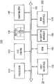
도 1을 참조하면, 전자 장치(10)는 호스트(20) 및 스토리지 장치(또는 메모리 시스템, 30)을 포함할 수 있다. 스토리지 장치(30)는 메모리 컨트롤러(또는 컨트롤러, 100) 및 적어도 하나의 비휘발성 메모리 장치(200)를 포함할 수 있다. 호스트(20)는 스토리지 장치(30)의 동작을 전반적으로 제어한다.Referring to FIG. 1, the
비휘발성 메모리 장치(200)는 낸드 플래시 메모리로 구현될 수 있다. 하지만 다른 실시예에 있어서, 비휘발성 메모리 장치(200)은 PRAM(Phase Change Random Access Memory), RRAM(Resistive Random Access Memory), 등의 비휘발성 메모리 장치로 구현될 수 있다.The
메모리 컨트롤러(100)는 호스트(20)와 커맨드, 어드레스, 데이터와 같은 신호를 교환할 수 있다. 메모리 컨트롤러(100)는 호스트(20)의 커맨드에 따라 비휘발성 메모리 장치(200)에 데이터를 기입하거나 비휘발성 메모리 장치(200)로부터 데이터를 독출할 수 있다.The
도 2는 본 발명의 실시예들에 따른 도 1의 전자 장치에서 스토리지 장치의 구성을 나타낸다.2 illustrates a configuration of a storage device in the electronic device of FIG. 1 according to embodiments of the present invention.
도 2를 참조하면, 스토리지 장치(30)는 메모리 컨트롤러(100) 및 적어도 하나의 비휘발성 메모리 장치(200)를 포함할 수 있다.Referring to FIG. 2, the
실시예에 있어서, 메모리 컨트롤러(100) 및 비휘발성 메모리 장치(200) 각각은 하나의 칩, 하나의 패키지, 하나의 모듈 등으로 제공될 수 있다. 또는 메모리 컨트롤러(100) 및 비휘발성 메모리 장치(200)는 PoP(Package on Package), Ball grid arrays(BGAs), Chip scale packages(CSPs), Plastic Leaded Chip Carrier(PLCC), Plastic Dual In-Line Package(PDIP), Die in Waffle Pack, Die in Wafer Form, Chip On Board(COB), Ceramic Dual In-Line Package(CERDIP), Plastic Metric Quad Flat Pack(MQFP), Thin Quad Flatpack(TQFP), Small Outline(SOIC), Shrink Small Outline Package(SSOP), Thin Small Outline(TSOP), Thin Quad Flatpack(TQFP), System In Package(SIP), Multi Chip Package(MCP), Wafer-level Fabricated Package(WFP), Wafer-Level Processed Stack Package(WSP) 등과 같은 패키지들을 기반으로 실장되어 메모리 카드와 같은 스토리지 장치로 제공될 수 있다.In an embodiment, each of the
비휘발성 메모리 장치(200)는 메모리 컨트롤러(100)의 제어에 따라 소거, 기입 또는 독출 동작 등을 수행할 수 있다. 이를 위하여, 비휘발성 메모리 장치(200)는 입출력 라인을 통해 커맨드(CMD), 어드레스(ADDR), 그리고 데이터(DATA)를 입력받는다. 또한, 비휘발성 메모리 장치(200)는 제어 라인을 통하여 제어 신호(CTRL)를 제공받을 수 있다. 또한 비휘발성 메모리 장치(200)는 메모리 컨트롤러(100)로부터 파워(PWR)를 제공받을 수 있다.The
비휘발성 메모리 장치(200)에 포함된 메모리 셀들은 프로그램 경과 시간, 온도, 프로그램 교란, 독출 교란 등과 같은 요인들로 인하여 문턱 전압 산포가 변화하는 물리적 특성을 갖는다. 즉, 상술된 요인들로 인하여 비휘발성 메모리 장치(200)에 저장된 데이터에 오류가 발생할 수 있다. 메모리 컨트롤러(100)는 이러한 오류들을 정정하기 위하여 다양한 에러 정정 기법을 사용할 수 있다. 예를 들어, 메모리 컨트롤러(100)는 에러 정정 코드(ECC; Error Correction Code) 엔진(120) 및 독출 관리 모듈(131)을 포함할 수 있다. 또한 메모리 컨트롤러(100)는 다양한 프로그램 동작을 관리하는 프로그램 관리 모듈(133)을 포함할 수 있다.Memory cells included in the
비휘발성 메모리 장치(200)에 대한 독출 동작시, 메모리 컨트롤러(100)는 기본 독출 전압 세트(default read voltage set)를 기반으로 비휘발성 메모리 장치(200)의 제1 페이지에 저장된 데이터를 읽을 수 있다. 예시적으로, 기본 독출 전압 세트는 미리 정해진 독출 전압들을 가리킨다. ECC 엔진(120)은 비휘발성 메모리 장치(200)로부터 독출한 데이터에 포함된 오류를 검출 및 정정할 수 있다. 예시적으로, ECC 엔진(120)은 하드웨어 형태로 제공될 수 있다.During a read operation on the
예를 들어, 상술된 요인들 또는 다른 외부 요인들로 인하여 ECC 엔진(120)의 오류 정정 능력을 초과하는 에러 비트가 데이터에 포함될 수 있다. 이 경우, ECC 엔진(120)은 데이터에 포함된 오류를 정정하지 못할 것이다. 이러한 에러는 'UECC(Uncorrectable Error Correction Code) 에러'라 불린다.For example, the data may include error bits that exceed the error correction capability of the
예를 들어, 기본 독출 전압 세트를 기반으로 독출된 데이터에 UECC 에러가 포함된 경우, 독출 관리 모듈(131)은 비휘발성 메모리 장치(200)의 독출 전압 세트를 조절할 수 있다. 메모리 컨트롤러(100)는 조절된 독출 전압 세트를 기반으로 비휘발성 메모리 장치(200)가 독출 동작을 수행하도록 어드레스(ADDR), 커맨드(CMD), 및 제어 신호(CTRL)를 전송할 수 있다.For example, when the UECC error is included in the read data based on the basic read voltage set, the
예를 들어, 조절된 독출 전압 세트에 대한 정보는 제어 신호(CTRL) 또는 커맨드(CMD)에 포함될 수 있다. ECC 엔진(120)은 조절된 독출 전압 세트에 의해 독출된 데이터의 오류를 검출 및 정정할 수 있다.For example, information about the adjusted read voltage set may be included in the control signal CTRL or command CMD. The
예를 들어, 독출 관리 모듈(131)은 미리 정해진 횟수만큼 독출 전압 세트를 조절하고, ECC 엔진(120)은 조절된 독출 전압 세트를 기반으로 독출된 데이터의 오류를 검출 및 정정할 수 있다. 즉, 메모리 컨트롤러(100)는 독출 전압 세트 조절, 조절된 독출 전압 세트를 기반으로 데이터 독출 동작 및 독출된 데이터의 오류 정정 동작을 미리 정해진 횟수만큼 반복적으로 수행할 수 있다.For example, the
예를 들어, 상술된 반복 동작 중 독출된 데이터의 오류가 정정된 경우, 메모리 컨트롤러(100)는 정정된 데이터를 호스트(20)로 출력할 수 있다. 예를 들어, 독출 관리 모듈(131)에 의해 독출 동작이 반복 수행되는 동안, 독출 데이터 또는 독출 데이터의 특정 페이지 데이터는 도 3의 버퍼(130)에 저장될 수 있다. 상기 버퍼(130)는 SRAM일 수 있다.For example, when an error of the read data is corrected during the above-described repetitive operation, the
상술된 바와 같은 반복 동작 이후에도 독출된 데이터의 오류가 정정되지 않는 경우(즉, UECC 에러가 포함된 경우), 메모리 컨트롤러(100)는 버퍼(130)에 저장된 데이터를 기반으로 밸리 서치 동작을 수행하기 위한 시작 전압 세트(start voltage set)를 결정할 수 있다.If the error of the read data is not corrected even after the repetitive operation as described above (that is, when the UECC error is included), the
실시예에 따라, 상기 독출 전압 세트를 조절하여 독출 동작을 반복적으로 수행하는 것은 생략될 수 있다.Depending on the embodiment, it may be omitted to repeatedly perform the read operation by adjusting the read voltage set.
기본 독출 전압 세트를 기반으로 독출된 데이터 또는 반복적인 독출 동작 이후에도 독출 데이터의 에러가 정정되지 않는 경우, 메모리 컨트롤러(100)는 버퍼(130)에 저장된 데이터를 기반으로 에러 비트가 가장 많이 포함된 프로그램 상태를 선택하고, 선택된 프로그램 상태와 대응되는 독출 전압을 시작 전압으로 결정할 수 있다. 독출 관리 모듈(131)은 결정된 시작 전압을 기초로 밸리 서치(valley search)를 수행하여 최적(optimal) 독출 레벨 전압을 결정하고, 상기 최적 독출 레벨 전압을 기초로 상기 독출 데이터에 대하여 리커버리 독출 동작을 수행할 수 있다.If the error of the read data or the read data is not corrected after the repetitive read operation based on the basic read voltage set, the
실시예에 따라서 상기 최적 독출 레벨 전압을 결정하기 위하여, 독출 관리 모듈(131)은 시작 독출 전압과 종료 읽기 전압에 의해 정의되는 검색 영역을 설정하고, 상기 검색 영역에 기준 영역에 속하는지를 판단하고, 상기 판단 결과, 상기 검색 영역이 상기 기준 영역에 속하지 않으면, 상기 검색 영역을 변경하고, 상기 판단 결과 상기 검색 영역이 상기 기준 영역에 속하면, 상기 검색 영역에 기초하여 새로운 독출 전압을 찾아서 상기 최적 독출 레벨 전압을 결정할 수 있다.In order to determine the optimal read level voltage according to an embodiment, the
프로그램 관리 모듈(133)은 비휘발성 메모리 장치(200)에 포함되는 멀티 레벨 셀들에 대한 프로그램 동작을 관리할 수 있다. 프로그램 관리 모듈(133)은 프리-프로그램 블록의 멀티 레벨 셀들에 멀티 비트 데이터를 프리-프로그램하는 프리-프로그램 동작과 멀티 레벨 셀들의 상태를 나타내는 상태 코드들에 기초하여 생성된 다이제스트 데이터를 다이제스트 블록에 프로그램하는 다이제스트 프로그램을 수행하도록 비휘발성 메모리 장치(200)를 제어할 수 있다. 또한 프로그램 관리 모듈(133)은 다이제스트 데이터와 프리-프로그램된 데이터에 기초하여 타겟 데이터를 복구하고, 타겟 데이터를 프리-프로그램 블록의 멀티 레벨 셀들에 리-프로그램하도록 비휘발성 메모리 장치(200)를 제어할 수 있다.The
프로그램 관리 모듈(133)은 또한 비휘발성 메모리 장치(200)의 성능, 저장 공간의 효율 및 신뢰성 중 적어도 하나에 기초하여 싱글 레벨 셀 버퍼링, 다이제스트 프로그램 및 리-프로그램의 프로그램 기법들을 선택적으로 비휘발성 메모리 장치(200)에 적용시킬 수 있다.The
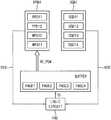
도 3은 본 발명의 실시예들에 따른 도 2의 스토리지 장치에서 메모리 컨트롤러의 구성을 나타내는 블록도이다.3 is a block diagram illustrating a configuration of a memory controller in the storage device of FIG. 2 according to embodiments of the present invention.
도 2 및 도 3을 참조하면, 메모리 컨트롤러(100)는 버스(105)를 통하여 서로 연결되는 프로세서(110) ECC 엔진(120), 버퍼(130), 독출 관리 모듈(131), 프로그램 관리 모듈(133), 랜더마이저(140), 호스트 인터페이스(150), 롬(160), 마이그레이션 관리자(180) 및 비휘발성 메모리 인터페이스(170)를 포함할 수 있다.2 and 3, the
ECC 엔진(120), 버퍼(130), 독출 관리 모듈(131) 및 프로그램 관리 모듈(133)은 도 2를 참조하여 설명되었으므로, 이에 대한 상세한 설명은 생략된다.Since the
프로세서(110)는 메모리 컨트롤러(100)의 제반 동작을 제어한다. 예를 들어, 독출 관리 모듈(131) 및 프로그램 관리 모듈(133)은 소프트웨어 형태로 제공되며, 버퍼(130)에 저장될 수 있다. 버퍼(130)에 저장된 독출 관리 모듈(131) 및 프로그램 관리 모듈(133)은 프로세서(110)에 의해 구동될 수 있다. ROM(160)은 메모리 컨트롤러(100)가 동작하는데 요구되는 다양한 정보를 펌웨어 형태로 저장할 수 있다.The
랜더마이저(140)는 비휘발성 메모리 장치(200)에 저장될 데이터를 랜더마이징(randomizing)할 수 있다. 예를 들어, 랜더마이저(140)는 비휘발성 메모리 장치(200)에 저장될 데이터를 워드 라인 단위로 랜더마이징할 수 있다.The
예를 들어, 데이터 랜더마이징은 하나의 워드라인에 연결된 메모리 셀들이 동일한 비율의 프로그램 상태를 갖도록 데이터를 처리하는 것을 가리킨다. 예를 들어, 하나의 워드라인에 연결된 메모리 셀들이 각각 4-비트의 데이터를 저장하는 쿼드 레벨 셀(QLC; Quad Level Cell)인 경우, 메모리 셀들 각각은 소거 상태 및 제 1 내지 제15 프로그램 상태들 중 어느 하나의 상태(또는 상태 코드)를 가질 것이다. 이 때, 랜더마이저(140)는 하나의 워드라인에 연결된 메모리 셀들 중 소거 상태 및 제 1 내지 제15 프로그램 상태들을 갖는 메모리 셀들의 개수가 서로 동일하도록 데이터를 랜더마이징할 수 있다. 즉, 랜더마이징된 데이터(randomized data)가 저장된 메모리 셀들은 실질적으로 서로 동일한 개수의 프로그램 상태들을 가질 것이다. 예시적으로, 랜더마이저(140)는 비휘발성 메모리 장치(200)로부터 읽은 데이터를 디랜더마이저할 수 있다.For example, data rendering refers to processing data such that memory cells connected to one word line have the same proportion of program states. For example, when the memory cells connected to one word line are quad-level cells (QLC) storing 4-bit data, each of the memory cells is erased and the first to fifteenth program states It will have either status (or status code). At this time, the
예를 들어, 랜더마이저(140)는 페이지 데이터를 랜더마이징할 수 있다. 예시적으로, 간결한 설명을 위하여 이상적인(ideal) 랜더마이저(140)의 구성이 설명되었다. 그러나, 본 발명의 기술적 사상이 이에 한정되는 것은 아니며, 실제 랜더마이저(140)는 하나의 워드라인에 연결된 메모리 셀들 중 소거 상태 및 제 1 내지 제15 프로그램 상태들 각각을 갖는 메모리 셀들의 개수가 실질적으로 서로 동일한 값에 가깝도록 데이터를 랜더마이징할수 있다. 즉, 실제 랜더마이징된 데이터(randomized data)가 저장된 메모리 셀들은 실질적으로 서로 비슷한 개수의 프로그램 상태들을 가질 수 있다.For example, the
마이그레이션 관리자(180)는 프리-프로그램된 데이터 및 다이제스트 데이터의 마이그레이션을 관리할 수 있다. 즉, 마이그레이션 관리자(180)는 프리-프로그램된 데이터와 프리-프로그램된 데이터에 상응하는 다이제스트 데이터를 로직 회로(도 21b의 190)로 마이그레이션 할 수 있다. 마이그레이션 관리자(180)는 다이제스트 데이터의 마이그레인션이 완료되는 경우, 이를 프로세서(110)에 통지할 수 있고, 프로세서(110)는 제어 회로(500)를 제어하여 다이제스트 블록에 대한 소거 동작이 수행되도록 할 수 있다.The
메모리 컨트롤러(100)는 호스트 인터페이스(150)를 통해 호스트(20)와 통신할 수 있다. 예를 들어, 호스트 인터페이스(150)는 USB (Universal Serial Bus), MMC (multimedia card), PCI (peripheral component interconnection), PCI-E (PCI-express), ATA (Advanced Technology Attachment), Serial-ATA, Parallel-ATA, SCSI (small computer small interface), ESDI (enhanced small disk interface), IDE (Integrated Drive Electronics), MIPI(Mobile Industry Processor Interface), NVMe(Nonvolatile Memory-express), UFS(Universal Flash Storage Interface) 등과 같은 다양한 인터페이스들 중 적어도 하나로 제공될 수 있다. 메모리 컨트롤러(100)는 비휘발성 메모리 인터페이스(170)를 통해 비휘발성 메모리 장치(200)와 통신할 수 있다.The
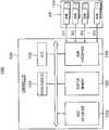
도 4는 본 발명의 실시예들에 따른 도 2의 스토리지 장치에서 비휘발성 메모리 장치를 나타내는 블록도이다.4 is a block diagram illustrating a nonvolatile memory device in the storage device of FIG. 2 according to embodiments of the present invention.
도 4를 참조하면, 비휘발성 메모리 장치(200)는 메모리 셀 어레이(300), 어드레스 디코더(430), 페이지 버퍼 회로(410), 데이터 입출력 회로(420), 제어 회로(500) 및 전압 생성기(700)를 포함할 수 있다.4, the
메모리 셀 어레이(300)는 스트링 선택 라인(SSL), 복수의 워드 라인들(WLs) 및 접지 선택 라인(GSL)을 통해 어드레스 디코더(430)와 연결될 수 있다. 또한, 메모리 셀 어레이(300)는 복수의 비트 라인들(BLs)을 통해 페이지 버퍼 회로(410)와 연결될 수 있다.The
메모리 셀 어레이(300)는 복수의 워드 라인들(WLs) 및 복수의 비트 라인들(BLs)에 연결되는 복수의 메모리 셀들을 포함할 수 있다.The
실시예에 있어서, 메모리 셀 어레이(300)는 기판 상에 삼차원 구조(또는 수직 구조)로 형성되는 삼차원(three dimensional) 메모리 셀 어레이일 수 있다. 이 경우, 메모리 셀 어레이(300)는 서로 적층되어 형성되는 복수의 메모리 셀들을 포함하는 수직 메모리 셀 스트링들을 포함할 수 있다.In an embodiment, the
다른 실시예에 있어서, 메모리 셀 어레이(300)는 기판 상에 이차원 구조(또는 수평 구조)로 형성되는 이차원(two dimensional) 메모리 셀 어레이일 수 있다.In another embodiment, the
도 5는 도 4의 메모리 셀 어레이를 나타내는 블록도이다.5 is a block diagram illustrating the memory cell array of FIG. 4.
도 5를 참조하면, 메모리 셀 어레이(300)는 복수의 메모리 블록들(BLK1~BLKz)을 포함한다. 실시예에 있어서, 메모리 블록들(BLK1~BLKz, z는 3이상의 자연수)은 도 4에 도시된 어드레스 디코더(430)에 의해 선택된다. 예를 들면, 어드레스 디코더(430)는 메모리 블록들(BLK1~BLKz) 중 블록 어드레스에 대응하는 메모리 블록(BLK)을 선택할 수 있다.Referring to FIG. 5, the
도 6은 도 5의 메모리 블록들(BLK1~BLKz) 중 하나(BLKi)를 나타내는 회로도이다.FIG. 6 is a circuit diagram illustrating one of the memory blocks BLK1 to BLKz of FIG. 5 BLKi.
도 6에 도시된 메모리 블록(BLKi)은 기판(SUB) 상에 삼차원 구조로 형성되는 삼차원 메모리 블록을 나타낸다. 예를 들어, 메모리 블록(BLKi)에 포함되는 복수의 메모리 셀 스트링들은 상기 기판(SUB)과 수직한 방향(PD)으로 적층될 수 있다.The memory block BLKi illustrated in FIG. 6 represents a three-dimensional memory block formed in a three-dimensional structure on the substrate SUB. For example, a plurality of memory cell strings included in the memory block BLKi may be stacked in a direction PD perpendicular to the substrate SUB.
도 6을 참조하면, 메모리 블록(BLKi)은 비트 라인들(BL1, BL2, BL3)과 공통 소스 라인(CSL) 사이에 연결되는 복수의 메모리 셀 스트링들(NS11~NS33)을 포함할 수 있다. 복수의 메모리 셀 스트링들(NS11~NS33) 각각은 스트링 선택 트랜지스터(SST), 복수의 메모리 셀들(MC1, MC2, ..., MC8) 및 접지 선택 트랜지스터(GST)를 포함할 수 있다. 도 6에는 복수의 메모리 셀 스트링들(NS11~NS33) 각각이 8개의 메모리 셀들(MC1, MC2, ..., MC8)을 포함하는 것으로 도시되어 있으나, 본 발명은 이에 한정되지 않는다.Referring to FIG. 6, the memory block BLKi may include a plurality of memory cell strings NS11 to NS33 connected between bit lines BL1, BL2, and BL3 and a common source line CSL. Each of the plurality of memory cell strings NS11 to NS33 may include a string select transistor SST, a plurality of memory cells MC1, MC2, ..., MC8, and a ground select transistor GST. 6, each of the plurality of memory cell strings NS11 to NS33 includes eight memory cells MC1, MC2, ..., MC8, but the present invention is not limited thereto.
스트링 선택 트랜지스터(SST)는 상응하는 스트링 선택 라인(SSL1, SSL2, SSL3)에 연결될 수 있다. 복수의 메모리 셀들(MC1, MC2, ..., MC8)은 각각 상응하는 워드 라인(WL1, WL2, ..., WL8)에 연결될 수 있다. 접지 선택 트랜지스터(GST)는 상응하는 접지 선택 라인(GSL1, GSL2, GSL3)에 연결될 수 있다. 스트링 선택 트랜지스터(SST)는 상응하는 비트 라인(BL1, BL2, BL3)에 연결되고, 접지 선택 트랜지스터(GST)는 공통 소스 라인(CSL)에 연결될 수 있다.The string select transistor SST may be connected to corresponding string select lines SSL1, SSL2, and SSL3. The plurality of memory cells MC1, MC2, ..., MC8 may be connected to corresponding word lines WL1, WL2, ..., WL8, respectively. The ground selection transistor GST may be connected to corresponding ground selection lines GSL1, GSL2, and GSL3. The string select transistor SST may be connected to corresponding bit lines BL1, BL2, and BL3, and the ground select transistor GST may be connected to a common source line CSL.
동일 높이의 워드 라인(예를 들면, WL1)은 공통으로 연결되고, 접지 선택 라인(GSL1, GSL2, GSL3) 및 스트링 선택 라인(SSL1, SSL2, SSL3)은 각각 분리될 수 있다. 도 6에는 메모리 블록(BLKi)이 여덟 개의 워드 라인들(WL1, WL2, ..., WL8) 및 세 개의 비트 라인들(BL1, BL2, BL3)에 연결되는 것으로 도시되어 있으나, 본 발명은 이에 한정되지 않는다.Word lines of the same height (for example, WL1) are commonly connected, and the ground selection lines GSL1, GSL2, and GSL3 and the string selection lines SSL1, SSL2, and SSL3 may be separated, respectively. 6, the memory block BLKi is illustrated as being connected to eight word lines WL1, WL2, ..., WL8 and three bit lines BL1, BL2, BL3, but the present invention It is not limited.
도 7은 도 6의 메모리 블록의 하나의 셀 스트링의 구조의 예를 보여준다.FIG. 7 shows an example of the structure of one cell string of the memory block of FIG. 6.
도 6 및 도 7를 참조하면, 셀 스트링(NS11)에는 기판(SUB) 위에 기판과 수직인 방향으로 신장되어 기판(SUB)과 접촉하는 필라(PL)가 제공될 수 있다. 도 9에 도시된 접지 선택 라인(GSL1), 워드 라인들(WL1~WL8), 그리고 스트링 선택 라인(SSL1)은 각각 기판(SUB)과 평행한 도전 물질들, 예를 들어 금속 물질들로 형성될 수 있다. 필라(PL)는 접지 선택 라인(GSL1), 워드 라인들(WL1~WL8), 그리고 스트링 선택 라인(SSL1)을 형성하는 도전 물질들을 관통하여 기판(SUB)과 접촉할 수 있다.Referring to FIGS. 6 and 7, the cell string NS11 may be provided with a pillar PL extending on a substrate SUB in a direction perpendicular to the substrate to contact the substrate SUB. The ground selection line GSL1, the word lines WL1 to WL8, and the string selection line SSL1 shown in FIG. 9 are each formed of conductive materials parallel to the substrate SUB, for example, metal materials. Can be. The pillar PL may penetrate the conductive materials forming the ground selection line GSL1, the word lines WL1 to WL8, and the string selection line SSL1 to contact the substrate SUB.
도 7에서, 절단 선(A-A')에 따른 단면도가 함께 도시되어 있다. 예시적으로, 제1 워드 라인(WL1)에 대응하는 제1 메모리 셀(MC1)의 단면도가 도시된다. 필라(PL)는 원통형의 바디(BD)를 포함할 수 있다. 바디(BD)의 내부에 에어갭(AG)이 제공될 수 있다.In Fig. 7, a cross-sectional view along the cutting line A-A' is shown together. For example, a cross-sectional view of the first memory cell MC1 corresponding to the first word line WL1 is shown. The pillar PL may include a cylindrical body BD. An air gap AG may be provided inside the body BD.
바디(BD)는 P-타입 실리콘을 포함하며, 채널이 형성되는 영역일 수 있다. 필라(PL)는 바디(BD)를 둘러싸는 원통형의 터널 절연막(TI) 및 터널 절연막(TI)을 둘러싸는 원통형의 전하 포획 막(CT)을 더 포함할 수 있다. 제1 워드 라인(WL1) 및 필라(PL)의 사이에 블로킹 절연막(BI)이 제공될 수 있다. 바디(BD), 터널 절연막(TI), 전하 포획 막(CT), 블로킹 절연막(BI), 그리고 제1 워드 라인(WL1)은 기판(SUB) 또는 기판(SUB)의 상부 면과 수직인 방향으로 형성된 전하 포획형 트랜지스터일 수 있다. 스트링 선택 트랜지스터(SST), 접지 선택 트랜지스터(GST) 및 다른 메모리 셀들은 제1 메모리 셀(MC1)과 동일한 구조를 가질 수 있다.The body BD includes P-type silicon and may be a region in which a channel is formed. The pillar PL may further include a cylindrical tunnel insulating layer TI surrounding the body BD and a cylindrical charge trapping film CT surrounding the tunnel insulating layer TI. A blocking insulating layer BI may be provided between the first word line WL1 and the pillar PL. The body BD, the tunnel insulating film TI, the charge trap film CT, the blocking insulating film BI, and the first word line WL1 are in a direction perpendicular to the upper surface of the substrate SUB or the substrate SUB. It may be a formed charge trapping transistor. The string select transistor SST, the ground select transistor GST, and other memory cells may have the same structure as the first memory cell MC1.
다시 도 4를 참조하면, 제어 회로(500)는 메모리 컨트롤러(100)로부터 커맨드 신호(CMD) 및 어드레스 신호(ADDR)를 수신하고, 커맨드 신호(CMD) 및 어드레스 신호(ADDR)에 기초하여 비휘발성 메모리 장치(200)의 소거 루프, 프로그램 루프 및 독출 동작을 제어할 수 있다. 여기서 프로그램 루프는 프로그램 동작과 프로그램 검증 동작을 포함할 수 있고, 소거 루프는 소거 동작과 소거 검증 동작을 포함할 수 있다.Referring to FIG. 4 again, the
예를 들어, 제어 회로(500)는 커맨드 신호(CMD)에 기초하여 전압 생성기(700)를 제어하기 위한 제어 신호들(CTLs)과 페이지 버퍼 회로(410)를 제어하기 위한 제어 신호(PCTL)를 생성하고, 어드레스 신호(ADDR)에 기초하여 로우 어드레스(R_ADDR) 및 컬럼 어드레스(C_ADDR)를 생성할 수 있다. 제어 회로(450)는 로우 어드레스(R_ADDR)를 어드레스 디코더(430)에 제공하고, 컬럼 어드레스(C_ADDR)를 데이터 입출력 회로(420)에 제공할 수 있다.For example, the
어드레스 디코더(430)는 스트링 선택 라인(SSL), 복수의 워드 라인들(WLs) 및 접지 선택 라인(GSL)을 통해 메모리 셀 어레이(300)와 연결될 수 있다. 프로그램 동작 또는 독출 동작 시, 어드레스 디코더(430)는 제어 회로(500)로부터 제공되는 로우 어드레스(R_ADDR)에 기초하여 복수의 워드 라인들(WLs) 중의 하나를 선택 워드라인으로 결정하고, 복수의 워드 라인들(WLs) 중에서 선택 워드라인을 제외한 나머지 워드 라인들을 비선택 워드라인들로 결정할 수 있다.The
전압 생성기(700)는 제어 회로(500)로부터 제공되는 제어 신호들(CTLs)에 기초하여 비휘발성 메모리 장치(200)의 동작에 필요한 워드 라인 전압들(VWLs)을 생성할 수 있다. 전압 생성기(700)로부터 생성되는 워드 라인 전압들(VWLs)은 어드레스 디코더(430)를 통해 복수의 워드 라인들(WLs)에 인가될 수 있다.The
예를 들어, 소거 동작 시, 전압 생성기(700)는 메모리 블록의 웰에 소거 전압을 인가하고 메모리 블록의 모든 워드라인들에 접지 전압을 인가할 수 있다. 소거 검증 동작 시, 전압 생성기(700)는 하나의 메모리 블록의 모든 워드라인들에 소거 검증 전압을 인가하거나 워드라인 단위로 소거 검증 전압을 인가할 수 있다.For example, during an erase operation, the
예를 들어, 프로그램 동작 시, 전압 생성기(700)는 선택 워드라인에 프로그램 전압을 인가하고, 비선택 워드라인들에는 프로그램 패스 전압을 인가할 수 있다. 또한 프로그램 검증 동작 시, 전압 생성기(700)는 선택 워드라인에 프로그램 검증 전압을 인가하고, 비선택 워드라인들에는 검증 패스 전압을 인가할 수 있다.For example, during a program operation, the
또한, 기본 독출 동작 시, 전압 생성기(700)는 선택 워드라인에 기본 독출 전압을 인가하고, 비선택 워드라인들에는 독출 패스 전압을 인가할 수 있다. 또한 리커버리 독출 동작 시, 전압 생성기(700)는 선택 워드라인에 최적 독출 레벨 전압을 인가할 수 있다.In addition, in the basic read operation, the
페이지 버퍼 회로(410)는 복수의 비트 라인들(BLs)을 통해 메모리 셀 어레이(300)와 연결될 수 있다. 페이지 버퍼 회로(410)는 복수의 페이지 버퍼를 포함할 수 있다. 일 실시예에 있어서, 하나의 페이지 버퍼에 하나의 비트 라인이 연결될 수 있다. 다른 실시예에 있어서, 하나의 페이지 버퍼에 두 개 이상의 비트 라인들이 연결될 수 있다.The
페이지 버퍼 회로(410)는 프로그램 동작 시 선택된 페이지에 프로그램될 데이터를 임시로 저장하고, 독출 동작 시 선택된 페이지로부터 독출된 데이터를 임시로 저장할 수 있다.The
데이터 입출력 회로(420)는 데이터 라인들(DLs)을 통해 페이지 버퍼 회로(410)와 연결될 수 있다. 프로그램 동작 시, 데이터 입출력 회로(420)는 메모리 컨트롤러(100)로부터 프로그램 데이터(DATA)를 수신하고, 제어 회로(450)로부터 제공되는 컬럼 어드레스(C_ADDR)에 기초하여 프로그램 데이터(DATA)를 페이지 버퍼 회로(410)에 제공할 수 있다. 독출 동작 시, 데이터 입출력 회로(420)는 제어 회로(450)로부터 제공되는 컬럼 어드레스(C_ADDR)에 기초하여 페이지 버퍼 회로(410)에 저장된 독출 데이터(DATA)를 상기 메모리 컨트롤러(100)에 제공할 수 있다.The data input/
도 8은 본 발명의 실시예들에 따른 도 4의 비휘발성 메모리 장치에서 제어 회로의 구성을 나타내는 블록도이다.8 is a block diagram illustrating a configuration of a control circuit in the nonvolatile memory device of FIG. 4 according to embodiments of the present invention.
도 8을 참조하면, 제어 회로(500)는 커맨드 디코더(510), 어드레스 버퍼(520) 및 제어 신호 생성기(530)를 포함할 수 있다.Referring to FIG. 8, the
커맨드 디코더(510)는 커맨드 신호(CMD)를 디코딩하여 디코딩된 커맨드(D_CMD)를 제어 신호 생성기(530)에 제공할 수 있다, 어드레스 버퍼(520)는 어드레스 신호(ADDR)를 수신하고, 어드레스 신호(ADDR) 중 로우 어드레스(R_ADDR)는 어드레스 디코더(430)에 제공하고 컬럼 어드레스(C_ADDR)는 데이터 입출력 회로(420)에 제공할 수 있다.The
제어 신호 생성기(530)는 디코딩된 커맨드(D_CMD)를 수신하고, 디코딩된 커맨드(D_CMD)가 지시하는 동작에 기초하여 제어 신호들(CTLs)을 생성하여 전압 생성기(600)에 제공할 수 있다. 또한 제어 신호 생성기(530)는 디코딩된 커맨드(D_CMD)가 지시하는 동작에 기초 제어 신호(PCTL)을 생성하고, 제어 신호(PCTL)을 페이지 버퍼 회로(410)에 제공할 수 있다.The
도 9는 본 발명의 실시예들에 따른 도 4의 비휘발성 메모리 장치에서 전압 생성기의 구성을 나타내는 블록도이다.9 is a block diagram illustrating a configuration of a voltage generator in the nonvolatile memory device of FIG. 4 according to embodiments of the present invention.
도 9를 참조하면, 전압 생성기(700)는 고전압 생성기(710) 및 저전압 생성기(730)를 포함할 수 있다. 실시예에 있어서, 전압 생성기(700)는 음전압(negative voltage) 생성기(750)를 더 포함할 수 있다.Referring to FIG. 9, the
고전압 생성기(710)는 제1 제어 신호(CTL1)에 응답하여 커맨드(CMD)가 지시하는 동작에 따라 프로그램 전압(VPGM), 프로그램 패스 전압(VPPASS), 검증 패스 전압(VVPASS), 독출 패스 전압(VRPASS) 및 소거 전압(VRES)을 생성할 수 있다. 프로그램 전압(VPGM)은 선택 워드라인에 인가되고, 프로그램 패스 전압(VPPASS), 프로그램 검증 패스 전압(VVPASS), 독출 패스 전압(VRPASS)은 비선택 워드라인들에 인가되고, 소거 전압(VRES)은 메모리 블록의 웰에 인가될 수 있다. 제1 제어 신호(CTL1)는 복수의 비트들을 포함하여 커맨드(CMD)가 지시하는 동작을 나타낼 수 있다.The
저전압 생성기(730)는 제2 제어 신호(CTL2)에 응답하여 커맨드(CMD)가 지시하는 동작에 따라 프로그램 검증 전압(VPV), 독출 전압(VRD), 최적 레벨 독출 전압(VORD) 및 소거 검증 전압(VEV)을 생성할 수 있다. 프로그램 검증 전압(VPV), 독출 전압(VRD,) 최적 레벨 독출 전압(VORD) 및 소거 검증 전압(VEV)은 동작에 따라 선택 워드라인에 인가될 수 있다. 제2 제어 신호(CTL2)는 복수의 비트들을 포함하여 커맨드(CMD)가 지시하는 동작을 나타낼 수 있다.The
음전압 생성기(750)는 제3 제어 신호(CTL3)에 응답하여 커맨드(CMD)가 지시하는 동작에 따라 음의 레벨을 가지는 프로그램 검증 전압(VPV'), 독출 전압(VRD'), 및 소거 검증 전압(VEV')을 생성할 수 있다. 제3 제어 신호(CTL3)는 복수의 비트들을 포함하여 커맨드(CMD)가 지시하는 동작을 나타낼 수 있다.The
도 10은 본 발명의 실시예들에 따른 비휘발성 메모리 장치의 동작 방법을 나타내는 흐름도이다.10 is a flowchart illustrating a method of operating a nonvolatile memory device according to embodiments of the present invention.
도 11은 도 10의 동작 방법을 설명하기 위한 것으로, 도 4의 비휘발성 메모리 장치에서 메모리 셀 어레이에 포함되는 프리-프로그램 블록과 다이제스트 블록을 나타낸다.FIG. 11 is a view illustrating an operation method of FIG. 10, and shows pre-program blocks and digest blocks included in a memory cell array in the nonvolatile memory device of FIG. 4.
도 3 내지 도 11을 참조하면, 복수의 메모리 블록들을 포함하고, 상기 메모리 블록들 각각은 복수의 페이지들을 구비하는 메모리 셀 어레이(300)를 포함하는 비휘발성 메모리 장치(200)의 동작 방법에서는 제어 회로(500)는 전압 생성기(700), 어드레스 디코더(430) 및 페이지 버퍼 회로(410)를 제어하여 메모리 블록들 중 프리-프로그램 블록(PPB)의 멀티 레벨 셀들에 멀티 비트 데이터들을 프리-프로그램하는 프리-프로그램(PRE_PGM)을 수행한다(S110).3 to 11, in a method of operating a
제어 회로(500)는 멀티 레벨 셀들 각각의 상태를 나타내는 상태 코드들에 기초하여 상기 프리-프로그램된 멀티 레벨 셀들을 상태 그룹들(GR1, GR2)로 분할하여 상태 그룹들(GR1, GR2)에 상응하는 상태 그룹 코드들을 나타내는 다이제스트 데이터(DGD)를 생성한다(S130). 제1 상태 그룹(GR1)은 상태 그룹 코드 '0'을 가질 수 있고, 제2 상태 그룹(GR2)는 상태 그룹 코드 '1'을 가질 수 있다.The
제어 회로(500)는 전압 생성기(700), 어드레스 디코더(430) 및 페이지 버퍼 회로(410)를 제어하여 메모리 블록들 중 다이제스트 블록에 다이제스트 데이터(DGD)를 프로그램하는 다이제스트 프로그램(DG_PRG)을 수행한다(S150).The
도 10에서는 멀티-레벨 셀들이 N(N은 3이상의 자연수)-비트 데이터를 저장할 수 있고, N은 4인 경우를 가정한다. 따라서 멀티 레벨 셀들 각각은 소거 상태(E0) 및 제1 프로그램 상태(P1) 내지 제15 프로그램 상태(P15) 중 하나에 상응하는 상태 코드를 가질 수 있다. 즉, 멀티 레벨 셀들 각각은 2N 개의 상태 코드들 중 하나의 상태 코드를 가질 수 있다. 제어 회로(500)는 프리-프로그램된 멀티 레벨 셀들을 상태 코드들에 기초하여 M(M은 N 보다 작거나 같은 자연수) 개의 상태 그룹들로 분할(또는 그루핑)할 수 있다. 도 10의 실시예에서는 M은 2인 경우를 가정한다.In FIG. 10, it is assumed that multi-level cells can store N (N is a natural number of 3 or more)-bit data, and N is 4. Therefore, each of the multi-level cells may have a status code corresponding to one of the erase state E0 and the first program state P1 to the fifteenth program state P15. That is, each of the multi-level cells may have one of 2N status codes. The
도 10에서 멀티 레벨 셀들에는 각각 제1 페이지 데이터(PAGE1) 내지 제4 페이지 데이터(PAGE4)가 순차적 또는 동시에 프리-프로그램될 수 있다. 제어 회로(500)는 프리-프로그램된 멀티 레벨 셀들을 서로 중첩하지 않는 문턱 전압 분포들을 가지는 상태 그룹들(GR1, GR2)로 분할할 수 있다.In FIG. 10, the first page data PAGE1 to the fourth page data PAGE4 may be pre-programmed in the multi-level cells, respectively, sequentially or simultaneously. The
실시예에 따라 제어 회로(500)는 프리-프로그램된 멀티 레벨 셀들을 각각이 포함하는 제1 로직 레벨을 가지는 데이터 비트들의 수에 따라 상태 그룹들(GR1, GR2)로 분할할 수 있다.According to an embodiment, the
따라서 제1 상태 그룹(GR1)은 서로 중첩하지 않거나 짝수개의 제1 로직 레벨의 데이터 비트들을 가지는 상태 코드들(E0, P2, P4, P6, P8, P10, P12, P14)을 포함할 수 있다. 제2 상태 그룹(GR2)은 서로 중첩하지 않거나 홀수개의 제1 로직 레벨의 데이터 비트들을 가지는 상태 코드들(P1, P3, P5, P7, P9, P11, P13, P15)을 포함할 수 있다.Accordingly, the first status group GR1 may include status codes E0, P2, P4, P6, P8, P10, P12, and P14 that do not overlap with each other or have an even number of data bits of the first logic level. The second status group GR2 may include status codes P1, P3, P5, P7, P9, P11, P13, and P15 that do not overlap with each other or have odd number of data bits of the first logic level.
16개의 프로그램 상태들(E0~P15)이 제1 및 제2 상태 그룹들(GR1, GR2)로 분할되었으므로, 다이제스트 데이터(DGD)는 E0와 DP1의 두 개의 상태들을 가지므로, 제어 회로(500)는 다이제스트 데이터(DGD)를 싱글 레벨 셀들을 포함하는 다이제스트 블록(DB)에 프로그램할 수 있다.Since the 16 program states E0 to P15 are divided into first and second state groups GR1 and GR2, the digest data DGD has two states E0 and DP1, so the
따라서, 재프로그램을 완료하지 않아도 데이터를 유지할 수 있고, 싱글 레벨 셀들에 다이제스트 데이터(DGD)를 프로그램하므로 페이지 데이터들을 각각의 싱글 레벨 셀들에 저장하는 경우보다 더 적은 저장 공간을 사용한다. 또한 메모리 컨트롤러(100)는 1회의 프리-프로그램 후 데이터 로딩을 위해 사용한 버퍼(130)를 릴리스할 수 있다.Therefore, data can be maintained without completing the reprogramming, and since digest data (DGD) is programmed in single-level cells, less storage space is used than when storing page data in respective single-level cells. Also, the
멀티 비트 데이터를 프리-프로그램하기 위하여, 제어 회로(500)는 멀티 비트 데이터를 멀티 레벨 셀들에 연결된 페이지 버퍼 회로(410)에 로딩할 수 있다. 제어 회로(500)는 페이지 버퍼 회로(410)에 로딩된 멀티-비트 데이터를 상기 멀티 레벨 셀들에 프리-프로그램할 수 있다.To pre-program the multi-bit data, the
제어 회로(500)는 페이지 버퍼 회로(410)에 로딩된 멀티-비트 데이터의 상태 코드들에 기초하여 상기 다이제스트 데이터(DGD)를 생성하고, 생성된 다이제스트 데이터(DGD)를 페이지 버퍼 회로(410)의 페이지 버퍼들에 임시로 저장할 수 있다. 제어 회로(500)는 페이지 버퍼 회로(410)에 로딩된 멀티-비트 데이터 각각의 비트들에 로직 연산을 수행하여 다이제스트 데이터(DGD)를 생성할 수 있다.The
제어 회로(500) 또는 컨트롤러(100)는 프리-프로그램 블록(PPB)과 다이제스트 블록(DGB)를 하나의 쌍으로 관리할 수 있다.The
실시예에 있어서, 상태 코드 그룹들이 4 개의 상태 그룹들로 분할되는 경우, 다이제스트 블록(DGB)는 멀티-레벨 셀들을 포함할 수 있다.In an embodiment, when the status code groups are divided into four status groups, the digest block (DGB) may include multi-level cells.
도 12는 프리-프로그램 동작 후 멀티 레벨 셀들의 문턱 전압 분포들을 예를 나타낸다.12 shows examples of threshold voltage distributions of multi-level cells after a pre-program operation.
도 12에는 상기 멀티 레벨 셀들에 4비트의 데이터들이 저장될 때의 상기 문턱 전압 분포들의 예가 도시되어 있다.12 shows an example of the threshold voltage distributions when 4 bits of data are stored in the multi-level cells.
도 12를 참조하면, 상기 멀티 레벨 셀들은 커플링에 의해 프리프로그램 동작 직후보다 넓어진 문턱 전압 분포들(E0, P1, P2, P3, P4, P5, P6, P7, P8, P9, P10, P11, P12, P13, P14, P15)을 가진다. 상기 멀티 레벨 셀들의 문턱 전압 분포들(E0, P1, P2, P3, P4, P5, P6, P7, P8, P9, P10, P11, P12, P13, P14, P15)은 서로 중첩될 수 있다.Referring to FIG. 12, the multi-level cells have threshold voltage distributions E0, P1, P2, P3, P4, P5, P6, P7, P8, P9, P10, and P11 that are wider than immediately after the preprogram operation by coupling. P12, P13, P14, P15). The threshold voltage distributions of the multi-level cells (E0, P1, P2, P3, P4, P5, P6, P7, P8, P9, P10, P11, P12, P13, P14, P15) may overlap each other.
문턱 전압 분포들(E0, P1, P2, P3, P4, P5, P6, P7, P8, P9, P10, P11, P12, P13, P14, P15)은 서로 중첩되지 않은 문턱 전압 분포들을 포함하는 상태 그룹들(GR1, GR2, GR3, GR4)로 분할한다. 예를 들어, 문턱 전압 분포들(E0, P1, P2, P3, P4, P5, P6, P7, P8, P9, P10, P11, P12, P13, P14, P15)을 제1 상태 그룹(GR1), 제2 상태 그룹(GR2), 제3 상태 그룹(GR3) 및 제4 상태 그룹(GR4)으로 분할할 수 있다.The threshold voltage distributions (E0, P1, P2, P3, P4, P5, P6, P7, P8, P9, P10, P11, P12, P13, P14, P15) are a group of states that include non-overlapping threshold voltage distributions. It is divided into fields (GR1, GR2, GR3, GR4). For example, the threshold voltage distributions (E0, P1, P2, P3, P4, P5, P6, P7, P8, P9, P10, P11, P12, P13, P14, P15) of the first state group (GR1), It can be divided into a second state group GR2, a third state group GR3, and a fourth state group GR4.
제1 상태 그룹(GR1)은 서로 중첩되지 않은 제1 문턱 전압 분포(E0), 제5 문턱 전압 분포(P4), 제9 문턱 전압 분포(P8) 및 제13 문턱 전압 분포(P12)를 포함하고, 제2 상태 그룹(GR2)은 서로 중첩되지 않은 제2 문턱 전압 분포(P1), 제6 문턱 전압 분포(P5), 제10 문턱 전압 분포(P9) 및 제14 문턱 전압 분포(P13)를 포함하며, 제3 상태 그룹(GR3)은 서로 중첩되지 않은 제3 문턱 전압 분포(P2), 제7 문턱 전압 분포(P6), 제11 문턱 전압 분포(P10) 및 제15 문턱 전압 분포(P14)를 포함하고, 제4 상태 그룹(GR4)은 서로 중첩되지 않은 제4 문턱 전압 분포(P3), 제8 문턱 전압 분포(P7), 제12 문턱 전압 분포(P11) 및 제16 문턱 전압 분포(P15)를 포함할 수 있다.The first state group GR1 includes a first threshold voltage distribution E0, a fifth threshold voltage distribution P4, a ninth threshold voltage distribution P8, and a thirteenth threshold voltage distribution P12 that are not overlapped with each other. , The second state group GR2 includes a second threshold voltage distribution P1, a sixth threshold voltage distribution P5, a tenth threshold voltage distribution P9, and a fourteenth threshold voltage distribution P13 that are not overlapped with each other. The third state group GR3 includes a third threshold voltage distribution P2, a seventh threshold voltage distribution P6, an eleventh threshold voltage distribution P10, and a fifteenth threshold voltage distribution P14 that are not overlapped with each other. Included, the fourth state group (GR4) is a fourth threshold voltage distribution (P3), the eighth threshold voltage distribution (P7), the twelfth threshold voltage distribution (P11) and the sixteenth threshold voltage distribution (P15) not overlapping each other It may include.
상태 그룹들(GRP1, GRP2, GRP3, GR4)에는 상태 그룹 코드들이 할당될 수 있다. 예를 들어, 제1 상태 그룹(GRP1)에는 상태 그룹 코드 "11"이 할당되고, 제2 상태 그룹(GR2)에는 상태 그룹 코드 "01"이 할당되며, 제3 상태 그룹(GR3)에는 상태 그룹 코드 "00"이 할당되고, 제4 상태 그룹(GR4)에는 상태 그룹 코드 "10"이 할당될 수 있다.Status group codes may be assigned to the status groups GRP1, GRP2, GRP3, and GR4. For example, the status group code "11" is assigned to the first status group GRP1, the status group code "01" is assigned to the second status group GR2, and the status group is assigned to the third status group GR3. The code "00" may be assigned, and the state group code "10" may be assigned to the fourth state group GR4.
상기 상태 그룹 코드들 각각의 비트수는 어느 하나의 문턱 전압 분포와 중첩된 문턱 전압 분포들 중 상기 문턱 전압 분포 보다 큰 문턱 전압 분포들의 수 또는 작은 문턱 전압 분포들의 수에 의해 결정될 수 있다. 예를 들어, 제1 문턱 전압 분포(P1)와 제2 내지 제4 문턱 전압 분포들(P2, P3, P4)이 중첩되어 있으므로, 중첩되지 않은 문턱 전압 분포들을 포함하기 위하여 4개의 상태 그룹들이 필요하다. 이 경우, 상기 상태 그룹 코드들은 2비트를 가질 수 있다.The number of bits of each of the state group codes may be determined by the number of threshold voltage distributions larger than the threshold voltage distribution or the number of small threshold voltage distributions among the threshold voltage distributions overlapped with any one threshold voltage distribution. For example, since the first threshold voltage distribution P1 and the second to fourth threshold voltage distributions P2, P3, and P4 overlap, four state groups are required to include non-overlapping threshold voltage distributions. Do. In this case, the state group codes may have 2 bits.
상기 상태 그룹 코드들을 나타내는 다이제스트 데이터(DGD)를 메모리 블록의 다이제스트 블록에 프로그램할 수 있다.Digest data DGD representing the state group codes can be programmed in a digest block of a memory block.
도 13은 도 4의 비휘발성 메모리 장치의 페이지 버퍼 회로에 포함된 페이지 버퍼의 일 예를 나타내는 블록도이다.13 is a block diagram illustrating an example of a page buffer included in the page buffer circuit of the nonvolatile memory device of FIG. 4.
도 13을 참조하면, 페이지 버퍼(411a)는 제1 데이터 래치(412a), 제2 데이터 래치(413a) 및 제3 데이터 래치(414a)를 포함한다.Referring to FIG. 13, the
제1 데이터 래치(412a), 제2 데이터 래치(413a) 및 제3 데이터 래치(414a)에는 멀티 비트 데이터가 일시적으로 저장될 수 있다. 예를 들어, 제1 데이터 래치(412a)에는 상기 멀티 비트 데이터의 제1 비트가 저장되고, 제2 데이터 래치(413a)에는 상기 멀티 비트 데이터의 제2 비트가 저장되며, 제3 데이터 래치(414a)에는 상기 멀티 비트 데이터의 제3 비트가 저장될 수 있다. 제3 데이터 래치(414a)에는 비트 라인을 통하여 연결된 멀티 레벨 셀의 상태 그룹 코드가 저장될 수 있다.Multi-bit data may be temporarily stored in the
도 14는 도 4의 비휘발성 메모리 장치의 페이지 버퍼 회로에 포함된 페이지 버퍼의 다른 예를 나타내는 블록도이다.14 is a block diagram illustrating another example of a page buffer included in the page buffer circuit of the nonvolatile memory device of FIG. 4.
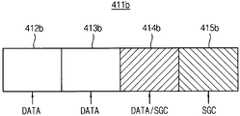
도 14를 참조하면, 페이지 버퍼(411b)는 제1 데이터 래치(412b), 제2 데이터 래치(413b), 제3 데이터 래치(414b) 및 상태 그룹 코드 래치(415b)를 포함한다.Referring to FIG. 14, the
제1 데이터 래치(412b), 제2 데이터 래치(413b) 및 제3 데이터 래치(414b)에는 멀티 비트 데이터가 일시적으로 저장될 수 있다. 상태 그룹 코드 래치(415b)에는 제1 상태 그룹 코드가 일시적으로 저장될 수 있다. 또한, 제3 데이터 래치(414b)에는 제2 상태 그룹 코드가 일시적으로 저장될 수 있다. 예를 들어, 상기 제1 상태 그룹 코드는 현재 선택된 워드 라인에 연결된 멀티 레벨 셀의 상태 그룹 코드이고, 상기 제2 상태 그룹 코드는 인접한 워드 라인에 연결된 멀티 레벨 셀의 상태 그룹 코드일 수 있다.Multi-bit data may be temporarily stored in the
도 15는 도 4의 비휘발성 메모리 장치의 페이지 버퍼 회로에 포함된 페이지 버퍼의 다른 예를 나타내는 블록도이다.15 is a block diagram illustrating another example of a page buffer included in the page buffer circuit of the nonvolatile memory device of FIG. 4.
도 15를 참조하면, 페이지 버퍼(411c)는 제1 데이터 래치(412c), 제2 데이터 래치(413c), 제3 데이터 래치(414c), 제1 상태 그룹 코드 래치(415c) 및 제2 상태 그룹 래치(416c)를 포함한다.Referring to FIG. 15, the
제1 데이터 래치(412c), 제2 데이터 래치(413c) 및 제3 데이터 래치(414c)에는 멀티 비트 데이터가 일시적으로 저장될 수 있다. 제1 상태 그룹 코드 래치(415c)에는 제1 상태 그룹 코드가 일시적으로 저장되고, 제2 상태 그룹 코드 래치(416)에는 제2 상태 그룹 코드가 일시적으로 저장될 수 있다. 예를 들어, 상기 제1 상태 그룹 코드는 현재 선택된 워드 라인에 연결된 멀티 레벨 셀의 상태 그룹 코드이고, 상기 제2 상태 그룹 코드는 인접한 워드 라인에 연결된 멀티 레벨 셀의 상태 그룹 코드일 수 있다.Multi-bit data may be temporarily stored in the
일 실시예에서, 제1 상태 그룹 코드 래치(415c) 또는 제2 상태 그룹 코드 래치(416)에는 프리프로그램 동작을 위해 페이지 버퍼(411c)에 로딩된 멀티 비트 데이터에 기초하여 생성된 상태 그룹 코드가 일시적으로 저장될 수 있다. 페이지 버퍼(411c)는 제1 데이터 래치(412c), 제2 데이터 래치(413c) 및 제3 데이터 래치(414c)에 일시적으로 저장된 상기 멀티 비트 데이터의 비트들에 로직 연산을 수행하여 상기 상태 그룹 코드를 생성하는 로직 회로를 더 포함할 수 있다.In one embodiment, the first status
도 16은 도 6의 비휘발성 메모리 장치에 포함된 메모리 셀 어레이의 일 예를 나타내는 블록도이다.16 is a block diagram illustrating an example of a memory cell array included in the nonvolatile memory device of FIG. 6.
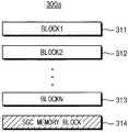
도 16을 참조하면, 메모리 셀 어레이(300a)는 데이터 블록들(311, 312, 313) 및 상태 그룹 코드 메모리 블록(314)을 포함한다.Referring to FIG. 16, the
복수의 데이터 블록들(311, 312, 313)은 멀티 비트 데이터들을 저장하는 멀티 레벨 셀들을 포함한다. 상태 그룹 코드 메모리 블록(314)은 복수의 데이터 블록들(311, 312, 313)에 포함된 상기 멀티 레벨 셀들의 상태 그룹 코드들을 저장할 수 있다. 일 실시예에서, 상태 그룹 코드 메모리 블록(314)은 싱글 레벨 셀들을 포함할 수 있다. 일 실시예에서, 상태 그룹 코드 메모리 블록(314)은 프리-프로그램 동작을 위해 도 4의 페이지 버퍼 회로(410)에 로딩된 멀티 비트 데이터들에 기초하여 생성된 상태 그룹 코드들을 저장할 수 있다.The plurality of data blocks 311, 312, and 313 include multi-level cells storing multi-bit data. The state group
메모리 컨트롤러(100)는 데이터 블록들(311, 312, 313) 중 적어도 일부를 프리-프로그램 블록(PPB)으로 이용하여 프리-프로그램 동작을 수행하고, 상태 그룹 코드 메모리 블록(314)을 다이제스트 블록(DGB)으로 이용하여 다이제스트 프로그램을 수행할 수 있다.The
도 17은 도 4의 비휘발성 메모리 장치에 포함된 로직 회로를 나타내는 블록도이다.17 is a block diagram illustrating a logic circuit included in the nonvolatile memory device of FIG. 4.
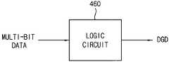
도 17을 참조하면, 로직 회로(660)는 멀티 비트 데이터에 기초하여 상태 그룹 코드를 나타내는 다이제스트 데이터(DGD)를 생성한다. 일 실시예에서, 로직 회로(460)는 도 4의 페이지 버퍼 회로(410)에 포함될 수 있다. 다른 실시예에서, 로직 회로(460)는 도 4의 제어 회로(500)에 포함될 수 있다. 예를 들어, 로직 회로(460)는 프리프로그램 동작을 위해 도 4의 페이지 버퍼 회로(410)에 로딩된 멀티 비트 데이터의 비트들에 로직 연산을 수행하여 상태 그룹 코드를 나타내는 다이제스트 데이터(DGD)를 생성할 수 있다.Referring to FIG. 17, the logic circuit 660 generates digest data DGD representing a state group code based on multi-bit data. In one embodiment, the
도 18 및 19는 도 17의 로직 회로의 예들을 나타내는 블록도들이다.18 and 19 are block diagrams illustrating examples of the logic circuit of FIG. 17.
도 18을 참조하면, 로직 회로(470)는 AND 게이트들(471~478) 및 OR 게이트(479)를 포함할 수 있다.Referring to FIG. 18, the
AND 게이트(471)는 멀티비트 데이터의 비트들(B1~B4)가 '0111'일 때 '1'을 출력할 수 있다. AND 게이트(472)는 멀티비트 데이터가 '0001'일 때 '1'을 출력할 수 있다. AND 게이트(473)는 멀티비트 데이터가 '1000'일 때 '1'을 출력할 수 있다. AND 게이트(474)는 멀티비트 데이터가 '0100'일 때 '1'을 출력할 수 있다. AND 게이트(475)는 멀티비트 데이터가 '0010'일 때 '1'을 출력할 수 있다. AND 게이트(476)는 멀티비트 데이터가 '1011'일 때 '1'을 출력할 수 있다. AND 게이트(477)는 멀티비트 데이터가 '1110'일 때 '1'을 출력할 수 있다. AND 게이트(478)는 멀티비트 데이터가 '1101'일 때 '1'을 출력할 수 있다. OR 게이트(479)는 AND 게이트들(471~478)의 출력들에 OR 연산을 수행하여 다이제스트 데이터(DGD)를 출력할 수 있다. 따라서, 로직 회로(470)는 상기 멀티 비트 데이터가 '0111, '0001, '1000', '0100', '0010', '1011', '1110' 또는 '1101'일 때, 다이제스트 데이터(DGD) '1'을 출력할 수 있다.The AND
도 19를 참조하면, 로직 회로(480)는 XOR 게이트들(181, 482, 483)을 포함한다. XOR 게이트(481)는 멀티 비트 데이터의 제1 비트(B1) 및 제2 비트(B2)에 XOR 연산을 수행한다. XOR 게이트(b)는 제1 비트(B1) 및 제2 비트(B2)가 서로 다른 로직 레벨을 가지는 경우 제1 로직 레벨('1')을 출력할 수 있다. XOR 게이트(482)는 상기 멀티 비트 데이터의 제3 비트(B3) 및 XOR 게이트(481)의 출력에 XOR 연산을 수행한다. XOR 게이트(483)는 상기 멀티 비트 데이터의 제4 비트(B4) 및 XOR 게이트(482)의 출력에 XOR 연산을 수행한다. 따라서, 로직 회로(480)는 상기 멀티 비트 데이터가 '0111, '0001, '1000', '0100', '0010', '1011', '1110' 또는 '1101'일 때, 다이제스트 데이터(DGD) '1'을 출력할 수 있다.Referring to FIG. 19, the
도 18 및 도 19에는 로직 회로(460)의 예들이 도시되어 있으나, 로직 회로(460)는 다양하게 변경될 수 있다. 또한, 멀티 비트 데이터의 비트수에 따라, 로직 회로(460)가 다양하게 변경될 수 있다.Although examples of the
도 20은 본 발명의 실시예들에 따른 스토리지 장치의 동작 방법을 나타내는 흐름도이다.20 is a flowchart illustrating a method of operating a storage device according to embodiments of the present invention.
도 1 내지 도 20을 참조하면, 복수의 메모리 블록들을 포함하고, 상기 메모리 블록들 각각은 복수의 페이지들을 구비하는 메모리 셀 어레이(300)를 포함하는 비휘발성 메모리 장치(200) 및 비휘발성 메모리 장치(200)를 제어하는 컨트롤러(300)를 포함하는 스토리지 장치(30)의 동작 방법에서는, 제어 회로(500)는 전압 생성기(700), 어드레스 디코더(430) 및 페이지 버퍼 회로(410)를 제어하여 메모리 블록들 중 프리-프로그램 블록(PPB)의 멀티 레벨 셀들에 멀티 비트 데이터들을 프리-프로그램하는 프리-프로그램(PRE_PGM)을 수행한다(S210).1 to 20, a
제어 회로(500)는 멀티 레벨 셀들 각각의 상태를 나타내는 상태 코드들에 기초하여 상기 프리-프로그램된 멀티 레벨 셀들을 멀티 레벨 셀들의 상태 코드들에 기초하여 상태 그룹들(GR1, GR2)로 분할하여 상태 그룹들(GR1, GR2)을 나타내는 다이제스트 데이터(DGD)를 생성한다(S220).The
제어 회로(500)는 전압 생성기(700), 어드레스 디코더(430) 및 페이지 버퍼 회로(410)를 제어하여 메모리 블록들 중 다이제스트 블록에 다이제스트 데이터(DGD)를 프로그램하는 다이제스트 프로그램(DG_PRG)을 수행한다(S230).The
컨트롤러(100)는 프리프로그램된 데이터 및 다이제스트 데이터(DGD)에 기초하여 타겟 데이터를 복원한다(S240). 컨트롤러(100)는 로직 회로를 이용하여 프리프로그램된 데이터 및 다이제스트 데이터(DGD)에 논리 연산을 수행하여 타겟 데이터를 복원할 수 있다. 컨트롤러(100)는 복원된 타겟 데이터를 프리-프로그램 블록(PPB)의 멀티-레벨 셀들에 재프로그램한다(S250).The
도 21a 내지 21c는 도 2에 도시된 스토리지 장치의 동작을 나타낸다.21A to 21C illustrate the operation of the storage device shown in FIG. 2.
도 21a를 참조하면, 상술한 바와 같이, 제어 회로(500)는 프리-프로그램 블록(PPB1)의 멀티 레벨 셀들에 멀티-비트 데이터를 프리-프로그램하고, 다이제스트 블록(DGB1)에 다이제스트 데이터를 프로그램한다. 프리-프로그램과 다이제스트 프로그램이 완료되면, 프리-프로그램 블록(PPB1)에는 프리-프로그램 데이터들(PPD11~PPD14)이 저장되고, 다이제스트 블록(DGB1)에는 다이제스트 데이터들(DGD11~DGD14)이 저장된다. 프리-프로그램 데이터들(PPD11~PPD14)은 다이제스트 데이터들(DGD11~DGD14)에 대응될 수 있다. 즉, 프리-프로그램 블록(PPB1)과 다이제스트 블록(DGB1)은 하나의 쌍을 구성할 수 있다.Referring to FIG. 21A, as described above, the
도 21b를 참조하면, 컨트롤러(100)는 프리-프로그램 데이터들(PPD11~PPD14)을 로직 회로(180)에 제공(610)하고, 다이제스트 데이터들(DGD11~DGD14)을 로직 회로(180)에 마이그레이션(620)하고, 컨트롤러(100)에 포함되는 로직 회로(180)는 프리-프로그램 데이터들(PPD11~PPD14)은 다이제스트 데이터들(DGD11~DGD14)에 로직 연산을 수행하여 타겟 데이터(TD)를 복구하여 페이지들(PAGE1~PAGE4) 단위로 버퍼(130)에 저장하고, 컨트롤러(100)는 버퍼(130)에 저장된 타겟 데이터(TD)를 프리-프로그램 블록(PPB1)의 멀티 레벨 셀들에 재-프로그램(RE_PRG)한다. 따라서, 프리-프로그램 데이터들(PPD11~PPD14) 중 일부(PPD13, PPD14)는 멀티 페이지 데이터들(MPG11, MPG12)로 변환된다.Referring to FIG. 21B, the
도 21c를 참조하면, 재-프로그램이 완료되고, 다이제스트 블록(DGB1)의 다이제스트 데이터들(DGD11~DGD14)의 마이그레이션이 완료되면, 프리-프로그램 블록(PPB1)에는 멀티 페이지 데이터들(MPG11~MPG14)이 저장되어, 프리-프로그램 블록(PPB1)은 멀티-비트 블록(MBB1)이 되고, 컨트롤러(100)는 다이제스트 블록(DGB1)에 소거 동작(DGB1)을 수행하여 다이제스트 블록(DGB1)을 프리 블록(FB1)으로 전환시킬 수 있다.Referring to FIG. 21C, when the re-program is completed and migration of the digest data DGD11 to DGD14 of the digest block DGB1 is completed, the multi-page data MPG11 to MPG14 are included in the pre-program block PPB1. This stored, the pre-program block (PPB1) is a multi-bit block (MBB1), the
도 22은 본 발명의 실시예들에 따른 도 4의 비휘발성 메모리 장치의 프로그램 방법의 예를 나타내는 순서도이다.22 is a flowchart illustrating an example of a programming method of the nonvolatile memory device of FIG. 4 according to embodiments of the present invention.
도 4 내지 도 19 및 도 22를 참조하면, 다음 워드 라인에 연결된 멀티 레벨 셀들에 프리프로그램 동작 및 다이제스트 프로그램 동작이 수행된 후, 현재 워드 라인에 연결된 멀티 레벨 셀들에 독출 동작 및 재프로그램 동작이 수행된다.4 to 19 and 22, after a pre-program operation and a digest program operation are performed on multi-level cells connected to the next word line, a read operation and a re-program operation are performed on multi-level cells connected to the current word line. do.
예를 들어, 제(k+1) 워드라인에 연결된 멀티 레벨 셀들에 멀티 비트 데이터들을 프리-프로그램하고(S310), 제(k+1) 워드라인에 대응되는 페이지에 멀티 레벨 셀들의 상태 코드들에 기초하여 생성된 다이제스트 데이터를 프로그램한다(S330). 제(k+1) 워드라인에 연결된 멀티 레벨 셀들에 프리-프로그램 동작이 수행된 후, 제k 워드라인에 연결된 멀티 레벨 셀들로부터 데이터들이 독출되고(S350), 제k 워드라인에 연결된 멀티 레벨 셀들에 멀티 비트 데이터들이 재프로그램된다(S370).For example, multi-bit data is pre-programmed in multi-level cells connected to the (k+1) word line (S310), and status codes of multi-level cells in a page corresponding to the (k+1) word line. Digest data generated based on the program is programmed (S330). After the pre-program operation is performed on multi-level cells connected to the (k+1) word line, data is read from the multi-level cells connected to the k-th word line (S350), and multi-level cells connected to the k-th word line. Multi-bit data is reprogrammed in step S370.
이와 같이, 다음 워드 라인에 연결된 멀티 레벨 셀들에 프리프로그램 동작이 수행된 후, 현재 워드 라인에 연결된 멀티 레벨 셀들에 독출 동작 및 재프로그램 동작이 수행됨으로써, 상기 재프로그램 동작 후 인접한 워드 라인에 연결된 멀티 레벨 셀들에 의한 커플링의 영향을 최소화할 수 있다.In this way, after the pre-program operation is performed on the multi-level cells connected to the next word line, a read operation and a re-program operation are performed on the multi-level cells connected to the current word line. The influence of coupling by level cells can be minimized.
도 23은 본 발명의 실시예들에 따른 에스에스디(SSD: solid state disk or solid state drive)를 나타내는 블록도이다.23 is a block diagram illustrating a solid state disk (SSD) or a solid state drive (SSD) according to embodiments of the present invention.
도 23을 참조하면, SSD(1000)는 복수의 비휘발성 메모리 장치들(1100) 및 SSD 제어기(1200)를 포함한다.Referring to FIG. 23, the
비휘발성 메모리 장치들(1100)은 옵션적으로 외부 고전압(VPP)을 제공받도록 구현될 수 있다. 비휘발성 메모리 장치들(1100)은 전술한 도 4의 비휘발성 메모리 장치(200)로 구현될 수 있다. 따라서 비휘발성 메모리 장치들(1100)은 각각 프리-프로그램 블록의 멀티-비트 셀들에 멀티-비트 데이터를 프로그램하고, 프리-프로그램된 멀티-비트 데이터의 상태 코드들에 기초하여 생성된 다이제스트 데이터를 다이제스트 블록에 프로그램하여 프로그램 성능 및 저장 공간 효율을 향상시킬 수 있다.The
SSD 제어기(1200)는 복수의 채널들(CH1~CH4)을 통하여 비휘발성 메모리 장치들(1100)에 연결된다. SSD 제어기(1200)는 적어도 하나의 프로세서(1210), 버퍼 메모리(1220), 에러 정정 회로(1230), 호스트 인터페이스(1250) 및 비휘발성 메모리 인터페이스(1260)를 포함한다.The
버퍼 메모리(1220)는 메모리 제어기(1200)의 구동에 필요한 데이터를 임시로 저장할 수 있다. 또한, 버퍼 메모리(1220)는 기입 요청시 프로그램 동작에 이용될 데이터를 버퍼링해 놓을 수 있다. 에러 정정 회로(1230)는 기입 동작에서 프로그램될 데이터의 에러 정정 코드 값을 계산하고, 읽기 동작에서 읽혀진 데이터를 에러 정정 코드 값에 근거로 하여 에러 정정하고, 데이터 복구 동작에서 비휘발성 메모리 장치(1100)로부터 복구된 데이터의 에러를 정정할 수 있다.The
본 발명의 실시 예에 따른 비휘발성 메모리 장치 또는 스토리지 장치는 다양한 형태들의 패키지를 이용하여 실장 될 수 있다.The nonvolatile memory device or the storage device according to an embodiment of the present invention may be mounted using various types of packages.
본 발명은 비휘발성 메모리 장치를 구비하는 임의의 전자 장치에 유용하게 이용될 수 있다. 예를 들어, 본 발명은 비휘발성 메모리 장치를 구비하는 휴대폰(Mobile Phone), 스마트 폰(Smart Phone), 개인 정보 단말기(Personal Digital Assistant; PDA), 휴대형 멀티미디어 플레이어(Portable Multimedia Player; PMP), 디지털 카메라(Digital Camera), 음악 재생기(Music Player), 휴대용 게임 콘솔(Portable Game Console), 네비게이션(Navigation) 시스템 등에 적용될 수 있다.The present invention can be usefully used in any electronic device having a nonvolatile memory device. For example, the present invention is a mobile phone having a non-volatile memory device, a smart phone, a personal digital assistant (PDA), a portable multimedia player (PMP), digital It can be applied to a digital camera, a music player, a portable game console, and a navigation system.
상술한 바와 같이, 본 발명의 바람직한 실시예를 참조하여 설명하였지만 해당 기술 분야에서 통상의 지식을 가진 자라면 하기의 특허청구범위에 기재된 본 발명의 사상 및 영역으로부터 벗어나지 않는 범위 내에서 본 발명을 다양하게 수정 및 변경시킬 수 있음을 이해할 수 있을 것이다.As described above, the present invention has been described with reference to preferred embodiments of the present invention, but those skilled in the art may vary the present invention within the scope not departing from the spirit and scope of the present invention as set forth in the claims below. You can understand that it can be modified and changed.
Claims (10)
Translated fromKorean상기 메모리 블록들 중 프리-프로그램 블록의 멀티 레벨 셀들에 멀티 비트 데이터들을 프리-프로그램하는 단계;
상기 멀티 레벨 셀들 각각의 상태를 나타내는 상태 코드들에 기초하여 상기 프리-프로그램된 멀티 레벨 셀들을 상태 그룹들로 분할하여 상기 상태 그룹들에 상응하는 상태 그룹 코드들을 나타내는 다이제스트 데이터를 생성하는 단계; 및
상기 메모리 블록들 중 다이제스트 블록에 상기 다이제스트 데이터를 프로그램하는 단계를 포함하는 비휘발성 메모리 장치의 동작 방법.A method of operating a nonvolatile memory device including a plurality of memory blocks, each of the memory blocks including a memory cell array including a plurality of pages,
Pre-programming multi-bit data into multi-level cells of a pre-program block among the memory blocks;
Dividing the pre-programmed multi-level cells into state groups based on state codes representing states of each of the multi-level cells to generate digest data representing state group codes corresponding to the state groups; And
And programming the digest data in a digest block among the memory blocks.
상기 상태 그룹들은 서로 중첩되지 않는 문턱 전압 분포들을 포함하고,
상기 멀티 비트 데이터를 프리-프로그램하는 단계는,
상기 멀티 비트 데이터를 상기 멀티 레벨 셀들에 연결된 페이지 버퍼 회로에 로딩하는 단계; 및
상기 페이지 버퍼 회로에 로딩된 상기 멀티 비트 데이터를 상기 멀티 레벨 셀들에 프리-프로그램하는 단계를 포함하는 비휘발성 메모리 장치의 동작 방법.According to claim 1,
The state groups include threshold voltage distributions that do not overlap each other,
Pre-programming the multi-bit data comprises:
Loading the multi-bit data into a page buffer circuit connected to the multi-level cells; And
And pre-programming the multi-bit data loaded in the page buffer circuit into the multi-level cells.
상기 페이지 버퍼 회로에 로딩된 상기 멀티 비트 데이터에 기초하여 상기 다이제스트 데이터를 생성하는 단계를 더 포함하고,
상기 다이제스트 데이터를 생성하는 단계는
상기 멀티 비트 데이터 각각의 비트들에 로직 연산을 수행하여 상기 다이제스트 데이터를 생성하는 단계를 포함하는 비휘발성 메모리 장치의 동작 방법.According to claim 2,
And generating the digest data based on the multi-bit data loaded in the page buffer circuit.
Generating the digest data is
And generating the digest data by performing a logic operation on each bit of the multi-bit data.
상기 프리-프로그램 블록과 상기 다이제스트 블록은 하나의 쌍을 구성하는 비휘발성 메모리 장치의 동작 방법.According to claim 1,
The pre-program block and the digest block constitute a pair of non-volatile memory device operating method.
상기 다이제스트 데이터는 상기 멀티 레벨 셀들 각각의 상태 코드들에 포함된 제1 로직 레벨을 가지는 비트들의 수에 기초하여 생성되고,
상기 다이제스트 블록은 싱글 레벨 셀들을 포함하는 비휘발성 메모리 장치의 동작 방법.According to claim 4,
The digest data is generated based on the number of bits having a first logic level included in the status codes of each of the multi-level cells,
The digest block includes a single-level cell operation method of a non-volatile memory device.
상기 멀티-레벨 셀들은 각각 N(N은 3 이상의 자연수) 비트 데이터를 저장할 수 있고, 상기 멀티-레벨 셀들은 각각 2N 개의 상태 코드들 중 하나를 가지고, 상기 상태 코드 그룹들은 M(M은 N 보다 작은 자연수) 개의 상태 코드 그룹들을 포함하고,
N은 4이고 M은 4이고,
상기 다이제스트 블록은 멀티-레벨 셀들을 포함하는 비휘발성 메모리 장치의 동작 방법.According to claim 1,
Each of the multi-level cells can store N (N is a natural number of 3 or more) bit data, and the multi-level cells each have one of 2N status codes, and the status code groups are M (M is N Smaller natural number) status code groups,
N is 4 and M is 4,
The digest block includes a method of operating a non-volatile memory device including multi-level cells.
상기 메모리 블록들 중 프리-프로그램 블록의 멀티 레벨 셀들에 멀티 비트 데이터들을 프리-프로그램하는 단계;
상기 멀티 레벨 셀들 각각의 상태를 나타내는 상태 코드들에 기초하여 상기 프리-프로그램된 멀티 레벨 셀들을 상태 그룹들로 분할하고, 상기 상태 그룹들에 상응하는 상태 그룹 코드들을 나타내는 다이제스트 데이터를 생성하는 단계;
상기 메모리 블록들 중 다이제스트 블록에 상기 다이제스트 데이터를 프로그램하는 단계;
상기 컨트롤러에서, 상기 프리-프로그램된 멀티 비트 데이터와 상기 다이제스트 데이터에 기초하여 타겟 데이터를 복원하는 단계; 및
상기 컨트롤러에서, 상기 복원된 타겟 데이터를 상기 프리-프로그램 블록의 상기 멀티 레벨 셀들에 재-프로그램하는 단계를 포함하는 스토리지 장치의 동작 방법.A method of operating a storage device including a plurality of memory blocks, each of the memory blocks comprising a memory cell array including a plurality of pages and a controller for controlling the nonvolatile memory device,
Pre-programming multi-bit data into multi-level cells of a pre-program block among the memory blocks;
Dividing the pre-programmed multi-level cells into state groups based on state codes representing states of each of the multi-level cells, and generating digest data indicating state group codes corresponding to the state groups;
Programming the digest data in a digest block of the memory blocks;
Restoring, at the controller, target data based on the pre-programmed multi-bit data and the digest data; And
And re-programming the restored target data into the multi-level cells of the pre-program block at the controller.
상기 상태 그룹들은 서로 중첩되지 않는 문턱 전압 분포들을 포함하고,
상기 프리-프로그램 블록과 상기 다이제스트 블록은 하나의 쌍을 구성하고,
상기 컨트롤러는 버퍼를 포함하고, 상기 멀티 비트 데이터를 상기 버퍼로부터 상기 비휘발성 메모리 장치의 페이지 버퍼 회로로 로딩한 후 상기 버퍼를 릴리스하고,
상기 다이제스트 데이터는 상기 멀티 레벨 셀들 각각의 상태 코드들에 포함된 제1 로직 레벨을 가지는 비트들의 수에 기초하여 생성되고,
상기 다이제스트 블록은 싱글 레벨 셀들을 포함하는 스토리지 장치의 동작 방법.The method of claim 7,
The state groups include threshold voltage distributions that do not overlap each other,
The pre-program block and the digest block constitute a pair,
The controller includes a buffer, loads the multi-bit data from the buffer into the page buffer circuit of the nonvolatile memory device, releases the buffer,
The digest data is generated based on the number of bits having a first logic level included in the status codes of each of the multi-level cells,
The digest block is a method of operating a storage device including single-level cells.
상기 컨트롤러에서 상기 프리-프로그램된 멀티 비트 데이터와 상기 다이제스트 데이터에 대하여 로직 연산을 수행하여 상기 타겟 데이터를 생성하는 단계; 및
상기 버퍼에 상기 타겟 데이터를 저장하는 단계를 포함하고,
상기 타겟 데이터를 생성하는 단계는
상기 프리-프로그램된 멀티 비트 데이터와 상기 다이제스트 데이터를 상기 컨트롤러에 마이그레이션하는 단계를 포함하고,
상기 컨트롤러는 상기 재-프로그램이 완료되면, 상기 다이제스트 블록에 소거 동작을 수행하여 상기 다이제스트 블록을 프리 블록으로 전환시키는 스토리지 장치의 동작 방법.The method of claim 7, wherein the step of restoring the target data,
Generating the target data by performing a logic operation on the pre-programmed multi-bit data and the digest data in the controller; And
And storing the target data in the buffer,
The step of generating the target data is
Migrating the pre-programmed multi-bit data and the digest data to the controller,
When the re-program is completed, the controller performs an erase operation on the digest block to convert the digest block into a free block.
상기 비휘발성 메모리 장치를 제어하는 컨트롤러를 포함하고,
상기 컨트롤러는 상기 메모리 블록들 중 프리-프로그램 블록의 멀티 레벨 셀들에 멀티 비트 데이터들을 프리-프로그램하고, 상기 멀티 레벨 셀들 각각의 상태를 나타내는 상태 코드들에 기초하여 상기 프리-프로그램된 멀티 레벨 셀들을 상태 그룹들로 분할하고, 상기 상태 그룹들에 상응하는 상태 그룹 코드들을 나타내는 다이제스트 데이터를 생성하고, 상기 메모리 블록들 중 다이제스트 블록에 상기 다이제스트 데이터를 프로그램하는 다이제스트 프로그램을 수행하도록 상기 비휘발성 메모리 장치를 제어하고,
상기 메모리 셀 어레이는 비트라인과 공통 소스 라인 사이에서 기판에 수직한 방향으로 적층된 워드라인들을 관통하는 필라들로 구성된 복수의 셀 스트링들을 포함하고,
상기 컨트롤러는 상기 프리-프로그램과 상기 다이제스트 프로그램을 제어하는 프로그램 관리 모듈을 포함하는 스토리지 장치.A non-volatile memory device including a plurality of memory blocks, each of the memory blocks including a memory cell array including a plurality of pages; And
And a controller that controls the nonvolatile memory device,
The controller pre-programs multi-bit data in multi-level cells of a pre-program block among the memory blocks, and uses the pre-programmed multi level cells based on status codes representing states of each of the multi level cells. The nonvolatile memory device is configured to divide into state groups, generate digest data representing state group codes corresponding to the state groups, and perform a digest program to program the digest data in a digest block among the memory blocks. Control,
The memory cell array includes a plurality of cell strings composed of pillars penetrating word lines stacked in a direction perpendicular to the substrate between a bit line and a common source line,
The controller includes a pre-program and a program management module that controls the digest program.
Priority Applications (5)
| Application Number | Priority Date | Filing Date | Title |
|---|---|---|---|
| KR1020180159593AKR102694842B1 (en) | 2018-12-12 | 2018-12-12 | Methods of operating of nonvolatile memory devices, methods of operating storage devices and storage devices |
| US16/543,532US11037628B2 (en) | 2018-12-12 | 2019-08-17 | Methods of operating nonvolatile memory devices, methods of operating storage device and storage devices |
| CN201910840852.4ACN111309517B (en) | 2018-12-12 | 2019-09-06 | Method for operating a memory device and memory device |
| CN202411604756.7ACN119739559A (en) | 2018-12-12 | 2019-09-06 | Method for operating storage device and storage device |
| US17/316,463US11610631B2 (en) | 2018-12-12 | 2021-05-10 | Methods of operating nonvolatile memory devices, methods of operating storage device and storage devices |
Applications Claiming Priority (1)
| Application Number | Priority Date | Filing Date | Title |
|---|---|---|---|
| KR1020180159593AKR102694842B1 (en) | 2018-12-12 | 2018-12-12 | Methods of operating of nonvolatile memory devices, methods of operating storage devices and storage devices |
Publications (2)
| Publication Number | Publication Date |
|---|---|
| KR20200071955Atrue KR20200071955A (en) | 2020-06-22 |
| KR102694842B1 KR102694842B1 (en) | 2024-08-14 |
Family
ID=71071222
Family Applications (1)
| Application Number | Title | Priority Date | Filing Date |
|---|---|---|---|
| KR1020180159593AActiveKR102694842B1 (en) | 2018-12-12 | 2018-12-12 | Methods of operating of nonvolatile memory devices, methods of operating storage devices and storage devices |
Country Status (3)
| Country | Link |
|---|---|
| US (2) | US11037628B2 (en) |
| KR (1) | KR102694842B1 (en) |
| CN (2) | CN111309517B (en) |
Families Citing this family (2)
| Publication number | Priority date | Publication date | Assignee | Title |
|---|---|---|---|---|
| JP2022045992A (en)* | 2020-09-10 | 2022-03-23 | キオクシア株式会社 | Semiconductor memory device |
| KR20240048893A (en) | 2022-10-07 | 2024-04-16 | 삼성전자주식회사 | Storage device and program method thereof |
Citations (5)
| Publication number | Priority date | Publication date | Assignee | Title |
|---|---|---|---|---|
| KR20100137128A (en)* | 2009-06-22 | 2010-12-30 | 삼성전자주식회사 | Program method of nonvolatile memory device, nonvolatile memory device and nonvolatile memory system |
| KR20140104829A (en)* | 2013-02-21 | 2014-08-29 | 삼성전자주식회사 | Multi level cell nonvolatile memory system |
| KR20150014705A (en)* | 2013-07-30 | 2015-02-09 | 삼성전자주식회사 | Memory system and programming method thereof |
| KR20150072517A (en)* | 2013-12-19 | 2015-06-30 | 삼성전자주식회사 | Non-volatile memory device and memory system including the same |
| KR20170045055A (en)* | 2015-10-16 | 2017-04-26 | 삼성전자주식회사 | Programming method and operating method of a non volatile memory device |
Family Cites Families (11)
| Publication number | Priority date | Publication date | Assignee | Title |
|---|---|---|---|---|
| JP4157563B2 (en) | 2006-01-31 | 2008-10-01 | 株式会社東芝 | Semiconductor integrated circuit device |
| US8130552B2 (en) | 2008-09-11 | 2012-03-06 | Sandisk Technologies Inc. | Multi-pass programming for memory with reduced data storage requirement |
| US8144512B2 (en) | 2009-12-18 | 2012-03-27 | Sandisk Technologies Inc. | Data transfer flows for on-chip folding |
| US8355280B2 (en) | 2010-03-09 | 2013-01-15 | Samsung Electronics Co., Ltd. | Data storage system having multi-bit memory device and operating method thereof |
| KR101635446B1 (en) | 2010-05-25 | 2016-07-04 | 삼성전자주식회사 | Method of merging blocks for a semiconductor memory device |
| KR101821604B1 (en) | 2011-07-25 | 2018-01-24 | 삼성전자주식회사 | Method of programming a nonvolatile memory device |
| DE102013108491A1 (en)* | 2012-08-10 | 2014-02-13 | Samsung Electronics Co., Ltd. | Programming method for e.g. flash memories in digital systems, involves programming data into non-volatile memory cells of buffer area by programming operation, invalidating data stored in memory cells, and redefining delete state |
| US9870169B2 (en) | 2015-09-04 | 2018-01-16 | Intel Corporation | Interleaved all-level programming of non-volatile memory |
| US9953703B2 (en)* | 2015-10-16 | 2018-04-24 | Samsung Electronics Co., Ltd. | Programming method of non volatile memory device |
| KR102302187B1 (en)* | 2017-03-13 | 2021-09-14 | 삼성전자주식회사 | Methods of operating nonvolatile memory devices and nonvolatile memory devices |
| US10354723B2 (en)* | 2017-06-29 | 2019-07-16 | SK Hynix Inc. | Memory device and method for programming the same |
- 2018
- 2018-12-12KRKR1020180159593Apatent/KR102694842B1/enactiveActive
- 2019
- 2019-08-17USUS16/543,532patent/US11037628B2/enactiveActive
- 2019-09-06CNCN201910840852.4Apatent/CN111309517B/enactiveActive
- 2019-09-06CNCN202411604756.7Apatent/CN119739559A/enactivePending
- 2021
- 2021-05-10USUS17/316,463patent/US11610631B2/enactiveActive
Patent Citations (5)
| Publication number | Priority date | Publication date | Assignee | Title |
|---|---|---|---|---|
| KR20100137128A (en)* | 2009-06-22 | 2010-12-30 | 삼성전자주식회사 | Program method of nonvolatile memory device, nonvolatile memory device and nonvolatile memory system |
| KR20140104829A (en)* | 2013-02-21 | 2014-08-29 | 삼성전자주식회사 | Multi level cell nonvolatile memory system |
| KR20150014705A (en)* | 2013-07-30 | 2015-02-09 | 삼성전자주식회사 | Memory system and programming method thereof |
| KR20150072517A (en)* | 2013-12-19 | 2015-06-30 | 삼성전자주식회사 | Non-volatile memory device and memory system including the same |
| KR20170045055A (en)* | 2015-10-16 | 2017-04-26 | 삼성전자주식회사 | Programming method and operating method of a non volatile memory device |
Also Published As
| Publication number | Publication date |
|---|---|
| KR102694842B1 (en) | 2024-08-14 |
| US11037628B2 (en) | 2021-06-15 |
| US20200194072A1 (en) | 2020-06-18 |
| CN111309517A (en) | 2020-06-19 |
| US11610631B2 (en) | 2023-03-21 |
| CN119739559A (en) | 2025-04-01 |
| US20210264985A1 (en) | 2021-08-26 |
| CN111309517B (en) | 2024-11-29 |
Similar Documents
| Publication | Publication Date | Title |
|---|---|---|
| KR102302187B1 (en) | Methods of operating nonvolatile memory devices and nonvolatile memory devices | |
| KR102687216B1 (en) | Methods of controlling reclaim of nonvolatile memory devices, methods of operating storage devices and storage devices | |
| US9478296B2 (en) | Erase method of nonvolatile memory device and storage device employing the same | |
| US9779790B2 (en) | Nonvolatile memory device and method of driving word line of the nonvolatile memory | |
| CN107093465B (en) | Data storage device including voltage search unit | |
| KR102355580B1 (en) | Nonvolatile memory device, storage device having the same, and operation method thereof | |
| KR102292642B1 (en) | Nonvolatile memory device and program method of a nonvolatile memory device | |
| KR102179270B1 (en) | Nonvolatile memory device and operating method thereof | |
| KR102083547B1 (en) | Data storage device including flash memory and memory controller and bad page management method thereof | |
| US9818477B2 (en) | Methods of programming memory cells in non-volatile memory devices | |
| US10497452B2 (en) | Semiconductor memory device and method of operating the same | |
| KR102396734B1 (en) | Semiconductor memory device and operating method thereof | |
| CN107871515B (en) | Semiconductor memory device and method of operating the same | |
| US20160141036A1 (en) | Nonvolatile memory and related reprogramming method | |
| US20180294031A1 (en) | Storage device and method of operating the same | |
| KR20210143612A (en) | Nonvolatile memory device, and method of operating nonvolatile memory device | |
| KR20120138895A (en) | Data storage system having multi-level memory device and operating method thereof | |
| KR101456592B1 (en) | Multi-bit flash memory device and analysis method of flag cells for the same | |
| KR102694842B1 (en) | Methods of operating of nonvolatile memory devices, methods of operating storage devices and storage devices | |
| KR102735056B1 (en) | Semiconductor memory device and method for operating thereof | |
| KR20190111608A (en) | Semiconductor memory device and operating method thereof | |
| KR20220048375A (en) | Semiconductor memory device and method for operating thereof |
Legal Events
| Date | Code | Title | Description |
|---|---|---|---|
| PA0109 | Patent application | St.27 status event code:A-0-1-A10-A12-nap-PA0109 | |
| P11-X000 | Amendment of application requested | St.27 status event code:A-2-2-P10-P11-nap-X000 | |
| P13-X000 | Application amended | St.27 status event code:A-2-2-P10-P13-nap-X000 | |
| R15-X000 | Change to inventor requested | St.27 status event code:A-3-3-R10-R15-oth-X000 | |
| R16-X000 | Change to inventor recorded | St.27 status event code:A-3-3-R10-R16-oth-X000 | |
| PG1501 | Laying open of application | St.27 status event code:A-1-1-Q10-Q12-nap-PG1501 | |
| A201 | Request for examination | ||
| P11-X000 | Amendment of application requested | St.27 status event code:A-2-2-P10-P11-nap-X000 | |
| P13-X000 | Application amended | St.27 status event code:A-2-2-P10-P13-nap-X000 | |
| PA0201 | Request for examination | St.27 status event code:A-1-2-D10-D11-exm-PA0201 | |
| E902 | Notification of reason for refusal | ||
| PE0902 | Notice of grounds for rejection | St.27 status event code:A-1-2-D10-D21-exm-PE0902 | |
| P11-X000 | Amendment of application requested | St.27 status event code:A-2-2-P10-P11-nap-X000 | |
| P13-X000 | Application amended | St.27 status event code:A-2-2-P10-P13-nap-X000 | |
| E701 | Decision to grant or registration of patent right | ||
| PE0701 | Decision of registration | St.27 status event code:A-1-2-D10-D22-exm-PE0701 | |
| PR0701 | Registration of establishment | St.27 status event code:A-2-4-F10-F11-exm-PR0701 | |
| PR1002 | Payment of registration fee | St.27 status event code:A-2-2-U10-U11-oth-PR1002 Fee payment year number:1 | |
| PG1601 | Publication of registration | St.27 status event code:A-4-4-Q10-Q13-nap-PG1601 |