KR20200065270A - Package structure of three-dimensional lamination using multiple devices - Google Patents
Package structure of three-dimensional lamination using multiple devicesDownload PDFInfo
- Publication number
- KR20200065270A KR20200065270AKR1020180151566AKR20180151566AKR20200065270AKR 20200065270 AKR20200065270 AKR 20200065270AKR 1020180151566 AKR1020180151566 AKR 1020180151566AKR 20180151566 AKR20180151566 AKR 20180151566AKR 20200065270 AKR20200065270 AKR 20200065270A
- Authority
- KR
- South Korea
- Prior art keywords
- chip
- substrate
- processing unit
- signal processing
- signal
- Prior art date
- Legal status (The legal status is an assumption and is not a legal conclusion. Google has not performed a legal analysis and makes no representation as to the accuracy of the status listed.)
- Granted
Links
Images

Classifications
- H—ELECTRICITY
- H01—ELECTRIC ELEMENTS
- H01L—SEMICONDUCTOR DEVICES NOT COVERED BY CLASS H10
- H01L25/00—Assemblies consisting of a plurality of semiconductor or other solid state devices
- H01L25/03—Assemblies consisting of a plurality of semiconductor or other solid state devices all the devices being of a type provided for in a single subclass of subclasses H10B, H10D, H10F, H10H, H10K or H10N, e.g. assemblies of rectifier diodes
- H01L25/04—Assemblies consisting of a plurality of semiconductor or other solid state devices all the devices being of a type provided for in a single subclass of subclasses H10B, H10D, H10F, H10H, H10K or H10N, e.g. assemblies of rectifier diodes the devices not having separate containers
- H01L25/065—Assemblies consisting of a plurality of semiconductor or other solid state devices all the devices being of a type provided for in a single subclass of subclasses H10B, H10D, H10F, H10H, H10K or H10N, e.g. assemblies of rectifier diodes the devices not having separate containers the devices being of a type provided for in group H10D89/00
- H01L25/0657—Stacked arrangements of devices
- H—ELECTRICITY
- H01—ELECTRIC ELEMENTS
- H01L—SEMICONDUCTOR DEVICES NOT COVERED BY CLASS H10
- H01L23/00—Details of semiconductor or other solid state devices
- H01L23/12—Mountings, e.g. non-detachable insulating substrates
- H01L23/13—Mountings, e.g. non-detachable insulating substrates characterised by the shape
- H—ELECTRICITY
- H01—ELECTRIC ELEMENTS
- H01L—SEMICONDUCTOR DEVICES NOT COVERED BY CLASS H10
- H01L23/00—Details of semiconductor or other solid state devices
- H01L23/58—Structural electrical arrangements for semiconductor devices not otherwise provided for, e.g. in combination with batteries
- H01L23/60—Protection against electrostatic charges or discharges, e.g. Faraday shields
Landscapes
- Engineering & Computer Science (AREA)
- Power Engineering (AREA)
- Microelectronics & Electronic Packaging (AREA)
- Physics & Mathematics (AREA)
- Condensed Matter Physics & Semiconductors (AREA)
- General Physics & Mathematics (AREA)
- Computer Hardware Design (AREA)
- Semiconductor Integrated Circuits (AREA)
- Design And Manufacture Of Integrated Circuits (AREA)
Abstract
Translated fromKoreanDescription
Translated fromKorean본 발명은 패키지 구조에 관한 것으로서, 보다 상세하게는 다종 소자를 이용한 3차원 적층형 패키지 구조에 있어서, 다종의 소자 연결 시 발생하는 신호 연결의 어려움을 해소하고 빠른 신호 전달이 가능하도록 하는 패키지 구조에 관한 것이다.The present invention relates to a package structure, and more specifically, in a three-dimensional stacked package structure using multiple devices, it relates to a package structure that solves the difficulty of signal connection when connecting multiple devices and enables fast signal transmission. will be.
다양한 산업군에서 반도체 칩의 경박단소화를 구현하기 위하여 다양한 기능을 구현하는 칩들이 적층됨에 따른 고집적 반도체 칩이 요구되고 있다.In various industries, high-density semiconductor chips are required as chips that implement various functions are stacked in order to realize thin and compact semiconductor chips.
특히, 고집적으로 인한 각 칩들의 입출력 장치인 IO의 수가 많아지며 그로 인해 신호가 얽히지 않고 바르게 전달될 수 있는 방법이 필요하며 이에 대한 연구가 이루어지고 있다.In particular, the number of IOs, which are input/output devices of each chip due to high integration, increases, and thus a method for properly transmitting signals without entanglement is required, and research has been conducted on this.
그러나, 다양한 기능을 2차원적으로 배치하여 연결하는 것에 비하여 3차원적으로 적층하여 연결할 경우, 소자 간의 신호 연결 시에 신호를 연결할 때 많은 신호들이 얽히지 않게 적층을 하는데 어려움이 있다.However, when stacking and connecting in three dimensions compared to connecting and placing various functions in two dimensions, it is difficult to stack so that many signals are not entangled when connecting signals when connecting signals between devices.
본 발명은, 칩에 전달되는 복잡한 신호를 풀어 전달함으로써 위와 같은 문제점을 해결할 수 있다.The present invention can solve the above problems by releasing and transmitting a complex signal transmitted to the chip.
본 발명은 상술한 종래 기술의 문제점을 해결하기 위하여 안출된 발명으로서, 개선된 구조에 의해 다종의 소자를 연결할 때 발생하는 신호의 얽힘을 해소하는 한편 신속한 신호 전달을 가능하게 하는 3차원 적층형 패키지 구조를 제공하기 위함이다.The present invention is an invention devised to solve the above-described problems of the prior art, and improves the structure to solve the entanglement of signals generated when connecting various types of devices while enabling a rapid signal transmission while stacking three-dimensional stacked packages Is to provide.
본 발명의 과제들은 이상에서 언급한 과제들로 제한되지 않으며, 언급되지 않은 또 다른 과제들은 아래의 기재로부터 당업자에게 명확하게 이해될 수 있을 것이다.The problems of the present invention are not limited to the problems mentioned above, and other problems not mentioned will be clearly understood by those skilled in the art from the following description.
상기한 목적을 달성하기 위한 본 발명의 3차원 적층형 패키지는 제1기판, 상기 제1기판에 구비되는 제1칩, 상기 제1칩 상에 구비되는 제2신호처리유닛 및 상기 제2신호처리유닛 상에 구비되는 제2칩을 포함할 수 있다.The three-dimensional stacked package of the present invention for achieving the above object is a first substrate, a first chip provided on the first substrate, a second signal processing unit and the second signal processing unit provided on the first chip It may include a second chip provided on the.
이 때, 상기 제2칩은 논리 칩에 해당하고, 상기 제2신호처리유닛은 상기 제2칩에서 생성되는 신호를 처리하여 상기 제1기판에 전달하는 것을 특징으로 할 수 있다.In this case, the second chip may correspond to a logic chip, and the second signal processing unit may process a signal generated by the second chip and transmit it to the first substrate.
그리고 상기 제1칩은 메모리 칩에 해당하는 것을 특징으로 할 수 있다.In addition, the first chip may be characterized as corresponding to a memory chip.
또는, 상기 제1기판 및 상기 제1칩 사이에 상기 제1칩에서 전달되는 신호를 처리하는 제1신호처리유닛을 더 포함할 수 있다.Alternatively, a first signal processing unit for processing a signal transmitted from the first chip between the first substrate and the first chip may be further included.
그리고 상기 제1기판과 대향하며 상기 제2칩에 구비되는 제2기판을 더 포함할 수 있다.In addition, a second substrate facing the first substrate and provided on the second chip may be further included.
이 때, 상기 제1기판은 상기 제1칩에서 생성되는 신호를 전달받고, 상기 제2기판은 상기 제2칩에서 생성되는 신호를 전달받는 것을 특징으로 할 수 있다.At this time, the first substrate may be characterized by receiving the signal generated by the first chip, and the second substrate receiving the signal generated by the second chip.
또는, 상기 제1기판 및 상기 제1칩 사이에 상기 제1칩에서 전달되는 신호를 처리하는 제1신호처리유닛을 더 포함하고, 상기 제1칩은 논리 칩에 해당하고, 상기 제1신호처리유닛은 상기 제1칩에서 생성되는 신호를 처리하여 상기 제1기판에 전달하는 것을 특징으로 할 수 있다.Or, further comprising a first signal processing unit for processing a signal transmitted from the first chip between the first substrate and the first chip, the first chip corresponds to a logic chip, the first signal processing The unit may be characterized in that the signal generated by the first chip is processed and transmitted to the first substrate.
상기한 과제를 해결하기 위한 본 발명의 3차원 적층형 패키지는 다음과 같은 효과가 있다.The three-dimensional stacked package of the present invention for solving the above problems has the following effects.
첫째, 종래의 신호 전달에 있어서 존재하던 시간차를 단축시킴으로써, 신속한 신호 전달이 가능하다.First, by shortening the time difference that existed in the conventional signal transmission, it is possible to rapidly transmit the signal.
둘째, 복잡한 신호를 선제적으로 풀어주고 이를 칩에 전달할 수 있어 정확한 신호 전달이 가능하다.Second, it is possible to solve complex signals preemptively and deliver them to the chip, thereby enabling accurate signal transmission.
셋째, 수직 방향으로의 칩의 적층이 가능하여 작은 면적의 반도체 패키지의 구현이 가능하다.Third, stacking of chips in the vertical direction is possible, thereby realizing a semiconductor package having a small area.
본 발명의 효과들은 이상에서 언급한 효과들로 제한되지 않으며, 언급되지 않은 또 다른 효과들은 청구범위의 기재로부터 당업자에게 명확하게 이해될 수 있을 것이다.The effects of the present invention are not limited to the effects mentioned above, and other effects not mentioned will be clearly understood by those skilled in the art from the description of the claims.
도 1 내지 도 3은 본 발명의 3차원 적층형 패키지의 구조를 나타낸 도면이다.1 to 3 are views showing the structure of the three-dimensional stacked package of the present invention.
이하 본 발명의 목적이 구체적으로 실현될 수 있는 본 발명의 바람직한 실시예를 첨부된 도면을 참조하여 설명한다. 본 실시예를 설명함에 있어서, 동일 구성에 대해서는 동일 명칭 및 동일 부호가 사용되며 이에 따른 부가적인 설명은 생략하기로 한다.Hereinafter, preferred embodiments of the present invention, in which the object of the present invention can be specifically realized, will be described with reference to the accompanying drawings. In describing this embodiment, the same name and the same code are used for the same configuration, and additional description will be omitted.
또한, 본 발명의 실시 예를 설명함에 있어서, 동일 기능을 갖는 구성요소에 대해서는 동일 명칭 및 동일부호를 사용할 뿐 실질적으론 종래와 완전히 동일하지 않음을 미리 밝힌다.In addition, in describing the embodiments of the present invention, it is revealed in advance that only components having the same function use the same name and the same code and are not substantially identical to the conventional one.
또한, 본 발명의 실시 예에서 사용한 용어는 단지 특정한 실시 예를 설명하기 위해 사용된 것으로, 본 발명을 한정하려는 의도가 아니다. 단수의 표현은 문맥상 명백하게 다르게 뜻하지 않는 한, 복수의 표현을 포함한다.In addition, the terms used in the embodiments of the present invention are only used to describe specific embodiments, and are not intended to limit the present invention. Singular expressions include plural expressions unless the context clearly indicates otherwise.
또한, 본 발명의 실시 예에서, "포함하다" 또는 "가지다" 등의 용어는 명세서상에 기재된 특징, 숫자, 단계, 동작, 구성요소, 부품 또는 이들을 조합한 것이 존재함을 지정하려는 것이지, 하나 또는 그 이상의 다른 특징들이나 숫자, 단계, 동작, 구성요소, 부품 또는 이들을 조합한 것들의 존재 또는 부가 가능성을 미리 배제하지 않는 것으로 이해되어야 한다.In addition, in the embodiments of the present invention, the terms "include" or "have" are intended to indicate that there are features, numbers, steps, operations, components, parts, or a combination thereof described in the specification, but one Or other features or numbers, steps, actions, components, parts or combinations thereof, should not be excluded in advance.
도 1 내지 도 3을 참조하여, 본 발명의 3차원 적층형 패키지의 구조에 대하여 설명한다. 도 1 내지 도 3은 본 발명의 3차원 적층형 패키지의 구조를 나타낸 도면이다.The structure of the three-dimensional stacked package of the present invention will be described with reference to FIGS. 1 to 3. 1 to 3 are views showing the structure of the three-dimensional stacked package of the present invention.
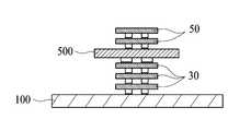
도 1 내지 도 3에 따르면, 본 발명의 3차원 적층형 패키지는 제1기판(100), 제1칩(30), 제2신호처리유닛(500) 및 제2칩(50)을 포함할 수 있다.According to FIGS. 1 to 3, the 3D stacked package of the present invention may include a
제1기판(100)은 회로가 구비되는 인쇄 회로 기판(PCB)일 수 있다. 다만, 상기 제1기판(100)은 반드시 PCB일 필요는 없고 신호 전달이 이루어지는 구성이라면 다양한 형태로 구비될 수 있음은 물론이다.The
제1칩(30)은 제1기판(100) 상에 구비되어 신호를 생성하는 구성일 수 있다.The
제2신호처리유닛(500)은 상기 제1칩(30) 상에 구비되어, 후술할 제2칩(50)에서 생성되는 신호를 풀어주어 최종적으로 제1기판(100)에 전달되도록 하는 구성일 수 있다.The second
제2칩(50)은 상기 제2신호처리유닛(500) 상에 구비되어 신호를 생성하는 구성일 수 있다.The
이 때, 상기 제2칩(50)은 논리 칩(Logic Chip)에 해당하고, 상기 제2신호처리유닛(500)은 상기 제2칩(50)에서 생성되는 신호를 처리하여 상기 제1기판(100)에 전달하는 것을 특징으로 할 수 있다.At this time, the
논리 칩의 경우 반도체 패키지 또는 메모리 모듈에 있어 핵심이 되는 구성으로서, 기기의 작동 등과 관련하여 상기 논리 칩에서 생성된 신호를 상기 제2신호처리유닛(500)이 먼저 처리하게 되므로 더 신속한 신호 전달이 가능하게 된다.In the case of a logic chip, the second
그리고 상기 제1칩(30)은 메모리 칩에 해당하는 것을 특징으로 할 수 있다.In addition, the
메모리 칩은 상기 제2신호처리유닛(500)에서 처리되거나 설정되는 바에 따라, 상기 논리 칩에서 생성되는 신호의 일부를 저장하거나 상기 제1기판(100)에 전달할 수 있다.As the memory chip is processed or set in the second
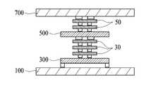
이 때, 본 발명의 3차원 적층형 패키지는 제1신호처리유닛(300)을 포함할 수 있다.At this time, the three-dimensional stacked package of the present invention may include a first
제1신호처리유닛(300)은, 상기 제1기판(100) 및 상기 제1칩(30) 사이에 상기 제1칩(30)에서 전달되는 신호를 처리하는 구성일 수 있다.The first
즉, 상기 제1신호처리유닛(300)은 제1기판(100) 상에 구비될 수 있으며, 상기 제1신호처리유닛(300)은 상기 제1칩(30)을 경유한 신호를 처리하거나 풀어준 후에 제1기판(100)에 전달할 수 있다.That is, the first
또한, 도 3에서와 같이, 본 발명의 3차원 적층형 패키지는 제2기판(700)을 포함할 수 있다.In addition, as shown in Figure 3, the three-dimensional stacked package of the present invention may include a
상기 제2기판(700)은, 상기 제1기판(100)과 대향하며 상기 제2칩(50)에 구비되는 구성일 수 있다.The
제2기판(700)은 회로가 구비되는 인쇄 회로 기판(PCB)일 수 있다. 다만, 상기 제2기판(700)은 반드시 PCB일 필요는 없고 신호 전달이 이루어지는 구성이라면 다양한 형태로 구비될 수 있음은 물론이다.The
이 때, 상기 제1기판(100)은 상기 제1칩(30)에서 생성되는 신호를 전달받고, 상기 제2기판(700)은 상기 제2칩(50)에서 생성되는 신호를 전달받는 것을 특징으로 할 수 있다.At this time, the
즉, 상기 제1신호처리유닛(300)과 상기 제2신호처리유닛(500)은 각각 상기 제1칩(30)과 상기 제2칩(50)에서 생성되는 신호를 처리한 후 상기 제1기판(100) 및 상기 제2기판(700)에 전달할 수 있다.That is, the first
제1칩(30) 및 제2칩(50)에서 생성되는 신호에 대하여 제1신호처리유닛(300)과 제2신호처리유닛(500)이 처리하는 범위 또는 우선 순위 등은 장치나 환경에 따라 달라질 수 있음은 물론이다.The range or priority of the first
예를 들어, 제1신호처리유닛(300)이 제1신호처리유닛(300)과 제2신호처리유닛(500) 사이에 구비되는 칩에 대한 신호를 처리할 수 있고, 제2신호처리유닛(500)이 제2신호처리유닛(500)과 제2기판(700) 사이에 구비되는 칩에 대한 신호를 처리할 수 있는 경우, 상기 제1신호처리유닛(300)과 상기 제2신호처리유닛(500)은 동시에 또는 이시에 우선순위에 따라 각각의 신호를 처리하여 제1기판(100) 및 제2기판 중 적어도 어느 하나로 전송할 수 있다.For example, the first
또한, 본 발명의 3차원 적층형 패키지는 상기 제1기판(100) 및 상기 제1칩(30) 사이에 상기 제1칩(30)에서 전달되는 신호를 처리하는 제1신호처리유닛(300)을 더 포함하고, 상기 제1칩(30)은 논리 칩에 해당하고, 상기 제1신호처리유닛(300)은 상기 제1칩(30)에서 생성되는 신호를 처리하여 상기 제1기판(100)에 전달하는 것을 특징으로 할 수 있다.In addition, the three-dimensional stacked package of the present invention is a first
이는 본 발명의 다른 실시 예일 수 있으며, 제2칩(50)이 아닌 제1칩(30)이 논리 칩(Logic Chip)으로서, 제1신호처리유닛(300)이 논리 칩에서 생성되는 신호를 처리할 수 있다. 다만, 이는 하나의 예시일 뿐이고 제2신호처리유닛(500)이 제1칩(30)의 신호를 처리할 수 있음은 통상의 기술자에 자명하다 할 것이다.This may be another embodiment of the present invention, the
본 발명의 3차원 적층형 패키지는 상술한 구성에 의해, 칩 간의 신호 전달은 신속하고 정확하게 할 수 있다.The three-dimensional stacked package of the present invention has the above-described configuration, so that signal transmission between chips can be performed quickly and accurately.
즉, 제1신호처리유닛 및 제2신호처리유닛(500)이 제1칩(30)과 제2칩(50)에서 발생하는 신호를 미리 풀어주거나 처리하여 기판에 신호 전달을 함으로써 신속하고 정확한 처리가 가능하게 된다.That is, the first signal processing unit and the second
또한, 수직적으로 적층되는 본 발명의 구조는 작은 면적의 반도체 패키징을 구현할 수 있게 된다.In addition, the structure of the present invention, which is vertically stacked, enables realization of semiconductor packaging in a small area.
이상과 같이 본 발명에 따른 바람직한 실시예를 살펴보았으며, 앞서 설명된 실시예 이외에도 본 발명이 그 취지나 범주에서 벗어남이 없이 다른 특정 형태로 구체화될 수 있다는 사실은 해당 기술에 통상의 지식을 가진 이들에게는 자명한 것이다. 그러므로, 상술된 실시예는 제한적인 것이 아니라 예시적인 것으로 여겨져야 하고, 이에 따라 본 발명은 상술한 설명에 한정되지 않고 첨부된 청구항의 범주 및 그 동등 범위 내에서 변경될 수도 있다.As described above, the preferred embodiments according to the present invention have been examined, and the fact that the present invention can be embodied in other specific forms without departing from the spirit or scope of the embodiments described above has ordinary knowledge in the art. It is obvious to them. Therefore, the above-described embodiments should be regarded as illustrative rather than restrictive, and accordingly, the present invention is not limited to the above description and may be changed within the scope of the appended claims and their equivalents.
30: 제1칩
50: 제2칩
100: 제1기판
300: 제1신호처리유닛
500: 제2신호처리유닛
700: 제2기판30: first chip
50: second chip
100: first substrate
300: first signal processing unit
500: second signal processing unit
700: second substrate
Claims (7)
Translated fromKorean상기 제1기판에 구비되는 제1칩;
상기 제1칩 상에 구비되는 제2신호처리유닛; 및
상기 제2신호처리유닛 상에 구비되는 제2칩;
을 포함하는 3차원 적층형 패키지.A first substrate;
A first chip provided on the first substrate;
A second signal processing unit provided on the first chip; And
A second chip provided on the second signal processing unit;
3D stacked package comprising a.
상기 제2칩은 논리 칩에 해당하고, 상기 제2신호처리유닛은 상기 제2칩에서 생성되는 신호를 처리하여 상기 제1기판에 전달하는 것을 특징으로 하는 3차원 적층형 패키지.According to claim 1,
The second chip corresponds to a logic chip, and the second signal processing unit processes a signal generated by the second chip and transmits it to the first substrate.
상기 제1칩은 메모리 칩에 해당하는 것을 특징으로 하는 3차원 적층형 패키지.According to claim 2,
The first chip is a three-dimensional stacked package, characterized in that corresponding to the memory chip.
상기 제1기판 및 상기 제1칩 사이에 상기 제1칩에서 전달되는 신호를 처리하는 제1신호처리유닛;
을 더 포함하는 3차원 적층형 패키지.According to claim 3,
A first signal processing unit processing a signal transmitted from the first chip between the first substrate and the first chip;
3D stacked package further comprising a.
상기 제1기판과 대향하며 상기 제2칩에 구비되는 제2기판;
을 더 포함하는 3차원 적층형 패키지.According to claim 1,
A second substrate facing the first substrate and provided on the second chip;
3D stacked package further comprising a.
상기 제1기판은 상기 제1칩에서 생성되는 신호를 전달받고, 상기 제2기판은 상기 제2칩에서 생성되는 신호를 전달받는 것을 특징으로 하는 3차원 적층형 패키지.The method of claim 5,
The first substrate receives the signal generated by the first chip, and the second substrate receives the signal generated by the second chip.
상기 제1기판 및 상기 제1칩 사이에 상기 제1칩에서 전달되는 신호를 처리하는 제1신호처리유닛;
을 더 포함하고,
상기 제1칩은 논리 칩에 해당하고, 상기 제1신호처리유닛은 상기 제1칩에서 생성되는 신호를 처리하여 상기 제1기판에 전달하는 것을 특징으로 하는 3차원 적층형 패키지.
According to claim 1,
A first signal processing unit processing a signal transmitted from the first chip between the first substrate and the first chip;
Further comprising,
The first chip corresponds to a logic chip, and the first signal processing unit processes a signal generated from the first chip and transmits it to the first substrate.
Priority Applications (1)
| Application Number | Priority Date | Filing Date | Title |
|---|---|---|---|
| KR1020180151566AKR102131648B1 (en) | 2018-11-30 | 2018-11-30 | Package structure of three-dimensional lamination using multiple devices |
Applications Claiming Priority (1)
| Application Number | Priority Date | Filing Date | Title |
|---|---|---|---|
| KR1020180151566AKR102131648B1 (en) | 2018-11-30 | 2018-11-30 | Package structure of three-dimensional lamination using multiple devices |
Publications (2)
| Publication Number | Publication Date |
|---|---|
| KR20200065270Atrue KR20200065270A (en) | 2020-06-09 |
| KR102131648B1 KR102131648B1 (en) | 2020-07-08 |
Family
ID=71082068
Family Applications (1)
| Application Number | Title | Priority Date | Filing Date |
|---|---|---|---|
| KR1020180151566AActiveKR102131648B1 (en) | 2018-11-30 | 2018-11-30 | Package structure of three-dimensional lamination using multiple devices |
Country Status (1)
| Country | Link |
|---|---|
| KR (1) | KR102131648B1 (en) |
Citations (5)
| Publication number | Priority date | Publication date | Assignee | Title |
|---|---|---|---|---|
| KR19990055507A (en) | 1997-12-27 | 1999-07-15 | 구본준 | Memory module and manufacturing method |
| US20100008058A1 (en)* | 2008-07-10 | 2010-01-14 | Hitachi, Ltd. | Semiconductor device |
| JP2010034436A (en)* | 2008-07-31 | 2010-02-12 | Hitachi Ltd | Semiconductor integrated circuit device |
| KR20110124063A (en)* | 2010-05-10 | 2011-11-16 | 하나 마이크론(주) | Stacked Semiconductor Packages |
| KR20120024026A (en)* | 2010-09-03 | 2012-03-14 | 삼성전자주식회사 | Semiconductor memory device |
- 2018
- 2018-11-30KRKR1020180151566Apatent/KR102131648B1/enactiveActive
Patent Citations (5)
| Publication number | Priority date | Publication date | Assignee | Title |
|---|---|---|---|---|
| KR19990055507A (en) | 1997-12-27 | 1999-07-15 | 구본준 | Memory module and manufacturing method |
| US20100008058A1 (en)* | 2008-07-10 | 2010-01-14 | Hitachi, Ltd. | Semiconductor device |
| JP2010034436A (en)* | 2008-07-31 | 2010-02-12 | Hitachi Ltd | Semiconductor integrated circuit device |
| KR20110124063A (en)* | 2010-05-10 | 2011-11-16 | 하나 마이크론(주) | Stacked Semiconductor Packages |
| KR20120024026A (en)* | 2010-09-03 | 2012-03-14 | 삼성전자주식회사 | Semiconductor memory device |
Also Published As
| Publication number | Publication date |
|---|---|
| KR102131648B1 (en) | 2020-07-08 |
Similar Documents
| Publication | Publication Date | Title |
|---|---|---|
| US8760181B2 (en) | Semiconductor system and device for identifying stacked chips and method thereof | |
| US9906312B2 (en) | Semiconductor packages with optical interconnection structures, memory cards including the same, and electronic systems including the same | |
| US7759785B2 (en) | Apparatus for packaging semiconductor devices, packaged semiconductor components, methods of manufacturing apparatus for packaging semiconductor devices, and methods of manufacturing semiconductor components | |
| US9336857B2 (en) | Semiconductor memory device including stacked memory chips | |
| US20170131487A1 (en) | Semiconductor chip package having optical interface | |
| US20130099235A1 (en) | Semiconductor wafer and method for manufacturing stack package using the same | |
| US9917061B2 (en) | Semiconductor apparatus and memory system | |
| US8487645B2 (en) | Through silicon via testing structure | |
| JP2015527754A5 (en) | ||
| US20150235715A1 (en) | Stacked semiconductor memory apparatus and test circuit therefor | |
| US11682627B2 (en) | Semiconductor package including an interposer | |
| TW201614785A (en) | Semiconductor stack packages | |
| US9335369B2 (en) | Semiconductor integrated circuit | |
| TWI667766B (en) | Semiconductor integrated circuit and semiconductor system with the same | |
| KR102131648B1 (en) | Package structure of three-dimensional lamination using multiple devices | |
| US9502384B2 (en) | Semiconductor devices and semiconductor systems including the same | |
| US9530756B2 (en) | Semiconductor apparatus having electrical connections with through-via and a metal layer and stacking method thereof | |
| KR102664732B1 (en) | Memory device and semiconductor package including the same | |
| US9396765B2 (en) | Stacked semiconductor package | |
| KR20160012551A (en) | Semiconductor apparatus and system including plurality of channels | |
| KR102072430B1 (en) | Memory module structure and manufacturing method | |
| KR20160115483A (en) | Semiconductor device | |
| KR20140088782A (en) | Three dimensional stacked semiconductor integrated circuit | |
| US9269414B2 (en) | Semiconductor integrated circuit | |
| CN101494218A (en) | Multi-channel stacked semiconductor device, method of manufacturing the same, and stacked substrate using the same |
Legal Events
| Date | Code | Title | Description |
|---|---|---|---|
| PA0109 | Patent application | Patent event code:PA01091R01D Comment text:Patent Application Patent event date:20181130 | |
| PA0201 | Request for examination | ||
| PE0902 | Notice of grounds for rejection | Comment text:Notification of reason for refusal Patent event date:20200129 Patent event code:PE09021S01D | |
| E90F | Notification of reason for final refusal | ||
| PE0902 | Notice of grounds for rejection | Comment text:Final Notice of Reason for Refusal Patent event date:20200606 Patent event code:PE09021S02D | |
| PG1501 | Laying open of application | ||
| E701 | Decision to grant or registration of patent right | ||
| PE0701 | Decision of registration | Patent event code:PE07011S01D Comment text:Decision to Grant Registration Patent event date:20200629 | |
| GRNT | Written decision to grant | ||
| PR0701 | Registration of establishment | Comment text:Registration of Establishment Patent event date:20200702 Patent event code:PR07011E01D | |
| PR1002 | Payment of registration fee | Payment date:20200703 End annual number:3 Start annual number:1 | |
| PG1601 | Publication of registration | ||
| PR1001 | Payment of annual fee | Payment date:20230626 Start annual number:4 End annual number:4 | |
| PR1001 | Payment of annual fee | Payment date:20240624 Start annual number:5 End annual number:5 | |
| PR1001 | Payment of annual fee | Payment date:20250623 Start annual number:6 End annual number:6 |