KR20200053455A - Display device - Google Patents
Display deviceDownload PDFInfo
- Publication number
- KR20200053455A KR20200053455AKR1020200055200AKR20200055200AKR20200053455AKR 20200053455 AKR20200053455 AKR 20200053455AKR 1020200055200 AKR1020200055200 AKR 1020200055200AKR 20200055200 AKR20200055200 AKR 20200055200AKR 20200053455 AKR20200053455 AKR 20200053455A
- Authority
- KR
- South Korea
- Prior art keywords
- oxide semiconductor
- thin film
- semiconductor layer
- film transistor
- layer
- Prior art date
- Legal status (The legal status is an assumption and is not a legal conclusion. Google has not performed a legal analysis and makes no representation as to the accuracy of the status listed.)
- Granted
Links
- 239000004065semiconductorSubstances0.000claimsabstractdescription299
- 230000015572biosynthetic processEffects0.000claimsdescription25
- 239000010409thin filmSubstances0.000abstractdescription253
- 239000001257hydrogenSubstances0.000abstractdescription43
- 229910052739hydrogenInorganic materials0.000abstractdescription43
- VYPSYNLAJGMNEJ-UHFFFAOYSA-NSilicium dioxideChemical compoundO=[Si]=OVYPSYNLAJGMNEJ-UHFFFAOYSA-N0.000abstractdescription41
- 229910052814silicon oxideInorganic materials0.000abstractdescription41
- 229910052581Si3N4Inorganic materials0.000abstractdescription40
- HQVNEWCFYHHQES-UHFFFAOYSA-Nsilicon nitrideChemical compoundN12[Si]34N5[Si]62N3[Si]51N64HQVNEWCFYHHQES-UHFFFAOYSA-N0.000abstractdescription40
- 239000007789gasSubstances0.000abstractdescription38
- UFHFLCQGNIYNRP-UHFFFAOYSA-NHydrogenChemical compound[H][H]UFHFLCQGNIYNRP-UHFFFAOYSA-N0.000abstractdescription32
- QGZKDVFQNNGYKY-UHFFFAOYSA-NAmmoniaChemical compoundNQGZKDVFQNNGYKY-UHFFFAOYSA-N0.000abstractdescription25
- 238000005268plasma chemical vapour depositionMethods0.000abstractdescription15
- -1hydrogen compoundChemical class0.000abstractdescription14
- 229910021529ammoniaInorganic materials0.000abstractdescription13
- BLRPTPMANUNPDV-UHFFFAOYSA-NSilaneChemical compound[SiH4]BLRPTPMANUNPDV-UHFFFAOYSA-N0.000abstractdescription11
- 229910000077silaneInorganic materials0.000abstractdescription11
- 230000004888barrier functionEffects0.000abstractdescription5
- 239000010410layerSubstances0.000description347
- 239000010408filmSubstances0.000description174
- IJGRMHOSHXDMSA-UHFFFAOYSA-NAtomic nitrogenChemical compoundN#NIJGRMHOSHXDMSA-UHFFFAOYSA-N0.000description147
- 229910052757nitrogenInorganic materials0.000description72
- 238000000034methodMethods0.000description51
- 238000004544sputter depositionMethods0.000description43
- XKRFYHLGVUSROY-UHFFFAOYSA-NArgonChemical compound[Ar]XKRFYHLGVUSROY-UHFFFAOYSA-N0.000description42
- 239000000758substrateSubstances0.000description41
- 230000008569processEffects0.000description37
- 238000010586diagramMethods0.000description30
- 102100040862Dual specificity protein kinase CLK1Human genes0.000description27
- 239000000463materialSubstances0.000description27
- 101000749294Homo sapiens Dual specificity protein kinase CLK1Proteins0.000description26
- XLOMVQKBTHCTTD-UHFFFAOYSA-NZinc monoxideChemical compound[Zn]=OXLOMVQKBTHCTTD-UHFFFAOYSA-N0.000description26
- 238000004519manufacturing processMethods0.000description24
- 102100040844Dual specificity protein kinase CLK2Human genes0.000description21
- 101000749291Homo sapiens Dual specificity protein kinase CLK2Proteins0.000description21
- 229910052786argonInorganic materials0.000description21
- PXHVJJICTQNCMI-UHFFFAOYSA-NNickelChemical compound[Ni]PXHVJJICTQNCMI-UHFFFAOYSA-N0.000description18
- 238000010438heat treatmentMethods0.000description18
- 238000000206photolithographyMethods0.000description18
- 239000004020conductorSubstances0.000description16
- 230000002829reductive effectEffects0.000description16
- QVGXLLKOCUKJST-UHFFFAOYSA-Natomic oxygenChemical compound[O]QVGXLLKOCUKJST-UHFFFAOYSA-N0.000description15
- 239000001301oxygenSubstances0.000description15
- 229910052760oxygenInorganic materials0.000description15
- 239000011787zinc oxideSubstances0.000description13
- 239000010949copperSubstances0.000description12
- 238000005530etchingMethods0.000description11
- 239000010936titaniumSubstances0.000description11
- 239000011701zincSubstances0.000description11
- RYGMFSIKBFXOCR-UHFFFAOYSA-NCopperChemical compound[Cu]RYGMFSIKBFXOCR-UHFFFAOYSA-N0.000description10
- GYHNNYVSQQEPJS-UHFFFAOYSA-NGalliumChemical compound[Ga]GYHNNYVSQQEPJS-UHFFFAOYSA-N0.000description10
- 239000012298atmosphereSubstances0.000description10
- 229910052802copperInorganic materials0.000description10
- 229910052733galliumInorganic materials0.000description10
- 238000007733ion platingMethods0.000description10
- 229910052751metalInorganic materials0.000description10
- 238000007736thin film deposition techniqueMethods0.000description10
- 229910005191Ga 2 O 3Inorganic materials0.000description9
- 229910052782aluminiumInorganic materials0.000description9
- 238000000151depositionMethods0.000description9
- 238000002347injectionMethods0.000description9
- 239000007924injectionSubstances0.000description9
- 229910044991metal oxideInorganic materials0.000description9
- 150000004706metal oxidesChemical class0.000description9
- 239000000203mixtureSubstances0.000description9
- 240000002329Inga feuilleiSpecies0.000description8
- XUIMIQQOPSSXEZ-UHFFFAOYSA-NSiliconChemical compound[Si]XUIMIQQOPSSXEZ-UHFFFAOYSA-N0.000description8
- 229910045601alloyInorganic materials0.000description8
- 239000000956alloySubstances0.000description8
- XAGFODPZIPBFFR-UHFFFAOYSA-NaluminiumChemical compound[Al]XAGFODPZIPBFFR-UHFFFAOYSA-N0.000description8
- 125000004429atomChemical group0.000description8
- 239000011651chromiumSubstances0.000description8
- 238000005070samplingMethods0.000description8
- 229910052710siliconInorganic materials0.000description8
- 239000010703siliconSubstances0.000description8
- 239000013078crystalSubstances0.000description7
- XEEYBQQBJWHFJM-UHFFFAOYSA-NIronChemical compound[Fe]XEEYBQQBJWHFJM-UHFFFAOYSA-N0.000description6
- RTAQQCXQSZGOHL-UHFFFAOYSA-NTitaniumChemical compound[Ti]RTAQQCXQSZGOHL-UHFFFAOYSA-N0.000description6
- 229910007541Zn OInorganic materials0.000description6
- 125000004435hydrogen atomChemical group[H]*0.000description6
- 229910052759nickelInorganic materials0.000description6
- 229920005989resinPolymers0.000description6
- 239000011347resinSubstances0.000description6
- 229910052719titaniumInorganic materials0.000description6
- 238000001771vacuum depositionMethods0.000description6
- 238000004891communicationMethods0.000description5
- 230000008021depositionEffects0.000description5
- 239000002184metalSubstances0.000description5
- 238000012545processingMethods0.000description5
- 238000007740vapor depositionMethods0.000description5
- VYZAMTAEIAYCRO-UHFFFAOYSA-NChromiumChemical compound[Cr]VYZAMTAEIAYCRO-UHFFFAOYSA-N0.000description4
- ZOKXTWBITQBERF-UHFFFAOYSA-NMolybdenumChemical compound[Mo]ZOKXTWBITQBERF-UHFFFAOYSA-N0.000description4
- 238000004458analytical methodMethods0.000description4
- 238000006243chemical reactionMethods0.000description4
- 229910052804chromiumInorganic materials0.000description4
- 230000006378damageEffects0.000description4
- 230000000694effectsEffects0.000description4
- 229910003437indium oxideInorganic materials0.000description4
- PJXISJQVUVHSOJ-UHFFFAOYSA-Nindium(iii) oxideChemical compound[O-2].[O-2].[O-2].[In+3].[In+3]PJXISJQVUVHSOJ-UHFFFAOYSA-N0.000description4
- 239000011572manganeseSubstances0.000description4
- 239000011159matrix materialSubstances0.000description4
- 229910052750molybdenumInorganic materials0.000description4
- 239000011733molybdenumSubstances0.000description4
- 150000002894organic compoundsChemical class0.000description4
- 230000002441reversible effectEffects0.000description4
- 239000002356single layerSubstances0.000description4
- 239000011734sodiumSubstances0.000description4
- 239000012798spherical particleSubstances0.000description4
- 229910052715tantalumInorganic materials0.000description4
- GUVRBAGPIYLISA-UHFFFAOYSA-Ntantalum atomChemical compound[Ta]GUVRBAGPIYLISA-UHFFFAOYSA-N0.000description4
- 229910052723transition metalInorganic materials0.000description4
- WFKWXMTUELFFGS-UHFFFAOYSA-NtungstenChemical compound[W]WFKWXMTUELFFGS-UHFFFAOYSA-N0.000description4
- 229910052721tungstenInorganic materials0.000description4
- 239000010937tungstenSubstances0.000description4
- QTBSBXVTEAMEQO-UHFFFAOYSA-NAcetic acidChemical compoundCC(O)=OQTBSBXVTEAMEQO-UHFFFAOYSA-N0.000description3
- MYMOFIZGZYHOMD-UHFFFAOYSA-NDioxygenChemical compoundO=OMYMOFIZGZYHOMD-UHFFFAOYSA-N0.000description3
- 230000015556catabolic processEffects0.000description3
- 238000006731degradation reactionMethods0.000description3
- 238000009792diffusion processMethods0.000description3
- 229910001873dinitrogenInorganic materials0.000description3
- 229910001882dioxygenInorganic materials0.000description3
- 230000001747exhibiting effectEffects0.000description3
- 239000000945fillerSubstances0.000description3
- 238000011049fillingMethods0.000description3
- AMGQUBHHOARCQH-UHFFFAOYSA-Nindium;oxotinChemical compound[In].[Sn]=OAMGQUBHHOARCQH-UHFFFAOYSA-N0.000description3
- 239000007788liquidSubstances0.000description3
- 230000007246mechanismEffects0.000description3
- QGLKJKCYBOYXKC-UHFFFAOYSA-NnonaoxidotritungstenChemical compoundO=[W]1(=O)O[W](=O)(=O)O[W](=O)(=O)O1QGLKJKCYBOYXKC-UHFFFAOYSA-N0.000description3
- 239000002245particleSubstances0.000description3
- 238000002161passivationMethods0.000description3
- 230000001737promoting effectEffects0.000description3
- 230000001681protective effectEffects0.000description3
- 239000003566sealing materialSubstances0.000description3
- 239000006104solid solutionSubstances0.000description3
- 239000000126substanceSubstances0.000description3
- 229910001930tungsten oxideInorganic materials0.000description3
- 238000001039wet etchingMethods0.000description3
- CURLTUGMZLYLDI-UHFFFAOYSA-NCarbon dioxideChemical compoundO=C=OCURLTUGMZLYLDI-UHFFFAOYSA-N0.000description2
- 206010052128GlareDiseases0.000description2
- MHAJPDPJQMAIIY-UHFFFAOYSA-NHydrogen peroxideChemical compoundOOMHAJPDPJQMAIIY-UHFFFAOYSA-N0.000description2
- DGAQECJNVWCQMB-PUAWFVPOSA-MIlexoside XXIXChemical compoundC[C@@H]1CC[C@@]2(CC[C@@]3(C(=CC[C@H]4[C@]3(CC[C@@H]5[C@@]4(CC[C@@H](C5(C)C)OS(=O)(=O)[O-])C)C)[C@@H]2[C@]1(C)O)C)C(=O)O[C@H]6[C@@H]([C@H]([C@@H]([C@H](O6)CO)O)O)O.[Na+]DGAQECJNVWCQMB-PUAWFVPOSA-M0.000description2
- PWHULOQIROXLJO-UHFFFAOYSA-NManganeseChemical compound[Mn]PWHULOQIROXLJO-UHFFFAOYSA-N0.000description2
- 229910052779NeodymiumInorganic materials0.000description2
- NBIIXXVUZAFLBC-UHFFFAOYSA-NPhosphoric acidChemical compoundOP(O)(O)=ONBIIXXVUZAFLBC-UHFFFAOYSA-N0.000description2
- 238000002441X-ray diffractionMethods0.000description2
- NIXOWILDQLNWCW-UHFFFAOYSA-Nacrylic acid groupChemical groupC(C=C)(=O)ONIXOWILDQLNWCW-UHFFFAOYSA-N0.000description2
- DQXBYHZEEUGOBF-UHFFFAOYSA-Nbut-3-enoic acid;etheneChemical compoundC=C.OC(=O)CC=CDQXBYHZEEUGOBF-UHFFFAOYSA-N0.000description2
- 229910052799carbonInorganic materials0.000description2
- 230000008859changeEffects0.000description2
- 229910017052cobaltInorganic materials0.000description2
- 239000010941cobaltSubstances0.000description2
- GUTLYIVDDKVIGB-UHFFFAOYSA-Ncobalt atomChemical compound[Co]GUTLYIVDDKVIGB-UHFFFAOYSA-N0.000description2
- 150000001875compoundsChemical class0.000description2
- 239000000428dustSubstances0.000description2
- 238000005401electroluminescenceMethods0.000description2
- 239000005038ethylene vinyl acetateSubstances0.000description2
- 230000005281excited stateEffects0.000description2
- 239000010419fine particleSubstances0.000description2
- 239000011521glassSubstances0.000description2
- 239000012535impuritySubstances0.000description2
- 238000001095inductively coupled plasma mass spectrometryMethods0.000description2
- 230000002401inhibitory effectEffects0.000description2
- 239000004973liquid crystal related substanceSubstances0.000description2
- 229910052748manganeseInorganic materials0.000description2
- 239000003094microcapsuleSubstances0.000description2
- 239000002159nanocrystalSubstances0.000description2
- QEFYFXOXNSNQGX-UHFFFAOYSA-Nneodymium atomChemical compound[Nd]QEFYFXOXNSNQGX-UHFFFAOYSA-N0.000description2
- 150000004767nitridesChemical class0.000description2
- 239000012299nitrogen atmosphereSubstances0.000description2
- 230000003287optical effectEffects0.000description2
- TWNQGVIAIRXVLR-UHFFFAOYSA-Noxo(oxoalumanyloxy)alumaneChemical compoundO=[Al]O[Al]=OTWNQGVIAIRXVLR-UHFFFAOYSA-N0.000description2
- BPUBBGLMJRNUCC-UHFFFAOYSA-Noxygen(2-);tantalum(5+)Chemical compound[O-2].[O-2].[O-2].[O-2].[O-2].[Ta+5].[Ta+5]BPUBBGLMJRNUCC-UHFFFAOYSA-N0.000description2
- 238000005192partitionMethods0.000description2
- 230000002093peripheral effectEffects0.000description2
- 229920001200poly(ethylene-vinyl acetate)Polymers0.000description2
- 229920002037poly(vinyl butyral) polymerPolymers0.000description2
- 239000004800polyvinyl chlorideSubstances0.000description2
- 229920000915polyvinyl chloridePolymers0.000description2
- 238000004549pulsed laser depositionMethods0.000description2
- 229910052706scandiumInorganic materials0.000description2
- SIXSYDAISGFNSX-UHFFFAOYSA-Nscandium atomChemical compound[Sc]SIXSYDAISGFNSX-UHFFFAOYSA-N0.000description2
- 229910052708sodiumInorganic materials0.000description2
- 229910001936tantalum oxideInorganic materials0.000description2
- 229910000314transition metal oxideInorganic materials0.000description2
- YVTHLONGBIQYBO-UHFFFAOYSA-Nzinc indium(3+) oxygen(2-)Chemical compound[O--].[Zn++].[In+3]YVTHLONGBIQYBO-UHFFFAOYSA-N0.000description2
- 241001408627Agriopis marginariaSpecies0.000description1
- 229910000838Al alloyInorganic materials0.000description1
- 229910017073AlLiInorganic materials0.000description1
- GRYLNZFGIOXLOG-UHFFFAOYSA-NNitric acidChemical compoundO[N+]([O-])=OGRYLNZFGIOXLOG-UHFFFAOYSA-N0.000description1
- 101100283966Pectobacterium carotovorum subsp. carotovorum outN geneProteins0.000description1
- 239000004642PolyimideSubstances0.000description1
- 229910001069Ti alloyInorganic materials0.000description1
- GWEVSGVZZGPLCZ-UHFFFAOYSA-NTitan oxideChemical compoundO=[Ti]=OGWEVSGVZZGPLCZ-UHFFFAOYSA-N0.000description1
- 230000009471actionEffects0.000description1
- 230000004913activationEffects0.000description1
- 239000002313adhesive filmSubstances0.000description1
- 229910000147aluminium phosphateInorganic materials0.000description1
- 239000005407aluminoborosilicate glassSubstances0.000description1
- 229910021417amorphous siliconInorganic materials0.000description1
- 239000012300argon atmosphereSubstances0.000description1
- 229910052788bariumInorganic materials0.000description1
- DSAJWYNOEDNPEQ-UHFFFAOYSA-Nbarium atomChemical compound[Ba]DSAJWYNOEDNPEQ-UHFFFAOYSA-N0.000description1
- 239000011230binding agentSubstances0.000description1
- 239000005388borosilicate glassSubstances0.000description1
- 239000001569carbon dioxideSubstances0.000description1
- 229910002092carbon dioxideInorganic materials0.000description1
- 239000000969carrierSubstances0.000description1
- 239000003795chemical substances by applicationSubstances0.000description1
- 238000005520cutting processMethods0.000description1
- 238000007872degassingMethods0.000description1
- 238000013461designMethods0.000description1
- 230000006866deteriorationEffects0.000description1
- 239000006185dispersionSubstances0.000description1
- 238000009826distributionMethods0.000description1
- 238000001312dry etchingMethods0.000description1
- 230000005684electric fieldEffects0.000description1
- 239000007772electrode materialSubstances0.000description1
- 239000003822epoxy resinSubstances0.000description1
- 238000000605extractionMethods0.000description1
- 230000004313glareEffects0.000description1
- 230000005283ground stateEffects0.000description1
- 230000005525hole transportEffects0.000description1
- 150000002431hydrogenChemical class0.000description1
- 150000002483hydrogen compoundsChemical class0.000description1
- 239000011261inert gasSubstances0.000description1
- 150000002484inorganic compoundsChemical class0.000description1
- 229910010272inorganic materialInorganic materials0.000description1
- 239000012212insulatorSubstances0.000description1
- 230000007257malfunctionEffects0.000description1
- 238000005259measurementMethods0.000description1
- 238000000691measurement methodMethods0.000description1
- 229910021645metal ionInorganic materials0.000description1
- 239000008239natural waterSubstances0.000description1
- 229910017604nitric acidInorganic materials0.000description1
- 239000012788optical filmSubstances0.000description1
- 125000000962organic groupChemical group0.000description1
- AHLBNYSZXLDEJQ-FWEHEUNISA-NorlistatChemical compoundCCCCCCCCCCC[C@H](OC(=O)[C@H](CC(C)C)NC=O)C[C@@H]1OC(=O)[C@H]1CCCCCCAHLBNYSZXLDEJQ-FWEHEUNISA-N0.000description1
- 230000003647oxidationEffects0.000description1
- 238000007254oxidation reactionMethods0.000description1
- 239000000049pigmentSubstances0.000description1
- 229920003023plasticPolymers0.000description1
- 239000004033plasticSubstances0.000description1
- 229920000647polyepoxidePolymers0.000description1
- 229920006267polyester filmPolymers0.000description1
- 229920001721polyimidePolymers0.000description1
- 229920001296polysiloxanePolymers0.000description1
- 239000011241protective layerSubstances0.000description1
- 238000011002quantificationMethods0.000description1
- 238000005215recombinationMethods0.000description1
- 230000006798recombinationEffects0.000description1
- 238000005001rutherford backscattering spectroscopyMethods0.000description1
- 229920002050silicone resinPolymers0.000description1
- 239000000243solutionSubstances0.000description1
- 229920001187thermosetting polymerPolymers0.000description1
- XOLBLPGZBRYERU-UHFFFAOYSA-Ntin dioxideChemical compoundO=[Sn]=OXOLBLPGZBRYERU-UHFFFAOYSA-N0.000description1
- 229910001887tin oxideInorganic materials0.000description1
- OGIDPMRJRNCKJF-UHFFFAOYSA-Ntitanium oxideInorganic materials[Ti]=OOGIDPMRJRNCKJF-UHFFFAOYSA-N0.000description1
- 230000007704transitionEffects0.000description1
- 150000003624transition metalsChemical class0.000description1
- 238000002834transmittanceMethods0.000description1
- XLYOFNOQVPJJNP-UHFFFAOYSA-NwaterSubstancesOXLYOFNOQVPJJNP-UHFFFAOYSA-N0.000description1
Images


Classifications
- G—PHYSICS
- G02—OPTICS
- G02F—OPTICAL DEVICES OR ARRANGEMENTS FOR THE CONTROL OF LIGHT BY MODIFICATION OF THE OPTICAL PROPERTIES OF THE MEDIA OF THE ELEMENTS INVOLVED THEREIN; NON-LINEAR OPTICS; FREQUENCY-CHANGING OF LIGHT; OPTICAL LOGIC ELEMENTS; OPTICAL ANALOGUE/DIGITAL CONVERTERS
- G02F1/00—Devices or arrangements for the control of the intensity, colour, phase, polarisation or direction of light arriving from an independent light source, e.g. switching, gating or modulating; Non-linear optics
- G02F1/01—Devices or arrangements for the control of the intensity, colour, phase, polarisation or direction of light arriving from an independent light source, e.g. switching, gating or modulating; Non-linear optics for the control of the intensity, phase, polarisation or colour
- G02F1/13—Devices or arrangements for the control of the intensity, colour, phase, polarisation or direction of light arriving from an independent light source, e.g. switching, gating or modulating; Non-linear optics for the control of the intensity, phase, polarisation or colour based on liquid crystals, e.g. single liquid crystal display cells
- G02F1/133—Constructional arrangements; Operation of liquid crystal cells; Circuit arrangements
- G02F1/136—Liquid crystal cells structurally associated with a semi-conducting layer or substrate, e.g. cells forming part of an integrated circuit
- G02F1/1362—Active matrix addressed cells
- G02F1/136204—Arrangements to prevent high voltage or static electricity failures
- H01L29/7869—
- H01L29/66742—
- H01L29/768—
- H01L29/78606—
- H01L29/78696—
- H—ELECTRICITY
- H10—SEMICONDUCTOR DEVICES; ELECTRIC SOLID-STATE DEVICES NOT OTHERWISE PROVIDED FOR
- H10D—INORGANIC ELECTRIC SEMICONDUCTOR DEVICES
- H10D1/00—Resistors, capacitors or inductors
- H10D1/40—Resistors
- H10D1/47—Resistors having no potential barriers
- H—ELECTRICITY
- H10—SEMICONDUCTOR DEVICES; ELECTRIC SOLID-STATE DEVICES NOT OTHERWISE PROVIDED FOR
- H10D—INORGANIC ELECTRIC SEMICONDUCTOR DEVICES
- H10D30/00—Field-effect transistors [FET]
- H10D30/60—Insulated-gate field-effect transistors [IGFET]
- H10D30/67—Thin-film transistors [TFT]
- H10D30/6704—Thin-film transistors [TFT] having supplementary regions or layers in the thin films or in the insulated bulk substrates for controlling properties of the device
- H—ELECTRICITY
- H10—SEMICONDUCTOR DEVICES; ELECTRIC SOLID-STATE DEVICES NOT OTHERWISE PROVIDED FOR
- H10D—INORGANIC ELECTRIC SEMICONDUCTOR DEVICES
- H10D30/00—Field-effect transistors [FET]
- H10D30/60—Insulated-gate field-effect transistors [IGFET]
- H10D30/67—Thin-film transistors [TFT]
- H10D30/674—Thin-film transistors [TFT] characterised by the active materials
- H10D30/6755—Oxide semiconductors, e.g. zinc oxide, copper aluminium oxide or cadmium stannate
- H—ELECTRICITY
- H10—SEMICONDUCTOR DEVICES; ELECTRIC SOLID-STATE DEVICES NOT OTHERWISE PROVIDED FOR
- H10D—INORGANIC ELECTRIC SEMICONDUCTOR DEVICES
- H10D62/00—Semiconductor bodies, or regions thereof, of devices having potential barriers
- H10D62/80—Semiconductor bodies, or regions thereof, of devices having potential barriers characterised by the materials
- H—ELECTRICITY
- H10—SEMICONDUCTOR DEVICES; ELECTRIC SOLID-STATE DEVICES NOT OTHERWISE PROVIDED FOR
- H10D—INORGANIC ELECTRIC SEMICONDUCTOR DEVICES
- H10D86/00—Integrated devices formed in or on insulating or conducting substrates, e.g. formed in silicon-on-insulator [SOI] substrates or on stainless steel or glass substrates
- H10D86/01—Manufacture or treatment
- H10D86/021—Manufacture or treatment of multiple TFTs
- H10D86/0221—Manufacture or treatment of multiple TFTs comprising manufacture, treatment or patterning of TFT semiconductor bodies
- H—ELECTRICITY
- H10—SEMICONDUCTOR DEVICES; ELECTRIC SOLID-STATE DEVICES NOT OTHERWISE PROVIDED FOR
- H10D—INORGANIC ELECTRIC SEMICONDUCTOR DEVICES
- H10D86/00—Integrated devices formed in or on insulating or conducting substrates, e.g. formed in silicon-on-insulator [SOI] substrates or on stainless steel or glass substrates
- H10D86/40—Integrated devices formed in or on insulating or conducting substrates, e.g. formed in silicon-on-insulator [SOI] substrates or on stainless steel or glass substrates characterised by multiple TFTs
- H10D86/421—Integrated devices formed in or on insulating or conducting substrates, e.g. formed in silicon-on-insulator [SOI] substrates or on stainless steel or glass substrates characterised by multiple TFTs having a particular composition, shape or crystalline structure of the active layer
- H10D86/423—Integrated devices formed in or on insulating or conducting substrates, e.g. formed in silicon-on-insulator [SOI] substrates or on stainless steel or glass substrates characterised by multiple TFTs having a particular composition, shape or crystalline structure of the active layer comprising semiconductor materials not belonging to the Group IV, e.g. InGaZnO
- H—ELECTRICITY
- H10—SEMICONDUCTOR DEVICES; ELECTRIC SOLID-STATE DEVICES NOT OTHERWISE PROVIDED FOR
- H10D—INORGANIC ELECTRIC SEMICONDUCTOR DEVICES
- H10D86/00—Integrated devices formed in or on insulating or conducting substrates, e.g. formed in silicon-on-insulator [SOI] substrates or on stainless steel or glass substrates
- H10D86/40—Integrated devices formed in or on insulating or conducting substrates, e.g. formed in silicon-on-insulator [SOI] substrates or on stainless steel or glass substrates characterised by multiple TFTs
- H10D86/481—Integrated devices formed in or on insulating or conducting substrates, e.g. formed in silicon-on-insulator [SOI] substrates or on stainless steel or glass substrates characterised by multiple TFTs integrated with passive devices, e.g. auxiliary capacitors
- H—ELECTRICITY
- H10—SEMICONDUCTOR DEVICES; ELECTRIC SOLID-STATE DEVICES NOT OTHERWISE PROVIDED FOR
- H10D—INORGANIC ELECTRIC SEMICONDUCTOR DEVICES
- H10D86/00—Integrated devices formed in or on insulating or conducting substrates, e.g. formed in silicon-on-insulator [SOI] substrates or on stainless steel or glass substrates
- H10D86/40—Integrated devices formed in or on insulating or conducting substrates, e.g. formed in silicon-on-insulator [SOI] substrates or on stainless steel or glass substrates characterised by multiple TFTs
- H10D86/60—Integrated devices formed in or on insulating or conducting substrates, e.g. formed in silicon-on-insulator [SOI] substrates or on stainless steel or glass substrates characterised by multiple TFTs wherein the TFTs are in active matrices
- G—PHYSICS
- G02—OPTICS
- G02F—OPTICAL DEVICES OR ARRANGEMENTS FOR THE CONTROL OF LIGHT BY MODIFICATION OF THE OPTICAL PROPERTIES OF THE MEDIA OF THE ELEMENTS INVOLVED THEREIN; NON-LINEAR OPTICS; FREQUENCY-CHANGING OF LIGHT; OPTICAL LOGIC ELEMENTS; OPTICAL ANALOGUE/DIGITAL CONVERTERS
- G02F2201/00—Constructional arrangements not provided for in groups G02F1/00 - G02F7/00
- G02F2201/50—Protective arrangements
Landscapes
- Physics & Mathematics (AREA)
- Nonlinear Science (AREA)
- Engineering & Computer Science (AREA)
- Microelectronics & Electronic Packaging (AREA)
- Mathematical Physics (AREA)
- Chemical & Material Sciences (AREA)
- Crystallography & Structural Chemistry (AREA)
- General Physics & Mathematics (AREA)
- Optics & Photonics (AREA)
- Thin Film Transistor (AREA)
- Semiconductor Integrated Circuits (AREA)
- Electroluminescent Light Sources (AREA)
- Metal-Oxide And Bipolar Metal-Oxide Semiconductor Integrated Circuits (AREA)
- Liquid Crystal (AREA)
- Shift Register Type Memory (AREA)
- Devices For Indicating Variable Information By Combining Individual Elements (AREA)
- Formation Of Insulating Films (AREA)
- Electrochromic Elements, Electrophoresis, Or Variable Reflection Or Absorption Elements (AREA)
- Geometry (AREA)
- Electrodes Of Semiconductors (AREA)
- Electronic Switches (AREA)
Abstract
Description
Translated fromKorean본 발명은, 반도체 특성을 나타내는 금속 산화물을 사용하여 형성되는 소자로 구성되는 구동 회로, 및 상기 구동 회로를 이용한 반도체 장치에 관한 것이다. 또한, 반도체 장치란, 반도체 특성을 이용함으로써 기능할 수 있는 장치 전반을 가리키고, 표시 장치, 반도체 회로 및 전자 기기는 모두 반도체 장치이다.The present invention relates to a driving circuit composed of an element formed using a metal oxide exhibiting semiconductor characteristics, and a semiconductor device using the driving circuit. In addition, a semiconductor device refers to an overall device capable of functioning by using semiconductor characteristics, and all display devices, semiconductor circuits, and electronic devices are semiconductor devices.
금속 산화물은 다양하게 존재하고, 여러 가지 용도에 이용되고 있다. 산화 인듐은 잘 알려진 재료이고, 액정 디스플레이 등에서 필요하게 되는 투명 전극 재료로서 사용되고 있다.Metal oxides exist in various ways and are used for various purposes. Indium oxide is a well-known material and is used as a transparent electrode material required in liquid crystal displays and the like.
금속 산화물 중에는, 반도체 특성을 나타내는 것이 있다. 반도체 특성을 나타내는 금속 산화물은 화합물 반도체의 1종이다. 화합물 반도체란, 2종 이상의 원자가 결합하여 이루어지는 반도체이다. 일반적으로 금속 산화물은 절연체가 된다. 그렇지만, 금속 산화물을 구성하는 원소의 조합에 따라서는, 반도체가 되는 것이 알려져 있다.Some metal oxides exhibit semiconductor properties. Metal oxides exhibiting semiconductor properties are one type of compound semiconductor. A compound semiconductor is a semiconductor formed by bonding two or more atoms. In general, metal oxides become insulators. However, depending on the combination of elements constituting the metal oxide, it is known to be a semiconductor.
예를 들어, 금속 산화물 중에서 산화 텅스텐, 산화 주석, 산화 인듐, 산화 아연 등은 반도체 특성을 나타내는 것이 알려져 있다. 이와 같은 금속 산화물로 구성되는 투명 반도체층을 채널 형성 영역으로 하는 박막 트랜지스터가 개시되어 있다(특허 문헌 1 내지 특허 문헌 4, 비특허 문헌 1 참조).For example, among metal oxides, it is known that tungsten oxide, tin oxide, indium oxide, zinc oxide and the like exhibit semiconductor properties. A thin film transistor using a transparent semiconductor layer made of such a metal oxide as a channel formation region has been disclosed (see
그런데, 금속 산화물은 일원계 산화물뿐만이 아니라 다원계 산화물도 알려져 있다. 예를 들어, 동족 계열(Homologous Series)을 갖는 InGaO3(ZnO)m(m: 자연수)은 공지의 재료이다(비특허 문헌 2 내지 비특허 문헌 4 참조).By the way, the metal oxide is known not only as a one-dimensional oxide, but also as a poly-based oxide. For example, InGaO3 (ZnO)m (m: natural water) having a homologous series is a known material (see Non-Patent
또한, 상술한 바와 같은 In-Ga-Zn계 산화물을 박막 트랜지스터의 채널 형성 영역으로서 적용 가능인 것이 확인되었다(특허 문헌 5, 비특허 문헌 5 및 비특허 문헌 6 참조).In addition, it was confirmed that the above-described In-Ga-Zn-based oxide can be applied as a channel formation region of a thin film transistor (see
[특허문헌 1] 특개소60-198861호 공보[Patent Document 1] Publication No. 60-198861
[특허문헌 2] 특개평8-264794호 공보[Patent Document 2] Publication No. 8-264794
[특허문헌 3] 특개평11-505377호 공보[Patent Document 3] Publication No. Hei 11-505377
[특허문헌 4] 특개2000-150900호 공보[Patent Document 4] Publication No. 2000-150900
[특허문헌 5] 특개2004-103957호 공보[Patent Document 5] Japanese Patent Publication No. 2004-103957
[비특허문헌 1][Non-Patent Document 1]
M. W. Prins, K. O. Grosse-Holz, G. Muller, J. F. M. Cillessen, J. B. Giesbers, R. P. Weening, and R. M. Wolf, “A ferroelectric transparent thin-film transistor”, Appl. Phys. Lett., 17 June 1996, Vol.68, p.3650-3652M. W. Prins, K. O. Grosse-Holz, G. Muller, J. F. M. Cillessen, J. B. Giesbers, R. P. Weening, and R. M. Wolf, “A ferroelectric transparent thin-film transistor”, Appl. Phys. Lett., 17 June 1996, Vol. 68, p. 3650-3652
[비특허문헌 2][Non-Patent Document 2]
M. Nakamura, N. Kimizuka, and T. Mohri, “The Phase Relations in the In2O3-Ga2ZnO4-ZnO System at 1350℃”, J. Solid State Chem., 1991, Vol.93, p.298-315M. Nakamura, N. Kimizuka, and T. Mohri, “The Phase Relations in the In2 O3 -Ga2 ZnO4 -ZnO System at 1350 ℃”, J. Solid State Chem., 1991, Vol. 93, p .298-315
[비특허문헌 3][Non-Patent Document 3]
N. Kimizuka, M. Isobe, and M. Nakamura, “Syntheses and Single-Crystal Data of Homologous Compounds, In2O3(ZnO)m(m=3, 4, and 5), InGaO3(ZnO)3, and Ga2O3(ZnO)m(m=7, 8, 9, and 16), in the In2O3-ZnGa2O4-ZnO System”, J. Solid State Chem., 1995, Vol. 116, p.170-178N. Kimizuka, M. Isobe, and M. Nakamura, “Syntheses and Single-Crystal Data of Homologous Compounds, In2 O3 (ZnO)m (m = 3, 4, and 5), InGaO3 (ZnO)3 , and Ga2 O3 (ZnO)m (m = 7, 8, 9, and 16), in the In2 O3 -ZnGa2 O4 -ZnO System ”, J. Solid State Chem., 1995, Vol. 116, p. 170-178
[비특허문헌 4][Non-patent document 4]
M. Nakamura, N. Kimizuka, T. Mohri, M. Isobe, “Homologous Series, InFeO3(ZnO)m(m=자연수)와 그 동형 화합물의 합성 및 결정 구조”, 고체 물리, 1993, Vol. 28, No. 5, p.317-327M. Nakamura, N. Kimizuka, T. Mohri, M. Isobe, “Homologous Series, Synthesis and Crystal Structure of InFeO3 (ZnO)m (m = natural water) and its isoforms”, Solid State Physics, 1993, Vol. 28, No. 5, p.317-327
[비특허문헌 5][Non-Patent Document 5]
K. Nomura, H. Ohta, K. Ueda, T. Kamiya, M. Hirano, and H. Hosono, “Thin-film transistor fabricated in single-crystalline transparent oxide semiconductor”, SCIENCE, 2003, Vol. 300, p.1269-1272K. Nomura, H. Ohta, K. Ueda, T. Kamiya, M. Hirano, and H. Hosono, “Thin-film transistor fabricated in single-crystalline transparent oxide semiconductor”, SCIENCE, 2003, Vol. 300, p.1269-1272
[비특허문헌 6][Non-Patent Document 6]
K. Nomura, H. Ohta, A. Takagi, T. Kamiya, M. Hirano, and H. Hosono, “Room-temperature fabrication of transparent flexible thin-film transistors using amorphous oxide semiconductors”, NATURE, 2004, Vol. 432, p.488-492K. Nomura, H. Ohta, A. Takagi, T. Kamiya, M. Hirano, and H. Hosono, “Room-temperature fabrication of transparent flexible thin-film transistors using amorphous oxide semiconductors”, NATURE, 2004, Vol. 432, p.488-492
반도체 특성을 나타내는 금속 산화물(이하, 산화물 반도체라고도 함)을 이용한 박막 트랜지스터를, 액티브 매트릭스형 표시 장치(액정 디스플레이, 일렉트로 루미네선스(electroluminescence) 디스플레이, 또는 전자 페이퍼 등)로 적용하는 것이 검토되어 있다. 액티브 매트릭스형 표시 장치는, 매트릭스 형상으로 배치된 수십만 내지 수백만의 화소와, 화소에 펄스 신호를 입력하는 구동 회로를 갖는다.It has been studied to apply a thin film transistor using a metal oxide (hereinafter also referred to as an oxide semiconductor) exhibiting semiconductor properties as an active matrix display device (liquid crystal display, electroluminescence display, or electronic paper, etc.). . The active matrix type display device has hundreds of thousands to millions of pixels arranged in a matrix shape and a driving circuit for inputting a pulse signal to the pixels.
액티브 매트릭스형 표시 장치에 있어서, 박막 트랜지스터는 각 화소에 형성되고, 구동 회로로부터의 펄스 신호가 입력됨으로써 온 및 오프의 전환을 행하는 스위칭 소자로서 기능하여 영상의 표시를 가능하게 한다. 또한, 박막 트랜지스터는 구동 회로를 구성하는 소자로서도 사용된다.In an active matrix display device, a thin film transistor is formed in each pixel and functions as a switching element for switching on and off by inputting a pulse signal from a driving circuit, thereby enabling display of an image. Further, the thin film transistor is also used as an element constituting the driving circuit.
화소부를 구동하기 위한 구동 회로는, 박막 트랜지스터, 용량 소자, 저항 소자 등의 소자를 포함하여 구성된다.The driving circuit for driving the pixel portion includes elements such as a thin film transistor, a capacitive element, and a resistive element.
본 발명의 일 형태는, 산화물 반도체를 사용하여 제작되는 능동 소자 및 수동 소자에 의하여 구성되는 구동 회로 및 상기 구동 회로를 갖는 반도체 장치를 제공하는 것을 목적의 하나로 한다.An object of one embodiment of the present invention is to provide a driving circuit constituted by an active element and a passive element manufactured using an oxide semiconductor, and a semiconductor device having the driving circuit.
본 발명의 일 형태는, 인핸스먼트(enhancement)형 박막 트랜지스터 및 저항 소자를 갖는다. 박막 트랜지스터 및 저항 소자는, 산화물 반도체층을 사용하여 형성된다. 또한, 박막 트랜지스터에 적용되는 산화물 반도체층의 수소 농도를, 저항 소자에 적용되는 산화물 반도체층의 수소 농도보다 낮게 한다. 이로써, 저항 소자에 적용되는 산화물 반도체층의 저항 값이 박막 트랜지스터에 적용되는 산화물 반도체층의 저항 값보다 낮게 되는 것을 특징으로 한다.One aspect of the present invention has an enhancement type thin film transistor and a resistance element. The thin film transistor and the resistive element are formed using an oxide semiconductor layer. Further, the hydrogen concentration of the oxide semiconductor layer applied to the thin film transistor is made lower than the hydrogen concentration of the oxide semiconductor layer applied to the resistance element. Accordingly, the resistance value of the oxide semiconductor layer applied to the resistance element is lower than that of the oxide semiconductor layer applied to the thin film transistor.
본 발명의 일 형태는, 산화물 반도체층을 사용하여 형성된 박막 트랜지스터 및 저항 소자를 갖고, 저항 소자에 적용되는 산화물 반도체층 위에는 실란(SiH4) 및 암모니아(NH3) 등의 수소 화합물을 포함하는 가스를 사용한 플라즈마 CVD법에 의하여 형성된 질화 실리콘층이 직접 접하도록 형성되고, 또 박막 트랜지스터에 적용되는 산화물 반도체층 위에는, 배리어층으로서 기능하는 산화 실리콘층을 사이에 두고, 상술한 질화 실리콘층이 형성된다. 그래서, 저항 소자에 적용되는 산화물 반도체층 중에는, 박막 트랜지스터에 적용되는 산화물 반도체층보다 고농도로 수소가 도입된다. 결과적으로 저항 소자에 적용되는 산화물 반도체층의 저항 값이 박막 트랜지스터에 적용되는 산화물 반도체층의 저항 값보다 낮게 되는 것을 특징으로 한다.One embodiment of the present invention has a thin film transistor and a resistance element formed using an oxide semiconductor layer, and a gas containing hydrogen compounds such as silane (SiH4 ) and ammonia (NH3 ) on the oxide semiconductor layer applied to the resistance element. The silicon nitride layer formed by the plasma CVD method using is formed in direct contact, and the above-described silicon nitride layer is formed on the oxide semiconductor layer applied to the thin film transistor with a silicon oxide layer serving as a barrier layer therebetween. . Therefore, hydrogen is introduced into the oxide semiconductor layer applied to the resistance element at a higher concentration than the oxide semiconductor layer applied to the thin film transistor. As a result, it is characterized in that the resistance value of the oxide semiconductor layer applied to the resistive element is lower than that of the oxide semiconductor layer applied to the thin film transistor.
즉, 본 발명의 일 형태는, 제 1 산화물 반도체층을 저항 성분에 적용한 저항 소자와, 제 1 산화물 반도체층보다 수소 농도가 낮은 제 2 산화물 반도체층을 채널 형성 영역에 적용한 박막 트랜지스터와, 제 2 산화물 반도체층 위에 형성된 산화 실리콘층과, 제 1 산화물 반도체층 및 상기 산화 실리콘층 위에 형성된 질화 실리콘층을 갖는 구동 회로이다.That is, one embodiment of the present invention includes a resistive element in which a first oxide semiconductor layer is applied to a resistance component, a thin film transistor in which a second oxide semiconductor layer having a lower hydrogen concentration than the first oxide semiconductor layer is applied to a channel formation region, and a second. It is a driving circuit having a silicon oxide layer formed on an oxide semiconductor layer, a first oxide semiconductor layer and a silicon nitride layer formed on the silicon oxide layer.
또한, 저항 소자의 저항 성분 및 박막 트랜지스터의 채널 형성 영역에 적용되는 산화물 반도체층과, 도전체인 배선 사이에 저저항화된 산화물 반도체층을 형성하는 구성도 본 발명의 일 형태이다.In addition, the configuration of forming a low-resistance oxide semiconductor layer between the resistance component of the resistance element and the oxide semiconductor layer applied to the channel formation region of the thin film transistor and the conductor wiring is also one embodiment of the present invention.
즉, 본 발명의 일 형태는, 상기 구성에 있어서 저항 소자의 한쪽 단자 또는 다른 쪽 단자 및 상기 제 1 산화물 반도체층에 접하는 제 3 산화물 반도체층과, 박막 트랜지스터의 제 1 단자 및 제 2 산화물 반도체층에 접하는 제 4 산화물 반도체층과, 박막 트랜지스터의 제 2 단자 및 제 2 산화물 반도체층에 접하는 제 5 산화물 반도체층을 갖고, 제 3 산화물 반도체층 내지 제 5 산화물 반도체층이, 제 2 산화물 반도체층보다 저항 값이 낮은 구동 회로이다.That is, in one aspect of the present invention, in the above structure, one terminal or the other terminal of the resistance element and the third oxide semiconductor layer contacting the first oxide semiconductor layer, and the first terminal and the second oxide semiconductor layer of the thin film transistor A third oxide semiconductor layer to a fifth oxide semiconductor layer having a fourth oxide semiconductor layer in contact with, a second terminal of the thin film transistor and a second oxide semiconductor layer in contact with the second oxide semiconductor layer It is a driving circuit with a low resistance value.
또한, 본 발명의 일 형태는, 고농도로 질소를 함유하는 산화물 반도체층을 사용하여 형성된 저항 소자 및 박막 트랜지스터를 갖는다. 또한, 박막 트랜지스터 위에는, 배리어층으로서 기능하는 산화 실리콘층이 형성된다. 이 단계에서는, 수소 원자의 공급원이 되는 물질을 포함하는 분위기 하에 있어서, 200℃ 내지 600℃의 열 처리, 대표적으로는 250℃ 내지 500℃의 열 처리를 행한다. 산화물 반도체층 중의 질소는, 산화물 반도체층을 구성하는 원자가 막 중에서 조밀하게 충전되는 것을 저해하는 것과 동시에, 수소의 막 중으로의 확산, 고용(固容)을 촉진하는 효과를 가지므로, 상기 열 처리에 의하여 저항 소자에 적용되는 고농도로 질소를 함유하는 산화물 반도체층에, 박막 트랜지스터에 적용되는 산화물 반도체층보다 고농도로 수소가 도입된다. 결과적으로, 저항 소자에 적용되는 고농도로 질소를 함유하는 산화물 반도체층의 저항 값이, 박막 트랜지스터에 적용되는 고농도로 질소를 함유하는 산화물 반도체층의 저항 값보다 낮게 된다.Further, one embodiment of the present invention has a resistive element and a thin film transistor formed using an oxide semiconductor layer containing nitrogen at a high concentration. Further, a silicon oxide layer functioning as a barrier layer is formed on the thin film transistor. In this step, heat treatment is performed at 200 ° C to 600 ° C, typically 250 ° C to 500 ° C, in an atmosphere containing a material that is a source of hydrogen atoms. Nitrogen in the oxide semiconductor layer inhibits the dense filling of the atoms constituting the oxide semiconductor layer in the film, and also has the effect of promoting diffusion and solid solution of hydrogen into the film. Thus, hydrogen is introduced into the oxide semiconductor layer containing nitrogen at a high concentration applied to the resistive element at a higher concentration than the oxide semiconductor layer applied to the thin film transistor. As a result, the resistance value of the oxide semiconductor layer containing nitrogen at a high concentration applied to the resistance element is lower than the resistance value of the oxide semiconductor layer containing nitrogen at a high concentration applied to the thin film transistor.
즉, 본 발명의 일 형태는, 고농도로 질소를 함유하는 제 1 산화물 반도체층을 저항 성분에 적용한 저항 소자와, 제 1 산화물 반도체층보다 수소 농도가 낮은, 고농도로 질소를 함유한 제 2 산화물 반도체층을 채널 형성 영역에 적용한 박막 트랜지스터를 갖는 구동 회로이다.That is, one embodiment of the present invention is a resistance element that applies a first oxide semiconductor layer containing nitrogen at a high concentration to a resistance component, and a second oxide semiconductor containing nitrogen at a high concentration, which has a lower hydrogen concentration than the first oxide semiconductor layer. It is a driving circuit having a thin film transistor in which a layer is applied to a channel formation region.
또한, 고농도로 질소를 함유하는 산화물 반도체층이란, 산소(O)에 대한 질소(N)의 비율(N/O)이 0.05 이상 0.8 이하의 범위, 바람직하게는 0.1 이상 0.5 이하로 되는 산화물 반도체층을 가리킨다.In addition, the oxide semiconductor layer containing nitrogen at a high concentration means that the ratio of nitrogen (N) to oxygen (O) (N / O) is in the range of 0.05 or more and 0.8 or less, preferably 0.1 or more and 0.5 or less. Points to.
또한, 저항 소자에 적용되는 고농도로 질소를 함유하는 산화물 반도체층 위에 실란(SiH4) 및 암모니아(NH3) 등의 수소 화합물을 포함하는 가스를 사용한 플라즈마 CVD법에 의하여 형성된 질화 실리콘층을, 직접 접하도록 형성하는 구성도 본 발명의 일 형태이다.In addition, a silicon nitride layer formed by a plasma CVD method using a gas containing a hydrogen compound such as silane (SiH4 ) and ammonia (NH3 ) directly on an oxide semiconductor layer containing nitrogen at a high concentration applied to a resistance element, directly The configuration to be in contact is also one form of the present invention.
즉, 본 발명의 일 형태는 상기 구성에 있어서, 제 2 산화물 반도체층 위에 형성된 산화 실리콘층과, 제 1 산화물 반도체층 및 산화 실리콘층 위에 형성된 질화 실리콘층을 갖는 구동 회로이다.That is, one aspect of the present invention is a driving circuit having a silicon oxide layer formed on the second oxide semiconductor layer and a silicon nitride layer formed on the first oxide semiconductor layer and the silicon oxide layer in the above configuration.
또한, 본 서류(명세서, 특허 청구의 범위 또는 도면 등)에 있어서 “막”이란, 기판 전체 면에 형성된 것이고, 후에 포토리소그래피 공정 등에 의하여 원하는 형상으로 가공되는 것이, 가공 전의 상태에 있는 것을 말한다. 그리고, “층”이란, “막”으로부터 포토리소그래피 공정 등에 의하여 원하는 형상으로 가공, 형성되는 것, 및 기판 전체 면에 형성하는 것을 목적으로 한 것을 말한다.In addition, in this document (specification, claims, drawings, or the like), the term "film" is formed on the entire surface of the substrate, and later processed into a desired shape by a photolithography process or the like means that it is in a state before processing. In addition, the term “layer” refers to a thing intended to be processed and formed into a desired shape from a “film” by a photolithography process or the like, and to be formed on the entire surface of the substrate.
또한, 본 서류(명세서, 특허 청구의 범위 또는 도면 등)에 있어서, A와 B가 접속되어 있다는 것이란, A와 B가 직접 접속되어 있는 것 외에, 전기적으로 접속되어 있는 것을 포함하는 것으로 한다. 여기서, A와 B가 전기적으로 접속되어 있다는 것이란, A와 B 사이에 어떠한 전기적 작용을 갖는 대상물이 존재하는 경우, 대상물을 통하여, A와 B가 대략 동일 노드가 되는 경우를 나타내는 것으로 한다.In addition, in this document (specification, a claim, drawings, etc.), that A and B are connected shall include what A and B are directly connected to and electrically connected. Here, the fact that A and B are electrically connected means that when there is an object having any electrical action between A and B, A and B become approximately the same node through the object.
구체적으로는, 트랜지스터와 같은 스위칭 소자를 통하여, A와 B가 접속되고, 상기 스위칭 소자의 도통에 의하여 A와 B가 대략 같은 전위가 되는 경우나, 저항 소자를 통하여 A와 B가 접속되고, 상기 저항 소자의 양단에 발생하는 전위차가 A와 B를 포함하는 회로의 동작에 영향을 주지 않을 정도로 되는 경우 등, 회로 동작을 고려한 경우, A와 B가 동일 노드로서 파악하여 지장이 없는 상태인 경우를 나타낸다.Specifically, A and B are connected through a switching element such as a transistor, and when A and B become approximately the same potential by conduction of the switching element, or A and B are connected through a resistance element, and When the circuit operation is considered, such as when the potential difference occurring at both ends of the resistance element does not affect the operation of the circuits including A and B, A and B are identified as the same node and there is no problem. Shows.
또한, 박막 트랜지스터의 소스 단자 및 드레인 단자는, 박막 트랜지스터의 구조나 동작 조건 등에 따라 변하므로, 어느 것이 소스 단자 또는 드레인 단자인지를 특정하는 것이 어렵다. 그래서, 본 서류(명세서, 특허 청구의 범위 또는 도면 등)에 있어서는, 소스 단자 및 드레인 단자의 한 쪽을 제 1 단자, 소스 단자 및 드레인 단자의 다른 쪽은 제 2 단자로 표기함으로써 구별하기로 한다.In addition, since the source terminal and the drain terminal of the thin film transistor vary depending on the structure and operating conditions of the thin film transistor, it is difficult to specify which is the source terminal or the drain terminal. Therefore, in this document (specification, claims or drawings, etc.), one of the source terminal and the drain terminal is indicated by denoting the first terminal, the other of the source terminal and the drain terminal as the second terminal. .
본 발명의 일 형태에 따르면, 저항 소자의 저항 성분에 적용되는 산화물 반도체층의 수소 농도를, 박막 트랜지스터의 채널 형성 영역에 적용되는 산화물 반도체층의 수소 농도보다 높게 할 수 있다. 그래서, 산화물 반도체층의 저항 값을 선택적으로 저하시킬 수 있다. 이로써, 박막 트랜지스터의 제작 공정 및 저항 소자의 제작 공정을 별도 형성할 필요가 없고, 제작 프로세스가 저감된 구동 회로, 및 상기 구동 회로를 구비하는 반도체 장치를 제공할 수 있다.According to one embodiment of the present invention, the hydrogen concentration of the oxide semiconductor layer applied to the resistance component of the resistance element can be made higher than the hydrogen concentration of the oxide semiconductor layer applied to the channel formation region of the thin film transistor. Therefore, the resistance value of the oxide semiconductor layer can be selectively lowered. As a result, it is not necessary to separately form a manufacturing process of a thin film transistor and a manufacturing process of a resistance element, and it is possible to provide a driving circuit with a reduced manufacturing process and a semiconductor device including the driving circuit.
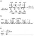
도 1은 반도체 장치의 일 구성예를 도시하는 도면.
도 2는 구동 회로의 일 구성예를 도시하는 블록도.
도 3a 및 도 3b는 구동 회로의 일 구성예를 도시하는 회로도.
도 4는 구동 회로의 타이밍 차트의 일례를 도시한 도면.
도 5a 내지 도 5c는 구동 회로의 일 구성예를 도시하는 회로도.
도 6a 내지 도 6c는 구동 회로의 일 구성예를 도시하는 회로도.
도 7은 구동 회로의 일 구성예를 도시하는 블록도.
도 8은 구동 회로의 일 구성예를 도시하는 레이아웃도.
도 9는 구동 회로의 일 구성예를 도시하는 레이아웃도.
도 10은 구동 회로의 일 구성예를 도시하는 레이아웃도.
도 11a 내지 도 11c는 구동 회로의 일 구성예를 도시하는 도면.
도 12a 및 도 12b는 구동 회로의 일 구성예를 도시하는 도면.
도 13a 및 도 13b는 구동 회로의 일 구성예를 도시하는 도면.
도 14a 및 도 14b는 구동 회로의 일 구성예를 도시하는 도면.
도 15a 내지 도 15c는 구동 회로의 제작 공정의 일례를 도시하는 도면.
도 16a 내지 도 16c는 구동 회로의 제작 공정의 일례를 도시하는 도면.
도 17은 구동 회로의 일 구성예를 도시하는 도면.
도 18a 내지 도 18c는 구동 회로의 제작 공정의 일례를 도시하는 도면.
도 19a 및 도 19b는 구동 회로의 제작 공정의 일례를 도시하는 도면.
도 20a 및 도 20b는 구동 회로의 일 구성예를 도시하는 회로도이고, 도 20c는 구동 회로의 타이밍 차트의 일례를 도시한 도면.
도 21은 반도체 장치의 일 구성예를 도시하는 도면.
도 22a 및 도 22b는 보호 회로의 일 구성예를 도시하는 회로도.
도 23은 반도체 장치의 화소의 일 구성예를 도시하는 회로도.
도 24a 내지 도 24c는 반도체 장치의 일 구성예를 도시하는 도면.
도 25a 및 도 25b는 반도체 장치의 일 구성예를 도시하는 도면.
도 26은 반도체 장치의 일 구성예를 도시하는 도면.
도 27a 내지 도 27c는 반도체 장치의 일례를 도시하는 도면.
도 28a 및 도 28b는 반도체 장치의 일례를 도시하는 도면.1 is a diagram showing an example of a configuration of a semiconductor device.
2 is a block diagram showing an example of a configuration of a driving circuit.
3A and 3B are circuit diagrams showing one configuration example of a drive circuit.
4 is a diagram showing an example of a timing chart of a driving circuit.
5A to 5C are circuit diagrams showing one configuration example of a driving circuit.
6A to 6C are circuit diagrams showing one configuration example of a drive circuit.
7 is a block diagram showing an example of a configuration of a driving circuit.
8 is a layout diagram showing an example of a configuration of a driving circuit.
9 is a layout diagram showing an example of a configuration of a driving circuit.
10 is a layout diagram showing an example of a configuration of a driving circuit.
11A to 11C are diagrams showing an example of a configuration of a driving circuit.
12A and 12B are diagrams showing an example of a configuration of a driving circuit.
13A and 13B are diagrams showing an example of a configuration of a driving circuit.
14A and 14B are diagrams showing an example of a configuration of a driving circuit.
15A to 15C are views showing an example of a manufacturing process of a driving circuit.
16A to 16C are views showing an example of a manufacturing process of a driving circuit.
17 is a diagram showing an example of a configuration of a driving circuit.
18A to 18C are views showing an example of a manufacturing process of a driving circuit.
19A and 19B are views showing an example of a manufacturing process of a drive circuit.
20A and 20B are circuit diagrams showing one configuration example of the drive circuit, and FIG. 20C is a diagram showing an example of a timing chart of the drive circuit.
21 is a diagram showing an example of a configuration of a semiconductor device.
22A and 22B are circuit diagrams showing one configuration example of a protection circuit.
23 is a circuit diagram showing a configuration example of a pixel of a semiconductor device.
24A to 24C are diagrams showing an example of a configuration of a semiconductor device.
25A and 25B are diagrams showing an example of a configuration of a semiconductor device.
26 is a diagram showing an example of a configuration of a semiconductor device.
27A to 27C are views showing an example of a semiconductor device.
28A and 28B are views showing an example of a semiconductor device.
이하에, 개시되는 발명의 실시형태에 대하여, 도면을 사용하여 예시한다. 다만, 개시되는 발명은 이하의 실시형태에 한정되지 않고, 그 발명의 취지 및 그 범위로부터 벗어남이 없이 그 형태 및 상세한 사항을 다양하게 변경할 수 있다는 것은 당업자라면 용이하게 이해할 수 있다. 따라서, 개시되는 발명은 하기에 나타내는 실시형태의 기재 내용에 한정하여 해석되는 것은 아니다. 이하에 예시하는 실시형태에 있어서, 동일한 것을 가리키는 부호는 다른 도면간에서 공통적으로 사용하는 경우가 있다.Hereinafter, the embodiment of the disclosed invention is illustrated using drawings. However, the disclosed invention is not limited to the following embodiments, and it can be easily understood by those skilled in the art that various forms and details can be changed without departing from the spirit and scope of the invention. Therefore, the disclosed invention is not to be interpreted as being limited to the contents of the embodiments shown below. In the embodiments illustrated below, the same reference numerals may be used in common between different drawings.
(실시형태 1)(Embodiment 1)
본 실시형태에서는, 도 1 내지 도 16c를 사용하여, 산화물 반도체를 사용하여 제작한 구동 회로를 구비한 표시 장치의 일례에 대하여 설명한다. 구체적으로는, 표시 장치의 화소부를 구동하기 위한 구동 회로인 소스선 구동 회로 및 게이트선 구동 회로의 일례로서 인핸스먼트형 박막 트랜지스터와 저항 소자를 조합하여 형성되는 인버터(이하, ERMOS 회로라고 함)를 갖는 구동 회로에 대하여 설명한다. 또한, 본 실시형태에서는, 단극성의 구동 회로를 구성하는 박막 트랜지스터로서, n 채널형 박막 트랜지스터를 적용한 예에 대하여 나타낸다.In this embodiment, an example of a display device provided with a driving circuit manufactured using an oxide semiconductor will be described using FIGS. 1 to 16C. Specifically, an inverter (hereinafter referred to as an ERMOS circuit) formed by combining an enhancement-type thin film transistor and a resistance element as an example of a source line driving circuit and a gate line driving circuit that are driving circuits for driving the pixel portion of the display device. The driving circuit to have will be described. In addition, in this embodiment, an example in which an n-channel type thin film transistor is applied as a thin film transistor constituting a unipolar driving circuit is shown.
또한, 표시 장치란, 발광 소자 또는 액상 소자 등의 표시 소자를 갖는 장치를 가리킨다. 표시 장치는 복수의 화소를 구동시키는 주변 구동 회로를 포함하여도 좋다. 또한, 복수의 화소를 구동시키는 주변 구동 회로는, 복수의 화소와 동일 기판 위에 형성된다. 또한, 표시 장치는, 플렉시블 프린트 기판(Flexible Print Circuit: FPC)을 포함하여도 좋다. 또한, 표시 장치는, 플렉시블 프린트 기판(FPC) 등을 통하여 접속되고, IC칩, 저항 소자, 용량 소자, 인덕터, 트랜지스터 등이 부착된 프린트 배선 기판(PWB)을 포함하여도 된다. 또한, 표시 장치는 편광판 또는 위상차판 등의 광학 시트, 조명 장치, 케이스, 음성 입출력장치, 또는 광 센서 등을 포함하여도 좋다.In addition, the display device refers to a device having a display element such as a light emitting element or a liquid element. The display device may include a peripheral driving circuit that drives a plurality of pixels. Further, a peripheral driving circuit for driving the plurality of pixels is formed on the same substrate as the plurality of pixels. In addition, the display device may include a flexible printed circuit (FPC). Further, the display device may include a printed wiring board (PWB) connected through a flexible printed circuit board (FPC) or the like, and attached with an IC chip, a resistive element, a capacitive element, an inductor and a transistor. Further, the display device may include an optical sheet such as a polarizing plate or a retardation plate, a lighting device, a case, an audio input / output device, or an optical sensor.
도 1에는, 표시 장치의 전체 도면에 대하여 도시한다. 기판(100) 위에, 소스선 구동 회로(101), 제 1 게이트선 구동 회로(102A), 제 2 게이트선 구동 회로(102B), 및 화소부(103)를 일체로 형성한다. 화소부(103)에 있어서, 점선 테두리(110)로 둘러싸인 부분이 1화소이다. 도 1에 도시하는 예에서는, 게이트선 구동 회로로서 제 1 게이트선 구동 회로(102A), 제 2 게이트선 구동 회로(102B)를 도시하였지만, 어느 한 쪽만이라도 좋다. 또한, 표시 장치의 화소에서는, 박막 트랜지스터에 의하여 표시 소자의 제어를 행한다. 소스선 구동 회로(101), 제 1 게이트선 구동 회로(102A), 제 2 게이트선 구동 회로(102B)를 구동하는 신호(클록 신호, 스타트 펄스 등)는, 플렉시블 프린트 기판(Flexible Print Circuit: FPC: 104A 및 104B)을 통하여, 외부로부터 입력된다.Fig. 1 shows an overall view of the display device. On the
화소부를 구동하기 위한 소스선 구동 회로, 게이트선 구동 회로는, 박막 트랜지스터, 용량 소자, 저항 소자 등에 의하여 구성되는 인버터 회로 등의 논리 회로를 갖는다. 단극성의 박막 트랜지스터를 사용하여 인버터 회로를 형성하는 경우, 인핸스먼트형 박막 트랜지스터 및 디플리션형 박막 트랜지스터를 조합하여 형성하는 경우(이하, EDMOS 회로라고 함)와, 인핸스먼트형 박막 트랜지스터끼리로 형성하는 경우(이하, EEMOS 회로라고 함)와, ERMOS 회로가 있다. 또한, n 채널형 박막 트랜지스터의 임계 값 전압이 양의 경우는, 인핸스먼트형 박막 트랜지스터라고 정의하고, n 채널형 박막 트랜지스터의 임계 값 전압이 음의 경우는, 디플리션형 박막 트랜지스터라고 정의하고, 본 명세서를 통하여 이 정의에 따르는 것으로 한다.The source line driving circuit and the gate line driving circuit for driving the pixel portion have logic circuits such as an inverter circuit composed of a thin film transistor, a capacitive element, and a resistive element. When an inverter circuit is formed using a unipolar thin film transistor, when an enhancement type thin film transistor and a depletion type thin film transistor are combined (hereinafter referred to as an EDMOS circuit), and an enhancement type thin film transistor is formed between each other. There are cases (hereinafter referred to as EEMOS circuits) and ERMOS circuits. Further, when the threshold voltage of the n-channel type thin film transistor is positive, it is defined as an enhancement type thin film transistor, and when the threshold voltage of the n-channel type thin film transistor is negative, it is defined as a depletion type thin film transistor. It is assumed that this definition is followed throughout this specification.
화소부에 형성하는 박막 트랜지스터로서, 임계 값 전압이 양인 인핸스먼트형 박막 트랜지스터를 적용하면, 게이트 단자와 소스 단자 사이에 인가되는 전압에 의하여 흐르는 전류를, 디플리션형 박막 트랜지스터보다 작게 할 수 있고, 저소비 전력화를 도모할 수 있다. 또한, 화소부를 구동시키기 위한 구동 회로에 이용되는 박막 트랜지스터로서, 화소부와 같은 인핸스먼트형 박막 트랜지스터를 사용하는 것이 바람직하다. 인버터 회로의 박막 트랜지스터로서 인핸스먼트형 박막 트랜지스터를 사용함으로써, 화소부 및 구동 회로를 제작할 때의 트랜지스터의 종류가 1종류가 되기 때문에, 제작 공정을 저감할 수 있다. 또한, 인핸스먼트형 박막 트랜지스터는 산화물 반도체를 사용하고, 그 전기 특성은 게이트 전압이 -20V 내지 20V에 있어서, 온 및 오프비율이 109 이상이기 때문에, 소스 단자 및 드레인 단자간의 누설 전류가 적고, 저소비 전력 구동을 실현할 수 있다.When an enhancement type thin film transistor having a positive threshold voltage is applied as a thin film transistor formed in the pixel portion, the current flowing by the voltage applied between the gate terminal and the source terminal can be made smaller than the depletion type thin film transistor, Low power consumption can be achieved. Further, it is preferable to use an enhancement-type thin film transistor such as a pixel part as a thin film transistor used in a driving circuit for driving the pixel part. When an enhancement type thin film transistor is used as the thin film transistor of the inverter circuit, the type of the transistor when manufacturing the pixel portion and the driving circuit becomes one type, so that the manufacturing process can be reduced. In addition, since the enhancement type thin film transistor uses an oxide semiconductor, and its electrical characteristics are that the gate voltage is -20V to 20V, and the on and off ratios are 109 or more, the leakage current between the source terminal and the drain terminal is small, Low power consumption can be realized.
또한, 본 서류(명세서, 특허 청구의 범위 또는 도면 등) 중에서 사용하는 산화물 반도체는, InMO3(ZnO)m(m>0)로 표기되는 박막을 형성하고, 그 박막을 이용하여 반도체 소자를 제작한다. 또한, M는 갈륨(Ga), 철(Fe), 니켈(Ni), 망간 (Mn), 및 코발트(Co) 중에서 선택된 하나의 금속 원소 또는 복수의 금속 원소를 나타낸다. 예를 들어, M가 갈륨(Ga)인 경우가 있는 이외에 갈륨(Ga)과 니켈(Ni), 또는 갈륨(Ga)과 철(Fe) 등, 갈륨(Ga) 이외의 상기 금속 원소가 포함되는 경우가 있다. 또한, 상기 산화물 반도체에 있어서, M로서 포함되는 금속 원소 이외에, 불순물 원소로서 철(Fe), 니켈(Ni), 그 이외의 천이 금속 원소, 또는 상기 천이 금속의 산화물이 포함되는 것이 있다. 그리고, 상기 산화물 반도체 중에 포함되는 나트륨(Na)은 5×10¹⁸(atoms/cm3) 이하, 바람직하게는 1×10¹⁸(atoms/cm3) 이하인 것으로 한다. 본 서류(명세서, 특허 청구의 범위 또는 도면 등) 중에 있어서는, 이 박막을 In-Ga-Zn-O계 비단결정막이라고도 부른다.In addition, the oxide semiconductor used in this document (specification, claims, drawings, etc.) forms a thin film represented by InMO3 (ZnO)m (m> 0), and uses the thin film to fabricate a semiconductor device. do. In addition, M represents one metal element or a plurality of metal elements selected from gallium (Ga), iron (Fe), nickel (Ni), manganese (Mn), and cobalt (Co). For example, when M is gallium (Ga) and other metal elements other than gallium (Ga), such as gallium (Ga) and nickel (Ni), or gallium (Ga) and iron (Fe), are included. There is. In addition, in the oxide semiconductor, in addition to the metal elements included as M, iron (Fe), nickel (Ni), other transition metal elements, or oxides of the transition metals are included as impurity elements. In addition, sodium (Na) contained in the oxide semiconductor is 5 × 10¹⁸ (atoms / cm3 ) or less, preferably 1 × 10¹⁸ (atoms / cm3 ) or less. In this document (specification, claims or drawings, etc.), this thin film is also referred to as an In-Ga-Zn-O-based non-single crystal film.
유도 결합 플라즈마 질량 분석법(Inductively Coupled Plasma Mass Spectrometry: ICP-MS분석법)에 의한 대표적인 측정예를 표 1에 나타낸다. 몰(mol) 수 비율을 In2O3: Ga2O3: ZnO=1: 1: 1로 한 타깃(In: Ga: Zn=1: 1: 0.5)을 사용하여, 압력 0.4Pa, 직류(DC) 전원 500W, 아르곤 가스 유량을 10sccm, 산소를 5sccm로 한 조건 1에서 얻어지는 산화물 반도체막은 InGa0.94Zn0.40O3.31이다. 또한, 상술한 조건으로부터 성막 분위기 조건만을 아르곤 가스 유량 40sccm, 산소를 0sccm로 변경한 조건 2에서 얻어지는 산화물 반도체막은, InGa0.95Zn0.41O3.31이다.Table 1 shows representative measurement examples by inductively coupled plasma mass spectrometry (ICP-MS analysis). Using a target having a molar number ratio of In2 O3 : Ga2 O3 : ZnO = 1: 1: 1 (In: Ga: Zn = 1: 1: 0.5), a pressure of 0.4 Pa, direct current ( DC) Power supply 500W, argon gas flow rate of 10sccm, and the oxide semiconductor film obtained under
또한, 측정 방법을 러더포드 후방 산란 분석법(Rutherford Backscattering Spectrometry: RBS 분석법)으로 바꾸어 정량화한 결과를 표 2에 나타낸다.In addition, Table 2 shows the results of quantification by changing the measurement method to Rutherford Backscattering Spectrometry (RBS method).
조건 1의 시료를 RBS 분석으로 측정한 결과, 산화물 반도체막은, InGa0.92Zn0.45O3.86이다. 또한, 조건 2의 시료를 RBS 분석으로 측정한 결과, 산화물 반도체막은, InGa0.93Zn0.44O3.49이다.In-Ga-Zn-O계 비단결정막의 결정 구조는, 스퍼터링법으로 성막한 후, 200℃ 내지 500℃, 대표적으로는, 300℃ 내지 400℃로 10분 내지 100분의 열 처리를 행하여도, 아모퍼스 구조가 XRD(X선 회절)의 분석에서 관찰된다. 또한, 박막 트랜지스터의 전기 특성도 게이트 전압이 -20V 내지 20V에 있어서, 온 및 오프 비율이 109 이상, 이동도가 10 이상인 것을 제작할 수 있다. 이와 같은 전기 특성을 갖는 산화물 반도체층을 사용하여 재작한 박막 트랜지스터는, 아모퍼스 실리콘을 사용하여 제작한 박막 트랜지스터와 비교하여 높은 이동도를 갖고, 시프트 레지스터로 구성되는 구동 회로를 고속으로 구동시킬 수 있다.As a result of measuring the sample under
다음, ERMOS 회로를 사용한 게이트선 구동 회로 및 소스선 구동 회로의 회로도에 대하여 일례를 도시하여 설명한다.Next, an example of a circuit diagram of a gate line driving circuit and a source line driving circuit using an ERMOS circuit is shown and described.
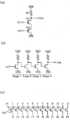
우선, 인버터 회로로서 ERMOS 회로를 사용한 소스선 구동 회로의 구성에 대하여 설명을 행한다.First, the configuration of a source line driving circuit using an ERMOS circuit as an inverter circuit is described.
도 2는, 도 1에 도시한 표시 장치에 있어서의 소스선 구동 회로(101)의 구성을 도시한 도면이다. 소스선 구동 회로는, 클록 신호용 레벨 시프터(201), 스타트 펄스용 레벨 시프터(202), 시프트 레지스터(251)를 구성하는 펄스 출력 회로(203), NAND 회로(204), 버퍼(205), 샘플링 스위치(206)를 갖고, 외부로부터 입력되는 신호는 제 1 클록 신호(CLK1), 제 2 클록 신호(CLK2), 및 스타트 펄스(SP), 아날로그 영상 신호(Video)이다. 이들 중에서 제 1 클록 신호(CLK1), 제 2 클록 신호(CLK2), 및 스타트 펄스(SP)에 관해서는, 외부로부터 저전압 진폭의 신호로서 입력된 직후, 레벨 시프터(201 또는 202)에 의하여 진폭 변환되어, 고전압 진폭의 신호로서 구동 회로에 입력된다.FIG. 2 is a diagram showing a configuration of a source
또한, 본 실시형태의 표시 장치에 있어서의 소스선 구동 회로는, 시프트 레지스터 중의 1단의 펄스 출력 회로로부터 출력되는 샘플링 펄스가, 샘플링 스위치(206)를 구동함으로써, 소스 신호선 12열 만큼의 아날로그 영상 신호를 동시에 샘플링하는 것을 설명한다. 또한, 이외에도 주사 방향을 전환하기 위한 주사 방향 전환 신호 등을 입력하는 구성으로 하여도 좋다. 또한, 본 실시형태에서는, 클록 신호로서 제 1 클록 신호(CLK1), 제 2 클록 신호(CLK2)의 2상의 클록 신호에 의하여 구동하는 예를 나타내지만, 2상 이외의 클록 신호의 입력에 의하여 구동 회로를 구동하는 구성으로 하여도 좋다.In addition, in the source line driving circuit in the display device of the present embodiment, the sampling pulse output from the pulse output circuit of one stage in the shift register drives the
도 3a 및 도 3b에 시프트 레지스터(251)가 갖는 복수의 펄스 출력 회로(203)의 구성을 도시한다. 펄스 출력 회로(300)는, 스타트 펄스(SP)가 입력되는 단자에 접속된 제 1 스위치(301)와, 제 1 스위치(301)를 통하여 입력되는 신호를 반전하여 출력하는 제 1 인버터 회로(302)와, 제 1 인버터 회로(302)로부터 출력된 신호를 반전하여 출력하는 제 2 인버터 회로(303) 및 제 3 인버터 회로(305)와, 제 2 인버터 회로(303)로부터 출력된 신호가 입력되는 단자에 접속된 제 2 스위치(304)로 구성된다.3A and 3B show the configuration of a plurality of
도 3a에 도시한 회로도에 있어서, 점선으로 도시한 블록이 1단분의 샘플링 펄스를 출력하는 펄스 출력 회로(350)이고, 도 3a의 시프트 레지스터는, N단(N은 자연수)의 펄스 출력 회로에 의하여 구성되어 있다. N단의 펄스 출력 회로로부터는, 각각의 제 3 인버터 회로(305)의 출력 단자로부터 출력 신호 out1 내지 출력 신호 outN가 출력된다. 또한, 상기 설명한 1단째의 다음 단의 펄스 출력 회로에서는, 제 1 스위치(301)와 제 2 스위치(304) 사이에서, 입력되는 제 1 클록 신호와 제 2 클록 신호를 입력하는 배선이 전환되어 접속된다. 이하, 3단째 이후, 교차로 제 1 클록 신호와 제 2 클록 신호를 입력하는 배선이 제 1 스위치(301)와 제 2 스위치(304) 사이에 교차로 전환되어 접속된다.In the circuit diagram shown in Fig. 3A, the block shown by the dotted line is a
도 3b는, 펄스 출력 회로의 회로 구성을 자세히 도시한다. 펄스 출력 회로 본체는, 박막 트랜지스터(351, 353, 355, 356, 358) 및 저항 소자(352, 354, 357)를 갖는다. 또한, 홀수단째의 펄스 출력 회로(331) 및 짝수단째의 펄스 출력 회로(332)는, 제 1 클록 신호(CLK1)를 공급하기 위한 배선(359), 및 제 2 클록 신호(CLK2)를 공급하기 위한 배선(360)에 접속되어 있다. 이하에 1단째의 펄스 출력 회로(331)를 예로 들어, 반도체 소자의 구체적인 접속 관계에 대하여 서술한다.3B shows the circuit configuration of the pulse output circuit in detail. The pulse output circuit body has
박막 트랜지스터(351)의 제 1 단자는, 스타트 펄스(SP)가 입력되는 단자에 접속되고, 게이트 단자는 배선(359)에 접속된다.The first terminal of the
저항 소자(352)의 한 쪽의 단자는, 고전원 전위 VDD가 공급되는 배선(고전원 전위선이라고도 함)에 접속된다.One terminal of the
박막 트랜지스터(353)의 제 1 단자는, 저항 소자(352)의 다른 쪽의 단자에 접속되고, 게이트 단자는 박막 트랜지스터(351)의 제 2 단자에 접속되고, 제 2 단자는 저전원 전위 VSS가 공급되는 배선(저전원 전위선이라고도 함)에 접속된다.The first terminal of the
저항 소자(354)의 한 쪽의 단자는, 고전원 전위선에 접속된다.One terminal of the
박막 트랜지스터(355)의 제 1 단자는, 저항 소자(354)의 다른 쪽의 단자에 접속되고, 게이트 단자는 저항 소자(352)의 다른 쪽의 단자 및 박막 트랜지스터(353)의 제 1 단자에 접속되고, 제 2 단자는 저전원 전위선에 접속된다.The first terminal of the
박막 트랜지스터(356)의 제 1 단자는, 저항 소자(354)의 다른 쪽의 단자 및 박막 트랜지스터(355)의 제 1 단자에 접속되고, 게이트 단자는 배선(360)에 접속되고, 제 2 단자는 박막 트랜지스터(351)의 제 2 단자 및 박막 트랜지스터(353)의 게이트 단자에 접속된다.The first terminal of the
저항 소자(357)의 한쪽의 단자는, 고전원 전위선에 접속되고, 다른 쪽의 단자는 2단째의 펄스 출력 회로(332)에 있어서의 박막 트랜지스터(351)의 제 1 단자에 접속된다.One terminal of the
박막 트랜지스터(358)의 제 1 단자는, 저항 소자(357)의 다른 쪽의 단자 및 2단째의 펄스 출력 회로(332)에 있어서의 박막 트랜지스터(351)의 제 1 단자에 접속되고, 게이트 단자는 저항 소자(352)의 다른 쪽의 단자, 박막 트랜지스터(353)의 제 1 단자, 및 박막 트랜지스터(355)의 게이트 단자에 접속되고, 제 2 단자는 저전원 전위선에 접속된다.The first terminal of the
2단째의 펄스 출력 회로도 1단째의 펄스 출력 회로와 배선(359)과 배선(360)의 접속이 반대로 되는 점을 제외하고, 같은 구성이 된다. 3단째 이후의 홀수단째의 펄스 출력 회로(331) 및 짝수단째의 펄스 출력 회로(332)도 이것에 준하고 순차적으로 접속된다.The second-stage pulse output circuit also has the same configuration except that the connection between the first-stage pulse output circuit and the
도 3b에 있어서, 박막 트랜지스터(351)는 도 3a에서 도시한 제 1 스위치(301)에 상당한다. 저항 소자(352) 및 박막 트랜지스터(353)는 도 3a에서 도시한 제 1 인버터 회로(302)에 상당하고, 제 1 인버터 회로(302)는 ERMOS 회로이다. 저항 소자(354) 및 박막 트랜지스터(355)는, 도 3a에서 도시한 제 2 인버터 회로(303)에 상당하고, 제 2 인버터 회로(303)는 ERMOS 회로이다. 박막 트랜지스터(356)는 도 3a에서 도시한 제 2 스위치(304)에 상당한다. 저항 소자(357) 및 박막 트랜지스터(358)는, 도 3a에서 도시한 제 3 인버터 회로(305)에 상당하고, 제 3 인버터 회로(305)는 ERMOS회로이다.3B, the
또한, 박막 트랜지스터(351, 356)는, 박막 트랜지스터(353, 355, 358)와 마찬가지로, 인핸스먼트형 박막 트랜지스터로 구성하는 것이 바람직하다. 스위치로서 인핸스먼트형 박막 트랜지스터를 사용함으로써, 트랜지스터의 오프 전류를 저감할 수 있기 때문에, 저소비 전력화를 도모할 수 있음과 함께, 제작 공정을 저감할 수 있다.In addition, the
여기서, 도 4에 도시하는 타이밍 차트를 참조하여, 도 3a 및 도 3b에서 도시한 회로의 회로 동작에 대하여 설명한다. 또한, 도 4에서는 설명의 편의상 도 3b에서 도시하는 회로에서의 노드로서 1단째의 펄스 출력 회로에 있어서, 박막 트랜지스터(351)의 제 2 단자를 노드 A(도 3b 및 도 4 중, A라고 기재함), 저항 소자(352)의 다른 단자를 노드 B(도 3b 및 도 4 중, B라고 기재함), 저항 소자(354)의 다른 단자를 노드 C(도 3b 및 도 4 중, C라고 기재함), 저항 소자(357)의 다른 단자를 노드 out1(도 3a 내지 도 4 중, out1라고 기재함)으로 한다.Here, with reference to the timing chart shown in Fig. 4, the circuit operation of the circuits shown in Figs. 3A and 3B will be described. In addition, in FIG. 4, for convenience of explanation, the second terminal of the
또한, 도 3b에서 도시하는 회로에서의 노드로서 2단째의 펄스 출력 회로에 있어서, 박막 트랜지스터(351)의 제 2 단자를 노드 D(도 3b 및 도 4 중, D라고 기재함), 저항 소자(352)의 다른 단자를 노드 E(도 3b 및 도 4 중, E라고 기재함), 저항 소자(354)의 다른 단자를 노드 F(도 3b 및 도 4 중, F라고 기재함), 저항 소자(357)의 다른 단자를 노드 out2(도 3b 및 도 4 중, out2라고 기재함)로 한다. 또한, 도 3b에서 도시하는 회로에서의 노드로서 3단째의 펄스 출력 회로에 있어서, 박막 트랜지스터(351)의 제 2 단자를 노드 G(도 3 내지 도 4b 중, G라고 기재함)로 한다.In addition, in the second-stage pulse output circuit as a node in the circuit shown in Fig. 3B, the second terminal of the
도 4 중, 기간 T1에서 스타트 펄스(SP)가 H레벨, 제 1 클록 신호(CLK1)가 H레벨, 제 2 클록 신호(CLK2)가 L레벨일 때의 동작에 대하여 설명한다.In Fig. 4, the operation when the start pulse SP is H level, the first clock signal CLK1 is H level, and the second clock signal CLK2 is L level in the period T1 will be described.
제 1 클록 신호(CLK1)가 H레벨이 됨으로써, 1단째의 펄스 출력 회로의 박막 트랜지스터(351)가 온 상태가 된다.When the first clock signal CLK1 becomes H level, the
그리고, 스타트 펄스의 전압 레벨인 H레벨이, 노드 A의 전압 레벨을 H레벨로 상승시킨다.Then, the H level, which is the voltage level of the start pulse, raises the voltage level of the node A to the H level.
그리고, 노드 A의 전압 레벨이 H레벨로 상승됨으로써, 1단째의 펄스 출력 회로의 박막 트랜지스터(353)가 온 상태가 된다.Then, when the voltage level of the node A rises to the H level, the
그리고, 저전원 전위의 전압 레벨인 L레벨이, 노드 B의 전압 레벨을 L레벨로 하강시킨다.Then, the L level, which is the voltage level of the low power supply potential, lowers the voltage level of the node B to the L level.
그리고, 노드 B의 전압 레벨이 L 레벨로 하강됨으로써, 1단째의 펄스 출력 회로의 박막 트랜지스터(355) 및 박막 트랜지스터(358)가 오프 상태가 된다.Then, when the voltage level of the node B falls to the L level, the
그리고, 1단째의 펄스 출력 회로의 박막 트랜지스터(355)가 오프 상태가 됨으로써, 고전원 전위의 전압 레벨인 H레벨이, 노드 C의 전압 레벨을 H레벨로 상승시킨다. 또한, 1단째의 펄스 출력 회로의 박막 트랜지스터(358)가 오프 상태가 됨으로써, 고전원 전위의 전압 레벨인 H레벨이, 노드 out1의 전압 레벨을 H레벨로 상승시킨다.Then, when the
또한, 제 2 클록 신호(CLK2)가 L레벨이기 때문에, 1단째의 펄스 출력 회로의 박막 트랜지스터(356) 및 2단째의 펄스 출력 회로의 박막 트랜지스터(351)는 오프 상태가 된다.Further, since the second clock signal CLK2 is at the L level, the
다음에, 도 4 중, 기간 T2에서 스타트 펄스(SP)가 L레벨, 제 1 클록 신호(CLK1)가 L레벨, 제 2 클록 신호(CLK2)가 H레벨일 때의 동작에 대하여 설명한다.Next, in Fig. 4, the operation when the start pulse SP is at the L level, the first clock signal CLK1 is at the L level, and the second clock signal CLK2 is at the H level in the period T2 will be described.
제 1 클록 신호(CLK1)가 L레벨이 됨으로써, 1단째의 펄스 출력 회로의 박막 트랜지스터(351)가 오프 상태가 된다. 한편, 제 2 클록 신호(CLK2)가 H레벨이기 때문에, 1단째의 펄스 출력 회로의 박막 트랜지스터(356)는 온 상태가 된다. 그래서, 기간 T1에서 H레벨에 있던 노드 C의 전압 레벨에 의하여, 노드 A의 전압 레벨이 H레벨을 유지하게 된다.When the first clock signal CLK1 becomes L level, the
그리고, 1단째의 펄스 출력 회로의 각 노드는, 기간 T1과 같은 레벨을 유지하게 된다.Then, each node of the first-stage pulse output circuit maintains the same level as the period T1.
한편, 제 2 클록 신호(CLK2)가 H레벨이 됨으로써, 2단째의 펄스 출력 회로의 박막 트랜지스터(351)가 온 상태가 된다.On the other hand, when the second clock signal CLK2 becomes H level, the
그리고, 노드 out1의 전압 레벨인 H레벨이, 노드 D의 전압 레벨을 H레벨로 상승시킨다.Then, the H level, which is the voltage level of the node out1, raises the voltage level of the node D to the H level.
그리고, 노드 D의 전압 레벨이 H레벨로 상승됨으로써, 2단째의 펄스 출력 회로의 박막 트랜지스터(353)가 온 상태가 된다.Then, the voltage level of the node D rises to the H level, so that the
그리고, 저전원 전위의 전압 레벨인 L레벨이, 노드 E의 전압 레벨을 L레벨로 하강시킨다.Then, the L level, which is the voltage level of the low power supply potential, lowers the voltage level of the node E to the L level.
그리고, 노드 E의 전압 레벨이 L레벨로 하강됨으로써, 2단째의 펄스 출력 회로의 박막 트랜지스터(355) 및 2단째의 펄스 출력 회로의 박막 트랜지스터(358)가 오프 상태가 된다.Then, when the voltage level of the node E falls to the L level, the
그리고, 2단째의 펄스 출력 회로의 박막 트랜지스터(355)가 오프 상태가 됨으로써, 고전원 전위의 전압 레벨인 H레벨이 노드 F의 전압 레벨을 H레벨로 상승시킨다. 또한, 2단째의 펄스 출력 회로의 박막 트랜지스터(358)가 오프 상태가 됨으로써, 고전원 전위의 전압 레벨인 H레벨이 노드 out2의 전압 레벨을 H레벨로 상승시킨다.Then, when the
제 1 클록 신호(CLK1)는, L레벨이기 때문에, 2단째의 펄스 출력 회로의 박막 트랜지스터(356) 및 3단째의 펄스 출력 회로의 박막 트랜지스터(351)는 오프 상태가 된다.Since the first clock signal CLK1 is L level, the
다음에, 도 4 중, 기간 T3에서 스타트 펄스(SP)가 L레벨, 제 1 클록 신호(CLK1)가 H레벨, 제 2 클록 신호(CLK2)가 L레벨일 때의 동작에 대하여 설명한다.Next, in Fig. 4, the operation when the start pulse SP is at the L level, the first clock signal CLK1 is at the H level, and the second clock signal CLK2 is at the L level in the period T3 will be described.
제 1 클록 신호(CLK1)가 H레벨이 됨으로써, 1단째의 펄스 출력 회로의 박막 트랜지스터(351)가 온 상태가 된다. 한편, 제 2 클록 신호(CLK2)는 L레벨이기 때문에, 1단째의 펄스 출력 회로의 박막 트랜지스터(356)는 오프 상태가 된다. 그래서, 노드 A의 전압 레벨이 L레벨로 하강하게 된다.When the first clock signal CLK1 becomes H level, the
그리고, 노드 A의 전압 레벨이 L레벨로 하강됨으로써, 1단째의 펄스 출력 회로의 박막 트랜지스터(353)가 오프 상태가 된다.Then, when the voltage level of the node A falls to the L level, the
그리고, 고전원 전위의 전압 레벨인 H레벨이, 노드 B의 전압 레벨을 H레벨로 상승시킨다.Then, the H level, which is the voltage level of the high power potential, raises the voltage level of the node B to the H level.
그리고, 노드 B의 전압 레벨이 L레벨로 상승됨으로써, 1단째의 펄스 출력 회로의 박막 트랜지스터(355) 및 1단째의 펄스 출력 회로의 박막 트랜지스터(358)가 온 상태가 된다.Then, the voltage level of the node B is raised to the L level, so that the
그리고, 1단째의 펄스 출력 회로의 박막 트랜지스터(355)가 온 상태가 됨으로써, 저전원 전위의 전압 레벨인 L레벨이 노드 C의 전압 레벨을 L레벨로 하강시켜, 1단째의 펄스 출력 회로의 박막 트랜지스터(358)가 온 상태가 됨으로써, 저전원 전위의 전압 레벨인 L레벨이 노드 out1의 전압 레벨을 L레벨로 하강시킨다.Then, when the
또한, 제 2 클록 신호(CLK2)는 L레벨이기 때문에, 1단째의 펄스 출력 회로의 박막 트랜지스터(356)는 오프 상태가 된다.In addition, since the second clock signal CLK2 is at the L level, the
또한, 기간 T2에서의 1단째의 펄스 출력 회로와 마찬가지로, 제 2 클록 신호(CLK2)가 L레벨이 됨으로써, 2단째의 펄스 출력 회로의 박막 트랜지스터(351)가 오프 상태가 된다. 한편, 제 1 클록 신호(CLK1)가 H레벨이기 때문에, 2단째의 펄스 출력 회로의 박막 트랜지스터(356)는 온 상태가 된다. 그래서, 기간 T2에서 H레벨에 있던 노드 F의 전압 레벨에 의하여, 노드 D의 전압 레벨이 H레벨을 유지하게 된다.Further, as in the first stage pulse output circuit in the period T2, the second clock signal CLK2 becomes L level, so that the
그리고, 2단째의 펄스 출력 회로의 각 노드는, 기간 T2와 같은 레벨을 유지하게 된다.Then, each node of the second-stage pulse output circuit maintains the same level as the period T2.
한편, 제 1 클록 신호(CLK1)가 H레벨이 됨으로써, 3단째의 펄스 출력 회로의 박막 트랜지스터(351)가 온 상태가 된다.On the other hand, when the first clock signal CLK1 becomes H level, the
그리고, 노드 out2의 전압 레벨인 H레벨이, 노드 G의 전압 레벨을 H레벨로 상승시킨다.Then, the H level, which is the voltage level of the node out2, raises the voltage level of the node G to the H level.
그리고, 노드 G의 전압 레벨이 H레벨로 상승됨으로써, 3단째의 펄스 출력 회로의 박막 트랜지스터(353)가 온 상태가 된다.Then, when the voltage level of the node G rises to the H level, the
이하, 순차적으로 트랜지스터의 온 및 오프가 제어됨으로써, 시프트 레지스터로서 구동할 수 있다.Hereinafter, the transistors can be driven as shift registers by sequentially controlling on and off of the transistors.
또한, 도 3a 및 도 3b에서 설명한 펄스 출력 회로에 있어서, 노드 A와 노드 C 사이에 박막 트랜지스터(356: 제 2 스위치(304))가 형성된 구성에 대하여 도시한다. 이것은, 저항 소자(354)에 의하여 노드 C의 전압 레벨이 고전압 전위 VDD로부터 전압 강하하는 것을 고려하였기 때문이다. 박막 트랜지스터(356: 제 2 스위치(304))에 의하여 노드 A와 노드 C의 접속을 절단하여 구동시킴으로써, 노드 A의 전위에 의한 박막 트랜지스터(353)의 구동 능력을 높게 할 수 있기 때문에 바람직하다. 또한, 박막 트랜지스터(356: 제 2 스위치(304))를 형성하지 않는 구성으로 하여도, 본 실시형태의 회로는 구동할 수 있다.In addition, in the pulse output circuit described in Figs. 3A and 3B, a configuration in which a thin film transistor 356 (second switch 304) is formed between node A and node C is shown. This is because the voltage level of the node C is considered to drop from the high voltage potential VDD by the
또한, 소스선 구동 회로의 구성에서는, 각 펄스 출력 회로로부터 출력되는 신호의 부정 논리곱(NAND)을 취하고, 각 소스선을 구동하기 위한 신호를 생성한다. 그래서, 소스선 구동 회로에 있어서는, 소스선의 개수보다 많은 펄스 출력 회로를 형성하고, 소스선에 출력하기 위한 신호를 생성하는 구성으로 하는 것이 바람직하다.In addition, in the configuration of the source line driving circuit, a negative logical product (NAND) of the signal output from each pulse output circuit is taken, and a signal for driving each source line is generated. Therefore, in the source line driving circuit, it is preferable to form a pulse output circuit having more than the number of source lines, and to construct a signal for output to the source line.
도 5a는, 도 2에서 도시한 클록 신호용 레벨 시프터(201)의 구성예를 도시한다. 또한, 도 5a에는, 제 1 클록 신호(CLK1)용 레벨 시프터 및 제 2 클록 신호(CLK2)용 레벨 시프터의 구성은 동일하기 때문에, 제 1 클록 신호(CLK1)용 레벨 시프터만을 도시한다. 도 5a에서는, 제 1 클록 신호(CLK1)가 ERMOS 회로에 의하여 진폭 변환되고(Stage 1), 이후에 버퍼 단(Stage 2, Stage 3)을 형성하는 구성을 취한다.Fig. 5A shows an example of the configuration of the
도 5a에 도시한 회로의 동작에 대하여 설명한다. 또한, 여기서 사용하는 전원의 전위는, VSS, VDD0, VDD의 3전위이고, VSS< VDD0< VDD로 한다. 제 1 클록 신호(CLK1)의 진폭을 소스선 구동 회로 입력부에서 레벨 시프트하는 구성으로 함으로써, 저소비 전력화 및 노이즈의 저감을 도모할 수 있다.The operation of the circuit shown in Fig. 5A will be described. In addition, the potential of the power source used here is three potentials of VSS, VDD0, and VDD, and VSS <VDD0 <VDD. By setting the amplitude of the first clock signal CLK1 at a level shift from the source line driver circuit input, it is possible to reduce power consumption and reduce noise.
신호 입력부(CLK in1)로부터 L레벨/H레벨=VSS/VDD0의 진폭을 갖는 제 1 입력 클록 신호(CLK1)가 입력된다.The first input clock signal CLK1 having an amplitude of L level / H level = VSS / VDD0 is input from the signal input unit CLK in1.
제 1 입력 클록 신호가 H레벨인 경우, 박막 트랜지스터(602)가 온 상태로 된다. 여기서, 박막 트랜지스터(602)의 온 저항은, 저항 소자(601)의 저항 값보다 충분히 낮게 설계해 둔다. 따라서, 노드 α는 L레벨이 된다.When the first input clock signal is at the H level, the
노드 α가 L레벨의 경우, 박막 트랜지스터(604)가 오프 상태가 된다. 여기서, 박막 트랜지스터(604)의 오프 저항은, 저항 소자(603)의 저항 값보다 충분히 높게 설계해 둔다. 따라서, 노드 β는 H레벨이 되고, 또 H레벨은 VDD와 같은 정도가 된다. 상술한 바와 같이, 진폭 변환이 완료된다.When the node α is L level, the
도 5a에서 설명하는 레벨 시프터는, 진폭 변환 후의 펄스에 대한 부하를 고려하여, 레벨 시프터 회로(Stage 1) 후에 버퍼 단을 형성한다(Stage 2, Stage 3). Stage 2, Stage 3에 있어서도 마찬가지인 동작에 의하여, 최종적으로 신호 출력부에 펄스가 출력된다.The level shifter described in FIG. 5A forms a buffer stage after the level shifter circuit (Stage 1) in consideration of the load on the pulse after amplitude conversion (
도 5a에는, 제 1 클록 신호(CLK1)용의 레벨 시프터에 대하여 도시하지만, 스타트 펄스(SP)용의 레벨 시프터도 구성은 동일하다.Although the level shifter for the first clock signal CLK1 is shown in Fig. 5A, the level shifter for the start pulse SP has the same configuration.
도 5b는, 클록 신호의 진폭 변환의 모양을 도시한다. 입력 신호의 진폭은, L레벨/H레벨=VSS/VDD0이고, 출력 신호의 진폭은, L레벨/H레벨=VSS/VDD이다.5B shows the shape of the amplitude conversion of the clock signal. The amplitude of the input signal is L level / H level = VSS / VDD0, and the amplitude of the output signal is L level / H level = VSS / VDD.
도 5c는, 스타트 펄스(SP)의 진폭 변환의 모양을 도시한다. 입력 신호의 진폭은, L레벨/H레벨=VSS/VDD0이고, 출력 신호의 진폭은, L레벨/H레벨=VSS/VDD이다.5C shows the shape of the amplitude conversion of the start pulse SP. The amplitude of the input signal is L level / H level = VSS / VDD0, and the amplitude of the output signal is L level / H level = VSS / VDD.
도 6a는, 도 2에서 도시한 2입력의 NAND 회로(204)를 도시한다. NAND 회로(204)의 구성은, ERMOS 회로와 유사하다. 구체적으로는, ERMOS 회로에 있어서의 신호 입력부가 2입력이 되어, 박막 트랜지스터(702, 703)가 직렬 배치되어 있는 점만 상이하다.Fig. 6A shows a two-
신호 입력부(In1) 및 신호 입력부(In2)에, 각각 H레벨이 입력되면, 박막 트랜지스터(702, 703)가 온 상태로 되므로, 신호 출력부(Out)에는 L레벨이 나타난다.When H levels are input to the signal input unit In1 and the signal input unit In2, respectively, since the
한편, 신호 입력부(In1) 및 신호 입력부(In2)의 어느 한쪽 또는 양쪽 모두에 L레벨이 입력되면, 신호 출력부(Out)에는 전위 VDD의 H레벨이 나타난다.On the other hand, when the L level is input to either or both of the signal input unit In1 and the signal input unit In2, the H level of the potential VDD appears in the signal output unit Out.
도 6b는, 도 2에서 도시한 버퍼(205)를 도시한다. 버퍼(205)는, ERMOS 회로(Stage 1 내지 Stage 4)에 의하여 구성되어 있다. ERMOS 회로의 동작에 관해서는, 레벨 시프터 회로의 항에서 설명하였기 때문에, 여기서는 상술의 설명을 원용한다.6B shows the
도 6c는 도 2에서 도시한 샘플링 스위치(206)를 도시한다. 샘플링 스위치(206)는, 신호 입력부(25)로부터 샘플링 펄스가 입력되고, 병렬 배치된 12개의 박막 트랜지스터(731)가 동시에 제어된다. 12개의 박막 트랜지스터(731)의 입력 전극(1) 내지 입력 전극(12)에 아날로그 영상 신호가 입력되고, 샘플링 펄스가 입력되었을 때의 영상 신호의 전위를, 소스 신호선에 기입하는 역할을 한다.6C shows the
도 7은, 도 1에서 도시한 표시 장치에 있어서의, 게이트선 구동 회로의 회로 구성을 도시한 도면이다. 클록 신호용 레벨 시프터(751), 스타트 펄스용 레벨 시프터(752), 시프트 레지스터(781)를 구성하는 펄스 출력 회로(753), NAND 회로(754), 버퍼(755)를 갖는다.7 is a diagram illustrating a circuit configuration of a gate line driving circuit in the display device illustrated in FIG. 1. It has a
게이트선 구동 회로에는, 제 1 클록 신호(CLK1), 제 2 클록 신호(CLK2), 스타트 펄스(SP)가 입력된다. 이들의 입력 신호는, 외부로부터 저전압 진폭의 신호로서 입력된 직후, 클록 신호용 레벨 시프터(751), 스타트 펄스용 레벨 시프터(752)에 의하여 진폭 변환되어, 고전압 진폭의 신호로서 구동 회로에 입력된다.The first clock signal CLK1, the second clock signal CLK2, and the start pulse SP are input to the gate line driving circuit. These input signals are amplitude-converted by a clock
또한, 클록 신호용 레벨 시프터(751), 스타트 펄스용 레벨 시프터(752), 펄스 출력 회로(753), NAND 회로(754), 및 버퍼(755)의 구성 및 동작에 관해서는, 소스선 구동 회로에 사용한 것과 마찬가지므로, 여기서는 상술한 설명을 원용한다.The structure and operation of the
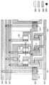
다음에, 도 3b에 도시한 펄스 출력 회로의 레이아웃도의 예를 도 8 내지 도 10에 도시한다. 도 8 내지 도 10에서는, 복수 단 형성되는 펄스 출력 회로 중, 1단째에 상당하는 펄스 출력 회로에 대하여 도시한다.Next, an example of the layout of the pulse output circuit shown in Fig. 3B is shown in Figs. 8 to 10, the pulse output circuit corresponding to the first stage among the pulse output circuits formed in a plurality of stages is illustrated.
도 8 내지 도 10의 펄스 출력 회로는, 전원선(801, 802), 제어 신호선(803, 804, 805), 박막 트랜지스터(351, 353, 355, 356, 358) 및 저항 소자(352, 354, 357)로 구성된다.The pulse output circuits of Figs. 8 to 10 include
도 8 내지 도 10 중에서는, 산화물 반도체층(806), 제 1 배선층(807), 제 2 배선층(808), 콘택트 홀(809)에 대하여 도시한다. 또한, 제 1 배선층(807)은 박막 트랜지스터의 게이트 단자를 포함하는 층이고, 제 2 배선층(808)은 박막 트랜지스터의 소스 단자 및 드레인 단자(제 1 단자 및 제 2 단자)를 포함하는 층이다.8 to 10, the
또한, 도 8 내지 도 10 중에서의 각 회로 소자의 접속 관계에 대해서는, 도 3b와 마찬가지다. 즉, 전원선(801)은, 고전원 전위 VDD가 공급되는 배선(고전원 전위선이라고도 함)이고, 전원선(802)은, 저전원 전위 VSS가 공급되는 배선(저전원 전위선이라고도 함)이고, 제어 신호선(803)은 스타트 펄스(SP)가 공급되는 배선이고, 제어 신호선(804)은 제 1 클록 신호가 공급되는 배선이고, 제어 신호선(805)은 제 2 클록 신호가 공급되는 배선이다.In addition, about the connection relationship of each circuit element in FIGS. 8-10, it is the same as that of FIG. 3B. That is, the
도 8에 도시한 ERMOS 회로의 저항 소자(352, 354, 357)에는, 직사각형 형상의 산화물 반도체층을 적용한다. 그래서, 도 8에 도시한 저항 소자(352, 354, 357)는, 전류 경로의 폭이 넓고, 높은 전류 구동 능력을 나타내는 저항 소자이다. 도 9 및 도 10에 도시한 ERMOS 회로의 저항 소자(352, 354, 357)에는, 미앤더(meander) 형상(사행(蛇行) 형상)의 산화물 반도체층을 적용한다. 미앤더 형상으로 함으로써, 저항 소자(352, 354, 357)의 저항 값을 증가시킬 수 있다.A rectangular oxide semiconductor layer is applied to the
또한, 도 8 내지 도 10의 펄스 출력 회로의 레이아웃도에 있어서, 박막 트랜지스터(351, 353, 355, 356, 358)의 채널 영역의 형상을 U 자형으로 하여도 좋다. 또한, 도 8 중에서는, 각 박막 트랜지스터의 사이즈를 같은 사이즈로서 도시하지만, 후단의 부하의 크기에 따라 박막 트랜지스터의 사이즈를 적절히 변경하여도 좋다.In addition, in the layout diagram of the pulse output circuits of Figs. 8 to 10, the shape of the channel region of the
다음에, 도 8 내지 도 10에서 설명한 레이아웃도에 있어서의 저항 소자(354) 및 박막 트랜지스터(355)에 의하여 구성되는 인버터 회로의 구성에 대하여, 도 11a 내지 도 11c를 사용하여 설명한다. 또한, 도 11a 내지 도 11c에 도시되는 저항 소자(354) 및 박막 트랜지스터(355)는, 각각 도 8 내지 도 10 중의 점선 A-B, 및 C-D에 대응하는 단면도에 대하여 도시한다.Next, the structures of the inverter circuit constituted by the
도 11a는, 도 8 중의 점선 A-B, 및 C-D에 대응하는 단면도이다. 도 11a에 있어서, 저항 소자(354)는 제 1 산화물 반도체층(905)을 저항 성분으로서 이용한다. 또한, 제 1 산화물 반도체층(905)의 일단이 제 1 배선층(807)에 포함되는 제 1 배선(901)과 절연층(903)에 형성된 콘택트 홀(904)을 통하여 접속되고, 다른 단이 제 2 배선층(808)에 포함되는 제 2 배선(907)과 접속되어 있다.11A is a cross-sectional view corresponding to the dotted line A-B and C-D in FIG. 8. In Fig. 11A, the
도 11a에 있어서, 박막 트랜지스터(355)는, 기판 위의 게이트 단자(902), 게이트 절연층으로서 기능하는 게이트 단자(902) 위의 절연층(903), 채널 형성 영역이 되는 절연층(903) 위의 제 2 산화물 반도체층(906), 소스 단자 및 드레인 단자(제 1 단자 및 제 2 단자)로서 기능하는 제 2 산화물 반도체층(906) 위의 제 2 배선(907) 및 제 3 배선(908)을 갖는다.In Fig. 11A, the
또한, 제 1 배선(901)은, 저항 소자(354)에 대해서는 한쪽의 단자이다. 또한, 제 2 배선(907)은 저항 소자(354)에 대해서는 다른 쪽의 단자이며, 박막 트랜지스터(355)에 대해서는 제 1 단자이고, 또 양자를 접속하는 배선이기도 하다. 마찬가지로 제 3 배선(908)은, 박막 트랜지스터(355)에 대해서는 제 2 단자이고, 또 저전원 전위 VSS가 공급되는 배선(저전원 전위선이라고도 함)이기도 하다. 바꾸어 말하면, 접속 배선 및 저(고)전원 전위선의 일부가, 각 박막 트랜지스터의 제 1 단자 또는 제 2 단자로서 이용된다.In addition, the
또한, 도 11a에 있어서, 제 1 산화물 반도체층(905) 및 제 2 산화물 반도체층(906)의 막 두께는 균일하지 않다. 구체적으로는, 제 2 배선(907) 및 제 3 배선(908)과 중첩하는 영역에 해당하는 제 1 산화물 반도체층(905) 및 제 2 산화물 반도체층(906)의 막 두께가 상기 영역에 해당하지 않는 제 1 산화물 반도체층(905) 및 제 2 산화물 반도체층(906)의 막 두께보다 두껍다. 이것은, 제 2 배선(907) 및 제 3 배선(908)을 형성할 때의 에칭에 있어서, 제 1 산화물 반도체층(905) 및 제 2 산화물 반도체층(906)의 일부도 에칭되기 때문이다.11A, the film thicknesses of the first
도 11b는, 도 9 중의 점선 A-B, 및 C-D에 대응하는 단면도이다. 도 11b에 있어서, 저항 소자(354)는 미앤더 형상으로 형성된 제 1 산화물 반도체층(905)을 저항 성분으로서 이용한다. 또한, 제 1 산화물 반도체층(905)의 일단이 제 1 배선(901)과 절연층(903)에 형성된 콘택트 홀(904)을 통하여 접속되고, 다른 쪽 단이 제 2 배선(907)과 접속되어 있다. 박막 트랜지스터의 구조는, 도 11a에서 설명한 박막 트랜지스터와 동일하기 때문에, 상술의 설명을 원용한다.11B is a cross-sectional view corresponding to the dotted line A-B and C-D in FIG. 9. In Fig. 11B, the
도 11c는, 도 10 중의 점선 A-B, 및 C-D에 대응하는 단면도이다. 도 11c에 있어서, 저항 소자(354)는 미앤더 형상으로 형성된 제 1 산화물 반도체층(905)을 저항 성분으로서 이용한다. 또한, 제 1 산화물 반도체층(905)의 일단이 제 2 배선층(808)에 포함되는 제 4 배선(912)과 접속되고, 다른 쪽 단이 제 2 배선층(808)에 포함되는 제 2 배선(907)과 접속되어 있다. 박막 트랜지스터의 구조는, 도 11a에서 설명한 박막 트랜지스터와 동일하기 때문에, 상술의 설명을 원용한다. 도 11c에 도시한 저항 소자(354)는 제 1 산화물 반도체층(905) 위에 직접 제 4 배선(912)이 형성되기 때문에, 제 1 산화물 반도체층과 제 4 배선 사이에 양호한 접합을 형성할 수 있다.11C is a cross-sectional view corresponding to the dotted line A-B and C-D in FIG. 10. In Fig. 11C, the
다음에, 도 11a 내지 도 11c에 도시한 ERMOS 회로의 구체적인 재료 구성에 대하여 설명한다.Next, a specific material configuration of the ERMOS circuit shown in Figs. 11A to 11C will be described.
도 11a 내지 도 11c에 있어서, 기판(900)에는 바륨 보로실리케이트 유리나, 알루미노 보로실리케이트 유리 등의 유리 기판 등을 사용할 수 있다. 제 1 배선(901) 및 게이트 단자(902)의 재료는, 알루미늄(Al)이나 구리(Cu) 등의 저저항 도전성 재료로 형성할 수도 있다. 또한, 알루미늄(Al)을 내열성 도전성 재료와 조합하여 형성할 수 있다. 내열성 도전성 재료로서는, 티타늄(Ti), 탄탈(Ta), 텅스텐(W), 몰리브덴(Mo), 크롬(Cr), 네오디뮴(Nd) 스칸듐(Sc) 중에서 선택된 원소, 또는 상술한 원소를 성분으로 하는 합금이나, 상술한 원소를 조합한 합금막, 또는 상술한 원소를 성분으로 하는 질화물을 적용할 수 있다.11A to 11C, a glass substrate such as barium borosilicate glass or alumino borosilicate glass can be used for the
절연층(903)은, 산화 실리콘막, 질화 실리콘막, 산화질화 실리콘막, 질화산화 실리콘막, 산화 알루미늄막, 산화 탄탈막 등의 절연막으로 형성할 수 있다. 또한, 이들의 절연막으로 이루어지는 적층 구조로서 형성하여도 좋다. 또한, 산화질화 실리콘막은 그 조성으로서, 질소보다도 산소의 함유량이 많은 것으로, 농도 범위로서 산소가 55원자% 내지 65원자%, 질소가 1원자% 내지 20원자%, 실리콘이 25원자% 내지 35원자%, 수소가 0.1원자% 내지 10원자%의 범위에 있어서, 합계가 100원자%로 되도록 각 원소를 임의의 농도로 포함하는 것을 말한다. 또한, 질화산화 실리콘막이란, 그 조성으로서 산소보다 질소의 함유량이 많은 것으로서, 농도 범위로서 산소가 15원자% 내지 30원자%, 질소가 20원자% 내지 35원자%, 실리콘이 25원자% 내지 35원자%, 수소가 15원자% 내지 25원자%의 범위에 있어서, 합계 100원자%가 되도록 각 원소를 임의의 농도로 포함하는 것으로 한다.The insulating
제 1 산화물 반도체층(905) 및 제 2 산화물 반도체층(906)은, InMO3(ZnO)m(m>0)로 표기되는 박막을 형성한다. 또한, M는 갈륨(Ga), 철(Fe), 니켈(Ni), 망간 (Mn) 또는 코발트(Co) 중에서 선택된 하나의 금속 원소 또는 복수의 금속 원소를 나타낸다. 예를 들어, M로서 갈륨(Ga)인 경우가 있는 이외에 갈륨(Ga)과 니켈(Ni), 또는 갈륨(Ga)과 철(Fe) 등, 갈륨(Ga) 이외의 상기 금속 원소가 포함되는 경우가 있다. 또한, 상기 산화물 반도체층에 있어서, M로서 포함되는 금속 원소 이외에, 불순물 원소로서 철(Fe), 니켈(Ni), 그 이외의 천이 금속 원소, 또는 상기 천이 금속 원소의 산화물이 포함되는 것이 있다. 그리고, 상기 산화물 반도체층 중에 포함되는 나트륨(Na)은 5×10¹⁸(atoms/cm3) 이하, 바람직하게는 1×10¹⁸(atoms/cm3) 이하인 것으로 한다.The first
제 2 배선(907) 및 제 3 배선(908)의 재료로서는, 알루미늄(Al), 크롬(Cr), 탄탈(Ta), 티타늄(Ti), 몰리브덴(Mo), 텅스텐(W) 중에서 선택된 원소, 또는 상술한 원소를 성분으로 하는 합금, 상술한 원소를 조합한 합금막 등을 들 수 있다. 또한, 이들의 재료로 이루어지는 적층 구조로 형성하여도 좋다.As the material of the
산화 실리콘층(909)은, 스퍼터링법에 의하여 성막된 산화 실리콘막으로 형성된다. 기판 전체 면에 형성되는 질화 실리콘층(910)은 실란(SiH4) 및 암모니아(NH3) 등의 수소 화합물을 포함하는 가스를 사용한 플라즈마 CVD법에 의하여 형성된다. 그래서, 질화 실리콘층(910)은 고농도로 수소를 함유한다.The
또한, 도 12a에 도시하는 바와 같이, 제 1 산화물 반도체층(905) 및 제 2 산화물 반도체층(906)과, 제 2 배선(907) 및 제 3 배선(908) 사이에 버퍼층(911a 내지 911c)을 형성할 수도 있다.12A, the
또한, 상술한 버퍼층(911a 내지 911c)이란, 제 1 산화물 반도체층(905) 및 제 2 산화물 반도체층(906)을 형성하는 성막 조건과는 상이한 성막 조건으로 형성되는 In-Ga-Zn-O계 비단결정막을 바탕으로 형성되고, 저저항의 산화물 반도체층이다. 또한, 이하의 문장에서는 편의상, 후에 제 1 산화물 반도체층(905) 및 제 2 산화물 반도체층(906)이 형성되는 산화물 반도체막을 제 1 산화물 반도체막이라고 표기하고, 후에 버퍼층(911a 내지 911c)이 형성되는 산화물 반도체막을 제 2 산화물 반도체막이라고 표기한다.In addition, the above-described
예를 들어, 스퍼터링법에 의하여 산화물 반도체막의 형성을 행하는 경우, 성막에 사용되는 스퍼터링 가스의 산소 농도를 변화시킴으로써, 산화물 반도체막의 저항 값을 변화시킬 수 있다. 구체적으로는, 스퍼터링 가스의 산소 농도를 높게 함으로써, 산화물 반도체막의 저항 값을 높게 할 수 있다. 스퍼터링법에 의한 제 1 산화물 반도체막 및 제 2 산화물 반도체막의 성막 조건의 하나는, 제 1 산화물 반도체막의 형성에 사용되는 스퍼터링 가스로서 아르곤 가스 유량을 10sccm, 산소 가스 유량 5sccm로 하고, 제 2 산화물 반도체막의 형성에 사용되는 스퍼터링 가스로서 아르곤 가스 유량을 40sccm로 한 조건이다. 또한, 버퍼층(911a 내지 911c)은, n형 도전형을 갖고, 활성화 에너지(ΔE)가 0.1eV 이하이다. 또한, In-Ga-Zn-O계 비단결정막을 바탕으로 형성되는 버퍼층(911a 내지 911c)은, 적어도 아모퍼스 성분을 포함하는 것으로 한다. 버퍼층(911a 내지 911c)은 비정질 구조 중에 결정립(나노크리스탈)을 포함하는 경우가 있다. 이 버퍼층(911a 내지 911c) 중의 결정립(나노크리스탈)은 직경 1nm 내지 10nm, 대표적으로는 2nm 내지 4nm 정도이다.For example, when the oxide semiconductor film is formed by the sputtering method, the resistance value of the oxide semiconductor film can be changed by changing the oxygen concentration of the sputtering gas used for film formation. Specifically, by increasing the oxygen concentration of the sputtering gas, the resistance value of the oxide semiconductor film can be increased. One of the conditions for forming the first oxide semiconductor film and the second oxide semiconductor film by the sputtering method is a sputtering gas used for forming the first oxide semiconductor film, having an argon gas flow rate of 10 sccm and an oxygen gas flow rate of 5 sccm, and a second oxide semiconductor. As a sputtering gas used to form the film, argon gas flow rate is set to 40 sccm. Further, the
제 1 산화물 반도체층(905) 및 제 2 산화물 반도체층(906)보다 저저항의 버퍼층(911a 내지 911c)을 형성함으로써, 도전체인 제 2 배선(907)과 제 1 산화물 반도체층(905), 도전체인 제 2 배선(907) 및 제 3 배선(908)과 제 2 산화물 반도체층(906) 사이에, 쇼트키 접합과 비교하여 양호한 접합을 형성하고, 열적으로도 안정적인 동작을 나타낼 수 있다. 또한, 박막 트랜지스터(355)에서는, 버퍼층(911b, 911c)을 형성함으로써, 높은 드레인 전압이라도 양호한 이동도를 유지할 수 있다.By forming the
또한, 도 12b에 도시하는 바와 같이, 제 1 산화물 반도체층(905) 및 제 2 산화물 반도체층(906)의 상하에 버퍼층(911a 내지 911e)을 형성할 수도 있다.12B,
버퍼층(911d)을 형성함으로써, 도전체인 제 1 배선(901)과 제 1 산화물 반도체층(905) 사이에 쇼트키 접합과 비교하여 양호한 접합을 형성하고, 열적으로도 안정적으로 동작시킬 수 있다.By forming the
도 11a 내지 도 12b에서 도시한 박막 트랜지스터와는 상이한 구조의 박막 트랜지스터를 도 13a및 도 13b에 도시하여, 설명한다. 또한, 도 13a및 도 13b에서는 도 8의 A-B선, 및 C-D선에 대용하는 저항 소자 및 박막 트랜지스터의 단면 구조를 도시하고, 도 11a 내지 도 11c와 같은 것에 대해서는, 같은 부호를 붙인다.13A and 13B, a thin film transistor having a structure different from that of the thin film transistor shown in FIGS. 11A to 12B is described. 13A and 13B show cross-sectional structures of the resistance elements and thin film transistors that are substituted for the A-B line and the C-D line in FIG. 8, and the same reference numerals are given to those in FIGS. 11A to 11C.
도 13a에 있어서, 제 2 산화물 반도체층(906) 위에는, 산화 실리콘층인 채널 보호층(1001)이 형성되고, 채널 보호층(1001) 및 제 2 산화물 반도체층(906) 위에 제 2 배선(907) 및 제 3 배선(908)이 형성된 구조가 되어 있다. 또한, 제 2 배선(907), 제 3 배선(908), 및 채널 보호층(1001) 위에 질화 실리콘층(910)이 형성되어 있다. 또한, 도 13b에서 도시하는 바와 같이, 제 1 산화물 반도체층(905) 및 제 2 산화물 반도체층(906)과, 제 2 배선(907) 및 제 3 배선(908) 각각 사이에 버퍼층(911a 내지 911c)을 형성하는 구성으로 할 수도 있다.13A, a
도 11a 내지 도 13b에서는, 역 스태거형의 박막 트랜지스터에 대하여 설명하였지만, 본 실시형태의 박막 트랜지스터의 구성은 역 스태거형에 한정되지 않는다. 일례로서, 코플래너(coplanar)형의 박막 트랜지스터에 있어서도, 마찬가지의 효과를 갖는다. 도 14a 및 도 14b에 단면 구조의 일례에 대하여 도시하여, 설명한다. 또한, 도 14a 및 도 14b에서는 도 8의 A-B선 및 C-D선에 대응하는 저항 소자 및 박막 트랜지스터의 단면 구조를 도시하고, 도 11a 내지 도 11c와 같은 구성에 대해서는, 같은 부호를 붙인다.11A to 13B, the inverse staggered thin film transistor has been described, but the configuration of the thin film transistor of this embodiment is not limited to the inverse staggered type. As an example, a coplanar type thin film transistor also has the same effect. 14A and 14B, an example of a cross-sectional structure is shown and explained. 14A and 14B show cross-sectional structures of the resistance elements and the thin film transistors corresponding to lines A-B and C-D in FIG. 8, and the same reference numerals are given to the structures as shown in FIGS. 11A to 11C.
도 14a에 있어서, 제 1 산화물 반도체층(905)의 일단은, 제 1 배선(901) 위에 형성되고, 제 1 산화물 반도체층(905)의 다른 단 및 제 2 산화물 반도체층(906)의 일단은, 제 2 배선(907) 위에 형성되고, 제 2 산화물 반도체층(906)의 다른 단은 제 3 배선(908) 위에 형성된 구조가 되어 있다. 또한, 제 2 산화물 반도체층(906) 위에는, 산화 실리콘층(909) 및 질화 실리콘층(910)의 적층이 형성되고, 제 1 산화물 반도체층(905) 위에는 질화 실리콘층(910)만이 형성되어 있다. 또한, 도 14b에서 도시하는 바와 같이, 제 2 배선(907) 및 제 3 배선(908)과 절연층(903) 사이에 버퍼층(1010a, 1010b)을 형성하는 구성으로 할 수도 있다.In FIG. 14A, one end of the first
도 11a 내지 도 14b에서는, 제 1 산화물 반도체층(905)에 직접 접하도록, 실란(SiH4) 및 암모니아(NH3) 등의 수소 화합물을 포함하는 가스를 사용한 플라즈마 CVD법에 의하여 형성된 질화 실리콘층(910)을 형성한다.11A to 14B, a silicon nitride layer formed by a plasma CVD method using a gas containing a hydrogen compound such as silane (SiH4 ) and ammonia (NH3 ) so as to directly contact the first
상술한 구조를 갖는 ERMOS 회로는, 질화 실리콘층(910)이 직접 접하는 제 1 산화물 반도체층(905)을 저항 성분으로 하는 저항 소자와, 산화 실리콘층(909)(채널 보호층(1001))을 사이에 두고, 질화 실리콘층(910)이 형성된 제 2 산화물 반도체층(906)을 채널 형성 영역으로 하는 박막 트랜지스터를 갖는다. 그래서, 제 1 산화물 반도체층(905)에는, 제 2 산화물 반도체층(906)보다 고농도로 수소를 도입할 수 있다. 결과적으로, 제 1 산화물 반도체층(905)의 저항 값을 제 2 산화물 반도체층(906)의 저항 값보다 낮게 할 수 있다.The ERMOS circuit having the above-described structure includes a resistive element having a first
다음에, ERMOS 회로의 제작 공정에 대하여 도 15a 내지 도 15c의 단면도를 사용하여 설명한다. 또한, 여기서는 도 14b에 도시하는 ERMOS 회로의 제작 공정에 대하여 나타낸다.Next, the manufacturing process of the ERMOS circuit will be described using the cross-sectional views of Figs. 15A to 15C. In addition, the manufacturing process of the ERMOS circuit shown in Fig. 14B is shown here.
기판(900) 위에 제 1 도전막을 형성한다. 제 1 도전막의 형성에는, 스퍼터링법, 진공 증착법, 펄스 레이저 퇴적법, 이온 도금 방법 등으로 대표되는 박막 퇴적법을 사용한다. 제 1 도전막의 재료는, 알루미늄(Al)이나 구리(Cu) 등의 저저항 도전성 재료로 형성할 수 있다. 또한, 알루미늄(Al)을 내열성 도전성 재료와 조합하여 형성할 수 있다. 내열성 도전성 재료로서는, 티타늄(Ti), 탄탈(Ta), 텅스텐(W), 몰리브덴(Mo), 크롬(Cr), 네오디뮴(Nd) 스칸듐(Sc) 중에서 선택된 원소, 또는 상술한 원소를 성분으로 하는 합금이나, 상술한 원소를 조합한 합금막, 또는 상술한 원소를 성분으로 하는 질화물을 적용할 수 있다. 다음에, 제 1 포토리소그래피 공정을 행하여, 제 1 도전막 위에 레지스트를 형성한다. 또한, 상기 레지스트를 마스크로 하여, 제 1 도전막을 선택적으로 에칭함으로써 제 1 배선(901) 및 게이트 단자(902)를 형성한다.A first conductive film is formed on the
다음에, 제 1 배선(901) 및 게이트 단자(902)를 덮는 절연막을 형성한다. 절연막의 형성에는, 스퍼터링법, 진공 증착법, 펄스 레이저 퇴적법, 이온 도금 방법, 플라즈마 CVD법 등으로 대표되는 박막 퇴적법을 사용한다. 절연막으로서, 산화 실리콘막, 질화 실리콘막, 산화질화 실리콘막, 질화산화 실리콘막, 산화 알루미늄막, 산화 탄탈막 등의 절연막을 사용할 수 있다. 또한, 이들의 절연막의 적층 구조로 하여도 좋다. 다음에, 제 2 포토리소그래피 공정을 행하여, 절연막 위에 레지스트를 형성한다. 또한, 상기 레지스트를 마스크로 하여, 절연막을 선택적으로 에칭함으로써 제 1 배선에 도달하는 콘택트 홀(904)이 형성된 절연층(903)을 형성한다. 여기까지의 공정이 완료된 단계의 단면도가 도 15a에 상당한다.Next, an insulating film covering the
다음에, 제 2 산화물 반도체막을 형성한다. 제 2 산화물 반도체막의 형성에는, 스퍼터링법, 진공 증착법, 펄스 레이저 퇴적법, 이온 도금 방법, 플라즈마 CVD법 등으로 대표되는 박막 퇴적법을 사용한다. 스퍼터링법에 의한 성막을 행하는 경우, In2O3, Ga2O3, ZnO를 소결한 타깃을 사용하는 것이 바람직하다. 스퍼터링 가스에는, 아르곤으로 대표되는 희 가스를 사용한다. 스퍼터링법에 의한 성막 조건의 하나는, In2O3: Ga2O3: ZnO=1: 1: 1을 혼합, 소결한 타깃을 사용하고, 압력 0.4Pa, 직류(DC) 전원 500W, 아르곤 가스 유량을 40sccm로 한다.Next, a second oxide semiconductor film is formed. For forming the second oxide semiconductor film, a thin film deposition method such as sputtering, vacuum deposition, pulse laser deposition, ion plating, plasma CVD, or the like is used. When forming a film by sputtering, it is preferable to use a target sintered with In2 O3 , Ga2 O3 or ZnO. As the sputtering gas, a rare gas typified by argon is used. One of the film formation conditions by the sputtering method is a mixture of In2 O3 : Ga2 O3 : ZnO = 1: 1: 1, and a sintered target, pressure 0.4 Pa, direct current (DC) power supply 500 W, argon gas The flow rate is 40 sccm.
다음에, 제 2 도전막을 형성한다. 제 2 도전막의 형성에는, 스퍼터링법, 진공 증착법, 펄스 레이저 퇴적법, 이온 도금 방법으로 대표되는 박막 퇴적법을 사용한다. 제 2 도전막의 재료로서는, 알루미늄(Al), 크롬(Cr), 탄탈(Ta), 티타늄(Ti), 몰리브덴(Mo), 텅스텐(W) 중에서 선택된 원소, 또는 상술한 원소를 성분으로 하는 합금, 또는 상술한 원소를 조합한 합금막 등을 들 수 있다. 또한, 이들의 재료로 이루어지는 적층 구조로서 형성하여도 좋다.Next, a second conductive film is formed. The thin film deposition method represented by the sputtering method, vacuum vapor deposition method, pulse laser deposition method, and ion plating method is used for formation of a 2nd conductive film. As a material of the second conductive film, an element selected from aluminum (Al), chromium (Cr), tantalum (Ta), titanium (Ti), molybdenum (Mo), tungsten (W), or an alloy containing the above-mentioned elements as a component, Or an alloy film etc. which combined the above-mentioned elements are mentioned. Moreover, you may form it as a laminated structure which consists of these materials.
다음에, 제 3 포토리소그래피 공정을 행하여, 제 2 도전막 위에 레지스트를 형성한다. 또한, 상기 레지스트를 마스크로 하여, 제 2 산화물 반도체막 및 제 2 도전막을 선택적으로 에칭하여, 제 2 배선(907) 및 제 3 배선(908), 그리고 버퍼층(1010a, 1010b)을 형성한다. 이 때의 에칭 방법으로서 웨트 에칭 또는 드라이 에칭을 사용한다. 예를 들어, 제 2 도전막으로서, 알루미늄(Al)막, 또는 알루미늄 합금막을 사용하는 경우에는, 인산과 초산과 질산을 혼합한 용액을 사용한 웨트 에칭을 행할 수 있다. 마찬가지로, 제 2 도전막으로서 티타늄(Ti)막, 또는 티타늄 합금막을 사용하는 경우에는, 암모니아과수(과산화수소: 암모니아: 물=5: 2: 2)를 사용한 웨트 에칭을 행할 수 있다.Next, a third photolithography process is performed to form a resist on the second conductive film. In addition, the second oxide semiconductor film and the second conductive film are selectively etched using the resist as a mask to form
다음에, 제 1 산화물 반도체막을 형성한다. 제 1 산화물 반도체막의 형성에는, 스퍼터링법, 진공 증착법, 펄스 레이저 퇴적법, 이온 도금 방법 등으로 대표되는 박막 퇴적법을 사용한다. 제 1 산화물 반도체막은 제 2 산화물 반도체막과 비교하여 스퍼터링 가스에 포함되는 산소 농도가 높은 조건으로 형성한다. 스퍼터링법에 의한 성막 조건의 하나는, In2O3: Ga2O3: ZnO=1: 1: 1을 혼합, 소결한 타깃을 사용하고, 압력 0.4Pa, 직류(DC) 전원 500W, 아르곤 가스 유량을 10sccm, 산소 가스 유량을 5sccm으로 한다.Next, a first oxide semiconductor film is formed. The thin film deposition method represented by the sputtering method, vacuum vapor deposition method, pulse laser deposition method, ion plating method, etc. is used for formation of a 1st oxide semiconductor film. The first oxide semiconductor film is formed under a condition in which the oxygen concentration contained in the sputtering gas is higher than that of the second oxide semiconductor film. One of the film formation conditions by the sputtering method is a mixture of In2 O3 : Ga2 O3 : ZnO = 1: 1: 1, and a sintered target, pressure 0.4 Pa, direct current (DC) power supply 500 W, argon gas The flow rate is 10 sccm and the oxygen gas flow rate is 5 sccm.
또한, 제 1 산화물 반도체막을 형성하기 전에, 아르곤 가스를 도입하여 플라즈마를 발생시키는 역 스퍼터링 처리를 행하여, 절연층(903), 제 1 배선(901), 제 2 배선(907), 및 제 3 배선(908)에 부착하는 먼지를 제거하는 것이 바람직하다. 또한, 역 스퍼터링 처리를 아르곤에 산소를 더한 분위기 하에서 행함으로써, 도전체인 제 1 배선(901), 제 2 배선(907), 및 제 3 배선(908)의 표면이 산화되어, 제 2 산화물 반도체막과의 접촉 계면 근방을 고저항화할 수 있다. 그래서, 후에 형성되는 박막 트랜지스터의 오프 전류의 값을 저하시킬 수 있다. 또한, 역 스퍼터링 처리란, 타깃 측에 전압을 인가시키지 않고, 아르곤 분위기 하에서 기판 측에 RF 전원을 사용하여 전압을 인가하고, 기판에 플라즈마를 형성함으로써 표면을 개질하는 처리 방법이다.Further, before forming the first oxide semiconductor film, an inverse sputtering process is performed in which argon gas is introduced to generate plasma, so that the insulating
다음에, 제 4 포토리소그래피 공정을 행하여, 제 1 산화물 반도체막 위에 레지스트를 형성한다. 또한, 상기 레지스트를 마스크로 하여, 제 1 산화물 반도체막을 선택적으로 에칭하여, 제 1 산화물 반도체막(905) 및 제 2 산화물 반도체막(906)을 형성한다. 여기까지의 공정이 완료된 단계의 단면도가 도 15b에 상당한다.Next, a fourth photolithography process is performed to form a resist on the first oxide semiconductor film. In addition, the first oxide semiconductor film is selectively etched using the resist as a mask to form the first
다음에, 산화 실리콘막을 스퍼터링법에 의하여 형성한다. 예를 들어, 산화 실리콘막은, 실리콘을 타깃으로 하고, 아르곤 및 산소를 함유하는 스퍼터링 가스를 사용하여 형성할 수 있다. 또한, 산화 실리콘을 타깃으로 사용하여 아르곤 가스를 스퍼터링 가스로서 사용하여, 산화 실리콘막을 형성할 수도 있다. 다음에, 제 5 포토리소그래피 공정을 행하여, 산화 실리콘막 위에 레지스트를 형성한다. 또한, 상기 레지스트를 마스크로 하여 산화 실리콘막을 선택적으로 에칭하여, 제 2 산화물 반도체층(906) 위에 산화 실리콘층(909)을 형성한다.Next, a silicon oxide film is formed by sputtering. For example, the silicon oxide film can be formed by using silicon as a target and using a sputtering gas containing argon and oxygen. Further, a silicon oxide film can also be formed by using argon gas as a sputtering gas using silicon oxide as a target. Next, a fifth photolithography process is performed to form a resist on the silicon oxide film. In addition, a silicon oxide film is selectively etched using the resist as a mask to form a
다음에, 기판 전체 면에 패시베이션막으로서의 기능을 갖는 질화 실리콘층(910)을 형성한다. 상기 질화 실리콘층(910)은 실란(SiH4) 및 암모니아(NH3) 등의 수소 화합물을 포함하는 가스를 사용한 플라즈마 CVD법으로 형성되고, 고농도로 수소를 함유하는 질화 실리콘층이다.Next, a
다음에 200℃ 내지 600℃의 열 처리, 대표적으로는 250℃ 내지 500℃의 열 처리를 행한다. 예를 들어, 노에 넣고 질소 분위기하에서 350℃, 1시간의 열 처리를 행한다. 여기까지의 공정을 종료한 단계의 단면도가 도 15c에 상당한다.Next, heat treatment is performed at 200 ° C to 600 ° C, typically 250 ° C to 500 ° C. For example, it is placed in a furnace and heat treated at 350 ° C. for 1 hour under a nitrogen atmosphere. 15C is a cross-sectional view of the step where the process up to this point has been completed.
이상에 의하여, 산화물 반도체층을 사용하여 저항 소자(354) 및 박막 트랜지스터(355)를 제작할 수 있다.As described above, the
또한, 상술한 공정의 순서는 일례이며, 특히 한정되지 않는다. 도 16a 내지 도 16c에, 도 15a 내지 도 15c와는 상이한 제작 공정의 예를 도시하여 설명한다.In addition, the procedure of the above-mentioned process is an example and is not specifically limited. 16A to 16C, an example of a manufacturing process different from that of Figs. 15A to 15C is shown and described.
기판(900) 위에 제 1 도전막을 형성한다. 다음에 제 1 포토리소그래피 공정을 행하여, 제 1 도전막 위에 레지스트를 형성한다. 또한, 상기 레지스트를 마스크로 하여, 제 1 도전막을 선택적으로 에칭하여, 제 1 배선(901) 및 게이트 단자(902)를 형성한다.A first conductive film is formed on the
다음에, 제 1 배선(901) 및 게이트 단자(902)를 덮는 절연막을 형성한다. 다음에, 제 2 산화물 반도체층을 형성한다. 다음에, 제 2 도전막을 형성한다. 다음에, 제 2 포토리소그래피 공정을 행하여, 제 2 도전막 위에 레지스트를 형성한다. 또한, 상기 레지스트를 마스크로 하여, 제 2 도전막 및 제 2 산화물 반도체막을 선택적으로 에칭하여, 제 2 배선(907) 및 제 3 배선(908), 그리고 버퍼층(1010a, 1010b)을 형성한다. 여기까지의 공정이 완료된 단계의 단면도가 도 16a에 상당한다.Next, an insulating film covering the
다음에, 제 3 포토리소그래피 공정을 행하여, 절연막 위에 레지스트를 형성한다. 또한, 상기 레지스트를 마스크로 하여, 절연막을 선택적으로 에칭하여, 제 1 배선(901)에 도달하는 콘택트 홀(904)이 형성된 절연층(903)을 형성한다.Next, a third photolithography process is performed to form a resist on the insulating film. Further, using the resist as a mask, the insulating film is selectively etched to form an insulating
다음에, 제 1 산화물 반도체막을 형성한다. 다음에, 제 4 포토리소그래피 공정을 행하여, 제 1 산화물 반도체막 위에 레지스트를 형성한다. 또한, 상기 레지스트를 마스크로 하여, 제 1 산화물 반도체막을 선택적으로 에칭하여, 제 1 산화물 반도체층(905) 및 제 2 산화물 반도체층(906)을 형성한다. 여기까지의 공정이 완료된 단계의 단면도가 도 16b에 상당한다.Next, a first oxide semiconductor film is formed. Next, a fourth photolithography process is performed to form a resist on the first oxide semiconductor film. In addition, the first oxide semiconductor film is selectively etched using the resist as a mask to form the first
다음에, 스퍼터링법을 사용하여, 산화 실리콘막을 형성한다. 다음에, 제 5 포토리소그래피 공정을 행하여, 산화 실리콘막 위에 레지스트를 형성한다. 또한, 상기 레지스트를 마스크로 하여, 산화 실리콘막을 선택적으로 에칭하여, 제 2 산화물 반도체층(906)을 덮는 산화 실리콘층(909)을 형성한다.Next, a silicon oxide film is formed using a sputtering method. Next, a fifth photolithography process is performed to form a resist on the silicon oxide film. Further, by using the resist as a mask, a silicon oxide film is selectively etched to form a
다음에, 실란(SiH4) 및 암모니아(NH3) 등의 수소 화합물을 포함하는 가스를 사용한 플라즈마 CVD법을 사용하여, 기판 전체 면에 패시베이션막으로서의 기능을 갖는 질화 실리콘층(910)을 형성한다.Next, a
다음에, 질소 분위기하에서 200℃ 내지 600℃의 열 처리를 행한다. 여기까지의 공정을 종료한 단계의 단면도가 도 16c에 상당한다.Next, heat treatment is performed at 200 ° C to 600 ° C in a nitrogen atmosphere. 16C is a cross-sectional view of the step where the process up to this point has been completed.
이상으로, 산화물 반도체층을 사용하여 형성된 저항 소자(354) 및 박막 트랜지스터(355)를 제작할 수 있다. 또한, 도 16a 내지 도 16c에서 설명하는 공정에 있어서는, 콘택트 홀(904)을 형성한 후, 제 1 산화물 반도체막을 형성할 수 있다. 그래서, 콘택트 홀의 저면이 노출되는 공정 수를 적게 할 수 있고, 제 1 배선(901)의 재료 선택의 자유도를 넓일 수 있다.As described above, a
본 실시형태에서 설명한 저항 소자 및 박막 트랜지스터는, 산화물 반도체층을 사용하여 형성된다. 그래서, 상기 저항 소자 및 박막 트랜지스터를 갖는 구동 회로는 양호한 동(動) 특성을 갖는다. 또한, 저항 소자에 적용되는 제 1 산화물 반도체층 위에는, 실란(SiH4) 및 암모니아(NH3) 등의 수소 화합물을 포함하는 가스를 사용한 플라즈마 CVD법에 의하여 형성되는 질화 실리콘층이 제 1 산화물 반도체층에 직접 접하도록 형성되고, 또 박막 트랜지스터에 적용되는 제 2 산화물 반도체층 위에는, 배리어층이 되는 산화 실리콘층을 사이에 두고, 질화 실리콘층이 형성된다. 그래서, 고농도로 수소를 함유하는 질화 실리콘층과 직접 접하는 제 1 산화물 반도체층에는, 제 2 산화물 반도체층보다 고농도로 수소가 도입된다. 결과적으로, 제 1 산화물 반도체층의 저항 값을 제 2 산화물 반도체층의 저항 값보다 낮게 할 수 있다. 이로써, 박막 트랜지스터의 제작 공정 및 저항 소자의 제작 공정을 별도 형성할 필요 없고, 제작 공정이 저감된 구동 회로를 제공할 수 있다.The resistance element and thin film transistor described in this embodiment are formed using an oxide semiconductor layer. Therefore, the driving circuit having the resistive element and the thin film transistor has good copper characteristics. In addition, a silicon nitride layer formed by a plasma CVD method using a gas containing a hydrogen compound such as silane (SiH4 ) and ammonia (NH3 ) on the first oxide semiconductor layer applied to the resistance element is the first oxide semiconductor. A silicon nitride layer is formed on the second oxide semiconductor layer that is formed to directly contact the layer and is applied to the thin film transistor with a silicon oxide layer serving as a barrier layer therebetween. Thus, hydrogen is introduced at a higher concentration than the second oxide semiconductor layer to the first oxide semiconductor layer directly contacting the silicon nitride layer containing hydrogen at a high concentration. As a result, the resistance value of the first oxide semiconductor layer can be made lower than the resistance value of the second oxide semiconductor layer. As a result, it is not necessary to separately form a manufacturing process of a thin film transistor and a manufacturing process of a resistance element, and a driving circuit with a reduced manufacturing process can be provided.
(실시형태 2)(Embodiment 2)
본 실시형태에서는, 실시형태 1과는 상이한 저항 소자 및 박막 트랜지스터의 일례에 대하여 도 17을 사용하여 설명한다. 또한, 도 17은, 실시형태 1에서 설명한 도 8의 A-B 및 C-D선에 대응한 저항 소자 및 박막 트랜지스터의 단면 구조를 도시한다.In this embodiment, an example of a resistance element and a thin film transistor different from the first embodiment will be described with reference to FIG. 17. In addition, FIG. 17 shows a cross-sectional structure of a resistance element and a thin film transistor corresponding to lines A-B and C-D in FIG. 8 described in
기판(900) 위에 제 1 배선(901) 및 게이트 단자(902)를 형성한다. 또한, 제 1 배선(901) 및 게이트 단자(902) 위에 절연층(903)을 형성한다. 또한, 기판(900), 제 1 배선(901), 게이트 단자(902) 및 절연층(903)의 재료는, 실시형태 1에서 설명한 재료를 적용할 수 있기 때문에, 본 실시형태에서는 실시형태 1의 설명을 원용한다.The
절연층(903) 위에, 제 1 배선(901)과 중첩하는 고농도로 질소를 함유하는 제 1 산화물 반도체층(2001), 및 게이트 단자(902)와 중첩하는 고농도로 질소를 함유하는 제 2 산화물 반도체층(2002)을 형성한다. 또한, 제 1 배선(901)은 절연층(903)에 형성된 콘택트 홀(904)에 있어서, 고농도로 질소를 함유하는 제 1 산화물 반도체층(2001)과 접한다.On the insulating
또한, 고농도로 질소를 함유하는 제 1 산화물 반도체층(2001) 및 고농도로 질소를 함유하는 제 2 산화물 반도체층(2002)은, 실시형태 1에서 나타낸 제 1 산화물 반도체막 및 제 2 산화물 반도체막과는 상이한 성막 조건으로 형성되는 산화물 반도체막으로 형성되는 질소 농도가 높은 산화물 반도체층이다. 구체적으로는, 산화물 반도체층 중의 산소(O)에 대한 질소(N)의 비율(N/O)이 0.05 이상 0.8 이하의 범위, 바람직하게는 0.1 이상 0.5 이하의 범위가 되는 산화물 반도체층이다.Further, the first
예를 들어, 고농도로 질소를 함유하는 산화물 반도체막을 스퍼터링법에 의하여 형성하는 경우, 질소 가스를 포함하는 스퍼터링 가스를 사용하여 형성하면 좋다. 스퍼터링법에 의한 성막 조건에 하나는, In2O3: Ga2O3: ZnO=1: 1: 1로 한 타깃(In: Ga: Zn=1: 1: 0.5)을 사용하여, 압력 0.4Pa, 직류(DC) 전원 500W, 아르곤 가스 유량을 35sccm, 질소 가스 유량을 5sccm로 하는 것이다. 또한, 펄스 직류(DC) 전원을 사용하면, 먼지를 경감할 수 있고, 막 두께 분포도 균일하게 되므로 바람직하다. 다음에, 포토리소그래피 공정에 의하여, 고농도로 질소를 함유하는 산화물 반도체막으로부터, 고농도로 질소를 함유하는 제 1 산화물 반도체층(2001) 및 고농도로 질소를 함유하는 제 2 산화물 반도체층(2002)을 형성한다.For example, when an oxide semiconductor film containing nitrogen at a high concentration is formed by a sputtering method, it may be formed using a sputtering gas containing nitrogen gas. One of the film formation conditions by the sputtering method was 0.4 Pa using a target (In: Ga: Zn = 1: 1: 0.5) with In2 O3 : Ga2 O3 : ZnO = 1: 1: 1 , DC (DC) power supply 500W, argon gas flow rate is 35sccm, nitrogen gas flow rate is 5sccm. In addition, the use of a pulsed direct current (DC) power source is preferable because dust can be reduced and the film thickness distribution is uniform. Next, a first
다음에, 제 2 배선(907) 및 제 3 배선(908)을 형성한다. 제 2 배선(907)은, 고농도로 질소를 함유하는 제 1 산화물 반도체층(2001)의 일단 및 고농도로 질소를 함유하는 제 2 산화물 반도체층(2002)의 일단을 덮고, 제 3 배선(908)은 고농도로 질소를 함유하는 제 2 산화물 반도체층(2002)의 다른 단을 덮는다. 또한, 제 2 배선(907) 및 제 3 배선(908)은, 실시형태 1에서 설명한 재료를 적용할 수 있기 때문에, 본 실시형태에서는, 실시형태 1의 설명을 원용한다.Next, the
다음에, 고농도로 질소를 함유하는 제 2 산화물 반도체층(2002) 위에 산화 실리콘층(909)을 형성한다. 산화 실리콘층은, 스퍼터링법에 의하여 성막된 산화 실리콘막을 선택적으로 에칭함으로써 형성된다. 상기 산화 실리콘막은, 실리콘을 타깃으로 하고, 아르곤 및 산소를 함유하는 스퍼터링 가스를 사용하여 형성하거나, 또는 산화 실리콘을 타깃으로 하고, 아르곤을 스퍼터링 가스로서 사용함으로써 형성할 수 있다.Next, a
이 단계에서는, 수소 원자의 공급원이 되는 물질을 포함하는 분위기 하에 있어서, 200℃ 내지 600℃의 열 처리, 대표적으로는 250℃ 내지 500℃의 열 처리를 행한다. 상기 열 처리 조건의 하나는, 350℃, 1시간의 열 처리이다. 또한, 수소 원자의 공급원이 되는 물질을 포함하는 분위기로서는, 수소와, 아르곤 등의 희 가스와의 혼합 분위기 등을 적용할 수 있다.In this step, heat treatment is performed at 200 ° C to 600 ° C, typically 250 ° C to 500 ° C, in an atmosphere containing a material that is a source of hydrogen atoms. One of the above-mentioned heat treatment conditions is 350 ° C and 1 hour of heat treatment. In addition, as an atmosphere containing a substance serving as a source of hydrogen atoms, a mixed atmosphere of hydrogen and a rare gas such as argon can be applied.
산화물 반도체층 중의 질소는, 산화물 반도체층을 구성하는 원자가 막 중에서 조밀하게 충전되는 것을 저해하는 것과 함께, 수소의 막 중에의 확산, 고용을 촉진하는 효과를 갖는다. 그래서, 상기 열 처리에 의하여, 고농도로 질소를 함유하는 제 1 산화물 반도체층(2001)에 수소가 도입된다. 결과적으로, 고농도로 질소를 함유하는 제 1 산화물 반도체층(2001)의 수소 농도가 고농도로 질소를 함유하는 제 2 산화물 반도체층(2002)의 수소 농도보다 높게 된다. 즉, 고농도로 질소를 함유하는 제 1 산화물 반도체층(2001)의 저항 값을, 고농도로 질소를 함유하는 제 2 산화물 반도체층(2002)의 저항 값보다 낮게 할 수 있다.Nitrogen in the oxide semiconductor layer has an effect of inhibiting the dense filling of the atoms constituting the oxide semiconductor layer in the film, and promoting the diffusion and solid solution of hydrogen into the film. Thus, by the heat treatment, hydrogen is introduced into the first
또한, 기판 전면에 실란(SiH4) 및 암모니아(NH3) 등의 수소 화합물을 포함하는 가스를 사용한 플라즈마 CVD법에 의하여 형성되는 질화 실리콘층(910)을 형성한다. 상기 질화 실리콘층(910)은 고농도로 질소를 함유하는 질화 실리콘이다. 그래서, 상기 질화 실리콘층(910)과 직접 접하는 고농도로 질소를 함유하는 제 1 산화물 반도체층(2001)의 수소 농도를 더욱 높여, 저저항화를 도모할 수 있다.In addition, a
이상으로, 저저항화된 고농도로 질소를 함유하는 제 1 산화물 반도체층(2001)을 사용한 저항 소자(354), 및 고저항 값을 유지하는 고농도로 질소를 함유하는 제 2 산화물 반도체층(2002)을 사용한 박막 트랜지스터(355)를 형성할 수 있다.As described above, the
또한, 본 실시형태에서는, 도 8의 A-B선에 대응하는 저항 소자의 단면 구조에 대하여 도시하지만, 도 9 및 도 10에 도시한 바와 같이, 고농도로 질소를 함유하는 제 1 산화물 반도체층을 미앤더 형상(사행 형상)으로 할 수도 있다. 또한, 도 10에 도시한 바와 같이, 고농도로 질소를 함유하는 산화물 반도체층의 양단 위에 배선층을 형성할 수도 있다.Further, in this embodiment, a cross-sectional structure of a resistance element corresponding to the AB line in Fig. 8 is shown, but as shown in Figs. 9 and 10, the first oxide semiconductor layer containing nitrogen at a high concentration is meandered. It can also be made into a shape (a meandering shape). Further, as shown in FIG. 10, a wiring layer may be formed on both ends of the oxide semiconductor layer containing nitrogen at a high concentration.
또한, 본 실시형태에서는, 채널 에칭형의 박막 트랜지스터의 단면 구조에 대하여 나타내지만, 채널 스톱형의 박막 트랜지스터로 할 수도 있다. 또한, 본 실시형태에서는, 역 스태거형의 박막 트랜지스터에 대하여 나타내지만, 코플래너(coplanar)형 박막 트랜지스터로 할 수도 있다.In addition, in this embodiment, although the cross-sectional structure of the channel etching type thin film transistor is shown, it can also be set as a channel stop type thin film transistor. In addition, in the present embodiment, an inverted stagger type thin film transistor is shown, but a coplanar type thin film transistor can also be used.
본 실시형태에서 설명한 저항 소자 및 박막 트랜지스터는, 고농도로 질소를 함유하는 산화물 반도체층을 사용하여 형성된다. 그래서, 상기 저항 소자 및 상기 박막 트랜지스터를 갖는 구동 회로는 양호한 동 특성을 갖는다. 또한, 수소 원자의 공급원이 되는 물질을 포함하는 분위기 하에 있어서, 200℃ 내지 600℃의 열 처리, 대표적으로는 250℃ 내지 500℃의 열 처리를 행함으로써, 저항 소자에 적용되는 고농도로 질소를 함유하는 제 1 산화물 반도체층에 수소가 도입된다. 그래서, 고농도로 질소를 함유하는 제 1 산화물 반도체층에는, 고농도로 질소를 함유하는 제 2 산화물 반도체층보다 고농도로 수소가 도입된다. 결과적으로, 고농도로 질소를 함유하는 제 1 산화물 반도체층의 저항 값을 고농도로 질소를 함유하는 제 2 산화물 반도체층보다 낮게 할 수 있다. 이로써, 박막 트랜지스터의 제작 공정 및 저항 소자의 제작 공정을 별도 형성할 필요 없이, 제작 공정이 저감된 구동 회로를 제공할 수 있다.The resistance element and thin film transistor described in this embodiment are formed using an oxide semiconductor layer containing nitrogen at a high concentration. Thus, the driving circuit having the resistive element and the thin film transistor has good copper characteristics. In addition, in an atmosphere containing a material serving as a source of hydrogen atoms, heat treatment at 200 ° C to 600 ° C, typically heat treatment at 250 ° C to 500 ° C, is used to contain nitrogen at a high concentration applied to the resistance element. Hydrogen is introduced into the first oxide semiconductor layer. Therefore, hydrogen is introduced to the first oxide semiconductor layer containing nitrogen at a high concentration at a higher concentration than the second oxide semiconductor layer containing nitrogen at a high concentration. As a result, the resistance value of the first oxide semiconductor layer containing nitrogen at a high concentration can be made lower than that of the second oxide semiconductor layer containing nitrogen at a high concentration. Thus, a driving circuit with a reduced manufacturing process can be provided without the need to separately form a manufacturing process of a thin film transistor and a manufacturing process of a resistive element.
(실시형태 3)(Embodiment 3)
본 실시형태에서는, 실시형태 1에서 설명한 산화물 반도체층 및 실시형태 2에서 설명한 고농도로 질소를 함유하는 산화물 반도체층을 사용하여 제작되는 저항 소자 및 박막 트랜지스터에 대하여 도 18a 내지 도 19b를 사용하여 설명한다. 또한, 도 18a 내지 도 19b는 도 8의 A-B선 및 C-D선에 대응한 저항 소자 및 박막 트랜지스터의 단면 구조를 도시한다.In this embodiment, a resistive element and a thin film transistor manufactured using the oxide semiconductor layer described in
구체적으로는, 본 실시형태에서는, 실시형태 2에서 서술한 고농도로 질소를 함유하는 산화물 반도체층을, 실시형태 1에서 서술한 버퍼층 대신에 적용하는 구성에 대하여, 도 18a 내지 도 19b를 사용하여 설명한다.Specifically, in the present embodiment, a configuration in which the oxide semiconductor layer containing nitrogen at a high concentration described in the second embodiment is applied in place of the buffer layer described in the first embodiment is explained using FIGS. 18A to 19B. do.
우선, 기판(900) 위에 제 1 도전막을 형성한다. 제 1 도전막의 형성 방법에는, 스퍼터링법, 진공 증착법, 펄스 레이저 증착법, 이온 도금 방법으로 대표되는 박막 퇴적법을 사용한다. 다음에, 제 1 포토리소그래피 공정을 행하여, 제 1 도전막 위에 레지스트를 형성한다. 또한, 상기 레지스트를 마스크로 하고, 제 1 도전막을 선택적으로 에칭하여 제 1 배선(901) 및 게이트 단자(902)를 형성한다. 다음에, 제 1 배선(901) 및 게이트 단자(902)를 덮는 절연막을 형성한다. 절연막의 형성에는, 스퍼터링법, 진공 증착법, 펄스 레이저 퇴적법, 이온 도금 방법, 플라즈마 CVD법 등으로 대표되는 박막 퇴적법을 사용한다. 다음에, 제 2 포토리소그래피 공정을 행하여, 절연막 위의 레지스트를 형성한다. 또한, 상기 레지스트를 마스크로 하고, 절연막을 선택적으로 에칭하여, 콘택트 홀(904)이 형성된 절연층(903)을 형성한다. 또한, 제 1 배선(901), 게이트 단자(902), 및 절연층(903)의 재료는, 실시형태 1에서 설명한 재료를 적용할 수 있기 때문에, 본 실시형태에서는 실시형태 1의 설명을 원용한다. 여기까지의 공정이 완료된 단계의 단면도가 도 18a에 상당한다.First, a first conductive film is formed on the
다음에, 산화물 반도체막(950)을 형성한다. 산화물 반도체막(950)의 형성에는, 스퍼터링법, 진공 증착법, 펄스 레이저 퇴적법, 이온 도금 방법, 플라즈마 CVD법 등으로 대표되는 박막 퇴적법을 사용한다. 스퍼터링법에 의한 성막을 행하는 경우, In2O3, Ga2O3, ZnO를 소결한 타깃을 사용하는 것이 바람직하다. 스퍼터링법에 의한 성막 조건의 하나는, In2O3: Ga2O3: ZnO=1: 1: 1을 혼합, 소결한 타깃을 사용하고, 압력 0.4Pa, 직류(DC) 전원 500W, 아르곤 가스 유량을 10sccm, 산소 가스 유량을 5sccm로 한다.Next, an
다음에, 고농도로 질소를 함유하는 산화물 반도체막(951)을 형성한다. 고농도로 질소를 함유하는 산화물 반도체막(951)의 형성에는, 스퍼터링법, 진공 증착법, 펄스 레이저 퇴적법, 이온 도금 방법 등으로 대표되는 박막 퇴적법을 사용한다. 스퍼터링법에 의한 성막을 행하는 경우, In2O3, Ga2O3, ZnO를 소결한 타깃을 사용하는 것이 바람직하다. 스퍼터링법에 의한 고농도로 질소를 함유하는 산화물 반도체막(951)의 성막 조건의 하나는, In2O3: Ga2O3: ZnO=1: 1: 1을 혼합, 소결한 타깃을 사용하고, 압력 0.4Pa, 직류(DC) 전원 500W, 아르곤 가스 유량을 35sccm, 질소 가스 유량을 5sccm로 한다. 여기까지의 공정이 완료된 단계의 단면도가 도 18b에 상당한다.Next, an
다음에, 제 3 포토리소그래피 공정을 행하여, 고농도로 질소를 함유하는 산화물 반도체막(951) 위에 레지스트를 형성한다. 또한, 상기 레지스트를 마스크로 하여, 산화물 반도체막(950) 및 고농도로 질소를 함유하는 산화물 반도체막(951)을 선택적으로 에칭하여, 제 1 산화물 반도체층(960) 및 고농도로 질소를 함유하는 제 1 산화물 반도체층(961)의 적층, 및 제 2 산화물 반도체층(962) 및 고농도로 질소를 함유하는 제 2 산화물 반도체층(963)의 적층을 형성한다. 여기까지의 공정이 완료된 단계의 단면도가 도 18c에 상당한다.Next, a third photolithography process is performed to form a resist on the
이 단계에서는, 수소 원자의 공급원이 되는 물질을 포함하는 분위기 중에 있어서, 200℃ 내지 600℃의 열 처리, 대표적으로는 250℃ 내지 500℃의 열 처리를 행한다. 상기 열 처리 조건의 하나는, 350℃, 1시간의 열 처리이다. 또한, 수소 원자의 공급원이 되는 물질을 포함하는 분위기로서는, 수소와, 아르곤 등의 희 가스와의 혼합 분위기 등을 적용할 수 있다.In this step, in an atmosphere containing a substance serving as a source of hydrogen atoms, heat treatment of 200 ° C to 600 ° C, typically heat treatment of 250 ° C to 500 ° C, is performed. One of the above-mentioned heat treatment conditions is 350 ° C and 1 hour of heat treatment. In addition, as an atmosphere containing a substance serving as a source of hydrogen atoms, a mixed atmosphere of hydrogen and a rare gas such as argon can be applied.
산화물 반도체층 중의 질소는, 산화물 반도체층을 구성하는 원자가 막 중에서 조밀하게 충전되는 것을 저해하는 것과 함께, 수소의 막 중에의 확산, 고용을 촉진하는 효과를 갖는다. 그래서, 상기 열 처리에 의하여, 고농도로 질소를 함유하는 제 1 산화물 반도체층(961) 및 고농도로 질소를 함유하는 제 2 산화물 반도체층(963)에 수소가 도입된다. 결과적으로, 고농도로 질소를 함유하는 제 1 산화물 반도체층(961) 및 고농도로 질소를 함유하는 제 2 산화물 반도체층(963)의 저항 값을 저하시킬 수 있다.Nitrogen in the oxide semiconductor layer has an effect of inhibiting the dense filling of the atoms constituting the oxide semiconductor layer in the film, and promoting the diffusion and solid solution of hydrogen into the film. Thus, by the heat treatment, hydrogen is introduced into the first
다음에, 제 2 도전막을 형성한다. 제 2 도전막의 형성에는, 스퍼터링법, 진공 증착법, 펄스 레이저 증착법, 이온 도금 방법 등으로 대표되는 박막 퇴적법을 사용한다. 다음에, 제 4 포토리소그래피 공정을 행하여, 제 2 절연막 위에 레지스트를 형성한다. 또한, 상기 레지스트를 마스크로 하고, 제 2 절연막을 선택적으로 에칭하여, 제 2 배선(907) 및 제 3 배선(908)을 형성한다. 또한, 제 2 배선(907) 및 제 3 배선(908)의 재료는, 실시형태 1에서 설명한 재료를 적용할 수 있기 때문에, 본 실시형태에서는 실시형태 1의 설명을 원용한다. 또한, 상기 에칭 공정에 있어서, 제 2 배선(907) 및 제 3 배선(908)과 중첩하지 않는 영역의 고농도로 질소를 함유하는 산화물 반도체층은 에칭되어, 제거된다. 또한, 상기 영역의 산화물 반도체층도 일부 에칭되어, 산화물 반도체층(964, 966) 및 고농도로 질소를 함유하는 산화물 반도체층(965, 967, 968)이 형성된다. 여기까지의 공정이 완료된 단계의 단면도가 도 19a에 상당한다.Next, a second conductive film is formed. The thin film deposition method represented by a sputtering method, a vacuum vapor deposition method, a pulse laser vapor deposition method, an ion plating method, etc. is used for formation of a 2nd conductive film. Next, a fourth photolithography process is performed to form a resist on the second insulating film. In addition, the
다음에, 산화 실리콘막을 스퍼터링법에 의하여 형성한다. 예를 들어, 산화 실리콘막은, 실리콘을 타깃으로 하고, 아르곤 및 산소를 함유하는 스퍼터링 가스를 사용하여 형성할 수 있다. 또한, 산화 실리콘을 타깃으로 사용하고, 아르곤을 스퍼터링 가스로서 사용하여 산화 실리콘막을 형성할 수도 있다. 다음에, 제 5 포토리소그래피 공정에 의하여, 산화 실리콘막 위에 레지스트를 형성한다. 또한, 상기 레지스트를 마스크로 하여 산화 실리콘막을 선택적으로 에칭하여, 산화 실리콘층(909)을 형성한다.Next, a silicon oxide film is formed by sputtering. For example, the silicon oxide film can be formed by using silicon as a target and using a sputtering gas containing argon and oxygen. Further, a silicon oxide film may be formed using silicon oxide as a target and argon as a sputtering gas. Next, a resist is formed on the silicon oxide film by the fifth photolithography process. Further, the silicon oxide film is selectively etched using the resist as a mask to form a
다음에, 패시베이션막으로서의 기능을 갖는 질화 실리콘층(910)을 형성한다. 상기 질화 실리콘층(910)은 실란(SiH4) 및 암모니아(NH3) 등의 수소 화합물을 포함하는 가스를 사용한 플라즈마 CVD법으로 형성한다. 상술한 공정에 의하여 저항 소자(354) 및 박막 트랜지스터(355)가 형성된다. 여기까지의 공정이 완료된 단계의 단면도가 도 19b에 상당한다.Next, a
본 실시형태에서 나타낸 저항 소자(354) 및 박막 트랜지스터(355)는, 산화물 반도체층과 도전체인 배선층 사이에, 수소가 도입되어 저저항화한 고농도로 질소를 함유하는 산화물 반도체층(965, 967, 968)이 형성된다. 그래서, 산화물 반도체층과 배선층과의 접합이 쇼트키 접합과 비교하여 양호한 접합이 되고, 열적으로도 안정적인 동작을 나타낼 수 있다. 또한, 박막 트랜지스터(355)에서는, 고농도로 질소를 함유하는 산화물 반도체층(967, 968)이 형성됨으로써, 높은 드레인 전압이라도 양호한 이동도를 유지할 수 있다.The
또한, 상술한 제작 공정에서는, 산화물 반도체층의 에칭 공정 후에 고농도로 질소를 함유하는 산화물 반도체층에 수소를 도입하는 열 처리를 행하는 예를 나타내지만, 상기 열 처리는, 고농도로 질소를 함유하는 산화물 반도체막의 형성 후이며, 제 2 도전막의 형성 전이라면, 언제 행하여도 좋다. 예를 들어, 고농도로 질소를 함유하는 산화물 반도체막의 형성 후에 다음의 공정으로서 상기 열 처리를 행할 수도 있다.Further, in the above-described fabrication process, an example of performing a heat treatment for introducing hydrogen into an oxide semiconductor layer containing nitrogen at a high concentration after the etching process of the oxide semiconductor layer is shown, but the heat treatment is an oxide containing nitrogen at a high concentration. After the formation of the semiconductor film and before the formation of the second conductive film, it may be performed at any time. For example, after formation of an oxide semiconductor film containing nitrogen at a high concentration, the heat treatment may be performed as a next step.
또한, 본 실시형태에서는, 도 8의 A-B선에 대응하는 저항 소자의 단면 구조에 대하여 나타내지만, 도 9 및 도 10에 도시한 바와 같이, 산화물 반도체층을 미앤더 형상(사행(蛇行) 형상)으로 할 수도 있다. 또한, 도 10에 도시한 바와 같이, 고농도로 질소를 함유하는 산화물 반도체층의 양단 위에 배선층을 형성할 수도 있다.In this embodiment, although the cross-sectional structure of the resistance element corresponding to the AB line in Fig. 8 is shown, as shown in Figs. 9 and 10, the oxide semiconductor layer has a meander shape (a meandering shape). You can also do Further, as shown in FIG. 10, a wiring layer may be formed on both ends of the oxide semiconductor layer containing nitrogen at a high concentration.
또한, 본 실시형태에서는, 채널 에칭형의 박막 트랜지스터의 단면 구조에 대하여 나타내지만, 채널 스톱형의 박막 트랜지스터로 할 수도 있다. 또한, 본 실시형태에서는, 역 스태거형의 박막 트랜지스터에 대하여 나타내지만, 코플래너형 박막 트랜지스터로 할 수도 있다.In addition, in this embodiment, although the cross-sectional structure of the channel etching type thin film transistor is shown, it can also be set as a channel stop type thin film transistor. In addition, in the present embodiment, an inverted stagger type thin film transistor is shown, but a coplanar type thin film transistor can also be used.
본 실시형태에서 설명한 저항 소자 및 박막 트랜지스터는, 산화물 반도체층 및 고농도로 질소를 함유하는 산화물 반도체층을 사용하여 형성된다. 그래서, 상기 저항 소자 및 박막 트랜지스터를 갖는 구동 회로는 양호한 동 특성을 갖는다. 또한, 저항 소자에 적용되는 제 1 산화물 반도체층 위에는, 실란(SiH4) 및 암모니아(NH3) 등의 수소 화합물을 포함하는 가스를 사용한 플라즈마 CVD법에 의하여 형성되는 질화 실리콘층이 제 1 산화물 반도체층에 직접 접하도록 형성되고, 또 박막 트랜지스터에 적용되는 제 2 산화물 반도체층 위에는, 배리어층이 되는 산화 실리콘층을 사이에 두고, 질화 실리콘층이 형성된다. 그래서, 고농도로 수소를 함유하는 질화 실리콘층과 직접 접하는 제 1 산화물 반도체층에는, 제 2 산화물 반도체층보다 고농도로 수소가 도입된다. 결과적으로, 제 1 산화물 반도체층의 저항 값을 제 2 산화물 반도체층의 저항 값보다 낮게 할 수 있다. 이로써, 박막 트랜지스터의 제작 공정 및 저항 소자의 제작 공정을 별도 형성할 필요 없고, 제작 공정이 저감된 구동 회로를 제공할 수 있다.The resistive element and thin film transistor described in this embodiment are formed using an oxide semiconductor layer and an oxide semiconductor layer containing nitrogen at a high concentration. Therefore, the driving circuit having the resistive element and the thin film transistor has good copper characteristics. In addition, a silicon nitride layer formed by a plasma CVD method using a gas containing a hydrogen compound such as silane (SiH4 ) and ammonia (NH3 ) on the first oxide semiconductor layer applied to the resistance element is the first oxide semiconductor. A silicon nitride layer is formed on the second oxide semiconductor layer that is formed to directly contact the layer and is applied to the thin film transistor with a silicon oxide layer serving as a barrier layer therebetween. Thus, hydrogen is introduced at a higher concentration than the second oxide semiconductor layer to the first oxide semiconductor layer directly contacting the silicon nitride layer containing hydrogen at a high concentration. As a result, the resistance value of the first oxide semiconductor layer can be made lower than the resistance value of the second oxide semiconductor layer. As a result, it is not necessary to separately form a manufacturing process of a thin film transistor and a manufacturing process of a resistance element, and a driving circuit with a reduced manufacturing process can be provided.
(실시형태 4)(Embodiment 4)
본 실시형태에서는, 다이나믹 회로에 의하여 구성되는 시프트 레지스터를 갖는 구동 회로의 구성예에 대하여 도 20a 내지 도 20c를 사용하여 설명한다.In this embodiment, a configuration example of a drive circuit having a shift register constituted by a dynamic circuit will be described with reference to Figs. 20A to 20C.
도 20a에 도시하는 펄스 출력 회로(1400)는, 스타트 펄스(SP)가 입력 단자로부터 입력되는 인버터 회로(1401)와, 인버터 회로(1401)의 출력 단자에 한쪽의 단자가 접속된 스위치(1402)와, 스위치(1402)의 다른 쪽 단자에 접속된 용량 소자(1403)로 구성된다. 또한, 홀수단째의 펄스 출력 회로의 스위치(1402)는, 제 1 클록 신호(CLK1)에 의하여 온 및 오프가 제어된다. 또한, 짝수단째의 펄스 출력 회로의 스위치(1402)는, 제 2 클록 신호(CLK2)에 의하여 온 및 오프가 제어된다.The
도 20b는, 펄스 출력 회로의 회로 구성을 자세히 도시한다. 펄스 출력 회로(1400)는, 박막 트랜지스터(1411, 1413), 저항 소자(1412), 용량 소자(1414)를 갖는다. 또한, 홀수단째의 펄스 출력 회로는 제 1 클록 신호(CLK1)를 공급하기 위한 배선(1415)에 접속되고, 짝수단째의 펄스 출력 회로는 제 2 클록 신호(CLK2)를 공급하기 위한 배선(1416)에 접속된다. 펄스 출력 회로(1400)에 있어서, 박막 트랜지스터(1411) 및 저항 소자(1412)는, 도 20a에서 도시한 인버터 회로에 상당하여, ERMOS 회로이다. 또한, 박막 트랜지스터(1413)는, 도 17a에서 도시한 스위치(1402)에 상당하여, 용량 소자(1414)는 도 20a에서 도시한 용량 소자(1403)에 상당한다. 또한, 박막 트랜지스터(1413)는, 박막 트랜지스터(1411)와 마찬가지로 인핸스먼트형 트랜지스터로 구성하는 것이 바람직하다. 스위치로서, 인핸스먼트형 트랜지스터를 사용함으로써, 트랜지스터의 오프 전류를 저감할 수 있기 때문에, 저소비 전력화를 도모할 수 있는 것과 함께, 제작 공정을 저감할 수 있다.Fig. 20B shows the circuit configuration of the pulse output circuit in detail. The
여기서, 도 20a 및 도 20b에서 도시한 회로의 회로 동작에 대하여, 도 20c에 티이밍 차트를 도시한다. 또한, 도 20c에서는 설명의 편의상, 도 20b 중의 회로의 노드에 대하여 A 내지 E의 부호를 붙이고 설명한다.Here, the timing chart is shown in Fig. 20C for the circuit operation of the circuit shown in Figs. 20A and 20B. In addition, in Fig. 20C, for convenience of explanation, the nodes of the circuit in Fig. 20B are denoted by A to E and described.
우선, 제 1 클록 신호(CLK1)가 H레벨이고, 제 2 클록 신호(CLK2)가 L레벨의 상태에 대하여 설명한다.First, the state where the first clock signal CLK1 is at the H level and the second clock signal CLK2 is at the L level will be described.
스타트 펄스(SP)에 대응하여, 반전한 신호가 노드 A에 나타난다. 노드 B의 신호는 제 1 클록 신호(CLK1)가 H레벨이기 때문에 노드 A와 동일하게 된다. 또한, 노드 B의 신호는 다음의 단의 인버터 회로에 의하여 반전되고, 노드 C에는 노드 B의 신호가 반전된 신호가 얻어진다. 노드 C의 신호는 제 2 클록 신호(CLK2)가 L레벨이며, 스위치가 닫고 있기 때문에 노드 D에는 나타나지 않는다.Corresponding to the start pulse SP, an inverted signal appears at the node A. The signal of the node B is the same as the node A because the first clock signal CLK1 is at the H level. Further, the signal of the node B is inverted by the inverter circuit of the next stage, and a signal in which the signal of the node B is inverted is obtained in the node C. The signal of the node C does not appear in the node D because the second clock signal CLK2 is L level and the switch is closed.
다음에, 제 1 클록 신호(CLK1)가 L레벨이고, 제 2 클록 신호(CLK2)가 H레벨의 상태에 대하여 설명한다.Next, the first clock signal CLK1 is at L level, and the second clock signal CLK2 isThe state of the H level will be described.
노드 C의 신호는 노드 D로 이동하여, 노드 D에 노드 C의 신호가 반영됨으로써 얻어진다. 또한, 노드 D의 신호는 인버터 회로에 의하여 반전되어, 노드 E에는 노드 D의 신호가 반전된 신호가 얻어진다. 또한, 제 1 클록 신호(CLK1) 및 제 2 클록 신호(CLK2)를 교대로 H레벨로 함으로써, 시프트 레지스터로서 기능시킬 수 있다.The signal of node C is obtained by moving to node D and reflecting the signal of node C on node D. In addition, the signal of the node D is inverted by the inverter circuit, so that the signal of the node D is inverted to the node E. Further, by alternately setting the first clock signal CLK1 and the second clock signal CLK2 to the H level, it can function as a shift register.
또한, 본 실시형태에서 나타내는 펄스 출력 회로를 구비하는 시프트 레지스터는, 소스선 구동 회로, 및 게이트선 구동 회로에 사용할 수 있다. 또한, 시프트 레지스터로부터 출력되는 신호는, 논리 회로 등을 통하여 출력하고, 원하는 신호를 얻는 구성으로 하여도 좋다.Moreover, the shift register provided with the pulse output circuit shown in this embodiment can be used for a source line driving circuit and a gate line driving circuit. Further, the signal output from the shift register may be outputted through a logic circuit or the like to obtain a desired signal.
본 실시형태에서 설명한 다이나믹 회로는, ERMOS 회로를 갖는다. 상기 ERMOS 회로는, 실시형태 1 내지 실시형태 3에서 나타낸 저항 소자 및 박막 트랜지스터에 의하여 구성된다. 그래서, 상기 다이나믹 회로는, 양호한 동 특성을 갖는다.The dynamic circuit described in this embodiment has an ERMOS circuit. The ERMOS circuit is constituted by the resistance elements and thin film transistors shown in
(실시형태 5)(Embodiment 5)
본 실시형태에서는, 보호 회로가 형성된 표시 장치의 일례에 대하여 도 21 내지 도 22b를 사용하여 설명한다.In this embodiment, an example of a display device with a protection circuit is described using FIGS. 21 to 22B.
도 21에는, 표시 장치의 전체 도에 대하여 도시한다. 기판(500) 위에 소스선 구동 회로(501), 제 1 게이트선 구동 회로(502A), 제 2 게이트선 구동 회로(502B), 및 화소부(503)를 일체로 형성한다. 화소부(503)에 있어서, 점선 틀(510)로 둘러싸인 부분이 1화소이다. 도 21에서 도시한 예에서는, 게이트선 구동 회로로서 제 1 게이트선 구동 회로(502A) 및 제 2 게이트선 구동 회로(502B)를 도시하지만, 어느 한쪽이라도 좋다. 또한, 표시 장치의 화소에서는, 박막 트랜지스터에 의하여 표시 소자의 제어를 행한다. 소스선 구동 회로(501), 제 1 게이트선 구동 회로(502A), 제 2 게이트선 구동 회로(502B)를 구동하는 신호(클록 신호, 스타트 펄스 등)는, 플렉시블 프린트 기판(Flexible Print Circuit(FPC): 504A 및 504B)을 통하여, 외부로부터 입력된다.Fig. 21 shows the overall view of the display device. The source
또한, 소스선 구동 회로(501) 및 제 1 게이트선 구동 회로(502A)와 화소부의 각각의 사이에는, 보호 회로(550, 551)가 형성된다. 또한, 보호 회로(550, 551)는, 소스선 구동 회로(501) 및 제 1 게이트선 구동 회로(502A)로부터 화소부(503)까지 연장된 배선을 접속한다. 보호 회로(550, 551)는, 신호나 전원 전압과 함께 노이즈가 입력된 경우에도, 노이즈에 의한 후단의 회로의 오동작, 또는 반도체 소자의 열화 혹은 파괴를 방지할 수 있다. 그래서, 신뢰성 및 수율을 향상시킬 수 있다.Further,
다음에, 도 21에 도시한 보호 회로(550, 551)의 구체적인 회로 구성의 예에 대하여, 도 22a 및 도 22b를 참조하여 설명한다.Next, an example of a specific circuit configuration of the
도 22a에 도시하는 보호 회로는, 보호 다이오드로서 기능하는 다이오드 접속된 n형 박막 트랜지스터(560 내지 567)와, 저항 소자(568)를 갖는다. 또한, 다이오드 접속된 n형 박막 트랜지스터는, 게이트 단자 및 제 1 단자 측이 애노드이고, 제 2 단자 측이 캐소드이다.The protection circuit shown in Fig. 22A has n-type
다이오드 접속된 n형 박막 트랜지스터(560)의 애노드는 저전원 전위 VSS가 공급되는 배선에 접속되어 있다. 다이오드 접속된 n형 박막 트랜지스터(561)의 애노드는, 다이오드 접속된 n형 박막 트랜지스터(560)의 캐소드에 접속되고, 캐소드는 배선(569)에 접속되어 있다. 또한, 다이오드 접속된 n형 박막 트랜지스터(562)의 애노드는, 배선(569)에 접속되어 있다. 다이오드 접속된 n형 박막 트랜지스터(563)의 애노드는, 다이오드 접속된 n형 박막 트랜지스터(562)의 캐소드에 접속되고, 캐소드는 고전원 전위 VDD에 접속되어 있다. 다이오드 접속된 n형 박막 트랜지스터(564) 내지 다이오드 접속된 n형 박막 트랜지스터(567)는, 다이오드 접속된 n형 박막 트랜지스터(560) 내지 다이오드 접속된 n형 박막 트랜지스터(563)와 마찬가지로 접속되어 있다. 저항 소자(568)는, 입력 전위 Vin가 입력되는 단자 및 출력 전위 Vout가 출력되는 단자에 직렬로 접속되어 있다.The anode of the diode-connected n-type
도 22a에 도시한 보호 회로의 동작에 대하여 이하에 설명한다.The operation of the protection circuit shown in Fig. 22A will be described below.
구동 회로로부터의 입력 전위 Vin가 지나치게 높은 경우, 구체적으로는 입력 전위 Vin가 고전원 전위 VDD 및 다이오드 접속된 n형 박막 트랜지스터(562, 563)의 순 방향 전압 강하의 합계 이상으로 높은 경우, 다이오드 접속된 n형 박막 트랜지스터(562, 563)가 도통하여, 배선(569)의 전위는, 고전원 전위 VDD 및 다이오드 접속된 n형 박막 트랜지스터(562, 563)의 순 방향 전압 강하의 합계에 준하는 전위를 나타낸다.When the input potential Vin from the driving circuit is too high, specifically, when the input potential Vin is higher than the sum of the high voltage potential VDD and the forward voltage drop of the diode-connected n-type
한편, 구동 회로로부터의 입력 전위 Vin가 지나치게 낮은 경우, 구체적으로는 저전원 전위 VSS로부터 다이오드 접속된 n형 박막 트랜지스터(560, 561)의 순 방향 전압 강하만큼 이하로 낮은 경우, 다이오드 접속된 n형 박막 트랜지스터(560, 561)가 도통하고, 배선(569)의 전위는 저전원 전위 VSS로부터 다이오드 접속된 n형 박막 트랜지스터(560, 561)의 순 방향 전압 강하만큼 저하한 전위에 준하는 전위를 나타낸다.On the other hand, when the input potential Vin from the driving circuit is too low, specifically, when it is lower than the forward voltage drop of the n-type
그래서, 보호 회로는 출력 전위 Vout를 어느 일정한 범위 내에 들어가게 할 수 있다.Thus, the protection circuit can cause the output potential Vout to fall within a certain range.
또한, 본 실시형태에서는, 다이오드 접속된 n형 박막 트랜지스터(560) 내지 다이오드 접속된 n형 박막 트랜지스터(563)와 마찬가지로 접속된 다이오드 접속된 n형 박막 트랜지스터(564) 내지 다이오드 접속된 n형 박막 트랜지스터(567)를 형성하는 구성을 나타낸다. 다이오드 접속된 n형 박막 트랜지스터(564) 내지 다이오드 접속된 n형 박막 트랜지스터(567)를 형성함으로써, 구동 회로로부터의 입력 전위 Vin가 지나치게 높은 경우 또는 낮은 경우의 전류의 경로를 증가시킬 수 있다. 따라서, 표시 장치의 신뢰성을 더욱 향상시킬 수 있다.Further, in this embodiment, the diode-connected n-type
또한, 저항 소자(568)는 배선(569)의 전위의 급격한 변동을 완화하여, 화소부의 반도체 소자의 열화 또는 파괴를 방지할 수 있다.In addition, the
도 22b에 도시하는 보호 회로는, 저항 소자(570)와, 저항 소자(571)와, 다이오드 접속된 n형 박막 트랜지스터(572)를 갖는다. 저항 소자(570), 저항 소자(571), 및 다이오드 접속된 n형 박막 트랜지스터(572)는, 배선(573)에 직렬로 접속되어 있다.The protection circuit shown in Fig. 22B has a
저항 소자(570) 및 저항 소자(571)에 의하여, 배선(573)의 전위의 급격한 변동을 완화하여, 화소부의 반도체 소자의 열화 또는 파괴를 방지할 수 있다. 또한, 다이오드 접속된 n형 박막 트랜지스터(572)에 의하여, 전위의 변동으로 인해 배선(573)에 역 방향 바이어스의 전류가 흐르는 것을 방지할 수 있다.By the
또한, 저항 소자만을 배선에 직렬로 접속하는 경우, 배선의 전위의 급격한 변동을 완화하여, 화소부의 반도체 소자의 열화 또는 파괴를 방지할 수 있다. 또한, 다이오드 접속된 n형 박막 트랜지스터만을 배선에 직렬로 접속하는 경우, 전위의 변동에 의하여 배선에 역 방향의 전류가 흐르는 것을 방지할 수 있다.Further, when only the resistance element is connected in series with the wiring, abrupt fluctuations in the potential of the wiring can be alleviated to prevent degradation or destruction of the semiconductor element of the pixel portion. In addition, when only the diode-connected n-type thin film transistor is connected in series to the wiring, it is possible to prevent a current flowing in the reverse direction from flowing through the wiring due to a change in potential.
또한, 본 실시형태의 보호 회로는 도 22a 및 도 22b에 도시하는 구성에 한정되지 않는다. 같은 기능을 하는 회로 구성이면, 적절히 설계를 변경할 수 있다.In addition, the protection circuit of this embodiment is not limited to the structure shown in FIGS. 22A and 22B. If it is a circuit configuration having the same function, the design can be appropriately changed.
본 실시형태에서 설명한 보호 회로는, 실시형태 1 내지 실시형태 3에서 서술한 저항 소자 및 박막 트랜지스터를 갖는다. 그래서, 상기 보호 회로는 양호한 동 특성을 갖는다.The protection circuit described in this embodiment includes the resistive elements and thin film transistors described in the first to third embodiments. Thus, the protection circuit has good copper characteristics.
(실시형태 6)(Embodiment 6)
본 실시형태에서는, 실시형태 1 내지 실시형태 3에서 나타낸 저항 소자 및 박막 트랜지스터를 갖는 반도체 장치로서 발광 표시 장치의 예를 나타낸다. 여기서는, 일렉트로 루미네선스를 이용하는 발광 소자를 갖는 발광 표시 장치에 대하여 나타낸다. 일렉트로 루미네선스를 이용하는 발광 소자는 발광 재료가 유기 화합물인지, 무기 화합물인지에 따라 구별되고, 일반적으로, 전자는 유기 EL 소자, 후자는 무기 EL 소자라고 불리고 있다.In this embodiment, an example of a light emitting display device is shown as a semiconductor device having the resistance elements and thin film transistors shown in
유기 EL 소자는 발광 소자에 전압을 인가함으로써, 한 쌍의 전극으로부터 전자 및 정공이 각각 발광성의 유기 화합물을 포함하는 층에 주입되고, 전류가 흐른다. 그리고, 그들 캐리어(전자 및 정공)가 재결합함으로써, 발광성 유기 화합물이 여기 상태로 되고, 그 여기 상태로부터 기저 상태로 복귀할 때 발광성 유기 화합물이 발광한다. 상술한 메커니즘 때문에, 이와 같은 발광 소자는 전류 여기형의 발광 소자라고 불린다.In the organic EL device, electrons and holes are injected from a pair of electrodes into a layer each containing a luminescent organic compound by applying a voltage to the light emitting device, and a current flows. And when these carriers (electrons and holes) recombine, the luminescent organic compound enters the excited state, and when it returns from the excited state to the ground state, the luminescent organic compound emits light. Due to the above-described mechanism, such a light-emitting element is called a current-excited light-emitting element.
무기 EL 소자는 그 소자 구성에 따라, 분산형 무기 EL 소자와 박막형 무기 EL 소자로 분류된다. 분산형 무기 EL 소자는, 발광 재료의 입자를 바인더 중에 분산시킨 발광층을 갖는 것이며, 발광 메카니즘은 도너 준위와 억셉터 준위를 이용하는 도너-억셉터 재결합형 발광이다. 박막형 무기 EL 소자는 발광층을 유전체층으로 끼우고, 또한, 그것을 전극으로 끼운 구조이고, 발광 메카니즘은 금속 이온의 내각(內殼) 전자 천이를 이용하는 국재형 발광이다. 여기서는, 발광 소자로서 유기 EL 소자를 사용하여 설명한다.The inorganic EL element is classified into a dispersion type inorganic EL element and a thin film type inorganic EL element according to the element configuration. The dispersion-type inorganic EL element has a light-emitting layer in which particles of a light-emitting material are dispersed in a binder, and the light-emitting mechanism is a donor-acceptor recombination type light emission using a donor level and an acceptor level. The thin-film inorganic EL device has a structure in which a light-emitting layer is sandwiched with a dielectric layer, and is also sandwiched with an electrode, and the light-emitting mechanism is localized light emission using an internal electron transition of metal ions. Here, it demonstrates using an organic EL element as a light emitting element.
적용 가능한 화소의 구성 및 화소의 동작에 대하여 설명한다. 여기서는, 산화물 반도체층을 채널 형성 영역에 적용한 n채널형 박막 트랜지스터를 포함하는 화소에 대하여 나타낸다.The configuration of the applicable pixel and the operation of the pixel will be described. Here, a pixel including an n-channel thin film transistor in which an oxide semiconductor layer is applied to a channel formation region is shown.
도 23은, 화소 구성의 일례를 도시하는 도면이다. 도 23에 있어서의 화소(6400)는, 박막 트랜지스터(6401, 6402), 발광 소자(6403)를 갖는다. 박막 트랜지스터(6401)는 게이트 단자가 게이트선(6406)에 접속되고, 제 1 단자가 소스선(6405)에 접속되어 있다. 박막 트랜지스터(6402)는, 게이트 단자가 박막 트랜지스터(6401)의 제 2 단자에 접속되고, 제 1 단자가 전원선(6407)에 접속되고, 제 2 단자가 발광 소자(6403)의 제 1 전극(화소 전극)에 접속되어 있다. 또한, 전원선(6407)에는 고전원 전위 VDD가 설정되어 있다.23 is a diagram showing an example of a pixel configuration. The
발광 소자(6403)의 제 2 전극은 공통 전극(6408)에 상당한다. 공통 전극(6408)은 동일 기판 위에 형성되는 공통 전위선과 전기적으로 접속된다. 또한, 발광 소자(6403)의 제 2 전극(공통 전극(6408))에는 저전원 전위 VSS가 설정되어 있다. 예를 들어, 저전원 전위 VSS로서 GND, 0V 등을 설정할 수 있다. 또한, 전원선(6407)에 설정되는 고전원 전위 VDD와, 제 2 전극에 설정되는 저전원 전위 VSS와의 전위차를 발광 소자(6403)에 인가하여, 전류를 흘림으로써 발광 소자(6403)를 발광시키기 위하여, 고전원 전위 VDD와 저전원 전위 VSS의 전위차가 발광 소자(6403)의 순 방향 임계 값 전압 이상이 되도록 각각의 전위를 설정한다.The second electrode of the
다음에, 발광 소자의 구성에 대하여, 도 24a 내지 도 24c를 사용하여 설명한다. 또한, 본 실시형태에서는, 발광 표시 장치의 박막 트랜지스터로서 도 12a에서 도시한 박막 트랜지스터를 적용하는 예를 나타내지만, 본 실시형태에서 나타내는 발광 표시 장치의 박막 트랜지스터에는, 실시형태 1 내지 실시형태 3에서 나타낸 박막 트랜지스터의 어느 것이나 적용할 수 있다.Next, the configuration of the light emitting element will be described with reference to Figs. 24A to 24C. Further, in this embodiment, an example of applying the thin film transistor shown in Fig. 12A as a thin film transistor of the light emitting display device is shown, but in the thin film transistors of the light emitting display device shown in this embodiment, in the first to third embodiments Any of the thin film transistors shown can be applied.
발광 소자는 발광을 추출하기 위하여, 적어도 양극 또는 음극 중 한쪽이 투명하면 좋다. 또한, 기판 위에 박막 트랜지스터 및 발광 소자를 형성하고, 기판과는 반대 측의 면으로부터 발광을 추출하는 상면 사출이나, 기판 측의 면으로부터 발광을 추출하는 하면 사출이나, 기판 측 및 기판과는 반대 측의 면으로부터 발광을 추출하는 양면 사출 구조의 발광 소자가 있고, 도 23에서 도시한 화소 구성은 어떠한 사출 구조의 발광 소자에도 적용할 수 있다.In order to extract light from the light emitting element, it is sufficient that at least one of the anode or the cathode is transparent. Further, a thin film transistor and a light emitting element are formed on a substrate, and a top surface injection for extracting light emission from a surface opposite to the substrate, or a bottom surface injection extracting light emission from a surface on the substrate side, or a side opposite to the substrate side and the substrate There is a light emitting device having a double-sided injection structure for extracting light emission from the surface of, and the pixel configuration shown in FIG. 23 can be applied to any light emitting device of the injection structure.
상면 사출 구조의 발광 소자에 대하여 도 24a를 사용하여 설명한다.A light emitting device having a top surface injection structure will be described with reference to FIG. 24A.
도 24a에, 박막 트랜지스터(7001)가 n형이고, 발광 소자(7002)로부터 발해지는 광이 양극(7005) 측으로 사출되는 경우의, 화소의 단면도를 도시한다. 도 24a에서는 발광 소자(7002)의 음극(7003)과 박막 트랜지스터(7001)가 전기적으로 접속되고, 음극(7003) 위에 발광층(7004), 양극(7005)이 순차적으로 적층된다. 음극(7003)은 일 함수가 작고, 또 광을 반사하는 도전층이라면 다양한 재료를 사용할 수 있다. 예를 들어, Ca, Al, CaF, MgAg, AlLi 등이 바람직하다. 또한, 발광층(7004)은, 단수의 층으로 구성되어도 좋고, 복수의 층이 적층되도록 구성되어도 좋다. 복수의 층으로 구성되는 경우, 음극(7003) 위에 전자 주입층, 전자 수송층, 발광층, 홀 수송층, 홀 주입층의 순서로 적층한다. 또한, 이들 층을 모두 형성할 필요는 없다. 양극(7005)은 광을 투과하는 투광성을 갖는 도전성 재료를 사용하여 형성하고, 예를 들어, 산화 텅스텐을 포함하는 인듐 산화물, 산화 텅스텐을 포함하는 인듐 아연 산화물, 산화 티타늄을 포함하는 인듐 산화물, 산화 티타늄을 포함하는 인듐 주석 산화물, 인듐 주석 산화물, 인듐 아연 산화물, 산화 실리콘을 첨가한 인듐 주석 산화물 등의 투광성을 갖는 도전성 산화물을 사용하여도 좋다.24A shows a cross-sectional view of a pixel when the
음극(7003) 및 양극(7005)으로 발광층(7004)을 끼운 영역이 발광 소자(7002)에 상당한다. 도 24a에 도시한 화소의 경우, 발광 소자(7002)로부터 발해지는 광은, 화살표로 도시하는 바와 같이 양극(7005) 측으로 사출된다.The region in which the
다음에, 하면 사출 구조의 발광 소자에 대하여 도 24b를 사용하여 설명한다. 박막 트랜지스터(7011)가 n형이고, 발광 소자(7012)로부터 발해지는 광이 음극(7013) 측으로 사출되는 경우의 화소의 단면도를 도시한다. 도 24b에서는, 박막 트랜지스터(7011)와 전기적으로 접속된 투광성을 갖는 도전막(7017) 위에, 발광 소자(7012)의 음극(7013)이 성막되고, 음극(7013) 위에 발광층(7014), 양극(7015)이 순차적으로 적층된다. 또한, 양극(7015)이 투광성을 갖는 경우, 양극 위를 덮도록, 광을 반사 또는 차폐하기 위한 차폐층(7016)이 성막되어 있어도 좋다. 음극(7013)은, 도 24a의 경우와 마찬가지로, 일 함수가 작은 도전성 재료라면 다양한 재료를 사용할 수 있다. 다만, 그 막 두께는, 광을 투과하는 정도(바람직하게는, 5nm 내지 30nm 정도)로 한다. 예를 들어, 20nm의 막 두께를 갖는 알루미늄을, 음극(7013)으로서 사용할 수 있다. 그리고, 발광층(7014)은, 도 24a와 마찬가지로, 단층으로 구성되어도 좋고, 복수 층이 적층되도록 구성되어도 좋다. 양극(7015)은 광을 투과할 필요는 없지만, 도 24a와 마찬가지로, 투광성을 갖는 도전성 재료를 사용하여 형성할 수 있다. 그리고 차폐층(7016)은, 예를 들어 광을 반사하는 금속 등을 사용할 수 있지만, 금속에 한정되지 않는다. 예를 들어, 흑색 안료를 첨가한 수지 등을 사용할 수도 있다.Next, a light emitting element having a lower surface injection structure will be described with reference to Fig. 24B. A
음극(7013) 및 양극(7015)으로 발광층(7014)을 끼운 영역이 발광 소자(7012)에 상당한다. 도 24b에 도시하는 화소의 경우, 발광 소자(7012)로부터 발해지는 광은, 화살표로 도시하는 바와 같이 음극(7013) 측으로 사출된다.The region where the
다음에, 양면 사출 구조의 발광 소자에 대하여, 도 24c를 사용하여 설명한다. 도 24c에서는, 박막 트랜지스터(7021)와 전기적으로 접속된 투광성을 갖는 도전층(7027) 위에, 발광 소자(7022)의 음극(7023)이 성막되고, 음극(7023) 위에 발광층(7024), 양극(7025)이 순차적으로 적층된다. 음극(7023)은, 도 24a의 경우와 마찬가지로, 일 함수가 작은 도전성 재료라면 다양한 재료를 사용할 수 있다. 다만, 그 막 두께는, 광을 투과하는 정도로 한다. 예를 들어, 20nm의 막 두께를 갖는 Al을, 음극(7023)으로서 사용할 수 있다. 그리고, 발광층(7024)은, 도 24a와 마찬가지로, 단층으로 구성되어도 좋고, 복수층이 적층되도록 구성되어도 좋다. 양극(7025)은, 도 24a와 마찬가지로, 광을 투과하는 투광성을 갖는 도전성 재료를 사용하여 형성할 수 있다.Next, a light emitting element having a double-sided injection structure will be described with reference to Fig. 24C. In FIG. 24C, a
음극(7023)과, 발광층(7024)과, 양극(7025)이 겹치는 부분이 발광 소자(7022)에 상당한다. 도 24c에 도시한 화소의 경우, 발광 소자(7022)로부터 발해지는 광은, 화살표로 도시하는 바와 같이, 양극(7025) 측과 음극(7023) 측의 양쪽으로 사출된다.The portion where the
또한, 여기서는, 발광 소자로서 유기 EL 소자에 대하여 서술하였지만, 발광 소자로서 무기 EL 소자를 형성하는 것도 가능하다.In addition, although an organic EL element has been described herein as a light emitting element, it is also possible to form an inorganic EL element as a light emitting element.
다음에, 표시 장치의 일 형태에 상당하는 발광 표시 패널(발광 패널이라고도 함)의 외관 및 단면에 대하여, 도 25a 및 도 25b를 사용하여 설명한다. 도 25a는, 제 1 기판 위에 형성된 박막 트랜지스터 및 발광 소자를, 제 2 기판과의 사이에 시일재에 의하여 밀봉한, 패널의 상면도이고, 도 25b는 도 25a의 E-F에 있어서의 단면도에 상당한다.Next, the appearance and cross section of a light emitting display panel (also called a light emitting panel) corresponding to one embodiment of the display device will be described with reference to Figs. 25A and 25B. Fig. 25A is a top view of a panel in which a thin film transistor and a light emitting element formed on a first substrate are sealed with a sealing material between a second substrate, and Fig. 25B corresponds to a sectional view in EF of Fig. 25A. .
제 1 기판(4501) 위에 형성된 화소부(4502), 소스선 구동 회로(4503a, 4503b) 및 게이트선 구동 회로(4504a, 4504b)를 둘러싸도록, 시일재(4505)가 형성되어 있다. 또한, 화소부(4502), 소스선 구동 회로(4503a, 4503b) 및 게이트선 구동 회로(4504a, 4504b) 위에 제 2 기판(4506)이 형성된다. 따라서, 화소부(4502), 소스선 구동 회로(4503a, 4503b) 및 게이트선 구동 회로(4504a, 4504b)는 제 1 기판(4501)과 시일재(4505)와 제 2 기판(4506)에 의하여 충전재(4507)와 함께 밀봉되어 있다. 이와 같이, 외기에 노출되지 않도록 기밀성이 높고, 탈 가스가 적은 보호 필름(부착 필름, 자외선 경화 수지 필름 등)이나 커버재로 패키징(밀봉)하는 것이 바람직하다.A sealing
또한, 제 1 기판(4501) 위에 형성된 화소부(4502)는, 소스선 구동 회로(4503a, 4503b), 및 게이트선 구동 회로(4504a, 4504b)와 마찬가지로 산화물 반도체를 사용하여 제작한 박막 트랜지스터를 갖고, 도 25b에서는, 화소부(4502)에 포함되는 박막 트랜지스터(4510)와, 신호선 구동 회로(4503a)에 포함되는 박막 트랜지스터(4509)를 예시한다.Further, the
또한, 박막 트랜지스터(4509, 4510)에는, 도 12a에 도시한 구조를 갖는 박막 트랜지스터를 적용하는 예를 나타내지만, 본 실시형태에서 나타내는 발광 표시 장치의 박막 트랜지스터에는 실시형태 1 내지 실시형태 3에서 나타낸 박막 트랜지스터 모두가 적용될 수 있다.Further, although an example of applying a thin film transistor having the structure shown in Fig. 12A to the
또한, 부호 4511은 발광 소자에 상당하고, 발광 소자(4511)가 갖는 화소 전극인 제 1 전극층(4517)은, 박막 트랜지스터(4510)의 소스 전극층 또는 드레인 전극층과 전기적으로 접속되어 있다. 또한, 발광 소자(4511)의 구성은, 제 1 전극층(4517), 전계 발광층(4512), 제 2 전극층(4513)의 적층 구조이지만, 본 실시형태에 나타낸 구성에 한정되지 않는다. 발광 소자(4511)로부터 추출하는 광의 방향 등에 맞추어, 발광 소자(4511)의 구성을 적절히 바꿀 수 있다.In addition,
격벽(4520)은, 유기 수지막, 무기 절연막 또는 유기 폴리실록산을 사용하여 형성한다. 특히, 감광성의 재료를 사용하여, 제 1 전극층(4517) 위에 개구부를 형성하고, 그 개구부의 측벽이 연속한 곡률을 갖고 형성되는 경사면이 되도록 형성하는 것이 바람직하다.The
전계 발광층(4512)은, 단수의 층으로 구성되어 있어도 좋고, 복수의 층이 적층되도록 구성되어 있어도 좋다.The
발광소자(4511)에 산소, 수소, 수분, 이산화탄소 등이 침입하지 않도록, 제 2 전극층(4513) 및 격벽(4520) 위에 보호막을 형성하여도 좋다. 보호막으로서, 질화 실리콘층, 질화산화 실리콘층, DLC층 등을 형성할 수 있다.A protective film may be formed on the
또한, 소스선 구동 회로(4503a, 4503b), 게이트선 구동 회로(4504a, 4504b), 또는 화소부(4502)에 주어지는 각종 신호 및 전위는 FPC(4518a, 4518b)로부터 공급된다.Further, various signals and potentials given to the source
본 실시형태에서는, 접속 단자 전극(4515)이, 발광 소자(4511)가 갖는 제 1 전극층(4517)과 같은 도전막으로 형성되고, 단자 전극(4516)은, 박막 트랜지스터(4509, 4510)가 갖는 소스 전극층 및 드레인 전극층과 같은 도전막으로 형성되어 있다.In this embodiment, the connecting
접속 단자 전극(4515)은, FPC(4518a)가 갖는 단자와, 이방성 도전막(4519)을 통하여, 전기적으로 접속되어 있다.The
발광 소자(4511)로부터의 광의 추출 방향에 위치하는 기판으로서는, 제 2 기판은 투광성일 필요가 있다. 그 경우에는, 유리 기판, 플라스틱 기판, 폴리에스테르필름 또는 아크릴 필름과 같은 투광성을 갖는 재료를 사용한다.As a substrate positioned in the extraction direction of light from the
또한, 충전재(4507)로서는 질소나 아르곤 등의 불활성 기체 외에, 자외선 경화 수지 또는 열 경화 수지를 사용할 수 있고, PVC(폴리비닐 클로라이드), 아크릴, 폴리이미드, 에폭시 수지, 실리콘(silicone) 수지, PVB(폴리비닐 부티랄) 또는 EVA(에틸렌비닐 아세테이트)를 사용할 수 있다. 본 실시형태에서는 충전재로서 질소를 사용한다.In addition, as the
또한, 필요하다면, 발광 소자의 사출면에 편광판, 또는 원형 편광판(타원형 편광판을 포함함), 위상차판(1/4 파장판, 1/2 파장판), 컬러 필터 등의 광학 필름을 적절히 형성하여도 좋다. 또한, 편광판 또는 원형 편광판에 반사 방지막을 형성하여도 좋다. 예를 들어, 표면에 요철에 의하여 반사광을 확산하고, 반사나 눈 부심을 저감할 수 있는 안티글래어(anti-glare) 처리를 실시할 수 있다.Further, if necessary, an optical film such as a polarizing plate or a circular polarizing plate (including an elliptical polarizing plate), a retardation plate (1/4 wave plate, 1/2 wave plate), and a color filter is appropriately formed on the emitting surface of the light emitting element. It is also good. Further, an antireflection film may be formed on the polarizing plate or the circular polarizing plate. For example, an anti-glare treatment that diffuses reflected light due to irregularities on the surface and reduces reflection or glare can be performed.
소스선 구동 회로(4503a, 4503b), 및 게이트선 구동 회로(4504a, 4504b)는, 별도로 준비된 기판 위에 형성된 구동 회로로 실장되어도 좋다. 또한, 소스선 구동 회로만, 또는 일부, 또는 게이트선 구동 회로만, 또는 일부만을 별도 형성하여 실장하여도 좋고, 본 실시형태는 도 25a 및 도 25b의 구성에 한정되지 않는다.The source
본 실시형태에서 나타낸 발광 표시 장치는, 실시형태 1 내지 실시형태 3에서 나타낸 저항 소자 및 박막 트랜지스터를 갖는다. 그래서, 상기 발광 표시 장치는, 양호한 동 특성을 갖는다.The light emitting display device shown in this embodiment has the resistive elements and thin film transistors shown in the first to third embodiments. Thus, the light-emitting display device has good copper characteristics.
(실시형태 7)(Embodiment 7)
본 실시형태에서는, 실시형태 1 내지 실시형태 3에서 나타낸 저항 소자 및 박막 트랜지스터를 갖는 반도체 장치로서, 전자 페이퍼의 예를 나타낸다.In this embodiment, an example of electronic paper is shown as a semiconductor device having the resistance elements and thin film transistors shown in the first to third embodiments.
도 26에는, 액티브 매트릭스형의 전자 페이퍼를 도시한다. 도 26의 전자 페이퍼는 트위스트 볼 표시 방식을 사용한다. 트위스트 볼 표시 방식이란, 백색과 흑색으로 나누어 칠해진 구(球)형 입자를 표시 소자에 사용하고, 전극층인 제 1 전극층 및 제 2 전극층 사이에 배치하고, 제 1 전극층 및 제 2 전극층에 전위차를 발생시켜 구형 입자의 방향을 제어함으로써, 표시를 행하는 방법이다.26 shows an active matrix type electronic paper. The electronic paper in Fig. 26 uses a twisted ball display method. The twisted ball display method uses spherical particles divided into white and black for display elements, is disposed between the first electrode layer and the second electrode layer as electrode layers, and generates a potential difference between the first electrode layer and the second electrode layer. It is a method of displaying by controlling the direction of the spherical particles.
제 1 기판(580)에 형성된 박막 트랜지스터(581)는, 보텀 게이트 구조의 박막 트랜지스터이고, 제 1 단자 또는 제 2 단자에 의하여 제 1 전극층(587)과 절연층(585)에 형성하는 개구로 접하여 전기적으로 접속된다. 제 1 전극층(587)과 제 2 전극층(588) 사이에는 흑색 영역(590a) 및 백색 영역(590b)을 갖고, 주위에 액체로 채워져 있는 캐비티(594)를 포함하는 구형 입자(589)가 제 1 기판(580) 및 제 2 기판(596) 사이에 형성되고, 구형 입자(589)의 주위는 수지 등의 충전재(595)로 충전된다(도 26 참조). 본 실시형태에 있어서는, 제 1 전극층(587)이 화소 전극에 상당하고, 제 2 전극층(588)이 공통 전극에 상당한다.The
또한, 트위스트 볼 대신에, 전기 영동 소자를 사용할 수도 있다. 투명한 액체와, 양으로 대전한 흰 미립자와 음으로 대전한 검은 미립자를 봉입한 직경 10㎛ 내지 200㎛ 정도의 마이크로 캡슐을 사용한다. 제 1 전극층과 제 2 전극층 사이에 형성되는 마이크로 캡슐은, 제 1 전극층과 제 2 전극층에 의하여, 전장(電場)이 주어지면, 흰 미립자와 검은 미립자가 반대 방향으로 이동하고, 백색 또는 흑색을 표시할 수 있다. 이 원리를 응용한 표시 소자가 전기 영동 표시 소자이고, 일반적으로 전자 페이퍼라고 불리고 있다. 전기 영동 표시 소자는, 액정 표시 소자에 비하여 반사율이 높기 때문에, 보조 라이트는 불필요하고, 또한 소비 전력이 작고, 어두운 장소에서도 표시부를 인식할 수 있다. 또한, 표시부에 전원이 공급되지 않은 경우에도, 한번 표시한 상을 유지할 수 있기 때문에, 전파 발신원으로부터 표시 기능을 갖는 반도체 장치(단순히 표시 장치, 또는 표시 장치를 구비하는 반도체 장치라고도 함)를 멀리한 경우에도, 표시된 상을 보존해 두는 것이 가능해진다.It is also possible to use electrophoretic elements instead of twist balls. A microcapsule having a diameter of about 10 µm to about 200 µm is used, in which a transparent liquid, positively charged white fine particles, and negatively charged black fine particles are enclosed. The microcapsules formed between the first electrode layer and the second electrode layer, when an electric field is given by the first electrode layer and the second electrode layer, the white particles and the black particles move in opposite directions and display white or black can do. A display element to which this principle is applied is an electrophoretic display element, and is generally called electronic paper. Since the electrophoretic display element has a higher reflectance than the liquid crystal display element, the auxiliary light is unnecessary, the power consumption is small, and the display portion can be recognized even in a dark place. Further, even when power is not supplied to the display unit, the image displayed once can be maintained, so that a semiconductor device having a display function (also referred to simply as a display device or a semiconductor device having a display device) from the radio wave source is kept away. Even in this case, it becomes possible to preserve the displayed image.
본 실시형태에서 나타낸 전자 페이퍼는, 실시형태 1 내지 실시형태 3에 나타낸 저항 소자 및 박막 트랜지스터를 갖는다. 그래서, 전자 페이퍼는 양호한 동 특성을 갖는다.The electronic paper shown in the present embodiment has the resistance elements and thin film transistors shown in the first to third embodiments. So, the electronic paper has good copper characteristics.
(실시형태 8)(Embodiment 8)
본 실시형태에 있어서는 실시형태 1 내지 실시형태 3에서 나타낸 저항 소자 및 박막 트랜지스터를 갖는 반도체 장치로서, 전자 기기의 예에 대하여 설명한다.In the present embodiment, an example of an electronic device will be described as a semiconductor device having the resistance elements and thin film transistors shown in the first to third embodiments.
도 27a는 휴대형 유기기이고, 케이스(9630), 표시부(9631), 스피커(9632), 조작키(9633), 접속 단자(9634), 기록 매체 판독부(9635) 등을 가질 수 있다. 도 27a에 도시하는 휴대형 유기기는 기록 매체에 기록된 프로그램 또는 데이터를 판독하여 표시부에 표시하는 기능, 다른 휴대형 유기기와 무선 통신을 행하여 정보를 공유하는 기능 등을 가질 수 있다. 또한, 도 27a에 도시하는 휴대형 유기기가 갖는 기능은 이것에 한정되지 않고, 다양한 기능을 가질 수 있다.27A is a portable organic device, and may include a
도 27b는 디지털 카메라이며, 케이스(9640), 표시부(9641), 스피커(9642), 조작키(9643), 접속 단자(9644), 셔터 버튼(9645), 수상부(9646) 등을 가질 수 있다. 도 27b에 도시하는 텔레비전 수상 기능을 갖는 디지털 카메라는 정지 화상을 촬영하는 가능, 동영상을 촬영하는 기능, 촬영한 화상을 자동 혹은 수동으로 보정하는 기능, 안테나로부터 다양한 정보를 취득하는 기능, 촬영한 화상, 또는 안테나로부터 취득한 정보를 보존하는 기능, 촬영한 화상, 혹은 안테나로부터 취득한 정보를 표시부에 표시하는 기능 등을 가질 수 있다. 또한, 도 27b에 도시하는 텔레비전 수상 기능을 갖는 디지털 카메라가 갖는 기능은 이것에 한정되지 않고, 다양한 기능을 가질 수 있다.27B is a digital camera, and may have a case 9940, a display portion 9601, a speaker 9602, an
도 27c는 텔레비전 수상기이고, 케이스(9650), 표시부(9651), 스피커(9652), 조작키(9653), 접속 단자(9654) 등을 가질 수 있다. 도 27c에 도시하는 텔레비전 수상기는 텔레비전용 전파를 처리하여 화상 신호로 변환하는 기능, 화상 신호를 처리하여 표시에 적합한 신호로 변환하는 기능, 화상 신호의 프레임 주파수를 변환하는 기능 등을 가질 수 있다. 또한, 도 27c에 도시하는 텔레비전 수상기가 갖는 기능은 이것에 한정되지 않고, 다양한 기능을 가질 수 있다.27C is a television receiver, and may have a
도 28a는 컴퓨터이고, 하우징(9660), 표시부(9661), 스피커(9662), 조작키(9663), 접속 단자(9664), 포인팅 디바이스(9665), 외부 접속 포트(9666) 등을 가질 수 있다. 도 28a에 도시하는 컴퓨터는 다양한 정보(정지 화상, 동영상, 텍스트 화상 등)를 표시부에 표시하는 기능, 다양한 소프트웨어(프로그램)에 의하여 처리를 제어하는 기능, 무선 통신 또는 유선 통신 등의 통신 기능, 통신 기능을 사용하여 다양한 컴퓨터 네트워크에 접속하는 기능, 통신 기능을 사용하여 다양한 데이터 송신 또는 수신을 행하는 기능 등을 가질 수 있다. 또한, 도 28a에 도시하는 컴퓨터가 갖는 기능은 이것에 한정되지 않고, 다양한 기능을 가질 수 있다.28A is a computer, and may have a housing 9606, a display portion 9601, a speaker 9602, an operation key 9603, a connection terminal 9264, a
다음에, 도 28b는 휴대 전화이고, 케이스(9670), 표시부(9671), 스피커(9672), 조작키(9673), 마이크로폰(9674) 등을 가질 수 있다. 도 28b에 도시한 휴대 전화는 다양한 정보(정지 화상, 동영상, 텍스트 화상 등)를 표시하는 기능, 달력, 날짜 혹은 시간 등을 표시부에 표시하는 기능, 표시부에 표시한 정보를 조작 또는 편집하는 기능, 다양한 소프트웨어(프로그램)에 의하여 처리를 제어하는 기능 등을 가질 수 있다. 또한, 도 28b에 도시한 휴대 전화가 갖는 기능은 이것에 한정되지 않고, 다양한 기능을 가질 수 있다.Next, FIG. 28B is a mobile phone, and may have a
본 실시형태에서 나타내는 전자 기기는, 실시형태 1 내지 실시형태 3에 나타낸 저항 소자, 및 박막 트랜지스터를 갖는다. 그래서, 전자 기기는 양호한 동 특성을 갖는다.The electronic device shown in the present embodiment has the resistance elements shown in the first to third embodiments, and a thin film transistor. Therefore, the electronic device has good copper characteristics.
354: 저항 소자355: 박막 트랜지스터
900: 기판901: 제 1 배선
902: 게이트 단자903: 절연층
904: 콘택트 홀905: 산화물 반도체층
906: 산화물 반도체층907: 배선
908: 배선909: 산화 실리콘층
910: 질화 실리콘층912: 배선354: resistance element 355: thin film transistor
900: substrate 901: first wiring
902: gate terminal 903: insulating layer
904: contact hole 905: oxide semiconductor layer
906: oxide semiconductor layer 907: wiring
908: wiring 909: silicon oxide layer
910: silicon nitride layer 912: wiring
Claims (3)
Translated fromKorean상기 화소부와 전기적으로 접속된 보호 회로를 갖고,
상기 화소부는 제 1 산화물 반도체층을 갖는 트랜지스터와, 상기 트랜지스터와 전기적으로 접속된 발광 소자를 갖고,
상기 제 1 산화물 반도체층은 상기 트랜지스터의 채널 형성 영역을 갖고,
상기 보호 회로는 제 1 배선과, 제 2 산화물 반도체층을 갖는 저항 소자를 갖고,
상기 제 1 배선은 상기 제 2 산화물 반도체층과 접속되고,
상기 제 1 배선은 상기 저항 소자를 통해 상기 트랜지스터와 전기적으로 접속되는, 표시 장치.A pixel portion,
A protection circuit electrically connected to the pixel portion,
The pixel portion has a transistor having a first oxide semiconductor layer, and a light emitting element electrically connected to the transistor,
The first oxide semiconductor layer has a channel formation region of the transistor,
The protection circuit has a first wiring and a resistance element having a second oxide semiconductor layer,
The first wiring is connected to the second oxide semiconductor layer,
The first wiring is a display device that is electrically connected to the transistor through the resistor element.
상기 화소부와 전기적으로 접속된 보호 회로를 갖고,
상기 화소부는 제 1 산화물 반도체층을 갖는 트랜지스터와, 상기 트랜지스터와 전기적으로 접속된 발광 소자를 갖고,
상기 제 1 산화물 반도체층은 상기 트랜지스터의 채널 형성 영역을 갖고,
상기 보호 회로는 제 1 전위를 전달하는 기능을 갖는 제 1 배선과, 제 2 산화물 반도체층을 갖는 저항 소자를 갖고,
상기 제 1 배선은 상기 제 2 산화물 반도체층과 접속되고,
상기 제 1 배선은 상기 저항 소자를 통해 상기 트랜지스터와 전기적으로 접속되는, 표시 장치.A pixel portion,
A protection circuit electrically connected to the pixel portion,
The pixel portion has a transistor having a first oxide semiconductor layer, and a light emitting element electrically connected to the transistor,
The first oxide semiconductor layer has a channel formation region of the transistor,
The protection circuit has a first wiring having a function of transmitting a first potential, and a resistance element having a second oxide semiconductor layer,
The first wiring is connected to the second oxide semiconductor layer,
The first wiring is a display device that is electrically connected to the transistor through the resistor element.
상기 화소부와 전기적으로 접속된 보호 회로를 갖고,
상기 화소부는 제 1 산화물 반도체층을 갖는 트랜지스터와, 상기 트랜지스터와 전기적으로 접속된 발광 소자를 갖고,
상기 제 1 산화물 반도체층은 상기 트랜지스터의 채널 형성 영역을 갖고,
상기 보호 회로는 제 1 전위를 전달하는 기능을 갖는 제 1 배선과, 제 2 산화물 반도체층을 갖는 저항 소자를 갖고,
상기 제 1 배선은 콘택트 홀을 통해 상기 제 2 산화물 반도체층과 접속되고,
상기 제 1 배선은 상기 저항 소자를 통해 상기 트랜지스터와 전기적으로 접속되고,
상기 제 1 산화물 반도체층과 상기 제 2 산화물 반도체층은 분리되어 제공되는, 표시 장치.
A pixel portion,
A protection circuit electrically connected to the pixel portion,
The pixel portion has a transistor having a first oxide semiconductor layer, and a light emitting element electrically connected to the transistor,
The first oxide semiconductor layer has a channel formation region of the transistor,
The protection circuit has a first wiring having a function of transmitting a first potential, and a resistance element having a second oxide semiconductor layer,
The first wiring is connected to the second oxide semiconductor layer through a contact hole,
The first wiring is electrically connected to the transistor through the resistance element,
The display device of claim 1, wherein the first oxide semiconductor layer and the second oxide semiconductor layer are provided separately.
Priority Applications (1)
| Application Number | Priority Date | Filing Date | Title |
|---|---|---|---|
| KR1020210066809AKR102426819B1 (en) | 2008-12-24 | 2021-05-25 | Semiconductor device |
Applications Claiming Priority (3)
| Application Number | Priority Date | Filing Date | Title |
|---|---|---|---|
| JPJP-P-2008-327998 | 2008-12-24 | ||
| JP2008327998 | 2008-12-24 | ||
| KR1020160128059AKR102111262B1 (en) | 2008-12-24 | 2016-10-05 | Oxide semiconductor layer, passive element, and semiconductor device |
Related Parent Applications (1)
| Application Number | Title | Priority Date | Filing Date |
|---|---|---|---|
| KR1020160128059ADivisionKR102111262B1 (en) | 2008-12-24 | 2016-10-05 | Oxide semiconductor layer, passive element, and semiconductor device |
Related Child Applications (1)
| Application Number | Title | Priority Date | Filing Date |
|---|---|---|---|
| KR1020210066809ADivisionKR102426819B1 (en) | 2008-12-24 | 2021-05-25 | Semiconductor device |
Publications (2)
| Publication Number | Publication Date |
|---|---|
| KR20200053455Atrue KR20200053455A (en) | 2020-05-18 |
| KR102258562B1 KR102258562B1 (en) | 2021-05-31 |
Family
ID=41558101
Family Applications (12)
| Application Number | Title | Priority Date | Filing Date |
|---|---|---|---|
| KR1020090129785AActiveKR101620517B1 (en) | 2008-12-24 | 2009-12-23 | Driver circuit and semiconductor device |
| KR1020130045491AActiveKR101460016B1 (en) | 2008-12-24 | 2013-04-24 | Semiconductor device and display device |
| KR1020140187347AActiveKR101610018B1 (en) | 2008-12-24 | 2014-12-23 | A method for manufacturing a semiconductor device |
| KR1020160055122AActiveKR101665960B1 (en) | 2008-12-24 | 2016-05-04 | Semiconductor device |
| KR1020160128059AActiveKR102111262B1 (en) | 2008-12-24 | 2016-10-05 | Oxide semiconductor layer, passive element, and semiconductor device |
| KR1020170120355AActiveKR101903353B1 (en) | 2008-12-24 | 2017-09-19 | Semiconductor device |
| KR1020180106837AActiveKR102005256B1 (en) | 2008-12-24 | 2018-09-07 | Semiconductor device |
| KR1020200055200AActiveKR102258562B1 (en) | 2008-12-24 | 2020-05-08 | Display device |
| KR1020210066809AActiveKR102426819B1 (en) | 2008-12-24 | 2021-05-25 | Semiconductor device |
| KR1020220091071AActiveKR102650248B1 (en) | 2008-12-24 | 2022-07-22 | Protective circuit |
| KR1020230099634AActiveKR102712927B1 (en) | 2008-12-24 | 2023-07-31 | Semiconductor device |
| KR1020240129531APendingKR20240149833A (en) | 2008-12-24 | 2024-09-25 | Semiconductor device |
Family Applications Before (7)
| Application Number | Title | Priority Date | Filing Date |
|---|---|---|---|
| KR1020090129785AActiveKR101620517B1 (en) | 2008-12-24 | 2009-12-23 | Driver circuit and semiconductor device |
| KR1020130045491AActiveKR101460016B1 (en) | 2008-12-24 | 2013-04-24 | Semiconductor device and display device |
| KR1020140187347AActiveKR101610018B1 (en) | 2008-12-24 | 2014-12-23 | A method for manufacturing a semiconductor device |
| KR1020160055122AActiveKR101665960B1 (en) | 2008-12-24 | 2016-05-04 | Semiconductor device |
| KR1020160128059AActiveKR102111262B1 (en) | 2008-12-24 | 2016-10-05 | Oxide semiconductor layer, passive element, and semiconductor device |
| KR1020170120355AActiveKR101903353B1 (en) | 2008-12-24 | 2017-09-19 | Semiconductor device |
| KR1020180106837AActiveKR102005256B1 (en) | 2008-12-24 | 2018-09-07 | Semiconductor device |
Family Applications After (4)
| Application Number | Title | Priority Date | Filing Date |
|---|---|---|---|
| KR1020210066809AActiveKR102426819B1 (en) | 2008-12-24 | 2021-05-25 | Semiconductor device |
| KR1020220091071AActiveKR102650248B1 (en) | 2008-12-24 | 2022-07-22 | Protective circuit |
| KR1020230099634AActiveKR102712927B1 (en) | 2008-12-24 | 2023-07-31 | Semiconductor device |
| KR1020240129531APendingKR20240149833A (en) | 2008-12-24 | 2024-09-25 | Semiconductor device |
Country Status (6)
| Country | Link |
|---|---|
| US (4) | US9202827B2 (en) |
| EP (2) | EP2515337B1 (en) |
| JP (15) | JP5568294B2 (en) |
| KR (12) | KR101620517B1 (en) |
| CN (4) | CN101794791B (en) |
| TW (10) | TWI727231B (en) |
Families Citing this family (127)
| Publication number | Priority date | Publication date | Assignee | Title |
|---|---|---|---|---|
| US8383470B2 (en) | 2008-12-25 | 2013-02-26 | Semiconductor Energy Laboratory Co., Ltd. | Thin film transistor (TFT) having a protective layer and manufacturing method thereof |
| WO2011007682A1 (en) | 2009-07-17 | 2011-01-20 | Semiconductor Energy Laboratory Co., Ltd. | Method of manufacturing semiconductor device |
| WO2011027701A1 (en) | 2009-09-04 | 2011-03-10 | Semiconductor Energy Laboratory Co., Ltd. | Light-emitting device and method for manufacturing the same |
| CN102024410B (en) | 2009-09-16 | 2014-10-22 | 株式会社半导体能源研究所 | Semiconductor devices and electronic equipment |
| CN105513644B (en) | 2009-09-24 | 2019-10-15 | 株式会社半导体能源研究所 | Driver circuit, display device including driver circuit, and electronic appliance including display device |
| KR101882350B1 (en) | 2009-10-09 | 2018-07-27 | 가부시키가이샤 한도오따이 에네루기 켄큐쇼 | Display device |
| KR101843558B1 (en) | 2009-10-09 | 2018-03-30 | 가부시키가이샤 한도오따이 에네루기 켄큐쇼 | Shift register and display device and driving method thereof |
| KR101812683B1 (en)* | 2009-10-21 | 2017-12-27 | 가부시키가이샤 한도오따이 에네루기 켄큐쇼 | Method for manufacturing semiconductor device |
| KR101945171B1 (en) | 2009-12-08 | 2019-02-07 | 가부시키가이샤 한도오따이 에네루기 켄큐쇼 | Semiconductor device |
| KR101511076B1 (en)* | 2009-12-08 | 2015-04-10 | 가부시키가이샤 한도오따이 에네루기 켄큐쇼 | Semiconductor device and manufacturing method thereof |
| KR101768433B1 (en) | 2009-12-18 | 2017-08-16 | 가부시키가이샤 한도오따이 에네루기 켄큐쇼 | Method for manufacturing semiconductor device |
| WO2011108678A1 (en)* | 2010-03-02 | 2011-09-09 | Semiconductor Energy Laboratory Co., Ltd. | Pulse signal output circuit and shift register |
| KR101838628B1 (en) | 2010-03-02 | 2018-03-14 | 가부시키가이샤 한도오따이 에네루기 켄큐쇼 | Pulse signal output circuit and shift register |
| KR102615409B1 (en) | 2010-05-21 | 2023-12-20 | 가부시키가이샤 한도오따이 에네루기 켄큐쇼 | Pulse output circuit, shift register, and display device |
| KR20110133251A (en)* | 2010-06-04 | 2011-12-12 | 삼성전자주식회사 | Thin film transistor array panel and manufacturing method thereof |
| KR101793047B1 (en)* | 2010-08-03 | 2017-11-03 | 삼성디스플레이 주식회사 | flexible display and Method for manufacturing the same |
| US8766253B2 (en)* | 2010-09-10 | 2014-07-01 | Semiconductor Energy Laboratory Co., Ltd. | Semiconductor device |
| US8803143B2 (en)* | 2010-10-20 | 2014-08-12 | Semiconductor Energy Laboratory Co., Ltd. | Thin film transistor including buffer layers with high resistivity |
| US8809852B2 (en) | 2010-11-30 | 2014-08-19 | Semiconductor Energy Laboratory Co., Ltd. | Semiconductor film, semiconductor element, semiconductor device, and method for manufacturing the same |
| US8823092B2 (en) | 2010-11-30 | 2014-09-02 | Semiconductor Energy Laboratory Co., Ltd. | Semiconductor device and manufacturing method thereof |
| US8629496B2 (en) | 2010-11-30 | 2014-01-14 | Semiconductor Energy Laboratory Co., Ltd. | Semiconductor device and method for manufacturing the same |
| TWI562379B (en) | 2010-11-30 | 2016-12-11 | Semiconductor Energy Lab Co Ltd | Semiconductor device and method for manufacturing semiconductor device |
| TWI423449B (en)* | 2010-12-09 | 2014-01-11 | Au Optronics Corp | Oxide semiconductor thin film transistor and manufacturing method thereof |
| US9911858B2 (en)* | 2010-12-28 | 2018-03-06 | Semiconductor Energy Laboratory Co., Ltd. | Semiconductor device and method for manufacturing the same |
| JP6001900B2 (en)* | 2011-04-21 | 2016-10-05 | 株式会社半導体エネルギー研究所 | Signal processing circuit |
| DE112012002113T5 (en)* | 2011-05-16 | 2014-02-13 | Semiconductor Energy Laboratory Co., Ltd. | Programmable logic device |
| US8581625B2 (en)* | 2011-05-19 | 2013-11-12 | Semiconductor Energy Laboratory Co., Ltd. | Programmable logic device |
| US9007972B2 (en) | 2011-07-01 | 2015-04-14 | Intel Corporation | Communication state transitioning control |
| US8718224B2 (en) | 2011-08-05 | 2014-05-06 | Semiconductor Energy Laboratory Co., Ltd. | Pulse signal output circuit and shift register |
| JP5819138B2 (en)* | 2011-08-23 | 2015-11-18 | 株式会社日立製作所 | Semiconductor device |
| JP2013149648A (en)* | 2012-01-17 | 2013-08-01 | Renesas Electronics Corp | Semiconductor device and manufacturing method of the same |
| US9526091B2 (en) | 2012-03-16 | 2016-12-20 | Intel Corporation | Method and apparatus for coordination of self-optimization functions in a wireless network |
| US9324449B2 (en)* | 2012-03-28 | 2016-04-26 | Semiconductor Energy Laboratory Co., Ltd. | Driver circuit, signal processing unit having the driver circuit, method for manufacturing the signal processing unit, and display device |
| US9029863B2 (en) | 2012-04-20 | 2015-05-12 | Semiconductor Energy Laboratory Co., Ltd. | Semiconductor device and method for manufacturing the same |
| JP6243136B2 (en) | 2012-05-02 | 2017-12-06 | 株式会社半導体エネルギー研究所 | Switching converter |
| KR102099445B1 (en) | 2012-06-29 | 2020-04-09 | 가부시키가이샤 한도오따이 에네루기 켄큐쇼 | Semiconductor device and method for manufacturing semiconductor device |
| US20140014948A1 (en)* | 2012-07-12 | 2014-01-16 | Semiconductor Energy Laboratory Co. Ltd. | Semiconductor device |
| CN108054175A (en) | 2012-08-03 | 2018-05-18 | 株式会社半导体能源研究所 | Semiconductor device |
| JP2014199899A (en) | 2012-08-10 | 2014-10-23 | 株式会社半導体エネルギー研究所 | Semiconductor device |
| US8937307B2 (en) | 2012-08-10 | 2015-01-20 | Semiconductor Energy Laboratory Co., Ltd. | Semiconductor device |
| DE102013216824B4 (en) | 2012-08-28 | 2024-10-17 | Semiconductor Energy Laboratory Co., Ltd. | semiconductor device |
| TWI611511B (en) | 2012-08-31 | 2018-01-11 | 半導體能源研究所股份有限公司 | Semiconductor device |
| US9018624B2 (en) | 2012-09-13 | 2015-04-28 | Semiconductor Energy Laboratory Co., Ltd. | Display device and electronic appliance |
| CN104620390A (en)* | 2012-09-13 | 2015-05-13 | 株式会社半导体能源研究所 | Semiconductor device |
| US8981372B2 (en) | 2012-09-13 | 2015-03-17 | Semiconductor Energy Laboratory Co., Ltd. | Display device and electronic appliance |
| US8927985B2 (en) | 2012-09-20 | 2015-01-06 | Semiconductor Energy Laboratory Co., Ltd. | Semiconductor device |
| KR102014197B1 (en)* | 2012-10-25 | 2019-08-26 | 삼성전자주식회사 | Semiconductor structure and method of manufacturing the same |
| TWI627483B (en)* | 2012-11-28 | 2018-06-21 | 半導體能源研究所股份有限公司 | Display device and television receiver |
| TWI662698B (en)* | 2012-11-28 | 2019-06-11 | 日商半導體能源研究所股份有限公司 | Display device |
| US9905585B2 (en) | 2012-12-25 | 2018-02-27 | Semiconductor Energy Laboratory Co., Ltd. | Semiconductor device comprising capacitor |
| KR102241249B1 (en) | 2012-12-25 | 2021-04-15 | 가부시키가이샤 한도오따이 에네루기 켄큐쇼 | Resistor, display device, and electronic device |
| KR102680781B1 (en) | 2012-12-25 | 2024-07-04 | 가부시키가이샤 한도오따이 에네루기 켄큐쇼 | Semiconductor device |
| TWI607510B (en) | 2012-12-28 | 2017-12-01 | 半導體能源研究所股份有限公司 | Semiconductor device and method of manufacturing semiconductor device |
| WO2014104265A1 (en) | 2012-12-28 | 2014-07-03 | Semiconductor Energy Laboratory Co., Ltd. | Semiconductor device and manufacturing method thereof |
| US8981374B2 (en) | 2013-01-30 | 2015-03-17 | Semiconductor Energy Laboratory Co., Ltd. | Semiconductor device |
| CN103187423B (en)* | 2013-02-04 | 2016-03-23 | 合肥京东方光电科技有限公司 | A kind of oxide film transistor array substrate and preparation method thereof, display floater |
| JP6083089B2 (en)* | 2013-03-27 | 2017-02-22 | 株式会社Joled | Semiconductor device, display device and electronic apparatus |
| TWI635613B (en)* | 2013-04-03 | 2018-09-11 | 半導體能源研究所股份有限公司 | Semiconductor device |
| US20140306219A1 (en)* | 2013-04-10 | 2014-10-16 | Semiconductor Energy Laboratory Co., Ltd. | Semiconductor device |
| US9915848B2 (en) | 2013-04-19 | 2018-03-13 | Semiconductor Energy Laboratory Co., Ltd. | Display device and electronic device |
| US20140312341A1 (en)* | 2013-04-22 | 2014-10-23 | Shenzhen China Star Optoelectronics Technology Co., Ltd. | Transistor, the Preparation Method Therefore, and Display Panel |
| US9231002B2 (en) | 2013-05-03 | 2016-01-05 | Semiconductor Energy Laboratory Co., Ltd. | Display device and electronic device |
| US9704894B2 (en)* | 2013-05-10 | 2017-07-11 | Semiconductor Energy Laboratory Co., Ltd. | Display device including pixel electrode including oxide |
| TWI809474B (en) | 2013-05-16 | 2023-07-21 | 日商半導體能源研究所股份有限公司 | Semiconductor device |
| WO2014188750A1 (en)* | 2013-05-22 | 2014-11-27 | シャープ株式会社 | Display device and display control circuit |
| JP6475424B2 (en) | 2013-06-05 | 2019-02-27 | 株式会社半導体エネルギー研究所 | Semiconductor device |
| TWI687748B (en) | 2013-06-05 | 2020-03-11 | 日商半導體能源研究所股份有限公司 | Display device and electronic device |
| KR102050447B1 (en)* | 2013-06-28 | 2019-12-02 | 엘지디스플레이 주식회사 | Inverter, liquid crystal display having the same, and method of fabricating liquid crystal display having the same |
| US9214127B2 (en)* | 2013-07-09 | 2015-12-15 | Apple Inc. | Liquid crystal display using depletion-mode transistors |
| US9293480B2 (en) | 2013-07-10 | 2016-03-22 | Semiconductor Energy Laboratory Co., Ltd. | Semiconductor device and display device including the semiconductor device |
| US9818763B2 (en) | 2013-07-12 | 2017-11-14 | Semiconductor Energy Laboratory Co., Ltd. | Display device and method for manufacturing display device |
| KR102244553B1 (en)* | 2013-08-23 | 2021-04-23 | 가부시키가이샤 한도오따이 에네루기 켄큐쇼 | Capacitor and semiconductor device |
| US10008513B2 (en) | 2013-09-05 | 2018-06-26 | Semiconductor Energy Laboratory Co., Ltd. | Semiconductor device |
| JP6383616B2 (en) | 2013-09-25 | 2018-08-29 | 株式会社半導体エネルギー研究所 | Semiconductor device |
| JP2015179247A (en) | 2013-10-22 | 2015-10-08 | 株式会社半導体エネルギー研究所 | display device |
| JP2016001712A (en) | 2013-11-29 | 2016-01-07 | 株式会社半導体エネルギー研究所 | Method for manufacturing semiconductor device |
| US20150155313A1 (en) | 2013-11-29 | 2015-06-04 | Semiconductor Energy Laboratory Co., Ltd. | Semiconductor device |
| JP2016027597A (en)* | 2013-12-06 | 2016-02-18 | 株式会社半導体エネルギー研究所 | Semiconductor device |
| JP6306343B2 (en)* | 2013-12-25 | 2018-04-04 | 株式会社半導体エネルギー研究所 | Source follower |
| KR102841877B1 (en) | 2013-12-27 | 2025-08-05 | 가부시키가이샤 한도오따이 에네루기 켄큐쇼 | Light-emitting device |
| US9397149B2 (en) | 2013-12-27 | 2016-07-19 | Semiconductor Energy Laboratory Co., Ltd. | Semiconductor device |
| US9443876B2 (en) | 2014-02-05 | 2016-09-13 | Semiconductor Energy Laboratory Co., Ltd. | Semiconductor device, display device including the semiconductor device, display module including the display device, and electronic device including the semiconductor device, the display device, and the display module |
| JP2015188062A (en) | 2014-02-07 | 2015-10-29 | 株式会社半導体エネルギー研究所 | semiconductor device |
| JP6585354B2 (en) | 2014-03-07 | 2019-10-02 | 株式会社半導体エネルギー研究所 | Semiconductor device |
| WO2015132694A1 (en) | 2014-03-07 | 2015-09-11 | Semiconductor Energy Laboratory Co., Ltd. | Touch sensor, touch panel, and manufacturing method of touch panel |
| JP2015187852A (en) | 2014-03-13 | 2015-10-29 | 株式会社半導体エネルギー研究所 | touch panel |
| JP6596224B2 (en) | 2014-05-02 | 2019-10-23 | 株式会社半導体エネルギー研究所 | Light emitting device and input / output device |
| US10073571B2 (en) | 2014-05-02 | 2018-09-11 | Semiconductor Energy Laboratory Co., Ltd. | Touch sensor and touch panel including capacitor |
| WO2015166376A1 (en) | 2014-05-02 | 2015-11-05 | Semiconductor Energy Laboratory Co., Ltd. | Display device and input/output device |
| US9455281B2 (en) | 2014-06-19 | 2016-09-27 | Semiconductor Energy Laboratory Co., Ltd. | Touch sensor, touch panel, touch panel module, and display device |
| WO2016035627A1 (en)* | 2014-09-02 | 2016-03-10 | シャープ株式会社 | Semiconductor device and method for manufacturing semiconductor device |
| US9766517B2 (en) | 2014-09-05 | 2017-09-19 | Semiconductor Energy Laboratory Co., Ltd. | Display device and display module |
| CN104201111A (en)* | 2014-09-18 | 2014-12-10 | 六安市华海电子器材科技有限公司 | Method for manufacturing oxide semiconductor thin-film transistors |
| WO2016063169A1 (en) | 2014-10-23 | 2016-04-28 | Semiconductor Energy Laboratory Co., Ltd. | Light-emitting element |
| US10680017B2 (en) | 2014-11-07 | 2020-06-09 | Semiconductor Energy Laboratory Co., Ltd. | Light-emitting element including EL layer, electrode which has high reflectance and a high work function, display device, electronic device, and lighting device |
| JP6758844B2 (en) | 2015-02-13 | 2020-09-23 | 株式会社半導体エネルギー研究所 | Display device |
| US9964799B2 (en) | 2015-03-17 | 2018-05-08 | Semiconductor Energy Laboratory Co., Ltd. | Display device, display module, and electronic device |
| JP6662665B2 (en) | 2015-03-19 | 2020-03-11 | 株式会社半導体エネルギー研究所 | Liquid crystal display device and electronic equipment using the liquid crystal display device |
| US9842938B2 (en) | 2015-03-24 | 2017-12-12 | Semiconductor Energy Laboratory Co., Ltd. | Semiconductor device and display device including semiconductor device |
| US10002970B2 (en) | 2015-04-30 | 2018-06-19 | Semiconductor Energy Laboratory Co., Ltd. | Semiconductor device, manufacturing method of the same, or display device including the same |
| JP6803682B2 (en) | 2015-05-22 | 2020-12-23 | 株式会社半導体エネルギー研究所 | Manufacturing method of semiconductor device |
| US10501003B2 (en) | 2015-07-17 | 2019-12-10 | Semiconductor Energy Laboratory Co., Ltd. | Semiconductor device, lighting device, and vehicle |
| JP6851166B2 (en) | 2015-10-12 | 2021-03-31 | 株式会社半導体エネルギー研究所 | Manufacturing method of semiconductor device |
| JP6864456B2 (en)* | 2015-10-15 | 2021-04-28 | 株式会社半導体エネルギー研究所 | Semiconductor device |
| CN105514122A (en)* | 2016-01-28 | 2016-04-20 | 深圳市华星光电技术有限公司 | TFT array substrate and manufacturing method thereof |
| JP2017207744A (en) | 2016-05-11 | 2017-11-24 | 株式会社半導体エネルギー研究所 | Display device, module, and electronic device |
| KR102458660B1 (en) | 2016-08-03 | 2022-10-26 | 가부시키가이샤 한도오따이 에네루기 켄큐쇼 | Display device and electronic device |
| CN109906405B (en) | 2016-11-09 | 2022-04-26 | 株式会社半导体能源研究所 | Display device, display module, electronic device, and manufacturing method of display device |
| US10790318B2 (en) | 2016-11-22 | 2020-09-29 | Semiconductor Energy Laboratory Co., Ltd. | Display device, method for manufacturing the same, and electronic device |
| CN110462802A (en)* | 2017-04-12 | 2019-11-15 | 三菱电机株式会社 | Thin film transistor substrate and manufacturing method thereof |
| JP6395974B1 (en)* | 2017-04-12 | 2018-09-26 | 三菱電機株式会社 | Thin film transistor substrate and manufacturing method thereof |
| CN107623041B (en)* | 2017-09-08 | 2021-05-28 | 河南大学 | A kind of inverter based on oxide thin film transistor and its manufacturing method |
| CN107644880B (en) | 2017-10-19 | 2020-04-14 | 京东方科技集团股份有限公司 | Oxide thin film transistor display substrate, method for making the same, and display device |
| KR101926069B1 (en) | 2017-10-26 | 2018-12-07 | 삼성디스플레이 주식회사 | flexible display and Method for manufacturing the same |
| WO2019176040A1 (en) | 2018-03-15 | 2019-09-19 | シャープ株式会社 | Active-matrix substrate and display device |
| CN109117546B (en)* | 2018-08-08 | 2023-03-14 | 北方电子研究院安徽有限公司 | Method for displaying parasitic resistance of interconnecting wire |
| CN110890428B (en) | 2018-09-07 | 2023-03-24 | 联华电子股份有限公司 | Oxide semiconductor field effect transistor and forming method thereof |
| KR102148429B1 (en)* | 2018-11-29 | 2020-08-27 | 삼성디스플레이 주식회사 | flexible display and Method for manufacturing the same |
| JP6703169B2 (en)* | 2019-05-24 | 2020-06-03 | 三菱電機株式会社 | Display panel substrate, display panel, and display device |
| GB2587793B (en)* | 2019-08-21 | 2023-03-22 | Pragmatic Printing Ltd | Electronic circuit comprising transistor and resistor |
| GB2610886B (en) | 2019-08-21 | 2023-09-13 | Pragmatic Printing Ltd | Resistor geometry |
| CN110828579B (en)* | 2019-10-29 | 2021-08-03 | 深圳市华星光电半导体显示技术有限公司 | TFT device with IGZO active layer in back channel etched structure and method of making the same |
| CN110828486B (en)* | 2019-11-19 | 2023-05-12 | 云谷(固安)科技有限公司 | Manufacturing method of display panel and display panel |
| KR102227484B1 (en)* | 2020-08-19 | 2021-03-15 | 삼성디스플레이 주식회사 | flexible display and Method for manufacturing the same |
| JP7616417B2 (en)* | 2021-11-17 | 2025-01-17 | 株式会社村田製作所 | Electronic elements and circuit devices |
| US12101966B2 (en) | 2022-04-28 | 2024-09-24 | Semiconductor Energy Laboratory Co., Ltd. | Display device and electronic device |
| KR20240130907A (en) | 2023-02-22 | 2024-08-30 | 삼성디스플레이 주식회사 | Scan driving circuit and display device having the same |
Citations (5)
| Publication number | Priority date | Publication date | Assignee | Title |
|---|---|---|---|---|
| JPH10242474A (en)* | 1997-02-21 | 1998-09-11 | Sony Corp | Thin-film semiconductor device |
| JP2006165532A (en)* | 2004-11-10 | 2006-06-22 | Canon Inc | Semiconductor device using amorphous oxide |
| JP2007220817A (en)* | 2006-02-15 | 2007-08-30 | Kochi Prefecture Sangyo Shinko Center | Thin film transistor and manufacturing method thereof |
| JP2008040343A (en)* | 2006-08-09 | 2008-02-21 | Nec Corp | Thin film transistor array, manufacturing method thereof, and liquid crystal display device |
| US20080303020A1 (en)* | 2007-05-29 | 2008-12-11 | Hyun-Soo Shin | Thin film transistor, flat panel display device having the same, and associated methods |
Family Cites Families (210)
| Publication number | Priority date | Publication date | Assignee | Title |
|---|---|---|---|---|
| JPS599959A (en) | 1982-07-07 | 1984-01-19 | Seiko Epson Corp | matrix array board |
| JPS6074576A (en)* | 1983-09-30 | 1985-04-26 | Fujitsu Ltd | Manufacture of inverter |
| JPS60198861A (en) | 1984-03-23 | 1985-10-08 | Fujitsu Ltd | Thin film transistor |
| JPH07104312B2 (en) | 1986-03-25 | 1995-11-13 | 株式会社東芝 | Stirring electrode device |
| JPH0244256B2 (en) | 1987-01-28 | 1990-10-03 | Kagaku Gijutsucho Mukizaishitsu Kenkyushocho | INGAZN2O5DESHIMESARERUROTSUHOSHOKEINOSOJOKOZOOJUSURUKAGOBUTSUOYOBISONOSEIZOHO |
| JPS63210023A (en) | 1987-02-24 | 1988-08-31 | Natl Inst For Res In Inorg Mater | Compound having a hexagonal layered structure represented by InGaZn↓4O↓7 and its manufacturing method |
| JPH0244258B2 (en) | 1987-02-24 | 1990-10-03 | Kagaku Gijutsucho Mukizaishitsu Kenkyushocho | INGAZN3O6DESHIMESARERUROTSUHOSHOKEINOSOJOKOZOOJUSURUKAGOBUTSUOYOBISONOSEIZOHO |
| JPH0244260B2 (en) | 1987-02-24 | 1990-10-03 | Kagaku Gijutsucho Mukizaishitsu Kenkyushocho | INGAZN5O8DESHIMESARERUROTSUHOSHOKEINOSOJOKOZOOJUSURUKAGOBUTSUOYOBISONOSEIZOHO |
| JPH0244262B2 (en) | 1987-02-27 | 1990-10-03 | Kagaku Gijutsucho Mukizaishitsu Kenkyushocho | INGAZN6O9DESHIMESARERUROTSUHOSHOKEINOSOJOKOZOOJUSURUKAGOBUTSUOYOBISONOSEIZOHO |
| JPH0244263B2 (en) | 1987-04-22 | 1990-10-03 | Kagaku Gijutsucho Mukizaishitsu Kenkyushocho | INGAZN7O10DESHIMESARERUROTSUHOSHOKEINOSOJOKOZOOJUSURUKAGOBUTSUOYOBISONOSEIZOHO |
| EP0445535B1 (en) | 1990-02-06 | 1995-02-01 | Sel Semiconductor Energy Laboratory Co., Ltd. | Method of forming an oxide film |
| JP2585118B2 (en) | 1990-02-06 | 1997-02-26 | 株式会社半導体エネルギー研究所 | Method for manufacturing thin film transistor |
| JP2959077B2 (en) | 1990-08-18 | 1999-10-06 | セイコーエプソン株式会社 | Semiconductor device |
| JP3357699B2 (en)* | 1992-02-21 | 2002-12-16 | 株式会社東芝 | Liquid crystal display |
| JPH05251705A (en) | 1992-03-04 | 1993-09-28 | Fuji Xerox Co Ltd | Thin-film transistor |
| JP2587754B2 (en) | 1992-06-29 | 1997-03-05 | セイコーエプソン株式会社 | Matrix array substrate |
| JP3231410B2 (en)* | 1992-08-13 | 2001-11-19 | カシオ計算機株式会社 | Thin film transistor array and method of manufacturing the same |
| JP2887032B2 (en)* | 1992-10-30 | 1999-04-26 | シャープ株式会社 | Thin film transistor circuit and method of manufacturing the same |
| US5604360A (en) | 1992-12-04 | 1997-02-18 | Semiconductor Energy Laboratory Co., Ltd. | Semiconductor device including a plurality of thin film transistors at least some of which have a crystalline silicon film crystal-grown substantially in parallel to the surface of a substrate for the transistor |
| TW226478B (en) | 1992-12-04 | 1994-07-11 | Semiconductor Energy Res Co Ltd | Semiconductor device and method for manufacturing the same |
| US5403762A (en) | 1993-06-30 | 1995-04-04 | Semiconductor Energy Laboratory Co., Ltd. | Method of fabricating a TFT |
| JP3241515B2 (en) | 1992-12-04 | 2001-12-25 | 株式会社半導体エネルギー研究所 | Method for manufacturing semiconductor device |
| US6323071B1 (en) | 1992-12-04 | 2001-11-27 | Semiconductor Energy Laboratory Co., Ltd. | Method for forming a semiconductor device |
| JP3101109B2 (en)* | 1992-12-28 | 2000-10-23 | カシオ計算機株式会社 | Thin film transistor array and method of manufacturing the same |
| US6413805B1 (en) | 1993-03-12 | 2002-07-02 | Semiconductor Energy Laboratory Co., Ltd. | Semiconductor device forming method |
| US6875628B1 (en) | 1993-05-26 | 2005-04-05 | Semiconductor Energy Laboratory Co., Ltd. | Semiconductor device and fabrication method of the same |
| JPH07104312A (en) | 1993-09-30 | 1995-04-21 | Sanyo Electric Co Ltd | Production of liquid crystal display device |
| JP3402400B2 (en)* | 1994-04-22 | 2003-05-06 | 株式会社半導体エネルギー研究所 | Manufacturing method of semiconductor integrated circuit |
| JP3479375B2 (en) | 1995-03-27 | 2003-12-15 | 科学技術振興事業団 | Metal oxide semiconductor device in which a pn junction is formed with a thin film transistor made of a metal oxide semiconductor such as cuprous oxide, and methods for manufacturing the same |
| JPH09162408A (en)* | 1995-12-06 | 1997-06-20 | Toshiba Corp | Semiconductor integrated circuit device |
| DE19622646B4 (en)* | 1995-06-06 | 2005-03-03 | Kabushiki Kaisha Toshiba, Kawasaki | Integrated semiconductor circuit device |
| KR100394896B1 (en) | 1995-08-03 | 2003-11-28 | 코닌클리케 필립스 일렉트로닉스 엔.브이. | A semiconductor device including a transparent switching element |
| US5847410A (en) | 1995-11-24 | 1998-12-08 | Semiconductor Energy Laboratory Co. | Semiconductor electro-optical device |
| US6758552B1 (en)* | 1995-12-06 | 2004-07-06 | Hewlett-Packard Development Company | Integrated thin-film drive head for thermal ink-jet printer |
| JP3490203B2 (en) | 1995-12-28 | 2004-01-26 | エルジー フィリップス エルシーディー カンパニー リミテッド | Field effect transistor and driving method thereof |
| JP3625598B2 (en) | 1995-12-30 | 2005-03-02 | 三星電子株式会社 | Manufacturing method of liquid crystal display device |
| JPH11111994A (en) | 1997-10-03 | 1999-04-23 | Sanyo Electric Co Ltd | Thin film transistor and method of manufacturing thin film transistor |
| JP3459560B2 (en)* | 1998-02-10 | 2003-10-20 | 三洋電機株式会社 | Semiconductor device and display device |
| JP4170454B2 (en) | 1998-07-24 | 2008-10-22 | Hoya株式会社 | Article having transparent conductive oxide thin film and method for producing the same |
| US6140198A (en)* | 1998-11-06 | 2000-10-31 | United Microelectronics Corp. | Method of fabricating load resistor |
| JP2000150861A (en) | 1998-11-16 | 2000-05-30 | Tdk Corp | Oxide thin film |
| JP3276930B2 (en) | 1998-11-17 | 2002-04-22 | 科学技術振興事業団 | Transistor and semiconductor device |
| TW460731B (en) | 1999-09-03 | 2001-10-21 | Ind Tech Res Inst | Electrode structure and production method of wide viewing angle LCD |
| JP2002014372A (en)* | 2000-06-29 | 2002-01-18 | Hitachi Ltd | Liquid crystal display |
| JP4089858B2 (en) | 2000-09-01 | 2008-05-28 | 国立大学法人東北大学 | Semiconductor device |
| JP2003050405A (en) | 2000-11-15 | 2003-02-21 | Matsushita Electric Ind Co Ltd | Thin film transistor array, method of manufacturing the same, and display panel using the same |
| KR20020038482A (en) | 2000-11-15 | 2002-05-23 | 모리시타 요이찌 | Thin film transistor array, method for producing the same, and display panel using the same |
| JP2002158304A (en) | 2000-11-17 | 2002-05-31 | Sanyo Electric Co Ltd | Semiconductor integrated circuit device and its manufacturing method |
| JP3997731B2 (en) | 2001-03-19 | 2007-10-24 | 富士ゼロックス株式会社 | Method for forming a crystalline semiconductor thin film on a substrate |
| JP2002289859A (en) | 2001-03-23 | 2002-10-04 | Minolta Co Ltd | Thin film transistor |
| KR100456137B1 (en)* | 2001-07-07 | 2004-11-08 | 엘지.필립스 엘시디 주식회사 | Array Substrate of Liquid Crystal Display and Fabricating Method Thereof |
| JP4090716B2 (en) | 2001-09-10 | 2008-05-28 | 雅司 川崎 | Thin film transistor and matrix display device |
| JP3925839B2 (en) | 2001-09-10 | 2007-06-06 | シャープ株式会社 | Semiconductor memory device and test method thereof |
| WO2003040441A1 (en) | 2001-11-05 | 2003-05-15 | Japan Science And Technology Agency | Natural superlattice homologous single crystal thin film, method for preparation thereof, and device using said single crystal thin film |
| JP4164562B2 (en) | 2002-09-11 | 2008-10-15 | 独立行政法人科学技術振興機構 | Transparent thin film field effect transistor using homologous thin film as active layer |
| JP4083486B2 (en) | 2002-02-21 | 2008-04-30 | 独立行政法人科学技術振興機構 | Method for producing LnCuO (S, Se, Te) single crystal thin film |
| CN1445821A (en) | 2002-03-15 | 2003-10-01 | 三洋电机株式会社 | Forming method of ZnO film and ZnO semiconductor layer, semiconductor element and manufacturing method thereof |
| JP3933591B2 (en) | 2002-03-26 | 2007-06-20 | 淳二 城戸 | Organic electroluminescent device |
| US7339187B2 (en) | 2002-05-21 | 2008-03-04 | State Of Oregon Acting By And Through The Oregon State Board Of Higher Education On Behalf Of Oregon State University | Transistor structures |
| US7189992B2 (en)* | 2002-05-21 | 2007-03-13 | State Of Oregon Acting By And Through The Oregon State Board Of Higher Education On Behalf Of Oregon State University | Transistor structures having a transparent channel |
| JP2004022625A (en) | 2002-06-13 | 2004-01-22 | Murata Mfg Co Ltd | Semiconductor device and method of manufacturing the semiconductor device |
| US7105868B2 (en) | 2002-06-24 | 2006-09-12 | Cermet, Inc. | High-electron mobility transistor with zinc oxide |
| US7067843B2 (en) | 2002-10-11 | 2006-06-27 | E. I. Du Pont De Nemours And Company | Transparent oxide semiconductor thin film transistors |
| US7230316B2 (en) | 2002-12-27 | 2007-06-12 | Semiconductor Energy Laboratory Co., Ltd. | Semiconductor device having transferred integrated circuit |
| JP4671600B2 (en) | 2002-12-27 | 2011-04-20 | 株式会社半導体エネルギー研究所 | Method for manufacturing semiconductor device |
| JP4166105B2 (en) | 2003-03-06 | 2008-10-15 | シャープ株式会社 | Semiconductor device and manufacturing method thereof |
| JP2004273732A (en) | 2003-03-07 | 2004-09-30 | Sharp Corp | Active matrix substrate and manufacturing method thereof |
| CN1324540C (en)* | 2003-06-05 | 2007-07-04 | 三星Sdi株式会社 | Flat panel display device with polysilicon thin film transistor |
| JP4108633B2 (en) | 2003-06-20 | 2008-06-25 | シャープ株式会社 | THIN FILM TRANSISTOR, MANUFACTURING METHOD THEREOF, AND ELECTRONIC DEVICE |
| US7262463B2 (en) | 2003-07-25 | 2007-08-28 | Hewlett-Packard Development Company, L.P. | Transistor including a deposited channel region having a doped portion |
| JP4483235B2 (en) | 2003-09-01 | 2010-06-16 | カシオ計算機株式会社 | Transistor array substrate manufacturing method and transistor array substrate |
| JP4877866B2 (en) | 2003-10-28 | 2012-02-15 | 株式会社半導体エネルギー研究所 | Method for manufacturing semiconductor device |
| WO2005055178A1 (en) | 2003-12-02 | 2005-06-16 | Semiconductor Energy Laboratory Co., Ltd. | Display device, method for manufacturing the same, and television apparatus |
| US7145174B2 (en) | 2004-03-12 | 2006-12-05 | Hewlett-Packard Development Company, Lp. | Semiconductor device |
| CN1998087B (en) | 2004-03-12 | 2014-12-31 | 独立行政法人科学技术振兴机构 | Amorphous oxide and thin film transistor |
| US7297977B2 (en) | 2004-03-12 | 2007-11-20 | Hewlett-Packard Development Company, L.P. | Semiconductor device |
| US7282782B2 (en) | 2004-03-12 | 2007-10-16 | Hewlett-Packard Development Company, L.P. | Combined binary oxide semiconductor device |
| JP2005338285A (en)* | 2004-05-25 | 2005-12-08 | Sanyo Electric Co Ltd | Liquid crystal display device |
| US7211825B2 (en) | 2004-06-14 | 2007-05-01 | Yi-Chi Shih | Indium oxide-based thin film transistors and circuits |
| JP4744109B2 (en)* | 2004-07-20 | 2011-08-10 | トヨタ自動車株式会社 | Semiconductor device and manufacturing method thereof |
| JP4906039B2 (en)* | 2004-08-03 | 2012-03-28 | 株式会社半導体エネルギー研究所 | Method for manufacturing semiconductor device |
| JP2006100760A (en) | 2004-09-02 | 2006-04-13 | Casio Comput Co Ltd | Thin film transistor and manufacturing method thereof |
| US7285501B2 (en) | 2004-09-17 | 2007-10-23 | Hewlett-Packard Development Company, L.P. | Method of forming a solution processed device |
| JP4801407B2 (en) | 2004-09-30 | 2011-10-26 | 株式会社半導体エネルギー研究所 | Method for manufacturing display device |
| US7298084B2 (en) | 2004-11-02 | 2007-11-20 | 3M Innovative Properties Company | Methods and displays utilizing integrated zinc oxide row and column drivers in conjunction with organic light emitting diodes |
| JP5138163B2 (en)* | 2004-11-10 | 2013-02-06 | キヤノン株式会社 | Field effect transistor |
| US7453065B2 (en) | 2004-11-10 | 2008-11-18 | Canon Kabushiki Kaisha | Sensor and image pickup device |
| US7863611B2 (en) | 2004-11-10 | 2011-01-04 | Canon Kabushiki Kaisha | Integrated circuits utilizing amorphous oxides |
| AU2005302964B2 (en) | 2004-11-10 | 2010-11-04 | Canon Kabushiki Kaisha | Field effect transistor employing an amorphous oxide |
| US7791072B2 (en) | 2004-11-10 | 2010-09-07 | Canon Kabushiki Kaisha | Display |
| KR100953596B1 (en) | 2004-11-10 | 2010-04-21 | 캐논 가부시끼가이샤 | Light emitting device |
| EP2453481B1 (en) | 2004-11-10 | 2017-01-11 | Canon Kabushiki Kaisha | Field effect transistor with amorphous oxide |
| US7829444B2 (en) | 2004-11-10 | 2010-11-09 | Canon Kabushiki Kaisha | Field effect transistor manufacturing method |
| JP2006156921A (en)* | 2004-11-30 | 2006-06-15 | Rikogaku Shinkokai | Semiconductor device and its manufacturing method |
| JP2006163507A (en)* | 2004-12-02 | 2006-06-22 | Sharp Corp | Reference potential generating circuit and display device having the same |
| US7579224B2 (en) | 2005-01-21 | 2009-08-25 | Semiconductor Energy Laboratory Co., Ltd. | Method for manufacturing a thin film semiconductor device |
| TWI445178B (en) | 2005-01-28 | 2014-07-11 | Semiconductor Energy Lab | Semiconductor device, electronic device, and method of manufacturing semiconductor device |
| TWI505473B (en) | 2005-01-28 | 2015-10-21 | Semiconductor Energy Lab | Semiconductor device, electronic device, and method of manufacturing semiconductor device |
| US7858451B2 (en) | 2005-02-03 | 2010-12-28 | Semiconductor Energy Laboratory Co., Ltd. | Electronic device, semiconductor device and manufacturing method thereof |
| US7948171B2 (en) | 2005-02-18 | 2011-05-24 | Semiconductor Energy Laboratory Co., Ltd. | Light emitting device |
| US20060197092A1 (en) | 2005-03-03 | 2006-09-07 | Randy Hoffman | System and method for forming conductive material on a substrate |
| US8681077B2 (en) | 2005-03-18 | 2014-03-25 | Semiconductor Energy Laboratory Co., Ltd. | Semiconductor device, and display device, driving method and electronic apparatus thereof |
| US7544967B2 (en) | 2005-03-28 | 2009-06-09 | Massachusetts Institute Of Technology | Low voltage flexible organic/transparent transistor for selective gas sensing, photodetecting and CMOS device applications |
| US7645478B2 (en) | 2005-03-31 | 2010-01-12 | 3M Innovative Properties Company | Methods of making displays |
| US8300031B2 (en) | 2005-04-20 | 2012-10-30 | Semiconductor Energy Laboratory Co., Ltd. | Semiconductor device comprising transistor having gate and drain connected through a current-voltage conversion element |
| GB2425401A (en) | 2005-04-21 | 2006-10-25 | Stuart Philip Speakman | Manufacture of microstructures using peelable mask |
| TW200642268A (en)* | 2005-04-28 | 2006-12-01 | Sanyo Electric Co | Compound semiconductor switching circuit device |
| JP4648081B2 (en)* | 2005-05-16 | 2011-03-09 | リンテック株式会社 | Bonding device and bonding method |
| JP2006344849A (en) | 2005-06-10 | 2006-12-21 | Casio Comput Co Ltd | Thin film transistor |
| US7402506B2 (en) | 2005-06-16 | 2008-07-22 | Eastman Kodak Company | Methods of making thin film transistors comprising zinc-oxide-based semiconductor materials and transistors made thereby |
| US7691666B2 (en) | 2005-06-16 | 2010-04-06 | Eastman Kodak Company | Methods of making thin film transistors comprising zinc-oxide-based semiconductor materials and transistors made thereby |
| WO2006137573A1 (en)* | 2005-06-24 | 2006-12-28 | Semiconductor Energy Laboratory Co., Ltd. | Semiconductor device and wireless communication system |
| JP2007036216A (en)* | 2005-06-24 | 2007-02-08 | Semiconductor Energy Lab Co Ltd | Semiconductor device and wireless communication system |
| US7507618B2 (en) | 2005-06-27 | 2009-03-24 | 3M Innovative Properties Company | Method for making electronic devices using metal oxide nanoparticles |
| KR100711890B1 (en) | 2005-07-28 | 2007-04-25 | 삼성에스디아이 주식회사 | OLED display and manufacturing method thereof |
| JP2007059128A (en) | 2005-08-23 | 2007-03-08 | Canon Inc | Organic EL display device and manufacturing method thereof |
| JP2007073705A (en) | 2005-09-06 | 2007-03-22 | Canon Inc | Oxide semiconductor channel thin film transistor and method for manufacturing the same |
| JP4850457B2 (en) | 2005-09-06 | 2012-01-11 | キヤノン株式会社 | Thin film transistor and thin film diode |
| JP4280736B2 (en) | 2005-09-06 | 2009-06-17 | キヤノン株式会社 | Semiconductor element |
| JP4560502B2 (en) | 2005-09-06 | 2010-10-13 | キヤノン株式会社 | Field effect transistor |
| JP5116225B2 (en) | 2005-09-06 | 2013-01-09 | キヤノン株式会社 | Manufacturing method of oxide semiconductor device |
| JP5064747B2 (en) | 2005-09-29 | 2012-10-31 | 株式会社半導体エネルギー研究所 | Semiconductor device, electrophoretic display device, display module, electronic device, and method for manufacturing semiconductor device |
| JP5078246B2 (en) | 2005-09-29 | 2012-11-21 | 株式会社半導体エネルギー研究所 | Semiconductor device and manufacturing method of semiconductor device |
| EP1770788A3 (en)* | 2005-09-29 | 2011-09-21 | Semiconductor Energy Laboratory Co., Ltd. | Semiconductor device having oxide semiconductor layer and manufacturing method thereof |
| CN101283388B (en)* | 2005-10-05 | 2011-04-13 | 出光兴产株式会社 | TFT substrate and method for manufacturing TFT substrate |
| JP2007115808A (en) | 2005-10-19 | 2007-05-10 | Toppan Printing Co Ltd | Transistor |
| JP5037808B2 (en) | 2005-10-20 | 2012-10-03 | キヤノン株式会社 | Field effect transistor using amorphous oxide, and display device using the transistor |
| CN101577231B (en) | 2005-11-15 | 2013-01-02 | 株式会社半导体能源研究所 | Semiconductor device and method of manufacturing the same |
| JP5376750B2 (en) | 2005-11-18 | 2013-12-25 | 出光興産株式会社 | Semiconductor thin film, manufacturing method thereof, thin film transistor, active matrix drive display panel |
| US7998372B2 (en) | 2005-11-18 | 2011-08-16 | Idemitsu Kosan Co., Ltd. | Semiconductor thin film, method for manufacturing the same, thin film transistor, and active-matrix-driven display panel |
| US20070115219A1 (en) | 2005-11-22 | 2007-05-24 | Matsushita Electric Industrial Co., Ltd. | Apparatus for driving plasma display panel and plasma display |
| US20090237000A1 (en) | 2005-11-22 | 2009-09-24 | Matsushita Electric Industrial Co., Ltd. | Pdp driving apparatus and plasma display |
| JP5099740B2 (en) | 2005-12-19 | 2012-12-19 | 財団法人高知県産業振興センター | Thin film transistor |
| TWI292281B (en) | 2005-12-29 | 2008-01-01 | Ind Tech Res Inst | Pixel structure of active organic light emitting diode and method of fabricating the same |
| US7867636B2 (en) | 2006-01-11 | 2011-01-11 | Murata Manufacturing Co., Ltd. | Transparent conductive film and method for manufacturing the same |
| JP4977478B2 (en) | 2006-01-21 | 2012-07-18 | 三星電子株式会社 | ZnO film and method of manufacturing TFT using the same |
| US7576394B2 (en) | 2006-02-02 | 2009-08-18 | Kochi Industrial Promotion Center | Thin film transistor including low resistance conductive thin films and manufacturing method thereof |
| US7977169B2 (en) | 2006-02-15 | 2011-07-12 | Kochi Industrial Promotion Center | Semiconductor device including active layer made of zinc oxide with controlled orientations and manufacturing method thereof |
| JP5110803B2 (en)* | 2006-03-17 | 2012-12-26 | キヤノン株式会社 | FIELD EFFECT TRANSISTOR USING OXIDE FILM FOR CHANNEL AND METHOD FOR MANUFACTURING THE SAME |
| US20070215945A1 (en)* | 2006-03-20 | 2007-09-20 | Canon Kabushiki Kaisha | Light control device and display |
| EP1843194A1 (en) | 2006-04-06 | 2007-10-10 | Semiconductor Energy Laboratory Co., Ltd. | Liquid crystal display device, semiconductor device, and electronic appliance |
| KR20070101595A (en) | 2006-04-11 | 2007-10-17 | 삼성전자주식회사 | ZnO TFT |
| US20070252928A1 (en) | 2006-04-28 | 2007-11-01 | Toppan Printing Co., Ltd. | Structure, transmission type liquid crystal display, reflection type display and manufacturing method thereof |
| TWI545380B (en)* | 2006-05-16 | 2016-08-11 | 半導體能源研究所股份有限公司 | Liquid crystal display device and semiconductor device |
| JP2007310334A (en)* | 2006-05-19 | 2007-11-29 | Mikuni Denshi Kk | Manufacturing method of liquid crystal display device using halftone exposure method |
| JP2008004256A (en) | 2006-05-25 | 2008-01-10 | Semiconductor Energy Lab Co Ltd | Semiconductor device |
| KR101446191B1 (en) | 2006-05-25 | 2014-10-01 | 가부시키가이샤 한도오따이 에네루기 켄큐쇼 | Semiconductor device |
| US7824943B2 (en)* | 2006-06-04 | 2010-11-02 | Akustica, Inc. | Methods for trapping charge in a microelectromechanical system and microelectromechanical system employing same |
| JP5028033B2 (en) | 2006-06-13 | 2012-09-19 | キヤノン株式会社 | Oxide semiconductor film dry etching method |
| JP4999400B2 (en) | 2006-08-09 | 2012-08-15 | キヤノン株式会社 | Oxide semiconductor film dry etching method |
| JP4609797B2 (en) | 2006-08-09 | 2011-01-12 | Nec液晶テクノロジー株式会社 | Thin film device and manufacturing method thereof |
| JP5127183B2 (en) | 2006-08-23 | 2013-01-23 | キヤノン株式会社 | Thin film transistor manufacturing method using amorphous oxide semiconductor film |
| KR20080017965A (en)* | 2006-08-23 | 2008-02-27 | 삼성전자주식회사 | Manufacturing Method of Display Board for Flexible Display |
| JP5128792B2 (en) | 2006-08-31 | 2013-01-23 | 財団法人高知県産業振興センター | Thin film transistor manufacturing method |
| JP4332545B2 (en) | 2006-09-15 | 2009-09-16 | キヤノン株式会社 | Field effect transistor and manufacturing method thereof |
| JP5164357B2 (en)* | 2006-09-27 | 2013-03-21 | キヤノン株式会社 | Semiconductor device and manufacturing method of semiconductor device |
| JP4274219B2 (en) | 2006-09-27 | 2009-06-03 | セイコーエプソン株式会社 | Electronic devices, organic electroluminescence devices, organic thin film semiconductor devices |
| JP4710779B2 (en)* | 2006-09-28 | 2011-06-29 | 株式会社日立製作所 | Mechanical quantity measuring device |
| TWI514347B (en)* | 2006-09-29 | 2015-12-21 | Semiconductor Energy Lab | Display device and electronic device |
| JP5468196B2 (en)* | 2006-09-29 | 2014-04-09 | 株式会社半導体エネルギー研究所 | Semiconductor device, display device, and liquid crystal display device |
| US7622371B2 (en) | 2006-10-10 | 2009-11-24 | Hewlett-Packard Development Company, L.P. | Fused nanocrystal thin film semiconductor and method |
| JP5090708B2 (en) | 2006-10-20 | 2012-12-05 | 株式会社ジャパンディスプレイイースト | Image display device and manufacturing method thereof |
| TWI442368B (en) | 2006-10-26 | 2014-06-21 | Semiconductor Energy Lab | Electronic device, display device, and semiconductor device, and driving method thereof |
| JP2008134625A (en) | 2006-10-26 | 2008-06-12 | Semiconductor Energy Lab Co Ltd | Semiconductor device, display device and electronic apparatus |
| KR20080047179A (en) | 2006-11-24 | 2008-05-28 | 삼성전자주식회사 | Thin film transistor substrate and manufacturing method thereof |
| US7772021B2 (en) | 2006-11-29 | 2010-08-10 | Samsung Electronics Co., Ltd. | Flat panel displays comprising a thin-film transistor having a semiconductive oxide in its channel and methods of fabricating the same for use in flat panel displays |
| JP2008140684A (en) | 2006-12-04 | 2008-06-19 | Toppan Printing Co Ltd | Color EL display and manufacturing method thereof |
| KR101146574B1 (en) | 2006-12-05 | 2012-05-16 | 캐논 가부시끼가이샤 | Method for manufacturing thin film transistor using oxide semiconductor and display apparatus |
| JP5305630B2 (en) | 2006-12-05 | 2013-10-02 | キヤノン株式会社 | Manufacturing method of bottom gate type thin film transistor and manufacturing method of display device |
| JP5105842B2 (en) | 2006-12-05 | 2012-12-26 | キヤノン株式会社 | Display device using oxide semiconductor and manufacturing method thereof |
| WO2008069255A1 (en) | 2006-12-05 | 2008-06-12 | Canon Kabushiki Kaisha | Method for manufacturing thin film transistor using oxide semiconductor and display apparatus |
| US20080158217A1 (en) | 2006-12-28 | 2008-07-03 | Semiconductor Energy Laboratory Co., Ltd. | Display device |
| KR101303578B1 (en) | 2007-01-05 | 2013-09-09 | 삼성전자주식회사 | Etching method of thin film |
| KR100787464B1 (en)* | 2007-01-08 | 2007-12-26 | 삼성에스디아이 주식회사 | Thin film transistor, and manufacturing method thereof |
| KR20080068240A (en) | 2007-01-18 | 2008-07-23 | 삼성전자주식회사 | Method of manufacturing thin film transistor substrate |
| US8207063B2 (en) | 2007-01-26 | 2012-06-26 | Eastman Kodak Company | Process for atomic layer deposition |
| JP4420032B2 (en) | 2007-01-31 | 2010-02-24 | ソニー株式会社 | Method for manufacturing thin film semiconductor device |
| US8816484B2 (en)* | 2007-02-09 | 2014-08-26 | Semiconductor Energy Laboratory Co., Ltd. | Semiconductor device |
| US8436349B2 (en) | 2007-02-20 | 2013-05-07 | Canon Kabushiki Kaisha | Thin-film transistor fabrication process and display device |
| JP5196870B2 (en) | 2007-05-23 | 2013-05-15 | キヤノン株式会社 | Electronic device using oxide semiconductor and method for manufacturing the same |
| WO2008105347A1 (en) | 2007-02-20 | 2008-09-04 | Canon Kabushiki Kaisha | Thin-film transistor fabrication process and display device |
| KR100858088B1 (en) | 2007-02-28 | 2008-09-10 | 삼성전자주식회사 | Thin film transistor and method of manufacturing the same |
| JP5121254B2 (en) | 2007-02-28 | 2013-01-16 | キヤノン株式会社 | Thin film transistor and display device |
| US20080213927A1 (en)* | 2007-03-02 | 2008-09-04 | Texas Instruments Incorporated | Method for manufacturing an improved resistive structure |
| JP4910779B2 (en)* | 2007-03-02 | 2012-04-04 | 凸版印刷株式会社 | Organic EL display and manufacturing method thereof |
| KR100851215B1 (en) | 2007-03-14 | 2008-08-07 | 삼성에스디아이 주식회사 | Thin film transistor and organic light emitting display device using same |
| WO2008117739A1 (en) | 2007-03-23 | 2008-10-02 | Idemitsu Kosan Co., Ltd. | Semiconductor device, polycrystalline semiconductor thin film, process for producing polycrystalline semiconductor thin film, field effect transistor, and process for producing field effect transistor |
| US7795613B2 (en) | 2007-04-17 | 2010-09-14 | Toppan Printing Co., Ltd. | Structure with transistor |
| KR101325053B1 (en) | 2007-04-18 | 2013-11-05 | 삼성디스플레이 주식회사 | Thin film transistor substrate and manufacturing method thereof |
| KR20080094300A (en) | 2007-04-19 | 2008-10-23 | 삼성전자주식회사 | Thin film transistors and methods of manufacturing the same and flat panel displays comprising thin film transistors |
| KR101334181B1 (en) | 2007-04-20 | 2013-11-28 | 삼성전자주식회사 | Thin Film Transistor having selectively crystallized channel layer and method of manufacturing the same |
| CN101663762B (en) | 2007-04-25 | 2011-09-21 | 佳能株式会社 | Oxynitride semiconductor |
| JP5294651B2 (en)* | 2007-05-18 | 2013-09-18 | キヤノン株式会社 | Inverter manufacturing method and inverter |
| KR101345376B1 (en) | 2007-05-29 | 2013-12-24 | 삼성전자주식회사 | Fabrication method of ZnO family Thin film transistor |
| JP5241143B2 (en) | 2007-05-30 | 2013-07-17 | キヤノン株式会社 | Field effect transistor |
| US7897482B2 (en)* | 2007-05-31 | 2011-03-01 | Semiconductor Energy Laboratory Co., Ltd. | Semiconductor device and manufacturing method thereof |
| KR101415561B1 (en)* | 2007-06-14 | 2014-08-07 | 삼성디스플레이 주식회사 | Thin film transistor display panel and manufacturing method thereof |
| CN100498447C (en)* | 2007-09-11 | 2009-06-10 | 华映视讯(吴江)有限公司 | Assembling method for LCD module group |
| JP2009099887A (en) | 2007-10-19 | 2009-05-07 | Hitachi Displays Ltd | Display device |
| KR101375831B1 (en)* | 2007-12-03 | 2014-04-02 | 삼성전자주식회사 | Display device using oxide semiconductor thin film transistor |
| US8202365B2 (en) | 2007-12-17 | 2012-06-19 | Fujifilm Corporation | Process for producing oriented inorganic crystalline film, and semiconductor device using the oriented inorganic crystalline film |
| JP5704790B2 (en)* | 2008-05-07 | 2015-04-22 | キヤノン株式会社 | Thin film transistor and display device |
| TWI469354B (en) | 2008-07-31 | 2015-01-11 | Semiconductor Energy Lab | Semiconductor device and method of manufacturing same |
| JP4623179B2 (en) | 2008-09-18 | 2011-02-02 | ソニー株式会社 | Thin film transistor and manufacturing method thereof |
| US8187919B2 (en)* | 2008-10-08 | 2012-05-29 | Lg Display Co. Ltd. | Oxide thin film transistor and method of fabricating the same |
| JP5451280B2 (en) | 2008-10-09 | 2014-03-26 | キヤノン株式会社 | Wurtzite crystal growth substrate, manufacturing method thereof, and semiconductor device |
| EP2184783B1 (en)* | 2008-11-07 | 2012-10-03 | Semiconductor Energy Laboratory Co, Ltd. | Semiconductor device and method for manufacturing the same |
| JP5491833B2 (en) | 2008-12-05 | 2014-05-14 | 株式会社半導体エネルギー研究所 | Semiconductor device |
| US8610119B2 (en)* | 2008-12-24 | 2013-12-17 | 3M Innovative Properties Company | Stability enhancements in metal oxide semiconductor thin film transistors |
| WO2011148537A1 (en) | 2010-05-24 | 2011-12-01 | シャープ株式会社 | Thin film transistor substrate and method for producing same |
- 2009
- 2009-12-09EPEP12005267.5Apatent/EP2515337B1/ennot_activeNot-in-force
- 2009-12-09EPEP09178444Apatent/EP2202802B1/ennot_activeNot-in-force
- 2009-12-15JPJP2009284307Apatent/JP5568294B2/enactiveActive
- 2009-12-17TWTW107143278Apatent/TWI727231B/enactive
- 2009-12-17TWTW110126105Apatent/TWI779720B/enactive
- 2009-12-17TWTW105119954Apatent/TWI600138B/enactive
- 2009-12-17TWTW102115027Apatent/TWI503955B/enactive
- 2009-12-17TWTW111105140Apatent/TWI835070B/enactive
- 2009-12-17TWTW104124065Apatent/TWI550826B/enactive
- 2009-12-17TWTW109134372Apatent/TWI754402B/enactive
- 2009-12-17TWTW106122257Apatent/TWI704695B/enactive
- 2009-12-17TWTW112138896Apatent/TWI885520B/enactive
- 2009-12-17TWTW098143361Apatent/TWI476899B/enactive
- 2009-12-18USUS12/641,446patent/US9202827B2/enactiveActive
- 2009-12-23CNCN200910262579.8Apatent/CN101794791B/enactiveActive
- 2009-12-23CNCN201410329040.0Apatent/CN104064473B/enactiveActive
- 2009-12-23KRKR1020090129785Apatent/KR101620517B1/enactiveActive
- 2009-12-23CNCN201410329038.3Apatent/CN104078471B/enactiveActive
- 2009-12-23CNCN201310138489.4Apatent/CN103219394B/enactiveActive
- 2012
- 2012-08-21JPJP2012182276Apatent/JP5352719B2/enactiveActive
- 2012-10-22JPJP2012232501Apatent/JP5470434B2/enactiveActive
- 2013
- 2013-04-24KRKR1020130045491Apatent/KR101460016B1/enactiveActive
- 2013-08-26JPJP2013174529Apatent/JP5452758B2/enactiveActive
- 2013-12-27JPJP2013271167Apatent/JP5679491B2/enactiveActive
- 2014
- 2014-02-03JPJP2014018210Apatent/JP2014143420A/ennot_activeWithdrawn
- 2014-04-14JPJP2014082518Apatent/JP5857085B2/enactiveActive
- 2014-08-18USUS14/461,938patent/US9443888B2/enactiveActive
- 2014-12-23KRKR1020140187347Apatent/KR101610018B1/enactiveActive
- 2015
- 2015-12-10JPJP2015241317Apatent/JP6114808B2/enactiveActive
- 2016
- 2016-05-04KRKR1020160055122Apatent/KR101665960B1/enactiveActive
- 2016-08-22USUS15/243,209patent/US20160358950A1/ennot_activeAbandoned
- 2016-10-05USUS15/285,661patent/US9941310B2/enactiveActive
- 2016-10-05KRKR1020160128059Apatent/KR102111262B1/enactiveActive
- 2017
- 2017-03-17JPJP2017052788Apatent/JP6386608B2/ennot_activeExpired - Fee Related
- 2017-09-19KRKR1020170120355Apatent/KR101903353B1/enactiveActive
- 2018
- 2018-08-09JPJP2018150437Apatent/JP6681952B2/enactiveActive
- 2018-08-09JPJP2018150440Apatent/JP6636582B2/enactiveActive
- 2018-09-07KRKR1020180106837Apatent/KR102005256B1/enactiveActive
- 2020
- 2020-03-24JPJP2020052442Apatent/JP2020123727A/ennot_activeWithdrawn
- 2020-05-08KRKR1020200055200Apatent/KR102258562B1/enactiveActive
- 2021
- 2021-05-25KRKR1020210066809Apatent/KR102426819B1/enactiveActive
- 2022
- 2022-02-14JPJP2022020129Apatent/JP2022070959A/ennot_activeWithdrawn
- 2022-07-22KRKR1020220091071Apatent/KR102650248B1/enactiveActive
- 2023
- 2023-06-28JPJP2023106265Apatent/JP7578764B2/enactiveActive
- 2023-07-31KRKR1020230099634Apatent/KR102712927B1/enactiveActive
- 2024
- 2024-09-25KRKR1020240129531Apatent/KR20240149833A/enactivePending
- 2024-10-24JPJP2024187266Apatent/JP7713079B2/enactiveActive
Patent Citations (5)
| Publication number | Priority date | Publication date | Assignee | Title |
|---|---|---|---|---|
| JPH10242474A (en)* | 1997-02-21 | 1998-09-11 | Sony Corp | Thin-film semiconductor device |
| JP2006165532A (en)* | 2004-11-10 | 2006-06-22 | Canon Inc | Semiconductor device using amorphous oxide |
| JP2007220817A (en)* | 2006-02-15 | 2007-08-30 | Kochi Prefecture Sangyo Shinko Center | Thin film transistor and manufacturing method thereof |
| JP2008040343A (en)* | 2006-08-09 | 2008-02-21 | Nec Corp | Thin film transistor array, manufacturing method thereof, and liquid crystal display device |
| US20080303020A1 (en)* | 2007-05-29 | 2008-12-11 | Hyun-Soo Shin | Thin film transistor, flat panel display device having the same, and associated methods |
Also Published As
Similar Documents
| Publication | Publication Date | Title |
|---|---|---|
| KR102258562B1 (en) | Display device | |
| JP2025157351A (en) | display device |
Legal Events
| Date | Code | Title | Description |
|---|---|---|---|
| A107 | Divisional application of patent | ||
| PA0107 | Divisional application | Comment text:Divisional Application of Patent Patent event date:20200508 Patent event code:PA01071R01D Filing date:20161005 Application number text:1020160128059 | |
| PA0201 | Request for examination | ||
| PG1501 | Laying open of application | ||
| E902 | Notification of reason for refusal | ||
| PE0902 | Notice of grounds for rejection | Comment text:Notification of reason for refusal Patent event date:20200619 Patent event code:PE09021S01D | |
| E701 | Decision to grant or registration of patent right | ||
| PE0701 | Decision of registration | Patent event code:PE07011S01D Comment text:Decision to Grant Registration Patent event date:20210224 | |
| A107 | Divisional application of patent | ||
| GRNT | Written decision to grant | ||
| PA0107 | Divisional application | Comment text:Divisional Application of Patent Patent event date:20210525 Patent event code:PA01071R01D Filing date:20161005 Application number text:1020160128059 | |
| PR0701 | Registration of establishment | Comment text:Registration of Establishment Patent event date:20210525 Patent event code:PR07011E01D | |
| PR1002 | Payment of registration fee | Payment date:20210526 End annual number:3 Start annual number:1 | |
| PG1601 | Publication of registration |