KR20200049767A - Method for polishing a substrate having a functional chip - Google Patents
Method for polishing a substrate having a functional chipDownload PDFInfo
- Publication number
- KR20200049767A KR20200049767AKR1020207005105AKR20207005105AKR20200049767AKR 20200049767 AKR20200049767 AKR 20200049767AKR 1020207005105 AKR1020207005105 AKR 1020207005105AKR 20207005105 AKR20207005105 AKR 20207005105AKR 20200049767 AKR20200049767 AKR 20200049767A
- Authority
- KR
- South Korea
- Prior art keywords
- polishing
- substrate
- end point
- insulating material
- light
- Prior art date
- Legal status (The legal status is an assumption and is not a legal conclusion. Google has not performed a legal analysis and makes no representation as to the accuracy of the status listed.)
- Granted
Links
Images


Classifications
- H—ELECTRICITY
- H01—ELECTRIC ELEMENTS
- H01L—SEMICONDUCTOR DEVICES NOT COVERED BY CLASS H10
- H01L21/00—Processes or apparatus adapted for the manufacture or treatment of semiconductor or solid state devices or of parts thereof
- H01L21/02—Manufacture or treatment of semiconductor devices or of parts thereof
- H01L21/04—Manufacture or treatment of semiconductor devices or of parts thereof the devices having potential barriers, e.g. a PN junction, depletion layer or carrier concentration layer
- H01L21/18—Manufacture or treatment of semiconductor devices or of parts thereof the devices having potential barriers, e.g. a PN junction, depletion layer or carrier concentration layer the devices having semiconductor bodies comprising elements of Group IV of the Periodic Table or AIIIBV compounds with or without impurities, e.g. doping materials
- H01L21/30—Treatment of semiconductor bodies using processes or apparatus not provided for in groups H01L21/20 - H01L21/26
- H01L21/31—Treatment of semiconductor bodies using processes or apparatus not provided for in groups H01L21/20 - H01L21/26 to form insulating layers thereon, e.g. for masking or by using photolithographic techniques; After treatment of these layers; Selection of materials for these layers
- H01L21/3105—After-treatment
- H01L21/31051—Planarisation of the insulating layers
- H01L21/31053—Planarisation of the insulating layers involving a dielectric removal step
- H—ELECTRICITY
- H01—ELECTRIC ELEMENTS
- H01L—SEMICONDUCTOR DEVICES NOT COVERED BY CLASS H10
- H01L21/00—Processes or apparatus adapted for the manufacture or treatment of semiconductor or solid state devices or of parts thereof
- H01L21/02—Manufacture or treatment of semiconductor devices or of parts thereof
- H01L21/04—Manufacture or treatment of semiconductor devices or of parts thereof the devices having potential barriers, e.g. a PN junction, depletion layer or carrier concentration layer
- H01L21/18—Manufacture or treatment of semiconductor devices or of parts thereof the devices having potential barriers, e.g. a PN junction, depletion layer or carrier concentration layer the devices having semiconductor bodies comprising elements of Group IV of the Periodic Table or AIIIBV compounds with or without impurities, e.g. doping materials
- H01L21/30—Treatment of semiconductor bodies using processes or apparatus not provided for in groups H01L21/20 - H01L21/26
- H01L21/302—Treatment of semiconductor bodies using processes or apparatus not provided for in groups H01L21/20 - H01L21/26 to change their surface-physical characteristics or shape, e.g. etching, polishing, cutting
- H01L21/306—Chemical or electrical treatment, e.g. electrolytic etching
- H01L21/30625—With simultaneous mechanical treatment, e.g. mechanico-chemical polishing
- B—PERFORMING OPERATIONS; TRANSPORTING
- B24—GRINDING; POLISHING
- B24B—MACHINES, DEVICES, OR PROCESSES FOR GRINDING OR POLISHING; DRESSING OR CONDITIONING OF ABRADING SURFACES; FEEDING OF GRINDING, POLISHING, OR LAPPING AGENTS
- B24B37/00—Lapping machines or devices; Accessories
- B24B37/11—Lapping tools
- B24B37/12—Lapping plates for working plane surfaces
- B24B37/16—Lapping plates for working plane surfaces characterised by the shape of the lapping plate surface, e.g. grooved
- B—PERFORMING OPERATIONS; TRANSPORTING
- B24—GRINDING; POLISHING
- B24B—MACHINES, DEVICES, OR PROCESSES FOR GRINDING OR POLISHING; DRESSING OR CONDITIONING OF ABRADING SURFACES; FEEDING OF GRINDING, POLISHING, OR LAPPING AGENTS
- B24B37/00—Lapping machines or devices; Accessories
- B24B37/005—Control means for lapping machines or devices
- B24B37/013—Devices or means for detecting lapping completion
- B—PERFORMING OPERATIONS; TRANSPORTING
- B24—GRINDING; POLISHING
- B24B—MACHINES, DEVICES, OR PROCESSES FOR GRINDING OR POLISHING; DRESSING OR CONDITIONING OF ABRADING SURFACES; FEEDING OF GRINDING, POLISHING, OR LAPPING AGENTS
- B24B49/00—Measuring or gauging equipment for controlling the feed movement of the grinding tool or work; Arrangements of indicating or measuring equipment, e.g. for indicating the start of the grinding operation
- B24B49/02—Measuring or gauging equipment for controlling the feed movement of the grinding tool or work; Arrangements of indicating or measuring equipment, e.g. for indicating the start of the grinding operation according to the instantaneous size and required size of the workpiece acted upon, the measuring or gauging being continuous or intermittent
- B24B49/04—Measuring or gauging equipment for controlling the feed movement of the grinding tool or work; Arrangements of indicating or measuring equipment, e.g. for indicating the start of the grinding operation according to the instantaneous size and required size of the workpiece acted upon, the measuring or gauging being continuous or intermittent involving measurement of the workpiece at the place of grinding during grinding operation
- B—PERFORMING OPERATIONS; TRANSPORTING
- B24—GRINDING; POLISHING
- B24B—MACHINES, DEVICES, OR PROCESSES FOR GRINDING OR POLISHING; DRESSING OR CONDITIONING OF ABRADING SURFACES; FEEDING OF GRINDING, POLISHING, OR LAPPING AGENTS
- B24B49/00—Measuring or gauging equipment for controlling the feed movement of the grinding tool or work; Arrangements of indicating or measuring equipment, e.g. for indicating the start of the grinding operation
- B24B49/10—Measuring or gauging equipment for controlling the feed movement of the grinding tool or work; Arrangements of indicating or measuring equipment, e.g. for indicating the start of the grinding operation involving electrical means
- B—PERFORMING OPERATIONS; TRANSPORTING
- B24—GRINDING; POLISHING
- B24B—MACHINES, DEVICES, OR PROCESSES FOR GRINDING OR POLISHING; DRESSING OR CONDITIONING OF ABRADING SURFACES; FEEDING OF GRINDING, POLISHING, OR LAPPING AGENTS
- B24B49/00—Measuring or gauging equipment for controlling the feed movement of the grinding tool or work; Arrangements of indicating or measuring equipment, e.g. for indicating the start of the grinding operation
- B24B49/12—Measuring or gauging equipment for controlling the feed movement of the grinding tool or work; Arrangements of indicating or measuring equipment, e.g. for indicating the start of the grinding operation involving optical means
- B—PERFORMING OPERATIONS; TRANSPORTING
- B24—GRINDING; POLISHING
- B24B—MACHINES, DEVICES, OR PROCESSES FOR GRINDING OR POLISHING; DRESSING OR CONDITIONING OF ABRADING SURFACES; FEEDING OF GRINDING, POLISHING, OR LAPPING AGENTS
- B24B49/00—Measuring or gauging equipment for controlling the feed movement of the grinding tool or work; Arrangements of indicating or measuring equipment, e.g. for indicating the start of the grinding operation
- B24B49/16—Measuring or gauging equipment for controlling the feed movement of the grinding tool or work; Arrangements of indicating or measuring equipment, e.g. for indicating the start of the grinding operation taking regard of the load
- H—ELECTRICITY
- H01—ELECTRIC ELEMENTS
- H01L—SEMICONDUCTOR DEVICES NOT COVERED BY CLASS H10
- H01L21/00—Processes or apparatus adapted for the manufacture or treatment of semiconductor or solid state devices or of parts thereof
- H01L21/02—Manufacture or treatment of semiconductor devices or of parts thereof
- H01L21/04—Manufacture or treatment of semiconductor devices or of parts thereof the devices having potential barriers, e.g. a PN junction, depletion layer or carrier concentration layer
- H01L21/18—Manufacture or treatment of semiconductor devices or of parts thereof the devices having potential barriers, e.g. a PN junction, depletion layer or carrier concentration layer the devices having semiconductor bodies comprising elements of Group IV of the Periodic Table or AIIIBV compounds with or without impurities, e.g. doping materials
- H01L21/30—Treatment of semiconductor bodies using processes or apparatus not provided for in groups H01L21/20 - H01L21/26
- H01L21/302—Treatment of semiconductor bodies using processes or apparatus not provided for in groups H01L21/20 - H01L21/26 to change their surface-physical characteristics or shape, e.g. etching, polishing, cutting
- H01L21/304—Mechanical treatment, e.g. grinding, polishing, cutting
- H—ELECTRICITY
- H01—ELECTRIC ELEMENTS
- H01L—SEMICONDUCTOR DEVICES NOT COVERED BY CLASS H10
- H01L21/00—Processes or apparatus adapted for the manufacture or treatment of semiconductor or solid state devices or of parts thereof
- H01L21/02—Manufacture or treatment of semiconductor devices or of parts thereof
- H01L21/04—Manufacture or treatment of semiconductor devices or of parts thereof the devices having potential barriers, e.g. a PN junction, depletion layer or carrier concentration layer
- H01L21/50—Assembly of semiconductor devices using processes or apparatus not provided for in a single one of the groups H01L21/18 - H01L21/326 or H10D48/04 - H10D48/07 e.g. sealing of a cap to a base of a container
- H01L21/56—Encapsulations, e.g. encapsulation layers, coatings
- H01L21/561—Batch processing
- H—ELECTRICITY
- H01—ELECTRIC ELEMENTS
- H01L—SEMICONDUCTOR DEVICES NOT COVERED BY CLASS H10
- H01L21/00—Processes or apparatus adapted for the manufacture or treatment of semiconductor or solid state devices or of parts thereof
- H01L21/02—Manufacture or treatment of semiconductor devices or of parts thereof
- H01L21/04—Manufacture or treatment of semiconductor devices or of parts thereof the devices having potential barriers, e.g. a PN junction, depletion layer or carrier concentration layer
- H01L21/50—Assembly of semiconductor devices using processes or apparatus not provided for in a single one of the groups H01L21/18 - H01L21/326 or H10D48/04 - H10D48/07 e.g. sealing of a cap to a base of a container
- H01L21/56—Encapsulations, e.g. encapsulation layers, coatings
- H01L21/563—Encapsulation of active face of flip-chip device, e.g. underfilling or underencapsulation of flip-chip, encapsulation preform on chip or mounting substrate
- H—ELECTRICITY
- H01—ELECTRIC ELEMENTS
- H01L—SEMICONDUCTOR DEVICES NOT COVERED BY CLASS H10
- H01L22/00—Testing or measuring during manufacture or treatment; Reliability measurements, i.e. testing of parts without further processing to modify the parts as such; Structural arrangements therefor
- H01L22/20—Sequence of activities consisting of a plurality of measurements, corrections, marking or sorting steps
- H01L22/26—Acting in response to an ongoing measurement without interruption of processing, e.g. endpoint detection, in-situ thickness measurement
- H—ELECTRICITY
- H01—ELECTRIC ELEMENTS
- H01L—SEMICONDUCTOR DEVICES NOT COVERED BY CLASS H10
- H01L21/00—Processes or apparatus adapted for the manufacture or treatment of semiconductor or solid state devices or of parts thereof
- H01L21/02—Manufacture or treatment of semiconductor devices or of parts thereof
- H01L21/04—Manufacture or treatment of semiconductor devices or of parts thereof the devices having potential barriers, e.g. a PN junction, depletion layer or carrier concentration layer
- H01L21/50—Assembly of semiconductor devices using processes or apparatus not provided for in a single one of the groups H01L21/18 - H01L21/326 or H10D48/04 - H10D48/07 e.g. sealing of a cap to a base of a container
- H01L21/56—Encapsulations, e.g. encapsulation layers, coatings
- H—ELECTRICITY
- H01—ELECTRIC ELEMENTS
- H01L—SEMICONDUCTOR DEVICES NOT COVERED BY CLASS H10
- H01L2224/00—Indexing scheme for arrangements for connecting or disconnecting semiconductor or solid-state bodies and methods related thereto as covered by H01L24/00
- H01L2224/01—Means for bonding being attached to, or being formed on, the surface to be connected, e.g. chip-to-package, die-attach, "first-level" interconnects; Manufacturing methods related thereto
- H01L2224/10—Bump connectors; Manufacturing methods related thereto
- H01L2224/15—Structure, shape, material or disposition of the bump connectors after the connecting process
- H01L2224/16—Structure, shape, material or disposition of the bump connectors after the connecting process of an individual bump connector
- H01L2224/161—Disposition
- H01L2224/16135—Disposition the bump connector connecting between different semiconductor or solid-state bodies, i.e. chip-to-chip
- H01L2224/16145—Disposition the bump connector connecting between different semiconductor or solid-state bodies, i.e. chip-to-chip the bodies being stacked
- H—ELECTRICITY
- H01—ELECTRIC ELEMENTS
- H01L—SEMICONDUCTOR DEVICES NOT COVERED BY CLASS H10
- H01L2224/00—Indexing scheme for arrangements for connecting or disconnecting semiconductor or solid-state bodies and methods related thereto as covered by H01L24/00
- H01L2224/01—Means for bonding being attached to, or being formed on, the surface to be connected, e.g. chip-to-package, die-attach, "first-level" interconnects; Manufacturing methods related thereto
- H01L2224/18—High density interconnect [HDI] connectors; Manufacturing methods related thereto
- H—ELECTRICITY
- H01—ELECTRIC ELEMENTS
- H01L—SEMICONDUCTOR DEVICES NOT COVERED BY CLASS H10
- H01L2924/00—Indexing scheme for arrangements or methods for connecting or disconnecting semiconductor or solid-state bodies as covered by H01L24/00
- H01L2924/15—Details of package parts other than the semiconductor or other solid state devices to be connected
- H01L2924/181—Encapsulation
Landscapes
- Engineering & Computer Science (AREA)
- Mechanical Engineering (AREA)
- Manufacturing & Machinery (AREA)
- Computer Hardware Design (AREA)
- Microelectronics & Electronic Packaging (AREA)
- Power Engineering (AREA)
- Physics & Mathematics (AREA)
- Condensed Matter Physics & Semiconductors (AREA)
- General Physics & Mathematics (AREA)
- Mechanical Treatment Of Semiconductor (AREA)
- Constituent Portions Of Griding Lathes, Driving, Sensing And Control (AREA)
- Finish Polishing, Edge Sharpening, And Grinding By Specific Grinding Devices (AREA)
Abstract
Translated fromKoreanDescription
Translated fromKorean본원 발명은, 기능성 칩을 구비하는 기판을 연마하는 방법에 관한 것이다.The present invention relates to a method for polishing a substrate provided with a functional chip.
일렉트로닉스 제품의 소형화, 고성능화를 실현하기 위해, 복수의 반도체 칩을 다층으로 쌓아올려 하나의 패키지로 하는 삼차원 실장 기술이 주목받고 있다. 고집적화를 위해, 마찬가지의 기능을 갖는 박판화한 반도체 칩끼리 또는 다른 기능을 갖는 박판화한 반도체 칩을 적층하고, 각 반도체 칩간의 전기적 접속을 취함으로써, 반도체 칩의 고밀도 실장을 도모하는 삼차원 실장 기술도 안출되어 있다. 삼차원 구조를 구비하는 패키지에 있어서, 반도체 칩간의 전기적 접속을 위해 인터포저나 인터커넥트 칩이 사용되는 경우가 있다. 또한, 삼차원의 배선 구조를 형성하기 위해, 반도체 칩을 배치한 층을 절연재로 밀봉하고, 절연재 상에 다음 배선 구조를 형성하는 경우가 있다.In order to realize miniaturization and high performance of electronic products, three-dimensional mounting technology in which a plurality of semiconductor chips are stacked in a single package to form a single package has attracted attention. For high integration, three-dimensional mounting technology is also proposed to stack semiconductor chips having the same function or to laminate semiconductor chips having different functions, and to make electrical connections between semiconductor chips, thereby achieving high-density mounting of semiconductor chips. It is. In a package having a three-dimensional structure, an interposer or an interconnect chip may be used for electrical connection between semiconductor chips. Further, in order to form a three-dimensional wiring structure, a layer on which a semiconductor chip is disposed is sealed with an insulating material, and the next wiring structure may be formed on the insulating material.
상술한 바와 같이, 매립된 칩을 갖는 삼차원의 배선 구조를 형성하기 위해, 절연재 상에 배선 구조를 형성하는 경우가 있다. 그 때문에, 절연재의 표면을 평탄하게 할 필요가 있다. 절연재의 표면을 평탄화하기 위한 화학 기계 연마(CMP)를 사용할 수 있다. 절연재의 연마에 CMP를 사용하는 경우, 적절한 위치에서 연마를 종료하기 위해, 연마의 종점 위치를 검지하는 것이 필요하게 된다. 그래서, 본 발명은, 절연재를 연마하는 방법을 제공하는 것을 목적으로 하고 있다.As described above, in order to form a three-dimensional wiring structure with embedded chips, a wiring structure may be formed on an insulating material. Therefore, it is necessary to level the surface of the insulating material. Chemical mechanical polishing (CMP) can be used to planarize the surface of the insulating material. When CMP is used for polishing the insulating material, it is necessary to detect the end point position of polishing in order to finish polishing at an appropriate position. Therefore, it is an object of the present invention to provide a method for polishing an insulating material.
[형태 1] 형태 1에 의하면, 기능성 칩을 구비하는 기판을 화학 기계적으로 연마하는 방법이 제공되고, 이러한 방법은, 기판에 기능성 칩을 배치하는 스텝과, 상기 기판에 종점 검지 요소를 배치하는 스텝과, 상기 기능성 칩 및 상기 종점 검지 요소가 배치된 기판을 절연재로 밀봉하는 스텝과, 상기 절연재를 연마하는 스텝과, 상기 절연재를 연마하고 있을 때, 상기 종점 검지 요소에 기초하여 연마의 종점을 검지하는 스텝을 갖는다.[Form 1] According to
[형태 2] 형태 2에 의하면, 형태 1에 의한 방법에 있어서, 상기 종점 검지 요소는, 반사 요소를 갖고, 상기 반사 요소에 광을 조사하는 스텝과, 상기 반사 요소로부터 반사된 광을 수광하는 스텝을 갖는다.[Form 2] According to
[형태 3] 형태 3에 의하면, 형태 1 또는 형태 2에 방법에 있어서, 상기 종점 검지 요소를, 접착제에 의해 기능성 칩의 상면에 고정하는 스텝을 갖는다.[Form 3] According to
[형태 4] 형태 4에 의하면, 형태 1 내지 형태 3 중 어느 하나의 형태에 의한 방법에 있어서, 상기 종점 검지 요소는, 기판 상에 구성되는 기능에 무관계한 더미 요소를 갖는다.[Form 4] According to
[형태 5] 형태 5에 의하면, 형태 1 내지 형태 4 중 어느 하나의 형태에 의한 방법에 있어서, 상기 절연재 상에 금속층을 형성하는 스텝과, 상기 금속층을 연마하는 스텝을 갖고, 상기 금속층을 연마할 때, (1) 와전류 센서에 의한 와전류의 변화, (2) 광학식 센서에 의해 금속층으로부터의 반사광의 변화, (3) 연마 저항의 변화 중 적어도 하나에 기초하여 연마의 종점을 검지한다.[Form 5] According to form 5, in the method according to any one of
[형태 6] 형태 6에 의하면, 형태 1 내지 형태 4 중 어느 하나의 형태에 의한 방법에 있어서, 상기 절연재 상에 배리어 몰드층을 형성하는 스텝과, 상기 배리어 몰드층 상에 금속층을 형성하는 스텝과, 상기 금속층을 연마할 때, (1) 와전류 센서에 의한 와전류의 변화, (2) 광학식 센서에 의해 금속층으로부터의 반사광의 변화, (3) 연마 저항의 변화 중 적어도 하나에 기초하여 연마의 종점을 검지한다.[Form 6] According to form 6, in the method according to any one of
[형태 7] 형태 7에 의하면, 형태 1 내지 형태 6 중 어느 하나의 형태에 의한 방법에 있어서, 절연재의 연마를 한 후에, 절연재에 배선용 가공을 실시하는 스텝과, 가공된 절연재의 표면에, 친수성을 향상시키기 위한 표면 처리를 실시하는 스텝을 갖는다.[Form 7] According to
[형태 8] 형태 8에 의하면, 기능성 칩을 구비하는 기판을 화학 기계적으로 연마하는 방법이 제공되고, 기판은, 기능성 칩 및 종점 검지 요소가 배치되고, 또한, 절연재로 밀봉된 상태이며, 상기 방법은, 상기 절연재를 연마하는 스텝과, 상기 절연재를 연마하고 있을 때, 상기 종점 검지 요소에 기초하여 연마의 종점을 검지하는 스텝을 갖는다.[Form 8] According to form 8, a method for chemically mechanically polishing a substrate having a functional chip is provided, and the substrate is provided with a functional chip and an end point detection element, and is also sealed with an insulating material. Silver has a step of polishing the insulating material, and a step of detecting the end point of polishing based on the end point detecting element when the insulating material is being polished.
[형태 9] 형태 9에 의하면, 형태 8에 의한 방법에 있어서, 상기 종점 검지 요소는, 반사 요소를 갖고, 상기 반사 요소에 광을 조사하는 스텝과, 상기 반사 요소로부터 반사된 광을 수광하는 스텝을 갖는다.[Form 9] According to form 9, in the method according to form 8, the end point detection element has a reflective element, and a step of irradiating light to the reflective element and a step of receiving light reflected from the reflective element. Have
[형태 10] 형태 10에 의하면, 형태 8 또는 형태 9에 의한 방법에 있어서, 상기 종점 검지 요소는, 접착제에 의해 기능성 칩의 상면에 고정되어 있다.[Form 10] According to
[형태 11] 형태 11에 의하면, 형태 8 내지 형태 10 중 어느 하나의 형태에 의한 방법에 있어서, 상기 종점 검지 요소는, 기판 상에 구성되는 기능에 무관계한 더미 요소를 갖는다.[Form 11] According to form 11, in the method according to any one of forms 8 to 10, the end point detection element has a dummy element irrelevant to a function configured on the substrate.
[형태 12] 형태 12에 의하면, 형태 8 내지 형태 11 중 어느 하나의 형태에 의한 방법에 있어서, 상기 기판은, 상기 절연재 상에 금속층이 형성된 상태이며, 상기 금속층을 연마하는 스텝을 갖고, 상기 금속층을 연마할 때, (1) 와전류 센서에 의한 와전류의 변화, (2) 광학식 센서에 의해 금속층으로부터의 반사광의 변화, (3) 연마 저항의 변화 중 적어도 하나에 기초하여 연마의 종점을 검지한다.[Form 12] According to form 12, in the method according to any one of forms 8 to 11, the substrate has a metal layer formed on the insulating material, and has a step of polishing the metal layer, and the metal layer When polishing, the end point of polishing is detected based on at least one of (1) a change in the eddy current by the eddy current sensor, (2) a change in reflected light from the metal layer by the optical sensor, and (3) a change in the polishing resistance.
[형태 13] 형태 13에 의하면, 형태 8 내지 형태 11 중 어느 하나의 형태에 의한 방법에 있어서, 상기 기판은, 상기 절연재 상에 배리어 몰드층이 형성되고, 또한, 상기 배리어 몰드층 상에 금속층이 형성된 상태이며, 상기 금속층을 연마할 때, (1) 와전류 센서에 의한 와전류의 변화, (2) 광학식 센서에 의해 금속층으로부터의 반사광의 변화, (3) 연마 저항의 변화 중 적어도 하나에 기초하여 연마의 종점을 검지한다.[Form 13] According to
[형태 14] 형태 14에 의하면, 절연재로 밀봉된 기능성 칩을 구비하는 기판을 화학 기계적으로 연마하는 방법이 제공되고, 이러한 방법은, 상기 기능성 칩의 상면에 상기 절연재를 통해 광을 조사하는 스텝과, 상기 기능성 칩의 상면으로부터 반사된 광을 수신하는 스텝과, 수신한 광의 변화에 기초하여 기판의 연마의 종점을 결정하는 스텝을 갖는다.[Form 14] According to
[형태 15] 형태 15에 의하면, 형태 14에 의한 방법에 있어서, 추가로, 상기 기능성 칩의 상면으로부터 반사된 광을 분광하는 스텝과, 상기 기능성 칩의 상면으로부터 반사된 광의 파장마다의 상대 반사율의 변화에 기초하여 기판의 연마의 종점을 결정하는 스텝을 갖는다.[Form 15] According to form 15, in the method according to
[형태 16] 형태 16에 의하면, 형태 15에 의한 방법에 있어서, 조사하는 광은, 가시광 영역 또는 적외광 영역의 파장이다.[Form 16] According to form 16, in the method according to form 15, the light to be irradiated is a wavelength in a visible light region or an infrared light region.
[형태 17] 형태 17에 의하면, 형태 14에 의한 방법에 있어서, 수신한 광의 강도의 변화에 기초하여 기판의 연마의 종점을 결정하는 스텝을 갖는다.[Form 17] According to form 17, the method according to
[형태 18] 형태 18에 의하면, 절연재로 밀봉된 기능성 칩을 구비하는 기판을 화학 기계적으로 연마하는 방법이 제공되고, 이러한 방법은, 기판의 표면에서 광이 전반사되도록 광을 조사하는 스텝과, 기판의 표면에서 전반사된 광을 수신하는 스텝과, 수신한 광의 변화에 기초하여 기판의 연마의 종점을 결정하는 스텝을 갖는다.[Form 18] According to form 18, there is provided a method of chemically mechanically polishing a substrate having a functional chip sealed with an insulating material, the method comprising: a step of irradiating light so that light is totally reflected on the surface of the substrate; It has a step of receiving the light totally reflected from the surface of, and a step of determining the end point of polishing of the substrate based on the change in the received light.
[형태 19] 형태 19에 의하면, 기판 연마 장치의 동작을 제어하기 위한 제어 장치에 의해 실행되었을 때, 상기 제어 장치가 상기 기판 연마 장치를 제어하여, 형태 1 내지 형태 18 중 어느 하나의 형태에 의한 방법을 실행시키는 프로그램이 기록된, 컴퓨터 판독 가능한 기록 매체가 제공된다.[Form 19] According to form 19, when executed by a control device for controlling the operation of the substrate polishing apparatus, the control device controls the substrate polishing apparatus, and according to any one of
[형태 20] 형태 20에 의하면, 컴퓨터를 포함하는 제어 장치에 형태 1 내지 형태 18 중 어느 하나의 형태에 의한 방법을 실행시키는 프로그램이 제공된다.[Form 20] According to form 20, a program for executing a method according to any one of
[형태 21] 형태 21에 의하면, 기판이 제공되고, 이러한 기판은, 기능성 칩과, 상기 기능성 칩을 덮는 절연재와, 종점 검지 요소를 갖는다.[Form 21] According to
[형태 22] 형태 22에 의하면, 형태 21에 의한 기판에 있어서, 상기 종점 검지 요소는, 반사 요소를 갖는다.[Form 22] According to form 22, in the substrate according to
[형태 23] 형태 23에 의하면, 형태 20 또는 형태 21에 의한 기판에 있어서, 상기 종점 검지 요소는, 접착제에 의해 기능성 칩의 상면에 고정되어 있다.[Form 23] According to form 23, in the substrate according to form 20 or
[형태 24] 형태 24에 의하면, 형태 21 내지 형태 23 중 어느 하나의 형태에 의한 기판에 있어서, 상기 종점 검지 요소는, 기판 상에 구성되는 기능에 무관계한 더미 요소를 갖는다.[Form 24] According to form 24, in the substrate according to any one of
[형태 25] 형태 25에 의하면, 형태 21 내지 형태 24 중 어느 하나의 형태에 의한 기판에 있어서, 상기 절연재 상에 금속층이 형성되어 있다.[Form 25] According to form 25, in the substrate according to any one of
[형태 26] 형태 26에 의하면, 형태 21 내지 형태 24 중 어느 하나의 형태에 의한 기판에 있어서, 상기 절연재 상에 배리어 몰드층이 형성되어 있고, 또한, 상기 배리어 몰드층 상에 금속층이 형성되어 있다.[Form 26] According to form 26, in the substrate according to any one of
도 1은 일 실시 형태에 의한, 기판의 연마 방법을 설명하기 위한 도면이다.
도 2는 일 실시 형태에 의한, 기판의 연마 방법을 설명하기 위한 도면이다.
도 3은 일 실시 형태에 의한, 기판의 연마 방법을 설명하기 위한 도면이다.
도 4는 일 실시 형태에 의한, 기판의 연마 방법을 설명하기 위한 도면이다.
도 5는 일 실시 형태에 의한, 기판의 연마 방법을 설명하기 위한 도면이다.
도 6은 일 실시 형태에 의한, 기판의 연마 방법을 설명하기 위한 도면이다.
도 7은 일 실시 형태에 의한, 기판의 연마 방법을 설명하기 위한 도면이다.
도 8은 일 실시 형태에 의한, 기판의 연마 방법을 설명하기 위한 도면이다.
도 9는 일 실시 형태에 의한, 기판의 연마 방법을 설명하기 위한 도면이다.
도 10은 일 실시 형태에 의한, 기판의 연마 방법을 설명하기 위한 도면이다.
도 11은 일 실시 형태에 의한 CMP 장치의 구성을 도시하는 개념도이다.
도 12는 일 실시 형태에 의한, 광학적인 종점 검출 기구를 개략적으로 도시하는 단면도이다.
도 13은 일 실시 형태에 의한, 기판의 연마 방법을 설명하기 위한 도면이다.
도 14는 일 실시 형태에 의한, 광학적인 종점 검출 기구를 개략적으로 도시하는 단면도이다.
도 15는 일 실시 형태에 의한, 광학적인 종점 검출 기구를 개략적으로 도시하는 단면도이다.
도 16은 일 실시 형태에 의한, 광학적인 종점 검출 기구를 개략적으로 도시하는 단면도이다.
도 17a는 일 실시 형태에 의한, 광학적인 종점 검출 기구를 개략적으로 도시하는 단면도이다.
도 17b는 도 17a에 도시된 광학적인 종점 검출 기구의 어댑터 부근을 확대한 도면이다.
도 17c는 도 17a에 도시된 광학적인 종점 검출 기구의 어댑터 부근을 확대한 도면이다.1 is a view for explaining a method of polishing a substrate according to one embodiment.
2 is a view for explaining a method of polishing a substrate according to one embodiment.
3 is a view for explaining a method of polishing a substrate according to one embodiment.
4 is a view for explaining a method of polishing a substrate according to one embodiment.
5 is a view for explaining a method of polishing a substrate according to one embodiment.
6 is a view for explaining a method of polishing a substrate according to one embodiment.
7 is a view for explaining a method of polishing a substrate according to one embodiment.
8 is a view for explaining a method of polishing a substrate according to one embodiment.
9 is a view for explaining a method of polishing a substrate according to one embodiment.
10 is a view for explaining a method of polishing a substrate according to one embodiment.
11 is a conceptual diagram showing the configuration of a CMP device according to an embodiment.
12 is a cross-sectional view schematically showing an optical end point detection mechanism according to one embodiment.
13 is a view for explaining a method of polishing a substrate according to one embodiment.
14 is a cross-sectional view schematically showing an optical end point detection mechanism according to one embodiment.
15 is a cross-sectional view schematically showing an optical end point detection mechanism according to one embodiment.
16 is a cross-sectional view schematically showing an optical end point detection mechanism according to an embodiment.
17A is a cross-sectional view schematically showing an optical end point detection mechanism according to one embodiment.
Fig. 17B is an enlarged view of the vicinity of the adapter of the optical end point detection mechanism shown in Fig. 17A.
17C is an enlarged view of the vicinity of the adapter of the optical end point detection mechanism shown in FIG. 17A.
이하에, 본 발명에 관한 기능성 칩을 구비하는 기판을 연마하는 방법의 실시 형태를 첨부 도면과 함께 설명한다. 첨부 도면에 있어서, 동일하거나 또는 유사한 요소에는 동일하거나 또는 유사한 참조 부호가 부여되고, 각 실시 형태의 설명에 있어서 동일하거나 또는 유사한 요소에 관한 중복되는 설명은 생략하는 경우가 있다. 또한, 각 실시 형태에서 나타나는 특징은, 서로 모순되지 않는 한 다른 실시 형태에도 적용 가능하다.Hereinafter, an embodiment of a method for polishing a substrate provided with a functional chip according to the present invention will be described with reference to the accompanying drawings. In the accompanying drawings, the same or similar reference numerals are assigned to the same or similar elements, and overlapping descriptions of the same or similar elements may be omitted in the description of each embodiment. In addition, the features shown in each embodiment can be applied to other embodiments as long as they do not contradict each other.
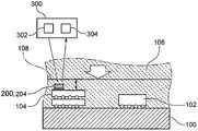
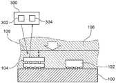
도 1은 일 실시 형태에 의한, 기판의 연마 방법을 설명하기 위한 도면이다. 도 1에 도시된 실시 형태에 있어서, 기판은 CCL(Copper Clad Laminate) 베이스(100)에, CPU나 GPU 등의 로직 칩(102), 및/또는 메모리 칩(104) 등이 배치된다. 본 명세서에 있어서, 로직 칩이나 메모리 칩 등의 소정의 기능을 구비하는 칩을 기능성 칩이라 칭한다. 도 1에 도시된 실시 형태에 있어서는, 기능성 칩(102, 104) 중에서, CCL 베이스(100)의 표면으로부터 가장 높은 위치 있는 기능성 칩의 상측의 표면에 종점 검지 요소(200)를 배치한다. 도 1의 실시 형태에 있어서는, 종점 검지 요소(200)는, 반사막(202)이며, 메모리 칩(104) 상에 배치되어 있다. 반사막(202)은, 예를 들어 기능성 칩의 상면에 실시한 금속막의 코팅으로 할 수 있다. CCL 베이스(100) 상에 기능성 칩(102, 104) 및 종점 검지 요소(200)를 배치하면, 기능성 칩(102, 104)이 실장된 CCL 베이스(100)를 절연재(106)에 의해 밀봉한다. 절연재(106)는, 예를 들어 수지나 유리 재료로 할 수 있다. 절연재(106)에 의해 밀봉하면, 절연재(106)가 평탄해지도록 절연재(106)를 연마한다. 절연재(106) 상에는, 그 후에 미세한 횡배선 및/또는 종배선이 행해지므로, 절연재(106)를 평탄하게 연마하는 것이 중요해진다. 절연재(106)의 연마는, 화학 기계적으로 연마(CMP)할 수 있다. CMP는, 일반적인 CMP 장치를 사용할 수 있다. CMP 장치는 임의의 것으로 할 수 있고, 예를 들어 공지의 CMP 장치를 이용해도 된다. 절연재(106)를 CMP에 의해 연마할 때, 종점 검지 요소(200)를 이용하여 연마의 종점을 검지할 수 있다. 도 1의 실시 형태에 있어서는, 종점 검지 요소(200)는 반사막(202)이므로, 광학식으로 종점 검지를 행할 수 있다. 예를 들어, CMP 장치(300)는, 반사막(202)에 레이저 등의 광을 조사하기 위한 광원(302)을 구비하고, 또한, 반사막(202)으로부터의 반사광을 수광하기 위한 센서(304)를 구비한다. 반사막(202)으로부터의 반사광에 의해 반사막(202)으로부터의 거리를 측정하고, 연마 목표 위치(108)까지 연마를 하면, 연마를 종료한다. 절연재(106)의 종점 위치는, 예를 들어 연마 목표 위치(108)로부터 ±10㎛ 이하로 하는 것이 바람직하다. 또한, 연마 목표 위치(108)는, 예를 들어 반사막(202)이 마련된 최상 위치에 있는 칩의 상면으로부터 10㎛ 내지 500㎛로 할 수 있다.1 is a view for explaining a method of polishing a substrate according to one embodiment. In the embodiment shown in FIG. 1, the substrate is provided with a
도 1에 도시된 상술한 실시 형태에 있어서는, 종점 검지 요소(200)로서 반사막(202)을 사용하고 있지만, 다른 실시 형태로서, 반사막(202) 대신에, 형광재 또는 형광재를 포함하는 수지 등을 사용할 수 있다. 형광재 또는 형광재를 포함하는 수지는, 도 1에 도시된 바와 같은 CCL 베이스(100)의 표면으로부터 가장 높은 위치에 있는 기능성 칩의 상측의 표면에만 도포해도 되고, 혹은, CCL 베이스(100)에 기능성 칩(102, 104)을 배치한 후에, 기판의 전체면에 도포해도 된다. 기능성 칩(102, 104)의 상측 표면에 형광재 또는 형광재를 포함하는 수지를 도포하는 경우, 표면의 일부만 도포해도 되고, 표면의 전체면에 도포해도 된다. 형광재를 도포한 후에, 기판의 전체를 절연재(106)로 밀봉한다. 이러한 실시 형태에 있어서는, 광원(302)은, 형광재에 형광을 발생시키는 파장을 포함하는 것을 선택한다. 센서(304)는, 가장 높은 위치에 있는 기능성 칩의 상면에 도포된 형광재로부터의 형광의 강도를 측정한다. 형광의 강도는, 형광재 상에 배치된 절연재(106)의 두께에 따라 변화된다. 그 때문에, 검출된 형광의 강도에 의해 절연재(106)의 두께를 검출할 수 있어, 절연재(106)의 연마의 종점을 검지할 수 있다. 또한, 센서(304)로 형광 파장만을 검출하기 위해 파장 필터를 사용할 수 있다. 혹은, 분광기를 사용하여 형광 파장의 강도를 검출해도 된다.In the above-described embodiment shown in FIG. 1, a reflective film 202 is used as the end
도 2는 일 실시 형태에 의한, 기판의 연마 방법을 설명하기 위한 도면이다. 도 2의 실시 형태에 있어서는, 종점 검지 요소(200)로서, 기능성 칩(102, 104) 중에서, CCL 베이스(100)의 표면으로부터 가장 높은 위치에 있는 기능성 칩(102, 104)의 상측의 표면에 반사판(204)을 고정한다. 반사판(204)은, 예를 들어 접착제를 사용하여 기능성 칩(102, 104)의 상면에 고정할 수 있다. 반사판(204)은, 예를 들어 판형 부재에 금속 코팅을 실시한 것으로 할 수 있다. 반사판(204) 이외에 대해서는, 도 1에 도시된 실시 형태와 마찬가지로 할 수 있다.2 is a view for explaining a method of polishing a substrate according to one embodiment. In the embodiment of FIG. 2, as the end
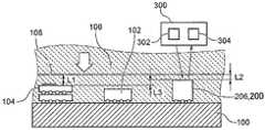
도 3은 일 실시 형태에 의한, 기판의 연마 방법을 설명하기 위한 도면이다. 도 3에 도시된 실시 형태에 있어서, 기판은 CCL(Copper Clad Laminate) 베이스(100)에, CPU나 GPU 등의 로직 칩(102), 및/또는 메모리 칩(104) 등이 배치된다. 도 3에 도시된 실시 형태에 있어서는, 기능성 칩(102, 104)과는 별도로, 기판에 형성되는 디바이스의 기능에 무관계한 더미 요소(206)를 종점 검지 요소(200)로서 배치한다. 더미 요소(206)는, 상면이, CCL 베이스(100)의 표면으로부터 가장 높은 위치에 있는 기능성 칩의 상면보다도 높은 위치가 되도록 배치된다. 더미 요소(206)의 상면은, 도 1의 실시 형태와 같이 반사막(202)으로 해도 되고, 또한, 더미 요소(206)의 상면에 도 2의 실시 형태와 같은 반사판(204)을 설치해도 된다. 더미 요소(206)는, 접착제에 의해 CCL 베이스(100)에 설치할 수 있다. 혹은, 더미 요소(206)는, 다른 기능성 칩(102, 104)과 마찬가지로 범프 접착해도 된다. 다른 기능성 칩(102, 104)과 동일한 공정에서 범프 접착을 함으로써, 기능성 칩(102, 104)과 더미 요소(206)의 설치의 오차를 작게 할 수 있다. 더미 요소(206)는, 임의의 장소에 배치할 수 있지만, 다른 기능성 칩을 방해하지 않는 장소에 마련할 필요가 있다. 또한, 더미 요소(206)는 복수 배치해도 된다. CCL 베이스(100) 상에 기능성 칩(102, 104) 및 더미 요소(206)를 배치하면, 기능성 칩(102, 104) 및 더미 요소(206)가 실장된 CCL 베이스(100)를 절연재(106)에 의해 밀봉한다. 절연재(106)는, 예를 들어 수지나 유리 재료로 할 수 있다. 절연재(106)에 의해 밀봉하면, 절연재(106)가 평탄해지도록 절연재(106)를 연마한다. 절연재(106)의 연마는, 화학 기계적으로 연마(CMP)할 수 있다. CMP는, 일반적인 CMP 장치를 사용할 수 있다. CMP 장치는 임의의 것으로 할 수 있고, 예를 들어 공지의 CMP 장치를 이용해도 된다. 절연재(106)를 CMP에 의해 연마할 때, 종점 검지 요소(200)인 더미 요소(206)를 이용하여 연마의 종점을 검지할 수 있다. 도 3의 실시 형태에 있어서는, 더미 요소(206)의 상면은 반사막(202) 또는 반사판(204)이므로, 상술한 바와 같이 광학식으로 종점 검지를 행할 수 있다. 연마 목표 위치(108)로서, 예를 들어 도 3에 도시된 바와 같이, CCL 베이스(100)의 표면으로부터 가장 높은 위치에 있는 기능성 칩의 상면으로부터의 거리 L1을 정한다. CCL 베이스(100)의 표면으로부터 가장 높은 위치에 있는 기능성 칩의 상면과, 더미 요소(206)의 상면의 높이의 차 L3을 측정해 둔다. 이러한 높이의 차 L3은, 기능성 칩(102, 104) 및 더미 요소(206)를 CCL 베이스(100)에 배치하고, 절연재(106)로 몰드하기 전에, 임의의 위치 센서나, 공초점 현미경 등으로 측정할 수 있다. 그리고, 연마 목표 위치(108)가 L1이 되도록, 더미 요소(206)의 상면으로부터 연마 목표 위치(108)의 거리 L2를 산출한다. 절연재(106)의 연마를 행할 때, 더미 요소(206)의 상면으로부터 절연재(106)의 표면까지의 거리가 L2로 될 때까지 절연재(106)의 연마를 행함으로써, 연마 목표 위치(108)까지 절연재(106)의 연마를 행할 수 있다. 종점의 연마 목표 위치(108)는, 예를 들어 반사막(202)이 마련된 최상 위치에 있는 칩의 상면으로부터 10㎛ 내지 500㎛로 할 수 있다.3 is a view for explaining a method of polishing a substrate according to one embodiment. In the embodiment illustrated in FIG. 3, the substrate is provided with a
도 4는 일 실시 형태에 의한, 기판의 연마 방법을 설명하기 위한 도면이다. 도 4는 평탄화된 절연재(106) 상에 배선층을 형성하고, 배선층을 연마할 때의 방법을 도시하고 있다. 도 4에 도시된 실시 형태에 있어서는, 도 1 내지 도 3에 도시된 실시 형태와 마찬가지의 방법으로, 절연재(106)를 연마 목표 위치(108)까지 연마한다. 도 4에 도시된 실시 형태에 있어서는, 그 후, 평탄화된 절연재(106)에 대하여, 배선을 위한 패턴 형성이 행해진다. 배선을 위한 패턴으로서, 종배선을 위한 비아(110)의 형성, 횡배선의 패턴(112)의 형성 등이, 노광이나 에칭 등에 의해 행해진다. 그 후, 예를 들어 구리 등의 금속층(114)이 패턴 형성된 절연재(106) 상에 성막된다(도 4에 도시된 상태). 그 후, 금속층(114)의 불필요한 부분을 연마 제거한다. 이 금속층(114)의 연마는, CMP에 의해 행할 수 있다. 금속층(114)의 연마에 있어서, 금속층(114)의 연마를 한 후의 연마면에 금속이 잔류하지 않도록 하는 것이 중요하다. 연마 후의 표면에 잔류 금속이 있으면, 누설 전류나 소자의 열화를 야기하는 경우가 있다. 그 때문에, 연마 목표 위치(108)는, 금속층(114)을 제거하고, 절연재(106)의 일부를 연마하도록 연마 목표 위치(108)를 정할 수 있다. 예를 들어, 연마 목표 위치(108)는, 금속층(114)과 절연재(106)의 층의 경계면으로부터 5㎛ 내지 10㎛ 정도 절연재(106)측으로 설정할 수 있다. 금속층(114)을 CMP에 의해 연마할 때, 연마의 종점 검지는, 금속층(114)에 발생하는 와전류를 검출하는 와전류 센서에 의해 와전류의 변화를 관찰함으로써 행할 수 있다. 혹은, 종점 검지는, 광학식의 센서에 의해 금속층(114)으로부터의 반사광의 변화를 관찰함으로써 행해도 된다. 혹은, 종점 검지는, 금속층(114)으로부터 절연재(106)로 재료가 변화되는 곳에서 발생하는 연마 저항의 변화나, CMP 장치의 구동 기구의 토크 변화를 관찰함으로써 행할 수 있다. 또한, 연마 후의 표면에 잔류 금속이 발생하지 않도록, 연마에 의해 층의 변화에 의한 층의 경계를 검지하고 나서 소정 시간만큼 연마를 행하여, 상술한 연마 목표 위치(108)까지 연마를 행하도록 해도 된다. 그 밖에도, 공지의 종점 검지를 채용해도 된다.4 is a view for explaining a method of polishing a substrate according to one embodiment. 4 shows a method for forming a wiring layer on the planarized insulating
도 5는 일 실시 형태에 의한, 기판의 연마 방법을 설명하기 위한 도면이다. 도 5에 도시된 실시 형태에 있어서는, 도 1 내지 도 3에 도시된 실시 형태와 마찬가지의 방법으로, 절연재(106)를 연마 목표 위치(108)까지 연마한다. 도 5에 도시된 실시 형태에 있어서는, 그 후, 평탄화된 절연재(106) 상에 배리어 몰드층(116)을 형성한다(도 5의 상부의 도면의 상태). 배리어 몰드층(116)은, 절연성의 재료로 형성된다. 배리어 몰드층(116)은, 그 아래의 절연재(106)와는 중량 밀도가 다른 재료를 사용하여, 연마 시의 마찰력이 배리어 몰드층(116)과 절연재(106)에서 상이하도록 한다. 또한, 배리어 몰드층(116)은, 절연재(106)의 층과 비교하여 얇은 층으로 할 수 있다. 예를 들어, 배리어 몰드층(116)은, 10nm 내지 10㎛ 정도의 두께로 할 수 있다. 배리어 몰드층(116)을 형성하면, 그 위의 배선을 위한 패턴 형성이 행해진다. 배선을 위한 패턴으로서, 종배선을 위한 비아(110)의 형성, 횡배선의 패턴(112)의 형성 등이, 노광이나 에칭 등에 의해 행해진다. 그 후, 예를 들어 구리 등의 금속층(114)이 패턴 형성된 절연재(106) 상에 성막된다. 그 후, 금속층(114)의 불필요한 부분을 연마 제거한다. 도 5의 하부의 도면은, 금속층(114)이 제거된 상태를 도시하는 도면이다. 이 금속층(114)의 연마는, CMP에 의해 행할 수 있다. 금속층(114)을 CMP에 의해 연마할 때, 금속층(114)이 제거되고 배리어 몰드층(116)이 노출될 때, 연마 저항이 변화된다. 그래서, 연마 저항의 변화를 CMP에 의한 금속층(114)을 제거하는 연마의 종점 검지에 사용할 수 있다. 또한, 과연마에 의해 배리어 몰드층(116)이 제거되어 버리면, 더 아래의 절연재(106)가 노출되어, 연마 저항이 더 변화되게 된다. 그래서, 배리어 몰드층(116)으로부터 절연재(106)로 변화될 때의 연마 저항의 변화로부터, 과연마의 검지를 행할 수 있다.5 is a view for explaining a method of polishing a substrate according to one embodiment. In the embodiment shown in FIG. 5, the insulating
도 6은 일 실시 형태에 의한, 기판의 연마 방법을 설명하기 위한 도면이다. 도 5에 도시된 실시 형태에 있어서는, 도 1 내지 도 3에 도시된 실시 형태와 마찬가지의 방법으로, 절연재(106)를 연마 목표 위치(108)까지 연마한다. 도 6에 도시된 실시 형태에 있어서는, 그 후, 평탄화된 절연재(106)에 대하여, 배선을 위한 패턴 형성이 행해진다. 배선을 위한 패턴으로서, 종배선을 위한 비아(110)의 형성, 횡배선의 패턴(112)의 형성 등이, 노광이나 에칭 등에 의해 행해진다(도 6의 상태). 그 후, 광이나 레이저를 노광함으로써 절연재(106)의 표면의 친수성을 향상시킨다. 이 처리에 의해, 그 후에 행해지는, 도전재인 금속층(114)의 밀착성을 향상시킬 수 있다. 이 이후의, 금속층(114)의 형성 등은 도 4에서 설명한 실시 형태와 마찬가지로 할 수 있다. 또한, 도 5에서 설명한 실시 형태, 또는 다른 실시 형태에 친수성을 향상시키는 처리를 추가해도 된다.6 is a view for explaining a method of polishing a substrate according to one embodiment. In the embodiment shown in FIG. 5, the insulating
도 7은 일 실시 형태에 의한, 기판의 연마 방법을 설명하기 위한 도면이다. 도 7의 실시 형태에 있어서, 기판은, 관통 배선(150)을 구비하는 CCL(Copper Clad Laminate) 베이스(100)를 갖는다. 관통 배선(150)을 구비하는 CCL 베이스(100)는, CMP 등에 의해 평탄화되어 있다. 평탄화되어 있는 CCL 베이스(100)의 상면에 종점 검지 요소(200)를 배치한다. 도 7의 실시 형태에 있어서는, 종점 검지 요소(200)는 반사판(204)이다. 반사판(204)은, 예를 들어 접착제를 사용하여 CCL 베이스(100) 상에 고정할 수 있다. 그 후, 반사판(204)이 배치된 CCL 베이스(100)를 절연재(106)에 의해 밀봉한다. 절연재(106)는, 이미 설명한 바와 같이, 예를 들어 수지나 유리 재료로 할 수 있다. 절연재(106)에 의해 밀봉하면, 절연재(106)가 평탄해지도록 절연재(106)를 연마한다. 절연재(106)의 연마 종점의 검지에 관해서는, 도 1, 도 2 등에서 이미 설명한 바와 같이, 광 또는 레이저의 반사광을 센서로 검출하여 행할 수 있다. 도 7의 실시 형태에 있어서, 반사판(204)의 위치는 임의이지만, 다른 기능성 칩 등을 방해하지 않는 위치로 할 필요가 있다. 또한, 반사판(204)은 복수 마련해도 된다. 또한, 도 7의 실시 형태에 있어서, 반사판(204) 대신에, 도 3에서 도시된 더미 요소(206)를 설치하도록 해도 된다.7 is a view for explaining a method of polishing a substrate according to one embodiment. In the embodiment of FIG. 7, the substrate has a CCL (Copper Clad Laminate)
도 8은 일 실시 형태에 의한, 기판의 연마 방법을 설명하기 위한 도면이다. 도 8은 평탄화된 절연재(106) 상에 배선층을 형성하고, 배선층을 연마할 때의 방법을 도시하고 있다. 도 8에 도시된 실시 형태에 있어서는, 도 7에 도시된 실시 형태와 마찬가지의 방법으로, 절연재(106)를 연마 목표 위치(108)까지 연마한다. 도 8에 도시된 실시 형태에 있어서는, 그 후, 평탄화된 절연재(106)에 대하여, 배선을 위한 패턴 형성이 행해진다. 배선을 위한 패턴으로서, 종배선을 위한 비아(110)의 형성, 횡배선의 패턴(112)의 형성 등이, 노광이나 에칭 등에 의해 행해진다. 그 후, 예를 들어 도전 재료인 구리 등의 금속층(114)이 패턴 형성된 절연재(106) 상에 성막된다(도 8의 상부의 도면에 도시된 상태). 그 후, 금속층(114)의 불필요한 부분을 연마 제거한다. 이 금속층(114)의 연마는, CMP에 의해 행할 수 있다. 금속층(114)의 연마는, 도 4의 실시 형태에서 설명한 것과 마찬가지로 할 수 있다.8 is a view for explaining a method of polishing a substrate according to one embodiment. 8 shows a method for forming a wiring layer on the planarized insulating
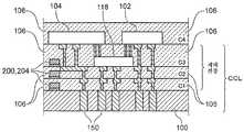
도 9는 일 실시 형태에 의한, 기판의 연마 방법을 설명하기 위한 도면이다. 도 9는 배선층을 구비하는 복수의 절연재(106)의 층을 형성할 때의 방법을 도시하고 있다. CCL 베이스(100) 상에 형성되는 절연재(106)의 제1 층 C1은, 도 8에서 도시된 실시 형태와 마찬가지의 방법으로 형성할 수 있다. 그 후, 평탄화된 제1 층 C1의 상면에 반사판(204)을 고정한다. 반사판(204)은, 예를 들어 접착제를 사용하여 제1 층 C1의 상면에 고정할 수 있다. 그 후, 절연재(106)를 성막하고, 도 8에서 설명한 바와 같이 또한 배선의 패턴 형성, 금속층(114)의 형성, 금속층(114)의 연마를 행하여, 제2 층 C2를 형성한다. 또한, 마찬가지로 제3 층 C3을 형성할 수 있다. 배선층을 구비하는 절연재(106)의 층은 임의의 수만큼 형성할 수 있다. 도 9에 도시된 실시 형태에 있어서는, 제3 층 C3 상에, 로직 칩(102) 및 메모리 칩(104) 등의 기능성 칩이 배치된다. 도 9에 도시된 바와 같이, 이들 기능성 칩 사이의 배선을 인터커넥트 칩(118)이나 인터포저에 의해 행해도 된다. 도 9에는, CCL 베이스(100)의 편측의 면에만 배선이나 기능성 칩을 실장하는 예를 도시하고 있지만, 다른 실시 형태로서, CCL 베이스(100)의 양쪽의 면에 실장해도 된다. 또한, 인터포저나 인터커넥트 칩(118)으로부터 패키지 몰드 외부로 배선을 취출하기 위한 종배선의 형성을 행해도 된다. 종배선의 형성은, 임의의 방법으로 행할 수 있고, 예를 들어 본 명세서에서 개시되는 방법으로 행해도 된다. 도 10은 CCL 베이스(100)의 양쪽의 면에 배선이나 기능성 칩을 실장한 예를 도시하고 있고, 또한, 인터커넥트 칩(118)으로부터 패키지 몰드 외부로 배선을 취출하기 위한 종배선(120)을 구비한다. 도 10에 도시된 패키지는, 본 명세서에서 개시된 방법을 합함으로써 형성할 수 있다.9 is a view for explaining a method of polishing a substrate according to one embodiment. 9 shows a method for forming a layer of a plurality of insulating
도 11은 일 실시 형태에 의한 CMP 장치(300)의 구성을 도시하는 개념도이다. CMP 장치(300)는, 기판 보유 지지 헤드(21), 베어링 볼(3), 헤드축(2), 연마반(38), 연마포(39), 제1 공기 공급 라인(36), 제2 공기 공급 라인(62), 제1 에어 레귤레이터 R1, 제2 에어 레귤레이터 R2, 순수 공급 라인(46), 순수 레귤레이터 R4를 구비한다. 연마 장치(1)는, 또한 헤드 고정 부재(4), 연결축(48), 에어 실린더(5), 피스톤(14), 제3 공기 공급 라인(51), 제3 에어 레귤레이터 R3, 회전통(6), 타이밍 풀리(7), 타이밍 벨트(8), 타이밍 풀리(10), 모터(9), 지액 공급 노즐(13) 등을 구비한다.11 is a conceptual diagram showing the configuration of a
기판 보유 지지 헤드(21)는, 베어링 볼(3)을 통해 헤드축(2)에 걸림 결합되어 있다. 헤드축(2)은, 헤드 고정 부재(4)에 승강 가능하게 및 회전 가능하게 도시하지 않은 베어링을 통해 걸림 결합되고, 연결축(48), 연결봉(61)을 통해 에어 실린더(5) 내의 피스톤(14)에 연결되어 있다. 에어 실린더(5)는, 제3 공기 공급 라인(51)에 접속되어 있다. 제3 공기 공급 라인(51)은, 제3 밸브 V3, 제3 에어 레귤레이터 R3을 통해 압축 공기원(42)에 접속된다. 에어 실린더(5)의 압력은, 제3 에어 레귤레이터 R3에 의해 소정의 압력으로 제어된다.The
에어 실린더(5)의 압력에 의해, 피스톤(14)은 상하 이동하고, 피스톤(14)의 상하 이동에 의해, 연결축(48), 기판 보유 지지 헤드축(2)은, 연결봉(61)을 통해 상하 이동하여, 기판 보유 지지 헤드(21)의 하면에 보유 지지된 기판 W를 연마반(38)으로부터 이격하거나, 혹은 연마반(38) 향하여 압박한다. 또한, 기판 보유 지지 헤드(21)의 상면과 헤드축(2)의 하단부면은, 베어링 볼(3)을 수용하는 볼 베어링을 형성하고 있고, 기판 보유 지지 헤드(21)는 베어링 볼(3)을 통해 연마반(38)에 대하여 또한 연마포(39)에 대하여 베어링 볼(3)을 중심으로 틸팅 가능하게 되어 있다. 또한, 베어링 볼(3)은 헤드축(2)의 중심에 위치한다.By the pressure of the air cylinder 5, the
또한, 헤드축(2)에는 회전통(6)이 설치되어 있고, 회전통(6)은 그 외주에 타이밍 풀리(7)를 구비하고 있다. 그리고, 타이밍 풀리(7)는, 타이밍 벨트(8)를 통해, 헤드 고정 부재(4)(암이라고도 함)에 고정된 모터(9)에 마련된 타이밍 풀리(10)에 접속되어 있다. 따라서, 모터(9)를 회전 구동함으로써, 타이밍 벨트(8) 및 타이밍 풀리(7)를 통해 회전통(6) 및 헤드축(2)이 일체로 회전하고, 헤드축(2)의 회전에 의해 기판 보유 지지 헤드(21)가 회전한다. 또한, 헤드 고정 부재(4)의 일단은, 요동축(64)에 의해 지지되어, 요동 가능하게 되어 있다. 또한, 연결축(48)으로는, 헤드축(2)으로부터의 회전은 전달되지 않는다.Further, a rotating cylinder 6 is provided on the
CMP 장치(300)는, 제어 장치(900)를 갖고, CMP 장치(300)에 마련되는 각종 센서나 동작 기구는 제어 장치(900)에 의해 제어되도록 구성할 수 있다. 제어 장치(900)는, 입출력 장치, 연산 장치, 기억 장치 등을 구비하는 일반적인 컴퓨터로 구성할 수 있다. 제어 장치에는, 본 명세서에서 설명한 방법을 동작시키기 위한 컴퓨터 프로그램이 인스톨된다. 이 컴퓨터 프로그램은 불휘발성의 기록 매체에 저장되어 있어도 되고, 또한, 각종 통신 기술에 의한 컴퓨터에 프로그램을 배신해도 된다.The
도 11에 도시된 CMP 장치(300)에 있어서, 연마되는 기판은, 기판 보유 지지 헤드(21)의 하면에 진공 흡착에 의해 보유 지지된다. 도 11에 도시된 바와 같이, 기판 보유 지지 헤드(21)의 연직 방향 하측에는, 연마반(38)이 배치된다. 연마반(38)의 상면에는 연마포(39)가 첩부되어 있다. 연마포(39)는, 기판의 피연마면이 접촉하도록 구성되어 있다. 연마포(39)는, 기판 W의 피연마면과 접촉하는 면이, 연마면이다.In the
도 11에 도시된 바와 같이, 기판 보유 지지 헤드(21)는, 공기 공급 라인(62)에 접속되어 있다. 공기 공급 라인(62)은, 밸브 V2, 에어 레귤레이터 R2를 통해 압축 공기원(42)에 접속되고, 밸브 V0을 통해 진공 배기원(49)에 접속되어 있다. 밸브 V0을 폐쇄로 하고 제2 밸브 V2를 개방으로 한 상태에서, 기판 보유 지지 헤드(21)에 보유 지지된 기판의 이면(피연마면의 반대측의 면)에 원하는 압력을 부여할 수 있고, 이 압력에 의해 기판은 연마반(38)을 향하여 압박된다. 또한, 밸브 V2를 폐쇄로 한 상태에서, 밸브 V0을 개방으로 함으로써, 기판 보유 지지 헤드(21)에 보유 지지되는 기판의 이면을 진공으로 하여, 기판 W를 기판 보유 지지 헤드(21)에 진공 흡착시킬 수 있다.11, the
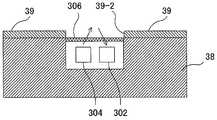
도 11에 도시된 CMP 장치(300)에 있어서, 연마반(38)은, 기판의 연마의 종점을 검지하기 위한 센서(100)를 구비할 수 있다. 도 12는 일 실시 형태에 의한, 광학적인 종점 검출 기구를 개략적으로 도시하는 단면도이다. 도 12는 연마반(38)의 센서(304)가 마련되는 부분을 도시하고 있다. 도 12에 도시된 센서(304)는, 광학식 센서이며, 연마반(38)에는 또한 광원(302)이 배치되어 있다. 센서(304) 및 광원(302)은, 유선 또는 무선에 의해 제어 장치(900)(도 11)와 연락 가능하게 구성된다. 도 12에 도시된 실시 형태에 있어서, 연마포(39)의 일부에 절결(39-2)이 마련되어 있다. 절결(39-2)의 위치에 뷰 포트(306)를 배치한다. 뷰 포트(306)를 통해, 광원(302)으로부터 광을 연마 중인 기판을 향하여 조사하고, 기판으로부터의 반사광을 센서(304)에 의해 검지할 수 있다. 연마 중인 기판의 반사율의 변화 등으로부터, 기판의 연마의 종점을 검지할 수 있다. 일 실시 형태로서, 센서(304)는, 예를 들어 패브리 페로 분광기 등의 분광기를 구비하는 것으로 할 수 있다. 또한, 센서(304)로서 파이버 센서를 사용하는 경우, 센서(304) 및 광원(302)은, 연마반(38)에 복수 배치해도 된다. 예를 들어, 연마반(38)의 중심부와 주변부에 배치하고, 양쪽의 센서(304) 및 광원(302)으로부터의 신호를 감시하여, 기판 W의 연마의 종점을 결정해도 된다. 또한, 복수의 센서(304) 및 광원(302)을 사용함으로써, 기판 W의 복수의 영역의 연마면의 막 두께를 감시할 수 있다. 기판 W의 복수의 영역의 연마의 종점이 동시기가 되도록, 복수의 센서(304)로부터의 신호에 기초하여 연마 조건을 제어할 수 있다.In the
도 11에 도시된 CMP 장치(300) 및 도 12에 도시된 종점 검지 센서는, 상술한 기판을 연마하는 방법 및 기판 연마의 종점을 검지하는 방법에 사용할 수 있다. 또한, 도 11에 도시된 CMP 장치(300) 및 도 12에 도시된 종점 검지 센서는, 다른 방법에 의한 기판 연마의 종점을 검지하는 방법에도 사용할 수 있다. 이하에, 기판 연마의 종점을 검지하는 방법을 몇 가지 설명한다.The
도 13은 일 실시 형태에 의한, 기판의 연마 방법을 설명하기 위한 도면이다. 도 13에 도시된 실시 형태에 있어서, 기판은 CCL(Copper Clad Laminate) 베이스(100)에, CPU나 GPU 등의 로직 칩(102), 및/또는 메모리 칩(104) 등이 배치된다. 도 13에 도시된 기판은, 도 1에 도시된 기판과 달리 반사막(202) 등의 종점 검지 요소(200)가 배치되지 않는다. 도 13에 도시된 실시 형태에 있어서는, CCL 베이스(100) 상에 기능성 칩(102, 104)을 배치하면, 기능성 칩(102, 104)이 실장된 CCL 베이스(100)를 절연재(106)에 의해 밀봉한다. 절연재(106)는, 예를 들어 수지나 유리 재료로 할 수 있다. 절연재(106)에 의해 밀봉하면, 절연재(106)가 평탄해지도록 절연재(106)를 연마한다. 절연재(106)의 연마는, 화학 기계적으로 연마(CMP)할 수 있고, 예를 들어 도 12에 도시된 광학식의 종점 검지 센서를 구비하는 CMP 장치(300)를 사용하여 연마할 수 있다. 도 13의 실시 형태에 있어서는, 기능성 칩(102, 104) 중에서 가장 높은 위치에 있는 칩의 표면에 광원(302)으로부터 광을 조사하고, 센서(304)로 반사광을 수광한다. 도 13에 도시된 실시 형태에 있어서는, 반사광을 분광하여, 반사광의 파장마다의 상대 반사율로부터 절연재(106)의 두께를 측정할 수 있다. 광원(302)으로부터 기판의 절연재(106)를 향하여 조사된 광은, 절연재(106)의 표면에서 반사되고, 또한 가장 높은 위치에 있는 기능성 칩(도 13의 예에서는 메모리 칩(104))의 표면에서 반사되게 된다. 다른 위치에서 반사된 광이 간섭함으로써, 센서(304)에 의해 검출되는 광의 파장마다의 상대 반사율이 절연재(106)의 두께에 따라서 변화된다. 그 때문에, 상대 반사율을 검출함으로써 기능성 칩(102, 104) 상의 절연재(106)의 두께를 측정할 수 있다. 미리 예비 실험에 의해 절연재(106)의 두께가 연마 목표 위치(108)가 될 때의 상대 반사율을 측정해 둠으로써, 도 12에 도시된 광원(302) 및 센서(304)를 연마 중인 기판의 종점 검지 센서로서 이용할 수 있다. 절연재(106)의 두께가 연마 목표 위치(108)에 도달하면 연마를 종료한다. 절연재(106)의 종점 위치는, 예를 들어 연마 목표 위치(108)로부터 ±10㎛ 이하로 하는 것이 바람직하다. 또한, 연마 목표 위치(108)는, 예를 들어 최상 위치에 있는 칩(104)의 상면으로부터 10㎛ 내지 500㎛로 할 수 있다. 또한, 분광기는, 패브리 페로 분광기 등을 사용할 수 있다. 또한, 광원(302)은, 레이저 다이오드, LED 등 임의의 광원을 사용할 수 있다. 광원(302)의 파장 범위는, 예를 들어 500㎚ 내지 800㎚를 포함하는 것으로 할 수 있다. 또한, 광원(302)의 파장은, 조사 대상인 절연재(106) 등의 막 두께나 막종에 따라서, 단파장인 200㎚ 내지 500㎚의 파장 범위를 사용하는 것도 가능하다.13 is a view for explaining a method of polishing a substrate according to one embodiment. In the embodiment shown in FIG. 13, the substrate is provided with a
도 13에 관하여, 상술한 방법은 반사광의 상대 반사율의 변화로부터 기판 연마의 종점을 검지하고 있지만, 광의 강도를 측정함으로써 기판 연마의 종점을 검지할 수도 있다. 이러한 방법에 있어서, 광원(302)으로부터 기판 상의 가장 높은 위치에 있는 기능성 칩(102, 104)에 광을 조사하고, 반사광을 센서(304)로 검지한다. 기능성 칩(102, 104) 상에 배치되어 있는 절연재(106)의 두께에 따라 반사광의 강도가 변화되므로, 미리 예비 실험에 의해, 절연재(106)의 두께가 연마 목표 위치(108)가 될 때의 반사광의 강도를 측정해 둠으로써, 도 12에 도시된 광원(302) 및 센서(304)를 연마 중인 기판의 종점 검지 센서로서 이용할 수 있다. 반사광의 강도를 측정하여 기판 연마의 종점을 검지하는 경우, 전술한 상대 반사율을 측정하여 종점 검지하는 경우와 달리 분광기가 필요없다. 이 경우, 반사광의 강도는 모든 파장 성분을 적분한 것이 측정된다. 단, 분광기를 사용하여 특정 파장(예를 들어 500㎚ 이하의 임의의 파장)의 반사광의 강도를 측정해도 된다. 반사광의 강도를 측정하는 경우에 있어서, 광원(302)은 레이저 다이오드, LED 등 임의의 광원을 사용할 수 있다. 또한, 광원(302)은, 기능성 칩(102, 104)의 표면(예를 들어 실리콘)에서의 반사율이 높은 파장 범위(예를 들어, 500㎚ 이하의 파장)를 포함하는 것이 바람직하다. 또한, 광원(302)으로서, 특정 파장(예를 들어 500㎚ 이하의 임의의 파장)의 단색 광원을 사용해도 된다.With respect to Fig. 13, the above-described method detects the end point of substrate polishing from a change in the relative reflectance of reflected light, but it is also possible to detect the end point of substrate polishing by measuring the intensity of light. In this method, light is emitted from the
도 13에 도시된 기판 연마 방법에 있어서, 광원(302)으로서 적외광(예를 들어 파장은 1㎛ 내지 3㎛)을 사용하고, 또한 적외 분광기를 사용하여 절연재(106)의 두께 및 연마의 종점을 검지할 수도 있다. 기능성 칩(102, 104)의 표면에서의 적외광의 반사율과 절연재(106)(예를 들어 수지)의 표면에서의 적외광의 반사율은 상이하다. 그 때문에, 기능성 칩(102, 104) 상에 형성되어 있는 절연재(106)의 두께에 따라, 센서(304)에 의해 수광되는 반사광의 스펙트럼 강도가 변화된다. 그 때문에, 반사광의 스펙트럼 변화에 따라 절연재(106)의 두께를 검출할 수 있다.In the substrate polishing method shown in FIG. 13, infrared light (for example, a wavelength of 1 µm to 3 µm) is used as the
도 14는 일 실시 형태에 의한, 광학적인 종점 검출 기구를 개략적으로 도시하는 단면도이다. 도 14는 연마반(38)의 센서(304)가 마련되는 부분을 도시하고 있다. 도 14에 도시된 종점 검출 기구는, 2개의 광원(302a, 302b)을 구비하고 있다. 각 광원(302a, 302b)은 연마 중인 기판(도시하지 않음)의 표면을 향하여 광을 조사하도록 위치 결정되어 있다. 센서(304)는 기판에 조사된 광의 산란광을 수광하도록 위치 결정되어 있다. 도 14에 도시된 실시 형태에 의한 종점 검출 기구는, 분광기를 구비하는 것으로 해도 된다. 센서(304) 및 광원(302)은, 유선 또는 무선에 의해 제어 장치(900)(도 11)와 연락 가능하게 구성된다. 도 14에 도시된 실시 형태에 있어서, 연마포(39)의 일부에 절결(39-2)이 마련되어 있다. 절결(39-2)의 위치에 뷰 포트(306)를 배치한다. 도 14에 도시된 실시 형태에 있어서, 뷰 포트(306)를 통해, 광원(302)으로부터 광을 연마 중인 기판을 향하여 조사하고, 기판으로부터의 산란광을 센서(304)에 의해 검지할 수 있다. 또한, 도 14에 도시된 실시 형태에 있어서, 뷰 포트(306)는 없어도 되고, 그 경우, 광원(302a, 302b) 및 센서(304)가 배치되는 연마반(38)의 오목부에 순수를 공급하면서 검출을 행할 수 있다. 도 14에 도시된 실시 형태에 의한 종점 검출 기구는, 상술한 연마 방법 및 종점 검지에 사용할 수 있다.14 is a cross-sectional view schematically showing an optical end point detection mechanism according to one embodiment. 14 shows a portion in which the
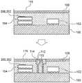
도 15는 일 실시 형태에 의한, 광학적인 종점 검출 기구를 개략적으로 도시하는 단면도이다. 도 15는 연마반(38)의 센서(304)가 마련되는 부분을 도시하고 있다. 도 15에 도시된 종점 검출 기구는, 하나의 광원(302), 제1 센서(304a) 및 제2 센서(304b)를 구비하고 있다. 광원(302)은 기판의 표면에서 전반사되는 각도로 기판에 광을 조사하도록 위치 결정된다. 또한, 제2 센서(304b)는, 전반사된 광을 수광하도록 위치 결정된다. 제1 센서(304a)는, 기판의 표면에서 산란된 광을 수광하도록 위치 결정되어 있다. 도 15의 실시 형태에 있어서, 광원(302) 및 제2 센서(304b)는, 기판의 표면에 대한 광의 입사 각도를 조정 가능한 구동 기구(도시하지 않음)를 구비할 수 있다. 도 15에 도시된 전반사를 이용한 종점 검출 기구는, 목표로 하는 연마 위치에 있어서 재질이 변화되는 경우에 이용 가능하다. 예를 들어, 도 4, 도 8과 함께 설명한 바와 같이, 절연재(106) 상에 적층된 금속층(114)을 제거하는 경우에 이용할 수 있다. 금속층(114)에서의 전반사 각도와, 금속층(114)이 제거되어 아래에 있는 절연재(106)가 노출되었을 때의 전반사 각도가 상이하므로, 수광한 광 강도의 변화로부터 금속층(114)이 제거되었음을 검출할 수 있다. 이 경우, 제2 센서(304b)로 전반사된 광을 측정해도 되고, 또한 산란광을 제1 센서(304a)로 측정해도 되고, 또한 양쪽을 측정해도 된다. 또한, 도 15에 도시된 실시 형태에 있어서는, 도 14에 도시된 바와 같은 뷰 포트(306)는 존재하지 않는다. 이것은, 뷰 포트(306)의 표면에서 광이 전반사되는 것을 방지하기 위함이다. 또한, 도 15에 도시된 실시 형태에 있어서는, 뷰 포트(306)를 사용하지 않으므로, 광원(302), 센서(304a, 304b)가 배치되는 연마반(38)의 오목부에 순수를 공급하면서 검출을 행할 수 있다.15 is a cross-sectional view schematically showing an optical end point detection mechanism according to one embodiment. 15 shows a portion in which the
또한, 전반사 조건은, 물 또는 순수 등의 연마 대상의 표면에 접촉하는 매체의 굴절률 A와 절연재(106) 등의 기판 표면의 굴절률 B의 관계가, 굴절률 A>굴절률 B를 만족시킬 필요가 있다.In addition, in the total reflection condition, the relationship between the refractive index A of the medium contacting the surface of the polishing object such as water or pure water and the refractive index B of the substrate surface such as the insulating
도 16은 일 실시 형태에 의한, 광학적인 종점 검출 기구를 개략적으로 도시하는 단면도이다. 도 16은 연마반(38)의 센서(304)가 마련되는 부분을 도시하고 있다. 도 16에 도시된 종점 검출 기구는, 도 15에 도시된 실시 형태와 마찬가지로 전반사를 이용한다. 도 16에 도시된 실시 형태에 있어서는, 광원(302)으로부터 조사된 광은, 제1 미러(308a)에 의해 반사되어 기판의 표면으로 유도된다. 제1 미러(308a)는, 기판의 표면에서 전반사되는 각도로 기판에 광을 향하게 하도록 위치 결정된다. 도 16에 도시된 종점 검출 기구는, 제2 미러(308b)를 구비한다. 제2 미러(308b)는, 연마 중인 기판 표면에서 전반사된 광을 제2 센서(304b)로 유도하도록 위치 결정되어 있다. 제1 미러(308a) 및 제2 미러(308b)는, 기판의 표면에 대한 광의 입사 각도를 조정 가능한 구동 기구(도시하지 않음)를 구비할 수 있다. 도 16의 종점 검출 기구는, 다른 구성은 도 15에 도시된 종점 검출 기구와 마찬가지로 할 수 있다. 도 16에 도시된 전반사를 이용한 종점 검출 기구는, 도 15에 도시된 종점 검출 기구와 마찬가지로, 목표로 하는 연마 위치에 있어서 재질이 변화되는 경우에 이용 가능하다.16 is a cross-sectional view schematically showing an optical end point detection mechanism according to an embodiment. 16 shows a portion in which the
도 17a는 일 실시 형태에 의한, 광학적인 종점 검출 기구를 개략적으로 도시하는 단면도이다. 도 17a는 연마반(38)의 센서(304)가 마련되는 부분을 도시하고 있지만, 명료화를 위해 연마반(38)과 패드(39)는 도시하지 않았다. 도 17a에 도시된 종점 검출 기구는, 다른 광학적인 종점 검출 기구와 마찬가지로, 광원(302) 및 센서(304)를 구비한다. 도 17a에 도시된 종점 검출 기구는, 또한 어댑터(310)를 구비한다. 어댑터(310)는, 예를 들어 광학 플라스틱 등의 고굴절률 재료로 형성할 수 있다. 어댑터(310)의 굴절률은, 연마 대상인 기판 표면의 절연재(106)의 굴절률보다도 큰 것이 바람직하다. 어댑터(310)는, 대략 직육면체 형상의 블록으로 할 수 있다. 어댑터(310)는, 연마 대상인 기판의 표면에 접촉 내지 근접하도록 배치할 수 있다. 또한, 어댑터(310)에는, 제1 광 파이버(312a) 및 제2 광 파이버(312b)가 마련되어 있다. 제1 광 파이버(312a) 및 광원(302)은, 광원(302)으로부터의 광을 제1 광 파이버(312a)가 수취하도록 배치된다. 제2 광 파이버(312b)는, 제1 광 파이버(312a)로부터 나온 광이 어댑터(310)와 기판의 표면의 경계에서 반사된 광을 수취하도록 배치된다. 제2 광 파이버(312b) 및 센서(304)는, 제2 광 파이버(312b)로부터 나온 광을 센서(304)가 수취하도록 배치된다. 제1 광 파이버(312a) 및 제2 광 파이버(312b)는, 동일한 구경의 광 파이버로 해도 되고, 다른 구경의 광 파이버로 해도 된다. 예를 들어, 제2 광 파이버(312b)는, 수율을 높이기 위해 제1 광 파이버(312a)보다도 구경이 큰 광 파이버로 해도 된다. 또한, 제2 광 파이버(312b) 대신에 어레이형 광 센서(예를 들어 포토다이오드 어레이)를 어댑터(310)에 내장시켜도 된다. 광원(302), 센서(304) 및 어댑터(310)는, 상대적인 위치를 유지한 채로, 기판의 표면에 수직인 방향으로 이동 가능하게 구성된다. 예를 들어, 이들은 도시하지 않은 이동 기구에 의해 연마반(38)에 설치된다.17A is a cross-sectional view schematically showing an optical end point detection mechanism according to one embodiment. 17A shows a portion in which the
도 17b는 도 17a에 도시된 광학적인 종점 검출 기구의 어댑터(310) 부근을 확대한 도면이다. 도 17b에 도시된 바와 같이, 제1 광 파이버(312a)는, 제1 광 파이버(312a)로부터 나온 광이 어댑터(310)의 경계면에 입사각 θ로 입사하도록 배치된다. 이러한 입사각 θ는, 어댑터(310)의 굴절률과 물 또는 순수의 굴절률로부터 정해지는 임계각 θ1보다도 크고, 또한 어댑터(310)의 굴절률과, 연마 대상인 기판 표면의 재료(예를 들어 절연재(106))의 굴절률로부터 정해지는 임계각 θ2보다도 작아지도록 설정된다.17B is an enlarged view of the vicinity of the
도 17a에 도시된 광학적인 종점 검출 기구를 사용하여 이하와 같이 기판 연마의 종점을 검출할 수 있다. 일례로서, 도 17a에 도시된 바와 같이, 연마 대상인 기판은 CCL(Copper Clad Laminate) 베이스(100)에, CPU나 GPU 등의 로직 칩(102) 및/또는 메모리 칩(104) 등의 기능성 칩이 배치되어 있다. 이들 기능성 칩(102, 104)이 배치된 CCL 베이스(100)가 절연재(106)에 의해 밀봉되어 있다. 절연재(106)는, 예를 들어 수지나 유리 재료로 할 수 있다. 여기서, 도 17a에 도시된 종점 검지 기구를 사용하여, 절연재(106)를 연마 목표 위치(108)까지 연마하는 방법을 설명한다.The end point of substrate polishing can be detected as follows using the optical end point detection mechanism shown in Fig. 17A. As an example, as shown in Figure 17a, the substrate to be polished is a CCL (Copper Clad Laminate)
먼저, 어댑터(310)가 기판의 표면에 접촉할 때까지 기판의 방향으로 이동시킨다. 어댑터(310)가 기판에 접촉되면, 어댑터(310)의 기판 표면에 수직인 방향의 위치를 고정한다. 이 상태에서 기판의 표면을 조연마하여, 기판의 표면을 평탄화한다. 기판의 표면을 평탄화하면, 어댑터(310)를 다시 기판쪽으로 이동시켜 어댑터(310)를 평탄화한 기판의 표면에 밀착시킨다. 조연마에 의한 연마량은, 어댑터(310)의 이동 거리로부터 산출할 수 있다. 혹은, 조연마 개시 시의 어댑터(310)의 위치와, 평탄화한 기판 표면 사이의 거리를 다른 방법으로 측정하여 조연마의 연마량을 산출해도 된다.First, the
다음에, 어댑터(310)를 평탄화한 기판의 표면에 밀착시키면 어댑터(310)의 기판 표면에 수직인 방향의 위치를 고정한다. 도 17a, 도 17b는 이러한 상태를 나타내고 있다. 이 상태에서 연마를 더 행한다. 이때, 광원(302)으로부터 광을 제1 광 파이버(312a)를 통해 기판의 표면을 향하여 조사한다. 제2 광 파이버(312b)를 통해 반사광을 센서(304)에 의해 검출함으로써, 기판의 연마량을 측정할 수 있다. 도 17b에 도시된 바와 같이, 연마를 개시하는 상태에 있어서는, 어댑터(310)가 기판의 표면의 절연재(106)에 접촉하고 있다. 상술한 바와 같이, 광은 입사각 θ로 어댑터(310)로부터 절연재(106)에 입사한다. 입사각 θ는, 상술한 바와 같이, 어댑터(310)의 굴절률과 절연재(106)의 굴절률로부터 정해지는 임계각 θ2보다도 작으므로, 광이 절연재(106)의 표면에서 전반사되는 일은 없다. 연마가 진행되면 도 17c에 도시된 바와 같이, 기판의 표면의 절연재(106)와 어댑터(310) 사이에 간극이 발생한다. 연마가 진행되면 이 간극에 연마액이나 순수가 들어가게 된다. 상술한 바와 같이, 광의 입사각 θ는, 어댑터(310)의 굴절률과 물 또는 순수의 굴절률로 정해지는 임계각 θ1보다도 크므로, 광은 어댑터(310)와 순수의 경계에서 전반사된다. 그 때문에, 연마가 진행되면, 센서(304)에 의해 검출되는 반사광의 강도가 커진다. 부분 반사로부터 전반사로 천이할 때 연마량과 반사광의 강도의 관계를 미리 교정해 둠으로써, 센서(304)에 의해 검출되는 반사광의 강도의 변화로부터 연마량을 결정할 수 있다. 이와 같이 하여, 절연재(106)를 연마 목표 위치(108)까지 연마할 수 있다. 또한, 연마 대상은, 상술한 바와 같은 절연재(106)뿐만 아니라, Si나 SiO2와 같은 반도체 재료인 경우에도 상술한 연마의 종점 검출을 마찬가지로 적용할 수 있다.Next, when the
이상, 몇 가지의 예에 기초하여 본 발명의 실시 형태에 대하여 설명하였지만, 상기한 발명의 실시 형태는, 본 발명의 이해를 용이하게 하기 위한 것이며, 본 발명을 한정하는 것은 아니다. 본 발명은 그 취지를 일탈하지 않고, 변경, 개량될 수 있음과 함께, 본 발명에는, 그 균등물이 포함되는 것은 물론이다. 또한, 상술한 과제의 적어도 일부를 해결할 수 있는 범위, 또는, 효과의 적어도 일부를 발휘하는 범위에 있어서, 특허 청구 범위 및 명세서에 기재된 각 구성 요소의 임의의 조합, 또는, 생략이 가능하다.The embodiments of the present invention have been described above based on several examples, but the above-described embodiments of the present invention are intended to facilitate understanding of the present invention and do not limit the present invention. The present invention can be changed and improved without departing from the gist, and it goes without saying that the present invention includes equivalents thereof. Moreover, in the range which can solve at least a part of the above-mentioned subject, or a range in which at least a part of the effect is exhibited, any combination of each component described in the claims and the specification, or omission may be possible.
100: CCL 베이스
102: 로직 칩
104: 메모리 칩
106: 절연재
108: 연마 목표 위치
114: 금속층
116: 배리어 몰드층
118: 인터커넥트 칩
200: 종점 검지 요소
202: 반사막
204: 반사판
206: 더미 요소100: CCL base
102: logic chip
104: memory chip
106: insulating material
108: polishing target position
114: metal layer
116: barrier mold layer
118: interconnect chip
200: endpoint detection element
202: reflective film
204: reflector
206: dummy element
Claims (26)
Translated fromKorean기판에 기능성 칩을 배치하는 스텝과,
상기 기판에 종점 검지 요소를 배치하는 스텝과,
상기 기능성 칩 및 상기 종점 검지 요소가 배치된 기판을 절연재로 밀봉하는 스텝과,
상기 절연재를 연마하는 스텝과,
상기 절연재를 연마하고 있을 때, 상기 종점 검지 요소에 기초하여 연마의 종점을 검지하는 스텝을 갖는,
방법.Method for chemically mechanically polishing a substrate having a functional chip,
A step of placing a functional chip on the substrate,
Disposing an end point detection element on the substrate,
Sealing the functional chip and the substrate on which the end point detection element is disposed with an insulating material;
A step of grinding the insulating material,
Having the step of detecting the end point of polishing based on the end point detecting element when the insulating material is being polished,
Way.
상기 종점 검지 요소는, 반사 요소를 갖고,
상기 반사 요소에 광을 조사하는 스텝과,
상기 반사 요소로부터 반사된 광을 수광하는 스텝을 갖는,
방법.According to claim 1,
The end point detection element has a reflective element,
Step of irradiating light to the reflective element,
Having a step of receiving light reflected from the reflective element,
Way.
상기 종점 검지 요소를, 접착제에 의해 기능성 칩의 상면에 고정하는 스텝을 갖는,
방법.The method according to claim 1 or 2,
The step of fixing the end point detection element to the upper surface of the functional chip with an adhesive,
Way.
상기 종점 검지 요소는, 기판 상에 구성되는 기능에 무관계한 더미 요소를 갖는,
방법.The method according to any one of claims 1 to 3,
The end point detection element has a dummy element irrelevant to a function configured on the substrate,
Way.
상기 절연재 상에 금속층을 형성하는 스텝과,
상기 금속층을 연마하는 스텝을 갖고,
상기 금속층을 연마할 때,
(1) 와전류 센서에 의한 와전류의 변화,
(2) 광학식 센서에 의해 금속층으로부터의 반사광의 변화,
(3) 연마 저항의 변화
중 적어도 하나에 기초하여 연마의 종점을 검지하는,
방법.The method according to any one of claims 1 to 4,
Forming a metal layer on the insulating material,
Having a step of polishing the metal layer,
When polishing the metal layer,
(1) Eddy current change by eddy current sensor,
(2) change of reflected light from the metal layer by an optical sensor,
(3) Change of polishing resistance
Detecting the end point of polishing based on at least one of the
Way.
상기 절연재 상에 배리어 몰드층을 형성하는 스텝과,
상기 배리어 몰드층 상에 금속층을 형성하는 스텝과,
상기 금속층을 연마할 때,
(1) 와전류 센서에 의한 와전류의 변화,
(2) 광학식 센서에 의해 금속층으로부터의 반사광의 변화,
(3) 연마 저항의 변화
중 적어도 하나에 기초하여 연마의 종점을 검지하는,
방법.The method according to any one of claims 1 to 4,
Forming a barrier mold layer on the insulating material,
Forming a metal layer on the barrier mold layer;
When polishing the metal layer,
(1) Eddy current change by eddy current sensor,
(2) change of reflected light from the metal layer by an optical sensor,
(3) Change of polishing resistance
Detecting the end point of polishing based on at least one of the
Way.
절연재의 연마를 한 후에, 절연재에 배선용 가공을 실시하는 스텝과,
가공된 절연재의 표면에, 친수성을 향상시키기 위한 표면 처리를 실시하는 스텝을 갖는,
방법.The method according to any one of claims 1 to 6,
After grinding the insulating material, the step of performing wiring processing on the insulating material,
Having a step of subjecting the surface of the processed insulating material to a surface treatment for improving hydrophilicity,
Way.
기판은, 기능성 칩 및 종점 검지 요소가 배치되고, 또한, 절연재로 밀봉된 상태이며,
상기 방법은,
상기 절연재를 연마하는 스텝과,
상기 절연재를 연마하고 있을 때, 상기 종점 검지 요소에 기초하여 연마의 종점을 검지하는 스텝을 갖는,
방법.Method for chemically mechanically polishing a substrate having a functional chip,
The substrate is a functional chip and an end point detection element disposed, and is also sealed with an insulating material,
The above method,
A step of grinding the insulating material,
Having the step of detecting the end point of polishing based on the end point detecting element when the insulating material is being polished,
Way.
상기 종점 검지 요소는, 반사 요소를 갖고,
상기 반사 요소에 광을 조사하는 스텝과,
상기 반사 요소로부터 반사된 광을 수광하는 스텝을 갖는,
방법.The method of claim 8,
The end point detection element has a reflective element,
Step of irradiating light to the reflective element,
Having a step of receiving light reflected from the reflective element,
Way.
상기 종점 검지 요소는, 접착제에 의해 기능성 칩의 상면에 고정되어 있는,
방법.The method of claim 8 or 9,
The end point detection element is fixed to the upper surface of the functional chip by an adhesive,
Way.
상기 종점 검지 요소는, 기판 상에 구성되는 기능에 무관계한 더미 요소를 갖는,
방법.The method according to any one of claims 8 to 10,
The end point detection element has a dummy element irrelevant to a function configured on the substrate,
Way.
상기 기판은, 상기 절연재 상에 금속층이 형성된 상태이며,
상기 금속층을 연마하는 스텝을 갖고,
상기 금속층을 연마할 때,
(1) 와전류 센서에 의한 와전류의 변화,
(2) 광학식 센서에 의해 금속층으로부터의 반사광의 변화,
(3) 연마 저항의 변화
중 적어도 하나에 기초하여 연마의 종점을 검지하는,
방법.The method according to any one of claims 8 to 11,
In the substrate, a metal layer is formed on the insulating material,
Having a step of polishing the metal layer,
When polishing the metal layer,
(1) Eddy current change by eddy current sensor,
(2) change of reflected light from the metal layer by an optical sensor,
(3) Change of polishing resistance
Detecting the end point of polishing based on at least one of the
Way.
상기 기판은, 상기 절연재 상에 배리어 몰드층이 형성되고, 또한, 상기 배리어 몰드층 상에 금속층이 형성된 상태이며,
상기 금속층을 연마할 때,
(1) 와전류 센서에 의한 와전류의 변화,
(2) 광학식 센서에 의해 금속층으로부터의 반사광의 변화,
(3) 연마 저항의 변화
중 적어도 하나에 기초하여 연마의 종점을 검지하는,
방법.The method according to any one of claims 8 to 11,
In the substrate, a barrier mold layer is formed on the insulating material, and a metal layer is formed on the barrier mold layer.
When polishing the metal layer,
(1) Eddy current change by eddy current sensor,
(2) change of reflected light from the metal layer by an optical sensor,
(3) Change of polishing resistance
Detecting the end point of polishing based on at least one of the
Way.
상기 기능성 칩의 상면에 상기 절연재를 통해 광을 조사하는 스텝과,
상기 기능성 칩의 상면으로부터 반사된 광을 수신하는 스텝과,
수신한 광의 변화에 기초하여 기판의 연마의 종점을 결정하는 스텝을 갖는,
방법.A method of chemically mechanically polishing a substrate having a functional chip sealed with an insulating material,
Step of irradiating light through the insulating material to the upper surface of the functional chip,
Step of receiving the light reflected from the upper surface of the functional chip,
Having a step of determining the end point of polishing of the substrate based on the received light change,
Way.
추가로, 상기 기능성 칩의 상면으로부터 반사된 광을 분광하는 스텝과,
상기 기능성 칩의 상면으로부터 반사된 광의 파장마다의 상대 반사율의 변화에 기초하여 기판의 연마의 종점을 결정하는 스텝을 갖는,
방법.The method of claim 14,
In addition, the step of spectralizing the light reflected from the top surface of the functional chip,
And having a step of determining an end point of polishing of the substrate based on a change in relative reflectance for each wavelength of light reflected from the upper surface of the functional chip,
Way.
조사하는 광은, 가시광 영역 또는 적외광 영역의 파장인 방법.The method of claim 15,
The light to be irradiated is a wavelength in a visible light region or an infrared light region.
수신한 광의 강도의 변화에 기초하여 기판의 연마의 종점을 결정하는 스텝을 갖는,
방법.The method of claim 14,
Having a step of determining the end point of polishing of the substrate based on the change in the intensity of the received light,
Way.
기판의 표면에서 광이 전반사되도록 광을 조사하는 스텝과,
기판의 표면에서 전반사된 광을 수신하는 스텝과,
수신한 광의 변화에 기초하여 기판의 연마의 종점을 결정하는 스텝을 갖는,
방법.A method of chemically mechanically polishing a substrate having a functional chip sealed with an insulating material,
Step of irradiating light so that light is totally reflected on the surface of the substrate,
A step of receiving light totally reflected from the surface of the substrate;
Having a step of determining the end point of polishing of the substrate based on the received light change,
Way.
컴퓨터 판독 가능한 기록 매체.A program in which the control device controls the substrate polishing device to execute the method according to any one of claims 1 to 18 when executed by a control device for controlling the operation of the substrate polishing device. ,
Computer readable recording media.
기능성 칩과,
상기 기능성 칩을 덮는 절연재와,
종점 검지 요소를 갖는,
기판.Is a substrate,
Functional chips,
An insulating material covering the functional chip,
Having an endpoint detection element,
Board.
상기 종점 검지 요소는, 반사 요소를 갖는,
기판.The method of claim 21,
The end point detection element has a reflective element,
Board.
상기 종점 검지 요소는, 접착제에 의해 기능성 칩의 상면에 고정되어 있는,
기판.The method of claim 20 or 21,
The end point detection element is fixed to the upper surface of the functional chip by an adhesive,
Board.
상기 종점 검지 요소는, 기판 상에 구성되는 기능에 무관계한 더미 요소를 갖는,
기판.The method according to any one of claims 21 to 23,
The end point detection element has a dummy element irrelevant to a function configured on the substrate,
Board.
상기 절연재 상에 금속층이 형성되어 있는 기판.The method according to any one of claims 21 to 24,
A substrate having a metal layer formed on the insulating material.
상기 절연재 상에 배리어 몰드층이 형성되어 있고, 또한, 상기 배리어 몰드층 상에 금속층이 형성되어 있는,
기판.The method according to any one of claims 21 to 24,
A barrier mold layer is formed on the insulating material, and a metal layer is formed on the barrier mold layer.
Board.
Priority Applications (1)
| Application Number | Priority Date | Filing Date | Title |
|---|---|---|---|
| KR1020237021860AKR102770137B1 (en) | 2017-09-05 | 2018-08-22 | Method for polishing substrate provided with functional chip |
Applications Claiming Priority (3)
| Application Number | Priority Date | Filing Date | Title |
|---|---|---|---|
| JP2017170302AJP6860451B2 (en) | 2017-09-05 | 2017-09-05 | How to polish a substrate with a functional chip |
| JPJP-P-2017-170302 | 2017-09-05 | ||
| PCT/JP2018/030894WO2019049659A1 (en) | 2017-09-05 | 2018-08-22 | Method for polishing substrate provided with functional chip |
Related Child Applications (1)
| Application Number | Title | Priority Date | Filing Date |
|---|---|---|---|
| KR1020237021860ADivisionKR102770137B1 (en) | 2017-09-05 | 2018-08-22 | Method for polishing substrate provided with functional chip |
Publications (2)
| Publication Number | Publication Date |
|---|---|
| KR20200049767Atrue KR20200049767A (en) | 2020-05-08 |
| KR102550564B1 KR102550564B1 (en) | 2023-07-04 |
Family
ID=65633980
Family Applications (2)
| Application Number | Title | Priority Date | Filing Date |
|---|---|---|---|
| KR1020237021860AActiveKR102770137B1 (en) | 2017-09-05 | 2018-08-22 | Method for polishing substrate provided with functional chip |
| KR1020207005105AActiveKR102550564B1 (en) | 2017-09-05 | 2018-08-22 | Method for polishing a substrate having functional chips |
Family Applications Before (1)
| Application Number | Title | Priority Date | Filing Date |
|---|---|---|---|
| KR1020237021860AActiveKR102770137B1 (en) | 2017-09-05 | 2018-08-22 | Method for polishing substrate provided with functional chip |
Country Status (6)
| Country | Link |
|---|---|
| US (2) | US11597051B2 (en) |
| JP (2) | JP6860451B2 (en) |
| KR (2) | KR102770137B1 (en) |
| CN (1) | CN111095492B (en) |
| TW (1) | TWI773810B (en) |
| WO (1) | WO2019049659A1 (en) |
Families Citing this family (2)
| Publication number | Priority date | Publication date | Assignee | Title |
|---|---|---|---|---|
| JP7325913B2 (en)* | 2019-11-22 | 2023-08-15 | 株式会社ディスコ | Wafer processing equipment |
| JP7693393B2 (en)* | 2021-05-24 | 2025-06-17 | キオクシア株式会社 | Semiconductor device manufacturing method |
Citations (5)
| Publication number | Priority date | Publication date | Assignee | Title |
|---|---|---|---|---|
| JPS628981A (en)* | 1985-07-04 | 1987-01-16 | Daido Steel Co Ltd | Take-up drum adapter |
| US20050173259A1 (en)* | 2004-02-06 | 2005-08-11 | Applied Materials, Inc. | Endpoint system for electro-chemical mechanical polishing |
| US20050258522A1 (en)* | 1998-09-28 | 2005-11-24 | Ibiden Co., Ltd. | Printed wiring board and method for producing the same |
| JP2007287803A (en) | 2006-04-13 | 2007-11-01 | Sony Corp | Process for manufacturing three-dimensional semiconductor package |
| KR20160089517A (en)* | 2013-11-27 | 2016-07-27 | 어플라이드 머티어리얼스, 인코포레이티드 | Limiting adjustment of polishing rates during substrate polishing |
Family Cites Families (21)
| Publication number | Priority date | Publication date | Assignee | Title |
|---|---|---|---|---|
| US5234868A (en)* | 1992-10-29 | 1993-08-10 | International Business Machines Corporation | Method for determining planarization endpoint during chemical-mechanical polishing |
| KR0166848B1 (en)* | 1995-04-07 | 1999-02-01 | 문정환 | End point detecting apparatus and method of semiconductor process |
| JPH09139369A (en)* | 1995-11-15 | 1997-05-27 | Hitachi Ltd | Semiconductor device manufacturing method and polishing apparatus used for the same |
| JP2000124601A (en)* | 1998-10-13 | 2000-04-28 | Ibiden Co Ltd | Method for manufacturing printed wiring board |
| JP3141939B2 (en) | 1998-11-26 | 2001-03-07 | 日本電気株式会社 | Metal wiring formation method |
| JP3774094B2 (en)* | 1999-12-02 | 2006-05-10 | 株式会社日立製作所 | Film thickness and processing depth measuring device and film forming method |
| JP2002246352A (en)* | 2001-02-20 | 2002-08-30 | Semiconductor Leading Edge Technologies Inc | Cmp end point detecting equipment, cmp end point detecting method and cmp polishing surface monitoring method |
| JP4056854B2 (en)* | 2002-11-05 | 2008-03-05 | 新光電気工業株式会社 | Manufacturing method of semiconductor device |
| JP2007214402A (en) | 2006-02-10 | 2007-08-23 | Cmk Corp | Semiconductor device and printed wiring board with built-in semiconductor device |
| KR101357290B1 (en)* | 2006-10-06 | 2014-01-28 | 가부시끼가이샤 도시바 | Processing end point detection method, polishing method, and polishing apparatus |
| JP2008100319A (en)* | 2006-10-19 | 2008-05-01 | Sharp Corp | Grinding method and grinding apparatus |
| JP2011000647A (en)* | 2009-06-16 | 2011-01-06 | Ebara Corp | Method for monitoring polishing |
| TWI453837B (en)* | 2011-06-13 | 2014-09-21 | Advanced Semiconductor Eng | Semiconductor package with nonconductive layer and manufacturing method thereof |
| JP2013044782A (en)* | 2011-08-22 | 2013-03-04 | Seiko Epson Corp | Optical element, electro-optical device, projection type video device and manufacturing method of optical element |
| JPWO2013035655A1 (en) | 2011-09-09 | 2015-03-23 | 株式会社村田製作所 | Module board |
| JP6005467B2 (en)* | 2011-10-26 | 2016-10-12 | 株式会社荏原製作所 | Polishing method and polishing apparatus |
| US9358660B2 (en)* | 2011-11-07 | 2016-06-07 | Taiwan Semiconductor Manufacturing Company, Ltd. | Grinding wheel design with elongated teeth arrangement |
| JP6157890B2 (en)* | 2013-03-26 | 2017-07-05 | 日東電工株式会社 | Underfill material, sealing sheet, and method for manufacturing semiconductor device |
| TWI591764B (en)* | 2015-01-12 | 2017-07-11 | 精材科技股份有限公司 | Chip package and manufacturing method thereof |
| US9595492B2 (en)* | 2015-03-16 | 2017-03-14 | Taiwan Semiconductor Manufacturing Company Ltd. | Device manufacture and packaging method thereof |
| US9754805B1 (en)* | 2016-02-25 | 2017-09-05 | Taiwan Semiconductor Manufacturing Company, Ltd. | Packaging method and structure |
- 2017
- 2017-09-05JPJP2017170302Apatent/JP6860451B2/enactiveActive
- 2018
- 2018-08-22USUS16/643,124patent/US11597051B2/enactiveActive
- 2018-08-22KRKR1020237021860Apatent/KR102770137B1/enactiveActive
- 2018-08-22WOPCT/JP2018/030894patent/WO2019049659A1/ennot_activeCeased
- 2018-08-22KRKR1020207005105Apatent/KR102550564B1/enactiveActive
- 2018-08-22CNCN201880057226.1Apatent/CN111095492B/enactiveActive
- 2018-08-28TWTW107129857Apatent/TWI773810B/enactive
- 2021
- 2021-03-26JPJP2021053348Apatent/JP7177207B2/enactiveActive
- 2023
- 2023-01-30USUS18/161,707patent/US20230173636A1/enactivePending
Patent Citations (5)
| Publication number | Priority date | Publication date | Assignee | Title |
|---|---|---|---|---|
| JPS628981A (en)* | 1985-07-04 | 1987-01-16 | Daido Steel Co Ltd | Take-up drum adapter |
| US20050258522A1 (en)* | 1998-09-28 | 2005-11-24 | Ibiden Co., Ltd. | Printed wiring board and method for producing the same |
| US20050173259A1 (en)* | 2004-02-06 | 2005-08-11 | Applied Materials, Inc. | Endpoint system for electro-chemical mechanical polishing |
| JP2007287803A (en) | 2006-04-13 | 2007-11-01 | Sony Corp | Process for manufacturing three-dimensional semiconductor package |
| KR20160089517A (en)* | 2013-11-27 | 2016-07-27 | 어플라이드 머티어리얼스, 인코포레이티드 | Limiting adjustment of polishing rates during substrate polishing |
Also Published As
| Publication number | Publication date |
|---|---|
| JP7177207B2 (en) | 2022-11-22 |
| JP2019047022A (en) | 2019-03-22 |
| JP2021103789A (en) | 2021-07-15 |
| WO2019049659A1 (en) | 2019-03-14 |
| US20200391341A1 (en) | 2020-12-17 |
| US20230173636A1 (en) | 2023-06-08 |
| CN111095492B (en) | 2023-12-01 |
| TWI773810B (en) | 2022-08-11 |
| KR102550564B1 (en) | 2023-07-04 |
| JP6860451B2 (en) | 2021-04-14 |
| KR20230101949A (en) | 2023-07-06 |
| US11597051B2 (en) | 2023-03-07 |
| TW201919822A (en) | 2019-06-01 |
| CN111095492A (en) | 2020-05-01 |
| KR102770137B1 (en) | 2025-02-20 |
Similar Documents
| Publication | Publication Date | Title |
|---|---|---|
| KR100715072B1 (en) | Endpoint detection with light beams of different wavelengths | |
| EP1176631B1 (en) | Method and apparatus for monitoring polishing state, polishing device, process wafer, semiconductor device, and method of manufacturing semiconductor device | |
| US7306507B2 (en) | Polishing pad assembly with glass or crystalline window | |
| US8591698B2 (en) | Peak-based endpointing for chemical mechanical polishing | |
| US8718810B2 (en) | Semi-quantitative thickness determination | |
| EP1176630A1 (en) | Polishing body, polisher, method for adjusting polisher, method for measuring thickness of polished film or end point of polishing, method for producing semiconductor device | |
| US20230173636A1 (en) | Method for polishing substrate including functional chip | |
| US9440327B2 (en) | Polishing apparatus and polishing method | |
| US20030032377A1 (en) | Measuring apparatus | |
| KR100335456B1 (en) | Polishing method of substrate and polishing device therefor | |
| JP7197999B2 (en) | polishing equipment and polishing pads | |
| US6913513B2 (en) | Polishing apparatus | |
| US20230311267A1 (en) | Polishing method and polishing apparatus for workpiece | |
| US20250153309A1 (en) | Signal processing for finding substrate notch | |
| US20250108474A1 (en) | Finding substrate notch on substrate between platens in chemical mechanical polishing | |
| KR100939554B1 (en) | Polishing device | |
| JP2025007984A (en) | Polishing apparatus and polishing method | |
| JP2003347259A (en) | Method for detecting polishing terminal point | |
| KR20090027523A (en) | Chemical mechanical polishing apparatus having multiple rotating platens and chemical mechanical polishing method using the apparatus |
Legal Events
| Date | Code | Title | Description |
|---|---|---|---|
| PA0105 | International application | Patent event date:20200221 Patent event code:PA01051R01D Comment text:International Patent Application | |
| PG1501 | Laying open of application | ||
| A201 | Request for examination | ||
| PA0201 | Request for examination | Patent event code:PA02012R01D Patent event date:20210727 Comment text:Request for Examination of Application | |
| E902 | Notification of reason for refusal | ||
| PE0902 | Notice of grounds for rejection | Comment text:Notification of reason for refusal Patent event date:20221018 Patent event code:PE09021S01D | |
| E701 | Decision to grant or registration of patent right | ||
| PE0701 | Decision of registration | Patent event code:PE07011S01D Comment text:Decision to Grant Registration Patent event date:20230424 | |
| A107 | Divisional application of patent | ||
| GRNT | Written decision to grant | ||
| PA0104 | Divisional application for international application | Comment text:Divisional Application for International Patent Patent event code:PA01041R01D Patent event date:20230628 | |
| PR0701 | Registration of establishment | Comment text:Registration of Establishment Patent event date:20230628 Patent event code:PR07011E01D | |
| PR1002 | Payment of registration fee | Payment date:20230629 End annual number:3 Start annual number:1 | |
| PG1601 | Publication of registration |