KR20200038800A - Stretchable display device - Google Patents
Stretchable display deviceDownload PDFInfo
- Publication number
- KR20200038800A KR20200038800AKR1020180118474AKR20180118474AKR20200038800AKR 20200038800 AKR20200038800 AKR 20200038800AKR 1020180118474 AKR1020180118474 AKR 1020180118474AKR 20180118474 AKR20180118474 AKR 20180118474AKR 20200038800 AKR20200038800 AKR 20200038800A
- Authority
- KR
- South Korea
- Prior art keywords
- disposed
- substrate
- substrates
- display area
- area
- Prior art date
- Legal status (The legal status is an assumption and is not a legal conclusion. Google has not performed a legal analysis and makes no representation as to the accuracy of the status listed.)
- Granted
Links
Images


Classifications
- H—ELECTRICITY
- H10—SEMICONDUCTOR DEVICES; ELECTRIC SOLID-STATE DEVICES NOT OTHERWISE PROVIDED FOR
- H10K—ORGANIC ELECTRIC SOLID-STATE DEVICES
- H10K77/00—Constructional details of devices covered by this subclass and not covered by groups H10K10/80, H10K30/80, H10K50/80 or H10K59/80
- H10K77/10—Substrates, e.g. flexible substrates
- H10K77/111—Flexible substrates
- H—ELECTRICITY
- H10—SEMICONDUCTOR DEVICES; ELECTRIC SOLID-STATE DEVICES NOT OTHERWISE PROVIDED FOR
- H10K—ORGANIC ELECTRIC SOLID-STATE DEVICES
- H10K59/00—Integrated devices, or assemblies of multiple devices, comprising at least one organic light-emitting element covered by group H10K50/00
- H10K59/10—OLED displays
- H10K59/12—Active-matrix OLED [AMOLED] displays
- H10K59/131—Interconnections, e.g. wiring lines or terminals
- H01L51/0097—
- H—ELECTRICITY
- H10—SEMICONDUCTOR DEVICES; ELECTRIC SOLID-STATE DEVICES NOT OTHERWISE PROVIDED FOR
- H10D—INORGANIC ELECTRIC SEMICONDUCTOR DEVICES
- H10D86/00—Integrated devices formed in or on insulating or conducting substrates, e.g. formed in silicon-on-insulator [SOI] substrates or on stainless steel or glass substrates
- H10D86/40—Integrated devices formed in or on insulating or conducting substrates, e.g. formed in silicon-on-insulator [SOI] substrates or on stainless steel or glass substrates characterised by multiple TFTs
- H10D86/411—Integrated devices formed in or on insulating or conducting substrates, e.g. formed in silicon-on-insulator [SOI] substrates or on stainless steel or glass substrates characterised by multiple TFTs characterised by materials, geometry or structure of the substrates
- G—PHYSICS
- G09—EDUCATION; CRYPTOGRAPHY; DISPLAY; ADVERTISING; SEALS
- G09F—DISPLAYING; ADVERTISING; SIGNS; LABELS OR NAME-PLATES; SEALS
- G09F9/00—Indicating arrangements for variable information in which the information is built-up on a support by selection or combination of individual elements
- G09F9/30—Indicating arrangements for variable information in which the information is built-up on a support by selection or combination of individual elements in which the desired character or characters are formed by combining individual elements
- G09F9/301—Indicating arrangements for variable information in which the information is built-up on a support by selection or combination of individual elements in which the desired character or characters are formed by combining individual elements flexible foldable or roll-able electronic displays, e.g. thin LCD, OLED
- G—PHYSICS
- G09—EDUCATION; CRYPTOGRAPHY; DISPLAY; ADVERTISING; SEALS
- G09F—DISPLAYING; ADVERTISING; SIGNS; LABELS OR NAME-PLATES; SEALS
- G09F9/00—Indicating arrangements for variable information in which the information is built-up on a support by selection or combination of individual elements
- G09F9/30—Indicating arrangements for variable information in which the information is built-up on a support by selection or combination of individual elements in which the desired character or characters are formed by combining individual elements
- G09F9/33—Indicating arrangements for variable information in which the information is built-up on a support by selection or combination of individual elements in which the desired character or characters are formed by combining individual elements being semiconductor devices, e.g. diodes
- H01L27/3244—
- H01L51/52—
- H—ELECTRICITY
- H10—SEMICONDUCTOR DEVICES; ELECTRIC SOLID-STATE DEVICES NOT OTHERWISE PROVIDED FOR
- H10D—INORGANIC ELECTRIC SEMICONDUCTOR DEVICES
- H10D86/00—Integrated devices formed in or on insulating or conducting substrates, e.g. formed in silicon-on-insulator [SOI] substrates or on stainless steel or glass substrates
- H10D86/40—Integrated devices formed in or on insulating or conducting substrates, e.g. formed in silicon-on-insulator [SOI] substrates or on stainless steel or glass substrates characterised by multiple TFTs
- H10D86/441—Interconnections, e.g. scanning lines
- H10D86/443—Interconnections, e.g. scanning lines adapted for preventing breakage, peeling or short circuiting
- H—ELECTRICITY
- H10—SEMICONDUCTOR DEVICES; ELECTRIC SOLID-STATE DEVICES NOT OTHERWISE PROVIDED FOR
- H10D—INORGANIC ELECTRIC SEMICONDUCTOR DEVICES
- H10D86/00—Integrated devices formed in or on insulating or conducting substrates, e.g. formed in silicon-on-insulator [SOI] substrates or on stainless steel or glass substrates
- H10D86/40—Integrated devices formed in or on insulating or conducting substrates, e.g. formed in silicon-on-insulator [SOI] substrates or on stainless steel or glass substrates characterised by multiple TFTs
- H10D86/451—Integrated devices formed in or on insulating or conducting substrates, e.g. formed in silicon-on-insulator [SOI] substrates or on stainless steel or glass substrates characterised by multiple TFTs characterised by the compositions or shapes of the interlayer dielectrics
- H—ELECTRICITY
- H10—SEMICONDUCTOR DEVICES; ELECTRIC SOLID-STATE DEVICES NOT OTHERWISE PROVIDED FOR
- H10D—INORGANIC ELECTRIC SEMICONDUCTOR DEVICES
- H10D86/00—Integrated devices formed in or on insulating or conducting substrates, e.g. formed in silicon-on-insulator [SOI] substrates or on stainless steel or glass substrates
- H10D86/40—Integrated devices formed in or on insulating or conducting substrates, e.g. formed in silicon-on-insulator [SOI] substrates or on stainless steel or glass substrates characterised by multiple TFTs
- H10D86/60—Integrated devices formed in or on insulating or conducting substrates, e.g. formed in silicon-on-insulator [SOI] substrates or on stainless steel or glass substrates characterised by multiple TFTs wherein the TFTs are in active matrices
- H—ELECTRICITY
- H10—SEMICONDUCTOR DEVICES; ELECTRIC SOLID-STATE DEVICES NOT OTHERWISE PROVIDED FOR
- H10H—INORGANIC LIGHT-EMITTING SEMICONDUCTOR DEVICES HAVING POTENTIAL BARRIERS
- H10H20/00—Individual inorganic light-emitting semiconductor devices having potential barriers, e.g. light-emitting diodes [LED]
- H10H20/80—Constructional details
- H10H20/81—Bodies
- H10H20/819—Bodies characterised by their shape, e.g. curved or truncated substrates
- H—ELECTRICITY
- H10—SEMICONDUCTOR DEVICES; ELECTRIC SOLID-STATE DEVICES NOT OTHERWISE PROVIDED FOR
- H10H—INORGANIC LIGHT-EMITTING SEMICONDUCTOR DEVICES HAVING POTENTIAL BARRIERS
- H10H20/00—Individual inorganic light-emitting semiconductor devices having potential barriers, e.g. light-emitting diodes [LED]
- H10H20/80—Constructional details
- H10H20/85—Packages
- H10H20/857—Interconnections, e.g. lead-frames, bond wires or solder balls
- H—ELECTRICITY
- H10—SEMICONDUCTOR DEVICES; ELECTRIC SOLID-STATE DEVICES NOT OTHERWISE PROVIDED FOR
- H10H—INORGANIC LIGHT-EMITTING SEMICONDUCTOR DEVICES HAVING POTENTIAL BARRIERS
- H10H29/00—Integrated devices, or assemblies of multiple devices, comprising at least one light-emitting semiconductor element covered by group H10H20/00
- H10H29/10—Integrated devices comprising at least one light-emitting semiconductor component covered by group H10H20/00
- H10H29/14—Integrated devices comprising at least one light-emitting semiconductor component covered by group H10H20/00 comprising multiple light-emitting semiconductor components
- H10H29/142—Two-dimensional arrangements, e.g. asymmetric LED layout
- H—ELECTRICITY
- H10—SEMICONDUCTOR DEVICES; ELECTRIC SOLID-STATE DEVICES NOT OTHERWISE PROVIDED FOR
- H10K—ORGANIC ELECTRIC SOLID-STATE DEVICES
- H10K50/00—Organic light-emitting devices
- H10K50/80—Constructional details
- H—ELECTRICITY
- H10—SEMICONDUCTOR DEVICES; ELECTRIC SOLID-STATE DEVICES NOT OTHERWISE PROVIDED FOR
- H10K—ORGANIC ELECTRIC SOLID-STATE DEVICES
- H10K59/00—Integrated devices, or assemblies of multiple devices, comprising at least one organic light-emitting element covered by group H10K50/00
- H10K59/10—OLED displays
- H10K59/12—Active-matrix OLED [AMOLED] displays
- H10K59/127—Active-matrix OLED [AMOLED] displays comprising two substrates, e.g. display comprising OLED array and TFT driving circuitry on different substrates
- H10K59/1275—Electrical connections of the two substrates
- H01L2251/5338—
- H—ELECTRICITY
- H10—SEMICONDUCTOR DEVICES; ELECTRIC SOLID-STATE DEVICES NOT OTHERWISE PROVIDED FOR
- H10K—ORGANIC ELECTRIC SOLID-STATE DEVICES
- H10K2102/00—Constructional details relating to the organic devices covered by this subclass
- H10K2102/301—Details of OLEDs
- H10K2102/311—Flexible OLED
- Y—GENERAL TAGGING OF NEW TECHNOLOGICAL DEVELOPMENTS; GENERAL TAGGING OF CROSS-SECTIONAL TECHNOLOGIES SPANNING OVER SEVERAL SECTIONS OF THE IPC; TECHNICAL SUBJECTS COVERED BY FORMER USPC CROSS-REFERENCE ART COLLECTIONS [XRACs] AND DIGESTS
- Y02—TECHNOLOGIES OR APPLICATIONS FOR MITIGATION OR ADAPTATION AGAINST CLIMATE CHANGE
- Y02E—REDUCTION OF GREENHOUSE GAS [GHG] EMISSIONS, RELATED TO ENERGY GENERATION, TRANSMISSION OR DISTRIBUTION
- Y02E10/00—Energy generation through renewable energy sources
- Y02E10/50—Photovoltaic [PV] energy
- Y02E10/549—Organic PV cells
Landscapes
- Engineering & Computer Science (AREA)
- Microelectronics & Electronic Packaging (AREA)
- Physics & Mathematics (AREA)
- General Physics & Mathematics (AREA)
- Theoretical Computer Science (AREA)
- Optics & Photonics (AREA)
- Devices For Indicating Variable Information By Combining Individual Elements (AREA)
- Electroluminescent Light Sources (AREA)
- Measuring Pulse, Heart Rate, Blood Pressure Or Blood Flow (AREA)
Abstract
Translated fromKorean
Description
Translated fromKorean본 발명은 스트레처블 표시장치에 관한 것으로서, 보다 상세하게는 표시 영역뿐만 아니라 비표시 영역도 스트레처블 가능한 스트레처블 표시장치에 관한 것이다.The present invention relates to a stretchable display device, and more particularly, to a stretchable display device capable of stretching not only a display area but also a non-display area.
컴퓨터의 모니터나 TV, 핸드폰 등에 사용되는 표시장치에는 스스로 광을 발광하는 유기발광 표시장치(Organic Light Emitting Display; OLED) 등과 별도의 광원을 필요로 하는 액정표시장치(Liquid Crystal Display; LCD) 등이 있다.Display devices used in computer monitors, TVs, and mobile phones include organic light emitting displays (OLEDs) that emit light themselves, and liquid crystal displays (LCDs) that require a separate light source. have.
표시장치는 컴퓨터의 모니터 및 TV 뿐만 아니라 개인 휴대 기기까지 그 적용 범위가 다양해지고 있으며, 넓은 표시 면적을 가지면서도 감소된 부피 및 무게를 갖는 표시장치에 대한 연구가 진행되고 있다.2. Description of the Related Art A range of application ranges from display devices to personal portable devices as well as computer monitors and TVs are being studied, and research on display devices having a large display area and a reduced volume and weight has been conducted.
또한, 최근에는 표시장치 관련 기술의 발달과 함께, 접거나 롤(Roll) 형상으로 변경 가능한 플렉서블 표시장치들이 연구 및 개발되고 있으며, 한발 더 나아가 가로 또는 세로 방향으로 늘어날 수 있는 스트레처블(stretchable) 표시장치에 대한 연구 및 개발이 활발히 진행되고 있다.In addition, in recent years, with the development of display device related technologies, flexible display devices that can be folded or changed into a roll shape have been researched and developed, and stretchable, which can be further extended in the horizontal or vertical direction. Research and development of display devices are actively being conducted.
본 발명이 해결하고자 하는 과제는 표시 영역뿐만 아니라 표시 영역을 둘러싸는 비표시 영역도 신축 가능하도록 구성되어 전면이 신축 가능한 스트레처블 표시장치를 제공하는 것이다.The problem to be solved by the present invention is to provide a stretchable display device having a stretchable front surface configured to be stretchable not only in a display area but also in a non-display area surrounding the display area.
본 발명이 해결하고자 하는 다른 과제는 비표시 영역이 구부러거나 접힐 수 있도록 하는 스트레처블 표시장치를 제공하는 것이다.Another problem to be solved by the present invention is to provide a stretchable display device that allows a non-display area to be bent or folded.
본 발명의 과제들은 이상에서 언급한 과제들로 제한되지 않으며, 언급되지 않은 또 다른 과제들은 아래의 기재로부터 당업자에게 명확하게 이해될 수 있을 것이다.The problems of the present invention are not limited to the problems mentioned above, and other problems not mentioned will be clearly understood by those skilled in the art from the following description.
전술한 바와 같은 과제를 해결하기 위하여 본 발명의 일 실시예에 따른 스트레처블 표시장치는 표시 영역, 상기 표시 영역을 둘러싸는 비표시 영역 및 상기 비표시 영역의 일측으로부터 연장된 패드 영역을 포함하는 제1 기판, 제1 기판 상에 아일랜드(island) 형태로 일정 간격으로 이격되어 배치된 복수의 제2 기판 및 복수의 제2 기판 중 서로 이웃하는 제2 기판에 배치된 패드를 전기적으로 연결하는 연결배선을 포함하고, 복수의 제2 기판 중 상기 비표시 영역 및 상기 패드 영역에 배치된 복수의 제2 기판은 상기 표시 영역에 배치된 복수의 제2 기판에 대응하여 배치될 수 있다. 이에 따라, 본 발명의 일 실시예에 따른 스트레처블 표시장치는 표시 영역뿐만 아니라 비표시 영역 및 패드 영역까지 스트레처블 표시장치 전면적으로 스트레처블이 가능하다.In order to solve the problems as described above, the stretchable display device according to an exemplary embodiment of the present invention includes a display area, a non-display area surrounding the display area, and a pad area extending from one side of the non-display area. A connection for electrically connecting a first substrate, a plurality of second substrates spaced apart at regular intervals in an island form on the first substrate, and pads disposed on second neighboring substrates among the plurality of second substrates A plurality of second substrates including wirings and disposed in the non-display area and the pad area among the plurality of second substrates may be disposed corresponding to the plurality of second substrates disposed in the display area. Accordingly, the stretchable display device according to an exemplary embodiment of the present invention can stretch the entire stretchable display device, not only the display area but also the non-display area and the pad area.
본 발명의 다른 실시예에 따른 스트레처블 표시장치는 제1 영역에서 일정거리 이격되어 배치된 복수의 강성 기판, 제1 영역과 이웃하는 제2 영역에 배치되고, 상기 복수의 강성 기판 중 이웃하는 강성 기판을 전기적으로 연결하는 연결배선 및 제1 영역과 제2 영역을 포함하고, 제1 방향 및 제1 방향과 수직 방향인 제2 방향으로 신축 가능한 연성 기판을 포함하고, 제1 영역과 상기 제2 영역은 상기 연성 기판 상에서 상기 제1 방향 또는 상기 2 방향으로 번갈아가며 배치될 수 있다. 이에 따라, 스트레처블 표시장치는 강성 기판이 배치되는 영역과 연성 기판이 배치되는 영역이 서로 번갈아가며 배치됨으로써 전 영역에 있어 동일한 신축력을 가할 수 있다. 따라서, 스트레처블 표시장치가 균일하게 스트레처블될 수 있다.The stretchable display device according to another exemplary embodiment of the present invention is disposed on a plurality of rigid substrates spaced a predetermined distance apart from a first area, a second area adjacent to the first area, and adjacent to the plurality of rigid substrates It includes a connection wiring for electrically connecting the rigid substrate and a first region and a second region, and includes a flexible substrate expandable in a first direction and a second direction perpendicular to the first direction, the first region and the first The two regions may be alternately arranged in the first direction or the second direction on the flexible substrate. Accordingly, the stretchable display device can exert the same elastic force in all regions by alternately arranging regions in which the rigid substrate is disposed and regions in which the flexible substrate is disposed. Therefore, the stretchable display device can be stretched uniformly.
본 발명은 표시패널이 신축성 있는 재질로 이루어져 스트레처블 표시장치가 쉽게 휘거나 늘어날 수 있다.In the present invention, the stretchable display device can be easily bent or stretched because the display panel is made of an elastic material.
본 발명은 연성 기판 상에 상대적으로 강성인 복수의 아일랜드 기판이 일정 간격 이격되도록 배치하고 각각의 아일랜드 기판 상에 발광 소자 및 구동 소자가 배치되도록 함으로써 스트레처블 표시장치가 연신되더라도 발광 소자 및 구동 소자의 파손을 최소화하여 스트레처블 표시장치의 신뢰성을 향상시킬 수 있다.According to the present invention, a plurality of island substrates, which are relatively rigid on a flexible substrate, are arranged to be spaced apart at regular intervals, and light emitting elements and driving elements are disposed on each island substrate. The reliability of the stretchable display device can be improved by minimizing damage.
본 발명은 표시 영역뿐만 아니라 비표시 영역에도 연신 기판 상에 상대적으로 강성 기판인 복수의 아일랜드 기판을 추가적으로 배치함으로써 표시장치 전체 영역에서 스트레처블이 가능해져 스트레처블 표시장치의 신축성이 보다 향상될 수 있다.According to the present invention, by stretching a plurality of island substrates, which are relatively rigid substrates, on the stretched substrate not only in the display area but also in the non-display area, the stretchability of the stretchable display device can be further improved. You can.
본 발명은 강성부와 연성부가 교번하도록 배치된 표시 영역과 대응되도록 비표시 영역에도 강성부와 연성부가 교번하도록 배치됨으로써 스트레처블 표시장치의 모든 영역에서 균일하게 스트레처블될 수 있다.The present invention can be uniformly stretched in all regions of the stretchable display device by arranging the rigid portion and the flexible portion alternately in the non-display area so as to correspond to the display region arranged to alternate the rigid portion and the flexible portion.
본 발명은 비표시 영역의 일부가 벤딩 가능하도록 설계됨으로써 네로우 베젤(narrow bezel)을 갖는 스트레처블 표시장치를 구현할 수 있다.According to the present invention, a stretchable display device having a narrow bezel can be implemented by designing a part of the non-display area to be bendable.
본 발명은 비표시 영역 중 표시 영역과 경계되는 영역에서부터 벤딩 라인까지 연성 기판으로만 이루어지도록 구성함으로써 스트레처블 표시장치가 보다 용이하게 벤딩될 수 있다.According to the present invention, a stretchable display device can be bent more easily by configuring only a flexible substrate from an area bordering the display area to a bending line among the non-display areas.
본 발명에 따른 효과는 이상에서 예시된 내용에 의해 제한되지 않으며, 더욱 다양한 효과들이 본 발명 내에 포함되어 있다.The effects according to the present invention are not limited by the contents exemplified above, and more various effects are included in the present invention.
도 1a는 본 발명의 일 실시예에 따른 스트레처블 표시장치의 개략적인 분해 사시도이다.
도 1b는 본 발명의 일 실시예에 따른 스트레처블 표시장치의 벤딩된 상태의 개략적인 단면도이다.
도 2a 및 도 2b는 본 발명의 일 실시예에 따른 스트레처블 표시패널의 개략적인 평면도이다.
도 3a 및 도 3b는 도 2a 및 도 2b의 A 영역을 확대하여 제1 영역 및 제2 영역의 배치를 설명하기 위한 개략적인 부분 평면도이다.
도 4a는 본 발명의 일 실시예에 따른 스트레처블 표시장치의 표시 영역에 배치된 화소 구조를 설명하기 위한 확대 평면도이다.
도 4b는 도 4a의 AA 영역의 다른 실시예를 확대한 확대 평면도이다.
도 5는 도 4a의 하나의 실시예에 따른 하나의 서브 화소에 대한 개략적인 단면도이다.
도 6은 도 4a의 다른 실시예에 따른 하나의 서브 화소에 대한 개략적인 단면도이다.
도 7은 본 발명의 다른 실시예에 따른 스트레처블 표시패널의 외곽부를 개략적으로 나타낸 평면도이다.
도 8은 도 7의 일부 영역을 확대하여 개략적으로 나타낸 확대 평면도이다.
도 9는 본 발명의 또다른 실시예에 따른 스트레처블 표시장치의 개략적인 평면도이다.
도 10은 도 9의 스트레처블 표시패널의 개략적인 평면도이다.
도 11은 도 10의 일부 영역을 확대하여 개략적으로 나타낸 확대 평면도이다.1A is a schematic exploded perspective view of a stretchable display device according to an exemplary embodiment of the present invention.
1B is a schematic cross-sectional view of a bent state of a stretchable display device according to an exemplary embodiment of the present invention.
2A and 2B are schematic plan views of a stretchable display panel according to an exemplary embodiment of the present invention.
3A and 3B are schematic partial plan views for enlarging the area A of FIGS. 2A and 2B to explain the arrangement of the first area and the second area.
4A is an enlarged plan view illustrating a pixel structure disposed in a display area of a stretchable display device according to an exemplary embodiment of the present invention.
4B is an enlarged plan view of another embodiment of area AA of FIG. 4A.
5 is a schematic cross-sectional view of one sub-pixel according to an exemplary embodiment of FIG. 4A.
6 is a schematic cross-sectional view of one sub-pixel according to another exemplary embodiment of FIG. 4A.
7 is a plan view schematically illustrating an outer portion of a stretchable display panel according to another exemplary embodiment of the present invention.
8 is an enlarged plan view schematically showing an enlarged portion of the region of FIG. 7.
9 is a schematic plan view of a stretchable display device according to another exemplary embodiment of the present invention.
10 is a schematic plan view of the stretchable display panel of FIG. 9.
11 is an enlarged plan view schematically showing an enlarged portion of the region of FIG. 10.
본 발명의 이점 및 특징, 그리고 그것들을 달성하는 방법은 첨부되는 도면과 함께 상세하게 후술되어 있는 실시예들을 참조하면 명확해질 것이다. 그러나 본 발명은 이하에서 개시되는 실시예들에 한정되는 것이 아니라 서로 다른 다양한 형태로 구현될 것이며, 단지 본 실시예들은 본 발명의 개시가 완전하도록 하며, 본 발명이 속하는 기술분야에서 통상의 지식을 가진 자에게 발명의 범주를 완전하게 알려주기 위해 제공되는 것이며, 본 발명은 청구항의 범주에 의해 정의될 뿐이다.Advantages and features of the present invention, and methods for achieving them will be clarified with reference to embodiments described below in detail together with the accompanying drawings. However, the present invention is not limited to the embodiments disclosed below, but will be implemented in various different forms, and only the present embodiments allow the disclosure of the present invention to be complete, and the ordinary knowledge in the technical field to which the present invention pertains. It is provided to fully inform the holder of the scope of the invention, and the invention is only defined by the scope of the claims.
본 발명의 실시예를 설명하기 위한 도면에 개시된 형상, 크기, 비율, 각도, 개수 등은 예시적인 것이므로 본 발명이 도시된 사항에 한정되는 것은 아니다. 명세서 전체에 걸쳐 동일 참조 부호는 동일 구성 요소를 지칭한다. 또한, 본 발명을 설명함에 있어서, 관련된 공지 기술에 대한 구체적인 설명이 본 발명의 요지를 불필요하게 흐릴 수 있다고 판단되는 경우 그 상세한 설명은 생략한다. 본 명세서 상에서 언급된 '포함한다', '갖는다', '이루어진다' 등이 사용되는 경우 '~만'이 사용되지 않는 이상 다른 부분이 추가될 수 있다. 구성 요소를 단수로 표현한 경우에 특별히 명시적인 기재 사항이 없는 한 복수를 포함하는 경우를 포함한다.The shapes, sizes, ratios, angles, numbers, etc. disclosed in the drawings for describing the embodiments of the present invention are exemplary and the present invention is not limited to the illustrated matters. The same reference numerals refer to the same components throughout the specification. In addition, in the description of the present invention, when it is determined that detailed descriptions of related known technologies may unnecessarily obscure the subject matter of the present invention, detailed descriptions thereof will be omitted. When 'include', 'have', 'consist of', etc. mentioned in this specification are used, other parts may be added unless '~ man' is used. When a component is expressed as a singular number, the plural number is included unless otherwise specified.
구성 요소를 해석함에 있어서, 별도의 명시적 기재가 없더라도 오차 범위를 포함하는 것으로 해석한다.In analyzing the components, it is interpreted as including the error range even if there is no explicit description.
위치 관계에 대한 설명일 경우, 예를 들어, '~상에', '~상부에', '~하부에', '~옆에' 등으로 두 부분의 위치 관계가 설명되는 경우, '바로' 또는 ‘직접’이 사용되지 않는 이상 두 부분 사이에 하나 이상의 다른 부분이 위치할 수도 있다.In the case of the description of the positional relationship, for example, when the positional relationship of two parts is described as '~ top', '~ upper', '~ bottom', '~ side', etc. Alternatively, one or more other parts may be located between the two parts unless 'direct' is used.
소자 또는 층이 다른 소자 또는 층 "위 (on)"로 지칭되는 것은 다른 소자 바로 위에 또는 중간에 다른 층 또는 다른 소자를 개재한 경우를 모두 포함한다.An element or layer being referred to as being "on" another element or layer includes all instances of other layers or other elements immediately above or in between.
비록 제1, 제2 등이 다양한 구성요소들을 서술하기 위해서 사용되나, 이들 구성요소들은 이들 용어에 의해 제한되지 않는다. 이들 용어들은 단지 하나의 구성요소를 다른 구성요소와 구별하기 위하여 사용하는 것이다. 따라서, 이하에서 언급되는 제1 구성요소는 본 발명의 기술적 사상 내에서 제2 구성요소일 수도 있다.Although the first, second, etc. are used to describe various components, these components are not limited by these terms. These terms are only used to distinguish one component from another component. Accordingly, the first component mentioned below may be the second component within the technical spirit of the present invention.
명세서 전체에 걸쳐 동일 참조 부호는 동일 구성 요소를 지칭한다.The same reference numerals refer to the same components throughout the specification.
도면에서 나타난 각 구성의 크기 및 두께는 설명의 편의를 위해 도시된 것이며, 본 발명이 도시된 구성의 크기 및 두께에 반드시 한정되는 것은 아니다.The size and thickness of each component shown in the drawings are illustrated for convenience of description, and the present invention is not necessarily limited to the size and thickness of the illustrated component.
본 발명의 여러 실시예들의 각각 특징들이 부분적으로 또는 전체적으로 서로 결합 또는 조합 가능하며, 당업자가 충분히 이해할 수 있듯이 기술적으로 다양한 연동 및 구동이 가능하며, 각 실시예들이 서로에 대하여 독립적으로 실시 가능할 수도 있고 연관 관계로 함께 실시 가능할 수도 있다.Each of the features of the various embodiments of the present invention may be partially or totally combined with or combined with each other, and technically various interlocking and driving may be possible as those skilled in the art can fully understand, and each of the embodiments may be independently implemented with respect to each other. It can also be implemented together in an association relationship.
이하, 첨부된 도면을 참조하여 본 발명의 다양한 실시예들을 상세히 설명한다.Hereinafter, various embodiments of the present invention will be described in detail with reference to the accompanying drawings.
스트레처블 표시장치는 휘거나 늘어나도 영상 표시가 가능한 표시장치로 지칭될 수 있다. 스트레처블 표시장치는 일반적인 표시장치와 비교하여 높은 플렉서빌리티(flexibility)를 가질 수 있다. 이에, 사용자가 스트레처블 표시장치를 휘게 하거나 늘어나게 하는 등 사용자의 조작에 따라 스트레처블 표시장치의 형상이 자유롭게 변경될 수 있다. 예를 들어, 사용자가 스트레처블 표시장치의 끝단을 잡고 잡아당기는 경우 스트레처블 표시장치는 사용자의 힘에 의해 늘어날 수 있다. 또는, 사용자가 스트레처블 표시장치를 평평하지 않은 벽면에 배치시키는 경우, 스트레처블 표시장치는 벽면의 표면의 형상을 따라 휘어지도록 배치될 수 있다. 또한, 사용자에 의해 가해지는 힘이 제거되는 경우, 스트레처블 표시장치는 다시 본래의 형태로 되돌아올 수 있다.The stretchable display device may be referred to as a display device capable of displaying an image even when it is bent or stretched. The stretchable display device may have high flexibility compared to a general display device. Accordingly, the shape of the stretchable display device can be freely changed according to a user's manipulation, such as a user bending or stretching the stretchable display device. For example, when the user grasps and pulls the end of the stretchable display device, the stretchable display device may be stretched by the user's force. Alternatively, when the user places the stretchable display device on a non-flat wall surface, the stretchable display device may be arranged to be curved along the shape of the surface of the wall surface. In addition, when the force exerted by the user is removed, the stretchable display device may return to its original form again.
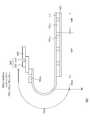
도 1a는 본 발명의 일 실시예에 따른 스트레처블 표시장치의 개략적인 분해 사시도이다. 도 1b는 본 발명의 일 실시예에 따른 스트레처블 표시장치의 벤딩된 상태의 개략적인 단면도이다.1A is a schematic exploded perspective view of a stretchable display device according to an exemplary embodiment of the present invention. 1B is a schematic cross-sectional view of a bent state of a stretchable display device according to an exemplary embodiment of the present invention.
도 1a 및 1b를 참조하면, 본 발명의 일 실시예에 따른 스트레처블(stretchable) 표시장치(1000)는 표시패널(100), 가요성 연결필름(200) 및 인쇄회로기판(300)을 포함한다.1A and 1B, a
표시패널(100)은 제1 방향(X) 또는 제2 방향(Y) 중 어느 하나의 방향에 따라 신축 가능하거나, 제1 방향(X) 및 제2 방향(Y)을 따라 2차원적으로 신축 가능하다. 여기서, 제1 방향(X)과 제2 방향(Y)은 스트레처블 표시장치(1000)의 평면을 이루며, 제2 방향(Y)은 제1 방향(X)에 대해 수직한 방향일 수 있다.The
표시패널(100)은 하부에 배치되는 하부 기판(110) 및 하부 기판(110)의 상부에 배치되는 상부 기판(120)을 포함한다. 하부 기판(110)과 상부 기판(120)은, 도 1a 및 도 1b에 도시된 바와 같이, 서로 다른 크기를 가질 수 있다. 보다 상세하게, 본 발명의 일 실시예에 따른 스트레처블 표시장치(1000)의 하부 기판(110)이 상부기판(120)보다 큰 크기를 가질 수 있다. 도 1a 및 도 1b에서는 하부 기판(110)이 상부 기판(120)보다 큰 크기를 갖는 것으로 도시하였으나, 이에 제한되지 않고, 하부 기판(110)과 상부 기판(120)이 동일한 크기를 가질 수 있다. 한편, 도 1a 및 도 1b에서는 도시하지 않았으나, 표시패널(100)은 하부 기판(110)의 하부 또는 상부 기판(120)의 상부에 배치될 수 있는 편광판을 더 포함할 수 있다.The
하부 기판(110)은 연성 재질로 이루어져 휘어지거나 늘어날 수 있는 하부 기판(110)의 제1 기판(111) 및 하부 기판(110)의 제1 기판(111) 상에 배치되고, 제1 기판(111)보다 강성 재질로 이루어진 하부 기판(110)의 제2 기판(112)을 포함하여 이루어질 수 있다.The
스트레처블 표시장치는 쉽게 휘거나 늘어나는 성질을 가져야 하므로, 모듈러스가 작아 연성 특성을 갖는 기판을 사용하려는 시도가 존재하였다. 다만, 모듈러스가 작은 폴리 메탈 실록산(polydimethylsiloxane; PDMS)과 같은 연성 물질을 표시 소자가 제조되는 동안 배치되는 하부의 기판으로 사용할 경우, 모듈러스가 작은 물질의 열에 약한 특성에 의하여 트랜지스터, 표시 소자를 형성하는 공정 중 발생하는 고온, 예를 들어, 100℃ 이상의 온도에 의해 기판이 손상되는 문제가 발생하였다.Since stretchable display devices must have a property of being easily bent or stretched, there have been attempts to use a substrate having a ductile property due to small modulus. However, when a flexible material such as polydimethylsiloxane (PDMS) having a small modulus is used as a lower substrate disposed while the display element is being manufactured, the modulus forms a transistor and a display element due to heat-sensitive characteristics of the small material. There was a problem that the substrate was damaged by a high temperature generated during the process, for example, a temperature of 100 ° C or higher.
이에, 고온에 견딜 수 있는 물질로 이루어진 기판 상에 표시 소자를 형성하여야, 표시 소자를 형성하는 공정에서 기판이 손상되는 것을 방지할 수 있다. 이에, 폴리이미드(polyimide; PI)와 같이 제조 공정 중에 발생하는 고온에 견딜 수 있는 물질로 기판을 형성하는 시도가 있었으나, 고온에 견딜 수 있는 물질들은 모듈러스가 커서 연성 특성을 가지지 못하여 스트레처블 표시 장치를 연신하는 과정에서 기판이 휘거나 늘어나기 어려운 문제가 발생하였다.Accordingly, the display element should be formed on a substrate made of a material capable of withstanding high temperature, thereby preventing damage to the substrate in the process of forming the display element. Accordingly, attempts have been made to form a substrate with a material that can withstand high temperatures that occur during the manufacturing process, such as polyimide (PI), but materials that can withstand high temperatures have a large modulus and do not have ductility properties, resulting in stretchable display. In the process of stretching the device, a problem occurs that the substrate is difficult to bend or stretch.
이에, 본 발명의 일 실시예에 따른 스트레처블 표시장치(1000)에서는 트랜지스터나 유기 발광 소자 등이 배치되는 영역에만 강성 기판인 복수의 제2 기판(112)을 배치하여 트랜지스터나 유기 발광 소자의 제조 공정에서의 고온에 의해 복수의 제2 기판(112)이 손상되지 않도록 할 수 있다.Accordingly, in the
또한, 본 발명의 일 실시예에 따른 스트레처블 표시장치(1000)에서는 복수의 제2 기판(112) 하부에 연성 기판인 제1 기판(111) 및 상부에는 상부 기판(120)을 배치할 수 있다. 이에, 복수의 아일랜드 기판인 제2 기판(112)과 중첩되는 영역을 제외한 제1 기판(111) 및 상부 기판(120)의 나머지 영역은 쉽게 늘어나거나 휘어질 수 있으므로, 스트레처블 표시장치(1000)가 구현될 수 있다. 또한, 강성 기판인 복수의 아일랜드 기판인 제2 기판(112) 상에 배치되는 트랜지스터, 유기 발광 소자 등이 스트레처블 표시장치(1000)가 휘거나 늘어남에 따라 손상되는 것을 방지될 수 있다.In addition, in the
제1 기판(111)은 스트레처블 표시장치(100)의 여러 구성요소들을 지지하고 보호하는 기판이다. 제1 기판(111)은 휘어지거나 신축 가능한 절연 물질로 구성될 수 있다. 예를 들어, 제1 기판(111)은 폴리디메틸실록산(polydimethylsiloxane; PDMS)과 같은 실리콘 고무(Silicon Rubber), 폴리우레탄(polyurethane; PU) 등의 탄성 중합체(elastomer)로 이루어질 수 있다. 그러나, 제1 기판(111)의 재질이 이에 제한되는 것은 아니다. 제1 기판(111)은 모듈러스(modulus)가 수 MPa 내지 수백 MPa일 수 있으며, 연신 파괴율이 100% 이상일 수 있다. 제1 기판(110)의 두께는 10㎛ 내지 1㎜일 수 있으나, 이에 제한되는 것은 아니다. 이러한 제1 기판(111) 상에는 복수의 제2 기판(112)을 전기적으로 연결하는 연결 배선(130)이 배치된다.The
제1 기판(111) 상에는 아일랜드(island) 형태로 서로 이격되어 배치되는 복수의 제2 기판(112)이 배치된다. 복수의 제2 기판(112)은 연성 기판(111)에 비해 강성을 갖는 기판이지만 플렉서블(flexible)하며 신축성이 덜한 기판이다. 복수의 제2 기판(112)은 예를 들어, 폴리이미드(polyimide; PI)계 수지 또는 에폭시(epoxy)계 수지로 이루어질 수 있다. 복수의 제2 기판(112)은 서로 이격되어 제1 기판(111) 상에 배치된다. 복수의 제2 기판(112)의 모듈러스는 제1 기판(111)의 모듈러스보다 1000배 이상 클 수 있으나, 이에 제한되는 것은 아니다.A plurality of
상부 기판(120)은 하부 기판(110)과 중첩되어 배치되고, 표시패널(100)의 여러 구성 요소들을 보호하기 위한 기판이다. 상부 기판(120)은 휘어지거나 늘어날 수 있는 절연 물질로 이루어질 수 있다. 예를 들어, 상부 기판(120)은 신축성을 갖는 재질로 이루어질 수 있고, 하부 기판(110)의 연성 기판, 즉 제1 기판(111)과 동일한 물질로 이루어질 수 있으나, 이에 제한되는 것은 아니다.The
표시패널(100)은 영상이 표시되는 표시 영역(A/A), 표시 영역(A/A)과 인접한 영역에서 표시 영역(A/A)을 둘러싸도록 배치된 비표시 영역(N/A) 및 가요성 연결필름(200)과 본딩되는 본딩 패드 및 전원 패드들이 배치된 패드 영역(P/A)을 포함한다.The
표시 영역(A/A)은 복수의 서브 화소를 포함하는 복수의 화소를 포함한다. 복수의 서브 화소 각각은 발광 소자를 포함하고, 게이트 배선, 데이터 배선, 고전위 전원배선 및 저전위 전원배선 등과 같은 다양한 배선과 연결될 수 있다.The display area A / A includes a plurality of pixels including a plurality of sub-pixels. Each of the plurality of sub-pixels includes a light emitting device, and may be connected to various wirings such as a gate wiring, data wiring, high potential power wiring, and low potential power wiring.
표시 영역(A/A) 상에는 하부 기판(110)의 제1 기판(111) 상부에 아일랜드 형상의 복수의 제2 기판(112a)이 배치될 수 있다. 제2 기판(112a) 상에는 발광 소자, 발광 소자를 구동하는 박막 트랜지스터 및 각종 신호 배선들이 배치될 수 있다. 이와 같은 하부 기판(110)의 제2 기판(112a)은 일정간격 이격되어 배치되고, 제1 기판(111) 상에 배치된 복수의 연결 배선(130)에 의해 전기적으로 연결된다. 제1 기판(111) 상에 배치된 복수의 연결 배선(130)에 대한 보다 상세한 설명은 다음 도 4a 및 도 4b를 참조하여 보다 상세히 살펴보기로 한다.On the display area A / A, a plurality of island-shaped
비표시 영역(N/A)은 표시 영역(A/A)에 인접하여 배치되고, 표시 영역(A/A)을 둘러싸는 영역으로, 영상이 표시되지 않는 영역이다. 비표시 영역(N/A)에는 표시 영역(A/A)에 배치된 화소를 구동하기 위해 화소에 신호를 전달하기 위한 연결 배선이 연장되어 배치된 신호 배선 및 회로부, 예를 들어 게이트 구동회로 등이 배치될 수 있다.The non-display area N / A is disposed adjacent to the display area A / A and surrounds the display area A / A, which is an area in which an image is not displayed. In the non-display area N / A, a connection wiring for transmitting a signal to a pixel is extended to drive a pixel disposed in the display area A / A, and a signal wiring and a circuit unit, for example, a gate driving circuit, etc. It can be placed.
비표시 영역(N/A)에는 더미 화소가 더 배치될 수 있다. 더미 화소는 표시 영역(A/A)에 배치된 화소와 동일한 형상을 가질 수 있다. 즉, 더미 화소에는 스위칭 트랜지스터, 구동 트랜지스터, 커패시터 및 발광 소자를 포함하도록 구성될 수 있다. 다만, 더미 화소에 배치된 발광 소자는 발광 기간에 발광하지 않을 수 있다. 또한, 더미 화소는 표시 영역(A/A)에 배치된 화소의 제2 기판과 다른 형상을 가질 수 있다. 이에 대한 보다 상세한 설명은 후술할 도 10을 참조하여 보다 상세히 설명하기로 한다.A dummy pixel may be further disposed in the non-display area N / A. The dummy pixel may have the same shape as the pixel disposed in the display area A / A. That is, the dummy pixel may be configured to include a switching transistor, a driving transistor, a capacitor, and a light emitting device. However, the light emitting element disposed in the dummy pixel may not emit light in the light emission period. Also, the dummy pixel may have a shape different from that of the second substrate of the pixel disposed in the display area A / A. A more detailed description of this will be described in more detail with reference to FIG. 10 to be described later.
비표시 영역(N/A)은 표시 영역(A/A)과 동일하게 하부 기판(110)의 제1 기판(111) 상에 아일랜드 형상의 제2 기판(112n)이 복수 개 배치될 수 있다. 이때, 비표시 영역(N/A)에 배치된 제2 기판(112n)은 표시 영역(A/A)에 배치된 제2 기판(112a)과 대응되도록 배치될 수 있다. 예를 들어, 표시 영역(A/A)에 배치된 제2 기판(112a)이 제1 방향(X)으로 일정 간격 이격되어 배치된다면 동일한 간격으로 제1 방향(X)으로 비표시 영역(N/A)의 제2 기판(112n) 또한 제1 방향(X)으로 동일한 간격으로 이격되어 배치될 수 있다. 보다 상세하게, 비표시 영역(N/A)에 배치된 복수의 제2 기판(112n)은 표시 영역(A/A)에 배치된 복수의 제2 기판(112a)이 배치된 열과 행에 대응하여 배치될 수 있다. 이와 같이, 본 발명의 일 실시예에 따른 스트레처블 표시장치(1000)는 표시 영역(A/A)에 배치된 제2 기판(112a)과 비표시 영역(N/A)에 배치된 제2 기판(112n)이 서로 대응되도록 배치됨으로써 스트레처블 표시장치(1000)의 적어도 둘 이상의 면이 균일하게 스트레처블(stretchable)될 수 있다.In the non-display area N / A, a plurality of island-shaped
한편, 비표시 영역(N/A)에 배치된 제2 기판(112n) 상에 배치된 배선과 제1 기판(111)에 배치된 배선은 동일한 형상을 가질 수도 있고, 서로 다른 형상을 가질 수 있다. 예를 들어, 제2 기판(112n)에 배치된 배선은 직선 형상을 가진다면 제1 기판(111)에 배치된 배선은 동일한 직선 형상을 가질 수도 있고, 직선 형상과는 다른 굴곡진 형상, 즉, 웨이브(wave) 형상 또는 다이아몬드 형상 등을 가질 수 있다.Meanwhile, the wiring disposed on the
패드 영역(P/A)은 비표시 영역(N/A)의 일측으로부터 연장되어 배치되는 영역으로, 영상이 표시되지 않는 영역이다. 즉, 패드 영역(P/A)은 표시패널(100)의 하부 기판(110)과 상부 기판(120)의 크기 차이로 인해 하부 기판(110)이 외부로 노출될 수 있는 영역이다. 본 발명의 일 실시예에서는 패드 영역(P/A)이 외부로 노출될 수 있다고 하였으나, 이에 제한되지 않고, 하부 기판(110)과 상부 기판(120)이 동일한 크기를 갖는 경우 외부로 노출되지 않을 수도 있다. 패드 영역(P/A)에는 표시 영역(A/A) 및 비표시 영역(N/A)에 배치된 배선이 연장되어 배치된 배선, 표시 패널에 고전위 전원 또는 저전위 전원을 공급하기 위한 전원 패드 및 가요성 연결필름(200)과 전기적으로 연결되기 위한 본딩 패드 등이 배치될 수 있다.The pad area P / A is an area extending from one side of the non-display area N / A and is an area in which an image is not displayed. That is, the pad area P / A is an area where the
다시 말해, 패드 영역(P/A)은 비표시 영역(N/A)의 제2 방향(Y)의 일측으로부터 일정 면적을 갖도록 연장된 영역이다. 패드 영역(P/A)은 표시 영역(A/A)과 동일하게 하부 기판(110)의 제1 기판(111) 상에 아일랜드 형상의 제2 기판(112p)이 복수 개 배치될 수 있다. 여기서 패드 영역(P/A)에 배치된 제2 기판(112p)은 제3 기판으로도 지칭될 수 있으나, 제3 기판 또한 표시 영역(A/A)에 배치된 제2 기판(112a) 및 비표시 영역(N/A)에 배치된 제2 기판(112n)과 동일한 모듈러스를 가질 수 있다. 다만, 패드 영역(P/A) 중 일부 영역에서는 표시 영역(A/A)과 대응되도록 제2 기판(112p)이 배치되지 않을 수 있다. 제2 기판(112p)이 배치되지 않은 영역은 벤딩 라인(BL)을 정의할 수 있는 영역이 될 수 있다. 이러한 패드 영역(P/A)은 제1 패드 영역(PA1) 및 제2 패드 영역(PA2)을 포함할 수 있다.In other words, the pad area P / A is an area extended to have a predetermined area from one side of the second direction Y of the non-display area N / A. In the pad area P / A, a plurality of island-shaped
제1 패드 영역(PA1)은 비표시 영역(N/A)과 인접하게 배치되는 영역이다. 보다 상세하게, 제1 패드 영역(PA1)은 비표시 영역(N/A)과 제2 패드 영역(PA2) 사이에 배치된 영역이다. 제1 패드 영역(PA1)에는 제2 방향(Y)의 가장 외측을 제외한 모든 영역에 제1 기판(111)만이 배치된 영역일 수 있다. 즉, 제1 패드 영역(PA1)은 제2 기판(112)이 표시 영역(A/A)과 대응되도록 배치되지 않는 영역이다. 이와 같이, 본 발명의 일 실시예에 따른 스트레처블 표시장치(1000)는 제1 패드 영역(PA1)이 상대적으로 연신율이 높은 제1 기판(111)만이 배치되도록 함으로써 보다 용이하게 패드 영역(P/A)의 일부가 벤딩(bending)되도록 할 수 있다.The first pad area PA1 is an area disposed adjacent to the non-display area N / A. More specifically, the first pad area PA1 is an area disposed between the non-display area N / A and the second pad area PA2. The first pad area PA1 may be an area in which only the
제2 패드 영역(PA2)은 가요성 연결필름(200)과 전기적으로 연결되는 본딩 패드들이 배치된 영역으로, 제1 패드 영역(PA1)과 가요성 연결필름(200) 사이에 배치되는 영역이다. 제2 패드 영역(PA2)은 복수 개의 제2 기판(112p)이 제1 방향(X)으로 일정 간격 이격되어 배치되고, 제2 패드 영역(PA2)의 제2 기판(112p)은 표시 영역(A/A)에 배치된 제2 기판(112a)과 대응되도록 배치될 수 있다. 예를 들어, 표시 영역(A/A)에 배치된 제2 기판(112a)이 제1 방향(X)으로 일정 간격 이격되어 배치된다면 패드 영역(P/A)에 배치된 제2 기판(112p) 또한 제1 방향(X)으로 동일한 간격으로 이격되어 배치될 수 있다.The second pad area PA2 is an area in which bonding pads electrically connected to the
패드 영역(P/A)에는 벤딩 라인(BL)이 정의될 수 있다. 보다 상세하게, 벤딩 라인(BL)은 제1 패드 영역(PA1)과 제2 패드 영역(PA2) 사이에 배치될 수 있고, 제1 패드 영역(PA1)에서 제1 기판(111)만이 배치된 영역의 끝단일 수 있다. 이에 따라, 벤딩 라인(BL)은 제1 패드 영역(PA1)과 제2 패드 영역(PA2)을 정의하는데 기준이 될 수 있다.A bending line BL may be defined in the pad area P / A. In more detail, the bending line BL may be disposed between the first pad area PA1 and the second pad area PA2, and only the
패드 영역(P/A)은, 도 1b에 도시된 바와 같이, 벤딩 라인(BL)을 기준으로 하부 기판(110)의 하부 방향으로 벤딩된다. 특히, 본 발명의 일 실시예에 따른 스트레처블 표시장치(1000)는 제1 패드 영역(PA1)이 제2 기판(112)에 비해 연성 재질로 이루어진 제1 기판(111)으로만 이루어지도록 구성됨으로써 보다 용이하게 표시장치가 벤딩될 수 있다. 또한, 본 발명의 일 실시예에 따른 스트레처블 표시장치(1000)는 표시패널(100)의 하부 방향으로 패드 영역(P/A)의 일부 영역이 벤딩되어 패드 영역(P/A)에 배치된 본딩 패드가 표시패널(110)의 하면에 배치되기 때문에 스트레처블 표시장치(1000)의 베젤 폭이 감소될 수 있다.The pad area P / A is bent in a downward direction of the
가요성 연결필름(200)은 플렉서빌리티(flexibility) 재질로 이루어진 베이스 필름(210)에 각종 부품을 배치한 필름으로, 표시 영역(A/A)의 복수의 서브 화소로 신호를 공급하기 위한 부품이다. 가요성 연결필름(200)은 표시패널(100)과 인쇄회로기판(300) 사이에 배치되어 인쇄회로기판(300)으로부터 입력되는 신호를 표시패널(100)에 전달한다. 즉, 가요성 연결필름(200)은 표시패널(100)과 인쇄회로기판(300) 사이에 배치되어 표시패널(100)과 인쇄회로기판(300)을 전기적으로 연결할 수 있다. 가요성 연결필름(200)은 패드 영역(P/A)에 배치된 복수의 본딩 패드가 배치된 복수의 제2 기판(112p)에 본딩될 수 있으며, 본딩 패드를 통하여 전원 전압, 데이터 전압, 게이트 전압 등을 표시 영역(A/A)의 복수의 서브 화소 각각으로 공급할 수 있다.The flexible connecting
본 발명의 일 실시예에 따른 가요성 연결필름(200)은, 도 1a에 도시된 바와 같이, 제2 방향(Y)의 일측에 배치된다. 그러나, 본 발명의 일 실시예에 따른 스트레처블 표시장치(1000)는 이에 한정되지 않고, 제1 방향(X) 및 제2 방향(Y)의 일측 모두에 가요성 연결필름(200)이 배치될 수 있다. 이는 게이트 구동회로의 배치 형태에 따라 달라질 수 있다.The flexible connecting
일반적으로 게이트 구동회로는 표시패널과 독립되게 형성되어 다양한 방식으로 표시패널과 전기적으로 연결되는 형태로 구성될 수도 있고, 최근 베젤 영역을 줄이기 위한 하나의 방안으로 게이트 구동회로를 표시패널에 배치된 화소 어레이들과 함께 내장하는 게이트 인 패널(Gate In Panel; 이하 'GIP'라 함)의 형태로 구성될 수도 있다.In general, the gate driving circuit is formed independently of the display panel and may be configured to be electrically connected to the display panel in various ways, and a pixel in which the gate driving circuit is disposed on the display panel as one way to reduce the recent bezel area It may be configured in the form of a gate-in panel (hereinafter referred to as 'GIP') embedded with the arrays.
게이트 인 패널의 형태로 게이트 구동회로가 구성된 경우, 도 1a에 도시된 바와 같이, 가요성 연결필름(200)은 제2 방향(Y)의 일측에만 배치되고, 게이트 구동회로가 표시패널과 독립적으로 배치된 경우, 제2 방향(Y)의 일측 뿐만 아니라 제1 방향(X)의 일측에도 가요성 연결필름(200)이 배치될 수 있다. 이에, 본 발명의 일 실시예에 따른 스트레처블 표시장치(1000)의 제1 방향(X)으로 배치된 가요성 연결필름(200) 상에 배치된 구동집적회로는 게이트 구동회로가 될 수 있고, 제2 방향(Y)으로 배치된 가요성 연결필름(200) 상에 배치된 구동집적회로는 데이터 구동회로가 될 수 있다. 이에, 후술할 본 발명의 일 실시예에 따른 스트레처블 표시장치(1000)는 게이트 구동회로가 게이트 인 패널의 형태로 배치된 경우와 표시패널과 독립적으로 배치된 경우 비표시 영역(N/A)의 형태는 달라질 수 있다. 이에 따라 후술할 본 발명의 일 실시예에 따른 스트레처블 표시장치(1000)는 게이트 구동회로가 게이트 인 패널의 형태로 배치된 경우와 표시패널과 독립적으로 배치된 경우를 나뉘어 설명하고자 한다. 이와 관련된 설명은 다음 도 7 내지 도 10을 참조하여 상세히 살펴보기로 한다.When the gate driving circuit is configured in the form of a gate-in panel, as illustrated in FIG. 1A, the
가요성 연결필름(200)은 베이스 필름(210) 및 베이스 필름(210) 상에 배치된 구동집적회로(220)를 포함한다.The
베이스 필름(210)은 구동집적회로(220)를 지지하는 층이다. 베이스 필름(210)은 플렉서빌리티(flexibility)를 갖는 절연 물질로 이루어질 수 있고, 예를 들어, 폴리이미드(polyimide; PI)계 수지 또는 에폭시(epoxy)계 수지로 이루어질 수 있다.The
구동집적회로(220)는 외부로부터 입력되는 영상을 표시하기 위한 데이터와 이를 처리하기 위한 구동 신호를 처리한다. 도 1a 및 도 1b에서는 구동집적회로(220)가 COF(Chip On Film) 방식으로 실장되는 것으로 도시하였으나, 이에 제한되지 않고 COG(Chip On Glass), TCP(Tape Carrier Package) 등의 방식으로도 실장될 수 있다.The driving
도 1a 및 도 1b에서 도시하지는 않았으나, 가요성 연결필름(200)은 베이스 필름(210) 상의 적어도 하나의 일면 상에 배치된 복수의 전도성 배선을 더 포함한다. 복수의 전도성 배선은 인쇄회로기판(300)으로부터 입력되는 영상 데이터 및 구동 데이터를 구동집적회로(220)로 전달하고, 구동집적회로(220)에서 출력되는 데이터 신호 및 구동 제어 신호를 표시패널(100)로 전달한다.Although not illustrated in FIGS. 1A and 1B, the
인쇄회로기판(300)은 표시패널(100)에 배치된 회로부 및 가요성 연결필름(200)에 배치된 구동집적회로(220)의 구동을 제어하기 위한 제어부가 배치될 수 있다. 인쇄회로기판(300)은 외부로부터 영상 데이터 및 구동 데이터를 수신하여 가요성 연결필름(200)으로 출력하고, 가요성 연결필름(200)은 영상 데이터 및 구동 데이터를 데이터 신호 및 구동 제어 신호로 변환하여 표시패널(100)에 출력한다. 또한, 인쇄회로기판(300)에는 메모리, 프로세서 등도 장착될 수 있다.The printed
한편, 생략된 구성이긴 하나, 본 발명의 일 실시예에 따른 스트레처블 표시장치(1000)에 포함될 수 있는 구성인 편광층은 스트레처블 표시 장치(1000)의 외광 반사를 억제하는 구성으로서 상부 기판(120)과 중첩되어 상부 기판(120) 상에 배치될 수 있다. 다만, 이에 제한되지 않고, 편광층은 상부 기판(120) 하부에 배치될 수도 있고, 스트레처블 표시 장치(1000)의 구성에 따라 생략될 수도 있다On the other hand, although it is omitted, the polarization layer, which may be included in the
이하에서는, 본 발명의 일 실시예에 따른 스트레처블 표시장치(1000)를 이루는 구성 중 벤딩 가능한 표시패널(100)의 구조에 대해 보다 상세히 살펴보기로 한다.Hereinafter, the structure of the
도 2a 및 도 2b는 본 발명의 일 실시예에 따른 스트레처블 표시패널의 개략적인 평면도이다. 도 3a 및 도 3b는 도 2a 및 도 2b의 A 영역의 확대하여 제1 영역 및 제2 영역의 배치를 설명하기 위한 개략적인 부분 평면도이다.2A and 2B are schematic plan views of a stretchable display panel according to an exemplary embodiment of the present invention. 3A and 3B are schematic partial plan views for enlarging the area A of FIGS. 2A and 2B to explain the arrangement of the first area and the second area.
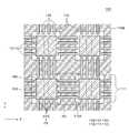
도 2a 및 도 2b를 참조하면, 본 발명의 일 실시예에 따른 스트레처블 표시패널(100)의 하부 기판(110)에는 모듈러스가 서로 다른 제1 영역(110A)과 제2 영역(110B)이 정의될 수 있다.2A and 2B, a
제1 영역(110A)은 제2 영역(110B)에 비해 높은 모듈러스를 가질 수 있다. 여기서, 모듈러스는 기판에 가해지는 응력에 대하여 응력에 의해 변형되는 비율을 나타내는 탄성 계수로서, 모듈러스가 상대적으로 높을 경우 강도가 상대적으로 높을 수 있다. 이에, 제1 영역(110A)은 제2 영역(110B)에 비해 높은 강성을 갖는 강성(rigid) 영역일 수 있다. 한편, 제2 영역(110B)은 제1 영역(110A)에 비해 연성을 갖는 연성(soft) 영역일 수 있다. 제1 영역(110A)의 모듈러스는 제2 영역(110B)의 모듈러스보다 1000배 이상 클 수 있으나, 이에 제한되는 것은 아니다.The
보다 상세하게, 제1 영역(110A)은 상대적으로 강성 재질을 갖는 제2 기판(112)이 배치된 영역이고, 제2 영역(110B)은 제2 기판(112)이 배치되지 않은 영역으로 제2 기판(112)에 비해 연성 재질로 이루어진 제1 기판(111)만으로 이루어진 영역일 수 있다. 이에 따라, 제1 영역(110A), 즉 표시 영역(A/A)에 배치된 복수의 제2 기판(112a) 각각에는 영상을 표시하도록 하는 복수의 서브 화소를 포함하는 화소가 배치될 수 있다,More specifically, the
또한, 도 2a 및 도 2b을 참조하여 살펴보면, 비표시 영역(N/A)에 배치된 복수의 제2 기판(112n)과 패드 영역(P/A)에 배치된 복수의 제2 기판(112p)에는 서브 화소(SPX)를 구동하기 위한 구동 소자 또는 신호 패드들이 배치될 수 있다. 예를 들어, 비표시 영역(N/A)에 게이트 인 패널(Gate In Panel; GIP, 이하 'GIP'라 지칭함.)의 형태로 게이트 구동회로가 배치된다면 GIP를 구성하는 복수의 스테이지 각각은 제2 기판(112n) 상에 배치될 수 있다.Further, referring to FIGS. 2A and 2B, a plurality of
아일랜드 형태의 복수의 제2 기판(112) 사이, 즉, 제2 영역(110B)에는 연결 배선(130)이 배치된다. 연결 배선(130)은 복수의 제2 기판(112)들을 서로 전기적으로 연결할 수 있다. 즉, 연결 배선(130)은 표시 영역(A/A)에 배치된 제2 기판(112a)과 그에 인접하는 하나의 제2 기판(112a)을 전기적으로 연결할 수 있고, 표시 영역(A/A)에 배치된 제2 기판(112a)과 비표시 영역(N/A)에 배치된 제2 기판(112n)을 전기적으로 연결할 수 있으며, 비표시 영역(N/A)에 배치된 제2 기판(112n)을 서로 전기적으로 연결할 수 있고, 비표시 영역(N/A)에 배치된 제2 기판(112n)과 패드 영역(P/A)에 배치된 제2 기판(112p)를 전기적으로 연결할 수 있으며 패드 영역(P/A)에 배치된 제2 기판(112p)들을 서로 전기적으로 연결할 수 있다. 예를 들어, 제2 기판(112a, 112n, 112p)과 인접하는 제2 기판(112a, 112n, 112p)을 전기적으로 연결하는 방법은 제2 기판(112a, 112n, 112p) 상에 배치된 표시 소자 또는 구동 소자를 구성하는 구성 요소 중 연결 배선(130)과 연결되어야 하는 패드, 예를 들어 게이트 패드, 데이터 패드, 전원 패드 또는 신호 패드가 각각의 제2 기판(112a, 112n, 112p) 상에 배치되어 각 제2 기판(112a, 112n, 112p)의 패드를 전기적으로 연결할 수 있다.The
연결 배선(130)은 제1 연결 배선(131) 및 제2 연결 배선(132)를 포함할 수 있다. 제1 연결 배선(131)은 표시패널(110)에서 제1 방향(X)으로 배치되는 배선이고, 제2 연결 배선(132)은 표시패널(110)에서 제2 방향(Y)으로 배치되는 배선을 의미한다.The
제1 영역(110A)은 표시 영역(A/A), 비표시 영역(N/A) 및 패드 영역(P/A)에서 제2 기판(112)이 배치된 영역으로 강성 영역이라 할 수 있다. 여기서, 표시 영역(A/A)에 배치된 제2 기판(112a), 비표시 영역(N/A)에 배치된 제2 기판(112n) 및 패드 영역(P/A)에 배치된 제2 기판(112p)은 각각 서로 대응되도록 배치될 수 있다. 예를 들어, 제1 방향(X)으로 표시 영역(A/A)에 배치된 제2 기판(112a)이 제1 간격(d1)으로 배치되었다면, 비표시 영역(N/A)에 배치된 제2 기판(112n) 및 패드 영역(P/A)에 배치된 제2 기판(112p) 또한 제1 간격(d1)으로 배치될 수 있다.The
제2 영역(110B)은 복수의 제2 기판(112)들 사이의 이격 영역으로, 제1 기판(111) 만이 배치된 영역이다. 즉, 연성 영역이라고도 할 수 있다. 다시 말해, 이러한 제2 영역(110B) 상에는 연결 배선(130)이 배치될 수 있다.The
이와 같은 제1 영역(110A)과 제2 영역(110B)은, 도 3a에 도시된 바와 같이, 제1 방향(X)으로 번갈아가며 배치된다. 예를 들어, 표시 영역(A/A)에 배치된 제2 기판(112a)이 제1 방향(X)으로 제1 간격(d1)만큼 이격되어 배치된다면 비표시 영역(N/A)에 배치된 제2 기판(112n) 또한 제1 방향(X)으로 동일한 간격인 제1 간격(d1)만큼 표시 영역(A/A)의 최외곽에 배치된 제2 기판(112a)과 이격되어 배치될 수 있다. 이러한 표시 영역(A/A)과 비표시 영역(N/A)에 배치된 제2 기판(112a, 112n)들은 동일한 열에 맞춰 배치될 수 있고, 해당 영역은 강성 영역인 제1 영역(110A)이 될 수 있다. 한편, 표시 영역(A/A)의 제2 기판(112a) 사이의 이격 영역 및 표시 영역(A/A)의 최외곽에 배치된 제2 기판(112a)과 비표시 영역(N/A)의 제2 기판(112n) 사이의 이격 영역에는 제2 기판(112a)들을 전기적으로 연결하는 연결 배선(130)이 배치된다. 이러한 제1 방향(X)으로 배치된 연결 배선(130), 보다 상세하게 제1 연결 배선(131)들이 배치된 영역은 연성 영역인 제2 영역(110B)이 될 수 있다. 이에, 도 3a에 도시된 바와 같이, 복수의 제2 기판(112a, 112n)들이 배치된 열에 해당되는 영역이 제1 영역(110A)이 될 수 있고, 복수의 제2 기판(112a, 112n)들을 연결하는 연결 배선(130)이 배치된 영역이 제2 영역(110B)이 될 수 있다. 즉, 본 발명의 일 실시예에 따른 스트레처블 표시패널(100)의 강성 영역인 제1 영역(110A)과 연성 영역인 제2 영역(110B)이 제1 방향(X)으로 제1 영역(110A)과 제2 영역(110B)이 번갈아가며 배치될 수 있다.The
한편, 제1 영역(110A)과 제2 영역(110B)은, 도 3b에 도시된 바와 같이, 제2 방향(Y)으로 번갈아가며 배치된다. 예를 들어, 표시 영역(A/A)에 배치된 제2 기판(112a)이 제2 방향(Y)으로 제2 간격(d2)만큼 이격되어 배치된다면 비표시 영역(N/A)에 배치된 제2 기판(112n) 또한 제2 방향(Y)으로 동일한 간격인 제2 간격(d2)만큼 이격되어 배치될 수 있다. 이러한 표시 영역(A/A)과 비표시 영역(N/A)에 배치된 제2 기판(112a, 112n)들은 동일한 행에 맞춰 배치될 수 있고, 해당 영역은 강성 영역인 제1 영역(110A)이 될 수 있다. 한편, 표시 영역(A/A)의 제2 기판(112a) 사이의 이격 영역 및 비표시 영역(N/A)의 제2 기판(112n) 사이의 이격 영역에는 제2 기판(112a)들을 전기적으로 연결하는 연결 배선(130)이 배치된다. 이러한 제2 방향(Y)으로 배치된 연결 배선(130), 보다 상세하게 제2 연결 배선(132)들이 배치된 영역은 연성 영역인 제2 영역(110B)이 될 수 있다. 이에, 도 3b에 도시된 바와 같이, 복수의 제2 기판(112a, 112n)들이 배치된 행에 해당되는 영역이 제1 영역(110A)이 될 수 있고, 복수의 제2 기판(112a, 112n)들을 연결하는 연결 배선(130)즉 제2 연결 배선(132)이 배치된 영역이 제2 영역(110B)이 될 수 있다. 즉, 본 발명의 일 실시예에 따른 스트레처블 표시패널(100)의 강성 영역인 제1 영역(110A)과 연성 영역인 제2 영역(110B)가 제2 방향(Y)으로 제1 영역(110A)과 제2 영역(110B)이 번갈아가며 배치될 수 있다.Meanwhile, the
이에 따라, 도 2a 및 도 2b에 도시된 바와 같이, 제1 방향(X)의 제2 영역(110B)과 제2 방향의 제2 영역(110B)은 교차되는 영역이 존재하게 되고, 이에 따라, 제1 영역(110A)은 제2 기판(111)이 배치된 영역과 동일한 영역일 수 있다.Accordingly, as illustrated in FIGS. 2A and 2B, an area where the
한편, 도 2a 및 도 2b를 참조하면, 패드 영역(P/A) 중 제1 패드 영역(PA1)에는 제2 영역(110B)이 제1 영역(A)에 비해 보다 넓은 영역을 갖도록 배치된다. 이때, 제2 영역(110B)의 끝단은 패드 영역(P/A)에서 벤딩 라인(BL)을 정의하는 기준이 될 수 있다.Meanwhile, referring to FIGS. 2A and 2B, the
한편, 도면에 명확히 도시하지는 않았으나, 스트레처블한 표시패널(100)의 최외곽 영역에는 제1 기판(111) 상에 제2 기판(112)이 배치될 수 있다. 가요성 연결필름(200)과의 전기적 연결을 위해서는 본딩 과정이 필요한데 본딩은 대체적으로 높은 온도 공정 하에서 이루어지게 된다. 그러나, 신축성있고 연성 재질을 갖는 제1 기판(111)만이 배치된 경우 높은 온도를 견디지 못하고 제1 기판(111)이 손상될 수 있다. 이에 따라, 표시패널(100)의 최외곽 영역은 본딩 패드들이 많이 배치되는 영역이기 때문에 본딩을 위해 제1 기판(111)의 상부 및/또는 하부면에 제2 기판(112)이 더 배치될 수 있다. 이에 따라, 본 발명의 일 실시예에 따른 스트레처블한 표시패널(100)은 안정적으로 가요성 연결필름(200)과 전기적으로 연결될 수 있다.Meanwhile, although not clearly shown in the drawings, the
이와 같이, 스트레처블한 표시패널(100)의 최외곽 영역은 본딩 공정에 의해 제2 기판(112)이 더 배치되어야 하기 때문에 제2 패드 영역(PA2)에서 최외곽 영역에 배치된 제2 기판(112p) 사이에 배치된 제1 기판(111)의 형상은 도 2a처럼 제2 기판(112p) 간 이격 공간만큼, 예를 들어, 사각 형상으로 배치될 수 있다.As described above, since the
또한, 도 2b에 도시된 바와 같이, 최외곽 영역에 배치된 제2 기판(112p) 사이에 배치된 제1 기판(111)은 표시패널(100)의 최외곽 영역으로 갈수록 폭이 점점 좁아지는 형상을 가질 수 있다.In addition, as illustrated in FIG. 2B, the
이와 같이, 제1 기판(111)의 형상이 표시패널(100)의 최외곽으로 갈수록 좁아지는 형상을 갖는 경우 가요성 연결필름(200)과의 본딩 공정이 고온으로 이루어짐에 따라 연성 기판인 제1 기판(111)의 형상이 변형될 수 있고, 이로 인해 제1 기판(111) 상에 배치되는 배선 등에 손상되는 문제가 발생할 수 있는데, 최외곽으로 갈수록 좁아지는 형상을 갖는 경우 본딩 공정에서 열에 의한 영향을 덜 받을 수 있으므로, 스트레처블 표시장치의 신뢰성을 보다 향상시킬 수 있다.As described above, when the shape of the
한편, 본 발명의 일 실시예에 따른 표시패널(100), 특히 표시 영역(A/A)에 배치되는 구성의 상세 구조에 대해 살펴보기로 한다.Meanwhile, a detailed structure of a configuration disposed on the
도 4a는 본 발명의 일 실시예에 따른 스트레처블 표시장치의 표시 영역에 배치된 화소 구조를 설명하기 위한 확대 평면도이다. 도 4b는 도 4a의 AA 영역의 다른 실시예를 확대한 확대 평면도이다.4A is an enlarged plan view illustrating a pixel structure disposed in a display area of a stretchable display device according to an exemplary embodiment of the present invention. 4B is an enlarged plan view of another embodiment of area AA of FIG. 4A.
도 4a를 참조하면, 본 발명의 일 실시예에 따른 스트레처블 표시장치(1000)의 하부 기판(110)은 제1 기판(111), 복수의 제2 기판(112) 및 연결 배선(130)을 포함할 수 있다. 제1 기판(111)과 제2 기판(112) 또는 제1 영역(110A) 및 제2 영역(110B)에 대한 설명은 앞서 도 1a 내지 도 2b의 도면을 참조하여 설명하였으므로, 도 4a에서는 연결 배선 위주로 설명하고자 한다.Referring to FIG. 4A, the
복수의 제2 기판(112) 사이, 즉, 제2 영역(110B)에는 연결 배선(130)이 배치된다. 연결 배선(130)은 복수의 제2 기판(112) 상에 배치되는 패드 사이에 배치되어 각각의 패드를 전기적으로 연결할 수 있다. 즉, 연결 배선(130)은 인접하는 두 개의 아일랜드 기판, 즉 제2 기판(112) 상의 패드를 전기적으로 연결한다. 따라서, 본 발명의 일 실시예에 따른 스트레처블 표시장치(1000)는 게이트 배선, 데이터 배선, 고전위 전원 배선, 기준 전압 배선 등과 같은 다양한 배선을 복수의 제2 기판(112) 사이에서 전기적으로 연결하도록 복수의 연결 배선(130)을 포함할 수 있다. 예를 들면, 제1 방향(X)으로 인접하게 배치된 복수의 제2 기판(112) 상에는 게이트 배선이 배치될 수 있고, 게이트 배선의 양 끝단에는 게이트 패드가 배치될 수 있다. 이때, 제1 방향(X)으로 인접하여 배치된 복수의 제2 기판(112) 상의 복수의 게이트 패드 각각은 게이트 배선으로 기능하는 연결 배선(130)에 의해 서로 연결될 수 있다. 이에, 복수의 제2 기판(112) 상에 배치된 게이트 배선과 제1 기판(111) 상에 배치된 연결 배선(130)이 하나의 게이트 배선으로 기능할 수 있다. 또한, 데이터 배선, 고전위 전원 배선, 기준 전압 배선 등과 같이 스트레처블 표시장치(1000)에 포함될 수 있는 모든 다양한 배선 또한 상술한 바와 같이, 연결 배선(130)에 의해 하나의 배선으로 기능할 수 있다.The
연결 배선(130)은 제1 연결 배선(131) 및 제2 연결 배선(132)를 포함할 수 있다.The
제1 연결 배선(131)은 표시패널(110)에서 제1 방향(X)으로 배치되는 배선이고, 제2 연결 배선(132)은 표시패널(110)에서 제2 방향(Y)으로 배치되어 배선을 의미한다. 제1 연결 배선(131)은 제1 방향(X)으로 인접하여 배치된 복수의 제2 기판(112) 상의 패드 중 나란히 배치된 두 개의 제2 기판(112) 상의 패드들을 서로 연결할 수 있다. 제1 연결 배선(131)은 게이트 배선, 고전위 전원 배선 또는 저전위 전원 배선으로 기능할 수 있으나, 이에 제한되지는 않는다.The
제2 연결 배선(132)은 제2 방향(Y)으로 인접하여 배치된 복수의 제2 기판(112) 상의 패드 중 나란히 배치된 두 개의 제2 기판(112) 상의 패드들을 서로 연결할 수 있다. 제2 연결 배선(132)은 데이터 배선 또는 기준 전압 배선으로 기능할 수 있으나, 이에 제한되지는 않는다.The
도 4a를 참조하면, 연결 배선(130)은 베이스 폴리머 및 전도성 입자를 포함한다. 구체적으로, 제1 연결 배선(131)은 베이스 폴리머 및 전도성 입자를 포함하며, 제2 연결 배선(132)은 베이스 폴리머 및 전도성 입자를 포함한다. 제1 연결 배선(131) 및 제2 연결 배선(132)의 베이스 폴리머는 제1 기판(111)과 유사하게 휘어지거나 늘어날 수 있는 절연 물질로 구성될 수 있다. 베이스 폴리머는, 예를 들어, 폴리메탈실록산(polydimethylsiloxane; PDMS)과 같은 실리콘 고무(Silicon Rubber), 폴리우레탄(polyurethane; PU) 등의 탄성중합체(elastomer), SBS(Styrene Butadiene Styrene) 등을 포함할 수 있으나, 이에 제한되지는 않는다. 이에, 스트레처블 표시 장치(1000)가 휘거나 늘어날 경우, 베이스 폴리머는 손상되지 않을 수 있다. 베이스 폴리머는 제1 기판(111) 상부 및 제2 기판(112) 하부에 베이스 폴리머를 구성하는 물질을 코팅하거나 슬릿(slit)을 사용하여 도포하는 방식으로 형성될 수 있다.Referring to FIG. 4A, the connecting
제1 연결 배선(131) 및 제2 연결 배선(132)의 전도성 입자는 베이스 폴리머에 분산될 수 있다. 구체적으로, 제1 연결 배선(131) 및 제2 연결 배선(132)은 베이스 폴리머 내에 일정한 농도로 분산된 전도성 입자를 포함할 수 있다. 제1 연결 배선(131) 및 제2 연결 배선(132)은, 예를 들어, 베이스 폴리머에 전도성 입자를 균일하게 교반한 후, 전도성 입자가 분산된 베이스 폴리머를 제1 기판(111)의 상부, 제2 기판(112) 하부 및 접착층의 하부에 코팅 및 경화하는 방식으로 형성될 수 있으나, 이에 제한되는 것은 아니다. 전도성 입자는 은(Ag), 금(Au), 탄소(Carbon) 중 적어도 하나를 포함할 수 있으나, 이에 제한되지는 않는다.The conductive particles of the first connecting
제1 연결 배선(131) 및 제2 연결 배선(132)의 베이스 폴리머에 분산되어 배치된 전도성 입자는 서로 이웃하는 제2 기판(112)에 각각 배치된 게이트 패드들을 전기적으로 연결하는 전도성 경로를 이룰 수 있다. 또한, 제1 연결 배선(131) 및 제2 연결 배선(132)의 베이스 폴리머에 분산되어 배치된 전도성 입자는 복수의 제2 기판(111) 중 최외곽에 배치된 아일랜드 기판, 즉 제2 기판(112)에 형성된 게이트 패드 또는 데이터 패드와 비표시 영역(N/A)에 배치된 패드를 전기적으로 연결하는 전도성 경로를 이룰 수 있다.The conductive particles dispersed and disposed in the base polymer of the first connecting
한편, 스트레처블 표시장치(1000)가 휘거나 늘어나는 경우, 연성 기판으로 이루어진 제1 기판(111)이 변형되며, 유기 발광 소자가 배치된 강성 기판으로 이루어진 아일랜드 기판인 제2 기판(112)은 변형되지 않을 수 있다. 이 경우, 복수의 아일랜드 기판에 배치된 각각의 패드를 연결하는 배선이 쉽게 휘거나 늘어나는 물질로 이루어지지 못한 경우, 배선은 하부 기판의 변형에 의하여 크랙이 발생되는 등 손상될 수 있다.On the other hand, when the
이와 달리, 본 발명의 일 실시예에 따른 스트레처블 표시장치(1000)에서는 복수의 제2 기판(112) 각각에 배치된 패드를 베이스 폴리머와 전도성 입자를 포함하는 연결 배선(130)이 전기적으로 연결할 수 있다. 베이스 폴리머는 쉽게 변형될 수 있는 연성을 가진다. 이에, 본 발명의 일 실시예에 따른 스트레처블 표시 장치(1000)는 스트레처블 표시장치(1000)가 휘거나 늘어나는 등 변형될지라도 베이스 폴리머를 포함하는 연결 배선(130)이 복수의 제2 기판(112) 사이 영역이 쉽게 변형될 수 있는 효과가 있다.In contrast, in the
또한, 본 발명의 일 실시예에 따른 스트레처블 표시장치(1000)에서는, 연결 배선(130)이 전도성 입자를 포함함으로써, 전도성 입자로 이루어진 전도성 경로에 베이스 폴리머의 변형에 의하여도 크랙 등의 손상이 발생되지 않을 수 있다. 예를 들어, 스트레처블 표시장치(1000)가 휘거나 늘어나는 등 변형될 경우, 연성 기판인 제1 기판(111)은 강성 기판인 복수의 제2 기판(112)이 배치된 영역을 제외한 나머지 영역에서 변형될 수 있다. 이때, 변형되는 제1 기판(111) 상에 배치된 복수의 전도성 입자 사이의 거리가 변화될 수 있다. 이때, 베이스 폴리머 상부에 배치되어 전도성 경로를 형성하는 복수의 전도성 입자의 농도는 복수의 전도성 입자 사이의 거리가 멀어지더라도 전기적 신호가 전달될 수 있도록 높게 유지될 수 있다. 따라서, 베이스 폴리머가 휘거나 늘어날지라도 복수의 전도성 입자에 의한 전도성 경로는 전기적 신호를 원활하게 전달할 수 있고, 스트레처블 표시장치(1000)가 휘거나 늘어나는 등 변형되더라도 각각의 패드 사이에서 전기적 신호를 전달할 수 있다.In addition, in the
도 4a를 참조하면, 제1 연결 배선(131) 및 제2 연결 배선(132)의 베이스 폴리머 및 베이스 폴리머에 분산된 전도성 입자는 서로 인접하는 제2 기판(112)에 배치된 게이트 패드 사이를 직선 형상으로 연결할 수 있다. 이에 따라, 연결 배선(130)이 베이스 폴리머 및 전도성 입자를 포함함으로써, 서로 인접한 복수의 제2 기판(112)에 배치된 각각의 패드 사이를 연결하는 연결 배선(130)이 최단 거리를 이루도록, 즉, 직선 형태로 배치될 수 있다. 즉, 연결 배선(130)은 굴곡진 형상으로 형성되지 않더라도 스트레처블 표시장치(1000)가 구현될 수 있다. 이를 위해, 제조 공정에서 베이스 폴리머는 복수의 제2 기판(112) 각각을 연결하는 직선 형상으로 형성될 수 있다. 이에, 베이스 폴리머에 분산된 전도성 입자가 이루는 전도성 경로 또한 직선 형상일 수 있다. 그러나, 제1 연결 배선(131) 및 제2 연결 배선(132)의 베이스 폴리머 및 전도성 입자의 형성 과정 및 형상은 이에 제한되지 않을 수 있다. 이에, 본 발명의 일 실시예에 따른 스트레처블 표시장치(1000)에서는 연결 배선(130)이 차지하는 공간을 최소화할 수 있다.Referring to FIG. 4A, the base polymer of the first connecting
몇몇 실시예에서, 연결 배선(130)의 베이스 폴리머는 서로 이웃하는 제2 기판(112) 사이에서 제1 기판(111) 상에 단일층으로 형성될 수도 있다. 구체적으로, 베이스 폴리머는 도 4a에 도시된 것과 달리, 제1 방향(X)으로 서로 가장 인접하는 제2 기판(112) 사이의 영역에서 제1 기판(111)과 접하며 단일층으로 배치될 수 있다. 베이스 폴리머는 하나의 제2 기판(112) 상의 일 측에 나란히 형성된 복수의 패드 모두와 중첩되어 형성될 수 있다. 그리고, 전도성 입자는 하나의 층으로 배치된 베이스 폴리머상에 복수의 전도성 경로를 이루며 복수의 패드 각각과 대응하도록 별도로 형성될 수 있다. 이에, 전도성 입자가 이루는 전도성 경로는 서로 인접하는 제2 기판(112)에 배치된 패드 사이를 직선 형상으로 연결할 수 있으며, 예를 들면, 복수의 제2 기판(112) 사이에 하나의 층으로 배치된 베이스 폴리머 상면에서 전도성 입자가 4개의 전도성 경로를 이루도록 주입될 수 있다.In some embodiments, the base polymer of the
또한, 몇몇 실시예에서, 연결 배선(130)의 베이스 폴리머는 제1 기판(111)의 전체 영역 상에 배치될 수도 있다. 즉, 베이스 폴리머는 제1 기판(111) 상에서 단일 층으로 배치될 수 있다. 그리고, 전도성 입자는 베이스 폴리머에서 인접하는 복수의 제2 기판(112) 상의 패드를 연결하는 전도성 경로를 형성할 수 있다.In addition, in some embodiments, the base polymer of the
베이스 폴리머가 제1 기판(111) 상에서 전체 영역에 단일 층으로 배치될 경우, 베이스 폴리머를 패터닝하기 위한 별도의 공정이 필요하지 않을 수 있다. 따라서, 베이스 폴리머 및 연결 배선의 제조 공정이 단순화될 수 있고, 공정 비용 및 시간이 감소할 수 있다.When the base polymer is disposed as a single layer over the entire area on the
또한, 베이스 폴리머가 제1 기판(111) 상에서 전체 영역에 단일 층으로 배치됨으로써, 스트레처블 표시장치(1000)가 휘거나 늘어나는 경우 가해지는 힘을 베이스 폴리머가 보다 효율적으로 분산시킬 수 있다.In addition, since the base polymer is disposed as a single layer over the entire area on the
한편, 도 4a에서는 연결 배선(130)이 직선 형상을 갖도록 도시하였으나, 이에 제한되지 않고, 표시패널(100) 연신 시 연결 배선(130)의 손상을 방지하기 위해, 도 4b에 도시된 바와 같이, 웨이브 형상을 가질 수 있다.Meanwhile, in FIG. 4A, the
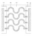
도 4b를 참조하면, 본 발명의 일 실시예에 따른 스트레처블 표시장치의 연결 배선(413)은 굴곡진 형상, 즉, 웨이브 형상을 갖는다. 연결 배선(431)은 복수의 제2 기판(112) 중 서로 이웃하는 제2 기판(112)에 배치된 패드를 전기적으로 연결하며 각각의 패드 사이에서 직선이 아닌 웨이브 형상으로 연장된다. 예를 들어, 도 4b에 도시된 바와 같이, 연결 배선(431)은 사인파 형상을 가질 수 있다. 다만, 연결 배선(431)의 형상은 이에 제한되지 않으며, 예를 들어, 연결 배선(431)은 지그재그 형상으로 연장될 수 있으며, 복수의 마름모 모양의 배선들이 꼭지점에서 연결되어 연장되는 등의 다양한 형상을 가질 수 있다.Referring to FIG. 4B, the
또한, 이러한 굴곡진 형상을 갖는 연결 배선(431)은 도 4a에 도시된 바와는 다른 물질로 형성될 수 있다. 즉, 굴곡진 형상을 갖는 연결 배선(431)은 제2 기판(112) 상에 형성된 게이트 배선 또는 데이터 배선을 이루는 물질과 동일한 금속 물질로 이루어질 수 있다.In addition, the
이에 따라, 본 발명의 일 실시예에 따른 스트레처블 표시장치(1000)는 직선 형상으로 이루어진 경우 연결 배선(130)의 크랙을 방지할 수 있는 전도성 입자를 포함하는 베이스 폴리머로 이루어지거나, 금속 물질로 이루어진 경우 굴곡진 형상을 갖도록 형성함으로써 스트레처블 표시장치(1000)가 연신되더라도 배선에 크랙이 발생하여 단선되는 형상을 최소화할 수 있다.Accordingly, the
다음으로 본 발명의 일 실시예에 따른 스트레처블 표시장치(1000)의 서브 화소 구조(SPX)의 구조에 대해 보다 상세히 살펴보기로 한다.Next, the structure of the sub-pixel structure SPX of the
도 5는 도 4a의 하나의 실시예에 따른 하나의 서브 화소에 대한 개략적인 단면도이다.5 is a schematic cross-sectional view of one sub-pixel according to an exemplary embodiment of FIG. 4A.
도 5를 참조하면, 하나의 실시예에 따른 복수의 제2 기판(112) 상에는 버퍼층(113)이 배치된다. 버퍼층(113)은 외부로부터 수분 및 산소 등의 침투로부터 스트레처블 표시장치(1000)의 다양한 구성 요소들을 보호하기 위해 복수의 제2 기판(112) 상에 배치된다. 버퍼층(113)은 절연 물질로 구성될 수 있으며, 예를 들어, 그래파이트(graphite) 또는 실리콘 질화물(SiNx), 실리콘 산화물(SiOx), 실리콘 산화질화물(SiON) 등으로 이루어지는 무기층이 단층 또는 복층으로 구성될 수 있다. 다만, 버퍼층(113)은 스트레처블 표시 장치(1000)의 구조나 특성에 따라 생략될 수도 있다.Referring to FIG. 5, a
이때, 버퍼층(113)은 복수의 제2 기판(112)과 중첩되는 영역에만 형성될 수 있다. 상술한 바와 같이 버퍼층(113)은 무기물로 이루어질 수 있으므로, 스트레처블 표시 장치(1000)를 연신하는 과정에서 쉽게 크랙(crack)이 발생되는 등 손상될 수 있다. 이에, 버퍼층(113)은 복수의 제2 기판(112) 사이의 영역에는 형성되지 않고, 복수의 제2 기판(112)의 형상과 유사하게 패터닝되어 복수의 제2 기판(112) 상부에만 형성될 수 있다. 이에, 본 발명의 일 실시예에 따른 스트레처블 표시 장치(1000)는 버퍼층(113)을 강성 기판인 복수의 제2 기판(112)과 중첩되는 영역에만 형성하여 스트레처블 표시장치(1000)가 휘거나 늘어나는 등 변형되는 경우에도 버퍼층(113)의 손상을 방지할 수 있다.In this case, the
도 5를 참조하면, 버퍼층(113) 상에는 게이트 전극(141), 액티브층(142), 소스 전극(143) 및 드레인 전극(144)을 포함하는 트랜지스터(140)가 형성된다. 예를 들어, 트랜지스터(140)가 형성되는 과정을 살펴보면, 버퍼층(113) 상에 액티브층(142)이 형성되고, 액티브층(142) 상에 액티브층(142)과 게이트 전극(141)을 절연시키기 위한 게이트 절연층(114)이 형성된다. 게이트 전극(141)과 소스 전극(143) 및 드레인 전극(144)을 절연시키기 위한 층간 절연층(115)이 형성되고, 층간 절연층(115) 상에 액티브층(142)과 각각 접하는 소스 전극(143) 및 드레인 전극(144)이 형성된다.Referring to FIG. 5, a
또한, 게이트 절연층(114) 및 층간 절연층(115)은 패터닝되어 복수의 제2 기판(112)과 중첩되는 영역에만 형성될 수 있다. 게이트 절연층(114) 및 층간 절연층(115) 또한 버퍼층(113)과 동일하게 무기물로 이루어질 수 있으므로, 스트레처블 표시장치(1000)를 연신하는 과정에서 쉽게 크랙이 발생되는 등 손상될 수 있다. 이에, 게이트 절연층(114) 및 층간 절연층(115)은 복수의 제2 기판(112) 사이의 영역, 즉, 제2 영역(110B)에는 형성되지 않고, 복수의 제2 기판(112)의 형상과 유사하게 패터닝되어 복수의 제2 기판(112) 상부에만 형성될 수 있다.In addition, the
도 5에서는 설명의 편의를 위해, 스트레처블 표시장치(1000)에 포함될 수 있는 다양한 트랜지스터 중 구동 트랜지스터만을 도시하였으나, 스위칭 트랜지스터, 커패시터 등도 표시장치에 포함될 수 있다. 또한, 본 명세서에서는 트랜지스터(140)가 코플래너(coplanar) 구조인 것으로 설명하였으나, 이에 제한되지 않고, 스태거드(staggered) 구조 등의 다양한 트랜지스터가 사용될 수도 있다.In FIG. 5, for convenience of description, only a driving transistor among various transistors that may be included in the
도 5를 참조하면, 게이트 절연층(114) 상에는 게이트 패드(161)가 배치된다. 게이트 패드(161)는 게이트 신호를 복수의 서브 화소(SPX)에 전달하기 위한 패드이다. 게이트 패드(161)는 게이트 전극(141)과 동일한 물질로 이루어질 수 있으나, 이에 제한되는 것은 아니다.Referring to FIG. 5, a
도 5를 참조하면, 트랜지스터(140) 및 층간 절연층(115) 상에 평탄화층(116)이 형성된다. 평탄화층(116)은 트랜지스터(140) 상부를 평탄화한다. 평탄화층(116)은 단층 또는 복수의 층으로 구성될 수 있으며, 유기 물질로 이루어질 수 있다. 예를 들어, 평탄화층(116)은 아크릴(acryl)계 유기 물질로 이루어질 수 있으나, 이에 제한되지 않는다. 평탄화층(116)은 트랜지스터(140)와 애노드(151)를 전기적으로 연결하기 위한 컨택홀, 데이터 패드(163)와 소스 전극(143)을 전기적으로 연결하기 위한 컨택홀, 및 연결 패드(162)와 게이트 패드(161)를 전기적으로 연결하기 위한 컨택홀을 포함할 수 있다.Referring to FIG. 5, a
몇몇 실시예에서, 트랜지스터(140)와 평탄화층(116) 사이에 패시베이션층이 형성될 수도 있다. 즉, 트랜지스터(140)를 수분 및 산소 등의 침투로부터 보호하기 위해, 트랜지스터(140)를 덮는 패시베이션층이 형성될 수 있다. 패시베이션층은 무기물로 이루어질 수 있고, 단층 또는 복층으로 이루어질 수 있으나, 이에 한정되는 것은 아니다.In some embodiments, a passivation layer may be formed between the
도 5를 참조하면, 평탄화층(116) 상에는 데이터 패드(163), 연결 패드(162) 및 유기 발광 소자(150)가 배치된다.Referring to FIG. 5, a
데이터 패드(163)는 데이터 배선으로 기능하는 연결 배선(130)으로부터 데이터 신호를 복수의 서브 화소(SPX)에 전달할 수 있다. 데이터 패드(163)는 평탄화층(116)에 형성된 컨택홀을 통하여 트랜지스터(140)의 소스 전극(143)과 연결된다. 데이터 패드(163)는 유기 발광 소자(150)의 애노드(151)와 동일한 물질로 이루어질 수 있으나, 이에 제한되는 것은 아니다. 또한, 데이터 패드(163)는 평탄화층(116) 상이 아닌 층간 절연층(115) 상에 형성되어, 트랜지스터(140)의 소스 전극(143) 및 드레인 전극(144)과 동일한 물질로 형성될 수 있다.The
연결 패드(162)는 게이트 배선으로 기능하는 연결 배선(130)으로부터 게이트 신호를 복수의 서브 화소(SPX)에 전달할 수 있다. 연결 패드(162)는 평탄화층(116) 및 층간 절연층(115)에 형성된 컨택홀을 통하여 게이트 패드(161)와 연결되며, 게이트 신호를 게이트 패드(161)에 전달한다. 연결 패드(162)는 데이터 패드(163)와 동일한 물질로 이루어질 수 있으나, 이에 제한되는 것은 아니다.The
유기 발광 소자(150)는 복수의 서브 화소(SPX) 각각에 대응되도록 배치되고, 특정 파장대를 가지는 광을 발광하는 구성요소이다. 즉, 유기 발광 소자(150)는 청색광을 발광하는 청색 유기 발광 소자, 적색광을 발광하는 적색 유기 발광 소자, 녹색광을 발광하는 녹색 유기 발광 소자 또는 백색광을 발광하는 백색 유기 발광 소자일 수 있으나, 이에 제한되는 것은 아니다. 유기 발광 소자(150)가 백색 유기 발광 소자인 경우, 스트레처블 표시장치(1000)는 컬러 필터를 더 포함할 수 있다.The organic
유기 발광 소자(150)는 애노드(151), 유기발광층(152) 및 캐소드(153)를 포함한다. 구체적으로, 애노드(151)는 평탄화층(116) 상에 배치된다. 애노드(151)는 유기발광층(152)으로 정공을 공급하도록 구성되는 전극이다. 애노드(151)는 일함수가 높은 투명 전도성 물질로 구성될 수 있다. 여기서, 투명 전도성 물질은 인듐 주석 산화물(ITO; Indium Tin Oxide), 인듐 아연 산화물(IZO; Indium Zinc Oxide), 인듐 주석 아연 산화물(ITZO; Indium Tin Zinc Oxide)을 포함할 수 있다. 애노드(151)는 평탄화층(116) 상에 배치된 데이터 패드(163) 및 게이트 패드(161)와 동일한 물질로 이루어질 수 있으나, 이에 제한되는 것은 아니다. 또한 스트레처블 표시 장치(1000)가 탑 에미션(top emission) 방식으로 구현되는 경우, 애노드(151)는 반사판을 더 포함하여 구성될 수도 있다.The organic
애노드(151)는 서브 화소(SPX) 별로 이격되어 배치되고, 평탄화층(116)의 컨택홀을 통해 트랜지스터(140)와 전기적으로 연결된다. 예를 들어, 도 3에서는 애노드(151)는 트랜지스터(140)의 드레인 전극(144)과 전기적으로 연결되는 것으로 도시되었으나, 소스 전극(143)과 전기적으로 연결될 수도 있다.The
애노드(151), 데이터 패드(163), 연결 패드(162) 및 평탄화층(116) 상에 뱅크(170)가 형성된다. 뱅크(170)는 인접하는 서브 화소(SPX)를 구분하는 구성요소이다. 뱅크(170)는 인접하는 애노드(151)의 양측의 적어도 일부를 덮도록 배치되어 애노드(151)의 상면 일부를 노출시킨다. 뱅크(116)는 애노드(151)의 모서리에 전류가 집중됨으로 인해 애노드(151)의 측면 방향으로 광이 발광하게 되어, 의도하지 않은 서브 화소(SPX)가 발광하거나 혼색되는 문제점을 방지하는 역할을 수행할 수도 있다. 뱅크(170)는 아크릴(acryl)계 수지, 벤조사이클로부텐(benzocyclobutene; BCB)계 수지, 또는 폴리이미드로 이루어질 수 있으나, 이에 제한되지 않는다.The
뱅크(170)는 데이터 배선으로 기능하는 연결 배선(130)과 데이터 패드(163)를 연결하는 컨택홀 및 게이트 배선으로 기능하는 연결 배선(130)과 연결 패드(162)를 연결하는 컨택홀을 포함한다.The
애노드(151) 상에 유기발광층(152)이 배치된다. 유기발광층(152)은 광을 발광하도록 구성된다. 유기발광층(152)은 발광 물질을 포함할 수 있으며, 발광 물질은 인광 물질 또는 형광 물질을 포함할 수 있으나 이에 한정되지 않는다.The organic
유기발광층(152)은 하나의 발광층으로 구성될 수 있다. 또는, 유기 발광층(152)은 전하 생성층을 사이에 두고 적층되어 있는 복수의 발광층이 적층된 스택(stack) 구조를 가질 수 있다. 그리고, 유기발광층(152)은 정공 수송층, 전자 수송층, 정공 저지층, 전자 저지층, 정공 주입층, 및 전자 주입층 중 적어도 하나의 유기층을 더 포함할 수도 있다.The organic
도 5를 참조하면, 캐소드(153)는 유기발광층(152) 상에 배치된다. 캐소드(153)는 유기발광층(152)으로 전자를 공급한다. 캐소드(153)는 인듐 주석 산화물(Indium Tin Oxide, ITO), 인듐 아연 산화물(Indium Zin Oxide, IZO), 인듐 주석 아연 산화물(Indium Tin Zinc Oxide, ITZO), 아연 산화물(Zinc Oxide, ZnO) 및 주석 산화물(Tin Oxide, TO) 계열의 투명 도전성 산화물 또는 이테르븀(Yb) 합금으로 이루어질 수도 있다. 또는, 캐소드(153)는 금속 물질로 이루어질 수도 있다.Referring to FIG. 5, the
캐소드(153)는 복수의 제2 기판(112) 각각과 중첩되도록 패터닝되어 형성될 수 있다. 즉, 캐소드(153)는 복수의 제2 기판(112)과 중첩되는 영역에만 형성되며, 복수의 제2 기판(112) 사이의 영역에는 형성되지 않도록 배치될 수 있다. 캐소드(153)는 투명 도전성 산화물, 금속 물질 등과 같은 물질로 이루어지므로, 캐소드(153)가 복수의 제2 기판(112) 사이의 영역에도 형성되는 경우, 스트레처블 표시 장치(1000)를 신축하는 과정에서 캐소드(153)가 손상될 수도 있다. 이에, 캐소드(153)는 평면 상에서 복수의 제2 기판(112) 각각에 대응되도록 형성될 수 있다. 캐소드(153)는 복수의 제2 기판(112)과 중첩되는 영역에서 연결 배선(130)이 배치된 영역과 중첩하지 않는 면적을 갖도록 형성될 수 있다.The
일반적인 유기발광 표시장치와는 상이하게, 본 발명의 일 실시예에 따른 스트레처블 표시 장치(1000)에서는 캐소드(153)가 복수의 제2 기판(112)과 대응하도록 패터닝되어 형성된다. 따라서, 복수의 제2 기판(112) 상에 배치된 캐소드(153) 각각은 연결 배선(130)을 통해 저전위 전원을 독립적으로 공급받을 수 있다.Unlike the general organic light emitting display device, in the
도 5를 참조하면, 유기 발광 소자(150) 상에 봉지층(180)이 배치된다. 봉지층(180)은 유기 발광 소자(150)를 덮으며 뱅크(170)의 상면 일부와 접하여 유기 발광 소자(150)를 밀봉할 수 있다. 이에, 봉지층(180)은 외부에서 침투할 수 있는 수분, 공기 또는 물리적 충격으로부터 유기 발광 소자(150)를 보호한다.Referring to FIG. 5, an
봉지층(180)은 복수의 제2 기판(112) 각각과 중첩되도록 패터닝된 캐소드(153) 각각을 덮으며, 복수의 제2 기판(112) 각각마다 형성될 수 있다. 즉, 하나의 제2 기판(112)에 배치된 하나의 캐소드(153)를 덮도록 봉지층(180)이 배치되며, 복수의 제2 기판(112) 각각에 배치된 봉지층(180)은 서로 이격될 수 있다.The
봉지층(180)은 복수의 제2 기판(112)과 중첩되는 영역에만 형성될 수 있다. 상술한 바와 같이, 봉지층(180)은 무기층을 포함하도록 구성될 수 있으므로, 스트레처블 표시 장치(1000)를 연신하는 과정에서 쉽게 크랙이 발생되는 등 손상될 수 있다. 특히, 유기 발광 소자(150)는 수분 또는 산소에 취약하므로, 봉지층(180)이 손상되는 경우 유기발광소자(150)의 신뢰성이 감소할 수 있다. 이에, 본 발명의 일 실시예에 따른 스트레처블 표시장치(1000)에서는 봉지층(180)이 복수의 제2 기판(112) 사이의 영역에는 형성되지 않음으로써, 는 스트레처블 표시장치(1000)가 휘거나 늘어나는 등 변형되는 경우에도 봉지층(180)의 손상이 최소화될 수 있다.The
본 발명의 일 실시예에 따른 스트레처블 표시장치(1000)를 종래의 일반적인 플렉서블 유기 발광 표시 장치와 비교하면, 스트레처블 표시 장치(1000)는 상대적으로 강성을 갖는 복수의 제2 기판(112)이 서로 이격되어 상대적으로 연성을 갖는 제1 기판(111) 상에 배치되는 구조를 갖는다. 또한, 스트레처블 표시장치(1000)의 캐소드(153) 및 봉지층(180)은 복수의 제2 기판(112) 각각에 대응되도록 패터닝되어 배치된다. 즉, 본 발명의 일 실시예에 따른 스트레처블 표시장치(1000)에서는 사용자가 스트레처블 표시장치(1000)를 늘어나게 하거나 휘게 하는 경우 스트레처블 표시장치(1000)가 보다 쉽게 변형될 수 있는 구조를 가지며, 스트레처블 표시장치(1000)가 변형되는 과정에서 스트레처블 표시장치(1000)의 구성요소들이 손상되는 것을 최소화할 수 있는 구조를 가질 수 있다.When the
도 5를 참조하면, 봉지층(180)이 배치된 하부 기판(110) 상에는 접착층(190), 제2 기판(120) 및 편광판(121)이 배치된다.Referring to FIG. 5, an
제2 기판(120)은 제2 기판(120)의 하부에 배치되는 다양한 구성 요소들을 지지하는 기판이다. 제2 기판(120)은 접착층(190)에 의해 하부 기판(110)과 합착될 수 있다.The
제2 기판(120) 상에는 편광판(121)이 배치된다. 편광판(121)은 스트레처블 표시장치(1000)의 외부로부터 입사되는 광을 편광시킬 수 있다. 편광판(121)을 통과하여 스트레처블 표시장치(1000)의 내부로 입사된 편광된 광은 스트레처블 표시장치(1000)의 내부에서 반사될 수 있고, 이에 따라 위상이 전환될 수 있다. 위상이 전환된 일부 광은 편광판(121)을 통과하지 못할 수 있다. 이에, 스트레처블 표시장치(1000)의 외부로부터 스트레처블 표시장치(1000)의 내부로 입사된 광은 스트레처블 표시장치(1000)의 외부로 다시 방출되지 못하도록 하여 스트레처블 표시장치(1000)의 외광 반사는 감소될 수 있다.The
한편, 도 5에서는 발광 소자가 유기 발광 소자인 경우를 예로 들어 설명하였으나, 스트레처블 표시장치(1000)의 발광 소자는 마이크로 LED로 이루어질 수 있다. 다음은 본 발명의 일 실시예에 따른 스트레처블 표시장치(1000)의 발광 소자가 마이크로 LED인 경우 하나의 서브 화소의 구조에 대해 설명하고자 한다.Meanwhile, in FIG. 5, the case where the light emitting device is an organic light emitting device is described as an example, but the light emitting device of the
도 6은 도 4a의 다른 실시예에 따른 하나의 서브 화소에 대한 개략적인 단면도이다.6 is a schematic cross-sectional view of one sub-pixel according to another exemplary embodiment of FIG. 4A.
도 6에 도시된 하나의 서브 화소의 구조는 도 5의 서브 화소 구조와 비교하여 발광 소자가 상이하다는 것을 제외하고는 실질적인 구성이 동일하므로, 동일 도면 부호에 대한 중복 설명은 생략하도록 한다.The structure of one sub-pixel shown in FIG. 6 is the same as that of the sub-pixel structure of FIG. 5 except that the light-emitting elements are different, so a duplicate description of the same reference numerals will be omitted.
도 6를 참조하면, 게이트 절연층(114) 상에는 공통 배선(CL)이 배치된다. 공통 배선(CL)은 복수의 서브 화소(SPX)에 공통 전압을 인가하는 배선이다. 공통 배선(CL)은 트랜지스터(140)의 소스 전극(143) 및 드레인 전극(144)과 동일한 물질로 이루어질 수 있으나, 이에 제한되는 것은 아니다.Referring to FIG. 6, the common wiring CL is disposed on the
그리고, 층간 절연층(115) 상에는 반사층(423)이 배치된다. 반사층(423)은 LED(410)에서 발광된 광 중 하부 기판(110) 측을 향해 발광된 광을 스트레처블 표시장치(1000) 상부로 반사시켜 외부로 출광시키기 위한 층이다. 반사층(423)은 높은 반사율을 갖는 금속 물질로 이루어질 수 있다.Then, the
반사층(423) 상에는 반사층(423)을 덮는 제1 접착층(417)이 배치된다. 제1 접착층(417)은 반사층(423) 상에 LED(410)를 접착시키기 위한 층으로, 금속 물질로 이루어지는 반사층(423)과 LED(410)를 절연시킬 수도 있다. 제1 접착층(417)은 열 경화 물질 또는 광 경화 물질로 이루어질 수 있으나, 이에 제한되는 것은 아니다. 도 6에서는 제1 접착층(417)이 반사층(423)만을 덮도록 배치된 것으로 도시되었으나, 제1 접착층(417)의 배치 위치는 이에 제한되는 것은 아니다.The first
제1 접착층(417) 상에는 LED(410)가 배치된다. LED(410)는 반사층(423)과 중첩되어 배치된다. LED(410)는 n형층(411), 활성층(412), p형층(413), p전극(414) 및 n전극(415)을 포함한다. 이하에서는, LED(410)로 레터럴(lateral) 구조의 LED(410)가 사용되는 것으로 설명하나, LED(410)의 구조가 이에 제한되는 것은 아니다.The
구체적으로, LED(410)의 n형층(411)은 제1 접착층(417) 상에서 반사층(423)과 중첩되어 배치된다. n형층(411)은 우수한 결정성을 갖는 질화 갈륨에 n형 불순물을 주입하여 형성될 수 있다. n형층(411) 상에는 활성층(412)이 배치된다. 활성층(412)은 LED(410)에서 빛을 발하는 발광층으로, 질화물 반도체, 예를 들어, 인듐 질화 갈륨으로 이루어질 수 있다. 활성층(412) 상에는 p형층(413)이 배치된다. p형층(413)은 질화 갈륨에 p형 불순물을 주입하여 형성될 수 있다. 다만, n형층(411), 활성층(412) 및 p형층(413)의 구성 물질은 이에 제한되는 것은 아니다.Specifically, the n-
LED(410)의 p형층(413) 상에는 p전극(414)이 배치된다. 또한, LED(410)의 n형층(411) 상에는 n전극(415)이 배치된다. n전극(415)은 p전극(414)과 이격되어 배치된다. 구체적으로, LED(410)는, n형층(411), 활성층(412) 및 p형층(413)이 차례대로 적층되고, 활성층(412) 및 p형층(413)의 소정 부분이 식각되고, n전극(415)과 p전극(414)을 형성하는 방식으로 제조될 수 있다. 이때, 소정 부분은 n전극(415)과 p전극(414)을 이격시키기 위한 공간으로, n형층(411)의 일부가 노출되도록 소정 부분이 식각될 수 있다. 다시 말해, n전극(415)과 p전극(414)이 배치될 LED(410)의 면은 평탄화된 면이 아닌 서로 다른 높이 레벨을 가질 수 있다. 이에, p전극(414)은 p형층(413) 상에 배치되고, n전극(415)은 n형층(411) 상에 배치되며, p전극(414)과 n전극(415)은 서로 다른 높이 레벨에서 서로 이격되어 배치된다. 이에, n전극(415)은 p전극(414)에 비하여 반사층(423)에 인접하게 배치될 수 있다. 그리고, n전극(415)과 p전극(414)은 도전성 물질로 이루어질 수 있고, 예를 들어, 투명 도전성 산화물로 이루어질 수 있다. 또한, n전극(415)과 p전극(414)은 동일한 물질로 이루어질 수 있으며, 그러나, 이에 제한되는 것은 아니다.The p-
층간 절연층(114) 및 제1 접착층(417) 상에는 평탄화층(116)이 배치된다. 평탄화층(116)은 트랜지스터(140)의 상부 표면을 평탄화하는 층이다. 평탄화층(116)은 LED(410)가 배치된 영역을 제외한 영역에서 평탄화층(116)의 상부 표면을 평탄화하며 배치될 수 있다. 이때, 평탄화층(116)은 2개 이상의 층으로 구성될 수도 있다.The
평탄화층(116) 상에는 제1 전극(421) 및 제2 전극(422)이 배치된다. 제1 전극(421)은 트랜지스터(140)와 LED(410)를 전기적으로 연결하는 전극이다. 제1 전극(421)은 평탄화층(116)에 형성된 컨택홀을 통하여 LED(410)의 p전극(414)과 연결된다. 또한, 제1 전극(421)은 평탄화층(116) 및 층간 절연층(115)에 형성된 컨택홀을 통해 트랜지스터(140)의 드레인 전극(144)과 연결된다. 다만, 이에 제한되지 않고, 트랜지스터(140)의 타입에 따라 제1 전극(421)은 트랜지스터(140)의 소스 전극(143)과 연결될 수도 있다. LED(410)의 p전극(414)과 트랜지스터(140)의 드레인 전극(144)은 제1 전극(421)에 의하여 전기적으로 연결된다.The
제2 전극(422)은 LED(410)와 공통 배선(CL)을 전기적으로 연결하는 전극이다. 구체적으로, 제2 전극(422)은 평탄화층(116) 및 층간 절연층(115)에 형성된 컨택홀을 통해 공통 배선(CL)과 연결되고, 평탄화층(116)에 형성된 컨택홀을 통해 LED(410)의 n전극(415)과 연결된다. 따라서, 공통 배선(CL)과 LED(410)의 n전극(415)은 전기적으로 연결된다.The
스트레처블 표시장치(1000)가 턴온(Turn-On)될 경우, 트랜지스터(140)의 드레인 전극(144) 및 공통 배선(CL) 각각에는 서로 상이한 레벨의 전압이 인가될 수 있다. 제1 전극(421)에는 트랜지스터(140)의 드레인 전극(144)에 인가되는 전압이 인가될 수 있고, 제2 전극(422)에는 공통 전압이 인가될 수 있다. 서로 상이한 레벨의 전압은 제1 전극(421) 및 제2 전극(422)을 통해 p전극(414)과 n전극(415)에 인가될 수 있고, 이에, LED(410)가 발광할 수 있다.When the
도 6에서는 트랜지스터(140)가 p전극(414)과 전기적으로 연결되고 공통 배선(CL)이 n전극(415)과 전기적으로 연결되는 것으로 설명되었으나, 이에 제한되지 않고, 트랜지스터(140)가 n전극(415)과 전기적으로 연결되고 공통 배선(CL)이 p전극(414)과 전기적으로 연결될 수도 있다.In FIG. 6, the
평탄화층(116), 제1 전극(421), 제2 전극(422), 데이터 패드(163) 및 연결 패드(162) 상에는 뱅크(170)가 배치된다. 뱅크(170)는 반사층(423)의 끝단과 중첩되도록 배치되며, 뱅크(170)와 중첩되지 않는 반사층(423)의 일부는 발광 영역으로 정의될 수 있다. 뱅크(170)는 유기 절연 물질로 이루어질 수 있으며, 평탄화층(116)과 동일한 물질로 이루어질 수 있다. 또한, 뱅크(170)는 LED(410)에서 발광된 광이 인접 서브 화소(SPX)로 전달되어 혼색 현상이 발생하는 것을 방지하기 위해, 블랙 물질을 포함하도록 구성될 수도 있다.The
이와 같이, 본 발명의 일 실시예에 따른 스트레처블 표시 장치(1000)는 발광 소자가 유기 발광 소자로 이루어질 수도 있으나, LED(410)로 이루어질 수도 있다. LED(410)는 유기 물질이 아닌 무기 물질로 이루어지므로, 신뢰성이 우수하여 액정 표시 소자나 유기 발광 소자에 비해 수명이 길다. 또한, LED(410)는 점등 속도가 빠를 뿐만 아니라, 소비 전력이 적고, 내충격성이 강해 안정성이 뛰어나며, 발광 효율이 우수해 고휘도의 영상을 표시할 수 있기 때문에 초대형 화면에도 적용되기에 적합한 소자이다. 특히, LED(410)는 유기 물질이 아닌 무기 물질로 이루어지므로, 유기 발광 소자를 사용하는 경우 요구되는 봉지층이 사용되지 않을 수 있다. 이에, 스트레처블 표시장치(1000)를 연신하는 과정에서 쉽게 크랙이 발생되는 등 손상될 수 있는 봉지층이 생략될 수 있다. 따라서, 본 발명의 또 다른 실시예에 따른 스트레처블 표시장치(1000)에서는 LED(410)를 표시 소자로 사용하여, 스트레처블 표시장치(1000)가 휘거나 늘어나는 등 변형될 경우 손상될 수 있는 봉지층의 사용을 생략할 수 있다. 또한, LED(410)는 유기 물질이 아닌 무기 물질로 이루어지므로, 본 발명의 또 다른 실시예에 따른 스트레처블 표시장치(1000)의 표시 소자는 수분 또는 산소로부터 보호될 수 있고, 신뢰성이 우수할 수 있다.As described above, in the
본 발명의 일 실시예에 따른 스트레처블 표시장치는 표시 영역(A/A)의 외곽부에 배치된 비표시 영역(N/A)에 게이트 구동회로가 어떤 형태로 배치되느냐에 따라 비표시 영역(N/A)에 배치되는 제2 기판(112)의 배치의 형태가 달라질 수 있다.The stretchable display device according to an exemplary embodiment of the present invention is a non-display area depending on how a gate driving circuit is disposed in a non-display area (N / A) disposed on an outer portion of the display area (A / A). The form of arrangement of the
일반적으로 게이트 구동회로는 표시패널과 독립되게 형성되어 다양한 방식으로 표시패널과 전기적으로 연결되는 형태로 구성될 수도 있고, 최근 베젤 영역을 줄이기 위한 하나의 방안으로 게이트 구동회로를 표시패널에 배치된 표시 영역(A/A)에 배열된 화소 어레이들과 함께 내장하는 게이트 인 패널(Gate In Panel; 이하 'GIP'라 함)의 형태로 구성될 수도 있다. 이에 따라, 본 발명의 실시예에 따른 스트레처블 표시장치에 대한 설명 또한 게이트 구동회로가 표시 패널과 독립되게 형성된 경우와 게이트 구동회로가 표시패널에 내장되어 형성된 경우로 구분하여 설명하고자 한다.In general, the gate driving circuit is formed to be independent of the display panel and may be configured to be electrically connected to the display panel in various ways, and a display in which the gate driving circuit is disposed on the display panel as one way to reduce the recent bezel area It may be configured in the form of a gate in panel (hereinafter referred to as 'GIP') embedded with pixel arrays arranged in the area A / A. Accordingly, the description of the stretchable display device according to an exemplary embodiment of the present invention will also be described separately when the gate driving circuit is formed independently of the display panel and when the gate driving circuit is built in the display panel.
먼저, 비표시 영역(N/A)에 게이트 구동회로가 게이트 인 패널의 형태로 구성된 경우의 예를 먼저 살펴보기로 한다.First, an example in which the gate driving circuit is configured in the form of a gate-in panel in the non-display area N / A will be described first.
도 7은 본 발명의 다른 실시예에 따른 스트레처블 표시패널의 외곽부를 개략적으로 나타낸 평면도이다. 도 8은 도 7의 일부 영역을 확대하여 개략적으로 나타낸 확대 평면도이다.7 is a plan view schematically illustrating an outer portion of a stretchable display panel according to another exemplary embodiment of the present invention. 8 is an enlarged plan view schematically showing an enlarged portion of the region of FIG. 7.
먼저, 도 7을 참조하면, 본 발명의 다른 실시예에 따른 스트레처블 표시패널(100')에는 모듈러스가 서로 다른 제1 기판(111) 및 제2 기판(112a, 112n, 112p)을 포함할 수 있다. 또한, 본 발명의 다른 실시예에 따른 스트레처블 표시패널(100')은 표시 영역(A/A), 표시 영역(A/A)을 둘러싸도록 배치된 비표시 영역(N/A) 및 비표시 영역(N/A)의 일측이 연장되어 배치되고 벤딩 가능한 패드 영역(P/A)을 포함할 수 있다. 특히, 본 발명의 다른 실시예에 따른 스트레처블 표시패널(100')의 비표시 영역(N/A)에는 각종 구동회로가 배치될 수 있고, 특히 게이트 구동회로(700)가 게이트 인 패널(Gate In Panel; GIP) 구조로 배치될 수 있다.First, referring to FIG. 7, the
게이트 구동회로(700)는 인쇄회로기판(300)에 배치된 제어부로부터 전송된 게이트 구동 제어 신호에 따라 순차적으로 게이트 배선의 기능을 하는 연결 배선(130)들에 게이트 신호를 공급한다. 게이트 구동회로(700)는 복수의 쉬프트 레지스터 및 레벨 쉬프터로 구성된 복수의 스테이지(710)를 포함할 수 있다.The
복수의 스테이지(710)는 게이트 구동회로(700)를 구성하는 회로 소자로 표시 영역(A/A)에 배치된 복수의 박막 트랜지스터와 동일한 형태의 박막 트랜지스터를 포함하여 이루어질 수 있다. 이에, 복수의 스테이지(710)는 제1 기판(111)에 비해 강성 재질로 이루어진 제2 기판(112n) 상에 배치될 수 있다.The plurality of
복수의 제2 기판(112n)은 연성 기판(111)에 비해 강성을 갖는 기판이지만 플렉서블(flexible)하며 신축성이 덜한 기판이다. 복수의 제2 기판(112n)은 예를 들어, 폴리이미드(polyimide; PI)계 수지 또는 에폭시(epoxy)계 수지로 이루어질 수 있다. 복수의 제2 기판(112n)은 서로 이격되어 제1 기판(111) 상에 배치된다. 복수의 제2 기판(112)의 모듈러스는 제1 기판(111)의 모듈러스보다 1000배 이상 클 수 있으나, 이에 제한되는 것은 아니다.The plurality of
복수의 스테이지(710)는 일정 간격 이격되어 배치될 수 있다. 보다 상세하게 복수의 스테이지(710)는 표시 영역(A/A)에 배치된 제2 기판(112a)이 배치된 영역과 대응하여 배치될 수 있다. 예를 들어, 복수의 스테이지(710)는 제2 방향(Y)으로 제1 간격만큼 이격되어 배치될 수 있다. 이 경우, 표시 영역(A/A)의 제2 기판(112a)도 제2 방향(Y)으로 제1 간격만큼 이격되어 배치될 수 있다. 한편, 복수의 스테이지(710)는 제1 방향(X)으로 표시 영역(A/A)에 배치된 제2 기판(112a)의 이격거리만큼 이격되어 배치될 수 있다. 즉, 표시 영역(A/A)의 최외곽에 배치된 제2 기판(112a)과 비표시 영역(N/A)에서 스테이지(710)가 배치된 제2 기판(112n) 간의 이격거리는 표시 영역(A/A)에서 복수의 제2 기판(112a) 중 어느 하나의 제2 기판(112a)과 어느 하나의 제2 기판(112a)에 인접하여 배치된 제2 기판(112a) 사이의 이격거리와 동일할 수 있다.The plurality of
복수의 스테이지(710)가 배치된 제2 기판(112n) 사이에는 게이트 구동 연결 배선(730)이 배치될 수 있다. 게이트 구동 연결 배선(730)은 복수의 제2 기판(112n) 상에 배치되는 패드 사이에 배치되어 각각의 패드를 전기적으로 연결할 수 있다. 즉, 게이트 구동 연결 배선(730)은 인접하는 두 개의 아일랜드 기판, 즉 제2 기판(112n) 상의 패드를 전기적으로 연결한다. 따라서, 본 발명의 일 실시예에 따른 스트레처블 표시패널(100')은 게이트 구동 배선 또는 고전위 전원 배선 등과 같은 다양한 배선을 복수의 제2 기판(112n) 사이에서 전기적으로 연결하도록 복수의 게이트 구동 연결 배선(730)을 포함할 수 있다. 예를 들면, 제2 방향(Y)으로 인접하게 배치된 복수의 제2 기판(112n) 상에는 게이트 구동 배선이 배치될 수 있고, 게이트 구동 배선의 양 끝단에는 게이트 구동 패드가 배치될 수 있다. 이때, 제2 방향(Y)으로 인접하여 배치된 복수의 제2 기판(112n) 상의 복수의 게이트 구동 패드 각각은 게이트 구동 배선으로 기능하는 게이트 구동 연결 배선(730)에 의해 서로 연결될 수 있다. 이에, 복수의 제2 기판(112n) 상에 배치된 게이트 구동 배선과 제1 기판(111) 상에 배치된 게이트 구동 연결 배선(730)이 하나의 게이트 구동 배선으로 기능할 수 있다.A gate driving
도 7 및 도 8을 참조하면, 게이트 구동 연결 배선(730)은 베이스 폴리머 및 전도성 입자를 포함한다. 게이트 구동 연결 배선(730)의 베이스 폴리머는 제1 기판(111)과 유사하게 휘어지거나 늘어날 수 있는 절연 물질로 구성될 수 있다. 베이스 폴리머는, 예를 들어, 폴리메탈실록산(polydimethylsiloxane; PDMS)과 같은 실리콘 고무(Silicon Rubber), 폴리우레탄(polyurethane; PU) 등의 탄성중합체(elastomer), SBS(Styrene Butadiene Styrene) 등을 포함할 수 있으나, 이에 제한되지는 않는다. 이에, 스트레처블 표시 장치(1000)가 휘거나 늘어날 경우, 베이스 폴리머는 손상되지 않을 수 있다. 베이스 폴리머는 제1 기판(111) 상부 및 제2 기판(112n) 하부에 베이스 폴리머를 구성하는 물질을 코팅하거나 슬릿(slit)을 사용하여 도포하는 방식으로 형성될 수 있다.7 and 8, the gate driving
게이트 구동 연결 배선(730)의 전도성 입자는 베이스 폴리머에 분산될 수 있다. 구체적으로, 게이트 구동 연결 배선(730)은 베이스 폴리머 내에 일정한 농도로 분산된 전도성 입자를 포함할 수 있다. 게이트 구동 연결 배선(730)은, 예를 들어, 베이스 폴리머에 전도성 입자를 균일하게 교반한 후, 전도성 입자가 분산된 베이스 폴리머를 제1 기판(111)의 상부, 제2 기판(112n) 하부 및 접착층의 하부에 코팅 및 경화하는 방식으로 형성될 수 있으나, 이에 제한되는 것은 아니다. 전도성 입자는 은(Ag), 금(Au), 탄소(Carbon) 중 적어도 하나를 포함할 수 있으나, 이에 제한되지는 않는다.The conductive particles of the gate driving
게이트 구동 연결 배선(730)의 베이스 폴리머에 분산되어 배치된 전도성 입자는 서로 이웃하는 제2 기판(112n)에 각각 배치된 쉬프트 레지스터의 게이트 구동 패드들을 전기적으로 연결하는 전도성 경로를 이룰 수 있다.The conductive particles dispersed in the base polymer of the gate driving
한편, 스트레처블 표시장치(1000)가 휘거나 늘어나는 경우, 연성 기판으로 이루어진 제1 기판(111)이 변형되며, 게이트 구동회로를 이루는 쉬프트 레지스터가 배치된 강성 기판으로 이루어진 아일랜드 기판인 제2 기판(112n)은 변형되지 않을 수 있다. 이 경우, 복수의 아일랜드 기판에 배치된 각각의 패드를 연결하는 배선이 쉽게 휘거나 늘어나는 물질로 이루어지지 못한 경우, 배선은 하부 기판의 변형에 의하여 크랙이 발생되는 등 손상될 수 있다.On the other hand, when the
이와 달리, 본 발명의 다른 실시예에 따른 스트레처블 표시장치(1000)에서는 복수의 제2 기판(112n) 각각에 배치된 구동 패드를 베이스 폴리머와 전도성 입자를 포함하는 게이트 구동 연결 배선(730)이 전기적으로 연결할 수 있다. 베이스 폴리머는 쉽게 변형될 수 있는 연성을 가진다. 이에, 본 발명의 다른 실시예에 따른 스트레처블 표시 장치(1000)는 스트레처블 표시장치(1000)가 휘거나 늘어나는 등 변형될지라도 베이스 폴리머를 포함하는 게이트 구동 연결 배선(730)이 복수의 제2 기판(112n) 사이 영역이 쉽게 변형될 수 있는 효과가 있다.In contrast, in the
또한, 본 발명의 다른 실시예에 따른 스트레처블 표시장치(1000)에서는, 게이트 구동 연결 배선(730)이 전도성 입자를 포함함으로써, 전도성 입자로 이루어진 전도성 경로에 베이스 폴리머의 변형에 의하여도 크랙 등의 손상이 발생되지 않을 수 있다. 예를 들어, 스트레처블 표시장치(1000)가 휘거나 늘어나는 등 변형될 경우, 연성 기판인 제1 기판(111)은 강성 기판인 복수의 제2 기판(112n)이 배치된 영역을 제외한 나머지 영역에서 변형될 수 있다. 이때, 변형되는 제1 기판(111) 상에 배치된 복수의 전도성 입자 사이의 거리가 변화될 수 있다. 이때, 베이스 폴리머 상부에 배치되어 전도성 경로를 형성하는 복수의 전도성 입자의 농도는 복수의 전도성 입자 사이의 거리가 멀어지더라도 전기적 신호가 전달될 수 있도록 높게 유지될 수 있다. 따라서, 베이스 폴리머가 휘거나 늘어날지라도 복수의 전도성 입자에 의한 전도성 경로는 전기적 신호를 원활하게 전달할 수 있고, 스트레처블 표시장치(1000)가 휘거나 늘어나는 등 변형되더라도 각각의 패드 사이에서 전기적 신호를 전달할 수 있다.In addition, in the
도 7을 참조하면, 게이트 구동 연결 배선(730)의 베이스 폴리머 및 베이스 폴리머에 분산된 전도성 입자는 서로 인접하는 제2 기판(112n)에 배치된 게이트 구동 패드 사이를 직선 형상으로 연결할 수 있다. 이에 따라, 게이트 구동 연결 배선(730)이 베이스 폴리머 및 전도성 입자를 포함함으로써, 서로 인접한 복수의 제2 기판(112n)에 배치된 각각의 패드 사이를 연결하는 게이트 구동 연결 배선(730)이 최단 거리를 이루도록, 즉, 직선 형태로 배치될 수 있다. 즉, 게이트 구동 연결 배선(730)은 굴곡진 형상으로 형성되지 않더라도 스트레처블 표시장치(1000)가 구현될 수 있다. 이를 위해, 제조 공정에서 베이스 폴리머는 복수의 제2 기판(112n) 각각을 연결하는 직선 형상으로 형성될 수 있다. 이에, 베이스 폴리머에 분산된 전도성 입자가 이루는 전도성 경로 또한 직선 형상일 수 있다. 그러나, 게이트 구동 연결 배선(730)의 베이스 폴리머 및 전도성 입자의 형성 과정 및 형상은 이에 제한되지 않을 수 있다. 이에, 본 발명의 다른 실시예에 따른 스트레처블 표시장치(1000)에서는 게이트 구동 연결 배선(730)이 차지하는 공간을 최소화할 수 있다.Referring to FIG. 7, the base polymer of the gate driving
한편, 도 7에서는 게이트 구동 연결 배선(730)이 직선 형상을 갖도록 도시하였으나, 이에 제한되지 않고, 표시패널(100) 연신 시 게이트 구동 연결 배선(730)의 손상을 방지하기 위해, 도 8에 도시된 바와 같이, 웨이브 형상을 가질 수 있다. 도 8에 도시된 바와 같이, 게이트 구동 연결 배선(730)이 웨이브 형상을 갖는 경우, 게이트 구동 연결 배선(730)은 베이스 폴리머 및 전도성 입자로 이루어지지 않고 금속 물질로 이루어질 수 있다. 이와 같이, 게이트 구동 연결 배선(730)이 웨이브 형상을 가짐으로써 본 발명의 일 실시예에 따른 스트레처블 표시장치(1000)는 게이트 구동 연결 배선(730)에 발생될 수 있는 크랙을 최소화하여 스트레처블 표시장치(1000)의 신뢰성을 향상시킬 수 있다.Meanwhile, in FIG. 7, the gate driving
한편, 도 8을 참조하면, 본 발명의 다른 실시예에 따른 스트레처블 표시패널(100')의 하부 기판(110)의 비표시 영역(N/A)에는, 앞서 도 2a 내지 도 3b에서 설명한 바와 같이, 모듈러스가 서로 다른 제1 영역(110A)과 제2 영역(110B)이 정의될 수 있다.Meanwhile, referring to FIG. 8, the non-display area N / A of the
제1 영역(110A)은 제2 영역(110B)에 비해 높은 모듈러스를 가질 수 있다. 여기서, 모듈러스는 기판에 가해지는 응력에 대하여 응력에 의해 변형되는 비율을 나타내는 탄성 계수로서, 모듈러스가 상대적으로 높을 경우 강도가 상대적으로 높을 수 있다. 이에, 제1 영역(110A)은 제2 영역(110B)에 비해 높은 강성을 갖는 강성(rigid) 영역일 수 있다.The
보다 상세하게, 제1 영역(110A)은 상대적으로 강성 재질을 갖는 제2 기판(112n)이 배치된 영역이고, 복수의 스테이지가 배치된 영역일 수 있다. 제2 영역(110B)은 제2 기판(112n)이 배치되지 않은 영역으로 게이트 구동 연결 배선(730)이 배치된 영역일 수 있다. 제1 영역(110A)은 제2 영역(110B)에 비해 높은 모듈러스를 가질 수 있다. 여기서, 모듈러스는 기판에 가해지는 응력에 의해 변형되는 비율을 나타내는 탄성 계수로서, 모듈러스가 상대적으로 높은 경우 강도가 상대적으로 높을 수 있다. 따라서, 제1 영역(110A)은 제2 영역(110B)에 비해 높은 강성을 갖는 강성(rigid) 영역일 수 있다. 이에 따라, 제1 영역(110A), 즉 복수의 제2 기판(112n) 각각에는 게이트 구동회로를 구성하는 복수의 박막 트랜지스터 및 구동 소자가 배치될 수 있다.More specifically, the
비표시 영역(N/A)에 배치된 제2 영역(110B)은 표시 영역(A/A)으로부터 제1 방향(X)으로 제2 영역(110B)이 연장되어 배치될 수 있다. 즉, 표시 영역(A/A)의 제2 영역(110B)과 비표시 영역(N/A)의 제2 영역(110B)은 제1 방향(X)으로 연장되어 배치될 수 있고, 제2 방향(Y)으로 배치된 복수의 제1 영역(110A) 중 어느 하나의 제1 영역(110A)과 어느 하나의 제1 영역(110A)과 인접하게 배치된 제1 영역(110A) 사이에 배치될 수 있다.The
비표시 영역(N/A)에 배치된 제2 영역(110B)은 복수의 제2 기판(112n)이 이격된 영역으로 게이트 구동 연결 배선(730)이 배치된 영역이다.The
이와 같은 제1 영역(110A)과 제2 영역(110B)은 비표시 영역(N/A)에서 제2 방향(Y)으로 번갈아가며 배치된다. 이는 표시 영역(A/A)에 배치된 제1 영역(110A)과 제2 영역(110B)이 제2 방향(Y)으로 대응되도록 배치될 수 있다. 즉, 제1 방향(X)으로 표시 영역(A/A)의 제1 영역(110A)이 비표시 영역(N/A)의 제1 영역(110A)에 대응하도록 연장되어 배치될 수 있고, 제1 방향(X)으로 표시 영역(A/A)의 제2 영역(110B)이 비표시 영역(N/A)의 제2 영역(110B)에 대응하도록 연장되어 배치될 수 있다.The
하부 기판(110)의 외곽에는 저전위 전압 배선(720)이 배치된다. 저전위 전원 배선(720)은 표시 영역(A/A)의 복수의 제2 기판(112) 상에 배치된 발광 소자에 저전위 전원을 전달하는 배선이다. 저전위 전원배선(720)은 하부 기판(110) 상에서 하부 기판(110)의 외곽을 둘러싸며 배치된다. 본 실시예에서는 저전위 전원배선(720)이 비표시 영역(N/A)에서 제1 기판(111) 상에만 배치되는 것으로 도시하였으나, 이에 제한되지 않고 제2 기판(112n) 상에 배치될 수도 있다.The low
이와 같이 본 발명의 일 실시예에 따른 스트레처블 표시패널(100')은 표시 영역(A/A)에 배치된 발광 소자에 게이트 신호를 인가하는 게이트 구동회로(700)가 표시패널(100) 내에 내장되어 배치될 수 있다. 이에 따라, 제2 방향(Y)으로 별도의 가요성 연결필름(220)을 배치할 필요없이 직접적으로 인쇄회로기판(300)과 게이트 구동회로(700)가 연결되도록 함으로써 스트레처블 표시패널(100')의 좌우 측면의 베젤을 축소시킬 수 있다.As described above, the
또한, 본 발명의 일 실시예에 따른 스트레처블 표시패널(100')는 게이트 인 패널 방식의 게이트 구동회로를 구성하는 스테이지(710)가 배치된 제2 기판(112n)과 표시 영역(A/A)의 제2 기판(112a)은 제1 방향(X)으로 동일 선상에 배치되도록 하고, 각 스테이지(710)를 연결하는 게이트 구동 연결 배선(730)과 표시 영역(A/A)에 배치된 제2 기판(112a)을 연결하는 연결배선(130)과 동일하게 제1 방향(X)으로 동일 선상에 배치되도록 함으로써, 스트레처블에 의한 게이트 인 패널을 구성하는 구동 소자의 손상을 최소화하면서 전 영역에 있어 균일하게 스트레처블 가능하다.In addition, the
도 9는 본 발명의 또다른 실시예에 따른 스트레처블 표시장치의 개략적인 평면도이다. 도 10은 본 발명의 또다른 실시예에 따른 스트레처블 표시패널의 개략적인 평면도이다. 도 11은 도 10의 일부 영역을 확대하여 개략적으로 나타낸 확대 평면도이다. 보다 상세하게, 도 10는 전원패드와의 연결 관계를 설명하기 위해 표시패널을 간략히 나타낸 도면이다. 또한, 도 11은 고전위 전원배선 및 저전위 전원배선의 배치를 상세히 설명하기 위한 도면으로 각 화소를 전기적으로 연결하는 연결배선, 게이트 배선 및 데이터 배선 등에 대해서는 도시하지 않았고 고전위 전원배선 및 저전위 전원배선만을 도시하였다.9 is a schematic plan view of a stretchable display device according to another exemplary embodiment of the present invention. 10 is a schematic plan view of a stretchable display panel according to another exemplary embodiment of the present invention. 11 is an enlarged plan view schematically showing an enlarged portion of the region of FIG. 10. More specifically, FIG. 10 is a view schematically showing a display panel to describe a connection relationship with a power pad. In addition, FIG. 11 is a view for explaining the arrangement of the high-potential power supply wiring and the low-potential power supply wiring in detail, and does not show connection wiring, gate wiring, and data wiring for electrically connecting each pixel. Only the power wiring is shown.
도 9를 참조하면, 본 발명의 또다른 실시예에 따른 스트레처블 표시패널(100'')은 표시 영역(A/A), 비표시 영역(N/A) 및 패드 영역(P/A)을 포함한다. 도 1a와 비교하면 도 9는 게이트 구동회로가 가요성 연결필름의 형태로 배치된 것을 제외하고 모든 구성요소가 동일하기 때문에 표시패널(100)과 별도로 배치된 게이트 구동회로에 대한 구성을 제외하고 동일한 도면 부호를 사용하였고, 이에 대한 상세한 설명 또한 생략하도록 한다. 도 9를 참조하면, 비표시 영역(N/A)에는 게이트 구동회로(250)가 표시 패널(100)과 별도로 배치된다. 즉, 게이트 구동회로(250)가 가요성 연결 필름(200)의 형태로 제2 방향(Y)으로 복수 개 배치될 수 있다. 이에 본 발명의 또다른 실시예에 따른 스트레처블 표시장치(1000'')의 비표시 영역(N/A)의 외곽에는 고전위 전원패드 및 저전위 전원패드가 배치될 수 있고, 이에 따라 비표시 영역(N/A)의 구성이 앞서 설명된 경우와 다르게 배치될 수 있다. 이러한 본 발명의 또다른 실시예에 따른 스트레처블 표시장치(1000'')의 비표시 영역(N/A)의 구성에 대해 다음 도 10 및 11을 참조하여 보다 상세히 살펴보기로 한다.Referring to FIG. 9, the
도 10을 참조하면, 본 발명의 또다른 실시예에 따른 스트레처블 표시패널(100'')의 비표시 영역(N/A)에는 고전위 전원패드(910), 저전위 전원패드(920), 양단에 배치된 고전위 전원패드(910)를 전기적으로 연결하는 제1 전원배선(911), 저전위 전원패드(920)를 전기적으로 연결하는 제2 전원 배선(921), 표시 영역(A/A)과 대응되도록 배치된 제2 기판(112n), 제1 전원배선(911)과 제2 기판(112n)을 전기적으로 연결하는 제1 전원연결배선(931) 및 제2 전원배선(921)과 제2 기판(112n)을 전기적으로 연결하는 제2 전원연결배선(932)을 포함한다.Referring to FIG. 10, a high
고전위 전원패드(910)는 비표시 영역(N/A)의 제2 방향(Y)으로 외곽 일측 양단에 배치되고, 고전위 전원을 외부로부터 인가받는다. 이렇게 형성된 고전위 전원은 제1 전원배선(911) 및 제1 전원연결배선(931)을 통해 표시 영역(A/A)에 배치된 제2 기판(112a) 상의 배치된 구동 소자에 고전위 전원을 공급한다.The high-
제1 전원배선(911)은 비표시 영역(N/A)의 양단에 배치된 고전위 전원패드(910)를 전기적으로 연결한다.The
비표시 영역(N/A)에는 복수의 제2 기판(112n)이 배치되고, 제2 기판(112n)은 고전위 전원패드(910)로부터 고전위 전원을 인가받을 수 있다. 제2 기판(112n)은 표시 영역(A/A)에 배치된 제2 기판(112a)과 전기적으로 연결되어 비표시 영역(N/A)의 제2 기판(112n)에 인가된 고전위 전원을 표시 영역(A/A)에 배치된 제2 기판(112a)에 인가할 수 있다. 도 11을 참조하면, 비표시 영역(N/A)에 배치된 복수의 제2 기판(112n) 중 표시 영역(A/A)과 가장 인접하게 배치된 제2 기판(112n)에는 더미 화소가 배치될 수 있다. 더미 화소는 표시 영역(A/A)에 배치된 화소와 동일한 형태를 가질 수 있고, 이에 따라, 더미 화소 또한 비표시 영역(N/A)에서 제2 기판(112ad) 상에 배치될 수 있다. 다만, 더미 화소가 배치된 제2 기판(112ad)의 형태는 표시 영역(A/A)에 배치된 제2 기판(112a) 및 비표시 영역에 배치된 제2 기판(112n)과는 다른 형태를 가질 수 있다. 즉, 더미 화소가 배치된 제2 기판(112ad)은, 도 11에 도시된 바와 같이, 표시 영역(A/A)의 제2 기판(112a)과 비표시 영역(N/A)에 배치된 제2 기판(112n)과 다른 크기를 가질 수 있다. 보다 상세하게, 표시 영역(A/A)의 제2 기판(112a)과 비표시 영역(N/A)에 배치된 제2 기판(112n)의 크기보다 더미 화소가 배치된 제2 기판(112ad)의 크기보다 큰 크기를 가질 수 있다.A plurality of
제1 전원연결배선(931)은 제1 전원배선(911)과 비표시 영역(N/A)의 제2 기판(112n)을 연결하거나, 제2 기판(112n)과 더미 화소가 배치된 제2 기판(112ad)을 연결할 수 있다. 제1 전원연결배선(931)은 고전위 전원배선에서 인가된 고전위 전원을 표시 영역(A/A)에 배치된 고전위 전원 배선에 인가할 수 있다. 표시 영역(A/A)에서 고전위 전원 배선은 표시 영역(A/A)에 배치된 연결 배선(130)일 수 있다.The first
저전위 전원패드(920)는 비표시 영역(N/A)의 제2 방향(Y)으로 외곽 타측 양단에 배치되고, 저전위 전원을 외부로부터 인가받는다. 이렇게 형성된 저전위 전원은 제2 전원배선(921) 및 제2 전원연결배선(932)을 통해 표시 영역(A/A)에 배치된 제2 기판(112a) 상의 배치된 구동 소자에 저전위 전원을 공급한다.The low
제2 전원배선(921)은 비표시 영역(N/A)의 양단에 배치된 저전위 전원패드(920)를 전기적으로 연결한다.The
비표시 영역(N/A)에는 복수의 제2 기판(112n)이 배치되고, 제2 기판(112n)은 저전위 전원패드(920)로부터 저전위 전원을 인가받을 수 있다. 제2 기판(112n)은 표시 영역(A/A)에 배치된 제2 기판(112a)과 전기적으로 연결되어 비표시 영역(N/A)의 제2 기판(112n)에 인가된 저전위 전원을 표시 영역(A/A)에 배치된 제2 기판(112a)에 인가할 수 있다. 도 11을 참조하면, 비표시 영역(N/A)에 배치된 복수의 제2 기판(112n) 중 표시 영역(A/A)과 가장 인접하게 배치된 제2 기판(112n)에는 더미 화소가 배치될 수 있다. 더미 화소는 표시 영역(A/A)에 배치된 화소와 동일한 형태를 가질 수 있고, 이에 따라, 더미 화소 또한 비표시 영역(N/A)에서 제2 기판(112ad) 상에 배치될 수 있다. 다만, 더미 화소가 배치된 제2 기판(112ad)의 형태는 표시 영역(A/A)에 배치된 제2 기판(112a) 및 비표시 영역에 배치된 제2 기판(112n)과는 다른 형태를 가질 수 있다. 즉, 더미 화소가 배치된 제2 기판(112ad)은, 도 11에 도시된 바와 같이, 표시 영역(A/A)의 제2 기판(112a)과 비표시 영역(N/A)에 배치된 제2 기판(112n)과 다른 크기를 가질 수 있다. 보다 상세하게, 표시 영역(A/A)의 제2 기판(112a)과 비표시 영역(N/A)에 배치된 제2 기판(112n)의 크기보다 더미 화소가 배치된 제2 기판(112ad)의 크기보다 큰 크기를 가질 수 있다.A plurality of
제2 전원연결배선(932)은 제2 전원배선(921)과 비표시 영역(N/A)의 제2 기판(112n)을 연결하거나, 제2 기판(112n)과 더미 화소가 배치된 제2 기판(112ad)을 연결할 수 있다. 제2 전원연결배선(932)은 저전위 전원배선에서 인가된 저전위 전원을 표시 영역(A/A)에 배치된 저전위 전원 배선에 인가할 수 있다. 표시 영역(A/A)에서 저전위 전원 배선은 표시 영역(A/A)에 배치된 연결 배선(130)일 수 있다.The second
한편, 비표시 영역(N/A)의 제2 기판(112n)은 앞서 설명한 바와 같이 더미 화소가 배치된 제2 기판(ad)과 다른 형태를 가질 수 있고, 이에 대해 보다 상세히 살펴보기로 한다.Meanwhile, as described above, the
도 11을 참조하면, 비표시 영역(N/A)에 배치된 제2 기판(112ad)은, 보다 상세하게 표시영역(A/A)과 가장 인접한 영역에 배치된다. 이러한 제2 기판(112ad)에는 더미 화소가 배치될 수 있다. 더미 화소가 배치된 제2 기판(112ad)은 제1 서브기판과 제2 서브기판을 포함한다. 제1 서브기판과 제2 서브기판에는 각각 제1 전원연결배선(931)과 제2 전원연결배선(932)과 연결된다. 다시 말해, 더미 화소가 배치된 제2 기판(112ad)에는 두 개의 아일랜드 기판으로 구성될 수 있고, 더미 화소가 배치되지 않은 제2 기판(112n)은 하나의 아일랜드 기판 형태로 구성될 수 있다. 이때, 더미 화소가 배치된 제2 기판(112ad)의 두 개의 아일랜드 기판 각각의 크기는 더미 화소가 배치되지 않은 제2 기판(112n)의 아일랜드 기판의 크기보다 작을 수 있다.Referring to FIG. 11, the second substrate 112ad disposed in the non-display area N / A is disposed in a region closest to the display area A / A in more detail. Dummy pixels may be disposed on the second substrate 112ad. The second substrate 112ad on which the dummy pixels are disposed includes a first sub-substrate and a second sub-substrate. The first sub-substrate and the second sub-substrate are respectively connected to the first
제1 전원연결배선(931)은 고전위 전원 패드(910)와 전기적으로 연결되고 고전위 전원을 전달하는 역할을 한다.The first
제2 전원연결배선(932)은 저전위 전원패드(920)와 전기적으로 연결되고, 저전위 전원을 전달하는 역할을 한다.The second
이와 같이, 스트레처블 표시장치(1000'')의 고전위 전원과 저전위 전원을 각각 분리되어 전기적으로 연결되도록 비표시 영역(N/A)의 제2 기판(112ad)을 제1 서브 기판과 제2 서브 기판으로 분리하여 배치함으로써 보다 용이하게 전원배선들의 설계가 용이하다.As such, the second substrate 112ad of the non-display area N / A is connected to the first sub-substrate so that the high-potential power and low-potential power of the
또한, 더미 화소가 배치된 제2 기판(112ad)을 두 개의 서브 기판으로 분리되도록 배치함으로써 본 발명의 또다른 실시예에 따른 스트레처블 표시장치(1000'')의 강성 영역과 연성 영역을 비율적으로 조절할 수 있고, 이에 따라, 본 발명의 또다른 실시예에 따른 스트레처블 표시장치(1000'')는 모든 영역에 걸쳐 균일적으로 스트레처블 가능하다.In addition, by arranging the second substrate 112ad on which the dummy pixels are disposed to be divided into two sub-substrates, the ratio between the rigid region and the flexible region of the
한편, 본 발명의 또다른 실시예에 따른 스트레처블 표시장치(1000'')는 비표시 영역(N/A), 표시 영역(A/A) 및 패드 영역(P/A)에 걸쳐 강성 영역인 제1 영역(110A)과 연성 영역인 제2 영역(110B)이 교대로 배치된다.Meanwhile, the
또한, 제1 전원연결배선(931)과 제2 전원연결배선(932)을 살펴보면, 제1 영역(110A)에서는 직선 형태를 갖지만, 제2 영역(110B)에서는 굴곡진 형상을 가질 수 있다.In addition, referring to the first
또한, 본 발명의 일 실시예에 따른 스트레처블 표시장치(1000'')는 연성기판인 제1 기판(111)이 배치된 제2 영역(110B)에 배치된 배선은 굴곡진 형상을 갖도록 배치하고, 강성기판인 제2 기판(112)이 배치된 제1 영역(110A)에 배치된 배선은 직선 형상을 갖도록 배치하여 스트레처블에 의한 배선의 손상을 최소화할 수 있다.In addition, in the
본 발명의 다양한 실시예들에 따른 스트레처블 표시장치는 다음과 같이 설명될 수 있다.A stretchable display device according to various embodiments of the present invention may be described as follows.
본 발명의 일 실시예에 따른 스트레처블 표시장치는 표시 영역, 상기 표시 영역을 둘러싸는 비표시 영역 및 상기 비표시 영역의 일측으로부터 연장된 패드 영역을 포함하는 제1 기판, 제1 기판 상에 아일랜드(island) 형태로 일정 간격으로 이격되어 배치된 복수의 제2 기판 및 복수의 제2 기판 중 서로 이웃하는 제2 기판에 배치된 패드를 전기적으로 연결하는 연결배선을 포함하고, 복수의 제2 기판 중 상기 비표시 영역 및 상기 패드 영역에 배치된 복수의 제2 기판은 상기 표시 영역에 배치된 복수의 제2 기판에 대응하여 배치될 수 있다.A stretchable display device according to an exemplary embodiment of the present invention includes: a first substrate, a first substrate including a display area, a non-display area surrounding the display area, and a pad area extending from one side of the non-display area It includes a plurality of second substrates spaced apart at regular intervals in the form of islands and connection wirings electrically connecting pads disposed on second neighboring substrates among the plurality of second substrates, and the plurality of second substrates A plurality of second substrates disposed in the non-display area and the pad area of the substrate may be disposed corresponding to the plurality of second substrates disposed in the display area.
본 발명의 다른 특징에 따르면, 복수의 제2 기판 중 비표시 영역 및 상기 패드 영역에 배치된 복수의 제2 기판은 표시 영역에 배치된 복수의 제2 기판이 배치된 행과 열을 기준으로 배치될 수 있다.According to another aspect of the present invention, a plurality of second substrates disposed in the non-display area and the pad area among the plurality of second substrates are arranged based on rows and columns in which a plurality of second substrates disposed in the display area are disposed. Can be.
본 발명의 또다른 특징에 따르면, 패드 영역은 표시 영역에 대응하여 상기 제1 기판만이 배치되는 제1 패드 영역 및 상기 표시 영역에 대응하여 상기 복수의 제2 기판이 배치된 제2 패드 영역을 포함할 수 있다.According to another aspect of the invention, the pad area corresponds to a first pad area in which only the first substrate is disposed in correspondence to the display area and a second pad area in which the plurality of second substrates are disposed in correspondence to the display area. It can contain.
본 발명의 또다른 특징에 따르면, 제2 패드 영역에 배치된 복수의 제2 기판 중 서로 이웃하는 제2 기판 사이에 배치된 상기 제1 기판은 상기 기판의 최외곽으로 갈수록 폭이 좁아지는 형상을 가질 수 있다.According to another feature of the present invention, the first substrate disposed between second neighboring substrates among a plurality of second substrates disposed in the second pad region has a shape in which the width narrows toward the outermost side of the substrate. Can have
본 발명의 또다른 특징에 따르면, 제1 패드 영역과 제2 패드 영역 사이에는 벤딩 라인이 정의되고, 패드 영역은 벤딩 라인을 기준으로 상기 제1 기판의 하부 방향으로 벤딩될 수 있다.According to another feature of the present invention, a bending line is defined between the first pad area and the second pad area, and the pad area may be bent in a downward direction of the first substrate based on the bending line.
본 발명의 또다른 특징에 따르면, 표시 영역에 배치된 복수의 제2 기판과 비표시 영역에 배치된 상기 복수의 제2 기판은 서로 다른 형태로 배치될 수 있다.According to another feature of the present invention, the plurality of second substrates disposed in the display area and the plurality of second substrates disposed in the non-display area may be arranged in different forms.
본 발명의 또다른 특징에 따르면, 비표시 영역에 배치된 상기 복수의 제2 기판은 하나의 아일랜드 형태로 배치되고, 표시 영역에 배치된 복수의 제2 기판은 두 개의 아일랜드 형태로 배치될 수 있다.According to another feature of the present invention, the plurality of second substrates disposed in the non-display area may be arranged in one island form, and the plurality of second substrates arranged in the display area may be arranged in two island forms. .
본 발명의 또다른 특징에 따르면, 표시 영역에 배치된 두 개의 아일랜드 형태 각각에는 서로 다른 전원 배선이 배치될 수 있다.According to another feature of the present invention, different power wirings may be disposed in each of the two island shapes arranged in the display area.
본 발명의 또다른 특징에 따르면, 제1 기판과 제2 기판은 서로 다른 모듈러스 값을 갖고, 제2 기판이 제1 기판에 비해 모듈러스 값이 클 수 있다.According to another feature of the present invention, the first substrate and the second substrate have different modulus values, and the second substrate may have a higher modulus value than the first substrate.
본 발명의 또다른 특징에 따르면, 표시 영역에 배치된 제2 기판의 패턴은 비표시 영역에 배치된 상기 제2 기판의 패턴과 서로 다를 수 있다.According to another feature of the invention, the pattern of the second substrate disposed in the display area may be different from the pattern of the second substrate disposed in the non-display area.
본 발명의 또다른 특징에 따르면, 표시 영역에 배치된 제2 기판은 제1 서브 기판과 제2 서브 기판으로 나뉘어지고, 제1 서브 기판과 제2 서브 기판 각각에는 고전위 전원배선과 저전위 전원배선이 각각 배치될 수 있다.According to another feature of the invention, the second substrate disposed in the display area is divided into a first sub-substrate and a second sub-substrate, and each of the first sub-substrate and the second sub-substrate has a high potential power wiring and a low potential power source. The wiring can be arranged respectively.
본 발명의 또다른 특징에 따르면, 연결 배선은 굴곡진 형상을 가질 수 있다.According to another feature of the present invention, the connection wiring may have a curved shape.
본 발명의 또다른 특징에 따르면, 비표시 영역 상에 배치된 복수의 제2 기판에는 GIP 방식의 구동회로부가 배치될 수 있다.According to another feature of the invention, a plurality of second substrates disposed on the non-display area may be provided with a GIP-type driving circuit.
본 발명의 또다른 특징에 따르면, GIP 방식의 구동회로부는 복수의 스테이지를 포함하여 구성되고, 복수의 스테이지가 표시 영역에 배치된 제2 기판과 대응하여 배치될 수 있다.According to another feature of the present invention, the GIP-type driving circuit part includes a plurality of stages, and a plurality of stages may be disposed corresponding to a second substrate disposed in the display area.
본 발명의 다른 실시예에 따른 스트레처블 표시장치는 신축 가능한 제1 기판, 제1 기판 상에 서로 이격되어 배치된 복수의 제2 기판 및 제1 기판 하부에 서로 이격되어 배치된 복수의 제3 기판을 포함하고, 복수의 제2 기판과 복수의 제3 기판은 동일한 모듈러스 값을 가질 수 있다.The stretchable display device according to another exemplary embodiment of the present invention includes a stretchable first substrate, a plurality of second substrates spaced apart from each other on a first substrate, and a plurality of third spaced spaces disposed under the first substrate. The substrate may include a plurality of second substrates and a plurality of third substrates may have the same modulus value.
본 발명의 다른 특징에 따르면, 복수의 제2 기판과 복수의 제3 기판은 동일한 재질로 이루어지고, 복수의 제3 기판은 상기 제1 기판보다 큰 모듈러스 값을 가질 수 있다.According to another feature of the invention, the plurality of second substrates and the plurality of third substrates are made of the same material, and the plurality of third substrates may have a modulus value greater than that of the first substrate.
본 발명의 또다른 특징에 따르면, 제1 기판의 일부 영역은 벤딩되어 접혀질 수 있다.According to another feature of the invention, some areas of the first substrate may be bent and folded.
본 발명의 또다른 특징에 따른 스트레처블 표시장치는 제1 영역에서 일정거리 이격되어 배치된 복수의 강성 기판, 제1 영역과 이웃하는 제2 영역에 배치되고, 복수의 강성 기판 중 이웃하는 강성 기판을 전기적으로 연결하는 연결배선 및 제1 영역과 제2 영역을 포함하고, 제1 방향 및 상기 제1 방향과 수직 방향인 제2 방향으로 신축 가능한 연성 기판을 포함하고, 제1 영역과 상기 제2 영역은 연성 기판 상에서 상기 제2 방향으로 번갈아가며 배치될 수 있다.According to another aspect of the present invention, a stretchable display device is disposed on a plurality of rigid substrates spaced a predetermined distance apart from a first area, disposed on a second area adjacent to the first area, and adjacent rigidity among the plurality of rigid substrates It includes a connection wiring for electrically connecting the substrate and a first region and a second region, and includes a flexible substrate stretchable in a first direction and a second direction perpendicular to the first direction, the first region and the first The two regions may be alternately arranged in the second direction on the flexible substrate.
본 발명의 다른 특징에 따르면, 복수의 강성 기판 중 일부의 강성 기판 상에는 게이트 구동회로가 배치되고, 게이트 구동회로가 배치된 강성 기판은 영상이 표시되도록 하는 발광 소자가 배치된 복수의 강성 기판과 상기 제1 방향으로 동일 선상에 위치할 수 있다.According to another feature of the present invention, a gate driving circuit is disposed on some of the rigid substrates among the plurality of rigid substrates, and the rigid substrate on which the gate driving circuit is disposed includes a plurality of rigid substrates on which light-emitting elements for displaying an image are arranged and the It may be located on the same line in the first direction.
본 발명의 또다른 특징에 따르면, 복수의 강성 기판 중 일부 복수의 강성 기판과 전기적으로 연결된 가요성 연결필름을 더 포함하고, 가요성 연결필름은 제1 방향으로 일렬로 배치된 일부 복수의 강성 기판과 제2 방향으로 일렬로 배치된 일부 복수의 강성 기판과 전기적으로 연결될 수 있다.According to another feature of the present invention, the flexible connection film further includes a flexible connection film electrically connected to some of the plurality of rigid substrates, and the flexible connection film is a plurality of rigid substrates arranged in a line in the first direction. And some rigid substrates arranged in a line in the second direction.
본 발명의 또다른 특징에 따르면, 연성 기판에는 벤딩되는 지점을 정의하는 벤딩 라인이 정의되고, 벤딩 라인과 인접한 영역은 상기 제2 영역으로만 이루어질 수 있다.According to another feature of the invention, the flexible substrate is defined with a bending line defining a point to bend, and an area adjacent to the bending line may be formed only of the second area.
이상 첨부된 도면을 참조하여 본 발명의 실시예들을더욱 상세하게 설명하였으나, 본 발명은 반드시 이러한 실시예로 국한되는 것은 아니고, 본 발명의 기술사상을 벗어나지 않는 범위 내에서 다양하게 변형실시될 수 있다. 따라서, 본 발명에 개시된 실시예들은 본 발명의 기술 사상을 한정하기 위한 것이 아니라 설명하기 위한 것이고, 이러한 실시예에 의하여 본 발명의 기술 사상의 범위가 한정되는 것은 아니다. 그러므로, 이상에서 기술한 실시예들은 모든 면에서 예시적인 것이며 한정적이 아닌 것으로 이해해야만 한다. 본 발명의 보호 범위는 아래의 청구범위에 의하여 해석되어야 하며, 그와 동등한 범위 내에 있는 모든 기술 사상은 본 발명의 권리범위에 포함되는 것으로 해석되어야 할 것이다.The embodiments of the present invention have been described in more detail with reference to the accompanying drawings, but the present invention is not necessarily limited to these embodiments, and may be variously modified within a range not departing from the technical spirit of the present invention. . Therefore, the embodiments disclosed in the present invention are not intended to limit the technical spirit of the present invention, but to explain, and the scope of the technical spirit of the present invention is not limited by these embodiments. Therefore, it should be understood that the embodiments described above are illustrative in all respects and not restrictive. The scope of protection of the present invention should be interpreted by the claims below, and all technical spirits within the scope equivalent thereto should be interpreted as being included in the scope of the present invention.
1000, 1000'': 스트레처블 표시장치
100, 100', 100'': 표시패널
110: 하부 기판
111: 제1 기판
112: 제2 기판
120: 상부 기판
130: 연결배선
131: 제1 연결배선
132: 제2 연결배선
110A: 제1 영역
110B: 제2 영역
200: 가요성 인쇄 회로 필름
210: 베이스 필름
220: 구동회로 칩
300: 인쇄회로기판
700: 게이트 인 패널
710 쉬프트 레지스터
730: 게이트 구동 연결 배선1000, 1000 '': stretchable display
100, 100 ', 100'': display panel
110: lower substrate
111: first substrate
112: second substrate
120: upper substrate
130: connection wiring
131: first connection wiring
132: second connection wiring
110A: first area
110B: second area
200: flexible printed circuit film
210: base film
220: driving circuit chip
300: printed circuit board
700: gate in panel
710 shift register
730: gate drive connection wiring
Claims (18)
Translated fromKorean상기 제1 기판 상에 아일랜드(island) 형태로 일정 간격으로 이격되어 배치된 복수의 제2 기판; 및
상기 복수의 제2 기판 중 서로 이웃하는 제2 기판에 배치된 패드를 전기적으로 연결하는 연결배선;을 포함하고,
상기 복수의 제2 기판 중 상기 비표시 영역 및 상기 패드 영역에 배치된 복수의 제2 기판은 상기 표시 영역에 배치된 복수의 제2 기판에 대응하여 배치된, 스트레처블 표시장치.A first substrate including a display area, a non-display area surrounding the display area, and a pad area extending from one side of the non-display area;
A plurality of second substrates spaced apart at regular intervals in the form of islands on the first substrate; And
It includes; connection wiring for electrically connecting the pad disposed on the second substrate adjacent to each other among the plurality of second substrate;
A stretchable display device, wherein a plurality of second substrates disposed in the non-display area and the pad area among the plurality of second substrates are disposed corresponding to a plurality of second substrates disposed in the display area.
상기 복수의 제2 기판 중 상기 비표시 영역 및 상기 패드 영역에 배치된 복수의 제2 기판은 상기 표시 영역에 배치된 복수의 제2 기판이 배치된 행과 열을 기준으로 배치되는, 스트레처블 표시장치.According to claim 1,
The plurality of second substrates disposed in the non-display area and the pad area among the plurality of second substrates are arranged based on rows and columns in which the plurality of second substrates disposed in the display area are disposed. Display device.
상기 패드 영역은 상기 제1 기판만이 배치되는 제1 패드 영역 및 상기 표시 영역에 대응하여 상기 복수의 제2 기판이 배치된 제2 패드 영역을 포함하는, 스트레처블 표시장치.According to claim 1,
The pad region includes a first pad region in which only the first substrate is disposed, and a second pad region in which the plurality of second substrates are disposed corresponding to the display region.
상기 제2 패드 영역에 배치된 복수의 제2 기판 중 서로 이웃하는 제2 기판 사이에 배치된 상기 제1 기판은 상기 기판의 최외곽으로 갈수록 폭이 좁아지는 형상을 갖는, 스트레처블 표시장치.According to claim 3,
The stretchable display device of claim 1, wherein the first substrate disposed between second neighboring substrates among the plurality of second substrates disposed in the second pad area has a shape that narrows toward the outermost side of the substrate.
상기 제1 패드 영역과 상기 제2 패드 영역 사이에는 벤딩 라인이 정의되고,
상기 패드 영역은 상기 벤딩 라인을 기준으로 상기 제1 기판의 하부 방향으로 벤딩되는, 스트레처블 표시장치.According to claim 3,
A bending line is defined between the first pad area and the second pad area,
The pad region is bent in a downward direction of the first substrate with respect to the bending line, the stretchable display device.
상기 비표시 영역에 배치된 복수의 제2 기판 중 적어도 하나의 제2 기판에는 더미 화소가 배치되고,
상기 더미 화소가 배치된 상기 적어도 하나의 제2 기판은 비표시 영역에 배치된 제2 기판과 다른 형태를 갖는, 스트레처블 표시장치.According to claim 1,
A dummy pixel is disposed on at least one second substrate among the plurality of second substrates disposed in the non-display area,
The at least one second substrate on which the dummy pixels are disposed has a different shape from the second substrate on the non-display area.
상기 비표시 영역에 배치된 상기 복수의 제2 기판 중 상기 더미 화소가 배치된 상기 적어도 하나의 제2 기판은 두 개의 아일랜드 형태로 배치되고,
상기 비표시 영역에 배치된 상기 복수의 제2 기판 중 상기 더미 화소가 배치되지 않은 복수의 제2 기판은 하나의 아일랜드 형태로 배치된, 스트레처블 표시장치.The method of claim 6,
The at least one second substrate in which the dummy pixels are disposed among the plurality of second substrates in the non-display area is disposed in two islands,
A stretchable display device in which a plurality of second substrates in which the dummy pixels are not disposed, among the plurality of second substrates disposed in the non-display area is disposed in an island shape.
상기 비표시 영역에 상기 더미 화소가 배치된 두 개의 아일랜드 각각에는 서로 다른 전원 배선이 배치된, 스트레처블 표시장치.The method of claim 7,
A stretchable display device in which different power lines are disposed in each of the two islands in which the dummy pixels are disposed in the non-display area.
상기 비표시 영역에 배치된 게이트 구동회로를 더 포함하고,
상기 게이트 구동회로는 상기 비표시 영역에서 칩 온 필름(Chip On Film; COF) 형태로 구성된, 스트레처블 표시장치.The method of claim 8,
Further comprising a gate driving circuit disposed in the non-display area,
The gate driving circuit is a stretchable display device configured in the form of a chip on film (COF) in the non-display area.
상기 제1 기판과 상기 제2 기판은 서로 다른 모듈러스 값을 갖고,
상기 제2 기판이 상기 제1 기판에 비해 모듈러스 값이 큰, 스트레처블 표시장치.According to claim 1,
The first substrate and the second substrate have different modulus values,
A stretchable display device in which the second substrate has a higher modulus value than the first substrate.
상기 연결 배선은 직선 형상 또는 굴곡진 형상을 갖는, 스트레처블 표시장치.According to claim 1,
The connecting wiring has a straight shape or a curved shape, the stretchable display device.
상기 비표시 영역 상에 배치된 상기 복수의 제2 기판에는 게이트 인 패널(Gate In Panel; GIP) 방식의 게이트 구동회로가 배치된, 스트레처블 표시장치.According to claim 1,
A stretchable display device in which a gate drive circuit of a gate in panel (GIP) method is disposed on the plurality of second substrates disposed on the non-display area.
상기 게이트 인 패널 방식의 게이트 구동회로는 복수의 스테이지를 포함하여 구성되고,
상기 복수의 스테이지는 상기 표시 영역에 배치된 상기 제2 기판이 배치된 행에 대응하여 배치된, 스트레처블 표시장치.The method of claim 12,
The gate-in-panel gate driving circuit includes a plurality of stages,
The plurality of stages are arranged in correspondence with a row in which the second substrate disposed in the display area is disposed.
상기 제1 영역과 이웃하는 제2 영역에 배치되고, 상기 복수의 강성 기판 중 이웃하는 강성 기판을 전기적으로 연결하는 연결배선; 및
상기 제1 영역과 제2 영역을 포함하고, 제1 방향 및 상기 제1 방향과 수직 방향인 제2 방향으로 신축 가능한 연성 기판;을 포함하고,
상기 제1 영역과 상기 제2 영역은 상기 연성 기판 상에서 상기 제1 방향 또는 상기 제2 방향으로 번갈아가며 배치된, 스트레처블 표시장치.A plurality of rigid substrates spaced a predetermined distance apart in the first region;
A connection wiring disposed in the second region adjacent to the first region and electrically connecting adjacent rigid substrates among the plurality of rigid substrates; And
The flexible substrate includes a first region and a second region, and is stretchable in a first direction and a second direction perpendicular to the first direction.
The first region and the second region are alternately arranged in the first direction or the second direction on the flexible substrate, the stretchable display device.
상기 복수의 강성 기판 중 일부의 강성 기판 상에는 게이트 구동회로가 배치되고,
상기 게이트 구동회로가 배치된 강성 기판은 영상이 표시되도록 하는 발광 소자가 배치된 복수의 강성 기판과 상기 제1 방향으로 동일 선상에 위치한, 스트레처블 표시장치.The method of claim 14,
A gate driving circuit is disposed on some of the plurality of rigid substrates,
The rigid substrate on which the gate driving circuit is disposed is a stretchable display device positioned on the same line in the first direction as a plurality of rigid substrates on which light-emitting elements for displaying an image are disposed.
상기 복수의 강성 기판 중 일부 복수의 강성 기판과 전기적으로 연결된 가요성 연결필름을 더 포함하고,
상기 가요성 연결필름은 상기 제1 방향으로 일렬로 배치된 일부 복수의 강성 기판과 상기 제2 방향으로 일렬로 배치된 일부 복수의 강성 기판과 전기적으로 연결되는, 스트레처블 표시장치.The method of claim 14,
A flexible connection film electrically connected to some of the plurality of rigid substrates among the plurality of rigid substrates is further included.
The flexible connecting film is electrically connected to some of the plurality of rigid substrates arranged in a line in the first direction and some of the plurality of rigid substrates arranged in a line in the second direction.
상기 연성 기판에는 벤딩되는 지점을 정의하는 벤딩 라인이 정의되고,
상기 벤딩 라인을 기준으로 상기 연성 기판의 하부 방향으로 상기 연성 기판이 벤딩되는, 스트레처블 표시장치.The method of claim 14,
A bending line defining a point to bend is defined in the flexible substrate,
A stretchable display device in which the flexible substrate is bent in a downward direction of the flexible substrate based on the bending line.
상기 벤딩 라인과 인접한 영역은 상기 강성 기판이 배치되지 않은 상기 제2 영역으로만 이루어진, 스트레처블 표시장치.The method of claim 17,
The region adjacent to the bending line is formed only of the second region in which the rigid substrate is not disposed.
Priority Applications (4)
| Application Number | Priority Date | Filing Date | Title |
|---|---|---|---|
| KR1020180118474AKR102598831B1 (en) | 2018-10-04 | 2018-10-04 | Stretchable display device |
| US16/588,371US11108004B2 (en) | 2018-10-04 | 2019-09-30 | Stretchable display device |
| CN201910953322.0ACN111009564B (en) | 2018-10-04 | 2019-10-08 | Telescopic display device |
| US17/374,490US11765962B2 (en) | 2018-10-04 | 2021-07-13 | Stretchable display device |
Applications Claiming Priority (1)
| Application Number | Priority Date | Filing Date | Title |
|---|---|---|---|
| KR1020180118474AKR102598831B1 (en) | 2018-10-04 | 2018-10-04 | Stretchable display device |
Publications (2)
| Publication Number | Publication Date |
|---|---|
| KR20200038800Atrue KR20200038800A (en) | 2020-04-14 |
| KR102598831B1 KR102598831B1 (en) | 2023-11-03 |
Family
ID=70051478
Family Applications (1)
| Application Number | Title | Priority Date | Filing Date |
|---|---|---|---|
| KR1020180118474AActiveKR102598831B1 (en) | 2018-10-04 | 2018-10-04 | Stretchable display device |
Country Status (3)
| Country | Link |
|---|---|
| US (2) | US11108004B2 (en) |
| KR (1) | KR102598831B1 (en) |
| CN (1) | CN111009564B (en) |
Cited By (1)
| Publication number | Priority date | Publication date | Assignee | Title |
|---|---|---|---|---|
| WO2025063787A1 (en)* | 2023-09-22 | 2025-03-27 | 삼성디스플레이주식회사 | Display device |
Families Citing this family (15)
| Publication number | Priority date | Publication date | Assignee | Title |
|---|---|---|---|---|
| KR102706522B1 (en)* | 2019-07-25 | 2024-09-11 | 엘지디스플레이 주식회사 | Stretchable display device |
| KR102857030B1 (en)* | 2019-11-05 | 2025-09-05 | 엘지디스플레이 주식회사 | Stretchable display device |
| CN113614816B (en)* | 2019-11-08 | 2023-12-08 | 京东方科技集团股份有限公司 | Array substrate, manufacturing method thereof, display panel and display device |
| KR20220003774A (en)* | 2020-07-02 | 2022-01-11 | 엘지디스플레이 주식회사 | Stretchable display |
| CN111653205B (en)* | 2020-07-15 | 2021-12-28 | 上海天马微电子有限公司 | Stretchable display panel and display device |
| CN114267683B (en)* | 2020-09-15 | 2025-07-25 | 京东方科技集团股份有限公司 | Display backboard, preparation method thereof and display device |
| CN112289193B (en)* | 2020-10-30 | 2022-08-19 | 合肥维信诺科技有限公司 | Display panel and display device |
| CN112863339B (en)* | 2021-01-12 | 2022-08-23 | 武汉华星光电半导体显示技术有限公司 | Stretchable display panel and display device |
| CN114764991B (en)* | 2021-01-12 | 2025-03-07 | 群创光电股份有限公司 | Display panels and windows |
| KR20220112570A (en) | 2021-02-04 | 2022-08-11 | 삼성전자주식회사 | Chip on film package and display apparatus including the same |
| CN113471240B (en) | 2021-06-30 | 2024-09-20 | 上海天马微电子有限公司 | Light-emitting module and preparation method thereof, and display device |
| TWI777734B (en)* | 2021-08-19 | 2022-09-11 | 友達光電股份有限公司 | Display device |
| KR20230034700A (en)* | 2021-09-03 | 2023-03-10 | 엘지디스플레이 주식회사 | Display device |
| CN114361224B (en)* | 2021-12-31 | 2025-08-12 | 昆山工研院新型平板显示技术中心有限公司 | Display panel and preparation method thereof |
| CN116844415B (en)* | 2023-06-30 | 2025-08-19 | 绵阳惠科光电科技有限公司 | Display panel and display device |
Citations (4)
| Publication number | Priority date | Publication date | Assignee | Title |
|---|---|---|---|---|
| KR20160022976A (en)* | 2014-08-20 | 2016-03-03 | 삼성디스플레이 주식회사 | Stretchable display panel and display device having the same |
| KR20160129174A (en)* | 2015-04-29 | 2016-11-09 | 삼성디스플레이 주식회사 | Display device |
| KR20160130062A (en)* | 2015-04-30 | 2016-11-10 | 삼성디스플레이 주식회사 | Stretchable display |
| KR20180002108A (en)* | 2016-06-28 | 2018-01-08 | 삼성디스플레이 주식회사 | Display device |
Family Cites Families (7)
| Publication number | Priority date | Publication date | Assignee | Title |
|---|---|---|---|---|
| US10098225B2 (en) | 2015-03-31 | 2018-10-09 | Industrial Technology Research Institute | Flexible electronic module and manufacturing method thereof |
| KR102363261B1 (en)* | 2015-04-16 | 2022-02-16 | 삼성디스플레이 주식회사 | Flexible display panel and the manufacturing method thereof |
| US9841548B2 (en)* | 2015-06-30 | 2017-12-12 | Apple Inc. | Electronic devices with soft input-output components |
| KR102487061B1 (en)* | 2016-06-30 | 2023-01-12 | 삼성디스플레이 주식회사 | Display device |
| KR102636680B1 (en)* | 2016-09-30 | 2024-02-14 | 엘지디스플레이 주식회사 | Backplane Substrate and Flexible Display Using the Same |
| US20180145124A1 (en)* | 2016-11-21 | 2018-05-24 | Samsung Display Co., Ltd. | Flexible display device |
| KR102493339B1 (en)* | 2017-10-10 | 2023-01-31 | 삼성디스플레이 주식회사 | Display apparatus and fabrication method thereof |
- 2018
- 2018-10-04KRKR1020180118474Apatent/KR102598831B1/enactiveActive
- 2019
- 2019-09-30USUS16/588,371patent/US11108004B2/enactiveActive
- 2019-10-08CNCN201910953322.0Apatent/CN111009564B/enactiveActive
- 2021
- 2021-07-13USUS17/374,490patent/US11765962B2/enactiveActive
Patent Citations (4)
| Publication number | Priority date | Publication date | Assignee | Title |
|---|---|---|---|---|
| KR20160022976A (en)* | 2014-08-20 | 2016-03-03 | 삼성디스플레이 주식회사 | Stretchable display panel and display device having the same |
| KR20160129174A (en)* | 2015-04-29 | 2016-11-09 | 삼성디스플레이 주식회사 | Display device |
| KR20160130062A (en)* | 2015-04-30 | 2016-11-10 | 삼성디스플레이 주식회사 | Stretchable display |
| KR20180002108A (en)* | 2016-06-28 | 2018-01-08 | 삼성디스플레이 주식회사 | Display device |
Cited By (1)
| Publication number | Priority date | Publication date | Assignee | Title |
|---|---|---|---|---|
| WO2025063787A1 (en)* | 2023-09-22 | 2025-03-27 | 삼성디스플레이주식회사 | Display device |
Also Published As
| Publication number | Publication date |
|---|---|
| KR102598831B1 (en) | 2023-11-03 |
| CN111009564A (en) | 2020-04-14 |
| US20210343955A1 (en) | 2021-11-04 |
| US20200111978A1 (en) | 2020-04-09 |
| US11108004B2 (en) | 2021-08-31 |
| CN111009564B (en) | 2024-02-09 |
| US11765962B2 (en) | 2023-09-19 |
Similar Documents
| Publication | Publication Date | Title |
|---|---|---|
| KR102598831B1 (en) | Stretchable display device | |
| EP3608964B1 (en) | Stretchable display device | |
| US11581397B2 (en) | Stretchable display panel and stretchable display device including the same | |
| US11714457B2 (en) | Stretchable display panel and stretchable display device including the same | |
| US12033544B2 (en) | Stretchable display panel and device and manufacturing method of the same | |
| KR102826430B1 (en) | Stretchable display device | |
| US11271179B2 (en) | Stretchable display device | |
| KR102718951B1 (en) | Stretchable display device and method of fabricaing the same | |
| KR102706521B1 (en) | Stretchable display device | |
| KR102638258B1 (en) | Stretchable display device | |
| CN110739333A (en) | Telescopic display device | |
| KR102609426B1 (en) | Stretchable display device | |
| KR20200124852A (en) | Stretchable display device | |
| KR20210011835A (en) | Stretchable display device | |
| KR20210079850A (en) | Stretchable display device | |
| KR20220003774A (en) | Stretchable display | |
| KR20210047199A (en) | Stretchable display device | |
| KR20200079856A (en) | Touch panel and stretchable display device comprising the same | |
| CN116367625A (en) | Display device |
Legal Events
| Date | Code | Title | Description |
|---|---|---|---|
| PA0109 | Patent application | Patent event code:PA01091R01D Comment text:Patent Application Patent event date:20181004 | |
| PG1501 | Laying open of application | ||
| A201 | Request for examination | ||
| PA0201 | Request for examination | Patent event code:PA02012R01D Patent event date:20210901 Comment text:Request for Examination of Application Patent event code:PA02011R01I Patent event date:20181004 Comment text:Patent Application | |
| E902 | Notification of reason for refusal | ||
| PE0902 | Notice of grounds for rejection | Comment text:Notification of reason for refusal Patent event date:20230417 Patent event code:PE09021S01D | |
| E701 | Decision to grant or registration of patent right | ||
| PE0701 | Decision of registration | Patent event code:PE07011S01D Comment text:Decision to Grant Registration Patent event date:20230828 | |
| GRNT | Written decision to grant | ||
| PR0701 | Registration of establishment | Comment text:Registration of Establishment Patent event date:20231101 Patent event code:PR07011E01D | |
| PR1002 | Payment of registration fee | Payment date:20231101 End annual number:3 Start annual number:1 | |
| PG1601 | Publication of registration |