KR20200037953A - Electronic device comprising structure connecting display and conductive supporting member with conductive adhesive member - Google Patents
Electronic device comprising structure connecting display and conductive supporting member with conductive adhesive memberDownload PDFInfo
- Publication number
- KR20200037953A KR20200037953AKR1020180117377AKR20180117377AKR20200037953AKR 20200037953 AKR20200037953 AKR 20200037953AKR 1020180117377 AKR1020180117377 AKR 1020180117377AKR 20180117377 AKR20180117377 AKR 20180117377AKR 20200037953 AKR20200037953 AKR 20200037953A
- Authority
- KR
- South Korea
- Prior art keywords
- conductive
- layer
- adhesive layer
- support member
- electronic device
- Prior art date
- Legal status (The legal status is an assumption and is not a legal conclusion. Google has not performed a legal analysis and makes no representation as to the accuracy of the status listed.)
- Granted
Links
Images


Classifications
- H—ELECTRICITY
- H04—ELECTRIC COMMUNICATION TECHNIQUE
- H04M—TELEPHONIC COMMUNICATION
- H04M1/00—Substation equipment, e.g. for use by subscribers
- H04M1/02—Constructional features of telephone sets
- H04M1/0202—Portable telephone sets, e.g. cordless phones, mobile phones or bar type handsets
- H04M1/0249—Details of the mechanical connection between the housing parts or relating to the method of assembly
- G—PHYSICS
- G06—COMPUTING OR CALCULATING; COUNTING
- G06F—ELECTRIC DIGITAL DATA PROCESSING
- G06F1/00—Details not covered by groups G06F3/00 - G06F13/00 and G06F21/00
- G06F1/16—Constructional details or arrangements
- G06F1/1613—Constructional details or arrangements for portable computers
- G06F1/1626—Constructional details or arrangements for portable computers with a single-body enclosure integrating a flat display, e.g. Personal Digital Assistants [PDAs]
- G—PHYSICS
- G06—COMPUTING OR CALCULATING; COUNTING
- G06F—ELECTRIC DIGITAL DATA PROCESSING
- G06F1/00—Details not covered by groups G06F3/00 - G06F13/00 and G06F21/00
- G06F1/16—Constructional details or arrangements
- G06F1/1613—Constructional details or arrangements for portable computers
- G06F1/1633—Constructional details or arrangements of portable computers not specific to the type of enclosures covered by groups G06F1/1615 - G06F1/1626
- G06F1/1637—Details related to the display arrangement, including those related to the mounting of the display in the housing
- G06F1/1652—Details related to the display arrangement, including those related to the mounting of the display in the housing the display being flexible, e.g. mimicking a sheet of paper, or rollable
- G—PHYSICS
- G06—COMPUTING OR CALCULATING; COUNTING
- G06F—ELECTRIC DIGITAL DATA PROCESSING
- G06F1/00—Details not covered by groups G06F3/00 - G06F13/00 and G06F21/00
- G06F1/16—Constructional details or arrangements
- G06F1/1613—Constructional details or arrangements for portable computers
- G06F1/1633—Constructional details or arrangements of portable computers not specific to the type of enclosures covered by groups G06F1/1615 - G06F1/1626
- G06F1/1656—Details related to functional adaptations of the enclosure, e.g. to provide protection against EMI, shock, water, or to host detachable peripherals like a mouse or removable expansions units like PCMCIA cards, or to provide access to internal components for maintenance or to removable storage supports like CDs or DVDs, or to mechanically mount accessories
- G—PHYSICS
- G06—COMPUTING OR CALCULATING; COUNTING
- G06F—ELECTRIC DIGITAL DATA PROCESSING
- G06F1/00—Details not covered by groups G06F3/00 - G06F13/00 and G06F21/00
- G06F1/16—Constructional details or arrangements
- G06F1/1613—Constructional details or arrangements for portable computers
- G06F1/1633—Constructional details or arrangements of portable computers not specific to the type of enclosures covered by groups G06F1/1615 - G06F1/1626
- G06F1/1684—Constructional details or arrangements related to integrated I/O peripherals not covered by groups G06F1/1635 - G06F1/1675
- G06F1/1698—Constructional details or arrangements related to integrated I/O peripherals not covered by groups G06F1/1635 - G06F1/1675 the I/O peripheral being a sending/receiving arrangement to establish a cordless communication link, e.g. radio or infrared link, integrated cellular phone
- H—ELECTRICITY
- H01—ELECTRIC ELEMENTS
- H01Q—ANTENNAS, i.e. RADIO AERIALS
- H01Q1/00—Details of, or arrangements associated with, antennas
- H01Q1/12—Supports; Mounting means
- H01Q1/22—Supports; Mounting means by structural association with other equipment or articles
- H01Q1/24—Supports; Mounting means by structural association with other equipment or articles with receiving set
- H01Q1/241—Supports; Mounting means by structural association with other equipment or articles with receiving set used in mobile communications, e.g. GSM
- H01Q1/242—Supports; Mounting means by structural association with other equipment or articles with receiving set used in mobile communications, e.g. GSM specially adapted for hand-held use
- H01Q1/243—Supports; Mounting means by structural association with other equipment or articles with receiving set used in mobile communications, e.g. GSM specially adapted for hand-held use with built-in antennas
- H—ELECTRICITY
- H04—ELECTRIC COMMUNICATION TECHNIQUE
- H04M—TELEPHONIC COMMUNICATION
- H04M1/00—Substation equipment, e.g. for use by subscribers
- H04M1/02—Constructional features of telephone sets
- H—ELECTRICITY
- H04—ELECTRIC COMMUNICATION TECHNIQUE
- H04M—TELEPHONIC COMMUNICATION
- H04M1/00—Substation equipment, e.g. for use by subscribers
- H04M1/02—Constructional features of telephone sets
- H04M1/0202—Portable telephone sets, e.g. cordless phones, mobile phones or bar type handsets
- H04M1/026—Details of the structure or mounting of specific components
- H04M1/0266—Details of the structure or mounting of specific components for a display module assembly
- H—ELECTRICITY
- H04—ELECTRIC COMMUNICATION TECHNIQUE
- H04M—TELEPHONIC COMMUNICATION
- H04M1/00—Substation equipment, e.g. for use by subscribers
- H04M1/02—Constructional features of telephone sets
- H04M1/0202—Portable telephone sets, e.g. cordless phones, mobile phones or bar type handsets
- H04M1/026—Details of the structure or mounting of specific components
- H04M1/0277—Details of the structure or mounting of specific components for a printed circuit board assembly
Landscapes
- Engineering & Computer Science (AREA)
- Computer Hardware Design (AREA)
- Theoretical Computer Science (AREA)
- General Engineering & Computer Science (AREA)
- Human Computer Interaction (AREA)
- Physics & Mathematics (AREA)
- General Physics & Mathematics (AREA)
- Signal Processing (AREA)
- Computer Networks & Wireless Communication (AREA)
- Telephone Set Structure (AREA)
- Devices For Indicating Variable Information By Combining Individual Elements (AREA)
Abstract
Translated fromKoreanDescription
Translated fromKorean본 문서에서 개시된 다양한 실시예들은 도전성 접착 부재를 통해 디스플레이와 도전성 지지부재를 연결하는 구조를 갖는 전자 장치에 관한 것이다.Various embodiments disclosed in this document relate to an electronic device having a structure that connects a display and a conductive support member through a conductive adhesive member.
이동 통신 기술의 발달로, 스마트 폰(smartphone), 웨어러블(wearable) 기기 등 안테나(antenna)를 구비한 전자 장치가 광범위하게 보급되고 있다. 전자 장치는 안테나를 이용하여 데이터(예: 메시지, 사진, 동영상, 음악 파일, 또는 게임 등)를 포함하는 신호를 수신 또는 송신한다. 전자 장치는 안테나를 이용하여 수신한 신호를 RFIC(radio frequency integrated circuit, 무선 주파수 집적 회로)로 전달한다.With the development of mobile communication technology, electronic devices equipped with antennas, such as smart phones and wearable devices, have been widely used. The electronic device receives or transmits a signal including data (eg, a message, a picture, a video, a music file, or a game) using an antenna. The electronic device transmits a signal received using an antenna to a radio frequency integrated circuit (RFIC).
전자 장치의 소형화에 따라서 전자 장치는 제한된 실장 공간 내에서 신호를 보다 효율적으로 수신 또는 송신하기 위하여 전자 장치의 측면 배젤 구조의 일부를 안테나의 일부(예: 방사체)로서 이용할 수 있다. 예를 들어, 전자 장치는 전자 장치의 상부 및/또는 하부에 위치된 측면 배젤 구조의 적어도 일부를 이용하여 지정된 주파수 대역의 무선 신호를 송수신할 수 있다.With the miniaturization of electronic devices, electronic devices may use a part of the side bezel structure of the electronic device as a part of an antenna (for example, a radiator) in order to more efficiently receive or transmit signals in a limited mounting space. For example, the electronic device may transmit and receive a radio signal in a designated frequency band by using at least a portion of a side bezel structure located at upper and / or lower parts of the electronic device.
전자 장치의 디스플레이는 점차 대형화되고 있다. 예를 들어, 전자 장치는 전면에 배젤을 포함하지 않는 배젤리스 디스플레이 또는 풀 디스플레이를 포함할 수 있다. 전자 장치의 디스플레이의 대형화에 따라서, 전면의 디스플레이와 전자 장치의 측면 배젤 구조 사이의 거리가 감소될 수 있다. 측면 배젤 구조와 디스플레이 사이의 거리가 감소됨에 따라서 측면 배젤 구조와 디스플레이 사이의 전기적 커플링이 강화될 수 있다.The display of electronic devices is gradually becoming larger. For example, the electronic device may include a bezelless display or a full display that does not include a bezel on the front side. According to the enlargement of the display of the electronic device, the distance between the front display and the side bezel structure of the electronic device may be reduced. As the distance between the side bezel structure and the display is reduced, the electrical coupling between the side bezel structure and the display can be enhanced.
디스플레이는 복수의 픽셀들을 포함하는 디스플레이 패널과 디스플레이를 제어하도록 설정된 디스플레이 구동 회로를 포함할 수 있다. 디스플레이는 디스플레이 패널로부터 발생된 노이즈가 전자 장치의 내부 회로로 유입되지 않도록 디스플레이의 후면에 위치된 도전 시트(예: 구리 시트(Cu sheet))를 포함할 수 있다. 일반적으로, 디스플레이 구동 회로는 상대적으로 높은 동작 클럭을 갖기 때문에, 디스플레이 구동 회로와 디스플레이 전원부로부터 노이즈가 발생될 수 있다.The display may include a display panel including a plurality of pixels and a display driving circuit configured to control the display. The display may include a conductive sheet (eg, a copper sheet) positioned on the rear side of the display so that noise generated from the display panel does not flow into the internal circuit of the electronic device. In general, since the display driving circuit has a relatively high operating clock, noise may be generated from the display driving circuit and the display power supply.
디스플레이와 측면 배젤 구조 사이의 커플링의 강도가 증가함에 따라서, 디스플레이 구동 회로로부터 발생된 노이즈가 도전 시트를 통하여 측면 배젤 구조에 유입될 수 있다. 이 경우, 노이즈의 유입으로 인하여 측면 배젤 구조를 이용한 안테나의 수신 감도가 감소될 수 있다.As the strength of the coupling between the display and the side bezel structure increases, noise generated from the display driving circuit may enter the side bezel structure through the conductive sheet. In this case, the reception sensitivity of the antenna using the side bezel structure may be reduced due to the inflow of noise.
본 문서의 다양한 실시예들에서, 안테나의 수신 감도 저하를 방지할 수 있는 구조를 갖는 전자 장치가 제공될 수 있다.In various embodiments of the present disclosure, an electronic device having a structure capable of preventing a decrease in reception sensitivity of an antenna may be provided.
본 문서의 일 실시예에 따른 휴대용 통신 장치는, 상기 휴대용 통신 장치의 전면을 향하는 디스플레이 레이어, 및 상기 디스플레이 레이어의 아래에 형성된 도전성 레이어를 포함하는 디스플레이 모듈, 상기 도전성 레이어의 아래에 배치된 도전성 지지부재, 상기 도전성 지지부재의 옆에 근접하여 배치된 안테나 모듈, 상기 도전성 레이어의 아래에 배치되고, 상기 디스플레이 모듈을 제어하기 위한 디스플레이 구동 회로가 배치된 인쇄 회로 기판, 및 상기 도전성 레이어와 상기 도전성 지지부재에 사이에 배치된 도전성 접착 레이어를 포함할 수 있다.A portable communication device according to an embodiment of the present document includes a display module facing a front surface of the portable communication device, and a display module including a conductive layer formed under the display layer, and a conductive support disposed under the conductive layer A member, an antenna module disposed adjacent to the side of the conductive support member, a printed circuit board disposed under the conductive layer, and having a display driving circuit for controlling the display module, and the conductive layer and the conductive support A conductive adhesive layer disposed between the members may be included.
또한, 본 문서의 일 실시예에 따른 전자 장치는, 윗면이 상기 전자 장치의 전면을 향하여 배치된 디스플레이 패널, 상기 디스플레이 패널의 아랫면에 배치된 도전성 레이어, 및 상기 디스플레이 패널의 구동 회로를 포함하는 인쇄 회로 기판을 포함하는 디스플레이 모듈, 상기 도전성 레이어의 아래에 배치된 도전성 지지부재, 상기 도전성 지지부재에 인접하게 상기 전자 장치의 상측 또는 하측에 위치되고, 상기 전자 장치의 측면을 통하여 적어도 일부 보여지고, 지정된 대역의 무선 신호를 송수신하도록 설정된 도전성 방사체, 및 상기 도전성 레이어와 상기 도전성 지지부재 사이에 위치되고, 상기 디스플레이 모듈의 적어도 일부를 상기 도전성 지지부재에 접착하는 도전성 접착 레이어를 포함할 수 있다.In addition, an electronic device according to an embodiment of the present document includes a display panel having an upper surface facing toward the front surface of the electronic device, a conductive layer disposed on a lower surface of the display panel, and a driving circuit of the display panel A display module including a circuit board, a conductive support member disposed under the conductive layer, positioned above or below the electronic device adjacent to the conductive support member, and at least partially visible through a side surface of the electronic device, It may include a conductive radiator set to transmit and receive wireless signals in a designated band, and a conductive adhesive layer positioned between the conductive layer and the conductive support member and bonding at least a portion of the display module to the conductive support member.
본 문서에 개시되는 다양한 실시예들에 따르면, 도전성 접착 레이어를 이용하여 안테나의 수신 감도 저하를 방지할 수 있다.According to various embodiments disclosed in the present document, a reduction in reception sensitivity of the antenna may be prevented by using a conductive adhesive layer.
본 문서에 개시되는 다양한 실시예들에 따르면, 전자 장치는 디스플레이 패널의 도전 시트와 브래킷을 이중 커플링함으로써 디스플레이 패널로부터 브래킷을 통하여 측면 부재로 전달된 전하로 인하여 발생될 수 있는 감전을 방지할 수 있다.According to various embodiments disclosed in the present disclosure, the electronic device may prevent electric shock that may be generated due to electric charge transferred from the display panel to the side member through the bracket by double coupling the bracket and the conductive sheet of the display panel. have.
이 외에, 본 문서를 통해 직접적 또는 간접적으로 파악되는 다양한 효과들이 제공될 수 있다.In addition, various effects that can be directly or indirectly identified through this document may be provided.
도 1은 다양한 실시예들에 따른 네트워크에서 전자 장치의 블록도를 도시한다.
도 2는 일 실시예에 따른 모바일 전자 장치의 전면의 사시도이다.
도 3은 도 2의 전자 장치의 후면의 사시도이다.
도 4는 도 2의 전자 장치의 전개 사시도이다.
도 5는 다양한 실시예들에 따른, 전면 플레이트에 대한 도전성 접착 레이어의 위치를 도시하는 구성도이다.
도 6은 다양한 실시예들에 따른, 제1 지지부재에 대한 도전성 접착 레이어의 위치를 도시하는 구성도이다.
도 7은 다양한 실시예들에 따른, 도전성 접착 레이어의 위치를 도시하는 전자 장치의 분해 사시도이다.
도 8은 일 실시예에 따른, 전자 장치의 단면의 구성도이다.
도 9는 일 실시예에 따른 전자 장치의 단면의 구성도이다.
도 10은 일 실시예에 따른 전자 장치의 단면의 구성도이다.
도 11은 일 실시예에 따른 도전성 접착 레이어의 레이어 구성도이다.
도 12는 일 실시예에 따른 전자 장치의 단면의 구성도이다.
도 13은 다양한 실시예들에 따른 도전성 접착 레이어의 형상을 도시한다.
도면의 설명과 관련하여, 동일 또는 유사한 구성요소에 대해서는 동일 또는 유사한 참조 부호가 사용될 수 있다.1 is a block diagram of an electronic device in a network according to various embodiments.
2 is a perspective view of the front of a mobile electronic device according to an embodiment.
3 is a perspective view of the rear of the electronic device of FIG. 2.
4 is an exploded perspective view of the electronic device of FIG. 2.
5 is a configuration diagram showing the position of the conductive adhesive layer with respect to the front plate, according to various embodiments.
6 is a configuration diagram illustrating a position of a conductive adhesive layer with respect to a first support member according to various embodiments.
7 is an exploded perspective view of an electronic device showing a location of a conductive adhesive layer, according to various embodiments.
8 is a configuration diagram of a cross-section of an electronic device, according to an embodiment.
9 is a configuration diagram of a cross-section of an electronic device according to an embodiment.
10 is a configuration diagram of a cross-section of an electronic device according to an embodiment.
11 is a layer configuration diagram of a conductive adhesive layer according to an embodiment.
12 is a configuration diagram of a cross-section of an electronic device according to an embodiment.
13 illustrates a shape of a conductive adhesive layer according to various embodiments.
In connection with the description of the drawings, the same or similar reference numerals may be used for the same or similar components.
이하, 본 문서의 다양한 실시예들이 첨부된 도면을 참조하여 기재된다. 실시예 및 이에 사용된 용어들은 본 문서에 기재된 기술을 특정한 실시 형태에 대해 한정하려는 것이 아니며, 해당 실시예의 다양한 변경, 균등물, 및/또는 대체물을 포함하는 것으로 이해되어야 한다.Hereinafter, various embodiments of the present document will be described with reference to the accompanying drawings. It should be understood that the examples and terms used therein are not intended to limit the technology described in this document to specific embodiments, but include various modifications, equivalents, and / or substitutes of the examples.
도 1은, 다양한 실시예들에 따른, 네트워크 환경(100) 내의 전자 장치(101)의 블록도이다. 도 1을 참조하면, 네트워크 환경(100)에서 전자 장치(101)는 제 1 네트워크(198)(예: 근거리 무선 통신 네트워크)를 통하여 전자 장치(102)와 통신하거나, 또는 제 2 네트워크(199)(예: 원거리 무선 통신 네트워크)를 통하여 전자 장치(104) 또는 서버(108)와 통신할 수 있다. 일실시예에 따르면, 전자 장치(101)는 서버(108)를 통하여 전자 장치(104)와 통신할 수 있다. 일실시예에 따르면, 전자 장치(101)는 프로세서(120), 메모리(130), 입력 장치(150), 음향 출력 장치(155), 표시 장치(160), 오디오 모듈(170), 센서 모듈(176), 인터페이스(177), 햅틱 모듈(179), 카메라 모듈(180), 전력 관리 모듈(188), 배터리(189), 통신 모듈(190), 가입자 식별 모듈(196), 또는 안테나 모듈(197)을 포함할 수 있다. 어떤 실시예에서는, 전자 장치(101)에는, 이 구성요소들 중 적어도 하나(예: 표시 장치(160) 또는 카메라 모듈(180))가 생략되거나, 하나 이상의 다른 구성 요소가 추가될 수 있다. 어떤 실시예에서는, 이 구성요소들 중 일부들은 하나의 통합된 회로로 구현될 수 있다. 예를 들면, 센서 모듈(176)(예: 지문 센서, 홍채 센서, 또는 조도 센서)은 표시 장치(160)(예: 디스플레이)에 임베디드된 채 구현될 수 있다1 is a block diagram of an electronic device 101 in a
프로세서(120)는, 예를 들면, 소프트웨어(예: 프로그램(140))를 실행하여 프로세서(120)에 연결된 전자 장치(101)의 적어도 하나의 다른 구성요소(예: 하드웨어 또는 소프트웨어 구성요소)을 제어할 수 있고, 다양한 데이터 처리 또는 연산을 수행할 수 있다. 일실시예에 따르면, 데이터 처리 또는 연산의 적어도 일부로서, 프로세서(120)는 다른 구성요소(예: 센서 모듈(176) 또는 통신 모듈(190))로부터 수신된 명령 또는 데이터를 휘발성 메모리(132)에 로드하고, 휘발성 메모리(132)에 저장된 명령 또는 데이터를 처리하고, 결과 데이터를 비휘발성 메모리(134)에 저장할 수 있다. 일실시예에 따르면, 프로세서(120)는 메인 프로세서(121)(예: 중앙 처리 장치 또는 어플리케이션 프로세서), 및 이와는 독립적으로 또는 함께 운영 가능한 보조 프로세서(123)(예: 그래픽 처리 장치, 이미지 시그널 프로세서, 센서 허브 프로세서, 또는 커뮤니케이션 프로세서)를 포함할 수 있다. 추가적으로 또는 대체적으로, 보조 프로세서(123)은 메인 프로세서(121)보다 저전력을 사용하거나, 또는 지정된 기능에 특화되도록 설정될 수 있다. 보조 프로세서(123)는 메인 프로세서(121)와 별개로, 또는 그 일부로서 구현될 수 있다.The processor 120, for example, executes software (eg, the program 140) to execute at least one other component (eg, hardware or software component) of the electronic device 101 connected to the processor 120. It can be controlled and can perform various data processing or operations. According to one embodiment, as at least part of data processing or computation, the processor 120 may receive instructions or data received from other components (eg, the sensor module 176 or the communication module 190) in the volatile memory 132. Loaded into, process instructions or data stored in volatile memory 132, and store result data in non-volatile memory 134. According to an embodiment, the processor 120 may include a main processor 121 (eg, a central processing unit or an application processor), and an auxiliary processor 123 (eg, a graphics processing unit, an image signal processor) that can be operated independently or together. , Sensor hub processor, or communication processor). Additionally or alternatively, the coprocessor 123 may be set to use lower power than the main processor 121, or to be specialized for a designated function. The coprocessor 123 may be implemented separately from the main processor 121 or as part of it.
보조 프로세서(123)는, 예를 들면, 메인 프로세서(121)가 인액티브(예: 슬립) 상태에 있는 동안 메인 프로세서(121)를 대신하여, 또는 메인 프로세서(121)가 액티브(예: 어플리케이션 실행) 상태에 있는 동안 메인 프로세서(121)와 함께, 전자 장치(101)의 구성요소들 중 적어도 하나의 구성요소(예: 표시 장치(160), 센서 모듈(176), 또는 통신 모듈(190))와 관련된 기능 또는 상태들의 적어도 일부를 제어할 수 있다. 일실시예에 따르면, 보조 프로세서(123)(예: 이미지 시그널 프로세서 또는 커뮤니케이션 프로세서)는 기능적으로 관련 있는 다른 구성 요소(예: 카메라 모듈(180) 또는 통신 모듈(190))의 일부로서 구현될 수 있다. The coprocessor 123 may replace, for example, the main processor 121 while the main processor 121 is in an inactive (eg, sleep) state, or the main processor 121 may be active (eg, execute an application) ) With the main processor 121 while in the state, at least one of the components of the electronic device 101 (for example, the display device 160, the sensor module 176, or the communication module 190) It can control at least some of the functions or states associated with. According to one embodiment, the coprocessor 123 (eg, image signal processor or communication processor) may be implemented as part of other functionally relevant components (eg,
메모리(130)는, 전자 장치(101)의 적어도 하나의 구성요소(예: 프로세서(120) 또는 센서모듈(176))에 의해 사용되는 다양한 데이터를 저장할 수 있다. 데이터는, 예를 들어, 소프트웨어(예: 프로그램(140)) 및, 이와 관련된 명령에 대한 입력 데이터 또는 출력 데이터를 포함할 수 있다. 메모리(130)는, 휘발성 메모리(132) 또는 비휘발성 메모리(134)를 포함할 수 있다.The memory 130 may store various data used by at least one component of the electronic device 101 (eg, the processor 120 or the sensor module 176). The data may include, for example, software (eg, the program 140) and input data or output data for commands related thereto. The memory 130 may include a volatile memory 132 or a non-volatile memory 134.
프로그램(140)은 메모리(130)에 소프트웨어로서 저장될 수 있으며, 예를 들면, 운영 체제(142), 미들 웨어(144) 또는 어플리케이션(146)을 포함할 수 있다.The program 140 may be stored as software in the memory 130, and may include, for example, an operating system 142, middleware 144, or an application 146.
입력 장치(150)는, 전자 장치(101)의 구성요소(예: 프로세서(120))에 사용될 명령 또는 데이터를 전자 장치(101)의 외부(예: 사용자)로부터 수신할 수 있다. 입력 장치(150)은, 예를 들면, 마이크, 마우스, 키보드, 또는 디지털 펜(예: 스타일러스(stylus) 펜)를 포함할 수 있다.The input device 150 may receive commands or data to be used for components (eg, the processor 120) of the electronic device 101 from outside (eg, a user) of the electronic device 101. The input device 150 may include, for example, a microphone, mouse, keyboard, or digital pen (eg, a stylus pen).
음향 출력 장치(155)는 음향 신호를 전자 장치(101)의 외부로 출력할 수 있다. 음향 출력 장치(155)는, 예를 들면, 스피커 또는 리시버를 포함할 수 있다. 스피커는 멀티미디어 재생 또는 녹음 재생과 같이 일반적인 용도로 사용될 수 있고, 리시버는 착신 전화를 수신하기 위해 사용될 수 있다. 일실시예에 따르면, 리시버는 스피커와 별개로, 또는 그 일부로서 구현될 수 있다.The audio output device 155 may output an audio signal to the outside of the electronic device 101. The audio output device 155 may include, for example, a speaker or a receiver. The speaker can be used for general purposes such as multimedia playback or recording playback, and the receiver can be used to receive an incoming call. According to one embodiment, the receiver may be implemented separately from, or as part of, a speaker.
표시 장치(160)는 전자 장치(101)의 외부(예: 사용자)로 정보를 시각적으로 제공할 수 있다. 표시 장치(160)은, 예를 들면, 디스플레이, 홀로그램 장치, 또는 프로젝터 및 해당 장치를 제어하기 위한 제어 회로를 포함할 수 있다. 일실시예에 따르면, 표시 장치(160)는 터치를 감지하도록 설정된 터치 회로(touch circuitry), 또는 상기 터치에 의해 발생되는 힘의 세기를 측정하도록 설정된 센서 회로(예: 압력 센서)를 포함할 수 있다.The display device 160 may visually provide information to the outside of the electronic device 101 (eg, a user). The display device 160 may include, for example, a display, a hologram device, or a projector and a control circuit for controlling the device. According to an embodiment, the display device 160 may include a touch circuitry configured to sense a touch, or a sensor circuit (eg, a pressure sensor) configured to measure the strength of the force generated by the touch. have.
오디오 모듈(170)은 소리를 전기 신호로 변환시키거나, 반대로 전기 신호를 소리로 변환시킬 수 있다. 일실시예에 따르면, 오디오 모듈(170)은, 입력 장치(150)를 통해 소리를 획득하거나, 음향 출력 장치(155), 또는 전자 장치(101)와 직접 또는 무선으로 연결된 외부 전자 장치(예: 전자 장치(102)) (예: 스피커 또는 헤드폰))를 통해 소리를 출력할 수 있다.The audio module 170 may convert sound into an electrical signal, or vice versa. According to an embodiment, the audio module 170 acquires sound through the input device 150, or an external electronic device (eg, directly or wirelessly connected to the sound output device 155 or the electronic device 101) Sound may be output through the electronic device 102 (eg, speakers or headphones).
센서 모듈(176)은 전자 장치(101)의 작동 상태(예: 전력 또는 온도), 또는 외부의 환경 상태(예: 사용자 상태)를 감지하고, 감지된 상태에 대응하는 전기 신호 또는 데이터 값을 생성할 수 있다. 일실시예에 따르면, 센서 모듈(176)은, 예를 들면, 제스처 센서, 자이로 센서, 기압 센서, 마그네틱 센서, 가속도 센서, 그립 센서, 근접 센서, 컬러 센서, IR(infrared) 센서, 생체 센서, 온도 센서, 습도 센서, 또는 조도 센서를 포함할 수 있다.The sensor module 176 detects an operating state (eg, power or temperature) of the electronic device 101 or an external environmental state (eg, a user state), and generates an electrical signal or data value corresponding to the detected state can do. According to one embodiment, the sensor module 176 includes, for example, a gesture sensor, a gyro sensor, a barometric pressure sensor, a magnetic sensor, an acceleration sensor, a grip sensor, a proximity sensor, a color sensor, an infrared (IR) sensor, a biological sensor, It may include a temperature sensor, a humidity sensor, or an illuminance sensor.
인터페이스(177)는 전자 장치(101)이 외부 전자 장치(예: 전자 장치(102))와 직접 또는 무선으로 연결되기 위해 사용될 수 있는 하나 이상의 지정된 프로토콜들을 지원할 수 있다. 일실시예에 따르면, 인터페이스(177)는, 예를 들면, HDMI(high definition multimedia interface), USB(universal serial bus) 인터페이스, SD카드 인터페이스, 또는 오디오 인터페이스를 포함할 수 있다.The
연결 단자(178)는, 그를 통해서 전자 장치(101)가 외부 전자 장치(예: 전자 장치(102))와 물리적으로 연결될 수 있는 커넥터를 포함할 수 있다. 일실시예에 따르면, 연결 단자(178)은, 예를 들면, HDMI 커넥터, USB 커넥터, SD 카드 커넥터, 또는 오디오 커넥터(예: 헤드폰 커넥터)를 포함할 수 있다.The
햅틱 모듈(179)은 전기적 신호를 사용자가 촉각 또는 운동 감각을 통해서 인지할 수 있는 기계적인 자극(예: 진동 또는 움직임) 또는 전기적인 자극으로 변환할 수 있다. 일실시예에 따르면, 햅틱 모듈(179)은, 예를 들면, 모터, 압전 소자, 또는 전기 자극 장치를 포함할 수 있다.The haptic module 179 may convert electrical signals into mechanical stimuli (eg, vibration or movement) or electrical stimuli that the user can perceive through tactile or motor sensations. According to one embodiment, the haptic module 179 may include, for example, a motor, a piezoelectric element, or an electrical stimulation device.
카메라 모듈(180)은 정지 영상 및 동영상을 촬영할 수 있다. 일실시예에 따르면, 카메라 모듈(180)은 하나 이상의 렌즈들, 이미지 센서들, 이미지 시그널 프로세서들, 또는 플래시들을 포함할 수 있다.The
전력 관리 모듈(188)은 전자 장치(101)에 공급되는 전력을 관리할 수 있다. 일실시예에 따르면, 전력 관리 모듈(388)은, 예를 들면, PMIC(power management integrated circuit)의 적어도 일부로서 구현될 수 있다.The power management module 188 may manage power supplied to the electronic device 101. According to one embodiment, the power management module 388 may be implemented, for example, as at least a part of a power management integrated circuit (PMIC).
배터리(189)는 전자 장치(101)의 적어도 하나의 구성 요소에 전력을 공급할 수 있다. 일실시예에 따르면, 배터리(189)는, 예를 들면, 재충전 불가능한 1차 전지, 재충전 가능한 2차 전지 또는 연료 전지를 포함할 수 있다.The battery 189 may supply power to at least one component of the electronic device 101. According to one embodiment, the battery 189 may include, for example, a non-rechargeable primary cell, a rechargeable secondary cell, or a fuel cell.
통신 모듈(190)은 전자 장치(101)와 외부 전자 장치(예: 전자 장치(102), 전자 장치(104), 또는 서버(108))간의 직접(예: 유선) 통신 채널 또는 무선 통신 채널의 수립, 및 수립된 통신 채널을 통한 통신 수행을 지원할 수 있다. 통신 모듈(190)은 프로세서(120)(예: 어플리케이션 프로세서)와 독립적으로 운영되고, 직접(예: 유선) 통신 또는 무선 통신을 지원하는 하나 이상의 커뮤니케이션 프로세서를 포함할 수 있다. 일실시예에 따르면, 통신 모듈(190)은 무선 통신 모듈(192)(예: 셀룰러 통신 모듈, 근거리 무선 통신 모듈, 또는 GNSS(global navigation satellite system) 통신 모듈) 또는 유선 통신 모듈(194)(예: LAN(local area network) 통신 모듈, 또는 전력선 통신 모듈)을 포함할 수 있다. 이들 통신 모듈 중 해당하는 통신 모듈은 제 1 네트워크(198)(예: 블루투스, WiFi direct 또는 IrDA(infrared data association) 같은 근거리 통신 네트워크) 또는 제 2 네트워크(199)(예: 셀룰러 네트워크, 인터넷, 또는 컴퓨터 네트워크(예: LAN 또는 WAN)와 같은 원거리 통신 네트워크)를 통하여 외부 전자 장치와 통신할 수 있다. 이런 여러 종류의 통신 모듈들은 하나의 구성 요소(예: 단일 칩)으로 통합되거나, 또는 서로 별도의 복수의 구성 요소들(예: 복수 칩들)로 구현될 수 있다. 무선 통신 모듈(192)은 가입자 식별 모듈(196)에 저장된 가입자 정보(예: 국제 모바일 가입자 식별자(IMSI))를 이용하여 제 1 네트워크(198) 또는 제 2 네트워크(199)와 같은 통신 네트워크 내에서 전자 장치(101)를 확인 및 인증할 수 있다.The communication module 190 is a direct (eg, wired) communication channel or a wireless communication channel between the electronic device 101 and an external electronic device (eg, the
안테나 모듈(197)은 신호 또는 전력을 외부(예: 외부 전자 장치)로 송신하거나 외부로부터 수신할 수 있다. 안테나 모듈은, 일실시예에 따르면, 도전체 또는 도전성 패턴으로 형성될 수 있고, 어떤 실시예에 따르면, 도전체 또는 도전성 패턴 이외에 추가적으로 다른 부품(예: RFIC)을 더 포함할 수 있다. 일실시예에 따르면, 안테나 모듈(197)은 하나 이상의 안테나들을 포함할 수 있고, 이로부터, 제 1 네트워크(198) 또는 제 2 네트워크(199)와 같은 통신 네트워크에서 사용되는 통신 방식에 적합한 적어도 하나의 안테나가, 예를 들면, 통신 모듈(190)에 의하여 선택될 수 있다. 신호 또는 전력은 상기 선택된 적어도 하나의 안테나를 통하여 통신 모듈(190)과 외부 전자 장치 간에 송신되거나 수신될 수 있다.The
상기 구성요소들 중 적어도 일부는 주변 기기들간 통신 방식(예: 버스, GPIO(general purpose input and output), SPI(serial peripheral interface), 또는 MIPI(mobile industry processor interface))를 통해 서로 연결되고 신호(예: 명령 또는 데이터)를 상호간에 교환할 수 있다.At least some of the components are connected to each other through a communication method between peripheral devices (for example, a bus, a general purpose input and output (GPIO), a serial peripheral interface (SPI), or a mobile industry processor interface (MIPI)) and a signal ( Ex: command or data) can be exchanged with each other.
일실시예에 따르면, 명령 또는 데이터는 제 2 네트워크(199)에 연결된 서버(108)를 통해서 전자 장치(101)와 외부의 전자 장치(104)간에 송신 또는 수신될 수 있다. 전자 장치(102, 104) 각각은 전자 장치(101)와 동일한 또는 다른 종류의 장치일 수 있다. 일실시예에 따르면, 전자 장치(101)에서 실행되는 동작들의 전부 또는 일부는 외부 전자 장치들(102, 104, or 108) 중 하나 이상의 외부 장치들에서 실행될 수 있다. 예를 들면, 전자 장치(101)가 어떤 기능이나 서비스를 자동으로, 또는 사용자 또는 다른 장치로부터의 요청에 반응하여 수행해야 할 경우에, 전자 장치(101)는 기능 또는 서비스를 자체적으로 실행시키는 대신에 또는 추가적으로, 하나 이상의 외부 전자 장치들에게 그 기능 또는 그 서비스의 적어도 일부를 수행하라고 요청할 수 있다. 상기 요청을 수신한 하나 이상의 외부 전자 장치들은 요청된 기능 또는 서비스의 적어도 일부, 또는 상기 요청과 관련된 추가 기능 또는 서비스를 실행하고, 그 실행의 결과를 전자 장치(101)로 전달할 수 있다. 전자 장치(101)는 상기 결과를, 그대로 또는 추가적으로 처리하여, 상기 요청에 대한 응답의 적어도 일부로서 제공할 수 있다. 이를 위하여, 예를 들면, 클라우드 컴퓨팅, 분산 컴퓨팅, 또는 클라이언트-서버 컴퓨팅 기술이 이용될 수 있다. According to an embodiment, commands or data may be transmitted or received between the electronic device 101 and the external
본 문서에 개시된 다양한 실시예들에 따른 전자 장치는 다양한 형태의 장치가 될 수 있다. 전자 장치는, 예를 들면, 휴대용 통신 장치 (예: 스마트폰), 컴퓨터 장치, 휴대용 멀티미디어 장치, 휴대용 의료 기기, 카메라, 웨어러블 장치, 또는 가전 장치를 포함할 수 있다. 본 문서의 실시예에 따른 전자 장치는 전술한 기기들에 한정되지 않는다.The electronic device according to various embodiments disclosed in the present document may be various types of devices. The electronic device may include, for example, a portable communication device (eg, a smart phone), a computer device, a portable multimedia device, a portable medical device, a camera, a wearable device, or a home appliance device. The electronic device according to the embodiment of the present document is not limited to the above-described devices.
본 문서의 다양한 실시예들 및 이에 사용된 용어들은 본 문서에 기재된 기술적 특징들을 특정한 실시예들로 한정하려는 것이 아니며, 해당 실시예의 다양한 변경, 균등물, 또는 대체물을 포함하는 것으로 이해되어야 한다. 도면의 설명과 관련하여, 유사한 또는 관련된 구성요소에 대해서는 유사한 참조 부호가 사용될 수 있다. 아이템에 대응하는 명사의 단수 형은 관련된 문맥상 명백하게 다르게 지시하지 않는 한, 상기 아이템 한 개 또는 복수 개를 포함할 수 있다. 본 문서에서, "A 또는 B", "A 및 B 중 적어도 하나", “A 또는 B 중 적어도 하나,”"A, B 또는 C," "A, B 및 C 중 적어도 하나,”및 “A, B, 또는 C 중 적어도 하나"와 같은 문구들 각각은 그 문구들 중 해당하는 문구에 함께 나열된 항목들의 모든 가능한 조합을 포함할 수 있다. "제 1", "제 2", 또는 "첫째" 또는 "둘째"와 같은 용어들은 단순히 해당 구성요소를 다른 해당 구성요소와 구분하기 위해 사용될 수 있으며, 해당 구성요소들을 다른 측면(예: 중요성 또는 순서)에서 한정하지 않는다. 어떤(예: 제 1) 구성요소가 다른(예: 제 2) 구성요소에, “기능적으로” 또는 “통신적으로”라는 용어와 함께 또는 이런 용어 없이, “커플드” 또는 “커넥티드”라고 언급된 경우, 그것은 상기 어떤 구성요소가 상기 다른 구성요소에 직접적으로(예: 유선으로), 무선으로, 또는 제 3 구성요소를 통하여 연결될 수 있다는 것을 의미한다.It should be understood that various embodiments of the document and terms used therein are not intended to limit the technical features described in this document to specific embodiments, and include various modifications, equivalents, or substitutes of the embodiment. In connection with the description of the drawings, similar reference numerals may be used for similar or related components. The singular form of a noun corresponding to an item may include one or more of the items, unless the context clearly indicates otherwise. In this document, “A or B”, “at least one of A and B”, “at least one of A or B,” “A, B or C,” “at least one of A, B and C,” and “A , B, or C. Each of the phrases such as “may include all possible combinations of items listed together in the corresponding phrase among the phrases. Terms such as “first”, “second”, or “first” or “second” can be used to simply distinguish a component from other components, and to separate components from other aspects (eg, importance or Order). Any (eg, first) component is “coupled” or “connected” to another (eg, second) component, with or without the term “functionally” or “communically” When mentioned, it means that any of the above components can be connected directly to the other components (eg, by wire), wirelessly, or through a third component.
본 문서에서 사용된 용어 "모듈"은 하드웨어, 소프트웨어 또는 펌웨어로 구현된 유닛을 포함할 수 있으며, 예를 들면, 로직, 논리 블록, 부품, 또는 회로 등의 용어와 상호 호환적으로 사용될 수 있다. 모듈은, 일체로 구성된 부품 또는 하나 또는 그 이상의 기능을 수행하는, 상기 부품의 최소 단위 또는 그 일부가 될 수 있다. 예를 들면, 일실시예에 따르면, 모듈은 ASIC(application-specific integrated circuit)의 형태로 구현될 수 있다.The term "module" as used herein may include a unit implemented in hardware, software, or firmware, and may be used interchangeably with terms such as logic, logic blocks, components, or circuits. The module may be an integrally configured component or a minimum unit of the component or a part thereof performing one or more functions. For example, according to an embodiment, the module may be implemented in the form of an application-specific integrated circuit (ASIC).
본 문서의 다양한 실시예들은 기기(machine)(예: 전자 장치(101)) 의해 읽을 수 있는 저장 매체(storage medium)(예: 내장 메모리(136) 또는 외장 메모리(138))에 저장된 하나 이상의 명령어들을 포함하는 소프트웨어(예: 프로그램(140))로서 구현될 수 있다. 예를 들면, 기기(예: 전자 장치(101))의 프로세서(예: 프로세서(120))는, 저장 매체로부터 저장된 하나 이상의 명령어들 중 적어도 하나의 명령을 호출하고, 그것을 실행할 수 있다. 이것은 기기가 상기 호출된 적어도 하나의 명령어에 따라 적어도 하나의 기능을 수행하도록 운영되는 것을 가능하게 한다. 상기 하나 이상의 명령어들은 컴파일러에 의해 생성된 코드 또는 인터프리터에 의해 실행될 수 있는 코드를 포함할 수 있다. 기기로 읽을 수 있는 저장매체 는, 비일시적(non-transitory) 저장매체의 형태로 제공될 수 있다. 여기서, ‘비일시적’은 저장매체가 실재(tangible)하는 장치이고, 신호(signal)(예: 전자기파)를 포함하지 않는다는 것을 의미할 뿐이며, 이 용어는 데이터가 저장매체에 반영구적으로 저장되는 경우와 임시적으로 저장되는 경우를 구분하지 않는다.Various embodiments of the present document may include one or more instructions stored in a storage medium (eg, internal memory 136 or external memory 138) readable by a machine (eg, electronic device 101). It may be implemented as software (e.g., program 140) that includes. For example, a processor (eg, processor 120) of a device (eg, electronic device 101) may call and execute at least one of one or more commands stored from a storage medium. This enables the device to be operated to perform at least one function according to the at least one command called. The one or more instructions may include code generated by a compiler or code executable by an interpreter. The storage medium readable by the device may be provided in the form of a non-transitory storage medium. Here, 'non-transitory' only means that the storage medium is a tangible device, and does not include a signal (eg, electromagnetic wave), and this term is used when data is semi-permanently stored in the storage medium. It does not distinguish between temporary storage cases.
일실시예에 따르면, 본 문서에 개시된 다양한 실시예들에 따른 방법은 컴퓨터 프로그램 제품(computer program product)에 포함되어 제공될 수 있다. 컴퓨터 프로그램 제품은 상품으로서 판매자 및 구매자 간에 거래될 수 있다. 컴퓨터 프로그램 제품은 기기로 읽을 수 있는 저장 매체(예: compact disc read only memory (CD-ROM))의 형태로 배포되거나, 또는 어플리케이션 스토어(예: 플레이 스토어TM)를 통해 또는 두개의 사용자 장치들(예: 스마트폰들) 간에 직접, 온라인으로 배포(예: 다운로드 또는 업로드)될 수 있다. 온라인 배포의 경우에, 컴퓨터 프로그램 제품의 적어도 일부는 제조사의 서버, 어플리케이션 스토어의 서버, 또는 중계 서버의 메모리와 같은 기기로 읽을 수 있는 저장 매체에 적어도 일시 저장되거나, 임시적으로 생성될 수 있다.According to one embodiment, a method according to various embodiments disclosed in this document may be provided as being included in a computer program product. Computer program products are commodities that can be traded between sellers and buyers. The computer program product is distributed in the form of a device-readable storage medium (eg compact disc read only memory (CD-ROM)), or through an application store (eg Play StoreTM) or two user devices ( It can be distributed (eg, downloaded or uploaded) directly or online between smartphones). In the case of online distribution, at least a portion of the computer program product may be stored at least temporarily in a storage medium readable by a device such as a memory of a manufacturer's server, an application store's server, or a relay server, or may be temporarily generated.
다양한 실시예들에 따르면, 상기 기술한 구성요소들의 각각의 구성요소(예: 모듈 또는 프로그램)는 단수 또는 복수의 개체를 포함할 수 있다. 다양한 실시예들에 따르면, 전술한 해당 구성요소들 중 하나 이상의 구성요소들 또는 동작들이 생략되거나, 또는 하나 이상의 다른 구성요소들 또는 동작들이 추가될 수 있다. 대체적으로 또는 추가적으로, 복수의 구성요소들(예: 모듈 또는 프로그램)은 하나의 구성요소로 통합될 수 있다. 이런 경우, 통합된 구성요소는 상기 복수의 구성요소들 각각의 구성요소의 하나 이상의 기능들을 상기 통합 이전에 상기 복수의 구성요소들 중 해당 구성요소에 의해 수행되는 것과 동일 또는 유사하게 수행할 수 있다. 다양한 실시예들에 따르면, 모듈, 프로그램 또는 다른 구성요소에 의해 수행되는 동작들은 순차적으로, 병렬적으로, 반복적으로, 또는 휴리스틱하게 실행되거나, 상기 동작들 중 하나 이상이 다른 순서로 실행되거나, 생략되거나, 또는 하나 이상의 다른 동작들이 추가될 수 있다.According to various embodiments, each component (eg, module or program) of the above-described components may include a singular or a plurality of entities. According to various embodiments, one or more components or operations of the above-described corresponding components may be omitted, or one or more other components or operations may be added. Alternatively or additionally, a plurality of components (eg, modules or programs) may be integrated into one component. In this case, the integrated component may perform one or more functions of each component of the plurality of components the same or similar to that performed by the corresponding component among the plurality of components prior to the integration. . According to various embodiments, operations performed by a module, program, or other component may be executed sequentially, in parallel, repeatedly, or heuristically, or one or more of the operations may be executed in a different order, or omitted Or, one or more other actions can be added.
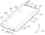
도 2 및 3을 참조하면, 일 실시예에 따른 전자 장치(200)(예: 도 1의 전자 장치(101))는, 제 1 면(또는 전면)(210A), 제 2 면(또는 후면)(210B), 및 제 1 면(210A) 및 제 2 면(210B) 사이의 공간을 둘러싸는 측면(210C)을 포함하는 하우징(210)을 포함할 수 있다. 다른 실시예(미도시)에서는, 하우징은, 도 2의 제 1 면(210A), 제 2 면(210B) 및 측면(210C)들 중 일부를 형성하는 구조를 지칭할 수도 있다. 일 실시예에 따르면, 제 1 면(210A)은 적어도 일부분이 실질적으로 투명한 전면 플레이트(202)(예: 다양한 코팅 레이어들을 포함하는 글라스 플레이트, 또는 폴리머 플레이트)에 의하여 형성될 수 있다. 제 2 면(210B)은 실질적으로 불투명한 후면 플레이트(211)에 의하여 형성될 수 있다. 상기 후면 플레이트(211)는, 예를 들어, 코팅 또는 착색된 유리, 세라믹, 폴리머, 금속(예: 알루미늄, 스테인레스 스틸(STS), 또는 마그네슘), 또는 상기 물질들 중 적어도 둘의 조합에 의하여 형성될 수 있다. 상기 측면(210C)은, 전면 플레이트(202) 및 후면 플레이트(211)와 결합하며, 금속 및/또는 폴리머를 포함하는 측면 배젤 구조 (또는 “측면 부재”)(218)에 의하여 형성될 수 있다. 어떤 실시예에서는, 후면 플레이트(211) 및 측면 배젤 구조(218)는 일체로 형성되고 동일한 물질(예: 알루미늄과 같은 금속 물질)을 포함할 수 있다.2 and 3, the
도시된 실시예에서는, 상기 전면 플레이트(202)는, 상기 제 1 면(210A)으로부터 상기 후면 플레이트(211) 쪽으로 휘어져 심리스하게(seamless) 연장된 2개의 제 1 영역(210D)들을, 상기 전면 플레이트(202)의 긴 엣지(long edge) 양단에 포함할 수 있다. 도시된 실시예(도 3 참조)에서, 상기 후면 플레이트(211)는, 상기 제 2 면(210B)으로부터 상기 전면 플레이트(202) 쪽으로 휘어져 심리스하게 연장된 2개의 제 2 영역(210E)들을 긴 엣지 양단에 포함할 수 있다. 어떤 실시예에서는, 상기 전면 플레이트(202)(또는 상기 후면 플레이트(211))가 상기 제 1 영역(210D)들(또는 상기 제 2 영역(210E)들) 중 하나 만을 포함할 수 있다. 다른 실시예에서는, 상기 제 1 영역(210D)들 또는 제 2 영역(210E)들 중 일부가 포함되지 않을 수 있다. 상기 실시예들에서, 상기 전자 장치(200)의 측면에서 볼 때, 측면 배젤 구조(218)는, 상기와 같은 제 1 영역(210D)들 또는 제 2 영역(210E)들이 포함되지 않는 측면 쪽에서는 제 1 두께(또는 폭)을 가지고, 상기 제 1 영역(210D)들 또는 제 2 영역(210E)들을 포함한 측면 쪽에서는 상기 제 1 두께보다 얇은 제 2 두께를 가질 수 있다.In the illustrated embodiment, the
일 실시예에 따르면, 전자 장치(200)는, 디스플레이(201)(예: 도 1의 표시 장치(160)), 오디오 모듈(203, 207, 214)(예: 도 1의 음향 출력 장치(155) 및/또는 오디오 모듈(170)), 센서 모듈(204, 216, 219)(예: 도 1의 센서 모듈(176)), 카메라 모듈(205, 212, 213)(예: 도 1의 카메라 모듈(180)), 키 입력 장치(217)(예: 도 1의 인터페이스(177)), 발광 소자(206)(예: 도 1의 인터페이스(177)), 및 커넥터 홀(208, 109) 중 적어도 하나 이상을 포함할 수 있다. 어떤 실시예에서는, 전자 장치(200)는, 구성요소들 중 적어도 하나(예: 키 입력 장치(217), 또는 발광 소자(206))를 생략하거나 다른 구성요소를 추가적으로 포함할 수 있다.According to an embodiment, the
디스플레이(201)는, 예를 들어, 전면 플레이트(202)의 상당 부분을 통하여 노출될 수 있다. 어떤 실시예에서는, 상기 제 1 면(210A), 및 상기 측면(210C)의 제 1 영역(210D)들을 형성하는 전면 플레이트(202)를 통하여 상기 디스플레이(201)의 적어도 일부가 노출될 수 있다. 어떤 실시예에서는, 디스플레이(201)의 모서리를 상기 전면 플레이트(202)의 인접한 외곽 형상과 대체로 동일하게 형성할 수 있다. 다른 실시예(미도시)에서는, 디스플레이(201)가 노출되는 면적을 확장하기 위하여, 디스플레이(201)의 외곽과 전면 플레이트(202)의 외곽간의 간격이 대체로 동일하게 형성될 수 있다.The
다른 실시예(미도시)에서는, 디스플레이(201)의 화면 표시 영역의 일부에 리세스 또는 개구부(opening)을 형성하고, 상기 리세스 또는 상기 개구부(opening)와 정렬되는 오디오 모듈(214), 센서 모듈(204), 카메라 모듈(205), 및 발광 소자(206) 중 적어도 하나 이상을 포함할 수 있다. 다른 실시예(미도시)에서는, 디스플레이(201)의 화면 표시 영역의 배면에, 오디오 모듈(214), 센서 모듈(204), 카메라 모듈(205), 지문 센서(216)(예: 도 1의 센서 모듈(176)), 및 발광 소자(206) 중 적어도 하나 이상을 포함할 수 있다. 다른 실시예(미도시)에서는, 디스플레이(201)는, 터치 감지 회로, 터치의 세기(압력)를 측정할 수 있는 압력 센서, 및/또는 자기장 방식의 스타일러스 펜을 검출하는 디지타이저와 결합되거나 인접하여 배치될 수 있다. 어떤 실시예에서는, 상기 센서 모듈(204, 219)의 적어도 일부, 및/또는 키 입력 장치(217)의 적어도 일부가, 상기 제 1 영역(210D)들, 및/또는 상기 제 2 영역(210E)들에 배치될 수 있다.In another embodiment (not shown), an
오디오 모듈(203, 207, 214)은, 마이크 홀(203) 및 스피커 홀(207, 214)을 포함할 수 있다. 마이크 홀(203)은 외부의 소리를 획득하기 위한 마이크가 내부에 배치될 수 있고, 어떤 실시예에서는 소리의 방향을 감지할 수 있도록 복수개의 마이크가 배치될 수 있다. 스피커 홀(207, 214)은, 외부 스피커 홀(207) 및 통화용 리시버 홀(214)을 포함할 수 있다. 어떤 실시예에서는 스피커 홀(207, 214)과 마이크 홀(203)이 하나의 홀로 구현 되거나, 스피커 홀(207, 214) 없이 스피커가 포함될 수 있다(예: 피에조 스피커).The
센서 모듈(204, 216, 219)은, 전자 장치(200)의 내부의 작동 상태, 또는 외부의 환경 상태에 대응하는 전기 신호 또는 데이터 값을 생성할 수 있다. 센서 모듈(204, 216, 219)은, 예를 들어, 하우징(210)의 제 1 면(210A)에 배치된 제 1 센서 모듈(204)(예: 근접 센서) 및/또는 제 2 센서 모듈(미도시)(예: 지문 센서), 및/또는 상기 하우징(210)의 제 2 면(210B)에 배치된 제 3 센서 모듈(219)(예: HRM 센서) (예: 도 1의 센서 모듈(176)) 및/또는 제 4 센서 모듈(216) (예: 지문 센서)을 포함할 수 있다. 상기 지문 센서는 하우징(210)의 제 1면(210A)(예: 디스플레이(201)뿐만 아니라 제 2면(210B)에 배치될 수 있다. 전자 장치(200)는, 도시되지 않은 센서 모듈, 예를 들어, 제스처 센서, 자이로 센서, 기압 센서, 마그네틱 센서, 가속도 센서, 그립 센서, 컬러 센서, IR(infrared) 센서, 생체 센서, 온도 센서, 습도 센서, 또는 조도 센서(204) 중 적어도 하나를 더 포함할 수 있다.The
카메라 모듈(205, 212, 213)은, 전자 장치(200)의 제 1 면(210A)에 배치된 제 1 카메라 장치(205), 및 제 2 면(210B)에 배치된 제 2 카메라 장치(212), 및/또는 플래시(213)를 포함할 수 있다. 상기 카메라 장치들(205, 212)은, 하나 또는 복수의 렌즈들, 이미지 센서, 및/또는 이미지 시그널 프로세서를 포함할 수 있다. 플래시(213)는, 예를 들어, 발광 다이오드 또는 제논 램프(xenon lamp)를 포함할 수 있다. 어떤 실시예에서는, 2개 이상의 렌즈들(적외선 카메라, 광각 및 망원 렌즈) 및 이미지 센서들이 전자 장치(200)의 한 면에 배치될 수 있다.The
키 입력 장치(217)는, 하우징(210)의 측면(210C)에 배치될 수 있다. 다른 실시예에서는, 전자 장치(200)는 상기 언급된 키 입력 장치(217) 중 일부 또는 전부를 포함하지 않을 수 있고 포함되지 않은 키 입력 장치(217)는 디스플레이(201) 상에 소프트 키 등 다른 형태로 구현될 수 있다. 어떤 실시예에서, 키 입력 장치는 하우징(210)의 제 2면(210B)에 배치된 센서 모듈(216)을 포함할 수 있다.The
발광 소자(206)는, 예를 들어, 하우징(210)의 제 1 면(210A)에 배치될 수 있다. 발광 소자(206)는, 예를 들어, 전자 장치(200)의 상태 정보를 광 형태로 제공할 수 있다. 다른 실시예에서는, 발광 소자(206)는, 예를 들어, 카메라 모듈(205)의 동작과 연동되는 광원을 제공할 수 있다. 발광 소자(206)는, 예를 들어, LED, IR LED 및 제논 램프를 포함할 수 있다.The
커넥터 홀(208, 109)은, 외부 전자 장치와 전력 및/또는 데이터를 송수신하기 위한 커넥터(예를 들어, USB 커넥터)를 수용할 수 있는 제 1 커넥터 홀(208), 및/또는 외부 전자 장치와 오디오 신호를 송수신하기 위한 커넥터를 수용할 수 있는 제 2 커넥터 홀(예를 들어, 이어폰 잭)(109)을 포함할 수 있다.The connector holes 208 and 109 include a
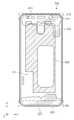
도 4를 참조하면, 전자 장치(400)(예: 전자 장치(101))는, 측면 배젤 구조(410), 제 1 지지부재(411)(예: 브라켓), 전면 플레이트(420), 디스플레이(430), 인쇄 회로 기판(440), 배터리(450)(예: 도 1의 배터리(189)), 제 2 지지부재(460)(예: 리어 케이스), 안테나(470)(예: 도 1의 안테나 모듈(197)), 및 후면 플레이트(480)를 포함할 수 있다. 어떤 실시예에서는, 전자 장치(400)는, 구성요소들 중 적어도 하나(예: 제 1 지지부재(411), 또는 제 2 지지부재(460))를 생략하거나 다른 구성요소를 추가적으로 포함할 수 있다. 전자 장치(400)의 구성요소들 중 적어도 하나는, 도 2, 또는 도 3의 전자 장치(200)의 구성요소들 중 적어도 하나와 동일, 또는 유사할 수 있으며, 중복되는 설명은 이하 생략한다.Referring to FIG. 4, the electronic device 400 (eg, the electronic device 101) includes a
제 1 지지부재(411)는, 전자 장치(400) 내부에 배치되어 측면 배젤 구조(410)와 연결될 수 있거나, 측면 배젤 구조(410)와 일체로 형성될 수 있다. 제 1 지지부재(411)는, 예를 들어, 금속 재질 및/또는 비금속 (예: 폴리머) 재질로 형성될 수 있다. 제 1 지지부재(411)는, 일면에 디스플레이(430)(예: 도 1의 표시 장치(160))가 결합되고 타면에 인쇄 회로 기판(440)이 결합될 수 있다. 인쇄 회로 기판(440)에는, 프로세서(예: 프로세서(120) 및/또는 통신 모듈(190)), 메모리(예: 메모리(130)), 및/또는 인터페이스(예: 인터페이스(177))가 장착될 수 있다. 프로세서는, 예를 들어, 중앙처리장치, 어플리케이션 프로세서, 그래픽 처리 장치, 이미지 시그널 프로세서, 센서 허브 프로세서, 또는 커뮤니케이션 프로세서 중 하나 또는 그 이상을 포함할 수 있다.The
메모리는, 예를 들어, 휘발성 메모리(예: 도 1의 휘발성 메모리(132)) 또는 비휘발성 메모리(예: 도 1의 비휘발성 메모리(134))를 포함할 수 있다.The memory may include, for example, volatile memory (eg, volatile memory 132 of FIG. 1) or non-volatile memory (eg, nonvolatile memory 134 of FIG. 1).
인터페이스는, 예를 들어, HDMI(high definition multimedia interface), USB(universal serial bus) 인터페이스, SD카드 인터페이스, 및/또는 오디오 인터페이스를 포함할 수 있다. 인터페이스는, 예를 들어, 전자 장치(400)를 외부 전자 장치와 전기적 또는 물리적으로 연결시킬 수 있으며, USB 커넥터, SD 카드/MMC 커넥터, 또는 오디오 커넥터를 포함할 수 있다.The interface may include, for example, a high definition multimedia interface (HDMI), a universal serial bus (USB) interface, an SD card interface, and / or an audio interface. The interface may electrically or physically connect the
배터리(450)는 전자 장치(400)의 적어도 하나의 구성 요소에 전력을 공급하기 위한 장치로서, 예를 들면, 재충전 불가능한 1차 전지, 또는 재충전 가능한 2차 전지, 또는 연료 전지를 포함할 수 있다. 배터리(450)의 적어도 일부는, 예를 들어, 인쇄 회로 기판(440)과 실질적으로 동일 평면 상에 배치될 수 있다. 배터리(450)는 전자 장치(400) 내부에 일체로 배치될 수 있고, 전자 장치(400)와 탈부착 가능하게 배치될 수도 있다.The
안테나(470)는, 후면 플레이트(480)와 배터리(450) 사이에 배치될 수 있다. 안테나(470)는, 예를 들어, NFC(near field communication) 안테나, 무선 충전 안테나, 및/또는 MST(magnetic secure transmission) 안테나를 포함할 수 있다. 안테나(470)는, 예를 들어, 외부 장치와 근거리 통신을 하거나, 충전에 필요한 전력을 무선으로 송수신 할 수 있다. 다른 실시예에서는, 측면 배젤 구조(410) 및/또는 상기 제 1 지지부재(411)의 일부 또는 그 조합에 의하여 안테나 구조가 형성될 수 있다.The
도 5는 다양한 실시예들에 따른, 전면 플레이트(420)에 대한 도전성 접착 레이어(550)의 위치를 도시하는 구성도(500)이다.5 is a configuration diagram 500 illustrating the location of a conductive
도 5는 전자 장치(예: 도 1의 전자 장치(101))의 전면 플레이트(420), 디스플레이(430), 및 도전성 접착 레이어(550)(예: 도전성 접착 부재)를 전자 장치(101)의 후면에서 전면 방향(예: +Z 방향)으로 바라본 전자 장치(101)의 일부의 구성도에 대응할 수 있다.5 illustrates the
도 5를 참조하여, 다양한 실시예들에 따르면, 디스플레이(430)(예: 도 1의 표시 장치(160))는 전면 플레이트(420)의 적어도 일부를 통하여 외부를 통하여 보여지도록, 전자 장치(101)의 전면을 향하여(예: +Z 방향) 배치된 디스플레이 레이어(예: 디스플레이 패널) 및 디스플레이 패널의 구동 회로가 배치된 인쇄 회로 기판(520)을 포함할 수 있다.Referring to FIG. 5, according to various embodiments, the display 430 (eg, the display device 160 of FIG. 1) is displayed through the outside through at least a portion of the
일 실시예에 따르면, 디스플레이(430)는 디스플레이 패널의 후면에배치된 도전성 레이어를 포함할 수 있다. 예를 들어, 도전성 레이어는 금속성 호일(foil)일 수 있다. 예를 들어, 도전성 레이어는 구리 시트(copper sheet)일 수 있다.According to one embodiment, the
일 실시예에 따르면, 디스플레이(430)는 도전성 레이어와 디스플레이 패널 사이에 위치된 완충 레이어(cushion layer)을 포함할 수 있다. 예를 들어, 완충 레이어는 디스플레이 패널을 물리적 충격으로부터 보호하기 위하여 이용될 수 있다.According to an embodiment, the
일 실시예에 따르면, 인쇄 회로 기판(520)은 도전성 레이어의 아래(예: 제1 영역)에 배치되고 디스플레이 패널의 구동을 위한 구동 회로를 포함할 수 있다. 예를 들어, 인쇄 회로 기판(520)은 디스플레이 패널의 일단(예: 하단)으로부터 연장되고, 가요성 인쇄 회로 기판일 수 있다. 예를 들어, 인쇄 회로 기판(520)은, 전자 장치(101)의 메인 인쇄 회로 기판(예: 도 4의 인쇄 회로 기판(440))에 연결될 수 있다. 예를 들어, 인쇄 회로 기판(520)은 디스플레이 패널의 아래쪽에 위치된 도전성 지지부재(예: 도 4의 제1 지지부재(411))를 통과하여 도전성 지지부재의 아래쪽에 위치된 메인 인쇄 회로 기판에 연결될 수 있다. 예를 들어, 인쇄 회로 기판(520)은 도전성 지지부재의 일부에 형성된 홀을 통하여 메인 인쇄 회로 기판에 연결될 수 있다.According to an embodiment, the printed
일 실시예에 따르면, 도전성 접착 레이어(550)는 도전성 접착 레이어(550)의 양면에 접착성을 갖는 열 감응(heat reactive) 테이프일 수 있다. 예를 들어, 도전성 접착 레이어(550)의 디스플레이(430)의 아래쪽에 위치되고, 디스플레이(430)를 도전성 접착 레이어(550)의 아래쪽에 위치된 도전성 지지부재에 고정하는데 이용될 수 있다. 일 실시예에 따르면, 도전성 접착 레이어(550)는 회로 기판(520)의 구동 회로에 의하여 발생된 노이즈 신호의 적어도 일부를 도전성 지지부재에 전달하도록 형성될 수 있다. 예를 들어, 회로 기판(520)의 구동 회로에 의하여 발생된 노이즈는 디스플레이(430)의 후면에 위치된 도전성 레이어에 전달되고, 도전성 접착 레이어(550)를 통하여 도전성 지지부재에 전달될 수 있다. 예를 들어, 도전성 접착 레이어(550)는 구동 회로에 의하여 발생되고 도전성 레이어에 유기된 노이즈 신호가 도전성 지지부재로 적어도 일부 통과될 수 있도록 형성될 수 있다.According to an embodiment, the conductive
일 실시예에 따르면, 디스플레이(430)의 도전성 레이어 아래에 제1 절연성 레이어가 위치될 수 있다. 예를 들어, 제1 절연성 레이어는 도전성 레이어와 도전성 접착 레이어(550) 사이에 위치될 수 있다. 예를 들어, 제1 절연성 레이어는 도전성 레이어에 대한 절연을 제공할 수 있다. 예를 들어, 도전성 레이어는 PET(polyethylene terephthalate)로 형성될 수 있다. 예를 들어, 전자 장치(500)는 디스플레이(430)의 도전성 레이어와 도전성 접착 레이어(550)의 사이에 제1 절연성 레이어를 포함하고, 도전성 접착 레이어(550)는 도전성 레이어와 전기적으로 커플링될 수 있다. 예를 들어, 도전성 레이어에 유기된 노이즈 신호는 도전성 레이어와 도전성 접착 레이어(550) 사이의 전기적 커플링에 기반하여 도전성 지지부재에 전달될 수 있다.According to an embodiment, the first insulating layer may be positioned under the conductive layer of the
일 실시예에 따르면, 인쇄 회로 기판(520)은 제1 면적(예: X-Y 평면 상의 인쇄 회로 기판(520)의 면적)을 가지고, 도전성 접착 레이어(550)는 제2 면적(예: X-Y 평면 상의 도전성 접착 레이어(550)의 면적)을 가질 수 있다. 예를 들어, 제2 면적은 제1 면적보다 넓을 수 있다. 예를 들어, 제2 면적은 제1 면적의 적어도 약 2배 이상일 수 있다. 도 5의 도전성 접착 레이어(550)의 형상은 예시적인 것으로서, 본 문서의 실시예들이 이에 제한되지 않는다.According to one embodiment, the printed
도 13은 다양한 실시예들에 따른 도전성 접착 레이어(550)의 형상을 도시한다.13 shows a shape of a conductive
다양한 실시예들에 따르면, 도전성 접착 레이어(550)는 다양한 형상일 수 있다. 예를 들어, 도전성 접착 레이어(550)는 전자 장치(101)의 형상, 도전성 지지부재(예: 도 4의 제1 지지부재(411))의 형상, 및/또는 인쇄 회로 기판(520)의 형상에 따라서 상이하게 형성될 수 있다.According to various embodiments, the conductive
일 실시예에 따르면, 참조번호 1301을 참조하여, 도전성 접착 레이어(550)는 적어도 하나의 개구부(opening)을 포함할 수 있다. 도 13에는 하나의 개구부 만이 도시되어 있으나, 도전성 접착 레이어(550)는 복수의 개구부를 포함할 수 있다. 일 실시예에 따르면, 개구부는 전자 장치(101)의 전면에서 바라보았을 때 배터리와 적어도 일부 중첩되도록 형성될 수 있다. 도 13의 개구부의 위치와 형상은 예시적인 것으로서, 본 문서의 실시예들이 이에 제한되지 않는다.According to one embodiment, referring to
일 실시예에 따르면, 참조번호 1302 및 1303을 참조하여, 도전성 접착 레이어(550)는 적어도 하나의 돌출부를 포함할 수 있다. 예를 들어, 참조번호 1302를 참조하여, 도전성 접착 레이어(550)는 상부 돌출부 및 하부 돌출부를 포함할 수 있다. 다른 예를 들어, 참조번호 1303을 참조하여, 도전성 접착 레이어(550)는 하부 돌출부를 포함할 수 있다. 일 실시예에 따르면, 도전성 접착 레이어(550)의 돌출부는 전자 장치(101)의 형상, 도전성 지지부재(예: 도 4의 제1 지지부재(411))의 형상, 접착 공정, 및/또는 인쇄 회로 기판(520)의 형상에 따라서 상이하게 형성될 수 있다. 도 13에 도시된 돌출부의 수, 위치 및 형상은 예시적인 것으로서 본 문서의 실시예들이 이에 제한되지 않는다.According to one embodiment, referring to
일 실시예에 따르면, 참조번호 1304를 참조하여, 도전성 전착 레이어(550)는 개구부 및 돌출부를 포함하지 않을 수 있다.According to an embodiment, with reference to 1304, the
다시 도 5를 참조하여, 일 실시예에 따르면, 도전성 접착 레이어(550)는 전자 장치(101)의 일 측면에서 볼 때 인쇄 회로 기판(520)과 적어도 일부가 중첩되도록 배치될 수 있다. 예를 들어, 전자 장치(101)의 우측면에서 좌측면 방향(예: -X 방향) 또는 좌측면에서 우측면 방향(예: +X 방향)으로 바라볼 때, 도전성 접착 레이어(550)의 적어도 일부는 인쇄 회로 기판(520)의 적어도 일부와 Z축 상에서 중첩될 수 있다. 다른 예를 들어, 전자 장치(101)의 상측면에서 하측면 방향(예: +Y 방향) 또는 하측면에서 상측면 방향(예: -Y 방향)으로 바라볼 때, 도전성 접착 레이어(550)의 적어도 일부는 인쇄 회로 기판(520)의 적어도 일부와 Z축 상에서 중첩될 수 있다. 도전성 접착 레이어(550)와 인쇄 회로 기판(520)의 중첩이 존재하는 영영에는 도전성 접착 레이어(550)와 인쇄 회로 기판(520) 사이에 배치된 절연 레이어가 위치될 수 있다.Referring back to FIG. 5, according to an embodiment, the conductive
일 실시예에 따르면, 도전성 접착 레이어(550)는 전자 장치(101)의 일 방향에서 볼 때 인쇄 회로 기판(520)과 중첩되지 않도록 배치될 수 있다. 예를 들어, 전자 장치(101)의 후면에서 전면 방향(예: +Z 방향)으로 바라볼 때, 도전성 접착 레이어(550) 는 인쇄 회로 기판(520)과 중첩되지 않을 수 있다. 다른 예를 들어, 도전성 접착 레이어(550) 는 인쇄 회로 기판(520)과 중첩되지 않는 형태를 가질 수 있다. 또 다른 예를 들어, 도전성 접착 레이어(550)는 인쇄 회로 기판(520)과 Z축 상에서 중첩되지 않도록 배치될 수 있다.According to an embodiment, the conductive
도 6은 다양한 실시예들에 따른, 제1 지지부재(411)에 대한 도전성 접착 레이어(550)의 위치를 도시하는 구성도(600)이다.6 is a configuration diagram 600 showing the position of the conductive
도 6는 전자 장치(예: 도 1의 전자 장치(101))의 전면 플레이트(예: 도 5의 전면 플레이트(420)) 및 디스플레이(예: 도 5의 디스플레이(430))를 제거한 뒤, 전자 장치(101)를 전자 장치(101)의 전면에서 후면 방향(예: -Z 방향)으로 바라본 전자 장치(101)의 일부의 구성도에 대응할 수 있다.6 is after removing the front plate (eg, the
도 6을 참조하여, 전자 장치(101)는 제1 지지부재(411)(예: 도전성 지지부재) 및 측면 배젤 구조(410)를 포함할 수 있다.Referring to FIG. 6, the electronic device 101 may include a first support member 411 (eg, a conductive support member) and a
일 실시예에 따르면, 제1 지지부재(411)는 측면 배젤 구조(410)과 물리적으로 연결되고, 측면 배젤 구조(410)의 적어도 일부와 전기적으로 분리될 수 있다. 예를 들어, 제1 지지부재(411)는 도전성 물질(예: 금속)로 구성될 수 있다. 예를 들어, 제1 지지부재(411)는 도전성 지지부재로 호칭될 수 있다. 일 실시예에 따르면, 제1 지지부재(411)는 전자 장치(101)의 일부 구성(예: 도 5의 인쇄회로 기판(520))에 대한 접지 영역으로서 동작할 수 있다.According to an embodiment, the
일 실시예에 따르면, 측면 배젤 구조(410)는 전자 장치(101)이 측면을 형성하고 적어도 일부가 외부에 노출될 수 있다. 예를 들어, 측면 배젤 구조(410)는, 절연 레이어(예: 제1 절연 레이어(611) 및 제2 절연 레이어(621))을 통하여, 제1 지지부재(411)와 물리적으로 연결되고 제1 지지부재(411)와 전기적으로 분리된 도전성 방사체(613 및 623)를 포함할 수 있다.According to an embodiment, the
일 실시예에 따르면, 제1 도전성 방사체(613)는 전자 장치(101)의 외부에서 보여지고, 지정된 대역의 신호를 송수신하도록 설정될 수 있다. 예를 들어, 제1 도전성 방사체(613)의 적어도 하나의 급전점과 적어도 하나의 접지점을 포함할 수 있으며, 안테나의 적어도 일부로서 동작할 수 있다. 예를 들어, 제1 도전성 방사체(613)는 제1 절연 레이어(611)을 통하여 제1 지지부재(411)로부터 전기적으로 분리될 수 있다. 예를 들어, 제1 도전성 방사체(613)는 제1 안테나부(610)(예: 제1 안테나 모듈)의 일부일 수 있다. 제1 안테나부(610)는 제1 지지부재(411)에 일 측면에 근접하여 배치될 수 있다.According to an embodiment, the first
일 실시예에 따르면, 제2 도전성 방사체(623)는 전자 장치(101)의 외부에서 보여지고, 지정된 대역의 신호를 송수신하도록 설정될 수 있다. 예를 들어, 제2 도전성 방사체(623)의 적어도 하나의 급전점과 적어도 하나의 접지점을 포함할 수 있으며, 안테나의 적어도 일부로서 동작할 수 있다. 예를 들어, 제2 도전성 방사체(623)는 제2 절연 레이어(621)를 통하여 제1 지지부재(411)로부터 전기적으로 분리될 수 있다. 예를 들어, 제2 도전성 방사체(623)는 제2 안테나부(620)(예: 제2 안테나 모듈)의 일부일 수 있다. 제2 안테나부(620)는 제2 지지부재(411)에 일 측면에 근접하여 배치될 수 있다.According to an embodiment, the second
일 실시예에 따르면, 도전성 접착 레이어(예: 도 5의 도전성 접착 레이어(550))는 제1 지지부재(411)의 제1 영역(650)에 위치될 수 있다. 따라서, 도전성 접착 레이어(550)는 제1 영역(650)을 통하여 제1 지지부재(411)에 노이즈 신호의 적어도 일부를 전달할 수 있다.According to an embodiment, the conductive adhesive layer (eg, the conductive
도 7은 다양한 실시예들에 따른, 도전성 접착 레이어의 위치를 도시하는 전자 장치의 분해 사시도(700)이다.7 is an exploded
다양한 실시예들에 따르면, 전자 장치(예: 도 1의 전자 장치(101))는 전자 장치(101)의 상면으로부터 하면 방향(예: -Z 방향)으로, 디스플레이 패널(710), 디스플레이 패널(710)의 아래에 배치된 완충 레이어(720), 완충 레이어(720)의 아래에 위치된 도전성 레이어(730)(예: 구리 시트), 도전성 레이어(730)의 아래에 위치된 제1 절연 레이어(740), 제1 절연 레이어(740)의 아래에 위치된 도전성 접착 레이어(550), 및 도전성 접착 레이어(550)의 아래에 위치된 제1 지지부재(411)를 포함할 수 있다.According to various embodiments of the present disclosure, the electronic device (eg, the electronic device 101 of FIG. 1) is directed from the upper surface of the electronic device 101 to a lower surface direction (eg, -Z direction), the
일 실시예에 따르면, 디스플레이 패널(710)은 도 4의 디스플레이(430)의 디스플레이 패널에 대응할 수 있다. 예를 들어, 디스플레이 패널(710)의 상면에는 커버 글래스(예: 도 4의 전면 플레이트(420))(미도시)가 배치될 수 있다. 일 실시예에 따르면, 완충 레이어(720) 및 도전성 레이어(730)는 디스플레이 패널(710)과 함께 디스플레이 모듈을 구성할 수 있다.According to an embodiment, the
일 실시예에 따르면, 제1 절연 레이어(740)는 도전성 레이어(730)를 다른 전자 장치(101)의 구성들로부터 절연하기 위한 막으로서, PET로 형성될 수 있다. 예를 들어, 제1 절연 레이어(740)는 디스플레이 패널로부터 발생된 전류가 제1 지지부재(411)를 통하여 측면 배젤 구조(410)로 전달되어 발생할 수 있는 감전을 방지하기 위하여 이용될 수 있다.According to an embodiment, the first insulating
일 실시예에 따르면, 도전성 접착 레이어(550)는 제1 절연 레이어(740)를 사이에 두고 도전성 레이어(730)와 전기적으로 커플링될 수 있다. 예를 들어, 도전성 접착 레이어(550)는, 커플링을 통하여, 도전성 레이어(730)로부터의 노이즈 신호의 적어도 일부를 제1 지지부재(411)로 전달함으로 도전성 레이어(730)의 노이즈 신호가 제1 도전성 방사체(613) 또는 제2 도전성 방사체(623)로 전달되는 것을 방지할 수 있다. 노이즈 신호의 전달을 방지함으로써 도전성 접착 레이어(550)는 제1 도전성 방사체(613) 및 제2 도전성 방사체(623)에 연관된 안테나의 안테나의 수신 감도가 감소하는 것을 방지할 수 있다.According to an embodiment, the conductive
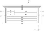
도 8은 일 실시예에 따른, 전자 장치의 단면의 구성도(800)이다.8 is a configuration diagram 800 of a cross-section of an electronic device, according to an embodiment.
도 8은 전자 장치(예: 도 1의 전자 장치(101))를 장축에 따라 절단한 뒤(예: 도 2의 Y 축), 전자 장치(101)의 우측면에서 좌측 방향(예: -X 방향)으로 전자 장치(101)를 보았을 때 전자 장치(101)의 단면에 대응하는 구성도일 수 있다.FIG. 8 shows an electronic device (eg, the electronic device 101 of FIG. 1) cut along a long axis (eg, the Y axis of FIG. 2), and then the left side of the electronic device 101 (eg, -X direction) ) May be a configuration diagram corresponding to a cross section of the electronic device 101 when the electronic device 101 is viewed.
일 실시예에 따르면, 전자 장치(101)는 전자 장치(101)의 외관을 형성하는 전면 플레이트(420), 후면 플레이트(480), 및 측면 배젤 구조(예: 도 4의 측면 배젤 구조(410))를 포함할 수 있다. 도 8에서, 측면 배젤 구조의 일부인 제1 도전성 방사체(613)와 제2 도전성 방사체(623)가 도시되어 있다.According to an embodiment, the electronic device 101 includes a
일 실시예에 따르면, 디스플레이 모듈은 전면 플레이트(420)의 아래쪽에 배치된 디스플레이 패널(710), 디스플레이 패널(710)의 아래쪽에 위치된 완충 레이어(720), 완충 레이어(720)의 아래쪽에 위치된 도전성 레이어(730), 및 도전성 레이어(730)의 아래쪽에 위치된 인쇄 회로 기판(520)을 포함할 수 있다.According to one embodiment, the display module is located below the
일 실시예에 따르면, 도전성 레이어(730)와 인쇄 회로 기판(520) 사이에는 제1 접착 레이어(810)가 위치될 수 있다. 예를 들어, 제1 접착 레이어(810)는 인쇄 회로 기판(520)을 도전성 레이어(730)에 접착할 수 있다. 예를 들어, 제1 접착 레이어(810)는 도전성으로, 인쇄 회로 기판(520)과 도전성 레이어(730)를 전기적으로 연결할 수 있다. 다른 예를 들어, 제1 접착 레이어(810)는 비도전성으로, 인쇄 회로 기판(520)과 도전성 레이어(730)를 전기적으로 절연할 수 있다.According to an embodiment, the first
일 실시예에 따르면, 인쇄 회로 기판(520)과 제1 지지부재(411) 사이에는 제2 접착 레이어(820)가 위치될 수 있다. 예를 들어, 제2 접착 레이어(820)는 인쇄 회로 기판(520)을 제1 지지부재(411)에 접착할 수 있다. 예를 들어, 제2 접착 레이어(820)는 도전성 물질(예: 구리)로 구성되고, 인쇄 회로 기판(520)을 제1 지지부재(411)에 전기적으로 연결할 수 있다.According to an embodiment, a second
일 실시예에 따르면, 도전성 접착 레이어(550)는 도전성 레이어(730)와 전기적으로 연결될 수 있다. 예를 들어, 도전성 접착 레이어(550)는 도전성 레이어(730)와 전기적으로 단락될 수 있다.According to an embodiment, the conductive
도 8의 실시예에 있어서, 도전성 레이어(730)는 도전성 접착 레이어(550)와 전기적으로 연결되기 때문에, 인쇄 회로 기판(520)의 구동 회로에 의한 노이즈 신호의 적어도 일부는 제1 절연 레이어(611)를 사이에 두고 전기적으로 커플링된 제1 도전성 방사체(613) 및/또는 제2 절연 레이어(621)를 사이에 두고 전기적으로 커플링된 제2 도전성 방사체(623)로 전달되는 대신에, 도전성 접착 레이어를 통하여 도전성 지지부재인 제1 지지부재(411)로 전달될 수 있다. 따라서, 인쇄 회로 기판(520)의 구동 회로로부터의 노이즈 신호로 인한 제1 도전성 방사체(613) 및/또는 제2 도전성 방사체(623)에 연관된 안테나의 수신 신호 감도 저하가 방지될 수 있다.In the embodiment of FIG. 8, since the
다양한 실시예들에 따르면, 전자 장치(101)는 제1 지지부재(411)의 아래에 배치된 인쇄 회로 기판(440), 제2 지지부재(460), 및 안테나(470)를 포함할 수 있다. 일 실시예에 따르면, 제2 지지부재(460)는 생략될 수 있다.According to various embodiments, the electronic device 101 may include a printed
도 9는 일 실시예에 따른 전자 장치(101)의 단면의 구성도(900)이다.9 is a configuration diagram 900 of a cross-section of an electronic device 101 according to an embodiment.
도 9에서, 다르게 설명되지 않으면 도 8과 관련하여 설명된 설명들이 도 9의 실시예에 동일하게 적용될 수 있다. 설명의 편의를 위하여 중복된 설명은 생략될 수 있다.In FIG. 9, descriptions related to FIG. 8 may be equally applied to the embodiment of FIG. 9 unless otherwise described. For convenience of description, duplicate descriptions may be omitted.
다양한 실시예들에 따르면, 전자 장치(101)는 도전성 레이어(730)와 도전성 접착 레이어(550) 사이에 배치된 제1 절연 레이어(740)를 더 포함할 수 있다. 예를 들어, 제1 절연 레이어(740)는 도전성 접착 레이어(550)를 도전 레이어(730)로부터 전기적으로 절연할 수 있다. 일 실시예에 따르면, 도전성 접착 레이어(550)는 제1 절연 레이어(740)를 통과하여 도전성 레이어(730)와 전기적으로 커플링될 수 있다. 전기적 커플링을 통하여 도전성 레이어(730)에 유기된 노이즈 신호의 적어도 일부가 제1 지지부재(411)에 전달될 수 있다. 따라서, 인쇄 회로 기판(520)의 구동 회로로부터의 노이즈 신호로 인한 제1 도전성 방사체(613) 및/또는 제2 도전성 방사체(623)에 연관된 안테나의 수신 신호 감도 저하가 방지될 수 있다. 제1 절연 레이어(740)를 통하여 도전성 레이어(730)와 도전성 접착 레이어(550)가 절연되기 때문에 도전성 레이어(730)어로부터 제1 지지부재(411) 및 측면 배젤 구조(예: 도 4의 측면 배젤 구조(410))를 통하여 사용자에 발생될 수 있는 감전이 방지될 수 있다.According to various embodiments, the electronic device 101 may further include a first insulating
도 10은 일 실시예에 따른 전자 장치(101)의 단면의 구성도(1000)이다.10 is a configuration diagram 1000 of a cross-section of an electronic device 101 according to an embodiment.
도 10에서, 다르게 설명되지 않으면 도 8 및 도 9 관련하여 설명된 설명들이 도 10의 실시예에 동일하게 적용될 수 있다. 설명의 편의를 위하여 중복된 설명은 생략될 수 있다.In FIG. 10, descriptions related to FIGS. 8 and 9 may be equally applied to the embodiment of FIG. 10 unless otherwise described. For convenience of description, duplicate descriptions may be omitted.
다양한 실시예들에 따르면, 전자 장치(101)는 도전성 접착 레이어(550)와 제1 지지부재(411) 사이에 배치된 제2 절연 레이어(1010)를 더 포함할 수 있다. 예를 들어, 제2 절연 레이어(1010)는 도전성 접착 레이어(550)를 제1 지지부재(411)로부터 전기적으로 절연할 수 있다. 일 실시예에 따르면, 도전성 접착 레이어(550)는 제2 절연 레이어(1010)를 통과하여 제1 지지부재(411)와 전기적으로 커플링될 수 있다.According to various embodiments, the electronic device 101 may further include a second insulating
일 실시예에 따르면, 도전성 레이어(730)와 도전성 접착 레이어(550)의 전기적 커플링 및 도전성 접착 레이어(550)와 제1 지지부재(411)의 전기적 커플링을 통하여 도전성 레이어(730)에 유기된 노이즈 신호의 적어도 일부가 제1 지지부재(411)에 전달될 수 있다. 예를 들어, 도전성 레이어(730)에 유기된 노이즈 신호는 2단계 커플링을 통하여 제1 지지부재(411)에 전달될 수 있다. 따라서, 인쇄 회로 기판(520)의 구동 회로로부터의 노이즈 신호로 인한 제1 도전성 방사체(613) 및/또는 제2 도전성 방사체(623)에 연관된 안테나의 수신 신호 감도 저하가 방지될 수 있다. 2단계 커플링을 통하여, 도전성 레이어(730)어로부터 제1 지지부재(411) 및 측면 배젤 구조(예: 도 4의 측면 배젤 구조(410))를 통하여 사용자에 발생될 수 있는 감전이 방지될 수 있다.According to one embodiment, the
표 1은 지정된 주파수 대역(예: LTE B19 주파수 대역)에서의 디스플레이 패널(710)의 온-오프에 따른 제1 도전성 방사체(613)에 연관된 제1 안테나 및 제2 도전성 방사체(623)에 연관된 제2 안테나의 수신감도(예: TIS(total isotropic sensitivity))의 변화를 나타낸다. 이하에서, 기존 구조는 도전성 접착 레이어(550) 대신에 비도전성 접착 테이프가 이용된 경우를 의미할 수 있다.Table 1 shows the first antenna associated with the first
표 2는 지정된 주파수 대역(예: LTE B1 주파수 대역)에서의 디스플레이 패널(710)의 온-오프에 따른 제1 도전성 방사체(613)에 연관된 제1 안테나 및 제2 도전성 방사체(623)에 연관된 제2 안테나의 수신감도(예: TIS(total isotropic sensitivity))의 변화를 나타낸다.Table 2 shows the first antenna associated with the first
표 3은 지정된 주파수 대역(예: LTE B12 주파수 대역)에서의 디스플레이 패널(710)의 온-오프에 따른 제1 도전성 방사체(613)에 연관된 제1 안테나 및 제2 도전성 방사체(623)에 연관된 제2 안테나의 수신감도(예: TIS(total isotropic sensitivity))의 변화를 나타낸다.Table 3 shows the first antenna associated with the first
표 3은 지정된 주파수 대역(예: LTE B12 주파수 대역)에서의 디스Table 3 shows the display in the specified frequency band (eg LTE B12 frequency band).
따라서, 표 1, 표2, 및 표 3에 나타난 바와 같이, 도전성 접착 레이어(550)를 이용하여, 모든 안테나에 대하여, 넓은 주파수 대역에 걸쳐 수신 감도 저하가 개선될 수 있다.Therefore, as shown in Table 1, Table 2, and Table 3, by using the conductive
일 실시예에 따르면, 제2 절연성 레이어(1010)는 도전성 접착 레이어(550)의 일부로서 구현될 수 있다.According to an embodiment, the second insulating
도 11은 일 실시예에 따른 도전성 접착 레이어(550)의 레이어 구성도이다.11 is a layer configuration diagram of a conductive
도 11을 참조하여, 도전성 접착 레이어(550)는 제1 접착 레이어(1110), 제1 도전성 레이어(1120), 및 제2 접착 레이어(1130)를 포함할 수 있다.Referring to FIG. 11, the conductive
일 실시예에 따르면, 제1 접착 레이어(1110)는 열감응성 접착 레이어일 수 있다. 예를 들어, 제1 접착 레이어(1110)는 온도에 따라서 접착성이 변하도록 구성될 수 있다. 일 실시예에 따르면, 제1 접착 레이어(1110)는 도전성 접착 레이어 또는 비도전성 접착 레이어일 수 있다. 예를 들어, 제1 접착 레이어(1110)는 HR CPSA(hear reactive conductive pressure sensitive adhesive)일 수 있다. 일 실시예에 따르면, 제1 접착 레이어(1110)는 제1 절연 레이어(예: 도 10의 제1 절연 레이어(730))에 접착될 수 있다.According to one embodiment, the
일 실시예에 따르면, 제1 도전성 레이어(1120)는 금속성 물질로 구성된 레이어일 수 있다. 예를 들어, 제1 도전성 레이어(1120)는 구리 호일 또는 알루미늄 호일을 포함한 도전성 기재일 수 있다.According to an embodiment, the first
일 실시예에 따르면, 제2 접착 레이어(1130)는 제1 지지부재(411)에 부착될 수 있다. 일 실시예에 따르면, 제2 접착 레이어(1130)는 도전성 접착 레이어 또는 비도전성 접착 레이어일 수 있다. 예를 들어, 제2 접착 레이어(1130)는 도 10의 제2 절연 레이어(1010)에 대응할 수 있다. 예를 들어, 제2 접착 레이어(1130)는 PSA(pressure sensitive adhesive)일 수 있다.According to an embodiment, the
도 12는 일 실시예에 따른 전자 장치(101)의 단면의 구성도(1200)이다.12 is a configuration diagram 1200 of a cross-section of an electronic device 101 according to an embodiment.
도 12에서, 다르게 설명되지 않으면 도 8과 관련하여 설명된 설명들이 도 12의 실시예에 동일하게 적용될 수 있다. 또한, 도 9, 도 10, 및 도 11과 관련하여 상술된 실시예들이 도 12의 구조에 유사하게 적용될 수 있다. 설명의 편의를 위하여 중복된 설명은 생략될 수 있다.In FIG. 12, descriptions related to FIG. 8 may be equally applied to the embodiment of FIG. 12 unless otherwise described. In addition, the embodiments described above with respect to FIGS. 9, 10, and 11 can be similarly applied to the structure of FIG. 12. For convenience of description, duplicate descriptions may be omitted.
다양한 실시예들에 따르면, 전자 장치(101)의 측면 배젤 구조(예: 도 4으 측면 배젤 구조(410)의 도전성 방사체들(예: 제1 도전성 방사체(611) 및 제2 도전성 방사체(621))은 전자 장치(101)의 일 측면에서 바라보았을 때 도전성 레이어(730)와 중첩되지 않을 수 있다. 예를 들어, 도전성 방사체들은 전자 장치(101)의 디스플레이에 수직한 축(예: Z 축) 상에서 도전성 레이어(7230)와 중첩되지 않도록 배치될 수 있다.According to various embodiments, conductive emitters (eg, a first
도 13을 참조하여, 일 실시예에 따르면, 측면 배젤 구조가 도전성 레이어(730)와 Z 축 상에서 중첩되는 영역에는 절연 영역(1213 및 1223)이 배치되고, 도전성 레이어(730)와 Z축 상에서 중첩되지 않는 영역에 도전성 방사체들(613 및 623)이 배치될 수 있다. 도전성 레이어(730)와 각각의 도전성 방사체들(613 및 623) 사이의 거리가 증가하기 때문에, 도전성 레이어(730)와 각각의 도전성 방사체들(613 및 623) 사이의 전기적 커플링의 강도가 감소될 수 있다. 이 경우, 도전성 레이어(730)에 유기된 노이즈 신호가 도 8의 실시예에 비하여 더 많이 도전성 접착 레이어(550)로 전달될 수 있다. 따라서, 노이즈 신호로 인한 수신 신호 감도 감소가 도 8의 실시예에 비하여 더 개선될 수 있다.Referring to FIG. 13, according to an embodiment, insulating
다양한 실시예들에 따르면, 휴대용 통신 장치(예: 도 1의 전자 장치(101))는, 상기 휴대용 통신 장치의 전면을 향하는 디스플레이 레이어(예: 도 7의 디스플레이 패널(710)), 및 상기 디스플레이 레이어의 아래에 형성된 도전성 레이어(예: 도 7의 도전성 레이어(730))를 포함하는 디스플레이 모듈(예: 도 4의 디스플레이(430)), 상기 도전성 레이어의 아래에 배치된 도전성 지지부재(예: 도 4의 제1 지지부재(411) 및 측면 베젤 구조(410)), 상기 도전성 지지부재의 옆에 근접하여 배치된 안테나 모듈(예: 도 6의 제1 안테나 모듈(610) 및/또는 제2 안테나 모듈(620)), 상기 도전성 레이어의 아래에 배치되고, 상기 디스플레이 모듈을 제어하기 위한 디스플레이 구동 회로가 배치된 인쇄 회로 기판(예: 도 5의 인쇄 회로 기판(520)), 및 상기 도전성 레이어와 상기 도전성 지지부재에 사이에 배치된 도전성 접착 레이어(예: 도 5의 도전성 접착 레이어(550))를 포함할 수 있다.According to various embodiments, a portable communication device (eg, the electronic device 101 of FIG. 1) includes a display layer (eg, the
예를 들어, 상기 도전성 접착 레이어는, 상기 디스플레이 구동 회로로부터 발생되고 상기 도전성 레이어로 유기된 노이즈가 상기 도전성 지지부재로 적어도 일부 통과될 수 있도록 형성될 수 있다.For example, the conductive adhesive layer may be formed so that noise generated from the display driving circuit and induced into the conductive layer can pass at least partially to the conductive support member.
예를 들어, 상기 휴대용 통신 장치는 상기 도전성 접착 레이어와 상기 도전성 레이어 사이에 제1 절연 레이어(예: 도 10의 제1 절연 레이어(750)) 및 상기 도전성 접착 레이어와 상기 도전성 지지부재 사이에 제2 절연 레이어(예: 도 10의 제2 절연 레이어(1010))를 더 포함하고, 상기 도전성 접착 레이어는 상기 노이즈가 상기 도전성 레이어로부터 커플링되어 상기 도전성 지지부재로 적어도 일부 통과될 수 있도록 형성될 수 있다.For example, the portable communication device may include a first insulating layer between the conductive adhesive layer and the conductive layer (eg, the first insulating layer 750 of FIG. 10) and the conductive adhesive layer and the conductive support member. A second insulating layer (eg, the second insulating
일 실시예에 따르면, 상기 인쇄 회로 기판은 제1 면적을 가지고, 상기 도전성 접착 레이어는 상기 제1 면적보다 넓은 제2 면적을 가질 수 있다. 예를 들어, 상기 도전성 접착 레이어의 상기 제2 면적은 상기 인쇄 회로 기판의 상기 제1 면적의 적어도 약 2배 이상일 수 있다.According to an embodiment, the printed circuit board may have a first area, and the conductive adhesive layer may have a second area larger than the first area. For example, the second area of the conductive adhesive layer may be at least about twice as large as the first area of the printed circuit board.
일 실시예에 따르면, 상기 인쇄 회로 기판은 상기 도전성 레이어의 제1 영역 아래에 배치되고, 상기 도전성 접착 레이어는 상기 도전성 레이어의 제2 영역 아래에 배치될 수 있다.According to an embodiment, the printed circuit board may be disposed under the first region of the conductive layer, and the conductive adhesive layer may be disposed under the second region of the conductive layer.
일 실시예에 따르면, 상기 휴대용 통신 장치의 일 측면(예: 도 6의 +X, -X, +Y, 또는 -Y 방향)에서 볼 때, 상기 도전성 접착 레이어는 상기 도전성 접착 레이어에 수직한 축(예: 도 6의 Z 축) 상에서 상기 인쇄 회로 기판과 적어도 일부 중첩되도록 배치될 수 있다. 예를 들어, 상기 도전성 접착 레이어와 상기 인쇄 회로 기판이 중첩되는 영역에 절연 부재가 배치될 수 있다.According to one embodiment, when viewed from one side (eg, + X, -X, + Y, or -Y direction of FIG. 6) of the portable communication device, the conductive adhesive layer is an axis perpendicular to the conductive adhesive layer It may be arranged to overlap at least partially with the printed circuit board (eg, Z axis in FIG. 6). For example, an insulating member may be disposed in an area where the conductive adhesive layer and the printed circuit board overlap.
일 실시예에 따르면, 상기 휴대용 통신 장치의 일 측면(예: 도 6의 +X, -X, +Y, 또는 -Y 방향)에서 볼 때, 상기 도전성 접착 레이어는 상기 도전성 접착 레이어에 수직한 축 상에서 상기 인쇄 회로 기판과 중첩되지 않도록 배치될 수 있다.According to one embodiment, when viewed from one side (eg, + X, -X, + Y, or -Y direction of FIG. 6) of the portable communication device, the conductive adhesive layer is an axis perpendicular to the conductive adhesive layer On the printed circuit board may be disposed so as not to overlap.
일 실시예에 따르면, 상기 인쇄 회로 기판은 가요성 인쇄 회로 기판일 수 있다.According to one embodiment, the printed circuit board may be a flexible printed circuit board.
다양한 실시예들에 따르면, 전자 장치(예: 도 1의 전자 장치(101))는, 윗면이 상기 전자 장치의 전면을 향하여 배치된 디스플레이 패널(예: 도 7의 디스플레이 패널(710)), 상기 디스플레이 패널의 아랫면에 배치된 도전성 레이어(예: 도 7의 도전성 레이어(730)), 및 상기 디스플레이 패널의 구동 회로를 포함하는 인쇄 회로 기판(예: 도 5의 인쇄 회로 기판(520))을 포함하는 디스플레이 모듈(예: 도 4의 디스플레이(439)), 상기 도전성 레이어의 아래에 배치된 도전성 지지부재(예: 도 4의 측면 베젤 구조(410) 및 제1 지지부재(411)), 상기 도전성 지지부재에 인접하게 상기 전자 장치의 상측 또는 하측에 위치되고, 상기 전자 장치의 측면을 통하여 적어도 일부 보여지고, 지정된 대역의 무선 신호를 송수신하도록 설정된 도전성 방사체(예: 도 6의 제1 도전성 방사체(613) 및/또는 제2 도전성 방사체(623)), 및 상기 도전성 레이어와 상기 도전성 지지부재 사이에 위치되고, 상기 디스플레이 모듈의 적어도 일부를 상기 도전성 지지부재에 접착하는 도전성 접착 레이어(예: 도 5의 도전성 접착 레이어(550))를 포함할 수 있다.According to various embodiments of the present disclosure, an electronic device (eg, the electronic device 101 of FIG. 1) includes a display panel having a top surface facing toward the front of the electronic device (eg, the
일 실시예에 따르면, 상기 도전성 접착 레이어는 상기 구동 회로로부터 발생되고 상기 도전성 레이어에 유기된 노이즈의 적어도 일부가 상기 도전성 지지부재로 전달될 수 있도록 형성될 수 있다.According to an embodiment, the conductive adhesive layer may be formed so that at least a portion of noise generated from the driving circuit and induced in the conductive layer can be transmitted to the conductive support member.
일 실시예에 따르면, 상기 도전성 레이어와 상기 도전성 접착 레이어의 사이에 위치된 제1 절연 레이어(예: 도 10의 제1 절연 레이어(740))를 더 포함하고, 상기 도전성 레이어와 상기 도전성 접착 레이어 사이의 전기적 커플링 및 상기 도전성 접착 레이어와 상기 도전성 지지부재 사이의 전기적 연결을 통하여 상기 유기된 노이즈의 적어도 일부가 상기 도전성 지지부재로 전달될 수 있다.According to an embodiment, the conductive layer further includes a first insulating layer (eg, the first insulating
일 실시예에 따르면, 상기 도전성 레이어와 상기 도전성 접착 레이어의 사이에 위치된 제1 절연 레이어를 더 포함하고, 상기 도전성 접착 레이어는 상기 제1 절연 레이어에 인접하게 위치된 제1 도전성 접착 레이어(예: 도 11의 제1 접착 레이어(1110) 및 제1 도전성 레이어(1120)) 및 상기 도전성 지지부재에 인접하게 위치된 제2 절연 접착 레이어(예: 도 11의 제2 접착 레이어(1130))를 포함할 수 있다.According to one embodiment, further comprising a first insulating layer positioned between the conductive layer and the conductive adhesive layer, the conductive adhesive layer is a first conductive adhesive layer positioned adjacent to the first insulating layer (eg : The
예를 들어, 상기 도전성 레이어와 상기 제1 도전성 접착 레이어 사이의 전기적 커플링 및 상기 제1 도전성 접착 레이어와 상기 도전성 지지부재 사이의 전기적 커플링을 통하여 상기 유기된 노이즈의 적어도 일부가 상기 도전성 지지부재로 전달될 수 있다.For example, at least a portion of the induced noise may be generated through the electrical coupling between the conductive layer and the first conductive adhesive layer and the electrical coupling between the first conductive adhesive layer and the conductive support member. Can be delivered to
예를 들어, 상기 제1 도전성 레이어는 상기 제1 절연 레이어에 인접하게 위치된 열 감응성(hear reactive) 접착 레이어(예: 도 11의 제1 접착 레이어(1110)) 및 상기 제2 접착 절연 레이어에 인접하게 위치된 금속성 레이어(예: 도 11의 제1 도전성 레이어(1120))를 포함할 수 있다. 예를 들어, 상기 열 감응성(hear reactive) 접착 레이어는 온도에 따라서 접착력이 달라질 수 있다.For example, the first conductive layer may be applied to a heat reactive adhesive layer (eg, the
일 실시예에 따르면, 전자 장치는 상기 도전성 방사체와 상기 도전성 지지부재를 물리적으로 연결하고, 상기 도전성 방사체와 상기 도전성 지지부재를 전기적으로 분리하며, 상기 도전성 방사체와 상기 도전성 지지부재 사이에 위치된 절연층(예: 도 6의 611 및 621)을 더 포함할 수 있다.According to an embodiment, the electronic device physically connects the conductive radiator and the conductive support member, electrically separates the conductive radiator and the conductive support member, and is located between the conductive radiator and the conductive support member. Layers (eg, 611 and 621 in FIG. 6) may be further included.
예를 들어, 전자 장치는 상기 도전성 지지부재의 아래쪽에 위치된 메인 인쇄 회로 기판(예: 도 4의 인쇄 회로 기판(440))을 더 포함하고, 상기 인쇄 회로 기판은 가요성을 갖는 인쇄 회로 기판으로, 상기 메인 인쇄 회로 기판과 전기적으로 연결될 수 있다.For example, the electronic device further includes a main printed circuit board (eg, the printed
일 실시예에 따르면, 상기 도전성 지지부재는 상기 인쇄 회로 기판에 접지를 제공하도록 설정될 수 있다.According to one embodiment, the conductive support member may be set to provide ground to the printed circuit board.
Claims (20)
Translated fromKorean상기 휴대용 통신 장치의 전면을 향하는 디스플레이 레이어, 및 상기 디스플레이 레이어의 아래에 형성된 도전성 레이어를 포함하는 디스플레이 모듈;
상기 도전성 레이어의 아래에 배치된 도전성 지지부재;
상기 도전성 지지부재의 옆에 근접하여 배치된 안테나 모듈;
상기 도전성 레이어의 아래에 배치되고, 상기 디스플레이 모듈을 제어하기 위한 디스플레이 구동 회로가 배치된 인쇄 회로 기판; 및
상기 도전성 레이어와 상기 도전성 지지부재에 사이에 배치된 도전성 접착 레이어를 포함하는, 휴대용 통신 장치.In a portable communication device,
A display module including a display layer facing the front side of the portable communication device, and a conductive layer formed below the display layer;
A conductive support member disposed under the conductive layer;
An antenna module disposed adjacent to the conductive support member;
A printed circuit board disposed under the conductive layer and having a display driving circuit for controlling the display module; And
And a conductive adhesive layer disposed between the conductive layer and the conductive support member.
상기 도전성 접착 레이어는,
상기 디스플레이 구동 회로로부터 발생되고 상기 도전성 레이어로 유기된 노이즈가 상기 도전성 지지부재로 적어도 일부 통과될 수 있도록 형성된, 휴대용 통신 장치.According to claim 1,
The conductive adhesive layer,
A portable communication device formed so that noise generated from the display driving circuit and induced into the conductive layer can pass at least partially to the conductive support member.
상기 휴대용 통신 장치는 상기 도전성 접착 레이어와 상기 도전성 레이어 사이에 제1 절연 레이어 및 상기 도전성 접착 레이어와 상기 도전성 지지부재 사이에 제2 절연 레이어를 더 포함하고,
상기 도전성 접착 레이어는 상기 노이즈가 상기 도전성 레이어로부터 커플링되어 상기 도전성 지지부재로 적어도 일부 통과될 수 있도록 형성된, 휴대용 통신 장치.According to claim 2,
The portable communication device further includes a first insulating layer between the conductive adhesive layer and the conductive layer, and a second insulating layer between the conductive adhesive layer and the conductive support member,
The conductive adhesive layer is formed so that the noise is coupled from the conductive layer to pass at least partly to the conductive support member, a portable communication device.
상기 인쇄 회로 기판은 제1 면적을 가지고,
상기 도전성 접착 레이어는 상기 제1 면적보다 넓은 제2 면적을 갖는,
휴대용 통신 장치.According to claim 1,
The printed circuit board has a first area,
The conductive adhesive layer has a second area larger than the first area,
Portable communication device.
상기 도전성 접착 레이어의 상기 제2 면적은 상기 인쇄 회로 기판의 상기 제1 면적의 적어도 2배 이상인, 휴대용 통신 장치.The method of claim 4,
And the second area of the conductive adhesive layer is at least twice the first area of the printed circuit board.
상기 인쇄 회로 기판은 상기 도전성 레이어의 제1 영역 아래에 배치되고,
상기 도전성 접착 레이어는 상기 도전성 레이어의 제2 영역 아래에 배치되는, 휴대용 통신 장치.According to claim 1,
The printed circuit board is disposed under the first area of the conductive layer,
The conductive adhesive layer is disposed under the second area of the conductive layer, the portable communication device.
상기 휴대용 통신 장치의 일 측면에서 볼 때, 상기 도전성 접착 레이어는 상기 도전성 접착 레이어에 수직한 축 상에서 상기 인쇄 회로 기판과 적어도 일부 중첩되도록 배치되는, 휴대용 통신 장치.The method of claim 6,
When viewed from one side of the portable communication device, the conductive adhesive layer is disposed to overlap at least partially with the printed circuit board on an axis perpendicular to the conductive adhesive layer.
상기 도전성 접착 레이어와 상기 인쇄 회로 기판이 중첩되는 영역에 절연 부재가 배치된, 휴대용 통신 장치.The method of claim 7,
A portable communication device in which an insulating member is disposed in an area where the conductive adhesive layer and the printed circuit board overlap.
상기 휴대용 통신 장치의 일 측면에서 볼 때, 상기 도전성 접착 레이어는 상기 도전성 접착 레이어에 수직한 축 상에서 상기 인쇄 회로 기판과 중첩되지 않도록 배치되는, 휴대용 통신 장치.The method of claim 6,
When viewed from one side of the portable communication device, the conductive adhesive layer is disposed so as not to overlap the printed circuit board on an axis perpendicular to the conductive adhesive layer.
상기 인쇄 회로 기판은 가요성(flexible) 인쇄 회로 기판인, 휴대용 통신 장치.According to claim 1,
The printed circuit board is a flexible printed circuit board, a portable communication device.
윗면이 상기 전자 장치의 전면을 향하여 배치된 디스플레이 패널, 상기 디스플레이 패널의 아랫면에 배치된 도전성 레이어, 및 상기 디스플레이 패널의 구동 회로를 포함하는 인쇄 회로 기판을 포함하는 디스플레이 모듈;
상기 도전성 레이어의 아래에 배치된 도전성 지지부재;
상기 도전성 지지부재에 인접하게 상기 전자 장치의 상측 또는 하측에 위치되고, 상기 전자 장치의 측면을 통하여 적어도 일부 보여지고, 지정된 대역의 무선 신호를 송수신하도록 설정된 도전성 방사체; 및
상기 도전성 레이어와 상기 도전성 지지부재 사이에 위치되고, 상기 디스플레이 모듈의 적어도 일부를 상기 도전성 지지부재에 접착하는 도전성 접착 레이어를 포함하는, 전자 장치.In the electronic device,
A display module including a display panel having a top surface facing toward the front of the electronic device, a conductive layer disposed on a bottom surface of the display panel, and a printed circuit board including a driving circuit of the display panel;
A conductive support member disposed under the conductive layer;
A conductive radiator positioned adjacent to the conductive support member on an upper or lower side of the electronic device, at least partially visible through a side surface of the electronic device, and configured to transmit and receive wireless signals in a designated band; And
And an electrically conductive adhesive layer positioned between the conductive layer and the conductive support member and adhering at least a portion of the display module to the conductive support member.
상기 도전성 접착 레이어는 상기 구동 회로로부터 발생되고 상기 도전성 레이어에 유기된 노이즈의 적어도 일부가 상기 도전성 지지부재로 전달될 수 있도록 형성된, 전자 장치.The method of claim 11,
The conductive adhesive layer is formed so that at least a portion of noise generated from the driving circuit and induced in the conductive layer can be transmitted to the conductive support member.
상기 도전성 레이어와 상기 도전성 접착 레이어의 사이에 위치된 제1 절연 레이어를 더 포함하고,
상기 도전성 레이어와 상기 도전성 접착 레이어 사이의 전기적 커플링 및 상기 도전성 접착 레이어와 상기 도전성 지지부재 사이의 전기적 연결을 통하여 상기 유기된 노이즈의 적어도 일부가 상기 도전성 지지부재로 전달되는, 전자 장치.The method of claim 12,
Further comprising a first insulating layer positioned between the conductive layer and the conductive adhesive layer,
An electronic device in which at least a portion of the induced noise is transmitted to the conductive support member through electrical coupling between the conductive layer and the conductive adhesive layer and an electrical connection between the conductive adhesive layer and the conductive support member.
상기 도전성 레이어와 상기 도전성 접착 레이어의 사이에 위치된 제1 절연 레이어를 더 포함하고,
상기 도전성 접착 레이어는:
상기 제1 절연 레이어에 인접하게 위치된 제1 도전성 접착 레이어; 및
상기 도전성 지지부재에 인접하게 위치된 제2 절연 접착 레이어를 포함하는, 전자 장치.The method of claim 12,
Further comprising a first insulating layer positioned between the conductive layer and the conductive adhesive layer,
The conductive adhesive layer:
A first conductive adhesive layer positioned adjacent to the first insulating layer; And
And a second insulating adhesive layer positioned adjacent to the conductive support member.
상기 도전성 레이어와 상기 제1 도전성 접착 레이어 사이의 전기적 커플링 및 상기 제1 도전성 접착 레이어와 상기 도전성 지지부재 사이의 전기적 커플링을 통하여 상기 유기된 노이즈의 적어도 일부가 상기 도전성 지지부재로 전달되는, 전자 장치.The method of claim 14,
At least a portion of the induced noise is transmitted to the conductive support member through electrical coupling between the conductive layer and the first conductive adhesive layer and the electrical coupling between the first conductive adhesive layer and the conductive support member, Electronic devices.
상기 제1 도전성 레이어는 상기 제1 절연 레이어에 인접하게 위치된 열 감응성(hear reactive) 접착 레이어 및 상기 제2 접착 절연 레이어에 인접하게 위치된 금속성 레이어를 포함하는, 전자 장치.The method of claim 14,
The first conductive layer includes a thermal reactive adhesive layer positioned adjacent to the first insulating layer and a metallic layer positioned adjacent to the second adhesive insulating layer.
상기 열 감응성(hear reactive) 접착 레이어는 온도에 따라서 접착력이 달라지는, 전자 장치.The method of claim 16,
The thermal reactive (hear reactive) adhesive layer, the electronic device, the adhesive strength is changed according to the temperature.
상기 도전성 방사체와 상기 도전성 지지부재를 물리적으로 연결하고, 상기 도전성 방사체와 상기 도전성 지지부재를 전기적으로 분리하며, 상기 도전성 방사체와 상기 도전성 지지부재 사이에 위치된 절연층을 더 포함하는, 전자 장치.The method of claim 11,
An electronic device further comprising a physically connecting the conductive radiator and the conductive support member, electrically separating the conductive radiator and the conductive support member, and further comprising an insulating layer positioned between the conductive radiator and the conductive support member.
상기 도전성 지지부재의 아래쪽에 위치된 메인 인쇄 회로 기판을 더 포함하고,
상기 인쇄 회로 기판은 가요성을 갖는 인쇄 회로 기판으로, 상기 메인 인쇄 회로 기판과 전기적으로 연결된, 전자 장치.The method of claim 11,
Further comprising a main printed circuit board located below the conductive support member,
The printed circuit board is a flexible printed circuit board, an electronic device electrically connected to the main printed circuit board.
상기 도전성 접착 부재는 적어도 일부 영역에 개구부 또는 돌출부를 포함하는, 전자 장치.The method of claim 11,
The conductive adhesive member includes an opening or a protrusion in at least a partial area.
Priority Applications (3)
| Application Number | Priority Date | Filing Date | Title |
|---|---|---|---|
| KR1020180117377AKR102522663B1 (en) | 2018-10-02 | 2018-10-02 | Electronic device comprising structure connecting display and conductive supporting member with conductive adhesive member |
| US17/274,141US11435789B2 (en) | 2018-10-02 | 2019-09-05 | Electronic device having structure for connecting display and conductive support member through conductive adhesive member |
| PCT/KR2019/011459WO2020071647A1 (en) | 2018-10-02 | 2019-09-05 | Electronic device having structure for connecting display and conductive support member through conductive adhesive member |
Applications Claiming Priority (1)
| Application Number | Priority Date | Filing Date | Title |
|---|---|---|---|
| KR1020180117377AKR102522663B1 (en) | 2018-10-02 | 2018-10-02 | Electronic device comprising structure connecting display and conductive supporting member with conductive adhesive member |
Publications (2)
| Publication Number | Publication Date |
|---|---|
| KR20200037953Atrue KR20200037953A (en) | 2020-04-10 |
| KR102522663B1 KR102522663B1 (en) | 2023-04-18 |
Family
ID=70054641
Family Applications (1)
| Application Number | Title | Priority Date | Filing Date |
|---|---|---|---|
| KR1020180117377AActiveKR102522663B1 (en) | 2018-10-02 | 2018-10-02 | Electronic device comprising structure connecting display and conductive supporting member with conductive adhesive member |
Country Status (3)
| Country | Link |
|---|---|
| US (1) | US11435789B2 (en) |
| KR (1) | KR102522663B1 (en) |
| WO (1) | WO2020071647A1 (en) |
Cited By (6)
| Publication number | Priority date | Publication date | Assignee | Title |
|---|---|---|---|---|
| KR20210155648A (en)* | 2020-06-16 | 2021-12-23 | 삼성전자주식회사 | Electronic device including a structure for ground connection |
| WO2022092756A1 (en)* | 2020-11-02 | 2022-05-05 | 삼성전자 주식회사 | Wearable electronic device comprising antenna |
| KR20220141591A (en)* | 2021-04-13 | 2022-10-20 | 삼성전자주식회사 | Electronic device comprising keyless sensor |
| WO2023068660A1 (en)* | 2021-10-19 | 2023-04-27 | 삼성전자 주식회사 | Antenna assembly and electronic device comprising same |
| WO2024258002A1 (en)* | 2023-06-14 | 2024-12-19 | 삼성전자주식회사 | Electronic device including support structure of printed circuit board |
| WO2025089553A1 (en)* | 2023-10-28 | 2025-05-01 | 삼성전자주식회사 | Foldable electronic device and multi-foldable electronic device including support plate in which wiring is embedded |
Families Citing this family (1)
| Publication number | Priority date | Publication date | Assignee | Title |
|---|---|---|---|---|
| CN115528411B (en)* | 2022-10-26 | 2025-06-20 | 维沃移动通信有限公司 | Electronic devices |
Citations (5)
| Publication number | Priority date | Publication date | Assignee | Title |
|---|---|---|---|---|
| KR20120020326A (en)* | 2010-08-30 | 2012-03-08 | 삼성전자주식회사 | Display apparatus |
| US20120087065A1 (en)* | 2010-10-06 | 2012-04-12 | Moon Kim | Shielding structures for wireless electronic devices with displays |
| KR20130005660A (en)* | 2011-07-07 | 2013-01-16 | 삼성전자주식회사 | Touch screen panel liquid crystal display device |
| KR20140009937A (en)* | 2012-07-13 | 2014-01-23 | 애플 인크. | Touch screen display with transparent electrical shielding layer |
| KR20170087334A (en)* | 2016-01-20 | 2017-07-28 | 삼성전자주식회사 | Antenna using Display |
Family Cites Families (23)
| Publication number | Priority date | Publication date | Assignee | Title |
|---|---|---|---|---|
| JP4700160B2 (en)* | 2000-03-13 | 2011-06-15 | 株式会社半導体エネルギー研究所 | Semiconductor device |
| US6483719B1 (en)* | 2000-03-21 | 2002-11-19 | Spraylat Corporation | Conforming shielded form for electronic component assemblies |
| KR100394151B1 (en) | 2001-04-25 | 2003-08-09 | 주성숙 | Conductive cushion for the liquid crystal displayer of movable wireless telecommunication terminal |
| US7217588B2 (en)* | 2005-01-05 | 2007-05-15 | Sharp Laboratories Of America, Inc. | Integrated MEMS packaging |
| KR100528003B1 (en) | 2003-12-19 | 2005-11-09 | 주식회사 팬택 | Mobile Communication Terminal with Key Input Apparatus |
| KR20060023623A (en) | 2004-09-10 | 2006-03-15 | 삼성전자주식회사 | How to improve the IC of SD module |
| US7629928B2 (en)* | 2005-03-23 | 2009-12-08 | Kyocera Wireless Corp. | Patch antenna with electromagnetic shield counterpoise |
| KR100803348B1 (en) | 2006-09-15 | 2008-02-13 | 주식회사유비와이즈 | Assembly for portable RF receiver with built-in antenna |
| TW200921483A (en)* | 2007-11-09 | 2009-05-16 | Tpk Touch Solutions Inc | Touch-control display panel with an electric-field shielding layer |
| JP5051648B2 (en)* | 2008-01-11 | 2012-10-17 | レノボ・シンガポール・プライベート・リミテッド | Electronic device casing structure and electronic device |
| US8099064B2 (en)* | 2008-05-08 | 2012-01-17 | Research In Motion Limited | Mobile wireless communications device with reduced harmonics resulting from metal shield coupling |
| KR20100046594A (en)* | 2008-10-27 | 2010-05-07 | 엘지전자 주식회사 | Portable terminal |
| TWI448239B (en)* | 2010-03-29 | 2014-08-01 | Au Optronics Corp | Power transmission circuit with emi shielding, lighting module, and a panel display module |
| KR101222388B1 (en) | 2011-10-14 | 2013-01-15 | 삼성전자주식회사 | Device for improving antenna receiving sensitivity in mobile phone |
| KR102181550B1 (en) | 2013-12-06 | 2020-11-23 | 삼성전자주식회사 | Electronic device having noise decrease means |
| KR102147964B1 (en) | 2014-01-03 | 2020-08-25 | 삼성전자주식회사 | Electronic device having improved assembling structure for display |
| EP3100364B1 (en)* | 2014-01-30 | 2019-12-11 | Sony Corporation | Avoiding nfc communication collisions between accessories and user equipment |
| JP6190528B2 (en) | 2014-06-02 | 2017-08-30 | タツタ電線株式会社 | Conductive adhesive film, printed circuit board, and electronic device |
| JP6566297B2 (en)* | 2015-03-06 | 2019-08-28 | Tianma Japan株式会社 | Display device and manufacturing method thereof |
| KR102497472B1 (en) | 2016-07-29 | 2023-02-08 | 삼성전자주식회사 | Electronic device including waterproof structure |
| US10564679B2 (en)* | 2018-04-05 | 2020-02-18 | Samsung Electro-Mechanics Co., Ltd. | Electronic device module, method of manufacturing the same and electronic apparatus |
| WO2021096310A1 (en)* | 2019-11-14 | 2021-05-20 | Samsung Electronics Co., Ltd. | Electronic device including antenna |
| KR102664719B1 (en)* | 2019-11-20 | 2024-05-10 | 삼성전자주식회사 | Electronic device including an isolated conductor |
- 2018
- 2018-10-02KRKR1020180117377Apatent/KR102522663B1/enactiveActive
- 2019
- 2019-09-05WOPCT/KR2019/011459patent/WO2020071647A1/ennot_activeCeased
- 2019-09-05USUS17/274,141patent/US11435789B2/enactiveActive
Patent Citations (5)
| Publication number | Priority date | Publication date | Assignee | Title |
|---|---|---|---|---|
| KR20120020326A (en)* | 2010-08-30 | 2012-03-08 | 삼성전자주식회사 | Display apparatus |
| US20120087065A1 (en)* | 2010-10-06 | 2012-04-12 | Moon Kim | Shielding structures for wireless electronic devices with displays |
| KR20130005660A (en)* | 2011-07-07 | 2013-01-16 | 삼성전자주식회사 | Touch screen panel liquid crystal display device |
| KR20140009937A (en)* | 2012-07-13 | 2014-01-23 | 애플 인크. | Touch screen display with transparent electrical shielding layer |
| KR20170087334A (en)* | 2016-01-20 | 2017-07-28 | 삼성전자주식회사 | Antenna using Display |
Cited By (7)
| Publication number | Priority date | Publication date | Assignee | Title |
|---|---|---|---|---|
| KR20210155648A (en)* | 2020-06-16 | 2021-12-23 | 삼성전자주식회사 | Electronic device including a structure for ground connection |
| WO2022092756A1 (en)* | 2020-11-02 | 2022-05-05 | 삼성전자 주식회사 | Wearable electronic device comprising antenna |
| KR20220141591A (en)* | 2021-04-13 | 2022-10-20 | 삼성전자주식회사 | Electronic device comprising keyless sensor |
| WO2023068660A1 (en)* | 2021-10-19 | 2023-04-27 | 삼성전자 주식회사 | Antenna assembly and electronic device comprising same |
| US12418119B2 (en) | 2021-10-19 | 2025-09-16 | Samsung Electronics Co., Ltd. | Antenna assembly and electronic device including same |
| WO2024258002A1 (en)* | 2023-06-14 | 2024-12-19 | 삼성전자주식회사 | Electronic device including support structure of printed circuit board |
| WO2025089553A1 (en)* | 2023-10-28 | 2025-05-01 | 삼성전자주식회사 | Foldable electronic device and multi-foldable electronic device including support plate in which wiring is embedded |
Also Published As
| Publication number | Publication date |
|---|---|
| US11435789B2 (en) | 2022-09-06 |
| KR102522663B1 (en) | 2023-04-18 |
| WO2020071647A1 (en) | 2020-04-09 |
| US20210216112A1 (en) | 2021-07-15 |
Similar Documents
| Publication | Publication Date | Title |
|---|---|---|
| EP3700175B1 (en) | Electronic device including component arrangement structure | |
| KR102522663B1 (en) | Electronic device comprising structure connecting display and conductive supporting member with conductive adhesive member | |
| KR102864053B1 (en) | An electronic device including antennas | |
| KR102487375B1 (en) | Antenna and electronic device including the same | |
| KR102442509B1 (en) | Electronic device including antenna and method for transmitting or receiving signal | |
| KR102613216B1 (en) | Antenna and electronic device including the same | |
| KR20210037300A (en) | Electronic device including interposer | |
| KR20200030768A (en) | A flexible printed circuit board coupled with connector and an electronic device including the same | |
| KR20210012533A (en) | Electronic device including a shielding sheet and a heat radiation member | |
| KR20200101234A (en) | A plurality of antennas and electronic device including the same | |
| KR102597996B1 (en) | Electronic device including leading structure of electro static discharge | |
| KR102463499B1 (en) | Antenna and electronic device including the same | |
| KR20210012316A (en) | Electronic device incluidng optical sensor module | |
| KR102553585B1 (en) | Electronic device and method for charging stylus pen thereof | |
| KR102689873B1 (en) | Electronic device including acoustic waveguide | |
| US11316266B2 (en) | Electronic device having structure for eliminating parasitic emission | |
| KR20200095959A (en) | Electronic device including display | |
| EP3734754A1 (en) | Antenna radiator including plurality of layers and electronic device including the same | |
| KR102457138B1 (en) | Electronic device with connector | |
| KR20220076257A (en) | Electronic device including reinforcement member | |
| KR20200044455A (en) | electronic device including antenna apparatus using a photo-conductive material and method for controlling antenna | |
| KR20200034349A (en) | Electronic device disposeing flexible antenna | |
| KR20210128782A (en) | An electronic device including a shield can | |
| US11563280B2 (en) | Electronic device including antenna | |
| KR20210054336A (en) | Grip detecting method and electronic device supporting the same |
Legal Events
| Date | Code | Title | Description |
|---|---|---|---|
| PA0109 | Patent application | Patent event code:PA01091R01D Comment text:Patent Application Patent event date:20181002 | |
| PG1501 | Laying open of application | ||
| PA0201 | Request for examination | Patent event code:PA02012R01D Patent event date:20210827 Comment text:Request for Examination of Application Patent event code:PA02011R01I Patent event date:20181002 Comment text:Patent Application | |
| E902 | Notification of reason for refusal | ||
| PE0902 | Notice of grounds for rejection | Comment text:Notification of reason for refusal Patent event date:20220713 Patent event code:PE09021S01D | |
| E701 | Decision to grant or registration of patent right | ||
| PE0701 | Decision of registration | Patent event code:PE07011S01D Comment text:Decision to Grant Registration Patent event date:20230129 | |
| GRNT | Written decision to grant | ||
| PR0701 | Registration of establishment | Comment text:Registration of Establishment Patent event date:20230412 Patent event code:PR07011E01D | |
| PR1002 | Payment of registration fee | Payment date:20230413 End annual number:3 Start annual number:1 | |
| PG1601 | Publication of registration |