KR20200036771A - Integrated circuit package and method - Google Patents
Integrated circuit package and methodDownload PDFInfo
- Publication number
- KR20200036771A KR20200036771AKR1020190118083AKR20190118083AKR20200036771AKR 20200036771 AKR20200036771 AKR 20200036771AKR 1020190118083 AKR1020190118083 AKR 1020190118083AKR 20190118083 AKR20190118083 AKR 20190118083AKR 20200036771 AKR20200036771 AKR 20200036771A
- Authority
- KR
- South Korea
- Prior art keywords
- conductive
- redistribution structure
- ring
- shaped substrate
- integrated circuit
- Prior art date
- Legal status (The legal status is an assumption and is not a legal conclusion. Google has not performed a legal analysis and makes no representation as to the accuracy of the status listed.)
- Granted
Links
Images


Classifications
- H—ELECTRICITY
- H01—ELECTRIC ELEMENTS
- H01L—SEMICONDUCTOR DEVICES NOT COVERED BY CLASS H10
- H01L23/00—Details of semiconductor or other solid state devices
- H01L23/52—Arrangements for conducting electric current within the device in operation from one component to another, i.e. interconnections, e.g. wires, lead frames
- H01L23/538—Arrangements for conducting electric current within the device in operation from one component to another, i.e. interconnections, e.g. wires, lead frames the interconnection structure between a plurality of semiconductor chips being formed on, or in, insulating substrates
- H01L23/5389—Arrangements for conducting electric current within the device in operation from one component to another, i.e. interconnections, e.g. wires, lead frames the interconnection structure between a plurality of semiconductor chips being formed on, or in, insulating substrates the chips being integrally enclosed by the interconnect and support structures
- H—ELECTRICITY
- H01—ELECTRIC ELEMENTS
- H01L—SEMICONDUCTOR DEVICES NOT COVERED BY CLASS H10
- H01L23/00—Details of semiconductor or other solid state devices
- H01L23/52—Arrangements for conducting electric current within the device in operation from one component to another, i.e. interconnections, e.g. wires, lead frames
- H01L23/522—Arrangements for conducting electric current within the device in operation from one component to another, i.e. interconnections, e.g. wires, lead frames including external interconnections consisting of a multilayer structure of conductive and insulating layers inseparably formed on the semiconductor body
- H01L23/528—Layout of the interconnection structure
- H—ELECTRICITY
- H01—ELECTRIC ELEMENTS
- H01L—SEMICONDUCTOR DEVICES NOT COVERED BY CLASS H10
- H01L21/00—Processes or apparatus adapted for the manufacture or treatment of semiconductor or solid state devices or of parts thereof
- H01L21/02—Manufacture or treatment of semiconductor devices or of parts thereof
- H01L21/04—Manufacture or treatment of semiconductor devices or of parts thereof the devices having potential barriers, e.g. a PN junction, depletion layer or carrier concentration layer
- H01L21/50—Assembly of semiconductor devices using processes or apparatus not provided for in a single one of the groups H01L21/18 - H01L21/326 or H10D48/04 - H10D48/07 e.g. sealing of a cap to a base of a container
- H01L21/56—Encapsulations, e.g. encapsulation layers, coatings
- H01L21/563—Encapsulation of active face of flip-chip device, e.g. underfilling or underencapsulation of flip-chip, encapsulation preform on chip or mounting substrate
- H—ELECTRICITY
- H01—ELECTRIC ELEMENTS
- H01L—SEMICONDUCTOR DEVICES NOT COVERED BY CLASS H10
- H01L21/00—Processes or apparatus adapted for the manufacture or treatment of semiconductor or solid state devices or of parts thereof
- H01L21/67—Apparatus specially adapted for handling semiconductor or electric solid state devices during manufacture or treatment thereof; Apparatus specially adapted for handling wafers during manufacture or treatment of semiconductor or electric solid state devices or components ; Apparatus not specifically provided for elsewhere
- H01L21/683—Apparatus specially adapted for handling semiconductor or electric solid state devices during manufacture or treatment thereof; Apparatus specially adapted for handling wafers during manufacture or treatment of semiconductor or electric solid state devices or components ; Apparatus not specifically provided for elsewhere for supporting or gripping
- H01L21/6835—Apparatus specially adapted for handling semiconductor or electric solid state devices during manufacture or treatment thereof; Apparatus specially adapted for handling wafers during manufacture or treatment of semiconductor or electric solid state devices or components ; Apparatus not specifically provided for elsewhere for supporting or gripping using temporarily an auxiliary support
- H—ELECTRICITY
- H01—ELECTRIC ELEMENTS
- H01L—SEMICONDUCTOR DEVICES NOT COVERED BY CLASS H10
- H01L21/00—Processes or apparatus adapted for the manufacture or treatment of semiconductor or solid state devices or of parts thereof
- H01L21/70—Manufacture or treatment of devices consisting of a plurality of solid state components formed in or on a common substrate or of parts thereof; Manufacture of integrated circuit devices or of parts thereof
- H01L21/71—Manufacture of specific parts of devices defined in group H01L21/70
- H01L21/768—Applying interconnections to be used for carrying current between separate components within a device comprising conductors and dielectrics
- H01L21/76838—Applying interconnections to be used for carrying current between separate components within a device comprising conductors and dielectrics characterised by the formation and the after-treatment of the conductors
- H01L21/76841—Barrier, adhesion or liner layers
- H01L21/76871—Layers specifically deposited to enhance or enable the nucleation of further layers, i.e. seed layers
- H—ELECTRICITY
- H01—ELECTRIC ELEMENTS
- H01L—SEMICONDUCTOR DEVICES NOT COVERED BY CLASS H10
- H01L21/00—Processes or apparatus adapted for the manufacture or treatment of semiconductor or solid state devices or of parts thereof
- H01L21/70—Manufacture or treatment of devices consisting of a plurality of solid state components formed in or on a common substrate or of parts thereof; Manufacture of integrated circuit devices or of parts thereof
- H01L21/71—Manufacture of specific parts of devices defined in group H01L21/70
- H01L21/768—Applying interconnections to be used for carrying current between separate components within a device comprising conductors and dielectrics
- H01L21/76838—Applying interconnections to be used for carrying current between separate components within a device comprising conductors and dielectrics characterised by the formation and the after-treatment of the conductors
- H01L21/76877—Filling of holes, grooves or trenches, e.g. vias, with conductive material
- H—ELECTRICITY
- H01—ELECTRIC ELEMENTS
- H01L—SEMICONDUCTOR DEVICES NOT COVERED BY CLASS H10
- H01L23/00—Details of semiconductor or other solid state devices
- H01L23/12—Mountings, e.g. non-detachable insulating substrates
- H01L23/13—Mountings, e.g. non-detachable insulating substrates characterised by the shape
- H—ELECTRICITY
- H01—ELECTRIC ELEMENTS
- H01L—SEMICONDUCTOR DEVICES NOT COVERED BY CLASS H10
- H01L23/00—Details of semiconductor or other solid state devices
- H01L23/28—Encapsulations, e.g. encapsulating layers, coatings, e.g. for protection
- H01L23/31—Encapsulations, e.g. encapsulating layers, coatings, e.g. for protection characterised by the arrangement or shape
- H01L23/3107—Encapsulations, e.g. encapsulating layers, coatings, e.g. for protection characterised by the arrangement or shape the device being completely enclosed
- H01L23/3121—Encapsulations, e.g. encapsulating layers, coatings, e.g. for protection characterised by the arrangement or shape the device being completely enclosed a substrate forming part of the encapsulation
- H—ELECTRICITY
- H01—ELECTRIC ELEMENTS
- H01L—SEMICONDUCTOR DEVICES NOT COVERED BY CLASS H10
- H01L23/00—Details of semiconductor or other solid state devices
- H01L23/48—Arrangements for conducting electric current to or from the solid state body in operation, e.g. leads, terminal arrangements ; Selection of materials therefor
- H01L23/481—Internal lead connections, e.g. via connections, feedthrough structures
- H—ELECTRICITY
- H01—ELECTRIC ELEMENTS
- H01L—SEMICONDUCTOR DEVICES NOT COVERED BY CLASS H10
- H01L23/00—Details of semiconductor or other solid state devices
- H01L23/48—Arrangements for conducting electric current to or from the solid state body in operation, e.g. leads, terminal arrangements ; Selection of materials therefor
- H01L23/488—Arrangements for conducting electric current to or from the solid state body in operation, e.g. leads, terminal arrangements ; Selection of materials therefor consisting of soldered or bonded constructions
- H01L23/498—Leads, i.e. metallisations or lead-frames on insulating substrates, e.g. chip carriers
- H01L23/49822—Multilayer substrates
- H—ELECTRICITY
- H01—ELECTRIC ELEMENTS
- H01L—SEMICONDUCTOR DEVICES NOT COVERED BY CLASS H10
- H01L23/00—Details of semiconductor or other solid state devices
- H01L23/48—Arrangements for conducting electric current to or from the solid state body in operation, e.g. leads, terminal arrangements ; Selection of materials therefor
- H01L23/488—Arrangements for conducting electric current to or from the solid state body in operation, e.g. leads, terminal arrangements ; Selection of materials therefor consisting of soldered or bonded constructions
- H01L23/498—Leads, i.e. metallisations or lead-frames on insulating substrates, e.g. chip carriers
- H01L23/49827—Via connections through the substrates, e.g. pins going through the substrate, coaxial cables
- H—ELECTRICITY
- H01—ELECTRIC ELEMENTS
- H01L—SEMICONDUCTOR DEVICES NOT COVERED BY CLASS H10
- H01L23/00—Details of semiconductor or other solid state devices
- H01L23/52—Arrangements for conducting electric current within the device in operation from one component to another, i.e. interconnections, e.g. wires, lead frames
- H01L23/522—Arrangements for conducting electric current within the device in operation from one component to another, i.e. interconnections, e.g. wires, lead frames including external interconnections consisting of a multilayer structure of conductive and insulating layers inseparably formed on the semiconductor body
- H01L23/5226—Via connections in a multilevel interconnection structure
- H—ELECTRICITY
- H01—ELECTRIC ELEMENTS
- H01L—SEMICONDUCTOR DEVICES NOT COVERED BY CLASS H10
- H01L23/00—Details of semiconductor or other solid state devices
- H01L23/52—Arrangements for conducting electric current within the device in operation from one component to another, i.e. interconnections, e.g. wires, lead frames
- H01L23/522—Arrangements for conducting electric current within the device in operation from one component to another, i.e. interconnections, e.g. wires, lead frames including external interconnections consisting of a multilayer structure of conductive and insulating layers inseparably formed on the semiconductor body
- H01L23/525—Arrangements for conducting electric current within the device in operation from one component to another, i.e. interconnections, e.g. wires, lead frames including external interconnections consisting of a multilayer structure of conductive and insulating layers inseparably formed on the semiconductor body with adaptable interconnections
- H—ELECTRICITY
- H01—ELECTRIC ELEMENTS
- H01L—SEMICONDUCTOR DEVICES NOT COVERED BY CLASS H10
- H01L24/00—Arrangements for connecting or disconnecting semiconductor or solid-state bodies; Methods or apparatus related thereto
- H01L24/01—Means for bonding being attached to, or being formed on, the surface to be connected, e.g. chip-to-package, die-attach, "first-level" interconnects; Manufacturing methods related thereto
- H01L24/02—Bonding areas ; Manufacturing methods related thereto
- H01L24/07—Structure, shape, material or disposition of the bonding areas after the connecting process
- H01L24/09—Structure, shape, material or disposition of the bonding areas after the connecting process of a plurality of bonding areas
- H—ELECTRICITY
- H01—ELECTRIC ELEMENTS
- H01L—SEMICONDUCTOR DEVICES NOT COVERED BY CLASS H10
- H01L24/00—Arrangements for connecting or disconnecting semiconductor or solid-state bodies; Methods or apparatus related thereto
- H01L24/01—Means for bonding being attached to, or being formed on, the surface to be connected, e.g. chip-to-package, die-attach, "first-level" interconnects; Manufacturing methods related thereto
- H01L24/10—Bump connectors ; Manufacturing methods related thereto
- H01L24/12—Structure, shape, material or disposition of the bump connectors prior to the connecting process
- H01L24/14—Structure, shape, material or disposition of the bump connectors prior to the connecting process of a plurality of bump connectors
- H—ELECTRICITY
- H01—ELECTRIC ELEMENTS
- H01L—SEMICONDUCTOR DEVICES NOT COVERED BY CLASS H10
- H01L25/00—Assemblies consisting of a plurality of semiconductor or other solid state devices
- H01L25/03—Assemblies consisting of a plurality of semiconductor or other solid state devices all the devices being of a type provided for in a single subclass of subclasses H10B, H10D, H10F, H10H, H10K or H10N, e.g. assemblies of rectifier diodes
- H01L25/04—Assemblies consisting of a plurality of semiconductor or other solid state devices all the devices being of a type provided for in a single subclass of subclasses H10B, H10D, H10F, H10H, H10K or H10N, e.g. assemblies of rectifier diodes the devices not having separate containers
- H01L25/065—Assemblies consisting of a plurality of semiconductor or other solid state devices all the devices being of a type provided for in a single subclass of subclasses H10B, H10D, H10F, H10H, H10K or H10N, e.g. assemblies of rectifier diodes the devices not having separate containers the devices being of a type provided for in group H10D89/00
- H01L25/0657—Stacked arrangements of devices
- H—ELECTRICITY
- H01—ELECTRIC ELEMENTS
- H01L—SEMICONDUCTOR DEVICES NOT COVERED BY CLASS H10
- H01L25/00—Assemblies consisting of a plurality of semiconductor or other solid state devices
- H01L25/03—Assemblies consisting of a plurality of semiconductor or other solid state devices all the devices being of a type provided for in a single subclass of subclasses H10B, H10D, H10F, H10H, H10K or H10N, e.g. assemblies of rectifier diodes
- H01L25/10—Assemblies consisting of a plurality of semiconductor or other solid state devices all the devices being of a type provided for in a single subclass of subclasses H10B, H10D, H10F, H10H, H10K or H10N, e.g. assemblies of rectifier diodes the devices having separate containers
- H01L25/105—Assemblies consisting of a plurality of semiconductor or other solid state devices all the devices being of a type provided for in a single subclass of subclasses H10B, H10D, H10F, H10H, H10K or H10N, e.g. assemblies of rectifier diodes the devices having separate containers the devices being integrated devices of class H10
- H—ELECTRICITY
- H01—ELECTRIC ELEMENTS
- H01L—SEMICONDUCTOR DEVICES NOT COVERED BY CLASS H10
- H01L2221/00—Processes or apparatus adapted for the manufacture or treatment of semiconductor or solid state devices or of parts thereof covered by H01L21/00
- H01L2221/67—Apparatus for handling semiconductor or electric solid state devices during manufacture or treatment thereof; Apparatus for handling wafers during manufacture or treatment of semiconductor or electric solid state devices or components; Apparatus not specifically provided for elsewhere
- H01L2221/683—Apparatus for handling semiconductor or electric solid state devices during manufacture or treatment thereof; Apparatus for handling wafers during manufacture or treatment of semiconductor or electric solid state devices or components; Apparatus not specifically provided for elsewhere for supporting or gripping
- H01L2221/68304—Apparatus for handling semiconductor or electric solid state devices during manufacture or treatment thereof; Apparatus for handling wafers during manufacture or treatment of semiconductor or electric solid state devices or components; Apparatus not specifically provided for elsewhere for supporting or gripping using temporarily an auxiliary support
- H01L2221/68345—Apparatus for handling semiconductor or electric solid state devices during manufacture or treatment thereof; Apparatus for handling wafers during manufacture or treatment of semiconductor or electric solid state devices or components; Apparatus not specifically provided for elsewhere for supporting or gripping using temporarily an auxiliary support used as a support during the manufacture of self supporting substrates
- H—ELECTRICITY
- H01—ELECTRIC ELEMENTS
- H01L—SEMICONDUCTOR DEVICES NOT COVERED BY CLASS H10
- H01L2221/00—Processes or apparatus adapted for the manufacture or treatment of semiconductor or solid state devices or of parts thereof covered by H01L21/00
- H01L2221/67—Apparatus for handling semiconductor or electric solid state devices during manufacture or treatment thereof; Apparatus for handling wafers during manufacture or treatment of semiconductor or electric solid state devices or components; Apparatus not specifically provided for elsewhere
- H01L2221/683—Apparatus for handling semiconductor or electric solid state devices during manufacture or treatment thereof; Apparatus for handling wafers during manufacture or treatment of semiconductor or electric solid state devices or components; Apparatus not specifically provided for elsewhere for supporting or gripping
- H01L2221/68304—Apparatus for handling semiconductor or electric solid state devices during manufacture or treatment thereof; Apparatus for handling wafers during manufacture or treatment of semiconductor or electric solid state devices or components; Apparatus not specifically provided for elsewhere for supporting or gripping using temporarily an auxiliary support
- H01L2221/68359—Apparatus for handling semiconductor or electric solid state devices during manufacture or treatment thereof; Apparatus for handling wafers during manufacture or treatment of semiconductor or electric solid state devices or components; Apparatus not specifically provided for elsewhere for supporting or gripping using temporarily an auxiliary support used as a support during manufacture of interconnect decals or build up layers
- H—ELECTRICITY
- H01—ELECTRIC ELEMENTS
- H01L—SEMICONDUCTOR DEVICES NOT COVERED BY CLASS H10
- H01L2224/00—Indexing scheme for arrangements for connecting or disconnecting semiconductor or solid-state bodies and methods related thereto as covered by H01L24/00
- H01L2224/01—Means for bonding being attached to, or being formed on, the surface to be connected, e.g. chip-to-package, die-attach, "first-level" interconnects; Manufacturing methods related thereto
- H01L2224/02—Bonding areas; Manufacturing methods related thereto
- H01L2224/023—Redistribution layers [RDL] for bonding areas
- H01L2224/0237—Disposition of the redistribution layers
- H01L2224/02372—Disposition of the redistribution layers connecting to a via connection in the semiconductor or solid-state body
- H—ELECTRICITY
- H01—ELECTRIC ELEMENTS
- H01L—SEMICONDUCTOR DEVICES NOT COVERED BY CLASS H10
- H01L2224/00—Indexing scheme for arrangements for connecting or disconnecting semiconductor or solid-state bodies and methods related thereto as covered by H01L24/00
- H01L2224/01—Means for bonding being attached to, or being formed on, the surface to be connected, e.g. chip-to-package, die-attach, "first-level" interconnects; Manufacturing methods related thereto
- H01L2224/02—Bonding areas; Manufacturing methods related thereto
- H01L2224/04—Structure, shape, material or disposition of the bonding areas prior to the connecting process
- H01L2224/0401—Bonding areas specifically adapted for bump connectors, e.g. under bump metallisation [UBM]
- H—ELECTRICITY
- H01—ELECTRIC ELEMENTS
- H01L—SEMICONDUCTOR DEVICES NOT COVERED BY CLASS H10
- H01L2224/00—Indexing scheme for arrangements for connecting or disconnecting semiconductor or solid-state bodies and methods related thereto as covered by H01L24/00
- H01L2224/01—Means for bonding being attached to, or being formed on, the surface to be connected, e.g. chip-to-package, die-attach, "first-level" interconnects; Manufacturing methods related thereto
- H01L2224/02—Bonding areas; Manufacturing methods related thereto
- H01L2224/04—Structure, shape, material or disposition of the bonding areas prior to the connecting process
- H01L2224/05—Structure, shape, material or disposition of the bonding areas prior to the connecting process of an individual bonding area
- H01L2224/0554—External layer
- H01L2224/05599—Material
- H01L2224/056—Material with a principal constituent of the material being a metal or a metalloid, e.g. boron [B], silicon [Si], germanium [Ge], arsenic [As], antimony [Sb], tellurium [Te] and polonium [Po], and alloys thereof
- H01L2224/05617—Material with a principal constituent of the material being a metal or a metalloid, e.g. boron [B], silicon [Si], germanium [Ge], arsenic [As], antimony [Sb], tellurium [Te] and polonium [Po], and alloys thereof the principal constituent melting at a temperature of greater than or equal to 400°C and less than 950°C
- H01L2224/05624—Aluminium [Al] as principal constituent
- H—ELECTRICITY
- H01—ELECTRIC ELEMENTS
- H01L—SEMICONDUCTOR DEVICES NOT COVERED BY CLASS H10
- H01L2224/00—Indexing scheme for arrangements for connecting or disconnecting semiconductor or solid-state bodies and methods related thereto as covered by H01L24/00
- H01L2224/01—Means for bonding being attached to, or being formed on, the surface to be connected, e.g. chip-to-package, die-attach, "first-level" interconnects; Manufacturing methods related thereto
- H01L2224/10—Bump connectors; Manufacturing methods related thereto
- H01L2224/12—Structure, shape, material or disposition of the bump connectors prior to the connecting process
- H01L2224/13—Structure, shape, material or disposition of the bump connectors prior to the connecting process of an individual bump connector
- H01L2224/13001—Core members of the bump connector
- H01L2224/1302—Disposition
- H01L2224/13023—Disposition the whole bump connector protruding from the surface
- H—ELECTRICITY
- H01—ELECTRIC ELEMENTS
- H01L—SEMICONDUCTOR DEVICES NOT COVERED BY CLASS H10
- H01L2224/00—Indexing scheme for arrangements for connecting or disconnecting semiconductor or solid-state bodies and methods related thereto as covered by H01L24/00
- H01L2224/01—Means for bonding being attached to, or being formed on, the surface to be connected, e.g. chip-to-package, die-attach, "first-level" interconnects; Manufacturing methods related thereto
- H01L2224/10—Bump connectors; Manufacturing methods related thereto
- H01L2224/12—Structure, shape, material or disposition of the bump connectors prior to the connecting process
- H01L2224/13—Structure, shape, material or disposition of the bump connectors prior to the connecting process of an individual bump connector
- H01L2224/13001—Core members of the bump connector
- H01L2224/13099—Material
- H01L2224/131—Material with a principal constituent of the material being a metal or a metalloid, e.g. boron [B], silicon [Si], germanium [Ge], arsenic [As], antimony [Sb], tellurium [Te] and polonium [Po], and alloys thereof
- H01L2224/13101—Material with a principal constituent of the material being a metal or a metalloid, e.g. boron [B], silicon [Si], germanium [Ge], arsenic [As], antimony [Sb], tellurium [Te] and polonium [Po], and alloys thereof the principal constituent melting at a temperature of less than 400°C
- H01L2224/13111—Tin [Sn] as principal constituent
- H—ELECTRICITY
- H01—ELECTRIC ELEMENTS
- H01L—SEMICONDUCTOR DEVICES NOT COVERED BY CLASS H10
- H01L2224/00—Indexing scheme for arrangements for connecting or disconnecting semiconductor or solid-state bodies and methods related thereto as covered by H01L24/00
- H01L2224/01—Means for bonding being attached to, or being formed on, the surface to be connected, e.g. chip-to-package, die-attach, "first-level" interconnects; Manufacturing methods related thereto
- H01L2224/10—Bump connectors; Manufacturing methods related thereto
- H01L2224/12—Structure, shape, material or disposition of the bump connectors prior to the connecting process
- H01L2224/13—Structure, shape, material or disposition of the bump connectors prior to the connecting process of an individual bump connector
- H01L2224/13001—Core members of the bump connector
- H01L2224/13099—Material
- H01L2224/131—Material with a principal constituent of the material being a metal or a metalloid, e.g. boron [B], silicon [Si], germanium [Ge], arsenic [As], antimony [Sb], tellurium [Te] and polonium [Po], and alloys thereof
- H01L2224/13117—Material with a principal constituent of the material being a metal or a metalloid, e.g. boron [B], silicon [Si], germanium [Ge], arsenic [As], antimony [Sb], tellurium [Te] and polonium [Po], and alloys thereof the principal constituent melting at a temperature of greater than or equal to 400°C and less than 950°C
- H01L2224/13124—Aluminium [Al] as principal constituent
- H—ELECTRICITY
- H01—ELECTRIC ELEMENTS
- H01L—SEMICONDUCTOR DEVICES NOT COVERED BY CLASS H10
- H01L2224/00—Indexing scheme for arrangements for connecting or disconnecting semiconductor or solid-state bodies and methods related thereto as covered by H01L24/00
- H01L2224/01—Means for bonding being attached to, or being formed on, the surface to be connected, e.g. chip-to-package, die-attach, "first-level" interconnects; Manufacturing methods related thereto
- H01L2224/10—Bump connectors; Manufacturing methods related thereto
- H01L2224/12—Structure, shape, material or disposition of the bump connectors prior to the connecting process
- H01L2224/13—Structure, shape, material or disposition of the bump connectors prior to the connecting process of an individual bump connector
- H01L2224/13001—Core members of the bump connector
- H01L2224/13099—Material
- H01L2224/131—Material with a principal constituent of the material being a metal or a metalloid, e.g. boron [B], silicon [Si], germanium [Ge], arsenic [As], antimony [Sb], tellurium [Te] and polonium [Po], and alloys thereof
- H01L2224/13138—Material with a principal constituent of the material being a metal or a metalloid, e.g. boron [B], silicon [Si], germanium [Ge], arsenic [As], antimony [Sb], tellurium [Te] and polonium [Po], and alloys thereof the principal constituent melting at a temperature of greater than or equal to 950°C and less than 1550°C
- H01L2224/13139—Silver [Ag] as principal constituent
- H—ELECTRICITY
- H01—ELECTRIC ELEMENTS
- H01L—SEMICONDUCTOR DEVICES NOT COVERED BY CLASS H10
- H01L2224/00—Indexing scheme for arrangements for connecting or disconnecting semiconductor or solid-state bodies and methods related thereto as covered by H01L24/00
- H01L2224/01—Means for bonding being attached to, or being formed on, the surface to be connected, e.g. chip-to-package, die-attach, "first-level" interconnects; Manufacturing methods related thereto
- H01L2224/10—Bump connectors; Manufacturing methods related thereto
- H01L2224/12—Structure, shape, material or disposition of the bump connectors prior to the connecting process
- H01L2224/13—Structure, shape, material or disposition of the bump connectors prior to the connecting process of an individual bump connector
- H01L2224/13001—Core members of the bump connector
- H01L2224/13099—Material
- H01L2224/131—Material with a principal constituent of the material being a metal or a metalloid, e.g. boron [B], silicon [Si], germanium [Ge], arsenic [As], antimony [Sb], tellurium [Te] and polonium [Po], and alloys thereof
- H01L2224/13138—Material with a principal constituent of the material being a metal or a metalloid, e.g. boron [B], silicon [Si], germanium [Ge], arsenic [As], antimony [Sb], tellurium [Te] and polonium [Po], and alloys thereof the principal constituent melting at a temperature of greater than or equal to 950°C and less than 1550°C
- H01L2224/13144—Gold [Au] as principal constituent
- H—ELECTRICITY
- H01—ELECTRIC ELEMENTS
- H01L—SEMICONDUCTOR DEVICES NOT COVERED BY CLASS H10
- H01L2224/00—Indexing scheme for arrangements for connecting or disconnecting semiconductor or solid-state bodies and methods related thereto as covered by H01L24/00
- H01L2224/01—Means for bonding being attached to, or being formed on, the surface to be connected, e.g. chip-to-package, die-attach, "first-level" interconnects; Manufacturing methods related thereto
- H01L2224/10—Bump connectors; Manufacturing methods related thereto
- H01L2224/12—Structure, shape, material or disposition of the bump connectors prior to the connecting process
- H01L2224/13—Structure, shape, material or disposition of the bump connectors prior to the connecting process of an individual bump connector
- H01L2224/13001—Core members of the bump connector
- H01L2224/13099—Material
- H01L2224/131—Material with a principal constituent of the material being a metal or a metalloid, e.g. boron [B], silicon [Si], germanium [Ge], arsenic [As], antimony [Sb], tellurium [Te] and polonium [Po], and alloys thereof
- H01L2224/13138—Material with a principal constituent of the material being a metal or a metalloid, e.g. boron [B], silicon [Si], germanium [Ge], arsenic [As], antimony [Sb], tellurium [Te] and polonium [Po], and alloys thereof the principal constituent melting at a temperature of greater than or equal to 950°C and less than 1550°C
- H01L2224/13147—Copper [Cu] as principal constituent
- H—ELECTRICITY
- H01—ELECTRIC ELEMENTS
- H01L—SEMICONDUCTOR DEVICES NOT COVERED BY CLASS H10
- H01L2224/00—Indexing scheme for arrangements for connecting or disconnecting semiconductor or solid-state bodies and methods related thereto as covered by H01L24/00
- H01L2224/01—Means for bonding being attached to, or being formed on, the surface to be connected, e.g. chip-to-package, die-attach, "first-level" interconnects; Manufacturing methods related thereto
- H01L2224/10—Bump connectors; Manufacturing methods related thereto
- H01L2224/12—Structure, shape, material or disposition of the bump connectors prior to the connecting process
- H01L2224/13—Structure, shape, material or disposition of the bump connectors prior to the connecting process of an individual bump connector
- H01L2224/13001—Core members of the bump connector
- H01L2224/13099—Material
- H01L2224/131—Material with a principal constituent of the material being a metal or a metalloid, e.g. boron [B], silicon [Si], germanium [Ge], arsenic [As], antimony [Sb], tellurium [Te] and polonium [Po], and alloys thereof
- H01L2224/13138—Material with a principal constituent of the material being a metal or a metalloid, e.g. boron [B], silicon [Si], germanium [Ge], arsenic [As], antimony [Sb], tellurium [Te] and polonium [Po], and alloys thereof the principal constituent melting at a temperature of greater than or equal to 950°C and less than 1550°C
- H01L2224/13155—Nickel [Ni] as principal constituent
- H—ELECTRICITY
- H01—ELECTRIC ELEMENTS
- H01L—SEMICONDUCTOR DEVICES NOT COVERED BY CLASS H10
- H01L2224/00—Indexing scheme for arrangements for connecting or disconnecting semiconductor or solid-state bodies and methods related thereto as covered by H01L24/00
- H01L2224/01—Means for bonding being attached to, or being formed on, the surface to be connected, e.g. chip-to-package, die-attach, "first-level" interconnects; Manufacturing methods related thereto
- H01L2224/10—Bump connectors; Manufacturing methods related thereto
- H01L2224/12—Structure, shape, material or disposition of the bump connectors prior to the connecting process
- H01L2224/13—Structure, shape, material or disposition of the bump connectors prior to the connecting process of an individual bump connector
- H01L2224/13001—Core members of the bump connector
- H01L2224/13099—Material
- H01L2224/131—Material with a principal constituent of the material being a metal or a metalloid, e.g. boron [B], silicon [Si], germanium [Ge], arsenic [As], antimony [Sb], tellurium [Te] and polonium [Po], and alloys thereof
- H01L2224/13163—Material with a principal constituent of the material being a metal or a metalloid, e.g. boron [B], silicon [Si], germanium [Ge], arsenic [As], antimony [Sb], tellurium [Te] and polonium [Po], and alloys thereof the principal constituent melting at a temperature of greater than 1550°C
- H01L2224/13164—Palladium [Pd] as principal constituent
- H—ELECTRICITY
- H01—ELECTRIC ELEMENTS
- H01L—SEMICONDUCTOR DEVICES NOT COVERED BY CLASS H10
- H01L2224/00—Indexing scheme for arrangements for connecting or disconnecting semiconductor or solid-state bodies and methods related thereto as covered by H01L24/00
- H01L2224/01—Means for bonding being attached to, or being formed on, the surface to be connected, e.g. chip-to-package, die-attach, "first-level" interconnects; Manufacturing methods related thereto
- H01L2224/10—Bump connectors; Manufacturing methods related thereto
- H01L2224/15—Structure, shape, material or disposition of the bump connectors after the connecting process
- H01L2224/16—Structure, shape, material or disposition of the bump connectors after the connecting process of an individual bump connector
- H01L2224/161—Disposition
- H01L2224/16151—Disposition the bump connector connecting between a semiconductor or solid-state body and an item not being a semiconductor or solid-state body, e.g. chip-to-substrate, chip-to-passive
- H01L2224/16221—Disposition the bump connector connecting between a semiconductor or solid-state body and an item not being a semiconductor or solid-state body, e.g. chip-to-substrate, chip-to-passive the body and the item being stacked
- H01L2224/16225—Disposition the bump connector connecting between a semiconductor or solid-state body and an item not being a semiconductor or solid-state body, e.g. chip-to-substrate, chip-to-passive the body and the item being stacked the item being non-metallic, e.g. insulating substrate with or without metallisation
- H01L2224/16237—Disposition the bump connector connecting between a semiconductor or solid-state body and an item not being a semiconductor or solid-state body, e.g. chip-to-substrate, chip-to-passive the body and the item being stacked the item being non-metallic, e.g. insulating substrate with or without metallisation the bump connector connecting to a bonding area disposed in a recess of the surface of the item
- H—ELECTRICITY
- H01—ELECTRIC ELEMENTS
- H01L—SEMICONDUCTOR DEVICES NOT COVERED BY CLASS H10
- H01L2224/00—Indexing scheme for arrangements for connecting or disconnecting semiconductor or solid-state bodies and methods related thereto as covered by H01L24/00
- H01L2224/01—Means for bonding being attached to, or being formed on, the surface to be connected, e.g. chip-to-package, die-attach, "first-level" interconnects; Manufacturing methods related thereto
- H01L2224/26—Layer connectors, e.g. plate connectors, solder or adhesive layers; Manufacturing methods related thereto
- H01L2224/28—Structure, shape, material or disposition of the layer connectors prior to the connecting process
- H01L2224/29—Structure, shape, material or disposition of the layer connectors prior to the connecting process of an individual layer connector
- H01L2224/29001—Core members of the layer connector
- H01L2224/29099—Material
- H01L2224/2919—Material with a principal constituent of the material being a polymer, e.g. polyester, phenolic based polymer, epoxy
- H—ELECTRICITY
- H01—ELECTRIC ELEMENTS
- H01L—SEMICONDUCTOR DEVICES NOT COVERED BY CLASS H10
- H01L2224/00—Indexing scheme for arrangements for connecting or disconnecting semiconductor or solid-state bodies and methods related thereto as covered by H01L24/00
- H01L2224/73—Means for bonding being of different types provided for in two or more of groups H01L2224/10, H01L2224/18, H01L2224/26, H01L2224/34, H01L2224/42, H01L2224/50, H01L2224/63, H01L2224/71
- H01L2224/732—Location after the connecting process
- H01L2224/73201—Location after the connecting process on the same surface
- H01L2224/73203—Bump and layer connectors
- H01L2224/73204—Bump and layer connectors the bump connector being embedded into the layer connector
- H—ELECTRICITY
- H01—ELECTRIC ELEMENTS
- H01L—SEMICONDUCTOR DEVICES NOT COVERED BY CLASS H10
- H01L2224/00—Indexing scheme for arrangements for connecting or disconnecting semiconductor or solid-state bodies and methods related thereto as covered by H01L24/00
- H01L2224/80—Methods for connecting semiconductor or other solid state bodies using means for bonding being attached to, or being formed on, the surface to be connected
- H01L2224/81—Methods for connecting semiconductor or other solid state bodies using means for bonding being attached to, or being formed on, the surface to be connected using a bump connector
- H01L2224/818—Bonding techniques
- H01L2224/81801—Soldering or alloying
- H01L2224/81815—Reflow soldering
- H—ELECTRICITY
- H01—ELECTRIC ELEMENTS
- H01L—SEMICONDUCTOR DEVICES NOT COVERED BY CLASS H10
- H01L2224/00—Indexing scheme for arrangements for connecting or disconnecting semiconductor or solid-state bodies and methods related thereto as covered by H01L24/00
- H01L2224/80—Methods for connecting semiconductor or other solid state bodies using means for bonding being attached to, or being formed on, the surface to be connected
- H01L2224/83—Methods for connecting semiconductor or other solid state bodies using means for bonding being attached to, or being formed on, the surface to be connected using a layer connector
- H01L2224/831—Methods for connecting semiconductor or other solid state bodies using means for bonding being attached to, or being formed on, the surface to be connected using a layer connector the layer connector being supplied to the parts to be connected in the bonding apparatus
- H01L2224/83102—Methods for connecting semiconductor or other solid state bodies using means for bonding being attached to, or being formed on, the surface to be connected using a layer connector the layer connector being supplied to the parts to be connected in the bonding apparatus using surface energy, e.g. capillary forces
- H—ELECTRICITY
- H01—ELECTRIC ELEMENTS
- H01L—SEMICONDUCTOR DEVICES NOT COVERED BY CLASS H10
- H01L2224/00—Indexing scheme for arrangements for connecting or disconnecting semiconductor or solid-state bodies and methods related thereto as covered by H01L24/00
- H01L2224/80—Methods for connecting semiconductor or other solid state bodies using means for bonding being attached to, or being formed on, the surface to be connected
- H01L2224/83—Methods for connecting semiconductor or other solid state bodies using means for bonding being attached to, or being formed on, the surface to be connected using a layer connector
- H01L2224/8319—Arrangement of the layer connectors prior to mounting
- H01L2224/83191—Arrangement of the layer connectors prior to mounting wherein the layer connectors are disposed only on the semiconductor or solid-state body
- H—ELECTRICITY
- H01—ELECTRIC ELEMENTS
- H01L—SEMICONDUCTOR DEVICES NOT COVERED BY CLASS H10
- H01L2225/00—Details relating to assemblies covered by the group H01L25/00 but not provided for in its subgroups
- H01L2225/03—All the devices being of a type provided for in the same main group of the same subclass of class H10, e.g. assemblies of rectifier diodes
- H01L2225/10—All the devices being of a type provided for in the same main group of the same subclass of class H10, e.g. assemblies of rectifier diodes the devices having separate containers
- H01L2225/1005—All the devices being of a type provided for in the same main group of the same subclass of class H10, e.g. assemblies of rectifier diodes the devices having separate containers the devices being integrated devices of class H10
- H01L2225/1011—All the devices being of a type provided for in the same main group of the same subclass of class H10, e.g. assemblies of rectifier diodes the devices having separate containers the devices being integrated devices of class H10 the containers being in a stacked arrangement
- H01L2225/1017—All the devices being of a type provided for in the same main group of the same subclass of class H10, e.g. assemblies of rectifier diodes the devices having separate containers the devices being integrated devices of class H10 the containers being in a stacked arrangement the lowermost container comprising a device support
- H01L2225/1035—All the devices being of a type provided for in the same main group of the same subclass of class H10, e.g. assemblies of rectifier diodes the devices having separate containers the devices being integrated devices of class H10 the containers being in a stacked arrangement the lowermost container comprising a device support the device being entirely enclosed by the support, e.g. high-density interconnect [HDI]
- H—ELECTRICITY
- H01—ELECTRIC ELEMENTS
- H01L—SEMICONDUCTOR DEVICES NOT COVERED BY CLASS H10
- H01L2225/00—Details relating to assemblies covered by the group H01L25/00 but not provided for in its subgroups
- H01L2225/03—All the devices being of a type provided for in the same main group of the same subclass of class H10, e.g. assemblies of rectifier diodes
- H01L2225/10—All the devices being of a type provided for in the same main group of the same subclass of class H10, e.g. assemblies of rectifier diodes the devices having separate containers
- H01L2225/1005—All the devices being of a type provided for in the same main group of the same subclass of class H10, e.g. assemblies of rectifier diodes the devices having separate containers the devices being integrated devices of class H10
- H01L2225/1011—All the devices being of a type provided for in the same main group of the same subclass of class H10, e.g. assemblies of rectifier diodes the devices having separate containers the devices being integrated devices of class H10 the containers being in a stacked arrangement
- H01L2225/1041—Special adaptations for top connections of the lowermost container, e.g. redistribution layer, integral interposer
- H—ELECTRICITY
- H01—ELECTRIC ELEMENTS
- H01L—SEMICONDUCTOR DEVICES NOT COVERED BY CLASS H10
- H01L2225/00—Details relating to assemblies covered by the group H01L25/00 but not provided for in its subgroups
- H01L2225/03—All the devices being of a type provided for in the same main group of the same subclass of class H10, e.g. assemblies of rectifier diodes
- H01L2225/10—All the devices being of a type provided for in the same main group of the same subclass of class H10, e.g. assemblies of rectifier diodes the devices having separate containers
- H01L2225/1005—All the devices being of a type provided for in the same main group of the same subclass of class H10, e.g. assemblies of rectifier diodes the devices having separate containers the devices being integrated devices of class H10
- H01L2225/1011—All the devices being of a type provided for in the same main group of the same subclass of class H10, e.g. assemblies of rectifier diodes the devices having separate containers the devices being integrated devices of class H10 the containers being in a stacked arrangement
- H01L2225/1047—Details of electrical connections between containers
- H01L2225/1058—Bump or bump-like electrical connections, e.g. balls, pillars, posts
- H—ELECTRICITY
- H01—ELECTRIC ELEMENTS
- H01L—SEMICONDUCTOR DEVICES NOT COVERED BY CLASS H10
- H01L2225/00—Details relating to assemblies covered by the group H01L25/00 but not provided for in its subgroups
- H01L2225/03—All the devices being of a type provided for in the same main group of the same subclass of class H10, e.g. assemblies of rectifier diodes
- H01L2225/10—All the devices being of a type provided for in the same main group of the same subclass of class H10, e.g. assemblies of rectifier diodes the devices having separate containers
- H01L2225/1005—All the devices being of a type provided for in the same main group of the same subclass of class H10, e.g. assemblies of rectifier diodes the devices having separate containers the devices being integrated devices of class H10
- H01L2225/1011—All the devices being of a type provided for in the same main group of the same subclass of class H10, e.g. assemblies of rectifier diodes the devices having separate containers the devices being integrated devices of class H10 the containers being in a stacked arrangement
- H01L2225/1047—Details of electrical connections between containers
- H01L2225/107—Indirect electrical connections, e.g. via an interposer, a flexible substrate, using TAB
- H—ELECTRICITY
- H01—ELECTRIC ELEMENTS
- H01L—SEMICONDUCTOR DEVICES NOT COVERED BY CLASS H10
- H01L23/00—Details of semiconductor or other solid state devices
- H01L23/28—Encapsulations, e.g. encapsulating layers, coatings, e.g. for protection
- H01L23/31—Encapsulations, e.g. encapsulating layers, coatings, e.g. for protection characterised by the arrangement or shape
- H01L23/3107—Encapsulations, e.g. encapsulating layers, coatings, e.g. for protection characterised by the arrangement or shape the device being completely enclosed
- H01L23/3121—Encapsulations, e.g. encapsulating layers, coatings, e.g. for protection characterised by the arrangement or shape the device being completely enclosed a substrate forming part of the encapsulation
- H01L23/3128—Encapsulations, e.g. encapsulating layers, coatings, e.g. for protection characterised by the arrangement or shape the device being completely enclosed a substrate forming part of the encapsulation the substrate having spherical bumps for external connection
- H—ELECTRICITY
- H01—ELECTRIC ELEMENTS
- H01L—SEMICONDUCTOR DEVICES NOT COVERED BY CLASS H10
- H01L23/00—Details of semiconductor or other solid state devices
- H01L23/48—Arrangements for conducting electric current to or from the solid state body in operation, e.g. leads, terminal arrangements ; Selection of materials therefor
- H01L23/488—Arrangements for conducting electric current to or from the solid state body in operation, e.g. leads, terminal arrangements ; Selection of materials therefor consisting of soldered or bonded constructions
- H01L23/498—Leads, i.e. metallisations or lead-frames on insulating substrates, e.g. chip carriers
- H01L23/49811—Additional leads joined to the metallisation on the insulating substrate, e.g. pins, bumps, wires, flat leads
- H01L23/49816—Spherical bumps on the substrate for external connection, e.g. ball grid arrays [BGA]
- H—ELECTRICITY
- H01—ELECTRIC ELEMENTS
- H01L—SEMICONDUCTOR DEVICES NOT COVERED BY CLASS H10
- H01L24/00—Arrangements for connecting or disconnecting semiconductor or solid-state bodies; Methods or apparatus related thereto
- H01L24/01—Means for bonding being attached to, or being formed on, the surface to be connected, e.g. chip-to-package, die-attach, "first-level" interconnects; Manufacturing methods related thereto
- H01L24/10—Bump connectors ; Manufacturing methods related thereto
- H01L24/15—Structure, shape, material or disposition of the bump connectors after the connecting process
- H01L24/16—Structure, shape, material or disposition of the bump connectors after the connecting process of an individual bump connector
- H—ELECTRICITY
- H01—ELECTRIC ELEMENTS
- H01L—SEMICONDUCTOR DEVICES NOT COVERED BY CLASS H10
- H01L24/00—Arrangements for connecting or disconnecting semiconductor or solid-state bodies; Methods or apparatus related thereto
- H01L24/80—Methods for connecting semiconductor or other solid state bodies using means for bonding being attached to, or being formed on, the surface to be connected
- H01L24/81—Methods for connecting semiconductor or other solid state bodies using means for bonding being attached to, or being formed on, the surface to be connected using a bump connector
Landscapes
- Engineering & Computer Science (AREA)
- Microelectronics & Electronic Packaging (AREA)
- Power Engineering (AREA)
- Computer Hardware Design (AREA)
- Physics & Mathematics (AREA)
- Condensed Matter Physics & Semiconductors (AREA)
- General Physics & Mathematics (AREA)
- Manufacturing & Machinery (AREA)
- Geometry (AREA)
- Internal Circuitry In Semiconductor Integrated Circuit Devices (AREA)
- Production Of Multi-Layered Print Wiring Board (AREA)
Abstract
Translated fromKorean
Description
Translated fromKorean우선권 주장 및 교차 참조Priority claims and cross-references
본원은 2018년 9월 27일자로 출원된 미국 가출원 제62/737,246호의 이익을 주장하며, 본 명세서에 참조로서 통합된다.This application claims the benefit of U.S. Provisional Application No. 62 / 737,246, filed September 27, 2018, and is incorporated herein by reference.
반도체 산업은 다양한 전자 부품(예를 들어, 트랜지스터, 다이오드, 저항, 커패시터 등)의 집적 밀도의 지속적인 개선으로 인해 급격한 성장을 경험했다. 대부분의 경우, 최소 피처 크기의 반복적인 감소로 인해 집적 밀도가 향상되었으며, 이는 주어진 영역에 더 많은 부품이 통합될 수 있도록 한다. 전자 디바이스의 소형화에 대한 요구가 커짐에 따라, 보다 작고 보다 창의적인 반도체 다이 패키징 기술에 대한 필요성이 대두되고 있다. 이러한 패키징 시스템의 예는 패키지 온 패키지(Package-on-Package: PoP) 기술이다. PoP 디바이스에서, 상부(top) 반도체 패키지는 하부(bottom) 반도체 패키지의 상부에 적층되어 높은 수준의 집적 및 부품 밀도를 제공한다. PoP 기술은 일반적으로 인쇄 회로 기판(PCB)상에 향상된 기능과 작은 설치 공간(footprint)을 가진 반도체 장치를 생산할 수 있게 한다.The semiconductor industry has experienced rapid growth due to the continuous improvement of the integration density of various electronic components (eg transistors, diodes, resistors, capacitors, etc.). In most cases, the integration density has been improved due to repeated reductions in the minimum feature size, which allows more components to be integrated into a given area. As the demand for miniaturization of electronic devices increases, a need for a smaller and more creative semiconductor die packaging technology has emerged. An example of such a packaging system is Package-on-Package (PoP) technology. In PoP devices, the top semiconductor package is stacked on top of the bottom semiconductor package to provide a high level of integration and component density. PoP technology generally enables the production of semiconductor devices with improved functionality and small footprint on a printed circuit board (PCB).
일 실시예에서, 패키지는, 제1 재배선 구조; 제1 재배선 구조에 연결된 제1 집적 회로 다이; 제1 집적 회로 다이를 둘러싸는 링 형상(ring-shaped) 기판으로서, 제1 재배선 구조에 연결되고, 코어와 코어를 통해 연장되는 도전성 비아들을 포함하는, 링 형상 기판; 링 형상 기판 및 제1 집적 회로 다이를 둘러싸는 봉지재(encapsulant)로서, 링 형상 기판을 통해 연장되는, 봉지재; 및 봉지재 상의 제2 재배선 구조로서, 링 형상 기판의 도전성 비아를 통해 제1 재배선 구조에 연결되는, 제2 재배선 구조를 포함한다.In one embodiment, the package includes a first redistribution structure; A first integrated circuit die connected to the first redistribution structure; A ring-shaped substrate surrounding the first integrated circuit die, the ring-shaped substrate being connected to a first redistribution structure and comprising a core and conductive vias extending through the core; An encapsulant surrounding the ring-shaped substrate and the first integrated circuit die, the encapsulant extending through the ring-shaped substrate; And a second redistribution structure on the encapsulant, the second redistribution structure being connected to the first redistribution structure through conductive vias of the ring-shaped substrate.
일 실시예에서, 방법은 기판에 제1 개구를 패터닝하는 단계; 제1 개구에 도전성 비아를 형성하는 단계; 도전성 비아에 연결되는 제1 도전성 커넥터를 형성하는 단계로서, 제1 도전성 커넥터는 기판의 제1 측(side) 상에 있는 것인, 제1 도전성 커넥터를 형성하는 단계; 기판에 캐비티(cavity)를 패터닝하는 단계; 제1 재배선 구조 상에 기판을 배치하는 단계로서, 제1 도전성 커넥터는 제1 재배선 구조에 커플링되는 것인, 기판을 배치하는 단계; 제1 재배선 구조 상에 그리고 기판의 캐비티에 집적 회로 다이를 배치하는 단계로서, 집적 회로 다이는 제1 재배선 구조에 커플링되는 제2 도전성 커넥터를 포함하는 것인, 집적 회로 다이를 배치하는 단계; 집적 회로 다이 및 기판을 봉지재로 캡슐화하는 단계; 및 봉지재 상에 제2 재배선 구조를 형성하는 단계로서, 제2 재배선 구조는 기판의 도전성 비아를 통해 제1 재배선 구조에 연결되는 것인, 제2 재배선 구조를 형성하는 단계를 포함한다.In one embodiment, a method includes patterning a first opening in a substrate; Forming conductive vias in the first opening; Forming a first conductive connector connected to the conductive via, the first conductive connector being on a first side of the substrate, forming a first conductive connector; Patterning a cavity in a substrate; Placing a substrate on the first redistribution structure, wherein the first conductive connector is coupled to the first redistribution structure; Placing the integrated circuit die on the first redistribution structure and in the cavity of the substrate, wherein the integrated circuit die includes a second conductive connector coupled to the first redistribution structure. step; Encapsulating the integrated circuit die and the substrate with an encapsulant; And forming a second redistribution structure on the encapsulant, wherein the second redistribution structure is connected to the first redistribution structure through conductive vias of the substrate, and forming a second redistribution structure. do.
일 실시예에서, 방법은 제1 재배선 구조에 링 형상 기판을 연결하는 단계로서, 링 형상 기판은, 캐비티를 갖는 코어; 코어를 통해 연장되는 제1 도전성 비아; 및 코어 상의, 제1 도전성 비아에 연결되는 도전성 라인을 포함하는 것인, 링 형상 기판을 연결하는 단계; 제1 재배선 구조에 제1 집적 회로 다이를 연결하는 단계로서, 제1 집적 회로 다이는 링 형상 기판의 캐비티에 배치되는 것인, 제1 집적 회로 다이를 연결하는 단계; 링 형상 기판 및 제1 집적 회로 다이를 봉지재로 캡슐화하는 단계; 및 봉지재 상에 제2 재배선 구조를 형성하는 단계로서, 제2 재배선 구조는 링 형상 기판의 제1 도전성 비아 및 도전성 라인을 통해 제1 재배선 구조에 연결되는 것인, 제2 재배선 구조를 형성하는 단계를 포함한다.In one embodiment, a method includes connecting a ring-shaped substrate to a first redistribution structure, the ring-shaped substrate comprising: a core having a cavity; A first conductive via extending through the core; And a conductive line connected to the first conductive via on the core, wherein the ring-shaped substrate is connected; Connecting a first integrated circuit die to a first redistribution structure, the first integrated circuit die being disposed in a cavity of a ring-shaped substrate; Encapsulating the ring-shaped substrate and the first integrated circuit die with an encapsulant; And forming a second redistribution structure on the encapsulant, the second redistribution structure being connected to the first redistribution structure through first conductive vias and conductive lines of the ring-shaped substrate. And forming a structure.
본 개시의 양태들은 첨부한 도면들과 함께 읽혀질 때 다음의 상세한 설명으로부터 가장 잘 이해된다. 업계의 표준 관행에 따라, 다양한 피처들이 일정한 비율(scale)로 그려지지 않는다는 것을 유의해야 한다. 실제로 다양한 피처의 크기는 설명의 명확성을 위해 임의로 증가되거나 축소될 수 있다.
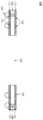
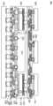
도 1 내지 도 7b는 일부 실시예에 따라 링 형상 기판(ring-shaped substrate)을 형성하는 공정의 중간 단계의 단면도이다.
도 8 내지 도 17은 일부 실시예에 따라 패키지 부품(package component)을 형성하기 위해 링 형상 기판을 다른 디바이스와 함께 패키징하기 위한 공정의 중간 단계의 단면도이다.
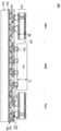
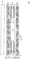
도 18은 일부 실시예에 따른 패키지 구조의 단면도이다.
도 19는 일부 다른 실시예에 따른 패키지 구조의 단면도이다.
도 20은 일부 다른 실시예에 따른 패키지 구조의 단면도이다.Aspects of the present disclosure are best understood from the following detailed description when read in conjunction with the accompanying drawings. It should be noted that, according to industry standard practice, various features are not drawn at a scale. Indeed, the size of the various features can be arbitrarily increased or reduced for clarity of explanation.
1-7B are cross-sectional views of an intermediate step of a process for forming a ring-shaped substrate in accordance with some embodiments.
8-17 are cross-sectional views of an intermediate step of a process for packaging a ring-shaped substrate with other devices to form a package component in accordance with some embodiments.
18 is a cross-sectional view of a package structure in accordance with some embodiments.
19 is a cross-sectional view of a package structure according to some other embodiments.
20 is a cross-sectional view of a package structure according to some other embodiments.
다음의 개시는 발명의 상이한 특징을 구현하기 위한 많은 상이한 실시예 또는 예를 제공한다. 본 개시를 단순화하기 위해 구성요소 및 배열의 특정 예가 아래에 설명된다. 이들은 물론 단지 예시일 뿐이며 제한하려는 의도는 아니다. 예를 들어, 후속하는 설명에서 제2 피처 위의 또는 상의 제1 피처의 형성은 제1 피처와 제2 피처가 직접 접촉하여 형성되는 실시예를 포함할 수 있으며, 추가적인 피처가 제1 피처와 제2 피처 사이에 형성되어 제1 피처와 제2 피처가 직접 접촉하지 않을 수 있도록 하는 실시예도 포함할 수 있다. 또한, 본 개시는 다양한 예에서 참조 번호 및/또는 문자를 반복할 수 있다. 이러한 반복은 간단하고 명확하게 하기 위한 목적이지, 논의된 다양한 실시예 및/또는 구성 간의 관계에 그 자체로 영향을 주는 것은 아니다.The following disclosure provides many different embodiments or examples for implementing different features of the invention. Specific examples of components and arrangements are described below to simplify the present disclosure. These, of course, are merely examples and are not intended to be limiting. For example, in the following description, the formation of the first feature above or on the second feature may include an embodiment in which the first feature and the second feature are formed in direct contact, and the additional feature is formed by the first feature and the second feature. It may also include embodiments that are formed between two features so that the first feature and the second feature are not in direct contact. In addition, the present disclosure may repeat reference numbers and / or letters in various examples. This repetition is for the purpose of simplicity and clarity, and does not itself affect the relationship between the various embodiments and / or configurations discussed.
또한, 도면들에 도시된 한 엘리먼트 또는 피처에 대한 다른 엘리먼트(들) 또는 피처(들)의 관계를 설명하기 위해 "아래", "밑", "보다 낮은", "위", "보다 위" 등과 같은 공간적으로 상대적인 용어들이 설명의 용이성을 위해 여기서 사용될 수 있다. 공간적으로 상대적인 용어들은, 도면들에 도시된 배향 뿐 아니라 사용중 또는 동작중의 디바이스의 상이한 배향들을 망라하도록 의도된 것이다. 장치는 달리 배향될 수 있고(90° 회전되거나 또는 다른 배향을 가짐), 이에 따라 여기서 사용되는 공간적으로 상대적인 기술어들이 이와 마찬가지로 해석될 수 있다.Also, "below", "below", "below", "above", "above" to describe the relationship of one element or feature (s) to another element (s) or feature (s) shown in the figures. Spatially relative terms such as can be used herein for ease of explanation. The spatially relative terms are intended to encompass different orientations of the device in use or in operation, as well as the orientation shown in the figures. The device can be oriented differently (rotated 90 ° or has a different orientation), and thus the spatially relative descriptors used herein can likewise be interpreted.
일부 실시예에 따르면, 링 형상(ring-shaped) 기판이 형성되거나 제공된다. 링 형상 기판은 도전성 라인 및 비아를 갖는 기판 코어를 포함한다. 링 형상 기판 내의 캐비티(cavity)는 집적 회로 다이(die)와 같은 반도체 디바이스를 수용할 수 있다. 그 다음 링 형상 기판은, 캐비티 내에 배치된 집적 회로 다이를 포함하는 패키지로 패키징될 수 있다. 패키지는 예를 들어 몰딩 화합물(molding compound)로 캡슐화된다(encapsulated). 링 형상 기판은 강성이기(rigid) 때문에 패키지를 형성할 때 기계적 지지를 제공한다. 봉지재(encapsulant)와 패키지의 다른 구성 요소 사이의 열 팽창 계수(coefficient of thermal expansion: CTE) 부정합(mismatch)을 피함으로써, 뒤틀림(warpage)이 감소될 수 있으며 패키지의 전체 스택킹 높이가 감소될 수 있다.According to some embodiments, a ring-shaped substrate is formed or provided. The ring-shaped substrate includes a substrate core having conductive lines and vias. Cavity in the ring-shaped substrate can accommodate a semiconductor device, such as an integrated circuit die. The ring-shaped substrate can then be packaged in a package that includes an integrated circuit die disposed within the cavity. The package is encapsulated, for example, with a molding compound. The ring-shaped substrate provides mechanical support when forming the package because of its rigidity. By avoiding the coefficient of thermal expansion (CTE) mismatch between the encapsulant and other components of the package, warpage can be reduced and the overall stacking height of the package reduced. You can.
도 1 내지 도 7b는 일부 실시예에 따라 링 형상 기판(100)을 형성하는 공정의 중간 단계의 단면도이다. 하나의 링 형상 기판(100)의 형성이 도시되어 있지만, 다수의 링 형상 기판(100)이 동일 웨이퍼 또는 기판을 사용하여 동시에 형성될 수 있고, 개별적인 링 형상 기판(100)을 형성하도록 개별화(singulate)될 수 있음을 알아야 한다.1-7B are cross-sectional views of intermediate steps of a process for forming a ring-
도 1에서, 대향 측들 상에 시드층(104)을 갖는 기판 코어(102)가 제공된다. 기판 코어(102)는 미리 함침된 복합 섬유("프리프레그(prepreg)"), 절연 필름 또는 빌드업(build-up) 필름, 종이, 유리 섬유, 부직(non-woven) 유리 직물, 실리콘 등으로 형성될 수 있다. 기판 코어(102)는 실리콘과의 CTE 정합의 달성을 돕는 물질로 형성된다. 일부 실시예에서, 기판 코어(102)는 유리 섬유 및 수지를 포함하는 프리프레그로 형성된다. 시드층(104)은 구리, 티타늄, 니켈, 알루미늄, 이들의 혼합물(composition) 등의 하나 이상의 층일 수 있고, 기판 코어(102)의 대향 측들 상에 퇴적(deposit)되거나 적층(laminate)된다. 일부 실시예에서, 기판 코어(102) 및 시드층(104)은 구리-클래드 에폭시-함침된 유리-직물 라미네이트, 구리-클래드 폴리이미드-함침된 유리-직물 라미네이트 등이다.In FIG. 1, a
도 2에서, 개구(106)가 기판 코어(102) 및 시드층(104)에 형성된다. 일부 실시예에서, 개구(106)는 레이저 드릴링에 의해 형성된다. 드릴 비트를 이용한 기계적 드릴링과 같은 다른 공정도 개구(106)를 형성하는데 사용될 수 있다. 개구(106)는 다각형 또는 원형 등과 같은 임의의 상면 형상을 가질 수 있다. 그 후, 기판 코어(102)의 제거된 물질이 스며들었을 수 있는 개구(106) 근처의 영역을 세정하기 위해 세정 공정이 수행될 수 있다. 세정 공정은 디스미어(desmear) 공정 일 수 있다. 디스미어링은 기계적으로(예를 들어, 습식 슬러리에서 미세 연마재로 분사), 화학적으로(예를 들어, 유기 용매 또는 과망간산염 등의 조합으로 린스), 또는 기계적 공정과 화학적 공정의 조합에 의해 수행될 수 있다.In FIG. 2,
도 3에서, 도전성 비아(108)는 개구(106) 내에 형성되고, 도전성 라인(110)은 기판 코어(102)의 대향 측들 상에 형성된다. 도전성 비아(108) 및 도전성 라인(110)은 구리, 티타늄, 텅스텐, 또는 알루미늄 등과 같은 도전성 물질로 형성될 수 있다. 도전성 비아(108) 및 도전성 라인(110)은 동일한 물질 또는 상이한 물질로 형성될 수 있고, 동일한 공정 또는 상이한 공정에 의해 형성될 수 있다. 일부 실시예에서, 도전성 비아(108)는 제1 공정으로 형성되고 도전성 라인(110)은 제2 공정으로 형성된다. 예를 들어, 무전해 도금과 같은 제1 도금 공정이 개구(106) 내에 도전성 물질을 퇴적(deposit)하여 도전성 비아(108)를 형성하는데 사용될 수 있다. 무전해 도금이 사용되는 실시예에서, 시드층이 개구(106)에 형성될 수 있다. 시드층(104)을 사용하여 전기 도금, 무전해 도금 등과 같은 제2 도금 공정이 수행될 수 있다. 시드층(104) 상에 포토레지스트가 형성되고 패터닝된다. 포토레지스트는 스핀 코팅 등에 의해 형성될 수 있으며, 패터닝을 위해 광에 노광될 수 있다. 포토레지스트의 패턴은 도전성 라인(110)에 대응한다. 패터닝은 시드층을 노출시키기 위해 포토레지스트를 통해 개구를 형성한다. 도전성 물질이 포토레지스트의 개구 및 시드층의 노출된 부분 상에 형성된다. 도전성 물질은 전기 도금 또는 무전해 도금 등과 같은 도금에 의해 형성될 수 있다. 포토레지스트 및 시드층(104) 중 그 위에 도전성 물질이 형성되지 않은 부분은 제거된다. 포토레지스트는 산소 플라즈마 등을 사용하는 것과 같은 수용 가능한 애싱(ashing) 또는 스트립핑(stripping) 공정을 사용하여 제거될 수 있다. 포토레지스트가 제거되면, 예를 들어 습식 또는 건식 에칭과 같은 수용 가능한 에칭 공정을 사용함으로써 시드층(104)의 노출된 부분이 제거된다. 시드층(104)의 남은 부분 및 도전성 물질은 도전성 라인(110)을 형성한다.In FIG. 3,
도 4에서, 솔더 레지스트층(solder resist layer)(112)은 기판 코어(102)의 대향 측면들 위에서 도전성 라인(110) 상에 형성된다. 솔더 레지스트층(112)은 외부 손상으로부터 기판 코어(102)의 영역을 보호한다. 일부 실시예에서, 솔더 레지스트층(112)은 감광성 유전체층을 퇴적하고, 광 패턴으로 감광성 물질을 노광하고, 노광된 층을 현상하여 개구(114)를 형성함으로써 형성된다. 일부 실시예에서, 솔더 레지스트층(112)은 비 감광성 유전체층(예를 들어, 실리콘 산화물 또는 실리콘 질화물 등)을 퇴적하고, 수용 가능한 포토리소그래피 및 에칭 기술로 유전체층을 패터닝하여 개구(114)를 형성한다. 개구(114)는 후속 공정에서 커넥터 패드로서 사용될 수 있는, 도전성 라인(110) 중 아래에 놓이는(underlying) 부분을 노출시킨다.In FIG. 4, a solder resist
도 5에서, 선택적으로, 보호층(116)은 개구(114) 내에, 도전성 라인(110)의 노출된 부분 상에 형성된다. 보호층(116) 각각은 단일층 또는 복수의 층을 포함하는 복합층일 수 있다. 보호층(116)은 니켈, 주석, 주석-납, 금, 은, 팔라듐, 인듐, 니켈-팔라듐-금, 니켈-금 등 또는 이들의 조합과 같은 금속으로 형성될 수 있다. 일부 실시예에서, 보호층(116)은 도전성 라인(110)의 노출된 부분 상의 금층 및 금층상의 니켈층을 포함하는 무전해 니켈 침지 금(Electroless Nickel Immersion Gold: ENIG)일 수 있다. 일부 실시예에서, 보호층(116)은 도전성 라인(110)의 노출된 부분 상의 금층, 금층 상의 팔라듐층 및 팔라듐층 상의 니켈층을 포함하는 무전해 니켈 무전해 팔라듐 침지 금(Electroless Nickel Electroless Palladium Immersion Gold: ENEPIG)일 수 있다. 보호층(116)은 전기 도금, 무전해 도금, 침지, 물리적 기상 증착(PVD) 또는 이들의 조합에 의해 형성될 수 있다. 보호층(116)의 경도(hardness)는 아래에 놓이는 도전성 라인(110)의 경도보다 클 수 있다.In FIG. 5, optionally, a
도 6에서, 도전성 커넥터(118)는 개구(114) 내에 형성된다. 보호층(116)이 사용되는 실시예에서, 도전성 커넥터(118)는 보호층(116)과 접촉한다. 보호층(116)이 생략된 실시예에서, 도전성 커넥터(118)는 도전성 라인(110)의 노출된 부분과 접촉한다. 도전성 커넥터(118)는 볼 그리드 어레이(BGA) 커넥터, 솔더 볼, 금속 필러(pillar), 제어 붕괴 칩 연결(controlled collapse chip connection: C4) 범프, 마이크로 범프, 무전해 니켈-무전해 팔라듐-침지 금 기술(ENEPIG)로 형성된 범프 등일 수 있다. 도전성 커넥터(118)는 솔더, 구리, 알루미늄, 금, 니켈, 은, 팔라듐, 주석 등 또는 이들의 조합과 같은 도전성 물질을 포함할 수 있다. 일부 실시예에서, 도전성 커넥터(118)는, 증발법(evaporation), 전기 도금, 프린팅, 솔더 이송, 볼 배치 등과 같은 일반적으로 사용되는 방법을 통해 처음에 솔더 층을 형성함으로써 형성되는 솔더 커넥터이다. 솔더 층이 구조물 상에 형성되면, 물질을 원하는 범프 형상으로 성형하기 위해 리플로우가 수행될 수 있다. 다른 실시예에서, 도전성 커넥터(118)는 스퍼터링, 프린팅, 전기 도금, 무전해 도금, 화학 기상 증착(CVD) 등에 의해 형성된 (구리 필러와 같은) 금속 필러(pillar)를 포함한다. 금속 필러는 솔더가 없고 실질적으로 수직인 측벽을 가질 수 있다.In FIG. 6, a
도 7a에서, 캐비티(120)는 기판 코어(102) 및 솔더 레지스트층(112)의 일부를 제거함으로써 형성된다. 캐비티(120)를 형성하기 위한 물질의 제거는 컴퓨터 수치 제어(CNC)를 이용한 기계적 드릴링 공정에 의해 달성될 수 있다. 이러한 실시예에서, 물질은 기계적 드릴에 의해 제거되고, 드릴의 위치는 컴퓨터 또는 제어기에 의해 제어된다. 제거는 또한 레이저 커팅 공정, 레이저 드릴링 공정 등과 같은 다른 공정에 의해 수행될 수 있다. 물질의 남은 부분은 링 형상 기판(100)을 형성한다.In FIG. 7A, the
도 7b는 도 7a의 링 형상 기판(100)의 평면도(top-down view)이다. 보이는 바와 같이, 링 형상 기판(100)은 평면도로 보았을 때 링 형상을 갖는다. 캐비티(120)는 링 형상 기판(100)의 중심부를 관통하여 연장되어 링을 형성한다. 도 7b의 예시적인 링 형상 기판(100)은 직사각형이다. 다른 실시예는 다른 형상을 가질 수 있다는 것을 이해해야 한다. 예를 들어, 다른 링 형상 기판(100)은 원형, 삼각형 등일 수 있다.7B is a top-down view of the ring-shaped
도 8 내지 도 17은 일부 실시예에 따라 패키지 부품(package component)(200)을 형성하기 위해 링 형상 기판을 다른 디바이스와 함께 패키징하기 위한 공정의 중간 단계의 단면도이다. 패키지 부품(200)은 다수의 영역을 포함하고, 각 영역에 하나의 링 형상 기판(100)이 패키징된다. 패키지 부품(200)의 하나의 영역이 도시되어있다.8-17 are cross-sectional views of intermediate steps of a process for packaging a ring-shaped substrate with other devices to form a
도 8에서, 캐리어 기판(202)이 제공되고, 릴리스층(release layer)(204)이 캐리어 기판(202) 상에 형성된다. 캐리어 기판(202)은 유리 캐리어 기판 또는 세라믹 캐리어 기판 등일 수 있다. 캐리어 기판(202)은 다수의 패키지가 캐리어 기판(202) 상에 형성될 수 있도록 웨이퍼일 수 있다. 릴리스층(204)은, 후속 단계에서 형성될 위에 놓이는(overlying) 구조로부터 캐리어 기판(202)과 함께 제거될 수 있는 폴리머 기반 물질로 형성될 수 있다. 일부 실시예에서, 릴리스층(204)은, 광-열-변환(LTHC: light-to-heat-conversion) 릴리스 코팅과 같은, 가열될 때 그 접착 특성을 상실하는 에폭시-기반 열-릴리스 물질이다. 다른 실시예에서, 릴리스층(204)은 자외선(UV) 광에 노출될 때 그 접착 특성을 상실하는 자외선(UV) 접착제(glue)일 수 있다. 릴리스층(204)은 액체로서 분배(dispense)되어 경화될 수 있거나, 캐리어 기판(202) 상에 적층된 라미네이트 필름일 수 있거나, 유사한 것일 수 있다. 릴리스층(204)의 상부 표면은 고르게될 수 있고 고도의 동일 평면성(coplanarity)을 가질 수 있다.In FIG. 8, a
도 9에서, 제1 재배선 구조(redistribution structure)(206)는 릴리스층(204) 상에 형성된다. 제1 재배선 구조(206)는 유전체층(208, 212, 216 및 220); 금속화 패턴(210, 214 및 218); 및 UBM(under bump metallurgies)(222)을 포함한다. 금속화 패턴(210, 214 및 218)은 재배선층 또는 재배선 라인으로도 지칭될 수 있다. 제1 재배선 구조(206)는 일례로서 도시된 것이다. 더 많은 또는 더 적은 수의 유전체층 및 금속화 패턴이 제1 재배선 구조(206)에 형성될 수 있다. 더 적은 수의 유전체층 및 금속화 패턴이 형성되는 경우, 이하에서 논의되는 단계 및 공정이 생략될 수 있다. 더 많은 수의 유전체층 및 금속화 패턴이 형성되는 경우, 이하에서 논의되는 단계 및 공정이 반복될 수 있다.In FIG. 9, a
제1 재배선 구조(206)를 형성하기 위한 일례로서, 유전체층(208)이 릴리스층(204) 상에 퇴적된다. 일부 실시예에서, 유전체층(208)은, 리소그래피 마스크를 사용하여 패터닝될 수 있는, 예를 들어 폴리벤즈옥사졸(PBO: polybenzoxazole), 폴리이미드(polyimide), 벤조시클로부텐(BCB: benzocyclobutene) 등과 같은, 감광성 물질로 형성된다. 유전체층(208)은 스핀 코팅, 적층(lamination), CVD 등, 또는 이들의 조합에 의해 형성될 수 있다. 그 다음, 유전체층(208)이 패터닝된다. 패터닝은 릴리스층(204)의 일부를 노출시키는 개구를 형성한다. 패터닝은 수용 가능한 공정에 의해, 예를 들어 유전체층(208)이 광감성 물질일 때 유전체층(208)을 광에 노광시킴으로써, 또는 예를 들어 이방성 에칭을 사용하여 에칭함으로써 수행될 수 있다. 유전체층(208)이 감광성 물질인 경우, 유전체층(208)은 노광 후에 현상될 수 있다.As an example for forming the
그 다음, 금속화 패턴(210)이 형성된다. 금속화 패턴(210)은 유전체층(208)의 주 표면 상에서 주 표면을 따라 연장되는 도전성 라인을 포함한다. 금속화 패턴(210)은 또한 유전체층(208)을 통해 연장되는 도전성 비아를 포함한다. 금속화 패턴(210)을 형성하기 위해, 시드층이 유전체층(208) 위에 그리고 유전체층(208)을 통해 연장되는 개구에 형성된다. 일부 실시예에서, 시드층은 금속층이며, 이 금속층은 단일층일 수 있거나, 상이한 물질로 형성된 복수의 서브층을 포함하는 복합층일 수 있다. 일부 실시예에서, 시드층은 티타늄층 및 그 위의 구리층을 포함한다. 시드층은 예를 들어 PVD 등을 사용하여 형성될 수 있다. 이어서, 포토레지스트가 시드층 상에 형성되고 패터닝된다. 포토레지스트는 스핀 코팅 등에 의해 형성될 수 있고, 패터닝을 위해 광에 노광될 수 있다. 포토레지스트의 패턴은 금속화 패턴(210)에 대응한다. 패터닝은, 시드층을 노출시키도록 포토레지스트를 통해 개구를 형성한다. 이어서, 포토레지스트의 개구에서 그리고 시드층의 노출된 부분 상에 도전성 물질이 형성된다. 도전성 물질은 전기 도금 또는 무전해 도금 등과 같은 도금에 의해 형성될 수 있다. 도전성 물질은 구리, 티타늄, 텅스텐, 또는 알루미늄 등과 같은 금속을 포함할 수 있다. 도전성 물질과 시드층 중 아래에 놓이는(underlying) 부분의 조합은 금속화 패턴(210)을 형성한다. 포토레지스트 및 시드층 중 그 위에 도전성 물질이 형성되지 않은 부분은 제거된다. 포토레지스트는, 예컨대 산소 플라즈마 등을 사용하는 수용 가능한 애싱 또는 스트립핑 공정에 의해 제거될 수 있다. 일단 포토레지스트가 제거되면, 예를 들어 습식 또는 건식 에칭과 같은 수용 가능한 에칭 공정을 사용하는 것에 의해, 시드층의 노출된 부분이 제거된다.Then, a
유전체층(212)은 금속화 패턴(210) 및 유전체층(208) 상에 퇴적된다. 유전체층(212)은 유전체층(208)과 유사한 방식으로 형성될 수 있고, 유전체층(208)과 동일한 물질로 형성될 수 있다.
그 다음, 금속화 패턴(214)이 형성된다. 금속화 패턴(214)은 유전체층(212)의 주 표면 상에서 주 표면을 따라 연장되는 도전성 라인을 포함한다. 금속화 패턴(214)은 금속화 패턴(210)에 물리적 및 전기적으로 연결되도록 유전체층(212)을 통해 연장되는 도전성 비아를 더 포함한다. 금속화 패턴(214)은 금속화 패턴(210)과 유사한 방식으로 형성될 수 있고, 금속화 패턴(210)과 동일한 물질로 형성될 수 있다. 금속화 패턴(214)의 도전성 비아는 금속화 패턴(210)의 도전성 비아보다 작은 폭을 갖는다. 이에 따라, 금속화 패턴(214)을 위해 유전체층(212)을 패터닝할 때, 유전체층(212)의 개구의 폭은 유전체층(208)의 개구의 폭보다 작다.Then, a
유전체층(216)은 금속화 패턴(214) 및 유전체층(212) 상에 퇴적된다. 유전체층(216)은 유전체층(208)과 유사한 방식으로 형성될 수 있고, 유전체층(208)과 동일한 물질로 형성될 수 있다.
그 다음에 금속화 패턴(218)이 형성된다. 금속화 패턴(218)은 유전체층(216)의 주 표면 상에서 주 표면을 따라 연장되는 도전성 라인을 포함한다. 금속화 패턴(218)은 또한 금속화 패턴(214)에 물리적 및 전기적으로 연결되도록 유전체층(216)을 통해 연장되는 도전성 비아를 포함한다. 금속화 패턴(218)은 금속화 패턴(210)과 유사한 방식으로 형성될 수 있고, 금속화 패턴(210)과 동일한 물질로 형성될 수 있다. 금속화 패턴(218)의 도전성 비아는 금속화 패턴(210)의 도전성 비아 보다 작은 폭을 갖는다. 따라서 금속화 패턴(218)을 위해 유전체층(216)을 패터닝할 때, 유전체층(216)의 개구의 폭은 유전체층(208)의 개구의 폭보다 작다.A
유전체층(220)은 금속화 패턴(218) 및 유전체층(216) 상에 퇴적된다. 유전체층(220)은 유전체층(208)과 유사한 방식으로 형성될 수 있고, 유전체층(208)과 동일한 물질로 형성될 수 있다.
UBM(222)은 유전체층(220) 상에 그리고 유전체층(220)을 통해 연장되게 형성된다. UBM(222)을 형성하기 위한 예로서, 유전체층(220)은 패터닝되어 금속화 패턴(218)의 일부를 노출시키는 개구를 형성할 수 있다. 패터닝은 수용 가능한 공정에 의해, 예를 들어 유전체층(220)이 광감성 물질일 때 유전체층(220)을 광에 노광시킴으로써, 또는 예를 들어 이방성 에칭을 사용하여 에칭함으로써 수행될 수 있다. 유전체층(220)이 감광성 물질인 경우, 유전체층(220)은 노광 후에 현상될 수 있다. UBM들(222)을 위한 개구는, 금속화 패턴(210, 214 및 218)의 도전성 비아 부분을 위한 개구보다 더 넓을 수 있다. 시드층이 유전체층(220) 위에 그리고 개구에 형성된다. 일부 실시예에서, 시드층은 금속층이며, 이 금속층은 단일층일 수 있거나, 상이한 물질로 형성된 복수의 서브층을 포함하는 복합층일 수 있다. 일부 실시예에서, 시드층은 티타늄층 및 그 위의 구리층을 포함한다. 시드층은 예를 들어 PVD 등을 사용하여 형성될 수 있다. 이어서, 포토레지스트가 시드층 상에 형성되고 패터닝된다. 포토레지스트는 스핀 코팅 등에 의해 형성될 수 있고, 패터닝을 위해 광에 노광될 수 있다. 포토레지스트의 패턴은 UBM(222)에 대응한다. 패터닝은 시드층을 노출시키기 위해 포토레지스트를 통한 개구를 형성한다. 포토레지스트의 개구에서 그리고 시드층의 노출된 부분 상에 도전성 물질이 형성된다. 도전성 물질은 전기 도금 또는 무전해 도금 등과 같은 도금에 의해 형성될 수 있다. 도전성 물질은 구리, 티타늄, 텅스텐, 또는 알루미늄 등과 같은 금속을 포함할 수 있다. 이어서, 포토레지스트 및 시드층 중 그 위에 도전성 물질이 형성되지 않은 부분이 제거된다. 포토레지스트는, 예컨대 산소 플라즈마 등을 사용하는, 수용 가능한 애싱 또는 스트립핑 공정에 의해 제거될 수 있다. 일단 포토레지스트가 제거되면, 예를 들어 습식 또는 건식 에칭과 같은 수용 가능한 에칭 공정을 사용함으로써, 시드층의 노출된 부분이 제거된다. 시드층의 남은 부분 및 도전성 물질은 UBM(222)을 형성한다. UBM(222)이 다르게 형성되는 실시예에서, 더 많은 수의 포토레지스트 및 패터닝 단계가 이용될 수도 있다.The
UBM(222)이 모두 동일한 폭을 가지지 않을 수 있다. 일부 실시예에서, 제1 재배선 구조(206)의 제1 영역(206A)에서 UBM(222)의 제1 서브셋은 제1 폭(W1)을 가지며, 제1 재배선 구조(206)의 제2 영역(206B)에서 UBM(222)의 제2 서브셋은 제2 폭(W2)을 가진다. 제1 폭(W1)은 제2 폭(W2)과 다를 수 있으며, 일부 실시예에서는 제1 폭(W1)이 제2 폭(W2)보다 크다.The
도 10에서, 링 형상 기판(100)은 제1 재배선 구조(206) 위에 배치된다. 링 형상 기판(100)은 예를 들어 픽 앤드 플레이스(pick-and-place) 툴을 사용하여 정렬 및 배치될 수 있다. 링 형상 기판(100)의 도전성 커넥터(118)는 제1 영역(206A)에서 UBM(222)과 정렬되고, 링 형상 기판(100)의 캐비티(120)는 제2 영역(206B)에서 UBM(222) 위에 정렬된다. 도전성 커넥터(118)가 솔더인 실시예에서, 도전성 커넥터(118)는 링 형상 기판(100)을 UBM(222)에 본딩하기 위한 리플로우가 즉시 행해지지 않을 수 있다. 도전성 커넥터(118)의 리플로우는 후속 프로세싱 단계까지 연기될 수 있다. 도전성 커넥터(118)가 구리 필러(pillar)인 실시예에서, 솔더가 형성되어 도전성 커넥터(118)를 제1 재배선 구조(206)에 본딩할 수 있다.In FIG. 10, the ring-shaped
도 11에서, 집적 회로 다이(224)는 제1 재배선 구조(206) 위에 배치된다. 집적 회로 다이(224)는 로직 다이(예: 중앙 처리 유닛, 마이크로 컨트롤러 등), 메모리 다이(예: 동적 랜덤 액세스 메모리(DRAM) 다이, 정적 랜덤 액세스 메모리(SRAM) 다이 등), 전력 관리 다이(예: 전력 관리 집적 회로(PMIC) 다이), 무선 주파수(RF) 다이, 센서 다이, 마이크로 전자 기계 시스템(micro-electro-mechanical-system: MEMS) 다이, 신호 처리 다이(예: 디지털 신호 처리(DSP) 다이), 프론트 엔드 다이(예: 아날로그 프론트 엔드(analog front-end: AFE) 다이) 등 또는 이들의 조합(예: 시스템 온 칩(system-on-chip: SoC))일 수 있다.In FIG. 11, integrated circuit die 224 is disposed over
집적 회로 다이(224)는, 반도체 기판 내에 및/또는 반도체 기판 상에 형성되는 트랜지스터, 다이오드, 커패시터, 저항기 등과 같은 디바이스를 갖는 반도체 기판을 포함한다. 디바이스는 집적 회로를 형성하기 위해 예를 들어 반도체 기판 상의 하나 이상의 유전체층에서의 금속화 패턴에 의해 형성된 상호 연결(interconnect) 구조에 의해 상호 연결될 수 있다. 집적 회로 다이(224)는 외부 접속이 이루어지는, 알루미늄 패드와 같은, 패드(226)를 더 포함한다. 패드(226)는 집적 회로 다이(224)의 각각의 활성 측(side)으로 지칭될 수 있는 것 상에 있고, 상호 연결 구조의 최상층에 있을 수 있다. 집적 회로 다이(224)의 활성 측이 제1 재배선 구조(206)쪽으로 향하기 때문에, 제1 재배선 구조(206)는 "전방 측(front-side) 재배선 구조"로도 지칭될 수 있다. 도전성 커넥터(228)가 패드(226) 상에 형성될 수 있다. 도전성 커넥터(228)는 솔더, 구리, 알루미늄, 금, 니켈, 은, 팔라듐, 주석 등 또는 이들의 조합과 같은 도전성 물질로 형성될 수 있다. 일부 실시예에서, 도전성 커넥터(228)는 솔더 커넥터이다.The integrated circuit die 224 includes a semiconductor substrate having devices such as transistors, diodes, capacitors, resistors, and the like formed in and / or on the semiconductor substrate. The devices can be interconnected to form an integrated circuit by, for example, an interconnect structure formed by a metallization pattern in one or more dielectric layers on a semiconductor substrate. The integrated circuit die 224 further includes a
집적 회로 다이(224)는 예를 들어 픽 앤드 플레이스(pick-and-place) 툴을 사용하여 정렬 및 배치될 수 있다. 집적 회로 다이(224)는 도전성 커넥터(228)가 제2 영역(206B)의 UBM(222)과 정렬되도록 캐비티(120) 내에 배치된다. 집적 회로 다이(224)가 배치된 후, 도전성 커넥터(228)는 리플로우되어 대응하는 UBM(222)과 패드(226) 사이의 접합부(joint)를 형성하여, 집적 회로 다이(224)를 제1 재배선 구조(206)에 물리적 및 전기적으로 연결한다. 링 형상 기판(100)의 도전성 커넥터(118)가 솔더이고 리플로우가 연기되는 실시예에서, 도전성 커넥터(118 및 228)는 동일 리플로우 공정에서 동시에 리플로우 될 수 있다. 이에 따라, 도전성 커넥터(118)도 리플로우되어 대응하는 UBM(222)과 도전성 라인(110) 사이의 접합부를 형성하여, 링 형상 기판(100)을 제1 재배선 구조(206)에 물리적 및 전기적으로 연결시킬 수 있다. 다시 말하면, 집적 회로 다이(224)와 링 형상 기판(100)은 제1 재배선 구조(206)에 동시에 본딩될 수 있다. 도전성 커넥터(118 및 228)는 상이한 크기일 수 있다. 일부 실시예에서, 링 형상 기판(100)의 높이(H1)는 집적 회로 다이(224)의 높이(H2)보다 작거나 같다. 또한, 높이(H1)는 또한 높이(H2)보다 클 수도 있다. 또한, 집적 회로 다이(224)의 폭은 캐비티(120)의 폭보다 작다.The integrated circuit die 224 can be aligned and placed using, for example, a pick-and-place tool. The integrated circuit die 224 is disposed within the
집적 회로 다이(224) 및 링 형상 기판(100)은 임의의 순서로 제1 재배선 구조(206) 위에 배치될 수 있음을 알아야 한다. 일부 실시예에서, 집적 회로 다이(224)가 먼저 배치되고, 링 형상 기판(100)이 집적 회로 다이(224) 주위에 배치된다.It should be noted that the integrated circuit die 224 and the ring-shaped
도 12에서, 언더필(underfill)(230)은 집적 회로 다이(224)와 제1 재배선 구조(206) 사이에서 도전성 커넥터(228)를 둘러싸면서 형성될 수 있다. 이에 따라, 도전성 커넥터(228)는 기계적 힘으로부터 보호될 수 있다. 언더필(230)은 집적 회로 다이(224)가 부착된 후에 모세관 유동 공정(capillary flow process)에 의해 형성될 수 있거나, 집적 회로 다이(224)가 부착되기 전에 적절한 퇴적 방법에 의해 형성될 수 있다.In FIG. 12, an
도 13에서, 봉지재(encapsulant)(232)는 다양한 부품(component) 상에 형성된다. 봉지재(232)는 몰딩 화합물(molding compound) 또는 에폭시 등일 수 있으며 압축 몰딩 또는 트랜스퍼 몰딩 등에 의해 적용될 수 있다. 봉지재(232)는, 집적 회로 다이(224) 및 링 형상 기판(100)이 매립되거나 커버되고 캐비티(120)가 충진되도록, 제1 재배선 구조(206) 위에 형성될 수 있다. 봉지재(232) 중 링 형상 기판(100)을 매립하는 부분은 두께(T1)을 갖는다. 일부 실시예에서, 두께(T1)는 약 10 ㎛ 내지 약 100 ㎛ 범위이다. 이어서, 봉지재(232)는 경화되고, 선택적으로는 예를 들어 그라인딩(grinding) 또는 화학 기계적 연마(CMP) 공정에 의해 평탄화될 수도 있다. 형성 후에, 봉지재(232)는 높이(H1 및 H2)보다 큰 높이(H3)를 가진다. 예를 들어 언더필(230)이 생략된 실시예에서, 봉지재(232)는 제1 재배선 구조(206)와 집적 회로 다이(224) 사이에도 형성된다.In FIG. 13,
링 형상 기판(100)은 패키지 부품(200)의 수직 높이의 상당 부분을 점유하고, 따라서 집적 회로 다이(224)를 커버하기 위해 필요한 봉지재(232)의 양이 감소될 수 있다. 예를 들어, 높이(H3) 대 높이(H1)의 비는 약 1:0.14 내지 약 1:0.60 일 수 있다. 따라서, 패키지 부품(200)의 전체 높이는 사용되는 봉지재(232)의 양을 현저히 증가시키지 않고 증가될 수 있다. 사용되는 봉지재(232)의 양을 감소시키는 것은 봉지재(232)와 패키지 부품(200)의 다른 부품 사이의 CTE 부정합으로 인한 패키지의 뒤틀림(package warpage)을 피하는 것을 도울 수 있다.The ring-shaped
도 14에서, 봉지재(232)에 개구(234)가 형성되어 링 형상 기판(100)의 보호층(116)을 노출시킨다. 개구(234)는 레이저 드릴링 또는 기계적 드릴링 등과 같은 드릴링 공정에 의해 형성될 수 있다. 개구(234)는, 상부폭(W3)과 상부폭(W3)보다 작거나 같은 하부폭(W4)을 갖는, 테이퍼된(tapered) 프로파일을 가질 수 있다. 일부 실시예에서, 상부폭(W3)은 약 50 ㎛ 내지 약 350 ㎛의 범위이고, 하부 폭(W4)은 약 50 ㎛ 내지 약 200 ㎛의 범위이다.In FIG. 14, an
도 15에서, 도전성 커넥터(236)는 개구(234)에 형성된다. 도전성 커넥터(236)는 솔더, 구리, 알루미늄, 금, 니켈, 은, 팔라듐, 주석 등 또는 이들의 조합과 같은 금속으로 형성될 수 있다. 일부 실시예에서, 도전성 커넥터(236)는 구리 페이스트(paste), 솔더 페이스트, 또는 은 페이스트 등과 같은 페이스트로 형성되고, 프린팅 공정 등에 의해 분배(dispense)된다. 프린팅 공정이 사용되는 실시예에서, 도전성 커넥터(236)의 원하는 패턴을 갖는 이미지가, 스텐실을 사용하여 봉지재(232) 상에 그리고 개구(234)에 프린트된다. 형성 후에, 도전성 페이스트는 그것을 굳히기 위해 경화됨으로써, 도전성 커넥터(236)를 형성한다. 도전성 페이스트는 약 80 ℃ 내지 약 230 ℃의 온도에서 약 20분 내지 약 4시간의 시간 동안 수행되는 어닐링 공정에 의해 경화될 수 있다. 도전성 커넥터(236)가 페이스트인 실시예에서, 도전성 커넥터(236)는, 봉지재(232)를 통해 연장되는 비아 부분 및 봉지재(232)의 상부 표면을 따라 연장되는 상부 부분을 갖도록, 개구를 과충진(overfill)시킬 수 있다.In Figure 15, a
도 16에서, 제2 재배선 구조(238)는 도전성 커넥터(236) 및 봉지재(232) 위에 형성된다. 집적 회로 다이(224)의 활성 측이 제2 재배선 구조(238)로부터 먼 쪽으로 향하기 때문에, 제2 재배선 구조(238)는 "후방 측(back-side) 재배선 구조"로도 지칭될 수 있다. 제2 재배선 구조(238)는 유전체층(240, 244, 248 및 252); 금속화 패턴(242, 246 및 250); 및 UBM(254)을 포함한다. 금속화 패턴은 재배선층 또는 재배선 라인으로도 지칭될 수 있다. 제2 재배선 구조(238)는 일례로서 도시된 것이다. 제2 재배선 구조(238)에 더 많은 또는 보다 적은 수의 유전체층 및 금속화 패턴이 형성될 수 있다. 더 적은 수의 유전체층 및 금속화 패턴이 형성되는 경우, 이하에서 논의되는 단계 및 공정이 생략될 수 있다. 더 많은 수의 유전체층 및 금속화 패턴이 형성되는 경우, 이하에서 논의되는 단계 및 공정이 반복될 수 있다.In FIG. 16, a
제2 재배선 구조(238)를 형성하기 위한 일례로서, 유전체층(240)은 도전성 커넥터(236) 및 봉지재(232) 상에 퇴적된다. 일부 실시예에서, 유전체층(240)은 리소그래피 마스크를 사용하여 패터닝될 수 있는, 예를 들어 PBO, 폴리이미드(polyimide), BCB 등과 같은, 감광성 물질로 형성된다. 유전체층(240)은 스핀 코팅, 적층(lamination), CVD 등, 또는 이들의 조합에 의해 형성될 수 있다. 그 다음, 유전체층(240)이 패터닝된다. 패터닝은 도전성 커넥터(236)의 일부를 노출시키는 개구를 형성한다. 패터닝은, 수용 가능한 공정에 의해, 예를 들어 유전체층(240)이 광감성 물질일 때 유전체층(240)을 광에 노광시킴으로써, 또는 예를 들어 이방성 에칭을 사용하여 에칭함으로써 수행될 수 있다. 유전체층(240)이 감광성 물질인 경우, 유전체층(240)은 노광 후에 현상될 수 있다.As an example for forming the
도전성 커넥터(236)가 개구를 과충진시키는 실시예에서, 유전체층(240)은 평탄화 리셋 층으로서 사용될 수 있다. 특히, 유전체층(240)은 평탄화를 허용하기 위해, 재배선 구조의 하부(bottom) 유전체층에 대한 통상적인 두께보다 큰 두께로 형성될 수 있다. 형성 후에, 유전체층(240)은 약 5㎛ 내지 약 15㎛ 범위의 두께(T2)를 가질 수 있다. 일부 실시예에서, 형성 후(post-formation) 평탄화 공정이 수행된다. 평탄화 공정은 상기 유전체층(240)에 그라인딩 공정 또는 CMP 공정을 수행하는 것을 포함할 수 있다. 유전체층(240)을 평탄화 리셋 층으로 사용함으로써 유전체층(240)의 상부 표면은 실질적으로 평면일 수 있으며, 유전체층(240)의 하부 표면(들)보다 더 높은 정도의 평탄성을 가질 수 있다. 평탄화 후에, 유전체층(240)의 두께는 감소될 수 있다. 유전체층(240)(예를 들어, 하부(bottom) 유전체층)의 두께는, 유전체층(252)(예를 들어, 상부(top) 유전체층)과 같은 제2 재배선 구조(238)의 다른 유전체층 보다 두껍다.In embodiments where the
그 다음, 금속화 패턴(242)이 형성된다. 금속화 패턴(242)은 유전체층(240)의 주 표면 상에서 주 표면을 따라 연장되는 도전성 라인을 포함한다. 금속화 패턴(242)은, 도전성 커넥터(236)에 물리적 및 전기적으로 연결되도록 유전체층(240)을 통해 연장되는 도전성 비아를 더 포함한다. 금속화 패턴(242)을 형성하기 위해, 시드층이 유전체층(240) 위에 그리고 유전체층(240)을 통해 연장되는 개구에 형성된다. 일부 실시예에서, 시드층은 금속층이며, 이 금속층은 단일층일 수 있거나, 상이한 물질로 형성된 복수의 서브층을 포함하는 복합층일 수 있다. 일부 실시예에서, 시드층은 티타늄층 및 그 위의 구리층을 포함한다. 시드층은 예를 들어 PVD 등을 사용하여 형성될 수 있다. 이어서, 포토레지스트가 시드층 상에 형성되고 패터닝된다. 포토레지스트는 스핀 코팅 등에 의해 형성될 수 있고, 패터닝을 위해 광에 노광될 수 있다. 포토레지스트의 패턴은 금속화 패턴(242)에 대응한다. 패터닝은, 시드층을 노출시키도록 포토레지스트를 통해 개구를 형성한다. 이어서, 포토레지스트의 개구에서 그리고 시드층의 노출된 부분 상에 도전성 물질이 형성된다. 도전성 물질은 전기 도금 또는 무전해 도금 등과 같은 도금에 의해 형성될 수 있다. 도전성 물질은 구리, 티타늄, 텅스텐, 또는 알루미늄 등과 같은 금속을 포함할 수 있다. 도전성 물질과 시드층 중 아래에 놓이는 부분의 조합은 금속화 패턴(242)을 형성한다. 포토레지스트 및 시드층 중 그 위에 도전성 물질이 형성되지 않은 부분은 제거된다. 포토레지스트는, 예컨대 산소 플라즈마 등을 사용하는 수용 가능한 애싱 또는 스트립핑 공정에 의해 제거될 수 있다. 일단 포토레지스트가 제거되면, 예를 들어 습식 또는 건식 에칭과 같은 수용 가능한 에칭 공정을 사용함으로써 시드층의 노출된 부분이 제거된다.Then, a
유전체층(244)은 금속화 패턴(242) 및 유전체층(240) 상에 퇴적된다. 유전체층(244)은 유전체층(240)과 유사한 방식으로 형성될 수 있고, 유전체층(240)과 동일한 물질로 형성될 수 있다.
그 다음에 금속화 패턴(246)이 형성된다. 금속화 패턴(246)은 유전체층(244)의 주 표면 상에서 주 표면을 따라 연장되는 도전성 라인을 포함한다. 금속화 패턴(246)은, 금속화 패턴(242)에 물리적 및 전기적으로 연결되도록 유전체층(244)을 통해 연장되는 도전성 비아를 더 포함한다. 금속화 패턴(246)은 금속화 패턴(242)과 유사한 방식으로 형성될 수 있고, 금속화 패턴(242)과 동일한 물질로 형성될 수 있다.A
유전체층(248)은 금속화 패턴(246) 및 유전체층(244) 상에 퇴적된다. 유전체층(248)은 유전체층(240)과 유사한 방식으로 형성될 수 있고, 유전체층(240)과 동일한 물질로 형성될 수 있다.
그 다음, 금속화 패턴(250)이 형성된다. 금속화 패턴(250)은 유전체층(248) 상에 유전체층(248)을 따라서 도전성 라인을 포함한다. 금속화 패턴(250)은 금속화 패턴(246)에 물리적 및 전기적으로 연결되도록 유전체층(248)을 통해 연장되는 도전성 비아를 더 포함한다. 금속화 패턴(250)은 금속화 패턴(242)과 유사한 방식으로 형성될 수 있고, 금속화 패턴(242)과 동일한 물질로 형성될 수 있다.Then, a
유전체층(252)은 금속화 패턴(250) 및 유전체층(248) 상에 퇴적된다. 유전체층(252)은 유전체층(240)과 유사한 방식으로 형성될 수 있고, 유전체층(240)과 동일한 물질로 형성될 수 있다.
UBM(254)은 유전체층(252) 상에 그리고 유전체층(252)을 통해 연장되게 형성된다. UBM(254)을 형성하기 위한 일례로서, 유전체층(252)은 패터닝되어 금속화 패턴(250)의 일부를 노출시키는 개구를 형성할 수 있다. 패터닝은 수용 가능한 공정에 의해, 예를 들어 유전체층(252)이 광감성 물질일 때 유전체층(252)을 광에 노광시킴으로써, 또는 예를 들어 이방성 에칭을 사용하여 에칭함으로써 수행될 수 있다. 유전체층(252)이 감광성 물질인 경우, 유전체층(252)은 노광 후에 현상될 수 있다. UBM(254)을 위한 개구는, 금속화 패턴(242, 246, 및 250)의 도전성 비아 부분을 위한 개구보다 넓을 수 있다. 시드층이 유전체층(252) 위에 그리고 개구에 형성된다. 일부 실시예에서, 시드층은 금속층이며, 이 금속층은 단일층일 수 있거나, 상이한 물질로 형성된 복수의 서브층을 포함하는 복합층일 수 있다. 일부 실시예에서, 시드층은 티타늄층 및 그 위의 구리층을 포함한다. 시드층은 예를 들어 PVD 등을 사용하여 형성될 수 있다. 이어서, 포토레지스트가 시드층 상에 형성되고 패터닝된다. 포토레지스트는 스핀 코팅 등에 의해 형성될 수 있고, 패터닝을 위해 광에 노광될 수 있다. 포토레지스트의 패턴은 UBM(254)에 대응한다. 패터닝은 시드층을 노출시키기 위해 포토레지스트를 통한 개구를 형성한다. 포토레지스트의 개구에서 그리고 시드층의 노출된 부분 상에 도전성 물질이 형성된다. 도전성 물질은 전기 도금 또는 무전해 도금 등과 같은 도금에 의해 형성될 수 있다. 도전성 물질은 구리, 티타늄, 텅스텐, 또는 알루미늄 등과 같은 금속을 포함할 수 있다. 이어서, 포토레지스트 및 시드층 중 그 위에 도전성 물질이 형성되지 않은 부분이 제거된다. 포토레지스트는, 예컨대 산소 플라즈마 등을 사용하는, 수용 가능한 애싱 또는 스트립핑 공정에 의해 제거될 수 있다. 일단 포토레지스트가 제거되면, 예를 들어 습식 또는 건식 에칭과 같은 수용 가능한 에칭 공정을 사용하는 것에 의해, 시드층의 노출된 부분이 제거된다. 도전성 물질 및 시드층의 남은 부분은 UBM(254)을 형성한다. UBM(254)이 다르게 형성되는 실시예에서, 더 많은 수의 포토레지스트 및 패터닝 단계가 이용될 수 있다.
형성 후에, 링 형상 기판(100)은 패키지 부품(200)의 다양한 피처를 전기적으로 연결한다. 특히, 링 형상 기판(100), 도전성 커넥터(118), 및 도전성 커넥터(236)는 제1 재배선 구조(206)를 제2 재배선 구조(206)에 전기적 및 물리적으로 연결한다. 따라서, 집적 회로 다이(224)는 제1 재배선 구조(206) 및 링 형상 기판(100)을 통해 제2 재배선 구조(238)에 전기적으로 연결된다.After formation, the ring-shaped
도 17에서, 캐리어 기판 디본딩(de-bonding)은 캐리어 기판(202)을 제1 재배선 구조(206), 예컨대 유전체층(208)으로부터 분리(또는 "디본드(de-bond)")하도록 수행된다. 일부 실시예에서, 디본딩은, 릴리스층(204)이 광의 열로 분해되어 캐리어 기판(202)이 제거되도록 레이저 광 또는 UV 광과 같은 광을 투사하는 것을 포함한다. 그런 다음, 구조를 뒤집어(flip over) 테이프 상에 배치한다. 디본딩은 제1 재배선 구조(206)의 금속화 패턴(210)을 노출시킨다.In FIG. 17, carrier substrate debonding is performed to separate (or “de-bond”) the
도 18은 일부 실시예에 따른 패키지 구조(a package structure)(300)의 단면도이다. 패키지 구조(300)는 제1 패키지(302), 집적 회로 다이(304), 및 패키지 기판(306)을 포함한다. 패키지 구조(300)는 SBS-MCM(side-by-side multi-chip-module)으로 지칭될 수 있다.18 is a cross-sectional view of a
제1 패키지(302)는 패키지 부품(200)에 형성된 패키지 중 하나이다. 예를 들어 패키지 부품(200)의 인접한 패키지 영역들 사이에서, 스크라이브 라인(scribe line) 영역을 따라 절단(sawing)함으로써 패키지 부품(200)에 대해 개별화(singulation) 공정이 수행된다. 결과적인 개별화된 제1 패키지(302)들은 개별화된 패키지 영역 중 하나로부터 나온 것이다.The
집적 회로 다이(304)는 완전한 시스템을 형성하기 위해 집적 회로 다이(224)와 통신하는 다이일 수 있다. 예를 들어, 집적 회로 다이(224)가 로직(logic) 다이인 실시예에서, 집적 회로 다이(304)는 메모리 다이, RF 다이, 수동 디바이스, 또는 이들의 조합일 수 있다. 집적 회로 다이(304)는, 반도체 기판 내에 및/또는 반도체 기판 상에 형성되는 트랜지스터, 다이오드, 커패시터, 저항기 등과 같은 디바이스를 갖는 반도체 기판을 포함한다. 디바이스는 집적 회로를 형성하기 위해 예를 들어 반도체 기판 상의 하나 이상의 유전체층에서의 금속화 패턴에 의해 형성된 상호 연결 구조에 의해 상호 연결될 수 있다. 집적 회로 다이(304)는 외부 접속이 이루어지는, 알루미늄 패드와 같은, 패드(308)를 더 포함한다. 패드(308)는 집적 회로 다이(304)의 각각의 활성 측으로 지칭될 수 있는 것 상에 있으며, 상호 연결 구조의 최상층에 있을 수 있다. 도전성 커넥터(310)는 패드(308) 상에 형성될 수 있다. 도전성 커넥터(310)는 솔더, 구리, 알루미늄, 금, 니켈, 은, 팔라듐, 주석 등 또는 이들의 조합과 같은 도전성 물질로 형성될 수 있다. 집적 회로 다이(304)는 도전성 커넥터(310)를 사용하여 UBM(254)에 실장(mount)된다. 일부 실시예에서, 도전성 커넥터(310)는 리플로우되어 집적 회로 다이(304)를 UBM(254)에 부착시킨다. 일부 실시예에서, 언더필 또는 봉지재가 형성되어 집적 회로 다이(304)와 제2 재배선 구조(238) 사이의 갭을 채운다. 사용되는 봉지재(232)의 양이 감소되기 때문에, 제1 패키지(302)의 두께가 감소될 수 있고, 이는 보다 큰 두께의 집적 회로 다이(304)가 부착되는 것을 가능케 한다. 예를 들어, 집적 회로 다이(304)가 메모리 디바이스인 경우, 메모리 디바이스의 용량이 증가될 수 있다.Integrated circuit die 304 may be a die in communication with integrated circuit die 224 to form a complete system. For example, in embodiments where the integrated circuit die 224 is a logic die, the integrated circuit die 304 may be a memory die, RF die, passive device, or combinations thereof. Integrated circuit die 304 includes a semiconductor substrate having devices such as transistors, diodes, capacitors, resistors, and the like formed in and / or on the semiconductor substrate. The devices can be interconnected to form an integrated circuit by, for example, interconnect structures formed by metallization patterns in one or more dielectric layers on a semiconductor substrate. The integrated circuit die 304 further includes
그 다음, 제1 패키지(302)는 도전성 커넥터(312)를 사용하여 패키지 기판(306)에 실장된다. 패키지 기판(306)은 실리콘, 게르마늄, 또는 다이아몬드 등과 같은 반도체 물질로 제조될 수 있다. 대안적으로, 실리콘 게르마늄(silicon germanium), 실리콘 카바이드(silicon carbide), 갈륨 비소(gallium arsenic), 인듐 아세나이드(indium arsenide), 인듐 인화물(indium phosphide), 실리콘 게르마늄 카바이드(silicon germanium carbide), 갈륨 비소 인화물(gallium arsenic phosphide), 갈륨 인듐 인화물(gallium indium phosphide), 이들의 조합 등과 같은 화합물 물질이 또한 사용될 수 있다. 또한, 패키지 기판(306)은 실리콘-온-인슐레이터(silicon-on-insulator: SOI) 기판일 수 있다. 일반적으로, SOI 기판은 에피택셜 실리콘, 게르마늄, 실리콘 게르마늄, SOI, SGOI(silicon-germanium-on-insulator) 또는 이들의 조합과 같은 반도체 물질의 층을 포함한다. 패키지 기판(306)은, 하나의 대안적인 실시예에서, 유리 섬유 보강된 수지 코어(fiberglass reinforced resin core)와 같은 절연 코어를 기반으로한다. 코어 물질의 일례는 FR4와 같은 유리 섬유 수지이다. 코어 물질의 대안에는 BT(bismaleimide-triazine) 수지 또는, 대안적으로, 다른 PCB 물질 또는 필름이 있다. ABF(Ajinomoto Build-up film) 또는 다른 라미네이트와 같은 빌드업(build-up) 필름이 패키지 기판(306)에 사용될 수 있다.The
패키지 기판(306)은 능동(active) 및 수동(passive) 디바이스(미도시)를 포함할 수 있다. 당업자가 인식할 바와 같이, 패키지 구조(300)에 대한 설계의 구조적 및 기능적 요구 사항을 만들어 내기 위해 트랜지스터, 커패시터, 저항기, 이들의 조합 등과 같은 다양한 디바이스가 사용될 수 있다. 이들 디바이스는 임의의 적합한 방법을 사용하여 형성될 수 있다.The
패키지 기판(306)은 또한 금속화층과 비아(미도시) 및 이들 금속화층과 비아 위의 본드 패드(314)를 포함할 수 있다. 금속화층은 능동 및 수동 디바이스 위에 형성될 수 있고, 다양한 디바이스를 연결하여 기능 회로를 형성하도록 설계된다. 금속화층은, 도전성 물질의 층들을 상호 연결하는 비아를 갖는, 유전체(예: 저 유전(low-k dielectric) 물질)와 도전성 물질(예: 구리)의 교대하는 층들로 형성될 수 있고, 임의의 적합한 공정(예를 들어, 퇴적(deposition), 다마신(damascene), 또는 듀얼 다마신(dual damascene) 등)을 통해 형성될 수 있다. 일부 실시예에서, 패키지 기판(306)에는 실질적으로 능동 및 수동 디바이스가 없다.The
도전성 커넥터(312)는 솔더, 구리, 알루미늄, 금, 니켈, 은, 팔라듐, 주석 등 또는 이들의 조합과 같은 도전성 물질로 형성될 수 있다. 일부 실시예에서, 도전성 커넥터(312)는 리플로우되어 제1 패키지(302)를 본드 패드(314)에 부착시킨다. 도전성 커넥터(312)는, 패키지 기판(306)의 금속화층을 포함하는 패키지 기판(306)을 제1 패키지(302)의 금속화 패턴(210)에 전기적 및/또는 물리적으로 커플링(coupling)시킨다. 일부 실시예에서, 수동 디바이스(예를 들어, 표면 실장 디바이스(SMD), 미도시)는 패키지 기판(306) 상에 실장되기 전에 제1 패키지(302)에 부착될 수 있다(예를 들어, 본드 패드(314)에 본딩됨). 그러한 실시예에서, 수동 디바이스는 도전성 커넥터(312)와 동일한 제1 패키지(302)의 표면에 본딩될 수 있다.The
도전성 커넥터(312)는 리플로우되기 전에 그 위에 형성된 에폭시 플럭스(미도시)를 가질 수 있으며, 이 에폭시 플럭스의 에폭시 부분 중 적어도 일부는 제1 패키지(302)가 패키지 기판(306)에 부착된 후에 잔류한다. 이 잔류하는 에폭시 부분은, 스트레스(stress)를 감소시키고 도전성 커넥터(312)의 리플로우로부터 유래한 접합부를 보호하기 위한 언더필로서 작용할 수 있다. 일부 실시예에서, 언더필(미도시)은 제1 패키지(302)와 패키지 기판(306) 사이에 도전성 커넥터(312)를 둘러싸도록 형성될 수 있다. 언더필은, 제1 패키지(302)가 부착된 후에 모세관 유동 공정에 의해 형성될 수 있거나 또는 제1 패키지(302)가 부착되기 전에 적절한 퇴적 방법에 의해 형성될 수 있다.The
도 19는 일부 다른 실시예에 따른 패키지 구조(300)의 단면도이다. 도시된 실시예에서, 언더필(230)은 또한 도전성 커넥터(118)의 서브셋을 둘러싸도록 형성된다. 이에 따라, 도전성 커넥터(118) 중 일부는 기계적 힘으로부터 보호될 수 있다.19 is a cross-sectional view of a
도 20은 일부 다른 실시예에 따른 패키지 구조(300)의 단면도이다. 도시된 실시예에서, 언더필(230)은 또한 모든 도전성 커넥터(118)를 둘러싸도록 형성된다. 이에 따라, 모든 도전성 커넥터(118)는 기계적 힘으로부터 보호될 수 있다.20 is a cross-sectional view of a
실시예는 장점을 얻을 수 있다. 링 형상 기판(100)은 강성이다(rigid). 제1 재배선 구조(206) 상에 도전성 비아를 직접 형성하는 것에 비해, 도전성 비아(108)를 포함하는 링 형상 기판(100)을 사용하면 패키지 부품(200)의 수직 지지력(vertical support)을 증가시킬 수 있다. 또한, 제1 재배선 구조(206)에 링 형상 기판(100)을 솔더링하는 것에 의해, 제1 재배선 구조(206)로부터의 도전성 비아의 박리(delamination)가 회피될 수 있다.Embodiments can benefit. The ring-shaped
일 실시예에서, 패키지는, 제1 재배선 구조; 제1 재배선 구조에 연결된 제1 집적 회로 다이; 제1 집적 회로 다이를 둘러싸는 링 형상(ring-shaped) 기판으로서, 제1 재배선 구조에 연결되고, 코어와 코어를 통해 연장되는 도전성 비아들을 포함하는, 링 형상 기판; 링 형상 기판 및 제1 집적 회로 다이를 둘러싸는 봉지재(encapsulant)로서, 링 형상 기판을 통해 연장되는, 봉지재; 및 봉지재 상의 제2 재배선 구조로서, 링 형상 기판의 도전성 비아를 통해 제1 재배선 구조에 연결되는, 제2 재배선 구조를 포함한다.In one embodiment, the package includes a first redistribution structure; A first integrated circuit die connected to the first redistribution structure; A ring-shaped substrate surrounding the first integrated circuit die, the ring-shaped substrate being connected to a first redistribution structure and comprising a core and conductive vias extending through the core; An encapsulant surrounding the ring-shaped substrate and the first integrated circuit die, the encapsulant extending through the ring-shaped substrate; And a second redistribution structure on the encapsulant, the second redistribution structure being connected to the first redistribution structure through conductive vias of the ring-shaped substrate.
일부 실시예에서, 패키지는, 봉지재의 제1 부분을 통해 연장되는 제1 도전성 커넥터로서, 제1 집적 회로 다이를 제1 재배선 구조에 연결시키는, 제1 도전성 커넥터; 및 봉지재의 제2 부분을 통해 연장되는 제2 도전성 커넥터로서, 링 형상 기판을 제1 재배선 구조에 연결시키고, 제1 도전성 커넥터와 상이한 크기인, 제2 도전성 커넥터를 더 포함한다. 일부 실시예에서, 제1 집적 회로 다이와 제1 재배선 구조 사이에 배치되는 언더필로서, 제1 도전성 커넥터를 둘러싸는, 언더필을 더 포함한다. 패키지의 일부 실시예에서, 언더필은 또한 제2 도전성 커넥터의 제2 서브셋을 둘러싸지 않으면서 제2 도전성 커넥터의 제1 서브셋을 둘러싼다. 패키지의 일부 실시예에서, 언더필은 또한 제2 도전성 커넥터 모두를 둘러싼다. 패키지의 일부 실시예에서, 제1 도전성 커넥터 및 제2 도전성 커넥터는 구리 필러(pillar)를 포함한다. 패키지의 일부 실시예에서, 제1 도전성 커넥터 및 제2 도전성 커넥터는 솔더(solder) 커넥터를 포함한다. 일부 실시예에서, 패키지는, 봉지재의 제3 부분을 통해 연장되는 제3 도전성 커넥터로서, 링 형상 기판을 제2 재배선 구조에 연결시키는, 제3 도전성 커넥터를 더 포함한다. 패키지의 일부 실시예에서, 제3 도전성 커넥터는 도전성 페이스트(conductive paste)를 포함한다. 패키지의 일부 실시예에서, 제2 재배선 구조는 하부(bottom) 유전체층 및 상부(top) 유전체층을 포함하고, 하부 유전체층은 제3 도전성 커넥터 및 봉지재와 접촉하고, 하부 유전체층의 상부 표면(top surface)은 하부 유전체층의 하부 표면(bottom surface)보다 더 높은 평탄도(degree of planarity)를 가지며, 하부 유전체층은 상부 유전체층보다 더 두껍다. 패키지의 일부 실시예에서, 링 형상 기판은, 링 형상 기판의 제1 측 상의 제1 도전성 라인으로서, 도전성 비아를 제1 재배선 구조에 연결시키는, 제1 도전성 라인; 제1 도전성 라인 상의 제1 솔더 레지스트(solder resist)로서, 제1 도전성 커넥터를 둘러싸는, 제1 솔더 레지스트; 링 형상 기판의 제2 측 상의 제2 도전성 라인으로서, 도전성 비아를 제2 재배선 구조에 연결시키는, 제2 도전성 라인; 및 제2 도전성 라인 상의 제2 솔더 레지스트로서, 제3 도전성 커넥터를 둘러싸는, 제2 솔더 레지스트를 더 포함한다. 패키지의 일부 실시예에서, 제1 집적 회로 다이의 제1 높이는 링 형상 기판의 제2 높이보다 크거나 같다. 일부 실시예에서, 패키지는, 제2 재배선 구조에 연결되는 제2 집적 회로 다이; 및 제1 재배선 구조에 연결되는 패키지 기판을 더 포함한다. 패키지의 일부 실시예에서, 코어는 미리 함침된(pre-impregnated) 복합 섬유(composite fiber)를 포함한다.In some embodiments, the package includes a first conductive connector that extends through a first portion of the encapsulant, the first conductive connector connecting the first integrated circuit die to the first redistribution structure; And a second conductive connector extending through the second portion of the encapsulant, the ring-shaped substrate being connected to the first redistribution structure, and further comprising a second conductive connector having a different size from the first conductive connector. In some embodiments, the underfill disposed between the first integrated circuit die and the first redistribution structure further includes an underfill surrounding the first conductive connector. In some embodiments of the package, the underfill also surrounds the first subset of the second conductive connector without surrounding the second subset of the second conductive connector. In some embodiments of the package, the underfill also surrounds all of the second conductive connectors. In some embodiments of the package, the first conductive connector and the second conductive connector include copper pillars. In some embodiments of the package, the first conductive connector and the second conductive connector include solder connectors. In some embodiments, the package further includes a third conductive connector that connects the ring-shaped substrate to the second redistribution structure, as a third conductive connector extending through the third portion of the encapsulant. In some embodiments of the package, the third conductive connector includes a conductive paste. In some embodiments of the package, the second redistribution structure includes a bottom dielectric layer and a top dielectric layer, the bottom dielectric layer in contact with a third conductive connector and encapsulant, and a top surface of the bottom dielectric layer ) Has a higher degree of planarity than the bottom surface of the bottom dielectric layer, and the bottom dielectric layer is thicker than the top dielectric layer. In some embodiments of the package, the ring-shaped substrate comprises: a first conductive line on a first side of the ring-shaped substrate, the conductive wire connecting a conductive via to the first redistribution structure; A first solder resist on the first conductive line, the first solder resist surrounding the first conductive connector; A second conductive line on the second side of the ring-shaped substrate, the second conductive line connecting conductive vias to the second redistribution structure; And a second solder resist on the second conductive line, the second solder resist surrounding the third conductive connector. In some embodiments of the package, the first height of the first integrated circuit die is greater than or equal to the second height of the ring-shaped substrate. In some embodiments, the package includes a second integrated circuit die connected to the second redistribution structure; And a package substrate connected to the first redistribution structure. In some embodiments of the package, the core includes pre-impregnated composite fibers.
일 실시예에서, 방법은 기판에 제1 개구를 패터닝하는 단계; 제1 개구에 도전성 비아를 형성하는 단계; 도전성 비아에 연결되는 제1 도전성 커넥터를 형성하는 단계로서, 제1 도전성 커넥터는 기판의 제1 측(side) 상에 있는 것인, 제1 도전성 커넥터를 형성하는 단계; 기판에 캐비티(cavity)를 패터닝하는 단계; 제1 재배선 구조 상에 기판을 배치하는 단계로서, 제1 도전성 커넥터는 제1 재배선 구조에 커플링되는 것인, 기판을 배치하는 단계; 제1 재배선 구조 상에 그리고 기판의 캐비티에 집적 회로 다이를 배치하는 단계로서, 집적 회로 다이는 제1 재배선 구조에 커플링되는 제2 도전성 커넥터를 포함하는 것인, 집적 회로 다이를 배치하는 단계; 집적 회로 다이 및 기판을 봉지재로 캡슐화하는 단계; 및 봉지재 상에 제2 재배선 구조를 형성하는 단계로서, 제2 재배선 구조는 기판의 도전성 비아를 통해 제1 재배선 구조에 연결되는 것인, 제2 재배선 구조를 형성하는 단계를 포함한다.In one embodiment, a method includes patterning a first opening in a substrate; Forming conductive vias in the first opening; Forming a first conductive connector connected to the conductive via, the first conductive connector being on a first side of the substrate, forming a first conductive connector; Patterning a cavity in a substrate; Placing a substrate on the first redistribution structure, wherein the first conductive connector is coupled to the first redistribution structure; Placing the integrated circuit die on the first redistribution structure and in the cavity of the substrate, wherein the integrated circuit die includes a second conductive connector coupled to the first redistribution structure. step; Encapsulating the integrated circuit die and the substrate with an encapsulant; And forming a second redistribution structure on the encapsulant, wherein the second redistribution structure is connected to the first redistribution structure through conductive vias of the substrate, and forming a second redistribution structure. do.
일부 실시예에서, 방법은 제1 도전성 커넥터 및 제2 도전성 커넥터를 리플로우하여 기판과 집적 회로 다이를 동시에 제1 재배선 구조에 본딩하는 단계를 더 포함한다. 일부 실시예에서, 방법은, 봉지재에 제2 개구를 형성하는 단계; 및 제2 개구에 도전성 페이스트를 분배(dispense)하는 단계를 더 포함한다. 방법의 일부 실시예에서, 제2 재배선 구조를 형성하는 단계는, 도전성 페이스트 및 봉지재 상에 하부(bottom) 유전체층을 형성하는 단계; 하부 유전체층을 평탄화하는 단계; 및 하부 유전체층을 따라 그리고 하부 유전체층을 통해 연장되는 금속화 패턴을 형성하는 단계를 포함한다.In some embodiments, the method further includes reflowing the first conductive connector and the second conductive connector to simultaneously bond the substrate and the integrated circuit die to the first redistribution structure. In some embodiments, a method includes forming a second opening in an encapsulant; And dispensing the conductive paste in the second opening. In some embodiments of the method, forming the second redistribution structure includes: forming a bottom dielectric layer on the conductive paste and the encapsulant; Planarizing the lower dielectric layer; And forming a metallization pattern extending along and through the lower dielectric layer.
일 실시예에서, 방법은 제1 재배선 구조에 링 형상 기판을 연결하는 단계로서, 링 형상 기판은, 캐비티를 갖는 코어; 코어를 통해 연장되는 제1 도전성 비아; 및 코어 상의, 제1 도전성 비아에 연결되는 도전성 라인을 포함하는 것인, 링 형상 기판을 연결하는 단계; 제1 재배선 구조에 제1 집적 회로 다이를 연결하는 단계로서, 제1 집적 회로 다이는 링 형상 기판의 캐비티에 배치되는 것인, 제1 집적 회로 다이를 연결하는 단계; 링 형상 기판 및 제1 집적 회로 다이를 봉지재로 캡슐화하는 단계; 및 봉지재 상에 제2 재배선 구조를 형성하는 단계로서, 제2 재배선 구조는 링 형상 기판의 제1 도전성 비아 및 도전성 라인을 통해 제1 재배선 구조에 연결되는 것인, 제2 재배선 구조를 형성하는 단계를 포함한다.In one embodiment, a method includes connecting a ring-shaped substrate to a first redistribution structure, the ring-shaped substrate comprising: a core having a cavity; A first conductive via extending through the core; And a conductive line connected to the first conductive via on the core, wherein the ring-shaped substrate is connected; Connecting a first integrated circuit die to a first redistribution structure, the first integrated circuit die being disposed in a cavity of a ring-shaped substrate; Encapsulating the ring-shaped substrate and the first integrated circuit die with an encapsulant; And forming a second redistribution structure on the encapsulant, the second redistribution structure being connected to the first redistribution structure through first conductive vias and conductive lines of the ring-shaped substrate. And forming a structure.
일부 실시예에서, 방법은, 링 형상 기판의 도전성 라인을 노출시키는 개구를 봉지재에 패터닝하는 단계; 및 개구를 도전성 페이스트로 충진하여 제2 도전성 비아를 형성하는 단계로서, 제2 재배선 구조는 제2 도전성 비아에 연결되는 것인, 제2 도전성 비아를 형성하는 단계를 더 포함한다.In some embodiments, a method includes patterning an opening exposing a conductive line of a ring-shaped substrate to an encapsulant; And filling the opening with a conductive paste to form a second conductive via, wherein the second redistribution structure is further connected to the second conductive via, forming a second conductive via.
실시예들Examples
실시예 1. 패키지에 있어서,Example 1. In a package,
제1 재배선 구조;A first redistribution structure;
상기 제1 재배선 구조에 연결된 제1 집적 회로 다이;A first integrated circuit die connected to the first redistribution structure;
상기 제1 집적 회로 다이를 둘러싸는 링 형상(ring-shaped) 기판으로서, 상기 제1 재배선 구조에 연결되고, 코어와 상기 코어를 통해 연장되는 도전성 비아들을 포함하는, 상기 링 형상 기판;A ring-shaped substrate surrounding the first integrated circuit die, the ring-shaped substrate being connected to the first redistribution structure and including a core and conductive vias extending through the core;
상기 링 형상 기판 및 상기 제1 집적 회로 다이를 둘러싸는 봉지재(encapsulant)로서, 상기 링 형상 기판을 통해 연장되는, 상기 봉지재; 및An encapsulant surrounding the ring-shaped substrate and the first integrated circuit die, the encapsulant extending through the ring-shaped substrate; And
상기 봉지재 상의 제2 재배선 구조로서, 상기 링 형상 기판의 도전성 비아를 통해 상기 제1 재배선 구조에 연결되는, 상기 제2 재배선 구조The second redistribution structure on the encapsulant, the second redistribution structure being connected to the first redistribution structure through conductive vias of the ring-shaped substrate
를 포함하는 패키지.Package containing the.
실시예 2. 실시예 1에 있어서,Example 2. In Example 1,
상기 봉지재의 제1 부분을 통해 연장되는 제1 도전성 커넥터로서, 상기 제1 집적 회로 다이를 상기 제1 재배선 구조에 연결시키는, 상기 제1 도전성 커넥터; 및A first conductive connector extending through the first portion of the encapsulant, the first conductive connector connecting the first integrated circuit die to the first redistribution structure; And
상기 봉지재의 제2 부분을 통해 연장되는 제2 도전성 커넥터로서, 상기 링 형상 기판을 상기 제1 재배선 구조에 연결시키고, 상기 제1 도전성 커넥터와 상이한 크기인, 상기 제2 도전성 커넥터A second conductive connector extending through the second portion of the encapsulant, the ring-shaped substrate being connected to the first redistribution structure, the second conductive connector being of a different size than the first conductive connector
를 더 포함하는 패키지.The package further comprising.
실시예 3. 실시예 2에 있어서,Example 3. In Example 2,
상기 제1 집적 회로 다이와 상기 제1 재배선 구조 사이에 배치되는 언더필로서, 상기 제1 도전성 커넥터를 둘러싸는, 상기 언더필An underfill disposed between the first integrated circuit die and the first redistribution structure, surrounding the first conductive connector;
을 더 포함하는 패키지.The package further comprising.
실시예 4. 실시예 3에 있어서,Example 4. In Example 3,
상기 언더필은 또한 상기 제2 도전성 커넥터의 제2 서브셋을 둘러싸지 않으면서 상기 제2 도전성 커넥터의 제1 서브셋을 둘러싸는 것인 패키지.The underfill also wraps the first subset of the second conductive connector without surrounding the second subset of the second conductive connector.
실시예 5. 실시예 3에 있어서,Example 5. In Example 3,
상기 언더필은 또한 상기 제2 도전성 커넥터 모두를 둘러싸는 것인 패키지.The underfill also wraps all of the second conductive connector.
실시예 6. 실시예 2에 있어서,Example 6. In Example 2,
상기 제1 도전성 커넥터 및 상기 제2 도전성 커넥터는 구리 필러(pillar)를 포함하는 것인 패키지.The package wherein the first conductive connector and the second conductive connector include copper pillars.
실시예 7. 실시예 2에 있어서,Example 7. In Example 2,
상기 제1 도전성 커넥터 및 상기 제2 도전성 커넥터는 솔더(solder) 커넥터를 포함하는 것인 패키지.The first conductive connector and the second conductive connector is a package that includes a solder (solder) connector.
실시예 8. 실시예 2에 있어서,Example 8. In Example 2,
상기 봉지재의 제3 부분을 통해 연장되는 제3 도전성 커넥터로서, 상기 링 형상 기판을 상기 제2 재배선 구조에 연결시키는, 상기 제3 도전성 커넥터A third conductive connector extending through a third portion of the encapsulant, the third conductive connector connecting the ring-shaped substrate to the second redistribution structure
를 더 포함하는 패키지.The package further comprising.
실시예 9. 실시예 8에 있어서,Example 9. In Example 8,
상기 제3 도전성 커넥터는 도전성 페이스트(conductive paste)를 포함하는 것인 패키지.The third conductive connector is a package that includes a conductive paste (conductive paste).
실시예 10. 실시예 8에 있어서,Example 10. In Example 8,
상기 제2 재배선 구조는 하부(bottom) 유전체층 및 상부(top) 유전체층을 포함하고, 상기 하부 유전체층은 상기 제3 도전성 커넥터 및 상기 봉지재와 접촉하고, 상기 하부 유전체층의 상부 표면(top surface)은 상기 하부 유전체층의 하부 표면(bottom surface)보다 더 높은 평탄도(degree of planarity)를 가지며, 상기 하부 유전체층은 상기 상부 유전체층보다 더 두꺼운 것인 패키지.The second redistribution structure includes a bottom dielectric layer and a top dielectric layer, the bottom dielectric layer is in contact with the third conductive connector and the encapsulant, and the top surface of the bottom dielectric layer is A package having a higher degree of planarity than the bottom surface of the bottom dielectric layer, wherein the bottom dielectric layer is thicker than the top dielectric layer.
실시예 11. 실시예 8에 있어서,Example 11. In Example 8,
상기 링 형상 기판은,The ring-shaped substrate,
상기 링 형상 기판의 제1 측 상의 제1 도전성 라인으로서, 상기 도전성 비아를 상기 제1 재배선 구조에 연결시키는, 상기 제1 도전성 라인;A first conductive line on the first side of the ring-shaped substrate, the first conductive line connecting the conductive via to the first redistribution structure;
상기 제1 도전성 라인 상의 제1 솔더 레지스트(solder resist)로서, 상기 제1 도전성 커넥터를 둘러싸는, 상기 제1 솔더 레지스트;A first solder resist on the first conductive line, the first solder resist surrounding the first conductive connector;
상기 링 형상 기판의 제2 측 상의 제2 도전성 라인으로서, 상기 도전성 비아를 상기 제2 재배선 구조에 연결시키는, 상기 제2 도전성 라인; 및A second conductive line on the second side of the ring-shaped substrate, the second conductive line connecting the conductive via to the second redistribution structure; And
상기 제2 도전성 라인 상의 제2 솔더 레지스트로서, 상기 제3 도전성 커넥터를 둘러싸는, 상기 제2 솔더 레지스트The second solder resist on the second conductive line, surrounding the third conductive connector, the second solder resist
를 더 포함하는 것인 패키지.Package that further comprises.
실시예 12. 실시예 1에 있어서,Example 12. In Example 1,
상기 제1 집적 회로 다이의 제1 높이는 상기 링 형상 기판의 제2 높이보다 크거나 같은 것인 패키지.A package in which the first height of the first integrated circuit die is greater than or equal to the second height of the ring-shaped substrate.
실시예 13. 실시예 1에 있어서,Example 13. In Example 1,
상기 제2 재배선 구조에 연결되는 제2 집적 회로 다이; 및A second integrated circuit die connected to the second redistribution structure; And
상기 제1 재배선 구조에 연결되는 패키지 기판Package substrate connected to the first redistribution structure
을 더 포함하는 패키지.The package further comprising.
실시예 14. 실시예 1에 있어서,Example 14. In Example 1,
상기 코어는 미리 함침된(pre-impregnated) 복합 섬유(composite fiber)를 포함하는 것인 패키지.The core package comprises a pre-impregnated composite fiber.
실시예 15. 방법에 있어서,Example 15. In the method,
기판에 제1 개구를 패터닝하는 단계;Patterning the first opening in the substrate;
상기 제1 개구에 도전성 비아를 형성하는 단계;Forming conductive vias in the first opening;
상기 도전성 비아에 연결되는 제1 도전성 커넥터를 형성하는 단계로서, 상기 제1 도전성 커넥터는 상기 기판의 제1 측(side) 상에 있는 것인, 상기 제1 도전성 커넥터를 형성하는 단계;Forming a first conductive connector connected to the conductive via, wherein the first conductive connector is on a first side of the substrate, forming the first conductive connector;
상기 기판에 캐비티(cavity)를 패터닝하는 단계;Patterning a cavity in the substrate;
제1 재배선 구조 상에 상기 기판을 배치하는 단계로서, 상기 제1 도전성 커넥터는 상기 제1 재배선 구조에 커플링되는 것인, 상기 기판을 배치하는 단계;Placing the substrate on a first redistribution structure, wherein the first conductive connector is coupled to the first redistribution structure;
상기 제1 재배선 구조 상에 그리고 상기 기판의 캐비티에 집적 회로 다이를 배치하는 단계로서, 상기 집적 회로 다이는 상기 제1 재배선 구조에 커플링되는 제2 도전성 커넥터를 포함하는 것인, 상기 집적 회로 다이를 배치하는 단계;Placing an integrated circuit die on the first redistribution structure and in a cavity of the substrate, wherein the integrated circuit die includes a second conductive connector coupled to the first redistribution structure. Placing a circuit die;
상기 집적 회로 다이 및 상기 기판을 봉지재로 캡슐화하는 단계; 및Encapsulating the integrated circuit die and the substrate with an encapsulant; And
상기 봉지재 상에 제2 재배선 구조를 형성하는 단계로서, 상기 제2 재배선 구조는 상기 기판의 도전성 비아를 통해 상기 제1 재배선 구조에 연결되는 것인, 상기 제2 재배선 구조를 형성하는 단계Forming a second redistribution structure on the encapsulant, wherein the second redistribution structure is connected to the first redistribution structure through conductive vias of the substrate. Steps to
를 포함하는 방법.How to include.
실시예 16. 실시예 15에 있어서,Example 16. The method of Example 15,
상기 제1 도전성 커넥터 및 상기 제2 도전성 커넥터를 리플로우하여 상기 기판과 상기 집적 회로 다이를 동시에 상기 제1 재배선 구조에 본딩하는 단계Reflowing the first conductive connector and the second conductive connector to simultaneously bond the substrate and the integrated circuit die to the first redistribution structure.
를 더 포함하는 방법.How to include more.
실시예 17. 실시예 15에 있어서,Example 17. The method of Example 15,
상기 봉지재에 제2 개구를 형성하는 단계; 및Forming a second opening in the encapsulant; And
상기 제2 개구에 도전성 페이스트를 분배(dispense)하는 단계Dispensing a conductive paste in the second opening
를 더 포함하는 방법.How to include more.
실시예 18. 실시예 17에 있어서,Example 18. The method of Example 17,
상기 제2 재배선 구조를 형성하는 단계는,The forming of the second redistribution structure may include:
상기 도전성 페이스트 및 상기 봉지재 상에 하부(bottom) 유전체층을 형성하는 단계;Forming a bottom dielectric layer on the conductive paste and the encapsulant;
상기 하부 유전체층을 평탄화하는 단계; 및Planarizing the lower dielectric layer; And
상기 하부 유전체층을 따라 그리고 상기 하부 유전체층을 통해 연장되는 금속화 패턴을 형성하는 단계Forming a metallization pattern extending along and through the lower dielectric layer
를 포함하는 것인 방법.How to include.
실시예 19. 방법에 있어서,Example 19. In a method,
제1 재배선 구조에 링 형상 기판을 연결하는 단계로서, 상기 링 형상 기판은,Connecting the ring-shaped substrate to the first redistribution structure, the ring-shaped substrate,
캐비티를 갖는 코어;A core having a cavity;
상기 코어를 통해 연장되는 제1 도전성 비아; 및A first conductive via extending through the core; And
상기 코어 상의, 상기 제1 도전성 비아에 연결되는 도전성 라인On the core, a conductive line connected to the first conductive via
을 포함하는 것인, 상기 링 형상 기판을 연결하는 단계;Containing, Connecting the ring-shaped substrate;
상기 제1 재배선 구조에 제1 집적 회로 다이를 연결하는 단계로서, 상기 제1 집적 회로 다이는 상기 링 형상 기판의 캐비티에 배치되는 것인, 상기 제1 집적 회로 다이를 연결하는 단계;Connecting a first integrated circuit die to the first redistribution structure, wherein the first integrated circuit die is disposed in a cavity of the ring-shaped substrate;
상기 링 형상 기판 및 상기 제1 집적 회로 다이를 봉지재로 캡슐화하는 단계; 및Encapsulating the ring-shaped substrate and the first integrated circuit die with an encapsulant; And
상기 봉지재 상에 제2 재배선 구조를 형성하는 단계로서, 상기 제2 재배선 구조는 상기 링 형상 기판의 제1 도전성 비아 및 도전성 라인을 통해 상기 제1 재배선 구조에 연결되는 것인, 상기 제2 재배선 구조를 형성하는 단계Forming a second redistribution structure on the encapsulant, wherein the second redistribution structure is connected to the first redistribution structure through first conductive vias and conductive lines of the ring-shaped substrate; Forming a second redistribution structure
를 포함하는 방법.How to include.
실시예 20. 실시예 19에 있어서,Example 20. The method of Example 19,
상기 링 형상 기판의 도전성 라인을 노출시키는 개구를 상기 봉지재에 패터닝하는 단계; 및Patterning an opening exposing the conductive line of the ring-shaped substrate to the encapsulant; And
상기 개구를 도전성 페이스트로 충진하여 제2 도전성 비아를 형성하는 단계로서, 상기 제2 재배선 구조는 상기 제2 도전성 비아에 연결되는 것인, 상기 제2 도전성 비아를 형성하는 단계Filling the opening with a conductive paste to form a second conductive via, wherein the second redistribution structure is connected to the second conductive via, forming the second conductive via
를 더 포함하는 방법.How to include more.
전술한 내용은 당업자가 본 개시의 양태를 더 잘 이해할 수 있도록 여러 실시예의 특징을 개략적으로 설명한다. 당업자는 본 개시에서 소개된 실시예들과 동일한 목적의 수행 및/또는 동일한 장점의 달성을 위한 다른 공정 및 구조를 설계 또는 변경하기 위한 기초로서 본 개시를 쉽게 사용할 수 있다는 것을 이해할 것이다. 또한, 당업자는 그러한 균등한 구성이 본 개시의 사상 및 범위를 벗어나지 않으며, 당업자가 본 개시의 사상 및 범위를 벗어나지 않으면서 본 개시에서 다양한 변경, 대체 및 변형을 행할 수 있다는 것도 인식할 것이다.The foregoing outlines features of various embodiments so that those skilled in the art may better understand the aspects of the present disclosure. Those skilled in the art will understand that the present disclosure can be readily used as a basis for designing or modifying other processes and structures for performing the same purpose and / or achieving the same advantages as the embodiments introduced in the present disclosure. In addition, those skilled in the art will also recognize that such equivalent arrangements are within the spirit and scope of the present disclosure, and various changes, substitutions, and modifications may be made in the present disclosure without departing from the spirit and scope of the present disclosure.
Claims (10)
Translated fromKorean제1 재배선 구조;
상기 제1 재배선 구조에 연결된 제1 집적 회로 다이;
상기 제1 집적 회로 다이를 둘러싸는 링 형상(ring-shaped) 기판으로서, 상기 제1 재배선 구조에 연결되고, 코어와 상기 코어를 통해 연장되는 도전성 비아들을 포함하는, 상기 링 형상 기판;
상기 링 형상 기판 및 상기 제1 집적 회로 다이를 둘러싸는 봉지재(encapsulant)로서, 상기 링 형상 기판을 통해 연장되는, 상기 봉지재; 및
상기 봉지재 상의 제2 재배선 구조로서, 상기 링 형상 기판의 도전성 비아를 통해 상기 제1 재배선 구조에 연결되는, 상기 제2 재배선 구조
를 포함하는 패키지.In the package,
A first redistribution structure;
A first integrated circuit die connected to the first redistribution structure;
A ring-shaped substrate surrounding the first integrated circuit die, the ring-shaped substrate being connected to the first redistribution structure and including a core and conductive vias extending through the core;
An encapsulant surrounding the ring-shaped substrate and the first integrated circuit die, the encapsulant extending through the ring-shaped substrate; And
The second redistribution structure on the encapsulant, the second redistribution structure being connected to the first redistribution structure through conductive vias of the ring-shaped substrate
Package containing the.
상기 봉지재의 제1 부분을 통해 연장되는 제1 도전성 커넥터로서, 상기 제1 집적 회로 다이를 상기 제1 재배선 구조에 연결시키는, 상기 제1 도전성 커넥터; 및
상기 봉지재의 제2 부분을 통해 연장되는 제2 도전성 커넥터로서, 상기 링 형상 기판을 상기 제1 재배선 구조에 연결시키고, 상기 제1 도전성 커넥터와 상이한 크기인, 상기 제2 도전성 커넥터
를 더 포함하는 패키지.According to claim 1,
A first conductive connector extending through the first portion of the encapsulant, the first conductive connector connecting the first integrated circuit die to the first redistribution structure; And
A second conductive connector extending through the second portion of the encapsulant, the ring-shaped substrate being connected to the first redistribution structure, the second conductive connector being of a different size than the first conductive connector
The package further comprising.
상기 제1 집적 회로 다이와 상기 제1 재배선 구조 사이에 배치되는 언더필로서, 상기 제1 도전성 커넥터를 둘러싸는, 상기 언더필
을 더 포함하는 패키지.According to claim 2,
An underfill disposed between the first integrated circuit die and the first redistribution structure, surrounding the first conductive connector;
The package further comprising.
상기 봉지재의 제3 부분을 통해 연장되는 제3 도전성 커넥터로서, 상기 링 형상 기판을 상기 제2 재배선 구조에 연결시키는, 상기 제3 도전성 커넥터
를 더 포함하는 패키지.According to claim 2,
A third conductive connector extending through a third portion of the encapsulant, the third conductive connector connecting the ring-shaped substrate to the second redistribution structure
The package further comprising.
상기 제2 재배선 구조는 하부(bottom) 유전체층 및 상부(top) 유전체층을 포함하고, 상기 하부 유전체층은 상기 제3 도전성 커넥터 및 상기 봉지재와 접촉하고, 상기 하부 유전체층의 상부 표면(top surface)은 상기 하부 유전체층의 하부 표면(bottom surface)보다 더 높은 평탄도(degree of planarity)를 가지며, 상기 하부 유전체층은 상기 상부 유전체층보다 더 두꺼운 것인 패키지.According to claim 4,
The second redistribution structure includes a bottom dielectric layer and a top dielectric layer, the bottom dielectric layer is in contact with the third conductive connector and the encapsulant, and the top surface of the bottom dielectric layer is A package having a higher degree of planarity than the bottom surface of the bottom dielectric layer, the bottom dielectric layer being thicker than the top dielectric layer.
상기 링 형상 기판은,
상기 링 형상 기판의 제1 측 상의 제1 도전성 라인으로서, 상기 도전성 비아를 상기 제1 재배선 구조에 연결시키는, 상기 제1 도전성 라인;
상기 제1 도전성 라인 상의 제1 솔더 레지스트(solder resist)로서, 상기 제1 도전성 커넥터를 둘러싸는, 상기 제1 솔더 레지스트;
상기 링 형상 기판의 제2 측 상의 제2 도전성 라인으로서, 상기 도전성 비아를 상기 제2 재배선 구조에 연결시키는, 상기 제2 도전성 라인; 및
상기 제2 도전성 라인 상의 제2 솔더 레지스트로서, 상기 제3 도전성 커넥터를 둘러싸는, 상기 제2 솔더 레지스트
를 더 포함하는 것인 패키지.According to claim 4,
The ring-shaped substrate,
A first conductive line on the first side of the ring-shaped substrate, the first conductive line connecting the conductive via to the first redistribution structure;
A first solder resist on the first conductive line, the first solder resist surrounding the first conductive connector;
A second conductive line on the second side of the ring-shaped substrate, the second conductive line connecting the conductive via to the second redistribution structure; And
The second solder resist on the second conductive line, surrounding the third conductive connector, the second solder resist
Package that further comprises.
상기 제1 집적 회로 다이의 제1 높이는 상기 링 형상 기판의 제2 높이보다 크거나 같은 것인 패키지.According to claim 1,
A package in which the first height of the first integrated circuit die is greater than or equal to the second height of the ring-shaped substrate.
기판에 제1 개구를 패터닝하는 단계;
상기 제1 개구에 도전성 비아를 형성하는 단계;
상기 도전성 비아에 연결되는 제1 도전성 커넥터를 형성하는 단계로서, 상기 제1 도전성 커넥터는 상기 기판의 제1 측(side) 상에 있는 것인, 상기 제1 도전성 커넥터를 형성하는 단계;
상기 기판에 캐비티(cavity)를 패터닝하는 단계;
제1 재배선 구조 상에 상기 기판을 배치하는 단계로서, 상기 제1 도전성 커넥터는 상기 제1 재배선 구조에 커플링되는 것인, 상기 기판을 배치하는 단계;
상기 제1 재배선 구조 상에 그리고 상기 기판의 캐비티에 집적 회로 다이를 배치하는 단계로서, 상기 집적 회로 다이는 상기 제1 재배선 구조에 커플링되는 제2 도전성 커넥터를 포함하는 것인, 상기 집적 회로 다이를 배치하는 단계;
상기 집적 회로 다이 및 상기 기판을 봉지재로 캡슐화하는 단계; 및
상기 봉지재 상에 제2 재배선 구조를 형성하는 단계로서, 상기 제2 재배선 구조는 상기 기판의 도전성 비아를 통해 상기 제1 재배선 구조에 연결되는 것인, 상기 제2 재배선 구조를 형성하는 단계
를 포함하는 방법.In the way,
Patterning the first opening in the substrate;
Forming conductive vias in the first opening;
Forming a first conductive connector connected to the conductive via, wherein the first conductive connector is on a first side of the substrate, forming the first conductive connector;
Patterning a cavity in the substrate;
Placing the substrate on a first redistribution structure, wherein the first conductive connector is coupled to the first redistribution structure;
Placing an integrated circuit die on the first redistribution structure and in a cavity of the substrate, wherein the integrated circuit die includes a second conductive connector coupled to the first redistribution structure. Placing a circuit die;
Encapsulating the integrated circuit die and the substrate with an encapsulant; And
Forming a second redistribution structure on the encapsulant, wherein the second redistribution structure is connected to the first redistribution structure through conductive vias of the substrate. Steps to
How to include.
상기 봉지재에 제2 개구를 형성하는 단계; 및
상기 제2 개구에 도전성 페이스트를 분배(dispense)하는 단계
를 더 포함하는 방법.The method of claim 8,
Forming a second opening in the encapsulant; And
Dispensing a conductive paste in the second opening
How to include more.
제1 재배선 구조에 링 형상 기판을 연결하는 단계로서, 상기 링 형상 기판은,
캐비티를 갖는 코어;
상기 코어를 통해 연장되는 제1 도전성 비아; 및
상기 코어 상의, 상기 제1 도전성 비아에 연결되는 도전성 라인
을 포함하는 것인, 상기 링 형상 기판을 연결하는 단계;
상기 제1 재배선 구조에 제1 집적 회로 다이를 연결하는 단계로서, 상기 제1 집적 회로 다이는 상기 링 형상 기판의 캐비티에 배치되는 것인, 상기 제1 집적 회로 다이를 연결하는 단계;
상기 링 형상 기판 및 상기 제1 집적 회로 다이를 봉지재로 캡슐화하는 단계; 및
상기 봉지재 상에 제2 재배선 구조를 형성하는 단계로서, 상기 제2 재배선 구조는 상기 링 형상 기판의 제1 도전성 비아 및 도전성 라인을 통해 상기 제1 재배선 구조에 연결되는 것인, 상기 제2 재배선 구조를 형성하는 단계
를 포함하는 방법.In the way,
Connecting the ring-shaped substrate to the first redistribution structure, the ring-shaped substrate,
A core having a cavity;
A first conductive via extending through the core; And
On the core, a conductive line connected to the first conductive via
Containing, Connecting the ring-shaped substrate;
Connecting a first integrated circuit die to the first redistribution structure, wherein the first integrated circuit die is disposed in a cavity of the ring-shaped substrate;
Encapsulating the ring-shaped substrate and the first integrated circuit die with an encapsulant; And
Forming a second redistribution structure on the encapsulant, wherein the second redistribution structure is connected to the first redistribution structure through first conductive vias and conductive lines of the ring-shaped substrate; Forming a second redistribution structure
How to include.
Applications Claiming Priority (4)
| Application Number | Priority Date | Filing Date | Title |
|---|---|---|---|
| US201862737246P | 2018-09-27 | 2018-09-27 | |
| US62/737,246 | 2018-09-27 | ||
| US16/207,850US10790162B2 (en) | 2018-09-27 | 2018-12-03 | Integrated circuit package and method |
| US16/207,850 | 2018-12-03 |
Publications (2)
| Publication Number | Publication Date |
|---|---|
| KR20200036771Atrue KR20200036771A (en) | 2020-04-07 |
| KR102324012B1 KR102324012B1 (en) | 2021-11-10 |
Family
ID=69946075
Family Applications (1)
| Application Number | Title | Priority Date | Filing Date |
|---|---|---|---|
| KR1020190118083AActiveKR102324012B1 (en) | 2018-09-27 | 2019-09-25 | Integrated circuit package and method |
Country Status (4)
| Country | Link |
|---|---|
| US (2) | US10790162B2 (en) |
| KR (1) | KR102324012B1 (en) |
| CN (1) | CN110957281B (en) |
| TW (1) | TWI720624B (en) |
Cited By (6)
| Publication number | Priority date | Publication date | Assignee | Title |
|---|---|---|---|---|
| KR20220001432A (en)* | 2020-06-29 | 2022-01-05 | 타이완 세미콘덕터 매뉴팩쳐링 컴퍼니 리미티드 | 3d semiconductor package including memory array |
| KR20220015909A (en)* | 2020-07-31 | 2022-02-08 | 타이완 세미콘덕터 매뉴팩쳐링 컴퍼니 리미티드 | Package structure and method |
| US11749644B2 (en) | 2020-04-27 | 2023-09-05 | Taiwan Semiconductor Manufacturing Co., Ltd. | Semiconductor device with curved conductive lines and method of forming the same |
| US11855008B2 (en) | 2020-07-17 | 2023-12-26 | Taiwan Semiconductor Manufacturing Co., Ltd. | Stacking via structures for stress reduction |
| KR20240098844A (en)* | 2022-12-21 | 2024-06-28 | 주식회사 네패스 | Semiconductor package and method for manufacturing thereof |
| US12094828B2 (en) | 2020-07-17 | 2024-09-17 | Taiwan Semiconductor Manufacturing Co., Ltd. | Eccentric via structures for stress reduction |
Families Citing this family (28)
| Publication number | Priority date | Publication date | Assignee | Title |
|---|---|---|---|---|
| KR102540829B1 (en)* | 2018-10-05 | 2023-06-08 | 삼성전자주식회사 | Semiconductor package, method for semiconductor package and method for re-distribution layer structure |
| KR102568705B1 (en) | 2018-10-05 | 2023-08-22 | 삼성전자주식회사 | Semiconductor package, method for semiconductor package and method for re-distribution layer structure |
| US10903169B2 (en) | 2019-04-30 | 2021-01-26 | Advanced Semiconductor Engineering, Inc. | Conductive structure and wiring structure including the same |
| US11600567B2 (en)* | 2019-07-31 | 2023-03-07 | Advanced Semiconductor Engineering, Inc. | Semiconductor device package and method for manufacturing the same |
| USD920266S1 (en)* | 2019-09-29 | 2021-05-25 | China Chippacking Technology Co., Ltd. | Integrated circuit package |
| USD920265S1 (en)* | 2019-09-29 | 2021-05-25 | China Chippacking Technology Co., Ltd. | Integrated circuit package |
| DE102019132314B4 (en)* | 2019-11-28 | 2022-03-03 | Infineon Technologies Ag | Package with encapsulation under compression load |
| US11158582B2 (en)* | 2019-12-04 | 2021-10-26 | Amkor Technology Singapore Holding Pte. Ltd. | Semiconductor devices and methods of manufacturing semiconductor devices |
| CN113035801A (en)* | 2019-12-25 | 2021-06-25 | 台湾积体电路制造股份有限公司 | Memory device and method of manufacturing the same |
| KR20210087299A (en)* | 2020-01-02 | 2021-07-12 | 삼성전기주식회사 | Radio frequency module and electronic device including thereof |
| US11735538B2 (en)* | 2020-02-17 | 2023-08-22 | Wolfspeed, Inc. | Semiconductor having a backside wafer cavity for radio frequency (RF) passive device integration and/or improved cooling and process of implementing the same |
| KR102766435B1 (en) | 2020-02-17 | 2025-02-12 | 삼성전자주식회사 | Semiconductor package |
| US11508665B2 (en)* | 2020-06-23 | 2022-11-22 | Taiwan Semiconductor Manufacturing Co., Ltd. | Packages with thick RDLs and thin RDLs stacked alternatingly |
| CN114068487A (en) | 2020-08-06 | 2022-02-18 | 力成科技股份有限公司 | Package structure and manufacturing method thereof |
| TWI777633B (en)* | 2020-08-06 | 2022-09-11 | 力成科技股份有限公司 | Package structure and manufacturing method thereof |
| KR102825929B1 (en)* | 2020-08-07 | 2025-06-25 | 삼성전자주식회사 | Semiconductor package |
| US11991824B2 (en)* | 2020-08-28 | 2024-05-21 | Unimicron Technology Corp. | Circuit board structure and manufacturing method thereof |
| US11540396B2 (en)* | 2020-08-28 | 2022-12-27 | Unimicron Technology Corp. | Circuit board structure and manufacturing method thereof |
| KR102843285B1 (en)* | 2020-09-28 | 2025-08-06 | 삼성전자주식회사 | Semiconductor package and method of manufacturing the semiconductor package |
| US11894243B2 (en)* | 2020-11-20 | 2024-02-06 | Sj Semiconductor (Jiangyin) Corporation | Wafer system-level fan-out packaging structure and manufacturing method |
| US11444051B2 (en)* | 2020-12-01 | 2022-09-13 | Deca Technologies Usa, Inc. | Fully molded semiconductor structure with face mounted passives and method of making the same |
| US20220336351A1 (en)* | 2021-04-19 | 2022-10-20 | Qualcomm Incorporated | Multiple function blocks on a system on a chip (soc) |
| KR20220161758A (en) | 2021-05-31 | 2022-12-07 | 삼성전자주식회사 | Semiconductor package |
| DE102021119190A1 (en)* | 2021-07-23 | 2023-01-26 | Infineon Technologies Ag | Method for producing a document structure and document structure |
| US11908764B2 (en)* | 2021-08-31 | 2024-02-20 | Taiwan Semiconductor Manufacturing Company, Ltd. | Semiconductor package including a circuit substrate having a cavity and a floor plate embedded in a dielectric material and a semiconductor die disposed in the cavity |
| US20230260896A1 (en)* | 2022-02-17 | 2023-08-17 | Taiwan Semiconductor Manufacturing Co., Ltd. | Integrated circuit package and method |
| US20230307345A1 (en)* | 2022-03-23 | 2023-09-28 | Taiwan Semiconductor Manufacturing Company Limited | Packaging substrate including an underfill injection opening and methods of forming the same |
| US20230343765A1 (en)* | 2022-04-26 | 2023-10-26 | Taiwan Semiconductor Manufacturing Co., Ltd. | Dual Side Intelligent Power Device Integration |
Citations (3)
| Publication number | Priority date | Publication date | Assignee | Title |
|---|---|---|---|---|
| KR20150011893A (en)* | 2013-07-24 | 2015-02-03 | 에스티에스반도체통신 주식회사 | Integrated circuit package and method for manufacturing the same |
| KR20160132751A (en)* | 2015-05-11 | 2016-11-21 | 삼성전기주식회사 | Electronic component package and method of manufacturing the same |
| KR20170088194A (en)* | 2016-01-22 | 2017-08-01 | 삼성전기주식회사 | Electronic component package and manufactruing method of the same |
Family Cites Families (34)
| Publication number | Priority date | Publication date | Assignee | Title |
|---|---|---|---|---|
| KR101037229B1 (en)* | 2006-04-27 | 2011-05-25 | 스미토모 베이클리트 컴퍼니 리미티드 | Semiconductor device and manufacturing method of semiconductor device |
| TWI366896B (en)* | 2006-11-30 | 2012-06-21 | Carrier structure embedded with chip and method for fabricating thereof | |
| US7989950B2 (en)* | 2008-08-14 | 2011-08-02 | Stats Chippac Ltd. | Integrated circuit packaging system having a cavity |
| JP2010114434A (en) | 2008-10-08 | 2010-05-20 | Ngk Spark Plug Co Ltd | Component built-in wiring board and method of manufacturing the same |
| US20110024899A1 (en)* | 2009-07-28 | 2011-02-03 | Kenji Masumoto | Substrate structure for cavity package |
| US8797057B2 (en) | 2011-02-11 | 2014-08-05 | Taiwan Semiconductor Manufacturing Company, Ltd. | Testing of semiconductor chips with microbumps |
| US20130249101A1 (en)* | 2012-03-23 | 2013-09-26 | Stats Chippac, Ltd. | Semiconductor Method of Device of Forming a Fan-Out PoP Device with PWB Vertical Interconnect Units |
| US9443783B2 (en) | 2012-06-27 | 2016-09-13 | Taiwan Semiconductor Manufacturing Company, Ltd. | 3DIC stacking device and method of manufacture |
| JP5993248B2 (en)* | 2012-08-27 | 2016-09-14 | 新光電気工業株式会社 | Electronic component built-in substrate and manufacturing method thereof |
| JP6152254B2 (en)* | 2012-09-12 | 2017-06-21 | 新光電気工業株式会社 | Semiconductor package, semiconductor device, and semiconductor package manufacturing method |
| US9299649B2 (en) | 2013-02-08 | 2016-03-29 | Taiwan Semiconductor Manufacturing Company, Ltd. | 3D packages and methods for forming the same |
| US8993380B2 (en) | 2013-03-08 | 2015-03-31 | Taiwan Semiconductor Manufacturing Company, Ltd. | Structure and method for 3D IC package |
| JP6200178B2 (en) | 2013-03-28 | 2017-09-20 | 新光電気工業株式会社 | Electronic component built-in substrate and manufacturing method thereof |
| JP6173781B2 (en)* | 2013-06-10 | 2017-08-02 | 新光電気工業株式会社 | Wiring board and method of manufacturing wiring board |
| US8980691B2 (en)* | 2013-06-28 | 2015-03-17 | Stats Chippac, Ltd. | Semiconductor device and method of forming low profile 3D fan-out package |
| KR101514539B1 (en)* | 2013-08-29 | 2015-04-22 | 삼성전기주식회사 | Substrate embedding electronic component |
| US9281254B2 (en) | 2014-02-13 | 2016-03-08 | Taiwan Semiconductor Manufacturing Company, Ltd. | Methods of forming integrated circuit package |
| US10121768B2 (en)* | 2015-05-27 | 2018-11-06 | Bridge Semiconductor Corporation | Thermally enhanced face-to-face semiconductor assembly with built-in heat spreader and method of making the same |
| US9425126B2 (en) | 2014-05-29 | 2016-08-23 | Taiwan Semiconductor Manufacturing Company, Ltd. | Dummy structure for chip-on-wafer-on-substrate |
| US9496189B2 (en) | 2014-06-13 | 2016-11-15 | Taiwan Semiconductor Manufacturing Company, Ltd. | Stacked semiconductor devices and methods of forming same |
| KR20160047424A (en)* | 2014-09-26 | 2016-05-02 | 인텔 코포레이션 | Integrated circuit package having wire-bonded multi-die stack |
| US9461018B1 (en) | 2015-04-17 | 2016-10-04 | Taiwan Semiconductor Manufacturing Company, Ltd. | Fan-out PoP structure with inconsecutive polymer layer |
| US9666502B2 (en) | 2015-04-17 | 2017-05-30 | Taiwan Semiconductor Manufacturing Company, Ltd. | Discrete polymer in fan-out packages |
| US10199337B2 (en)* | 2015-05-11 | 2019-02-05 | Samsung Electro-Mechanics Co., Ltd. | Electronic component package and method of manufacturing the same |
| US10109588B2 (en) | 2015-05-15 | 2018-10-23 | Samsung Electro-Mechanics Co., Ltd. | Electronic component package and package-on-package structure including the same |
| US9735131B2 (en) | 2015-11-10 | 2017-08-15 | Taiwan Semiconductor Manufacturing Company, Ltd. | Multi-stack package-on-package structures |
| US10818621B2 (en)* | 2016-03-25 | 2020-10-27 | Samsung Electronics Co., Ltd. | Fan-out semiconductor package |
| JP2017195261A (en)* | 2016-04-20 | 2017-10-26 | イビデン株式会社 | Interposer and method of producing interposer |
| US10068855B2 (en) | 2016-09-12 | 2018-09-04 | Samsung Electro-Mechanics Co., Ltd. | Semiconductor package, method of manufacturing the same, and electronic device module |
| US10026681B2 (en)* | 2016-09-21 | 2018-07-17 | Samsung Electro-Mechanics Co., Ltd. | Fan-out semiconductor package |
| KR101952864B1 (en)* | 2016-09-30 | 2019-02-27 | 삼성전기주식회사 | Fan-out semiconductor package |
| KR101939046B1 (en)* | 2017-10-31 | 2019-01-16 | 삼성전기 주식회사 | Fan-out semiconductor package |
| KR101942746B1 (en)* | 2017-11-29 | 2019-01-28 | 삼성전기 주식회사 | Fan-out semiconductor package |
| KR101912290B1 (en)* | 2017-12-06 | 2018-10-29 | 삼성전기 주식회사 | Fan-out semiconductor package |
- 2018
- 2018-12-03USUS16/207,850patent/US10790162B2/enactiveActive
- 2019
- 2019-04-16CNCN201910305554.5Apatent/CN110957281B/enactiveActive
- 2019-09-20TWTW108133988Apatent/TWI720624B/enactive
- 2019-09-25KRKR1020190118083Apatent/KR102324012B1/enactiveActive
- 2020
- 2020-09-28USUS17/034,805patent/US11527474B2/enactiveActive
Patent Citations (3)
| Publication number | Priority date | Publication date | Assignee | Title |
|---|---|---|---|---|
| KR20150011893A (en)* | 2013-07-24 | 2015-02-03 | 에스티에스반도체통신 주식회사 | Integrated circuit package and method for manufacturing the same |
| KR20160132751A (en)* | 2015-05-11 | 2016-11-21 | 삼성전기주식회사 | Electronic component package and method of manufacturing the same |
| KR20170088194A (en)* | 2016-01-22 | 2017-08-01 | 삼성전기주식회사 | Electronic component package and manufactruing method of the same |
Cited By (10)
| Publication number | Priority date | Publication date | Assignee | Title |
|---|---|---|---|---|
| US11749644B2 (en) | 2020-04-27 | 2023-09-05 | Taiwan Semiconductor Manufacturing Co., Ltd. | Semiconductor device with curved conductive lines and method of forming the same |
| US12100664B2 (en) | 2020-04-27 | 2024-09-24 | Taiwan Semiconductor Manufacturing Co., Ltd. | Semiconductor device with curved conductive lines and method of forming the same |
| KR20220001432A (en)* | 2020-06-29 | 2022-01-05 | 타이완 세미콘덕터 매뉴팩쳐링 컴퍼니 리미티드 | 3d semiconductor package including memory array |
| US12293999B2 (en) | 2020-06-29 | 2025-05-06 | Taiwan Semiconductor Manufacturing Co., Ltd. | 3D semiconductor package including memory array |
| US11855008B2 (en) | 2020-07-17 | 2023-12-26 | Taiwan Semiconductor Manufacturing Co., Ltd. | Stacking via structures for stress reduction |
| US12094828B2 (en) | 2020-07-17 | 2024-09-17 | Taiwan Semiconductor Manufacturing Co., Ltd. | Eccentric via structures for stress reduction |
| US12322703B2 (en) | 2020-07-17 | 2025-06-03 | Taiwan Semiconductor Manufacturing Co., Ltd. | Eccentric via structures for stress reduction |
| KR20220015909A (en)* | 2020-07-31 | 2022-02-08 | 타이완 세미콘덕터 매뉴팩쳐링 컴퍼니 리미티드 | Package structure and method |
| US12148684B2 (en) | 2020-07-31 | 2024-11-19 | Taiwan Semiconductor Manufacturing Co., Ltd. | Package structure and method |
| KR20240098844A (en)* | 2022-12-21 | 2024-06-28 | 주식회사 네패스 | Semiconductor package and method for manufacturing thereof |
Also Published As
| Publication number | Publication date |
|---|---|
| US10790162B2 (en) | 2020-09-29 |
| CN110957281B (en) | 2023-06-30 |
| US20200105663A1 (en) | 2020-04-02 |
| TW202015137A (en) | 2020-04-16 |
| CN110957281A (en) | 2020-04-03 |
| US20210013053A1 (en) | 2021-01-14 |
| US11527474B2 (en) | 2022-12-13 |
| TWI720624B (en) | 2021-03-01 |
| KR102324012B1 (en) | 2021-11-10 |
Similar Documents
| Publication | Publication Date | Title |
|---|---|---|
| KR102324012B1 (en) | Integrated circuit package and method | |
| KR102454016B1 (en) | Package structure and method | |
| US11682655B2 (en) | Semiconductor packages and methods of forming the same | |
| US20220352086A1 (en) | Dense Redistribution Layers in Semiconductor Packages and Methods of Forming the Same | |
| US11164754B2 (en) | Fan-out packages and methods of forming the same | |
| US12014979B2 (en) | Methods of forming semiconductor packages | |
| US11728249B2 (en) | Semiconductor package and method | |
| US11948890B2 (en) | Semiconductor package and method | |
| TWI754839B (en) | Package structure and methods of forming the same | |
| KR20190055692A (en) | Metallization patterns in semiconductor packages and methods of forming the same | |
| US20220359427A1 (en) | Semiconductor Device and Method of Manufacture | |
| CN113140516A (en) | Package and method of forming the same | |
| US12074104B2 (en) | Integrated circuit packages with ring-shaped substrates | |
| US20240250036A1 (en) | Semiconductor package and method | |
| US20240079356A1 (en) | Integrated Circuit Packages and Methods of Forming the Same | |
| US20250219024A1 (en) | Semiconductor Packages And Methods Of Forming The Same | |
| KR20250021280A (en) | Package connectors in semiconductor packages and methods of forming |
Legal Events
| Date | Code | Title | Description |
|---|---|---|---|
| PA0109 | Patent application | Patent event code:PA01091R01D Comment text:Patent Application Patent event date:20190925 | |
| PA0201 | Request for examination | ||
| PG1501 | Laying open of application | ||
| E902 | Notification of reason for refusal | ||
| PE0902 | Notice of grounds for rejection | Comment text:Notification of reason for refusal Patent event date:20201224 Patent event code:PE09021S01D | |
| AMND | Amendment | ||
| E601 | Decision to refuse application | ||
| PE0601 | Decision on rejection of patent | Patent event date:20210628 Comment text:Decision to Refuse Application Patent event code:PE06012S01D Patent event date:20201224 Comment text:Notification of reason for refusal Patent event code:PE06011S01I | |
| AMND | Amendment | ||
| PX0901 | Re-examination | Patent event code:PX09011S01I Patent event date:20210628 Comment text:Decision to Refuse Application Patent event code:PX09012R01I Patent event date:20210218 Comment text:Amendment to Specification, etc. | |
| PX0701 | Decision of registration after re-examination | Patent event date:20210810 Comment text:Decision to Grant Registration Patent event code:PX07013S01D Patent event date:20210727 Comment text:Amendment to Specification, etc. Patent event code:PX07012R01I Patent event date:20210628 Comment text:Decision to Refuse Application Patent event code:PX07011S01I Patent event date:20210218 Comment text:Amendment to Specification, etc. Patent event code:PX07012R01I | |
| X701 | Decision to grant (after re-examination) | ||
| GRNT | Written decision to grant | ||
| PR0701 | Registration of establishment | Comment text:Registration of Establishment Patent event date:20211103 Patent event code:PR07011E01D | |
| PR1002 | Payment of registration fee | Payment date:20211104 End annual number:3 Start annual number:1 | |
| PG1601 | Publication of registration | ||
| PR1001 | Payment of annual fee | Payment date:20241022 Start annual number:4 End annual number:4 |