KR20200036720A - Device-region layout for embedded flash - Google Patents
Device-region layout for embedded flashDownload PDFInfo
- Publication number
- KR20200036720A KR20200036720AKR1020190091305AKR20190091305AKR20200036720AKR 20200036720 AKR20200036720 AKR 20200036720AKR 1020190091305 AKR1020190091305 AKR 1020190091305AKR 20190091305 AKR20190091305 AKR 20190091305AKR 20200036720 AKR20200036720 AKR 20200036720A
- Authority
- KR
- South Korea
- Prior art keywords
- word line
- device region
- isolation structure
- control gate
- substrate
- Prior art date
- Legal status (The legal status is an assumption and is not a legal conclusion. Google has not performed a legal analysis and makes no representation as to the accuracy of the status listed.)
- Granted
Links
- 238000002955isolationMethods0.000claimsabstractdescription143
- 239000000758substrateSubstances0.000claimsabstractdescription93
- 238000000034methodMethods0.000claimsabstractdescription62
- 238000000151depositionMethods0.000claimsdescription19
- 238000000059patterningMethods0.000claimsdescription11
- 230000008569processEffects0.000abstractdescription41
- 238000005530etchingMethods0.000abstractdescription37
- 210000004027cellAnatomy0.000description128
- 229910021332silicideInorganic materials0.000description23
- FVBUAEGBCNSCDD-UHFFFAOYSA-Nsilicide(4-)Chemical compound[Si-4]FVBUAEGBCNSCDD-UHFFFAOYSA-N0.000description23
- 210000003888boundary cellAnatomy0.000description21
- 239000006117anti-reflective coatingSubstances0.000description20
- 125000006850spacer groupChemical group0.000description19
- 230000015572biosynthetic processEffects0.000description15
- 238000007373indentationMethods0.000description12
- 230000008878couplingEffects0.000description11
- 238000010168coupling processMethods0.000description11
- 238000005859coupling reactionMethods0.000description11
- VYPSYNLAJGMNEJ-UHFFFAOYSA-NSilicium dioxideChemical compoundO=[Si]=OVYPSYNLAJGMNEJ-UHFFFAOYSA-N0.000description10
- 229910052814silicon oxideInorganic materials0.000description10
- 230000003667anti-reflective effectEffects0.000description9
- 238000011068loading methodMethods0.000description9
- 239000000463materialSubstances0.000description9
- 238000010586diagramMethods0.000description8
- 229910052581Si3N4Inorganic materials0.000description7
- HQVNEWCFYHHQES-UHFFFAOYSA-Nsilicon nitrideChemical compoundN12[Si]34N5[Si]62N3[Si]51N64HQVNEWCFYHHQES-UHFFFAOYSA-N0.000description7
- 229920002120photoresistant polymerPolymers0.000description6
- 239000000243solutionSubstances0.000description6
- 238000001039wet etchingMethods0.000description6
- 238000004140cleaningMethods0.000description5
- 230000008021depositionEffects0.000description5
- 238000005137deposition processMethods0.000description5
- 239000004020conductorSubstances0.000description4
- 238000005520cutting processMethods0.000description4
- 150000004767nitridesChemical class0.000description4
- 229910021420polycrystalline siliconInorganic materials0.000description4
- 229920005591polysiliconPolymers0.000description4
- 238000007740vapor depositionMethods0.000description4
- KRHYYFGTRYWZRS-UHFFFAOYSA-NFluoraneChemical compoundFKRHYYFGTRYWZRS-UHFFFAOYSA-N0.000description3
- 239000002253acidSubstances0.000description3
- 239000003989dielectric materialSubstances0.000description3
- 230000008859changeEffects0.000description2
- 229910000040hydrogen fluorideInorganic materials0.000description2
- 238000004519manufacturing processMethods0.000description2
- 229910021334nickel silicideInorganic materials0.000description2
- RUFLMLWJRZAWLJ-UHFFFAOYSA-Nnickel silicideChemical compound[Ni]=[Si]=[Ni]RUFLMLWJRZAWLJ-UHFFFAOYSA-N0.000description2
- 238000004380ashingMethods0.000description1
- 230000003247decreasing effectEffects0.000description1
- 239000010432diamondSubstances0.000description1
- 230000000694effectsEffects0.000description1
- 238000011049fillingMethods0.000description1
- 239000012530fluidSubstances0.000description1
- 230000005484gravityEffects0.000description1
- 230000036039immunityEffects0.000description1
- 238000002347injectionMethods0.000description1
- 239000007924injectionSubstances0.000description1
- 239000012212insulatorSubstances0.000description1
- 230000010354integrationEffects0.000description1
- 238000005468ion implantationMethods0.000description1
- 238000003475laminationMethods0.000description1
- 230000007257malfunctionEffects0.000description1
- 239000002184metalSubstances0.000description1
- 229910052751metalInorganic materials0.000description1
- 238000012986modificationMethods0.000description1
- 230000004048modificationEffects0.000description1
- 229910021421monocrystalline siliconInorganic materials0.000description1
- 230000003647oxidationEffects0.000description1
- 238000007254oxidation reactionMethods0.000description1
- 238000000206photolithographyMethods0.000description1
- 230000005855radiationEffects0.000description1
- 239000004065semiconductorSubstances0.000description1
- HBMJWWWQQXIZIP-UHFFFAOYSA-Nsilicon carbideChemical compound[Si+]#[C-]HBMJWWWQQXIZIP-UHFFFAOYSA-N0.000description1
- 229910010271silicon carbideInorganic materials0.000description1
- 238000006467substitution reactionMethods0.000description1
Images


Classifications
- H—ELECTRICITY
- H10—SEMICONDUCTOR DEVICES; ELECTRIC SOLID-STATE DEVICES NOT OTHERWISE PROVIDED FOR
- H10B—ELECTRONIC MEMORY DEVICES
- H10B41/00—Electrically erasable-and-programmable ROM [EEPROM] devices comprising floating gates
- H10B41/30—Electrically erasable-and-programmable ROM [EEPROM] devices comprising floating gates characterised by the memory core region
- H—ELECTRICITY
- H10—SEMICONDUCTOR DEVICES; ELECTRIC SOLID-STATE DEVICES NOT OTHERWISE PROVIDED FOR
- H10B—ELECTRONIC MEMORY DEVICES
- H10B41/00—Electrically erasable-and-programmable ROM [EEPROM] devices comprising floating gates
- H10B41/10—Electrically erasable-and-programmable ROM [EEPROM] devices comprising floating gates characterised by the top-view layout
- H01L27/11521—
- H—ELECTRICITY
- H10—SEMICONDUCTOR DEVICES; ELECTRIC SOLID-STATE DEVICES NOT OTHERWISE PROVIDED FOR
- H10D—INORGANIC ELECTRIC SEMICONDUCTOR DEVICES
- H10D30/00—Field-effect transistors [FET]
- H10D30/60—Insulated-gate field-effect transistors [IGFET]
- H10D30/68—Floating-gate IGFETs
- H10D30/6891—Floating-gate IGFETs characterised by the shapes, relative sizes or dispositions of the floating gate electrode
- H10D30/6892—Floating-gate IGFETs characterised by the shapes, relative sizes or dispositions of the floating gate electrode having at least one additional gate other than the floating gate and the control gate, e.g. program gate, erase gate or select gate
- G—PHYSICS
- G11—INFORMATION STORAGE
- G11C—STATIC STORES
- G11C11/00—Digital stores characterised by the use of particular electric or magnetic storage elements; Storage elements therefor
- G11C11/02—Digital stores characterised by the use of particular electric or magnetic storage elements; Storage elements therefor using magnetic elements
- G11C11/16—Digital stores characterised by the use of particular electric or magnetic storage elements; Storage elements therefor using magnetic elements using elements in which the storage effect is based on magnetic spin effect
- G11C11/165—Auxiliary circuits
- G11C11/1653—Address circuits or decoders
- G11C11/1657—Word-line or row circuits
- G—PHYSICS
- G11—INFORMATION STORAGE
- G11C—STATIC STORES
- G11C16/00—Erasable programmable read-only memories
- G11C16/02—Erasable programmable read-only memories electrically programmable
- G11C16/04—Erasable programmable read-only memories electrically programmable using variable threshold transistors, e.g. FAMOS
- G11C16/0408—Erasable programmable read-only memories electrically programmable using variable threshold transistors, e.g. FAMOS comprising cells containing floating gate transistors
- G11C16/0433—Erasable programmable read-only memories electrically programmable using variable threshold transistors, e.g. FAMOS comprising cells containing floating gate transistors comprising cells containing a single floating gate transistor and one or more separate select transistors
- G—PHYSICS
- G11—INFORMATION STORAGE
- G11C—STATIC STORES
- G11C16/00—Erasable programmable read-only memories
- G11C16/02—Erasable programmable read-only memories electrically programmable
- G11C16/06—Auxiliary circuits, e.g. for writing into memory
- G11C16/08—Address circuits; Decoders; Word-line control circuits
- H01L27/0611—
- H01L27/11526—
- H01L27/11548—
- H—ELECTRICITY
- H10—SEMICONDUCTOR DEVICES; ELECTRIC SOLID-STATE DEVICES NOT OTHERWISE PROVIDED FOR
- H10B—ELECTRONIC MEMORY DEVICES
- H10B12/00—Dynamic random access memory [DRAM] devices
- H10B12/01—Manufacture or treatment
- H10B12/02—Manufacture or treatment for one transistor one-capacitor [1T-1C] memory cells
- H10B12/05—Making the transistor
- H10B12/053—Making the transistor the transistor being at least partially in a trench in the substrate
- H—ELECTRICITY
- H10—SEMICONDUCTOR DEVICES; ELECTRIC SOLID-STATE DEVICES NOT OTHERWISE PROVIDED FOR
- H10B—ELECTRONIC MEMORY DEVICES
- H10B41/00—Electrically erasable-and-programmable ROM [EEPROM] devices comprising floating gates
- H10B41/40—Electrically erasable-and-programmable ROM [EEPROM] devices comprising floating gates characterised by the peripheral circuit region
- H—ELECTRICITY
- H10—SEMICONDUCTOR DEVICES; ELECTRIC SOLID-STATE DEVICES NOT OTHERWISE PROVIDED FOR
- H10B—ELECTRONIC MEMORY DEVICES
- H10B41/00—Electrically erasable-and-programmable ROM [EEPROM] devices comprising floating gates
- H10B41/50—Electrically erasable-and-programmable ROM [EEPROM] devices comprising floating gates characterised by the boundary region between the core region and the peripheral circuit region
- H—ELECTRICITY
- H10—SEMICONDUCTOR DEVICES; ELECTRIC SOLID-STATE DEVICES NOT OTHERWISE PROVIDED FOR
- H10B—ELECTRONIC MEMORY DEVICES
- H10B69/00—Erasable-and-programmable ROM [EPROM] devices not provided for in groups H10B41/00 - H10B63/00, e.g. ultraviolet erasable-and-programmable ROM [UVEPROM] devices
- H—ELECTRICITY
- H10—SEMICONDUCTOR DEVICES; ELECTRIC SOLID-STATE DEVICES NOT OTHERWISE PROVIDED FOR
- H10D—INORGANIC ELECTRIC SEMICONDUCTOR DEVICES
- H10D84/00—Integrated devices formed in or on semiconductor substrates that comprise only semiconducting layers, e.g. on Si wafers or on GaAs-on-Si wafers
- H—ELECTRICITY
- H10—SEMICONDUCTOR DEVICES; ELECTRIC SOLID-STATE DEVICES NOT OTHERWISE PROVIDED FOR
- H10B—ELECTRONIC MEMORY DEVICES
- H10B41/00—Electrically erasable-and-programmable ROM [EEPROM] devices comprising floating gates
- H10B41/40—Electrically erasable-and-programmable ROM [EEPROM] devices comprising floating gates characterised by the peripheral circuit region
- H10B41/42—Simultaneous manufacture of periphery and memory cells
Landscapes
- Engineering & Computer Science (AREA)
- Microelectronics & Electronic Packaging (AREA)
- Computer Hardware Design (AREA)
- Manufacturing & Machinery (AREA)
- Semiconductor Memories (AREA)
- Non-Volatile Memory (AREA)
Abstract
Description
Translated fromKorean본 출원은 2018년 9월 27일에 출원된 미국 가특허 출원 제62/737,288호의 우선권을 청구하며, 이 가특허 출원의 내용은 그 전체가 참조로서 본 명세서 내에서 원용된다.This application claims the priority of U.S. Provisional Patent Application No. 62 / 737,288 filed on September 27, 2018, the contents of which is incorporated herein by reference in its entirety.
임베딩된 플래시는 공통 집적 회로(integrated circuit; IC) 칩 상에 논리 디바이스들로 집적된 플래시 메모리이다. 이러한 집적은 칩들 간의 상호연결 구조물들을 제거시킴으로써 성능을 향상시키고, 플래시 메모리와 논리 디바이스 간에 공정 단계들을 공유함으로써 제조 비용을 감소시킨다. 일부 유형의 플래시 메모리는 적층형(stacked) 게이트 플래시 메모리 및 분할형(split) 게이트 플래시 메모리를 포함한다. 분할형 게이트 플래시 메모리는 적층형 게이트 플래시 메모리에 비해, 전력 소모가 낮고, 주입 효율이 높고, 짧은 채널 효과에 대한 민감도(susceptibility)가 적고, 과도 소거 면역성(over erase immunity)을 갖는다.An embedded flash is a flash memory integrated with logic devices on a common integrated circuit (IC) chip. This integration improves performance by eliminating interconnect structures between chips, and reduces manufacturing cost by sharing process steps between flash memory and logic devices. Some types of flash memory include stacked gate flash memory and split gate flash memory. The split type gate flash memory has lower power consumption, higher injection efficiency, less susceptibility to short channel effects, and has over erase immunity, compared to the stacked gate flash memory.
일부 실시예들에서, 본 출원은 집적 칩을 제공하고, 집적 칩은, 제1 디바이스 영역을 포함하고, 제1 디바이스 영역의 가장자리에 있는 디바이스 영역 측벽을 더 포함하는 기판; 기판 내의 격리 구조물 - 격리 구조물은 제1 디바이스 영역을 둘러싸서 이를 경계짓고, 또한 디바이스 영역 측벽에 인접해 있음 -; 및 제1 디바이스 영역 상에 있고 제1 방향으로 서로 이격되어 있는 소거 게이트, 제어 게이트, 및 워드 라인을 포함하고, 제어 게이트는 소거 게이트와 워드 라인 사이에서 이들과 접해 있으며, 디바이스 영역 측벽은 제1 방향을 가로지르는 제2 방향으로 횡측으로 연장되고 워드 라인 아래에 놓여 있다. 일부 실시예들에서, 기판은 제2 디바이스 영역을 더 포함하고, 격리 구조물은 폐쇄 경로로 연장되어 제2 디바이스 영역을 완전히 둘러싸서 이를 경계짓고, 워드 라인은 제2 디바이스 영역 위에 놓여 있다. 일부 실시예들에서, 기판은 제1 및 제2 디바이스 영역들 상에 각각 있는 제1 소스/드레인 영역과 제2 소스/드레인 영역을 더 포함하고, 제1 소스/드레인 영역은 소거 게이트 아래에 놓여 있고, 제2 소스/드레인 영역은 워드 라인에 접한다. 일부 실시예들에서, 제1 디바이스 영역은 제2 방향으로 세장화되어 있으며, 제1 디바이스 영역은 디바이스 영역 측벽으로 제1 방향으로 돌출해 있다. 일부 실시예들에서, 제1 디바이스 영역은 소거 게이트, 제어 게이트, 및 워드 라인 아래에 놓인 H형상 부분을 갖는다. 일부 실시예들에서, 워드 라인의 바닥면은 기판의 최상면 아래로 격리 구조물 내로 돌출해 있다.In some embodiments, the present application provides an integrated chip, the integrated chip comprising: a substrate comprising a first device region, and further comprising a device region sidewall at an edge of the first device region; An isolation structure within the substrate, the isolation structure surrounding and bordering the first device region and also adjacent the device region sidewalls; And an erase gate, a control gate, and a word line on the first device region and spaced apart from each other in a first direction, wherein the control gate is in contact with them between the erase gate and the word line, and the device region sidewall is the first. It extends laterally in the second direction across the direction and lies below the word line. In some embodiments, the substrate further includes a second device region, the isolation structure extends in a closed path to completely surround and border the second device region, and the word line overlies the second device region. In some embodiments, the substrate further includes a first source / drain region and a second source / drain region respectively on the first and second device regions, the first source / drain region lying under the erase gate And the second source / drain region is in contact with the word line. In some embodiments, the first device region is elongated in the second direction, and the first device region protrudes in the first direction toward the sidewall of the device region. In some embodiments, the first device region has an erase gate, a control gate, and an H-shaped portion underneath the word line. In some embodiments, the bottom surface of the word line projects into the isolation structure below the top surface of the substrate.
일부 실시예들에서, 본 출원은 다른 집적 칩을 제공하고, 다른 집적 칩은, 제1 소스/드레인 영역을 포함하는 기판; 기판 상에 있는 제어 게이트와 워드 라인 - 워드 라인은 제1 소스/드레인 영역과 제어 게이트 사이에 있고 이들과 접해 있으며, 워드 라인은 워드 라인의 길이를 따라 세장화되어 있음 -; 및 기판 내로 연장되고 제1 격리 구조물 측벽을 갖는 격리 구조물 - 제1 격리 구조물 측벽은 워드 라인의 길이를 따라 횡측으로 연장되고 워드 라인 아래에 놓여 있음 - 을 포함한다. 일부 실시예들에서, 격리 구조물은 제2 격리 구조물 측벽을 더 갖고, 제2 격리 구조물 측벽은 워드 라인의 길이를 따라 횡측으로 연장되고, 제2 격리 구조물 측벽은 제1 소스/드레인 영역과 제1 격리 구조물 측벽 사이에 있다. 일부 실시예들에서, 제2 격리 구조물 측벽은 워드 라인 바로 아래에 있다. 일부 실시예들에서, 격리 구조물의 최상면은 제1 격리 구조물 측벽에서부터 제2 격리 구조물 측벽까지 연속적으로 호(arc) 형상을 갖는다. 일부 실시예들에서, 격리 구조물은 제1 소스/드레인 영역을 완전히 에워싸도록 폐쇄 경로에서 횡측으로 연장된다. 일부 실시예들에서, 워드 라인은 제1 소스/드레인 영역과 접하고 워드 라인의 길이를 따라 세장화되어 있는 워드 라인 측벽을 가지며, 워드 라인 측벽은 제1 격리 구조물 측벽으로부터 적어도 10나노미터만큼 오프셋되어 있다. 일부 실시예들에서, 기판은 워드 라인과는 반대쪽의 제어 게이트의 측부 상에서 제어 게이트와 접하는 제2 소스/드레인 영역을 더 포함한다. 일부 실시예들에서, 격리 구조물은 제1 격리 구조물 측벽에서부터 제2 소스/드레인 영역까지 워드 라인의 길이를 가로질러 연장되는 제2 격리 구조물 측벽을 갖는다.In some embodiments, the present application provides another integrated chip, the other integrated chip comprising: a substrate comprising a first source / drain region; Control gate and word line on the substrate-the word line is between the first source / drain region and the control gate and is in contact with them, the word line is elongated along the length of the word line-; And an isolation structure extending into the substrate and having a first isolation structure sidewall, wherein the first isolation structure sidewall extends laterally along the length of the word line and lies below the word line. In some embodiments, the isolation structure further has a second isolation structure sidewall, the second isolation structure sidewall extends laterally along the length of the word line, and the second isolation structure sidewall comprises a first source / drain region and a first Between the sidewalls of the isolation structure. In some embodiments, the second isolation structure sidewall is directly below the word line. In some embodiments, the top surface of the isolation structure has a continuous arc shape from the first isolation structure sidewall to the second isolation structure sidewall. In some embodiments, the isolation structure extends laterally in the closed path to completely enclose the first source / drain region. In some embodiments, the word line has a word line sidewall that is elongated along the length of the word line and abuts the first source / drain region, the word line sidewall being offset by at least 10 nanometers from the first isolation structure sidewall. have. In some embodiments, the substrate further includes a second source / drain region contacting the control gate on a side of the control gate opposite the word line. In some embodiments, the isolation structure has a second isolation structure sidewall that extends across the length of the word line from the first isolation structure sidewall to the second source / drain region.
일부 실시예들에서, 본 출원은 집적 칩을 형성하는 방법을 제공하고, 본 방법은, 기판 내로 연장되는 격리 구조물을 형성하는 단계 - 격리 구조물은 기판의 제1 디바이스 영역과 기판의 제2 디바이스 영역을 경계짓고 이들을 전기적으로 분리시킴 -; 제1 디바이스 영역 상에 제어 게이트 스택을 형성하는 단계; 제어 게이트 스택, 격리 구조물, 그리고 제1 및 제2 디바이스 영역들을 덮는 게이트층을 퇴적하는 단계; 및 제어 게이트 스택에 접하는 워드 라인을 형성하도록 게이트층을 패터닝하는 단계를 포함하고, 워드 라인은 격리 구조물과 제1 및 제2 디바이스 영역들 위에 놓여 있다. 일부 실시예들에서, 패터닝하는 단계는, 게이트층의 최상면이 제어 게이트 스택의 최상면 아래에 있을 때까지 게이트층을 에치백(etch back)하는 단계; 및 게이트층 내에 워드 라인 패턴을 형성하기 위해 게이트층 내로 에칭을 수행하는 단계를 포함한다. 일부 실시예들에서, 격리 구조물은 격리 구조물 측벽들의 쌍을 갖고, 격리 구조물 측벽들은 실질적으로 동일한 횡측 배향을 갖고 각각 제1 및 제2 디바이스 영역들에 인접해 있으며, 워드 라인은 격리 구조물 측벽들 바로 위에 형성된다. 일부 실시예들에서, 패터닝은 워드 라인과는 반대쪽의 제어 게이트 스택의 측부 상에서 제어 게이트 스택과 접하는 소거 게이트를 더 형성한다. 일부 실시예들에서, 상기 방법은, 제어 게이트 스택에 접하는 제1 소스/드레인 영역을 형성하기 위해 제1 디바이스 영역을 도핑하는 단계; 및 워드 라인에 접하는 제2 소스/드레인 영역을 형성하기 위해 제2 디바이스 영역을 도핑하는 단계를 더 포함한다. 일부 실시예들에서, 격리 구조물은 제1 격리 구조물 측벽과 제2 격리 구조물 측벽을 갖고, 제1 및 제2 격리 구조물 측벽들은 제2 디바이스 영역의 대향 측부들 상에 있고 제2 디바이스 영역에 인접해 있으며, 게이트층은 제1 격리 구조물 측벽에서부터 제2 격리 구조물 측벽까지 평면 프로파일을 갖는다.In some embodiments, the present application provides a method of forming an integrated chip, the method comprising forming an isolation structure extending into a substrate, the isolation structure comprising a first device region of a substrate and a second device region of a substrate Bounding and electrically separating them-; Forming a control gate stack on the first device region; Depositing a control gate stack, an isolation structure, and a gate layer covering the first and second device regions; And patterning the gate layer to form a word line that abuts the control gate stack, the word line overlying the isolation structure and the first and second device regions. In some embodiments, the patterning step includes: etching back the gate layer until the top surface of the gate layer is below the top surface of the control gate stack; And performing etching into the gate layer to form a word line pattern in the gate layer. In some embodiments, the isolation structure has a pair of isolation structure sidewalls, the isolation structure sidewalls have substantially the same lateral orientation, and are adjacent to the first and second device regions, respectively, and the word line is directly on the isolation structure sidewalls. It is formed on. In some embodiments, patterning further forms an erase gate in contact with the control gate stack on the side of the control gate stack opposite the word line. In some embodiments, the method further comprises doping the first device region to form a first source / drain region contacting the control gate stack; And doping the second device region to form a second source / drain region contacting the word line. In some embodiments, the isolation structure has a first isolation structure sidewall and a second isolation structure sidewall, wherein the first and second isolation structure sidewalls are on opposite sides of the second device region and adjacent the second device region. The gate layer has a flat profile from the sidewall of the first isolation structure to the sidewall of the second isolation structure.
본 발명개시의 양태들은 첨부 도면들과 함께 읽혀질 때 아래의 상세한 설명으로부터 최상으로 이해된다. 본 산업계에서의 표준적인 관행에 따라, 다양한 피처들은 실척도로 작도되지 않았음을 유념한다. 실제로, 다양한 피처들의 치수는 설명의 명료함을 위해 임의적으로 증가되거나 또는 감소될 수 있다.
도 1은 본 출원의 양태에 따른 강화된 디바이스 영역 레이아웃을 포함하는 집적 메모리 칩의 일부 실시예들의 평면 레이아웃을 도시한다.
도 2a와 도 2b는 도 1의 집적 메모리 칩의 다양한 실시예들의 단면도들을 도시한다.
도 3a 내지 도 3c는 강화된 디바이스 영역 레이아웃이 변경되는 도 1의 집적 메모리 칩의 일부 대안적인 실시예들의 평면 레이아웃들을 도시한다.
도 4a 내지 도 4c는 도 1의 강화된 디바이스 영역 레이아웃을 갖는 스트랩 셀들의 쌍을 포함하는 집적 메모리 칩의 다양한 실시예들의 평면 레이아웃들을 도시한다.
도 5는 도 1에서의 경계 셀들 및/또는 도 4a 내지 도 4c 중 임의의 하나 또는 그 조합의 스트랩 셀들을 갖는 메모리 어레이를 포함하는 집적 메모리 칩의 일부 실시예들의 블록도를 도시한다.
도 6a와 도 6b는 도 5의 메모리 어레이의 경계 부분을 포함하는 집적 메모리 칩의 다양한 실시예들의 평면 레이아웃들을 도시한다.
도 7은 도 5의 메모리 어레이의 경계 부분을 포함하는 집적 메모리 칩의 일부 실시예들의 블록도를 도시하며, 여기서는 복수의 와이어들 및 복수의 비아들이 경계 부분 내 셀들을 상호연결시킨다.
도 8 내지 도 19는 본 출원의 양태들에 따라 강화된 디바이스 영역 레이아웃을 갖는 경계 또는 스트랩 셀들의 쌍을 포함하는 집적 메모리 칩을 형성하는 방법의 일부 실시예들의 일련의 단면도들을 도시한다.
도 20은 도 8 내지 도 19의 일부 실시예들의 블록도이다.Aspects of the present disclosure are best understood from the following detailed description when read in conjunction with the accompanying drawings. Note that, according to standard practice in this industry, various features have not been drawn to scale. Indeed, the dimensions of the various features can be arbitrarily increased or decreased for clarity of explanation.
1 shows a planar layout of some embodiments of an integrated memory chip including an enhanced device area layout in accordance with aspects of the present application.
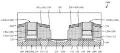
2A and 2B show cross-sectional views of various embodiments of the integrated memory chip of FIG. 1.
3A-3C show plan layouts of some alternative embodiments of the integrated memory chip of FIG. 1 in which the enhanced device area layout is changed.
4A-4C show plan layouts of various embodiments of an integrated memory chip including a pair of strap cells with the enhanced device area layout of FIG. 1.
FIG. 5 shows a block diagram of some embodiments of an integrated memory chip including a memory array having boundary cells in FIG. 1 and / or strap cells in any one or combination of FIGS. 4A-4C.
6A and 6B show plan layouts of various embodiments of an integrated memory chip that includes a boundary portion of the memory array of FIG. 5.
FIG. 7 shows a block diagram of some embodiments of an integrated memory chip that includes a boundary portion of the memory array of FIG. 5, where a plurality of wires and a plurality of vias interconnect cells in the boundary portion.
8-19 show a series of cross-sectional views of some embodiments of a method of forming an integrated memory chip comprising a pair of boundary or strap cells with an enhanced device area layout in accordance with aspects of the present application.
20 is a block diagram of some embodiments of FIGS. 8 to 19.
본 발명개시는 본 발명개시의 여러 특징들을 구현하는 많은 여러 실시예들 또는 예시들을 제공한다. 본 발명개시를 단순화하기 위해 컴포넌트 및 장치의 특정예들이 아래에서 설명된다. 물론, 이것들은 단지 예시들에 불과하며, 이것들로 한정시키고자 의도한 것은 아니다. 예를 들어, 이후의 상세설명에서 제2 피처 상에서의 또는 그 위에서의 제1 피처의 형성은 제1 및 제2 피처들이 직접적으로 접촉하여 형성되는 실시예들을 포함할 수 있으며, 또한 제1 및 제2 피처들이 직접적으로 접촉하지 않을 수 있도록 추가적인 피처들이 제1 및 제2 피처들 사이에서 형성될 수 있는 실시예들을 포함할 수 있다. 또한, 본 발명개시는 다양한 예시들에서 참조 숫자들 및/또는 문자들을 반복할 수 있다. 이러한 반복은 간략화 및 명료화를 목적으로 한 것이며, 그러한 반복 자체는 개시된 다양한 실시예들 및/또는 구성들 간의 관계에 영향을 주는 것은 아니다.The present disclosure provides many different embodiments or examples that implement various features of the present disclosure. Specific examples of components and devices are described below to simplify the present disclosure. Of course, these are only examples, and are not intended to be limited to these. For example, in the following detailed description, formation of a first feature on or above the second feature may include embodiments in which the first and second features are formed by direct contact, and also the first and first features. Additional features may include embodiments in which additional features may be formed between the first and second features so that the two features are not in direct contact. In addition, the present disclosure may repeat reference numerals and / or letters in various examples. This repetition is intended for simplicity and clarity, and such repetition itself does not affect the relationship between the various embodiments and / or configurations disclosed.
또한, 도면들에서 도시된 하나의 엘리먼트 또는 피처에 대한 다른 엘리먼트(들) 또는 피처(들)의 관계를 설명하기 위해 "아래", "밑", "보다 낮은", "위", "보다 위" 등과 같은 공간 상대적 용어들이 설명의 용이성을 위해 여기서 이용될 수 있다. 공간 상대적 용어들은 도면들에서 도시된 배향에 더하여 이용중에 있거나 또는 동작중에 있는 디바이스의 상이한 배향들을 망라하도록 의도된 것이다. 장치는 이와달리 배향될 수 있고(90° 회전되거나 또는 다른 배향으로 회전됨), 이에 따라 여기서 이용되는 공간 상대적 기술어들이 이와 똑같이 해석될 수 있다.Also, "below", "below", "below", "above", "above" to describe the relationship of one element or feature (s) to another element (s) or feature (s) shown in the figures. Spatial relative terms such as "can be used here for ease of explanation. Spatial relative terms are intended to cover different orientations of the device in use or in operation in addition to the orientation shown in the figures. The device can be oriented differently (rotated 90 ° or rotated in another orientation), and thus the spatial relative descriptors used herein can be interpreted the same.
예를 들어, 메모리 디바이스는 기판, 제1 워드 라인, 제2 워드 라인, 제1 소스/드레인 영역, 및 제2 소스/드레인 영역을 포함할 수 있다. 제1 및 제2 워드 라인들은 기판의 디바이스 영역 위에 놓여 있고, 각각의 워드 라인 길이를 따라 평행하게 세장화(elongated)되어 있다. 디바이스 영역은 격리 구조물에 의해 경계지어지고(demarcated), 제1 디바이스 영역 돌출부 및 제2 디바이스 영역 돌출부를 갖는다. 제1 디바이스 영역 돌출부는 워드 라인 길이와 교차하는 방향으로 제1 워드 라인쪽으로 돌출해 있고 기판의 제1 디바이스 영역 측벽에서 종결된다. 제2 디바이스 영역 돌출부는 워드 라인 길이와 교차하는 방향으로 제2 워드 라인쪽으로 돌출해 있고 기판의 제2 디바이스 영역 측벽에서 종결된다. 제1 및 제2 디바이스 영역 측벽들은 격리 구조물에 접해 있고, 제1 및 제2 워드 라인들 사이에서 횡측으로 있고 제1 및 제2 워드 라인들로부터 횡측으로 이격되어 있다. 제1 및 제2 소스/드레인 영역들은 각각 제1 및 제2 디바이스 영역 측벽들에서 디바이스 영역 상에 있다. 또한, 제1 및 제2 소스/드레인 영역들은 제1 및 제2 워드 라인들 사이에 있고, 각각 제1 및 제2 워드 라인들과 접해 있다.For example, the memory device may include a substrate, a first word line, a second word line, a first source / drain area, and a second source / drain area. The first and second word lines lie over the device area of the substrate and are elongated parallel to each word line length. The device area is demarcated by the isolation structure, and has a first device area protrusion and a second device area protrusion. The first device region protrusion protrudes toward the first word line in a direction crossing the word line length and terminates at the sidewall of the first device region of the substrate. The second device region protrusion protrudes toward the second word line in a direction crossing the word line length and terminates at the sidewall of the second device region of the substrate. The sidewalls of the first and second device regions abut the isolation structure, are transverse between the first and second word lines and are transversely spaced from the first and second word lines. The first and second source / drain regions are on the device region at the first and second device region sidewalls, respectively. Also, the first and second source / drain regions are between the first and second word lines, and are in contact with the first and second word lines, respectively.
메모리 디바이스의 형성 동안, 에칭 및/또는 세정 공정들은 제1 및 제2 디바이스 영역 측벽들에서 격리 구조물의 일부분을 기판의 최상면 아래로 리세싱함으로써, 제1 및 제2 디바이스 영역 측벽들을 노출시키는 리세스를 규정한다. 해결과제는 제1 및 제2 워드 라인들을 형성한 후에 수행되는 실리사이드 공정 동안 제1 및 제2 디바이스 영역 측벽들 상에 실리사이드가 형성될 수 있다는 것이다. 그 결과, 실리사이드는 제1 및 제2 소스/드레인 영역들에서부터 기판의 벌크까지 누설 경로를 초래할 수 있다. 또한, 메모리 디바이스의 사용 동안, 누설 경로는 제1 및 제2 워드 라인들 아래에 있는 선택적 도전 채널들을 따라 메모리 디바이스의 소스 라인들까지 연장될 수 있다. 이러한 연장은 읽기 및/또는 쓰기 실패를 야기시킬 수 있다. 다른 해결과제는 제1 및 제2 워드 라인들의 형성 동안 리세스가 에칭 공정 윈도우(예를 들어, 에칭 탄력성)를 감소시킨다는 것이다. 제1 및 제2 워드 라인들을 형성하는 단계는, 예를 들어, 도전층을 퇴적하는 단계; 도전층 상에 반사 방지 코팅(anti-reflective coating; ARC)을 퇴적하는 단계; 및 포토레지스트 마스크를 적소에 위치시킨 상태에서 ARC 및 도전층 내로 에칭을 수행하여 ARC 및 도전층 내에서 워드 라인 패턴을 형성하는 단계를 포함할 수 있다. 리세스로 인해, 도전층은 리세스에서 만입화(indented)될 수 있고, ARC는 리세스에서 증가된 두께를 가질 수 있다. 증가된 두께는 에칭 로딩(etch loading)을 증가시키므로, 리세스에 있는 ARC의 일부분을 에칭하는데 있어서 ARC의 다른 부분들보다 더 긴 시간이 걸린다. 결과적으로, 워드 라인 패턴은 도전층 내에서 정확하게 형성되지 않을 수 있다. 도전성 에칭 잔류물은 잔존하여 제1 및 제2 워드 라인들 사이에서 누설 경로를 규정할 수 있으며, 이에 따라 제1 및 제2 워드 라인들을 따라 메모리 셀들의 고장을 야기시킬 수 있다.During the formation of the memory device, etching and / or cleaning processes recess a portion of the isolation structure from the first and second device region sidewalls below the top surface of the substrate, thereby exposing the first and second device region sidewalls. Stipulate The challenge is that silicide can be formed on the sidewalls of the first and second device regions during the silicide process performed after forming the first and second word lines. As a result, the silicide can result in a leakage path from the first and second source / drain regions to the bulk of the substrate. Also, during use of the memory device, the leakage path may extend to the source lines of the memory device along optional conductive channels below the first and second word lines. This extension can lead to read and / or write failures. Another challenge is that during formation of the first and second word lines, the recess reduces the etch process window (eg, etch resilience). The forming of the first and second word lines may include, for example, depositing a conductive layer; Depositing an anti-reflective coating (ARC) on the conductive layer; And forming a word line pattern in the ARC and conductive layer by performing etching into the ARC and conductive layer while the photoresist mask is in place. Due to the recess, the conductive layer can be indented in the recess, and the ARC can have an increased thickness in the recess. The increased thickness increases the etch loading, so it takes longer to etch a portion of the ARC in the recess than the other portions of the ARC. As a result, the word line pattern may not be formed accurately in the conductive layer. The conductive etch residue may remain and define a leakage path between the first and second word lines, thus causing memory cell failures along the first and second word lines.
본 출원의 다양한 실시예들은 감소된 누설 전류 및 확장된 워드 라인 에칭 공정 윈도우(예를 들어, 강화된 워드 라인 에칭 탄력성)를 위한 강화된 디바이스 영역 레이아웃을 갖는 집적 메모리 칩에 관한 것이다. 일부 실시예들에서, 집적 메모리 칩은 기판, 제1 워드 라인, 제2 워드 라인, 및 소스/드레인 영역을 포함한다. 제1 및 제2 워드 라인들은 기판의 제1 디바이스 영역과 기판의 제2 디바이스 영역 위에 놓여 있고, 각각의 워드 라인 길이를 따라 평행하게 세장화되어 있다. 제1 및 제2 디바이스 영역들은 격리 구조물에 의해, 경계지어지고, 서로 전기적으로 분리된다. 제2 디바이스 영역은 제1 및 제2 워드 라인들 사이에 있고 제1 및 제2 워드 라인들과 접한다. 제1 디바이스 영역은 제2 디바이스 영역을 감싸며, 제2 디바이스 영역의 대향 측부들 상에서 각각 제1 디바이스 영역 돌출부 및 제2 디바이스 영역 돌출부를 갖는다. 제1 디바이스 영역 돌출부는 워드 라인 길이와 교차하는 제1 방향으로 제1 워드 라인아래에서 돌출해 있고 기판의 제1 디바이스 영역 측벽에서 종결된다. 제2 디바이스 영역 돌출부는 워드 라인 길이와 교차하는 제2 방향으로 제2 워드 라인아래에서 돌출해 있고 기판의 제2 디바이스 영역 측벽에서 종결된다. 제1 및 제2 디바이스 영역 측벽들은 격리 구조물과 인접해 있고 제2 디바이스 영역을 마주본다. 또한, 제1 및 제2 디바이스 영역 측벽들은 각각 제1 및 제2 워드 라인들 아래에 놓여 있다. 소스/드레인 영역은 제2 디바이스 영역 상에 있고, 제1 및 제2 워드 라인들 사이에 있으며 제1 및 제2 워드 라인들과 접한다.Various embodiments of the present application relate to integrated memory chips with enhanced device area layout for reduced leakage current and extended word line etch process window (eg, enhanced word line etch resilience). In some embodiments, the integrated memory chip includes a substrate, a first word line, a second word line, and source / drain regions. The first and second word lines overlie the first device region of the substrate and the second device region of the substrate, and are elongated in parallel along the length of each word line. The first and second device regions are bounded by an isolation structure, and are electrically isolated from each other. The second device area is between the first and second word lines and contacts the first and second word lines. The first device region surrounds the second device region, and has first and second device region protrusions on opposite sides of the second device region, respectively. The first device region protrusion protrudes below the first word line in a first direction crossing the word line length and terminates at the sidewall of the first device region of the substrate. The second device region protrusion protrudes below the second word line in a second direction crossing the word line length and terminates at the sidewall of the second device region of the substrate. The first and second device region sidewalls are adjacent the isolation structure and face the second device region. Also, sidewalls of the first and second device regions lie below the first and second word lines, respectively. The source / drain region is on the second device region, is between the first and second word lines, and is in contact with the first and second word lines.
메모리 디바이스의 형성 동안, 에칭 및/또는 세정 공정은, 예를 들어, 제1 및 제2 디바이스 영역 측벽들에서의 격리 구조물의 부분들을 리세싱할 수 있으며, 이에 의해 제1 및 제2 디바이스 영역 측벽들을 각각 노출시키는 제1 리세스 부분 및 제2 리세스 부분을 규정한다. 제1 및 제2 워드 라인들이 제1 및 제2 디바이스 영역 측벽들 위에 놓여 있기 때문에, 제1 및 제2 워드 라인들은, 예를 들어, 제1 및 제2 리세스 부분들을 채우고, 제1 및 제2 디바이스 영역 측벽들을 덮을 수 있다. 이것은, 예컨대, 제1 및 제2 워드 라인들을 형성한 후에 수행되는 실리사이드 공정 동안 제1 및 제2 디바이스 영역 측벽들 상에서 실리사이드가 형성되는 것을 방지할 수 있다. 제1 및 제2 디바이스 영역 측벽들 상에서 실리사이드가 형성되는 것을 방지함으로써, 기판의 벌크까지 누설 경로가 형성되는 것을 방지하고 수율을 향상시킬 수 있다.During the formation of the memory device, the etching and / or cleaning process can recess portions of the isolation structure, for example, in the first and second device region sidewalls, whereby the first and second device region sidewalls The first recess portion and the second recess portion respectively exposing them are defined. Since the first and second word lines lie over the sidewalls of the first and second device regions, the first and second word lines fill, for example, the first and second recess portions, and the first and second The sidewalls of the two device regions may be covered. This can prevent, for example, silicide from forming on the sidewalls of the first and second device regions during a silicide process performed after forming the first and second word lines. By preventing silicide from being formed on the sidewalls of the first and second device regions, it is possible to prevent the leakage path from being formed to the bulk of the substrate and improve the yield.
제1 및 제2 워드 라인들의 형성 동안, 예를 들어, 도전층 및 ARC가 순차적으로 퇴적될 수 있다. 또한, 제1 및 제2 워드 라인들을 형성하기 위해, 예를 들어, ARC 및 도전층 내로 에칭이 수행될 수 있다. 에칭을 수행하는 동안, 도전층의 일부분과 제2 디바이스 영역 상의 ARC의 일부분이 제거되어, 제1 및 제2 워드 라인들의 대향 측벽들을 각각 규정한다. 제2 디바이스 영역은 격리 구조물과는 상이한 물질이기 때문에, 제2 디바이스 영역은 격리 구조물의 리세싱을 받지 않아서 평면이거나 또는 실질적으로 평면인 최상면을 갖는다. 따라서, 도전층 및 ARC가 각각 제2 디바이스 영역에서 균일하거나 실질적으로 균일한 두께 및 평면이거나 또는 실질적으로 평면인 최상면을 갖도록 형성된다. 이것은 제2 디바이스 영역에서 균일하거나 실질적으로 균일한 에칭 로딩을 야기시킨다. 균일하거나 실질적으로 균일한 에칭 로딩은, 에칭 잔류물이 잔존하고 제1 및 제2 워드 라인들을 함께 전기적으로 단락시킬 가능성을 감소시킨다. 따라서, 균일하거나 실질적으로 균일한 에칭 로딩은 에칭의 공정 윈도우(예를 들어, 탄력성)를 확장시킬 수 있다.During the formation of the first and second word lines, for example, a conductive layer and ARC may be sequentially deposited. Also, to form the first and second word lines, etching may be performed, for example, into the ARC and the conductive layer. During etching, a portion of the conductive layer and a portion of the ARC on the second device region are removed to define opposite sidewalls of the first and second word lines, respectively. Since the second device region is a different material than the isolation structure, the second device region has a top surface that is planar or substantially planar because it is not subjected to recessing of the isolation structure. Accordingly, the conductive layer and the ARC are formed to have uniform or substantially uniform thickness and planar or substantially planar top surface in the second device region, respectively. This causes uniform or substantially uniform etch loading in the second device region. Uniform or substantially uniform etch loading reduces the likelihood of etch residue remaining and electrically shorting the first and second word lines together. Thus, uniform or substantially uniform etch loading can extend the process window (eg, elasticity) of the etch.
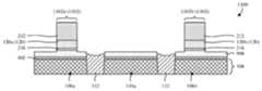
도 1을 참조하면, 강화된 디바이스 영역 레이아웃을 포함하는 집적 메모리 칩의 일부 실시예들의 평면 레이아웃(100)이 제공된다. 이하에서 살펴볼 수 있는 바와 같이, 강화된 디바이스 영역 레이아웃은 누설 전류 감소 및/또는 확장된 워드 라인 에칭 공정 윈도우를 야기시킬 수 있다는 점에서 "강화"된 것이다. 제1 워드 라인(102a)과 제2 워드 라인(102b)은 기판(104) 상에 있고, 각각의 워드 라인 길이(Lw1)를 따라 평행하게 세장화되어 있다. 워드 라인 길이(Lwl)들 중 하나만이 라벨표시된다는 점에 유의한다. 제1 워드 라인(102a)은 제2 워드 라인(102b)을 마주보는 제1 워드 라인 측벽(106a)을 갖고, 제2 워드 라인(102b)은 제1 워드 라인(102a)을 마주보는 제2 워드 라인 측벽(106b)을 갖는다. 기판(104)은, 예를 들어, 벌크 단결정 실리콘 기판, SOI(silicon-on-insulator) 기판, 또는 일부 다른 적절한 반도체 기판일 수 있거나 또는 이를 포함할 수 있다.1, a
기판(104)은 제1 소거측 디바이스 영역(108a), 제2 소거측 디바이스 영역(108b), 및 워드 라인측 디바이스 영역(110a)을 갖는다. 제1 및 제2 소거측 디바이스 영역들(108a, 108b) 및 워드 라인측 디바이스 영역(110a)은 (단면에서 봤을 때) 격리 구조물(112)에 의해 둘러싸여서 격리 구조물(112)에 의해 경계지어지는 기판(104)의 최상부 영역들에 대응한다. 격리 구조물(112)은 제1 및 제2 소거측 디바이스 영역들(108a, 108b)과 워드 라인측 디바이스 영역(110a) 사이에 전기적 및 물리적 격리를 제공한다. 격리 구조물(112)은 예를 들어, 실리콘 산화물 및/또는 일부 다른 적절한 유전체 물질(들)일 수 있거나 또는 이를 포함할 수 있고, 및/또는, 예를 들어, 얕은 트렌치 격리(shallow trench isolation; STI) 구조물 또는 일부 다른 적절한 격리 구조물일 수 있거나 또는 이를 포함할 수 있다.The
제1 소거측 디바이스 영역(108a)은 워드 라인 길이(Lwl)와 교차하는 제1 방향으로 제1 워드 라인(102a)쪽으로 돌출해 있고 제1 디바이스 영역 측벽(114)에서 종결된다. 마찬가지로, 제2 소거측 디바이스 영역(108b)은 워드 라인 길이(Lwl)와 교차하는 제2 방향으로 제2 워드 라인(102b)쪽으로 돌출해 있고 제2 디바이스 영역 측벽(116)에서 종결된다. 제1 디바이스 영역 측벽들(114) 중 단하나만이 114로 라벨표시되고, 제2 디바이스 영역 측벽들(116) 중 단하나만이 116으로 라벨표시된다는 점을 유의한다. 제1 및 제2 디바이스 영역 측벽들(114, 116)은 각각 제1 및 제2 워드 라인들(102a, 102b) 아래에 놓여 있으며, 제1 오프셋(Oa)만큼 제1 및 제2 워드 라인 측벽들(106a, 106b)로부터 각각 오프셋되어 있다. 일부 실시예들에서, 제1 및 제2 소거측 디바이스 영역들(108a, 108b)은 서로 독립적이다. 다른 실시예들에서, 제1 및 제2 소거측 디바이스 영역들(108a, 108b)은 집적 메모리 칩의 도시된 부분의 외부에서 연결되며, 따라서 하나이며 동일체다.The first erase-
워드 라인측 디바이스 영역(110a)은 제1 및 제2 소거측 디바이스 영역들(108a, 108b) 사이에 있고, 제3 디바이스 영역 측벽들(118)의 쌍을 갖는다. 제3 디바이스 영역 측벽들(118) 중 단하나만이 라벨표시되어 있음에 유의한다. 제3 디바이스 영역 측벽들(118)은 각각 워드 라인측 디바이스 영역(110a)의 대향 측부들 상에 있고 제1 및 제2 소거측 디바이스 영역들(108a, 108a)을 각각 마주본다. 또한, 제3 디바이스 영역 측벽들(118)은 각각 제1 및 제2 워드 라인들(102a, 102b) 아래에 놓여 있으며, 제1 오프셋(Oa)보다 작은 제2 오프셋(Ob)만큼 제1 및 제2 워드 라인 측벽들(106a, 106b)로부터 각각 오프셋되어 있다. 대안적인 실시예들에서, 제3 디바이스 영역 측벽들(118)은 제1 및 제2 워드 라인들(102a, 102b) 사이에서 횡측으로 이들로부터 이격되어 있어서, 제3 디바이스 영역 측벽들(118)은 제1 및 제2 워드 라인들(102a, 102b) 아래에 놓여 있지 않다(예컨대, 제2 오프셋(Ob)은 음수(negative)이다). 워드 라인측 디바이스 영역(110a)은, 예를 들어, 정사각형, 직사각형, 또는 일부 다른 적절한 형상인 평면 레이아웃을 가질 수 있다.The word line
집적 메모리 칩의 형성 동안, 에칭 및/또는 세정 공정은, 예를 들어, 제1 및 제2 디바이스 영역 측벽들(114, 116)에서의 격리 구조물(112)의 부분들을 리세싱할 수 있으며, 이에 의해 제1 및 제2 디바이스 영역 측벽들(114, 116)을 노출시킨다. 제1 및 제2 워드 라인들(102a, 102b)은 제1 및 제2 디바이스 영역 측벽들(114, 116) 위에 놓여있기 때문에, 제1 및 제2 워드 라인들(102a, 102b)은, 예를 들어, 제1 및 제2 워드 라인들(102a, 102b)을 형성한 후에 수행되는 실리사이드 공정 동안 제1 및 제2 디바이스 영역 측벽들(114, 116) 상에 실리사이드가 형성되는 것을 방지할 수 있다. 이것은 결국, 기판(104)의 벌크까지의 누설 경로를 방지할 수 있고 수율을 향상시킬 수 있다.During the formation of the integrated memory chip, the etching and / or cleaning process may recess portions of
일부 실시예들에서, 제1 오프셋(Oa)은 약 10~150나노미터, 약 10~80나노미터, 또는 약 80~150나노미터 사이이다. 그러나, 제1 오프셋(Oa)에 대해 다른 값들이 적용될 수 있다. 제1 오프셋(Oa)이 너무 작으면(예를 들어, 약 10나노미터 또는 일부 다른 적절한 값 미만), 제1 및 제2 워드 라인들(102a, 102b)을 형성한 후에 수행되는 실리사이드 공정 동안 제1 및 제2 디바이스 영역 측벽들(114, 116)이 여전히 노출될 수 있다. 예를 들어, 제1 및 제2 워드 라인들(102a, 102b)을 리세싱하는 에칭 및/또는 세정 공정은 제1 및 제2 디바이스 영역 측벽들(114, 116)에서 격리 구조물(112)을 횡측으로 에칭할 수 있다. 제1 오프셋(Oa)이 너무 작으면, 횡측 에칭은 제1 및 제2 워드 라인들(102a, 102b)을 언더컷(undercut)하고, 제1 및 제2 디바이스 영역 측벽들(114, 116)을 노출시킬 수 있다. 제1 오프셋(Oa)이 너무 크면(예를 들어, 약 150나노미터 또는 일부 다른 적절한 값 초과), 제1 및 제2 디바이스 영역 측벽들(114, 116)이 제1 및 제2 워드 라인들(102a, 102b) 아래에 있기 때문에 제1 및 제2 워드 라인들(102a, 102b)은 크기가 과대해질 것이다. 이에 따라, 재료가 낭비될 것이고 메모리 어레이 크기가 필요한 것보다 커질 것이다.In some embodiments, the first offset Oa is between about 10-150 nanometers, about 10-80 nanometers, or between about 80-150 nanometers. However, other values may be applied for the first offset Oa . If the first offset Oa is too small (eg, less than about 10 nanometers or some other suitable value), during the silicide process performed after forming the first and
제1 및 제2 워드 라인들(102a, 102b)의 형성 동안, 예를 들어, 도전층과 ARC가 순차적으로 퇴적될 수 있다. 또한, 제1 및 제2 워드 라인들(102a, 102b)을 형성하기 위해, 예를 들어, ARC 및 도전층 내로 에칭이 수행될 수 있다. 에칭을 수행하는 동안, 워드 라인측 디바이스 영역(110a) 상의 도전층의 일부분 및 ARC의 일부분이 제거되어, 제1 및 제2 워드 라인 측벽들(106a, 106b)이 규정된다. 워드 라인측 디바이스 영역(110a)은 격리 구조물(112)과는 상이한 물질이기 때문에, 워드 라인측 디바이스 영역(110a)은 격리 구조물(112)의 리세싱을 받지 않고, (단면에서 바라봤을 때) 평면이거나 또는 실질적으로 평면인 최상면을 갖는다. 따라서, 도전층 및 ARC가 각각 워드 라인측 디바이스 영역(110a)에서 균일하거나 실질적으로 균일한 두께와, 평면이거나 또는 실질적으로 평면인 최상면을 갖도록 형성된다. 이것은 워드 라인측 디바이스 영역(110a)에서 균일하거나 실질적으로 균일한 에칭 로딩을 야기시킨다. 균일하거나 실질적으로 균일한 에칭 로딩은, 에칭 잔류물이 잔존하고 제1 및 제2 워드 라인들(102a, 102b)을 함께 전기적으로 단락시킬 가능성을 감소시킨다. 따라서, 워드 라인측 디바이스 영역(110a)은 에칭의 공정 윈도우(예를 들어, 탄력성)를 확장시킬 수 있다.During the formation of the first and
제1 제어 게이트(120a), 제2 제어 게이트(120b), 제1 소거 게이트(122a), 및 제2 소거 게이트(122b)가 기판(104) 상에 있다. 제1 제어 게이트(120a)와 제1 소거 게이트(122a)는 제1 소거측 디바이스 영역(108a) 상에 있고, 제1 제어 게이트(120a)는 제1 소거 게이트(122a)와 제1 워드 라인(102a) 사이에 있고 이들과 접한다. 마찬가지로, 제2 제어 게이트(120b)와 제2 소거 게이트(122b)는 제2 소거측 디바이스 영역(108b) 상에 있고, 제2 제어 게이트(120b)는 제2 소거 게이트(122b)와 제2 워드 라인(102b) 사이에 있고 이들과 접한다. 제1 및 제2 워드 라인들(102a, 102b), 제1 및 제2 제어 게이트들(120a, 120b), 및 제1 및 제2 소거 게이트들(122a, 122b)은 제1 차원(예를 들어, X 차원)으로 평행하게 세장화되어 있고, 또한 제1 차원을 가로지르는 제2 차원(예를 들어, Y 차원)으로 서로로부터 횡측으로 이격되어 있다.The
일부 실시예들에서, 제1 및 제2 소거 게이트들(122a, 122b)은 제1 차원에서 불연속적이다. 다른 실시예들에서, 제1 및 제2 소거 게이트들(122a, 122b)은 제1 차원에서 연속적이다. 일부 실시예들에서, 제1 및 제2 워드 라인들(102a, 102b)은 제1 차원에서 불연속적이다. 다른 실시예들에서, 제1 및 제2 워드 라인들(102a, 102b)은 제1 차원에서 연속적이다. 일부 실시예들에서, 제1 및 제2 워드 라인들(102a, 102b), 제1 및 제2 제어 게이트들(120a, 120b), 및 제1 및 제2 소거 게이트들(122a, 122b)은 도핑된 폴리실리콘, 금속, 일부 다른 적절한 도전성 물질(들), 또는 이들의 임의의 조합이거나 또는 이들을 포함할 수 있다.In some embodiments, the first and second erase
일부 실시예에서, 제1 경계 셀(124a)과 제2 경계 셀(124b)은 워드 라인측 디바이스 영역(110a) 상에 있고, 각각 제1 및 제2 소거측 디바이스 영역들(108a, 108b) 상에 있다. 제1 경계 셀(124a)은 제1 워드 라인(102a), 제1 제어 게이트(120a), 및 제1 소거 게이트(122a)에 의해 부분적으로 규정되는 반면에, 제2 경계 셀(124b)은 제2 워드 라인(102b), 제2 제어 게이트(120b), 및 제2 소거 게이트(122b)에 의해 부분적으로 규정된다. 제1 및 제2 경계 셀들(124a, 124b)은 사용되지 않거나 또는 메모리 어레이의 가장자리 또는 경계에 있는 더미 셀들이며, 이 더미 셀들은 가장자리 또는 경계로부터 메모리 어레이의 메모리 및 스트랩 셀들을 오프셋시킨다. 제1 및 제2 경계 셀들(124a, 124b)은 사용되지 않는데, 그 이유는 메모리 어레이의 가장자리 또는 경계에서는 피처 밀도의 큰 변화가 있기 때문이다. 피처 밀도의 이러한 큰 변화는 고도의 공정 불균일성을 야기하며, 이에 따라 제1 및 제2 경계 셀들(124a, 124b)은 불균일하여 사용하기에 적절하지 않다.In some embodiments, the
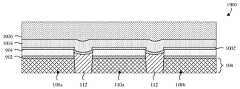
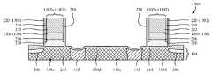
도 2a를 참조하면, 도 1의 집적 메모리 칩의 일부 실시예들의 단면도(200A)가 제공된다. 단면도(200A)는 예를 들어, 도 1에서의 A 라인을 따라 취해진 것일 수 있다. 제1 및 제2 워드 라인들(102a, 102b), 제1 및 제2 제어 게이트들(120a, 120b), 및 제1 및 제2 소거 게이트들(122a, 122b)은 상호연결 유전체층(202)에 의해 덮혀 있다. 상호연결 유전체층(202)은 예를 들어, 로우 k 유전체 및/또는 일부 다른 적절한 유전체(들)일 수 있거나 또는 이들을 포함할 수 있다.2A, a
추가적으로, 제1 및 제2 워드 라인들(102a, 102b), 제1 및 제2 제어 게이트들(120a, 120b), 및 제1 및 제2 소거 게이트들(122a, 122b)은 기판(104) 및 격리 구조물(112) 위에 놓여있다. 격리 구조물(112)은 제1 및 제2 소거측 디바이스 영역들(108a, 108b)과 워드 라인측 디바이스 영역(110a)을 경계짓기 위해 기판(104)의 최상부 내로 돌출해 있다. 일부 실시예들에서, 제1 및 제2 소거측 디바이스 영역들(108a, 108b) 및/또는 워드 라인측 디바이스 영역(110a)은 활성(active)이다. 기판(104)의 영역은 예를 들어, 집적 메모리 칩의 동작 동안 공핍 및/또는 강화를 겪을 수 있다는 점에서 활성일 수 있고, 및/또는 예를 들어, 집적 메모리 칩의 동작 동안 상기 영역에 전류가 흐른다는 점에서 활성일 수 있다.Additionally, the first and
소스/드레인 영역(204)은 워드 라인측 디바이스 영역(110a) 상에 있고, 제1 및 제2 워드 라인들(102a, 102b) 사이에 있고 이들과 접해 있다. 다중 소스 라인들(206)이 각각 제1 및 제2 소거측 디바이스 영역들(108a, 108b) 상에 있고, 각각 제1 및 제2 소거 게이트들(122a, 122b) 아래에 놓여 있다. 소스 라인들(206) 중 하나만이 라벨표시되어 있음에 유의한다. 소스/드레인 영역(204) 및 소스 라인들(206)은 기판(104)의 도핑된 영역들이다. 소스/드레인 영역(204) 및 소스 라인들(206)은 예를 들어, 도핑 유형(예를 들어, p형 또는 n형)을 공유할 수 있고/있거나, 예를 들어, 기판(104)의 인접한 영역들과 상반되는 도핑 유형들을 가질 수 있다.The source /
복수의 선택적 도전 채널들(208)이 제1 및 제2 소거측 디바이스 영역들(108a, 108b)과 워드 라인측 디바이스 영역(110a) 내에 있다. 선택적 도전 채널들(208) 중 하나만이 라벨표시되어 있음에 유의한다. 선택적 도전 채널들(208)은 기판(104)의 최상면을 따라 연장되고, 제1 및 제2 워드 라인들(102a, 102b) 및 제1 및 제2 제어 게이트들(120a, 120b) 아래에 놓여 있다. 또한, 선택적 도전 채널들(208)은 위에 있는 게이트(예컨대, 제1 워드 라인(102a))의 바이어스 전압에 의존하여 도통된다. 격리 구조물(112)이 소스/드레인 영역(204)으로부터 소스 라인들(206)을 전기적으로 격리시키기 때문에, 격리 구조물(112)은 선택적 도전 채널들(208)이 소스/드레인 영역(204)을 소스 라인들(206)에 전기적으로 결합시키는 것을 방지한다.A plurality of optional
제1 및 제2 제어 게이트들(120a, 120b)은 개별 플로우팅 게이트들(210) 위에 놓여 있고, 개별 제어 게이트 하드 마스크들(212)에 의해 덮혀 있다. 플로우팅 게이트들(210)은 개별 플로우팅 게이트 유전체층들(214)에 의해 기판(104)으로부터 이격되어 있고, 개별 제어 게이트 유전체층들(216)에 의해 제1 및 제2 제어 게이트들(120a, 120b)로부터 이격되어 있다. 플로우팅 게이트들(210) 중 단하나, 제어 게이트 하드 마스크들(212) 중 단하나, 플로우팅 게이트 유전체층들(214) 중 단하나, 및 제어 게이트 유전체층들(216) 중 단하나가 라벨표시되어 있음에 유의한다. 플로우팅 게이트들(210)은 예를 들어, 도핑된 폴리실리콘 및/또는 일부 다른 적절한 도전성 물질(들)일 수 있거나 또는 이들을 포함할 수 있다. 플로우팅 게이트 유전체층들(214)은 예를 들어, 실리콘 산화물 및/또는 일부 다른 적절한 유전체(들)일 수 있거나 또는 이들을 포함할 수 있다. 제어 게이트 하드 마스크들(212) 및/또는 제어 게이트 유전체층들(216)은 예를 들어, 실리콘 산화물, 실리콘 질화물, 일부 다른 적절한 유전체(들), 또는 이들의 임의의 조합일 수 있거나 또는 이들을 포함할 수 있다.The first and
제1 및 제2 제어 게이트들(120a, 120b)은 개별 제어 게이트 측벽 스페이서들(218)에 의해 라이닝(line)된다. 또한, 제1 및 제2 소거 게이트들(122a, 122b)은 개별 소거 게이트 유전체층들(220)에 의해 라이닝되고, 제1 및 제2 워드 라인들(102a, 102b)은 개별 워드 라인 유전체층들(222)에 의해 라이닝된다. 제어 게이트 측벽 스페이서들(218) 중 단하나, 소거 게이트 유전체층들(220) 중 단하나, 및 워드 라인 유전체층들(222) 중 단하나가 라벨표시되어 있음에 유의한다. 소거 게이트 유전체층들(220)은 플로우팅 게이트들(210), 제어 게이트 측벽 스페이서들(218), 및 기판(104)으로부터 제1 및 제2 소거 게이트들(122a, 122b)을 분리시킨다. 워드 라인 유전체층들(222)은 플로우팅 게이트들(210), 제어 게이트 측벽 스페이서들(218), 기판(104), 및 격리 구조물(112)로부터 제1 및 제2 워드 라인들(102a, 102b)을 분리시킨다. 제어 게이트 측벽 스페이서들(218)은 예를 들어, 실리콘 산화물, 실리콘 질화물, 일부 다른 적절한 유전체(들), 또는 이들의 임의의 조합일 수 있거나 또는 이들을 포함할 수 있다. 소거 게이트 유전체층들(220) 및/또는 워드 라인 유전체층들(222)은 예를 들어, 실리콘 산화물 및/또는 일부 다른 적절한 유전체(들)일 수 있거나 또는 이들을 포함할 수 있다.The first and
실리사이드층들(224)은 각각 제1 및 제2 워드 라인들(102a, 102b), 제1 및 제2 소거 게이트들(122a, 122b), 및 소스/드레인 영역(204)을 덮는다. 실리사이드층들(224) 중 일부만이 라벨표시되어 있음에 유의한다. 실리사이드층들(224)은 예를 들어, 니켈 실리사이드 및/또는 일부 다른 적절한 실리사이드일 수 있거나 또는 이들을 포함할 수 있다. 이하에서 살펴볼 수 있는 바와 같이, 실리사이드층들(224)의 형성은 제1 및 제2 워드 라인들(102a, 102b)의 형성 이후에 수행된다. 이와 같이, 제1 및 제2 디바이스 영역 측벽들(114, 116)은 제1 및 제2 워드 라인들(102a, 102b)에 의해 덮히고, 실리사이드는 집적 메모리 칩의 형성 동안에 노출된 제1 및 제2 디바이스 영역 측벽들(114, 116)의 임의의 부분들 상에 형성될 수 없다. 이것은 결국, 누설 경로가 제1 및 제2 디바이스 영역 측벽들(114, 116)을 따라, 선택적 도전 채널들(208) 중의 대응하는 선택적 도전 채널(208)에서부터 기판(104)의 벌크까지 연장되는 것을 방지한다.The silicide layers 224 cover the first and
도 2b를 참조하면, 도 2a의 집적 메모리 칩의 일부 대안적인 실시예들의 단면도(200B)가 제공되며, 여기서는 게이트간 유전체 구조물(226)이 제1 및 제2 워드 라인들(102a, 102b), 제1 및 제2 제어 게이트들(120a, 120b), 그리고 제1 및 제2 소거 게이트들(122a, 122b)을 서로간에 그리고 기판(104)으로부터 분리시킨다. 또한, 게이트간 유전체 구조물(226)은 격리 구조물(112)을 규정한다. 게이트간 유전체 구조물(226)은 예를 들어, 실리콘 산화물 및/또는 일부 다른 적절한 유전체 물질(들)일 수 있거나 또는 이들을 포함할 수 있다.2B, a
다중 측벽 스페이서들(228), 다중 제어 게이트 유전체층들(230), 및 다중 제어 게이트 하드 마스크들(232)이 게이트간 유전체 구조물(226) 내에 있다. 측벽 스페이서들(228) 중 일부만이, 제어 게이트 유전체층들(230) 중 단하나가, 그리고 다중 제어 게이트 하드 마스크들(232) 중 단하나가 라벨표시되어 있음에 유의한다. 측벽 스페이서들(228)은 각각 제1 및 제2 제어 게이트들(120a, 120b) 및 제1 및 제2 워드 라인들(102a, 102b)의 측벽들 상에 있고 및/또는 이들을 따라 있다. 제어 게이트 유전체층들(230)은 각각, 플로우팅 게이트들(210)과 제1 및 제2 제어 게이트들(120a, 120b) 사이에서 플로우팅 게이트들(210) 위에 놓여 있다. 제어 게이트 하드 마스크들(212)은 각각 제1 및 제2 제어 게이트들(120a, 120b)를 덮는다. 측벽 스페이서들(228), 제어 게이트 유전체층들(230), 및 다중 제어 게이트 하드 마스크들(232)은 예를 들어, 실리콘 질화물 및/또는 일부 다른 적절한 유전체(들)일 수 있거나 또는 이들을 포함할 수 있다. 일부 실시예들에서, 게이트간 유전체 구조물(226)은 실리콘 산화물이거나 또는 이것을 포함하는 반면에, 측벽 스페이서(228), 제어 게이트 유전체층들(230), 및 제어 게이트 하드 마스크들(232)은 실리콘 질화물이거나 이것을 포함한다. 그러나 다른 물질들이 사용가능하다.
콘택트 에칭 정지층(234)이 상호연결 유전체층(202) 아래에 놓여 있고, 제1 및 제2 워드 라인들(102a, 102b), 제1 및 제2 제어 게이트들(120a, 120b), 및 제1 및 제2 소거 게이트들(122a, 122b)을 덮는다. 집적 메모리 칩의 형성 동안, 콘택트 에칭 정지층(234)은 상호연결 유전체층(202) 내의 콘택트 비아 개구를 에칭하는 동안의 에칭 정지부로서 역할을 한다. 단면도(200B)에서는 콘택트 비아가 도시되어 있지 않음에 유의한다. 콘택트 에칭 정지층(234)은 예를 들어, 실리콘 탄화물, 실리콘 질화물, 일부 다른 적절한 유전체(들), 또는 이들의 임의의 조합일 수 있거나 또는 이들을 포함할 수 있다.A contact
도 3a 내지 도 3c을 참조하면, 강화된 디바이스 영역 레이아웃이 변경되는 도 1의 집적 메모리 칩의 일부 대안적인 실시예들의 평면 레이아웃들(300A~300C)이 제공된다. 도 3a의 평면 레이아웃(300A)에 의해 예시된 바와 같이, 워드 라인측 디바이스 영역(110a)은 제1 및 제2 워드 라인들(102a, 102b) 사이에서 횡측으로 이들로부터 이격되어 있다. 따라서, 제2 오프셋(Ob)은 도 3a에서는 음수이며, 도 1에서는 양수(positive)이고, 그 반대일 수도 있다. 도 3b의 평면 레이아웃(300B)에 의해 예시된 바와 같이, 제1 디바이스 영역 측벽들(114)의 가장자리들이 제1 디바이스 영역 측벽들(114)의 중심보다 제1 제어 게이트(120a)로부터 더 멀리 있도록, 제1 디바이스 영역 측벽들(114)은 만곡화되어 있다. 또한, 제2 디바이스 영역 측벽들(116)이 마찬가지로 만곡화되어 있다. 도 3c의 평면 레이아웃(300C)에 의해 예시된 바와 같이, 제1 디바이스 영역 측벽들(114)의 가장자리들이 제1 디바이스 영역 측벽들(114)의 중심보다 제1 제어 게이트(120a)로부터 더 가까이 있도록, 제1 디바이스 영역 측벽들(114)은 만곡화되어 있다. 또한, 제2 디바이스 영역 측벽들(116)이 마찬가지로 만곡화되어 있다. 도시되지는 않았지만, 워드 라인측 디바이스 영역(110a)은, 도 3b와 도 3c의 대안적인 실시예에서, 도 3a에서 도시된 바와 같이, 제1 및 제2 워드 라인들(102a, 102b) 사이에서 횡측으로 이들로부터 이격되어 있을 수 있다.3A-3C,
도 4a를 참조하면, 도 1의 강화된 디바이스 영역 레이아웃을 갖는 소스 라인/소거 게이트(source-line/erase-gate; SLEG) 스트랩 셀들의 쌍을 포함하는 집적 메모리 칩의 일부 실시예들의 평면 레이아웃(400A)이 제공된다. SLEG 스트랩 셀들의 쌍은 제1 SLEG 스트랩 셀(402a)과 제2 SLEG 스트랩 셀(402b)을 포함한다. 제1 및 제2 SLEG 스트랩 셀들(402a, 402b)은 워드 라인측 디바이스 영역(110a) 상에 있고, 각각 제1 및 제2 소거측 디바이스 영역들(108a, 108b) 상에 있다. 제1 및 제2 소거측 디바이스 영역들(108a, 108b) 및 워드 라인측 디바이스 영역(110a)은 도 1에서 설명된 바와 같다.4A, a planar layout of some embodiments of an integrated memory chip including a pair of source-line / erase-gate (SLEG) strap cells with the enhanced device area layout of FIG. 1 ( 400A) is provided. The pair of SLEG strap cells includes a first
제1 SLEG 스트랩 셀(402a)은 제1 워드 라인(102a), 제1 제어 게이트(120a), 및 제1 소거 게이트(122a)에 의해 부분적으로 규정되는 반면에, 제2 SLEG 스트랩 셀(402b)은 제2 워드 라인(102b), 제2 제어 게이트(120b), 및 제2 소거 게이트(122b)에 의해 부분적으로 규정된다. 일부 실시예들에서, 제1 및 제2 SLEG 스트랩 셀들(402a, 402b)은 도 1의 제1 및 제2 경계 셀들(124a, 124b)과 동일한 단면 또는 유사한 단면을 갖는다. 따라서, 도 2a의 단면도(200A) 및/또는 도 2b의 단면도(200B)는 예를 들어, 도 4a에서의 B 라인을 따라 절단하여 바라본 것일 수 있다.The first
제1 및 제2 SLEG 스트랩 셀들(402a, 402b)은 제1 및 제2 소거 게이트들(122a, 122b)이 소거 게이트 스트랩 라인들(도시되지 않음)에 전기적으로 결합되는 위치를 제공한다. 또한, 제1 및 제2 SLEG 스트랩 셀들(402a, 402b)은 소스 라인들(도시되지 않음; 도 2a와 도 2b에서의 소스 라인들(206)을 참조하라)이 소스 라인 스트랩 라인들(도시되지 않음)에 전기적으로 결합되는 위치를 제공한다. 제1 및 제2 SLEG 스트랩 셀들(402a, 402b)로부터 소거 게이트 및 소스 라인 스트랩 라인들로의 전기적 결합은 예를 들어, 제1 및 제2 SLEG 스트랩 셀들(402a, 402b) 상의 복수의 콘택트 비아들(404a)에 의해 부분적으로 수행될 수 있다. 콘택트 비아들(404a) 중 일부만이 라벨표시되어 있음에 유의한다.The first and second
소거 게이트 및 소스 라인 스트랩 라인들은 제1 및 제2 소거 게이트들(122a, 122b) 및 소스 라인들과 평행하게 세장화되어 있다. 또한, 소거 게이트 및 소스 라인 스트랩 라인들은 제1 및 제2 소거 게이트들(122a, 122b) 및 소스 라인들보다 더 낮은 저항을 갖는다. 따라서, 제1 및 제2 소거 게이트들(122a, 122b)을 제1 및 제2 SLEG 스트랩 셀들(402a, 402b), 및 제1 및 제2 소거 게이트들(122a, 122b)을 따른 다른 SLEG 스트랩 셀들에서의 소거 게이트 스트랩 라인들에 전기적으로 결합시키는 것은 제1 및 제2 소거 게이트들(122a, 122b)을 따른 저항 및 전압 강하를 감소시킨다. 또한, 제1 및 제2 SLEG 스트랩 셀들(402a, 402b), 및 소스 라인들을 따른 다른 SLEG 스트랩 셀들에서의 소스 라인 스트랩 라인들에 전기적으로 결합시키는 것은 소스 라인들을 따른 저항 및 전압 강하를 감소시킨다.The erase gate and source line strap lines are elongated parallel to the first and second erase
도 4b를 참조하면, 도 1의 강화된 디바이스 영역 레이아웃을 갖는 제어 게이트/워드 라인(control-gate/word-line; CGWL) 스트랩 셀들의 쌍을 포함하는 집적 메모리 칩의 일부 실시예들의 평면 레이아웃(400B)이 제공된다. CGWL 스트랩 셀들의 쌍은 제1 CGWL 스트랩 셀(406a)과 제2 CGWL 스트랩 셀(406b)을 포함한다. 제1 및 제2 CGWL 스트랩 셀들(406a, 406b)은 워드 라인측 디바이스 영역(110a) 상에 있고, 각각 제1 및 제2 소거측 디바이스 영역들(108a, 108b) 상에 있다. 또한, 제1 및 제2 CGWL 스트랩 셀들(406a, 406b)은 제2 워드 라인측 디바이스 영역(110b) 상에 있다. 제1 및 제2 소거측 디바이스 영역들(108a, 108b) 및 워드 라인측 디바이스 영역(110a)은, 제1 및 제2 소거측 디바이스 영역들(108a, 108b)이 각각 (도 1에서의 2개 이상의 위치와 비교하여) 4개 이상의 위치에서 워드 라인 길이(Lwl)와 교차하는 방향으로 돌출해 있다는 것을 제외하고는, 도 1에서 설명되고 도시된 것과 같다. 또한, 제2 워드 라인측 디바이스 영역(110b)은 워드 라인측 디바이스 영역(110a)이 도 1에서 설명되고 도시되어 있는 바와 같다.4B, a planar layout of some embodiments of an integrated memory chip including a pair of control-gate / word-line (CGWL) strap cells with the enhanced device area layout of FIG. 1 ( 400B) is provided. The pair of CGWL strap cells includes a first
제1 CGWL 스트랩 셀(406a)은 제1 워드 라인(102a), 제1 제어 게이트(120a), 및 제1 소거 게이트(122a)에 의해 부분적으로 규정되는 반면에, 제2 CGWL 스트랩 셀(406b)은 제2 워드 라인(102b), 제2 제어 게이트(120b), 및 제2 소거 게이트(122b)에 의해 부분적으로 규정된다. 일부 실시예들에서, 제1 및 제2 CGWL 스트랩 셀들(406a, 406b)은 도 1의 제1 및 제2 경계 셀들(124a, 124b)과 동일한 단면 또는 유사한 단면을 갖는다. 따라서, 도 2a의 단면도(200A) 및/또는 도 2b의 단면도(200B)는 예를 들어, 도 4b에서의 C 라인을 따라 절단하여 바라본 것일 수 있다.The first
제1 및 제2 CGWL 스트랩 셀들(406a, 406b)은 제1 및 제2 제어 게이트들(120a, 120b)이 제어 게이트 스트랩 라인들(도시되지 않음)에 전기적으로 결합되는 위치를 제공한다. 예를 들어, 제1 및 제2 제어 게이트들(120a, 120b)은 제어 게이트 스트랩 라인들에 제1 및 제2 제어 게이트들(120a, 120b)을 전기적으로 결합시키기 위해 제1 및 제2 CGWL 스트랩 셀들(406a, 406b)에서의 패드 영역들(408)을 가질 수 있다. 또한, 제1 및 제2 CGWL 스트랩 셀들(406a, 406b)은 제1 및 제2 워드 라인들(102a, 102b)이 워드 라인 스트랩 라인들(도시되지 않음)에 전기적으로 결합되는 위치를 제공한다. 제1 및 제2 CGWL 스트랩 셀들(406a, 406b)로부터 제어 게이트 및 워드 라인 스트랩 라인들로의 전기적 결합은 예를 들어, 제1 및 제2 CGWL 스트랩 셀들(406a, 406b) 상의 복수의 콘택트 비아들(404b)에 의해 부분적으로 수행될 수 있다. 콘택트 비아들(404b) 중 일부만이 라벨표시되어 있음에 유의한다.The first and second
제어 게이트 및 워드 라인 스트랩 라인들은 제1 및 제2 제어 게이트들(120a, 120b), 그리고 제1 및 제2 워드 라인들(102a, 102b)과 평행하게 세장화되어 있다. 또한, 제어 게이트 및 워드 라인 스트랩 라인들은 제1 및 제2 제어 게이트들(120a, 120b), 그리고 제1 및 제2 워드 라인들(102a, 102b)보다 더 낮은 저항을 갖는다. 따라서, 제1 및 제2 제어 게이트들(120a, 120b)을 제1 및 제2 CGWL 스트랩 셀들(406a, 406b), 및 제1 및 제2 제어 게이트들(120a, 120b)을 따른 다른 CGWL 스트랩 셀들에서의 제어 게이트 스트랩 라인들에 전기적으로 결합시키는 것은 제1 및 제2 제어 게이트들(120a, 120b)을 따른 저항 및 전압 강하를 감소시킨다. 또한, 제1 및 제2 워드 라인들(102a, 102b)을 제1 및 제2 CGWL 스트랩 셀들(406a, 406b), 및 제1 및 제2 워드 라인들(102a, 102b)을 따른 다른 CGWL 스트랩 셀들에서의 워드 라인 스트랩 라인들에 전기적으로 결합시키는 것은 제1 및 제2 워드 라인들(102a, 102b)을 따른 저항 및 전압 강하를 감소시킨다.The control gate and word line strap lines are elongated parallel to the first and
도 4c를 참조하면, 도 1의 강화된 디바이스 영역 레이아웃을 갖는 워드 라인 스트랩 셀들의 쌍을 포함하는 집적 메모리 칩의 일부 실시예들의 평면 레이아웃(400C)이 제공된다. 워드 라인 스트랩 셀들의 쌍은 제1 워드 라인 스트랩 셀(410a)과 제2 워드 라인 스트랩 셀(410b)을 포함한다. 제1 및 제2 워드 라인 스트랩 셀들(410a, 410b)은 워드 라인측 디바이스 영역(110a) 상에 있고, 각각 제1 및 제2 소거측 디바이스 영역들(108a, 108b) 상에 있다. 제1 및 제2 소거측 디바이스 영역들(108a, 108b) 및 워드 라인측 디바이스 영역(110a)은, 제1 및 제2 소거측 디바이스 영역들(108a, 108b)이 각각 (도 1에서의 2개 이상의 위치와 비교하여) 하나 이상의 위치에서 워드 라인 길이(Lwl)와 교차하는 방향으로 돌출해 있다는 것을 제외하고는, 도 1에서 설명되고 도시된 것과 같다.4C, a
제1 워드 라인 스트랩 셀(410a)은 제1 워드 라인(102a), 제1 제어 게이트(120a), 및 제1 소거 게이트(122a)에 의해 부분적으로 규정되는 반면에, 제2 워드 라인 스트랩 셀(410b)은 제2 워드 라인(102b), 제2 제어 게이트(120b), 및 제2 소거 게이트(122b)에 의해 부분적으로 규정된다. 일부 실시예들에서, 제1 및 제2 워드 라인 스트랩 셀들(410a, 410b)은 도 1의 제1 및 제2 경계 셀들(124a, 124b)과 동일한 단면 또는 유사한 단면을 갖는다. 따라서, 도 2a의 단면도(200A) 및/또는 도 2b의 단면도(200B)는 예를 들어, 도 4c에서의 D 라인을 따라 절단하여 바라본 것일 수 있다.The first word
제1 및 제2 워드 라인 스트랩 셀들(410a, 410b)은 제1 및 제2 워드 라인들(102a, 102b)이 워드 라인 스트랩 라인들(도시되지 않음)에 전기적으로 결합되는 위치를 제공한다. 제1 및 제2 워드 라인 스트랩 셀들(410a, 410b)로부터 제어 게이트 및 워드 라인 스트랩 라인들로의 전기적 결합은 예를 들어, 제1 및 제2 워드 라인 스트랩 셀들(410a, 410b) 상의 복수의 콘택트 비아들(404c)에 의해 부분적으로 수행될 수 있다. 콘택트 비아들(404c) 중 하나만이 라벨표시되어 있음에 유의한다. 워드 라인 스트랩 라인들은 제1 및 제2 워드 라인들(102a, 102b)과 평행하게 세장화되어 있으며, 제1 및 제2 워드 라인들(102a, 102b)보다 더 낮은 저항을 갖는다. 따라서, 제1 및 제2 워드 라인들(102a, 102b)을 제1 및 제2 워드 라인 스트랩 셀들(410a, 410b), 및 제1 및 제2 워드 라인들(102a, 102b)을 따른 다른 워드 라인 스트랩 셀들에서의 워드 라인 스트랩 라인들에 전기적으로 결합시키는 것은 제1 및 제2 워드 라인들(102a, 102b)을 따른 저항 및 전압 강하를 감소시킨다.The first and second word
도 4a 내지 도 4c는 도 1에서의 강화된 디바이스 영역 레이아웃의 실시예들을 사용하여 예시되었지만, 도 4a 내지 도 4c는 도 3a 내지 도 3c 중 임의의 하나 또는 그 조합에서의 강화된 디바이스 영역 레이아웃의 실시예들을 대안적으로 사용할 수 있음을 이해해야 한다. 예를 들어, 도 4a 내지 도 4c에서의 제1 및 제2 디바이스 영역 측벽들(114, 116)은 도 3b 또는 도 3c에서 도시된 바와 같이 만곡화될 수 있다. 다른 예로서, 도 4a 및/또는 도 4c의 워드 라인측 디바이스 영역(110a)은 도 3a에서 도시된 바와 같이 제1 및 제2 워드 라인들(102a, 102b) 사이에서 횡측으로 이들로부터 이격되어 있을 수 있다. 또다른 예로서, 도 4b의 워드 라인측 디바이스 영역(110a)과 도 4b의 제2 워드 라인측 디바이스 영역(110b)은 각각 도 3a에서 도시된 바와 같이 제1 및 제2 워드 라인들(102a, 102b) 사이에서 횡측으로 이들로부터 이격되어 있을 수 있다.4A-4C are illustrated using embodiments of the enhanced device region layout in FIG. 1, FIGS. 4A-4C are diagrams of the enhanced device region layout in any one or combination of FIGS. 3A-3C. It should be understood that the embodiments can be used alternatively. For example, the first and second device region sidewalls 114 and 116 in FIGS. 4A to 4C may be curved as shown in FIGS. 3B or 3C. As another example, the word line
도 5를 참조하면, 도 1의 강화된 디바이스 영역 레이아웃을 갖는 메모리 어레이(502)를 포함하는 집적 메모리 칩의 일부 실시예들의 블록도(500)가 제공된다. 메모리 어레이(502)는 복수의 행들과 복수의 열들로 있는 복수의 셀들을 포함한다. 명료화를 위해, 행들은 각각 Rm~Rm+15로 라벨표시되어 있으며, 열들은 각각 C1~Cu+2로 라벨표시되어 있다. 행 라벨들의 아래첨자들은 해당 행 번호를 식별하고, 열 라벨들의 아래첨자들은 해당 열 번호를 식별한다. 또한, m은 메모리 어레이(502) 내에서의 행 번호를 나타내는 정수이고, n 내지 u는 메모리 어레이(502) 내에서의 열 번호를 나타내는 정수이다. 복수의 셀들은 복수의 경계 셀들(124), 복수의 SLEG 스트랩 셀들(402), 복수의 CGWL 스트랩 셀들(406), 복수의 워드 라인 스트랩 셀들(410), 및 복수의 메모리 셀들(504)을 포함한다. 각 유형의 셀들 중의 일부만이 라벨표시되어 있음에 유의한다.Referring to FIG. 5, a block diagram 500 of some embodiments of an integrated memory chip including a memory array 502 having the enhanced device area layout of FIG. 1 is provided. The memory array 502 includes a plurality of cells in a plurality of rows and a plurality of columns. For clarity, the rows are labeled Rm to Rm + 15 respectively, and the columns are labeled C1 to Cu + 2 respectively. The subscripts of the row labels identify the corresponding row number, and the subscripts of the column labels identify the corresponding column number. Further, m is an integer representing the row number in the memory array 502, and n to u are integers representing the column number in the memory array 502. The plurality of cells includes a plurality of
경계 셀들(124)은 메모리 어레이(502)의 경계(예를 들어, C1 열)에 있고, 각각은 2개의 행들에 걸쳐 있다. 예를 들어, 경계 셀들(124)은 각각 도 1의 제1 및 제2 경계 셀들(124a, 124b)이 도시되고 설명된 바와 같을 수 있다. 또한, 도 1의 제1 및 제2 경계 셀들(124a, 124b)은 예를 들어, 박스(W) 내에서 취해질 수 있고, 및/또는 도 1은 예를 들어, 제1 및 제2 경계 셀들(124a, 124b)의 부분들만을 나타낼 수 있다. 상기한 바와 같이, 경계 셀들(124)은 경계로부터 메모리 및 스트랩 셀들을 오프셋시키는, 메모리 어레이의 경계에 있는 더미 셀들이며, 이에 의해 경계에서의 피처 밀도의 큰 변화로부터 메모리 및 스트랩 셀들을 보호한다.The
SLEG 스트랩 셀들(402), CGWL 스트랩 셀들(406), 및 워드 라인 스트랩 셀들(410)은 각각의 행을 따라 주기적으로 반복되고, 각각은 2개의 행들에 걸쳐 있다. 예를 들어, SLEG 스트랩 셀들(402)은 C2 열, Cp+1 열, 및 CS+1 열에 있을 수 있고, CGWL 스트랩 셀들(406)은 Cn+1 열, Cq+1 열, 및 Ct+1 열에 있을 수 있고, 워드 라인 스트랩 셀들(410)은 Co+1 열, Cr+1 열, 및 Cu+1 열에 있을 수 있다. SLEG 스트랩 셀들(402)은 예를 들어, 각각 도 4a의 제1 및 제2 SLEG 스트랩 셀들(402a, 402b)이 도시되고 설명된 바와 같을 수 있다. 또한, 도 4a의 제1 및 제2 SLEG 스트랩 셀들(402a, 402b)은 예를 들어, 박스(X) 내에서 취해질 수 있고, 및/또는 도 4a는 예를 들어, 제1 및 제2 SLEG 스트랩 셀들(402a, 402b)의 부분들만을 나타낼 수 있다. CGWL 스트랩 셀들(406)은 예를 들어, 각각 도 4b의 제1 및 제2 CGWL 스트랩 셀들(406a, 406b)이 도시되고 설명된 바와 같을 수 있다. 또한, 도 4b의 제1 및 제2 CGWL 스트랩 셀들(406a, 406b)은 예를 들어, 박스(Y) 내에서 취해질 수 있고, 및/또는 도 4b는 예를 들어, 제1 및 제2 CGWL 스트랩 셀들(406a, 406b)의 부분들만을 나타낼 수 있다. 워드 라인 스트랩 셀들(410)은 예를 들어, 각각 도 4c의 제1 및 제2 워드 라인 스트랩 셀들(410a, 410b)이 도시되고 설명된 바와 같을 수 있다. 또한, 도 4c의 제1 및 제2 워드 라인 스트랩 셀들(410a, 410b)은 예를 들어, 박스(Z) 내에서 취해질 수 있고, 및/또는 도 4c는 예를 들어, 제1 및 제2 워드 라인 스트랩 셀들(410a, 410b)의 부분들만을 나타낼 수 있다. 상기한 바와 같이, 스트랩 셀들은 게이트, 워드 라인, 및 소스 라인을 스트랩 라인에 전기적으로 결합시켜서 저항을 감소시키고, 이에 따라 게이트, 워드 라인, 및 소스 라인을 따른 전압 강하를 감소시킨다.
메모리 셀들(504)은 행을 따라 반복되고, 스트랩 셀들(예를 들어, 워드 라인 스트랩 셀들(410))을 서로 분리시킨다. 예를 들어, 각각의 스트랩 셀은 16개의 메모리 셀들 또는 다른 적절한 수의 메모리 셀들만큼 대응 행을 따라 이웃해 있는 스트랩 셀로부터 분리될 수 있다. 메모리 셀들(504)은 예를 들어, 제3세대 SUPERFLASH(ESF3) 셀 또는 일부 다른 적절한 셀일 수 있거나 또는 이들을 포함할 수 있다.
도 6a를 참조하면, 도 5의 메모리 어레이(502)의 경계 부분을 포함하는 집적 메모리 칩의 일부 실시예들의 평면 레이아웃(600A)이 제공된다. 경계 부분은 예를 들어, 도 5에서의 박스(G)의 상반부 또는 도 5에서의 박스(G)의 하반부에 대응할 수 있다. 복수의 워드 라인들(102), 복수의 제어 게이트들(120), 및 복수의 소거 게이트들(122)은 기판(104) 및 격리 구조물(112) 상에 있다. 기판(104)은 소거측 디바이스 영역(108) 및 복수의 워드 라인측 디바이스 영역들(110)을 갖는다. 워드 라인측 디바이스 영역들(110)의 일부만이 라벨표시되어 있음에 유의한다.Referring to FIG. 6A, a
소거측 디바이스 영역(108)이 워드 라인들의 길이와 교차하는 방향으로 (예컨대, Y 차원으로) 돌출해 있고, 워드 라인들(102) 아래에 있는 디바이스 영역 측벽들에서 종결되도록, 소거측 디바이스 영역(108)은 도 1의 제1 및 제2 소거측 디바이스 영역들(108a, 108b)에 대해 설명한 바와 같이 레이아웃되어 있다. 마찬가지로, 워드 라인측 디바이스 영역들(110)이 이웃해 있는 워드 라인들 아래에 놓여 있도록, 워드 라인측 디바이스 영역들(110)은 각각 도 1의 워드 라인측 디바이스 영역(110a)에 대해 설명된 바와 같이 레이아웃되어 있다. 소거측 디바이스 영역(108) 및 워드 라인측 디바이스 영역들(110)을 워드 라인들(102)의 아래에 놓여 있는 디바이스 영역 측벽들까지 돌출시키고 거기에서 종결시킴으로써, 디바이스 영역 측벽들은 워드 라인들(102)에 의해 덮혀진다. 이는 예를 들어, 실리사이드가 디바이스 영역 측벽 상에 형성되는 것을 방지할 수 있고, 이에 따라, 예를 들어 디바이스 영역 측벽들에서의 누설 경로를 방지할 수 있다.The erase-side device region (e.g., the erase-
워드 라인들(102), 제어 게이트들(120), 및 소거 게이트들(122)은 제1 차원(예를 들어, X 차원)으로 평행하게 세장화되어 있고, 제2 차원(예를 들어, Y 차원)으로 서로 이격되어 있다. 또한, 워드 라인들(102), 제어 게이트들(120), 및 소거 게이트들(122)은 부분적으로 복수의 셀들을 규정한다. 워드 라인들(102), 제어 게이트들(120), 및 소거 게이트들(122)은 예컨대, 제1 및 제2 워드 라인들(102a, 102b), 제1 및 제2 제어 게이트들(120a, 120b), 및 제1 및 제2 소거 게이트들(122a, 122b)이 도 1, 도 2a, 도 2b, 도 3a 내지 도 3c, 및 도 4a 내지 도 4c 중 임의의 하나 또는 그 조합에서 설명된 바와 같을 수 있다.The word lines 102, the
복수의 셀들은 경계 셀들(124), SLEG 스트랩 셀들(402), CGWL 스트랩 셀들(406), 워드 라인 스트랩 셀들(410), 및 메모리 셀들(504)을 포함한다. 메모리 셀들(504)의 일부만이 라벨표시되어 있음에 유의한다. 셀들은 C1 행 내지 Co+1 열에 걸쳐 있고, 또한 Rk 행 내지 Rk+3 행에 걸쳐 있으며, 여기서, o와 k는 각각 도 5의 메모리 어레이(502) 내에서의 열과 행을 나타내는 정수이다. 또한, 셀들은 복수의 콘택트 비아들(404)만큼 (단면으로 보았을 때) 셀들 위로 융기되어 있는 와이어들(도시되지 않음)에 전기적으로 결합된다. 콘택트 비아들(404) 중 일부만이 라벨표시되어 있음에 유의한다. 경계 셀들(124), SLEG 스트랩 셀들(402), CGWL 스트랩 셀들(406), 및 워드 라인 스트랩 셀들(410)은 예를 들어, 도 1, 도 2a, 도 2b, 도 3a 내지 도 3c, 및 도 4a 내지 도 4c에서의 각자의 대응물들이 도시되고 설명된 바와 같을 수 있다.The plurality of cells includes
도 6b를 참조하면, 경계 셀들(124) 및 이에 접해있는 SLEG 스트랩 셀들(402)이 워드 라인측 디바이스 영역들(110)을 공유하고 있는, 도 6a의 집적 메모리 칩의 일부 대안적인 실시예들의 평면 레이아웃(600B)이 제공된다.Referring to FIG. 6B, a plan view of some alternative embodiments of the integrated memory chip of FIG. 6A, with
도 6a와 도 6b는 도 1 및 도 4a 내지 도 4c에서의 강화된 디바이스 영역 레이아웃의 실시예들을 사용하여 예시되었지만, 도 6a와 도 6b는 도 3a 내지 도 3c 중 임의의 하나 또는 그 조합에서의 강화된 디바이스 영역 레이아웃의 실시예들을 대안적으로 사용할 수 있음을 이해해야 한다. 예를 들어, 도 6a와 도 6b에서의 제1 및 제2 디바이스 영역 측벽들(114, 116)은 도 3b 또는 도 3c에서 도시된 바와 같이 만곡화될 수 있다. 다른 예로서, 도 6a와 도 6b에서의 워드 라인측 디바이스 영역들(110)은 도 3a에서 도시된 바와 같이 워드 라인들(102) 사이에서 횡측으로 이들로부터 이격되어 있을 수 있다.6A and 6B are illustrated using embodiments of the enhanced device area layout in FIGS. 1 and 4A-4C, but FIGS. 6A and 6B are in any one or combination of FIGS. 3A-3C It should be understood that embodiments of the enhanced device area layout may alternatively be used. For example, sidewalls 114 and 116 of the first and second device regions in FIGS. 6A and 6B may be curved as illustrated in FIGS. 3B or 3C. As another example, the word line
도 7을 참조하면, 도 5의 메모리 어레이(502)의 경계 부분을 포함하는 집적 메모리 칩의 일부 실시예들의 블록도(700)가 제공되며, 여기서는 복수의 와이어들(702) 및 복수의 비아들(704)이 경계 부분 내 셀들을 상호연결시킨다. 예시의 용이화를 위해 경계 부분 아래의 범례에서는 와이어들(702)과 비아들(704)만이 라벨표시되어 있음에 유의한다. 예를 들어, 경계 부분은 도 5의 박스(G) 및/또는 도 5의 일부 다른 유사한 크기의 경계 부분 내에서 취해질 수 있다. 또한, 경계 부분은 예를 들어, 도 5의 메모리 어레이(502)에서의 R1 행 내지 R1+7 행에 대응할 수 있으며, 여기서 l은 행을 나타내는 정수이다. 셀들은 경계 셀들(124), SLEG 스트랩 셀들(402), CGWL 스트랩 셀들(406), 워드 라인 스트랩 셀들(410), 및 메모리 셀들(504)을 포함한다. 각 유형의 셀들 중의 일부만이 라벨표시되어 있음에 유의한다.Referring to FIG. 7, a block diagram 700 of some embodiments of an integrated memory chip including a boundary portion of the memory array 502 of FIG. 5 is provided, where a plurality of
와이어들(702)은 복수의 와이어 레벨들로 그룹화되고, 비아들(704)은 복수의 비아 레벨들로 그룹화된다. 레벨은, 집적 메모리 칩을 단면으로 보았을 때 경계 부분이 배열되어 있는 기판 (예를 들어, 도 2a와 도 2b의 기판(104)을 참조하라) 위로의 높이에 대응한다. 복수의 와이어 레벨들은 제1 와이어 레벨(M1), 제2 와이어 레벨(M2), 제3 와이어 레벨(M3), 및 제4 와이어 레벨(M4)을 포함한다. 와이어 레벨들은 와이어들(702)의 두께에 의해 개략적으로 도시되며, 기판 위로의 높이는 와이어 두께에 비례하여 증가한다. 복수의 비아 레벨들은 콘택트 비아 레벨(CO)(즉, 제로 비아 레벨), 제1 비아 레벨(V1), 제2 비아 레벨(V2), 및 제3 비아 레벨(V3)을 포함한다.The
비아 레벨들은 형상 및/또는 색상에 의해 개략적으로 도시된다. 예를 들어, 검은색 원은 콘택트 비아 레벨(CO) 내의 비아들에 대응하는 반면에, 흰색 원은 제3 비아 레벨(V3) 내의 비아들에 대응한다. 다른 예로서, 흰색 다이아몬드와 흰색 사각형은 각각 제1 비아 레벨(V1) 및 제2 비아 레벨(V2) 내의 비아들에 대응한다. 콘택트 비아 레벨(CO) 내의 비아들은 셀들로부터 제1 와이어 레벨(M1) 내의 와이어들까지 연장하고, 제1 비아 레벨(V1) 내의 비아들은 제1 와이어 레벨(M1) 내의 와이어들로부터 제2 와이어 레벨(M2) 내의 와이어들까지 연장한다. 또한, 제2 비아 레벨(V2) 내의 비아들은 제2 와이어 레벨(M2) 내의 와이어들로부터 제3 와이어 레벨(M3) 내의 와이어들까지 연장하며, 제3 비아 레벨(V3) 내의 비아들은 제3 와이어 레벨(M3) 내의 와이어들로부터 제4 와이어 레벨(M4) 내의 와이어들까지 연장한다. 비아들이 상이한 레벨들에 있고 직접 중첩되는 곳에서는, 명료화를 위해 개재 와이어들이 도시되어 있지 않음에 유의한다.Via levels are schematically illustrated by shape and / or color. For example, a black circle corresponds to vias in the contact via level CO, while a white circle corresponds to vias in the third via level V3. As another example, the white diamond and the white square correspond to vias in the first via level V1 and the second via level V2, respectively. Vias in the contact via level CO extend from cells to the wires in the first wire level M1, and vias in the first via level V1 from the wires in the first wire level M1 to the second wire level It extends to the wires in (M2). Also, vias in the second via level V2 extend from wires in the second wire level M2 to wires in the third wire level M3, and vias in the third via level V3 are third wire It extends from the wires in the level M3 to the wires in the fourth wire level M4. Note that where vias are at different levels and overlap directly, intervening wires are not shown for clarity.
복수의 와이어들(702)은 제1 와이어 레벨(M1) 내의 복수의 비트 라인들(706), 소거 게이트 션트 와이어(708), 및 소스 라인 션트 와이어(710)를 포함한다. 비트 라인들(706) 중 일부만이 라벨표시되어 있음에 유의한다. 비트 라인들(706)은 메모리 셀들(504)이 위치해 있고 대응하는 열들을 따라 연장되어 있는 열들(예를 들어, C3 열, Cn 열, Cn+2 열, 및 Co 열)에 대응한다. 또한, 비트 라인들(706)은 콘택트 비아 레벨(CO) 내의 비아들을 통해 대응하는 열들 내의 메모리 셀들에 전기적으로 결합된다. 소거 게이트 션트 와이어(708) 및 소스 라인 션트 와이어(710)는 SLEG 스트랩 셀들(402)이 위치해 있는 열(예를 들어, C2 열)에 대응하고 상기 열을 따라 연장되어 있다. 소거 게이트 션트 와이어(708)는 콘택트 비아 레벨(CO) 내의 비아들을 통해 SLEG 스트랩 셀들(402)에서의 소거 게이트들(도시되지 않음)에 전기적으로 결합된다. 마찬가지로, 소스 라인 션트 와이어(710)는 콘택트 비아 레벨(CO) 내의 비아들을 통해 SLEG 스트랩 셀들(402)에서의 소스 라인들(도시되지 않음)에 전기적으로 결합된다.The plurality of
추가적으로, 복수의 와이어들(702)은 복수의 워드 라인 스트랩 라인들(712), 복수의 제어 게이트 스트랩 라인들(714), 소거 게이트 스트랩 라인(716), 및 소스 라인 스트랩 라인(718)을 포함한다. 워드 라인 스트랩 라인들(712) 중의 일부와 제어 게이트 스트랩 라인들(714) 중의 일부만이 라벨표시되어 있음에 유의한다. 워드 라인 스트랩 라인들(712)은 제2 와이어 레벨(M2) 내에 있다. 또한, 워드 라인 스트랩 라인들(712)은 대응하는 행들을 따라 연장되고, CGWL 스트랩 셀들(406) 및 워드 라인 스트랩 셀들(410)에서의 대응하는 행들 내의 워드 라인들(도시되지 않음)에 전기적으로 결합된다. 이러한 전기적 결합은 콘택트 비아 레벨(CO) 및 제1 비아 레벨(V1) 내의 비아들을 통해 이루어진다. 제어 게이트 스트랩 라인들(714)은 제3 와이어 레벨(M3) 내에 있다. 또한, 제어 게이트 스트랩 라인들(714)은 대응하는 행들을 따라 연장되고, CGWL 스트랩 셀들(406)에서의 대응하는 행들 내의 제어 게이트들(도시되지 않음)에 전기적으로 결합된다. 이러한 전기적 결합은 콘택트 비아 레벨(CO)과, 제1 및 제2 비아 레벨들(V1, V2) 내의 비아들을 통해 이루어진다. 소거 게이트 및 소스 라인 스트랩 라인들(716, 718)은 제4 와이어 레벨(M4) 내에 있고, 행들(예를 들어, Rl+1 행 및 Rl+5 행)을 따라 연장한다. 소거 게이트 및 소스 라인 스트랩 라인들(716, 718)은 각각 제1, 제2, 및 제3 비아 레벨들(V1, V2, V3) 내의 비아들을 통해 소거 게이트 및 소스 라인 션트 와이어들(708, 710)에 전기적으로 결합된다.Additionally, the plurality of
도 8 내지 도 19를 참조하면, 본 발명개시의 양태들에 따라 강화된 디바이스 영역 레이아웃을 갖는 경계 또는 스트랩 셀들의 쌍을 포함하는 집적 메모리 칩을 형성하는 방법의 일부 실시예들의 일련의 단면도들(800~1900)이 제공된다. 본 방법은 도 1, 도 2a, 도 2b, 도 3a 내지 도 3c, 도 4a 내지 도 4c, 및 도 5 내지 도 7의 임의의 하나 또는 이들의 조합으로부터 집적 메모리 칩(들)을 형성하는데 사용될 수 있다. 추가적으로, 단면도들(800~1900)은 예를 들어, 다양한 제조 단계들에서의 도 2a의 단면도(200A)에 대응할 수 있고/있거나, 예를 들어, 도 1에서의 A 라인, 도 3a에서의 B 라인, 도 3b에서의 C 라인, 또는 도 3c에서의 D 라인, 또는 이들의 임의의 조합을 따라 절단하여 바라본 것일 수 있다.8-19, a series of cross-sectional views of some embodiments of a method of forming an integrated memory chip comprising a pair of boundary or strap cells with an enhanced device area layout in accordance with aspects of the present disclosure ( 800 ~ 1900). The method can be used to form integrated memory chip (s) from any one or combination of FIGS. 1, 2A, 2B, 3A-3C, 4A-4C, and 5-7. have. Additionally, the cross-sectional views 800-1900 may correspond to, for example,
도 8의 단면도(800)에 의해 예시된 바와 같이, 제1 소거측 디바이스 영역(108a), 제2 소거측 디바이스 영역(108b), 워드 라인측 디바이스 영역(110a)을 경계짓는 격리 구조물(112)이 기판(104) 내에 형성된다. 제1 및 제2 소거측 디바이스 영역들(108a, 108b), 워드 라인측 디바이스 영역(110a), 및 격리 구조물(112)은 도 1, 도 3a 내지 도 3c, 및 도 4a 내지 도 4c 중 임의의 하나 또는 이들의 조합으로 예시된 바와 같은 평면 레이아웃을 갖는다. 따라서, 위에서 아래로 바라볼 때, 제1 소거측 디바이스 영역(108a)은 제2 소거측 디바이스 영역(108b)쪽으로 돌출해 있고, 제1 디바이스 영역 측벽(114)에서 종결된다. 마찬가지로, 위에서 아래로 바라볼 때, 제2 소거측 디바이스 영역(108b)은 제1 소거측 디바이스 영역(108a)쪽으로 돌출해 있고, 제2 디바이스 영역 측벽(116)에서 종결된다. 일부 실시예들에서, 제1 및 제2 소거측 디바이스 영역들(108a, 108b)은 단면도(800) 밖에서 연결되어 있다. 그러한 실시예들 중 몇몇에서, 격리 구조물(112)은 도 6a 및/또는 도 6b에서 도시된 바와 같은 평면 레이아웃을 갖는다. 또한, 일부 실시예들에서, 제1 및 제2 소거측 디바이스 영역들(108a, 108b)은 도 6a 및/또는 도 6b의 소거측 디바이스 영역(108)에 의해 예시된 바와 같이 조합된 평면 레이아웃을 갖는다.As illustrated by the
일부 실시예들에서, 격리 구조물(112)을 형성하는 공정은, 1) 기판(104) 상에 패드 산화물층을 퇴적하는 단계; 2) 패드 산화물층 상에 패드 질화물층을 퇴적하는 단계; 3) 격리 구조물(112)의 레이아웃으로 패드 산화물층과 패드 질화물층을 패터닝하는 단계; 4) 패드 산화물층과 패드 질화물층을 적소에 위치시킨 상태에서 기판(104) 내로 에칭을 수행하여 격리 개구를 형성하는 단계; 5) 격리 개구를 유전체 물질로 채우는 단계; 및 6) 패드 산화물층과 패드 질화물층을 제거하는 단계를 포함한다. 그러나, 다른 공정들이 사용가능하다.In some embodiments, the process of forming the
도 9의 단면도(900)에 의해 예시된 바와 같이, 제1 유전체층(902)과 제1 도전층(904)(이것은 플로우팅 게이트층이라고도 알려짐)이 격리 구조물(112)의 세그먼트들 사이에서, 기판(104) 상에 적층 형성된다. 제1 유전체층(902)과 제1 도전층(904)을 형성하는 공정은, 예를 들어, 1) 기판(104) 상에 제1 유전체층(902)을 퇴적하는 단계; 2) 제1 유전체층(902)과 격리 구조물(112) 상에 제1 도전층(904)을 퇴적하는 단계; 및 3) 격리 구조물(112)에 도달될 때까지 제1 도전층(904)에 대해 평탄화를 수행하는 단계를 포함할 수 있다. 그러나, 다른 공정들이 사용가능하다. 제1 유전체층(902)의 퇴적은 예를 들어, 열 산화 및/또는 일부 다른 적절한 퇴적 공정(들)에 의해 수행될 수 있다. 제1 도전층(904)의 퇴적은 예를 들어, 기상 증착 및/또는 일부 다른 적절한 퇴적 공정(들)에 의해 수행될 수 있다.As illustrated by
도 10의 단면도(1000)에 의해 예시된 바와 같이, 에칭 공정이 수행되어 격리 구조물(112)을 에치백(etch back)한다. 에칭 공정은 예를 들어, 습식 에칭 및/또는 일부 다른 적절한 에칭에 의해 수행될 수 있다. 습식 에칭은 예를 들어, 불화수소(HF)산의 용액 및/또는 일부 다른 적절한 용액(들)을 격리 구조물(112)에 도포시킴으로써 수행될 수 있다.As illustrated by
또한, 도 10의 단면도(1000)에 의해 예시된 바와 같이, 제2 유전체층(1002), 제2 도전층(1004)(이것은 제어 게이트층이라고도 알려짐), 및 하드 마스크층(1006)이 제1 도전층(904)과 격리 구조물(112) 위에 적층 형성된다. 제2 유전체층(1002)과 하드 마스크층(1006)은 예를 들어, 실리콘 산화물, 실리콘 질화물, 일부 다른 적절한 유전체(들), 또는 이들의 임의의 조합일 수 있거나 또는 이들을 포함할 수 있다. 일부 실시예들에서, 제2 유전체층(1002)은 산화물-질화물-산화물(ONO) 막이거나 또는 이것을 포함하고, 및/또는 하드 마스크층(1006)은 ONO 막이거나 또는 이를 포함한다. 제2 도전층(1004)은 예를 들어, 도핑된 폴리실리콘 및/또는 일부 다른 적절한 도전성 물질(들)일 수 있거나 또는 이들을 포함할 수 있다.Further, as illustrated by the
도 11의 단면도(1100)에 의해 예시된 바와 같이, 복수의 제어 게이트 스택들(1102)이 제2 유전체층(1002)(도 10 참조), 제2 도전층(1004)(도 10 참조), 및 하드 마스크층(1006)(도 10 참조)으로부터 형성된다. 제어 게이트 스택들(1102)은 개별 제어 게이트 유전체층들(216), 개별 제어 게이트들(120), 및 개별 제어 게이트 하드 마스크들(212)을 포함한다. 제어 게이트들(120)은 각각 제어 게이트 유전체층들(216) 위에 놓여 있고, 제어 게이트 하드 마스크들(212)은 각각 제어 게이트들(120) 위에 놓여 있다. 복수의 제어 게이트 스택들(1102)은 예를 들어, 도 6a 및/또는 도 6b에서의 복수의 제어 게이트들(120)과 동일한 평면 레이아웃을 가질 수 있다. 그러나, 다른 평면 레이아웃들이 사용가능하다.As illustrated by the
복수의 제어 게이트 스택들(1102)은 제1 제어 게이트 스택(1102a) 및 제2 제어 게이트 스택(1102b)을 포함하고, 제1 및 제2 제어 게이트 스택들(1102a, 1102b)은 각각 제1 제어 게이트(120a) 및 제2 제어 게이트(120b)를 포함한다. 예를 들어, 제1 제어 게이트 스택(1102a)은 도 1, 도 3a 내지 도 3c, 및 도 4a 내지 도 4c 중 임의의 하나 또는 이들의 조합에서 제1 제어 게이트(120a)를 위해 예시된 바와 같은 평면 레이아웃을 가질 수 있고, 및/또는 제2 제어 게이트 스택(1102b)은 도 1, 도 3a 내지 도 3c, 및 도 4a 내지 도 4c 중 임의의 하나 또는 이들의 조합에서 제2 제어 게이트(120b)를 위해 예시된 바와 같은 평면 레이아웃을 가질 수 있다. 그러나, 다른 평면 레이아웃들이 사용가능하다.The plurality of
일부 실시예들에서, 제어 게이트 스택(1102)을 형성하는 공정은: 1) 제어 게이트 패턴으로 하드 마스크층(1006)을 패터닝하는 단계; 및 2) 하드 마스크층(1006)을 적소에 위치시킨 상태에서 제2 유전체층(1002)과 제2 도전층(1004) 내로 에칭을 수행하여 제어 게이트 패턴을 전사하는 단계를 포함한다. 그러나, 제어 게이트 스택(1102)을 형성하기 위한 다른 공정들이 사용가능할 수 있다. 패터닝은, 예를 들어, 포토리소그래피/에칭 공정 또는 일부 다른 적절한 패터닝 공정에 의해 수행될 수 있다.In some embodiments, the process of forming the
도 12의 단면도(1200)에 의해 예시된 바와 같이, 제어 게이트 측벽 스페이서들(218)이 제어 게이트 스택들(1102)의 측벽 상에 형성된다. 제어 게이트 측벽 스페이서들(218)은 예를 들어, 실리콘 산화물, 실리콘 질화물, 일부 다른 적절한 유전체(들), 또는 이들의 임의의 조합일 수 있거나 또는 이들을 포함할 수 있다. 일부 실시예들에서, 제어 게이트 측벽 스페이서들(218)은 ONO 막이거나 또는 이것을 포함한다. 일부 실시예들에서, 제어 게이트 측벽 스페이서들(218)을 형성하는 공정은: 1) 제어 게이트 스택들(1102)을 덮고 라이닝하는 측벽 스페이서층을 퇴적하는 단계; 및 2) 측벽 스페이서층 내로 에치백을 수행하는 단계를 포함한다. 그러나, 다른 공정들이 사용가능하다.12, control
도 12의 단면도(1200)에 의해 또한 예시된 바와 같이, 제1 도전층(904)(도 11 참조) 및 제1 유전체층(902)(도 11 참조)으로부터 플로우팅 게이트들(210)과 플로우팅 게이트 유전체층들(214)이 형성된다. 플로우팅 게이트들(210)은 각각 제어 게이트들(120) 아래에 놓여 있고, 플로우팅 게이트 유전체층들(214)은 각각 플로우팅 게이트들(210) 아래에 놓여 있다. 일부 실시예들에서, 플로우팅 게이트들(210) 및 플로우팅 게이트 유전체층들(214)을 형성하는 공정은, 1) 제어 게이트 측벽 스페이서들(218)과 제어 게이트 하드 마스크들(212)을 마스크로서 사용하여 제1 도전층(904) 내로 제1 에칭을 수행하는 단계; 및 2) 이어서, 제어 게이트 측벽 스페이서들(218)과 제어 게이트 하드 마스크들(212)을 마스크로서 사용하여 제1 유전체층(902) 내로 제2 에칭을 수행하는 단계를 포함한다. 그러나, 다른 공정들이 사용가능하다. 일부 실시예들에서, 제2 에칭은 또한 격리 구조물(112)을 에치백하고, 및/또는 습식 에칭 및/또는 일부 다른 적절한 에칭에 의해 수행된다. 습식 에칭은 예를 들어, HF 산의 용액 및/또는 일부 다른 적절한 용액(들)을 제1 유전체층(902)에 도포시킴으로써 수행될 수 있다.Floating
도 13의 단면도(1300)에 의해 예시된 바와 같이, 제어 게이트 측벽 스페이서들(218)의 측벽들 및 플로우팅 게이트들(210)의 측벽들 상에, 제3 유전체층(1302)(이것은 게이트 유전체층이라고도 알려짐)이 형성된다. 또한, 제3 유전체층(1302)은 제어 게이트 스택들(1102)의 측부들까지 기판(104)과 격리 구조물(112)을 라이닝하도록 형성된다. 제3 유전체층(1302)은 제어 게이트 스택들(1102)의 측벽들을 따라 소거 게이트 유전체층들(220)을 규정하고, 이 소거 게이트 유전체층들(220)은 소거 게이트들(아직 형성되지 않음)과 접할 것이고, 예를 들어, 실리콘 산화물 및/또는 일부 다른 적절한 유전체(들)일 수 있거나 또는 이들을 포함할 수 있다.As illustrated by
제3 유전체층(1302)을 형성하는 공정은, 예를 들어, 1) 제어 게이트 스택들(1102)을 덮고 라이닝하는 제3 유전체층(1302)의 제1 유전체 부분을 퇴적하는 단계; 2) 제1 유전체 부분을 에치백하는 단계; 및 3) 기판(104) 상에 제3 유전체층(1302)의 제2 유전체 부분을 퇴적하는 단계를 포함할 수 있다. 그러나, 다른 공정들이 사용가능하다. 제1 유전체 부분은 예를 들어, 기상 증착 및/또는 일부 다른 적절한 퇴적 공정(들)에 의해 형성될 수 있고, 및/또는 제2 유전체 부분은 예를 들어, 열 산화 및/또는 일부 다른 적절한 퇴적 공정(들)에 의해 형성될 수 있다. 일부 실시예들에서, 제3 유전체층(1302)을 형성하는 동안, 격리 구조물(112)은 에치백된다. 예를 들어, 제1 유전체 부분의 에치백은 습식 에칭 및/또는 격리 구조물(112)을 에치백하는 일부 다른 적절한 에칭에 의해 수행될 수 있다. 습식 에칭은 예를 들어, HF 산의 용액 및/또는 일부 다른 적절한 용액(들)을 제1 유전체 부분에 도포시킴으로써 수행될 수 있다.The process of forming the
도 13의 단면도(1300)에 의해 또한 예시된 바와 같이, 소스 라인들(206)이 제1 및 제2 소거측 디바이스 영역들(108a, 108b) 상에 각각 형성된다. 소스 라인들(206)은 기판(104)의 인접한 부분들과는 반대되는 도핑 유형을 갖는 기판(104)의 도핑된 부분들이다. 소스 라인들(206)의 형성은, 예를 들어, 제3 유전체층(1302)의 형성 이전, 도중에, 또는 그 후에 수행될 수 있고, 및/또는 예를 들어, 이온 주입 및/또는 일부 다른 적절한 도핑 공정(들)에 의해 수행될 수 있다.As also illustrated by the
도 14의 단면도(1400)에 의해 예시된 바와 같이, 제3 도전층(1402)(이것은 게이트층이라고도 알려짐) 및 반사방지층(1404)이 기판(104)과 제어 게이트 스택들(1102) 위에 적층 형성되어 이들을 덮는다. 제3 도전층(1402)은 제어 게이트 스택들(1102)에서부터 제어 게이트 스택들(1102) 사이의 공간들까지의 높이 강하로 인해 제어 게이트 스택들(1102)의 측부들에서 만입화된다. 예를 들어, 제1 및 제2 제어 게이트 스택들(1102a, 1102b)에서부터 제1 및 제2 제어 게이트 스택들(1102a, 1102b) 사이의 공간까지의 높이 강하로 인해 제1 및 제2 제어 게이트 스택들(1102a, 1102b) 사이에 제1 만입부(1406)(반사방지층(1404)에 의해 채워짐)가 형성된다.As illustrated by
제3 도전층(1402)은 제1 만입부(1406)에서 균일하거나 실질적으로 균일한 두께(Tgl)를 갖는다. 이는 예를 들어, 컨포멀(conformal) 퇴적 및/또는 일부 다른 적절한 퇴적에 의한 제3 도전층(1402)의 형성에 기인할 수 있다. 또한, 제3 도전층(1402)은 제1 만입부(1406)에서 평면이거나 또는 실질적으로 평면인 최상면(1402t)을 갖는다. 그 이유는 예를 들어, 워드 라인측 디바이스 영역(110a)이 평면이거나 또는 실질적으로 평면인 최상면을 갖고, 격리 구조물(112)을 제1 만입부(1406)의 측부들까지 제한시키기 때문일 수 있다. 워드 라인측 디바이스 영역(110a)이 없었다면, 격리 구조물(112)은 제1 만입부(1406) 바로 아래에 있을 수 있으며, 이로써 격리 구조물(112)의 최상위 만입부는 제3 도전층의 최상면(1402t) 내에서 만입부를 야기시켰을 것이다. 제3 도전층(1402)은 예를 들어, 도핑된 폴리실리콘 및/또는 일부 다른 적절한 도전성 물질일 수 있거나 또는 이들을 포함할 수 있다. 또한, 제3 도전층(1402)은 예를 들어, 기상 증착 및/또는 일부 다른 적절한 퇴적 공정(들)에 의해 형성될 수 있다.The third
반사방지층(1404)은 평면이거나 또는 실질적으로 평면인 최상면(1404t)을 갖는다. 일부 실시예들에서, 반사방지층(1404)을 형성하는 공정은, 1) 반사방지층(1404)의 최상면(1404t)이 중력에 의해 셀프 레벨링(self-level)되도록 반사방지층(1404)을 유동성 물질로 퇴적하는 단계; 및 2) 후속하여 반사방지층(1404)을 경화시키거나 또는 굳게하는 단계를 포함한다. 이러한 실시예들의 적어도 일부 실시예들에서, 반사방지층(1404)은 예를 들어, 바닥부 반사방지 코팅(bottom antireflective coating; BARC) 물질 및/또는 일부 다른 적절한 반사방지 물질일 수 있거나 또는 이들을 포함할 수 있다. 다른 실시예들에서, 반사방지층(1404)을 형성하는 공정은, 1) 기상 증착 및/또는 일부 다른 적절한 퇴적 공정(들)에 의해 반사방지층(1404)을 퇴적하는 단계; 및 2) 후속하여 반사방지층(1404)에 대해 평탄화를 수행하는 단계를 포함한다. 그러나, 반사방지층(1404)을 형성하기 위한 다른 공정들이 사용가능할 수 있다. 반사방지층(1404)은 평면이거나 또는 실질적으로 평면인 최상면(1404t)을 갖기 때문에, 그리고 제3 도전층(1402)이 제1 만입부(1406)에서 평면이거나 또는 실질적으로 평면인 최상면(1402t)을 갖기 때문에, 반사방지층(1404)은 제1 만입부(1406)에서 균일하거나 또는 실질적으로 균일한 두께(Tarc)를 갖는다. 이하에서 살펴볼 수 있는 바와 같이, 이러한 균일하거나 또는 실질적으로 균일한 두께는 후속하는 워드 라인 에칭으로 전파되어 균일하거나 또는 실질적으로 균일한 에칭 로딩을 야기시킨다.The
도 15의 단면도(1500)에 의해 예시된 바와 같이, 제3 도전층(1402) 및 반사방지층(1404) 각각의 최상면은 제어 게이트 스택들(1102)의 최상면 아래로 리세싱된다. 이러한 리세싱은 제3 도전층(1402)으로부터 복수의 소거 게이트들(122)을 형성한다. 복수의 소거 게이트들(122)은 소거 게이트 유전체층들(220) 상에 있고, 제1 및 제2 소거측 디바이스 영역들(108a, 108b) 상에서 각각 제1 소거 게이트(122a)와 제2 소거 게이트(122b)를 포함한다. 소거 게이트들(122)은 예를 들어, 도 6a 및/또는 도 6b에서의 소거 게이트들(122)과 동일한 평면 레이아웃을 가질 수 있다. 제1 및 제2 소거 게이트들(122a, 122b)은 예를 들어, 도 1, 도 3a 내지 도 3c, 및 도 4a 내지 도 4c 중 임의의 하나 또는 이들의 조합에서 각자의 대응물과 동일한 평면 레이아웃을 가질 수 있다. 리세싱은 예를 들어, 에치백 및/또는 일부 다른 적절한 공정(들)에 의해 수행될 수 있다. 에치백은, 예를 들어, 1) 제3 도전층(1402)이 노출될 때까지 반사방지층(1404)을 에칭하는 단계; 및 2) 제3 도전층(1402)의 최상면이 제어 게이트 스택들(1102)의 최상면 아래로 리세싱될 때까지 제3 도전층(1402)과 반사방지층(1404)을 동시에 에칭하는 단계를 포함할 수 있다. 일부 실시예들에서, 반사방지층(1404)의 두께(Tarc)는 예를 들어, 에치백 및/또는 리세싱의 고도의 균일성으로 인해 제1 만입부(1406)에서 균일하거나 또는 실질적으로 균일하게 유지된다.15, the top surface of each of the third
도 16의 단면도(1600)에 의해 예시된 바와 같이, 제어 게이트 스택들(1102), 제3 도전층(1402), 및 반사방지층(1404) 상에 워드 라인 마스크(1602)가 형성된다. 워드 라인 마스크(1602)는 형성되는 워드 라인들의 워드 라인 패턴을 가지며, 예를 들어, 포토레지스트, 하드 마스크 물질, 일부 다른 적절한 마스크 물질(들), 또는 이들의 임의의 조합일 수 있거나 또는 이들을 포함할 수 있다. 워드 라인 마스크(1602)가 포토레지스트이거나 또는 이것을 포함하는 일부 실시예들에서, 반사방지층(1404)은 포토레지스트를 복사선에 노광시키는 동안 광 반사를 방지하거나 감소시킴으로써 워드 라인 마스크(1602) 내에 워드 라인 패턴을 정확하게 형성하는 것을 도울 수 있다.As illustrated by
도 17의 단면도(1700)에 의해 예시된 바와 같이, 제3 유전체층(1302)(도 16 참조), 제3 도전층(1402)(도 16 참조), 및 반사방지층(1404) 내로 에칭이 수행된다. 에칭은 워드 라인 마스크(1602)로부터 제3 도전층(1402)과 제3 유전체층(1302)으로 워드 라인 패턴을 전사시킴으로써, 복수의 워드 라인들(102)과 복수의 워드 라인 유전체층들(222)을 형성한다. 워드 라인들(102)은 제어 게이트 스택들(1102)의 측벽을 따라 형성되고, 워드 라인 유전체층들(222)은 워드 라인들(102)을 라이닝한다. 복수의 워드 라인들(102)은 제1 및 제2 제어 게이트 스택들(1102a, 1102b)을 따라 각각 존재하는 제1 워드 라인(102a)과 제2 워드 라인(102b)을 포함한다. 워드 라인들(102)은 예를 들어, 도 6a 및/또는 도 6b에서의 복수의 워드 라인들(102)과 동일한 평면 레이아웃을 가질 수 있다. 제1 및 제2 워드 라인들(102a, 102b)은 예를 들어, 도 1, 도 3a 내지 도 3c, 및 도 4a 내지 도 4c 중 임의의 하나 또는 이들의 조합에서 각자의 대응물과 동일한 평면 레이아웃을 가질 수 있다. 그러나, 다른 평면 레이아웃들이 사용가능하다.As illustrated by the
도 16과 도 17의 비교를 통해 살펴볼 수 있는 바와 같이, 워드 라인 패턴은 에칭이 제1 만입부(1406)에서 제3 도전층(1402)의 일부분들과 반사방지층(1404)의 일부분들을 제거하도록 한다. 이러한 제거된 부분들은 전술한 바와 같이 균일하거나 또는 실질적으로 균일한 두께(Tarc, Tgl)를 갖기 때문에, 에칭은 제1 만입부(1406)에서 균일하거나 또는 실질적으로 균일한 에칭 로딩을 갖는다. 균일하거나 또는 실질적으로 균일한 에칭 로딩은 에칭 잔류물의 가능성을 감소시킨다. 에칭 잔류물은 제1 및 제2 워드 라인들(102a, 102b)을 전기적으로 함께 단락시킬 가능성을 갖기 때문에, 에칭 잔류물의 가능성이 감소되고, 에칭 잔류물이 제1 및 제2 워드 라인들(102a, 102b)을 전기적으로 함께 단락시킬 가능성이 감소된다. 이것은 결국, 에칭의 공정 윈도우(예를 들어, 탄력성)를 확장시키고, 따라서 수율을 증가시킨다.As can be seen through comparison of FIGS. 16 and 17, the word line pattern removes portions of the third
도 18의 단면도(1800)에 의해 예시된 바와 같이, 반사방지층(1404)(도 17 참조)이 제거된다. 또한, 워드 라인 마스크(1602)(도 17 참조)는 완전히 또는 부분적으로 제거된다. 예를 들어, 워드 라인 마스크(1602)가 포토레지스트이거나 또는 이것을 포함하는 경우, 포토레지스트는 완전히 제거될 수 있다. 이러한 제거는 예를 들어, 플라즈마 애싱(ashing) 및/또는 일부 다른 적절한 제거 공정(들)에 의해 수행될 수 있다.18, the antireflective layer 1404 (see FIG. 17) is removed. Also, the word line mask 1602 (see FIG. 17) is completely or partially removed. For example, if
도 18의 단면도(1800)에 의해 또한 예시된 바와 같이, 소스/드레인 영역(204)이 제1 및 제2 워드 라인들(102a, 102b) 사이에서, 워드 라인측 디바이스 영역(110a) 상에 형성된다. 소스/드레인 영역(204)은 예를 들어, 기판(104)의 인접한 영역과는 반대되는 도핑 유형을 갖는 기판(104)의 도핑된 부분일 수 있다.The source /
도 19의 단면도(1900)에 의해 예시된 바와 같이, 실리사이드층들(224)이 각각 제1 및 제2 워드 라인들(102a, 102b), 제1 및 제2 소거 게이트들(122a, 122b), 및 소스/드레인 영역(204)을 덮도록 형성된다. 실리사이드층들(224)은 예를 들어, 니켈 실리사이드 및/또는 일부 다른 적절한 실리사이드일 수 있거나 또는 이들을 포함할 수 있다.As illustrated by the
전술한 바와 같이, 격리 구조물(112)은 에칭 및/또는 세정 공정 동안 리세싱을 받는다. 예를 들어, 도 10, 도 12, 및 도 13의 동작들은 이러한 리세싱을 야기시킬 수 있다. 이러한 리세싱은 제1 및 제2 소거측 디바이스 영역들(108a, 108b)의 제1 및 제2 디바이스 영역 측벽들(114, 116)이 노출될 정도로 행해질 수 있다. 워드 라인들(102)이 격리 구조물(112) 위에 놓여 있고 제1 및 제2 디바이스 영역 측벽들(114, 116)을 덮기 때문에, 제1 및 제2 디바이스 영역 측벽들(114, 116)은 실리사이드층들(224)의 형성 동안 노출되지 않는다. 따라서, 실리사이드는 제1 및 제2 디바이스 영역 측벽들(114, 116) 상에 형성되지 않는다.As described above, the
실리사이드가 제1 및 제2 디바이스 영역 측벽들(114, 116) 상에 형성되는 경우, 누설 경로가 기판(104)의 벌크로부터, 제1 및 제2 소거측 디바이스 영역들(108a, 108b)을 따라, 소스 라인들(206)까지 연장될 수 있다. 예를 들어, 누설 경로는 기판(104)의 벌크로부터, 제1 및 제2 소거측 디바이스 영역들(108a, 108b)을 따라, 제1 및 제2 워드 라인들(102a, 102b) 아래에 있는 선택적 도전 채널들(208)까지 연장될 수 있다. 또한, 제1 및 제2 워드 라인들(102a, 102b)과 제1 및 제2 제어 게이트들(120a, 120b)이 적절하게 바이어스된 경우, 누설 경로는 선택적 도전 채널들(208)을 따라 소스 라인들(206)까지 연장될 수 있다. 누설 경로가 기판(104)의 벌크로부터, 제1 및 제2 소거측 디바이스 영역들(108a, 108b)을 따라, 소스 라인들(206)까지 연장되면, 메모리 셀들은 읽기 및/또는 쓰기 교란을 겪어서 잠재적으로 고장을 야기시킬 수 있다. 따라서, 제1 및 제2 소거측 디바이스 영역들(108a, 108b)을 덮는 워드 라인들(102)을 형성함으로써, 소스 라인 누설 경로를 방지할 수 있고, 수율을 향상시킬 수 있다.When the silicide is formed on the first and second device region sidewalls 114, 116, the leakage path is from the bulk of the
도 19의 단면도(1900)에 의해 또한 예시된 바와 같이, 워드 라인들(102), 제어 게이트 스택들(1102), 및 소거 게이트들(122)을 덮는 상호연결 유전체층(202)이 형성된다. 일부 실시예들에서, 복수의 와이어들(도시되지 않음) 및 복수의 비아들(도시되지 않음)이 상호연결 유전체층(202) 내에 형성된다.19, an
방법을 도 8 내지 도 19를 참조하여 설명하지만, 도 8 내지 도 19에서 도시된 구조물들은 본 방법으로 제한되지 않으며, 대신에 본 방법과는 별개로 자립할 수 있다는 것을 알 것이다. 또한, 도 8 내지 도 19는 일련의 동작들로서 설명되지만, 이러한 동작들은 다른 실시예들에서 동작들의 순서가 변경될 수 있다는 점에서 제한적인 것은 아니며, 개시된 방법은 다른 구조물들에도 적용가능하다는 것을 이해할 것이다. 다른 실시예들에서, 도시되고/도시되거나 설명된 일부 동작들은 전체적으로 또는 부분적으로 생략될 수 있다.Although the method will be described with reference to FIGS. 8 to 19, it will be appreciated that the structures shown in FIGS. 8 to 19 are not limited to this method, but instead can be independent of the method. Further, although FIGS. 8-19 are described as a series of operations, it is understood that these operations are not limiting in that the order of operations in other embodiments is changeable, and that the disclosed method is applicable to other structures as well. will be. In other embodiments, some operations shown and / or described may be omitted in whole or in part.
도 20을 참조하면, 도 8 내지 도 19의 방법의 일부 실시예들의 블록도(2000)가 제공된다.20, a block diagram 2000 of some embodiments of the methods of FIGS. 8-19 is provided.
동작(2002)에서, 격리 구조물이 기판 내로 연장되도록 형성된다. 격리 구조물은 기판의 소거측 디바이스 영역들의 쌍과 기판의 워드 라인측 디바이스 영역을 경계짓고 전기적으로 분리시킨다. 또한, 워드 라인측 디바이스 영역은 소거측 디바이스 영역들 사이에 있고 이들과 접해 있다. 예컨대, 도 8을 참조하라. 일부 실시예들에서, 소거측 디바이스 영역들은 서로 독립적이다. 다른 실시예들에서, 소거측 디바이스 영역들은 하나이며 동일체다.In
동작(2004)에서, 플로우팅 게이트층이 기판 상에 형성된다. 예컨대, 도 9를 참조하라.In
동작(2006)에서, 제1 제어 게이트 스택과 제2 제어 게이트 스택이 플로우팅 게이트층 상에 형성되고, 제1 제어 게이트 스택과 제2 제어 게이트 스택 각각은 소거측 디바이스 영역들 위에 놓인다. 예컨대, 도 10과 도 11을 참조하라.In
동작(2008)에서, 플로우팅 게이트층을 패터닝하여 제1 및 제2 제어 게이트 스택들 아래에 놓여 있는 플로우팅 게이트들을 형성한다. 예컨대, 도 12를 참조하라.In
동작(2010)에서, 제1 및 제2 제어 게이트 스택들의 측부들까지 제1 및 제2 제어 게이트 스택들 및 기판을 라이닝하는 게이트 유전체층이 형성된다. 예컨대, 도 13을 참조하라.In
동작(2012)에서, 게이트층과 반사방지 코팅이 제1 및 제2 제어 게이트 스택들과 게이트 유전체층을 덮도록 형성된다. 예컨대, 도 14를 참조하라.In operation 2012, a gate layer and an anti-reflective coating are formed to cover the first and second control gate stacks and the gate dielectric layer. See, for example, FIG. 14.
동작(2014)에서, 게이트층의 최상면이 제1 및 제2 제어 게이트 스택들의 최상면 아래에 있을 때까지 게이트층과 반사방지 코팅이 리세싱된다. 예컨대, 도 15를 참조하라.In
동작(2016)에서, 워드 라인 마스크가 제1 및 제2 제어 게이트 스택들, 게이트층, 및 반사방지 코팅 상에 형성된다. 예컨대, 도 16을 참조하라.In
동작(2018)에서, 제1 및 제2 제어 게이트 스택들과 각각 접하는 제1 워드 라인과 제2 워드 라인을 제1 및 제2 제어 게이트 스택들 사이에 형성하기 위해 워드 라인 마스크를 적소에 위치시킨 상태에서 게이트층과 반사방지 코팅 내로 에칭이 수행된다. 제1 및 제2 워드 라인들은 워드 라인측 디바이스 영역 위에 놓여 있고, 각각 제1 및 제2 소거측 디바이스 영역 위에 놓인다. 예컨대, 도 17을 참조하라.In
동작(2020)에서, 소스/드레인 영역이 제1 및 제2 워드 라인들과 접하면서 이들 사이에 있도록, 워드 라인측 디바이스 영역 상에 형성된다. 예컨대, 도 18을 참조하라.In
동작(2022)에서, 실리사이드층들이 소스/드레인 영역과, 제1 및 제2 워드 라인들 상에 형성된다. 예컨대, 도 18을 참조하라.In
동작(2024)에서, 상호연결 구조물이 제1 및 제2 제어 게이트 스택들과, 제1 및 제2 워드 라인들 위에 형성된다. 예컨대, 도 19를 참조하라.In
도 20의 블록도(2000)가 여기서 일련의 동작들 또는 이벤트들로서 예시되고 설명되지만, 이러한 동작들 또는 이벤트들의 나타난 순서는 제한적인 의미로서 해석되어서는 안된다는 것을 알 것이다. 예를 들어, 몇몇의 동작들은 여기서 예시되고 및/또는 설명된 것 이외에 다른 순서로 발생할 수 있고 및/또는 이와 다른 동작들 또는 이벤트들과 동시적으로 발생할 수 있다. 또한, 예시된 모든 동작들이 본 명세서의 설명의 하나 이상의 양태 또는 실시예를 구현하는데 필요한 것은 아니며, 본 명세서에서 도시된 동작들 중의 하나 이상의 동작은 하나 이상의 별개의 동작 및/또는 단계에서 수행될 수 있다.It will be appreciated that although the block diagram 2000 of FIG. 20 is illustrated and described herein as a series of actions or events, the order in which such actions or events appear should not be interpreted in a limiting sense. For example, some actions may occur in a different order than those illustrated and / or described herein and / or may occur concurrently with other actions or events. Also, not all illustrated acts are necessary to implement one or more aspects or embodiments of the description herein, and one or more of the acts depicted herein may be performed in one or more distinct acts and / or steps. have.
본 발명개시의 양태들을 본 발명분야의 당업자가 보다 잘 이해할 수 있도록 앞에서는 여러 개의 실시예들의 특징들을 약술해왔다. 본 발명분야의 당업자는 여기서 소개한 실시예들의 동일한 목적들을 수행하거나 및/또는 동일한 장점들을 달성하기 위한 다른 공정들 및 구조물들을 설계하거나 또는 수정하기 위한 기초로서 본 발명개시를 자신들이 손쉽게 이용할 수 있다는 것을 알아야 한다. 본 발명분야의 당업자는 또한 이와 같은 등가적 구성들은 본 발명개시의 사상과 범위를 이탈하지 않는다는 것과, 본 발명개시의 사상과 범위를 이탈하지 않고서 당업자가 다양한 변경들, 대체들, 및 개조들을 본 발명에서 행할 수 있다는 것을 자각해야 한다.The foregoing has outlined features of several embodiments so that those skilled in the art may better understand the aspects of the present disclosure. Those skilled in the art can readily use the present disclosure as a basis for designing or modifying other processes and structures to accomplish the same objectives and / or achieve the same advantages of the embodiments presented herein. You should know Those skilled in the art also appreciate that such equivalent arrangements do not depart from the spirit and scope of the disclosure, and those skilled in the art will appreciate various changes, substitutions, and modifications without departing from the spirit and scope of the disclosure. It should be appreciated that it can be done in the invention.
실시예들Examples
실시예 1. 집적 칩에 있어서,Example 1 In an integrated chip,
제1 디바이스 영역을 포함하고, 상기 제1 디바이스 영역의 가장자리에 있는 디바이스 영역 측벽을 더 포함하는 기판;A substrate including a first device region and further comprising a device region sidewall at an edge of the first device region;
상기 기판 내의 격리 구조물 - 상기 격리 구조물은 상기 제1 디바이스 영역을 둘러싸서 상기 제1 디바이스 영역을 경계짓고(demarcate), 또한 상기 디바이스 영역 측벽에 인접해 있음 -; 및An isolation structure in the substrate, the isolation structure surrounding the first device region to demarcate the first device region and also adjacent to the device region sidewall; And
상기 제1 디바이스 영역 상에 있고 제1 방향으로 서로 이격되어 있는 소거 게이트, 제어 게이트, 및 워드 라인을 포함하고, 상기 제어 게이트는 상기 소거 게이트와 상기 워드 라인 사이에서 이들과 접해 있으며, 상기 디바이스 영역 측벽은 상기 제1 방향을 가로지르는 제2 방향으로 횡측으로 연장되고 상기 워드 라인 아래에 놓여 있는 것인 집적 칩.An erase gate, a control gate, and a word line on the first device region and spaced apart from each other in a first direction, wherein the control gate is in contact with them between the erase gate and the word line, and the device region The sidewall extends laterally in a second direction across the first direction and lies under the word line.
실시예 2. 실시예 1에 있어서, 상기 기판은 제2 디바이스 영역을 더 포함하고, 상기 격리 구조물은 폐쇄 경로로 연장되어 상기 제2 디바이스 영역을 완전히 둘러싸서 상기 제2 디바이스 영역을 경계짓고, 상기 워드 라인은 상기 제2 디바이스 영역 위에 놓여 있는 것인 집적 칩.
실시예 3. 실시예 2에 있어서, 상기 기판은 상기 제1 디바이스 영역과 상기 제2 디바이스 영역 상에 각각 있는 제1 소스/드레인 영역과 제2 소스/드레인 영역을 더 포함하고, 상기 제1 소스/드레인 영역은 상기 소거 게이트 아래에 놓여 있고, 상기 제2 소스/드레인 영역은 상기 워드 라인에 접해 있는 것인 집적 칩.
실시예 4. 실시예 1에 있어서, 상기 제1 디바이스 영역은 상기 제2 방향으로 세장화(elongated)되어 있으며, 상기 제1 디바이스 영역은 상기 디바이스 영역 측벽으로 상기 제1 방향으로 돌출해 있는 것인 집적 칩.
실시예 5. 실시예 1에 있어서, 상기 제1 디바이스 영역은 상기 소거 게이트, 상기 제어 게이트, 및 상기 워드 라인 아래에 놓인 H형상 부분을 갖는 것인 집적 칩.
실시예 6. 실시예 1에 있어서, 상기 워드 라인의 바닥면은 상기 기판의 최상면 아래로 상기 격리 구조물 내로 돌출해 있는 것인 집적 칩.Example 6. The integrated chip of Example 1, wherein the bottom surface of the word line protrudes into the isolation structure below the top surface of the substrate.
실시예 7. 집적 칩에 있어서,Example 7. In an integrated chip,
제1 소스/드레인 영역을 포함하는 기판;A substrate including a first source / drain region;
상기 기판 상에 있는 제어 게이트와 워드 라인 - 상기 워드 라인은 상기 제1 소스/드레인 영역과 상기 제어 게이트 사이에 있고 상기 제1 소스/드레인 영역 및 상기 제어 게이트와 접해 있으며, 상기 워드 라인은 상기 워드 라인의 길이를 따라 세장화되어 있음 -; 및Control gate and word line on the substrate-the word line is between the first source / drain region and the control gate and is in contact with the first source / drain region and the control gate, and the word line is the word Elongated along the length of the line-; And
상기 기판 내로 연장되고 제1 격리 구조물 측벽을 갖는 격리 구조물 - 상기 제1 격리 구조물 측벽은 상기 워드 라인의 길이를 따라 횡측으로 연장되고 상기 워드 라인 아래에 놓여 있음 -An isolation structure extending into the substrate and having a first isolation structure sidewall, wherein the first isolation structure sidewall extends laterally along the length of the word line and lies below the word line-
을 포함하는 집적 칩.Integrated chip comprising a.
실시예 8. 실시예 7에 있어서, 상기 격리 구조물은 제2 격리 구조물 측벽을 더 갖고, 상기 제2 격리 구조물 측벽은 상기 워드 라인의 길이를 따라 횡측으로 연장되고, 상기 제2 격리 구조물 측벽은 상기 제1 소스/드레인 영역과 상기 제1 격리 구조물 측벽 사이에 있는 것인 집적 칩.
실시예 9. 실시예 8에 있어서, 상기 제2 격리 구조물 측벽은 상기 워드 라인 바로 아래에 있는 것인 집적 칩.
실시예 10. 실시예 8에 있어서, 상기 격리 구조물의 최상면은 상기 제1 격리 구조물 측벽에서부터 상기 제2 격리 구조물 측벽까지 연속적으로 호(arc) 형상을 갖는 것인 집적 칩.
실시예 11. 실시예 7에 있어서, 상기 격리 구조물은 상기 제1 소스/드레인 영역을 완전히 에워싸도록 폐쇄 경로에서 횡측으로 연장된 것인 집적 칩.Example 11. The integrated chip of example 7, wherein the isolation structure extends laterally in a closed path to completely enclose the first source / drain region.
실시예 12. 실시예 7에 있어서, 상기 워드 라인은 상기 제1 소스/드레인 영역과 접하고 상기 워드 라인의 길이를 따라 세장화되어 있는 워드 라인 측벽을 가지며, 상기 워드 라인 측벽은 상기 제1 격리 구조물 측벽으로부터 적어도 10나노미터만큼 오프셋(offset)되어 있는 것인 집적 칩.
실시예 13. 실시예 7에 있어서, 상기 기판은 상기 워드 라인과는 반대쪽의 상기 제어 게이트의 측부 상에서 상기 제어 게이트와 접하는 제2 소스/드레인 영역을 더 포함한 것인 집적 칩.
실시예 14. 실시예 13에 있어서, 상기 격리 구조물은 상기 제1 격리 구조물 측벽에서부터 상기 제2 소스/드레인 영역까지 상기 워드 라인의 길이를 가로질러 연장되는 제2 격리 구조물 측벽을 갖는 것인 집적 칩.
실시예 15. 집적 칩을 형성하는 방법에 있어서,Example 15. A method of forming an integrated chip,
기판 내로 연장되는 격리 구조물을 형성하는 단계 - 상기 격리 구조물은 상기 기판의 제1 디바이스 영역과 상기 기판의 제2 디바이스 영역을 경계짓고 상기 제1 디바이스 영역과 상기 제2 디바이스 영역을 전기적으로 분리시킴 -;Forming an isolation structure extending into the substrate, the isolation structure demarcating the first device region of the substrate and the second device region of the substrate and electrically separating the first device region and the second device region- ;
상기 제1 디바이스 영역 상에 제어 게이트 스택을 형성하는 단계;Forming a control gate stack on the first device region;
상기 제어 게이트 스택, 상기 격리 구조물, 그리고 상기 제1 디바이스 영역과 상기 제2 디바이스 영역을 덮는 게이트층을 퇴적하는 단계; 및Depositing a gate layer covering the control gate stack, the isolation structure, and the first device region and the second device region; And
상기 제어 게이트 스택에 접하는 워드 라인을 형성하도록 상기 게이트층을 패터닝하는 단계를 포함하고, 상기 워드 라인은 상기 격리 구조물, 상기 제1 디바이스 영역, 및 상기 제2 디바이스 영역 위에 놓여 있는 것인 집적 칩을 형성하는 방법.And patterning the gate layer to form a word line contacting the control gate stack, wherein the word line overlies the isolation structure, the first device region, and the second device region. How to form.
실시예 16. 실시예 15에 있어서, 상기 패터닝하는 단계는,Example 16. The method of example 15, wherein the patterning step comprises:
상기 게이트층의 최상면이 상기 제어 게이트 스택의 최상면 아래에 있을 때까지 상기 게이트층을 에치백(etch back)하는 단계; 및Etching back the gate layer until the top surface of the gate layer is below the top surface of the control gate stack; And
상기 게이트층 내에 워드 라인 패턴을 형성하기 위해 상기 게이트층 내로 에칭을 수행하는 단계를 포함한 것인 집적 칩을 형성하는 방법.And performing an etching into the gate layer to form a word line pattern in the gate layer.
실시예 17. 실시예 15에 있어서, 상기 격리 구조물은 격리 구조물 측벽들의 쌍을 갖고, 상기 격리 구조물 측벽들은 실질적으로 동일한 횡측 배향을 갖고 각각 상기 제1 디바이스 영역과 상기 제2 디바이스 영역에 인접해 있으며, 상기 워드 라인은 상기 격리 구조물 측벽들 바로 위에 형성된 것인 집적 칩을 형성하는 방법.Embodiment 17. The
실시예 18. 실시예 15에 있어서, 상기 패터닝하는 단계는 상기 워드 라인과는 반대쪽의 상기 제어 게이트 스택의 측부 상에서 상기 제어 게이트 스택과 접하는 소거 게이트를 더 형성하는 것인 집적 칩을 형성하는 방법.Embodiment 18. The method of
실시예 19. 실시예 15에 있어서,Example 19. The method of Example 15,
상기 제어 게이트 스택에 접하는 제1 소스/드레인 영역을 형성하기 위해 상기 제1 디바이스 영역을 도핑하는 단계; 및Doping the first device region to form a first source / drain region contacting the control gate stack; And
상기 워드 라인에 접하는 제2 소스/드레인 영역을 형성하기 위해 상기 제2 디바이스 영역을 도핑하는 단계를 더 포함하는 집적 칩을 형성하는 방법.And doping the second device region to form a second source / drain region contacting the word line.
실시예 20. 실시예 15에 있어서, 상기 격리 구조물은 제1 격리 구조물 측벽과 제2 격리 구조물 측벽을 갖고, 상기 제1 격리 구조물 측벽과 상기 제2 격리 구조물 측벽은 상기 제2 디바이스 영역의 대향 측부들 상에 있고 상기 제2 디바이스 영역에 인접해 있으며, 상기 게이트층은 상기 제1 격리 구조물 측벽에서부터 상기 제2 격리 구조물 측벽까지 평면 프로파일을 갖는 것인 집적 칩을 형성하는 방법.Embodiment 20. The
Claims (10)
Translated fromKorean제1 디바이스 영역을 포함하고, 상기 제1 디바이스 영역의 가장자리에 있는 디바이스 영역 측벽을 더 포함하는 기판;
상기 기판 내의 격리 구조물 - 상기 격리 구조물은 상기 제1 디바이스 영역을 둘러싸서 상기 제1 디바이스 영역을 경계짓고(demarcate), 또한 상기 디바이스 영역 측벽에 인접해 있음 -; 및
상기 제1 디바이스 영역 상에 있고 제1 방향으로 서로 이격되어 있는 소거 게이트, 제어 게이트, 및 워드 라인
을 포함하고,
상기 제어 게이트는 상기 소거 게이트와 상기 워드 라인 사이에서 이들과 접해 있으며,
상기 디바이스 영역 측벽은 상기 제1 방향을 가로지르는 제2 방향으로 횡측으로 연장되고 상기 워드 라인 아래에 놓여 있는 것인 집적 칩.In the integrated chip,
A substrate including a first device region and further comprising a device region sidewall at an edge of the first device region;
An isolation structure in the substrate, the isolation structure surrounding the first device region to demarcate the first device region and also adjacent to the device region sidewall; And
An erase gate, a control gate, and a word line on the first device region and spaced apart from each other in a first direction
Including,
The control gate is in contact with them between the erase gate and the word line,
The sidewall of the device region extends laterally in a second direction across the first direction and lies under the word line.
상기 기판은 제2 디바이스 영역
을 더 포함하고,
상기 격리 구조물은 폐쇄 경로로 연장되어 상기 제2 디바이스 영역을 완전히 둘러싸서 상기 제2 디바이스 영역을 경계짓고,
상기 워드 라인은 상기 제2 디바이스 영역 위에 놓여 있는 것인 집적 칩.According to claim 1,
The substrate is a second device area
Further comprising,
The isolation structure extends in a closed path to completely surround the second device region to border the second device region,
The word line is over the second device region.
상기 제1 디바이스 영역은 상기 제2 방향으로 세장화(elongated)되어 있으며,
상기 제1 디바이스 영역은 상기 디바이스 영역 측벽으로 상기 제1 방향으로 돌출해 있는 것인 집적 칩.According to claim 1,
The first device region is elongated in the second direction,
The first device region is an integrated chip that protrudes in the first direction toward a sidewall of the device region.
상기 워드 라인의 바닥면은 상기 기판의 최상면 아래로 상기 격리 구조물 내로 돌출해 있는 것인 집적 칩.According to claim 1,
The bottom surface of the word line protrudes into the isolation structure below the top surface of the substrate.
제1 소스/드레인 영역을 포함하는 기판;
상기 기판 상에 있는 제어 게이트와 워드 라인 - 상기 워드 라인은 상기 제1 소스/드레인 영역과 상기 제어 게이트 사이에 있고 상기 제1 소스/드레인 영역 및 상기 제어 게이트와 접해 있으며, 상기 워드 라인은 상기 워드 라인의 길이를 따라 세장화되어 있음 -; 및
상기 기판 내로 연장되고 제1 격리 구조물 측벽을 갖는 격리 구조물 - 상기 제1 격리 구조물 측벽은 상기 워드 라인의 길이를 따라 횡측으로 연장되고 상기 워드 라인 아래에 놓여 있음 -
을 포함하는 집적 칩.In the integrated chip,
A substrate including a first source / drain region;
Control gate and word line on the substrate-the word line is between the first source / drain region and the control gate and is in contact with the first source / drain region and the control gate, and the word line is the word Elongated along the length of the line-; And
An isolation structure extending into the substrate and having a first isolation structure sidewall, wherein the first isolation structure sidewall extends laterally along the length of the word line and lies below the word line-
Integrated chip comprising a.
상기 격리 구조물은 제2 격리 구조물 측벽을 더 갖고,
상기 제2 격리 구조물 측벽은 상기 워드 라인의 길이를 따라 횡측으로 연장되고,
상기 제2 격리 구조물 측벽은 상기 제1 소스/드레인 영역과 상기 제1 격리 구조물 측벽 사이에 있는 것인 집적 칩.The method of claim 5,
The isolation structure further has a second sidewall of the isolation structure,
The sidewall of the second isolation structure extends laterally along the length of the word line,
The sidewall of the second isolation structure is between the first source / drain region and the sidewall of the first isolation structure.
상기 격리 구조물은 상기 제1 소스/드레인 영역을 완전히 에워싸도록 폐쇄 경로에서 횡측으로 연장된 것인 집적 칩.The method of claim 5,
The isolation structure extends laterally in a closed path to completely enclose the first source / drain region.
상기 워드 라인은 상기 제1 소스/드레인 영역과 접하고 상기 워드 라인의 길이를 따라 세장화되어 있는 워드 라인 측벽을 가지며,
상기 워드 라인 측벽은 상기 제1 격리 구조물 측벽으로부터 적어도 10나노미터만큼 오프셋(offset)되어 있는 것인 집적 칩.The method of claim 5,
The word line has a word line sidewall that is in contact with the first source / drain region and is elongated along the length of the word line,
The word line sidewall is at least 10 nanometers offset from the sidewall of the first isolation structure.
상기 기판은 상기 워드 라인과는 반대쪽의 상기 제어 게이트의 측부 상에서 상기 제어 게이트와 접하는 제2 소스/드레인 영역을 더 포함한 것인 집적 칩.The method of claim 5,
The substrate further includes a second source / drain region in contact with the control gate on a side of the control gate opposite to the word line.
기판 내로 연장되는 격리 구조물을 형성하는 단계 - 상기 격리 구조물은 상기 기판의 제1 디바이스 영역과 상기 기판의 제2 디바이스 영역을 경계짓고 상기 제1 디바이스 영역과 상기 제2 디바이스 영역을 전기적으로 분리시킴 -;
상기 제1 디바이스 영역 상에 제어 게이트 스택을 형성하는 단계;
상기 제어 게이트 스택, 상기 격리 구조물, 그리고 상기 제1 디바이스 영역과 상기 제2 디바이스 영역을 덮는 게이트층을 퇴적하는 단계; 및
상기 제어 게이트 스택에 접하는 워드 라인을 형성하도록 상기 게이트층을 패터닝하는 단계
를 포함하고,
상기 워드 라인은 상기 격리 구조물, 상기 제1 디바이스 영역, 및 상기 제2 디바이스 영역 위에 놓여 있는 것인 집적 칩을 형성하는 방법.A method for forming an integrated chip,
Forming an isolation structure extending into the substrate, the isolation structure demarcating the first device region of the substrate and the second device region of the substrate and electrically separating the first device region and the second device region- ;
Forming a control gate stack on the first device region;
Depositing a gate layer covering the control gate stack, the isolation structure, and the first device region and the second device region; And
Patterning the gate layer to form a word line contacting the control gate stack.
Including,
The word line overlies the isolation structure, the first device region, and the second device region.
Applications Claiming Priority (4)
| Application Number | Priority Date | Filing Date | Title |
|---|---|---|---|
| US201862737288P | 2018-09-27 | 2018-09-27 | |
| US62/737,288 | 2018-09-27 | ||
| US16/400,361US10861553B2 (en) | 2018-09-27 | 2019-05-01 | Device-region layout for embedded flash |
| US16/400,361 | 2019-05-01 |
Publications (2)
| Publication Number | Publication Date |
|---|---|
| KR20200036720Atrue KR20200036720A (en) | 2020-04-07 |
| KR102282231B1 KR102282231B1 (en) | 2021-07-28 |
Family
ID=69946053
Family Applications (1)
| Application Number | Title | Priority Date | Filing Date |
|---|---|---|---|
| KR1020190091305AActiveKR102282231B1 (en) | 2018-09-27 | 2019-07-26 | Device-region layout for embedded flash |
Country Status (3)
| Country | Link |
|---|---|
| US (2) | US10861553B2 (en) |
| KR (1) | KR102282231B1 (en) |
| TW (1) | TWI709224B (en) |
Families Citing this family (5)
| Publication number | Priority date | Publication date | Assignee | Title |
|---|---|---|---|---|
| DE102010032492A1 (en)* | 2010-07-28 | 2012-02-02 | Siemens Aktiengesellschaft | Portable hearing aid for assisting hearing impaired person in ear, has sensor detecting corrosive substances, where sensor is provided with two metallic electrodes that are designed as interdigital electrodes |
| US12353503B2 (en)* | 2019-05-02 | 2025-07-08 | Silicon Storage Technology, Inc. | Output array neuron conversion and calibration for analog neural memory in deep learning artificial neural network |
| US11588031B2 (en)* | 2019-12-30 | 2023-02-21 | Taiwan Semiconductor Manufacturing Company Ltd. | Semiconductor structure for memory device and method for forming the same |
| US11527543B2 (en) | 2020-06-30 | 2022-12-13 | Taiwan Semiconductor Manufacturing Co., Ltd. | Polysilicon removal in word line contact region of memory devices |
| US20230252276A1 (en)* | 2022-02-08 | 2023-08-10 | Silicon Storage Technology, Inc. | Calibration of electrical parameters in a deep learning artificial neural network |
Citations (6)
| Publication number | Priority date | Publication date | Assignee | Title |
|---|---|---|---|---|
| US20110115000A1 (en)* | 2009-11-19 | 2011-05-19 | Qualcomm Incorporated | Semiconductor Device having Strain Material |
| JP2014203898A (en)* | 2013-04-02 | 2014-10-27 | ルネサスエレクトロニクス株式会社 | Semiconductor storage device and manufacturing method of the same |
| US20150333082A1 (en)* | 2014-05-16 | 2015-11-19 | Taiwan Semiconductor Manufacturing Co., Ltd. | Dual silicide formation method to embed split gate flashmemory in high-k metal gate (hkmg) technology |
| KR20180030739A (en)* | 2016-09-16 | 2018-03-26 | 타이완 세미콘덕터 매뉴팩쳐링 컴퍼니 리미티드 | Semiconductor device and manufacturing method thereof |
| US20180151581A1 (en)* | 2016-11-29 | 2018-05-31 | Taiwan Semiconductor Manufacturing Co., Ltd. | Semiconductor device and manufacturing method thereof |
| KR20180077010A (en)* | 2016-12-28 | 2018-07-06 | 타이완 세미콘덕터 매뉴팩쳐링 컴퍼니 리미티드 | Semiconductor device and method of manufacturing the same |
Family Cites Families (8)
| Publication number | Priority date | Publication date | Assignee | Title |
|---|---|---|---|---|
| US9269766B2 (en)* | 2013-09-20 | 2016-02-23 | Globalfoundries Singapore Pte. Ltd. | Guard ring for memory array |
| US9287280B2 (en)* | 2014-07-09 | 2016-03-15 | Taiwan Semiconductor Manufacturing Co., Ltd. | Method to improve memory cell erasure |
| US20160190146A1 (en) | 2014-12-29 | 2016-06-30 | GLOBAL FOUNDRIES Singapore Pte. Ltd. | Integrated circuits and methods for fabricating memory cells and integrated circuits |
| US9728545B2 (en) | 2015-04-16 | 2017-08-08 | Taiwan Semiconductor Manufacturing Co., Ltd. | Method for preventing floating gate variation |
| TWI643315B (en) | 2015-10-15 | 2018-12-01 | 聯華電子股份有限公司 | Semiconductor structure and method of manufacturing same |
| US10103156B2 (en) | 2017-02-16 | 2018-10-16 | Globalfoundries Singapore Pte. Ltd. | Strap layout for non-volatile memory device |
| US11127827B2 (en)* | 2018-09-26 | 2021-09-21 | Taiwan Semiconductor Manufacturing Company, Ltd. | Control gate strap layout to improve a word line etch process window |
| US10943913B2 (en)* | 2018-09-27 | 2021-03-09 | Taiwan Semiconductor Manufacturing Co., Ltd. | Strap-cell architecture for embedded memory |
- 2019
- 2019-05-01USUS16/400,361patent/US10861553B2/enactiveActive
- 2019-07-26KRKR1020190091305Apatent/KR102282231B1/enactiveActive
- 2019-09-25TWTW108134711Apatent/TWI709224B/enactive
- 2020
- 2020-11-19USUS16/952,411patent/US11158377B2/enactiveActive
Patent Citations (6)
| Publication number | Priority date | Publication date | Assignee | Title |
|---|---|---|---|---|
| US20110115000A1 (en)* | 2009-11-19 | 2011-05-19 | Qualcomm Incorporated | Semiconductor Device having Strain Material |
| JP2014203898A (en)* | 2013-04-02 | 2014-10-27 | ルネサスエレクトロニクス株式会社 | Semiconductor storage device and manufacturing method of the same |
| US20150333082A1 (en)* | 2014-05-16 | 2015-11-19 | Taiwan Semiconductor Manufacturing Co., Ltd. | Dual silicide formation method to embed split gate flashmemory in high-k metal gate (hkmg) technology |
| KR20180030739A (en)* | 2016-09-16 | 2018-03-26 | 타이완 세미콘덕터 매뉴팩쳐링 컴퍼니 리미티드 | Semiconductor device and manufacturing method thereof |
| US20180151581A1 (en)* | 2016-11-29 | 2018-05-31 | Taiwan Semiconductor Manufacturing Co., Ltd. | Semiconductor device and manufacturing method thereof |
| KR20180077010A (en)* | 2016-12-28 | 2018-07-06 | 타이완 세미콘덕터 매뉴팩쳐링 컴퍼니 리미티드 | Semiconductor device and method of manufacturing the same |
Also Published As
| Publication number | Publication date |
|---|---|
| TWI709224B (en) | 2020-11-01 |
| TW202029466A (en) | 2020-08-01 |
| US20210074360A1 (en) | 2021-03-11 |
| US20200105346A1 (en) | 2020-04-02 |
| US10861553B2 (en) | 2020-12-08 |
| KR102282231B1 (en) | 2021-07-28 |
| US11158377B2 (en) | 2021-10-26 |
Similar Documents
| Publication | Publication Date | Title |
|---|---|---|
| KR102282231B1 (en) | Device-region layout for embedded flash | |
| TWI717738B (en) | Integrated chip and method for forming integrated chip | |
| KR100448911B1 (en) | Non-volatile memory device having dummy pattern | |
| JP2021506113A (en) | Non-volatile split gate memory cell with integrated high K metal control gate and manufacturing method | |
| KR100814408B1 (en) | Non-volatile memory device and manufacturing method thereof. | |
| KR102295999B1 (en) | Floating gate test structure for embedded memory device | |
| KR102763644B1 (en) | Split gate, 2-bit nonvolatile memory cell having an erase gate arranged over a word line gate, and method for manufacturing the same | |
| KR102392931B1 (en) | Etch method for opening a source line in flash memory | |
| CN112018083B (en) | Memory test structure, integrated circuit and method of forming the same | |
| KR102737028B1 (en) | NOR type memory device, method for manufacturing the same, and electronic device including the memory device | |
| CN103066024A (en) | Method for fabricating nonvolatile memory device | |
| US20240355393A1 (en) | Device-region layout for embedded flash | |
| KR101044486B1 (en) | Register of semiconductor device and manufacturing method thereof | |
| US6972456B2 (en) | Semiconductor device and method of fabricating the same | |
| KR100784081B1 (en) | Flash memory device and manufacturing method thereof | |
| TWI718222B (en) | Non-volatile memory and method of manufacturing the same | |
| KR100871982B1 (en) | Flash memory cell and manufacturing method thereof | |
| KR20080061482A (en) | Semiconductor element and manufacturing method thereof | |
| KR20020094505A (en) | Nonvolatile Memory Device and Method Of Fabricating The Same | |
| KR20100074648A (en) | Method of manufacturing flash memory device | |
| KR20080061517A (en) | Nonvolatile Memory Device and Manufacturing Method Thereof |
Legal Events
| Date | Code | Title | Description |
|---|---|---|---|
| PA0109 | Patent application | Patent event code:PA01091R01D Comment text:Patent Application Patent event date:20190726 | |
| PA0201 | Request for examination | ||
| PG1501 | Laying open of application | ||
| E902 | Notification of reason for refusal | ||
| PE0902 | Notice of grounds for rejection | Comment text:Notification of reason for refusal Patent event date:20200530 Patent event code:PE09021S01D | |
| E701 | Decision to grant or registration of patent right | ||
| PE0701 | Decision of registration | Patent event code:PE07011S01D Comment text:Decision to Grant Registration Patent event date:20210428 | |
| GRNT | Written decision to grant | ||
| PR0701 | Registration of establishment | Comment text:Registration of Establishment Patent event date:20210721 Patent event code:PR07011E01D | |
| PR1002 | Payment of registration fee | Payment date:20210722 End annual number:3 Start annual number:1 | |
| PG1601 | Publication of registration | ||
| PR1001 | Payment of annual fee | Payment date:20240704 Start annual number:4 End annual number:4 |