KR20200036690A - Semiconductor device and method of manufacture - Google Patents
Semiconductor device and method of manufactureDownload PDFInfo
- Publication number
- KR20200036690A KR20200036690AKR1020190020991AKR20190020991AKR20200036690AKR 20200036690 AKR20200036690 AKR 20200036690AKR 1020190020991 AKR1020190020991 AKR 1020190020991AKR 20190020991 AKR20190020991 AKR 20190020991AKR 20200036690 AKR20200036690 AKR 20200036690A
- Authority
- KR
- South Korea
- Prior art keywords
- region
- gate
- work function
- metal material
- gate stack
- Prior art date
- Legal status (The legal status is an assumption and is not a legal conclusion. Google has not performed a legal analysis and makes no representation as to the accuracy of the status listed.)
- Ceased
Links
Images


Classifications
- H—ELECTRICITY
- H10—SEMICONDUCTOR DEVICES; ELECTRIC SOLID-STATE DEVICES NOT OTHERWISE PROVIDED FOR
- H10D—INORGANIC ELECTRIC SEMICONDUCTOR DEVICES
- H10D84/00—Integrated devices formed in or on semiconductor substrates that comprise only semiconducting layers, e.g. on Si wafers or on GaAs-on-Si wafers
- H10D84/01—Manufacture or treatment
- H10D84/0123—Integrating together multiple components covered by H10D12/00 or H10D30/00, e.g. integrating multiple IGBTs
- H10D84/0126—Integrating together multiple components covered by H10D12/00 or H10D30/00, e.g. integrating multiple IGBTs the components including insulated gates, e.g. IGFETs
- H10D84/0135—Manufacturing their gate conductors
- H—ELECTRICITY
- H10—SEMICONDUCTOR DEVICES; ELECTRIC SOLID-STATE DEVICES NOT OTHERWISE PROVIDED FOR
- H10D—INORGANIC ELECTRIC SEMICONDUCTOR DEVICES
- H10D30/00—Field-effect transistors [FET]
- H10D30/60—Insulated-gate field-effect transistors [IGFET]
- H10D30/62—Fin field-effect transistors [FinFET]
- H10D30/6215—Fin field-effect transistors [FinFET] having multiple independently-addressable gate electrodes
- H—ELECTRICITY
- H10—SEMICONDUCTOR DEVICES; ELECTRIC SOLID-STATE DEVICES NOT OTHERWISE PROVIDED FOR
- H10D—INORGANIC ELECTRIC SEMICONDUCTOR DEVICES
- H10D84/00—Integrated devices formed in or on semiconductor substrates that comprise only semiconducting layers, e.g. on Si wafers or on GaAs-on-Si wafers
- H10D84/01—Manufacture or treatment
- H10D84/0123—Integrating together multiple components covered by H10D12/00 or H10D30/00, e.g. integrating multiple IGBTs
- H10D84/0126—Integrating together multiple components covered by H10D12/00 or H10D30/00, e.g. integrating multiple IGBTs the components including insulated gates, e.g. IGFETs
- H10D84/0135—Manufacturing their gate conductors
- H10D84/014—Manufacturing their gate conductors the gate conductors having different materials or different implants
- H01L29/7855—
- H—ELECTRICITY
- H01—ELECTRIC ELEMENTS
- H01L—SEMICONDUCTOR DEVICES NOT COVERED BY CLASS H10
- H01L21/00—Processes or apparatus adapted for the manufacture or treatment of semiconductor or solid state devices or of parts thereof
- H01L21/02—Manufacture or treatment of semiconductor devices or of parts thereof
- H01L21/02104—Forming layers
- H01L21/02107—Forming insulating materials on a substrate
- H01L21/02225—Forming insulating materials on a substrate characterised by the process for the formation of the insulating layer
- H01L21/0226—Forming insulating materials on a substrate characterised by the process for the formation of the insulating layer formation by a deposition process
- H01L21/02263—Forming insulating materials on a substrate characterised by the process for the formation of the insulating layer formation by a deposition process deposition from the gas or vapour phase
- H01L21/02271—Forming insulating materials on a substrate characterised by the process for the formation of the insulating layer formation by a deposition process deposition from the gas or vapour phase deposition by decomposition or reaction of gaseous or vapour phase compounds, i.e. chemical vapour deposition
- H—ELECTRICITY
- H01—ELECTRIC ELEMENTS
- H01L—SEMICONDUCTOR DEVICES NOT COVERED BY CLASS H10
- H01L21/00—Processes or apparatus adapted for the manufacture or treatment of semiconductor or solid state devices or of parts thereof
- H01L21/02—Manufacture or treatment of semiconductor devices or of parts thereof
- H01L21/04—Manufacture or treatment of semiconductor devices or of parts thereof the devices having potential barriers, e.g. a PN junction, depletion layer or carrier concentration layer
- H01L21/18—Manufacture or treatment of semiconductor devices or of parts thereof the devices having potential barriers, e.g. a PN junction, depletion layer or carrier concentration layer the devices having semiconductor bodies comprising elements of Group IV of the Periodic Table or AIIIBV compounds with or without impurities, e.g. doping materials
- H01L21/28—Manufacture of electrodes on semiconductor bodies using processes or apparatus not provided for in groups H01L21/20 - H01L21/268
- H01L21/28008—Making conductor-insulator-semiconductor electrodes
- H01L21/28017—Making conductor-insulator-semiconductor electrodes the insulator being formed after the semiconductor body, the semiconductor being silicon
- H01L21/28026—Making conductor-insulator-semiconductor electrodes the insulator being formed after the semiconductor body, the semiconductor being silicon characterised by the conductor
- H01L21/28079—Making conductor-insulator-semiconductor electrodes the insulator being formed after the semiconductor body, the semiconductor being silicon characterised by the conductor the final conductor layer next to the insulator being a single metal, e.g. Ta, W, Mo, Al
- H—ELECTRICITY
- H01—ELECTRIC ELEMENTS
- H01L—SEMICONDUCTOR DEVICES NOT COVERED BY CLASS H10
- H01L21/00—Processes or apparatus adapted for the manufacture or treatment of semiconductor or solid state devices or of parts thereof
- H01L21/02—Manufacture or treatment of semiconductor devices or of parts thereof
- H01L21/04—Manufacture or treatment of semiconductor devices or of parts thereof the devices having potential barriers, e.g. a PN junction, depletion layer or carrier concentration layer
- H01L21/18—Manufacture or treatment of semiconductor devices or of parts thereof the devices having potential barriers, e.g. a PN junction, depletion layer or carrier concentration layer the devices having semiconductor bodies comprising elements of Group IV of the Periodic Table or AIIIBV compounds with or without impurities, e.g. doping materials
- H01L21/28—Manufacture of electrodes on semiconductor bodies using processes or apparatus not provided for in groups H01L21/20 - H01L21/268
- H01L21/28008—Making conductor-insulator-semiconductor electrodes
- H01L21/28017—Making conductor-insulator-semiconductor electrodes the insulator being formed after the semiconductor body, the semiconductor being silicon
- H01L21/28026—Making conductor-insulator-semiconductor electrodes the insulator being formed after the semiconductor body, the semiconductor being silicon characterised by the conductor
- H01L21/28088—Making conductor-insulator-semiconductor electrodes the insulator being formed after the semiconductor body, the semiconductor being silicon characterised by the conductor the final conductor layer next to the insulator being a composite, e.g. TiN
- H—ELECTRICITY
- H01—ELECTRIC ELEMENTS
- H01L—SEMICONDUCTOR DEVICES NOT COVERED BY CLASS H10
- H01L21/00—Processes or apparatus adapted for the manufacture or treatment of semiconductor or solid state devices or of parts thereof
- H01L21/02—Manufacture or treatment of semiconductor devices or of parts thereof
- H01L21/04—Manufacture or treatment of semiconductor devices or of parts thereof the devices having potential barriers, e.g. a PN junction, depletion layer or carrier concentration layer
- H01L21/18—Manufacture or treatment of semiconductor devices or of parts thereof the devices having potential barriers, e.g. a PN junction, depletion layer or carrier concentration layer the devices having semiconductor bodies comprising elements of Group IV of the Periodic Table or AIIIBV compounds with or without impurities, e.g. doping materials
- H01L21/30—Treatment of semiconductor bodies using processes or apparatus not provided for in groups H01L21/20 - H01L21/26
- H01L21/31—Treatment of semiconductor bodies using processes or apparatus not provided for in groups H01L21/20 - H01L21/26 to form insulating layers thereon, e.g. for masking or by using photolithographic techniques; After treatment of these layers; Selection of materials for these layers
- H01L21/3205—Deposition of non-insulating-, e.g. conductive- or resistive-, layers on insulating layers; After-treatment of these layers
- H01L21/321—After treatment
- H01L21/3213—Physical or chemical etching of the layers, e.g. to produce a patterned layer from a pre-deposited extensive layer
- H01L21/32133—Physical or chemical etching of the layers, e.g. to produce a patterned layer from a pre-deposited extensive layer by chemical means only
- H01L21/823431—
- H01L21/823462—
- H01L29/66795—
- H—ELECTRICITY
- H10—SEMICONDUCTOR DEVICES; ELECTRIC SOLID-STATE DEVICES NOT OTHERWISE PROVIDED FOR
- H10D—INORGANIC ELECTRIC SEMICONDUCTOR DEVICES
- H10D30/00—Field-effect transistors [FET]
- H10D30/01—Manufacture or treatment
- H10D30/021—Manufacture or treatment of FETs having insulated gates [IGFET]
- H10D30/024—Manufacture or treatment of FETs having insulated gates [IGFET] of fin field-effect transistors [FinFET]
- H—ELECTRICITY
- H10—SEMICONDUCTOR DEVICES; ELECTRIC SOLID-STATE DEVICES NOT OTHERWISE PROVIDED FOR
- H10D—INORGANIC ELECTRIC SEMICONDUCTOR DEVICES
- H10D30/00—Field-effect transistors [FET]
- H10D30/60—Insulated-gate field-effect transistors [IGFET]
- H10D30/62—Fin field-effect transistors [FinFET]
- H—ELECTRICITY
- H10—SEMICONDUCTOR DEVICES; ELECTRIC SOLID-STATE DEVICES NOT OTHERWISE PROVIDED FOR
- H10D—INORGANIC ELECTRIC SEMICONDUCTOR DEVICES
- H10D64/00—Electrodes of devices having potential barriers
- H10D64/01—Manufacture or treatment
- H—ELECTRICITY
- H10—SEMICONDUCTOR DEVICES; ELECTRIC SOLID-STATE DEVICES NOT OTHERWISE PROVIDED FOR
- H10D—INORGANIC ELECTRIC SEMICONDUCTOR DEVICES
- H10D64/00—Electrodes of devices having potential barriers
- H10D64/01—Manufacture or treatment
- H10D64/017—Manufacture or treatment using dummy gates in processes wherein at least parts of the final gates are self-aligned to the dummy gates, i.e. replacement gate processes
- H—ELECTRICITY
- H10—SEMICONDUCTOR DEVICES; ELECTRIC SOLID-STATE DEVICES NOT OTHERWISE PROVIDED FOR
- H10D—INORGANIC ELECTRIC SEMICONDUCTOR DEVICES
- H10D64/00—Electrodes of devices having potential barriers
- H10D64/60—Electrodes characterised by their materials
- H10D64/66—Electrodes having a conductor capacitively coupled to a semiconductor by an insulator, e.g. MIS electrodes
- H10D64/665—Electrodes having a conductor capacitively coupled to a semiconductor by an insulator, e.g. MIS electrodes the conductor comprising a layer of elemental metal contacting the insulator, e.g. tungsten or molybdenum
- H10D64/666—Electrodes having a conductor capacitively coupled to a semiconductor by an insulator, e.g. MIS electrodes the conductor comprising a layer of elemental metal contacting the insulator, e.g. tungsten or molybdenum the conductor further comprising additional layers
- H—ELECTRICITY
- H10—SEMICONDUCTOR DEVICES; ELECTRIC SOLID-STATE DEVICES NOT OTHERWISE PROVIDED FOR
- H10D—INORGANIC ELECTRIC SEMICONDUCTOR DEVICES
- H10D64/00—Electrodes of devices having potential barriers
- H10D64/60—Electrodes characterised by their materials
- H10D64/66—Electrodes having a conductor capacitively coupled to a semiconductor by an insulator, e.g. MIS electrodes
- H10D64/667—Electrodes having a conductor capacitively coupled to a semiconductor by an insulator, e.g. MIS electrodes the conductor comprising a layer of alloy material, compound material or organic material contacting the insulator, e.g. TiN workfunction layers
- H—ELECTRICITY
- H10—SEMICONDUCTOR DEVICES; ELECTRIC SOLID-STATE DEVICES NOT OTHERWISE PROVIDED FOR
- H10D—INORGANIC ELECTRIC SEMICONDUCTOR DEVICES
- H10D84/00—Integrated devices formed in or on semiconductor substrates that comprise only semiconducting layers, e.g. on Si wafers or on GaAs-on-Si wafers
- H10D84/01—Manufacture or treatment
- H10D84/0123—Integrating together multiple components covered by H10D12/00 or H10D30/00, e.g. integrating multiple IGBTs
- H10D84/0126—Integrating together multiple components covered by H10D12/00 or H10D30/00, e.g. integrating multiple IGBTs the components including insulated gates, e.g. IGFETs
- H10D84/0144—Manufacturing their gate insulating layers
- H—ELECTRICITY
- H10—SEMICONDUCTOR DEVICES; ELECTRIC SOLID-STATE DEVICES NOT OTHERWISE PROVIDED FOR
- H10D—INORGANIC ELECTRIC SEMICONDUCTOR DEVICES
- H10D84/00—Integrated devices formed in or on semiconductor substrates that comprise only semiconducting layers, e.g. on Si wafers or on GaAs-on-Si wafers
- H10D84/01—Manufacture or treatment
- H10D84/0123—Integrating together multiple components covered by H10D12/00 or H10D30/00, e.g. integrating multiple IGBTs
- H10D84/0126—Integrating together multiple components covered by H10D12/00 or H10D30/00, e.g. integrating multiple IGBTs the components including insulated gates, e.g. IGFETs
- H10D84/0147—Manufacturing their gate sidewall spacers
- H—ELECTRICITY
- H10—SEMICONDUCTOR DEVICES; ELECTRIC SOLID-STATE DEVICES NOT OTHERWISE PROVIDED FOR
- H10D—INORGANIC ELECTRIC SEMICONDUCTOR DEVICES
- H10D84/00—Integrated devices formed in or on semiconductor substrates that comprise only semiconducting layers, e.g. on Si wafers or on GaAs-on-Si wafers
- H10D84/01—Manufacture or treatment
- H10D84/0123—Integrating together multiple components covered by H10D12/00 or H10D30/00, e.g. integrating multiple IGBTs
- H10D84/0126—Integrating together multiple components covered by H10D12/00 or H10D30/00, e.g. integrating multiple IGBTs the components including insulated gates, e.g. IGFETs
- H10D84/0158—Integrating together multiple components covered by H10D12/00 or H10D30/00, e.g. integrating multiple IGBTs the components including insulated gates, e.g. IGFETs the components including FinFETs
- H—ELECTRICITY
- H10—SEMICONDUCTOR DEVICES; ELECTRIC SOLID-STATE DEVICES NOT OTHERWISE PROVIDED FOR
- H10D—INORGANIC ELECTRIC SEMICONDUCTOR DEVICES
- H10D84/00—Integrated devices formed in or on semiconductor substrates that comprise only semiconducting layers, e.g. on Si wafers or on GaAs-on-Si wafers
- H10D84/01—Manufacture or treatment
- H10D84/0123—Integrating together multiple components covered by H10D12/00 or H10D30/00, e.g. integrating multiple IGBTs
- H10D84/0126—Integrating together multiple components covered by H10D12/00 or H10D30/00, e.g. integrating multiple IGBTs the components including insulated gates, e.g. IGFETs
- H10D84/0165—Integrating together multiple components covered by H10D12/00 or H10D30/00, e.g. integrating multiple IGBTs the components including insulated gates, e.g. IGFETs the components including complementary IGFETs, e.g. CMOS devices
- H10D84/0172—Manufacturing their gate conductors
- H10D84/0177—Manufacturing their gate conductors the gate conductors having different materials or different implants
- H—ELECTRICITY
- H10—SEMICONDUCTOR DEVICES; ELECTRIC SOLID-STATE DEVICES NOT OTHERWISE PROVIDED FOR
- H10D—INORGANIC ELECTRIC SEMICONDUCTOR DEVICES
- H10D84/00—Integrated devices formed in or on semiconductor substrates that comprise only semiconducting layers, e.g. on Si wafers or on GaAs-on-Si wafers
- H10D84/01—Manufacture or treatment
- H10D84/0123—Integrating together multiple components covered by H10D12/00 or H10D30/00, e.g. integrating multiple IGBTs
- H10D84/0126—Integrating together multiple components covered by H10D12/00 or H10D30/00, e.g. integrating multiple IGBTs the components including insulated gates, e.g. IGFETs
- H10D84/0165—Integrating together multiple components covered by H10D12/00 or H10D30/00, e.g. integrating multiple IGBTs the components including insulated gates, e.g. IGFETs the components including complementary IGFETs, e.g. CMOS devices
- H10D84/0181—Manufacturing their gate insulating layers
- H—ELECTRICITY
- H10—SEMICONDUCTOR DEVICES; ELECTRIC SOLID-STATE DEVICES NOT OTHERWISE PROVIDED FOR
- H10D—INORGANIC ELECTRIC SEMICONDUCTOR DEVICES
- H10D84/00—Integrated devices formed in or on semiconductor substrates that comprise only semiconducting layers, e.g. on Si wafers or on GaAs-on-Si wafers
- H10D84/01—Manufacture or treatment
- H10D84/0123—Integrating together multiple components covered by H10D12/00 or H10D30/00, e.g. integrating multiple IGBTs
- H10D84/0126—Integrating together multiple components covered by H10D12/00 or H10D30/00, e.g. integrating multiple IGBTs the components including insulated gates, e.g. IGFETs
- H10D84/0165—Integrating together multiple components covered by H10D12/00 or H10D30/00, e.g. integrating multiple IGBTs the components including insulated gates, e.g. IGFETs the components including complementary IGFETs, e.g. CMOS devices
- H10D84/0184—Manufacturing their gate sidewall spacers
- H—ELECTRICITY
- H10—SEMICONDUCTOR DEVICES; ELECTRIC SOLID-STATE DEVICES NOT OTHERWISE PROVIDED FOR
- H10D—INORGANIC ELECTRIC SEMICONDUCTOR DEVICES
- H10D84/00—Integrated devices formed in or on semiconductor substrates that comprise only semiconducting layers, e.g. on Si wafers or on GaAs-on-Si wafers
- H10D84/01—Manufacture or treatment
- H10D84/02—Manufacture or treatment characterised by using material-based technologies
- H10D84/03—Manufacture or treatment characterised by using material-based technologies using Group IV technology, e.g. silicon technology or silicon-carbide [SiC] technology
- H10D84/038—Manufacture or treatment characterised by using material-based technologies using Group IV technology, e.g. silicon technology or silicon-carbide [SiC] technology using silicon technology, e.g. SiGe
- H—ELECTRICITY
- H10—SEMICONDUCTOR DEVICES; ELECTRIC SOLID-STATE DEVICES NOT OTHERWISE PROVIDED FOR
- H10D—INORGANIC ELECTRIC SEMICONDUCTOR DEVICES
- H10D84/00—Integrated devices formed in or on semiconductor substrates that comprise only semiconducting layers, e.g. on Si wafers or on GaAs-on-Si wafers
- H10D84/40—Integrated devices formed in or on semiconductor substrates that comprise only semiconducting layers, e.g. on Si wafers or on GaAs-on-Si wafers characterised by the integration of at least one component covered by groups H10D12/00 or H10D30/00 with at least one component covered by groups H10D10/00 or H10D18/00, e.g. integration of IGFETs with BJTs
- H—ELECTRICITY
- H10—SEMICONDUCTOR DEVICES; ELECTRIC SOLID-STATE DEVICES NOT OTHERWISE PROVIDED FOR
- H10D—INORGANIC ELECTRIC SEMICONDUCTOR DEVICES
- H10D84/00—Integrated devices formed in or on semiconductor substrates that comprise only semiconducting layers, e.g. on Si wafers or on GaAs-on-Si wafers
- H10D84/80—Integrated devices formed in or on semiconductor substrates that comprise only semiconducting layers, e.g. on Si wafers or on GaAs-on-Si wafers characterised by the integration of at least one component covered by groups H10D12/00 or H10D30/00, e.g. integration of IGFETs
- H10D84/82—Integrated devices formed in or on semiconductor substrates that comprise only semiconducting layers, e.g. on Si wafers or on GaAs-on-Si wafers characterised by the integration of at least one component covered by groups H10D12/00 or H10D30/00, e.g. integration of IGFETs of only field-effect components
- H10D84/83—Integrated devices formed in or on semiconductor substrates that comprise only semiconducting layers, e.g. on Si wafers or on GaAs-on-Si wafers characterised by the integration of at least one component covered by groups H10D12/00 or H10D30/00, e.g. integration of IGFETs of only field-effect components of only insulated-gate FETs [IGFET]
- H10D84/834—Integrated devices formed in or on semiconductor substrates that comprise only semiconducting layers, e.g. on Si wafers or on GaAs-on-Si wafers characterised by the integration of at least one component covered by groups H10D12/00 or H10D30/00, e.g. integration of IGFETs of only field-effect components of only insulated-gate FETs [IGFET] comprising FinFETs
- H—ELECTRICITY
- H10—SEMICONDUCTOR DEVICES; ELECTRIC SOLID-STATE DEVICES NOT OTHERWISE PROVIDED FOR
- H10D—INORGANIC ELECTRIC SEMICONDUCTOR DEVICES
- H10D84/00—Integrated devices formed in or on semiconductor substrates that comprise only semiconducting layers, e.g. on Si wafers or on GaAs-on-Si wafers
- H10D84/80—Integrated devices formed in or on semiconductor substrates that comprise only semiconducting layers, e.g. on Si wafers or on GaAs-on-Si wafers characterised by the integration of at least one component covered by groups H10D12/00 or H10D30/00, e.g. integration of IGFETs
- H10D84/82—Integrated devices formed in or on semiconductor substrates that comprise only semiconducting layers, e.g. on Si wafers or on GaAs-on-Si wafers characterised by the integration of at least one component covered by groups H10D12/00 or H10D30/00, e.g. integration of IGFETs of only field-effect components
- H10D84/83—Integrated devices formed in or on semiconductor substrates that comprise only semiconducting layers, e.g. on Si wafers or on GaAs-on-Si wafers characterised by the integration of at least one component covered by groups H10D12/00 or H10D30/00, e.g. integration of IGFETs of only field-effect components of only insulated-gate FETs [IGFET]
- H10D84/85—Complementary IGFETs, e.g. CMOS
- H10D84/853—Complementary IGFETs, e.g. CMOS comprising FinFETs
- H—ELECTRICITY
- H10—SEMICONDUCTOR DEVICES; ELECTRIC SOLID-STATE DEVICES NOT OTHERWISE PROVIDED FOR
- H10D—INORGANIC ELECTRIC SEMICONDUCTOR DEVICES
- H10D84/00—Integrated devices formed in or on semiconductor substrates that comprise only semiconducting layers, e.g. on Si wafers or on GaAs-on-Si wafers
- H10D84/80—Integrated devices formed in or on semiconductor substrates that comprise only semiconducting layers, e.g. on Si wafers or on GaAs-on-Si wafers characterised by the integration of at least one component covered by groups H10D12/00 or H10D30/00, e.g. integration of IGFETs
- H10D84/82—Integrated devices formed in or on semiconductor substrates that comprise only semiconducting layers, e.g. on Si wafers or on GaAs-on-Si wafers characterised by the integration of at least one component covered by groups H10D12/00 or H10D30/00, e.g. integration of IGFETs of only field-effect components
- H10D84/83—Integrated devices formed in or on semiconductor substrates that comprise only semiconducting layers, e.g. on Si wafers or on GaAs-on-Si wafers characterised by the integration of at least one component covered by groups H10D12/00 or H10D30/00, e.g. integration of IGFETs of only field-effect components of only insulated-gate FETs [IGFET]
- H10D84/85—Complementary IGFETs, e.g. CMOS
- H10D84/856—Complementary IGFETs, e.g. CMOS the complementary IGFETs having different architectures than each other, e.g. high-voltage and low-voltage CMOS
- H—ELECTRICITY
- H01—ELECTRIC ELEMENTS
- H01L—SEMICONDUCTOR DEVICES NOT COVERED BY CLASS H10
- H01L21/00—Processes or apparatus adapted for the manufacture or treatment of semiconductor or solid state devices or of parts thereof
- H01L21/02—Manufacture or treatment of semiconductor devices or of parts thereof
- H01L21/027—Making masks on semiconductor bodies for further photolithographic processing not provided for in group H01L21/18 or H01L21/34
- H01L21/0271—Making masks on semiconductor bodies for further photolithographic processing not provided for in group H01L21/18 or H01L21/34 comprising organic layers
- H01L21/0273—Making masks on semiconductor bodies for further photolithographic processing not provided for in group H01L21/18 or H01L21/34 comprising organic layers characterised by the treatment of photoresist layers
- H—ELECTRICITY
- H01—ELECTRIC ELEMENTS
- H01L—SEMICONDUCTOR DEVICES NOT COVERED BY CLASS H10
- H01L21/00—Processes or apparatus adapted for the manufacture or treatment of semiconductor or solid state devices or of parts thereof
- H01L21/02—Manufacture or treatment of semiconductor devices or of parts thereof
- H01L21/04—Manufacture or treatment of semiconductor devices or of parts thereof the devices having potential barriers, e.g. a PN junction, depletion layer or carrier concentration layer
- H01L21/18—Manufacture or treatment of semiconductor devices or of parts thereof the devices having potential barriers, e.g. a PN junction, depletion layer or carrier concentration layer the devices having semiconductor bodies comprising elements of Group IV of the Periodic Table or AIIIBV compounds with or without impurities, e.g. doping materials
- H01L21/28—Manufacture of electrodes on semiconductor bodies using processes or apparatus not provided for in groups H01L21/20 - H01L21/268
- H01L21/283—Deposition of conductive or insulating materials for electrodes conducting electric current
- H01L21/285—Deposition of conductive or insulating materials for electrodes conducting electric current from a gas or vapour, e.g. condensation
- H01L21/28506—Deposition of conductive or insulating materials for electrodes conducting electric current from a gas or vapour, e.g. condensation of conductive layers
- H01L21/28512—Deposition of conductive or insulating materials for electrodes conducting electric current from a gas or vapour, e.g. condensation of conductive layers on semiconductor bodies comprising elements of Group IV of the Periodic Table
- H01L21/28556—Deposition of conductive or insulating materials for electrodes conducting electric current from a gas or vapour, e.g. condensation of conductive layers on semiconductor bodies comprising elements of Group IV of the Periodic Table by chemical means, e.g. CVD, LPCVD, PECVD, laser CVD
- H—ELECTRICITY
- H01—ELECTRIC ELEMENTS
- H01L—SEMICONDUCTOR DEVICES NOT COVERED BY CLASS H10
- H01L2924/00—Indexing scheme for arrangements or methods for connecting or disconnecting semiconductor or solid-state bodies as covered by H01L24/00
- H01L2924/01—Chemical elements
- H01L2924/01042—Molybdenum [Mo]
- H—ELECTRICITY
- H01—ELECTRIC ELEMENTS
- H01L—SEMICONDUCTOR DEVICES NOT COVERED BY CLASS H10
- H01L2924/00—Indexing scheme for arrangements or methods for connecting or disconnecting semiconductor or solid-state bodies as covered by H01L24/00
- H01L2924/01—Chemical elements
- H01L2924/01074—Tungsten [W]
- H—ELECTRICITY
- H01—ELECTRIC ELEMENTS
- H01L—SEMICONDUCTOR DEVICES NOT COVERED BY CLASS H10
- H01L2924/00—Indexing scheme for arrangements or methods for connecting or disconnecting semiconductor or solid-state bodies as covered by H01L24/00
- H01L2924/049—Nitrides composed of metals from groups of the periodic table
- H01L2924/0494—4th Group
- H01L2924/04941—TiN
- H—ELECTRICITY
- H10—SEMICONDUCTOR DEVICES; ELECTRIC SOLID-STATE DEVICES NOT OTHERWISE PROVIDED FOR
- H10D—INORGANIC ELECTRIC SEMICONDUCTOR DEVICES
- H10D64/00—Electrodes of devices having potential barriers
- H10D64/20—Electrodes characterised by their shapes, relative sizes or dispositions
- H10D64/27—Electrodes not carrying the current to be rectified, amplified, oscillated or switched, e.g. gates
- H10D64/311—Gate electrodes for field-effect devices
- H10D64/411—Gate electrodes for field-effect devices for FETs
- H10D64/511—Gate electrodes for field-effect devices for FETs for IGFETs
- H10D64/517—Gate electrodes for field-effect devices for FETs for IGFETs characterised by the conducting layers
- H—ELECTRICITY
- H10—SEMICONDUCTOR DEVICES; ELECTRIC SOLID-STATE DEVICES NOT OTHERWISE PROVIDED FOR
- H10D—INORGANIC ELECTRIC SEMICONDUCTOR DEVICES
- H10D64/00—Electrodes of devices having potential barriers
- H10D64/60—Electrodes characterised by their materials
- H10D64/66—Electrodes having a conductor capacitively coupled to a semiconductor by an insulator, e.g. MIS electrodes
- H10D64/68—Electrodes having a conductor capacitively coupled to a semiconductor by an insulator, e.g. MIS electrodes characterised by the insulator, e.g. by the gate insulator
- H10D64/691—Electrodes having a conductor capacitively coupled to a semiconductor by an insulator, e.g. MIS electrodes characterised by the insulator, e.g. by the gate insulator comprising metallic compounds, e.g. metal oxides or metal silicates
- H—ELECTRICITY
- H10—SEMICONDUCTOR DEVICES; ELECTRIC SOLID-STATE DEVICES NOT OTHERWISE PROVIDED FOR
- H10D—INORGANIC ELECTRIC SEMICONDUCTOR DEVICES
- H10D84/00—Integrated devices formed in or on semiconductor substrates that comprise only semiconducting layers, e.g. on Si wafers or on GaAs-on-Si wafers
- H10D84/01—Manufacture or treatment
- H10D84/0123—Integrating together multiple components covered by H10D12/00 or H10D30/00, e.g. integrating multiple IGBTs
- H10D84/0126—Integrating together multiple components covered by H10D12/00 or H10D30/00, e.g. integrating multiple IGBTs the components including insulated gates, e.g. IGFETs
- H10D84/013—Manufacturing their source or drain regions, e.g. silicided source or drain regions
- H10D84/0133—Manufacturing common source or drain regions between multiple IGFETs
- H—ELECTRICITY
- H10—SEMICONDUCTOR DEVICES; ELECTRIC SOLID-STATE DEVICES NOT OTHERWISE PROVIDED FOR
- H10D—INORGANIC ELECTRIC SEMICONDUCTOR DEVICES
- H10D84/00—Integrated devices formed in or on semiconductor substrates that comprise only semiconducting layers, e.g. on Si wafers or on GaAs-on-Si wafers
- H10D84/01—Manufacture or treatment
- H10D84/0123—Integrating together multiple components covered by H10D12/00 or H10D30/00, e.g. integrating multiple IGBTs
- H10D84/0126—Integrating together multiple components covered by H10D12/00 or H10D30/00, e.g. integrating multiple IGBTs the components including insulated gates, e.g. IGFETs
- H10D84/0165—Integrating together multiple components covered by H10D12/00 or H10D30/00, e.g. integrating multiple IGBTs the components including insulated gates, e.g. IGFETs the components including complementary IGFETs, e.g. CMOS devices
- H10D84/0193—Integrating together multiple components covered by H10D12/00 or H10D30/00, e.g. integrating multiple IGBTs the components including insulated gates, e.g. IGFETs the components including complementary IGFETs, e.g. CMOS devices the components including FinFETs
Landscapes
- Engineering & Computer Science (AREA)
- Manufacturing & Machinery (AREA)
- Physics & Mathematics (AREA)
- Condensed Matter Physics & Semiconductors (AREA)
- General Physics & Mathematics (AREA)
- Computer Hardware Design (AREA)
- Microelectronics & Electronic Packaging (AREA)
- Power Engineering (AREA)
- Chemical & Material Sciences (AREA)
- Chemical Kinetics & Catalysis (AREA)
- General Chemical & Material Sciences (AREA)
- Composite Materials (AREA)
- Insulated Gate Type Field-Effect Transistor (AREA)
- Metal-Oxide And Bipolar Metal-Oxide Semiconductor Integrated Circuits (AREA)
- Electrodes Of Semiconductors (AREA)
- Materials Engineering (AREA)
Abstract
Description
Translated fromKorean우선권 주장 및 교차 참조Priority claims and cross-references
본 출원은, 2018년 9월 27일 출원된 미국 가출원 번호 제62/737,419호의 이익을 주장하고, 여기서 그 출원이 참조용으로 사용되었다.This application claims the benefit of U.S. Provisional Application No. 62 / 737,419, filed September 27, 2018, the application of which is used for reference.
반도체 디바이스는, 예컨대 퍼스널 컴퓨터, 셀 폰, 디지털 카메라, 및 다른 전자 장치와 같은 다양한 전자 애플리케이션에서 사용된다. 반도체 디바이스는 통상적으로, 반도체 기판 위에 아이솔레이션(insulating) 또는 유전체층들, 도전성층들, 및 반도체 재료층들을 순차로 성막(deposit)하고, 그 위에 회로 구성 요소들 및 소자들을 형성하기 위하여 리소그래피를 사용하여 다양한 재료층들을 패터닝함으로써 제조된다.Semiconductor devices are used in a variety of electronic applications, such as personal computers, cell phones, digital cameras, and other electronic devices. Semiconductor devices typically use lithography to sequentially insulate or deposit dielectric layers, conductive layers, and semiconductor material layers over a semiconductor substrate, and to form circuit components and elements thereon. It is manufactured by patterning various material layers.
반도체 산업은, 최소 피쳐(feature) 크기의 거듭된 감소로 인하여 다양한 전자 구성 요소들(예컨대, 트랜지스터, 다이오드, 레지스터, 커패시터 등)의 집적 밀도를 계속 향상시키고 있으며, 이는 주어진 영역에 더 많은 구성 요소들이 집적되는 것을 허용한다. 그러나, 최소 피쳐 크기가 감소됨에 따라, 풀어야 할 추가적인 문제점들이 발생한다.The semiconductor industry continues to improve the integration density of various electronic components (e.g., transistors, diodes, resistors, capacitors, etc.) due to repeated reductions in minimum feature size, which means that more components in a given area Allow to accumulate. However, as the minimum feature size is reduced, additional problems arise to be solved.
본 개시의 태양은, 첨부된 도면을 참조하여 다음의 상세한 설명으로부터 가장 잘 이해된다. 산업 표준 관행에 따라, 다양한 피쳐들은 일정한 비례대로 도시되지 않는다는 것이 주목된다. 사실상, 다양한 피쳐들의 치수는 논의의 명확성을 위하여 임의로 증가되거나 감소될 수도 있다.
도 1은, 일부 실시예들에 따른 반도체 핀(fin)들의 형성의 사시도를 도시한다.
도 2는, 일부 실시예들에 따른 소스/드레인 영역들의 형성을 도시한다.
도 3은, 일부 실시예들에 따른, 게이트 스택용 재료들의 형성을 도시한다.
도 4는, 일부 실시예들에 따른 제1 배리어층의 제거 공정을 도시한다.
도 5는, 일부 실시예들에 따른 제2 배리어층의 성막(deposition)을 도시한다.
도 6은, 일부 실시예들에 따른 제2 배리어층의 제거 공정을 도시한다.
도 7은, 일부 실시예들에 따른 제1 배리어층의 또다른 제거 공정을 도시한다.
도 8은, 일부 실시예들에 따른 충전 재료의 성막을 도시한다.
도 9는, 일부 실시예들에 따른 캡(cap)의 형성을 도시한다.Aspects of the present disclosure are best understood from the following detailed description with reference to the accompanying drawings. It is noted that, according to industry standard practice, various features are not drawn to scale. In fact, the dimensions of the various features may be arbitrarily increased or decreased for clarity of discussion.
1 shows a perspective view of the formation of semiconductor fins in accordance with some embodiments.
2 shows formation of source / drain regions in accordance with some embodiments.
3 shows the formation of materials for a gate stack, in accordance with some embodiments.
4 illustrates a process for removing a first barrier layer in accordance with some embodiments.
5 illustrates the deposition of a second barrier layer in accordance with some embodiments.
6 illustrates a process for removing a second barrier layer in accordance with some embodiments.
7 illustrates another removal process of the first barrier layer in accordance with some embodiments.
8 illustrates deposition of a filling material in accordance with some embodiments.
9 shows the formation of a cap according to some embodiments.
다음의 개시는, 예컨대 본 발명의 상이한 피쳐들을 구현하기 위한 많은 상이한 실시예들을 제공한다. 구성 요소들과 장치들의 특정 예들이 본 개시를 단순화하기 위하여 이하에 설명된다. 물론, 이들은 단지 예들이며, 제한하고자 함이 아니다. 예컨대, 다음의 설명에서 제2 피쳐 위의 또는 그 상의 제1 피쳐의 형성은, 제1 및 제2 피쳐들이 집적 접촉하여 형성되는 실시예들을 포함할 수도 있고, 또한, 제1 및 제2 피쳐들이 직접 접촉하지 않을 수도 있도록 제1 피쳐 및 제2 피쳐 사이에 추가적인 피쳐들이 형성될 수도 있는 실시예들을 포함할 수도 있다. 또한, 본 개시는 다양한 예들에서 도면 부호 및/또는 문자를 반복할 수도 있다. 이 반복은 단순성 및 명확성을 목적으로 하는 것이고, 그 자체로 논의된 다양한 실시예들 및/또는 구성들 간의 관계를 지시하지 않는다.The following disclosure provides many different embodiments for implementing different features of the invention, for example. Specific examples of components and devices are described below to simplify the present disclosure. Of course, these are examples only and are not intended to be limiting. For example, in the following description, formation of the first feature over or on the second feature may include embodiments in which the first and second features are formed in direct contact, and also, the first and second features may be It may include embodiments in which additional features may be formed between the first feature and the second feature such that they may not be in direct contact. Further, the present disclosure may repeat reference numerals and / or letters in various examples. This repetition is intended for simplicity and clarity and does not in itself dictate the relationship between the various embodiments and / or configurations discussed.
또한, 공간적으로 관련된 용어들, 예를 들어 "아래에(beneath)", "보다 아래에(below)", "더 낮은(lower)", "위에(above)", "더 위에(upper)" 등은, 도면들에 도시된 바와 같이, 하나의 요소 또는 피쳐의 다른 요소(들) 또는 피쳐(들)에 관한 관계를 설명하기 위하여 설명의 단순성을 위하여 여기서 사용될 수도 있다. 공간적으로 관련된 용어들은, 도면에 도시된 방향 외에, 사용시 또는 동작시 디바이스의 상이한 방향들을 포함하고자 한다. 장치는 달리 지향될 수도 있고(90도 또는 다른 방향으로 회전됨), 여기서 사용된 공간적으로 관련된 기술자(descriptor)는 따라서 유사하게 해석될 수도 있다.Also, spatially related terms such as "beneath", "below", "lower", "above", "upper" Etc. may be used herein for simplicity of description to illustrate the relationship of one element or feature to another element (s) or feature (s), as shown in the figures. Spatially related terms are intended to include different directions of the device in use or operation, in addition to the directions shown in the figures. The device may be otherwise oriented (rotated 90 degrees or other directions), and the spatially related descriptors used herein may thus be interpreted similarly.
5 nm 또는 3 nm 기술 노드에 대한 복수 문턱 전압을 갖는 핀펫(finFET) 디바이스를 포함하는 구체적인 예들에 관한 실시예들이 설명될 것이다. 그러나, 실시예들은 여기서 제공된 예들에 제한되지 않고, 사상은 실시예의 광범위한 배치로 구현될 수도 있다.DETAILED DESCRIPTION Embodiments will be described with respect to specific examples including finFET devices having multiple threshold voltages for a 5 nm or 3 nm technology node. However, the embodiments are not limited to the examples provided herein, and the spirit may be implemented in a wide range of embodiments.
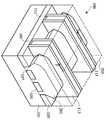
이제 도 1을 참조하여, 핀펫 디바이스와 같은 반도체 디바이스(100)의 사시도가 도시되어 있다. 실시예에서, 반도체 디바이스(100)는 기판(101)과 제1 트렌치들(103)을 포함한다. 기판(101)은 실리콘 기판일 수 있으나, SOI(semiconductor-on-insulator), 스트레인드(strained) SOI, 및 인슐레이터 상 실리콘 게르마늄과 같은 다른 기판들이 사용될 수 있다. 기판(101)은 p형 반도체일 수 있으나, 다른 실시예에서, n형 반도체일 수 있다.Referring now to FIG. 1, a perspective view of a
제1 트렌치들(103)은, 제1 아이솔레이션 영역들(105)의 최종 형성시 개시 단계로서 형성될 수 있다. 제1 트렌치들(103)은, 적합한 에칭 공정과 함께 마스킹층(도 1에 별도로 도시되지 않음)을 사용하여 형성될 수 있다. 예컨대, 마스킹층은 화학적 기상 증착(CVD)과 같은 공정을 통하여 형성된 실리콘 질화물을 포함하는 하드마스크일 수 있으나, 산화물, 산질화물, 실리콘 카바이드, 이들의 조합 등과 같은 다른 재료들, 및 플라즈마 강화된 화학적 기상 증착(PECVD), 저압 화학적 기상 증착(LPCVD), 또는 질화(nitridation)가 따르는 실리콘 산화물 형성과도 같은 다른 공정들이 이용될 수 있다. 마스킹층은, 형성되면, 적합한 포토리소그래피 공정을 통하여 패터닝되어, 제1 트렌치들(103)을 형성하기 위하여 제거될 것인, 기판(101)의 이들 부분들을 노출시킬 수 있다.The
그러나, 당업자는, 마스킹층을 형성하기 위한 상술된 공정들과 재료들이, 제1 트렌치들(103)의 형성을 위하여 기판(101)의 다른 부분들을 노출시키면서, 기판(101)의 부분들을 보호하는 데 사용될 수 있는 유일한 방법이 아니라는 것을 인식할 것이다. 패터닝되고 현상된 포토레지스트와 같은 임의의 적합한 공정이, 제1 트렌치들(103)을 형성하기 위하여 제거될 기판(101)의 부분들을 노출시키는 데 이용될 수 있다. 이러한 모든 방법들은 본 실시예들의 범위에 완전히 포함되고자 한다.However, those skilled in the art, the above-described processes and materials for forming the masking layer protect the parts of the
마스킹층이 형성되고 패터닝되면, 기판(101)에 제1 트렌치들(103)이 형성된다. 노출된 기판(101)은, 기판(101)에 제1 트렌치들(103)을 형성하기 위하여 반응성 이온 에칭(RIE)과 같은 적합한 공정을 통하여 제거될 수 있으나, 임의의 적합한 공정들이 사용될 수 있다. 실시예에서, 제1 트렌치들(103)은, 약 2,500Å과 같은, 기판(101)의 표면으로부터 약 5,000Å 보다 작은 제1 깊이를 갖도록 형성될 수 있다.When the masking layer is formed and patterned,
그러나, 당업자는, 제1 트렌치들(103)을 형성하기 위한 상술된 공정들이 단지 하나의 가능성 있는 공정이지, 유일한 실시예인 것으로 의미하지 않는다는 것을 인식할 것이다. 오히려, 제1 트렌치들(103)이 형성될 수 있는 임의의 적합한 공정이 이용될 수 있고, 임의 수의 마스킹 및 제거 단계들을 포함하는 임의의 적합한 공정이 사용될 수 있다.However, those skilled in the art will recognize that the above-described processes for forming the
제1 트렌치들(103)을 형성하는 것 외에, 마스킹 및 에칭 공정들은, 제거되지 않고 남아 있는 기판(101)의 그 부분들로부터 핀들(107)을 추가적으로 형성한다. 편의를 위해, 핀들(107)은 점선으로 기판(101)으로부터 분리되어 있는 것으로 도면에 도시되었으나, 이 분리의 물리적 표시는 존재할 수도, 존재하지 않을 수도 있다. 이들 핀들(107)은, 후술되는 바와 같이, 복수 게이트 FinFET 트랜지스터의 채널 영역을 형성하는 데 사용될 수 있다. 도 1이 단지 기판(101)으로부터 형성된 3개의 핀들(107)을 도시하지만, 임의 수의 핀들(107)이 이용될 수 있다.In addition to forming the
핀들(107)은, 약 30 nm와 같이, 약 5 nm와 약 80 nm 사이의, 기판(101)의 표면에서의 폭을 갖도록 형성될 수 있다. 부가적으로, 핀들(107)은, 약 50 nm와 같이, 약 10 nm와 약 100 nm 사이의 거리만큼 서로로부터 이격될 수 있다. 그러한 방식으로 핀들(107)을 떨어지게 함으로써, 핀들(107) 각각은, 공통 게이트(이하에 더욱 논의됨)를 공유하는 데 충분히 가까우면서, 개별 채널 영역을 형성할 수 있다.The
제1 트렌치들(103)과 핀들(107)이 형성되었으면, 제1 트렌치들(103)은 유전체 재료로 충전될 수 있고, 이 유전체 재료는 제1 아이솔레이션 영역들(105)을 형성하기 위하여 제1 트렌치들(103) 내에 리세스될 수 있다. 이 유전체 재료는 산화물 재료, 고밀도 플라즈마(high-density plasma, HDP) 산화물, 등일 수 있다. 유전체 재료는, 화학적 기상 증착(CVD)법(예컨대, HARP 공정), 고밀도 플라즈마 CVD법, 또는 종래 기술에 알려진 바와 같은 다른 적합한 형성 방법 중 하나를 이용하여, 제1 트렌치들(103)의 선택적인 세정 및 라이닝(lining) 후에, 형성될 수 있다.Once the
제1 트렌치들(103)은, 제1 트렌치들(103) 및 기판(101)을 유전체 재료로 오퍼필(overfill)한 다음, 화학 기계적 연마(CMP), 에칭, 이들의 조합 등과 같은 적합한 공정을 통하여 제1 트렌치들(103)과 핀들(107)의 외부의 과잉 재료를 제거함으로써 충전될 수 있다. 실시예에서, 제거 공정은 또한 핀들(107) 위에 위치된 임의의 유전체 재료를 제거하여, 유전체 재료의 제거는 추가의 공정 단계에 핀들(107)의 표면을 노출시킬 것이다.The
제1 트렌치들(103)이 유전체 재료로 충전되었으면, 그 후 유전체 재료는 핀들(107)의 표면으로부터 떨어져 리세싱될 수 있다. 리세싱은, 핀들(107)의 상부 표면에 인접한 핀들(107)의 측벽들의 적어도 일부를 노출시키도록 수행될 수 있다. 유전체 재료는, HF와 같은 에천트로 핀들(107)의 상부 표면을 담금으로써 습식 에칭을 사용하여 리세싱될 수 있으나, H2와 같은 다른 에천트, 및 반응성 이온 에칭, NH3/NF3과 같은 에천트로의 건식 에칭, 화학적 산화물 제거, 또는 건식 화학적 세정과 같은 다른 방법들이 사용될 수 있다. 유전체 재료는, 약 400 Å와 같이, 약 50 Å 내지 약 500 Å 사이의, 핀들(107)의 표면으로부터 거리까지 리세싱될 수 있다. 추가적으로, 리세싱은 또한, 핀들(107)이 추가의 공정을 위하여 노출되는 것을 보증하기 위하여, 핀들(107) 위에 위치된 임의의 남은 유전체 재료를 제거할 수 있다.Once the
그러나, 당업자는, 상술된 단계들은 유전체 재료를 충전하고 리세싱하는 데 사용된 전체 공정 흐름의 단지 부분일 수 있다는 것을 인식할 것이다. 예컨대, 라이닝 단계, 세정 단계, 어닐링 단계, 갭 충전 단계들, 이들의 조합, 등은 또한, 제1 트렌치들(103)을 형성하고 유전체 재료로 이 제1 트렌치들(103)을 충전하는 데 이용될 수 있다. 모든 가능성 있는 공정 단계들은, 본 실시예의 범위 내에 완전히 포함되고자 한다.However, one of ordinary skill in the art will recognize that the steps described above may only be part of the overall process flow used to fill and recess the dielectric material. For example, a lining step, a cleaning step, an annealing step, a gap filling steps, a combination thereof, etc., are also used to form the
제1 아이솔레이션 영역들(105)이 형성된 후, 더미 게이트 유전체(109), 이 더미 게이트 유전체(109) 위의 더미 게이트 전극(111), 및 제1 스페이서들(113)이 핀들(107) 각각 위에 형성될 수 있다. 실시예에서, 더미 게이트 유전체(109)는, 열 산화, 화학적 기상 증착, 스퍼터링, 또는 게이트 유전체를 형성하기 위하여 종래 기술에 알려지고 사용된 임의의 다른 방법들에 의하여 형성될 수 있다. 게이트 유전체 형성의 기술에 따라, 핀들(107)의 상부 상의 더미 게이트 유전체(109)의 두께는, 핀들(107)의 측벽 상의 게이트 유전체 두께와는 상이할 수 있다.After the
더미 게이트 유전체(109)는, 약 10 옹스트롬과 같이 약 3 옹스트롬 내지 약 100 옹스트롬의 범위의 두께를 갖는 실리콘 다이옥사이드 또는 실리콘 옥시나이트라이드와 같은 재료를 포함할 수 있다. 더미 게이트 유전체(109)는, 약 10 옹스트롬 이하와 같이, 약 0.5 옹스트롬 내지 약 100 옹스트롬의 등가 산화물(equivalent oxide) 두께를 갖는, 산화 란탄(La2O3), 알루미늄 산화물(Al2O3), 하프늄 산화물(HfO2), 하프늄 옥시나이트라이드(HfON), 또는 지르코늄 산화물(ZrO2), 또는 그 조합과 같은 고 유전율(high permittivity)(high-k) 재료(예컨대, 약 5보다 큰 비 유전율(relative permittivity)을 갖는)로 형성될 수 있다. 또한, 더미 게이트 유전체(109)를 위하여 실리콘 다이옥사이드, 실리콘 옥시나이트라이드 및/또는 하이-k 재료의 임의의 조합이 또한 사용될 수 있다.The dummy gate dielectric 109 may include a material such as silicon dioxide or silicon oxynitride having a thickness in the range of about 3 Angstroms to about 100 Angstroms, such as about 10 Angstroms. The
더미 게이트 전극(111)은 도전성 또는 비도전성 재료를 포함할 수도 있고, 폴리실리콘, W, Al, Cu, AlCu, W, Ti, TiAlN, TaC, TaCN, TaSiN, Mn, Zr, TiN, Ta, TaN, Co, Ni, 이들의 조합 등을 포함하는 그룹에서 선택될 수도 있다. 더미 게이트 전극(111)은, 화학적 기상 증착(CVD), 스퍼터 증착, 또는 도전성 재료들을 성막하기 위하여 종래 기술에서 알려지고 사용된 다른 기술들에 의하여 성막될 수 있다. 더미 게이트 전극(111)의 두께는 약 5Å 내지 약 200Å의 범위 내에 있을 수 있다. 더미 게이트 전극(111)의 상부 표면은, 비평면 상부 표면을 가질 수 있고, 더미 게이트 전극(111)의 패터닝 또는 게이트 에칭 전에 평탄화될 수 있다. 이 시점에서 이온들이 더미 게이트 전극(111)에 도입될 수 있거나 도입되지 않을 수도 있다. 예컨대, 이온들은 이온 주입 공정(ion implantation techniques)에 의하여 도입될 수 있다.The
더미 게이트 전극(109)와 더미 게이트 전극(111)은, 형성되면, 핀들(107) 위에 일련의 스택들(115)을 형성하기 위하여 패터닝될 수 있다. 스택들(115)은, 더미 게이트 유전체(109)의 밑에 핀들(107)의 각 측 상에 위치된 복수의 채널 영역들을 정의한다. 스택들(115)은, 예컨대 종래 기술에 알려진 성막 및 포토리소그래피 기술을 사용하여, 더미 게이트 전극(111) 상의 게이트 마스크(도 1에는 별도로 도시되지 않음)를 성막하고 패터닝함으로써 형성될 수 있다. 게이트 마스크는, 실리콘 산화물, 실리콘 옥시나이트라이드, SiCON, SiC, SiOC, 및/또는 실리콘 질화물과 같은(그러나, 이들에 한정되지 않은) 상용되는 마스킹 및 희생 재료들을 포함할 수도 있고, 약 5Å 내지 약 200Å 사이의 두께로 성막될 수 있다. 더미 게이트 전극(111) 및 더미 게이트 유전체(109)는, 패터닝된 스택들(115)을 형성하기 위하여 건식 에칭 공정을 사용하여 에칭될 수 있다.When formed, the
스택들(115)이 패터닝되었으면, 제1 스페이서들(113)이 형성될 수 있다. 제1 스페이서들(113)은 스택들(115)의 양 면들 상에 형성될 수 있다. 제1 스페이서들(113)은 통상적으로, 이미 형성된 구조 상에 스페이서층(도 1에 별도로 도시되지 않음)을 블랭킷 성막(blanket depositing)시킴으로써 형성된다. 스페이서층은, SiN, 옥시나이트라이드, SiC, SiON, SiOCN, SiOC, 산화물 등을 포함할 수 있고, 화학적 기상 증착(CVD), 플라즈마 강화 CVD, 스퍼터, 및 종래 기술에 알려진 다른 방법들과 같은, 그러한 층을 형성하기 위하여 이용되는 방법들에 의하여 형성될 수 있다. 스페이서층은, 상이한 에칭 특성을 갖는 상이한 재료, 또는 제1 아이솔레이션 영역들(105) 내의 유전체 재료와 동일한 재료를 포함할 수 있다. 이후, 제1 스페이서들(113)은, 제1 스페이서들(113)을 형성하기 위하여, 구조의 수평 표면들로부터 스페이서층을 제거하는 하나 이상의 에칭에 의해서와 같이, 패터닝될 수 있다.When the
일 실시예에서, 제1 스페이서층들(113)은 약 5Å 내지 약 500Å 사이의 두께를 갖도록 형성될 수 있다. 또한, 제1 스페이서들(113)이 형성되었으면, 하나의 스택(115)에 인접한 제1 스페이서(113)는, 약 20nm와 같이, 약 5nm 내지 약 200nm 사이의 거리만큼, 또다른 스택(115)에 인접한 제1 스페이서(113)로부터 떨어질 수 있다. 그러나, 임의의 적합한 두께 및 거리가 이용될 수도 있다.In one embodiment, the first spacer layers 113 may be formed to have a thickness between about 5
도 2는, 스택들(115)과 제1 스페이서들(113)로 보호되지 않은 그러한 영역들로부터의 핀들(107)의 제거, 및 소스/드레인 영역들(201)의 재성장을 도시한다. 스택들(115)과 제1 스페이서층(113)으로 보호되지 않은 그러한 영역들로부터의 핀들(107)의 제거는, 스택들(115)과 제1 스페이서층(113)을 하드마스크들로서 이용하는 반응성 이온 에칭(RIE)에 의하여, 또는 임의의 다른 적합한 제거 공정에 의하여 수행될 수 있다. 이 제거는, 핀들(107)이 제1 아이솔레이션 영역들(105)의 표면과 평면이거나(도시된 바와 같이) 제1 아이솔레이션 영역들(105)의 표면 밑에 있을 때까지, 계속될 수 있다.FIG. 2 shows removal of
핀들(107)의 이들 부분들이 제거되었으면, 하드 마스크(별도로 도시되지 않음)가 배치되고 패터닝되어 더미 게이트 전극(111)을 덮어 성장을 방지하고, 소스/드레인 영역들(201)은 핀들(107) 각각과 접촉하여 재성장될 수 있다. 일 실시예에서, 소스/드레인 영역들(201)이 재성장될 수 있고, 일부 실시예등레서, 소스/드레인 영역들(201)이 재성장되어, 스택들(115) 밑에 위치된 핀들(107)의 채널 영역들에 응력을 부과할 것인 스트레서(stressor)를 형성할 수 있다. 핀들(107)이 실리콘을 포함하고, FinFET이 P형 디바이스인 실시예에서, 소스/드레인 영역들(201)은, 실리콘과 같은 재료, 아니면 채널 영역들과는 상이한 격자 상수를 갖는 실리콘 게르마늄과 같은 재료로 선택적 에피택셜 공정을 통하여 재성장될 수 있다. 에피택셜 성장 공정은, 실란, 디클로로실란, 게르만(germane) 등과 같은 전구체들을 사용할 수 있고, 약 30분과 같이, 약 5분 내지 약 120분 사이 동안 계속될 수 있다.When these portions of the
실시예에서, 소스/드레인 영역들(201)은, 약 5Å 내지 약 1000Å 사이의 두께, 및 약 200Å과 같이, 약 10Å 내지 약 500Å 사이의 제1 아이솔레이션 영역들(105) 너머의 높이를 갖도록 형성될 수 있다. 이 실시예에서, 소스/드레인 영역들(201)은, 약 100 nm와 같이, 약 5nm 내지 약 250nm 사이의 제1 아이솔레이션 영역들(105)의 상부 표면 위의 높이를 갖도록 형성될 수 있다. 그러나, 임의의 적합한 높이가 이용될 수 있다.In an embodiment, the source /
소스/드레인 영역들(201)이 형성되면, 적절한 도펀트를 주입함으로써 도펀트를 소스/드레인 영역들(201)에 주입되어, 핀들(107)에서의 도펀트를 보완할 수 있다. 예컨대, 붕소, 갈륨, 인듐 등과 같은 p형 도펀트가 PMOS 디바이스를 형성하기 위하여 주입될 수 있다. 또는, 인, 비소, 안티모니 등과 같은 n형 도펀트가 NMOS 디바이스를 형성하기 위하여 주입될 수 있다. 이들 도펀트는, 스택들(115)과 제1 스페이서들(113)을 마스크들로서 사용하여 주입될 수 있다. 당업자들은, 많은 다른 공정들, 단계들, 등이 도펀트를 주입하기 위하여 사용될 수 있다는 것을 인식할 것이다는 것이 주목되어야 한다. 예컨대, 당업자들은, 특정 목적을 위하여 적합한 특정 형상 또는 특징을 갖는 소스/드레인 영역들을 형성하기 위하여, 다양한 조합의 스페이서들과 라이너들을 사용하여 복수의 임플란트들이 수행될 수 있다는 것을 인식할 것이다. 이들 공정들 중 임의의 것이 도펀트를 주입하는 데 사용될 수 있고, 상기 설명은, 본 실시예들을 위에 나타낸 단계들에 한정하고자 의미하지 않는다.Once the source /
또한, 이 시점에서, 소스/드레인 영역들(201)의 형성 동안, 더미 게이트 전극(111)을 덮었던 하드 마스크가 제거된다. 실시예에서, 하드 마스크는, 예컨대, 하드 마스크의 재료에 선택적인 습식 또는 건식 에칭 공정을 이용하여 제거될 수 있다. 그러나, 임의의 적합한 제거 공정들이 이용될 수 도 있다.Also, at this point, during formation of the source /
도 2는 또한, 스택들(115)과 소스/드레인 영역들(201) 위에 층간 유전체(inter-layer dielectric; ILD)층(203)(밑의 구조를 보다 명확하게 도시하기 위하여 도 2에 점선으로 도시함)의 형성을 도시한다. ILD층(203)은 BPSG(boron phosphorous silicate glass)와 같은 재료를 포함할 수도 있으나, 임의의 적합한 유전체들이 사용될 수도 있다. ILD층(203)은 PECVD와 같은 공정을 이용하여 형성될 수 있으나, LPCVD와 같은 다른 공정들이 대안적으로 사용될 수도 있다. ILD층(203)은 약 100Å 내지 약 3,000Å 사이의 두께로 형성될 수 있다. ILD층(203)은, 형성되면, 예컨대 화학 기계적 연마 공정과 같은 평탄화 공정을 사용하여 제1 스페이서들(113)로 평탄화될 수 있으나, 임의의 적합한 공정이 이용될 수도 있다.FIG. 2 also shows the inter-layer dielectric (ILD)
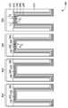
도 3은, 제1 게이트 스택(902)(도 3에는 도시되지 않으나, 도 9에 관하여 이하에 설명됨)에 대한 복수의 층들을 갖는 더미 게이트 전극(111)과 더미 게이트 유전체(109)의 재료의 제거 및 교체를 보다 양호하게 도시하기 위하여, 선 3-3'을 따른, 도 2의 단면도를 도시한다. 또한, 도 3에서, 제1 게이트 스택(902)이 기판(101)의 제1 영역(302) 내에 있는 것으로서 도시되나, 기판(101)의 제2 영역(304)(제2 게이트 스택(904)에 대한), 기판(101)의 제3 영역(306)(제3 게이트 스택(906)에 대한), 및 기판(101)의 제4 영역(308)(제4 게이트 스택(908)에 대한)이 또한 도시된다. 실시예에서, 제1 게이트 스택(902)은, 제1 전압 문턱값(Vt1)을 갖는 제1 트랜지스터(903)(예컨대, 제1 NMOS finFET 트랜지스터)에 대한 게이트 스택일 수 있고, 제2 게이트 스택(904)은, 제1 전압 문턱값(Vt1)과는 상이한 제2 전압 문턱값(Vt2)을 갖는 제2 트랜지스터(905)(예컨대, 제2 NMOS finFET 트랜지스터)에 대한 것일 수 있다. 또는, 제3 게이트 스택(906)은, 제3 전압 문턱값(Vt3)을 갖는 제3 트랜지스터(907)(예컨대, 제1 PMOS finFET 트랜지스터)에 대한 것일 수 있고, 제4 게이트 스택(908)은, 제3 전압 문턱값(Vt3)과는 상이한 제4 전압 문턱값(Vt4)을 갖는 제4 트랜지스터(909)(예컨대, 제2 PMOS finFET 트랜지스터)에 대한 것일 수 있다. 그러나, 임의의 적합한 디바이스들이 이용될 수도 있다.FIG. 3 shows the material of the
실시예에서, 더미 게이트 전극(111)과 더미 게이트 유전체(109)는, 더미 게이트 전극(111)과 더미 게이트 유전체(109)의 재료에 선택적인 에천트를 이용하는 하나 이상의 습식 또는 건식 에칭 공정들을 이용하여 제거될 수 있다. 그러나, 임이의 적합한 제거 공정 또는 공정들이 이용될 수도 있다.In an embodiment, the
더미 게이트 전극(111)과 더미 게이트 유전체(109)가 제거되었으면, 제1 게이트 스택(902), 제2 게이트 스택(904), 제3 게이트 스택(906), 및 제4 게이트 스택(908)을 형성하기 위한 공정이 일련의 층들을 성막함으로써 시작될 수 있다. 실시예에서, 일련의 층들은, 계면층(301), 제1 유전체 재료(303), 제1 금속 재료(305), 및 제1 p-금속 일함수층(307)을 포함할 수 있다.When the
선택적으로, 계면층(301)은 제1 유전체 재료(303)의 형성 전에 형성될 수 있다. 실시예에서, 계면층(301)은, 인 시츄 스팀 생성(in situ steam generation; ISSG)과 같은 공정을 통하여 형성된 실리콘 다이옥사이드와 같은 재료일 수 있다. 다른 실시예에서, 계면층(301)은, 약 10Å과 같은, 약 5Å 내지 약 20Å의 제1 두께(T1)까지의, HfO2, HfSiO, HfSiON, HfTaO, HfTiO, HfZrO, LaO, ZrO, Ta2O5, 이들의 조합 등과 같은 하이-k 재료일 수 있다. 그러나, 임의의 적합한 재료 또는 형성의 공정이 이용될 수도 있다.Optionally, the
계면층(301)이 형성되면, 계면층(301) 위에 캐핑층으로서 제1 유전체 재료(303)가 형성될 수 있다. 실시예에서, 제1 유전체 재료(303)는, 원자층 증착, 화학적 기상 증착 등과 같은 공정을 통하여 성막된, HfO2, HfSiO, HfSiON, HfTaO, HfTiO, HfZrO, LaO, ZrO, Ta2O5, 이들의 조합 등과 같은 하이-k 재료이다. 제1 유전체 재료(303)는, 약 5Å 내지 약 200Å의 제2 두께(T2)로 성막될 수 있으나, 임의의 적합한 재료 및 두께가 이용될 수도 있다.When the
제1 금속 재료(305)는, 배리어층으로서 제1 유전체 재료(303)에 인접하게 형성성될 수 있고, Ta, N, Ti, TiAlN, TaC, TaCN, TaSiN, Mn, Zr, TiN, Ru, Mo, WN, 다른 금속 산화물, 금속 질화물, 금속 실리케이트, 전이 금속-산화물, 전이 금속-질화물, 전이 금속-실리케이트, 금속의 옥시나이트라이드, 금속 알루미네이트, 지르코늄 실리케이트, 지르코늄 알루미네이트, 이들의 조합, 등과 같은 금속성 재료로부터 생성될 수 있다. 제1 금속 재료(305)는, 원자층 증착, 화학적 기상 증착, 스퍼터링 등과 같은 성막 공정을 이용하여, 약 5Å 내지 약 200Å의 제3 두께(T3)로 성막될 수 있으나, 임의의 적합한 공정 또는 두께가 이용될 수도 있다.The
제1 p-금속 일함수층(307)는, 제1 금속 재료(305)에 인접하여 형성될 수 있고, 특정 실시예에서, 제1 금속 재료(305)와 유사할 수 있다. 예컨대, 제1 p-금속 일함수층(307)은, TiN, Ti, TiAiN, TaC, TaCN, TaSiN, TaSi2, NiSi2, Mn, Zr, ZrSi2, TaN, Ru, Al, Mo, MoSi2, Wn, 다른 금속 산화물, 금속 질화물, 금속 실리케이트, 전이 금속-산화물, 전이 금속-질화물, 전이 금속-실리케이트, 금속의 옥시나이트라이드, 금속 알루미네이트, 지르코늄 실리케이트, 지르코늄 알루미네이트, 이들 조합, 등과 같은 금속성 재료로 형성될 수 있다. 또한, 제1 p-금속 일함수층(307)은, 약 5 Å 내지 약 200 Å의 제4 두께(T4)까지, 원자층 증착, 화학적 기상 증착, 스퍼터링 등과 같은 성막 공정을 사용하여 성막될 수 있으나, 임의의 적합한 성막 공정 또는 두께가 사용될 수 있다.The first p-metal
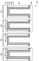
도 4는, 제1 영역(302), 제2 영역(304), 및 제4 영역(306)으로부터는 아니고, 제3 영역(306)으로부터 제1 p-금속 일함수(307)의 제거를 도시한다. 실시예에서, 이 제거는, 제1 영역(302), 제2 영역(304), 제3 영역(306), 및 제4 영역(308) 위에 제1 포토레지스트(401)를 배치함으로써 개시될 수 있다. 다음, 제1 포토레지스트(401)는, 제 위치에 있으면, 제1 영역(302), 제2 영역(304), 및 제4 영역(308)을 노출시키지 않고, 제3 영역(306)을 노출시키도록 패터닝될 수 있다. 이 패터닝은, 제1 포토레지스트(401)의 물리적 특성을 변형시키기 위하여 패터닝된 에너지 소스에 제1 포토레지스트(401)를 노출시키고, 그 후 제1 영역(302), 제2 영역(304), 및 제4 영역(308)을 보호하도록 제1 포토레지스트(401)는 남기면서 제3 영역(306) 위의 제1 포토레지스트(401)의 그 부분을 제거하도록 현상액(developer)을 인가함으로써 수행될 수 있다.FIG. 4 shows removal of the first p-
제1 p-금속 일함수층(307)이 제3 영역(307)에서 노출되었으면, 제3 영역(306)의 제1 p-금속 일함수층(307)이 제거될 수 있다. 실시예에서, 제1 p-금속 일함수층(307)은, 제1 p-금속 일함수층(307)(예컨대, 티타늄 나이트라이드)의 재료에 선택적인, 그리고 밑에 있는 제1 금속 재료(305)(예컨대, 탄탈럼 나이트라이드)의 재료를 현저하게 제거하지 않고 정지하는 습식 에칭 공정 또는 건식 에칭 공정과 같은 하나 이상의 에칭 공정을 이용하여 제3 영역(306)에서 제거될 수 있다. 그러나, 임의의 적합한 제거 공정이 이용될 수 있다.If the first p-metal
도 5는, 제1 p-금속 일함수층(307)이 제거되었으면, 제1 포토레지스트(401)가 제1 영역(302), 제2 영역(304), 및 제4 영역(308) 위로부터 제거될 수 있는 것을 도시한다. 실시예에서, 제1 포토레지스트(401)는, 애싱과 같은 공정을 이용하여 제거될 수 있고, 이로서 제1 포토레지스트(401)의 온도는, 제1 포토레지스트(401)가 열 분해를 경험하고 이후 제거될 수 있을 때 까지 증가된다. 그러나, 제1 포토레지스트(401)를 제거하기 위하여 임의의 다른 적합한 공정이 이용될 수도 있다.5, when the first p-metal
도 5는, 제1 포토레지스트(401)가 제거되었으면, 제2 p-금속 일함수층(501)이 제1 영역(302), 제2 영역(304), 및 제3 영역(306), 및 제4 영역(308) 위에 성막될 수 있는 것을 도시한다. 실시예에서, 제2 p-금속 일함수층(501)은, 제1 p-금속 일함수층(307)의 재료와의 에칭 공정에 대한 큰 선택성을 갖는 것은 물론, 제1 p-금속 일함수층(307)(예컨대, TiN)의 재료보다 큰 또는 이에 근접한 일함수를 갖는 금속일 수 있다. 제2 p-금속 일함수층(501)은 NH4OH 또는 DIO3와 같은 습식 에천트로 습식 에칭 공정을 사용하여 패터닝되고, 제1 p-금속 일함수층(307)이 티타늄 나이트라이드인 일 실시예에서, 제2 p-금속 일함수층(501)의 재료는 약 500 보다 큰 선택도를 가질 수 있다. 그러나, 임의의 적합한 선택도가 이용될 수도 있다.5, when the
특정 실시예에서, 제2 p-금속 일함수층(501)의 재료는, 텅스텐계 금속형 텅스텐, 텅스텐 나이트라이드(WNx), 텅스텐 카바이드 나이트라이드(WCxNy), 텅스텐 옥사이드(WOx), 이들의 조합 등일 수 있다. 다른 실시예에서, 제2 p-금속 일함수층(501)은 몰리브덴, 몰리브덴 나이트라이드(MoNx), 이들의 조합 등과 같은 몰리브덴계 금속일 수 있다. 또다른 실시예에서, 제2 p-금속 일함수층(501)은, 금, 플래티넘, 팔라듐, 이들의 조합 등과 같은 재료일 수 있다. 그러나, 임의의 적합한 재료가 이용될 수도 있다.In a specific embodiment, the material of the second p-metal
실시예에서, 제2 p-금속 일함수층(501)은, 원자층 증착, 화학적 기상 증착, 스퍼터링 등과 같은 성막 공정을 이용하여 성막될 수 있다. 또한, 제2 p-금속 일함수층(501)은 약 5 Å 내지 약 200 Å의 제5 두께(T5)로 성막될 수 있으나, 임의의 적합한 성막 공정 또는 두께가 사용될 수 있다.In an embodiment, the second p-metal
도 6은, 제2 p-금속 일함수층(501)이 제1 영역(302), 제2 영역(304), 제3 영역(306), 및 제4 영역(308) 위에 성막되었으면, 제2 p-금속 일함수층(501)이 제1 영역(302)과 제2 영역(304)으로부터 제거되는 것을 도시한다. 실시예에서, 이 제거는, 제1 영역(302), 제2 영역(304), 및 제3 영역(306), 및 제4 영역(308) 위에 제2 포토레지스트(601)를 배치함으로써 개시될 수 있다. 다음, 제2 포토레지스트(601)는, 제 위치에 있으면, 제3 영역(306) 및 제4 영역(308)을 노출시키지 않고, 제1 영역(302) 및 제2 영역(304)을 노출시키도록 패터닝될 수 있다. 이 패터닝은, 제2 포토레지스트(601)의 물리적 특성을 변형시키도록 패터닝된 에너지 소스에 제2 포토레지스트(601)를 노출시킴으로써, 그리고 그후 제3 영역(306) 및 제4 영역(308)을 보호하도록 제2 포토레지스트(601)는 남기면서 제1 영역(302) 및 제2 영역(304) 위의 제2 포토레지스트(601)의 부분을 제거하도록 현상액을 인가함으로써 수행될 수 있다.6, if the second p-metal
제2 p-금속 일함수층(501)이 제1 영역(302) 및 제2 영역(304)에서 노출되었으면, 제1 영역(302) 및 제2 영역(304)에서의 제2 p-금속 일함수층(501)이 제거될 수 있다. 실시예에서, 제2 p-금속 일함수층(501)은, 제2 p-금속 일함수층(501)의 재료에 선택적이며, 밑에 있는 제1 p-금속 일함수층(307)의 재료를 현저하게 제거하지 않고 정지하는 습식 에칭 공정 또는 건식 에칭 공정과 같은 하나 이상의 에칭 공정을 사용하여 제1 영역(302) 및 제2 영역(304)에서 제거될 수 있다. 그러나, 임의의 적합한 제거 공정이 이용될 수도 있다.If the second p-metal
도 7은, 제2 p-금속 일함수층(501)이 제거되었으면, 제2 포토레지스트(601)가 제3 영역(306) 및 제4 영역(308) 위로부터 제거될 수 있는 것을 도시한다. 실시예에서, 제2 포토레지스트(601)는 애싱과 같은 공정을 이용하여 제거될 수 있고, 이로써 제2 포토레지스트(601)의 온도는, 제2 포토레지스트(601)가 열 분해를 경험하고 이후 제거될 수 있을 때까지 증가된다. 그러나, 제2 포토레지스트(601)를 제거하기 위하여 임의의 다른 적합한 공정이 이용될 수도 있다.FIG. 7 shows that once the second p-metal
도 7은 또한, 제2 포토레지스트(601)가 제거되었으면, 제1 p-금속 일함수층(307)이 제1 영역(302)로부터 제거될 수 있는 것을 도시한다. 실시예에서, 이 제거는, 제3 포토레지스트(701)를, 제1 영역(32), 제2 영역(304), 제3 영역(306), 및 제4 영역(308) 위에 배치시킴으로써 개시될 수 있다. 제 위치에 있으면, 다음, 제3 포토레지스트(701)는, 제2 영역(304), 제3 영역(306), 및 제4 영역(308)을 노출시키지 않고, 제1 영역(302)을 노출시키도록 패터닝될 수 있다. 이 패터닝은, 제3 포토레지스트(701)의 물리적 특성을 변형시키도록 패터닝된 에너지 소스에 제3 포토레지스트(701)를 노출시키고, 그리고 그후 제2 영역(304), 제3 영역(306), 및 제4 영역(308)에 제3 포토레지스트(701)를 남기면서, 제2 영역(302) 위의 제3 포토레지스트(701)의 그 부분을 제거하도록 현상액을 인가함으로써 수행될 수 있다.7 also shows that once the
제1 p-금속 일함수층(307)이 제1 영역(302)에서 노출되었으면, 제1 영역(302)의 제1 p-금속 일함수층(307)이 제거될 수 있다. 실시예에서, 제1 p-금속 일함수층(307)은, 제1 p-금속 일함수층(307)의 재료에 선택적이며, 밑에 있는 제1 금속 재료(305)의 재료를 현저하게 제거하지 않고 정지하는 습식 에칭 공정 또는 건식 에칭 공정과 같은 하나 이상의 에칭 공정을 이용하여 제1 영역(302)에서 제거될 수 있다. 그러나, 임의의 적합한 제거 공정이 이용될 수 있다.If the first p-metal
도 8은, 제3 포토레지스트(701)의 제거, 및 제1 n-금속 일함수층(802), 글루층(804), 및 충전 재료(806)의 성막을 도시한다. 실시예에서, 제3 포토레지스트(701)는, 애싱과 같은 공정을 사용하여 제2 영역(304), 제3 영역(306), 및 제4 영역(308) 위로부터 제거될 수 있고, 이로써 제3 포토레지스트(701)의 온도는, 제3 포토레지스트(701)가 열 분해를 경험하고, 그후 제거될 수 있을 때까지 증가된다. 그러나, 제3 포토레지스트(701)를 제거하기 위하여 임의의 다른 적합한 공정이 사용될 수도 있다.8 shows removal of the
제3 포토레지스트(701)가 제거되었으면, 제1 n-금속 일함수층(802)이 성막될 수 있다. 실시예에서, 제1 n-금속 일함수층(802)은, Ti, Ag, Al, TaAl, TaAlC, TiAlN, TaC, TaCN, TaSiN, Mn, Zr, 다른 적합한 n-형 일함수 재료, 또는 그 조합과 같은 재료일 수 있다. 예컨대, 제1 n-금속 일함수층(802)은, 약 30 Å과 같이, 약 20 Å 내지 약 50 Å의 제6 두께(T6)까지, 원자층 증착(ALD) 공정, CVD 공정 등을 사용하여 성막될 수 있다. 그러나, 제1 n-금속 일함수층(802)을 형성하기 위하여 임의의 적합한 재료들 및 공정들이 사용될 수도 있다.When the
제1 n-금속 일함수층(802)이 형성되었으면, 충전 재료(806)의 형성을 위하여 핵형성층(nucleation layer)을 제공할 뿐 아니라, 밑에 있는 제1 n-금속 일함수층(802)과 밑에 있는 충전 재료(806)을 부착시키는 것을 돕기 위하여 글루층(804)이 형성될 수 있다. 실시예에서, 글루층(804)은, 티타늄 나이트라이드와 같은 재료일 수 있거나 그렇지 않으면 제1 n-금속 일함수층(802)에 유사한 재료일 수 있고, 약 50 Å과 같이, 약 10 Å 내지 약 10 Å의 제7 두께(T7)까지 ALD와 같은 유사한 공정을 사용하여 형성될 수 있다. 그러나, 임의의 적합한 재료들 및 공정들이 사용될 수도 있다.When the first n-metal
글루층(804)이 형성되었으면, 충전 재료(806)가 글루층(804)을 사용하여 개구부의 잔여부를 충전하기 위하여 성막된다. 그러나, 제1 p-금속 일함수층(501)의 부가층들을 단순히 성막하는 것 대신에 제2 p-금속 일함수층(501)을 이용함으로써, 문턱 전압들의 원하는 조정을 획득하기 위하여 더 적은 층들이 사용되고(이하 더 설명됨), 후속하여 성막된 충전 재료(806)에 의하여 충전될 폭들은 다른 것보다 더 큰 채로 있다. 예컨대, 제1 영역(302)에서, 글루층(804)의 성막 후 개구부의 잔여부는, 약 30 Å와 같이, 약 10 Å 내지 약 50 Å의 제1 폭(W1)을 가질 수 있다. 유사하게는, 제2 영역(304)에서, 글루층(804)의 성막 후 개구부의 잔여부는, 약 20 Å와 같이, 약 10 Å 내지 약 40 Å의 제2 폭(W2)을 가질 수 있다. 제3 영역(306)에서, 글루층(804)의 성막 후 개구부의 잔여부는, 약 15 Å와 같이, 약 10 Å 내지 약 40 Å의 제3 폭(W3)을 가질 수 있다. 마지막으로, 제4 영역(308)에서, 글루층(804)의 성막 후 개구부의 잔여부는, 약 15 Å와 같이, 약 10 Å 내지 약 40 Å의 제4 폭(W4)을 가질 수 있다.Once the
또한, 제1 영역(302), 제2 영역(304), 제3 영역(306), 및 제4 영역(308) 각각에서의 상이한 수의 층들로 인하여, 개구부는 각각 충전 재료(806)의 성막 동안 상이한 높이를 가질 수 있다. 예컨대, 제1 영역(302)에서, 글루층(804)의 성막 후 개구부의 전여부는, 약 80 nm와 같이, 약 60 nm 내지 약 100 nm의 제1 높이(H1)를 가질 수 있다. 유사하게, 제2 영역(304)에서, 글루층(804)의 성막 후 개구부의 전여부는, 약 80 nm와 같이, 약 60 nm 내지 약 100 nm의 제2 높이(H2)를 가질 수 있다. 제3 영역(306)에서, 글루층(804)의 성막 후 개구부의 전여부는, 약 100 nm와 같이, 약 60 nm 내지 약 80 nm의 제3 높이(H3)를 가질 수 있다. 마지막으로, 제4 영역(308)에서, 글루층(804)의 성막 후 개구부의 전여부는, 약 80 nm와 같이, 약 60 nm 내지 약 100 nm의 제4 높이(H4)를 가질 수 있다.In addition, due to the different number of layers in each of the
실시예에서, 충전 재료(806)는, 텅스텐, Al, Cu, AlCu, W, Ti, TiAlN, TaC, TaCN, TaSiN, Mn, Zr, TiN, Ta, TaN, Co, Ni, 이들의 조합 등과 같은 재료일 수 있고, 도금, 화학적 기상 증착, 원자층 증착, 물리적 기상 증착, 이들의 조합 등과 같은 성막 공정을 사용하여 형성될 수 있다. 또한, 충전 재료(806)는, 약 1500 Å과 같이, 약 1000 Å 내지 약 2000 Å의 두께로 성막될 수 있다. 그러나, 임의의 적합한 재료가 이용될 수 있다.In an embodiment, the filling
그러나, 여기서 설명된 실시예를 사용함으로써, 개구부들 각각의 애스펙트비(예컨대, 폭에 대한 높이의 비)는, 충전 재료(806)의 성막을 억제시키지 않기에 충분히 작게 유지될 수 있다. 특히, 애스펙트비가 너무 크면, 충전 재료(806)의 성막 공정은 충전 재료(806) 내에 위치된 보이드(void)가 형성되는 결과를 가질 수 있으며, 이는 추가의 제조 또는 동작 동안 원하지 않는 문제점을 야기할 것이다. 그러나, 다양한 게이트 스택들의 조정시 더 적은 수의 층들을 사용함으로써, 애스펙트비가 너 낮게 유지될 수 있고, 이로써 보이드의 형성 및 그 부정적인 결과들의 가능성을 감소시킬 수 있다.However, by using the embodiment described herein, the aspect ratio of each of the openings (eg, the ratio of the height to the width) can be kept small enough not to inhibit the deposition of the filling
도 9는, 충전 재료(806)가 개구부를 충전하고 오버필하도록 성막된 후, 제1 영역(302), 제2 영역(304), 제3 영역(306), 및 제4 영역(308)의 개구부들 각각 내의 재료들은 평탄화되어 제1 게이트 스택(902), 제2 게이트 스택(904), 제3 게이트 스택(906), 및 제4 게이트 스택(908)을 형성할 수 있다. 실시예에서, 재료들은, 예컨대 화학 기계적 연마 공정을 이용하여 제1 스페이서들(113)로 평탄화될 수 있으나, 그라인딩(grinding) 또는 에칭과 같은 임의의 적합한 공정이 사용될 수도 있다.FIG. 9 shows the
제1 게이트 스택(902), 제2 게이트 스택(904), 제3 게이트 스택(906), 및 제4 게이트 스택(908)의 재료들이 형성되고 평탄화된 후, 제1 게이트 스택(902), 제2 게이트 스택(904), 제3 게이트 스택(906), 및 제4 게이트 스택(908)의 재료들이 리세싱되고 캐핑층(capping layer)(901)으로 캐핑(capping)될 수 있다. 실시예에서, 제1 게이트 스택(902), 제2 게이트 스택(904), 제3 게이트 스택(906), 및 제4 게이트 스택(908)의 재료들은, 예컨대, 제1 게이트 스택(902), 제2 게이트 스택(904), 제3 게이트 스택(906), 및 제4 게이트 스택(908)의 재료들에 선택적인 에천트를 사용하는 습식 또는 건식 에칭 공정을 사용하여 리세싱될 수 있다. 실시예에서, 제1 게이트 스택(902), 제2 게이트 스택(904), 제3 게이트 스택(906), 및 제4 게이트 스택(908)의 재료들은, 약 120 nm와 같이, 약 5 nm 내지 약 150 nm의 거리로 리세싱될 수 있다. 그러나, 임의의 적합한 공정 및 거리가 사용될 수도 있다.After the materials of the
제1 게이트 스택(902), 제2 게이트 스택(904), 제3 게이트 스택(906), 및 제4 게이트 스택(908)의 재료들이 리세싱되었으면, 캐핑층(901)이 제1 스페이서들(113)로 성막되고 평탄화될 수 있다. 실시예에서, 캐핑층(901)은, 원자층 증착, 화학적 기상 증착, 스퍼터링 등과 같은 성막 공정을 사용하여 성막된, SiN, SiON, SiCON, SiC, SiOC, 이들의 조합 등과 같은 재료이다. 캐핑층(901)은, 약 5 Å 내지 약 200 Å의 두께로 성막된 후, 캐핑층(901)이 제1 스페이서들(113)과 평면을 이루도록, 화학 기계적 연마와 같은 평탄화 공정을 이용하여 평탄화될 수 있다.Once the materials of the
여기서 설명된 실시예들을 이용함으로써, 다양한 제조 공정 윈도우에서의 감소없이 개별적으로 조정된 문턱 전압들을 갖는 복수의 트랜지스터들이 달성될 수 있다. 예컨대, 제1 영역(302) 내에서, 제1 트랜지스터(903)는, 계면층(301), 제1 유전체 재료(303), 제1 금속 재료(305), 제1 n-금속 일함수층(802), 글루층(804), 및 충전 재료(806)를 포함하는 게이트 스택으로 형성될 수 있다. 이로써, 제1 NMOS 디바이스에 대하여, 제1 트랜지스터(903)는, 약 0.1V와 같이, 약 0.01V 내지 약 0.15V의 제1 문턱 전압(Vt1)을 가질 수 있다.By using the embodiments described herein, a plurality of transistors with individually adjusted threshold voltages can be achieved without reduction in various manufacturing process windows. For example, in the
유사하게, 제2 영역(304) 내에서, 제2 트랜지스터(905)는, 계면층(301), 제1 유전체 재료(303), 제1 금속 재료(305), 제1 p-금속 일함수층(807), 제1 n-금속 일함수층(802), 글루층(804), 및 충전 재료(806)를 포함하는 게이트 스택으로 형성될 수 있다. 이로써, 제2 NMOS 디바이스에 대하여, 제2 트랜지스터(905)는, 약 0.25V와 같이, 약 0.15V 내지 약 0.4V의 제2 문턱 전압(Vt2)을 가질 수 있다.Similarly, within the
또한, 제3 영역(306) 내에서, 제3 트랜지스터(907)는, 계면층(301), 제1 유전체 재료(303), 제1 금속 재료(305), 제2 p-금속 일함수층(501), 제1 n-금속 일함수층(802), 글루층(804), 및 충전 재료(806)를 포함하는 게이트 스택으로 형성될 수 있다. 이로써, 제1 PMOS 디바이스에 대하여, 제1 트랜지스터(907)는, 약 0.25V와 같이, 약 0.15V 내지 약 0.4V의 제3 문턱 전압(Vt3)을 가질 수 있다.In addition, within the
마지막으로, 제4 영역(308) 내에서, 제4 트랜지스터(909)는, 계면층(301), 제1 유전체 재료(303), 제1 금속 재료(305), 제1 p-금속 일함수층(307), 제2 p-금속 일함수층(501), 제1 n-금속 일함수층(802), 글루층(804), 및 충전 재료(806)를 포함하는 게이트 스택으로 형성될 수 있다. 이로써, 제2 PMOS 디바이스에 대하여, 제4 트랜지스터(909)는, 약 0.1V와 같이, 약 0.01V 내지 약 0.15V의 제4 문턱 전압(Vt4)을 가질 수 있다.Finally, within the
여기서 설명된 실시예들을 이용함으로써, 디바이스의 문턱 전압들을 조정하기 위하여 복수의 상이한 재료들이 이용된다. 복수의 상이한 금속들을 이용함으로써, 동일한 재료(예컨대, TiN)의 복수의 층들의 스택이 회피될 수 있고, 그 자체로 동일한 재료로보다 두께의 전체적인 감소가 달성될 수 있다. 이로써, 층들의 총 두께가 감소될 수 있고, 이는 후속 층들에 대하여 보다 적은 비용으로 갭-충전 윈도우(gap-fill window)를 증가시킨다. 이러한 감소는, 보다 적은 보이드가 형성될 것이고, 금속 게이트가 개구부를 완전히 충전할 수 있으므로, 보다 양호한 문턱값 안정성(threshold stability)을 또한 허용한다. 이로써, 복수의 문턱 전압 조정은, N/P 패터닝과 금속 게이트 갭-충전 윈도우를 희생시키지 않고, 훨씬 더 좁은 임계 치수(예컨대, 5nm 및 3nm 기술 노드에 대하여)로 달성될 수 있다.By using the embodiments described herein, a plurality of different materials are used to adjust the threshold voltages of the device. By using a plurality of different metals, a stack of multiple layers of the same material (eg TiN) can be avoided, and an overall reduction in thickness than with the same material itself can be achieved. Thereby, the total thickness of the layers can be reduced, which increases the gap-fill window at a lower cost for subsequent layers. This reduction also allows for better threshold stability as fewer voids will be formed and the metal gate can completely fill the opening. As such, multiple threshold voltage adjustments can be achieved with much narrower critical dimensions (eg, for 5nm and 3nm technology nodes) without sacrificing N / P patterning and metal gate gap-filling windows.
실시예에서, 반도체 디바이스의 제조 방법은, 제1 영역, 제2 영역, 제3 영역, 및 제4 영역 위에 게이트 유전체를 성막하는 단계; 제1 영역, 제2 영역, 제3 영역, 및 제4 영역 위에 제1 금속 재료를 성막하는 단계; 제1 영역, 제2 영역, 제3 영역, 및 제4 영역 위에 제1 일함수층을 성막하는 단계; 제1 일함수층을 제3 영역으로부터 제거하는 단계; 제1 일함수층을 제거한 후, 제1 영역, 제2 영역, 제3 영역, 및 제4 영역 위에 제2 일함수층을 성막하는 단계 - 상기 제2 일함수층은 상기 제1 일함수층과는 상이함 - ; 제1 영역 및 제2 영역으로부터 제2 일함수층을 제거하는 단계; 제1 영역으로부터 제1 일함수층을 제거하는 단계; 및 제1 일함수층을 제거한 후, 제1 영역, 제2 영역, 제3 영역, 및 제4 영역 위에 충전 재료를 성막하는 단계를 포함한다. 실시예에서, 제1 일함수층은 티타늄 나이트라이드를 포함한다. 실시예에서, 제2 일함수층은 텅스텐을 포함한다. 실시예에서, 제2 일함수층은 텅스텐 옥사이드를 포함한다. 실시예에서, 제2 일함수층은 텅스텐 나이트라이드를 포함한다. 실시예에서, 제2 일함수층은 몰리브덴을 포함한다. 실시예에서, 제2 일함수층은 몰리브덴 나이트라이드를 포함한다.In an embodiment, a method of manufacturing a semiconductor device includes depositing a gate dielectric over a first region, a second region, a third region, and a fourth region; Depositing a first metal material over the first, second, third, and fourth regions; Depositing a first work function layer on the first region, the second region, the third region, and the fourth region; Removing the first work function layer from the third region; After removing the first work function layer, depositing a second work function layer over the first region, the second region, the third region, and the fourth region-the second work function layer is formed with the first work function layer. Is different-; Removing the second work function layer from the first region and the second region; Removing the first work function layer from the first region; And after removing the first work function layer, depositing a filling material over the first region, the second region, the third region, and the fourth region. In an embodiment, the first work function layer comprises titanium nitride. In an embodiment, the second work function layer comprises tungsten. In an embodiment, the second work function layer comprises tungsten oxide. In an embodiment, the second work function layer comprises tungsten nitride. In an embodiment, the second work function layer comprises molybdenum. In an embodiment, the second work function layer includes molybdenum nitride.
다른 실시예에서, 반도체 디바이스를 제조하는 방법은, 제1 영역 및 제2 영역 위에 제1 복수의 게이트 재료들을 성막하는 단계; 제1 영역으로부터 제1 복수의 게이트 재료들 중 제1 게이트 재료를 제거함으로써 제1 복수의 게이트 재료들로부터 형성된 트랜지스터들 중 제1 트랜지스터의 제1 문턱 전압을 조정하는 단계; 및 제1 영역 및 제2 영역 위에 제2 게이트 재료를 형성하고, 제2 영역으로부터 제2 게이트 재료를 제거함으로써 제1 복수의 게이트 재료들로부터 형성된 트랜지스터들 중 제2 트랜지스터의 제2 문턱 전압을 조정하는 단계 - 상기 제1 게이트 재료는 상기 제2 게이트 재료와는 상이하고, 상기 트랜지스터들 중 제1 트랜지스터는 제1 PMOS 트랜지스터이고, 상기 트랜지스터들 중 제2 트랜지스터는 제2 PMOS 트랜지스터임 -를 포함한다. 실시예에서, 제1 영역 위에 제2 게이트 재료를 형성하는 것은, 배리어층과 물리적 접촉하는 제2 게이트 재료를 성막하는 것을 포함한다. 실시예에서, 제2 영역 위에 제2 게이트 재료를 형성하는 것은, 제2 영역에서 제1 게이트 재료와 물리적 접촉하는 제2 게이트 재료를 성막하는 것을 포함한다. 실시예에서, 배리어층은 탄탈럼 나이트라이드를 포함한다. 실시예에서, 제1 복수의 게이트 재료들을 성막하는 단계는 또한, 반도체 핀 위에 계면층을 성막하는 단계; 및 상기 계면층 위에 유전체 캐핑층을 성막하는 단계를 포함한다. 실시예에서, 본 방법은 또한, 제2 게이트 재료 위에 글루층을 성막하는 단계를 포함한다. 실시예에서, 본 방법은 또한, 글루층 위에 충전 재료를 성막하는 단계를 포함한다.In another embodiment, a method of manufacturing a semiconductor device includes depositing a first plurality of gate materials over a first region and a second region; Adjusting a first threshold voltage of the first transistor among the transistors formed from the first plurality of gate materials by removing the first gate material among the first plurality of gate materials from the first region; And forming a second gate material over the first and second regions, and removing the second gate material from the second region to adjust the second threshold voltage of the second transistor among the transistors formed from the first plurality of gate materials. The first gate material is different from the second gate material, the first of the transistors is a first PMOS transistor, and the second of the transistors is a second PMOS transistor. . In an embodiment, forming the second gate material over the first region includes depositing a second gate material in physical contact with the barrier layer. In an embodiment, forming the second gate material over the second region includes depositing a second gate material in physical contact with the first gate material in the second region. In an embodiment, the barrier layer comprises tantalum nitride. In an embodiment, depositing the first plurality of gate materials may also include depositing an interfacial layer over the semiconductor fins; And depositing a dielectric capping layer over the interface layer. In an embodiment, the method also includes depositing a glue layer over the second gate material. In an embodiment, the method also includes depositing a filling material over the glue layer.
또다른 실시예에서, 반도체 디바이스는, 제1 반도체 핀 위의 제1 게이트 스택 - 상기 제1 게이트 스택은 제1 금속 재료를 포함함 - ; 제2 반도체 핀 위의 제2 게이트 스택 - 상기 제2 게이트 스택은, 제1 금속 재료, 및 상기 제1 금속 재료와는 상이한 제1 p-금속 재료를 포함함 -; 제3 반도체 핀 위의 제3 게이트 스택 - 상기 제3 게이트 스택은, 상기 제1 금속 재료, 및 상기 제1 금속 재료와는 상이한 제2 p-금속 재료를 포함함 - ; 및 제4 반도체 핀 위의 제4 게이트 스택 - 상기 제4 게이트 스택은, 상기 제1 금속 재료, 상기 제1 p-금속 재료, 및 제2 p-금속 재료를 포함함 - 을 포함하고, 상기 제1 게이트 스택, 상기 제2 게이트 스택, 상기 제3 게이트 스택, 및 상기 제4 게이트 스택 각각은, n-금속 재료를 포함하고, 상기 제1 게이트 스택에서의 상기 n-금속 재료는 상기 제1 금속 재료와 물리적 접촉하고, 상기 제2 게이트 스택에서의 상기 n-금속 재료는 상기 제1 p-금속 재료와 물리적 접촉하고, 상기 제3 게이트 스택에서의 상기 n-금속 재료는 상기 제2 p-금속 재료와 물리적 접촉하고, 상기 제4 게이트 스택에서의 상기 n-금속 재료는 상기 제2 p-금속 재료와 물리적 접촉한다. 실시예에서, 제2 p-금속 재료는 텅스텐계 재료를 포함한다. 실시예에서, 제2 p-금속 재료는 텅스텐 카본 나이트라이드를 포함한다. 실시예에서, 제2 p-금속 재료는 몰리브덴계 재료를 포함한다. 실시예에서, 제2 p-금속 재료는 몰리브덴 나이트라이드를 포함한다. 실시예에서, 제1 p-금속 재료는 티타늄 나이트라이드를 포함한다.In another embodiment, a semiconductor device comprises: a first gate stack over a first semiconductor fin, the first gate stack comprising a first metal material; A second gate stack over a second semiconductor fin, the second gate stack comprising a first metal material, and a first p-metal material different from the first metal material; A third gate stack over a third semiconductor fin, the third gate stack comprising the first metal material and a second p-metal material different from the first metal material; And a fourth gate stack over the fourth semiconductor fin, the fourth gate stack including the first metal material, the first p-metal material, and the second p-metal material. Each of the first gate stack, the second gate stack, the third gate stack, and the fourth gate stack includes an n-metal material, and the n-metal material in the first gate stack is the first metal Material in physical contact, the n-metal material in the second gate stack in physical contact with the first p-metal material, and the n-metal material in the third gate stack in the second p-metal In physical contact with the material, and the n-metal material in the fourth gate stack in physical contact with the second p-metal material. In an embodiment, the second p-metal material comprises a tungsten-based material. In an embodiment, the second p-metal material comprises tungsten carbon nitride. In an embodiment, the second p-metal material comprises a molybdenum-based material. In an embodiment, the second p-metal material comprises molybdenum nitride. In an embodiment, the first p-metal material comprises titanium nitride.
상기 내용은 몇몇 실시예들의 특징의 개요를 서술하여, 당업자는 본 개시의 태양을 보다 잘 이해할 것이다. 당업자는, 그들이 동일한 목적을 달성하고/달성하거나, 여기서 도입된 실시예들의 동일한 이점을 달성하기 위한 다른 공정들 및 구조들을 설계하거나 변경하기 위한 기초로서 본 개시를 용이하게 이용할 수 있다는 것을 이해해야한다. 당업자들은 또한, 그러한 등가 구조들은 본 개시의 사상 및 범위로부터 벗어나지 않으며, 당업자들이 본 개시의 사상 및 범위로부터 벗어나지 않고 여기서 다양한 변경, 대체, 및 개조를 행할 수 있다는 것을 인식해야 한다.The above outlines features of some embodiments, and those skilled in the art will better understand aspects of the present disclosure. Those skilled in the art should understand that they can readily use the present disclosure as a basis for designing or altering other processes and structures to achieve the same purpose and / or achieve the same advantages of the embodiments introduced herein. Those skilled in the art should also recognize that such equivalent structures do not depart from the spirit and scope of the present disclosure, and those skilled in the art can make various changes, replacements, and modifications without departing from the spirit and scope of the present disclosure.
[부기][bookkeeping]
1. 반도체 디바이스의 제조 방법으로서,1. A method for manufacturing a semiconductor device,
제1 영역, 제2 영역, 제3 영역, 및 제4 영역 위에 게이트 유전체를 성막(deposit)하는 단계;Depositing a gate dielectric over the first region, the second region, the third region, and the fourth region;
상기 제1 영역, 상기 제2 영역, 상기 제3 영역, 및 상기 제4 영역 위에 제1 금속 재료를 성막하는 단계;Depositing a first metal material over the first region, the second region, the third region, and the fourth region;
상기 제1 영역, 상기 제2 영역, 상기 제3 영역, 및 상기 제4 영역 위에 제1 일함수층을 성막하는 단계;Depositing a first work function layer on the first region, the second region, the third region, and the fourth region;
상기 제3 영역으로부터 상기 제1 일함수층을 제거하는 단계;Removing the first work function layer from the third region;
상기 제1 일함수층을 제거하는 단계 후, 상기 제1 영역, 상기 제2 영역, 상기 제3 영역, 및 상기 제4 영역 위에 제2 일함수층을 성막하는 단계 - 상기 제2 일함수층은 상기 제1 일함수층과는 상이함 - ;After the step of removing the first work function layer, depositing a second work function layer over the first region, the second region, the third region, and the fourth region-the second work function layer Different from the first work function layer-;
상기 제1 영역 및 상기 제2 영역으로부터 상기 제2 일함수층을 제거하는 단계;Removing the second work function layer from the first region and the second region;
상기 제1 영역으로부터 상기 제1 일함수층을 제거하는 단계; 및Removing the first work function layer from the first region; And
상기 제1 일함수층을 제거하는 단계 후, 상기 제1 영역, 상기 제2 영역, 상기 제3 영역, 및 상기 제4 영역 위에 충전 재료를 성막하는 단계After the step of removing the first work function layer, depositing a filling material over the first region, the second region, the third region, and the fourth region
를 포함하는 반도체 디바이스의 제조 방법.Method for manufacturing a semiconductor device comprising a.
2. 제 1 항에 있어서, 상기 제1 일함수층은 티타늄 나이트라이드를 포함하는 것인 반도체 디바이스의 제조 방법.2. The method of claim 1, wherein the first work function layer comprises titanium nitride.
3. 제 2 항에 있어서, 상기 제2 일함수층은 텅스텐을 포함하는 것인 반도체 디바이스의 제조 방법.3. The method of
4. 제 2 항에 있어서, 상기 제2 일함수층은 텅스텐 옥사이드를 포함하는 것인 반도체 디바이스의 제조 방법.4. The method of
5. 제 2 항에 있어서, 상기 제2 일함수층은 텅스텐 나이트라이드를 포함하는 것인 반도체 디바이스의 제조 방법.5. The method of
6. 제 2 항에 있어서, 상기 제2 일함수층은 몰리브덴을 포함하는 것인 반도체 디바이스의 제조 방법.6. The method of
7. 제 1 항에 있어서, 상기 제2 일함수층은 몰리브덴 나이트라이드를 포함하는 것인 반도체 디바이스의 제조 방법.7. The method of claim 1, wherein the second work function layer comprises molybdenum nitride.
8. 반도체 디바이스를 제조하는 방법으로서,8. A method for manufacturing a semiconductor device,
제1 영역 및 제2 영역 위에 제1 복수의 게이트 재료들을 성막하는 단계;Depositing a first plurality of gate materials over the first and second regions;
상기 제1 영역으로부터 상기 제1 복수의 게이트 재료들 중의 제1 게이트 재료를 제거함으로써 상기 제1 복수의 게이트 재료들로부터 형성된 트랜지스터들 중 제1 트랜지스터의 제1 문턱 전압을 조정하는 단계; 및Adjusting a first threshold voltage of a first transistor among transistors formed from the first plurality of gate materials by removing a first gate material of the first plurality of gate materials from the first region; And
상기 제1 영역 및 상기 제2 영역 위에 제2 게이트 재료를 형성하고, 상기 제2 영역으로부터 상기 제2 게이트 재료를 제거함으로써 상기 제1 복수의 게이트 재료들로부터 형성된 트랜지스터들 중 제2 트랜지스터의 제2 문턱 전압을 조정하는 단계 - 상기 제1 게이트 재료는 상기 제2 게이트 재료와는 상이하고, 상기 트랜지스터들 중 상기 제1 트랜지스터는 제1 PMOS 트랜지스터이고, 상기 트랜지스터들 중 상기 제2 트랜지스터는 제2 PMOS 트랜지스터임 -Forming a second gate material over the first region and the second region, and removing the second gate material from the second region, such that a second of the second transistors among the transistors formed from the first plurality of gate materials Adjusting the threshold voltage-the first gate material is different from the second gate material, the first transistor of the transistors is a first PMOS transistor, and the second transistor of the transistors is a second PMOS Transistor-
를 포함하는 반도체 디바이스를 제조하는 방법.Method for manufacturing a semiconductor device comprising a.
9. 제 8 항에 있어서, 상기 제1 영역 위에 상기 제2 게이트 재료를 형성하는 것은, 배리어층과 물리적 접촉하는 상기 제2 게이트 재료를 성막하는 것을 포함하는 것인 반도체 디바이스를 제조하는 방법.9. The method of claim 8, wherein forming the second gate material over the first region comprises depositing the second gate material in physical contact with a barrier layer.
10. 제 9 항에 있어서, 상기 제2 영역 위에 상기 제2 게이트 재료를 형성하는 것은, 상기 제2 영역에서 상기 제1 게이트 재료와 물리적 접촉하는 상기 제2 게이트 재료를 성막하는 것을 포함하는 것인 반도체 디바이스를 제조하는 방법.10. The method of claim 9, wherein forming the second gate material over the second region comprises depositing the second gate material in physical contact with the first gate material in the second region. Method for manufacturing a semiconductor device.
11. 제 10 항에 있어서, 상기 배리어층은 탄탈럼 나이트라이드를 포함하는 것인 반도체 디바이스를 제조하는 방법.11. The method of claim 10, wherein the barrier layer comprises tantalum nitride.
12. 제 8 항에 있어서, 상기 제1 복수의 게이트 재료들을 성막하는 단계는,12. The method of claim 8, wherein depositing the first plurality of gate materials comprises:
반도체 핀 위에 계면층을 성막하는 단계; 및Depositing an interfacial layer on the semiconductor fin; And
상기 계면층 위에 유전체 캐핑층(dielectric capping layer)을 성막하는 단계Depositing a dielectric capping layer on the interfacial layer
를 더 포함하는 것인 반도체 디바이스를 제조하는 방법.A method of manufacturing a semiconductor device further comprising a.
13. 제 8 항에 있어서, 상기 제2 게이트 재료 위에 글루층을 성막하는 단계를 더 포함하는 반도체 디바이스를 제조하는 방법.13. The method of claim 8, further comprising depositing a glue layer over the second gate material.
14. 제 13 항에 있어서, 상기 글루층 위에 충전 재료를 성막하는 단계를 더 포함하는 반도체 디바이스를 제조하는 방법.14. The method of claim 13, further comprising depositing a filling material over the glue layer.
15. 반도체 디바이스로서,15. As a semiconductor device,
제1 반도체 핀 위의 제1 게이트 스택 - 상기 제1 게이트 스택은 제1 금속 재료를 포함함 - ;A first gate stack over a first semiconductor fin, the first gate stack comprising a first metal material;
제2 반도체 핀 위의 제2 게이트 스택 - 상기 제2 게이트 스택은, 상기 제1 금속 재료, 및 상기 제1 금속 재료와는 상이한 제1 p-금속 재료를 포함함 -;A second gate stack over a second semiconductor fin, the second gate stack comprising the first metal material, and a first p-metal material different from the first metal material;
제3 반도체 핀 위의 제3 게이트 스택 - 상기 제3 게이트 스택은, 상기 제1 금속 재료, 및 상기 제1 금속 재료와는 상이한 제2 p-금속 재료를 포함함 - ; 및A third gate stack over a third semiconductor fin, the third gate stack comprising the first metal material and a second p-metal material different from the first metal material; And
제4 반도체 핀 위의 제4 게이트 스택 - 상기 제4 게이트 스택은, 상기 제1 금속 재료, 상기 제1 p-금속 재료, 및 상기 제2 p-금속 재료를 포함함 -A fourth gate stack over a fourth semiconductor fin, the fourth gate stack comprising the first metal material, the first p-metal material, and the second p-metal material-
을 포함하고,Including,
상기 제1 게이트 스택, 상기 제2 게이트 스택, 상기 제3 게이트 스택, 및 상기 제4 게이트 스택 각각은, n-금속 재료를 포함하고, 상기 제1 게이트 스택에서의 상기 n-금속 재료는 상기 제1 금속 재료와 물리적 접촉하고, 상기 제2 게이트 스택에서의 상기 n-금속 재료는 상기 제1 p-금속 재료와 물리적 접촉하고, 상기 제3 게이트 스택에서의 상기 n-금속 재료는 상기 제2 p-금속 재료와 물리적 접촉하고, 상기 제4 게이트 스택에서의 상기 n-금속 재료는 상기 제2 p-금속 재료와 물리적 접촉하는 것인 반도체 디바이스.Each of the first gate stack, the second gate stack, the third gate stack, and the fourth gate stack includes an n-metal material, and the n-metal material in the first gate stack is the first Physical contact with one metal material, the n-metal material in the second gate stack in physical contact with the first p-metal material, and the n-metal material in the third gate stack in the second p A semiconductor device in physical contact with a metal material and the n-metal material in the fourth gate stack in physical contact with the second p-metal material.
16. 제 15 항에 있어서, 상기 제2 p-금속 재료는 텅스텐계 재료를 포함하는 것인 반도체 디바이스.16. The semiconductor device according to 15, wherein said second p-metal material comprises a tungsten-based material.
17. 제 16 항에 있어서, 상기 제2 p-금속 재료는 텅스텐 카본 나이트라이드를 포함하는 것인 반도체 디바이스.17. The semiconductor device of claim 16, wherein the second p-metal material comprises tungsten carbon nitride.
18. 제 15 항에 있어서, 상기 제2 p-금속 재료는 몰리브덴계 재료를 포함하는 것인 반도체 디바이스.18. The semiconductor device according to 15, wherein said second p-metal material comprises a molybdenum-based material.
19. 제 18 항에 있어서, 상기 제2 p-금속 재료는 몰리브덴 나이트라이드를 포함하는 것인 반도체 디바이스.19. The semiconductor device of claim 18, wherein the second p-metal material comprises molybdenum nitride.
20. 제 15 항에 있어서, 상기 제1 p-금속 재료는 티타늄 나이트라이드를 포함하는 것인 반도체 디바이스.20. The semiconductor device of claim 15, wherein the first p-metal material comprises titanium nitride.
Claims (10)
Translated fromKorean제1 영역, 제2 영역, 제3 영역, 및 제4 영역 위에 게이트 유전체를 성막(deposit)하는 단계;
상기 제1 영역, 상기 제2 영역, 상기 제3 영역, 및 상기 제4 영역 위에 제1 금속 재료를 성막하는 단계;
상기 제1 영역, 상기 제2 영역, 상기 제3 영역, 및 상기 제4 영역 위에 제1 일함수층을 성막하는 단계;
상기 제3 영역으로부터 상기 제1 일함수층을 제거하는 단계;
상기 제1 일함수층을 제거하는 단계 후, 상기 제1 영역, 상기 제2 영역, 상기 제3 영역, 및 상기 제4 영역 위에 제2 일함수층을 성막하는 단계 - 상기 제2 일함수층은 상기 제1 일함수층과는 상이함 - ;
상기 제1 영역 및 상기 제2 영역으로부터 상기 제2 일함수층을 제거하는 단계;
상기 제1 영역으로부터 상기 제1 일함수층을 제거하는 단계; 및
상기 제1 일함수층을 제거하는 단계 후, 상기 제1 영역, 상기 제2 영역, 상기 제3 영역, 및 상기 제4 영역 위에 충전 재료를 성막하는 단계
를 포함하는 반도체 디바이스의 제조 방법.A method for manufacturing a semiconductor device,
Depositing a gate dielectric over the first region, the second region, the third region, and the fourth region;
Depositing a first metal material over the first region, the second region, the third region, and the fourth region;
Depositing a first work function layer on the first region, the second region, the third region, and the fourth region;
Removing the first work function layer from the third region;
After the step of removing the first work function layer, depositing a second work function layer over the first region, the second region, the third region, and the fourth region-the second work function layer Different from the first work function layer-;
Removing the second work function layer from the first region and the second region;
Removing the first work function layer from the first region; And
After the step of removing the first work function layer, depositing a filling material over the first region, the second region, the third region, and the fourth region
Method for manufacturing a semiconductor device comprising a.
제1 영역 및 제2 영역 위에 제1 복수의 게이트 재료들을 성막하는 단계;
상기 제1 영역으로부터 상기 제1 복수의 게이트 재료들 중의 제1 게이트 재료를 제거함으로써 상기 제1 복수의 게이트 재료들로부터 형성된 트랜지스터들 중 제1 트랜지스터의 제1 문턱 전압을 조정하는 단계; 및
상기 제1 영역 및 상기 제2 영역 위에 제2 게이트 재료를 형성하고, 상기 제2 영역으로부터 상기 제2 게이트 재료를 제거함으로써 상기 제1 복수의 게이트 재료들로부터 형성된 트랜지스터들 중 제2 트랜지스터의 제2 문턱 전압을 조정하는 단계 - 상기 제1 게이트 재료는 상기 제2 게이트 재료와는 상이하고, 상기 트랜지스터들 중 상기 제1 트랜지스터는 제1 PMOS 트랜지스터이고, 상기 트랜지스터들 중 상기 제2 트랜지스터는 제2 PMOS 트랜지스터임 -
를 포함하는 반도체 디바이스를 제조하는 방법.A method for manufacturing a semiconductor device,
Depositing a first plurality of gate materials over the first and second regions;
Adjusting a first threshold voltage of a first transistor among transistors formed from the first plurality of gate materials by removing a first gate material of the first plurality of gate materials from the first region; And
Forming a second gate material over the first region and the second region, and removing the second gate material from the second region, such that a second of the second transistors among the transistors formed from the first plurality of gate materials Adjusting the threshold voltage-the first gate material is different from the second gate material, the first transistor of the transistors is a first PMOS transistor, and the second transistor of the transistors is a second PMOS Transistor-
Method for manufacturing a semiconductor device comprising a.
반도체 핀 위에 계면층을 성막하는 단계; 및
상기 계면층 위에 유전체 캐핑층(dielectric capping layer)을 성막하는 단계
를 더 포함하는 것인 반도체 디바이스를 제조하는 방법.The method of claim 5, wherein depositing the first plurality of gate materials comprises:
Depositing an interfacial layer on the semiconductor fin; And
Depositing a dielectric capping layer on the interfacial layer
A method of manufacturing a semiconductor device further comprising a.
제1 반도체 핀 위의 제1 게이트 스택 - 상기 제1 게이트 스택은 제1 금속 재료를 포함함 - ;
제2 반도체 핀 위의 제2 게이트 스택 - 상기 제2 게이트 스택은, 상기 제1 금속 재료, 및 상기 제1 금속 재료와는 상이한 제1 p-금속 재료를 포함함 -;
제3 반도체 핀 위의 제3 게이트 스택 - 상기 제3 게이트 스택은, 상기 제1 금속 재료, 및 상기 제1 금속 재료와는 상이한 제2 p-금속 재료를 포함함 - ; 및
제4 반도체 핀 위의 제4 게이트 스택 - 상기 제4 게이트 스택은, 상기 제1 금속 재료, 상기 제1 p-금속 재료, 및 상기 제2 p-금속 재료를 포함함 -
을 포함하고,
상기 제1 게이트 스택, 상기 제2 게이트 스택, 상기 제3 게이트 스택, 및 상기 제4 게이트 스택 각각은, n-금속 재료를 포함하고, 상기 제1 게이트 스택에서의 상기 n-금속 재료는 상기 제1 금속 재료와 물리적 접촉하고, 상기 제2 게이트 스택에서의 상기 n-금속 재료는 상기 제1 p-금속 재료와 물리적 접촉하고, 상기 제3 게이트 스택에서의 상기 n-금속 재료는 상기 제2 p-금속 재료와 물리적 접촉하고, 상기 제4 게이트 스택에서의 상기 n-금속 재료는 상기 제2 p-금속 재료와 물리적 접촉하는 것인 반도체 디바이스.As a semiconductor device,
A first gate stack over a first semiconductor fin, the first gate stack comprising a first metal material;
A second gate stack over a second semiconductor fin, the second gate stack comprising the first metal material, and a first p-metal material different from the first metal material;
A third gate stack over a third semiconductor fin, the third gate stack comprising the first metal material and a second p-metal material different from the first metal material; And
A fourth gate stack over a fourth semiconductor fin, the fourth gate stack comprising the first metal material, the first p-metal material, and the second p-metal material-
Including,
Each of the first gate stack, the second gate stack, the third gate stack, and the fourth gate stack includes an n-metal material, and the n-metal material in the first gate stack is the first Physical contact with one metal material, the n-metal material in the second gate stack in physical contact with the first p-metal material, and the n-metal material in the third gate stack in the second p A semiconductor device in physical contact with a metal material and the n-metal material in the fourth gate stack in physical contact with the second p-metal material.
Priority Applications (1)
| Application Number | Priority Date | Filing Date | Title |
|---|---|---|---|
| KR1020210040239AKR102374899B1 (en) | 2018-09-27 | 2021-03-29 | Semiconductor device and method of manufacture |
Applications Claiming Priority (4)
| Application Number | Priority Date | Filing Date | Title |
|---|---|---|---|
| US201862737419P | 2018-09-27 | 2018-09-27 | |
| US62/737,419 | 2018-09-27 | ||
| US16/193,906 | 2018-11-16 | ||
| US16/193,906US10867864B2 (en) | 2018-09-27 | 2018-11-16 | Semiconductor device and method of manufacture |
Related Child Applications (1)
| Application Number | Title | Priority Date | Filing Date |
|---|---|---|---|
| KR1020210040239ADivisionKR102374899B1 (en) | 2018-09-27 | 2021-03-29 | Semiconductor device and method of manufacture |
Publications (1)
| Publication Number | Publication Date |
|---|---|
| KR20200036690Atrue KR20200036690A (en) | 2020-04-07 |
Family
ID=69946534
Family Applications (1)
| Application Number | Title | Priority Date | Filing Date |
|---|---|---|---|
| KR1020190020991ACeasedKR20200036690A (en) | 2018-09-27 | 2019-02-22 | Semiconductor device and method of manufacture |
Country Status (4)
| Country | Link |
|---|---|
| US (2) | US10867864B2 (en) |
| KR (1) | KR20200036690A (en) |
| CN (1) | CN110957270B (en) |
| TW (1) | TWI715218B (en) |
Families Citing this family (9)
| Publication number | Priority date | Publication date | Assignee | Title |
|---|---|---|---|---|
| US11114347B2 (en)* | 2017-06-30 | 2021-09-07 | Taiwan Semiconductor Manufacturing Co., Ltd. | Self-protective layer formed on high-k dielectric layers with different materials |
| US10629700B1 (en)* | 2018-09-28 | 2020-04-21 | Taiwan Semiconductor Manufacturing Co., Ltd. | High-K metal gate process and device |
| US11257921B2 (en)* | 2019-04-18 | 2022-02-22 | Taiwan Semiconductor Manufacturing Company, Ltd. | Semiconductor device and method of manufacture |
| US11417653B2 (en)* | 2019-09-30 | 2022-08-16 | Taiwan Semiconductor Manufacturing Company Ltd. | Semiconductor structure and method for forming the same |
| DE102020115004A1 (en)* | 2020-01-30 | 2021-08-05 | Taiwan Semiconductor Manufacturing Co., Ltd. | SELECTIVE HYBRID LAYER FOR METAL GATES OF TRANSISTORS |
| US11538805B2 (en)* | 2020-06-29 | 2022-12-27 | Taiwan Semiconductor Manufacturing Company, Ltd. | Method of tuning threshold voltages of transistors |
| US20220302129A1 (en)* | 2021-03-10 | 2022-09-22 | Invention And Collaboration Laboratory Pte. Ltd. | SRAM Cell Structures |
| KR20230085636A (en) | 2021-12-07 | 2023-06-14 | 삼성전자주식회사 | Semiconductor device |
| US12237400B2 (en)* | 2022-04-06 | 2025-02-25 | Taiwan Semiconductor Manufacturing Company, Ltd. | Method of forming semiconductor device |
Family Cites Families (46)
| Publication number | Priority date | Publication date | Assignee | Title |
|---|---|---|---|---|
| KR100666917B1 (en)* | 2005-12-02 | 2007-01-10 | 삼성전자주식회사 | A method of manufacturing a semiconductor device comprising a tungsten carbon nitride film. |
| US20070158702A1 (en)* | 2005-12-30 | 2007-07-12 | Doczy Mark L | Transistor including flatband voltage control through interface dipole engineering |
| JP2009176997A (en) | 2008-01-25 | 2009-08-06 | Panasonic Corp | Semiconductor device and manufacturing method thereof |
| US7927943B2 (en)* | 2008-09-12 | 2011-04-19 | Taiwan Semiconductor Manufacturing Company, Ltd. | Method for tuning a work function of high-k metal gate devices |
| US9202822B2 (en)* | 2010-12-17 | 2015-12-01 | Semiconductor Energy Laboratory Co., Ltd. | Semiconductor device and manufacturing method thereof |
| US8487378B2 (en) | 2011-01-21 | 2013-07-16 | Taiwan Semiconductor Manufacturing Company, Ltd. | Non-uniform channel junction-less transistor |
| US8887106B2 (en) | 2011-12-28 | 2014-11-11 | Taiwan Semiconductor Manufacturing Company, Ltd. | Method of generating a bias-adjusted layout design of a conductive feature and method of generating a simulation model of a predefined fabrication process |
| US9093550B1 (en)* | 2012-01-31 | 2015-07-28 | Mie Fujitsu Semiconductor Limited | Integrated circuits having a plurality of high-K metal gate FETs with various combinations of channel foundation structure and gate stack structure and methods of making same |
| US8729634B2 (en) | 2012-06-15 | 2014-05-20 | Taiwan Semiconductor Manufacturing Company, Ltd. | FinFET with high mobility and strain channel |
| US8826213B1 (en) | 2013-03-11 | 2014-09-02 | Taiwan Semiconductor Manufacturing Company, Ltd. | Parasitic capacitance extraction for FinFETs |
| US8943455B2 (en) | 2013-03-12 | 2015-01-27 | Taiwan Semiconductor Manufacturing Company, Ltd. | Methods for layout verification for polysilicon cell edge structures in FinFET standard cells |
| KR102056582B1 (en)* | 2013-06-05 | 2020-01-22 | 삼성전자 주식회사 | Semiconductor device and method for the same |
| US20150021699A1 (en)* | 2013-07-18 | 2015-01-22 | International Business Machines Corporation | FIN Field Effect Transistors Having Multiple Threshold Voltages |
| US9012319B1 (en)* | 2013-11-01 | 2015-04-21 | Globalfoundries Inc. | Methods of forming gate structures with multiple work functions and the resulting products |
| US9219155B2 (en) | 2013-12-16 | 2015-12-22 | Intel Corporation | Multi-threshold voltage devices and associated techniques and configurations |
| US9362385B2 (en)* | 2013-12-18 | 2016-06-07 | Taiwan Semiconductor Manufacturing Company Ltd. | Method for tuning threshold voltage of semiconductor device with metal gate structure |
| US9356120B2 (en)* | 2013-12-31 | 2016-05-31 | Taiwan Semiconductor Manufacturing Company, Ltd. | Metal gate transistor and method for tuning metal gate profile |
| CN104821296B (en)* | 2014-01-30 | 2017-11-28 | 中芯国际集成电路制造(上海)有限公司 | Semiconductor devices and forming method thereof |
| US9306023B2 (en)* | 2014-02-06 | 2016-04-05 | Taiwan Semiconductor Manufacturing Co., Ltd. | Semiconductor device with gate stacks and method of manufacturing the same |
| US9576952B2 (en) | 2014-02-25 | 2017-02-21 | Globalfoundries Inc. | Integrated circuits with varying gate structures and fabrication methods |
| US9634006B2 (en)* | 2014-02-28 | 2017-04-25 | International Business Machines Corporation | Third type of metal gate stack for CMOS devices |
| KR102190673B1 (en)* | 2014-03-12 | 2020-12-14 | 삼성전자주식회사 | Semiconductor element having mid-gap work function metal gate electrode |
| EP2953162A1 (en)* | 2014-06-06 | 2015-12-09 | IMEC vzw | Method for manufacturing a semiconductor device comprising transistors each having a different effective work function |
| US9330938B2 (en) | 2014-07-24 | 2016-05-03 | International Business Machines Corporation | Method of patterning dopant films in high-k dielectrics in a soft mask integration scheme |
| JP2016072454A (en) | 2014-09-30 | 2016-05-09 | 株式会社日立国際電気 | Semiconductor device manufacturing method, substrate processing apparatus, and program |
| TWI632617B (en)* | 2014-11-03 | 2018-08-11 | 聯華電子股份有限公司 | Semiconductor component and manufacturing method thereof |
| TWI635535B (en) | 2015-03-10 | 2018-09-11 | 聯華電子股份有限公司 | Semiconductor process and semiconductor structure of metal gates with different threshold voltages |
| CN106033745B (en)* | 2015-03-19 | 2020-07-07 | 联华电子股份有限公司 | Semiconductor device and method for forming the same |
| KR20160139814A (en) | 2015-05-28 | 2016-12-07 | 삼성전자주식회사 | Semiconductor device and method for manufacturing the same |
| KR102290685B1 (en) | 2015-06-04 | 2021-08-17 | 삼성전자주식회사 | Semiconductor device |
| CN106409830B (en)* | 2015-07-27 | 2020-05-05 | 联华电子股份有限公司 | Semiconductor element with metal grid and manufacturing method thereof |
| US9947540B2 (en) | 2015-07-31 | 2018-04-17 | Taiwan Semiconductor Manufacturing Company, Ltd. | Pre-deposition treatment and atomic layer deposition (ALD) process and structures formed thereby |
| CN106531618B (en) | 2015-09-15 | 2021-05-18 | 联华电子股份有限公司 | Work function adjusting method for semiconductor element with metal gate structure |
| KR102402761B1 (en)* | 2015-10-30 | 2022-05-26 | 삼성전자주식회사 | Semiconductor device and method for fabricating the same |
| CN106684144B (en)* | 2015-11-05 | 2019-11-01 | 中芯国际集成电路制造(上海)有限公司 | The manufacturing method of semiconductor structure |
| US10170477B2 (en)* | 2015-11-06 | 2019-01-01 | International Business Machines Corporation | Forming MOSFET structures with work function modification |
| TWI667698B (en) | 2016-01-12 | 2019-08-01 | 聯華電子股份有限公司 | Semiconductor device and method of forming the same |
| US10068901B2 (en)* | 2016-01-25 | 2018-09-04 | Samsung Electronics Co., Ltd. | Semiconductor device including transistors with different threshold voltages |
| US10037995B2 (en) | 2016-02-10 | 2018-07-31 | Taiwan Semiconductor Manufacturing Co., Ltd. | Semiconductor device and a method for fabricating the same |
| CN107369650B (en) | 2016-05-11 | 2019-12-31 | 中芯国际集成电路制造(上海)有限公司 | Multi-threshold voltage transistor and method of forming same |
| CN107452604B (en)* | 2016-06-01 | 2019-11-01 | 中芯国际集成电路制造(上海)有限公司 | Semiconductor device and its manufacturing method |
| US10128237B2 (en)* | 2016-06-24 | 2018-11-13 | Taiwan Semiconductor Manufacturing Co., Ltd. | Methods of gate replacement in semiconductor devices |
| US9899264B2 (en)* | 2016-06-30 | 2018-02-20 | International Business Machines Corporation | Integrated metal gate CMOS devices |
| US9685520B1 (en)* | 2016-11-17 | 2017-06-20 | United Microelectronics Corp. | Manufacturing method of semiconductor device |
| US10283406B2 (en)* | 2017-01-23 | 2019-05-07 | International Business Machines Corporation | Fabrication of self-aligned gate contacts and source/drain contacts directly above gate electrodes and source/drains |
| US10943924B2 (en)* | 2018-04-18 | 2021-03-09 | International Business Machines Corporation | Semiconductor-on-insulator finFET devices with high thermal conductivity dielectrics |
- 2018
- 2018-11-16USUS16/193,906patent/US10867864B2/enactiveActive
- 2019
- 2019-02-22KRKR1020190020991Apatent/KR20200036690A/ennot_activeCeased
- 2019-04-24CNCN201910333651.5Apatent/CN110957270B/enactiveActive
- 2019-09-27TWTW108135103Apatent/TWI715218B/enactive
- 2020
- 2020-12-14USUS17/120,499patent/US12087637B2/enactiveActive
Also Published As
| Publication number | Publication date |
|---|---|
| CN110957270B (en) | 2023-01-06 |
| US20210098301A1 (en) | 2021-04-01 |
| US12087637B2 (en) | 2024-09-10 |
| US20200105602A1 (en) | 2020-04-02 |
| US10867864B2 (en) | 2020-12-15 |
| TWI715218B (en) | 2021-01-01 |
| CN110957270A (en) | 2020-04-03 |
| TW202027278A (en) | 2020-07-16 |
Similar Documents
| Publication | Publication Date | Title |
|---|---|---|
| US12369387B2 (en) | Semiconductor device and method | |
| US12087637B2 (en) | Semiconductor device and method of manufacture | |
| KR102123920B1 (en) | Semiconductor device and method of manufacture | |
| US11043427B2 (en) | Method of manufacture of a FinFET device | |
| US12068388B2 (en) | Semiconductor device and method of manufacture | |
| US20210384034A1 (en) | Semiconductor Device and Method of Manufacture | |
| CN112420515A (en) | Method for forming semiconductor device | |
| US20250185344A1 (en) | Semiconductor Device and Method of Manufacture | |
| US20240363424A1 (en) | Semiconductor device and method of manufacture | |
| KR102370296B1 (en) | Semiconductor device and method of manufacture | |
| CN111816564B (en) | Semiconductor device and manufacturing method | |
| KR102844697B1 (en) | Semiconductor device and method of manufacture |
Legal Events
| Date | Code | Title | Description |
|---|---|---|---|
| PA0109 | Patent application | Patent event code:PA01091R01D Comment text:Patent Application Patent event date:20190222 | |
| PA0201 | Request for examination | ||
| E902 | Notification of reason for refusal | ||
| PE0902 | Notice of grounds for rejection | Comment text:Notification of reason for refusal Patent event date:20200306 Patent event code:PE09021S01D | |
| PG1501 | Laying open of application | ||
| AMND | Amendment | ||
| E601 | Decision to refuse application | ||
| PE0601 | Decision on rejection of patent | Patent event date:20201224 Comment text:Decision to Refuse Application Patent event code:PE06012S01D Patent event date:20200306 Comment text:Notification of reason for refusal Patent event code:PE06011S01I | |
| AMND | Amendment | ||
| PX0901 | Re-examination | Patent event code:PX09011S01I Patent event date:20201224 Comment text:Decision to Refuse Application Patent event code:PX09012R01I Patent event date:20200720 Comment text:Amendment to Specification, etc. | |
| PX0601 | Decision of rejection after re-examination | Comment text:Decision to Refuse Application Patent event code:PX06014S01D Patent event date:20210302 Comment text:Amendment to Specification, etc. Patent event code:PX06012R01I Patent event date:20210127 Comment text:Decision to Refuse Application Patent event code:PX06011S01I Patent event date:20201224 Comment text:Amendment to Specification, etc. Patent event code:PX06012R01I Patent event date:20200720 Comment text:Notification of reason for refusal Patent event code:PX06013S01I Patent event date:20200306 | |
| X601 | Decision of rejection after re-examination | ||
| A107 | Divisional application of patent | ||
| PA0107 | Divisional application | Comment text:Divisional Application of Patent Patent event date:20210329 Patent event code:PA01071R01D |