KR20200034745A - High frequency optical switch and its manufacturing method - Google Patents
High frequency optical switch and its manufacturing methodDownload PDFInfo
- Publication number
- KR20200034745A KR20200034745AKR1020207004692AKR20207004692AKR20200034745AKR 20200034745 AKR20200034745 AKR 20200034745AKR 1020207004692 AKR1020207004692 AKR 1020207004692AKR 20207004692 AKR20207004692 AKR 20207004692AKR 20200034745 AKR20200034745 AKR 20200034745A
- Authority
- KR
- South Korea
- Prior art keywords
- metamaterial
- optical
- modulator
- layer
- resonator
- Prior art date
- Legal status (The legal status is an assumption and is not a legal conclusion. Google has not performed a legal analysis and makes no representation as to the accuracy of the status listed.)
- Ceased
Links
Images


Classifications
- G—PHYSICS
- G02—OPTICS
- G02F—OPTICAL DEVICES OR ARRANGEMENTS FOR THE CONTROL OF LIGHT BY MODIFICATION OF THE OPTICAL PROPERTIES OF THE MEDIA OF THE ELEMENTS INVOLVED THEREIN; NON-LINEAR OPTICS; FREQUENCY-CHANGING OF LIGHT; OPTICAL LOGIC ELEMENTS; OPTICAL ANALOGUE/DIGITAL CONVERTERS
- G02F1/00—Devices or arrangements for the control of the intensity, colour, phase, polarisation or direction of light arriving from an independent light source, e.g. switching, gating or modulating; Non-linear optics
- G02F1/01—Devices or arrangements for the control of the intensity, colour, phase, polarisation or direction of light arriving from an independent light source, e.g. switching, gating or modulating; Non-linear optics for the control of the intensity, phase, polarisation or colour
- G02F1/21—Devices or arrangements for the control of the intensity, colour, phase, polarisation or direction of light arriving from an independent light source, e.g. switching, gating or modulating; Non-linear optics for the control of the intensity, phase, polarisation or colour by interference
- G02F1/225—Devices or arrangements for the control of the intensity, colour, phase, polarisation or direction of light arriving from an independent light source, e.g. switching, gating or modulating; Non-linear optics for the control of the intensity, phase, polarisation or colour by interference in an optical waveguide structure
- G02F1/2255—Devices or arrangements for the control of the intensity, colour, phase, polarisation or direction of light arriving from an independent light source, e.g. switching, gating or modulating; Non-linear optics for the control of the intensity, phase, polarisation or colour by interference in an optical waveguide structure controlled by a high-frequency electromagnetic component in an electric waveguide structure
- H—ELECTRICITY
- H04—ELECTRIC COMMUNICATION TECHNIQUE
- H04B—TRANSMISSION
- H04B10/00—Transmission systems employing electromagnetic waves other than radio-waves, e.g. infrared, visible or ultraviolet light, or employing corpuscular radiation, e.g. quantum communication
- H04B10/90—Non-optical transmission systems, e.g. transmission systems employing non-photonic corpuscular radiation
- G—PHYSICS
- G02—OPTICS
- G02F—OPTICAL DEVICES OR ARRANGEMENTS FOR THE CONTROL OF LIGHT BY MODIFICATION OF THE OPTICAL PROPERTIES OF THE MEDIA OF THE ELEMENTS INVOLVED THEREIN; NON-LINEAR OPTICS; FREQUENCY-CHANGING OF LIGHT; OPTICAL LOGIC ELEMENTS; OPTICAL ANALOGUE/DIGITAL CONVERTERS
- G02F1/00—Devices or arrangements for the control of the intensity, colour, phase, polarisation or direction of light arriving from an independent light source, e.g. switching, gating or modulating; Non-linear optics
- G02F1/01—Devices or arrangements for the control of the intensity, colour, phase, polarisation or direction of light arriving from an independent light source, e.g. switching, gating or modulating; Non-linear optics for the control of the intensity, phase, polarisation or colour
- G—PHYSICS
- G02—OPTICS
- G02F—OPTICAL DEVICES OR ARRANGEMENTS FOR THE CONTROL OF LIGHT BY MODIFICATION OF THE OPTICAL PROPERTIES OF THE MEDIA OF THE ELEMENTS INVOLVED THEREIN; NON-LINEAR OPTICS; FREQUENCY-CHANGING OF LIGHT; OPTICAL LOGIC ELEMENTS; OPTICAL ANALOGUE/DIGITAL CONVERTERS
- G02F2202/00—Materials and properties
- G02F2202/30—Metamaterials
Landscapes
- Physics & Mathematics (AREA)
- Nonlinear Science (AREA)
- Optics & Photonics (AREA)
- Electromagnetism (AREA)
- General Physics & Mathematics (AREA)
- Engineering & Computer Science (AREA)
- Computer Networks & Wireless Communication (AREA)
- Signal Processing (AREA)
- Optical Modulation, Optical Deflection, Nonlinear Optics, Optical Demodulation, Optical Logic Elements (AREA)
Abstract
Translated fromKoreanDescription
Translated fromKorean본 발명은 일반적으로 고주파 광파 변조에 이용 가능한 광 스위치 분야와 관련된다.The present invention relates generally to the field of optical switches available for high frequency light wave modulation.
데이터 통신 서비스에서의 대역폭에 대한 수요가 지속적으로 증가하고 있는데, 이는 스마트 폰, 소셜 미디어, 비디오 스트리밍 및 빅 데이터의 광범위한 사용에 주로 기인하여 빠르게 증가하는 요구를 충족시키기 위해 필요하다. 오늘날 데이터 센터에서 널리 사용되는 10Gb/s 기술은 성숙 단계에 이르렀으며, 이제는 통신 네트워크를 통해 스트리밍되는 대량의 데이터를 처리하기 위해 더 큰 데이터 통신 파이프가 필요하다. 실제로, 서비스 제공자(SP)는 더 높은 비트 전송률 장비로 이동하여, 파장 당 40Gb/s 및 100Gb/s 범위로 대역폭을 증가시키고 있다.The demand for bandwidth in data communication services is continually increasing, which is necessary to meet the rapidly increasing demand mainly due to the widespread use of smart phones, social media, video streaming and big data. The 10Gb / s technology widely used in today's data centers has reached maturity, and now requires larger data communication pipes to handle the bulk of data streamed through the communication network. Indeed, service providers (SPs) are moving to higher bit rate equipment, increasing bandwidth in the range of 40 Gb / s and 100 Gb / s per wavelength.
ITU(International Telecommunication Union, 국제 전기 통신 연합)는 1530 내지 1565nm의 관련 전자기 마이크로파 스펙트럼 범위(여기서, 광섬유가 최저 손실을 나타내며, 이는 또한 C 대역으로 알려짐)를 고정된 50GHz 스펙트럼 슬롯으로 나눈다. 그러나, 이 채널 간격 계획안은 100Gb/s보다 큰 비트 전송률에는 적합하지 않을 수 있다. 따라서, 미래 대역폭 요구의 필요를 충족시킬 수 있는 보다 유연한 그리드 패러다임이 당 업계에 요구된다.The International Telecommunication Union (ITU) divides the relevant electromagnetic microwave spectral range from 1530 to 1565 nm, where the optical fiber represents the lowest loss, also known as the C band, into a fixed 50 GHz spectrum slot. However, this channel spacing scheme may not be suitable for bit rates greater than 100 Gb / s. Accordingly, there is a need in the art for a more flexible grid paradigm that can meet the needs of future bandwidth needs.
실제로, 충분히 넓은 스펙트럼이 이용 가능하더라도, 높은 데이터 속도의 신호가 높은 스펙트럼 효율로 장거리 전송되기에는 점점 어려워지고 있다. 그러므로, 스펙트럼 효율을 최대화하기 위해, 트랜시버가 주어진 트래픽 요구를 위해 네트워크의 실제 조건 및 데이터 속도에 적응하는 것이 유리하다. 스펙트럼 효율성을 향상시켜야 할 필요 이상으로, 대규모 컨텐츠 제공자, 새로 구성된 데이터 센터 및 제공자들 사이에서 진화하는 피어링 관계는 네트워크를 통한 수요의 불확실성과 이질성을 가속시킨다. 따라서, 실제 진행중인 증가하는 데이터 통신 트래픽 요구에 적응할 수 있는, 유연한 트랜시버 및 네트워크 요소를 구비한, 유연하고 적응적인 네트워크가 필요하다.Indeed, even when a sufficiently wide spectrum is available, it is becoming increasingly difficult for high data rate signals to be transmitted over long distances with high spectral efficiency. Therefore, in order to maximize spectral efficiency, it is advantageous for the transceiver to adapt to the actual conditions and data rates of the network for a given traffic demand. Beyond the need to improve spectral efficiency, evolving peering relationships among large content providers, newly constructed data centers and providers accelerate the uncertainty and heterogeneity of demand across the network. Accordingly, there is a need for a flexible and adaptive network with flexible transceivers and network elements that can adapt to the actual ongoing demands of increasing data communication traffic.
고속-스위칭 및 변조는 100Gb/s보다 큰 비트 전송률 및 테라헤르츠에서, 증가된 대역폭 통신의 주요 장벽으로 인식된다. 초고속 통신의 장벽과 한계는 아래에 설명된 바와 같이, 오늘날 사용되는 네트워크 인프라와 관련된 RF, 광학, 스위칭 및 테라헤르츠 제한사항에 기인할 수 있다.Fast-switching and modulation is recognized as a major barrier to increased bandwidth communication, in terahertz and bit rates greater than 100 Gb / s. The barriers and limitations of high-speed communication can be attributed to RF, optical, switching and terahertz limitations associated with the network infrastructure used today, as described below.
● RF 제한(마이크로파 스펙트럼)은 주로 수백 기가헤르츠 이상의 주파수 범위에서 작동하도록 구성된 전자 장치를 제조하기 어렵기 때문에 발생한다. 이러한 어려움은 부분적으로 반도체 활성 영역에서 매우 짧은 반송파 통과 시간이 필요하고, 또한 커패시턴스를 최소화하기 위해 작은 활성 영역을 가져야만 하는 디바이스에 의해 생성되는 저전력의 결과에 기인하는 것이다.● RF limitations (microwave spectrum) arise mainly because it is difficult to manufacture electronic devices configured to operate in the frequency range of hundreds of gigahertz or more. This difficulty is due in part to the result of low power generated by devices that require a very short carrier pass time in the semiconductor active region and also have to have a small active region to minimize capacitance.
● 대역 간 다이오드 레이저가 주로 가시 및 근적외선 주파수에서 작동하도록 설계되었기 때문에, 광학적 제한과 직면하게 된다. 그러나, 적합한 좁은 밴드 갭 반도체를 이용할 수 없기 때문에, 활성 반도체 재료의 밴드 갭에 걸쳐 원자가 대역 홀을 갖는 전도 대역 전자의 방사 재결합에 의한 광 신호의 생성은 중간-IR 또는 더 긴 파장 범위로 간단히 확장될 수 없는 것으로 보인다.● Because the band-to-band diode laser is mainly designed to operate at visible and near infrared frequencies, it faces optical limitations. However, since a suitable narrow band gap semiconductor is not available, the generation of an optical signal by radiation recombination of conduction band electrons with valence band holes across the band gap of the active semiconductor material simply extends to the mid-IR or longer wavelength range It seems to be impossible.
● 전계로 재료를 통한 광 전달을 제어하는 것이 광 스펙트럼의 테라헤르츠 영역 근처의 긴 파장에 대해 적합하지 않기 때문에, 스위칭 제한과 또한 직면하게 된다. 이는 고체-상태 전자 장비에 의해 달성될 수 있는 ON/OFF 상태 사이의 스위칭 콘트라스트가 너무 약하고 느리기 때문이다.• Controlling light transmission through the material with the electric field is also confronted with switching limitations, as it is not suitable for long wavelengths near the terahertz region of the light spectrum. This is because the switching contrast between ON / OFF states that can be achieved by solid-state electronic equipment is too weak and slow.
● 테라헤르츠 제한은 우수한 분해능을 가진 강력한 테라헤르츠 주파수 소스의 부재에 기인한다.• Terahertz limitations are due to the absence of powerful terahertz frequency sources with good resolution.
특허 문헌에서 제안된 일부 해결책은 아래에 간략하게 기재된다.Some solutions proposed in the patent literature are briefly described below.
유럽 특허 공보 제 2,876,824 호는 테라헤르츠 영역에서 적어도 하나의 반송파로 데이터를 전송하기 위한 전송 장치를 기술하고 있다. 전송 장치는 송신 장치, 수신 수단, 및 광선의 전달을 위한 광 전달 시스템을 포함한다. 송신 장치 및 수신 수단은 송신기의 테라헤르츠 범위에서 변조된 웨이브 반송파에 의해 데이터를 무선으로 전송하도록 구성된다. 반송파는 하나 또는 두 개의 광원에 의해 생성된 두 개의 광선의 차 주파수 믹싱(difference frequency mixing)을 사용하여 생성된다.European Patent Publication No. 2,876,824 describes a transmission device for transmitting data in at least one carrier in the terahertz region. The transmission device includes a transmission device, a receiving means, and an optical transmission system for transmission of light rays. The transmitting device and the receiving means are configured to wirelessly transmit data by a wave carrier modulated in the terahertz range of the transmitter. The carrier wave is generated using difference frequency mixing of two rays generated by one or two light sources.
미국 특허 제 8,111,722 호에 기술된 기술 및 장치는 RF 또는 마이크로파 발진 및 광학 콤(comb) 신호를 생성하기 위해, 비선형 광학 재료 및 비선형 파 믹싱으로 만들어진 광 공진기에 기초한다.The technology and apparatus described in U.S. Patent No. 8,111,722 is based on an optical resonator made of nonlinear optical material and nonlinear wave mixing to produce RF or microwave oscillation and optical comb signals.
미국 특허 제 8,159,736 호는 상이한 편광의 위스퍼링 갤러리 모드들 사이의 커플링을 수행하기 위해, 전기 광학 재료로 형성된 위스퍼링 갤러리 모드 공진기에서의 조정 가능한 단일 측파대(SSB) 변조에 기초한 광 소자 및 기술을 기술하고 있다.U.S. Pat.No. 8,159,736 discloses an optical device and technology based on adjustable single sideband (SSB) modulation in a whispering gallery mode resonator formed of an electro-optic material to perform coupling between whispering gallery modes of different polarization. Is described.
미국 특허 제 8,655,189 호에 기술된 광 변조 시스템은 적어도 하나의 작동 파장에서 입력 광 신호를 수신하고 처리하도록 구성된 메타물질 구조를 포함하며, 여기서 메타물질 구조는 메타물질 구조에 적용된 외부 자극에 응답하여, 작동 파장에서의 광 신호에 대하여 투과 상태와 비투과 상태 사이에서 변화한다. 외부 자극 소스는 메타물질 구조와 결합되고, 선택된 자극 펄스를 메타물질 구조에 적용함으로써 메타물질 구조를 투과 상태와 비투과 상태 사이에서 변화시키도록 구성된다. 광 변조 시스템은 입력 광 신호를 처리하여, 메타물질 구조에 적용된 선택된 펄스에 대응하여 변조하는 변조된 광 신호를 출력한다.The light modulation system described in U.S. Patent No. 8,655,189 includes a metamaterial structure configured to receive and process an input optical signal at at least one operating wavelength, wherein the metamaterial structure is responsive to external stimuli applied to the metamaterial structure, It changes between the transmissive state and the non-transmissive state for an optical signal at an operating wavelength. The external stimulus source is coupled to the metamaterial structure, and is configured to change the metamaterial structure between a transmissive state and a non-transmissive state by applying a selected stimulation pulse to the metamaterial structure. The optical modulation system processes the input optical signal and outputs a modulated optical signal that modulates in response to a selected pulse applied to the metamaterial structure.
상기 설명은 본 명세서의 다양한 양태와 관련될 수 있고 그 다양한 양태의 더 나은 이해를 용이하게 하도록 의도된 다양한 양태의 기술을 소개한다. 본 출원에 언급된 임의의 종래 기술에 대한 참조는 종래 기술이 통상적인 일반 지식의 일부를 형성하거나 또는 종래 기술이 당업자에 의해 종래 기술의 다른 조각들과 결합 및/또는 관련있는 것으로 간주되어, 합리적으로 이해될 것으로 예상될 수 있다는 것을 인정하거나 암시하는 것이 아니라는 점에 유의해야 한다.The above description may relate to various aspects of the specification and introduces various aspects of the technology intended to facilitate a better understanding of the various aspects. References to any prior art referred to in this application are reasonable, as the prior art forms part of the general general knowledge, or the prior art is considered to be combined and / or related to other pieces of the prior art by those skilled in the art. It should be noted that it is not to admit or imply that it can be expected to be understood as.
본 명세서에 개시된 주제는 매우 높은 비트 속도(100Gb/s, 400Gb/s, 및 그 이상, 및 테라헤르츠 비트 속도 영역)를 달성하기 위해, 광 스펙트럼의 테라헤르츠 영역에서 및/또는 그 근처의 긴 파장에서의 광 변조를 위한 기술 및 구현을 제공하는 것을 목표로 한다. 본 명세서에 개시된 실시 예는 실온에서 작동하도록 구성된 고상/칩 장치에서의 광 변조기의 구현에 적합하다. 이들 실시 예는 스케일러블 적응형 네트워크에 필요한 유연성 및 데이터 통신 속도를 제공할 수 있으며, 따라서 오늘날 예컨대 플래튼(flattened)(동-서)토폴로지를 이용하여 구성된 새로운 데이터 센터에서 사용하기에 매력적이다.The subject matter disclosed herein is a long wavelength in and / or near the terahertz region of the light spectrum to achieve very high bit rates (100 Gb / s, 400 Gb / s, and higher, and terahertz bit rate regions). It aims to provide a technique and implementation for light modulation in. The embodiments disclosed herein are suitable for implementation of light modulators in solid-state / chip devices configured to operate at room temperature. These embodiments can provide the flexibility and data communication speeds required for a scalable adaptive network, and are therefore attractive for use in new data centers constructed today using, for example, flattened (east-west) topologies.
적응형 데이터 센터는 완벽하게 재구성될 수 있는 가상 블록을 사용하는 블록형 네트워크 인프라 유닛으로부터 구성될 수 있다. 쉽게 확장될 수 있는 블록을 사용하는 물리적 네트워크로 이동하는 것은 전체 백플레인을 재구성할 필요 없이도, 네트워크를 유연하게 조정할 수 있음을 의미한다. 적응형 트랜시버, 유연한 그리드 및 지능형 클라이언트 노드의 조합은 새로운 "적응형" 네트워킹 패러다임을 가능하게 하여, SP가 네트워크를 자주 점검하지 않고서도, 네트워크의 증가하는 니즈를 해결할 수 있도록 한다.The adaptive data center can be constructed from block network infrastructure units that use virtual blocks that can be completely reconstructed. Moving to a physical network that uses blocks that can be easily expanded means that the network can be flexibly adjusted without the need to reconstruct the entire backplane. The combination of adaptive transceivers, flexible grids and intelligent client nodes enables a new "adaptive" networking paradigm, allowing the SP to address the growing needs of the network without frequent network checks.
100Gb/s 기반 전송 시스템은 최근에 상용화되었으며, 이는 이미 설치된 50GHz ITU 그리드/채널 스페이싱(spacing)과 호환되므로, 그리드를 교체할 필요가 없다. 통신 및 데이터 통신 산업은 현재 100Gb/s 이상의 표준 전송 데이터 속도를 고려하고 있으며, 400Gb/s는 많은 관심을 받고 있다. 불행히도, 표준 변조 포맷에서 400Gb/s가 차지하는 스펙트럼 폭은 50GHz ITU 그리드에 맞추기에는 너무 넓으며, 더 높은 스펙트럼 효율 변조 포맷을 채택하여 맞추는 것은 단지 짧은 전송 거리에서 가능하게 할 것이다. 고정 그리드는 표준 변조 포맷에서 적어도 하나의 50GHz 그리드 경계와 겹치게 되므로, 400Gb/s 및 1Tb/s의 비트 전송률을 지원하지 않는다. 따라서, 여기에 개시된 실시 예는 대역폭 수요의 지속적인 증가를 만족시키도록 설계된 데이터 센터 구현으로서 유리하다는 것을 이해해야 한다.100Gb / s based transmission systems have recently been commercialized and are compatible with the already installed 50GHz ITU grid / channel spacing, so there is no need to replace the grid. The telecommunications and data communications industry is currently considering standard transmission data rates of over 100 Gb / s, and 400 Gb / s is receiving a lot of attention. Unfortunately, the spectral width occupied by 400 Gb / s in the standard modulation format is too wide to fit in the 50 GHz ITU grid, and adopting a higher spectral efficiency modulation format to fit will only allow for short transmission distances. Since the fixed grid overlaps at least one 50 GHz grid boundary in the standard modulation format, it does not support bit rates of 400 Gb / s and 1 Tb / s. Therefore, it should be understood that the embodiments disclosed herein are advantageous as data center implementations designed to satisfy a constant increase in bandwidth demand.
본 명세서에 개시된 실시 예는 테라헤르츠 데이터 전송 속도로 동작하도록 구성된 고품질 광 스위치, 변조기 및/또는 필터를 구축하도록, 웨이브 컨덕터에 결합된 활성 메타물질을 이용한다. 일부 실시 예에서, 메타물질은 테라헤르츠 통신 및 신호 처리 애플리케이션을 가능하게 할 수 있는 효율적인 박막 테라헤르츠 스위치를 구현하는데 사용된다. 이러한 장치는 테라헤르츠 신호를 필터링, 스위칭 및 변조하는데 절실히 필요하다. 테라헤르츠-주파수 전자기파의 파장이 300 마이크로미터 범위보다 크기 때문에, 박막 장치를 이용한 테라헤르츠 방사선의 스위칭은 지금까지 방해받아 왔으며, 따라서 이 파장보다 훨씬 작은 구조와는 인지할 수 있을 정도로 상호 작용할 수 없다. 메타물질을 사용하면, 이러한 문제를 피할 수 있다.The embodiments disclosed herein utilize active metamaterials coupled to the wave conductors to build high quality optical switches, modulators and / or filters configured to operate at terahertz data rates. In some embodiments, metamaterials are used to implement efficient thin film terahertz switches that can enable terahertz communication and signal processing applications. These devices are desperately needed to filter, switch and modulate terahertz signals. Since the wavelength of terahertz-frequency electromagnetic waves is larger than the 300 micrometer range, switching of terahertz radiation using thin film devices has been hindered so far, and thus cannot be perceived to interact with structures much smaller than this wavelength. . By using metamaterials, this problem can be avoided.
웨이브 컨덕터, 광파 도체 또는 웨이브 라인이라는 용어는 본 명세서에서 광 데이터 통신에 사용되는 광 도파관, 광섬유, 공기와 같이(이들에 제한되지 않음), 전자기 방사선의 전송에 사용 가능한 매체 및/또는 요소를 지칭하기 위해 사용된다. 메타물질은 서로 다른 나노 크기의 오브젝트를 조립하여, 기존 물질에서 볼 수 있는 원자와 분자를 대신하여, 베이스 물질이 자연적으로 나타내지 않는 특성을 나타내도록 공학적으로 설계된 인공 구조의 물질이다. 본원에 개시된 실시 예에서 사용된 메타물질은 전형적으로 자연 발생 또는 화학적으로 합성된 물질에서 발견되는 것과는 매우 다른 전자기 특성을 갖는다. 일부 실시 예에서 사용된 메타물질은 음의 굴절을 제어 가능하게 나타내도록 설계된다.The term wave conductor, light wave conductor or wave line herein refers to media and / or elements usable for the transmission of electromagnetic radiation, such as, but not limited to, optical waveguides, optical fibers, air used for optical data communication. It is used to Metamaterials are materials of artificial structure that are engineered to assemble different nano-sized objects, and instead of atoms and molecules found in existing materials, the base material exhibits properties that are not naturally expressed. The metamaterials used in the examples disclosed herein typically have very different electromagnetic properties than those found in naturally occurring or chemically synthesized materials. The metamaterial used in some embodiments is designed to controllable negative refraction.
본원에 개시된 일부 실시 예에서 사용된 메타물질은 이를 통과하는 전자기 방사선(광)과 상호 작용하도록 구성된 광학 미세 구조를 갖도록 설계된다. 예를 들어, 제한없이, 이러한 광학 미세 구조는 VO2, V2O3, WO3, Ti2O3, NiS2-ySey, LaCoO3, PrNiO3, Cd2Os2O7, NdNiO3, Tl2Ru2O7, NiS, BaCo1-yNiyS2(여기서, y≤1), Ca1-ySryVO3(여기서, y≤1), PrRu4P12, BaVS3, EuB6, Fe3O4, La1-yCayMnO3(여기서, y≤1), La2-2Sr1+2Mn2O7(여기서, y≤1), Ti4O7, La2NiO4, 망간나이트 유형의 혼합산화물 RExAE1-xMnO3(여기서, RE는 란타늄 또는 프라세오디뮴과 같은 희토류 금속, AE는 칼슘과 같은 알칼리 토금속 및 x≤1 임), 금속간 물질(예컨대, NiAl), 아조벤젠-함유 폴리디아세틸렌, 폴리비닐리덴 플루오라이드, 폴리비닐 아세테이트, 폴리비닐 페닐렌, 폴리스티렌 설포네이트, 폴리아닐린(예를 들어, 합성 오팔 나노 구조로 도핑된 폴리아닐린)과 같은 중합체, 및 디블록(예를 들어, 폴리[스티렌-b-이소프렌] 또는 PS-b-PI) 및 트리블록(예를 들어, 로드-코일 공중합체 폴리[폴리(N-이소프로필아크릴아미드)-b-폴리플루오렌-b-폴리(N-이소프로필아크릴아미드)])와 같은 나노구조의 중합체와 같은 금속 산화물 계 재료를 사용하여 구성될 수 있다.The metamaterial used in some embodiments disclosed herein is designed to have an optical microstructure configured to interact with electromagnetic radiation (light) passing through it. For example, without limitation, such optical microstructures include VO2, V2O3, WO3, Ti2O3, NiS2-ySey, LaCoO3, PrNiO3, Cd2Os2O7, NdNiO3, Tl2Ru2O7, NiS, BaCo1-yNiyS2 (where y≤1), Ca1-ySryVO3 (Here, y≤1), PrRu4P12, BaVS3, EuB6, Fe3O4, La1-yCayMnO3 (here, y≤1), La2-2Sr1 + 2Mn2O7 (here, y≤1), Ti4O7, La2NiO4, manganese type mixed oxide RExAE1-xMnO3, where RE is a rare earth metal such as lanthanum or praseodymium, AE is an alkaline earth metal such as calcium and x≤1, intermetallic materials (such as NiAl), azobenzene-containing polydiacetylene, polyvinylidene fluorine Polymers such as rides, polyvinyl acetate, polyvinyl phenylene, polystyrene sulfonates, polyanilines (eg, polyanilines doped with synthetic opal nanostructures), and diblocks (eg, poly [styrene-b-isoprene] Or PS-b-PI) and triblock (eg, rod-coil copolymer poly [poly (N-isopropyl) Acrylamide) -b-polyfluorene-b-poly (N-isopropylacrylamide)]).
이러한 메타물질은 산화바나듐(VO2)으로 제조된 초소형 및 초고속 광 스위치 장치를 구성하는데 사용될 수 있다. 이러한 장치가 테라헤르츠 주파수 범위에서 스위칭하는 기능은 기가헤르츠 주파수에서 작동하도록 구성된 유사한 스위치 장치보다 훨씬 빠르다. 광 스위치 장치를 구성하기 위해 VO2 메타물질을 사용하는 것은 트랜지스터 같은 장치를 구성하는데 이용될 수 있는 전하/필드를 유도함으로써, 투과성(절연체) 상태와 비-투과성(도체) 상태 사이에서 테라헤르츠 속도로 스위칭될 수 있기 때문에, 특히 매력적인 것으로 보인다.These metamaterials can be used to construct ultra-small and ultra-fast optical switch devices made of vanadium oxide (VO2). The ability of these devices to switch in the terahertz frequency range is much faster than similar switch devices configured to operate at gigahertz frequencies. The use of VO2 metamaterials to construct optical switch devices induces charge / fields that can be used to construct devices such as transistors, resulting in a terahertz rate between transmissive (insulator) and non-transmissive (conductor) states. Since it can be switched, it seems particularly attractive.
일부 실시 예에서 사용된 메타물질은 광학적으로 투명한 기판(유리) 상에 증착되며 작은 금 나노입자의 "나노메쉬"에 의해 코팅된 VO2의 나노입자로 제조되었다. 이러한 층 구조에 초고속 THz 소스(예를 들어, 이들에 제한되지 않지만, 레이저 소스, 임의의 유형의 THz 방출 결정 기반 장치, 또는 주파수 체배기와 같은 임의의 THz 신호 발생기)로부터의 전자기 펄스가 조사될 때, 금 나노메쉬로부터 VO2 나노입자 층으로 방출된 뜨거운 전자가 피코 초(PS, 10-12 초) 시간 도메인 내의 시간주기에서 광학적으로 불투명한(금속성) 상으로부터 광학적으로 투명한(반도체) 상으로 그 상을 변화시킨다. 본 명세서에 개시된 실시 예는 통신 애플리케이션을 위한 광 스위치 장치를 구현하기 위해, PS 시간 프레임 내에서 광학적으로 불투명한 상태와 광학적으로 투명한 상태 사이에서 제어 가능하게 변화하는 이러한 메타물질의 특성을 이용한다.The metamaterial used in some embodiments was deposited on an optically transparent substrate (glass) and was made of nanoparticles of VO2 coated with "nanomesh" of small gold nanoparticles. When this layer structure is irradiated with electromagnetic pulses from an ultrafast THz source (for example, but not limited to a laser source, any type of THz emission crystal based device, or any THz signal generator such as a frequency multiplier) , The hot electrons emitted from the gold nanomesh to the layer of VO2 nanoparticles from the optically opaque (metallic) phase to the optically transparent (semiconductor) phase in a time period within the picosecond (PS, 10-12 seconds) time domain Changes. The embodiments disclosed herein utilize the properties of these metamaterials to controllably vary between optically opaque and optically transparent states within a PS time frame to implement optical switch devices for communication applications.
본 명세서에 개시된 본 발명의 일 측면은 테라헤르츠 데이터 통신 속도에 이용 가능한 광 스위치 장치에 관한 것이다. 장치는 일부 실시 예에서, 전자기 방사선을 전파하도록 구성된 광 투과성 기판, 및 상기 기판에 광학적으로 결합된 메타물질 배열을 포함한다. 메타물질 배열은 광 투과성 기판의 적어도 일부에 광학적으로 결합된 적어도 하나의 메타물질 입자 층, 및 적어도 하나의 메타물질 층의 적어도 일부 위에 배치되며 적어도 하나의 전기 전도성 재료로 만들어진 적어도 하나의 나노메쉬 층을 포함한다. 적어도 하나의 나노메쉬 층은 메타물질 배열에 인가된 전자기 또는 전기 신호에 응답하여, 전자를 적어도 하나의 메타물질 층 내로 방출하도록 구성되고, 적어도 하나의 메타물질 층은 상기 방출된 전자를 수신할 때, 광학적으로 불투명한 상태로부터 광학적으로 투명한 상태로 변화하도록 구성되고, 이에 의해 전자기 방사선이 기판을 통과하도록 적어도 부분적으로 바꾼다.One aspect of the present invention disclosed herein relates to an optical switch device usable for terahertz data communication speed. The device includes, in some embodiments, a light transmissive substrate configured to propagate electromagnetic radiation, and an array of metamaterials optically coupled to the substrate. The metamaterial arrangement is at least one metamaterial particle layer optically coupled to at least a portion of the light transmissive substrate, and at least one nanomesh layer disposed over at least a portion of the at least one metamaterial layer and made of at least one electrically conductive material. It includes. The at least one nanomesh layer is configured to emit electrons into the at least one metamaterial layer in response to an electromagnetic or electrical signal applied to the metamaterial arrangement, the at least one metamaterial layer when receiving the emitted electrons , Configured to change from an optically opaque state to an optically transparent state, whereby at least partially alters electromagnetic radiation to pass through the substrate.
선택적으로, 광 투과성 기판은 광섬유의 적어도 일부에 있다. 대안적으로, 광 투과성 기판은 광학 WMG 공진기, 예를 들어 PANDA 공진기의 적어도 일부이다. 또 다른 대안에서, 광 투과성 기판은 박막이다.Optionally, the light transmissive substrate is on at least a portion of the optical fiber. Alternatively, the light transmissive substrate is at least part of an optical WMG resonator, for example a PANDA resonator. In another alternative, the light transmissive substrate is a thin film.
일부 실시 예에서, 기판은 약 0.1 내지 1 나노미터의 두께를 갖는다.In some embodiments, the substrate has a thickness of about 0.1 to 1 nanometer.
선택적으로, 그러나 일부 실시 예에서 바람직하게는, 적어도 하나의 메타물질 층은 산화바나듐을 포함한다. 적어도 하나의 메타물질 층은 방출된 전자를 수신할 때 음의 굴절을 나타내도록 구성될 수 있다.Optionally, but preferably in some embodiments, the at least one metamaterial layer comprises vanadium oxide. The at least one layer of metamaterial may be configured to exhibit negative refraction when receiving emitted electrons.
장치는 일부 가능한 실시 예에서, 메타물질 배열 상에 형성된 금속 격자를 포함한다.The device includes, in some possible embodiments, a metal grid formed on the metamaterial arrangement.
적어도 하나의 메타물질 입자 층의 두께는 일반적으로 약 0.1 내지 1 나노미터일 수 있다. 일부 실시 예에서, 적어도 하나의 메타물질 입자 층의 입자 크기는 약 1 내지 100 나노미터이다.The thickness of the at least one metamaterial particle layer may generally be about 0.1 to 1 nanometer. In some embodiments, the particle size of the at least one metamaterial particle layer is between about 1 and 100 nanometers.
선택적으로, 그러나 일부 실시 예에서 바람직하게는, 적어도 하나의 나노메쉬 층은 금을 포함한다. 적어도 하나의 나노메쉬 층의 두께는 일반적으로 약 0.1 내지 1 나노미터일 수 있다. 일부 실시 예에서, 적어도 하나의 나노메쉬 층의 입자 크기는 약 20 내지 100 나노미터이다. 적어도 하나의 나노메쉬 층의 구멍 치수/직경은 일부 실시 예에서 약 0.1 내지 1 나노미터이다.Optionally, but in some embodiments, preferably, the at least one nanomesh layer comprises gold. The thickness of the at least one nanomesh layer can generally be about 0.1 to 1 nanometer. In some embodiments, the particle size of the at least one nanomesh layer is between about 20 and 100 nanometers. The hole dimension / diameter of the at least one nanomesh layer is between about 0.1 and 1 nanometer in some embodiments.
광 스위치 장치는 약 100 내지 500 나노미터의 기하학적 치수를 가질 수 있다. 일부 실시 예에서, 메타물질 배열에 인가되는 전자기 또는 전기 신호는 RF, 마이크로파 또는 테라헤르츠 주파수 대역(예를 들어, 100 MHz 내지 40 THz의 범위)에 있다.The optical switch device can have a geometric dimension of about 100 to 500 nanometers. In some embodiments, the electromagnetic or electrical signal applied to the metamaterial arrangement is in the RF, microwave or terahertz frequency band (eg, in the range of 100 MHz to 40 THz).
본 발명의 다른 측면에서, 여기에 개시된 본 발명은 테라헤르츠 데이터 통신 속도에 이용 가능한 광 변조기에 관한 것이다. 변조기는 상기 또는 하기 광 스위치 장치, 입력 전자기 방사선을 광 스위치 장치 내로 도입하도록 구성된 입력 웨이브 라인, 및 광 스위치 장치에 의해 적어도 부분적으로 변경된 출력 전자기 방사선을 전달하도록 구성된 출력 웨이브 라인을 포함할 수 있다.In another aspect of the invention, the invention disclosed herein relates to an optical modulator usable for terahertz data communication rates. The modulator may include the above or below optical switch device, an input wave line configured to introduce input electromagnetic radiation into the optical switch device, and an output wave line configured to deliver output electromagnetic radiation at least partially modified by the optical switch device.
테라헤르츠 데이터 통신 속도에 이용 가능한 다른 광 변조기 어셈블리는 입력 전자기 방사선을 광 변조기 어셈블리에 도입하도록 구성된 입력 웨이브 라인, 입력 웨이브 라인으로부터 입력 전자기 방사선을 수신하도록 구성된 광 스플리터, 입력 웨이브 라인으로부터 전자기 방사선의 일부를 수신하도록 광 스플리터에 광학적으로 결합되며 그에 의해 스플릿된 제 1 및 제 2 웨이브 라인, 상기 제 1 및 제 2 웨이브 라인의 적어도 하나의 각 코어에 광학적으로 결합된 상기 또는 하기 적어도 하나의 광 스위치 장치, 및 상기 광 스플리터로부터 수신되며 상기 적어도 하나의 광 스위치 장치에 의해 적어도 부분적으로 변경되는 전자기 방사선을 컴바인하도록 상기 제 1 및 제 2 웨이브 라인에 광학적으로 결합되는 광 합성기를 이용하여, 구현될 수 있다. 광 변조기는 광 합성기에 의해 컴바인되는 전자기 방사선을 수신하도록 구성된 출력 웨이브 라인을 포함할 수 있다.Other optical modulator assemblies available for terahertz data communication speeds include input wave lines configured to introduce input electromagnetic radiation into the light modulator assembly, optical splitters configured to receive input electromagnetic radiation from the input wave lines, and portions of electromagnetic radiation from the input wave lines. At least one optical switch device optically coupled to the optical splitter and split by the first and second wave lines, optically coupled to each core of at least one of the first and second wave lines to receive a And an optical synthesizer optically coupled to the first and second wave lines to combine electromagnetic radiation received from the optical splitter and at least partially altered by the at least one optical switch device. . The light modulator may include an output wave line configured to receive electromagnetic radiation combined by the light synthesizer.
광 변조기는 제 1 및 제 2 웨이브 라인의 코어에 각각 결합된 제 1 및 제 2 광 스위치 장치를 포함할 수 있다. 선택적으로, 그러나 일부 실시 예에서 바람직하게는, 적어도 하나의 메타물질 층은 산화바나듐을 포함한다. 선택적으로, 적어도 하나의 메타물질 층은 방출된 전자를 수신할 때, 음의 굴절을 나타내도록 구성된다.The optical modulator may include first and second optical switch devices coupled to the cores of the first and second wave lines, respectively. Optionally, but preferably in some embodiments, the at least one metamaterial layer comprises vanadium oxide. Optionally, the at least one metamaterial layer is configured to exhibit negative refraction when receiving emitted electrons.
변조기는 일부 실시 예에서 메타물질 배열 상에 형성된 금속 격자를 포함한다.The modulator in some embodiments includes a metal grating formed on the metamaterial arrangement.
본 발명의 또 다른 측면은 2 개 이상의 전자기 데이터 반송파를 컴바인하기 위한 광 합성기 장치에 관한 것이다. 합성기 장치는 그 내부 벽 섹션 위에 메타물질 어셈블리 코트를 갖는 적어도 하나의 변조 WGM 공진기, 적어도 2 개의 전자기 데이터 반송파 각각을 내부로 도입하도록 적어도 하나의 변조 WGM 공진기에 광학적으로 결합된 적어도 2 개의 입력 웨이브 라인, 및 상기 적어도 하나의 변조 WGM 공진기 내에 트랩핑된 전자기 방사선을 출력하고 상기 적어도 2 개의 전자기 데이터 반송파를 적어도 부분적으로 병합하도록 상기 적어도 하나의 WGM 공진기에 광학적으로 결합된 적어도 하나의 출력 웨이브 라인을 포함한다.Another aspect of the invention relates to an optical synthesizer device for combining two or more electromagnetic data carriers. The synthesizer device comprises at least one modulated WGM resonator having a metamaterial assembly coat over its inner wall section, and at least two input wave lines optically coupled to at least one modulated WGM resonator to introduce each of the at least two electromagnetic data carriers into the interior. And at least one output wave line optically coupled to the at least one WGM resonator to output electromagnetic radiation trapped within the at least one modulated WGM resonator and at least partially merge the at least two electromagnetic data carriers. do.
메타물질 어셈블리는 일부 실시 예에서 산화바나듐, 예를 들어 본원에 기술된 나노입자 층을 포함한다. 메타물질 어셈블리는 본원에 기술된 바와 같이, 금, 예를 들어 산화바나듐 층 위에 적용된 금 나노메쉬 층을 포함할 수 있다.The metamaterial assembly includes in some embodiments vanadium oxide, for example the nanoparticle layer described herein. The metamaterial assembly can include a gold nanomesh layer applied over a layer of gold, for example vanadium oxide, as described herein.
광 합성기는 일부 실시 예에서 내부 벽 위에 메타물질 어셈블리 코트를 갖고 상기 적어도 하나의 WGM 공진기에 광학적으로 결합된 적어도 하나의 보조 WGM 공진기를 포함한다. 적어도 하나의 보조 WGM 공진기는 미리 정의된 방식으로 적어도 하나의 WGM 공진기 내에 트랩핑된 전자기 방사선을 형상화(shape)하도록 구성될 수 있다.The optical synthesizer includes, in some embodiments, at least one auxiliary WGM resonator having a metamaterial assembly coat over the inner wall and optically coupled to the at least one WGM resonator. The at least one auxiliary WGM resonator can be configured to shape electromagnetic radiation trapped within the at least one WGM resonator in a predefined manner.
광 합성기는 적어도 하나의 WGM 공진기의 메타물질 어셈블리 상에 형성된 격자를 포함할 수 있다. 선택적으로, WGM 공진기 중 적어도 하나는 타원형 공진기이다.The optical synthesizer may include a grating formed on the metamaterial assembly of at least one WGM resonator. Optionally, at least one of the WGM resonators is an elliptical resonator.
본 발명을 이해하고 그것이 실제로 어떻게 수행될 수 있는지를 보기 위해, 실시 예는 단지 비-제한적인 예로서 첨부 도면을 참조하여 설명될 것이다. 도면에 도시된 특징은 달리 명시적으로 표시되지 않는 한, 단지 본 발명의 일부 실시 예를 설명하기 위한 것이다. 도면에서, 동일한 참조 번호는 대응하는 부분을 나타내기 위해 사용된다:
도 1a 내지 도 1c는 일부 가능한 실시 예에 따른 광 스위치의 동작을 개략적으로 도시하는데, 여기서 도 1a는 박막 상에 메타물질의 증착에 의해 제조된 광 스위치를 도시하고, 도 1b는 광 스위치의 가능한 구현 예를 도시하고, 도 1c는 광 스위치와의 상호 작용을 형성하는 입력 및 출력 파형의 타임 플롯을 도시한다.
도 2는 일부 가능한 실시 예에 따른 광 스위치를 개략적으로 도시한다.
도 3은 일부 가능한 실시 예에 따른 광 변조기의 가능한 구현 예를 개략적으로 도시한다.
도 4a 및 4b는 위스퍼링 갤러리 모드(WGM) 공진기를 이용하는 광파 변조기를 개략적으로 도시하는데, 여기서 도 4a는 링형 공진기를 이용하는 광파 변조기의 가능한 구현 예를 도시하고, 도 4b는 다수의 광학적으로 결합된 WGM 공진기를 이용하는 광파 변조기의 가능한 구현 예를 도시하는데, 이는 WGM 변조를 위한 크로스토크/신호 결합을 용이하게 하기 위해 필요한 근접성을 보여준다.
도 5a 내지 도 5c는 WGM 공진기 기반 광파 변조기를 이용하여 상이한 주파수의 데이터 반송파를 결합하는 데이터 통신 시스템을 예시적으로 도시한다.In order to understand the present invention and see how it can actually be performed, embodiments will be described with reference to the accompanying drawings as merely non-limiting examples. Features shown in the drawings are merely for describing some embodiments of the present invention, unless expressly indicated otherwise. In the drawings, the same reference numbers are used to indicate corresponding parts:
1A-1C schematically illustrate the operation of an optical switch in accordance with some possible embodiments, where FIG. 1A shows an optical switch produced by the deposition of metamaterials on a thin film, and FIG. 1B shows the possible operation of an optical switch Illustrating an implementation, FIG. 1C shows a time plot of input and output waveforms that form an interaction with an optical switch.
2 schematically shows an optical switch in accordance with some possible embodiments.
3 schematically depicts a possible implementation of a light modulator according to some possible embodiments.
4A and 4B schematically show a light wave modulator using a whispering gallery mode (WGM) resonator, where FIG. 4A shows a possible implementation of a light wave modulator using a ring-shaped resonator, and FIG. 4B is a plurality of optically coupled A possible implementation example of a light wave modulator using a WGM resonator is shown, which shows the proximity needed to facilitate crosstalk / signal combining for WGM modulation.
5A to 5C illustrate a data communication system for combining data carriers of different frequencies using a WGM resonator-based optical wave modulator.
본 명세서의 하나 이상의 특정 실시 예들이 도면들을 참조하여 아래에서 설명될 것이며, 이는 모든 실시 예들에서 단지 예시적인 것으로서 임의의 방식으로 제한되지 않는 것으로 간주되어야 한다. 이들 실시 예들의 간결한 설명을 제공하기 위해, 실제 구현 예의 모든 특징들이 본 명세서에서 설명되는 것은 아니다. 도면에 도시된 요소는 일정한 비율이거나 정확한 비례 관계에 있을 필요가 없으며, 사실 이러한 비율 또는 비례 관계는 중요하지는 않다. 대신에, 본 기술 분야의 당업자가 일단 그 구조 및 동작 원리를 이해하면, 본 명세서에 개시된 광 스위치/변조기를 제조 및 사용할 수 있도록, 본 발명의 원리가 명확하게 설명되었음을 강조한다. 본 발명은 여기에 기술된 필수적인 특징들로부터 벗어나지 않으면서, 다른 특정 형태 및 실시 예로 제공될 수 있다.One or more specific embodiments of the present specification will be described below with reference to the drawings, which should be regarded as illustrative only in all embodiments and not limited in any way. To provide a concise description of these embodiments, not all features of an actual implementation are described in this specification. The elements shown in the drawings need not be to scale or to be in exact proportions, and in fact, these proportions or proportions are not critical. Instead, it is emphasized that the principles of the present invention have been clearly described to enable those skilled in the art to manufacture and use the optical switches / modulators disclosed herein once the structure and operating principles are understood. The invention may be provided in other specific forms and examples without departing from the essential features described herein.
이 문서는 테라헤르츠 주파수 영역 근처 및 고주파 범위에서 작동하도록 구성된 광 스위치 및 변조기 장치를 기술한다. 본 명세서에 개시된 광 스위치 및 변조기 장치는 그들의 광학적 특성을 제어 가능하게 변화시킴으로써 광학적으로 결합된 파 전도성 매체(예를 들어, 광섬유 코어)를 통과하는 전자기 방사선의 통과를 변경하도록 구성된 메타물질(들)을 활용한다. 이것은 일부 실시 예에서 메타물질을 광섬유와 같은 파 전도성 매체의 일부에 증착하여, 메타물질과 파 전도성 매체(코어) 사이를 광학적으로 결합시키고, 메타물질이 그것을 통과하는 전자기 방사선과 상호 작용할 수 있게 함으로써 달성된다. 예를 들어, 제한없이, 광섬유에 사용될 때, 메타물질은 광섬유를 따라 적은 파장(λ)(예를 들어, 적어도 4λ)과 일치하는 일부 소정 길이에 걸쳐 적용될 수 있으며, 이는 그 전체 원주(360 도)를 덮는 정의된 각도/그 원호 섹션을 덮는다.This document describes an optical switch and modulator device configured to operate near the terahertz frequency domain and in the high frequency range. The optical switch and modulator devices disclosed herein are metamaterial (s) configured to alter the passage of electromagnetic radiation through an optically coupled wave-conducting medium (eg, optical fiber core) by controllably changing their optical properties. To utilize. This is achieved in some embodiments by depositing a metamaterial on a portion of a wave-conducting medium, such as an optical fiber, to optically couple the metamaterial to the wave-conducting medium (core) and allow the metamaterial to interact with electromagnetic radiation passing through it. do. For example, without limitation, when used in an optical fiber, the metamaterial can be applied over some predetermined length that matches a small wavelength (λ) (eg, at least 4λ) along the optical fiber, which is the entire circumference (360 degrees). ) To define the defined angle / covering that arc section.
일부 실시 예에서, 광 스위치 및/또는 변조기 장치는 위스퍼링 갤러리 모드(WGM) 광 공진기 어셈블리에서 결합되어, 메타물질에 인가된 전기/광 신호에 의해 광 공진기로 도입된 광을 변조한다. 이는 메타물질과 공진기의 파 전도성 매체/코어 사이의 광학적 결합을 위해 WGM 공진기의 일부분에 메타물질을 증착시킴으로써 달성될 수 있고, 이는 메타물질이 공진기 내에 트랩핑된 전자기 방사선과 상호 작용하게 한다. 예를 들어, 제한없이, WGM 공진기가 원형/타원형 고리/토러스-형태(torus-shaped)의 공진기 유형인 경우, 메타물질은 WGM 공진기를 따라 적어도 4 개의 파장의 미리 정의된 길이에 걸쳐서 적용될 수 있으며, 이는 그 전체 원주(360 도)를 덮는 정의된 각도/그 원호 섹션을 덮는다. 그러나, 상이한 형상의 WGM 공진기가 본 출원의 실시 예에서, 예를 들어 3D 구형, 3D 타원체형, 다각형 단면 형상을 갖는 3D 토로이드형(toroidal) 구조(다각형을 토로이드 대칭축을 중심으로 회전시킴으로써 그래픽적으로 획득됨)로 유사하게 사용될 수 있다.In some embodiments, an optical switch and / or modulator device is coupled in a whispering gallery mode (WGM) optical resonator assembly to modulate the light introduced into the optical resonator by an electrical / optical signal applied to the metamaterial. This can be achieved by depositing the metamaterial on a portion of the WGM resonator for optical coupling between the metamaterial and the wave conducting medium / core of the resonator, which allows the metamaterial to interact with electromagnetic radiation trapped within the resonator. For example, without limitation, when the WGM resonator is a circular / elliptical ring / torus-shaped resonator type, the metamaterial can be applied over a predefined length of at least four wavelengths along the WGM resonator, , Which covers a defined angle / its arc section that covers its entire circumference (360 degrees). However, WGM resonators of different shapes, in an embodiment of the present application, for example, 3D spherical, 3D ellipsoidal, 3D toroidal structure having a polygonal cross-sectional shape (by rotating the polygon around the toroidal axis of symmetry Can be used similarly.
선택적으로, 그러나 일부 실시 예에서, 바람직하게는, 메타물질은 산화바나듐(VO2) 나노입자와 같은(이에 제한되지 않음) 바나듐 계 물질의 나노입자로 제조된다. 그러나, 본 출원의 범위 및 기술사상을 벗어나지 않으면서, 다른 가능한 메타물질이 본 명세서에 개시된 광파 스위치 및/또는 변조기 장치를 구현하는데 유사하게 사용될 수 있다.Optionally, but in some embodiments, preferably, the metamaterial is made of nanoparticles of a vanadium-based material, such as, but not limited to, vanadium oxide (VO2) nanoparticles. However, other possible metamaterials can be similarly used to implement the light wave switch and / or modulator device disclosed herein without departing from the scope and spirit of the present application.
본 명세서에 개시된 광파 스위치/변조기는 생화학적 분석, 생의학적 분석, 화학 및 분자 생물학적 분석의 검출을 위해 나노- 및 매크로-네트워크(THz ←→ GHz) 사이에 인터페이스하도록 구성될 수 있다.The light wave switch / modulator disclosed herein can be configured to interface between nano- and macro-networks (THz ← → GHz) for detection of biochemical analysis, biomedical analysis, chemical and molecular biological analysis.
본 발명의 몇몇 예시적인 특징, 프로세스 단계 및 원리의 개관을 위해, 도면에 개략적으로 그리고 도해식으로 도시된 광 변조 구조의 예는 반도체 레이저 장치에 의해 생성된 것과 같이, 간섭광(coherent light)과 함께 사용하도록 의도된 바나듐 계 재료로 제조된다. 메타물질 기반 구조는 광 스위치/변조기를 구현하는 데 사용되는 많은 특징, 프로세스 및 원리를 보여주는 하나의 예시적인 구현 예로 도시되지만, 그것들은 다른 응용들에도 유용하며 다른 변형으로 제조될 수 있다. 따라서, 이 설명은 도시된 예들을 참조하여 진행될 것이지만, 이하의 청구 범위에 기재된 본 발명은 또한 일단 원리들이 여기에 제공된 기재내용, 설명 및 도면으로부터 이해되면, 무수한 다른 방식으로 구현될 수 있다는 것을 이해해야 한다. 당업자에게 명백하고 데이터 통신 애플리케이션에 유용한 임의의 다른 변형뿐만 아니라 이러한 모든 변형이 적절하게 사용될 수 있으며, 이는 본 명세서의 범위 내에 포함되는 것으로 의도된다.For an overview of some exemplary features, process steps and principles of the present invention, examples of light modulation structures shown schematically and schematically in the drawings, such as those produced by semiconductor laser devices, include coherent light and coherent light. It is made of a vanadium-based material intended to be used together. The metamaterial based structure is shown as one exemplary implementation example showing many of the features, processes and principles used to implement an optical switch / modulator, but they are useful in other applications and can be manufactured in other variations. Accordingly, this description will proceed with reference to the illustrated examples, but it should be understood that the invention described in the claims below can also be implemented in a myriad of other ways once the principles are understood from the description, description and drawings provided herein. do. All of these modifications, as well as any other modifications apparent to those skilled in the art and useful for data communication applications, can be used as appropriate, and are intended to be included within the scope of this specification.
THz 소스의 적용에 의해 금 나노입자로 코팅된 VO2와 같은 바나듐 계 메타물질 나노입자의 광학 상 변화에 대한 연구는 이러한 광학 상 변화가 예를 들어 제어 가능한 가변 전계를 사용하는 전자의 적용에 의해 얻어질 수 있는지 명확하지 않다. 테라헤르츠 통신 도메인에서, 장치는 작동 및 복구를 위한 에너지 및 시간 소비가 가능한 낮도록 전자 및 광자에 민감해야 한다. 본 발명의 발명자는 VO2의 광학 상 변화가 전자와 잘 작동하고(즉, 전계의 적용에 의해 작동될 수 있음), 금 나노입자로부터의 뜨거운 전자의 주입이 또한 베어(bare) VO2 나노입자에 직접 레이저 광을 적용하는 데 요구되는 에너지 입력의 1/5 내지 1/10로 그 변환을 유발한다는 것을 발견하였다(금 나노입자의 사용은 VO2 나노입자에 직접 레이저 광을 적용하는 것보다 90 % 더 효율적임). 따라서, 본 명세서에 개시된 광 스위치 장치는 RF, 마이크로파 및 테라헤르츠 데이터 전송 속도로 동작하는 광 및/또는 전자/전계 소스의 적용에 의해 온 및 오프로 스위칭될 수 있다고 결론지었다.Studies on the optical phase change of vanadium-based metamaterial nanoparticles such as VO2 coated with gold nanoparticles by the application of the THz source are obtained by the application of electrons using a variable electric field that can be controlled, for example. It's not clear if you can lose. In the terahertz communication domain, devices must be sensitive to electrons and photons so that energy and time consumption for operation and recovery are as low as possible. The inventor of the present invention allows the optical phase change of VO2 to work well with electrons (i.e., can be operated by application of an electric field), and the injection of hot electrons from gold nanoparticles also directly into the bare VO2 nanoparticle It has been found that causing conversion to 1/5 to 1/10 of the energy input required to apply laser light (use of gold nanoparticles is 90% more efficient than applying laser light directly to VO2 nanoparticles) being). Thus, it was concluded that the optical switch devices disclosed herein can be switched on and off by application of optical and / or electronic / electric field sources operating at RF, microwave and terahertz data rates.
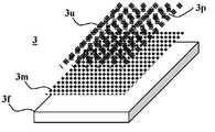
도 1a는 일부 실시 예에서 박막에 의해 구현된 기판(3f)으로 형성된 광 스위치 장치(3)를 개략적으로 도시한다. 이 비-제한적인 예에서, 스위치 장치(3)는 기판(3f)의 적어도 일부에(예를 들어, 증착에 의해) 광학적으로 결합된, 약 0.1 내지 1 나노미터의 두께를 갖는 나노입자(3m)의 층, 및 메타물질 층(3m)의 적어도 일부에 걸쳐(예를 들어, 증착에 의해) 적용된 약 0.1 내지 1 나노미터의 두께를 갖는 금 및/또는 유사한(전기 전도성) 나노입자의 나노메쉬(3u)로 이루어진다.1A schematically illustrates an
메타물질(3m)의 나노입자의 입자 크기는 일반적으로 약 1 내지 20 나노미터, 선택적으로 약 1 내지 100 나노미터의 범위일 수 있다. 금 나노메쉬(3u)의 입자 크기는 일반적으로 약 20 내지 100 나노미터일 수 있고, 그 구멍(pore)(3p)의 치수(크기)는 일반적으로 약 0.1 내지 1 나노미터일 수 있다. 기판(3f)은 광학적으로 투명한 재료로 제조될 수 있고, 일부 실시 예에서 소결(예를 들어, 세라믹)에 의해 투명성을 제공하고 약 0.1 내지 1 나노미터의 두께를 갖는 재료(들)로 만들어진 박막으로 구현된다.The particle size of the nanoparticles of the metamaterial (3m) may generally range from about 1 to 20 nanometers, optionally from about 1 to 100 nanometers. The particle size of the
일부 실시 예에서, 메타물질 층(3m)은 상이한 다양한 형상을 가질 수 있는 VO2 나노입자로 제조된다. 일부 가능한 실시 예들에서, 광 스위치(3)의 기하학적 치수는 직경이 수백 나노미터, 선택적으로 약 100 내지 500 나노미터이며, 이는 지금까지 이용 가능한 광 스위치의 기하학적 치수보다 상당히 작다. 테라헤르츠 속도 스위칭 속도(예컨대, 산화바나듐 재료 기반)를 위한 보다 작은 사이즈의 광 스위치는 데이터 저장, 데이터 통신 및 통신 기술을 변경할 수 있는 솔루션을 제공함으로써, 테라헤르츠 고속 스위칭에 대한 일부 기술적 장벽을 극복할 수 있다.In some embodiments, the metamaterial layer (3m) is made of VO2 nanoparticles that can have a variety of different shapes. In some possible embodiments, the geometrical dimension of the
도 1b는 일부 가능한 실시 예에 따른 광 스위치(10)의 구조 및 동작을 개략적으로 도시한다. 이 비-제한적인 예에서, 메타물질(3m)의 얇은 층은 얇은 기판(도시되지 않음) 상에 증착되고, 신호 소스(8)에 의해 생성된 신호에 의해 조사되도록 구성된 금 나노메쉬(도시되지 않음)에 의해 적어도 부분적으로 덮힌다. 광 스위치(10)는 일부 실시 예에서, 메타물질(3m)의 적어도 일부 섹션 또는 전체 표면에 걸쳐서 적용된 평행한 금속 라인에 의해 형성된 광학 격자(11)를 포함하여, 표면 비선형 프로세스(예를 들어, 주파수 변환)를 향상시킨다. 격자(11)는 기계적 또는 화학적 부식에 의해 제조될 수 있다.1B schematically illustrates the structure and operation of an
금속 격자들(11) 사이의 거리(d)는 상이한 파장의 위상 정합 입력 방사선(10a)이 응답성 위상 정합 및 코히어런트(coherent) 출력 방사선(10b)을 제공하도록 구성될 수 있다. 이 거리(d)는 전형적으로 입력 방사선(10a)(예를 들어, RF, 마이크로파 또는 테라헤르츠)의 파장보다 실질적으로 더 작게 설정되고, 예를 들어 일부 실시 예에서, d는 약 10 마이크로미터이고, 이에 의해 입력 방사선의 모든 입력 파장이 광 스위치(10)를 통과하여, 코히어런트 및 위상 정합된 출력 방사선(10b)을 생성하는 것을 보장한다.The distance d between the
광 스위치(10)의 메타물질(3m)에 인가된 신호 소스(8)로부터의 신호(8r)(전자기 광/RF/마이크로파 방사선 또는 전자/전계)는 나노메쉬의 금 입자로부터 메타물질 층(3m)으로 뜨거운 전자를 방출시키고, 이는 피코 초보다 작은 시간 간격 내에서, 메타물질 층(3m)이 불투명한 상으로부터 투명한 상으로 변하게 한다. 메타물질 층(3m)의 상 변화는 장치(10)의 타측에서 전자기 방사선의 위상 편이된 출력(10b)을 생성하기 위해, 장치(10)의 일측으로 지향되는 입력 전자기 방사선(10a)을 변조하는데 사용될 수 있다.The
신호 소스(8)는 예를 들어 광 믹서 또는 주파수 체배기를 사용하여 광 스위치(10)에 물리적으로 연결될 수 있거나, 입력 전자기 방사선(10a), 예를 들어 광 믹서 또는 주파수 체배기(즉, 스위치 장치(10)에 물리적으로 접촉함이 없이)를 적용하기 위해 근접 포트를 사용하는 신호 소스에 의해 구현될 수 있는데, 이는 테라헤르츠 주파수 범위 근처 및/또는 예를 들어, ≥400Gb/s 및 최대 40THz의 펄스 신호를 발생시킬 수 있다. 도 1c는 입력 전자기 방사선(10a)과 광 스위치(10)로부터 출력된 전자기 방사선(10b) 사이에서 얻어진 위상 편이를 그래프로 도시하며, 전자기 방사선(10b)는 점선 플롯(10c)으로 도시된 계산결과에 꼭 맞다.The
도 2는 일부 가능한 실시 예에 따른 광 스위치(7)를 개략적으로 도시한다. 광 스위치(7)는 EMR 소스(9)(예를 들어, 레이저 광 발생기)에 의해 생성된 전자기 방사선(EMR)(9d)을 통과하도록 구성된 파 전도성 기판(7t), 투과성 기판의 적어도 일부에 광학적으로 결합된 메타물질 나노입자 층(7u), 및 메타물질 층(7u)의 적어도 일부에 걸쳐 적용된 나노메쉬 층(7v)을 포함한다. 파 전도성 기판(7t)은 예를 들어 적합한 광 투과성 재료 및/또는 클래딩(도시되지 않음)을 사용하여 전체 내부 반사(TIR)에 의해 그 길이를 따라 EMR(9d)을 통과하도록 구성될 수 있다.2 schematically shows an
신호 소스(8)에 의해 생성되며 나노메쉬 층(7v)에 적용되는 변조(EMR 광, RF, 마이크로파, 테라헤르츠 또는 전기) 신호(8r)는 메타물질 층(7u)을 광학적으로 불투명한 상과 투명한 상 사이에서 스위칭하는데 사용되고, 이에 따라 광학적 반사 및 비-반사(또는 부분 반사) 상태들 사이에서 광 전도성 기판(7t)의 내부 반사 특성에 영향을 미치고, 이에 의해 인가된 변조 신호(8r)에 따라 입력 EMR(9d)을 변조한다.The modulated (EMR optical, RF, microwave, terahertz or electric)
일부 실시 예에서, 전자기 방사선 소스 및/또는 변조 신호 소스(8)는 동일한 출원인의 국제 공개 번호 WO 2007/132459 및/또는 미국 특허 제 9,964,442 호(이들의 개시 내용은 본원에 참조로 포함됨)에 기재되고 도시된 기술 및/또는 구현 예를 이용한다. 본원에 개시된 장치에 의해 생성된 변조된 EMR은 수동 또는 능동 검출기(이들에 제한되지 않음)와 같은 최첨단 검출기에 의해 검출될 수 있다.In some embodiments, the electromagnetic radiation source and / or modulated
일부 실시 예에서, 음의 굴절을 제어 가능하게 야기하도록 구성된 메타물질이 전자기 방사선을 변조하는데 사용된다. 예를 들어, 가능한 실시 예에서, 메타물질은 광섬유 또는 광 공진기의 투과 코어의 일부에 광학적으로 결합되며, 이를 통해 통과하는 광의 위상은 메타물질의 적어도 일부에 걸쳐 적용된 금 나노메쉬에 변조 신호(8r)를 적용함으로써 변이된다. 이러한 광 스위치/변조기의 목적은 높은 변조 효율, 저전력 변조 신호(8r), 예를 들어 전압, 낮은 삽입 손실, 높은 ON/OFF 속도, "탄성" 파장을 갖는 큰 변조, 무시할 수 있거나 제어 가능한 주파수 처프 및 긴 수명을 포함한다.In some embodiments, metamaterials configured to controlably cause negative refraction are used to modulate electromagnetic radiation. For example, in a possible embodiment, the metamaterial is optically coupled to a portion of the transmission core of an optical fiber or optical resonator, and the phase of the light passing through it is modulated signal (8r) to the gold nanomesh applied across at least a portion of the metamaterial. ). The purpose of this optical switch / modulator is high modulation efficiency, low power modulation signal (8r), for example voltage, low insertion loss, high ON / OFF rate, large modulation with "elastic" wavelength, negligible or controllable frequency chirp. And long life.
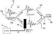
도 3은 일부 가능한 실시 예에 따른 광 변조 장치(17)를 개략적으로 도시한다. 변조 장치(17)는 입력 EMR(9d)(입력 A)을 변조기(17)에 도입하도록 구성된 입력 웨이브 라인(22a), 입력 EMR(9d)을 각각 제 1 및 제 2 웨이브 라인(22f 및 22s)으로 분할하도록 구성된 광 스플리터(22p), 제 2 웨이브 라인(22s)에 광학적으로 결합된 광 변조기(30), 및 제 1 및 제 2 웨이브 라인(22f 및 22s)을 따라 이동하는 EMR을 출력 웨이브 라인(22b)(출력 C)으로 컴바인하도록 구성된 광 합성기(22c)를 포함한다. 광 변조기(30)는 신호 소스(8)로부터 수신된 변조 신호(입력 b)에 응답하여 제 2 웨이브 라인(22s)을 통과하는 EMR을 제어 가능하게 변경하고, 이에 응답하여 거기에 위상 변이를 도입하도록 구성된다. 이러한 방식으로, 제 1 및 제 2 웨이브 라인으로부터의 EMR은 신호 소스(8)로부터의 변조 신호에 응답하여, 광 합성기(22c)에 의해 건설적으로 또는 파괴적으로 컴바인되어, 입력 EMR(9d)을 광학적으로 변조한다. 광 변조기(30)는 상기 및 하기 기술된 임의의 광 스위치/변조기를 이용하여 구현될 수 있다.3 schematically shows an
도 4a는 링 WGM 공진기(28)를 이용하는 광 변조기(20)를 개략적으로 도시한다. 링 공진기(28)는 공진기(28)에 입력 EMR을 도입하도록 구성된 입력 웨이브 라인(22a)에 광학적으로 결합되고, 공진기(28)에 의해 변조된 출력 EMR을 공진기(28)로부터 수신하도록 구성된 출력 웨이브 라인(22b)에 광학적으로 결합된다. 링 공진기(28)는 그 광 투과성 코어의 적어도 일부 섹션에 광학적으로 결합된 메타물질 어셈블리(23)를 포함한다. 메타물질 어셈블리(23)는 공진기(28c)의 중심/대칭축(각도 α에 의해 정의됨) 및/또는 그 원형축(28r)(각도 β에 의해 정의됨)에 대해 정의된 각진/원호 섹션에 결합될 수 있다. 선택적으로, 메타물질 어셈블리(23)는 링 공진기(28)의 전체 횡 방향 둘레에 광학적으로 결합된다(α=360도). 선택적으로, 메타물질 어셈블리(23)는 링 공진기(28)의 전체 단면 둘레에 광학적으로 결합된다(β=360도).4A schematically shows an
메타물질 어셈블리(23)는 링 공진기(28)의 코어 물질의 벽 부분의 적어도 일부(또는 전체)에 적용된 메타물질(예를 들어, VO2) 나노입자 층(23v), 및 메타물질 나노입자 층(23v)의 적어도 일부에 걸쳐 적용된 금 나노메쉬(23u)를 포함한다. 나노메쉬(23u)는 신호 소스(8)로부터 변조(전자기 및/또는 전기) 신호를 수신하고, 이에 반응하여 입력 웨이브 라인(22a)에 의해 도입된 EMR을 변조하기 위해 광학적으로 투과성인 상태와 광학적으로 비-투과성인 상태 사이에서 메타물질 나노입자 층(23v)을 변화시키도록 구성된다.The
도 4b는 상이한 주파수의 2 개의 입력 EMR 데이터 반송파(F1 및 F2)(예를 들어, 광 및/또는 테라헤르츠 신호) 사이에서 파장 갭을 브리지하도록 구성된 복수의 광 결합 WGM 공진기(41, 42, 43 및 44)를 이용하는 광 변조기 장치(40)를 개략적으로 도시한다. 변조기(40)는 예를 들어 근접(proximity), 즉 WGM 공진기(41)와 물리적으로 접촉하지 않으면서 이루어지는 광학 결합에 의해, EMR 반송파(F1 및 F2)를 각각 메인/변조 WGM 공진기(41)로 도입하도록 구성된 각각의 입력 웨이브 라인(45 및 46)을 포함한다. WGM 공진기(41)는 일부 실시 예에서 내벽이 메타물질 어셈블리(23)에 의해 덮혀지는 유전체 물질, 즉 전기 전도성 나노메쉬(예를 들어, 금으로 제조됨)에 의해 덮인 메타물질 나노입자(예를 들어, VO2) 층을 포함하는 유전체 물질로 제조된다.4B is a plurality of optically coupled
메인 WGM 공진기(41)는 입력 라인(45 및 46)을 따라 전파되는 변조된 EMR 반송파(F1 및 F2)를 트랩핑하고, 메타물질 어셈블리(23)에 의해 덮인 WGM 공진기(41)의 내벽을 따라 공진할 때 그들의 주파수를 서로 결합시키고, 메인 WMR 공진기(41)에 광학적으로 결합된 출력 라인(47)을 통해 EMR 방사선을 출력하도록 구성된다. 출력 웨이브 라인(47)을 따라 전파되는 출력 EMR은 변조된 EMR 반송파를 컴바인하여, 출력 EMR(F1+F2)를 제공한다. 이는 일부 실시 예에서, 표면상의 임의의 표면 전하 및 가능한 평형 국부 상태에 의해 EMR 병합(merging) 효과를 생성하는 비선형 프로세스를 용이하게 하도록 구성된 격자에 의해 달성된다. 이러한 방식으로, 실질적으로 상이한 파장의 EMR 간의 크로스토크/결합이 용이해진다(예를 들어, RF 및 테라헤르츠). 격자(예를 들어, 금속 격자-미도시)는 도 1b에 도시된 바와 같이, 메타물질 어셈블리 위에 적용될 수 있다.The
보조 WGM 공진기(42, 43 및 44)는 내벽이 메타물질 어셈블리(23)에 의해 덮힌 유전체 재료로 제조될 수 있다. 보조 WGM 공진기(42, 43 및 44)는 (근접에 의해) 메인 WGM 공진기에 광학적으로 결합된다. 그러나, 그들의 기하학적 치수는 출력 웨이브 라인(47)을 따라 전파하는 출력 EMR을 수신하는 수신기(도시되지 않음)에서 결합된 신호를 복조하기 위해 사용될 방사 패턴을 도입하기 위해, 메인/변조 WGM 공진기(41)내에 트랩핑된 상기 결합된 EMR을 미리 정의된 방식으로 형상화하도록 구성되는데, 예를 들어, (정보 없음) 패턴을 반송파의 스펙트럼 변화 및 변조된 정보에 추가함으로써 통신에서의 오류를 방지하게 한다.The
이러한 방식으로, 상이한 주파수(예를 들어, RF, 마이크로파 및/또는 테라헤르츠)를 갖는 다수의 EMR 반송파가 단일 EMR 반송파 상에 광학적으로 결합되어, 수신기를 향해 전송될 수 있다. 이러한 비-제한적인 예에서, 도시된 WGM 공진기(41, 42, 43 및 44)가 타원체이지만, 다른 구성 및 형상이 유사하게 사용될 수 있다. 메인 타원체 WGM 공진기(41)의 치수는 일반적으로 약 10-150 미크론일 수 있고, 보조 타원체 WGM 공진기(42, 43 및 44)의 치수는 변조를 방지하기 위해 메인/변조 타원체(41)보다 일반적으로 더 작을 수 있다.In this way, multiple EMR carriers with different frequencies (eg, RF, microwave and / or terahertz) can be optically coupled onto a single EMR carrier and transmitted towards the receiver. In this non-limiting example, the illustrated
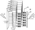
도 5a는 2 개의 변조 신호를 수신하고 이들을 EMR 반송파, 특정 및 비-제한적인 예에서 테라헤르츠 반송파(THz1, THz2)로 컴바인하도록 구성된 광 변조기(17')를 이용하는 광 데이터 통신 시스템(33)을 개략적으로 도시한다. 광 변조기(17')는 도 3a에 도시된 광 변조기 장치(17)의 배열에 의해, 또는 도 4a 및/또는 도 4b의 WGM 공진기 기반 변조기의 구현 예에 의해 구현될 수 있고, 이는 상이한 파장(THz1, THz2, ...)을 갖는 복수의 EMR 파를 광학적으로 변조하기 위해 수정될 수 있다.FIG. 5A shows an optical
이 예에서 수정된 광 변조기 장치(17')는 각각의 웨이브 라인(22f 및 22s)에서, 2 개의 각각의 변조 신호에 의해 각각의 광 변조기 장치(17')로 도입된 EMR을 광학적으로 변조하는 광 변조 유닛(30)을 포함하고, 이는 각각의 브랜치가 그 각각의 광 변조 유닛(30)에 의해 별개의 데이터 채널을 구현하도록 브랜치(branch) 변조를 수행한다. 시스템(33)은 트랜스폰더(26)로부터의 2 개의 변조 신호에 의해 각각의 EMR 반송파(THz1, THz2, ...)를 위상 변이함으로써 수신 및 변조하도록 각각 구성된 광 변조기 장치(17')의 제 1 세트(39)를 포함한다. 트랜스폰더(26)는 제 1 세트의 광 변조기 장치(39)에서 각각의 광 변조기 장치(17')를 위한 2 개의 변조 신호를 발생시키도록 구성된다.The modified
광 변조기 장치의 제 2 세트(38)는 웨이브 라인(36x)을 통과하는 광원(예를 들어, 레이저 소스)으로부터 EMR을 변조하도록 구성된다. 제 2 세트의 광 변조기 장치(38)의 각각의 광 변조기 장치(17')는 웨이브 라인(36x)에서 EMR을 변조하기 위해 제 1 세트의 광 변조기 장치(39)의 광 변조기 장치(17')에 의해 생성된 2 개의 각각의 변조된 광 신호를 수신하도록 구성된다. 제 2 세트의 광 변조기 장치(38)에 의해 생성된 변조된 EMR(복합(complex) 신호로도 지칭됨)은 무선 인터페이스를 통해 복합 신호를 방출하도록 구성된 안테나 트랜스미터 유닛(36)에 의해 방출될 수 있다. 튜닝 유닛(37)은 변조된 신호를 EMR 반송파의 대역폭에 적응시키기 위한 효율적인 샤논 연관성(Shannon correlation)을 위해 선택적으로 사용된다.The second set 38 of light modulator devices is configured to modulate EMR from a light source (eg, laser source) passing through
도 5b는 상이한 주파수의 2 개의 THz 신호를 믹싱하도록 구성된 복수의 광 변조기 칩 유닛(50)을 포함하는 광 데이터 통신 시스템(35)을 개략적으로 도시하며, 각각의 광 변조기 칩 유닛(50)은 포커싱된 프리즘에 의해 지향된 입력 EMR(51)(예를 들어, 광/레이저 소스로부터)의 각각의 특정 대역을 수신하고, 다수의 채널 생성을 위해 시프트된 프리즘에 의해 분할되고, 신호 통합을 위해 결합기 유닛(39)으로부터(예를 들어, 광/레이저 소스로부터) EMR(52)을 입력하고, 마찬가지로 각각의 테라헤르츠 파(THz1, THz2, ...)에 변조하도록 구성된다. 광 변조기 칩 유닛(50)은 상술한 바와 같이, 2 개의 EMR 데이터 반송파로부터 EMR을 결합하고, 2 개의 데이터 반송파를 결합하는 각각의 테라헤르츠 출력 EMR을 생성하도록 구성된, 도 4b에 도시된 WGM 공진기(40)에 의해 구현될 수 있다.5B schematically shows an optical
도 5c는 또 다른 광 데이터 통신 시스템(34)을 개략적으로 도시하며, 각각의 광 변조기 장치(17')는 도 5b에 도시된 시스템(35)의 각각의 광 변조기 칩 유닛(50)에 광학적으로 결합된다. 이러한 비-제한적인 예에서, 광 변조기 장치(17')는 RF 신호를 입력 EMR(51)에 결합하고, 그 다음 각각의 광 변조기 칩 유닛(50)에 의해 결합기(39)로부터의 EMR 입력 반송파(52)와 결합되고, 그에 의해 각각의 THz 채널을 생성하도록 이용된다.5C schematically shows another optical
상기 및 하기 설명된 바와 같이, 본 출원의 광 변조/스위치 장치는 신호의 물리적 특성에 따라 작동할 수 있는 변조 기술을 도입하고, 광 변조기/스위치의 실시 예는 넓게 분리된 파장들, 즉 RF와 테라헤르츠 대역 사이에서의 크로스토크/결합을 용이하게 하도록 채용될 수 있다.As described above and below, the optical modulation / switch device of the present application introduces a modulation technique that can operate according to the physical characteristics of the signal, and an embodiment of the optical modulator / switch includes widely separated wavelengths, namely RF and It can be employed to facilitate crosstalk / combination between terahertz bands.
광 RF 및/또는 THz는 광범위한 신규 장치를 포함하는 범주 중 하나 일뿐이다. 일부 실시 예에서, 위스퍼링 갤러리 모드(WGM) 광학 및 THz 공진기는 입력 EMR을 변조하는데 이용된다. 이들 장치의 제조 및 사용 방법을 이해하는 것은 그 성능과 한계를 이해하는 데 중요하다. 따라서, 이 설명 부분에서는 이러한 분류의 공진기 센서(송신기 및 수신기)를 소개하고, 이러한 장치가 일반적인 THz 데이터 통신, 특히 데이터 센터의 빠른 통신을 위한 실행 가능한 솔루션으로 사용되는 방법을 설명한다.Optical RF and / or THz are just one of the categories that cover a wide range of new devices. In some embodiments, whispering gallery mode (WGM) optics and THz resonators are used to modulate the input EMR. Understanding how these devices are manufactured and used is important for understanding their performance and limitations. Therefore, this part of the description introduces this type of resonator sensor (transmitter and receiver) and explains how these devices are used as a viable solution for general THz data communication, especially for fast communication in data centers.
WGM 광 공진기는 튜닝성 및 좁은 공진 선폭을 나타내며, 일부 실시 예에서 변조기 장치로서의 통신을 위해 이들을 원래 사용하도록 하는 탁월한 광학 특성 강도를 달성한다. 그것들은 이후 비선형 광학 현상과 양자 전기 역학적 원리를 조사하기 위한 소중한 도구로 발전했다. 일부 가능한 실시 예에서, WGM 광 공진기는 후술되는 바와 같이, 광 통신 변조기를 구현하는데 이용된다. 이들 실시 예에서, 이들의 극도의 감도가 분석 및 진단기구를 개발하는데 이용될 수 있기 때문에, 이들 실시 예는 통신 생화학적 분석, 생의학적 분석, 화학 및 분자 생물학적 분석에 사용될 수 있지만, 이에 제한되지는 않는다.WGM optical resonators exhibit tunability and narrow resonant line widths, and in some embodiments achieve excellent optical property strengths that make them originally used for communication as modulator devices. They have since developed into valuable tools for investigating nonlinear optical phenomena and quantum electrodynamic principles. In some possible embodiments, the WGM optical resonator is used to implement an optical communication modulator, as described below. In these embodiments, these embodiments can be used for, but not limited to, communication biochemical analysis, biomedical analysis, chemical and molecular biological analysis, since their extreme sensitivity can be used to develop analytical and diagnostic instruments. Does not.
WGM 공진기는 캐비티에서 순환할 때 공진 광이 취하는 경로로부터 그 이름을 얻는다. 이 경로는 음파가 Lrd Rayleigh가 연구한 원형 방의 구부러진 벽을 따라 가는 경로와 유사하다. 이러한 위스퍼링 갤러리에서는, 방의 반대편 벽을 향하여 서있는 두 사람이 심지어 위스퍼링에서도 서로 들을 수 있다. 이 사람들은 방 중앙을 향해 뒷걸음질하면 서로 들을 수 없다. 이 효과는 방 주변의 음파를 효율적으로 안내하는 스무스하고 곡선인 벽으로 인해 야기된다. 청취자에게 다른 경로를 취하면, 음파는 경로를 따라 소산되거나 분산된다.The WGM resonator gets its name from the path taken by the resonant light as it circulates in the cavity. This path is analogous to the path where sound waves follow the curved walls of a circular room studied by Lrd Rayleigh. In this whispering gallery, two people standing towards the opposite wall of the room can hear each other even in whispering. These people cannot hear each other if they step back toward the center of the room. This effect is caused by smooth, curved walls that efficiently guide sound waves around the room. When the listener takes a different path, the sound waves are dissipated or distributed along the path.
WGM 광 공진기는 위스퍼링 갤러리에서 한 사람으로부터 다른 사람으로 이동하는 음파에 의해 취해진 것과 유사한 주변 경로에서의 광을 트랩핑할 수 있는 유전체 구조이다. Mie와 Debye는 Lord Rayleigh의 연구 이전에, 유전체 구체(sphere)의 공진 고유 주파수를 설명했지만, 그 이름은 이 유형의 광 공진기에 훨씬 이후까지 적용되지 않았다.The WGM optical resonator is a dielectric structure capable of trapping light in a peripheral path similar to that taken by sound waves traveling from one person to another in a whispering gallery. Mie and Debye described the resonant natural frequencies of dielectric spheres before Lord Rayleigh's work, but the name did not apply much later to this type of optical resonator.
본 명세서에 개시된 광 스위치/변조기의 실시 예는 현대 데이터 네트워크, 예를 들어 클라우드에서 관리되는 애플리케이션 및 데이터 저장소에 필요한 확장 성 및 적응성 네트워킹을 제공하기 위해 데이터 센터에서 이용될 수 있다. 데이터 센터의 에너지 효율을 결정하기 위해 일반적으로 사용되는 메트릭(metric)은 전력 사용 효율(PUE)이다. 이 간단한 비율은 데이터 센터에 들어가는 총 전력을 IT 장비가 사용하는 전력으로 나눈 값이다.Embodiments of the optical switch / modulator disclosed herein can be used in a data center to provide the scalability and adaptive networking required for modern data networks, for example, applications and data storage managed in the cloud. A commonly used metric for determining the energy efficiency of a data center is power usage efficiency (PUE). This simple ratio is the total power entering the data center divided by the power used by IT equipment.

총 설비 전력은 IT 장비에서 사용하는 전력과, 컴퓨팅 또는 데이터 통신 장치로 간주되지 않는 모든 것(예컨대, 냉각, 조명 등)에 의해 소비되는 오버헤드 전력으로 구성된다. 0 오버헤드 전력의 가상적 상황에 대하여, 이상적인 PUE 값은 1.0이다. 미국의 평균적인 데이터 센터의 PUE는 2.0이고, 이는 시설이 IT 장비로 전달되는 와트 당 2 와트의 총 전력(오버헤드 + IT 장비)을 사용함을 의미한다. 최신 데이터 센터 에너지 효율은 약 1.2로 추정된다. 마이크로소프트 및 야후와 같은 일부 대규모 데이터 센터 운영자는 개발 시설에 대한 PUE 전망을 발표했다. Google은 운영중인 데이터 센터로부터 분기 별 실제 효율성 성능을 발표한다.Total equipment power consists of the power used by IT equipment and the overhead power consumed by everything not considered a computing or data communication device (eg, cooling, lighting, etc.). For the hypothetical situation of zero overhead power, the ideal PUE value is 1.0. The average data center in the United States has a PUE of 2.0, which means that the facility uses 2 watts of total power per watt (overhead + IT equipment) delivered to the IT equipment. Modern data center energy efficiency is estimated at about 1.2. Some large data center operators, such as Microsoft and Yahoo, have released PUE outlook for development facilities. Google announces actual efficiency performance quarterly from its operational data center.
에너지 효율은 본 명세서에 개시된 일부 실시 예에 대한 주요 특징이다. 미국 환경 보호국은 독립형 또는 대규모 데이터 센터에 대해 에너지 스타 등급을 받았다. 에코 라벨을 받으려면, 데이터 센터는 보고된 모든 시설의 에너지 효율의 상위 사분위수내에 있어야 한다. 유럽 연합은 또한 EU 데이터 센터 행동 규범으로 알려진 유사한 계획을 가지고 있다.Energy efficiency is a key feature for some embodiments disclosed herein. The US Environmental Protection Agency has received Energy Star ratings for standalone or large data centers. To receive the eco-label, the data center must be within the upper quartile of the energy efficiency of all reported facilities. The European Union also has a similar plan known as the EU Data Center Code of Conduct.
종종, 데이터 센터에서 에너지 사용을 억제하기 위한 첫 번째 단계는 데이터 센터에서 에너지가 어떻게 사용되고 있는지 이해하는 것이다. 데이터 센터 에너지 사용을 측정하기 위한 여러 유형의 분석이 있다. 측정된 양태들은 IT 장비 자체에 의해 사용되는 에너지뿐만 아니라 냉각기 및 팬과 같은 데이터 센터 시설 장비에 의해 사용되는 에너지를 포함한다.Often, the first step to curbing energy use in a data center is to understand how energy is being used in the data center. There are several types of analysis to measure data center energy use. Measured aspects include energy used by the data center facility equipment such as coolers and fans, as well as energy used by the IT equipment itself.
전력은 데이터 센터 사용자에게 가장 크게 되풀이해서 일어나는 비용이다. 열 평가라고도 지칭되는 전력 및 냉각 분석은 특정 영역에서의 상대 온도와 특정 주변 온도를 처리할 수 있는 냉각 시스템의 용량을 측정한다. 전력 및 냉각 분석은 데이터 센터 전체의 온도 균형을 달성하기 위하여, 핫스팟, 더 높은 전력 사용 밀도를 처리할 수 있는 과냉각 영역, 장비 로딩의 중단점, 고층 전략의 효율성 및 최적의 장비 포지셔닝(예컨대, AC 장치)을 식별하는 것을 도울 수 있다. 전력 냉각 밀도는 센터가 최대 용량으로 냉각할 수 있는 평방 피트의 양을 측정한 것이다.Power is the most recurring cost for data center users. Power and cooling analysis, also referred to as thermal evaluation, measures the relative temperature in a particular area and the capacity of the cooling system to handle a particular ambient temperature. Power and cooling analysis allows hot spots, supercooled areas capable of handling higher power usage densities, breakpoints in equipment loading, high-level strategy efficiency and optimal equipment positioning (e.g. AC) to achieve temperature balance across the data center. Device). The power cooling density is a measure of the amount of square feet a center can cool to its maximum capacity.
에너지 효율 분석은 데이터 센터 IT 및 시설 장비의 에너지 사용을 측정한다. 전형적인 에너지 효율 분석은 산업 표준에 대한 데이터 센터의 전력 사용 효율(PUE)과 같은 인자를 측정하고, 비효율적인 기계적 및 전기적 소스를 식별하고, 공기 관리 메트릭스를 식별한다.Energy efficiency analysis measures the energy use of data center IT and facility equipment. A typical energy efficiency analysis measures factors such as data center power usage efficiency (PUE) to industry standards, identifies inefficient mechanical and electrical sources, and identifies air management metrics.
THz 데이터 속도 데이터 통신을 위해 본 명세서에 개시된 광 스위치/변조기의 기회를 탐색하기 위해, 본 명세서에 개시된 바와 같은 데이터 통신 시스템은 멀티-홉 통신을 이용하여 구성될 수 있으며, 여기서 네트워크 내의 노드는 2 개 이상의 다른 노드들의 도움으로 통신할 수 있고, 이는 수동 및 능동 릴레이 모두와의 소스 및 목적지 노드 THz 통신 사이의 릴레이 노드로서 작용한다. THz 대역 주파수에서 송신기와 수신기 사이에 중간 릴레이를 사용하여 얻을 수 있는 이점은 여러 가지이다. 임의의 무선 통신 시스템에서와 같이, 송신기와 수신기 사이에 여러 개의 중간 홉을 가짐으로써, 전송 전력 및 따라서 에너지 소비가 감소될 수 있다. 또한, 이용 가능한 대역폭의 고유한 거리-의존적 거동으로 인해, 전송 거리의 감소는 훨씬 더 넓은 대역의 이용 가능성을 초래하고, 따라서 훨씬 더 높은 비트 속도로 전송한다. 이것들은 다시 한 번 주요한 에너지 절약에 기여할 수 있다.To explore the opportunities of the optical switch / modulator disclosed herein for THz data rate data communication, the data communication system as disclosed herein can be configured using multi-hop communication, where the nodes in the network are 2 It can communicate with the help of more than one other node, which acts as a relay node between source and destination node THz communication with both passive and active relays. There are several advantages to using intermediate relays between the transmitter and receiver at the THz band frequency. As in any wireless communication system, by having multiple intermediate hops between the transmitter and the receiver, transmission power and thus energy consumption can be reduced. In addition, due to the inherent distance-dependent behavior of the available bandwidth, the reduction in transmission distance results in the availability of a much wider band, thus transmitting at a much higher bit rate. These can once again contribute to major energy savings.
전술한 바와 같이, 본 명세서에 개시된 실시 예는 전하 결합 대 규칙적인 전도도에 기초하여 동작하도록 구성된 새로운 유형의 고속 광 전도체를 개발하는데 사용될 수 있다.As described above, the embodiments disclosed herein can be used to develop new types of high-speed optical conductors configured to operate based on charge coupling versus regular conductivity.
최신 웨어러블 나노 센서 네트워크는 생체 의학 및 환경 분야에서 일련의 유용한 응용을 가능하게 한다. 동시에, 현재의 통신 기술 상태는 미래의 나노 기기의 처리 능력을 크게 제한한다. 결과적으로, 수집된 데이터의 모든 분석이 매크로 장치에서 수행되어야 함을 암시한다. 따라서, 오랫동안 기다려온 나노 네트워크의 애플리케이션을 효과적으로 사용하려면, 기존 네트워킹 인프라에 완벽하게 통합되어, 나노 사물 인터넷 개념으로 이어질 것이 요구된다. 본 출원의 실시 예에서, 이미 배치된 매크로 네트워크와 최신 나노 네트워크 사이의 상호 운용성은 시기 상조로 미리 조사된다.The latest wearable nanosensor networks enable a range of useful applications in biomedical and environmental applications. At the same time, the current state of communication technology greatly limits the processing power of future nanodevices. As a result, it is implied that all analysis of the collected data should be performed on the macro device. Therefore, in order to effectively use the long-awaited application of the nano network, it is required to be fully integrated into the existing networking infrastructure and lead to the nano-Internet of Things concept. In the embodiments of the present application, interoperability between the already deployed macro network and the latest nano network is investigated in advance.
그러나, 기존의 매크로 무선 네트워크가 주로 반송파-기반 전자기 통신을 사용하는 반면, 나노 기기는 초 저전력 펄스 기반 EM 방사선 또는 본질적으로 모바일 오브젝트를 정보 반송파로 사용해야 하기 때문에, 이 문제에 대한 솔루션은 쉽지 않다. 따라서, 현재 매크로 네트워크와 나노 네트워크 사이의 직접적인 상호 작용은 불가능하며, 특수 게이트웨이 노드를 사용해야 한다. 더욱이, 기존의 링크 레벨 기술 뿐만 아니라, 대규모 네트워크를 구축할 수 있도록, 나노 통신을 위한 최신 솔루션을 빠르게 개선해야 한다. 적절한 변조 및 코딩 기술의 설계로부터 잡음 및 간섭 효과의 완화에 이르기까지, 이 목표를 달성하기 위해 수많은 이론적 문제가 해결되어야 한다. 여기에 개시된 실시 예는 이 분야에 대한 게이트웨이를 또한 제시한다.However, the solution to this problem is not easy because existing macro wireless networks mainly use carrier-based electromagnetic communication, while nanodevices must use ultra low power pulse based EM radiation or essentially mobile objects as information carriers. Therefore, direct interaction between the macro network and the nano network is not possible at present, and a special gateway node must be used. Moreover, in order to build large networks as well as existing link-level technologies, the latest solutions for nano-communications must be rapidly improved. From designing appropriate modulation and coding techniques to mitigating noise and interference effects, a number of theoretical problems must be addressed to achieve this goal. The embodiments disclosed herein also present gateways for this field.
WGM 공진기(예를 들어, PANDA 공명 링)와 메타물질 기반 스위치/변조기의 결합(예를 들어, PS 시간 범위에서 메타물질의 불투명 상태와 투명 상태 사이의 천이를 위해 VO2 입자를 사용함)은 빠른 광학 데이터 통신 구현, 및 생물학, 화학, 재료 과학, 나노 네트워크 등의 분야에서의 다양한 응용들을 위한 맞춤형 안테나를 제공할 수 있다.The combination of a WGM resonator (e.g. PANDA resonance ring) and a metamaterial-based switch / modulator (e.g. using VO2 particles to transition between the opaque and transparent state of the metamaterial in the PS time range) is fast optical It can provide customized antennas for data communication implementations and various applications in fields such as biology, chemistry, materials science, and nano networks.
위에서 설명되고 관련 도면에 도시된 바와 같이, 본 출원은 테라헤르츠 데이터 통신 속도를 위한 광 스위치 및 변조기 및 그 제조 방법을 제공한다. 본 발명의 특정 실시 예들이 설명되었지만, 본 발명은 특히 전술된 교시사항들에 비추어 당업자에 의해 변형될 수 있기 때문에, 그러한 실시 예들에 의해 제한되지 않는 것으로 이해되어야 할 것이다. 당업자에 의해 이해되는 바와 같이, 본 발명은 청구 범위를 초과하지 않으면서, 전술한 기술들로부터 하나 이상의 기술을 사용하여 매우 다양한 방식으로 수행될 수 있다.As described above and shown in the associated drawings, the present application provides an optical switch and modulator for terahertz data communication speed and a method of manufacturing the same. Although specific embodiments of the invention have been described, it should be understood that the invention is not limited by such embodiments, as it may be modified by those skilled in the art, particularly in light of the foregoing teachings. As will be appreciated by those skilled in the art, the present invention can be performed in a wide variety of ways using one or more techniques from the techniques described above without exceeding the scope of the claims.
Claims (40)
Translated fromKorean전자기 방사선을 이를 통해 전파하도록 구성된 광 투과성 기판과 상기 기판에 광학적으로 결합된 메타물질 배열; 여기서 상기 메타물질 배열은 상기 광 투과성 기판의 적어도 일부에 광학적으로 결합된 적어도 하나의 메타물질 입자 층을 포함하고; 및
상기 적어도 하나의 메타물질 층의 적어도 일부 위에 배치되며 적어도 하나의 전기 전도성 물질로 이루어진 적어도 하나의 나모메쉬 층으로서, 상기 적어도 하나의 나노메쉬 층은 상기 메타물질 배열에 인가된 전자기 또는 전기 신호에 응답하여, 상기 적어도 하나의 메타물질 층내로 전자를 방출하도록 구성되며, 상기 적어도 하나의 메타물질 층은 상기 방출된 전자를 수신할 때 광학적으로 불투명한 상태로부터 광학적으로 투명한 상태로 변하도록 구성되어, 적어도 부분적으로 전자기 방사선이 상기 기판을 통과하도록 바꾸고;
를 포함하는 광 스위치 장치.An optical switch device that can be used for terahertz data communication speed,
A light-transmitting substrate configured to propagate electromagnetic radiation therethrough and an array of metamaterials optically coupled to the substrate; Wherein the metamaterial arrangement comprises at least one metamaterial particle layer optically coupled to at least a portion of the light transmissive substrate; And
At least one namomesh layer disposed on at least a portion of the at least one metamaterial layer and made of at least one electrically conductive material, wherein the at least one nanomesh layer is responsive to electromagnetic or electrical signals applied to the metamaterial arrangement Thus, it is configured to emit electrons into the at least one metamaterial layer, and the at least one metamaterial layer is configured to change from an optically opaque state to an optically transparent state upon receiving the emitted electrons, at least Partially convert electromagnetic radiation through the substrate;
Optical switch device comprising a.
제 1 항 내지 제 18 항 중 어느 한 항의 광 스위치 장치, 입력 전자기 방사선을 상기 광 스위치 장치내로 도입하도록 구성된 입력 웨이브 라인, 및 상기 광 스위치 장치에 의해 적어도 부분적으로 변경된 출력 전자기 방사선을 전달하도록 구성된 출력 웨이브 라인을 포함하는 광 변조기.An optical modulator available for terahertz data communication speeds,
19. The optical switch device of any one of claims 1 to 18, an input wave line configured to introduce input electromagnetic radiation into the optical switch device, and an output configured to deliver output electromagnetic radiation at least partially modified by the optical switch device. Light modulator comprising a wave line.
입력 전자기 방사선을 상기 광 변조기 어셈블리 내로 도입하도록 구성된 입력 웨이브 라인, 상기 입력 웨이브 라인으로부터 상기 입력 전자기 방사선을 수신하도록 구성된 광 스플리터, 및 상기 입력 웨이브 라인으로부터 전자기 방사선의 일부를 수신하기 위해 상기 광 스플리터에 광학적으로 결합되며 그에 의해 스플릿되는 제 1 및 제 2 웨이브 라인, 상기 제 1 및 제 2 웨이브 라인 중 적어도 하나의 각 코어에 광학적으로 결합되는 제 2 항의 적어도 하나의 광 스위치 장치, 및 상기 광 스플리터로부터 수신되며 상기 적어도 하나의 광 스위치 장치에 의해 적어도 부분적으로 변경되는 전자기 방사선을 컴바인하기 위하여 상기 제 1 및 제 2 웨이브 라인에 광학적으로 결합되는 광 합성기를 포함하는 광 변조기 어셈블리.An optical modulator assembly available for terahertz data communication speeds,
An input wave line configured to introduce input electromagnetic radiation into the light modulator assembly, an optical splitter configured to receive the input electromagnetic radiation from the input wave line, and to the optical splitter to receive a portion of the electromagnetic radiation from the input wave line. First and second wave lines optically coupled and split by, at least one optical switch device of claim 2 optically coupled to each core of at least one of the first and second wave lines, and from the optical splitter And a light synthesizer optically coupled to the first and second wave lines to combine electromagnetic radiation received and at least partially modified by the at least one optical switch device.
그 내부 벽 섹션 위에 메타물질 어셈블리 코트를 갖는 적어도 하나의 WGM 공진기, 적어도 2 개의 전자기 데이터 반송파를 각각 도입하기 위해 상기 적어도 하나의 WGM 공진기에 광학적으로 결합된 적어도 2개의 입력 웨이브 라인, 및 상기 적어도 하나의 WGM 공진기 내에 트랩핑된 전자기 방사선을 출력하고 상기 적어도 2 개의 전자기 데이터 반송파를 적어도 부분적으로 병합하기 위해 상기 적어도 하나의 WGM 공진기에 광학적으로 결합된 적어도 하나의 출력 웨이브 라인을 포함하는 광 합성기 장치.An optical synthesizer device for combining two or more electromagnetic data carriers,
At least one WGM resonator having a metamaterial assembly coat over its inner wall section, at least two input wave lines optically coupled to the at least one WGM resonator to introduce at least two electromagnetic data carriers, and the at least one And at least one output wave line optically coupled to the at least one WGM resonator to output electromagnetic radiation trapped in the WGM resonator of the and at least partially merge the at least two electromagnetic data carriers.
40. The optical synthesizer of any one of claims 38 and 39, wherein at least one of the WGM resonators is an elliptical resonator.
Applications Claiming Priority (3)
| Application Number | Priority Date | Filing Date | Title |
|---|---|---|---|
| US201762535980P | 2017-07-24 | 2017-07-24 | |
| US62/535,980 | 2017-07-24 | ||
| PCT/IL2018/050822WO2019021282A1 (en) | 2017-07-24 | 2018-07-24 | High frequency optical switch and fabrication methods thereof |
Publications (1)
| Publication Number | Publication Date |
|---|---|
| KR20200034745Atrue KR20200034745A (en) | 2020-03-31 |
Family
ID=65039513
Family Applications (1)
| Application Number | Title | Priority Date | Filing Date |
|---|---|---|---|
| KR1020207004692ACeasedKR20200034745A (en) | 2017-07-24 | 2018-07-24 | High frequency optical switch and its manufacturing method |
Country Status (11)
| Country | Link |
|---|---|
| US (2) | US11181800B2 (en) |
| EP (1) | EP3658985A4 (en) |
| JP (2) | JP2020528581A (en) |
| KR (1) | KR20200034745A (en) |
| CN (1) | CN111133375A (en) |
| AU (1) | AU2018306670A1 (en) |
| BR (1) | BR112020001377A2 (en) |
| CA (1) | CA3070849A1 (en) |
| IL (1) | IL272229B2 (en) |
| WO (1) | WO2019021282A1 (en) |
| ZA (1) | ZA202000962B (en) |
Families Citing this family (9)
| Publication number | Priority date | Publication date | Assignee | Title |
|---|---|---|---|---|
| US11112491B2 (en) | 2017-06-29 | 2021-09-07 | Rockley Photonics Limited | Optical scanner and detector |
| WO2019007998A1 (en) | 2017-07-05 | 2019-01-10 | Rockley Photonics Limited | Reconfigurable spectroscopy system |
| WO2020176095A1 (en)* | 2019-02-28 | 2020-09-03 | Bae Systems Information And Electronic Systems Integration Inc. | Optically induced phase change materials |
| WO2020194215A1 (en)* | 2019-03-26 | 2020-10-01 | Terahertz Group Ltd. | Devices for generation of electromagnetic radiation of predetermined profile |
| US10739256B1 (en)* | 2019-03-29 | 2020-08-11 | Rockley Photonics Limited | Spectroscopy system with beat component |
| KR102503881B1 (en)* | 2020-10-08 | 2023-02-27 | 한국전자통신연구원 | Terahertz signal transmission apparatus and terahertz signal transmission method using the same |
| CN113391469B (en)* | 2020-12-02 | 2023-03-28 | 北京索通新动能科技有限公司 | Linear coupling-based medium-based super-surface all-optical switch |
| CN117040445A (en)* | 2023-07-08 | 2023-11-10 | 湖北九峰山实验室 | High-performance frequency multiplier based on phase change material resistor |
| CN117031787A (en)* | 2023-08-10 | 2023-11-10 | 东北师范大学 | VO-based 2 Phase-change terahertz wave transmission modulation super-surface and application thereof |
Family Cites Families (26)
| Publication number | Priority date | Publication date | Assignee | Title |
|---|---|---|---|---|
| JPH04371913A (en) | 1991-06-20 | 1992-12-24 | Matsushita Electric Ind Co Ltd | Optical modulator and optical switch |
| JP2002525679A (en) | 1998-09-17 | 2002-08-13 | コーニンクレッカ フィリップス エレクトロニクス エヌ ヴィ | Optical switching device |
| US6633696B1 (en) | 1998-12-07 | 2003-10-14 | California Institute Of Technology | Resonant optical wave power control devices and methods |
| JP3311722B2 (en)* | 1999-02-09 | 2002-08-05 | 財団法人神奈川科学技術アカデミー | Optical waveguide type wavelength filter with ring resonator and 1 × N optical waveguide type wavelength filter |
| WO2002016986A1 (en) | 2000-08-18 | 2002-02-28 | Cquint Communications Corporation | Fiber-optic waveguides for transverse optical coupling |
| US7277065B2 (en)* | 2003-09-02 | 2007-10-02 | Jay Hsing Wu | Tunable photonic band gap structures for microwave signals |
| US8143566B2 (en) | 2006-05-11 | 2012-03-27 | Novatrans Group Sa | Electron emission device of high current density and high operational frequency |
| WO2008121159A2 (en)* | 2006-10-19 | 2008-10-09 | Los Alamos National Security Llc | Active terahertz metamaterial devices |
| CA2970259C (en) | 2007-07-11 | 2018-11-06 | Ravenbrick, Llc | Thermally switched reflective optical shutter |
| US8111722B1 (en) | 2008-03-03 | 2012-02-07 | Oewaves, Inc. | Low-noise RF oscillation and optical comb generation based on nonlinear optical resonator |
| US8159736B2 (en) | 2008-11-13 | 2012-04-17 | Oewaves, Inc. | Tunable single sideband modulators based on electro-optic optical whispering gallery mode resonators and their applications |
| US8264759B2 (en) | 2009-05-12 | 2012-09-11 | Uti Limited Partnership | Fast all-optical switch |
| US8259381B2 (en)* | 2009-06-05 | 2012-09-04 | Exelis Inc. | Phase-change materials and optical limiting devices utilizing phase-change materials |
| US8655189B2 (en)* | 2010-06-18 | 2014-02-18 | Exelis, Inc. | Optical modulation utilizing structures including metamaterials |
| US9279723B2 (en) | 2010-08-19 | 2016-03-08 | Novatrans Group Sa | Terahertz spectroscopy system and method |
| KR101175699B1 (en)* | 2011-03-16 | 2012-08-21 | 광주과학기술원 | Terahertz modulator based on hole injection and transport |
| US8908251B2 (en) | 2013-01-30 | 2014-12-09 | Hrl Laboratories, Llc | Tunable optical metamaterial |
| KR101417957B1 (en)* | 2013-05-13 | 2014-07-09 | 코닝정밀소재 주식회사 | Thermochromic window and manufacturing method thereof |
| CN103454784B (en)* | 2013-09-23 | 2015-12-09 | 哈尔滨工程大学 | The tunable light-operated switch of a kind of THz wave based on artificial electromagnetic material |
| DE102013112993A1 (en) | 2013-11-25 | 2015-05-28 | Deutsche Telekom Ag | Transmission arrangement for transmitting data with a carrier wave in the terahertz range |
| CN105204190A (en) | 2014-06-10 | 2015-12-30 | 中国科学院苏州纳米技术与纳米仿生研究所 | Terahertz modulator based on low-dimension electron plasma waves and manufacturing method thereof |
| US9746746B2 (en)* | 2014-08-01 | 2017-08-29 | Mohammad A Mazed | Fast optical switch and its applications in optical communication |
| US20160371885A1 (en)* | 2015-06-22 | 2016-12-22 | Anatolie Gavriliuc | Sharing of markup to image data |
| CN105093777B (en) | 2015-07-23 | 2017-11-07 | 北京大学 | A kind of Meta Materials microcavity composite construction and its production and use |
| US11215563B2 (en)* | 2016-06-29 | 2022-01-04 | Arizona Board Of Regents On Behalf Of The University Of Arizona | Photonic apparatus, methods, and applications |
| CN106646930B (en) | 2016-12-29 | 2019-07-19 | 电子科技大学 | Multilevel terahertz modulator based on flexible graphene field effect transistor structure |
- 2018
- 2018-07-24KRKR1020207004692Apatent/KR20200034745A/ennot_activeCeased
- 2018-07-24CNCN201880059395.9Apatent/CN111133375A/enactivePending
- 2018-07-24EPEP18838938.1Apatent/EP3658985A4/enactivePending
- 2018-07-24BRBR112020001377-3Apatent/BR112020001377A2/ennot_activeApplication Discontinuation
- 2018-07-24JPJP2020504172Apatent/JP2020528581A/enactivePending
- 2018-07-24CACA3070849Apatent/CA3070849A1/enactivePending
- 2018-07-24ILIL272229Apatent/IL272229B2/enunknown
- 2018-07-24WOPCT/IL2018/050822patent/WO2019021282A1/ennot_activeCeased
- 2018-07-24AUAU2018306670Apatent/AU2018306670A1/ennot_activeAbandoned
- 2018-07-24USUS16/633,500patent/US11181800B2/enactiveActive
- 2020
- 2020-02-14ZAZA2020/00962Apatent/ZA202000962B/enunknown
- 2021
- 2021-09-09USUS17/470,590patent/US11747705B2/enactiveActive
- 2024
- 2024-03-29JPJP2024055344Apatent/JP7745913B2/enactiveActive
Also Published As
| Publication number | Publication date |
|---|---|
| IL272229B2 (en) | 2024-05-01 |
| US11181800B2 (en) | 2021-11-23 |
| EP3658985A4 (en) | 2021-05-19 |
| IL272229A (en) | 2020-03-31 |
| RU2020106422A3 (en) | 2022-02-17 |
| RU2020106422A (en) | 2021-08-26 |
| AU2018306670A1 (en) | 2020-02-27 |
| US20200225554A1 (en) | 2020-07-16 |
| JP7745913B2 (en) | 2025-09-30 |
| JP2024088690A (en) | 2024-07-02 |
| EP3658985A1 (en) | 2020-06-03 |
| CA3070849A1 (en) | 2019-01-31 |
| IL272229B1 (en) | 2024-01-01 |
| JP2020528581A (en) | 2020-09-24 |
| BR112020001377A2 (en) | 2020-10-06 |
| WO2019021282A1 (en) | 2019-01-31 |
| US11747705B2 (en) | 2023-09-05 |
| ZA202000962B (en) | 2021-06-30 |
| US20220171252A1 (en) | 2022-06-02 |
| CN111133375A (en) | 2020-05-08 |
Similar Documents
| Publication | Publication Date | Title |
|---|---|---|
| US11747705B2 (en) | High frequency optical switch and fabrication methods thereof | |
| Maram et al. | Recent trends and advances of silicon-based integrated microwave photonics | |
| Amiri et al. | GHz frequency band soliton generation using integrated ring resonator for WiMAX optical communication | |
| Wu et al. | Flexible terahertz metamaterial filter with high transmission intensity and large tuning range for optical communication application | |
| Nallappan et al. | Terahertz waveguides for next generation communication network: Needs, challenges and perspectives | |
| Sun et al. | The perspective of topological photonics for on-chip terahertz modulation and sensing | |
| Parandin et al. | Recent advances in photonic crystal based all-optical analog to digital converter: a review | |
| Sridarshini et al. | Photonic crystal based routers for all optical communication networks | |
| RU2782978C2 (en) | High-frequency optical switch and its manufacturing methods | |
| RU2782978C9 (en) | High-frequency optical switch and its manufacturing methods | |
| US8693881B2 (en) | Optical hetrodyne devices | |
| Shahidinejad et al. | Optical wireless quantum communication coding system using decimal convertor | |
| Ghadban et al. | A 60 GHz RoF generation system based on optical beat of narrowband Bragg filters | |
| Sadegh Amiri et al. | Solitonic Signals Generation and Transmission Using MRR | |
| Katti et al. | Terahertz signal generation based on a microwave photonic system with add‐drop microring resonator | |
| Duan et al. | Single-photon scattering controlled by an imperfect cavity | |
| Bunruangses et al. | High-density wavelength multiplexing model for THz-EMI transmission | |
| Saha et al. | Frequency shift keying using photonic crystal based ring cavity resonator | |
| Asghari-Govar et al. | All optical FSK demodulator using PhC-based ring resonators | |
| Ni et al. | Ultra-wideband bandpass filter with notched band based on electrooptic phase modulator and phase-shift fiber Bragg grating | |
| Moss | Phase-encoded RF signal generation based on an integrated 49GHz micro-comb soliton crystal optical source | |
| Chitimireddy et al. | Sinusoidal Bragg grating based on hybrid metal insulator metal plasmonic waveguide | |
| Xu | UWB Signal Generation and Modulation Based on Photonic Approaches | |
| He et al. | Review for wireless communication system based on space–time-coding digital metasurfaces | |
| Tao | Integrated Electro-Optics |
Legal Events
| Date | Code | Title | Description |
|---|---|---|---|
| PA0105 | International application | Patent event date:20200218 Patent event code:PA01051R01D Comment text:International Patent Application | |
| PG1501 | Laying open of application | ||
| PA0201 | Request for examination | Patent event code:PA02012R01D Patent event date:20210716 Comment text:Request for Examination of Application | |
| E902 | Notification of reason for refusal | ||
| PE0902 | Notice of grounds for rejection | Comment text:Notification of reason for refusal Patent event date:20230725 Patent event code:PE09021S01D | |
| E601 | Decision to refuse application | ||
| PE0601 | Decision on rejection of patent | Patent event date:20230926 Comment text:Decision to Refuse Application Patent event code:PE06012S01D Patent event date:20230725 Comment text:Notification of reason for refusal Patent event code:PE06011S01I |