KR20200032122A - Semiconductor device and manufacturing method of semiconductor device - Google Patents
Semiconductor device and manufacturing method of semiconductor deviceDownload PDFInfo
- Publication number
- KR20200032122A KR20200032122AKR1020207003875AKR20207003875AKR20200032122AKR 20200032122 AKR20200032122 AKR 20200032122AKR 1020207003875 AKR1020207003875 AKR 1020207003875AKR 20207003875 AKR20207003875 AKR 20207003875AKR 20200032122 AKR20200032122 AKR 20200032122A
- Authority
- KR
- South Korea
- Prior art keywords
- insulator
- conductor
- oxide
- transistor
- addition
- Prior art date
- Legal status (The legal status is an assumption and is not a legal conclusion. Google has not performed a legal analysis and makes no representation as to the accuracy of the status listed.)
- Granted
Links
Images


Classifications
- H01L29/42364—
- H—ELECTRICITY
- H10—SEMICONDUCTOR DEVICES; ELECTRIC SOLID-STATE DEVICES NOT OTHERWISE PROVIDED FOR
- H10D—INORGANIC ELECTRIC SEMICONDUCTOR DEVICES
- H10D30/00—Field-effect transistors [FET]
- H10D30/60—Insulated-gate field-effect transistors [IGFET]
- H10D30/67—Thin-film transistors [TFT]
- H10D30/6729—Thin-film transistors [TFT] characterised by the electrodes
- H10D30/673—Thin-film transistors [TFT] characterised by the electrodes characterised by the shapes, relative sizes or dispositions of the gate electrodes
- H10D30/6733—Multi-gate TFTs
- H10D30/6734—Multi-gate TFTs having gate electrodes arranged on both top and bottom sides of the channel, e.g. dual-gate TFTs
- H—ELECTRICITY
- H01—ELECTRIC ELEMENTS
- H01L—SEMICONDUCTOR DEVICES NOT COVERED BY CLASS H10
- H01L21/00—Processes or apparatus adapted for the manufacture or treatment of semiconductor or solid state devices or of parts thereof
- H01L21/02—Manufacture or treatment of semiconductor devices or of parts thereof
- H01L21/04—Manufacture or treatment of semiconductor devices or of parts thereof the devices having potential barriers, e.g. a PN junction, depletion layer or carrier concentration layer
- H01L21/18—Manufacture or treatment of semiconductor devices or of parts thereof the devices having potential barriers, e.g. a PN junction, depletion layer or carrier concentration layer the devices having semiconductor bodies comprising elements of Group IV of the Periodic Table or AIIIBV compounds with or without impurities, e.g. doping materials
- H01L21/28—Manufacture of electrodes on semiconductor bodies using processes or apparatus not provided for in groups H01L21/20 - H01L21/268
- H01L21/28008—Making conductor-insulator-semiconductor electrodes
- H01L21/28017—Making conductor-insulator-semiconductor electrodes the insulator being formed after the semiconductor body, the semiconductor being silicon
- H01L21/28158—Making the insulator
- H—ELECTRICITY
- H01—ELECTRIC ELEMENTS
- H01L—SEMICONDUCTOR DEVICES NOT COVERED BY CLASS H10
- H01L23/00—Details of semiconductor or other solid state devices
- H01L23/52—Arrangements for conducting electric current within the device in operation from one component to another, i.e. interconnections, e.g. wires, lead frames
- H01L23/538—Arrangements for conducting electric current within the device in operation from one component to another, i.e. interconnections, e.g. wires, lead frames the interconnection structure between a plurality of semiconductor chips being formed on, or in, insulating substrates
- H01L23/5386—Geometry or layout of the interconnection structure
- H01L29/41725—
- H01L29/7869—
- H01L29/788—
- H01L29/792—
- H—ELECTRICITY
- H10—SEMICONDUCTOR DEVICES; ELECTRIC SOLID-STATE DEVICES NOT OTHERWISE PROVIDED FOR
- H10D—INORGANIC ELECTRIC SEMICONDUCTOR DEVICES
- H10D30/00—Field-effect transistors [FET]
- H10D30/60—Insulated-gate field-effect transistors [IGFET]
- H10D30/67—Thin-film transistors [TFT]
- H10D30/6729—Thin-film transistors [TFT] characterised by the electrodes
- H10D30/673—Thin-film transistors [TFT] characterised by the electrodes characterised by the shapes, relative sizes or dispositions of the gate electrodes
- H—ELECTRICITY
- H10—SEMICONDUCTOR DEVICES; ELECTRIC SOLID-STATE DEVICES NOT OTHERWISE PROVIDED FOR
- H10D—INORGANIC ELECTRIC SEMICONDUCTOR DEVICES
- H10D30/00—Field-effect transistors [FET]
- H10D30/60—Insulated-gate field-effect transistors [IGFET]
- H10D30/67—Thin-film transistors [TFT]
- H10D30/6729—Thin-film transistors [TFT] characterised by the electrodes
- H10D30/6737—Thin-film transistors [TFT] characterised by the electrodes characterised by the electrode materials
- H10D30/6739—Conductor-insulator-semiconductor electrodes
- H—ELECTRICITY
- H10—SEMICONDUCTOR DEVICES; ELECTRIC SOLID-STATE DEVICES NOT OTHERWISE PROVIDED FOR
- H10D—INORGANIC ELECTRIC SEMICONDUCTOR DEVICES
- H10D30/00—Field-effect transistors [FET]
- H10D30/60—Insulated-gate field-effect transistors [IGFET]
- H10D30/67—Thin-film transistors [TFT]
- H10D30/674—Thin-film transistors [TFT] characterised by the active materials
- H10D30/6755—Oxide semiconductors, e.g. zinc oxide, copper aluminium oxide or cadmium stannate
- H—ELECTRICITY
- H10—SEMICONDUCTOR DEVICES; ELECTRIC SOLID-STATE DEVICES NOT OTHERWISE PROVIDED FOR
- H10D—INORGANIC ELECTRIC SEMICONDUCTOR DEVICES
- H10D30/00—Field-effect transistors [FET]
- H10D30/60—Insulated-gate field-effect transistors [IGFET]
- H10D30/67—Thin-film transistors [TFT]
- H10D30/6757—Thin-film transistors [TFT] characterised by the structure of the channel, e.g. transverse or longitudinal shape or doping profile
- H—ELECTRICITY
- H10—SEMICONDUCTOR DEVICES; ELECTRIC SOLID-STATE DEVICES NOT OTHERWISE PROVIDED FOR
- H10D—INORGANIC ELECTRIC SEMICONDUCTOR DEVICES
- H10D62/00—Semiconductor bodies, or regions thereof, of devices having potential barriers
- H10D62/80—Semiconductor bodies, or regions thereof, of devices having potential barriers characterised by the materials
- H—ELECTRICITY
- H10—SEMICONDUCTOR DEVICES; ELECTRIC SOLID-STATE DEVICES NOT OTHERWISE PROVIDED FOR
- H10D—INORGANIC ELECTRIC SEMICONDUCTOR DEVICES
- H10D64/00—Electrodes of devices having potential barriers
- H10D64/20—Electrodes characterised by their shapes, relative sizes or dispositions
- H10D64/27—Electrodes not carrying the current to be rectified, amplified, oscillated or switched, e.g. gates
- H10D64/311—Gate electrodes for field-effect devices
- H10D64/411—Gate electrodes for field-effect devices for FETs
- H10D64/511—Gate electrodes for field-effect devices for FETs for IGFETs
- H10D64/512—Disposition of the gate electrodes, e.g. buried gates
- H—ELECTRICITY
- H10—SEMICONDUCTOR DEVICES; ELECTRIC SOLID-STATE DEVICES NOT OTHERWISE PROVIDED FOR
- H10D—INORGANIC ELECTRIC SEMICONDUCTOR DEVICES
- H10D86/00—Integrated devices formed in or on insulating or conducting substrates, e.g. formed in silicon-on-insulator [SOI] substrates or on stainless steel or glass substrates
- H10D86/40—Integrated devices formed in or on insulating or conducting substrates, e.g. formed in silicon-on-insulator [SOI] substrates or on stainless steel or glass substrates characterised by multiple TFTs
- H10D86/421—Integrated devices formed in or on insulating or conducting substrates, e.g. formed in silicon-on-insulator [SOI] substrates or on stainless steel or glass substrates characterised by multiple TFTs having a particular composition, shape or crystalline structure of the active layer
- H10D86/423—Integrated devices formed in or on insulating or conducting substrates, e.g. formed in silicon-on-insulator [SOI] substrates or on stainless steel or glass substrates characterised by multiple TFTs having a particular composition, shape or crystalline structure of the active layer comprising semiconductor materials not belonging to the Group IV, e.g. InGaZnO
- H—ELECTRICITY
- H10—SEMICONDUCTOR DEVICES; ELECTRIC SOLID-STATE DEVICES NOT OTHERWISE PROVIDED FOR
- H10D—INORGANIC ELECTRIC SEMICONDUCTOR DEVICES
- H10D86/00—Integrated devices formed in or on insulating or conducting substrates, e.g. formed in silicon-on-insulator [SOI] substrates or on stainless steel or glass substrates
- H10D86/40—Integrated devices formed in or on insulating or conducting substrates, e.g. formed in silicon-on-insulator [SOI] substrates or on stainless steel or glass substrates characterised by multiple TFTs
- H10D86/60—Integrated devices formed in or on insulating or conducting substrates, e.g. formed in silicon-on-insulator [SOI] substrates or on stainless steel or glass substrates characterised by multiple TFTs wherein the TFTs are in active matrices
- H—ELECTRICITY
- H10—SEMICONDUCTOR DEVICES; ELECTRIC SOLID-STATE DEVICES NOT OTHERWISE PROVIDED FOR
- H10B—ELECTRONIC MEMORY DEVICES
- H10B12/00—Dynamic random access memory [DRAM] devices
- H—ELECTRICITY
- H10—SEMICONDUCTOR DEVICES; ELECTRIC SOLID-STATE DEVICES NOT OTHERWISE PROVIDED FOR
- H10B—ELECTRONIC MEMORY DEVICES
- H10B41/00—Electrically erasable-and-programmable ROM [EEPROM] devices comprising floating gates
- H10B41/70—Electrically erasable-and-programmable ROM [EEPROM] devices comprising floating gates the floating gate being an electrode shared by two or more components
Landscapes
- Engineering & Computer Science (AREA)
- Physics & Mathematics (AREA)
- Microelectronics & Electronic Packaging (AREA)
- General Physics & Mathematics (AREA)
- Condensed Matter Physics & Semiconductors (AREA)
- Computer Hardware Design (AREA)
- Power Engineering (AREA)
- Manufacturing & Machinery (AREA)
- Geometry (AREA)
- Thin Film Transistor (AREA)
- Semiconductor Memories (AREA)
- Metal-Oxide And Bipolar Metal-Oxide Semiconductor Integrated Circuits (AREA)
- Non-Volatile Memory (AREA)
Abstract
Translated fromKoreanDescription
Translated fromKorean본 발명의 일 형태는 반도체 장치, 그리고 반도체 장치의 제작 방법에 관한 것이다. 또는, 본 발명의 일 형태는 반도체 웨이퍼, 모듈, 및 전자 기기에 관한 것이다.One aspect of the present invention relates to a semiconductor device and a method for manufacturing the semiconductor device. Or, one aspect of the present invention relates to a semiconductor wafer, a module, and an electronic device.
또한, 본 명세서 등에서 반도체 장치란, 반도체 특성을 이용함으로써 기능할 수 있는 장치 전반을 가리킨다. 트랜지스터 등의 반도체 소자를 비롯하여, 반도체 회로, 연산 장치, 기억 장치는, 반도체 장치의 일 형태이다. 표시 장치(액정 표시 장치, 발광 표시 장치 등), 투영 장치, 조명 장치, 전기 광학 장치, 축전 장치, 기억 장치, 반도체 회로, 촬상 장치, 및 전자 기기 등은 반도체 장치를 포함한다고 할 수 있는 경우가 있다.In addition, in this specification and the like, a semiconductor device refers to an overall device that can function by using semiconductor characteristics. Semiconductor circuits, arithmetic devices, and storage devices, including semiconductor elements such as transistors, are one type of semiconductor devices. Display devices (liquid crystal display devices, light-emitting display devices, etc.), projection devices, lighting devices, electro-optical devices, power storage devices, storage devices, semiconductor circuits, imaging devices, and electronic devices may include semiconductor devices. have.
또한, 본 발명의 일 형태는 상술한 기술분야에 한정되지 않는다. 본 명세서 등에서 개시(開示)하는 발명의 일 형태는 물건, 방법, 또는 제조 방법에 관한 것이다. 또는, 본 발명의 일 형태는 공정(process), 기계(machine), 제품(manufacture), 또는 조성물(composition of matter)에 관한 것이다.In addition, one aspect of the present invention is not limited to the above-described technical field. One embodiment of the invention disclosed in this specification and the like relates to an object, a method, or a manufacturing method. Or, one aspect of the present invention relates to a process, machine, product, or composition of matter.
근년, 반도체 장치의 개발이 진행되고, LSI나 CPU나 메모리가 주로 사용되고 있다. CPU는, 반도체 웨이퍼로부터 분리된 반도체 집적 회로(적어도 트랜지스터 및 메모리)를 포함하고, 접속 단자인 전극이 형성된 반도체 소자의 집합체이다.In recent years, development of semiconductor devices has progressed, and LSI, CPU, and memory are mainly used. The CPU is a collection of semiconductor elements including semiconductor integrated circuits (at least transistors and memories) separated from a semiconductor wafer, and having electrodes as connection terminals.
LSI나 CPU나 메모리 등의 반도체 회로(IC칩)는, 회로 기판, 예를 들어 인쇄 배선판에 실장되고, 다양한 전자 기기의 부품의 하나로서 사용된다.Semiconductor circuits (IC chips) such as LSIs, CPUs, and memories are mounted on circuit boards, for example, printed wiring boards, and used as one of various electronic device components.
또한, 절연 표면을 포함하는 기판 위에 형성된 반도체 박막을 사용하여 트랜지스터를 구성하는 기술이 주목되고 있다. 상기 트랜지스터는 집적 회로(IC)나 화상 표시 장치(단순히 표시 장치라고도 표기함)와 같은 전자 디바이스에 널리 응용되어 있다. 트랜지스터에 적용할 수 있는 반도체 박막으로서 실리콘계 반도체 재료가 널리 알려져 있지만, 그 외의 재료로서 산화물 반도체가 주목되고 있다.In addition, a technique for constructing a transistor using a semiconductor thin film formed on a substrate including an insulating surface has been noted. The transistor is widely applied to electronic devices such as integrated circuits (ICs) and image display devices (also simply referred to as display devices). Silicon-based semiconductor materials are widely known as semiconductor thin films applicable to transistors, but oxide semiconductors have attracted attention as other materials.
또한, 산화물 반도체를 사용한 트랜지스터는, 비도통 상태에서 누설 전류가 매우 작다는 것이 알려져 있다. 예를 들어, 산화물 반도체를 사용한 트랜지스터의 누설 전류가 낮다는 특성을 응용한 저소비전력의 CPU 등이 개시되어 있다(특허문헌 1 참조).Further, it is known that a transistor using an oxide semiconductor has a very small leakage current in a non-conductive state. For example, a low power consumption CPU or the like has been disclosed in which a characteristic of a transistor using an oxide semiconductor having a low leakage current is applied (see Patent Document 1).
또한, 산화물 반도체를 사용한 트랜지스터에서, 게이트 전극을 개구부에 매립하여 제작하는 방법 등이 개시되어 있다(특허문헌 2 참조).In addition, in a transistor using an oxide semiconductor, a method is disclosed in which a gate electrode is buried in an opening, and the like is disclosed (see Patent Document 2).
또한, 근년에는 전자 기기의 소형화, 경량화에 따라, 트랜지스터 등을 고밀도로 집적한 집적 회로에 대한 요구가 높아지고 있다. 또한, 집적 회로를 포함하는 반도체 장치의 생산성의 향상이 요구된다.In addition, in recent years, with the downsizing and weight reduction of electronic devices, there is an increasing demand for integrated circuits in which transistors and the like are integrated with high density. In addition, there is a need to improve productivity of semiconductor devices including integrated circuits.
산화물 반도체로서는, 예를 들어 산화 인듐, 산화 아연 등의 일원계 금속의 산화물뿐만 아니라, 다원계 금속의 산화물도 알려져 있다. 다원계 금속의 산화물 중에서도 특히 In-Ga-Zn 산화물(이하, IGZO라고도 부름)에 관한 연구가 활발하게 진행되고 있다.As the oxide semiconductor, not only oxides of monometallic metals such as indium oxide or zinc oxide, but also oxides of polymetallic metals are known. Among multi-metal oxides, research on In-Ga-Zn oxide (hereinafter also referred to as IGZO) has been actively conducted.
IGZO에 관한 연구에 의하여, 산화물 반도체에서 단결정도 비정질도 아닌, CAAC(c-axis aligned crystalline) 구조 및 nc(nanocrystalline) 구조가 발견되었다(비특허문헌 1 내지 비특허문헌 3 참조). 비특허문헌 1 및 비특허문헌 2에서는, CAAC 구조를 가지는 산화물 반도체를 사용하여 트랜지스터를 제작하는 기술도 개시되어 있다. 또한, CAAC 구조 및 nc 구조보다 결정성이 낮은 산화물 반도체이더라도, 미소한 결정을 포함하는 것이 비특허문헌 4 및 비특허문헌 5에 나타나 있다.According to the research on IGZO, a c-axis aligned crystalline (CAAC) structure and a nanocrystalline (nc) structure, which are neither single crystal nor amorphous, have been found in oxide semiconductors (see Non-Patent
또한, IGZO를 활성층으로서 사용한 트랜지스터는 매우 낮은 오프 전류를 가지고(비특허문헌 6 참조), 그 특성을 이용한 LSI 및 디스플레이가 보고되어 있다(비특허문헌 7 및 비특허문헌 8 참조).In addition, transistors using IGZO as an active layer have a very low off current (see Non-Patent Document 6), and LSIs and displays using the properties have been reported (see Non-Patent Document 7 and Non-Patent Document 8).
본 발명의 일 형태는 미세화 또는 고집적화가 가능한 반도체 장치를 제공하는 것을 과제의 하나로 한다. 본 발명의 일 형태는 양호한 전기 특성을 가지는 반도체 장치를 제공하는 것을 과제의 하나로 한다. 본 발명의 일 형태는 양호한 주파수 특성을 가지는 반도체 장치를 제공하는 것을 과제의 하나로 한다. 본 발명의 일 형태는 신뢰성이 양호한 반도체 장치를 제공하는 것을 과제의 하나로 한다. 본 발명의 일 형태는 생산성이 높은 반도체 장치를 제공하는 것을 과제의 하나로 한다.An object of one embodiment of the present invention is to provide a semiconductor device capable of miniaturization or high integration. An object of one embodiment of the present invention is to provide a semiconductor device having good electrical properties. An object of one embodiment of the present invention is to provide a semiconductor device having good frequency characteristics. An object of one embodiment of the present invention is to provide a semiconductor device having good reliability. An object of one embodiment of the present invention is to provide a semiconductor device with high productivity.
본 발명의 일 형태는 장기간의 데이터 유지가 가능한 반도체 장치를 제공하는 것을 과제의 하나로 한다. 본 발명의 일 형태는 정보의 기록 속도가 빠른 반도체 장치를 제공하는 것을 과제의 하나로 한다. 본 발명의 일 형태는 설계 자유도가 높은 반도체 장치를 제공하는 것을 과제의 하나로 한다. 본 발명의 일 형태는 소비전력을 억제할 수 있는 반도체 장치를 제공하는 것을 과제의 하나로 한다. 본 발명의 일 형태는 신규 반도체 장치를 제공하는 것을 과제의 하나로 한다.An object of one embodiment of the present invention is to provide a semiconductor device capable of long-term data retention. An object of one embodiment of the present invention is to provide a semiconductor device having a high recording speed of information. One aspect of the present invention is to provide a semiconductor device with high design freedom. An object of one embodiment of the present invention is to provide a semiconductor device capable of suppressing power consumption. One aspect of the present invention is to provide a novel semiconductor device.
또한, 이들 과제의 기재는 다른 과제의 존재를 방해하는 것은 아니다. 또한, 본 발명의 일 형태는 이들 과제 모두를 해결할 필요는 없는 것으로 한다. 또한, 이들 외의 과제는 명세서, 도면, 청구항 등의 기재로부터 저절로 명백해지는 것이며 명세서, 도면, 청구항 등의 기재로부터 이들 외의 과제를 추출할 수 있다.Moreover, the description of these tasks does not hinder the existence of other tasks. In addition, it is assumed that one aspect of the present invention does not need to solve all of these problems. In addition, problems other than these will become apparent from the descriptions of specifications, drawings, claims, and the like, and problems other than these can be extracted from descriptions of specifications, drawings, and claims.
본 발명의 일 형태는 산화물과, 산화물 위에 서로 떨어져 배치된 제 1 도전체 및 제 2 도전체와, 제 1 도전체 및 제 2 도전체 위에 배치되고 제 1 도전체와 제 2 도전체 사이에 중첩하여 개구가 형성된 제 1 절연체와, 개구 내에 배치된 제 3 도전체와, 산화물, 제 1 도전체, 제 2 도전체, 및 제 1 절연체와 제 3 도전체 사이에 배치된 제 2 절연체를 포함하고, 제 2 절연체는 산화물과 제 3 도전체 사이에서 제 1 막 두께를 가지고, 제 1 도전체 또는 제 2 도전체와 제 3 도전체 사이에서 제 2 막 두께를 가지고, 제 1 막 두께는 제 2 막 두께보다 얇은 것을 특징으로 하는 반도체 장치이다.One aspect of the present invention superimposes between an oxide, a first conductor and a second conductor disposed apart from one another on an oxide, and disposed between the first conductor and the second conductor and disposed between the first conductor and the second conductor. And a first insulator having an opening, a third conductor disposed in the opening, an oxide, a first conductor, a second conductor, and a second insulator disposed between the first insulator and the third conductor. , The second insulator has a first film thickness between the oxide and the third conductor, the second conductor has a second film thickness between the second conductor and the third conductor, and the first film thickness is the second It is a semiconductor device characterized by being thinner than the film thickness.
또한, 상기에서, 제 2 절연체는 제 3 절연체와 제 4 절연체를 포함하고, 제 3 절연체는 산화물, 제 1 도전체, 제 2 도전체, 및 제 1 절연체와 제 3 도전체 사이에 배치되고, 제 4 절연체는 제 1 도전체, 제 2 도전체, 및 제 1 절연체와 제 3 절연체 사이에 배치되어도 좋다.Further, in the above, the second insulator includes a third insulator and a fourth insulator, and the third insulator is disposed between the oxide, the first conductor, the second conductor, and the first insulator and the third conductor, The fourth insulator may be disposed between the first conductor, the second conductor, and the first insulator and the third insulator.
또한, 상기에서, 산화물, 제 1 도전체, 및 제 2 도전체와 제 1 절연체 사이에 제 5 절연체가 배치되고, 제 5 절연체는 알루미늄 및 하프늄 중 적어도 한쪽을 포함하는 산화물이어도 좋다.In addition, in the above, a fifth insulator is disposed between the oxide, the first conductor, and the second conductor and the first insulator, and the fifth insulator may be an oxide containing at least one of aluminum and hafnium.
또한, 상기에서, 산화물은 In과, 원소 M(M은 Al, Ga, Y, 또는 Sn)과, Zn을 포함하는 것이 바람직하다.In addition, in the above, it is preferable that the oxide contains In, the element M (M is Al, Ga, Y, or Sn) and Zn.
또한, 본 발명의 다른 일 형태는, 제 1 산화물과, 제 1 산화물 위에 서로 떨어져 배치된 제 1 도전체 및 제 2 도전체와, 제 1 도전체 및 제 2 도전체 위에 배치되고 제 1 도전체와 제 2 도전체 사이에 중첩하여 개구가 형성된 제 1 절연체와, 개구 내에 배치된 제 3 도전체와, 제 1 산화물, 제 1 도전체, 제 2 도전체, 및 제 1 절연체와 제 3 도전체 사이에 배치된 제 2 절연체와, 제 1 산화물, 제 1 도전체, 제 2 도전체, 및 제 1 절연체와 제 2 절연체 사이에 배치된 제 2 산화물을 포함하고, 제 2 절연체는 제 1 산화물과 제 3 도전체 사이에서 제 1 막 두께를 가지고, 제 1 도전체 또는 제 2 도전체와 제 3 도전체 사이에서 제 2 막 두께를 가지고, 제 1 막 두께는 제 2 막 두께보다 얇은 것을 특징으로 하는 반도체 장치이다.In addition, another aspect of the present invention includes a first oxide, a first conductor and a second conductor disposed apart from each other on the first oxide, and a first conductor disposed on the first conductor and the second conductor. The first insulator having an opening overlapped between the and the second conductor, the third conductor disposed in the opening, the first oxide, the first conductor, the second conductor, and the first insulator and the third conductor A second insulator disposed between, a first oxide, a first conductor, a second conductor, and a second oxide disposed between the first insulator and the second insulator, the second insulator being the first oxide Characterized in that it has a first film thickness between the third conductors, a second film thickness between the first conductor or the second conductor and the third conductor, and the first film thickness is thinner than the second film thickness. It is a semiconductor device.
또한, 상기에서, 제 1 산화물, 제 1 도전체, 및 제 2 도전체와 제 1 절연체 사이에 제 3 절연체가 배치되고, 제 3 절연체는 알루미늄 및 하프늄 중 적어도 한쪽을 포함하는 산화물이어도 좋다.In addition, in the above, a third insulator is disposed between the first oxide, the first conductor, and the second conductor and the first insulator, and the third insulator may be an oxide containing at least one of aluminum and hafnium.
또한, 상기에서, 제 4 절연체는 제 1 도전체, 제 2 도전체, 및 제 1 절연체와 제 2 산화물 사이에 배치되고, 제 4 절연체는 알루미늄 및 하프늄 중 적어도 한쪽을 포함하는 산화물이어도 좋다.Further, in the above, the fourth insulator is disposed between the first conductor, the second conductor, and the first insulator and the second oxide, and the fourth insulator may be an oxide containing at least one of aluminum and hafnium.
또한, 상기에서, 제 1 산화물 및 제 2 산화물은 In과, 원소 M(M은 Al, Ga, Y, 또는 Sn)과, Zn을 포함하는 것이 바람직하다.In addition, in the above, it is preferable that the first oxide and the second oxide include In, the element M (M is Al, Ga, Y, or Sn) and Zn.
또한, 상기에서, 제 1 절연체의 상면과, 제 3 도전체의 상면과, 제 2 절연체의 상면은 실질적으로 일치하여도 좋다. 또한, 상기에서, 제 1 절연체의 상면과, 제 3 도전체의 상면과, 제 2 절연체의 상면에 접하여 제 6 절연체가 배치되고, 제 6 절연체는 알루미늄을 포함하는 산화물이어도 좋다.In addition, in the above, the upper surface of the first insulator, the upper surface of the third conductor, and the upper surface of the second insulator may substantially coincide. In addition, in the above, the sixth insulator is disposed in contact with the upper surface of the first insulator, the upper surface of the third conductor, and the upper surface of the second insulator, and the sixth insulator may be an oxide containing aluminum.
또한, 상기에서, 제 1 도전체 및 제 2 도전체는 알루미늄, 크로뮴, 구리, 은, 금, 백금, 탄탈럼, 니켈, 타이타늄, 몰리브데넘, 텅스텐, 하프늄, 바나듐, 나이오븀, 망가니즈, 마그네슘, 지르코늄, 베릴륨, 인듐, 루테늄, 이리듐, 스트론튬, 및 란타넘 중 적어도 하나를 포함하는 것이 바람직하다.In addition, in the above, the first conductor and the second conductor are aluminum, chromium, copper, silver, gold, platinum, tantalum, nickel, titanium, molybdenum, tungsten, hafnium, vanadium, niobium, manganese, It is preferred to include at least one of magnesium, zirconium, beryllium, indium, ruthenium, iridium, strontium, and lanthanum.
또한, 상기에서, 제 1 도전체 및 제 2 도전체는 질화 탄탈럼, 질화 타이타늄, 타이타늄과 알루미늄을 포함하는 질화물, 탄탈럼과 알루미늄을 포함하는 질화물, 산화 루테늄, 질화 루테늄, 스트론튬과 루테늄을 포함하는 산화물, 및 란타넘과 니켈을 포함하는 산화물 중 적어도 하나를 포함하는 것이 바람직하다.In addition, in the above, the first conductor and the second conductor include tantalum nitride, titanium nitride, nitride including titanium and aluminum, nitride including tantalum and aluminum, ruthenium oxide, ruthenium nitride, strontium and ruthenium It is preferable to contain at least one of the oxides mentioned above and oxides containing lanthanum and nickel.
본 발명의 일 형태에 의하여 미세화 또는 고집적화가 가능한 반도체 장치를 제공할 수 있다. 본 발명의 일 형태에 의하여 양호한 전기 특성을 가지는 반도체 장치를 제공할 수 있다. 본 발명의 일 형태에 의하여 양호한 주파수 특성을 가지는 반도체 장치를 제공할 수 있다. 본 발명에 의하여 신뢰성이 양호한 반도체 장치를 제공할 수 있다. 본 발명의 일 형태에 의하여 생산성이 높은 반도체 장치를 제공할 수 있다.According to one embodiment of the present invention, a semiconductor device capable of miniaturization or high integration can be provided. According to one aspect of the present invention, a semiconductor device having good electrical characteristics can be provided. According to one aspect of the present invention, a semiconductor device having good frequency characteristics can be provided. According to the present invention, a semiconductor device having good reliability can be provided. According to one embodiment of the present invention, a semiconductor device having high productivity can be provided.
또는, 장기간의 데이터 유지가 가능한 반도체 장치를 제공할 수 있다. 또는, 데이터의 기록 속도가 빠른 반도체 장치를 제공할 수 있다. 또는, 설계 자유도가 높은 반도체 장치를 제공할 수 있다. 또는, 소비전력을 억제할 수 있는 반도체 장치를 제공할 수 있다. 또는, 신규 반도체 장치를 제공할 수 있다.Alternatively, a semiconductor device capable of long-term data retention can be provided. Alternatively, a semiconductor device having a high data writing speed can be provided. Alternatively, a semiconductor device with high design freedom can be provided. Alternatively, a semiconductor device capable of suppressing power consumption can be provided. Alternatively, a new semiconductor device can be provided.
또한, 이들 효과의 기재는 다른 효과의 존재를 방해하는 것은 아니다. 또한 본 발명의 일 형태는 이들 효과의 모두를 가질 필요는 없다. 또한 이들 이외의 효과는 명세서, 도면, 청구항 등의 기재로부터 저절로 명백해지는 것이고, 명세서, 도면, 청구항 등의 기재로부터 이들 이외의 효과를 추출할 수 있다.Moreover, the description of these effects does not hinder the existence of other effects. Also, one aspect of the present invention need not have all of these effects. In addition, effects other than these will become apparent by themselves from descriptions of specifications, drawings, and claims, and effects other than these can be extracted from descriptions of specifications, drawings, and claims.
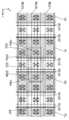
도 1은 본 발명의 일 형태에 따른 반도체 장치의 상면도 및 단면도.
도 2는 본 발명의 일 형태에 따른 반도체 장치의 단면도.
도 3은 본 발명의 일 형태에 따른 반도체 장치의 단면도.
도 4는 본 발명의 일 형태에 따른 반도체 장치의 제작 방법을 도시한 상면도 및 단면도.
도 5는 본 발명의 일 형태에 따른 반도체 장치의 제작 방법을 도시한 상면도 및 단면도.
도 6은 본 발명의 일 형태에 따른 반도체 장치의 제작 방법을 도시한 상면도 및 단면도.
도 7은 본 발명의 일 형태에 따른 반도체 장치의 제작 방법을 도시한 상면도 및 단면도.
도 8은 본 발명의 일 형태에 따른 반도체 장치의 제작 방법을 도시한 상면도 및 단면도.
도 9는 본 발명의 일 형태에 따른 반도체 장치의 제작 방법을 도시한 상면도 및 단면도.
도 10은 본 발명의 일 형태에 따른 반도체 장치의 제작 방법을 도시한 상면도 및 단면도.
도 11은 본 발명의 일 형태에 따른 반도체 장치의 제작 방법을 도시한 상면도 및 단면도.
도 12는 본 발명의 일 형태에 따른 반도체 장치의 제작 방법을 도시한 상면도 및 단면도.
도 13은 본 발명의 일 형태에 따른 반도체 장치의 제작 방법을 도시한 상면도 및 단면도.
도 14는 본 발명의 일 형태에 따른 반도체 장치의 상면도 및 단면도.
도 15는 본 발명의 일 형태에 따른 반도체 장치의 상면도 및 단면도.
도 16은 본 발명의 일 형태에 따른 반도체 장치의 상면도 및 단면도.
도 17은 본 발명의 일 형태에 따른 반도체 장치의 상면도 및 단면도.
도 18은 본 발명의 일 형태에 따른 기억 장치의 상면도 및 단면도.
도 19는 본 발명의 일 형태에 따른 기억 장치의 회로도.
도 20은 본 발명의 일 형태에 따른 기억 장치의 모식도.
도 21은 본 발명의 일 형태에 따른 기억 장치의 모식도.
도 22는 본 발명의 일 형태에 따른 기억 장치의 구성을 도시한 단면도.
도 23은 본 발명의 일 형태에 따른 기억 장치의 구성을 도시한 단면도.
도 24는 본 발명의 일 형태에 따른 기억 장치의 구성예를 도시한 블록도.
도 25는 본 발명의 일 형태에 따른 기억 장치의 구성예를 도시한 회로도.
도 26은 본 발명의 일 형태에 따른 기억 장치의 구성예를 도시한 회로도.
도 27은 본 발명의 일 형태에 따른 기억 장치의 구성예를 도시한 블록도.
도 28은 본 발명의 일 형태에 따른 기억 장치의 구성예를 도시한 블록도 및 회로도.
도 29는 본 발명의 일 형태에 따른 AI 시스템의 구성예를 도시한 블록도.
도 30은 본 발명의 일 형태에 따른 AI 시스템의 응용예를 설명하는 블록도.
도 31은 본 발명의 일 형태에 따른 AI 시스템을 포함한 IC의 구성예를 도시한 사시 모식도.
도 32는 본 발명의 일 형태에 따른 전자 기기를 도시한 도면.
도 33은 본 발명의 일 형태에 따른 전자 기기를 도시한 도면.
도 34는 본 발명의 일 형태에 따른 전자 기기를 도시한 도면.1 is a top view and a cross-sectional view of a semiconductor device according to one embodiment of the present invention.
2 is a cross-sectional view of a semiconductor device according to one embodiment of the present invention.
3 is a cross-sectional view of a semiconductor device according to one embodiment of the present invention.
4 is a top view and a cross-sectional view showing a method of manufacturing a semiconductor device according to one embodiment of the present invention.
5 is a top view and a cross-sectional view showing a method of manufacturing a semiconductor device according to one embodiment of the present invention.
6 is a top view and a cross-sectional view showing a method of manufacturing a semiconductor device according to one embodiment of the present invention.
7 is a top view and a cross-sectional view showing a method of manufacturing a semiconductor device according to one embodiment of the present invention.
8 is a top view and a cross-sectional view showing a method of manufacturing a semiconductor device according to one embodiment of the present invention.
9 is a top view and a cross-sectional view showing a method of manufacturing a semiconductor device according to one embodiment of the present invention.
10 is a top view and a cross-sectional view showing a method of manufacturing a semiconductor device according to one embodiment of the present invention.
11 is a top view and a cross-sectional view showing a method of manufacturing a semiconductor device according to one embodiment of the present invention.
12 is a top view and a cross-sectional view showing a method of manufacturing a semiconductor device according to one embodiment of the present invention.
13 is a top view and a cross-sectional view showing a method of manufacturing a semiconductor device according to one embodiment of the present invention.
14 is a top view and a cross-sectional view of a semiconductor device according to one embodiment of the present invention.
15 is a top view and a cross-sectional view of a semiconductor device according to one embodiment of the present invention.
16 is a top view and a cross-sectional view of a semiconductor device according to one embodiment of the present invention.
17 is a top view and a cross-sectional view of a semiconductor device according to one embodiment of the present invention.
18 is a top view and a cross-sectional view of a memory device according to one embodiment of the present invention.
19 is a circuit diagram of a storage device according to one embodiment of the present invention.
20 is a schematic diagram of a storage device according to one embodiment of the present invention.
21 is a schematic diagram of a memory device according to one embodiment of the present invention.
22 is a sectional view showing the configuration of a memory device according to one embodiment of the present invention.
23 is a sectional view showing the configuration of a memory device according to one embodiment of the present invention.
24 is a block diagram showing a configuration example of a memory device according to one embodiment of the present invention.
25 is a circuit diagram showing a configuration example of a memory device according to one embodiment of the present invention.
26 is a circuit diagram showing a configuration example of a memory device according to one embodiment of the present invention.
27 is a block diagram showing a configuration example of a memory device according to one embodiment of the present invention.
28 is a block diagram and a circuit diagram showing a configuration example of a memory device according to one embodiment of the present invention.
29 is a block diagram showing a configuration example of an AI system according to one embodiment of the present invention.
30 is a block diagram illustrating an application example of an AI system according to one embodiment of the present invention.
31 is a perspective schematic diagram showing a configuration example of an IC including an AI system according to an embodiment of the present invention.
32 illustrates an electronic device according to one embodiment of the present invention.
33 illustrates an electronic device according to one embodiment of the present invention.
34 illustrates an electronic device according to one embodiment of the present invention.
이하에서, 실시형태에 대하여 도면을 참조하면서 설명한다. 다만, 실시형태는 많은 상이한 형태로 실시할 수 있고, 취지 및 그 범위로부터 벗어남이 없이 그 형태 및 자세한 사항을 다양하게 변경할 수 있다는 것은, 통상의 기술자라면 용이하게 이해할 수 있다. 따라서, 본 발명은, 이하의 실시형태의 기재 내용에 한정하여 해석되는 것은 아니다.Hereinafter, embodiments will be described with reference to the drawings. However, it can be easily understood by those skilled in the art that the embodiments can be implemented in many different forms, and that the forms and details can be variously changed without departing from the spirit and scope of the embodiments. Therefore, the present invention is not limited to the contents described in the following embodiments.
또한, 도면에서, 크기, 층의 두께, 또는 영역은, 명료화를 위하여 과장되어 있는 경우가 있다. 따라서, 그 스케일에 반드시 한정되는 것은 아니다. 또한, 도면은 이상적인 예를 모식적으로 도시한 것이므로, 도면에 도시된 형상 또는 값 등에 한정되지 않는다. 예를 들어, 실제의 제조 공정에서, 에칭 등의 처리에 의하여 층이나 레지스트 마스크 등이 의도치 않게 감소되는 경우가 있지만, 이해를 용이하게 하기 위하여 이를 생략하는 경우가 있다. 또한, 도면에서, 동일한 부분 또는 같은 기능을 가지는 부분에는 동일한 부호를 상이한 도면 사이에서 공통적으로 사용하고, 이의 반복적인 설명은 생략하는 경우가 있다. 또한, 같은 기능을 가지는 부분을 가리키는 경우에는, 해치 패턴을 동일하게 하고, 특별히 부호를 붙이지 않는 경우가 있다.In addition, in the drawings, the size, the thickness of the layer, or the area may be exaggerated for clarity. Therefore, it is not necessarily limited to the scale. In addition, since the drawing schematically shows an ideal example, it is not limited to the shape or value shown in the drawing. For example, in an actual manufacturing process, a layer, a resist mask, or the like may be unintentionally reduced by treatment such as etching, but this may be omitted in order to facilitate understanding. In addition, in the drawings, the same reference numerals are commonly used for the same parts or parts having the same function, and repeated descriptions thereof may be omitted. In addition, when referring to the part having the same function, the hatch pattern may be the same, and a sign may not be used in particular.
또한, 특히 상면도('평면도'라고도 함)나 사시도 등에서는, 발명의 이해를 용이하게 하기 위하여 일부의 구성 요소의 기재를 생략하는 경우가 있다. 또한, 일부의 숨은선 등의 기재를 생략하는 경우가 있다.In addition, in order to facilitate understanding of the invention, description of some components may be omitted, especially in a top view (also referred to as a 'plan view') or a perspective view. In addition, description of some hidden lines may be omitted.
또한, 본 명세서 등에서, 제 1, 제 2 등으로 붙여지는 서수사는 편의상 사용하는 것이며, 공정 순서 또는 적층 순서를 나타내는 것이 아니다. 그러므로, 예를 들어 '제 1'을 '제 2' 또는 '제 3' 등으로 적절히 치환하여 설명할 수 있다. 또한, 본 명세서 등에 기재되어 있는 서수사와, 본 발명의 일 형태를 특정하기 위하여 사용되는 서수사는 일치하지 않는 경우가 있다.In addition, in this specification, etc., the ordinal yarns attached by 1st, 2nd, etc. are used for convenience, and do not show a process order or a lamination order. Therefore, for example, 'first' may be explained by appropriately substituting 'second' or 'third'. In addition, there may be cases where the ordinal yarn described in this specification and the like and the ordinal yarn used to specify one embodiment of the present invention do not match.
또한, 본 명세서 등에서, '위', '아래' 등의 배치를 나타내는 말은 구성끼리의 위치 관계를 도면을 참조하여 설명하기 위하여 편의상 사용하는 것이다. 또한, 구성끼리의 위치 관계는 각 구성을 묘사하는 방향에 따라 적절히 변화되는 것이다. 따라서, 명세서에서 설명된 말에 한정되지 않고, 상황에 따라 적절히 환언할 수 있다.In addition, in this specification and the like, the words indicating the arrangement of 'up' and 'down' are used for convenience to explain the positional relationship between components with reference to the drawings. In addition, the positional relationship between components is appropriately changed according to the direction in which each component is described. Therefore, it is not limited to the words described in the specification, and can be appropriately interpreted depending on the situation.
예를 들어, 본 명세서 등에서, X와 Y가 접속되어 있다고 명시적으로 기재되어 있는 경우에는, X와 Y가 전기적으로 접속되어 있는 경우와, X와 Y가 기능적으로 접속되어 있는 경우와, X와 Y가 직접적으로 접속되어 있는 경우가 본 명세서 등에 개시되어 있는 것으로 한다. 따라서, 소정의 접속 관계, 예를 들어 도면 또는 문장에 나타낸 접속 관계에 한정되지 않고, 도면 또는 문장에 나타낸 접속 관계 이외의 것도, 도면 또는 문장에 기재되어 있는 것으로 한다.For example, in the present specification and the like, when it is explicitly stated that X and Y are connected, X and Y are electrically connected, X and Y are functionally connected, and X and It is assumed that the case where Y is directly connected is disclosed in this specification and the like. Therefore, it is not limited to a predetermined connection relationship, for example, a connection relationship shown in a drawing or a sentence, and anything other than the connection relationship shown in a drawing or a sentence shall be described in a drawing or sentence.
여기서, X, Y는 대상물(예를 들어 장치, 소자, 회로, 배선, 전극, 단자, 도전막, 층 등)인 것으로 한다.Here, X and Y are assumed to be objects (for example, devices, elements, circuits, wiring, electrodes, terminals, conductive films, layers, etc.).
X와 Y가 직접적으로 접속되어 있는 경우의 일례로서는, X와 Y의 전기적인 접속을 가능하게 하는 소자(예를 들어 스위치, 트랜지스터, 용량 소자, 인덕터, 저항 소자, 다이오드, 표시 소자, 발광 소자, 부하 등)가 X와 Y 사이에 접속되어 있지 않은 경우이고, X와 Y의 전기적인 접속을 가능하게 하는 소자(예를 들어 스위치, 트랜지스터, 용량 소자, 인덕터, 저항 소자, 다이오드, 표시 소자, 발광 소자, 부하 등)를 통하지 않고 X와 Y가 접속되어 있는 경우이다.As an example of the case where X and Y are directly connected, elements that enable electrical connection between X and Y (for example, switches, transistors, capacitive elements, inductors, resistance elements, diodes, display elements, light emitting elements, When the load and the like are not connected between X and Y, and elements that enable electrical connection between X and Y (for example, switches, transistors, capacitive elements, inductors, resistance elements, diodes, display elements, and light emission) Device, load, etc.), and X and Y are connected.
X와 Y가 전기적으로 접속되어 있는 경우의 일례로서는, X와 Y의 전기적인 접속을 가능하게 하는 소자(예를 들어 스위치, 트랜지스터, 용량 소자, 인덕터, 저항 소자, 다이오드, 표시 소자, 발광 소자, 부하 등)가 X와 Y 사이에 하나 이상 접속될 수 있다. 또한, 스위치는 온, 오프가 제어되는 기능을 가진다. 즉, 스위치는 도통 상태(온 상태) 또는 비도통 상태(오프 상태)가 되고, 전류를 흘릴지 여부를 제어하는 기능을 가진다. 또는, 스위치는 전류를 흘리는 경로를 선택하여 전환하는 기능을 가진다. 또한, X와 Y가 전기적으로 접속되어 있는 경우에는, X와 Y가 직접적으로 접속되어 있는 경우를 포함하는 것으로 한다.As an example of the case where X and Y are electrically connected, elements (eg, switches, transistors, capacitive elements, inductors, resistance elements, diodes, display elements, light-emitting elements) that enable electrical connections between X and Y, Load, etc.) may be connected to one or more between X and Y. In addition, the switch has a function of controlling on and off. That is, the switch is in a conducting state (on state) or a non-conducting state (off state), and has a function of controlling whether or not current flows. Alternatively, the switch has a function of selecting and switching a path through which current flows. In addition, when X and Y are electrically connected, it is assumed that X and Y are directly connected.
X와 Y가 기능적으로 접속되어 있는 경우의 일례로서는, X와 Y의 기능적인 접속을 가능하게 하는 회로(예를 들어 논리 회로(인버터, NAND 회로, NOR 회로 등), 신호 변환 회로(DA 변환 회로, AD 변환 회로, 감마 보정 회로 등), 전위 레벨 변환 회로(전원 회로(승압 회로, 강압 회로 등), 신호의 전위 레벨을 변화시키는 레벨 시프터 회로 등), 전압원, 전류원, 전환 회로, 증폭 회로(신호 진폭 또는 전류량 등을 크게 할 수 있는 회로, 연산 증폭기, 차동 증폭 회로, 소스 폴로어 회로, 버퍼 회로 등), 신호 생성 회로, 기억 회로, 제어 회로 등)가, X와 Y 사이에 1개 이상 접속될 수 있다. 또한, 일례로서, X와 Y 사이에 다른 회로를 끼워도 X로부터 출력된 신호가 Y로 전달되는 경우에는, X와 Y는 기능적으로 접속되어 있는 것으로 한다. 또한, X와 Y가 기능적으로 접속되어 있는 경우에는, X와 Y가 직접적으로 접속되어 있는 경우와 X와 Y가 전기적으로 접속되어 있는 경우를 포함하는 것으로 한다.As an example of the case where X and Y are functionally connected, a circuit (for example, a logic circuit (inverter, NAND circuit, NOR circuit, etc.)) that enables functional connection of X and Y, a signal conversion circuit (DA conversion circuit) , AD conversion circuit, gamma correction circuit, etc.), potential level conversion circuit (power supply circuit (step-up circuit, step-down circuit, etc.), level shifter circuit to change the potential level of the signal, etc.), voltage source, current source, switching circuit, amplification circuit ( Circuits that can increase the signal amplitude or current amount, operational amplifiers, differential amplifier circuits, source follower circuits, buffer circuits, etc.), signal generation circuits, memory circuits, control circuits, etc. Can be connected. In addition, as an example, when a signal output from X is transmitted to Y even if another circuit is inserted between X and Y, X and Y are assumed to be functionally connected. In addition, when X and Y are functionally connected, it is assumed that X and Y are directly connected and X and Y are electrically connected.
또한, 본 명세서 등에서, 트랜지스터란, 게이트와, 드레인과, 소스를 포함하는 적어도 3개의 단자를 포함하는 소자이다. 그리고, 드레인(드레인 단자, 드레인 영역, 또는 드레인 전극)과 소스(소스 단자, 소스 영역, 또는 소스 전극) 사이에 채널이 형성되는 영역을 가지고, 채널이 형성되는 영역을 통하여 소스와 드레인 사이에 전류를 흘릴 수 있다. 또한, 본 명세서 등에서 채널이 형성되는 영역이란 전류가 주로 흐르는 영역을 말한다.In addition, in this specification and the like, a transistor is an element including at least three terminals including a gate, a drain, and a source. In addition, a region in which a channel is formed between a drain (drain terminal, drain region, or drain electrode) and a source (source terminal, source region, or source electrode), and a current between the source and drain through the region in which the channel is formed Can shed. In addition, in this specification and the like, a region in which a channel is formed refers to a region in which current mainly flows.
또한, 소스나 드레인의 기능은 상이한 극성의 트랜지스터를 채용하는 경우나 회로 동작에서 전류의 방향이 변화하는 경우 등에는 바뀌는 경우가 있다. 그러므로, 본 명세서 등에서는, 소스나 드레인의 용어는 바꾸어 사용할 수 있는 경우가 있다.In addition, the function of the source or drain may be changed in the case of employing transistors of different polarities or when the direction of the current changes in circuit operation. Therefore, in this specification and the like, the terms of source and drain may be used interchangeably.
또한, 채널 길이란, 예를 들어 트랜지스터의 상면도에 있어서, 반도체(또는 트랜지스터가 온 상태일 때 반도체 내에서 전류가 흐르는 부분)와 게이트 전극이 서로 중첩되는 영역, 또는 채널이 형성되는 영역에서의 소스(소스 영역 또는 소스 전극)와 드레인(드레인 영역 또는 드레인 전극) 사이의 거리를 말한다. 또한, 하나의 트랜지스터에 있어서, 채널 길이가 모든 영역에서 같은 값을 취한다고 할 수는 없다. 즉, 하나의 트랜지스터의 채널 길이는, 하나의 값으로 정해지지 않는 경우가 있다. 그러므로, 본 명세서에서는 채널 길이는 채널이 형성되는 영역에서의 어느 하나의 값, 최댓값, 최솟값, 또는 평균값으로 한다.In addition, the channel length is, for example, in a top view of a transistor, in a region where a semiconductor (or a portion in which a current flows in a semiconductor when the transistor is on) and a gate electrode overlap each other, or in a region where a channel is formed. Refers to the distance between the source (source region or source electrode) and the drain (drain region or drain electrode). Also, in one transistor, the channel length cannot be said to take the same value in all regions. That is, the channel length of one transistor may not be determined by one value. Therefore, in this specification, the channel length is set to any one value, maximum value, minimum value, or average value in the region where the channel is formed.
채널 폭이란, 예를 들어 반도체(또는 트랜지스터가 온 상태일 때 반도체 내에서 전류가 흐르는 부분)와 게이트 전극이 서로 중첩되는 영역, 또는 채널이 형성되는 영역에서의 소스와 드레인이 대향하는 부분의 길이를 말한다. 또한, 하나의 트랜지스터에 있어서, 채널 폭이 모든 영역에서 같은 값을 취하는 것으로는 한정되지 않는다. 즉, 하나의 트랜지스터의 채널 폭은 하나의 값으로 정해지지 않는 경우가 있다. 그러므로, 본 명세서에서 채널 폭은 채널이 형성되는 영역에서의 어느 하나의 값, 최댓값, 최솟값, 또는 평균값으로 한다.The channel width is, for example, the length of a region where a semiconductor (or a portion in which a current flows in a semiconductor when the transistor is turned on) and a gate electrode overlap each other, or a source and a drain opposite each other in a region where a channel is formed. Says Further, in one transistor, the channel width is not limited to taking the same value in all regions. That is, the channel width of one transistor may not be determined by one value. Therefore, in this specification, the channel width is set to any one value, maximum value, minimum value, or average value in the region where the channel is formed.
또한, 트랜지스터의 구조에 따라서는, 실제로 채널이 형성되는 영역에서의 채널 폭(이하, '실효적인 채널 폭'이라고도 함)과 트랜지스터의 상면도에 나타내는 채널 폭(이하, '외관상 채널 폭'이라고도 함)이 상이한 경우가 있다. 예를 들어, 게이트 전극이 반도체의 측면을 덮는 경우, 실효적인 채널 폭이 외관상 채널 폭보다 커져, 그 영향을 무시할 수 없는 경우가 있다. 예를 들어, 미세하고 게이트 전극이 반도체의 측면을 덮는 트랜지스터에서는, 반도체의 측면에 형성되는 채널 형성 영역의 비율이 커지는 경우가 있다. 이 경우에는 외관상 채널 폭보다 실효적인 채널 폭이 커진다.In addition, depending on the structure of the transistor, the channel width in the region where the channel is actually formed (hereinafter also referred to as 'effective channel width') and the channel width shown in the top view of the transistor (hereinafter also referred to as 'external channel width') ) May be different. For example, when the gate electrode covers the side surface of the semiconductor, the effective channel width may be apparently larger than the channel width, and the effect may not be negligible. For example, in a transistor that is fine and the gate electrode covers the side surface of the semiconductor, the proportion of the channel formation region formed on the side surface of the semiconductor may be increased. In this case, the effective channel width is larger than the channel width in appearance.
이러한 경우, 실효적인 채널 폭을 실측에 의하여 어림잡기 어려워지는 경우가 있다. 예를 들어, 설계값으로부터 실효적인 채널 폭을 어림잡기 위해서는, 반도체의 형상이 미리 알려져 있다는 가정이 필요하다. 따라서, 반도체의 형상을 정확하게 알 수 없는 경우에는 실효적인 채널 폭을 정확하게 측정하기 어렵다.In this case, it may be difficult to estimate the effective channel width by measurement. For example, in order to estimate the effective channel width from the design value, it is necessary to assume that the shape of the semiconductor is known in advance. Therefore, it is difficult to accurately measure the effective channel width when the shape of the semiconductor is not accurately known.
따라서, 본 명세서에서는, 외관상 채널 폭을 '둘러싸인 채널 폭(SCW: Surrounded Channel Width)'이라고 부르는 경우가 있다. 또한, 본 명세서에서 단순히 채널 폭이라고 기재한 경우에는, 둘러싸인 채널 폭 또는 외관상 채널 폭을 가리키는 경우가 있다. 또는, 본 명세서에서 단순히 채널 폭이라고 기재한 경우에는, 실효적인 채널 폭을 가리키는 경우가 있다. 또한, 채널 길이, 채널 폭, 실효적인 채널 폭, 외관상 채널 폭, 및 둘러싸인 채널 폭 등은, 단면 TEM 이미지 등을 해석하는 것 등에 의하여 값을 결정할 수 있다.Accordingly, in this specification, the channel width may be referred to as 'surrounded channel width (SCW)' in appearance. In addition, in the case where the channel width is simply referred to in this specification, the channel width may be referred to as the enclosed channel width or apparently the channel width. Or, in this specification, when simply describing the channel width, there may be a case where the effective channel width is indicated. In addition, the channel length, the channel width, the effective channel width, the apparent channel width, and the enclosed channel width can be determined by analyzing a cross-sectional TEM image or the like.
또한, 반도체의 불순물이란, 예를 들어 반도체를 구성하는 주성분 외의 것을 말한다. 예를 들어, 농도가 0.1atomic% 미만인 원소는 불순물이라고 할 수 있다. 불순물이 포함됨으로써, 예를 들어 반도체의 DOS(Density of States)가 높아지거나, 결정성의 저하 등이 일어나는 경우가 있다. 반도체가 산화물 반도체인 경우, 반도체의 특성을 변화시키는 불순물로서는, 예를 들어 1족 원소, 2족 원소, 13족 원소, 14족 원소, 15족 원소, 및 산화물 반도체의 주성분 외의 전이 금속(transition metal) 등이 있고, 예를 들어 수소, 리튬, 소듐, 실리콘, 붕소, 인, 탄소, 질소 등이 있다. 산화물 반도체의 경우, 물도 불순물로서 기능하는 경우가 있다. 또한, 산화물 반도체의 경우, 예를 들어 불순물의 혼입으로 인하여 산소 결손이 형성되는 경우가 있다. 또한, 반도체가 실리콘인 경우, 반도체의 특성을 변화시키는 불순물로서는, 예를 들어 산소, 수소를 제외한 1족 원소, 2족 원소, 13족 원소, 및 15족 원소 등이 있다.In addition, the impurity of a semiconductor means the thing other than the main component which comprises a semiconductor, for example. For example, an element with a concentration of less than 0.1 atomic percent can be said to be an impurity. When impurities are contained, for example, the DOS (Density of States) of the semiconductor may increase, or crystallinity may decrease. When the semiconductor is an oxide semiconductor, as an impurity that changes the properties of the semiconductor, for example, a transition metal other than the main components of the
또한, 본 명세서 등에서, 산화질화 실리콘막이란, 그 조성으로서 질소보다 산소의 함유량이 많은 것이다. 예를 들어, 바람직하게는 산소가 55atomic% 이상 65atomic% 이하, 질소가 1atomic% 이상 20atomic% 이하, 실리콘이 25atomic% 이상 35atomic% 이하, 수소가 0.1atomic% 이상 10atomic% 이하인 농도 범위에서 포함되는 것을 말한다. 또한, 질화산화 실리콘막이란, 그 조성으로서 산소보다 질소의 함유량이 많은 것이다. 예를 들어, 바람직하게는 질소가 55atomic% 이상 65atomic% 이하, 산소가 1atomic% 이상 20atomic% 이하, 실리콘이 25atomic% 이상 35atomic% 이하, 수소가 0.1atomic% 이상 10atomic% 이하의 농도 범위에서 포함되는 것을 말한다.In addition, in the present specification and the like, the silicon oxynitride film has a higher oxygen content than nitrogen as its composition. For example, preferably, oxygen is contained in a concentration range of 55atomic% or more and 65atomic% or less, nitrogen is 1atomic% or more and 20atomic% or less, silicon is 25atomic% or more and 35atomic% or less, and hydrogen is 0.1atomic% or more and 10atomic% or less . Note that the silicon nitride oxide film has a nitrogen content higher than that of oxygen as its composition. For example, preferably, nitrogen is contained in a concentration range of 55atomic% or more and 65atomic% or less, oxygen of 1atomic% or more and 20atomic% or less, silicon of 25atomic% or more and 35atomic% or less, hydrogen of 0.1atomic% or more and 10atomic% or less Speak.
또한, 본 명세서 등에서, '막'이라는 용어와 '층'이라는 용어는 서로 바꿀 수 있다. 예를 들어, '도전층'이라는 용어를 '도전막'이라는 용어로 변경할 수 있는 경우가 있다. 또는, 예를 들어 '절연막'이라는 용어를 '절연층'이라는 용어로 변경할 수 있는 경우가 있다.In addition, in this specification and the like, the terms 'membrane' and 'layer' can be interchanged. For example, the term 'conductive layer' may be changed to the term 'conductive film'. Alternatively, for example, the term 'insulating film' may be changed to the term 'insulating layer'.
또한, 본 명세서 등에서, '절연체'라는 용어를 절연막 또는 절연층이라고 환언할 수 있다. 또한, '도전체'라는 용어를 도전막 또는 도전층이라고 환언할 수 있다. 또한, '반도체'라는 용어를 반도체막 또는 반도체층이라고 환언할 수 있다.In addition, in this specification and the like, the term 'insulator' may be referred to as an insulating film or an insulating layer. Further, the term 'conductor' may be referred to as a conductive film or a conductive layer. Also, the term 'semiconductor' may be referred to as a semiconductor film or a semiconductor layer.
또한, 본 명세서 등에 나타내는 트랜지스터는, 명시되어 있는 경우를 제외하고, 전계 효과 트랜지스터로 한다. 또한, 본 명세서 등에 나타내는 트랜지스터는, 명시되어 있는 경우를 제외하고, n채널형 트랜지스터로 한다. 따라서, 그 문턱 전압('Vth'라고도 함)은, 명시되어 있는 경우를 제외하고, 0V보다 큰 것으로 한다.Note that the transistors shown in this specification and the like are used as field effect transistors except where specified. Note that the transistors shown in this specification and the like are n-channel transistors except where specified. Therefore, it is assumed that the threshold voltage (also referred to as 'Vth') is greater than 0 V, except where specified.
또한, 본 명세서 등에서, '평행'이란, 2개의 직선이 -10° 이상 10° 이하의 각도로 배치되어 있는 상태를 말한다. 따라서, -5° 이상 5° 이하의 경우도 포함된다. 또한, '실질적으로 평행'이란, 2개의 직선이 -30° 이상 30° 이하의 각도로 배치되어 있는 상태를 말한다. 또한, '수직'이란, 2개의 직선이 80° 이상 100° 이하의 각도로 배치되어 있는 상태를 말한다. 따라서, 85° 이상 95° 이하의 경우도 포함된다. 또한, '실질적으로 수직'이란, 2개의 직선이 60° 이상 120° 이하의 각도로 배치되어 있는 상태를 말한다.In addition, in this specification and the like, 'parallel' refers to a state in which two straight lines are arranged at an angle of -10 ° to 10 °. Therefore, the case of -5 ° or more and 5 ° or less is also included. In addition, 'substantially parallel' refers to a state in which two straight lines are arranged at an angle of -30 ° to 30 °. In addition, 'vertical' refers to a state in which two straight lines are arranged at an angle of 80 ° or more and 100 ° or less. Therefore, the case of 85 degrees or more and 95 degrees or less is also included. In addition, 'substantially vertical' refers to a state in which two straight lines are arranged at an angle of 60 ° or more and 120 ° or less.
또한, 본 명세서에서 배리어막이란 수소 등의 불순물 및 산소의 투과를 억제하는 기능을 가지는 막이며, 상기 배리어막이 도전성을 가지는 경우에는 도전성 배리어막이라고 부르는 경우가 있다.In addition, in this specification, the barrier film is a film having a function of suppressing the penetration of impurities such as hydrogen and oxygen, and when the barrier film has conductivity, it may be referred to as a conductive barrier film.
본 명세서 등에서, 금속 산화물(metal oxide)이란, 넓은 의미로의 금속의 산화물이다. 금속 산화물은, 산화물 절연체, 산화물 도전체(투명 산화물 도전체를 포함함), 산화물 반도체(Oxide Semiconductor 또는 단순히 OS라고도 함) 등으로 분류된다. 예를 들어 트랜지스터의 반도체층에 금속 산화물을 사용한 경우, 상기 금속 산화물을 산화물 반도체라고 부르는 경우가 있다. 즉, OS FET 또는 OS 트랜지스터라고 기재하는 경우에는, 산화물 또는 산화물 반도체를 포함하는 트랜지스터로 환언할 수 있다.In the present specification and the like, a metal oxide is a metal oxide in a broad sense. Metal oxides are classified into oxide insulators, oxide conductors (including transparent oxide conductors), and oxide semiconductors (also referred to as oxide semiconductors or simply OS). For example, when a metal oxide is used for a semiconductor layer of a transistor, the metal oxide may be referred to as an oxide semiconductor. That is, when described as an OS FET or OS transistor, it can be referred to as a transistor including an oxide or an oxide semiconductor.
또한, 본 명세서 등에서 노멀리 오프란, 게이트에 전위를 인가하지 않거나, 또는 게이트에 접지 전위를 공급하였을 때, 트랜지스터를 흐르는 채널 폭 1μm당 전류가 실온에서 1×10-20A 이하, 85℃에서 1×10-18A 이하, 또는 125℃에서 1×10-16A 이하인 것을 말한다.In addition, in the present specification, normally off, when a potential is not applied to the gate or when a ground potential is supplied to the gate, the current per channel width of 1 μm flowing through the transistor is 1 × 10-20 A or less at room temperature and 85 ° C. It means that it is 1 × 10-18 A or less, or 1 × 10-16 A or less at 125 ° C.
(실시형태 1)(Embodiment 1)
이하에서는, 본 발명의 일 형태에 따른 트랜지스터(200)를 포함하는 반도체 장치의 일례에 대하여 설명한다.Hereinafter, an example of a semiconductor device including the
<반도체 장치의 구성예><Structure example of semiconductor device>
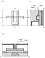
도 1의 (A), (B), 및 (C)는 본 발명의 일 형태에 따른 트랜지스터(200) 및 트랜지스터(200) 주변의 상면도 및 단면도이다.(A), (B), and (C) of Figure 1 is a top view and a cross-sectional view of the
도 1의 (A)는 트랜지스터(200)를 포함하는 반도체 장치의 상면도이다. 또한, 도 1의 (B) 및 (C)는 상기 반도체 장치의 단면도이다. 여기서, 도 1의 (B)는 도 1의 (A)에 A1-A2의 일점쇄선으로 나타낸 부분의 단면도이고, 트랜지스터(200)의 채널 길이 방향의 단면도이기도 하다. 또한, 도 1의 (C)는 도 1의 (A)에 A3-A4의 일점쇄선으로 나타낸 부분의 단면도이고, 트랜지스터(200)의 채널 폭 방향의 단면도이기도 하다. 또한, 도 1의 (A)의 상면도에서는 도면의 명료화를 위하여 일부의 요소를 생략하여 도시하였다.1A is a top view of a semiconductor device including a
본 발명의 일 형태의 반도체 장치는, 트랜지스터(200)와, 층간막으로서 기능하는 절연체(210), 절연체(212), 및 절연체(281)를 포함한다. 또한, 트랜지스터(200)와 전기적으로 접속되고 배선으로서 기능하는 도전체(203) 및 플러그로서 기능하는 도전체(240)(도전체(240a) 및 도전체(240b))를 포함한다.The semiconductor device of one embodiment of the present invention includes a
또한, 도전체(203)에서는, 절연체(212)의 개구의 내벽에 접하여 도전체(203a)가 형성되고, 더 내측에 도전체(203b)가 형성되어 있다. 여기서 도전체(203)의 상면의 높이와 절연체(212)의 상면의 높이는 같은 정도로 할 수 있다. 또한, 트랜지스터(200)에서 도전체(203)가 도전체(203a) 및 도전체(203b)의 적층 구조가 되는 구성을 나타내었지만, 본 발명은 이에 한정되는 것이 아니다. 예를 들어, 도전체(203)를 단층, 또는 3층 이상의 적층 구조로 제공하는 구성으로 하여도 좋다. 구조체가 적층 구조를 가지는 경우, 형성 순으로 서수를 붙여 구별하는 경우가 있다.In addition, in the
또한, 도전체(240)에서는, 절연체(244), 절연체(280), 절연체(274), 및 절연체(281)의 개구의 내벽에 접하여 도전체(240)의 제 1 도전체가 형성되고, 더 내측에 도전체(240)의 제 2 도전체가 형성되어 있다. 여기서, 도전체(240)의 상면의 높이와 절연체(281)의 상면의 높이는 같은 정도로 할 수 있다. 또한, 트랜지스터(200)에서 도전체(240)의 제 1 도전체 및 도전체(240)의 제 2 도전체를 적층하는 구성을 나타내었지만, 본 발명은 이에 한정되는 것이 아니다. 예를 들어, 도전체(240)를 단층, 또는 3층 이상의 적층 구조로 제공하는 구성으로 하여도 좋다. 구조체가 적층 구조를 가지는 경우, 형성 순으로 서수를 붙여 구별하는 경우가 있다.In addition, in the
[트랜지스터(200)][Transistor 200]
도 1에 도시된 바와 같이, 트랜지스터(200)는 기판(도시하지 않았음) 위에 배치된 산화물(230a)과, 산화물(230a) 위에 배치된 산화물(230b)과, 산화물(230b) 위에 서로 떨어져 배치된 도전체(242a) 및 도전체(242b)와, 도전체(242a) 및 도전체(242b) 위에 배치되고 도전체(242a)와 도전체(242b) 사이에 중첩하여 개구가 형성된 절연체(280)와, 개구 내에 배치된 도전체(260)와, 산화물(230b), 도전체(242a), 도전체(242b), 및 절연체(280)와 도전체(260) 사이에 배치된 절연체(250)와, 산화물(230b), 도전체(242a), 도전체(242b), 및 절연체(280)와 절연체(250) 사이에 배치된 산화물(230c)을 포함한다. 또한, 도 1에 도시된 바와 같이, 산화물(230a), 산화물(230b), 도전체(242a), 및 도전체(242b)와 절연체(280) 사이에 절연체(244)가 배치되는 것이 바람직하다. 또한, 도 1에 도시된 바와 같이, 도전체(260)는 절연체(250)의 내측에 제공된 도전체(260a)와, 도전체(260a)의 내측에 매립되도록 제공된 도전체(260b)를 포함하는 것이 바람직하다. 또한, 도 1에 도시된 바와 같이, 절연체(280), 도전체(260), 및 절연체(250) 위에 절연체(274)가 배치되는 것이 바람직하다.As shown in FIG. 1, the
또한, 이하에서, 산화물(230a), 산화물(230b), 및 산화물(230c)을 통틀어 산화물(230)이라고 하는 경우가 있다. 또한, 도전체(242a) 및 도전체(242b)를 통틀어 도전체(242)라고 하는 경우가 있다.In addition, hereinafter, the
또한, 트랜지스터(200)에서 채널이 형성되는 영역(이하, 채널 형성 영역이라고도 함)과 그 근방에서, 산화물(230a), 산화물(230b), 및 산화물(230c)의 3층을 적층하는 구성을 나타내었지만, 본 발명은 이에 한정되는 것이 아니다. 예를 들어, 산화물(230b)의 단층, 산화물(230b)과 산화물(230a)의 2층 구조, 산화물(230b)과 산화물(230c)의 2층 구조, 또는 4층 이상의 적층 구조를 제공하는 구성으로 하여도 좋다. 또한, 트랜지스터(200)에서는, 도전체(260)를 2층의 적층 구조로서 나타내었지만, 본 발명은 이에 한정되는 것이 아니다. 예를 들어, 도전체(260)가 단층 구조이어도 좋고, 3층 이상의 적층 구조이어도 좋다.In addition, a region in which a channel is formed in the transistor 200 (hereinafter, also referred to as a channel formation region) and its vicinity, a structure in which three layers of
여기서, 도전체(260)는 트랜지스터의 게이트 전극으로서 기능하고, 도전체(242a) 및 도전체(242b)는 각각 소스 전극 또는 드레인 전극으로서 기능한다. 상술한 바와 같이, 도전체(260)는 절연체(280)의 개구, 및 도전체(242a)와 도전체(242b) 사이의 영역에 매립되도록 형성된다. 여기서, 도전체(260), 도전체(242a), 및 도전체(242b)의 배치는, 절연체(280)의 개구에 대하여, 자기 정합(self-aligned)적으로 선택된다. 즉, 트랜지스터(200)에서, 게이트 전극을 소스 전극과 드레인 전극 사이에 자기 정합적으로 배치시킬 수 있다. 따라서, 도전체(260)를 위치를 맞추기 위한 마진의 제공없이 형성할 수 있기 때문에, 트랜지스터(200)의 점유 면적의 축소를 도모할 수 있다. 이로써, 반도체 장치의 미세화, 고집적화를 도모할 수 있다.Here, the
또한, 도전체(260)가 도전체(242a)와 도전체(242b) 사이의 영역에 자기 정합적으로 형성되기 때문에, 도전체(260)는 도전체(242a) 또는 도전체(242b)와 중첩되는 영역을 가지지 않는다. 이로써, 도전체(260)와 도전체(242a) 및 도전체(242b) 사이에 형성되는 기생 용량을 저감할 수 있다. 따라서, 트랜지스터(200)의 스위칭 속도를 향상시키고, 트랜지스터(200)가 높은 주파수 특성을 가지게 할 수 있다.In addition, since the
또한, 트랜지스터(200)는, 절연체(212) 위에 배치된 절연체(214)와, 절연체(214) 위에 배치된 절연체(216)와, 절연체(214) 및 절연체(216)에 매립되도록 배치된 도전체(205)와, 절연체(216)와 도전체(205) 위에 배치된 절연체(220)와, 절연체(220) 위에 배치된 절연체(222)와, 절연체(222) 위에 배치된 절연체(224)를 포함하는 것이 바람직하다. 절연체(224) 위에 산화물(230a)이 배치되는 것이 바람직하다.In addition, the
또한, 트랜지스터(200)에서는 채널 형성 영역을 포함하는 산화물(230)(산화물(230a), 산화물(230b), 및 산화물(230c))에 산화물 반도체로서 기능하는 금속 산화물(이하, 산화물 반도체라고도 함)을 사용하는 것이 바람직하다.Further, in the
채널 형성 영역에 산화물 반도체를 사용한 트랜지스터(200)는 비도통 상태에서 누설 전류가 매우 작기 때문에 저소비전력의 반도체 장치를 제공할 수 있다. 또한 산화물 반도체는 스퍼터링법 등을 사용하여 성막할 수 있기 때문에, 고집적형의 반도체 장치를 구성하는 트랜지스터(200)에 사용할 수 있다.The
예를 들어 산화물(230)로서 In-M-Zn 산화물(원소 M은 알루미늄, 갈륨, 이트륨, 구리, 바나듐, 베릴륨, 붕소, 타이타늄, 철, 니켈, 저마늄, 지르코늄, 몰리브데넘, 란타넘, 세륨, 네오디뮴, 하프늄, 탄탈럼, 텅스텐, 또는 마그네슘 등에서 선택된 1종류 또는 복수 종류) 등의 금속 산화물을 사용하는 것이 좋다. 또한 산화물(230)로서 In-Ga 산화물, In-Zn 산화물을 사용하여도 좋다.For example, In-M-Zn oxide as oxide 230 (element M is aluminum, gallium, yttrium, copper, vanadium, beryllium, boron, titanium, iron, nickel, germanium, zirconium, molybdenum, lanthanum, It is preferable to use a metal oxide such as cerium, neodymium, hafnium, tantalum, tungsten, magnesium, or the like. In addition, an In-Ga oxide or an In-Zn oxide may be used as the
여기서, 산화물(230)은 수소, 질소, 또는 금속 원소 등의 불순물이 존재하면, 캐리어 밀도가 증대하고 저저항화하는 경우가 있다. 또한, 산화물(230)에 포함되는 산소 농도가 저하하면, 캐리어 밀도가 증대하고 저저항화하는 경우가 있다.Here, the
산화물(230) 위에 접하도록 제공되고, 소스 전극이나 드레인 전극으로서 기능하는 도전체(242)(도전체(242a) 및 도전체(242b))가 산화물(230)의 산소를 흡수하는 기능을 가지는 경우, 또는 산화물(230)에 수소, 질소, 또는 금속 원소 등의 불순물을 공급하는 기능을 가지는 경우, 산화물(230)에는 부분적으로 저저항 영역이 형성되는 경우가 있다.When the conductor 242 (
절연체(244)는 도전체(242)의 산화를 억제하기 위하여 제공되어 있다. 따라서, 도전체(242)가 내산화성 재료인 경우 또는 산소를 흡수하여도 도전성이 현저히 저하하지 않는 경우에는, 절연체(244)는 반드시 제공할 필요는 없다.The
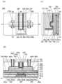
여기서, 도 1의 (B)에서 일점쇄선으로 둘러싼 영역(239)의 확대도를 도 2에 도시하였다. 도 2에 도시된 바와 같이, 절연체(250)는 산화물(230b)과 도전체(260) 사이에서 막 두께 T1을 가지고, 도전체(242a) 또는 도전체(242b)와 도전체(260) 사이에서 막 두께 T2를 가진다. 절연체(250)에서, 막 두께 T1은 막 두께 T2보다 얇은 것이 바람직하다.Here, an enlarged view of the
절연체(250)의 막 두께 T1을 막 두께 T2보다 얇게 하기 위해서는, 예를 들어 산화물(230b)과 도전체(260) 사이에 위치하는 절연체(250)를 단층으로 하고, 도전체(242)와 도전체(260) 사이에 위치하는 절연체(250)를 적층 구조로 하는 것이 바람직하다. 산화물(230b)과 도전체(260) 사이에 위치하는 절연체(250)를 적층 구조로 하는 경우, 도전체(242)와 도전체(260) 사이에 위치하는 절연체(250)의 적층 수는 산화물(230b)과 도전체(260) 사이에 위치하는 절연체(250)의 적층 수보다 많으면 좋다.In order to make the film thickness T1 of the
이와 같이 절연체(250)의 막 두께 T2를 막 두께 T1보다 두껍게 함으로써, 도전체(260)와 도전체(242) 사이의 기생 용량을 저감하여 높은 주파수 특성을 가지는 트랜지스터(200)를 제공할 수 있다. 또한, 막 두께 T1이 얇기 때문에, 게이트 전극으로부터의 전계가 약해지지 않으므로 양호한 전기 특성을 가지는 트랜지스터(200)를 제공할 수 있다.As described above, by making the film thickness T2 of the
또한, 도 2에 도시된 바와 같이, 산화물(230) 위에 접하도록 도전체(242)가 제공되고, 산화물(230)과 도전체(242)의 계면과 그 근방에는, 저저항 영역으로서 영역(243)(영역(243a) 및 영역(243b))이 형성되어 있다. 산화물(230)은 트랜지스터(200)의 채널 형성 영역으로서 기능하는 영역(234)과, 영역(243)의 일부를 포함하고 소스 영역 또는 드레인 영역으로서 기능하는 영역(231)(영역(231a) 및 영역(231b))과, 영역(243)의 일부를 포함하고 접합 영역으로서 기능하는 영역(232)(영역(232a) 및 영역(232b))을 포함한다.In addition, as shown in FIG. 2, a conductor 242 is provided so as to be in contact with the
소스 영역 또는 드레인 영역으로서 기능하는 영역(231)에서, 특히 영역(243)은 산소 농도가 낮거나, 또는 수소, 질소, 금속 원소 등의 불순물을 포함함으로써, 캐리어 농도가 증가하여 저저항화한 영역이다. 즉, 영역(231)은 영역(234)과 비교하여, 캐리어 밀도가 높고 저항이 낮은 영역이다. 또한, 채널 형성 영역으로서 기능하는 영역(234)은, 영역(231) 내에서 특히 영역(243)보다 산소 농도가 높거나 또는 불순물 농도가 낮기 때문에, 캐리어 밀도가 낮은 고저항 영역이다. 또한, 영역(232)의 산소 농도는, 영역(231)의 산소 농도와 동등하거나 또는 그보다 높고, 영역(234)의 산소 농도와 동등하거나 또는 그보다 낮은 것이 바람직하다. 또는, 영역(232)의 불순물 농도는, 영역(231)의 불순물 농도와 동등하거나 또는 그보다 낮고, 영역(234)의 불순물 농도와 동등하거나 또는 그보다 높은 것이 바람직하다.In the region 231 serving as the source region or the drain region, particularly, the region 243 has a low oxygen concentration or contains impurities such as hydrogen, nitrogen, and metal elements, thereby increasing the carrier concentration and lowering the resistance. to be. That is, the region 231 is a region having a high carrier density and a low resistance as compared to the
또한, 저저항 영역인 영역(243)이 금속 원소를 포함하는 경우, 영역(243)은 산화물(230)에 포함되는 금속 원소 외에, 알루미늄, 크로뮴, 구리, 은, 금, 백금, 탄탈럼, 니켈, 타이타늄, 몰리브데넘, 텅스텐, 하프늄, 바나듐, 나이오븀, 망가니즈, 마그네슘, 지르코늄, 베릴륨, 인듐, 루테늄, 이리듐, 스트론튬, 란타넘 등의 금속 원소 중에서 선택되는 어느 하나 또는 복수의 금속 원소를 포함하는 것이 바람직하다.In addition, when the region 243, which is a low-resistance region, includes a metal element, the region 243 may include aluminum, chromium, copper, silver, gold, platinum, tantalum, and nickel, in addition to the metal elements included in the
또한, 도 2에서는, 영역(243)이 산화물(230b)의 막 두께 방향에서 산화물(230b)의 도전체(242)와의 계면 근방에 형성되어 있지만, 이에 한정되지 않는다. 예를 들어, 영역(243)은 산화물(230b)의 막 두께와 실질적으로 같은 두께를 가져도 좋고, 산화물(230a)에도 형성되어 있어도 좋다. 또한, 도 2에서는 영역(243)이 영역(231) 및 영역(232)에 형성되어 있지만, 이에 한정되지 않는다. 예를 들어, 영역(231)에만 형성되어 있어도 좋고, 영역(231)과, 영역(232)의 일부에 형성되어 있어도 좋고, 영역(231)과, 영역(232)과, 영역(234)의 일부에 형성되어 있어도 좋다.In Fig. 2, the region 243 is formed in the vicinity of the interface with the conductor 242 of the
또한, 산화물(230)에서, 각 영역의 경계를 명확히 검출하기 어려운 경우가 있다. 각 영역 내에서 검출되는 금속 원소, 그리고 수소 및 질소 등의 불순물 원소의 농도는, 영역마다의 단계적인 변화에 한정되지 않고, 각 영역 내에서도 연속적으로 변화(그러데이션이라고도 함)되어도 좋다. 즉, 채널 형성 영역에 가까운 영역일수록, 금속 원소, 그리고 수소 및 질소 등의 불순물 원소의 농도가 감소되어 있으면 좋다.In addition, in the
산화물(230)을 선택적으로 저저항화하기 위해서는, 도전체(242)로서, 예를 들어 알루미늄, 크로뮴, 구리, 은, 금, 백금, 탄탈럼, 니켈, 타이타늄, 몰리브데넘, 텅스텐, 하프늄, 바나듐, 나이오븀, 망가니즈, 마그네슘, 지르코늄, 베릴륨, 인듐, 루테늄, 이리듐, 스트론튬, 란타넘 등의 도전성을 높이는 금속 원소, 및 불순물 중 적어도 하나를 포함하는 재료를 사용하는 것이 바람직하다. 또는, 도전체(242)가 되는 도전막(242A)의 형성에서, 산화물(230)에, 산소 결손을 형성하는 원소, 또는 산소 결손에 포획되는 원소 등의 불순물이 주입되는 재료나 성막 방법 등을 사용하면 좋다. 예를 들어 이 원소로서 수소, 붕소, 탄소, 질소, 플루오린, 인, 황, 염소, 희가스 등을 들 수 있다. 또한 희가스 원소의 대표적인 예로서 헬륨, 네온, 아르곤, 크립톤, 및 제논 등이 있다.To selectively lower the
여기서 산화물 반도체를 사용한 트랜지스터는 산화물 반도체 내의 채널이 형성되는 영역에 불순물 및 산소 결손이 존재하면 전기 특성이 변동하기 쉽고 신뢰성이 떨어지는 경우가 있다. 또한 산화물 반도체 내의 채널이 형성되는 영역에 산소 결손이 포함되면 트랜지스터는 노멀리 온 특성을 가지기 쉽다. 따라서, 채널이 형성되는 영역(234) 내의 산소 결손은 가능한 한 저감되어 있는 것이 바람직하다.Here, in the case of a transistor using an oxide semiconductor, when impurities and oxygen deficiencies exist in a region in which a channel in the oxide semiconductor is formed, electrical characteristics are likely to fluctuate and reliability may be poor. In addition, when an oxygen deficiency is included in a region where a channel in an oxide semiconductor is formed, the transistor is likely to have normally-on characteristics. Therefore, it is preferable that the oxygen deficiency in the
트랜지스터의 노멀리 온이 되는 것을 억제하기 위해서는 산화물(230)과 근접하는 절연체(250)가, 화학량론적 조성을 만족시키는 산소보다 많은 산소(과잉 산소라고도 함)를 포함하는 것이 바람직하다. 절연체(250)가 포함하는 산소는 산화물(230)로 확산되어 산화물(230)의 산소 결손을 저감하고, 트랜지스터가 노멀리 온이 되는 것을 억제할 수 있다.In order to suppress the normal on of the transistor, it is preferable that the
즉, 절연체(250) 및 절연체(280)가 포함하는 산소가 산화물(230)의 영역(234)으로 확산됨으로써, 산화물(230)의 영역(234)에서의 산소 결손을 저감할 수 있다.That is, oxygen contained in the
또한, 절연체(250) 및 절연체(280)에 산소 영역을 제공하기 위해서는, 절연체(250) 및 절연체(280)의 상면에 접하는 절연체(274)로서, 산화물을 스퍼터링법으로 성막하는 것이 좋다. 산화물의 성막에 스퍼터링법을 사용함으로써, 산소를 많이 포함하고, 또한 물 또는 수소 등의 불순물이 적은 절연체를 성막할 수 있다. 예를 들어, 절연체(274)에는 산화 알루미늄을 사용하는 것이 바람직하다.Further, in order to provide the oxygen region to the
스퍼터링법에 의한 성막 시에는 타깃과 기판 사이에 이온과 스퍼터링된 입자가 존재한다. 예를 들어, 타깃에는 전원이 접속되어 있고, 전위 E0이 공급된다. 또한 기판에는 접지 전위 등의 전위 E1이 공급된다. 다만, 기판이 전기적으로 부유되어도 좋다. 또한 타깃과 기판 사이에는 전위 E2가 되는 영역이 존재한다. 각 전위의 대소 관계는 E2>E1>E0이다.In the film formation by the sputtering method, ions and sputtered particles exist between the target and the substrate. For example, a power source is connected to the target, and the potential E0 is supplied. Further, a potential E1 such as a ground potential is supplied to the substrate. However, the substrate may be electrically floating. In addition, a region serving as potential E2 exists between the target and the substrate. The magnitude relationship of each potential is E2> E1> E0.
플라스마 내의 이온이 전위차 E2-E0에 의하여 가속되고 타깃에 충돌함으로써, 타깃으로부터 스퍼터링된 입자가 튀어나온다. 이 스퍼터링된 입자가 성막 표면에 부착되고 퇴적됨으로써 성막이 수행된다. 또한, 일부의 이온은 타깃에 의하여 반도(反跳)되어, 반도 이온으로서 형성된 막을 통과하고, 피성막면과 접하는 절연체(250) 및 절연체(280)에 들어가는 경우가 있다. 또한 플라스마 내의 이온은 전위차 E2-E1에 의하여 가속되어 성막 표면을 충격한다. 이때, 일부의 이온은 절연체(280) 내부까지 도달한다. 이온이 절연체(250) 및 절연체(280)에 들어감으로써, 이온이 들어간 영역이 절연체(280)에 형성된다. 즉, 이온이 산소를 포함하는 이온인 경우, 절연체(250) 및 절연체(280)에 과잉 산소 영역이 형성된다.The ions in the plasma are accelerated by the potential difference E2-E0 and collide with the target, so that sputtered particles protrude from the target. Filming is performed by depositing and depositing the sputtered particles on the surface of the film. In addition, some of the ions are semiconducted by the target, pass through the film formed as the semiconducting ions, and may enter the
절연체(250) 및 절연체(280)에 과잉 산소를 도입함으로써, 절연체(250) 및 절연체(280) 내에 과잉 산소 영역을 형성할 수 있다. 절연체(250) 및 절연체(280)의 과잉 산소는, 열처리 등에 의하여 산화물(230)에 공급되고, 산화물(230)의 영역(234)에서의 산소 결손을 보전할 수 있다.By introducing excess oxygen into the
또한, 절연체(280)에는 산화 실리콘, 산화질화 실리콘, 질화산화 실리콘, 공공(空孔)을 포함하는 산화 실리콘을 사용하는 것이 바람직하다. 산화질화 실리콘 등의 재료는 과잉 산소 영역이 형성되기 쉬운 경향이 있다. 한편, 상술한 산화질화 실리콘 등의 재료와 비교하여, 산화물(230)은 스퍼터링법을 사용하여 성막한 산화막을 산화물(230) 위에 형성하더라도, 과잉 산소 영역이 형성되기 어려운 경향이 있다. 따라서, 과잉 산소 영역을 포함하는 절연체(280)를 산화물(230)의 영역(234) 주변에 제공함으로써, 산화물(230)의 영역(234)에 절연체(280)의 과잉 산소를 효과적으로 공급할 수 있다.In addition, it is preferable to use silicon oxide including silicon oxide, silicon oxynitride, silicon nitride oxide, and voids for the
상술한 바와 같이, 온 전류가 큰 트랜지스터를 포함하는 반도체 장치를 제공할 수 있다. 또는, 오프 전류가 작은 트랜지스터를 포함하는 반도체 장치를 제공할 수 있다. 또는, 전기 특성의 변동을 억제하고, 안정적인 전기 특성을 가지면서, 신뢰성을 향상시킨 반도체 장치를 제공할 수 있다.As described above, it is possible to provide a semiconductor device including a transistor having a large on-state current. Alternatively, a semiconductor device including a transistor with a small off current can be provided. Alternatively, it is possible to provide a semiconductor device that suppresses fluctuations in electrical properties and has improved reliability while having stable electrical properties.
이하에서는, 본 발명의 일 형태에 따른 트랜지스터(200)를 포함하는 반도체 장치의 자세한 구성에 대하여 설명한다.Hereinafter, a detailed configuration of the semiconductor device including the
도전체(203)는 도 1의 (A) 및 (C)에 도시된 바와 같이, 채널 폭 방향으로 연장되어 있고, 도전체(205)에 전위를 인가하는 배선으로서 기능한다. 또한 도전체(203)는 절연체(212)에 매립되어 제공되는 것이 바람직하다.The
도전체(205)는 산화물(230) 및 도전체(260)와 중첩되도록 배치된다. 또한 도전체(205)는 도전체(203) 위에 접하여 제공되는 것이 좋다. 또한 도전체(205)는 절연체(214) 및 절연체(216)에 매립되어 제공되는 것이 바람직하다.The
여기서, 도전체(260)는 제 1 게이트(톱 게이트라고도 함) 전극으로서 기능하는 경우가 있다. 또한, 도전체(205)는 제 2 게이트(보텀 게이트라고도 함) 전극으로서 기능하는 경우가 있다. 그 경우, 도전체(205)에 인가하는 전위를 도전체(260)에 인가하는 전위와 연동시키지 않고 독립적으로 변화시킴으로써, 트랜지스터(200)의 Vth를 제어할 수 있다. 특히, 도전체(205)에 음의 전위를 인가함으로써 트랜지스터(200)의 Vth를 0V보다 크게 하고, 오프 전류를 저감할 수 있게 된다. 따라서, 도전체(205)에 음의 전위를 인가하는 경우는 인가하지 않는 경우보다 도전체(260)에 인가하는 전위가 0V일 때의 드레인 전류를 작게 할 수 있다.Here, the
또한 도전체(203) 위에 도전체(205)를 제공함으로써, 제 1 게이트 전극 및 배선으로서의 기능을 가지는 도전체(260)와 도전체(203) 사이의 거리를 적절히 설계할 수 있게 된다. 즉, 도전체(203)와 도전체(260) 사이에 절연체(214) 및 절연체(216) 등이 제공됨으로써, 도전체(203)와 도전체(260) 사이의 기생 용량을 저감하여 도전체(203)와 도전체(260) 사이의 절연 내압을 높일 수 있다.In addition, by providing the
또한 도전체(203)와 도전체(260) 사이의 기생 용량을 저감함으로써, 트랜지스터(200)의 스위칭 속도를 향상시켜 높은 주파수 특성을 가지는 트랜지스터로 할 수 있다. 또한 도전체(203)와 도전체(260) 사이의 절연 내압을 높임으로써, 트랜지스터(200)의 신뢰성을 향상시킬 수 있다. 따라서, 절연체(214) 및 절연체(216)의 막 두께를 두껍게 하는 것이 바람직하다. 또한 도전체(203)의 연장 방향은 이에 한정되지 않고, 예를 들어 트랜지스터(200)의 채널 길이 방향으로 연장되어도 좋다.In addition, by reducing the parasitic capacitance between the
또한, 도전체(205)는 도 1의 (A)에 도시된 바와 같이, 산화물(230) 및 도전체(260)와 중첩되도록 배치한다. 또한 도전체(205)는 산화물(230)에서의 영역(234)보다 크게 제공하는 것이 좋다. 특히, 도 1의 (C)에 도시된 바와 같이, 도전체(205)는 산화물(230)의 영역(234)의 채널 폭 방향과 교차되는 단부보다 외측의 영역에서도 연장되어 있는 것이 바람직하다. 즉, 산화물(230)의 채널 폭 방향에서의 측면의 외측에서 도전체(205)와 도전체(260)는 절연체를 개재(介在)하여 중첩되어 있는 것이 바람직하다.In addition, the
상기 구성을 가짐으로써, 도전체(260) 및 도전체(205)에 전위를 인가한 경우, 도전체(260)로부터 발생하는 전계와 도전체(205)로부터 발생하는 전계가 연결되어, 산화물(230)에 형성되는 채널 형성 영역을 덮을 수 있다.By having the above configuration, when a potential is applied to the
즉, 제 1 게이트 전극으로서의 기능을 가지는 도전체(260)의 전계와 제 2 게이트 전극으로서의 기능을 가지는 도전체(205)의 전계로 영역(234)의 채널 형성 영역을 전기적으로 둘러쌀 수 있다. 본 명세서에서 제 1 게이트 전극 및 제 2 게이트 전극의 전계로 채널 형성 영역을 전기적으로 둘러싸는 트랜지스터의 구조를 surrounded channel(S-channel) 구조라고 부른다.That is, it is possible to electrically surround the channel formation region of the
또한, 도전체(205)에서는 절연체(214) 및 절연체(216)의 개구의 내벽에 접하여 도전체(205a)가 형성되고, 더 내측에 도전체(205b)가 형성되어 있다. 여기서, 도전체(205a) 및 도전체(205b)의 상면의 높이와 절연체(216)의 상면의 높이는 같은 정도로 할 수 있다. 또한, 트랜지스터(200)에서 도전체(205a) 및 도전체(205b)를 적층하는 구성을 나타내었지만, 본 발명은 이에 한정되는 것이 아니다. 예를 들어, 도전체(205)는 단층, 또는 3층 이상의 적층 구조로 제공하는 구성으로 하여도 좋다. 구조체가 적층 구조를 가지는 경우, 형성 순으로 서수를 붙여 구별하는 경우가 있다.In addition, in the
여기서, 도전체(205a) 또는 도전체(203a)에는 수소 원자, 수소 분자, 물 분자, 질소 원자, 질소 분자, 산화 질소 분자(N2O, NO, NO2 등), 구리 원자 등의 불순물의 확산을 억제하는 기능을 가지는(상기 불순물이 투과하기 어려운) 도전성 재료를 사용하는 것이 바람직하다. 또는, 산소(예를 들어 산소 원자, 산소 분자 등 중 적어도 하나)의 확산을 억제하는 기능을 가지는(상기 산소가 투과하기 어려운) 도전성 재료를 사용하는 것이 바람직하다. 또한, 본 명세서에서, 불순물 또는 산소의 확산을 억제하는 기능이란, 상기 불순물 또는 상기 산소 중 어느 하나 또는 모두의 확산을 억제하는 기능으로 한다.Here, the
도전체(205a) 또는 도전체(203a)가 산소의 확산을 억제하는 기능을 가짐으로써, 도전체(205b) 또는 도전체(203b)가 산화되어 도전율이 저하하는 것을 억제할 수 있다. 산소의 확산을 억제하는 기능을 가지는 도전성 재료로서는, 예를 들어 탄탈럼, 질화 탄탈럼, 루테늄, 또는 산화 루테늄 등을 사용하는 것이 바람직하다. 따라서, 도전체(205a) 또는 도전체(203a)로서는, 상기 도전성 재료를 단층 또는 적층으로 하면 좋다. 이로써, 수소, 물 등의 불순물이 도전체(203) 및 도전체(205)를 통하여 트랜지스터(200) 측으로 확산되는 것을 억제할 수 있다.When the
또한, 도전체(205b)에는 텅스텐, 구리, 또는 알루미늄을 주성분으로 하는 도전성 재료를 사용하는 것이 바람직하다. 또한, 도전체(205b)를 단층으로 도시하였지만, 적층 구조로 하여도 좋고, 예를 들어 타이타늄, 질화 타이타늄과 상기 도전성 재료의 적층으로 하여도 좋다.In addition, it is preferable to use a conductive material mainly composed of tungsten, copper, or aluminum as the
또한, 도전체(203b)는 배선으로서 기능하기 때문에, 도전체(205b)보다 도전성이 높은 도전체를 사용하는 것이 바람직하다. 예를 들어, 구리 또는 알루미늄을 주성분으로 하는 도전성 재료를 사용할 수 있다. 또한, 도전체(203b)는 적층 구조로 하여도 좋고, 예를 들어 타이타늄, 질화 타이타늄과 상기 도전성 재료의 적층으로 하여도 좋다.In addition, since the
특히, 도전체(203b)에 구리를 사용하는 것이 바람직하다. 구리는 저항이 작기 때문에, 배선 등으로 사용하는 것이 바람직하다. 한편, 구리는 확산되기 쉽기 때문에, 산화물(230)로 확산됨으로써 트랜지스터(200)의 전기 특성을 저하시키는 경우가 있다. 그래서, 예를 들어 절연체(214)에는 구리의 투과성이 낮은 산화 알루미늄 또는 산화 하프늄 등의 재료를 사용함으로써, 구리의 확산을 억제할 수 있다.In particular, it is preferable to use copper for the
또한 도전체(205), 절연체(214), 및 절연체(216)는 반드시 제공하지 않아도 된다. 이 경우, 도전체(203)의 일부가 제 2 게이트 전극으로서 기능할 수 있다.In addition, the
절연체(210) 및 절연체(214)는 물 또는 수소 등의 불순물이 기판 측으로부터 트랜지스터(200)로 혼입되는 것을 억제하는 배리어 절연막으로서 기능하는 것이 바람직하다. 따라서, 절연체(210) 및 절연체(214)에는, 수소 원자, 수소 분자, 물 분자, 질소 원자, 질소 분자, 산화 질소 분자(N2O, NO, NO2 등), 구리 원자 등의 불순물의 확산을 억제하는 기능을 가지는(상기 불순물이 투과하기 어려운) 절연성 재료를 사용하는 것이 바람직하다. 또는, 산소(예를 들어 산소 원자, 산소 분자 등 중 적어도 하나)의 확산을 억제하는 기능을 가지는(상기 산소가 투과하기 어려운) 절연성 재료를 사용하는 것이 바람직하다.It is preferable that the
예를 들어, 절연체(210)로서 산화 알루미늄 등을 사용하고, 절연체(214)로서 질화 실리콘 등을 사용하는 것이 바람직하다. 이로써, 수소, 물 등의 불순물이 절연체(210) 및 절연체(214)보다 기판 측으로부터 트랜지스터(200) 측으로 확산되는 것을 억제할 수 있다. 또는, 절연체(224) 등에 포함되는 산소가 절연체(210) 및 절연체(214)보다 기판 측으로 확산되는 것을 억제할 수 있다.For example, it is preferable to use aluminum oxide or the like as the
또한 도전체(203) 위에 도전체(205)를 적층시켜 제공하는 구성으로 함으로써, 도전체(203)와 도전체(205) 사이에 절연체(214)를 제공할 수 있다. 여기서, 도전체(203b)에 구리 등 확산되기 쉬운 금속을 사용하더라도, 절연체(214)로서 질화 실리콘 등을 제공함으로써 상기 금속이 절연체(214)보다 위의 층으로 확산되는 것을 억제할 수 있다.In addition, by providing a structure in which a
또한, 층간막으로서 기능하는 절연체(212), 절연체(216), 절연체(280), 및 절연체(281)는 절연체(210) 또는 절연체(214)보다 유전율이 낮은 것이 바람직하다. 유전율이 낮은 재료를 층간막으로 함으로써, 배선 사이에 생기는 기생 용량을 저감할 수 있다.In addition, it is preferable that the
예를 들어, 절연체(212), 절연체(216), 절연체(280), 및 절연체(281)로서 산화 실리콘, 산화질화 실리콘, 질화산화 실리콘, 산화 알루미늄, 산화 하프늄, 산화 탄탈럼, 산화 지르코늄, 타이타늄산 지르콘산 연(PZT), 타이타늄산 스트론튬(SrTiO3), 또는 (Ba,Sr)TiO3(BST) 등의 절연체를 단층 또는 적층으로 사용할 수 있다. 또는 이들 절연체에 예를 들어 산화 알루미늄, 산화 비스무트, 산화 저마늄, 산화 나이오븀, 산화 실리콘, 산화 타이타늄, 산화 텅스텐, 산화 이트륨, 산화 지르코늄을 첨가하여도 좋다. 또는 이들 절연체를 질화 처리하여도 좋다. 상기 절연체에 산화 실리콘, 산화질화 실리콘, 또는 질화 실리콘을 적층하여 사용하여도 좋다.For example, silicon oxide, silicon oxynitride, silicon nitride oxide, aluminum oxide, hafnium oxide, tantalum oxide, zirconium oxide, titanium as
절연체(220), 절연체(222), 절연체(224), 및 절연체(250)는 게이트 절연체로서의 기능을 가진다.The
여기서, 산화물(230)과 접하는 절연체(224)에는 화학량론적 조성을 만족시키는 산소보다 많은 산소를 포함하는 절연체를 사용하는 것이 바람직하다. 즉, 절연체(224)에는 과잉 산소 영역이 형성되어 있는 것이 바람직하다. 이와 같은 과잉 산소를 포함하는 절연체를 산화물(230)에 접하여 제공함으로써, 산화물(230) 내의 산소 결손을 저감하여 트랜지스터(200)의 신뢰성을 향상시킬 수 있다.Here, it is preferable to use an insulator containing more oxygen than the oxygen satisfying the stoichiometric composition for the
과잉 산소 영역을 포함하는 절연체로서, 구체적으로는 가열에 의하여 일부의 산소가 이탈되는 산화물 재료를 사용하는 것이 바람직하다. 가열에 의하여 산소가 이탈되는 산화물이란, TDS(Thermal Desorption Spectroscopy) 분석에서 산소 원자로 환산한 산소의 이탈량이 1.0×10¹⁸atoms/cm3 이상, 바람직하게는 1.0×10¹⁹atoms/cm3 이상, 더 바람직하게는 2.0×10¹⁹atoms/cm3 이상, 또는 3.0×10²⁰atoms/cm3 이상인 산화물막이다. 또한, 상기 TDS 분석 시에서의 막의 표면 온도로서는 100℃ 이상 700℃ 이하, 또는 100℃ 이상 400℃ 이하의 범위가 바람직하다.As an insulator containing an excess oxygen region, specifically, it is preferable to use an oxide material in which some oxygen is released by heating. Oxide from which oxygen is released by heating means that the amount of oxygen released in terms of oxygen atom in a TDS (Thermal Desorption Spectroscopy) analysis is 1.0 × 10¹⁸ atoms / cm3 or more, preferably 1.0 × 10¹⁹ atoms / cm3 or more, and more It is preferably an oxide film of 2.0 × 10¹⁹ atoms / cm3 or more, or 3.0 × 10²⁰ atoms / cm3 or more. Further, the surface temperature of the film during the TDS analysis is preferably 100 ° C or more and 700 ° C or less, or 100 ° C or more and 400 ° C or less.
또한, 절연체(224)가 과잉 산소 영역을 포함하는 경우, 절연체(222)는 산소(예를 들어 산소 원자, 산소 분자 등의 적어도 하나)의 확산을 억제하는 기능을 가지는(상기 산소가 투과하기 어려운) 것이 바람직하다.In addition, when the
절연체(222)가 산소나 불순물의 확산을 억제하는 기능을 가짐으로써, 산화물(230)이 포함하는 산소는 절연체(220) 측으로 확산되지 않음므로 바람직하다. 또한, 도전체(205)가 절연체(224)나 산화물(230)이 포함하는 산소와 반응하는 것을 억제할 수 있다.Since the
절연체(222)에는 예를 들어 산화 알루미늄, 산화 하프늄, 산화 탄탈럼, 산화 지르코늄, 타이타늄산 지르콘산 연(PZT), 타이타늄산 스트론튬(SrTiO3), 또는 (Ba,Sr)TiO3(BST) 등의 소위 high-k 재료를 포함하는 절연체를 단층 또는 적층으로 사용하는 것이 바람직하다. 트랜지스터의 미세화 및 고집적화가 진행되면, 게이트 절연체가 박막화됨으로써 누설 전류 등의 문제가 생기는 경우가 있다. 게이트 절연체로서 기능하는 절연체에 high-k 재료를 사용함으로써 물리적 막 두께를 유지하면서, 트랜지스터 동작 시의 게이트 전위의 저감이 가능해진다.Examples of the
특히, 불순물 및 산소 등의 확산을 억제하는 기능을 가지는(상기 산소가 투과하기 어려운) 절연성 재료인 알루미늄 및 하프늄 중 한쪽 또는 양쪽의 산화물을 포함하는 절연체를 사용하는 것이 좋다. 알루미늄 및 하프늄 중 한쪽 또는 양쪽의 산화물을 포함하는 절연체로서, 산화 알루미늄, 산화 하프늄, 알루미늄 및 하프늄을 포함하는 산화물(하프늄 알루미네이트) 등을 사용하는 것이 바람직하다. 이와 같은 재료를 사용하여 절연체(222)를 형성한 경우, 절연체(222)는 산화물(230)로부터의 산소의 방출이나, 트랜지스터(200)의 주변부로부터 산화물(230)로의 수소 등의 불순물의 혼입을 억제하는 층으로서 기능한다.In particular, it is preferable to use an insulator containing oxides of one or both of aluminum and hafnium, which are insulating materials having a function of suppressing diffusion of impurities and oxygen and the like (the oxygen is hardly permeable). As an insulator containing oxides of one or both of aluminum and hafnium, it is preferable to use aluminum oxide, hafnium oxide, oxides containing hafnium (hafnium aluminate), or the like. When the
또는, 이들 절연체에 예를 들어 산화 알루미늄, 산화 비스무트, 산화 저마늄, 산화 나이오븀, 산화 실리콘, 산화 타이타늄, 산화 텅스텐, 산화 이트륨, 산화 지르코늄을 첨가하여도 좋다. 또는 이들 절연체를 질화 처리하여도 좋다. 상기 절연체에 산화 실리콘, 산화질화 실리콘, 또는 질화 실리콘을 적층시켜 사용하여도 좋다.Alternatively, for example, aluminum oxide, bismuth oxide, germanium oxide, niobium oxide, silicon oxide, titanium oxide, tungsten oxide, yttrium oxide, or zirconium oxide may be added to these insulators. Alternatively, these insulators may be nitrided. Silicon oxide, silicon oxynitride, or silicon nitride may be stacked on the insulator.
또한 절연체(220)는 열적으로 안정적인 것이 바람직하다. 예를 들어 산화 실리콘 및 산화질화 실리콘은 열적으로 안정적이기 때문에 high-k 재료의 절연체와 절연체(220)를 조합함으로써, 열적으로 안정적이며 비유전율이 높은 적층 구조로 할 수 있다.In addition, the
또한 절연체(220), 절연체(222), 및 절연체(224)가 2층 이상의 적층 구조를 가져도 좋다. 이 경우, 같은 재료로 이루어지는 적층 구조에 한정되지 않고, 상이한 재료로 이루어지는 적층 구조이어도 좋다.Further, the
산화물(230)은 산화물(230a)과, 산화물(230a) 위의 산화물(230b)과, 산화물(230b) 위의 산화물(230c)을 포함한다. 산화물(230b) 아래에 산화물(230a)을 포함함으로써, 산화물(230a)보다 아래쪽에 형성된 구조물로부터 산화물(230b)로의 불순물의 확산을 억제할 수 있다. 또한 산화물(230b) 위에 산화물(230c)을 포함함으로써, 산화물(230c) 위쪽에 형성된 구조물로부터 산화물(230b)로의 불순물의 확산을 억제할 수 있다.The
또한 산화물(230)은 각 금속 원자의 원자수비가 상이한 산화물의 적층 구조를 가지는 것이 바람직하다. 구체적으로는, 산화물(230a)에 사용하는 금속 산화물에서, 구성 원소 중의 원소 M의 원자수비가 산화물(230b)에 사용하는 금속 산화물에서의 구성 원소 중의 원소 M의 원자수비보다 큰 것이 바람직하다. 또한 산화물(230a)에 사용하는 금속 산화물에서 In에 대한 원소 M의 원자수비가 산화물(230b)에 사용하는 금속 산화물에서의 In에 대한 원소 M의 원자수비보다 큰 것이 바람직하다. 또한 산화물(230b)에 사용하는 금속 산화물에서 원소 M에 대한 In의 원자수비가 산화물(230a)에 사용하는 금속 산화물에서의 원소 M에 대한 In의 원자수비보다 큰 것이 바람직하다. 또한 산화물(230c)은 산화물(230a) 또는 산화물(230b)에 사용할 수 있는 금속 산화물을 사용할 수 있다.In addition, it is preferable that the
또한 산화물(230a) 및 산화물(230c)의 전도대 하단의 에너지가 산화물(230b)의 전도대 하단의 에너지보다 높아지는 것이 바람직하다. 또한 환언하면 산화물(230a) 및 산화물(230c)의 전자 친화력이 산화물(230b)의 전자 친화력보다 작은 것이 바람직하다.In addition, it is preferable that the energy at the bottom of the conduction band of the
여기서, 산화물(230a), 산화물(230b), 및 산화물(230c)의 접합부에서 전도대 하단의 에너지 준위는 완만하게 변화한다. 환언하면, 산화물(230a), 산화물(230b), 및 산화물(230c)의 접합부에서의 전도대 하단의 에너지 준위는 연속적으로 변화 또는 연속 접합한다고도 할 수 있다. 이와 같이 하기 위해서는, 산화물(230a)과 산화물(230b) 사이의 계면 및 산화물(230b)과 산화물(230c) 사이의 계면에 형성되는 혼합층의 결함 준위 밀도를 낮추는 것이 좋다.Here, at the junction of the
구체적으로는, 산화물(230a)과 산화물(230b), 산화물(230b)과 산화물(230c)이 산소 이외에 공통되는 원소를 포함함으로써(주성분으로 함으로써), 결함 준위 밀도가 낮은 혼합층을 형성할 수 있다. 예를 들어, 산화물(230b)이 In-Ga-Zn 산화물인 경우, 산화물(230a) 및 산화물(230c)로서 In-Ga-Zn 산화물, Ga-Zn 산화물, 산화 갈륨 등을 사용하는 것이 좋다.Specifically, the
이때, 캐리어의 주된 경로는 산화물(230b)이 되는 경우가 있다. 산화물(230a), 산화물(230c)을 상술한 구성으로 함으로써, 산화물(230a)과 산화물(230b) 사이의 계면 및 산화물(230b)과 산화물(230c) 사이의 계면에서의 결함 준위 밀도를 낮출 수 있다. 그래서 캐리어 전도에 대한 계면 산란의 영향이 작아져 트랜지스터(200)는 높은 온 전류를 얻을 수 있다.At this time, the main path of the carrier may be
또한, 산화물(230)은 영역(231) 및 영역(234)을 포함한다. 또한, 영역(231)의 적어도 일부는 도전체(242)와 접하는 영역을 포함한다.In addition,
또한 트랜지스터(200)를 온으로 하면, 영역(231a) 또는 영역(231b)은 소스 영역 또는 드레인 영역으로서 기능한다. 한편, 영역(234)의 적어도 일부는 채널이 형성되는 영역으로서 기능한다. 또한, 영역(231)과 영역(234) 사이에 접합 영역으로서 기능하는 영역(232)을 포함하여도 좋다.Also, when the
즉, 각 영역의 범위를 적절히 선택함으로써, 회로 설계에 맞추어 요구에 걸맞은 전기 특성을 가지는 트랜지스터를 용이하게 제공할 수 있다.That is, by appropriately selecting the range of each region, it is possible to easily provide a transistor having electrical characteristics suited to the needs in accordance with the circuit design.
산화물(230)에는 산화물 반도체로서 기능하는 금속 산화물(이하, 산화물 반도체라고도 함)을 사용하는 것이 바람직하다. 예를 들어, 영역(234)이 되는 금속 산화물로서는 밴드 갭이 2eV 이상, 바람직하게는 2.5eV 이상인 것을 사용하는 것이 바람직하다. 이와 같이, 밴드 갭이 큰 금속 산화물을 사용함으로써, 트랜지스터의 오프 전류를 저감할 수 있다.It is preferable to use a metal oxide (hereinafter also referred to as an oxide semiconductor) that functions as an oxide semiconductor for the
산화물 반도체를 사용한 트랜지스터는 비도통 상태에서 누설 전류가 매우 작기 때문에, 저소비전력의 반도체 장치를 제공할 수 있다. 또한 산화물 반도체는 스퍼터링법 등을 사용하여 성막될 수 있으므로 고집적형 반도체 장치를 구성하는 트랜지스터에 사용될 수 있다.Since a transistor using an oxide semiconductor has a very small leakage current in a non-conductive state, it is possible to provide a semiconductor device with low power consumption. In addition, since the oxide semiconductor can be formed using a sputtering method or the like, it can be used for transistors constituting a highly integrated semiconductor device.
산화물(230b) 위에는 소스 전극 및 드레인 전극으로서 기능하는 도전체(242)(도전체(242a) 및 도전체(242b))가 제공된다. 도전체(242)로서는, 알루미늄, 크로뮴, 구리, 은, 금, 백금, 탄탈럼, 니켈, 타이타늄, 몰리브데넘, 텅스텐, 하프늄, 바나듐, 나이오븀, 망가니즈, 마그네슘, 지르코늄, 베릴륨, 인듐, 루테늄, 이리듐, 스트론튬, 란타넘에서 선택된 금속 원소, 또는 상술한 금속 원소를 성분으로 하는 합금이나, 상술한 금속 원소를 조합한 합금 등을 사용하는 것이 바람직하다. 예를 들어, 질화 탄탈럼, 질화 타이타늄, 텅스텐, 타이타늄과 알루미늄을 포함하는 질화물, 탄탈럼과 알루미늄을 포함하는 질화물, 산화 루테늄, 질화 루테늄, 스트론튬과 루테늄을 포함하는 산화물, 란타넘과 니켈을 포함하는 산화물 등을 사용하는 것이 바람직하다. 또한, 질화 탄탈럼, 질화 타이타늄, 타이타늄과 알루미늄을 포함하는 질화물, 탄탈럼과 알루미늄을 포함하는 질화물, 산화 루테늄, 질화 루테늄, 스트론튬과 루테늄을 포함하는 산화물, 란타넘과 니켈을 포함하는 산화물은 산화되기 어려운 도전성 재료 또는 산소를 흡수하여도 도전성을 유지하는 재료이기 때문에 바람직하다.On the
산화물(230)과 접하도록 상기 도전체(242)를 제공함으로써, 영역(243)의 산소 농도가 저감하는 경우가 있다. 또한, 영역(243)에, 도전체(242)에 포함되는 금속과, 산화물(230)의 성분을 포함하는 금속 화합물층이 형성되는 경우가 있다. 이와 같은 경우, 영역(243)의 캐리어 밀도가 증가하여 영역(243)은 저저항 영역이 된다.By providing the conductor 242 in contact with the
여기서, 도전체(242a)와 도전체(242b) 사이의 영역은 절연체(280)의 개구에 중첩되어 형성된다. 이로써, 도전체(242a)와 도전체(242b) 사이에 도전체(260)를 자기 정합적으로 배치할 수 있다.Here, the region between the
절연체(244)는 도전체(242)를 덮도록 제공되고, 도전체(242)의 산화를 억제한다. 이때, 절연체(244)는 산화물(230)의 측면을 덮어 절연체(224)와 접하도록 제공되어도 좋다.The
절연체(244)로서 하프늄, 알루미늄, 갈륨, 이트륨, 지르코늄, 텅스텐, 타이타늄, 탄탈럼, 니켈, 저마늄, 또는 마그네슘 등에서 선택된 1종류 또는 2종류 이상이 포함된 금속 산화물을 사용할 수 있다.As the
특히, 알루미늄 또는 하프늄 중 한쪽 또는 양쪽의 산화물을 포함하는 절연체인, 산화 알루미늄, 산화 하프늄, 알루미늄 및 하프늄을 포함하는 산화물(하프늄 알루미네이트) 등을 사용하는 것이 바람직하다. 특히, 하프늄 알루미네이트는 산화 하프늄막보다 내열성이 높다. 그러므로, 추후의 공정에서의 열 이력에서, 결정화하기 어렵기 때문에 바람직하다. 또한, 도전체(242)가 내산화성을 가지는 재료인 경우 또는 산소를 흡수하여도 현저히 도전성이 저하하지 않는 경우, 절연체(244)는 필수적인 구성이 아니다. 요구되는 트랜지스터 특성에 따라 적절히 설계하면 좋다.In particular, it is preferable to use aluminum oxide, hafnium oxide, oxides containing aluminum and hafnium (hafnium aluminate), etc., which are insulators containing oxides of one or both of aluminum or hafnium. In particular, hafnium aluminate has higher heat resistance than hafnium oxide films. Therefore, it is preferable because it is difficult to crystallize from the heat history in a later step. In addition, in the case where the conductor 242 is a material having oxidation resistance or when the conductivity does not deteriorate significantly even when oxygen is absorbed, the
절연체(250)는 게이트 절연체로서 기능한다. 절연체(250)는 산화물(230c)의 내측(상면 및 측면)에 접하여 배치되는 것이 바람직하다. 절연체(250)는 가열에 의하여 산소가 방출되는 절연체를 사용하여 형성하는 것이 바람직하다. 예를 들어, 승온 이탈 가스 분광법 분석(TDS 분석)에서, 산소 분자로 환산한 산소의 이탈량이 1.0×10¹⁸atoms/cm3 이상, 바람직하게는 1.0×10¹⁹atoms/cm3 이상, 더 바람직하게는 2.0×10¹⁹atoms/cm3 이상, 또는 3.0×10²⁰atoms/cm3 이상인 산화물막이다. 또한, 상기 TDS 분석 시에서의 막의 표면 온도로서는 100℃ 이상 700℃ 이하의 범위가 바람직하다.The
구체적으로는, 과잉 산소를 포함하는 산화 실리콘, 산화질화 실리콘, 질화산화 실리콘, 질화 실리콘, 플루오린을 첨가한 산화 실리콘, 탄소를 첨가한 산화 실리콘, 탄소 및 질소를 첨가한 산화 실리콘, 공공을 포함하는 산화 실리콘을 사용할 수 있다. 특히, 산화 실리콘 및 산화질화 실리콘은 열에 대하여 안정적이기 때문에 바람직하다.Specifically, it includes silicon oxide containing excess oxygen, silicon oxynitride, silicon nitride oxide, silicon nitride, silicon oxide with fluorine, silicon oxide with carbon, silicon oxide with carbon and nitrogen, and voids Silicon oxide to be used can be used. In particular, silicon oxide and silicon oxynitride are preferred because they are stable against heat.
가열에 의하여 산소가 방출되는 절연체를 절연체(250)로서 산화물(230c)의 상면에 접하여 제공함으로써, 절연체(250)로부터 산화물(230c)을 통하여 산화물(230b)의 영역(234)에 효과적으로 산소를 공급할 수 있다. 또한 절연체(224)와 마찬가지로, 절연체(250) 내의 물 또는 수소 등의 불순물 농도가 저감되는 것이 바람직하다. 절연체(250)의 막 두께는, 1nm 이상 20nm 이하로 하는 것이 바람직하다.By providing an insulator in which oxygen is released by heating in contact with the upper surface of the
또한, 절연체(250)는 산화물(230b)과 도전체(260) 사이뿐만 아니라, 도전체(242)와 도전체(260) 사이에도 제공된다. 절연체(250)로서 요구되는 막 두께에 따라, 도전체(242)와 도전체(260) 사이에 기생 용량이 형성되고, 트랜지스터(200) 또는 반도체 장치의 특성에 악영향을 주는 경우에는, 도전체(242)와 도전체(260) 사이에 위치하는 절연체(250)의 막 두께를 산화물(230b)과 도전체(260) 사이에 위치하는 절연체(250)의 막 두께보다 두껍게 하는 것이 바람직하다. 이를 위해서는, 예를 들어 도전체(242)와 도전체(260) 사이에 위치하는 절연체(250)를 2층 구조로 하고, 산화물(230b)과 도전체(260) 사이에 위치하는 절연체(250)를 단층 구조로 하면 좋다. 자세한 내용은 후술하지만, 산화물(230c)이 되는 산화막(230C)의 내측에 제 1 절연체가 되는 절연막을 형성하고, 상기 절연막에 대하여 이방성 에칭을 수행함으로써, 산화막(230C)의 내벽에만 제 1 절연체를 형성한다. 이어서, 제 2 절연체가 되는 절연막을 형성함으로써, 산화물(230b)과 도전체(260) 사이에 위치하는 절연체(250)는 단층 구조가 되고, 도전체(242)와 도전체(260) 사이에 위치하는 절연체(250)는 2층 구조가 된다. 따라서, 도전체(242)와 도전체(260) 사이에 위치하는 절연체(250)의 막 두께를 산화물(230b)과 도전체(260) 사이에 위치하는 절연체(250)의 막 두께보다 두껍게 할 수 있다.In addition, the
또한, 절연체(250)가 포함하는 과잉 산소를 효율적으로 산화물(230)에 공급하기 위하여, 절연체(250)와 도전체(260) 사이에 금속 산화물을 제공하여도 좋다. 상기 금속 산화물은 절연체(250)로부터 도전체(260)로의 산소 확산을 억제하는 것이 바람직하다. 산소의 확산을 억제하는 금속 산화물을 제공함으로써, 절연체(250)로부터 도전체(260)로의 과잉 산소의 확산이 억제된다. 즉, 산화물(230)에 공급하는 과잉 산소량의 감소를 억제할 수 있다. 또한 과잉 산소로 인한 도전체(260)의 산화를 억제할 수 있다.In addition, a metal oxide may be provided between the
또한, 상기 금속 산화물은 게이트 절연체의 일부로서의 기능을 가지는 경우가 있다. 따라서, 절연체(250)에 산화 실리콘이나 산화질화 실리콘 등을 사용하는 경우, 상기 금속 산화물에는 비유전율이 높은 high-k 재료인 금속 산화물을 사용하는 것이 바람직하다. 게이트 절연체를 절연체(250)와 상기 금속 산화물의 적층 구조로 함으로써, 열에 대하여 안정적이고, 또한 비유전율이 높은 적층 구조로 할 수 있다. 따라서, 게이트 절연체의 물리적 막 두께를 유지한 채, 트랜지스터 동작 시에 인가하는 게이트 전위의 저감화가 가능해진다. 또한 게이트 절연체로서 기능하는 절연체의 등가 산화 막 두께(EOT)의 박막화가 가능해진다.In addition, the metal oxide may have a function as a part of the gate insulator. Therefore, when using silicon oxide or silicon oxynitride for the
구체적으로는, 하프늄, 알루미늄, 갈륨, 이트륨, 지르코늄, 텅스텐, 타이타늄, 탄탈럼, 니켈, 저마늄, 또는 마그네슘 등에서 선택된 1종류 또는 2종류 이상이 포함된 금속 산화물을 사용할 수 있다.Specifically, a metal oxide containing one or two or more types selected from hafnium, aluminum, gallium, yttrium, zirconium, tungsten, titanium, tantalum, nickel, germanium, or magnesium can be used.
특히, 알루미늄 또는 하프늄 중 한쪽 또는 양쪽의 산화물을 포함하는 절연체인, 산화 알루미늄, 산화 하프늄, 알루미늄 및 하프늄을 포함하는 산화물(하프늄 알루미네이트) 등을 사용하는 것이 바람직하다. 특히, 하프늄 알루미네이트는 산화 하프늄막보다 내열성이 높다. 그러므로, 추후의 공정에서의 열 이력에서, 결정화하기 어렵기 때문에 바람직하다. 또한, 상기 금속 산화물은 필수적인 구성이 아니다. 요구되는 트랜지스터 특성에 따라 적절히 설계하면 좋다.In particular, it is preferable to use aluminum oxide, hafnium oxide, oxides containing aluminum and hafnium (hafnium aluminate), etc., which are insulators containing oxides of one or both of aluminum or hafnium. In particular, hafnium aluminate has higher heat resistance than hafnium oxide films. Therefore, it is preferable because it is difficult to crystallize from the heat history in a later step. In addition, the metal oxide is not an essential component. It may be appropriately designed according to the required transistor characteristics.
제 1 게이트 전극으로서 기능하는 도전체(260)는, 도 1에서는 2층 구조로서 도시하였지만, 단층 구조이어도 좋고 3층 이상의 적층 구조이어도 좋다.Although the
도전체(260a)에는 도전체(205a)와 마찬가지로, 수소 원자, 수소 분자, 물 분자, 질소 원자, 질소 분자, 산화 질소 분자(N2O, NO, NO2 등), 구리 원자 등의 불순물의 확산을 억제하는 기능을 가지는 도전성 재료를 사용하는 것이 바람직하다. 또는, 산소(예를 들어 산소 원자, 산소 분자 등 중 적어도 하나)의 확산을 억제하는 기능을 가지는 도전성 재료를 사용하는 것이 바람직하다.Like the
또한, 도전체(260a)가 산소의 확산을 억제하는 기능을 가짐으로써, 절연체(250)에 포함되는 산소로 인하여 도전체(260b)가 산화되어 도전율이 저하하는 것을 억제할 수 있다. 산소의 확산을 억제하는 기능을 가지는 도전성 재료로서는, 예를 들어 탄탈럼, 질화 탄탈럼, 루테늄, 또는 산화 루테늄 등을 사용하는 것이 바람직하다.In addition, since the
또한 도전체(260b)는 텅스텐, 구리, 또는 알루미늄을 주성분으로 하는 도전성 재료를 사용하는 것이 바람직하다. 또한, 도전체(260b)는 배선으로서도 기능하기 때문에, 도전성이 높은 도전체를 사용하는 것이 바람직하다. 예를 들어, 텅스텐, 구리, 또는 알루미늄을 주성분으로 하는 도전성 재료를 사용할 수 있다. 또한, 도전체(260b)는 적층 구조로 하여도 좋고, 예를 들어 타이타늄, 질화 타이타늄과 상기 도전성 재료의 적층 구조로 하여도 좋다.In addition, it is preferable to use a conductive material mainly composed of tungsten, copper, or aluminum as the
또한, 도 1의 (C)에 도시된 바와 같이, 도전체(205)가 산화물(230)의 채널 폭 방향과 교차되는 단부보다 외측의 영역에서 연장되어 있는 경우, 도전체(260)는 상기 영역에서 절연체(250)를 개재하여 도전체(205)와 중첩되어 있는 것이 바람직하다. 즉, 산화물(230)의 측면의 외측에서, 도전체(205)와 절연체(250)와 도전체(260)는 적층 구조를 형성하는 것이 바람직하다.Also, as shown in FIG. 1C, when the
상기 구성을 가짐으로써, 도전체(260) 및 도전체(205)에 전위를 인가한 경우, 도전체(260)로부터 발생하는 전계와 도전체(205)로부터 발생하는 전계가 연결되어, 산화물(230)에 형성되는 채널 형성 영역을 덮을 수 있다.By having the above configuration, when a potential is applied to the
즉, 제 1 게이트 전극으로서의 기능을 가지는 도전체(260)의 전계와 제 2 게이트 전극으로서의 기능을 가지는 도전체(205)의 전계로 영역(234)의 채널 형성 영역을 전기적으로 둘러쌀 수 있다.That is, it is possible to electrically surround the channel formation region of the
절연체(280)는 절연체(244)를 개재하여 도전체(242) 위에 제공된다. 절연체(280)는 과잉 산소 영역을 포함하는 것이 바람직하다. 예를 들어, 절연체(280)로서 산화 실리콘, 산화질화 실리콘, 질화산화 실리콘, 질화 실리콘, 플루오린을 첨가한 산화 실리콘, 탄소를 첨가한 산화 실리콘, 탄소 및 질소를 첨가한 산화 실리콘, 공공을 포함하는 산화 실리콘, 또는 수지 등을 포함하는 것이 바람직하다. 특히 산화 실리콘 및 산화질화 실리콘은 열적으로 안정적이므로 바람직하다. 특히 산화 실리콘 및 공공을 포함하는 산화 실리콘은 추후의 공정에서 용이하게 과잉 산소 영역을 형성할 수 있으므로 바람직하다.The
상술한 바와 같이, 절연체(280)는 과잉 산소 영역을 포함하는 것이 바람직하다. 가열에 의하여 산소가 방출되는 절연체(280)를 산화물(230c)과 접하여 제공함으로써, 절연체(280) 내의 산소를, 산화물(230c)을 통하여 산화물(230)의 영역(234)에 효율적으로 공급할 수 있다. 또한, 절연체(280) 내의 물 또는 수소 등의 불순물 농도가 저감되어 있는 것이 바람직하다.As described above, it is preferable that the
또한, 절연체(280)의 상면은 도전체(260)의 상면 및 절연체(250)의 상면과 실질적으로 일치하는 것이 바람직하다.In addition, it is preferable that the upper surface of the
절연체(274)는 절연체(280)의 상면, 도전체(260)의 상면, 및 절연체(250)의 상면에 접하여 제공되는 것이 바람직하다. 절연체(274)를 스퍼터링법으로 성막함으로써, 절연체(250) 및 절연체(280)에 과잉 산소 영역을 제공할 수 있다. 이로써 이 과잉 산소 영역으로부터 산화물(230) 내에 산소를 공급할 수 있다.The
예를 들어, 절연체(274)로서 하프늄, 알루미늄, 갈륨, 이트륨, 지르코늄, 텅스텐, 타이타늄, 탄탈럼, 니켈, 저마늄, 또는 마그네슘 등에서 선택된 1종류 또는 2종류 이상이 포함된 금속 산화물을 사용할 수 있다.For example, as the
특히, 산화 알루미늄은 배리어성이 높아 0.5nm 이상 3.0nm 이하의 박막이어도 수소 및 질소의 확산을 억제할 수 있다. 따라서, 스퍼터링법으로 성막한 산화 알루미늄은 산소 공급원이면서 수소 등의 불순물의 배리어막으로서의 기능도 가질 수 있다. 예를 들어, 스퍼터링법으로 성막한 산화 알루미늄을 절연체(274)에 사용함으로써, 절연체(274)는 절연체(280)에 산소 공급을 수행하면서 절연체(274)의 위쪽으로부터의 수소 등의 불순물이 절연체(280) 측으로 혼입되는 것을 억제할 수 있다.In particular, aluminum oxide has a high barrier property, so that diffusion of hydrogen and nitrogen can be suppressed even in thin films of 0.5 nm to 3.0 nm. Therefore, the aluminum oxide film formed by the sputtering method can serve as an oxygen source and also function as a barrier film of impurities such as hydrogen. For example, by using aluminum oxide formed by sputtering on the
또한, 절연체(274) 위에 층간막으로서 기능하는 절연체(281)를 제공하는 것이 바람직하다. 절연체(281)는 절연체(224) 등과 마찬가지로, 막 내의 물 또는 수소 등의 불순물 농도가 저감되어 있는 것이 바람직하다.It is also desirable to provide an
또한, 절연체(281), 절연체(274), 절연체(280), 및 절연체(244)에 형성된 개구에 도전체(240a) 및 도전체(240b)를 배치한다. 도전체(240a) 및 도전체(240b)는 도전체(260)를 끼워 대향하여 제공된다. 또한, 도전체(240a) 및 도전체(240b)의 상면의 높이는 절연체(281)의 상면과 동일 평면상에 있어도 좋다.In addition, the
또한, 절연체(281), 절연체(274), 절연체(280), 및 절연체(244)의 개구의 내벽에 접하여 도전체(240a)의 제 1 도전체가 형성되어 있다. 상기 개구의 바닥부의 적어도 일부에는 도전체(242a)가 위치하고, 도전체(240a)가 도전체(242a)와 접한다. 마찬가지로, 절연체(281), 절연체(274), 절연체(280), 및 절연체(244)의 개구의 내벽에 접하여 도전체(240b)의 제 1 도전체가 형성되어 있다. 상기 개구의 바닥부의 적어도 일부에는 도전체(242b)가 위치하고, 도전체(240b)가 도전체(242b)와 접한다.Further, the first conductor of the
여기서, 도 3의 (A)에, 도 1의 (A)에 A5-A6의 일점쇄선으로 나타낸 부분, 즉 트랜지스터(200)의 소스 영역 또는 드레인 영역의 단면도를 도시하였다. 도 3에 도시된 바와 같이, 도전체(240a)(도전체(240b))는 적어도 도전체(242a)(도전체(242b))의 상면 및 측면과 접하고, 또한 산화물(230b)의 측면 및 산화물(230a)의 측면과 접하는 것이 바람직하다. 특히, 도전체(240a)(도전체(240b))는 산화물(230)의 채널 폭 방향과 교차되는 측면에서, A5 측의 측면 및 A6 측의 측면의 양쪽 또는 한쪽과 접하는 것이 바람직하다. 또한, 도전체(240a)(도전체(240b))가 산화물(230)의 채널 길이 방향과 교차되는 측면에서, A1 측(A2 측)의 측면과 접하는 구성으로 하여도 좋다. 이와 같이, 도전체(240a) 및 도전체(240b)를 도전체(242a)(도전체(242b))의 상면 및 측면에 더하여, 산화물(230b)의 측면 및 산화물(230a)의 측면과 접하는 구성으로 함으로써, 도전체(240a)(도전체(240b))와 도전체(242a)(도전체(242b))의 콘택트부의 상면적을 늘리지 않고 콘택트부의 접촉 면적을 증가시켜, 도전체(240a)(도전체(240b))와 도전체(242a)(도전체(242b))의 접촉 저항을 저감할 수 있다. 이로써, 트랜지스터의 소스 전극 및 드레인 전극의 미세화를 도모하면서 온 전류를 크게 할 수 있다.Here, in FIG. 3 (A), in FIG. 1 (A), a cross-sectional view of a portion indicated by a dashed line A5-A6, that is, a source region or a drain region of the
또한, 도 3의 (B)는 도전체(242a)(도전체(242b))의 일부를 노출시키는 개구를 형성할 때, 리소그래피법에서의 마스크의 얼라인먼트가 A5 방향으로 어긋난 경우의 예를 도시한 것이다. 채널 폭 방향에서, 도전체(242a)(도전체(242b)), 산화물(230b), 및 산화물(230a)의 폭보다 개구의 폭을 크게 함으로써, 얼라인먼트에 어긋남이 생겨도 도전체(240a)(도전체(240b))는 도전체(242a)(도전체(242b))의 상면 및 측면, 산화물(230b)의 측면, 및 산화물(230a)의 측면과 접할 수 있어, 양호한 콘택트를 얻을 수 있다.In addition, Fig. 3B shows an example in the case where the alignment of the mask in the lithography method is displaced in the A5 direction when forming an opening exposing a part of the
도전체(240a) 및 도전체(240b)에는 텅스텐, 구리, 또는 알루미늄을 주성분으로 하는 도전성 재료를 사용하는 것이 바람직하다. 또한 도전체(240a) 및 도전체(240b)는 적층 구조로 하여도 좋다.It is preferable to use a conductive material containing tungsten, copper, or aluminum as a main component for the
또한, 도전체(240)를 적층 구조로 하는 경우, 산화물(230a), 산화물(230b), 도전체(242), 절연체(244), 절연체(280), 절연체(274), 절연체(281)와 접하는 도전체에는 도전체(205a) 등과 마찬가지로, 물 또는 수소 등의 불순물의 투과를 억제하는 기능을 가지는 도전성 재료를 사용하는 것이 바람직하다. 예를 들어, 탄탈럼, 질화 탄탈럼, 타이타늄, 질화 타이타늄, 루테늄, 또는 산화 루테늄 등을 사용하는 것이 바람직하다. 또한 물 또는 수소 등의 불순물의 투과를 억제하는 기능을 가지는 도전성 재료는 단층 또는 적층으로 사용하여도 좋다. 상기 도전성 재료를 사용함으로써, 절연체(281)보다 위층으로부터 수소, 물 등의 불순물이 도전체(240a) 및 도전체(240b)를 통하여 산화물(230)로 혼입되는 것을 억제할 수 있다.In addition, when the
또한 도시하지 않았지만 도전체(240a)의 상면 및 도전체(240b)의 상면에 접하여 배선으로서 기능하는 도전체를 배치하여도 좋다. 배선으로서 기능하는 도전체에는 텅스텐, 구리, 또는 알루미늄을 주성분으로 하는 도전성 재료를 사용하는 것이 바람직하다. 또한 이 도전체는 적층 구조로 하여도 좋고, 예를 들어 타이타늄, 질화 타이타늄과 상기 도전성 재료의 적층으로 하여도 좋다. 또한 상기 도전체는 도전체(203) 등과 마찬가지로, 절연체에 제공된 개구에 매립되도록 형성하여도 좋다.Further, although not shown, a conductor that functions as wiring in contact with the upper surface of the
<반도체 장치의 구성 재료><Constituent material of semiconductor device>
이하에서는, 반도체 장치에 사용할 수 있는 구성 재료에 대하여 설명한다.Hereinafter, the constituent materials which can be used for the semiconductor device will be described.
<<기판>><< board >>
트랜지스터(200)를 형성하는 기판으로서는, 예를 들어 절연체 기판, 반도체 기판, 또는 도전체 기판을 사용하면 좋다. 절연체 기판으로서는 예를 들어 유리 기판, 석영 기판, 사파이어 기판, 안정화 지르코니아 기판(이트리아 안정화 지르코니아 기판 등), 수지 기판 등이 있다. 또한 반도체 기판으로서는 예를 들어 실리콘, 저마늄 등으로 이루어지는 반도체 기판, 또는 탄소화 실리콘, 실리콘 저마늄, 비소화 갈륨, 인화 인듐, 산화 아연, 산화 갈륨으로 이루어지는 화합물 반도체 기판 등이 있다. 또한, 상술한 반도체 기판 내부에 절연체 영역을 포함하는 반도체 기판, 예를 들어 SOI(Silicon On Insulator) 기판 등이 있다. 도전체 기판으로서는, 흑연 기판, 금속 기판, 합금 기판, 도전성 수지 기판 등이 있다. 또는, 금속의 질화물을 포함하는 기판, 금속의 산화물을 포함하는 기판 등이 있다. 또한 절연체 기판에 도전체 또는 반도체가 제공된 기판, 반도체 기판에 도전체 또는 절연체가 제공된 기판, 도전체 기판에 반도체 또는 절연체가 제공된 기판 등이 있다. 또는, 이들 기판에 소자가 제공된 것을 사용하여도 좋다. 기판에 제공되는 소자로서는, 용량 소자, 저항 소자, 스위칭 소자, 발광 소자, 기억 소자 등이 있다.As the substrate for forming the
또한 기판으로서, 가요성 기판을 사용하여도 좋다. 또한 가요성 기판 위에 트랜지스터를 제공하는 방법으로서는, 비가요성 기판 위에 트랜지스터를 제작한 후, 트랜지스터를 박리하고, 가요성 기판인 기판으로 전치(轉置)하는 방법도 있다. 이 경우에는, 비가요성 기판과 트랜지스터 사이에 박리층을 제공하면 좋다. 또한 기판이 신축성을 가져도 좋다. 또한 기판은 구부리거나 당기는 것을 중지하였을 때 원래의 형상으로 되돌아가는 성질을 가져도 좋다. 또는, 원래의 형상으로 되돌아가지 않는 성질을 가져도 좋다. 기판은 예를 들어, 5μm 이상 700μm 이하, 바람직하게는 10μm 이상 500μm 이하, 더 바람직하게는 15μm 이상 300μm 이하의 두께가 되는 영역을 포함한다. 기판을 얇게 하면, 트랜지스터를 포함하는 반도체 장치를 경량화시킬 수 있다. 또한 기판을 얇게 함으로써, 유리 등을 사용하여도 신축성을 가지는 경우나, 구부리거나 당기는 것을 중지하였을 때 원래의 형상으로 되돌아가는 성질을 가지는 경우가 있다. 그러므로, 낙하 등으로 인하여 기판 위의 반도체 장치에 가해지는 충격 등을 완화시킬 수 있다. 즉, 튼튼한 반도체 장치를 제공할 수 있다.In addition, a flexible substrate may be used as the substrate. As a method of providing a transistor on a flexible substrate, there is also a method of fabricating a transistor on a non-flexible substrate, peeling the transistor, and displacing the substrate to a flexible substrate. In this case, a peeling layer may be provided between the non-flexible substrate and the transistor. Further, the substrate may have elasticity. In addition, the substrate may have a property of returning to its original shape when stopping bending or pulling. Alternatively, it may have properties that do not return to the original shape. The substrate includes, for example, a region having a thickness of 5 μm or more and 700 μm or less, preferably 10 μm or more and 500 μm or less, more preferably 15 μm or more and 300 μm or less. When the substrate is made thin, the semiconductor device including the transistor can be made lighter. In addition, by thinning the substrate, even when glass or the like is used, it may have elasticity or may have a property of returning to its original shape when bending or pulling is stopped. Therefore, it is possible to alleviate the impact and the like applied to the semiconductor device on the substrate due to falling or the like. That is, a robust semiconductor device can be provided.
가요성 기판인 기판으로서는 예를 들어 금속, 합금, 수지, 또는 유리, 또는 이들의 섬유 등을 사용할 수 있다. 또한, 기판으로서 섬유를 짠 시트, 필름, 또는 포일 등을 사용하여도 좋다. 가요성 기판인 기판은 선팽창률이 낮을수록 환경에 기인한 변형이 억제되므로 바람직하다. 가요성 기판인 기판으로서는 예를 들어 선팽창률이 1×10⁻³/K 이하, 5×10⁻⁵/K 이하, 또는 1×10⁻⁵/K 이하인 재질을 사용하면 좋다. 수지로서는, 예를 들어 폴리에스터, 폴리올레핀, 폴리아마이드(나일론, 아라미드 등), 폴리이미드, 폴리카보네이트, 아크릴 등이 있다. 특히, 아라미드는 선팽창률이 낮기 때문에, 가요성 기판인 기판으로서 적합하다.As a flexible substrate, for example, a metal, alloy, resin, or glass, or fibers thereof can be used. Moreover, you may use the sheet | seat, film, foil etc. which woven fibers as a board | substrate. A flexible substrate is preferable because the lower the linear expansion coefficient, the more the strain due to the environment is suppressed. As the flexible substrate, for example, a material having a linear expansion coefficient of 1 × 10⁻³ / K or less, 5 × 10⁻⁵ / K or less, or 1 × 10⁻⁵ / K or less may be used. Examples of the resin include polyester, polyolefin, polyamide (nylon, aramid, etc.), polyimide, polycarbonate, acrylic, and the like. In particular, since aramid has a low linear expansion rate, it is suitable as a flexible substrate.
<<절연체>><< insulator >>
절연체로서는, 절연성을 가지는 산화물, 질화물, 산화질화물, 질화산화물, 금속 산화물, 금속 산화질화물, 금속 질화산화물 등이 있다.Examples of the insulator include oxides, nitrides, oxynitrides, nitride oxides, metal oxides, metal oxynitrides, and metal nitride oxides having insulating properties.
예를 들어, 트랜지스터의 미세화 및 고집적화가 진행되면, 게이트 절연체의 박막화로 인하여 누설 전류 등의 문제가 생기는 경우가 있다. 게이트 절연체로서 기능하는 절연체에 high-k 재료를 사용함으로써 물리적 막 두께를 유지하면서 트랜지스터 동작 시의 저전압화가 가능해진다. 한편, 층간막으로서 기능하는 절연체에는 비유전율이 낮은 재료를 사용함으로써, 배선 간에 생기는 기생 용량을 저감할 수 있다. 따라서, 절연체의 기능에 따라 재료를 선택하는 것이 좋다.For example, when the miniaturization and high integration of the transistor proceeds, a problem such as leakage current may occur due to thinning of the gate insulator. By using a high-k material for an insulator functioning as a gate insulator, it is possible to lower the voltage during transistor operation while maintaining the physical film thickness. On the other hand, by using a material having a low relative dielectric constant for an insulator functioning as an interlayer film, parasitic capacitance generated between wirings can be reduced. Therefore, it is good to select a material according to the function of the insulator.
또한, 비유전율이 높은 절연체로서는, 산화 갈륨, 산화 하프늄, 산화 지르코늄, 알루미늄 및 하프늄을 포함하는 산화물, 알루미늄 및 하프늄을 포함하는 산화질화물, 실리콘 및 하프늄을 포함하는 산화물, 실리콘 및 하프늄을 포함하는 산화질화물, 또는 실리콘 및 하프늄을 포함하는 질화물 등이 있다.Further, as the insulator having a high dielectric constant, gallium oxide, hafnium oxide, zirconium oxide, oxides containing aluminum and hafnium, oxynitrides containing aluminum and hafnium, oxides containing silicon and hafnium, oxidations containing silicon and hafnium Nitrides, or nitrides containing silicon and hafnium.
또한, 비유전율이 낮은 절연체로서는, 산화 실리콘, 산화질화 실리콘, 질화산화 실리콘, 질화 실리콘, 플루오린을 첨가한 산화 실리콘, 탄소를 첨가한 산화 실리콘, 탄소 및 질소를 첨가한 산화 실리콘, 공공을 포함하는 산화 실리콘, 또는 수지 등이 있다.In addition, insulators having a low dielectric constant include silicon oxide, silicon oxynitride, silicon nitride oxide, silicon nitride, silicon oxide with fluorine, silicon oxide with carbon, silicon oxide with carbon and nitrogen, and voids And silicon oxide or resin.
또한 특히 산화 실리콘 및 산화질화 실리콘은 열적으로 안정적이다. 그러므로 예를 들어, 수지와 조합됨으로써 열적으로 안정적이고 비유전율이 낮은 적층 구조로 할 수 있다. 수지로서는, 예를 들어 폴리에스터, 폴리올레핀, 폴리아마이드(나일론, 아라미드 등), 폴리이미드, 폴리카보네이트, 또는 아크릴 등이 있다. 또한 예를 들어, 산화 실리콘 및 산화질화 실리콘은 비유전율이 높은 절연체와 조합됨으로써 열적으로 안정적이고 비유전율이 높은 적층 구조로 할 수 있다.In addition, especially silicon oxide and silicon oxynitride are thermally stable. Therefore, for example, by being combined with a resin, a thermally stable and low dielectric constant laminate structure can be obtained. Examples of the resin include polyester, polyolefin, polyamide (nylon, aramid, etc.), polyimide, polycarbonate, or acrylic. In addition, for example, silicon oxide and silicon oxynitride can be combined with an insulator having a high relative dielectric constant to form a thermally stable and high dielectric constant laminate structure.
또한 산화물 반도체를 사용한 트랜지스터를 수소 등의 불순물 및 산소의 투과를 억제하는 기능을 가지는 절연체로 둘러쌈으로써, 트랜지스터의 전기 특성을 안정화시킬 수 있다.In addition, by wrapping the transistor using an oxide semiconductor with an insulator having a function of suppressing the transmission of impurities such as hydrogen and oxygen, the electrical characteristics of the transistor can be stabilized.
수소 등의 불순물 및 산소의 투과를 억제하는 기능을 가지는 절연체로서는, 예를 들어 붕소, 탄소, 질소, 산소, 플루오린, 마그네슘, 알루미늄, 실리콘, 인, 염소, 아르곤, 갈륨, 저마늄, 이트륨, 지르코늄, 란타넘, 네오디뮴, 하프늄, 또는 탄탈럼을 포함하는 절연체를, 단층으로 또는 적층으로 사용하면 좋다. 구체적으로는, 수소 등의 불순물 및 산소의 투과를 억제하는 기능을 가지는 절연체로서, 산화 알루미늄, 산화 마그네슘, 산화 갈륨, 산화 저마늄, 산화 이트륨, 산화 지르코늄, 산화 란타넘, 산화 네오디뮴, 산화 하프늄, 또는 산화 탄탈럼 등의 금속 산화물, 질화산화 실리콘, 또는 질화 실리콘 등을 사용할 수 있다.Examples of the insulator having the function of inhibiting the penetration of impurities such as hydrogen and oxygen, for example, boron, carbon, nitrogen, oxygen, fluorine, magnesium, aluminum, silicon, phosphorus, chlorine, argon, gallium, germanium, yttrium, An insulator containing zirconium, lanthanum, neodymium, hafnium, or tantalum may be used as a single layer or as a laminate. Specifically, as an insulator having the function of suppressing the permeation of impurities such as hydrogen and oxygen, aluminum oxide, magnesium oxide, gallium oxide, germanium oxide, yttrium oxide, zirconium oxide, lanthanum oxide, neodymium oxide, hafnium oxide, Alternatively, metal oxides such as tantalum oxide, silicon nitride oxide, or silicon nitride can be used.
예를 들어, 절연체(274)로서 하프늄, 알루미늄, 갈륨, 이트륨, 지르코늄, 텅스텐, 타이타늄, 탄탈럼, 니켈, 저마늄, 또는 마그네슘 등에서 선택된 1종류 또는 2종류 이상이 포함된 금속 산화물을 사용할 수 있다. 또한, 실리콘의 질화물이나, 산소를 포함하는 실리콘의 질화물, 즉 질화 실리콘이나 질화산화 실리콘 등을 사용할 수 있다.For example, as the
특히, 산화 알루미늄은 배리어성이 높아 0.5nm 이상 3.0nm 이하의 박막이어도 수소 및 질소의 확산을 억제할 수 있다. 또한 산화 하프늄은 산화 알루미늄보다 배리어성이 낮지만, 막 두께를 두껍게 함으로써 배리어성을 높일 수 있다. 따라서 산화 하프늄의 막 두께를 조정함으로써, 수소 및 질소의 적절한 첨가량을 조정할 수 있다.In particular, aluminum oxide has a high barrier property, so that diffusion of hydrogen and nitrogen can be suppressed even in thin films of 0.5 nm to 3.0 nm. In addition, hafnium oxide has a lower barrier property than aluminum oxide, but the barrier property can be increased by increasing the thickness. Therefore, by adjusting the film thickness of hafnium oxide, an appropriate amount of hydrogen and nitrogen can be adjusted.
예를 들어, 게이트 절연체로서 기능하는 절연체(250) 및 절연체(224)는, 과잉 산소 영역을 포함하는 절연체인 것이 바람직하다. 예를 들어, 과잉 산소 영역을 포함하는 산화 실리콘 또는 산화질화 실리콘을 산화물(230)과 접하는 구조로 함으로써, 산화물(230)이 포함하는 산소 결손을 보상할 수 있다.For example, it is preferable that the
또한 예를 들어 게이트 절연체의 일부로서 기능하는 절연체(222)에 알루미늄, 하프늄, 및 갈륨 중 1종류 또는 복수 종류의 산화물을 포함하는 절연체를 사용할 수 있다. 특히, 알루미늄 및 하프늄 중 한쪽 또는 양쪽의 산화물을 포함하는 절연체로서 산화 알루미늄, 산화 하프늄, 알루미늄 및 하프늄을 포함하는 산화물(하프늄 알루미네이트) 등을 사용하는 것이 바람직하다.Further, for example, an insulator including one or a plurality of oxides of aluminum, hafnium, and gallium may be used for the
예를 들어, 절연체(220)에는 열에 대하여 안정적인 산화 실리콘 또는 산화질화 실리콘을 사용하는 것이 바람직하다. 게이트 절연체로서, 열에 대하여 안정적인 막과 비유전율이 높은 막의 적층 구조로 함으로써, 물리적 막 두께를 유지한 채, 게이트 절연체의 등가 산화 막 두께(EOT)의 박막화가 가능해진다.For example, it is preferable to use silicon oxide or silicon oxynitride that is stable against heat for the
상기 적층 구조로 함으로써, 게이트 전극으로부터의 전계의 영향을 저감하지 않고, 온 전류의 향상을 도모할 수 있다. 또한 게이트 절연체의 물리적인 두께에 의하여, 게이트 전극과 채널이 형성되는 영역 사이의 거리를 유지함으로써, 게이트 전극과 채널 형성 영역 사이의 누설 전류를 억제할 수 있다.By setting it as the above-mentioned laminated structure, it is possible to improve the on-state current without reducing the influence of the electric field from the gate electrode. In addition, by maintaining the distance between the gate electrode and the region where the channel is formed by the physical thickness of the gate insulator, leakage current between the gate electrode and the channel formation region can be suppressed.
절연체(212), 절연체(216), 절연체(280), 및 절연체(281)는 비유전율이 낮은 절연체를 포함하는 것이 바람직하다. 예를 들어, 절연체(212), 절연체(216), 절연체(280), 및 절연체(281)는, 산화 실리콘, 산화질화 실리콘, 질화산화 실리콘, 질화 실리콘, 플루오린을 첨가한 산화 실리콘, 탄소를 첨가한 산화 실리콘, 탄소 및 질소를 첨가한 산화 실리콘, 공공을 포함하는 산화 실리콘, 또는 수지 등을 포함하는 것이 바람직하다. 또는, 절연체(212), 절연체(216), 절연체(280), 및 절연체(281)는 산화 실리콘, 산화질화 실리콘, 질화산화 실리콘, 질화 실리콘, 플루오린을 첨가한 산화 실리콘, 탄소를 첨가한 산화 실리콘, 탄소 및 질소를 첨가한 산화 실리콘, 또는 공공을 포함하는 산화 실리콘과, 수지의 적층 구조를 가지는 것이 바람직하다. 산화 실리콘 및 산화질화 실리콘은 열적으로 안정적이기 때문에, 수지와 조합됨으로써 열적으로 안정적이고 비유전율이 낮은 적층 구조로 할 수 있다. 수지로서는, 예를 들어 폴리에스터, 폴리올레핀, 폴리아마이드(나일론, 아라미드 등), 폴리이미드, 폴리카보네이트, 또는 아크릴 등이 있다.The
절연체(210), 절연체(214), 절연체(244), 및 절연체(274)로서는 수소 등의 불순물 및 산소의 투과를 억제하는 기능을 가지는 절연체를 사용하면 좋다. 절연체(210), 절연체(214), 절연체(244), 및 절연체(274)로서는, 예를 들어 산화 알루미늄, 산화 하프늄, 산화 마그네슘, 산화 갈륨, 산화 저마늄, 산화 이트륨, 산화 지르코늄, 산화 란타넘, 산화 네오디뮴, 또는 산화 탄탈럼 등의 금속 산화물, 질화산화 실리콘, 또는 질화 실리콘 등을 사용하면 좋다.As the
<<도전체>><< conductor >>
도전체로서는, 알루미늄, 크로뮴, 구리, 은, 금, 백금, 탄탈럼, 니켈, 타이타늄, 몰리브데넘, 텅스텐, 하프늄, 바나듐, 나이오븀, 망가니즈, 마그네슘, 지르코늄, 베릴륨, 인듐, 루테늄, 이리듐, 스트론튬, 란타넘 등에서 선택된 금속 원소를 1종류 이상 포함하는 재료를 사용할 수 있다. 또한 인 등의 불순물 원소를 함유시킨 다결정 실리콘으로 대표되는 전기 전도도가 높은 반도체, 니켈 실리사이드 등의 실리사이드를 사용하여도 좋다.As the conductor, aluminum, chromium, copper, silver, gold, platinum, tantalum, nickel, titanium, molybdenum, tungsten, hafnium, vanadium, niobium, manganese, magnesium, zirconium, beryllium, indium, ruthenium, iridium , Strontium, lanthanum, and the like, and may include a material containing one or more metal elements. Further, a semiconductor having high electrical conductivity, such as polycrystalline silicon containing impurity elements such as phosphorus, or silicide such as nickel silicide may be used.
또한 상기 재료로 형성되는 도전층을 복수로 적층시켜 사용하여도 좋다. 예를 들어, 상술한 금속 원소를 포함하는 재료와, 산소를 포함하는 도전성 재료를 조합한 적층 구조로 하여도 좋다. 또한 상술한 금속 원소를 포함하는 재료와, 질소를 포함하는 도전성 재료를 조합한 적층 구조로 하여도 좋다. 또한 상술한 금속 원소를 포함하는 재료와, 산소를 포함하는 도전성 재료와, 질소를 포함하는 도전성 재료를 조합한 적층 구조로 하여도 좋다.Further, a plurality of conductive layers formed of the above materials may be used. For example, a laminate structure in which the above-described metal element-containing material and oxygen-containing conductive material are combined may be used. Moreover, you may set it as the laminated structure which combined the material containing the above-mentioned metal element and the conductive material containing nitrogen. Moreover, you may set it as the laminated structure which combined the material containing the metal element mentioned above, the conductive material containing oxygen, and the conductive material containing nitrogen.
또한 트랜지스터의 채널 형성 영역에 산화물을 사용하는 경우, 게이트 전극으로서 기능하는 도전체에는 상술한 금속 원소를 포함하는 재료와, 산소를 포함하는 도전성 재료를 조합한 적층 구조를 사용하는 것이 바람직하다. 이 경우에는 산소를 포함하는 도전성 재료를 채널 형성 영역 측에 제공하면 좋다. 산소를 포함하는 도전성 재료를 채널 형성 영역 측에 제공함으로써 상기 도전성 재료에서 이탈된 산소가 채널 형성 영역에 공급되기 쉬워진다.In addition, when an oxide is used for the channel formation region of the transistor, it is preferable to use a layered structure in which a material containing the above-described metal element and a conductive material containing oxygen are used for a conductor functioning as a gate electrode. In this case, a conductive material containing oxygen may be provided on the channel formation region side. By providing a conductive material containing oxygen to the channel formation region side, oxygen released from the conductive material is easily supplied to the channel formation region.
특히, 게이트 전극으로서 기능하는 도전체에는, 채널이 형성되는 금속 산화물에 포함되는 금속 원소 및 산소를 포함하는 도전성 재료를 사용하는 것이 바람직하다. 또한 상술한 금속 원소 및 질소를 포함하는 도전성 재료를 사용하여도 좋다. 예를 들어, 질화 타이타늄, 질화 탄탈럼 등의 질소를 포함하는 도전성 재료를 사용하여도 좋다. 또한 인듐 주석 산화물, 산화 텅스텐을 포함하는 인듐 산화물, 산화 텅스텐을 포함하는 인듐 아연 산화물, 산화 타이타늄을 포함하는 인듐 산화물, 산화 타이타늄을 포함하는 인듐 주석 산화물, 인듐 아연 산화물, 실리콘을 첨가한 인듐 주석 산화물을 사용하여도 좋다. 또한 질소를 포함하는 인듐 갈륨 아연 산화물을 사용하여도 좋다. 이러한 재료를 사용함으로써, 채널이 형성되는 금속 산화물에 포함되는 수소를 포획할 수 있는 경우가 있다. 또는, 외방의 절연체 등으로부터 혼입되는 수소를 포획할 수 있는 경우가 있다.In particular, it is preferable to use a conductive material containing a metal element and oxygen contained in the metal oxide in which the channel is formed as a conductor that functions as a gate electrode. Moreover, you may use the conductive material containing the above-mentioned metal element and nitrogen. For example, a conductive material containing nitrogen such as titanium nitride or tantalum nitride may be used. In addition, indium tin oxide, indium oxide including tungsten oxide, indium zinc oxide including tungsten oxide, indium oxide including titanium oxide, indium tin oxide including titanium oxide, indium zinc oxide, and indium tin oxide containing silicon You may use Also, indium gallium zinc oxide containing nitrogen may be used. By using such a material, hydrogen contained in the metal oxide in which the channel is formed may be captured in some cases. Alternatively, hydrogen mixed from an external insulator may be captured in some cases.
도전체(260), 도전체(203), 도전체(205), 도전체(242), 및 도전체(240)로서는, 알루미늄, 크로뮴, 구리, 은, 금, 백금, 탄탈럼, 니켈, 타이타늄, 몰리브데넘, 텅스텐, 하프늄, 바나듐, 나이오븀, 망가니즈, 마그네슘, 지르코늄, 베릴륨, 인듐, 루테늄, 이리듐, 스트론튬, 란타넘에서 선택된 금속 원소, 또는 상술한 금속 원소를 성분으로 하는 합금이나, 상술한 금속 원소를 조합한 합금 등을 사용하는 것이 바람직하다. 예를 들어, 질화 탄탈럼, 질화 타이타늄, 텅스텐, 타이타늄과 알루미늄을 포함하는 질화물, 탄탈럼과 알루미늄을 포함하는 질화물, 산화 루테늄, 질화 루테늄, 스트론튬과 루테늄을 포함하는 산화물, 란타넘과 니켈을 포함하는 산화물 등을 사용하는 것이 바람직하다. 또한, 질화 탄탈럼, 질화 타이타늄, 타이타늄과 알루미늄을 포함하는 질화물, 탄탈럼과 알루미늄을 포함하는 질화물, 산화 루테늄, 질화 루테늄, 스트론튬과 루테늄을 포함하는 산화물, 란타넘과 니켈을 포함하는 산화물은 산화되기 어려운 도전성 재료 또는 산소를 흡수하여도 도전성을 유지하는 재료이기 때문에 바람직하다. 또한 인 등의 불순물 원소를 함유시킨 다결정 실리콘으로 대표되는 전기 전도도가 높은 반도체, 니켈 실리사이드 등의 실리사이드를 사용하여도 좋다.As the
<<금속 산화물>><< metal oxide >>
산화물(230)로서, 산화물 반도체로서 기능하는 금속 산화물(이하, 산화물 반도체라고도 함)을 사용하는 것이 바람직하다. 아래에서는 본 발명에 따른 산화물(230)에 적용할 수 있는 금속 산화물에 대하여 설명한다.As the
금속 산화물은 적어도 인듐 또는 아연을 포함하는 것이 바람직하다. 특히 인듐 및 아연을 포함하는 것이 바람직하다. 또한 이들에 더하여 알루미늄, 갈륨, 이트륨, 또는 주석 등이 포함되는 것이 바람직하다. 또한 붕소, 타이타늄, 철, 니켈, 저마늄, 지르코늄, 몰리브데넘, 란타넘, 세륨, 네오디뮴, 하프늄, 탄탈럼, 텅스텐, 또는 마그네슘 등 중에서 선택된 1종류 또는 복수 종류가 포함되어도 좋다.It is preferable that the metal oxide contains at least indium or zinc. It is particularly preferable to include indium and zinc. Moreover, it is preferable that aluminum, gallium, yttrium, tin, etc. are included in addition to these. In addition, one or more types selected from boron, titanium, iron, nickel, germanium, zirconium, molybdenum, lanthanum, cerium, neodymium, hafnium, tantalum, tungsten, or magnesium may be included.
여기서는, 금속 산화물이 인듐, 원소 M, 및 아연을 포함하는 In-M-Zn 산화물인 경우를 생각한다. 또한, 원소 M은 알루미늄, 갈륨, 이트륨, 또는 주석 등으로 한다. 그 외의 원소 M에 적용할 수 있는 원소로서는 붕소, 타이타늄, 철, 니켈, 저마늄, 지르코늄, 몰리브데넘, 란타넘, 세륨, 네오디뮴, 하프늄, 탄탈럼, 텅스텐, 마그네슘 등이 있다. 다만, 원소 M으로서 상술한 원소를 복수로 조합하여도 되는 경우가 있다.Here, a case where the metal oxide is an In-M-Zn oxide containing indium, element M, and zinc is considered. The element M is made of aluminum, gallium, yttrium, tin, or the like. Other elements applicable to element M include boron, titanium, iron, nickel, germanium, zirconium, molybdenum, lanthanum, cerium, neodymium, hafnium, tantalum, tungsten, magnesium, and the like. However, in some cases, the above-mentioned elements may be combined as the element M.
또한 본 명세서 등에서 질소를 포함하는 금속 산화물도 금속 산화물(metal oxide)이라고 총칭하는 경우가 있다. 또한 질소를 포함하는 금속 산화물을 금속 산질화물(metal oxynitride)이라고 불러도 좋다.In addition, in the present specification, the metal oxide containing nitrogen may also be collectively referred to as a metal oxide. Further, the metal oxide containing nitrogen may be called a metal oxynitride.
[금속 산화물의 구성][Composition of metal oxide]
아래에서는 본 발명의 일 형태에 개시된 트랜지스터에 사용할 수 있는 CAC(Cloud-Aligned Composite)-OS의 구성에 대하여 설명한다.Hereinafter, a configuration of a cloud-aligned composite (CAC) -OS that can be used in the transistor disclosed in one embodiment of the present invention will be described.
또한 본 명세서 등에서 CAAC(c-axis aligned crystal) 및 CAC(Cloud-Aligned Composite)라고 기재하는 경우가 있다. 또한 CAAC는 결정 구조의 일례를 나타내고, CAC는 기능 또는 재료의 구성의 일례를 나타낸다.In addition, in this specification and the like, there may be described as a c-axis aligned crystal (CAAC) and a cloud-aligned composite (CAC). In addition, CAAC represents an example of a crystal structure, and CAC represents an example of a structure of a function or a material.
CAC-OS 또는 CAC-metal oxide는 재료의 일부에서는 도전성의 기능을 가지고, 재료의 일부에서는 절연성의 기능을 가지며, 재료의 전체에서는 반도체로서의 기능을 가진다. 또한, CAC-OS 또는 CAC-metal oxide를 트랜지스터의 반도체층에 사용하는 경우, 도전성의 기능은 캐리어가 되는 전자(또는 정공)를 흘리는 기능이고, 절연성의 기능은 캐리어가 되는 전자를 흘리지 않는 기능이다. 도전성의 기능과 절연성의 기능을 각각 상보적으로 작용시킴으로써, 스위칭 기능(On/Off 기능)을 CAC-OS 또는 CAC-metal oxide에 부여할 수 있다. CAC-OS 또는 CAC-metal oxide에서 각각의 기능을 분리시킴으로써 양쪽의 기능을 최대한 높일 수 있다.CAC-OS or CAC-metal oxide has a conductive function in a part of the material, an insulating function in a part of the material, and a semiconductor as a whole in the material. In addition, when CAC-OS or CAC-metal oxide is used in a semiconductor layer of a transistor, the conductive function is a function of flowing electrons (or holes) as carriers, and the insulating function is a function of not flowing electrons as carriers. . Switching functions (on / off functions) can be provided to CAC-OS or CAC-metal oxide by acting complementarily and electrically conductive functions, respectively. By separating each function from CAC-OS or CAC-metal oxide, both functions can be maximized.
또한 CAC-OS 또는 CAC-metal oxide는 도전성 영역 및 절연성 영역을 포함한다. 도전성 영역은 상술한 도전성의 기능을 가지고, 절연성 영역은 상술한 절연성의 기능을 가진다. 또한 재료 내에서 도전성 영역과 절연성 영역은 나노 입자 레벨로 분리되어 있는 경우가 있다. 또한 도전성 영역과 절연성 영역은 각각 재료 내에 편재하는 경우가 있다. 또한 도전성 영역은 주변이 흐릿하게 되어 클라우드상으로 연결되어 관찰되는 경우가 있다.In addition, CAC-OS or CAC-metal oxide includes a conductive region and an insulating region. The conductive region has the above-described conductive function, and the insulating region has the above-described insulating function. In addition, in the material, the conductive region and the insulating region may be separated at the nanoparticle level. In addition, the conductive region and the insulating region may be localized in the material, respectively. In addition, the conductive area may be observed when the surrounding is blurred and connected in the cloud.
또한 CAC-OS 또는 CAC-metal oxide에서 도전성 영역과 절연성 영역은 각각 0.5nm 이상 10nm 이하, 바람직하게는 0.5nm 이상 3nm 이하의 크기로 재료 내에 분산되어 있는 경우가 있다.In addition, in the CAC-OS or CAC-metal oxide, the conductive region and the insulating region may be dispersed in the material in a size of 0.5 nm or more and 10 nm or less, preferably 0.5 nm or more and 3 nm or less, respectively.
또한 CAC-OS 또는 CAC-metal oxide는 상이한 밴드 갭을 가지는 성분으로 구성된다. 예를 들어, CAC-OS 또는 CAC-metal oxide는 절연성 영역에 기인하는 와이드 갭(wide gap)을 가지는 성분과, 도전성 영역에 기인하는 내로 갭(narrow gap)을 가지는 성분으로 구성된다. 상기 구성의 경우, 캐리어를 흘릴 때 내로 갭을 가지는 성분에서 주로 캐리어가 흐른다. 또한 내로 갭을 가지는 성분이 와이드 갭을 가지는 성분과 상보적으로 작용하여, 내로 갭을 가지는 성분에 연동하여 와이드 갭을 가지는 성분에도 캐리어가 흐른다. 이 때문에, 상기 CAC-OS 또는 CAC-metal oxide를 트랜지스터의 채널 형성 영역에 사용하는 경우, 트랜지스터의 온 상태에서 높은 전류 구동력, 즉 큰 온 전류, 및 높은 전계 효과 이동도를 얻을 수 있다.Also, CAC-OS or CAC-metal oxide is composed of components having different band gaps. For example, CAC-OS or CAC-metal oxide is composed of a component having a wide gap due to the insulating region and a component having a narrow gap due to the conductive region. In the case of the above configuration, the carrier mainly flows in the component having a gap into the carrier when flowing. In addition, a component having a gap inward acts complementarily to a component having a wide gap, and a carrier flows to a component having a wide gap in conjunction with a component having a gap in the gap. For this reason, when the CAC-OS or CAC-metal oxide is used in the channel formation region of the transistor, it is possible to obtain a high current driving force in the on state of the transistor, that is, a large on current, and a high field effect mobility.
즉, CAC-OS 또는 CAC-metal oxide는 매트릭스 복합재(matrix composite) 또는 금속 매트릭스 복합재(metal matrix composite)라고 부를 수도 있다.That is, CAC-OS or CAC-metal oxide may be referred to as a matrix composite or a metal matrix composite.
[금속 산화물의 구조][Structure of metal oxide]
산화물 반도체(금속 산화물)는 단결정 산화물 반도체와, 그 외의 비단결정 산화물 반도체로 나누어진다. 비단결정 산화물 반도체로서는, 예를 들어 CAAC-OS(c-axis aligned crystalline oxide semiconductor), 다결정 산화물 반도체, nc-OS(nanocrystalline oxide semiconductor), a-like OS(amorphous-like oxide semiconductor), 및 비정질 산화물 반도체 등이 있다.The oxide semiconductor (metal oxide) is divided into a single crystal oxide semiconductor and other non-single crystal oxide semiconductors. Examples of the non-single-crystal oxide semiconductor include, for example, c-axis aligned crystalline oxide semiconductor (CAAC-OS), polycrystalline oxide semiconductor, nanocrystalline oxide semiconductor (nc-OS), amorphous-like oxide semiconductor (OS-OS), and amorphous oxide. Semiconductors and the like.
CAAC-OS는 c축 배향성을 가지며, a-b면 방향에서 복수의 나노 결정이 연결됨으로써 변형을 가지는 결정 구조를 가진다. 또한 변형이란 복수의 나노 결정이 연결되는 영역에서, 격자 배열이 정렬된 영역과 다른 격자 배열이 정렬된 영역 사이에서 격자 배열의 방향이 변화된 부분을 가리킨다.CAAC-OS has a c-axis orientation, and has a crystal structure having a deformation by connecting a plurality of nano crystals in the a-b plane direction. In addition, the deformation refers to a portion in which a direction of a lattice array is changed between a region in which a lattice array is aligned and a region in which other lattice arrays are aligned in a region where a plurality of nanocrystals are connected.
나노 결정은 기본적으로 육각형이지만, 정육각형에 한정되지 않고, 비정육각형인 경우가 있다. 또한 변형은 오각형 및 칠각형 등의 격자 배열을 가지는 경우가 있다. 또한 CAAC-OS의 변형 근방에서도 명확한 결정립계(그레인 바운더리라고도 함)를 확인하기 어렵다. 즉 격자 배열의 변형에 의하여 결정립계의 형성이 억제되는 것을 알 수 있다. 이는 CAAC-OS가 a-b면 방향에서 산소 원자의 배열이 조밀하지 않은 것이나 금속 원소가 치환됨으로써 원자 간의 결합 거리가 변화되는 것 등에 의하여 변형을 허용할 수 있기 때문이다.The nanocrystal is basically a hexagon, but is not limited to a regular hexagon, and may be a non-hexagonal hexagon. In addition, the deformation may have a lattice arrangement such as a pentagon or a heptagon. Also, it is difficult to identify a clear grain boundary (also called a grain boundary) in the vicinity of the deformation of CAAC-OS. That is, it can be seen that the formation of grain boundaries is suppressed by deformation of the lattice arrangement. This is because the CAAC-OS can allow deformation due to a poor arrangement of oxygen atoms in the a-b plane direction or a change in the bonding distance between atoms due to substitution of a metal element.
또한 CAAC-OS는 인듐 및 산소를 포함하는 층(이후, In층)과 원소 M, 아연, 및 산소를 포함하는 층(이후, (M, Zn)층)이 적층된 층상의 결정 구조(층상 구조라고도 함)를 가지는 경향이 있다. 또한 인듐과 원소 M은 서로 치환할 수 있고 (M, Zn)층의 원소 M이 인듐으로 치환된 경우, (In, M, Zn)층이라고 나타낼 수도 있다. 또한 In층의 인듐이 원소 M으로 치환된 경우, (In, M)층이라고 나타낼 수도 있다.In addition, CAAC-OS is a layered crystal structure (layered structure) in which a layer containing indium and oxygen (hereinafter, an In layer) and a layer containing elements M, zinc, and oxygen (hereinafter, (M, Zn) layers) are stacked. ). Further, indium and element M can be substituted with each other, and when element M of the (M, Zn) layer is replaced with indium, it can also be represented as a (In, M, Zn) layer. In addition, when the indium of the In layer is replaced with the element M, it can also be referred to as a (In, M) layer.
CAAC-OS는 결정성이 높은 금속 산화물이다. 한편, CAAC-OS에서는 명확한 결정립계를 확인하기 어려우므로 결정립계에 기인하는 전자 이동도의 저하가 발생하기 어렵다고 할 수 있다. 또한, 금속 산화물의 결정성은 불순물의 혼입이나 결함의 생성 등에 의하여 저하하는 경우가 있기 때문에 CAAC-OS는 불순물이나 결함(산소 결손(VO: oxygen vacancy라고도 함) 등)이 적은 금속 산화물이라고도 할 수 있다. 따라서, CAAC-OS를 포함하는 금속 산화물은 물리적 성질이 안정된다. 그러므로 CAAC-OS를 포함하는 금속 산화물은 열에 강하고 신뢰성이 높다.CAAC-OS is a highly crystalline metal oxide. On the other hand, in CAAC-OS, it is difficult to identify a clear grain boundary, so it can be said that it is difficult to cause a decrease in electron mobility caused by the grain boundary. In addition, since the crystallinity of metal oxides may decrease due to incorporation of impurities or generation of defects, CAAC-OS can also be said to be a metal oxide with fewer impurities or defects (also known as oxygen vacancies (VO )). have. Thus, the metal oxide containing CAAC-OS has stable physical properties. Therefore, the metal oxide containing CAAC-OS is heat resistant and highly reliable.
nc-OS는 미소한 영역(예를 들어 1nm 이상 10nm 이하의 영역, 특히 1nm 이상 3nm 이하의 영역)에서 원자 배열에 주기성을 가진다. 또한 nc-OS는 상이한 나노 결정 간에서 결정 방위에 규칙성을 확인할 수 없다. 그러므로 막 전체에서 배향성을 확인할 수 없다. 따라서 nc-OS는 분석 방법에 따라서는 a-like OS나 비정질 산화물 반도체와 구별할 수 없는 경우가 있다.nc-OS has a periodicity in the atomic arrangement in a small region (for example, a region of 1 nm or more and 10 nm or less, particularly a region of 1 nm or more and 3 nm or less). In addition, nc-OS cannot confirm the regularity of crystal orientation between different nanocrystals. Therefore, it is not possible to confirm the orientation of the entire film. Therefore, nc-OS may not be distinguishable from a-like OS or amorphous oxide semiconductor depending on the analysis method.
또한, 인듐과, 갈륨과, 아연을 포함하는 금속 산화물의 1종류인 인듐-갈륨-아연 산화물(이하, IGZO)은 상술한 나노 결정으로 구성됨으로써 안정적인 구조를 가지는 경우가 있다. 특히, IGZO는 대기 중에서는 결정 성장이 어려운 경향이 있기 때문에 큰 결정(여기서는, 수mm의 결정 또는 수cm의 결정)보다 작은 결정(예를 들어 상술한 나노 결정)으로 하는 것이 구조적으로 더 안정되는 경우가 있다.In addition, indium-gallium-zinc oxide (hereinafter, IGZO), which is one kind of metal oxide containing indium, gallium, and zinc, may have a stable structure by being composed of the above-described nanocrystals. In particular, since IGZO tends to be difficult to grow crystals in the atmosphere, it is structurally more stable to make smaller crystals (for example, the nanocrystals described above) than large crystals (here, several mm crystals or several cm crystals). There are cases.
a-like OS는 nc-OS와 비정질 산화물 반도체의 중간의 구조를 가지는 금속 산화물이다. a-like OS는 공동(void) 또는 저밀도 영역을 포함한다. 즉 a-like OS는 nc-OS 및 CAAC-OS에 비하여 결정성이 낮다.The a-like OS is a metal oxide having an intermediate structure between nc-OS and an amorphous oxide semiconductor. The a-like OS includes a void or low density region. That is, a-like OS has lower crystallinity than nc-OS and CAAC-OS.
산화물 반도체(금속 산화물)는 다양한 구조를 가지고, 각각이 상이한 특성을 가진다. 본 발명의 일 형태의 산화물 반도체는 비정질 산화물 반도체, 다결정 산화물 반도체, a-like OS, nc-OS, CAAC-OS 중 2종류 이상을 포함하여도 좋다.Oxide semiconductors (metal oxides) have various structures and each has different characteristics. The oxide semiconductor of one embodiment of the present invention may include two or more types of an amorphous oxide semiconductor, a polycrystalline oxide semiconductor, a-like OS, nc-OS, and CAAC-OS.
[금속 산화물을 포함하는 트랜지스터][Transistor containing metal oxide]
이어서 상기 금속 산화물을 트랜지스터의 채널 형성 영역에 사용하는 경우에 대하여 설명한다.Next, the case where the metal oxide is used for the channel formation region of the transistor will be described.
또한 상기 금속 산화물을 트랜지스터의 채널 형성 영역에 사용함으로써, 전계 효과 이동도가 높은 트랜지스터를 실현할 수 있다. 또한 신뢰성이 높은 트랜지스터를 실현할 수 있다.Further, by using the metal oxide in the channel formation region of the transistor, a transistor with high field effect mobility can be realized. In addition, a highly reliable transistor can be realized.
또한 트랜지스터에는 캐리어 밀도가 낮은 금속 산화물을 사용하는 것이 바람직하다. 금속 산화물막의 캐리어 밀도를 낮추기 위해서는 금속 산화물막 내의 불순물 농도를 낮추어 결함 준위 밀도를 낮추면 좋다. 본 명세서 등에서, 불순물 농도가 낮고 결함 준위 밀도가 낮은 것을 고순도 진성 또는 실질적으로 고순도 진성이라고 한다. 예를 들어 금속 산화물의 캐리어 밀도는 8×10¹¹/cm3 미만, 바람직하게는 1×10¹¹/cm3 미만, 더 바람직하게는 1×10¹⁰/cm3 미만이고 1×10⁻⁹/cm3 이상으로 하면 좋다.In addition, it is preferable to use a metal oxide having a low carrier density for the transistor. In order to lower the carrier density of the metal oxide film, it is sufficient to lower the density of defect levels by lowering the impurity concentration in the metal oxide film. In this specification and the like, a low-purity intrinsic or a substantially high-purity intrinsic having a low impurity concentration and a low defect level density. For example, the carrier density of the metal oxide is less than 8 × 10¹¹ / cm3 , preferably less than 1 × 10¹¹ / cm3 , more preferably less than 1 × 10¹⁰ / cm3 and 1 × 10⁻⁹ / cmIt is good to set it to3 or more.
또한 고순도 진성 또는 실질적으로 고순도 진성인 금속 산화물막은 결함 준위 밀도가 낮기 때문에 트랩 준위 밀도도 낮아지는 경우가 있다.In addition, since the high-purity intrinsic or substantially high-purity intrinsic metal oxide film has a low defect level density, the trap level density may also be lowered.
또한 금속 산화물의 트랩 준위에 포획된 전하는 소실하는 데 걸리는 시간이 길어, 마치 고정 전하처럼 작용하는 경우가 있다. 그러므로 트랩 준위 밀도가 높은 금속 산화물을 채널 형성 영역에 포함하는 트랜지스터는 전기 특성이 불안정하게 되는 경우가 있다.In addition, the charges trapped at the trap level of the metal oxide take a long time to disappear, so it may act as a fixed charge. Therefore, a transistor including a metal oxide having a high trap level density in a channel formation region may have unstable electrical properties.
따라서 트랜지스터의 전기 특성을 안정시키기 위해서는, 금속 산화물 내의 불순물 농도를 저감하는 것이 효과적이다. 또한 금속 산화물 내의 불순물 농도를 저감하기 위해서는, 근접한 막 내의 불순물 농도도 저감하는 것이 바람직하다. 불순물로서는, 수소, 질소, 알칼리 금속, 알칼리 토금속, 철, 니켈, 실리콘 등이 있다.Therefore, in order to stabilize the electrical properties of the transistor, it is effective to reduce the concentration of impurities in the metal oxide. Moreover, in order to reduce the impurity concentration in the metal oxide, it is preferable to also reduce the impurity concentration in the adjacent film. Examples of impurities include hydrogen, nitrogen, alkali metal, alkaline earth metal, iron, nickel, and silicon.
또한, 트랜지스터의 반도체에 사용하는 금속 산화물로서, 결정성이 높은 박막을 사용하는 것이 바람직하다. 상기 박막을 사용함으로써, 트랜지스터의 안정성 또는 신뢰성을 향상시킬 수 있다. 상기 박막으로서, 예를 들어 단결정 금속 산화물의 박막 또는 다결정 금속 산화물의 박막을 들 수 있다. 그러나, 단결정 금속 산화물의 박막 또는 다결정 금속 산화물의 박막을 기판 위에 형성하기 위해서는, 고온 또는 레이저 가열의 공정이 필요하게 된다. 따라서, 제조 공정의 비용이 증가하고, 또한 스루풋도 저하된다.In addition, it is preferable to use a thin film having high crystallinity as a metal oxide used in the semiconductor of the transistor. By using the thin film, stability or reliability of the transistor can be improved. Examples of the thin film include a thin film of a single crystal metal oxide or a thin film of a polycrystalline metal oxide. However, in order to form a thin film of a single crystal metal oxide or a thin film of a polycrystalline metal oxide on a substrate, a high temperature or laser heating process is required. Therefore, the cost of the manufacturing process increases, and the throughput also decreases.
2009년에 CAAC 구조를 가지는 In-Ga-Zn 산화물(CAAC-IGZO라고 부름)이 발견된 것이 비특허문헌 1 및 비특허문헌 2에서 보고되어 있다. 여기서는, CAAC-IGZO는 c축 배향성을 가지고, 결정립계가 명확히 확인되지 않고, 저온에서 기판 위에 형성 가능하다는 것이 보고되어 있다. 또한, CAAC-IGZO를 사용한 트랜지스터는, 우수한 전기 특성 및 신뢰성을 가진다는 것이 보고되어 있다.It has been reported in
또한, 2013년에는 nc 구조를 가지는 In-Ga-Zn 산화물(nc-IGZO라고 부름)이 발견되었다(비특허문헌 3 참조). 여기서는, nc-IGZO는 미소한 영역(예를 들어 1nm 이상 3nm 이하의 영역)에서 원자 배열에 주기성을 가지고, 상이한 상기 영역 사이에서 결정 방위에 규칙성이 보이지 않는다는 것이 보고되어 있다.In addition, In-Ga-Zn oxide (called nc-IGZO) having a nc structure was discovered in 2013 (see Non-Patent Document 3). Here, it has been reported that nc-IGZO has periodicity in the atomic arrangement in minute regions (for example, a region of 1 nm or more and 3 nm or less), and there is no regularity of crystal orientation between different regions.
비특허문헌 4 및 비특허문헌 5에서는, 상기 CAAC-IGZO, nc-IGZO, 및 결정성이 낮은 IGZO의 각각의 박막에 대한 전자선의 조사에 의한 평균 결정 크기의 추이(推移)가 나타나 있다. 결정성이 낮은 IGZO의 박막에서 전자선이 조사되기 전에서도 1nm 정도의 결정성 IGZO가 관찰되어 있다. 따라서, 여기서는 IGZO에서 완전한 비정질 구조(completely amorphous structure)의 존재가 확인되지 않았다고 보고되어 있다. 또한, 결정성이 낮은 IGZO의 박막에 비하여, CAAC-IGZO의 박막 및 nc-IGZO의 박막은 전자선 조사에 대한 안정성이 높은 것이 나타나 있다. 따라서, 트랜지스터의 반도체로서 CAAC-IGZO의 박막 또는 nc-IGZO의 박막을 사용하는 것이 바람직하다.In Non-Patent Document 4 and Non-Patent Document 5, the trend of the average crystal size by irradiation of electron beams for each thin film of CAAC-IGZO, nc-IGZO, and IGZO having low crystallinity is shown. Crystalline IGZO of about 1 nm was observed even before the electron beam was irradiated in the thin film of IGZO having low crystallinity. Therefore, it is reported here that the existence of a completely amorphous structure in IGZO has not been confirmed. In addition, it has been shown that the thin film of CAAC-IGZO and the thin film of nc-IGZO have high stability to electron beam irradiation, compared to the thin film of IGZO having low crystallinity. Therefore, it is preferable to use a thin film of CAAC-IGZO or a thin film of nc-IGZO as the semiconductor of the transistor.
금속 산화물을 사용한 트랜지스터는, 비도통 상태에서 누설 전류가 매우 작고, 구체적으로는 트랜지스터의 채널 폭 1μm당 오프 전류가 yA/μm(10-24A/μm) 오더인 것이 비특허문헌 6에 나타나 있다. 예를 들어, 금속 산화물을 사용한 트랜지스터의 누설 전류가 작다는 특성을 응용한 저소비전력의 CPU 등이 개시되어 있다(비특허문헌 7 참조).In the non-patent document 6, a transistor using a metal oxide has a very low leakage current in a non-conductive state, and specifically, an off current per 1 μm of the channel width of the transistor is a yA / μm (10-24 A / μm) order. . For example, a low power consumption CPU or the like has been disclosed in which a characteristic of a transistor using a metal oxide having a small leakage current is applied (see Non-Patent Document 7).
또한, 금속 산화물을 사용한 트랜지스터의 누설 전류가 작다는 특성을 이용한, 상기 트랜지스터의 표시 장치로의 응용이 보고되어 있다(비특허문헌 8 참조). 표시 장치에서는 표시되는 화상이 1초간에 수십 번 전환된다. 1초간당 화상 전환 횟수는 리프레시 레이트라고 불린다. 또한, 리프레시 레이트를 구동 주파수라고 부르는 경우도 있다. 이와 같이, 사람의 눈으로 지각하기 어려운 고속의 화면 전환이 눈의 피로의 원인으로 생각되고 있다. 그러므로, 표시 장치의 리프레시 레이트를 저하시켜, 화상의 재기록 횟수를 줄이는 것이 제안되어 있다. 또한, 리프레시 레이트를 저하시킨 구동에 의하여, 표시 장치의 소비전력을 저감할 수 있다. 이와 같은 구동 방법을 아이들링 스톱(idling stop(IDS)) 구동이라고 부른다.In addition, the application of the transistor to a display device using the property that the leakage current of the transistor using a metal oxide is small has been reported (see Non-Patent Document 8). In the display device, the displayed image is switched dozens of times per second. The number of image conversions per second is called a refresh rate. Also, the refresh rate may be referred to as a drive frequency. As described above, it is considered that high-speed screen switching, which is difficult to perceive by the human eye, is a cause of eye fatigue. Therefore, it has been proposed to reduce the refresh rate of the display device and reduce the number of times of rewriting an image. In addition, power consumption of the display device can be reduced by driving the refresh rate lowered. This driving method is called idling stop (IDS) driving.
CAAC 구조 및 nc 구조의 발견은 CAAC 구조 또는 nc 구조를 가지는 금속 산화물을 사용한 트랜지스터의 전기 특성 및 신뢰성의 향상, 그리고 제조 공정의 비용 저하 및 스루풋의 향상에 기여하고 있다. 또한, 상기 트랜지스터의 누설 전류가 낮다는 특성을 이용한, 상기 트랜지스터의 표시 장치 및 LSI로의 응용 연구가 진행되고 있다.The discovery of the CAAC structure and the nc structure has contributed to the improvement of the electrical properties and reliability of the transistor using a metal oxide having the CAAC structure or the nc structure, and to the reduction of the cost and the throughput of the manufacturing process. In addition, research on application of the transistor to the display device and the LSI using the property that the leakage current of the transistor is low has been conducted.
[불순물][impurities]
여기서 금속 산화물 내에서 각 불순물이 미치는 영향에 대하여 설명한다.Here, the effect of each impurity in the metal oxide will be described.
금속 산화물에서 14족 원소 중 하나인 실리콘이나 탄소가 포함되면, 금속 산화물에서 결함 준위가 형성된다. 이로 인해 금속 산화물에서의 실리콘이나 탄소의 농도와, 금속 산화물과의 계면 근방의 실리콘이나 탄소의 농도(이차 이온 질량 분석법(SIMS: Secondary Ion Mass Spectrometry)에 의하여 얻어지는 농도)를 2×10¹⁸atoms/cm3 이하, 바람직하게는 2×10¹⁷atoms/cm3 이하로 한다.When silicon or carbon, which is one of Group 14 elements in the metal oxide, is included, a defect level is formed in the metal oxide. For this reason, the concentration of silicon or carbon in the metal oxide and the concentration of silicon or carbon in the vicinity of the interface with the metal oxide (concentration obtained by secondary ion mass spectrometry (SIMS)) is 2 × 10¹⁸ atoms / cm3 or less, preferably 2 × 10¹⁷ atoms / cm3 or less.
또한 금속 산화물에 알칼리 금속 또는 알칼리 토금속이 포함되면, 결함 준위를 형성하고, 캐리어를 생성하는 경우가 있다. 따라서, 알칼리 금속 또는 알칼리 토금속이 포함되는 금속 산화물을 채널 형성 영역에 사용한 트랜지스터는 노멀리 온(normally-on) 특성을 가지기 쉽다. 따라서, 금속 산화물 내의 알칼리 금속 또는 알칼리 토금속의 농도를 저감하는 것이 바람직하다. 구체적으로는, SIMS에 의하여 얻어지는 금속 산화물 내의 알칼리 금속 또는 알칼리 토금속의 농도를 1×10¹⁸atoms/cm3 이하, 바람직하게는 2×10¹⁶atoms/cm3 이하로 한다.Moreover, when an alkali metal or alkaline earth metal is contained in a metal oxide, a defect level may be formed and a carrier may be produced. Therefore, a transistor using a metal oxide containing an alkali metal or alkaline earth metal in a channel formation region is likely to have normally-on characteristics. Therefore, it is desirable to reduce the concentration of the alkali metal or alkaline earth metal in the metal oxide. Specifically, the concentration of the alkali metal or alkaline earth metal in the metal oxide obtained by SIMS is 1 × 10¹⁸ atoms / cm3 or less, preferably 2 × 10¹⁶ atoms / cm3 or less.
또한 금속 산화물에서 질소가 포함되면, 캐리어인 전자가 생성되고 캐리어 밀도가 증가되어 n형화되기 쉽다. 이 결과, 질소가 포함되는 금속 산화물을 채널 형성 영역에 사용한 트랜지스터는 노멀리 온 특성을 가지기 쉽다. 따라서 이 금속 산화물에서 채널 형성 영역의 질소는 가능한 한 저감되는 것이 바람직하다. 예를 들어, 금속 산화물 내의 질소 농도는 SIMS에서 5×10¹⁹atoms/cm3 미만, 바람직하게는 5×10¹⁸atoms/cm3 이하, 더 바람직하게는 1×10¹⁸atoms/cm3 이하, 더욱 바람직하게는 5×10¹⁷atoms/cm3 이하로 한다.In addition, when nitrogen is included in the metal oxide, electrons as carriers are generated and carrier density is increased, and thus, it is easy to form n. As a result, a transistor using a metal oxide containing nitrogen in the channel formation region tends to have normally-on characteristics. Therefore, it is preferable that the nitrogen in the channel formation region in this metal oxide is reduced as much as possible. For example, the nitrogen concentration in the metal oxide is less than 5 × 10¹⁹ atoms / cm3 in SIMS, preferably 5 × 10¹⁸ atoms / cm3 or less, more preferably 1 × 10¹⁸ atoms / cm3 or less, more Preferably, it is 5 x 10¹⁷ atoms / cm3 or less.
또한 금속 산화물에 포함되는 수소는 금속 원자와 결합된 산소와 반응하여 물이 되기 때문에, 산소 결손이 형성되는 경우가 있다. 이 산소 결손에 수소가 들어감으로써 캐리어인 전자가 생성되는 경우가 있다. 또한 수소의 일부가 금속 원자와 결합하는 산소와 결합하여 캐리어인 전자를 생성하는 경우가 있다. 따라서, 수소가 포함되어 있는 금속 산화물을 사용한 트랜지스터는 노멀리 온 특성을 가지기 쉽다.In addition, since hydrogen contained in the metal oxide reacts with oxygen bonded to the metal atom to become water, oxygen vacancies may be formed. When oxygen enters the oxygen vacancies, electrons as carriers may be generated. In addition, some of the hydrogen may be combined with oxygen that is bonded to a metal atom to generate electrons as carriers. Therefore, a transistor using a metal oxide containing hydrogen tends to have normally-on characteristics.
또한, 금속 산화물에 포함되는 수소는, 금속 산화물 내에 얕은 결함 준위(sDOS: shallow level Density of States)를 형성하는 경우가 있다. 얕은 결함 준위란, 전도대 하단의 가까이에 위치하는 계면 준위를 가리킨다. 얕은 결함 준위는 금속 산화물 내의 고밀도 영역과 저밀도 영역의 경계 근방에 존재하는 것으로 추정된다. 여기서는, 금속 산화물 내의 고밀도 영역과 저밀도 영역은 영역에 포함되는 수소의 양으로 구별한다. 즉, 저밀도 영역과 비교하여 고밀도 영역은 수소를 더 많이 포함하는 영역으로 한다. 금속 산화물 내의 고밀도 영역과 저밀도 영역의 경계 근방은 양쪽 영역 사이의 응력변형에 의하여, 미소한 크랙이 생기기 쉽고, 상기 크랙 근방에 산소 결손 및 인듐의 댕글링 본드가 발생하고, 여기에 수소 또는 물 등의 불순물이 국재함으로써, 얕은 결함 준위가 형성되는 것으로 추정된다.In addition, the hydrogen contained in the metal oxide may form a shallow defect level (sDOS) in the metal oxide. The shallow defect level refers to the interface level located near the bottom of the conduction band. It is assumed that the shallow defect level exists near the boundary between the high-density region and the low-density region in the metal oxide. Here, the high density region and the low density region in the metal oxide are distinguished by the amount of hydrogen contained in the region. That is, compared with the low-density region, the high-density region is a region containing more hydrogen. In the vicinity of the boundary between the high-density region and the low-density region in the metal oxide, microscopic cracks are likely to occur due to stress deformation between both regions, oxygen vacancies and dangling bonds of indium are generated in the vicinity of the crack, and hydrogen or water, etc. It is estimated that a shallow defect level is formed by the impurity localization of.
또한, 상기 금속 산화물 내의 고밀도 영역은 저밀도 영역보다 결정성이 높아지는 경우가 있다. 또한, 상기 금속 산화물 내의 고밀도 영역은 저밀도 영역보다 막 밀도가 높아지는 경우가 있다. 또한, 상기 금속 산화물이 인듐과, 갈륨과, 아연을 포함하는 조성의 경우, 고밀도 영역은 인듐과, 갈륨과, 아연을 포함하고, 저밀도 영역은 인듐과 아연을 포함하는 경우가 있다. 환언하면, 저밀도 영역은 고밀도 영역보다 갈륨의 비율이 적은 경우가 있다.In addition, the high-density region in the metal oxide may have higher crystallinity than the low-density region. In addition, the high-density region in the metal oxide may have a higher film density than the low-density region. In addition, in the case where the metal oxide contains a composition containing indium, gallium, and zinc, the high-density region may include indium, gallium, and zinc, and the low-density region may include indium and zinc. In other words, the low-density region may have a smaller proportion of gallium than the high-density region.
또한, 상기 얕은 결함 준위는 산소 결손에 기인하는 것으로 추정된다. 금속 산화물 내의 산소 결손이 증가하면 얕은 결함 준위와 함께 깊은 결함 준위(dDOS: deep level Density of States)도 증가하는 것으로 추정된다. 이는, 깊은 결함 준위도 산소 결손으로 인한 것으로 생각되기 때문이다. 또한, 깊은 결함 준위란, 밴드 갭의 중앙 부근에 위치하는 결함 준위를 가리킨다.In addition, it is assumed that the shallow defect level is due to oxygen deficiency. It is estimated that as the oxygen deficiency in the metal oxide increases, the deep defect level (dDOS) increases as well as the shallow defect level. This is because the deep defect level is also thought to be due to oxygen deficiency. Note that the deep defect level refers to a defect level located near the center of the band gap.
따라서, 금속 산화물 내의 산소 결손을 억제함으로써, 얕은 결함 준위 및 깊은 결함 준위의 양쪽의 준위를 저감시킬 수 있게 된다. 또한, 얕은 결함 준위에 대해서는, 금속 산화물의 성막 시의 온도를 조정함으로써, 어느 정도 제어할 수 있는 가능성이 있다. 구체적으로는, 금속 산화물의 성막 시의 온도를 170℃ 또는 그 근방, 바람직하게는 130℃ 또는 그 근방, 더 바람직하게는 실온으로 함으로써, 얕은 결함 준위를 저감할 수 있다.Therefore, by suppressing the oxygen deficiency in the metal oxide, it is possible to reduce both levels of the shallow defect level and the deep defect level. Moreover, there is a possibility that the shallow defect level can be controlled to some extent by adjusting the temperature at the time of film formation of the metal oxide. Specifically, a shallow defect level can be reduced by setting the temperature at the time of film formation of the metal oxide to 170 ° C or its vicinity, preferably 130 ° C or its vicinity, and more preferably room temperature.
또한, 금속 산화물의 얕은 결함 준위는 금속 산화물을 반도체층에 사용한 트랜지스터의 전기 특성에 영향을 준다. 즉, 얕은 결함 준위에 의하여, 트랜지스터의 드레인 전류-게이트 전압(Id-Vg) 특성에서, 게이트 전압 Vg에 대한 드레인 전류 Id의 변화가 완만하게 되어, 트랜지스터의 오프 상태로부터 온 상태로의 상승 특성의 양부의 기준의 하나인 S값(Subthreshold Swing, SS라고도 함)이 악화된다. 이는 얕은 결함 준위에 전자가 트랩되기 때문이라고 생각된다.In addition, the shallow defect level of the metal oxide affects the electrical properties of the transistor using the metal oxide in the semiconductor layer. That is, due to the shallow defect level, in the drain current-gate voltage (Id-Vg) characteristic of the transistor, the change in the drain current Id with respect to the gate voltage Vg becomes gentle, and the rising characteristic from the off state to the on state of the transistor The S value (also called the subthreshold swing, SS), which is one of the criteria for both parts, deteriorates. This is thought to be because electrons are trapped at the shallow defect level.
그러므로, 금속 산화물 내의 수소는 가능한 한 저감되어 있는 것이 바람직하다. 구체적으로는, 금속 산화물에서 SIMS에 의하여 얻어지는 수소 농도를 1×10²⁰atoms/cm3 미만, 바람직하게는 1×10¹⁹atoms/cm3 미만, 더 바람직하게는 5×10¹⁸atoms/cm3 미만, 더 바람직하게는 1×10¹⁸atoms/cm3 미만으로 한다. 불순물이 충분히 저감된 금속 산화물을 트랜지스터의 채널 형성 영역에 사용함으로써, 안정된 전기 특성을 부여할 수 있다.Therefore, it is preferable that hydrogen in the metal oxide is reduced as much as possible. Specifically, the hydrogen concentration obtained by SIMS in the metal oxide is less than 1 × 10²⁰ atoms / cm3 , preferably less than 1 × 10¹⁹ atoms / cm3 , more preferably less than 5 × 10¹⁸ atoms / cm3 , More preferably 1 × 10¹⁸ atoms / cm3 or less. By using a metal oxide whose impurities are sufficiently reduced in the channel formation region of the transistor, stable electrical characteristics can be provided.
<반도체 장치의 제작 방법><Method of manufacturing a semiconductor device>
다음으로, 본 발명에 따른 트랜지스터(200)를 포함하는 반도체 장치에 대하여, 제작 방법을 도 4 내지 도 13을 사용하여 설명한다. 또한, 도 4 내지 도 13에서, 각 도면의 (A)는 상면도를 도시한 것이다. 또한, 각 도면의 (B)는 (A)에 A1-A2의 일점쇄선으로 나타낸 부분에 대응하는 단면도이고, 트랜지스터(200)의 채널 길이 방향의 단면도이기도 하다. 또한, 각 도면의 (C)는 (A)에 A3-A4의 일점쇄선으로 나타낸 부분에 대응하는 단면도이고, 트랜지스터(200)의 채널 폭 방향의 단면도이기도 하다. 또한, 각 도면의 (A)의 상면도에서는, 도면의 명료화를 위하여 일부의 요소를 생략하여 도시하였다.Next, a manufacturing method of the semiconductor device including the
우선, 기판(도시하지 않았음)을 준비하고, 상기 기판 위에 절연체(210)를 성막한다. 절연체(210)의 성막은 스퍼터링법, 화학 기상 성장(CVD: Chemical Vapor Deposition)법, 분자선 에피택시(MBE: Molecular Beam Epitaxy)법, 펄스 레이저 퇴적(PLD: Pulsed Laser Deposition)법, 또는 ALD(Atomic Layer Deposition)법 등을 사용하여 수행할 수 있다.First, a substrate (not shown) is prepared, and an
또한, CVD법은 플라스마를 이용하는 플라스마 CVD(PECVD: Plasma Enhanced CVD)법, 열을 이용하는 열 CVD(TCVD: Thermal CVD)법, 광을 이용하는 광 CVD(Photo CVD)법 등으로 분류할 수 있다. 또한, 사용하는 원료 가스에 따라 금속 CVD(MCVD: Metal CVD)법, 유기 금속 CVD(MOCVD: Metal Organic CVD)법으로 나눌 수 있다.In addition, the CVD method may be classified into plasma CVD (PECVD: Plasma Enhanced CVD) method using plasma, thermal CVD (TCVD) method using heat, and photo CVD (Photo CVD) method using light. In addition, it can be divided into a metal CVD (MCVD: Metal CVD) method and a metal organic CVD (MOCVD) method depending on the source gas used.
플라스마 CVD법은 비교적 저온에서 고품질의 막을 얻을 수 있다. 또한, 열 CVD법은 플라스마를 사용하지 않기 때문에, 피처리물에 대한 플라스마 대미지를 작게 할 수 있는 성막 방법이다. 예를 들어, 반도체 장치에 포함되는 배선, 전극, 소자(트랜지스터, 용량 소자 등) 등은 플라스마로부터 전하를 받음으로써 차지 업하는 경우가 있다. 이때, 축적된 전하에 의하여 반도체 장치에 포함되는 배선, 전극, 소자 등이 파괴되는 경우가 있다. 한편, 플라스마를 사용하지 않는 열 CVD법의 경우, 이와 같은 플라스마 대미지가 생기지 않기 때문에, 반도체 장치의 수율을 높일 수 있다. 또한, 열 CVD법에서는 성막 중의 플라스마 대미지가 생기지 않기 때문에 결함이 적은 막을 얻을 수 있다.The plasma CVD method can obtain a high quality film at a relatively low temperature. In addition, since the thermal CVD method does not use plasma, it is a film forming method capable of reducing plasma damage to the object to be treated. For example, the wiring, electrodes, elements (transistors, capacitive elements, etc.) included in the semiconductor device may be charged up by receiving electric charge from the plasma. In this case, wiring, electrodes, elements, and the like included in the semiconductor device may be destroyed by the accumulated charges. On the other hand, in the case of a thermal CVD method that does not use plasma, since such plasma damage does not occur, the yield of the semiconductor device can be increased. In addition, in the thermal CVD method, since plasma damage during film formation does not occur, a film with few defects can be obtained.
또한, ALD법도 피처리물에 대한 플라스마 대미지를 작게 할 수 있는 성막 방법이다. 또한, ALD법은 성막 중의 플라스마 대미지가 생기지 않기 때문에, 결함이 적은 막을 얻을 수 있다. 또한, ALD법에서 사용하는 전구체에는 탄소 등의 불순물을 포함하는 것이 있다. 그러므로, ALD법으로 제공된 막은, 다른 성막법으로 제공된 막과 비교하여 탄소 등의 불순물을 많이 포함하는 경우가 있다. 또한, 불순물의 정량은 X선 광전자 분광법(XPS: X-ray Photoelectron Spectroscopy)을 사용하여 수행할 수 있다.In addition, the ALD method is also a film-forming method capable of reducing plasma damage to the object to be treated. Further, since the ALD method does not cause plasma damage during film formation, a film with few defects can be obtained. In addition, some precursors used in the ALD method contain impurities such as carbon. Therefore, the film provided by the ALD method may contain more impurities such as carbon than the film provided by other film formation methods. In addition, the determination of impurities may be performed using X-ray photoelectron spectroscopy (XPS).
CVD법 및 ALD법은 타깃 등으로부터 방출되는 입자가 퇴적되는 성막 방법과 달리, 피처리물의 표면에서의 반응에 의하여 막이 형성되는 성막 방법이다. 따라서, 피처리물의 형상의 영향을 받기 어렵고, 양호한 단차 피복성을 가지는 성막 방법이다. 특히, ALD법은 우수한 단차 피복성과 우수한 두께 균일성을 가지기 때문에, 아스펙트비가 높은 개구부의 표면을 피복하는 경우 등에 적합하다. 다만, ALD법은 성막 속도가 비교적 느리기 때문에, 성막 속도가 빠른 CVD법 등의 다른 성막 방법과 조합하여 사용하는 것이 바람직한 경우도 있다.CVD and ALD are deposition methods in which a film is formed by reaction on the surface of an object to be processed, unlike deposition methods in which particles emitted from a target or the like are deposited. Therefore, it is difficult to be influenced by the shape of the object to be treated, and it is a film forming method having good step coverage. In particular, the ALD method has excellent step coverage and excellent thickness uniformity, and is therefore suitable for the case of covering the surface of an opening having a high aspect ratio. However, since the ALD method has a relatively slow deposition rate, it may be preferable to use it in combination with other deposition methods such as a CVD method with a high deposition rate.
CVD법 및 ALD법은 원료 가스의 유량비에 의하여, 얻어지는 막의 조성을 제어할 수 있다. 예를 들어, CVD법 및 ALD법에서는 원료 가스의 유량비에 의하여 임의의 조성의 막을 성막할 수 있다. 또한, 예를 들어 CVD법 및 ALD법에서는 성막하면서 원료 가스의 유량비를 변화시킴으로써, 조성이 연속적으로 변화된 막을 성막할 수 있다. 원료 가스의 유량비를 변화시키면서 성막하는 경우, 복수의 성막실을 사용하여 성막하는 경우에 비하여, 반송이나 압력 조정에 걸리는 시간이 불필요한 만큼, 성막에 걸리는 시간을 짧게 할 수 있다. 따라서, 반도체 장치의 생산성을 높일 수 있는 경우가 있다.In the CVD method and the ALD method, the composition of the resulting film can be controlled by the flow rate ratio of the source gas. For example, in the CVD method and the ALD method, a film having an arbitrary composition can be formed by the flow rate ratio of the source gas. In addition, for example, in the CVD method and the ALD method, a film whose composition is continuously changed can be formed by changing the flow rate ratio of the source gas while forming the film. In the case of forming a film while changing the flow rate of the raw material gas, compared with the case of forming a film using a plurality of film forming chambers, the time taken for film formation can be shortened because the time required for transport or pressure adjustment is unnecessary. Therefore, there are cases where the productivity of the semiconductor device can be increased.
본 실시형태에서는, 절연체(210)로서 스퍼터링법으로 산화 알루미늄을 성막한다. 또한, 절연체(210)는 다층 구조로 하여도 좋다. 예를 들어, 스퍼터링법으로 산화 알루미늄을 성막하고, 상기 산화 알루미늄 위에, ALD법으로 산화 알루미늄을 성막하는 구조로 하여도 좋다. 또는, ALD법으로 산화 알루미늄을 성막하고, 상기 산화 알루미늄 위에 스퍼터링법으로 산화 알루미늄을 성막하는 구조로 하여도 좋다.In the present embodiment, aluminum oxide is formed as an
다음으로, 절연체(210) 위에 절연체(212)를 성막한다. 절연체(212)의 성막은 스퍼터링법, CVD법, MBE법, PLD법, 또는 ALD법 등을 사용하여 수행할 수 있다. 본 실시형태에서는, 절연체(212)로서 CVD법으로 산화 실리콘을 성막한다.Next, an
다음으로, 절연체(212)에, 절연체(210)에 도달하는 개구를 형성한다. 개구란, 예를 들어 홈이나 슬릿 등도 포함된다. 또한, 개구가 형성된 영역을 가리키고 개구부라고 하는 경우가 있다. 개구의 형성에는 웨트 에칭법을 사용하여도 좋지만, 드라이 에칭법을 사용하는 것이 미세 가공에는 더 바람직하다. 또한, 절연체(210)로서는 절연체(212)를 에칭하여 개구를 형성할 때의 에칭 스토퍼막으로서 기능하는 절연체를 선택하는 것이 바람직하다. 예를 들어, 개구를 형성하는 절연체(212)에 산화 실리콘막을 사용한 경우에는, 절연체(210)에는 에칭 스토퍼막으로서 기능하는 절연막으로서 질화 실리콘막, 산화 알루미늄막, 산화 하프늄막을 사용하는 것이 좋다.Next, an opening reaching the
개구의 형성 후에 도전체(203a)가 되는 도전막을 성막한다. 상기 도전막은, 산소의 투과를 억제하는 기능을 가지는 도전체를 포함하는 것이 바람직하다. 예를 들어, 질화 탄탈럼, 질화 텅스텐, 질화 타이타늄 등을 사용할 수 있다. 또는 탄탈럼, 텅스텐, 타이타늄, 몰리브데넘, 알루미늄, 구리, 몰리브데넘 텅스텐 합금과의 적층막으로 할 수 있다. 도전체(203a)가 되는 도전막의 성막은 스퍼터링법, CVD법, MBE법, PLD법, 또는 ALD법 등을 사용하여 수행할 수 있다.After the opening is formed, a conductive film that becomes the
본 실시형태에서는, 도전체(203a)가 되는 도전막으로서, 스퍼터링법으로 질화 탄탈럼, 또는 질화 탄탈럼 위에 질화 타이타늄을 적층한 막을 성막한다. 도전체(203a)로서 이와 같은 금속 질화물을 사용함으로써, 후술하는 도전체(203b)에서 구리 등 확산되기 쉬운 금속을 사용하여도, 상기 금속이 도전체(203a)로부터 외부 확산되는 것을 억제할 수 있다.In the present embodiment, as a conductive film to be the
다음으로, 도전체(203a)가 되는 도전막 위에, 도전체(203b)가 되는 도전막을 성막한다. 상기 도전막의 성막은 스퍼터링법, CVD법, MBE법, PLD법, 또는 ALD법 등을 사용하여 수행할 수 있다. 본 실시형태에서는, 도전체(203b)가 되는 도전막으로서 구리 등의 저저항 도전성 재료를 성막한다.Next, a conductive film to be the
다음으로, CMP 처리를 수행함으로써, 도전체(203a)가 되는 도전막, 그리고 도전체(203b)가 되는 도전막의 일부를 제거하여 절연체(212)를 노출시킨다. 그 결과, 개구부에만 도전체(203a)가 되는 도전막, 그리고 도전체(203b)가 되는 도전막이 잔존한다. 이로써, 상면이 평탄한 도전체(203a) 및 도전체(203b)를 포함하는 도전체(203)를 형성할 수 있다(도 4 참조). 또한, 상기 CMP 처리에 의하여 절연체(212)의 일부가 제거되는 경우가 있다.Next, by performing the CMP process, the conductive film serving as the
다음으로, 절연체(212) 및 도전체(203) 위에 절연체(214)를 성막한다. 절연체(214)의 성막은 스퍼터링법, CVD법, MBE법, PLD법, 또는 ALD법 등을 사용하여 수행할 수 있다. 본 실시형태에서는, 절연체(214)로서 CVD법으로 질화 실리콘을 성막한다. 이와 같이, 절연체(214)로서 질화 실리콘 등의 구리가 투과하기 어려운 절연체를 사용함으로써, 도전체(203b)에 구리 등 확산되기 쉬운 금속을 사용하여도, 상기 금속이 절연체(214)보다 위의 층으로 확산되는 것을 억제할 수 있다.Next, an
다음으로, 절연체(214) 위에 절연체(216)를 성막한다. 절연체(216)의 성막은 스퍼터링법, CVD법, MBE법, PLD법, 또는 ALD법 등을 사용하여 수행할 수 있다. 본 실시형태에서는, 절연체(216)로서 CVD법으로 산화 실리콘을 성막한다.Next, an
다음으로, 절연체(214) 및 절연체(216)에 도전체(203)에 도달하는 개구를 형성한다. 개구의 형성에는 웨트 에칭법을 사용하여도 좋지만, 드라이 에칭법을 사용하는 것이 미세 가공에는 더 바람직하다.Next, openings reaching the
개구의 형성 후에, 도전체(205a)가 되는 도전막을 성막한다. 상기 도전막은 산소의 투과를 억제하는 기능을 가지는 도전성 재료를 포함하는 것이 바람직하다. 예를 들어, 질화 탄탈럼, 질화 텅스텐, 질화 타이타늄 등을 사용할 수 있다. 또는 탄탈럼, 텅스텐, 타이타늄, 몰리브데넘, 알루미늄, 구리, 몰리브데넘 텅스텐 합금과의 적층막으로 할 수 있다. 도전체(205a)가 되는 도전막의 성막은 스퍼터링법, CVD법, MBE법, PLD법, 또는 ALD법 등을 사용하여 수행할 수 있다.After the opening is formed, a conductive film to be the
본 실시형태에서는, 도전체(205a)가 되는 도전막으로서 스퍼터링법으로 질화 탄탈럼을 성막한다.In this embodiment, tantalum nitride is formed by sputtering as a conductive film to be the
다음으로, 도전체(205a)가 되는 도전막 위에 도전체(205b)가 되는 도전막을 성막한다. 상기 도전막의 성막은 스퍼터링법, CVD법, MBE법, PLD법, 또는 ALD법 등을 사용하여 수행할 수 있다.Next, a conductive film to be the
본 실시형태에서는, 도전체(205b)가 되는 도전막으로서, CVD법으로 질화 타이타늄을 성막하고, 상기 질화 타이타늄 위에 CVD법으로 텅스텐을 성막한다.In this embodiment, as the conductive film to be the
다음으로, CMP 처리를 수행함으로써, 도전체(205a)가 되는 도전막, 그리고 도전체(205b)가 되는 도전막의 일부를 제거하여 절연체(216)를 노출시킨다. 그 결과, 개구부에만 도전체(205a) 및 도전체(205b)가 되는 도전막이 잔존한다. 이로써, 상면이 평탄한 도전체(205a) 및 도전체(205b)를 포함하는 도전체(205)를 형성할 수 있다(도 4 참조). 또한, 상기 CMP 처리에 의하여, 절연체(216)의 일부가 제거되는 경우가 있다.Next, by performing the CMP process, the conductive film serving as the
다음으로, 절연체(216) 및 도전체(205) 위에 절연체(220)를 성막한다. 절연체(220)의 성막은 스퍼터링법, CVD법, MBE법, PLD법, 또는 ALD법 등을 사용하여 수행할 수 있다. 본 실시형태에서는, 절연체(220)로서 CVD법으로 산화 실리콘을 성막한다.Next, an
다음으로, 절연체(220) 위에 절연체(222)를 성막한다. 절연체(222)로서 알루미늄 및 하프늄 중 한쪽 또는 양쪽의 산화물을 포함하는 절연체를 성막하는 것이 좋다. 또한, 알루미늄 및 하프늄 중 한쪽 또는 양쪽의 산화물을 포함하는 절연체로서 산화 알루미늄, 산화 하프늄, 알루미늄 및 하프늄을 포함하는 산화물(하프늄 알루미네이트) 등을 사용하는 것이 바람직하다. 알루미늄 및 하프늄 중 한쪽 또는 양쪽의 산화물을 포함하는 절연체는 산소, 수소, 및 물에 대한 배리어성을 가진다. 절연체(222)가 수소 및 물에 대한 배리어성을 가짐으로써, 트랜지스터(200) 주변에 제공된 구조체에 포함되는 수소 및 물이 절연체(222)를 통하여 트랜지스터(200)의 내측으로 확산되는 것이 억제되고, 산화물(230) 내의 산소 결손의 생성을 억제할 수 있다.Next, an
절연체(222)의 성막은 스퍼터링법, CVD법, MBE법, PLD법, 또는 ALD법 등을 사용하여 수행할 수 있다.The film formation of the
다음으로, 절연체(222) 위에 절연체(224)를 성막한다. 절연체(224)의 성막은 스퍼터링법, CVD법, MBE법, PLD법, 또는 ALD법 등을 사용하여 수행할 수 있다. 본 실시형태에서는, 절연체(224)로서 CVD법으로 산화 실리콘을 성막한다.Next, an
이어서, 가열 처리를 수행하는 것이 바람직하다. 가열 처리는 250℃ 이상 650℃ 이하, 바람직하게는 300℃ 이상 500℃ 이하, 더 바람직하게는 320℃ 이상 450℃ 이하에서 수행하면 좋다. 또한, 가열 처리는 질소 또는 불활성 가스 분위기, 또는 산화성 가스를 10ppm 이상, 1% 이상, 또는 10% 이상 포함하는 분위기에서 수행한다. 또한, 가열 처리는 감압 상태에서 수행하여도 좋다. 또는, 질소 또는 불활성 가스 분위기에서 가열 처리한 후에, 이탈된 산소를 보충하기 위하여 산화성 가스를 10ppm 이상, 1% 이상, 또는 10% 이상 포함하는 분위기에서 가열 처리를 수행하여도 좋다.Next, it is preferable to perform heat treatment. The heat treatment may be performed at 250 ° C or higher and 650 ° C or lower, preferably 300 ° C or higher and 500 ° C or lower, more preferably 320 ° C or higher and 450 ° C or lower. Further, the heat treatment is performed in a nitrogen or inert gas atmosphere, or an atmosphere containing 10 ppm or more, 1% or more, or 10% or more of an oxidizing gas. Further, the heat treatment may be performed under reduced pressure. Alternatively, after heat treatment in a nitrogen or inert gas atmosphere, heat treatment may be performed in an atmosphere containing 10 ppm or more, 1% or more, or 10% or more of oxidizing gas in order to replenish the released oxygen.
본 실시형태에서는, 가열 처리로서, 절연체(224)의 성막 후에 질소 분위기에서 400℃의 온도에서 1시간의 처리를 수행한다. 상기 가열 처리에 의하여 절연체(224)에 포함되는 수소나 물 등의 불순물의 제거 등을 할 수 있다.In the present embodiment, as the heat treatment, after the film formation of the
또한, 가열 처리는 절연체(220) 성막 후 및 절연체(222)의 성막 후의 각각의 타이밍에서 수행할 수도 있다. 상기 가열 처리에는 상술한 가열 처리 조건을 사용할 수 있지만, 절연체(220) 성막 후의 가열 처리는 질소를 포함하는 분위기 중에서 수행하는 것이 바람직하다.Further, the heat treatment may be performed at each timing after the
여기서, 절연체(224)에 과잉 산소 영역을 형성하기 위하여, 감압 상태에서 산소를 포함하는 플라스마 처리를 수행하여도 좋다. 산소를 포함하는 플라스마 처리에는, 예를 들어 마이크로파를 사용한 고밀도 플라스마를 발생시키는 전원을 포함하는 장치를 사용하는 것이 바람직하다. 또는, 기판 측에 RF(Radio Frequency)를 인가하는 전원을 포함하여도 좋다. 고밀도 플라스마를 사용함으로써 고밀도의 산소 라디칼을 생성할 수 있고, 기판 측에 RF를 인가함으로써 고밀도 플라스마에 의하여 생성된 산소 라디칼을 절연체(224) 내에 효율적으로 도입할 수 있다. 또는, 이 장치를 사용하여 불활성 가스를 포함하는 플라스마 처리를 수행한 후에 이탈된 산소를 보충하기 위하여 산소를 포함하는 플라스마 처리를 수행하여도 좋다. 또한, 상기 플라스마 처리의 조건을 적절히 선택함으로써, 절연체(224)에 포함되는 수소나 물 등의 불순물을 제거할 수 있다. 그 경우, 가열 처리는 수행하지 않아도 된다.Here, in order to form an excess oxygen region in the
여기서, 절연체(224) 위에 후공정에서 절연체(280), 절연체(244A), 및 도전체(242B)를 에칭할 때의 스토퍼로서 기능하는 절연체를 성막하여도 좋다. 상기 절연체로서는, 절연체(222)에 사용할 수 있는 절연체를 사용하면 좋다. 상기 절연체의 성막은 스퍼터링법, CVD법, MBE법, PLD법, 또는 ALD법 등을 사용하여 수행할 수 있다. 상기 절연체의 성막 후에 상술한 가열 처리를 수행하여도 좋다.Here, an insulator that functions as a stopper when etching the
다음으로, 절연체(224) 위에 산화물(230a)이 되는 산화막(230A)과 산화물(230b)이 되는 산화막(230B)을 순차적으로 성막한다(도 4 참조). 또한, 상기 산화막은 대기 환경에 노출시키지 않고 연속적으로 성막하는 것이 바람직하다. 대기 개방하지 않고 성막함으로써, 산화막(230A) 및 산화막(230B) 위에 대기 환경으로부터의 불순물 또는 수분이 부착되는 것을 방지할 수 있고, 산화막(230A)과 산화막(230B)의 계면 근방을 청정하게 유지할 수 있다.Next, an
산화막(230A) 및 산화막(230B)의 성막은 스퍼터링법, CVD법, MBE법, PLD법, 또는 ALD법 등을 사용하여 수행할 수 있다.The
예를 들어, 산화막(230A) 및 산화막(230B)을 스퍼터링법으로 성막하는 경우에는, 스퍼터링 가스로서 산소 또는 산소와 희가스의 혼합 가스를 사용한다. 스퍼터링 가스에 포함되는 산소의 비율을 높임으로써, 성막되는 산화막 내의 과잉 산소를 증가시킬 수 있다. 또한, 상기 산화막을 스퍼터링법으로 성막하는 경우에는, 예를 들어 In-M-Zn 산화물 타깃을 사용할 수 있다.For example, when the
특히, 산화막(230A)의 성막 시에, 스퍼터링 가스에 포함되는 산소의 일부가 절연체(224)에 공급되는 경우가 있다. 따라서, 산화막(230A)의 스퍼터링 가스에 포함되는 산소의 비율은 70% 이상, 바람직하게는 80% 이상, 더 바람직하게는 100%로 하면 좋다.Particularly, when the
또한, 산화막(230B)을 스퍼터링법으로 형성하는 경우, 스퍼터링 가스에 포함되는 산소의 비율을 1% 이상 30% 이하, 바람직하게는 5% 이상 20% 이하로 하여 성막하면, 산소 결핍형 산화물 반도체가 형성된다. 산소 결핍형 산화물 반도체를 채널 형성 영역에 사용한 트랜지스터는 비교적 높은 전계 효과 이동도를 얻을 수 있다.In addition, when the
본 실시형태에서는, 산화막(230A)으로서 스퍼터링법으로, In:Ga:Zn=1:3:4[원자수비]의 타깃을 사용하여 성막한다. 또한 산화막(230B)으로서 스퍼터링법으로, In:Ga:Zn=4:2:4.1[원자수비]의 타깃을 사용하여 성막한다. 또한, 각 산화막은 성막 조건 및 원자수비를 적절히 선택함으로써, 산화물(230)에 요구되는 특성에 맞추어 형성되는 것이 좋다.In this embodiment, a film is formed using a target of In: Ga: Zn = 1: 3: 4 [atomic ratio] by sputtering as the
다음으로, 가열 처리를 수행하여도 좋다. 가열 처리에는 상술한 가열 처리 조건을 사용할 수 있다. 가열 처리에 의하여 산화막(230A) 및 산화막(230B) 내의 수소나 물 등의 불순물의 제거 등을 할 수 있다. 본 실시형태에서는, 질소 분위기에서 400℃의 온도에서 1시간의 처리를 수행한 후에, 연속적으로 산소 분위기에서 400℃의 온도에서 1시간의 처리를 수행한다.Next, heat treatment may be performed. The heat treatment conditions mentioned above can be used for the heat treatment. The heat treatment can remove impurities such as hydrogen and water in the
다음으로, 산화막(230B) 위에 도전막(242A)을 형성한다. 도전막(242A)은 알루미늄, 크로뮴, 구리, 은, 금, 백금, 탄탈럼, 니켈, 타이타늄, 몰리브데넘, 텅스텐, 하프늄, 바나듐, 나이오븀, 망가니즈, 마그네슘, 지르코늄, 베릴륨, 인듐, 루테늄, 이리듐, 스트론튬, 란타넘에서 선택된 금속 원소, 또는 상술한 금속 원소를 성분으로 하는 합금이나, 상술한 금속 원소를 조합한 합금 등을 사용하는 것이 바람직하다. 예를 들어, 질화 탄탈럼, 질화 타이타늄, 텅스텐, 타이타늄과 알루미늄을 포함하는 질화물, 탄탈럼과 알루미늄을 포함하는 질화물, 산화 루테늄, 질화 루테늄, 스트론튬과 루테늄을 포함하는 산화물, 란타넘과 니켈을 포함하는 산화물 등을 사용하는 것이 바람직하다. 또한, 질화 탄탈럼, 질화 타이타늄, 타이타늄과 알루미늄을 포함하는 질화물, 탄탈럼과 알루미늄을 포함하는 질화물, 산화 루테늄, 질화 루테늄, 스트론튬과 루테늄을 포함하는 산화물, 란타넘과 니켈을 포함하는 산화물은 산화되기 어려운 도전성 재료 또는 산소를 흡수하여도 도전성을 유지하는 재료이기 때문에 바람직하다. 또한, 도전막(242A)의 형성은 스퍼터링법, CVD법, MBE법, PLD법, 또는 ALD법 등을 사용하여 수행할 수 있다.Next, a
다음으로, 도전막(242A)을 가공하여 산화막(230A) 및 산화막(230B)을 가공하기 위한 하드 마스크를 형성한다.Next, a hard mask for processing the
또한, 도전막(242A)의 가공은 리소그래피법을 사용하여 수행하면 좋다. 또한, 상기 가공은 드라이 에칭법이나 웨트 에칭법을 사용할 수 있다. 드라이 에칭법에 의한 가공은 미세 가공에 적합하다.Note that the processing of the
리소그래피법에서는, 우선 마스크를 통하여 레지스트를 노광한다. 다음으로, 노광된 영역을, 현상액을 사용하여 제거 또는 잔존시켜 레지스트 마스크를 형성한다. 다음으로, 상기 레지스트 마스크를 통하여 에칭 처리함으로써 도전체, 반도체, 또는 절연체 등을 원하는 형상으로 가공할 수 있다. 예를 들어, KrF 엑시머 레이저 광, ArF 엑시머 레이저 광, EUV(Extreme Ultraviolet)광 등을 사용하여, 레지스트를 노광함으로써 레지스트 마스크를 형성하면 좋다. 또한, 기판과 투영 렌즈 사이에 액체(예를 들어 물)를 채워 노광하는, 액침 기술을 사용하여도 좋다. 또한, 상술한 광 대신에, 전자 빔이나 이온 빔을 사용하여도 좋다. 또한, 전자 빔이나 이온 빔을 사용하는 경우에는, 레지스트 위에 직접 묘화를 하기 때문에 상술한 레지스트 노광용 마스크는 불필요하다. 또한, 레지스트 마스크는 애싱 등의 드라이 에칭 처리를 수행하거나, 웨트 에칭 처리를 수행하거나, 드라이 에칭 처리 후에 웨트 에칭 처리를 수행하거나, 또는 웨트 에칭 처리 후에 드라이 에칭 처리를 수행하는 등에 의하여 제거할 수 있다.In the lithography method, the resist is first exposed through a mask. Next, a resist mask is formed by removing or remaining the exposed area using a developer. Next, a conductor, a semiconductor, or an insulator can be processed into a desired shape by etching through the resist mask. For example, a resist mask may be formed by exposing the resist using KrF excimer laser light, ArF excimer laser light, EUV (Extreme Ultraviolet) light, or the like. In addition, a liquid immersion technique, which fills and exposes a liquid (for example, water) between the substrate and the projection lens, may be used. In addition, an electron beam or an ion beam may be used instead of the above-described light. In addition, in the case of using an electron beam or an ion beam, the mask for resist exposure described above is unnecessary since it is directly drawn on the resist. Further, the resist mask can be removed by performing a dry etching treatment such as ashing, performing a wet etching treatment, performing a wet etching treatment after the dry etching treatment, or performing a dry etching treatment after the wet etching treatment, or the like. .
다음으로, 레지스트 마스크를 사용하여 도전막(242A)을 에칭함으로써 하드 마스크로서 기능하는 도전체(242B)를 형성한다(도 5 참조). 도전체(242B) 형성 후에는, 레지스트 마스크를 제거한 후에 산화막의 가공을 수행하여도 좋고, 레지스트 마스크를 남긴 채 수행하여도 좋다. 후자의 경우, 에칭 중에 레지스트 마스크가 소실되는 경우가 있다. 상기 산화막의 에칭 후에 하드 마스크를 에칭에 의하여 제거하여도 좋지만, 본 실시형태에서는 도전체(242B)를 더 가공하여 소스 전극 및 드레인 전극을 형성하기 때문에, 도전체(242B)는 제거하지 않는다.Next, a
드라이 에칭 장치로서는 평행 평판형 전극을 포함하는 용량 결합형 플라스마(CCP: Capacitively Coupled Plasma) 에칭 장치를 사용할 수 있다. 평행 평판형 전극을 포함하는 용량 결합형 플라스마 에칭 장치는 평행 평판형 전극의 한쪽의 전극에 고주파 전원을 인가하는 구성이어도 좋다. 또는 평행 평판형 전극의 한쪽의 전극에 복수의 상이한 고주파 전원을 인가하는 구성이어도 좋다. 또는 평행 평판형 전극 각각에 같은 주파수의 고주파 전원을 인가하는 구성이어도 좋다. 또는 평행 평판형 전극 각각에 주파수가 상이한 고주파 전원을 인가하는 구성이어도 좋다. 또는 고밀도 플라스마원을 포함하는 드라이 에칭 장치를 사용할 수 있다. 고밀도 플라스마원을 포함하는 드라이 에칭 장치로서는, 예를 들어 유도 결합형 플라스마(ICP: Inductively Coupled Plasma) 에칭 장치 등을 사용할 수 있다.As the dry etching apparatus, a capacitively coupled plasma (CCP) etching apparatus including a parallel plate type electrode can be used. The capacitively coupled plasma etching apparatus including a parallel plate type electrode may be configured to apply a high frequency power to one electrode of the parallel plate type electrode. Alternatively, a configuration in which a plurality of different high-frequency power sources are applied to one electrode of the parallel plate-shaped electrode may be used. Alternatively, a configuration in which a high frequency power source having the same frequency is applied to each of the parallel plate-shaped electrodes may be used. Alternatively, a configuration in which a high frequency power source having a different frequency is applied to each of the parallel plate-shaped electrodes may be used. Alternatively, a dry etching device containing a high-density plasma source can be used. As a dry etching apparatus containing a high-density plasma source, for example, an inductively coupled plasma (ICP) etching apparatus or the like can be used.
다음으로, 도전체(242B)를 하드 마스크로서 사용하고, 산화막(230A) 및 산화막(230B)을 섬 형상으로 가공하여 산화물(230a) 및 산화물(230b)을 형성한다(도 5 참조). 또한, 상기 가공 처리에서 절연체(224)의 일부가 제거되는 경우가 있다.Next, the
여기서, 산화물(230a) 및 산화물(230b)은 적어도 일부가 도전체(205)와 중첩되도록 형성한다. 또한, 산화물(230a) 및 산화물(230b)의 측면은 절연체(222)의 상면에 대하여 실질적으로 수직인 것이 바람직하다. 산화물(230a) 및 산화물(230b)의 측면을 절연체(222)의 상면에 대하여 실질적으로 수직으로 함으로써, 복수의 트랜지스터(200)를 제공할 때, 소면적화, 고밀도화가 가능해진다. 또한, 산화물(230a) 및 산화물(230b)의 측면과 절연체(222)의 상면이 이루는 각이 예각이 되는 구성으로 하여도 좋다. 그 경우, 산화물(230a) 및 산화물(230b)의 측면과 절연체(222)의 상면이 이루는 각은 클수록 바람직하다.Here, the
또한, 산화물(230a), 산화물(230b), 및 도전체(242B)의 측면과 도전체(242B)의 상면 사이에 만곡면을 가진다. 즉, 측면의 단부와 상면의 단부는 만곡되어 있는 것이 바람직하다(이하, 라운드 형상이라고도 함). 만곡면은, 예를 들어 도전체(242B)의 단부에서, 곡률 반경이 3nm 이상 10nm 이하, 바람직하게는 5nm 이상 6nm 이하로 한다. 단부에 각을 가지지 않음으로써, 추후의 성막 공정에서의 막의 피복성이 향상된다.Further, it has a curved surface between the side surfaces of the
또한, 상기 산화막의 가공에는 도전체(242B)를 하드 마스크에 사용하고, 드라이 에칭법이나 웨트 에칭법을 사용할 수 있다. 드라이 에칭법에 의한 가공은 미세 가공에 적합하다.In addition, a
또한, 상기 드라이 에칭 등의 처리를 수행함으로써, 에칭 가스 등에 기인한 불순물이 산화물(230a) 및 산화물(230b) 등의 측면 또는 내부에 부착 또는 확산되는 경우가 있다. 불순물로서는, 예를 들어 플루오린 또는 염소 등이 있다.In addition, by performing the treatment such as dry etching, impurities due to the etching gas or the like may adhere or diffuse to the side or inside of the
상기 불순물 등을 제거하기 위하여 세정을 수행한다. 세정 방법으로서는, 세정액 등을 사용한 웨트 세정, 플라스마를 사용한 플라스마 처리, 또는 열처리에 의한 세정 등이 있고, 상기 세정을 적절히 조합하여 수행하여도 좋다.Cleaning is performed to remove the impurities. Examples of the washing method include wet washing using a washing liquid, plasma treatment using plasma, washing by heat treatment, and the like, and the washing may be appropriately combined.
웨트 세정으로서는, 옥살산, 인산, 과산화 수소수, 또는 플루오린화 수소산 등을 탄산수 또는 순수로 희석한 수용액을 사용하여 세정 처리를 수행하여도 좋다. 또는, 순수 또는 탄산수를 사용한 초음파 세정을 수행하여도 좋다. 본 실시형태에서는, 순수 또는 탄산수를 사용한 초음파 세정을 수행한다.As the wet cleaning, a washing treatment may be performed using an aqueous solution in which oxalic acid, phosphoric acid, hydrogen peroxide water or hydrofluoric acid is diluted with carbonated water or pure water. Alternatively, ultrasonic cleaning using pure water or carbonated water may be performed. In this embodiment, ultrasonic cleaning using pure water or carbonated water is performed.
이어서, 가열 처리를 수행하여도 좋다. 가열 처리의 조건은 상술한 가열 처리의 조건을 사용할 수 있다. 다만, 상기 가열 처리에 의하여 도전체(242B)가 산화되는 것으로 우려되는 경우, 상기 가열 처리는 산소를 포함하지 않은 분위기에서 수행되는 것이 바람직하다. 한편, 도전체(242B)가 내산화성 재료를 포함하는 경우, 상기 가열 처리를 산소를 포함하는 분위기에서 수행하여도 좋다.Subsequently, heat treatment may be performed. As the conditions of the heat treatment, the conditions of the above-described heat treatment can be used. However, when it is concerned that the
다음으로, 절연체(224), 산화물(230a), 산화물(230b), 및 도전체(242B) 위에 절연체(244A)를 성막한다(도 6 참조). 또한, 절연체(244A)는 절연성 배리어로서 기능하는 것이 바람직하고, 알루미늄 및 하프늄 중 한쪽 또는 양쪽의 산화물을 포함하는 절연체를 성막하는 것이 좋다. 또한, 알루미늄 및 하프늄 중 한쪽 또는 양쪽의 산화물을 포함하는 절연체로서 산화 알루미늄, 산화 하프늄, 알루미늄 및 하프늄을 포함하는 산화물(하프늄 알루미네이트) 등을 사용하는 것이 바람직하다. 배리어성을 가지는 절연체(244A)에 의하여 도전체(242B)의 산화를 억제할 수 있다. 또한, 도전체(242B)가 내산화성 재료를 포함하는 경우, 절연체(244A)는 반드시 제공할 필요는 없다. 또한, 절연체(244A)의 성막은 스퍼터링법, CVD법, MBE법, PLD법, 또는 ALD법 등을 사용하여 수행할 수 있다.Next, an
다음으로, 절연체(244A) 위에 절연체(280)를 성막한다. 절연체(280)는 비유전율이 낮은 절연체를 포함하는 것이 바람직하다. 예를 들어, 산화 실리콘, 산화질화 실리콘, 질화산화 실리콘, 질화 실리콘, 플루오린을 첨가한 산화 실리콘, 탄소를 첨가한 산화 실리콘, 탄소 및 질소를 첨가한 산화 실리콘, 공공을 포함하는 산화 실리콘, 또는 수지 등을 포함하는 것이 바람직하다. 특히, 산화 실리콘, 산화질화 실리콘, 질화산화 실리콘, 공공을 포함하는 산화 실리콘을 절연체(280)에 사용하면, 추후의 공정에서 절연체(280) 내에 과잉 산소 영역을 용이하게 형성할 수 있기 때문에 바람직하다. 또한, 산화 실리콘 및 산화질화 실리콘은 열적으로 안정적이기 때문에 바람직하다. 절연체(280)의 성막은 스퍼터링법, CVD법, MBE법, PLD법, 또는 ALD법 등을 사용하여 수행할 수 있다. 또는, 스핀 코팅법, 딥법(dipping method), 액적 토출법(잉크젯법 등), 인쇄법(스크린 인쇄, 오프셋 인쇄 등), 닥터 나이프법, 롤 코터법, 또는 커튼 코터법 등을 사용하여 수행할 수 있다. 본 실시형태에서는, 절연체(280)로서 CVD법으로 산화질화 실리콘을 성막한다.Next, an
또한, 절연체(280)는 상면이 평탄성을 가지도록 형성하는 것이 바람직하다. 예를 들어, 절연체(280)는 성막된 직후에 상면이 평탄성을 가져도 좋다. 또는, 예를 들어 절연체(280)는 성막 후에 기판 뒷면 등의 기준면과 평행하게 되도록 절연체 등을 상면으로부터 제거함으로써 평탄성을 가져도 좋다. 이와 같은 처리를 평탄화 처리라고 부른다. 평탄화 처리로서는 CMP 처리, 드라이 에칭 처리 등이 있다. 본 실시형태에서는, 평탄화 처리로서 CMP 처리를 사용한다. 다만, 절연체(280)의 상면은 반드시 평탄성을 가지지 않아도 된다.In addition, the
다음으로, 적어도 도전체(205)와 중첩되는 영역을 포함하도록, 절연체(280)에 대하여 가공 처리를 수행하여 개구(245)를 형성한다(도 7 참조). 개구의 형성에는 웨트 에칭법을 사용하여도 좋지만, 미세 가공이 가능하다는 점, 또한 절연체(280)의 측면을 실질적으로 수직으로 가공할 수 있다는 점에서 드라이 에칭법을 사용하는 것이 더 바람직하다. 또한, 개구(245)의 형성은 절연체(280) 위에 하드 마스크를 형성하여 수행하는 것이 바람직하다. 상기 하드 마스크에는 도전체를 사용하여도 좋고, 절연체를 사용하여도 좋다.Next, an
다음으로, 절연체(244A) 및 도전체(242B)를 가공하여, 절연체(244) 및 도전체(242)(도전체(242a) 및 도전체(242b))를 형성한다(도 8 참조). 상기 가공에는 이방성 에칭이 가능한 드라이 에칭을 사용하는 것이 바람직하다. 상기 가공에 의하여, 산화물(230a)의 측면, 산화물(230b)의 표면, 측면, 및 절연체(224)의 표면의 일부가 노출된다. 또한, 상기 가공에 의하여 절연체(224)의 일부가 에칭되는 경우가 있다. 또한, 도전체(242a) 및 도전체(242b)가 서로 대향되는 면의 단면은, 테이퍼 형상을 가지는 경우가 있다. 한편, 상기 단면은 실질적으로 수직인 형상을 가져도 좋다.Next, the
이때, 절연체(280) 및/또는 상기 하드 마스크를 마스크로서 사용하여, 도전체(242a) 및 도전체(242b)를 형성한다. 따라서, 절연체(280)에 형성된 개구(245)는 도전체(242a)와 도전체(242b) 사이의 영역에 중첩된다. 이로써, 추후의 공정에서 도전체(242a)와 도전체(242b) 사이에 도전체(260)를 자기 정합적으로 배치할 수 있다.At this time, the
여기서, 가열 처리를 수행하는 것이 바람직하다. 가열 처리는 250℃ 이상 650℃ 이하, 바람직하게는 300℃ 이상 500℃ 이하, 더 바람직하게는 320℃ 이상 450℃ 이하에서 수행하면 좋다. 또한, 가열 처리는 질소 또는 불활성 가스 분위기에서 수행한다. 한편, 도전체(242)가 내산화성을 가지는 도전체인 경우, 상기 가열 처리를 산소를 포함하는 분위기에서 수행하여도 좋다. 또한, 가열 처리는 감압 상태에서 수행하여도 좋다. 예를 들어, 가열 처리로서, 질소 분위기에서 400℃의 온도에서 1시간의 처리를 수행한다.Here, it is preferable to perform heat treatment. The heat treatment may be performed at 250 ° C or higher and 650 ° C or lower, preferably 300 ° C or higher and 500 ° C or lower, more preferably 320 ° C or higher and 450 ° C or lower. Further, the heat treatment is performed in a nitrogen or inert gas atmosphere. On the other hand, when the conductor 242 is a conductor having oxidation resistance, the heat treatment may be performed in an atmosphere containing oxygen. Further, the heat treatment may be performed under reduced pressure. For example, as a heat treatment, treatment for 1 hour is performed at a temperature of 400 ° C in a nitrogen atmosphere.
상기 가열 처리에 의하여 산화물(230a) 및 산화물(230b)에 포함되는 수소나 물 등의 불순물을 제거할 수 있다. 또한, 상기 가공에서의 드라이 에칭으로 산화물(230a) 또는 산화물(230b)에 생긴 대미지를 회복할 수 있다. 또한, 산소를 포함하는 분위기에서 가열 처리를 수행한 경우, 산화물(230a) 및 산화물(230b)에 산소를 첨가할 수 있다.Impurities such as hydrogen or water contained in the
또한, 상기 가열 처리에 의하여 도전체(242)로부터 상술한 금속 원소가 산화물(230)로 확산되어 산화물(230)에 금속 원소를 첨가할 수 있다. 또한, 산화물(230)의 도전체(242)와의 계면 근방에서의 산소가 도전체(242)에 흡수되는 경우가 있다. 그 결과, 산화물(230)의 도전체(242)와의 계면 근방이 금속 화합물이 되어 저저항화한다. 또한, 이때 산화물(230)의 일부와 상술한 금속 원소가 합금화되어도 좋다. 산화물(230)의 일부와 금속 원소가 합금화됨으로써, 산화물(230)에 첨가된 금속 원소는 비교적 안정적인 상태가 되기 때문에, 신뢰성이 높은 반도체 장치를 제공할 수 있다. 또한, 도 8의 (B)에서는, 산화물(230)의 상기 저저항화 영역의 일례로서, 점선으로 영역(243a) 및 영역(243b)을 나타내었다.In addition, the metal element described above is diffused from the conductor 242 to the
영역(243a) 및 영역(243b)이 산화물(230b)의 도전체(242) 근방에서, 깊이 방향으로 확산되도록 제공되는 예를 나타내었지만, 본 발명은 이에 한정되지 않는다. 영역(243a) 및 영역(243b)은 깊이 방향에서, 산화물(230b)의 전체에 형성되어 있어도 좋고, 산화물(230a)에 형성되어 있어도 좋다. 또한, 영역(243a) 및 영역(243b)이 수평 방향에서, 도전체(242)로부터 수평 방향으로 확산된 영역(도 2에 도시된 영역(231) 및 영역(232))에 형성되는 예를 나타내었지만, 본 발명은 이에 한정되지 않는다. 영역(243a) 및 영역(243b)은 도전체(242)와 중첩되는 영역(영역(231))에만 형성되어 있어도 좋고, 후공정에서 형성되는 도전체(260)의 일부와 중첩되는 영역(영역(234)의 일부)에도 형성되어도 좋다.Although an example in which the
또한, 산화물(230) 내의 수소는 도 2에 도시된 영역(231)으로 확산되고, 영역(231)에 존재하는 산소 결손 내에 들어간 경우, 비교적 안정적인 상태가 된다. 또한 영역(234)에 존재하는 산소 결손 내의 수소는 250℃ 이상의 열처리에 의하여 산소 결손에서 빠져나가고, 영역(231)으로 확산되고, 영역(231)에 존재하는 산소 결손 내에 들어가, 비교적으로 안정적인 상태가 된다. 따라서, 열처리에 의하여 영역(231)은 더 저저항화하고, 영역(234)은 고순도화(물, 수소 등의 불순물의 저감)하고 더 고저항화한다.In addition, hydrogen in the
또한, 질소 또는 불활성 가스 분위기에서 가열 처리한 후에, 산화성 가스를 10ppm 이상, 1% 이상, 또는 10% 이상 포함하는 분위기에서 가열 처리를 수행하여도 좋다. 가열 처리는 250℃ 이상 650℃ 이하, 바람직하게는 300℃ 이상 500℃ 이하, 더 바람직하게는 320℃ 이상 450℃ 이하에서 수행하면 좋다.Further, after heat treatment in a nitrogen or inert gas atmosphere, heat treatment may be performed in an atmosphere containing 10 ppm or more, 1% or more, or 10% or more of an oxidizing gas. The heat treatment may be performed at 250 ° C or higher and 650 ° C or lower, preferably 300 ° C or higher and 500 ° C or lower, more preferably 320 ° C or higher and 450 ° C or lower.
또한, 도전막(242A)의 성막 후, 또는 도전체(242)의 형성 후의 가열 처리에서, 도전막(242A) 또는 도전체(242)에 산화물(230)의 영역(231)의 산소가 흡수됨으로써, 영역(231)에 산소 결손이 발생하는 경우가 있다. 산화물(230) 내의 수소가 상기 산소 결손에 들어감으로써, 영역(231)의 캐리어 밀도는 증가한다. 따라서, 산화물(230)의 영역(231)은 n형이 되어 저저항화된다.In addition, in the heat treatment after the formation of the
영역(231)의 산소 농도는 영역(234)의 산소 농도보다 낮은 경우가 있다. 또한, 영역(232)의 산소 농도는 영역(231)의 산소 농도 이상 영역(234)의 산소 농도 이하가 되는 경우가 있다. 또한, 영역(231)의 수소 농도는 영역(234)의 수소 농도보다 높은 경우가 있다. 또한, 영역(232)의 수소 농도는 영역(234)의 수소 농도 이상 영역(231)의 수소 농도 이하가 되는 경우가 있다.The oxygen concentration in the region 231 may be lower than the oxygen concentration in the
다음으로, 산화물(230a)의 측면, 산화물(230b)의 상면 및 측면, 도전체(242)의 측면, 절연체(280)의 측면과 접하는 영역을 포함하도록, 절연체(280) 위에 산화물(230c)이 되는 산화막(230C)을 성막한다(도 9 참조).Next, the
산화막(230C)의 성막은 스퍼터링법, CVD법, MBE법, PLD법, 또는 ALD법 등을 사용하여 수행할 수 있다. 산화물(230c)에 요구되는 특성에 맞추어 산화막(230A) 또는 산화막(230B)과 같은 성막 방법을 사용하여 산화막(230C)을 성막하면 좋다. 본 실시형태에서는, 산화막(230C)으로서 스퍼터링법으로, In:Ga:Zn=1:3:4[원자수비]의 타깃을 사용하여 성막한다.The
이어서, 산화막(230C) 위에 절연체(250A)를 성막한다(도 9 참조).Next, an
절연체(250A)는 스퍼터링법, CVD법, MBE법, PLD법, 또는 ALD법 등을 사용하여 성막할 수 있다. 절연체(250A)로서, CVD법으로 산화질화 실리콘을 성막하는 것이 바람직하다. 또한, 절연체(250A)를 성막할 때의 성막 온도는 350℃ 이상 450℃ 미만, 특히 400℃ 전후로 하는 것이 바람직하다. 절연체(250A)를 400℃에서 성막함으로써, 불순물이 적은 절연체를 성막할 수 있다.The
또한, 마이크로파로 산소를 여기시켜 고밀도의 산소 플라스마를 발생시키고, 상기 산소 플라스마에 절연체(250A)를 노출시킴으로써, 절연체(250A)에 산소를 도입할 수 있다.In addition, oxygen can be excited by microwave to generate a high-density oxygen plasma, and oxygen can be introduced into the
또한, 가열 처리를 수행하여도 좋다. 가열 처리에는 상술한 가열 처리 조건을 사용할 수 있다. 상기 가열 처리에 의하여 절연체(250A)의 수분 농도 및 수소 농도를 저감시킬 수 있다.Moreover, you may perform heat processing. The heat treatment conditions mentioned above can be used for the heat treatment. The water concentration and the hydrogen concentration of the
여기서, 도전체(242)와, 후공정에서 형성되는 도전체(260)는 기생 용량을 형성할 수 있다. 즉, 도전체(242)의 측면에 제공되는 절연막은 상기 기생 용량의 유전체로서 기능할 수 있다. 한편, 상기 절연막은 트랜지스터(200)의 게이트 절연체로서 기능하기 때문에, 20nm 이하, 바람직하게는 10nm 이하, 더 바람직하게는 5nm 이하의 박막으로 형성하는 것이 바람직하다. 도전체(242)의 측면에 제공되는 절연막을 상기 기생 용량을 무시할 수 있을 정도로 두껍게 하기 위해서는, 절연막을 도전체(242)의 측면에서 적어도 2층 이상의 적층 구조로 하는 것이 바람직하다.Here, the conductor 242 and the
그래서, 절연체(250A)에 대하여 이방성 에칭을 수행하고, 도전체(242)의 측면 및 절연체(280)의 측면에 산화막(230C)을 개재하여 절연체(250B)를 형성하는 것이 바람직하다(도 10 참조).Therefore, it is preferable to perform anisotropic etching on the
다음으로, 산화막(230C) 및 절연체(250B)를 덮도록 절연체(250C)를 형성한다(도 11 참조). 절연체(250C)는 절연체(250A)와 같은 장치를 사용하고, 같은 재료로 형성할 수 있다. 상기 공정에 의하여 산화물(230b) 위쪽에는 절연체(250C)가 제공되고, 도전체(242)의 측면에는 절연체(250B) 및 절연체(250C)를 제공할 수 있다. 즉, 도전체(242)의 측면에 산화물(230b) 위쪽의 절연체보다 두꺼운 절연체를 제공할 수 있다.Next, an
이어서, 도전막(260A) 및 도전막(260B)을 순차적으로 성막한다(도 11 참조). 도전막(260A) 및 도전막(260B)은 스퍼터링법, CVD법, MBE법, PLD법, 또는 ALD법 등을 사용하여 성막할 수 있다. 예를 들어, 도전막(260A)으로서 질화 타이타늄을 성막하고, 도전막(260B)으로서 텅스텐을 성막하여도 좋다.Subsequently, the
도전막(260A)으로서, CVD법 또는 스퍼터링법으로, 금속 질화물을 형성하는 것이 좋다. 도전막(260A)에 금속 질화물을 사용함으로써, 절연체(250C)가 포함하는 산소로 인하여 도전막(260B)이 산화되어 도전율이 저하하는 것을 방지할 수 있다.As the
또한, 도전막(260B)으로서 저항이 낮은 금속막을 적층함으로써, 구동 전압이 작은 트랜지스터를 제공할 수 있다.Further, by stacking a metal film with low resistance as the
이어서, 가열 처리를 수행할 수 있다. 가열 처리에는 상술한 가열 처리 조건을 사용할 수 있다. 또한, 가열 처리는 수행하지 않아도 되는 경우가 있다. 본 가열 처리에 의하여, 산화물(230b)에 저저항 영역이 형성되는 경우가 있다.Subsequently, heat treatment can be performed. The heat treatment conditions mentioned above can be used for the heat treatment. In addition, there may be cases where the heat treatment need not be performed. By this heat treatment, a low-resistance region may be formed in the
다음으로, 도전막(260B), 도전막(260A), 절연체(250B), 절연체(250C), 및 산화막(230C)을 가공하여 평탄화 처리를 수행하여, 도전체(260)(도전체(260a) 및 도전체(260b)), 절연체(250)(절연체(250a) 및 절연체(250b)), 및 산화물(230c)을 형성한다(도 12 참조). 평탄화 처리로서는 CMP법을 사용하여 도전막(260B), 도전막(260A), 절연체(250B), 절연체(250C), 및 산화막(230C)을 연마하는 방법이나, 에치 백법을 사용하는 방법 등이 있다. 또한, 도전막(260B), 도전막(260A), 절연체(250B), 절연체(250C), 및 산화막(230C)을 일괄적으로 가공할 필요는 없고, 조건을 적절히 변경하면서 가공하면 좋다.Next, a flattening process is performed by processing the
이와 같이, 도전체(260)는 절연체(280)의 개구 및 도전체(242a)와 도전체(242b) 사이의 영역에 매립되도록 형성된다. 도전체(260)의 형성은 리소그래피법을 사용하지 않고 자기 정합적으로 수행되기 때문에, 도전체(260)의 위치를 맞추기 위한 마진을 제공할 필요가 없다. 따라서, 트랜지스터(200)의 점유 면적의 축소를 도모하고, 반도체 장치의 미세화, 고집적화를 도모할 수 있다. 또한, 리소그래피 공정이 불필요하게 되기 때문에, 공정 간략화에 의한 생산성의 향상을 기대할 수 있다.As such, the
또한, 반도체 장치를 미세화하기 위하여, 게이트 길이를 짧게 하는 것이 요구되지만, 도전체(260)의 도전성이 낮아지지 않도록 할 필요가 있다. 이를 위하여 도전체(260)의 막 두께를 두껍게 하면, 도전체(260)는 아스펙트비가 높은 형상이 될 수 있다. 본 실시형태에서는, 도전체(260)를 절연체(280)의 개구에 매립되도록 제공하기 때문에, 도전체(260)를 아스펙트비가 높은 형상으로 하여도 공정 중에 도전체(260)가 무너지지 않게 형성할 수 있다.Further, in order to refine the semiconductor device, it is required to shorten the gate length, but it is necessary to prevent the conductivity of the
이때, 도전체(260)는 적어도 일부가 도전체(205), 산화물(230a), 및 산화물(230b)과 중첩되도록 형성된다.At this time, the
또한, 상기 가공에 의하여 절연체(280)의 상면과, 도전체(260)의 상면과, 절연체(250)의 상면과, 산화물(230c)의 상면은 실질적으로 일치하는 것이 바람직하다.In addition, it is preferable that the upper surface of the
여기서, 절연체(250b)는 산화물(230b), 도전체(242a)(도전체(242b)), 및 절연체(280)와, 도전체(260) 사이에 배치되고, 절연체(250a)는 도전체(242a)(도전체(242b)) 및 절연체(280)와, 절연체(250b) 사이에 배치된다. 즉, 절연체(250)는 산화물(230b)과 도전체(260) 사이에서 절연체(250b)를 포함하고, 도전체(242)와 도전체(260) 사이에서 절연체(250a) 및 절연체(250b)를 포함한다. 따라서, 상술한 방법으로 트랜지스터(200)를 제작함으로써, 절연체(250)의 막 두께 T1을 막 두께 T2보다 얇게 할 수 있다. 이로써, 도전체(260)와 도전체(242) 사이의 기생 용량을 저감하고, 높은 주파수 특성을 가지는 트랜지스터(200)를 제공할 수 있다.Here, the
또한, 본 실시형태에서는, 절연체(250)를 절연체(250a)와 절연체(250b)를 사용하여 제작하는 방법을 나타내었지만, 본 실시형태에 나타내는 반도체 장치의 제작 방법은 이에 한정되는 것이 아니다. 예를 들어, 도 10에 나타낸 공정의 이방성 에칭에서, 절연체(250A)의 개구(245)의 바닥부에 해당되는 영역을 완전히 제거하는 것이 아니라, 상기 영역의 막 두께를 얇게 할 정도로 하면 좋다. 이로써, 절연체(250A)만으로 막 두께 T1이 막 두께 T2보다 얇은 절연체(250)를 형성할 수 있다.In addition, although the method of manufacturing the
또한, 본 실시형태에서, 절연체(250)에 절연체(250a)와 절연체(250b)의 2층을 사용하였지만, 트랜지스터(200)의 구성은 이에 한정되는 것이 아니다. 도전체(242)와 도전체(260) 사이에 위치하는 절연체(250)의 적층 수가, 산화물(230b)과 도전체(260) 사이에 위치하는 절연체(250)의 적층 수보다 많으면, 절연체(250)가 3층 이상으로 구성되어 있어도 좋다.In addition, in the present embodiment, the
다음으로, 절연체(280) 및 도전체(260) 위에 절연체(274)를 성막한다(도 13 참조). 절연체(274)에는 배리어성을 가지는 알루미늄 및 하프늄 중 한쪽 또는 양쪽의 산화물을 사용하는 것이 바람직하다. 예를 들어, 스퍼터링법을 사용하여 산화 알루미늄을 성막하는 것이 바람직하다. 스퍼터링법을 사용함으로써, 산소를 많이 포함하고, 또한 물 또는 수소 등의 불순물이 적은 산화 알루미늄을 성막할 수 있다.Next, an
또한, 스퍼터링 장치를 사용하여, 산소 가스를 포함하는 분위기하에서 성막을 수행함으로써, 절연체(274)를 성막하면서 절연체(250) 및 절연체(280)에 산소를 도입할 수도 있다. 이로써, 절연체(274)를 산소 공급원으로 하여 절연체(250) 및 절연체(280)에 절연체(274) 내의 산소가 공급되고, 절연체(250) 및 절연체(280) 내에 과잉 산소 영역을 형성할 수 있다.In addition, oxygen can be introduced into the
상술한 바와 같이, 과잉 산소 영역이 형성된 절연체(250) 및 절연체(280)는 상기 과잉 산소 영역으로부터 산화물(230c) 등을 통하여 산화물(230)의 영역(234)에 산소를 효과적으로 공급할 수 있다.As described above, the
이어서, 가열 처리를 수행할 수 있다. 가열 처리에는 상술한 가열 처리 조건을 사용할 수 있다. 가열 처리를 수행함으로써, 절연체(250) 등의 절연체가 포함하는 산소를 산화물(230)에 공급할 수 있다. 또한, 산화물(230)의 영역(231)에 형성된 산소 결손에 포획된 수소가 절연체(244) 및 절연체(280)를 통하여 절연체(274)로 흡수되어, 산화물(230) 내의 수소를 저감할 수 있는 경우가 있다.Subsequently, heat treatment can be performed. The heat treatment conditions mentioned above can be used for the heat treatment. By performing the heat treatment, oxygen contained in an insulator such as the
다음으로, 절연체(274) 위에 절연체(281)를 성막한다. 절연체(281)의 성막은 스퍼터링법, CVD법, MBE법, PLD법, 또는 ALD법 등을 사용하여 수행할 수 있다. 또는, 스핀 코팅법, 딥법, 액적 토출법(잉크젯법 등), 인쇄법(스크린 인쇄, 오프셋 인쇄 등), 닥터 나이프법, 롤 코터법, 또는 커튼 코터법 등을 사용하여 수행할 수 있다. 본 실시형태에서는, 상기 절연체(281)로서 산화질화 실리콘을 사용한다.Next, an
다음으로, 절연체(281)의 일부를 제거한다. 절연체(281)는 상면이 평탄성을 가지도록 형성하는 것이 바람직하다. 예를 들어, 절연체(281)는 성막된 직후에 상면이 평탄성을 가져도 좋다. 또는, 예를 들어 절연체(281)는 성막 후에 기판 뒷면 등의 기준면과 평행하게 되도록 절연체 등을 상면으로부터 제거함으로써 평탄성을 가져도 좋다. 이와 같은 처리를 평탄화 처리라고 부른다. 평탄화 처리로서는 CMP 처리, 드라이 에칭 처리 등이 있다. 본 실시형태에서는, 평탄화 처리로서 CMP 처리를 사용한다. 다만, 절연체(281)의 상면은 반드시 평탄성을 가지지 않아도 된다.Next, a part of the
다음으로, 절연체(281), 절연체(274), 절연체(280), 및 절연체(244)에 산화물(230)에 도달하는 개구를 형성한다. 상기 개구의 형성은 리소그래피법을 사용하여 수행하면 좋다. 또한, 도전체(240a) 및 도전체(240b)가 산화물(230)의 측면에 접하여 제공되도록, 산화물(230)에 도달하는 개구에서 산화물(230)의 측면이 노출되도록 상기 개구를 형성한다.Next, openings reaching the
다음으로, 도전체(240)의 제 1 도전체 및 도전체(240)의 제 2 도전체가 되는 도전막을 성막한다. 상기 도전막의 성막은 스퍼터링법, CVD법, MBE법, PLD법, 또는 ALD법 등을 사용하여 수행할 수 있다.Next, a conductive film that becomes the first conductor of the
다음으로, CMP 처리를 수행함으로써, 도전체(240a) 및 도전체(240b)가 되는 도전막의 일부를 제거하여 절연체(281)를 노출시킨다. 그 결과, 상기 개구에만 상기 도전막이 잔존함으로써, 상면이 평탄한 도전체(240a) 및 도전체(240b)를 형성할 수 있다(도 13 참조). 또한, 상기 CMP 처리에 의하여 절연체(281)의 일부가 제거되는 경우가 있다.Next, by performing CMP processing, the
상술한 바와 같이, 트랜지스터(200)를 포함하는 반도체 장치를 제작할 수 있다. 도 4 내지 도 13에 도시된 바와 같이, 본 실시형태에 나타내는 반도체 장치의 제작 방법을 사용함으로써, 양호한 전기 특성을 가지고, 미세화 또는 고집적화가 가능한 트랜지스터(200)를 제작할 수 있다.As described above, a semiconductor device including the
본 발명의 일 형태에 의하여 미세화 또는 고집적화가 가능한 반도체 장치를 제공할 수 있다. 또는, 본 발명의 일 형태에 의하여 양호한 전기 특성을 가지는 반도체 장치를 제공할 수 있다. 또는, 본 발명의 일 형태에 의하여 양호한 주파수 특성을 가지는 반도체 장치를 제공할 수 있다. 또는, 본 발명의 일 형태에 의하여 신뢰성이 양호한 반도체 장치를 제공할 수 있다. 또는, 본 발명의 일 형태에 의하여 오프 전류가 작은 반도체 장치를 제공할 수 있다. 또는, 본 발명의 일 형태에 의하여 온 전류가 큰 반도체 장치를 제공할 수 있다. 또는, 본 발명의 일 형태에 의하여 소비전력이 저감된 반도체 장치를 제공할 수 있다. 또는, 본 발명의 일 형태에 의하여 생산성이 높은 반도체 장치를 제공할 수 있다.According to one embodiment of the present invention, a semiconductor device capable of miniaturization or high integration can be provided. Alternatively, according to one embodiment of the present invention, a semiconductor device having good electrical characteristics can be provided. Alternatively, according to one embodiment of the present invention, a semiconductor device having good frequency characteristics can be provided. Alternatively, according to one embodiment of the present invention, a semiconductor device having good reliability can be provided. Alternatively, according to one embodiment of the present invention, a semiconductor device having a small off current can be provided. Alternatively, according to one embodiment of the present invention, a semiconductor device having a large on-state current can be provided. Alternatively, a semiconductor device with reduced power consumption according to one embodiment of the present invention can be provided. Alternatively, according to one embodiment of the present invention, a semiconductor device having high productivity can be provided.
이상, 본 실시형태에 나타낸 구성, 방법 등은, 다른 실시형태에 나타내는 구성, 방법 등과 적절히 조합하여 사용할 수 있다.As described above, the structures, methods, and the like shown in this embodiment can be used in appropriate combinations with the structures, methods, and the like shown in other embodiments.
<반도체 장치의 변형예><Modification of semiconductor device>
이하에서는, 도 14 내지 도 17을 사용하여, 앞의 <반도체 장치의 구성예>에 나타낸 것과 상이한, 본 발명의 일 형태에 따른 트랜지스터(200)를 포함하는 반도체 장치의 일례에 대하여 설명한다.Hereinafter, an example of a semiconductor device including a
또한, 도 14 내지 도 17에서 각 도면의 (A)는 상면도를 도시한 것이다. 또한, 각 도면의 (B)는 (A)에 A1-A2의 일점쇄선으로 나타낸 부분에 대응하는 단면도이고, 트랜지스터(200)의 채널 길이 방향의 단면도이기도 하다. 또한, 각 도면의 (C)는 (A)에 A3-A4의 일점쇄선으로 나타낸 부분에 대응하는 단면도이고, 트랜지스터(200)의 채널 폭 방향의 단면도이기도 하다. 또한, 각 도면의 (A)의 상면도에서는, 도면의 명료화를 위하여 일부의 요소를 생략하여 도시하였다.In addition, (A) of each figure in FIGS. 14 to 17 is a top view. In addition, (B) of each figure is a cross-sectional view corresponding to the part indicated by a one-dot chain line of A1-A2 in (A), and is also a cross-sectional view of the channel length direction of the
또한, 도 14 내지 도 17에 도시된 반도체 장치에서 <반도체 장치의 구성예>에 나타낸 반도체 장치(도 1 참조)를 구성하는 구조와 같은 기능을 가지는 구조에는, 같은 부호를 부기한다. 또한, 본 항목에서, 트랜지스터(200)의 구성 재료에 대해서는 <반도체 장치의 구성예>에서 자세히 설명한 재료를 사용할 수 있다.In the semiconductor devices shown in FIGS. 14 to 17, the same reference numerals are assigned to structures having the same functions as those of the semiconductor device (see FIG. 1) shown in <Structure Example of Semiconductor Device>. In addition, in this item, for the constituent material of the
도 14에 도시된 트랜지스터(200)는 산화물(230), 도전체(242), 및 절연체(280)와, 산화물(230c) 사이에 절연체(252)가 배치되어 있다는 점에서, 도 1에 도시된 트랜지스터(200)와 상이하다. 여기서, 절연체(252)에는 절연체(244)에 사용할 수 있는, 수소 등의 불순물 및 산소의 투과를 억제하는 기능을 가지는 절연체를 사용하면 좋다. 이와 같은 절연체(252)를 사용함으로써, 도전체(242a) 및 도전체(242b)의 절연체(252)와 접하는 면의 산화를 억제할 수 있다.The
또한, 도 14에 도시된 트랜지스터(200)는 도전체(242)와 도전체(260) 사이에 절연체(252)가 제공되고, 산화물(230b)과 도전체(260) 사이에는 절연체(252)가 제공되지 않는다. 따라서, 도 14에 도시된 트랜지스터(200)에서는, 절연체(252)가 제공됨으로써 도전체(260)와 도전체(242) 사이의 기생 용량을 저감할 수 있다. 이로써, 도 14에 도시된 트랜지스터(200)에서는, 도전체(242)와 도전체(260) 사이의 절연체(250)의 막 두께와 산화물(230b)과 도전체(260) 사이의 절연체(250)의 막 두께를 실질적으로 같게 하는 구성으로 하여도 좋다.In addition, in the
또한, 도 1에 도시된 트랜지스터(200)에서는, 산화물(230)로서 산화물(230a), 산화물(230b), 및 산화물(230c)의 3층을 적층하는 구성을 도시하였지만, 본 실시형태에 나타내는 반도체 장치는 이에 한정되는 것이 아니다. 예를 들어, 도 15에 도시된 트랜지스터(200)와 같이, 산화물(230c)을 제공하지 않는 구성으로 하여도 좋다.In addition, in the
또한, 도 1에 도시된 트랜지스터(200)에서는, 도전체(242), 산화물(230), 및 절연체(224)를 덮어 절연체(244)를 제공하는 구성을 도시하였지만, 본 실시형태에 나타내는 반도체 장치는 이에 한정되는 것이 아니다. 예를 들어, 도전체(242)에 내산화성 재료를 사용하는 경우, 도 16에 도시된 트랜지스터(200)와 같이, 절연체(244)를 제공하지 않는 구성으로 하여도 좋다.In addition, in the
절연체(244)를 제공하지 않는 구성으로 함으로써, 절연체(274)의 성막에 의하여, 절연체(280)에 첨가된 산소를 산화물(230)의 측면으로부터도 공급할 수 있다. 또한, 이 경우, 절연체(280)에 첨가된 산소를 절연체(224)를 통하여 산화물(230)에 공급할 수도 있다. 이로써, 산화물(230)의 영역(234)에 산소를 더 효과적으로 공급할 수 있다.By providing a structure in which the
도 17에 도시된 트랜지스터(200)는 도전체(242)가 제공되어 있지 않다는 점에서, 도 1에 도시된 트랜지스터(200)와 상이하다. 도 17에 도시된 트랜지스터(200)에서는, 예를 들어 산화물(230)의 캐리어 밀도를 증대시켜, 저저항화시킬 수 있는 원소를 도펀트로서 첨가함으로써, 영역(243)을 형성하면 좋다.The
도펀트로서는, 산소 결손을 형성하는 원소 또는 산소 결손과 결합하는 원소 등을 사용하면 좋다. 이와 같은 원소로서는, 대표적으로는 붕소 또는 인을 들 수 있다. 또한, 수소, 탄소, 질소, 플루오린, 황, 염소, 타이타늄, 희가스 등을 사용하여도 좋다. 또한, 희가스 원소의 대표적인 예로서는, 헬륨, 네온, 아르곤, 크립톤, 및 제논 등이 있다. 또한, 알루미늄, 크로뮴, 구리, 은, 금, 백금, 탄탈럼, 니켈, 타이타늄, 몰리브데넘, 텅스텐, 하프늄, 바나듐, 나이오븀, 망가니즈, 마그네슘, 지르코늄, 베릴륨, 인듐, 루테늄, 이리듐, 스트론튬, 란타넘 등의 금속 원소 중에서 선택되는 어느 하나 또는 복수의 금속 원소를 첨가하여도 좋다. 상술한 것 중에서도, 도펀트로서는 붕소 및 인이 바람직하다. 붕소, 인을 도펀트로서 사용하는 경우, 비정질 실리콘 또는 저온 폴리실리콘의 제조 라인의 장치를 사용할 수 있기 때문에, 설비 투자를 억제할 수 있다. 상기 원소의 농도는 SIMS 등을 사용하여 측정하면 좋다.As the dopant, an element that forms oxygen vacancies or an element that binds to oxygen vacancies may be used. As such an element, boron or phosphorus is typically mentioned. Further, hydrogen, carbon, nitrogen, fluorine, sulfur, chlorine, titanium, and rare gases may be used. Further, typical examples of the rare gas element include helium, neon, argon, krypton, and xenon. Also, aluminum, chromium, copper, silver, gold, platinum, tantalum, nickel, titanium, molybdenum, tungsten, hafnium, vanadium, niobium, manganese, magnesium, zirconium, beryllium, indium, ruthenium, iridium, strontium , Any one or a plurality of metal elements selected from metal elements such as lanthanum may be added. Among the above, boron and phosphorus are preferred as dopants. When boron and phosphorus are used as a dopant, equipment investment in the production line of amorphous silicon or low-temperature polysilicon can be suppressed. The concentration of the element may be measured using SIMS or the like.
특히, 영역(243)에 첨가하는 원소로서, 산화물을 형성하기 쉬운 원소를 사용하는 것이 바람직하다. 이와 같은 원소로서는, 대표적으로는 붕소, 인, 알루미늄, 마그네슘 등이 있다. 영역(243)에 첨가된 상기 원소는 산화물(230) 내의 산소를 빼앗아 산화물을 형성할 수 있다. 그 결과, 영역(243)에는 많은 산소 결손이 발생한다. 상기 산소 결손과 산화물(230) 내의 수소가 결합됨으로써 캐리어가 생겨, 저항이 매우 낮은 영역이 된다. 또한, 영역(243)에 첨가된 원소는 안정적인 산화물의 상태로 영역(243)에 존재하기 때문에, 그 후의 공정에서 높은 온도가 필요한 처리가 수행되어도, 영역(243)으로부터 이탈되기 어렵다. 즉, 영역(243)에 첨가하는 원소로서, 산화물을 형성하기 쉬운 원소를 사용함으로써, 고온의 프로세스를 거쳐도 고저항화하기 어려운 영역을 산화물(230) 내에 형성할 수 있다.In particular, it is preferable to use an element that is easy to form an oxide as an element added to the region 243. Examples of such elements include boron, phosphorus, aluminum and magnesium. The element added to the region 243 may take away oxygen in the
산화물(230)에 소스 영역 또는 드레인 영역으로서 기능하는 영역(243)을 형성함으로써, 금속으로 형성된 소스 전극 및 드레인 전극을 제공하지 않고, 영역(243)에 플러그로서 기능하는 도전체(240)를 접속할 수 있다.By forming a region 243 functioning as a source region or a drain region in the
도펀트의 첨가에 의하여 영역(243)을 형성하는 경우, 예를 들어 산화물(230c), 절연체(250), 및 도전체(260)를 제공하는 위치에 더미 게이트를 형성하고, 상기 더미 게이트를 마스크로서 사용하여 도펀트의 첨가를 수행하면 좋다. 이로써, 산화물(230)에서, 상기 더미 게이트가 중첩되지 않은 영역에, 상기 원소를 포함하는 영역(243)을 형성할 수 있다.When the region 243 is formed by the addition of a dopant, for example, a dummy gate is formed at a position where an
도펀트의 첨가 방법으로서는 이온화된 원료 가스를 질량 분리하여 첨가하는 이온 주입법, 이온화된 원료 가스를 질량 분리하지 않고 첨가하는 이온 도핑법, 플라스마 잠입 이온 주입법 등을 사용할 수 있다. 질량 분리를 수행하는 경우, 첨가하는 이온 종류 및 그 농도를 엄밀하게 제어할 수 있다. 한편, 질량 분리를 수행하지 않는 경우, 단시간에 고농도의 이온을 첨가할 수 있다. 또한, 원자 또는 분자의 클러스터를 생성하여 이온화하는 이온 도핑법을 사용하여도 좋다. 또한, 도펀트를 이온, 도너, 억셉터, 불순물, 또는 원소 등으로 환언하여도 좋다.As a dopant addition method, an ion implantation method in which ionized raw material gas is added by mass separation, an ion doping method in which ionized raw material gas is added without mass separation, a plasma immersion ion implantation method, or the like can be used. When performing mass separation, the type of ions to be added and their concentration can be strictly controlled. On the other hand, when mass separation is not performed, a high concentration of ions can be added in a short time. Alternatively, an ion doping method in which a cluster of atoms or molecules is generated and ionized may be used. Further, the dopant may be referred to as ions, donors, acceptors, impurities, or elements.
또한, 영역(243)에 산소 결손을 형성하는 원소를 첨가하고 열처리를 수행함으로써, 채널 형성 영역으로서 기능하는 영역(234)에 포함되는 수소를 영역(243)에 포함되는 산소 결손에 의하여 포획할 수 있는 경우가 있다. 이로써, 트랜지스터(200)에 안정적인 전기 특성을 부여하여 신뢰성의 향상을 도모할 수 있다.In addition, by adding an element forming an oxygen deficiency to the region 243 and performing heat treatment, hydrogen contained in the
또한, 도펀트의 첨가 후에는, 도 6에 도시된 바와 같이 절연체(280)를 성막하고, 더미 게이트가 노출될 때까지 CMP 처리를 수행하고, 노출된 더미 게이트를 제거하면 좋다. 이와 같이, 도 7에 도시된 개구(245)를 형성할 수 있다.In addition, after the dopant is added, the
이상, 본 실시형태에 나타낸 구성, 구조, 방법 등은 다른 실시형태에 나타내는 구성, 구조, 방법 등과 적절히 조합하여 사용할 수 있다.As described above, the structures, structures, methods, and the like shown in this embodiment can be used in appropriate combinations of structures, structures, methods, and the like shown in other embodiments.
(실시형태 2)(Embodiment 2)
본 실시형태에서는, 상기 실시형태와 상이한, 기억 장치로서 기능하는 반도체 장치의 일 형태를 도 18 내지 도 21을 사용하여 설명한다.In this embodiment, an embodiment of a semiconductor device that functions as a storage device, which is different from the above embodiment, will be described with reference to Figs.
<기억 장치 1><
도 18의 (A), (B)에 기억 장치를 구성하는 셀(600)을 도시하였다. 셀(600)은 트랜지스터(200a), 트랜지스터(200b), 용량 소자(100a), 및 용량 소자(100b)를 포함한다. 도 18의 (A)는 셀(600)의 상면도이다. 또한, 도 18의 (B)는 도 18의 (A)에 A1-A2의 일점쇄선으로 나타낸 부분의 단면도이다. 또한, 도 18의 (A)의 상면도에서는, 도면의 명료화를 위하여 일부의 요소를 생략하여 도시하였다.18A and 18B show
셀(600)은 트랜지스터(200a) 및 트랜지스터(200b)를 포함하고, 트랜지스터(200a) 위에 중첩하여 용량 소자(100a)를 포함하고, 트랜지스터(200b) 위에 중첩하여 용량 소자(100b)를 포함한다. 셀(600)에서는, 트랜지스터(200a)와 트랜지스터(200b), 및 용량 소자(100a)와 용량 소자(100b)는 선대칭으로 배치되는 경우가 있다. 따라서, 트랜지스터(200a)와 트랜지스터(200b)는 같은 구성을 가지는 것이 바람직하고, 용량 소자(100a)와 용량 소자(100b)는 같은 구성을 가지는 것이 바람직하다.The
트랜지스터(200a) 및 트랜지스터(200b) 위의 절연체(281) 위에 절연체(130)를 포함하고, 절연체(130) 위에 절연체(150)를 포함한다. 여기서, 절연체(150)로서는 절연체(281)에 사용할 수 있는 절연체를 사용하면 좋다.The
또한, 절연체(150) 위에 도전체(160)를 포함한다. 또한, 절연체(280), 절연체(274), 절연체(281), 절연체(130), 및 절연체(150)에 형성된 개구에 매립되도록 도전체(240)가 제공된다. 도전체(240)의 하면은 도전체(242b)와 접하고, 도전체(240)의 상면은 도전체(160)와 접한다.In addition, the
트랜지스터(200a) 및 트랜지스터(200b)에는 상기 실시형태에 나타낸 트랜지스터(200)를 사용할 수 있다. 따라서, 트랜지스터(200a) 및 트랜지스터(200b)의 구성에 대해서는 상기 트랜지스터(200)의 기재를 참작할 수 있다. 또한, 도 18의 (A), (B)에서, 트랜지스터(200a), 트랜지스터(200b)의 요소의 부호는 생략하였다. 또한, 도 18의 (A), (B)에 도시된 트랜지스터(200a) 및 트랜지스터(200b)는 일례이며, 그 구조에 한정되지 않고, 회로 구성이나 구동 방법에 따라 적절한 트랜지스터를 사용하면 좋다.The
트랜지스터(200a)와 트랜지스터(200b)는 모두 산화물(230)로 구성되어 있고, 트랜지스터(200a)의 소스 및 드레인 중 한쪽과 트랜지스터(200b)의 소스 및 드레인 중 한쪽은 모두 도전체(242b)와 접한다. 따라서, 트랜지스터(200a)의 소스 및 드레인 중 한쪽과 트랜지스터(200b)의 소스 및 드레인 중 한쪽은 도전체(242b)를 통하여 도전체(240)와 전기적으로 접속되어 있다. 이로써, 트랜지스터(200a) 및 트랜지스터(200b)의 콘택트부가 공유되어, 플러그와 콘택트 홀의 개수를 저감할 수 있다. 이와 같이, 소스 및 드레인 중 한쪽과 전기적으로 접속되는 배선을 공유함으로써, 메모리 셀 어레이의 점유 면적을 더 축소할 수 있다.The
[용량 소자(100a) 및 용량 소자(100b)][
도 18의 (A), (B)에 도시된 바와 같이, 용량 소자(100a)는 트랜지스터(200a)와 중첩되는 영역에 제공된다. 마찬가지로, 용량 소자(100b)는 트랜지스터(200b)와 중첩되는 영역에 제공된다. 또한, 용량 소자(100b)는 용량 소자(100a)가 가지는 구조와 각각 대응하는 구조를 가진다. 이하에서, 용량 소자(100a)의 자세한 구조에 대하여 설명하지만, 특별히 언급이 없는 경우, 용량 소자(100b)에 대해서는 용량 소자(100a)의 설명을 참작할 수 있다.As shown in FIGS. 18A and 18B, the
용량 소자(100a)는 도전체(110), 절연체(130), 절연체(130) 위의 도전체(120)를 포함한다. 여기서, 도전체(110) 및 도전체(120)에는 도전체(203), 도전체(205), 또는 도전체(260) 등에 사용할 수 있는 도전체를 사용하면 좋다.The
용량 소자(100a)는 절연체(244), 절연체(280), 절연체(274), 및 절연체(281)가 포함하는 개구에 형성되어 있다. 상기 개구의 저면 및 측면에서, 하부 전극으로서 기능하는 도전체(110)와 상부 전극으로서 기능하는 도전체(120)가 유전체로서 기능하는 절연체(130)를 사이에 두고 대향하는 구성이다. 여기서, 용량 소자(100a)의 도전체(110)는 트랜지스터(200a)의 도전체(242a)에 접하여 형성되어 있다.The
특히, 절연체(280), 절연체(274), 및 절연체(281)가 포함하는 개구의 깊이를 깊게 함으로써, 투영 면적을 변경시키지 않고 용량 소자(100a)의 정전 용량을 크게 할 수 있다. 따라서, 용량 소자(100a)는 실린더형(저면적보다 측면적 이 더 큼)으로 하는 것이 바람직하다.In particular, by deepening the depth of the openings included in the
상기 구성으로 함으로써, 용량 소자(100a)의 단위 면적당 정전 용량을 크게 할 수 있어, 반도체 장치의 미세화 또는 고집적화를 추진할 수 있다. 또한, 절연체(280), 절연체(274), 및 절연체(281)의 막 두께에 의하여 용량 소자(100a)의 정전 용량의 값을 적절히 설정할 수 있다. 따라서, 설계 자유도가 높은 반도체 장치를 제공할 수 있다.By setting it as the above structure, the electrostatic capacity per unit area of the
또한, 절연체(130)에는 유전율이 큰 절연체를 사용하는 것이 바람직하다. 예를 들어 알루미늄 및 하프늄 중 한쪽 또는 양쪽의 산화물을 포함하는 절연체를 사용할 수 있다. 알루미늄 및 하프늄 중 한쪽 또는 양쪽의 산화물을 포함하는 절연체로서, 산화 알루미늄, 산화 하프늄, 알루미늄 및 하프늄을 포함하는 산화물(하프늄 알루미네이트) 등을 사용하는 것이 바람직하다.In addition, it is preferable to use an insulator having a high dielectric constant for the
또한, 절연체(130)는 적층 구조이어도 좋고, 예를 들어 산화 실리콘, 산화질화 실리콘, 질화산화 실리콘, 질화 실리콘, 산화 알루미늄, 산화 하프늄, 알루미늄 및 하프늄을 포함하는 산화물(하프늄 알루미네이트) 등으로부터 2층 이상을 선택하여 적층 구조로 하여도 좋다. 예를 들어, ALD법으로 산화 하프늄, 산화 알루미늄 및 산화 하프늄을 순차적으로 성막하고, 적층 구조로 하는 것이 바람직하다. 산화 하프늄 및 산화 알루미늄의 막 두께는 각각 0.5nm 이상 5nm 이하로 한다. 이와 같은 적층 구조로 함으로써, 용량값이 크고, 또한 누설 전류가 작은 용량 소자(100a)로 할 수 있다.In addition, the
또한, 도전체(110) 또는 도전체(120)는 적층 구조이어도 좋다. 예를 들어, 도전체(110) 또는 도전체(120)는 타이타늄, 질화 타이타늄, 탄탈럼, 또는 질화 탄탈럼을 주성분으로 하는 도전성 재료와, 텅스텐, 구리, 또는 알루미늄을 주성분으로 하는 도전성 재료의 적층 구조로 하여도 좋다. 또한, 도전체(110) 또는 도전체(120)는 단층 구조로 하여도 좋고, 3층 이상의 적층 구조로 하여도 좋다.Further, the
또한, 용량 소자(100a)를 형성하는 개구에서, 도전체(120)의 내측에 절연체(140)를 형성하는 것이 바람직하다. 여기서, 절연체(140)에는 절연체(281)에 사용할 수 있는 절연체를 사용하면 좋다. 또한, 절연체(140)의 상면은 도전체(120)의 상면과 대략 평평한 것이 바람직하다. 다만, 이에 한정되지 않고, 예를 들어 도전체(120)의 막 두께를 두껍게 하여 개구를 매립하여도 좋고, 도전체(120)의 내측에 개구가 형성된 상태에서 절연체(150)를 성막하여 상기 개구를 매립하여도 좋다.In addition, it is preferable to form the
[셀 어레이의 구조][Structure of cell array]
다음으로, 상기 셀을 행렬 또는 매트릭스상으로 배치한 셀 어레이의 일례에 대하여 도 19 내지 도 21을 사용하여 설명한다.Next, an example of a cell array in which the cells are arranged in a matrix or matrix will be described with reference to FIGS. 19 to 21.
도 19는 도 18에 도시된 셀을 매트릭스상으로 배치한 일 형태를 도시한 회로도이다. 도 20은 도 19에 도시된 회로도의 셀(600)과, 셀(600)에 인접한 셀(601)의 근방의 단면 구조를 도시한 모식도이다. 도 21은 도 19에 도시된 회로도의 배선(WL), 배선(BL), 및 산화물(230)의 레이아웃을 도시한 모식도이다. 도 19 내지 도 21에서는, 배선(BL)의 연장 방향을 x 방향으로 하고, 배선(WL)의 연장 방향을 y 방향으로 하고, xy 평면에 수직인 방향을 z 방향으로 한다. 또한, 도 19 및 도 21에서는, 셀을 3×3개 배치하는 예를 나타내었지만, 본 실시형태는 이에 한정되지 않고, 셀 어레이에 포함되는 메모리 셀 또는 배선 등의 개수 및 배치는 적절히 설정하면 좋다. 또한, 도 21의 상면도에서는, 도면의 명료화를 위하여 도 19에 도시된 일부의 요소를 생략하여 도시하였다.FIG. 19 is a circuit diagram showing an embodiment in which cells shown in FIG. 18 are arranged in a matrix. 20 is a schematic diagram showing a cross-sectional structure of a
도 19에 도시된 바와 같이, 셀을 구성하는 트랜지스터(200a)와 트랜지스터(200b)의 소스 및 드레인 중 한쪽이 공통의 배선(BL)(BL01, BL02, BL03)과 전기적으로 접속한다. 또한, 상기 배선(BL)은 x 방향으로 배열된 셀(600)이 포함하는 트랜지스터(200a)와 트랜지스터(200b)의 소스 및 드레인 중 한쪽과도 전기적으로 접속된다. 한편, 셀(600)을 구성하는 트랜지스터(200a)의 제 1 게이트와 트랜지스터(200b)의 제 1 게이트는 각각 상이한 배선(WL)(WL01 내지 WL06)과 전기적으로 접속된다. 또한, 이들 배선(WL)은 y 방향으로 배열된 셀(600)이 포함하는 트랜지스터(200a)의 제 1 게이트 및 트랜지스터(200b)의 제 1 게이트와 각각 전기적으로 접속된다.As shown in FIG. 19, one of the
또한, 셀(600)이 포함하는 용량 소자(100a)의 한쪽의 전극 및 용량 소자(100b)의 한쪽의 전극은 배선(PL)과 전기적으로 접속된다. 예를 들어, 배선(PL)은 y 방향으로 연장되어 형성되면 좋다.In addition, one electrode of the
또한, 각 셀(600)이 포함하는 트랜지스터(200a) 및 트랜지스터(200b)에는 제 2 게이트인 BG가 제공되어 있어도 좋다. BG에 인가되는 전위에 의하여, 트랜지스터의 문턱값을 제어할 수 있다. 상기 BG는 트랜지스터(400)와 접속되어 있고, BG에 인가되는 전위는 트랜지스터(400)에 의하여 제어할 수 있다.Further, the second gate BG may be provided to the
예를 들어, 도 20에 도시된 바와 같이, 도전체(160)를 x 방향으로 연장시켜 배선(BL)으로서 기능시키고, 도전체(260)를 y 방향으로 연장시켜 배선(WL)으로서 기능시키고, 도전체(120)를 y 방향으로 연장시켜 배선(PL)으로서 기능시킬 수 있다. 또한, 도전체(203)를 y 방향으로 연장시켜 BG에 접속되는 배선으로서 기능시킬 수도 있다.For example, as shown in FIG. 20, the
또한, 도 20에 도시된 바와 같이, 셀(600)이 포함하는 용량 소자(100b)의 한쪽의 전극으로서 기능하는 도전체(120)가, 셀(601)이 포함하는 용량 소자(100a)의 한쪽의 전극을 겸하는 구성으로 하는 것이 바람직하다. 또한, 도시하지 않았지만, 셀(600)이 포함하는 용량 소자(100a)의 한쪽의 전극으로서 기능하는 도전체(120)가, 셀(600)의 왼쪽에 인접한 셀의 용량 소자의 한쪽의 전극을 겸한다. 셀(601)의 오른쪽의 셀에 대해서도 같은 구성이 되어 있다. 따라서, 셀 어레이를 구성할 수 있다. 상기 셀 어레이의 구성으로 함으로써, 인접한 셀의 간격을 작게 할 수 있기 때문에, 셀 어레이의 투영 면적을 작게 할 수 있어, 고집적화가 가능해진다.In addition, as shown in FIG. 20, the
또한, 도 21에 도시된 바와 같이, 산화물(230) 및 배선(WL)을 매트릭스상으로 배치함으로써, 도 19에 도시된 회로도의 반도체 장치를 형성할 수 있다. 여기서, 배선(BL)은 배선(WL) 및 산화물(230)과 상이한 층에 제공하는 것이 바람직하다. 특히, 배선(BL)보다 아래 층에 용량 소자(100a) 및 용량 소자(100b)를 제공함으로써, 산화물(230)의 긴 변 방향과 배선(BL)이 실질적으로 평행하게 되는 레이아웃을 실현할 수 있다. 따라서, 셀의 레이아웃을 단순화할 수 있어, 설계의 자유도가 향상되고, 공정 비용을 저감할 수 있다.In addition, as shown in FIG. 21, by disposing the
또한, 도 21에서는, 산화물(230)의 긴 변이 배선(WL)의 연장 방향과 실질적으로 직교하도록 산화물(230) 및 배선(WL)을 제공하였지만, 이에 한정되는 것이 아니다. 예를 들어, 산화물(230)의 긴 변이 배선(WL)의 연장 방향과 직교하지 않고, 산화물(230)의 긴 변이 배선(WL)의 연장 방향에 대하여 기울어져 배치되는 레이아웃으로 하여도 좋다. 바람직하게는, 산화물(230)의 긴 변과 배선(WL)이 이루는 각이 20° 이상 70° 이하, 바람직하게는 30° 이상 60° 이하가 되도록 산화물(230)과 배선(WL)을 제공하면 좋다.In addition, in FIG. 21, the
또한, 상기 셀 어레이를 평면으로 구성하여도 좋고, 적층하는 구성으로 하여도 좋다. 복수의 셀 어레이를 적층함으로써, 셀 어레이의 점유 면적을 증가시키지 않고, 셀을 집적하여 배치할 수 있다. 즉, 3D 셀 어레이를 구성할 수 있다.Further, the cell array may be configured in a plane or may be configured in a stacked manner. By stacking a plurality of cell arrays, cells can be integrated and arranged without increasing the area occupied by the cell array. That is, a 3D cell array can be configured.
상술한 바와 같이, 본 발명의 일 형태에 의하여 미세화 또는 고집적화가 가능한 반도체 장치를 제공할 수 있다. 또는, 본 발명의 일 형태에 의하여 양호한 전기 특성을 가지는 반도체 장치를 제공할 수 있다. 또는, 본 발명의 일 형태에 의하여 오프 전류가 작은 반도체 장치를 제공할 수 있다. 또는, 본 발명의 일 형태에 의하여 온 전류가 큰 반도체 장치를 제공할 수 있다. 또는, 본 발명의 일 형태에 의하여 신뢰성이 높은 반도체 장치를 제공할 수 있다. 또는, 본 발명의 일 형태에 의하여 소비전력이 저감된 반도체 장치를 제공할 수 있다. 또는, 본 발명의 일 형태에 의하여 생산성이 높은 반도체 장치를 제공할 수 있다.As described above, according to one embodiment of the present invention, a semiconductor device capable of miniaturization or high integration can be provided. Alternatively, according to one embodiment of the present invention, a semiconductor device having good electrical characteristics can be provided. Alternatively, according to one embodiment of the present invention, a semiconductor device having a small off current can be provided. Alternatively, according to one embodiment of the present invention, a semiconductor device having a large on-state current can be provided. Alternatively, a highly reliable semiconductor device can be provided according to one embodiment of the present invention. Alternatively, a semiconductor device with reduced power consumption according to one embodiment of the present invention can be provided. Alternatively, according to one embodiment of the present invention, a semiconductor device having high productivity can be provided.
이상, 본 실시형태에 나타낸 구성, 방법 등은, 다른 실시형태에 나타내는 구성, 방법 등과 적절히 조합하여 사용할 수 있다.As described above, the structures, methods, and the like shown in this embodiment can be used in appropriate combinations with the structures, methods, and the like shown in other embodiments.
(실시형태 3)(Embodiment 3)
본 실시형태에서는, 상기 실시형태와 상이한, 기억 장치로서 기능하는 반도체 장치의 일 형태를 도 22 및 도 23을 사용하여 설명한다.In this embodiment, an embodiment of a semiconductor device that functions as a storage device, which is different from the above embodiment, will be described with reference to FIGS. 22 and 23.
<기억 장치 2><
도 22에 도시된 기억 장치는 트랜지스터(300), 트랜지스터(200), 및 용량 소자(100)를 포함한다. 도 22는, 트랜지스터(200) 및 트랜지스터(300)의 채널 길이 방향의 단면도이다. 도 23에는 트랜지스터(300) 근방의 트랜지스터(300)의 채널 폭 방향의 단면도를 도시하였다.The memory device shown in FIG. 22 includes a
트랜지스터(200)는 산화물 반도체를 포함하는 반도체층에 채널이 형성되는 트랜지스터이다. 트랜지스터(200)는, 오프 전류가 작기 때문에, 이를 기억 장치에 사용함으로써 장기간에 걸쳐 기억 내용을 유지할 수 있다. 즉, 리프레시 동작을 필요로 하지 않거나, 또는 리프레시 동작의 빈도가 매우 적기 때문에, 기억 장치의 소비전력을 충분히 저감할 수 있다.The
도 22에 도시된 기억 장치에서, 배선(1001)은 트랜지스터(300)의 소스와 전기적으로 접속되고, 배선(1002)은 트랜지스터(300)의 드레인과 전기적으로 접속되어 있다. 또한, 배선(1003)은 트랜지스터(200)의 소스 및 드레인 중 한쪽과 전기적으로 접속되고, 배선(1004)은 트랜지스터(200)의 톱 게이트와 전기적으로 접속되고, 배선(1006)은 트랜지스터(200)의 보텀 게이트와 전기적으로 접속되어 있다. 그리고, 트랜지스터(300)의 게이트 및 트랜지스터(200)의 소스 및 드레인 중 다른 쪽은 용량 소자(100)의 전극 중 한쪽과 전기적으로 접속되고, 배선(1005)은 용량 소자(100)의 전극 중 다른 쪽과 전기적으로 접속되어 있다.In the memory device shown in FIG. 22, the
도 22에 도시된 기억 장치는 트랜지스터(300)의 게이트의 전위를 유지할 수 있다는 특성을 가짐으로써, 이하에 나타내는 바와 같이, 정보의 기록, 유지, 판독이 가능하다.The memory device shown in FIG. 22 has the characteristic that the potential of the gate of the
정보의 기록 및 유지에 대하여 설명한다. 우선, 배선(1004)의 전위를 트랜지스터(200)가 도통 상태가 되는 전위로 하여, 트랜지스터(200)를 도통 상태로 한다. 이로써, 배선(1003)의 전위가 트랜지스터(300)의 게이트 및 용량 소자(100)의 전극의 한쪽과 전기적으로 접속되는 노드(SN)에 공급된다. 즉, 트랜지스터(300)의 게이트에는 소정의 전하가 공급된다(기록). 여기서는, 상이한 2개의 전위 레벨을 제공하는 전하(이하, Low 레벨 전하, High 레벨 전하라고 함) 중 어느 한쪽이 공급되는 것으로 한다. 그 후, 배선(1004)의 전위를 트랜지스터(200)가 비도통 상태가 되는 전위로 하여, 트랜지스터(200)를 비도통 상태로 함으로써, 노드(SN)에 전하가 유지된다(유지).The recording and maintenance of information will be explained. First, the potential of the wiring 1004 is set to a potential at which the
트랜지스터(200)의 오프 전류가 작은 경우, 노드(SN)의 전하는 장기간에 걸쳐 유지된다.When the off current of the
다음으로 정보의 판독에 대하여 설명한다. 배선(1001)에 소정의 전위(정(定)전위)를 공급한 상태에서, 배선(1005)에 적절한 전위(판독 전위)를 공급하면, 배선(1002)은 노드(SN)에 유지된 전하량에 따른 전위를 취한다. 이는, 트랜지스터(300)를 n채널형으로 하면, 트랜지스터(300)의 게이트에 High 레벨 전하가 공급되어 있는 경우의 외관상 문턱 전압 Vth_H는 트랜지스터(300)의 게이트에 Low 레벨 전하가 공급되어 있는 경우의 외관상 문턱 전압 Vth_L보다 낮아지기 때문이다. 여기서, 외관상 문턱 전압이란, 트랜지스터(300)를 도통 상태로 하기 위하여 필요한 배선(1005)의 전위를 가리키는 것으로 한다. 따라서, 배선(1005)의 전위를 Vth_H와 Vth_L 사이의 전위 V0으로 함으로써, 노드(SN)에 공급된 전하를 판별할 수 있다. 예를 들어, 기록에서 노드(SN)에 High 레벨 전하가 공급된 경우에는, 배선(1005)의 전위가 V0(>Vth_H)이 되면 트랜지스터(300)는 도통 상태가 된다. 한편, 노드(SN)에 Low 레벨 전하가 공급된 경우에는, 배선(1005)의 전위가 V0(<Vth_L)이 되어도 트랜지스터(300)는 비도통 상태를 유지한다. 그러므로, 배선(1002)의 전위를 판별함으로써, 노드(SN)에 유지되어 있는 정보를 판독할 수 있다.Next, reading of information will be described. When a predetermined potential (constant potential) is supplied to the
또한, 메모리 셀을 어레이상으로 배치하는 경우, 판독 시에는 원하는 메모리 셀의 정보를 판독할 필요가 있다. 예를 들어, 메모리 셀 어레이가 NOR형 구성인 경우, 정보를 판독하지 않는 메모리 셀의 트랜지스터(300)를 비도통 상태로 함으로써, 원하는 메모리 셀의 정보만을 판독할 수 있다. 이 경우, 노드(SN)에 공급된 전하와 상관없이 트랜지스터(300)가 비도통 상태가 되는 전위, 즉 Vth_H보다 낮은 전위를, 정보를 판독하지 않는 메모리 셀과 접속되는 배선(1005)에 공급하면 좋다. 또는, 예를 들어 메모리 셀 어레이가 NAND형 구성인 경우, 정보를 판독하지 않는 메모리 셀의 트랜지스터(300)를 도통 상태로 함으로써, 원하는 메모리 셀의 정보만을 판독할 수 있다. 이 경우, 노드(SN)에 공급된 전하와 상관없이 트랜지스터(300)가 도통 상태가 되는 전위, 즉 Vth_L보다 높은 전위를, 정보를 판독하지 않는 메모리 셀과 접속되는 배선(1005)에 공급하면 좋다.In addition, when the memory cells are arranged in an array, it is necessary to read the information of the desired memory cells during reading. For example, when the memory cell array is of the NOR type, only the information of the desired memory cell can be read by making the
<기억 장치 2의 구조><Structure of
본 발명의 일 형태의 기억 장치는 도 22에 도시된 바와 같이, 트랜지스터(300), 트랜지스터(200), 용량 소자(100)를 포함한다. 트랜지스터(200)는 트랜지스터(300)의 위쪽에 제공되고, 용량 소자(100)는 트랜지스터(300) 및 트랜지스터(200)의 위쪽에 제공되어 있다.The memory device of one embodiment of the present invention includes a
트랜지스터(300)는 기판(311) 위에 제공되고, 도전체(316), 절연체(315), 기판(311)의 일부로 이루어지는 반도체 영역(313), 및 소스 영역 또는 드레인 영역으로서 기능하는 저저항 영역(314a) 및 저저항 영역(314b)을 포함한다.The
트랜지스터(300)는 도 23에 도시된 바와 같이, 반도체 영역(313)의 상면 및 채널 폭 방향의 측면이 절연체(315)를 개재하여 도전체(316)로 덮여 있다. 이와 같이, 트랜지스터(300)를 Fin형으로 함으로써, 실효상의 채널 폭이 증대됨으로써 트랜지스터(300)의 온 특성을 향상시킬 수 있다. 또한, 게이트 전극의 전계의 기여를 높일 수 있기 때문에, 트랜지스터(300)의 오프 특성을 향상시킬 수 있다.As shown in FIG. 23, the
트랜지스터(300)는 p채널형 및 n채널형 중 어느 것이어도 좋다.The
반도체 영역(313)의 채널이 형성되는 영역, 그 근방의 영역, 소스 영역 또는 드레인 영역이 되는 저저항 영역(314a) 및 저저항 영역(314b) 등에서 실리콘계 반도체 등의 반도체를 포함하는 것이 바람직하고, 단결정 실리콘을 포함하는 것이 바람직하다. 또는, Ge(저마늄), SiGe(실리콘 저마늄), GaAs(갈륨 비소), GaAlAs(갈륨 알루미늄 비소) 등을 포함하는 재료로 형성하여도 좋다. 결정 격자에 응력을 가하여, 격자 간격을 변화시킴으로써 유효 질량을 제어한 실리콘을 사용한 구성으로 하여도 좋다. 또는 GaAs와 GaAlAs 등을 사용함으로써, 트랜지스터(300)를 HEMT(High Electron Mobility Transistor)로 하여도 좋다.It is preferable to include a semiconductor such as a silicon-based semiconductor in a region in which a channel of the
저저항 영역(314a) 및 저저항 영역(314b)은 반도체 영역(313)에 적용되는 반도체 재료에 더하여 비소, 인 등의 n형 도전성을 부여하는 원소 또는 붕소 등의 p형 도전성을 부여하는 원소를 포함한다.The low-
게이트 전극으로서 기능하는 도전체(316)는 비소, 인 등의 n형 도전성을 부여하는 원소, 또는 붕소 등의 p형 도전성을 부여하는 원소를 포함하는 실리콘 등의 반도체 재료, 금속 재료, 합금 재료, 또는 금속 산화물 재료 등의 도전성 재료를 사용할 수 있다.The
또한, 도전체의 재료에 따라 일함수가 정해지기 때문에, 도전체의 재료를 변경함으로써 트랜지스터의 Vth를 조정할 수 있다. 구체적으로는, 도전체에 질화 타이타늄이나 질화 탄탈럼 등의 재료를 사용하는 것이 바람직하다. 또한 도전성과 매립성을 양립하기 위하여 도전체에 텅스텐이나 알루미늄 등의 금속 재료를 적층으로 사용하는 것이 바람직하고, 특히 텅스텐을 사용하는 것이 내열성의 관점에서 바람직하다.In addition, since the work function is determined according to the material of the conductor, Vth of the transistor can be adjusted by changing the material of the conductor. Specifically, it is preferable to use a material such as titanium nitride or tantalum nitride for the conductor. In addition, it is preferable to use a metal material such as tungsten or aluminum as a laminate in order to achieve both conductivity and embedding properties. In particular, it is preferable to use tungsten from the viewpoint of heat resistance.
또한, 도 22에 도시된 트랜지스터(300)는 일례이며, 그 구조에 한정되지 않고, 회로 구성이나 구동 방법에 따라 적절한 트랜지스터를 사용하면 좋다.In addition, the
트랜지스터(300)를 덮어 절연체(320), 절연체(322), 절연체(324), 및 절연체(326)가 순차적으로 적층되어 제공되어 있다.The
절연체(320), 절연체(322), 절연체(324), 및 절연체(326)로서, 예를 들어 산화 실리콘, 산화질화 실리콘, 질화산화 실리콘, 질화 실리콘, 산화 알루미늄, 산화질화 알루미늄, 질화산화 알루미늄, 질화 알루미늄 등을 사용하면 좋다.As the
절연체(322)는, 그 아래쪽에 제공되는 트랜지스터(300) 등에 의하여 생기는 단차를 평탄화하는 평탄화막으로서의 기능을 가져도 좋다. 예를 들어, 절연체(322)의 상면은 평탄성을 높이기 위하여 화학 기계 연마(CMP)법 등을 사용한 평탄화 처리에 의하여 평탄화되어 있어도 좋다.The
또한, 절연체(324)에는 기판(311) 또는 트랜지스터(300) 등으로부터 트랜지스터(200)가 제공되는 영역으로 수소나 불순물이 확산되지 않도록 하는 배리어성을 가지는 막을 사용하는 것이 바람직하다.In addition, it is preferable to use a film having a barrier property to prevent hydrogen or impurities from diffusing from the
수소에 대한 배리어성을 가지는 막의 일례로서, 예를 들어 CVD법으로 형성한 질화 실리콘을 사용할 수 있다. 여기서, 트랜지스터(200) 등의 산화물 반도체를 포함하는 반도체 소자로 수소가 확산됨으로써, 상기 반도체 소자의 특성이 저하하는 경우가 있다. 따라서, 트랜지스터(200)와 트랜지스터(300) 사이에 수소의 확산을 억제하는 막을 사용하는 것이 바람직하다. 수소의 확산을 억제하는 막이란, 구체적으로는 수소의 이탈량이 적은 막으로 한다.As an example of a film having a barrier property to hydrogen, silicon nitride formed by, for example, CVD can be used. Here, hydrogen diffuses into a semiconductor device including an oxide semiconductor such as the
수소의 이탈량은, 예를 들어 승온 이탈 가스 분석법(TDS) 등을 사용하여 분석할 수 있다. 예를 들어, 절연체(324)의 수소의 이탈량은 TDS 분석에 있어서 막의 표면 온도가 50℃ 내지 500℃의 범위에서 수소 원자로 환산한 이탈량이 절연체(324)의 면적당으로 환산하여, 10×1015atoms/cm2 이하, 바람직하게는 5×10¹⁵atoms/cm2 이하인 것이 좋다.The amount of hydrogen released can be analyzed, for example, by using a temperature rising gas analysis method (TDS). For example, the amount of hydrogen released from the
또한, 절연체(326)는 절연체(324)보다 유전율이 낮은 것이 바람직하다. 예를 들어, 절연체(326)의 비유전율은 4 미만이 바람직하고, 3 미만이 더 바람직하다. 또한, 예를 들어 절연체(326)의 비유전율은 절연체(324)의 비유전율의 0.7배 이하가 바람직하고, 0.6배 이하가 더 바람직하다. 유전율이 낮은 재료를 층간막으로 함으로써, 배선 사이에 생기는 기생 용량을 저감할 수 있다.In addition, it is preferable that the
또한, 절연체(320), 절연체(322), 절연체(324), 및 절연체(326)에는 용량 소자(100) 또는 트랜지스터(200)와 전기적으로 접속되는 도전체(328) 및 도전체(330) 등이 매립되어 있다. 또한, 도전체(328) 및 도전체(330)는 플러그 또는 배선으로서의 기능을 가진다. 또한, 플러그 또는 배선으로서의 기능을 가지는 도전체에는, 복수의 구조를 합쳐 동일한 부호를 부여하는 경우가 있다. 또한, 본 명세서 등에서, 배선과, 배선과 전기적으로 접속되는 플러그가 일체물이어도 좋다. 즉, 도전체의 일부가 배선으로서 기능하는 경우 및 도전체의 일부가 플러그로서 기능하는 경우도 있다.In addition, the
각 플러그 및 배선(도전체(328) 및 도전체(330) 등)의 재료로서는, 금속 재료, 합금 재료, 금속 질화물 재료, 또는 금속 산화물 재료 등의 도전성 재료를 단층으로 또는 적층하여 사용할 수 있다. 내열성과 도전성을 양립하는 텅스텐이나 몰리브데넘 등의 고융점 재료를 사용하는 것이 바람직하고, 텅스텐을 사용하는 것이 바람직하다. 또는, 알루미늄이나 구리 등의 저저항 도전성 재료로 형성하는 것이 바람직하다. 저저항 도전성 재료를 사용함으로써 배선 저항을 낮출 수 있다.As a material for each plug and wiring (
절연체(326) 및 도전체(330) 위에 배선층을 제공하여도 좋다. 예를 들어, 도 22에서 절연체(350), 절연체(352), 및 절연체(354)가 순차적으로 적층하여 제공되어 있다. 또한, 절연체(350), 절연체(352), 및 절연체(354)에는 도전체(356)가 형성되어 있다. 도전체(356)는 플러그 또는 배선으로서의 기능을 가진다. 또한 도전체(356)는 도전체(328) 및 도전체(330)와 같은 재료를 사용하여 제공할 수 있다.A wiring layer may be provided over the
또한, 예를 들어 절연체(350)는 절연체(324)와 마찬가지로, 수소에 대한 배리어성을 가지는 절연체를 사용하는 것이 바람직하다. 또한, 도전체(356)는 수소에 대한 배리어성을 가지는 도전체를 포함하는 것이 바람직하다. 특히, 수소에 대한 배리어성을 가지는 절연체(350)가 포함하는 개구부에 수소에 대한 배리어성을 가지는 도전체가 형성된다. 상기 구성에 의하여, 트랜지스터(300)와 트랜지스터(200)는 배리어층에 의하여 분리할 수 있어, 트랜지스터(300)로부터 트랜지스터(200)로의 수소의 확산을 억제할 수 있다.In addition, for example, the
또한, 수소에 대한 배리어성을 가지는 도전체로서는, 예를 들어 질화 탄탈럼 등을 사용하면 좋다. 또한, 질화 탄탈럼과 도전성이 높은 텅스텐을 적층함으로써, 배선으로서의 도전성을 유지한 채, 트랜지스터(300)로부터의 수소의 확산을 억제할 수 있다. 이 경우, 수소에 대한 배리어성을 가지는 질화 탄탈럼층이, 수소에 대한 배리어성을 가지는 절연체(350)와 접하는 구조인 것이 바람직하다.In addition, as a conductor having a barrier property to hydrogen, tantalum nitride or the like may be used, for example. Further, by stacking tantalum nitride and tungsten having high conductivity, diffusion of hydrogen from the
절연체(354) 및 도전체(356) 위에 배선층을 제공하여도 좋다. 예를 들어, 도 22에서 절연체(360), 절연체(362), 및 절연체(364)가 순차적으로 적층하여 제공되어 있다. 또한, 절연체(360), 절연체(362), 및 절연체(364)에는 도전체(366)가 형성되어 있다. 도전체(366)는 플러그 또는 배선으로서의 기능을 가진다. 또한, 도전체(366)는 도전체(328) 및 도전체(330)와 같은 재료를 사용하여 제공할 수 있다.A wiring layer may be provided over the
또한, 예를 들어 절연체(360)에는 절연체(324)와 마찬가지로, 수소에 대한 배리어성을 가지는 절연체를 사용하는 것이 바람직하다. 또한, 도전체(366)는 수소에 대한 배리어성을 가지는 도전체를 포함하는 것이 바람직하다. 특히, 수소에 대한 배리어성을 가지는 절연체(360)가 포함하는 개구부에 수소에 대한 배리어성을 가지는 도전체가 형성된다. 상기 구성에 의하여, 트랜지스터(300)와 트랜지스터(200)는 배리어층에 의하여 분리할 수 있어, 트랜지스터(300)로부터 트랜지스터(200)로의 수소의 확산을 억제할 수 있다.In addition, it is preferable to use an insulator having a barrier property to hydrogen, for example, as the
절연체(364) 및 도전체(366) 위에 배선층을 제공하여도 좋다. 예를 들어, 도 22에서 절연체(370), 절연체(372), 및 절연체(374)가 순차적으로 적층하여 제공되어 있다. 또한, 절연체(370), 절연체(372), 및 절연체(374)에는 도전체(376)가 형성되어 있다. 도전체(376)는 플러그 또는 배선으로서의 기능을 가진다. 또한, 도전체(376)는 도전체(328) 및 도전체(330)와 같은 재료를 사용하여 제공할 수 있다.A wiring layer may be provided over the
또한, 예를 들어 절연체(370)에는 절연체(324)와 마찬가지로, 수소에 대한 배리어성을 가지는 절연체를 사용하는 것이 바람직하다. 또한, 도전체(376)는 수소에 대한 배리어성을 가지는 도전체를 포함하는 것이 바람직하다. 특히, 수소에 대한 배리어성을 가지는 절연체(370)가 포함하는 개구부에 수소에 대한 배리어성을 가지는 도전체가 형성된다. 상기 구성에 의하여, 트랜지스터(300)와 트랜지스터(200)는 배리어층에 의하여 분리할 수 있어, 트랜지스터(300)로부터 트랜지스터(200)로의 수소의 확산을 억제할 수 있다.In addition, for example, it is preferable to use an insulator having a barrier property to hydrogen, similar to the
절연체(374) 및 도전체(376) 위에 배선층을 제공하여도 좋다. 예를 들어, 도 22에서 절연체(380), 절연체(382), 및 절연체(384)가 순차적으로 적층하여 제공되어 있다. 또한, 절연체(380), 절연체(382), 및 절연체(384)에는 도전체(386)가 형성되어 있다. 도전체(386)는, 플러그 또는 배선으로서의 기능을 가진다. 또한 도전체(386)는 도전체(328) 및 도전체(330)와 같은 재료를 사용하여 제공할 수 있다.A wiring layer may be provided over the
또한, 예를 들어 절연체(380)에는 절연체(324)와 마찬가지로, 수소에 대한 배리어성을 가지는 절연체를 사용하는 것이 바람직하다. 또한, 도전체(386)는 수소에 대한 배리어성을 가지는 도전체를 포함하는 것이 바람직하다. 특히, 수소에 대한 배리어성을 가지는 절연체(380)가 포함하는 개구부에 수소에 대한 배리어성을 가지는 도전체가 형성된다. 상기 구성에 의하여, 트랜지스터(300)와 트랜지스터(200)는 배리어층에 의하여 분리할 수 있어, 트랜지스터(300)로부터 트랜지스터(200)로의 수소의 확산을 억제할 수 있다.In addition, for example, it is preferable to use an insulator having a barrier property to hydrogen, similarly to the
상기에서, 도전체(356)를 포함하는 배선층, 도전체(366)를 포함하는 배선층, 도전체(376)를 포함하는 배선층, 및 도전체(386)를 포함하는 배선층에 대하여 설명하였지만, 본 실시형태에 따른 기억 장치는 이에 한정되는 것이 아니다. 도전체(356)를 포함하는 배선층과 같은 배선층을 3층 이하로 하여도 좋고, 도전체(356)를 포함하는 배선층과 같은 배선층을 5층 이상으로 하여도 좋다.In the above, the wiring layer including the
절연체(384) 위에는 절연체(210), 절연체(212), 절연체(214), 및 절연체(216)가 순차적으로 적층하여 제공되어 있다. 절연체(210), 절연체(212), 절연체(214), 및 절연체(216) 중 어느 것은 산소나 수소에 대하여 배리어성이 있는 물질을 사용하는 것이 바람직하다.On the
예를 들어, 절연체(210) 및 절연체(214)에는, 예를 들어 기판(311) 또는 트랜지스터(300)를 제공하는 영역 등으로부터 트랜지스터(200)를 제공하는 영역으로 수소나 불순물이 확산되지 않도록 하는 배리어성을 가지는 막을 사용하는 것이 바람직하다. 따라서, 절연체(324)와 같은 재료를 사용할 수 있다.For example, the
수소에 대한 배리어성을 가지는 막의 일례로서, CVD법으로 형성된 질화 실리콘을 사용할 수 있다. 여기서, 트랜지스터(200) 등의 산화물 반도체를 포함하는 반도체 소자로 수소가 확산됨으로써, 상기 반도체 소자의 특성이 저하하는 경우가 있다. 따라서, 트랜지스터(200)와 트랜지스터(300) 사이에 수소의 확산을 억제하는 막을 사용하는 것이 바람직하다. 수소의 확산을 억제하는 막이란, 구체적으로는 수소의 이탈량이 적은 막으로 한다.As an example of a film having a barrier property to hydrogen, silicon nitride formed by a CVD method can be used. Here, hydrogen diffuses into a semiconductor device including an oxide semiconductor such as the
또한, 수소에 대한 배리어성을 가지는 막으로서, 예를 들어 절연체(210) 및 절연체(214)에는 산화 알루미늄, 산화 하프늄, 산화 탄탈럼 등의 금속 산화물을 사용하는 것이 바람직하다.Further, as a film having a barrier property to hydrogen, it is preferable to use metal oxides such as aluminum oxide, hafnium oxide, and tantalum oxide for the
특히, 산화 알루미늄은 산소 및 트랜지스터의 전기 특성의 변동 요인이 되는 수소, 수분 등의 불순물의 양쪽에 대하여 막을 투과시키지 않도록 하는 차단 효과가 높다. 따라서, 산화 알루미늄은 트랜지스터의 제작 공정 중 및 제작 후에서 수소, 수분 등의 불순물의 트랜지스터(200)로의 혼입을 방지할 수 있다. 또한, 트랜지스터(200)를 구성하는 산화물로부터의 산소의 방출을 억제할 수 있다. 그러므로, 트랜지스터(200)에 대한 보호막으로서 사용하는 것에 적합하다.In particular, aluminum oxide has a high blocking effect to prevent the membrane from permeating both impurities such as hydrogen and moisture, which are factors that cause variations in the electrical properties of oxygen and transistors. Therefore, aluminum oxide can prevent mixing of impurities such as hydrogen and moisture into the
또한, 예를 들어 절연체(212) 및 절연체(216)에는 절연체(320)와 같은 재료를 사용할 수 있다. 또한, 비교적 유전율이 낮은 재료를 층간막으로 함으로써, 배선 사이에 생기는 기생 용량을 저감할 수 있다. 예를 들어, 절연체(212) 및 절연체(216)로서 산화 실리콘막이나 산화질화 실리콘막 등을 사용할 수 있다.Further, for example, the same material as the
또한, 절연체(210), 절연체(212), 절연체(214), 및 절연체(216)에는 도전체(218) 및 트랜지스터(200)를 구성하는 도전체(도전체(205)) 등이 매립되어 있다. 또한, 도전체(218)는 용량 소자(100) 또는 트랜지스터(300)와 전기적으로 접속되는 플러그 또는 배선으로서의 기능을 가진다. 도전체(218)는 도전체(328) 및 도전체(330)와 같은 재료를 사용하여 제공할 수 있다.Further, conductors (conductors 205) constituting the
특히, 절연체(210) 및 절연체(214)와 접하는 영역의 도전체(218)는 산소, 수소, 및 물에 대한 배리어성을 가지는 도전체인 것이 바람직하다. 상기 구성에 의하여, 트랜지스터(300)와 트랜지스터(200)를 산소, 수소, 및 물에 대한 배리어성을 가지는 층에 의하여 분리할 수 있어, 트랜지스터(300)로부터 트랜지스터(200)로의 수소 확산을 억제할 수 있다.In particular, the
절연체(216)의 위쪽에는 트랜지스터(200)가 제공되어 있다. 또한, 트랜지스터(200)의 구조는 앞의 실시형태에서 설명한 반도체 장치가 포함하는 트랜지스터를 사용하면 좋다. 또한, 도 22에 도시된 트랜지스터(200)는 일례이며, 그 구조에 한정되지 않고, 회로 구성이나 구동 방법에 따라 적절한 트랜지스터를 사용하면 좋다.A
트랜지스터(200)의 위쪽에는 절연체(281)를 제공한다.An
절연체(281) 위에는 절연체(282)가 제공되어 있다. 절연체(282)는 산소나 수소에 대하여 배리어성이 있는 물질을 사용하는 것이 바람직하다. 따라서, 절연체(282)에는 절연체(214)와 같은 재료를 사용할 수 있다. 예를 들어, 절연체(282)에는 산화 알루미늄, 산화 하프늄, 산화 탄탈럼 등의 금속 산화물을 사용하는 것이 바람직하다.An
특히, 산화 알루미늄은 산소 및 트랜지스터의 전기 특성의 변동 요인이 되는 수소, 수분 등의 불순물의 양쪽에 대하여 막을 투과시키지 않도록 하는 차단 효과가 높다. 따라서, 산화 알루미늄은 트랜지스터의 제작 공정 중 및 제작 후에서 수소, 수분 등의 불순물의 트랜지스터(200)로의 혼입을 방지할 수 있다. 또한, 트랜지스터(200)를 구성하는 산화물로부터의 산소의 방출을 억제할 수 있다. 그러므로, 트랜지스터(200)에 대한 보호막으로서 사용하는 것에 적합하다.In particular, aluminum oxide has a high blocking effect to prevent the membrane from permeating both impurities such as hydrogen and moisture, which are factors that cause variations in the electrical properties of oxygen and transistors. Therefore, aluminum oxide can prevent mixing of impurities such as hydrogen and moisture into the
또한, 절연체(282) 위에는 절연체(286)가 제공되어 있다. 절연체(286)에는 절연체(320)와 같은 재료를 사용할 수 있다. 또한, 비교적 유전율이 낮은 재료를 층간막으로 함으로써, 배선 사이에 생기는 기생 용량을 저감할 수 있다. 예를 들어, 절연체(286)로서 산화 실리콘막이나 산화질화 실리콘막 등을 사용할 수 있다.In addition, an
또한, 절연체(220), 절연체(222), 절연체(224), 절연체(280), 절연체(274), 절연체(281), 절연체(282), 및 절연체(286)에는 도전체(246) 및 도전체(248) 등이 매립되어 있다.In addition, the
도전체(246) 및 도전체(248)는 용량 소자(100), 트랜지스터(200), 또는 트랜지스터(300)와 전기적으로 접속되는 플러그 또는 배선으로서의 기능을 가진다. 도전체(246) 및 도전체(248)는 도전체(328) 및 도전체(330)와 같은 재료를 사용하여 제공할 수 있다.The
이어서, 트랜지스터(200)의 위쪽에는 용량 소자(100)가 제공되어 있다. 용량 소자(100)는 도전체(110), 도전체(120), 절연체(130)를 포함한다.Subsequently, a
또한, 도전체(246) 및 도전체(248) 위에 도전체(112)를 제공하여도 좋다. 도전체(112)는 용량 소자(100), 트랜지스터(200), 또는 트랜지스터(300)와 전기적으로 접속되는 플러그 또는 배선으로서의 기능을 가진다. 도전체(110)는 용량 소자(100)의 전극으로서의 기능을 가진다. 또한, 도전체(112) 및 도전체(110)는 동시에 형성할 수 있다.Further, the
도전체(112) 및 도전체(110)에는 몰리브데넘, 타이타늄, 탄탈럼, 텅스텐, 알루미늄, 구리, 크로뮴, 네오디뮴, 스칸듐에서 선택된 원소를 포함하는 금속막, 또는 상술한 원소를 성분으로 하는 금속 질화물막(질화 탄탈럼막, 질화 타이타늄막, 질화몰리브데넘막, 질화 텅스텐막) 등을 사용할 수 있다. 또는, 인듐 주석 산화물, 산화 텅스텐을 포함하는 인듐 산화물, 산화 텅스텐을 포함하는 인듐 아연 산화물, 산화 타이타늄을 포함하는 인듐 산화물, 산화 타이타늄을 포함하는 인듐 주석 산화물, 인듐 아연 산화물, 산화 실리콘을 첨가한 인듐 주석 산화물 등의 도전성 재료를 적용할 수도 있다.The
도 22에서는 도전체(112) 및 도전체(110)는 단층 구조를 도시하였지만, 상기 구성에 한정되지 않고, 2층 이상의 적층 구조이어도 좋다. 예를 들어, 배리어성을 가지는 도전체와 도전성이 높은 도전체 사이에 배리어성을 가지는 도전체 및 도전성이 높은 도전체에 대하여 밀착성이 높은 도전체를 형성하여도 좋다.In FIG. 22, the
절연체(130)를 개재하여 도전체(110)와 중첩되도록 도전체(120)를 제공한다. 또한, 도전체(120)는 금속 재료, 합금 재료, 또는 금속 산화물 재료 등의 도전성 재료를 사용할 수 있다. 내열성과 도전성을 양립하는 텅스텐이나 몰리브데넘 등의 고융점 재료를 사용하는 것이 바람직하고, 특히 텅스텐을 사용하는 것이 바람직하다. 또한, 도전체 등의 다른 구조와 동시에 형성하는 경우에는, 저저항 금속 재료인 Cu(구리)나 Al(알루미늄) 등을 사용하면 좋다.The
도전체(120) 및 절연체(130) 위에는 절연체(150)가 제공되어 있다. 절연체(150)는 절연체(320)와 같은 재료를 사용하여 제공할 수 있다. 또한, 절연체(150)는 그 아래쪽의 요철 형상을 피복하는 평탄화막으로서 기능하여도 좋다.The
본 구조를 사용함으로써, 산화물 반도체를 포함하는 트랜지스터를 사용한 반도체 장치에서, 전기 특성의 변동을 억제하면서 신뢰성을 향상시킬 수 있다. 또는, 온 전류가 큰 산화물 반도체를 포함하는 반도체 장치를 제공할 수 있다. 또는, 오프 전류가 작은 산화물 반도체를 포함하는 반도체 장치를 제공할 수 있다. 또는, 소비전력이 저감된 반도체 장치를 제공할 수 있다. 또는, 산화물 반도체를 포함하는 트랜지스터를 사용한 반도체 장치에서 미세화 또는 고집적화를 도모할 수 있다.By using this structure, in a semiconductor device using a transistor including an oxide semiconductor, reliability can be improved while suppressing fluctuations in electrical characteristics. Alternatively, a semiconductor device including an oxide semiconductor having a large on-state current can be provided. Alternatively, a semiconductor device including an oxide semiconductor having a small off current can be provided. Alternatively, a semiconductor device with reduced power consumption can be provided. Alternatively, miniaturization or high integration can be achieved in a semiconductor device using a transistor including an oxide semiconductor.
이상, 본 실시형태에 나타낸 구성, 구조, 방법 등은 다른 실시형태에 나타내는 구성, 구조, 방법 등과 적절히 조합하여 사용할 수 있다.As described above, the structures, structures, methods, and the like shown in this embodiment can be used in appropriate combinations of structures, structures, methods, and the like shown in other embodiments.
(실시형태 4)(Embodiment 4)
본 실시형태에서는 도 24 내지 도 26을 사용하여 본 발명의 일 형태에 따른 산화물을 반도체에 사용한 트랜지스터(이하, OS 트랜지스터라고 부름) 및 용량 소자가 적용되어 있는 기억 장치의 일례로서 NOSRAM에 대하여 설명한다. NOSRAM(등록 상표)이란 'Nonvolatile Oxide Semiconductor RAM'의 약칭이고, 게인 셀형(2T형, 3T형)의 메모리 셀을 포함하는 RAM을 가리킨다. 또한, 이하에서 NOSRAM과 같이 OS 트랜지스터를 사용한 메모리 장치를 OS 메모리라고 부르는 경우가 있다.In this embodiment, NOSRAM will be described as an example of a storage device to which a transistor (hereinafter referred to as an OS transistor) and a capacitive element using an oxide according to one embodiment of the present invention are used for semiconductors using FIGS. 24 to 26. . NOSRAM (registered trademark) is an abbreviation of 'Nonvolatile Oxide Semiconductor RAM' and refers to a RAM including a gain cell type (2T type, 3T type) memory cell. In addition, hereinafter, a memory device using an OS transistor such as NOSRAM is sometimes referred to as an OS memory.
NOSRAM에서는, 메모리 셀에 OS 트랜지스터가 사용되는 메모리 장치(이하, 'OS 메모리'라고 부름)가 적용되어 있다. OS 메모리는 적어도 용량 소자와 용량 소자의 충방전을 제어하는 OS 트랜지스터를 포함하는 메모리이다. OS 트랜지스터는 오프 전류가 매우 작은 트랜지스터이기 때문에, OS 메모리는 우수한 유지 특성을 가지고, 비휘발성 메모리로서 기능시킬 수 있다.In NOSRAM, a memory device in which an OS transistor is used (hereinafter referred to as “OS memory”) is applied to a memory cell. The OS memory is a memory including at least a capacitive element and an OS transistor that controls charging and discharging of the capacitive element. Since the OS transistor is a transistor with a very small off-state current, the OS memory has excellent retention characteristics and can function as a non-volatile memory.
<<NOSRAM(1600)>><< NOSRAM (1600) >>
도 24에 NOSRAM의 구성예를 도시하였다. 도 24에 도시된 NOSRAM(1600)은 메모리 셀 어레이(1610), 컨트롤러(1640), 행 드라이버(1650), 열 드라이버(1660), 출력 드라이버(1670)를 포함한다. 또한, NOSRAM(1600)은 1개의 메모리 셀로 멀티 레벨 데이터를 기억하는 멀티 레벨 NOSRAM이다.24 shows a configuration example of NOSRAM. The
메모리 셀 어레이(1610)는 복수의 메모리 셀(1611), 복수의 워드선(WWL), 복수의 워드선(RWL), 비트선(BL), 소스선(SL)을 포함한다. 워드선(WWL)은 기록 워드선이고, 워드선(RWL)은 판독 워드선이다. NOSRAM(1600)에서는 1개의 메모리 셀(1611)로 3비트(8레벨)의 데이터를 기억한다.The
컨트롤러(1640)는, NOSRAM(1600) 전체를 통괄적으로 제어하여, 데이터(WDA[31:0])의 기록, 데이터(RDA[31:0])의 판독을 수행한다. 컨트롤러(1640)는 외부로부터의 명령 신호(예를 들어 칩 인에이블 신호, 기록 인에이블 신호 등)를 처리하여, 행 드라이버(1650), 열 드라이버(1660), 및 출력 드라이버(1670)의 제어 신호를 생성한다.The
행 드라이버(1650)는 액세스하는 행을 선택하는 기능을 가진다. 행 드라이버(1650)는 행 디코더(1651) 및 워드선 드라이버(1652)를 포함한다.The
열 드라이버(1660)는 소스선(SL) 및 비트선(BL)을 구동한다. 열 드라이버(1660)는 열 디코더(1661), 기록 드라이버(1662), DAC(디지털-아날로그 변환 회로)(1663)를 포함한다.The
DAC(1663)는 3비트의 디지털 데이터를 아날로그 전압으로 변환한다. DAC(1663)는 32비트의 데이터(WDA[31:0])를 3비트마다 아날로그 전압으로 변환한다.The
기록 드라이버(1662)는 소스선(SL)을 프리차지하는 기능, 소스선(SL)을 전기적으로 플로팅 상태로 하는 기능, 소스선(SL)을 선택하는 기능, 선택된 소스선(SL)에 DAC(1663)에서 생성한 기록 전압을 입력하는 기능, 비트선(BL)을 프리차지하는 기능, 비트선(BL)을 전기적으로 플로팅 상태로 하는 기능 등을 가진다.The
출력 드라이버(1670)는 실렉터(1671), ADC(아날로그-디지털 변환 회로)(1672), 출력 버퍼(1673)를 포함한다. 실렉터(1671)는 액세스하는 소스선(SL)을 선택하고, 선택된 소스선(SL)의 전위를 ADC(1672)로 송신한다. ADC(1672)는 아날로그 전압을 3비트의 디지털 데이터로 변환하는 기능을 가진다. 소스선(SL)의 전위는 ADC(1672)에서 3비트의 데이터로 변환되고, 출력 버퍼(1673)는 ADC(1672)로부터 출력되는 데이터를 유지한다.The
또한, 본 실시형태에 나타낸 행 드라이버(1650), 열 드라이버(1660), 및 출력 드라이버(1670)의 구성은 상기에 한정되지 않는다. 메모리 셀 어레이(1610)의 구성 또는 구동 방법 등에 따라, 이들 드라이버 및 상기 드라이버에 접속되는 배선의 배치를 변경하여도 좋고, 이들 드라이버 및 상기 드라이버에 접속되는 배선이 가지는 기능을 변경 또는 추가하여도 좋다. 예를 들어, 상기 소스선(SL)이 가지는 기능의 일부를 비트선(BL)이 가지는 구성으로 하여도 좋다.Note that the configuration of the
또한, 상기에서는 각 메모리 셀(1611)에 유지시키는 정보량을 3비트로 하였지만, 본 실시형태에 나타내는 기억 장치의 구성은 이에 한정되지 않는다. 각 메모리 셀(1611)에 유지시키는 정보량을 2비트 이하로 하여도 좋고, 4비트 이상으로 하여도 좋다. 예를 들어, 각 메모리 셀(1611)에 유지시키는 정보량을 1비트로 하는 경우, DAC(1663) 및 ADC(1672)를 제공하지 않는 구성으로 하여도 좋다.In addition, although the amount of information held in each
<메모리 셀(1611) 내지 메모리 셀(1614)><
도 25의 (A)는 메모리 셀(1611)의 구성예를 도시한 회로도이다. 메모리 셀(1611)은 2T형의 게인 셀이고, 메모리 셀(1611)은 워드선(WWL), 워드선(RWL), 비트선(BL), 소스선(SL), 배선(BGL)에 전기적으로 접속되어 있다. 메모리 셀(1611)은 노드(SN), OS 트랜지스터(MO61), 트랜지스터(MP61), 용량 소자(C61)를 포함한다. OS 트랜지스터(MO61)는 기록 트랜지스터이다. 트랜지스터(MP61)는 판독 트랜지스터이고, 예를 들어 p채널형 Si 트랜지스터로 구성된다. 용량 소자(C61)는 노드(SN)의 전위를 유지하기 위한 유지 용량이다. 노드(SN)는 데이터의 유지 노드이고, 여기서는 트랜지스터(MP61)의 게이트에 상당한다.25A is a circuit diagram showing a configuration example of a
메모리 셀(1611)의 기록 트랜지스터가 OS 트랜지스터(MO61)로 구성되어 있기 때문에, NOSRAM(1600)은 장시간 데이터를 유지할 수 있다.Since the write transistor of the
도 25의 (A)의 예에서는, 비트선은 기록과 판독에서 공통되는 비트선이지만, 도 25의 (B)에 도시된 바와 같이, 기록 비트선으로서 기능하는 비트선(WBL)과 판독 비트선으로서 기능하는 비트선(RBL)을 제공하여도 좋다.In the example of Fig. 25A, the bit line is a bit line common in writing and reading, but as shown in Fig. 25B, the bit line WBL and the reading bit line functioning as the writing bit line A bit line RBL functioning as may be provided.
도 25의 (C) 내지 (E)에 메모리 셀의 다른 구성예를 도시하였다. 도 25의 (C) 내지 (E)에는 기록용 비트선(WBL)과 판독용 비트선(RBL)을 제공한 예를 도시하였지만, 도 25의 (A)와 같이 기록과 판독에서 공유되는 비트선을 제공하여도 좋다.25C to 25E show another configuration example of the memory cell. 25C to 25E show an example in which a writing bit line WBL and a reading bit line RBL are provided, but a bit line shared in recording and reading as shown in FIG. 25A. You may provide.
도 25의 (C)에 도시된 메모리 셀(1612)은 메모리 셀(1611)의 변형예이고, 판독 트랜지스터를 n채널형 트랜지스터(MN61)로 변경한 것이다. 트랜지스터(MN61)는 OS 트랜지스터이어도 좋고, Si 트랜지스터이어도 좋다.The
메모리 셀(1611), 메모리 셀(1612)에서, OS 트랜지스터(MO61)는 보텀 게이트가 없는 OS 트랜지스터이어도 좋다.In the
도 25의 (D)에 도시된 메모리 셀(1613)은 3T형 게인 셀이고, 워드선(WWL, RWL), 비트선(WBL), 비트선(RBL), 소스선(SL), 배선(BGL), 배선(PCL)에 전기적으로 접속되어 있다. 메모리 셀(1613)은 노드(SN), OS 트랜지스터(MO62), 트랜지스터(MP62), 트랜지스터(MP63), 용량 소자(C62)를 포함한다. OS 트랜지스터(MO62)는 기록 트랜지스터이다. 트랜지스터(MP62)는 판독 트랜지스터이고, 트랜지스터(MP63)는 선택 트랜지스터이다.The
도 25의 (E)에 도시된 메모리 셀(1614)은 메모리 셀(1613)의 변형예이고, 판독 트랜지스터 및 선택 트랜지스터를 n채널형 트랜지스터(트랜지스터(MN62), 트랜지스터(MN63))로 변경한 것이다. 트랜지스터(MN62), 트랜지스터(MN63)는 OS 트랜지스터이어도 좋고, Si 트랜지스터이어도 좋다.The
메모리 셀(1611) 내지 메모리 셀(1614)에 제공되는 OS 트랜지스터는, 보텀 게이트가 없는 트랜지스터이어도 좋고, 보텀 게이트가 있는 트랜지스터이어도 좋다.The OS transistors provided in the
상기에서 메모리 셀(1611) 등이 병렬로 접속된 소위 NOR형 기억 장치에 대하여 설명하였지만, 본 실시형태에 나타내는 기억 장치는 이에 한정되지 않는다. 예를 들어, 이하에 나타내는 바와 같이 메모리 셀(1615)이 직렬로 접속된 소위 NAND형 기억 장치로 하여도 좋다.Although the so-called NOR type memory device in which the
도 26은 NAND형 메모리 셀 어레이(1610)의 구성예를 도시한 회로도이다. 도 26에 도시된 메모리 셀 어레이(1610)는 소스선(SL), 비트선(RBL), 비트선(WBL), 워드선(WWL), 워드선(RWL), 배선(BGL), 및 메모리 셀(1615)을 포함한다. 메모리 셀(1615)은 노드(SN), OS 트랜지스터(MO63), 트랜지스터(MN64), 용량 소자(C63)를 포함한다. 여기서, 트랜지스터(MN64)는, 예를 들어 n채널형 Si 트랜지스터로 구성된다. 이에 한정되지 않고, 트랜지스터(MN64)는 p채널형 Si 트랜지스터이어도 좋고, OS 트랜지스터이어도 좋다.26 is a circuit diagram showing a configuration example of a NAND type
이하에서는, 도 26에 도시된 메모리 셀(1615a) 및 메모리 셀(1615b)을 예로 설명한다. 여기서, 메모리 셀(1615a) 및 메모리 셀(1615b) 중 어느 것에 접속되는 배선 또는 회로 소자의 부호에 대해서는 a 또는 b의 부호를 부여하여 나타내었다.Hereinafter, the
메모리 셀(1615a)에서, 트랜지스터(MN64a)의 게이트와, OS 트랜지스터(MO63a)의 소스 및 드레인 중 한쪽과, 용량 소자(C63a)의 전극의 한쪽은 전기적으로 접속되어 있다. 또한, 비트선(WBL)과 OS 트랜지스터(MO63a)의 소스 및 드레인 중 다른 쪽은 전기적으로 접속되어 있다. 또한, 워드선(WWLa)과 OS 트랜지스터(MO63a)의 게이트는 전기적으로 접속되어 있다. 또한, 배선(BGLa)과 OS 트랜지스터(MO63a)의 보텀 게이트는 전기적으로 접속되어 있다. 그리고, 워드선(RWLa)과 용량 소자(C63a)의 전극의 다른 쪽은 전기적으로 접속되어 있다.In the
메모리 셀(1615b)은 비트선(WBL)과의 콘택트부를 대칭의 축으로 하여, 메모리 셀(1615a)과 대칭적으로 제공할 수 있다. 따라서, 메모리 셀(1615b)에 포함되는 회로 소자도 상기 메모리 셀(1615a)과 마찬가지로 배선과 접속된다.The
또한, 메모리 셀(1615a)이 포함하는 트랜지스터(MN64a)의 소스는 메모리 셀(1615b)의 트랜지스터(MN64b)의 드레인과 전기적으로 접속된다. 메모리 셀(1615a)이 포함하는 트랜지스터(MN64a)의 드레인은 비트선(RBL)과 전기적으로 접속된다. 메모리 셀(1615b)이 포함하는 트랜지스터(MN64b)의 소스는 복수의 메모리 셀(1615)이 포함하는 트랜지스터(MN64)를 통하여 소스선(SL)과 전기적으로 접속된다. 이와 같이, NAND형 메모리 셀 어레이(1610)에서는 비트선(RBL)과 소스선(SL) 사이에 복수의 트랜지스터(MN64)가 직렬로 접속된다.Further, the source of the transistor MN64a included in the
도 26에 도시된 메모리 셀 어레이(1610)를 포함하는 기억 장치에서는, 같은 워드선(WWL)(또는 워드선(RWL))에 접속된 복수의 메모리 셀(이하, 메모리 셀 열이라고 부름)마다, 기록 동작 및 판독 동작을 수행한다. 예를 들어, 기록 동작은 다음과 같이 수행할 수 있다. 기록을 수행하는 메모리 셀 열에 접속된 워드선(WWL)에 OS 트랜지스터(MO63)가 온 상태가 되는 전위를 공급하여, 기록을 수행하는 메모리 셀 열의 OS 트랜지스터(MO63)를 온 상태로 한다. 이로써, 지정된 메모리 셀 열의 트랜지스터(MN64)의 게이트 및 용량 소자(C63)의 전극의 한쪽에 비트선(WBL)의 전위가 공급되어, 상기 게이트에 소정의 전하가 인가된다. 그리고, 상기 메모리 셀 열의 OS 트랜지스터(MO63)를 오프 상태로 하면, 상기 게이트에 인가된 소정의 전하를 유지할 수 있다. 이와 같이, 지정된 메모리 셀 열의 메모리 셀(1615)에 데이터를 기록할 수 있다.In the memory device including the
또한, 예를 들어 판독 동작은 다음과 같이 수행할 수 있다. 우선, 판독을 수행하는 메모리 셀 열에 접속되지 않은 워드선(RWL)에, 트랜지스터(MN64)의 게이트에 인가된 전하와 상관없이, 트랜지스터(MN64)가 온 상태가 되는 전위를 공급하여 판독을 수행하는 메모리 셀 열 이외의 트랜지스터(MN64)를 온 상태로 한다. 그리고, 판독을 수행하는 메모리 셀 열에 접속된 워드선(RWL)에, 트랜지스터(MN64)의 게이트가 가지는 전하에 따라 트랜지스터(MN64)의 온 상태 또는 오프 상태가 선택되는 전위(판독 전위)를 공급한다. 그리고, 소스선(SL)에 정전위를 공급하고, 비트선(RBL)에 접속되어 있는 판독 회로를 동작 상태로 한다. 여기서, 소스선(SL)-비트선(RBL) 사이의 복수의 트랜지스터(MN64)는, 판독을 수행하는 메모리 셀 열을 제외하고 온 상태가 되어 있기 때문에, 소스선(SL)-비트선(RBL) 사이의 컨덕턴스는 판독을 수행하는 메모리 셀 열의 트랜지스터(MN64)의 상태(온 상태 또는 오프 상태)에 따라 결정된다. 판독을 수행하는 메모리 셀 열의 트랜지스터(MN64)의 게이트가 가지는 전하에 따라 트랜지스터의 컨덕턴스는 상이하기 때문에, 이에 따라 비트선(RBL)의 전위는 상이한 값을 취하게 된다. 비트선(RBL)의 전위를 판독 회로에 의하여 판독함으로써, 지정된 메모리 셀 열의 메모리 셀(1615)로부터 정보를 판독할 수 있다.Also, for example, a read operation can be performed as follows. First, the readout is performed by supplying a potential at which the transistor MN64 is turned on, regardless of the charge applied to the gate of the transistor MN64, to the word line RWL not connected to the memory cell column for reading. Transistors MN64 other than the memory cell rows are turned on. Then, a potential (read potential) in which the on-state or off-state of the transistor MN64 is selected is supplied to the word line RWL connected to the memory cell column for reading, according to the charge of the gate of the transistor MN64. . Then, a positive potential is supplied to the source line SL, and the read circuit connected to the bit line RBL is brought into operation. Here, since the plurality of transistors MN64 between the source line SL and the bit line RBL is turned on except for the memory cell column for reading, the source line SL and the bit line RBL ) Is determined according to the state (on or off state) of the transistor MN64 of the row of memory cells performing the read. Since the conductance of the transistor differs depending on the charge of the gate of the transistor MN64 of the memory cell row for reading, the potential of the bit line RBL takes a different value. By reading the potential of the bit line RBL by a reading circuit, information can be read from the memory cell 1615 of the designated memory cell row.
용량 소자(C61), 용량 소자(C62), 또는 용량 소자(C63)의 충방전에 의하여 데이터를 재기록하기 때문에, NOSRAM(1600)은 원리적으로는 재기록 횟수에 제약은 없고, 또한 낮은 에너지로 데이터의 기록 및 판독이 가능하다. 또한, 장시간 데이터를 유지할 수 있기 때문에 리프레시 빈도를 저감할 수 있다.Since the data is rewritten by charging / discharging of the capacitive element C61, the capacitive element C62, or the capacitive element C63, the
상기 실시형태에 나타낸 반도체 장치를 메모리 셀(1611), 메모리 셀(1612), 메모리 셀(1613), 메모리 셀(1614), 메모리 셀(1615)에 사용하는 경우, OS 트랜지스터(MO61), OS 트랜지스터(MO62), OS 트랜지스터(MO63)로서 트랜지스터(200)를 사용하고, 용량 소자(C61), 용량 소자(C62), 용량 소자(C63)로서 용량 소자(100)를 사용하고, 트랜지스터(MP61), 트랜지스터(MP62), 트랜지스터(MP63), 트랜지스터(MN61), 트랜지스터(MN62), 트랜지스터(MN63), 트랜지스터(MN64)로서 트랜지스터(300)를 사용할 수 있다. 이로써, 상면에서 보았을 때의 트랜지스터와 용량 소자 한 쌍당 점유 면적을 저감할 수 있기 때문에, 본 실시형태에 따른 기억 장치를 더 고집적화시킬 수 있다. 따라서, 본 실시형태에 따른 기억 장치의 단위 면적당 기억 용량을 증가시킬 수 있다.When the semiconductor device shown in the above embodiment is used for the
본 실시형태에 나타낸 구성은 다른 실시형태에 나타내는 구성과 적절히 조합하여 사용할 수 있다.The structure shown in this embodiment can be used in appropriate combination with the structure shown in other embodiments.
(실시형태 5)(Embodiment 5)
본 실시형태에서는, 도 27 및 도 28을 사용하여 본 발명의 일 형태에 따른 OS 트랜지스터 및 용량 소자가 적용되어 있는 기억 장치의 일례로서, DOSRAM에 대하여 설명한다. DOSRAM(등록 상표)이란, 'Dynamic Oxide Semiconductor RAM'의 약칭이고, 1T(트랜지스터) 1C(용량)형 메모리 셀을 포함하는 RAM을 가리킨다. DOSRAM에도 NOSRAM과 마찬가지로 OS 메모리가 적용되어 있다.In this embodiment, DOSRAM will be described as an example of a storage device to which an OS transistor and a capacitive element according to one embodiment of the present invention are applied, using FIGS. 27 and 28. DOSRAM (registered trademark) is an abbreviation for 'Dynamic Oxide Semiconductor RAM', and refers to RAM containing 1T (transistor) 1C (capacity) type memory cells. OS memory is applied to DOSRAM like NOSRAM.
<<DOSRAM(1400)>><< DOSRAM (1400) >>
도 27에 DOSRAM의 구성예를 도시하였다. 도 27에 도시된 바와 같이, DOSRAM(1400)은 컨트롤러(1405), 행 회로(1410), 열 회로(1415), 메모리 셀 및 감지 증폭기 어레이(1420)(이하, 'MC-SA 어레이(1420)'라고 부름)를 포함한다.27 shows a configuration example of DOSRAM. As shown in FIG. 27, the
행 회로(1410)는 디코더(1411), 워드선 드라이버 회로(1412), 열 실렉터(1413), 감지 증폭기 드라이버 회로(1414)를 포함한다. 열 회로(1415)는 글로벌 감지 증폭기 어레이(1416), 입출력 회로(1417)를 포함한다. 글로벌 감지 증폭기 어레이(1416)는 복수의 글로벌 감지 증폭기(1447)를 포함한다. MC-SA 어레이(1420)는 메모리 셀 어레이(1422), 감지 증폭기 어레이(1423), 글로벌 비트선(GBLL, GBLR)을 포함한다.The
(MC-SA 어레이(1420))(MC-SA array (1420))
MC-SA 어레이(1420)는 메모리 셀 어레이(1422)를 감지 증폭기 어레이(1423) 위에 적층한 적층 구조를 가진다. 글로벌 비트선(GBLL), 글로벌 비트선(GBLR)은 메모리 셀 어레이(1422) 위에 적층되어 있다. DOSRAM(1400)에서는 비트선의 구조에 로컬 비트선과 글로벌 비트선으로 계층화된 계층 비트선 구조가 채용되어 있다.The MC-
메모리 셀 어레이(1422)는, N개(N은 2 이상의 정수(整數))의 로컬 메모리 셀 어레이(1425<0>) 내지 로컬 메모리 셀 어레이(1425<N-1>)를 포함한다. 도 28의 (A)에 로컬 메모리 셀 어레이(1425)의 구성예를 도시하였다. 로컬 메모리 셀 어레이(1425)는 복수의 메모리 셀(1445), 복수의 워드선(WL), 복수의 비트선(BLL), 복수의 비트선(BLR)을 포함한다. 도 28의 (A)의 예에서 로컬 메모리 셀 어레이(1425)의 구조는 오픈 비트선형이지만 폴디드 비트선형이어도 좋다.The
도 28의 (B)에, 공통되는 비트선(BLL)(비트선(BLR))에 접속되는 한 쌍의 메모리 셀(1445a) 및 메모리 셀(1445b)의 회로 구성예를 도시하였다. 메모리 셀(1445a)은 트랜지스터(MW1a), 용량 소자(CS1a), 단자(B1a), 단자(B2a)를 포함하고, 워드선(WLa), 비트선(BLL)(비트선(BLR))에 접속된다. 또한, 메모리 셀(1445b)은 트랜지스터(MW1b), 용량 소자(CS1b), 단자(B1b), 단자(B2b)를 포함하고, 워드선(WLb), 비트선(BLL)(비트선(BLR))에 접속된다. 또한, 이하에서 메모리 셀(1445a) 및 메모리 셀(1445b) 중 어느 것인지를 특별히 한정하지 않는 경우에는, 메모리 셀(1445) 및 이에 부속하는 구성에 a 또는 b의 부호를 부여하지 않는 경우가 있다.28B illustrates an example of the circuit configuration of a pair of
트랜지스터(MW1a)는 용량 소자(CS1a)의 충방전을 제어하는 기능을 가지고, 트랜지스터(MW1b)는 용량 소자(CS1b)의 충방전을 제어하는 기능을 가진다. 트랜지스터(MW1a)의 게이트는 워드선(WLa)에 전기적으로 접속되고, 제 1 단자는 비트선(BLL)(비트선(BLR))에 전기적으로 접속되고, 제 2 단자는 용량 소자(CS1a)의 제 1 단자에 전기적으로 접속되어 있다. 또한, 트랜지스터(MW1b)의 게이트는 워드선(WLb)에 전기적으로 접속되고, 제 1 단자는 비트선(BLL)(비트선(BLR))에 전기적으로 접속되고, 제 2 단자는 용량 소자(CS1b)의 제 1 단자에 전기적으로 접속되어 있다. 이와 같이, 비트선(BLL)(비트선(BLR))이 트랜지스터(MW1a)의 제 1 단자와 트랜지스터(MW1b)의 제 1 단자에 공통적으로 사용된다.The transistor MW1a has a function of controlling charging and discharging of the capacitor element CS1a, and the transistor MW1b has a function of controlling charging and discharging of the capacitor element CS1b. The gate of the transistor MW1a is electrically connected to the word line WLa, the first terminal is electrically connected to the bit line BLL (bit line BLR), and the second terminal of the capacitive element CS1a. It is electrically connected to the first terminal. Further, the gate of the transistor MW1b is electrically connected to the word line WLb, the first terminal is electrically connected to the bit line BLL (bit line BLR), and the second terminal is the capacitive element CS1b. ) Is electrically connected to the first terminal. In this way, the bit line BLL (bit line BLR) is commonly used for the first terminal of the transistor MW1a and the first terminal of the transistor MW1b.
트랜지스터(MW1)는 용량 소자(CS1)의 충방전을 제어하는 기능을 가진다. 용량 소자(CS1)의 제 2 단자는 단자(B2)에 전기적으로 접속되어 있다. 단자(B2)에는 정전위(예를 들어 저전원 전위)가 입력된다.The transistor MW1 has a function of controlling charging and discharging of the capacitor element CS1. The second terminal of the capacitor element CS1 is electrically connected to the terminal B2. A positive potential (eg, a low power potential) is input to the terminal B2.
상기 실시형태에 나타낸 반도체 장치를 메모리 셀(1445a), 메모리 셀(1445b)에 사용하는 경우, 트랜지스터(MW1a)로서 트랜지스터(200a)를, 트랜지스터(MW1b)로서 트랜지스터(200b)를 사용하고, 용량 소자(CS1a)로서 용량 소자(100a)를 사용하고, 용량 소자(CS1b)로서 용량 소자(100b)를 사용할 수 있다. 이로써, 상면에서 보았을 때의 트랜지스터와 용량 소자 한 쌍당 점유 면적을 저감할 수 있기 때문에, 본 실시형태에 따른 기억 장치를 고집적화시킬 수 있다. 따라서, 본 실시형태에 따른 기억 장치의 단위 면적당 기억 용량을 증가시킬 수 있다.When the semiconductor device shown in the above embodiment is used for the
트랜지스터(MW1)는 보텀 게이트를 구비하고, 보텀 게이트는 단자(B1)에 전기적으로 접속되어 있다. 그러므로, 단자(B1)의 전위에 의하여 트랜지스터(MW1)의 Vth를 변경할 수 있다. 예를 들어, 단자(B1)의 전위는 고정 전위(예를 들어 음의 정전위)이어도 좋고, DOSRAM(1400)의 동작에 따라 단자(B1)의 전위를 변화시켜도 좋다.The transistor MW1 has a bottom gate, and the bottom gate is electrically connected to the terminal B1. Therefore, Vth of the transistor MW1 can be changed by the potential of the terminal B1. For example, the potential of the terminal B1 may be a fixed potential (for example, a negative potential), or the potential of the terminal B1 may be changed according to the operation of the
트랜지스터(MW1)의 보텀 게이트를 트랜지스터(MW1)의 게이트, 소스, 또는 드레인에 전기적으로 접속하여도 좋다. 또는, 트랜지스터(MW1)에 보텀 게이트를 제공하지 않아도 된다.The bottom gate of the transistor MW1 may be electrically connected to the gate, source, or drain of the transistor MW1. Alternatively, it is not necessary to provide the bottom gate for the transistor MW1.
감지 증폭기 어레이(1423)는 N개의 로컬 감지 증폭기 어레이(1426<0>) 내지 로컬 감지 증폭기 어레이(1426<N-1>)를 포함한다. 로컬 감지 증폭기 어레이(1426)는 1개의 스위치 어레이(1444), 복수의 감지 증폭기(1446)를 포함한다. 감지 증폭기(1446)에는 비트선쌍이 전기적으로 접속되어 있다. 감지 증폭기(1446)는 비트선쌍을 프리차지하는 기능, 비트선쌍의 전위차를 증폭하는 기능, 이 전위차를 유지하는 기능을 가진다. 스위치 어레이(1444)는, 비트선쌍을 선택하여, 선택한 비트선쌍과 글로벌 비트선쌍 사이를 도통 상태로 하는 기능을 가진다.The
여기서, 비트선쌍이란 감지 증폭기에 의하여 동시에 비교되는 2개의 비트선을 가리킨다. 글로벌 비트선쌍이란, 글로벌 감지 증폭기에 의하여 동시에 비교되는 2개의 글로벌 비트선을 가리킨다. 비트선쌍을 한 쌍의 비트선이라고 부를 수 있고, 글로벌 비트선쌍을 한 쌍의 글로벌 비트선이라고 부를 수 있다. 여기서는, 비트선(BLL)과 비트선(BLR)이 한 쌍의 비트선쌍을 이룬다. 글로벌 비트선(GBLL)과 글로벌 비트선(GBLR)이 한 쌍의 글로벌 비트선쌍을 이룬다. 이하, 비트선쌍(BLL, BLR), 글로벌 비트선쌍(GBLL, GBLR)이라고도 나타낸다.Here, the bit line pair refers to two bit lines that are simultaneously compared by sense amplifiers. The global bit line pair refers to two global bit lines that are simultaneously compared by a global sense amplifier. A pair of bit lines may be referred to as a pair of bit lines, and a pair of global bit lines may be referred to as a pair of global bit lines. Here, the bit line BLL and the bit line BLR form a pair of bit line pairs. A global bit line (GBLL) and a global bit line (GBLR) form a pair of global bit lines. Hereinafter, it is also referred to as a bit line pair (BLL, BLR) and a global bit line pair (GBLL, GBLR).
(컨트롤러(1405))(Controller (1405))
컨트롤러(1405)는 DOSRAM(1400)의 동작 전체를 제어하는 기능을 가진다. 컨트롤러(1405)는 외부로부터 입력되는 명령 신호를 논리 연산하여 동작 모드를 결정하는 기능, 결정한 동작 모드가 실행되도록 행 회로(1410), 열 회로(1415)의 제어 신호를 생성하는 기능, 외부로부터 입력되는 어드레스 신호를 유지하는 기능, 내부 어드레스 신호를 생성하는 기능을 가진다.The
(행 회로(1410))(Row circuit 1410)
행 회로(1410)는 MC-SA 어레이(1420)를 구동하는 기능을 가진다. 디코더(1411)는 어드레스 신호를 디코드하는 기능을 가진다. 워드선 드라이버 회로(1412)는 액세스 대상 행의 워드선(WL)을 선택하는 선택 신호를 생성한다.The
열 실렉터(1413), 감지 증폭기 드라이버 회로(1414)는 감지 증폭기 어레이(1423)를 구동하기 위한 회로이다. 열 실렉터(1413)는 액세스 대상 열의 비트선을 선택하기 위한 선택 신호를 생성하는 기능을 가진다. 열 실렉터(1413)의 선택 신호에 의하여, 각 로컬 감지 증폭기 어레이(1426)의 스위치 어레이(1444)가 제어된다. 감지 증폭기 드라이버 회로(1414)의 제어 신호에 의하여, 복수의 로컬 감지 증폭기 어레이(1426)는 독립적으로 구동된다.The
(열 회로(1415))(Thermal circuit 1415)
열 회로(1415)는 데이터 신호(WDA[31:0])의 입력을 제어하는 기능, 데이터 신호(RDA[31:0])의 출력을 제어하는 기능을 가진다. 데이터 신호(WDA[31:0])는 기록 데이터 신호이고, 데이터 신호(RDA[31:0])는 판독 데이터 신호이다.The
글로벌 감지 증폭기(1447)는 글로벌 비트선쌍(GBLL, GBLR)에 전기적으로 접속되어 있다. 글로벌 감지 증폭기(1447)는 글로벌 비트선쌍(GBLL, GBLR) 간의 전위차를 증폭하는 기능, 이 전위차를 유지하는 기능을 가진다. 글로벌 비트선쌍(GBLL, GBLR)으로의 데이터의 기록 및 판독은 입출력 회로(1417)에 의하여 수행된다.The
DOSRAM(1400)의 기록 동작의 개요를 설명한다. 입출력 회로(1417)에 의하여, 데이터가 글로벌 비트선쌍에 기록된다. 글로벌 비트선쌍의 데이터는 글로벌 감지 증폭기 어레이(1416)에 의하여 유지된다. 어드레스 신호가 지정하는 로컬 감지 증폭기 어레이(1426)의 스위치 어레이(1444)에 의하여, 글로벌 비트선쌍의 데이터가 대상 열의 비트선쌍에 기록된다. 로컬 감지 증폭기 어레이(1426)는 기록된 데이터를 증폭하고 유지한다. 지정된 로컬 메모리 셀 어레이(1425)에서 행 회로(1410)에 의하여 대상 행의 워드선(WL)이 선택되고, 선택 행의 메모리 셀(1445)에 로컬 감지 증폭기 어레이(1426)의 유지 데이터가 기록된다.An outline of the write operation of the
DOSRAM(1400)의 판독 동작의 개요를 설명한다. 어드레스 신호에 의하여, 로컬 메모리 셀 어레이(1425)의 1행이 지정된다. 지정된 로컬 메모리 셀 어레이(1425)에서 대상 행의 워드선(WL)이 선택 상태가 되고, 메모리 셀(1445)의 데이터가 비트선에 기록된다. 로컬 감지 증폭기 어레이(1426)에 의하여, 각 열의 비트선쌍의 전위차가 데이터로서 검출되고, 또한 유지된다. 스위치 어레이(1444)에 의하여 로컬 감지 증폭기 어레이(1426)의 유지 데이터 중, 어드레스 신호가 지정하는 열의 데이터가 글로벌 비트선쌍에 기록된다. 글로벌 감지 증폭기 어레이(1416)는 글로벌 비트선쌍의 데이터를 검출하고 유지한다. 글로벌 감지 증폭기 어레이(1416)의 유지 데이터는 입출력 회로(1417)에 출력된다. 이상으로 판독 동작이 완료된다.An outline of the read operation of the
용량 소자(CS1)의 충방전에 의하여 데이터를 재기록하기 때문에, DOSRAM(1400)에는 원리적으로는 재기록 횟수에 제약은 없으며 낮은 에너지로 데이터의 기록 및 판독이 가능하다. 또한, 메모리 셀(1445)의 회로 구성이 단순하기 때문에 대용량화가 용이하다.Since data is rewritten by charging / discharging of the capacitive element CS1, the number of rewrites is not limited in principle in the
트랜지스터(MW1)는 OS 트랜지스터이다. OS 트랜지스터는 오프 전류가 매우 작기 때문에, 용량 소자(CS1)로부터 전하가 누설되는 것을 억제할 수 있다. 따라서, DOSRAM(1400)의 유지 시간은 DRAM에 비하여 매우 길다. 따라서 리프레시의 빈도를 저감할 수 있기 때문에, 리프레시 동작에 필요한 전력을 삭감할 수 있다. 따라서, DOSRAM(1400)은 대용량의 데이터를 고빈도로 재기록하는 메모리 장치, 예를 들어 화상 처리에 이용되는 프레임 메모리에 적합하다.The transistor MW1 is an OS transistor. Since the OS transistor has a very small off-state current, it is possible to suppress leakage of charges from the capacitor element CS1. Therefore, the holding time of the
MC-SA 어레이(1420)가 적층 구조임으로써, 로컬 감지 증폭기 어레이(1426)의 길이와 같은 정도의 길이로 비트선을 짧게 할 수 있다. 비트선을 짧게 함으로써, 비트선 용량이 작아지므로 메모리 셀(1445)의 유지 용량을 저감할 수 있다. 또한, 로컬 감지 증폭기 어레이(1426)에 스위치 어레이(1444)를 제공함으로써, 긴 비트선의 개수를 줄일 수 있다. 이상의 이유로, DOSRAM(1400)의 액세스 시에 구동하는 부하가 저감되고, 소비전력을 저감할 수 있다.Since the MC-
본 실시형태에 나타낸 구성은 다른 실시형태에 나타내는 구성과 적절히 조합하여 사용할 수 있다.The structure shown in this embodiment can be used in appropriate combination with the structure shown in other embodiments.
(실시형태 6)(Embodiment 6)
본 실시형태에서는, 도 29를 사용하여 상기 실시형태에 나타낸 반도체 장치를 적용한 AI 시스템에 대하여 설명한다.In this embodiment, an AI system to which the semiconductor device shown in the above embodiment is applied will be described with reference to FIG. 29.
도 29는 AI 시스템(4041)의 구성예를 나타낸 블록도이다. AI 시스템(4041)은 연산부(4010)와, 제어부(4020)와, 입출력부(4030)를 포함한다.29 is a block diagram showing a configuration example of an
연산부(4010)는 아날로그 연산 회로(4011)와, DOSRAM(4012)과, NOSRAM(4013)과, FPGA(field programmable gate array)(4014)를 포함한다. DOSRAM(4012) 및 NOSRAM(4013)으로서 상기 실시형태에 나타낸 DOSRAM(1400), NOSRAM(1600)을 사용할 수 있다. 또한, FPGA(4014)는 컨피규레이션 메모리 및 레지스터에 OS 메모리가 적용되어 있다. 여기서는, 이와 같은 FPGA를 'OS-FPGA'라고 부른다.The
제어부(4020)는 CPU(Central Processing Unit)(4021)와, GPU(Graphics Processing Unit)(4022)와, PLL(Phase Locked Loop)(4023)과, SRAM(Static Random Access Memory)(4024)과, PROM(Programmable Read Only Memory)(4025)과, 메모리 컨트롤러(4026)와, 전원 회로(4027)와, PMU(Power Management Unit)(4028)를 포함한다.The
입출력부(4030)는 외부 기억 제어 회로(4031)와, 음성 코덱(4032)과, 영상 코덱(4033)과, 범용 입출력 모듈(4034)과, 통신 모듈(4035)을 포함한다.The input /
연산부(4010)는 신경망에 의한 학습 또는 추론을 실행할 수 있다.The
아날로그 연산 회로(4011)는 A/D(아날로그/디지털) 변환 회로, D/A(디지털/아날로그) 변환 회로, 및 적화 연산 회로를 포함한다.The
아날로그 연산 회로(4011)는 OS 트랜지스터를 사용하여 형성하는 것이 바람직하다. OS 트랜지스터를 사용한 아날로그 연산 회로(4011)는 아날로그 메모리를 포함하고, 학습 또는 추론에 필요한 적화 연산을 저소비전력으로 실행할 수 있게 된다.The
DOSRAM(4012)은 OS 트랜지스터를 사용하여 형성된 DRAM이고, DOSRAM(4012)은 CPU(4021)로부터 송신되는 디지털 데이터를 일시적으로 저장하는 메모리이다. DOSRAM(4012)은 OS 트랜지스터를 포함하는 메모리 셀과, Si 트랜지스터를 포함하는 판독 회로부를 포함한다. 상기 메모리 셀과 판독 회로부는 적층된 상이한 층에 제공할 수 있기 때문에, DOSRAM(4012)은 전체의 회로 면적을 작게 할 수 있다.The
신경망을 사용한 계산은 입력 데이터가 1000개를 넘는 경우가 있다. 상기 입력 데이터를 SRAM에 저장하는 경우, SRAM은 회로 면적에 제한이 있어 기억 용량이 작기 때문에, 상기 입력 데이터를 작게 나누어 저장할 수밖에 없다. DOSRAM(4012)은 제한된 회로 면적에서도 메모리 셀을 높은 집적도로 배치할 수 있고, SRAM에 비하여 기억 용량이 크다. 그러므로, DOSRAM(4012)은 상기 입력 데이터를 효율적으로 저장할 수 있다.When calculating using a neural network, there are cases where the input data exceeds 1000. When the input data is stored in the SRAM, the SRAM is limited in circuit area and has a small storage capacity, and thus the input data must be divided and stored. The
NOSRAM(4013)은 OS 트랜지스터를 사용한 비휘발성 메모리이다. NOSRAM(4013)은 플래시 메모리나, ReRAM(Resistive Random Access Memory), MRAM(Magnetoresistive Random Access Memory) 등의 다른 비휘발성 메모리에 비하여, 데이터를 기록할 때의 소비전력이 작다. 또한, 플래시 메모리나 ReRAM과 달리, 데이터를 기록할 때 소자가 열화되지 않고, 데이터의 기록 가능 횟수에 제한이 없다.The
또한, NOSRAM(4013)은, 1비트의 2레벨 데이터 외에, 2비트 이상의 멀티 레벨 데이터를 기억할 수 있다. NOSRAM(4013)은 멀티 레벨 데이터를 기억함으로써, 1비트당 메모리 셀 면적을 작게 할 수 있다.Further, the
또한, NOSRAM(4013)은 디지털 데이터 외에 아날로그 데이터를 기억할 수 있다. 그러므로, 아날로그 연산 회로(4011)는 NOSRAM(4013)을 아날로그 메모리로서 사용할 수도 있다. NOSRAM(4013)은 아날로그 데이터를 그대로 기억할 수 있기 때문에, D/A 변환 회로나 A/D 변환 회로가 불필요하다. 그러므로, NOSRAM(4013)은 주변 회로의 면적을 작게 할 수 있다. 또한, 본 명세서에서 아날로그 데이터란, 3비트(8레벨) 이상의 분해능을 가지는 데이터를 가리킨다. 상술한 멀티 레벨 데이터가 아날로그 데이터에 포함되는 경우도 있다.Also, the
신경망의 계산에 사용되는 데이터나 파라미터는, 일단 NOSRAM(4013)에 저장할 수 있다. 상기 데이터나 파라미터는 CPU(4021)를 통하여 AI 시스템(4041)의 외부에 제공된 메모리에 저장하여도 좋지만, 내부에 제공된 NOSRAM(4013)이 더 고속으로, 그리고 저소비전력으로 상기 데이터나 파라미터를 저장할 수 있다. 또한, NOSRAM(4013)은 DOSRAM(4012)보다 비트선을 길게 할 수 있기 때문에, 기억 용량을 크게 할 수 있다.The data and parameters used for the calculation of the neural network can be stored in the
FPGA(4014)는 OS 트랜지스터를 사용한 FPGA이다. AI 시스템(4041)은 FPGA(4014)를 사용함으로써, 후술하는 심층 신경망(DNN), 컨볼루셔널 신경망(CNN), 순환 신경망(RNN), 자기 부호화기(autoencorder), 심층 볼츠만 머신(DBM), 심층 신뢰 신경망(DBN) 등의 신경망의 접속을 하드웨어로 구성할 수 있다. 상기 신경망의 접속을 하드웨어로 구성함으로써, 더 고속으로 실행할 수 있다.The
FPGA(4014)는 OS 트랜지스터를 포함하는 FPGA이다. OS-FPGA는 SRAM으로 구성되는 FPGA보다 메모리의 면적을 작게 할 수 있다. 그러므로, 컨텍스트 전환 기능을 추가하여도 면적 증가가 적다. 또한, OS-FPGA는 부스팅에 의하여 데이터나 파라미터를 고속으로 전달할 수 있다.The
AI 시스템(4041)은 아날로그 연산 회로(4011), DOSRAM(4012), NOSRAM(4013), 및 FPGA(4014)를 1개의 다이(칩) 위에 제공할 수 있다. 그러므로, AI 시스템(4041)은 고속으로, 그리고 저소비전력으로 신경망의 계산을 실행할 수 있다. 또한, 아날로그 연산 회로(4011), DOSRAM(4012), NOSRAM(4013), 및 FPGA(4014)는 같은 제조 프로세스에서 제작할 수 있다. 그러므로, AI 시스템(4041)은 낮은 비용으로 제작할 수 있다.The
또한, 연산부(4010)는, DOSRAM(4012), NOSRAM(4013), 및 FPGA(4014)를 모두 가질 필요는 없다. AI 시스템(4041)이 해결하려고 하는 과제에 따라 DOSRAM(4012), NOSRAM(4013), 및 FPGA(4014) 중 하나 또는 복수를 선택하여 제공하면 좋다.In addition, the
AI 시스템(4041)은 해결하려고 하는 과제에 따라 심층 신경망(DNN), 컨볼루셔널 신경망(CNN), 순환 신경망(RNN), 자기 부호화기, 심층 볼츠만 머신(DBM), 심층 신뢰 신경망(DBN) 등의 기법을 실행할 수 있다. PROM(4025)은 이들 기법 중 적어도 하나를 실행하기 위한 프로그램을 저장할 수 있다. 또한, 상기 프로그램의 일부 또는 전부를 NOSRAM(4013)에 저장하여도 좋다.The
라이브러리로서 존재하는 기존의 프로그램은 GPU의 처리를 전제로 하는 것이 많다. 그러므로, AI 시스템(4041)은 GPU(4022)를 포함하는 것이 바람직하다. AI 시스템(4041)은 학습과 추론으로 사용되는 적화 연산 중, 보틀넥이 되는 적화 연산을 연산부(4010)에서 실행하고, 그 이외의 적화 연산을 GPU(4022)에서 실행할 수 있다. 이로써, 학습과 추론을 고속으로 실행할 수 있다.Many existing programs that exist as libraries presuppose GPU processing. Therefore, the
전원 회로(4027)는 논리 회로용 저전원 전위를 생성하는 것뿐만 아니라, 아날로그 연산을 위한 전위 생성도 수행한다. 전원 회로(4027)는 OS 메모리를 사용하여도 좋다. 전원 회로(4027)는 기준 전위를 OS 메모리에 저장함으로써, 소비전력을 저감할 수 있다.The
PMU(4028)는 AI 시스템(4041)의 전력 공급을 일시적으로 오프로 하는 기능을 가진다.The
CPU(4021) 및 GPU(4022)는 레지스터로서 OS 메모리를 포함하는 것이 바람직하다. CPU(4021) 및 GPU(4022)는 OS 메모리를 포함함으로써, 전력 공급이 오프가 되어도 OS 메모리 내에 데이터(논리값)를 계속 유지할 수 있다. 그 결과, AI 시스템(4041)은 전력을 절약할 수 있다.It is preferable that the
PLL(4023)은 클록을 생성하는 기능을 가진다. AI 시스템(4041)은 PLL(4023)이 생성한 클록을 기준으로 동작을 수행한다. PLL(4023)은 OS 메모리를 포함하는 것이 바람직하다. PLL(4023)은 OS 메모리를 포함함으로써, 클록의 발진 주기를 제어하는 아날로그 전위를 유지할 수 있다.The
AI 시스템(4041)은 DRAM 등의 외부 메모리에 데이터를 저장하여도 좋다. 그러므로, AI 시스템(4041)은 외부의 DRAM과의 인터페이스로서 기능하는 메모리 컨트롤러(4026)를 포함하는 것이 바람직하다. 또한, 메모리 컨트롤러(4026)는 CPU(4021) 또는 GPU(4022)의 가까이에 배치하는 것이 바람직하다. 이로써, 데이터를 고속으로 주고받을 수 있다.The
제어부(4020)에 나타내는 회로의 일부 또는 전부는, 연산부(4010)와 같은 다이 위에 형성할 수 있다. 이로써, AI 시스템(4041)은 고속으로, 그리고 저소비전력으로 신경망의 계산을 실행할 수 있다.A part or all of the circuit shown in the
신경망의 계산에 사용되는 데이터는 외부 기억 장치(HDD(Hard Disk Drive), SSD(Solid State Drive) 등)에 저장되는 경우가 많다. 그러므로, AI 시스템(4041)은 외부 기억 장치와의 인터페이스로서 기능하는 외부 기억 제어 회로(4031)를 포함하는 것이 바람직하다.Data used for the calculation of neural networks are often stored in external storage devices (hard disk drives (HDDs), solid state drives (SSDs, etc.)). Therefore, it is preferable that the
신경망을 사용한 학습과 추론은 음성이나 영상을 취급하는 경우가 많기 때문에, AI 시스템(4041)은 음성 코덱(4032) 및 영상 코덱(4033)을 포함한다. 음성 코덱(4032)은 음성 데이터의 인코드(부호화) 및 디코드(복호화)를 수행하고, 영상 코덱(4033)은 영상 데이터의 인코드 및 디코드를 수행한다.Since learning and inference using a neural network often handle voice or video, the
AI 시스템(4041)은 외부 센서로부터 얻어진 데이터를 사용하여 학습 또는 추론을 수행할 수 있다. 그러므로, AI 시스템(4041)은 범용 입출력 모듈(4034)을 포함한다. 범용 입출력 모듈(4034)은, 예를 들어 USB(Universal Serial Bus)나 I2C(Inter-Integrated Circuit) 등을 포함한다.The
AI 시스템(4041)은 인터넷을 경유하여 얻어진 데이터를 사용하여 학습 또는 추론을 수행할 수 있다. 그러므로, AI 시스템(4041)은 통신 모듈(4035)을 포함하는 것이 바람직하다.The
아날로그 연산 회로(4011)는 멀티 레벨의 플래시 메모리를 아날로그 메모리로서 사용하여도 좋다. 그러나, 플래시 메모리는 재기록 가능 횟수에 제한이 있다. 또한, 멀티 레벨의 플래시 메모리는 임베디드로 형성하는(연산 회로와 메모리를 같은 다이 위에 형성하는) 것이 매우 어렵다.The
또한, 아날로그 연산 회로(4011)는 ReRAM을 아날로그 메모리로서 사용하여도 좋다. 그러나, ReRAM은 재기록 가능 횟수에 제한이 있고, 기억 정확도의 관점에서도 문제가 있다. 또한, 2개의 단자로 이루어지는 소자이기 때문에 데이터의 기록과 판독을 나누는 회로 설계가 복잡해진다.Note that the
또한, 아날로그 연산 회로(4011)는 MRAM을 아날로그 메모리로서 사용하여도 좋다. 그러나, MRAM은 저항 변화율이 낮기 때문에, 기억 정확도의 관점에서 문제가 있다.Further, the
이상을 감안하여, 아날로그 연산 회로(4011)에는 OS 메모리를 아날로그 메모리로서 사용하는 것이 바람직하다.In view of the above, it is preferable to use the OS memory as the analog memory in the
본 실시형태에 나타낸 구성은 다른 실시형태에 나타내는 구성과 적절히 조합하여 사용할 수 있다.The structure shown in this embodiment can be used in appropriate combination with the structure shown in other embodiments.
(실시형태 7)(Embodiment 7)
<AI 시스템의 응용예><Application example of AI system>
본 실시형태에서는, 상기 실시형태에 나타낸 AI 시스템의 응용예에 대하여 도 30을 사용하여 설명한다.In this embodiment, an application example of the AI system shown in the above embodiment will be described with reference to FIG. 30.
도 30의 (A)는 도 29에서 설명한 AI 시스템(4041)을 병렬로 배치하고, 버스선을 통하여 시스템 사이에서의 신호의 송수신을 가능하게 한 AI 시스템(4041A)이다.FIG. 30A is an
도 30의 (A)에 도시된 AI 시스템(4041A)은 복수의 AI 시스템(4041_1) 내지 AI 시스템(4041_n)(n은 자연수)을 포함한다. AI 시스템(4041_1) 내지 AI 시스템(4041_n)은 버스선(4098)을 통하여 서로 접속되어 있다.The
또한, 도 30의 (B)는 도 29에서 설명한 AI 시스템(4041)을 도 30의 (A)와 마찬가지로 병렬로 배치하고, 네트워크를 통하여 시스템 사이에서의 신호의 송수신을 가능하게 한 AI 시스템(4041B)이다.In addition, in FIG. 30B, the
도 30의 (B)에 도시된 AI 시스템(4041B)은 복수의 AI 시스템(4041_1) 내지 AI 시스템(4041_n)을 포함한다. AI 시스템(4041_1) 내지 AI 시스템(4041_n)은 네트워크(4099)를 통하여 서로 접속되어 있다.The
네트워크(4099)는 AI 시스템(4041_1) 내지 AI 시스템(4041_n)의 각각에 통신 모듈을 제공하고, 무선 또는 유선에 의한 통신을 수행하는 구성으로 하면 좋다. 통신 모듈은 안테나를 통하여 통신을 수행할 수 있다. 예를 들어 World Wide Web(WWW)의 기반인 인터넷, 인트라넷, 엑스트라넷, PAN(Personal Area Network), LAN(Local Area Network), CAN(Campus Area Network), MAN(Metropolitan Area Network), WAN(Wide Area Network), GAN(Global Area Network) 등의 컴퓨터 네트워크에 각 전자 기기를 접속시켜, 통신을 수행할 수 있다. 무선 통신을 수행하는 경우, 통신 프로토콜 또는 통신 기술로서, LTE(Long Term Evolution), GSM(Global System for Mobile Communication: 등록 상표), EDGE(Enhanced Data Rates for GSM Evolution), CDMA2000(Code Division Multiple Access 2000), W-CDMA(등록 상표) 등의 통신 규격, 또는 Wi-Fi(등록 상표), Bluetooth(등록 상표), ZigBee(등록 상표) 등의 IEEE에 의하여 통신 규격화된 사양을 사용할 수 있다.The
도 30의 (A) 및 도 30의 (B)의 구성으로 함으로써, 외부의 센서 등으로 얻어진 아날로그 신호를 별개의 AI 시스템으로 처리할 수 있다. 예를 들어, 생체 정보로서, 뇌파, 맥박, 혈압, 체온 등과 같은 정보를 뇌파 센서, 맥파 센서, 혈압 센서, 온도 센서와 같은 각종 센서로 취득하고, 별개의 AI 시스템으로 아날로그 신호를 처리할 수 있다. 별개의 AI 시스템의 각각에서 신호의 처리 또는 학습을 수행함으로써 하나의 AI 시스템당 정보 처리량을 적게 할 수 있다. 그러므로, 더 적은 연산량으로 신호의 처리 또는 학습을 수행할 수 있다. 그 결과, 인식 정확도를 높일 수 있다. 각각의 AI 시스템으로 얻어진 정보로부터, 복잡하게 변화하는 생체 정보의 변화를 순식간에 통합적으로 파악할 수 있다는 것 등을 기대할 수 있다.With the configuration of FIGS. 30A and 30B, the analog signal obtained by an external sensor or the like can be processed by a separate AI system. For example, as biometric information, information such as brain waves, pulse, blood pressure, and body temperature may be acquired by various sensors such as an EEG sensor, pulse wave sensor, blood pressure sensor, and temperature sensor, and analog signals may be processed by a separate AI system. . By performing signal processing or learning in each of the separate AI systems, information throughput per one AI system can be reduced. Therefore, it is possible to perform signal processing or learning with a smaller amount of computation. As a result, recognition accuracy can be increased. From the information obtained by each AI system, it can be expected that a complex change of biometric information can be grasped in an instant.
본 실시형태에 나타낸 구성은 다른 실시형태에 나타내는 구성과 적절히 조합하여 사용할 수 있다.The structure shown in this embodiment can be used in appropriate combination with the structure shown in other embodiments.
(실시형태 8)(Embodiment 8)
본 실시형태에서는, 상기 실시형태에 나타낸 AI 시스템이 제공된 IC의 일례를 나타낸다.In this embodiment, an example of the IC provided with the AI system shown in the above embodiment is shown.
상기 실시형태에 나타낸 AI 시스템은 CPU 등의 Si 트랜지스터로 이루어지는 디지털 처리 회로, OS 트랜지스터를 사용한 아날로그 연산 회로, OS-FPGA, 및 DOSRAM, NOSRAM 등의 OS 메모리를 하나의 다이에 집적할 수 있다.The AI system shown in the above embodiment can integrate a digital processing circuit made of Si transistors such as a CPU, an analog operation circuit using OS transistors, OS-FPGA, and OS memories such as DOSRAM and NOSRAM on one die.
도 31에 AI 시스템을 포함한 IC의 일례를 도시하였다. 도 31에 도시된 AI 시스템 IC(7000)는 리드(7001) 및 회로부(7003)를 포함한다. AI 시스템 IC(7000)는, 예를 들어 인쇄 기판(7002)에 실장된다. 이와 같은 IC칩이 복수 조합되고, 각각이 인쇄 기판(7002) 위에서 전기적으로 접속됨으로써 전자 부품이 실장된 기판(실장 기판(7004))이 완성된다. 회로부(7003)에는 상기 실시형태에 나타낸 각종 회로가 하나의 다이에 제공되어 있다. 회로부(7003)는 앞의 실시형태에 나타낸 바와 같이, 적층 구조를 가지고, Si 트랜지스터층(7031), 배선층(7032), OS 트랜지스터층(7033)으로 크게 나누어진다. OS 트랜지스터층(7033)을 Si 트랜지스터층(7031)에 적층하여 제공할 수 있기 때문에, AI 시스템 IC(7000)의 소형화가 용이하다.31 shows an example of an IC including an AI system. The
도 31에서는 AI 시스템 IC(7000)의 패키지에 QFP(Quad Flat Package)를 적용하였지만, 패키지의 형태는 이에 한정되지 않는다.In FIG. 31, QFP (Quad Flat Package) is applied to the package of the
CPU 등의 디지털 처리 회로, OS 트랜지스터를 사용한 아날로그 연산 회로, OS-FPGA, 및 DOSRAM, NOSRAM 등의 OS 메모리는 모두, Si 트랜지스터층(7031), 배선층(7032), 및 OS 트랜지스터층(7033)에 형성할 수 있다. 즉, 상기 AI 시스템을 구성하는 소자는 동일한 제조 프로세스에서 형성할 수 있다. 그러므로, 본 실시형태에 나타내는 IC는 구성하는 소자가 증가하여도 제조 프로세스를 증가시킬 필요가 없어, 상기 AI 시스템을 낮은 비용으로 포함할 수 있다.Digital processing circuits such as CPUs, analog operation circuits using OS transistors, OS-FPGA, and OS memories such as DOSRAM and NOSRAM are all provided in the
본 실시형태에 나타낸 구성은 다른 실시형태에 나타내는 구성과 적절히 조합하여 사용할 수 있다.The structure shown in this embodiment can be used in appropriate combination with the structure shown in other embodiments.
(실시형태 9)(Embodiment 9)
<전자 기기><Electronic device>
본 발명의 일 형태에 따른 반도체 장치는 다양한 전자 기기에 사용할 수 있다. 도 32 내지 도 34에 본 발명의 일 형태에 따른 반도체 장치를 사용한 전자 기기의 구체적인 예를 도시하였다.The semiconductor device of one embodiment of the present invention can be used for various electronic devices. 32 to 34 show specific examples of electronic devices using the semiconductor device of one embodiment of the present invention.
도 32의 (A)에 도시된 로봇(2100)은 연산 장치(2110), 조도 센서(2101), 마이크로폰(2102), 상부 카메라(2103), 스피커(2104), 디스플레이(2105), 하부 카메라(2106) 및 장애물 센서(2107), 이동 기구(2108)를 구비한다.The
마이크로폰(2102)은 사용자의 목소리 및 환경 소리 등을 검지하는 기능을 가진다. 또한, 스피커(2104)는 음성을 출력하는 기능을 가진다. 로봇(2100)은 마이크로폰(2102) 및 스피커(2104)를 사용하여 사용자와 의사소통을 할 수 있다.The
디스플레이(2105)는 다양한 정보를 표시하는 기능을 가진다. 로봇(2100)은 사용자가 원하는 정보를 디스플레이(2105)에 표시할 수 있다. 디스플레이(2105)에는 터치 패널을 탑재하여도 좋다.The
상부 카메라(2103) 및 하부 카메라(2106)는 로봇(2100)의 주위를 촬상하는 기능을 가진다. 또한, 장애물 센서(2107)는 이동 기구(2108)를 사용하여 로봇(2100)이 앞으로 가는 진행 방향에서의 장애물의 유무를 감지할 수 있다. 로봇(2100)은 상부 카메라(2103), 하부 카메라(2106), 및 장애물 센서(2107)를 사용하여 주위의 환경을 인식함으로써 안전하게 이동할 수 있다.The
도 32의 (B)에 도시된 비행체(2120)는 연산 장치(2121)와, 프로펠러(2123)와, 카메라(2122)를 포함하고, 자율적으로 비행하는 기능을 가진다.The
비행체(2120)에서 연산 장치(2121) 및 카메라(2122)에 상기 전자 부품을 사용할 수 있다.The electronic component may be used for the
도 32의 (C)는 자동차의 일례를 도시한 외관도이다. 자동차(2980)는 카메라(2981) 등을 포함한다. 또한, 자동차(2980)는 적외선 레이더, 밀리파 레이더, 레이저 레이더 등 각종 센서 등을 구비한다. 자동차(2980)는 카메라(2981)가 촬영한 화상을 해석하여 보행자의 유무 등 주위의 교통 상황을 판단함으로써 자동 운전을 할 수 있다.32C is an external view showing an example of a vehicle. The
도 32의 (D)에, 서로 다른 언어를 쓰는 복수의 사람들 간의 의사소통에서 휴대 전자 기기(2130)가 동시 통역을 하는 상황을 도시하였다.FIG. 32D illustrates a situation where the portable
휴대 전자 기기(2130)는 마이크로폰 및 스피커 등을 포함하고, 사용자의 목소리를 인식하고, 이를 상대방이 쓰는 언어로 번역하는 기능을 가진다.The portable
또한, 도 32의 (D)에서 사용자는 휴대형 마이크로폰(2131)을 가지고 있다. 휴대형 마이크로폰(2131)은 무선 통신 기능을 가지고, 검지한 음성을 휴대 전자 기기(2130)로 송신하는 기능을 가진다.In addition, in FIG. 32D, the user has a
도 33의 (A)는 페이스메이커의 일례를 도시한 단면 모식도이다.33A is a schematic cross-sectional view showing an example of a face maker.
페이스메이커 본체(5300)는 배터리(5301a, 5301b), 레귤레이터, 제어 회로, 안테나(5304), 우심방으로의 와이어(5302), 우심실로의 와이어(5303)를 적어도 포함한다.The
페이스메이커 본체(5300)는 수술에 의하여 체내에 설치되고, 2개의 와이어는 인체의 쇄골하정맥(5305) 및 상대정맥(5306)을 통과시켜 한쪽의 와이어 끝이 우심실에, 다른 쪽의 와이어 끝이 우심방에 설치되도록 한다.The
또한, 안테나(5304)로 전력을 수신할 수 있고, 그 전력은 복수의 배터리(5301a, 5301b)에 충전되므로, 페이스메이커의 교환 빈도를 줄일 수 있다. 페이스메이커 본체(5300)는 복수의 배터리를 포함하기 때문에, 안전성이 높고, 한쪽이 고장 나더라도, 다른 쪽을 기능시킬 수 있기 때문에, 보조 전원으로서도 기능한다.In addition, since the power can be received by the
또한, 전력을 수신할 수 있는 안테나(5304)와 별도로 생리 신호를 송신할 수 있는 안테나를 포함하여도 좋고, 예를 들어 맥박, 호흡수, 심박수, 체온 등의 생리 신호를 외부의 모니터 장치로 확인할 수 있는, 심장 활동을 감시하는 시스템을 구성하여도 좋다.In addition, an
도 33의 (B)에 도시된 센서(5900)는 접착 패드 등을 사용하여 인체에 장착된다. 센서(5900)는 배선(5932)을 통하여 인체에 장착된 전극(5931) 등에 신호를 공급하여 심박수, 심전도 등의 생체 정보 등을 취득한다. 취득된 정보는 무선 신호로서 판독기 등의 단말로 송신된다.The
도 34는 청소 로봇의 일례를 도시한 모식도이다.34 is a schematic view showing an example of a cleaning robot.
청소 로봇(5100)은 상면에 배치된 디스플레이(5101), 측면에 배치된 복수의 카메라(5102), 브러시(5103), 조작 버튼(5104)을 포함한다. 또한 도시하지 않았지만, 청소 로봇(5100)의 하면에는 타이어, 흡입구 등이 구비된다. 청소 로봇(5100)은 그 외에 적외선 센서, 초음파 센서, 가속도 센서, 피에조 센서, 광 센서, 자이로 센서 등의 각종 센서를 구비한다. 또한, 청소 로봇(5100)은, 무선 통신 수단을 구비한다.The
청소 로봇(5100)은 자율적으로 움직이고, 먼지(5120)를 검지하고, 하면에 제공된 흡입구로부터 먼지를 흡인할 수 있다.The
또한, 청소 로봇(5100)은 카메라(5102)가 촬영한 화상을 해석하여 벽, 가구, 또는 단차 등 장애물의 유무를 판단할 수 있다. 또한, 화상 해석으로 배선 등 브러시(5103)에 얽히기 쉬운 물체를 검지한 경우에는, 브러시(5103)의 회전을 멈출 수 있다.Also, the
디스플레이(5101)에는 배터리 잔량이나 흡인한 먼지의 양 등을 표시할 수 있다. 청소 로봇(5100)이 주행한 경로를 디스플레이(5101)에 표시하여도 좋다. 또한, 디스플레이(5101)를 터치 패널로 하고, 조작 버튼(5104)을 디스플레이(5101)에 제공하여도 좋다.The remaining amount of the battery or the amount of dust sucked in may be displayed on the
청소 로봇(5100)은 스마트폰 등의 휴대 전자 기기(5140)와 통신할 수 있다. 카메라(5102)가 촬영한 화상을 휴대 전자 기기(5140)에 표시할 수 있다. 그러므로, 청소 로봇(5100)의 소유자는 외출 중에도 방의 상황을 알 수 있다. 또한, 디스플레이(5101)의 표시를 스마트폰 등의 휴대 전자 기기로 확인할 수도 있다.The
예를 들어, 본 발명의 일 형태의 반도체 장치를 사용한 기억 장치는 상술한 전자 기기의 제어 정보나, 제어 프로그램 등을 장기간 유지할 수 있다. 본 발명의 일 형태에 따른 반도체 장치를 사용함으로써, 신뢰성이 높은 전자 기기를 실현할 수 있다.For example, a memory device using a semiconductor device of one embodiment of the present invention can hold control information, control programs, and the like of the above-mentioned electronic equipment for a long period of time. By using the semiconductor device of one embodiment of the present invention, a highly reliable electronic device can be realized.
또한, 예를 들어 상술한 전자 기기의 연산 장치 등에 앞의 실시형태에서 나타낸 AI 시스템이 포함된 IC를 사용할 수 있다. 이로써, 본 실시형태에 나타낸 전자 기기는 AI 시스템에 의하여 상황에 따른 적확한 동작을 저소비전력으로 수행할 수 있다.In addition, for example, an IC including the AI system shown in the previous embodiment can be used in the above-described computing device of the electronic device. Thus, the electronic device shown in the present embodiment can perform the correct operation according to the situation with low power consumption by the AI system.
본 실시형태는 다른 실시형태 등에 기재된 구성과 적절히 조합하여 실시할 수 있다.This embodiment can be implemented in appropriate combination with any of the structures described in the other embodiments and the like.
200: 트랜지스터, 200a: 트랜지스터, 200b: 트랜지스터, 203: 도전체, 203a: 도전체, 203b: 도전체, 205: 도전체, 205a: 도전체, 205b: 도전체, 210: 절연체, 212: 절연체, 214: 절연체, 216: 절연체, 218: 도전체, 220: 절연체, 222: 절연체, 224: 절연체, 230: 산화물, 230a: 산화물, 230A: 산화막, 230b: 산화물, 230B: 산화막, 230c: 산화물, 230C: 산화막, 231: 영역, 231a: 영역, 231b: 영역, 232: 영역, 232a: 영역, 232b: 영역, 234: 영역, 239: 영역, 240: 도전체, 240a: 도전체, 240b: 도전체, 242: 도전체, 242a: 도전체, 242A: 도전막, 242b: 도전체, 242B: 도전체, 243: 영역, 243a: 영역, 243b: 영역, 244: 절연체, 244A: 절연체, 245: 개구, 246: 도전체, 248: 도전체, 250: 절연체, 250a: 절연체, 250A: 절연체, 250b: 절연체, 250B: 절연체, 250C: 절연체, 252: 절연체, 260: 도전체, 260a: 도전체, 260A: 도전막, 260b: 도전체, 260B: 도전막, 274: 절연체, 280: 절연체, 281: 절연체, 282: 절연체, 286: 절연체200: transistor, 200a: transistor, 200b: transistor, 203: conductor, 203a: conductor, 203b: conductor, 205: conductor, 205a: conductor, 205b: conductor, 210: insulator, 212: insulator, 214: insulator, 216: insulator, 218: conductor, 220: insulator, 222: insulator, 224: insulator, 230: oxide, 230a: oxide, 230A: oxide film, 230b: oxide, 230B: oxide film, 230c: oxide, 230C : Oxide film, 231: region, 231a: region, 231b: region, 232: region, 232a: region, 232b: region, 234: region, 239: region, 240: conductor, 240a: conductor, 240b: conductor, 242: conductor, 242a: conductor, 242A: conductor, 242b: conductor, 242B: conductor, 243: zone, 243a: zone, 243b: zone, 244: insulator, 244A: insulator, 245: opening, 246 : Conductor, 248: conductor, 250: insulator, 250a: insulator, 250A: insulator, 250b: insulator, 250B: insulator, 250C: insulator, 252: insulator, 260: conductor, 260a: conductor, 260A: conductor Membrane, 260b: conductor, 260B: conductive film, 274: insulator, 280: clause Soft body, 281: insulator, 282: insulator, 286: insulator
Claims (12)
Translated fromKorean산화물과,
상기 산화물 위에 서로 떨어져 배치된 제 1 도전체 및 제 2 도전체와,
상기 제 1 도전체 및 상기 제 2 도전체 위에 배치되고, 상기 제 1 도전체와 상기 제 2 도전체 사이에 중첩하여 개구가 형성된 제 1 절연체와,
상기 개구 내에 배치된 제 3 도전체와,
상기 산화물, 상기 제 1 도전체, 상기 제 2 도전체, 및 상기 제 1 절연체와, 상기 제 3 도전체 사이에 배치된 제 2 절연체를 포함하고,
상기 제 2 절연체는 상기 산화물과 상기 제 3 도전체 사이에서 제 1 막 두께를 가지고, 상기 제 1 도전체 또는 상기 제 2 도전체와 상기 제 3 도전체 사이에서 제 2 막 두께를 가지고,
상기 제 1 막 두께는 상기 제 2 막 두께보다 얇은 것을 특징으로 하는, 반도체 장치.As a semiconductor device,
Oxides,
A first conductor and a second conductor disposed apart from each other on the oxide,
A first insulator disposed on the first conductor and the second conductor and overlapping between the first conductor and the second conductor to form an opening;
A third conductor disposed in the opening,
And the second insulator disposed between the oxide, the first conductor, the second conductor, and the first insulator and the third conductor,
The second insulator has a first film thickness between the oxide and the third conductor, and a second film thickness between the first conductor or the second conductor and the third conductor,
Wherein the first film thickness is thinner than the second film thickness.
상기 제 2 절연체는 제 3 절연체와 제 4 절연체를 포함하고,
상기 제 3 절연체는 상기 산화물, 상기 제 1 도전체, 상기 제 2 도전체, 및 상기 제 1 절연체와, 상기 제 3 도전체 사이에 배치되고,
상기 제 4 절연체는 상기 제 1 도전체, 상기 제 2 도전체, 및 상기 제 1 절연체와, 상기 제 3 절연체 사이에 배치되는 것을 특징으로 하는, 반도체 장치.According to claim 1,
The second insulator includes a third insulator and a fourth insulator,
The third insulator is disposed between the oxide, the first conductor, the second conductor, and the first insulator and the third conductor,
The fourth insulator is disposed between the first conductor, the second conductor, and the first insulator and the third insulator.
상기 산화물, 상기 제 1 도전체, 및 상기 제 2 도전체와, 상기 제 1 절연체 사이에 제 5 절연체가 배치되고,
상기 제 5 절연체는 알루미늄 및 하프늄 중 적어도 한쪽을 포함하는 산화물인 것을 특징으로 하는, 반도체 장치.The method of claim 1 or 2,
A fifth insulator is disposed between the oxide, the first conductor, and the second conductor and the first insulator,
The fifth insulator is an oxide comprising at least one of aluminum and hafnium, a semiconductor device.
상기 산화물은 In과, 원소 M(M은 Al, Ga, Y, 또는 Sn)과, Zn을 포함하는 것을 특징으로 하는, 반도체 장치.The method of claim 1 or 2,
The oxide is characterized in that it comprises In, element M (M is Al, Ga, Y, or Sn), and Zn, a semiconductor device.
제 1 산화물과,
상기 제 1 산화물 위에 서로 떨어져 배치된 제 1 도전체 및 제 2 도전체와,
상기 제 1 도전체 및 상기 제 2 도전체 위에 배치되고, 상기 제 1 도전체와 상기 제 2 도전체 사이에 중첩하여 개구가 형성된 제 1 절연체와,
상기 개구 내에 배치된 제 3 도전체와,
상기 제 1 산화물, 상기 제 1 도전체, 상기 제 2 도전체, 및 상기 제 1 절연체와, 상기 제 3 도전체 사이에 배치된 제 2 절연체와,
상기 제 1 산화물, 상기 제 1 도전체, 상기 제 2 도전체, 및 상기 제 1 절연체와, 상기 제 2 절연체 사이에 배치된 제 2 산화물을 포함하고,
상기 제 2 절연체는 상기 제 1 산화물과 상기 제 3 도전체 사이에서 제 1 막 두께를 가지고, 상기 제 1 도전체 또는 상기 제 2 도전체와 상기 제 3 도전체 사이에서 제 2 막 두께를 가지고,
상기 제 1 막 두께는 상기 제 2 막 두께보다 얇은 것을 특징으로 하는, 반도체 장치.As a semiconductor device,
A first oxide,
A first conductor and a second conductor disposed apart from each other on the first oxide,
A first insulator disposed on the first conductor and the second conductor and overlapping between the first conductor and the second conductor to form an opening;
A third conductor disposed in the opening,
A second insulator disposed between the first oxide, the first conductor, the second conductor, and the first insulator and the third conductor,
And a second oxide disposed between the first oxide, the first conductor, the second conductor, and the first insulator and the second insulator,
The second insulator has a first film thickness between the first oxide and the third conductor, and a second film thickness between the first conductor or the second conductor and the third conductor,
Wherein the first film thickness is thinner than the second film thickness.
상기 제 1 산화물, 상기 제 1 도전체, 및 상기 제 2 도전체와, 상기 제 1 절연체 사이에 제 3 절연체가 배치되고,
상기 제 3 절연체는 알루미늄 및 하프늄 중 적어도 한쪽을 포함하는 산화물인 것을 특징으로 하는, 반도체 장치.The method of claim 5,
A third insulator is disposed between the first oxide, the first conductor, and the second conductor and the first insulator,
The third insulator is an oxide comprising at least one of aluminum and hafnium, a semiconductor device.
상기 제 4 절연체는 상기 제 1 도전체, 상기 제 2 도전체, 및 상기 제 1 절연체와 상기 제 2 산화물 사이에 배치되고,
상기 제 4 절연체는 알루미늄 및 하프늄 중 적어도 한쪽을 포함하는 산화물인 것을 특징으로 하는, 반도체 장치.The method of claim 6,
The fourth insulator is disposed between the first conductor, the second conductor, and the first insulator and the second oxide,
The fourth insulator is an oxide comprising at least one of aluminum and hafnium, a semiconductor device.
상기 제 1 산화물 및 상기 제 2 산화물은 In과, 원소 M(M은 Al, Ga, Y, 또는 Sn)과, Zn을 포함하는 것을 특징으로 하는, 반도체 장치.The method of claim 5 or 6,
The semiconductor device according to claim 1, wherein the first oxide and the second oxide include In, an element M (M is Al, Ga, Y, or Sn) and Zn.
상기 제 1 절연체의 상면과, 상기 제 3 도전체의 상면과, 상기 제 2 절연체의 상면은 실질적으로 일치하는 것을 특징으로 하는, 반도체 장치.The method according to any one of claims 1, 2, 5, and 6,
A semiconductor device, characterized in that the top surface of the first insulator, the top surface of the third conductor, and the top surface of the second insulator substantially coincide.
상기 제 1 절연체의 상면과, 상기 제 3 도전체의 상면과, 상기 제 2 절연체의 상면에 접하여 제 6 절연체가 배치되고,
상기 제 6 절연체는 알루미늄을 포함하는 산화물인 것을 특징으로 하는, 반도체 장치.The method according to any one of claims 1, 2, 5, and 6,
The sixth insulator is disposed in contact with the top surface of the first insulator, the top surface of the third conductor, and the top surface of the second insulator,
The sixth insulator is an oxide containing aluminum, characterized in that the semiconductor device.
상기 제 1 도전체 및 상기 제 2 도전체는 알루미늄, 크로뮴, 구리, 은, 금, 백금, 탄탈럼, 니켈, 타이타늄, 몰리브데넘, 텅스텐, 하프늄, 바나듐, 나이오븀, 망가니즈, 마그네슘, 지르코늄, 베릴륨, 인듐, 루테늄, 이리듐, 스트론튬, 및 란타넘 중 적어도 하나를 포함하는 것을 특징으로 하는, 반도체 장치.The method according to any one of claims 1, 2, 5, and 6,
The first conductor and the second conductor are aluminum, chromium, copper, silver, gold, platinum, tantalum, nickel, titanium, molybdenum, tungsten, hafnium, vanadium, niobium, manganese, magnesium, zirconium , Beryllium, indium, ruthenium, iridium, strontium, and lanthanum.
상기 제 1 도전체 및 상기 제 2 도전체는 질화 탄탈럼, 질화 타이타늄, 타이타늄과 알루미늄을 포함하는 질화물, 탄탈럼과 알루미늄을 포함하는 질화물, 산화 루테늄, 질화 루테늄, 스트론튬과 루테늄을 포함하는 산화물, 및 란타넘과 니켈을 포함하는 산화물 중 적어도 하나를 포함하는 것을 특징으로 하는, 반도체 장치.The method according to any one of claims 1, 2, 5, and 6,
The first conductor and the second conductor are tantalum nitride, titanium nitride, nitride including titanium and aluminum, nitride including tantalum and aluminum, ruthenium oxide, ruthenium nitride, oxide including strontium and ruthenium, And an oxide containing lanthanum and nickel.
Priority Applications (1)
| Application Number | Priority Date | Filing Date | Title |
|---|---|---|---|
| KR1020237040618AKR20230168211A (en) | 2017-08-04 | 2018-07-26 | Semiconductor device, and method for manufacturing semiconductor device |
Applications Claiming Priority (5)
| Application Number | Priority Date | Filing Date | Title |
|---|---|---|---|
| JPJP-P-2017-151446 | 2017-08-04 | ||
| JP2017151446 | 2017-08-04 | ||
| JP2018027721 | 2018-02-20 | ||
| JPJP-P-2018-027721 | 2018-02-20 | ||
| PCT/IB2018/055578WO2019025911A1 (en) | 2017-08-04 | 2018-07-26 | Semiconductor device, and method for manufacturing semiconductor device |
Related Child Applications (1)
| Application Number | Title | Priority Date | Filing Date |
|---|---|---|---|
| KR1020237040618ADivisionKR20230168211A (en) | 2017-08-04 | 2018-07-26 | Semiconductor device, and method for manufacturing semiconductor device |
Publications (2)
| Publication Number | Publication Date |
|---|---|
| KR20200032122Atrue KR20200032122A (en) | 2020-03-25 |
| KR102608084B1 KR102608084B1 (en) | 2023-11-29 |
Family
ID=65232429
Family Applications (2)
| Application Number | Title | Priority Date | Filing Date |
|---|---|---|---|
| KR1020237040618ACeasedKR20230168211A (en) | 2017-08-04 | 2018-07-26 | Semiconductor device, and method for manufacturing semiconductor device |
| KR1020207003875AActiveKR102608084B1 (en) | 2017-08-04 | 2018-07-26 | Semiconductor devices and methods of manufacturing semiconductor devices |
Family Applications Before (1)
| Application Number | Title | Priority Date | Filing Date |
|---|---|---|---|
| KR1020237040618ACeasedKR20230168211A (en) | 2017-08-04 | 2018-07-26 | Semiconductor device, and method for manufacturing semiconductor device |
Country Status (5)
| Country | Link |
|---|---|
| US (1) | US20200227562A1 (en) |
| JP (3) | JP7232764B2 (en) |
| KR (2) | KR20230168211A (en) |
| CN (2) | CN110998808B (en) |
| WO (1) | WO2019025911A1 (en) |
Cited By (2)
| Publication number | Priority date | Publication date | Assignee | Title |
|---|---|---|---|---|
| US12068198B2 (en) | 2019-05-10 | 2024-08-20 | Semiconductor Energy Laboratory Co., Ltd. | Method for manufacturing semiconductor device |
| US12159941B2 (en) | 2019-11-08 | 2024-12-03 | Semiconductor Energy Laboratory Co., Ltd. | Transistor and electronic device |
Families Citing this family (8)
| Publication number | Priority date | Publication date | Assignee | Title |
|---|---|---|---|---|
| JP2020141100A (en)* | 2019-03-01 | 2020-09-03 | キオクシア株式会社 | Semiconductor devices and their manufacturing methods |
| WO2020250083A1 (en)* | 2019-06-14 | 2020-12-17 | 株式会社半導体エネルギー研究所 | Semiconductor device and semiconductor device production method |
| JP7550759B2 (en)* | 2019-07-12 | 2024-09-13 | 株式会社半導体エネルギー研究所 | SEMICONDUCTOR DEVICE AND METHOD FOR MANUFACTURING SEMICONDUCTOR DEVICE |
| JP7568633B2 (en) | 2019-10-04 | 2024-10-16 | 株式会社半導体エネルギー研究所 | Semiconductor Device |
| KR102747696B1 (en)* | 2020-05-28 | 2024-12-30 | 삼성전자주식회사 | Semiconductor device and method of manufacturing thereof |
| CN114373732A (en)* | 2020-10-15 | 2022-04-19 | 中芯国际集成电路制造(上海)有限公司 | Capacitor structure and forming method thereof |
| KR102840435B1 (en) | 2020-12-16 | 2025-07-29 | 삼성전자주식회사 | Semiconductor device |
| WO2025046434A1 (en)* | 2023-08-31 | 2025-03-06 | 株式会社半導体エネルギー研究所 | Semiconductor device |
Citations (4)
| Publication number | Priority date | Publication date | Assignee | Title |
|---|---|---|---|---|
| US20070138545A1 (en)* | 2005-12-19 | 2007-06-21 | Nanya Technology Corporation | Semiconductor device having a trench gate and method of fabricating the same |
| JP2012257187A (en) | 2010-08-06 | 2012-12-27 | Semiconductor Energy Lab Co Ltd | Semiconductor integrated circuit |
| WO2016125052A1 (en)* | 2015-02-06 | 2016-08-11 | 株式会社半導体エネルギー研究所 | Semiconductor device and method for manufacturing same |
| JP2017050530A (en) | 2015-07-08 | 2017-03-09 | 株式会社半導体エネルギー研究所 | Semiconductor device and manufacturing method thereof |
Family Cites Families (20)
| Publication number | Priority date | Publication date | Assignee | Title |
|---|---|---|---|---|
| JP2001345442A (en)* | 2000-06-01 | 2001-12-14 | Nec Corp | MIS FET and method of manufacturing semiconductor device |
| JP3833903B2 (en)* | 2000-07-11 | 2006-10-18 | 株式会社東芝 | Manufacturing method of semiconductor device |
| US6406945B1 (en)* | 2001-01-26 | 2002-06-18 | Chartered Semiconductor Manufacturing Ltd. | Method for forming a transistor gate dielectric with high-K and low-K regions |
| KR100521369B1 (en)* | 2002-12-18 | 2005-10-12 | 삼성전자주식회사 | High speed and low power consumption semiconductor device and method for fabricating the same |
| US20090045458A1 (en)* | 2007-08-15 | 2009-02-19 | Advanced Micro Devices, Inc. | Mos transistors for thin soi integration and methods for fabricating the same |
| JP5394025B2 (en)* | 2007-09-20 | 2014-01-22 | ローム株式会社 | Semiconductor device and manufacturing method of semiconductor device |
| WO2011068028A1 (en)* | 2009-12-04 | 2011-06-09 | Semiconductor Energy Laboratory Co., Ltd. | Semiconductor element, semiconductor device, and method for manufacturing the same |
| JP2012119356A (en)* | 2010-11-29 | 2012-06-21 | Panasonic Corp | Semiconductor device and method of manufacturing the same |
| TWI663726B (en)* | 2014-05-30 | 2019-06-21 | Semiconductor Energy Laboratory Co., Ltd. | Semiconductor device, module and electronic device |
| CN113793872A (en)* | 2014-12-10 | 2021-12-14 | 株式会社半导体能源研究所 | Semiconductor device and method of manufacturing the same |
| TWI718125B (en)* | 2015-03-03 | 2021-02-11 | 日商半導體能源研究所股份有限公司 | Semiconductor device and manufacturing method thereof |
| TW202316486A (en)* | 2015-03-30 | 2023-04-16 | 日商半導體能源研究所股份有限公司 | Method for manufacturing semiconductor device |
| WO2016166628A1 (en)* | 2015-04-13 | 2016-10-20 | Semiconductor Energy Laboratory Co., Ltd. | Semiconductor device and manufacturing method of the same |
| US10164120B2 (en)* | 2015-05-28 | 2018-12-25 | Semiconductor Energy Laboratory Co., Ltd. | Method for manufacturing semiconductor device |
| US9825177B2 (en)* | 2015-07-30 | 2017-11-21 | Semiconductor Energy Laboratory Co., Ltd. | Manufacturing method of a semiconductor device using multiple etching mask |
| JP6584196B2 (en)* | 2015-07-31 | 2019-10-02 | 株式会社半導体エネルギー研究所 | Semiconductor device |
| US9773919B2 (en)* | 2015-08-26 | 2017-09-26 | Semiconductor Energy Laboratory Co., Ltd. | Semiconductor device and manufacturing method thereof |
| TWI851493B (en)* | 2015-10-30 | 2024-08-01 | 日商半導體能源研究所股份有限公司 | Method for forming capacitor, semiconductor device, module, and electronic device |
| US10096631B2 (en)* | 2015-11-30 | 2018-10-09 | Semiconductor Energy Laboratory Co., Ltd. | Signal processing circuit and semiconductor device including the signal processing circuit |
| WO2017103723A1 (en)* | 2015-12-15 | 2017-06-22 | 株式会社半導体エネルギー研究所 | Transistor, semiconductor device, electronic device, and method for producing transistor |
- 2018
- 2018-07-26KRKR1020237040618Apatent/KR20230168211A/ennot_activeCeased
- 2018-07-26USUS16/630,977patent/US20200227562A1/ennot_activeAbandoned
- 2018-07-26WOPCT/IB2018/055578patent/WO2019025911A1/ennot_activeCeased
- 2018-07-26KRKR1020207003875Apatent/KR102608084B1/enactiveActive
- 2018-07-26CNCN201880050764.8Apatent/CN110998808B/enactiveActive
- 2018-07-26CNCN202410407131.5Apatent/CN118248744A/enactivePending
- 2018-07-26JPJP2019533720Apatent/JP7232764B2/enactiveActive
- 2023
- 2023-02-20JPJP2023024496Apatent/JP7549688B2/enactiveActive
- 2024
- 2024-08-30JPJP2024148116Apatent/JP7693924B2/enactiveActive
Patent Citations (4)
| Publication number | Priority date | Publication date | Assignee | Title |
|---|---|---|---|---|
| US20070138545A1 (en)* | 2005-12-19 | 2007-06-21 | Nanya Technology Corporation | Semiconductor device having a trench gate and method of fabricating the same |
| JP2012257187A (en) | 2010-08-06 | 2012-12-27 | Semiconductor Energy Lab Co Ltd | Semiconductor integrated circuit |
| WO2016125052A1 (en)* | 2015-02-06 | 2016-08-11 | 株式会社半導体エネルギー研究所 | Semiconductor device and method for manufacturing same |
| JP2017050530A (en) | 2015-07-08 | 2017-03-09 | 株式会社半導体エネルギー研究所 | Semiconductor device and manufacturing method thereof |
Non-Patent Citations (8)
| Title |
|---|
| K. Kato et al., "Japanese Journal of Applied Physics", 2012, volume 51, p.021201-1-021201-7 |
| S. Amano et al., "SID Symposium Digest of Technical Papers", 2010, volume 41, issue 1, p.626-629 |
| S. Ito et al., "The Proceedings of AM-FPD'13 Digest of Technical Papers", 2013, p.151-154 |
| S. Matsuda et al., "2015 Symposium on VLSI Technology Digest of Technical Papers", 2015, p.T216-T217 |
| S. Yamazaki et al., "ECS Journal of Solid State Science and Technology", 2014, volume 3, issue 9, p.Q3012-Q3022 |
| S. Yamazaki et al., "Japanese Journal of Applied Physics", 2014, volume 53, Number 4S, p.04ED18-1-04ED18-10 |
| S. Yamazaki et al., "SID Symposium Digest of Technical Papers", 2012, volume 43, issue 1, p.183-186 |
| S. Yamazaki, "ECS Transactions", 2014, volume 64, issue 10, p.155-164 |
Cited By (2)
| Publication number | Priority date | Publication date | Assignee | Title |
|---|---|---|---|---|
| US12068198B2 (en) | 2019-05-10 | 2024-08-20 | Semiconductor Energy Laboratory Co., Ltd. | Method for manufacturing semiconductor device |
| US12159941B2 (en) | 2019-11-08 | 2024-12-03 | Semiconductor Energy Laboratory Co., Ltd. | Transistor and electronic device |
Also Published As
| Publication number | Publication date |
|---|---|
| CN110998808A (en) | 2020-04-10 |
| KR20230168211A (en) | 2023-12-12 |
| JP2024163154A (en) | 2024-11-21 |
| WO2019025911A1 (en) | 2019-02-07 |
| JP7693924B2 (en) | 2025-06-17 |
| JPWO2019025911A1 (en) | 2020-08-06 |
| JP7232764B2 (en) | 2023-03-03 |
| CN118248744A (en) | 2024-06-25 |
| US20200227562A1 (en) | 2020-07-16 |
| KR102608084B1 (en) | 2023-11-29 |
| JP2023057165A (en) | 2023-04-20 |
| JP7549688B2 (en) | 2024-09-11 |
| CN110998808B (en) | 2024-04-30 |
Similar Documents
| Publication | Publication Date | Title |
|---|---|---|
| KR102608084B1 (en) | Semiconductor devices and methods of manufacturing semiconductor devices | |
| JP7554854B2 (en) | Semiconductor Device | |
| JP7573570B2 (en) | Semiconductor Device | |
| US20200227561A1 (en) | Semiconductor device and method for manufacturing the same | |
| KR102651186B1 (en) | Semiconductor devices and methods of manufacturing semiconductor devices | |
| KR20200044851A (en) | Semiconductor device and manufacturing method of semiconductor device | |
| KR20200018504A (en) | Semiconductor Device and Manufacturing Method | |
| JP2019047101A (en) | Semiconductor device and method of manufacturing semiconductor device | |
| WO2018220491A1 (en) | Semiconductor device, electronic component, and electronic device | |
| KR20190122804A (en) | Semiconductor device and manufacturing method of semiconductor device | |
| JP7258754B2 (en) | SEMICONDUCTOR DEVICE AND METHOD FOR MANUFACTURING SEMICONDUCTOR DEVICE | |
| JP2018206828A (en) | Semiconductor device, and method of manufacturing the same | |
| KR20190133024A (en) | Semiconductor device and manufacturing method of semiconductor device | |
| JP2018195794A (en) | Storage device |
Legal Events
| Date | Code | Title | Description |
|---|---|---|---|
| PA0105 | International application | St.27 status event code:A-0-1-A10-A15-nap-PA0105 | |
| PG1501 | Laying open of application | St.27 status event code:A-1-1-Q10-Q12-nap-PG1501 | |
| A201 | Request for examination | ||
| PA0201 | Request for examination | St.27 status event code:A-1-2-D10-D11-exm-PA0201 | |
| PE0902 | Notice of grounds for rejection | St.27 status event code:A-1-2-D10-D21-exm-PE0902 | |
| AMND | Amendment | ||
| P11-X000 | Amendment of application requested | St.27 status event code:A-2-2-P10-P11-nap-X000 | |
| P13-X000 | Application amended | St.27 status event code:A-2-2-P10-P13-nap-X000 | |
| E601 | Decision to refuse application | ||
| PE0601 | Decision on rejection of patent | St.27 status event code:N-2-6-B10-B15-exm-PE0601 | |
| T11-X000 | Administrative time limit extension requested | St.27 status event code:U-3-3-T10-T11-oth-X000 | |
| T13-X000 | Administrative time limit extension granted | St.27 status event code:U-3-3-T10-T13-oth-X000 | |
| AMND | Amendment | ||
| P11-X000 | Amendment of application requested | St.27 status event code:A-2-2-P10-P11-nap-X000 | |
| P13-X000 | Application amended | St.27 status event code:A-2-2-P10-P13-nap-X000 | |
| PX0901 | Re-examination | St.27 status event code:A-2-3-E10-E12-rex-PX0901 | |
| PX0701 | Decision of registration after re-examination | St.27 status event code:A-3-4-F10-F13-rex-PX0701 | |
| X701 | Decision to grant (after re-examination) | ||
| PA0104 | Divisional application for international application | St.27 status event code:A-0-1-A10-A18-div-PA0104 St.27 status event code:A-0-1-A10-A16-div-PA0104 | |
| GRNT | Written decision to grant | ||
| PR0701 | Registration of establishment | St.27 status event code:A-2-4-F10-F11-exm-PR0701 | |
| PR1002 | Payment of registration fee | St.27 status event code:A-2-2-U10-U12-oth-PR1002 Fee payment year number:1 | |
| PG1601 | Publication of registration | St.27 status event code:A-4-4-Q10-Q13-nap-PG1601 | |
| P22-X000 | Classification modified | St.27 status event code:A-4-4-P10-P22-nap-X000 |