KR20200031743A - Apparatus for manufacturing light emitting display device - Google Patents
Apparatus for manufacturing light emitting display deviceDownload PDFInfo
- Publication number
- KR20200031743A KR20200031743AKR1020180110420AKR20180110420AKR20200031743AKR 20200031743 AKR20200031743 AKR 20200031743AKR 1020180110420 AKR1020180110420 AKR 1020180110420AKR 20180110420 AKR20180110420 AKR 20180110420AKR 20200031743 AKR20200031743 AKR 20200031743A
- Authority
- KR
- South Korea
- Prior art keywords
- light emitting
- electric field
- stage
- disposed
- probe head
- Prior art date
- Legal status (The legal status is an assumption and is not a legal conclusion. Google has not performed a legal analysis and makes no representation as to the accuracy of the status listed.)
- Granted
Links
- 238000004519manufacturing processMethods0.000titleclaimsabstractdescription83
- 230000005684electric fieldEffects0.000claimsabstractdescription152
- 239000000523sampleSubstances0.000claimsabstractdescription131
- 238000010438heat treatmentMethods0.000claimsabstractdescription26
- 238000000034methodMethods0.000claimsdescription32
- 239000000758substrateSubstances0.000description105
- 239000010410layerSubstances0.000description53
- 239000002904solventSubstances0.000description36
- 239000004065semiconductorSubstances0.000description33
- 101100445049Caenorhabditis elegans elt-1 geneProteins0.000description27
- 101100445050Caenorhabditis elegans elt-2 geneProteins0.000description27
- 239000000463materialSubstances0.000description13
- 101100481793Arabidopsis thaliana TOC33 geneProteins0.000description11
- 101150031304ppi1 geneProteins0.000description11
- 239000010408filmSubstances0.000description10
- 230000008569processEffects0.000description9
- 101100533312Caenorhabditis elegans seu-1 geneProteins0.000description7
- 238000001035dryingMethods0.000description7
- GHOKWGTUZJEAQD-ZETCQYMHSA-N(D)-(+)-Pantothenic acidChemical compoundOCC(C)(C)[C@@H](O)C(=O)NCCC(O)=OGHOKWGTUZJEAQD-ZETCQYMHSA-N0.000description6
- 239000003990capacitorSubstances0.000description6
- 229910002704AlGaNInorganic materials0.000description4
- 238000003860storageMethods0.000description4
- 101150080924CNE1 geneProteins0.000description3
- -1InGaNInorganic materials0.000description3
- 238000013475authorizationMethods0.000description3
- 239000002019doping agentSubstances0.000description3
- 239000011810insulating materialSubstances0.000description3
- 102100037249Egl nine homolog 1Human genes0.000description2
- 101710111663Egl nine homolog 1Proteins0.000description2
- 102100037248Prolyl hydroxylase EGLN2Human genes0.000description2
- 101710170760Prolyl hydroxylase EGLN2Proteins0.000description2
- 238000013459approachMethods0.000description2
- 239000011248coating agentSubstances0.000description2
- 238000000576coating methodMethods0.000description2
- 239000000470constituentSubstances0.000description2
- 239000013078crystalSubstances0.000description2
- 230000014509gene expressionEffects0.000description2
- 230000001939inductive effectEffects0.000description2
- 238000012986modificationMethods0.000description2
- 230000004048modificationEffects0.000description2
- 238000005507sprayingMethods0.000description2
- 229910018072Al 2 O 3Inorganic materials0.000description1
- 101000614354Homo sapiens Transmembrane prolyl 4-hydroxylaseProteins0.000description1
- OAICVXFJPJFONN-UHFFFAOYSA-NPhosphorusChemical compound[P]OAICVXFJPJFONN-UHFFFAOYSA-N0.000description1
- 102100037247Prolyl hydroxylase EGLN3Human genes0.000description1
- 101710170720Prolyl hydroxylase EGLN3Proteins0.000description1
- 229910004298SiO 2Inorganic materials0.000description1
- 229910010413TiO 2Inorganic materials0.000description1
- 102100040472Transmembrane prolyl 4-hydroxylaseHuman genes0.000description1
- 230000008859changeEffects0.000description1
- 238000005253claddingMethods0.000description1
- 230000007547defectEffects0.000description1
- 238000013461designMethods0.000description1
- 230000007613environmental effectEffects0.000description1
- 239000012530fluidSubstances0.000description1
- 239000011521glassSubstances0.000description1
- 238000009434installationMethods0.000description1
- 239000002184metalSubstances0.000description1
- 230000002093peripheral effectEffects0.000description1
- 230000000704physical effectEffects0.000description1
- 238000011160researchMethods0.000description1
- 230000004044responseEffects0.000description1
- 230000000630rising effectEffects0.000description1
- 238000000926separation methodMethods0.000description1
- 239000002356single layerSubstances0.000description1
- 239000007921spraySubstances0.000description1
- 239000000126substanceSubstances0.000description1
- 238000004381surface treatmentMethods0.000description1
- 239000010409thin filmSubstances0.000description1
- 229910052718tinInorganic materials0.000description1
- 239000005341toughened glassSubstances0.000description1
Images


Classifications
- H—ELECTRICITY
- H01—ELECTRIC ELEMENTS
- H01L—SEMICONDUCTOR DEVICES NOT COVERED BY CLASS H10
- H01L21/00—Processes or apparatus adapted for the manufacture or treatment of semiconductor or solid state devices or of parts thereof
- H01L21/67—Apparatus specially adapted for handling semiconductor or electric solid state devices during manufacture or treatment thereof; Apparatus specially adapted for handling wafers during manufacture or treatment of semiconductor or electric solid state devices or components ; Apparatus not specifically provided for elsewhere
- H01L21/67005—Apparatus not specifically provided for elsewhere
- H01L21/67011—Apparatus for manufacture or treatment
- H01L21/67144—Apparatus for mounting on conductive members, e.g. leadframes or conductors on insulating substrates
- H—ELECTRICITY
- H01—ELECTRIC ELEMENTS
- H01L—SEMICONDUCTOR DEVICES NOT COVERED BY CLASS H10
- H01L21/00—Processes or apparatus adapted for the manufacture or treatment of semiconductor or solid state devices or of parts thereof
- H01L21/67—Apparatus specially adapted for handling semiconductor or electric solid state devices during manufacture or treatment thereof; Apparatus specially adapted for handling wafers during manufacture or treatment of semiconductor or electric solid state devices or components ; Apparatus not specifically provided for elsewhere
- H01L21/67005—Apparatus not specifically provided for elsewhere
- H01L21/67011—Apparatus for manufacture or treatment
- H01L21/67098—Apparatus for thermal treatment
- H—ELECTRICITY
- H01—ELECTRIC ELEMENTS
- H01L—SEMICONDUCTOR DEVICES NOT COVERED BY CLASS H10
- H01L21/00—Processes or apparatus adapted for the manufacture or treatment of semiconductor or solid state devices or of parts thereof
- H01L21/67—Apparatus specially adapted for handling semiconductor or electric solid state devices during manufacture or treatment thereof; Apparatus specially adapted for handling wafers during manufacture or treatment of semiconductor or electric solid state devices or components ; Apparatus not specifically provided for elsewhere
- H01L21/67005—Apparatus not specifically provided for elsewhere
- H01L21/67242—Apparatus for monitoring, sorting or marking
- H01L21/67259—Position monitoring, e.g. misposition detection or presence detection
- H01L27/156—
- H01L33/005—
- H01L33/642—
- H—ELECTRICITY
- H10—SEMICONDUCTOR DEVICES; ELECTRIC SOLID-STATE DEVICES NOT OTHERWISE PROVIDED FOR
- H10H—INORGANIC LIGHT-EMITTING SEMICONDUCTOR DEVICES HAVING POTENTIAL BARRIERS
- H10H20/00—Individual inorganic light-emitting semiconductor devices having potential barriers, e.g. light-emitting diodes [LED]
- H10H20/01—Manufacture or treatment
- H—ELECTRICITY
- H10—SEMICONDUCTOR DEVICES; ELECTRIC SOLID-STATE DEVICES NOT OTHERWISE PROVIDED FOR
- H10H—INORGANIC LIGHT-EMITTING SEMICONDUCTOR DEVICES HAVING POTENTIAL BARRIERS
- H10H20/00—Individual inorganic light-emitting semiconductor devices having potential barriers, e.g. light-emitting diodes [LED]
- H10H20/80—Constructional details
- H10H20/85—Packages
- H10H20/858—Means for heat extraction or cooling
- H10H20/8582—Means for heat extraction or cooling characterised by their shape
- H—ELECTRICITY
- H10—SEMICONDUCTOR DEVICES; ELECTRIC SOLID-STATE DEVICES NOT OTHERWISE PROVIDED FOR
- H10H—INORGANIC LIGHT-EMITTING SEMICONDUCTOR DEVICES HAVING POTENTIAL BARRIERS
- H10H29/00—Integrated devices, or assemblies of multiple devices, comprising at least one light-emitting semiconductor element covered by group H10H20/00
- H10H29/10—Integrated devices comprising at least one light-emitting semiconductor component covered by group H10H20/00
- H10H29/14—Integrated devices comprising at least one light-emitting semiconductor component covered by group H10H20/00 comprising multiple light-emitting semiconductor components
- H10H29/142—Two-dimensional arrangements, e.g. asymmetric LED layout
Landscapes
- Engineering & Computer Science (AREA)
- Physics & Mathematics (AREA)
- Condensed Matter Physics & Semiconductors (AREA)
- General Physics & Mathematics (AREA)
- Manufacturing & Machinery (AREA)
- Computer Hardware Design (AREA)
- Microelectronics & Electronic Packaging (AREA)
- Power Engineering (AREA)
- Devices For Indicating Variable Information By Combining Individual Elements (AREA)
- Electroluminescent Light Sources (AREA)
Abstract
Description
Translated fromKorean본 발명의 실시예는 발광 표시 장치의 제조 장치에 관한 것이다.An embodiment of the present invention relates to an apparatus for manufacturing a light emitting display device.
발광 표시 장치는 발광 다이오드(Light Emitting Diode)와 같은 자발광 소자를 화소의 광원으로 이용하여 고화질의 영상을 표시한다. 발광 다이오드는 열악한 환경 조건에서도 비교적 양호한 내구성을 나타내며, 수명 및 휘도 측면에서도 우수한 성능을 나타낸다.The light emitting display device displays a high-quality image by using a self-luminous element such as a light emitting diode as a light source of pixels. The light emitting diode exhibits relatively good durability even in harsh environmental conditions, and exhibits excellent performance in terms of life and luminance.
최근, 신뢰성이 높은 무기 결정 구조의 재료를 이용하여 초소형의 발광 다이오드를 제조하고, 이를 발광 표시 장치의 패널(이하, "발광 표시 패널"이라 함)에 배치하여 차세대 화소 광원으로 이용하기 위한 연구가 진행되고 있다. 이러한 연구의 일환으로서, 마이크로 스케일 또는 나노 스케일 정도로 작은 초소형의 발광 다이오드를 제조하고, 이를 각 화소의 발광 영역에 배치하여 광원을 구성하는 기술이 개발되고 있다.Recently, a researcher for manufacturing an ultra-small light-emitting diode using a highly reliable inorganic crystal structure material and placing it on a panel of a light-emitting display device (hereinafter referred to as a "light-emitting display panel") to use as a next-generation pixel light source Is going on. As a part of such research, a technique for manufacturing a light emitting diode having a small size as small as a micro-scale or a nano-scale and arranging it in a light-emitting region of each pixel has been developed.
본 발명이 이루고자 하는 기술적 과제는, 발광 표시 패널의 기판 상에 발광 소자들을 효율적으로 정렬할 수 있도록 한 발광 표시 장치의 제조 장치를 제공하는 것이다.The technical problem to be achieved by the present invention is to provide an apparatus for manufacturing a light emitting display device capable of efficiently aligning light emitting elements on a substrate of a light emitting display panel.
본 발명의 일 실시예에 의한 발광 표시 장치의 제조 장치는, 스테이지; 상기 스테이지의 적어도 일 측에 배치되는 적어도 하나의 전계 인가 모듈; 및 상기 스테이지의 내부 또는 상기 스테이지의 주변에 배치되는 발열체를 포함한다. 그리고, 상기 적어도 하나의 전계 인가 모듈 각각은, 적어도 하나의 프로브 핀을 구비한 프로브 헤드; 및 상기 프로브 헤드에 결합되어, 상기 프로브 헤드를 적어도 상하로 이동시키는 구동부를 포함한다.An apparatus for manufacturing a light emitting display device according to an exemplary embodiment of the present invention includes a stage; At least one electric field applying module disposed on at least one side of the stage; And a heating element disposed inside or around the stage. And, each of the at least one electric field applying module, a probe head having at least one probe pin; And a driving unit coupled to the probe head and moving the probe head at least up and down.
실시예에 따라, 상기 스테이지는, 상기 발열체를 포함한 핫 플레이트를 구비할 수 있다.According to an embodiment, the stage may include a hot plate including the heating element.
실시예에 따라, 상기 발열체는, 상기 스테이지의 상부에 상기 스테이지로부터 이격되어 배치될 수 있다.According to an embodiment, the heating element may be disposed spaced apart from the stage above the stage.
실시예에 따라, 상기 적어도 하나의 전계 인가 모듈은, 상기 스테이지의 제1 측에 배치되는 제1 전계 인가 모듈; 및 상기 스테이지의 제1 측과 마주하는 제2 측에 배치되는 제2 전계 인가 모듈을 포함할 수 있다.According to an embodiment, the at least one electric field applying module may include: a first electric field applying module disposed on a first side of the stage; And a second electric field applying module disposed on a second side facing the first side of the stage.
실시예에 따라, 상기 제1 및 제2 전계 인가 모듈은 서로 독립적으로 구동될 수 있다.According to an embodiment, the first and second electric field applying modules may be driven independently of each other.
실시예에 따라, 상기 제1 및 제2 전계 인가 모듈은 동시에 구동될 수 있다.According to an embodiment, the first and second electric field application modules may be simultaneously driven.
실시예에 따라, 상기 구동부는, 상기 프로브 헤드를 전후 또는 좌우로 수평 이동시키는 제1 구동부; 및 상기 프로브 헤드를 상하로 수직 이동시키는 제2 구동부 중 적어도 하나를 포함할 수 있다.According to an embodiment, the driving unit may include: a first driving unit horizontally moving the probe head back and forth or left and right; And a second driving unit vertically moving the probe head vertically.
실시예에 따라, 상기 적어도 하나의 전계 인가 모듈 각각은, 상기 구동부의 주변에 배치되어 상기 프로브 헤드의 위치를 감지하는 적어도 하나의 센서 유닛을 더 포함할 수 있다.According to an embodiment, each of the at least one electric field applying module may further include at least one sensor unit disposed around the driving unit to sense the position of the probe head.
실시예에 따라, 상기 적어도 하나의 전계 인가 모듈 각각은, 상기 프로브 헤드와 상기 구동부에 결합되는 바디부; 및 상기 바디부에 결합되는 적어도 하나의 리니어 모션 가이드를 더 포함할 수 있다.According to an embodiment, each of the at least one electric field applying module includes: a body part coupled to the probe head and the driving part; And it may further include at least one linear motion guide coupled to the body portion.
실시예에 따라, 상기 프로브 헤드는, 제1 전원선에 연결되는 적어도 하나의 제1 프로브 핀; 및 제2 전원선에 연결되는 적어도 하나의 제2 프로브 핀을 구비할 수 있다.According to an embodiment, the probe head may include at least one first probe pin connected to a first power line; And at least one second probe pin connected to the second power line.
실시예에 따라, 상기 프로브 헤드는, 상기 제1 전원선에 공통으로 연결되는 복수의 제1 프로브 핀들; 및 상기 제1 프로브 핀들 각각과 쌍을 이루도록 배치되며 상기 제2 전원선에 공통으로 연결되는 복수의 제2 프로브 핀들을 구비할 수 있다.According to an embodiment, the probe head may include a plurality of first probe pins commonly connected to the first power line; And a plurality of second probe pins disposed to be paired with each of the first probe pins and commonly connected to the second power line.
실시예에 따라, 상기 제조 장치는, 상기 제1 및 제2 전원선을 통해 상기 제1 및 제2 프로브 핀에 연결되는 전원 공급부를 더 포함할 수 있다.According to an embodiment, the manufacturing apparatus may further include a power supply connected to the first and second probe pins through the first and second power lines.
본 발명의 일 실시예에 의한 발광 표시 장치의 제조 장치는 적어도 하나의 전계 인가 모듈을 포함한다. 또한, 상기 제조 장치는, 상기 전계 인가 모듈과 더불어, 발광 소자들의 공급을 위한 프린팅 헤드와, 발광 소자들을 포함한 용액의 용매를 제거하기 위한 발열체 중 적어도 하나를 더 포함한다. 이러한 본 발명의 일 실시예에 의하면, 발광 표시 패널의 기판 상에 발광 소자들을 효율적으로 공급 및 정렬하고, 그 정렬의 품질을 높일 수 있다.An apparatus for manufacturing a light emitting display device according to an embodiment of the present invention includes at least one electric field application module. In addition, the manufacturing apparatus, in addition to the electric field application module, further includes at least one of a printing head for supplying light emitting elements and a heating element for removing a solvent of a solution containing the light emitting elements. According to one embodiment of the present invention, it is possible to efficiently supply and align light emitting elements on a substrate of a light emitting display panel, and to increase the quality of the alignment.
도 1은 본 발명의 일 실시예에 의한 발광 소자를 나타낸다.
도 2는 본 발명의 일 실시예에 의한 발광 표시 패널을 나타낸다.
도 3a 및 도 3b는 도 2의 발광 표시 패널에 구비될 수 있는 화소의 실시예를 나타낸다.
도 4는 본 발명의 일 실시예에 의한 화소의 발광 유닛을 나타낸다.
도 5는 본 발명의 일 실시예에 의한 발광 표시 패널을 제조하기 위한 원장 기판을 나타낸다.
도 6은 본 발명의 일 실시예에 의한 발광 표시 장치의 제조 장치를 나타낸다.
도 7은 도 6의 전계 인가 모듈의 구성에 대한 실시예를 나타낸다.
도 8a 내지 도 8c는 도 7의 전계 인가 모듈의 수평 이동 방식에 대한 실시예를 나타낸다.
도 9a 내지 도 9c는 도 7의 전계 인가 모듈의 수직 이동 방식에 대한 실시예를 나타낸다.
도 10 및 도 11a 내지 도 11d는 도 6의 제조 장치의 구동 방법에 대한 일 실시예를 나타낸다.
도 12 및 도 13은 도 6의 제조 장치의 구동 방법에 대한 다른 실시예를 나타낸다.
도 14 내지 도 16은 도 6의 제조 장치에 구비될 수 있는 전계 인가 모듈의 배치와 관련한 다양한 실시예를 나타낸다.
도 17a 및 도 17b는 도 6의 제조 장치에 구비될 수 있는 프린팅 헤드와 관련한 다양한 실시예를 나타낸다.
도 18 및 도 19는 각각 본 발명의 일 실시예에 의한 발광 표시 장치의 제조 장치를 나타낸다.
도 20a는 도 18 및 도 19의 제조 장치의 구동 방법에 대한 일 실시예를 나타낸다.
도 20b는 도 20a의 일 영역(EA 영역)에 대한 실시예를 나타낸다.
도 21은 도 18 및 도 19의 제조 장치의 구동 방법에 대한 일 실시예를 나타낸다.
도 22 및 도 23은 각각 본 발명의 일 실시예에 의한 발광 표시 장치의 제조 장치를 나타낸다.
도 24는 도 22 및 도 23의 제조 장치의 구동 방법에 대한 일 실시예를 나타낸다.1 shows a light emitting device according to an embodiment of the present invention.
2 shows a light emitting display panel according to an embodiment of the present invention.
3A and 3B show an example of a pixel that may be provided in the light emitting display panel of FIG. 2.
4 illustrates a light emitting unit of a pixel according to an embodiment of the present invention.
5 shows a ledger substrate for manufacturing a light emitting display panel according to an embodiment of the present invention.
6 illustrates an apparatus for manufacturing a light emitting display device according to an embodiment of the present invention.
7 shows an embodiment of the configuration of the electric field application module of FIG. 6.
8A to 8C show an embodiment of a horizontal movement method of the electric field application module of FIG. 7.
9A to 9C show an embodiment of a vertical movement method of the electric field application module of FIG. 7.
10 and 11A to 11D show an embodiment of a method of driving the manufacturing apparatus of FIG. 6.
12 and 13 show another embodiment of a method of driving the manufacturing apparatus of FIG. 6.
14 to 16 show various embodiments related to the arrangement of the electric field applying module that may be provided in the manufacturing apparatus of FIG. 6.
17A and 17B show various embodiments related to the printing head that may be provided in the manufacturing apparatus of FIG. 6.
18 and 19 respectively show a manufacturing apparatus of a light emitting display device according to an embodiment of the present invention.
20A shows an embodiment of a method of driving the manufacturing apparatus of FIGS. 18 and 19.
20B shows an embodiment of one region (EA region) of FIG. 20A.
21 shows an embodiment of a method of driving the manufacturing apparatus of FIGS. 18 and 19.
22 and 23 respectively show a manufacturing apparatus of a light emitting display device according to an embodiment of the present invention.
24 shows an embodiment of a method of driving the manufacturing apparatuses of FIGS. 22 and 23.
본 발명은 다양한 변경을 가할 수 있고 여러 가지 형태를 가질 수 있는 바, 특정 실시예를 도면에 예시하고 본문에 상세하게 설명하고자 한다. 다만, 본 발명은 이하에서 개시되는 실시예에 한정되지는 않으며, 다양한 형태로 변경되어 실시될 수 있을 것이다.The present invention can be applied to various changes and may have various forms, and specific embodiments will be illustrated in the drawings and described in detail in the text. However, the present invention is not limited to the embodiments disclosed below, and may be implemented in various forms.
한편, 도면에서 본 발명의 특징과 직접적으로 관계되지 않은 일부 구성 요소는 본 발명을 명확하게 나타내기 위하여 생략되었을 수 있다. 또한, 도면 상의 일부 구성 요소는 그 크기나 비율 등이 다소 과장되어 도시되었을 수 있다. 도면 전반에서 동일 또는 유사한 구성 요소들에 대해서는 비록 다른 도면 상에 표시되더라도 가능한 한 동일한 참조 번호 및 부호를 부여하고, 중복되는 설명은 생략하기로 한다.On the other hand, some components that are not directly related to the features of the present invention in the drawings may have been omitted to clearly indicate the present invention. In addition, some of the components in the drawings may be illustrated with a slight exaggeration in size or proportion. Throughout the drawings, the same or similar elements are assigned the same reference numbers and symbols as possible, even if they are displayed on different drawings, and redundant descriptions will be omitted.
본 출원에서, 제1, 제2 등의 용어는 다양한 구성 요소들을 구별하여 설명하는데 사용될 뿐, 상기 구성 요소들이 상기 용어에 의해 한정되지는 않는다. 또한, "포함하다" 또는 "가지다" 등의 용어는 명세서 상에 기재된 특징, 숫자, 단계, 동작, 구성 요소, 부품 또는 이들의 조합이 존재함을 지정하려는 것이지, 하나 또는 그 이상의 다른 특징들이나 숫자, 단계, 동작, 구성 요소, 부분품 또는 이들의 조합의 존재 또는 부가 가능성을 미리 배제하지 않는 것으로 이해되어야 한다. 또한, 어떤 요소 또는 부분이 다른 요소 또는 부분 "상에" 있다고 할 경우, 이는 상기 다른 요소 또는 부분 "바로 위에" 있는 경우뿐만 아니라 그 중간에 또 다른 요소 또는 부분이 있는 경우도 포함한다. 또한, 이하의 설명에서 규정하는 특정 위치 또는 방향 등은 상대적인 관점에서 기술한 것으로서, 일 예로 이는 보는 관점이나 방향에 따라서는 반대로 변경될 수도 있음에 유의하여야 할 것이다.In the present application, terms such as first and second are used only to describe various components separately, and the components are not limited by the terms. Also, the terms “include” or “have” are intended to indicate the presence of features, numbers, steps, actions, components, parts, or combinations thereof described in the specification, one or more other features or numbers. It should be understood that it does not preclude the possibility of the presence or addition of, steps, actions, components, parts or combinations thereof. Also, when an element or part is said to be "on" another element or part, this includes not only the case "above" the other element or part, but also another element or part in the middle. In addition, it should be noted that a specific position or direction specified in the following description is described from a relative viewpoint, and for example, it may be changed in reverse depending on a viewing viewpoint or direction.
이하, 첨부된 도면을 참조하여 본 발명의 실시예 및 그 밖에 당업자가 본 발명의 내용을 쉽게 이해하기 위하여 필요한 사항에 대하여 상세히 설명하기로 한다. 아래의 설명에서, 단수의 표현은 문맥상 명백하게 단수만을 포함하지 않는 한, 복수의 표현도 포함한다.Hereinafter, exemplary embodiments of the present invention and other matters necessary for those skilled in the art to easily understand the contents of the present invention will be described in detail with reference to the accompanying drawings. In the description below, singular expressions include plural expressions unless the context clearly includes only the singular.
도 1은 본 발명의 일 실시예에 의한 발광 소자(LD)를 나타낸다. 도 1에서는 발광 소자(LD)의 일 예로서, 원 기둥 형상의 막대형 발광 다이오드를 도시하기로 한다. 하지만, 본 발명에 적용될 수 있는 발광 소자(LD)의 종류 및/또는 형상이 이에 한정되지는 않는다.1 shows a light emitting device LD according to an embodiment of the present invention. In FIG. 1, as an example of the light emitting element LD, a rod-shaped light emitting diode having a column shape will be illustrated. However, the type and / or shape of the light emitting device LD that can be applied to the present invention is not limited thereto.
도 1을 참조하면, 본 발명의 일 실시예에 의한 발광 소자(LD)는 제1 도전형 반도체층(11) 및 제2 도전형 반도체층(13)과, 상기 제1 및 제2 도전형 반도체층(11, 13)의 사이에 개재된 활성층(12)을 포함할 수 있다. 일 예로, 발광 소자(LD)는 제1 도전형 반도체층(11), 활성층(12) 및 제2 도전형 반도체층(13)이 순차적으로 적층된 적층체로 구성될 수 있다.Referring to FIG. 1, a light emitting device LD according to an embodiment of the present invention includes a first conductivity
실시예에 따라, 발광 소자(LD)는 일 방향을 따라 연장된 막대 형상으로 제공될 수 있다. 발광 소자(LD)의 연장 방향을 길이 방향이라고 하면, 상기 발광 소자(LD)는 상기 길이 방향을 따라 일측 단부와 타측 단부를 가질 수 있다.According to an embodiment, the light emitting element LD may be provided in a rod shape extending along one direction. When the extending direction of the light emitting element LD is a longitudinal direction, the light emitting element LD may have one end and the other end along the length direction.
실시예에 따라, 발광 소자(LD)의 일측 단부에는 제1 및 제2 도전형 반도체층(11, 13) 중 하나가 배치되고, 상기 발광 소자(LD)의 타측 단부에는 상기 제1 및 제2 도전형 반도체층(11, 13) 중 나머지 하나가 배치될 수 있다.According to an embodiment, one of the first and second conductivity
실시예에 따라, 발광 소자(LD)는 막대 형상으로 제조될 수 있다. 여기서, "막대형"이라 함은 원 기둥, 다각 기둥 등과 같이, 길이 방향으로 긴(즉, 종횡비가 1보다 큰) 로드 형상(rod-like shape), 혹은 바 형상(bar-like shape)을 포괄하며, 그 단면의 형상이 특별히 한정되지는 않는다. 예컨대, 발광 소자(LD)의 길이는 그 직경(또는, 단면의 너비)보다 클 수 있다.According to an embodiment, the light emitting device LD may be manufactured in a rod shape. Here, the term "rod-shaped" encompasses a rod-like shape or a bar-like shape that is long in the longitudinal direction (that is, aspect ratio is greater than 1), such as a circular column or a polygonal column. The shape of the cross section is not particularly limited. For example, the length of the light emitting element LD may be greater than its diameter (or the width of the cross section).
실시예에 따라, 발광 소자(LD)는 일 예로 마이크로 스케일 또는 나노 스케일 정도로 작은 직경 및/또는 길이를 가질 수 있다. 다만, 발광 소자(LD)의 크기가 이에 한정되지는 않는다. 예컨대, 발광 소자(LD)가 적용되는 발광 표시 장치의 설계 조건 등에 따라 상기 발광 소자(LD)의 크기는 다양하게 변경될 수 있다.According to an embodiment, the light emitting device LD may have a diameter and / or length as small as a micro-scale or a nano-scale, for example. However, the size of the light emitting element LD is not limited thereto. For example, the size of the light emitting device LD may be variously changed according to design conditions of a light emitting display device to which the light emitting device LD is applied.
제1 도전형 반도체층(11)은 일 예로 적어도 하나의 n형 반도체층을 포함할 수 있다. 예컨대, 제1 도전형 반도체층(11)은 InAlGaN, GaN, AlGaN, InGaN, AlN, InN 중 어느 하나의 반도체 재료를 포함하며, Si, Ge, Sn 등과 같은 제1 도전성 도펀트가 도핑된 n형 반도체층을 포함할 수 있다. 다만, 제1 도전형 반도체층(11)을 구성하는 물질이 이에 한정되는 것은 아니며, 이 외에도 다양한 물질로 제1 도전형 반도체층(11)을 구성할 수 있다.The first
활성층(12)은 제1 도전형 반도체층(11) 상에 배치되며, 단일 또는 다중 양자 우물 구조로 형성될 수 있다. 일 실시예에서, 활성층(12)의 상부 및/또는 하부에는 도전성 도펀트가 도핑된 클래드층(미도시)이 형성될 수도 있다. 일 예로, 상기 클래드층은 AlGaN층 또는 InAlGaN층으로 형성될 수 있다. 실시예에 따라, AlGaN, AlInGaN 등의 물질이 활성층(12)을 형성하는 데에 이용될 수 있으며, 이 외에도 다양한 물질이 활성층(12)을 구성할 수 있다.The
발광 소자(LD)의 양단에 소정 전압 이상의 전계를 인가하게 되면, 활성층(12)에서 전자-정공 쌍이 결합하면서 발광 소자(LD)가 발광하게 된다. 이러한 원리를 이용하여 발광 소자(LD)의 발광을 제어함으로써, 상기 발광 소자(LD)를 화소의 광원으로 이용할 수 있다.When an electric field of a predetermined voltage or more is applied to both ends of the light emitting device LD, the light emitting device LD emits light while the electron-hole pairs are combined in the
제2 도전형 반도체층(13)은 활성층(12) 상에 배치되며, 제1 도전형 반도체층(11)과 상이한 타입의 반도체층을 포함할 수 있다. 일 예로, 제2 도전형 반도체층(13)은 적어도 하나의 p형 반도체층을 포함할 수 있다. 예컨대, 제2 도전형 반도체층(13)은 InAlGaN, GaN, AlGaN, InGaN, AlN, InN 중 적어도 하나의 반도체 재료를 포함하며, Mg 등과 같은 제2 도전성 도펀트가 도핑된 p형 반도체층을 포함할 수 있다. 다만, 제2 도전형 반도체층(13)을 구성하는 물질이 이에 한정되는 것은 아니며, 이 외에도 다양한 물질이 제2 도전형 반도체층(13)을 구성할 수 있다.The second conductivity
일 실시예에서, 발광 소자(LD)는 상술한 제1 도전형 반도체층(11), 활성층(12) 및 제2 도전형 반도체층(13) 외에도 추가적인 구성 요소를 더 포함할 수 있다. 일 예로, 발광 소자(LD)는 제1 도전형 반도체층(11), 활성층(12) 및/또는 제2 도전형 반도체층(13)의 상부 및/또는 하부에 배치된 하나 이상의 형광체층, 활성층, 반도체층 및/또는 전극층을 추가적으로 포함할 수 있다.In one embodiment, the light emitting device LD may further include additional components in addition to the first
또한, 실시예에 따라, 발광 소자(LD)는 절연성 피막(14)을 더 포함할 수 있다. 실시예에 따라, 절연성 피막(14)은 적어도 상기 활성층(12)의 외주면을 둘러싸도록 형성될 수 있으며, 이외에도 제1 및 제2 도전형 반도체층(11, 13)의 적어도 일부를 더 둘러쌀 수 있다.Further, according to an embodiment, the light emitting device LD may further include an insulating
한편, 도 1에서는 발광 소자(LD)의 적층 구조를 명확히 보여주기 위하여 절연성 피막(14)의 일부를 삭제하여 도시하였으나, 상기 절연성 피막(14)은 발광 소자(LD)의 양 단부를 제외한 외주면(예컨대, 원 기둥의 측면)을 전체적으로 둘러쌀 수 있다. 또는, 다른 실시예에서 절연성 피막(14)은 제1 도전형 반도체층(11), 활성층(12) 및/또는 제2 도전형 반도체층(13)의 측면 중 일부 영역만을 덮을 수도 있다. 또는, 또 다른 실시예에서는, 절연성 피막(14)이 생략될 수도 있다.On the other hand, in FIG. 1, a part of the insulating
실시예에 따라, 절연성 피막(14)은 투명한 절연 물질을 포함할 수 있다. 예를 들어, 상기 절연성 피막(14)은 SiO2, Si3N4, Al2O3 및 TiO2로 이루어지는 군으로부터 선택된 하나 이상의 절연 물질을 포함할 수 있으나, 이에 한정되지는 않는다. 즉, 절연성 피막(14)은 다양한 절연 물질로 구성될 수 있다.Depending on the embodiment, the insulating
발광 소자(LD)에 절연성 피막(14)이 제공되면, 상기 발광 소자(LD)의 활성층(12)이 도시되지 않은 제1 및/또는 제2 전극 등과 단락되는 것을 방지할 수 있다. 이에 따라, 발광 소자(LD)의 전기적 안정성을 확보할 수 있다.When the insulating
또한, 발광 소자(LD)의 표면에 절연성 피막(14)을 형성함에 의해 상기 발광 소자(LD)의 표면 결함을 최소화하여 수명 및 효율을 향상시킬 수 있다. 또한, 각각의 발광 소자(LD)에 절연성 피막(14)이 형성되면, 다수의 발광 소자들(LD)이 서로 밀접하여 배치되어 있는 경우에도 상기 발광 소자들(LD)의 사이에서 원치 않는 단락이 발생하는 것을 방지할 수 있다.In addition, by forming an insulating
실시예에 따라, 발광 소자(LD)는 표면 처리 과정을 거쳐 제조될 수 있다. 예를 들어, 다수의 발광 소자들(LD)을 유동성의 용액에 혼합하여 각각의 발광 영역(일 예로, 각 화소의 발광 영역)에 공급할 때, 상기 발광 소자들(LD)이 용액 내에 불균일하게 응집하지 않고 균일하게 분산될 수 있도록 각각의 발광 소자(LD)를 표면 처리(일 예로, 코팅)할 수 있다.According to an embodiment, the light emitting device LD may be manufactured through a surface treatment process. For example, when a plurality of light-emitting elements (LD) are mixed with a fluid solution and supplied to each light-emitting region (eg, the light-emitting region of each pixel), the light-emitting elements (LD) are unevenly aggregated in the solution Each light emitting device LD may be surface treated (eg, coated) so as to be uniformly dispersed without being carried out.
상술한 발광 소자(LD)는 발광 표시 패널을 비롯하여 다양한 종류의 표시 장치에서 광원으로 이용될 수 있다. 일례로, 발광 표시 패널의 각 화소 영역에 적어도 하나의 발광 소자(LD)를 배치하고, 이를 통해 각 화소의 발광 유닛을 구성할 수 있다. 다만, 본 발명에서 발광 소자(LD)의 적용 분야가 표시 장치에 한정되지는 않는다. 예컨대, 발광 소자(LD)는 조명 장치와 같이 광원을 필요로 하는 다른 종류의 발광 장치에도 이용될 수 있다.The above-described light emitting device LD may be used as a light source in various types of display devices including a light emitting display panel. For example, at least one light emitting element LD may be disposed in each pixel area of the light emitting display panel, and thus the light emitting unit of each pixel may be configured. However, the application field of the light emitting element LD in the present invention is not limited to the display device. For example, the light emitting element LD may be used in other types of light emitting devices that require a light source, such as a lighting device.
도 2는 본 발명의 일 실시예에 의한 발광 표시 패널(110)을 나타낸다. 그리고, 도 3a 및 도 3b는 도 2의 발광 표시 패널(110)에 구비될 수 있는 화소(PXL)의 실시예를 나타낸다. 실시예에 따라, 도 2 내지 도 3b에서는 표시 영역(DA)을 중심으로 발광 표시 패널(110)의 구조를 간략하게 도시하기로 한다. 다만, 실시예에 따라서는 적어도 하나의 구동 회로부, 일 예로 주사 구동부 및/또는 데이터 구동부 등이 발광 표시 패널(110)에 더 배치될 수도 있다.2 shows a light emitting
도 2를 참조하면, 발광 표시 패널(110)은, 기판(111)과, 상기 기판(111) 상에 배치된 다수의 화소들(PXL)을 포함할 수 있다. 구체적으로, 발광 표시 패널(110)은, 영상을 표시하기 위한 표시 영역(DA)과, 상기 표시 영역(DA)을 제외한 비표시 영역(NDA)을 포함할 수 있다. 그리고, 기판(111) 상의 표시 영역(DA)에는 화소들(PXL)이 배치될 수 있다.Referring to FIG. 2, the light emitting
실시예에 따라, 표시 영역(DA)은 발광 표시 패널(110)의 중앙 영역에 배치되고, 비표시 영역(NDA)은 상기 표시 영역(DA)을 둘러싸도록 상기 발광 표시 패널(110)의 가장자리 영역에 배치될 수 있다. 다만, 표시 영역(DA) 및 비표시 영역(NDA)의 위치가 이에 한정되지는 않으며, 이들의 위치는 변경될 수 있다.According to an exemplary embodiment, the display area DA is disposed in the central area of the light emitting
기판(111)은 경성 기판 또는 가요성 기판일 수 있으며, 그 재료나 물성이 특별히 한정되지는 않는다. 예를 들어, 기판(111)은 유리 또는 강화 유리로 구성된 경성 기판, 또는 플라스틱 또는 금속 재질의 박막 필름으로 구성된 가요성 기판일 수 있다.The
기판(111) 상의 일 영역은 표시 영역(DA)으로 규정되어 상기 화소들(PXL)이 배치되고, 나머지 영역은 비표시 영역(NDA)으로 규정된다. 비표시 영역(NDA)에는 표시 영역(DA)의 화소들(PXL)에 연결되는 각종 배선들 및/또는 내장 회로부가 배치될 수 있다.One area on the
화소들(PXL) 각각은 해당 주사 신호 및 데이터 신호에 의해 구동되는 적어도 하나의 발광 소자(LD), 일 예로 도 1에 도시된 적어도 하나의 발광 소자(LD)를 포함할 수 있다. 예를 들어, 화소들(PXL) 각각은 마이크로 스케일 또는 나노 스케일 정도의 작은 크기를 가지는 복수의 막대형 발광 다이오드들을 포함할 수 있다. 일 예로, 화소들(PXL) 각각은 직렬 및/또는 병렬로 연결된 다수의 막대형 발광 다이오드들을 포함하고, 상기 다수의 막대형 발광 다이오드들이 각 화소(PXL)의 광원을 구성할 수 있다.Each of the pixels PXL may include at least one light emitting device LD driven by a corresponding scan signal and a data signal, for example, at least one light emitting device LD shown in FIG. 1. For example, each of the pixels PXL may include a plurality of rod-shaped light emitting diodes having a small size of micro-scale or nano-scale. For example, each of the pixels PXL includes a plurality of rod-shaped light emitting diodes connected in series and / or in parallel, and the plurality of rod-shaped light-emitting diodes may constitute a light source of each pixel PXL.
일 실시예에서, 각각의 화소(PXL)는 도 3a 또는 도 3b 등에 도시된 능동형 화소로 구성될 수 있다. 다만, 화소들(PXL)의 종류 및/또는 구조가 특별히 한정되지는 않는다. 예컨대, 각각의 화소(PXL)는 현재 공지된 다양한 구조의 수동형 또는 능동형 발광 표시 장치의 화소로 구성될 수 있다.In one embodiment, each pixel PXL may be configured as an active pixel illustrated in FIG. 3A or 3B or the like. However, the type and / or structure of the pixels PXL is not particularly limited. For example, each pixel PXL may be configured as a pixel of a passive or active light emitting display device having various structures currently known.
도 3a를 참조하면, 각각의 화소(PXL)는 데이터 신호에 대응하는 휘도의 빛을 생성하기 위한 발광 유닛(EMU)과, 상기 발광 유닛(EMU)을 구동하기 위한 화소 회로(PXC)를 포함할 수 있다.Referring to FIG. 3A, each pixel PXL includes a light emitting unit EMU for generating light having luminance corresponding to a data signal, and a pixel circuit PXC for driving the light emitting unit EMU. You can.
실시예에 따라, 상기 발광 유닛(EMU)은 제1 및 제2 화소 전원(VDD, VSS)의 사이에 직렬 및/또는 병렬로 연결된 다수의 발광 소자들(LD)을 포함할 수 있다. 여기서, 제1 및 제2 화소 전원(VDD, VSS)은 발광 소자들(LD)이 발광할 수 있도록 서로 다른 전위를 가질 수 있다. 일 예로, 제1 화소 전원(VDD)은 고전위 화소 전원으로 설정되고, 제2 화소 전원(VSS)은 저전위 화소 전원으로 설정될 수 있다. 이때, 제1 및 제2 화소 전원(VDD, VSS)의 전위 차는 발광 소자들(LD)의 문턱 전압 이상일 수 있다.According to an embodiment, the light emitting unit EMU may include a plurality of light emitting elements LD connected in series and / or in parallel between the first and second pixel power sources VDD and VSS. Here, the first and second pixel power sources VDD and VSS may have different potentials so that the light emitting elements LD emit light. For example, the first pixel power VDD may be set as a high potential pixel power, and the second pixel power VSS may be set as a low potential pixel power. In this case, the potential difference between the first and second pixel power sources VDD and VSS may be greater than or equal to a threshold voltage of the light emitting elements LD.
한편, 도 3a에서는 각 화소(PXL)의 발광 유닛(EMU)을 구성하는 다수의 발광 소자들(LD)이 제1 및 제2 화소 전원(VDD, VSS)의 사이에 서로 동일한 방향(일 예로, 순방향)으로 병렬 연결된 실시예를 도시하였으나, 본 발명이 이에 한정되지는 않는다. 예컨대, 다른 실시예에서는 상기 발광 소자들(LD) 중 일부는 제1 및 제2 화소 전원(VDD, VSS)의 사이에 순방향으로 연결되고, 다른 일부는 역방향으로 연결될 수도 있다. 또는, 또 다른 실시예에서는, 적어도 하나의 화소(PXL)가 단일의 발광 소자(LD)만을 포함할 수도 있다.Meanwhile, in FIG. 3A, a plurality of light emitting elements LD constituting the light emitting unit EMU of each pixel PXL are in the same direction (eg, as an example) between the first and second pixel power sources VDD and VSS. Forward), but the present invention is not limited thereto. For example, in another embodiment, some of the light emitting elements LD may be connected in the forward direction between the first and second pixel power sources VDD and VSS, and the other parts may be connected in the reverse direction. Alternatively, in another embodiment, at least one pixel PXL may include only a single light emitting element LD.
실시예에 따라, 각각의 발광 유닛(EMU)을 구성하는 발광 소자들(LD)의 일단은 해당 발광 유닛(EMU)의 제1 전극을 통해 해당 화소 회로(PXC)에 공통으로 접속되며, 상기 화소 회로(PXC)를 통해 제1 화소 전원(VDD)에 접속될 수 있다. 그리고, 상기 발광 소자들(LD)의 타단은 해당 발광 유닛(EMU)의 제2 전극을 통해 제2 화소 전원(VSS)에 공통으로 접속될 수 있다. 이하에서는 각각의 발광 유닛(EMU)에 배치되는 제1 전극 및 제2 전극을 각각 제1 화소 전극 및 제2 화소 전극이라 하기로 한다.According to an embodiment, one end of the light emitting elements LD constituting each light emitting unit EMU is commonly connected to the corresponding pixel circuit PXC through the first electrode of the light emitting unit EMU, and the pixel The first pixel power VDD may be connected to the circuit PXC. In addition, the other end of the light emitting elements LD may be commonly connected to the second pixel power source VSS through the second electrode of the light emitting unit EMU. Hereinafter, the first electrode and the second electrode disposed in each light emitting unit EMU are referred to as first pixel electrodes and second pixel electrodes, respectively.
각각의 발광 유닛(EMU)은 해당 화소 회로(PXC)를 통해 공급되는 구동 전류에 대응하는 휘도로 발광할 수 있다. 이에 따라, 표시 영역(DA)에서 소정의 영상이 표시될 수 있다.Each light emitting unit EMU may emit light at a luminance corresponding to a driving current supplied through the corresponding pixel circuit PXC. Accordingly, a predetermined image may be displayed in the display area DA.
화소 회로(PXC)는 해당 화소(PXL)의 주사선(Si) 및 데이터선(Dj)에 접속될 수 있다. 일 예로, 상기 화소(PXL)가 표시 영역(DA)의 i번째 행 및 j번째 열에 배치되었다고 할 때, 상기 화소(PXL)의 화소 회로(PXC)는 표시 영역(DA)의 i번째 주사선(Si) 및 j번째 데이터선(Dj)에 접속될 수 있다. 실시예에 따라, 화소 회로(PXC)는 제1 및 제2 트랜지스터(M1, M2)와 스토리지 커패시터(Cst)를 포함할 수 있다.The pixel circuit PXC may be connected to the scan line Si and the data line Dj of the corresponding pixel PXL. For example, when the pixel PXL is disposed in the i-th row and the j-th column of the display area DA, the pixel circuit PXC of the pixel PXL is the i-th scan line Si of the display area DA ) And the j-th data line Dj. According to an embodiment, the pixel circuit PXC may include first and second transistors M1 and M2 and a storage capacitor Cst.
제1 트랜지스터(스위칭 트랜지스터; M1)의 제1 전극은 데이터선(Dj)에 접속되고, 제2 전극은 제1 노드(N1)에 접속된다. 여기서, 상기 제1 및 제2 전극은 서로 다른 전극으로서, 일 예로 제1 전극이 소스 전극이면 제2 전극은 드레인 전극일 수 있다. 그리고, 제1 트랜지스터(M1)의 게이트 전극은 주사선(Si)에 접속된다.The first electrode of the first transistor (switching transistor; M1) is connected to the data line Dj, and the second electrode is connected to the first node N1. Here, the first and second electrodes are different electrodes. For example, if the first electrode is a source electrode, the second electrode may be a drain electrode. The gate electrode of the first transistor M1 is connected to the scan line Si.
이러한 제1 트랜지스터(M1)는, 주사선(Si)으로부터 게이트-온 전압(예컨대, 로우 전압)의 주사 신호가 공급될 때 턴-온되어, 데이터선(Dj)과 제1 노드(N1)를 전기적으로 연결한다. 이때, 데이터선(Dj)으로는 해당 프레임의 데이터 신호가 공급되고, 상기 데이터 신호는 제1 트랜지스터(M1)를 경유하여 제1 노드(N1)로 전달된다. 이에 따라, 스토리지 커패시터(Cst)에는 데이터 신호에 대응하는 전압이 충전된다.The first transistor M1 is turned on when a scan signal of a gate-on voltage (for example, a low voltage) is supplied from the scan line Si, so that the data line Dj and the first node N1 are electrically turned on. Connect with. At this time, the data signal of the corresponding frame is supplied to the data line Dj, and the data signal is transmitted to the first node N1 via the first transistor M1. Accordingly, the voltage corresponding to the data signal is charged in the storage capacitor Cst.
제2 트랜지스터(구동 트랜지스터; M2)의 제1 전극은 제1 화소 전원(VDD)에 접속되고, 제2 전극은 제1 화소 전극(즉, 해당 발광 유닛(EMU)의 제1 전극)을 통해 발광 유닛(EMU)에 접속된다. 그리고, 제2 트랜지스터(M2)의 게이트 전극은 제1 노드(N1)에 접속된다. 이러한 제2 트랜지스터(M2)는 제1 노드(N1)의 전압에 대응하여 각각의 발광 유닛(EMU)으로 공급되는 구동 전류를 제어한다.The first electrode of the second transistor (drive transistor; M2) is connected to the first pixel power supply VDD, and the second electrode emits light through the first pixel electrode (ie, the first electrode of the corresponding light emitting unit EMU). It is connected to the unit EMU. The gate electrode of the second transistor M2 is connected to the first node N1. The second transistor M2 controls the driving current supplied to each light emitting unit EMU in response to the voltage of the first node N1.
스토리지 커패시터(Cst)의 일 전극은 제1 화소 전원(VDD)에 접속되고, 다른 전극은 제1 노드(N1)에 접속된다. 이러한 스토리지 커패시터(Cst)는 해당 프레임 기간 동안 제1 노드(N1)로 공급되는 데이터 신호에 대응하는 전압을 충전하고, 다음 프레임의 데이터 신호가 공급될 때까지 충전된 전압을 유지한다.One electrode of the storage capacitor Cst is connected to the first pixel power supply VDD, and the other electrode is connected to the first node N1. The storage capacitor Cst charges a voltage corresponding to the data signal supplied to the first node N1 during a corresponding frame period, and maintains the charged voltage until the data signal of the next frame is supplied.
한편, 화소 회로(PXC)의 구조가 도 3a에 도시된 실시예에 한정되지는 않는다. 예컨대, 화소 회로(PXC)는 현재 공지된 다양한 구조 및/또는 구동 방식의 화소 회로로 구성될 수 있다. 일 예로, 화소 회로(PXC)는 제2 트랜지스터(M2)의 문턱전압을 보상하기 위한 스위칭 소자, 제2 트랜지스터(M2)의 게이트 전압을 초기화하기 위한 스위칭 소자, 및/또는 발광 유닛(EMU)의 발광 시간을 제어하기 위한 스위칭 소자 등과 같은 적어도 하나의 스위칭 소자를 더 포함할 수도 있다. 실시예에 따라, 각각의 스위칭 소자는 트랜지스터로 구성될 수 있으나, 이에 한정되지는 않는다. 또한, 화소 회로(PXC)는 제2 트랜지스터(M2)의 게이트 전압을 부스팅하기 위한 부스팅 커패시터를 비롯한 적어도 하나의 커패시터를 더 포함할 수도 있다.Meanwhile, the structure of the pixel circuit PXC is not limited to the embodiment shown in FIG. 3A. For example, the pixel circuit PXC may be composed of pixel circuits of various structures and / or driving methods currently known. For example, the pixel circuit PXC includes a switching element for compensating the threshold voltage of the second transistor M2, a switching element for initializing the gate voltage of the second transistor M2, and / or a light emitting unit EMU. It may further include at least one switching element such as a switching element for controlling the emission time. According to an embodiment, each switching element may be configured as a transistor, but is not limited thereto. Also, the pixel circuit PXC may further include at least one capacitor, including a boosting capacitor for boosting the gate voltage of the second transistor M2.
또한, 도 3a에서는 화소 회로(PXC)에 포함되는 트랜지스터들, 예를 들어 제1 및 제2 트랜지스터(M1, M2)를 모두 P타입의 트랜지스터로 도시하였으나, 본 발명이 이에 한정되지는 않는다. 즉, 제1 및 제2 트랜지스터(M1, M2) 중 적어도 하나는 N타입의 트랜지스터로 변경될 수도 있다.In addition, in FIG. 3A, transistors included in the pixel circuit PXC, for example, the first and second transistors M1 and M2 are both illustrated as P-type transistors, but the present invention is not limited thereto. That is, at least one of the first and second transistors M1 and M2 may be changed to an N-type transistor.
일 예로, 도 3b에 도시된 바와 같이, 제1 및 제2 트랜지스터(M1, M2)는 모두 N타입의 트랜지스터일 수 있다. 도 3b에 도시된 화소(PXL)는, 트랜지스터 타입 변경에 따라 일부 회로 소자의 접속 위치가 변경된 것을 제외하고는, 그 구성 및 동작이 도 3a의 화소 회로(PXC)와 실질적으로 유사하다. 따라서, 도 3b의 화소(PXL)에 대한 상세한 설명은 생략하기로 한다.For example, as illustrated in FIG. 3B, both the first and second transistors M1 and M2 may be N-type transistors. The pixel PXL illustrated in FIG. 3B is substantially similar in structure and operation to the pixel circuit PXC of FIG. 3A except that the connection position of some circuit elements is changed according to a change in the transistor type. Therefore, a detailed description of the pixel PXL in FIG. 3B will be omitted.
도 4는 본 발명의 일 실시예에 의한 화소의 발광 유닛(EMU)을 나타낸다. 편의상, 도 4에서는 각각의 전극이 단일층으로 구성되는 비교적 단순한 구조의 발광 유닛(EMU)을 개시하기로 한다. 다만, 본 발명이 이에 한정되지는 않으며, 일 예로 도 4에 도시된 전극들 중 적어도 하나는 다중층으로 구성될 수도 있다. 또한, 발광 유닛(EMU)에는 도시되지 않은 적어도 하나의 도전층 및/또는 절연층이 더 배치될 수도 있음은 물론이다.4 illustrates a light emitting unit (EMU) of a pixel according to an embodiment of the present invention. For convenience, in FIG. 4, a light emitting unit (EMU) having a relatively simple structure in which each electrode is composed of a single layer will be described. However, the present invention is not limited thereto, and for example, at least one of the electrodes illustrated in FIG. 4 may be composed of multiple layers. In addition, of course, at least one conductive layer and / or insulating layer (not shown) may be further disposed on the light emitting unit EMU.
한편, 도 4의 발광 유닛(EMU)은 도 2 및 도 3a 내지 도 3b에 도시된 화소(PXL)의 광원을 구성할 수 있으며, 이외에도 다양한 발광 장치의 광원을 구성할 수 있다. 편의상, 이하에서는 도 4를 도 3a 및 도 3b와 결부하여, 본 발명의 일 실시예에 의한 발광 유닛(EMU)을 설명하기로 한다.Meanwhile, the light emitting unit EMU of FIG. 4 may constitute a light source of the pixels PXL illustrated in FIGS. 2 and 3A to 3B, and may also constitute light sources of various light emitting devices. For convenience, hereinafter, FIG. 4 will be described with reference to FIGS. 3A and 3B to describe a light emitting unit (EMU) according to an embodiment of the present invention.
도 3a 내지 도 4를 참조하면, 각각의 발광 유닛(EMU)은 제1 및 제2 화소 전극(ELT1, ELT2)과, 상기 제1 및 제2 화소 전극(ELT1, ELT2)의 사이에 접속된 다수의 발광 소자들(LD)을 포함할 수 있다. 다만, 본 발명이 도 3a 내지 도 4에 도시된 실시예에 한정되지는 않는다. 예를 들어, 발광 유닛(EMU)은 단일의 발광 소자(LD)만을 구비할 수도 있다. 실시예에 따라, 각각의 발광 유닛(EMU)은 각각의 화소(PXL)를 형성하기 위한 화소 영역에 배치될 수 있으며, 도시되지 않은 댐 또는 뱅크 구조물 등에 의해 둘러싸일 수 있다.3A to 4, each light emitting unit EMU is connected to a plurality of first and second pixel electrodes ELT1 and ELT2 and the first and second pixel electrodes ELT1 and ELT2. It may include the light emitting device (LD) of. However, the present invention is not limited to the embodiments illustrated in FIGS. 3A to 4. For example, the light emitting unit EMU may include only a single light emitting element LD. According to an exemplary embodiment, each light emitting unit EMU may be disposed in a pixel area for forming each pixel PXL, and may be surrounded by a dam or bank structure (not shown).
실시예에 따라, 제1 화소 전극(ELT1)은 해당 화소의 화소 회로, 일 예로 도 3a 등에 도시된 화소 회로(PXC)에 접속되고, 제2 화소 전극(ELT2)은 제2 화소 전원(VSS)에 접속될 수 있다. 일 예로, 제1 화소 전극(ELT1)은 제1 컨택홀(CH1)을 통해 도 3a의 제2 트랜지스터(M2)에 접속되고, 제2 화소 전극(ELT2)은 제2 컨택홀(CH2)을 통해 제2 화소 전원(VSS)에 접속될 수 있다.According to an embodiment, the first pixel electrode ELT1 is connected to the pixel circuit of the corresponding pixel, for example, the pixel circuit PXC shown in FIG. 3A and the like, and the second pixel electrode ELT2 is the second pixel power source VSS. Can be connected to. For example, the first pixel electrode ELT1 is connected to the second transistor M2 of FIG. 3A through the first contact hole CH1, and the second pixel electrode ELT2 is through the second contact hole CH2. It may be connected to the second pixel power supply VSS.
다만, 본 발명이 이에 한정되지는 않는다. 예를 들어, 본 발명의 다른 실시예에서는, 제1 화소 전극(ELT1)이 제1 컨택홀(CH1)을 통해 제1 화소 전원(VDD)에 접속되고, 제2 화소 전극(ELT2)이 제2 컨택홀(CH2)을 통해 도 3b의 제2 트랜지스터(M2)에 접속될 수도 있다. 또는, 본 발명의 또 다른 실시예에서는, 제1 및/또는 제2 화소 전극(ELT1, ELT2)이 제1 컨택홀(CH1), 제2 컨택홀(CH2) 및/또는 화소 회로(PXC) 등을 경유하지 않고, 제1 및/또는 제2 화소 전원(VDD, VSS)에 직접적으로 연결 또는 접속될 수도 있다.However, the present invention is not limited to this. For example, in another embodiment of the present invention, the first pixel electrode ELT1 is connected to the first pixel power source VDD through the first contact hole CH1, and the second pixel electrode ELT2 is second. It may be connected to the second transistor M2 of FIG. 3B through the contact hole CH2. Alternatively, in another embodiment of the present invention, the first and / or second pixel electrodes ELT1 and ELT2 are the first contact hole CH1, the second contact hole CH2, and / or the pixel circuit PXC, etc. It may be directly connected to or connected to the first and / or second pixel power sources VDD and VSS without passing through.
제1 화소 전극(ELT1)의 적어도 일 영역은 제2 화소 전극(ELT2)의 적어도 일 영역과 대향되도록 배치되고, 상기 제1 및 제2 화소 전극(ELT1, ELT2)의 사이에는 다수의 발광 소자들(LD)이 접속될 수 있다. 본 발명에서, 발광 소자들(LD)의 배열 방향이 특별히 한정되지는 않는다. 또한, 발광 소자들(LD)은 제1 및 제2 화소 전극(ELT1, ELT2)의 사이에 직렬 및/또는 병렬로 연결될 수 있다.At least one region of the first pixel electrode ELT1 is disposed to face at least one region of the second pixel electrode ELT2, and a plurality of light emitting elements are disposed between the first and second pixel electrodes ELT1 and ELT2. (LD) can be connected. In the present invention, the arrangement direction of the light emitting elements LD is not particularly limited. Also, the light emitting elements LD may be connected in series and / or in parallel between the first and second pixel electrodes ELT1 and ELT2.
실시예에 따라, 발광 소자들(LD)은 무기 결정 구조의 재료를 이용한 초소형의, 일 예로 나노 스케일 내지 마이크로 스케일 정도로 작은, 발광 다이오드일 수 있다. 예를 들어, 각각의 발광 소자(LD)는 도 1의 발광 소자(LD)일 수 있다. 실시예에 따라, 발광 소자들(LD)은 소정의 용액(이하, "LED 용액"이라 함) 내에 분산된 형태로 준비되어, 잉크젯 방식 등을 이용해 각각의 발광 유닛(EMU)에 공급될 수 있다. 일 예로, 발광 소자들(LD)은 휘발성 용매에 섞여 각각의 발광 유닛(EMU)에 공급될 수 있다. 이때, 제1 및 제2 화소 전극(ELT1, ELT2)으로 소정의 전압(또는, "정렬 전압"이라고도 함)을 인가하게 되면, 상기 제1 및 제2 화소 전극(ELT1, ELT2)의 사이에 전계가 형성되면서, 상기 제1 및 제2 화소 전극(ELT1, ELT2)의 사이에 발광 소자들(LD)이 자가 정렬하게 된다. 발광 소자들(LD)이 정렬된 이후에는 용매를 휘발시키거나 또는 그 외의 방식으로 제거함으로써, 제1 및 제2 화소 전극(ELT1, ELT2)의 사이에 발광 소자들(LD)을 안정적으로 배치할 수 있다. 즉, 발광 소자들(LD)은 제1 및 제2 화소 전극(ELT1, ELT2)의 사이에 물리적 및/또는 전기적으로 연결되게 된다.According to an exemplary embodiment, the light emitting elements LD may be a light-emitting diode that is small in size, for example, nanoscale to microscale, using an inorganic crystal structure material. For example, each light emitting element LD may be the light emitting element LD of FIG. 1. According to an embodiment, the light emitting elements LD are prepared in a form dispersed in a predetermined solution (hereinafter referred to as "LED solution"), and can be supplied to each light emitting unit EMU using an inkjet method or the like. . For example, the light emitting elements LD may be mixed with a volatile solvent and supplied to each light emitting unit EMU. At this time, when a predetermined voltage (or also referred to as "alignment voltage") is applied to the first and second pixel electrodes ELT1 and ELT2, an electric field is generated between the first and second pixel electrodes ELT1 and ELT2. As is formed, the light emitting elements LD are self-aligned between the first and second pixel electrodes ELT1 and ELT2. After the light emitting elements LD are aligned, the solvent is volatilized or removed in other ways to stably arrange the light emitting elements LD between the first and second pixel electrodes ELT1 and ELT2. You can. That is, the light emitting elements LD are physically and / or electrically connected between the first and second pixel electrodes ELT1 and ELT2.
실시예에 따라, 발광 소자들(LD)의 양단에는 각각 적어도 하나의 컨택 전극이 연결될 수 있다. 예를 들어, 각각의 발광 유닛(EMU)은, 발광 소자들(LD)의 일 단부를 제1 화소 전극(ELT1)에 안정적으로 연결하기 위한 제1 컨택 전극(CNE1)과, 상기 발광 소자들(LD)의 다른 단부를 제2 화소 전극(ELT2)에 안정적으로 연결하기 위한 제2 컨택 전극(CNE2)을 포함할 수 있다.According to an embodiment, at least one contact electrode may be connected to both ends of the light emitting elements LD, respectively. For example, each light emitting unit EMU includes a first contact electrode CNE1 for stably connecting one end of the light emitting elements LD to the first pixel electrode ELT1, and the light emitting elements ( A second contact electrode CNE2 for stably connecting the other end of LD) to the second pixel electrode ELT2 may be included.
제1 및 제2 컨택 전극(CNE1, CNE2) 각각은, 제1 및 제2 화소 전극(ELT1, ELT2) 중 어느 하나와, 발광 소자들(LD) 중 적어도 하나의 일단에 접촉 및/또는 전기적으로 연결될 수 있다. 예를 들어, 제1 및 제2 컨택 전극(CNE1, CNE2)은, 발광 소자들(LD)의 양 단부와 제1 및 제2 화소 전극(ELT1, ELT2)의 적어도 일 영역을 커버할 수 있다.Each of the first and second contact electrodes CNE1 and CNE2 contacts and / or electrically contacts one of the first and second pixel electrodes ELT1 and ELT2 and at least one end of the light emitting elements LD. Can be connected. For example, the first and second contact electrodes CNE1 and CNE2 may cover both ends of the light emitting elements LD and at least one region of the first and second pixel electrodes ELT1 and ELT2.
발광 유닛(EMU)에 배치된 다수의 발광 소자들(LD)이 모여 해당 화소(PXL)의 광원을 구성할 수 있다. 일 예로, 각각의 프레임 기간 동안 적어도 한 화소(PXL)의 발광 유닛(EMU)으로 구동 전류가 공급되면, 상기 화소(PXL)의 제1 및 제2 화소 전극(ELT1, ELT2)의 사이에 순방향으로 연결된 발광 소자들(LD)이 발광하면서 상기 구동 전류에 대응하는 휘도의 빛을 방출할 수 있다.A plurality of light emitting elements LD disposed in the light emitting unit EMU may be collected to configure a light source of the corresponding pixel PXL. For example, when a driving current is supplied to the light emitting unit EMU of at least one pixel PXL during each frame period, in the forward direction between the first and second pixel electrodes ELT1 and ELT2 of the pixel PXL The connected light emitting devices LD emit light and emit light having a luminance corresponding to the driving current.
도 5는 본 발명의 일 실시예에 의한 발광 표시 패널(110)을 제조하기 위한 원장 기판(100)을 나타낸다. 상기 원장 기판(100)은 하나의 모기판(111A) 상에서 다수의 발광 표시 패널들(110)을 동시에 제조하기 위한 것일 수 있다. 예를 들어, 다수의 발광 표시 패널들(110)이 대형의 모기판(111A) 상에서 원장 기판(100)의 형태로 동시에 제조된 이후, 스크라이빙 공정 등을 통해 개개의 발광 표시 패널(110)로 분리될 수 있다.5 shows a
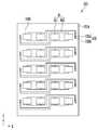
도 5를 참조하면, 원장 기판(100)은, 모기판(111A) 상에서 제1 및/또는 제2 방향(예컨대, X-축 및/또는 Y-축 방향)을 따라 나열된 다수의 셀들(110A)을 포함할 수 있다. 각각의 셀(110A)은 개개의 발광 표시 패널(110)을 제조하기 위한 것으로서, 일 예로 도 2에 도시된 발광 표시 패널(110)을 제조하기 위한 것일 수 있다. 예를 들어, 각각의 셀(110A)은 소정의 표시 영역(DA)에 배치된 다수의 화소들(PXL)을 포함할 수 있다. 그리고, 각각의 화소(PXL)는 일 예로 도 4 등에 도시된 바와 같이 다수의 발광 소자들(LD)을 구비한 발광 유닛(EMU)을 포함할 수 있다. 편의상, 도 5에서는 개별 셀(110A)의 내부 구성에 대한 도시는 생략하기로 한다.Referring to FIG. 5, the
원장 기판(100)의 일 영역, 일 예로 원장 기판(100)의 적어도 어느 일 측 가장자리 영역에는 복수의 도전성 패드들(102)이 배치된다. 실시예에 따라, 상기 복수의 도전성 패드들(102)은, 서로 다른 전압을 공급받는 제1 및 제2 패드(102a, 102b)로 구성된 적어도 한 쌍의 패드들을 포함할 수 있다. 일 예로, 원장 기판(100)의 서로 마주하는 양측 가장자리 영역에는 각각 복수의 제1 및 제2 패드(102a, 102b) 쌍이 배치될 수 있다. 실시예에 따라, 각각의 제1 및 제2 패드(102a, 102b) 쌍은 적어도 하나의 셀(110A)에 연결될 수 있다.A plurality of
또한, 원장 기판(100)은 셀들(110A)을 도전성 패드들(102)에 전기적으로 연결하기 위한 복수의 정렬 배선들(AL)을 포함할 수 있다. 실시예에 따라, 상기 정렬 배선들(AL)은, 원장 기판(100)에 형성된 셀들(110A) 중 적어도 하나를 어느 한 쌍의 제1 및 제2 패드(102a, 102b)에 연결하기 위한 적어도 한 쌍의 제1 및 제2 정렬 배선(AL1, AL2)을 포함할 수 있다. 일 예로, 원장 기판(100)에는, 복수의 제1 및 제2 패드(102a, 102b) 쌍에 대응하는 복수의 제1 및 제2 정렬 배선(AL1, AL2) 쌍이 배치될 수 있다.In addition, the
각각의 제1 정렬 배선(AL1)은 적어도 하나의 셀(110A) 내부에 형성된 일 전극에 전기적으로 연결되고, 각각의 제2 정렬 배선(AL2)은 적어도 하나의 셀(110A) 내부에 형성된 다른 전극에 전기적으로 연결된다. 일 예로, 각각의 제1 정렬 배선(AL1)은 적어도 하나의 셀(110A) 내부에 형성된 화소들(PXL)의 제1 화소 전극들(ELT1)에 공통으로 연결되고, 각각의 제2 정렬 배선(AL2)은 적어도 하나의 셀(110A) 내부에 형성된 화소들(PXL)의 제2 화소 전극들(ELT2)에 공통으로 연결될 수 있다. 이에 따라, 제1 패드들(102a)에 인가되는 전압은 제1 정렬 배선들(AL1)을 통해 각 셀(110A) 내부의 제1 화소 전극들(ELT1)에 전달되고, 제2 패드들(102b)에 인가되는 전압은 제2 정렬 배선들(AL2)을 통해 각 셀(110A) 내부의 제2 화소 전극들(ELT2)에 전달될 수 있다.Each first alignment line AL1 is electrically connected to one electrode formed inside the at least one
실시예에 따라, 원장 기판(100)에 형성된 셀들(110A) 중 상기 원장 기판(100)의 어느 일 측, 일 예로 좌측에 배치된 적어도 하나의 셀(110A)은 상기 원장 기판(100)의 다른 일 측, 일 예로 우측에 배치된 제1 및 제2 패드(102a, 102b) 쌍에 전기적으로 연결될 수 있다. 또한, 상기 셀들(110A) 중 상기 원장 기판(100)의 다른 일 측, 일 예로 우측에 배치된 적어도 하나의 셀(110A)은 상기 원장 기판(100)의 반대편 일 측, 일 예로 좌측에 배치된 제1 및 제2 패드(102a, 102b) 쌍에 전기적으로 연결될 수 있다.According to an embodiment, one of the
이 경우, 원장 기판(100)의 어느 일 측에 배치된 적어도 하나의 셀(110A)에 발광 소자들(LD)을 공급함과 동시에, 상기 원장 기판(100)의 다른 일 측에 배치된 제1 및 제2 패드(102a, 102b) 쌍을 통해 상기 적어도 하나의 셀(110A)에 전압을 인가할 수 있다. 이에 따라, 상기 적어도 하나의 셀(110A)에 발광 소자들(LD)을 공급함과 동시에, 상기 발광 소자들(LD)의 정렬을 위한 전계를 인가할 수 있게 된다.In this case, while supplying the light emitting elements LD to at least one
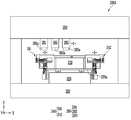
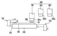
도 6은 본 발명의 일 실시예에 의한 발광 표시 장치의 제조 장치(200A)를 나타낸다. 구체적으로, 도 6은 상기 발광 표시 장치의 패널, 즉 발광 표시 패널(110)을 제조하기 위한 모기판(111A) 상에 발광 소자들(LD)을 공급함과 동시에 상기 발광 소자들(LD)에 전계를 인가할 수 있는 제조 장치(200A)의 실시예를 나타낸다. 일 예로, 상기 제조 장치(200A)는 도 5에 도시된 모기판(111A) 상에 배치된 각 셀(110A)의 내부(특히, 화소들(PXL) 각각의 발광 영역)에 발광 소자들(LD)을 공급함과 동시에, 상기 발광 소자들(LD)의 자가 정렬을 유도하기 위한 전계를 인가할 수 있도록 구성될 수 있다. 또한, 실시예에 따라, 상기 제조 장치(200A)는 잉크젯 방식으로 모기판(111A) 상에 발광 소자들(LD)을 공급(예컨대, 투하)하는 잉크젯 프린터일 수 있다.6 illustrates an
도 6을 참조하면, 본 발명의 일 실시예에 의한 발광 표시 장치의 제조 장치(200A)는, 하부로부터 순차적으로 배치된 주정반(210) 및 보조정반(220)과, 상기 보조정반(220)의 상부에 배치되는 스테이지(230)와, 상기 스테이지(230)의 적어도 일 측에 배치되는 적어도 하나의 전계 인가 모듈(240)과, 상기 스테이지(230)의 상부에 배치되는 갠트리(250)와, 상기 갠트리(250)에 의해 지지되며 상기 스테이지(230)의 상부에 배치되는 적어도 하나의 프린팅 헤드(260)를 포함한다. 도 6에서, 도면 부호 "240"은 하나 이상의 전계 인가 모듈에 포괄적으로 대응하며, 예를 들어 각각의 전계 인가 모듈, 또는 복수의 전계 인가 모듈들에 모두 대응할 수 있다. 또한, 도면 부호 "260"은 하나 이상의 프린팅 헤드에 포괄적으로 대응하며, 예를 들어 각각의 프린팅 헤드, 또는 복수의 프린팅 헤드들에 모두 대응할 수 있다.Referring to FIG. 6, an
실시예에 따라, 전계 인가 모듈(240) 및/또는 프린팅 헤드(260)는, 수평 이동 및 수직 이동이 모두 가능하도록 구성될 수 있다. 일 예로, 전계 인가 모듈(240) 및/또는 프린팅 헤드(260)는, X-축 방향을 따른 수평 이동과, Z-축 방향을 따른 수직 이동(예컨대, 상하 이동)이 모두 가능하도록 구성될 수 있다. 또한, 실시예에 따라서는 스테이지(230)도 적어도 어느 일 방향을 따라 이동 가능하도록 구성될 수 있다. 일 예로, 스테이지(230)는 Y-축 방향을 따른 수평 이동이 가능하도록 설계될 수 있다.According to an embodiment, the electric
상술한 실시예에 의하면, 스테이지(230), 전계 인가 모듈(240) 및/또는 프린팅 헤드(260)의 동작을 보다 용이하게 제어할 수 있게 된다. 이에 따라, 스테이지(230) 상에 원장 기판(100)을 배치하여 발광 소자들(LD)을 공급하는 공정과 동시에 상기 발광 소자들(LD)이 공급되는 셀(110A)에 원활히 전계를 인가할 수 있게 된다.According to the above-described embodiment, it is possible to more easily control the operation of the
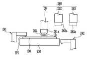
일 실시예에서, 전계 인가 모듈(240)은 스테이지(230)의 적어도 두 가장자리 영역에 각각 인접하도록 배치될 수 있다. 예를 들어, 전계 인가 모듈(240)은, 스테이지(230)의 제1 측에 배치되는 제1 전계 인가 모듈(241)과, 스테이지(230)의 제2 측에 배치되는 제2 전계 인가 모듈(242)을 포함할 수 있다.In one embodiment, the electric
실시예에 따라, 스테이지(230)의 제1 측 및 제2 측은 서로 마주하는 반대편 단부일 수 있다. 일 예로, 상기 제1 측 및 상기 제2 측은 각각 상기 스테이지(230)의 좌측 및 우측일 수 있다. 즉, 제1 및 제2 전계 인가 모듈(241, 242)은 스테이지(230)의 서로 마주하는 양측 각각에 인접하여 배치될 수 있다.According to an embodiment, the first side and the second side of the
또한, 실시예에 따라, 제1 및 제2 전계 인가 모듈(241, 242)은 스테이지(230) 하단의 구조물에 연결 및/또는 설치될 수 있다. 일 예로, 제1 및 제2 전계 인가 모듈(241, 242)은 스테이지(230) 하단의 지지판(230a)에 결합될 수 있다. 다만, 본 발명에서, 제1 및 제2 전계 인가 모듈(241, 242)의 위치 및/또는 설치 구조가 특별히 한정되지는 않으며, 이는 다양하게 변경될 수 있다.In addition, according to an embodiment, the first and second electric
실시예에 따라, 제1 및 제2 전계 인가 모듈(241, 242)은 서로 독립적으로 구동되거나, 또는 서로 연동하여 구동될 수 있다. 일 예로, 제1 및 제2 전계 인가 모듈(241, 242)은 동시에 구동되거나, 순차 또는 교번적으로 구동될 수 있다.Depending on the embodiment, the first and second electric
이와 같이, 발광 표시 장치의 제조 장치(200A)가 스테이지(230)의 서로 다른 일 측에 배치된 제1 및 제2 전계 인가 모듈(241, 242)을 구비하게 되면, 전계 인가 모듈(240)과 프린팅 헤드(260)와의 충돌을 회피하면서, 스테이지(230) 상에 안착된 원장 기판(100) 상에 원활히 전계를 인가할 수 있게 된다. 일 예로, 프린팅 헤드(260)의 위치에 따라 제1 및 제2 전계 인가 모듈(241, 242) 중 적어도 하나를 선택적으로 구동함으로써, 전계 인가 모듈(240)과 프린팅 헤드(260)의 상호 간섭 및/또는 충돌을 방지하면서도 원장 기판(100) 상의 각 셀(110A)에 원하는 전계를 인가할 수 있게 된다.As described above, when the
실시예에 따라, 프린팅 헤드(260)는 서로 다른 종류의 용액, 일 예로 각각 소정 색상의 발광 소자들(LD)이 분산된 용액을 스테이지(230)의 상부로 분사하기 위한 복수의 프린팅 헤드들, 일 예로 제1, 제2 및 제3 프린팅 헤드(261, 262, 263)를 포함할 수 있다. 예를 들어, 제1, 제2 및 제3 프린팅 헤드(261, 262, 263)는 각각 다수의 적색, 녹색 및 청색 발광 소자들(LD)이 분산된 용액을 액적의 형태로 스테이지(230)의 상부(일 예로, 상기 스테이지(230) 상에 안착된 원장 기판(100)의 각 셀(110A) 내부)에 투하할 수 있다. 이를 위해, 제1, 제2 및 제3 프린팅 헤드(261, 262, 263)는 각각 분사 노즐(261a, 262a, 263a)을 구비하고, 잉크젯 방식으로 각각 적색, 녹색 및 청색 발광 소자들(LD)을 각각의 셀(110A)에 공급할 수 있다. 일 예로, 제1, 제2 및 제3 프린팅 헤드(261, 262, 263)는 잉크젯 헤드(또는, 분사 헤드)일 수 있다.According to an embodiment, the
상술한 바와 같이, 본 실시예에 의한 제조 장치(200A)는 전계 인가 모듈(240) 및 프린팅 헤드(260)를 모두 구비한다. 이에 따라, 스테이지(230) 상에 놓인 발광 표시 장치의 기판, 일 예로 원장 기판(100) 상에 발광 소자들(LD)을 공급함과 동시에, 상기 발광 소자들(LD)에 소정의 전계를 인가하여 상기 발광 소자들(LD)의 자가 정렬을 유도할 수 있다. 이에 따라, 발광 소자들(LD)을 광원으로 이용하는 발광 표시 패널(110)을 용이하게 제조할 수 있다.As described above, the
한편, 제조 장치(200A)를 구성하는 나머지 구성 요소들, 예를 들어 주정반(210), 보조정반(220) 및 갠트리(250) 등은, 현재 공지된 다양한 형상 및/또는 구조를 가질 수 있다. 따라서, 이에 대한 상세한 설명은 생략하기로 한다.Meanwhile, the remaining components constituting the
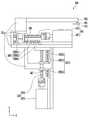
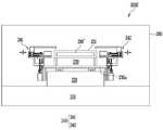
도 7은 도 6의 전계 인가 모듈(240)의 구성에 대한 실시예를 나타낸다. 실시예에 따라, 도 7에 도시된 전계 인가 모듈(240)은 도 6의 제1 및 제2 전계 인가 모듈(241, 242)에 모두 대응될 수 있다. 예를 들어, 제1 및 제2 전계 인가 모듈(241, 242)은 실질적으로 동일하게 구성되며, 서로 마주하여 배치될 수 있다.7 shows an embodiment of the configuration of the electric
도 7을 참조하면, 각각의 전계 인가 모듈(240)은, 프로브 헤드(PHD)와, 상기 프로브 헤드(PHD)에 결합되어 상기 프로브 헤드(PHD)를 소정 방향을 따라 이동시키기 위한 제1 및 제2 구동부(LA1, LA2)와, 상기 프로브 헤드(PHD)와 제1 및 제2 구동부(LA1, LA2)에 결합되는 바디부(BD)를 포함할 수 있다.Referring to FIG. 7, each electric
또한, 실시예에 따라, 각각의 전계 인가 모듈(240)은, 바디부(BD)에 결합되어 상기 전계 인가 모듈(240)의 안정적인 이동을 보조하는 적어도 하나의 리니어 모션 가이드(LM1, LM2)와, 프로브 헤드(PHD) 등의 이동 위치를 실시간으로 감지하기 위한 적어도 하나의 센서 유닛(SEU1, SEU2)을 더 포함할 수 있다. 일 예로, 각각의 전계 인가 모듈(240)은, 제1 구동부(LA1)의 주변에 배치되는 제1 리니어 모션 가이드(LM1) 및 제1 센서 유닛(SEU1)과, 상기 제2 구동부(LA2)의 주변에 배치되는 제2 리니어 모션 가이드(LM2) 및 제2 센서 유닛(SEU2)을 더 포함할 수 있다.In addition, according to an embodiment, each electric
프로브 헤드(PHD)는 일면에 배치된 적어도 하나의 프로브 핀(또는, "전극 패드"라고도 함; PPI)을 구비한다. 일 예로, 프로브 헤드(PHD)는 하부면의 가장자리 영역에 위치된 패드부(PAU) 내에 배열된 다수의 프로브 핀(PPI)을 포함할 수 있다. 실시예에 따라, 각각의 프로브 핀(PPI)은 도시되지 않은 전원 공급부에 연결되어, 상기 전원 공급부로부터 각각 소정의 전원 또는 전압을 공급받을 수 있다.The probe head PHD includes at least one probe pin (or, also referred to as "electrode pad"; PPI) disposed on one surface. For example, the probe head PHD may include a plurality of probe pins PPI arranged in the pad portion PAU located in the edge region of the lower surface. According to an embodiment, each probe pin PPI may be connected to a power supply unit (not shown) to receive a predetermined power or voltage from the power supply unit.
실시예에 따라, 프로브 헤드(PHD)는 바(bar) 형상을 가지는 프로브 바로 구현될 수 있으나, 이에 한정되지는 않는다. 예를 들어, 프로브 헤드(PHD)의 형상, 구조 및/또는 구성 물질 등은 다양하게 변경될 수 있다.According to an embodiment, the probe head PHD may be implemented as a probe bar having a bar shape, but is not limited thereto. For example, the shape, structure, and / or constituent materials of the probe head PHD may be variously changed.
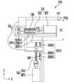
제1 구동부(LA1)는 바디부(BD)를 통해 프로브 헤드(PHD)에 결합되어, 상기 프로브 헤드(PHD)를 수평 방향으로 이동시킬 수 있다. 일 예로, 제1 구동부(LA1)는 X-축 방향을 따라 프로브 헤드(PHD)를 전후 또는 좌우로 이동시키는 리니어 액추에이터일 수 있다.The first driving part LA1 is coupled to the probe head PHD through the body part BD, and may move the probe head PHD in the horizontal direction. For example, the first driving unit LA1 may be a linear actuator that moves the probe head PHD back and forth or left and right along the X-axis direction.
실시예에 따라, 제1 구동부(LA1)는 제1 모터(MT1)와, 수평 방향으로 상기 제1 모터(MT1)에 결합 및/또는 연결되는 제1 볼 스크류(BS1)를 포함할 수 있다. 이를 통해, 제1 구동부(LA1)는 프로브 헤드(PHD)가 원하는 위치에 도달할 수 있도록 상기 프로브 헤드(PHD)의 수평 위치를 조정할 수 있다.According to an embodiment, the first driving unit LA1 may include a first motor MT1 and a first ball screw BS1 coupled and / or connected to the first motor MT1 in a horizontal direction. Through this, the first driving unit LA1 may adjust the horizontal position of the probe head PHD so that the probe head PHD can reach a desired position.
실시예에 따라, 제1 모터(MT1)는 서보모터(servomotor)일 수 있으나 이에 한정되지는 않는다. 예를 들어, 제1 모터(MT1)는 서보모터 외에도 다양한 종류의 동력원으로 구성될 수 있다. 또한, 실시예에 따라, 제1 모터(MT1)는 모터 가이드 등을 포함하여 구성될 수 있다.According to an embodiment, the first motor MT1 may be a servomotor, but is not limited thereto. For example, the first motor MT1 may be configured with various types of power sources in addition to the servo motor. Also, according to an embodiment, the first motor MT1 may include a motor guide or the like.
실시예에 따라, 제1 볼 스크류(BS1)는 전조 볼 스크류(rolled ball screw)일 수 있으나, 이에 한정되지는 않는다. 예를 들어, 제1 볼 스크류(BS1)는 전조 볼 스크류 외에도, 제1 모터(MT1)에 의해 발생한 동력을 이용하여 프로브 헤드(PHD)를 직선 운동시킬 수 있는 다양한 기구적 장치(일 예로, 회전 운동을 직선 운동으로 변환할 수 있는 다양한 부품)로 구성될 수 있다.According to an embodiment, the first ball screw BS1 may be a rolled ball screw, but is not limited thereto. For example, the first ball screw BS1, in addition to the rolled ball screw, various mechanical devices capable of linearly moving the probe head PHD using the power generated by the first motor MT1 (eg, rotation It can be composed of a variety of parts that can convert the motion to linear motion).
제2 구동부(LA2)는 바디부(BD)를 통해 프로브 헤드(PHD)에 결합되어, 상기 프로브 헤드(PHD)를 수직 방향으로 이동시킬 수 있다. 일 예로, 제2 구동부(LA2)는 Z-축 방향을 따라 프로브 헤드(PHD)를 상하로 이동시키는 리니어 액추에이터일 수 있다.The second driving part LA2 is coupled to the probe head PHD through the body part BD, and may move the probe head PHD in the vertical direction. For example, the second driving unit LA2 may be a linear actuator that moves the probe head PHD up and down along the Z-axis direction.
실시예에 따라, 제2 구동부(LA2)는 제2 모터(MT2)와, 수직 방향으로 상기 제2 모터(MT2)에 결합 및/또는 연결되는 제2 볼 스크류(BS2)를 포함할 수 있다. 이를 통해, 제2 구동부(LA2)는 프로브 헤드(PHD)가 원하는 위치에 도달할 수 있도록 상기 프로브 헤드(PHD)의 높이를 조정할 수 있다.According to an embodiment, the second driving unit LA2 may include a second motor MT2 and a second ball screw BS2 coupled and / or connected to the second motor MT2 in the vertical direction. Through this, the second driving unit LA2 may adjust the height of the probe head PHD so that the probe head PHD can reach a desired position.
실시예에 따라, 제2 모터(MT2)는 서보모터일 수 있으나 이에 한정되지는 않으며, 이 외에도 다양한 종류의 동력원으로 구성될 수 있다. 또한, 실시예에 따라, 제2 모터(MT2)는 모터 가이드 등을 포함하여 구성될 수 있다.According to an embodiment, the second motor MT2 may be a servo motor, but is not limited thereto, and may be configured with various types of power sources. Further, according to an embodiment, the second motor MT2 may include a motor guide or the like.
실시예에 따라, 제2 볼 스크류(BS2)는 전조 볼 스크류일 수 있으나 이에 한정되지는 않으며, 이 외에도 제2 모터(MT2)에 의해 발생한 동력을 이용하여 프로브 헤드(PHD)를 직선 운동시킬 수 있는 다양한 기구적 장치로 구성될 수 있다.According to an embodiment, the second ball screw BS2 may be a rolled ball screw, but is not limited thereto. In addition, the probe head PHD may be linearly moved using power generated by the second motor MT2. It can be configured with a variety of mechanical devices.
제1 리니어 모션 가이드(LM1)는 제1 구동부(LA1)의 주변에 배치되어, 프로브 헤드(PHD)의 수평 이동을 보조할 수 있다. 그리고, 제2 리니어 모션 가이드(LM2)는 제2 구동부(LA2)의 주변에 배치되어, 프로브 헤드(PHD)의 수직 이동을 보조할 수 있다.The first linear motion guide LM1 is disposed around the first driving unit LA1 to assist horizontal movement of the probe head PHD. In addition, the second linear motion guide LM2 is disposed around the second driving unit LA2 to assist vertical movement of the probe head PHD.
제1 센서 유닛(SEU1)은 제1 구동부(LA1)의 주변에 배치되어, 프로브 헤드(PHD)의 수평 위치를 감지할 수 있다. 이러한 제1 센서 유닛(SEU1)을 통해, 해당 전계 인가 모듈(240), 특히 프로브 헤드(PHD)가 원하는 수평 위치에 도달했는지 판단할 수 있다.The first sensor unit SEU1 is disposed around the first driving unit LA1 to detect a horizontal position of the probe head PHD. Through the first sensor unit SEU1, it may be determined whether the corresponding electric
실시예에 따라, 제1 센서 유닛(SEU1)은, 프로브 헤드(PHD)의 전방 한계를 감지하기 위한 제1 위치 센서(SEN11)와, 프로브 헤드(PHD)의 후방 한계를 감지하기 위한 제2 위치 센서(SEN12)와, 상기 제1 및 제2 위치 센서(SEN11, SEN12)의 사이에 위치되어 프로브 헤드(PHD)가 소정의 목표 지점(예컨대, 원장 기판(100)의 도전성 패드들(102)과 접촉하기 위한 수평 위치)에 도달했음을 감지하기 위한 제3 위치 센서(SEN13) 중 적어도 하나를 포함할 수 있다. 제1 및 제2 위치 센서(SEN11, SEN12)를 통해 전후방 한계를 감지할 수 있게 되면, 프로브 헤드(PHD)의 과도한 이동을 방지할 수 있다. 이에 따라, 전계 인가 모듈(240)의 기계적 손상을 방지할 수 있다. 또한, 제3 위치 센서(SEN13)를 통해 프로브 헤드(PHD)가 상기 목표 지점에 도달했음을 감지하게 되면, 공정의 용이성 및 신뢰성을 확보할 수 있다.According to an embodiment, the first sensor unit SEU1 includes a first position sensor SEN11 for detecting the front limit of the probe head PHD and a second position for detecting the rear limit of the probe head PHD. The probe head PHD is positioned between the sensor SEN12 and the first and second position sensors SEN11 and SEN12 so that the probe head PHD and the
제2 센서 유닛(SEU2)은 제2 구동부(LA2)의 주변에 배치되어, 프로브 헤드(PHD)의 수직 위치(즉, 높이)를 감지할 수 있다. 이러한 제2 센서 유닛(SEU2)을 통해, 해당 전계 인가 모듈(240), 특히 프로브 헤드(PHD)가 원하는 수직 위치에 도달했는지 판단할 수 있다.The second sensor unit SEU2 is disposed around the second driving unit LA2 to sense the vertical position (ie, height) of the probe head PHD. Through the second sensor unit SEU2, it may be determined whether the corresponding electric
실시예에 따라, 제2 센서 유닛(SEU2)은, 프로브 헤드(PHD)의 상승 한계를 감지하기 위한 제1 위치 센서(SEN21)와, 프로브 헤드(PHD)의 하강 한계를 감지하기 위한 제2 위치 센서(SEN22)와, 상기 제1 및 제2 위치 센서(SEN21, SEN22)의 사이에 위치되어 프로브 헤드(PHD)가 소정의 목표 높이(예컨대, 원장 기판(100)의 도전성 패드들(102)과 접촉하기 위한 소정의 높이)에 도달했음을 감지하기 위한 제3 위치 센서(SEN23) 중 적어도 하나를 포함할 수 있다. 제1 및 제2 위치 센서(SEN21, SEN22)를 통해 승강 한계를 감지할 수 있게 되면, 프로브 헤드(PHD)의 과도한 이동을 방지할 수 있다. 이에 따라, 전계 인가 모듈(240)의 기계적 손상을 방지할 수 있다. 또한, 제3 위치 센서(SEN23)를 통해 프로브 헤드(PHD)가 목표 높이에 도달했음을 감지하게 되면, 공정의 용이성 및 신뢰성을 확보할 수 있다.According to an embodiment, the second sensor unit SEU2 includes a first position sensor SEN21 for detecting a rising limit of the probe head PHD, and a second position for detecting a falling limit of the probe head PHD. The probe head PHD is positioned between the sensor SEN22 and the first and second position sensors SEN21 and SEN22 so that the probe head PHD and the
도 8a 내지 도 8c는 도 7의 전계 인가 모듈(240)의 수평 이동 방식에 대한 실시예를 나타낸다.8A to 8C show an embodiment of a horizontal movement method of the electric
도 8a 내지 도 8c를 참조하면, 전계 인가 모듈(240)은 제1 구동부(LA1)에 의해 수평 방향으로 이동할 수 있다. 일 예로, 프로브 헤드(PHD)는 제1 구동부(LA1)에 의해 X-축을 따라 전방으로 이동할 수 있다. 이 경우, 프로브 헤드(PHD)의 전방 일단은, 제1 구동부(LA1)의 일단으로부터 수평 방향을 따라 점차 멀어지는 제1 거리(d1), 제2 거리(d2) 및 제3 거리(d3)만큼 이격된 위치를 차례로 지나도록 전진할 수 있다. 반대로, 제1 구동부(LA1)에 의해 프로브 헤드(PHD)가 후방으로 이동할 경우, 상기 프로브 헤드(PHD)의 전방 단부는, 제1 구동부(LA1)의 일단으로부터 수평 방향을 따라 각각 제3 거리(d3), 제2 거리(d2) 및 제1 거리(d1)만큼 이격된 위치를 차례로 지나도록 후진할 수 있다.8A to 8C, the electric
도 9a 내지 도 9c는 도 7의 전계 인가 모듈(240)의 수직 이동 방식에 대한 실시예를 나타낸다.9A to 9C show an embodiment of a vertical movement method of the electric
도 9a 내지 도 9c를 참조하면, 전계 인가 모듈(240)은 제2 구동부(LA2)에 의해 수직 방향으로 이동할 수 있다. 일 예로, 프로브 헤드(PHD)는 제2 구동부(LA2)에 의해 Z-축을 따라 상승할 수 있다. 이 경우, 프로브 헤드(PHD)의 배면은 제2 구동부(LA2)의 일단으로부터 수직 방향을 따라 점차 높아지는 제1 높이(h1), 제2 높이(h2) 및 제3 높이(h3)에 해당하는 위치를 차례로 지나도록 상승할 수 있다. 반대로, 제2 구동부(LA2)에 의해 프로브 헤드(PHD)가 하강할 경우, 상기 프로브 헤드(PHD)의 배면은 제2 구동부(LA2)의 일단으로부터 수직 방향을 따라 제3 높이(h3), 제2 높이(h2) 및 제1 높이(h1)만큼 이격된 위치를 차례로 지나도록 하강할 수 있다.9A to 9C, the electric
도 10 및 도 11a 내지 도 11d는 도 6의 제조 장치(200A)의 구동 방법에 대한 일 실시예를 나타낸다. 구체적으로, 도 10은 상기 제조 장치(200A)의 스테이지(230) 상에 일 예로 도 5에 도시된 원장 기판(100)이 배치된 상태를 개략적으로 나타낸 평면도이다. 도 10에서는 제조 장치(200A)의 프로브 핀들(PPI)과 원장 기판(100)의 정렬 위치를 보여주기 위하여, 프로브 헤드(PHD)를 전체적으로 도시하는 대신 상기 프로브 헤드(PHD)의 일면에 배치된 패드부(PAU)를 도시하기로 한다. 또한, 도 10 및 도 11a 내지 도 11d에서, 전계 인가 모듈(240) 등의 구조는 개략적으로 도시하기로 한다.10 and 11A to 11D show an embodiment of a driving method of the
도 10을 참조하면, 프로브 헤드(PHD)의 패드부(PAU)에는 복수의 프로브 핀들(PPI)이 배열될 수 있다. 또한, 본 발명의 실시예에 의한 제조 장치(200A)는 프로브 핀들(PPI)로 소정의 전압을 공급하기 위한 전원 공급부(270)와, 상기 프로브 핀들(PPI)과 전원 공급부(270)의 사이에 연결되는 복수의 전원선들(PL1, PL2)을 더 포함할 수 있다.Referring to FIG. 10, a plurality of probe pins PPI may be arranged in the pad portion PAU of the probe head PHD. In addition, the
일 예로, 프로브 헤드(PHD)의 일면, 예컨대 하부면에는 패드부(PAU)가 배치되고, 상기 패드부(PAU)는, 제1 전원선(PL1)을 통해 전원 공급부(270)에 연결되는 적어도 하나의 제1 프로브 핀(PPI1)과, 제2 전원선(PL2)을 통해 전원 공급부(270)에 연결되는 적어도 하나의 제2 프로브 핀(PPI2)을 구비할 수 있다. 예컨대, 패드부(PAU)는, 제1 전원선(PL1)에 공통으로 연결되는 복수의 제1 프로브 핀들(PPI1)과, 상기 제1 프로브 핀들(PPI1) 각각과 쌍을 이루도록 배치되며 제2 전원선(PL2)에 공통으로 연결되는 복수의 제2 프로브 핀들(PPI2)을 구비할 수 있다.For example, a pad portion PAU is disposed on one surface of the probe head PHD, for example, a lower surface, and the pad portion PAU is at least connected to the
실시예에 따라, 제1 및 제2 프로브 핀들(PPI1, PPI2)은 원장 기판(100)에 형성된 도전성 패드들(102)에 대응할 수 있다. 예컨대, 제1 전계 인가 모듈(241)에 구비된 제1 및 제2 프로브 핀들(PPI1, PPI2)은 상기 제1 전계 인가 모듈(241)이 구동될 때 원장 기판(100)의 좌측에 배치된 도전성 패드들(102)에 접촉되어 소정의 전압을 인가할 수 있도록 구성될 수 있다. 그리고, 제2 전계 인가 모듈(242)에 구비된 제1 및 제2 프로브 핀들(PPI1, PPI2)은 상기 제2 전계 인가 모듈(242)이 구동될 때 원장 기판(100)의 우측에 배치된 도전성 패드들(102)에 접촉되어 소정의 전압을 인가할 수 있도록 구성될 수 있다.According to an embodiment, the first and second probe pins PPI1 and PPI2 may correspond to
실시예에 따라, 전원 공급부(270)는, 제1 출력 단자(OUT1)를 통해 제1 전원선(PL1)으로 소정 파형 및/또는 전위를 가지는 소정의 전압(또는 신호)를 공급하고, 제2 출력 단자(OUT2)를 통해 제2 전원선(PL2)으로 소정의 기준 전위를 가지는 레퍼런스 전압을 공급할 수 있다. 일 예로, 전원 공급부(270)는, 제1 전원선(PL1)으로 사인(sine) 파형을 가지는 교류 전압을 공급하고, 제2 전원선(PL2)으로 그라운드 전압을 공급할 수 있다.According to an embodiment, the
한편, 실시예에 따라, 제조 장치(200A)는 적어도 하나의 추가적인 부품을 더 포함할 수 있다. 일 예로, 제조 장치(200A)는 제1 및/또는 제2 전계 인가 모듈(241, 242)의 내부 또는 그 주변에 배치되는 적어도 하나의 수평 가이드(HGD)와, 스테이지(230) 상에 구비되는 적어도 하나의 고정부(FXP)를 더 포함할 수 있다.Meanwhile, according to an embodiment, the
실시예에 따라, 스테이지(230) 상에 원장 기판(100)이 안착된 이후, 상기 원장 기판(100) 상에 발광 소자들(LD)을 배치하기 위한 공정이 시작되면, 제1 및 제2 전계 인가 모듈(241, 242)이 구동되어 원장 기판(100)의 도전성 패드들(102) 중 적어도 일부로 소정의 전압을 공급한다. 이에 따라, 원장 기판(100)에 위치된 적어도 하나의 셀(110A), 특히 상기 적어도 하나의 셀(110A)의 각 화소 영역에 형성된 제1 및 제2 화소 전극들(ELT1, ELT2)의 사이에 전계가 형성된다. 또한, 상기 공정이 시작되면, 적어도 하나의 프린팅 헤드(260)가 원장 기판(100)의 상부로 이동하여 상기 적어도 하나의 셀(110A)에 발광 소자들(LD)을 공급한다. 이에 따라, 상기 적어도 하나의 셀(110A)에 발광 소자들(LD)을 공급함과 동시에, 상기 발광 소자들(LD)을 상기 제1 및 제2 화소 전극들(ELT1, ELT2)의 사이에 정렬할 수 있게 된다.According to an embodiment, after the
실시예에 따라, 제1 및 제2 전계 인가 모듈(241, 242)은 순차적 또는 교번적으로 구동될 수 있다. 예컨대, 제1 및 제2 전계 인가 모듈(241, 242)은 동작 중인 프린팅 헤드(260)의 위치 및/또는 이동 방향에 대응하여 순차적으로 구동될 수 있다. 일 예로, 제1 및 제2 전계 인가 모듈(241, 242)은 프린팅 헤드(260)와의 충돌을 피할 수 있도록 순차적 또는 교번적으로 동작할 수 있다.Depending on the embodiment, the first and second electric
예를 들어, 도 11a 내지 도 11d에 도시된 바와 같이, 적어도 하나의 프린팅 헤드(260)는 스테이지(230)의 우측 상부로부터 좌측 상부로 이동하면서 상기 스테이지(230)의 상부에 액적(DRL)을 분사할 수 있다. 실시예에 따라, 상기 프린팅 헤드(260)는 스테이지(230)의 상부에 안착된 원장 기판(100)의 상부, 특히 상기 원장 기판(100) 상에 위치된 적어도 하나의 셀(110A)(일 예로, 상기 셀(110A)의 내부에 규정된 각각의 화소 영역)에, 발광 소자들(LD)이 분산된 용액을 액적(DRL)의 형태로 분사하면서 이동할 수 있다.For example, as shown in FIGS. 11A to 11D, at least one
실시예에 따라, 프린팅 헤드(260)가 스테이지(230)의 우측으로 접근할 때 상기 스테이지(230)의 좌측에 위치된 제1 전계 인가 모듈(241), 특히 상기 제1 전계 인가 모듈(241)의 프로브 헤드(PHD)가 스테이지(230)의 좌측 상부로 이동할 수 있다. 예를 들어, 도 11a 및 도 11b에 도시된 바와 같이, 제1 전계 인가 모듈(241)은, 동작 중인 프린팅 헤드(260)(예컨대, 제1 프린팅 헤드(261))가 스테이지(230)의 우측 상부에 위치해있는 기간 동안, 상기 스테이지(230)의 좌측 상부에서 원장 기판(100)에 전계를 인가할 수 있다. 일 예로, 제1 전계 인가 모듈(241)은 원장 기판(100)의 좌측에 위치한 도전성 패드들(102)을 통해 상기 원장 기판(100)의 우측에 위치한 셀들(110A)에 소정의 정렬 전압을 인가할 수 있다. 한편, 이 기간 동안 제2 전계 인가 모듈(242)은 스테이지(230)를 기준으로 후진 및 하강한 상태에서 대기할 수 있다.According to an embodiment, when the
한편, 프린팅 헤드(260)가 스테이지(230)의 좌측으로 접근할 때 상기 스테이지(230)의 우측에 위치된 제2 전계 인가 모듈(242), 특히 상기 제2 전계 인가 모듈(242)의 프로브 헤드(PHD)가 스테이지(230)의 우측 상부로 이동할 수 있다. 예를 들어, 도 11c 및 도 11d에 도시된 바와 같이, 제2 전계 인가 모듈(242)은, 동작 중인 프린팅 헤드(260)가 스테이지(230)의 좌측 상부에 위치해있는 기간 동안, 상기 스테이지(230)의 우측 상부에서 원장 기판(100)에 전계를 인가할 수 있다. 일 예로, 제2 전계 인가 모듈(242)은 원장 기판(100)의 우측에 위치한 도전성 패드들(102)을 통해 상기 원장 기판(100)의 좌측에 위치한 셀들(110A)에 소정의 정렬 전압을 인가할 수 있다. 한편, 이 기간 동안 제1 전계 인가 모듈(241)은 스테이지(230)를 기준으로 후진 및 하강한 상태에서 대기할 수 있다.On the other hand, when the
상술한 실시예에 의하면, 적어도 하나의 프린팅 헤드(260)를 구동하여 원장 기판(100) 상에 발광 소자들(LD)을 공급함과 동시에, 적어도 하나의 전계 인가 모듈(240)을 구동하여 상기 원장 기판(100) 상에 상기 발광 소자들(LD)의 정렬을 유도하기 위한 전계를 인가할 수 있다. 특히, 상술한 실시예에서는 동작 중인 프린팅 헤드(260)의 위치에 따라 제1 및/또는 제2 전계 인가 모듈(241, 242)을 선택적으로 구동함으로써, 프린팅 헤드(260)와 전계 인가 모듈(240) 사이의 간섭 및/또는 충돌을 방지할 수 있다. 또한, 이에 따라 프린팅 헤드(260)의 이동 거리를 확장할 수 있게 되면서, 원장 기판(100) 상에서 발광 소자들(LD)을 공급할 수 있는 유효 영역(예컨대, 개별 셀들(110A)을 배치할 수 있는 영역)을 충분히 확보할 수 있게 된다.According to the above-described embodiment, at least one
도 12 및 도 13은 도 6의 제조 장치(200A)의 구동 방법에 대한 다른 실시예를 나타낸다. 도 12 및 도 13의 실시예에서, 도 10 내지 도 11d의 실시예와 유사 또는 동일한 구성에 대해서는 동일 부호를 부여하고, 이에 대한 상세한 설명은 생략하기로 한다.12 and 13 show another embodiment of a method of driving the
도 12 및 도 13을 참조하면, 실시예에 따라 제1 및 제2 전계 인가 모듈(241, 242)은 동시에 구동될 수도 있다. 예를 들어, 상기 제1 및 제2 전계 인가 모듈(241, 242)은 서로 독립적 및/또는 개별적으로 구동될 수 있고, 필요에 따라서는 동시에 구동될 수도 있다.12 and 13, the first and second electric
일 예로, 각각의 제1 및 제2 정렬 배선(AL1, AL2)이 원장 기판(100)의 좌측 및 우측에 배치된 복수의 도전성 패드들(102)에 동시 접속된다고 할 때, 제1 및 제2 전계 인가 모듈(241, 242)을 동시에 구동하여 원장 기판(100)의 양단을 통해 소정의 전계를 인가할 수 있다. 이 경우, 제1 및 제2 정렬 배선(AL1, AL2)에서 발생하는 전압 강하를 저감 또는 최소화함으로써, 각 셀(110A)의 내부에 발광 소자들(LD)을 원활히 정렬할 수 있게 된다.For example, when the first and second alignment wirings AL1 and AL2 are simultaneously connected to a plurality of
또는, 다른 실시예에서, 각 셀(110A)은 원장 기판(100)의 양측에 배치된 도전성 패드들(102) 중 가장 인접한 적어도 한 쌍의 도전성 패드들(102)에 접속되고, 상기 셀(110A)의 내부에 발광 소자들(LD)이 공급되는 기간 동안 상기 적어도 한 쌍의 도전성 패드들(102)로부터 소정의 전압을 인가받을 수 있다. 예를 들어, 원장 기판(100)의 좌측에 배치된 셀들(110A)은 상기 원장 기판(100)의 좌측 가장자리에 배치된 도전성 패드들(102)로부터, 원장 기판(100)의 우측에 배치된 셀들(110A)은 상기 원장 기판(100)의 우측 가장자리에 배치된 도전성 패드들(102)로부터 소정의 전압을 공급받을 수 있다. 이 경우에도 제1 및 제2 정렬 배선(AL1, AL2)에서 발생하는 전압 강하를 저감 또는 최소화함으로써, 각 셀(110A)의 내부에 발광 소자들(LD)을 원활히 정렬할 수 있게 된다.Or, in another embodiment, each
도 14 내지 도 16은 도 6의 제조 장치(200A)에 구비될 수 있는 전계 인가 모듈(240)의 배치와 관련한 다양한 실시예를 나타낸다. 그리고, 도 17a 및 도 17b는 도 6의 제조 장치(200A)에 구비될 수 있는 프린팅 헤드(260)와 관련한 다양한 실시예를 나타낸다. 도 14 내지 도 17b에서는 스테이지(230) 및 프린팅 헤드(260)의 위치 및/또는 이동 방향에 따른 전계 인가 모듈(240)의 위치 등만을 개략적으로 도시하기로 한다.14 to 16 show various embodiments related to the arrangement of the electric
도 14를 참조하면, 일 실시예에서, 스테이지(230)와 프린팅 헤드(260)는 서로 직교하는 방향을 따라 이동할 수 있다. 일 예로, 스테이지 무빙 방식의 제조 장치(200A)에서, 스테이지(230)는 Y-축 방향을 따라 큰 폭으로 이동하고, 프린팅 헤드(260)는 X-축 방향을 따라 상대적으로 작은 폭으로 이동할 수 있다. 이에 따라, 상기 스테이지(230) 상부의 유효 영역에 전면적으로 발광 소자들(LD)을 공급할 수 있게 된다. 상기 실시예에서, 제1 및 제2 전계 인가 모듈(241, 242)은 스테이지(230)의 이동을 방해하지 않도록 상기 스테이지(230)의 좌측 및 우측에 배치될 수 있다. 이에 따라, 스테이지(230)가 Y-축 방향을 따라 큰 폭으로 이동하더라도, 상기 스테이지(230)가 제1 및 제2 전계 인가 모듈(241, 242), 특히 상기 제1 및 제2 전계 인가 모듈(241, 242)의 프로브 헤드(PHD1, PHD2)와 충돌하는 것을 방지할 수 있다. 또한, 앞서 설명한 실시예에서와 같이 제1 및 제2 전계 인가 모듈(241, 242)은 프린팅 헤드(260)와의 충돌을 방지할 수 있도록 구동될 수 있다.Referring to FIG. 14, in one embodiment, the
도 15를 참조하면, 일 예로 헤드 무빙 방식의 제조 장치(200A)에서, 스테이지(230)는 X-축 방향을 따라 비교적 큰 폭으로 이동하고, 프린팅 헤드(260)는 Y-축 방향을 따라 이동할 수 있다. 상기 실시예에서, 제1 및 제2 전계 인가 모듈(241, 242)은 스테이지(230)의 이동을 방해하지 않도록 상기 스테이지(230)의 상단 및 하단 측에 배치될 수 있다.Referring to FIG. 15, as an example, in the head moving
도 16을 참조하면, 또 다른 실시예에서는, 스테이지(230)의 적어도 세 측면에 전계 인가 모듈(240)이 배치될 수도 있다. 예컨대, 전계 인가 모듈(240)은, 스테이지(230)의 네 측면 모두에 배치될 수 있다. 일 예로, 상기 실시예에 의한 제조 장치(200A)는, 스테이지(230)의 제3 측, 일 예로 상단 측에 배치되는 제3 전계 인가 모듈(243)과, 상기 스테이지(230)의 제4 측, 일 예로 하단 측에 배치되는 제4 전계 인가 모듈(244)을 더 포함할 수 있다. 실시예에 따라, 각각의 전계 인가 모듈(240)은 실질적으로 동일하게 구성되어, 각각 두 개의 전계 인가 모듈(240)이 서로 마주하도록 배치될 수 있다. 또한, 각각의 전계 인가 모듈(240)은, 각각의 프로브 헤드(PHD1, PHD2, PHD3, PHD4)가 스테이지(230) 및/또는 프린팅 헤드(260)와 충돌하는 것을 방지하도록 구동될 수 있다.Referring to FIG. 16, in another embodiment, the electric
도 16의 실시예에서, 프린팅 헤드(260)는 X-축 및 Y-축 방향을 따라 이동할 수 있도록 설계될 수 있다. 또는, 다른 실시예에서, 프린팅 헤드(260)는 도 17a 및 도 17b에 도시된 바와 같이 X-축 또는 Y-축 방향을 따라 확장된 길이를 가지면서, 길이 방향에 교차하는 방향으로 이동하도록 설계될 수도 있다.In the embodiment of Fig. 16, the
상술한 실시예들에 의하면, 스테이지(230), 전계 인가 모듈(240) 및/또는 프린팅 헤드(260)의 상호 간섭 및/또는 충돌을 방지하면서, 상기 스테이지(230) 상부의 유효 영역에 발광 소자들(LD)을 원활히 공급함과 동시에 상기 발광 소자들(LD)의 정렬을 위한 전계를 인가할 수 있다.According to the above-described embodiments, while preventing mutual interference and / or collision of the
도 6 내지 도 17b의 실시예들에 의한 발광 표시 장치의 제조 장치(200A)는, 발광 소자들(LD)의 공급을 위한 프린팅 헤드(260)와, 상기 발광 소자들(LD)의 정렬을 위한 전계 인가 모듈(240)을 포함한다. 예를 들어, 상기 전계 인가 모듈(240)은 발광 소자들(LD)의 자가 정렬을 유도하기 위한 소정의 정렬 전압을 원장 기판(100)(또는, 발광 표시 패널(110)의 기판(111)) 상에 전달할 수 있다. 이에 따라, 상기 제조 장치(200A)의 스테이지(230) 상에 안착된 원장 기판(100)(또는, 발광 표시 패널(110)의 기판(111)) 상에 발광 소자들(LD)을 공급함과 동시에, 상기 발광 소자들(LD)을 각 화소(PXL)의 제1 및 제2 화소 전극(ELT1, ELT2)의 사이에 정렬할 수 있다.The
또한, 상기 전계 인가 모듈(240)은, 프로브 헤드(PHD)의 수평 이동을 위한 제1 구동부(LA1)와, 상기 프로브 헤드(PHD)의 수직 이동을 위한 제2 구동부(LA2)를 포함한다. 이에 따라, 상기 전계 인가 모듈(240)의 이동을 용이하게 제어할 수 있다.In addition, the electric
또한, 일 실시예에서, 상기 제조 장치(200A)는 순차 및/또는 동시 구동이 가능한 복수의 전계 인가 모듈(240)을 포함할 수 있다. 상기 실시예에 의하면, 상기 전계 인가 모듈(240)과 프린팅 헤드(260)의 상호 간섭 및/또는 충돌을 방지하면서, 원장 기판(100)(또는, 발광 표시 패널(110)의 기판(111)) 상에 원활히 전계를 인가할 수 있다.In addition, in one embodiment, the
도 18 및 도 19는 각각 본 발명의 일 실시예에 의한 발광 표시 장치의 제조 장치(200B)를 나타낸다. 구체적으로, 도 18 및 도 19는 발광 표시 패널(110)의 기판(111) 또는 원장 기판(100) 상에 발광 소자들(LD)과 함께 공급된 용매를 제거하는 데에 이용될 수 있는 제조 장치(200B)의 실시예를 나타낸다. 일 예로, 상기 제조 장치(200B)는, 발광 표시 패널(110)의 기판(111) 또는 원장 기판(100) 상에 발광 소자들(LD)을 포함한 액적(DRL)을 공급하는 과정에서 상기 발광 소자들(LD)과 함께 공급된 용매를 제거하기 위한 열(heat)을 방출하도록 구성될 수 있다. 또한, 실시예에 따라, 상기 제조 장치(200B)는 발광 표시 패널(110)의 기판(111) 또는 원장 기판(100)을 수용할 수 있는 오븐 타입의 건조 장치일 수 있으나, 이에 한정되지는 않는다. 도 18 및 도 19의 실시예에 의한 제조 장치(200B)에서, 도 6 내지 도 17b의 실시예에 의한 제조 장치(200A)와 유사 또는 동일한 구성에 대해서는 동일 부호를 부여하고, 이에 대한 상세한 설명은 생략하기로 한다.18 and 19 respectively show a
도 18 및 도 19를 참조하면, 본 발명의 일 실시예에 의한 발광 표시 장치의 제조 장치(200B)는, 챔버(280) 내에 배치된 스테이지(230)와, 상기 스테이지(230)의 적어도 일 측에 배치되는 적어도 하나의 전계 인가 모듈(240, 240')과, 상기 스테이지(230)의 주변에 배치되는 발열체(290)를 포함한다. 또한, 실시예에 따라, 상기 제조 장치(200B)는 주정반(210) 및/또는 보조정반(220) 등을 더 포함할 수 있다.18 and 19, an
실시예에 따라, 상기 제조 장치(200B)는, 스테이지(230)의 제1 측에 배치되는 제1 전계 인가 모듈(241, 241')과, 상기 스테이지(230)의 제2 측에 배치되는 제2 전계 인가 모듈(242, 242') 중 적어도 하나를 포함할 수 있다. 실시예에 따라, 상기 스테이지(230)의 제1 측과 제2 측은 서로 마주하는 반대편 단부일 수 있다. 일 예로, 상기 제1 측 및 상기 제2 측은 각각 상기 스테이지(230)의 좌측 및 우측일 수 있다. 즉, 제1 및 제2 전계 인가 모듈(241, 241', 242, 242')은 스테이지(230)의 서로 마주하는 양측 각각에 인접하여 배치될 수 있다. 다만, 본 발명이 이에 한정되지는 않으며, 제1 및 제2 전계 인가 모듈(241, 241', 242, 242')의 위치는 변경될 수 있다. 또한, 본 발명의 다른 실시예에서는, 스테이지(230)의 어느 일 측에만 단일의 전계 인가 모듈(240, 240')이 배치될 수도 있다.According to an embodiment, the
실시예에 따라, 제1 및 제2 전계 인가 모듈(241, 241', 242, 242')은 서로 독립적 및/또는 개별적으로 구동될 수 있다. 이에 따라, 제1 및 제2 전계 인가 모듈(241, 241', 242, 242')을 용이하게 선택적으로 구동할 수 있다.Depending on the embodiment, the first and second electric
또한, 실시예에 따라, 제1 및 제2 전계 인가 모듈(241, 241', 242, 242')은 동시에 구동될 수도 있다. 이에 따라, 발광 표시 패널(110)의 기판(111) 또는 원장 기판(100) 상에 원하는 전계를 원활히 공급할 수 있다.Further, according to an embodiment, the first and second electric
실시예에 따라, 각각의 전계 인가 모듈(240, 240')은, 앞서 설명한 실시예들에서와 실질적으로 동일 또는 유사하게 구성될 수 있다. 일 예로, 도 7 및 도 18에 도시된 바와 같이, 각각의 전계 인가 모듈(240)은, 적어도 하나의 프로브 핀(PPI)을 구비한 프로브 헤드(PHD)와, 상기 프로브 헤드(PHD)를 각각 수평 방향 및 수직 방향을 따라 이동시키기 위한 제1 및 제2 구동부(LA1, LA2)와, 상기 프로브 헤드(PHD)와 제1 및 제2 구동부(LA1, LA2)에 결합되는 바디부(BD)를 포함할 수 있다. 또한, 실시예에 따라, 각각의 전계 인가 모듈(240)은, 제1 및/또는 제2 구동부(LA1, LA2)의 주변에 배치되어 프로브 헤드(PHD)의 위치를 감지하는 적어도 하나의 센서 유닛(일 예로, 제1 및/또는 제2 센서 유닛(SEU1, SEU2))과, 바디부(BD)에 결합되는 적어도 하나의 리니어 모션 가이드(일 예로, 제1 및/또는 제2 리니어 모션 가이드(LM1, LM2))를 선택적으로 더 포함할 수 있다. 실시예에 따라, 제1 구동부(LA1)는 프로브 헤드(PHD)를 전후 또는 좌우로 수평 이동시키고, 제2 구동부(LA2)는 상기 프로브 헤드(PHD)를 상하로 수직 이동시킬 수 있다. 이에 따라, 전계 인가 모듈(240)의 이동을 용이하게 제어할 수 있다.Depending on the embodiment, each of the electric
한편, 실시예에 따라서는 도 19에 도시된 바와 같이 각각의 전계 인가 모듈(240')이 상하로 수직 이동만 가능하도록 구성될 수도 있다. 일 예로, 제1 및 제2 전계 인가 모듈(241', 242') 각각은 프로브 헤드(PHD)의 수평 이동을 위한 제1 구동부(LA1)는 구비하지 않고, 상기 프로브 헤드(PHD)의 수직 이동만을 위한 제2 구동부(LA2)만을 구비할 수 있다. 이 경우, 각각의 프로브 헤드(PHD)는 상하로 수직 이동될 수 있다.Meanwhile, according to an embodiment, as shown in FIG. 19, each electric
또한, 상기 제조 장치(200B)는 각각의 전계 인가 모듈(240, 240')에 소정의 전압을 공급하기 위한 장치, 일 예로 도 10에 도시된 전원 공급부(270)를 더 포함할 수 있다. 예를 들어, 프로브 헤드(PHD)는, 도 10에 도시된 바와 같이 제1 전원선(PL1)에 연결되는 적어도 하나의 제1 프로브 핀(PPI1)(일 예로, 상기 제1 전원선(PL1)에 공통으로 연결되는 복수의 제1 프로브 핀들(PPI1))과, 제2 전원선(PL2)에 연결되는 적어도 하나의 제2 프로브 핀(PPI2)(일 예로, 상기 제1 프로브 핀들(PPI1) 각각과 쌍을 이루며, 상기 제2 전원선(PL2)에 공통으로 연결되는 복수의 제2 프로브 핀들(PPI2))을 구비할 수 있다. 그리고, 전원 공급부(270)는 각각 제1 및 제2 전원선(PL1, PL2)을 통해 각각 적어도 하나의 제1 및 제2 프로브 핀(PPI1, PPI2)에 연결될 수 있다. 실시예에 따라, 전원 공급부(270)는 제1 전원선(PL1)을 통해 적어도 하나의 제1 프로브 핀(PPI1)으로 교류 또는 직류 신호를 공급하고, 제2 전원선(PL2)을 통해 적어도 하나의 제2 프로브 핀(PPI2)으로 소정의 기준 전위를 가지는 레퍼런스 전압을 공급할 수 있다.In addition, the
실시예에 따라, 발열체(290)는 스테이지(230)의 상부에, 상기 스테이지(230)로부터 이격되어 배치될 수 있다. 일 예로, 발열체(290)는 챔버(280)의 천장에 배치되어, 스테이지(230)를 향해 열을 방출할 수 있다. 실시예에 따라, 발열체(290)의 형상, 크기, 구조 및/또는 구성 물질이 특별히 한정되지는 않으며, 상기 발열체(290)는 현재 공지된 다양한 발열 물질을 포함할 수 있다.According to an embodiment, the
또한, 실시예에 따라 발열체(290)의 위치는 변경될 수 있다. 예를 들어, 본 발명의 다른 실시예에서는 챔버(280)의 적어도 일 측 코너부 및/또는 적어도 일 측벽 상에 적어도 하나의 발열체(290)가 배치될 수도 있을 것이다.In addition, according to an embodiment, the position of the
도 20a는 도 18 및 도 19의 제조 장치(200B)의 구동 방법에 대한 일 실시예를 나타낸다. 그리고, 도 20b는 도 20a의 일 영역(EA 영역)에 대한 실시예를 나타낸다. 실시예에 따라, 도 20a의 EA 영역은, 각 화소(PXL)의 발광 영역일 수 있다. 도 20a 및 도 20b의 실시예에서, 앞서 설명한 실시예들과 유사 또는 동일한 구성에 대해서는 동일 부호를 부여하고, 이에 대한 상세한 설명은 생략하기로 한다.20A shows an embodiment of a method of driving the
도 20a 및 도 20b를 참조하면, 앞서 설명한 프린팅 방식 등을 통해 원장 기판(100)의 각 셀(110A) 내에 발광 소자들(LD)을 공급하였을 경우, 상기 각 셀(110A)의 내부에 규정된 각각의 화소 영역, 특히 뱅크(BNK)에 의해 둘러싸인 각 화소(PXL)의 발광 영역(EA)에는, 발광 소자들(LD)과 함께 LED 용액의 용매(SOL)가 공급되게 된다. 따라서, 각각의 발광 영역(EA)에 발광 소자들(LD)이 공급된 이후에는 용매(SOL)를 제거하여 제1 및 제2 화소 전극(ELT1, ELT2)의 사이에 발광 소자들(LD)을 안정적으로 배치할 수 있다.20A and 20B, when light emitting elements LD are supplied into each
실시예에 따라, 도 18 및 도 19의 실시예 등에 의한 발광 표시 장치의 제조 장치(200B), 일 예로 발열체(290)를 구비한 오븐 형태의 건조 장치를 이용하여 상기 용매(SOL)를 제거할 수 있다. 일 예로, 적어도 하나의 전계 인가 모듈(240, 240')을 이용하여 스테이지(230)의 상부에 안착된 원장 기판(100) 상에 전계를 형성한 상태에서, 발열체(290)를 구동하여 상기 원장 기판(100)에 공급된 용매(SOL)를 제거할 수 있다.According to an embodiment, the solvent (SOL) may be removed using an
예를 들어, 제1 및 제2 전계 인가 모듈(241, 241', 242, 242')을 상하로 이동시켜 프로브 핀들(PPI)을 원장 기판(100) 상의 도전성 패드들(102)에 접촉시키고, 상기 도전성 패드들(102)에 소정의 정렬 전압을 인가할 수 있다. 이에 따라, 각 화소(PXL)의 제1 및 제2 화소 전극(ELT1, ELT2)에 정렬 전압이 인가된 상태에서, 발열체(290)를 구동하여 원장 기판(100)에 열을 공급함에 의해 용매(SOL)를 제거할 수 있다.For example, the first and second electric
이와 같이, 각 화소(PXL)의 제1 및 제2 화소 전극(ELT1, ELT2)에 정렬 전압이 인가된 상태에서 용매(SOL)를 제거하게 되면, 용매(SOL)를 제거하는 과정에서 발광 소자들(LD)의 정렬이 틀어지는 현상을 방지할 수 있다. 예를 들어, 용매(SOL) 건조 시, 용매(SOL)의 유동이나 증기가 발생하더라도 정렬 전압에 의해 제1 및 제2 화소 전극(ELT1, ELT2)의 사이에 형성된 전계에 의해 발광 소자들(LD)의 유동 및/또는 이탈이 방지될 수 있다. 이에 따라, 각 화소(PXL)의 발광 영역(EMA)에 발광 소자들(LD)을 안정적으로 정렬하고, 그 정렬의 품질을 높일 수 있다.As described above, when the solvent SOL is removed while alignment voltages are applied to the first and second pixel electrodes ELT1 and ELT2 of each pixel PXL, the light emitting elements are removed in the process of removing the solvent SOL. The misalignment of (LD) can be prevented. For example, when the solvent SOL is dried, even if flow or vapor of the solvent SOL occurs, the light emitting elements LD are generated by the electric field formed between the first and second pixel electrodes ELT1 and ELT2 by the alignment voltage. ) Can be prevented from flowing and / or leaving. Accordingly, the light emitting elements LD can be stably aligned in the light emitting area EMA of each pixel PXL, and the quality of the alignment can be improved.
도 21은 도 18 및 도 19의 제조 장치(200B)의 구동 방법에 대한 일 실시예를 나타낸다. 도 21의 실시예에서, 앞서 설명한 실시예들과 유사 또는 동일한 구성에 대해서는 동일 부호를 부여하고, 이에 대한 상세한 설명은 생략하기로 한다.21 shows an embodiment of a method of driving the
도 21을 도 20a 및 도 20b와 함께 참조하면, 실시예에 따라, 복수의 챔버들(280), 일 예로 적어도 제1 및 제2 챔버(281, 282)의 내부에서, 복수의 원장 기판들(100)에 대한 용매(SOL) 건조 공정을 동시에 진행할 수 있다. 한편, 본 발명의 실시예를 설명함에 있어, 적어도 하나의 원장 기판(100) 상에서 복수의 발광 표시 패널들(110)을 동시에 제조하는 예를 설명하였으나, 본 발명이 이에 한정되지는 않는다. 예를 들어, 본 발명의 다른 실시예에서는 개개의 발광 표시 패널(110)을 제조하기 위한 개개의 기판(111)을 스테이지(230) 상에 배치하고, 상기 기판(111)에 대하여 발광 소자들(LD)의 공급 공정 및/또는 용매(SOL) 건조 공정을 진행할 수도 있다.Referring to FIG. 21 together with FIGS. 20A and 20B, according to an embodiment, a plurality of ledger substrates (in the interior of the plurality of
도 22 및 도 23은 각각 본 발명의 일 실시예에 의한 발광 표시 장치의 제조 장치(200C)를 나타낸다. 그리고, 도 24는 도 22 및 도 23의 제조 장치(200C)의 구동 방법에 대한 일 실시예를 나타낸다. 구체적으로, 도 22 및 도 23은 발광 표시 패널(110)의 기판(111) 또는 원장 기판(100) 상에 발광 소자들(LD)과 함께 공급된 용매를 제거하는 데에 이용될 수 있는 제조 장치(200C)의 실시예를 나타내고, 도 24는 상기 제조 장치(200C)를 이용한 용매(SOL) 건조 방법에 대한 실시예를 나타낸다. 실시예에 따라, 도 22 내지 도 24의 실시예들에 의한 제조 장치(200C)는 발광 표시 패널(110)의 기판(111) 또는 원장 기판(100)에 열을 가할 수 있는 핫 플레이트 타입의 건조 장치일 수 있다. 도 22 내지 도 24의 실시예를 설명함에 있어, 앞서 설명한 실시예들, 일 예로 도 18 내지 도 20b의 실시예들과 유사 또는 동일한 구성에 대해서는 동일 부호를 부여하고, 이에 대한 상세한 설명은 생략하기로 한다.22 and 23 respectively show a
먼저 도 22 및 도 23을 참조하면, 본 발명의 일 실시예에 의한 발광 표시 장치의 제조 장치(200C)는, 스테이지(230)의 내부에 배치되는 발열체(290')를 포함할 수 있다. 일 예로, 스테이지(230)는, 발열체(290')를 포함한 핫 플레이트(231)를 구비할 수 있다. 실시예에 따라, 핫 플레이트(231)는 스테이지(230)의 상단부에 배치될 수 있으나, 핫 플레이트(231)의 위치가 이에 한정되지는 않는다.22 and 23, the
도 24를 참조하면, 적어도 하나의 전계 인가 모듈(240, 240')을 이용하여 스테이지(230)의 상부에 안착된 원장 기판(100)(또는, 발광 표시 패널(110)의 개별 기판(111)) 상에 소정의 정렬 전압을 인가하면서, 발열체(290')를 구동하여 상기 원장 기판(100) 상에 공급된 용매(SOL)를 제거할 수 있다. 이에 따라, 상기 원장 기판(100) 상에 발광 소자들(LD)을 안정적으로 정렬하고, 그 정렬의 품질을 높일 수 있다.Referring to FIG. 24, a ledger substrate 100 (or an
도 18 내지 도 24의 실시예들에 의한 발광 표시 장치의 제조 장치(200B, 200C)는, 발열체(290, 290')와 더불어, 전계 인가 모듈(240)을 포함한다. 이에 따라, 상기 제조 장치(200B, 200C)의 스테이지(230) 상에 안착된 발광 표시 패널(110)의 기판(111) 또는 원장 기판(100) 상에 소정의 정렬 전압을 공급하여 발광 소자들(LD)의 이탈을 방지하면서, LED 용액의 용매(SOL)를 제거할 수 있다.The
한편, 도 6 내지 도 24의 실시예들에서는, 발광 소자들(LD)의 공급을 위한 프린팅 헤드(260)를 구비한 제조 장치(200A)와, 용매(SOL) 건조를 위한 발열체(290, 290')를 구비한 제조 장치(200B, 200C)를 별개의 구성으로 도시 및 설명하였으나, 본 발명이 이에 한정되지는 않는다. 예를 들어, 본 발명의 다른 실시예에서는, 앞서 설명한 제조 장치들(200A, 200B, 200C)의 특징을 적어도 부분적으로 결합한 제조 장치를 구성할 수도 있을 것이다. 일 예로, 도 6 내지 도 24의 실시예들 중 적어도 일부를 결합하여, 프린팅 헤드(260), 발열체(290, 290') 및 적어도 하나의 전계 인가 모듈(240, 240')을 구비한 발광 표시 장치의 제조 장치를 구성할 수도 있을 것이다.Meanwhile, in the embodiments of FIGS. 6 to 24, a
본 발명의 기술 사상은 전술한 실시예에 따라 구체적으로 기술되었으나, 상기 실시예는 그 설명을 위한 것이며 그 제한을 위한 것이 아님을 주의하여야 한다. 또한, 본 발명의 기술 분야의 통상의 지식을 가진 자라면 본 발명의 기술 사상의 범위 내에서 다양한 변형 예가 가능함을 이해할 수 있을 것이다.It should be noted that, although the technical spirit of the present invention has been specifically described according to the above-described embodiment, the above embodiment is for the purpose of explanation and not for the limitation. In addition, those skilled in the art of the present invention will understand that various modifications are possible within the scope of the technical spirit of the present invention.
본 발명의 범위는 명세서의 상세한 설명에 기재된 내용으로 한정되는 것이 아니라, 특허 청구범위에 의해 정해져야만 할 것이다. 또한, 특허 청구범위의 의미 및 범위, 그리고 그 균등 개념으로부터 도출되는 모든 변경 또는 변형된 형태가 본 발명의 범위에 포함되는 것으로 해석되어야 할 것이다.The scope of the present invention is not limited to the contents described in the detailed description of the specification, but should be defined by the claims. In addition, all changes or modifications derived from the meaning and scope of the claims and equivalent concepts thereof should be interpreted as being included in the scope of the present invention.
100: 원장 기판102: 도전성 패드
110: 발광 표시 패널110A: 셀
200A~200C: 발광 표시 장치의 제조 장치230: 스테이지
231: 핫 플레이트240: 전계 인가 모듈
260: 프린팅 헤드290: 발열체
EMU: 발광 유닛LA1, LA2: 구동부
LD: 발광 소자SEU1, SEU2: 센서 유닛
PHD: 프로브 헤드PPI: 프로브 핀
PXL: 화소100: ledger substrate 102: conductive pad
110: light emitting
200A to 200C: manufacturing apparatus of a light emitting display device 230: stage
231: hot plate 240: electric field application module
260: printing head 290: heating element
EMU: Light emitting units LA1, LA2: Driver
LD: Light emitting element SEU1, SEU2: Sensor unit
PHD: probe head PPI: probe pin
PXL: Pixel
Claims (12)
Translated fromKorean상기 스테이지의 적어도 일 측에 배치되는 적어도 하나의 전계 인가 모듈; 및
상기 스테이지의 내부 또는 상기 스테이지의 주변에 배치되는 발열체를 포함하며,
상기 적어도 하나의 전계 인가 모듈 각각은,
적어도 하나의 프로브 핀을 구비한 프로브 헤드; 및
상기 프로브 헤드에 결합되어, 상기 프로브 헤드를 적어도 상하로 이동시키는 구동부를 포함하는 발광 표시 장치의 제조 장치.stage;
At least one electric field applying module disposed on at least one side of the stage; And
It includes a heating element disposed inside or around the stage,
Each of the at least one electric field application module,
A probe head having at least one probe pin; And
And a driving unit coupled to the probe head and moving the probe head at least up and down.
상기 스테이지는, 상기 발열체를 포함한 핫 플레이트를 구비하는 발광 표시 장치의 제조 장치.According to claim 1,
The stage is an apparatus for manufacturing a light emitting display device having a hot plate including the heating element.
상기 발열체는, 상기 스테이지의 상부에 상기 스테이지로부터 이격되어 배치된 발광 표시 장치의 제조 장치.According to claim 1,
The heating element is an apparatus for manufacturing a light emitting display device, which is disposed above the stage and spaced apart from the stage.
상기 적어도 하나의 전계 인가 모듈은,
상기 스테이지의 제1 측에 배치되는 제1 전계 인가 모듈; 및
상기 스테이지의 제1 측과 마주하는 제2 측에 배치되는 제2 전계 인가 모듈을 포함하는 발광 표시 장치의 제조 장치.According to claim 1,
The at least one electric field application module,
A first electric field applying module disposed on a first side of the stage; And
And a second electric field application module disposed on a second side facing the first side of the stage.
상기 제1 및 제2 전계 인가 모듈은 서로 독립적으로 구동되는 발광 표시 장치의 제조 장치.According to claim 4,
The first and second electric field applying module is an apparatus for manufacturing a light emitting display device that is driven independently of each other.
상기 제1 및 제2 전계 인가 모듈은 동시에 구동되는 발광 표시 장치의 제조 장치.According to claim 4,
The first and second electric field applying module is a simultaneous manufacturing device for a light emitting display device.
상기 구동부는,
상기 프로브 헤드를 전후 또는 좌우로 수평 이동시키는 제1 구동부; 및
상기 프로브 헤드를 상하로 수직 이동시키는 제2 구동부 중 적어도 하나를 포함하는 발광 표시 장치의 제조 장치.According to claim 1,
The driving unit,
A first driving unit horizontally moving the probe head back and forth or left and right; And
And a second driving unit that vertically moves the probe head vertically.
상기 적어도 하나의 전계 인가 모듈 각각은, 상기 구동부의 주변에 배치되어 상기 프로브 헤드의 위치를 감지하는 적어도 하나의 센서 유닛을 더 포함하는 발광 표시 장치의 제조 장치.According to claim 1,
Each of the at least one electric field applying module further includes at least one sensor unit disposed around the driving unit to sense the position of the probe head.
상기 적어도 하나의 전계 인가 모듈 각각은,
상기 프로브 헤드와 상기 구동부에 결합되는 바디부; 및
상기 바디부에 결합되는 적어도 하나의 리니어 모션 가이드를 더 포함하는 발광 표시 장치의 제조 장치.According to claim 1,
Each of the at least one electric field application module,
A body part coupled to the probe head and the driving part; And
And an at least one linear motion guide coupled to the body portion.
상기 프로브 헤드는,
제1 전원선에 연결되는 적어도 하나의 제1 프로브 핀; 및
제2 전원선에 연결되는 적어도 하나의 제2 프로브 핀을 구비하는 발광 표시 장치의 제조 장치.According to claim 1,
The probe head,
At least one first probe pin connected to the first power line; And
A device for manufacturing a light emitting display device having at least one second probe pin connected to a second power line.
상기 프로브 헤드는,
상기 제1 전원선에 공통으로 연결되는 복수의 제1 프로브 핀들; 및
상기 제1 프로브 핀들 각각과 쌍을 이루도록 배치되며, 상기 제2 전원선에 공통으로 연결되는 복수의 제2 프로브 핀들을 구비하는 발광 표시 장치의 제조 장치.The method of claim 10,
The probe head,
A plurality of first probe pins commonly connected to the first power line; And
A device for manufacturing a light emitting display device that is disposed to be paired with each of the first probe pins and includes a plurality of second probe pins commonly connected to the second power line.
상기 제1 및 제2 전원선을 통해 상기 제1 및 제2 프로브 핀에 연결되는 전원 공급부를 더 포함하는 발광 표시 장치의 제조 장치.The method of claim 11,
And a power supply connected to the first and second probe pins through the first and second power lines.
Priority Applications (5)
| Application Number | Priority Date | Filing Date | Title |
|---|---|---|---|
| KR1020180110420AKR102627216B1 (en) | 2018-09-14 | 2018-09-14 | Apparatus for manufacturing light emitting display device |
| PCT/KR2019/001545WO2020004762A1 (en) | 2018-06-27 | 2019-02-07 | Apparatus for manufacturing light-emitting display device |
| EP19826398.0AEP3817036A4 (en) | 2018-06-27 | 2019-02-07 | Apparatus for manufacturing light-emitting display device |
| US17/255,795US12243953B2 (en) | 2018-06-27 | 2019-02-07 | Apparatus for manufacturing light-emitting display device |
| CN201980040773.3ACN112352306B (en) | 2018-06-27 | 2019-02-07 | Apparatus for manufacturing a light-emitting display device |
Applications Claiming Priority (1)
| Application Number | Priority Date | Filing Date | Title |
|---|---|---|---|
| KR1020180110420AKR102627216B1 (en) | 2018-09-14 | 2018-09-14 | Apparatus for manufacturing light emitting display device |
Publications (2)
| Publication Number | Publication Date |
|---|---|
| KR20200031743Atrue KR20200031743A (en) | 2020-03-25 |
| KR102627216B1 KR102627216B1 (en) | 2024-01-23 |
Family
ID=70001755
Family Applications (1)
| Application Number | Title | Priority Date | Filing Date |
|---|---|---|---|
| KR1020180110420AActiveKR102627216B1 (en) | 2018-06-27 | 2018-09-14 | Apparatus for manufacturing light emitting display device |
Country Status (1)
| Country | Link |
|---|---|
| KR (1) | KR102627216B1 (en) |
Cited By (7)
| Publication number | Priority date | Publication date | Assignee | Title |
|---|---|---|---|---|
| US20210320089A1 (en)* | 2018-09-21 | 2021-10-14 | Samsung Display Co., Ltd. | Apparatus and method for manufacturing light-emitting display device |
| KR20220019133A (en)* | 2020-08-06 | 2022-02-16 | 세메스 주식회사 | Apparatus for treating substrate |
| KR20220060073A (en)* | 2020-11-03 | 2022-05-11 | 삼성디스플레이 주식회사 | Manufacturing device for a display device and method of manufacturing for the display device |
| CN114664690A (en)* | 2020-12-23 | 2022-06-24 | 细美事有限公司 | Substrate processing apparatus |
| US12027508B2 (en) | 2018-09-21 | 2024-07-02 | Samsung Display Co., Ltd. | Display device and method for manufacturing same |
| US12243953B2 (en) | 2018-06-27 | 2025-03-04 | Samsung Display Co., Ltd. | Apparatus for manufacturing light-emitting display device |
| US12324312B2 (en) | 2018-09-21 | 2025-06-03 | Samsung Display Co., Ltd. | Display device and manufacturing method thereof |
Citations (6)
| Publication number | Priority date | Publication date | Assignee | Title |
|---|---|---|---|---|
| KR20130033450A (en)* | 2010-07-14 | 2013-04-03 | 샤프 가부시키가이샤 | Method for disposing fine objects, apparatus for arranging fine objects, illuminating apparatus and display apparatus |
| US8877636B1 (en)* | 2010-02-26 | 2014-11-04 | The United States Of America As Represented By The Adminstrator Of National Aeronautics And Space Administration | Processing of nanostructured devices using microfabrication techniques |
| KR101627365B1 (en)* | 2015-11-17 | 2016-06-08 | 피에스아이 주식회사 | The nano-scale LED electrode assembly for emitting polarized light, method for manufacturing thereof and the polarized LED lamp comprising the same |
| KR20180007376A (en)* | 2016-07-12 | 2018-01-23 | 삼성디스플레이 주식회사 | Display Apparatus and Method for manufacturing the same |
| KR20180009014A (en)* | 2016-07-15 | 2018-01-25 | 삼성디스플레이 주식회사 | Light emitting device and fabricating method thereof |
| KR20180055021A (en)* | 2016-11-15 | 2018-05-25 | 삼성디스플레이 주식회사 | Light emitting device and fabricating method thereof |
- 2018
- 2018-09-14KRKR1020180110420Apatent/KR102627216B1/enactiveActive
Patent Citations (6)
| Publication number | Priority date | Publication date | Assignee | Title |
|---|---|---|---|---|
| US8877636B1 (en)* | 2010-02-26 | 2014-11-04 | The United States Of America As Represented By The Adminstrator Of National Aeronautics And Space Administration | Processing of nanostructured devices using microfabrication techniques |
| KR20130033450A (en)* | 2010-07-14 | 2013-04-03 | 샤프 가부시키가이샤 | Method for disposing fine objects, apparatus for arranging fine objects, illuminating apparatus and display apparatus |
| KR101627365B1 (en)* | 2015-11-17 | 2016-06-08 | 피에스아이 주식회사 | The nano-scale LED electrode assembly for emitting polarized light, method for manufacturing thereof and the polarized LED lamp comprising the same |
| KR20180007376A (en)* | 2016-07-12 | 2018-01-23 | 삼성디스플레이 주식회사 | Display Apparatus and Method for manufacturing the same |
| KR20180009014A (en)* | 2016-07-15 | 2018-01-25 | 삼성디스플레이 주식회사 | Light emitting device and fabricating method thereof |
| KR20180055021A (en)* | 2016-11-15 | 2018-05-25 | 삼성디스플레이 주식회사 | Light emitting device and fabricating method thereof |
Cited By (10)
| Publication number | Priority date | Publication date | Assignee | Title |
|---|---|---|---|---|
| US12243953B2 (en) | 2018-06-27 | 2025-03-04 | Samsung Display Co., Ltd. | Apparatus for manufacturing light-emitting display device |
| US20210320089A1 (en)* | 2018-09-21 | 2021-10-14 | Samsung Display Co., Ltd. | Apparatus and method for manufacturing light-emitting display device |
| US12027508B2 (en) | 2018-09-21 | 2024-07-02 | Samsung Display Co., Ltd. | Display device and method for manufacturing same |
| US12100689B2 (en) | 2018-09-21 | 2024-09-24 | Samsung Display Co., Ltd. | Apparatus and method for manufacturing light-emitting display device |
| US12324312B2 (en) | 2018-09-21 | 2025-06-03 | Samsung Display Co., Ltd. | Display device and manufacturing method thereof |
| KR20220019133A (en)* | 2020-08-06 | 2022-02-16 | 세메스 주식회사 | Apparatus for treating substrate |
| US12376422B2 (en) | 2020-08-06 | 2025-07-29 | Semes Co., Ltd. | Apparatus for treating substrate |
| KR20220060073A (en)* | 2020-11-03 | 2022-05-11 | 삼성디스플레이 주식회사 | Manufacturing device for a display device and method of manufacturing for the display device |
| CN114664690A (en)* | 2020-12-23 | 2022-06-24 | 细美事有限公司 | Substrate processing apparatus |
| CN114664690B (en)* | 2020-12-23 | 2025-06-06 | 细美事有限公司 | Substrate processing equipment |
Also Published As
| Publication number | Publication date |
|---|---|
| KR102627216B1 (en) | 2024-01-23 |
Similar Documents
| Publication | Publication Date | Title |
|---|---|---|
| KR102630588B1 (en) | Apparatus and method for manufacturing light emitting display device | |
| KR102627216B1 (en) | Apparatus for manufacturing light emitting display device | |
| CN112352306B (en) | Apparatus for manufacturing a light-emitting display device | |
| KR102559961B1 (en) | Apparatus for manufacturing light emitting display device | |
| US11610934B2 (en) | Light emitting device and manufacturing method of the light emitting device | |
| US12218175B2 (en) | Display device having banks with at least two areas having different widths | |
| CN107706217B (en) | Display panel, display substrate and ink-jet printing method applied to display substrate | |
| KR20210130885A (en) | Inkjet printing apparatus and method of printing dipolar elements using the same | |
| US20100099322A1 (en) | Method for manufacturing electro-optical device and apparatus for manufacturing electro-optical device | |
| US9231032B2 (en) | Organic electroluminescent device and method of fabricating the same | |
| US12384169B2 (en) | Inkjet printing apparatus | |
| KR20140018080A (en) | Apparatus and method treating substrate | |
| KR102542963B1 (en) | Display device | |
| US12433069B2 (en) | Display device manufacturing apparatus, method of manufacturing display device using the same, and display device manufactured by the same | |
| KR100703159B1 (en) | Inkjet Devices and Inkjet Methods | |
| KR20220051891A (en) | Apparatus for manufacturing display device, manufacturing method for display device using the same, and display device manufactured by the same | |
| KR20220128520A (en) | inkjet printing device |
Legal Events
| Date | Code | Title | Description |
|---|---|---|---|
| PA0109 | Patent application | Patent event code:PA01091R01D Comment text:Patent Application Patent event date:20180914 | |
| PG1501 | Laying open of application | ||
| A201 | Request for examination | ||
| PA0201 | Request for examination | Patent event code:PA02012R01D Patent event date:20210830 Comment text:Request for Examination of Application Patent event code:PA02011R01I Patent event date:20180914 Comment text:Patent Application | |
| E902 | Notification of reason for refusal | ||
| PE0902 | Notice of grounds for rejection | Comment text:Notification of reason for refusal Patent event date:20230518 Patent event code:PE09021S01D | |
| E701 | Decision to grant or registration of patent right | ||
| PE0701 | Decision of registration | Patent event code:PE07011S01D Comment text:Decision to Grant Registration Patent event date:20231018 | |
| GRNT | Written decision to grant | ||
| PR0701 | Registration of establishment | Comment text:Registration of Establishment Patent event date:20240116 Patent event code:PR07011E01D | |
| PR1002 | Payment of registration fee | Payment date:20240117 End annual number:3 Start annual number:1 | |
| PG1601 | Publication of registration |