KR20200023622A - Display device - Google Patents
Display deviceDownload PDFInfo
- Publication number
- KR20200023622A KR20200023622AKR1020200022879AKR20200022879AKR20200023622AKR 20200023622 AKR20200023622 AKR 20200023622AKR 1020200022879 AKR1020200022879 AKR 1020200022879AKR 20200022879 AKR20200022879 AKR 20200022879AKR 20200023622 AKR20200023622 AKR 20200023622A
- Authority
- KR
- South Korea
- Prior art keywords
- electrode
- liquid crystal
- film
- display device
- insulating film
- Prior art date
- Legal status (The legal status is an assumption and is not a legal conclusion. Google has not performed a legal analysis and makes no representation as to the accuracy of the status listed.)
- Granted
Links
- 239000004973liquid crystal related substanceSubstances0.000claimsabstractdescription302
- 230000005684electric fieldEffects0.000claimsabstractdescription77
- 239000004065semiconductorSubstances0.000claimsdescription160
- 239000000463materialSubstances0.000claimsdescription87
- 238000000034methodMethods0.000claimsdescription87
- 239000011368organic materialSubstances0.000claimsdescription21
- 229910052782aluminiumInorganic materials0.000claimsdescription20
- XAGFODPZIPBFFR-UHFFFAOYSA-NaluminiumChemical compound[Al]XAGFODPZIPBFFR-UHFFFAOYSA-N0.000claimsdescription19
- 239000010936titaniumSubstances0.000claimsdescription19
- RTAQQCXQSZGOHL-UHFFFAOYSA-NTitaniumChemical compound[Ti]RTAQQCXQSZGOHL-UHFFFAOYSA-N0.000claimsdescription13
- 229910021420polycrystalline siliconInorganic materials0.000claimsdescription13
- 229910052719titaniumInorganic materials0.000claimsdescription13
- 238000007667floatingMethods0.000claimsdescription7
- 230000015572biosynthetic processEffects0.000claimsdescription6
- 239000010408filmSubstances0.000abstractdescription715
- 239000000758substrateSubstances0.000abstractdescription219
- 239000010409thin filmSubstances0.000abstractdescription65
- 239000013078crystalSubstances0.000abstractdescription11
- 239000012535impuritySubstances0.000description127
- 239000010410layerSubstances0.000description103
- 239000011229interlayerSubstances0.000description80
- 230000000694effectsEffects0.000description58
- 238000004519manufacturing processMethods0.000description48
- VYPSYNLAJGMNEJ-UHFFFAOYSA-Nsilicon dioxideInorganic materialsO=[Si]=OVYPSYNLAJGMNEJ-UHFFFAOYSA-N0.000description46
- 229910052814silicon oxideInorganic materials0.000description41
- IJGRMHOSHXDMSA-UHFFFAOYSA-NAtomic nitrogenChemical compoundN#NIJGRMHOSHXDMSA-UHFFFAOYSA-N0.000description36
- XUIMIQQOPSSXEZ-UHFFFAOYSA-NSiliconChemical compound[Si]XUIMIQQOPSSXEZ-UHFFFAOYSA-N0.000description35
- 229910052710siliconInorganic materials0.000description35
- 239000010703siliconSubstances0.000description35
- 230000006870functionEffects0.000description31
- 229910052581Si3N4Inorganic materials0.000description28
- HQVNEWCFYHHQES-UHFFFAOYSA-Nsilicon nitrideChemical compoundN12[Si]34N5[Si]62N3[Si]51N64HQVNEWCFYHHQES-UHFFFAOYSA-N0.000description28
- 229910052751metalInorganic materials0.000description27
- 239000002184metalSubstances0.000description27
- 230000008569processEffects0.000description25
- XLOMVQKBTHCTTD-UHFFFAOYSA-NZinc monoxideChemical compound[Zn]=OXLOMVQKBTHCTTD-UHFFFAOYSA-N0.000description24
- 239000011159matrix materialSubstances0.000description24
- 229910010272inorganic materialInorganic materials0.000description23
- 239000011147inorganic materialSubstances0.000description23
- PXHVJJICTQNCMI-UHFFFAOYSA-NNickelChemical compound[Ni]PXHVJJICTQNCMI-UHFFFAOYSA-N0.000description20
- 238000005530etchingMethods0.000description19
- 229920002120photoresistant polymerPolymers0.000description19
- 229910052757nitrogenInorganic materials0.000description18
- QVGXLLKOCUKJST-UHFFFAOYSA-Natomic oxygenChemical compound[O]QVGXLLKOCUKJST-UHFFFAOYSA-N0.000description17
- 229910052760oxygenInorganic materials0.000description17
- 239000001301oxygenSubstances0.000description17
- 150000001875compoundsChemical class0.000description16
- AMGQUBHHOARCQH-UHFFFAOYSA-Nindium;oxotinChemical compound[In].[Sn]=OAMGQUBHHOARCQH-UHFFFAOYSA-N0.000description16
- 239000002356single layerSubstances0.000description16
- 239000011521glassSubstances0.000description14
- 238000010438heat treatmentMethods0.000description14
- OAICVXFJPJFONN-UHFFFAOYSA-NPhosphorusChemical compound[P]OAICVXFJPJFONN-UHFFFAOYSA-N0.000description13
- 238000005247getteringMethods0.000description13
- 229910052698phosphorusInorganic materials0.000description13
- 239000011574phosphorusSubstances0.000description13
- 239000010949copperSubstances0.000description12
- BASFCYQUMIYNBI-UHFFFAOYSA-NplatinumChemical compound[Pt]BASFCYQUMIYNBI-UHFFFAOYSA-N0.000description12
- ZOKXTWBITQBERF-UHFFFAOYSA-NMolybdenumChemical compound[Mo]ZOKXTWBITQBERF-UHFFFAOYSA-N0.000description11
- 229910052750molybdenumInorganic materials0.000description11
- 239000011733molybdenumSubstances0.000description11
- -1acrylChemical group0.000description10
- 239000011651chromiumSubstances0.000description10
- 238000009792diffusion processMethods0.000description10
- 239000007789gasSubstances0.000description10
- 239000011810insulating materialSubstances0.000description10
- 239000010931goldSubstances0.000description9
- 238000002834transmittanceMethods0.000description9
- YVTHLONGBIQYBO-UHFFFAOYSA-Nzinc indium(3+) oxygen(2-)Chemical compound[O--].[Zn++].[In+3]YVTHLONGBIQYBO-UHFFFAOYSA-N0.000description9
- 239000011787zinc oxideSubstances0.000description9
- 229910004286SiNxOyInorganic materials0.000description8
- 229910020286SiOxNyInorganic materials0.000description8
- 229910021417amorphous siliconInorganic materials0.000description8
- 230000008859changeEffects0.000description8
- 229910052802copperInorganic materials0.000description8
- 239000012528membraneSubstances0.000description8
- 229910052759nickelInorganic materials0.000description8
- 229920005591polysiliconPolymers0.000description8
- 229920005989resinPolymers0.000description8
- 239000011347resinSubstances0.000description8
- 229910052709silverInorganic materials0.000description8
- 229910052779NeodymiumInorganic materials0.000description7
- BQCADISMDOOEFD-UHFFFAOYSA-NSilverChemical compound[Ag]BQCADISMDOOEFD-UHFFFAOYSA-N0.000description7
- 239000005083Zinc sulfideSubstances0.000description7
- 239000000919ceramicSubstances0.000description7
- 230000007547defectEffects0.000description7
- 238000010586diagramMethods0.000description7
- 230000001678irradiating effectEffects0.000description7
- 229920003023plasticPolymers0.000description7
- 239000004033plasticSubstances0.000description7
- 229920000642polymerPolymers0.000description7
- 239000004332silverSubstances0.000description7
- 229910052984zinc sulfideInorganic materials0.000description7
- ZOXJGFHDIHLPTG-UHFFFAOYSA-NBoronChemical compound[B]ZOXJGFHDIHLPTG-UHFFFAOYSA-N0.000description6
- RYGMFSIKBFXOCR-UHFFFAOYSA-NCopperChemical compound[Cu]RYGMFSIKBFXOCR-UHFFFAOYSA-N0.000description6
- 230000004888barrier functionEffects0.000description6
- 229910052796boronInorganic materials0.000description6
- 239000000460chlorineSubstances0.000description6
- 229910052804chromiumInorganic materials0.000description6
- 239000003086colorantSubstances0.000description6
- 239000004020conductorSubstances0.000description6
- 238000002425crystallisationMethods0.000description6
- 230000008025crystallizationEffects0.000description6
- 229910052733galliumInorganic materials0.000description6
- 230000010355oscillationEffects0.000description6
- WFKWXMTUELFFGS-UHFFFAOYSA-NtungstenChemical compound[W]WFKWXMTUELFFGS-UHFFFAOYSA-N0.000description6
- 229910052721tungstenInorganic materials0.000description6
- 239000010937tungstenSubstances0.000description6
- 244000126211Hericium coralloidesSpecies0.000description5
- 229910052785arsenicInorganic materials0.000description5
- RQNWIZPPADIBDY-UHFFFAOYSA-Narsenic atomChemical compound[As]RQNWIZPPADIBDY-UHFFFAOYSA-N0.000description5
- 239000011230binding agentSubstances0.000description5
- 239000003990capacitorSubstances0.000description5
- 238000000576coating methodMethods0.000description5
- KPUWHANPEXNPJT-UHFFFAOYSA-NdisiloxaneChemical class[SiH3]O[SiH3]KPUWHANPEXNPJT-UHFFFAOYSA-N0.000description5
- 239000002019doping agentSubstances0.000description5
- PCHJSUWPFVWCPO-UHFFFAOYSA-NgoldChemical compound[Au]PCHJSUWPFVWCPO-UHFFFAOYSA-N0.000description5
- 229910052737goldInorganic materials0.000description5
- COHYTHOBJLSHDF-UHFFFAOYSA-Nindigo powderNatural productsN1C2=CC=CC=C2C(=O)C1=C1C(=O)C2=CC=CC=C2N1COHYTHOBJLSHDF-UHFFFAOYSA-N0.000description5
- 238000010030laminatingMethods0.000description5
- 230000002093peripheral effectEffects0.000description5
- 230000006798recombinationEffects0.000description5
- 238000005215recombinationMethods0.000description5
- 239000003566sealing materialSubstances0.000description5
- 239000000126substanceSubstances0.000description5
- 229910052715tantalumInorganic materials0.000description5
- XLYOFNOQVPJJNP-UHFFFAOYSA-NwaterSubstancesOXLYOFNOQVPJJNP-UHFFFAOYSA-N0.000description5
- OKTJSMMVPCPJKN-UHFFFAOYSA-NCarbonChemical compound[C]OKTJSMMVPCPJKN-UHFFFAOYSA-N0.000description4
- VYZAMTAEIAYCRO-UHFFFAOYSA-NChromiumChemical compound[Cr]VYZAMTAEIAYCRO-UHFFFAOYSA-N0.000description4
- KRHYYFGTRYWZRS-UHFFFAOYSA-NFluoraneChemical compoundFKRHYYFGTRYWZRS-UHFFFAOYSA-N0.000description4
- GYHNNYVSQQEPJS-UHFFFAOYSA-NGalliumChemical compound[Ga]GYHNNYVSQQEPJS-UHFFFAOYSA-N0.000description4
- 239000004952PolyamideSubstances0.000description4
- 239000004642PolyimideSubstances0.000description4
- 229910009372YVO4Inorganic materials0.000description4
- UBSJOWMHLJZVDJ-UHFFFAOYSA-Naluminum neodymiumChemical compound[Al].[Nd]UBSJOWMHLJZVDJ-UHFFFAOYSA-N0.000description4
- 239000012298atmosphereSubstances0.000description4
- 230000008901benefitEffects0.000description4
- 230000000903blocking effectEffects0.000description4
- 229910052801chlorineInorganic materials0.000description4
- 229910052839forsteriteInorganic materials0.000description4
- 230000006872improvementEffects0.000description4
- 239000011777magnesiumSubstances0.000description4
- QEFYFXOXNSNQGX-UHFFFAOYSA-Nneodymium atomChemical compound[Nd]QEFYFXOXNSNQGX-UHFFFAOYSA-N0.000description4
- 239000010955niobiumSubstances0.000description4
- 150000004767nitridesChemical class0.000description4
- SIWVEOZUMHYXCS-UHFFFAOYSA-Noxo(oxoyttriooxy)yttriumChemical compoundO=[Y]O[Y]=OSIWVEOZUMHYXCS-UHFFFAOYSA-N0.000description4
- 229910052697platinumInorganic materials0.000description4
- 229920002647polyamidePolymers0.000description4
- 229920001721polyimidePolymers0.000description4
- 239000010453quartzSubstances0.000description4
- 229910021332silicideInorganic materials0.000description4
- FVBUAEGBCNSCDD-UHFFFAOYSA-Nsilicide(4-)Chemical compound[Si-4]FVBUAEGBCNSCDD-UHFFFAOYSA-N0.000description4
- GUVRBAGPIYLISA-UHFFFAOYSA-Ntantalum atomChemical compound[Ta]GUVRBAGPIYLISA-UHFFFAOYSA-N0.000description4
- 229910052691ErbiumInorganic materials0.000description3
- 235000000177Indigofera tinctoriaNutrition0.000description3
- 229910052775ThuliumInorganic materials0.000description3
- ATJFFYVFTNAWJD-UHFFFAOYSA-NTinChemical compound[Sn]ATJFFYVFTNAWJD-UHFFFAOYSA-N0.000description3
- 229910052769YtterbiumInorganic materials0.000description3
- PNEYBMLMFCGWSK-UHFFFAOYSA-Naluminium oxideInorganic materials[O-2].[O-2].[O-2].[Al+3].[Al+3]PNEYBMLMFCGWSK-UHFFFAOYSA-N0.000description3
- 239000002041carbon nanotubeSubstances0.000description3
- 229910021393carbon nanotubeInorganic materials0.000description3
- 229940097275indigoDrugs0.000description3
- 229910052738indiumInorganic materials0.000description3
- APFVFJFRJDLVQX-UHFFFAOYSA-Nindium atomChemical compound[In]APFVFJFRJDLVQX-UHFFFAOYSA-N0.000description3
- 229910003437indium oxideInorganic materials0.000description3
- PJXISJQVUVHSOJ-UHFFFAOYSA-Nindium(iii) oxideChemical compound[O-2].[O-2].[O-2].[In+3].[In+3]PJXISJQVUVHSOJ-UHFFFAOYSA-N0.000description3
- 239000012212insulatorSubstances0.000description3
- 150000002500ionsChemical class0.000description3
- 239000011572manganeseSubstances0.000description3
- 229910021421monocrystalline siliconInorganic materials0.000description3
- 239000012788optical filmSubstances0.000description3
- 238000005268plasma chemical vapour depositionMethods0.000description3
- 238000009832plasma treatmentMethods0.000description3
- 229920001709polysilazanePolymers0.000description3
- MZLGASXMSKOWSE-UHFFFAOYSA-Ntantalum nitrideChemical compound[Ta]#NMZLGASXMSKOWSE-UHFFFAOYSA-N0.000description3
- SKJCKYVIQGBWTN-UHFFFAOYSA-N(4-hydroxyphenyl) methanesulfonateChemical compoundCS(=O)(=O)OC1=CC=C(O)C=C1SKJCKYVIQGBWTN-UHFFFAOYSA-N0.000description2
- PFNQVRZLDWYSCW-UHFFFAOYSA-N(fluoren-9-ylideneamino) n-naphthalen-1-ylcarbamateChemical compoundC12=CC=CC=C2C2=CC=CC=C2C1=NOC(=O)NC1=CC=CC2=CC=CC=C12PFNQVRZLDWYSCW-UHFFFAOYSA-N0.000description2
- WUPHOULIZUERAE-UHFFFAOYSA-N3-(oxolan-2-yl)propanoic acidChemical compoundOC(=O)CCC1CCCO1WUPHOULIZUERAE-UHFFFAOYSA-N0.000description2
- MBXOOYPCIDHXGH-UHFFFAOYSA-N3-butylpentane-2,4-dioneChemical compoundCCCCC(C(C)=O)C(C)=OMBXOOYPCIDHXGH-UHFFFAOYSA-N0.000description2
- 229920000178Acrylic resinPolymers0.000description2
- 239000004925Acrylic resinSubstances0.000description2
- PIGFYZPCRLYGLF-UHFFFAOYSA-NAluminum nitrideChemical compound[Al]#NPIGFYZPCRLYGLF-UHFFFAOYSA-N0.000description2
- QGZKDVFQNNGYKY-UHFFFAOYSA-NAmmoniaChemical compoundNQGZKDVFQNNGYKY-UHFFFAOYSA-N0.000description2
- XKRFYHLGVUSROY-UHFFFAOYSA-NArgonChemical compound[Ar]XKRFYHLGVUSROY-UHFFFAOYSA-N0.000description2
- ZAMOUSCENKQFHK-UHFFFAOYSA-NChlorine atomChemical compound[Cl]ZAMOUSCENKQFHK-UHFFFAOYSA-N0.000description2
- PXGOKWXKJXAPGV-UHFFFAOYSA-NFluorineChemical compoundFFPXGOKWXKJXAPGV-UHFFFAOYSA-N0.000description2
- XEEYBQQBJWHFJM-UHFFFAOYSA-NIronChemical compound[Fe]XEEYBQQBJWHFJM-UHFFFAOYSA-N0.000description2
- FYYHWMGAXLPEAU-UHFFFAOYSA-NMagnesiumChemical compound[Mg]FYYHWMGAXLPEAU-UHFFFAOYSA-N0.000description2
- 229910019015Mg-AgInorganic materials0.000description2
- CBENFWSGALASAD-UHFFFAOYSA-NOzoneChemical compound[O-][O+]=OCBENFWSGALASAD-UHFFFAOYSA-N0.000description2
- 239000004695Polyether sulfoneSubstances0.000description2
- UCKMPCXJQFINFW-UHFFFAOYSA-NSulphideChemical compound[S-2]UCKMPCXJQFINFW-UHFFFAOYSA-N0.000description2
- NRTOMJZYCJJWKI-UHFFFAOYSA-NTitanium nitrideChemical compound[Ti]#NNRTOMJZYCJJWKI-UHFFFAOYSA-N0.000description2
- 125000000217alkyl groupChemical group0.000description2
- 238000005275alloyingMethods0.000description2
- CSDREXVUYHZDNP-UHFFFAOYSA-NalumanylidynesiliconChemical compound[Al].[Si]CSDREXVUYHZDNP-UHFFFAOYSA-N0.000description2
- 238000000137annealingMethods0.000description2
- GPBUGPUPKAGMDK-UHFFFAOYSA-NazanylidynemolybdenumChemical compound[Mo]#NGPBUGPUPKAGMDK-UHFFFAOYSA-N0.000description2
- CJDPJFRMHVXWPT-UHFFFAOYSA-Nbarium sulfideChemical compound[S-2].[Ba+2]CJDPJFRMHVXWPT-UHFFFAOYSA-N0.000description2
- 229910002113barium titanateInorganic materials0.000description2
- 230000005540biological transmissionEffects0.000description2
- 229910052980cadmium sulfideInorganic materials0.000description2
- JGIATAMCQXIDNZ-UHFFFAOYSA-Ncalcium sulfideChemical compound[Ca]=SJGIATAMCQXIDNZ-UHFFFAOYSA-N0.000description2
- 230000015556catabolic processEffects0.000description2
- 238000005229chemical vapour depositionMethods0.000description2
- 239000011248coating agentSubstances0.000description2
- 229910017052cobaltInorganic materials0.000description2
- 239000010941cobaltSubstances0.000description2
- GUTLYIVDDKVIGB-UHFFFAOYSA-Ncobalt atomChemical compound[Co]GUTLYIVDDKVIGB-UHFFFAOYSA-N0.000description2
- 238000010276constructionMethods0.000description2
- 230000007423decreaseEffects0.000description2
- 239000000428dustSubstances0.000description2
- 239000005262ferroelectric liquid crystals (FLCs)Substances0.000description2
- 238000011049fillingMethods0.000description2
- 229910052731fluorineInorganic materials0.000description2
- 239000011737fluorineSubstances0.000description2
- 229910052736halogenInorganic materials0.000description2
- 150000002367halogensChemical class0.000description2
- 238000003475laminationMethods0.000description2
- 229910052749magnesiumInorganic materials0.000description2
- HCWCAKKEBCNQJP-UHFFFAOYSA-Nmagnesium orthosilicateChemical compound[Mg+2].[Mg+2].[O-][Si]([O-])([O-])[O-]HCWCAKKEBCNQJP-UHFFFAOYSA-N0.000description2
- SJCKRGFTWFGHGZ-UHFFFAOYSA-Nmagnesium silverChemical compound[Mg].[Ag]SJCKRGFTWFGHGZ-UHFFFAOYSA-N0.000description2
- GALOTNBSUVEISR-UHFFFAOYSA-Nmolybdenum;siliconChemical compound[Mo]#[Si]GALOTNBSUVEISR-UHFFFAOYSA-N0.000description2
- RUFLMLWJRZAWLJ-UHFFFAOYSA-Nnickel silicideChemical compound[Ni]=[Si]=[Ni]RUFLMLWJRZAWLJ-UHFFFAOYSA-N0.000description2
- 229910021334nickel silicideInorganic materials0.000description2
- 229910052758niobiumInorganic materials0.000description2
- GUCVJGMIXFAOAE-UHFFFAOYSA-Nniobium atomChemical compound[Nb]GUCVJGMIXFAOAE-UHFFFAOYSA-N0.000description2
- 230000003287optical effectEffects0.000description2
- TWNQGVIAIRXVLR-UHFFFAOYSA-Noxo(oxoalumanyloxy)alumaneChemical compoundO=[Al]O[Al]=OTWNQGVIAIRXVLR-UHFFFAOYSA-N0.000description2
- 239000002245particleSubstances0.000description2
- 230000035515penetrationEffects0.000description2
- 229920003207poly(ethylene-2,6-naphthalate)Polymers0.000description2
- 239000004417polycarbonateSubstances0.000description2
- 229920006393polyether sulfonePolymers0.000description2
- 239000011112polyethylene naphthalateSubstances0.000description2
- 229920000139polyethylene terephthalatePolymers0.000description2
- 239000005020polyethylene terephthalateSubstances0.000description2
- 230000009467reductionEffects0.000description2
- 229910052706scandiumInorganic materials0.000description2
- SIXSYDAISGFNSX-UHFFFAOYSA-Nscandium atomChemical compound[Sc]SIXSYDAISGFNSX-UHFFFAOYSA-N0.000description2
- 238000007493shaping processMethods0.000description2
- 125000006850spacer groupChemical group0.000description2
- 238000004544sputter depositionMethods0.000description2
- 229910019655synthetic inorganic crystalline materialInorganic materials0.000description2
- JBQYATWDVHIOAR-UHFFFAOYSA-NtellanylidenegermaniumChemical compound[Te]=[Ge]JBQYATWDVHIOAR-UHFFFAOYSA-N0.000description2
- 230000009466transformationEffects0.000description2
- 229910052724xenonInorganic materials0.000description2
- FHNFHKCVQCLJFQ-UHFFFAOYSA-Nxenon atomChemical compound[Xe]FHNFHKCVQCLJFQ-UHFFFAOYSA-N0.000description2
- BQCIDUSAKPWEOX-UHFFFAOYSA-N1,1-DifluoroetheneChemical compoundFC(F)=CBQCIDUSAKPWEOX-UHFFFAOYSA-N0.000description1
- KXJGSNRAQWDDJT-UHFFFAOYSA-N1-acetyl-5-bromo-2h-indol-3-oneChemical compoundBrC1=CC=C2N(C(=O)C)CC(=O)C2=C1KXJGSNRAQWDDJT-UHFFFAOYSA-N0.000description1
- WSMQKESQZFQMFW-UHFFFAOYSA-N5-methyl-pyrazole-3-carboxylic acidChemical compoundCC1=CC(C(O)=O)=NN1WSMQKESQZFQMFW-UHFFFAOYSA-N0.000description1
- FCNCGHJSNVOIKE-UHFFFAOYSA-N9,10-diphenylanthraceneChemical compoundC1=CC=CC=C1C(C1=CC=CC=C11)=C(C=CC=C2)C2=C1C1=CC=CC=C1FCNCGHJSNVOIKE-UHFFFAOYSA-N0.000description1
- OYPRJOBELJOOCE-UHFFFAOYSA-NCalciumChemical compound[Ca]OYPRJOBELJOOCE-UHFFFAOYSA-N0.000description1
- 229920000298CellophanePolymers0.000description1
- 229910052684CeriumInorganic materials0.000description1
- 229910052693EuropiumInorganic materials0.000description1
- JMASRVWKEDWRBT-UHFFFAOYSA-NGallium nitrideChemical compound[Ga]#NJMASRVWKEDWRBT-UHFFFAOYSA-N0.000description1
- UFHFLCQGNIYNRP-UHFFFAOYSA-NHydrogenChemical compound[H][H]UFHFLCQGNIYNRP-UHFFFAOYSA-N0.000description1
- DGAQECJNVWCQMB-PUAWFVPOSA-MIlexoside XXIXChemical compoundC[C@@H]1CC[C@@]2(CC[C@@]3(C(=CC[C@H]4[C@]3(CC[C@@H]5[C@@]4(CC[C@@H](C5(C)C)OS(=O)(=O)[O-])C)C)[C@@H]2[C@]1(C)O)C)C(=O)O[C@H]6[C@@H]([C@H]([C@@H]([C@H](O6)CO)O)O)O.[Na+]DGAQECJNVWCQMB-PUAWFVPOSA-M0.000description1
- 229910003334KNbO3Inorganic materials0.000description1
- 229910012463LiTaO3Inorganic materials0.000description1
- PWHULOQIROXLJO-UHFFFAOYSA-NManganeseChemical compound[Mn]PWHULOQIROXLJO-UHFFFAOYSA-N0.000description1
- 229920000877Melamine resinPolymers0.000description1
- 229910000583Nd alloyInorganic materials0.000description1
- 239000004988Nematic liquid crystalSubstances0.000description1
- ZCQWOFVYLHDMMC-UHFFFAOYSA-NOxazoleChemical compoundC1=COC=N1ZCQWOFVYLHDMMC-UHFFFAOYSA-N0.000description1
- 229910003781PbTiO3Inorganic materials0.000description1
- 239000004693PolybenzimidazoleSubstances0.000description1
- 239000004698PolyethyleneSubstances0.000description1
- 239000004743PolypropyleneSubstances0.000description1
- 239000004372Polyvinyl alcoholSubstances0.000description1
- 229910052772SamariumInorganic materials0.000description1
- 239000004990Smectic liquid crystalSubstances0.000description1
- 229910002370SrTiO3Inorganic materials0.000description1
- 229910052771TerbiumInorganic materials0.000description1
- GWEVSGVZZGPLCZ-UHFFFAOYSA-NTitan oxideChemical compoundO=[Ti]=OGWEVSGVZZGPLCZ-UHFFFAOYSA-N0.000description1
- NIXOWILDQLNWCW-UHFFFAOYSA-Nacrylic acid groupChemical groupC(C=C)(=O)ONIXOWILDQLNWCW-UHFFFAOYSA-N0.000description1
- 230000009471actionEffects0.000description1
- 230000002411adverseEffects0.000description1
- 125000005376alkyl siloxane groupChemical group0.000description1
- 239000000956alloySubstances0.000description1
- 229910021529ammoniaInorganic materials0.000description1
- 230000003321amplificationEffects0.000description1
- 239000007864aqueous solutionSubstances0.000description1
- 239000004760aramidSubstances0.000description1
- 229910052786argonInorganic materials0.000description1
- 229920003235aromatic polyamidePolymers0.000description1
- NWAIGJYBQQYSPW-UHFFFAOYSA-NazanylidyneindiganeChemical compound[In]#NNWAIGJYBQQYSPW-UHFFFAOYSA-N0.000description1
- JRPBQTZRNDNNOP-UHFFFAOYSA-Nbarium titanateChemical compound[Ba+2].[Ba+2].[O-][Ti]([O-])([O-])[O-]JRPBQTZRNDNNOP-UHFFFAOYSA-N0.000description1
- BJXXCWDIBHXWOH-UHFFFAOYSA-Nbarium(2+);oxygen(2-);tantalum(5+)Chemical compound[O-2].[O-2].[O-2].[O-2].[O-2].[O-2].[O-2].[O-2].[O-2].[O-2].[O-2].[O-2].[O-2].[O-2].[O-2].[Ba+2].[Ba+2].[Ba+2].[Ba+2].[Ba+2].[Ta+5].[Ta+5].[Ta+5].[Ta+5]BJXXCWDIBHXWOH-UHFFFAOYSA-N0.000description1
- UMIVXZPTRXBADB-UHFFFAOYSA-NbenzocyclobuteneChemical compoundC1=CC=C2CCC2=C1UMIVXZPTRXBADB-UHFFFAOYSA-N0.000description1
- QHIWVLPBUQWDMQ-UHFFFAOYSA-Nbutyl prop-2-enoate;methyl 2-methylprop-2-enoate;prop-2-enoic acidChemical compoundOC(=O)C=C.COC(=O)C(C)=C.CCCCOC(=O)C=CQHIWVLPBUQWDMQ-UHFFFAOYSA-N0.000description1
- 239000011575calciumSubstances0.000description1
- 229910052791calciumInorganic materials0.000description1
- 229910052799carbonInorganic materials0.000description1
- 239000000969carrierSubstances0.000description1
- 239000003054catalystSubstances0.000description1
- 239000012461cellulose resinSubstances0.000description1
- GWXLDORMOJMVQZ-UHFFFAOYSA-NceriumChemical compound[Ce]GWXLDORMOJMVQZ-UHFFFAOYSA-N0.000description1
- 238000004140cleaningMethods0.000description1
- 239000003989dielectric materialSubstances0.000description1
- NKZSPGSOXYXWQA-UHFFFAOYSA-Ndioxido(oxo)titanium;lead(2+)Chemical compound[Pb+2].[O-][Ti]([O-])=ONKZSPGSOXYXWQA-UHFFFAOYSA-N0.000description1
- 238000009826distributionMethods0.000description1
- 238000001312dry etchingMethods0.000description1
- 238000005516engineering processMethods0.000description1
- 239000003822epoxy resinSubstances0.000description1
- UYAHIZSMUZPPFV-UHFFFAOYSA-NerbiumChemical compound[Er]UYAHIZSMUZPPFV-UHFFFAOYSA-N0.000description1
- OGPBJKLSAFTDLK-UHFFFAOYSA-Neuropium atomChemical compound[Eu]OGPBJKLSAFTDLK-UHFFFAOYSA-N0.000description1
- 230000005284excitationEffects0.000description1
- 230000005669field effectEffects0.000description1
- 239000010419fine particleSubstances0.000description1
- BVSHTEBQPBBCFT-UHFFFAOYSA-Ngallium(iii) sulfideChemical compound[S-2].[S-2].[S-2].[Ga+3].[Ga+3]BVSHTEBQPBBCFT-UHFFFAOYSA-N0.000description1
- 230000009477glass transitionEffects0.000description1
- 239000001307heliumSubstances0.000description1
- 229910052734heliumInorganic materials0.000description1
- SWQJXJOGLNCZEY-UHFFFAOYSA-Nhelium atomChemical compound[He]SWQJXJOGLNCZEY-UHFFFAOYSA-N0.000description1
- 239000001257hydrogenSubstances0.000description1
- 229910052739hydrogenInorganic materials0.000description1
- 238000002513implantationMethods0.000description1
- RHZWSUVWRRXEJF-UHFFFAOYSA-Nindium tinChemical compound[In].[Sn]RHZWSUVWRRXEJF-UHFFFAOYSA-N0.000description1
- 238000002347injectionMethods0.000description1
- 239000007924injectionSubstances0.000description1
- 238000009413insulationMethods0.000description1
- 229910052742ironInorganic materials0.000description1
- 229910052743kryptonInorganic materials0.000description1
- DNNSSWSSYDEUBZ-UHFFFAOYSA-Nkrypton atomChemical compound[Kr]DNNSSWSSYDEUBZ-UHFFFAOYSA-N0.000description1
- 239000007788liquidSubstances0.000description1
- 238000004020luminiscence typeMethods0.000description1
- 229910052748manganeseInorganic materials0.000description1
- 230000007246mechanismEffects0.000description1
- QSHDDOUJBYECFT-UHFFFAOYSA-NmercuryChemical compound[Hg]QSHDDOUJBYECFT-UHFFFAOYSA-N0.000description1
- 229910052753mercuryInorganic materials0.000description1
- 229910001507metal halideInorganic materials0.000description1
- 150000005309metal halidesChemical class0.000description1
- 229910021645metal ionInorganic materials0.000description1
- 150000002739metalsChemical class0.000description1
- 238000002156mixingMethods0.000description1
- 239000000203mixtureSubstances0.000description1
- 229910052754neonInorganic materials0.000description1
- GKAOGPIIYCISHV-UHFFFAOYSA-Nneon atomChemical compound[Ne]GKAOGPIIYCISHV-UHFFFAOYSA-N0.000description1
- 238000005121nitridingMethods0.000description1
- 239000012299nitrogen atmosphereSubstances0.000description1
- 238000003199nucleic acid amplification methodMethods0.000description1
- BPUBBGLMJRNUCC-UHFFFAOYSA-Noxygen(2-);tantalum(5+)Chemical compound[O-2].[O-2].[O-2].[O-2].[O-2].[Ta+5].[Ta+5]BPUBBGLMJRNUCC-UHFFFAOYSA-N0.000description1
- RVTZCBVAJQQJTK-UHFFFAOYSA-Noxygen(2-);zirconium(4+)Chemical compound[O-2].[O-2].[Zr+4]RVTZCBVAJQQJTK-UHFFFAOYSA-N0.000description1
- 239000003973paintSubstances0.000description1
- 239000005011phenolic resinSubstances0.000description1
- 238000001782photodegradationMethods0.000description1
- 239000000049pigmentSubstances0.000description1
- 229920002037poly(vinyl butyral) polymerPolymers0.000description1
- 229920002480polybenzimidazolePolymers0.000description1
- 229920002577polybenzoxazolePolymers0.000description1
- 229920000515polycarbonatePolymers0.000description1
- 229920000647polyepoxidePolymers0.000description1
- 229920000573polyethylenePolymers0.000description1
- 229920001155polypropylenePolymers0.000description1
- 229920005990polystyrene resinPolymers0.000description1
- 229920002451polyvinyl alcoholPolymers0.000description1
- UKDIAJWKFXFVFG-UHFFFAOYSA-Npotassium;oxido(dioxo)niobiumChemical compound[K+].[O-][Nb](=O)=OUKDIAJWKFXFVFG-UHFFFAOYSA-N0.000description1
- 230000001737promoting effectEffects0.000description1
- 230000001681protective effectEffects0.000description1
- 239000011241protective layerSubstances0.000description1
- 230000008439repair processEffects0.000description1
- 230000004044responseEffects0.000description1
- YYMBJDOZVAITBP-UHFFFAOYSA-NrubreneChemical compoundC1=CC=CC=C1C(C1=C(C=2C=CC=CC=2)C2=CC=CC=C2C(C=2C=CC=CC=2)=C11)=C(C=CC=C2)C2=C1C1=CC=CC=C1YYMBJDOZVAITBP-UHFFFAOYSA-N0.000description1
- 239000010979rubySubstances0.000description1
- 229910001750rubyInorganic materials0.000description1
- KZUNJOHGWZRPMI-UHFFFAOYSA-Nsamarium atomChemical compound[Sm]KZUNJOHGWZRPMI-UHFFFAOYSA-N0.000description1
- 238000007650screen-printingMethods0.000description1
- 238000007789sealingMethods0.000description1
- 229920002050silicone resinPolymers0.000description1
- 239000010944silver (metal)Substances0.000description1
- 239000011734sodiumSubstances0.000description1
- 229910052708sodiumInorganic materials0.000description1
- 241000894007speciesSpecies0.000description1
- 238000004528spin coatingMethods0.000description1
- 239000007921spraySubstances0.000description1
- 239000010935stainless steelSubstances0.000description1
- 229910001220stainless steelInorganic materials0.000description1
- 239000004575stoneSubstances0.000description1
- 238000003860storageMethods0.000description1
- XXCMBPUMZXRBTN-UHFFFAOYSA-Nstrontium sulfideChemical compound[Sr]=SXXCMBPUMZXRBTN-UHFFFAOYSA-N0.000description1
- VEALVRVVWBQVSL-UHFFFAOYSA-Nstrontium titanateChemical compound[Sr+2].[O-][Ti]([O-])=OVEALVRVVWBQVSL-UHFFFAOYSA-N0.000description1
- ZEGFMFQPWDMMEP-UHFFFAOYSA-Nstrontium;sulfideChemical compound[S-2].[Sr+2]ZEGFMFQPWDMMEP-UHFFFAOYSA-N0.000description1
- 150000004763sulfidesChemical class0.000description1
- OFIYHXOOOISSDN-UHFFFAOYSA-NtellanylidenegalliumChemical compound[Te]=[Ga]OFIYHXOOOISSDN-UHFFFAOYSA-N0.000description1
- GZCRRIHWUXGPOV-UHFFFAOYSA-Nterbium atomChemical compound[Tb]GZCRRIHWUXGPOV-UHFFFAOYSA-N0.000description1
- 229920002803thermoplastic polyurethanePolymers0.000description1
- 230000008719thickeningEffects0.000description1
- FRNOGLGSGLTDKL-UHFFFAOYSA-Nthulium atomChemical compound[Tm]FRNOGLGSGLTDKL-UHFFFAOYSA-N0.000description1
- 230000007704transitionEffects0.000description1
- 125000000391vinyl groupChemical group[H]C([*])=C([H])[H]0.000description1
- 229920002554vinyl polymerPolymers0.000description1
- 229910052727yttriumInorganic materials0.000description1
- VWQVUPCCIRVNHF-UHFFFAOYSA-Nyttrium atomChemical compound[Y]VWQVUPCCIRVNHF-UHFFFAOYSA-N0.000description1
- DRDVZXDWVBGGMH-UHFFFAOYSA-Nzinc;sulfideChemical compound[S-2].[Zn+2]DRDVZXDWVBGGMH-UHFFFAOYSA-N0.000description1
- 229910001928zirconium oxideInorganic materials0.000description1
Images


Classifications
- G—PHYSICS
- G02—OPTICS
- G02F—OPTICAL DEVICES OR ARRANGEMENTS FOR THE CONTROL OF LIGHT BY MODIFICATION OF THE OPTICAL PROPERTIES OF THE MEDIA OF THE ELEMENTS INVOLVED THEREIN; NON-LINEAR OPTICS; FREQUENCY-CHANGING OF LIGHT; OPTICAL LOGIC ELEMENTS; OPTICAL ANALOGUE/DIGITAL CONVERTERS
- G02F1/00—Devices or arrangements for the control of the intensity, colour, phase, polarisation or direction of light arriving from an independent light source, e.g. switching, gating or modulating; Non-linear optics
- G02F1/01—Devices or arrangements for the control of the intensity, colour, phase, polarisation or direction of light arriving from an independent light source, e.g. switching, gating or modulating; Non-linear optics for the control of the intensity, phase, polarisation or colour
- G02F1/13—Devices or arrangements for the control of the intensity, colour, phase, polarisation or direction of light arriving from an independent light source, e.g. switching, gating or modulating; Non-linear optics for the control of the intensity, phase, polarisation or colour based on liquid crystals, e.g. single liquid crystal display cells
- G02F1/133—Constructional arrangements; Operation of liquid crystal cells; Circuit arrangements
- G02F1/1333—Constructional arrangements; Manufacturing methods
- G02F1/1343—Electrodes
- G02F1/134309—Electrodes characterised by their geometrical arrangement
- G02F1/134363—Electrodes characterised by their geometrical arrangement for applying an electric field parallel to the substrate, i.e. in-plane switching [IPS]
- G—PHYSICS
- G02—OPTICS
- G02F—OPTICAL DEVICES OR ARRANGEMENTS FOR THE CONTROL OF LIGHT BY MODIFICATION OF THE OPTICAL PROPERTIES OF THE MEDIA OF THE ELEMENTS INVOLVED THEREIN; NON-LINEAR OPTICS; FREQUENCY-CHANGING OF LIGHT; OPTICAL LOGIC ELEMENTS; OPTICAL ANALOGUE/DIGITAL CONVERTERS
- G02F1/00—Devices or arrangements for the control of the intensity, colour, phase, polarisation or direction of light arriving from an independent light source, e.g. switching, gating or modulating; Non-linear optics
- G02F1/01—Devices or arrangements for the control of the intensity, colour, phase, polarisation or direction of light arriving from an independent light source, e.g. switching, gating or modulating; Non-linear optics for the control of the intensity, phase, polarisation or colour
- G02F1/13—Devices or arrangements for the control of the intensity, colour, phase, polarisation or direction of light arriving from an independent light source, e.g. switching, gating or modulating; Non-linear optics for the control of the intensity, phase, polarisation or colour based on liquid crystals, e.g. single liquid crystal display cells
- G02F1/133—Constructional arrangements; Operation of liquid crystal cells; Circuit arrangements
- G02F1/1333—Constructional arrangements; Manufacturing methods
- G02F1/1343—Electrodes
- G02F1/134309—Electrodes characterised by their geometrical arrangement
- G02F1/134372—Electrodes characterised by their geometrical arrangement for fringe field switching [FFS] where the common electrode is not patterned
- G—PHYSICS
- G02—OPTICS
- G02F—OPTICAL DEVICES OR ARRANGEMENTS FOR THE CONTROL OF LIGHT BY MODIFICATION OF THE OPTICAL PROPERTIES OF THE MEDIA OF THE ELEMENTS INVOLVED THEREIN; NON-LINEAR OPTICS; FREQUENCY-CHANGING OF LIGHT; OPTICAL LOGIC ELEMENTS; OPTICAL ANALOGUE/DIGITAL CONVERTERS
- G02F1/00—Devices or arrangements for the control of the intensity, colour, phase, polarisation or direction of light arriving from an independent light source, e.g. switching, gating or modulating; Non-linear optics
- G02F1/01—Devices or arrangements for the control of the intensity, colour, phase, polarisation or direction of light arriving from an independent light source, e.g. switching, gating or modulating; Non-linear optics for the control of the intensity, phase, polarisation or colour
- G02F1/13—Devices or arrangements for the control of the intensity, colour, phase, polarisation or direction of light arriving from an independent light source, e.g. switching, gating or modulating; Non-linear optics for the control of the intensity, phase, polarisation or colour based on liquid crystals, e.g. single liquid crystal display cells
- G02F1/133—Constructional arrangements; Operation of liquid crystal cells; Circuit arrangements
- G02F1/1333—Constructional arrangements; Manufacturing methods
- G02F1/133345—Insulating layers
- G—PHYSICS
- G02—OPTICS
- G02F—OPTICAL DEVICES OR ARRANGEMENTS FOR THE CONTROL OF LIGHT BY MODIFICATION OF THE OPTICAL PROPERTIES OF THE MEDIA OF THE ELEMENTS INVOLVED THEREIN; NON-LINEAR OPTICS; FREQUENCY-CHANGING OF LIGHT; OPTICAL LOGIC ELEMENTS; OPTICAL ANALOGUE/DIGITAL CONVERTERS
- G02F1/00—Devices or arrangements for the control of the intensity, colour, phase, polarisation or direction of light arriving from an independent light source, e.g. switching, gating or modulating; Non-linear optics
- G02F1/01—Devices or arrangements for the control of the intensity, colour, phase, polarisation or direction of light arriving from an independent light source, e.g. switching, gating or modulating; Non-linear optics for the control of the intensity, phase, polarisation or colour
- G02F1/13—Devices or arrangements for the control of the intensity, colour, phase, polarisation or direction of light arriving from an independent light source, e.g. switching, gating or modulating; Non-linear optics for the control of the intensity, phase, polarisation or colour based on liquid crystals, e.g. single liquid crystal display cells
- G02F1/133—Constructional arrangements; Operation of liquid crystal cells; Circuit arrangements
- G02F1/1333—Constructional arrangements; Manufacturing methods
- G02F1/1337—Surface-induced orientation of the liquid crystal molecules, e.g. by alignment layers
- G02F1/133707—Structures for producing distorted electric fields, e.g. bumps, protrusions, recesses, slits in pixel electrodes
- G—PHYSICS
- G02—OPTICS
- G02F—OPTICAL DEVICES OR ARRANGEMENTS FOR THE CONTROL OF LIGHT BY MODIFICATION OF THE OPTICAL PROPERTIES OF THE MEDIA OF THE ELEMENTS INVOLVED THEREIN; NON-LINEAR OPTICS; FREQUENCY-CHANGING OF LIGHT; OPTICAL LOGIC ELEMENTS; OPTICAL ANALOGUE/DIGITAL CONVERTERS
- G02F1/00—Devices or arrangements for the control of the intensity, colour, phase, polarisation or direction of light arriving from an independent light source, e.g. switching, gating or modulating; Non-linear optics
- G02F1/01—Devices or arrangements for the control of the intensity, colour, phase, polarisation or direction of light arriving from an independent light source, e.g. switching, gating or modulating; Non-linear optics for the control of the intensity, phase, polarisation or colour
- G02F1/13—Devices or arrangements for the control of the intensity, colour, phase, polarisation or direction of light arriving from an independent light source, e.g. switching, gating or modulating; Non-linear optics for the control of the intensity, phase, polarisation or colour based on liquid crystals, e.g. single liquid crystal display cells
- G02F1/133—Constructional arrangements; Operation of liquid crystal cells; Circuit arrangements
- G02F1/1333—Constructional arrangements; Manufacturing methods
- G02F1/1343—Electrodes
- G02F1/13439—Electrodes characterised by their electrical, optical, physical properties; materials therefor; method of making
- G—PHYSICS
- G02—OPTICS
- G02F—OPTICAL DEVICES OR ARRANGEMENTS FOR THE CONTROL OF LIGHT BY MODIFICATION OF THE OPTICAL PROPERTIES OF THE MEDIA OF THE ELEMENTS INVOLVED THEREIN; NON-LINEAR OPTICS; FREQUENCY-CHANGING OF LIGHT; OPTICAL LOGIC ELEMENTS; OPTICAL ANALOGUE/DIGITAL CONVERTERS
- G02F1/00—Devices or arrangements for the control of the intensity, colour, phase, polarisation or direction of light arriving from an independent light source, e.g. switching, gating or modulating; Non-linear optics
- G02F1/01—Devices or arrangements for the control of the intensity, colour, phase, polarisation or direction of light arriving from an independent light source, e.g. switching, gating or modulating; Non-linear optics for the control of the intensity, phase, polarisation or colour
- G02F1/13—Devices or arrangements for the control of the intensity, colour, phase, polarisation or direction of light arriving from an independent light source, e.g. switching, gating or modulating; Non-linear optics for the control of the intensity, phase, polarisation or colour based on liquid crystals, e.g. single liquid crystal display cells
- G02F1/133—Constructional arrangements; Operation of liquid crystal cells; Circuit arrangements
- G02F1/136—Liquid crystal cells structurally associated with a semi-conducting layer or substrate, e.g. cells forming part of an integrated circuit
- G02F1/1362—Active matrix addressed cells
- G02F1/136227—Through-hole connection of the pixel electrode to the active element through an insulation layer
- G—PHYSICS
- G02—OPTICS
- G02F—OPTICAL DEVICES OR ARRANGEMENTS FOR THE CONTROL OF LIGHT BY MODIFICATION OF THE OPTICAL PROPERTIES OF THE MEDIA OF THE ELEMENTS INVOLVED THEREIN; NON-LINEAR OPTICS; FREQUENCY-CHANGING OF LIGHT; OPTICAL LOGIC ELEMENTS; OPTICAL ANALOGUE/DIGITAL CONVERTERS
- G02F1/00—Devices or arrangements for the control of the intensity, colour, phase, polarisation or direction of light arriving from an independent light source, e.g. switching, gating or modulating; Non-linear optics
- G02F1/01—Devices or arrangements for the control of the intensity, colour, phase, polarisation or direction of light arriving from an independent light source, e.g. switching, gating or modulating; Non-linear optics for the control of the intensity, phase, polarisation or colour
- G02F1/13—Devices or arrangements for the control of the intensity, colour, phase, polarisation or direction of light arriving from an independent light source, e.g. switching, gating or modulating; Non-linear optics for the control of the intensity, phase, polarisation or colour based on liquid crystals, e.g. single liquid crystal display cells
- G02F1/133—Constructional arrangements; Operation of liquid crystal cells; Circuit arrangements
- G02F1/136—Liquid crystal cells structurally associated with a semi-conducting layer or substrate, e.g. cells forming part of an integrated circuit
- G02F1/1362—Active matrix addressed cells
- G02F1/136277—Active matrix addressed cells formed on a semiconductor substrate, e.g. of silicon
- G—PHYSICS
- G02—OPTICS
- G02F—OPTICAL DEVICES OR ARRANGEMENTS FOR THE CONTROL OF LIGHT BY MODIFICATION OF THE OPTICAL PROPERTIES OF THE MEDIA OF THE ELEMENTS INVOLVED THEREIN; NON-LINEAR OPTICS; FREQUENCY-CHANGING OF LIGHT; OPTICAL LOGIC ELEMENTS; OPTICAL ANALOGUE/DIGITAL CONVERTERS
- G02F1/00—Devices or arrangements for the control of the intensity, colour, phase, polarisation or direction of light arriving from an independent light source, e.g. switching, gating or modulating; Non-linear optics
- G02F1/01—Devices or arrangements for the control of the intensity, colour, phase, polarisation or direction of light arriving from an independent light source, e.g. switching, gating or modulating; Non-linear optics for the control of the intensity, phase, polarisation or colour
- G02F1/13—Devices or arrangements for the control of the intensity, colour, phase, polarisation or direction of light arriving from an independent light source, e.g. switching, gating or modulating; Non-linear optics for the control of the intensity, phase, polarisation or colour based on liquid crystals, e.g. single liquid crystal display cells
- G02F1/133—Constructional arrangements; Operation of liquid crystal cells; Circuit arrangements
- G02F1/136—Liquid crystal cells structurally associated with a semi-conducting layer or substrate, e.g. cells forming part of an integrated circuit
- G02F1/1362—Active matrix addressed cells
- G02F1/136286—Wiring, e.g. gate line, drain line
- G—PHYSICS
- G02—OPTICS
- G02F—OPTICAL DEVICES OR ARRANGEMENTS FOR THE CONTROL OF LIGHT BY MODIFICATION OF THE OPTICAL PROPERTIES OF THE MEDIA OF THE ELEMENTS INVOLVED THEREIN; NON-LINEAR OPTICS; FREQUENCY-CHANGING OF LIGHT; OPTICAL LOGIC ELEMENTS; OPTICAL ANALOGUE/DIGITAL CONVERTERS
- G02F1/00—Devices or arrangements for the control of the intensity, colour, phase, polarisation or direction of light arriving from an independent light source, e.g. switching, gating or modulating; Non-linear optics
- G02F1/01—Devices or arrangements for the control of the intensity, colour, phase, polarisation or direction of light arriving from an independent light source, e.g. switching, gating or modulating; Non-linear optics for the control of the intensity, phase, polarisation or colour
- G02F1/13—Devices or arrangements for the control of the intensity, colour, phase, polarisation or direction of light arriving from an independent light source, e.g. switching, gating or modulating; Non-linear optics for the control of the intensity, phase, polarisation or colour based on liquid crystals, e.g. single liquid crystal display cells
- G02F1/133—Constructional arrangements; Operation of liquid crystal cells; Circuit arrangements
- G02F1/136—Liquid crystal cells structurally associated with a semi-conducting layer or substrate, e.g. cells forming part of an integrated circuit
- G02F1/1362—Active matrix addressed cells
- G02F1/1368—Active matrix addressed cells in which the switching element is a three-electrode device
- G—PHYSICS
- G02—OPTICS
- G02F—OPTICAL DEVICES OR ARRANGEMENTS FOR THE CONTROL OF LIGHT BY MODIFICATION OF THE OPTICAL PROPERTIES OF THE MEDIA OF THE ELEMENTS INVOLVED THEREIN; NON-LINEAR OPTICS; FREQUENCY-CHANGING OF LIGHT; OPTICAL LOGIC ELEMENTS; OPTICAL ANALOGUE/DIGITAL CONVERTERS
- G02F1/00—Devices or arrangements for the control of the intensity, colour, phase, polarisation or direction of light arriving from an independent light source, e.g. switching, gating or modulating; Non-linear optics
- G02F1/01—Devices or arrangements for the control of the intensity, colour, phase, polarisation or direction of light arriving from an independent light source, e.g. switching, gating or modulating; Non-linear optics for the control of the intensity, phase, polarisation or colour
- G02F1/13—Devices or arrangements for the control of the intensity, colour, phase, polarisation or direction of light arriving from an independent light source, e.g. switching, gating or modulating; Non-linear optics for the control of the intensity, phase, polarisation or colour based on liquid crystals, e.g. single liquid crystal display cells
- G02F1/133—Constructional arrangements; Operation of liquid crystal cells; Circuit arrangements
- G02F1/1333—Constructional arrangements; Manufacturing methods
- G02F1/1343—Electrodes
- G02F1/134309—Electrodes characterised by their geometrical arrangement
- G02F1/134318—Electrodes characterised by their geometrical arrangement having a patterned common electrode
- G—PHYSICS
- G02—OPTICS
- G02F—OPTICAL DEVICES OR ARRANGEMENTS FOR THE CONTROL OF LIGHT BY MODIFICATION OF THE OPTICAL PROPERTIES OF THE MEDIA OF THE ELEMENTS INVOLVED THEREIN; NON-LINEAR OPTICS; FREQUENCY-CHANGING OF LIGHT; OPTICAL LOGIC ELEMENTS; OPTICAL ANALOGUE/DIGITAL CONVERTERS
- G02F1/00—Devices or arrangements for the control of the intensity, colour, phase, polarisation or direction of light arriving from an independent light source, e.g. switching, gating or modulating; Non-linear optics
- G02F1/01—Devices or arrangements for the control of the intensity, colour, phase, polarisation or direction of light arriving from an independent light source, e.g. switching, gating or modulating; Non-linear optics for the control of the intensity, phase, polarisation or colour
- G02F1/13—Devices or arrangements for the control of the intensity, colour, phase, polarisation or direction of light arriving from an independent light source, e.g. switching, gating or modulating; Non-linear optics for the control of the intensity, phase, polarisation or colour based on liquid crystals, e.g. single liquid crystal display cells
- G02F1/133—Constructional arrangements; Operation of liquid crystal cells; Circuit arrangements
- G02F1/136—Liquid crystal cells structurally associated with a semi-conducting layer or substrate, e.g. cells forming part of an integrated circuit
- G02F1/1362—Active matrix addressed cells
- G02F1/1368—Active matrix addressed cells in which the switching element is a three-electrode device
- G02F1/13685—Top gates
- G—PHYSICS
- G02—OPTICS
- G02F—OPTICAL DEVICES OR ARRANGEMENTS FOR THE CONTROL OF LIGHT BY MODIFICATION OF THE OPTICAL PROPERTIES OF THE MEDIA OF THE ELEMENTS INVOLVED THEREIN; NON-LINEAR OPTICS; FREQUENCY-CHANGING OF LIGHT; OPTICAL LOGIC ELEMENTS; OPTICAL ANALOGUE/DIGITAL CONVERTERS
- G02F2201/00—Constructional arrangements not provided for in groups G02F1/00 - G02F7/00
- G02F2201/12—Constructional arrangements not provided for in groups G02F1/00 - G02F7/00 electrode
- G02F2201/121—Constructional arrangements not provided for in groups G02F1/00 - G02F7/00 electrode common or background
Landscapes
- Physics & Mathematics (AREA)
- Nonlinear Science (AREA)
- General Physics & Mathematics (AREA)
- Mathematical Physics (AREA)
- Chemical & Material Sciences (AREA)
- Crystallography & Structural Chemistry (AREA)
- Optics & Photonics (AREA)
- Engineering & Computer Science (AREA)
- Microelectronics & Electronic Packaging (AREA)
- Geometry (AREA)
- Spectroscopy & Molecular Physics (AREA)
- Liquid Crystal (AREA)
- Thin Film Transistor (AREA)
- Electroluminescent Light Sources (AREA)
- Devices For Indicating Variable Information By Combining Individual Elements (AREA)
- Recrystallisation Techniques (AREA)
- Diaphragms For Electromechanical Transducers (AREA)
- Measuring Pulse, Heart Rate, Blood Pressure Or Blood Flow (AREA)
- Vehicle Body Suspensions (AREA)
- Theoretical Computer Science (AREA)
Abstract
Description
Translated fromKorean본 발명은, 반도체 장치 및 액정표시장치에 관한 것이다. 특히, 기판에 대략 평행한 전계를 생기게 하여, 액정분자를 제어하는 표시장치에 관한 것이다.The present invention relates to a semiconductor device and a liquid crystal display device. In particular, the present invention relates to a display device that generates an electric field substantially parallel to a substrate and controls liquid crystal molecules.
액정표시장치의 기술개발 방침의 하나로, 시야각을 넓히는 것이 있다. 넓은 시야각을 실현하는 기술로서, 기판에 대략 평행한 전계를 생기게 하여, 기판과 평행한 면내에서 액정분자를 동작시키고, 계조를 제어하는 방식이 사용된다. 이러한 방식으로서, IPS(In-Plane Switching)와 FFS(Fringe-Field Switching)가 있다. FFS에는, 액정의 하방에 개구 패턴을 가지는 제 2 전극(예를 들면, 각 화소별로 전압이 제어되는 화소전극)을 배치하고, 또, 그 개구 패턴의 하방에 제 1 전극(예를 들면 전화소에 공통의 전압이 공급되는 공통전극)을 배치하는 것이 있다. 화소전극과 공통전극의 사이에 전계가 가하여, 액정이 제어된다. 액정에는, 기판에 평행한 방향에 전계가 가하기 때문에, 그 전계를 사용하여, 액정분자를 제어할 수 있다. 즉, 기판과 평행으로 배향하는 액정분자(이른바, 수평방향배향)를, 기판과 평행한 방향으로 제어할 수 있기 때문에, 시야각이 넓어진다.One of the technology development policies for liquid crystal display devices is to widen the viewing angle. As a technique for realizing a wide viewing angle, a method of generating an electric field substantially parallel to the substrate, operating the liquid crystal molecules in a plane parallel to the substrate, and controlling the gradation is used. In this manner, there are In-Plane Switching (IPS) and Freight-Field Switching (FFS). In the FFS, a second electrode (for example, a pixel electrode whose voltage is controlled for each pixel) is disposed below the liquid crystal, and a first electrode (for example, a telephone station is located below the opening pattern). Common electrodes to which a common voltage is supplied). An electric field is applied between the pixel electrode and the common electrode to control the liquid crystal. Since an electric field is applied to the liquid crystal in a direction parallel to the substrate, the liquid crystal molecules can be controlled using the electric field. That is, since the liquid crystal molecules oriented parallel to the substrate (so-called horizontal orientation) can be controlled in a direction parallel to the substrate, the viewing angle is widened.
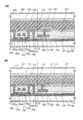
제 1 전극(공통전극)은, 유리기판의 위에 직접 접하여 형성되고 있으며, 역 스태거형 트랜지스터에 있어서의 게이트 전극도, 유리기판의 위에 직접 접하여 형성되고 있다. 그 위에는, 역 스태거형의 트랜지스터에 있어서의 게이트 절연막으로서 기능시키는 절연막이 직접 접하여 형성되고 있다. 그리고, 그 위에, 제 2 전극(화소전극)이 형성되고 있다(특허문헌 1 참조).The first electrode (common electrode) is formed in direct contact with the glass substrate, and the gate electrode in the reverse staggered transistor is also formed in direct contact with the glass substrate. On it, the insulating film which functions as a gate insulating film in an inverted staggered transistor is formed in direct contact. And the 2nd electrode (pixel electrode) is formed on it (refer patent document 1).
또는, 제 1 전극(공통전극)은, 역 스태거형 트랜지스터에 있어서의 게이트 절연막으로서 기능시키는 절연막의 위에 직접 접하여 형성되고 있다. 또한, 반도체 막이나 소스 전극 및 드레인 전극도, 역 스태거형 트랜지스터에 있어서의 게이트 절연막으로서 기능시키는 절연막의 위에 직접 접하여 형성된다. 그리고, 그 위에 절연층이 직접 접하여 형성된다. 그리고, 그 위에, 제 2 전극(화소전극)이 직접 접하여 형성되고 있다(특허문헌 1 참조).Alternatively, the first electrode (common electrode) is formed in direct contact with the insulating film functioning as the gate insulating film in the reverse staggered transistor. The semiconductor film, the source electrode, and the drain electrode are also formed in direct contact with the insulating film functioning as the gate insulating film in the reverse staggered transistor. And an insulating layer is formed directly on it. And the 2nd electrode (pixel electrode) is formed in direct contact with it (refer patent document 1).
상기의 종래예에서는, 액정을 구동하는 전극은, 하나의 절연막을 개재하여 배치되었다. 따라서, 전극과 전극의 사이의 거리를 크게 하려고 해도, 한계가 있었다. 만약, 전극간의 절연막의 막 두께를 크게 하면, 예를 들면, 트랜지스터에 있어서의 게이트 절연막도 두껍게 되기 때문에, 트랜지스터의 전류구동능력이 작아져 버리는 등의 영향이 있었다.In the above conventional example, the electrode for driving the liquid crystal is disposed through one insulating film. Therefore, there was a limit even if the distance between the electrode and the electrode was to be increased. If the thickness of the insulating film between the electrodes is increased, for example, the gate insulating film of the transistor also becomes thick, and thus the current driving capability of the transistor is reduced.
또한, 화소전극이 가지는 개구 패턴의 배치간격이나 개구 패턴의 폭은, 화소전극과 공통전극의 사이의 거리에 따라, 최적 값이 변화한다. 따라서, 화소전극과 공통전극의 사이의 거리를 자유롭게 설정할 수 없는 경우, 화소전극이 가지는 개구 패턴의 배치 간격이나 개구 패턴의 폭도, 크게 제한된 값을 선택하지 않을 수 없다. 그렇기 때문에, 액정분자에 가하는 전계의 크기나 방향이 충분하지 않은 상황으로 되었다.The optimum value of the arrangement interval of the opening patterns of the pixel electrodes and the width of the opening patterns vary depending on the distance between the pixel electrodes and the common electrode. Therefore, when the distance between the pixel electrode and the common electrode cannot be freely set, it is necessary to select a value in which the arrangement pattern of the opening pattern of the pixel electrode and the width of the opening pattern are largely limited. As a result, the size and direction of the electric field applied to the liquid crystal molecules are insufficient.
본 발명은 상기와 같은 사정을 고려하여 이루어진 것으로, 그 목적은, 표시소자의 2개의 전극의 간격의 자유도를 향상시킬 수 있고, 최적의 전계를 전극간에 가할 수 있는 표시장치 및 그 제조방법을 제공하는 것이다.SUMMARY OF THE INVENTION The present invention has been made in view of the above circumstances, and an object thereof is to provide a display device and a method of manufacturing the same, which can improve the degree of freedom between the two electrodes of a display element and apply an optimal electric field between electrodes. It is.
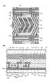
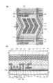
상기 문제를 해결하기 위해, 본 발명에 관한 반도체 장치는, 기판의 상방에 형성된 제 1 전극과, 제 1 전극의 상방에 형성된 제 1 절연막과, 제 1 절연막의 상방에 형성된 반도체 막과, 반도체 막의 상방에 형성된 제 2 절연막과 제 2 절연막의 상방에 형성된 도전막과, 도전막의 상방에 형성된 제 3 절연막과, 제 3 절연막의 상방에 형성되고, 개구 패턴을 가지는 제 2 전극을 구비한다.MEANS TO SOLVE THE PROBLEM In order to solve the said problem, the semiconductor device which concerns on this invention is the 1st electrode formed above the board | substrate, the 1st insulating film formed above the 1st electrode, the semiconductor film formed above the 1st insulating film, and the semiconductor film of the A second insulating film formed above and a conductive film formed above the second insulating film, a third insulating film formed above the conductive film, and a second electrode formed above the third insulating film and having an opening pattern.
본 발명에 관한 액정표시장치는, 기판의 상방에 형성된 제 1 전극과, 제 1 전극의 상방에 형성된 제 1 절연막과, 제 1 절연막의 상방에 형성된 반도체 막과, 반도체 막의 상방에 형성된 제 2 절연막과, 제 2 절연막의 상방에 형성된 도전막과, 도전막의 상방에 형성된 제 3 절연막과, 제 3 절연막의 상방에 형성되고, 개구 패턴을 가지는 제 2 전극과, 제 2 전극의 상방에 배치된 액정을 구비한다.A liquid crystal display device according to the present invention includes a first electrode formed above the substrate, a first insulating film formed above the first electrode, a semiconductor film formed above the first insulating film, and a second insulating film formed above the semiconductor film. And a conductive film formed above the second insulating film, a third insulating film formed above the conductive film, a second electrode formed above the third insulating film, having an opening pattern, and a liquid crystal disposed above the second electrode. It is provided.
이 반도체 장치 및 액정표시장치는, 제 1 전극을 기판 위, 즉, 반도체막의 아래에 형성하여 배치한다. 또한, 상기 제 2 전극은, 도전막(일례로서, 트랜지스터의 게이트 전극, 또는 소스 전극 등)이나 제 3 절연막의 상방에 배치되고 있기 때문에, 종래와 비교하고, 제 1 전극과 제 2 전극의 간격을 넓어질 수 있다. 또한, 제 1 절연막의 막 두께는, 두께를 변화시켜도, 트랜지스터 등의 다른 소자에 별로 영향을 미치지 않다. 그렇기 때문에, 두께를 임의로 변화시킬 수 있고, 그 결과로서, 제 1 전극과 제 2 전극의 간격을 자유롭게 설정할 수 있다. 따라서, 제 1 전극과 제 2 전극의 간격의 자유도가 향상한다. 그리고, 전극간에 가하는 전계의 구배를 제어할 수 있게 되고, 예를 들면, 기판과 평행방향의 전계를 증가하는 것 등을 용이하게 할 수 있다. 즉, 액정을 사용한 표시장치에 있어서는, 기판과 평행으로 배향하고 있는 액정분자(이른바 수평방향배향)를, 기판과 평행한 방향으로 제어할 수 있기 때문에, 최적의 전계를 가하는 것으로써, 시야각이 넓어진다.In this semiconductor device and the liquid crystal display device, a first electrode is formed and arranged on a substrate, that is, under the semiconductor film. In addition, since the second electrode is disposed above the conductive film (for example, a gate electrode, a source electrode, or the like of a transistor) or the third insulating film, the gap between the first electrode and the second electrode is compared with the conventional one. Can be widened. In addition, even if the thickness of the first insulating film is changed, the film thickness of the first insulating film does not significantly affect other elements such as transistors. Therefore, thickness can be changed arbitrarily and as a result, the space | interval of a 1st electrode and a 2nd electrode can be set freely. Therefore, the degree of freedom of the space | interval of a 1st electrode and a 2nd electrode improves. Then, the gradient of the electric field applied between the electrodes can be controlled, and for example, it is possible to easily increase the electric field in the direction parallel to the substrate. That is, in a display device using liquid crystals, since the liquid crystal molecules (so-called horizontal orientation) aligned in parallel with the substrate can be controlled in a direction parallel to the substrate, the viewing angle is widened by applying an optimum electric field. All.
또한, 개구 패턴은, 제 1 전극과 제 2 전극의 사이에, 기판에 대략 평행한 방향의 전계를 발생시키는 것이다. 따라서, 기판에 대략 평행한 방향의 전계를 발생시킬 수 있으면, 여러가지 형상으로 할 수 있다.The opening pattern is to generate an electric field in a direction substantially parallel to the substrate between the first electrode and the second electrode. Therefore, as long as it can generate the electric field of the direction substantially parallel to a board | substrate, it can be set in various shapes.
따라서, 개구 패턴에는, 슬릿 등의 닫힌 개구 패턴뿐만 아니라, 예를 들면, 빗살형상의 전극에 있어서의 빗살부분의 상호간의 스페이스 등, 도전체 패턴의 상호간에 위치하고, 해당 도전체 패턴이 형성되지 않은 스페이스를 포함한다. 즉, 전극과 전극의 사이에, 빈틈이나 간격이 있으면 좋다. 이하, 같다.Therefore, the opening pattern is located not only in a closed opening pattern such as a slit, but also in a conductor pattern such as, for example, a space between comb portions in a comb-shaped electrode, and the conductor pattern is not formed. Contains a space. In other words, there may be a gap or a gap between the electrode and the electrode. Hereinafter, it is the same.
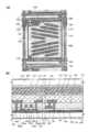
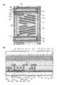
본 발명에 관한 다른 반도체 장치는, 기판의 상방에 형성된 제 1 전극과, 제 1 전극의 상방에 형성된 제 1 절연막과, 제 1 절연막의 상방에 형성된 반도체막과, 반도체막의 상방에 형성된 도전막과, 도전막의 상방에 형성된 제 2 절연막과, 제 2 절연막의 상방에 형성되고, 개구 패턴을 가지는 제 2 전극을 구비한다.Another semiconductor device according to the present invention includes a first electrode formed above the substrate, a first insulating film formed above the first electrode, a semiconductor film formed above the first insulating film, and a conductive film formed above the semiconductor film; And a second insulating film formed above the conductive film, and a second electrode formed above the second insulating film and having an opening pattern.
이 반도체 장치 및 액정표시장치에 의하면, 상기 제 1 전극을 상기 기판의 위, 즉, 상기 반도체막의 아래에 형성하여 배치한다. 또한, 상기 제 2 전극은, 도전막(일례로서, 소스 전극 등)이나 절연막의 상방에 배치되어 있기 때문에, 종래와 비교해서, 상기 제 1 전극과 상기 제 2 전극의 간격을 넓어질 수 있다. 또한, 제 1 절연막의 막 두께는, 두께를 변화시켜도, 트랜지스터 등의 다른 소자에 별로 영향을 미치지 않다. 그렇기 때문에, 두께를 임의로 변화시킬 수 있고, 그 결과로서, 제 1 전극과 제 2 전극의 간격을 자유롭게 설정할 수 있다. 따라서, 상기 제 1 전극과 상기 제 2 전극의 간격의 자유도가 향상한다. 그리고, 전극간에 가하는 전계의 구배를 제어할 수 있게 되고, 예를 들면, 기판과 평행방향의 전계를 증가하는 것 등을 용이하게 할 수 있다. 즉, 액정을 사용한 표시장치에 있어서는, 기판과 평행으로 배향하고 있는 액정분자(이른바 수평방향배향)를, 기판과 평행한 방향으로 제어할 수 있기 때문에, 최적의 전계를 가하는 것으로써, 시야각이 다르다.According to the semiconductor device and the liquid crystal display device, the first electrode is formed and disposed on the substrate, that is, under the semiconductor film. In addition, since the second electrode is disposed above the conductive film (for example, the source electrode or the like) or the insulating film, the gap between the first electrode and the second electrode can be widened as compared with the conventional one. In addition, even if the thickness of the first insulating film is changed, the film thickness of the first insulating film does not significantly affect other elements such as transistors. Therefore, thickness can be changed arbitrarily and as a result, the space | interval of a 1st electrode and a 2nd electrode can be set freely. Thus, the degree of freedom of the gap between the first electrode and the second electrode is improved. Then, the gradient of the electric field applied between the electrodes can be controlled, and for example, it is possible to easily increase the electric field in the direction parallel to the substrate. That is, in a display device using liquid crystals, since the liquid crystal molecules (so-called horizontal orientation) aligned in parallel with the substrate can be controlled in a direction parallel to the substrate, the viewing angle is different by applying an optimum electric field. .
본 발명에 관한 다른 반도체 장치는, 기판의 상방에 형성된 제 1 전극과, 제 1 전극의 상방에 형성된 제 1 절연막과, 제 1 절연막의 상방에 형성된 도전막과, 도전막의 상방에 형성된 반도체 막과, 반도체 막의 상방에 형성된 제 2 절연막과, 제 2 절연막의 상방에 형성되고, 개구 패턴을 가지는 제 2 전극을 구비한다.Another semiconductor device according to the present invention includes a first electrode formed above the substrate, a first insulating film formed above the first electrode, a conductive film formed above the first insulating film, and a semiconductor film formed above the conductive film; And a second insulating film formed above the semiconductor film, and a second electrode formed above the second insulating film and having an opening pattern.
이 반도체 장치 및 액정표시장치에 의하면, 상기 제 1 전극을 상기 기판의 위, 즉, 상기 반도체 막의 아래이며, 도전막(일례로서 게이트 전극)의 아래에 형성하여 배치된다. 또한, 상기 제 2 전극은, 제 2 절연막의 상방에 배치되기 때문에, 종래와 비교하여, 상기 제 1 전극과 상기 제 2 전극의 간격을 넓힐 수 있다. 또한, 제 2 절연막의 막 두께는, 두께를 변화시켜도, 트랜지스터 등의 다른 소자에 별로 영향을 미치지 않다. 그렇기 때문에, 두께를 임의로 변화시킬 수 있고, 그 결과로서, 제 1 전극과 제 2 전극의 간격을 자유롭게 설정할 수 있다. 따라서, 상기 제 1 전극과 제 2 전극의 간격의 자유도가 향상한다. 그리고, 전극간에 가하는 전계의 구배를 제어할 수 있기 때문에, 예를 들면, 기판과 평행방향의 전계를 증가하는 것 등을 용이하게 할 수 있다. 즉, 액정을 사용한 표시장치에 있어서는, 기판과 평행으로 배향하는 액정분자(이른바 수평방향배향)를, 기판과 평행한 방향으로 제어할 수 있기 때문에, 최적의 전계를 가하는 것으로써, 시야각이 넓어진다.According to the semiconductor device and the liquid crystal display device, the first electrode is formed on the substrate, that is, under the semiconductor film, and formed under a conductive film (for example, a gate electrode). In addition, since the second electrode is disposed above the second insulating film, the distance between the first electrode and the second electrode can be widened as compared with the related art. In addition, even if the thickness of the second insulating film is changed, the film thickness of the second insulating film does not affect much on other elements such as transistors. Therefore, thickness can be changed arbitrarily and as a result, the space | interval of a 1st electrode and a 2nd electrode can be set freely. Thus, the degree of freedom of the gap between the first electrode and the second electrode is improved. Since the gradient of the electric field applied between the electrodes can be controlled, for example, it is possible to easily increase the electric field in the direction parallel to the substrate. That is, in a display device using liquid crystals, the liquid crystal molecules oriented in parallel with the substrate (so-called horizontal orientation) can be controlled in a direction parallel to the substrate, so that the viewing angle is widened by applying an optimum electric field. .
본 발명에 관한 다른 반도체 장치는, 상기 구성에 있어서, 제 1 전극은 공통전극이며, 제 2 전극은 화소전극이다.In another semiconductor device according to the present invention, in the above configuration, the first electrode is a common electrode, and the second electrode is a pixel electrode.
본 발명에 관한 다른 반도체 장치는, 상기 구성에 있어서, 제 1 전극은 화소전극이며, 제 2 전극은 공통전극이다.In another semiconductor device according to the present invention, in the above configuration, the first electrode is a pixel electrode, and the second electrode is a common electrode.
본 발명에 관한 다른 액정표시장치는, 기판의 상방에 형성된 제 1 전극과, 제 1 전극의 상방에 형성된 제 1 절연막과, 제 1 절연막의 상방에 형성된 반도체막과, 반도체막의 상방에 형성된 도전막과, 도전막의 상방에 형성된 제 2 절연막과, 제 2 절연막의 상방에 형성되고, 개구 패턴을 가지는 제 2 전극과, 제 2 전극의 상방에 배치된 액정을 구비한다.Another liquid crystal display device according to the present invention includes a first electrode formed above the substrate, a first insulating film formed above the first electrode, a semiconductor film formed above the first insulating film, and a conductive film formed above the semiconductor film. And a second insulating film formed above the conductive film, a second electrode formed above the second insulating film, having an opening pattern, and a liquid crystal disposed above the second electrode.
본 발명에 관한 다른 액정표시장치는, 기판의 상방에 형성된 제 1 전극과, 제 1 전극의 상방에 형성된 제 1 절연막과, 제 1 절연막의 상방에 형성된 도전막과, 도전막의 상방에 형성된 반도체막과, 반도체막의 상방에 형성된 제 2 절연막과, 제 2 절연막의 상방에 형성되고, 개구 패턴을 가지는 제 2 전극과, 제 2 전극의 상방에 배치된 액정을 구비한다.Another liquid crystal display device according to the present invention includes a first electrode formed above the substrate, a first insulating film formed above the first electrode, a conductive film formed above the first insulating film, and a semiconductor film formed above the conductive film. And a second insulating film formed above the semiconductor film, a second electrode formed above the second insulating film, having an opening pattern, and a liquid crystal disposed above the second electrode.
본 발명에 관한 다른 액정표시장치는, 상기 구성에 있어서, 제 1 전극과 제 2 전극의 사이의 전계에 의하여, 상기 액정을 제어한다.According to another liquid crystal display device according to the present invention, the liquid crystal is controlled by an electric field between the first electrode and the second electrode.
본 발명에 관한 다른 액정표시장치는, 상기 구성에 있어서, 제 1 전극은 공통전극이며, 제 2 전극은 화소전극이다.In another liquid crystal display device according to the present invention, in the above configuration, the first electrode is a common electrode, and the second electrode is a pixel electrode.
본 발명에 관한 다른 액정표시장치는, 상기 구성에 있어서, 제 1 전극은 화소전극이며, 제 2 전극은 공통전극이다.In another liquid crystal display device according to the present invention, in the above configuration, the first electrode is a pixel electrode, and the second electrode is a common electrode.
또한, 본 발명에 나타내고 있는 스위치는, 여러가지 형태의 스위치를 사용할 수 있고, 일례로서, 전기적 스위치나 기계적인 스위치 등이 있다. 즉, 전류의 흐름을 제어할 수 있는 것이면, 특정의 것으로 한정되지 않고, 여러가지 것을 사용할 수 있다. 예를 들면, 트랜지스터이어도 좋고, 다이오드(PN 다이오드, PIN 다이오드, 숏 키 다이오드, 다이오드접속의 트랜지스터 등)도 좋고, 그들을 조합한 논리회로이라도 좋다. 따라서, 스위치로서 트랜지스터를 사용하는 경우, 그 트랜지스터는, 단순한 스위치로서 동작하기 때문에, 트랜지스터의 극성(도전형)은 특히 한정되지 않는다. 다만, 오프전류가 적은 쪽이 바람직한 경우, 오프전류가 적은 쪽의 극성의 트랜지스터를 사용하는 것이 바람직하다. 오프전류가 적은 트랜지스터로서는, LDD영역을 형성하는 것이나, 멀티 게이트 구조로 하는 것 등이 있다. 또한, 스위치로서 동작시키는 트랜지스터의 소스단자의 전위가, 저전위측 전원(Vss, GND, 0V 등)에 가까운 상태로 동작하는 경우는, N채널형을, 반대로, 소스단자의 전위가, 고전위측 전원(Vdd 등)에 가까운 상태로 동작하는 경우는, P채널형을 사용하는 것이 바람직하다. 왜냐하면, 게이트 소스간 전압의 절대치를 크게 할 수 있기 때문에, 스위치로서 동작하기 쉽기 때문이다. 또한, N채널형과 P채널형의 양쪽을 사용하고, CMOS형의 스위치로 하여도 좋다. CMOS형의 스위치로 하면, 스위치를 개재하여 출력하는 전압(즉, 입력전압)이, 출력전압에 대해서 높거나, 낮거나 하고, 상황이 변화하는 경우에 있어서도, 적절히 동작을 할 수 있다. 또한, 본 발명에 있어서의 스위치로서는, 예를 들면, 화소전극을 제어하는 TFT나, 구동회로부에 사용하는 스위치 소자를 들을 수 있지만, 이 이외의 부분에 있어서도, 전류의 흐름을 제어할 필요가 있는 부분이면, 스위치를 사용할 수 있다.In addition, various types of switches can be used for the switch shown by this invention, As an example, an electrical switch, a mechanical switch, etc. are mentioned. That is, as long as it can control the flow of electric current, it is not limited to a specific thing, Various things can be used. For example, a transistor may be sufficient, a diode (PN diode, a PIN diode, a Schottky diode, a transistor of a diode connection, etc.) may be sufficient, and the logic circuit which combined them may be sufficient. Therefore, in the case of using a transistor as a switch, since the transistor operates as a simple switch, the polarity (conductive type) of the transistor is not particularly limited. However, when the less off current is desired, it is preferable to use a transistor having a polarity with the less off current. As the transistor with less off current, an LDD region may be formed, or a multi-gate structure may be used. In the case where the potential of the source terminal of the transistor operated as a switch is close to the low potential power supply (Vss, GND, 0V, etc.), the N-channel type is reversed, whereas the source terminal has a high potential side. When operating in a state close to a power supply (Vdd or the like), it is preferable to use a P-channel type. This is because it is easy to operate as a switch because the absolute value of the voltage between the gate and source can be increased. In addition, both of the N-channel type and the P-channel type may be used to form a CMOS switch. In the case of a CMOS type switch, even when the voltage outputted through the switch (that is, the input voltage) is high or low with respect to the output voltage and the situation changes, the operation can be performed properly. In addition, as a switch in this invention, although the TFT which controls a pixel electrode and the switch element used for a drive circuit part are mentioned, it is necessary to control the flow of an electric current also in other parts. If so, a switch can be used.
또한, 본 발명에 있어서, 접속된다라고 하는 의미는, 전기적으로 접속되는 경우와, 직접 접속되는 경우를 포함하는 것으로 한다. 따라서, 본 발명이 개시하는 구성에 있어서, 소정의 접속관계에 가하여, 그 사이에 전기적인 접속을 가능하게 하는 다른 소자(예를 들면, 스위치나 트랜지스터나 용량소자나 인덕터나 저항소자나 다이오드 등)가 배치되어 있어도, 좋다. 또는, 사이에 다른 소자를 끼우지 않고 배치되어도 좋다. 또한, 어느 2개의 도전막이, 전기적인 접속을 가능하게 하는 다른 소자를 사이에 개재하지 않고, 전기적으로 접속되지 않은 경우에는, 직접 접속되고 있는, 또는 직접적으로 접속된다라고 기재한다. 또한, 전기적으로 접속된다라고 기재하는 경우는, 전기적으로 접속되고 있는 경우와 직접 접속되는 경우를 포함한다.In addition, in this invention, the meaning of being connected shall include the case where it is electrically connected, and the case where it is directly connected. Therefore, in the configuration disclosed by the present invention, another element (for example, a switch, a transistor, a capacitor, an inductor, a resistor, a diode, etc.) that enables electrical connection therebetween in addition to a predetermined connection relationship. May be arranged. Or you may arrange | position without inserting another element between them. In addition, any two conductive films are described as being directly connected or directly connected when they are not electrically connected without interposing another element that enables electrical connection. In addition, the case of describing as electrically connected includes the case where it is electrically connected, and the case where it is directly connected.
또한, 본 발명의 표시소자나 표시장치나 발광장치는, 여러가지 형태를 적용할 수 있고, 또한, 여러가지 소자를 가질 수 있다. 본 발명에서는, 액정소자를 사용할 수 있다. 액정소자는, 액정의 광학적인 변조작용에 의하여, 빛의 투과 또는 비투과를 제어하는 소자이며, 한 쌍의 전극 및 액정에 의해서 구성된다. 액정소자를 사용한 표시장치로서는, 액정 디스플레이, 투과형 액정 디스플레이, 반투과형 액정 디스플레이, 반사형 액정 디스플레이 등이 있다. 또한, 예를 들면, EL소자(EL 소자는, 전장을 가하는 것으로써 발생하는 루미네선스를 얻을 수 있는 발광층을 가지는 소자를 가리킨다. 또한, 유기EL소자, 무기EL소자 또는 유기물 및 무기물을 포함하는 EL소자를 포함한다), 전자방출소자, 전자 잉크, 회절 광 밸브(GLV), 플라즈마 디스플레이(PDP), 디지털 마이크로 미러 장치(DMD), 압전 세라믹 디스플레이, 카본 나노 튜브 등, 전기자기적 작용에 의하여 콘트라스트가 변화하는 표시매체를 구비할 수 있다. 또한, EL소자를 사용한 표시소자로서는, EL 디스플레이, 전자방출소자를 사용한 표시소자로서는, 전계 방출형 디스플레이(FED),나 SED방식 평면형 디스플레이(SED: Surface-conduction Electron-emitter Display)등이 있고, 또한, 전자 잉크를 사용한 표시장치로서는 전자 페이퍼가 있다.In addition, various aspects can be applied to the display device, the display device, or the light emitting device of the present invention, and can have various devices. In the present invention, a liquid crystal element can be used. A liquid crystal element is an element which controls the transmission or non-transmission of light by the optical modulation action of a liquid crystal, and is comprised by a pair of electrode and a liquid crystal. As a display apparatus using a liquid crystal element, there are a liquid crystal display, a transmissive liquid crystal display, a transflective liquid crystal display, a reflective liquid crystal display, and the like. In addition, for example, an EL element (EL element refers to an element having a light emitting layer capable of obtaining a luminescence generated by applying an electric field. Further, an organic EL element, an inorganic EL element or an organic substance and an inorganic substance are included. EL element), electron-emitting device, electronic ink, diffraction light valve (GLV), plasma display (PDP), digital micro mirror device (DMD), piezoelectric ceramic display, carbon nanotube, etc. The display medium may be changed. In addition, examples of display elements using EL elements include EL displays and field emission displays (FEDs), SED type flat display (SED: Surface-conduction Electron-emitter Display), and the like. In addition, there is an electronic paper as a display device using electronic ink.
또한, 본 발명에 있어서, 트랜지스터는 여러가지 형태의 트랜지스터를 적용시킬 수 있다. 따라서, 적용가능한 트랜지스터의 종류에 한정은 없다. 따라서, 비정질 규소나 다결정 규소에 대표되는 비단결정 반도체막을 사용한 박막 트랜지스터(TFT), 반도체 기판이나 SOI 기판을 사용하여 형성된 트랜지스터, MOS형 트랜지스터, 접합형 트랜지스터, 바이폴러 트랜지스터, ZnO, a-InGaZnO 등의 화합물 반도체를 사용한 트랜지스터, 유기 반도체나 카본 나노 튜브를 사용한 트랜지스터, 그 이외의 트랜지스터를 적용할 수 있다. 또한, 트랜지스터가 배치되는 기판의 종류는, 여러가지 사용할 수 있고, 특정의 것으로 한정되지 않는다. 따라서, 예를 들면, 유리기판, 플라스틱 기판, 종이 기판, 셀로판 기판, 석제 기판 등에 배치할 수 있다. 또한, 반사형 디스플레이로 하는 경우에는, 단결정 기판, SOI 기판도 사용할 수 있다. 또한, 어느 기판에 트랜지스터를 형성하고, 그 후, 다른 기판에 트랜지스터를 이동시켜, 다른 기판 위에 배치하도록 하여도 좋다.In the present invention, the transistor can be applied to various types of transistors. Therefore, there is no limitation on the type of transistor applicable. Therefore, a thin film transistor (TFT) using a non-single crystal semiconductor film represented by amorphous silicon or polycrystalline silicon, a transistor formed using a semiconductor substrate or an SOI substrate, a MOS transistor, a junction transistor, a bipolar transistor, ZnO, a-InGaZnO, or the like A transistor using a compound semiconductor of, a transistor using an organic semiconductor or a carbon nanotube, and other transistors can be used. In addition, the kind of board | substrate in which a transistor is arrange | positioned can be used variously, It is not limited to a specific thing. Therefore, for example, it can be disposed on a glass substrate, a plastic substrate, a paper substrate, a cellophane substrate, a stone substrate, or the like. In the case of a reflective display, a single crystal substrate or an SOI substrate can also be used. Alternatively, the transistor may be formed on one substrate, and then the transistor may be moved to another substrate to be disposed on another substrate.
또한, 이미 설명한 바와 같이, 본 발명에 있어서의 트랜지스터는, 여러가지 타입을 사용할 수 있고, 여러가지 기판 위에 형성시킬 수 있다. 따라서, 모두 회로가 유리 기판 위에 형성되어도 좋고, 플라스틱 기판에 형성되어도 좋다. 또한, 제작하는 제품이 반사형 디스플레이로 하는 경우에는, 단결정 기판에 형성되어도 좋고, SOI기판에 형성되어도 좋다. 즉, 어떤 기판 위에 형성되어도 좋다. 모두 회로가 동일한 기판 위에 형성되는 것으로써, 부품점수를 감소시켜, 비용을 저감하는 것이나, 회로부품과의 접속점수를 저감하는 것이나, 회로부품과의 접속점수를 줄이고 신뢰성을 향상시킬 수 있다. 또한, 회로의 일부가 어느 기판에 형성되어 있고, 회로의 다른 일부가, 다른 기판에 형성되어도 좋다. 즉, 회로의 전부가 같은 기판 위에 형성되지 않아도 좋다. 예를 들면, 회로의 일부는, 유리기판 위에 트랜지스터를 사용하여 형성하고, 회로의 다른 일부는, 단결정 기판 위에 형성하고, 그 IC칩을 COG(Chip On Glass)로 접속하고 유리기판 위에 배치하여도 좋다. 또한, 그 IC칩을 TAB(Tape Automated Bonding)나 프린트 기판을 사용하여 유리기판과 접속하여도 좋다. 이와 같이, 회로의 일부가 같은 기판에 형성되는 것으로써, 부품점수를 줄이고 비용을 저감하는 것이나, 회로부품과의 접속점수를 줄이고 신뢰성을 향상시킬 수 있다. 또한, 구동전압이 높은 부분이나, 구동주파수가 높은 부분은, 소비전력이 커져 버리기 때문에, 그런 부분은 같은 기판에 형성하지 않도록 하면, 소비전력의 증가를 방지할 수 있다.In addition, as described above, the transistors in the present invention can use various types and can be formed on various substrates. Therefore, a circuit may be formed on a glass substrate in all, and may be formed in a plastic substrate. When the product to be produced is a reflective display, it may be formed on a single crystal substrate or may be formed on an SOI substrate. That is, it may be formed on any substrate. Since both circuits are formed on the same substrate, the number of parts can be reduced, the cost can be reduced, the number of connection points with circuit components can be reduced, the number of connection points with circuit components can be reduced, and reliability can be improved. In addition, a part of a circuit may be formed in which board | substrate, and the other part of a circuit may be formed in another board | substrate. That is, not all of the circuits need to be formed on the same substrate. For example, a part of a circuit may be formed using a transistor on a glass substrate, and another part of the circuit may be formed on a single crystal substrate, and the IC chip may be connected by COG (Chip On Glass) and disposed on a glass substrate. good. In addition, the IC chip may be connected to a glass substrate using TAB (Tape Automated Bonding) or a printed circuit board. As described above, since a part of the circuit is formed on the same substrate, the number of parts can be reduced and the cost can be reduced, and the number of connection points with the circuit parts can be reduced and the reliability can be improved. In addition, since the power consumption increases in a portion having a high driving voltage and a portion having a high driving frequency, an increase in power consumption can be prevented if such a portion is not formed on the same substrate.
또한, 트랜지스터의 구성은, 여러가지 형태를 취할 수 있고, 특정의 구성으로 한정되지 않는다. 예를 들면, 게이트 전극의 본수가 2본 이상으로 되는 멀티 게이트 구조를 사용하여도 좋다. 멀티 게이트 구조로 하는 것으로써, 오프전류를 저감하는 것이나, 트랜지스터의 내압을 향상시켜 신뢰성을 좋게 하는 것이나, 포화영역에서 동작할 때, 드레인 · 소스간 전압이 변화하여도, 드레인 · 소스간 전류가 별로 변화하지 않고, 플랫한 특성으로 할 수 있다. 또한, 채널의 상하에 게이트 전극이 배치되는 구조라도 좋다. 채널의 상하에 게이트 전극이 배치된 구조로 하는 것으로써, 채널영역이 증가하기 때문에, 전류 값을 크게 하는 것이나, 공핍층이 생기기 쉽게 되기 때문에, S치를 작게 할 수 있다. 또한, 채널의 위에 게이트 전극이 배치되고 있는 구조라도 좋고, 채널의 아래에 게이트 전극이 배치되는 구조라도 좋다. 또한, 정 스태거 구조라도 좋고, 역 스태거 구조라도 좋다. 또한, 채널영역이 복수의 영역으로 분할되어도 좋고, 병렬로 접속되어도 좋고, 직렬로 접속되어도 좋다. 또한, 채널(또는 그 일부)에 소스 전극이나 드레인 전극이 겹쳐도 좋다. 채널(또는 그 일부)에 소스 전극이나 드레인 전극이 겹치는 구조로 하는 것으로써, 채널의 일부에 전하가 늘고, 동작이 불안정으로 되는 것을 방지할 수 있다. 또한, LDD영역이 있어도 좋다. LDD영역을 형성하는 것으로써, 오프전류를 저감하는 것이나, 트랜지스터의 내압을 향상시켜, 신뢰성을 좋게 하는 것이나, 포화영역에서 동작할 때에, 드레인 · 소스 간 전압이 변화해도, 드레인 · 소스 간 전류가 별로 변화하지 않고, 플랫한 특성으로 할 수 있다.In addition, the structure of a transistor can take various forms, and is not limited to a specific structure. For example, a multi-gate structure in which the number of gate electrodes is two or more may be used. The multi-gate structure reduces the off current, improves the breakdown voltage of the transistor to improve reliability, and when operating in the saturation region, even when the drain-source voltage changes, the drain-source current does not change. It does not change very much and can be made into a flat characteristic. Further, the structure may be such that the gate electrode is disposed above and below the channel. The structure in which the gate electrodes are arranged above and below the channel increases the channel value because the channel region increases, and the S value can be reduced because the depletion layer tends to be increased. In addition, the structure may be such that the gate electrode is arranged above the channel, or the structure may be arranged below the channel. Moreover, a forward stagger structure may be sufficient and a reverse stagger structure may be sufficient. In addition, the channel region may be divided into a plurality of regions, may be connected in parallel, or may be connected in series. In addition, the source electrode or the drain electrode may overlap the channel (or part thereof). By having a structure in which a source electrode or a drain electrode overlaps with a channel (or a part thereof), it is possible to prevent an increase in electric charge in a part of the channel and unstable operation. There may also be an LDD region. By forming the LDD region, it is possible to reduce the off current, to improve the breakdown voltage of the transistor to improve the reliability, and to operate in the saturation region, even when the drain-source voltage changes, even if the drain-source current changes. It does not change very much and can be made into a flat characteristic.
또한, 본 발명에 있어서는, 1화소는, 명도를 제어할 수 있는 요소 하나 분을 나타내는 것으로 한다. 따라서, 일례로서는, 1화소는, 하나의 색 요소를 나타내고, 그 색 요소 하나로 명도를 표현한다. 따라서, 그 때는, R(적), G(녹), B(청)의 색 요소로 되는 컬러 표시장치의 경우에는, 화상의 최소단위는, R의 화소와 G의 화소와 B의 화소의 3화소로 구성되는 것으로 한다. 또한, 색 요소는 3색으로 한정되지 않고, 그 이상도 좋고, 예를 들면, RGBW(W는 백)나, RGB에 노랑색, 남색, 자홍색을 추가한 것이 있다. 또한, 다른 예로서는, 하나의 색 요소에 대해서, 복수의 영역을 사용하여 명도를 제어하는 경우는, 그 영역의 1개분을 1화소로 한다. 따라서, 일례로서는, 면적 계조를 하는 경우는, 하나의 색 요소에 명도를 제어하는 영역이 복수 있고, 그 전체로 계조를 표현하지만, 명도를 제어하는 영역의 1개분을 1화소로 한다. 따라서, 그 경우는, 하나의 색 요소는, 복수의 화소로 구성되는 것으로 한다. 또한, 그 경우, 화소에 따라, 표시에 기여하는 영역의 크기가 다른 경우가 있다. 또한, 하나의 색 요소에 대해서 복수 있는, 명도를 제어하는 영역에 있어서, 즉, 하나의 색 요소를 구성하는 복수의 화소에 있어서, 각각에 공급하는 신호를 조금 다르게 하도록 하고, 시야각을 넓어지도록 하여도 좋다. 또한, 1화소(3색분)라고 기재하는 경우는, R와 G와 B의 3화소분을 1화소로 고려하는 경우라고 가정한다. 1화소(1색분)라고 기재하는 경우는, 하나의 색 요소에 대해서, 복수의 화소가 있는 경우, 그들을 조합하여 1화소로 고려하는 경우로 가정한다.In addition, in this invention, 1 pixel shall show one element which can control brightness. Therefore, as an example, one pixel represents one color element and expresses brightness with one color element. Therefore, in the case of a color display device that is a color element of R (red), G (green), and B (blue), the minimum unit of the image is 3 pixels of R pixels, G pixels, and B pixels. It is assumed that it is composed of pixels. In addition, the color element is not limited to three colors, and more than that may be sufficient. For example, RGBW (W is white) and yellow, indigo, and magenta are added to RGB. As another example, when the brightness is controlled using a plurality of regions for one color element, one portion of the region is one pixel. Therefore, as an example, in the case of area gradation, one color element has a plurality of regions for controlling the brightness, and the gradation is expressed as a whole, but one portion of the region for controlling the brightness is assumed to be one pixel. Therefore, in that case, one color element shall be comprised by several pixel. In that case, the size of the region contributing to the display may vary depending on the pixel. In addition, in a region in which brightness is controlled with respect to one color element, that is, in a plurality of pixels constituting one color element, the signals supplied to the pixels are slightly different, and the viewing angle is widened. Also good. In addition, when describing as 1 pixel (3 colors), it is assumed that it is a case where 3 pixels of R, G, and B are considered as 1 pixel. In the case of describing one pixel (one color), it is assumed that when there are a plurality of pixels with respect to one color element, the case is considered as one pixel by combining them.
또한, 본 발명에 있어서, 화소는, 매트릭스 상태로 배치(배열)되는 경우를 포함한다. 여기에서, 화소가 매트릭스로 배치(배열)되는 것은, 세로줄무늬와 가로줄무늬를 조합한 이른바 격자상태로 스트라이프 배치되어 있는 경우를 포함한다. 그리고, 3색의 색 요소(예를 들면, RGB)로 풀컬러 표시를 하는 경우에, 3개의 색 요소의 도트가 이른바 델타배치되는 경우도 포함한다. 또한, 베이야 배치되는 경우도 포함한다. 또한, 색 요소는, 3색으로 한정되지 않고, 그 이상이라도 좋고, 예를 들면, RGBW(W는 백)나, 노랑색, 남색, 자홍색을 추가한 것 등이 있다. 또한, 색 요소마다 그 발광영역의 크기가 달라도 좋다.In addition, in this invention, the pixel includes the case where it arrange | positions (arranges) in a matrix state. Here, the arrangement (arrangement) of pixels in a matrix includes the case where the stripes are arranged in a so-called lattice state in which vertical stripes and horizontal stripes are combined. In addition, when full-color display is performed by three color elements (for example, RGB), the dot of three color elements is also called delta arrangement | positioning. It also includes the case where bayers are arranged. In addition, the color element is not limited to three colors, and may be more than that. For example, RGBW (W is white), yellow, indigo, magenta, etc. are added. In addition, the size of the light emitting area may be different for each color element.
트랜지스터는, 각각 게이트와 드레인과, 소스를 포함하는 적어도 3개의 단자를 가지는 소자이며, 드레인 영역과 소스 영역의 사이에 채널형성영역을 가진다. 여기에서, 트랜지스터의 소스와 드레인은, 트랜지스터의 구조나 동작조건 등에 의해서 변화하기 때문에, 어느 것이 소스 또는 드레인인지 한정하는 것이 어렵다. 그래서, 본 발명에 있어서는, 소스 및 드레인 영역으로서 기능하는 영역을, 각각 제 1 단자, 제 2 단자라고 표기한다.The transistor is an element having at least three terminals each including a gate, a drain, and a source, and has a channel forming region between the drain region and the source region. Here, since the source and the drain of the transistor change depending on the structure, operating conditions, and the like of the transistor, it is difficult to limit which source or drain is the source or the drain. Therefore, in this invention, the area | region which functions as a source and a drain area is described with a 1st terminal and a 2nd terminal, respectively.
또한, 게이트는, 게이트 전극과 게이트 배선(게이트 선 또는 게이트 신호선 등이라고도 한다)을 포함한 전체, 또는, 그들의 일부를 가리킨다. 게이트 전극은, 채널 영역이나 LDD(Light Doped Drain)영역 등을 형성하는 반도체와, 게이트 절연막을 개재하여 오버랩하는 부분의 도전막을 의미한다. 게이트 배선은, 각 화소의 게이트 전극의 사이를 접속하거나 게이트 전극과 다른 배선을 접속하기 위한 배선의 것을 의미한다.In addition, the gate refers to all or part thereof including the gate electrode and the gate wiring (also called a gate line or a gate signal line). The gate electrode means a semiconductor that forms a channel region, a light doped drain (LDD) region, or the like, and a conductive film that overlaps the gate insulating film. The gate wiring means a wiring for connecting between the gate electrodes of the respective pixels or for connecting the gate electrode with another wiring.
다만, 게이트 전극으로서도 기능하고, 게이트 배선으로서도 기능하는 부분도 존재한다. 그런 영역은, 게이트 전극이라고 불러도 좋고, 게이트 배선이라고 불러도 좋다. 즉, 게이트 전극과 게이트 배선이, 명확하게 구별할 수 없는 영역도 존재한다. 예를 들면, 연장하여 배치되는 게이트 배선과 오버랩하고 채널영역이 있는 경우, 그 영역은 게이트 배선으로서 기능하지만, 게이트 전극으로서도 기능한다. 따라서, 그런 영역은, 게이트 전극이라고 불러도 좋고, 게이트 배선이라고 불러도 좋다.However, there exists a part which also functions as a gate electrode and also as a gate wiring. Such a region may be called a gate electrode or may be called a gate wiring. In other words, there are regions in which the gate electrode and the gate wiring cannot be clearly distinguished. For example, in the case where there is a channel region overlapping with the gate wiring arranged to extend, the region functions as a gate wiring, but also functions as a gate electrode. Therefore, such a region may be called a gate electrode or may be called a gate wiring.
또한, 게이트 전극과 같은 재료로 형성되고, 게이트 전극과 전기적으로 접속하는 영역도, 게이트 전극이라도 불러도 좋다. 마찬가지로, 게이트 배선과 같은 재료로 형성되고, 게이트 배선과 전기적으로 접속하는 영역도, 게이트 배선이라고 불러도 좋다. 이러한 영역은, 엄밀한 의미로는, 채널영역과 오버랩하지 않거나, 다른 게이트 전극과 접속시키는 기능을 가지지 않거나 하는 경우가 있다. 그렇지만, 제조비용이나 공정의 삭감, 또는 레이아웃의 간략화 등의 관계로, 게이트 전극이나 게이트 배선과 같은 재료로 형성되고, 게이트 전극이나 게이트 배선과 전기적으로 접속하는 영역이 있다. 따라서, 그런 영역도 게이트 전극이나 게이트 배선이라고 불러도 좋다.Further, the region formed of the same material as the gate electrode and electrically connected to the gate electrode may be called the gate electrode. Similarly, a region formed of the same material as the gate wiring and electrically connected to the gate wiring may also be referred to as a gate wiring. In a strict sense, such an area may not overlap with the channel area or may not have a function of connecting with another gate electrode. However, there is a region formed of the same material as the gate electrode or the gate wiring and electrically connected to the gate electrode or the gate wiring due to the production cost, the reduction of the process, or the simplification of the layout. Therefore, such a region may also be called a gate electrode or a gate wiring.
또한, 예를 들면, 멀티 게이트의 트랜지스터에 있어서, 하나의 트랜지스터의 게이트 전극과, 다른 트랜지스터의 게이트 전극은, 게이트 전극과 같은 재료로 형성된 도전막으로 접속되는 경우가 많다. 그런 영역은, 게이트 전극과 게이트 전극을 접속시키기 위한 영역이기 때문에, 게이트 배선이라고 불러도 좋지만, 멀티 게이트의 트랜지스터를 하나의 트랜지스터라고 간주할 수 있기 때문에, 게이트 전극이라고 불러도 좋다. 즉, 게이트 전극이나 게이트 배선과 같은 재료로 형성되고, 그들과 전기적으로 접속하여 배치된 것은, 게이트 전극이나 게이트 배선이라고 불러도 좋다. 또한, 예를 들면, 게이트 전극과 게이트 배선을 접속하고 있는 부분의 도전막도, 게이트 전극이라고 불러도 좋고, 게이트 배선이라고 불러도 좋다.For example, in a multi-gate transistor, the gate electrode of one transistor and the gate electrode of another transistor are often connected by a conductive film formed of the same material as the gate electrode. Since such a region is a region for connecting the gate electrode and the gate electrode, it may be referred to as a gate wiring, but may be referred to as a gate electrode because the transistor of the multi-gate can be regarded as one transistor. That is, what is formed of the same material as a gate electrode or a gate wiring, and electrically arrange | positioned with them may be called a gate electrode or a gate wiring. For example, the conductive film of the part which connects a gate electrode and a gate wiring may also be called a gate electrode, and may be called a gate wiring.
또한, 게이트 단자는, 게이트 전극의 영역이나, 게이트 전극과 전기적으로 접속되고 있는 영역에 대해서, 그 일부분을 가리킨다.In addition, a gate terminal points to the part of the area | region of the gate electrode and the area | region electrically connected with the gate electrode.
또한, 소스는, 소스 영역과 소스 전극과 소스 배선(소스 선 또는 소스 신호선 등이라고도 한다)을 포함한 전체, 또는 그들의 일부를 가리킨다. 소스 영역은, P형 불순물(붕소나 갈륨 등)이나 N형 불순물(인이나 비소 등)이 많은 포함되는 반도체 영역을 의미한다. 따라서, 조금만 P형 불순물이나 N형 불순물이 포함되는 영역, 이른바, LDD(Lightly Doped Drain)영역은, 소스 영역에는 포함되지 않는다. 소스 전극은, 소스 영역과는 다른 재료로 형성되고, 소스 영역과 전기적으로 접속되어 배치되는 부분의 도전층을 의미한다. 다만, 소스 전극은, 소스 영역도 포함하여 소스 전극이라고 부르기도 한다. 소스 배선은, 각 화소의 소스 전극 간을 접속하거나, 소스 전극과 다른 배선을 접속하기 위한 배선을 의미한다.In addition, a source refers to all or part thereof including a source region, a source electrode, and a source wiring (also called a source line or a source signal line). The source region means a semiconductor region containing a large amount of P-type impurities (such as boron or gallium) and N-type impurities (such as phosphorus and arsenic). Therefore, a region containing only P-type impurities or N-type impurities, so-called LDD (Lightly Doped Drain) region, is not included in the source region. The source electrode means a conductive layer of a portion formed of a material different from the source region and electrically connected to the source region. However, a source electrode is also called a source electrode including a source area. Source wiring means wiring for connecting between source electrodes of each pixel, or connecting other wiring with a source electrode.
그렇지만, 소스 전극으로서도 기능하고, 소스 배선으로서도 기능하는 부분도 존재한다. 그런 영역은, 소스 전극이라고 불러도 좋고, 소스 배선이라고 불러도 좋다. 즉, 소스 전극과 소스 배선이, 명확하게 구별할 수 없는 영역도 존재한다. 예를 들면, 연장하여 배치되는 소스 배선과 오버랩하고 소스 영역이 있는 경우, 그 영역은 소스 배선으로서 기능하지만, 소스 전극으로서도 기능한다. 따라서, 그런 영역은, 소스 전극이라도 불러도 좋고, 소스 배선이라도 불러도 좋다.However, there exists a part which also functions as a source electrode and also as a source wiring. Such a region may be called a source electrode or may be called a source wiring. In other words, there are regions in which the source electrode and the source wiring cannot be clearly distinguished. For example, in the case where there is a source region overlapping with the source wiring arranged to extend, the region functions as a source wiring, but also functions as a source electrode. Therefore, such a region may be called a source electrode or a source wiring may be called.
또한, 소스 전극과 같은 재료로 형성되고, 소스 전극과 전기적으로 접속하는 영역이나, 소스 전극과 소스 전극을 접속하는 부분도, 소스 전극이라고 불러도 좋다. 또한, 소스 영역과 오버랩하고 있는 부분도, 소스 전극이라고 불러도 좋다. 마찬가지로, 소스 배선과 같은 재료로 형성되고, 소스 배선과 전기적으로 접속하는 영역도, 소스 배선이라고 불러도 좋다. 이러한 영역은, 엄밀한 의미에서는, 다른 소스 전극과 접속되는 기능을 갖지 않은 경우가 있다. 그렇지만, 제조 비용이나 공정의 삭감, 또는 레이아웃의 간략화 등의 관계에서, 소스 전극이나 소스 배선과 같은 재료로 형성되고, 소스 전극이나 소스 배선과 전기적으로 접속하는 영역이 있다. 따라서, 그런 영역도 소스 전극이나 소스 배선이라고 불러도 좋다.Also, a region formed of the same material as the source electrode and electrically connected to the source electrode, or a portion connecting the source electrode and the source electrode may be referred to as a source electrode. The portion overlapping with the source region may also be referred to as a source electrode. Similarly, a region formed of the same material as the source wiring and electrically connected to the source wiring may also be referred to as a source wiring. In a strict sense, such an area may not have a function of connecting with another source electrode. However, there is an area formed of the same material as the source electrode and the source wiring and electrically connected to the source electrode and the source wiring in view of manufacturing cost, process reduction, or layout simplification. Therefore, such a region may also be called a source electrode or a source wiring.
또한, 예를 들면, 소스 전극과 소스 배선을 접속하고 있는 부분의 도전막도, 소스 전극이라고 불러도 좋고, 소스 배선이라고 불러도 좋다.For example, the conductive film of the part which connects a source electrode and a source wiring may also be called a source electrode, and may be called a source wiring.
또한, 소스 단자는, 소스 전극의 영역이나, 소스 전극과 전기적으로 접속되고 있는 영역에 대해서, 그 일부분을 가리킨다.In addition, a source terminal points to the part of the area | region of the source electrode and the area | region electrically connected with the source electrode.
또한, 드레인에 대해서는, 드레인 영역과 드레인 전극과 드레인 배선을 포함하는 것을 의미하고, 본 명세서 중에서의 문언의 사용방법은 소스와 같다. 또한, 드레인 단자에 대해서도, 소스 단자와 마찬가지로 사용된다.In addition, about a drain, it means including a drain area | region, a drain electrode, and a drain wiring, and the usage method of the language in this specification is the same as that of a source. The drain terminal is also used in the same manner as the source terminal.
또한, 본 발명에 있어서, 반도체 장치는 반도체 소자(트랜지스터나 다이오드 등)를 포함하는 회로를 가지는 장치를 의미한다. 또한, 반도체 특성을 이용하는 것으로써 기능할 수 있는 장치 전반이라도 좋다. 또한, 표시장치는, 표시소자(액정소자나 발광소자 등)를 가지는 장치를 의미한다. 또한, 기판 위에 액정소자나 EL소자 등의 표시소자를 포함하는 복수의 화소나 그들의 화소를 구동시키는 주변구동회로가 형성된 표시패널 본체라도 좋다. 또한, 플렉시블 프린트 회로(FPC)나 프린트 배선 기판(PWB)이 표시패널에 설치된 것도 포함하여도 좋다. 또한, 발광장치는, 특히, EL소자나 FED로 사용하는 소자 등의 자발광형의 표시소자를 가지는 표시장치를 의미한다. 액정표시장치는, 액정소자를 가지는 표시장치를 의미한다.In addition, in this invention, a semiconductor device means the apparatus which has the circuit containing a semiconductor element (transistor, a diode, etc.). Moreover, the whole apparatus which can function by using a semiconductor characteristic may be sufficient. In addition, a display apparatus means the apparatus which has a display element (liquid crystal element, a light emitting element, etc.). Further, the display panel body may include a plurality of pixels including display elements such as liquid crystal elements and EL elements or peripheral drive circuits for driving those pixels on the substrate. The flexible printed circuit FPC and the printed wiring board PWB may also be provided in the display panel. In addition, the light emitting device means, in particular, a display device having a self-luminous display element such as an element used in an EL element or an FED. The liquid crystal display device means a display device having a liquid crystal element.
또한, 본 발명에 있어서, 어느 것의 위에 형성된다, 또는 어느 물상에 형성된다라고 하도록, 어느 것의 위에, 또는 어느 물상에 라고 하는 기재에 대해서는, 어느 것의 위에 직접 접하는 것으로 한정되지 않는다. 직접 접하지 않은 경우, 즉, 사이에 다른 것이 협지되는 경우도 포함한다. 따라서, 예를 들면, 층A의 위에(또는, 층A 위에), 층B가 형성된다라고 하는 경우는, 층A의 위에 직접 접하고 층B가 형성되는 경우와, 층A의 위에 직접 접하고 다른 층(예를 들면, 층C나 층D 등)이 형성되고 있고, 그 위에 직접 접하고 층B가 형성되고 있는 경우를 포함한다. 또한, 어느 것의 상방에, 라고 하는 기재에 대해서도 마찬가지이고, 어느 것의 위에 직접 접하고 있는 것으로 한정되지 않고, 사이에 다른 것이 협지되는 경우도 포함한다. 따라서, 예를 들면, 층A의 상방에, 층B가 형성된다, 라고 하는 경우는, 층A의 위에 직접 접하고 층B가 형성되는 경우와, 층A의 위에 직접 접하고 다른 층(예를 들면, 층C나 층D 등)이 형성되어 있고, 그 위에 직접 접하고 층B가 형성되고 있는 경우를 포함한다. 또한, 어느 것 아래에, 또한, 어느 것의 하방에, 의 경우에 대해서도 마찬가지이고, 직접 접하고 있는 경우와, 접하지 않은 경우를 포함한다. 또한, 여기에서 어느 것의 상방에, 라고 기재하는 경우에는, 전극을 형성하는 기판을 기준으로 해, 전극을 형성하는 측을 상방으로 한다.In addition, in this invention, it is not limited to directly contacting on which about the base material which is formed on which, or on which water, to be formed on which, or on which water. This includes cases where there is no direct contact, ie when there is a gap between them. Thus, for example, when layer B is formed on layer A (or on layer A), the case where layer B is in direct contact with layer A is formed and the layer B is in direct contact with layer A. (For example, layer C, layer D, etc.) is formed, and the case where layer B is formed directly in contact with it is included. In addition, it is the same also about the description mentioned above above and is not limited to what directly contacts on any one, and also includes the case where the other thing is sandwiched in between. Therefore, for example, in the case where layer B is formed above layer A, the layer B is directly in contact with layer A and formed in layer B, and the other layer is directly in contact with layer A (for example, Layer C, layer D, etc.) are formed, and the layer B is formed in direct contact therewith. In addition, it is the same also about the case under which, and also below which, and includes the case where it directly contacts, and the case where it does not contact. In addition, when it is described above above any one, the side which forms an electrode is made into the upper side on the basis of the board | substrate which forms an electrode.
본 발명에 의거하면, 상기 제 1 전극과 상기 제 2 전극 간격을 넓게 할 수 있는 것과 함께, 다른 소자에 영향을 주지 않고 간격을 제어할 수 있기 때문에, 간격의 자유도가 향상한다. 그 결과, 화소전극이 가지는 개구 패턴의 배치간격이나 개구 패턴의 폭은, 화소전극과 공통전극의 사이의 거리에 따라, 최적값이 변화하기 때문에, 개구 패턴의 크기나 폭이나 간격도 자유롭게 설정할 수 있다. 그리고, 전극간에 더해지는 전계의 구배를 제어할 수 있기 때문에, 예를 들면, 기판과 평행방향의 전계를 증가하는 것 등을 용이하게 할 수 있다. 특히, 액정을 사용한 표시장치에 있어서는, 기판과 평행으로 배향하고 있는 액정분자(이른바 수직방향 배향)를, 기판과 평행한 방향으로 제어할 수 있기 때문에, 최적의 전계를 가하는 것으로써, 시야각이 넓어진다.According to the present invention, since the distance between the first electrode and the second electrode can be widened and the distance can be controlled without affecting other elements, the degree of freedom of the space is improved. As a result, since the optimum value of the arrangement interval of the opening pattern and the width of the opening pattern of the pixel electrode change depending on the distance between the pixel electrode and the common electrode, the size, width, or interval of the opening pattern can be freely set. have. And since the gradient of the electric field added between electrodes can be controlled, for example, increasing the electric field parallel to a board | substrate, etc. can be made easy. In particular, in a display device using liquid crystals, since the liquid crystal molecules oriented in parallel with the substrate (so-called vertical orientation) can be controlled in a direction parallel to the substrate, the viewing angle is widened by applying an optimum electric field. All.
도 1a는 제 2 실시형태에 관한 FFS방식의 액정표시장치의 구성을 설명하기 위한 평면도, 도 1b는 도 1a의 E-F 단면도 및 G-H 단면도.
도 2a는 제 2 실시형태에 관한 FFS방식의 액정표시장치의 구성을 설명하기 위한 평면도, 도 2b는 도 2a의 E-F 단면도 및 G-H 단면도.
도 3a는 제 3 실시형태에 관한 FFS방식의 액정표시장치의 구성을 설명하기 위한 평면도, 도 3b는 도 3a의 E-F 단면도 및 G-H 단면도.
도 4a는 제 4 실시형태에 관한 FFS방식의 액정표시장치의 구성을 설명하기 위한 평면도, 도 4b는 도 4a의 A-B 단면도 및 C-D 단면도.
도 5a는 제 5 실시형태에 관한 IPS방식의 액정표시장치의 구성을 설명하기 위한 평면도, 도 5b는 도 5a의 A-B 단면도 및 C-D 단면도.
도 6a는 제 6 실시형태에 관한 FFS방식의 액정표시장치의 구성을 설명하기 위한 평면도, 도 6b는 도 6a의 E-F 단면도 및 G-H 단면도.
도 7a는 제 7 실시형태에 관한 FFS방식의 액정표시장치의 구성을 설명하기 위한 평면도, 도 7b는 도 7a의 E-F 단면도 및 G-H 단면도.
도 8a는 제 8 실시형태에 관한 FFS방식의 액정표시장치의 구성을 설명하기 위한 평면도, 도 8b는 도 8a의 E-F 단면도 및 G-H 단면도.
도 9a는 제 9 실시형태에 관한 FFS방식의 액정표시장치의 구성을 설명하기 위한 평면도, 도 9b는 도 9a의 E-F 단면도 및 G-H 단면도.
도 10a는 제 10 실시형태에 관한 FFS방식의 액정표시장치의 구성을 설명하기 위한 평면도, 도 10b는 도 10a의 E-F 단면도 및 G-H 단면도.
도 11a는 제 11 실시형태에 관한 FFS방식의 액정표시장치의 구성을 설명하기 위한 평면도, 도 11b는 도 11a의 E-F 단면도 및 G-H 단면도.
도 12a는 제 12 실시형태에 관한 FFS방식의 액정표시장치의 구성을 설명하기 위한 평면도, 도 12b는 도 12a의 E-F 단면도 및 G-H 단면도.
도 13a는 제 13 실시형태에 관한 FFS방식의 액정표시장치의 구성을 설명하기 위한 평면도, 도 13b는 도 13a의 E-F 단면도 및 G-H 단면도.
도 14a는 제 14 실시형태에 관한 FFS방식의 액정표시장치의 구성을 설명하기 위한 평면도, 도 14b는 도 14a의 E-F 단면도 및 G-H 단면도.
도 15a는 제 15 실시형태에 관한 FFS방식의 액정표시장치의 구성을 설명하기 위한 평면도, 도 15b는 도 15a의 E-F 단면도 및 G-H 단면도.
도 16a는 제 16 실시형태에 관한 FFS방식의 액정표시장치의 구성을 설명하기 위한 평면도, 도 16b는 도 16a의 E-F 단면도 및 G-H 단면도.
도 17a는 제 17 실시형태에 관한 FFS방식의 액정표시장치의 구성을 설명하기 위한 평면도, 도 15b는 도 15a의 E-F 단면도, G-H 단면도, 및 I-J 단면도.
도 18a는 제 18 실시형태에 관한 FFS방식의 액정표시장치의 구성을 설명하기 위한 평면도, 도 18b는 도 18a의 E-F 단면도 및 G-H 단면도.
도 19a는 제 19 실시형태에 관한 FFS방식의 액정표시장치의 구성을 설명하기 위한 평면도, 도 19b는 도 19a의 K-L 단면도 및 I-J 단면도.
도 20a는 제 20 실시형태에 관한 FFS방식의 액정표시장치의 구성을 설명하기 위한 평면도, 도 20b는 도 20a의 M-N 단면도 및 O-P 단면도.
도 21a는 제 21 실시형태에 관한 FFS방식의 액정표시장치의 구성을 설명하기 위한 단면도, 도 21b는 제 22 실시형태에 관한 FFS방식의 액정표시장치의 구성을 설명하기 위한 단면도.
도 22는 제 23 실시형태에 관한 FFS방식의 액정표시장치의 구성을 설명하기 위한 단면도.
도 23은 제 24 실시형태에 관한 액정표시장치의 구성을 설명하기 위한 단면도.
도 24a는 도 23에 도시한 액정표시장치의 평면도, 도 24b는 도 24a의 화소부의 확대도.
도 25a는 제 25 실시형태에 관한 액정표시장치의 평면도, 도 25b는 도 25a의 화소부의 확대도.
도 26은 제 26 실시형태에 관한 액정표시장치의 구성을 설명하기 위한 단면도.
도 27은, 제 27 실시형태에 관한 FFS 방식이 액정표시장치의 전극의 형상을 설명하기 위한 평면도.
도 28은, 제 28 실시형태에 관한 IPS 방식의 액정표시장치의 전극의 형상을 설명하기 위한 평면도.
도 29는 제 29 실시형태에 관한 액정표시장치의 회로구성을 설명하기 위한 회로도.
도 30은 제 30 실시형태에 관한 액정표시장치의 회로구성을 설명하기 위한 회로도.
도 31a 내지 도 31e는, 제 31 실시형태에 관한 액정모듈의 제조방법을 도시하는 단면도.
도 32a 내지 도 32d는 제 31 실시형태에 관한 액정모듈의 제조방법을 도시하는 단면도.
도 33a는 제 31 실시형태에 관한 액정모듈의 평면도, 도 33b는 도 33a의 K-L 단면도.
도 34는 제 32 실시형태에 관한 액정표시모듈을 설명하기 위한 도면.
도 35는 제 32 실시형태에 관한 액정표시모듈을 설명하기 위한 도면.
도 36a 내지 도 36h는 제 33 실시형태에 관한 전자기기를 도시하는 사시도.
도 37은 제 1 실시형태이며, 본 발명의 기본적인 구성을 설명하기 위한 단면도.
도 38a 내지 도 38b는, 제 34 실시형태에 관한 발광장치의 구성을 설명하기 위한 단면도.1A is a plan view for explaining the configuration of an FFS type liquid crystal display device according to a second embodiment, and FIG. 1B is a sectional view taken along line EF and GH in FIG. 1A.
2A is a plan view for explaining the configuration of the FFS liquid crystal display device according to the second embodiment, and FIG. 2B is a sectional view taken along line EF and GH in FIG. 2A.
3A is a plan view for explaining the configuration of the FFS liquid crystal display device according to the third embodiment, and FIG. 3B is a sectional view taken along line EF and GH in FIG. 3A.
4A is a plan view for explaining the configuration of an FFS liquid crystal display device according to a fourth embodiment, and FIG. 4B is a cross-sectional view along AB and CD in FIG. 4A;
Fig. 5A is a plan view for explaining the configuration of an IPS type liquid crystal display device according to a fifth embodiment, and Fig. 5B is a cross-sectional view along AB and CD in Fig. 5A;
6A is a plan view for explaining the configuration of the FFS liquid crystal display device according to the sixth embodiment, and FIG. 6B is a sectional view taken along line EF and GH in FIG. 6A.
7A is a plan view for explaining the configuration of the FFS liquid crystal display device according to the seventh embodiment, and FIG. 7B is a sectional view taken along line EF and GH in FIG. 7A.
8A is a plan view for explaining the configuration of the FFS liquid crystal display device according to the eighth embodiment, and FIG. 8B is a sectional view taken along line EF and GH in FIG. 8A.
9A is a plan view for explaining the configuration of the FFS liquid crystal display device according to the ninth embodiment, and FIG. 9B is a sectional view taken along line EF and GH in FIG. 9A.
Fig. 10A is a plan view for explaining the configuration of the FFS liquid crystal display device according to the tenth embodiment, and Fig. 10B is a sectional view taken along line EF and GH in Fig. 10A.
Fig. 11A is a plan view for explaining the configuration of the FFS liquid crystal display device according to the eleventh embodiment, and Fig. 11B is a sectional view taken along line EF and GH in Fig. 11A.
12A is a plan view for explaining the configuration of an FFS liquid crystal display device according to a twelfth embodiment, and FIG. 12B is a sectional view taken along line EF and GH in FIG. 12A.
Fig. 13A is a plan view for explaining the configuration of the FFS liquid crystal display device according to the thirteenth embodiment, and Fig. 13B is a sectional view taken along line EF and GH in Fig. 13A.
14A is a plan view for explaining the configuration of the FFS liquid crystal display device according to the fourteenth embodiment, and FIG. 14B is a sectional view taken along line EF and GH in FIG. 14A.
15A is a plan view for explaining the configuration of the FFS liquid crystal display device according to the fifteenth embodiment, and FIG. 15B is a sectional view taken along line EF and GH in FIG. 15A.
16A is a plan view for explaining the configuration of the FFS liquid crystal display device according to the sixteenth embodiment, and FIG. 16B is a sectional view taken along line EF and GH in FIG. 16A.
17A is a plan view for explaining the configuration of the FFS liquid crystal display device according to the seventeenth embodiment; FIG. 15B is a sectional view taken along line EF, GH, and IJ in FIG. 15A;
Fig. 18A is a plan view for explaining the configuration of the FFS liquid crystal display device according to the eighteenth embodiment, and Fig. 18B is a sectional view taken along line EF and GH in Fig. 18A.
Fig. 19A is a plan view for explaining the configuration of the FFS liquid crystal display device according to the nineteenth embodiment, and Fig. 19B is a KL cross-sectional view and an IJ cross-sectional view of Fig. 19A.
20A is a plan view for explaining the configuration of an FFS liquid crystal display device according to a twentieth embodiment, and FIG. 20B is a sectional view taken along line MN and OP in FIG. 20A.
21A is a cross-sectional view for explaining the configuration of the FFS liquid crystal display device according to the twenty-first embodiment, and FIG. 21B is a cross-sectional view for explaining the configuration of the FFS liquid crystal display device according to the twenty-second embodiment.
Fig. 22 is a sectional view for explaining a configuration of an FFS liquid crystal display device according to a twenty-third embodiment.
Fig. 23 is a sectional view for explaining a configuration of a liquid crystal display device according to a twenty-fourth embodiment.
24A is a plan view of the liquid crystal display shown in FIG. 23, and FIG. 24B is an enlarged view of the pixel portion of FIG. 24A.
25A is a plan view of the liquid crystal display device according to the 25th embodiment, and FIG. 25B is an enlarged view of the pixel portion of FIG. 25A.
Fig. 26 is a sectional view for explaining a configuration of a liquid crystal display device according to a 26th embodiment.
Fig. 27 is a plan view for explaining a shape of an electrode of a liquid crystal display device in the FFS system according to the 27th embodiment.
Fig. 28 is a plan view for explaining the shape of an electrode of an IPS type liquid crystal display device according to a 28th embodiment.
29 is a circuit diagram for explaining the circuit construction of the liquid crystal display device according to the 29th embodiment.
30 is a circuit diagram for explaining the circuit construction of the liquid crystal display device according to the thirtieth embodiment.
31A to 31E are sectional views showing the manufacturing method of the liquid crystal module according to the thirty-first embodiment.
32A to 32D are sectional views showing the manufacturing method of the liquid crystal module according to the thirty-first embodiment.
33A is a plan view of a liquid crystal module according to a thirty-first embodiment, and FIG. 33B is a KL cross-sectional view of FIG. 33A.
Fig. 34 is a view for explaining a liquid crystal display module according to the thirty-second embodiment.
35 is a diagram for explaining a liquid crystal display module according to a thirty-second embodiment;
36A to 36H are perspective views showing the electronic device according to the 33rd embodiment.
Fig. 37 is a cross-sectional view for explaining a basic configuration of the present invention in the first embodiment.
38A to 38B are cross-sectional views for explaining a configuration of a light emitting device according to a thirty-fourth embodiment.
이하, 본 발명의 실시형태에 대해서 도면을 참조하면서 설명한다. 그러나, 본 발명은 많은 다른 모양으로 실시하는 것이 가능하고, 본 발명의 형태 및 상세한 사항은 본 발명의 취지 및 범위에서 벗어남이 없이 다양하게 변경될 수 있다는 것은 당업자라면 용이하게 이해할 수 있다. 따라서, 본 발명이 하기 실시형태의 기재 내용에 한정하여 해석되는 것은 아니다.EMBODIMENT OF THE INVENTION Hereinafter, embodiment of this invention is described, referring drawings. However, it will be apparent to those skilled in the art that the present invention may be embodied in many different forms, and that the form and details of the invention may be variously changed without departing from the spirit and scope of the invention. Therefore, this invention is not limited to description of the following embodiment.
(실시형태 1)(Embodiment 1)
도 37은, 본 발명의 기본적인 구성을 설명하기 위한 단면도이다. 기판(3700)의 위에는, 제 1 전극(3701)이 형성되고 있다. 기판(3700)은, 유리기판, 석영기판, 알루미나 등 절연물로 형성되는 기판, 후 공정의 처리온도에 견딜 수 있는 내열성을 가지는 플라스틱 기판, 실리콘 기판, 또는 금속 기판이다. 투과형의 표시장치로서 동작시키는 경우는, 기판(3700)은 광투과성을 가지는 것이 바람직하다.37 is a cross-sectional view for explaining the basic configuration of the present invention. The
제 1 전극(3701)은, 가시광을 투과하는 도전성의 막(예를 들면, ITO: 인듐주석산화물)을 사용하여 형성된다.The
기판(3700) 및 제 1 전극(3701) 위에는, 절연막(3704)이 형성된다. 절연막(3704)은, 예를 들면, 산화규소(SiOx), 질화규소(SiNx), 산질화규소(SiOxNy: x >y), 질산화규소(SiNxOy: x>y) 등, 산소 또는 질소를 가지는 절연물질로 구성되어 있고, 이들의 막의 어느 단층구조라고 좋고, 이들의 막을 복수 적층한 적층구조라도 좋다. 절연막(3704)을 형성하는 것으로써, 기판(3700)으로부터 절연막(3704)의 상층에 불순물이 확산하는 것을 방지할 수 있다.An insulating
또한, 기판(3700)과 절연막(3704)의 사이에는, 더, 게이트 전극이나, 게이트 배선이나, 게이트 절연막 등이 배치되어도 좋다. 이들의 중에서, 예를 들면, 게이트 전극 및 게이트 배선은, 제 1 전극(3701)과 동일한 공정으로 형성되어도 된다.Further, a gate electrode, a gate wiring, a gate insulating film, or the like may be further disposed between the
절연막(3704) 위에는, 박막 트랜지스터(3703)가 형성된다. 박막 트랜지스터(3703)는, 톱 게이트형, 보텀 게이트형의 어느 것도 좋다. 박막 트랜지스터(3703)는, 제 1 전극(3701)이나 제 2 전극(3702)의 부근에 배치된다.On the insulating
박막 트랜지스터(3703) 및 절연막(3704) 위에는, 층간 절연막(3705)이 형성된다. 층간 절연막(3705)은, 단층이라도 좋고, 다층구조라도 좋다.An interlayer insulating
층간 절연막(3705)을 구성하는 재료는, 무기재료 또는 유기재료를 사용할 수 있다. 유기재료로서는, 폴리이미드, 아크릴, 폴리아미드, 폴리이미드아미드, 레지스트, 실록산, 또는 폴리실라잔 등을 사용할 수 있다. 무기재료로서는, 산화규소(SiOx), 질화규소(SiNx), 산질화규소(SiOxNy: x> y), 질산화규소(SiNxOy: x>y) 등, 산소 또는 질소를 가지는 절연물질을 사용할 수 있다. 또한, 이들의 막을 복수 적층한 적층막이라도 좋다. 또한, 유기재료와 무기재료를 조합해서 적층막을 형성하여도 좋다.As the material constituting the
층간 절연막(3705)으로서 무기재료를 사용한 경우, 수분이나 불순물의 침입을 방지할 수 있다. 특히, 질소를 포함하는 층을 사용하면, 수분이나 불순물을 블록하는 기능이 높다. 또한, 층간 절연막(3705)으로서 유기재료를 사용한 경우, 표면을 평탄으로 할 수 있다. 그렇기 때문에, 그 위의 층에 대해서, 좋은 효과를 초래할 수 있다. 예를 들면, 유기재료의 위에 형성하는 층도 평탄하게 할 수 있기 때문에, 액정의 배향의 흐트러짐을 방지하거나, 배선이 끊어지는 것을 방지하거나, 레지스트를 정확하게 형성할 수도 있다.When an inorganic material is used as the
층간절연막(3705)의 위에는, 제 2 전극(3702)이 형성된다. 제 2 전극(3702)은, 광 투과성이 높은 재료가 바람직하다. 예를 들면, 인듐(In), 주석(Sn), 산소(O)로 구성된 군으로부터 선택된 하나 또는 복수의 원소, 또는 상기 군으로부터 선택된 하나 또는 복수의 원소를 성분으로 하는 화합물이나 합금재료(예를 들면, 인듐주석산화물(ITO), 인듐아연산화물(IZO), 산화규소를 첨가한 인듐주석산화물(ITSO))가 바람직하다. 특히, IZO는, 가공하기 쉽고, 정확한 형상으로 미세하게 형성하기 쉽기 때문에, 바람직하다. 다만, 이것으로 한정되지 않는다.On the
제 1 전극(3701) 및 제 2 전극(3702)은, 어느 한 쪽이, 영상신호에 응하여 화소마다 다른 신호가 공급되는 전극, 즉, 이른바 화소전극으로서 기능하고, 박막 트랜지스터(3703)의 소스 또는 드레인에 전기적으로 접속하고 있다. 또한, 제 1 전극(3701) 및 제 2 전극(3702)의 남은 하나는, 공통전극으로서 기능한다.Either one of the
제 2 전극(3702)에는, 개구 패턴(슬릿)을 형성한다. 또한, 이 개구 패턴은, 제 1 전극(3701)과 제 2 전극(3702)의 사이에, 기판에 대략 평행한 방향의 전계를 발생시키는 것이다. 기판에 대략 평행한 방향을 포함하는 전계를 발생시키는 것이 가능하면, 개구 패턴은 여러가지 형상으로 형성될 수 있다. 여기에서, 대략 평행의 의미는, 다소의 차이를 포함하고, 평행한 경우를 가리킨다. 따라서, 표시에 지장이 생기지 않는 범위에 있어서, 평행한 방향으로부터 벗어나도 좋다. 예를 들면, ±10°, 보다 바람직하게는, ±5°정도의 차이를 가지는 경우를 포함한다.An opening pattern (slit) is formed in the
따라서, 상기한 개구 패턴에는, 슬릿 등의 닫힌 개구 패턴뿐만 아니라, 예를 들면, 빗살형상의 전극에 있어서의 빗살부분의 상호간의 스페이스 등, 도전체 패턴의 상호간에 위치하고, 상기 도전체 패턴이 형성되지 않은 스페이스를 포함한다. 즉, 전극과 전극의 사이에 빈틈이나 간격이 있으면 좋다.Therefore, the said opening pattern is not only closed opening patterns, such as a slit, but is located between conductor patterns, such as space | interval of comb-shaped parts in a comb-shaped electrode, for example, and the said conductor pattern is formed. Include spaces that are not included. In other words, there may be a gap or a gap between the electrode and the electrode.
이와 같이, 제 2 전극(3702)과 제 1 전극(3701)의 사이에서 전계를 발생시키고, 액정분자의 배향상태를 제어할 수 있다.In this way, an electric field is generated between the
이상과 같이, 본 실시형태에서는, 제 1 전극(3701)과 박막 트랜지스터(3703)의 사이에 절연막(3704)이 위치하고 있다. 따라서, 절연막(3704)의 두께를 조절하는 것으로써, 제 1 전극(3701)과 제 2 전극(3702)의 간격의 자유도가 향상한다. 그 결과, 화소전극이 가지는 개구 패턴의 배치간격이나 개구 패턴의 베치간격이나 개구 패턴의 폭은, 화소전극과 공통전극의 사이의 거리에 의하여, 최적 값이 변화하는 것으로써, 개구 패턴의 크기나 폭이나 간격도 자유롭게 설정할 수 있다. 그리고, 전극간에 가하는 전계의 구배를 제어할 수 있게 되고, 예를 들면, 기판과 평행방향의 전계를 증가하는 것 등을 용이하게 할 수 있다. 즉, 액정을 사용한 표시장치에 있어서는, 기판과 평행으로 배향하고 있는 액정분자(이른바 수평방향배향)를, 기판과 평행한 방향으로 제어할 수 있기 때문에, 최적의 전계를 가하는 것으로써, 시야각이 넓어진다.As described above, in the present embodiment, the insulating
또한, 절연막(3704)의 막 두께를 변화시켜도, 트랜지스터의 동작 등에 영향을 주지 않기 때문에, 자유롭게 두께를 제어할 수 있다. 그렇기 때문에, 제 1 전극(3701)과 제 2 전극(3702)의 간격을 넓힐 수 있다.In addition, even if the film thickness of the insulating
또한, 도 37에 있어서는, 제 2 전극(3702)만이 개구 패턴을 가지지만, 제 1 전극(3701)도 개구 패턴을 가져도 좋다. 따라서, 기판에 대략 평행한 전계를 발생시키고, 액정분자를 제어할 수 있다.In FIG. 37, only the
또한, 제 1 전극(3701)이 있으면, 투과율이 100%가 아닌 한, 빛의 투과량이 줄어들어 버린다. 이에 대한, 제 1 전극(3701)에 개구 패턴이 있으면, 그 개구 패턴의 부분은, 빛이 감쇠하지 않기 때문에, 전체적으로 빛의 투과량이 증가한다. 그 결과, 휘도를 향상시키거나, 소비전력을 저감시킬 수 있다.If the
(실시형태 2)(Embodiment 2)
도 1a는, 본 발명의 제 2 실시형태에 관한 액정표시장치의 구성을 설명하기 위한 평면도이다. 1화소분의 화소를 나타내고 있다. 이 액정표시장치는, FFS방식으로 액정의 배향방향을 제어하는 장치이다. 도 1a에 있어서, 복수의 소스배선(108)이 서로 평행(도면중의 세로방향에 연장) 및 서로 이간한 상태로 배치된다. 복수의 게이트 배선(105)은, 소스배선(108)에 대략 직교하는 방향(도면의 가로방향)에 연장하고, 서로 이간하도록 배치된다. 보조배선(106)은, 복수의 게이트 배선(105) 각각에 인접하는 위치에 배치되고, 게이트 배선(105)에 대략 평행한 방향, 즉, 소스배선(108)에 대략 직교하는 방향(도면중의 좌우방향)에 연장한다. 소스배선(108)과, 보조배선(106) 및 게이트 배선(105)에 의해서, 대략 직사각형의 공간이 둘러싸여, 이 공간에 액정표시장치의 화소전극이 배치되어 있다. 화소전극을 구동하는 박막 트랜지스터(121)는, 도면중의 왼쪽 위의 모서리에 배치된다. 화소전극 및 박막 트랜지스터는, 매트릭스 형상으로 복수 배치되고 있다.1A is a plan view for explaining the configuration of a liquid crystal display device according to a second embodiment of the present invention. The pixel for one pixel is shown. This liquid crystal display device is a device which controls the alignment direction of liquid crystal by the FFS method. In Fig. 1A, a plurality of source wirings 108 are arranged in parallel with each other (extending in the longitudinal direction in the figure) and spaced apart from each other. The plurality of
또한, 게이트 배선(105), 보조 배선(106), 및 소스 배선(108)은, 알루미늄(Al), 탄탈(Ta), 티탄(Ti), 몰리브덴(Mo), 텅스텐(W), 네오디뮴(Nd), 크롬(Cr), 니켈(Ni), 백금(Pt), 금(Au), 은(Ag), 구리(Cu), 마그네슘(Mg), 스칸듐(Sc), 코발트(Co), 아연(Zn), 니오븀(Nb), 규소(Si), 인(P), 붕소(B), 비소(As), 갈륨(Ga), 인듐(In), 주석(Sn), 및 산소(O) 중에서 선택된 하나 또는 복수의 원소, 또한, 상기 군으로부터 선택된 하나 또는 복수의 원소를 성분으로 하는 화합물이나 합금재료 (예를 들어, 인듐 주석 산화물(ITO), 인듐 아연 산화물(IZO), 산화규소를 첨가한 인듐 주석 산화물(ITSO), 산화아연(ZnO), 알루미늄 네오디뮴(Al-Nd), 마그네슘 은(Mg-Ag) 등), 또한, 이들의 화합물을 조합한 물질 등을 가지고 형성된다. 또는, 상기 물질과 규소의 화합물(실리사이드)(예를 들어, 알루미늄 규소, 몰리브덴 규소, 니켈 실리사이드 등), 또는 상기 물질과 질소의 화합물(예를 들어, 질화티탄, 질화탄탈, 질화몰리브덴 등)을 가지고 형성된다. 또한, 규소(Si)에는 n형 불순물(인 등) 또는 p형 불순물(붕소 등)을 다량 함유하여도 좋다. 이들의 불순물을 함유하는 것으로써, 도전율이 향상하고, 통상의 도체와 유사한 방식으로 거동하기 때문에, 배선 또는 전극으로서 용이하게 사용될 수 있다. 또한, 규소는 단결정이라도 좋고, 다결정(폴리실리콘)이라도 좋고, 및 비정질(아모르퍼스 실리콘)이라도 좋다. 단결정 규소 또는 다결정 규소를 사용하면, 저항이 감소될 수 있다. 비정질 규소를 사용하면, 단순한 제조공정으로 제조할 수 있다. 또한, 알루미늄과 은은 높은 도전율을 가지기 때문에, 신호 지연을 감소할 수 있고, 에칭하기 쉽기 때문에, 가공하기 쉽고, 미세가공을 할 수 있다. 또한, 구리는 높은 도전율을 가지고 있으므로, 신호 지연을 감소할 수 있다. 또한, 몰리브덴은 ITO 또는 IZO 등의 산화물 반도체와, 규소와 접촉하여도, 재료의 결함과 같은 문제를 야기함이 없이 제조될 수 있고, 쉽게 가공 및 에칭될 수 있고, 높은 내열성을 가지기 때문에, 바람직하다. 또한, 티탄은 ITO 또는 IZO 등의 산화물 반도체와, 규소와 접촉해도, 재료의 결함과 같은 문제를 야기함이 없이 제조될 수 있음과 동시에, 높은 내열성을 가지기 때문에, 바람직하다. 또한, 텅스텐은 내열성이 높으므로, 바람직하다. 특히, 네오디뮴과 알루미늄의 합금으로 하면, 내열성이 향상하고, 알루미늄이 힐록을 거의 가지지 않으므로, 바람직하다. 또한, 규소는, 트래지스터가 가지는 반도체막과 동시에 형성할 수 있고, 또한, 내열성이 높기 때문에, 바람직하다. 또한, 인듐 주석 산화물(ITO), 인듐 아연 산화물(IZO), 산화규소가 첨가된 인듐 주석 산화물(ITSO), 산화아연(ZnO), 및 규소(Si)는 투광성을 가지므로, 빛을 투과하는 부분에 사용될 수 있어, 바람직하다. 예를 들어, 그러한 재료들은 화소 전극이나 공통 전극으로서 사용될 수 있다.The
또한, 이들이 단층으로 배선이나 전극을 형성하여도 좋고, 단층 구조가 되어도 좋다. 단층구조로 형성하는 것으로써, 제조공정을 간략화할 수 있고, 공정 일수를 적게 할 수 있고, 비용을 저감할 수 있다. 또한, 다층 구조를 사용하는 것으로써, 각각의 재료의 장점을 발휘시켜, 단점을 저감시켜, 성능이 좋은 배선 또는 전극을 형성할 수 있다. 예를 들어, 저저항 재료(예를 들어, 알루미늄 등)를 함유하는 다층 구조가 형성되는 경우, 배선의 저저항화를 도모할 수 있다. 또한, 내열성이 높은 재료를 포함하도록 하면, 예를 들면, 내열성이 약하지만, 다른 장점을 가지는 재료를 가지는 재료를, 내열성이 높은 재료로 끼우도록 적층구조로 하는 것으로써, 배선이나 전극 전체적으로, 내열성을 높아질 수 있다. 예를 들어, 알루미늄을 함유하는 층을 몰리브덴 또는 티탄을 함유하는 층들 사이에 끼어진 적층 구조를 형성하는 것이 바람직하다. 또한, 다른 재료의 배선이나 전극 등과 직접 접하는 부분이 있는 경우, 서로 악영향을 미치는 것이 있다. 예를 들어, 한가지 재료가 다른 재료에 혼입하여 재료의 성질이 변하고, 원래의 목적을 달성할 수 없거나, 제조할 때에 문제가 생겨, 정상으로 제조할 수 없다고 하는 문제가 있다. 그러한 경우, 어느 층을 다른 층들 사이에 끼우거나 덮거나 함으로써, 문제를 해결할 수 있다. 예를 들어, 인듐 주석 산화물(ITO)과 알루미늄을 접촉하게 하는 경우, 사이에 티탄 또는 몰리브덴을 끼우는 것이 바람직하다. 또한, 규소와 알루미늄을 접촉하게 하는 경우, 사이에 티탄 또는 몰리브덴을 끼우는 것이 바람직하다.Moreover, these may form a wiring and an electrode by a single layer, and may be a single layer structure. By forming in a single layer structure, the manufacturing process can be simplified, the number of process days can be reduced, and the cost can be reduced. Moreover, by using a multilayer structure, the merit of each material can be exhibited, the shortcomings can be reduced, and the wiring or an electrode with high performance can be formed. For example, when a multilayer structure containing a low resistance material (for example, aluminum) is formed, the wiring can be reduced in resistance. In addition, when a material having a high heat resistance is included, for example, a material having a material having a low heat resistance but other advantages may have a laminated structure so as to sandwich a material having a high heat resistance. Can be raised. For example, it is preferable to form a laminated structure in which a layer containing aluminum is sandwiched between layers containing molybdenum or titanium. Moreover, when there exists a part which directly contacts wiring, an electrode, etc. of another material, there exists a bad influence mutually. For example, there is a problem that one material is mixed with another material, the properties of the material change, the original purpose cannot be achieved, or a problem arises during manufacture, and thus it cannot be manufactured normally. In such a case, the problem can be solved by sandwiching or covering one layer between the other layers. For example, when making indium tin oxide (ITO) and aluminum contact, it is preferable to sandwich titanium or molybdenum in between. In addition, when making silicon and aluminum contact, it is preferable to sandwich titanium or molybdenum in between.
또한, 게이트 배선(105) 쪽이 소스 배선(108)보다도 내열성이 높은 재료를 사용하는 것이 바람직하다. 왜냐하면, 게이트 배선(105)이, 제조 공정의 과정으로, 높은 온도상태로 배치되는 것이 많기 때문이다.In addition, the
또한, 소스배선(108)이 게이트 배선(105)보다, 저항이 낮은 재료를 사용하는 것이 바람직하다. 왜냐하면, 게이트 배선(105)에는, H신호와 L신호의 2값의 신호를 줄뿐이지만, 소스 배선(108)에는, 아날로그의 신호를 주고, 그것이 표시에 기여하기 때문이다. 따라서, 소스 배선(108)에는, 정확한 크기의 신호를 공급할 수 있도록 하기 위해, 저항이 낮은 재료를 사용하는 것이 바람직하다.In addition, it is preferable that the
또한, 보조 배선(106)을 형성하지 않아도 좋지만, 보조배선(106)을 형성하는 것으로써, 각 화소에 있는 공통전극의 전위를 안정화시킬 수 있다. 또한, 도 1a 내지 도 1b에서는, 보조 배선(106)은, 게이트 선과 대략 평행으로 배치되지만, 이것으로 한정되지 않는다. 소스 배선(108)과 대략 평행으로 배치되어도 좋다. 그 때는, 소스 배선(108)과 같은 재질로 형성되는 것이 바람직하다.In addition, although the
다만, 보조 배선(106)은 게이트 선과 대략 평행으로 배치하면, 개구율을 크게 할 수 있고, 효율적으로 레이아웃할 수 있기 때문에, 바람직하다.However, when the
도 1b는, 도 1a의 E-F 단면도 및 G-H 단면도이다. 도 1b 및 도 1a에 나타내는 바와 같이, 기판(100)의 일부 위에는, 액정의 배향방향을 제어하는 제 1 전극(101)이 배치된다. 다만, 기판(100)과 제 1 전극(101)의 사이에 다른 층이 배치되어도 좋다.FIG. 1B is a cross-sectional view taken along the line E-F and G-H of FIG. 1A. As shown to FIG. 1B and 1A, the
기판(100)은, 유리기판, 석영기판, 알루미나 등 절연물로 형성되는 기판, 후 공정의 처리온도로 견딜 수 있는 내열성을 가지는 플라스틱 기판, 실리콘 기판, 또는 금속기판이다. 또한, 폴리실리콘이어도 좋다.The
또한, 투과형의 표시장치로서 동작시키는 경우는, 기판(100)은, 빛 투과성을 가지는 것이 바람직하다.In the case of operating as a transmissive display device, the
제 1 전극(101)은, 빛 투과성을 가지는 도전막(예를 들면, ITO(인듐주석산화물)막, IZO(인듐아연산화물)막, ZnO막, 또는 불순물이 도입된 폴리실리콘막 또는 아모르퍼스 실리콘막)으로 형성되고, 공통전극으로서 기능한다. 또한, 도 1a에 나타내는 바와 같이, 제 1 전극(101)은, 상하에 연결된다. 이와 같이, 연결됨으로써, 공통전극의 저항을 낮추고, 소정의 전압이 가하기 쉽게 할 수 있다.The
제 1 전극(101) 위 및 기판(100) 위에는, 절연막(102)이 형성된다. 절연막(102)은, 기판(100)으로부터 불순물이 확산하는 것을 방지하는 막이며, 하지막으로서 기능한다. 절연막(102)은, 예를 들면, 산화규소(SiOx), 질화규소(SiNx), 산질화규소(SiOxNy: x > y), 질산화규소(SiNxOy: x > y) 등, 산소 또는 질소를 가지는 절연물질로 형성된다. 또한, 이들의 막을 복수 적층한 적층막이라도 좋다. 또한, 기판(100)과 제 1 전극(101)의 사이에 절연막(102)과 같은 기능을 가지는 절연막이 있어도 좋다.An insulating
절연막(102) 위에는, 반도체막(103)이 형성된다. 반도체막(103)에는, 박막 트랜지스터(121)의 소스로 된 불순물 영역(103a) 및 드레인으로 된 불순물 영역(103b)이 형성된다. 불순물 영역(103a, 103b)은, 예를 들면, n형의 불순물 영역이지만, p형의 불순물 영역이라도 좋다. n형을 부여하는 불순물로서는, 예를 들면, 인(P) 및 비소(As)가 있으며, p형을 부여하는 불순물로서는, 예를 들면, 붕소(B) 및 갈륨(Ga)이 있다.The
도 1a의 점선으로 나타내는 바와 같이, 제 1 전극(101)은 직사각형의 일 모서리(도면 중의 좌상의 모서리)를 깬 형상이며, 화소의 대략 전면에 형성된다. 또한, 직사각형의 모서리를 깬 부분(101d)에는, 박막 트랜지스터(121)를 배치하는 것으로써, 화소내에 있어서의 표시에 유효한 영역을, 보다 효율적으로 형성할 수 있다. 즉, 개구율이 향상한다. 또한, 반도체 막(103)은, 예를 들면, 폴리실리콘막이지만, 다른 반도체막(예를 들면, 아모르퍼스 실리콘막, 단결정 실리콘막, 유기 반도체막, 또는 카본 나노 튜브)이라도 좋다.As shown by a dotted line in FIG. 1A, the
반도체 막(103)을 덮도록, 박막 트랜지스터(121)의 게이트 절연막(104)이 형성된다.The
다만, 게이트 절연막(104)은, 채널형성영역 근방만 배치되고, 그 이외의 부분에서는, 배치되지 않은 경우도 있다. 또한, 장소에 따라서, 두께나 적층구조가 다른 경우가 있다. 예를 들면, 채널 근방만 두껍거나, 층의 수가 많거나 하여, 그 이외의 장소에서, 막 두께가 얇거나, 층의 수가 적은 경우도 있다. 이와 같이 하는 것으로써, 소스 영역이나 드레인 영역에의 불순물의 첨가가 제어하기 쉽게 된다. 또한, 채널 근방의 게이트 절연막(104)의 두께나 층의 수를 변화시키는 것으로써, 반도체막에의 불순물위 첨가량이 곳에 의하여 변화하도록 하여, LDD영역을 형성할 수 있다. LDD영역을 형성하는 것으로써, 누설 전류를 저감시키는 것이나, 핫 캐리어의 발생을 억제하여 신뢰성을 향상시킬 수 있다.However, the
게이트 절연막(104)은, 예를 들면, 산화규소(SiOx), 질화규소(SiNx), 산질화규소(SiOxNy: x>y), 질산화규소(SiNxOy: x>y) 등, 산소 또는 질소를 가지는 절연물질로 형성된다. 또한, 이들의 막을 복수 적층한 적층막이라도 좋다. 게이트 절연막(104) 위에는, 반도체 막(103)의 상방에 위치하는 게이트 전극(105a, 105b)이 형성된다. 도 1b 및 도 1a에 나타내는 바와 같이, 게이트 전극(105a, 105b)은, 보조배선(106) 및 게이트 배선(105)과 동일배선층이며, 게이트 배선(105)에 전기적으로 접속한다. 게이트 전극(105a, 105b) 각각의 하방에 위치하는 반도체막(103)은, 채널영역(103c)으로서도 기능한다. 또한, 2개의 채널영역(103c)이 상호간에 위치하는 반도체막(103)에도, 불순물 영역(103a, 103b)과 동일한 불순물이 도입된다. 또한, 본 실시형태에 있어서는, 2개의 게이트 전극을 가지는 멀티 게이트 구조로 했지만, 본 발명은 이 구성으로 한정되지 않는다.The
게이트 절연막(104) 및 게이트 전극(105a, 105b) 위에는, 제 1 층간절연막(107)이 형성된다. 제 1 층간절연막(107)에는, 무기재료 또는 유기재료를 사용할 수 있다. 유기재료로서는, 폴리이미드, 아크릴, 폴리아미드, 폴리이미드아미드, 레지스트, 실록산, 또는 폴리실라잔 등을 사용할 수 있다. 무기재료로서는, 산화규소(SiOx), 질화규소(SiNx), 산질화규소(SiOxNy: x>y), 질산화규소(SiNxOy: x > y) 등, 산소 또는 질소를 가지는 절연물질을 사용할 수 있다. 또한, 이들의 막을 복수 적층한 적층막이라도 좋다. 또한, 유기재료와 무기재료를 조합해서 적층막으로 하여도 좋다. 절연막(102), 게이트 절연막(104), 및 제 1 층간절연막(107)에는, 불순물 영역(103a) 위에 위치하는 접속구멍, 불순물 영역(103b) 위에 위치하는 접속구멍, 제 1 전극(101) 위에 위치하는 접속구멍 및 보조배선(106) 위에 위치하는 접속구멍이 형성된다. 제 1 층간절연막(107) 위에는, 소스 배선(108), 접속용 도전막(109), 및 접속용 도전막(110)이 형성된다.On the
또한, 절연막으로서 무기재료를 사용하는 것으로써, 수분이나 불순물의 침입을 방지할 수 있다. 특히, 질소를 포함하는 층을 사용하면, 수분이나 불순물을 블록하는 기능이 높다.In addition, by using an inorganic material as the insulating film, intrusion of moisture or impurities can be prevented. In particular, when a layer containing nitrogen is used, the function of blocking moisture and impurities is high.
또한, 절연막으로서 유기재료를 사용하는 것으로써, 표면을 평탄하게 할 수 있다. 따라서, 그 위의 층에 대해서, 좋은 효과를 줄 수 있다. 예를 들면, 유기재료의 위에 형성하는 층도 평탄하게 할 수 있기 때문에, 액정의 배향의 흐트러짐을 방지할 수 있다.Moreover, the surface can be made flat by using an organic material as an insulating film. Thus, for the layer above it, a good effect can be given. For example, since the layer formed on an organic material can also be made flat, the disorder of the orientation of a liquid crystal can be prevented.
소스 배선(108)은 불순물 영역(103a)의 상방에 위치하고, 일부가 접속구멍에 매립됨으로써, 불순물 영역(103a)에 전기적으로 접속하고 있다. 따라서, 소스 전극은, 소스 배선(108)의 일부로 되어 존재한다. 접속용 도전막(109)은, 일부가 접속구멍에 매립됨으로써, 불순물 영역(103b)에 전기적으로 접속한다. 이와 같이, 접속용 도전막(109)을 배치하는 것으로써, 접속구멍을 깊게 개구할 필요가 없으므로, 정확하게 형성할 수 있다.The
다만, 도 2b에 나타내는 바와 같이, 제 2 전극(112)과, 불순물 영역(103b)을, 도 1b에 나타낸 접속용 도전막(109)을 개재하지 않고, 직접 접속하여도 좋다. 이 경우, 제 2 전극(112)과, 불순물 영역(103b)을 접속하기 위한 접속구멍은, 깊게 개구할 필요가 있지만, 접속용 도전막(109)이 불필요하기 때문에, 그 영역을 개구영역으로서 화상표시에 이용된다. 그렇기 때문에, 개구율이 향상하고, 저소비전력화를 도모할 수 있다.However, as shown in FIG. 2B, the
접속용 도전막(110)은, 보조배선(106)의 상방에 위치하고, 일부가 접속구멍에 매립됨으로써, 보조배선(106) 및 제 1 전극(101) 각각에 전기적으로 접속하고 있다. 이와 같이, 제 1 전극(101)은, 접속용 도전막(110)을 개재하여 보조배선(106)에 전기적으로 접속한다. 또한, 접속용 도전막(110)은 복수 형성되어도 좋다. 이렇게 하면, 제 1 전극(101)의 전위가 안정화한다. 또한, 접속용 도전막(110)을 개재하여 제 1 전극(101)과 보조배선(106)을 접속하는 것으로써, 접속구멍을 개구하는 회수를 감소시킬 수 있으므로, 프로세스 공정을 간략화할 수 있다.The connection
또한, 접속용 도전막(110)은, 소스배선(108)과 동시에, 같은 재료를 사용하여 형성했지만, 이것으로 한정되지 않는다. 제 2 전극(112)과 동시에, 같은 재료를 사용하여 형성하여도 좋다.In addition, although the connection
소스 배선(108), 접속용 도전막(109), 접속용 도전막(110), 및 제 1 층간절연막(107) 위에는, 제 2 층간절연막(111)이 형성된다. 또한, 제 2 층간절연막(111)을 형성하지 않은 구성으로서 하여도 좋다. 제 2 층간절연막(111)에는, 무기재료 또는 유기재료를 사용할 수 있다. 유기재료로서는, 폴리이미드, 아크릴, 폴리아미드, 폴리이미드아미드, 레지스트, 실록산, 또는 폴리실라잔 등을 사용할 수 있다. 무기재료로서는, 산화규소(SiOx), 질화규소(SiNx), 산질화규소(SiOxNy: x > y), 질산화규소(SiNxOy: x> y) 등, 산소 또는 질소를 가지는 절연물질을 사용할 수 있다. 또한, 이들의 막을 복수 적층한 적층막이라도 좋다. 또한, 유기재료와 무기재료를 조합해서 적층막으로 하여도 좋다. 제 2 층간절연막(111)에는, 접속용 도전막(109) 위에 위치하는 접속구멍이 형성된다.A second
제 2 층간절연막(111) 위에는, 액정의 배향방향을 제어하는 제 2 전극(112)이 형성된다. 제 2 전극(112)은 화소마다 개별의 전압이 공급되는 화소전극으로서 기능하고, ITO(인듐주석산화물), ZnO(산화아연), 산화인듐에, 2 내지 20wt%의 ZnO를 혼합한 타깃을 사용하여 형성된 IZO(인듐아연산화물) 등으로 구성된다. 제 2 전극(112)은, 일부가 접속용 도전막(109)의 상방에 위치하고, 이 부분의 일부가 접속구멍 중에 매립됨으로써, 접속용도전막(109)에 전기적으로 접속한다. 이와 같이, 제 2 전극(112)은, 접속용 도전막(109)을 개재하여 박막 트랜지스터(121)의 불순물 영역(103b)에 직접 접속하고 있다.On the second
또한, 도 2a 내지 도 2b에 나타내는 바와 같이, 접속용 도전막(109)이 없는 경우는, 제 2 전극(112)은, 박막 트랜지스터(121)의 불순물 영역(103b)에 직접 접속한다.2A to 2B, when there is no connection
도 2a 내지 도 2b, 및 도 1a에 나타내는 바와 같이, 제 2 전극(112)은 대략 직사각형이며, 제 1 전극(101)의 상방에 위치하고, 복수의 개구 패턴(112a, 112b)을 가진다. 개구 패턴(112a, 112b)의 예로서는, 슬릿형상으로 서로 평행인 것을 많이 포함한다. 본 도면에 나타낸 예로서는, 개구 패턴(112a, 112b)의 방향은, 소스배선(108)에 대해 비스듬하지만, 화소의 도면의 상반분에 위치하는 개구 패턴(112a)과, 하반분에 위치하는 개구 패턴(112b)의 방향은 서로 다르다. 개구 패턴(112a, 112b)이 형성됨으로써, 제 1 전극(101)과 제 2 전극(112)의 사이에 기판에 평행한 성분을 가지는 전계가, 제 2 전극(112)의 상방으로 생긴다. 따라서, 제 2 전극(112)의 전위를 제어하는 것으로써, 뒤에서 설명하는 액정의 배향방향을 제어할 수 있다.As shown to FIG. 2A-FIG. 2B and FIG. 1A, the
또한, 개구 패턴(112a, 112b)과 같이, 개구 패턴의 방향이 다른 것을 배치하는 것으로써, 액정분자의 동작하는 방향이 다른 영역을 복수 형성할 수 있다. 즉, 멀티 도메인 구조로 할 수 있다. 멀티 도메인 구조로 하는 것으로써, 어느 특정의 방향으로부터 볼 때, 화상의 표시가 정확하지 않은 것을 방지할 수 있고, 그 결과, 시야각을 향상시킬 수 있다.In addition, by arranging different directions of the opening patterns like the
또한, 개구 패턴의 형상은 본 실시형태의 형상으로 한정되지 않는다. 제 3 실시형태 이후에 기재하는 개구 패턴의 형상도 적용할 수 있다. 즉, 개구 패턴에는, 예를 들면, 빗살 형상의 전극에 있어서의 빗살부분의 상호간의 스페이스 등, 도전체 패턴이 형성되지 않은 스페이스를 포함한다.In addition, the shape of an opening pattern is not limited to the shape of this embodiment. The shape of the opening pattern described after 3rd Embodiment is also applicable. That is, the opening pattern includes, for example, a space in which a conductor pattern is not formed, such as a space between comb portions in a comb-shaped electrode.
또한, 도 1a에 나타내는 바와 같이, 기판(100)에 대해서 수직한 방향으로부터 본 경우에, 공통전극으로서 기능하는 제 1 전극(101)이, 화소전극으로서 기능하는 제 2 전극(112)의 외측에 비어져 나온다. 이렇게 함으로써, 신호를 수신한 후, 부유(floating) 상태로 된 제 2 전극(112)이, 소스배선(108)을 개재하여 다른 화소에 전달된 신호의 영향을 받는 것이 억제된다. 그 결과, 크로스 토크 등의 화상불량을 저감할 수 있다. 또한, 본 발명은, 이러한 전극구조로 한정되지 않고, 공통전극이 화소전극의 안쪽에 배치되는 부분을 가져도 좋다.In addition, as shown in FIG. 1A, when viewed from a direction perpendicular to the
제 2 층간절연막(111) 위 및 제 2 전극(112) 위에는, 제 1 배향막(113) 및 액정(114)이 적층된다. 액정(114)으로서는, 강유전성 액정(FLC), 네마틱 액정, 스멕틱 액정, 수평방향배향으로 되는 액정, 수직배향이 되는 액정 등을 사용할 수 있다. 액정(114) 위에는, 제 2 배향막(115) 및 컬러 필터(116)를 개재하여 대향기판(120)이 배치된다. 또한, 기판(100) 및 대향기판(120) 각각에는, 편광판(118, 119)이 형성된다.The
또한, 편광판 이외에, 위상차판이나 λ/4판 등이 배치되고 있는 경우도 많다.In addition to the polarizing plate, a retardation plate, a λ / 4 plate, and the like are often disposed.
또한, 상기한 구성에 있어서, 제 1 전극(101), 제 2 전극(112) 중의 개구 패턴이 형성되지 않은 부분, 및 이들의 상호간에 위치하는 각 절연막에 의해서, 용량이 형성된다. 이 용량이 형성되는 것으로써, 유지용량이 크게 된다.In addition, in the above configuration, the capacitance is formed by the portions in which the opening pattern is not formed in the
다음에, 본 발명의 반도체 장치, 액정표시장치의 제조방법의 일례에 대해서 설명한다. 우선, 기판(100) 위에 광투과성을 가지는 도전막(예를 들면, ITO(인듐주석산화물)막, IZO막, ZnO막, 또는, Si막)을 형성한다. 다음, 이 도전막 위에 포토레지스트막(도시하지 않음)을 형성하고, 이 포토레지스트막을 노광 및 현상한다. 따라서, 도전막 위에는 레지스트 패턴이 형성된다. 다음, 이 레지스트 패턴을 마스크로서, 도전막을 에칭한다. 따라서, 도전막이 선택적으로 제거되고, 기판(100) 위에는 제 1 전극(101)이 형성된다. 그 후, 레지스트 패턴을 제거한다.Next, an example of the manufacturing method of the semiconductor device and liquid crystal display device of this invention is demonstrated. First, a conductive film (eg, an ITO (indium tin oxide) film, an IZO film, a ZnO film, or a Si film) having a light transmittance is formed on the
다음, 기판(100) 위 및 제 1 전극(101) 위에, 절연막(102)을 형성한다. 절연막(102)은, 후술하는 게이트 절연막(104)보다 두껍게 형성되는 것이 바람직하다. 다음, 절연막(102) 위에 반도체막(예를 들면, 폴리실리콘막)을 형성하고, 이 반도체 막을, 레지스트 패턴을 사용한 에칭에 의하여 선택적으로 제거한다. 따라서, 절연막(102) 위에는, 섬형상의 반도체막(103)이 형성된다.Next, an insulating
다음, 반도체막(103) 위 및 절연막(102) 위에, 게이트 절연막(104)을 형성한다. 게이트 절연막(104)은 예를 들면 산화질화규소막 또는 산화규소막이며, 플라즈마CVD법에 의하여 형성된다. 또한, 게이트 절연막(104)은 질화규소막, 또는 질화규소 및 산화규소를 가지는 다층막에 의해서 형성하여도 좋다. 다음, 게이트 절연막(104) 위에 도전막을 형성하고, 이 도전막을, 레지스터 패턴을 마스크로 하여 에칭을 하는 것으로써, 선택적으로 제거한다. 따라서, 반도체막(103) 위에 위치하는 게이트 절연막(104) 위에는, 게이트 전극(105a, 105b)이 형성된다. 또한 본 공정에 의해서, 게이트 배선(105) 및 보조배선(106)이 형성된다.Next, a
또한, 상기와 같이, 보조배선(106)을 형성하는 것으로써, 각 화소에 있어서 제 1 전극(101)의 전위를 안정화시킬 수 있다. 또한, 보조배선(106)을 형성하지 않아도 좋다. 또한, 보조배선(106)을 다른 층(예를 들면 소스배선(108)과 동일의 층, 또는 제 1 전극(101)과 동일의 층, 또는 제 2 전극(112)과 동일의 층)에 형성하여도 좋고, 복수의 층으로 분할하고 형성하여도 좋다. 또한, 도 1b에 있어서, 보조배선(106)은, 소스배선(108)에 직교하는 방향에 연장하지만, 소스배선(108)과 동일방향으로 연장하는 구성이라도 좋다.In addition, by forming the
또한, 도전막은, 알루미늄(Al), 탄탈(Ta), 티탄(Ti), 몰리브덴(Mo), 텅스텐(W), 네오디뮴(Nd), 크롬(Cr), 니켈(Ni), 백금(Pt), 금(Au), 은(Ag), 구리(Cu), 마그네슘(Mg), 스칸듐(Sc), 코발트(Co), 아연(Zn), 니오븀(Nb), 규소(Si), 인(P), 붕소(B), 비소(As), 갈륨(Ga), 인듐(In), 주석(Sn), 및 산소(O)로 구성된 군으로부터 선택된 하나 또는 복수의 원소, 또한, 상기 군으로부터 선택된 하나 또는 복수의 원소를 성분으로 하는 화합물이나 합금재료 (예를 들어, 인듐 주석 산화물(ITO), 인듐 아연 산화물(IZO), 산화규소를 첨가한 인듐 주석 산화물(ITSO), 산화아연(ZnO), 알루미늄 네오디뮴(Al-Nd), 마그네슘 은(Mg-Ag) 등), 또한, 이들의 화합물을 조합한 물질 등을 가지고 형성된다. 또는, 상기 물질과 규소의 화합물(실리사이드)(예를 들어, 알루미늄 규소, 몰리브덴 규소, 니켈 실리사이드 등), 또는 상기 물질과 질소의 화합물(예를 들어, 질화티탄, 질화탄탈, 질화몰리브덴 등)을 가지고 형성된다. 또한, 규소(Si)에는 n형 불순물(인 등) 또는 p형 불순물(붕소 등)을 다량 함유하여도 좋다.The conductive film may be made of aluminum (Al), tantalum (Ta), titanium (Ti), molybdenum (Mo), tungsten (W), neodymium (Nd), chromium (Cr), nickel (Ni), platinum (Pt), Gold (Au), silver (Ag), copper (Cu), magnesium (Mg), scandium (Sc), cobalt (Co), zinc (Zn), niobium (Nb), silicon (Si), phosphorus (P), One or more elements selected from the group consisting of boron (B), arsenic (As), gallium (Ga), indium (In), tin (Sn), and oxygen (O), and one or more selected from the group Compounds or alloying materials containing elements of (e.g., indium tin oxide (ITO), indium zinc oxide (IZO), indium tin oxide (ITSO) added with silicon oxide, zinc oxide (ZnO), aluminum neodymium ( Al-Nd), magnesium silver (Mg-Ag), and the like), and a substance obtained by combining these compounds. Or a compound (silicide) of the material and silicon (for example, aluminum silicon, molybdenum silicon, nickel silicide, etc.), or a compound of the material and nitrogen (for example, titanium nitride, tantalum nitride, molybdenum nitride, etc.) Is formed with. In addition, silicon (Si) may contain a large amount of n-type impurities (phosphorus, etc.) or p-type impurities (boron, etc.).
또한, 이들이 단층으로 배선이나 전극을 형성하여도 좋고, 다층 구조가 되어도 좋다. 단층구조로 형성하는 것으로써, 제조공정을 간략화할 수 있고, 공정 일수를 작게 할 수 있고, 비용을 저감할 수 있다. 또한, 다층 구조를 사용하는 것으로써, 각각 재료의 장점을 발휘시키고, 단점을 저감시켜, 성능이 좋은 배선 또는 전극을 형성할 수 있다. 예를 들어, 저저항 재료(예를 들어, 알루미늄 등)를 함유하는 다층 구조가 형성되는 경우, 배선의 저항이 감소를 도모할 수 있다. 또한, 내열성이 높은 재료를 포함하도록 하면, 예를 들면, 내열성이 약하지만, 다른 장점을 가지는 재료를 가지는 재료를, 내열성이 높은 재료로 끼우도록 적층구조로 하는 것으로써, 배선이나 전극 전체적으로 내열성을 높일 수 있다. 예를 들어, 알루미늄을 함유하는 층을 몰리브덴 또는 티탄을 함유하는 층들 사이에 끼워진 적층 구조를 형성하는 것이 바람직하다. 또한, 다른 재료의 배선이나 전극 등과 직접 접하는 부분이 있는 경우, 서로 악영향을 미치는 일이 있다. 예를 들어, 한가지 재료가 다른 재료에 혼입하여 재료의 성질이 변하고, 원래의 목적을 달성할 수 없거나, 제조할 때에 문제가 생기고, 정상으로 제조할 수 없다라고 하는 문제가 있다. 그러한 경우, 어느 층을 다른 층들 사이에 끼우거나 덮음으로써, 문제를 해결할 수 있다. 예를 들어, 인듐 주석 산화물(ITO)과 알루미늄을 접촉하게 하는 경우, 사이에 티탄 또는 몰리브덴을 끼우는 것이 바람직하다. 또한, 규소와 알루미늄을 접촉하게 하는 경우, 사이에 티탄 또는 몰리브덴을 끼우는 것이 바람직하다.In addition, these may form wiring and an electrode in a single layer, and may have a multilayered structure. By forming in a single layer structure, a manufacturing process can be simplified, the number of process days can be made small, and cost can be reduced. In addition, by using the multilayer structure, the advantages of the materials can be exhibited, and the disadvantages can be reduced, respectively, and a wiring or an electrode having good performance can be formed. For example, when a multilayer structure containing a low resistance material (for example, aluminum or the like) is formed, the resistance of the wiring can be reduced. In addition, when a material having a high heat resistance is included, for example, a material having a material having a low heat resistance but other advantages may have a laminated structure so as to sandwich a material having a high heat resistance, thereby providing heat resistance to the wiring and the electrode as a whole. It can increase. For example, it is preferable to form a laminated structure in which a layer containing aluminum is sandwiched between layers containing molybdenum or titanium. Moreover, when there exists a part which directly contacts wiring, an electrode, etc. of another material, they may adversely affect each other. For example, there is a problem that one material is mixed with another material, the properties of the material change, the original purpose cannot be achieved, problems occur during manufacturing, and normal production cannot be achieved. In such a case, the problem can be solved by sandwiching or covering one layer between the other layers. For example, when making indium tin oxide (ITO) and aluminum contact, it is preferable to sandwich titanium or molybdenum in between. In addition, when making silicon and aluminum contact, it is preferable to sandwich titanium or molybdenum in between.
다음, 게이트 전극(105a, 105b)를 마스크로서, 반도체 막(103)에 불순물을 주입한다. 따라서, 반도체막(103)에는, 불순물 영역(103a, 103b), 및 게이트 전극(105a, 105b) 상호간에 위치하는 불순물 영역이 형성된다. 또한, n형, p형의 불순물원소를 개별로 주입하여도 좋고, 특정의 영역에는, n형의 불순물 원소 및 p형의 불순물 원소를 함께 주입하여도 좋다. 다만, 후자의 경우에는, n형의 불순물 원소 또는 p형의 불순물 원소의 어느 한 쪽의 주입량이 많아지도록 한다. 또한, 본 공정에 있어서, 레지스트 패턴을 마스크로서 사용해도 좋다.Next, impurities are implanted into the
또한, 이 때, 게이트 절연막(104)의 두께나 적층구조를 변화시키는 것으로써, LDD영역을 형성하여도 좋다. LDD영역을 형성하고 싶은 부분은, 게이트 절연막(104)을 두껍게 형성하는 것이나, 층의 수를 늘리는 것을 하면 좋다. 그 결과, 불순물의 주입량이 감소하기 때문에, LDD영역을 용이하게 형성할 수 있다.At this time, the LDD region may be formed by changing the thickness or the lamination structure of the
또한, 반도체막(103)에 불순물을 주입하는 경우, 게이트 전극(105a, 105b)을 형성하기 전에, 예를 들면, 게이트 절연막(104)을 성막하기 전이나, 성막한 후에 행하여도 좋다. 그 경우는, 레지스트 패턴을 마스크로서 사용하여 형성한다. 따라서, 게이트와 같은 층의 전극과, 불순물이 주입된 반도체막의 사이에, 용량을 형성할 수 있다. 게이트와 같은 층의 전극과, 불순물이 주입된 반도체막의 사이에는, 게이트 절연막이 배치되고 있기 때문에, 막 두께가 얇고, 큰 용량을 형성할 수 있다.In addition, when impurity is injected into the
다음, 제 1 층간절연막(107) 및 각 접속구멍을 형성한다. 다음, 제 1 층간 절연막(107) 위 및 각 접속구멍 중에 도전막(예를 들면, 금속막)을 형성하고, 이 도전막을 레지스트 패턴을 사용한 에칭에 의해서 선택적으로 제거한다. 따라서, 소스배선(108), 접속용 도전막(109), 및 접속용 도전막(110)이 형성된다.Next, the first
다음, 제 2 층간절연막(111) 및 각 접속구멍을 형성한다. 다음, 제 2 층간절연막(111) 위, 및 각 접속구멍 중에 빛 투과성을 가지는 도전막(예를 들면, ITO막, IZO막, ZnO막, 또는 Si막)을 형성하고, 이 도전막을, 레지스트 패턴을 사용한 에칭에 의해서 선택적으로 제거한다. 따라서, 제 2 전극(112)이 형성된다.Next, the second
또한, 접속용 도전막(109)의 일부가 파묻히는 접속구멍과, 제 2 전극(112)의 일부가 파묻히는 접속구멍은 위치가 서로 다르다. 이렇게 하는 것으로써, 접속용 도전막(109) 및 제 2 전극(112) 중의, 접속구멍 위에 위치하는 부분이 움푹 패여도, 이 패인 부분이 겹치는 경우는 없다. 따라서, 제 2 전극(112)에 깊이 움푹 패인 부분이 형성되지 않고, 상기한 레지스트 패턴의 불량이 발생하는 것을 억제할 수 있다. 그 후, 레지스트 패턴을 제거한다.In addition, the connection hole in which a part of the connection
다음, 제 1 배향막(113)을 형성하고, 제 2 배향막(115)이 형성된 대향기판(120)과의 사이에 액정(114)을 밀봉한다. 그 후, 액정(114)과 접하지 않은 측의 대향기판(120)이나 기판(100)에, 편광판(118, 119), 위상차판(도시하지 않다), λ/4판 등의 광학 필름(도시하지 않음), 확산판이나 프리즘 시트 등의 광학 필름 등을 형성한다. 또한, 백 라이트나 프런트 라이트를 형성한다. 백 라이트로서는, 직하형이나 사이드 라이트형을 사용할 수 있다. 광원으로서는, 냉음극관이나 LED(발광 다이오드)를 사용할 수 있다. LED로서는, 백색LED나 색 마다의 LED(예를 들면, 백, 적, 청, 녹, 남색. 자홍색)를 조합해서 사용하면 좋다. LED를 사용하면, 빛의 파장의 피크가 날카롭기 때문에, 색 순도를 올릴 수 있다. 사이드 라이트형의 경우는, 도광판을 배치하고, 균일한 면광원을 실현한다. 이렇게 하여, 액정표시장치가 형성된다.Next, the
또한, 액정표시장치는, 기판과 대향기판과, 그것에 끼워진 액정만의 부분을 불러도 좋다. 또한, 액정표시장치는, 편광판이나 위상차판 등의 광학 필름을 배치한 것까지 포함하는 경우도 있고, 그 이외에도, 확산판이나 프리즘 시트나 광원(냉음극관이나 LED 등)이나 도광판 등도 포함하여도 좋다.In addition, the liquid crystal display device may bring up a substrate, an opposing substrate, and a part of only the liquid crystal sandwiched therein. The liquid crystal display may also include an optical film such as a polarizing plate or a retardation plate, and may also include a diffusion plate, a prism sheet, a light source (such as a cold cathode tube or LED), a light guide plate, or the like. .
이상, 본 발명의 제 2 실시형태에 의하면, FFS 방식으로 액정의 배향방향을 제어하는 액정표시장치에 있어서, 제 1 전극(101)을 기판(100) 위, 즉, 절연막(102)의 아래에 배치된다. 따라서, 제 1 전극(101)을 제 2 전극(102) 위에 배치하는 경우와 비교해서, 제 1 전극(101)과 제 2 전극(112)의 간격을 넓힐 수 있다. 따라서, 제 1 전극(101)과 제 2 전극(112)의 간격의 자유도가 향상한다. 그 결과, 화소전극이 가지는 개구 패턴의 배치간격이나 개구 패턴의 폭은, 화소전극과 공통전극의 사이의 거리에 따라, 최적값이 변화하기 때문에, 개구 패턴의 크기나 폭이나 간격도 자유롭게 설정할 수 있다. 그리고, 전극간에 가하는 전계의 구배를 제어할 수 있고, 예를 들면, 기판과 평행방향의 전계를 증가시키는 것 등을 용이하게 할 수 있다. 즉, 액정을 사용한 표시장치에 있어서는, 기판과 평행으로 배향하고 있는 액정분자(이른바 수평방향배향)를, 기판과 평행한 방향으로 제어할 수 있기 때문에, 최적의 전계를 가하는 것으로써, 시야각이 넓어진다.As described above, according to the second embodiment of the present invention, in the liquid crystal display device which controls the alignment direction of the liquid crystal by the FFS method, the
또한, 절연막(102)의 막 두께를 변화시켜도, 트랜지스터의 동작 등에 영향을 주지 않기 때문에, 자유롭게 두께를 제어할 수 있다. 따라서, 제 1 전극(101)과 제 2 전극(112)의 간격을 자유롭게 넓게 할 수 있다.In addition, even if the film thickness of the insulating
또한, 절연막(102)을 두껍게 하는 것으로써, 게이트 절연막(104)을 얇게 해도, 제 1 전극(101)과 제 2 전극(112)의 간격을 넓게 하고, 액정(114)에 적절한 전계를 가할 수 있다. 게이트 절연막(104)을 얇게 한 경우, 박막 트랜지스터(121)의 전류구동능력을 향상시킬 수 있고, 게이트 용량을 향상시킬 수 있다.In addition, by making the insulating
또한, 게이트 전극(105a)과 게이트 배선(105)은 다른 층에 형성되어도 좋고, 다른 재료로 형성되어도 좋다.The
또한, 접속용 도전막(109)을, 소스 배선(108)과 동일의 층에 배치하지만, 다른 배선층(예를 들면 게이트 배선(105), 제 1 전극(101), 또는, 제 2 전극(112)과 동일층)에 배치하여도 좋다. 또한, 게이트 절연막(104)은, 전면에 형성되지 않아도 좋다.In addition, although the connection
또한, 제 2 전극(112)의 일부가 매립된 접속구멍을, 접속용 도전막(109)의 일부가 매립된 접속구멍과 겹치는 위치에 형성하여도 좋다. 이 경우, 한 장소에 넣을 수 있기 때문에, 효율적으로 레이아웃할 수 있다. 따라서, 화소의 개구율을 향상시킬 수 있다.Further, a connection hole in which a part of the
또한, 본 실시형태에서는, 채널영역의 상방에 게이트 전극을 배치한, 이른바 톱 게이트형의 박막 트랜지스터에 대해서 설명했지만, 본 발명은 특히 이것으로 한정되지 않는다. 채널영역의 하방에 게이트 전극이 배치된, 이른바 보텀 게이트형 박막 트랜지스터로 하여도 좋고, 채널영역의 상하에 게이트 전극이 배치된 구조를 가지는 트랜지스터를 형성하여도 좋다.In addition, in this embodiment, the so-called top gate type thin film transistor in which the gate electrode is disposed above the channel region has been described, but the present invention is not particularly limited thereto. A so-called bottom gate type thin film transistor in which the gate electrode is disposed below the channel region may be used, or a transistor having a structure in which the gate electrode is disposed above and below the channel region may be formed.
또한, 액정표시장치는 투과형이라도 좋고, 반투과형 또는 반사형의 액정표시장치라도 좋다. 반 투과형의 액정표시장치는, 예를 들면, 제 1 전극(101)을 광 투과성의 막(예를 들면, ITO(인듐주석산화물)막, IZO(인듐아연산화물)막, ZnO막, 또는 불순물이 도입된 폴리실리콘막 또는 아모르퍼스 실리콘막)으로 형성하고, 제 2 전극(112)을 금속막으로 형성하는 것으로써 실현할 수 있다. 또한, 제 2 전극(112)을 빛 투과성의 막으로 형성하고, 제 1 전극(101)의 일부를 금속막으로 형성하고, 나머지를 빛 투과성의 막으로 형성해도 반 투과형의 액정표시장치를 실현할 수 있다. 또한, 반사형의 액정표시장치에 있어서는, 제 1 전극(101)을 금속막으로 함으로써, 제 1 전극(101)에 반사판의 기능을 가지게 할 수 있다. 또한, 기판(100)과 제 1 전극(101)의 사이에 절연막(예를 들면 산화규소막)을 형성하고, 이 절연막 중에 반사막으로서의 금속막을 형성할 수 있다. 또한, 기판(100)의 외측의 면에, 반사막으로서의 반사 시트(예를 들면, 알루미늄막)를 형성할 수 있다. 또한, 여기에서 설명한 내용은, 후술하는 각 실시형태에도 마찬가지로 적용할 수 있다.The liquid crystal display device may be a transmissive type or a transflective or reflective type liquid crystal display device. In the transflective liquid crystal display device, for example, the
(실시형태 3)(Embodiment 3)
도 3a는, 제 3 실시형태에 관한 액정표시장치의 구성을 설명하기 위한 평면도이다. 도 3b는, 도 3a의 E-F 단면도 및 G-H 단면도이다. 본 실시형태는, 제 1 전극(101)이 박막 트랜지스터(121)의 불순물 영역(103b)에 전기적으로 접속되어 있고, 화소전극으로서 기능하고 있는 점, 제 2 전극(112)이 보조배선(106)에 전기적으로 접속되고, 공통전극으로서 기능하고 있는 점, 기판(100)에 대해서 수직한 방향으로부터 본 경우에, 제 2 전극(112)이 제 1 전극(101)의 외측에 비어져 나오는 점, 및, 제 1 전극(101) 및 제 2 전극(112)과 각 배선의 접속구조를 제외하고, 제 2 실시형태와 대체로 같은 구성이다. 또한, 본 실시형태에 관한 액정표시장치의 제조 방법은, 제 2 실시형태와 대략 같다. 따라서, 제 2 실시형태에서 설명한 내용은, 본 실시형태에도 적용할 수 있다. 이하, 제 2 실시형태와 같은 구성부분에 대해서는 동일의 부호로 나타내고, 설명을 생략한다.3A is a plan view for explaining the configuration of a liquid crystal display device according to a third embodiment. 3B is a cross-sectional view taken along the line E-F and G-H of FIG. 3A. In the present embodiment, the
본 실시형태에 있어서, 제 1 층간절연막(107), 게이트 절연막(104), 및 절연막(102)에는, 제 1 전극(101) 위에 위치하는 접속구멍이 형성되어 있고, 제 1 층간 절연막(107) 및 게이트 절연막(104)에는, 박막 트랜지스터(121)의 불순물 영역(103a, 103b) 위에 위치하는 접속구멍이 형성된다. 또한, 제 1 층간절연막(107)에는, 보조배선(106) 위에 위치하는 접속구멍이 형성된다.In the present embodiment, the first
접속용 도전막(109)은, 불순물 영역(103b)의 상방으로부터 제 1 전극(101)의 상방까지 연장하고, 일부가 접속구멍에 매립됨으로써, 부순물 영역(103b) 및 제 1 전극(101) 각각에 전기적으로 접속한다. 이와 같이, 제 1 전극(101)은, 접속용 도전막(109)을 개재하여 불순물 영역(103b)에 전기적으로 접속한다. 또한, 접속용 도전막(110)은, 일부가 접속구멍에 매립됨으로써, 보조배선(106)에 전기적으로 접속한다.The connection
또한, 제 1 전극(101)은, 제 2 전극(112)과 같은 층으로 형성된 접속용 도전막을 형성하고, 그것을 개재하여 불순물 영역(103b)과 전기적으로 접속하여도 좋다.In addition, the
또한, 제 2 층간절연막(111)에는, 접속용 도전막(110) 위에 위치하는 접속구멍이 형성된다. 제 2 전극(112)은, 일부가 접속구멍에 매립됨으로써, 접속용 도전막(110)에 전기적으로 접속한다. 이와 같이, 제 2 전극(112)은 접속용 도전막(110)을 개재하여 보조배선(106)에 전기적으로 접속한다. 또한, 도 3a에 나타내는 바와 같이, 상하로 위치하는 제 2 전극(112)들은, 부분적으로 서로 이어진다.In the second
또한, 접속용 도전막(110)을 배치하지 않고, 보조배선(106)과 제 2 전극(112)이, 직접 접속되어도 좋다.In addition, the
또한, 본 실시형태에서는, 접속용 도전막(110), 제 1 전극(101)이 가지는 4개의 모서리 중, 박막 트랜지스터에 가까운 모서리를 제외하는 3개의 모서리의 상방 각각에 형성된다.In the present embodiment, among the four corners of the
본 실시형태에 있어서도, 제 2 실시형태와 같은 효과를 얻을 수 있다. 또한, 본 실시형태에 있어서, 접속용 도전막(110)을 형성하지 않아도 좋다. 이 경우, 제 1 및 제 2 층간절연막(107, 111)에는, 보조배선(106) 위에 위치하는 접속구멍이 형성된다. 그리고, 이 접속구멍에 제 2 전극(112)의 일부가 매립됨으로써, 보조배선(106)과 제 2 전극(112)이 전기적으로 접속된다. 이 경우, 개구율을 향상시킬 수 있다. 다만, 접속용 도전막(110)을 형성하면, 제 1 및 제 2 층간절연막(107, 111) 각각에 형성된 접속구멍에 위치차이가 생겨도, 이 위치차이를 접속용 도전막(110)에 의하여 흡수할 수 있다.Also in this embodiment, the effect similar to 2nd Embodiment can be acquired. In addition, in this embodiment, the connection
또한, 도 3a 내지 도 3b에 나타낸 것처럼, 제 1 전극(101)이 화소전극으로서 기능하고, 제 2 전극(112)이 공통전극으로서 기능하고, 화소전극보다도, 공통전극이 액정과 근접하여 배치된다. 그 결과, 화소마다 화소전극의 전압이 변화해도, 공통전극의 전압은 일정하기 때문에, 액정이 존재하는 부분의 전계는 인접하는 화소로부터의 영향을 받기 어렵고, 크로스토크를 저감할 수 있다. 예를 들면, 표시하는 화상에 따라서, 인접하는 화소에 입력되는 신호가 크게 다른 경우가 있지만, 본 실시형태와 같이, 공통전극을 액정과 근접하게 배치하는 구성을 채용하므로, 크로스토크를 방지할 수 있다.3A to 3B, the
또한, 도 3a 내지 도 3b에서는, 화소를 하나만 도시했지만, 실제로는, 복수의 화소가 매트릭스 형상으로 배치된다. 이 경우, 각 화소의 제 2 전극(112)을 상호 접속하여도 좋다. 이렇게 하는 것으로써, 저항을 낮게 하여, 제 2 전극(112)에 전압이 충분하게 가하도록 할 수 있다.3A to 3B, only one pixel is shown, but in practice, a plurality of pixels are arranged in a matrix. In this case, the
또한, 본 실시형태는, 제 2 실시형태로 설명한 내용을, 일부 변경, 개량, 또는 변형한 경우의 일례를 나타낸다. 따라서, 제 2 실시형태로 설명한 내용은, 본 실시형태에도 적용하거나, 조합하거나 할 수 있다.In addition, this embodiment shows an example in the case where the content demonstrated by 2nd Embodiment was changed, improved, or transformed in part. Therefore, the content described in the second embodiment can also be applied to or combined with the present embodiment.
또한, 여러가지 도면을 사용하여 설명했지만, 하나의 도면은, 여러가지 구성요건에 의하여 성립하고 있다. 따라서, 각각의 도면 중에서, 각각의 구성요건에 관하여, 조합해서, 또 다른 구성을 제작할 수도 있다.In addition, although description was made using various drawings, one drawing is satisfied by various configuration requirements. Therefore, in each of the drawings, another configuration may be produced in combination with respect to each configuration requirement.
(실시형태 4)(Embodiment 4)
도 4a는, 본 발명의 제 4 실시형태에 관한 액정표시장치의 구성을 설명하기 위한 평면도이며, 도 4b는 도 4a의 A-B 단면도 및 C-D 단면도이다. 본 실시형태에 관한 액정표시장치는, 제 2 전극(112)에 형성된 개구 패턴(112c)의 형상이 다른 점, 및 제 1 전극(101)에 개구 패턴(101a)이 형성되고 있는 점을 제외하고, 제 3 실시형태와 같은 구성이다. 즉, 본 실시형태에 관한 액정표시장치는, IPS방식으로, 액정의 배향방향을 제어하는 장치이며, 액정표시장치에 대해서 수직한 방향으로부터 본 경우에는, 화소전극 및 공통전극이 주요부분에서 교호로, 대략 평행으로 되어 있다. FFS방식으로는, 화소전극 및 공통전극의 하방에 위치하는 전극은, 개구 패턴을 갖지 않는다. 또한, 본 실시형태에 관한 액정표시장치의 제조방법은, 제 3 실시형태와 대략 같다. 따라서, 제 3 실시형태로 설명한 내용은, 본 실시형태에도 적용할 수 있다. 또한, 제 2 실시형태로 설명한 내용은, 제 3 실시형태에서도 적용가능하기 때문에, 제 4 실시형태에도 적용가능하다. 이하, 제 3 실시형태와 같은 구성부분에는, 동일의 부호로 나타내고, 설명을 생략한다.4A is a plan view for explaining the configuration of a liquid crystal display device according to a fourth embodiment of the present invention, and FIG. 4B is a sectional view taken along line A-B and C-D in FIG. 4A. In the liquid crystal display device according to the present embodiment, except that the shape of the
개구 패턴(112c, 101a)은, 각각 도 4a중 상하에 지그재그로 연장한다. 개구 패턴(101a)은, 제 2 전극(112)에서, 개구 패턴(112c)이 형성되지 않은 영역의 하방 및 그 주위에 위치한다.The opening
또한, 개구 패턴(112c, 101a)과 같이, 개구 패턴의 방향이 다른 것을 배치하는 것으로써, 액정분자의 동작하는 방향이 다른 영역을 복수 형성할 수 있다. 즉, 멀티 도메인 구조로 할 수 있다. 멀티 도메인 구조로 하는 것으로써, 어느 특정의 방향으로부터 본 경우, 화상의 표시가 정확하지 않게 되는 것을 방지할 수 있고, 그 결과, 시야각을 향상시킬 수 있다.In addition, like the opening
본 실시형태에서도, 제 3 실시형태와 같은 효과를 얻을 수 있다. 또한, 본 실시형태에 있어서, 제 2 전극(112)의 형상 및 개구 패턴(112c)의 형상, 및 제 1 전극(101) 및 개구 패턴(101a)의 형상을, 제 2 실시형태에 있어서의 제 2 전극(112)의 형상 및 개구 패턴(112c)의 형상으로 하여도 좋다. 다만, 기판(100)에 대해서 수직한 방향으로부터 본 경우에, 개구 패턴(101a, 112c)은, 제 1 전극(101) 및 제 2 전극(112)의 주변부분을 제외하고 교호로 대략 평행으로 되도록 배치될 필요가 있다. 단, 이것으로 한정되지 않다.Also in this embodiment, the same effects as in the third embodiment can be obtained. In addition, in this embodiment, the shape of the
또한, 제 2 실시형태 또는 제 3 실시형태에서 나타낸 FFS방식의 액정표시장치에 있어서, 제 2 전극(112)의 형상 및 개구 패턴(112a, 112b)의 형상을, 본 실시형태에서 나타내는 형상으로 하여도 좋다.In the FFS liquid crystal display device shown in the second or third embodiment, the shape of the
또한, 제 1 전극(101)과 제 2 전극(112)이나 보조배선(106)을 오버랩시키는 것으로써, 용량을 형성할 수 있고, 그것을 유지용량으로서 사용할 수 있다.In addition, by overlapping the
또한, 본 실시형태는, 제 2 실시형태 내지 제 3 실시형태에서 설명한 내용을, 일부 변경, 개량, 또는 변형한 경우의 일례를 나타낸다. 따라서, 제 2 실시형태 내지 제 3 실시형태에서 설명한 내용은, 본 실시형태에서도 적용하거나, 조합할 수 있다.In addition, this embodiment shows an example in the case where the content demonstrated in 2nd Embodiment-3rd Embodiment changed partly, improved, or modified. Therefore, the content described in the second to third embodiments can also be applied or combined in this embodiment.
또한, 여러가지 도면을 사용하여 설명했지만, 하나의 도면은, 여러가지 구성요건으로 성립한다. 따라서, 각각의 도면 중에서, 각각의 구성요건에 관해서, 조합하여, 또 다른 구성을 제작할 수도 있다.In addition, although description was made using various figures, one figure is satisfied with various structural requirements. Therefore, in each of the drawings, another configuration may be produced in combination with respect to each configuration requirement.
(실시형태 5)(Embodiment 5)
도 5a는, 본 발명의 제 5 실시형태에 관한 IPS방식의 액정표시장치의 구성을 설명하기 위한 평면도이다. 도 5b는, 도 5a의 A-B 단면도 및 C-D 단면도이다. 본 실시형태는, 제 1 전극(101)이 보조배선(106)에 전기적으로 접속되고, 공통전극으로서 기능하는 점, 제 2 전극(112)이 접속용 도전막(109)에 전기적으로 접속되어 있고, 화소전극으로서 기능하는 점, 및, 제 1 전극(101) 및 제 2 전극(112)과 각 배선의 접속구조를 제외하고는 제 4 실시형태와 같은 구성이다. 또한, 본 실시형태에 관한 액정표시장치의 제조방법은, 제 4 실시형태와 같은 구성이다. 또한, 본 실시형태에 관한 액정표시장치의 제조방법은, 제 4 실시형태와 대략 같다. 이하, 제 4 실시형태와 같은 구성부분에 대해서는, 동일의 부호로 나타내며, 설명을 생략한다.5A is a plan view for explaining the configuration of a liquid crystal display device of an IPS system according to a fifth embodiment of the present invention. FIG. 5B is a cross-sectional view A-B and C-D of FIG. 5A. In this embodiment, the
따라서, 제 1 실시형태 내지 제 4 실시형태에서 설명한 내용은, 본 실시형태에 대해서도, 적용할 수 있다.Therefore, the content described in the first to fourth embodiments can also be applied to the present embodiment.
본 실시형태에 있어서, 제 3 실시형태에 나타낸 접속용 도전막(110)은 형성되지 않는다. 그 대신에, 게이트 절연막(104) 및 절연막(102)에는, 제 1 전극(101) 위에 위치하는 접속구멍이 형성된다. 보조배선(106)은, 일부가 이 접속구멍에 매립됨으로써, 제 1 전극(101)에 전기적으로 접속한다.In the present embodiment, the
또한, 이 접속구멍은, 게이트 전극(105a, 105b)을 형성하기 전에 형성한다.This connection hole is formed before the
이와 같은 배치하는 것으로써, 효율적으로 레이아웃을 할 수 있고, 개구율을 향상시킬 수 있다.By arranging in this way, layout can be performed efficiently and an aperture ratio can be improved.
또한, 제 2 층간절연막(111)에는, 접속용 도전막(110) 위에 위치하는 접속구멍은 형성되지 않고, 그 대신에, 접속용 도전막(109) 위에 위치하는 접속구멍이 형성된다. 제 2 전극(112)은, 이 접속구멍에 일부가 매립됨으로써, 접속용 도전막(109)에 전기적으로 접속한다.In the second
또한, 제 2 전극(112)이 접속용 도전막(109)에 전기적으로 접속되지만, 이것으로 한정되지 않는다. 접속용 도전막(109)을 배치되지 않고, 불순물 영역(103b)과 전기적으로 접속되어도 좋다.In addition, although the
또한, 본 실시형태에 있어서, 제 2 전극(112)의 형상 및 개구 패턴(112c)의 형상, 및 제 1 전극(101) 및 개구 패턴(101a)의 형상을, 제 2 실시형태에 있어서의 제 2 전극(112)의 형상 및 개구 패턴(112c)의 형상으로 하여도 좋다. 다만, 기판(100)에 대해서 수직한 방향으로부터 본 경우에, 개구 패턴(101a, 112c)은, 제 1 전극(101) 및 제 2 전극(112)의 주변부분을 제외하고 교호로 대략 평행으로 되도록 배치될 필요가 있다.In addition, in this embodiment, the shape of the
또한, 개구 패턴(112c, 101a)과 같이, 개구 패턴의 방향이 다른 것을 배치하는 것으로써, 액정분자의 동작하는 방향이 다른 영역을 복수 형성할 수 있다. 즉, 멀티 도메인 구조로 하는 것으로써, 어느 특정의 방향으로부터 볼 때, 화상의 표시가 정확하지 않은 것을 방지할 수 있고, 그 결과, 시야각을 향상시킬 수 있다.In addition, like the opening
또한, 본 실시형태는, 제 2 실시형태 내지 제 4 실시형태로 설명한 내용을, 일부변경, 개량, 또는, 변형한 경우의 일례를 나타낸다. 따라서, 제 2 실시형태 내지 제 4 실시형태로 설명한 내용은, 본 실시형태에도 적용하거나, 조합할 수 있다.In addition, this embodiment shows an example in the case where the content demonstrated by 2nd Embodiment-4th Embodiment changed a part, improvement, or deformation | transformation. Therefore, the content described in the second to fourth embodiments can also be applied to or combined with the present embodiment.
또한, 여러가지 도면을 사용하여 설명했지만, 하나의 도면은, 여러가지 구성요건에 의하여 성립하고 있다. 따라서, 각각의 도면 중에서, 각각의 구성요건에 관해서, 조합하여, 또 다른 구성을 제작할 수도 있다.In addition, although description was made using various drawings, one drawing is satisfied by various configuration requirements. Therefore, in each of the drawings, another configuration may be produced in combination with respect to each configuration requirement.
(실시형태 6)Embodiment 6
도 6a는, 본 발명의 제 6 실시형태에 관한 FFS방식의 액정표시장치의 구성을 설명하기 위한 평면도이다. 도 6b는, 도 6a의 E-F 단면도 및 G-H 단면도이다. 본 실시형태는, 소스배선(108)이 굴곡하고 있는 점, 소스배선(108)에 맞추고 제 1 전극(101) 및 제 2 전극(112)도 굴곡하고 있는 점, 및 제 2 전극(112)이 가지는 개구 패턴(112h)이 소스배선(108)을 따라서 연장하고, 굴곡하고 있는 점을 제외하고, 제 2 실시형태에 나타낸 FFS방식의 액정표시장치와 같은 구성이다. 따라서, 제 2 실시형태로 설명한 내용은 본 실시형태에도 적용할 수 있다. 이하, 제 2 실시형태와 같은 구성부분에 대해서는, 동일의 부호로 나타내도, 설명을 생략한다.6A is a plan view for explaining the configuration of a liquid crystal display device of an FFS system according to a sixth embodiment of the present invention. FIG. 6B is a cross-sectional view taken along the line E-F and G-H of FIG. 6A. In this embodiment, the point where the
따라서, 제 2 실시형태 내지 제 5 실시형태에서 설명한 내용은, 본 실시형태에 대해서도 적용할 수 있다.Therefore, the content described in the second to fifth embodiments can also be applied to the present embodiment.
도 6a 내지 도 6b의 개구 패턴(112h)처럼, 개구 패턴의 방향이 다른 것을 배치하는 것으로써, 액정분자의 동작하는 방향이 다른 영역을 복수 형성할 수 있다. 즉, 멀티 도메인 구조로 할 수 있다. 멀티 도메인 구조로 하는 것으로써, 어느 특정의 방향으로부터 볼 때, 화상의 표시가 정확하지 않은 것을 방지할 수 있고, 그 결과, 시야각을 향상시킬 수 있다.As shown in the
또한, 개구 패턴(112h)을 따라서 소스배선(108)도 굴곡하기 때문에, 효율적으로 레이아웃을 할 수 있고, 개구율을 향상시킬 수 있다.In addition, since the
본 실시형태에 의해서도, 제 2 실시형태와 같은 효과를 얻을 수 있다. 또한, 본 실시형태에 있어서, 제 2 전극(112)이 가지는 개구 패턴의 형상을, 제 2 실시형태 또는 제 4 실시형태로 나타낸 형상으로 하여도 좋다.Also in this embodiment, the same effect as in the second embodiment can be obtained. In addition, in this embodiment, the shape of the opening pattern which the
또한, 본 실시형태는, 제 2 실시형태 내지 제 5 실시형태에서 설명한 내용을, 일부 변경, 개량, 또는 변형한 경우의 일례를 나타낸다. 따라서, 제 2 실시형태 내지 제 5 실시형태로 설명한 내용은, 본 실시형태에도 적용하거나, 조합하거나 할 수 있다.In addition, this embodiment shows an example in the case where the content demonstrated in 2nd Embodiment-5th Embodiment changed a part, improvement, or deformation | transformation. Therefore, the content described in the second to fifth embodiments can also be applied to or combined with the present embodiment.
또한, 여러가지 도면을 사용하여 설명했지만, 하나의 도면은, 여러가지 구성요건에 의하여 성립하고 있다. 따라서, 각각의 도면 중에서, 각각의 구성요건에 관해서, 조합하여, 또 다른 구성을 제작할 수도 있다.In addition, although description was made using various drawings, one drawing is satisfied by various configuration requirements. Therefore, in each of the drawings, another configuration may be produced in combination with respect to each configuration requirement.
(실시형태 7)(Embodiment 7)
도 7a는, 본 발명의 제 7 실시형태에 관한 FFS방식의 액정표시장치의 구성을 설명하기 위한 평면도이다. 도 7b는, 도 7a의 E-F 단면도 및 G-H 단면도이다. 본 실시형태는, 소스배선(108)이 굴곡하고 있는 점, 소스배선(108)에 맞추어 제 1 전극(101) 및 제 2 전극(112)도 굴곡하고 있는 점, 및 제 2 전극(112)이 가지는 개구 패턴(112h)이 소스배선(108)을 따라서 연장하고, 굴곡하고 있는 점을 제외하고, 제 2 실시형태에 나타낸 FFS방식의 액정표시장치와 같은 구성이다. 따라서, 제 3 실시형태로 설명한 내용은 본 실시형태에도 적용할 수 있다. 이하, 제 3 실시형태와 같은 구성부분에 대해서는, 동일의 부호로 나타내고, 설명을 생략한다.7A is a plan view for explaining the configuration of a liquid crystal display device of an FFS system according to a seventh embodiment of the present invention. FIG. 7B is a cross-sectional view taken along the line E-F and G-H of FIG. 7A. In this embodiment, the
따라서, 제 2 실시형태 내지 제 6 실시형태에서 설명한 내용은, 본 실시형태에 대해서도 적용할 수 있다.Therefore, the content described in the second to sixth embodiments can also be applied to the present embodiment.
도 7a 내지 도 7b의 개구 패턴(112h)처럼, 개구 패턴의 방향이 다른 것을 배치하는 것으로써, 액정분자의 동작하는 방향이 다른 영역을 복수 형성할 수 있다. 즉, 멀티 도메인 구조로 할 수 있다. 멀티 도메인 구조로 하는 것으로써, 어느 특정의 방향으로부터 볼 때, 화상의 표시가 정확하지 않은 것을 방지할 수 있고, 그 결과, 시야각을 향상시킬 수 있다.As shown in the
또한, 개구 패턴(112h)을 따라서 소스배선(108)도 굴곡하기 때문에, 효율적으로 레이아웃을 할 수 있고, 개구율을 향상시킬 수 있다.In addition, since the
본 실시형태에서도, 제 3 실시형태와 같은 효과를 얻을 수 있다. 또한, 본 실시형태에 있어서 제 2 전극(112)이 가지는 개구 패턴의 형상을, 제 2 실시형태 또는 제 4 실시형태로 나타낸 형상으로 하여도 좋다.Also in this embodiment, the same effects as in the third embodiment can be obtained. In addition, in this embodiment, the shape of the opening pattern which the
또한, 본 실시형태는, 제 2 실시형태 내지 제 6 실시형태에서 설명한 내용을, 일부 변경, 개량, 또는 변형한 경우의 일례를 나타낸다. 따라서, 제 2 실시형태 내지 제 5 실시형태로 설명한 내용은, 본 실시형태에도 적용하거나, 조합하거나 할 수 있다.In addition, this embodiment shows an example in the case where the content demonstrated in 2nd Embodiment-6th Embodiment changed partly, improved, or modified. Therefore, the content described in the second to fifth embodiments can also be applied to or combined with the present embodiment.
또한, 여러가지 도면을 사용하여 설명했지만, 하나의 도면은, 여러가지 구성요건에 의하여 성립하고 있다. 따라서, 각각의 도면 중에서, 각각의 구성요건에 관해서, 조합하여, 또 다른 구성을 제작할 수도 있다.In addition, although description was made using various drawings, one drawing is satisfied by various configuration requirements. Therefore, in each of the drawings, another configuration may be produced in combination with respect to each configuration requirement.
(실시형태 8)Embodiment 8
도 8a는, 본 발명의 제 8 실시형태에 관한 FFS방식의 액정표시장치의 구성을 설명하기 위한 평면도이다. 도 8b는, 도 8a의 E-F 단면도 및 G-H 단면도이다. 본 실시형태는, 기판(100) 위에, 반도체막(103)의 하방전면에 위치하는 도전막(160)이 형성되는 점을 제외하고, 제 2 실시형태와 같은 구성이다. 또한, 본 실시형태에 관한 액정표시장치의 제조방법은, 도전막(160)이 제 1 전극(101)과 동일의 공정으로 형성되는 점을 제외하고, 제 2 실시형태와 대략 같다. 따라서, 제 2 실시형태로 설명한 내용은 본 실시형태에도 적용할 수 있다. 또한, 도전막(160)은 어느 부재에도 전기적으로 접속되지 않고, 부유(floating) 상태이다. 이하, 제 2 실시형태와 같은 구성부분에 대해서는, 동일의 부호로 나타내고, 설명을 생략한다.8A is a plan view for explaining the configuration of an FFS liquid crystal display device according to an eighth embodiment of the present invention. FIG. 8B is a cross-sectional view taken along the line E-F and G-H of FIG. 8A. This embodiment is the same structure as the second embodiment except that the
따라서, 제 2 실시형태 내지 제 7 실시형태에서 설명한 내용은, 본 실시형태에 대해서도 적용할 수 있다.Therefore, the content described in the second to seventh embodiments can also be applied to the present embodiment.
본 실시형태에서도, 제 2 실시형태와 같은 효과를 얻을 수 있다. 또한, 기판(100) 위에, 반도체막(103)의 하방에 위치하는 도전막(160)이 형성되기 때문에, 절연막(102)을 산화규소막의 단층으로 하여도 좋다. 도전막(160)이 형성되지 않고, 절연막(102)이 산화규소막 단층의 경우, 기판(100)으로부터 반도체막(103)에의 불순물 확산을 충분하게 억제할 수 없는 가능성이 있다. 따라서, 절연막(102)에 질화규소막을 가할 필요가 있다. 그렇지만, 질화규소막과 반도체막(103)을 접속시키면, 박막 트랜지스터(121)의 동작이 불안정으로 된다. 이것에 대해서, 본 실시형태에서는, 도전막(160)을 형성하는 것으로써, 절연막(102)을 산화규소막 단층이어도, 기판(100)으로부터 반도체막(103)에의 불순물 확산을 충분하게 억제할 수 있다. 그래서, 절연막(102)을 산화규소막 단층으로 하는 것으로써, 박막 트랜지스터(121)의 동작을 안정하게 할 수 있다.Also in this embodiment, the same effects as in the second embodiment can be obtained. In addition, since the
또한, 절연막(102)은 산화규소막과 질화규소막의 적층구조라도 좋다. 이렇게 하면, 산화규소막에 철 등의 불순물이 포함되어도, 이 불순물이 반도체 막(103)에 확산하는 것을 억제할 수 있다. 또한, 기판(100)으로부터의 불순물의 침입을, 보다 좋고 블록할 수 있다.The insulating
또한, 제 3 실시형태에서 나타낸 FFS방식의 액정표시장치, 및 제 4 실시형태 및 제 5 실시형태에서 나타낸 IPS방식의 액정표시장치 각각에 있어서, 도전막(160)을 형성해도, 본 실시형태와 같은 효과를 얻을 수 있다. 또한, 본 실시형태에 있어서, 제 2 전극(112) 및 개구 패턴(112a)의 형상을, 제 4 실시형태에서 나타낸 형상으로 하여도 좋다.In the FFS liquid crystal display device shown in the third embodiment and the IPS liquid crystal display device shown in the fourth embodiment and the fifth embodiment, even if the
또한, 개구 패턴(112a, 112b)과 같이, 개구 패턴의 방향이 다른 것을 배치하는 것으로써, 액정분자의 동작하는 방향이 다른 영역을 복수 형성할 수 있다. 즉, 멀티 도메인 구조로 할 수 있다. 멀티 도메인 구조로 하는 것으로써, 어느 특정의 방향으로부터 볼 때, 화상의 표시가 정확하지 않은 것을 방지할 수 있고, 그 결과, 시야각을 향상시킬 수 있다.In addition, by arranging different directions of the opening patterns like the
또한, 본 실시형태는, 제 2 실시형태 내지 제 7 실시형태에서 설명한 내용을, 일부 변경, 개량, 또는 변형한 경우의 일례를 나타낸다. 따라서, 제 2 실시형태 내지 제 7 실시형태로 설명한 내용은, 본 실시형태에도 적용하거나, 조합하거나 할 수 있다.In addition, this embodiment shows an example in the case where the content demonstrated in 2nd Embodiment-7th Embodiment changed partly, improved, or modified. Therefore, the content described in the second to seventh embodiments can be applied to or combined with the present embodiment.
또한, 여러 가지 도면을 사용하여 설명했지만, 하나의 도면은, 여러 가지 구성요건에 의하여 성립하고 있다. 따라서, 각각의 도면 중에서, 각각의 구성요건에 관해서, 조합하여, 또 다른 구성을 제작할 수도 있다.In addition, although description was made using various drawings, one drawing is satisfied by various configuration requirements. Therefore, in each of the drawings, another configuration may be produced in combination with respect to each configuration requirement.
(실시형태 9)(Embodiment 9)
도 9a는, 본 발명의 제 9 실시형태에 관한 FFS방식의 액정표시장치의 구성을 설명하기 위한 평면도이다. 도 9b는, 도 9a의 E-F 단면도 및 G-H 단면도이다. 본 실시형태는, 제 1 전극(101)의 일부가, 반도체막(103) 중에서, 불순물 영역(103b)의 하방까지 연장하는 점을 제외하고, 제 2 실시형태와 같은 구성이다. 또한, 본 실시형태에 관한 액정표시장치의 제조방법은, 제 2 실시형태와 대략 같다. 따라서, 제 2 실시형태에서 설명한 내용은, 본 실시형태에도 적용할 수 있다. 이하, 제 2 실시형태와 같은 구성부분에 대해서는 동일의 부호로 나타내고, 설명을 생략한다.9A is a plan view for explaining the configuration of a liquid crystal display device of an FFS system according to a ninth embodiment of the present invention. FIG. 9B is a cross-sectional view taken along the line E-F and G-H of FIG. 9A. This embodiment has the same structure as the second embodiment except that a part of the
따라서, 제 2 실시형태 내지 제 8 실시형태에서 설명한 내용은, 본 실시형태에 대해서도 적용할 수 있다.Therefore, the content described in the second to eighth embodiments can also be applied to the present embodiment.
또한, 여러 가지 도면을 사용하여 설명했지만, 하나의 도면은, 여러 가지 구성요건에 의하여 성립하고 있다. 따라서, 각각의 도면 중에서, 각각의 구성요건에 관해서, 조합하여, 또 다른 구성을 제작할 수도 있다.In addition, although description was made using various drawings, one drawing is satisfied by various configuration requirements. Therefore, in each of the drawings, another configuration may be produced in combination with respect to each configuration requirement.
본 실시형태에서도, 제 2 실시형태와 같은 효과를 얻을 수 있다. 또한, 본 실시형태에 있어서, 제 2 전극(112) 및 개구 패턴(112a)의 형상을, 제 4 실시형태로 나타낸 형상으로 하여도 좋다. 또한, 제 6 실시형태에서 나타낸 FFS방식의 액정표시장치 및 제 5 실시형태에서 나타낸 IPS방식의 액정표시장치 각각에 있어서, 본 실시형태와 같이, 제 1 전극(101)의 일부를 불순물 영역(103b)의 하방에 위치시켜도 좋다.Also in this embodiment, the same effects as in the second embodiment can be obtained. In addition, in this embodiment, the shape of the
또한, 제 3 실시형태와 제 7 실시형태에 나타낸 FFS방식의 액정표시장치, 및 제 4 실시형태에 나타낸 IPS방식의 액정표시장치 각각에 있어서, 본 실시형태와 같이, 제 1 전극(101)의 일부를 불순물 영역(103b)의 하방에 위치시켜도 좋다. 이렇게 하면, 제 1 전극(101)의 전압은 불순물 영역(103b)의 전압과 동일이며, 노이즈 등의 영향을 받기 어렵고, 불순물 영역(103b)의 전압이 안정하다. 그 결과, 개구 패턴(112a)의 간격을 좁게 할 수 있고, 또는, 전계의 가하는 방법이 매끈하게 되므로, 액정분자를 제어하기 쉽다. 또한, 개구 패턴(112a)의 간격을 좁게하는 것으로써, 전압을 작게 할 수 있기 때문에, 소비전력도 작게 할 수 있다. 또한, 전계가 집중하는 것도 완화시키기 때문에, 박막 트랜지스터(121)의 신뢰성도 향상한다.In the FFS liquid crystal display device shown in the third embodiment and the seventh embodiment, and the liquid crystal display device of the IPS method shown in the fourth embodiment, as in the present embodiment, the
또한, 본 실시형태에 있어서, 제 1 전극(101) 중에서, 불순물 영역(103b)의 하방에 위치하는 부분을 제 1 전극(101)의 본체로부터 분리하고, 접속용 도전막(109)에 전기적으로 접속해도 좋다. 이렇게 해도, 상기한 효과를 얻을 수 있다. 즉, 액정분자가 제어하기 쉽고, 소비전력이 작게 되거나, 박막 트랜지스터(121)의 신뢰성이 향상한다.In addition, in this embodiment, the part located below the
(실시형태 10)(Embodiment 10)
도 10a는, 본 발명의 제 10 실시형태에 관한 FFS방식의 액정표시장치의 구성을 설명하기 위한 평면도이다. 도 10b는, 도 10a의 E-F 단면도 및 G-H 단면도이다. 본 실시형태는, 제 1 전극(101)의 일부가, 반도체막(103) 중에서, 불순물 영역(103b), 2개의 채널영역(103c), 및 채널영역(103c) 상호간의 불순물 영역 각각의 하방까지 연장하는 점을 제외하고, 제 9 실시형태와 같은 구성이다. 또한, 본 실시형태에 관한, 액정표시장치의 제조방법은, 제 9 실시형태와 대략 같다. 따라서, 제 9 실시형태에서 설명한 내용은, 본 실시형태에도 적용할 수 있다. 이하, 제 9 실시형태와 같은 구성부분에 대해서는 동일의 부호로 나타내고, 설명을 생략한다.10A is a plan view for explaining the configuration of an FFS liquid crystal display device according to a tenth embodiment of the present invention. FIG. 10B is a cross-sectional view taken along the line E-F and G-H of FIG. 10A. In the present embodiment, a part of the
따라서, 제 2 실시형태 내지 제 9 실시형태에서 설명한 내용은, 본 실시형태에 대해서도 적용할 수 있다.Therefore, the content described in the second to ninth embodiments can also be applied to the present embodiment.
또한, 여러 가지 도면을 사용하여 설명했지만, 하나의 도면은, 여러가지 구성요건에 의하여 성립하고 있다. 따라서, 각각의 도면 중에서, 각각의 구성요건에 관해서, 조합하여, 또 다른 구성을 제작할 수도 있다.In addition, although description was made using various drawings, one drawing is satisfied by various configuration requirements. Therefore, in each of the drawings, another configuration may be produced in combination with respect to each configuration requirement.
본 실시형태에서도, 제 9 실시형태와 같은 효과를 얻을 수 있다. 또한, 제 6 실시형태에서 나타낸 FFS방식의 액정표시장치 및 제 5 실시형태에서 나타낸 IPS방식의 액정표시장치 각각에 있어서, 본 실시형태와 같이, 제 1 전극(101)의 일부를 불순물 영역(103b), 2개의 채널영역(103c) 및 채널영역(103c) 상호간의 불순물 영역 각각의 하방까지 연장시켜도 좋다.Also in this embodiment, the same effects as in the ninth embodiment can be obtained. Further, in each of the FFS type liquid crystal display device shown in the sixth embodiment and the IPS type liquid crystal display device shown in the fifth embodiment, as in the present embodiment, a part of the
또한, 본 실시형태에 있어서, 제 2 전극(112) 및 개구 패턴(112a)의 형상을, 제 4 실시형태에서 나타낸 형상으로 하여도 좋다.In addition, in this embodiment, the shape of the
또한, 제 3 실시형태와 제 7 실시형태에 나타낸 FFS방식의 액정표시장치, 및 제 4 실시형태에 나타낸 IPS방식의 액정표시장치 각각에 있어서, 본 실시형태와 같이, 제 1 전극(101)의 일부를 불순물 영역(103b), 2개의 채널영역(103c) 및 채널영역(103c) 상호간의 불순물 영역 각각의 하방까지 연장시켜도 좋다. 이렇게 하면, 제 1 전극(101)의 전압은 불순물 영역(103b)의 전압과 동일이며, 노이즈 등의 영향을 받기 어렵고, 불순물 영역(103b)의 전압이 안정하다. 그 결과, 개구 패턴(112a)의 간격을 좁게 할 수 있고, 또는, 전계의 가하는 방법이 매끈하게 되므로, 액정분자를 제어하기 쉽다. 또한, 개구 패턴(112a)의 간격을 좁게하는 것으로써, 전압을 작게 할 수 있기 때문에, 소비전력도 작게 할 수 있다. 또한, 전계가 집중하는 것도 완화시키기 때문에, 박막 트랜지스터(121)의 신뢰성도 향상한다.In the FFS liquid crystal display device shown in the third embodiment and the seventh embodiment, and the liquid crystal display device of the IPS method shown in the fourth embodiment, as in the present embodiment, the
또한, 본 실시형태에 있어서, 제 1 전극(101) 중의 불순물 영역(103b), 2개의 채널영역(103c), 및 채널영역(103c) 상호간의 불순물 영역 각각의 하방에 위치하는 부분을 제 1 전극(101)의 본체로부터 분리하고, 접속용 도전막(109)에 전기적으로 접속하여도 좋다. 이렇게 해도, 상기의 효과를 얻을 수 있다. 즉, 액정분자가 제어하기 쉽고, 소비전력이 작게 되고, 박막 트랜지스터(121)의 신뢰성이 향상한다.In the present embodiment, the
(실시형태 11)(Embodiment 11)
도 11a는, 본 발명의 제 11 실시형태에 관한 FFS방식의 액정표시장치의 구성을 설명하기 위한 평면도이다. 도 11b는, 도 11a의 E-F 단면도 및 G-H 단면도이다. 본 실시형태는, 제 1 전극(101)의 일부가, 반도체막(103) 전면의 하방까지 연장하는 점을 제외하고, 제 10 실시형태와 같은 구성이다. 또한, 본 실시형태에 관한, 액정표시장치의 제조방법은, 제 10 실시형태와 대략 같다. 따라서, 제 10 실시형태에서 설명한 내용은, 본 실시형태에도 적용할 수 있다. 이하, 제 10 실시형태와 같은 구성부분에 대해서는 동일의 부호로 나타내고, 설명을 생략한다.FIG. 11: A is a top view for demonstrating the structure of the FFS system liquid crystal display device which concerns on 11th Embodiment of this invention. FIG. FIG. 11B is a cross-sectional view taken along the line E-F and G-H of FIG. 11A. This embodiment has the same structure as that of the tenth embodiment except that a part of the
따라서, 제 2 실시형태 내지 제 10 실시형태에서 설명한 내용은, 본 실시형태에 대해서도 적용할 수 있다.Therefore, the content described in the second to tenth embodiments can also be applied to the present embodiment.
또한, 여러가지 도면을 사용하여 설명했지만, 하나의 도면은, 여러가지 구성요건에 의하여 성립하고 있다. 따라서, 각각의 도면 중에서, 각각의 구성요건에 관해서, 조합하여, 또 다른 구성을 제작할 수도 있다.In addition, although description was made using various drawings, one drawing is satisfied by various configuration requirements. Therefore, in each of the drawings, another configuration may be produced in combination with respect to each configuration requirement.
본 실시형태에서도, 제 10 실시형태와 같은 효과를 얻을 수 있다. 또한, 제 8 실시형태와 같은 작용에 의하여, 절연막(102)을 산화규소막 단층으로 해도, 기판(100)으로부터 반도체막(103)에의 불순물 확산을 충분하게 억제할 수 있다. 그래서, 절연막(102)을 산화규소막 단층으로 하는 것으로써, 박막 트랜지스터(121)의 동작을 안정하게 할 수 있다.Also in this embodiment, the same effects as in the tenth embodiment can be obtained. In addition, by the same operation as in the eighth embodiment, even when the insulating
또한, 본 실시형태에 있어서, 제 2 전극(112) 및 개구 패턴(112a)의 형상을, 제 4 실시형태에서 나타낸 형상으로 하여도 좋다. 또한, 제 6 실시형태에서 나타낸 FFS방식의 액정표시장치 및 제 5 실시형태에서 나타낸 IPS방식의 액정표시장치 각각에 있어서, 본 실시형태와 같이, 제 1 전극(101)의 일부를 반도체막(103) 전면의 하방까지 연장시켜도 좋다.In addition, in this embodiment, the shape of the
또한, 제 3 실시형태와 제 7 실시형태에 나타낸 FFS방식의 액정표시장치, 및 제 4 실시형태에 나타낸 IPS방식의 액정표시장치 각각에 있어서, 본 실시형태와 같이, 제 1 전극(101)의 일부를 반도체막(103)의 전면의 하방까지 연장시켜도 좋다. 이렇게 하면, 제 1 전극(101)의 전압은 불순물 영역(103b)의 전압과 동일이며, 노이즈 등의 영향을 받기 어렵고, 불순물 영역(103b)의 전압이 안정하다. 그 결과, 개구 패턴(112a)의 간격을 좁게 할 수 있고, 또는, 전계의 가하는 방법이 매끈하게 되므로, 액정분자를 제어하기 쉽다. 또한, 개구 패턴(112a)의 간격을 좁게하는 것으로써, 전압을 작게 할 수 있기 때문에, 소비전력도 작게 할 수 있다. 또한, 전계가 집중하는 것도 완화시키기 때문에, 박막 트랜지스터(121)의 신뢰성도 향상한다.In the FFS liquid crystal display device shown in the third embodiment and the seventh embodiment, and the liquid crystal display device of the IPS method shown in the fourth embodiment, as in the present embodiment, the
또한, 본 실시형태에 있어서, 제 1 전극(101) 중의 반도체막(103)의 하방에 위치하는 부분을 제 1 전극(101)의 본체로부터 분리하고, 접속용 도전막(109)에 전기적으로 접속하여도 좋다. 이렇게 해도, 상기의 효과를 얻을 수 있다. 즉, 액정분자가 제어하기 쉽고, 소비전력이 작게 되고, 박막 트랜지스터(121)의 신뢰성이 향상한다.In addition, in this embodiment, the part located below the
(실시형태 12)(Twelfth Embodiment)
도 12a는, 본 발명의 제 12 실시형태에 관한 FFS방식의 액정표시장치의 구성을 설명하기 위한 평면도이다. 도 12b는, 도 12a의 E-F 단면도 및 G-H 단면도이다. 본 실시형태는, 기판(100) 위에, 반도체막(103) 중, 소스배선(108)에 전기적으로 접속되고 있는 불순물영역(103a)의 하방에 위치하는 도전막(170)이 형성되고 있는 점, 및 도전막(170)이 소스배선(108)에 전기적으로 접속되고 있는 점을 제외하고, 제 2 실시형태와 같은 구성이다. 또한, 본 실시형태에 관한 액정표시장치의 제조방법은, 도전막(170)이 제 1 전극(101)과 동일의 공정으로 형성되는 점을 제외하여, 제 2 실시형태와 대략 같다. 따라서, 제 2 실시형태로 설명한 내용은 본 실시형태에도 적용할 수 있다. 또한, 도전막(160)은 어느 부재에도 전기적으로 접속되지 않고, 부유(floating) 상태이다. 이하, 제 2 실시형태과 같은 구성부분에 대해서는, 동일의 부호로 나타내고, 설명을 생략한다.12A is a plan view for explaining the configuration of an FFS liquid crystal display device according to a twelfth embodiment of the present invention. FIG. 12B is a cross-sectional view taken along the line E-F and G-H of FIG. 12A. In this embodiment, the
따라서, 제 2 실시형태 내지 제 11 실시형태에서 설명한 내용은, 본 실시형태에 대해서도 적용할 수 있다.Therefore, the content described in the second to eleventh embodiments can also be applied to the present embodiment.
또한, 여러 가지 도면을 사용하여 설명했지만, 하나의 도면은, 여러 가지 구성요건에 의하여 성립하고 있다. 따라서, 각각의 도면 중에서, 각각의 구성요건에 관해서, 조합하여, 또 다른 구성을 제작할 수도 있다.In addition, although description was made using various drawings, one drawing is satisfied by various configuration requirements. Therefore, in each of the drawings, another configuration may be produced in combination with respect to each configuration requirement.
제 1 층간 절연막(107), 게이트 절연막(104) 및 절연막(102)에는, 도전막(170) 위에 위치하는 접속구멍이 형성된다. 소스배선(108)은, 일부가 이 접속구멍 중에 매립됨으로써, 도전막(170)에 전기적으로 접속된다.Connection holes located on the
본 실시형태에서도, 제 2 실시형태와 같은 효과를 얻을 수 있다. 또한, 소스배선(108)에 전기적으로 접속되고 있는 불순물 영역(103a)의 하방에 위치하는 도전막(170)에도, 불순물 영역(103a)과 동일의 전압이 가하고 있다. 따라서, 불순물 영역(103a)의 전압이 안정하다.Also in this embodiment, the same effects as in the second embodiment can be obtained. The same voltage as that of the
또한, 제 3 실시형태, 제 6 실시형태, 제 7 실시형태, 제 9 실시형태, 및 제 10 실시형태에서 나타낸 FFS방식의 액정표시장치, 및 제 4 실시형태 및 제 5 실시형태에서 나타낸 IPS방식의 액정표시장치 각각에 있어서, 본 실시형태와 같은 도전막(170)을 형성하여도 좋다. 이렇게 해도, 본 실시형태와 같은 효과를 얻을 수 있다. 예를 들면, 불순물 영역(103a)의 전압을 안정화시킬 수 있다. 또한, 본 실시형태에 있어서,제 2 전극(112) 및 개구 패턴(112a)의 형상을, 제 4 실시형태에서 나타낸 형성으로 하여도 좋다.Moreover, the FFS liquid crystal display device shown in 3rd Embodiment, 6th Embodiment, 7th Embodiment, 9th Embodiment, and 10th Embodiment, and the IPS system shown in 4th Embodiment and 5th Embodiment In each of the liquid crystal display devices, the same
(실시형태 13)(Embodiment 13)
도 13a는, 본 발명의 제 13 실시형태에 관한 FFS방식의 액정표시장치의 구성을 설명하기 위한 평면도이다. 도 13b는, 도 13a의 E-F 단면도 및 G-H 단면도이다. 본 실시형태는, 도전막(170)이, 반도체막(103) 중, 불순물 영역(103a)에 인접하는 채널영역(103c) 및 불순물 영역(103a)의 하방에 형성되고, 제 1 전극(101)의 일부가 반도체막(103) 중, 불순물 영역(103b)에 인접하는 채널영역(103c) 및 불순물 영역(103b)의 하방에 형성되고 있는 점을 제외하고, 제 12 실시형태와 같은 구성이다. 또한, 본 실시형태에 관한 액정표시장치의 제조방법은, 제 12 실시형태와 대략 같다. 따라서, 제 12 실시형태에서 설명한 내용은 본 실시형태에도 적용할 수 있다. 이하, 제 12 실시형태와 같은 구성부분에 대해서는, 동일의 부호로 나타내고, 설명을 생략한다.13A is a plan view for explaining the configuration of a liquid crystal display device of an FFS system according to a thirteenth embodiment of the present invention. FIG. 13B is a cross-sectional view taken along the line E-F and G-H of FIG. 13A. In the present embodiment, the
따라서, 제 2 실시형태 내지 제 12 실시형태에서 나타낸 내용은, 본 실시형태에 대해서도 적용할 수 있다.Therefore, the content shown in 2nd Embodiment-12th Embodiment is applicable also to this embodiment.
또한, 여러 가지 도면을 사용하여 설명했지만, 하나의 도면은, 여러 가지 구성요건에 의하여 성립하고 있다. 따라서, 각각의 도면 중에서, 각각의 구성요건에 관해서, 조합하여, 또 다른 구성을 제작할 수도 있다. 본 실시형태에서도, 제 12 실시형태와 같은 효과와, 제 9 실시형태와 같은 효과를 얻을 수 있다. 또한, 제 3 실시형태, 제 6 실시형태, 및 제 7 실시형태에서 나타낸 FFS방식의 액정표시장치, 및 제 4 실시형태 및 제 5 실시형태로 나타낸 IPS방식의 액정표시장치 각각에 있어서, 본 실시형태와 같은 도전막(170)을 형성하고, 제 1 전극(101)의 형상을 본 실시형태와 같게 하여도 좋다. 이렇게 해도, 본 실시형태와 같은 효과를 얻을 수 있다. 또한, 본 실시형태에 있어서, 제 2 전극(112) 및 개구 패턴(112a)의 형상을, 제 4 실시형태로 나타낸 형상으로 하여도 좋다.In addition, although description was made using various drawings, one drawing is satisfied by various configuration requirements. Therefore, in each of the drawings, another configuration may be produced in combination with respect to each configuration requirement. Also in this embodiment, the effect similar to 12th Embodiment and the effect similar to 9th Embodiment can be acquired. Further, in the FFS liquid crystal display device shown in the third embodiment, the sixth embodiment, and the seventh embodiment, and the liquid crystal display device of the IPS method shown in the fourth embodiment and the fifth embodiment, respectively, this embodiment. The
(실시형태 14)(Embodiment 14)
도 14a는, 본 발명의 제 14 실시형태에 관한 FFS방식의 액정표시장치의 구성을 설명하기 위한 평면도이다. 도 10b는, 도 10a의 E-F 단면도 및 G-H 단면도이다. 본 실시형태는, 도전막(170)이, 반도체막(103) 중, 불순물 영역(103a), 2개의 채널영역(103c), 및 채널영역(103c) 상호간의 불순물 영역 각각의 하방에 형셩되는 점을 제외하고, 제 12 실시형태와 같은 구성이다. 또한, 본 실시형태에 관한, 액정표시장치의 제조방법은, 제 12 실시형태와 대략 같다. 따라서, 제 12 실시형태에서 설명한 내용은, 본 실시형태에도 적용할 수 있다. 이하, 제 12 실시형태와 같은 구성부분에 대해서는 동일의 부호로 나타내고, 설명을 생략한다.14A is a plan view for explaining the configuration of a liquid crystal display device of an FFS system according to a fourteenth embodiment of the present invention. FIG. 10B is a cross-sectional view taken along the line E-F and G-H of FIG. 10A. In this embodiment, the
따라서, 제 2 실시형태 내지 제 13 실시형태에서 나타낸 내용은, 본 실시형태에 대해서도 적용할 수 있다.Therefore, the content shown in 2nd Embodiment-13th Embodiment is applicable also to this embodiment.
또한, 여러 가지 도면을 사용하여 설명했지만, 하나의 도면은, 여러 가지 구성요건에 의하여 성립하고 있다. 따라서, 각각의 도면 중에서, 각각의 구성요건에 관해서, 조합하여, 또 다른 구성을 제작할 수도 있다.In addition, although description was made using various drawings, one drawing is satisfied by various configuration requirements. Therefore, in each of the drawings, another configuration may be produced in combination with respect to each configuration requirement.
본 실시형태에서도, 제 12 실시형태와 같은 효과를 얻을 수 있다. 예를 들면, 불순물 영역(103a)의 전압을 안정화시킬 수 있다. 또한, 제 3 실시형태, 제 6 실시형태, 제 7 실시형태, 및 제 9 실시형태로 나타낸 FFS방식의 액정표시장치, 및 제 4 실시형태, 제 5 실시형태에 나타낸 IPS방식의 액정표시장치 각각에 있어서, 본 실시형태와 같은 도전막(170)을 형성하여도 좋다. 이렇게 해도, 본 실시형태와 같은 효과를 얻을 수 있다. 예를 들면, 불순물 영역(103a)의 전압을 안정화시킬 수 있다. 또한, 본 실시형태에 있어서, 제 2 전극(112) 및 개구 패턴(112a)의 형상을, 제 4 실시형태에서 나타낸 형상으로 하여도 좋다.Also in this embodiment, the same effects as in the twelfth embodiment can be obtained. For example, the voltage of the
(실시형태 15)(Embodiment 15)
도 15a는, 본 발명의 제 15 실시형태에 관한 FFS방식의 액정표시장치의 구성을 설명하기 위한 평면도이다. 도 15b는, 도 15a의 E-F 단면도 및 G-H 단면도이다. 본 실시형태는, 도전막(170)이 반도체막(103) 전면의 하방에 형성되고 있는 점을 제외하고, 제 14 실시형태와 같은 구성이다. 또한, 본 실시형태에 관한, 액정표시장치의 제조방법은, 제 14 실시형태와 대략 같다. 이하, 제 14 실시형태와 같은 구성에 대해서는 동일의 부호로 나타내고, 설명을 생략한다.Fig. 15A is a plan view for explaining the configuration of a liquid crystal display device of an FFS system according to a fifteenth embodiment of the present invention. FIG. 15B is a cross-sectional view taken along the line E-F and G-H of FIG. 15A. This embodiment is the same structure as the 14th embodiment except that the
따라서, 제 2 실시형태 내지 제 14 실시형태에서 설명한 내용은, 본 실시형태에 대해서도 적용할 수 있다.Therefore, the content described in the second to fourteenth embodiments is also applicable to the present embodiment.
또한, 여러 가지 도면을 사용하여 설명했지만, 하나의 도면은, 여러 가지 구성요건에 의하여 성립하고 있다. 따라서, 각각의 도면 중에서, 각각의 구성요건에 관해서, 조합하여, 또 다른 구성을 제작할 수도 있다.In addition, although description was made using various drawings, one drawing is satisfied by various configuration requirements. Therefore, in each of the drawings, another configuration may be produced in combination with respect to each configuration requirement.
본 실시형태에서도, 제 14 실시형태와 같은 효과를 얻을 수 있다. 예를 들면, 불순물 영역(103a)의 전압을 안정화시킬 수 있다. 또한, 제 3 실시형태, 제 6 실시형태, 제 7 실시형태, 및 제 9 실시형태로 나타낸 FFS방식의 액정표시장치, 및 제 4 실시형태, 제 5 실시형태에 나타낸 IPS방식의 액정표시장치 각각에 있어서, 본 실시형태와 같은 도전막(170)을 형성하여도 좋다. 이렇게 해도, 본 실시형태와 같은 효과를 얻을 수 있다, 예를 들면, 불순물 영역(103a)의 전압을 안정화시킬 수 있다. 또한, 본 실시형태에 있어서, 제 2 전극(112) 및 개구 패턴(112a)의 형상을, 제 4 실시형태에서 나타낸 형상으로 하여도 좋다.Also in this embodiment, the same effects as in the fourteenth embodiment can be obtained. For example, the voltage of the
(실시형태 16)Embodiment 16
도 16a는, 본 발명의 제 16 실시형태에 관한 FFS방식의 액정표시장치의 구성을 설명하기 위한 평면도이다. 도 16b는, 도 16a의 E-F 단면도 및 G-H 단면도이다. 본 실시형태는, 기판(100) 위에, 제 2 게이트 배선(180) 및 제 2 게이트 전극(180a, 180b)이 형성되고 있는 점을 제외하고, 제 2 실시형태와 같은 구성이다. 기판(100)에 대해서 대략 수직한 방향으로부터 본 경우, 제 2 게이트 배선(180) 및 제 2 게이트 전극(180a, 180b)의 각각은, 게이트 배선(105) 및 게이트 전극(105a, 105b)과 대략 겹친다.Fig. 16A is a plan view for explaining the configuration of an FFS liquid crystal display device according to a sixteenth embodiment of the present invention. FIG. 16B is a cross-sectional view taken along the line E-F and G-H of FIG. 16A. This embodiment is the same structure as the second embodiment except that the
또한, 본 실시형태에 관한 액정표시장치의 제조방법은, 제 2 게이트 배선(180) 및 제 2 게이트 전극(180a, 180b)이 제 1 전극(101)과 동일의 공정으로 형성되는 점을 제외하고, 제 2 실시형태와 대략 같다. 따라서, 제 2 실시형태에서 설명한 내용은, 본 실시형태에도 적용할 수 있다. 이하, 제 2 실시형태와 같은 구성부분에 대해서는, 동일의 부호로 나타내고, 설명을 생략한다.In addition, in the manufacturing method of the liquid crystal display device which concerns on this embodiment, except that the
따라서, 제 2 실시형태 내지 제 15 실시형태에서 설명한 내용은, 본 실시형태에 대해서도 적용할 수 있다.Therefore, the content described in the second to fifteenth embodiments is also applicable to the present embodiment.
또한, 여러 가지 도면을 사용하여 설명했지만, 하나의 도면은, 여러 가지 구성요건에 의하여 성립하고 있다. 따라서, 각각의 도면 중에서, 각각의 구성요건에 관해서, 조합하여, 또 다른 구성을 제작할 수도 있다.In addition, although description was made using various drawings, one drawing is satisfied by various configuration requirements. Therefore, in each of the drawings, another configuration may be produced in combination with respect to each configuration requirement.
본 실시형태에서도, 제 2 실시형태와 같은 효과를 얻을 수 있다. 또한, 반도체막(103)의 2개의 채널영역(103c)은, 게이트 전극(105a) 및 제 2 게이트 전극(180a), 또는 게이트 전극(105b) 및 제 2 게이트 전극(180b)에 끼워져 있다. 따라서, 실질적으로 채널영역이 2배로 되기 때문에, 박막 트랜지스터(121)를 흐르는 전류량이 많아진다.Also in this embodiment, the same effects as in the second embodiment can be obtained. The two
또한, 제 3 실시형태, 제 6 실시형태, 제 7 실시형태, 제 9 실시형태, 및 제 12 실시형태에서 나타낸 FFS방식의 액정표시장치, 및 제 4 실시형태 및 제 5 실시형태에서 나타낸 IPS방식의 액정표시장치에 있어서, 본 실시형태와 같이, 제 2 게이트 배선(180) 및 제 2 게이트 전극(180a, 180b)을 제 1 전극(101)과 동일의 공정으로 형성하여도 좋다. 이렇게 해도, 본 실시형태와 같은 효과를 얻을 수 있다. 또한, 본 실시형태에 있어서, 제 2 전극(112) 및 개구 패턴(112a)의 형상을, 제 4 실시형태에서 나타낸 형성으로 하여도 좋다.Further, the FFS liquid crystal display device shown in the third embodiment, the sixth embodiment, the seventh embodiment, the ninth embodiment, and the twelfth embodiment, and the IPS method shown in the fourth and fifth embodiments. In the liquid crystal display device of the present invention, as in this embodiment, the
(실시형태 17)(Embodiment 17)
도 17a는, 본 발명의 제 17 실시형태에 관한 FFS방식의 액정표시장치의 구성을 설명하기 위한 평면도이다. 도 17b는, 도 17a의 E-F 단면도, G-H 단면도, 및 I-J 단면도이다. 본 실시형태는, 게이트 배선(105)이 형성되지 않고, 접속용 배선(105c)을 개재하여 게이트 전극(105a, 105b)이 제 2 게이트 배선(180)에 전기적으로 접속하고 있는 점을 제외하고, 제 16 실시형태와 같은 구성이다. 따라서, 제 16 실시형태로 설명한 내용은, 본 실시형태에도 적용할 수 있다. 접속용 배선(105c)은, 게이트 전극(105a, 105b)과 동일 배선층으로 형성된다.Fig. 17A is a plan view for explaining a configuration of a liquid crystal display device of an FFS system according to a seventeenth embodiment of the present invention. FIG. 17B is a cross-sectional view taken along the line E-F, G-H, and I-J of FIG. 17A. In this embodiment, except that the
따라서, 제 2 실시형태 내지 제 16 실시형태에서 설명한 내용은, 본 실시형태에 대해서도 적용할 수 있다.Therefore, the content described in the second to sixteenth embodiments is also applicable to the present embodiment.
또한, 여러 가지 도면을 사용하여 설명했지만, 하나의 도면은, 여러 가지 구성요건에 의하여 성립하고 있다. 따라서, 각각의 도면 중에서, 각각의 구성요건에 관해서, 조합하여, 또 다른 구성을 제작할 수도 있다.In addition, although description was made using various drawings, one drawing is satisfied by various configuration requirements. Therefore, in each of the drawings, another configuration may be produced in combination with respect to each configuration requirement.
절연막(102) 및 게이트 절연막(104)에는, 제 2 게이트 배선(180) 위에 위치하는 접속구멍이 형성된다. 접속용 배선(105c)은, 일부가 이 접속구멍에 매립됨으로써, 제 2 게이트 배선(180)에 전기적으로 접속된다.In the insulating
또한, 본 실시형태에 관한 액정표시장치의 방법은, 접속용 배선(105c)이 게이트 전극(105a, 105b)과 동일의 공정으로 형성되고 있는 점을 제외하고, 제 2 실시형태와 대략 같다. 이하, 제 2 실시형태와 같은 구성에 대해서는, 동일의 부호로 나타내고, 설명을 생략하다.In addition, the method of the liquid crystal display device which concerns on this embodiment is substantially the same as 2nd Embodiment except that the
본 실시형태에서도, 제 16 실시형태와 같은 효과를 얻을 수 있다. 또한, 제 3 실시형태, 제 6 실시형태, 제 7 실시형태, 제 9 실시형태, 및 제 12 실시형태로 나타낸 FFS방식의 액정표시장치, 및 제 4 실시형태, 제 5 실시형태에 나타낸 IPS방식의 액정표시장치 각각에 있어서, 본 실시형태와 같이, 제 2 게이트 선(180) 및 제 2 게이트 전극(180a, 180b)을 제 1 전극(101)과 동일의 공정으로 형성하고, 게이트 배선(105)을 형성하지 않고, 접속용 배선(105c)을 개재하여 게이트 전극(105a, 105b)을 제 2 게이트 배선(180)에 전기적으로 접속하는 구성으로 하여도 좋다. 이렇게 해도, 본 실시형태와 같은 효과를 얻을 수 있다. 또한, 본 실시형태에 있어서, 제 2 전극(112) 및 개구 패턴(112a)의 형상을, 제 4 실시형태에서 나타낸 형상으로 하여도 좋다.Also in this embodiment, the same effects as in the sixteenth embodiment can be obtained. Moreover, the FFS liquid crystal display device shown in 3rd Embodiment, 6th Embodiment, 7th Embodiment, 9th Embodiment, and 12th Embodiment, and the IPS system shown in 4th Embodiment and 5th Embodiment In each of the liquid crystal display devices of the above, as in the present embodiment, the
(실시형태 18)(Embodiment 18)
도 18a는, 본 발명의 제 18 실시형태에 관한 FFS방식의 액정표시장치의 구성을 설명하기 위한 평면도이다. 도 18b는, 도 18a의 E-F 단면도 및 G-H 단면도이다. 본 실시형태는, 박막 트랜지스터(121)가 보텀 게이트형의 트랜지스터인 점을 제외하고, 제 2 실시형태와 같은 구성이다. 따라서, 제 2 실시형태에서 설명한 내용은 본 실시형태에도 적용할 수 있다. 이하, 제 2 실시형태와 같은 구성부분에 대해서는, 동일의 부호로 나타내고, 설명을 생략한다.18A is a plan view for explaining the configuration of a liquid crystal display device of an FFS system according to an eighteenth embodiment of the present invention. FIG. 18B is a cross-sectional view taken along the line E-F and G-H of FIG. 18A. FIG. This embodiment has the same structure as the second embodiment except that the
따라서, 제 2 실시형태 내지 제 17 실시형태에서 설명한 내용은, 본 실시형태에 대해서도 적용할 수 있다.Therefore, the content described in the second to seventeenth embodiments can also be applied to the present embodiment.
또한, 여러 가지 도면을 사용하여 설명했지만, 하나의 도면은, 여러 가지 구성요건에 의하여 성립하고 있다. 따라서, 각각의 도면 중에서, 각각의 구성요건에 관해서, 조합하여, 또 다른 구성을 제작할 수도 있다.In addition, although description was made using various drawings, one drawing is satisfied by various configuration requirements. Therefore, in each of the drawings, another configuration may be produced in combination with respect to each configuration requirement.
본 실시형태에 있어서, 게이트 전극(105a, 105b), 보조배선(106), 및 게이트 배선(105)은 기판(100) 위에 형성되어 있고, 게이트 절연막(104)은, 기판(100), 게이트 전극(105a, 105b), 보조배선(106), 및 게이트 배선(105) 각각 위에 형성된다. 또한, 반도체막(103)은 게이트 절연막(104) 위에 형성된다.In the present embodiment, the
본 실시형태에 관한 액정표시장치의 제조방법은, 이하와 같다. 우선, 기판(100) 위에 제 1 전극(101) 및 절연막(102)을 형성한다. 다음, 절연막(102) 위에 도전막을 형성한다.The manufacturing method of the liquid crystal display device which concerns on this embodiment is as follows. First, the
또한, 도전막은, 알루미늄(Al), 탄탈(Ta), 티탄(Ti), 몰리브덴(Mo), 텅스텐(W), 네오디뮴(Nd), 크롬(Cr), 니켈(Ni), 백금(Pt), 금(Au), 은(Ag) 중에서 선택된 하나 또는 복수의 원소, 또한, 상기 군으로부터 선택된 하나 또는 복수의 원소를 성분으로 하는 화합물 또는, 이 화합물을 조합한 물질, 또한, 상기 군으로부터 선택된 하나 또는 복수의 원소와 규소의 화합물(실리사이드)로 형성된다. 또한, n형 불순물이 도입된 규소(Si)를 사용해도 좋다.The conductive film may be made of aluminum (Al), tantalum (Ta), titanium (Ti), molybdenum (Mo), tungsten (W), neodymium (Nd), chromium (Cr), nickel (Ni), platinum (Pt), One or a plurality of elements selected from gold (Au) and silver (Ag), a compound containing one or a plurality of elements selected from the group, or a material in combination of these compounds, or one selected from the group above or It is formed of a compound (silicide) of a plurality of elements and silicon. Further, silicon (Si) in which n-type impurities are introduced may be used.
다음, 이 도전막을, 레지스트 패턴을 사용한 에칭에 의하여 선택적으로 제거한다. 따라서, 절연막(102) 위에는, 게이트 전극(105a, 105b), 보조배선(106), 및 게이트 배선(105)이 형성된다. 그 후, 레지스트 패턴을 제거한다. 다음, 게이트 절연막(104)을 형성한다.Next, this conductive film is selectively removed by etching using a resist pattern. Therefore, the
다음, 게이트 절연막(104) 위에 반도체막을 형성하고, 이 반도체막을, 레지스트 패턴을 사용한 에칭에 의하여 선택적으로 제거한다. 따라서, 반도체막(103)이 형성된다. 그 후, 레지스트 패턴을 제거한다.Next, a semiconductor film is formed over the
다음, 반도체막(103) 위에 레지스트 패턴을 형성하고, 이 레지스트 패턴을 마스크로서 반도체막(103)에 불순물을 주입한다. 따라서, 불순물 영역(103a, 103b), 및 게이트 전극(105a, 105b) 상호간에 위치하는 불순물 영역이 형성된다. 또한, 기판(100)이 유리 등의 투과성을 가지는 재료로 형성되는 경우, 레지스트 패턴을 형성할 때에, 노광용의 마스크를 사용하지 않고, 게이트 배선을 노광용 패턴으로서 기판(100)의 이면으로부터 노광하는 것으로써, 레지스트 패턴을 형성하는 경우도 있다. 이 경우는, 노광용의 마스크를 사용하지 않은 분만 공정수를 적게 할 수 있기 때문에, 제조 비용을 삭감할 수 있다. 또한, 자기정합적으로 레지스트 패턴을 형성할 수 있기 때문에, 레지스트 패턴의 차이가 억제되고, 이 차이를 고려할 필요가 없다라고 하는 이점도 있다. 그 뒤 공정은, 제 2 실시형태와 같다.Next, a resist pattern is formed on the
본 실시형태에서도, 제 2 실시형태와 같은 효과를 얻을 수 있다. 또한, 제 3 실시형태 내지 제 14 실시형태 각각에 나타낸 FFS방식 또는 IPS방식의 액정표시장치에 있어서, 화소를 구동하는 박막 트랜지스터를, 본 실시형태와 같은 보텀 게이트형 박막 트랜지스터로 하여도 좋다. 또한, 본 실시형태에 있어서, 제 2 전극(112) 및 개구 패턴(112a)의 형상을, 제 4 실시형태에서 나타낸 형상으로 하여도 좋다.Also in this embodiment, the same effects as in the second embodiment can be obtained. In the FFS or IPS type liquid crystal display device shown in each of the third to fourteenth embodiments, the thin film transistor for driving the pixel may be a bottom gate type thin film transistor as in the present embodiment. In addition, in this embodiment, the shape of the
(실시형태 19)(Embodiment 19)
도 19a는, 본 발명의 제 19 실시형태에 관한 FFS방식의 액정표시장치의 구성을 설명하기 위한 평면도이다. 도 19b는, 도 19a의 I-J 단면도 및 K-L 단면도이다. 본 실시형태에 관한 액정표시장치는, 화소전극이 되는 제 2 전극(112)을 제어하는 박막 트랜지스터의 구성이 다른 점, 제 2 층간 절연막(111)이 없는 점, 제 2 전극(112) 및 제 1 배향막(113)이 제 1 층간 절연막(107) 위에 형성되고 있는 점, 소스배선(108) 및 접속용 도전막(109)이 게이트 절연막(104) 위에 형성되고 있는 점, 및 접속용 도전막(110)이 제 2 전극(112)과 동일의 층에 형성되고 있는 점을 제외하고, 제 2 실시형태와 같은 구성이다. 이하, 제 2 실시형태와 같은 구성에 대해서는, 동일의 부호로 나타내고, 설명을 생략한다.19A is a plan view for explaining the configuration of a liquid crystal display device of an FFS system according to a nineteenth embodiment of the present invention. FIG. 19B is a cross-sectional view taken along line I-J and K-L of FIG. 19A. In the liquid crystal display device according to the present embodiment, the structure of the thin film transistor for controlling the
따라서, 제 2 실시형태 내지 제 18 실시형태에서 설명한 내용은, 본 실시형태에 대해서도 적용할 수 있다.Therefore, the content described in the second to eighteenth embodiments is also applicable to the present embodiment.
또한, 여러 가지 도면을 사용하여 설명했지만, 하나의 도면은, 여러가지 구성요건에 의하여 성립하고 있다. 따라서, 각각의 도면 중에서, 각각의 구성요건에 관해서, 조합하여, 또 다른 구성을 제작할 수도 있다.In addition, although description was made using various drawings, one drawing is satisfied by various configuration requirements. Therefore, in each of the drawings, another configuration may be produced in combination with respect to each configuration requirement.
본 실시형태에 있어서, 박막 트랜지스터(122)는 보텀 게이트형이며, 게이트 배선(105) 위에 게이트 절연막(104)이 형성된다. 게이트 절연막(104) 위에는, 채널영역이 되는 반도체막(123)이 형성된다. 반도체막(123)은, 예를 들면, 아모르퍼스 실리콘막이다.In the present embodiment, the
반도체막(123)은, n형 반도체막(124a)을 개재하여 소스배선(108)과 전기적으로 접속하고, n형 반도체막(124b)을 개재하여 접속용 도전막(109)과 전기적으로 접속한다. n형 반도체막(124a, 124b)은, 예를 들면, 인 또는 비소가 도입된 폴리실리콘막이며, 소스 또는 드레인으로서 기능한다.The
본 실시형태에 관한 액정표시장치의 제조방법은, 이하와 같다. 우선, 기판(100) 위에 제 1 전극(101) 및 절연막(102)을 형성한다. 다음, 절연막(102) 위에 도전막을 형성한다.The manufacturing method of the liquid crystal display device which concerns on this embodiment is as follows. First, the
또한, 도전막은, 알루미늄(Al), 탄탈(Ta), 티탄(Ti), 몰리브덴(Mo), 텅스텐(W), 네오디뮴(Nd), 크롬(Cr), 니켈(Ni), 백금(Pt), 금(Au), 은(Ag) 중에서 선택된 하나 또는 복수의 원소, 또한, 상기 군으로부터 선택된 하나 또는 복수의 원소를 성분으로 하는 화합물 또는, 이 화합물을 조합한 물질, 또한, 상기 군으로부터 선택된 하나 또는 복수의 원소와 규소의 화합물(실리사이드)로 형성된다. 또한, n형 불순물이 도입된 규소(Si)를 사용해도 좋다.The conductive film may be made of aluminum (Al), tantalum (Ta), titanium (Ti), molybdenum (Mo), tungsten (W), neodymium (Nd), chromium (Cr), nickel (Ni), platinum (Pt), One or a plurality of elements selected from gold (Au) and silver (Ag), a compound containing one or a plurality of elements selected from the group, or a material in combination of these compounds, or one selected from the group above or It is formed of a compound (silicide) of a plurality of elements and silicon. Further, silicon (Si) in which n-type impurities are introduced may be used.
다음, 이 도전막을, 레지스트 패턴을 사용한 에칭에 의하여 선택적으로 제거한다. 따라서, 절연막(102) 위에는, 게이트 배선(105), 및 보조배선(106)이 형성된다. 그 후, 레지스트 패턴을 제거한다. 다음, 게이트 절연막(104)을 형성한다.Next, this conductive film is selectively removed by etching using a resist pattern. Therefore, the
다음, 게이트 절연막(104) 위에 반도체막을 예를 들면, CVD법으로 형성하고, 이 반도체막을, 레지스트 패턴을 사용한 에칭에 의하여 선택적으로 제거한다. 따라서, 반도체막(123)이 형성된다. 그 후, 레지스트 패턴을 제거한다.Next, a semiconductor film is formed on the
다음, 반도체막(123) 위 및 게이트 절연막(104) 위에 반도체막을 형성하고, 이 반도체막에 n형의 불순물을 주입한다. 다음, 이 반도체막을, 레지스트 패턴을 사용한 에칭에 의하여 선택적으로 제거한다. 따라서, 반도체막(123) 위에는, n형 반도체막(124a, 124b)이 형성된다. 그 후, 레지스트 패턴을 제거한다.Next, a semiconductor film is formed over the
다음, 반도체막(123), n형 반도체막(124a, 124b), 및 게이트 절연막(104) 각각 위에 도전막을 형성하고, 이 도전막을 레지스트 패턴을 사용한 에칭에 의하여 선택적으로 제거한다. 따라서, 소스 배선(108) 및 접속용 도전막(109)이 형성된다. 그 후, 레지스트 패턴을 제거한다.Next, a conductive film is formed over each of the
다음, 제 1 층간절연막(107)을 형성한다. 다음, 제 1 층간 절연막(107)에, 접속용 도전막(109) 위에 위치하는 접속구멍을 형성한다. 또한, 본 공정에 있어서, 제 1 층간 절연막(107) 및 게이트 절연막(104)에는, 보조배선(106) 위에 위치하는 접속구멍이 형성되고, 제 1 층간 절연막(107), 및 게이트 절연막(104), 및 절연막(102)에는, 제 1 전극(101) 위에 위치하는 접속구멍이 형성된다.Next, a first
다음, 제 1 층간절연막(107) 위, 및 각 접속구멍 내에, 빛 투과성을 가지는 도전막(예를 들면, ITO막, IZO막, ZnO막, 또는, Si막)을 형성하고, 이 도전막을 레지스트 패턴을 사용한 에칭에 의하여 선택적으로 제거한다. 따라서, 제 2 전극(112) 및 접속용 도전막(110)이 형성된다. 다음, 제 1 층간 절연막(107), 제 2 전극, 및 접속용 도전막(110) 각각 위에, 제 1 배향막(113)을 형성한다. 이후의 공정은, 제 2 실시형태에 관한 액정표시장치의 제조방법과 같다.Next, a conductive film (for example, an ITO film, an IZO film, a ZnO film, or a Si film) having light transmittance is formed on the first
본 실시형태에 의해서도, 제 2 실시형태와 같은 효과를 얻을 수 있다. 또한, n형 반도체막(124a, 124b)을 형성하지 않고, 소스배선(108) 및 접속용 도전막(109)을 직접 반도체막(123)에 접속하여도 좋다. 또한, 제 2 전극(112)의 개구 패턴의 형상을, 제 5 실시형태와 같은 형상으로 하여도 좋다.Also in this embodiment, the same effect as in the second embodiment can be obtained. In addition, the
또한, 제 6 실시형태 내지 제 18 실시형태에 나타낸 FFS방식의 액정표시장치 및 제 5 실시형태에 나타낸 IPS방식의 액정표시장치 각각에 있어서, 본 실시형태와 같이, 박막 트랜지스터의 구성을 변경하여, 제 2 층간 절연막(111)을 형성하지 않고, 제 2 전극(112) 및 제 1 배향막(113)을 제 1 층간 절연막(107) 위에 형성하고, 소스 배선(108) 및 접속용 도전막(109)을 게이트 절연막(104) 위에 형성하고, 접속용 도전막(110)을 제 2 전극(112)과 동일층에 형성하여도 좋다.In the FFS liquid crystal display device shown in the sixth embodiment to the eighteenth embodiment and the IPS liquid crystal display device shown in the fifth embodiment, as in the present embodiment, the configuration of the thin film transistor is changed, Without forming the second
(실시형태 20)
도 20a는, 본 발명의 제 20 실시형태에 관한 FFS방식의 액정표시장치의 구성을 설명하기 위한 평면도이다. 도 20b는, 도 20a의 M-N 단면도 및 O-P 단면도이다. 본 실시형태는, 접속용 도전막(110)이 접속용 도전막(109)과 제 1 전극(101)을 전기적으로 접속하고 있는 점, 및 제 2 전극(112)이 보조배선(106)에 접속하고 있는 점, 및 기판(100)에 대해서 수직한 방향으로부터 본 경우에, 제 2 전극(112)이 제 1 전극(101)의 외측에 비어져 나와 있는 점을 제외하고, 제 19 실시형태와 같은 구성이다. 제 1 전극(101)은 화소전극으로서 기능하고, 제 2 전극(112)은 공통전극으로서 기능한다.20A is a plan view for explaining the configuration of a liquid crystal display device of an FFS system according to a twentieth embodiment of the present invention. 20B is a cross-sectional view taken along line M-N and O-P in FIG. 20A. In this embodiment, the connection
본 실시형태에 관한 액정표시장치의 제조방법은, 제 19 실시형태에 관한 액정표시장치의 제조방법과 같다. 따라서, 제 19 실시형태로 설명한 본 실시형태에도, 적용할 수 있다.The manufacturing method of the liquid crystal display device according to the present embodiment is the same as the manufacturing method of the liquid crystal display device according to the nineteenth embodiment. Therefore, it is applicable also to this embodiment demonstrated by 19th Embodiment.
따라서, 제 2 실시형태 내지 제 19 실시형태에서 설명한 내용은, 본 실시형태에 대해서도 적용할 수 있다.Therefore, the content described in the second to nineteenth embodiments can also be applied to the present embodiment.
또한, 여러 가지 도면을 사용하여 설명했지만, 하나의 도면은, 여러 가지 구성요건에 의하여 성립하고 있다. 따라서, 각각의 도면 중에서, 각각의 구성요건에 관해서, 조합하여, 또 다른 구성을 제작할 수도 있다.In addition, although description was made using various drawings, one drawing is satisfied by various configuration requirements. Therefore, in each of the drawings, another configuration may be produced in combination with respect to each configuration requirement.
본 실시형태에 의해서도, 제 2 실시형태와 같은 효과를 얻을 수 있다. 또한, n형 반도체막(124a, 124b)을 형성하지 않고, 소스배선(108) 및 접속용 도전막(109)을 직접 반도체막(123)에 접속하여도 좋다. 또한, 제 2 전극(112)의 개구 패턴의 형상을, 제 4 실시형태와 같은 형상으로 하여도 좋다.Also in this embodiment, the same effect as in the second embodiment can be obtained. In addition, the
또한, 제 1 전극(101)에도 개구 패턴을 형성하여도 좋다. 이 경우, IPS방식으로 액정의 배향방향을 제어하는 장치로 된다. 또한, 제 1 전극(101) 및 제 2 전극(112)의 형상 및 이들 전극이 가지는 개구 패턴의 형상은, 예를 들면, 제 4 실시형태로 나타낸 형상이다.An opening pattern may also be formed in the
(실시형태 21)Embodiment 21
도 21a는, 본 발명의 제 21 실시형태에 관한 FFS방식의 액정표시장치의 구성을 설명하기 위한 단면도이다. 이 단면도는, 도 3a의 E-F 단면도 및 G-H 단면도에 상당하는 단면을 나타낸다. 본 실시형태는, 도 3b에 나타낸 제 2 층간 절연막(111)이 형성되지 않은 점, 제 2 전극(112)이 제 1 층간절연막(107) 위에 위치하는 점, 및 제 2 전극(112)의 일부가 접속용 도전막(110) 위에 위치하는 점을 제외하고, 제 3 실시형태와 같은 구성이다.Fig. 21A is a cross sectional view for explaining a configuration of a liquid crystal display device of an FFS system according to a twenty-first embodiment of the present invention. This cross section shows the cross section corresponding to E-F cross section and G-H cross section of FIG. 3A. In this embodiment, the second
본 실시형태에 관한 액정표시장치의 제조방법은, 제 2 층간 절연막(111)의 형성공정이 생략되는 점을 제외하고, 제 3 실시형태와 대략 같다. 따라서, 제 3 실시형태에서 설명한 내용은, 본 실시형태에도 적용할 수 있다. 이하, 제 3 실시형태와 같은 구성부분에 대해서는, 동일의 부호로 나타내고, 설명을 생략한다.The manufacturing method of the liquid crystal display device according to the present embodiment is substantially the same as that of the third embodiment except that the step of forming the second
또한, 제 2 전극(112)은, 소스 배선(108) 등을 동시에 형성하여도 좋다. 즉, 같은 재료를 사용하여, 동시에 가공하여 형성하여도 좋다. 그 결과, 투광성을 가지는 전극으로 형성하는 공정을 생략할 수 있고, 비용을 저감할 수 있다.In addition, the
따라서, 제 2 전극(112)은, 빛 투과성을 가지지 않아도 좋다. 즉, 제 2 전극(112)은 빛을 반사하는 성질을 가져도 좋다.Therefore, the
따라서, 제 2 실시형태 내지 제 20 실시형태에서 설명한 내용은, 본 실시형태에 대해서도 적용할 수 있다.Therefore, the content described in the second to twentieth embodiments can also be applied to the present embodiment.
또한, 여러가지 도면을 사용하여 설명했지만, 하나의 도면은, 여러가지 구성요건에 의하여 성립하고 있다. 따라서, 각각의 도면 중에서, 각각의 구성요건에 관해서, 조합하여, 또 다른 구성을 제작할 수도 있다.In addition, although description was made using various drawings, one drawing is satisfied by various configuration requirements. Therefore, in each of the drawings, another configuration may be produced in combination with respect to each configuration requirement.
본 실시형태에 있어서도, 제 3 실시형태와 같은 효과를 얻을 수 있다. 또한, 제 2 층간 절연막(111)의 형성공정이 생략되기 때문에, 제조 비용을 낮게 할 수 있다. 또한, 이러한 구조로 하여도, 하지막으로서 기능하는 절연막(102)의 아래에 제 1 전극(101)이 배치되기 때문에, 제 1 전극(101)과 제 2 전극(112)의 간격을 충분히 크게 할 수 있고, 액정(114)에 적절한 전계를 가할 수 있다.Also in this embodiment, the effect similar to 3rd embodiment can be acquired. In addition, since the step of forming the second
또한, 제 2 실시형태, 제 6 실시형태 내지 제 18 실시형태에서 나타낸 FFS방식의 액정표시장치, 및 제 4 실시형태 및 제 5 실시형태로 나타낸 IPS방식의 액정표시장치 각각에 있어서, 본 실시형태와 같이, 제 2 층간 절연막(111)을 형성하지 않고, 제 2 전극(112)을 제 1 층간 절연막(107) 위에 배치시키고, 제 2 전극(112)의 일부를 접속용 도전막(110) 위에 위치시켜도 좋다. 이 경우에도, 본 실시형태와 같은 효과를 얻을 수 있다.Further, in the FFS liquid crystal display device shown in the second embodiment, the sixth embodiment to the eighteenth embodiment, and the liquid crystal display device of the IPS method shown in the fourth embodiment and the fifth embodiment, respectively, this embodiment As described above, the
(실시형태 22)(Embodiment 22)
도 21b는, 본 발명의 제 22 실시형태에 관한 FFS방식의 액정표시장치의 구성을 설명하기 위한 단면도이다. 이 단면도는, 도 1a의 E-F 단면도 및 G-H 단면도에 상당하는 단면을 나타낸다. 본 실시형태는, 제 2 전극(112)의 모두가 제 1 층간 절연막(107) 위에 위치하는 점, 및 접속용 도전막(110)의 일부가 제 2 전극(112) 위에 위치하고 있는 점을 제외하고, 제 21 실시형태와 같은 구성이다.Fig. 21B is a cross sectional view for explaining a configuration of a liquid crystal display device of an FFS system according to a twenty-second embodiment of the present invention. This cross section shows the cross section corresponding to E-F cross section and G-H cross section of FIG. 1A. In this embodiment, except that all of the
본 실시형태에 관한 액정표시장치의 제조방법은, 제 2 전극(112)이 형성된 후, 소스배선(108), 접속용 도전막(109), 및 접속용 도전막(110)이 형성되는 점을 제외하고, 제 21 실시형태와 대략 같다. 따라서, 제 21 실시형태에서 설명한 내용은, 본 실시형태에도 적용할 수 있다. 이하, 제 21 실시형태와 같은 구성부분에 대해서는, 동일의 부호로 나타내고, 설명을 생략한다.The method for manufacturing the liquid crystal display device according to the present embodiment is that the
따라서, 제 2 실시형태 내지 제 21 실시형태에서 설명한 내용은, 본 실시형태에 대해서도 적용할 수 있다.Therefore, the content described in the second to twenty first embodiments can also be applied to the present embodiment.
또한, 여러가지 도면을 사용하여 설명했지만, 하나의 도면은, 여러가지 구성요건에 의하여 성립하고 있다. 따라서, 각각의 도면 중에서, 각각의 구성요건에 관해서, 조합하여, 또 다른 구성을 제작할 수도 있다.In addition, although description was made using various drawings, one drawing is satisfied by various configuration requirements. Therefore, in each of the drawings, another configuration may be produced in combination with respect to each configuration requirement.
본 실시형태에 의해서도, 제 21 실시형태와 같은 효과를 얻을 수 있다. 또한, 제 2 전극(112) 위에 접속용 도전막(110)이 위치하기 때문에, 제 2 전극(112)의 단선을 방지할 수 있다. 즉, 제 21 실시형태와 같이, 제 2 전극(112)이 접속용 도전막(110)의 상부에 형성되면, 제 2 전극(112)보다 접속용 도전막(110)이 두껍게 형성되는 것이 많기 때문에, 접속용 도전막(110) 단부에서 제 2 전극(112)이 단선을 일으킬 가능성이 있다. 한편, 본 실시형태와 같이, 제 2 전극(112)을 접속용 도전막(110)의 아래에 형성하면, 제 2 전극(112)의 단선을 방지할 수 있다. 또한, 상기와 같이, 접속용 도전막(110)은 두껍게 형성되는 경우가 많기 때문에, 접속용 도전막(110)이 단선을 일으킬 가능성은 낮다. 또한, 제 2 층간 절연막(111)의 형성공정이 생략되기 때문에, 제조비용을 낮게 할 수 있다. 또한, 이러한 구조로 해도, 하지막으로서 기능하는 절연막(102)의 아래에 제 1 전극(101)이 배치되기 때문에, 제 1 전극(101)과 제 2 전극(112)의 간격을 충분히 크게 할 수 있고, 액정(114)에 적절한 전계를 가할 수 있다.Also in this embodiment, the same effect as in the twenty-first embodiment can be obtained. In addition, since the connection
또한, 제 2 실시형태, 제 6 실시형태 내지 제 18 실시형태에서 나타낸 FFS방식의 액정표시장치, 및 제 4 실시형태 및 제 5 실시형태로 나타낸 IPS방식의 액정표시장치 각각에 있어서, 본 실시형태와 같이, 제 2 층간 절연막(111)을 형성하지 않고, 제 2 전극(112)을 제 1 층간 절연막(107) 위에 배치시키고, 접속용 도전막(110)의 일부를 제 2 전극(112) 위에 위치시켜도, 본 실시형태와 같은 효과를 얻을 수 있다.Further, in the FFS liquid crystal display device shown in the second embodiment, the sixth embodiment to the eighteenth embodiment, and the liquid crystal display device of the IPS method shown in the fourth embodiment and the fifth embodiment, respectively, this embodiment As described above, without forming the second
(실시형태 23)Embodiment 23
도 22는, 본 발명의 제 23 실시형태에 관한 FFS방식의 액정표시장치의 구성을 설명하기 위한 단면도이다. 이 단면도는, 도 3a의 E-F 단면도 및 G-H 단면도에 상당하는 단면을 나타낸다. 본 실시형태는, 제 2 층간 절연막(111) 위에 금속막(110a)이 형성되어 있고, 이 금속막(110a)을 개재하여 제 2 전극(112)과 접속용 도전막(110)이 전기적으로 접속하고 있는 점을 제외하고, 제 3 실시형태와 같다. 따라서, 제 3 실시형태로 설명한 내용은, 본 실시형태에도 적용할 수 있다. 이하, 제 3 실시형태와 같은 구성부분에 대해서는, 동일의 부호로 나타내고, 설명을 생략한다.Fig. 22 is a cross sectional view for explaining a configuration of a liquid crystal display device of an FFS system according to a twenty-third embodiment of the present invention. This cross section shows the cross section corresponding to E-F cross section and G-H cross section of FIG. 3A. In this embodiment, the
따라서, 제 2 실시형태 내지 제 22 실시형태에서 설명한 내용은, 본 실시형태에 대해서도 적용할 수 있다.Therefore, the content described in the second to twenty second embodiments can also be applied to the present embodiment.
또한, 여러가지 도면을 사용하여 설명했지만, 하나의 도면은, 여러가지 구성요건에 의하여 성립하고 있다. 따라서, 각각의 도면 중에서, 각각의 구성요건에 관해서, 조합하여, 또 다른 구성을 제작할 수도 있다.In addition, although description was made using various drawings, one drawing is satisfied by various configuration requirements. Therefore, in each of the drawings, another configuration may be produced in combination with respect to each configuration requirement.
금속막(110a)은, 일부가 제 2 층간 절연막(111)에 형성된 접속구멍에 매립됨으로써, 접속용 도전막(110)에 접속하고 있다. 제 2 전극(112)은, 일부가 금속막(110a)에 위치하는 것으로써, 금속막(110a)에 전기적으로 접속하고 있다.Part of the
또한, 본 실시형태에 관한 액정표시장치의 제조방법은, 제 2 층간 절연막(111)에 접속구멍을 형성하는 공정과, 제 2 전극(112)을 형성하는 공정의 사이에, 금속막(110a)은, 제 2 층간 절연막(111) 위, 및 접속구멍 중에 금속막을 형성하고, 이 금속막을, 레지스트 패턴을 사용한 에칭에 의하여 선택적으로 제거하는 것으로써 형성된다.In the manufacturing method of the liquid crystal display device according to the present embodiment, the
본 실시형태에서도, 제 3 실시형태와 같은 효과를 얻을 수 있다.Also in this embodiment, the same effects as in the third embodiment can be obtained.
또한, 제 4 실시형태에 나타낸 IPS방식의 액정표시장치에 있어서, 금속막(110a)을 형성하여도 좋다. 또한, 제 2 실시형태, 제 6 실시형태 네지 제 18 실시형태에서 설명한 FFS방식의 액정장치, 및 제 5 실시형태에서 설명한 IPS방식의 액정표시장치 각각에 있어서, 금속막(110a)과 같은 금속막을 접속용 도전막(109)의 상방에 형성하고, 이 금속막을 개재하여 접속용 도전막(109)과 제 2 전극(112)이 전기적으로 접속하도록 해도 좋다.In the IPS liquid crystal display device shown in the fourth embodiment, the
(실시형태 24)Embodiment 24
도 23은, 본 발명의 제 24 실시형태에 관한 FFS방식의 액정표시장치의 화소부의 구성을 설명하기 위한 단면도이다. 본 실시형태에 관한 액정표시장치의 화소부는, 대향기판(120) 측에 컬러 필터를 배치시키지 않고, 제 1 층간 절연막(107) 대신에, 적색의 컬러필터(130r), 청색의 컬러필터(130b), 및 녹색의 컬러필터(130g)를 배치한 점을 제외하고, 제 2 실시형태와 대략 같은 구성이다. 따라서, 제 2 실시형태 내지 제 23 실시형태로 설명한 내용은, 본 실시형태에도 적용할 수 있다. 이하, 제 2 실시형태와 같은 구성부분에 대해서는, 동일의 부호로 나타내고, 설명을 생략한다. 또한, 게이트 절연막(104)은, 컬러 필터(130r, 130b, 130g)와 반도체막(103)의 사이에 위치하기 때문에, 각 컬러 필터로부터 반도체막(103)에 불순물이 확산하는 것을 억제하는 기능도 가진다.Fig. 23 is a cross-sectional view for explaining the structure of a pixel portion of an FFS liquid crystal display device according to a twenty-fourth embodiment of the present invention. In the pixel portion of the liquid crystal display device according to the present embodiment, the
또한, 컬러 필터와 게이트 전극(105a, 105b)의 사이에, 무기 재료의 절연막을 배치하여도 좋다. 무기재료로서는, 산화규소(SiOx), 질화규소(SiNx), 산질화규소(SiOxNy: x> y), 질산화규소(SiNxOy: x> y) 등, 산소 또는 질소를 가지는 절연물질을 사용할 수 있다. 불순물의 침입을 블록하기 위해서는, 질소를 많은 포함하는 재료로 하는 것이 바람직하다.Further, an insulating film of an inorganic material may be disposed between the color filter and the
또한, 컬러 필터의 색은, 적, 청, 녹 이외의 색도 좋고, 3색보다 많고, 예를 들면, 4색이나 6색이어도 좋다. 예를 들면, 노랑색, 남색, 자홍색이나 백색이 추가되어도 좋다. 또한, 컬러 필터뿐만 아니라, 블랙 매트릭스도 배치하여도 좋다.In addition, the color of a color filter may be colors other than red, blue, and green, and may be more than three colors, for example, may be four or six colors. For example, yellow, indigo blue, magenta or white may be added. In addition to the color filter, a black matrix may also be disposed.
이와 같이, 기판(100) 위에 컬러 필터를 배치하는 것으로써, 대향기판(120)과의 위치맞춤을 정확하게 할 필요가 없으므로, 용이하게 제작하는 것이 가능하게 되고, 비용이 저감하여, 제조 수율이 향상한다.In this way, by arranging the color filter on the
본 실시형태에 관한 액정표시장치의 제조방법은, 제 1 층간절연막(107)을 형성하는 공정 대신에, 컬러 필터(130r, 130g, 130b)를 형성하는 공정이 삽입되는 점을 제외하고, 제 2 실시형태 내지 제 23 실시형태와 같다. 컬러 필터(130r, 130g, 130b)는, 컬러 필터층을 형성하는 공정, 컬러 필터층 위에 레지스트 패턴을 형성하는 공정, 및 레지스트 패턴을 마스크로서 컬러 필터층을 선택적으로 드라이 에칭하는 공정을 3번 반복하는 것으로써 형성된다. 또한, 레지스트를 사용하지 않고, 감광성의 재료나 안료 등을 사용하여 형성된다. 또한, 컬러 필터층 상호간에 스페이스가 생기지만, 이 스페이스에는 제 2 층간 절연막(111)이 매립된다. 또한, 무기재료나 유기재료가 더 적층된다. 또한, 블랙 매트릭스 등이 적층된다. 또한, 컬러 필터(130r, 130g, 130b)나 블랙 매트릭스는, 액적 토출법(예를 들면, 잉크제트법)을 사용해도 형성할 수 있다.The manufacturing method of the liquid crystal display device according to the present embodiment is the second except that the step of forming the
따라서, 액정표시장치의 제작공정을 줄일 수 있다. 또한, 기판(100)측에 컬러 필터를 형성하기 때문에, 대향기판에 컬러 필터를 형성하는 경우와 비교하여, 대향기판과의 사이에 위치차이가 생겨도, 개구율이 저하하는 것을 억제할 수 있다. 즉, 대향기판의 위치차이에 대한 마진이 크게 된다.Therefore, the manufacturing process of the liquid crystal display device can be reduced. In addition, since the color filter is formed on the
도 24a는, 도 23에 나타낸 액정표시장치의 평면도이다. 도 24a에 나타내는 바와 같이, 본 액정표시장치는, 화소부(150)의 주위에, 주변구동회로인 소스선 구동회로(152) 및 게이트선 구동회로(154)가 형성된다. 소스선 구동회로(152) 및 게이트선 구동회로(154) 각각 위에는, 적색의 컬러필터(130r)가 형성되어도 좋다. 컬러 필터(130r)가 형성되는 것으로써, 소스선 구동회로(152) 및 게이트선 구동회로(154)가 가지는 박막 트랜지스터의 활성층의 광열화가 방지되고, 평탄화가 도모된다.FIG. 24A is a plan view of the liquid crystal display shown in FIG. As shown in FIG. 24A, in the liquid crystal display device, a source
도 28b는, 도 24a의 화소부(150)의 일부(3 x 3행렬)를 확대한 도이다. 화소부(150)에는, 적색의 컬러 필터(130r), 청색(130b), 및 녹색 컬러 필터(130g)가 스트라이프 상태로 교호로 배치된다. 또한, 각 화소가 가지는 박막 트랜지스터 위에는, 적색의 컬러 필터(130r)가 배치된다.FIG. 28B is an enlarged view of a portion (3 × 3 matrix) of the
또한, 소스배선(도시하지 않음) 및 게이트 배선(도시하지 않음)은, 컬라 필터의 상호간의 스페이스와 겹치도록 배치되기 때문에, 빛 누설이 생기는 것이 억제된다.Further, since source wirings (not shown) and gate wirings (not shown) are disposed so as to overlap the spaces between the color filters, light leakage is suppressed.
이와 같이, 컬러 필터(130r)는 블랙 매트릭스의 역할을 다하기 때문에, 종래 필요했던 블랙 매트릭스의 형성공정을 생략할 수도 있다.In this way, since the
이상, 본 실시형태에 의하면, 제 2 실시형태 내지 제 23 실시형태와 같은 효과를 얻을 수 있다. 또한, 제 1 층간 절연막(107) 대신에, 컬러필터(130r, 130g, 130b)를 형성했기 때문에, 액정표시장치의 제작공정수를 줄일 수 있다. 또한, 대향기판에 컬러 필터를 형성하는 경우와 비고해서, 대향기판과의 사이에 위치차이가 생겨도, 개구율의 저하를 억제할 수 있다. 즉, 대향기판의 위치차이에 대한 마진이 크게 된다.As mentioned above, according to this embodiment, the effect similar to 2nd Embodiment-23rd Embodiment can be acquired. In addition, since the
또한, 도 23에서는, 게이트 전극(105a, 105b)과, 소스배선(108)의 사이에 컬러 필터를 배치하지만, 이것으로 한정되지 않는다. 소스배선(108)과 제 2 전극(112)의 사이에 배치하여도 좋다.In addition, although the color filter is arrange | positioned between the
또한, 컬러 필터뿐만 아니라, 블랙 매트릭스도 배치하여도 좋다.In addition to the color filter, a black matrix may also be disposed.
또한, 컬러 필터와 소스배선(108)의 사이나, 컬러 필터와 제 2 전극(112)의 사이에는, 무기재료의 절연막을 배치하여도 좋다. 무기재료로서는, 산화규소(SiOx), 질화규소(SiNx), 산질화규소(SiOxNy: x > y), 질산화규소(SiNxOy: x> y) 등, 산소 또는 질소를 가지는 절연물질을 사용할 수 있다. 불순물의 침입을 블록하기 위해서는, 질소를 많은 포함하는 재료로 하는 것이 바람직하다.An insulating film of an inorganic material may be disposed between the color filter and the
이와 같이, 제 2 전극(112)의 아래에 컬러 필터나 블랙 매트릭스를 배치하는 것으로써, 액정이나 배향막에 접하는 부분을 평탄하게 할 수 있다. 평탄하게 하는 것으로써, 액정분자의 배향 흐트러짐을 억제할 수 있고, 빛 누설을 억제하고, 콘트라스트를 향상시킬 수 있다.In this way, by arranging the color filter or the black matrix under the
또한, 제 3 실시형태 내지 제 18 실시형태, 제 22 실시형태에서 나타낸 FFS방식 또는 IPS방식의 액정표시장치에 있어서, 본 실시형태와 같이, 제 1 층간 절연막(107)이나 제 2 층간 절연막(111)의 대신에 컬러 필터(130r, 130b, 130g)를 형성하여도 좋다. 이 경우에 있어서도, 본 실시형태와 같은 효과를 얻을 수 있다.In the FFS system or IPS system liquid crystal display device shown in the third to eighteenth and twenty-second embodiments, the first
(실시형태 25)(25th Embodiment)
도 25a는 본 발명의 제 25 실시형태에 관한 FFS방식의 액정표시장치의 구성을 설명하기 위한 평면도이고, 도 25b는, 도 25a의 화소부의 구성을 설명하기 위한 확대도이다. 본 실시형태는, 컬러 필터(130r, 130b, 130g)의 레이아웃을 제외하고, 제 24 실시형태와 같은 구성이다. 따라서, 제 24 실시형태에서 설명한 내용은, 본 실시형태에도 적용할 수 있다. 이하, 제 24 실시형태와 같은 구성부분에 대해서는, 동일의 부호로 나타내고, 설명을 생략한다.25A is a plan view for explaining the configuration of an FFS liquid crystal display device according to a twenty fifth embodiment of the present invention, and FIG. 25B is an enlarged view for explaining the configuration of the pixel portion of FIG. 25A. This embodiment is the same structure as 24th embodiment except the layout of the
본 실시형태에서는, 컬러 필터(130r, 130b, 130g)는, 화소 단위로 매트릭스 상태로 교호로 배치된다. 자세하게는, 청색의 컬러 필터(130b) 및 녹색의 컬러 필터(130g)의 빈틈을 매립하도록, 적색의 컬러 필터(130r)가 형성된다. 또한, 주변 구동회로인 소스선 구동회로(152) 및 게이트선 구동회로(154) 위에도 컬러 필터(130r)가 형성되지만, 소스선 구동회로(152) 및 게이트선 구동회로(154) 각각과 화소부(150)의 사이의 스페이스에도, 컬러 필터(130r)가 형성된다. 따라서, 컬러 필터층 상호간에 스페이스가 생기는 것이 억제된다.In this embodiment, the
본 실시형태에 의해서도, 제 24 실시형태와 같은 효과를 얻을 수 있다. 또한, 제 1 층간 절연막(107)을 형성한 후에, 제 2 층간 절연막(111)의 대신에, 컬러 필터(130r, 130b, 130g)를 형성하여도 좋다. 이 경우에도, 본 실시형태와 같은 효과를 얻을 수 있다.Also in this embodiment, the same effect as in the twenty-fourth embodiment can be obtained. After the first
또한, 제 3 실시형태 내지 제 18 실시형태, 제 23 실시형태에서 나타낸 FFS방식 또는 IPS방식의 액정표시장치 각각에 있어서, 본 실시형태와 같이, 제 1 층간 절연막(107)이나 제 2 층간 절연막(111)의 대신에 컬러 필터(130r, 130b, 130g)를 형성하여도 좋다. 이 경우에 있어서도, 본 실시형태와 같은 효과를 얻을 수 있다.In each of the liquid crystal display devices of the FFS system or the IPS system shown in the third to eighteenth and twenty-third embodiments, the first
(실시형태 26)Embodiment 26
도 26은 본 발명의 제 26 실시형태에 관한 FFS방식의 액정표시장치의 구성을 설명하기 위한 평면도이다. 본 실시형태에 관한 액정표시장치는, 제 1 층간 절연막(107)의 대신에 컬러 필터(130r, 130b, 130g)가 형성되는 점을 제외하고, 제 22 실시형태와 같은 구성이다. 본 실시형태에 있어서의 컬러 필터(130r, 130b, 130g)이 레이아웃은, 제 25 실시형태에 나타낸 레이아웃과 같다. 따라서, 제 22 실시형태에서 설명한 내용 및 제 25 실시형태에서 설명한 내용은, 본 실시형태에도 적용할 수 있다. 이하, 제 22 실시형태와 같은 구성 및, 제 25 실시형태와 같은 구성에 대해서는, 동일의 부호로 나타내고, 설명을 생략한다.Fig. 26 is a plan view for explaining the arrangement of an FFS liquid crystal display device according to a twenty sixth embodiment of the present invention. The liquid crystal display device according to the present embodiment has the same configuration as the twenty-second embodiment except that the
본 실시형태에서도, 제 25 실시형태와 같은 효과를 얻을 수 있다. 또한, 제 19 실시형태 내지 제 21 실시형태에서 나타낸 FFS방식의 액정표시장치 각각에 있어서, 본 실시형태와 같이, 제 1 층간 절연막(107)의 대신에, 컬러 필터(130r, 130b, 130g)를 형성하여도 좋다. 이 경우에도, 본 실시형태와 같은 효과를 얻을 수 있다.Also in this embodiment, the same effect as the 25th embodiment can be obtained. In each of the FFS liquid crystal display devices shown in the nineteenth to twenty-first embodiments, the
또한, 컬러 필터(130r, 130b, 130g)의 레이아웃은, 상기한 제 23 실시형태 내지 제 25 실시형태로 나타낸 레이아웃으로 한정되지 않고, 삼각 모자이크 배열, RGBG 4화소 배열, RGBW 4화소 배열 등, 여러가지 레이아웃을 선택할 수 있다. 또한, 이들의 경우에 있어서도, 박막 트랜지스터의 활성층의 상방에 적색의 컬러 필터(130r)를 배치하는 것이 바람직하다.In addition, the layout of the
(실시형태 27)Embodiment 27
도 27a 내지 도 27d 각각은, 본 발명의 제 27 실시형태에 관한 FFS방식의 액정표시장치의 전극의 형상을 설명하기 위한 평면도이다. 본 실시형태는, 제 2 전극(112)의 형상을 제외하고, 제 2 실시형태와 같은 구성이기 때문에, 제 1 전극(101) 및 제 2 전극(112)을 제외하고 도시를 생략한다.27A to 27D are plan views illustrating the shapes of electrodes of the FFS liquid crystal display device according to the twenty-seventh embodiment of the present invention. Since this embodiment is the same structure as 2nd Embodiment except the shape of the
도 27a에 있어서, 제 2 전극(112)에는, 슬릿 형상의 개구 패턴(112d, 112e)이 각각 복수 형성된다. 개구 패턴(112d, 112e)은, 소스배선에 대해서 비스듬하다. 개구 패턴(112d)은 도면 중의 제 2 전극(112)의 상반분에 형성되고 있고, 개구 패턴(112e)은 도면 중의 제 2 전극(112)의 하반분에 형성되지만, 서로 각도가 다르다.In FIG. 27A, a plurality of slit-shaped
도 27b에 있어서, 제 2 전극(112)은, 원주를 따라가는 형상이며, 서로 반경이 다른 복수의 전극을 동심원상으로 배치하고, 이들을 접속한 형상이다. 그리고, 각 전극의 상호간의 스페이스가, 개구 패턴의 역할을 한다.In FIG. 27B, the
도 27c에 있어서, 제 2 전극(112)은, 빗살형상의 2개의 전극을, 역방향 또한 빗살 부분이 교호로 되도록 배치한 것이다. 그리고, 빗살부분의 상호간에 위치하는 스페이스가 개구 패턴의 역할을 한다.In FIG. 27C, the
도 27d에 있어서, 제 2 전극(112)은, 빗살형상을 가지고, 빗살형상 부분의 상호간에 위치하는 스페이스가 개구 패턴의 역할을 한다.In FIG. 27D, the
본 실시형태에 관한 액정표시장치의 제작방법은, 어느 경우에 있어서도 제 2 실시형태와 대략 같다. 따라서, 제 2 실시형태에서 설명한 내용은 본 실시형태에서도 적용할 수 있다.The manufacturing method of the liquid crystal display device which concerns on this embodiment is substantially the same as that of 2nd embodiment in any case. Therefore, the content described in the second embodiment is also applicable to the present embodiment.
본 실시형태에 의해서도, 제 2 실시형태와 같은 효과를 얻을 수 있다. 또한, 제 3 실시형태, 제 4 실시형태 내지 제 26 실시형태에서 나타낸 FFS방식의 액정표시장치 각각에 있어서, 제 2 전극(112)의 형상을 도 27a 내지 도 27d의 어느 하나에 나타내는 형성으로 하여도 좋다.Also in this embodiment, the same effect as in the second embodiment can be obtained. Further, in each of the FFS liquid crystal display devices shown in the third embodiment, the fourth embodiment to the twenty-sixth embodiment, the shape of the
(실시형태 28)(Embodiment 28)
도 28a 내지 도 28d는, 본 발명의 제 28 실시형태에 관한 IPS방식의 액정표시장치의 전극의 형상을 설명하기 위한 평면도이다. 본 실시형태는, 제 1 전극(101) 및 제 2 전극(112)의 형상을 제외하고, 제 4 실시형태와 같은 구성이기 때문에, 제 1 전극(101) 및 제 2 전극(112)을 제외하고, 도시를 생략한다.28A to 28D are plan views illustrating the shapes of electrodes of the IPS type liquid crystal display device according to the 28th embodiment of the present invention. Since the present embodiment has the same configuration as the fourth embodiment except for the shapes of the
도 28a에 있어서, 제 1 전극(101)의 개구 패턴(101b), 및 제 2 전극(112)의 개구 패턴(112f)의 각각은 파선형상이다. 개구 패턴(101b)은, 제 2 전극(112)에 있어서, 개구 패턴(112f)이 형성되지 않은 영역의 아래쪽, 및 그 주위에 위치하고 있다.In FIG. 28A, each of the
도 28b에 있어서, 제 1 전극(101)은, 직사각형의 본체부분의 중앙부에 원형의 개구 패턴(101c)을 형성하고, 개구 패턴(101c) 내에, 원주를 따라가는 형상으로 서로 반경이 다른 복수의 전극을 개구 패턴(101c)과 동심원상으로 배치하고, 이들 원주를 따라가는 형상의 전극 각각을 1본의 직선형상의 전극으로 본체부분에 접속한 형상이다. 또한, 제 2 전극(112)은, 직사각형의 본체부분의 중앙부에 원형의 개구 패턴(112g)을 형성하고, 개구 패턴(112g)내에, 원주를 따라가는 형상의 전극을 개구 패턴(112g)과 동심원상으로 배치하고, 이 전극과 본체부분을 직선형상의 전극으로 접속한 형상이다. 또한, 제 2 전극(112)이 가지는 원주를 따라가는 형상의 전극의 수는, 복수이어도 좋다.In FIG. 28B, the
또한, 개구 패턴(101c, 112g)은 서로 동심이기 때문에, 제 1 전극(101)이 가지는 원주를 따라가는 형상의 전극과, 제 2 전극(112)이 가지는 원주를 따라가는 형상의 전극은, 서로 동심이다. 또한, 제 1 전극(101)이 가지는 원주를 따라가는 형상의 전극과, 제 2 전극(112)이 가지는 원주를 따라가는 형상의 전극은, 서로 반경이 다르기 때문에, 교호로 평행하다.In addition, since the opening
도 28c에 있어서, 제 1 전극(101)은, 도면 중, 상하에 연장하는 직선형상의 전극을 복수 서로 평행으로 배치하고, 이들의 상단부 및 하단부 각각을, 도면중 가로방향으로 연장하는 직선형상의 전극으로 접속한 형상이다. 또한, 제 2 전극(112)은 빗살 형상이며, 빗살 형상 부분이, 제 1 전극(101)을 구성하는 직선 형상의 전극 상호간의 스페이스에 위치한다.In FIG. 28C, the
도 28d에 있어서, 제 1 전극(101) 및 제 2 전극(112) 각각은, 빗살형상이며, 서로 거꾸로 배치된다. 그리고, 빗살형상 부분은, 교호로 배치된다.In FIG. 28D, each of the
본 실시형태에 관한 액정표시장치의 제작방법은, 어느 경우에 있어서도 제 4 실시형태와 대략 같다. 따라서, 제 4 실시형태에서 설명한 내용은 본 실시형태에서도 적용할 수 있다.The manufacturing method of the liquid crystal display device which concerns on this embodiment is substantially the same as that of 4th embodiment in any case. Therefore, the content described in the fourth embodiment is also applicable to the present embodiment.
본 실시형태에 의해서도, 제 4 실시형태와 같은 효과를 얻을 수 있다. 또한, 제 5 실시형태에 관한 액정표시장치에 있어서, 제 1 전극(101) 및 제 2 전극(112)의 형상을, 도 28a 내지 도 28d 중의 어느 도면에 나타낸 형상으로 하여도 좋다.Also in this embodiment, the same effects as in the fourth embodiment can be obtained. In the liquid crystal display device according to the fifth embodiment, the shapes of the
(실시형태 29)Embodiment 29
도 29는, 본 발명의 제 29 실시형태에 관한 액정표시장치의 회로구성을 설명하기 위한 회로도이다. 본 실시형태에 관한 액정표시장치에 있어서, 복수의 화소가 매트릭스 상태로 배치된다. 각 화소의 구성은, 도면 중 세로방향에 연장하는 제 2 보조배선(106a)이 형성되고 있는 점을 제외하고, 상기 제 2 실시형태 내지 제 28 실시형태에서 나타낸 액정표시장치가 가지는 화소와 같은 구성이다. 따라서, 제 2 실시형태 내지 제 28 실시형태에서 설명한 내용은, 본 실시형태에도 적용할 수 있다. 이하, 제 2 실시형태 내지 제 28 실시형태와 같은 구성부분에 대해서는 동일의 부호로 나타내고, 설명을 생략한다.29 is a circuit diagram for explaining the circuit configuration of a liquid crystal display device according to a twenty-ninth embodiment of the present invention. In the liquid crystal display device according to the present embodiment, a plurality of pixels are arranged in a matrix state. Each pixel has the same configuration as the pixel of the liquid crystal display device shown in the second to twenty-eighth embodiments except that the second
제 2 보조배선(106a)은 보조배선(106)과 동일층에 형성되어 있고, 보조배선(106)과 교차하는 부분 각각에 있어서 보조배선(106)과 전기적으로 접속한다.The second
또한, 화소는, 박막 트랜지스터(121, 122)에 접속하는 용량 Cs 및 용량 Cls를 가진다. 용량 Cs는, 제 1 전극(101), 제 2 전극(112)에 있어서, 개구 패턴이 형성되지 않은 부분, 및 이들의 상호간에 위치하는 각 절연막에 의하여 형성된 용량이다. 용량 Cls는, 제 1 전극(101)에 있어서 제 2 전극(112)의 개구 패턴과 겹치고 있는 부분과, 이 상방에 위치하는 부분으로 형성된 용량이다. 이들의 용량이 형성되는 것으로써, 유지용량이 크게 된다.In addition, the pixel has a capacitor Cs and a capacitor Cls connected to the
본 실시형태에서도, 제 2 실시형태 내지 제 28 실시형태와 같은 효과를 얻을 수 있다. 또한, 제 2 보조배선(106a)을 형성한 것으로써, 모두 화소에 있어서, 공통전극의 전위를 동일한 값으로 유지하기 쉽게 된다. 또한, 본 실시형태에 관한 액정표시장치는, FFS방식이라도 좋고, IPS방식이라도 좋다.Also in this embodiment, the effect similar to 2nd Embodiment-28th Embodiment can be acquired. Further, since the second
(실시형태 30)Embodiment 30
도 30a 내지 도 30b의 각각은, 제 30 실시형태에 관한 액정표시장치의 회로도이다. 본 실시형태에 관한 액정표시장치는, FFS방식 또는 IPS방식의 액정표시장치이며, 하나의 화소가 복수(예를 들면 2개)의 서브화소로 구성된다. 각 서브화소의 구조는, 제 2 실시형태 내지 제 28 실시형태에서 나타낸 액정표시장치가 가지는 화소의 어느 것과 같은 구조이다. 따라서, 제 2 실시형태 내지 제 28 실시형태에서 설명한 내용은 본 실시형태에도 적용할 수 있다. 이하, 제 2 실시형태 내지 제 28 실시형태와 같은 구성부분에 대해서는 동일의 부호로 나타내고, 설명을 생략한다.30A to 30B are circuit diagrams of the liquid crystal display device according to the thirtieth embodiment. The liquid crystal display device according to the present embodiment is a liquid crystal display device of an FFS method or an IPS method, and one pixel is composed of a plurality of subpixels (for example, two). Each sub-pixel has the same structure as any of the pixels of the liquid crystal display device shown in the second to twenty-eighth embodiments. Therefore, the content described in the second to twenty-eighth embodiments can also be applied to the present embodiment. Hereinafter, the component parts similar to 2nd Embodiment-28th Embodiment are shown with the same code | symbol, and abbreviate | omit description.
도 30a에 나타낸 예에 있어서, 동일의 화소를 구성하는 복수의 서브화소는, 동일의 게이트 배선(105)에 전기적으로 접속하고, 서로 다른 소스배선(108) 및 보조배선(106)에 전기적으로 접속한다. 소스배선(108)은, 하나 화소열에 대해서 서브화소의 수와 동수(도 30a에서는 2본) 형성된다. 따라서, 각 서브화소별로 다른 신호를 송신할 수 있다.In the example shown in FIG. 30A, a plurality of subpixels constituting the same pixel are electrically connected to the
도 30b에 나타낸 예에 있어서, 동일의 화소를 구성하는 복수의 서브화소가 서로 다른 게이트 배선(105)에 전기적으로 접속하고, 동일의 보조배선(106)에 전기적으로 접속한다.In the example shown in FIG. 30B, a plurality of subpixels constituting the same pixel are electrically connected to
또한, 각 서브화소는 용량 Cs 및 용량 Cls를 가진다. 이들의 용량은, 제 29 실시형태와 같은 구성이기 때문에, 설명을 생략한다.In addition, each subpixel has a capacity Cs and a capacity Cls. Since these capacitances are the same as those in the twenty-ninth embodiment, description thereof is omitted.
본 실시형태에 의하면, 제 2 실시형태 내지 제 28 실시형태와 같은 효과를 얻을 수 있다. 또한, 하나의 화소를 복수의 서브화소로 구성하기 때문에, 시야각을 더 넓힐 수 있다. 또한, 화소에 용장성을 갖게 할 수 있는 효과, 및 면적계조표시가 가능하다고 하는 효과도 얻을 수 있다.According to this embodiment, the effect similar to 2nd Embodiment-28th Embodiment can be acquired. In addition, since one pixel is composed of a plurality of sub-pixels, the viewing angle can be further widened. In addition, the effect of providing redundancy to the pixels and the effect of enabling area gradation display can also be obtained.
(실시형태 31)Embodiment 31
도 31, 도 32 및 도 33을 참조하면서, 제 31 실시형태에 관한 액정표시장치의 제작방법에 대해서 설명한다. 본 실시형태는, 제 3 실시형태에 나타낸 구조를 가지는 액정표시장치의 제작방법의 일례이다. 이 제작방법을 사용하는 것으로써, 공통전극과 화소전극의 간격의 자유도가 향상한다. 화소전극이 가지는 개구 패턴의 배치간격이나 개구 패턴의 폭은, 화소전극과 공통전극의 사이의 거리에 따라, 최적값이 변화하기 때문에, 개구 패턴의 크기나 폭이나 간격도 자유롭게 설정할 수 있다. 그리고, 전극간에 더해지는 전계의 구배를 제어할 수 있고, 예를 들면, 기판과 평행방향의 전계를 증가시키는 것 등을 용이하게 할 수 있다. 즉, 액정을 사용한 표시장치에 있어서는, 기판과 평행으로 배향하고 있는 액정분자(이른바 수평방향배향)를, 기판과 평행한 방향으로 제어할 수 있기 때문에, 최적의 전계를 가하는 것으로써, 시야각이 넓어진다. 또한, 도 31, 도 32 및 도 33에서는, 층간 절연막을 단층구조로 했지만, 2층 구조로 하여도 좋다.With reference to FIG. 31, FIG. 32, and FIG. 33, the manufacturing method of the liquid crystal display device which concerns on 31st Embodiment is demonstrated. This embodiment is an example of the manufacturing method of the liquid crystal display device which has a structure shown in 3rd Embodiment. By using this fabrication method, the degree of freedom between the common electrode and the pixel electrode is improved. Since the optimum value varies depending on the distance between the pixel electrode and the common electrode, the size of the opening pattern, the width and the interval can be set freely. And the gradient of the electric field added between electrodes can be controlled, for example, making it easy to increase the electric field parallel to a board | substrate. That is, in a display device using liquid crystals, since the liquid crystal molecules (so-called horizontal orientation) aligned in parallel with the substrate can be controlled in a direction parallel to the substrate, the viewing angle is widened by applying an optimum electric field. All. 31, 32, and 33, the interlayer insulating film has a single layer structure, but may be a two layer structure.
우선, 도 31a에 나타내도록, 기판(800) 위에 빛 투과성을 가지는 도전막을 형성한다. 기판(800)은, 유리기판, 석영기판, 알루미나 등 절연물로 형성되는 기판, 후 공정의 처리온도에 견딜 수 있는 내열성을 가지는 플라스틱 기판, 실리콘 기판, 또는 금속판이다. 또한, 기판(800)은, 스테인리스 등의 금속, 또는 반도체 기판 등의 표면에 산화규소나 질화규소 등의 절연막을 형성한 기판이라도 좋다. 또한, 기판(800)에 플라스틱 기판을 사용하는 경우, PC(폴리 카보네이트), PES(폴리에테르 술폰), PET(폴리에틸렌 테레프탈레이트) 또는 PEN(폴리에틸렌 나프탈레이트) 등의 유리전이점이 비교적 높은 것을 사용하는 것이 바람직하다.First, as shown in FIG. 31A, a conductive film having light transmittance is formed on the
또한, 도전막은, 예를 들면, ITO막 또는, Si원소를 포함하는 인듐쥬석산화물이나 산화인듐에 2 내지 20wt%의 산화아연(ZnO)을 혼합한 IZO(Indium Zinc Oxide)막이다.The conductive film is, for example, an ITO film or an IZO (Indium Zinc Oxide) film in which 2 to 20 wt% of zinc oxide (ZnO) is mixed with indium tin oxide or indium oxide containing an Si element.
다음, 이 도전막 위에 포토레지스트막을 형성하고, 이 포토레지스트막을 노광 및 현상한다. 따라서, 도전막 위에는, 레지스트 패턴이 형성된다. 다음, 이 레지스트 패턴을 마스크로서, 도전막을 에칭한다. 따라서, 기판(800) 위에는, 화소전극인 제 1 전극(801)이 형성된다. 그 후, 레지스트 패턴을 제거한다.Next, a photoresist film is formed on the conductive film, and the photoresist film is exposed and developed. Thus, a resist pattern is formed on the conductive film. Next, the conductive film is etched using this resist pattern as a mask. Therefore, the
다음, 제 1 전극(801) 위 및 기판(800) 위에 절연막(802)을 형성한다. 절연막(802)은, 예를 들면, 질화규소(SiNx)막 위에 산화규소막(SiOx)을 적층한 것이지만, 다른 절연물(예를 들면, 산질화규소(SiOxNy: x>y), 또는 질산화규소(SiNxOy: x> y)이어도 좋다.Next, an insulating
여기에서는, 산화규소막이나 산질화규소막 등으로 된 절연막(802)의 표면에 고밀도 플라즈마에 의한 질화처리를 하는 것으로써, 절연막(802)의 표면에 질화막을 형성하여도 좋다.Here, the nitride film may be formed on the surface of the insulating
고밀도 플라즈마는, 예를 들면, 2.45GHz의 마이크로파를 사용하는 것으로써 생성되고, 전자밀도가 1 x 10¹¹ 내지 1 x 10¹³/cm3 이며, 전자온도가 2eV이하, 이온 에너지가 5eV이하로 한다. 이러한 고밀도 플라즈마는 활성종의 운동 에너지가 낮고, 종래의 플라즈마 처리와 비교하여 플라즈마에 의한 대미지가 적고, 결함이 적은 막을 형성할 수 있다. 마이크로파를 발성하는 안테나로부터 절연막(802)까지의 거리는 20 내지 80mm, 바람직하게는, 20 내지 60mm로 하여도 좋다.High-density plasma is produced by using a microwave of 2.45 GHz, for example, has an electron density of 1 x 10¹¹ to 1 x 10¹³ / cm3 , an electron temperature of 2 eV or less, and ion energy of 5 eV or less. . Such a high density plasma can form a film having low kinetic energy of the active species, less damage by plasma and less defects as compared with the conventional plasma treatment. The distance from the antenna that emits microwaves to the insulating
질소 분위기, 예를 들면 질소와 희가스를 포함하는 분위기하, 또는, 질소와 희가스를 포함하는 분위기하, 또는, 암모니아와 희가스를 포함하는 분위기하에 있어서, 상기 고밀도 플라즈마 처리를 하는 것으로써, 절연막(802)의 표면을 질화할 수 있다. 질화막은 기판(800)으로부터의 불순물의 확산을 억제할 수 있고, 또한, 상기 고밀도 플라즈마 처리에 의해서, 극히 얇게 형성할 수 있기 때문에, 그 위에 형성된 반도체막에의 응력의 영향을 적게 할 수 있다.The insulating
다음, 도 31b에 나타내는 바와 같이, 절연막(802) 위에, 결정성 반도체막(예를 들면, 폴리실리콘막)을 형성한다. 결정성 반도체막의 형성방법으로서는, 절연막(802) 위에 직접 결정성 반도체막을 형성하는 방법, 및 절연막(802) 위에 비정질 반도체막을 형성한 후에 결정화시키는 방법을 들 수 있다.Next, as shown in FIG. 31B, a crystalline semiconductor film (eg, a polysilicon film) is formed over the insulating
비정질 반도체막을 결정화시키는 방법으로서는, 레이저광을 조사하는 방법, 반도체막의 결정화를 촉진시키는 원소(예를 들면, 니켈 등의 금속원소)를 사용하여, 가열하여 결정화시키는 방법, 또는, 반도체막의 결정화를 촉진시키는 원소를 사용하여 가열하여 결정화시킨 후, 레이저광을 조사하는 방법을 사용할 수 있다. 물론, 상기 원소를 사용하지 않고, 비정질 반도체막을 열결정화시키는 방법을 사용할 수도 있다. 다만, 기판이 석영기판, 실리콘 웨이퍼 등 고온으로 견딜 수 있는 것으로 한정된다.As a method of crystallizing an amorphous semiconductor film, a method of irradiating laser light, a method of crystallizing by heating using an element (for example, a metal element such as nickel) that promotes crystallization of the semiconductor film, or promoting crystallization of the semiconductor film After heating and crystallizing using an element to make it possible, the method of irradiating a laser beam can be used. Of course, a method of thermally crystallizing the amorphous semiconductor film may be used without using the element. However, the substrate is limited to a high temperature such as a quartz substrate and a silicon wafer.
레이저 조사를 사용하는 경우, 연속 발진형 레이저 빔(CW 레이저 빔)이나 펄스 발진형 레이저 빔(펄스 레이저 빔)을 사용할 수 있다. 여기서 사용 가능한 레이저 빔은, Ar 레이저, Kr 레이저, 엑시머 레이저 등의 기체 레이저, 단결정의 YAG, YVO4, 포스테라이트(Mg2SiO4), YAlO3, GdVO4, 또는 다결정(세라믹)의 YAG, Y2O3, YVO4, YAlO3, GdVO4에 도펀트로서 Nd, Yb, Cr, Ti, Ho, Er, Tm, Ta 중 1종 또는 복수 종이 첨가되어 있는 것을 매질로 하는 레이저, 유리 레이저, 루비 레이저, 알렉산드라이트 레이저, Ti:사파이어 레이저, 구리 증기 레이저, 금 증기 레이저 중 1종 또는 복수 종으로부터 발진되는 것을 들 수 있다. 이와 같은 레이저 빔의 기본파, 및 이들 기본파의 제 2 고조파 내지 제 4 고조파의 레이저 빔을 조사함으로써, 대립경의 결정을 얻을 수 있다. 예를 들어, Nd:YVO4 레이저(기본파 1064 nm)의 제 2 고조파(532 nm)나 제 3 고조파(355 nm)를 사용할 수 있다. 이때, 레이저의 에너지 밀도는 0.01∼100 MW/cm2 정도(바람직하게는 0.1∼10 MW/cm2)가 필요하다. 그리고, 주사 속도를 10∼2000 cm/sec 정도로 하여 조사한다.When using laser irradiation, a continuous oscillation laser beam (CW laser beam) or a pulse oscillation laser beam (pulse laser beam) can be used. The laser beams that can be used here are gas lasers such as Ar lasers, Kr lasers, excimer lasers, YAG, YVO4, forsterite (Mg2SiO4), YAlO3, GdVO4, YAG, Y2O3, YVO4, YAlO3, or polycrystalline (ceramic). Laser, glass laser, ruby laser, alexandrite laser, Ti: sapphire laser, copper, in which one or more species of Nd, Yb, Cr, Ti, Ho, Er, Tm, Ta are added as a dopant to GdVO4. The oscillation from one type or multiple types of a vapor laser and a gold vapor laser is mentioned. By irradiating the fundamental wave of such a laser beam and the laser beam of the 2nd-4th harmonics of these fundamental waves, determination of an opposing diameter can be obtained. For example, a second harmonic (532 nm) or a third harmonic (355 nm) of an Nd: YVO 4 laser (fundamental wave 1064 nm) can be used. At this time, the energy density of the laser needs to be about 0.01 to 100 MW / cm2 (preferably 0.1 to 10 MW / cm2 ). Then, the scanning speed is set at about 10 to 2000 cm / sec.
또한, 단결정의 YAG, YVO4, 포스테라이트(Mg2SiO4), YAlO3, GdVO4, 또는 다결정(세라믹)의 YAG, Y2O3, YVO4, YAlO3, GdVO4에 도펀트로서 Nd, Yb, Cr, Ti, Ho, Er, Tm, Ta 중 1 종 또는 다수 종이 첨가되어 있는 것을 매질로 하는 레이저, Ar 이온 레이저, Ti:사파이어 레이저 각각은 연속 발진할 수 있고, 또한, Q 스위치 동작이나 모드 동기 등을 행함으로써 10 MHz 이상의 발진 주파수로 펄스 발진시키는 것도 가능하다. 10 MHz 이상의 발진 주파수로 레이저 빔을 발진시키면, 반도체막이 레이저에 의해 용융된 다음, 고화될 때까지의 사이에, 다음의 펄스가 반도체막에 조사된다. 따라서, 발진 주파수가 낮은 펄스 레이저를 사용하는 경우와 달리, 반도체막 중에서 고액 계면을 연속적으로 이동시킬 수 있기 때문에, 주사 방향 쪽으로 연속적으로 성장한 결정립을 얻을 수 있다.In addition, single crystals of YAG, YVO4, forsterite (Mg2SiO4), YAlO3, GdVO4, or polycrystalline (ceramic) YAG, Y2O3, YVO4, YAlO3, GdVO4 as dopants Nd, Yb, Cr, Ti, Ho, Er, Tm The laser, Ar ion laser, and Ti: sapphire laser, each of which one or more of Ta are added, can be oscillated continuously, and the oscillation frequency of 10 MHz or more can be obtained by performing Q switch operation or mode synchronization. It is also possible to oscillate pulses. When the laser beam is oscillated at an oscillation frequency of 10 MHz or more, the next pulse is irradiated onto the semiconductor film until the semiconductor film is melted by the laser and then solidified. Therefore, unlike the case where a pulse laser having a low oscillation frequency is used, since the solid-liquid interface can be continuously moved in the semiconductor film, crystal grains continuously grown in the scanning direction can be obtained.
매질로서, 세라믹(다결정)을 사용하면, 단시간, 저비용으로 자유로운 형상으로 매질을 형성할 수 있다. 단결정을 사용하는 경우, 통상, 직경 수 mm, 길이 수십 mm의 원주상의 매질이 사용되지만, 세라믹을 사용하는 경우에는, 보다 큰 매질을 형성할 수 있다.As a medium, when a ceramic (polycrystalline) is used, the medium can be formed in a free shape in a short time and at low cost. In the case of using a single crystal, a circumferential medium of several mm in diameter and several tens of mm in length is usually used, but in the case of using a ceramic, a larger medium can be formed.
발광에 직접 기여하는 매질 중의 Nd, Yb 등의 도펀트의 농도는 단결정의 경우와 다결정의 경우 모두에서 크게 변경될 수 없기 때문에, 도펀트의 농도를 증가시킴으로써 레이저의 출력의 향상에는 어느 정도 한계가 있다. 그러나, 세라믹의 경우, 단결정과 비교하여 매질의 크기를 현저하게 크게 할 수 있기 때문에, 대폭적인 레이저의 출력 향상을 기대할 수 있다.Since the concentrations of dopants such as Nd and Yb in the medium directly contributing to the emission cannot be greatly changed in both the single crystal and the polycrystalline case, there is a limit to the improvement of the laser output by increasing the dopant concentration. However, in the case of ceramics, since the size of the medium can be remarkably increased as compared with the single crystal, a significant improvement in laser output can be expected.
또한, 세라믹의 경우에는, 평행 육면체 형상이나 직방체 형상의 매질을 용이하게 형성하는 것이 가능하다. 이와 같은 형상의 매질을 사용하는 경우, 발진광을 매질 내부에서 지그재그로 진행시키면, 발진 광로를 길게 취할 수 있다. 따라서, 증폭이 커지고, 레이저 빔이 대출력으로 발진될 수 있다. 또한, 이와 같은 형상의 매질로부터 취출되는 레이저 빔은 출사 시의 단면 형상이 사각 형상이기 때문에, 원형 형상의 빔과 비교하면, 단면이 사각 형상인 레이저 빔은 선형 빔으로 정형하기에 유리하다. 이와 같이, 출사된 레이저 빔을 광학계를 사용하여 정형함으로써, 짧은 변의 길이가 1 mm 이하이고, 긴 변의 길이가 수 mm∼수 m인 선형 빔을 용이하게 얻을 수 있다. 또한, 여기광을 매질에 균일하게 조사하는 것으로써, 선형 빔은 긴 변 방향으로 에너지 분포가 균일하게 된다.In addition, in the case of ceramics, it is possible to easily form a medium of a parallelepiped shape or a rectangular parallelepiped shape. When the medium having such a shape is used, the oscillating light path can be lengthened by advancing the oscillating light in a zigzag inside the medium. Therefore, the amplification becomes large, and the laser beam can be oscillated at a large output. In addition, since the cross-sectional shape at the time of emission of the laser beam taken out from the medium of such a shape is square, compared with the circular beam, the laser beam having a square cross-section is advantageous for shaping into a linear beam. Thus, by shaping the emitted laser beam using an optical system, a linear beam having a length of short side of 1 mm or less and a length of long side of several mm to several m can be easily obtained. Further, by uniformly irradiating the excitation light to the medium, the linear beam has a uniform energy distribution in the long side direction.
이 선형 빔을 반도체막에 조사함으로써, 반도체막의 전면을 균일하게 어닐할 수 있다. 선형 빔의 한쪽 끝으로부터 다른 쪽 끝까지 균일한 어닐이 필요한 경우, 선형 빔의 양끝에 슬릿을 배치하여, 에너지의 감쇠부를 차광하는 것 등의 고안을 할 필요가 있다.By irradiating this linear beam to a semiconductor film, the whole surface of a semiconductor film can be annealed uniformly. If uniform annealing is needed from one end of the linear beam to the other end, it is necessary to devise a slit at both ends of the linear beam to light shield the energy attenuation part.
이와 같이 하여 얻어진 강도가 균일한 선형 빔을 사용하여 반도체막을 어닐하고, 이 반도체막을 사용하여 전자기기를 제작하면, 그 전자기기의 특성은, 양호하고 균일하다.When the semiconductor film is annealed using a linear beam having a uniform intensity obtained in this way and an electronic device is produced using the semiconductor film, the characteristics of the electronic device are good and uniform.
비정질 반도체막의 결정화를 촉진시키는 원소를 사용하여 가열하여 결정화시키는 방법으로서는, 특개평8-78329호 공보 기재의 기술을 사용할 수 있다. 상기 공보에 기재의 기술은, 비정질 반도체막(아모르퍼스 실리콘막이라도 불린다)에 대해서 결정화를 촉진하는 금속원소를 첨가하여, 가열처리를 행하는 것으로써, 첨가영역을 기점으로서 비정질 반도체막을 결정화시키는 것이다.As a method of crystallizing by heating using an element that promotes crystallization of an amorphous semiconductor film, the technique described in Japanese Patent Application Laid-Open No. 8-78329 can be used. The technique described in the above publication is to add a metal element that promotes crystallization to an amorphous semiconductor film (also called an amorphous silicon film) and perform heat treatment to crystallize the amorphous semiconductor film starting from the addition region.
또한, 가열 처리 대신에, 강한 빛을 조사함으로써, 비정질 반도체막의 결정화를 할 수 있다. 이 경우, 적외광, 가시광 및 자외광 중 어느 하나 또는 이들의 조합이 이용될 수 있지만, 대표적으로는, 할로겐 램프, 메탈 할라이드 램프, 크세논 아크 램프, 카본 아크 램프, 고압 나트륨 램프 또는 고압 수은 램프로부터 사출된 빛을 이용한다. 램프 광원은 1 내지 60초, 바람직하게는 30 내지 60초 동안 켜지고, 이러한 점등이 1 내지 10회, 바람직하게는 2 내지 6회 반복된다. 램프 광원의 발광 강도는 임의적이나, 반도체막이 순간적으로 약 600 내지 1000℃ 까지 가열된다. 또한, 필요하면, 강한 빛으로 조사하기 전에 비정질 구조를 가지는 비정질 반도체막에 함유하는 수소를 방출시키는 열 처리를 하여도 좋다. 또한, 가열 처리 및 강한 빛을 이용한 조사의 양쪽을 하는 것으로써, 결정화를 하여도 좋다.In addition, instead of the heat treatment, strong light can be irradiated to crystallize the amorphous semiconductor film. In this case, any one or a combination of infrared light, visible light and ultraviolet light may be used, but typically, from a halogen lamp, metal halide lamp, xenon arc lamp, carbon arc lamp, high pressure sodium lamp or high pressure mercury lamp Use the emitted light. The lamp light source is turned on for 1 to 60 seconds, preferably 30 to 60 seconds, and this lighting is repeated 1 to 10 times, preferably 2 to 6 times. The light emission intensity of the lamp light source is arbitrary, but the semiconductor film is heated to about 600 to 1000 ° C instantaneously. If necessary, a heat treatment for releasing hydrogen contained in the amorphous semiconductor film having an amorphous structure may be performed before irradiation with strong light. In addition, crystallization may be performed by performing both heat treatment and irradiation using strong light.
가열 처리 이후, 결정질 반도체막의 결정화율(막의 전체 체적에 있어서의 결정성분의 비율)을 증가시키고, 결정질 입자들에 남아 있는 결함을 보수하기 위하여, 결정질 반도체막에 대해서 레이저 광을 대기 또는 산소 분위기에서 조사하여도 좋다. 레이저 광으로서는, 상술한 것을 사용할 수 있다.After the heat treatment, in order to increase the crystallization rate (the ratio of crystalline components in the total volume of the film) of the crystalline semiconductor film and to repair defects remaining in the crystalline particles, laser light is directed to the crystalline semiconductor film in an atmospheric or oxygen atmosphere. You may check. As the laser light, those mentioned above can be used.
또한, 첨가한 원소를 결정성 반도체막으로부터 제거하는 것이 필요하여, 그 방법을 이하에 설명한다. 먼저, 오존함유 수용액(대표적으로는, 오존수)으로 결정성 반도체막의 표면을 처리하는 것으로써, 결정성 반도체막의 표면에 산화막(chemical oxide라고 불린다)으로 된 배리어층을 1 내지 10nm의 두께로 형성한다. 배리어층은, 후 공정으로, 게터링층만을 선택적으로 제거할 때에 에칭 스토퍼로서 기능한다.In addition, it is necessary to remove the added element from the crystalline semiconductor film, and the method will be described below. First, by treating the surface of the crystalline semiconductor film with an ozone-containing aqueous solution (typically ozone water), a barrier layer of an oxide film (called a chemical oxide) is formed on the surface of the crystalline semiconductor film to a thickness of 1 to 10 nm. . The barrier layer functions as an etching stopper when selectively removing only the gettering layer in a later step.
다음, 배리어 층 위에 희가스 원소를 함유하는 게터링층을 게터링 사이트로서 형성한다. 여기에서는, CVD 방법 또는 스퍼터링 방법에 의해, 희 가스 원소를 함유하는 반도체막을 게터링층으로서 형성한다. 게터링층을 형성할 때, 희 가스 원소가 게터링층에 첨가되도록 스퍼터링 조건을 적절히 조절한다. 희 가스 원소로서는, 헬륨(He), 네온(Ne), 아르곤(Ar), 크립톤(Kr), 또는 크세논(Xe) 중으로부터 선택된 하나 또는 복수종을 사용한다.Next, a gettering layer containing a rare gas element is formed as a gettering site on the barrier layer. Here, a semiconductor film containing a rare gas element is formed as a gettering layer by the CVD method or the sputtering method. When forming the gettering layer, the sputtering conditions are appropriately adjusted so that the rare gas element is added to the gettering layer. As the rare gas element, one or plural kinds selected from helium (He), neon (Ne), argon (Ar), krypton (Kr), or xenon (Xe) is used.
또한, 불순물 원소인, 인을 포함하는 원료 가스를 사용한 경우나, 인을 포함하는 타겟을 사용하여 게터링층을 형성한 경우, 희가스 원소에 의한 게터링에 가하여, 인의 쿨롱의 힘을 이용하여 게터링을 할 수 있다. 또한, 게터링을 할 때, 금속원소(예를 들면, 니켈)는 산소농도가 높은 영역에 이동하기 쉬운 경향이 있기 때문에, 게터링층에 포함되는 산소농도는, 예를 들면, 5 x 10¹⁸/cm-3 이상으로 설정하는 것이 바람직하다.In the case where a source gas containing phosphorus, which is an impurity element, or a gettering layer is formed using a target containing phosphorus, a gettering with rare gas elements is used to apply crab by using coulomb force of phosphorus. You can turn. In addition, when gettering, since the metal element (for example, nickel) tends to move to a region with high oxygen concentration, the oxygen concentration included in the gettering layer is, for example, 5 x 10¹⁸. It is preferable to set it to / cm-3 or more.
다음, 결정성 반도체막, 배리어층 및 게터링층에 열처리(예를 들면, 가열처리 또는 강한 빛을 조사하는 처리)를 하고, 금속원소(예를 들면, 니켈)의 게터링을 행하고, 결정성 반도체막 중에 있어서의 금속원소를 저농도화 또는 제거한다.Next, the crystalline semiconductor film, the barrier layer, and the gettering layer are subjected to heat treatment (for example, a heat treatment or a treatment for irradiating strong light), and gettering of a metal element (for example, nickel), and crystallinity is performed. The metal element in the semiconductor film is reduced or removed.
다음, 배리어층을 에칭 스토퍼로서 공지의 에칭방법을 하여, 게터링 층만을 선택적으로 제거한다. 그 후, 산화막으로 된 배리어층을, 예를 들면, 불산을 포함하는 에천트에 의하여 제거한다.Next, the barrier layer is subjected to a known etching method as an etching stopper to selectively remove only the gettering layer. Thereafter, the barrier layer made of an oxide film is removed by, for example, an etchant containing hydrofluoric acid.
여기에서, 제작된 TFT의 임계값 특성을 고려하고, 불순물 이온을 도핑하여도 좋다.Here, in consideration of the threshold characteristics of the fabricated TFT, dopant ions may be doped.
다음, 결정성 반도체막 위에, 포토레지스트막(도시하지 않음)을 도포법에 의하여 도포하고, 이 포토레지스트막을 노광 및 현상한다. 도포법은, 스핀 코팅법, 스프레이법, 스크린 인쇄법, 페인트법 등의 의미이다. 이것으로, 결정성 반도체막 위에는, 레지스트 패턴이 형성된다. 다음, 이 레지스트 패턴을 마스크로서 결정성 반도체막을 에칭한다. 이것으로, 절연막(802) 위에는, 결정성 반도체막(803)이 형성된다.Next, a photoresist film (not shown) is applied on the crystalline semiconductor film by a coating method, and the photoresist film is exposed and developed. The coating method means a spin coating method, a spray method, a screen printing method, a paint method, or the like. As a result, a resist pattern is formed on the crystalline semiconductor film. Next, the crystalline semiconductor film is etched using this resist pattern as a mask. As a result, the
다음, 결정성 반도체막(803)의 표면을 불산 함유 에천트 등으로 세정한 후, 결정성 반도체막(803) 위에 게이트 절연막(804)을 10nm 내지 200nm의 두께로 형성한다. 게이트 절연막(804)은, 규소를 주성분으로 하는 절연막, 예를 들면, 산화규소막, 질화규소막, 산질화규소막, 질산화규소막 등으로 형성된다. 또한, 단층이어도, 적층막이어도 좋다. 또한, 절연막(802) 위에도 게이트 절연막(804)이 형성된다.Next, after cleaning the surface of the
다음, 도 31c에 나타내는 바와 같이, 게이트 절연막(804)을 세정한 후, 게이트 절연막(804) 위에, 제 1 도전막 및 제 2 도전막을, 순서로 형성한다. 제 1 도전막은, 예를 들면, 텅스텐막이며, 제 2 도전막은 질화탄탈막이다.Next, as shown in FIG. 31C, after the
다음, 제 2 도전막 위에 포토레지스트막(도시하지 않음)을 도포하고, 이 포토레지스트막을 노광 및 현상한다. 이것으로, 제 2 도전막 위에는, 레지스트 패턴이 형성된다. 다음, 이 레지스트 패턴을 마스크로서, 제 1 도전막 및 제 2 도전막을 제 1 조건으로 에칭하고, 또, 제 2 도전막을 제 2 조건으로 에칭한다. 따라서, 결정성 반도체막(803) 위에는, 제 1 게이트 전극(805a, 805b) 및 제 2 게이트 전극(806a, 806b)이 형성된다. 제 1 게이트 전극(805a, 805b)은 상호 이간하고 있다. 제 2 게이트 전극(806a)은, 제 1 게이트 전극(805a) 위에 위치하고, 제 2 게이트 전극(806b)은 제 1 게이트 전극(805b) 위에 위치하고 있다. 제 1 게이트 전극(805a, 805b) 각각의 측면의 경사각은, 제 2 게이트 전극(806a, 806b) 각각의 측면의 경사각보다 완만하다.Next, a photoresist film (not shown) is applied on the second conductive film, and the photoresist film is exposed and developed. As a result, a resist pattern is formed on the second conductive film. Next, using this resist pattern as a mask, the first conductive film and the second conductive film are etched under the first condition, and the second conductive film is etched under the second condition. Therefore, the
또한, 본 에칭처리에 의하여, 제 1 전극(801)의 부근에, 제 1 배선(807) 및 제 1 배선(807) 위에 위치하는 제 2 배선(808)이 형성된다. 여기에서 상기한 각 게이트 전극 및 각 배선은, 기판(800)에 수직한 방향으로부터 본 경우에 모서리가 둥글어지도록 도선하는 것이 바람직하다. 모서리부를 둥글게 함으로써, 먼지 등이 배선의 모서리부에 남는 것을 방지할 수 있고, 먼지가 원인으로 발생하는 불량을 억제하고, 수율을 향상할 수 있다. 그 후, 포토레지스트막을 제거한다.In addition, by this etching process, the
다음, 도 31d에 나타내는 바와 같이, 제 1 게이트 전극(805a, 805b) 및 제 2 게이트 전극(806a, 806b)을 마스크로서, 결정성 반도체막(803)에 제 1 도전형(예를 들면, n형)의 불순물 원소(예를 들면, 인)를 주입한다. 따라서, 결정성 반도체막(803)에는, 제 1 불순물 영역(810a, 810b, 810c)이 형성된다. 제 1 불순물 영역(810a)은, 박막 트랜지스터의 소스로 된 영역에 위치하고, 제 1 불순물 영역(810c)은, 박막 트랜지스터의 드레인으로 된 영역에 위치한다. 제 1 불순물 영역(810b)은, 제 1 게이트 전극(805a, 805b) 상호간에 위치하고 있다.Next, as shown in FIG. 31D, the
다음, 도 31e에 나타내는 바와 같이, 제 1 게이트 전극(805a, 805b), 제 2 게이트 전극(806a, 806b) 각각을 덮도록, 포토레지스트막을 도포하고, 이 포토레지스트막을 노광 및 현상한다. 이것에 따라, 제 1 게이트 전극(805a), 제 2 게이트 전극(806a) 각각의 상면 및 그 주위, 및 제 1 게이트 전극(805b), 제 2 게이트 전극(806b) 각각의 상면 및 그 주위는, 레지스트 패턴(812a, 812b)으로 덮인다. 다음, 레지스트 패턴(812a, 812b)을 마스크로서, 결정성 반도체막(803)에 제 1 도전형의 불순물 원소(811)(예를 들면, 인)를 주입한다. 이것에 따라, 제 1 불순물 영역(810a, 810b, 810c) 각각의 일부에는, 제 1 도전형의 불순물 원소(811)가 다시 주입되고, 제 2 불순물 영역(813a, 813b, 813c)이 형성된다. 또한, 제 1 불순물 영역(810a, 810b, 810c) 각각의 남는 부분은, 제 3 불순물 영역(814a, 814b, 814c)으로서 남는다.Next, as shown in FIG. 31E, a photoresist film is applied so as to cover each of the
그 후, 도 32a에 나타내는 바와 같이, 레지스트 패턴(812a, 812b)을 제거한다. 다음, 거의 전면을 덮는 절연막(도시하지 않음)을 형성한다. 이 절연막은, 에를 들면, 산화규소막이며, 플라즈마 CVD법에 의하여 형성된다.Thereafter, as shown in FIG. 32A, the resist
다음, 결정성 반도체막(803)에 열처리를 하고, 각각에 첨가된 불순물 원소를 활성화한다. 이 열처리는, 램프 광원을 사용한 고속 열 어닐링법(RTA법), 또한, YAG레이저 또는, 엑시머 레이저를 이면으로부터 조사하는 방법, 또한, 노(furnace)를 사용한 열처리, 또한, 이들의 방법을 복수 조합된 방법에 의한 처리이다.Next, the
상기한 열처리에 의해서, 불순물 원소가 활성화할 때와 동시에, 결정성 반도체막(803)을 결정화할 때에 촉매로서 사용한 원소(예를 들면, 니켈 등의 금속원소)가, 고농도의 불순물(예를 들면, 인)을 포함하는 제 2 불순물 영역(813a 내지 813c)에 게터링되고, 결정성 반도체막(803) 중 주로 채널형성영역의 결정성이 좋게 된다. 따라서, TFT의 오프 전류 값은 낮고, 높은 전계효과 이동도를 얻을 수 있다. 이와 같이, 양호한 특성을 가지는 TFT를 얻을 수 있다.At the same time as the impurity element is activated by the heat treatment described above, an element (for example, a metal element such as nickel) used as a catalyst when crystallizing the
다음, 결정성 반도체막(803)을 덮도록, 절연막(815)을 형성한다. 절연막(815)은, 예를 들면, 질화규소막이며, 플라즈마 CVD법에 의하여 형성된다. 다음, 절연막(815) 위에, 층간 절연막(816)으로 된 평탄화막을 형성한다. 층간절연막(816)으로서는, 투광성을 가지는 무기재로(산화규소, 질화규소, 산소를 포함하는 질화규소 등), 감광성 또는 비감광성의 유기재료(폴리이미드, 아크릴, 폴리아미드, 폴리이미드아미드, 레지스트 또는, 벤조시클로부텐) 또한, 이들의 적층 등을 사용한다. 또한, 평탄화막에 사용한 다른 투광성을 가지는 막으로서는, 도포법에 의하여 얻을 수 있는 알킬기를 포함하는 SiOx막으로 되는 절연막, 예를 들면 실리카 유리, 알킬실록산 폴리머, 알킬실세스키옥산폴리머, 수소화 실세스키옥산폴리머, 수소화 알킬실세스키옥산폴리머 등을 사용하여 형성된 절연막을 사용할 수 있다. 실록산계 폴리머의 일례로서는, 도포 절연막재료인 PSB-Kl 및 PSB-K31(Toray사 제품)이나 도포 절연막 재료인 ZRS-5PH(Catalysts & Chemicals사 제품)를 들 수 있다. 층간 절연막(816)은 단층막이어도 다층막이어도 좋다.Next, an insulating
다음, 층간 절연막(816) 위에 포토레지스트막(도시하지 않음)을 도포하고, 이 포토레지스트막을 노광 및 현상한다. 이것으로, 층간 절연막(816) 위에는, 레지스트 패턴이 형성된다. 다음, 이 레지스트 패턴을 마스크로서, 층간 절연막(816), 절연막(815), 및 게이트 절연막(804)을 에칭한다. 따라서, 층간 절연막(816), 절연막(815), 및 게이트 절연막(804)에는, 접속구멍(817a, 817b, 817c, 817d)이 형성된다. 접속구멍(817a)은, 트랜지스터의 소스인 제 2 불순물 영역(813a) 위에 위치하고, 접속구멍(817b)은, 트랜지스터의 드레인인 제 2 불순물 영역(813c) 위에 위치한다. 접속구멍(817c)은 제 1 전극(801) 위에 위치하고, 접속구멍(817d)은 제 2 배선(808) 위에 위치하고 있다. 그 후, 레지스트 패턴을 제거한다.Next, a photoresist film (not shown) is applied over the
다음, 도 32b에 나타낸 것처럼, 접속구멍(817a 내지 817d) 각각 중, 및 층간 절연막(816) 위에, 제 1 도전막(818)을 형성한다. 제 1 도전막(818)은, 투광성을 가지는 도전막이며, 예를 들면, ITO막, Si원소를 포함하는 인듐주석산화물이나, 산화인듐에 2 내지 20wt%의 산화아연(ZnO)을 혼합한 타깃을 사용하여 형성된 IZO(Indium Zinc Oxide)막이다. 다음, 제 1 도전막(818) 위에 제 2 도전막(819)을 형성한다. 제 2 도전막(819)은 예를 들면, 금속막이다.Next, as shown in FIG. 32B, a first
다음, 제 2 도전막(819) 위에 포토레지스트막(820)을 도포한다. 다음, 포토레지스트막(820)의 상방에, 레티클(840)을 배치한다. 레티클(840)은, 유리기판 위에 반투막 패턴(842a, 842b, 842c, 842d)을 형성하고, 또한, 반투막 패턴(842a, 842b, 842c, 842d) 각각의 일부 위에, 차광 패턴(841a, 841b, 841c)을 형성한 것이다. 반투막 패턴(842a) 및 차광 패턴(841a)은 접속구멍(817a)의 상방에 위치하고, 반투막 패턴(842b) 및 차광 패턴(841b)은 접속구멍(817b) 및 접속구멍(817c)의 상방에 위치하고, 반투막 패턴(842c) 및 차광 패턴(841c)은 접속구멍(817d)의 상방에 위치하고, 반투막 패턴(842d)은 제 1 전극(801)의 상방에 위치한다.Next, a
다음, 레티클(840)을 마스크로서, 포토레지스트막(820)을 노광한다. 이에 따라, 포토레지스트막(820)은, 차광패턴(841a, 841b, 841c)의 아래쪽에 위치하는 부분과, 반투막 패턴(842a, 842b, 842c, 842d)과 차광패턴(841a, 841b, 841c)이 겹치지 않은 부분의 아래쪽이며, 제 2 도전막(819)의 근방에 위치하는 하층부분을 제외하여 감광된다. 또한, 감광하지 않은 부분에는, 부호 821a, 821b, 821c, 821d를 부여한다.Next, the
다음, 도 32c에 나타내는 바와 같이, 포토레지스트막(820)을 현상한다. 이것에 따라, 포토레지스트막(820) 중, 감광한 부분이 제거되고, 레지스트 패턴(822a, 822b, 822c, 822d)이 형성된다. 레지스트 패턴(822a)은 접속구멍(817a)의 상방에 위치하고 있다. 레지스트 패턴(822b)은 접속구멍(817b, 817c) 각각의 상방, 및 이들의 사이에 위치한다. 레지스트 패턴(822d)은 제 1 전극(801)의 상방에 위치한다. 또한, 레지스트 패턴(822c) 중, 접속구멍(817d)의 상방이외의 부분, 및 레지스트 패턴(822d)은, 다른 레지스트 패턴과 비교하여 얇다.Next, as shown in FIG. 32C, the
다음, 도 32d에 나타내는 바와 같이, 레지스트 패턴(822a, 822b, 822c, 822d)을 마스크로서, 제 1 도전막(818) 및 제 2 도전막(819)을 에칭한다. 이것에 따라, 레지스트 패턴(822a, 822b, 822c, 822d)으로 덮이지 않은 영역에서, 제 1 도전막(818) 및 제 2 도전막(819)이 제거된다,Next, as shown in FIG. 32D, the first
또한, 레지스트 패턴(822a, 822b, 822c, 822d)도 서서히 에칭되기 때문에, 에칭처리 중에, 레지스트 패턴의 얇은 부분(구체적으로는, 레지스트 패턴(822c) 중, 접속구멍(817d)의 상방이외의 부분, 및 레지스트 패턴(822d))이 제거된다. 따라서, 레지스트 패턴(822c) 중, 접속구멍(817d)의 상방이외의 부분, 및 레지스트 패턴(822d) 각각의 아래에 위치하는 영역에서는, 제 2 도전막(819)이 제거되고, 제 1 도전막(818)만이 남는다. 그 후, 레지스트 패턴(822a, 822b, 822c)을 제거한다.In addition, since the resist
이렇게 하여, 1매의 레지스트 패턴 및 1회의 에칭처리에 의하여, 소스배선(823a, 824a), 드레인 배선(823b, 824b), 접속용 도전막(824c), 및 공통전극인 제 2 전극(828)이 형성된다. 소스배선(823a, 824a) 및 드레인 배선(823b, 824b)은, 결정성 반도체막(803)에 형성된 각 불순물 영역, 게이트 절연막(804), 제 1 게이트 전극(805a, 805b) 및 제 2 게이트 전극(806a, 806b)과 함께, 박막 트랜지스터(825)를 형성한다. 또한, 드레인 배선(823b, 824b)은, 드레인으로 된 불순물 영역(813c)과 제 1 전극(801)을 전기적으로 접속한다. 제 2 전극(828)은, 일부가 접속구멍(817d)에 매립됨으로써, 제 2 배선(808)에 전기적으로 접속한다. 접속용 도전막(824c)은, 접속구멍(817d) 위에 위치하는 제 2 전극(828) 위에 위치하고 있다.Thus, by one resist pattern and one etching treatment, the
그 후, 제 1 배향막(826)을 형성한다. 이렇게 하여, 액티브 매트릭스 기판이 형성된다. 또한, 도 31a 내지 도 32d에 나타낸 처리에 의하여, 도 33a 내지 도 33b에 나타낸 액정표시장치의 게이트 신호선 구동회로 영역(854)에도, 박막 트랜지스터(827, 829; 도 33b에 도시함)가 형성된다. 또한, 도 31b 내지 도 31d에 나타내는 처리에 의하여, 액티브 매트릭스 기판과 외부를 접속하는 제 1 단자전극(838a) 및 제 2 단자전극(838b; 도 33b에 도시함)이 형성된다.Thereafter, a
그 후, 도 33a의 평면도 및 도 33b의 K-L 단면도에 나타낸 것처럼, 액티브 매트릭스 기판 위에 아크릴 수지막 등의 유기수지막을 형성하고, 이 유기수지막을, 레지스트 패턴을 사용한 에칭에 의하여, 선택적으로 제거한다. 이것에 따라, 액티브 매트릭스 기판 위에는, 주상의 스페이서(833)가 형성된다. 다음, 밀봉영역(853)에 시일재(834)를 형성한 후, 액티브 매트릭스 기판 위에 액정을 적하한다. 액정을 적하하기 전에, 시일재 위에, 시일재와 액정이 반응하는 것을 방지하는 보호막을 형성하여도 좋다.Thereafter, as shown in the plan view of FIG. 33A and the K-L cross-sectional view of FIG. 33B, an organic resin film such as an acrylic resin film is formed on the active matrix substrate, and the organic resin film is selectively removed by etching using a resist pattern. As a result, a
그 후, 액티브 매트릭스 기판에 대향하는 위치에, 컬러 필터(832) 및 제 2 배향막(831)이 형성된 대향기판(830)을 배치하고, 이들 2개의 기판을 시일재(834)로 붙인다. 이 때, 스페이서(833)에 의하여, 액티브 매트릭스 기판과 대향기판(830)은, 균일한 간격을 유지하여 붙인다. 다음, 밀봉재(도시하지 않음)를 사용하여, 양 기판의 사이를 완전히 밀봉한다. 이렇게 하여, 액티브 매트릭스 기판과 대향기판의 사이에는 액정이 봉지된다.Thereafter, the opposing
다음, 필요에 따라서, 액티브 매트릭스 기판 또는, 대향 기판 또는 쌍방의 기판을 소망의 형상으로 분단한다. 또한, 편광판(835a, 835b)을 형성한다. 다음, 가요성 프린트 기판(Flexible Printed Circuit: 이하, FPC라고 기재; 837)을 이방성 도전막(836)을 통하여, 외부단자 접속영역(852)에 배치된 제 2 단자전극(838b)에 접속한다.Next, if necessary, the active matrix substrate, the opposing substrate, or both substrates are divided into a desired shape. In addition,
이렇게 하여, 형성된 액정 모듈의 구성을 이하에 설명한다. 액티브 매트릭스 기판의 중앙부에는, 화소영역(856)이 배치된다. 화소영역(856)에는, 복수의 화소가 형성된다. 도 33a에 있어서, 화소영역(856)의 상하 각각에는, 게이트 신호선을 구동하기 위한 게이트 신호선 구동회로 영역(854)이 배치된다. 또한, 화소영역(856)과 FPC(837)의 사이에 위치하는 영역에는, 소스 신호선을 구동하기 위한 소스 신호선 구동회로 영역(857)이 배치된다. 게이트 신호선 구동회로 영역(854)은, 한쪽에만 배치되어도 좋고, 액정 모듈에 있어서의 기판 사이즈 등을 고려하여, 설계자가 적절하게 선택하면 좋다. 다만, 회로의 동작 신뢰성이나 구동효율 등을 고려하면, 화소영역(856)을 끼워서 대칭으로 배치되는 것이 바람직하다. 그리고, 각 구동회로에의 신호의 입력은, FPC(837)로부터 행해진다.In this way, the structure of the formed liquid crystal module is demonstrated below. The
본 실시형태에서도, 제 3 실시형태와 동일의 효과를 얻을 수 있다.Also in this embodiment, the effect similar to 3rd embodiment can be acquired.
(실시형태 32)(32th Embodiment)
제 32 실시형태에 관한 액정 모듈에 대해서, 도 34a 내지 도 35b의 각도를 사용하여 설명한다. 각 도면에 있어서, 화소부(930)의 구성은, 제 31 실시형태에서 나타낸 화소영역(856)의 구성과 같고, 기판(100) 위에 복수의 화소가 형성된다.The liquid crystal module according to the thirty-second embodiment will be described using the angles of FIGS. 34A to 35B. In each drawing, the configuration of the
도 34a는 액정표시 모듈의 평면 개략도이며, 도 34b는, 소스 드라이버(910)의 회로구성을 설명하기 위한 도면이다. 도 34a 내지 도 34b에 나타낸 예에서는, 도 34a에 나타낸 것처럼 게이트 드라이버(920) 및 소스 드라이버(910)의 쌍방이, 화소부(930)와 동일의 기판(100) 위에 일체적으로 형성된다. 소스 드라이버(910)는, 도 34b에 나타낸 것처럼, 입력된 비디오 신호를 어느 소스 신호선에 전달할까를 제어하는 복수의 박막 트랜지스터(912)와, 복수의 박막 트랜지스터(912)를 제어하는 시프트 레지스터(911)를 가진다.34A is a schematic plan view of the liquid crystal display module, and FIG. 34B is a diagram for explaining the circuit configuration of the
도 35a는 액정표시 모듈의 평면 개략도이며, 도 35b는 소스 드라이버의 회로구성을 설명하기 위한 도면이다. 도 35에 나타내는 예에서는, 도 35a에 나타낸 것처럼, 소스 드라이버가, 기판(100) 위에 형성된 박막 트랜지스터 군(940)과, 기판(100)과는 별체의 IC(950)로 구성된다. IC(950)와 박막 트랜지스터 군(940)은, 예를 들면, FPC(960)로 전기적으로 접속된다.35A is a schematic plan view of the liquid crystal display module, and FIG. 35B is a diagram for describing a circuit configuration of a source driver. In the example shown in FIG. 35, as shown in FIG. 35A, the source driver is composed of a thin
IC(950)는, 예를 들면, 단결정 실리콘 기판을 사용하여 형성되어 있고, 박막 트랜지스터 군(940)을 제어하고, 박막 트랜지스터 군(940)에 비디오 신호를 입력한다. 박막 트랜지스터 군(940)은, IC(950)에서의 제어신호에 의거하여, 어느 소스신호선에 비디오 신호를 전달할까를 제어한다.The
제 32 실시형태에 관한 액정표시모듈에서도, 제 3 실시형태와 동일의 효과를 얻을 수 있다.Also in the liquid crystal display module according to the thirty-second embodiment, the same effects as in the third embodiment can be obtained.
(실시형태 33)Embodiment 33
도 38a 내지 도 38b는, 본 발명을 사용한 발광소자의 구성을 설명하기 위한 단면도이다. 본 실시형태에서는, 본 발명의 구성과, 자발광 소자(EL소자 등)를 조합한 예를 나타낸다.38A to 38B are cross-sectional views for explaining the structure of a light emitting element using the present invention. In this embodiment, the example which combined the structure of this invention and a self-luminous element (EL element etc.) is shown.
도 38a는, 본 발명의 구성과 박막형 EL소자를 조합한 발광장치의 일례이다. 박막형 EL소자는, 발광재료의 박막으로 된 발광층을 가지고 있고, 고전계로 가속된 전자에 의한 발광중심 또는 모체재료의 충돌여기에 의하여 발광을 얻을 수 있다.38A is an example of the light-emitting device which combined the structure of this invention and thin film type EL element. The thin film type EL element has a light emitting layer made of a thin film of a light emitting material, and light emission can be obtained by collision of the light emitting center due to electrons accelerated by a high electric field or the mother material.
발광의 메커니즘으로서는, 도너준위와 억셉터준위를 이용하는 도너- 억셉터 재결합형 발광과, 금속 이온의 내각전자천이를 이용하는 국재형 발광이 알려져 있다. 일반적으로, 박막형 EL소자에서는 국재형 발광, 분산형EL소자에서는, 도너-억셉터 재결합형 발광인 경우가 많다.As the mechanism of light emission, donor-acceptor recombination type light emission using donor level and acceptor level, and localized light emission using internal electron transition of metal ions are known. In general, localized light emission in thin-film EL devices and donor-acceptor recombination light emission are often performed in distributed EL devices.
구체적인 구성을 이하에 나타낸다. 도 38a는, 톱 게이트형의 박막 트랜지스터(221)를 사용한 구성을 가지고, 제 1 전극(201)과 제 2 전극(212)을 사용하는 점에 있어서, 제 1 실시형태에 관한 액정표시장치에 가까운 구성으로 된다. 즉, 기판(200) 위에 제 1 전극(201)이 형성되고, 기판(200) 위 및 제 1 전극(201) 위에 절연막(202)이 형성되고, 절연막(202) 위에 박막 트랜지스터(221)가 형성된다. 또한, 박막 트랜지스터(221) 위에는, 층간 절연막(206, 207)이 형성되고, 층간 절연막(207) 위에 제 2 전극(212)이 형성된다. 제 2 전극(212)에는, 슬릿이 형성된다. 또한, 제 1 전극(201)에도 슬릿이 형성되어도 좋다. 본 실시형태에서는, 제 2 전극(212)의 상방에 발광재료를 포함하는 층(214)을 형성한다.The specific structure is shown below. FIG. 38A has a configuration using the top gate
제 2 실시형태와 같은 공정으로, 기판(200), 제 1 전극(201), 절연막(202), 박막 트랜지스터(221), 층간절연막(206, 207), 제 2 전극(212)을 형성한다. 다음, 제 2 전극(212) 위에 유전체(213)를 형성하고, 유전체(213) 위에 발광재료를 포함하는 층(214)을 형성하여도 좋다. 그러나, 상술의 구성으로 한정되지 않고, 유전체(213)는 반드시 형성할 필요는 없다. 유전체(213)를 형성하지 않은 경우에는, 층간 절연막(206, 207)이 유전체로서 기능한다. 또한, 발광재료를 포함하는 층(214) 위에 보호층(215)을 개재하여, 제 2 기판(220)을 배치한다.In the same process as in the second embodiment, the
발광재료는, 모체재료와 발광중심으로 이루어진다. 국재형 발광의 발광중심으로서, 망간(Mn), 구리(Cu), 사마륨(Sm), 테르븀(Tb), 에르븀(Er), 툴륨(Tm), 유러퓸(Eu), 세륨(Ce), 플라세오디뮴(Pr) 등을 사용할 수 있다. 또한, 전하보상으로서, 불소(F), 염소(Cl) 등의 할로겐 원소가 첨가되어도 좋다.The light emitting material is composed of a mother material and a light emitting center. As the emission center of localized light emission, manganese (Mn), copper (Cu), samarium (Sm), terbium (Tb), erbium (Er), thulium (Tm), europium (Eu), cerium (Ce), plastic Seodymium (Pr) or the like can be used. As charge compensation, halogen elements such as fluorine (F) and chlorine (Cl) may be added.
도너-억셉터 재결합형 발광의 발광종심으로서, 도너준위를 형성하는 제 1 불순물 원소 및 억셉터준위를 형성하는 제 2 불순물 원소를 포함하는 발광재료를 사용할 수 있다. 제 1 불순물 원소로서는, 예를 들면, 플루오르(F), 염소(Cl), 알루미늄(Al) 등을 사용할 수 있고, 제 2 불순물 원소로서는, 예를 들면, 구리(Cu), 은(Ag) 등을 사용할 수 있다.As a light emitting center of donor-acceptor recombination type light emission, the light emitting material containing the 1st impurity element which forms a donor level, and the 2nd impurity element which forms an acceptor level can be used. As the first impurity element, for example, fluorine (F), chlorine (Cl), aluminum (Al) or the like can be used. As the second impurity element, for example, copper (Cu), silver (Ag) or the like Can be used.
발광재료에 사용하는 모체재료로서는, 황화물, 산화물, 질화물을 사용할 수 있다. 황화물로서는, 예를 들면, 황화아연(ZnS), 황화카드뮴(CdS), 황화칼슘(CaS), 황화이트륨(Y2S3), 황화갈륨(Ga2S3), 황화스트론튬(SrS), 황화바륨(BaS) 등을 사용할 수 있고, 산화물로서는, 예를 들면, 산화아연(ZnO), 산화이트륨(Y2O3) 등을 사용할 수 있다.As a base material used for a luminescent material, sulfide, oxide, nitride can be used. Examples of sulfides include zinc sulfide (ZnS), cadmium sulfide (CdS), calcium sulfide (CaS), yttrium sulfide (Y2S3), gallium sulfide (Ga2S3), strontium sulfide (SrS), barium sulfide (BaS), and the like. Zinc oxide (ZnO), yttrium oxide (Y2O3), etc. can be used as an oxide, for example.
또한, 질화물로서는, 예를 들면, 질화 알루미늄(AlN), 질화갈륨(GaN), 질화인듐(InN) 등도 사용할 수 있다. 또한, 셀렌화 아연(ZnSe), 텔루르화 아연(ZnTe) 등도 사용할 수 있고, 황화칼슘-갈륨(CaGa2S4), 황화스트론튬-갈륨(SrGa2S4), 황화바륨-갈륨(BaGa2S4) 등의 3원계의 혼정이어도 좋다. 이들 모체재료와 발광중심을 적절히 조합해서, 발광재료로 하면 좋다.Moreover, as nitride, aluminum nitride (AlN), gallium nitride (GaN), indium nitride (InN), etc. can also be used, for example. In addition, zinc selenide (ZnSe), zinc telluride (ZnTe), and the like can also be used, and even ternary mixtures such as calcium sulfide-gallium (CaGa2S4), strontium sulfide (SrGa2S4) and barium-gallium sulfide (BaGa2S4) can be used. good. What is necessary is just to combine these base materials and light emission center suitably, and to make it a light emitting material.
박막형 EL소자에서는, 국재형 발광, 분산형 EL소자에서는, 도너-억셉터 재결합형 발광의 경우가 많다. 도 38a의 구성으로 하는 경우는, 국재발광으로 되는 발광중심을 사용하여 발광재료(예를 들면, ZnS : Mn, ZnS : Cu, Cl 등)로 하는 것이 바람직하다.In thin-film EL devices, localized light emission and distributed EL devices often use donor-acceptor recombination light emission. 38A, it is preferable to set it as a light emitting material (for example, ZnS: Mn, ZnS: Cu, Cl etc.) using the light emission center which becomes local light emission.
다음, 도 38b에, 본 발명의 구성과 분산형 EL소자를 조합한 발광장치의 일례를 나타낸다. 분산형 EL소자는, 발광재료의 입자를 바인더 중에 분산시킨 발광층을 가지며, 박막형 EL소자와 동시에, 고전계로 가속된 전자에 의한 발광중심 또는 모체재료의 충돌여기에 의하여 발광을 얻을 수 있다. 분산형의 EL소자의 경우에는, 제 2 전극(212) 위에 접하여 발광재료를 포함하는 층(224)을 형성하는 구성으로 한다.38B shows an example of a light emitting device in which the configuration of the present invention and the distributed EL element are combined. The distributed EL device has a light emitting layer in which particles of the light emitting material are dispersed in a binder, and at the same time as the thin film type EL device, light emission can be obtained by collision between the light emitting center due to electrons accelerated by the high electric field or the mother material. In the case of the distributed EL device, the
바인더 중에 분산시키는 발광재료로서는, 박막형 EL소자와 같이, 상술한 발광재료를 사용할 수 있다. 또한, 분산형 EL소자의 경우에는, 도너 -억셉터 재결합형 발광으로 된 발광중심을 사용하여 발광재료(예를 들면, ZnS : Ag, Cl, ZnS : Cu, Al 등)로 하는 것이 바람직하다. 또한, 발광재료는, 상술한 무기물로 한정되지 않고, 유기물로 되는 발광재료(예를 들면, 루브렌, 9,10-디페닐안트라센 등)를 사용하여도 좋다.As the light emitting material to be dispersed in the binder, the light emitting material described above can be used as in the thin film type EL element. In addition, in the case of a distributed EL device, it is preferable to set it as a light emitting material (for example, ZnS: Ag, Cl, ZnS: Cu, Al etc.) using the light emission center which becomes donor-acceptor recombination type light emission. In addition, the light emitting material is not limited to the above-mentioned inorganic material, and may use a light emitting material (for example, rubrene, 9,10-diphenylanthracene, etc.) which becomes an organic material.
분산형 EL소자에 사용할 수 있는 바인더로서는, 유기재료나 무기재료를 사용할 수 있고, 또는, 유기재료 및 무기재료의 혼합재료를 사용하여도 좋다. 유기재료로서는, 시아노에틸셀룰로오스계 수지처럼, 비교적 유전율이 높은 폴리머나, 폴리에틸렌, 폴리프로필렌, 폴리스티렌계 수지, 실리콘 수지, 에폭시 수지, 불화비닐리덴 등의 수지를 사용할 수 있다. 또한, 방향족 폴리아미드, 폴리벤조이미다졸(polybenzimidazole) 등의 내열성 고분자, 또는 실록산 수지를 사용해도 좋다.As a binder which can be used for a distributed EL device, an organic material or an inorganic material may be used, or a mixed material of an organic material and an inorganic material may be used. As the organic material, a polymer having a relatively high dielectric constant, such as cyanoethyl cellulose resin, polyethylene, polypropylene, polystyrene resin, silicone resin, epoxy resin, vinylidene fluoride, or the like can be used. Moreover, you may use heat resistant polymers, such as an aromatic polyamide and polybenzimidazole, or a siloxane resin.
폴리비닐알코오르, 폴리비닐부티랄 등의 비닐수지, 페놀 수지, 노블락 수지, 아크릴 수지, 멜라민 수지, 우레탄 수지, 옥사졸 수지(폴리벤조옥사졸) 등의 수지재료를 사용하여도 좋고, 또한, 광경화형 수지 등을 사용할 수 있다. 또한, 이들의 수지에 티탄산 바륨(BaTiO3)이나 티탄산스트론튬(SrTiO3) 등의 고유전율의 미립자를 적절하게 혼합하여 유전율을 조정할 수도 있다.Resin materials such as vinyl resins such as polyvinyl alcohol and polyvinyl butyral, phenol resins, noblock resins, acrylic resins, melamine resins, urethane resins, and oxazole resins (polybenzoxazoles) may be used. Photocurable resin etc. can be used. Further, the dielectric constant can be adjusted by appropriately mixing fine particles of high dielectric constant such as barium titanate (BaTiO 3) and strontium titanate (SrTiO 3) with these resins.
또한, 바인더에 사용하는 무기재료로서는, 산화규소(SiOx), 질화규소(SiNx), 산소 및 질소를 포함하는 규소, 질화알루미늄(AlN), 산소 및 질소를 포함하는 알루미늄, 또는 산화 알루미늄(Al2O3), 산화티탄(TiO2), BaTiO3, SrTiO3, 티탄산연(PbTiO3), 니오브산칼륨(KNbO3), 니오브산연(PbNbO3), 산화탄탈(Ta2O5), 탄탈산바륨(BaTa2O6), 탄탈산리튬(LiTaO3), 산화이트륨(Y2O3), 산화지르코늄(ZrO2), ZnS, 그 이외의 무기재료를 포함하는 물질로부터 선택된 재료로 형성할 수 있다. 유기재료로, 유전율의 높은 무기재료를 포함시키는 (첨가 등) 것으로써, 반광재료 및 바인더로 되는 발광물질을 포함하는 층의 유전율을 제어할 수 있고, 보다 유전율을 크게 할 수 있다.As the inorganic material used for the binder, silicon oxide (SiOx), silicon nitride (SiNx), silicon containing oxygen and nitrogen, aluminum nitride (AlN), aluminum containing oxygen and nitrogen, or aluminum oxide (Al2O3), Titanium oxide (TiO2), BaTiO3, SrTiO3, lead titanate (PbTiO3), potassium niobate (KNbO3), lead niobate (PbNbO3), tantalum oxide (Ta2O5), barium tantalate (BaTa2O6), lithium tantalate (LiTaO3) It may be formed of a material selected from materials including yttrium (Y 2 O 3), zirconium oxide (ZrO 2), ZnS, and other inorganic materials. By including (adding, etc.) an inorganic material having a high dielectric constant as the organic material, the dielectric constant of the layer containing the semi-luminescent material and the light emitting material as the binder can be controlled, and the dielectric constant can be increased.
또한, EL소자는, 한 쌍의 전극층간에 전압을 인가하는 것으로써, 발광을 얻을 수 있지만, 본 실시형태에 있어서는, 교류구동을 사용하는 것이 바람직하다. 본 실시형태에 나타낸 EL발광소자에 있어서는, 제 1 전극(201) 및 제 2 전극(212)에 의해 발생되는 전계를 사용하는 것에 의해 발광시키기 위함이다. 또한, 발광을 위해 발생되는 전계는, 다른 실시형태에 있어서 설명한 액정표시장치에 있어서의 전계와 마찬가지이다.In addition, although the EL element can obtain light emission by applying a voltage between the pair of electrode layers, in the present embodiment, it is preferable to use alternating current driving. In the EL light emitting element shown in the present embodiment, it is to emit light by using an electric field generated by the
본 실시형태에 나타낸 것처럼, 제 1 전극 위에 절연막을 형성하는 것으로써, 전극간의 간격을 제어할 수 있다. 예를 들면, 본 실시형태에 나타내는 구성으로서, 전극간의 간격을 제어하는 것으로써, 제 1 전극과 제 2 전극의 사이에 마이크로 공동 효과(micro cavity effect)를 얻는 것도 가능하게 되고, 색순도가 좋은 발광장치를 제작할 수 있다.As shown in this embodiment, by forming an insulating film on the first electrode, the distance between the electrodes can be controlled. For example, as the structure shown in this embodiment, by controlling the space | interval between electrodes, it becomes possible to acquire a micro cavity effect between a 1st electrode and a 2nd electrode, and light emission with good color purity is possible. The device can be manufactured.
이상와 같이, 본 발명의 적용범위는 극히 넓고, 여러가지 분야의 전자기기에 사용할 수 있다.As described above, the scope of application of the present invention is extremely wide and can be used for electronic devices in various fields.
또한, 본 발명은 상술한 실시형태로 한정되지 않고, 본 발명의 취지를 일탈하지 않은 범위내에서 여러가지 변경하여 실시할 수 있다.In addition, this invention is not limited to embodiment mentioned above, It can implement in various changes within the range which does not deviate from the meaning of this invention.
(실시형태 34)Embodiment 34
본 발명의 제 34 실시형태에 관한 전자기기에 대해서, 도 36a 내지 도 36h를 참조하면서 설명한다. 이들의 전자기기는, 상기한 어느 한 실시형태에서 나타낸 표시장치 또는 표시모듈을 탑재한 것이다.An electronic device according to a thirty-fourth embodiment of the present invention will be described with reference to FIGS. 36A to 36H. These electronic devices are equipped with the display device or display module shown in any one of the above embodiments.
이들의 전자기기로서, 비디오카메라, 디지털카메라 등의 카메라, 고글형 디스플레이(헤드 마운트 디스플레이), 네비게이션 시스템, 음향재생장치(카오디오, 오디오콤보 등), 노트형 퍼스널 컴퓨터, 게임기기, 휴대 정보단말(모바일 컴퓨터, 휴대전화 또는 전자서적 등), 기록매체를 구비한 화상재생장치(대표적으로는 DVD:Digital Versatile Disc 등의 기록매체를 재생하여, 그 화상을 디스플레이할 수 있는 디스플레이를 갖는 장치) 등을 들 수 있다. 이들 전자기기의 구체적인 예를 도 36a 내지 도 36h에 나타낸다.As these electronic devices, cameras such as video cameras and digital cameras, goggle displays (head mounted displays), navigation systems, sound reproducing apparatuses (car audio, audio combos, etc.), notebook personal computers, game devices, portable information terminals (Mobile computer, mobile phone or electronic book, etc.), an image reproducing apparatus (typically, a device having a display capable of reproducing a recording medium such as a DVD: Digital Versatile Disc and displaying the image) Can be mentioned. Specific examples of these electronic devices are shown in Figs. 36A to 36H.
도 36a는, 텔레비전 수상기 또는 퍼스널 컴퓨터의 모니터이다. 하우징(2001), 지지대(2002), 표시부(2003), 스피커부(2004), 비디오 입력단자(2005) 등을 포함한다. 표시부(2003)에는, 상기한 어느 실시형태에서 나타낸 표시장치 또는 표시모듈이 사용된다. 이 표시장치 또는 표시모듈을 가지는 것으로써, 화소전극과 공통전극의 간격의 자유도가 향상한다. 화소전극이 가지는 개구 패턴의 배치간격이나 개구 패턴의 폭은, 화소전극이나 공통전극의 사이의 거리에 따라, 최적값이 변화하기 때문에, 개구 패턴의 크기나 폭이나 간격도 자유롭게 배치할 수 있다. 그리고, 전극간에 가해지는 전계의 구배를 제어할 수 있고, 예를 들면, 기판과 평행방향의 전계를 증가하는 것 등을 용이하게 할 수 있다. 특히, 액정을 사용한 표시장치에 있어서는, 기판과 평행으로 배향하고 있는 액정분자(이른바 수직방향배향)를, 기판과 평행한 방향으로 제어할 수 있기 때문에, 최적의 전계를 가하는 것으로써, 시야각이 넓어진다. 또한, 박막 트랜지스터의 드레인 또는 소스의 아래에, 상기 한측과 동전위의 화소전극의 일부를 배치한 경우, 상기한 드레인 또는 소스의 전위가 안정하다. 그 결과, 전극이 가지는 개구 패턴의 간격을 좁게 할 수 있고, 또한, 전계의 가하는 방법이 매끈하게 되므로, 액정분자를 제어하기 쉽다. 또한, 개구 패턴의 간격을 좁게하는 것으로써, 전압을 작게 할 수 있기 때문에, 소비전력도 작게 할 수 있다.36A is a monitor of a television receiver or a personal computer. The
도 36b는, 디지털 카메라이다. 본체(2101)의 정면부분에는, 수상부(2103)가 설치되고, 본체(2101)의 상면부분에는, 릴리스 버튼(2106)이 설치된다. 또한, 본체(2101)의 배면부분에는, 표시부(2102), 조작 키(2104), 및 외부접속 포트(2105)가 설치된다. 표시부(2102)에는, 상기한 어느 실시형태에서 나타낸 표시장치 또는 표시모듈이 사용된다. 이 표시장치 또는 표시모듈을 가지는 것으로써, 상기한 실시형태와 같은 효과를 얻을 수 있다. 예를 들면, 화소전극과 공통전극의 간격의 자유도가 향상한다. 그 결과, 화소전극이 가지는 개구 패턴의 배치간격이나 개구 패턴의 폭은, 화소전극이나 공통전극의 사이의 거리에 따라, 최적값이 변화하기 때문에, 개구 패턴의 크기나 폭이나 간격도 자유롭게 배치할 수 있다. 그리고, 전극간에 가하는 전계의 구배를 제어할 수 있고, 예를 들면, 기판과 평행방향의 전계를 증가하는 것 등을 용이하게 행할 수 있다. 특히, 액정을 사용한 표시장치에 있어서는, 기판과 평행으로 배향하고 있는 액정분자(이른바 수직방향배향)를, 기판과 평행한 방향으로 제어할 수 있기 때문에, 시야각이 넓은 액정표시장치 또는 액정모듈을 가지는 제품을 제공한다.36B is a digital camera. The
도 36c는 노트형 퍼스널 컴퓨터이다. 본체(2201)에는, 키보드(2204), 외부접속포트(2205), 포인팅 디바이스(2206)가 형성된다. 또한, 본체(2201)에는, 표시부(2203)를 가지는 하우징(2202)이 형성된다. 표시부(2203)에는, 상기한 어느 실시형태로 나타낸 표시장치 또는 표시모듈이 사용된다. 이 표시장치 또는 표시모듈을 가지는 것으로써, 상기한 실시형태와 같은 효과를 얻을 수 있다. 예를 들면, 화소전극과 공통전극의 간격의 자유도가 향상한다. 그 결과, 화소전극이 가지는 개구 패턴의 배치간격이나 개구 패턴의 폭은, 화소전극이나 공통전극의 사이의 거리에 따라, 최적값이 변화하기 때문에, 개구 패턴의 크기나 폭이나 간격도 자유롭게 배치할 수 있다. 그리고, 전극간에 가하는 전계의 구배를 제어할 수 있고, 예를 들면, 가판과 평행방향의 전계를 증가하는 것 등을 용이하게 행할 수 있다. 특히, 액정을 사용한 표시장치에 있어서는, 기판과 평행으로 배향하고 있는 액정분자(이른바 수직방향배향)를, 기판과 평행한 방향으로 제어할 수 있기 때문에, 시야각이 넓은 액정표시장치 또는 액정모듈을 가지는 제품을 제공한다.36C is a notebook personal computer. In the
도 36d는 모바일 컴퓨터이며, 본체(2301), 표시부(2302), 스위치(2303), 조작 키(2304), 적외선 포트(2305) 등을 포함한다. 표시부(2302)에는, 상기한 어느 실시형태에서 나타낸 표시장치 또는 표시모듈이 형성된다. 표시부(2302)에는, 상기한 어느 실시형태로 나타낸 표시장치 또는 표시모듈이 사용된다. 이 표시장치 또는 표시모듈을 가지는 것으로써, 상기한 실시형태와 같은 효과를 얻을 수 있다. 예를 들면, 화소전극과 공통전극의 간격의 자유도가 향상한다. 그 결과, 화소전극이 가지는 개구 패턴의 배치간격이나 개구 패턴의 폭은, 화소전극이나 공통전극의 사이의 거리에 따라, 최적값이 변화하기 때문에, 개구 패턴의 크기나 폭이나 간격도 자유롭게 배치할 수 있다. 그리고, 전극간에 가하는 전계의 구배를 제어할 수 있고, 예를 들면, 기판과 평행방향의 전계를 증가하는 것 등을 용이하게 행할 수 있다. 특히, 액정을 사용한 표시장치에 있어서는, 기판과 평행으로 배향하고 있는 액정분자(이른바 수직방향배향)를, 기판과 평행한 방향으로 제어할 수 있기 때문에, 시야각이 넓은 액정표시장치 또는 액정모듈을 가지는 제품을 제공한다.36D is a mobile computer and includes a
도 36e는, 화상재생장치이다. 본체(2401)에는, 표시부(2404), 기록매체 판독부(2405) 및 조작 키(2406)가 형성된다. 또한, 본체(2401)에는, 스피커부(2407) 및 표시부(2403)를 가지는 케이스(2402)가 설치된다. 표시부(2403) 및 표시부(2404) 각각에는, 상기한 어느 실시형태로 나타낸 표시장치 또는 표시모듈이 사용된다. 이 표시장치 또는 표시모듈을 가지는 것으로써, 상기한 실시형태와 같은 효과를 얻을 수 있다. 예를 들면, 화소전극과 공통전극의 간격의 자유도가 향상한다. 그 결과, 화소전극이 가지는 개구 패턴의 배치간격이나 개구 패턴의 폭은, 화소전극이나 공통전극의 사이의 거리에 따라, 최적값이 변화하기 때문에, 개구 패턴의 크기나 폭이나 간격도 자유롭게 설정할 수 있다. 그리고, 전극간에 가하는 전계의 구배를 제어할 수 있고, 예를 들면, 기판과 평행방향의 전계를 증가하는 것 등을 용이하게 행할 수 있다. 특히, 액정을 사용한 표시장치에 있어서는, 기판과 평행으로 배향하고 있는 액정분자(이른바 수직방향배향)를, 기판과 평행한 방향으로 제어할 수 있기 때문에, 시야각이 넓은 액정표시장치 또는 액정모듈을 가지는 제품을 제공한다.36E is an image reproducing apparatus. In the
도 36f는 전자서적이다. 본체(2501)에는 조작 키(2503)가 설치되어 있다. 또한, 본체(2501)에는 복수의 표시부(2502)가 취부되어 있다. 표시부(2502)에는, 상기한 어느 실시형태에서 나타낸 표시장치 또는 표시모듈이 사용된다. 이 표시장치 또는 표시모듈을 가지는 것으로써, 상기한 실시형태와 같은 효과를 얻을 수 있다. 예를 들면, 화소전극과 공통전극의 간격의 자유도가 향상한다. 그 결과, 화소전극이 가지는 개구 패턴의 배치간격이나 개구 패턴의 폭은, 화소전극이나 공통전극의 사이의 거리에 따라, 최적값이 변화하기 때문에, 개구 패턴의 크기나 폭이나 간격도 자유롭게 설정할 수 있다. 그리고, 전극간에 가하는 전계의 구배를 제어할 수 있고, 예를 들면, 기판과 평행방향의 전계를 증가하는 것 등을 용이하게 행할 수 있다. 특히, 액정을 사용한 표시장치에 있어서는, 기판과 평행으로 배향하고 있는 액정분자(이른바 수직방향배향)를, 기판과 평행한 방향으로 제어할 수 있기 때문에, 시야각이 넓은 액정표시장치 또는 액정모듈을 가지는 제품을 제공한다.36F is an electronic book. The
도 36g는 비디오 카메라이며, 본체(2601)에는 외부 접속포트(2604), 리모트 컨트롤 수신부(2605), 수상부(2606), 배터리(2607), 음성입력부(2608), 조작 키(2609), 및 접안부(2610)가 설치되어 있다. 또한, 본체(2601)에는, 표시부(2602)를 가지는 하우징(2603)이 취부되어 있다. 표시부(2602)에는, 상기한 어느 실시형태에서 나타낸 표시장치 또는 표시모듈이 사용된다. 이 표시장치 또는 표시모듈을 가지는 것으로써, 상기한 실시형태와 같은 효과를 얻을 수 있다. 예를 들면, 화소전극과 공통전극의 간격의 자유도가 향상한다. 그 결과, 화소전극이 가지는 개구 패턴의 배치간격이나 개구 패턴의 폭은, 화소전극이나 공통전극의 사이의 거리에 따라, 최적값이 변화하기 때문에, 개구 패턴의 크기나 폭이나 간격도 자유롭게 설정할 수 있다. 그리고, 전극간에 가하는 전계의 구배를 제어할 수 있고, 예를 들면, 기판과 평행방향의 전계를 증가하는 것 등을 용이하게 행할 수 있다. 특히, 액정을 사용한 표시장치에 있어서는, 기판과 평행으로 배향하고 있는 액정분자(이른바 수직방향배향)를, 기판과 평행한 방향으로 제어할 수 있기 때문에, 시야각이 넓은 액정표시장치 또는 액정모듈을 가지는 제품을 제공한다.36G is a video camera, and the
도 36h는 휴대전화이며, 본체(2701), 하우징(2702), 표시부(2703), 음성입력부(2704), 음성출력부(2705), 조작 키(2706), 외부 접속 포트(2707), 안테나(2708) 등을 포함한다. 표시부(2703)에는, 상기한 어느 실시형태에서 나타낸 표시장치 또는 표시모듈이 사용된다. 이 표시장치 또는 표시모듈을 가지는 것으로써, 상기한 실시형태와 같은 효과를 얻을 수 있다. 예를 들면, 화소전극과 공통전극의 간격의 자유도가 향상한다. 그 결과, 화소전극이 가지는 개구 패턴의 배치간격이나 개구 패턴의 폭은, 화소전극이나 공통전극의 사이의 거리에 따라, 최적값이 변화하기 때문에, 개구 패턴의 크기나 폭이나 간격도 자유롭게 설정할 수 있다. 그리고, 전극간에 가하는 전계의 구배를 제어할 수 있고, 예를 들면, 기판과 평행방향의 전계를 증가하는 것 등을 용이하게 행할 수 있다. 특히, 액정을 사용한 표시장치에 있어서는, 기판과 평행으로 배향하고 있는 액정분자(이른바 수직방향배향)를, 기판과 평행한 방향으로 제어할 수 있기 때문에, 시야각이 넓은 액정표시장치 또는 액정모듈을 가지는 제품을 제공한다.36H shows a mobile phone, which includes a
100: 기판101: 전극
102: 절연막103: 반도체막
103a: 불순물 영역103b: 불순물 영역
103c: 채널 영역104: 게이트 절연막
105: 게이트 배선105a: 게이트 전극
105b: 게이트 전극106: 보조 배선
107: 층간 절연막108: 소스 배선
109: 접속용 도전막110: 접속용 도전막
111: 층간 절연막112: 전극
112a: 개구 패턴112b: 개구 패턴
113: 배향막114: 액정
115: 배향막116: 컬러 필터
118: 편광판119: 편광판
120: 대향기판121: 박막 트랜지스터100
102: insulating film 103: semiconductor film
103a:
103c: channel region 104: gate insulating film
105:
105b: gate electrode 106: auxiliary wiring
107: interlayer insulating film 108: source wiring
109: conductive film for connection 110: conductive film for connection
111: interlayer insulating film 112: electrode
112a: opening
113: alignment film 114: liquid crystal
115: alignment layer 116: color filter
118: polarizer 119: polarizer
120: opposing substrate 121: thin film transistor
Claims (16)
Translated fromKorean평면에서 봤을 때, 복수의 개구를 가지는 투광성의 화소 전극, 상기 화소 전극과 중첩되는 영역을 가지는 투광성의 공통 전극, 상기 화소 전극과 전기적으로 접속된 톱 게이트형 트랜지스터, 및 상기 톱 게이트형 트랜지스터와 전기적으로 접속된 소스 배선을 가지고,
절연막에 형성된 접속구멍을 통하여 상기 공통 전극과 전기적으로 접속되고, 평면에서 봤을 때 상기 소스 배선과 대략 평행하게 배치된 보조 배선을 가지고,
상기 보조 배선은 상기 소스 배선과 같은 재료를 가지는, 액정표시장치.
As a liquid crystal display device,
In planar view, a translucent pixel electrode having a plurality of openings, a transmissive common electrode having an area overlapping with the pixel electrode, a top gate transistor electrically connected to the pixel electrode, and an electrical connection with the top gate transistor With source wiring connected to
An auxiliary wiring electrically connected to the common electrode through a connection hole formed in the insulating film, and arranged in substantially parallel with the source wiring in plan view,
And the auxiliary wiring has the same material as the source wiring.
상기 화소 전극과 상기 공통 전극 사이의 전계가 액정에 가해지는, 액정표시장치.
The method of claim 1,
And an electric field between the pixel electrode and the common electrode is applied to the liquid crystal.
상기 톱 게이트형 트랜지스터의 반도체층은 다결정 실리콘을 가지는, 액정표시장치.
The method of claim 1,
And a semiconductor layer of the top gate transistor includes polycrystalline silicon.
평면에서 봤을 때, 상기 톱 게이트형 트랜지스터의 채널 형성 영역은 부유(floating) 상태의 도전막과 중첩되는, 액정표시장치.
The method of claim 1,
The liquid crystal display device of claim 1, wherein the channel forming region of the top gate transistor overlaps the conductive film in a floating state.
평면에서 봤을 때, 복수의 개구를 가지는 투광성의 제 1 화소 전극, 복수의 개구를 가지는 투광성의 제 2 화소 전극, 상기 제 1 화소 전극과 중첩되는 영역 및 상기 제 2 화소 전극과 중첩되는 영역을 가지는 투광성의 공통 전극, 상기 제 1 화소 전극과 전기적으로 접속된 제 1 톱 게이트형 트랜지스터, 상기 제 2 화소 전극과 전기적으로 접속된 제 2 톱 게이트형 트랜지스터, 및 상기 제 1 톱 게이트형 트랜지스터 및 상기 제 2 톱 게이트형 트랜지스터와 전기적으로 접속된 소스 배선을 가지고,
절연막에 형성된 접속구멍을 통하여 상기 공통 전극과 전기적으로 접속되고, 평면에서 봤을 때 상기 소스 배선과 대략 평행하게 배치된 보조 배선을 가지고,
상기 보조 배선은 상기 소스 배선과 같은 재료를 가지는, 액정표시장치.
As a liquid crystal display device,
When viewed in plan view, the first pixel electrode has a translucent first pixel electrode having a plurality of openings, the second transparent pixel electrode has a plurality of openings, a region overlapping with the first pixel electrode, and a region overlapping with the second pixel electrode. A transmissive common electrode, a first top gate transistor electrically connected to the first pixel electrode, a second top gate transistor electrically connected to the second pixel electrode, and the first top gate transistor and the first transistor Has a source wiring electrically connected to a two top gate transistor,
An auxiliary wiring electrically connected to the common electrode through a connection hole formed in the insulating film, and arranged in substantially parallel with the source wiring in plan view,
And the auxiliary wiring has the same material as the source wiring.
상기 제 1 화소 전극과 상기 공통 전극 사이의 전계 및 상기 제 2 화소 전극과 상기 공통 전극 사이의 전계가 액정에 가해지는, 액정표시장치.
The method of claim 5, wherein
And an electric field between the first pixel electrode and the common electrode and an electric field between the second pixel electrode and the common electrode is applied to the liquid crystal.
상기 제 1 톱 게이트형 트랜지스터의 반도체층 및 상기 제 2 톱 게이트형 트랜지스터의 반도체층의 각각은, 다결정 실리콘을 가지는, 액정표시장치.
The method of claim 5, wherein
Wherein each of the semiconductor layer of the first top gate transistor and the semiconductor layer of the second top gate transistor has polycrystalline silicon.
평면에서 봤을 때, 상기 제 1 톱 게이트형 트랜지스터의 채널 형성 영역은 부유 상태의 제 1 도전막과 중첩되고,
평면에서 봤을 때, 상기 제 2 톱 게이트형 트랜지스터의 채널 형성 영역은 부유 상태의 제 2 도전막과 중첩되는, 액정표시장치.
The method of claim 5, wherein
In plan view, the channel formation region of the first top gate transistor overlaps the first conductive film in the floating state,
The liquid crystal display device of claim 2, wherein the channel formation region of the second top gate transistor overlaps the second conductive film in a floating state.
평면에서 봤을 때, 소스 배선의 연장 방향에서 인접하는 제 1 화소 및 제 2 화소를 가지고, 상기 제 1 화소 및 상기 제 2 화소의 각각은, 상기 소스 배선과 전기적으로 접속된 톱 게이트형 트랜지스터, 및 상기 톱 게이트형 트랜지스터의 반도체층과 전기적으로 접속되고, 상기 소스 배선과 같은 재료를 가지는 제 1 도전막, 및 상기 제 1 도전막을 개재하여 상기 반도체층과 전기적으로 접속되고, 복수의 개구를 가지는 투광성의 제 1 전극, 및 상기 제 1 전극과 중첩되는 영역을 가지는 투광성의 제 2 전극을 가지고, 상기 제 1 화소의 제 2 전극과 상기 제 2 화소의 제 2 전극은 상기 제 1 화소와 상기 제 2 화소에 걸쳐 연속한 제 2 도전막의 일부이고,
절연막에 형성된 접속구멍을 통하여 상기 제 2 도전막과 전기적으로 접속되고, 평면에서 봤을 때 상기 소스 배선과 대략 평행하게 배치되는 보조 배선을 가지고,
상기 보조 배선은 상기 소스 배선과 같은 재료를 가지는, 액정표시장치.
As a liquid crystal display device,
A top gate transistor having a first pixel and a second pixel adjacent in an extension direction of the source wiring in a plan view, each of the first pixel and the second pixel being electrically connected to the source wiring; and A light-transmitting member electrically connected to the semiconductor layer of the top gate transistor, electrically connected to the semiconductor layer via a first conductive film having the same material as the source wiring, and the first conductive film, and having a plurality of openings And a light-transmitting second electrode having a first electrode of and a region overlapping with the first electrode, wherein the second electrode of the first pixel and the second electrode of the second pixel are the first pixel and the second electrode. Is a part of the second conductive film that is continuous over the pixels,
An auxiliary wiring electrically connected to the second conductive film through a connection hole formed in the insulating film and arranged substantially parallel to the source wiring in plan view,
And the auxiliary wiring has the same material as the source wiring.
상기 제 1 전극과 상기 제 2 전극 사이의 전계가 액정에 가해지는, 액정표시장치.
The method of claim 9,
And an electric field between the first electrode and the second electrode is applied to the liquid crystal.
상기 반도체층은 다결정 실리콘을 가지는, 액정표시장치.
The method of claim 9,
And said semiconductor layer has polycrystalline silicon.
평면에서 봤을 때, 상기 톱 게이트형 트랜지스터의 채널 형성 영역은 부유 상태의 제 3 도전막과 중첩되는, 액정표시장치.
The method of claim 9,
The liquid crystal display device of claim 1, wherein the channel forming region of the top gate transistor overlaps with the third conductive film in the floating state.
평면에서 봤을 때, 상기 제 2 도전막은 상기 제 1 도전막과 중첩되지 않는 영역을 가지는, 액정표시장치.
The method of claim 9,
When viewed in plan view, the second conductive film has a region that does not overlap the first conductive film.
상기 제 2 도전막과 상기 보조 배선과의 접속구멍을 복수 가지고,
상기 복수의 접속구멍은, 평면에서 봤을 때, 상기 소스 배선을 따르도록 배치되어 있는, 액정표시장치.
The method of claim 9,
Has a plurality of connection holes between the second conductive film and the auxiliary wiring;
The plurality of connection holes are arranged so as to follow the source wiring in a plan view.
상기 소스 배선 및 상기 보조 배선의 각각은, 티탄을 포함하는 제 1 층, 상기 제 1 층 위에 알루미늄을 포함하는 제 2 층, 및 상기 제 2 층 위에 티탄을 포함하는 제 3 층을 가지는, 액정표시장치.
The method according to any one of claims 1, 5, and 9,
Wherein each of the source wiring and the auxiliary wiring has a first layer comprising titanium, a second layer comprising aluminum on the first layer, and a third layer comprising titanium on the second layer. Device.
상기 절연막은 유기 재료를 가지는, 액정표시장치.
The method according to any one of claims 1, 5, and 9,
And the insulating film has an organic material.
Priority Applications (1)
| Application Number | Priority Date | Filing Date | Title |
|---|---|---|---|
| KR1020210051123AKR102425376B1 (en) | 2006-05-16 | 2021-04-20 | Display device |
Applications Claiming Priority (2)
| Application Number | Priority Date | Filing Date | Title |
|---|---|---|---|
| JPJP-P-2006-135954 | 2006-05-16 | ||
| JP2006135954 | 2006-05-16 |
Related Parent Applications (1)
| Application Number | Title | Priority Date | Filing Date |
|---|---|---|---|
| KR1020190048499ADivisionKR20190045143A (en) | 2006-05-16 | 2019-04-25 | Display device |
Related Child Applications (1)
| Application Number | Title | Priority Date | Filing Date |
|---|---|---|---|
| KR1020210051123ADivisionKR102425376B1 (en) | 2006-05-16 | 2021-04-20 | Display device |
Publications (2)
| Publication Number | Publication Date |
|---|---|
| KR20200023622Atrue KR20200023622A (en) | 2020-03-05 |
| KR102245038B1 KR102245038B1 (en) | 2021-04-26 |
Family
ID=38821000
Family Applications (18)
| Application Number | Title | Priority Date | Filing Date |
|---|---|---|---|
| KR1020070046941AActiveKR101437037B1 (en) | 2006-05-16 | 2007-05-15 | Liquid crystal display device and semiconductor device |
| KR1020130125227AExpired - Fee RelatedKR101405906B1 (en) | 2006-05-16 | 2013-10-21 | Semiconductor device and liquid crystal display device |
| KR1020130125226AActiveKR101405904B1 (en) | 2006-05-16 | 2013-10-21 | Liquid crystal display device and electronic device |
| KR1020140032210AActiveKR101469936B1 (en) | 2006-05-16 | 2014-03-19 | Display device |
| KR1020140053306AActiveKR101457658B1 (en) | 2006-05-16 | 2014-05-02 | Liquid crystal display device |
| KR1020140115657AActiveKR101648930B1 (en) | 2006-05-16 | 2014-09-01 | Display device |
| KR1020140137907AActiveKR101649362B1 (en) | 2006-05-16 | 2014-10-13 | Display device |
| KR1020150007550AActiveKR101590144B1 (en) | 2006-05-16 | 2015-01-15 | Display device |
| KR1020150094354AActiveKR101627310B1 (en) | 2006-05-16 | 2015-07-01 | Display device |
| KR1020160101373ACeasedKR20160099076A (en) | 2006-05-16 | 2016-08-09 | Display device |
| KR1020170089752AActiveKR101873451B1 (en) | 2006-05-16 | 2017-07-14 | Display device |
| KR1020180072859AActiveKR101931639B1 (en) | 2006-05-16 | 2018-06-25 | Display device |
| KR1020180161850AActiveKR102060552B1 (en) | 2006-05-16 | 2018-12-14 | Display device |
| KR1020190048499ACeasedKR20190045143A (en) | 2006-05-16 | 2019-04-25 | Display device |
| KR1020200022879AActiveKR102245038B1 (en) | 2006-05-16 | 2020-02-25 | Display device |
| KR1020210051123AActiveKR102425376B1 (en) | 2006-05-16 | 2021-04-20 | Display device |
| KR1020220089416AActiveKR102614424B1 (en) | 2006-05-16 | 2022-07-20 | Display device |
| KR1020230179355APendingKR20230173634A (en) | 2006-05-16 | 2023-12-12 | Display device |
Family Applications Before (14)
| Application Number | Title | Priority Date | Filing Date |
|---|---|---|---|
| KR1020070046941AActiveKR101437037B1 (en) | 2006-05-16 | 2007-05-15 | Liquid crystal display device and semiconductor device |
| KR1020130125227AExpired - Fee RelatedKR101405906B1 (en) | 2006-05-16 | 2013-10-21 | Semiconductor device and liquid crystal display device |
| KR1020130125226AActiveKR101405904B1 (en) | 2006-05-16 | 2013-10-21 | Liquid crystal display device and electronic device |
| KR1020140032210AActiveKR101469936B1 (en) | 2006-05-16 | 2014-03-19 | Display device |
| KR1020140053306AActiveKR101457658B1 (en) | 2006-05-16 | 2014-05-02 | Liquid crystal display device |
| KR1020140115657AActiveKR101648930B1 (en) | 2006-05-16 | 2014-09-01 | Display device |
| KR1020140137907AActiveKR101649362B1 (en) | 2006-05-16 | 2014-10-13 | Display device |
| KR1020150007550AActiveKR101590144B1 (en) | 2006-05-16 | 2015-01-15 | Display device |
| KR1020150094354AActiveKR101627310B1 (en) | 2006-05-16 | 2015-07-01 | Display device |
| KR1020160101373ACeasedKR20160099076A (en) | 2006-05-16 | 2016-08-09 | Display device |
| KR1020170089752AActiveKR101873451B1 (en) | 2006-05-16 | 2017-07-14 | Display device |
| KR1020180072859AActiveKR101931639B1 (en) | 2006-05-16 | 2018-06-25 | Display device |
| KR1020180161850AActiveKR102060552B1 (en) | 2006-05-16 | 2018-12-14 | Display device |
| KR1020190048499ACeasedKR20190045143A (en) | 2006-05-16 | 2019-04-25 | Display device |
Family Applications After (3)
| Application Number | Title | Priority Date | Filing Date |
|---|---|---|---|
| KR1020210051123AActiveKR102425376B1 (en) | 2006-05-16 | 2021-04-20 | Display device |
| KR1020220089416AActiveKR102614424B1 (en) | 2006-05-16 | 2022-07-20 | Display device |
| KR1020230179355APendingKR20230173634A (en) | 2006-05-16 | 2023-12-12 | Display device |
Country Status (5)
| Country | Link |
|---|---|
| US (14) | US7816682B2 (en) |
| JP (19) | JP5376739B2 (en) |
| KR (18) | KR101437037B1 (en) |
| CN (6) | CN113608385A (en) |
| TW (12) | TWI545380B (en) |
Families Citing this family (113)
| Publication number | Priority date | Publication date | Assignee | Title |
|---|---|---|---|---|
| CN102331639A (en)* | 2005-12-05 | 2012-01-25 | 株式会社半导体能源研究所 | LCD Monitor |
| EP1843194A1 (en) | 2006-04-06 | 2007-10-10 | Semiconductor Energy Laboratory Co., Ltd. | Liquid crystal display device, semiconductor device, and electronic appliance |
| TWI545380B (en) | 2006-05-16 | 2016-08-11 | 半導體能源研究所股份有限公司 | Liquid crystal display device and semiconductor device |
| US8106865B2 (en)* | 2006-06-02 | 2012-01-31 | Semiconductor Energy Laboratory Co., Ltd. | Display device and driving method thereof |
| US7847904B2 (en) | 2006-06-02 | 2010-12-07 | Semiconductor Energy Laboratory Co., Ltd. | Liquid crystal display device and electronic appliance |
| JP5216204B2 (en) | 2006-10-31 | 2013-06-19 | 株式会社半導体エネルギー研究所 | Liquid crystal display device and manufacturing method thereof |
| US8591694B2 (en)* | 2007-03-23 | 2013-11-26 | Semiconductor Energy Laboratory Co., Ltd. | Method for manufacturing liquid crystal display device |
| US8105458B2 (en)* | 2007-03-23 | 2012-01-31 | Semiconductor Energy Laboratory Co., Ltd. | Method for manufacturing liquid crystal display device |
| KR100848341B1 (en)* | 2007-06-13 | 2008-07-25 | 삼성에스디아이 주식회사 | Thin film transistor, manufacturing method thereof, and organic light emitting display device comprising the same |
| JP5137798B2 (en) | 2007-12-03 | 2013-02-06 | 株式会社半導体エネルギー研究所 | Method for manufacturing semiconductor device |
| JP5246782B2 (en) | 2008-03-06 | 2013-07-24 | 株式会社ジャパンディスプレイウェスト | Liquid crystal device and electronic device |
| JP5137680B2 (en)* | 2008-05-08 | 2013-02-06 | 株式会社ジャパンディスプレイウェスト | Liquid crystal display |
| JP5325608B2 (en)* | 2008-05-22 | 2013-10-23 | リンテック株式会社 | Luminescent composition, electroluminescent sheet using the same, and method for producing the same |
| JP5197193B2 (en)* | 2008-07-02 | 2013-05-15 | 株式会社ジャパンディスプレイウェスト | LCD panel |
| KR101588576B1 (en) | 2008-07-10 | 2016-01-26 | 가부시키가이샤 한도오따이 에네루기 켄큐쇼 | Light emitting device and electronic device |
| TWI469354B (en) | 2008-07-31 | 2015-01-11 | Semiconductor Energy Lab | Semiconductor device and method of manufacturing same |
| KR101670695B1 (en) | 2008-09-19 | 2016-10-31 | 가부시키가이샤 한도오따이 에네루기 켄큐쇼 | Semiconductor device |
| KR20100043011A (en)* | 2008-10-17 | 2010-04-27 | 세이코 엡슨 가부시키가이샤 | Organic electroluminescent device, method for producing organic electroluminescent device, and electronic apparatus |
| TWI749283B (en)* | 2008-11-28 | 2021-12-11 | 日商半導體能源研究所股份有限公司 | Liquid crystal display device |
| TWI633371B (en)* | 2008-12-03 | 2018-08-21 | 半導體能源研究所股份有限公司 | Liquid crystal display device |
| JP5491833B2 (en)* | 2008-12-05 | 2014-05-14 | 株式会社半導体エネルギー研究所 | Semiconductor device |
| EP2515337B1 (en)* | 2008-12-24 | 2016-02-24 | Semiconductor Energy Laboratory Co., Ltd. | Driver circuit and semiconductor device |
| KR101719350B1 (en)* | 2008-12-25 | 2017-03-23 | 가부시키가이샤 한도오따이 에네루기 켄큐쇼 | Semiconductor device and manufacturing method thereof |
| JP5470928B2 (en)* | 2009-03-11 | 2014-04-16 | ソニー株式会社 | Method for manufacturing solid-state imaging device |
| KR101752640B1 (en) | 2009-03-27 | 2017-06-30 | 가부시키가이샤 한도오따이 에네루기 켄큐쇼 | Semiconductor device |
| CN102483546B (en)* | 2009-09-08 | 2015-04-01 | 夏普株式会社 | Liquid crystal display device and manufacturing method thereof |
| KR102162746B1 (en) | 2009-10-21 | 2020-10-07 | 가부시키가이샤 한도오따이 에네루기 켄큐쇼 | Analog circuit and semiconductor device |
| KR20190124813A (en)* | 2009-11-20 | 2019-11-05 | 가부시키가이샤 한도오따이 에네루기 켄큐쇼 | Semiconductor device |
| US8653510B2 (en)* | 2009-12-18 | 2014-02-18 | Sri International | Enhanced E-field sensing using negative capacitance FET subthreshold slope enhancement |
| KR20190093706A (en)* | 2010-01-24 | 2019-08-09 | 가부시키가이샤 한도오따이 에네루기 켄큐쇼 | Display device and manufacturing method thereof |
| KR102838177B1 (en)* | 2010-02-26 | 2025-07-23 | 가부시키가이샤 한도오따이 에네루기 켄큐쇼 | Liquid crystal display device |
| US8854583B2 (en) | 2010-04-12 | 2014-10-07 | Semiconductor Energy Laboratory Co., Ltd. | Semiconductor device and liquid crystal display device |
| JP5056908B2 (en)* | 2010-06-18 | 2012-10-24 | 凸版印刷株式会社 | Transflective liquid crystal display substrate and liquid crystal display device |
| KR20120004045A (en) | 2010-07-06 | 2012-01-12 | 삼성전자주식회사 | Liquid crystal display |
| JP5864054B2 (en)* | 2010-12-28 | 2016-02-17 | 株式会社半導体エネルギー研究所 | Semiconductor device |
| WO2012099127A1 (en)* | 2011-01-17 | 2012-07-26 | 株式会社オルタステクノロジー | Liquid crystal lens, liquid crystal lens drive method, lens unit, camera module, and capsule-type medical apparatus |
| JP5836846B2 (en) | 2011-03-11 | 2015-12-24 | 株式会社半導体エネルギー研究所 | Method for manufacturing liquid crystal display device |
| JP2012226151A (en)* | 2011-04-20 | 2012-11-15 | Sony Corp | Display device and barrier device |
| JP2012238753A (en)* | 2011-05-12 | 2012-12-06 | Sony Corp | Thin film element assembly |
| SG2014013833A (en)* | 2011-06-24 | 2014-10-30 | Sharp Kk | Display device and method for manufacturing same |
| KR20130029532A (en)* | 2011-09-15 | 2013-03-25 | 삼성전자주식회사 | Display device having functionality of radiating heat |
| TWI474092B (en)* | 2011-11-07 | 2015-02-21 | Pixel structure and its manufacturing method | |
| CN103135290A (en)* | 2011-11-24 | 2013-06-05 | 东莞万士达液晶显示器有限公司 | Fringe electric field switching liquid crystal display panel |
| JP5729280B2 (en)* | 2011-11-30 | 2015-06-03 | ヤマハ株式会社 | Electrostatic speaker |
| CN102681276B (en)* | 2012-02-28 | 2014-07-09 | 京东方科技集团股份有限公司 | Array substrate, method for manufacturing same and display device comprising same |
| CN102654703B (en) | 2012-03-31 | 2015-01-07 | 京东方科技集团股份有限公司 | Array substrate and manufacturing method thereof as well as display equipment |
| KR102099262B1 (en) | 2012-07-11 | 2020-04-09 | 가부시키가이샤 한도오따이 에네루기 켄큐쇼 | Liquid crystal display device and method for driving the same |
| KR101379330B1 (en)* | 2012-08-20 | 2014-04-04 | 부산대학교 산학협력단 | Horizontal Electric Field Type Liquid Crystal Display Device And Method Of Fabricating The Same |
| CN103268045B (en)* | 2012-09-24 | 2016-08-10 | 厦门天马微电子有限公司 | Tft array substrate and preparation method thereof, liquid crystal display |
| CN102854684B (en)* | 2012-09-26 | 2015-02-04 | 南京中电熊猫液晶显示科技有限公司 | Metallic oxide fringing field switching mode liquid crystal display panel and manufacture method thereof |
| CN102866552B (en)* | 2012-09-26 | 2015-04-08 | 南京中电熊猫液晶显示科技有限公司 | Metal oxide planar switch type liquid crystal display panel and manufacturing method thereof |
| CN103913903B (en)* | 2013-01-05 | 2016-12-28 | 钰瀚科技股份有限公司 | Liquid crystal display with strip-shaped gaps on electrodes |
| CN103926760B (en)* | 2013-01-14 | 2017-08-25 | 瀚宇彩晶股份有限公司 | pixel structure and pixel array substrate |
| CN103149760B (en)* | 2013-02-19 | 2015-03-11 | 合肥京东方光电科技有限公司 | Thin film transistor array substrate, manufacturing method and display device |
| KR102187047B1 (en) | 2013-07-10 | 2020-12-04 | 가부시키가이샤 한도오따이 에네루기 켄큐쇼 | Semiconductor device, driver circuit, and display device |
| KR20150018728A (en)* | 2013-08-09 | 2015-02-24 | 삼성디스플레이 주식회사 | Liquid crystal display device and method of fabricating the same |
| CN103474436B (en)* | 2013-09-18 | 2016-03-09 | 京东方科技集团股份有限公司 | A kind of array base palte and preparation method thereof, display unit |
| KR101668381B1 (en)* | 2013-09-30 | 2016-10-31 | 삼성디스플레이 주식회사 | Liquid crystal display and method of manufacturing the same |
| CN103499906B (en)* | 2013-10-15 | 2017-02-15 | 京东方科技集团股份有限公司 | Array substrate, manufacturing method of array substrate and display device |
| CN103698955A (en) | 2013-12-13 | 2014-04-02 | 京东方科技集团股份有限公司 | Pixel unit, array substrate, manufacturing method of array substrate and display device |
| CN103700668B (en)* | 2013-12-19 | 2016-08-17 | 合肥京东方光电科技有限公司 | A kind of array base palte and preparation method thereof and display device |
| CN103730474B (en)* | 2013-12-26 | 2016-03-30 | 京东方科技集团股份有限公司 | A kind of array base palte and manufacture method, display unit |
| CN103824864A (en)* | 2014-02-12 | 2014-05-28 | 北京京东方显示技术有限公司 | Array substrate and preparation method thereof, and display apparatus |
| JP6431278B2 (en)* | 2014-04-18 | 2018-11-28 | 株式会社ジャパンディスプレイ | Substrate for display device |
| JP2016038539A (en)* | 2014-08-11 | 2016-03-22 | 株式会社ジャパンディスプレイ | Liquid crystal display |
| KR102221845B1 (en)* | 2014-08-27 | 2021-03-04 | 삼성디스플레이 주식회사 | Display Substrate and Method for Preparing the Same |
| KR102227519B1 (en)* | 2014-08-27 | 2021-03-16 | 삼성디스플레이 주식회사 | Display Substrate and Method for Preparing the Same |
| KR102232258B1 (en)* | 2014-08-27 | 2021-03-29 | 삼성디스플레이 주식회사 | Display Substrate and Method for Preparing the Same |
| CN104332473A (en)* | 2014-08-29 | 2015-02-04 | 京东方科技集团股份有限公司 | Array substrate and preparation method thereof, display panel and display device |
| KR20160078606A (en)* | 2014-12-24 | 2016-07-05 | 엘지디스플레이 주식회사 | Display panel and diplay device |
| KR102259511B1 (en) | 2015-02-24 | 2021-06-04 | 삼성디스플레이 주식회사 | Liquid crystal display device |
| TWI657362B (en) | 2015-03-23 | 2019-04-21 | 群創光電股份有限公司 | Touch device |
| CN104698709A (en)* | 2015-04-01 | 2015-06-10 | 上海天马微电子有限公司 | Array substrate and liquid crystal display panel |
| TWI576646B (en)* | 2015-04-30 | 2017-04-01 | 群創光電股份有限公司 | Display device |
| KR102343411B1 (en)* | 2015-05-15 | 2021-12-24 | 삼성디스플레이 주식회사 | Display device |
| KR102619052B1 (en) | 2015-06-15 | 2023-12-29 | 가부시키가이샤 한도오따이 에네루기 켄큐쇼 | Display device |
| CN105097840B (en) | 2015-07-27 | 2018-12-11 | 合肥鑫晟光电科技有限公司 | A kind of array substrate, its production method, liquid crystal display panel and display device |
| KR102465381B1 (en)* | 2015-12-14 | 2022-11-10 | 삼성디스플레이 주식회사 | Organic light emitting device |
| JP6175698B1 (en)* | 2015-12-28 | 2017-08-09 | 凸版印刷株式会社 | Liquid crystal display |
| WO2017142032A1 (en)* | 2016-02-19 | 2017-08-24 | シャープ株式会社 | Scanning antenna and method for manufacturing same |
| CN107275361B (en)* | 2016-04-08 | 2020-10-02 | 乐金显示有限公司 | Organic Light Emitting Display Device |
| TWI685089B (en) | 2016-06-22 | 2020-02-11 | 聯華電子股份有限公司 | Semiconductor device and method of forming the same |
| CN109565115B (en)* | 2016-08-17 | 2021-03-09 | 夏普株式会社 | Liquid crystal cell for scanning antenna and method for manufacturing liquid crystal cell for scanning antenna |
| CN106711086B (en)* | 2016-12-23 | 2019-08-20 | 深圳市华星光电技术有限公司 | Array substrate, method for manufacturing array substrate, and liquid crystal display |
| JP6880723B2 (en)* | 2016-12-27 | 2021-06-02 | 住友金属鉱山株式会社 | Double-sided metal laminate, double-sided metal laminate manufacturing method, and pattern image transfer method |
| US10151953B2 (en)* | 2017-02-22 | 2018-12-11 | A. U. Vista, Inc. | In-plane switching display having protrusion electrodes with metal enhanced adhesion |
| US11133580B2 (en)* | 2017-06-22 | 2021-09-28 | Innolux Corporation | Antenna device |
| CN107565049B (en)* | 2017-08-25 | 2019-11-01 | 京东方科技集团股份有限公司 | AMOLED display panel and preparation method thereof |
| US20190355836A1 (en)* | 2018-05-21 | 2019-11-21 | Wuhan China Star Optoelectronics Technology Co., Ltd. | Manufacturing method for amorphous silicon tft substrate |
| TWI648722B (en)* | 2018-05-30 | 2019-01-21 | 凌巨科技股份有限公司 | Pixel structure and its manufacturing method |
| CN108873438A (en)* | 2018-07-27 | 2018-11-23 | 京东方科技集团股份有限公司 | A kind of array substrate, display panel and display device |
| CN109613772B (en)* | 2019-01-03 | 2021-12-10 | 京东方科技集团股份有限公司 | Display substrate, manufacturing method and repairing method thereof and display device |
| CN109491124B (en)* | 2019-01-17 | 2021-08-10 | 京东方科技集团股份有限公司 | Array substrate, liquid crystal display panel and display device |
| JP7183061B2 (en)* | 2019-01-31 | 2022-12-05 | 株式会社ジャパンディスプレイ | Display device and transistor |
| KR102819878B1 (en) | 2019-03-15 | 2025-06-12 | 삼성디스플레이 주식회사 | Display device |
| CN112673483B (en)* | 2019-04-10 | 2024-03-22 | 松下知识产权经营株式会社 | Image pickup apparatus |
| KR20200119994A (en) | 2019-04-11 | 2020-10-21 | 이균 | Ionized mineral nutrient for nutritional management of organic comprehensive seafood and its manufacturing method |
| CN112151568B (en)* | 2019-06-28 | 2024-08-27 | 群创光电股份有限公司 | Electronic Devices |
| KR102774516B1 (en)* | 2020-03-20 | 2025-03-05 | 삼성디스플레이 주식회사 | Display device |
| CN111934644B (en)* | 2020-07-31 | 2021-11-02 | 见闻录(浙江)半导体有限公司 | Interdigitated electrode structure, method for manufacturing the same, and surface acoustic wave device having the same |
| CN112034656B (en)* | 2020-09-11 | 2022-08-26 | 合肥鑫晟光电科技有限公司 | Array substrate and display device |
| US11880052B2 (en) | 2020-11-20 | 2024-01-23 | Applied Materials, Inc. | Structure and method of mirror grounding in LCoS devices |
| US11586067B2 (en)* | 2020-11-20 | 2023-02-21 | Applied Materials, Inc. | Structure and method of advanced LCoS back-plane having robust pixel via metallization |
| US11573452B2 (en) | 2020-11-20 | 2023-02-07 | Applied Materials, Inc. | Method for LCoS DBR multilayer stack protection via sacrificial hardmask for RIE and CMP processes |
| US12055821B2 (en) | 2020-11-20 | 2024-08-06 | Applied Materials, Inc. | Structure and method of bi-layer pixel isolation in advanced LCOS back-plane |
| US11881539B2 (en) | 2020-11-20 | 2024-01-23 | Applied Materials, Inc. | Structure and method of advanced LCoS back-plane having highly reflective pixel via metallization |
| KR102497752B1 (en) | 2020-12-10 | 2023-02-10 | 오승찬 | A coating composition for use of protecting a printed circuit board, comprising a water-dispersed polyurethane and the printed circuit board coated by the composition |
| TWI770750B (en)* | 2020-12-31 | 2022-07-11 | 友達光電股份有限公司 | Pixel array substrate |
| US11908678B2 (en) | 2021-01-14 | 2024-02-20 | Applied Materials, Inc. | Method of CMP integration for improved optical uniformity in advanced LCOS back-plane |
| US11527555B2 (en)* | 2021-03-30 | 2022-12-13 | Innolux Corporation | Driving substrate and electronic device with a thin film transistor that is divided into multiple active blocks |
| US20230134994A1 (en)* | 2021-11-02 | 2023-05-04 | Raytheon Company | Systems and methods for nitridization of niobium traces |
| CN114690496B (en)* | 2022-03-25 | 2023-08-22 | Tcl华星光电技术有限公司 | Display panel, array substrate and manufacturing method thereof |
| TWI867792B (en)* | 2023-10-11 | 2024-12-21 | 群創光電股份有限公司 | Thin film transistor substrate and electronic device comprising same |
Citations (7)
| Publication number | Priority date | Publication date | Assignee | Title |
|---|---|---|---|---|
| JP2000089255A (en) | 1998-08-24 | 2000-03-31 | Hyundai Electronics Ind Co Ltd | Liquid crystal display device having high aperture ratio and high transmittance and its production |
| JP2000098255A (en)* | 1998-09-22 | 2000-04-07 | Olympus Optical Co Ltd | Rotary changeover device for microscope |
| WO2001033292A1 (en)* | 1999-10-29 | 2001-05-10 | Hitachi, Ltd. | Liquid crystal display device |
| JP2004271970A (en)* | 2003-03-10 | 2004-09-30 | Hitachi Displays Ltd | Liquid crystal display |
| KR20040110386A (en)* | 2003-06-19 | 2004-12-31 | 삼성전자주식회사 | Liquid crystal display apparatus |
| JP2005148534A (en)* | 2003-11-18 | 2005-06-09 | Hitachi Displays Ltd | Liquid crystal display |
| JP2005148602A (en)* | 2003-11-19 | 2005-06-09 | Hitachi Displays Ltd | Liquid crystal display |
Family Cites Families (234)
| Publication number | Priority date | Publication date | Assignee | Title |
|---|---|---|---|---|
| US4211773A (en) | 1978-10-02 | 1980-07-08 | Sloan Kettering Institute For Cancer Research | 5-Substituted 1-(2'-Deoxy-2'-substituted-β-D-arabinofuranosyl)pyrimidine nucleosides |
| JPS591513B2 (en) | 1980-08-19 | 1984-01-12 | 新日本製鐵株式会社 | Melting type flux for submerged arc welding |
| JPS591513A (en) | 1982-06-26 | 1984-01-06 | Japan Synthetic Rubber Co Ltd | Method for producing branched conjugated diene polymer |
| JPS61102628A (en) | 1984-10-25 | 1986-05-21 | Sony Corp | liquid crystal display device |
| JPS6254315A (en) | 1985-09-02 | 1987-03-10 | Nec Corp | Power supply control system |
| JPS6254315U (en) | 1985-09-25 | 1987-04-04 | ||
| JP3587537B2 (en) | 1992-12-09 | 2004-11-10 | 株式会社半導体エネルギー研究所 | Semiconductor device |
| JPH0736030A (en) | 1993-07-23 | 1995-02-07 | Sharp Corp | Reflective liquid crystal display |
| US5603393A (en) | 1993-10-12 | 1997-02-18 | Snap-On Technologies, Inc. | Ratchet head assembly and reversing knob therefor |
| JPH07270823A (en)* | 1994-03-30 | 1995-10-20 | Sanyo Electric Co Ltd | Liquid crystal display device |
| JPH07325323A (en) | 1994-06-02 | 1995-12-12 | Matsushita Electric Ind Co Ltd | Liquid crystal display |
| JP3375731B2 (en) | 1994-06-07 | 2003-02-10 | 三菱電機株式会社 | Liquid crystal display device and manufacturing method thereof |
| TW321731B (en)* | 1994-07-27 | 1997-12-01 | Hitachi Ltd | |
| TW289097B (en) | 1994-08-24 | 1996-10-21 | Hitachi Ltd | |
| JP3464287B2 (en) | 1994-09-05 | 2003-11-05 | 株式会社半導体エネルギー研究所 | Method for manufacturing semiconductor device |
| IT1271697B (en) | 1994-10-25 | 1997-06-04 | Bticino Spa | MODULAR STRUCTURE FOR WALL MOUNTING ELECTRICAL APPLIANCES |
| JPH08211406A (en)* | 1995-02-02 | 1996-08-20 | A G Technol Kk | Active matrix display element |
| TW505801B (en)* | 1995-10-12 | 2002-10-11 | Hitachi Ltd | In-plane field type liquid crystal display device comprising a structure prevented from charging with electricity |
| JPH09146108A (en) | 1995-11-17 | 1997-06-06 | Semiconductor Energy Lab Co Ltd | Liquid crystal display device and its driving method |
| JPH09292504A (en) | 1996-02-27 | 1997-11-11 | Sharp Corp | Reflection plate, method for manufacturing the same, and reflection type liquid crystal display device using the reflection plate |
| JPH09281508A (en) | 1996-04-12 | 1997-10-31 | Semiconductor Energy Lab Co Ltd | Liquid crystal display device and its manufacture |
| JP3126661B2 (en)* | 1996-06-25 | 2001-01-22 | 株式会社半導体エネルギー研究所 | Liquid crystal display |
| CN1196832A (en) | 1996-06-28 | 1998-10-21 | 精工爱普生株式会社 | Thin film transistor, manufacturing method thereof, circuit and liquid crystal display device using same |
| US7195960B2 (en) | 1996-06-28 | 2007-03-27 | Seiko Epson Corporation | Thin film transistor, manufacturing method thereof, and circuit and liquid crystal display device using the thin film transistor |
| US6429120B1 (en) | 2000-01-18 | 2002-08-06 | Micron Technology, Inc. | Methods and apparatus for making integrated-circuit wiring from copper, silver, gold, and other metals |
| JP3708637B2 (en)* | 1996-07-15 | 2005-10-19 | 株式会社半導体エネルギー研究所 | Liquid crystal display device |
| JP2701832B2 (en) | 1996-07-31 | 1998-01-21 | 株式会社日立製作所 | Liquid crystal display |
| JP3567183B2 (en) | 1996-08-19 | 2004-09-22 | 大林精工株式会社 | Liquid crystal display |
| JP3830213B2 (en)* | 1996-10-04 | 2006-10-04 | セイコーエプソン株式会社 | Substrate provided with switching element, liquid crystal display panel, and electronic apparatus using the same |
| GB9626344D0 (en) | 1996-12-19 | 1997-02-05 | Philips Electronics Nv | Electronic devices and their manufacture |
| US20010011981A1 (en) | 1996-12-27 | 2001-08-09 | Tsunenori Yamamoto | Active matrix addressed liquid crystal display device |
| JPH10186405A (en) | 1996-12-27 | 1998-07-14 | Hitachi Ltd | Active matrix type liquid crystal display |
| KR100235592B1 (en)* | 1997-01-22 | 1999-12-15 | 구본준 | Parallel field type liquid crystal display device |
| JPH10260400A (en) | 1997-03-19 | 1998-09-29 | Toshiba Corp | Liquid crystal display device |
| US20010055074A1 (en) | 1997-07-22 | 2001-12-27 | Hiroshi Komatsu | In-plane switching mode lcd with specific arrangement of common bus line, data electrode, and common electrode |
| TW387997B (en) | 1997-12-29 | 2000-04-21 | Hyundai Electronics Ind | Liquid crystal display and fabrication method |
| US6839108B1 (en) | 1998-05-16 | 2005-01-04 | Semiconductor Energy Laboratory Co., Ltd. | Liquid crystal display device and method of manufacturing the same |
| JP3702096B2 (en) | 1998-06-08 | 2005-10-05 | 三洋電機株式会社 | Thin film transistor and display device |
| JP2000081637A (en) | 1998-09-03 | 2000-03-21 | Nec Corp | Liquid crystal display device |
| JP3125872B2 (en)* | 1998-09-14 | 2001-01-22 | 日本電気株式会社 | Active matrix type liquid crystal display |
| US7106400B1 (en) | 1998-09-28 | 2006-09-12 | Sharp Kabushiki Kaisha | Method of making LCD with asperities in insulation layer under reflective electrode |
| JP2004157552A (en) | 1998-09-28 | 2004-06-03 | Sharp Corp | Manufacturing method of liquid crystal display device |
| KR100325072B1 (en)* | 1998-10-28 | 2002-08-24 | 주식회사 현대 디스플레이 테크놀로지 | Manufacturing method of high opening rate and high transmittance liquid crystal display device |
| KR20000027776A (en)* | 1998-10-29 | 2000-05-15 | 김영환 | Method for manufacturing lcd |
| KR100330096B1 (en) | 1998-11-27 | 2002-10-25 | 삼성전자 주식회사 | LCD Display |
| CN1185527C (en)* | 1999-03-25 | 2005-01-19 | 时至准钟表股份有限公司 | Liquid crystal panel |
| GB9907019D0 (en)* | 1999-03-27 | 1999-05-19 | Koninkl Philips Electronics Nv | Thin film transistors and their manufacture |
| JP4174951B2 (en)* | 1999-04-07 | 2008-11-05 | 株式会社日立製作所 | Liquid crystal display |
| KR100356832B1 (en)* | 1999-04-23 | 2002-10-18 | 주식회사 현대 디스플레이 테크놀로지 | Method for manufacturing high aperture ratio and high transmittance LCD |
| JP4197574B2 (en) | 1999-05-20 | 2008-12-17 | 株式会社半導体エネルギー研究所 | Liquid crystal display |
| US6630977B1 (en) | 1999-05-20 | 2003-10-07 | Semiconductor Energy Laboratory Co., Ltd. | Semiconductor device with capacitor formed around contact hole |
| US6449026B1 (en) | 1999-06-25 | 2002-09-10 | Hyundai Display Technology Inc. | Fringe field switching liquid crystal display and method for manufacturing the same |
| KR100494682B1 (en) | 1999-06-30 | 2005-06-13 | 비오이 하이디스 테크놀로지 주식회사 | Liquid crystal display and manufacturing method thereof |
| JP3464944B2 (en)* | 1999-07-02 | 2003-11-10 | シャープ株式会社 | Thin film transistor substrate, manufacturing method thereof and liquid crystal display device |
| TW460731B (en) | 1999-09-03 | 2001-10-21 | Ind Tech Res Inst | Electrode structure and production method of wide viewing angle LCD |
| KR100881357B1 (en) | 1999-09-07 | 2009-02-02 | 가부시키가이샤 히타치세이사쿠쇼 | LCD Display |
| TW457384B (en) | 1999-09-13 | 2001-10-01 | Ind Tech Res Inst | Electrode structure for a wide viewing angle liquid crystal display |
| JP3819651B2 (en)* | 1999-10-20 | 2006-09-13 | 株式会社日立製作所 | Active matrix type liquid crystal display device |
| KR100433596B1 (en) | 1999-10-21 | 2004-05-31 | 마쯔시다덴기산교 가부시키가이샤 | Liquid crystal device |
| JP2001147446A (en)* | 1999-11-19 | 2001-05-29 | Hitachi Ltd | Liquid crystal display device and manufacturing method thereof |
| JP2001174818A (en)* | 1999-12-15 | 2001-06-29 | Hitachi Ltd | Liquid crystal display |
| JP3420201B2 (en) | 1999-12-22 | 2003-06-23 | 日本電気株式会社 | Liquid crystal display |
| KR100697365B1 (en) | 1999-12-28 | 2007-03-20 | 비오이 하이디스 테크놀로지 주식회사 | Fringe Field Drive Liquid Crystal Display |
| US7023021B2 (en) | 2000-02-22 | 2006-04-04 | Semiconductor Energy Laboratory Co., Ltd. | Semiconductor device and method of manufacturing the same |
| JP2001257350A (en)* | 2000-03-08 | 2001-09-21 | Semiconductor Energy Lab Co Ltd | Semiconductor device and manufacturing method thereof |
| JP4683688B2 (en) | 2000-03-16 | 2011-05-18 | 株式会社半導体エネルギー研究所 | Method for manufacturing liquid crystal display device |
| KR100482720B1 (en)* | 2000-03-21 | 2005-04-13 | 가부시키가이샤 히타치세이사쿠쇼 | Liquid crystal display |
| TW521237B (en) | 2000-04-18 | 2003-02-21 | Semiconductor Energy Lab | Light emitting device |
| KR100481593B1 (en) | 2000-04-21 | 2005-04-08 | 세이코 엡슨 가부시키가이샤 | Electrooptical device |
| US7492417B2 (en) | 2000-05-11 | 2009-02-17 | Semiconductor Energy Laboratory Co., Ltd. | Method of manufacturing liquid crystal display device |
| JP4472116B2 (en) | 2000-05-19 | 2010-06-02 | Nec液晶テクノロジー株式会社 | Active matrix liquid crystal display device |
| KR100736114B1 (en) | 2000-05-23 | 2007-07-06 | 엘지.필립스 엘시디 주식회사 | Transverse electric field type liquid crystal display device and manufacturing method thereof |
| TW538246B (en) | 2000-06-05 | 2003-06-21 | Semiconductor Energy Lab | Display panel, display panel inspection method, and display panel manufacturing method |
| KR100620322B1 (en)* | 2000-07-10 | 2006-09-13 | 엘지.필립스 엘시디 주식회사 | Transverse electric field type liquid crystal display device and manufacturing method thereof |
| TW515103B (en) | 2000-07-24 | 2002-12-21 | Matsushita Electric Industrial Co Ltd | Semiconductor device, liquid crystal display device, EL display device, and manufacturing methods of semiconductor thin film and semiconductor device |
| KR100338012B1 (en)* | 2000-07-27 | 2002-05-24 | 윤종용 | Liquid Crystal Display apparatus using a swing common voltage and driving method therefor the same |
| JP3864678B2 (en) | 2000-07-28 | 2007-01-10 | セイコーエプソン株式会社 | Electro-optical device manufacturing method and electro-optical device |
| KR100393642B1 (en)* | 2000-09-14 | 2003-08-06 | 엘지.필립스 엘시디 주식회사 | liquid crystal display with wide viewing angle |
| JP4974427B2 (en) | 2000-09-29 | 2012-07-11 | 株式会社半導体エネルギー研究所 | Semiconductor device and electronic device |
| US6509616B2 (en) | 2000-09-29 | 2003-01-21 | Semiconductor Energy Laboratory Co., Ltd. | Semiconductor device and its manufacturing method |
| KR100482468B1 (en) | 2000-10-10 | 2005-04-14 | 비오이 하이디스 테크놀로지 주식회사 | Fringe field switching mode lcd |
| KR100476045B1 (en)* | 2000-12-12 | 2005-03-10 | 비오이 하이디스 테크놀로지 주식회사 | Fringe field switching mode LCD |
| JP2002182228A (en) | 2000-12-13 | 2002-06-26 | Seiko Epson Corp | Liquid crystal display and electronic equipment |
| KR20020053575A (en)* | 2000-12-27 | 2002-07-05 | 주식회사 현대 디스플레이 테크놀로지 | Liquid crystal display device and method for manufacturing the same |
| TW471181B (en)* | 2000-12-27 | 2002-01-01 | Ind Tech Res Inst | Manufacturing method of wide view angle flat panel display cell |
| JP2002202527A (en) | 2000-12-28 | 2002-07-19 | Nec Corp | Active matrix type liquid crystal display device |
| KR100587217B1 (en) | 2000-12-29 | 2006-06-08 | 엘지.필립스 엘시디 주식회사 | Array board for liquid crystal display device of transverse electric field method and manufacturing method |
| JP3949897B2 (en)* | 2001-01-29 | 2007-07-25 | 株式会社日立製作所 | Liquid crystal display |
| JP4152623B2 (en)* | 2001-01-29 | 2008-09-17 | 株式会社日立製作所 | Liquid crystal display |
| TW575775B (en) | 2001-01-29 | 2004-02-11 | Hitachi Ltd | Liquid crystal display device |
| US6833883B2 (en) | 2001-02-13 | 2004-12-21 | Lg. Philips Lcd Co., Ltd. | Array substrate for reflective and transflective liquid crystal display devices and manufacturing method for the same |
| JP2002323706A (en)* | 2001-02-23 | 2002-11-08 | Nec Corp | Active matrix liquid crystal display device of transverse electric field system and method for manufacturing the same |
| JP3750055B2 (en) | 2001-02-28 | 2006-03-01 | 株式会社日立製作所 | Liquid crystal display |
| JP3793915B2 (en) | 2001-02-28 | 2006-07-05 | 株式会社日立製作所 | Liquid crystal display |
| JP5165169B2 (en) | 2001-03-07 | 2013-03-21 | 株式会社ジャパンディスプレイイースト | Liquid crystal display |
| JP4757393B2 (en)* | 2001-03-23 | 2011-08-24 | Nec液晶テクノロジー株式会社 | Liquid crystal display device and manufacturing method thereof |
| JP2002296515A (en) | 2001-03-30 | 2002-10-09 | Ngk Insulators Ltd | Optical system of display |
| KR20020083249A (en)* | 2001-04-26 | 2002-11-02 | 삼성전자 주식회사 | A contact structure of a wires and method manufacturing the same, and thin film transistor substrate including the contact structure and method manufacturing the same |
| JP4831885B2 (en)* | 2001-04-27 | 2011-12-07 | 株式会社半導体エネルギー研究所 | Method for manufacturing semiconductor device |
| KR100743101B1 (en) | 2001-05-07 | 2007-07-27 | 엘지.필립스 엘시디 주식회사 | Liquid crystal display device and manufacturing method thereof and pixel repair method using same |
| KR20020085242A (en)* | 2001-05-07 | 2002-11-16 | 주식회사 현대 디스플레이 테크놀로지 | Apparatus for fringe field switching liquid crystal display and method for manufacturing the same |
| KR100471397B1 (en) | 2001-05-31 | 2005-02-21 | 비오이 하이디스 테크놀로지 주식회사 | Apparatus for fringe field switching liquid crystal display and method for manufacturing the same |
| US6897477B2 (en) | 2001-06-01 | 2005-05-24 | Semiconductor Energy Laboratory Co., Ltd. | Semiconductor device, manufacturing method thereof, and display device |
| JP2003229578A (en) | 2001-06-01 | 2003-08-15 | Semiconductor Energy Lab Co Ltd | Semiconductor device, display device and manufacturing method therefor |
| JP4647843B2 (en) | 2001-06-28 | 2011-03-09 | 株式会社日立製作所 | Liquid crystal display device |
| WO2003007066A2 (en) | 2001-07-09 | 2003-01-23 | E Ink Corporation | Electro-optical display having a lamination adhesive layer |
| FR2827703B1 (en) | 2001-07-18 | 2004-05-14 | Schneider Electric Ind Sa | MULTIPOLAR CONTACTOR-CIRCUIT-BREAKER APPARATUS |
| JP2003033258A (en) | 2001-07-23 | 2003-02-04 | Nemoto Living:Kk | Sleeping mat |
| KR100833955B1 (en)* | 2001-07-27 | 2008-05-30 | 엘지디스플레이 주식회사 | Array board for transverse electric field liquid crystal display |
| TWI298110B (en)* | 2001-07-31 | 2008-06-21 | Hitachi Ltd | Liquid crystal display device |
| US7218349B2 (en) | 2001-08-09 | 2007-05-15 | Semiconductor Energy Laboratory Co., Ltd. | Semiconductor device |
| TWI271573B (en) | 2001-08-22 | 2007-01-21 | Advanced Display Kk | Liquid crystal display device and method of producing the same |
| TWI282126B (en) | 2001-08-30 | 2007-06-01 | Semiconductor Energy Lab | Method for manufacturing semiconductor device |
| JP4305811B2 (en) | 2001-10-15 | 2009-07-29 | 株式会社日立製作所 | Liquid crystal display device, image display device and manufacturing method thereof |
| JP3939140B2 (en)* | 2001-12-03 | 2007-07-04 | 株式会社日立製作所 | Liquid crystal display |
| KR100829785B1 (en) | 2001-12-11 | 2008-05-16 | 엘지디스플레이 주식회사 | Transverse electric field type liquid crystal display device |
| JP2003243668A (en)* | 2001-12-12 | 2003-08-29 | Seiko Epson Corp | Electro-optical device, liquid crystal device, and projection display device |
| US7061866B2 (en)* | 2002-01-10 | 2006-06-13 | Intel Corporation | Metered packet flow for packet switched networks |
| JP3881248B2 (en) | 2002-01-17 | 2007-02-14 | 株式会社日立製作所 | Liquid crystal display device and image display device |
| TWI244571B (en)* | 2002-01-30 | 2005-12-01 | Sanyo Electric Co | Semiconductor display device |
| JP4216092B2 (en) | 2002-03-08 | 2009-01-28 | 株式会社半導体エネルギー研究所 | Liquid crystal display |
| JP3763358B2 (en) | 2002-03-12 | 2006-04-05 | 住友電気工業株式会社 | Method and apparatus for expanding mode field diameter of optical fiber |
| US6933528B2 (en) | 2002-04-04 | 2005-08-23 | Nec Lcd Technologies, Ltd. | In-plane switching mode active matrix type liquid crystal display device and method of fabricating the same |
| JP4248835B2 (en) | 2002-04-15 | 2009-04-02 | シャープ株式会社 | Substrate for liquid crystal display device and liquid crystal display device including the same |
| JP4373052B2 (en) | 2002-05-06 | 2009-11-25 | 大林精工株式会社 | Ultra high aperture ratio wide viewing angle LCD |
| JP4084080B2 (en) | 2002-05-10 | 2008-04-30 | 株式会社日立製作所 | Method for manufacturing thin film transistor substrate |
| JP4117148B2 (en) | 2002-05-24 | 2008-07-16 | 日本電気株式会社 | Transflective liquid crystal display device |
| CN1215361C (en)* | 2002-07-30 | 2005-08-17 | Nec液晶技术株式会社 | Liquid crystal display and manufacturing method thereof |
| KR100852806B1 (en) | 2002-08-01 | 2008-08-18 | 비오이 하이디스 테크놀로지 주식회사 | Method for fabricating liquid crystal display |
| KR100873497B1 (en) | 2002-10-17 | 2008-12-15 | 삼성전자주식회사 | Integrated LCD with Fingerprint Recognition Device and Manufacturing Method Thereof |
| JP4095518B2 (en) | 2002-10-31 | 2008-06-04 | セイコーエプソン株式会社 | Electro-optical device and electronic apparatus |
| US7289179B2 (en) | 2002-11-08 | 2007-10-30 | Samsung Electronics Co., Ltd. | Liquid crystal display |
| US20040109119A1 (en) | 2002-12-05 | 2004-06-10 | Hannstar Display Corporation | In-plane switching liquid crystal display with high aperture ratio |
| KR100507107B1 (en)* | 2002-12-06 | 2005-08-09 | 현대자동차주식회사 | A filter device for oil control valve of a continuously variable valvetiming system |
| US7192812B2 (en)* | 2002-12-20 | 2007-03-20 | Seiko Epson Corporation | Method for manufacturing electro-optical substrate |
| KR100905409B1 (en) | 2002-12-26 | 2009-07-02 | 엘지디스플레이 주식회사 | LCD and its manufacturing method |
| KR100488156B1 (en)* | 2002-12-31 | 2005-05-06 | 엘지.필립스 엘시디 주식회사 | Liquid Crystal Display Device |
| US7405033B2 (en) | 2003-01-17 | 2008-07-29 | Semiconductor Energy Laboratory Co., Ltd. | Method for manufacturing resist pattern and method for manufacturing semiconductor device |
| JP4341062B2 (en) | 2003-02-12 | 2009-10-07 | 日本電気株式会社 | Thin film transistor and manufacturing method thereof |
| JP2004252071A (en) | 2003-02-19 | 2004-09-09 | Sharp Corp | Liquid crystal display device and method of manufacturing the same |
| JP4074207B2 (en)* | 2003-03-10 | 2008-04-09 | 株式会社 日立ディスプレイズ | Liquid crystal display |
| JP2004271971A (en) | 2003-03-10 | 2004-09-30 | Hitachi Displays Ltd | Liquid crystal display device |
| KR100930916B1 (en) | 2003-03-20 | 2009-12-10 | 엘지디스플레이 주식회사 | Lateral electric field type liquid crystal display device and manufacturing method thereof |
| KR100683149B1 (en) | 2003-03-31 | 2007-02-15 | 비오이 하이디스 테크놀로지 주식회사 | Stress Reduction Method of Array Substrate for Liquid Crystal Display Devices |
| JP4342824B2 (en) | 2003-04-16 | 2009-10-14 | 日本Cmo株式会社 | Image display panel, image display device, and array substrate manufacturing method |
| TW594310B (en)* | 2003-05-12 | 2004-06-21 | Hannstar Display Corp | Transflective LCD with single cell gap and the fabrication method thereof |
| KR100984345B1 (en)* | 2003-05-30 | 2010-09-30 | 삼성전자주식회사 | Thin film transistor array panel and liquid crystal display including the same |
| KR20040105934A (en)* | 2003-06-10 | 2004-12-17 | 삼성전자주식회사 | Liquid crystal display having multi domain and panel for the same |
| KR101085150B1 (en) | 2003-06-28 | 2011-11-18 | 엘지디스플레이 주식회사 | Transverse electric field type liquid crystal display device and manufacturing method thereof |
| JP2005031662A (en) | 2003-07-09 | 2005-02-03 | Samsung Electronics Co Ltd | Array substrate, method of manufacturing the same, and liquid crystal display device having the same |
| JP4325479B2 (en) | 2003-07-17 | 2009-09-02 | セイコーエプソン株式会社 | Organic transistor manufacturing method, active matrix device manufacturing method, display device manufacturing method, and electronic device manufacturing method |
| TWI283326B (en) | 2003-07-25 | 2007-07-01 | Chi Mei Optoelectronics Corp | Pixel structure of transflective liquid crystal display device |
| JP2005062802A (en)* | 2003-07-28 | 2005-03-10 | Advanced Display Inc | Thin film transistor array substrate manufacturing method |
| TWI226484B (en)* | 2003-08-06 | 2005-01-11 | Display Optronics Corp M | Pixel for a fringe field switching reflective and transflective liquid crystal display |
| KR100617612B1 (en)* | 2003-08-26 | 2006-09-01 | 비오이 하이디스 테크놀로지 주식회사 | Fs mode liquid crystal display |
| JP4241238B2 (en) | 2003-08-29 | 2009-03-18 | 株式会社 日立ディスプレイズ | Liquid crystal display |
| JP2005084087A (en) | 2003-09-04 | 2005-03-31 | Toshiba Matsushita Display Technology Co Ltd | Liquid crystal display and its manufacturing method |
| JP2005107489A (en) | 2003-09-12 | 2005-04-21 | Seiko Epson Corp | Electro-optical device and manufacturing method thereof |
| TWI282001B (en) | 2003-09-19 | 2007-06-01 | Sharp Kk | Active substrate, display apparatus and method for producing display apparatus |
| JP3973223B2 (en) | 2003-09-19 | 2007-09-12 | シャープ株式会社 | Active substrate, display device and manufacturing method thereof |
| JP4082683B2 (en) | 2003-09-29 | 2008-04-30 | 株式会社 日立ディスプレイズ | Transflective liquid crystal display device |
| US7894026B2 (en)* | 2003-10-01 | 2011-02-22 | Samsung Electronics Co., Ltd. | Thin film transistor array panel and liquid crystal display including light shield |
| JP2005121908A (en)* | 2003-10-16 | 2005-05-12 | Advanced Display Inc | Reflection-type liquid crystal display, semi-transparent liquid crystal display, and method for manufacturing the same |
| JP3698154B2 (en) | 2003-10-27 | 2005-09-21 | セイコーエプソン株式会社 | Active matrix substrate and liquid crystal device |
| KR100987859B1 (en) | 2003-11-03 | 2010-10-13 | 엘지디스플레이 주식회사 | Polycrystalline Liquid Crystal Display Device and Manufacturing Method Thereof |
| KR100560399B1 (en) | 2003-11-04 | 2006-03-14 | 엘지.필립스 엘시디 주식회사 | Horizontal field applied thin film transistor substrate and manufacturing method thereof |
| KR100560404B1 (en) | 2003-11-04 | 2006-03-14 | 엘지.필립스 엘시디 주식회사 | Horizontal field applied thin film transistor substrate and manufacturing method thereof |
| JP4381785B2 (en) | 2003-11-26 | 2009-12-09 | 株式会社 日立ディスプレイズ | Liquid crystal display |
| KR100958246B1 (en) | 2003-11-26 | 2010-05-17 | 엘지디스플레이 주식회사 | Transverse electric field type liquid crystal display device and manufacturing method thereof |
| JP2005165486A (en) | 2003-12-01 | 2005-06-23 | Sony Corp | File management device, system and method for managing storage, program, and recording medium |
| KR20050058058A (en)* | 2003-12-11 | 2005-06-16 | 엘지.필립스 엘시디 주식회사 | Thin film transistor array substrate and fabricating method thereof |
| KR101007206B1 (en)* | 2003-12-11 | 2011-01-12 | 엘지디스플레이 주식회사 | Fringe field switching mode liquid crystal display device and manufacturing method thereof |
| CN100376932C (en)* | 2003-12-12 | 2008-03-26 | 鸿富锦精密工业(深圳)有限公司 | Liquid crystal display unit |
| US7295275B2 (en) | 2003-12-26 | 2007-11-13 | Lg.Philips Lcd Co., Ltd. | In-plane switching mode liquid crystal display device |
| KR101074947B1 (en) | 2003-12-27 | 2011-10-18 | 엘지디스플레이 주식회사 | Thin Film Transistor Array Substrate And Fabricating Method Thereof |
| KR101031669B1 (en)* | 2003-12-30 | 2011-04-29 | 엘지디스플레이 주식회사 | Semi-transmissive planar drive mode liquid crystal display device with ferroelectric liquid crystal alignment film |
| CN100383647C (en) | 2004-01-13 | 2008-04-23 | 鸿富锦精密工业(深圳)有限公司 | Planar-switching liquid crystal display device and its storage capacitance |
| US7691685B2 (en) | 2004-01-26 | 2010-04-06 | Semiconductor Energy Laboratory Co., Ltd. | Method for manufacturing semiconductor device |
| JP2005244204A (en) | 2004-01-26 | 2005-09-08 | Semiconductor Energy Lab Co Ltd | Electronic device, semiconductor device and its manufacturing method |
| KR101123751B1 (en) | 2004-01-26 | 2012-03-15 | 가부시키가이샤 한도오따이 에네루기 켄큐쇼 | Electric appliance, semiconductor device, and method for manufacturing the same |
| JP2005258176A (en) | 2004-03-12 | 2005-09-22 | Seiko Epson Corp | Electro-optical device and electronic apparatus |
| US7297977B2 (en) | 2004-03-12 | 2007-11-20 | Hewlett-Packard Development Company, L.P. | Semiconductor device |
| WO2005094042A1 (en) | 2004-03-22 | 2005-10-06 | Keste | Method system and computer program for interfacing a mobile device to a configurator and/or backend applications |
| JP4191641B2 (en)* | 2004-04-02 | 2008-12-03 | 三菱電機株式会社 | Transflective liquid crystal display device and manufacturing method thereof |
| CN1683956A (en) | 2004-04-15 | 2005-10-19 | 鸿富锦精密工业(深圳)有限公司 | Reflective plane internal switching liquid crystal display device |
| JP4516348B2 (en)* | 2004-04-21 | 2010-08-04 | 株式会社 日立ディスプレイズ | Liquid crystal display |
| JP5025095B2 (en) | 2004-05-07 | 2012-09-12 | 株式会社半導体エネルギー研究所 | Method for manufacturing semiconductor device |
| US7521368B2 (en) | 2004-05-07 | 2009-04-21 | Semiconductor Energy Laboratory Co., Ltd. | Method for manufacturing semiconductor device |
| JP2006013433A (en) | 2004-05-24 | 2006-01-12 | Toppan Printing Co Ltd | Thin film transistor |
| KR100603835B1 (en)* | 2004-05-24 | 2006-07-24 | 엘지.필립스 엘시디 주식회사 | Array board for transverse electric field type liquid crystal display |
| JP4223992B2 (en)* | 2004-05-25 | 2009-02-12 | 株式会社 日立ディスプレイズ | Liquid crystal display |
| JP2005345766A (en) | 2004-06-03 | 2005-12-15 | Shoka Kagi Kofun Yugenkoshi | Method for arraying light emission region of pixel and circuit region |
| JP4653421B2 (en)* | 2004-06-08 | 2011-03-16 | 株式会社 日立ディスプレイズ | Liquid crystal display device |
| CN2715193Y (en) | 2004-06-19 | 2005-08-03 | 鸿富锦精密工业(深圳)有限公司 | In-plane switching LCD device |
| KR20050123357A (en) | 2004-06-25 | 2005-12-29 | 엘지.필립스 엘시디 주식회사 | An array substrate for in-plane switching mode lcd and method for fabricating the same |
| KR20060046241A (en)* | 2004-06-29 | 2006-05-17 | 엘지.필립스 엘시디 주식회사 | LCD |
| US7557886B2 (en) | 2004-06-29 | 2009-07-07 | Lg Display Co., Ltd. | Liquid crystal display device and method of fabricating the same |
| KR101066482B1 (en)* | 2004-06-30 | 2011-09-21 | 엘지디스플레이 주식회사 | Transverse electric field liquid crystal display device and manufacturing method thereof |
| KR101016286B1 (en) | 2004-06-30 | 2011-02-22 | 엘지디스플레이 주식회사 | LCD and its manufacturing method |
| KR101126344B1 (en) | 2004-06-30 | 2012-03-26 | 엘지디스플레이 주식회사 | Fabricating method of fringe field switch type thin film transistor substrate |
| JP4541787B2 (en) | 2004-07-06 | 2010-09-08 | 株式会社神戸製鋼所 | Display device |
| KR20060016503A (en)* | 2004-08-18 | 2006-02-22 | 삼성전자주식회사 | Thin film transistor array panel |
| KR101074395B1 (en) | 2004-09-13 | 2011-10-17 | 엘지디스플레이 주식회사 | In-Plane Switching mode Liquid Crystal Display Device |
| KR100590932B1 (en) | 2004-09-23 | 2006-06-19 | 비오이 하이디스 테크놀로지 주식회사 | Fringe field switching mode LCD |
| JP4292132B2 (en) | 2004-09-24 | 2009-07-08 | 株式会社 日立ディスプレイズ | Liquid crystal display |
| US8148895B2 (en) | 2004-10-01 | 2012-04-03 | Semiconductor Energy Laboratory Co., Ltd. | Display device and manufacturing method of the same |
| JP2006126551A (en)* | 2004-10-29 | 2006-05-18 | Hitachi Displays Ltd | Liquid crystal display |
| JP4550551B2 (en)* | 2004-10-29 | 2010-09-22 | 株式会社 日立ディスプレイズ | Liquid crystal display |
| JP2006145602A (en) | 2004-11-16 | 2006-06-08 | Nec Lcd Technologies Ltd | Liquid crystal display panel and liquid crystal display device |
| KR101109978B1 (en) | 2004-12-13 | 2012-02-29 | 엘지디스플레이 주식회사 | High aperture ratio liquid crystal display device |
| JP2006184325A (en) | 2004-12-24 | 2006-07-13 | Sony Corp | Liquid crystal display device |
| TWI261719B (en)* | 2005-01-21 | 2006-09-11 | Au Optronics Corp | Transflective liquid crystal display device and pixel electrode thereof |
| JP4111203B2 (en)* | 2005-03-28 | 2008-07-02 | エプソンイメージングデバイス株式会社 | Liquid crystal device and electronic device |
| US7423713B2 (en)* | 2005-03-28 | 2008-09-09 | Epson Imaging Devices Corporation | Liquid crystal device and electronic equipment |
| JP2007004126A (en)* | 2005-05-25 | 2007-01-11 | Sanyo Epson Imaging Devices Corp | Liquid crystal device and electronic apparatus |
| US20070002199A1 (en) | 2005-06-30 | 2007-01-04 | Semiconductor Energy Laboratory Co., Ltd. | Liquid crystal display device and method for manufacturing the same |
| KR100735219B1 (en) | 2005-08-25 | 2007-07-03 | 비오이 하이디스 테크놀로지 주식회사 | Fs mode liquid crystal display device and manufacturing method thereof |
| US7338824B2 (en) | 2005-09-09 | 2008-03-04 | Hannstar Display Corp. | Method for manufacturing FFS mode LCD |
| JP4623464B2 (en)* | 2005-09-26 | 2011-02-02 | 株式会社 日立ディスプレイズ | Liquid crystal display device |
| CN101577231B (en) | 2005-11-15 | 2013-01-02 | 株式会社半导体能源研究所 | Semiconductor device and method of manufacturing the same |
| KR101219046B1 (en) | 2005-11-17 | 2013-01-08 | 삼성디스플레이 주식회사 | Display device and manufacturing method thereof |
| CN102331639A (en)* | 2005-12-05 | 2012-01-25 | 株式会社半导体能源研究所 | LCD Monitor |
| EP1793266B1 (en)* | 2005-12-05 | 2017-03-08 | Semiconductor Energy Laboratory Co., Ltd. | Transflective Liquid Crystal Display with a Horizontal Electric Field Configuration |
| JP4637815B2 (en)* | 2005-12-05 | 2011-02-23 | 株式会社半導体エネルギー研究所 | Liquid crystal display device and electronic device |
| KR100930363B1 (en) | 2005-12-28 | 2009-12-08 | 엘지디스플레이 주식회사 | Manufacturing method of array substrate for transverse electric field type liquid crystal display device |
| KR101180718B1 (en) | 2005-12-29 | 2012-09-07 | 엘지디스플레이 주식회사 | An array substrate for In-Plane switching mode LCD and method for fabricating the same |
| JP2007226175A (en) | 2006-01-26 | 2007-09-06 | Epson Imaging Devices Corp | Liquid crystal device and electronic equipment |
| JP4572854B2 (en)* | 2006-03-29 | 2010-11-04 | ソニー株式会社 | Liquid crystal device and electronic device |
| EP1843194A1 (en) | 2006-04-06 | 2007-10-10 | Semiconductor Energy Laboratory Co., Ltd. | Liquid crystal display device, semiconductor device, and electronic appliance |
| TWI545380B (en) | 2006-05-16 | 2016-08-11 | 半導體能源研究所股份有限公司 | Liquid crystal display device and semiconductor device |
| US7847904B2 (en) | 2006-06-02 | 2010-12-07 | Semiconductor Energy Laboratory Co., Ltd. | Liquid crystal display device and electronic appliance |
| KR101297804B1 (en)* | 2006-07-25 | 2013-08-20 | 삼성디스플레이 주식회사 | Array substrate and display panel having the same |
| KR20080027623A (en) | 2006-09-25 | 2008-03-28 | 난강 러버 타이어 코포레이션, 리미티드. | Rubber composition of studless tire tread |
| JP5130711B2 (en) | 2006-12-26 | 2013-01-30 | セイコーエプソン株式会社 | Electro-optical device and manufacturing method thereof |
- 2007
- 2007-04-26TWTW102123460Apatent/TWI545380B/enactive
- 2007-04-26TWTW096114831Apatent/TWI444731B/ennot_activeIP Right Cessation
- 2007-04-26TWTW113131466Apatent/TW202449481A/enunknown
- 2007-04-26TWTW106145361Apatent/TWI641897B/enactive
- 2007-04-26TWTW112139660Apatent/TWI858965B/enactive
- 2007-04-26TWTW107102231Apatent/TWI633365B/enactive
- 2007-04-26TWTW106101016Apatent/TWI617869B/enactive
- 2007-04-26TWTW108115168Apatent/TWI752316B/enactive
- 2007-04-26TWTW107130485Apatent/TWI675243B/enactive
- 2007-04-26TWTW111113307Apatent/TWI839708B/enactive
- 2007-04-26TWTW109114919Apatent/TWI764143B/enactive
- 2007-04-26TWTW105101549Apatent/TWI585498B/enactive
- 2007-05-09USUS11/746,377patent/US7816682B2/ennot_activeExpired - Fee Related
- 2007-05-15KRKR1020070046941Apatent/KR101437037B1/enactiveActive
- 2007-05-16CNCN202110688965.4Apatent/CN113608385A/enactivePending
- 2007-05-16CNCN201610952614.9Apatent/CN106873259B/ennot_activeExpired - Fee Related
- 2007-05-16CNCN201310139061.1Apatent/CN103257488B/enactiveActive
- 2007-05-16CNCN202410023439.XApatent/CN117850106A/enactivePending
- 2007-05-16CNCN2010105522796Apatent/CN102053429A/enactivePending
- 2007-05-16CNCN2007101041314Apatent/CN101075051B/ennot_activeExpired - Fee Related
- 2010
- 2010-10-08USUS12/900,612patent/US8338865B2/enactiveActive
- 2012
- 2012-12-21USUS13/723,332patent/US8872182B2/enactiveActive
- 2013
- 2013-04-23JPJP2013090070Apatent/JP5376739B2/enactiveActive
- 2013-05-17JPJP2013104636Apatent/JP5542266B2/enactiveActive
- 2013-08-29USUS14/013,292patent/US8841671B2/enactiveActive
- 2013-10-21KRKR1020130125227Apatent/KR101405906B1/ennot_activeExpired - Fee Related
- 2013-10-21KRKR1020130125226Apatent/KR101405904B1/enactiveActive
- 2014
- 2014-03-19KRKR1020140032210Apatent/KR101469936B1/enactiveActive
- 2014-05-02KRKR1020140053306Apatent/KR101457658B1/enactiveActive
- 2014-05-05JPJP2014095592Apatent/JP2014167649A/ennot_activeWithdrawn
- 2014-05-28JPJP2014109692Apatent/JP2014197211A/ennot_activeWithdrawn
- 2014-05-28JPJP2014109678Apatent/JP5933628B2/enactiveActive
- 2014-09-01KRKR1020140115657Apatent/KR101648930B1/enactiveActive
- 2014-09-22USUS14/492,136patent/US9268188B2/enactiveActive
- 2014-10-13KRKR1020140137907Apatent/KR101649362B1/enactiveActive
- 2014-12-01JPJP2014243235Apatent/JP5965974B2/enactiveActive
- 2015
- 2015-01-15KRKR1020150007550Apatent/KR101590144B1/enactiveActive
- 2015-07-01KRKR1020150094354Apatent/KR101627310B1/enactiveActive
- 2016
- 2016-02-19USUS15/047,844patent/US9709861B2/enactiveActive
- 2016-04-12JPJP2016079797Apatent/JP2016170421A/ennot_activeWithdrawn
- 2016-08-09KRKR1020160101373Apatent/KR20160099076A/ennot_activeCeased
- 2017
- 2017-05-23JPJP2017101961Apatent/JP6254315B2/enactiveActive
- 2017-07-14USUS15/649,756patent/US10001678B2/enactiveActive
- 2017-07-14KRKR1020170089752Apatent/KR101873451B1/enactiveActive
- 2017-11-27JPJP2017227096Apatent/JP6310609B2/enactiveActive
- 2018
- 2018-03-16JPJP2018049008Apatent/JP6570686B2/enactiveActive
- 2018-06-15USUS16/009,973patent/US11106096B2/enactiveActive
- 2018-06-25KRKR1020180072859Apatent/KR101931639B1/enactiveActive
- 2018-12-14KRKR1020180161850Apatent/KR102060552B1/enactiveActive
- 2019
- 2019-03-18JPJP2019049653Apatent/JP6613003B2/enactiveActive
- 2019-04-09USUS16/378,632patent/US11435626B2/enactiveActive
- 2019-04-25KRKR1020190048499Apatent/KR20190045143A/ennot_activeCeased
- 2019-07-08JPJP2019126828Apatent/JP6591719B2/enactiveActive
- 2019-07-24USUS16/520,560patent/US10509271B2/enactiveActive
- 2019-08-06JPJP2019144595Apatent/JP6839736B2/enactiveActive
- 2019-10-31JPJP2019198103Apatent/JP6903113B2/enactiveActive
- 2019-12-16USUS16/714,866patent/US11061285B2/enactiveActive
- 2020
- 2020-02-25KRKR1020200022879Apatent/KR102245038B1/enactiveActive
- 2021
- 2021-02-15JPJP2021022016Apatent/JP7198299B2/enactiveActive
- 2021-04-20KRKR1020210051123Apatent/KR102425376B1/enactiveActive
- 2021-07-09USUS17/371,944patent/US11726371B2/enactiveActive
- 2022
- 2022-07-20KRKR1020220089416Apatent/KR102614424B1/enactiveActive
- 2022-12-16JPJP2022200852Apatent/JP2023033295A/ennot_activeWithdrawn
- 2023
- 2023-08-09USUS18/231,950patent/US20230384639A1/ennot_activeAbandoned
- 2023-12-12KRKR1020230179355Apatent/KR20230173634A/enactivePending
- 2024
- 2024-03-07JPJP2024035173Apatent/JP7534567B2/enactiveActive
- 2024-03-07JPJP2024035172Apatent/JP7522945B2/enactiveActive
- 2024-06-14JPJP2024096998Apatent/JP2024107448A/ennot_activeWithdrawn
- 2025
- 2025-01-02USUS19/007,722patent/US20250138374A1/enactivePending
Patent Citations (7)
| Publication number | Priority date | Publication date | Assignee | Title |
|---|---|---|---|---|
| JP2000089255A (en) | 1998-08-24 | 2000-03-31 | Hyundai Electronics Ind Co Ltd | Liquid crystal display device having high aperture ratio and high transmittance and its production |
| JP2000098255A (en)* | 1998-09-22 | 2000-04-07 | Olympus Optical Co Ltd | Rotary changeover device for microscope |
| WO2001033292A1 (en)* | 1999-10-29 | 2001-05-10 | Hitachi, Ltd. | Liquid crystal display device |
| JP2004271970A (en)* | 2003-03-10 | 2004-09-30 | Hitachi Displays Ltd | Liquid crystal display |
| KR20040110386A (en)* | 2003-06-19 | 2004-12-31 | 삼성전자주식회사 | Liquid crystal display apparatus |
| JP2005148534A (en)* | 2003-11-18 | 2005-06-09 | Hitachi Displays Ltd | Liquid crystal display |
| JP2005148602A (en)* | 2003-11-19 | 2005-06-09 | Hitachi Displays Ltd | Liquid crystal display |
Also Published As
Similar Documents
| Publication | Publication Date | Title |
|---|---|---|
| KR102060552B1 (en) | Display device | |
| JP2007334317A (en) | Liquid crystal display device and semiconductor device | |
| JP2025156486A (en) | liquid crystal display device |
Legal Events
| Date | Code | Title | Description |
|---|---|---|---|
| A107 | Divisional application of patent | ||
| A201 | Request for examination | ||
| PA0107 | Divisional application | Comment text:Divisional Application of Patent Patent event date:20200225 Patent event code:PA01071R01D Filing date:20190425 Application number text:1020190048499 | |
| PA0201 | Request for examination | ||
| PG1501 | Laying open of application | ||
| E902 | Notification of reason for refusal | ||
| PE0902 | Notice of grounds for rejection | Comment text:Notification of reason for refusal Patent event date:20200518 Patent event code:PE09021S01D | |
| E701 | Decision to grant or registration of patent right | ||
| PE0701 | Decision of registration | Patent event code:PE07011S01D Comment text:Decision to Grant Registration Patent event date:20210128 | |
| A107 | Divisional application of patent | ||
| PA0107 | Divisional application | Comment text:Divisional Application of Patent Patent event date:20210420 Patent event code:PA01071R01D Filing date:20190425 Application number text:1020190048499 | |
| GRNT | Written decision to grant | ||
| PR0701 | Registration of establishment | Comment text:Registration of Establishment Patent event date:20210421 Patent event code:PR07011E01D | |
| PR1002 | Payment of registration fee | Payment date:20210421 End annual number:3 Start annual number:1 | |
| PG1601 | Publication of registration | ||
| PR1001 | Payment of annual fee | Payment date:20240319 Start annual number:4 End annual number:4 | |
| PR1001 | Payment of annual fee | Payment date:20250317 Start annual number:5 End annual number:5 |