KR20200022118A - Data storage device and operating method thereof - Google Patents
Data storage device and operating method thereofDownload PDFInfo
- Publication number
- KR20200022118A KR20200022118AKR1020180097844AKR20180097844AKR20200022118AKR 20200022118 AKR20200022118 AKR 20200022118AKR 1020180097844 AKR1020180097844 AKR 1020180097844AKR 20180097844 AKR20180097844 AKR 20180097844AKR 20200022118 AKR20200022118 AKR 20200022118A
- Authority
- KR
- South Korea
- Prior art keywords
- logical block
- address
- block addresses
- map
- memory
- Prior art date
- Legal status (The legal status is an assumption and is not a legal conclusion. Google has not performed a legal analysis and makes no representation as to the accuracy of the status listed.)
- Withdrawn
Links
Images


Classifications
- G—PHYSICS
- G06—COMPUTING OR CALCULATING; COUNTING
- G06F—ELECTRIC DIGITAL DATA PROCESSING
- G06F12/00—Accessing, addressing or allocating within memory systems or architectures
- G06F12/02—Addressing or allocation; Relocation
- G06F12/0223—User address space allocation, e.g. contiguous or non contiguous base addressing
- G06F12/0292—User address space allocation, e.g. contiguous or non contiguous base addressing using tables or multilevel address translation means
- G—PHYSICS
- G06—COMPUTING OR CALCULATING; COUNTING
- G06F—ELECTRIC DIGITAL DATA PROCESSING
- G06F12/00—Accessing, addressing or allocating within memory systems or architectures
- G06F12/02—Addressing or allocation; Relocation
- G06F12/0223—User address space allocation, e.g. contiguous or non contiguous base addressing
- G06F12/023—Free address space management
- G06F12/0238—Memory management in non-volatile memory, e.g. resistive RAM or ferroelectric memory
- G06F12/0246—Memory management in non-volatile memory, e.g. resistive RAM or ferroelectric memory in block erasable memory, e.g. flash memory
- G—PHYSICS
- G06—COMPUTING OR CALCULATING; COUNTING
- G06F—ELECTRIC DIGITAL DATA PROCESSING
- G06F3/00—Input arrangements for transferring data to be processed into a form capable of being handled by the computer; Output arrangements for transferring data from processing unit to output unit, e.g. interface arrangements
- G06F3/06—Digital input from, or digital output to, record carriers, e.g. RAID, emulated record carriers or networked record carriers
- G06F3/0601—Interfaces specially adapted for storage systems
- G06F3/0668—Interfaces specially adapted for storage systems adopting a particular infrastructure
- G06F3/0671—In-line storage system
- G06F3/0673—Single storage device
- G06F3/0679—Non-volatile semiconductor memory device, e.g. flash memory, one time programmable memory [OTP]
- G—PHYSICS
- G11—INFORMATION STORAGE
- G11C—STATIC STORES
- G11C16/00—Erasable programmable read-only memories
- G11C16/02—Erasable programmable read-only memories electrically programmable
- G11C16/06—Auxiliary circuits, e.g. for writing into memory
- G11C16/08—Address circuits; Decoders; Word-line control circuits
- G—PHYSICS
- G06—COMPUTING OR CALCULATING; COUNTING
- G06F—ELECTRIC DIGITAL DATA PROCESSING
- G06F12/00—Accessing, addressing or allocating within memory systems or architectures
- G06F12/02—Addressing or allocation; Relocation
- G06F12/08—Addressing or allocation; Relocation in hierarchically structured memory systems, e.g. virtual memory systems
- G06F12/10—Address translation
- G06F12/1009—Address translation using page tables, e.g. page table structures
- G—PHYSICS
- G06—COMPUTING OR CALCULATING; COUNTING
- G06F—ELECTRIC DIGITAL DATA PROCESSING
- G06F12/00—Accessing, addressing or allocating within memory systems or architectures
- G06F12/02—Addressing or allocation; Relocation
- G06F12/08—Addressing or allocation; Relocation in hierarchically structured memory systems, e.g. virtual memory systems
- G06F12/10—Address translation
- G06F12/1027—Address translation using associative or pseudo-associative address translation means, e.g. translation look-aside buffer [TLB]
- G—PHYSICS
- G06—COMPUTING OR CALCULATING; COUNTING
- G06F—ELECTRIC DIGITAL DATA PROCESSING
- G06F3/00—Input arrangements for transferring data to be processed into a form capable of being handled by the computer; Output arrangements for transferring data from processing unit to output unit, e.g. interface arrangements
- G06F3/06—Digital input from, or digital output to, record carriers, e.g. RAID, emulated record carriers or networked record carriers
- G06F3/0601—Interfaces specially adapted for storage systems
- G06F3/0602—Interfaces specially adapted for storage systems specifically adapted to achieve a particular effect
- G06F3/061—Improving I/O performance
- G06F3/0611—Improving I/O performance in relation to response time
- G—PHYSICS
- G06—COMPUTING OR CALCULATING; COUNTING
- G06F—ELECTRIC DIGITAL DATA PROCESSING
- G06F3/00—Input arrangements for transferring data to be processed into a form capable of being handled by the computer; Output arrangements for transferring data from processing unit to output unit, e.g. interface arrangements
- G06F3/06—Digital input from, or digital output to, record carriers, e.g. RAID, emulated record carriers or networked record carriers
- G06F3/0601—Interfaces specially adapted for storage systems
- G06F3/0628—Interfaces specially adapted for storage systems making use of a particular technique
- G06F3/0638—Organizing or formatting or addressing of data
- G06F3/064—Management of blocks
- G—PHYSICS
- G06—COMPUTING OR CALCULATING; COUNTING
- G06F—ELECTRIC DIGITAL DATA PROCESSING
- G06F3/00—Input arrangements for transferring data to be processed into a form capable of being handled by the computer; Output arrangements for transferring data from processing unit to output unit, e.g. interface arrangements
- G06F3/06—Digital input from, or digital output to, record carriers, e.g. RAID, emulated record carriers or networked record carriers
- G06F3/0601—Interfaces specially adapted for storage systems
- G06F3/0628—Interfaces specially adapted for storage systems making use of a particular technique
- G06F3/0655—Vertical data movement, i.e. input-output transfer; data movement between one or more hosts and one or more storage devices
- G06F3/0658—Controller construction arrangements
- G—PHYSICS
- G11—INFORMATION STORAGE
- G11C—STATIC STORES
- G11C11/00—Digital stores characterised by the use of particular electric or magnetic storage elements; Storage elements therefor
- G11C11/21—Digital stores characterised by the use of particular electric or magnetic storage elements; Storage elements therefor using electric elements
- G11C11/34—Digital stores characterised by the use of particular electric or magnetic storage elements; Storage elements therefor using electric elements using semiconductor devices
- G11C11/40—Digital stores characterised by the use of particular electric or magnetic storage elements; Storage elements therefor using electric elements using semiconductor devices using transistors
- G11C11/401—Digital stores characterised by the use of particular electric or magnetic storage elements; Storage elements therefor using electric elements using semiconductor devices using transistors forming cells needing refreshing or charge regeneration, i.e. dynamic cells
- G11C11/4063—Auxiliary circuits, e.g. for addressing, decoding, driving, writing, sensing or timing
- G11C11/407—Auxiliary circuits, e.g. for addressing, decoding, driving, writing, sensing or timing for memory cells of the field-effect type
- G11C11/408—Address circuits
- G11C11/4082—Address Buffers; level conversion circuits
- G—PHYSICS
- G06—COMPUTING OR CALCULATING; COUNTING
- G06F—ELECTRIC DIGITAL DATA PROCESSING
- G06F2212/00—Indexing scheme relating to accessing, addressing or allocation within memory systems or architectures
- G06F2212/72—Details relating to flash memory management
- G06F2212/7201—Logical to physical mapping or translation of blocks or pages
- Y—GENERAL TAGGING OF NEW TECHNOLOGICAL DEVELOPMENTS; GENERAL TAGGING OF CROSS-SECTIONAL TECHNOLOGIES SPANNING OVER SEVERAL SECTIONS OF THE IPC; TECHNICAL SUBJECTS COVERED BY FORMER USPC CROSS-REFERENCE ART COLLECTIONS [XRACs] AND DIGESTS
- Y02—TECHNOLOGIES OR APPLICATIONS FOR MITIGATION OR ADAPTATION AGAINST CLIMATE CHANGE
- Y02D—CLIMATE CHANGE MITIGATION TECHNOLOGIES IN INFORMATION AND COMMUNICATION TECHNOLOGIES [ICT], I.E. INFORMATION AND COMMUNICATION TECHNOLOGIES AIMING AT THE REDUCTION OF THEIR OWN ENERGY USE
- Y02D10/00—Energy efficient computing, e.g. low power processors, power management or thermal management
Landscapes
- Engineering & Computer Science (AREA)
- Theoretical Computer Science (AREA)
- Physics & Mathematics (AREA)
- General Engineering & Computer Science (AREA)
- General Physics & Mathematics (AREA)
- Human Computer Interaction (AREA)
- Microelectronics & Electronic Packaging (AREA)
- Computer Hardware Design (AREA)
- Techniques For Improving Reliability Of Storages (AREA)
- Memory System (AREA)
Abstract
Description
Translated fromKorean본 발명은 전자 장치에 관한 것으로, 보다 구체적으로는 데이터 저장 장치 및 그 동작 방법에 관한 것이다.The present invention relates to an electronic device, and more particularly, to a data storage device and a method of operating the same.
최근 컴퓨터 환경에 대한 패러다임(paradigm)이 언제, 어디서나 컴퓨터 시스템을 사용할 수 있도록 하는 유비쿼터스 컴퓨팅(ubiquitous computing)으로 전환되고 있다. 이로 인해 휴대폰, 디지털 카메라, 노트북 컴퓨터 등과 같은 휴대용 전자 장치의 사용이 급증하고 있다. 이와 같은 휴대용 전자 장치는 일반적으로 메모리 장치를 이용하는 데이터 저장 장치를 사용한다. 데이터 저장 장치는 휴대용 전자 장치에서 사용되는 데이터를 저장하기 위해서 사용된다.Recently, the paradigm of the computer environment has been shifted to ubiquitous computing, which enables the use of computer systems anytime and anywhere. As a result, the use of portable electronic devices such as mobile phones, digital cameras, notebook computers, and the like is increasing rapidly. Such portable electronic devices generally use a data storage device using a memory device. Data storage devices are used to store data used in portable electronic devices.
메모리 장치를 이용한 데이터 저장 장치는 기계적인 구동부가 없어서 안정성 및 내구성이 뛰어나며 정보의 액세스 속도가 매우 빠르고 전력 소모가 적다는 장점이 있다. 이러한 장점을 갖는 데이터 저장 장치는 USB(Universal Serial Bus) 메모리 장치, 다양한 인터페이스를 갖는 메모리 카드, UFS(Universal Flash Storage) 장치, 솔리드 스테이트 드라이브(Solid State Drive)를 포함한다.The data storage device using the memory device has the advantage of having no mechanical driving part, which is excellent in stability and durability, and provides fast access to information and low power consumption. Data storage devices having this advantage include universal serial bus (USB) memory devices, memory cards with various interfaces, universal flash storage (UFS) devices, and solid state drives.
본 발명의 실시 예는 맵 업데이트 시간을 단축시킬 수 있는 데이터 저장 장치 및 그 동작 방법을 제공한다.An embodiment of the present invention provides a data storage device and a method of operating the same that can shorten a map update time.
본 발명의 실시 예에 따른 데이터 저장 장치는 어드레스 맵핑 테이블을 포함하는 불휘발성 메모리 장치; 호스트 장치로부터 라이트 요청들과 함께 수신된 논리 블록 어드레스들 중 연속적인 논리 블록 어드레스들에 대한 시퀀셜 맵 엔트리들이 저장된 시퀀셜 맵 테이블을 포함하는 메모리; 및 맵 업데이트 동작이 트리거되면, 매핑 정보를 업데이트할 논리 블록 어드레스들을 포함하는 적어도 하나 이상의 맵 세그먼트를 상기 어드레스 맵핑 테이블로부터 독출하여 상기 메모리에 저장하고, 상기 시퀀셜 맵 테이블에 저장된 상기 업데이트할 논리 블록 어드레스들을 포함하는 제1 시퀀셜 맵 엔트리를 이용하여 상기 업데이트할 논리 블록 어드레스들 각각에 맵핑된 물리 블록 어드레스들을 순차적으로 변경하여 상기 메모리에 저장하는 프로세서를 포함한다.A data storage device according to an embodiment of the present invention includes a nonvolatile memory device including an address mapping table; A memory including a sequential map table storing sequential map entries for consecutive logical block addresses of logical block addresses received with write requests from a host device; And when a map update operation is triggered, at least one map segment including logical block addresses to update mapping information is read from the address mapping table and stored in the memory, and the logical block address to be updated stored in the sequential map table. And a processor configured to sequentially change physical block addresses mapped to each of the logical block addresses to be updated using the first sequential map entry including the first sequential map entries, and to store them in the memory.
본 발명의 실시 예에 따른 데이터 저장 장치의 동작 방법은 맵 업데이트 동작이 트리거되면, 매핑 정보를 업데이트할 논리 블록 어드레스들을 포함하는 맵 세그먼트를 어드레스 맵핑 테이블로부터 독출하여 메모리에 저장하는 단계; 및 상기 업데이트할 논리 블록 어드레스들을 포함하는 시퀀셜 맵 엔트리를 이용하여 상기 업데이트할 논리 블록 어드레스들 각각에 맵핑된 물리 블록 어드레스들을 순차적으로 변경하여 상기 메모리에 저장하는 단계를 포함한다.According to an embodiment of the present disclosure, a method of operating a data storage device may include: reading a map segment including logical block addresses to update mapping information from an address mapping table when a map update operation is triggered; And sequentially changing physical block addresses mapped to each of the logical block addresses to be updated by using the sequential map entry including the logical block addresses to be updated and storing them in the memory.
본 실시 예에 따르면, 시퀀셜 라이트 요청에 대응하는 연속적인 논리 블록 어드레스들에 대한 시퀀셜 맵 엔트리를 별도로 생성 및 관리하고, 시퀀셜 맵 엔트리를 이용하여 연속적인 논리 블록 어드레스들의 매핑 정보를 순차적으로 증가시키는 방식으로 변경함으로써 맵 업데이트 시간을 단축시킬 수 있다.According to the present embodiment, a method of separately generating and managing sequential map entries for consecutive logical block addresses corresponding to a sequential write request and sequentially increasing mapping information of consecutive logical block addresses using the sequential map entries By changing this, the map update time can be shortened.
도 1은 본 발명의 실시 예에 따른 데이터 저장 장치를 나타낸 도면이다.
도 2는 도 1의 메모리를 나타낸 도면이다.
도 3a는 도 2의 플래시 변환 계층(flash translation layer, FTL)을 나타낸 도면이다.
도 3b는 도 2의 메타 데이터 영역을 나타낸 도면이다.
도 3c는 도 3b의 업데이트할 맵 세그먼트 리스트의 구조를 나타낸 도면이다.
도 3d 및 도 3e는 각각 도 3b의 맵 세그먼트 리스트 포인터 및 시퀀셜 맵 테이블 포인터를 나타낸 도면들이다.
도 4a는 도 2의 어드레스 버퍼를 나타낸 도면이다.
도 4b는 메모리 블록을 나타낸 도면이다.
도 4c는 도 2의 시퀀셜 맵 테이블을 나타낸 도면이다.
도 5는 도 1의 어드레스 맵핑 테이블을 나타낸 도면이다.
도 6a는 라이트 동작 시 어드레스 버퍼에 논리 블록 어드레스들이 저장되고, 맵 세그먼트 리스트 및 시퀀셜 맵 테이블이 생성되는 것을 나타낸 도면이다.
도 6b는 연속적인 논리 블록 어드레스들의 매핑 정보를 변경하는 예를 나타낸 도면이다.
도 6c는 랜덤한 논리 블록 어드레스의 매핑 정보를 변경하는 예를 나타낸 도면이다.
도 7은 본 발명의 실시 예에 따른 데이터 저장 장치의 동작 방법을 나타낸 도면이다.
도 8은 본 발명의 실시 예에 따른 솔리드 스테이트 드라이브(SSD)를 포함하는 데이터 처리 시스템을 예시적으로 나타낸 도면이다.
도 9는 도 8의 컨트롤러의 구성을 예시적으로 나타낸 도면이다.
도 10은 본 발명의 실시 예에 따른 데이터 저장 장치를 포함하는 데이터 처리 시스템을 예시적으로 나타낸 도면이다.
도 11은 본 발명의 실시 예에 따른 데이터 저장 장치를 포함하는 데이터 처리 시스템을 예시적으로 나타낸 도면이다.
도 12는 본 발명의 실시 예에 따른 데이터 저장 장치를 포함하는 네트워크 시스템을 예시적으로 나타낸 도면이다.
도 13은 본 발명의 실시 예에 따른 데이터 저장 장치에 포함된 불휘발성 메모리 장치를 예시적으로 나타낸 블록도이다.1 is a diagram illustrating a data storage device according to an exemplary embodiment of the present invention.
FIG. 2 is a diagram illustrating the memory of FIG. 1.
FIG. 3A is a diagram illustrating a flash translation layer (FTL) of FIG. 2.
FIG. 3B is a diagram illustrating the metadata area of FIG. 2.
FIG. 3C is a diagram illustrating the structure of a map segment list to be updated in FIG. 3B.
3D and 3E are diagrams illustrating a map segment list pointer and a sequential map table pointer of FIG. 3B, respectively.
4A is a diagram illustrating the address buffer of FIG. 2.
4B is a diagram illustrating a memory block.
4C is a diagram illustrating the sequential map table of FIG. 2.
5 is a diagram illustrating an address mapping table of FIG. 1.
FIG. 6A illustrates that logical block addresses are stored in an address buffer and a map segment list and a sequential map table are generated during a write operation.
6B is a diagram illustrating an example of changing mapping information of consecutive logical block addresses.
6C is a diagram illustrating an example of changing mapping information of a random logical block address.
7 is a diagram illustrating a method of operating a data storage device according to an embodiment of the present invention.
8 is a diagram illustrating a data processing system including a solid state drive (SSD) according to an embodiment of the present invention.
9 is a diagram illustrating a configuration of the controller of FIG. 8.
10 is a diagram illustrating a data processing system including a data storage device according to an embodiment of the present invention.
11 is a diagram illustrating a data processing system including a data storage device according to an exemplary embodiment of the present invention.
12 is a diagram illustrating a network system including a data storage device according to an embodiment of the present invention.
13 is a block diagram illustrating a nonvolatile memory device included in a data storage device according to an embodiment of the present invention.
이하, 첨부한 도면에 의거하여 본 발명의 바람직한 실시 예를 설명하도록 한다.Hereinafter, preferred embodiments of the present invention will be described with reference to the accompanying drawings.
도 1은 본 발명의 실시 예에 따른 데이터 저장 장치(10)의 구성을 예시적으로 나타낸 도면이다.1 is a diagram illustrating a configuration of a
도 1을 참조하면, 본 실시 예에 따른 데이터 저장 장치(10)는 휴대폰, MP3 플레이어, 랩탑 컴퓨터, 데스크탑 컴퓨터, 게임기, TV, 차량용 인포테인먼트(in-vehicle infotainment) 시스템 등과 같은 호스트 장치(도시되지 않음)에 의해서 액세스되는 데이터를 저장할 수 있다. 데이터 저장 장치(10)는 메모리 시스템으로 불릴 수 있다.Referring to FIG. 1, a
데이터 저장 장치(10)는 호스트 장치와 연결되는 인터페이스 프로토콜에 따라서 다양한 종류의 저장 장치들 중 어느 하나로 제조될 수 있다. 예를 들어, 데이터 저장 장치(10)는 솔리드 스테이트 드라이브(solid state drive, SSD), MMC, eMMC, RS-MMC, micro-MMC 형태의 멀티미디어 카드(multimedia card), SD, mini-SD, micro-SD 형태의 시큐어 디지털(secure digital) 카드, USB(universal storage bus) 저장 장치, UFS(universal flash storage) 장치, PCMCIA(personal computer memory card international association) 카드 형태의 저장 장치, PCI(peripheral component interconnection) 카드 형태의 저장 장치, PCI-E(PCI-express) 카드 형태의 저장 장치, CF(compact flash) 카드, 스마트 미디어(smart media) 카드, 메모리 스틱(memory stick) 등과 같은 다양한 종류의 저장 장치들 중 어느 하나로 구성될 수 있다.The
데이터 저장 장치(10)는 다양한 종류의 패키지(package) 형태들 중 어느 하나로 제조될 수 있다. 예를 들어, 데이터 저장 장치(10)는 POP(package on package), SIP(system in package), SOC(system on chip), MCP(multi chip package), COB(chip on board), WFP(wafer-level fabricated package), WSP(wafer-level stack package) 등과 같은 다양한 종류의 패키지 형태들 중 어느 하나로 제조될 수 있다.The
데이터 저장 장치(10)는 불휘발성 메모리 장치(100) 및 컨트롤러(200)를 포함할 수 있다.The
불휘발성 메모리 장치(100)는 데이터 저장 장치(10)의 저장 매체로서 동작할 수 있다. 불휘발성 메모리 장치(100)는 메모리 셀에 따라서 낸드(NAND) 플래시 메모리 장치, 노어(NOR) 플래시 메모리 장치, 강유전체 커패시터를 이용한 강유전체 램(ferroelectric random access memory, FRAM), 티엠알(tunneling magneto-resistive, TMR) 막을 이용한 마그네틱 램(magnetic random access memory, MRAM), 칼코겐 화합물(chalcogenide alloys)을 이용한 상 변화 램(phase change random access memory, PRAM), 전이 금속 화합물(transition metal oxide)을 이용한 저항성 램(resistive random access memory, ReRAM) 등과 같은 다양한 형태의 불휘발성 메모리 장치들 중 어느 하나로 구성될 수 있다.The
도 1에서는 불휘발성 메모리 장치(100)를 하나의 블록으로 도시하였으나, 이는 설명의 편의를 위한 것으로, 데이터 저장 장치(10)는 복수의 불휘발성 메모리 장치(100)들을 포함할 수 있으며, 본 발명은 복수의 불휘발성 메모리 장치(100)들을 포함하는 데이터 저장 장치(10)에 대해서도 동일하게 적용될 수 있다.In FIG. 1, the
불휘발성 메모리 장치(100)는 복수의 비트라인들(도시되지 않음) 및 복수의 워드라인들(도시되지 않음)이 교차하는 영역들에 각각 배치되는 복수의 메모리 셀들을 갖는 메모리 셀 어레이(도시되지 않음)를 포함할 수 있다. 메모리 셀 어레이는 복수의 메모리 블록들을 포함할 수 있고, 복수의 메모리 블록들은 각각 복수의 페이지들을 포함할 수 있다.The
예를 들어, 메모리 셀 어레이의 각 메모리 셀은 하나의 비트를 저장하는 싱글 레벨 셀(single, level cell, SLC), 2 비트의 데이터를 저장할 수 있는 멀티 레벨 셀(multi level cell, MLC), 3 비트의 데이터를 저장할 수 있는 트리플 레벨 셀(triple level cell, TLC) 또는 4 비트의 데이터를 저장할 수 있는 쿼드 레벨 셀(quad level cell, QLC)일 수 있다. 메모리 셀 어레이(110)는 싱글 레벨 셀, 멀티 레벨 셀, 트리플 레벨 셀, 및 쿼드 레벨 셀 중 적어도 하나 이상을 포함할 수 있다. 예를 들어, 메모리 셀 어레이(110)는 2차원 수평 구조의 메모리 셀들을 포함할 수도 있고, 또는 3차원 수직 구조의 메모리 셀들을 포함할 수도 있다.For example, each memory cell of the memory cell array includes a single level cell (SLC) storing one bit, a multi level cell (MLC) capable of storing two bits of data, and 3 It may be a triple level cell (TLC) capable of storing bits of data or a quad level cell (QLC) capable of storing data of 4 bits. The
컨트롤러(200)는 메모리(230)에 로딩된 펌웨어 또는 소프트웨어의 구동을 통해서 데이터 저장 장치(10)의 제반 동작을 제어할 수 있다. 컨트롤러(200)는 펌웨어 또는 소프트웨어와 같은 코드 형태의 명령(instruction) 또는 알고리즘을 해독하고 구동할 수 있다. 컨트롤러(200)는 하드웨어, 또는 하드웨어와 소프트웨어가 조합된 형태로 구현될 수 있다.The
컨트롤러(200)는 호스트 인터페이스(210), 프로세서(220), 메모리(230) 및 메모리 인터페이스(240)를 포함할 수 있다. 도 1에 도시하지는 않았으나, 컨트롤러(200)는 호스트 장치로부터 제공된 라이트 데이터를 ECC(error correction code) 인코딩하여 패리티(parity)를 생성하고, 불휘발성 메모리 장치(100)로부터 독출된 리드 데이터를 패리티(parity)를 이용하여 ECC(error correction code) 디코딩하는 ECC 엔진을 더 포함할 수 있다.The
호스트 인터페이스(210)는 호스트 장치의 프로토콜에 대응하여 호스트 장치와 데이터 저장 장치(10) 사이를 인터페이싱할 수 있다. 예를 들어, 호스트 인터페이스(210)는 USB(universal serial bus), UFS(universal flash storage), MMC(multimedia card), PATA(parallel advanced technology attachment), SATA(serial advanced technology attachment), SCSI(small computer system interface), SAS(serial attached SCSI), PCI(peripheral component interconnection), PCI-E(PCI express) 프로토콜 중 어느 하나를 통해 호스트 장치와 통신할 수 있다.The
프로세서(220)는 마이크로 컨트롤 유닛(micro control unit)(MCU), 중앙 처리 장치(central processing unit)(CPU)로 구성될 수 있다. 프로세서(220)는 호스트 장치로부터 전송된 요청을 처리할 수 있다. 호스트 장치로부터 전송된 요청을 처리하기 위해서, 프로세서(220)는 메모리(230)에 로딩된 코드 형태의 명령(instruction) 또는 알고리즘, 즉, 펌웨어를 구동하고, 호스트 인터페이스(210), 메모리(230) 및 메모리 인터페이스(240) 등과 같은 내부 기능 블록들 및 불휘발성 메모리 장치(100)를 제어할 수 있다.The
프로세서(220)는 호스트 장치로부터 전송된 요청들에 근거하여 불휘발성 메모리 장치(100)의 동작을 제어할 제어 신호들을 생성하고, 생성된 제어 신호들을 메모리 인터페이스(240)를 통해 불휘발성 메모리 장치(100)로 제공할 수 있다.The
메모리(230)는 동적 랜덤 액세스 메모리(DRAM) 또는 정적 랜덤 액세스 메모리(SRAM)와 같은 랜덤 액세스 메모리로 구성될 수 있다. 메모리(230)는 프로세서(220)에 의해서 구동되는 펌웨어를 저장할 수 있다. 또한, 메모리(230)는 펌웨어의 구동에 필요한 데이터, 예를 들면, 메타 데이터를 저장할 수 있다. 즉, 메모리(230)는 프로세서(220)의 동작 메모리(working memory)로서 동작할 수 있다.
메모리(230)는 호스트 장치로부터 불휘발성 메모리 장치(100)로 전송될 라이트 데이터 또는 불휘발성 메모리 장치(100)로부터 호스트 장치로 전송될 리드 데이터를 임시 저장하기 위한 버퍼(buffer)를 포함하도록 구성될 수 있다. 즉, 메모리(230)는 버퍼 메모리(buffer memory)로서 동작할 수 있다.The
메모리 인터페이스(240)는 프로세서(220)의 제어에 따라 불휘발성 메모리 장치(100)를 제어할 수 있다. 메모리 인터페이스(240)는 메모리 컨트롤러로도 불릴 수 있다. 메모리 인터페이스(240)는 프로세서(220)에 의해 생성된 제어 신호들을 불휘발성 메모리 장치(100)로 제공할 수 있다. 제어 신호들은 불휘발성 메모리 장치(100)를 제어하기 위한 커맨드, 어드레스, 동작 제어 신호 등을 포함할 수 있다. 메모리 인터페이스(240)는 라이트 데이터를 불휘발성 메모리 장치(100)로 제공하거나, 불휘발성 메모리 장치(100)로부터 리드 데이터를 제공 받을 수 있다.The
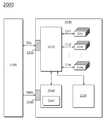
도 2는 도 1의 메모리(230)를 나타낸 도면이다.2 is a diagram illustrating the
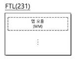
도 2를 참조하면, 본 실시 예에 따른 메모리(230)는 제1 영역(231), 제2 영역(233), 제3 영역(234) 및 제4 영역(235)을 포함할 수 있다. 설명의 편의 및 도면의 간략화를 위하여 도 2에서는 메모리(230)가 4개의 영역을 포함하는 것으로 도시하였으나, 메모리(230)는 다양한 데이터들이 저장되는 다양한 영역들을 더 포함할 수 있다. 예를 들어, 메모리(230)는 호스트 장치로부터 수신된 요청들에 근거하여 생성된 커맨드들이 큐잉되는 커맨드 큐 영역 등을 더 포함할 수 있다.Referring to FIG. 2, the
메모리(230)의 제1 영역(231)에는 플래시 변환 계층(flash translation layer, FTL)이 저장될 수 있다. 플래시 변환 계층(FTL)은 프로세서(220)에 의해 구동되는 소프트웨어로서, 프로세서(220)는 플래시 변환 계층(FTL)을 구동시켜 불휘발성 메모리 장치(100)의 고유 동작을 제어하고, 호스트 장치에 장치 호환성을 제공할 수 있다. 플래시 변환 계층(FTL)의 구동을 통해서, 호스트 장치는 데이터 저장 장치(10)를 하드 디스크와 같은 일반적인 데이터 저장 장치로 인식하고 사용할 수 있다. 플래시 변환 계층(FTL)은 여러 기능을 수행하기 위한 모듈들을 포함할 수 있다. 플래시 변환 계층(FTL)은 불휘발성 메모리 장치(100)의 시스템 영역(도시되지 않음)에 저장될 수 있고, 데이터 저장 장치(10)가 파워-온 되면 불휘발성 메모리 장치(100)의 시스템 영역으로부터 독출되어 메모리(230)의 제1 영역(231)에 로드될 수 있다.A flash translation layer (FTL) may be stored in the
메모리(230)의 제1 영역(231)은 플래시 변환 계층(FTL)에 포함된 다양한 모듈들의 구동에 필요한 메타 데이터가 저장되는 메타 데이터 영역(232)을 포함할 수 있다. 메타 데이터 영역(232)에 저장되는 메타 데이터는 이후 도 3b를 참조하여 설명할 것이다.The
메모리(230)의 제2 영역(233)은 호스트 장치로부터 수신된 라이트할 어드레스 즉, 논리 블록 어드레스(logical block address, LBA)를 불휘발성 메모리 장치(100)의 실제 어드레스 즉, 물리 블록 어드레스(physical block address, PBA)에 매핑시켜 저장하는 어드레스 버퍼(AB)로서 사용될 수 있다. 어드레스 버퍼(AB)에 대해서는 이후 도 4a를 참조하여 설명할 것이다.The
메모리(230)의 제3 영역(234)은 호스트 장치로부터 수신된 시퀀셜 라이트 요청에 대응하는 시퀀셜 맵 엔트리들을 포함하는 시퀀셜 맵 테이블(SMT)이 저장될 수 있다. 시퀀셜 맵 엔트리는 기 설정된 임계 이상의 연속되는 논리 블록 어드레스들(LBAs)의 시작 논리 블록 어드레스, 논리 블록 어드레스의 길이, 및 시작 논리 블록 어드레스에 대응하는 시작 물리 블록 어드레스로 구성될 수 있다.The
메모리(230)의 제4 영역(235)은 어드레스 맵핑 테이블(AMT, 도 5 참조)에 포함된 복수의 맵 세그먼트들(MS0~MS99, 도 5 참조) 중 업데이트할 논리 블록 어드레스들(LBAs)을 포함하는 적어도 하나 이상의 맵 세그먼트들을 저장하는 맵 업데이트 버퍼(MUB)로서 사용될 수 있다.The
도 3a는 플래시 변환 계층(FTL)을 나타낸 도면이다.3A illustrates a flash translation layer (FTL).
도 3a를 참조하면, 플래시 변환 계층(FTL)은 맵 모듈(MM)을 포함할 수 있으나, 특별히 이에 한정되는 것은 아니며 플래시 변환 계층(FTL)은 다양한 모듈들을 포함할 수 있다. 예를 들어, 플래시 변환 계층(FTL)은 리드 모듈, 라이트 모듈, 가비지 컬렉션 모듈, 웨어-레벨링 모듈, 배드 블록 관리 모듈 등을 더 포함할 수 있음은 당업자에게 자명할 것이다.Referring to FIG. 3A, the flash translation layer FTL may include a map module MM, but is not particularly limited thereto, and the flash translation layer FTL may include various modules. For example, it will be apparent to those skilled in the art that the flash translation layer (FTL) may further include a read module, a write module, a garbage collection module, a wear-leveling module, a bad block management module, and the like.
맵 모듈(MM)은 맵 데이터에 관련된 동작들을 수행하도록 불휘발성 메모리 장치(100) 및 메모리(230)를 관리할 수 있다. 맵 데이터에 관련된 동작들은 크게 어드레스 맵핑(변환) 동작, 맵 업데이트 동작, 및 맵 캐싱 동작을 포함할 수 있으나, 특별히 이에 한정되는 것은 아니다.The map module MM may manage the
호스트 장치로부터 라이트 요청, 논리 블록 어드레스 및 라이트 데이터가 제공되면, 프로세서(220)는 맵 모듈(MM)을 구동시켜 어드레스 버퍼(AB)에서 라이트 데이터가 저장될 물리 블록 어드레스에 대응하는 영역에 논리 블록 어드레스를 저장할 수 있다. 이로써, 논리 블록 어드레스와 물리 블록 어드레스가 매핑될 수 있다.When the write request, the logical block address, and the write data are provided from the host device, the
또한, 프로세서(220)는 맵 모듈(MM)을 구동시켜 어드레스 버퍼(AB)에 저장된 논리 블록 어드레스와 물리 블록 어드레스의 매핑 정보에 근거하여 기 설정된 임계 이상의 연속되는 논리 블록 어드레스들(LBAs)에 대한 시퀀셜 맵 엔트리들을 생성하고, 생성된 시퀀셜 맵 엔트리들을 시퀀셜 맵 테이블(SMT)에 저장할 수 있다.In addition, the
도 3b는 메모리(230)의 제1 영역(231)에 포함된 메타 데이터 영역(232)을 나타낸 도면이다.3B is a diagram illustrating the
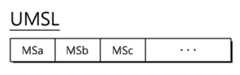
도 3b를 참조하면, 메타 데이터 영역(232)에는 업데이트할 맵 세그먼트 리스트(UMSL), 맵 세그먼트 리스트 포인터(MSLP), 및 시퀀셜 맵 테이블 포인터(SMTP) 등이 저장될 수 있으나, 특별히 이에 한정되는 것은 아니다. 도 3b에 도시하지는 않았으나, 메타 데이터 영역(232)에는 플래시 변환 계층(FTL)에 포함된 각종 모듈들의 구동에 필요한 다양한 메타 데이터들이 저장될 수 있음은 당업자에게 자명할 것이다.Referring to FIG. 3B, a map segment list UMSL, a map segment list pointer MSLP, a sequential map table pointer SMTP, etc. to be updated may be stored in the
도 3c는 업데이트할 맵 세그먼트 리스트(UMSL)를 나타낸 도면이고, 도 3d 및 도 3e는 각각 맵 세그먼트 리스트 포인터(MSLP) 및 시퀀셜 맵 테이블 포인터(SMTP)를 나타낸 도면이다.3C is a diagram illustrating a map segment list UMSL to be updated, and FIGS. 3D and 3E are views of a map segment list pointer MSLP and a sequential map table pointer SMTP, respectively.
도 3c를 참조하면, 업데이트할 맵 세그먼트 리스트(UMSL)는 업데이트할 맵 세그먼트의 인덱스(또는 번호)를 저장하도록 구성될 수 있다. 여기에서, 업데이트할 맵 세그먼트는 매핑 정보를 업데이트할 적어도 하나 이상의 논리 블록 어드레스를 포함하는 맵 세그먼트를 의미할 수 있다.Referring to FIG. 3C, the map segment list UMSL to be updated may be configured to store an index (or number) of the map segment to be updated. Here, the map segment to be updated may mean a map segment including at least one logical block address to update mapping information.
호스트 장치로부터 라이트 요청 및 논리 블록 어드레스가 수신되면 프로세서(220)는 맵 모듈(MM)을 구동시켜 호스트 장치로부터 수신된 논리 블록 어드레스를 포함하는 맵 세그먼트의 인덱스(또는 번호)를 업데이트할 맵 세그먼트 리스트(UMSL)에 저장할 수 있다.When the write request and the logical block address are received from the host device, the
도 3d를 참조하면, 맵 세그먼트 리스트 포인터(MSLP)는 x 개의 비트들(B0 ~ Bx-1)을 포함하는 비트맵일 수 있다. 여기에서, x는 0 이상의 자연수일 수 있다. 맵 세그먼트 리스트 포인터(MSLP)는 업데이트할 맵 세그먼트 리스트(UMSL)에 저장된 맵 세그먼트들 중 맵 업데이트 동작을 수행해야 할 맵 세그먼트가 저장된 위치를 가리키도록 구성될 수 있다.Referring to FIG. 3D, the map segment list pointer MSLP may be a bitmap including x bits B0 to Bx-1. Here, x may be a natural number of zero or more. The map segment list pointer MSLP may be configured to indicate a location where the map segment to perform a map update operation is stored among the map segments stored in the map segment list UMSL to be updated.
도 3e를 참조하면, 시퀀셜 맵 테이블 포인터(SMTP)는 x 개의 비트들(B0 ~ Bx-1)을 포함하는 비트맵일 수 있다. 여기에서, x는 0 이상의 자연수일 수 있다. 시퀀셜 맵 테이블 포인터(SMTP)는 맵 업데이트 동작 시 시퀀셜 맵 테이블(SMT)에 저장된 시퀀셜 맵 엔트리들 중 검색을 시작할 시퀀셜 맵 엔트리가 저장된 위치를 가리키도록 구성될 수 있다.Referring to FIG. 3E, the sequential map table pointer SMTP may be a bitmap including x bits B0 to Bx-1. Here, x may be a natural number of zero or more. The sequential map table pointer SMTP may be configured to indicate a position where a sequential map entry to start searching is stored among sequential map entries stored in the sequential map table SMT during a map update operation.
도 4a는 어드레스 버퍼(AB)를 나타낸 도면이고, 도 4b는 오픈 메모리 블록(OBLK)을 나타낸 도면이고, 도 4c는 시퀀셜 맵 테이블(SMT)을 나타낸 도면이다.FIG. 4A illustrates an address buffer AB, FIG. 4B illustrates an open memory block OBLK, and FIG. 4C illustrates a sequential map table SMT.
도 4a를 참조하면, 어드레스 버퍼(AB)는 복수의 영역들(1~ij)을 포함할 수 있다. 각 영역(1~ij)에는 호스트 장치로부터 라이트 요청과 함께 수신된 논리 블록 어드레스들이 각각 저장될 수 있다.Referring to FIG. 4A, the address buffer AB may include a plurality of
도 4b를 참조하면, 오픈 메모리 블록(OBLK)은 복수의 섹터(sector)들을 포함할 수 있다. 오픈 메모리 블록(OBLK)은 호스트 장치로부터 수신된 라이트 데이터를 저장하기 위해 할당된 메모리 블록을 의미할 수 있다. 오픈 메모리 블록(OBLK)은 단일 메모리 블록의 전체 또는 일부일 수도 있고, 복수의 메모리 블록들의 일부들 또는 전체들을 그룹화한 메모리 영역일 수도 있다. 설명의 편의를 위해 본 실시 예에서는 오픈 메모리 블록(OBLK)이 단일 메모리 블록의 전체인 것으로 가정한다.Referring to FIG. 4B, the open memory block OBLK may include a plurality of sectors. The open memory block OBLK may mean a memory block allocated to store write data received from a host device. The open memory block OBLK may be all or part of a single memory block, or may be a memory area grouping some or all of a plurality of memory blocks. For convenience of description, it is assumed in the present embodiment that the open memory block OBLK is the entirety of a single memory block.
도 4b에 도시한 바와 같이, 오픈 메모리 블록(OBLK)의 각 섹터(sector)는 대응하는 물리 블록 어드레스를 가질 수 있다. 예를 들어, 각 섹터(sector)의 물리 블록 어드레스는 베이스 어드레스(base address)와 오프셋(offset)의 합으로 표현될 수 있다. 도 4b에 도시한 것처럼 오픈 메모리 블록(OBLK)이 z 개의 섹터(sector)들을 포함하는 경우, 첫 번째 섹터의 물리 블록 어드레스는 ‘base address + offset 0’으로 표현되고, 두 번째 내지 z 번째 섹터들의 물리 블록 어드레스들은 ‘base address + offset 1’ 내지 ‘base address + offset z-1’로 표현될 수 있다.As shown in FIG. 4B, each sector of the open memory block OBLK may have a corresponding physical block address. For example, the physical block address of each sector may be expressed as a sum of a base address and an offset. As shown in FIG. 4B, when the open memory block OBLK includes z sectors, the physical block address of the first sector is expressed as 'base address + offset 0', and the second to z th sectors are represented. The physical block addresses may be expressed as 'base address + offset 1' to 'base address + offset z-1'.
또한, 도면에 도시하지는 않았으나, 오픈 메모리 블록(OBLK)은 고유의 블록 번호를 가질 수 있으며, 프로세서(220)는 오픈 메모리 블록(OBLK)을 할당할 때 블록 번호를 획득할 수 있다.In addition, although not shown, the open memory block OBLK may have a unique block number, and the
도 4a 및 도 4b를 참조하면, 어드레스 버퍼(AB)의 각 영역(1~ij)은 오픈 메모리 블록(OBLK)의 각 섹터(sector)의 물리 블록 어드레스와 대응될 수 있다. 예를 들어, 어드레스 버퍼(AB)의 영역 ‘1’은 오픈 메모리 블록(OBLK)의 첫 번째 섹터의 물리 블록 어드레스(base address + offset 0)와 대응되고, 어드레스 버퍼(AB)의 영역 ‘ij’는 오픈 메모리 블록(OBLK)의 z 번째 섹터의 물리 블록 어드레스(base address + offset z-1)와 대응될 수 있다. 즉, 어드레스 버퍼(AB)에 포함된 영역들의 수와 오픈 메모리 블록(OBLK)에 포함된 섹터들의 수는 동일할 수 있다. 또한, 어드레스 버퍼(AB)에 포함된 영역들의 순서와 오픈 메모리 블록(OBLK)에 포함된 섹터들의 순서는 동일할 수 있다. 이에 근거하여, 어드레스 버퍼(AB)의 각 영역(1~ij)에 저장된 논리 블록 어드레스에 매핑된 물리 블록 어드레스를 알 수 있다.4A and 4B, each
도 4c를 참조하면, 시퀀셜 맵 테이블(SMT)은 복수의 시퀀셜 맵 엔트리(sequential map entry)들 및 각 시퀀셜 맵 엔트리의 유효 여부를 나타내는 정보(예컨대, 유효 정보)를 포함할 수 있다.Referring to FIG. 4C, the sequential map table SMT may include a plurality of sequential map entries and information (eg, valid information) indicating whether each sequential map entry is valid.
호스트 장치로부터 시퀀셜 라이트 요청 및 연속적인 복수의 논리 블록 어드레스들이 수신되면, 라이트 데이터들은 오픈 메모리 블록(OBLK) 내의 연속되는 섹터들에 순차적으로 저장될 수 있다. 이에 따라, 연속적인 논리 블록 어드레스들 각각에 매핑되는 물리 블록 어드레스들도 연속적일 수 있다.When a sequential write request and a plurality of consecutive logical block addresses are received from the host device, the write data may be sequentially stored in consecutive sectors in the open memory block OBLK. Accordingly, physical block addresses mapped to each of the consecutive logical block addresses may also be consecutive.
프로세서(220)는 맵 모듈(MM)을 구동시켜 연속적인 논리 블록 어드레스들의 시작 논리 블록 어드레스(Start LBA), 길이(Length), 및 연속적인 물리 블록 어드레스들의 시작 물리 블록 어드레스(Start PBA)를 포함하는 시퀀셜 맵 엔트리를 생성하고, 생성된 시퀀셜 맵 엔트리를 시퀀셜 맵 테이블(SMT)에 저장할 수 있다. 즉, 시퀀셜 맵 테이블(SMT)은 연속적인 논리 블록 어드레스들과 연속적인 물리 블록 어드레스들의 매핑 정보만을 저장하는 별도의 테이블이다. 시퀀셜 맵 엔트리에서 길이(Length)는 연속적인 논리 블록 어드레스들의 개수와 대응할 수 있다.The
시퀀셜 맵 테이블(SMT)의 유효 정보는 대응하는 시퀀셜 맵 엔트리가 유효한지 여부를 나타내는 정보이다. 예를 들어, 제1 시점에서 호스트 장치로부터 시퀀셜 라이트 요청과 함께 제1 논리 블록 어드레스들이 수신되고, 제1 시점으로부터 일정 시간 경과한 제2 시점에서 호스트 장치로부터 시퀀셜 라이트 요청과 함께 제1 논리 블록 어드레스들이 다시 수신되면, 제1 시점에 수신된 제1 논리 블록 어드레스들에 대응하는 시퀀셜 맵 엔트리는 무효 엔트리가 되고 제2 시점에 수신된 제1 논리 블록 어드레스들에 대응하는 시퀀셜 맵 엔트리는 유효 엔트리가 된다. 즉, 동일한 논리 블록 어드레스에 대한 라이트 동작이 복수 회 수행되는 경우, 최근의 논리 블록 어드레스의 매핑 정보만 유효하다.Valid information of the sequential map table SMT is information indicating whether a corresponding sequential map entry is valid. For example, first logical block addresses are received with a sequential write request from a host device at a first point in time, and a first logical block address is received with a sequential write request from a host device at a second point in time after the first point in time. Are received again, the sequential map entry corresponding to the first logical block addresses received at the first time point becomes an invalid entry and the sequential map entry corresponding to the first logical block addresses received at the second time point is determined to be a valid entry. do. That is, when the write operation for the same logical block address is performed multiple times, only the mapping information of the latest logical block address is valid.
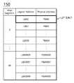
도 5는 도 1의 어드레스 맵핑 테이블(address mapping table, AMT)(150)을 나타낸 도면이다.FIG. 5 is a diagram illustrating an address mapping table (AMT) 150 of FIG. 1.
도 5를 참조하면, 어드레스 맵핑 테이블(150)은 복수의 맵 세그먼트들을 포함할 수 있다. 각 맵 세그먼트는 복수의 L2P(logical to physical) 엔트리들을 포함할 수 있다. 각 L2P 엔트리는 하나의 논리 블록 어드레스에 매핑된 하나의 물리 블록 어드레스를 포함할 수 있다. 각 맵 세그먼트에 포함된 논리 블록 어드레스들은 오름차순으로 정렬 및 고정되고, 각 논리 블록 어드레스에 매핑되는 물리 블록 어드레스만이 갱신될 수 있다.Referring to FIG. 5, the address mapping table 150 may include a plurality of map segments. Each map segment may include a plurality of L2P (logical to physical) entries. Each L2P entry may include one physical block address mapped to one logical block address. The logical block addresses included in each map segment are sorted and fixed in ascending order, and only the physical block addresses mapped to each logical block address can be updated.
설명의 편의를 위하여 도 5에서는 어드레스 맵핑 테이블(150)이 100개의 맵 세그먼트들(0~99)을 포함하고, 각 맵 세그먼트(0~99)가 100개의 L2P 엔트리들을 포함하는 것을 예를 들어 도시하였으나, 맵 세그먼트들의 개수 및 L2P 엔트리들의 개수가 특별히 이에 한정되는 것은 아니다.For convenience of description, in FIG. 5, the address mapping table 150 includes 100
도 6a는 라이트 동작 시 어드레스 버퍼에 논리 블록 어드레스들이 저장되고, 맵 세그먼트 리스트에 업데이트할 맵 세그먼트가 저장되고, 시퀀셜 맵 테이블에 시퀀셜 맵 엔트리들이 저장되는 것을 나타낸 도면이다. 도 6a에서 ‘write workload’는 호스트 장치로부터 수신되고 처리된 라이트 요청들을 의미할 수 있다. 도 6a에서는 설명의 편의를 위하여 ‘write workload’를 커맨드 번호, 시작 논리 블록 어드레스 및 길이를 포함하는 것으로 도시하였다. 또한, 호스트 장치로부터 커맨드 1부터 커맨드 9의 순서로 수신된 것으로 가정한다.FIG. 6A illustrates that logical block addresses are stored in an address buffer, a map segment to be updated in a map segment list, and sequential map entries are stored in a sequential map table during a write operation. In FIG. 6A, "write workload" may refer to write requests received and processed from the host device. In FIG. 6A, 'write workload' is illustrated as including a command number, a starting logical block address, and a length for convenience of description. It is also assumed that the command is received from the host device in the order of
도 6a를 참조하면, 커맨드 1, 커맨드 4, 커맨드 6 내지 9에 해당하는 라이트 요청들은 시퀀셜 라이트 요청이고, 커맨드 2, 커맨드 3 및 커맨드 5에 해당하는 라이트 요청들은 랜덤 라이트 요청일 수 있다.Referring to FIG. 6A, write requests corresponding to
호스트 장치로부터 라이트 요청 및 논리 블록 어드레스가 수신되면, 프로세서(220)는 맵 블록(MM)을 구동시켜 논리 블록 어드레스를 어드레스 버퍼(AB)의 임의의 영역에 저장한다. 이때, 어드레스 버퍼(AB)에서 논리 블록 어드레스가 저장될 영역은 어드레스 버퍼 포인터(도시하지 않음)가 가리키는 영역일 수 있다. 어드레스 버퍼 포인터가 가리키는 영역에 논리 블록 어드레스가 저장되면, 어드레스 버퍼 포인터는 다음 순서로 논리 블록 어드레스가 저장될 영역을 가리키는 값으로 변경될 수 있다. 본 실시 예에서는 설명의 편의를 위해 어드레스 버퍼(AB)가 빈 상태인 것으로 가정한다.When the write request and the logical block address are received from the host device, the
프로세서(220)는 커맨드 1에 해당하는 시작 논리 블록 어드레스부터 30개의 논리 블록 어드레스들 즉, LBA100 내지 LBA129를 어드레스 버퍼(AB)의 첫 번째 영역부터 순차적으로 저장할 수 있다. 전술한 바와 같이, 어드레스 버퍼(AB)의 각 영역은 오픈 메모리 블록(OBLK, 도 4b 참조)의 각 섹터(sector)에 대응하므로, 어드레스 버퍼(AB)에 저장된 LBA100 내지 LBA129 각각에 대응하는 물리 블록 어드레스들이 결정될 수 있다.The
같은 방식으로 커맨드 2 내지 커맨드 9에 해당하는 논리 블록 어드레스들이 어드레스 버퍼(AB)의 영역들에 순차적으로 저장될 수 있다. 이때, 커맨드 7에 해당하는 시작 논리 블록 어드레스(LBA 250)가 커맨드 4에 해당하는 시작 논리 블록 어드레스(LBA 250)와 동일하므로, 먼저 수신된 커맨드 4에 해당하는 논리 블록 어드레스들에 매핑된 물리 블록 어드레스들은 무효 매핑 정보가 되고, 나중에 수신된 커맨드 7에 해당하는 논리 블록 어드레스에 매핑된 물리 블록 어드레스들이 유효 매핑 정보가 된다.In the same manner, logical block addresses corresponding to
프로세서(220)는 호스트 장치로부터 라이트 요청들과 함께 수신된 논리 블록 어드레스들을 포함하는 맵 세그먼트들의 번호를 업데이트할 맵 세그먼트 리스트(UMSL)에 순차적으로 저장할 수 있다.The
예를 들어, 도 5를 참조하면, 커맨드 1에 해당하는 논리 블록 어드레스들 LBA100 내지 LBA129는 맵 세그먼트 1에 포함되므로, 프로세서(200)는 맵 세그먼트 1을 업데이트할 맵 세그먼트 리스트(UMSL)에 저장할 수 있다. 마찬가지로, 커맨드 2 내지 커맨드 9 각각에 해당하는 논리 블록 어드레스들을 포함하는 맵 세그먼트들 즉, 맵 세그먼트 20, 맵 세그먼트 30, 맵 세그먼트 2, 맵 세그먼트 40, 맵 세그먼트 3, 맵 세그먼트 5, 맵 세그먼트 10을 순차적으로 맵 세그먼트 리스트(UMSL)에 저장할 수 있다. 이후, 맵 업데이트 동작 수행 시 업데이트할 맵 세그먼트 리스트(UMSL)를 참조하여 업데이트할 맵 세그먼트들을 어드레스 맵핑 테이블(150)로부터 독출하여 메모리(230)의 맵 업데이트 버퍼(MUB)에 저장할 수 있다.For example, referring to FIG. 5, since the logical block addresses LBA100 to LBA129 corresponding to the
프로세서(220)는 어드레스 버퍼(AB)에 저장된 논리 블록 어드레스들 중 연속적인 논리 블록 어드레스들에 대한 시퀀셜 맵 엔트리를 생성하여 시퀀셜 맵 테이블(SMT)에 저장할 수 있다. 도 6a를 참조하면, 시퀀셜 맵 테이블(SMT)은 커맨드 1, 커맨드 4, 커맨드 6 내지 9 각각에 해당하는 시퀀셜 맵 엔트리들을 포함할 수 있다. 이때, 커맨드 4에 대한 시퀀셜 맵 엔트리의 유효 정보는 ‘X’로 표시되고, 커맨드 7에 대한 시퀀셜 맵 엔트리의 유효 정보는 ‘O’으로 표시되었다.The
설명의 편의를 위해, 오픈 메모리 블록(OBLK)의 블록 번호는 ‘A’로 가정하고, 첫 번째 섹터(sector)부터 라이트 데이터가 저장되는 것으로 가정한다.For convenience of description, it is assumed that the block number of the open memory block OBLK is 'A', and that write data is stored from the first sector.
도 6b는 연속적인 논리 블록 어드레스들의 매핑 정보를 변경하는 예를 나타낸 도면이다.6B is a diagram illustrating an example of changing mapping information of consecutive logical block addresses.
맵 업데이트 동작이 트리거(trigger)되면, 프로세서(220)는 맵 모듈(MM)을 구동시켜 업데이트할 맵 세그먼트 리스트(UMSL)를 참조하여 업데이트할 맵 세그먼트 번호(또는 인덱스)를 확인한다. 업데이트할 맵 세그먼트 번호(또는 인덱스)가 확인되면, 맵 모듈(MM)은 불휘발성 메모리 장치(100)의 어드레스 맵핑 테이블(150)에 저장된 맵 세그먼트(즉, 맵 세그먼트 1)를 독출하여 메모리(230)의 맵 업데이트 버퍼(MUB)에 저장할 수 있다. 맵 업데이트 버퍼(MUB)에 저장된 맵 세그먼트 1의 각 영역은 하나의 논리 블록 어드레스를 나타내고, 저장된 값 즉, ‘XXX’는 이전에 매핑된 물리 블록 어드레스 또는 매핑된 정보가 없음을 나타낸다.When the map update operation is triggered, the
도 6a를 참조하면, 라이트 동작이 수행된 논리 블록 어드레스들은 LBA100부터 LBA129이므로, 도 6b에 도시한 것처럼 점선 박스로 표시된 논리 블록 어드레스들만이 업데이트 대상이며, 나머지 논리 블록 어드레스들은 업데이트 대상이 아니다.Referring to FIG. 6A, since the logical block addresses to which the write operation is performed are LBA100 to LBA129, only logical block addresses indicated by dotted lines as shown in FIG. 6B are to be updated, and the remaining logical block addresses are not to be updated.
맵 모듈(MM)은 우선 시퀀셜 맵 테이블(SMT)에 논리 블록 어드레스들 ‘LBA100 내지 LBA129’를 포함하는 시퀀셜 맵 엔트리가 존재하는지 여부를 확인한다. 도 6a에 도시한 바와 같이, 시퀀셜 맵 테이블(SMT)에 논리 블록 어드레스들 ‘LBA100 내지 LBA129’를 포함하는 시퀀셜 맵 엔트리가 존재하므로, 맵 모듈(MM)은 논리 블록 어드레스들 ‘LBA100 내지 LBA129’중 시작 논리 블록 어드레스인 LBA100에 대응하는 영역에는 시작 물리 블록 어드레스인 ‘A, 0’을 저장하고, 나머지 논리 블록 어드레스들 즉, ‘LBA100 내지 LBA129’에 대응하는 영역들에는 시작 물리 블록 어드레스 ‘A, 0’에서 오프셋만 1씩 증가된 물리 블록 어드레스들을 저장한다. 이에 따라, 논리 블록 어드레스들 ‘LBA100 내지 LBA129’에 대한 매핑 정보 변경이 완료될 수 있다. 매핑 정보 변경이 완료된 맵 세그먼트 1은 불휘발성 메모리 장치(100)의 어드레스 맵핑 테이블(150)에 다시 저장된다.The map module MM first checks whether there is a sequential map entry including logical block addresses 'LBA100 to LBA129' in the sequential map table SMT. As shown in FIG. 6A, since the sequential map entry including the logical block addresses 'LBA100 to LBA129' exists in the sequential map table SMT, the map module MM may select one of the logical block addresses 'LBA100 to LBA129'. The first physical block address 'A, 0' is stored in the area corresponding to the starting logical block address LBA100, and the starting physical block address 'A,' is stored in the areas corresponding to the remaining logical block addresses, that is, the 'LBA100 to LBA129'. Only offsets from 0 'store physical block addresses incremented by one. Accordingly, the mapping information change for the logical block addresses 'LBA100 to LBA129' may be completed. The
도 6c는 랜덤한 논리 블록 어드레스의 매핑 정보를 변경하는 예를 나타낸 도면이다.6C is a diagram illustrating an example of changing mapping information of a random logical block address.
맵 모듈(MM)은 다음 순서로 맵 업데이트 동작을 수행할 맵 세그먼트 즉, 맵 세그먼트 20을 불휘발성 메모리 장치(100)의 어드레스 맵핑 테이블(150)로부터 독출하여 메모리(230)의 맵 업데이트 버퍼(MUB)에 저장할 수 있다.The map module MM reads a map segment, that is, a
맵 모듈(MM)은 우선 시퀀셜 맵 테이블(SMT)에 논리 블록 어드레스 ‘LBA2000’을 포함하는 시퀀셜 맵 엔트리가 존재하는지 여부를 확인한다. 도 6a에 도시한 바와 같이, 시퀀셜 맵 테이블(SMT)에는 논리 블록 어드레스 ‘LBA2000’을 포함하는 시퀀셜 맵 엔트리가 존재하지 않으므로, 맵 모듈(MM)은 어드레스 버퍼(AB)에서 ‘LBA2000’이 저장된 영역을 검색한다.The map module MM first checks whether there is a sequential map entry including the logical block address 'LBA2000' in the sequential map table SMT. As shown in FIG. 6A, since there is no sequential map entry including the logical block address 'LBA2000' in the sequential map table SMT, the map module MM stores an area where 'LBA2000' is stored in the address buffer AB. Search for.
어드레스 버퍼(AB)에서 ‘LBA2000’이 저장된 영역이 검색되면, 맵 모듈(MM)은 해당 영역에 대응하는 물리 블록 어드레스 즉, ‘A, 30’을 LBA2000에 대응하는 영역에 저장한다. 이에 따라, 논리 블록 어드레스 ‘LBA2000’에 대한 매핑 정보 변경이 완료될 수 있다. 매핑 정보 변경이 완료된 맵 세그먼트 20은 불휘발성 메모리 장치(100)의 어드레스 맵핑 테이블(150)에 다시 저장된다.When an area where 'LBA2000' is stored in the address buffer AB is found, the map module MM stores the physical block address corresponding to the corresponding area, that is, 'A, 30' in the area corresponding to the LBA2000. Accordingly, the mapping information change for the logical block address 'LBA2000' may be completed. The
이와 같이, 시퀀셜 라이트 요청에 대응하는 연속적인 논리 블록 어드레스들에 대한 시퀀셜 맵 엔트리를 별도로 생성 및 관리하고, 맵 업데이트 동작을 수행할 때 연속적인 논리 블록 어드레스들의 매핑 정보는 시퀀셜 맵 엔트리를 이용하여 순차적으로 증가시키는 방식으로 변경함으로써 맵 업데이트 동작에 소요되는 시간을 단축시킬 수 있다.As such, when generating and managing sequential map entries for successive logical block addresses corresponding to the sequential write request separately, and performing a map update operation, the mapping information of successive logical block addresses is sequentially generated using the sequential map entry. The time required for the map update operation can be shortened by changing the method in increments.
도 7은 본 실시 예에 따른 데이터 저장 장치의 동작 방법을 나타낸 순서도이다. 도 7을 참조하여 본 실시 예에 따른 데이터 저장 장치의 동작 방법을 설명함에 있어서, 도 1 내지 도 6c 중 적어도 하나의 도면이 참조될 수 있다.7 is a flowchart illustrating a method of operating a data storage device according to an exemplary embodiment. Referring to FIG. 7, a method of operating a data storage device according to an exemplary embodiment may be referred to at least one of FIGS. 1 to 6C.
S710 단계에서, 컨트롤러(200)의 프로세서(220)는 맵 업데이트 동작을 수행할 지 여부를 판단할 수 있다. 맵 업데이트 동작은 어드레스 버퍼(AB)의 모든 영역들에 논리 블록 어드레스들이 저장되면 수행될 수 있으나, 특별히 이에 한정되는 것은 아니다. 맵 업데이트 동작을 수행해야 하는 것으로 판단되면, S720 단계로 진행될 수 있다.In operation S710, the
S720 단계에서, 프로세서(220)는 맵 모듈(MM)을 구동시켜 매핑 정보를 업데이트할 논리 블록 어드레스들을 포함하는 맵 세그먼트를 불휘발성 메모리 장치(100)의 어드레스 맵핑 테이블(150)로부터 독출하여 메모리(230)의 맵 업데이트 버퍼(MUB)에 저장할 수 있다. 이때, 업데이트할 맵 세그먼트는 메모리(230)의 메타 데이터 영역(232)에 저장된 업데이트할 맵 세그먼트 리스트(UMSL)를 참조하여 확인할 수 있다.In operation S720, the
S730 단계에서, 프로세서(220)는 메모리(230)에 저장된 시퀀셜 맵 테이블(SMT)을 확인하여 업데이트할 논리 블록 어드레스들을 포함하는 시퀀셜 맵 엔트리가 존재하는지 여부를 판단할 수 있다. 시퀀셜 맵 엔트리가 존재하면, S740 단계로 진행될 수 있다. 한편, 시퀀셜 맵 엔트리가 존재하지 않으면, S750 단계로 진행될 수 있다.In operation S730, the
S740 단계에서, 프로세서(220)는 업데이트할 논리 블록 어드레스들 중 시작 논리 블록 어드레스에 매핑된 물리 블록 어드레스는 시퀀셜 맵 엔트리의 시작 물리 블록 어드레스로 변경하고, 나머지 논리 블록 어드레스들 각각의 물리 블록 어드레스는 시작 물리 블록 어드레스에서 1씩 증가시킨 물리 블록 어드레스로 변경하여 저장할 수 있다. 이때, 시작 물리 블록 어드레스는 블록 번호 및 오프셋을 포함할 수 있고, 나머지 논리 블록 어드레스들 각각에 매핑되는 변경된 물리 블록 어드레스는 오프셋이 1씩 증가된 값일 수 있다.In operation S740, the
S750 단계에서, 프로세서(220)는 메모리(230)의 어드레스 버퍼(AB)에서 업데이트할 논리 블록 어드레스들이 저장된 영역들을 각각 검색하고, 검색된 영역들에 대응하는 물리 블록 어드레스들을 획득할 수 있다.In operation S750, the
S760 단계에서, 프로세서(220)는 업데이트할 논리 블록 어드레스들 각각에 매핑된 물리 블록 어드레스를 S750 단계에서 획득한 물리 블록 어드레스로 변경하여 저장할 수 있다.In operation S760, the
S750 단계 및 S760 단계는 하나의 논리 블록 어드레스에 대하여 반복적으로 수행될 수 있다.Steps S750 and S760 may be repeatedly performed on one logical block address.
S770 단계에서, 프로세서(220)는 업데이트할 논리 블록 어드레스들 각각의 매핑 정보 변경이 완료되었는지 여부를 판단할 수 있다. 매핑 정보 변경이 완료되지 않았으면, S750 단계로 진행될 수 있다. 매핑 정보 변경이 완료되었으면 S780 단계로 진행될 수 있다.In operation S770, the
S780 단계에서, 프로세서(220)는 맵 업데이트 동작이 완료되었는지 여부를 판단할 수 있다. 맵 업데이트 동작이 완료되었는지 여부를 판단하는 것은 업데이트할 논리 블록 어드레스들을 포함하는 복수의 맵 세그먼트들 각각에 대한 매핑 정보 변경이 완료되었는지 여부를 판단하는 것일 수 있다. 맵 업데이트 동작이 완료되었으면, 단계를 종료할 수 있다. 맵 업데이트 동작이 완료되지 않았으면, S790 단계로 진행될 수 있다.In operation S780, the
S790 단계에서, 프로세서(220)는 업데이트할 맵 세그먼트 리스트(UMSL)를 참조하여 다음 순서로 매핑 정보를 업데이트할 논리 블록 어드레스들을 포함하는 맵 세그먼트를 불휘발성 메모리 장치(100)의 어드레스 맵핑 테이블(150)로부터 독출하여 메모리(230)의 맵 업데이트 버퍼(MUB)에 저장할 수 있다. 이후, S730 단계로 진행될 수 있다.In operation S790, the
도 8은 본 발명의 실시 예에 따른 솔리드 스테이트 드라이브(SSD)를 포함하는 데이터 처리 시스템을 예시적으로 나타낸 도면이다. 도 8을 참조하면, 데이터 처리 시스템(2000)은 호스트 장치(2100)와 솔리드 스테이트 드라이브(solid state drive)(2200)(이하, SSD라 칭함)를 포함할 수 있다.8 is a diagram illustrating a data processing system including a solid state drive (SSD) according to an embodiment of the present invention. Referring to FIG. 8, the
SSD(2200)는 컨트롤러(2210), 버퍼 메모리 장치(2220), 불휘발성 메모리 장치들(2231~223n), 전원 공급기(2240), 신호 커넥터(2250) 및 전원 커넥터(2260)를 포함할 수 있다.The
컨트롤러(2210)는 SSD(2200)의 제반 동작을 제어할 수 있다.The
버퍼 메모리 장치(2220)는 불휘발성 메모리 장치들(2231~223n)에 저장될 데이터를 임시 저장할 수 있다. 또한, 버퍼 메모리 장치(2220)는 불휘발성 메모리 장치들(2231~223n)로부터 읽혀진 데이터를 임시 저장할 수 있다. 버퍼 메모리 장치(2220)에 임시 저장된 데이터는 컨트롤러(2210)의 제어에 따라 호스트 장치(2100) 또는 불휘발성 메모리 장치들(2231~223n)로 전송될 수 있다.The
불휘발성 메모리 장치들(2231~223n)은 SSD(2200)의 저장 매체로 사용될 수 있다. 불휘발성 메모리 장치들(2231~223n) 각각은 복수의 채널들(CH1~CHn)을 통해 컨트롤러(2210)와 연결될 수 있다. 하나의 채널에는 하나 또는 그 이상의 불휘발성 메모리 장치가 연결될 수 있다. 하나의 채널에 연결되는 불휘발성 메모리 장치들은 동일한 신호 버스 및 데이터 버스에 연결될 수 있다.The
전원 공급기(2240)는 전원 커넥터(2260)를 통해 입력된 전원(PWR)을 SSD(2200) 내부에 제공할 수 있다. 전원 공급기(2240)는 보조 전원 공급기(2241)를 포함할 수 있다. 보조 전원 공급기(2241)는 서든 파워 오프(sudden power off)가 발생되는 경우, SSD(2200)가 정상적으로 종료될 수 있도록 전원을 공급할 수 있다. 보조 전원 공급기(2241)는 전원(PWR)을 충전할 수 있는 대용량 캐패시터들(capacitors)을 포함할 수 있다.The
컨트롤러(2210)는 신호 커넥터(2250)를 통해서 호스트 장치(2100)와 신호(SGL)를 주고 받을 수 있다. 여기에서, 신호(SGL)는 커맨드, 어드레스, 데이터 등을 포함할 수 있다. 신호 커넥터(2250)는 호스트 장치(2100)와 SSD(2200)의 인터페이스 방식에 따라 다양한 형태의 커넥터로 구성될 수 있다.The
도 9는 도 8의 컨트롤러의 구성을 예시적으로 나타낸 도면이다. 도 9를 참조하면, 컨트롤러(2210)는 호스트 인터페이스 유닛(2211), 컨트롤 유닛(2212), 랜덤 액세스 메모리(2213), 에러 정정 코드(ECC) 유닛(2214) 및 메모리 인터페이스 유닛(2215)을 포함할 수 있다.9 is a diagram illustrating a configuration of the controller of FIG. 8. Referring to FIG. 9, the
호스트 인터페이스 유닛(2211)은, 호스트 장치(2100)의 프로토콜에 따라서, 호스트 장치(2100)와 SSD(2200)를 인터페이싱할 수 있다. 예를 들면, 호스트 인터페이스 유닛(2211)은, 시큐어 디지털(secure digital), USB(universal serial bus), MMC(multi-media card), eMMC(embedded MMC), PCMCIA(personal computer memory card international association), PATA(parallel advanced technology attachment), SATA(serial advanced technology attachment), SCSI(small computer system interface), SAS(serial attached SCSI), PCI(peripheral component interconnection), PCI-E(PCI Expresss), UFS(universal flash storage) 프로토콜들 중 어느 하나를 통해서 호스트 장치(2100)와 통신할 수 있다. 또한, 호스트 인터페이스 유닛(2211)은 호스트 장치(2100)가 SSD(2200)를 범용 데이터 저장 장치, 예를 들면, 하드 디스크 드라이브(HDD)로 인식하도록 지원하는 디스크 에뮬레이션(disk emulation) 기능을 수행할 수 있다.The
컨트롤 유닛(2212)은 호스트 장치(2100)로부터 입력된 신호(SGL)를 분석하고 처리할 수 있다. 컨트롤 유닛(2212)은 SSD(2200)를 구동하기 위한 펌웨어 또는 소프트웨어에 따라서 내부 기능 블럭들의 동작을 제어할 수 있다. 랜덤 액세스 메모리(2213)는 이러한 펌웨어 또는 소프트웨어를 구동하기 위한 동작 메모리로서 사용될 수 있다.The
에러 정정 코드(ECC) 유닛(2214)은 불휘발성 메모리 장치들(2231~223n)로 전송될 데이터의 패리티 데이터를 생성할 수 있다. 생성된 패리티 데이터는 데이터와 함께 불휘발성 메모리 장치들(2231~223n)에 저장될 수 있다. 에러 정정 코드(ECC) 유닛(2214)은 패리티 데이터에 근거하여 불휘발성 메모리 장치들(2231~223n)로부터 독출된 데이터의 에러를 검출할 수 있다. 만약, 검출된 에러가 정정 범위 내이면, 에러 정정 코드(ECC) 유닛(2214)은 검출된 에러를 정정할 수 있다.The error correction code (ECC)
메모리 인터페이스 유닛(2215)은, 컨트롤 유닛(2212)의 제어에 따라서, 불휘발성 메모리 장치들(2231~223n)에 커맨드 및 어드레스와 같은 제어 신호를 제공할 수 있다. 그리고 메모리 인터페이스 유닛(2215)은, 컨트롤 유닛(2212)의 제어에 따라서, 불휘발성 메모리 장치들(2231~223n)과 데이터를 주고받을 수 있다. 예를 들면, 메모리 인터페이스 유닛(2215)은 버퍼 메모리 장치(2220)에 저장된 데이터를 불휘발성 메모리 장치들(2231~223n)로 제공하거나, 불휘발성 메모리 장치들(2231~223n)로부터 읽혀진 데이터를 버퍼 메모리 장치(2220)로 제공할 수 있다.The
도 10은 본 발명의 실시 예에 따른 데이터 저장 장치를 포함하는 데이터 처리 시스템을 예시적으로 나타낸 도면이다. 도 10을 참조하면, 데이터 처리 시스템(3000)은 호스트 장치(3100)와 데이터 저장 장치(3200)를 포함할 수 있다.10 is a diagram illustrating a data processing system including a data storage device according to an embodiment of the present disclosure. Referring to FIG. 10, the
호스트 장치(3100)는 인쇄 회로 기판(printed circuit board)과 같은 기판(board) 형태로 구성될 수 있다. 비록 도시되지 않았지만, 호스트 장치(3100)는 호스트 장치의 기능을 수행하기 위한 내부 기능 블럭들을 포함할 수 있다.The
호스트 장치(3100)는 소켓(socket), 슬롯(slot) 또는 커넥터(connector)와 같은 접속 터미널(3110)을 포함할 수 있다. 데이터 저장 장치(3200)는 접속 터미널(3110)에 마운트(mount)될 수 있다.The
데이터 저장 장치(3200)는 인쇄 회로 기판과 같은 기판 형태로 구성될 수 있다. 데이터 저장 장치(3200)는 메모리 모듈 또는 메모리 카드로 불릴 수 있다. 데이터 저장 장치(3200)는 컨트롤러(3210), 버퍼 메모리 장치(3220), 불휘발성 메모리 장치(3231~3232), PMIC(power management integrated circuit)(3240) 및 접속 터미널(3250)을 포함할 수 있다.The
컨트롤러(3210)는 데이터 저장 장치(3200)의 제반 동작을 제어할 수 있다. 컨트롤러(3210)는 도 9에 도시된 컨트롤러(2210)와 동일하게 구성될 수 있다.The
버퍼 메모리 장치(3220)는 불휘발성 메모리 장치들(3231~3232)에 저장될 데이터를 임시 저장할 수 있다. 또한, 버퍼 메모리 장치(3220)는 불휘발성 메모리 장치들(3231~3232)로부터 읽혀진 데이터를 임시 저장할 수 있다. 버퍼 메모리 장치(3220)에 임시 저장된 데이터는 컨트롤러(3210)의 제어에 따라 호스트 장치(3100) 또는 불휘발성 메모리 장치들(3231~3232)로 전송될 수 있다.The
불휘발성 메모리 장치들(3231~3232)은 데이터 저장 장치(3200)의 저장 매체로 사용될 수 있다.The
PMIC(3240)는 접속 터미널(3250)을 통해 입력된 전원을 데이터 저장 장치(3200) 내부에 제공할 수 있다. PMIC(3240)는, 컨트롤러(3210)의 제어에 따라서, 데이터 저장 장치(3200)의 전원을 관리할 수 있다.The
접속 터미널(3250)은 호스트 장치의 접속 터미널(3110)에 연결될 수 있다. 접속 터미널(3250)을 통해서, 호스트 장치(3100)와 데이터 저장 장치(3200) 간에 커맨드, 어드레스, 데이터 등과 같은 신호와, 전원이 전달될 수 있다. 접속 터미널(3250)은 호스트 장치(3100)와 데이터 저장 장치(3200)의 인터페이스 방식에 따라 다양한 형태로 구성될 수 있다. 접속 터미널(3250)은 데이터 저장 장치(3200)의 어느 한 변에 배치될 수 있다.The
도 11은 본 발명의 실시 예에 따른 데이터 저장 장치를 포함하는 데이터 처리 시스템을 예시적으로 나타낸 도면이다. 도 11을 참조하면, 데이터 처리 시스템(4000)은 호스트 장치(4100)와 데이터 저장 장치(4200)를 포함할 수 있다.11 is a diagram illustrating a data processing system including a data storage device according to an exemplary embodiment of the present invention. Referring to FIG. 11, the
호스트 장치(4100)는 인쇄 회로 기판(printed circuit board)과 같은 기판(board) 형태로 구성될 수 있다. 비록 도시되지 않았지만, 호스트 장치(4100)는 호스트 장치의 기능을 수행하기 위한 내부 기능 블럭들을 포함할 수 있다.The
데이터 저장 장치(4200)는 표면 실장형 패키지 형태로 구성될 수 있다. 데이터 저장 장치(4200)는 솔더 볼(solder ball)(4250)을 통해서 호스트 장치(4100)에 마운트될 수 있다. 데이터 저장 장치(4200)는 컨트롤러(4210), 버퍼 메모리 장치(4220) 및 불휘발성 메모리 장치(4230)를 포함할 수 있다.The
컨트롤러(4210)는 데이터 저장 장치(4200)의 제반 동작을 제어할 수 있다. 컨트롤러(4210)는 도 9에 도시된 컨트롤러(2210)와 동일하게 구성될 수 있다.The
버퍼 메모리 장치(4220)는 불휘발성 메모리 장치(4230)에 저장될 데이터를 임시 저장할 수 있다. 또한, 버퍼 메모리 장치(4220)는 불휘발성 메모리 장치들(4230)로부터 읽혀진 데이터를 임시 저장할 수 있다. 버퍼 메모리 장치(4220)에 임시 저장된 데이터는 컨트롤러(4210)의 제어에 따라 호스트 장치(4100) 또는 불휘발성 메모리 장치(4230)로 전송될 수 있다.The
불휘발성 메모리 장치(4230)는 데이터 저장 장치(4200)의 저장 매체로 사용될 수 있다.The
도 12는 본 발명의 실시 예에 따른 데이터 저장 장치를 포함하는 네트워크 시스템(5000)을 예시적으로 나타낸 도면이다. 도 12는 참조하면, 네트워크 시스템(5000)은 네트워크(5500)를 통해서 연결된 서버 시스템(5300) 및 복수의 클라이언트 시스템들(5410~5430)을 포함할 수 있다.12 is a diagram illustrating a
서버 시스템(5300)은 복수의 클라이언트 시스템들(5410~5430)의 요청에 응답하여 데이터를 서비스할 수 있다. 예를 들면, 서버 시스템(5300)은 복수의 클라이언트 시스템들(5410~5430)로부터 제공된 데이터를 저장할 수 있다. 다른 예로서, 서버 시스템(5300)은 복수의 클라이언트 시스템들(5410~5430)로 데이터를 제공할 수 있다.The
서버 시스템(5300)은 호스트 장치(5100) 및 데이터 저장 장치(5200)를 포함할 수 있다. 데이터 저장 장치(5200)는 도 1의 데이터 저장 장치(10), 도 8의 데이터 저장 장치(2200), 도 10의 데이터 저장 장치(3200) 및 도 11의 데이터 저장 장치(4200)로 구성될 수 있다.The
도 13은 본 발명의 실시 예에 따른 데이터 저장 장치에 포함된 불휘발성 메모리 장치를 예시적으로 보여주는 블록도이다. 도 13을 참조하면, 불휘발성 메모리 장치(100)는 메모리 셀 어레이(110), 행 디코더(120), 열 디코더(130), 데이터 읽기/쓰기 블럭(140), 전압 발생기(150) 및 제어 로직(160)을 포함할 수 있다.13 is a block diagram illustrating a nonvolatile memory device included in a data storage device according to an embodiment of the present invention. Referring to FIG. 13, a
메모리 셀 어레이(110)는 워드 라인들(WL1~WLm)과 비트 라인들(BL1~BLn)이 서로 교차된 영역에 배열된 메모리 셀(MC)들을 포함할 수 있다.The
행 디코더(120)는 워드 라인들(WL1~WLm)을 통해서 메모리 셀 어레이(110)와 연결될 수 있다. 행 디코더(120)는 제어 로직(160)의 제어에 따라 동작할 수 있다. 행 디코더(120)는 외부 장치(도시되지 않음)로부터 제공된 어드레스를 디코딩할 수 있다. 행 디코더(120)는 디코딩 결과에 근거하여 워드 라인들(WL1~WLm)을 선택하고, 구동할 수 있다. 예시적으로, 행 디코더(120)는 전압 발생기(150)로부터 제공된 워드 라인 전압을 워드 라인들(WL1~WLm)에 제공할 수 있다.The
데이터 읽기/쓰기 블럭(140)은 비트 라인들(BL1~BLn)을 통해서 메모리 셀 어레이(110)와 연결될 수 있다. 데이터 읽기/쓰기 블럭(140)은 비트 라인들(BL1~BLn) 각각에 대응하는 읽기/쓰기 회로들(RW1~RWn)을 포함할 수 있다. 데이터 읽기/쓰기 블럭(140)은 제어 로직(160)의 제어에 따라 동작할 수 있다. 데이터 읽기/쓰기 블럭(140)은 동작 모드에 따라서 쓰기 드라이버로서 또는 감지 증폭기로서 동작할 수 있다. 예를 들면, 데이터 읽기/쓰기 블럭(140)은 쓰기 동작 시 외부 장치로부터 제공된 데이터를 메모리 셀 어레이(110)에 저장하는 쓰기 드라이버로서 동작할 수 있다. 다른 예로서, 데이터 읽기/쓰기 블럭(140)은 읽기 동작 시 메모리 셀 어레이(110)로부터 데이터를 독출하는 감지 증폭기로서 동작할 수 있다.The data read /
열 디코더(130)는 제어 로직(160)의 제어에 따라 동작할 수 있다. 열 디코더(130)는 외부 장치로부터 제공된 어드레스를 디코딩할 수 있다. 열 디코더(130)는 디코딩 결과에 근거하여 비트 라인들(BL1~BLn) 각각에 대응하는 데이터 읽기/쓰기 블럭(140)의 읽기/쓰기 회로들(RW1~RWn)과 데이터 입출력 라인(또는 데이터 입출력 버퍼)을 연결할 수 있다.The
전압 발생기(150)는 불휘발성 메모리 장치(100)의 내부 동작에 사용되는 전압을 생성할 수 있다. 전압 발생기(150)에 의해서 생성된 전압들은 메모리 셀 어레이(110)의 메모리 셀들에 인가될 수 있다. 예를 들면, 프로그램 동작 시 생성된 프로그램 전압은 프로그램 동작이 수행될 메모리 셀들의 워드 라인에 인가될 수 있다. 다른 예로서, 소거 동작 시 생성된 소거 전압은 소거 동작이 수행될 메모리 셀들의 웰-영역에 인가될 수 있다. 다른 예로서, 읽기 동작 시 생성된 읽기 전압은 읽기 동작이 수행될 메모리 셀들의 워드 라인에 인가될 수 있다.The
제어 로직(160)은 외부 장치로부터 제공된 제어 신호에 근거하여 불휘발성 메모리 장치(100)의 제반 동작을 제어할 수 있다. 예를 들면, 제어 로직(160)은 불휘발성 메모리 장치(100)의 읽기, 쓰기, 소거 동작과 같은 불휘발성 메모리 장치(100)의 동작을 제어할 수 있다.The
본 발명이 속하는 기술분야의 통상의 기술자는 본 발명이 그 기술적 사상이나 필수적 특징을 변경하지 않고서 다른 구체적인 형태로 실시될 수 있으므로, 이상에서 기술한 실시 예들은 모든 면에서 예시적인 것이며 한정적이 아닌 것으로서 이해해야만 한다. 본 발명의 범위는 상기 상세한 설명보다는 후술하는 특허청구범위에 의하여 나타내어지며, 특허청구범위의 의미 및 범위 그리고 그 등가개념으로부터 도출되는 모든 변경 또는 변형된 형태가 본 발명의 범위에 포함되는 것으로 해석되어야 한다.As those skilled in the art to which the present invention pertains may implement the present invention in other specific forms without changing the technical spirit or essential features, the embodiments described above are exemplary in all respects and are not intended to be limiting. You have to understand. The scope of the present invention is shown by the following claims rather than the detailed description, and all changes or modifications derived from the meaning and scope of the claims and their equivalents should be construed as being included in the scope of the present invention. do.
10: 데이터 저장 장치100: 불휘발성 메모리 장치
200: 컨트롤러210: 호스트 인터페이스
220: 프로세서230: 메모리
240: 메모리 인터페이스10: data storage device 100: nonvolatile memory device
200: controller 210: host interface
220: processor 230: memory
240: memory interface
Claims (16)
Translated fromKorean호스트 장치로부터 라이트 요청들과 함께 수신된 논리 블록 어드레스들 중 연속적인 논리 블록 어드레스들에 대한 시퀀셜 맵 엔트리들이 저장된 시퀀셜 맵 테이블을 포함하는 메모리; 및
맵 업데이트 동작이 트리거되면, 매핑 정보를 업데이트할 논리 블록 어드레스들을 포함하는 적어도 하나 이상의 맵 세그먼트를 상기 어드레스 맵핑 테이블로부터 독출하여 상기 메모리에 저장하고, 상기 시퀀셜 맵 테이블에 저장된 상기 업데이트할 논리 블록 어드레스들을 포함하는 제1 시퀀셜 맵 엔트리를 이용하여 상기 업데이트할 논리 블록 어드레스들 각각에 맵핑된 물리 블록 어드레스들을 순차적으로 변경하여 상기 메모리에 저장하는 프로세서
를 포함하는 데이터 저장 장치.A nonvolatile memory device including an address mapping table;
A memory including a sequential map table storing sequential map entries for consecutive logical block addresses of logical block addresses received with write requests from a host device; And
When a map update operation is triggered, at least one map segment including logical block addresses to update mapping information is read from the address mapping table and stored in the memory, and the logical block addresses to be updated are stored in the sequential map table. A processor for sequentially changing physical block addresses mapped to each of the logical block addresses to be updated using a first sequential map entry including
Data storage device comprising a.
상기 제1 시퀀셜 맵 엔트리는 시작 논리 블록 어드레스, 논리 블록 어드레스 길이 및 시작 물리 블록 어드레스를 포함하는 데이터 저장 장치.The method of claim 1,
And the first sequential map entry comprises a starting logical block address, a logical block address length and a starting physical block address.
상기 시작 물리 블록 어드레스는 블록 번호 및 오프셋을 포함하는 데이터 저장 장치.The method of claim 2,
And the starting physical block address comprises a block number and an offset.
상기 프로세서는 상기 업데이트할 논리 블록 어드레스들 중 시작 논리 블록 어드레스에 매핑된 물리 블록 어드레스를 상기 시작 물리 블록 어드레스로 변경하고, 나머지 논리 블록 어드레스들 각각에 매핑된 물리 블록 어드레스는 상기 시작 물리 블록 어드레스에서 상기 오프셋을 1씩 증가시킨 물리 블록 어드레스로 변경하여 상기 업데이트할 논리 블록 어드레스들 각각에 맵핑된 물리 블록 어드레스들을 순차적으로 변경하는 데이터 저장 장치.The method of claim 3,
The processor changes a physical block address mapped to a starting logical block address among the logical block addresses to be updated to the starting physical block address, and a physical block address mapped to each of the remaining logical block addresses is in the starting physical block address. And sequentially changing physical block addresses mapped to each of the logical block addresses to be updated by changing the offset to a physical block address incremented by one.
상기 메모리는 상기 호스트 장치로부터 상기 라이트 요청들과 함께 수신된 각각의 논리 블록 어드레스가 저장되는 영역들로 구성된 어드레스 버퍼를 더 포함하는 데이터 저장 장치.The method of claim 1,
And the memory further comprises an address buffer consisting of areas in which each logical block address received with the write requests from the host device is stored.
상기 프로세서는 상기 시퀀셜 맵 테이블에 상기 제1 시퀀셜 맵 엔트리가 존재하는지 여부를 판단하고, 및
상기 제1 시퀀셜 맵 엔트리가 존재하지 않으면, 상기 어드레스 버퍼에서 상기 업데이트할 논리 블록 어드레스들이 각각 저장된 영역들을 검색하고, 검색된 영역들 각각에 대응하는 물리 블록 어드레스를 이용하여 상기 업데이트할 논리 블록 어드레스들에 매핑된 물리 블록 어드레스를 변경하는 데이터 저장 장치.The method of claim 5,
The processor determines whether the first sequential map entry exists in the sequential map table, and
If the first sequential map entry does not exist, the regions in which the logical block addresses to be updated are stored are searched in the address buffer, and the physical block addresses corresponding to each of the retrieved regions are used to update the logical block addresses. A data storage device that changes a mapped physical block address.
상기 맵 업데이트 동작은 상기 어드레스 버퍼의 모든 영역들에 논리 블록 어드레스들이 저장되면 트리거되는 데이터 저장 장치.The method of claim 5,
And the map update operation is triggered when logical block addresses are stored in all regions of the address buffer.
맵 업데이트 동작이 트리거되면, 매핑 정보를 업데이트할 논리 블록 어드레스들을 포함하는 맵 세그먼트를 상기 어드레스 맵핑 테이블로부터 독출하여 메모리에 저장하는 단계; 및
상기 업데이트할 논리 블록 어드레스들을 포함하는 시퀀셜 맵 엔트리를 이용하여 상기 업데이트할 논리 블록 어드레스들 각각에 맵핑된 물리 블록 어드레스들을 순차적으로 변경하여 상기 메모리에 저장하는 단계
를 포함하는 데이터 저장 장치의 동작 방법.A method of operating a data storage device including a nonvolatile memory device including an address mapping table and a controller to control the nonvolatile memory device,
If a map update operation is triggered, reading a map segment including logical block addresses to update mapping information from the address mapping table and storing the map segment in a memory; And
Sequentially changing and storing physical block addresses mapped to each of the logical block addresses to be updated using the sequential map entry including the logical block addresses to be updated and storing in the memory
Method of operating a data storage device comprising a.
상기 맵 세그먼트를 상기 어드레스 맵핑 테이블로부터 독출하여 메모리에 저장하는 단계는 상기 메모리에 저장된 업데이트할 맵 세그먼트 리스트를 참조하여 수행되는 데이터 저장 장치의 동작 방법.The method of claim 8,
And reading the map segment from the address mapping table and storing the map segment in a memory is performed by referring to a list of map segments to be updated stored in the memory.
상기 업데이트할 논리 블록 어드레스들을 포함하는 상기 시퀀셜 맵 엔트리가 존재하는지 여부를 판단하는 단계를 더 포함하는 데이터 저장 장치의 동작 방법.The method of claim 8,
Determining whether the sequential map entry including the logical block addresses to update exists.
상기 시퀀셜 맵 엔트리는 시작 논리 블록 어드레스, 논리 블록 어드레스 길이, 및 시작 물리 블록 어드레스를 포함하는 데이터 저장 장치의 동작 방법.The method of claim 8,
And the sequential map entry comprises a starting logical block address, a logical block address length, and a starting physical block address.
상기 시작 물리 블록 어드레스는 블록 번호 및 오프셋을 포함하는 데이터 저장 장치의 동작 방법.The method of claim 11,
And the starting physical block address comprises a block number and an offset.
상기 업데이트할 논리 블록 어드레스들 각각에 맵핑된 물리 블록 어드레스들을 순차적으로 변경하는 단계는,
상기 업데이트할 논리 블록 어드레스들 중 시작 논리 블록 어드레스에 매핑된 물리 블록 어드레스를 상기 시작 물리 블록 어드레스로 변경하는 단계; 및
상기 업데이트할 논리 블록 어드레스들의 나머지 논리 블록 어드레스들 각각에 매핑된 물리 블록 어드레스를 상기 시작 물리 블록 어드레스에서 상기 오프셋을 1씩 증가시킨 물리 블록 어드레스로 변경하는 단계
를 포함하는 데이터 저장 장치의 동작 방법.The method of claim 12,
The step of sequentially changing the physical block addresses mapped to each of the logical block addresses to be updated,
Changing a physical block address mapped to a starting logical block address of the logical block addresses to be updated to the starting physical block address; And
Changing a physical block address mapped to each of the remaining logical block addresses of the logical block addresses to be updated to a physical block address obtained by incrementing the offset by one from the starting physical block address;
Method of operating a data storage device comprising a.
상기 업데이트할 논리 블록 어드레스들을 포함하는 상기 시퀀셜 맵 엔트리가 존재하는지 여부를 판단하는 단계를 더 포함하는 데이터 저장 장치의 동작 방법.The method of claim 8,
Determining whether the sequential map entry including the logical block addresses to update exists.
상기 시퀀셜 맵 엔트리가 존재하지 않으면, 호스트 장치로부터 라이트 요청들과 함께 수신되는 논리 블록 어드레스들이 각각 저장되는 영역들을 포함하는 어드레스 버퍼에서 상기 업데이트할 논리 블록 어드레스들이 저장된 영역들을 검색하는 단계; 및
상기 업데이트할 논리 블록 어드레스들에 매핑된 물리 블록 어드레스들을 상기 검색된 영역들에 대응하는 물리 블록 어드레스들로 변경하는 단계
를 더 포함하는 데이터 저장 장치의 동작 방법.The method of claim 14,
If the sequential map entry does not exist, retrieving regions in which the logical block addresses to be updated are stored in an address buffer including regions in which logical block addresses received with write requests from a host device are respectively stored; And
Changing the physical block addresses mapped to the logical block addresses to be updated to physical block addresses corresponding to the retrieved regions.
Operation method of a data storage device further comprising.
상기 맵 업데이트 동작은 상기 어드레스 버퍼에 포함된 모든 영역들에 논리 블록 어드레스들이 저장되면 트리거되는 데이터 저장 장치의 동작 방법.The method of claim 15,
And the map update operation is triggered when logical block addresses are stored in all regions included in the address buffer.
Priority Applications (3)
| Application Number | Priority Date | Filing Date | Title |
|---|---|---|---|
| KR1020180097844AKR20200022118A (en) | 2018-08-22 | 2018-08-22 | Data storage device and operating method thereof |
| US16/524,777US11216362B2 (en) | 2018-08-22 | 2019-07-29 | Data storage device and operating method thereof |
| CN201910748761.8ACN110858129B (en) | 2018-08-22 | 2019-08-14 | Data storage device and method of operation thereof |
Applications Claiming Priority (1)
| Application Number | Priority Date | Filing Date | Title |
|---|---|---|---|
| KR1020180097844AKR20200022118A (en) | 2018-08-22 | 2018-08-22 | Data storage device and operating method thereof |
Publications (1)
| Publication Number | Publication Date |
|---|---|
| KR20200022118Atrue KR20200022118A (en) | 2020-03-03 |
Family
ID=69583924
Family Applications (1)
| Application Number | Title | Priority Date | Filing Date |
|---|---|---|---|
| KR1020180097844AWithdrawnKR20200022118A (en) | 2018-08-22 | 2018-08-22 | Data storage device and operating method thereof |
Country Status (3)
| Country | Link |
|---|---|
| US (1) | US11216362B2 (en) |
| KR (1) | KR20200022118A (en) |
| CN (1) | CN110858129B (en) |
Cited By (1)
| Publication number | Priority date | Publication date | Assignee | Title |
|---|---|---|---|---|
| US11068206B2 (en) | 2019-01-07 | 2021-07-20 | SK Hynix Inc. | Data storage device for processing a sequential unmap entry by using trim instruction data and operating method thereof |
Families Citing this family (25)
| Publication number | Priority date | Publication date | Assignee | Title |
|---|---|---|---|---|
| US10409614B2 (en) | 2017-04-24 | 2019-09-10 | Intel Corporation | Instructions having support for floating point and integer data types in the same register |
| US10474458B2 (en) | 2017-04-28 | 2019-11-12 | Intel Corporation | Instructions and logic to perform floating-point and integer operations for machine learning |
| EP3938913A1 (en) | 2019-03-15 | 2022-01-19 | INTEL Corporation | Multi-tile architecture for graphics operations |
| EP3938893B1 (en) | 2019-03-15 | 2025-10-15 | Intel Corporation | Systems and methods for cache optimization |
| CN113383310A (en) | 2019-03-15 | 2021-09-10 | 英特尔公司 | Pulse decomposition within matrix accelerator architecture |
| US11934342B2 (en) | 2019-03-15 | 2024-03-19 | Intel Corporation | Assistance for hardware prefetch in cache access |
| TWI707234B (en)* | 2019-05-20 | 2020-10-11 | 慧榮科技股份有限公司 | A data storage device and a data processing method |
| EP3792800A1 (en)* | 2019-09-12 | 2021-03-17 | Nxp B.V. | Managing equally sized virtual memory regions and physical memory regions in an electronic device |
| US11663746B2 (en) | 2019-11-15 | 2023-05-30 | Intel Corporation | Systolic arithmetic on sparse data |
| US11422945B2 (en)* | 2020-03-20 | 2022-08-23 | Micron Technology, Inc. | Generating, maintaining, or utilizing a compressed logical-to-physical table based on sequential writes |
| US11036625B1 (en)* | 2020-04-24 | 2021-06-15 | Micron Technology, Inc. | Host-resident translation layer write command associated with logical block to physical address of a memory device |
| US11507518B2 (en)* | 2020-05-08 | 2022-11-22 | Micron Technology, Inc. | Logical-to-physical mapping using a flag to indicate whether a mapping entry points to [[for]] sequentially stored data |
| US11436153B2 (en)* | 2020-05-26 | 2022-09-06 | Western Digital Technologies, Inc. | Moving change log tables to align to zones |
| US11347648B2 (en)* | 2020-06-26 | 2022-05-31 | Micron Technology, Inc. | Direct cache hit and transfer in a memory sub-system that programs sequentially |
| US11550724B2 (en)* | 2020-08-14 | 2023-01-10 | Samsung Electronics Co., Ltd. | Method and system for logical to physical (L2P) mapping for data-storage device comprising nonvolatile memory |
| US11360888B1 (en)* | 2021-02-16 | 2022-06-14 | Micron Technology, Inc. | Host system notification based on entry miss |
| WO2022193143A1 (en)* | 2021-03-16 | 2022-09-22 | Micron Technology, Inc. | Validity mapping techniques |
| US11520525B2 (en)* | 2021-05-07 | 2022-12-06 | Micron Technology, Inc. | Integrated pivot table in a logical-to-physical mapping having entries and subsets associated via a flag |
| CN113419675B (en)* | 2021-06-11 | 2023-03-03 | 联芸科技(杭州)股份有限公司 | Write operation method and read operation method for memory |
| CN113892140A (en)* | 2021-08-31 | 2022-01-04 | 长江存储科技有限责任公司 | Load the logical-to-physical mapping table into the memory controller's cache |
| US12056048B2 (en)* | 2021-11-11 | 2024-08-06 | Samsung Electronics Co., Ltd. | System and method for management of electronic memory |
| CN114911716A (en)* | 2022-03-08 | 2022-08-16 | 太仓市同维电子有限公司 | Dynamic, discrete and fragmented embedded system nand flash using method |
| US11940926B2 (en)* | 2022-05-13 | 2024-03-26 | Micron Technology, Inc. | Creating high density logical to physical mapping |
| KR20240048375A (en)* | 2022-10-06 | 2024-04-15 | 삼성전자주식회사 | Memory Controller with improved mapping information management, Memory System including the same and Operating Method of Memory Controller |
| CN116340198B (en)* | 2023-05-26 | 2023-08-04 | 苏州浪潮智能科技有限公司 | Data writing method of solid-state hard disk, its device and solid-state hard disk |
Family Cites Families (13)
| Publication number | Priority date | Publication date | Assignee | Title |
|---|---|---|---|---|
| JP3594082B2 (en)* | 2001-08-07 | 2004-11-24 | 日本電気株式会社 | Data transfer method between virtual addresses |
| KR101469771B1 (en)* | 2008-12-03 | 2014-12-08 | 삼성전자주식회사 | Semiconductor device including flash memory and address mapping method therefor |
| JP5664347B2 (en)* | 2011-03-04 | 2015-02-04 | ソニー株式会社 | Virtual memory system, virtual memory control method, and program |
| KR101810932B1 (en) | 2011-04-27 | 2017-12-20 | 시게이트 테크놀로지 엘엘씨 | Method for managing address mapping information, accessing method of disk drive, method for managing address mapping information via network, and storage device, computer system and storage medium applying the same |
| TWI486767B (en)* | 2012-06-22 | 2015-06-01 | Phison Electronics Corp | Data storing method, and memory controller and memory storage apparatus using the same |
| US20140229657A1 (en)* | 2013-02-08 | 2014-08-14 | Microsoft Corporation | Readdressing memory for non-volatile storage devices |
| TWI506430B (en)* | 2013-03-20 | 2015-11-01 | Phison Electronics Corp | Method of recording mapping information method, and memory controller and memory storage apparatus using the same |
| US9514057B2 (en)* | 2013-12-04 | 2016-12-06 | Sandisk Technologies Llc | Storage module and method for managing logical-to-physical address mapping |
| KR20170053278A (en)* | 2015-11-06 | 2017-05-16 | 에스케이하이닉스 주식회사 | Data storage device and operating method thereof |
| KR101805828B1 (en)* | 2016-03-21 | 2017-12-07 | 주식회사 디에이아이오 | Method for translating address of storage system and memory device controller for storage system |
| KR102856626B1 (en)* | 2017-01-04 | 2025-09-08 | 에스케이하이닉스 주식회사 | Data storage device and operating method thereof |
| KR20190087217A (en) | 2018-01-16 | 2019-07-24 | 에스케이하이닉스 주식회사 | Data storage device and operating method thereof |
| KR102691851B1 (en)* | 2018-08-29 | 2024-08-06 | 에스케이하이닉스 주식회사 | Nonvolatile memory device, data storage apparatus including the same and operating method thereof |
- 2018
- 2018-08-22KRKR1020180097844Apatent/KR20200022118A/ennot_activeWithdrawn
- 2019
- 2019-07-29USUS16/524,777patent/US11216362B2/enactiveActive
- 2019-08-14CNCN201910748761.8Apatent/CN110858129B/enactiveActive
Cited By (1)
| Publication number | Priority date | Publication date | Assignee | Title |
|---|---|---|---|---|
| US11068206B2 (en) | 2019-01-07 | 2021-07-20 | SK Hynix Inc. | Data storage device for processing a sequential unmap entry by using trim instruction data and operating method thereof |
Also Published As
| Publication number | Publication date |
|---|---|
| CN110858129B (en) | 2023-07-07 |
| US11216362B2 (en) | 2022-01-04 |
| CN110858129A (en) | 2020-03-03 |
| US20200065241A1 (en) | 2020-02-27 |
Similar Documents
| Publication | Publication Date | Title |
|---|---|---|
| CN110858129B (en) | Data storage device and method of operation thereof | |
| US10891236B2 (en) | Data storage device and operating method thereof | |
| KR102691851B1 (en) | Nonvolatile memory device, data storage apparatus including the same and operating method thereof | |
| KR102839223B1 (en) | Data storage device and operating method thereof | |
| US11249897B2 (en) | Data storage device and operating method thereof | |
| KR102839226B1 (en) | Controller, operating method thereof and memory system | |
| KR20190087217A (en) | Data storage device and operating method thereof | |
| KR20200095103A (en) | Data storage device and operating method thereof | |
| KR20200020464A (en) | Data storage device and operating method thereof | |
| KR20180080589A (en) | Data storage device and operating method thereof | |
| KR20190057887A (en) | Data storage device and operating method thereof | |
| KR20190090635A (en) | Data storage device and operating method thereof | |
| KR102806970B1 (en) | Data storage device and operating method thereof | |
| KR102835407B1 (en) | Data storage device and operating method thereof | |
| KR20200048978A (en) | Data storage device and operating method thereof | |
| KR102596964B1 (en) | Data storage device capable of changing map cache buffer size | |
| KR20210144249A (en) | Storage device and operating method of the same | |
| US11281590B2 (en) | Controller, operating method thereof and storage device including the same | |
| KR102703487B1 (en) | Data storage device and operating method thereof | |
| KR20220103340A (en) | Data storage device and operating method thereof | |
| KR20210156090A (en) | Storage device and operating method thereof | |
| KR102836067B1 (en) | Controller, memory system and operating method thereof | |
| KR102835936B1 (en) | Data storage device, electronic device including the same and operating method of data storage device | |
| KR102816524B1 (en) | Data storage device and operating method thereof | |
| KR20210156061A (en) | Storage device and operating method thereof |
Legal Events
| Date | Code | Title | Description |
|---|---|---|---|
| PA0109 | Patent application | Patent event code:PA01091R01D Comment text:Patent Application Patent event date:20180822 | |
| PG1501 | Laying open of application | ||
| A201 | Request for examination | ||
| PA0201 | Request for examination | Patent event code:PA02012R01D Patent event date:20210819 Comment text:Request for Examination of Application Patent event code:PA02011R01I Patent event date:20180822 Comment text:Patent Application | |
| E902 | Notification of reason for refusal | ||
| PE0902 | Notice of grounds for rejection | Comment text:Notification of reason for refusal Patent event date:20240208 Patent event code:PE09021S01D | |
| PC1202 | Submission of document of withdrawal before decision of registration | Comment text:[Withdrawal of Procedure relating to Patent, etc.] Withdrawal (Abandonment) Patent event code:PC12021R01D Patent event date:20240401 | |
| WITB | Written withdrawal of application |