KR20200019463A - Storage device and operation method thereof - Google Patents
Storage device and operation method thereofDownload PDFInfo
- Publication number
- KR20200019463A KR20200019463AKR1020180095016AKR20180095016AKR20200019463AKR 20200019463 AKR20200019463 AKR 20200019463AKR 1020180095016 AKR1020180095016 AKR 1020180095016AKR 20180095016 AKR20180095016 AKR 20180095016AKR 20200019463 AKR20200019463 AKR 20200019463A
- Authority
- KR
- South Korea
- Prior art keywords
- dram
- row
- address
- storage controller
- memory device
- Prior art date
- Legal status (The legal status is an assumption and is not a legal conclusion. Google has not performed a legal analysis and makes no representation as to the accuracy of the status listed.)
- Granted
Links
Images


Classifications
- G—PHYSICS
- G11—INFORMATION STORAGE
- G11C—STATIC STORES
- G11C29/00—Checking stores for correct operation ; Subsequent repair; Testing stores during standby or offline operation
- G11C29/70—Masking faults in memories by using spares or by reconfiguring
- G—PHYSICS
- G06—COMPUTING OR CALCULATING; COUNTING
- G06F—ELECTRIC DIGITAL DATA PROCESSING
- G06F3/00—Input arrangements for transferring data to be processed into a form capable of being handled by the computer; Output arrangements for transferring data from processing unit to output unit, e.g. interface arrangements
- G06F3/06—Digital input from, or digital output to, record carriers, e.g. RAID, emulated record carriers or networked record carriers
- G06F3/0601—Interfaces specially adapted for storage systems
- G06F3/0602—Interfaces specially adapted for storage systems specifically adapted to achieve a particular effect
- G06F3/0614—Improving the reliability of storage systems
- G06F3/0616—Improving the reliability of storage systems in relation to life time, e.g. increasing Mean Time Between Failures [MTBF]
- G—PHYSICS
- G11—INFORMATION STORAGE
- G11C—STATIC STORES
- G11C29/00—Checking stores for correct operation ; Subsequent repair; Testing stores during standby or offline operation
- G11C29/70—Masking faults in memories by using spares or by reconfiguring
- G11C29/76—Masking faults in memories by using spares or by reconfiguring using address translation or modifications
- G—PHYSICS
- G06—COMPUTING OR CALCULATING; COUNTING
- G06F—ELECTRIC DIGITAL DATA PROCESSING
- G06F3/00—Input arrangements for transferring data to be processed into a form capable of being handled by the computer; Output arrangements for transferring data from processing unit to output unit, e.g. interface arrangements
- G06F3/06—Digital input from, or digital output to, record carriers, e.g. RAID, emulated record carriers or networked record carriers
- G06F3/0601—Interfaces specially adapted for storage systems
- G06F3/0628—Interfaces specially adapted for storage systems making use of a particular technique
- G06F3/0629—Configuration or reconfiguration of storage systems
- G—PHYSICS
- G06—COMPUTING OR CALCULATING; COUNTING
- G06F—ELECTRIC DIGITAL DATA PROCESSING
- G06F11/00—Error detection; Error correction; Monitoring
- G06F11/07—Responding to the occurrence of a fault, e.g. fault tolerance
- G06F11/0703—Error or fault processing not based on redundancy, i.e. by taking additional measures to deal with the error or fault not making use of redundancy in operation, in hardware, or in data representation
- G06F11/0706—Error or fault processing not based on redundancy, i.e. by taking additional measures to deal with the error or fault not making use of redundancy in operation, in hardware, or in data representation the processing taking place on a specific hardware platform or in a specific software environment
- G06F11/0727—Error or fault processing not based on redundancy, i.e. by taking additional measures to deal with the error or fault not making use of redundancy in operation, in hardware, or in data representation the processing taking place on a specific hardware platform or in a specific software environment in a storage system, e.g. in a DASD or network based storage system
- G—PHYSICS
- G06—COMPUTING OR CALCULATING; COUNTING
- G06F—ELECTRIC DIGITAL DATA PROCESSING
- G06F11/00—Error detection; Error correction; Monitoring
- G06F11/07—Responding to the occurrence of a fault, e.g. fault tolerance
- G06F11/0703—Error or fault processing not based on redundancy, i.e. by taking additional measures to deal with the error or fault not making use of redundancy in operation, in hardware, or in data representation
- G06F11/079—Root cause analysis, i.e. error or fault diagnosis
- G—PHYSICS
- G06—COMPUTING OR CALCULATING; COUNTING
- G06F—ELECTRIC DIGITAL DATA PROCESSING
- G06F11/00—Error detection; Error correction; Monitoring
- G06F11/07—Responding to the occurrence of a fault, e.g. fault tolerance
- G06F11/0703—Error or fault processing not based on redundancy, i.e. by taking additional measures to deal with the error or fault not making use of redundancy in operation, in hardware, or in data representation
- G06F11/0793—Remedial or corrective actions
- G—PHYSICS
- G06—COMPUTING OR CALCULATING; COUNTING
- G06F—ELECTRIC DIGITAL DATA PROCESSING
- G06F11/00—Error detection; Error correction; Monitoring
- G06F11/07—Responding to the occurrence of a fault, e.g. fault tolerance
- G06F11/08—Error detection or correction by redundancy in data representation, e.g. by using checking codes
- G06F11/10—Adding special bits or symbols to the coded information, e.g. parity check, casting out 9's or 11's
- G06F11/1008—Adding special bits or symbols to the coded information, e.g. parity check, casting out 9's or 11's in individual solid state devices
- G06F11/1048—Adding special bits or symbols to the coded information, e.g. parity check, casting out 9's or 11's in individual solid state devices using arrangements adapted for a specific error detection or correction feature
- G—PHYSICS
- G06—COMPUTING OR CALCULATING; COUNTING
- G06F—ELECTRIC DIGITAL DATA PROCESSING
- G06F11/00—Error detection; Error correction; Monitoring
- G06F11/07—Responding to the occurrence of a fault, e.g. fault tolerance
- G06F11/08—Error detection or correction by redundancy in data representation, e.g. by using checking codes
- G06F11/10—Adding special bits or symbols to the coded information, e.g. parity check, casting out 9's or 11's
- G06F11/1008—Adding special bits or symbols to the coded information, e.g. parity check, casting out 9's or 11's in individual solid state devices
- G06F11/1068—Adding special bits or symbols to the coded information, e.g. parity check, casting out 9's or 11's in individual solid state devices in sector programmable memories, e.g. flash disk
- G—PHYSICS
- G06—COMPUTING OR CALCULATING; COUNTING
- G06F—ELECTRIC DIGITAL DATA PROCESSING
- G06F11/00—Error detection; Error correction; Monitoring
- G06F11/30—Monitoring
- G06F11/3003—Monitoring arrangements specially adapted to the computing system or computing system component being monitored
- G06F11/3037—Monitoring arrangements specially adapted to the computing system or computing system component being monitored where the computing system component is a memory, e.g. virtual memory, cache
- G—PHYSICS
- G06—COMPUTING OR CALCULATING; COUNTING
- G06F—ELECTRIC DIGITAL DATA PROCESSING
- G06F3/00—Input arrangements for transferring data to be processed into a form capable of being handled by the computer; Output arrangements for transferring data from processing unit to output unit, e.g. interface arrangements
- G06F3/06—Digital input from, or digital output to, record carriers, e.g. RAID, emulated record carriers or networked record carriers
- G06F3/0601—Interfaces specially adapted for storage systems
- G06F3/0602—Interfaces specially adapted for storage systems specifically adapted to achieve a particular effect
- G06F3/0614—Improving the reliability of storage systems
- G06F3/0619—Improving the reliability of storage systems in relation to data integrity, e.g. data losses, bit errors
- G—PHYSICS
- G06—COMPUTING OR CALCULATING; COUNTING
- G06F—ELECTRIC DIGITAL DATA PROCESSING
- G06F3/00—Input arrangements for transferring data to be processed into a form capable of being handled by the computer; Output arrangements for transferring data from processing unit to output unit, e.g. interface arrangements
- G06F3/06—Digital input from, or digital output to, record carriers, e.g. RAID, emulated record carriers or networked record carriers
- G06F3/0601—Interfaces specially adapted for storage systems
- G06F3/0628—Interfaces specially adapted for storage systems making use of a particular technique
- G06F3/0653—Monitoring storage devices or systems
- G—PHYSICS
- G06—COMPUTING OR CALCULATING; COUNTING
- G06F—ELECTRIC DIGITAL DATA PROCESSING
- G06F3/00—Input arrangements for transferring data to be processed into a form capable of being handled by the computer; Output arrangements for transferring data from processing unit to output unit, e.g. interface arrangements
- G06F3/06—Digital input from, or digital output to, record carriers, e.g. RAID, emulated record carriers or networked record carriers
- G06F3/0601—Interfaces specially adapted for storage systems
- G06F3/0628—Interfaces specially adapted for storage systems making use of a particular technique
- G06F3/0655—Vertical data movement, i.e. input-output transfer; data movement between one or more hosts and one or more storage devices
- G06F3/0658—Controller construction arrangements
- G—PHYSICS
- G06—COMPUTING OR CALCULATING; COUNTING
- G06F—ELECTRIC DIGITAL DATA PROCESSING
- G06F3/00—Input arrangements for transferring data to be processed into a form capable of being handled by the computer; Output arrangements for transferring data from processing unit to output unit, e.g. interface arrangements
- G06F3/06—Digital input from, or digital output to, record carriers, e.g. RAID, emulated record carriers or networked record carriers
- G06F3/0601—Interfaces specially adapted for storage systems
- G06F3/0668—Interfaces specially adapted for storage systems adopting a particular infrastructure
- G06F3/0671—In-line storage system
- G06F3/0673—Single storage device
- G06F3/068—Hybrid storage device
- G—PHYSICS
- G11—INFORMATION STORAGE
- G11C—STATIC STORES
- G11C29/00—Checking stores for correct operation ; Subsequent repair; Testing stores during standby or offline operation
- G11C29/04—Detection or location of defective memory elements, e.g. cell constructio details, timing of test signals
- G11C29/08—Functional testing, e.g. testing during refresh, power-on self testing [POST] or distributed testing
- G11C29/12—Built-in arrangements for testing, e.g. built-in self testing [BIST] or interconnection details
- G11C2029/4402—Internal storage of test result, quality data, chip identification, repair information
Landscapes
- Engineering & Computer Science (AREA)
- Theoretical Computer Science (AREA)
- Physics & Mathematics (AREA)
- General Engineering & Computer Science (AREA)
- General Physics & Mathematics (AREA)
- Human Computer Interaction (AREA)
- Quality & Reliability (AREA)
- Computing Systems (AREA)
- Mathematical Physics (AREA)
- Computer Security & Cryptography (AREA)
- Biomedical Technology (AREA)
- Health & Medical Sciences (AREA)
- Techniques For Improving Reliability Of Storages (AREA)
- For Increasing The Reliability Of Semiconductor Memories (AREA)
- Electrotherapy Devices (AREA)
- Supplying Of Containers To The Packaging Station (AREA)
- Memory System Of A Hierarchy Structure (AREA)
Abstract
Translated fromKoreanDescription
Translated fromKorean본 발명은 반도체 메모리에 관한 것으로, 좀 더 상세하게는 스토리지 장치 및 그것의 동작 방법에 관한 것이다.The present invention relates to a semiconductor memory, and more particularly, to a storage device and a method of operating the same.
반도체 메모리는 SRAM, DRAM 등과 같이 전원 공급이 차단되면 저장하고 있던 데이터가 소멸되는 휘발성 메모리 장치 및 플래시 메모리 장치, PRAM, MRAM, RRAM, FRAM 등과 같이 전원 공급이 차단되어도 저장하고 있던 데이터를 유지하는 불휘발성 메모리 장치로 구분된다.The semiconductor memory maintains the stored data even when the power supply is cut off such as volatile memory device and flash memory device, PRAM, MRAM, RRAM, FRAM, etc. It is divided into volatile memory devices.
플래시 메모리를 기반으로 하는 SSD(solid state drvie)는 컴퓨팅 장치의 대용량 저장 매체로서 널리 사용된다. SSD는 플래시 메모리에 데이터를 저장하도록 구성되나, 플래시 메모리를 관리하기 위한 다양한 정보를 관리하기 위하여, DRAM 장치를 버퍼 메모리로서 사용한다. DRAM 장치의 제조 과정에서, 결함(fault)이 발견된 경우, 다양한 리페어 방식을 통해, 결함 셀(fault cell)을 복구할 수 있다. 그러나, DRAM 장치의 제조가 완료되고, SSD 장치에 실장되어 제품이 출하된 이후에(즉, SSD가 사용자 레벨에서 사용 중인 경우) DRAM 장치에서 결함이 발생할 경우, DRAM 뿐만 아니라, SSD 장치 또한 정상적으로 동작하지 못하는 문제점이 있다.Solid state drvies (SSDs) based on flash memory are widely used as mass storage media of computing devices. The SSD is configured to store data in flash memory, but uses a DRAM device as a buffer memory to manage various information for managing the flash memory. In the manufacturing process of a DRAM device, when a fault is found, a fault cell can be repaired through various repair methods. However, if the DRAM device has been manufactured and has been mounted in the SSD device and shipped to the product (i.e. when the SSD is in use at the user level), and a defect occurs in the DRAM device, the SSD device as well as the DRAM will operate normally. There is a problem that can not be.
본 발명은 상술된 기술적 과제를 해결하기 위한 것으로서, 향상된 신뢰성 및 향상된 수명을 갖는 스토리지 장치 및 그것의 동작 방법을 제공한다.The present invention has been made to solve the above technical problem, and provides a storage device having an improved reliability and an improved lifespan and a method of operating the same.
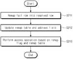
본 발명의 실시 예에 따른 스토리지 장치는 불휘발성 메모리 장치 및 동적 랜덤 액세스 메모리(DRAM; Dynamic Random Access Memory) 장치 및 스토리지 컨트롤러를 포함하고, 상기 스토리지 장치의 동작 방법은 상기 DRAM 장치에 대한 액세스 동작을 수행하는 단계, 상기 액세스 동작을 기반으로 상기 DRAM 장치에 대한 누적 에러 정보를 수집하는 단계, 상기 누적 에러 정보를 기반으로 상기 DRAM 장치에 페일 로우를 검출하는 단계, 및 상기 검출된 페일 로우에 대한 런타임 리페어 동작을 수행하는 단계를 포함한다.According to an embodiment of the present invention, a storage device includes a nonvolatile memory device, a dynamic random access memory (DRAM) device, and a storage controller, and the method of operating the storage device performs an access operation on the DRAM device. Performing, collecting cumulative error information for the DRAM device based on the access operation, detecting a fail row in the DRAM device based on the cumulative error information, and runtime for the detected fail row. Performing a repair operation.
본 발명의 실시 예에 따른 스토리지 장치는 불휘발성 메모리 장치, 동적 랜덤 액세스 메모리(DRAM; Dynamic Random Access Memory) 장치, 및 상기 불휘발성 메모리 장치 및 상기 DRAM 장치를 제어하도록 구성된 스토리지 컨트롤러를 포함하고, 상기 스토리지 컨트롤러는 상기 DRAM 장치로부터 읽은 데이터에 대한 에러 검출 및 정정 동작을 수행하도록 구성된 DRAM 에러 정정 엔진, 및 상기 DRAM 에러 정정 엔진에 의해 검출된 에러를 기반으로 누적 에러 정보를 관리하고, 상기 누적 에러 정보를 기반으로 상기 DRAM 장치의 페일 로우를 검출하고, 상기 검출된 페일 로우에 대한 런타임 리페어 동작을 수행하도록 구성된 리페어 관리자를 포함한다.A storage device according to an embodiment of the present invention includes a nonvolatile memory device, a dynamic random access memory (DRAM) device, and a storage controller configured to control the nonvolatile memory device and the DRAM device. The storage controller manages cumulative error information based on a DRAM error correction engine configured to perform an error detection and correction operation on data read from the DRAM device, and an error detected by the DRAM error correction engine. And a repair manager configured to detect a fail row of the DRAM device and perform a runtime repair operation on the detected fail row.
본 발명의 실시 예에 따른 스토리지 장치는 불휘발성 메모리 장치, 휘발성 메모리 장치, 및 상기 불휘발성 메모리 장치 및 상기 휘발성 메모리 장치를 제어하도록 구성된 스토리지 컨트롤러를 포함하고, 상기 스토리지 장치의 동작 방법은 상기 휘발성 메모리 장치로부터 데이터를 읽는 단계, 상기 읽은 데이터에 대한 에러 검출 및 정정 동작을 수행하는 단계, 상기 에러 검출 및 정정 동작의 결과를 기반으로 상기 휘발성 메모리 장치의 복수의 행들 각각에 대한 누적 에러 정보를 갱신하는 단계, 상기 갱신된 누적 에러 정보를 기반으로 상기 휘발성 메모리 장치의 페일 로우를 검출하는 단계, 및 상기 검출된 페일 로우에 대한 런타임 리페어 동작을 수행하는 단계를 포함하고, 상기 런타임 리페어 동작은 상기 스토리지 장치의 동작 중에 수행된다.A storage device according to an embodiment of the present invention includes a nonvolatile memory device, a volatile memory device, and a storage controller configured to control the nonvolatile memory device and the volatile memory device, and a method of operating the storage device is the volatile memory. Reading data from a device, performing error detection and correction operations on the read data, and updating cumulative error information for each of a plurality of rows of the volatile memory device based on a result of the error detection and correction operation. The method may include: detecting a fail row of the volatile memory device based on the updated accumulated error information, and performing a runtime repair operation on the detected fail row, wherein the runtime repair operation is performed by the storage device. Is performed during the operation.
본 발명에 따르면, 스토리지 장치의 구동 중에 발생한 DRAM 장치의 페일 로우에 대한 런타임 리페어 동작이 수행될 수 있다. 즉, DRAM 장치를 포함하는 스토리지 장치의 구동 중에, DRAM 장치에서 페일 로우가 발생하더라도, DRAM 장치 또는 스토리지 장치가 정상적으로 동작할 수 있다. 따라서 향상된 신뢰성 및 향상된 수명을 갖는 스토리지 장치 및 그것의 동작 방법이 제공된다.According to the present invention, a runtime repair operation on a fail row of a DRAM device generated while the storage device is driven may be performed. That is, even when a fail low occurs in the DRAM device while the storage device including the DRAM device is driven, the DRAM device or the storage device may operate normally. Thus, a storage device having improved reliability and improved lifetime and a method of operating the same are provided.
도 1은 본 발명의 실시 예에 따른 컴퓨팅 시스템을 보여주는 블록도이다.
도 2는 도 1의 스토리지 컨트롤러를 예시적으로 보여주는 블록도이다.
도 3은 도 2의 스토리지 컨트롤러의 동작을 예시적으로 보여주는 순서도이다.
도 4는 도 3의 S13 단계 및 S14 단계의 동작들을 설명하기 위한 도면이다.
도 5는 도 3의 S15 단계의 동작을 예시적으로 보여주는 순서도이다.
도 6a 내지 도 6c는 도 5의 S112 단계 내지 S114 단계의 동작들을 설명하기 위한 도면들이다.
도 7은 도 5의 S113 단계의 동작을 수행하는 DRAM 장치를 예시적으로 보여주는 블록도이다.
도 8은 도 6b의 직접 리페어 동작에 대한 입출력 신호를 보여주는 타이밍도이다.
도 9는 도 3의 S15 단계의 동작을 예시적으로 보여주는 순서도이다.
도 10은 도 2의 스토리지 컨트롤러의 동작을 보여주는 순서도이다.
도 11은 본 발명의 실시 예에 따른 스토리지 컨트롤러를 예시적으로 보여주는 블록도이다.
도 12는 도 11의 스토리지 컨트롤러의 간접 리페어 동작을 예시적으로 보여주는 순서도이다.
도 13a 및 도 13b는 도 12의 순서도에 따른 동작을 설명하기 위한 도면들이다.
도 14는 도 11의 스토리지 컨트롤러의 DRAM 장치에 대한 액세스 동작을 보여주는 순서도이다.
도 15는 본 발명의 일 실시 예에 따른 런타임 리페어 동작을 예시적으로 보여주는 순서도이다.
도 16은 본 발명의 실시 예에 따른 스토리지 컨트롤러의 동작을 예시적으로 보여주는 순서도이다.
도 17은 본 발명의 실시 예에 따른 스토리지 장치가 적용된 사용자 시스템을 예시적으로 보여주는 블록도이다.1 is a block diagram illustrating a computing system according to an example embodiment.
2 is a block diagram illustrating an example storage controller of FIG. 1.
3 is a flowchart illustrating an operation of a storage controller of FIG. 2.
4 is a diagram for describing operations of step S13 and step S14 of FIG. 3.
FIG. 5 is a flowchart illustrating an operation of step S15 of FIG. 3.
6A through 6C are diagrams for describing operations of operation S112 to S114 of FIG. 5.
FIG. 7 is a block diagram illustrating a DRAM device performing an operation of step S113 of FIG. 5.
FIG. 8 is a timing diagram illustrating an input / output signal for the direct repair operation of FIG. 6B.
FIG. 9 is a flowchart illustrating an operation of step S15 of FIG. 3.
FIG. 10 is a flowchart illustrating an operation of a storage controller of FIG. 2.
11 is a block diagram illustrating a storage controller in accordance with an embodiment of the disclosure.
12 is a flowchart illustrating an indirect repair operation of the storage controller of FIG. 11.
13A and 13B are diagrams for describing an operation according to the flowchart of FIG. 12.
FIG. 14 is a flowchart illustrating an access operation of a DRAM device of the storage controller of FIG. 11.
15 is a flowchart exemplarily illustrating a runtime repair operation according to an embodiment of the present invention.
16 is a flowchart illustrating an operation of a storage controller according to an embodiment of the present disclosure.
17 is a block diagram illustrating a user system to which a storage device is applied according to an exemplary embodiment of the inventive concept.
이하에서, 본 발명의 기술 분야에서 통상의 지식을 가진 자가 본 발명을 용이하게 실시할 수 있을 정도로, 본 발명의 실시 예들이 명확하고 상세하게 기재될 것이다.Hereinafter, embodiments of the present invention will be described clearly and in detail so that those skilled in the art can easily carry out the present invention.
이하에서, 다르게 정의되지 않는 한, 상세한 설명 또는 도면에서 사용되는 유닛(unit), 모듈(module), 기능 블록(functional blokc) 등과 같은 표현 및 기재는 하드웨어, 소프트웨어, 또는 그것들의 조합으로 구현될 수 있다. 일 예로서, 소프트웨어는 기계 코드, 펌웨어, 임베디드 코드, 및 애플리케이션 소프트웨어일 수 있다. 예를 들어, 하드웨어는 전기 회로, 전자 회로, 프로세서, 컴퓨터, 집적 회로, 집적 회로 코어들, 압력 센서, 관성 센서, 멤즈(MEMS; microelectromechanical system), 수동 소자, 또는 그것들의 조합을 포함할 수 있다.Hereinafter, unless otherwise defined, representations and descriptions such as units, modules, functional blocks, etc. used in the detailed description or the drawings may be implemented in hardware, software, or a combination thereof. have. As one example, the software can be machine code, firmware, embedded code, and application software. For example, the hardware may include electrical circuits, electronic circuits, processors, computers, integrated circuits, integrated circuit cores, pressure sensors, inertial sensors, microelectromechanical systems (MEMS), passive elements, or combinations thereof. .
도 1은 본 발명의 실시 예에 따른 컴퓨팅 시스템을 보여주는 블록도이다. 도 1을 참조하면, 컴퓨팅 시스템(10)은 호스트(11) 및 스토리지 장치(100)를 포함할 수 있다. 예시적인 실시 예에서, 컴퓨팅 시스템(10)은 컴퓨터, 휴대용 컴퓨터, UMPC (Ultra Mobile PC), 워크스테이션, 서버 컴퓨터, 넷-북(net-book), PDA, 포터블(portable) 컴퓨터, 웹 타블렛(web tablet), 무선 전화기(wireless phone), 모바일 폰(mobile phone), 스마트폰(smart phone), 디지털 카메라(digital camera), 디지털 음성 녹음기(digital audio recorder), 디지털 음성 재생기(digital audio player), 디지털 영상 녹화기(digital picture recorder), 디지털 영상 재생기(digital picture player), 디지털 동영상 녹화기(digital video recorder), 디지털 동영상 재생기(digital video player), 정보를 무선 환경에서 송수신할 수 있는 장치, 홈 네트워크를 구성하는 다양한 전자 장치들 중 하나를 포함할 수 있다.1 is a block diagram illustrating a computing system according to an example embodiment. Referring to FIG. 1, the
호스트(11)는 스토리지 장치(100)를 제어하도록 구성될 수 있다. 예를 들어, 호스트(11)는 스토리지 장치(100)에 데이터를 저장하거나 또는 스토리지 장치에 저장된 데이터를 독출하도록 구성될 수 있다.The
스토리지 장치(100)는 스토리지 컨트롤러(110), 휘발성 메모리 장치(120), 및 불휘발성 메모리 장치(130)를 포함할 수 있다. 예시적인 실시 예에서, 스토리지 장치(100)는 솔리드-스테이트 드라이브(SSD; Solid State Drive), 메모리 카드 등과 같은 대용량 저장 매체일 수 있다. 스토리지 컨트롤러(110)는 호스트(11)의 제어에 따라, 불휘발성 메모리 장치(130)에 데이터를 저장하거나 또는 불휘발성 메모리 장치(130)에 저장된 데이터를 읽을 수 있다.The
휘발성 메모리 장치(120)는 스토리지 장치(100)의 동작 메모리(working memory)로서 사용될 수 있다. 예를 들어, 스토리지 컨트롤러(110)는 스토리지 장치(100)의 동작에 필요한 다양한 정보(예를 들어, 메타 정보, 매핑 테이블 등)를 휘발성 메모리 장치(120)에 저장하고, 휘발성 메모리 장치(120)에 저장된 정보를 기반으로 불휘발성 메모리 장치(130)에 대한 액세스 동작을 수행할 수 있다. 또는 휘발성 메모리 장치(120)는 스토리지 장치(100)의 버퍼 메모리로서 사용될 수 있다. 예를 들어, 호스트(11)로부터 수신된 쓰기 데이터 또는 불휘발성 메모리 장치(130)로부터 읽은 데이터가 휘발성 메모리 장치(120)에 임시 저장될 수 있다.The
이하에서, 스토리지 장치(100)에 포함된 휘발성 메모리 장치(120)는 “DRAM(Dynamic Random Access Memory) 장치”인 것으로 가정한다. 그러나 본 발명의 범위가 이에 한정되는 것은 아니며, 휘발성 메모리 장치(120)는 고속 동작을 지원하는 다양한 메모리 장치들 중 어느 하나일 수 있다.Hereinafter, it is assumed that the
스토리지 컨트롤러(110)는 DRAM 제어 유닛(111)을 포함할 수 있다. DRAM 제어 유닛(111)은 DRAM 장치(120)를 제어하도록 구성될 수 있다. 예를 들어, DRAM 제어 유닛(111)은 스토리지 컨트롤러(110)의 제어에 따라, DRAM 장치(120)에 대한 액세스 동작을 수행하도록 구성될 수 있다.The
예시적인 실시 예에서, DRAM 제어 유닛(111)은 DRAM 장치(120)에 대한 런타임 리페어(Runtime Repair) 동작을 수행할 수 있다. 런타임 리페어 동작은 스토리지 장치(100)의 구동 중에, DRAM 장치에서 발생한 페일 로우(fail row)에 대하여 수행되는 리페어 동작을 가리킬 수 있다. 즉, 스토리지 장치(100)가 동작 중이더라도, DRAM 제어 유닛(111)은 DRAM 장치에서 발생한 페일 로우에 대한 리페어 동작을 수행할 수 있다. 따라서, DRAM 장치(120)에서 페일 로우가 발생하더라도, DRAM 장치(120) 또는 스토리지 장치(100)가 정상적으로 동작할 수 있다.In an example embodiment, the
예시적인 실시 예에서, DRAM 제어 유닛(111)은 DRAM 장치(120)의 복수의 행들 각각에 대한 누적 에러 정보를 관리하고, 누적 에러 정보를 기반으로 페일 로우를 검출할 수 있다. DRAM 제어 유닛(111)은 검출된 페일 로우에 대한 런타임 리페어 동작을 수행할 수 있다. 예시적인 실시 예에서, 본 발명의 실시 예에 따른 런타임 리페어 동작은 다양한 방식들을 기반으로 수행될 수 있다. 본 발명의 실시 예에 따른 런타임 리페어 동작에 대한 다양한 방식들은 이하의 도면들을 참조하여 더욱 상세하게 설명된다.In an exemplary embodiment, the
상술된 바와 같이, 본 발명의 실시 예에 따르면, 스토리지 장치(100)가 구동 중에, DRAM 장치(120)에서 페일 로우가 발생하더라도, 페일 로우에 대한 런타임 리페어 동작을 수행함으로써, DRAM 장치(120) 또는 스토리지 장치(100)가 정상적으로 동작할 수 있다. 따라서, DRAM 장치(120) 또는 스토리지 장치(100)에 대한 신뢰성이 향상되고, 수명이 향상될 수 있다.As described above, according to an embodiment of the present invention, even when a fail low occurs in the
도 2는 도 1의 스토리지 컨트롤러를 예시적으로 보여주는 블록도이다. 도 2를 참조하면, 스토리지 컨트롤러(110)는 DRAM 제어 유닛(111), 프로세서(112), SRAM(113), 불휘발성 메모리 에러 정정(ECC) 엔진(114), 호스트 인터페이스(115), 및 플래시 인터페이스(116)를 포함할 수 있다.2 is a block diagram illustrating an example storage controller of FIG. 1. Referring to FIG. 2, the
DRAM 제어 유닛(111)은 스토리지 컨트롤러(110)의 제어에 따라 DRAM 장치(120)에 대한 액세스 동작(예를 들어, 쓰기 동작 또는 읽기 동작)을 수행하도록 구성될 수 있다. 예를 들어, 프로세서(112)는 스토리지 컨트롤러(110)의 제반 동작을 제어하기 위하여, DRAM 장치(120)를 액세스할 수 있다. 프로세서(112)는 DRAM 장치(120)를 액세스하기 위한 DRAM 어드레스를 발생할 수 있다. DRAM 제어 유닛(111)은 프로세서(112)로부터의 DRAM 어드레스에 대응하는 영역에 대한 액세스 동작을 수행할 수 있다.The
예시적인 실시 예에서, DRAM 제어 유닛(111)은 DDR(Double Data Rate) 인터페이스, LPDDR(Low-Power DDR) 인터페이스, GDDR(Graphic DDR) 인터페이스 등과 같은 고속 인터페이스를 기반으로 DRAM 장치(120)와 통신할 수 있다.In an exemplary embodiment, the
DRAM 제어 유닛(111)은 DRAM ECC 엔진(111a) 및 리페어 관리자(111b)를 포함할 수 있다. DRAM ECC 엔진(111a)은 DRAM 장치(120)로부터 읽은 데이터에 대한 에러 검출 및 정정을 수행할 수 있다. 예시적인 실시 예에서, 에러 검출에 대한 결과는 리페어 관리자(111b)로 제공될 수 있다.The
리페어 관리자(111b)는 DRAM ECC 엔진(111a)의 에러 검출 결과를 기반으로, DRAM 장치(120)에 대한 누적 에러 정보를 관리할 수 있다. 예를 들어, 리페어 관리자(111b)는, DRAM ECC 엔진(111a)의 에러 검출 결과를 기반으로, DRAM 장치(120)의 복수의 행들 각각에 대한 누적 에러 정보를 관리할 수 있다. 누적 에러 정보는 DRAM 장치(120)의 행들 각각에서 발생한 에러 비트의 개수를 누적한 값일 수 있다.The
좀 더 상세한 예로서, DRAM 제어 유닛(111)이 DRAM 장치(120)의 제1 행에 대한 액세스 동작을 n회 수행하는 동안, k개의 에러 비트가 검출된 경우(이 때, k개의 에러 비트는 n회의 액세스 동작들 중 특정 액세스 동작에서 발생하거나 또는 n회의 액세스 동작들 중 복수의 액세스 동작들에서 발생할 수 있음), DRAM 장치(120)의 제1 행의 누적 에러 정보는 “k”일 것이다. 즉, 누적 에러 정보는 복수의 행들 각각에 대하여, 복수의 액세스 동작들 동안 검출된 에러 비트 개수의 누적된 값일 수 있다.As a more detailed example, if k error bits are detected while the
리페어 관리자(111b)는 누적 에러 정보를 기반으로 DRAM 장치(120)에서 페일 로우(fail row)를 판별할 수 있다. 예를 들어, 리페어 관리자(111b)는 누적된 에러 비트 정보가 기준 값을 초과하는 경우, 대응하는 행을 페일 로우인 것으로 판별할 수 있다. 예를 들어, DRAM 장치(120)의 제1 행에 대한 누적 에러 정보가 “k”이고, “k”가 미리 정해진 기준 값보다 큰 경우, 리페어 관리자(111b)는 제1 행을 페일 로우인 것으로 판별할 수 있다.The
예시적인 실시 예에서, 리페어 관리자(111b)에 의해 페일 로우인 것으로 판별된 제1 행은 실제 페일 로우은 아닐 수 있다. 즉, 현지 시점에서, 리페어 관리자(111b)에 의해 페일 로우인 것으로 판별된 제1 행에 대한 액세스 동작은 정상적으로 수행될 수 있으나(예를 들어, 제1 행에 포함된 에러 비트가 정상적으로 정정됨.), 추가적인 액세스 동작들에 의해 또는 시간이 흐름에 따라 제1 행이 실제 페일 로우가 될 수 있다. 실제 페일 로우는 메모리 셀들의 결함(예를 들어, 메모리 셀의 리프레쉬 성능 저하, 리텐션 특성 저하 등)으로 인하여, 저장된 데이터가 소실되는 행을 가리킬 수 있다. 실제 페일 로우로부터 읽어진 데이터는 DRAM ECC 엔진(111a)에 의해 에러가 정정되지 않을 수 있다.In an example embodiment, the first row determined by the
즉, 상세한 설명에서 사용되는 “페일 로우(fail row)”, 좀 더 상세하게는, 리페어 관리자(111b)에 의해 판별된 페일 로우는 시간의 흐름 또는 추가적인 액세스 동작에 의해 실제 페일 로우가 될 가능성이 높은 행을 가리킬 수 있다. 그러나 본 발명의 범위가 이에 한정되는 것은 아니며, 리페어 관리자(111b)에 의해 판별된 페일 로우는 실제 페일 로우를 가리킬 수 있다.That is, the "fail row" used in the description, and more specifically, the fail row determined by the
예시적인 실시 예에서, 기준 값은 DRAM 장치(120)의 물리적 특성, 동작 환경, 또는 DRAM ECC 엔진(111a)의 성능에 따라 달라질 수 있다. 예를 들어, DRAM 장치(120)의 물리적 특성 또는 동작 환경이 좋은 경우(다시 말해서, DRAM 장치에서의 PVT 변이(Process, voltage, temperature variation)가 상대적으로 작은 경우 또는 DRAM ECC 엔진(111a)의 성능이 상대적으로 높은 경우) 기준 값은 제1 값으로 설정될 수 있고, DRAM 장치(120)의 물리적 특성 또는 동작 환경이 좋지 않은 경우(다시 말해서, DRAM 장치에서의 PVT 변이가 상대적으로 큰 경우 또는 DRAM ECC 엔진(111a)의 성능이 상대적으로 낮은 경우) 기준 값은 제1 값보다 작은 제2 값으로 설정될 수 있다.In an exemplary embodiment, the reference value may vary depending on the physical characteristics of the
페일 로우가 검출된 경우, 리페어 관리자(111b)는 DRAM 장치(120)에 대한 런타임 리페어 동작(runtime repair operation)을 수행할 수 있다. 예시적인 실시 예에서, 리페어 관리자(111b)는 다양한 방식들을 기반으로 런타임 리페어 동작을 수행할 수 있다. 본 발명에 따른 다양한 런타임 리페어 동작들은 이하의 도면들을 참조하여 더욱 상세하게 설명된다.When a fail low is detected, the
SRAM(113)은 스토리지 컨트롤러(110)의 동작 메모리, 캐시 메모리, 또는 버퍼 메모리로서 사용될 수 있다. 예시적인 실시 예에서, SRAM(113)에 저장된 다양한 정보 또는 소프트웨어 구성들은 프로세서(112)에 의해 관리되거나 또는 구동될 수 있다.The
불휘발성 ECC 엔진(114)은 불휘발성 메모리 장치(130)로부터 읽은 데이터에 대한 에러 검출 및 정정 동작을 수행할 수 있다. 예를 들어, 불휘발성 ECC 엔진(114)은 호스트(11)로부터 수신된 제1 데이터에 대한 에러 정정 코드를 생성할 수 있다. 생성된 에러 정정 코드는 제1 데이터와 함께 불휘발성 메모리 장치(130)에 저장될 수 있다. 이후에, 불휘발성 메모리 ECC 엔진(114)은 불휘발성 메모리 장치(130)로부터 제1 데이터 및 에러 정정 코드를 읽고, 읽어진 에러 정정 코드를 사용하여 제1 데이터에 대한 에러를 검출 및 정정할 수 있다.The
예시적인 실시 예에서, NVM ECC 엔진(114) 및 DRAM ECC 엔진(111a)은 서로 다른 기능 블록으로 구현될 수 있다. 또는 NVM ECC 엔진(114) 및 DRAM ECC 엔진(111a)은 동일한 기능 블록으로 구현될 수 있다.In an exemplary embodiment, the
스토리지 컨트롤러(110)는 호스트 인터페이스(115)를 통해 호스트(11)와 통신할 수 있다. 예시적인 실시 예에서, 호스트 인터페이스(115)는 USB(Universal Serial Bus), MMC(multimedia card), PCI(peripheral component interconnection), PCI-E(PCI-express), ATA(Advanced Technology Attachment), SATA(Serial-ATA), PATA(Parallel-ATA), SCSI(small computer small interface), ESDI(enhanced small disk interface), IDE(Integrated Drive Electronics), MIPI(Mobile Industry Processor Interface), NVM-e(Nonvolatile Memory-express), UFS(Universal Flash Storage) 등과 같은 다양한 인터페이스들 중 적어도 하나를 포함할 수 있다.The
스토리지 컨트롤러(110)는 플래시 인터페이스(116)를 통해 불휘발성 메모리 장치(130)와 통신할 수 있다. 예시적인 실시 예에서, 플래시 인터페이스(116)는 낸드 인터페이스를 포함할 수 있다.The
도 3은 도 2의 스토리지 컨트롤러의 동작을 예시적으로 보여주는 순서도이다. 도 2 및 도 3을 참조하면, S11 단계에서, 스토리지 컨트롤러(110)는 리페어 정보를 로드할 수 있다. 리페어 정보는 페일 로우 검출 또는 런타임 리페어 동작을 수행하기 위해 필요한 정보를 포함할 수 있다. 예를 들어, 리페어 정보는 DRAM 장치(120)의 복수의 행들 각각에 대한 누적 에러 정보를 포함할 수 있다. 리페어 정보는 불휘발성 메모리 장치(120)의 특정 영역(예를 들어, 메타 영역)에 저장될 수 있다. 스토리지 컨트롤러(110)는 불휘발성 메모리 장치(120)의 특정 영역에 저장된 리페어 정보를 로드할 수 있다. 예시적인 실시 예에서, 리페어 정보는 SRAM(113)에 저장되고, 프로세서(112) 또는 DRAM 제어 유닛(111)에 의해 관리될 수 있다.3 is a flowchart illustrating an operation of a storage controller of FIG. 2. 2 and 3, in operation S11, the
S12 단계에서, 스토리지 컨트롤러(110)는 DRAM 장치(120)에 대한 액세스 동작을 수행할 수 있다. 예를 들어, 스토리지 컨트롤러(110)는 DRAM 장치(120)에 다양한 정보 또는 데이터를 기입할 수 있다. 또는 스토리지 컨트롤러(110)는 DRAM 장치(120)에 저장된 정보 또는 데이터를 읽을 수 있고, 읽은 데이터에 대한 에러 검출 및 정정 동작을 수행할 수 있다.In operation S12, the
S13 단계에서, 스토리지 컨트롤러(110)는 액세스 동작을 기반으로 누적 에러 정보를 수집할 수 있다. 예를 들어, 스토리지 컨트롤러(110)는 상술된 에러 검출 동작의 결과를 기반으로 DRAM 장치(120)의 복수의 행들 각각에 대한 누적 에러 정보를 관리할 수 있다. 누적 에러 정보는, 앞서 설명된 바와 같이, DRAM 장치(120)의 복수의 행들 각각에 대한 에러 비트들의 누적된 개수를 가리킬 수 있다.In operation S13, the
S14 단계에서, 스토리지 컨트롤러(110)는 누적 에러 정보를 기반으로 DRAM 장치(120)에서, 페일 로우(fail row)를 판별할 수 있다. 예를 들어, 스토리지 컨트롤러(110)는 DRAM 장치(120)의 복수의 행들 중 기준 값을 초과하는 누적 에러 정보와 대응하는 행을 페일 로우인 것으로 판별할 수 있다.In operation S14, the
S15 단계에서, 스토리지 컨트롤러(110)는 판별된 페일 로우에 대한 런타임 리페어 동작을 수행할 수 있다. 예를 들어, 스토리지 컨트롤러(110)는 페일 로우에 대한 직접 리페어 동작(direct repair oepration)을 수행할 수 있다. 직접 리페어 동작은 DRAM 장치(120) 내에서 전기적 퓨즈-셋팅 등의 동작을 통해 페일 로우를 직접적으로 복구하는 동작을 가리킨다.In operation S15, the
또는 스토리지 컨트롤러(110)는 페일 로우에 대한 간접 리페어 동작(indirect repair oepration)을 수행할 수 있다. 간접 리페어 동작은 DRAM 제어 유닛(111) 상에서, 페일 로우를 예비 영역의 예비 로우로 리맵핑하여, 페일 로우를 스토리지 컨트롤러(110) 계층에서, 간접적으로 복구하는 동작을 가리킨다. 또는 스토리지 컨트롤러(110)는 페일 로우에 대한 간접 리페어 동작을 수행한 이후에, 특정 조건 하에서, 직접 리페어 동작을 수행할 수 있다. 본 발명의 실시 예에 따른 직접 리페어 동작 및 간접 리페어 동작은 이하의 도면들을 참조하여 더욱 상세하게 설명된다.Alternatively, the
상술된 바와 같이, DRAM 장치(120)를 포함한 스토리지 장치(100)의 구동 중에, DRAM 장치(120)에서 페일 로우가 검출된 경우, 스토리지 컨트롤러(110)는 페일 로우에 대한 런타임 리페어 동작을 수행할 수 있다. 이에 따라, 스토리지 장치(100)가 구동 중에 DRAM 장치(120)에서 발생하는 페일 로우를 미리 복구할 수 있기 때문에, DRAM 장치(120) 또는 DRAM 장치(120)를 포함한 스토리지 장치(100)의 신뢰성 및 수명이 향상된다.As described above, when a fail low is detected in the
도 4는 도 3의 S13 단계 및 S14 단계의 동작들을 설명하기 위한 도면이다. 도 3의 S13 단계 및 S14 단계의 동작들은 누적 에러 정보를 수집하는 동작을 가리킨다. 도면의 간결성 및 설명의 편의를 위하여, 도 3의 S13 단계 및 S14 단계의 동작들을 설명하는데 불필요한 구성 요소들은 생략된다. 또한, DRAM 장치(120)는 제1 내지 제4 행들(ROW1~ROW4)을 포함하는 것으로 가정한다. 그러나 본 발명의 범위가 이에 한정되는 것은 아니다.4 is a diagram for describing operations of step S13 and step S14 of FIG. 3. The operations of steps S13 and S14 of FIG. 3 indicate an operation of collecting cumulative error information. For simplicity and convenience of description, components unnecessary for describing operations of steps S13 and S14 of FIG. 3 are omitted. In addition, it is assumed that the
도 2 내지 도 4를 참조하면, DRAM 제어 유닛(111)은 DRAM 장치(120)의 제1 행(ROW1)에 대한 액세스 동작을 수행할 수 있다. 예를 들어, DRAM 제어 유닛(111)은 DRAM 장치(120)의 제1 행(ROW1)으로부터 제1 데이터(DATA1)를 읽을 수 있다. DRAM ECC 엔진(111a)은 제1 데이터(DATA1)에 대한 에러 검출 및 정정 동작을 수행하고, 에러가 정정된 제1 데이터(DATA1')는 호스트(11) 또는 불휘발성 메모리 장치(130)로 제공될 수 있다.2 to 4, the
DRAM ECC 엔진(111a)에 의해 검출된 에러에 대한 에러 검출 정보(E)는 리페어 관리자(111b)로 제공될 수 있다. 예시적인 실시 예에서, 에러 검출 정보(E)는 검출된 에러 비트들의 개수를 가리킬 수 있다.The error detection information E for the error detected by the
리페어 관리자(111b)는 에러 검출 정보(E)를 기반으로 누적 에러 정보(AEI)를 갱신할 수 있다. 예를 들어, 리페어 관리자(111b)는 누적 에러 정보(AEI)를 관리할 수 있다. 누적 에러 정보(AEI)는 DRAM 장치(120)의 복수의 행들(ROW1~ROW4) 각각에 대하여 누적된 에러 비트들의 개수에 대한 정보를 포함할 수 있다. 일 예로서, 제1 행(ROW1)에 대하여 누적된 에러 비트들의 개수는 “a”개일 수 있고, 제2 행(ROW2)에 대하여 누적된 에러 비트들의 개수는 “b”개일 수 있고, 제3 행(ROW3)에 대하여 누적된 에러 비트들의 개수는 “c”개일 수 있고, 제4 행(ROW4)에 대하여 누적된 에러 비트들의 개수는 “d”개일 수 있다.The
리페어 관리자(111b)는 DRAM ECC 엔진(111a)으로부터 수신된 에러 검출 정보(E)를 기반으로 대응하는 행에 대한 값을 갱신할 수 있다. 예를 들어, 수신된 에러 검출 정보(E)가 제1 행(ROW1)으로부터의 제1 데이터(DATA1)에 대한 에러 비트 개수에 대한 정보를 가리키는 경우, 리페어 관리자(111b)는 누적 에러 정보(AEI)에서, 제1 행(ROW1)에 대응하는 값을 “a”에서 “a+E”로 갱신할 수 있다. 즉, 리페어 관리자(111b)는 누적 에러 정보(AEI)에서, 제1 행(ROW1)에 대응하는 값에 검출된 에러에 대한 정보(E)를 누적시킬 수 있다. DRAM 제어 유닛(111)은 상술된 동작을 반복 수행함으로써, DRAM 장치(120)의 복수의 행들 각각에 대한 누적 에러 정보(AEI)를 관리할 수 있다.The
예시적인 실시 예에서, 제1 행(ROW1)에 대하여 갱신된 값(즉, a+E)이 기준 값(REF)보다 큰 경우, 리페어 관리자(111b)는 대응하는 제1 행(ROW1)이 페일 로우인 것으로 판별할 수 있다.In an exemplary embodiment, when the updated value (ie, a + E) for the first row ROW1 is greater than the reference value REF, the
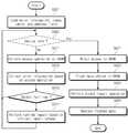
도 5는 도 3의 S15 단계의 동작을 예시적으로 보여주는 순서도이다. 도 5를 참조하여 본 발명에 따른 런타임 리페어 동작들 중 일 실시 예인 직접 리페어 동작(또는 하드 리페어 동작)이 설명된다. 예시적인 실시 예에서, 도 5의 순서도에 따른 동작은 도 3의 S14 단계의 동작에 따라 페일 로우가 검출된 이후에 수행될 수 있다.FIG. 5 is a flowchart illustrating an operation of step S15 of FIG. 3. A direct repair operation (or a hard repair operation) as an embodiment of runtime repair operations according to the present invention will be described with reference to FIG. 5. In an exemplary embodiment, the operation according to the flowchart of FIG. 5 may be performed after a fail low is detected according to the operation of step S14 of FIG. 3.
도 2, 도 3, 및 도 5를 참조하면, S110 단계에서, 스토리지 컨트롤러(110)는 스토리지 장치(100)가 유휴 상태(Idle)인지 판별할 수 있다. 예를 들어, 스토리지 장치(100)의 유휴 상태는 호스트(11)로부터 커맨드 또는 요청이 수신되지 않는 상태를 가리킬 수 있다. 예시적인 실시 예에서, 스토리지 장치(100)가 유휴 상태가 아닌 경우, 스토리지 장치(100)는 호스트(11)의 요청에 따라 정상 동작을 수행할 수 있다.2, 3, and 5, in operation S110, the
스토리지 장치(100)가 유휴 상태인 경우, S111 단계에서, 스토리지 컨트롤러(110)는 DRAM 장치(120)의 액세스를 차단할 수 있다. 예를 들어, DRAM 장치(120)는 복수의 뱅크들을 포함할 수 있다. 스토리지 컨트롤러(110)는 DRAM 장치(120)의 복수의 뱅크들로의 액세스를 모두 차단 또는 중단할 수 있다.When the
S112 단계에서, 스토리지 컨트롤러(110)는 DRAM 장치(120)에 저장된 데이터를 불휘발성 메모리 장치(130)로 플러쉬(flush)할 수 있다. 예를 들어, 스토리지 컨트롤러(110)가 DRAM 장치(120)에 대한 직접 리페어 동작을 수행하는 동안, DRAM 장치(120)에 대한 리프레쉬 동작이 수행되지 않을 수 있다. 이로 인하여, DRAM 장치(120)에 저장된 데이터가 소실될 수 있다. DRAM 장치(120)에 저장된 데이터의 소실을 방지하기 위하여, 스토리지 컨트롤러(110)는 DRAM 장치(120)에 저장된 데이터를 불휘발성 메모리 장치(130)로 플러쉬할 수 있다.In operation S112, the
예시적인 실시 예에서, 스토리지 컨트롤러(110)는 DRAM 장치(120)의 복수의 뱅크들에 저장된 데이터 전부를 불휘발성 메모리 장치(130)로 플러쉬할 수 있다. 또는 스토리지 컨트롤러(110)는 DRAM 장치(120)의 복수의 뱅크들 중 일부 뱅크들에 저장된 데이터를 불휘발성 메모리 장치(130)로 플러쉬할 수 있다. 예시적인 실시 예에서, 일부 뱅크들은 페일 로우를 포함하는 적어도 2개의 뱅크들을 포함할 수 있다.In an example embodiment, the
S113 단계에서, 스토리지 컨트롤러(110)는 직접 리페어 동작을 수행할 수 있다. 예를 들어, 스토리지 컨트롤러(110)는 DRAM 장치(120)에서, 전기적 퓨즈 세팅을 통해 페일 로우를 복구하는 동작을 수행할 수 있다. 예시적인 실시 예에서, 직접 리페어 동작은 포스트 패키지 리페어(PPR; post-package repair) 동작을 기반으로 수행될 수 있다.In operation S113, the
S114 단계에서, 스토리지 컨트롤러(110)는 불휘발성 메모리 장치(130)로 플러쉬된 데이터를 DRAM 장치(120)로 복원할 수 있다. 이후에, 스토리지 장치(100)는 정상적으로 동작할 수 있다.In operation S114, the
도 6a 내지 도 6c는 도 5의 S112 단계 내지 S114 단계의 동작들을 설명하기 위한 도면들이다. 도면의 간결성 및 설명의 편의를 위하여, S112 단계 내지 S114 단계의 동작들을 설명하는데 불필요한 구성 요소들은 생략된다. 설명의 편의를 위하여, DRAM 장치(120)는 제1 내지 제4 뱅크들(BANK1~BANK4)을 포함하고, 페일 로우는 제1 뱅크(BANK1)에 포함되는 것으로 가정하나 본 발명의 범위가 이에 한정되는 것은 아니다.6A through 6C are diagrams for describing operations of operation S112 to S114 of FIG. 5. For simplicity and convenience of description, components unnecessary for describing operations of steps S112 to S114 are omitted. For convenience of description, it is assumed that the
도 2 및 도 6a 내지 도 6c를 참조하면, 스토리지 컨트롤러(110)는 DRAM 장치(120)의 뱅크들(BANK1~BANK4) 중 페일 로우(Fail Row)가 포함된 제1 뱅크(BANK1) 및 인접한 제2 뱅크(BANK2)에 저장된 데이터(DATA_1, DATA_2)를 불휘발성 메모리 장치(130)로 전달할 수 있다. 예를 들어, DRAM 제어 유닛(111)은 제1 및 제2 뱅크들(BANK1, BANK2)로부터 제1 및 제2 데이터(DATA_1, DATA_2)를 읽을 수 있다. 예시적인 실시 예에서, 제1 및 제2 뱅크들(BANK1, BANK2)로부터 읽은 제1 및 제2 데이터(DATA_1, DATA_2)는 DRAM ECC 엔진(111a)에 의해 에러가 정정될 수 있다. 이후에, 제1 및 제2 데이터(DATA_1, DATA_2)(또는 에러가 정정된 제1 및 제2 데이터)는 플래시 인터페이스(116)를 통해 불휘발성 메모리 장치(130)로 제공될 수 있다. 불휘발성 메모리 장치(130)는 제1 및 제2 데이터(DATA_1, DATA_2)를 저장할 수 있다.2 and 6A through 6C, the
다음으로, 도 6b에 도시된 바와 같이, DRAM 제어 유닛(111)은 페일 로우(Fail Row)가 포함된 제1 뱅크(BANK1)에 대한 직접 리페어 동작을 수행할 수 있다. 예를 들어, DRAM 장치(120)는 DRAM 제어 유닛(111)으로부터의 다양한 신호에 응답하여, 전기적 퓨즈 셋팅과 같은 동작을 통해 페일 로우(Fail Row)를 복구할 수 있다.Next, as illustrated in FIG. 6B, the
이후에, 도 6c에 도시된 바와 같이, 스토리지 컨트롤러(110)는 불휘발성 메모리 장치(130)에 저장된 제1 및 제2 데이터(DATA_1, DATA_2)를 제1 및 제2 뱅크들(BANK1, BANK2)에 저장할 수 있다. 예를 들어, DRAM 제어 유닛(111)은 플래시 인터페이스(116)를 통해 불휘발성 메모리 장치(130)로부터 제1 및 제2 데이터(DATA_1, DATA_2)를 수신하고, 수신된 제1 및 제2 데이터(DATA_1, DATA_2)를 각각 제1 및 제2 뱅크들(BANK1, BANK2)에 저장할 수 있다.Thereafter, as illustrated in FIG. 6C, the
도 7은 도 5의 S113 단계의 동작(즉, 직접 리페어 동작)을 수행하는 DRAM 장치를 예시적으로 보여주는 블록도이다. 설명의 편의 및 도면의 간결성을 위하여, 도 5의 S113 단계의 동작을 설명하는데 불필요한 구성 요소들은 생략된다.FIG. 7 is a block diagram illustrating a DRAM device for performing an operation (ie, a direct repair operation) of operation S113 of FIG. 5. For convenience of description and the brevity of the drawings, unnecessary components are omitted to describe the operation of step S113 of FIG. 5.
도 2 및 도 7을 참조하면, DRAM 장치(130)는 메모리 셀 어레이(131), 로우 디코더(132), 컬럼 디코더(133), 제어 로직 회로(134), 및 퓨즈 회로(135)를 포함할 수 있다.2 and 7, the
메모리 셀 어레이(131)는 복수의 DRAM 셀들을 포함할 수 있다. 복수의 DRAM 셀들은 각각 워드라인 및 비트라인과 연결될 수 있다. 복수의 DRAM 셀들 중 일부는 노멀 셀들일 수 있고, 나머지 일부는 리던던시 셀들(Redundancy cells)(131a)일 수 있다. 리던던시 셀들(131a)은 노멀 셀들 중 페일 셀들을 대체하기 위한 DRAM 셀일 수 있다.The
로우 디코더(132)는 워드라인들(NWL, RWL)을 통해 메모리 셀 어레이(131)와 연결될 수 있다. 로우 디코더(132)는 어드레스(ADDR)를 기반으로 워드라인들(NWL, RWL) 중 하나를 선택하고, 선택된 워드라인의 전압을 제어할 수 있다.The
컬럼 디코더(133)는 비트라인(BL)을 통해 메모리 셀 어레이(131)와 연결될 수 있다. 컬럼 디코더(131)는 어드레스(ADDR)를 기반으로 비트라인들(BL) 중 일부를 선택하고, 선택된 비트라인들의 전압을 제어하거나 또는 감지할 수 있다. 예시적인 실시 예에서, 컬럼 디코더(133)는 DRAM 제어 유닛(111)과 데이터를 송수신할 수 있다.The
제어 로직 회로(134)는 DRAM 장치(130)의 동작을 제어할 수 있다. 퓨즈 회로(135)는 제어 로직 회로(134)의 제어에 따라 퓨즈 셋팅 동작을 수행할 수 있다. 즉, 제어 로직 회로(134)는, 스토리지 컨트롤러(110)의 런타임 리페어 동작(예를 들어, 직접 리페어 동작)에 의해, 퓨즈 회로(135)의 퓨즈-셋팅을 재설정하도록 구성될 수 있다. 퓨즈 회로(135)의 퓨즈 셋팅에 의해 메모리 셀 어레이(131)의 노멀 셀들이 리던던시 셀들(131a)로 대체될 수 있다. 예를 들어, 퓨즈 회로(135)는 DRAM 제어 유닛(111)으로부터 어드레스(ADDR)를 수신할 수 있다. 이 때, 어드레스(ADDR)가 페일 로우와 대응되는 노멀 워드라인(NWL)에 대한 어드레스(즉, 페일 어드레스)일 수 있다. 이 경우, 퓨즈 회로(135)는 로우 디코더(132)가 노멀 워드라인(NWL) 대신에 리던던시 워드라인(RWL)을 선택하도록 리페어 어드레스(ADDR_r)를 출력할 수 있다.The
즉, 퓨즈 회로(135)는 페일 로우와 대응되는 페일 어드레스를 리페어 어드레스로 변환하여 출력하도록 퓨즈-셋팅될 수 있다. 로우 디코더(132)는 퓨즈 회로(135)로부터의 리페어 어드레스를 기반으로 리던던시 워드라인(RWL)을 선택할 수 있다. 예시적인 실시 예에서, 퓨즈 회로(135)는 페일 로우와 대응되지 않는 어드레스(ADDR)는 별도의 변환없이 수신된 어드레스(ADDR)를 로우 디코더(132)로 전달할 수 있다.That is, the
상술된 바와 같이, DRAM 장치(130)는 퓨즈 회로(135)에 대한 전기적 퓨즈-셋팅를 통해 페일 로우에 대한 복구 동작을 수행할 수 있다.As described above, the
도 8은 도 6b의 직접 리페어 동작에 대한 입출력 신호를 보여주는 타이밍도이다. 예시적인 실시 예에서, 하드 포스트 패키지 리페어(hPPR; hard Post Package Repair)를 기반으로 동작할 수 있다. 예시적인 실시 예에서, 도 8의 타이밍도의 신호들에 응답하여, 도 7을 참조하여 설명된 퓨즈 회로(135)의 전기적 퓨즈 셋팅이 수행될 수 있다.FIG. 8 is a timing diagram illustrating an input / output signal for the direct repair operation of FIG. 6B. In an example embodiment, the operation may be performed based on a hard post package repair (hPPR). In an exemplary embodiment, in response to the signals of the timing diagram of FIG. 8, electrical fuse setting of the
도 2 및 도 8을 참조하면, 제1 시점(t1) 내지 제2 시점(t2) 동안, DRAM 장치(120)는 스토리지 컨트롤러(110)로부터의 모드 레지스터 셋 커맨드들(MRS4, MRS0) 및 어드레스 신호들(BG, BA, ADDR)에 응답하여, 하드 포스트 패키지 리페어 모드(hPPR)로 진입할 수 있다. 예시적인 실시 예에서, 제1 시점(t1)에서, 제13 어드레스(A13)의 값은 하드 포스트 패키지 리페어 동작의 활성화를 가리키는 “1”로 설정될 수 있다. 예시적인 실시 예에서, 하드 포스트 패키지 리페어 모드(hPPR)로 진입하기 전에, 페일 로우(Fail Row)가 포함된 뱅크 또는 인접한 뱅크에 저장된 데이터가 불휘발성 메모리 장치(130)로 플러쉬될 수 있다. 또한 하드 포스트 패키지 리페어 모드(hPPR)로 진입하기 전에, DRAM 장치(120)의 모든 뱅크들이 프리차지될 수 있다.2 and 8, during the first to t2 times t2, the
이후에, DRAM 장치(120)는, 제2 시점(t2) 내지 제3 시점(t3) 동안, 스토리지 컨트롤러(110)로부터의 활성 커맨드(ACT), 자동 프리차지 쓰기 커맨드(WRA), 어드레스 신호들(BGf, BAf)에 응답하여 hPPR 리페어 동작을 수행할 수 있다. 예시적으로, 어드레스 신호들(BGf, BAf, ADDR)은 페일 로우에 대응하는 어드레스 신호들일 수 있다. hPPR 리페어 동작은 도 7을 참조하여 설명된 바와 같이, 퓨즈 회로(135)의 전기적인 퓨즈 셋팅을 통해 수행될 수 있다.Thereafter, the
이후에, DRAM 장치(120)는, 제3 시점(t3) 내지 제4 시점(t4) 동안, 프리 차지 커맨드(PRE)에 응답하여, hPPR 인식(hPPR Recognition)을 수행할 수 있다. 이후에, DRAM 장치(120)는, 제4 시점(t4) 내지 제5 시점(t5) 동안, 모드 레지스터 셋 커맨드(MRS4) 및 어드레스 신호(특히, A13=0)에 응답하여 hPPR 모드를 해제(Exit)할 수 있다. 이후에, DRAM 장치(130)는 DRAM 제어 유닛(111)의 제어에 따라 플러쉬된 데이터를 복원할 수 있다.Thereafter, the
예시적인 실시 예에서, 도 8의 타이밍도는 직접 리페어 동작에 대한 예시적인 실시 예이며, 본 발명의 범위가 이에 한정되는 것은 아니다. 예를 들어, 자동 프리차지 쓰기 커맨드(WRA) 대신에 일반 쓰기 커맨드(WR)를 사용하여 상술된 hPPR 동작이 수행될 수 있다. 이 경우, hPPR 모드로 진입하기 전에, DRAM 장치(120)의 모든 뱅크들에 저장된 데이터에 대한 백업(즉, 플러쉬)이 수행될 수 있다. 또는, 직접 리페어 동작은 소프트 포스트 패키지 리페어(sPPR; soft PPR)을 기반으로 수행될 수 있다.In an exemplary embodiment, the timing diagram of FIG. 8 is an exemplary embodiment for a direct repair operation, and the scope of the present invention is not limited thereto. For example, the above-described hPPR operation may be performed using the general write command WR instead of the automatic precharge write command WRA. In this case, before entering the hPPR mode, a backup (ie, flushing) of data stored in all banks of the
도 9는 도 3의 S15 단계의 동작을 예시적으로 보여주는 순서도이다. 도 2, 도 3, 및 도 9를 참조하면, 스토리지 컨트롤러(110)는 S120 단계 및 S121 단계의 동작들을 수행할 수 있다. S120 단계 및 S121 단계의 동작들은 도 5의 S110 단계 및 S111 단계의 동작들과 동일하므로, 이에 대한 상세한 설명은 생략된다.FIG. 9 is a flowchart illustrating an operation of step S15 of FIG. 3. 2, 3, and 9, the
S123 단계에서, 스토리지 컨트롤러(110)는 DRAM 장치(120)에 저장된 데이터에 대한 백업이 요구되는지 판별할 수 있다. 예를 들어, DRAM 장치(120)의 복수의 뱅크들 중 페일 로우가 포함된 뱅크들에 중요 데이터(예를 들어, 매핑 정보, 메타 정보 등)가 저장된 경우, 스토리지 컨트롤러(110)는 백업이 요구되는 것으로 판별할 수 있다. 이 경우, 스토리지 장치(110)는 S123 단계 내지 S125 단계의 동작들을 수행할 수 있다. S123 단계 내지 S125 단계의 동작들은 도 5의 S112 단계 내지 S114 단계의 동작들과 유사하므로, 이에 대한 상세한 설명은 생략된다.In operation S123, the
DRAM 장치(120)의 복수의 뱅크들 중 페일 로우가 포함된 뱅크들에 중요 데이터가 포함되지 않은 경우(예를 들어, 페일 로우가 포함된 뱅크들에 단순 버퍼링된 사용자 데이터만 저장된 경우), 스토리지 컨트롤러(110)는 백업이 요구되지 않은 것으로 판별할 수 있다. 이 경우, S126 단계에서, 스토리지 컨트롤러(110)는 별도의 백업 동작 없이 직접 리페어 동작을 수행할 수 있다. 예를 들어, 직접 리페어 동작이 수행될 뱅크들에, 불휘발성 메모리 장치(130)에 이미 저장되어 있는, 단순 사용자 데이터만 저장된 경우, 직접 리페어 동작 동안, DRAM 장치(120)에서 데이터가 소실되더라도, 불휘발성 메모리 장치(120)로부터 소실된 데이터(즉, 단순 사용자 데이터)가 복구될 수 있다. 즉, 스토리지 컨트롤러(110)가 별도의 백업 동작 없이 직접 리페어 동작을 수행하더라도, 스토리지 장치(100)가 정상적으로 동작할 수 있다. 직접 리페어 동작이 완료된 이후에, S127 단계에서, 스토리지 컨트롤러(110) 또는 스토리지 장치(100)가 리셋된다.If the critical data is not included in the banks including the fail row among the plurality of banks of the DRAM device 120 (for example, only the simple buffered user data is stored in the banks including the fail row). The
상술된 바와 같이, 직접 리페어 동작이 수행될 뱅크들에 중요 데이터가 저장되어 있지 않은 경우, 별도의 백업 동작 없이 직접 리페어 동작이 수행될 수 있다.As described above, when important data is not stored in the banks in which the direct repair operation is to be performed, the direct repair operation may be performed without a separate backup operation.
도 10은 도 2의 스토리지 컨트롤러의 동작을 보여주는 순서도이다. 도 10을 참조하여, 직접 리페어 동작을 수행하는 동안 스토리지 컨트롤러(110)가 호스트(11)의 요청을 처리하는 방법이 설명된다.FIG. 10 is a flowchart illustrating an operation of a storage controller of FIG. 2. Referring to FIG. 10, a method in which the
도 2 및 도 10을 참조하면, S130 단계에서, 스토리지 컨트롤러(110)는 호스트(11)로부터 요청(request)을 수신할 수 있다. 예를 들어, 호스트(11)는 다양한 동작(예를 들어, 읽기, 쓰기, 소거 등)을 수행하기 위하여, 스토리지 장치(110)로 요청(request)을 전송할 수 있다.2 and 10, in operation S130, the
S131 단계에서, 스토리지 컨트롤러(110)는 직접 리페어 동작이 수행 중인지 판별할 수 있다. 예를 들어, 스토리지 컨트롤러(110)는 도 1 내지 도 9를 참조하여 설명된 직접 리페어 동작을 수행하는 도중에 호스트(11)로부터 요청을 수신할 수 있다.In operation S131, the
직접 리페어 동작을 수행 중인 경우, S132 단계에서, 스토리지 컨트롤러(110)는 수신된 요청이 DRAM 장치(120)가 요구되지 않는 동작인지 판별할 수 이다.In the case of performing the direct repair operation, in operation S132, the
DRAM 장치(120)의 동작이 요구되는 동작인 경우, S133 단계에서, 스토리지 컨트롤러(110)는 인터럽트 신호를 호스트(11)로 제공할 수 있다. 예를 들어, 앞서 설명된 바와 같이, 직접 리페어 동작이 수행 중인 경우, DRAM 장치(120)로의 모든 액세스가 차단 또는 중단될 것이다. 즉, 호스트(11)로부터의 요청이 DRAM 장치(120)를 사용하는 동작(예를 들어, 읽기 동작, 쓰기 동작 등)인 경우, 호스트(11)로부터의 요청을 즉시 또는 정해진 시간 내에 처리하지 못할 수 있다. 이 경우, 스토리지 컨트롤러(110)는 호스트(11)로 인터럽트 신호를 제공하고, 호스트(11)는 인터럽트 신호에 응답하여, 스토리지 컨트롤러(110)가 런타임 리페어 동작(또는 직접 리페어 동작)을 수행 중임을 인지할 수 있다.When the operation of the
스토리지 컨트롤러(110)가 직접 리페어 동작을 수행 중이지 않은 경우, S134 단계에서, 스토리지 컨트롤러(110)는 수신된 요청에 대응하는 동작을 수행할 수 있다. 또는 직접 리페어 동작을 수행 중이더라도, 수신된 요청이 DRAM 장치(120) 없이 수행 가능한 동작(예를 들어, 불휘발성 메모리 장치(130)의 물리적 소거 동작 등)인 경우, 스토리지 컨트롤러(110)는 S134 단계의 동작을 수행할 수 있다.If the
도 11은 본 발명의 실시 예에 따른 스토리지 컨트롤러를 예시적으로 보여주는 블록도이다. 도 11을 참조하면, 스토리지 컨트롤러(210)는 DRAM 제어 유닛(211), 프로세서(212), SRAM(213), NVM ECC 엔진(214), 호스트 인터페이스(215), 및 플래시 인터페이스(216)를 포함할 수 있다. 프로세서(212), SRAM(213), NVM ECC 엔진(214), 호스트 인터페이스(215), 및 플래시 인터페이스(216)는 앞서 설명되었으므로, 이에 대한 상세한 설명은 생략된다.11 is a block diagram illustrating a storage controller in accordance with an embodiment of the disclosure. Referring to FIG. 11, the
DRAM 제어 유닛(211)은 DRAM ECC 엔진(211a), 리페어 관리자(211b), 및 DRAM 액세스 관리자(211c)를 포함할 수 있다. DRAM ECC 엔진(211a) 및 리페어 관리자(211b)는 앞서 설명되었으므로, 이에 대한 상세한 설명은 생략된다.The
DRAM 액세스 관리자(211c)는 DRAM 장치(220)로의 액세스를 위한 어드레스를 관리할 수 있다. DRAM 액세스 관리자(211c)는 캐시 계층 구조로 구현될 수 있다. 예를 들어, 프로세서(212)가 DRAM 장치(220)를 액세스하기 위하여 제1 어드레스를 발행하는 경우, DRAM 액세스 관리자(211c)는 제1 어드레스에 대응하는 행이 페일 로우인지 판별하고, 제1 어드레스에 대응하는 행이 페일 로우인 경우, 제1 어드레스 대신에, 대응하는 예비 어드레스를 출력하도록 구성될 수 있다. DRAM 액세스 관리자(211c)에 의해 출력된 예비 어드레스를 기반으로 DRAM 장치(220)에 대한 액세스 동작이 수행될 수 있다.The
예시적인 실시 예에서, DRAM 액세스 관리자(211c)는 상술된 페일 로우 판별 동작 및 어드레스 리맵핑 동작을 위한 다양한 정보를 포함할 수 있다. 예를 들어, DRAM 액세스 관리자(211c)는 DRAM 장치(220)의 복수의 행들 각각에 대한 어드레스 및 대응하는 리맵 플래그를 포함하는 어드레스 필드 정보를 포함할 수 있다. DRAM 액세스 관리자(211c)는 페일 로우의 어드레스 및 예비 영역의 예비 어드레스 사이의 리맵 정보를 포함하는 리맵 테이블을 포함할 수 있다.In an exemplary embodiment, the
예시적인 실시 예에서, DRAM 관리자(211c)에 의해 관리되는 다양한 정보(즉, 어드레스 필드 정보 및 리맵 테이블)는 SRAM(213)에 저장될 수 있고, 리페어 관리자(211b)의 간접 리페어 동작(또는 소프트 리페어 동작)에 의해 갱신될 수 있다. 간접 리페어 동작은 이하의 도면들을 참조하여 더욱 상세하게 설명된다.In an example embodiment, various information managed by the
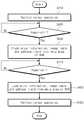
도 12는 도 11의 스토리지 컨트롤러의 간접 리페어 동작을 예시적으로 보여주는 순서도이다. 도 13a 및 도 13b는 도 12의 순서도에 따른 동작을 설명하기 위한 도면들이다. 예시적인 실시 예에서, 도 12의 순서도는 도 3의 S15 단계의 동작에 대한 일 실시 예일 수 있다. 즉, 도 12의 순서도에 따른 동작은 DRAM 장치(220)로부터 페일 로우가 검출된 경우에 수행될 수 있다.12 is a flowchart illustrating an indirect repair operation of the storage controller of FIG. 11. 13A and 13B are diagrams for describing an operation according to the flowchart of FIG. 12. In an example embodiment, the flowchart of FIG. 12 may be an embodiment of an operation of step S15 of FIG. 3. That is, the operation according to the flowchart of FIG. 12 may be performed when a fail low is detected from the
도 11 및 도 12를 참조하면, S211 단계에서, 스토리지 컨트롤러(210)는 페일 로우와 대응되는 페일 어드레스를 예비 어드레스로 리맵핑할 수 있다. 예를 들어, 도 13a에 도시된 바와 같이, 스토리지 컨트롤러(210)는 DRAM 장치(220)의 사용자 영역 및 예비 영역을 모두 인식할 수 있다. 즉, 스토리지 장치(210)는 DRAM 장치(220)의 제0 내지 제n 어드레스들(ADDR_u0~ADDR_un)에 대응되는 영역을 사용자 영역(User Area)으로서 인식하고, 제0 내지 제m 어드레스들(ADDR_rn~ADDR_rm)에 대응되는 영역을 예비 영역(Reserved Area)으로서 인식할 수 있다.11 and 12, in operation S211, the
사용자 영역(User Area)은 스토리지 장치(210)의 일반적인 동작에서, 액세스되는 영역을 가리킬 수 있다. 예비 영역(Reserved Area)은 스토리지 컨트롤러(210)에 의해 인식되는 영역이나, 정상 액세스 동작에서 액세스되지 않는 영역을 가리킬 수 있다. 다시 말해서, 스토리지 장치(210)(특히, 프로세서(212))는 DRAM 장치(220)를 액세스하기 위하여, 사용자 영역에 포함된 어드레스(즉, ADDR_u0~ADDR_un)를 원본 어드레스(Original address)로서 발행할 수 있다.The user area may refer to an area that is accessed in a general operation of the
사용자 영역에서 페일 로우(Fail Row)가 발생한 경우, 스토리지 컨트롤러(210)는 페일 로우(Fail Row)에 대응하는 영역을 예비 영역의 예비 로우(Reserved Row)로 리맵핑할 수 있다. 예를 들어, 도 11a에 도시된 바와 같이, 사용자 영역의 어드레스(ADDR_uk)에 대응하는 행이 페일 로우로 검출된 경우, DRAM 액세스 관리자(211c)는 사용자 영역의 사용자 어드레스(ADDR_uk)를 예비 영역의 예비 어드레스(ADDR_rk)로 리맵핑할 수 있다.When a fail row occurs in the user area, the
S212 단계에서, 스토리지 컨트롤러(210)는 리맵 테이블 및 어드레스 필드를 갱신할 수 있다. 예를 들어, 도 11b에 도시된 바와 같이, DRAM 액세스 관리자(211c)는 어드레스 필드(AF) 및 리맵 테이블(RT)을 포함할 수 있다. 어드레스 필드(AF)는 앞서 설명된 바와 같이, DRAM 장치(220)의 복수의 행들 각각에 대한 리맵 플래그(Remap Flag) 정보를 포함할 수 있다. 리맵 테이블(RT)은 페일 로우에 대응하는 페일 어드레스 및 예비 로우에 대응하는 예비 어드레스 사이의 매핑 관계에 대한 정보를 포함할 수 있다.In operation S212, the
도 11a를 참조하여 설명된 바와 같이, 사용자 어드레스(ADDR_uk)에 대응하는 행이 페일 로우이고, 사용자 어드레스(ADDR_uk)가 예비 어드레스(ADDR_rk)로 리맵된 경우, 스토리지 컨트롤러(210)는 사용자 영역의 제k 어드레스(ADDR_uk)를 페일 로우로 설정하고, 예비 영역의 제k 어드레스(ADDR_rk)를 대응하는 예비 로우로 설정할 수 있다. 즉, 스토리지 컨트롤러(210)는 사용자 영역의 페일 로우 및 리맵된 예비 로우에 대한 정보를 기반으로 리맵 테이블(RT)을 갱신할 수 있다.As described with reference to FIG. 11A, when the row corresponding to the user address ADDR_uk is a fail row, and the user address ADDR_uk is remapped to the reserved address ADDR_rk, the
예시적인 실시 예에서, 스토리지 컨트롤러(210)는 어드레스 필드(AF)에서, 사용자 어드레스(ADDR_uk)에 대한 리맵 플래그(Remap Flag)의 값을 “0”에서 “1”로 변경할 수 있다. 예시적인 실시 예에서, 리맵 플래그(Remap Flag)가 “1”인 경우, 대응하는 어드레스가 예비 영역으로 리맵된 것을 가리킬 수 있고, 리맵 플래그(Remap Flag)가 “0”인 경우, 대응하는 어드레스가 예비 영역으로 리맵되지 않은 것을 가리킬 수 있다.In an example embodiment, the
도 14는 도 11의 스토리지 컨트롤러의 DRAM 장치에 대한 액세스 동작을 보여주는 순서도이다. 도 11 및 도 14를 참조하면, S221 단계에서, 스토리지 컨트롤러(210)는 액세스될 행과 대응되는 원본 어드레스를 발행할 수 있다. 예를 들어, 스토리지 컨트롤러(210)의 프로세서(212)는 DRAM 장치(220)를 액세스하기 위한 원본 어드레스를 발행할 수 있다. 예시적인 실시 예에서, 원본 어드레스는 도 11a를 참조하여 설명된 사용자 영역의 어드레스들(ADDR_r0~ADDR_rn)에 포함된 어드레스일 수 있다. 즉, 프로세서(212)는 DRAM 장치(220)의 사용자 영역을 액세스하도록 구성될 수 있다.FIG. 14 is a flowchart illustrating an access operation of a DRAM device of the storage controller of FIG. 11. 11 and 14, in operation S221, the
S222 단계에서, 스토리지 컨트롤러(210)는 원본 어드레스와 대응되는 행이 페일 로우인지 판별할 수 있다. 예를 들어, 스토리지 컨트롤러(210)는 어드레스 필드(AF)에서, 원본 어드레스에 대한 리맵 플래그(Remap Flag)를 확인할 수 있다. 리맵 플래그(Remap Flag)가 “0”인 경우, 스토리지 컨트롤러(210)는 원본 어드레스와 대응되는 행이 페인 로우가 아닌 것으로 판별한다. 이 경우, S223 단계에서, 스토리지 컨트롤러(210)는 원본 어드레스에 대응하는 행(즉, 사용자 영역의 행)에 대한 액세스 동작을 수행할 수 있다.In operation S222, the
원본 어드레스에 대응하는 리맵 플래그(Remap Flag)가 “1”인 경우, 스토리지 컨트롤러(210)는 원본 어드레스에 대응하는 행이 페일 로우인 것으로 판별한다. 이 경우, S224 단계에서, 스토리지 컨트롤러(210)는 리맵 테이블(RT)을 기반으로 원본 어드레스에 대응하는 리맵된 어드레스를 검색할 수 있다. 예를 들어, 도 11b를 참조하여 설명된 바와 같이, 리맵 테이블(RT)은 페일 로우에 대한 원본 어드레스 및 예비 로우에 대한 리맵된 어드레스 사이의 관계에 대한 정보를 포함할 수 있다. 즉, 스토리지 컨트롤러(210)는 리맵 테이블(RT)에서, 원본 어드레스에 대응하는 리맵된 어드레스를 검색할 수 있다.When the remap flag corresponding to the original address is "1", the
S225 단계에서, 스토리지 컨트롤러(210)는 리맵된 어드레스에 대응하는 예비 행에 대한 액세스 동작을 수행할 수 있다.In operation S225, the
상술된 바와 같이, 본 발명의 실시 예에 따르면, DRAM 장치(220)에 대한 직접적인 리페어 동작 대신에, 캐시 계층 구조를 사용하여 DRAM 장치(220)의 페일 로우를 DRAM 장치(220)의 예비 영역으로 리맵시킬 수 있다. 따라서, 스토리지 장치(200)의 구동 중에, DRAM 장치(220)에서 페일 로우가 검출되더라도, DRAM 장치(220) 또는 스토리지 장치(200)가 정상적으로 동작할 수 있다.As described above, according to an embodiment of the present invention, instead of a direct repair operation on the
도 15는 본 발명의 일 실시 예에 따른 런타임 리페어 동작을 예시적으로 보여주는 순서도이다. 예시적으로, 도 15를 참조하여, 직접 리페어 동작 및 간접 리페어 동작이 결합된 런타임 리페어 동작이 예시적으로 설명된다.15 is a flowchart exemplarily illustrating a runtime repair operation according to an embodiment of the present invention. For example, with reference to FIG. 15, a runtime repair operation in which a direct repair operation and an indirect repair operation are combined is described as an example.
도 11 및 도 15를 참조하면, S301 단계에서, 스토리지 컨트롤러(210)는 누적 에러 정보, 리맵 테이블, 및 어드레스 필드를 로드할 수 있다. 예를 들어, 누적 에러 정보는, 도 4를 참조하여 설명된 바와 같이, DRAM 장치(220)의 복수의 행들 각각에 대한 에러 비트들의 누적된 개수를 가리킬 수 있고, 리맵 테이블은, 도 13b를 참조하여 설명된 바와 같이, 페일 로우에 대한 어드레스 및 리맵된 어드레스 사이의 매핑 관계를 가리킬 수 있고, 어드레스 필드는 어드레스 및 대응되는 리맵 플래그에 대한 정보를 가리킬 수 있다.11 and 15, in operation S301, the
예시적인 실시 예에서, 상술된 정보들은, 데이터 유지를 위하여, 불휘발성 메모리 장치(230)의 특정 영역(예를 들어, 메타 영역)에 주기적으로 플러쉬될 수 있다. 스토리지 컨트롤러(210)는 스토리지 장치(210)의 초기화 동작시, 불휘발성 메모리 장치(230)로부터 상술된 정보를 로드할 수 있다. 예시적인 실시 예에서, 로드된 정보는 SRAM(223)에 저장되고, 프로세서(212) 또는 DRAM 제어 유닛(211)에 의해 관리될 수 있다.In an exemplary embodiment, the above-described information may be periodically flushed to a specific region (eg, a meta region) of the
S302 단계에서, 스토리지 컨트롤러(210)는 장치가 유휴 상태인지 판별할 수 있다. 장치가 유휴 상태가 아닌 경우, 스토리지 컨트롤러(210)는 S311 단계 내지 S314 단계의 동작들을 수행할 수 있다. S311 단계 내지 S313 단계의 동작들은 도 3의 S12 단계 내지 S14 단계의 동작들과 유사하므로, 이에 대한 상세한 설명은 생략된다. S314 단계의 동작은 도 12를 참조하여 설명된 간접 리페어 동작과 유사하므로, 이에 대한 상세한 설명은 생략된다.In operation S302, the
장치가 유휴 상태인 경우, 스토리지 컨트롤러(210)는 S321 단계 내지 S324 단계의 동작들을 수행할 수 있다. S321 단계 내지 S324 단계의 동작들은 도 5의 S111 단계 내지 S114 단계의 동작들(즉, 직접 리페어 동작)과 유사하므로, 이에 대한 상세한 설명은 생략된다.When the device is in the idle state, the
즉, 스토리지 컨트롤러(210)는 장치가 유휴 상태가 아니고, DRAM 장치(220)에서 페일 로우가 검출된 경우, 간접 리페어 동작을 수행할 수 있다. 앞서 설명된 바와 같이, 간접 리페어 동작은 DRAM 장치(220)로의 액세스 차단, 데이터 백업 등과 같은 동작을 필요로 하지 않기 때문에, 추가적인 성능 저하가 없을 것이다. 다만, 장치가 유휴 상태인 경우, 스토리지 컨트롤러(210)는 직접 리페어 동작을 수행할 수 있다. 이 때, 스토리지 컨트롤러(210)는 검출된 페일 로우 뿐만 아니라, 리맵 테이블(RT)에 리맵된 어드레스들에 대한 직접 리페어 동작을 수행할 수 있다.That is, the
예시적인 실시 예에서, 점선으로 표기된 S302 단계의 동작은 S301 단계 및 S311/S321 단계 사이뿐만 아니라, 스토리지 장치(200)가 동작하는 도중에 수행될 수 있다. 즉, 스토리지 컨트롤러(210)는 스토리지 장치(200)가 동작하는 도중에, 유휴 상태인지 지속적으로 판별하고, 이에 따라, 간접 리페어 동작 또는 직접 리페어 동작을 수행할 수 있다.In an exemplary embodiment, the operation of step S302 indicated by a dotted line may be performed during the operation of the storage device 200 as well as between steps S301 and S311 / S321. That is, the
비록 도면에 도시되지는 않았으나, 예시적인 실시 예에서, 리맵 테이블(RT)에 포함된 리맵 어드레스들의 개수가 기준치 이상인 경우, 스토리지 컨트롤러(210)는 직접 리페어 동작을 수행할 수 있다.Although not shown in the drawing, in an exemplary embodiment, when the number of remap addresses included in the remap table RT is greater than or equal to the reference value, the
도 16은 본 발명의 실시 예에 따른 스토리지 컨트롤러의 동작을 예시적으로 보여주는 순서도이다. 도 11 및 도 16을 참조하면, S410 단계에서, 스토리지 컨트롤러(210)는 정상 동작을 수행할 수 있다. 이 때, 정상 동작은 스토리지 장치(200)에 대한 다양한 동작들 또는 도 1 내지 도 13을 참조하여 설명된 런타임 리페어 동작들을 포함할 수 있다.16 is a flowchart illustrating an operation of a storage controller according to an embodiment of the present disclosure. 11 and 16, in operation S410, the
S420 단계에서, 스토리지 컨트롤러(410)는 파워-오프인지 판별할 수 있다. 예를 들어, 호스트의 제어에 따라 스토리지 장치(200)로 제공되는 전원이 차단되거나 또는 다양한 요인으로 인하여 서든-파워-오프(SPO; sudden power off)가 발생할 수 있다.In operation S420, the storage controller 410 may determine whether the power is off. For example, power provided to the storage device 200 may be cut off or sudden power off (SPO) may occur due to various factors under the control of the host.
파워가 오프된 경우, S430 단계에서, 스토리지 컨트롤러(210)는 누적 에러 정보, 리맵 테이블, 및 어드레스 필드를 불휘발성 메모리 장치(230)의 메타 영역으로 플러쉬할 수 있다. 예시적인 실시 예에서, 스토리지 컨트롤러(210)는 DRAM 장치(220)에 저장된 중요 데이터(예를 들어, 맵핑 테이블, 메타 정보 등)와 함께 상술된 정보를 불휘발성 메모리 장치(230)로 플러쉬할 수 있다.When the power is turned off, in operation S430, the
S440 단계에서, 스토리지 컨트롤러(210)는 파워-온 상태인지 판별할 수 있다. 예를 들어, 전원이 차단된 이후에, 호스트(21)로부터 전원이 다시 제공될 수 있다. 이 경우, S450 단계에서, 스토리지 컨트롤러(210)는 불휘발성 메모리 장치(230)의 메타 영역으로부터 플러쉬된 다양한 정보(예를 들어, 누적 에러 정보, 리맵 테이블, 및 어드레스 필드 등)를 로드할 수 있다. 로드된 정보는 SRAM(213)에 저장되고, 프로세서(212) 또는 DRAM 제어 유닛(211)에 의해 관리될 수 있다. 예시적인 실시 예에서, 상술된 로딩 동작은 스토리지 컨트롤러(210)의 초기화 동작 도중에 수행될 수 있다.In operation S440, the
이후에, S460 단계에서, 스토리지 컨트롤러(210)는 정상 동작을 수행할 수 있다. 예를 들어, 스토리지 컨트롤러(210)는 로드된 다양한 정보를 기반으로 도 1 내지 도 15를 참조하여 설명된 런타임 리페어 동작을 수행할 수 있다.Thereafter, in operation S460, the
상술된 바와 같이, 본 발명의 실시 예에 따른 스토리지 컨트롤러는 DRAM 장치에 대한 누적 에러 정보를 관리하고, 누적 에러 정보를 기반으로 DRAM 장치의 페일 로우를 검출할 수 있다. 스토리지 컨트롤러는 검출된 페일 로우에 대한 런타임 리페어 동작을 수행하므로써, 페일 로우를 복구할 수 있다. 예시적인 실시 예에서, 누적 에러 정보, 리맵 테이블, 및 어드레스 필드와 같은 정보는 페일 로우를 검출하거나 또는 런타임 리페어 동작을 위해 유지되어야 하므로, 도 16을 참조하여 설명된 바와 같이, 파워-오프시 불휘발성 메모리 장치로 플러쉬되거나 또는 주기적 또는 비주기적으로 불휘발성 메모리 장치로 플러쉬될 수 있다.As described above, the storage controller according to an exemplary embodiment of the present invention manages cumulative error information of a DRAM device and detects a fail row of the DRAM device based on the cumulative error information. The storage controller can recover the fail row by performing a runtime repair operation on the detected fail row. In an exemplary embodiment, information such as cumulative error information, remap table, and address field must be maintained for detecting a fail row or for a runtime repair operation, as described with reference to FIG. It may be flushed to a volatile memory device or may be flushed to a nonvolatile memory device periodically or aperiodically.
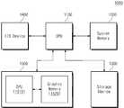
도 17은 본 발명의 실시 예에 따른 스토리지 장치가 적용된 사용자 시스템을 예시적으로 보여주는 블록도이다. 도 17을 참조하면, 사용자 시스템(1000)은 CPU(1100), 시스템 메모리(1200), 스토리지 장치(1300), 입출력 장치(1400), 및 그래픽 장치(1500)를 포함할 수 있다.17 is a block diagram illustrating a user system to which a storage device is applied according to an exemplary embodiment of the inventive concept. Referring to FIG. 17, the
CPU(1100)는 사용자 시스템(1000)에서 요구되는 명령어 연산 동작, 명령어 해독 동작, 또는 명령어 제어 동작 등을 수행할 수 있다. 시스템 메모리(1200)는 CPU(1100)의 버퍼 메모리, 캐시 메모리, 주 메모리로써 사용될 수 있다. 예시적인 실시 예에서, 시스템 메모리(1200)는 DRAM 장치를 포함할 수 있다. CPU(1100) 및 시스템 메모리(1200)는 도 1 내지 도 16을 참조하여 설명된 런타임 리페어 동작을 수행하도록 구성될 수 있다. 즉, 사용자 시스템(1000)이 구동 중인 도중에, 시스템 메모리(1200)에 대한 페일 로우를 검출하고, 검출된 페일 로우에 대한 런타임 리페어 동작이 수행될 수 있다.The
스토리지 장치(1300)는 사용자 시스템(1000)에서 사용되는 데이터를 저장할 수 있다. 스토리지 장치(1300)는 PRAM(Phase-change RAM), MRAM(Magnetic RAM), RRAM(Resistive RAM), NAND flash, NOR flash, 3차원 구조의 NAND 플래시 등과 같은 불휘발성 반도체 메모리 소자로 구현될 수 있다. 스토리지 장치(1300)는 대용량 저장 매체일 수 있다. 예시적인 실시 예에서, 스토리지 장치(1300)는 도 1 내지 도 16을 참조하여 설명된 실시 예들에 기반된 스토리지 장치일 수 있다.The
입출력 장치(1400)는 사용자 시스템(1000)에 데이터 또는 명령어를 입력하거나 또는 외부 장치로 데이터를 출력하는 장치들을 포함할 수 있다. 예시적으로, 입출력 장치(1400)는 키보드, 키패드, 버튼, 터치 패널, 터치 스크린, 터치 패드, 터치 볼, 카메라, 마이크, 자이로스코프 센서, 진동 센서, 압전 소자 등과 같은 사용자 입력 인터페이스들을 포함할 수 있다. 입출력 장치(1400)는 LCD (Liquid Crystal Display), OLED (Organic Light Emitting Diode) 표시 장치, AMOLED (Active Matrix OLED) 표시 장치, LED, 스피커, 모터 등과 같은 사용자 출력 인터페이스들을 포함할 수 있다.The input /
그래픽 장치(1500)는 CPU(1100)의 동작 결과를 표시하기 위한 장치일 수 있다. 그래픽 장치(1500)는 GPU(1510) 및 그래픽 메모리(1520)를 포함할 수 있다. GPU(1510)는 CPU(1100)로부터 제공되는 데이터 신호를 영상 신호로 변환할 수 있다. GPU(1510)는 그래픽 처리를 위한 다양한 연산 동작을 수행할 수 있다.The
그래픽 메모리(1520)는 GPU(1510)가 연산 동작을 수행하는데 요구되는 정보를 임시 저장하는 버퍼 메모리 또는 캐시 메모리일 수 있다. 예시적인 실시 예에서, 그래픽 메모리(1520)는 DRAM 장치를 포함할 수 있다. GPU(1510) 및 그래픽 메모리(1520)는 도 1 내지 도 16을 참조하여 설명된 런타임 리페어 동작을 수행하도록 구성될 수 있다. 즉, 그래픽 장치(1500)가 구동 중인 도중에, 시스템 메모리(1200)에 대한 페일 로우를 검출하고, 검출된 페일 로우에 대한 런타임 리페어 동작이 수행될 수 있다.The
상술된 내용은 본 발명을 실시하기 위한 구체적인 실시 예들이다. 본 발명은 상술된 실시 예들뿐만 아니라, 단순하게 설계 변경되거나 용이하게 변경할 수 있는 실시 예들 또한 포함할 것이다. 또한, 본 발명은 실시 예들을 이용하여 용이하게 변형하여 실시할 수 있는 기술들도 포함될 것이다. 따라서, 본 발명의 범위는 상술된 실시 예들에 국한되어 정해져서는 안되며 후술하는 특허청구범위뿐만 아니라 이 발명의 특허청구범위와 균등한 것들에 의해 정해져야 할 것이다.The foregoing is specific embodiments for practicing the present invention. The present invention will include not only the above-described embodiments but also embodiments that can be simply changed in design or easily changed. In addition, the present invention will also include techniques that can be easily modified and practiced using the embodiments. Therefore, the scope of the present invention should not be limited to the above-described embodiments, but should be determined by the equivalents of the claims of the present invention as well as the following claims.
Claims (20)
Translated fromKorean상기 DRAM 장치에 대한 액세스 동작을 수행하는 단계;
상기 액세스 동작을 기반으로 상기 DRAM 장치에 대한 누적 에러 정보를 수집하는 단계;
상기 누적 에러 정보를 기반으로 상기 DRAM 장치에 페일 로우를 검출하는 단계; 및
상기 검출된 페일 로우에 대한 런타임 리페어 동작을 수행하는 단계를 포함하는 동작 방법.A method of operating a storage device including a nonvolatile memory device, a dynamic random access memory (DRAM) device, and a storage controller,
Performing an access operation on the DRAM device;
Collecting cumulative error information for the DRAM device based on the access operation;
Detecting a fail row in the DRAM device based on the accumulated error information; And
Performing a runtime repair operation on the detected fail row.
상기 액세스 동작은 상기 DRAM 장치로부터 데이터를 읽는 동작 및 상기 읽은 데이터에 대한 에러 검출 및 정정 동작을 포함하는 동작 방법.The method of claim 1,
And the access operation includes reading data from the DRAM device and error detecting and correcting the read data.
상기 누적 에러 정보는 상기 DRAM 장치의 복수의 행들 각각에 대하여, 상기 에러 검출 및 정정 동작에 의해 검출된 에러 비트의 누적된 개수를 가리키는 동작 방법.The method of claim 2,
And the cumulative error information indicates a cumulative number of error bits detected by the error detection and correction operation for each of a plurality of rows of the DRAM device.
상기 검출된 페일 로우는 상기 복수의 행들 중 상기 누적된 개수가 기준 값보다 큰 행인 동작 방법.The method of claim 3, wherein
The detected fail row is a row in which the accumulated number of the plurality of rows is larger than a reference value.
상기 누적 에러 정보는 상기 스토리지 컨트롤러의 램에 저장되고, 상기 스토리지 장치의 파워-오프시 상기 램으로부터 상기 불휘발성 메모리 장치로 플러쉬되고, 상기 스토리지 장치의 파워-온시 상기 불휘발성 메모리 장치로부터 상기 램으로 로드되는 동작 방법.The method of claim 3, wherein
The cumulative error information is stored in a RAM of the storage controller, is flushed from the RAM to the nonvolatile memory device at power-off of the storage device, and from the nonvolatile memory device to the RAM at power-on of the storage device. The method of operation that is loaded.
상기 런타임 리페어 동작을 수행하는 단계는:
상기 DRAM 장치에 저장된 데이터 중 일부 데이터 또는 전체 데이터를 상기 불휘발성 메모리 장치로 플러쉬하는 단계;
상기 DRAM 장치의 상기 페일 로우에 대한 포스트 패키지 리페어 동작을 수행하는 단계; 및
상기 불휘발성 메모리 장치로 플러쉬된 일부 데이터 또는 전체 데이터를 상기 DRAM 장치로 복원하는 단계를 포함하는 동작 방법.The method of claim 1,
The performing of the runtime repair operation includes:
Flushing some or all of the data stored in the DRAM device to the nonvolatile memory device;
Performing a post package repair operation on the fail row of the DRAM device; And
Restoring partial data or all data flushed to the nonvolatile memory device to the DRAM device.
상기 포스트 패키지 리페어 동작은 모드 레지스터 셋 커맨드, 어드레스 신호들, 활성 커맨드, 자동 프리차지 쓰기 커맨드, 및 프리차지 커맨드를 사용하여 수행되는 동작 방법.The method of claim 6,
And the post package repair operation is performed using a mode register set command, address signals, an active command, an automatic precharge write command, and a precharge command.
상기 일부 데이터는 상기 DRAM 장치의 복수의 뱅크들 중 상기 페일 로우를 포함하는 뱅크들에 저장된 데이터인 동작 방법.The method of claim 7, wherein
And the partial data is data stored in banks including the fail row among a plurality of banks of the DRAM device.
상기 런타임 리페어 동작을 수행하는 단계는:
상기 DRAM 장치의 상기 검출된 페일 로우를 상기 DRAM 장치의 예비 영역의 예비 로우로 리맵하는 단계; 및
상기 검출된 페일 로우에 대응하는 페일 어드레스 및 상기 예비 로우에 대응하는 예비 어드레스를 기반으로 리맵 테이블을 갱신하는 단계를 포함하는 동작 방법.The method of claim 1,
The performing of the runtime repair operation includes:
Remapping the detected fail row of the DRAM device to a spare row of a spare area of the DRAM device; And
Updating a remap table based on a fail address corresponding to the detected fail row and a spare address corresponding to the spare row.
상기 DRAM 장치의 사용자 영역에 대한 원본 어드레스를 발행하는 단계; 및
상기 원본 어드레스와 대응되는 행이 상기 검출된 페일 로우인 경우 상기 리맵 테이블을 기반으로 상기 예비 영역을 액세스하고, 상기 원본 어드레스와 대응되는 상기 행이 상기 검출된 페일 로우가 아닌 경우 상기 원본 어드레스에 대응되는 상기 사용자 영역을 액세스하는 단계를 더 포함하는 동작 방법.The method of claim 9,
Issuing an original address for the user area of the DRAM device; And
Access the spare area based on the remap table when the row corresponding to the source address is the detected fail row, and correspond to the source address when the row corresponding to the source address is not the detected fail row. And accessing the user area.
상기 스토리지 장치의 유휴 상태 동안, 상기 리맵 테이블을 기반으로 상기 DRAM 장치에 대한 포스트 패키지 리페어 동작을 수행하는 단계를 더 포함하는 동작 방법.The method of claim 9,
During the idle state of the storage device, performing a post-package repair operation on the DRAM device based on the remap table.
동적 랜덤 액세스 메모리(DRAM; Dynamic Random Access Memory) 장치; 및
상기 불휘발성 메모리 장치 및 상기 DRAM 장치를 제어하도록 구성된 스토리지 컨트롤러를 포함하고,
상기 스토리지 컨트롤러는:
상기 DRAM 장치로부터 읽은 데이터에 대한 에러 검출 및 정정 동작을 수행하도록 구성된 DRAM 에러 정정 엔진; 및
상기 DRAM 에러 정정 엔진에 의해 검출된 에러를 기반으로 누적 에러 정보를 관리하고, 상기 누적 에러 정보를 기반으로 상기 DRAM 장치의 페일 로우를 검출하고, 상기 검출된 페일 로우에 대한 런타임 리페어 동작을 수행하도록 구성된 리페어 관리자를 포함하는 스토리지 장치.Nonvolatile memory devices;
A dynamic random access memory (DRAM) device; And
A storage controller configured to control the nonvolatile memory device and the DRAM device;
The storage controller is:
A DRAM error correction engine configured to perform error detection and correction operations on data read from the DRAM device; And
Manage cumulative error information based on an error detected by the DRAM error correction engine, detect a fail row of the DRAM device based on the cumulative error information, and perform a runtime repair operation on the detected fail row. Storage device with a configured repair manager.
상기 스토리지 컨트롤러는:
상기 누적 에러 정보를 저장하도록 구성된 메모리를 더 포함하고,
상기 메모리에 저장된 상기 누적 에러 정보는 상기 불휘발성 메모리 장치로 주기적으로 플러쉬되는 스토리지 장치.The method of claim 12,
The storage controller is:
A memory configured to store the cumulative error information;
The accumulated error information stored in the memory is periodically flushed to the nonvolatile memory device.
상기 리페어 관리자는 상기 DRAM 장치에 저장된 데이터 중 일부 데이터 또는 전체 데이터를 상기 불휘발성 메모리 장치로 플러쉬하고, 상기 DRAM 장치에 대한 포스트 패키지 리페어 동작을 수행하고, 상기 포스트 패키지 리페어 동작이 수행된 상기 DRAM 장치로 상기 플러쉬된 데이터를 복원함으로써, 상기 런타임 리페어 동작을 수행하는 스토리지 장치.The method of claim 12,
The repair manager flushes some or all of the data stored in the DRAM device to the nonvolatile memory device, performs a post package repair operation on the DRAM device, and performs the post package repair operation. And performing the runtime repair operation by restoring the flushed data.
상기 DRAM 장치는:
상기 스토리지 컨트롤러부터 어드레스를 수신하고, 퓨즈-셋팅에 따라 상기 어드레스 및 상기 어드레스가 변환된 변환 어드레스 중 어느 하나를 출력하도록 구성된 퓨즈 회로;
노멀 셀들 및 리던던시 셀들을 포함하는 메모리 셀 어레이;
노멀 워드라인들을 통해 상기 노멀 셀들과 연결되고, 리던던시 워드라인들을 통해 상기 리던던시 셀들과 연결되고, 상기 어드레스에 응답하여 상기 노멀 워드라인들 중 어느 하나를 선택하고, 상기 변환 어드레스에 응답하여 상기 리던던시 워드라인들 중 어느 하나를 선택하도록 구성된 로우 디코더;
비트라인들을 통해 상기 메모리 셀 어레이와 연결된 컬럼 디코더; 및
상기 스토리지 컨트롤러의 상기 런타임 리페어 동작에 의해 상기 퓨즈 회로의 상기 퓨즈-셋팅을 재설정하도록 구성된 제어 로직 회로를 포함하는 스토리지 장치.The method of claim 14,
The DRAM device is:
A fuse circuit configured to receive an address from the storage controller and output one of the address and a translation address converted from the address according to a fuse-setting;
A memory cell array comprising normal cells and redundancy cells;
Connected to the normal cells through normal word lines, connected to the redundancy cells through redundancy word lines, selecting one of the normal word lines in response to the address, and the redundancy word in response to the translation address A row decoder configured to select one of the lines;
A column decoder coupled to the memory cell array through bit lines; And
A control logic circuit configured to reset the fuse-setting of the fuse circuit by the runtime repair operation of the storage controller.
상기 DRAM 장치는 사용자 영역 및 예비 영역을 포함하고, 상기 검출된 페일 로우는 상기 사용자 영역에 포함되고,
상기 리페어 관리자는 상기 검출된 페일 로우에 대응하는 원본 어드레스를 상기 예비 영역 중 하나의 예비 행에 대응되는 예비 어드레스로 리맵핑하는 스토리지 장치.The method of claim 12,
The DRAM device includes a user area and a spare area, the detected fail row is included in the user area,
The repair manager may remap an original address corresponding to the detected fail row to a spare address corresponding to one spare row of the spare areas.
상기 스토리지 컨트롤러는:
상기 원본 어드레스를 발행하여 상기 DRAM 장치를 액세스하도록 구성된 프로세서; 및
상기 원본 어드레스가 상기 페일 로우와 대응되는 경우, 상기 예비 어드레스를 출력하도록 구성된 DRAM 액세스 관리자를 더 포함하는 스토리지 장치.The method of claim 16,
The storage controller is:
A processor configured to access the DRAM device by issuing the original address; And
And a DRAM access manager configured to output the reserved address when the original address corresponds to the fail row.
상기 휘발성 메모리 장치로부터 데이터를 읽는 단계;
상기 읽은 데이터에 대한 에러 검출 및 정정 동작을 수행하는 단계;
상기 에러 검출 및 정정 동작의 결과를 기반으로 상기 휘발성 메모리 장치의 복수의 행들 각각에 대한 누적 에러 정보를 갱신하는 단계;
상기 갱신된 누적 에러 정보를 기반으로 상기 휘발성 메모리 장치의 페일 로우를 검출하는 단계; 및
상기 검출된 페일 로우에 대한 런타임 리페어 동작을 수행하는 단계를 포함하고,
상기 런타임 리페어 동작은 상기 스토리지 장치의 동작 중에 수행되는 동작 방법.A method of operating a storage device comprising a nonvolatile memory device, a volatile memory device, and a storage controller configured to control the nonvolatile memory device and the volatile memory device.
Reading data from the volatile memory device;
Performing an error detection and correction operation on the read data;
Updating cumulative error information for each of a plurality of rows of the volatile memory device based on a result of the error detection and correction operation;
Detecting a fail row of the volatile memory device based on the updated cumulative error information; And
Performing a runtime repair operation on the detected fail row;
The runtime repair operation is performed during the operation of the storage device.
상기 런타임 리페어 동작을 수행하는 단계는:
상기 휘발성 메모리 장치에 저장된 상기 데이터 중 일부 데이터 또는 전체 데이터를 상기 불휘발성 메모리 장치로 플러쉬하는 단계;
상기 휘발성 메모리 장치에 대한 포스트 패키지 리페어 동작을 수행하여 상기 검출된 페일 로우를 복구하는 단계; 및
상기 플러쉬된 데이터를 상기 불휘발성 메모리 장치로부터 상기 포스트 패키지 리페어 동작이 수행된 상기 휘발성 메모리 장치로 복원하는 단계를 포함하는 동작 방법.The method of claim 18,
The performing of the runtime repair operation includes:
Flushing some or all of the data stored in the volatile memory device to the nonvolatile memory device;
Recovering the detected fail row by performing a post package repair operation on the volatile memory device; And
Restoring the flushed data from the nonvolatile memory device to the volatile memory device on which the post-package repair operation was performed.
상기 런타임 리페어 동작을 수행하는 단계는:
상기 검출된 페일 로우를 상기 휘발성 메모리 장치의 예비 영역의 예비 로우로 리맵하는 단계; 및
상기 페일 로우와 대응되는 원본 어드레스 및 상기 예비 로우의 리맵 어드레스를 기반으로 리맵 테이블을 갱신하는 단계를 포함하는 동작 방법.
The method of claim 18,
The performing of the runtime repair operation includes:
Remapping the detected fail row to a spare row of a spare area of the volatile memory device; And
Updating a remap table based on an original address corresponding to the fail row and a remap address of the spare row.
Priority Applications (4)
| Application Number | Priority Date | Filing Date | Title |
|---|---|---|---|
| KR1020180095016AKR102623234B1 (en) | 2018-08-14 | 2018-08-14 | Storage device and operation method thereof |
| US16/351,118US11302414B2 (en) | 2018-08-14 | 2019-03-12 | Storage device that performs runtime repair operation based on accumulated error information and operation method thereof |
| DE102019117787.1ADE102019117787B4 (en) | 2018-08-14 | 2019-07-02 | Storage device and method of operation thereof |
| CN201910742162.5ACN110825321B (en) | 2018-08-14 | 2019-08-12 | Memory device and method of operating the same |
Applications Claiming Priority (1)
| Application Number | Priority Date | Filing Date | Title |
|---|---|---|---|
| KR1020180095016AKR102623234B1 (en) | 2018-08-14 | 2018-08-14 | Storage device and operation method thereof |
Publications (2)
| Publication Number | Publication Date |
|---|---|
| KR20200019463Atrue KR20200019463A (en) | 2020-02-24 |
| KR102623234B1 KR102623234B1 (en) | 2024-01-11 |
Family
ID=69320613
Family Applications (1)
| Application Number | Title | Priority Date | Filing Date |
|---|---|---|---|
| KR1020180095016AActiveKR102623234B1 (en) | 2018-08-14 | 2018-08-14 | Storage device and operation method thereof |
Country Status (4)
| Country | Link |
|---|---|
| US (1) | US11302414B2 (en) |
| KR (1) | KR102623234B1 (en) |
| CN (1) | CN110825321B (en) |
| DE (1) | DE102019117787B4 (en) |
Cited By (3)
| Publication number | Priority date | Publication date | Assignee | Title |
|---|---|---|---|---|
| EP3868482A1 (en) | 2020-02-18 | 2021-08-25 | Samsung Medison Co., Ltd. | Ultrasonic probe with grooved matching layer |
| KR20220100496A (en)* | 2021-01-08 | 2022-07-15 | 타이완 세미콘덕터 매뉴팩쳐링 컴퍼니 리미티드 | Memory repair using optimized redundancy utilization |
| KR20230015033A (en)* | 2021-07-22 | 2023-01-31 | 성균관대학교산학협력단 | Apparatus and method for remapping of memory |
Families Citing this family (12)
| Publication number | Priority date | Publication date | Assignee | Title |
|---|---|---|---|---|
| US11068365B2 (en)* | 2018-08-23 | 2021-07-20 | Micron Technology, Inc. | Data recovery within a memory sub-system without moving or processing the data through a host |
| EP3761193A1 (en)* | 2019-07-04 | 2021-01-06 | Siemens Aktiengesellschaft | Safety analysis of technical systems comprising human objects |
| CN111338851B (en)* | 2020-02-26 | 2024-02-13 | 东莞记忆存储科技有限公司 | Method, device, computer equipment and storage medium for automatically repairing fault memory boot hPR |
| CN113495812B (en)* | 2020-04-01 | 2024-02-06 | 森富科技股份有限公司 | Maintenance and inspection methods after memory packaging |
| US11011251B1 (en)* | 2020-08-10 | 2021-05-18 | Nanya Technology Corporation | System and method of verifying hard post package repair and non-transitory computer readable medium |
| US11334458B2 (en)* | 2020-08-27 | 2022-05-17 | Micron Technology, Inc. | Completing memory repair operations interrupted by power loss |
| KR20220049856A (en)* | 2020-10-15 | 2022-04-22 | 에스케이하이닉스 주식회사 | Memory system and contrller |
| US11990199B2 (en)* | 2021-01-21 | 2024-05-21 | Micron Technology, Inc. | Centralized error correction circuit |
| US11791011B1 (en)* | 2022-05-03 | 2023-10-17 | Micron Technology, Inc. | Self-repair verification |
| US12148498B2 (en)* | 2022-06-02 | 2024-11-19 | Micron Technology, Inc. | Post package repair management |
| KR20240114927A (en) | 2023-01-18 | 2024-07-25 | 삼성전자주식회사 | Memory system and method of operating memory system |
| CN119559996A (en)* | 2025-01-21 | 2025-03-04 | 碳芯微电子科技(深圳)有限公司 | DRAM repair method, test equipment, storage medium and computer program product |
Citations (9)
| Publication number | Priority date | Publication date | Assignee | Title |
|---|---|---|---|---|
| US20090172498A1 (en)* | 2007-12-27 | 2009-07-02 | Mark Shlick | Error correction in copy back memory operations |
| KR20100031148A (en)* | 2008-09-12 | 2010-03-22 | 삼성전자주식회사 | Semiconductor memory device for accumulation test and system including the same |
| KR20110036816A (en)* | 2008-06-24 | 2011-04-11 | 샌디스크 아이엘 엘티디 | Method and apparatus for correcting errors according to erase count of solid state memory |
| KR20140034333A (en)* | 2012-08-16 | 2014-03-20 | 삼성전자주식회사 | Operating method of memory controller and memory device including the same |
| US20170161143A1 (en)* | 2015-12-08 | 2017-06-08 | Nvidia Corporation | Controller-based memory scrub for drams with internal error-correcting code (ecc) bits contemporaneously during auto refresh or by using masked write commands |
| US20170169905A1 (en)* | 2014-03-03 | 2017-06-15 | Hewlett Packard Enterprise Development Lp | Dram row sparing |
| KR20170134989A (en)* | 2016-05-30 | 2017-12-08 | 삼성전자주식회사 | Semiconductor memory device and method of operating the same |
| KR20180040474A (en)* | 2016-10-12 | 2018-04-20 | 삼성전자주식회사 | Memory module reporting fail information of chip unit and Operating method of Memory module and Memory controller |
| US20180182465A1 (en)* | 2016-12-22 | 2018-06-28 | Seagate Technology Llc | Read Disturb Detection Based on Dynamic Bit Error Rate Estimation |
Family Cites Families (35)
| Publication number | Priority date | Publication date | Assignee | Title |
|---|---|---|---|---|
| US4479214A (en)* | 1982-06-16 | 1984-10-23 | International Business Machines Corporation | System for updating error map of fault tolerant memory |
| US20020091965A1 (en)* | 2000-12-22 | 2002-07-11 | Mark Moshayedi | System and method for early detection of impending failure of a data storage system |
| KR100512178B1 (en) | 2003-05-28 | 2005-09-02 | 삼성전자주식회사 | Semiconductor memory device having flexible column redundancy scheme |
| US7372731B2 (en)* | 2003-06-17 | 2008-05-13 | Sandisk Il Ltd. | Flash memories with adaptive reference voltages |
| US7325078B2 (en)* | 2005-10-06 | 2008-01-29 | Hewlett-Packard Development Company, L.P. | Secure data scrubbing |
| JP4472010B2 (en)* | 2006-08-09 | 2010-06-02 | 株式会社日立超エル・エス・アイ・システムズ | Storage device |
| KR100802059B1 (en)* | 2006-09-06 | 2008-02-12 | 삼성전자주식회사 | Memory system and method of operation thereof capable of suppressing bad block generation due to read disturb |
| US7895482B2 (en) | 2007-04-26 | 2011-02-22 | Agere Systems Inc. | Embedded memory repair |
| TW200921691A (en)* | 2007-11-14 | 2009-05-16 | Etron Technology Inc | Method for controlling a dram |
| KR20100102925A (en)* | 2009-03-12 | 2010-09-27 | 삼성전자주식회사 | Non-volatile memory device and memory system generating read reclaim signal |
| US9691504B2 (en)* | 2011-10-24 | 2017-06-27 | Rambus Inc. | DRAM retention test method for dynamic error correction |
| KR101882681B1 (en)* | 2011-10-27 | 2018-07-31 | 삼성전자 주식회사 | Memory device and driving method thereof |
| US9087613B2 (en)* | 2012-02-29 | 2015-07-21 | Samsung Electronics Co., Ltd. | Device and method for repairing memory cell and memory system including the device |
| US8793556B1 (en)* | 2012-05-22 | 2014-07-29 | Pmc-Sierra, Inc. | Systems and methods for reclaiming flash blocks of a flash drive |
| US9037949B1 (en)* | 2012-06-21 | 2015-05-19 | Rambus Inc. | Error correction in a memory device |
| US9165679B2 (en)* | 2012-09-18 | 2015-10-20 | Samsung Electronics Co., Ltd. | Post package repairing method, method of preventing multiple activation of spare word lines, and semiconductor memory device including fuse programming circuit |
| US8930778B2 (en)* | 2012-11-15 | 2015-01-06 | Seagate Technology Llc | Read disturb effect determination |
| KR102025193B1 (en)* | 2013-02-19 | 2019-09-25 | 삼성전자주식회사 | Memory controller and operating method the same, memory system comprising the memory controller |
| KR20140108938A (en) | 2013-03-04 | 2014-09-15 | 삼성전자주식회사 | Access method of accessing semiconductor memory and semiconductor circuit |
| TWI502601B (en)* | 2013-04-24 | 2015-10-01 | Ind Tech Res Inst | Hybrid error repair method and memory apparatus thereof |
| US9424953B2 (en) | 2013-06-20 | 2016-08-23 | Samsung Electronics Co., Ltd. | Semiconductor memory device including repair circuit |
| US9218242B2 (en)* | 2013-07-02 | 2015-12-22 | Sandisk Technologies Inc. | Write operations for defect management in nonvolatile memory |
| US9343184B2 (en)* | 2014-04-07 | 2016-05-17 | Micron Technology, Inc. | Soft post package repair of memory devices |
| KR20160014976A (en) | 2014-07-30 | 2016-02-12 | 에스케이하이닉스 주식회사 | Memory device and memory system including the same |
| US10002043B2 (en)* | 2014-08-19 | 2018-06-19 | Samsung Electronics Co., Ltd. | Memory devices and modules |
| KR102233068B1 (en) | 2014-09-01 | 2021-03-30 | 삼성전자주식회사 | Method for repairing defect memory cells in semiconductor memory device |
| KR102269899B1 (en) | 2015-01-12 | 2021-06-28 | 삼성전자주식회사 | Memory device and memory system including the same |
| CN105843699B (en)* | 2015-02-02 | 2019-06-04 | 国际商业机器公司 | Dynamic random access memory device and method for error monitoring and correction |
| KR20170023439A (en) | 2015-08-24 | 2017-03-06 | 삼성전자주식회사 | Memory test system and memory system |
| US9606889B1 (en)* | 2015-09-04 | 2017-03-28 | Dell Products L.P. | Systems and methods for detecting memory faults in real-time via SMI tests |
| US20170131947A1 (en)* | 2015-11-06 | 2017-05-11 | Pho Hoang | Data and collection methods to analyze life acceleration of SSD with real usages |
| US20170131948A1 (en)* | 2015-11-06 | 2017-05-11 | Virtium Llc | Visualization of usage impacts on solid state drive life acceleration |
| US9965346B2 (en) | 2016-04-12 | 2018-05-08 | International Business Machines Corporation | Handling repaired memory array elements in a memory of a computer system |
| US10042700B2 (en)* | 2016-05-28 | 2018-08-07 | Advanced Micro Devices, Inc. | Integral post package repair |
| KR102650154B1 (en)* | 2016-12-08 | 2024-03-22 | 삼성전자주식회사 | Memory device comprising virtual fail generator and memory cell repair method thereof |
- 2018
- 2018-08-14KRKR1020180095016Apatent/KR102623234B1/enactiveActive
- 2019
- 2019-03-12USUS16/351,118patent/US11302414B2/enactiveActive
- 2019-07-02DEDE102019117787.1Apatent/DE102019117787B4/enactiveActive
- 2019-08-12CNCN201910742162.5Apatent/CN110825321B/enactiveActive
Patent Citations (9)
| Publication number | Priority date | Publication date | Assignee | Title |
|---|---|---|---|---|
| US20090172498A1 (en)* | 2007-12-27 | 2009-07-02 | Mark Shlick | Error correction in copy back memory operations |
| KR20110036816A (en)* | 2008-06-24 | 2011-04-11 | 샌디스크 아이엘 엘티디 | Method and apparatus for correcting errors according to erase count of solid state memory |
| KR20100031148A (en)* | 2008-09-12 | 2010-03-22 | 삼성전자주식회사 | Semiconductor memory device for accumulation test and system including the same |
| KR20140034333A (en)* | 2012-08-16 | 2014-03-20 | 삼성전자주식회사 | Operating method of memory controller and memory device including the same |
| US20170169905A1 (en)* | 2014-03-03 | 2017-06-15 | Hewlett Packard Enterprise Development Lp | Dram row sparing |
| US20170161143A1 (en)* | 2015-12-08 | 2017-06-08 | Nvidia Corporation | Controller-based memory scrub for drams with internal error-correcting code (ecc) bits contemporaneously during auto refresh or by using masked write commands |
| KR20170134989A (en)* | 2016-05-30 | 2017-12-08 | 삼성전자주식회사 | Semiconductor memory device and method of operating the same |
| KR20180040474A (en)* | 2016-10-12 | 2018-04-20 | 삼성전자주식회사 | Memory module reporting fail information of chip unit and Operating method of Memory module and Memory controller |
| US20180182465A1 (en)* | 2016-12-22 | 2018-06-28 | Seagate Technology Llc | Read Disturb Detection Based on Dynamic Bit Error Rate Estimation |
Cited By (4)
| Publication number | Priority date | Publication date | Assignee | Title |
|---|---|---|---|---|
| EP3868482A1 (en) | 2020-02-18 | 2021-08-25 | Samsung Medison Co., Ltd. | Ultrasonic probe with grooved matching layer |
| KR20220100496A (en)* | 2021-01-08 | 2022-07-15 | 타이완 세미콘덕터 매뉴팩쳐링 컴퍼니 리미티드 | Memory repair using optimized redundancy utilization |
| US11776647B2 (en) | 2021-01-08 | 2023-10-03 | Taiwan Semiconductor Manufacturing Company Limited | Memory repair using optimized redundancy utilization |
| KR20230015033A (en)* | 2021-07-22 | 2023-01-31 | 성균관대학교산학협력단 | Apparatus and method for remapping of memory |
Also Published As
| Publication number | Publication date |
|---|---|
| CN110825321A (en) | 2020-02-21 |
| CN110825321B (en) | 2024-08-20 |
| KR102623234B1 (en) | 2024-01-11 |
| US20200058365A1 (en) | 2020-02-20 |
| DE102019117787B4 (en) | 2022-08-18 |
| US11302414B2 (en) | 2022-04-12 |
| DE102019117787A1 (en) | 2020-02-20 |
Similar Documents
| Publication | Publication Date | Title |
|---|---|---|
| KR102623234B1 (en) | Storage device and operation method thereof | |
| US10847244B2 (en) | Storage device including repairable volatile memory and method of operating the same | |
| US10649894B2 (en) | Nonvolatile memory module and operation method thereof | |
| US20210026732A1 (en) | Memory systems for performing failover | |
| US9824734B2 (en) | Nonvolatile memory module having backup function | |
| US7130962B2 (en) | Writing cache lines on a disk drive | |
| US10013310B2 (en) | Cache memory device and operating method thereof | |
| US12086073B2 (en) | Storage device including nonvolatile memory device and operating method thereof | |
| KR102571747B1 (en) | Data storage device and operating method thereof | |
| CN110837340B (en) | Flash memory controller, method for managing flash memory module and related electronic device | |
| KR102669545B1 (en) | Method of controlling repair of volatile memory device and storage device performing the same | |
| KR102835731B1 (en) | Apparatuses that detect error of data stored in memory device and operating method thereof | |
| US10846013B1 (en) | Data storage device and operation method thereof | |
| US10998073B2 (en) | Systems and methods to wake up memory array | |
| KR20190060429A (en) | Memory system and operation method thereof | |
| US10725910B2 (en) | Controller for recovering map segments in case of sudden power off and operating method thereof | |
| CN114627939A (en) | Memory controller and memory device including the same | |
| KR102513913B1 (en) | Nonvolatile memory module and memory system | |
| KR20170007580A (en) | Nonvolatile memory module and operation method thereof | |
| CN115248748A (en) | Storage device performing metadata management and method of operating the same |
Legal Events
| Date | Code | Title | Description |
|---|---|---|---|
| PA0109 | Patent application | St.27 status event code:A-0-1-A10-A12-nap-PA0109 | |
| PG1501 | Laying open of application | St.27 status event code:A-1-1-Q10-Q12-nap-PG1501 | |
| A201 | Request for examination | ||
| PA0201 | Request for examination | St.27 status event code:A-1-2-D10-D11-exm-PA0201 | |
| D13-X000 | Search requested | St.27 status event code:A-1-2-D10-D13-srh-X000 | |
| D14-X000 | Search report completed | St.27 status event code:A-1-2-D10-D14-srh-X000 | |
| E902 | Notification of reason for refusal | ||
| PE0902 | Notice of grounds for rejection | St.27 status event code:A-1-2-D10-D21-exm-PE0902 | |
| E13-X000 | Pre-grant limitation requested | St.27 status event code:A-2-3-E10-E13-lim-X000 | |
| P11-X000 | Amendment of application requested | St.27 status event code:A-2-2-P10-P11-nap-X000 | |
| P13-X000 | Application amended | St.27 status event code:A-2-2-P10-P13-nap-X000 | |
| E701 | Decision to grant or registration of patent right | ||
| PE0701 | Decision of registration | St.27 status event code:A-1-2-D10-D22-exm-PE0701 | |
| PR0701 | Registration of establishment | St.27 status event code:A-2-4-F10-F11-exm-PR0701 | |
| PR1002 | Payment of registration fee | St.27 status event code:A-2-2-U10-U11-oth-PR1002 Fee payment year number:1 | |
| PG1601 | Publication of registration | St.27 status event code:A-4-4-Q10-Q13-nap-PG1601 |