KR20200005692A - Light emitting display device and fabricating method of the same - Google Patents
Light emitting display device and fabricating method of the sameDownload PDFInfo
- Publication number
- KR20200005692A KR20200005692AKR1020180078393AKR20180078393AKR20200005692AKR 20200005692 AKR20200005692 AKR 20200005692AKR 1020180078393 AKR1020180078393 AKR 1020180078393AKR 20180078393 AKR20180078393 AKR 20180078393AKR 20200005692 AKR20200005692 AKR 20200005692A
- Authority
- KR
- South Korea
- Prior art keywords
- layer
- light emitting
- sub
- pixel
- disposed
- Prior art date
- Legal status (The legal status is an assumption and is not a legal conclusion. Google has not performed a legal analysis and makes no representation as to the accuracy of the status listed.)
- Granted
Links
- 238000000034methodMethods0.000titleclaimsdescription31
- 238000006243chemical reactionMethods0.000claimsabstractdescription147
- 238000005192partitionMethods0.000claimsabstractdescription67
- 230000004888barrier functionEffects0.000claimsabstractdescription15
- 239000000758substrateSubstances0.000claimsdescription63
- 238000000149argon plasma sinteringMethods0.000claimsdescription46
- 239000002096quantum dotSubstances0.000claimsdescription29
- 238000004519manufacturing processMethods0.000claimsdescription24
- 239000000463materialSubstances0.000claimsdescription22
- 238000007641inkjet printingMethods0.000claimsdescription7
- 239000012530fluidSubstances0.000claimsdescription4
- 239000010410layerSubstances0.000description441
- 101100445049Caenorhabditis elegans elt-1 geneProteins0.000description64
- 101100445050Caenorhabditis elegans elt-2 geneProteins0.000description62
- 239000004065semiconductorSubstances0.000description61
- 101150056821spx1 geneProteins0.000description29
- 101000836906Homo sapiens Signal-induced proliferation-associated protein 1Proteins0.000description26
- 101150012812SPA2 geneProteins0.000description26
- 102100027163Signal-induced proliferation-associated protein 1Human genes0.000description26
- 101150091285spx2 geneProteins0.000description26
- 239000010408filmSubstances0.000description25
- 101100257420Arabidopsis thaliana SPA3 geneProteins0.000description24
- 101150036141SPX3 geneProteins0.000description20
- 101150081544Slc37a3 geneProteins0.000description20
- 102100038952Sugar phosphate exchanger 3Human genes0.000description20
- 101100072420Caenorhabditis elegans ins-5 geneProteins0.000description17
- 239000003990capacitorSubstances0.000description16
- 150000001875compoundsChemical class0.000description13
- 239000002245particleSubstances0.000description11
- 101150080924CNE1 geneProteins0.000description10
- 239000011159matrix materialSubstances0.000description10
- 239000000203mixtureSubstances0.000description10
- 238000003860storageMethods0.000description9
- 101150016835CPL1 geneProteins0.000description8
- 101100179594Caenorhabditis elegans ins-4 geneProteins0.000description8
- 101001090688Homo sapiens Lymphocyte cytosolic protein 2Proteins0.000description8
- 101000596046Homo sapiens Plastin-2Proteins0.000description8
- 101000762938Homo sapiens TOX high mobility group box family member 4Proteins0.000description8
- 101150050055LCP3 geneProteins0.000description8
- 102100034709Lymphocyte cytosolic protein 2Human genes0.000description8
- 101100058498Saccharomyces cerevisiae (strain ATCC 204508 / S288c) CNL1 geneProteins0.000description8
- 101100468774Saccharomyces cerevisiae (strain ATCC 204508 / S288c) RIM13 geneProteins0.000description8
- 101100294209Schizosaccharomyces pombe (strain 972 / ATCC 24843) cnl2 geneProteins0.000description8
- 101100401683Schizosaccharomyces pombe (strain 972 / ATCC 24843) mis13 geneProteins0.000description8
- 102100026749TOX high mobility group box family member 4Human genes0.000description8
- 239000003086colorantSubstances0.000description7
- 230000008569processEffects0.000description7
- 101100221835Arabidopsis thaliana CPL2 geneProteins0.000description6
- 101150119033CSE2 geneProteins0.000description6
- 101100007792Escherichia coli (strain K12) casB geneProteins0.000description6
- 101150071403INP1 geneProteins0.000description6
- XLOMVQKBTHCTTD-UHFFFAOYSA-NZinc monoxideChemical compound[Zn]=OXLOMVQKBTHCTTD-UHFFFAOYSA-N0.000description6
- 101100179596Caenorhabditis elegans ins-3 geneProteins0.000description5
- 102100029091Exportin-2Human genes0.000description5
- 101000770958Homo sapiens Exportin-2Proteins0.000description5
- 101150089655Ins2 geneProteins0.000description5
- 101100072652Xenopus laevis ins-b geneProteins0.000description5
- 239000002356single layerSubstances0.000description5
- 229910002704AlGaNInorganic materials0.000description4
- 101150016601INP2 geneProteins0.000description4
- PXHVJJICTQNCMI-UHFFFAOYSA-NNickelChemical compound[Ni]PXHVJJICTQNCMI-UHFFFAOYSA-N0.000description4
- 239000011810insulating materialSubstances0.000description4
- -1InGaNInorganic materials0.000description3
- 239000011651chromiumSubstances0.000description3
- 239000000470constituentSubstances0.000description3
- 238000010586diagramMethods0.000description3
- 239000002019doping agentSubstances0.000description3
- 230000005684electric fieldEffects0.000description3
- 239000010931goldSubstances0.000description3
- 239000012535impuritySubstances0.000description3
- 229910052751metalInorganic materials0.000description3
- 239000002184metalSubstances0.000description3
- 239000011347resinSubstances0.000description3
- 229920005989resinPolymers0.000description3
- 239000011787zinc oxideSubstances0.000description3
- OAICVXFJPJFONN-UHFFFAOYSA-NPhosphorusChemical compound[P]OAICVXFJPJFONN-UHFFFAOYSA-N0.000description2
- 101100397598Saccharomyces cerevisiae (strain ATCC 204508 / S288c) JNM1 geneProteins0.000description2
- VYPSYNLAJGMNEJ-UHFFFAOYSA-NSilicium dioxideChemical compoundO=[Si]=OVYPSYNLAJGMNEJ-UHFFFAOYSA-N0.000description2
- 229910010413TiO 2Inorganic materials0.000description2
- 101100397001Xenopus laevis ins-a geneProteins0.000description2
- 229910045601alloyInorganic materials0.000description2
- 239000000956alloySubstances0.000description2
- 229910052782aluminiumInorganic materials0.000description2
- 230000008859changeEffects0.000description2
- 229910052804chromiumInorganic materials0.000description2
- 238000005253claddingMethods0.000description2
- 239000011248coating agentSubstances0.000description2
- 238000000576coating methodMethods0.000description2
- 239000013078crystalSubstances0.000description2
- 238000005538encapsulationMethods0.000description2
- 229910052732germaniumInorganic materials0.000description2
- 229910052737goldInorganic materials0.000description2
- 229910021480group 4 elementInorganic materials0.000description2
- 229910010272inorganic materialInorganic materials0.000description2
- 239000011147inorganic materialSubstances0.000description2
- 101150032953ins1 geneProteins0.000description2
- 238000012986modificationMethods0.000description2
- 230000004048modificationEffects0.000description2
- 229910052759nickelInorganic materials0.000description2
- 239000012044organic layerSubstances0.000description2
- 239000011368organic materialSubstances0.000description2
- 230000000149penetrating effectEffects0.000description2
- 238000011160researchMethods0.000description2
- 230000004044responseEffects0.000description2
- 229910052710siliconInorganic materials0.000description2
- 239000002904solventSubstances0.000description2
- 239000010936titaniumSubstances0.000description2
- 230000007704transitionEffects0.000description2
- YBNMDCCMCLUHBL-UHFFFAOYSA-N(2,5-dioxopyrrolidin-1-yl) 4-pyren-1-ylbutanoateChemical compoundC=1C=C(C2=C34)C=CC3=CC=CC4=CC=C2C=1CCCC(=O)ON1C(=O)CCC1=OYBNMDCCMCLUHBL-UHFFFAOYSA-N0.000description1
- 229910018072Al 2 O 3Inorganic materials0.000description1
- 229910017083AlNInorganic materials0.000description1
- 229910017115AlSbInorganic materials0.000description1
- 241000283690Bos taurusSpecies0.000description1
- 229910004613CdTeInorganic materials0.000description1
- 229910004611CdZnTeInorganic materials0.000description1
- VYZAMTAEIAYCRO-UHFFFAOYSA-NChromiumChemical compound[Cr]VYZAMTAEIAYCRO-UHFFFAOYSA-N0.000description1
- 229910002601GaNInorganic materials0.000description1
- 229910005540GaPInorganic materials0.000description1
- 229910005542GaSbInorganic materials0.000description1
- 229910001218Gallium arsenideInorganic materials0.000description1
- 229910004262HgTeInorganic materials0.000description1
- 229910000673Indium arsenideInorganic materials0.000description1
- GPXJNWSHGFTCBW-UHFFFAOYSA-NIndium phosphideChemical compound[In]#PGPXJNWSHGFTCBW-UHFFFAOYSA-N0.000description1
- 241000764773InnaSpecies0.000description1
- 229910000661Mercury cadmium tellurideInorganic materials0.000description1
- 229910052779NeodymiumInorganic materials0.000description1
- 229910002665PbTeInorganic materials0.000description1
- 229910004298SiO 2Inorganic materials0.000description1
- 229910000577Silicon-germaniumInorganic materials0.000description1
- 229910005642SnTeInorganic materials0.000description1
- RTAQQCXQSZGOHL-UHFFFAOYSA-NTitaniumChemical compound[Ti]RTAQQCXQSZGOHL-UHFFFAOYSA-N0.000description1
- 229910007709ZnTeInorganic materials0.000description1
- 238000010521absorption reactionMethods0.000description1
- XAGFODPZIPBFFR-UHFFFAOYSA-NaluminiumChemical compound[Al]XAGFODPZIPBFFR-UHFFFAOYSA-N0.000description1
- 229910021417amorphous siliconInorganic materials0.000description1
- UHYPYGJEEGLRJD-UHFFFAOYSA-Ncadmium(2+);selenium(2-)Chemical compound[Se-2].[Cd+2]UHYPYGJEEGLRJD-UHFFFAOYSA-N0.000description1
- 229910052956cinnabarInorganic materials0.000description1
- 229920001940conductive polymerPolymers0.000description1
- 239000004020conductorSubstances0.000description1
- 230000007547defectEffects0.000description1
- 238000013461designMethods0.000description1
- 238000011161developmentMethods0.000description1
- 230000007613environmental effectEffects0.000description1
- 239000011521glassSubstances0.000description1
- PCHJSUWPFVWCPO-UHFFFAOYSA-NgoldChemical compound[Au]PCHJSUWPFVWCPO-UHFFFAOYSA-N0.000description1
- WPYVAWXEWQSOGY-UHFFFAOYSA-Nindium antimonideChemical compound[Sb]#[In]WPYVAWXEWQSOGY-UHFFFAOYSA-N0.000description1
- RPQDHPTXJYYUPQ-UHFFFAOYSA-Nindium arsenideChemical compound[In]#[As]RPQDHPTXJYYUPQ-UHFFFAOYSA-N0.000description1
- AMGQUBHHOARCQH-UHFFFAOYSA-Nindium;oxotinChemical compound[In].[Sn]=OAMGQUBHHOARCQH-UHFFFAOYSA-N0.000description1
- 238000009413insulationMethods0.000description1
- 229910052741iridiumInorganic materials0.000description1
- 230000000155isotopic effectEffects0.000description1
- 229910052749magnesiumInorganic materials0.000description1
- 229910044991metal oxideInorganic materials0.000description1
- 150000004706metal oxidesChemical class0.000description1
- 239000002121nanofiberSubstances0.000description1
- 239000002105nanoparticleSubstances0.000description1
- 239000002064nanoplateletSubstances0.000description1
- 239000002071nanotubeSubstances0.000description1
- 239000002070nanowireSubstances0.000description1
- 229910052763palladiumInorganic materials0.000description1
- KDLHZDBZIXYQEI-UHFFFAOYSA-NpalladiumSubstances[Pd]KDLHZDBZIXYQEI-UHFFFAOYSA-N0.000description1
- 229920002120photoresistant polymerPolymers0.000description1
- 230000000704physical effectEffects0.000description1
- 229910052697platinumInorganic materials0.000description1
- BASFCYQUMIYNBI-UHFFFAOYSA-NplatinumSubstances[Pt]BASFCYQUMIYNBI-UHFFFAOYSA-N0.000description1
- 229910021420polycrystalline siliconInorganic materials0.000description1
- 229920005591polysiliconPolymers0.000description1
- 238000007639printingMethods0.000description1
- 230000001681protective effectEffects0.000description1
- SBIBMFFZSBJNJF-UHFFFAOYSA-Nselenium;zincChemical compound[Se]=[Zn]SBIBMFFZSBJNJF-UHFFFAOYSA-N0.000description1
- 238000000926separation methodMethods0.000description1
- 238000004904shorteningMethods0.000description1
- 239000000377silicon dioxideSubstances0.000description1
- 229910052709silverInorganic materials0.000description1
- 238000001228spectrumMethods0.000description1
- 238000004381surface treatmentMethods0.000description1
- OCGWQDWYSQAFTO-UHFFFAOYSA-NtellanylideneleadChemical compound[Pb]=[Te]OCGWQDWYSQAFTO-UHFFFAOYSA-N0.000description1
- 239000010409thin filmSubstances0.000description1
- 229910052718tinInorganic materials0.000description1
- 229910052719titaniumInorganic materials0.000description1
- 239000005341toughened glassSubstances0.000description1
- 238000012546transferMethods0.000description1
- YVTHLONGBIQYBO-UHFFFAOYSA-Nzinc indium(3+) oxygen(2-)Chemical compound[O--].[Zn++].[In+3]YVTHLONGBIQYBO-UHFFFAOYSA-N0.000description1
- TYHJXGDMRRJCRY-UHFFFAOYSA-Nzinc indium(3+) oxygen(2-) tin(4+)Chemical compound[O-2].[Zn+2].[Sn+4].[In+3]TYHJXGDMRRJCRY-UHFFFAOYSA-N0.000description1
Images


Classifications
- H—ELECTRICITY
- H01—ELECTRIC ELEMENTS
- H01L—SEMICONDUCTOR DEVICES NOT COVERED BY CLASS H10
- H01L25/00—Assemblies consisting of a plurality of semiconductor or other solid state devices
- H01L25/16—Assemblies consisting of a plurality of semiconductor or other solid state devices the devices being of types provided for in two or more different subclasses of H10B, H10D, H10F, H10H, H10K or H10N, e.g. forming hybrid circuits
- H01L25/167—Assemblies consisting of a plurality of semiconductor or other solid state devices the devices being of types provided for in two or more different subclasses of H10B, H10D, H10F, H10H, H10K or H10N, e.g. forming hybrid circuits comprising optoelectronic devices, e.g. LED, photodiodes
- H—ELECTRICITY
- H10—SEMICONDUCTOR DEVICES; ELECTRIC SOLID-STATE DEVICES NOT OTHERWISE PROVIDED FOR
- H10D—INORGANIC ELECTRIC SEMICONDUCTOR DEVICES
- H10D86/00—Integrated devices formed in or on insulating or conducting substrates, e.g. formed in silicon-on-insulator [SOI] substrates or on stainless steel or glass substrates
- H10D86/40—Integrated devices formed in or on insulating or conducting substrates, e.g. formed in silicon-on-insulator [SOI] substrates or on stainless steel or glass substrates characterised by multiple TFTs
- H01L27/156—
- H—ELECTRICITY
- H10—SEMICONDUCTOR DEVICES; ELECTRIC SOLID-STATE DEVICES NOT OTHERWISE PROVIDED FOR
- H10H—INORGANIC LIGHT-EMITTING SEMICONDUCTOR DEVICES HAVING POTENTIAL BARRIERS
- H10H29/00—Integrated devices, or assemblies of multiple devices, comprising at least one light-emitting semiconductor element covered by group H10H20/00
- H10H29/10—Integrated devices comprising at least one light-emitting semiconductor component covered by group H10H20/00
- H10H29/14—Integrated devices comprising at least one light-emitting semiconductor component covered by group H10H20/00 comprising multiple light-emitting semiconductor components
- H10H29/142—Two-dimensional arrangements, e.g. asymmetric LED layout
- H01L33/005—
- H01L33/06—
- H01L33/24—
- H01L33/50—
- H01L33/58—
- H—ELECTRICITY
- H10—SEMICONDUCTOR DEVICES; ELECTRIC SOLID-STATE DEVICES NOT OTHERWISE PROVIDED FOR
- H10D—INORGANIC ELECTRIC SEMICONDUCTOR DEVICES
- H10D86/00—Integrated devices formed in or on insulating or conducting substrates, e.g. formed in silicon-on-insulator [SOI] substrates or on stainless steel or glass substrates
- H10D86/01—Manufacture or treatment
- H10D86/021—Manufacture or treatment of multiple TFTs
- H—ELECTRICITY
- H10—SEMICONDUCTOR DEVICES; ELECTRIC SOLID-STATE DEVICES NOT OTHERWISE PROVIDED FOR
- H10D—INORGANIC ELECTRIC SEMICONDUCTOR DEVICES
- H10D86/00—Integrated devices formed in or on insulating or conducting substrates, e.g. formed in silicon-on-insulator [SOI] substrates or on stainless steel or glass substrates
- H10D86/40—Integrated devices formed in or on insulating or conducting substrates, e.g. formed in silicon-on-insulator [SOI] substrates or on stainless steel or glass substrates characterised by multiple TFTs
- H10D86/60—Integrated devices formed in or on insulating or conducting substrates, e.g. formed in silicon-on-insulator [SOI] substrates or on stainless steel or glass substrates characterised by multiple TFTs wherein the TFTs are in active matrices
- H—ELECTRICITY
- H10—SEMICONDUCTOR DEVICES; ELECTRIC SOLID-STATE DEVICES NOT OTHERWISE PROVIDED FOR
- H10H—INORGANIC LIGHT-EMITTING SEMICONDUCTOR DEVICES HAVING POTENTIAL BARRIERS
- H10H20/00—Individual inorganic light-emitting semiconductor devices having potential barriers, e.g. light-emitting diodes [LED]
- H10H20/01—Manufacture or treatment
- H—ELECTRICITY
- H10—SEMICONDUCTOR DEVICES; ELECTRIC SOLID-STATE DEVICES NOT OTHERWISE PROVIDED FOR
- H10H—INORGANIC LIGHT-EMITTING SEMICONDUCTOR DEVICES HAVING POTENTIAL BARRIERS
- H10H20/00—Individual inorganic light-emitting semiconductor devices having potential barriers, e.g. light-emitting diodes [LED]
- H10H20/80—Constructional details
- H10H20/81—Bodies
- H10H20/811—Bodies having quantum effect structures or superlattices, e.g. tunnel junctions
- H10H20/812—Bodies having quantum effect structures or superlattices, e.g. tunnel junctions within the light-emitting regions, e.g. having quantum confinement structures
- H—ELECTRICITY
- H10—SEMICONDUCTOR DEVICES; ELECTRIC SOLID-STATE DEVICES NOT OTHERWISE PROVIDED FOR
- H10H—INORGANIC LIGHT-EMITTING SEMICONDUCTOR DEVICES HAVING POTENTIAL BARRIERS
- H10H20/00—Individual inorganic light-emitting semiconductor devices having potential barriers, e.g. light-emitting diodes [LED]
- H10H20/80—Constructional details
- H10H20/81—Bodies
- H10H20/819—Bodies characterised by their shape, e.g. curved or truncated substrates
- H10H20/821—Bodies characterised by their shape, e.g. curved or truncated substrates of the light-emitting regions, e.g. non-planar junctions
- H—ELECTRICITY
- H10—SEMICONDUCTOR DEVICES; ELECTRIC SOLID-STATE DEVICES NOT OTHERWISE PROVIDED FOR
- H10H—INORGANIC LIGHT-EMITTING SEMICONDUCTOR DEVICES HAVING POTENTIAL BARRIERS
- H10H20/00—Individual inorganic light-emitting semiconductor devices having potential barriers, e.g. light-emitting diodes [LED]
- H10H20/80—Constructional details
- H10H20/85—Packages
- H10H20/851—Wavelength conversion means
- H—ELECTRICITY
- H10—SEMICONDUCTOR DEVICES; ELECTRIC SOLID-STATE DEVICES NOT OTHERWISE PROVIDED FOR
- H10H—INORGANIC LIGHT-EMITTING SEMICONDUCTOR DEVICES HAVING POTENTIAL BARRIERS
- H10H20/00—Individual inorganic light-emitting semiconductor devices having potential barriers, e.g. light-emitting diodes [LED]
- H10H20/80—Constructional details
- H10H20/85—Packages
- H10H20/855—Optical field-shaping means, e.g. lenses
- H—ELECTRICITY
- H10—SEMICONDUCTOR DEVICES; ELECTRIC SOLID-STATE DEVICES NOT OTHERWISE PROVIDED FOR
- H10K—ORGANIC ELECTRIC SOLID-STATE DEVICES
- H10K59/00—Integrated devices, or assemblies of multiple devices, comprising at least one organic light-emitting element covered by group H10K50/00
- H10K59/10—OLED displays
- H10K59/12—Active-matrix OLED [AMOLED] displays
- H10K59/121—Active-matrix OLED [AMOLED] displays characterised by the geometry or disposition of pixel elements
- H—ELECTRICITY
- H10—SEMICONDUCTOR DEVICES; ELECTRIC SOLID-STATE DEVICES NOT OTHERWISE PROVIDED FOR
- H10K—ORGANIC ELECTRIC SOLID-STATE DEVICES
- H10K59/00—Integrated devices, or assemblies of multiple devices, comprising at least one organic light-emitting element covered by group H10K50/00
- H10K59/30—Devices specially adapted for multicolour light emission
- H10K59/38—Devices specially adapted for multicolour light emission comprising colour filters or colour changing media [CCM]
- H—ELECTRICITY
- H10—SEMICONDUCTOR DEVICES; ELECTRIC SOLID-STATE DEVICES NOT OTHERWISE PROVIDED FOR
- H10H—INORGANIC LIGHT-EMITTING SEMICONDUCTOR DEVICES HAVING POTENTIAL BARRIERS
- H10H20/00—Individual inorganic light-emitting semiconductor devices having potential barriers, e.g. light-emitting diodes [LED]
- H10H20/80—Constructional details
- H10H20/81—Bodies
- H10H20/813—Bodies having a plurality of light-emitting regions, e.g. multi-junction LEDs or light-emitting devices having photoluminescent regions within the bodies
- H—ELECTRICITY
- H10—SEMICONDUCTOR DEVICES; ELECTRIC SOLID-STATE DEVICES NOT OTHERWISE PROVIDED FOR
- H10H—INORGANIC LIGHT-EMITTING SEMICONDUCTOR DEVICES HAVING POTENTIAL BARRIERS
- H10H20/00—Individual inorganic light-emitting semiconductor devices having potential barriers, e.g. light-emitting diodes [LED]
- H10H20/80—Constructional details
- H10H20/84—Coatings, e.g. passivation layers or antireflective coatings
- H—ELECTRICITY
- H10—SEMICONDUCTOR DEVICES; ELECTRIC SOLID-STATE DEVICES NOT OTHERWISE PROVIDED FOR
- H10H—INORGANIC LIGHT-EMITTING SEMICONDUCTOR DEVICES HAVING POTENTIAL BARRIERS
- H10H20/00—Individual inorganic light-emitting semiconductor devices having potential barriers, e.g. light-emitting diodes [LED]
- H10H20/80—Constructional details
- H10H20/85—Packages
- H10H20/851—Wavelength conversion means
- H10H20/8511—Wavelength conversion means characterised by their material, e.g. binder
- H10H20/8512—Wavelength conversion materials
- H10H20/8513—Wavelength conversion materials having two or more wavelength conversion materials
Landscapes
- Engineering & Computer Science (AREA)
- Microelectronics & Electronic Packaging (AREA)
- Physics & Mathematics (AREA)
- Condensed Matter Physics & Semiconductors (AREA)
- General Physics & Mathematics (AREA)
- Computer Hardware Design (AREA)
- Power Engineering (AREA)
- Geometry (AREA)
- Electroluminescent Light Sources (AREA)
- Devices For Indicating Variable Information By Combining Individual Elements (AREA)
Abstract
Translated fromKorean
Description
Translated fromKorean본 발명의 실시예는 발광 표시 장치 및 그의 제조 방법에 관한 것이다.Embodiments of the present invention relate to a light emitting display device and a manufacturing method thereof.
발광 표시 장치는 발광 다이오드(Light Emitting Diode)와 같은 발광 소자를 화소의 광원으로 이용하여 고화질의 영상을 표시한다. 발광 다이오드는 열악한 환경 조건에서도 비교적 양호한 내구성을 나타내며, 수명 및 휘도 측면에서도 우수한 성능을 나타낸다.A light emitting display device displays a high quality image by using a light emitting element such as a light emitting diode as a light source of a pixel. Light emitting diodes exhibit relatively good durability even in harsh environmental conditions, and exhibit excellent performance in terms of lifetime and luminance.
최근, 신뢰성이 높은 무기 결정 구조의 재료를 이용하여 초소형의 발광 다이오드를 제조하고, 이를 발광 표시 장치의 패널(이하, "발광 표시 패널"이라 함)에 배치하여 차세대 화소 광원으로 이용하기 위한 연구가 진행되고 있다. 이러한 연구의 일환으로서, 마이크로 스케일 또는 나노 스케일 정도로 작은 초소형의 발광 다이오드를 제조하고, 이를 각 화소의 광원으로 이용하는 발광 표시 장치에 대한 개발이 진행되고 있다.Recently, a research has been made to manufacture a small sized light emitting diode using a material having a highly reliable inorganic crystal structure, and place it on a panel of a light emitting display device (hereinafter referred to as a "light emitting display panel") to use as a next-generation pixel light source. It's going on. As a part of such research, development of a light emitting display device using a small sized light emitting diode as small as a micro scale or a nano scale and using this as a light source of each pixel is being developed.
본 발명이 이루고자 하는 기술적 과제는, 광 효율을 높이고 선명한 색상을 표현할 수 있는 발광 표시 장치 및 그의 제조 방법을 제공하는 것이다.SUMMARY OF THE INVENTION The present invention has been made in an effort to provide a light emitting display device and a method of manufacturing the same, which can improve light efficiency and express vivid colors.
본 발명의 일 실시예에 의한 발광 표시 장치는, 복수의 발광 소자들을 포함하는 표시 소자층; 상기 표시 소자층의 제1 서브 화소 영역에 배치된 제1 발광 소자를 포함하는 제1 서브 화소; 상기 표시 소자층의 제2 서브 화소 영역에 배치된 제2 발광 소자를 포함하는 제2 서브 화소; 상기 표시 소자층의 제3 서브 화소 영역에 배치된 제3 발광 소자를 포함하는 제3 서브 화소; 상기 제1, 제2 및 제3 서브 화소들의 사이에 배치되며, 상기 제1, 제2 및 제3 발광 소자들을 커버하는 절연막의 상부에 위치되는 격벽; 상기 제1 서브 화소 영역에서 상기 절연막의 상부에 위치되며, 상기 격벽에 의해 둘러싸인 제1 컬러 변환층; 및 상기 제1 컬러 변환층 상에 배치된 제1 컬러 필터를 포함한다.A light emitting display device according to an embodiment of the present invention, a display element layer including a plurality of light emitting elements; A first sub pixel including a first light emitting element disposed in a first sub pixel area of the display element layer; A second sub pixel including a second light emitting element disposed in a second sub pixel area of the display element layer; A third sub pixel including a third light emitting element disposed in a third sub pixel area of the display element layer; Barrier ribs disposed between the first, second and third sub-pixels and positioned on the insulating layer covering the first, second and third light emitting devices; A first color conversion layer positioned on the insulating layer in the first sub pixel area and surrounded by the partition wall; And a first color filter disposed on the first color conversion layer.
실시예에 따라, 상기 제1, 제2 및 제3 발광 소자들은 서로 동일한 색상의 빛을 방출할 수 있다.In some embodiments, the first, second and third light emitting devices may emit light having the same color as each other.
실시예에 따라, 상기 제1, 제2 및 제3 발광 소자들은 청색의 빛을 방출할 수 있다.In some embodiments, the first, second and third light emitting devices may emit blue light.
실시예에 따라, 상기 제1 컬러 변환층은 적색 퀀텀 닷을 포함하며, 상기 제1 컬러 필터는 적색 컬러 필터일 수 있다.In example embodiments, the first color conversion layer may include a red quantum dot, and the first color filter may be a red color filter.
실시예에 따라, 상기 발광 표시 장치는, 상기 제2 서브 화소 영역에서 상기 절연막의 상부에 위치되며 상기 격벽에 의해 둘러싸인 제2 컬러 변환층; 및 상기 제2 컬러 변환층 상에 배치된 제2 컬러 필터를 더 포함할 수 있다.In example embodiments, the light emitting display device includes: a second color conversion layer positioned on the insulating layer in the second sub pixel area and surrounded by the partition wall; And a second color filter disposed on the second color conversion layer.
실시예에 따라, 상기 제1, 제2 및 제3 발광 소자들은 모두 청색의 빛을 방출하고, 상기 제1 컬러 변환층 및 상기 제2 컬러 변환층은 각각 적색 퀀텀 닷 및 녹색 퀀텀 닷을 포함하며, 상기 제1 컬러 필터 및 상기 제2 컬러 필터는 각각 적색 컬러 필터 및 녹색 컬러 필터일 수 있다.In example embodiments, the first, second, and third light emitting devices all emit blue light, and the first color conversion layer and the second color conversion layer each include a red quantum dot and a green quantum dot. The first color filter and the second color filter may be red color filters and green color filters, respectively.
실시예에 따라, 상기 제1, 제2 및 제3 발광 소자들은 모두 청색의 빛을 방출하고, 상기 제1 및 제2 컬러 변환층들 각각은, 적색 및 녹색 퀀텀 닷을 복합적으로 포함하며, 상기 제1 컬러 필터 및 상기 제2 컬러 필터는 각각 적색 컬러 필터 및 녹색 컬러 필터일 수 있다.In example embodiments, the first, second and third light emitting devices all emit blue light, and each of the first and second color conversion layers includes a red and green quantum dot in combination. The first color filter and the second color filter may be red color filters and green color filters, respectively.
실시예에 따라, 상기 발광 표시 장치는, 상기 제3 서브 화소 영역에서 상기 절연막의 상부에 위치되며 상기 격벽에 의해 둘러싸인 광 산란층; 및 상기 광 산란층 상에 배치된 제3 컬러 필터를 더 포함할 수 있다.In example embodiments, the light emitting display device may include: a light scattering layer positioned on the insulating layer in the third sub pixel area and surrounded by the partition wall; And a third color filter disposed on the light scattering layer.
실시예에 따라, 상기 발광 표시 장치는, 상기 제1 컬러 변환층과 상기 제1 컬러 필터의 사이에 배치된 제1 캡핑층; 상기 제2 컬러 변환층과 상기 제2 컬러 필터의 사이에 배치된 제2 캡핑층; 및 상기 광 산란층과 상기 제3 컬러 필터의 사이에 배치된 제3 캡핑층을 더 포함할 수 있다.In example embodiments, the light emitting display device may include: a first capping layer disposed between the first color conversion layer and the first color filter; A second capping layer disposed between the second color conversion layer and the second color filter; And a third capping layer disposed between the light scattering layer and the third color filter.
실시예에 따라, 상기 발광 표시 장치는, 상기 제3 서브 화소 영역에서 상기 절연막의 상부에 위치되는 광 산란층 및 제3 컬러 필터 중 적어도 하나를 더 포함할 수 있다.In example embodiments, the light emitting display device may further include at least one of a light scattering layer and a third color filter positioned on the insulating layer in the third sub pixel area.
실시예에 따라, 상기 발광 표시 장치는, 격벽의 표면에 배치된 반사막을 더 포함할 수 있다.In example embodiments, the light emitting display device may further include a reflective film disposed on a surface of the partition wall.
실시예에 따라, 상기 반사막은 상기 표시 소자층의 상부로 노출된 상기 격벽의 표면을 전면적으로 커버할 수 있다.In example embodiments, the reflective layer may cover the entire surface of the partition wall exposed to the upper portion of the display element layer.
실시예에 따라, 상기 격벽은, 상기 표시 소자층으로부터 멀어질수록 폭이 좁아지는 사다리꼴, 반원, 또는 반타원의 단면을 가질 수 있다.In some embodiments, the partition wall may have a cross-section of a trapezoid, a semicircle, or a semi-ellipse that becomes narrower as it moves away from the display element layer.
실시예에 따라, 상기 격벽의 높이는, 상기 제1 컬러 변환층의 높이 이상일 수 있다.In some embodiments, the height of the partition wall may be equal to or greater than the height of the first color conversion layer.
실시예에 따라, 상기 발광 표시 장치는, 일면에 상기 표시 소자층 및 상기 격벽이 순차적으로 배치된 기판을 더 포함할 수 있다.In example embodiments, the light emitting display device may further include a substrate on which one surface of the display element layer and the barrier rib are sequentially arranged.
실시예에 따라, 상기 발광 표시 장치는, 상기 기판과 상기 표시 소자층의 사이에 배치된 화소 회로층을 더 포함할 수 있다.In example embodiments, the light emitting display device may further include a pixel circuit layer disposed between the substrate and the display element layer.
실시예에 따라, 상기 제1, 제2 및 제3 발광 소자들 각각은, 마이크로 스케일 또는 나노 스케일의 크기를 가진 막대형 발광 다이오드일 수 있다.In some embodiments, each of the first, second, and third light emitting devices may be a rod-type light emitting diode having a size of a micro scale or a nano scale.
본 발명의 일 실시예에 의한 발광 표시 장치의 제조 방법은, 제1, 제2 및 제3 서브 화소 영역들을 포함하는 기판을 준비하는 단계; 상기 제1, 제2 및 제3 서브 화소 영역들에 각각 제1, 제2 및 제3 발광 소자들을 배치하고, 상기 제1, 제2 및 제3 발광 소자들을 커버하는 절연막을 형성하여 표시 소자층을 형성하는 단계; 상기 절연막 상의 상기 제1, 제2 및 제3 서브 화소 영역들의 사이에 격벽을 형성하는 단계; 상기 표시 소자층 상의 상기 제1 및 제2 서브 화소 영역들에 각각 제1 및 제2 컬러 변환층들을 형성하는 단계; 및 상기 제1 및 제2 컬러 변환층들 상에 각각 제1 및 제2 컬러 필터들을 형성하는 단계를 포함할 수 있다.A method of manufacturing a light emitting display device according to an embodiment of the present invention may include preparing a substrate including first, second and third sub pixel regions; A display element layer by disposing first, second, and third light emitting elements on the first, second, and third subpixel regions, and forming an insulating layer covering the first, second, and third light emitting elements, respectively; Forming a; Forming a partition between the first, second and third sub pixel regions on the insulating layer; Forming first and second color conversion layers in the first and second sub pixel regions on the display element layer, respectively; And forming first and second color filters on the first and second color conversion layers, respectively.
실시예에 따라, 상기 제1 및 제2 컬러 변환층들을 형성하는 단계는, 적어도 한 가지 색상의 퀀텀 닷을 포함한 유동성 물질을 잉크젯 프린팅 방식으로 상기 격벽 내부의 상기 제1 및 제2 서브 화소 영역들에 투하하는 단계를 포함할 수 있다.In example embodiments, the forming of the first and second color conversion layers may include forming the first and second sub-pixel areas within the barrier rib by inkjet printing a fluid material including at least one color quantum dot. And dropping in.
실시예에 따라, 상기 발광 표시 장치의 제조 방법은, 상기 표시 소자층 상의 상기 제3 서브 화소 영역에 광 산란층 및 제3 컬러 필터 중 적어도 하나를 형성하는 단계를 더 포함할 수 있다.In example embodiments, the method may further include forming at least one of a light scattering layer and a third color filter in the third sub-pixel area on the display element layer.
본 발명의 실시예에 의하면, 광 효율을 높이고 선명한 색상을 표현할 수 있는 발광 표시 장치 및 그의 제조 방법을 제공할 수 있다. 또한, 상기 발광 표시 장치의 제조 공정을 단순화하고, 제조 비용을 절감할 수 있다.According to an embodiment of the present invention, it is possible to provide a light emitting display device and a method of manufacturing the same which can improve light efficiency and express vivid colors. In addition, the manufacturing process of the light emitting display device can be simplified and manufacturing cost can be reduced.
도 1a 및 도 1b는 각각 본 발명의 일 실시예에 의한 발광 소자를 나타내는 사시도이다.
도 2는 본 발명의 일 실시예에 의한 발광 표시 패널을 개략적으로 나타내는 평면도이다.
도 3a 내지 도 3c는 각각 본 발명의 일 실시예에 의한 서브 화소를 나타내는 회로도이다.
도 4 내지 도 6은 각각 본 발명의 일 실시예에 의한 발광 표시 패널의 구조를 나타내는 평면도이다.
도 7 내지 도 9는 각각 본 발명의 일 실시예에 의한 서브 화소의 구조를 나타내는 단면도이다.
도 10 내지 도 16은 각각 본 발명의 일 실시예에 의한 화소의 구조를 나타내는 단면도이다.
도 17a 내지 도 17e는 본 발명의 일 실시예에 의한 발광 표시 장치의 제조 방법을 순차적으로 나타내는 단면도이다.1A and 1B are perspective views illustrating a light emitting device according to an embodiment of the present invention, respectively.
2 is a plan view schematically illustrating a light emitting display panel according to an exemplary embodiment of the present invention.
3A to 3C are circuit diagrams illustrating sub-pixels according to one embodiment of the present invention, respectively.
4 to 6 are plan views illustrating the structure of a light emitting display panel according to an exemplary embodiment of the present invention, respectively.
7 to 9 are cross-sectional views illustrating structures of sub-pixels according to embodiments of the present invention, respectively.
10 to 16 are cross-sectional views each illustrating a structure of a pixel according to an exemplary embodiment of the present invention.
17A to 17E are cross-sectional views sequentially illustrating a method of manufacturing a light emitting display device according to an embodiment of the present invention.
본 발명은 다양한 변경을 가할 수 있고 여러 가지 형태를 가질 수 있는 바, 특정 실시예를 도면에 예시하고 본문에 상세하게 설명하고자 한다. 다만, 본 발명은 이하에서 개시되는 실시예에 한정되지는 않으며, 다양한 형태로 변경되어 실시될 수 있을 것이다.As the inventive concept allows for various changes and numerous embodiments, particular embodiments will be illustrated in the drawings and described in detail in the text. However, the present invention is not limited to the embodiments disclosed below, but may be modified and practiced in various forms.
한편, 도면에서 본 발명의 특징과 직접적으로 관계되지 않은 일부 구성 요소는 본 발명을 명확하게 나타내기 위하여 생략되었을 수 있다. 또한, 도면 상의 일부 구성 요소는 그 크기나 비율 등이 다소 과장되어 도시되었을 수 있다. 도면 전반에서 동일 또는 유사한 구성 요소들에 대해서는 비록 다른 도면 상에 표시되더라도 가능한 한 동일한 참조 번호 및 부호를 부여하고, 중복되는 설명은 생략하기로 한다.On the other hand, in the drawings some components not directly related to the features of the present invention may be omitted to clearly represent the present invention. In addition, some of the components in the drawings may be shown that the size, proportion, etc. are slightly exaggerated. Throughout the drawings, the same or similar components will be given the same reference numerals and symbols as much as possible even though they are shown in different drawings, and redundant descriptions will be omitted.
본 출원에서, 제1, 제2 등의 용어는 다양한 구성 요소들을 구별하여 설명하는데 사용될 뿐, 상기 구성 요소들이 상기 용어에 의해 한정되지는 않는다. 또한, "포함하다" 또는 "가지다" 등의 용어는 명세서 상에 기재된 특징, 숫자, 단계, 동작, 구성 요소, 부품 또는 이들의 조합이 존재함을 지정하려는 것이지, 하나 또는 그 이상의 다른 특징들이나 숫자, 단계, 동작, 구성 요소, 부분품 또는 이들의 조합의 존재 또는 부가 가능성을 미리 배제하지 않는 것으로 이해되어야 한다. 또한, 층, 막, 영역, 판 등의 부분이 다른 부분 "상에" 있다고 할 경우, 이는 다른 부분 "바로 위에" 있는 경우뿐만 아니라 그 중간에 또 다른 부분이 있는 경우도 포함한다. 또한, 이하의 설명에서 규정하는 특정 위치 또는 방향 등은 상대적인 관점에서 기술한 것으로서, 일 예로 이는 보는 관점이나 방향에 따라서는 반대로 변경될 수도 있음에 유의하여야 할 것이다.In the present application, terms such as first and second are only used to distinguish various components, and the components are not limited by the terms. In addition, terms such as "include" or "have" are intended to indicate the presence of a feature, number, step, operation, component, part, or combination thereof described on the specification, and one or more other features or numbers. It should be understood that it does not exclude in advance the possibility of the presence or addition of steps, actions, components, parts or combinations thereof. In addition, when a part such as a layer, film, region, plate, etc. is said to be "on" another part, this includes not only when the other part is "just above", but also when there is another part in the middle. In addition, specific positions or directions defined in the following description are described in a relative viewpoint, and for example, it should be noted that they may be changed in reverse depending on the viewpoint or direction in which they are viewed.
이하, 첨부된 도면을 참조하여 본 발명의 실시예 및 그 밖에 당업자가 본 발명의 내용을 쉽게 이해하기 위하여 필요한 사항에 대하여 상세히 설명하기로 한다. 아래의 설명에서, 단수의 표현은 문맥상 명백하게 단수만을 포함하지 않는 한, 복수의 표현도 포함한다.Hereinafter, with reference to the accompanying drawings will be described in detail with respect to matters necessary for a person skilled in the art to easily understand the content of the present invention and other embodiments of the present invention. In the following description, the singular forms also include the plural forms unless the context clearly includes the singular.
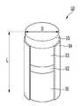
도 1a 및 도 1b는 각각 본 발명의 일 실시예에 의한 발광 소자(LD)를 나타내는 사시도이다. 도 1a 및 도 1b에서는 발광 소자(LD)의 일 예로서 원 기둥 형상의 막대형 발광 다이오드를 도시하였으나, 본 발명에 의한 발광 소자(LD)의 종류 및/또는 형상 등이 이에 한정되지는 않는다.1A and 1B are perspective views illustrating a light emitting device LD according to an embodiment of the present invention, respectively. 1A and 1B illustrate a rod-shaped rod-shaped light emitting diode as an example of the light emitting device LD, the type and / or shape of the light emitting device LD according to the present invention is not limited thereto.
도 1a 및 도 1b를 참조하면, 본 발명의 일 실시예에 의한 발광 소자(LD)는, 제1 도전성 반도체층(11) 및 제2 도전성 반도체층(13)과, 상기 제1 및 제2 도전성 반도체층들(11, 13)의 사이에 개재된 활성층(12)을 포함할 수 있다. 일 예로, 발광 소자(LD)는 제1 도전성 반도체층(11), 활성층(12) 및 제2 도전성 반도체층(13)이 순차적으로 적층된 적층체로 구성될 수 있다.1A and 1B, a light emitting device LD according to an embodiment of the present invention may include a first
실시예에 따라, 발광 소자(LD)는 일 방향을 따라 연장된 막대 형상으로 제공될 수 있다. 발광 소자(LD)의 연장 방향을 길이 방향이라고 하면, 발광 소자(LD)는 상기 길이 방향을 따라 일측 단부와 타측 단부를 가질 수 있다.According to an embodiment, the light emitting device LD may be provided in a rod shape extending in one direction. When the extending direction of the light emitting device LD is called a longitudinal direction, the light emitting device LD may have one end and the other end along the length direction.
실시예에 따라, 발광 소자(LD)의 일측 단부에는 제1 및 제2 도전성 반도체층들(11, 13) 중 하나가 배치되고, 상기 발광 소자(LD)의 타측 단부에는 상기 제1 및 제2 도전성 반도체층들(11, 13) 중 나머지 하나가 배치될 수 있다.In some embodiments, one of the first and second
실시예에 따라, 발광 소자(LD)는 막대 형상으로 제조될 수 있다. 본 명세서에서, "막대형"이라 함은 원 기둥 또는 다각 기둥 등과 같이 길이 방향으로 긴(즉, 종횡비가 1보다 큰) 로드 형상(rod-like shape), 또는 바 형상(bar-like shape)을 포괄하며, 그 단면의 형상이 특별히 한정되지는 않는다. 예를 들어, 발광 소자(LD)의 길이(L)는 그 직경(D)(또는, 단면의 너비)보다 클 수 있다.In some embodiments, the light emitting device LD may be manufactured in a rod shape. As used herein, the term "rod" refers to a rod-like shape that is long in the longitudinal direction (ie, an aspect ratio of greater than 1), or a bar-like shape, such as a circular column or a polygonal column. It is comprehensive and the shape of the cross section is not specifically limited. For example, the length L of the light emitting element LD may be larger than the diameter D (or the width of the cross section).
실시예에 따라, 발광 소자(LD)는 마이크로 스케일 또는 나노 스케일 정도로 작은 크기, 일 예로 마이크로 스케일 또는 나노 스케일 정도의 길이(L) 및/또는 직경(D)을 가질 수 있다. 다만, 발광 소자(LD)의 크기가 이에 한정되지는 않는다. 예를 들어, 발광 표시 장치를 비롯하여 발광 소자(LD)를 이용하는 각종 발광 장치의 설계 조건에 따라 발광 소자(LD)의 크기는 다양하게 변경될 수 있다.In some embodiments, the light emitting device LD may have a size L, and / or a diameter D, such as a micro scale or a nano scale. However, the size of the light emitting device LD is not limited thereto. For example, the size of the light emitting device LD may be variously changed according to design conditions of various light emitting devices including the light emitting display device and the light emitting device LD.
제1 도전성 반도체층(11)은 일 예로 적어도 하나의 n형 반도체층을 포함할 수 있다. 예를 들어, 제1 도전성 반도체층(11)은 InAlGaN, GaN, AlGaN, InGaN, AlN, InN 중 어느 하나의 반도체 재료를 포함하며, Si, Ge, Sn 등과 같은 제1 도전성 도펀트가 도핑된 n형 반도체층을 포함할 수 있다. 다만, 제1 도전성 반도체층(11)을 구성하는 물질이 이에 한정되는 것은 아니며, 이 외에도 다양한 물질로 제1 도전성 반도체층(11)을 구성할 수 있다.For example, the first
활성층(12)은 제1 도전성 반도체층(11) 상에 배치되며, 단일 또는 다중 양자 우물 구조로 형성될 수 있다. 일 실시예에서, 활성층(12)의 상부 및/또는 하부에는 도전성 도펀트가 도핑된 클래드층(미도시)이 형성될 수도 있다. 일 예로, 상기 클래드층은 AlGaN층 또는 InAlGaN층으로 형성될 수 있다. 실시예에 따라, AlGaN, AlInGaN 등의 물질이 활성층(12)을 형성하는 데에 이용될 수 있으며, 이 외에도 다양한 물질이 활성층(12)을 구성할 수 있다.The
발광 소자(LD)의 양단에 소정 전압 이상의 전계를 인가하게 되면, 활성층(12)에서 전자-정공 쌍이 결합하면서 발광 소자(LD)가 발광하게 된다. 이러한 원리를 이용하여 발광 소자(LD)의 발광을 제어함으로써, 상기 발광 소자(LD)를 화소를 비롯한 다양한 발광 장치의 광원으로 이용할 수 있다.When an electric field of a predetermined voltage or more is applied to both ends of the light emitting device LD, the light emitting device LD emits light while the electron-hole pair is coupled in the
제2 도전성 반도체층(13)은 활성층(12) 상에 배치되며, 제1 도전성 반도체층(11)과 상이한 타입의 반도체층을 포함할 수 있다. 일 예로, 제2 도전성 반도체층(13)은 적어도 하나의 p형 반도체층을 포함할 수 있다. 예컨대, 제2 도전성 반도체층(13)은 InAlGaN, GaN, AlGaN, InGaN, AlN, InN 중 적어도 하나의 반도체 재료를 포함하며, Mg 등과 같은 제2 도전성 도펀트가 도핑된 p형 반도체층을 포함할 수 있다. 다만, 제2 도전성 반도체층(13)을 구성하는 물질이 이에 한정되는 것은 아니며, 이 외에도 다양한 물질이 제2 도전성 반도체층(13)을 구성할 수 있다.The second
일 실시예에서, 발광 소자(LD)는 제1 도전성 반도체층(11), 활성층(12) 및 제2 도전성 반도체층(13) 외에도 추가적인 구성 요소를 더 포함할 수 있다. 예를 들면, 발광 소자(LD)는 제1 도전성 반도체층(11), 활성층(12) 및/또는 제2 도전성 반도체층(13)의 상부 및/또는 하부에 배치된 하나 이상의 형광체층, 활성층, 반도체층 및/또는 전극층을 추가적으로 포함할 수 있다.In one embodiment, the light emitting device LD may further include additional components in addition to the first
예를 들면, 발광 소자(LD)는 도 1a에 도시된 바와 같이 제2 도전성 반도체층(13)의 일단(일 예로, 상부면) 측에 배치되는 적어도 하나의 전극층(15)을 더 포함할 수 있다. 또한, 실시예에 따라 발광 소자(LD)는 도 1b에 도시된 바와 같이 제1 도전성 반도체층(11)의 일단(일 예로, 하부면) 측에 배치되는 적어도 하나의 다른 전극층(16)을 더 포함할 수 있다. 상기 전극층들(15, 16) 각각은 오믹(Ohmic) 컨택 전극일 수 있으나, 이에 한정되지는 않는다. 또한, 상기 전극층들(15, 16) 각각은 금속 또는 금속 산화물을 포함할 수 있으며, 일 예로, 크롬(Cr), 티타늄(Ti), 알루미늄(Al), 금(Au), 니켈(Ni), ITO 및 이들의 산화물 또는 합금 등을 단독 또는 혼합하여 사용할 수 있으나, 이에 한정되지 않는다. 또한, 실시예에 따라, 상기 전극층들(15, 16)은 실질적으로 투명 또는 반투명할 수 있다. 이에 따라, 발광 소자(LD)에서 생성되는 빛이 전극층들(15, 16)을 투과하여 발광 소자(LD)의 외부로 방출될 수 있다.For example, the light emitting device LD may further include at least one
본 발명의 일 실시예에서, 발광 소자(LD)는 절연성 피막(14)을 더 포함할 수 있다. 실시예에 따라, 절연성 피막(14)은 적어도 활성층(12)의 외주면을 둘러싸도록 형성될 수 있으며, 이외에도 제1 및 제2 도전성 반도체층들(11, 13)의 적어도 일부를 더 둘러쌀 수 있다.In one embodiment of the present invention, the light emitting device LD may further include an insulating
한편, 도 1a에서는 발광 소자(LD)의 적층 구조를 명확히 보여주기 위하여 절연성 피막(14)의 일부를 삭제하여 도시하였으나, 상기 절연성 피막(14)은 제1 도전성 반도체층(11), 활성층(12) 및/또는 제2 도전성 반도체층(13)의 외주면(일 예로, 원 기둥의 측면)을 전체적으로 둘러쌀 수 있다. 예를 들면, 절연성 피막(14)은 도 1a에 도시된 바와 같이 제2 도전성 반도체층(13)의 일단 측에 배치된 전극층(15)만을 노출하고, 제1 도전성 반도체층(11), 활성층(12) 및/또는 제2 도전성 반도체층(13)의 측면을 전체적으로 둘러쌀 수 있다. 다만, 절연성 피막(14)은 적어도 발광 소자(LD)의 양 단부를 노출하며, 일 예로 제2 도전성 반도체층(13)의 일단 측에 배치된 전극층(15)과 더불어, 제1 도전성 반도체층(11)의 일 단부(일 예로, 하부면)를 노출할 수 있다.Meanwhile, in FIG. 1A, a portion of the insulating
또한, 실시예에 따라, 도 1b에 도시된 바와 같이 발광 소자(LD)의 양단에 전극층들(15, 16)이 배치될 경우, 절연성 피막(14)은 상기 전극층들(15, 16) 각각의 적어도 일 영역을 노출할 수 있다. 또는, 또 다른 실시예에서는, 절연성 피막(14)이 제공되지 않을 수도 있다.In addition, in some embodiments, when the electrode layers 15 and 16 are disposed at both ends of the light emitting element LD, as illustrated in FIG. 1B, the insulating
실시예에 따라, 절연성 피막(14)은 투명한 절연 물질을 포함할 수 있다. 예를 들어, 절연성 피막(14)은 SiO2, Si3N4, Al2O3 및 TiO2로 이루어지는 군으로부터 선택된 하나 이상의 절연 물질을 포함할 수 있으나, 이에 한정되지는 않는다. 즉, 절연성 피막(14)의 구성 물질이 특별히 한정되지는 않으며, 절연성 피막(14)은 현재 공지된 다양한 절연 물질로 구성될 수 있다.According to an embodiment, the insulating
발광 소자(LD)에 절연성 피막(14)이 제공되면, 상기 발광 소자(LD)의 활성층(12)이 도시되지 않은 제1 및/또는 제2 화소 전극 등과 단락되는 것을 방지할 수 있다. 이에 따라, 발광 소자(LD)의 전기적 안정성을 확보할 수 있다.When the insulating
또한, 발광 소자(LD)의 표면에 절연성 피막(14)을 형성함에 의해 상기 발광 소자(LD)의 표면 결함을 최소화하여 수명 및 효율을 향상시킬 수 있다. 또한, 각각의 발광 소자(LD)에 절연성 피막(14)이 형성되면, 다수의 발광 소자들(LD)이 서로 밀접하여 배치되어 있는 경우에도 상기 발광 소자들(LD)의 사이에서 원치 않는 단락이 발생하는 것을 방지할 수 있다.In addition, by forming the insulating
또한, 본 발명의 일 실시예에서, 발광 소자(LD)는 표면 처리 과정을 거쳐 제조될 수 있다. 일 예로, 다수의 발광 소자들(LD)을 유동성의 용액에 혼합하여 각각의 서브 화소 영역에 공급할 때, 상기 발광 소자들(LD)이 용액 내에 불균일하게 응집하지 않고 균일하게 분산될 수 있도록 발광 소자(LD)를 표면 처리(일 예로, 코팅)할 수 있다.In addition, in one embodiment of the present invention, the light emitting device LD may be manufactured through a surface treatment process. For example, when a plurality of light emitting devices LD are mixed in a fluid solution and supplied to each sub-pixel region, the light emitting devices LD may be uniformly dispersed without being uniformly aggregated in the solution. (LD) may be surface treated (eg, coated).
상술한 발광 소자(LD)는 발광 표시 장치를 비롯한 다양한 종류의 발광 장치에서 광원으로 이용될 수 있다. 일례로, 발광 표시 패널의 각 화소 영역에 적어도 하나의 발광 소자(LD)를 배치하고, 이를 통해 각 화소의 발광 유닛을 구성할 수 있다. 다만, 본 발명에서 발광 소자(LD)의 적용 분야가 표시 장치에 한정되지는 않는다. 예컨대, 발광 소자(LD)는 조명 장치와 같이 광원을 필요로 하는 다른 종류의 발광 장치에도 이용될 수 있다.The above-described light emitting device LD may be used as a light source in various kinds of light emitting devices including a light emitting display device. For example, at least one light emitting element LD may be disposed in each pixel area of the light emitting display panel, thereby configuring the light emitting unit of each pixel. However, the application field of the light emitting device LD is not limited to the display device in the present invention. For example, the light emitting element LD may be used in other kinds of light emitting devices that require a light source, such as a lighting device.
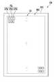
도 2는 본 발명의 일 실시예에 의한 발광 표시 패널(100)을 개략적으로 나타내는 평면도이다. 실시예에 따라, 도 2에서는 표시 영역(DA)을 중심으로 발광 표시 패널(100)의 구조를 간략하게 도시하기로 한다. 다만, 실시예에 따라서는 도시되지 않은 적어도 하나의 구동 회로부(일 예로, 주사 구동부 및 데이터 구동부) 및/또는 복수의 배선들이 발광 표시 패널(100)에 더 배치될 수 있다.2 is a plan view schematically illustrating a light emitting
도 2를 참조하면, 발광 표시 패널(100)은, 기판(SUB)과, 상기 기판(SUB) 상에 배치된 다수의 화소들(PXL)을 포함할 수 있다. 구체적으로, 발광 표시 패널(100)은, 영상을 표시하기 위한 표시 영역(DA)과, 상기 표시 영역(DA)을 제외한 비표시 영역(NDA)을 포함하며, 상기 표시 영역(DA)에는 화소들(PXL)이 배치될 수 있다.Referring to FIG. 2, the light emitting
실시예에 따라, 표시 영역(DA)은 발광 표시 패널(100)의 중앙 영역에 배치되고, 비표시 영역(NDA)은 표시 영역(DA)을 둘러싸도록 발광 표시 패널(100)의 가장자리 영역에 배치될 수 있다. 다만, 표시 영역(DA) 및 비표시 영역(NDA)의 위치가 이에 한정되지는 않으며, 이들의 위치는 변경될 수 있다.In some embodiments, the display area DA is disposed in the center area of the light emitting
기판(SUB)은 경성 기판 또는 가요성 기판일 수 있으며, 그 재료나 물성이 특별히 한정되지는 않는다. 일 예로, 기판(SUB)은 유리 또는 강화 유리로 구성된 경성 기판, 또는 플라스틱 또는 금속 재질의 박막 필름으로 구성된 가요성 기판일 수 있다. 또한, 기판(SUB)은 투명 기판일 수 있으나 이에 한정되지는 않는다. 일 예로, 기판(SUB)은 반투명 기판, 불투명 기판, 또는 반사성 기판일 수도 있다.The substrate SUB may be a rigid substrate or a flexible substrate, and its material and physical properties are not particularly limited. For example, the substrate SUB may be a rigid substrate composed of glass or tempered glass, or a flexible substrate composed of a thin film made of plastic or metal. In addition, the substrate SUB may be a transparent substrate, but is not limited thereto. For example, the substrate SUB may be a translucent substrate, an opaque substrate, or a reflective substrate.
기판(SUB) 상의 일 영역은 표시 영역(DA)으로 규정되어 화소들(PXL)이 배치되고, 나머지 영역은 비표시 영역(DA)으로 규정된다. 일 예로, 기판(SUB)은, 각각의 화소(PXL)가 형성되는 복수의 화소 영역들을 포함한 표시 영역(DA)과, 상기 표시 영역(DA)의 외곽에 배치되는 비표시 영역(NA)을 포함할 수 있다. 비표시 영역(NA)에는 표시 영역(DA)의 화소들(PXL)에 연결되는 각종 배선들 및/또는 내장 회로부가 배치될 수 있다.One area on the substrate SUB is defined as the display area DA so that the pixels PXL are disposed, and the remaining area is defined as the non-display area DA. For example, the substrate SUB may include a display area DA including a plurality of pixel areas in which each pixel PXL is formed, and a non-display area NA disposed outside the display area DA. can do. Various wirings and / or internal circuits connected to the pixels PXL of the display area DA may be disposed in the non-display area NA.
화소들(PXL) 각각은 해당 주사 신호 및 데이터 신호에 의해 구동되는 적어도 하나의 발광 소자(LD), 일 예로 도 1에 도시된 적어도 하나의 막대형 발광 다이오드를 포함할 수 있다. 예를 들어, 화소들(PXL) 각각은 마이크로 스케일 또는 나노 스케일 정도로 작은 크기를 가지며 서로 병렬로 연결된 복수의 막대형 발광 다이오드들을 포함할 수 있다. 상기 복수의 막대형 발광 다이오드들은 각 화소(PXL)의 광원을 구성할 수 있다.Each of the pixels PXL may include at least one light emitting device LD driven by a corresponding scan signal and a data signal, for example, at least one bar light emitting diode shown in FIG. 1. For example, each of the pixels PXL may have a small size, such as a micro scale or a nano scale, and include a plurality of rod-shaped light emitting diodes connected in parallel with each other. The bar-shaped light emitting diodes may constitute a light source of each pixel PXL.
또한, 화소들(PXL) 각각은 복수의 서브 화소들을 포함할 수 있다. 일 예로, 각각의 화소(PXL)는 제1 서브 화소(SPX1), 제2 서브 화소(SPX2) 및 제3 서브 화소(SPX3)를 포함할 수 있다. 실시예에 따라, 제1, 제2 및 제3 서브 화소들(SPX1, SPX2, SPX3)은 서로 다른 색상의 빛을 방출할 수 있다. 일 예로, 제1 서브 화소(SPX1)는 적색의 빛을 방출하는 적색 서브 화소일 수 있고, 제2 서브 화소(SPX2)는 녹색의 빛을 방출하는 녹색 서브 화소일 수 있으며, 제3 서브 화소(SPX3)는 청색의 빛을 방출하는 청색 서브 화소일 수 있다. 다만, 각각의 화소(PXL)를 구성하는 서브 화소들의 색상, 종류 및/또는 개수 등이 특별히 한정되지는 않으며, 일 예로 각각의 서브 화소가 방출하는 빛의 색상은 다양하게 변경될 수 있다. 또한, 도 2에서는 표시 영역(DA)에서 화소들(PXL)이 스트라이프 형태로 배열되는 실시예를 도시하였으나, 본 발명이 이에 한정되지는 않는다. 예를 들어, 표시 영역(DA)은 현재 공지된 다양한 화소 배열 형태를 가질 수 있다.In addition, each of the pixels PXL may include a plurality of sub pixels. For example, each pixel PXL may include a first sub pixel SPX1, a second sub pixel SPX2, and a third sub pixel SPX3. In some embodiments, the first, second and third sub-pixels SPX1, SPX2, and SPX3 may emit light of different colors. For example, the first sub pixel SPX1 may be a red sub pixel emitting red light, the second sub pixel SPX2 may be a green sub pixel emitting green light, and the third sub pixel SPX3) may be a blue sub-pixel emitting blue light. However, the color, type, and / or number of sub-pixels constituting each pixel PXL are not particularly limited. For example, the color of light emitted from each sub-pixel may be variously changed. In addition, although FIG. 2 illustrates an embodiment in which the pixels PXL are arranged in a stripe shape in the display area DA, the present invention is not limited thereto. For example, the display area DA may have various pixel array types currently known.
일 실시예에서, 각각의 화소(PXL)(또는, 서브 화소)는 능동형 화소로 구성될 수 있다. 다만, 본 발명에 적용될 수 있는 화소들(PXL)의 종류, 구조 및/또는 구동 방식이 특별히 한정되지는 않는다. 예를 들면, 각각의 화소(PXL)는 현재 공지된 다양한 수동형 또는 능동형 구조를 가진 발광 표시 장치의 화소로 구성될 수 있다.In one embodiment, each pixel PXL (or sub-pixel) may be composed of active pixels. However, the type, structure, and / or driving method of the pixels PXL applicable to the present invention is not particularly limited. For example, each pixel PXL may be configured as a pixel of a light emitting display device having various passive or active structures currently known.
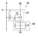
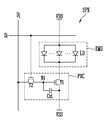
도 3a 내지 도 3c는 각각 본 발명의 일 실시예에 의한 서브 화소(SPX)를 나타내는 회로도로서, 일 예로 도 2에 도시된 제1, 제2 및 제3 서브 화소들(SPX1, SPX2, SPX3) 중 어느 하나를 도시한 회로도이다.3A to 3C are circuit diagrams illustrating a sub pixel SPX according to an exemplary embodiment of the present invention, for example, the first, second and third sub pixels SPX1, SPX2, and SPX3 illustrated in FIG. 2. It is a circuit diagram which shows either.
구체적으로, 도 3a 내지 도 3c에서는 능동형 발광 표시 장치에 구비될 수 있는 서브 화소의 서로 다른 실시예를 도시한 것이다. 일 예로, 도 3a 내지 도 3c에 도시된 각각의 서브 화소(SPX)는 도 2의 발광 표시 패널(100)에 구비된 제1, 제2 및 제3 서브 화소들(SPX1, SPX2, SPX3) 중 어느 하나일 수 있으며, 상기 제1, 제2 및 제3 서브 화소들(SPX1, SPX2, SPX3)은 실질적으로 동일 또는 유사한 구조를 가질 수 있다. 따라서, 도 3a 내지 도 3c에서는 제1, 제2 및 제3 서브 화소들(SPX1, SPX2, SPX3)을 포괄하여 서브 화소(SPX)로 지칭하기로 한다.In detail, FIGS. 3A to 3C illustrate different embodiments of sub-pixels that may be provided in the active light emitting display device. For example, each of the sub-pixels SPX illustrated in FIGS. 3A to 3C may be one of the first, second, and third sub-pixels SPX1, SPX2, and SPX3 of the light emitting
먼저 도 3a를 참조하면, 본 발명의 일 실시예에 의한 서브 화소(SPX)는 데이터 신호에 대응하는 휘도의 빛을 생성하기 위한 발광 유닛(EMU)과, 상기 발광 유닛(EMU)을 구동하기 위한 화소 회로(PXC)를 포함할 수 있다.First, referring to FIG. 3A, a sub-pixel SPX according to an exemplary embodiment of the present invention may include a light emitting unit EMU for generating light having a luminance corresponding to a data signal, and a light emitting unit EMU for driving the light emitting unit EMU. The pixel circuit PXC may be included.
실시예에 따라, 발광 유닛(EMU)은 제1 및 제2 전원들(VDD, VSS)의 사이에 병렬로 연결된 복수의 발광 소자들(LD)을 포함할 수 있다. 여기서, 제1 및 제2 전원들(VDD, VSS)은 발광 소자들(LD)이 발광할 수 있도록 서로 다른 전위를 가질 수 있다. 일 예로, 제1 전원(VDD)은 고전위 전원으로 설정되고, 제2 전원(VSS)은 저전위 전원으로 설정될 수 있다. 이때, 제1 및 제2 전원들(VDD, VSS)의 전위 차는 적어도 서브 화소(SPX)의 발광 기간 동안 발광 소자들(LD)의 문턱 전압 이상으로 설정될 수 있다.According to an embodiment, the light emitting unit EMU may include a plurality of light emitting elements LD connected in parallel between the first and second power sources VDD and VSS. Here, the first and second power sources VDD and VSS may have different potentials so that the light emitting devices LD may emit light. For example, the first power supply VDD may be set as a high potential power and the second power supply VSS may be set as a low potential power. In this case, the potential difference between the first and second power sources VDD and VSS may be set to be equal to or greater than the threshold voltage of the light emitting elements LD during the light emitting period of the sub-pixel SPX.
한편, 도 3a에서는 각 서브 화소(SPX)의 발광 유닛(EMU)을 구성하는 발광 소자들(LD)이 제1 전원(VDD)과 제2 전원(VSS)의 사이에 서로 동일한 방향(일 예로, 순방향)으로 병렬 연결된 실시예를 도시하였으나, 본 발명이 이에 한정되지는 않는다. 예컨대, 다른 실시예에서는 상기 발광 소자들(LD) 중 일부는 제1 및 제2 전원들(VDD, VSS)의 사이에 순방향으로 연결되고, 다른 일부는 역방향으로 연결될 수도 있다. 또는, 또 다른 실시예에서는, 적어도 하나의 서브 화소(SPX)가 단일의 발광 소자(LD)만을 포함할 수도 있다.Meanwhile, in FIG. 3A, the light emitting devices LD constituting the light emitting unit EMU of each sub-pixel SPX are in the same direction between the first power supply VDD and the second power supply VSS (for example, While the embodiment is connected in parallel to the forward direction), the present invention is not limited thereto. For example, in another embodiment, some of the light emitting elements LD may be connected in the forward direction between the first and second power sources VDD and VSS, and the other part may be connected in the reverse direction. Alternatively, in another embodiment, at least one sub-pixel SPX may include only a single light emitting element LD.
실시예에 따라, 각각의 발광 유닛(EMU)을 구성하는 발광 소자들(LD)의 일단은 제1 전극을 통해 해당 화소 회로(PXC)에 공통으로 접속되며, 상기 화소 회로(PXC)를 통해 제1 전원(VDD)에 접속될 수 있다. 그리고, 발광 소자들(LD)의 타단은 제2 전극을 통해 제2 전원(VSS)에 공통으로 접속될 수 있다. 이하에서는 각 발광 유닛(EMU)에 배치되는 제1 전극 및 제2 전극을 각각 제1 화소 전극 및 제2 화소 전극이라 지칭하기로 한다.According to an embodiment, one end of the light emitting elements LD constituting each light emitting unit EMU is commonly connected to the corresponding pixel circuit PXC through a first electrode, and made through the pixel circuit PXC. 1 may be connected to the power supply (VDD). The other ends of the light emitting devices LD may be commonly connected to the second power supply VSS through the second electrode. Hereinafter, the first electrode and the second electrode disposed in each light emitting unit EMU will be referred to as a first pixel electrode and a second pixel electrode, respectively.
각각의 발광 유닛(EMU)은 해당 화소 회로(PXC)를 통해 공급되는 구동 전류에 대응하는 휘도로 발광할 수 있다. 이에 따라, 표시 영역(DA)에서 소정의 영상이 표시될 수 있다.Each light emitting unit EMU may emit light at a luminance corresponding to a driving current supplied through the pixel circuit PXC. Accordingly, a predetermined image may be displayed in the display area DA.
화소 회로(PXC)는 해당 서브 화소(SPX)의 주사선(Si) 및 데이터선(Dj)에 접속될 수 있다. 일 예로, 서브 화소(SPX)가 표시 영역(DA)의 i번째 행 및 j번째 열에 배치되었다고 할 때, 상기 서브 화소(SPX)의 화소 회로(PXC)는 표시 영역(DA)의 i번째 주사선(Si) 및 j번째 데이터선(Dj)에 접속될 수 있다. 이러한 화소 회로(PXC)는 제1 및 제2 트랜지스터(T1, T2)와 스토리지 커패시터(Cst)를 포함할 수 있다.The pixel circuit PXC may be connected to the scan line Si and the data line Dj of the corresponding sub pixel SPX. For example, when the sub-pixel SPX is disposed in the i-th row and the j-th column of the display area DA, the pixel circuit PXC of the sub-pixel SPX is the i-th scan line of the display area DA. Si) and the j-th data line Dj. The pixel circuit PXC may include first and second transistors T1 and T2 and a storage capacitor Cst.
제1 트랜지스터(구동 트랜지스터; T1)의 제1 전극은 제1 전원(VDD)에 접속되고, 제2 전극은 제1 화소 전극(즉, 해당 발광 유닛(EMU)의 제1 전극)을 통해 발광 소자들(LD)에 접속된다. 여기서, 상기 제1 전극 및 상기 제2 전극은 서로 다른 전극으로서, 일 예로 제1 전극이 소스 전극이면 제2 전극은 드레인 전극일 수 있다. 그리고, 제1 트랜지스터(T1)의 게이트 전극은 제1 노드(N1)에 접속된다. 이러한 제1 트랜지스터(T1)는 제1 노드(N1)의 전압에 대응하여 발광 유닛(EMU)으로 공급되는 구동 전류를 제어한다.The first electrode of the first transistor (driving transistor) T1 is connected to the first power supply VDD, and the second electrode is connected to the first pixel electrode (that is, the first electrode of the corresponding light emitting unit EMU). To LD. The first electrode and the second electrode may be different electrodes. For example, when the first electrode is a source electrode, the second electrode may be a drain electrode. The gate electrode of the first transistor T1 is connected to the first node N1. The first transistor T1 controls the driving current supplied to the light emitting unit EMU in response to the voltage of the first node N1.
제2 트랜지스터(스위칭 트랜지스터; T2)의 제1 전극은 데이터선(Dj)에 접속되고, 제2 전극은 제1 노드(N1)에 접속된다. 그리고, 제1 트랜지스터(T1)의 게이트 전극은 주사선(Si)에 접속된다.The first electrode of the second transistor (switching transistor) T2 is connected to the data line Dj, and the second electrode is connected to the first node N1. The gate electrode of the first transistor T1 is connected to the scan line Si.
이러한 제2 트랜지스터(T2)는, 주사선(Si)으로부터 게이트-온 전압(예컨대, 로우 전압)의 주사 신호가 공급될 때 턴-온되어, 데이터선(Dj)과 제1 노드(N1)를 전기적으로 연결한다. 각각의 프레임 기간마다 데이터선(Dj)으로는 해당 프레임의 데이터 신호가 공급되고, 상기 데이터 신호는 제2 트랜지스터(T2)를 경유하여 제1 노드(N1)로 전달된다. 이에 따라, 스토리지 커패시터(Cst)에는 데이터 신호에 대응하는 전압이 충전된다.The second transistor T2 is turned on when a scan signal of a gate-on voltage (eg, a low voltage) is supplied from the scan line Si to electrically connect the data line Dj and the first node N1. Connect with In each frame period, the data signal of the frame is supplied to the data line Dj, and the data signal is transmitted to the first node N1 via the second transistor T2. Accordingly, the storage capacitor Cst is charged with a voltage corresponding to the data signal.
스토리지 커패시터(Cst)의 일 전극은 제1 전원(VDD)에 접속되고, 다른 전극은 제1 노드(N1)에 접속된다. 이러한 스토리지 커패시터(Cst)는 각각의 프레임 기간 동안 제1 노드(N1)로 공급되는 데이터 신호에 대응하는 전압을 충전하고, 다음 프레임의 데이터 신호가 공급될 때까지 충전된 전압을 유지한다.One electrode of the storage capacitor Cst is connected to the first power supply VDD, and the other electrode is connected to the first node N1. The storage capacitor Cst charges a voltage corresponding to the data signal supplied to the first node N1 during each frame period, and maintains the charged voltage until the data signal of the next frame is supplied.
한편, 도 3a에서는 화소 회로(PXC)에 포함되는 트랜지스터들, 예컨대 제1 및 제2 트랜지스터들(T1, T2)을 모두 P타입의 트랜지스터들로 도시하였으나, 본 발명이 이에 한정되지는 않는다. 즉, 제1 및 제2 트랜지스터들(T1, T2) 중 적어도 하나는 N타입의 트랜지스터로 변경될 수도 있다.Meanwhile, in FIG. 3A, the transistors included in the pixel circuit PXC, for example, the first and second transistors T1 and T2 are illustrated as P-type transistors, but the present invention is not limited thereto. That is, at least one of the first and second transistors T1 and T2 may be changed to an N type transistor.
일 예로, 도 3b에 도시된 바와 같이, 제1 및 제2 트랜지스터들(T1, T2)은 모두 N타입의 트랜지스터들일 수 있다. 도 3b에 도시된 서브 화소(SPX)는, 트랜지스터 타입 변경에 따라 일부 회로 소자의 접속 위치가 변경된 것을 제외하고, 그 구성 및 동작이 도 3a의 화소 회로(PXC)와 실질적으로 유사하다. 따라서, 도 3b의 서브 화소(SPX)에 대한 상세한 설명은 생략하기로 한다.For example, as illustrated in FIG. 3B, the first and second transistors T1 and T2 may be N-type transistors. The configuration and operation of the sub-pixel SPX shown in FIG. 3B are substantially similar to those of the pixel circuit PXC of FIG. 3A except that the connection positions of some circuit elements are changed according to the transistor type change. Therefore, a detailed description of the sub pixel SPX of FIG. 3B will be omitted.
한편, 화소 회로(PXC)의 구조가 도 3a 및 도 3b에 도시된 실시예에 한정되지는 않는다. 즉, 화소 회로(PXC)는 현재 공지된 다양한 구조 및/또는 구동 방식의 화소 회로로 구성될 수 있다. 일 예로, 화소 회로(PXC)는 도 3c에 도시된 실시예와 같이 구성될 수도 있다.On the other hand, the structure of the pixel circuit PXC is not limited to the embodiment shown in Figs. 3A and 3B. That is, the pixel circuit PXC may be configured as a pixel circuit of various structures and / or driving schemes currently known. For example, the pixel circuit PXC may be configured as in the embodiment shown in FIG. 3C.
도 3c를 참조하면, 화소 회로(PXC)는 해당 수평 라인의 주사선(Si) 외에도 적어도 하나의 다른 주사선(또는, 제어선)에 더 접속될 수 있다. 일 예로, 표시 영역(DA)의 i번째 행에 배치된 서브 화소(SPX)의 화소 회로(PXC)는 i-1번째 주사선(Si-1) 및/또는 i+1번째 주사선(Si+1)에 더 접속될 수 있다. 또한, 실시예에 따라 화소 회로(PXC)는 제1 및 제2 전원들(VDD, VSS) 외에 다른 전원에 더 연결될 수 있다. 일 예로, 화소 회로(PXC)는 초기화 전원(Vint)에도 연결될 수 있다. 실시예에 따라, 이러한 화소 회로(PXC)는 제1 내지 제7 트랜지스터(T1 내지 T7)와 스토리지 커패시터(Cst)를 포함할 수 있다.Referring to FIG. 3C, the pixel circuit PXC may be further connected to at least one other scan line (or control line) in addition to the scan line Si of the horizontal line. For example, the pixel circuit PXC of the sub-pixel SPX disposed in the i-th row of the display area DA may have an i−1 th scan line Si−1 and / or an i + 1 th scan
제1 트랜지스터(T1)의 제1 전극은 제5 트랜지스터(T5)를 경유하여 제1 전원(VDD)에 접속되고, 제2 전극은 제6 트랜지스터(T6)를 경유하여 발광 소자들(LD)에 접속된다. 그리고, 제1 트랜지스터(T1)의 게이트 전극은 제1 노드(N1)에 접속될 수 있다. 이러한 제1 트랜지스터(T1)는 제1 노드(N1)의 전압에 대응하여 발광 유닛(EMU)으로 공급되는 구동 전류를 제어한다.The first electrode of the first transistor T1 is connected to the first power supply VDD via the fifth transistor T5, and the second electrode is connected to the light emitting elements LD via the sixth transistor T6. Connected. The gate electrode of the first transistor T1 may be connected to the first node N1. The first transistor T1 controls the driving current supplied to the light emitting unit EMU in response to the voltage of the first node N1.
제2 트랜지스터(T2)는 데이터선(Dj)과 제1 트랜지스터(T1)의 제1 전극 사이에 접속된다. 그리고, 제2 트랜지스터(T2)의 게이트 전극은 해당 주사선(Si)에 접속된다. 이와 같은 제2 트랜지스터(T2)는 상기 주사선(Si)으로부터 게이트-온 전압의 주사 신호가 공급될 때 턴-온되어 데이터선(Dj)을 제1 트랜지스터(T1)의 제1 전극에 전기적으로 연결한다. 따라서, 제2 트랜지스터(T2)가 턴-온되면, 데이터선(Dj)으로부터 공급되는 데이터 신호가 제1 트랜지스터(T1)로 전달된다.The second transistor T2 is connected between the data line Dj and the first electrode of the first transistor T1. The gate electrode of the second transistor T2 is connected to the scan line Si. The second transistor T2 is turned on when the scan signal of the gate-on voltage is supplied from the scan line Si to electrically connect the data line Dj to the first electrode of the first transistor T1. do. Therefore, when the second transistor T2 is turned on, the data signal supplied from the data line Dj is transferred to the first transistor T1.
제3 트랜지스터(T3)는 제1 트랜지스터(T1)의 제2 전극과 제1 노드(N1) 사이에 접속된다. 그리고, 제3 트랜지스터(T3)의 게이트 전극은 해당 주사선(Si)에 접속된다. 이와 같은 제3 트랜지스터(T3)는 상기 주사선(Si)으로부터 게이트-온 전압의 주사 신호가 공급될 때 턴-온되어 제1 트랜지스터(T1)의 제2 전극과 제1 노드(N1)를 전기적으로 연결한다. 따라서, 제3 트랜지스터(T3)가 턴-온되면, 제1 트랜지스터(T1)는 다이오드 형태로 접속된다.The third transistor T3 is connected between the second electrode of the first transistor T1 and the first node N1. The gate electrode of the third transistor T3 is connected to the scan line Si. The third transistor T3 is turned on when a scan signal of a gate-on voltage is supplied from the scan line Si to electrically connect the second electrode and the first node N1 of the first transistor T1. Connect. Therefore, when the third transistor T3 is turned on, the first transistor T1 is connected in the form of a diode.
제4 트랜지스터(T4)는 제1 노드(N1)와 초기화 전원(Vint) 사이에 접속된다. 그리고, 제4 트랜지스터(T4)의 게이트 전극은 이전 주사선, 일 예로 i-1번째 주사선(Si-1)에 접속된다. 이와 같은 제4 트랜지스터(T4)는 i-1번째 주사선(Si-1)으로 게이트-온 전압의 주사 신호가 공급될 때 턴-온되어 초기화 전원(Vint)의 전압을 제1 노드(N1)로 전달한다. 여기서, 초기화 전원(Vint)의 전압은 데이터 신호의 최저 전압 이하일 수 있다.The fourth transistor T4 is connected between the first node N1 and the initialization power supply Vint. The gate electrode of the fourth transistor T4 is connected to the previous scan line, for example, the i-1 th scan line Si-1. The fourth transistor T4 is turned on when the scan signal of the gate-on voltage is supplied to the i-1 th scan line Si-1 to transfer the voltage of the initialization power supply Vint to the first node N1. To pass. The voltage of the initialization power supply Vint may be equal to or less than the lowest voltage of the data signal.
제5 트랜지스터(T5)는 제1 전원(VDD)과 제1 트랜지스터(T1) 사이에 접속된다. 그리고, 제5 트랜지스터(T5)의 게이트 전극은 해당 발광 제어선, 일 예로 i번째 발광 제어선(Ei)에 접속된다. 이와 같은 제5 트랜지스터(T5)는 상기 발광 제어선(Ei)으로 게이트-오프 전압(일 예로, 하이 전압)의 발광 제어신호가 공급될 때 턴-오프되고, 그 외의 경우에 턴-온된다.The fifth transistor T5 is connected between the first power supply VDD and the first transistor T1. The gate electrode of the fifth transistor T5 is connected to the emission control line, for example, the i-th emission control line Ei. The fifth transistor T5 is turned off when a light emission control signal having a gate-off voltage (eg, a high voltage) is supplied to the light emission control line Ei, and is turned on in other cases.
제6 트랜지스터(T6)는 제1 트랜지스터(T1)와 발광 소자들(LD)의 사이에 접속된다. 그리고, 제6 트랜지스터(T6)의 게이트 전극은 해당 발광 제어선, 일 예로 i번째 발광 제어선(Ei)에 접속된다. 이와 같은 제6 트랜지스터(T6)는 상기 발광 제어선(Ei)으로 게이트-오프 전압의 발광 제어신호가 공급될 때 턴-오프되고, 그 외의 경우에 턴-온된다.The sixth transistor T6 is connected between the first transistor T1 and the light emitting elements LD. The gate electrode of the sixth transistor T6 is connected to the emission control line, for example, the i-th emission control line Ei. The sixth transistor T6 is turned off when the emission control signal of the gate-off voltage is supplied to the emission control line Ei, and is turned on in other cases.
제7 트랜지스터(T7)는 발광 유닛(EMU)(일 예로, 발광 소자들(LD)의 일 단부에 연결된 제1 화소 전극)과 초기화 전원(Vint)의 사이에 접속된다. 그리고, 제7 트랜지스터(T7)의 게이트 전극은 다음 단의 주사선들 중 어느 하나, 일 예로 i+1번째 주사선(Si+1)에 접속된다. 이와 같은 제7 트랜지스터(T7)는 상기 i+1번째 주사선(Si+1)으로 게이트-온 전압의 주사 신호가 공급될 때 턴-온되어 초기화 전원(Vint)의 전압을 제1 화소 전극으로 공급한다.The seventh transistor T7 is connected between the light emitting unit EMU (eg, a first pixel electrode connected to one end of the light emitting elements LD) and the initialization power supply Vint. The gate electrode of the seventh transistor T7 is connected to any one of the next scan lines, for example, the i + 1 th scan
스토리지 커패시터(Cst)는 제1 전원(VDD)과 제1 노드(N1)의 사이에 접속된다. 이와 같은 스토리지 커패시터(Cst)는 각 프레임 기간에 제1 노드(N1)로 공급되는 데이터 신호 및 제1 트랜지스터(T1)의 문턱전압에 대응하는 전압을 저장한다.The storage capacitor Cst is connected between the first power supply VDD and the first node N1. The storage capacitor Cst stores a data signal supplied to the first node N1 and a voltage corresponding to the threshold voltage of the first transistor T1 in each frame period.
한편, 도 3c에서는 화소 회로(PXC)에 포함되는 트랜지스터들, 예를 들어 제1 내지 제7 트랜지스터들(T1 내지 T7)을 모두 P타입의 트랜지스터들로 도시하였으나, 본 발명이 이에 한정되지는 않는다. 일 예로, 제1 내지 제7 트랜지스터들(T1 내지 T7) 중 적어도 하나는 N타입의 트랜지스터로 변경될 수도 있다.In FIG. 3C, all of the transistors included in the pixel circuit PXC, for example, the first to seventh transistors T1 to T7 are illustrated as P-type transistors, but the present invention is not limited thereto. . For example, at least one of the first to seventh transistors T1 to T7 may be changed to an N type transistor.
또한, 본 발명에 적용될 수 있는 서브 화소(SPX)의 구조가 도 3a 내지 도 3c에 도시된 실시예에 한정되지는 않으며, 각각의 서브 화소(SPX)는 현재 공지된 다양한 구조를 가질 수 있다. 예를 들어, 각각의 서브 화소(SPX)에 포함된 화소 회로(PXC)는 현재 공지된 다양한 구조 및/또는 구동 방식의 화소 회로로 구성될 수 있다. 또한, 본 발명의 다른 실시예에서 각각의 서브 화소(SPX)는 수동형 발광 표시 장치의 내부에 구성될 수도 있다. 이 경우, 화소 회로(PXC)는 생략되고, 발광 유닛(EMU)의 제1 및 제2 화소 전극들 각각은 주사선(Si), 데이터선(Dj), 전원선 및/또는 제어선에 직접 접속될 수 있다.In addition, the structure of the sub-pixel SPX that may be applied to the present invention is not limited to the exemplary embodiment illustrated in FIGS. 3A to 3C, and each sub-pixel SPX may have various structures currently known. For example, the pixel circuit PXC included in each sub-pixel SPX may be configured as a pixel circuit of various structures and / or driving schemes currently known. Also, in another embodiment of the present invention, each sub-pixel SPX may be configured in the passive light emitting display device. In this case, the pixel circuit PXC is omitted, and each of the first and second pixel electrodes of the light emitting unit EMU may be directly connected to the scan line Si, the data line Dj, the power line, and / or the control line. Can be.
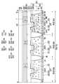
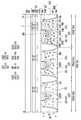
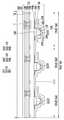
도 4 내지 도 6은 각각 본 발명의 일 실시예에 의한 발광 표시 패널(도 2의 100)의 구조를 나타내는 평면도로서, 일 예로 도 2 내지 도 3c에 도시된 화소들(PXL) 중 어느 하나의 화소 영역(PXA)을 도시한 평면도이다. 도 4 내지 도 6에서는 각 화소(PXL)의 표시 소자층을 위주로 상기 화소(PXL)의 구조를 도시하기로 하며, 일 예로 화소 회로(PXC)의 레이아웃에 대한 도시는 생략하기로 한다. 또한, 도 4 내지 도 6에서는 각각의 전극을 단일의 전극층으로만 도시하는 등 화소(PXL)의 구조를 단순화하여 도시하기로 한다. 다만, 본 발명이 이에 한정되지는 않는다. 일 예로, 도 4 내지 도 6에 도시된 전극들 중 적어도 하나는 다층 구조로 구성될 수 있다. 또한, 실시예에 따라서는 도시되지 않은 적어도 하나의 도전층 및/또는 절연층 등이 각각의 화소 영역(PXA)에 더 배치될 수도 있다.4 to 6 are top views illustrating the structure of a light emitting
도 4 내지 도 6을 참조하면, 각각의 화소 영역(PXA)은 각각의 서브 화소(SPX)를 구성하는 복수의 서브 화소들(SPX)에 대응하는 복수의 서브 화소 영역들(SPA)을 포함할 수 있다. 일 예로, 각각의 화소 영역(PXA)은, 제1 서브 화소(SPX1)가 형성되는 제1 서브 화소 영역(SPA1), 제2 서브 화소(SPX2)가 형성되는 제2 서브 화소 영역(SPA2), 및 제3 서브 화소(SPX3)가 형성되는 제3 서브 화소 영역(SPA3)을 포함할 수 있다.4 to 6, each pixel area PXA may include a plurality of sub pixel areas SPA corresponding to a plurality of sub pixels SPX constituting each sub pixel SPX. Can be. For example, each pixel area PXA may include a first sub pixel area SPA1 in which the first sub pixel SPX1 is formed, a second sub pixel area SPA2 in which a second sub pixel SPX2 is formed, And a third sub pixel area SPA3 in which the third sub pixel SPX3 is formed.
각각의 서브 화소 영역(SPA)은, 제1 화소 전극(ELT1) 및 제2 화소 전극(ELT2)과, 상기 제1 및 제2 화소 전극들(ELT1, ELT2)의 사이에 연결된 복수의 발광 소자들(LD)을 포함할 수 있다. 다만, 본 발명이 이에 한정되지는 않는다. 예를 들어, 본 발명의 다른 실시예에서는 적어도 하나의 서브 화소 영역(SPA)이 단일의 발광 소자(LD)만을 구비할 수도 있다.Each of the sub pixel areas SPA includes a plurality of light emitting devices connected between the first pixel electrode ELT1 and the second pixel electrode ELT2, and the first and second pixel electrodes ELT1 and ELT2. (LD). However, the present invention is not limited thereto. For example, in another embodiment of the present invention, at least one sub pixel area SPA may include only a single light emitting device LD.
실시예에 따라, 제1 화소 전극(ELT1) 및 제2 화소 전극(ELT2)은 서로 이격되어 배치되며, 적어도 일 영역이 서로 마주하도록 배치될 수 있다. 일 예로, 각각의 서브 화소 영역(SPA)에서, 제1 및 제2 화소 전극들(ELT1, ELT2)은 각각 제1 방향(DR1)을 따라 연장되며, 제2 방향(DR2)을 따라 소정 간격만큼 이격되어 나란히 배치될 수 있다. 다만, 본 발명이 이에 한정되지는 않는다. 예를 들어, 제1 및 제2 화소 전극들(ELT1, ELT2)의 형상 및/또는 상호 배치 관계 등은 다양하게 변경될 수 있다.In some embodiments, the first pixel electrode ELT1 and the second pixel electrode ELT2 may be spaced apart from each other, and at least one region may be disposed to face each other. For example, in each sub-pixel area SPA, the first and second pixel electrodes ELT1 and ELT2 extend along the first direction DR1, respectively, by a predetermined interval along the second direction DR2. Can be spaced apart side by side. However, the present invention is not limited thereto. For example, shapes and / or mutual arrangements of the first and second pixel electrodes ELT1 and ELT2 may be variously changed.
실시예에 따라, 제1 화소 전극(ELT1)은 제1 컨택홀(CH1)을 통해 각 서브 화소(SPX)의 화소 회로, 일 예로 도 3a 내지 도 3c 중 어느 하나에 도시된 화소 회로(PXC)에 접속될 수 있다. 실시예에 따라, 각각의 화소 회로(PXC)는 해당 서브 화소 영역(SPA)에 배치된 발광 소자들(LD)의 하부에 위치될 수 있다. 예컨대, 각각의 화소 회로(PXC)는 상기 발광 소자들(LD) 하부의 화소 회로층에 형성될 수 있다.In example embodiments, the first pixel electrode ELT1 may be a pixel circuit of each sub-pixel SPX through the first contact hole CH1, for example, the pixel circuit PXC illustrated in any one of FIGS. 3A to 3C. Can be connected to. In some embodiments, each pixel circuit PXC may be positioned under the light emitting devices LD disposed in the corresponding sub pixel area SPA. For example, each pixel circuit PXC may be formed in a pixel circuit layer under the light emitting elements LD.
실시예에 따라, 제1 화소 전극(ELT1)은 제1 연결 전극(CNL1)에 연결될 수 있다. 예를 들면, 제1 화소 전극(ELT1)은 제1 연결 전극(CNL1)과 일체로 연결될 수 있다. 일 예로, 제1 화소 전극(ELT1)은 제1 연결 전극(CNL1)으로부터 적어도 한 갈래로 분기되어 형성될 수 있다. 다만, 본 발명이 이에 한정되지는 않는다. 예컨대, 다른 실시예에서는 제1 화소 전극(ELT1) 및 제1 연결 전극(CNL1)이 서로 개별적으로 형성되어, 도시되지 않은 적어도 하나의 컨택홀 또는 비아홀 등을 통해 서로 전기적으로 연결될 수도 있다.In some embodiments, the first pixel electrode ELT1 may be connected to the first connection electrode CNL1. For example, the first pixel electrode ELT1 may be integrally connected to the first connection electrode CNL1. For example, the first pixel electrode ELT1 may be formed by branching at least one branch from the first connection electrode CNL1. However, the present invention is not limited thereto. For example, in another embodiment, the first pixel electrode ELT1 and the first connection electrode CNL1 may be formed separately from each other, and may be electrically connected to each other through at least one contact hole or via hole (not shown).
실시예에 따라, 제1 화소 전극(ELT1) 및 제1 연결 전극(CNL1)은 각각의 서브 화소 영역(SPA) 내에서 서로 다른 방향을 따라 연장될 수 있다. 일 예로, 제1 화소 전극(ELT1)이 제1 방향(DR1)을 따라 연장된다고 할 때, 제1 연결 전극(CNL1)은 상기 제1 방향(DR1)과 교차하는 제2 방향(DR2)을 따라 연장될 수 있다.In some embodiments, the first pixel electrode ELT1 and the first connection electrode CNL1 may extend in different directions in each sub-pixel area SPA. For example, when the first pixel electrode ELT1 extends along the first direction DR1, the first connection electrode CNL1 may extend along the second direction DR2 crossing the first direction DR1. Can be extended.
실시예에 따라, 제2 화소 전극(ELT2)은 제2 전원(VSS)에 접속될 수 있다. 예를 들어, 제2 화소 전극(ELT2)은 제2 연결 전극(CNL2), 제2 컨택홀(CH2) 및 전원 배선(PL)을 경유하여 제2 화소 전원(VSS)에 접속될 수 있다. 실시예에 따라, 제2 전원(VSS)을 공급하기 위한 전원 배선(PL)의 일 영역은 발광 소자들(LD) 하부의 화소 회로층에 배치될 수 있으나, 이에 한정되지는 않는다.In some embodiments, the second pixel electrode ELT2 may be connected to the second power source VSS. For example, the second pixel electrode ELT2 may be connected to the second pixel power supply VSS through the second connection electrode CNL2, the second contact hole CH2, and the power supply line PL. According to an embodiment, one region of the power line PL for supplying the second power source VSS may be disposed in the pixel circuit layer under the light emitting devices LD, but is not limited thereto.
실시예에 따라, 제2 화소 전극(ELT2) 및 제2 연결 전극(CNL2)은 각각의 서브 화소 영역(SPA) 내에서 서로 다른 방향을 따라 연장될 수 있다. 일 예로, 제2 화소 전극(ELT2)이 제1 방향(DR1)을 따라 연장된다고 할 때, 제2 연결 전극(CNL2)은 제2 방향(DR2)을 따라 연장될 수 있다.In some embodiments, the second pixel electrode ELT2 and the second connection electrode CNL2 may extend in different directions in each sub-pixel area SPA. For example, when the second pixel electrode ELT2 extends along the first direction DR1, the second connection electrode CNL2 may extend along the second direction DR2.
또한, 실시예에 따라 제2 화소 전극(ELT2) 및 제2 연결 전극(CNL2)은 서로 일체로 연결될 수 있다. 예를 들면, 제2 화소 전극(ELT2)은 제2 연결 전극(CNL2)으로부터 적어도 한 갈래로 분기되어 형성될 수 있다. 다만, 본 발명이 이에 한정되지는 않는다. 일 예로, 다른 실시예에서는 제2 화소 전극(ELT2) 및 제2 연결 전극(CNL2)이 서로 개별적으로 형성되어, 도시되지 않은 적어도 하나의 컨택홀 또는 비아홀 등을 통해 서로 전기적으로 연결될 수도 있다.In some embodiments, the second pixel electrode ELT2 and the second connection electrode CNL2 may be integrally connected to each other. For example, the second pixel electrode ELT2 may be formed by branching at least one branch from the second connection electrode CNL2. However, the present invention is not limited thereto. For example, in another embodiment, the second pixel electrode ELT2 and the second connection electrode CNL2 may be formed separately from each other, and may be electrically connected to each other through at least one contact hole or via hole (not shown).
실시예에 따라, 각 서브 화소(SPX)의 제1 및 제2 화소 전극들(ELT1, ELT2)의 사이에는 적어도 하나의 발광 소자(LD), 일 예로 복수의 발광 소자들(LD)이 배열될 수 있다. 예를 들면, 제1 서브 화소(SPX1)의 제1 및 제2 화소 전극들(ELT1, ELT2)의 사이에는 적어도 하나의 제1 발광 소자(LD)가, 제2 서브 화소(SPX2)의 제1 및 제2 화소 전극들(ELT1, ELT2)의 사이에는 적어도 하나의 제2 발광 소자(LD)가, 제3 서브 화소(SPX3)의 제1 및 제2 화소 전극들(ELT1, ELT2)의 사이에는 적어도 하나의 제3 발광 소자(LD)가 배열될 수 있다. 일 예로, 각각의 서브 화소 영역(SPA)에서, 제1 화소 전극(ELT1)과 제2 화소 전극(ELT2)이 서로 대향하도록 배치된 영역(일 예로, 각 서브 화소(SPX)의 발광 영역)에는, 복수의 발광 소자들(LD)이 병렬로 연결될 수 있다.In example embodiments, at least one light emitting device LD, for example, a plurality of light emitting devices LD may be arranged between the first and second pixel electrodes ELT1 and ELT2 of each sub-pixel SPX. Can be. For example, at least one first light emitting element LD is disposed between the first and second pixel electrodes ELT1 and ELT2 of the first sub-pixel SPX1 and the first of the second sub-pixel SPX2. And at least one second light emitting element LD between the second pixel electrodes ELT1 and ELT2, and between the first and second pixel electrodes ELT1 and ELT2 of the third sub-pixel SPX3. At least one third light emitting device LD may be arranged. For example, in each sub pixel area SPA, an area in which the first pixel electrode ELT1 and the second pixel electrode ELT2 are disposed to face each other (for example, a light emitting area of each sub pixel SPX) is disposed in the sub pixel area SPA. The plurality of light emitting elements LD may be connected in parallel.
한편, 도 4 내지 도 6에서는 발광 소자들(LD)이 모두 제2 방향(DR2), 일 예로 수평 방향으로 정렬된 것으로 도시하였으나, 발광 소자들(LD)의 배열 방향이 이에 한정되지는 않는다. 예를 들어, 발광 소자들(LD) 중 적어도 하나는 사선 방향으로 배치되어 있을 수도 있다.Meanwhile, in FIGS. 4 to 6, the light emitting devices LD are all aligned in the second direction DR2, for example, in a horizontal direction, but the arrangement direction of the light emitting devices LD is not limited thereto. For example, at least one of the light emitting elements LD may be disposed in an oblique direction.
실시예에 따라, 제1, 제2 및 제3 발광 소자들(LD1, LD2, LD3)은 서로 동일하거나 상이한 색상의 빛을 방출할 수 있다. 일 예로, 제1, 제2 및 제3 발광 소자들(LD1, LD2, LD3)은 모두 청색의 빛을 방출하는 청색 발광 다이오드들일 수 있다.In some embodiments, the first, second, and third light emitting devices LD1, LD2, and LD3 may emit light of the same or different colors. For example, all of the first, second, and third light emitting devices LD1, LD2, and LD3 may be blue light emitting diodes emitting blue light.
이러한 발광 소자들(LD)은 각 서브 화소(SPX)의 제1 및 제2 화소 전극들(ELT1, ELT2)의 사이에 전기적으로 연결된다. 예컨대, 발광 소자들(LD)의 일 단부(이하, "제1 단부"라 함)는 해당 서브 화소(SPX)의 제1 화소 전극(ELT1)에 전기적으로 연결되고, 상기 발광 소자들(LD)의 다른 단부(이하, "제2 단부"라 함)는 해당 서브 화소(SPX)의 제2 화소 전극(ELT2)에 전기적으로 연결될 수 있다.The light emitting elements LD are electrically connected between the first and second pixel electrodes ELT1 and ELT2 of each sub-pixel SPX. For example, one end of the light emitting elements LD (hereinafter, referred to as a “first end”) is electrically connected to the first pixel electrode ELT1 of the corresponding sub pixel SPX, and the light emitting elements LD are connected to each other. The other end of the (hereinafter, referred to as “second end”) may be electrically connected to the second pixel electrode ELT2 of the corresponding sub pixel SPX.
일 실시예에서, 발광 소자들(LD)의 제1 단부는 각각의 제1 화소 전극(ELT1) 상에 직접적으로 배치되지 않고, 적어도 하나의 컨택 전극, 일 예로 제1 컨택 전극(CNE1)을 통해 제1 화소 전극(ELT1)에 전기적으로 연결될 수 있다. 다만, 본 발명이 이에 한정되지는 않는다. 예컨대, 다른 실시예에서, 발광 소자들(LD)의 제1 단부는 각각의 제1 화소 전극(ELT1)과 직접적으로 접촉되어, 상기 제1 화소 전극(ELT1)에 전기적으로 연결될 수도 있다.In an embodiment, the first end of the light emitting elements LD is not directly disposed on each first pixel electrode ELT1, but through at least one contact electrode, for example, the first contact electrode CNE1. It may be electrically connected to the first pixel electrode ELT1. However, the present invention is not limited thereto. For example, in another embodiment, the first ends of the light emitting elements LD may be in direct contact with each of the first pixel electrodes ELT1 and electrically connected to the first pixel electrodes ELT1.
이와 유사하게, 발광 소자들(LD)의 제2 단부는 각각의 제2 화소 전극(ELT2) 상에 직접적으로 배치되지 않고, 적어도 하나의 컨택 전극, 일 예로 제2 컨택 전극(CNE2)을 통해 제2 화소 전극(ELT2)에 전기적으로 연결될 수 있다. 다만, 본 발명이 이에 한정되지는 않는다. 예컨대, 다른 실시예에서, 상기 발광 소자들(LD)의 제2 단부는 각각의 제2 화소 전극(ELT2)과 직접적으로 접촉되어, 상기 제2 화소 전극(ELT2)에 전기적으로 연결될 수도 있다.Similarly, the second end of the light emitting elements LD may not be directly disposed on each second pixel electrode ELT2, but may be formed through at least one contact electrode, for example, the second contact electrode CNE2. It may be electrically connected to the two pixel electrode ELT2. However, the present invention is not limited thereto. For example, in another embodiment, the second ends of the light emitting elements LD may be in direct contact with each of the second pixel electrodes ELT2, and may be electrically connected to the second pixel electrodes ELT2.
실시예에 따라, 발광 소자들(LD)은 무기 결정 구조의 재료를 이용한 초소형의, 일 예로 나노 또는 마이크로 스케일 정도로 작은 크기의, 발광 다이오드일 수 있다. 예컨대, 제1, 제2 및 제3 발광 소자들(LD1, LD2, LD3) 각각은 도 1에 도시된 바와 같은 나노 또는 마이크로 스케일의 크기를 가진 초소형의 막대형 발광 다이오드일 수 있다.In some embodiments, the light emitting devices LD may be light emitting diodes having a small size, for example, nano or micro scale, using an inorganic crystal material. For example, each of the first, second, and third light emitting devices LD1, LD2, and LD3 may be a miniature rod-shaped light emitting diode having a nano or micro scale size as shown in FIG. 1.
실시예에 따라, 발광 소자들(LD)은 소정의 용액 내에 분산된 형태로 준비되어, 잉크젯 프린팅 방식 등을 통해 각 서브 화소(SPX)의 발광 영역에 공급될 수 있다. 일 예로, 발광 소자들(LD)은 휘발성 용매에 섞여 각각의 발광 영역에 투하될 수 있다. 이때, 각 서브 화소(SPX)의 제1 및 제2 화소 전극들(ELT1, ELT2)을 통해 소정의 전압을 공급하게 되면, 상기 제1 및 제2 화소 전극들(ELT1, ELT2)의 사이에 전계가 형성되면서, 상기 제1 및 제2 화소 전극들(ELT1, ELT2)의 사이에 발광 소자들(LD)이 자가 정렬하게 된다. 발광 소자들(LD)이 정렬된 이후에는 용매를 휘발시키거나 이 외의 다른 방식으로 제거하여 제1 및 제2 화소 전극들(ELT1, ELT2)의 사이에 발광 소자들(LD)을 안정적으로 배열할 수 있다. 또한, 이러한 발광 소자들(LD)의 제1 및 제2 단부에 각각 제1 컨택 전극(CNE1) 및 제2 컨택 전극(CNE2)을 형성함으로써, 상기 발광 소자들(LD)을 제1 및 제2 화소 전극들(ELT1, ELT2)의 사이에 안정적으로 연결할 수 있다.In some embodiments, the light emitting devices LD may be prepared in a dispersed form in a predetermined solution, and may be supplied to the light emitting area of each sub-pixel SPX through an inkjet printing method. For example, the light emitting devices LD may be mixed with a volatile solvent and dropped to each light emitting area. In this case, when a predetermined voltage is supplied through the first and second pixel electrodes ELT1 and ELT2 of each sub-pixel SPX, an electric field is formed between the first and second pixel electrodes ELT1 and ELT2. Is formed, the light emitting devices LD self-align between the first and second pixel electrodes ELT1 and ELT2. After the light emitting devices LD are aligned, the solvent may be volatilized or removed in other ways to stably arrange the light emitting devices LD between the first and second pixel electrodes ELT1 and ELT2. Can be. In addition, the first and second contact electrodes CNE1 and CNE2 are formed at the first and second ends of the light emitting devices LD, respectively, thereby forming the first and second light emitting devices LD. The pixel electrodes ELT1 and ELT2 can be stably connected.
실시예에 따라, 각각의 제1 컨택 전극(CNE1)은, 발광 소자들(LD)의 제1 단부 및 이에 대응하는 제1 화소 전극(ELT1)의 적어도 일 영역을 커버하도록 형성되어, 상기 발광 소자들(LD)의 제1 단부를 상기 제1 화소 전극(ELT1)에 물리적 및/또는 전기적으로 연결할 수 있다. 유사하게, 각각의 제2 컨택 전극(CNE2)은 발광 소자들(LD)의 제2 단부 및 이에 대응하는 제2 화소 전극(ELT2)의 적어도 일 영역을 커버하도록 형성되어, 상기 발광 소자들(LD)의 제2 단부를 상기 제2 화소 전극(ELT2)에 물리적 및/또는 전기적으로 연결할 수 있다.In example embodiments, each of the first contact electrodes CNE1 may be formed to cover the first end of the light emitting devices LD and at least one region of the first pixel electrode ELT1 corresponding thereto. The first end of each field LD may be physically and / or electrically connected to the first pixel electrode ELT1. Similarly, each second contact electrode CNE2 is formed to cover the second end of the light emitting devices LD and at least one region of the second pixel electrode ELT2 corresponding thereto, so that the light emitting devices LD ) May be physically and / or electrically connected to the second pixel electrode ELT2.
각 서브 화소 영역(SPA)에 배치된 발광 소자들(LD)이 모여 해당 서브 화소(SPX)의 광원을 구성할 수 있다. 일 예로, 각각의 프레임 기간 동안 적어도 하나의 서브 화소(SPX)에 구동 전류가 흐르게 되면, 상기 서브 화소(SPX)의 제1 및 제2 화소 전극들(ELT1, ELT2)의 사이에 순방향으로 연결된 발광 소자들(LD)이 발광하면서 상기 구동 전류에 대응하는 휘도의 빛을 방출할 수 있다.The light emitting devices LD disposed in each sub pixel area SPA may be gathered to form a light source of the corresponding sub pixel SPX. For example, when a driving current flows in at least one sub-pixel SPX during each frame period, light emission connected in a forward direction between the first and second pixel electrodes ELT1 and ELT2 of the sub-pixel SPX. The devices LD emit light and emit light having luminance corresponding to the driving current.
실시예에 따라, 각각의 서브 화소(SPX)에 배치된 발광 소자들(LD)은 격벽(PW)에 의해 둘러싸일 수 있다. 일 예로, 각각의 서브 화소 영역(SPA)의 발광 영역에 배치된 적어도 하나의 발광 소자(LD)는, 적어도 평면 상에서 보았을 때, 해당 서브 화소 영역(SPA)에 배치된 격벽(PW)에 의해 둘러싸일 수 있다.In example embodiments, the light emitting devices LD disposed in each sub pixel SPX may be surrounded by the partition wall PW. For example, the at least one light emitting element LD disposed in the light emitting region of each sub pixel region SPA is surrounded by the partition wall PW disposed in the corresponding sub pixel region SPA, at least in plan view. Can be.
일 예로, 도 4 및 도 5에 도시된 바와 같이, 제1 서브 화소 영역(SPA1)의 발광 영역에 배치된 적어도 하나의 제1 발광 소자(LD1)는 상기 제1 서브 화소 영역(SPA1)에 배치된 제1 격벽(PW1)에 의해 둘러싸일 수 있다. 유사하게, 제2 서브 화소 영역(SPA2)의 발광 영역에 배치된 적어도 하나의 제2 발광 소자(LD2)는 상기 제2 서브 화소 영역(SPA2)에 배치된 제2 격벽(PW2)에 의해 둘러싸이고, 제3 서브 화소 영역(SPA3)의 발광 영역에 배치된 적어도 하나의 제3 발광 소자(LD3)는 상기 제3 서브 화소 영역(SPA3)에 배치된 제3 격벽(PW3)에 의해 둘러싸일 수 있다.For example, as illustrated in FIGS. 4 and 5, at least one first light emitting device LD1 disposed in the light emitting area of the first sub pixel area SPA1 is disposed in the first sub pixel area SPA1. It may be surrounded by the first partition wall PW1. Similarly, at least one second light emitting element LD2 disposed in the light emitting region of the second sub pixel region SPA2 is surrounded by the second partition wall PW2 disposed in the second sub pixel region SPA2. At least one third light emitting element LD3 disposed in the emission area of the third sub pixel area SPA3 may be surrounded by a third partition PW3 disposed in the third sub pixel area SPA3. .
실시예에 따라, 각각의 격벽(PW)은 도 4에 도시된 바와 같이 해당 서브 화소 영역(SPA)의 발광 영역만을 둘러쌀 수 있을 정도로 비교적 작은 둘레를 가지면서, 각각의 서브 화소 영역(SPA)에 개별적으로 배치될 수 있다. 또는, 각각의 격벽(PW)은 도 5에 도시된 바와 같이 해당 서브 화소 영역(SPA) 내에서 보다 확장된 둘레를 가지면서, 각각의 서브 화소 영역(SPA)에 개별적으로 배치될 수 있다.According to an embodiment, each partition wall PW has a relatively small circumference so as to surround only the light emitting region of the corresponding sub pixel region SPA, as shown in FIG. 4, and each sub pixel region SPA is formed. Can be arranged separately. Alternatively, each partition wall PW may be disposed in each sub pixel area SPA while having a more extended perimeter in the corresponding sub pixel area SPA, as shown in FIG. 5.
즉, 실시예에 따라, 제1, 제2 및 제3 격벽들(PW1, PW2, PW3) 각각은 서로 분리된 개별 패턴으로 구성될 수 있다. 다만, 본 발명이 이에 한정되지는 않는다. 예를 들면, 제1, 제2 및 제3 격벽들(PW1, PW2, PW3)은 도 6에 도시된 바와 같이 일체로 연결된 하나의 격벽(PW)으로 통합될 수도 있다. 일 예로, 격벽(PW)은 각 서브 화소 영역(SPA)의 발광 영역을 노출하는 메쉬 형상을 가지면서, 도 2의 표시 영역(DA)의 전반에서 통합된 형태로 배치될 수도 있다. 즉, 격벽(PW)은 일체형 또는 분리형 격벽일 수 있다.That is, according to an embodiment, each of the first, second and third partitions PW1, PW2, and PW3 may be configured in a separate pattern separated from each other. However, the present invention is not limited thereto. For example, the first, second and third partitions PW1, PW2, and PW3 may be integrated into one partition PW connected integrally as shown in FIG. 6. For example, the partition wall PW may have a mesh shape exposing a light emitting area of each sub pixel area SPA, and may be arranged in an integrated form throughout the display area DA of FIG. 2. That is, the partition wall PW may be an integral or separate partition wall.
한편, 도 4 내지 도 6에서는 격벽(PW)의 형상을 사각 형상 또는 사각의 메쉬 형상으로 도시하였으나, 격벽(PW)의 형상이 이에 한정되지는 않는다. 일 예로, 본 발명의 다른 실시예에서, 격벽(PW)은 사각 형상 이외의 다른 다각 형상, 원 형상, 타원 형상, 또는 이들의 조합에 대응하는 다양한 형상의 둘레를 가질 수도 있다. 즉, 격벽(PW)의 형상, 크기 및/또는 배열 구조 등은 실시예에 따라 다양하게 변경될 수 있다.Meanwhile, although the shape of the partition wall PW is illustrated in a quadrangular shape or a square mesh shape in FIGS. 4 to 6, the shape of the partition wall PW is not limited thereto. For example, in another embodiment of the present invention, the partition wall PW may have a perimeter of various shapes corresponding to polygonal shapes, circular shapes, elliptic shapes, or a combination thereof other than the rectangular shape. That is, the shape, size, and / or arrangement of the partition wall PW may be variously changed according to an embodiment.
실시예에 따라, 격벽(PW)은 광 레지스트(photo resist)계 유기 물질 등으로 구성된 한 층 이상의 유기막, 및/또는 SiNx나 SiOx 등의 무기 물질로 구성된 한 층 이상의 무기막을 포함할 수 있다. 일 예로, 단일의 유기막 또는 무기막으로 단일층 구조의 격벽(PW)을 구성할 수 있다. 또는, 다른 실시예에서는 각각 한 층 이상의 유기막 및 무기막을 포함하는 다중층 구조로 격벽(PW)을 구성함에 의해 격벽(PW)의 높이를 용이하게 제어할 수 있다.According to an embodiment, the partition wall PW may include one or more organic films made of a photoresist-based organic material and the like, and / or one or more layers of inorganic film made of an inorganic material, such as SiNx or SiOx . have. For example, the single barrier layer PW may be formed of a single organic layer or an inorganic layer. Alternatively, in another embodiment, the height of the partition wall PW may be easily controlled by configuring the partition wall PW in a multilayer structure including at least one organic layer and an inorganic layer.
또한, 실시예에 따라, 격벽(PW)의 표면에는 반사막 등이 추가적으로 구비될 수 있다. 이 경우, 발광 소자들(LD)로부터 방출되는 빛을 효율적으로 이용할 수 있게 되며, 이에 따라 서브 화소들(SPX)의 광 효율을 개선할 수 있게 된다.In some embodiments, a reflective film may be additionally provided on the surface of the partition wall PW. In this case, the light emitted from the light emitting elements LD may be efficiently used, thereby improving the light efficiency of the sub-pixels SPX.
본 발명의 일 실시예에서, 격벽(PW)에 의해 둘러싸인 각 서브 화소 영역(SPA)의 발광 영역에는 선택적으로 광 변환 패턴(LCP)이 배치될 수 있다. 일 예로, 제1 서브 화소 영역(SPA1)의 제1 발광 소자들(LD1)의 상부에는 제1 광 변환 패턴(LCP1)이, 제2 서브 화소 영역(SPA2)의 제2 발광 소자들(LD2)의 상부에는 제2 광 변환 패턴(LCP2)이, 제3 서브 화소 영역(SPA3)의 제3 발광 소자들(LD3)의 상부에는 제3 광 변환 패턴(LCP3)이 배치될 수 있다. 각각의 광 변환 패턴(LCP)은 컬러 변환층, 산란층 및 컬러 필터 중 적어도 하나를 포함할 수 있으며, 이에 대한 상세한 설명은 후술하기로 한다.In an exemplary embodiment, the light conversion pattern LCP may be selectively disposed in the emission area of each sub pixel area SPA surrounded by the partition wall PW. For example, the first light conversion pattern LCP1 is formed on the first light emitting elements LD1 of the first sub pixel area SPA1 and the second light emitting elements LD2 of the second sub pixel area SPA2. The second light conversion pattern LCP2 may be disposed on the upper portion of the second light conversion pattern LCP2, and the third light conversion pattern LCP3 may be disposed on the third light emitting elements LD3 of the third sub pixel area SPA3. Each light conversion pattern LCP may include at least one of a color conversion layer, a scattering layer, and a color filter, which will be described later.
도 7 내지 도 9는 각각 본 발명의 일 실시예에 의한 서브 화소(SPX)의 구조를 나타내는 단면도로서, 일 예로 도 6의 Ⅰ~Ⅰ'선에 대응되는 단면의 서로 다른 실시예를 도시한 단면도이다. 실시예에 따라, 앞서 설명한 제1, 제2 및 제3 서브 화소들(SPX1, SPX2, SPX3)은 실질적으로 동일 또는 유사한 단면 구조를 가질 수 있다. 일 예로, 제1, 제2 및 제3 서브 화소들(SPX1, SPX2, SPX3)은 서로 다른 광 변환 패턴(LCP)을 구비하되, 이를 제외한 나머지 구성은 실질적으로 동일 또는 유사할 수 있다. 편의상, 도 7 내지 도 9에서는 도 6의 Ⅰ~Ⅰ'선에 대응되는 제1 서브 화소(SPX1)의 단면을 통해, 각 서브 화소(SPX)의 구조를 포괄적으로 설명하기로 한다.7 to 9 are cross-sectional views illustrating the structure of a sub-pixel SPX according to an embodiment of the present invention. For example, cross-sectional views illustrating different embodiments of cross-sections corresponding to lines I to I 'of FIG. 6 are illustrated. to be. According to an embodiment, the first, second and third sub-pixels SPX1, SPX2, and SPX3 described above may have substantially the same or similar cross-sectional structures. For example, the first, second, and third sub-pixels SPX1, SPX2, and SPX3 have different light conversion patterns LCP, but the rest of the configuration may be substantially the same or similar. For convenience, in FIG. 7 to FIG. 9, the structure of each sub-pixel SPX will be described in general through the cross section of the first sub-pixel SPX1 corresponding to the line I-I ′ of FIG. 6.
도 7 내지 도 9를 도 1 내지 도 6과 함께 참조하면, 기판(SUB) 상의 각 화소 영역(PXA)에는 화소 회로층(PCL), 표시 소자층(DPL) 및 광 변환 패턴층(LCPL)이 순차적으로 배치된다. 실시예에 따라, 이러한 화소 회로층(PCL), 표시 소자층(DPL) 및 광 변환 패턴층(LCPL)은 발광 표시 패널(100)의 표시 영역(DA)에 전면적으로 형성될 수 있다.7 to 9, the pixel circuit layer PCL, the display element layer DPL, and the light conversion pattern layer LCPL are formed in each pixel area PXA on the substrate SUB. Are arranged sequentially. In some embodiments, the pixel circuit layer PCL, the display element layer DPL, and the light conversion pattern layer LCPL may be formed on the display area DA of the light emitting
화소 회로층(PCL)은 서브 화소들(SPX)의 화소 회로들(PXC)을 구성하는 회로 소자들을 포함하고, 표시 소자층(DPL)은 서브 화소들(SPX)의 발광 소자들(LD)을 포함할 수 있다. 또한, 광 변환 패턴층(LCPL)은 서브 화소들(SPX)의 광 변환 패턴들(LCP)을 포함할 수 있다.The pixel circuit layer PCL includes circuit elements constituting the pixel circuits PXC of the subpixels SPX, and the display element layer DPL includes the light emitting elements LD of the subpixels SPX. It may include. In addition, the light conversion pattern layer LCPL may include light conversion patterns LCP of the sub-pixels SPX.
일 예로, 기판(SUB)의 제1 서브 화소 영역(SPA1)에는, 상기 기판(SUB)의 일면으로부터, 제1 서브 화소(SPX1)의 화소 회로(PXC)를 구성하는 회로 소자들을 포함한 화소 회로층(PCL)과, 상기 제1 서브 화소(SPX1)에 구비되는 적어도 하나의 발광 소자(LD), 일 예로, 복수의 제1 발광 소자들(LD1)을 포함하는 표시 소자층(DPL)과, 상기 제1 발광 소자들(LD1)을 포함한 발광 소자층(DPL)의 상부에 배치되는 제1 광 변환 패턴(LCP1)이 순차적으로 배치될 수 있다.For example, a pixel circuit layer including circuit elements constituting the pixel circuit PXC of the first sub pixel SPX1 from one surface of the substrate SUB in the first sub pixel area SPA1 of the substrate SUB. A display element layer DPL including a PCL and at least one light emitting element LD provided in the first sub-pixel SPX1, for example, a plurality of first light emitting elements LD1. The first light conversion pattern LCP1 may be sequentially disposed on the light emitting device layer DPL including the first light emitting devices LD1.
유사하게, 기판(SUB)의 제2 서브 화소 영역(SPA2)에는, 상기 기판(SUB)의 일면으로부터, 제2 서브 화소(SPX2)의 화소 회로(PXC)를 구성하는 회로 소자들을 포함한 화소 회로층(PCL)과, 상기 제2 서브 화소(SPX2)에 구비되는 복수의 제2 발광 소자들(LD2)을 포함하는 표시 소자층(DPL)과, 상기 제2 발광 소자들(LD2)을 포함한 발광 소자층(DPL)의 상부에 배치되는 제2 광 변환 패턴(LCP2)이 순차적으로 배치될 수 있다. 그리고, 기판(SUB)의 제3 서브 화소 영역(SPA3)에는, 상기 기판(SUB)의 일면으로부터, 제3 서브 화소(SPX3)의 화소 회로(PXC)를 구성하는 회로 소자들을 포함한 화소 회로층(PCL)과, 상기 제3 서브 화소(SPX3)에 구비되는 복수의 제3 발광 소자들(LD3)을 포함하는 표시 소자층(DPL)과, 상기 제3 발광 소자들(LD3)을 포함한 발광 소자층(DPL)의 상부에 선택적으로 배치되는 제3 광 변환 패턴(LCP3)이 순차적으로 배치될 수 있다.Similarly, in the second sub pixel area SPA2 of the substrate SUB, a pixel circuit layer including circuit elements constituting the pixel circuit PXC of the second sub pixel SPX2 from one surface of the substrate SUB. A display device layer DPL including a PCL, a plurality of second light emitting devices LD2 included in the second sub-pixel SPX2, and a light emitting device including the second light emitting devices LD2. The second light conversion pattern LCP2 disposed on the layer DPL may be sequentially disposed. In the third sub pixel area SPA3 of the substrate SUB, a pixel circuit layer including circuit elements constituting the pixel circuit PXC of the third sub pixel SPX3 from one surface of the substrate SUB ( A display device layer DPL including a PCL, a plurality of third light emitting devices LD3 included in the third sub-pixel SPX3, and a light emitting device layer including the third light emitting devices LD3. The third light conversion pattern LCP3 may be sequentially disposed on the upper portion of the DPL.
이와 같은 방식으로, 기판(SUB) 상의 표시 영역(DA)에는 화소 회로층(PCL), 표시 소자층(DPL) 및 광 변환 패턴층(LCPL)이 순차적으로 배치된다. 예컨대, 화소 회로층(PCL)은 기판(SUB)의 일면 상에 형성되고, 표시 소자층(LDL)은 화소 회로층(PCL)이 형성된 기판(SUB)의 일면 상에 형성되며, 광 변환 패턴층(LCPL)은 표시 소자층(LDL)이 형성된 기판(SUB)의 일면 상에 형성될 수 있다.In this manner, the pixel circuit layer PCL, the display element layer DPL, and the light conversion pattern layer LCPL are sequentially disposed in the display area DA on the substrate SUB. For example, the pixel circuit layer PCL is formed on one surface of the substrate SUB, the display element layer LDL is formed on one surface of the substrate SUB on which the pixel circuit layer PCL is formed, and the light conversion pattern layer. The LCPL may be formed on one surface of the substrate SUB on which the display element layer LDL is formed.
실시예에 따라, 화소 회로층(PCL)은 표시 영역(DA)에 배치되는 복수의 회로 소자들을 포함한다. 예를 들어, 화소 회로층(PCL)은 각각의 서브 화소 영역(SPA)에 형성되어 각 서브 화소(SPX)의 화소 회로(PXC)를 구성하는 복수의 회로 소자들을 포함할 수 있다. 일 예로, 화소 회로층(PCL)은 각각의 서브 화소 영역(SPA)에 배치된 적어도 하나의 트랜지스터(T) 및 스토리지 커패시터(Cst)를 포함할 수 있다.In example embodiments, the pixel circuit layer PCL includes a plurality of circuit elements disposed in the display area DA. For example, the pixel circuit layer PCL may include a plurality of circuit elements formed in each sub pixel area SPA to constitute the pixel circuit PXC of each sub pixel SPX. For example, the pixel circuit layer PCL may include at least one transistor T and a storage capacitor Cst disposed in each sub pixel area SPA.
편의상, 도 7 내지 도 9에서는 각각의 제1 화소 전극(ELT1)을 통해 해당 서브 화소(SPX)의 발광 소자들(LD)에 연결되는 하나의 트랜지스터(T)(일 예로, 도 3a 및 도 3b의 제1 트랜지스터(T1), 또는 도 3c의 제6 트랜지스터(T6))만을 도시하였으나, 각각의 화소 회로(PXC)를 구성하는 트랜지스터들, 일 예로 도 3a 내지 도 3c의 제1 내지 제7 트랜지스터들(T1 내지 T7)은 실질적으로 동일 또는 유사한 단면 구조를 가질 수 있다. 또한, 본 발명에서, 각 트랜지스터(T)의 구조가 도 7 내지 도 9에 도시된 실시예에 한정되지는 않는다. 예컨대, 각각의 트랜지스터(T)는 현재 공지된 다양한 단면 구조를 가질 수 있다. 또한, 본 발명의 다른 실시예에서, 각각의 화소 회로(PXC)를 구성하는 복수의 트랜지스터들, 일 예로 제1 내지 제7 트랜지스터들(T1 내지 T7) 중 일부는 서로 다른 타입 및/또는 구조를 가질 수도 있다.For convenience, in FIGS. 7 to 9, one transistor T connected to the light emitting devices LD of the corresponding sub pixel SPX through each first pixel electrode ELT1 (for example, FIGS. 3A and 3B). Although only the first transistor T1 of FIG. 3 or the sixth transistor T6 of FIG. 3C is illustrated, transistors constituting each pixel circuit PXC, for example, the first to seventh transistors of FIGS. 3A to 3C. These T1 to T7 may have substantially the same or similar cross-sectional structure. In addition, in the present invention, the structure of each transistor T is not limited to the embodiment shown in Figs. For example, each transistor T may have various cross-sectional structures currently known. Further, in another embodiment of the present invention, a plurality of transistors constituting each pixel circuit PXC, for example, some of the first to seventh transistors T1 to T7 may have different types and / or structures. May have
또한, 화소 회로층(PCL)은 복수의 절연막들을 포함한다. 일 예로, 화소 회로층(PCL)은 기판(SUB)의 일면 상에 순차적으로 적층된 제1, 제2, 제3 및 제4 절연층들(INS1, INS2, INS3, INS4)을 선택적으로 포함할 수 있다. 실시예에 따라, 제1, 제2, 제3 및 제4 절연층들(INS1, INS2, INS3, INS4)은 기판(SUB)과 표시 소자층(DPL)의 사이에 순차적으로 적층될 수 있다. 또한, 화소 회로층(PCL)은 기판(SUB)과 회로 소자들의 사이에 배치된 적어도 한 층의 버퍼층(BFL)을 추가적으로 포함할 수 있다.In addition, the pixel circuit layer PCL includes a plurality of insulating layers. For example, the pixel circuit layer PCL may selectively include first, second, third and fourth insulating layers INS1, INS2, INS3, and INS4 sequentially stacked on one surface of the substrate SUB. Can be. In some embodiments, the first, second, third, and fourth insulating layers INS1, INS2, INS3, and INS4 may be sequentially stacked between the substrate SUB and the display element layer DPL. In addition, the pixel circuit layer PCL may further include at least one buffer layer BFL disposed between the substrate SUB and the circuit elements.
실시예에 따라, 버퍼층(BFL)은 각각의 회로 소자에 불순물이 확산되는 것을 방지할 수 있다. 상기 버퍼층(BFL)은 단일층으로 구성될 수 있으나, 적어도 2중층 이상의 다중층으로 구성될 수도 있다. 버퍼층(BFL)이 다중층으로 제공될 경우, 각 층은 동일한 재료로 형성되거나 또는 서로 다른 재료로 형성될 수 있다. 한편, 실시예에 따라서는 버퍼층(BFL)이 생략될 수도 있다.In some embodiments, the buffer layer BFL may prevent impurities from diffusing into the respective circuit elements. The buffer layer BFL may be composed of a single layer, but may be composed of at least two or more multilayers. When the buffer layer BFL is provided in multiple layers, each layer may be formed of the same material or different materials. In some embodiments, the buffer layer BFL may be omitted.
실시예에 따라, 각각의 트랜지스터(T)는 반도체층(SCL), 게이트 전극(GE), 제1 전극(ET1) 및 제2 전극(ET2)을 포함한다. 한편, 실시예에 따라 도 7 내지 도 9에서는 각각의 트랜지스터(T)가 반도체층(SCL)과 별개로 형성된 제1 전극(ET1) 및 제2 전극(ET2)을 구비하는 실시예를 도시하였으나, 본 발명이 이에 한정되지는 않는다. 예컨대, 다른 실시예에서는 각각의 서브 화소 영역(SPA)에 배치되는 적어도 하나의 트랜지스터(T)가 별개의 제1 및/또는 제2 전극들(ET1, ET2)을 구비하는 대신, 상기 제1 및/또는 제2 전극들(ET1, ET2)이 각각의 반도체층(SCL)과 통합되어 구성될 수도 있다.In some embodiments, each transistor T includes a semiconductor layer SCL, a gate electrode GE, a first electrode ET1, and a second electrode ET2. 7 to 9 illustrate embodiments in which each transistor T includes a first electrode ET1 and a second electrode ET2 formed separately from the semiconductor layer SCL. The present invention is not limited to this. For example, in another embodiment, at least one transistor T disposed in each sub pixel area SPA is provided with the first and / or second electrodes ET1 and ET2, instead of the first and / or second electrodes ET2 and ET2. The second electrodes ET1 and ET2 may be integrated with each semiconductor layer SCL.
반도체층(SCL)은 버퍼층(BFL) 상에 배치될 수 있다. 일 예로, 반도체층(SCL)은 버퍼층(BFL)이 형성된 기판(SUB)과 제1 절연막(INS1)의 사이에 배치될 수 있다. 이러한 반도체층(SCL)은 제1 전극(ET1)에 접촉되는 제1 영역과, 제2 전극(ET2)에 접촉되는 제2 영역과, 상기 제1 및 제2 영역들의 사이에 위치된 채널 영역을 포함할 수 있다. 실시예에 따라, 상기 제1 및 제2 영역들 중 하나는 소스 영역이고, 다른 하나는 드레인 영역일 수 있다.The semiconductor layer SCL may be disposed on the buffer layer BFL. For example, the semiconductor layer SCL may be disposed between the substrate SUB on which the buffer layer BFL is formed and the first insulating layer INS1. The semiconductor layer SCL may include a first region in contact with the first electrode ET1, a second region in contact with the second electrode ET2, and a channel region located between the first and second regions. It may include. In some embodiments, one of the first and second regions may be a source region and the other may be a drain region.
실시예에 따라, 반도체층(SCL)은 폴리 실리콘, 아몰퍼스 실리콘, 산화물 반도체 등으로 이루어진 반도체 패턴일 수 있다. 또한, 반도체층(SCL)의 채널 영역은 불순물이 도핑되지 않은 반도체 패턴으로서 진성 반도체일 수 있고, 상기 반도체층(SCL)의 제1 및 제2 영역들은 각각 소정의 불순물이 도핑된 반도체 패턴일 수 있다.In some embodiments, the semiconductor layer SCL may be a semiconductor pattern made of polysilicon, amorphous silicon, an oxide semiconductor, or the like. In addition, the channel region of the semiconductor layer SCL may be an intrinsic semiconductor as an impurity doped semiconductor pattern, and the first and second regions of the semiconductor layer SCL may be semiconductor patterns doped with a predetermined impurity, respectively. have.
게이트 전극(GE)은 제1 절연막(INS1)을 사이에 개재하고 반도체층(SCL) 상에 배치될 수 있다. 일 예로, 게이트 전극(GE)은 제1 및 제2 절연막들(INS1, INS2)의 사이에 배치되며, 반도체층(SCL)의 적어도 일 영역과 중첩될 수 있다.The gate electrode GE may be disposed on the semiconductor layer SCL with the first insulating layer INS1 therebetween. For example, the gate electrode GE may be disposed between the first and second insulating layers INS1 and INS2 and may overlap at least one region of the semiconductor layer SCL.
제1 및 제2 전극들(ET1, ET2)은 적어도 한 층의 절연막, 일 예로 복수의 절연막을 사이에 개재하고 반도체층(SCL) 상에 배치될 수 있다. 예를 들어, 제1 및 제2 전극들(ET1, ET2)은 제3 및 제4 절연막들(INS3, INS4)의 사이에 배치될 수 있다. 이러한 제1 및 제2 전극들(ET1, ET2)은 반도체층(SCL)에 전기적으로 연결될 수 있다. 예를 들어, 제1 및 제2 전극들(ET1, ET2) 각각은 제1 내지 제3 절연막들(INS1 내지 INS3)을 관통하는 각각의 컨택홀을 통해 각각 반도체층(SCL)의 제1 영역 및 제2 영역에 접촉될 수 있다.The first and second electrodes ET1 and ET2 may be disposed on the semiconductor layer SCL with at least one insulating layer, for example, a plurality of insulating layers interposed therebetween. For example, the first and second electrodes ET1 and ET2 may be disposed between the third and fourth insulating layers INS3 and INS4. The first and second electrodes ET1 and ET2 may be electrically connected to the semiconductor layer SCL. For example, each of the first and second electrodes ET1 and ET2 may have a first region of the semiconductor layer SCL through a respective contact hole penetrating through the first to third insulating layers INS1 to INS3. Can be in contact with the second region.
한편, 실시예에 따라 제1 및 제2 전극들(ET1, ET2) 중 어느 하나는 제4 절연막(INS4)을 관통하는 적어도 하나의 컨택홀, 일 예로 제1 컨택홀(CH1)에 의해 상기 제4 절연막(INS4)의 상부에 배치된 제1 화소 전극(ELT1)에 전기적으로 연결될 수 있다. 다만, 이는 각 트랜지스터(T1)의 접속 위치 등에 따라 트랜지스터 별로 다를 수 있다.In some embodiments, one of the first and second electrodes ET1 and ET2 may be formed by at least one contact hole penetrating the fourth insulating layer INS4, for example, the first contact hole CH1. 4 may be electrically connected to the first pixel electrode ELT1 disposed on the insulating layer INS4. However, this may be different for each transistor according to the connection position of each transistor T1.
실시예에 따라, 스토리지 커패시터(Cst)는 서로 다른 층에 이격되어 배치된 제1 및 제2 커패시터 전극들(CSE1, CSE2)을 포함할 수 있다. 일 예로, 제1 커패시터 전극(CSE1)은 제2 및 제3 절연막들(INS2, INS3)의 사이에 배치될 수 있다. 그리고, 제2 커패시터 전극(CSE2)은 트랜지스터(T)를 구성하는 적어도 하나의 도전층, 일 예로, 반도체층(SCL), 게이트 전극(GE), 제1 및 제2 전극들(ET1, ET2) 중 적어도 하나와 동일한 층에 배치될 수 있다. 예를 들어, 제2 커패시터 전극(CSE2)은 트랜지스터(T)의 게이트 전극(GE)과 함께 제1 및 제2 절연막들(INS1, INS2)의 사이에 배치될 수 있다.In some embodiments, the storage capacitor Cst may include first and second capacitor electrodes CSE1 and CSE2 spaced apart from each other. For example, the first capacitor electrode CSE1 may be disposed between the second and third insulating layers INS2 and INS3. The second capacitor electrode CSE2 is at least one conductive layer constituting the transistor T, for example, the semiconductor layer SCL, the gate electrode GE, the first and second electrodes ET1 and ET2. It may be disposed on the same layer as at least one of the. For example, the second capacitor electrode CSE2 may be disposed between the first and second insulating layers INS1 and INS2 together with the gate electrode GE of the transistor T.
한편, 편의상 도 7 내지 도 9에서는 제1 및 제2 커패시터 전극들(CSE1, CSE2) 각각을 단일층으로 도시하였으나, 본 발명이 이에 한정되지는 않는다. 예컨대, 제1 및 제2 커패시터 전극들(CSE1, CSE2) 중 적어도 하나는 다중층으로 구성될 수도 있다. 즉, 상기 제1 및 제2 커패시터 전극들(CSE1, CSE2)의 적층 구조, 위치 및/또는 형상 등은 다양하게 변경될 수 있다.Meanwhile, for convenience, each of the first and second capacitor electrodes CSE1 and CSE2 is illustrated as a single layer in FIGS. 7 to 9, but the present invention is not limited thereto. For example, at least one of the first and second capacitor electrodes CSE1 and CSE2 may be composed of multiple layers. That is, the stacked structure, position, and / or shape of the first and second capacitor electrodes CSE1 and CSE2 may be variously changed.
실시예에 따라, 표시 소자층(DPL)은 화소 회로층(PCL) 상부의 각 서브 화소 영역(SPA)에 배치되는 복수의 발광 소자들(LD)을 포함할 수 있다. 예컨대, 표시 소자층(DPL)은, 각각의 제1 서브 화소 영역(SPA1)에 배치되는 제1 발광 소자들(LD1), 각각의 제2 서브 화소 영역(SPA2)에 배치되는 제2 발광 소자들(LD2) 및 각각의 제3 서브 화소 영역(SPA3)에 배치되는 제3 발광 소자들(LD3)을 포함할 수 있다. 또한, 표시 소자층(DPL)은 발광 소자들(LD)의 주변에 배치되는 적어도 하나의 절연막 및/또는 절연 패턴을 더 포함할 수 있다.In example embodiments, the display device layer DPL may include a plurality of light emitting devices LD disposed in each sub pixel area SPA on the pixel circuit layer PCL. For example, the display device layer DPL may include first light emitting devices LD1 disposed in each first sub pixel area SPA1 and second light emitting devices disposed in each second sub pixel area SPA2. And the third light emitting devices LD3 disposed in the LD2 and each third sub pixel area SPA3. In addition, the display device layer DPL may further include at least one insulating film and / or an insulating pattern disposed around the light emitting devices LD.
예를 들면, 표시 소자층(DPL)은 각각의 서브 화소 영역(SPA)에 배치된 제1 및 제2 화소 전극들(ELT1, ELT2)과, 서로 대응하는 제1 및 제2 화소 전극들(ELT1, ELT2)의 사이에 배치된 발광 소자들(LD)과, 상기 발광 소자들(LD) 각각의 제1 및 제2 단부들(EP1, EP2) 상에 배치된 제1 및 제2 컨택 전극들(CNE1, CNE2)을 포함할 수 있다. 이 외에도 표시 소자층(DPL)은 적어도 하나의 도전막 및/또는 절연막(또는, 절연 패턴) 등을 추가적으로 포함할 수 있다. 일 예로, 표시 소자층(DPL)은 제1 및 제2 뱅크층들(BNK1, BNK2), 제1, 제2 및 제3 절연 패턴들(INP1, INP2, INP3), 및 제5 절연막(INS5) 중 적어도 하나를 더 포함할 수 있다.For example, the display element layer DPL may include first and second pixel electrodes ELT1 and ELT2 disposed in each sub pixel area SPA, and first and second pixel electrodes ELT1 corresponding to each other. , The light emitting devices LD disposed between the ELT2 and the first and second contact electrodes disposed on the first and second ends EP1 and EP2 of the light emitting devices LD, respectively. CNE1, CNE2). In addition, the display element layer DPL may further include at least one conductive layer and / or an insulating layer (or an insulation pattern). For example, the display element layer DPL may include the first and second bank layers BNK1 and BNK2, the first, second and third insulating patterns INP1, INP2, and INP3, and the fifth insulating layer INS5. It may further include at least one of.
실시예에 따라, 화소 회로층(PCL)의 제4 절연막(INS4) 상에는 제1 및 제2 뱅크층들(BNK1, BNK2)이 선택적으로 배치될 수 있다. 일 예로, 제1 및 제2 뱅크층들(BNK1, BNK2)은 제4 절연막(INS4) 상에 소정 간격 이격되어 배치될 수 있다.In some embodiments, first and second bank layers BNK1 and BNK2 may be selectively disposed on the fourth insulating layer INS4 of the pixel circuit layer PCL. For example, the first and second bank layers BNK1 and BNK2 may be disposed on the fourth insulating layer INS4 at predetermined intervals.
실시예에 따라, 제1 및 제2 뱅크층들(BNK1, BNK2) 각각은 무기 재료 또는 유기 재료를 포함하는 절연 물질을 포함할 수 있다. 또한, 제1 및 제2 뱅크층들(BNK1, BNK2) 각각은 단일층 또는 다중층으로 구성될 수 있다. 즉, 제1 및 제2 뱅크층들(BNK1, BNK2)의 구성 물질 및/또는 적층 구조가 특별히 한정되지는 않으며, 이는 다양하게 변경될 수 있다.In some embodiments, each of the first and second bank layers BNK1 and BNK2 may include an insulating material including an inorganic material or an organic material. In addition, each of the first and second bank layers BNK1 and BNK2 may be configured as a single layer or multiple layers. That is, the constituent material and / or the stacked structure of the first and second bank layers BNK1 and BNK2 are not particularly limited, and may be variously changed.
또한, 제1 및 제2 뱅크층들(BNK1, BNK2) 각각은 다양한 형상을 가질 수 있다. 일 예로, 제1 및 제2 뱅크층들(BNK1, BNK2) 각각은 도 7에 도시된 바와 같이 상부로 갈수록 폭이 좁아지는 반원 또는 반타원 등의 단면을 가지는 곡면을 가질 수 있다. 또는, 제1 및 제2 뱅크층들(BNK1, BNK2) 각각은 도 8에 도시된 바와 같이 상부로 갈수록 폭이 좁아지는 사다리꼴의 단면을 가질 수도 있다. 즉, 제1 및 제2 뱅크층들(BNK1, BNK2)의 형상이 특별히 한정되지는 않으며, 이는 다양하게 변경될 수 있다.In addition, each of the first and second bank layers BNK1 and BNK2 may have various shapes. For example, each of the first and second bank layers BNK1 and BNK2 may have a curved surface having a cross-section such as a semicircle or a semi-ellipse that becomes narrower toward the top as shown in FIG. 7. Alternatively, each of the first and second bank layers BNK1 and BNK2 may have a trapezoidal cross section that becomes narrower toward the top as shown in FIG. 8. That is, the shapes of the first and second bank layers BNK1 and BNK2 are not particularly limited, and may be variously changed.
실시예에 따라, 제1 및 제2 뱅크층들(BNK1, BNK2) 등이 제공된 각각의 서브 화소 영역(SPA)에는 제1 및 제2 화소 전극들(ELT1, ELT2)과 제1 및 제2 연결 전극들(CNL1, CNL2)이 배치될 수 있다.In example embodiments, the first and second pixel electrodes ELT1 and ELT2 may be connected to the first and second pixel electrodes SPA in which the first and second bank layers BNK1 and BNK2 are provided. The electrodes CNL1 and CNL2 may be disposed.
실시예에 따라, 제1 및 제2 화소 전극들(ELT1, ELT2)은 화소 회로층(PCL) 및/또는 제1 및 제2 뱅크층들(BNK1, BNK2)이 형성된 기판(SUB) 상에 소정 간격 이격되어 배치될 수 있다. 그리고, 제1 및 제2 연결 전극들(CNL1, CNL2)은 각각 제1 및 제2 화소 전극들(ELT1, ELT2)과 일체로 연결될 수 있다.In some embodiments, the first and second pixel electrodes ELT1 and ELT2 may be formed on the substrate SUB on which the pixel circuit layer PCL and / or the first and second bank layers BNK1 and BNK2 are formed. It may be arranged spaced apart. The first and second connection electrodes CNL1 and CNL2 may be integrally connected to the first and second pixel electrodes ELT1 and ELT2, respectively.
실시예에 따라, 제1 화소 전극들(ELT1)은 각각의 제1 뱅크층(BNK1) 상에 배치되고, 제2 화소 전극들(ELT2)은 각각의 제2 뱅크층(BNK2) 상에 배치될 수 있다. 실시예에 따라, 제1 및 제2 화소 전극들(ELT1, ELT2) 중 어느 하나는 애노드 전극일 수 있으며, 나머지 하나는 캐소드 전극일 수 있다.In example embodiments, the first pixel electrodes ELT1 may be disposed on the respective first bank layers BNK1, and the second pixel electrodes ELT2 may be disposed on the respective second bank layers BNK2. Can be. In some embodiments, one of the first and second pixel electrodes ELT1 and ELT2 may be an anode electrode, and the other may be a cathode electrode.
이러한 제1 및 제2 화소 전극들(ELT1, ELT2)은 각각 제1 및 제2 뱅크층들(BNK1, BNK2)의 형상에 대응되는 형상을 가질 수 있다. 일 예로, 제1 화소 전극들(ELT1)은 각각의 제1 뱅크층(BNK1)의 단면에 대응되는 경사를 가질 수 있고, 제2 화소 전극들(ELT2)은 각각의 제2 뱅크층(BNK2)의 단면에 대응되는 경사를 가질 수 있다.The first and second pixel electrodes ELT1 and ELT2 may have shapes corresponding to the shapes of the first and second bank layers BNK1 and BNK2, respectively. For example, the first pixel electrodes ELT1 may have an inclination corresponding to a cross section of each first bank layer BNK1, and the second pixel electrodes ELT2 may each have a second bank layer BNK2. It may have a slope corresponding to the cross section of.
한편, 실시예에 따라서는 각각의 서브 화소 영역(SPA)에 제1 및 제2 뱅크층들(BNK1, BNK2)이 배치되지 않을 수도 있다. 일 예로, 도 9에 도시된 바와 같이 제1 및 제2 뱅크층들(BNK1, BNK2)은 생략되고, 제1 및 제2 화소 전극들(ELT1, ELT2)이 제4 절연막(INS4)의 상부에 바로 배치될 수도 있다. 이 경우, 제1 및 제2 화소 전극들(ELT1, ELT2)은 실질적으로 평탄하게 구현될 수 있다.In some embodiments, the first and second bank layers BNK1 and BNK2 may not be disposed in each sub-pixel area SPA. For example, as illustrated in FIG. 9, the first and second bank layers BNK1 and BNK2 are omitted, and the first and second pixel electrodes ELT1 and ELT2 are disposed on the fourth insulating layer INS4. It may be placed immediately. In this case, the first and second pixel electrodes ELT1 and ELT2 may be substantially flat.
실시예에 따라, 제1 및 제2 화소 전극들(ELT1, ELT2)은 동일 평면 상에 배치될 수 있으며, 동일한 높이를 가질 수 있다. 이와 같이, 제1 및 제2 화소 전극들(ELT1, ELT2)이 동일한 높이를 가지면, 상기 제1 및 제2 화소 전극들(ELT1, ELT2)의 사이에 발광 소자들(LD)이 보다 안정적으로 연결될 수 있다. 다만, 본 발명이 이에 한정되지는 않으며, 제1 및 제2 화소 전극들(ELT1, ELT2)의 형상, 구조 및/또는 상호 배치 관계는 다양하게 변경될 수 있다.In some embodiments, the first and second pixel electrodes ELT1 and ELT2 may be disposed on the same plane and have the same height. As such, when the first and second pixel electrodes ELT1 and ELT2 have the same height, the light emitting devices LD may be more stably connected between the first and second pixel electrodes ELT1 and ELT2. Can be. However, the present invention is not limited thereto, and shapes, structures, and / or mutual arrangements of the first and second pixel electrodes ELT1 and ELT2 may be variously changed.
실시예에 따라, 제1 및 제2 화소 전극들(ELT1, ELT2)은 각각 반사 전극을 포함할 수 있으나, 이에 한정되지는 않는다. 예컨대, 제1 및 제2 화소 전극들(ELT1, ELT2) 각각은 일정한 반사율을 갖는 도전성 재료로 이루어질 수 있다. 일 예로, 제1 및 제2 화소 전극들(ELT1, ELT2)은 Ag, Mg, Al, Pt, Pd, Au, Ni, Nd, Ir, Cr, 이들의 합금과 같은 금속, ITO(indium tin oxide), IZO(indium zinc oxide), ZnO(zinc oxide), ITZO(indium tin zinc oxide)와 같은 도전성 산화물, PEDOT와 같은 도전성 고분자 중 적어도 하나를 포함할 수 있으나, 이에 한정되지는 않는다.In some embodiments, each of the first and second pixel electrodes ELT1 and ELT2 may include a reflective electrode, but is not limited thereto. For example, each of the first and second pixel electrodes ELT1 and ELT2 may be made of a conductive material having a constant reflectance. For example, the first and second pixel electrodes ELT1 and ELT2 may be formed of a metal such as Ag, Mg, Al, Pt, Pd, Au, Ni, Nd, Ir, Cr, or an alloy thereof, indium tin oxide (ITO). , IZO (indium zinc oxide), ZnO (zinc oxide), conductive oxides such as ITZO (indium tin zinc oxide), it may include at least one of conductive polymers, such as, but not limited to.
또한, 제1 및 제2 화소 전극들(ELT1, ELT2) 각각은 단일층 또는 다중층으로 구성될 수 있으며, 그 적층 구조가 한정되지는 않는다. 일 예로, 제1 및 제2 화소 전극들(ELT1, ELT2) 각각은 적어도 한 층의 반사 전극과, 적어도 한 층의 도전성 캡핑층을 포함한 다중층으로 구성될 수 있다.In addition, each of the first and second pixel electrodes ELT1 and ELT2 may be formed of a single layer or multiple layers, and the stacked structure thereof is not limited. For example, each of the first and second pixel electrodes ELT1 and ELT2 may be formed of a multilayer including at least one reflective electrode and at least one conductive capping layer.
이러한 제1 및 제2 화소 전극들(ELT1, ELT2)은 발광 소자들(LD) 각각의 양단, 즉 제1 및 제2 단부들(EP1, EP2)에서 방출되는 광을 화상이 표시되는 방향(일 예로, 정면 방향)으로 진행되게 할 수 있다. 특히, 제1 및 제2 화소 전극들(ELT1, ELT2)이 각각 제1 및 제2 뱅크층들(BNK1, BNK2)의 형상에 대응되는 경사를 가지게 되면, 발광 소자들(LD) 각각의 제1 및 제2 단부들(EP1, EP2)에서 출사된 광은 제1 및 제2 화소 전극들(ELT1, ELT2)에 의해 반사되어 정면 방향으로 더욱 진행될 수 있다. 이에 따라, 발광 소자들(LD)에서 출사된 광의 효율이 향상될 수 있다.The first and second pixel electrodes ELT1 and ELT2 may emit light emitted from both ends of each of the light emitting devices LD, that is, the first and second ends EP1 and EP2. For example, in the front direction). In particular, when the first and second pixel electrodes ELT1 and ELT2 have an inclination corresponding to the shape of the first and second bank layers BNK1 and BNK2, respectively, the first of each of the light emitting devices LD may be formed. The light emitted from the second ends EP1 and EP2 may be reflected by the first and second pixel electrodes ELT1 and ELT2 to further travel in the front direction. Accordingly, the efficiency of light emitted from the light emitting elements LD may be improved.
또한, 본 발명의 일 실시예에서, 제1 및 제2 뱅크층들(BNK1, BNK2)은 반사 부재로 기능할 수도 있다. 일 예로, 제1 및 제2 뱅크층들(BNK1, BNK2)은 그 상부에 제공된 제1 및 제2 화소 전극들(ELT1, ELT2)과 함께 발광 소자들(LD) 각각에서 출사된 광의 효율을 향상시키는 반사 부재로 기능할 수 있다.Further, in one embodiment of the present invention, the first and second bank layers BNK1 and BNK2 may also function as reflective members. For example, the first and second bank layers BNK1 and BNK2 may improve the efficiency of light emitted from each of the light emitting devices LD together with the first and second pixel electrodes ELT1 and ELT2 provided thereon. Can function as a reflective member.
실시예에 따라, 제1 및 제2 화소 전극들(ELT1, ELT2) 등이 제공된 각각의 서브 화소 영역(SPA) 상에는 제1 절연 패턴(INP1)이 배치될 수 있다. 실시예에 따라, 제1 절연 패턴(INP1)은 화소 회로층(PCL)과 발광 소자들(LD)의 사이에 배치될 수 있다. 이러한 제1 절연 패턴(INP1)은 발광 소자들(LD)을 안정적으로 지지하며 상기 발광 소자들(LD)의 이탈을 방지할 수 있다. 실시예에 따라, 제1 절연 패턴(INP1)은 표시 소자층(DPL)에 형성되는 어느 하나의 절연막과 동시에 형성되거나, 또는 독립적으로 형성될 수 있다.In example embodiments, a first insulating pattern INP1 may be disposed on each sub pixel area SPA provided with the first and second pixel electrodes ELT1 and ELT2. In some embodiments, the first insulating pattern INP1 may be disposed between the pixel circuit layer PCL and the light emitting devices LD. The first insulating pattern INP1 may stably support the light emitting devices LD and prevent separation of the light emitting devices LD. In some embodiments, the first insulating pattern INP1 may be formed at the same time as one insulating layer formed on the display element layer DPL or may be formed independently.
실시예에 따라, 제1 절연 패턴(INP1)이 제공된 각각의 서브 화소 영역(SPA) 상에는 적어도 하나의 발광 소자(LD), 일 예로 복수의 발광 소자들(LD)이 공급 및 정렬될 수 있다. 일 예로, 각각의 제1 서브 화소 영역(SPA1) 상에는 복수의 제1 발광 소자들(LD1)이 공급 및 정렬될 수 있다.In example embodiments, at least one light emitting device LD, for example, a plurality of light emitting devices LD may be supplied and aligned on each sub pixel area SPA provided with the first insulating pattern INP1. For example, a plurality of first light emitting devices LD1 may be supplied and aligned on each first sub pixel area SPA1.
실시예에 따라, 발광 소자들(LD)은 제1 및 제2 화소 전극들(ELT1, ELT2)의 사이에 형성된 전계를 통해 자가 정렬하도록 유도될 수 있다. 이에 따라, 각각의 발광 소자(LD)가 해당 서브 화소 영역(SPA)의 제1 및 제2 화소 전극들(ELT1, ELT2)의 사이에 배열될 수 있다.In example embodiments, the light emitting devices LD may be induced to self-align through an electric field formed between the first and second pixel electrodes ELT1 and ELT2. Accordingly, each light emitting device LD may be arranged between the first and second pixel electrodes ELT1 and ELT2 of the corresponding sub pixel area SPA.
한편, 발광 소자들(LD) 각각의 형상 및/또는 구조가 도 7 내지 도 9에 도시된 바에 한정되지는 않는다. 예컨대, 각각의 발광 소자(LD)는 현재 공지된 다양한 형상, 단면 구조 및/또는 접속 구조를 가질 수 있다.Meanwhile, the shape and / or structure of each of the light emitting devices LD is not limited to those illustrated in FIGS. 7 to 9. For example, each light emitting element LD may have various shapes, cross-sectional structures, and / or connection structures currently known.
실시예에 따라, 발광 소자들(LD)이 제공된 각각의 서브 화소 영역(SPA) 상에는 상기 발광 소자들(LD) 각각의 상면 일부를 덮는 제2 절연 패턴(INP2)이 배치될 수 있다. 실시예에 따라, 제2 절연 패턴(INP2)은 표시 소자층(DPL)에 형성되는 어느 하나의 절연막과 동시에 형성되거나, 또는 독립적으로 형성될 수 있다.In example embodiments, a second insulating pattern INP2 may be disposed on each of the sub-pixel areas SPA provided with the light emitting devices LD to cover a portion of the top surface of each of the light emitting devices LD. In some embodiments, the second insulating pattern INP2 may be formed at the same time as one of the insulating layers formed on the display element layer DPL or may be formed independently.
실시예에 따라, 제2 절연 패턴(INP2)이 제공된 각각의 서브 화소 영역(SPA) 상에는 제1 컨택 전극(CNE1)이 배치될 수 있다. 실시예에 따라, 각각의 제1 컨택 전극(CNE1)은 각각의 제1 화소 전극(ELT1)을 커버하며 상기 제1 화소 전극(ELT1)에 전기적으로 연결될 수 있다. 또한, 각각의 제1 컨택 전극(CNE1)은 해당 서브 화소 영역(SPA)에 배치된 적어도 하나의 발광 소자(LD)의 제1 단부(EP1)를 커버하며, 상기 제1 단부(EP1)를 각각의 제1 화소 전극(ELT1)에 전기적으로 연결할 수 있다.In some embodiments, the first contact electrode CNE1 may be disposed on each sub pixel area SPA provided with the second insulating pattern INP2. In some embodiments, each first contact electrode CNE1 covers each first pixel electrode ELT1 and may be electrically connected to the first pixel electrode ELT1. In addition, each of the first contact electrodes CNE1 covers the first end EP1 of the at least one light emitting element LD disposed in the corresponding sub pixel area SPA, and respectively covers the first end EP1. May be electrically connected to the first pixel electrode ELT1.
실시예에 따라, 제1 컨택 전극(CNE1)이 제공된 각각의 서브 화소 영역(SPA) 상에는 제3 절연 패턴(INP3)이 배치될 수 있다. 실시예에 따라, 각각의 제3 절연 패턴(INP3)은 각각의 제1 컨택 전극(CNE1)을 커버하도록 제공될 수 있다.In example embodiments, a third insulating pattern INP3 may be disposed on each sub pixel area SPA provided with the first contact electrode CNE1. In some embodiments, each third insulating pattern INP3 may be provided to cover each first contact electrode CNE1.
실시예에 따라, 제3 절연 패턴(INP3)이 제공된 각각의 서브 화소 영역(SPA) 상에는 제2 컨택 전극(CNE2)이 배치될 수 있다. 실시예에 따라, 각각의 제2 컨택 전극(CNE2)은 각각의 제2 화소 전극(ELT2)을 커버하며 상기 제2 화소 전극(ELT2)에 전기적으로 연결될 수 있다. 또한, 각각의 제2 컨택 전극(CNE2)은 해당 서브 화소 영역(SPA)에 배치된 적어도 하나의 발광 소자(LD)의 제2 단부(EP2)를 커버하며, 상기 제2 단부(EP2)를 각각의 제2 화소 전극(ELT2)에 전기적으로 연결할 수 있다.In example embodiments, the second contact electrode CNE2 may be disposed on each sub pixel area SPA provided with the third insulating pattern INP3. In some embodiments, each second contact electrode CNE2 may cover each second pixel electrode ELT2 and be electrically connected to the second pixel electrode ELT2. In addition, each of the second contact electrodes CNE2 covers the second end EP2 of the at least one light emitting element LD disposed in the corresponding sub pixel area SPA, and respectively covers the second end EP2. May be electrically connected to the second pixel electrode ELT2.
실시예에 따라, 제2 컨택 전극(CNE2)이 제공된 각각의 서브 화소 영역(SPA) 상에는 제5 절연층(INS5)이 배치될 수 있다. 실시예에 따라, 제5 절연층(INS5)은 표시 영역(DA)에 전면적으로 형성되어, 표시 소자층(DPL)에 배치된 발광 소자들(LD)(일 예로, 각각 제1, 제2 및 제3 서브 화소 영역들(SPA1, SPA2, SPA3)에 배치되는 제1, 제2 및 제3 발광 소자들(LD1, LD2, LD3))과 이에 연결되는 전극들(일 예로, 제1 및 제2 화소 전극들(ELT1, ELT2)과, 제1 및 제2 컨택 전극들(CNE1, CNE2))을 전면적으로 커버할 수 있다.In example embodiments, the fifth insulating layer INS5 may be disposed on each sub pixel area SPA provided with the second contact electrode CNE2. In example embodiments, the fifth insulating layer INS5 is formed entirely on the display area DA, so that the light emitting devices LD disposed on the display device layer DPL (for example, first, second and First, second and third light emitting devices LD1, LD2, and LD3 disposed in the third sub pixel areas SPA1, SPA2, and SPA3 and electrodes connected thereto (eg, the first and second electrodes). The pixel electrodes ELT1 and ELT2 and the first and second contact electrodes CNE1 and CNE2 may be entirely covered.
실시예에 따라, 제5 절연층(INS5)이 형성된 표시 소자층(DPL)의 상부에는 광 변환 패턴층(LCPL)이 배치될 수 있다. 실시예에 따라, 광 변환 패턴층(LCPL)은 제5 절연층(INS5)이 제공된 각각의 서브 화소 영역(SPA) 상에 배치된 각각의 광 변환 패턴(LCP)을 포함할 수 있다. 일 예로, 광 변환 패턴층(LCPL)은 제5 절연층(INS5)이 제공된 각각의 제1 서브 화소 영역(SPA1) 상에 배치된 제1 광 변환 패턴(LCP1)을 포함할 수 있다. 유사하게, 광 변환 패턴층(LCPL)은, 제5 절연층(INS5)이 제공된 각각의 제2 서브 화소 영역(SPA2) 상에 배치된 제2 광 변환 패턴(LCP2)을 포함할 수 있다. 또한, 광 변환 패턴층(LCPL)은, 제5 절연층(INS5)이 제공된 각각의 제3 서브 화소 영역(SPA3) 상에 배치된 제3 광 변환 패턴(LCP3)을 선택적으로 포함할 수 있다.In example embodiments, the light conversion pattern layer LCPL may be disposed on the display element layer DPL on which the fifth insulating layer INS5 is formed. In example embodiments, the light conversion pattern layer LCPL may include each light conversion pattern LCP disposed on each sub pixel area SPA provided with the fifth insulating layer INS5. For example, the light conversion pattern layer LCPL may include a first light conversion pattern LCP1 disposed on each first sub pixel area SPA1 provided with the fifth insulating layer INS5. Similarly, the light conversion pattern layer LCPL may include a second light conversion pattern LCP2 disposed on each second sub pixel area SPA2 provided with the fifth insulating layer INS5. In addition, the light conversion pattern layer LCPL may optionally include a third light conversion pattern LCP3 disposed on each third sub pixel area SPA3 provided with the fifth insulating layer INS5.
실시예에 따라, 각각의 광 변환 패턴(LCP)은, 적어도 하나의 컬러 변환층 또는 광 산란층, 캡핑층, 및/또는 컬러 필터를 포함할 수 있다. 일 예로, 각각의 제1 광 변환 패턴(LCP1)은, 제1 컬러 변환층(CCL1), 제1 캡핑층(CPL1) 및 제1 컬러 필터(CF1)를 포함할 수 있다.In some embodiments, each light conversion pattern LCP may include at least one color conversion layer or a light scattering layer, a capping layer, and / or a color filter. For example, each first light conversion pattern LCP1 may include a first color conversion layer CCL1, a first capping layer CPL1, and a first color filter CF1.
실시예에 따라, 각각의 컬러 변환층은 적어도 한 종류의 광 변환 입자들을 포함할 수 있다. 일 예로, 제1 서브 화소(SPX1)가 적색 서브 화소이고 상기 제1 서브 화소(SPX1)에 구비된 제1 발광 소자들(LD1)이 적색 이외의 다른 색상의 빛을 방출하는 발광 소자들인 경우, 제1 컬러 변환층(CCL1)은 적색 퀀텀 닷(QDr)을 포함할 수 있다. 또한, 이 경우 제1 컬러 필터(CF1)는 적색 컬러 필터일 수 있다.In some embodiments, each color conversion layer may include at least one kind of light conversion particles. For example, when the first sub-pixel SPX1 is a red sub-pixel and the first light-emitting elements LD1 included in the first sub-pixel SPX1 are light-emitting elements that emit light of a color other than red, The first color conversion layer CCL1 may include a red quantum dot QDr. In this case, the first color filter CF1 may be a red color filter.
상술한 실시예에 의하면, 표시 소자층(DPL) 등이 형성된 기판(SUB)의 일면 상에 직접 광 변환 패턴층(LCPL)을 형성 및/또는 배치함으로써, 광 효율을 높이면서도 보다 선명한 색상을 표현할 수 있다. 또한, 발광 표시 장치의 제조 공정을 단순화하고 제조 비용을 절감할 수도 있다. 이러한 광 변환 패턴층(LCPL)과 관련한 보다 상세한 설명은 후술하기로 한다.According to the embodiment described above, by forming and / or arranging the light conversion pattern layer LCPL directly on one surface of the substrate SUB on which the display element layer DPL and the like are formed, it is possible to express brighter colors while increasing light efficiency. Can be. In addition, the manufacturing process of the light emitting display device may be simplified and the manufacturing cost may be reduced. More detailed description regarding the light conversion pattern layer LCPL will be described later.
도 10 내지 도 16은 각각 본 발명의 일 실시예에 의한 화소(PXL)의 구조를 나타내는 단면도로서, 일 예로 도 6의 Ⅱ~Ⅱ?'선에 대응되는 단면의 서로 다른 실시예를 도시한 단면도이다. 실시예에 따라, 표시 영역(DA)에 배치되는 화소들(PXL)은 실질적으로 동일 또는 유사한 단면 구조를 가질 수 있다. 따라서, 도 10 내지 도 16에서는 어느 하나의 화소(PXL)의 단면을 통해, 각 화소(PXL)의 구조를 포괄적으로 설명하기로 한다. 도 10 내지 도 16에서, 도 1 내지 도 9와 유사 또는 동일한 구성 요소에 대해서는 동일 부호를 부여하고, 이에 대한 상세한 설명은 생략하기로 한다.10 to 16 are cross-sectional views illustrating the structure of the pixel PXL according to the exemplary embodiment of the present invention, respectively. For example, cross-sectional views illustrating different embodiments of cross-sections corresponding to lines II to II ′ of FIG. 6. to be. In some embodiments, the pixels PXL disposed in the display area DA may have substantially the same or similar cross-sectional structure. Therefore, in FIG. 10 to FIG. 16, the structure of each pixel PXL will be comprehensively described through the cross section of any one pixel PXL. In FIGS. 10 to 16, the same or similar components as those of FIGS. 1 to 9 are denoted by the same reference numerals, and detailed description thereof will be omitted.
먼저 도 10 및 도 11을 도 1 내지 도 9와 함께 참조하면, 기판(SUB)의 일면에는 화소 회로층(PCL), 표시 소자층(DPL) 및 광 변환 패턴층(LCPL)이 순차적으로 배치될 수 있다. 다만, 화소 회로층(PCL)은 선택적으로 구비될 수 있는 것으로서, 일 예로 능동형 발광 표시 패널(100)은 상기 화소 회로층(PCL)을 포함할 수 있다.Referring to FIGS. 10 and 11 together with FIGS. 1 to 9, the pixel circuit layer PCL, the display element layer DPL, and the light conversion pattern layer LCPL may be sequentially disposed on one surface of the substrate SUB. Can be. However, the pixel circuit layer PCL may be selectively provided. For example, the active light emitting
실시예에 따라, 화소 회로층(PCL)은 각 서브 화소(SPX)의 화소 회로(PXC)를 구성하는 적어도 하나의 회로 소자를 포함할 수 있다. 일 예로, 화소 회로층(PCL)은 적어도 하나의 트랜지스터(T)를 포함할 수 있다.In example embodiments, the pixel circuit layer PCL may include at least one circuit element constituting the pixel circuit PXC of each sub-pixel SPX. For example, the pixel circuit layer PCL may include at least one transistor T.
또한, 실시예에 따라, 화소 회로층(PCL)에는 적어도 하나의 전원선(PL) 및/또는 신호선 등이 더 배치될 수 있다. 일 예로, 화소 회로층(PCL)에는 제2 전원(VSS)을 공급하기 위한 전원선(PL)이 배치될 수 있다. 실시예에 따라, 전원선(PL)은 단일층 또는 다중층으로 구성될 수 있으며, 화소 회로층(PCL)에 포함된 회로 소자의 일 전극과 동일한 층에 배치되는 적어도 하나의 도전층을 포함할 수 있다.In some embodiments, at least one power line PL and / or a signal line may be further disposed in the pixel circuit layer PCL. For example, the power line PL for supplying the second power source VSS may be disposed in the pixel circuit layer PCL. According to an embodiment, the power line PL may be formed of a single layer or multiple layers, and may include at least one conductive layer disposed on the same layer as one electrode of a circuit element included in the pixel circuit layer PCL. Can be.
한편, 본 발명에 의한 발광 표시 장치가 반드시 화소 회로층(PCL)을 구비해야만 하는 것은 아니다. 예를 들면, 본 발명의 다른 실시예에 의한 발광 표시 장치는 수동형 발광 표시 패널을 포함한 수동형 발광 표시 장치일 수 있다. 이 경우, 발광 표시 장치는 화소 회로층(PCL)을 포함하지 않거나, 적어도 하나의 버퍼층(BFL) 및/또는 절연막만을 선택적으로 포함할 수 있다. 일 예로, 표시 소자층(DPL)이 기판(SUB) 및/또는 버퍼층(BFL) 상에 바로 형성될 수도 있다.On the other hand, the light emitting display device according to the present invention does not necessarily have to include the pixel circuit layer PCL. For example, the light emitting display device according to another embodiment of the present invention may be a passive light emitting display device including a passive light emitting display panel. In this case, the light emitting display device may not include the pixel circuit layer PCL or selectively include only at least one buffer layer BFL and / or an insulating layer. For example, the display element layer DPL may be directly formed on the substrate SUB and / or the buffer layer BFL.
화소 회로층(PCL)이 배치된 기판(SUB)의 일면 상에는 표시 소자층(DPL)이 배치될 수 있다. 이러한 표시 소자층(DPL)은 각각의 화소 영역(PXA)에 배치된 복수의 발광 소자들(LD)을 포함할 수 있다.The display element layer DPL may be disposed on one surface of the substrate SUB on which the pixel circuit layer PCL is disposed. The display device layer DPL may include a plurality of light emitting devices LD disposed in each pixel area PXA.
예를 들어, 표시 소자층(DPL)은, 각각의 제1 서브 화소 영역(SPA1)에 배치된 적어도 하나의 제1 발광 소자(LD1), 각각의 제2 서브 화소 영역(SPA2)에 배치된 적어도 하나의 제2 발광 소자(LD2), 및 각각의 제3 서브 화소 영역(SPA3)에 배치된 적어도 하나의 제3 발광 소자(LD3)를 포함할 수 있다. 즉, 제1 서브 화소(SPX1)는 표시 소자층(DPL)의 제1 서브 화소 영역(SPA1)에 배치된 제1 발광 소자(LD1)를 포함하며, 상기 제1 발광 소자(LD1)에 연결되는 화소 회로(PXC)를 선택적으로 포함할 수 있다. 유사하게, 제2 서브 화소(SPX2)는 표시 소자층(DPL)의 제2 서브 화소 영역(SPA2)에 배치된 제2 발광 소자(LD2)를 포함하며, 상기 제2 발광 소자(LD2)에 연결되는 화소 회로(PXC)를 선택적으로 포함할 수 있다. 또한, 제3 서브 화소(SPX3)는 표시 소자층(DPL)의 제3 서브 화소 영역(SPA3)에 배치된 제3 발광 소자(LD3)를 포함하며, 상기 제3 발광 소자(LD3)에 연결되는 화소 회로(PXC)를 선택적으로 포함할 수 있다. 또한, 표시 소자층(DPL)은 발광 소자들(LD)을 커버하는 적어도 한 층의 절연막, 일 예로 제5 절연막(INS5)을 포함할 수 있다.For example, the display element layer DPL may include at least one first light emitting element LD1 disposed in each first sub pixel region SPA1 and at least one second sub pixel region SPA2 disposed in each second sub pixel region SPA2. One second light emitting device LD2 and at least one third light emitting device LD3 disposed in each third sub pixel area SPA3 may be included. That is, the first sub pixel SPX1 includes the first light emitting element LD1 disposed in the first sub pixel area SPA1 of the display element layer DPL and is connected to the first light emitting element LD1. The pixel circuit PXC may be optionally included. Similarly, the second sub pixel SPX2 includes a second light emitting element LD2 disposed in the second sub pixel area SPA2 of the display element layer DPL and is connected to the second light emitting element LD2. The pixel circuit PXC may be selectively included. In addition, the third sub-pixel SPX3 includes a third light emitting element LD3 disposed in the third sub pixel area SPA3 of the display element layer DPL and is connected to the third light emitting element LD3. The pixel circuit PXC may be optionally included. In addition, the display element layer DPL may include at least one insulating layer covering the light emitting elements LD, for example, the fifth insulating layer INS5.
표시 소자층(DPL)이 배치된 기판(SUB)의 일면 상에는 광 변환 패턴층(LCPL)이 배치될 수 있다. 이러한 광 변환 패턴층(LCPL)은, 제5 절연막(INS5)의 상부에 위치되는 격벽(PW) 및 광 변환 패턴들(LCP)을 포함할 수 있다.The light conversion pattern layer LCPL may be disposed on one surface of the substrate SUB on which the display element layer DPL is disposed. The light conversion pattern layer LCPL may include a partition wall PW and light conversion patterns LCP positioned on the fifth insulating layer INS5.
실시예에 따라, 격벽(PW)은 제1, 제2 및 제3 서브 화소들(SPX1, SPX2, SPX3)의 사이에 배치될 수 있다. 일 예로, 격벽(PW)은 제1, 제2 및 제3 서브 화소 영역들(SPA1, SPA2, SPA3)이 접하는 경계 영역에 배치될 수 있다.In some embodiments, the partition wall PW may be disposed between the first, second and third sub-pixels SPX1, SPX2, and SPX3. For example, the partition wall PW may be disposed in a boundary area where the first, second and third sub-pixel areas SPA1, SPA2, and SPA3 are in contact with each other.
실시예에 따라, 격벽(PW)은 다양한 형상을 가질 수 있다. 예를 들어, 격벽(PW)은 소정 각도 이상의 시야각을 만족할 수 있는 형상을 가질 수 있다. 일 예로, 도 10에 도시된 바와 같이 격벽(PW)은 표시 소자층(DPL)으로부터 멀어지는 상부로 갈수록 폭이 좁아지는 반원 또는 반타원 등의 곡면형 단면을 가질 수 있다. 또는, 도 11에 도시된 바와 같이 격벽(PW)은 표시 소자층(DPL)으로부터 멀어질수록 폭이 좁아지는 사다리꼴의 단면을 가질 수도 있다. 또는, 또 다른 실시예에서 격벽(PW)은 삼각형 등의 다른 단면을 가질 수도 있다. 즉, 본 발명에서, 격벽(PW)의 형상 및/또는 경사도 등이 특별히 한정되지는 않으며, 이는 다양하게 변경될 수 있다.In some embodiments, the partition wall PW may have various shapes. For example, the partition wall PW may have a shape that may satisfy a viewing angle of a predetermined angle or more. For example, as illustrated in FIG. 10, the partition wall PW may have a curved cross section such as a semicircle or a semi-ellipse that becomes narrower toward an upper portion away from the display element layer DPL. Alternatively, as illustrated in FIG. 11, the partition wall PW may have a trapezoidal cross section that becomes narrower as it moves away from the display element layer DPL. Alternatively, in another embodiment, the partition wall PW may have another cross section such as a triangle. That is, in the present invention, the shape and / or the slope of the partition wall PW is not particularly limited, and this may be variously changed.
실시예에 따라, 격벽(PW)은 적어도 컬러 변환층(CCL) 및/또는 광 산란층(LSL)보다 높게 형성될 수 있다. 일 예로, 격벽(PW)은 제1 및 제2 컬러 변환층(CCL1, CCL2) 및 광 산란층(LSL) 각각의 높이(H1) 이상의 높이(H2)를 가지도록 형성될 수 있다. 이 경우, 각각의 컬러 변환층(CCL) 및/또는 광 산란층(LSL)을 형성하는 단계에서, 격벽(PW)을 댐 구조물과 같이 이용하여 잉크젯 프린팅 방식 등으로 적어도 하나의 컬러 변환층(CCL) 및/또는 광 산란층(LSL)을 용이하게 형성할 수 있다.In some embodiments, the partition wall PW may be formed at least higher than the color conversion layer CCL and / or the light scattering layer LSL. For example, the partition wall PW may be formed to have a height H2 greater than or equal to the height H1 of each of the first and second color conversion layers CCL1 and CCL2 and the light scattering layer LSL. In this case, in the forming of each color conversion layer CCL and / or light scattering layer LSL, at least one color conversion layer CCL may be formed by inkjet printing using a partition wall PW as a dam structure. ) And / or light scattering layer (LSL) can be easily formed.
또한, 격벽(PW)의 표면에는 반사막(RFL)이 선택적으로 배치될 수 있다. 일 예로, 반사막(RFL)은 표시 소자층(DPL)의 상부로 노출된 격벽(PW)의 표면을 전면적으로 커버할 수 있다. 이 경우, 제1, 제2 및 제3 서브 화소들(SPX1, SPX2, SPX3)의 사이에 반사 격벽(RPW)이 위치하여, 인접한 서브 화소들(SPX)의 사이에서 빛샘이 발생하는 것을 방지할 수 있다. 예를 들어, 반사 격벽(RPW)을 형성함에 의해 각 서브 화소(SPX)의 측면 방향으로 빛샘이 발생하는 것을 차단할 수 있다. 이 경우, 별도의 블랙 매트릭스를 구비하지 않는 경우에도 인접한 서브 화소들(SPX) 사이에서의 혼색을 방지할 수 있다. 또한, 반사 격벽(RPW)을 형성함에 의해 각 서브 화소(SPX)의 내부에서 발생한 빛을 효율적으로 방출할 수 있다. 이에 따라, 서브 화소들(SPX)의 광 효율이 향상될 수 있다.In addition, the reflective film RFL may be selectively disposed on the surface of the partition wall PW. For example, the reflective film RFL may cover the entire surface of the partition wall PW exposed to the upper portion of the display device layer DPL. In this case, the reflective partition wall RPW is positioned between the first, second and third sub-pixels SPX1, SPX2, and SPX3 to prevent light leakage from occurring between the adjacent sub-pixels SPX. Can be. For example, by forming the reflective barrier rib RPW, light leakage may be prevented from occurring in the lateral direction of each sub-pixel SPX. In this case, even when no separate black matrix is provided, color mixing between adjacent sub pixels SPX can be prevented. In addition, by forming the reflective barrier rib RPW, light generated inside each sub-pixel SPX can be efficiently emitted. Accordingly, the light efficiency of the sub pixels SPX may be improved.
한편, 반사막(RFL)의 구성 물질이 특별히 한정되지는 않는다. 예를 들어, 반사막(RFL)은 현재 공지된 다양한 반사성 물질로 구성될 수 있다.In addition, the constituent material of the reflective film RFL is not particularly limited. For example, the reflective film RFL may be made of various reflective materials currently known.
실시예에 따라, 광 변환 패턴들(LCP)은, 각각 제1, 제2 및 제3 서브 화소 영역들(SPA1, SPA2, SPA3)에 배치된 제1, 제2 및 제3 광 변환 패턴들(LCP1, LCP2, LCP3)을 포함할 수 있다. 실시예에 따라, 제1, 제2 및 제3 광 변환 패턴들(LCP1, LCP2, LCP3) 각각은, 컬러 변환층(CCL) 또는 광 산란층(LSL), 캡핑층(CPL) 및/또는 컬러 필터(CF)를 포함할 수 있다.In some example embodiments, the light conversion patterns LCP may include first, second and third light conversion patterns disposed in the first, second and third sub pixel areas SPA1, SPA2, and SPA3, respectively. LCP1, LCP2, LCP3). In some embodiments, each of the first, second, and third light conversion patterns LCP1, LCP2, LCP3 may include a color conversion layer CCL or a light scattering layer LSL, a capping layer CPL, and / or a color. It may include a filter (CF).
본 발명의 일 실시예에서, 제1, 제2 및 제3 서브 화소들(SPX1, SPX2, SPX3)은 서로 다른 색상의 빛을 방출하는 서브 화소들일 수 있다. 일 예로, 제1, 제2 및 제3 서브 화소들(SPX1, SPX2, SPX3)은 각각 적색, 녹색 및 청색의 빛을 방출하는 적색, 녹색 및 청색 서브 화소들일 수 있다. 그리고, 제1, 제2 및 제3 발광 소자들(LD1, LD2, LD3)은 서로 동일한 색상의 빛을 방출할 수 있다. 일 예로, 제1, 제2 및 제3 발광 소자들(LD1, LD2, LD3)은 모두 청색의 빛을 방출하는 청색 발광 다이오드들일 수 있다.In one embodiment of the present invention, the first, second and third sub-pixels SPX1, SPX2 and SPX3 may be sub-pixels that emit light of different colors. For example, the first, second, and third sub-pixels SPX1, SPX2, and SPX3 may be red, green, and blue sub-pixels that emit red, green, and blue light, respectively. The first, second, and third light emitting devices LD1, LD2, and LD3 may emit light having the same color. For example, all of the first, second, and third light emitting devices LD1, LD2, and LD3 may be blue light emitting diodes emitting blue light.
이 경우, 제1, 제2 및 제3 광 변환 패턴들(LCP1, LCP2, LCP3) 중 적어도 하나는 컬러 변환층(CCL)을 포함할 수 있다. 일 예로, 각각의 제1 광 변환 패턴(LCP1)은, 제1 컬러 변환층(CCL1) 및 제1 컬러 필터(CF1)를 포함하며, 상기 제1 컬러 변환층(CCL1)과 제1 컬러 필터(CF1)의 사이에 선택적으로 제1 캡핑층(CPL1)을 포함할 수 있다. 유사하게, 각각의 제2 광 변환 패턴(LCP2)은, 제2 컬러 변환층(CCL2) 및 제2 컬러 필터(CF2)를 포함하며, 상기 제2 컬러 변환층(CCL2)과 제2 컬러 필터(CF2)의 사이에 선택적으로 제2 캡핑층(CPL2)을 포함할 수 있다. 한편, 각각의 제3 광 변환 패턴(LCP3)은, 컬러 변환층(CCL)을 구비하지 않을 수 있다. 일 예로, 각각의 제3 광 변환 패턴(LCP3)은, 광 산란층(LSL) 및 제3 컬러 필터(CF3)를 포함하며, 상기 광 산란층(LSL)과 제3 컬러 필터(CF3)의 사이에 선택적으로 제3 캡핑층(CPL3)을 포함할 수 있다.In this case, at least one of the first, second, and third light conversion patterns LCP1, LCP2, and LCP3 may include a color conversion layer CCL. For example, each of the first light conversion patterns LCP1 may include a first color conversion layer CCL1 and a first color filter CF1, and the first color conversion layer CCL1 and the first color filter ( The first capping layer CPL1 may be optionally included between the CF1). Similarly, each second light conversion pattern LCP2 includes a second color conversion layer CCL2 and a second color filter CF2, and the second color conversion layer CCL2 and the second color filter ( A second capping layer CPL2 may be optionally included between the CF2s. Meanwhile, each third light conversion pattern LCP3 may not include the color conversion layer CCL. For example, each third light conversion pattern LCP3 may include a light scattering layer LSL and a third color filter CF3, and may be disposed between the light scattering layer LSL and the third color filter CF3. It may optionally include a third capping layer (CPL3).
실시예에 따라, 제1 컬러 변환층(CCL1)은 각각의 제1 서브 화소 영역(SPA1)에서 제5 절연막(INS5)의 상부에 위치되며, 격벽(PW)에 의해 둘러싸일 수 있다. 이러한 제1 컬러 변환층(CCL1)은 제1 발광 소자(LD1)에서 방출되는 특정 파장 및/또는 색상의 빛을 다른 파장 및/또는 색상의 빛으로 변환하기 위한 광 변환 입자들(일 예로, 퀀텀 닷(Quantum dot)을 비롯한 형광체 입자들)을 포함할 수 있다.In example embodiments, the first color conversion layer CCL1 may be positioned above the fifth insulating layer INS5 in each of the first sub pixel regions SPA1 and may be surrounded by the partition wall PW. The first color conversion layer CCL1 may include light conversion particles (eg, quantum) for converting light of a specific wavelength and / or color emitted from the first light emitting device LD1 into light of another wavelength and / or color. Phosphor particles, including dots (Quantum dot)).
예를 들어, 제1 발광 소자(LD1)가 청색 발광 소자이고 제1 서브 화소(SPX1)가 적색 서브 화소인 경우, 제1 컬러 변환층(CCL1)은, 청색 광을 흡수하여 에너지 천이에 따라 파장을 쉬프트시켜 대략 620nm 내지 780nm 파장의 적색 광을 방출하는 적색 퀀텀 닷(QDr)을 포함할 수 있다. 일 예로, 제1 컬러 변환층(CCL1)은 투명한 수지 등과 같은 소정의 매트릭스 재료 내에 분산된 다수의 적색 퀀텀 닷(QDr)을 포함할 수 있다. 한편, 제1 서브 화소(SPX1)가 다른 색상의 서브 화소인 경우, 제1 컬러 변환층(CCL1)은 제1 서브 화소(SPX1)의 색상에 대응하는 색상의 제1 퀀텀 닷을 포함할 수 있다.For example, when the first light emitting element LD1 is a blue light emitting element and the first sub-pixel SPX1 is a red subpixel, the first color conversion layer CCL1 absorbs blue light and has a wavelength according to energy transition. It may include a red quantum dot (QDr) that is shifted to emit red light of approximately 620nm to 780nm wavelength. For example, the first color conversion layer CCL1 may include a plurality of red quantum dots QDr dispersed in a predetermined matrix material such as a transparent resin. Meanwhile, when the first sub-pixel SPX1 is a sub-pixel having a different color, the first color conversion layer CCL1 may include a first quantum dot having a color corresponding to the color of the first sub-pixel SPX1. .
실시예에 따라, 제1 컬러 변환층(CCL1)의 상부에는 제1 컬러 필터(CF1)가 배치될 수 있다. 일 예로, 제1 서브 화소(SPX1)가 적색 서브 화소인 경우, 제1 컬러 필터(CF1)는 적색 컬러 필터일 수 있다.In some embodiments, the first color filter CF1 may be disposed on the first color conversion layer CCL1. For example, when the first sub-pixel SPX1 is a red sub-pixel, the first color filter CF1 may be a red color filter.
실시예에 따라, 제1 컬러 변환층(CCL1)과 제1 컬러 필터(CF1)의 사이에는 제1 캡핑층(CPL1)이 배치될 수 있다. 일 예로, 제1 캡핑층(CPL1)은 제1 컬러 변환층(CCL1)을 커버하도록 상기 제1 컬러 변환층(CCL1)의 상부에 배치되며, 제1 발광 소자(LD1)로부터 방출되는 광의 손실을 최소화하기 위하여 투명하게 구성될 수 있다. 이러한 제1 캡핑층(CPL1)은 발광 표시 장치의 제조 공정 등에서 제1 컬러 변환층(CCL1)이 손상되는 것을 방지하며, 제1 컬러 변환층(CCL1)과 제1 컬러 필터(CF1) 사이의 접착력을 강화할 수 있다. 다만, 다른 실시예에서 제1 캡핑층(CPL1)은 생략될 수도 있다.In some embodiments, the first capping layer CPL1 may be disposed between the first color conversion layer CCL1 and the first color filter CF1. For example, the first capping layer CPL1 may be disposed on the first color conversion layer CCL1 to cover the first color conversion layer CCL1, and the loss of light emitted from the first light emitting element LD1 may be reduced. It can be configured transparently to minimize it. The first capping layer CPL1 prevents the first color conversion layer CCL1 from being damaged in the manufacturing process of the light emitting display device and the adhesion between the first color conversion layer CCL1 and the first color filter CF1. Can strengthen. However, in another embodiment, the first capping layer CPL1 may be omitted.
실시예에 따라, 제1 캡핑층(CPL1)은 각각의 서브 화소 영역(SPA)마다 개별적으로 형성되거나, 또는 표시 영역(DA)의 전반에서 일체형으로 통합되어 형성될 수 있다. 즉, 제1, 제2 및 제3 캡핑층들(CPL1, CPL2, CPL3)은 서로 분리된 개별의 패턴으로 형성되거나, 또는 서로 통합된 일체형 패턴으로 형성될 수 있다.In some embodiments, the first capping layer CPL1 may be formed separately for each sub pixel area SPA, or may be integrally formed in the entire area of the display area DA. That is, the first, second and third capping layers CPL1, CPL2, and CPL3 may be formed in separate patterns separated from each other, or in an integrated pattern integrated with each other.
실시예에 따라, 제2 컬러 변환층(CCL2)은 각각의 제2 서브 화소 영역(SPA2)에서 제5 절연막(INS5)의 상부에 위치되며, 격벽(PW)에 의해 둘러싸일 수 있다. 이러한 제2 컬러 변환층(CCL2)은 제2 발광 소자(LD2)에서 방출되는 특정 파장 및/또는 색상의 빛을 다른 파장 및/또는 색상의 빛으로 변환하기 위한 광 변환 입자들을 포함할 수 있다.In example embodiments, the second color conversion layer CCL2 may be positioned on the fifth insulating layer INS5 in each of the second sub pixel areas SPA2 and may be surrounded by the partition wall PW. The second color conversion layer CCL2 may include light conversion particles for converting light of a specific wavelength and / or color emitted from the second light emitting element LD2 into light of another wavelength and / or color.
예를 들어, 제2 발광 소자(LD2)가 청색 발광 소자이고 제2 서브 화소(SPX2)가 녹색 서브 화소인 경우, 제2 컬러 변환층(CCL2)은 청색 광을 흡수하여 에너지 천이에 따라 파장을 쉬프트시켜 대략 500nm 내지 570nm 파장의 녹색 광을 방출하는 녹색 퀀텀 닷(QDr)을 포함할 수 있다. 일 예로, 제2 컬러 변환층(CCL2)은 투명한 수지 등과 같은 소정의 매트릭스 재료 내에 분산된 다수의 녹색 퀀텀 닷(QDg)을 포함할 수 있다. 한편, 제2 서브 화소(SPX2)가 다른 색상의 서브 화소인 경우, 제2 컬러 변환층(CCL2)은 제2 서브 화소(SPX2)의 색상에 대응하는 색상의 제2 퀀텀 닷을 포함할 수 있다.For example, when the second light emitting element LD2 is a blue light emitting element and the second sub pixel SPX2 is a green sub pixel, the second color conversion layer CCL2 absorbs blue light to change the wavelength according to the energy transition. It may include a green quantum dot (QDr) that is shifted to emit green light of approximately 500 nm to 570 nm wavelength. For example, the second color conversion layer CCL2 may include a plurality of green quantum dots QDg dispersed in a predetermined matrix material such as a transparent resin. Meanwhile, when the second sub pixel SPX2 is a sub pixel of a different color, the second color conversion layer CCL2 may include a second quantum dot of a color corresponding to the color of the second sub pixel SPX2. .
제1 및 제2 퀀텀 닷(또는, 적색 및 녹색 퀀텀 닷(QDr)) 각각은 Ⅱ-Ⅳ족 화합물, IV-VI족 화합물, IV족 원소, IV족 화합물 및 이들의 조합에서 선택될 수 있다.Each of the first and second quantum dots (or red and green quantum dots (QDr)) may be selected from Group II-IV compounds, Group IV-VI compounds, Group IV elements, Group IV compounds, and combinations thereof.
상기 Ⅱ-VI족 화합물은 CdSe, CdTe, ZnS, ZnSe, ZnTe, ZnO, HgS, HgSe, HgTe, MgSe, MgS 및 이들의 혼합물로 이루어진 군에서 선택되는 이원소 화합물; CdSeS, CdSeTe, CdSTe, ZnSeS, ZnSeTe, ZnSTe, HgSeS, HgSeTe, HgSTe, CdZnS, CdZnSe, CdZnTe, CdHgS, CdHgSe, CdHgTe, HgZnS, HgZnSe, HgZnTe, MgZnSe, MgZnS 및 이들의 혼합물로 이루어진 군에서 선택되는 삼원소 화합물; 및 HgZnTeS, CdZnSeS, CdZnSeTe, CdZnSTe, CdHgSeS, CdHgSeTe, CdHgSTe, HgZnSeS, HgZnSeTe, HgZnSTe 및 이들의 혼합물로 이루어진 군에서 선택되는 사원소 화합물로 이루어진 군에서 선택될 수 있다.The II-VI compound may be selected from the group consisting of CdSe, CdTe, ZnS, ZnSe, ZnTe, ZnO, HgS, HgSe, HgTe, MgSe, MgS, and mixtures thereof; CdSeS, CdSeTe, CdSTe, ZnSeS, ZnSeTe, ZnSTe, HgSeS, HgSeTe, HgSTe, CdZnS, CdZnSe, CdZnTe, CdHgS, CdHgSe, CdHgTe, HgZnS, HgZnSe, HgZnSe, HgZnSe, HgZnSe Bovine compounds; And an elemental compound selected from the group consisting of HgZnTeS, CdZnSeS, CdZnSeTe, CdZnSTe, CdHgSeS, CdHgSeTe, CdHgSTe, HgZnSeS, HgZnSeTe, HgZnSTe, and mixtures thereof.
상기 III-V족 화합물은 GaN, GaP, GaAs, GaSb, AlN, AlP, AlAs, AlSb, InN, InP, InAs, InSb 및 이들의 혼합물로 이루어진 군에서 선택되는 이원소 화합물; GaNP, GaNAs, GaNSb, GaPAs, GaPSb, AlNP, AlNAs, AlNSb, AlPAs, AlPSb, InNP, InNAs, InNSb, InPAs, InPSb, GaAlNP 및 이들의 혼합물로 이루어진 군에서 선택되는 삼원소 화합물; 및 GaAlNAs, GaAlNSb, GaAlPAs, GaAlPSb, GaInNP, GaInNAs, GaInNSb, GaInPAs, GaInPSb, InAlNP, InAlNAs, InAlNSb, InAlPAs, InAlPSb 및 이들의 혼합물로 이루어진 군에서 선택되는 사원소 화합물로 이루어진 군에서 선택될 수 있다.The group III-V compound is selected from the group consisting of GaN, GaP, GaAs, GaSb, AlN, AlP, AlAs, AlSb, InN, InP, InAs, InSb and mixtures thereof; Three-element compounds selected from the group consisting of GaNP, GaNAs, GaNSb, GaPAs, GaPSb, AlNP, AlNAs, AlNSb, AlPAs, AlPSb, InNP, InNAs, InNSb, InPAs, InPSb, GaAlNP and mixtures thereof; And an elemental compound selected from the group consisting of GaAlNAs, GaAlNSb, GaAlPAs, GaAlPSb, GaInNP, GaInNAs, GaInNSb, GaInPAs, GaInPSb, InAlNP, InAlNAs, InAlNSb, InAlPAs, InAlPSb and mixtures thereof.
상기 IV-VI족 화합물은 SnS, SnSe, SnTe, PbS, PbSe, PbTe 및 이들의 혼합물로 이루어진 군에서 선택되는 이원소 화합물; SnSeS, SnSeTe, SnSTe, PbSeS, PbSeTe, PbSTe, SnPbS, SnPbSe, SnPbTe 및 이들의 혼합물로 이루어진 군에서 선택되는 삼원소 화합물; 및 SnPbSSe, SnPbSeTe, SnPbSTe 및 이들의 혼합물로 이루어진 군에서 선택되는 사원소 화합물로 이루어진 군에서 선택될 수 있다. IV족 원소로는 Si, Ge 및 이들의 혼합물로 이루어진 군에서 선택될 수 있다. IV족 화합물로는 SiC, SiGe 및 이들의 혼합물로 이루어진 군에서 선택되는 이원소 화합물일 수 있다.Group IV-VI compound is a binary element selected from the group consisting of SnS, SnSe, SnTe, PbS, PbSe, PbTe and mixtures thereof; A three-element compound selected from the group consisting of SnSeS, SnSeTe, SnSTe, PbSeS, PbSeTe, PbSTe, SnPbS, SnPbSe, SnPbTe, and mixtures thereof; And an isotopic compound selected from the group consisting of SnPbSSe, SnPbSeTe, SnPbSTe, and mixtures thereof. The group IV element may be selected from the group consisting of Si, Ge and mixtures thereof. The group IV compound may be a binary element selected from the group consisting of SiC, SiGe, and mixtures thereof.
이러한 제1 및 제2 퀀텀 닷은 약 45nm 이하의 발광 파장 스펙트럼의 반치폭(full width of half maximum, FWHM)을 가질 수 있으며, 제1 및 제2 퀀텀 닷을 통해 발광되는 광은 전 방향으로 방출될 수 있다. 이에 따라, 발광 표시 장치의 시야각이 향상될 수 있다.The first and second quantum dots may have a full width of half maximum (FWHM) of the emission wavelength spectrum of about 45 nm or less, and light emitted through the first and second quantum dots may be emitted in all directions. Can be. Accordingly, the viewing angle of the light emitting display device can be improved.
한편, 제1 및 제2 퀀텀 닷은 구형, 피라미드형, 다중 가지형(multi-arm), 또는 입방체(cubic)의 나노 입자, 나노 튜브, 나노 와이어, 나노 섬유, 나노 판상 입자 등의 형태를 가질 수 있으나, 이에 한정되지는 않는다. 즉, 제1 및 제2 퀀텀 닷의 형태는 다양하게 변경될 수 있다.On the other hand, the first and second quantum dots may have the form of spherical, pyramidal, multi-arm, or cubic nanoparticles, nanotubes, nanowires, nanofibers, nanoplatelets, and the like. It may be, but is not limited thereto. That is, the shapes of the first and second quantum dots may be variously changed.
본 발명의 일 실시예에서, 가시광선 영역 중 비교적 짧은 파장을 갖는 청색의 광을 각각 적색 및 녹색 퀀텀 닷(QDR, QDg)에 입사시킴으로써, 상기 적색 및 녹색 퀀텀 닷(QDR, QDg)의 흡수 계수를 증가시킬 수 있다. 이에 따라, 최종적으로 제1 및 제2 서브 화소들(SPX1, SPX2)에서 방출되는 광의 효율을 증가시킴과 아울러, 우수한 색 재현성을 확보할 수 있다. 또한, 제1, 제2 및 제3 서브 화소 영역들(SPA1, SPA2, SPA3) 각각에 동일 색상, 일 예로 청색의 제1, 제2 및 제3 발광 소자들(LD1, LD2, LD3)을 배치함으로써, 발광 표시 장치의 제조 효율을 높일 수 있다.In one embodiment of the present invention, the absorption coefficients of the red and green quantum dots (QDR, QDg) by injecting blue light having a relatively short wavelength in the visible region into the red and green quantum dots (QDR, QDg), respectively. Can be increased. Accordingly, the efficiency of the light emitted from the first and second sub-pixels SPX1 and SPX2 may be increased, and the color reproducibility may be secured. In addition, the first, second, and third light emitting devices LD1, LD2, and LD3 having the same color, for example, blue, are disposed in each of the first, second, and third sub-pixel areas SPA1, SPA2, and SPA3. As a result, the manufacturing efficiency of the light emitting display device can be improved.
실시예에 따라, 각각의 제2 컬러 변환층(CCL2)의 상부에는 제2 컬러 필터(CF2)가 배치될 수 있다. 일 예로, 제2 서브 화소(SPX2)가 녹색 서브 화소인 경우, 제2 컬러 필터(CF2)는 녹색 컬러 필터일 수 있다.In some embodiments, the second color filter CF2 may be disposed on the second color conversion layer CCL2. For example, when the second sub-pixel SPX2 is a green sub-pixel, the second color filter CF2 may be a green color filter.
실시예에 따라, 제2 컬러 변환층(CCL2)과 제2 컬러 필터(CF2)의 사이에는 제2 캡핑층(CPL2)이 배치될 수 있다. 일 예로, 제2 캡핑층(CPL2)은 제2 컬러 변환층(CCL2)을 커버하도록 상기 제2 컬러 변환층(CCL2)의 상부에 배치되며, 제2 발광 소자(LD2)로부터 방출되는 광의 손실을 최소화하기 위하여 투명하게 형성될 수 있다. 이러한 제2 캡핑층(CPL2)은 발광 표시 장치의 제조 공정 등에서 제2 컬러 변환층(CCL2)이 손상되는 것을 방지하며, 제2 컬러 변환층(CCL2)과 제2 컬러 필터(CF2) 사이의 접착력을 강화할 수 있다. 다만, 다른 실시예에서 제2 캡핑층(CPL2)은 생략될 수도 있다.In some embodiments, the second capping layer CPL2 may be disposed between the second color conversion layer CCL2 and the second color filter CF2. For example, the second capping layer CPL2 is disposed on the second color conversion layer CCL2 to cover the second color conversion layer CCL2, and the loss of light emitted from the second light emitting element LD2 is prevented. It can be formed transparent to minimize. The second capping layer CPL2 prevents the second color conversion layer CCL2 from being damaged during the manufacturing process of the light emitting display device, and the adhesion between the second color conversion layer CCL2 and the second color filter CF2. Can strengthen. However, in another embodiment, the second capping layer CPL2 may be omitted.
실시예에 따라, 광 산란층(LSL)은 각각의 제3 서브 화소 영역(SPA3)에서 제5 절연막(INS5)의 상부에 선택적으로 위치되며, 격벽(PW)에 의해 둘러싸일 수 있다. 실시예에 따라, 제3 발광 소자(LD3)가 청색 발광 소자이고 제3 서브 화소(SPX3)가 청색 서브 화소인 경우, 광 산란층(LSL)은 제3 발광 소자(LD3)로부터 방출되는 빛을 효율적으로 이용하기 위하여 선택적으로 구비될 수 있다. 이러한 광 산란층(LSL)은 적어도 한 종류의 산란 입자들(SCT)을 포함할 수 있다. 일 예로, 광 산란층(LSL)은 TiO2나 실리카(Silica) 등의 산란 입자들(SCT)을 포함할 수 있다. 예를 들어, 광 산란층(LSL)은 투명한 수지 등과 같은 소정의 매트릭스 재료 내에 분산된 다수의 산란 입자들(SCT)을 포함할 수 있다. 본 발명에서, 산란 입자들(SCT)의 구성 물질이 특별히 한정되지는 않으며, 광 산란층(LSL)은 현재 공지된 다양한 물질로 구성될 수 있다.In example embodiments, the light scattering layer LSL may be selectively positioned on the fifth insulating layer INS5 in each of the third sub pixel regions SPA3, and may be surrounded by the partition wall PW. In example embodiments, when the third light emitting element LD3 is a blue light emitting element and the third sub pixel SPX3 is a blue sub pixel, the light scattering layer LSL may emit light emitted from the third light emitting element LD3. It may be optionally provided for efficient use. The light scattering layer LSL may include at least one type of scattering particles SCT. For example, the light scattering layer LSL may include scattering particles SCT, such as TiO2 or silica. For example, the light scattering layer LSL may include a plurality of scattering particles SCT dispersed in a predetermined matrix material such as a transparent resin. In the present invention, the material of the scattering particles (SCT) is not particularly limited, the light scattering layer (LSL) may be composed of a variety of materials currently known.
한편, 산란 입자들(SCT)이 제3 서브 화소 영역(SPA3)에만 배치되어야 하는 것은 아니다. 일 예로, 산란 입자들(SCT)은 제1 및/또는 제2 컬러 변환층(CCL1, CCL2)의 내부에도 선택적으로 포함될 수 있다.Meanwhile, the scattering particles SCT need not be disposed only in the third sub pixel region SPA3. For example, the scattering particles SCT may be selectively included in the first and / or second color conversion layers CCL1 and CCL2.
실시예에 따라, 각각의 광 산란층(LSL)의 상부에는 제3 컬러 필터(CF3)가 선택적으로 배치될 수 있다. 일 예로, 제3 서브 화소(SPX3)가 청색 서브 화소인 경우, 제3 컬러 필터(CF3)는 청색 컬러 필터일 수 있다.In some embodiments, a third color filter CF3 may be selectively disposed on the light scattering layer LSL. For example, when the third sub-pixel SPX3 is a blue sub-pixel, the third color filter CF3 may be a blue color filter.
실시예에 따라, 광 산란층(LSL)과 제3 컬러 필터(CF3)의 사이에는 제3 캡핑층(CPL3)이 선택적으로 배치될 수 있다. 일 예로, 제3 캡핑층(CPL3)은 광 산란층(LSL)을 커버하도록 상기 광 산란층(LSL)의 상부에 배치되며, 제3 발광 소자(LD3)로부터 방출되는 광의 손실을 최소화하기 위하여 투명하게 형성될 수 있다. 이러한 제3 캡핑층(CPL3)은 발광 표시 장치의 제조 공정 등에서 광 산란층(LSL)이 손상되는 것을 방지하며, 광 산란층(LSL)과 제3 컬러 필터(CF3) 사이의 접착력을 강화할 수 있다. 다만, 다른 실시예에서 제3 캡핑층(CPL3)은 생략될 수도 있다.In some embodiments, the third capping layer CPL3 may be selectively disposed between the light scattering layer LSL and the third color filter CF3. For example, the third capping layer CPL3 is disposed on the light scattering layer LSL to cover the light scattering layer LSL, and is transparent to minimize the loss of light emitted from the third light emitting element LD3. Can be formed. The third capping layer CPL3 may prevent the light scattering layer LSL from being damaged in a manufacturing process of the light emitting display device, and may enhance the adhesion between the light scattering layer LSL and the third color filter CF3. . However, in another embodiment, the third capping layer CPL3 may be omitted.
실시예에 따라, 광 변환 패턴층(LCPL)이 형성된 기판(SUB)의 상부에는 도시되지 않은 오버 코팅막이나 봉지층 등이 선택적으로 배치될 수 있다. 이 경우, 별도의 상부 기판(또는, 봉지 기판) 등을 구비하지 않고도 표시 영역(DA)을 효과적으로 밀봉 및 보호할 수 있다.In some embodiments, an overcoat or encapsulation layer (not shown) may be selectively disposed on the substrate SUB on which the light conversion pattern layer LCPL is formed. In this case, the display area DA can be effectively sealed and protected without having a separate upper substrate (or encapsulation substrate).
도 12를 참조하면, 각각의 제3 서브 화소 영역(SPA3)은 광 산란층(LSL)을 포함하지 않을 수도 있다. 예를 들어, 각각의 제3 서브 화소 영역(SPA3)에 배치된 제3 발광 소자들(LD)의 발광 성능(일 예로 휘도, 광량 및/또는 광 효율)이 소정 범위의 조건을 만족할 수 있을 정도로 충분한 경우에는, 광 산란층(LSL)을 생략할 수도 있다. 이 경우, 각각의 제3 서브 화소 영역(SPA3)에서는 제5 절연막(INS5)의 상부에 바로 제3 컬러 필터(CF3)가 배치될 수 있다.Referring to FIG. 12, each third sub pixel area SPA3 may not include the light scattering layer LSL. For example, the light emission performance (eg, luminance, light amount and / or light efficiency) of the third light emitting devices LD disposed in each third sub pixel area SPA3 may satisfy a predetermined range of conditions. If sufficient, the light scattering layer LSL may be omitted. In this case, the third color filter CF3 may be disposed directly on the fifth insulating layer INS5 in each of the third sub pixel areas SPA3.
도 13 및 도 14를 참조하면, 각각의 컬러 필터(CF)는 반사 격벽(RFW)보다 높은 위치에 배치될 수도 있다. 이 경우, 도 13에 도시된 바와 같이 인접한 서브 화소들(SPX)의 사이에서, 반사 격벽(RFW)의 상부에 블랙 매트릭스(BM)를 추가적으로 배치함에 의해 빛샘을 차단할 수 있다. 또는, 도 14에 도시된 바와 같이 인접한 컬러 필터들(CF)을 서로 중첩시켜 블랙 매트릭스(BM)를 대체함에 의해 빛샘을 차단할 수도 있다.13 and 14, each color filter CF may be disposed at a position higher than the reflective partition wall RFW. In this case, as shown in FIG. 13, light leakage may be blocked by additionally disposing the black matrix BM on the reflective partition wall RFW between the adjacent sub-pixels SPX. Alternatively, as illustrated in FIG. 14, light leakage may be blocked by overlapping adjacent color filters CF with each other to replace the black matrix BM.
도 15를 참조하면, 제1 및 제2 컬러 변환층들(CCL1', CCL2')은 실질적으로 동일하게 구성될 수 있다. 일 예로, 제1, 제2 및 제3 발광 소자들(LD1, LD2, LD3)이 모두 청색의 빛을 방출하고 제1 및 제2 서브 화소들(SPX1, SPX2)이 각각 적색 및 녹색 서브 화소들이라고 할 때, 제1 및 제2 컬러 변환층들(CCL1', CCL2') 각각은 적색 및 녹색 퀀텀 닷(QDr, QDg)을 복합적으로 포함하고, 제1 및 제2 컬러 필터들(CF1, CF2)은 각각 적색 컬러 필터 및 녹색 컬러 필터일 수 있다.Referring to FIG. 15, the first and second color conversion layers CCL1 ′ and CCL2 ′ may be configured to be substantially the same. For example, all of the first, second, and third light emitting devices LD1, LD2, and LD3 emit blue light, and the first and second subpixels SPX1 and SPX2 are red and green subpixels, respectively. , The first and second color conversion layers CCL1 'and CCL2' each include a red and green quantum dots QDr and QDg, and each of the first and second color filters CF1 and CF2. ) May be a red color filter and a green color filter, respectively.
이 경우, 제1 및 제2 컬러 변환층들(CCL1', CCL2')을 동일 공정에서 동시에 형성함으로써, 발광 표시 장치의 제조 공정을 보다 단순화할 수 있다.In this case, by simultaneously forming the first and second color conversion layers CCL1 ′ and CCL2 ′ in the same process, the manufacturing process of the light emitting display device may be simplified.
도 16을 참조하면, 인접한 한 쌍의 제1 및 제2 컬러 변환층들(CCL1, CCL2)은 단일의 컬러 변환층(CCL')으로 통합될 수도 있다. 일 예로, 각각의 화소(PXL) 내부에서, 제1 및 제2 서브 화소들(SPX1, SPX2) 사이에 격벽(PW)을 형성하지 않고, 제1 및 제2 서브 화소 영역들(SPA1, SPA2)에 통합된 컬러 변환층(CCL')을 형성할 수 있다.Referring to FIG. 16, a pair of adjacent first and second color conversion layers CCL1 and CCL2 may be integrated into a single color conversion layer CCL '. For example, in each pixel PXL, the partition walls PW are not formed between the first and second sub pixels SPX1 and SPX2, and the first and second sub pixel areas SPA1 and SPA2 are not formed. It is possible to form a color conversion layer (CCL ') integrated in the.
이 경우, 제1 서브 화소 영역(SPA1)에서 컬러 변환층(CCL')의 상부에는 제1 컬러 필터(CF1), 일 예로 적색의 제1 컬러 필터(CF1)가 배치되고, 제2 서브 화소 영역(SPA2)의 상부에서 상기 컬러 변환층(CCL')의 상부에는 제2 컬러 필터(CF2), 일 예로 녹색의 제2 컬러 필터(CF2)가 배치될 수 있다. 그리고, 제1 및 제2 컬러 필터들(CF1, CF2)의 사이에는 블랙 매트릭스(BM)가 배치될 수 있다. 이에 따라, 제1 및 제2 서브 화소들(SPX1, SPX2)을 각각 적색 서브 화소 및 녹색 서브 화소로 구성할 수 있다. 또한, 한 쌍의 제1 및 제2 서브 화소 영역들(SPA1, SPA2)에는, 통합된 캡핑층(CPL')을 선택적으로 배치할 수 있다.In this case, a first color filter CF1, for example, a red first color filter CF1, is disposed on the color conversion layer CCL ′ in the first sub pixel area SPA1, and the second sub pixel area is disposed on the second sub pixel area. A second color filter CF2, for example, a green second color filter CF2, may be disposed on the color conversion layer CCL ′ above the SPA2. In addition, a black matrix BM may be disposed between the first and second color filters CF1 and CF2. Accordingly, the first and second sub pixels SPX1 and SPX2 may be configured as red sub pixels and green sub pixels, respectively. In addition, an integrated capping layer CPL ′ may be selectively disposed in the pair of first and second sub pixel regions SPA1 and SPA2.
상술한 실시예들에 의하면, 발광 소자들(LD)이 배치되는 기판(SUB) 상에 광 변환 패턴층(LCPL)을 직접 형성한다. 이에 따라, 발광 소자들(LD)과 광 변환 패턴층(LCPL) 사이의 거리를 단축함으로써, 빛샘 경로를 축소 또는 차단할 수 있다. 또한, 이에 따라 선택적으로 발광 표시 장치의 상부 기판 등을 생략할 수 있게 된다. 상부 기판을 생략할 경우, 상,하부 기판의 합착 공정도 불필요해지게 된다. 이에 따라, 발광 표시 장치의 제조 공정을 단순화하고 제조 비용을 절감하면서도, 광 효율을 높일 수 있게 된다.According to the above embodiments, the light conversion pattern layer LCPL is directly formed on the substrate SUB on which the light emitting devices LD are disposed. Accordingly, the light leakage path may be reduced or blocked by shortening the distance between the light emitting devices LD and the light conversion pattern layer LCPL. In addition, it is possible to selectively omit the upper substrate of the light emitting display device. If the upper substrate is omitted, the bonding process of the upper and lower substrates is also unnecessary. Accordingly, it is possible to simplify the manufacturing process of the light emitting display device and to reduce the manufacturing cost while increasing the light efficiency.
또한, 광 변환 패턴층(LCPL)을 기판(SUB) 상에 직접 형성함에 따라, 일 예로 상,하부 기판의 합착 공정 등을 실시하는 경우와 비교할 때, 공정 오차를 축소할 수 있다. 이에 따라, 서브 화소들(SPX) 사이의 데드 스페이스를 축소하고, 서브 화소들(SPX)을 서로 밀접하게 배치할 수 있게 된다.In addition, since the light conversion pattern layer LCPL is directly formed on the substrate SUB, the process error may be reduced when compared to the case where the upper and lower substrates are bonded together. Accordingly, the dead space between the subpixels SPX can be reduced, and the subpixels SPX can be disposed closely to each other.
또한, 서브 화소들(SPX)의 사이에, 적어도 컬러 변환층(CCL, CCL') 및/또는 광 산란층(LSL)의 높이(H1) 이상으로 격벽(PW)을 형성함으로써, 각각의 컬러 변환층(CCL, CCL') 및/또는 광 산란층(LSL)의 형성 공정을 단순화 및/또는 용이화할 수 있다. 또한, 서브 화소들(SPX) 사이에서 발생할 수 있는 빛샘도 저감 또는 방지할 수 있다.In addition, by forming the partition wall PW between the sub-pixels SPX at least the height H1 of the color conversion layers CCL and CCL 'and / or the light scattering layer LSL, the respective color conversions are performed. The process of forming the layers CCL and CCL 'and / or the light scattering layer LSL may be simplified and / or facilitated. In addition, light leakage that may occur between the sub pixels SPX may be reduced or prevented.
또한, 격벽(PW)의 표면에 반사막(RFL)을 형성하여 반사 격벽(RFW)을 형성할 경우, 서브 화소들(SPX)의 측면 또는 사선 방향 등으로 빛샘이 발생하는 것을 방지 또는 저감함과 더불어, 서브 화소들(SPX)의 광 효율을 더욱 향상시킬 수 있다. 또한, 이 경우 블랙 매트릭스(BM)의 폭을 축소하거나, 또는 선택적으로 블랙 매트릭스(BM)를 생략할 수도 있다. 이에 따라, 발광 표시 장치의 개구율을 향상시킴과 더불어, 제조 공정을 보다 단순화하고, 제조 비용을 절감할 수 있다.In addition, when the reflective barrier rib RF is formed by forming the reflective film RFL on the surface of the barrier rib PW, light leakage may be prevented or reduced in the lateral direction or diagonal direction of the sub-pixels SPX. The light efficiency of the sub pixels SPX may be further improved. In this case, the width of the black matrix BM may be reduced, or the black matrix BM may be omitted. Accordingly, the aperture ratio of the light emitting display device can be improved, the manufacturing process can be simplified, and the manufacturing cost can be reduced.
따라서, 상술한 실시예들에 의하면, 광 효율을 높이고 선명한 색상을 표현할 수 있는 발광 표시 장치를 제공할 수 있다. 또한, 상기 발광 표시 장치의 제조 공정을 단순화하고 제조 비용을 절감할 수 있다.Therefore, according to the above-described embodiments, it is possible to provide a light emitting display device capable of increasing light efficiency and expressing vivid colors. In addition, the manufacturing process of the light emitting display device can be simplified and manufacturing cost can be reduced.
도 17a 내지 도 17e는 본 발명의 일 실시예에 의한 발광 표시 장치의 제조 방법을 순차적으로 나타내는 단면도로서, 일 예로 도 10에 도시된 화소(PXL)의 제조 단계를 순차적으로 도시한 단면도이다. 도 17a 내지 도 17e에서, 앞선 실시예들을 통해 설명한 각 구성 요소에 대한 상세한 설명은 생략하기로 한다.17A to 17E are cross-sectional views sequentially illustrating a method of manufacturing a light emitting display device according to an embodiment of the present invention. For example, cross-sectional views sequentially illustrating a manufacturing step of the pixel PXL illustrated in FIG. 10. In FIGS. 17A to 17E, detailed descriptions of the components described through the above embodiments will be omitted.
도 17a를 참조하면, 먼저 제1, 제2 및 제3 서브 화소 영역들(SPA1, SPA2, SPA3)을 포함하는 기판(SUB)을 준비한다. 또한, 실시예에 따라 상기 기판(SUB)의 일면 상에 화소 회로층(PCL)을 선택적으로 형성할 수 있다.Referring to FIG. 17A, a substrate SUB including first, second, and third sub pixel regions SPA1, SPA2, and SPA3 is prepared. In some embodiments, the pixel circuit layer PCL may be selectively formed on one surface of the substrate SUB.
도 17b를 참조하면, 준비된 기판(SUB)의 일면, 일 예로, 화소 회로층(PCL)이 형성된 기판(SUB)의 일면 상에 표시 소자층(DPL)을 형성한다. 실시예에 따라, 표시 소자층(DPL)을 형성하는 단계는, 제1, 제2 및 제3 서브 화소 영역들(SPA1, SPA2, SPA3)에 각각 제1, 제2 및 제3 발광 소자들(LD1, LD2, LD3)을 배치(일 예로, 공급 및 정렬)하는 단계와, 상기 제1, 제2 및 제3 발광 소자들(LD1, LD2, LD3)이 배치된 기판(SUB)의 일면 상에 적어도 한 층의 절연막, 일 예로 제5 절연막(INS5)을 형성하는 단계를 포함할 수 있다.Referring to FIG. 17B, the display element layer DPL is formed on one surface of the prepared substrate SUB, for example, one surface of the substrate SUB on which the pixel circuit layer PCL is formed. In example embodiments, the forming of the display device layer DPL may include forming first, second, and third light emitting devices in the first, second, and third sub-pixel areas SPA1, SPA2, and SPA3, respectively. Disposing (eg, supplying and aligning) LD1, LD2, and LD3, and on one surface of the substrate SUB on which the first, second, and third light emitting devices LD1, LD2, and LD3 are disposed. The method may include forming at least one insulating layer, for example, a fifth insulating layer INS5.
도 17c를 참조하면, 표시 소자층(DPL)이 형성된 기판(SUB)의 일면 상에 격벽(PW)을 형성한다. 일 예로, 제5 절연막(INS5) 상의 제1, 제2 및 제3 서브 화소 영역들(SPA1, SPA2, SPA3)의 사이에 일체형 또는 분리형의 격벽(PW)을 형성할 수 있다. 또한, 실시예에 따라서는, 격벽(PW)의 표면에 반사막(RFL)을 추가적으로 형성하여, 반사 격벽(PW)을 형성할 수도 있다.Referring to FIG. 17C, the partition wall PW is formed on one surface of the substrate SUB on which the display element layer DPL is formed. For example, an integral or separate partition wall PW may be formed between the first, second and third sub pixel regions SPA1, SPA2, and SPA3 on the fifth insulating layer INS5. In some embodiments, the reflective barrier RW may be further formed on the surface of the barrier rib PW to form the reflective barrier rib PW.
도 17d를 참조하면, 표시 소자층(DPL) 및 격벽(PW)이 형성된 기판(SUB)의 일면 상에 제1 및 제2 컬러 변환층들(CCL1, CCL2)을 형성할 수 있다. 일 예로, 표시 소자층(DPL) 상의 제1 및 제2 서브 화소 영역들(SPA1, SPA2)에 각각 제1 및 제2 컬러 변환층들(CCL1, CCL2)을 형성할 수 있다.Referring to FIG. 17D, first and second color conversion layers CCL1 and CCL2 may be formed on one surface of the substrate SUB on which the display element layer DPL and the partition wall PW are formed. For example, the first and second color conversion layers CCL1 and CCL2 may be formed in the first and second sub pixel areas SPA1 and SPA2 on the display element layer DPL.
또한, 실시예에 따라서는 상기 기판(SUB)의 일면 상에 광 산란층(LSL)을 더 형성할 수도 있다. 일 예로, 표시 소자층(DPL) 상의 제3 서브 화소 영역(SPA3)에 광 산란층(LSL)을 형성할 수 있다.In some embodiments, the light scattering layer LSL may be further formed on one surface of the substrate SUB. For example, the light scattering layer LSL may be formed in the third sub pixel area SPA3 on the display element layer DPL.
실시예에 따라, 제1 및 제2 컬러 변환층들(CCL1, CCL2)과 광 산란층(LSL)은 순차적으로 형성될 수 있다. 일 예로, 각각의 제1 서브 화소 영역(SPA1)에 각각의 제1 컬러 변환층(CCL1)을 형성하는 단계, 각각의 제2 서브 화소 영역(SPA2)에 각각의 제2 컬러 변환층(CCL2)을 형성하는 단계, 및 각각의 제3 서브 화소 영역(SPA3)에 각각의 광 산란층(LSL)을 형성하는 단계는 순차적으로 실시될 수 있다. 여기서, 제1 컬러 변환층(CCL1)을 형성하는 단계, 제2 컬러 변환층(CCL2)을 형성하는 단계 및 광 산란층(LSL)을 형성하는 단계의 실행 순서가 특별히 한정되지는 않으며, 이는 다양하게 변경될 수 있다.In some embodiments, the first and second color conversion layers CCL1 and CCL2 and the light scattering layer LSL may be sequentially formed. For example, forming each first color conversion layer CCL1 in each first sub pixel area SPA1, and each second color conversion layer CCL2 in each second sub pixel area SPA2. Forming the light scattering layer and forming the light scattering layer LSL in each of the third sub pixel regions SPA3 may be sequentially performed. The order of forming the first color conversion layer CCL1, forming the second color conversion layer CCL2, and forming the light scattering layer LSL is not particularly limited. Can be changed.
또는, 다른 실시예에서 제1 및 제2 컬러 변환층들(CCL1, CCL2)과 광 산란층(LSL) 중 일부는 동일 공정에서 동시에 형성될 수도 있다. 일 예로, 제1 및 제2 컬러 변환층들(CCL1, CCL2)은 적색 및 녹색 퀀텀 닷(QDr, QDg)을 복합적으로 포함하는 통합형 컬러 변환층(CCL')으로 구성되어, 제1 및 제2 서브 화소 영역들(SPA1, SPA2)에 동시에 형성될 수도 있다.Alternatively, in another embodiment, some of the first and second color conversion layers CCL1 and CCL2 and the light scattering layer LSL may be simultaneously formed in the same process. For example, the first and second color conversion layers CCL1 and CCL2 may be formed of an integrated color conversion layer CCL ′ including a combination of red and green quantum dots QDr and QDg. It may be formed in the sub pixel areas SPA1 and SPA2 simultaneously.
실시예에 따라, 제1 및 제2 컬러 변환층들(CCL1, CCL2)(또는, 통합형 컬러 변환층(CCL'))을 형성하는 단계는, 적어도 한 가지 색상의 퀀텀 닷을 포함한 유동성 물질을 잉크젯 프린팅 방식으로 격벽(PW) 내부의 제1 및 제2 서브 화소 영역들(SPA1, SPA2)에 투하하는 단계를 포함할 수 있다. 일 예로, 격벽(PW)을 댐 구조물과 같이 이용하여, 잉크젯 프린팅 방식 등으로 광 변환 입자들을 포함한 매트릭스 물질을 제1 및 제2 서브 화소 영역들(SPA1, SPA2)에 공급하고, 경화 등의 후속 공정을 거쳐 제1 및 제2 컬러 변환층들(CCL1, CCL2)을 형성할 수 있다. 유사하게, 광 산란층(LSL)을 형성하는 단계도, 격벽(PW)을 이용하여 잉크젯 프린팅 방식으로 광 산란층(LSL)을 형성하는 단계를 포함할 수 있다.According to an embodiment, the forming of the first and second color conversion layers CCL1 and CCL2 (or the integrated color conversion layer CCL ′) may include inkjetting a fluid material including a quantum dot of at least one color. The method may include dropping the first and second sub pixel areas SPA1 and SPA2 inside the partition wall PW in a printing manner. For example, by using the partition wall PW as a dam structure, the matrix material including the light conversion particles is supplied to the first and second sub-pixel regions SPA1 and SPA2 by inkjet printing, and the like, followed by curing. Through the process, the first and second color conversion layers CCL1 and CCL2 may be formed. Similarly, the forming of the light scattering layer LSL may include forming the light scattering layer LSL by inkjet printing using the partition wall PW.
도 17e를 참조하면, 제1 및 제2 컬러 변환층들(CCL1, CCL2) 및/또는 광 산란층(LSL)이 형성된 기판(SUB)의 일면 상에 선택적으로 캡핑층(CPL)을 형성할 수 있다. 또한, 상기 기판(SUB)의 일면 상에 제1 및 제2 컬러 필터들(CF1, CF2)을 형성할 수 있다. 일 예로, 제1 및 제2 컬러 변환층들(CCL1, CCL2) 상에 각각 제1 및 제2 컬러 필터들(CF1, CF2)을 형성할 수 있다.Referring to FIG. 17E, the capping layer CPL may be selectively formed on one surface of the substrate SUB on which the first and second color conversion layers CCL1 and CCL2 and / or the light scattering layer LSL are formed. have. In addition, first and second color filters CF1 and CF2 may be formed on one surface of the substrate SUB. For example, first and second color filters CF1 and CF2 may be formed on the first and second color conversion layers CCL1 and CCL2, respectively.
또한, 실시예에 따라, 상기 기판(SUB)의 일면 상에 제3 캡핑층(CPL3) 및/또는 제3 컬러 필터(CF3)를 더 형성할 수도 있다. 일 예로, 제3 서브 화소 영역(SPA3)에서 제5 절연막(INS5) 및/또는 광 산란층(LSL) 상에, 제3 캡핑층(CPL3) 및/또는 제3 컬러 필터(CF3)를 형성할 수 있다.In some embodiments, the third capping layer CPL3 and / or the third color filter CF3 may be further formed on one surface of the substrate SUB. For example, the third capping layer CPL3 and / or the third color filter CF3 may be formed on the fifth insulating layer INS5 and / or the light scattering layer LSL in the third sub pixel area SPA3. Can be.
추가적으로, 실시예에 따라서는 광 변환 패턴층(LCPL) 상에 보호막 등을 더 형성할 수도 있다.Additionally, in some embodiments, a protective film or the like may be further formed on the light conversion pattern layer LCPL.
본 발명의 기술 사상은 전술한 실시예에 따라 구체적으로 기술되었으나, 상기 실시예는 그 설명을 위한 것이며 그 제한을 위한 것이 아님을 주의하여야 한다. 또한, 본 발명의 기술 분야의 통상의 지식을 가진 자라면 본 발명의 기술 사상의 범위 내에서 다양한 변형 예가 가능함을 이해할 수 있을 것이다.Although the technical spirit of the present invention has been described in detail in accordance with the above-described embodiments, it should be noted that the above embodiments are for the purpose of description and not of limitation. In addition, those skilled in the art will understand that various modifications are possible within the scope of the technical idea of the present invention.
본 발명의 범위는 명세서의 상세한 설명에 기재된 내용으로 한정되는 것이 아니라, 특허 청구범위에 의해 정해져야만 할 것이다. 또한, 특허 청구범위의 의미 및 범위, 그리고 그 균등 개념으로부터 도출되는 모든 변경 또는 변형된 형태가 본 발명의 범위에 포함되는 것으로 해석되어야 할 것이다.The scope of the invention is not limited to the details described in the detailed description of the specification, but should be defined by the claims. In addition, it is to be construed that all changes or modifications derived from the meaning and scope of the claims and equivalent concepts thereof are included in the scope of the present invention.
CCL: 컬러 변환층CF: 컬러 필터
DA: 표시 영역DPL: 표시 소자층
LCP: 광 변환 패턴LCPL: 광 변환 패턴층
LD: 발광 소자LSL: 광 산란층
PCL: 화소 회로층PW: 격벽
PXA: 화소 영역PXL: 화소
SPA: 서브 화소 영역SPX: 서브 화소CCL: color conversion layer CF: color filter
DA: display area DPL: display element layer
LCP: Light Conversion Pattern LCPL: Light Conversion Pattern Layer
LD: light emitting element LSL: light scattering layer
PCL: pixel circuit layer PW: bulkhead
PXA: Pixel Area PXL: Pixel
SPA: Sub Pixel Area SPX: Sub Pixel
Claims (20)
Translated fromKorean상기 표시 소자층의 제1 서브 화소 영역에 배치된 제1 발광 소자를 포함하는 제1 서브 화소;
상기 표시 소자층의 제2 서브 화소 영역에 배치된 제2 발광 소자를 포함하는 제2 서브 화소;
상기 표시 소자층의 제3 서브 화소 영역에 배치된 제3 발광 소자를 포함하는 제3 서브 화소;
상기 제1, 제2 및 제3 서브 화소들의 사이에 배치되며, 상기 제1, 제2 및 제3 발광 소자들을 커버하는 절연막의 상부에 위치되는 격벽;
상기 제1 서브 화소 영역에서 상기 절연막의 상부에 위치되며, 상기 격벽에 의해 둘러싸인 제1 컬러 변환층; 및
상기 제1 컬러 변환층 상에 배치된 제1 컬러 필터를 포함하는 발광 표시 장치.A display element layer including a plurality of light emitting elements;
A first sub pixel including a first light emitting element disposed in a first sub pixel area of the display element layer;
A second sub pixel including a second light emitting element disposed in a second sub pixel area of the display element layer;
A third sub pixel including a third light emitting element disposed in a third sub pixel area of the display element layer;
Barrier ribs disposed between the first, second and third sub-pixels and positioned on the insulating layer covering the first, second and third light emitting devices;
A first color conversion layer positioned on the insulating layer in the first sub pixel area and surrounded by the partition wall; And
And a first color filter disposed on the first color conversion layer.
상기 제1, 제2 및 제3 발광 소자들은 서로 동일한 색상의 빛을 방출하는 발광 표시 장치.The method of claim 1,
The first, second and third light emitting devices emit light of the same color as each other.
상기 제1, 제2 및 제3 발광 소자들은 청색의 빛을 방출하는 발광 표시 장치.The method of claim 2,
The first, second and third light emitting devices emit blue light.
상기 제1 컬러 변환층은 적색 퀀텀 닷을 포함하며,
상기 제1 컬러 필터는 적색 컬러 필터인 발광 표시 장치.The method of claim 3,
The first color conversion layer includes a red quantum dot,
The first color filter is a red color filter.
상기 제2 서브 화소 영역에서 상기 절연막의 상부에 위치되며, 상기 격벽에 의해 둘러싸인 제2 컬러 변환층; 및
상기 제2 컬러 변환층 상에 배치된 제2 컬러 필터를 더 포함하는 발광 표시 장치.The method of claim 1,
A second color conversion layer positioned on the insulating layer in the second sub pixel area and surrounded by the partition wall; And
And a second color filter disposed on the second color conversion layer.
상기 제1, 제2 및 제3 발광 소자들은 모두 청색의 빛을 방출하고,
상기 제1 컬러 변환층 및 상기 제2 컬러 변환층은 각각 적색 퀀텀 닷 및 녹색 퀀텀 닷을 포함하며,
상기 제1 컬러 필터 및 상기 제2 컬러 필터는 각각 적색 컬러 필터 및 녹색 컬러 필터인 발광 표시 장치.The method of claim 5,
The first, second and third light emitting devices all emit blue light,
The first color conversion layer and the second color conversion layer each include a red quantum dot and a green quantum dot,
The first color filter and the second color filter are red color filters and green color filters, respectively.
상기 제1, 제2 및 제3 발광 소자들은 모두 청색의 빛을 방출하고,
상기 제1 및 제2 컬러 변환층들 각각은, 적색 및 녹색 퀀텀 닷을 복합적으로 포함하며,
상기 제1 컬러 필터 및 상기 제2 컬러 필터는 각각 적색 컬러 필터 및 녹색 컬러 필터인 발광 표시 장치.The method of claim 5,
The first, second and third light emitting devices all emit blue light,
Each of the first and second color conversion layers may include a red and green quantum dot in combination.
The first color filter and the second color filter are red color filters and green color filters, respectively.
상기 제3 서브 화소 영역에서 상기 절연막의 상부에 위치되며, 상기 격벽에 의해 둘러싸인 광 산란층; 및
상기 광 산란층 상에 배치된 제3 컬러 필터를 더 포함하는 발광 표시 장치.The method of claim 5,
A light scattering layer positioned on the insulating layer in the third sub pixel area and surrounded by the partition wall; And
And a third color filter disposed on the light scattering layer.
상기 제1 컬러 변환층과 상기 제1 컬러 필터의 사이에 배치된 제1 캡핑층;
상기 제2 컬러 변환층과 상기 제2 컬러 필터의 사이에 배치된 제2 캡핑층; 및
상기 광 산란층과 상기 제3 컬러 필터의 사이에 배치된 제3 캡핑층을 더 포함하는 발광 표시 장치.The method of claim 8,
A first capping layer disposed between the first color conversion layer and the first color filter;
A second capping layer disposed between the second color conversion layer and the second color filter; And
And a third capping layer disposed between the light scattering layer and the third color filter.
상기 제3 서브 화소 영역에서 상기 절연막의 상부에 위치되는 광 산란층 및 제3 컬러 필터 중 적어도 하나를 더 포함하는 발광 표시 장치.The method of claim 1,
And at least one of a light scattering layer and a third color filter positioned on the insulating layer in the third sub pixel area.
상기 격벽의 표면에 배치된 반사막을 더 포함하는 발광 표시 장치.The method of claim 1,
And a reflective film disposed on a surface of the barrier rib.
상기 반사막은 상기 표시 소자층의 상부로 노출된 상기 격벽의 표면을 전면적으로 커버하는 발광 표시 장치.The method of claim 11,
And the reflective layer covers the entire surface of the partition wall exposed to the upper portion of the display element layer.
상기 격벽은, 상기 표시 소자층으로부터 멀어질수록 폭이 좁아지는 사다리꼴, 반원, 또는 반타원의 단면을 가지는 발광 표시 장치.The method of claim 1,
The barrier rib has a trapezoidal, semi-circular, or semi-elliptic cross section whose width becomes narrower as it moves away from the display element layer.
상기 격벽의 높이는, 상기 제1 컬러 변환층의 높이 이상인 발광 표시 장치.The method of claim 1,
The height of the partition wall is greater than or equal to the height of the first color conversion layer.
일면에 상기 표시 소자층 및 상기 격벽이 순차적으로 배치된 기판을 더 포함하는 발광 표시 장치.The method of claim 1,
And a substrate on which one surface of the display element layer and the partition wall are sequentially disposed.
상기 기판과 상기 표시 소자층의 사이에 배치된 화소 회로층을 더 포함하는 발광 표시 장치.The method of claim 15,
And a pixel circuit layer disposed between the substrate and the display element layer.
상기 제1, 제2 및 제3 발광 소자들 각각은, 마이크로 스케일 또는 나노 스케일의 크기를 가진 막대형 발광 다이오드인 발광 표시 장치.The method of claim 1,
Each of the first, second, and third light emitting elements is a bar-type light emitting diode having a microscale or nanoscale size.
상기 제1, 제2 및 제3 서브 화소 영역들에 각각 제1, 제2 및 제3 발광 소자들을 배치하고, 상기 제1, 제2 및 제3 발광 소자들을 커버하는 절연막을 형성하여 표시 소자층을 형성하는 단계;
상기 절연막 상의 상기 제1, 제2 및 제3 서브 화소 영역들의 사이에 격벽을 형성하는 단계;
상기 표시 소자층 상의 상기 제1 및 제2 서브 화소 영역들에 각각 제1 및 제2 컬러 변환층들을 형성하는 단계; 및
상기 제1 및 제2 컬러 변환층들 상에 각각 제1 및 제2 컬러 필터들을 형성하는 단계를 포함하는 발광 표시 장치의 제조 방법.Preparing a substrate including first, second and third sub pixel regions;
A display element layer by disposing first, second, and third light emitting elements on the first, second, and third subpixel regions, and forming an insulating layer covering the first, second, and third light emitting elements, respectively; Forming a;
Forming a partition between the first, second and third sub pixel regions on the insulating layer;
Forming first and second color conversion layers in the first and second sub pixel regions on the display element layer, respectively; And
And forming first and second color filters on the first and second color conversion layers, respectively.
상기 제1 및 제2 컬러 변환층들을 형성하는 단계는, 적어도 한 가지 색상의 퀀텀 닷을 포함한 유동성 물질을 잉크젯 프린팅 방식으로 상기 격벽 내부의 상기 제1 및 제2 서브 화소 영역들에 투하하는 단계를 포함하는 발광 표시 장치의 제조 방법.The method of claim 18,
The forming of the first and second color conversion layers may include dropping a fluid material including at least one color quantum dot into the first and second sub pixel areas inside the partition by inkjet printing. A method of manufacturing a light emitting display device.
상기 표시 소자층 상의 상기 제3 서브 화소 영역에 광 산란층 및 제3 컬러 필터 중 적어도 하나를 형성하는 단계를 더 포함하는 발광 표시 장치의 제조 방법.The method of claim 18,
And forming at least one of a light scattering layer and a third color filter in the third sub-pixel region on the display element layer.
Priority Applications (4)
| Application Number | Priority Date | Filing Date | Title |
|---|---|---|---|
| KR1020180078393AKR102600928B1 (en) | 2018-07-05 | 2018-07-05 | Light emitting display device and fabricating method of the same |
| US16/437,678US11037914B2 (en) | 2018-07-05 | 2019-06-11 | Light emitting display device and method of fabricating the same |
| CN201910564146.1ACN110752217B (en) | 2018-07-05 | 2019-06-25 | Light emitting display device and method for manufacturing the same |
| US17/344,383US11791323B2 (en) | 2018-07-05 | 2021-06-10 | Light emitting display device and method of fabricating the same |
Applications Claiming Priority (1)
| Application Number | Priority Date | Filing Date | Title |
|---|---|---|---|
| KR1020180078393AKR102600928B1 (en) | 2018-07-05 | 2018-07-05 | Light emitting display device and fabricating method of the same |
Publications (2)
| Publication Number | Publication Date |
|---|---|
| KR20200005692Atrue KR20200005692A (en) | 2020-01-16 |
| KR102600928B1 KR102600928B1 (en) | 2023-11-14 |
Family
ID=69101269
Family Applications (1)
| Application Number | Title | Priority Date | Filing Date |
|---|---|---|---|
| KR1020180078393AActiveKR102600928B1 (en) | 2018-07-05 | 2018-07-05 | Light emitting display device and fabricating method of the same |
Country Status (3)
| Country | Link |
|---|---|
| US (2) | US11037914B2 (en) |
| KR (1) | KR102600928B1 (en) |
| CN (1) | CN110752217B (en) |
Cited By (29)
| Publication number | Priority date | Publication date | Assignee | Title |
|---|---|---|---|---|
| KR20210099246A (en)* | 2020-02-03 | 2021-08-12 | 삼성디스플레이 주식회사 | Display device |
| KR20210107227A (en)* | 2020-02-21 | 2021-09-01 | 삼성디스플레이 주식회사 | Display device and fabricating method for display device |
| KR20210129790A (en)* | 2020-04-20 | 2021-10-29 | 삼성디스플레이 주식회사 | Display device and method of manufacturing the same |
| WO2021233104A1 (en)* | 2020-05-22 | 2021-11-25 | 北京芯海视界三维科技有限公司 | Light-emitting module, display module, display screen and display |
| WO2021246578A1 (en)* | 2020-06-02 | 2021-12-09 | 삼성디스플레이 주식회사 | Manufacturing apparatus and manufacturing method for light-emitting device |
| KR20220022011A (en)* | 2020-08-14 | 2022-02-23 | 삼성디스플레이 주식회사 | Display apparatus and manufacturing the same |
| WO2022050771A1 (en)* | 2020-09-07 | 2022-03-10 | 삼성디스플레이 주식회사 | Display device |
| WO2022065544A1 (en)* | 2020-09-24 | 2022-03-31 | 엘지전자 주식회사 | Transfer substrate used in manufacture of display device, display device, and manufacturing method for display device |
| WO2022085923A1 (en)* | 2020-10-22 | 2022-04-28 | 삼성디스플레이 주식회사 | Display device and manufacturing method thereof |
| WO2022215867A1 (en)* | 2021-04-08 | 2022-10-13 | 삼성디스플레이 주식회사 | Display device |
| WO2022244989A1 (en)* | 2021-05-17 | 2022-11-24 | 삼성전자주식회사 | Display module and electronic device including same |
| WO2023008829A1 (en)* | 2021-07-26 | 2023-02-02 | 삼성디스플레이 주식회사 | Display device |
| WO2023113542A1 (en)* | 2021-12-16 | 2023-06-22 | 삼성디스플레이 주식회사 | Display device and method for manufacturing same |
| WO2023140458A1 (en)* | 2022-01-21 | 2023-07-27 | 삼성디스플레이 주식회사 | Display device and tiled display device |
| WO2023172038A1 (en)* | 2022-03-07 | 2023-09-14 | 삼성디스플레이주식회사 | Display device |
| US11785824B2 (en) | 2020-04-27 | 2023-10-10 | Samsung Display Co., Ltd. | Display device and manufacturing method thereof |
| WO2023219248A1 (en)* | 2022-05-09 | 2023-11-16 | 주식회사 어드밴스트뷰테크널러지 | Led display device comprising stacked micro-led elements and method for manufacturing same |
| US11903270B2 (en) | 2020-03-05 | 2024-02-13 | Samsung Display Co., Ltd. | Display device, method of manufacturing the same, and tiled display device having the same |
| WO2024059434A1 (en)* | 2022-09-15 | 2024-03-21 | Applied Materials, Inc. | Pixel isolation structures and methods of making them |
| US11984434B2 (en) | 2018-10-12 | 2024-05-14 | Samsung Display Co., Ltd. | Light unit and display device including the same |
| WO2024191640A1 (en)* | 2023-03-15 | 2024-09-19 | Applied Materials, Inc. | Encapsulation of quantum dots with encapsulation films and methods of manufacture |
| US12255270B2 (en) | 2021-09-24 | 2025-03-18 | Samsung Display Co., Ltd. | Display device including inorganic layers with different porosity and method of manufacturing display device |
| WO2025084614A1 (en)* | 2023-10-18 | 2025-04-24 | 삼성전자주식회사 | Display and electronic device comprising same |
| US12302669B2 (en) | 2020-09-03 | 2025-05-13 | Samsung Display Co., Ltd. | Display device having bank and a light emitting element in an opening |
| US12317648B2 (en) | 2020-09-03 | 2025-05-27 | Samsung Display Co., Ltd. | Display device |
| US12324313B2 (en) | 2021-01-14 | 2025-06-03 | Samsung Display Co., Ltd. | Display device |
| US12336360B2 (en) | 2020-09-07 | 2025-06-17 | Samsung Display Co., Ltd. | Display devices including conversion layers with quantum dots and low-refraction color filters |
| WO2025154902A1 (en)* | 2024-01-18 | 2025-07-24 | 삼성디스플레이 주식회사 | Display device |
| US12446386B2 (en) | 2021-04-30 | 2025-10-14 | Samsung Display Co., Ltd. | Display device and method of manufacturing the same |
Families Citing this family (49)
| Publication number | Priority date | Publication date | Assignee | Title |
|---|---|---|---|---|
| WO2017163598A1 (en)* | 2016-03-24 | 2017-09-28 | ソニー株式会社 | Light emitting device, display apparatus, and illumination apparatus |
| TWI649738B (en)* | 2017-11-17 | 2019-02-01 | 英屬開曼群島商錼創科技股份有限公司 | Display panel and its repair method |
| KR102657126B1 (en)* | 2018-07-20 | 2024-04-16 | 삼성디스플레이 주식회사 | Light emitting device and display device having the same |
| KR20200075409A (en)* | 2018-12-18 | 2020-06-26 | 삼성전자주식회사 | Display device and manufacturing method thereof |
| KR102720538B1 (en)* | 2019-02-28 | 2024-10-24 | 삼성디스플레이 주식회사 | Display device |
| EP3987582A4 (en) | 2019-06-19 | 2023-10-04 | Jade Bird Display (Shanghai) Limited | Systems and methods for multi-color led pixel unit |
| US11271032B2 (en)* | 2019-06-20 | 2022-03-08 | Samsung Display Co., Ltd. | Display device |
| KR102761460B1 (en)* | 2019-07-05 | 2025-02-04 | 삼성디스플레이 주식회사 | Display device |
| CN119029010A (en)* | 2019-07-16 | 2024-11-26 | 群创光电股份有限公司 | Display device |
| CN112310300A (en)* | 2019-07-23 | 2021-02-02 | 群创光电股份有限公司 | Light emitting device and method of manufacturing the same |
| KR102765728B1 (en)* | 2019-08-02 | 2025-02-13 | 삼성디스플레이 주식회사 | Pixel and display device having the same |
| CN112420897A (en)* | 2019-08-20 | 2021-02-26 | 群创光电股份有限公司 | Electronic device |
| KR20210031586A (en)* | 2019-09-11 | 2021-03-22 | 삼성디스플레이 주식회사 | Display device |
| CN112530988B (en)* | 2019-09-19 | 2025-01-24 | 群创光电股份有限公司 | Electronic device and method for manufacturing electronic device |
| KR102760275B1 (en)* | 2019-09-23 | 2025-01-31 | 삼성디스플레이 주식회사 | Display device |
| KR20210042195A (en)* | 2019-10-08 | 2021-04-19 | 삼성디스플레이 주식회사 | Display device |
| KR102831080B1 (en)* | 2019-11-13 | 2025-07-09 | 삼성디스플레이 주식회사 | Display device |
| KR102817840B1 (en)* | 2019-12-30 | 2025-06-11 | 삼성디스플레이 주식회사 | Display device and manufacturing of the same |
| KR102864218B1 (en)* | 2020-04-03 | 2025-09-26 | 삼성디스플레이 주식회사 | Display device |
| KR20210132787A (en)* | 2020-04-27 | 2021-11-05 | 삼성디스플레이 주식회사 | Display device and method of manufacturing the same |
| KR102837274B1 (en)* | 2020-05-18 | 2025-07-22 | 삼성디스플레이 주식회사 | Method for manufacturing display apparatus |
| US12074151B2 (en) | 2020-06-03 | 2024-08-27 | Jade Bird Display (shanghai) Limited | Systems and methods for multi-color LED pixel unit with vertical light emission |
| JP2023527963A (en)* | 2020-06-03 | 2023-07-03 | ジェイド バード ディスプレイ(シャンハイ) リミテッド | System and method for multi-color LED pixel units with horizontal emission |
| TWI766293B (en)* | 2020-06-09 | 2022-06-01 | 友達光電股份有限公司 | Display panel |
| KR20220001788A (en)* | 2020-06-30 | 2022-01-06 | 엘지디스플레이 주식회사 | Display apparatus and manufacturing of the same |
| KR102741338B1 (en)* | 2020-07-07 | 2024-12-13 | 삼성디스플레이 주식회사 | Display device |
| CN111864105A (en)* | 2020-07-09 | 2020-10-30 | 武汉华星光电半导体显示技术有限公司 | Display panel and method of making the same |
| CN112133734B (en)* | 2020-09-29 | 2022-08-30 | 湖北长江新型显示产业创新中心有限公司 | Display panel and display device |
| KR20220053765A (en)* | 2020-10-22 | 2022-05-02 | 삼성디스플레이 주식회사 | Display device |
| CN114495734A (en)* | 2020-10-27 | 2022-05-13 | 深圳市柔宇科技股份有限公司 | Display device |
| KR20220067647A (en)* | 2020-11-17 | 2022-05-25 | 삼성디스플레이 주식회사 | Display device |
| KR20220087611A (en)* | 2020-12-17 | 2022-06-27 | 삼성디스플레이 주식회사 | Display device and method for manufacturing the same |
| KR20220100746A (en)* | 2021-01-08 | 2022-07-18 | 삼성디스플레이 주식회사 | Display device |
| KR102859719B1 (en)* | 2021-03-03 | 2025-09-15 | 삼성디스플레이 주식회사 | Display device and method for fabricating the same |
| KR102845535B1 (en)* | 2021-04-06 | 2025-08-13 | 삼성디스플레이 주식회사 | Display device and method of manufacturing the same |
| KR102824409B1 (en)* | 2021-04-07 | 2025-06-26 | 삼성디스플레이 주식회사 | Display device and manufacturing method thereof |
| KR102848809B1 (en)* | 2021-04-22 | 2025-08-25 | 삼성디스플레이 주식회사 | Display device and method of manufacturing display device |
| US20220367765A1 (en)* | 2021-05-17 | 2022-11-17 | Samsung Electronics Co., Ltd. | Display module and electronic device including the same |
| KR20220168602A (en)* | 2021-06-16 | 2022-12-26 | 삼성디스플레이 주식회사 | Pixel and display device including the same |
| US12259112B2 (en) | 2021-06-22 | 2025-03-25 | Darfon Electronics Corp. | Illuminating circuit structure |
| CN113506539B (en)* | 2021-07-19 | 2022-09-09 | Oppo广东移动通信有限公司 | Display module and display device |
| CN113782576A (en)* | 2021-09-10 | 2021-12-10 | 武汉华星光电半导体显示技术有限公司 | Display panel, manufacturing method thereof, and mobile terminal |
| CN114582948A (en)* | 2022-03-07 | 2022-06-03 | 武汉华星光电半导体显示技术有限公司 | Electronic device and manufacturing method thereof |
| KR20240032263A (en)* | 2022-09-01 | 2024-03-12 | 삼성디스플레이 주식회사 | Display panel |
| CN115240597B (en)* | 2022-09-20 | 2023-01-10 | 惠科股份有限公司 | Pixel circuit, display panel and display device |
| CN119317329A (en)* | 2023-07-12 | 2025-01-14 | 昆山国显光电有限公司 | Display panel and display device |
| CN116669480B (en)* | 2023-07-12 | 2024-04-05 | 昆山国显光电有限公司 | Display panel and display device |
| WO2025101519A1 (en)* | 2023-11-08 | 2025-05-15 | Applied Materials, Inc. | Quantum dot resists for micro-led based display applications |
| US20250316223A1 (en)* | 2024-04-03 | 2025-10-09 | Innolux Corporation | Display device |
Citations (2)
| Publication number | Priority date | Publication date | Assignee | Title |
|---|---|---|---|---|
| US20170133357A1 (en)* | 2015-11-05 | 2017-05-11 | Innolux Corporation | Display device |
| KR20180007376A (en)* | 2016-07-12 | 2018-01-23 | 삼성디스플레이 주식회사 | Display Apparatus and Method for manufacturing the same |
Family Cites Families (14)
| Publication number | Priority date | Publication date | Assignee | Title |
|---|---|---|---|---|
| US8541792B2 (en)* | 2010-10-15 | 2013-09-24 | Guardian Industries Corp. | Method of treating the surface of a soda lime silica glass substrate, surface-treated glass substrate, and device incorporating the same |
| KR20130032743A (en) | 2011-09-23 | 2013-04-02 | 삼성디스플레이 주식회사 | Liquid crystal display |
| US8933433B2 (en)* | 2012-07-30 | 2015-01-13 | LuxVue Technology Corporation | Method and structure for receiving a micro device |
| US9111464B2 (en) | 2013-06-18 | 2015-08-18 | LuxVue Technology Corporation | LED display with wavelength conversion layer |
| CN105453284B (en)* | 2013-07-09 | 2018-03-20 | Psi株式会社 | Microminiature light emitting diode electrode assemblie and its manufacture method |
| US9698204B2 (en)* | 2013-12-06 | 2017-07-04 | Sharp Kabushiki Kaisha | Light-emitting substrate, photovoltaic cell, display device, lighting device, electronic device, organic light-emitting diode, and method of manufacturing light-emitting substrate |
| KR102098245B1 (en)* | 2014-02-11 | 2020-04-07 | 삼성전자 주식회사 | Light source package and a display device including the same |
| US9831387B2 (en)* | 2014-06-14 | 2017-11-28 | Hiphoton Co., Ltd. | Light engine array |
| KR102415331B1 (en)* | 2015-08-26 | 2022-06-30 | 삼성전자주식회사 | light emitting diode(LED) package and apparatus including the same |
| CN106558597B (en)* | 2015-09-30 | 2020-03-06 | 三星电子株式会社 | Light emitting device package |
| KR102626853B1 (en)* | 2015-10-30 | 2024-01-18 | 삼성디스플레이 주식회사 | Organic light emitting diode display |
| US10606121B2 (en)* | 2016-09-12 | 2020-03-31 | Seoul Semiconductor Co., Ltd. | Display apparatus |
| US10304375B2 (en)* | 2016-09-23 | 2019-05-28 | Hong Kong Beida Jade Bird Display Limited | Micro display panels with integrated micro-reflectors |
| KR102651097B1 (en)* | 2016-10-28 | 2024-03-22 | 엘지디스플레이 주식회사 | Light emitting diode display apparatus |
- 2018
- 2018-07-05KRKR1020180078393Apatent/KR102600928B1/enactiveActive
- 2019
- 2019-06-11USUS16/437,678patent/US11037914B2/enactiveActive
- 2019-06-25CNCN201910564146.1Apatent/CN110752217B/enactiveActive
- 2021
- 2021-06-10USUS17/344,383patent/US11791323B2/enactiveActive
Patent Citations (2)
| Publication number | Priority date | Publication date | Assignee | Title |
|---|---|---|---|---|
| US20170133357A1 (en)* | 2015-11-05 | 2017-05-11 | Innolux Corporation | Display device |
| KR20180007376A (en)* | 2016-07-12 | 2018-01-23 | 삼성디스플레이 주식회사 | Display Apparatus and Method for manufacturing the same |
Cited By (35)
| Publication number | Priority date | Publication date | Assignee | Title |
|---|---|---|---|---|
| US11984434B2 (en) | 2018-10-12 | 2024-05-14 | Samsung Display Co., Ltd. | Light unit and display device including the same |
| KR20210099246A (en)* | 2020-02-03 | 2021-08-12 | 삼성디스플레이 주식회사 | Display device |
| US12408534B2 (en) | 2020-02-03 | 2025-09-02 | Samsung Display Co., Ltd. | Display device |
| KR20210107227A (en)* | 2020-02-21 | 2021-09-01 | 삼성디스플레이 주식회사 | Display device and fabricating method for display device |
| US11903270B2 (en) | 2020-03-05 | 2024-02-13 | Samsung Display Co., Ltd. | Display device, method of manufacturing the same, and tiled display device having the same |
| KR20210129790A (en)* | 2020-04-20 | 2021-10-29 | 삼성디스플레이 주식회사 | Display device and method of manufacturing the same |
| US12191291B2 (en) | 2020-04-20 | 2025-01-07 | Samsung Display Co., Ltd. | Display device and manufacturing method thereof |
| US11785824B2 (en) | 2020-04-27 | 2023-10-10 | Samsung Display Co., Ltd. | Display device and manufacturing method thereof |
| WO2021233104A1 (en)* | 2020-05-22 | 2021-11-25 | 北京芯海视界三维科技有限公司 | Light-emitting module, display module, display screen and display |
| WO2021246578A1 (en)* | 2020-06-02 | 2021-12-09 | 삼성디스플레이 주식회사 | Manufacturing apparatus and manufacturing method for light-emitting device |
| KR20210149962A (en)* | 2020-06-02 | 2021-12-10 | 삼성디스플레이 주식회사 | Manufacturing Apparatus and Manufacturing Method of Light Emitting Device |
| KR20220022011A (en)* | 2020-08-14 | 2022-02-23 | 삼성디스플레이 주식회사 | Display apparatus and manufacturing the same |
| US12302669B2 (en) | 2020-09-03 | 2025-05-13 | Samsung Display Co., Ltd. | Display device having bank and a light emitting element in an opening |
| US12317648B2 (en) | 2020-09-03 | 2025-05-27 | Samsung Display Co., Ltd. | Display device |
| US11817432B2 (en) | 2020-09-07 | 2023-11-14 | Samsung Display Co., Ltd. | Display device |
| US12336360B2 (en) | 2020-09-07 | 2025-06-17 | Samsung Display Co., Ltd. | Display devices including conversion layers with quantum dots and low-refraction color filters |
| WO2022050771A1 (en)* | 2020-09-07 | 2022-03-10 | 삼성디스플레이 주식회사 | Display device |
| WO2022065544A1 (en)* | 2020-09-24 | 2022-03-31 | 엘지전자 주식회사 | Transfer substrate used in manufacture of display device, display device, and manufacturing method for display device |
| US12176381B2 (en) | 2020-10-22 | 2024-12-24 | Samsung Display Co., Ltd. | Display device having reduced dead space |
| WO2022085923A1 (en)* | 2020-10-22 | 2022-04-28 | 삼성디스플레이 주식회사 | Display device and manufacturing method thereof |
| US12324313B2 (en) | 2021-01-14 | 2025-06-03 | Samsung Display Co., Ltd. | Display device |
| WO2022215867A1 (en)* | 2021-04-08 | 2022-10-13 | 삼성디스플레이 주식회사 | Display device |
| US12446386B2 (en) | 2021-04-30 | 2025-10-14 | Samsung Display Co., Ltd. | Display device and method of manufacturing the same |
| WO2022244989A1 (en)* | 2021-05-17 | 2022-11-24 | 삼성전자주식회사 | Display module and electronic device including same |
| WO2023008829A1 (en)* | 2021-07-26 | 2023-02-02 | 삼성디스플레이 주식회사 | Display device |
| US12424597B2 (en) | 2021-07-26 | 2025-09-23 | Samsung Display Co., Ltd. | Display device |
| US12255270B2 (en) | 2021-09-24 | 2025-03-18 | Samsung Display Co., Ltd. | Display device including inorganic layers with different porosity and method of manufacturing display device |
| WO2023113542A1 (en)* | 2021-12-16 | 2023-06-22 | 삼성디스플레이 주식회사 | Display device and method for manufacturing same |
| WO2023140458A1 (en)* | 2022-01-21 | 2023-07-27 | 삼성디스플레이 주식회사 | Display device and tiled display device |
| WO2023172038A1 (en)* | 2022-03-07 | 2023-09-14 | 삼성디스플레이주식회사 | Display device |
| WO2023219248A1 (en)* | 2022-05-09 | 2023-11-16 | 주식회사 어드밴스트뷰테크널러지 | Led display device comprising stacked micro-led elements and method for manufacturing same |
| WO2024059434A1 (en)* | 2022-09-15 | 2024-03-21 | Applied Materials, Inc. | Pixel isolation structures and methods of making them |
| WO2024191640A1 (en)* | 2023-03-15 | 2024-09-19 | Applied Materials, Inc. | Encapsulation of quantum dots with encapsulation films and methods of manufacture |
| WO2025084614A1 (en)* | 2023-10-18 | 2025-04-24 | 삼성전자주식회사 | Display and electronic device comprising same |
| WO2025154902A1 (en)* | 2024-01-18 | 2025-07-24 | 삼성디스플레이 주식회사 | Display device |
Also Published As
| Publication number | Publication date |
|---|---|
| KR102600928B1 (en) | 2023-11-14 |
| US11037914B2 (en) | 2021-06-15 |
| US20210305225A1 (en) | 2021-09-30 |
| CN110752217B (en) | 2024-11-22 |
| US11791323B2 (en) | 2023-10-17 |
| CN110752217A (en) | 2020-02-04 |
| US20200013766A1 (en) | 2020-01-09 |
Similar Documents
| Publication | Publication Date | Title |
|---|---|---|
| KR102600928B1 (en) | Light emitting display device and fabricating method of the same | |
| EP3848969B1 (en) | Light emitting element based display device | |
| CN112514085B (en) | Light emitting device and display device including the same | |
| KR102559514B1 (en) | Display device | |
| CN113841246B (en) | Display device and method of manufacturing the same | |
| US11769787B2 (en) | Display device | |
| US12402462B2 (en) | Pixel including a conductive pattern connected to a light emitting element and a contact electrode, display device comprising same, and manufacturing method thereof | |
| US11723241B2 (en) | Display device with reduced parasitic capacitances between pixel electrodes and data lines | |
| KR20210113478A (en) | Display device, manufacturing method thereof, and tiled display device having the same | |
| KR102783809B1 (en) | Display device and tiled display device having the same | |
| KR102675589B1 (en) | Display device |
Legal Events
| Date | Code | Title | Description |
|---|---|---|---|
| PA0109 | Patent application | Patent event code:PA01091R01D Comment text:Patent Application Patent event date:20180705 | |
| PG1501 | Laying open of application | ||
| A201 | Request for examination | ||
| PA0201 | Request for examination | Patent event code:PA02012R01D Patent event date:20210609 Comment text:Request for Examination of Application Patent event code:PA02011R01I Patent event date:20180705 Comment text:Patent Application | |
| E902 | Notification of reason for refusal | ||
| PE0902 | Notice of grounds for rejection | Comment text:Notification of reason for refusal Patent event date:20230129 Patent event code:PE09021S01D | |
| E701 | Decision to grant or registration of patent right | ||
| PE0701 | Decision of registration | Patent event code:PE07011S01D Comment text:Decision to Grant Registration Patent event date:20230826 | |
| GRNT | Written decision to grant | ||
| PR0701 | Registration of establishment | Comment text:Registration of Establishment Patent event date:20231107 Patent event code:PR07011E01D | |
| PR1002 | Payment of registration fee | Payment date:20231108 End annual number:3 Start annual number:1 | |
| PG1601 | Publication of registration |