KR20200002044A - Display device - Google Patents
Display deviceDownload PDFInfo
- Publication number
- KR20200002044A KR20200002044AKR1020180074767AKR20180074767AKR20200002044AKR 20200002044 AKR20200002044 AKR 20200002044AKR 1020180074767 AKR1020180074767 AKR 1020180074767AKR 20180074767 AKR20180074767 AKR 20180074767AKR 20200002044 AKR20200002044 AKR 20200002044A
- Authority
- KR
- South Korea
- Prior art keywords
- thin film
- film transistor
- conductive layer
- layer
- display device
- Prior art date
- Legal status (The legal status is an assumption and is not a legal conclusion. Google has not performed a legal analysis and makes no representation as to the accuracy of the status listed.)
- Granted
Links
- 239000010409thin filmSubstances0.000claimsabstractdescription127
- 239000000758substrateSubstances0.000claimsabstractdescription60
- 238000000034methodMethods0.000claimsdescription18
- 229910052750molybdenumInorganic materials0.000claimsdescription17
- ZOKXTWBITQBERF-UHFFFAOYSA-NMolybdenumChemical compound[Mo]ZOKXTWBITQBERF-UHFFFAOYSA-N0.000claimsdescription16
- 229910052782aluminiumInorganic materials0.000claimsdescription16
- 239000011733molybdenumSubstances0.000claimsdescription16
- XAGFODPZIPBFFR-UHFFFAOYSA-NaluminiumChemical compound[Al]XAGFODPZIPBFFR-UHFFFAOYSA-N0.000claimsdescription14
- 229910052751metalInorganic materials0.000claimsdescription11
- 239000002184metalSubstances0.000claimsdescription11
- 238000007789sealingMethods0.000claimsdescription9
- 239000010410layerSubstances0.000description123
- 239000010408filmSubstances0.000description38
- 239000011229interlayerSubstances0.000description22
- 239000000463materialSubstances0.000description14
- 239000010936titaniumSubstances0.000description14
- 239000003990capacitorSubstances0.000description12
- 239000004065semiconductorSubstances0.000description12
- 238000002161passivationMethods0.000description11
- PXHVJJICTQNCMI-UHFFFAOYSA-NNickelChemical compound[Ni]PXHVJJICTQNCMI-UHFFFAOYSA-N0.000description10
- 239000010949copperSubstances0.000description10
- BASFCYQUMIYNBI-UHFFFAOYSA-NplatinumChemical compound[Pt]BASFCYQUMIYNBI-UHFFFAOYSA-N0.000description10
- KDLHZDBZIXYQEI-UHFFFAOYSA-NpalladiumSubstances[Pd]KDLHZDBZIXYQEI-UHFFFAOYSA-N0.000description8
- RTAQQCXQSZGOHL-UHFFFAOYSA-NTitaniumChemical compound[Ti]RTAQQCXQSZGOHL-UHFFFAOYSA-N0.000description7
- 239000011651chromiumSubstances0.000description7
- 239000011521glassSubstances0.000description7
- 239000010931goldSubstances0.000description7
- 229910052719titaniumInorganic materials0.000description7
- 238000010586diagramMethods0.000description6
- RYGMFSIKBFXOCR-UHFFFAOYSA-NCopperChemical compound[Cu]RYGMFSIKBFXOCR-UHFFFAOYSA-N0.000description5
- 229910052802copperInorganic materials0.000description5
- 229910052709silverInorganic materials0.000description5
- 102100040862Dual specificity protein kinase CLK1Human genes0.000description4
- 102100040844Dual specificity protein kinase CLK2Human genes0.000description4
- 102100040856Dual specificity protein kinase CLK3Human genes0.000description4
- 102100040858Dual specificity protein kinase CLK4Human genes0.000description4
- 101000749294Homo sapiens Dual specificity protein kinase CLK1Proteins0.000description4
- 101000749291Homo sapiens Dual specificity protein kinase CLK2Proteins0.000description4
- 101000749304Homo sapiens Dual specificity protein kinase CLK3Proteins0.000description4
- 101000749298Homo sapiens Dual specificity protein kinase CLK4Proteins0.000description4
- 239000011575calciumSubstances0.000description4
- 229910052804chromiumInorganic materials0.000description4
- 229910052737goldInorganic materials0.000description4
- 239000011777magnesiumSubstances0.000description4
- 229910052759nickelInorganic materials0.000description4
- 229910052697platinumInorganic materials0.000description4
- 239000002356single layerSubstances0.000description4
- VYZAMTAEIAYCRO-UHFFFAOYSA-NChromiumChemical compound[Cr]VYZAMTAEIAYCRO-UHFFFAOYSA-N0.000description3
- BQCADISMDOOEFD-UHFFFAOYSA-NSilverChemical compound[Ag]BQCADISMDOOEFD-UHFFFAOYSA-N0.000description3
- XLOMVQKBTHCTTD-UHFFFAOYSA-NZinc monoxideChemical compound[Zn]=OXLOMVQKBTHCTTD-UHFFFAOYSA-N0.000description3
- 239000004020conductorSubstances0.000description3
- 230000000694effectsEffects0.000description3
- 238000005538encapsulationMethods0.000description3
- PCHJSUWPFVWCPO-UHFFFAOYSA-NgoldChemical compound[Au]PCHJSUWPFVWCPO-UHFFFAOYSA-N0.000description3
- AMGQUBHHOARCQH-UHFFFAOYSA-Nindium;oxotinChemical group[In].[Sn]=OAMGQUBHHOARCQH-UHFFFAOYSA-N0.000description3
- 229910052749magnesiumInorganic materials0.000description3
- 239000007769metal materialSubstances0.000description3
- 239000000203mixtureSubstances0.000description3
- 229910052763palladiumInorganic materials0.000description3
- 239000000843powderSubstances0.000description3
- 239000004332silverSubstances0.000description3
- 125000006850spacer groupChemical group0.000description3
- YVTHLONGBIQYBO-UHFFFAOYSA-Nzinc indium(3+) oxygen(2-)Chemical compound[O--].[Zn++].[In+3]YVTHLONGBIQYBO-UHFFFAOYSA-N0.000description3
- 239000004925Acrylic resinSubstances0.000description2
- 101000597862Homo sapiens Transmembrane protein 199Proteins0.000description2
- 101000805729Homo sapiens V-type proton ATPase 116 kDa subunit a 1Proteins0.000description2
- 101000854879Homo sapiens V-type proton ATPase 116 kDa subunit a 2Proteins0.000description2
- 101000854873Homo sapiens V-type proton ATPase 116 kDa subunit a 4Proteins0.000description2
- 101100049503Pleurotus eryngii vpl1 geneProteins0.000description2
- 101100049504Pleurotus eryngii vpl2 geneProteins0.000description2
- 101100116846Saccharomyces cerevisiae (strain ATCC 204508 / S288c) DID4 geneProteins0.000description2
- 101100102583Schizosaccharomyces pombe (strain 972 / ATCC 24843) vgl1 geneProteins0.000description2
- 102100023478Transcription cofactor vestigial-like protein 1Human genes0.000description2
- 102100035335Transmembrane protein 199Human genes0.000description2
- 102100020737V-type proton ATPase 116 kDa subunit a 4Human genes0.000description2
- 229910052791calciumInorganic materials0.000description2
- 150000001875compoundsChemical class0.000description2
- 230000003111delayed effectEffects0.000description2
- 238000002347injectionMethods0.000description2
- 239000007924injectionSubstances0.000description2
- 229910052741iridiumInorganic materials0.000description2
- 229910052744lithiumInorganic materials0.000description2
- 239000004033plasticSubstances0.000description2
- 230000000007visual effectEffects0.000description2
- 229920000178Acrylic resinPolymers0.000description1
- OYPRJOBELJOOCE-UHFFFAOYSA-NCalciumChemical compound[Ca]OYPRJOBELJOOCE-UHFFFAOYSA-N0.000description1
- 101000805481Homo sapiens VigilinProteins0.000description1
- WHXSMMKQMYFTQS-UHFFFAOYSA-NLithiumChemical compound[Li]WHXSMMKQMYFTQS-UHFFFAOYSA-N0.000description1
- FYYHWMGAXLPEAU-UHFFFAOYSA-NMagnesiumChemical compound[Mg]FYYHWMGAXLPEAU-UHFFFAOYSA-N0.000description1
- 229910052779NeodymiumInorganic materials0.000description1
- 101100049272Staphylococcus aureus vgb geneProteins0.000description1
- 229910052771TerbiumInorganic materials0.000description1
- -1VGH1Proteins0.000description1
- 101001004718Vatairea guianensis Seed lectinProteins0.000description1
- 102100037814VigilinHuman genes0.000description1
- 229910021417amorphous siliconInorganic materials0.000description1
- 239000003086colorantSubstances0.000description1
- 238000000151depositionMethods0.000description1
- 238000010304firingMethods0.000description1
- 230000005525hole transportEffects0.000description1
- 239000012535impuritySubstances0.000description1
- NJWNEWQMQCGRDO-UHFFFAOYSA-Nindium zincChemical compound[Zn].[In]NJWNEWQMQCGRDO-UHFFFAOYSA-N0.000description1
- 229910010272inorganic materialInorganic materials0.000description1
- 239000011147inorganic materialSubstances0.000description1
- GKOZUEZYRPOHIO-UHFFFAOYSA-Niridium atomChemical compound[Ir]GKOZUEZYRPOHIO-UHFFFAOYSA-N0.000description1
- 239000004973liquid crystal related substanceSubstances0.000description1
- PQXKHYXIUOZZFA-UHFFFAOYSA-Mlithium fluorideInorganic materials[Li+].[F-]PQXKHYXIUOZZFA-UHFFFAOYSA-M0.000description1
- 229910044991metal oxideInorganic materials0.000description1
- 150000004706metal oxidesChemical class0.000description1
- 238000010295mobile communicationMethods0.000description1
- 239000012044organic layerSubstances0.000description1
- 239000011368organic materialSubstances0.000description1
- 230000035515penetrationEffects0.000description1
- 229920002120photoresistant polymerPolymers0.000description1
- 229910021420polycrystalline siliconInorganic materials0.000description1
- 229920001721polyimidePolymers0.000description1
- 239000009719polyimide resinSubstances0.000description1
- 229920005591polysiliconPolymers0.000description1
- 229920001296polysiloxanePolymers0.000description1
- 239000010944silver (metal)Substances0.000description1
- 239000007787solidSubstances0.000description1
- 229910052715tantalumInorganic materials0.000description1
- 229910052713technetiumInorganic materials0.000description1
- TYHJXGDMRRJCRY-UHFFFAOYSA-Nzinc indium(3+) oxygen(2-) tin(4+)Chemical compound[O-2].[Zn+2].[Sn+4].[In+3]TYHJXGDMRRJCRY-UHFFFAOYSA-N0.000description1
Images


Classifications
- H01L51/5246—
- G—PHYSICS
- G09—EDUCATION; CRYPTOGRAPHY; DISPLAY; ADVERTISING; SEALS
- G09G—ARRANGEMENTS OR CIRCUITS FOR CONTROL OF INDICATING DEVICES USING STATIC MEANS TO PRESENT VARIABLE INFORMATION
- G09G3/00—Control arrangements or circuits, of interest only in connection with visual indicators other than cathode-ray tubes
- G09G3/20—Control arrangements or circuits, of interest only in connection with visual indicators other than cathode-ray tubes for presentation of an assembly of a number of characters, e.g. a page, by composing the assembly by combination of individual elements arranged in a matrix no fixed position being assigned to or needed to be assigned to the individual characters or partial characters
- G09G3/22—Control arrangements or circuits, of interest only in connection with visual indicators other than cathode-ray tubes for presentation of an assembly of a number of characters, e.g. a page, by composing the assembly by combination of individual elements arranged in a matrix no fixed position being assigned to or needed to be assigned to the individual characters or partial characters using controlled light sources
- G09G3/30—Control arrangements or circuits, of interest only in connection with visual indicators other than cathode-ray tubes for presentation of an assembly of a number of characters, e.g. a page, by composing the assembly by combination of individual elements arranged in a matrix no fixed position being assigned to or needed to be assigned to the individual characters or partial characters using controlled light sources using electroluminescent panels
- G09G3/32—Control arrangements or circuits, of interest only in connection with visual indicators other than cathode-ray tubes for presentation of an assembly of a number of characters, e.g. a page, by composing the assembly by combination of individual elements arranged in a matrix no fixed position being assigned to or needed to be assigned to the individual characters or partial characters using controlled light sources using electroluminescent panels semiconductive, e.g. using light-emitting diodes [LED]
- G09G3/3208—Control arrangements or circuits, of interest only in connection with visual indicators other than cathode-ray tubes for presentation of an assembly of a number of characters, e.g. a page, by composing the assembly by combination of individual elements arranged in a matrix no fixed position being assigned to or needed to be assigned to the individual characters or partial characters using controlled light sources using electroluminescent panels semiconductive, e.g. using light-emitting diodes [LED] organic, e.g. using organic light-emitting diodes [OLED]
- G09G3/3225—Control arrangements or circuits, of interest only in connection with visual indicators other than cathode-ray tubes for presentation of an assembly of a number of characters, e.g. a page, by composing the assembly by combination of individual elements arranged in a matrix no fixed position being assigned to or needed to be assigned to the individual characters or partial characters using controlled light sources using electroluminescent panels semiconductive, e.g. using light-emitting diodes [LED] organic, e.g. using organic light-emitting diodes [OLED] using an active matrix
- H—ELECTRICITY
- H10—SEMICONDUCTOR DEVICES; ELECTRIC SOLID-STATE DEVICES NOT OTHERWISE PROVIDED FOR
- H10K—ORGANIC ELECTRIC SOLID-STATE DEVICES
- H10K59/00—Integrated devices, or assemblies of multiple devices, comprising at least one organic light-emitting element covered by group H10K50/00
- H10K59/30—Devices specially adapted for multicolour light emission
- H10K59/35—Devices specially adapted for multicolour light emission comprising red-green-blue [RGB] subpixels
- H01L27/3211—
- H01L27/3244—
- H01L51/5203—
- H01L51/525—
- H—ELECTRICITY
- H10—SEMICONDUCTOR DEVICES; ELECTRIC SOLID-STATE DEVICES NOT OTHERWISE PROVIDED FOR
- H10K—ORGANIC ELECTRIC SOLID-STATE DEVICES
- H10K50/00—Organic light-emitting devices
- H10K50/80—Constructional details
- H10K50/84—Passivation; Containers; Encapsulations
- H10K50/841—Self-supporting sealing arrangements
- H—ELECTRICITY
- H10—SEMICONDUCTOR DEVICES; ELECTRIC SOLID-STATE DEVICES NOT OTHERWISE PROVIDED FOR
- H10K—ORGANIC ELECTRIC SOLID-STATE DEVICES
- H10K59/00—Integrated devices, or assemblies of multiple devices, comprising at least one organic light-emitting element covered by group H10K50/00
- H—ELECTRICITY
- H10—SEMICONDUCTOR DEVICES; ELECTRIC SOLID-STATE DEVICES NOT OTHERWISE PROVIDED FOR
- H10K—ORGANIC ELECTRIC SOLID-STATE DEVICES
- H10K59/00—Integrated devices, or assemblies of multiple devices, comprising at least one organic light-emitting element covered by group H10K50/00
- H10K59/10—OLED displays
- H10K59/12—Active-matrix OLED [AMOLED] displays
- H10K59/121—Active-matrix OLED [AMOLED] displays characterised by the geometry or disposition of pixel elements
- H10K59/1213—Active-matrix OLED [AMOLED] displays characterised by the geometry or disposition of pixel elements the pixel elements being TFTs
- H—ELECTRICITY
- H10—SEMICONDUCTOR DEVICES; ELECTRIC SOLID-STATE DEVICES NOT OTHERWISE PROVIDED FOR
- H10K—ORGANIC ELECTRIC SOLID-STATE DEVICES
- H10K59/00—Integrated devices, or assemblies of multiple devices, comprising at least one organic light-emitting element covered by group H10K50/00
- H10K59/10—OLED displays
- H10K59/12—Active-matrix OLED [AMOLED] displays
- H10K59/131—Interconnections, e.g. wiring lines or terminals
- H—ELECTRICITY
- H10—SEMICONDUCTOR DEVICES; ELECTRIC SOLID-STATE DEVICES NOT OTHERWISE PROVIDED FOR
- H10K—ORGANIC ELECTRIC SOLID-STATE DEVICES
- H10K59/00—Integrated devices, or assemblies of multiple devices, comprising at least one organic light-emitting element covered by group H10K50/00
- H10K59/80—Constructional details
- H10K59/87—Passivation; Containers; Encapsulations
- H10K59/871—Self-supporting sealing arrangements
- H10K59/8722—Peripheral sealing arrangements, e.g. adhesives, sealants
- G—PHYSICS
- G09—EDUCATION; CRYPTOGRAPHY; DISPLAY; ADVERTISING; SEALS
- G09G—ARRANGEMENTS OR CIRCUITS FOR CONTROL OF INDICATING DEVICES USING STATIC MEANS TO PRESENT VARIABLE INFORMATION
- G09G2300/00—Aspects of the constitution of display devices
- G09G2300/04—Structural and physical details of display devices
- G09G2300/0404—Matrix technologies
- G09G2300/0413—Details of dummy pixels or dummy lines in flat panels
- G—PHYSICS
- G09—EDUCATION; CRYPTOGRAPHY; DISPLAY; ADVERTISING; SEALS
- G09G—ARRANGEMENTS OR CIRCUITS FOR CONTROL OF INDICATING DEVICES USING STATIC MEANS TO PRESENT VARIABLE INFORMATION
- G09G2300/00—Aspects of the constitution of display devices
- G09G2300/08—Active matrix structure, i.e. with use of active elements, inclusive of non-linear two terminal elements, in the pixels together with light emitting or modulating elements
- G09G2300/0809—Several active elements per pixel in active matrix panels
- G09G2300/0819—Several active elements per pixel in active matrix panels used for counteracting undesired variations, e.g. feedback or autozeroing
- G—PHYSICS
- G09—EDUCATION; CRYPTOGRAPHY; DISPLAY; ADVERTISING; SEALS
- G09G—ARRANGEMENTS OR CIRCUITS FOR CONTROL OF INDICATING DEVICES USING STATIC MEANS TO PRESENT VARIABLE INFORMATION
- G09G2310/00—Command of the display device
- G09G2310/02—Addressing, scanning or driving the display screen or processing steps related thereto
- G09G2310/0202—Addressing of scan or signal lines
- G09G2310/0216—Interleaved control phases for different scan lines in the same sub-field, e.g. initialization, addressing and sustaining in plasma displays that are not simultaneous for all scan lines
- G—PHYSICS
- G09—EDUCATION; CRYPTOGRAPHY; DISPLAY; ADVERTISING; SEALS
- G09G—ARRANGEMENTS OR CIRCUITS FOR CONTROL OF INDICATING DEVICES USING STATIC MEANS TO PRESENT VARIABLE INFORMATION
- G09G2310/00—Command of the display device
- G09G2310/02—Addressing, scanning or driving the display screen or processing steps related thereto
- G09G2310/0243—Details of the generation of driving signals
- G09G2310/0251—Precharge or discharge of pixel before applying new pixel voltage
- G—PHYSICS
- G09—EDUCATION; CRYPTOGRAPHY; DISPLAY; ADVERTISING; SEALS
- G09G—ARRANGEMENTS OR CIRCUITS FOR CONTROL OF INDICATING DEVICES USING STATIC MEANS TO PRESENT VARIABLE INFORMATION
- G09G2310/00—Command of the display device
- G09G2310/08—Details of timing specific for flat panels, other than clock recovery
- G—PHYSICS
- G09—EDUCATION; CRYPTOGRAPHY; DISPLAY; ADVERTISING; SEALS
- G09G—ARRANGEMENTS OR CIRCUITS FOR CONTROL OF INDICATING DEVICES USING STATIC MEANS TO PRESENT VARIABLE INFORMATION
- G09G2370/00—Aspects of data communication
- G09G2370/08—Details of image data interface between the display device controller and the data line driver circuit
- H—ELECTRICITY
- H10—SEMICONDUCTOR DEVICES; ELECTRIC SOLID-STATE DEVICES NOT OTHERWISE PROVIDED FOR
- H10K—ORGANIC ELECTRIC SOLID-STATE DEVICES
- H10K59/00—Integrated devices, or assemblies of multiple devices, comprising at least one organic light-emitting element covered by group H10K50/00
- H10K59/80—Constructional details
- H10K59/87—Passivation; Containers; Encapsulations
- H10K59/871—Self-supporting sealing arrangements
Landscapes
- Engineering & Computer Science (AREA)
- Physics & Mathematics (AREA)
- Computer Hardware Design (AREA)
- General Physics & Mathematics (AREA)
- Theoretical Computer Science (AREA)
- Microelectronics & Electronic Packaging (AREA)
- Optics & Photonics (AREA)
- Geometry (AREA)
- Devices For Indicating Variable Information By Combining Individual Elements (AREA)
- Electroluminescent Light Sources (AREA)
Abstract
Description
Translated fromKorean본 발명은 표시장치에 관한 것으로, 더욱 상세하게는 서로 대향하는 기판을 시일 부재에 의해 결합하는 구조를 갖는 표시장치이다.BACKGROUND OF THE
표시장치는 이미지 또는 영상과 같은 시각 정보를 사용자에게 제공하기 위하여 사용되는 장치이다. 이러한 표시장치는 이미지 또는 영상과 같은 시각 정보를 표현하기 위하여 다양한 형태로 제작되고 있다.The display device is a device used to provide visual information such as an image or an image to a user. Such display devices are manufactured in various forms to express visual information such as an image or an image.
표시장치는 하부 기판과 상부 기판을 접합할 때 시일 부재를 이용할 수 있다. 시일 부재로 통상 사용되는 프릿은 접합을 위해 레이저가 사용된다. 레이저는 시일 부재에 중첩한 배선들에 영향을 줄 수 있다. 이를 회피하기 위해 구동 소자를 시일 부재의 내측으로 위치시키면 데드 스페이스가 늘어날 수 있다.The display device may use a seal member when bonding the lower substrate and the upper substrate. A frit commonly used as a seal member uses a laser for bonding. The laser can affect the wirings superimposed on the seal member. To avoid this, placing the drive element inside the seal member can increase the dead space.
본 발명이 해결하고자 하는 과제는 데드 스페이스를 줄이고 베젤이 얇은 표시장치를 제공하는 것이다.An object of the present invention is to reduce the dead space and to provide a thin bezel display device.
본 발명의 과제들은 이상에서 언급한 기술적 과제로 제한되지 않으며, 언급되지 않은 또 다른 기술적 과제들은 아래의 기재로부터 당업자에게 명확하게 이해될 수 있을 것이다.The objects of the present invention are not limited to the above-mentioned technical problem, and other technical problems not mentioned will be clearly understood by those skilled in the art from the following description.
상기 과제를 해결하기 위한 일 실시예에 따른 표시장치는 표시영역 및 비표시영역을 포함하는 표시장치로서, 복수의 박막 트랜지스터를 포함하는 제1 표시 기판, 상기 제1 표시 기판과 대향하는 제2 표시 기판 및 상기 제1 표시 기판과 상기 제2 표시 기판 사이의 상기 비표시영역에 배치되어 상기 제1 표시 기판과 상기 제2 표시 기판을 접합시키는 시일 부재를 포함하되, 상기 각 박막 트랜지스터는 게이트 전극을 포함하고, 상기 복수의 박막 트랜지스터 중 적어도 하나의 박막 트랜지스터의 상기 게이트 전극은 상기 시일 부재와 두께 방향으로 중첩하는 표시장치다.According to an aspect of the present invention, there is provided a display device including a display area and a non-display area, including: a first display substrate including a plurality of thin film transistors, and a second display facing the first display substrate. And a sealing member disposed in the non-display area between the first display substrate and the second display substrate to bond the first display substrate and the second display substrate, wherein each thin film transistor includes a gate electrode. And the gate electrode of at least one of the plurality of thin film transistors overlaps the seal member in a thickness direction.
상기 적어도 하나의 박막 트랜지스터는 제1 박막 트랜지스터이고, 상기 복수의 박막 트랜지스터는 상기 제1 박막 트랜지스터에 인접 배치되고 상기 비표시영역에 위치하는 제2 박막 트랜지스터를 더 포함하되, 상기 제1 박막 트랜지스터의 소스/드레인 전극은 제1 도전층으로 이루어지고, 상기 제2 박막 트랜지스터의 소스/드레인 전극은 상기 제1 도전층과 상이한 층에 위치하는 제2 도전층으로 이루어질 수 있다.The at least one thin film transistor is a first thin film transistor, and the plurality of thin film transistors further include a second thin film transistor disposed adjacent to the first thin film transistor and positioned in the non-display area, wherein The source / drain electrode may be formed of a first conductive layer, and the source / drain electrode of the second thin film transistor may be formed of a second conductive layer positioned on a different layer from the first conductive layer.
상기 제1 박막 트랜지스터의 게이트 전극 및 상기 제2 박막 트랜지스터의 게이트 전극은 상기 제1 도전층 및 상기 제2 도전층과 상이한 층에 위치하는 제3 도전층으로 이루어질 수 있다.The gate electrode of the first thin film transistor and the gate electrode of the second thin film transistor may be formed of a third conductive layer positioned on a layer different from the first conductive layer and the second conductive layer.
표시장치의 상기 복수의 박막 트랜지스터는 상기 표시영역에 배치된 제3 박막 트랜지스터를 더 포함할 수 있다.The plurality of thin film transistors of the display device may further include a third thin film transistor disposed in the display area.
상기 제3 박막 트랜지스터의 상기 게이트 전극은 상기 제3 도전층으로 이루어지고, 상기 제3 박막 트랜지스터의 소스/드레인 전극은 상기 제2 도전층으로 이루어질 수 있다.The gate electrode of the third thin film transistor may be formed of the third conductive layer, and the source / drain electrode of the third thin film transistor may be formed of the second conductive layer.
상기 비표시 영역은 게이트 구동부를 포함하되, 상기 게이트 구동부는 상기 제1 박막 트랜지스터와 상기 제2 박막 트랜지스터를 포함할 수 있다.The non-display area may include a gate driver, and the gate driver may include the first thin film transistor and the second thin film transistor.
상기 표시장치는 직사각형 형상을 갖고, 상기 게이트 구동부는 상기 표시장치의 제1 변 에지에 위치할 수 있다.The display device may have a rectangular shape, and the gate driver may be positioned at an edge of the first side of the display device.
상기 제1 도전층은 몰리브덴(Mo)을 포함하고, 상기 제2 도전층은 알루미늄(Al)을 포함할 수 있다.The first conductive layer may include molybdenum (Mo), and the second conductive layer may include aluminum (Al).
표시장치는 상기 제1 박막 트랜지스터의 상기 드레인 전극과 연결되고, 상기 제2 도전층으로 이루어진 전원 배선을 더 포함할 수 있다.The display device may further include a power line connected to the drain electrode of the first thin film transistor and formed of the second conductive layer.
상기 제2 박막 트랜지스터의 게이트 전극은 상기 시일 부재와 두께 방향으로 비중첩할 수 있다.The gate electrode of the second thin film transistor may be non-overlapping in the thickness direction with the seal member.
상기 표시장치는 직사각형 형상을 갖고, 상기 제1 박막 트랜지스터 및 상기 제2 박막 트랜지스터는 상기 표시장치의 제1 변 에지에 위치할 수 있다.The display device may have a rectangular shape, and the first thin film transistor and the second thin film transistor may be positioned at an edge of a first side of the display device.
표시장치는 상기 제1 변에 대향하는 상기 표시장치의 제2 변 에지에 위치하는 금속 패턴층을 더 포함할 수 있다.The display device may further include a metal pattern layer positioned at an edge of the second side of the display device opposite to the first side.
상기 금속 패턴층은 시일 부재와 두께 방향으로 중첩할 수 있다.The metal pattern layer may overlap the sealing member in the thickness direction.
상기 제1 박막 트랜지스터 및 상기 제2 박막 트랜지스터는 각각 복수개이고, 상기 제1 박막 트랜지스터 및 상기 제2 박막 트랜지스터는 상기 제1 변에 대향하는 상기 표시장치의 제2 변 에지에 더 위치할 수 있다.The first thin film transistor and the second thin film transistor may each be provided in plural, and the first thin film transistor and the second thin film transistor may be further positioned on an edge of the second side of the display device opposite to the first side.
표시장치는 상기 제1 박막 트랜지스터 및 상기 제2 박막 트랜지스터 사이에 배치된 클럭 배선을 더 포함할 수 있다.The display device may further include a clock wire disposed between the first thin film transistor and the second thin film transistor.
상기 적어도 하나의 박막 트랜지스터는 제1 박막 트랜지스터이고, 상기 복수의 박막 트랜지스터는 상기 제1 박막 트랜지스터에 인접 배치되고 상기 비표시영역에 위치하는 제2 박막 트랜지스터 및 제3 박막 트랜지스터를 더 포함하되, 상기 제1 박막 트랜지스터 및 상기 제2 박막 트랜지스터의 소스/드레인 전극은 제1 도전층으로 이루어지고, 상기 제3 박막 트랜지스터의 소스/드레인 전극은 상기 제1 도전층과 상이한 층에 위치하는 제2 도전층으로 이루어질 수 있다.The at least one thin film transistor is a first thin film transistor, and the plurality of thin film transistors further include a second thin film transistor and a third thin film transistor disposed adjacent to the first thin film transistor and positioned in the non-display area. The source / drain electrodes of the first thin film transistor and the second thin film transistor are formed of a first conductive layer, and the source / drain electrodes of the third thin film transistor are positioned on a different layer from the first conductive layer. Can be made.
상기 과제를 해결하기 위한 다른 실시예에 따른 표시장치는 표시영역 및 비표시영역을 포함하는 기판, 상기 기판 상의 제1 도전층, 상기 제1 도전층 상의 제1 절연층, 상기 제1 절연층 상의 제2 도전층, 상기 제2 도전층 상의 제2 절연층 및 상기 제2 절연층 상의 제3 도전층을 포함하되, 상기 제3 도전층은 몰리브덴(Mo)을 포함하고, 상기 제3 도전층은 상기 표시영역에는 위치하지 않고, 상기 비표시영역에 위치하는 표시장치다.According to another aspect of the present invention, a display device includes a substrate including a display area and a non-display area, a first conductive layer on the substrate, a first insulating layer on the first conductive layer, and a first insulating layer on the substrate. A second conductive layer, a second insulating layer on the second conductive layer, and a third conductive layer on the second insulating layer, wherein the third conductive layer comprises molybdenum (Mo), and the third conductive layer The display device is located in the non-display area, not in the display area.
표시장치는 상기 제3 도전층 상에 중첩 배치된 시일 부재를 더 포함할 수 있다.The display device may further include a sealing member overlying the third conductive layer.
표시장치는 상기 제3 도전층과 상기 시일 부재 사이에 배치된 전원 배선을 더 포함할 수 있다.The display device may further include a power line arranged between the third conductive layer and the seal member.
상기 제2 도전층은 알루미늄(Al)을 포함할 수 있다.The second conductive layer may include aluminum (Al).
기타 실시예의 구체적인 사항들은 상세한 설명 및 도면들에 포함되어 있다.Specific details of other embodiments are included in the detailed description and drawings.
일 실시예에 따른 표시장치에 의하면, 데드 스페이스를 줄이고 베젤이 얇은 표시장치를 구현할 수 있다.According to the display device according to the exemplary embodiment, a dead space can be reduced and a thin bezel can be implemented.
본 발명의 실시예들에 따른 효과는 이상에서 예시된 내용에 의해 제한되지 않으며, 더욱 다양한 효과들이 본 명세서 내에 포함되어 있다.Effects according to embodiments of the present invention are not limited by the contents exemplified above, and more various effects are included in the present specification.
도 1은 본 발명의 일 실시예에 따른 유기발광 표시장치의 블럭도이다.
도 2는 본 발명의 일 실시예에 따른 화소의 등가회로도이다.
도 3은 본 발명의 일 실시예에 따른 게이트 구동회로의 구동 스테이지의 블럭도이다.
도 4는 본 발명의 일 실시예에 따른 유기발광 표시장치의 배치도이다.
도 5은 도 4의 I1-I1’ 및 I2-I2’를 따라 자른 단면도이다.
도 6은 본 발명의 다른 실시예에 따른 유기발광 표시장치의 배치도이다.
도 7은 도 6의 II1-II1’ 및 II2-II2’를 따라 자른 단면도이다.
도 8은 본 발명의 다른 실시예에 따른 유기발광 표시장치의 배치도이다.
도 9은 도 8의 III-III’’을 따라 자른 단면도이다.
도 10은 본 발명의 다른 실시예에 따른 유기발광 표시장치의 배치도이다.
도 11은 도 10의 IV1-IV1’ 및 IV2-IV2’를 따라 자른 단면도이다.1 is a block diagram of an organic light emitting display device according to an embodiment of the present invention.
2 is an equivalent circuit diagram of a pixel according to an exemplary embodiment of the present invention.
3 is a block diagram of a driving stage of a gate driving circuit according to an exemplary embodiment of the present invention.
4 is a layout view of an organic light emitting display device according to an exemplary embodiment.
FIG. 5 is a cross-sectional view taken along lines I1-I1 'and I2-I2' of FIG. 4.
6 is a layout view of an organic light emitting display device according to another exemplary embodiment of the present invention.
FIG. 7 is a cross-sectional view taken along lines II1-II1 'and II2-II2' of FIG. 6.
8 is a layout view of an organic light emitting display device according to another exemplary embodiment of the present invention.
FIG. 9 is a cross-sectional view taken along line III-III '' of FIG. 8.
10 is a layout view of an organic light emitting display device according to another exemplary embodiment of the present invention.
FIG. 11 is a cross-sectional view taken along lines IV1-IV1 'and IV2-IV2' of FIG. 10.
본 발명의 이점 및 특징, 그리고 그것들을 달성하는 방법은 첨부되는 도면과 함께 상세하게 후술되어 있는 실시예들을 참조하면 명확해질 것이다. 그러나 본 발명은 이하에서 개시되는 실시예들에 한정되는 것이 아니라 서로 다른 다양한 형태로 구현될 것이며, 단지 본 실시예들은 본 발명의 개시가 완전하도록 하며, 본 발명이 속하는 기술분야에서 통상의 지식을 가진 자에게 발명의 범주를 완전하게 알려주기 위해 제공되는 것이며, 본 발명은 청구항의 범주에 의해 정의될 뿐이다.Advantages and features of the present invention and methods for achieving them will be apparent with reference to the embodiments described below in detail with the accompanying drawings. However, the present invention is not limited to the embodiments disclosed below, but will be implemented in various forms, and only the present embodiments are intended to complete the disclosure of the present invention, and the general knowledge in the art to which the present invention pertains. It is provided to fully convey the scope of the invention to those skilled in the art, and the present invention is defined only by the scope of the claims.
소자(elements) 또는 층이 다른 소자 또는 층의 "위(on)" 또는 "상(on)"으로 지칭되는 것은 다른 소자 또는 층의 바로 위뿐만 아니라 중간에 다른 층 또는 다른 소자를 개재한 경우를 모두 포함한다. 반면, 소자가 "직접 위(directly on)" 또는 "바로 위"로 지칭되는 것은 중간에 다른 소자 또는 층을 개재하지 않은 것을 나타낸다.When elements or layers are referred to as "on" or "on" of another element or layer, intervening other elements or layers as well as intervening another layer or element in between. It includes everything. On the other hand, when a device is referred to as "directly on" or "directly on" indicates that no device or layer is intervened in the middle.
명세서 전체를 통하여 동일하거나 유사한 부분에 대해서는 동일한 도면 부호를 사용한다.The same reference numerals are used for the same or similar parts throughout the specification.
표시장치는 동영상이나 정지영상을 표시하는 장치로서, 표시장치는 이동 통신 단말기, 스마트폰, 태블릿, 스마트 워치 및 내비게이션 등과 같은 휴대용 전자 기기뿐만 아니라 텔레비전, 노트북, 모니터, 광고판, 사물 인터넷 등의 다양한 제품의 표시 화면으로 사용될 수 있다.The display device is a device for displaying a moving image or still image, and the display device is not only a portable electronic device such as a mobile communication terminal, a smartphone, a tablet, a smart watch and a navigation device, but also a variety of products such as televisions, laptops, monitors, billboards, and the Internet of things. Can be used as a display screen.
표시장치는 유기발광 표시장치, 액정 표시장치이나, 전계 방출 디스플레이(field emission display, FED) 패널이나, 전기영동장치 등일 수 있다. 이하의 실시예에서는 표시장치로서 유기발광 표시장치를 예로 하여 설명하지만, 이에 제한되지 않고 발명의 사상을 변경하지 않는 한 다른 표시장치에도 적용될 수 있다.The display device may be an organic light emitting display device, a liquid crystal display device, a field emission display (FED) panel, an electrophoretic device, or the like. In the following embodiments, the organic light emitting display device is described as an example of the display device, but the present invention is not limited thereto and may be applied to other display devices without changing the spirit of the present invention.
이하, 도면을 참조하여 본 발명의 실시예들에 대하여 설명한다.Hereinafter, embodiments of the present invention will be described with reference to the drawings.
도 1은 본 발명의 일 실시예에 따른 유기발광 표시장치의 블럭도이다.1 is a block diagram of an organic light emitting display device according to an embodiment of the present invention.
유기발광 표시장치는 타이밍 제어부(TC), 게이트 구동부(GDC), 데이터 구동부(DDC) 및 표시부(DP)를 포함한다.The organic light emitting diode display includes a timing controller TC, a gate driver GDC, a data driver DDC, and a display unit DP.
타이밍 제어부(TC)는 입력 영상신호들(미도시)을 수신하고, 게이트 구동부(GDC)와의 인터페이스 사양에 맞도록 입력 영상신호들의 데이터 포맷을 변환하여 영상 데이터들(D-RGB)을 생성한다. 타이밍 제어부(TC)는 영상 데이터들(D-RGB)과 각종 제어 신호들(DCS, GCS)을 출력한다.The timing controller TC receives the input image signals (not shown) and converts the data format of the input image signals to meet the interface specification with the gate driver GDC to generate the image data D-RGB. The timing controller TC outputs image data D-RGB and various control signals DCS and GCS.
게이트 구동부(GDC)는 타이밍 제어부(TC)로부터 게이트 제어 신호(GCS)를 수신한다. 게이트 제어 신호(GCS)는 게이트 구동부(GDC)의 동작을 개시하는 수직개시신호, 신호들의 출력 시기를 결정하는 클럭신호 등을 포함할 수 있다. 게이트 구동부(GDC)는 복수 개의 주사 신호들을 생성하고, 복수 개의 주사 신호들을 후술하는 복수 개의 주사 라인들(SL1~SLn)에 순차적으로 출력한다. 또한, 게이트 구동부(GDC)는 게이트 제어 신호(GCS)에 응답하여 복수 개의 발광 제어 신호들을 생성하고, 후술하는 복수 개의 발광 라인들(EL1~ELn)에 복수 개의 발광 제어 신호들을 출력한다.The gate driver GDC receives the gate control signal GCS from the timing controller TC. The gate control signal GCS may include a vertical start signal for starting the operation of the gate driver GDC, a clock signal for determining an output timing of the signals, and the like. The gate driver GDC generates a plurality of scan signals and sequentially outputs the plurality of scan signals to the plurality of scan lines SL1 to SLn described later. In addition, the gate driver GDC generates a plurality of emission control signals in response to the gate control signal GCS, and outputs a plurality of emission control signals to the plurality of emission lines EL1 to ELn described later.
도 1에서 복수 개의 주사 신호들과 복수 개의 발광 제어 신호들이 하나의 게이트 구동부(GDC)로부터 출력되는 것으로 도시하였지만, 본 발명은 이에 한정되는 것은 아니다. 본 발명의 일 실시예에서, 복수 개의 게이트 구동부(GDC)가 복수 개의 주사 신호들을 분할하여 출력하고, 복수 개의 발광 제어 신호들을 분할하여 출력할 수 있다. 또한, 본 발명의 일 실시예에서, 복수 개의 주사 신호들을 생성하여 출력하는 구동회로와 복수 개의 발광 제어 신호들을 생성하여 출력하는 구동회로는 별개로 구분될 수 있다.Although a plurality of scan signals and a plurality of emission control signals are output from one gate driver GDC in FIG. 1, the present invention is not limited thereto. In one embodiment of the present invention, the plurality of gate drivers GDC divides and outputs a plurality of scan signals and splits and outputs a plurality of emission control signals. In addition, in one embodiment of the present invention, the driving circuit for generating and outputting a plurality of scan signals and the driving circuit for generating and outputting a plurality of emission control signals may be separated.
데이터 구동부(DDC)는 타이밍 제어부(TC)로부터 데이터 제어 신호(DCS) 및 영상 데이터들(D-RGB)을 수신한다. 데이터 구동부(DDC)는 영상 데이터들(D-RGB)을 데이터 신호들로 변환하고, 데이터 신호들을 후술하는 복수 개의 데이터 라인들(DL1~DLm)에 출력한다. 데이터 신호들은 영상 데이터들(D-RGB)의 계조값에 대응하는 아날로그 전압들이다.The data driver DDC receives the data control signal DCS and the image data D-RGB from the timing controller TC. The data driver DDC converts the image data D-RGB into data signals and outputs the data signals to the plurality of data lines DL1 to DLm described later. The data signals are analog voltages corresponding to grayscale values of the image data D-RGB.
표시부(DP)는 복수 개의 주사 라인들(SL1~SLn), 복수 개의 발광 라인들(EL1~ELn), 복수 개의 데이터 라인들(DL1~DLm), 및 복수 개의 화소들(PX)을 포함한다. 복수 개의 주사 라인들(SL1~SLn)은 제1 방향(DR1)으로 연장되고, 제1 방향(DR1)에 직교하는 제2 방향(DR2)으로 나열된다. 복수 개의 발광 라인들(EL1~ELn) 각각은 복수 개의 주사 라인들(SL1~SLn) 중 대응하는 주사 라인에 나란하게 배열될 수 있다. 복수 개의 데이터 라인들(DL1~DLm)은 복수 개의 주사 라인들(SL1~SLn)과 절연되게 교차한다. 복수 개의 화소들(PX) 각각은 복수 개의 주사 라인들(SL1~SLn) 중 대응하는 주사 라인, 복수 개의 발광 라인들(EL1~ELn) 중 대응하는 발광 라인, 및 복수 개의 데이터 라인들(DL1~DLm) 중 대응하는 데이터 라인들에 접속된다.The display unit DP includes a plurality of scan lines SL1 to SLn, a plurality of light emitting lines EL1 to ELn, a plurality of data lines DL1 to DLm, and a plurality of pixels PX. The plurality of scan lines SL1 to SLn extend in the first direction DR1 and are arranged in the second direction DR2 perpendicular to the first direction DR1. Each of the plurality of light emitting lines EL1 to ELn may be arranged in parallel with a corresponding scan line among the plurality of scan lines SL1 to SLn. The plurality of data lines DL1 to DLm cross each other insulated from the plurality of scan lines SL1 to SLn. Each of the plurality of pixels PX includes a corresponding scan line among the plurality of scan lines SL1 through SLn, a corresponding light emitting line among the plurality of light emitting lines EL1 through ELn, and a plurality of data lines DL1 through. DLm) is connected to the corresponding data lines.
복수 개의 화소들(PX) 각각은 제1 전압(ELVDD) 및 제1 전압(ELVDD)보다 낮은 레벨의 제2 전압(ELVSS)을 수신한다. 복수 개의 화소들(PX) 각각은 제1 전압(ELVDD)이 인가되는 전원 라인(PL)에 접속된다. 복수 개의 화소들(PX) 각각은 초기화 전압(Vint)을 수신하는 초기화 라인(RL)에 접속된다.Each of the plurality of pixels PX receives a first voltage ELVDD and a second voltage ELVSS at a level lower than that of the first voltage ELVDD. Each of the plurality of pixels PX is connected to a power line PL to which the first voltage ELVDD is applied. Each of the plurality of pixels PX is connected to an initialization line RL that receives an initialization voltage Vint.
복수 개의 화소들(PX) 각각은 3개의 주사 라인들에 전기적으로 연결될 수 있다. 도 1에 도시된 것과 같이, 제2 번째 화소행의 화소들은 제1 번째 내지 제3 번째 주사 라인(SL1 내지 SL3)에 연결될 수 있다.Each of the plurality of pixels PX may be electrically connected to three scan lines. As illustrated in FIG. 1, the pixels of the second pixel row may be connected to the first to third scan lines SL1 to SL3.
복수 개의 화소들(PX)은 레드 컬러를 발광하는 레드 화소들, 그린 컬러를 발광하는 그린 화소들, 및 블루 컬러를 발광하는 블루 화소들을 포함할 수 있다. 복수 개의 화소들(PX) 각각은 유기발광 다이오드(미도시) 및 유기발광 다이오드의 발광을 제어하는 화소의 구동회로(미도시)를 포함한다. 레드 화소의 유기발광 다이오드, 그린 화소의 유기발광 다이오드, 및 블루 화소의 유기발광 다이오드는 서로 다른 물질의 발광층을 포함할 수 있다.The plurality of pixels PX may include red pixels emitting red color, green pixels emitting green color, and blue pixels emitting blue color. Each of the plurality of pixels PX includes an organic light emitting diode (not shown) and a driving circuit (not shown) of a pixel that controls light emission of the organic light emitting diode. The organic light emitting diode of the red pixel, the organic light emitting diode of the green pixel, and the organic light emitting diode of the blue pixel may include light emitting layers of different materials.
도시하진 않았으나, 표시부(DP)은 복수 개의 더미 주사 라인들을 더 포함할 수 있다. 표시부(DP)은 제1 번째 화소행의 화소들(PX)에 연결된 더미 주사 라인 및 제n 번째 화소행의 화소들(PX)에 연결된 더미 주사 라인을 더 포함할 수 있다. 또한, 복수 개의 데이터 라인들(DL1~DLm) 중 어느 하나의 데이터 라인에 연결된 화소들(이하, 화소열의 화소들)은 서로 연결될 수 있다. 화소열의 화소들 중 인접하는 2개의 화소들이 전기적으로 연결될 수 있다.Although not shown, the display unit DP may further include a plurality of dummy scan lines. The display unit DP may further include a dummy scan line connected to the pixels PX of the first pixel row and a dummy scan line connected to the pixels PX of the nth pixel row. In addition, pixels (hereinafter, referred to as pixels in a pixel column) connected to any one of the plurality of data lines DL1 to DLm may be connected to each other. Two adjacent pixels among the pixels in the pixel column may be electrically connected to each other.
타이밍 제어부(TC), 데이터 구동부(DDC) 및 게이트 구동부(GDC)는 칩의 형태로 기판에 실장 되거나, 기판의 외부에 실장 되어 표시부(DP)와 연결될 수 있다.The timing controller TC, the data driver DDC, and the gate driver GDC may be mounted on a substrate in the form of a chip, or may be mounted outside the substrate and connected to the display unit DP.
이상에서, 도 1을 참조하여 일 실시예에 따른 유기발광 표시장치를 설명하였으나, 본 발명의 표시장치는 이에 제한되지 않는다. 화소 구동회로의 구성에 따라 신호라인들이 더 추가되거나, 생략될 수 있다. 또한, 하나의 화소와 주사 라인들의 연결관계도 변경될 수 있다.In the above, although the organic light emitting display device according to the exemplary embodiment has been described with reference to FIG. 1, the display device of the present invention is not limited thereto. Signal lines may be further added or omitted according to the configuration of the pixel driving circuit. In addition, the connection relationship between one pixel and the scan lines may be changed.
도 2는 본 발명의 일 실시예에 따른 화소의 등가회로도이다.2 is an equivalent circuit diagram of a pixel according to an exemplary embodiment of the present invention.
도 2에는 복수 개의 데이터 라인들(DL1~DLm) 중 k번째 데이터 라인(DLk)에 연결된 i번째 화소(PXi)를 예시적으로 도시하였다. i번째 화소(PXi)는 i번째 주사 라인(SLi)에 인가된 i번째 주사 신호(Si)에 응답하여 활성화된다.FIG. 2 exemplarily illustrates an i-th pixel PXi connected to a k-th data line DLk among the plurality of data lines DL1 to DLm. The i-th pixel PXi is activated in response to an i-th scan signal Si applied to the i-th scan line SLi.
i번째 화소(PXi)는 유기발광 다이오드(OLED) 및 유기발광 다이오드를 제어하는 화소 구동회로를 포함한다. 화소 구동회로는 7개의 박막 트랜지스터들(T1~T7) 및 하나의 커패시터(Cst)를 포함할 수 있다. 이하, 7개의 박막 트랜지스터들(T1~T7)은 N타입의 박막 트랜지스터인 것으로 설명된다. 본 발명의 일 실시예에서 박막 트랜지스터들(T1~T7)은 P타입의 박막 트랜지스터일 수도 있다. 도 2를 설명함에 있어서 트랜지스터는 박막 트랜지스터를 의미한다.The i-th pixel PXi includes an organic light emitting diode OLED and a pixel driving circuit for controlling the organic light emitting diode. The pixel driving circuit may include seven thin film transistors T1 to T7 and one capacitor Cst. Hereinafter, the seven thin film transistors T1 to T7 are described as N type thin film transistors. In one embodiment of the present invention, the thin film transistors T1 to T7 may be P type thin film transistors. In FIG. 2, a transistor means a thin film transistor.
구동 트랜지스터는 유기발광 다이오드(OLED)에 공급되는 구동전류를 제어한다. 본 발명의 실시예에서 구동 트랜지스터는 제1 트랜지스터(T1)일 수 있다. 제1 트랜지스터(T1)의 출력전극은 유기발광 다이오드(OLED)와 전기적으로 연결된다. 제1 트랜지스터(T1)의 출력전극은 유기발광 다이오드(OLED)의 애노드와 직접 접촉하거나, 다른 트랜지스터를 경유하여 연결될 수 있다.The driving transistor controls the driving current supplied to the organic light emitting diode OLED. In an embodiment of the present invention, the driving transistor may be a first transistor T1. The output electrode of the first transistor T1 is electrically connected to the organic light emitting diode OLED. The output electrode of the first transistor T1 may be in direct contact with the anode of the organic light emitting diode OLED or connected via another transistor.
제어 트랜지스터의 제어 전극은 제어 신호를 수신할 수 있다. i번째 화소(PXi)에 인가되는 제어 신호는 i-1번째 주사 신호(Si-1), i번째 주사 신호(Si), i+1번째 주사 신호(Si+1), 데이터 신호(Dk), 및 i번째 발광 제어 신호(Ei)를 포함할 수 있다. 본 발명의 실시예에서 제어 트랜지스터는 제2 내지 제7 트랜지스터들(T2~T7)을 포함할 수 있다.The control electrode of the control transistor may receive a control signal. The control signal applied to the i th pixel PXi includes an i-1 th scan signal Si-1, an i th scan signal Si, an i + 1 th scan signal Si + 1, a data signal Dk, And an i-th emission control signal Ei. In an embodiment of the present invention, the control transistor may include second to seventh transistors T2 to T7.
제4 트랜지스터(T4)의 출력 전극과 제1 트랜지스터(T1)의 제어 전극 사이의 노드는 제1 노드(N1)로 정의되고, 제7 트랜지스터(T7)와 커패시터(Cst) 사이의 노드는 제2 노드(N2)로 정의된다.The node between the output electrode of the fourth transistor T4 and the control electrode of the first transistor T1 is defined as the first node N1, and the node between the seventh transistor T7 and the capacitor Cst is the second node. It is defined as node N2.
제1 트랜지스터(T1)는 제5 트랜지스터(T5)를 경유하여 제1 전압(ELVDD)을 수신하는 입력 전극, 제1 노드(N1)에 접속된 제어 전극, 및 출력 전극을 포함한다. 제1 트랜지스터(T1)의 출력 전극은 제6 트랜지스터(T6)를 경유하여 유기발광 다이오드(OLED)에 제1 전압(ELVDD)을 제공한다. 제1 트랜지스터(T1)의 입력 전극은 제3 트랜지스터(T3)를 경유하여 제1 노드(N1)에 접속된다. 제1 트랜지스터(T1)는 제1 노드(N1)의 전위에 대응하여 유기발광 다이오드(OLED)에 공급되는 구동전류를 제어한다.The first transistor T1 includes an input electrode receiving the first voltage ELVDD via the fifth transistor T5, a control electrode connected to the first node N1, and an output electrode. The output electrode of the first transistor T1 provides the first voltage ELVDD to the organic light emitting diode OLED via the sixth transistor T6. The input electrode of the first transistor T1 is connected to the first node N1 via the third transistor T3. The first transistor T1 controls the driving current supplied to the organic light emitting diode OLED in response to the potential of the first node N1.
제2 트랜지스터(T2)는 k번째 데이터 라인(DLk)에 접속된 입력 전극, i번째 주사 라인(SLi)에 접속된 제어 전극, 및 제1 트랜지스터(T1)의 출력 전극에 접속된 출력 전극을 포함한다. 제2 트랜지스터(T2)는 i번째 주사 라인(SLi)에 인가된 주사 신호(Si, 이하 i번째 주사 신호)에 의해 턴-온되고, k번째 데이터 라인(DLk)에 인가된 데이터 신호(Dk)를 커패시터(Cst)에 제공한다. 제2 트랜지스터(T2)는 스위칭 트랜지스터로 지칭될 수 있다.The second transistor T2 includes an input electrode connected to the k-th data line DLk, a control electrode connected to the i-th scan line SLi, and an output electrode connected to the output electrode of the first transistor T1. do. The second transistor T2 is turned on by the scan signal Si (hereinafter referred to as the i-th scan signal) applied to the i-th scan line SLi and the data signal Dk applied to the k-th data line DLk. To the capacitor Cst. The second transistor T2 may be referred to as a switching transistor.
제3 트랜지스터(T3)는 제1 트랜지스터(T1)의 입력 전극에 접속된 입력 전극, i번째 주사 라인(SLi)에 접속된 제어 전극, 및 제1 노드(N1)에 접속된 출력 전극을 포함한다. 제3 트랜지스터(T3)는 i번째 주사 신호(Si)에 응답하여 턴-온된다.The third transistor T3 includes an input electrode connected to the input electrode of the first transistor T1, a control electrode connected to the i-th scan line SLi, and an output electrode connected to the first node N1. . The third transistor T3 is turned on in response to the i th scan signal Si.
제2 트랜지스터(T2) 및 제3 트랜지스터(T3)가 턴-온될 때, 제1 트랜지스터(T1)는 제2 트랜지스터(T2)와 제3 트랜지스터(T3) 사이에 다이오드 형태로 접속된다. 그에 따라, 제2 트랜지스터(T2)는 제1 트랜지스터(T1) 및 제3 트랜지스터(T3)를 경유하여 제1 노드(N1)에 접속된다.When the second transistor T2 and the third transistor T3 are turned on, the first transistor T1 is connected in the form of a diode between the second transistor T2 and the third transistor T3. Accordingly, the second transistor T2 is connected to the first node N1 via the first transistor T1 and the third transistor T3.
커패시터(Cst)는 제1 노드(N1)와 유기발광 다이오드(OLED)의 애노드 사이에 접속된다. 커패시터(Cst)는 제1 노드(N1)에 인가된 전압에 대응하는 전압을 충전한다.The capacitor Cst is connected between the first node N1 and the anode of the organic light emitting diode OLED. The capacitor Cst charges a voltage corresponding to the voltage applied to the first node N1.
제4 트랜지스터(T4)는 전원 라인(PL)에 접속된 입력 전극, i-1번째 주사 신호(Si-1)를 수신하는 제어 전극, 및 제1 노드(N1)에 접속된 출력 전극을 포함한다. 제4 트랜지스터(T4)는 i-1번째 주사 신호(Si-1)에 응답하여 스위칭된다. 제4 트랜지스터(T4)의 제어 전극은 i-1번째 주사 라인(SLi-1)에 접속될 수 있다. i-1번째 주사 신호(Si-1)가 인가되는 신호라인은 더미 신호라인 등으로 변경될 수도 있다.The fourth transistor T4 includes an input electrode connected to the power supply line PL, a control electrode for receiving the i-th scan signal Si-1, and an output electrode connected to the first node N1. . The fourth transistor T4 is switched in response to the i-1 th scan signal Si-1. The control electrode of the fourth transistor T4 may be connected to the i-1 th scan line SLi-1. The signal line to which the i-1 th scan signal Si-1 is applied may be changed to a dummy signal line.
제5 트랜지스터(T5)는 전원 라인(PL)에 접속된 입력 전극, i번째 발광 라인(ELi)에 접속된 제어 전극, 및 제1 트랜지스터(T1)의 입력 전극에 접속된 출력 전극을 포함한다. 제5 트랜지스터(T5)는 i번째 발광 제어 신호(Ei)에 응답하여 스위칭된다.The fifth transistor T5 includes an input electrode connected to the power supply line PL, a control electrode connected to the i-th light emission line ELi, and an output electrode connected to the input electrode of the first transistor T1. The fifth transistor T5 is switched in response to the i-th light emission control signal Ei.
제6 트랜지스터(T6)는 제1 트랜지스터(T1)의 출력 전극에 접속된 입력 전극, i번째 발광 라인(ELi)에 접속된 제어 전극, 및 유기발광 다이오드(OLED)의 애노드에 접속된 출력 전극을 포함한다. 제6 트랜지스터(T6)는 i번째 발광 라인(ELi)으로부터 공급되는 i번째 발광 제어 신호(Ei)에 응답하여 스위칭된다.The sixth transistor T6 includes an input electrode connected to the output electrode of the first transistor T1, a control electrode connected to the i-th light emitting line ELi, and an output electrode connected to the anode of the organic light emitting diode OLED. Include. The sixth transistor T6 is switched in response to the i-th light emission control signal Ei supplied from the i-th light emission line ELi.
제5 트랜지스터(T5) 및 제6 트랜지스터(T6)의 동작에 따라 전원 라인(PL)과 유기발광 다이오드(OLED) 사이에 전류패스가 형성 또는 차단된다. 본 발명의 일 실시예에서 제5 트랜지스터(T5) 및 제6 트랜지스터(T6) 중 어느 하나는 생략될 수도 있다.According to the operations of the fifth transistor T5 and the sixth transistor T6, a current path is formed or blocked between the power line PL and the organic light emitting diode OLED. In one embodiment of the present invention, any one of the fifth transistor T5 and the sixth transistor T6 may be omitted.
제7 트랜지스터(T7)는 초기화 라인(RL)에 접속된 입력 전극, i+1번째 주사 신호(Si+1)를 수신하는 제어 전극, 및 유기발광 다이오드(OLED)의 애노드에 접속된 출력 전극을 포함한다. 제7 트랜지스터(T7)의 제어 전극은 i+1번째 주사 라인(SLi+1)에 접속될 수 있다. i+1번째 주사 신호(Si+1)가 인가되는 신호라인은 더미 신호라인 등으로 변경될 수도 있다.The seventh transistor T7 includes an input electrode connected to the initialization line RL, a control electrode for receiving the i + 1 th scan signal Si + 1, and an output electrode connected to the anode of the organic light emitting diode OLED. Include. The control electrode of the seventh transistor T7 may be connected to the i + 1 th scan line SLi + 1. The signal line to which the i + 1th scan signal Si + 1 is applied may be changed to a dummy signal line.
제4 트랜지스터(T4)가 턴-온되면, 제1 노드(N1)는 제1 전압(ELVDD)에 의해 리셋된다. 제7 트랜지스터(T7)가 턴-온되면, 제2 노드(N2)는 초기화 전압(Vint)에 의해 초기화된다. 유기발광 다이오드(OLED)의 애노드는 제7 트랜지스터(T7)가 턴-온될 때 초기화 전압(Vint)에 의해 초기화된다. 초기화 전압(Vint)과 유기발광 다이오드(OLED)의 캐소드에 인가된 제2 전압(ELVSS) 사이의 전위차는 유기발광 다이오드(OLED)의 발광 문턱전압 보다 작을 수 있다.When the fourth transistor T4 is turned on, the first node N1 is reset by the first voltage ELVDD. When the seventh transistor T7 is turned on, the second node N2 is initialized by the initialization voltage Vint. The anode of the organic light emitting diode OLED is initialized by the initialization voltage Vint when the seventh transistor T7 is turned on. The potential difference between the initialization voltage Vint and the second voltage ELVSS applied to the cathode of the organic light emitting diode OLED may be smaller than the emission threshold voltage of the organic light emitting diode OLED.
도 3은 본 발명의 일 실시예에 따른 게이트 구동회로의 구동 스테이지의 블럭도이다.3 is a block diagram of a driving stage of a gate driving circuit according to an exemplary embodiment of the present invention.
도 3에서는 복수 개의 게이트 구동부(GDC)의 구동 스테이지들 중 i번째 게이트 라인(GLi) 및 i번째 발광 라인(ELi)에 연결된 구동 스테이지(GDSi)를 예시적으로 도시하였다.In FIG. 3, the driving stage GDSi connected to the i-th gate line GLi and the i-th emission line ELi among the driving stages of the gate drivers GDC is illustrated.
구동 스테이지(GDSi)는 발광 제어 스테이지(EC-Ci) 및 게이트 구동 스테이지(GC-Ci)를 포함할 수 있다. 구동 스테이지(GDSi)의 발광 제어 스테이지(EC-Ci)에는 제1 클록 신호 라인(CL1), 제2 클록 신호 라인(CL2), 제1 전압 라인(VL1), 제2 전압 라인(VH1), 제1 개시신호 라인(EF1)을 통해 발광 제어 신호들(CLK1, CLK2, VGL, VGH, EMFLM)이 제공될 수 있다. 게이트 구동 스테이지(GC-Ci)에는 제3 클록 신호 라인(CL3), 제4 클록 신호 라인(CL4), 제3 전압 라인(VL2), 제4 전압 라인(VH2), 제2 개시신호 라인(EF2)을 통해 게이트 제어 신호들(CLK3, CLK4, VGH1, VGL1, FLM)이 제공될 수 있다.The driving stage GDSi may include a light emission control stage EC-Ci and a gate driving stage GC-Ci. The light emission control stage EC-Ci of the driving stage GDSi includes a first clock signal line CL1, a second clock signal line CL2, a first voltage line VL1, a second voltage line VH1, and a first clock signal line CL1. The emission control signals CLK1, CLK2, VGL, VGH, and EMFLM may be provided through the first start signal line EF1. The gate driving stage GC-Ci includes a third clock signal line CL3, a fourth clock signal line CL4, a third voltage line VL2, a fourth voltage line VH2, and a second start signal line EF2. The gate control signals CLK3, CLK4, VGH1, VGL1, and FLM may be provided through.
본 실시예에서는 하나의 구동 스테이지(GDSi)안에 발광 제어 스테이지(EC-Ci) 및 게이트 구동 스테이지(GC-Ci)가 포함되는 것을 예시적으로 도시하였으나, 이에 제한되는 것은 아니다. 예컨대, 발광 제어 스테이지(EC-Ci) 및 게이트 구동 스테이지(GC-Ci)는 서로 다른 구동 스테이지 안에 포함될 수 있다.In the present exemplary embodiment, the emission control stage EC-Ci and the gate driving stage GC-Ci are included in one driving stage GDSi, but embodiments are not limited thereto. For example, the emission control stage EC-Ci and the gate driving stage GC-Ci may be included in different driving stages.
발광 제어 스테이지(EC-Ci)는 제1 클록 단자(CK1), 제2 클록 단자(CK2), 제1 전압 입력 단자(VPL1), 제2 전압 입력 단자(VPH1), 입력 단자(IN), 캐리단자(CR), 및 출력 단자(OUT1)를 포함할 수 있다.The light emission control stage EC-Ci includes a first clock terminal CK1, a second clock terminal CK2, a first voltage input terminal VPL1, a second voltage input terminal VPH1, an input terminal IN, and a carry. The terminal CR and an output terminal OUT1 may be included.
제1 클록 단자(CK1)는 제1 클록 신호(CLK1)를 수신하고, 제2 클록 단자(CK2)는 제2 클록 신호(CLK2)를 수신한다. 제1 클록 신호(CLK1)와 제2 클록 신호(CLK2)는 위상이 다른 신호일 수 있다. 제2 클록 신호(CLK2)는 제1 클록 신호(CLK1)의 위상이 반전된 신호이거나 위상이 지연된 신호일 수 있다.The first clock terminal CK1 receives the first clock signal CLK1, and the second clock terminal CK2 receives the second clock signal CLK2. The first clock signal CLK1 and the second clock signal CLK2 may be signals having different phases. The second clock signal CLK2 may be a signal whose phase of the first clock signal CLK1 is inverted or a signal whose phase is delayed.
제1 전압 입력 단자(VPL1)는 제1 전압(VGL)을 수신하고, 제2 전압 입력 단자(VPH1)는 제2 전압(VGH)을 수신한다. 제1 전압(VGL)의 전압 레벨은 제2 전압(VGH)의 전압 레벨보다 낮을 수 있다.The first voltage input terminal VPL1 receives the first voltage VGL, and the second voltage input terminal VPH1 receives the second voltage VGH. The voltage level of the first voltage VGL may be lower than the voltage level of the second voltage VGH.
입력 단자(IN)는 이전 발광 제어 스테이지(예를 들어, EC-Ci-1(미도시))의 캐리 신호를 수신할 수 있고, 캐리단자(CR)는 다음 발광 제어 스테이지(예를 들어, EC-Ci+1(미도시))로 캐리 신호를 출력할 수 있다. 출력 단자(OUT1)는 발광 제어 스테이지(EC-Ci)로부터 생성된 발광 제어 신호를 발광 라인(ELi)에 제공할 수 있다.The input terminal IN may receive a carry signal of a previous light emission control stage (eg, EC-Ci-1 (not shown)), and the carry terminal CR may receive a next light emission control stage (eg, EC). The carry signal may be output to -Ci + 1 (not shown). The output terminal OUT1 may provide a light emission control signal generated from the light emission control stage EC-Ci to the light emission line ELi.
개시신호(EMFLM)는 발광 제어 스테이지 중 첫 번째 발광 제어 스테이지(예를 들어, EC-C1(미도시))의 입력 단자(IN)로 입력될 수 있다.The start signal EMFLM may be input to the input terminal IN of the first emission control stage (eg, EC-C1 (not shown)) of the emission control stage.
게이트 구동 스테이지(GC-Ci)는 제3 클록 단자(CK3), 제4 클록 단자(CK4), 제3 전압 입력 단자(VPL2), 제4 전압 입력 단자(VPH2), 입력 단자(IN), 캐리단자(CR), 및 출력 단자(OUT2)를 포함할 수 있다.The gate driving stage GC-Ci includes a third clock terminal CK3, a fourth clock terminal CK4, a third voltage input terminal VPL2, a fourth voltage input terminal VPH2, an input terminal IN, and a carry. It may include a terminal CR and an output terminal OUT2.
제3 클록 단자(CK3)는 제3 클록 신호(CLK3)를 수신하고, 제4 클록 단자(CK4)는 제4 클록 신호(CLK4)를 수신한다. 제3 클록 신호(CLK3)와 제4 클록 신호(CLK4)는 위상이 다른 신호일 수 있다. 제4 클록 신호(CLK4)는 제3 클록 신호(CLK3)의 위상이 반전된 신호이거나 위상이 지연된 신호일 수 있다.The third clock terminal CK3 receives the third clock signal CLK3, and the fourth clock terminal CK4 receives the fourth clock signal CLK4. The third clock signal CLK3 and the fourth clock signal CLK4 may be signals having different phases. The fourth clock signal CLK4 may be a signal whose phase of the third clock signal CLK3 is inverted or a signal whose phase is delayed.
제3 전압 입력 단자(VPL2)는 제3 전압(VL)을 수신하고, 제4 전압 입력 단자(VPH2)는 제4 전압(VGH1)을 수신한다. 제3 전압(VGL1)의 전압 레벨은 제4 전압(VGH1)의 전압 레벨보다 낮을 수 있다.The third voltage input terminal VPL2 receives the third voltage VL and the fourth voltage input terminal VPH2 receives the fourth voltage VGH1. The voltage level of the third voltage VGL1 may be lower than the voltage level of the fourth voltage VGH1.
입력 단자(IN)는 이전 게이트 구동 스테이지(예를 들어, GC-Ci-1(미도시))의 캐리 신호를 수신할 수 있고, 캐리단자(CR)는 다음 게이트 구동 스테이지(예를 들어, GC-Ci+1(미도시))로 캐리 신호를 출력할 수 있다. 출력 단자(OUT2)는 게이트 구동 스테이지(GC-Ci)로부터 생성된 게이트 신호 게이트 라인(GLi)에 제공할 수 있다.The input terminal IN may receive a carry signal of a previous gate driving stage (eg, GC-Ci-1 (not shown)), and the carry terminal CR may include a next gate driving stage (eg, GC). The carry signal may be output to -Ci + 1 (not shown). The output terminal OUT2 may be provided to the gate signal gate line GLi generated from the gate driving stage GC-Ci.
개시신호(FLM)는 게이트 구동 스테이지 중 첫 번째 게이트 구동 스테이지(예를 들어, GC-C1(미도시))의 입력 단자(IN)로 입력될 수 있다.The start signal FLM may be input to the input terminal IN of the first gate driving stage (eg, GC-C1 (not shown)) of the gate driving stages.
도 3에서는 발광 제어 스테이지(EC-Ci)의 입력 단자(IN) 및 게이트 구동 스테이지(GC-Ci)의 입력 단자(IN)가 이전 스테이지의 캐리단자들 각각과 연결된 것을 예시적으로 설명하였으나, 이에 제한되는 것은 아니다. 구동 스테이지 간의 연결은 다양하게 변경될 수 있다.In FIG. 3, the input terminal IN of the emission control stage EC-Ci and the input terminal IN of the gate driving stage GC-Ci are connected to each of the carry terminals of the previous stage. It is not limited. The connection between the drive stages can be variously changed.
도 4는 본 발명의 일 실시예에 따른 유기발광 표시장치의 배치도이다.4 is a layout view of an organic light emitting display device according to an exemplary embodiment.
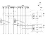
도 4에 도시된 것과 같이, 유기발광 표시장치(10)은 평면상 표시영역(DA)과 비표시영역(NDA)을 포함한다.As shown in FIG. 4, the organic light emitting
표시부(DP)은 복수 개의 화소들(PX)을 포함한다. 복수 개의 화소들(PX)이 배치된 영역이 표시영역(DA)으로 정의된다. 본 실시예에서 비표시영역(NDA)은 표시영역(DA)의 테두리를 따라 정의될 수 있다.The display unit DP includes a plurality of pixels PX. An area in which the plurality of pixels PX is disposed is defined as the display area DA. In the present embodiment, the non-display area NDA may be defined along the edge of the display area DA.
유기발광 표시장치(10)는 게이트 라인들(GL), 데이터 라인들(DL), 발광 라인들(EL), 초기화 전압 라인(SL-Vint), 제1 전압(ELVDD) 라인, 제2 전압(ELVSS) 라인 및 패드부(PD)를 포함할 수 있다.The
상기 게이트 라인들(GL), 상기 데이터 라인들(DL), 상기 발광 라인들(EL), 상기 초기화 전압 라인(SL-Vint), 상기 제1 전압(ELVDD) 라인 및 상기 제2 전압(ELVSS) 라인 중 일부는 동일층에 배치되고, 일부는 다른 층에 배치될 수 있다.The gate lines GL, the data lines DL, the light emitting lines EL, the initialization voltage line SL-Vint, the first voltage ELVDD line, and the second voltage ELVSS. Some of the lines may be disposed on the same layer, and some may be disposed on other layers.
비표시영역(NDA)에 표시영역(DA)을 둘러싸는 시일(seal) 부재(220)가 배치된다. 시일 부재(220)에 대한 설명은 도 5에서 자세히 후술된다.A
비표시영역(NDA)의 일측에는 상기 게이트 라인들(GL) 및 상기 발광 라인들(EL)이 연결된 게이트 구동부(GDC)가 배치된다. 본 도면에서 게이트 구동부(GDC)가 유기발광 표시장치(10)의 일측에 배치된 것으로 도시하였으나, 이에 한정되는 것은 아니다. 다른 실시예에서, 게이트 구동부(GDC)는 도 6과 같이 비표시영역의 양측에 배치될 수 있다. 이에 대한 설명은 도 6에서 후술된다.A gate driver GDC connected to the gate lines GL and the light emitting lines EL is disposed at one side of the non-display area NDA. Although the gate driver GDC is illustrated as being disposed on one side of the organic light emitting
게이트 구동부(GDC)는 시일 부재(220)와 평면상 중첩되는 부분을 포함할 수 있다. 시일 부재(220)와 그와 가장 인접한 픽셀(PX)간의 간격은 게이트 구동부(GDC)가 시일 부재(220)와 중첩되게 배치함으로써 줄어들 수 있다.The gate driver GDC may include a portion overlapping the
상기 게이트 라인들(GL)은 복수 개의 화소들(PX) 중 대응하는 화소(PX)에 각각 연결되고, 상기 데이터 라인들(DL)은 복수 개의 화소들(PX) 중 대응하는 화소(PX)에 각각 연결된다. 상기 발광 라인들(EL) 각각은 상기 게이트 라인들(GL) 중 대응하는 상기 게이트 라인(GL)에 나란하게 배열될 수 있다. 상기 제어신호 라인은 게이트 구동부(GDC)에 제어신호들을 제공할 수 있다. 상기 초기화 전압 라인은 복수 개의 화소들(PX)에 초기화 전압을 제공할 수 있다. 상기 제1 및 제2 전압 라인은 복수 개의 화소들(PX)에 연결되며, 복수 개의 화소들(PX)에 제1 전압을 제공할 수 있다. 제1 전압(ELVDD)은 제1 방향(DR1)으로 연장하는 복수의 라인들 및 제2 방향(DR2)으로 연장하는 복수의 라인들을 포함할 수 있다. 제2 전압(ELVSS)의 복수 개의 화소들(PX)에 공통 전압을 제공할 수 있다. 제2 전압(ELVSS)은 상기 제1 전압(ELVDD)보다 낮은 레벨의 전압일 수 있다.The gate lines GL are respectively connected to the corresponding pixels PX of the plurality of pixels PX, and the data lines DL are connected to the corresponding pixels PX of the plurality of pixels PX. Each is connected. Each of the emission lines EL may be arranged to be parallel to the corresponding gate line GL of the gate lines GL. The control signal line may provide control signals to the gate driver GDC. The initialization voltage line may provide an initialization voltage to the plurality of pixels PX. The first and second voltage lines may be connected to the plurality of pixels PX, and may provide a first voltage to the plurality of pixels PX. The first voltage ELVDD may include a plurality of lines extending in the first direction DR1 and a plurality of lines extending in the second direction DR2. The common voltage may be provided to the plurality of pixels PX of the second voltage ELVSS. The second voltage ELVSS may be a voltage at a level lower than the first voltage ELVDD.
패드부(PD)는 상기 게이트 라인들(GL), 상기 데이터 라인들(DL), 상기 발광 라인들(EL), 상기 초기화 전압 라인(SL-Vint), 상기 제1 전압(ELVDD) 라인 및 상기 제2 전압(ELVSS) 라인의 말단에 연결될 수 있다.The pad part PD may include the gate lines GL, the data lines DL, the light emitting lines EL, the initialization voltage line SL-Vint, the first voltage ELVDD line, and the gate lines GL. It may be connected to the end of the second voltage ELVSS line.
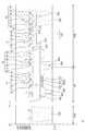
도 5은 도 4의 I1-I1’ 및 I2-I2’를 따라 자른 단면도이다.FIG. 5 is a cross-sectional view taken along lines I1-I1 'and I2-I2' of FIG. 4.
유기발광 표시장치(10)은 제1 기판(201)과 제1 기판(201) 상에 대향하여 배치된 제2 기판(210)을 포함한다.The organic light emitting
제1 기판(201)은 리지드(rigid)한 글래스(glass) 기판 또는 내열성을 지니는 플라스틱 기판일 수 있다. 제1 기판(201)은 투명하거나, 불투명하거나, 반투명할 수 있다.The
제1 기판(201)은 표시 영역(DA)과 표시 영역(DA)의 바깥으로 연장된 비표시 영역(NDA)이 배치될 수 있다.The
표시 영역(DA)은 화상을 표시하는 영역을 포함하며, 표시 소자가 배치될 수 있다. 예를 들면, 상기 표시 소자는 유기발광 소자일 수 있다.The display area DA includes an area for displaying an image, and a display element may be disposed. For example, the display device may be an organic light emitting device.
비표시 영역(NDA)에는 표시 영역(DA)의 소자들에 전기적인 신호를 전달하는 복수의 회로 배선이 배치될 수 있고, 제1 기판(201)과 제2 기판(210) 사이의 내부 공간을 밀폐시키는 시일 부재(220)가 배치될 수 있다.In the non-display area NDA, a plurality of circuit wires for transmitting an electrical signal to the elements of the display area DA may be disposed, and an internal space between the
제1 기판(201) 상에는 버퍼층(202)이 배치된다. 버퍼층(202)은 제1 기판(201)의 표면을 평활하게 하고, 수분 또는 외부 공기의 침투를 방지하는 역할을 한다. 버퍼층(202)은 무기막일 수 있다. 버퍼층(202)은 단일막 또는 다층막일 수 있다.The
표시 영역(DA)에는 제1 박막 트랜지스터(Ta) 및 스토리지 커패시터(Cst)가 배치될 수 있다. 일 실시예에 있어서 제1 박막 트랜지스터(Ta)는 구동 박막 트랜지스터일 수 있으나 이에 한정되는 것은 아니다.The first thin film transistor Ta and the storage capacitor Cst may be disposed in the display area DA. In an exemplary embodiment, the first thin film transistor Ta may be a driving thin film transistor, but is not limited thereto.
제1 박막 트랜지스터(Ta)는 반도체층(A1), 게이트 전극(G1_1, G2_2), 소스 전극(S1), 드레인 전극(D1)을 포함한다.The first thin film transistor Ta includes the semiconductor layer A1, the gate electrodes G1_1 and G2_2, the source electrode S1, and the drain electrode D1.
버퍼층(202) 상에는 반도체층(A1)이 배치된다. 반도체층(A1)은 비정질 실리콘(amorphous silicon), 폴리 실리콘(poly silicon), 유기 반도체를 포함할 수 있다. 다른 실시예에서, 반도체층(A1)은 산화물 반도체일 수 있다. 반도체층(A1)은 채널 영역과, 채널 영역의 양 측에 배치되며, 불순물이 도핑된 소스 영역 및 드레인 영역을 포함할 수 있다.The semiconductor layer A1 is disposed on the
반도체층(A1) 상에는 게이트 절연막(203)이 배치된다. 게이트 절연막(203)은 무기막일 수 있다. 게이트 절연막(203)은 단일막 또는 다층막일 수 있다.The
게이트 절연막(203) 상에는 제1 게이트 전극(G1_1)이 배치된다. 제1 게이트 전극(G1_1)은 도전성을 가지는 금속 물질로 형성될 수 있다. 예를 들면, 제1 게이트 전극(G1_1)은 몰리브덴(Mo), 알루미늄(Al), 구리(Cu), 티타늄(Ti)을 포함할 수 있다. 제1 게이트 전극(G1_1)은 단일막 또는 다층막일 수 있다.The first gate electrode G1_1 is disposed on the
제1 게이트 전극(G1_1) 상에는 제1 층간 절연막(204)이 배치된다. 제1 층간 절연막(204)은 무기막일 수 있다. 제1 층간 절연막(204)은 단일막 또는 다층막일 수 있다.The first
제1 층간 절연막(204) 상에는 제2 게이트 전극(G1_2)이 배치된다. 제2 게이트 전극(G1_2)은 도전성을 가지는 금속 물질로 형성될 수 있다. 예를 들면, 제2 게이트 전극은 몰리브덴(Mo), 알루미늄(Al), 구리(Cu), 티타늄(Ti)을 포함할 수 있다. 제2 게이트 전극은 단일막 또는 다층막일 수 있다.The second gate electrode G1_2 is disposed on the first
제1 게이트 전극(G1_1)과 제2 게이트 전극(G1_2)은 같은 물질로 형성될 수 있다. 예를 들면 제1 게이트 전극(G1_1)이 알루미늄(Al)으로 형성되어 있다면, 제2 게이트 전극(G1_2) 또한 알루미늄(Al)으로 형성되어 있을 수 있다.The first gate electrode G1_1 and the second gate electrode G1_2 may be formed of the same material. For example, when the first gate electrode G1_1 is formed of aluminum Al, the second gate electrode G1_2 may also be formed of aluminum Al.
제2 게이트 전극(G1_2) 상에는 제2 층간 절연막(205)이 배치 배치된다. 제2 층간 절연막(205)은 무기막일 수 있다. 제2 층간 절연막(205)은 단일막 또는 다층막일 수 있다.The second
제2 층간 절연막(205) 상에는 소스 전극(S1)과, 드레인 전극(D1)이 배치된다. 제1 층간 절연막(204)과 제2 층간 절연막(205)의 일부 및 게이트 절연막(203)의 일부를 제거하여서 컨택 홀을 형성하고, 컨택 홀을 통하여 반도체층(A1)의 소스 영역 및 드레인 영역에 소스 전극(S1) 및 드레인 전극(D1)이 각각 전기적으로 연결될 수 있다.The source electrode S1 and the drain electrode D1 are disposed on the second
소스 전극(S1)과 드레인 전극(D1)은 도전성을 가지는 금속 물질로 형성된다. 예를 들면, 소스 전극(S1)과 드레인 전극(D1)은 몰리브덴(Mo), 알루미늄(Al), 구리(Cu), 티타늄(Ti)을 포함할 수 있다.The source electrode S1 and the drain electrode D1 are formed of a conductive metal material. For example, the source electrode S1 and the drain electrode D1 may include molybdenum (Mo), aluminum (Al), copper (Cu), and titanium (Ti).
소스 전극(S1, S2)과 드레인 전극(D1, D2)은 단일막, 또는, 다층막일 수 있다. 예를 들면, 상기 소스 전극(S1, S2)과 드레인 전극(D1, D2)은 티타늄(Ti)/알루미늄(Al)/티타늄(Ti)이 적층된 구조일 수 있다.The source electrodes S1 and S2 and the drain electrodes D1 and D2 may be a single film or a multilayer film. For example, the source electrodes S1 and S2 and the drain electrodes D1 and D2 may have a structure in which titanium (Ti) / aluminum (Al) / titanium (Ti) is stacked.
소스 전극(S1)과 드레인 전극(D1) 상에는 제3 층간 절연막(206)이 배치될 수 있다. 제3 층간 절연막(206)은 무기막일 수 있다. 제3 층간 절연막(206)은 단일막 또는 다층막일 수 있다. 다른 실시예에서 제3 층간 절연막(206)은 생략될 수 있다.The third
제3 층간 절연막(206) 상에 보호막(207)이 배치될 수 있다. 보호막(207)은 유기막, 또는, 무기막일 수 있다. 보호막(207)은 패시베이션막 또는 평탄화막일 수 있다. 상기 패시베이션 막 또는 평탄화막중 어느 하나는 생략될 수 있다.The
스토리지 커패시터(Cst)는 제1 커패시터 전극(CE1), 제2 커패시터 전극(CE2), 및 이들 사이에 개재되는 유전체층을 포함한다. 일 실시예에 있어서, 상기 유전체층은 층간 절연막(204)에 대응될 수 있다. 제1 커패시터 전극(CE1)은 제1 게이트 전극(G1_1) 또는 제2 게이트 전극(G1_2)과 동일한 층에 동일한 물질로 형성될 수 있다. 제2 커패시터 전극은(CE2) 소스 전극(S1)과 드레인 전극(D1)과 동일한 층에 동일한 물질로 형성될 수 있다. 보호막(207)은 상기 제 2 커패시터 전극(CE2)을 덮을 수 있다.The storage capacitor Cst includes a first capacitor electrode CE1, a second capacitor electrode CE2, and a dielectric layer interposed therebetween. In one embodiment, the dielectric layer may correspond to the
제1 박막 트랜지스터(Ta)는 유기발광 소자(OLED)에 전기적으로 연결될 수 있다.The first thin film transistor Ta may be electrically connected to the organic light emitting diode OLED.
유기발광 소자(OLED)는 보호막(207) 상에 배치될 수 있다. 유기발광 소자(OLED)는 제1 전극(231), 유기발광층(232) 및 제2 전극(233)을 포함한다.The organic light emitting diode OLED may be disposed on the
제1 전극(231)은 화소마다 배치된 화소 전극일 수 있다. 또한, 제1 전극은 유기발광 다이오드의 애노드(anode) 전극일 수 있다.The
제1 전극(231)은 일함수가 높은 물질을 포함하여 이루어질 수 있다. 제1 전극은 인듐-주석-산화물(Indium-Tin-Oxide: ITO), 인듐-아연-산화물(Indium-Zinc-Oxide: IZO), 산화아연(Zinc Oxide: ZnO), 산화인듐(Induim Oxide: In2O3) 등을 포함할 수 있다. 상기 예시된 도전성 물질들은 상대적으로 일함수가 크면서도, 투명한 특성을 갖는다. 유기발광 표시장치가 전면 발광형일 경우, 상기 예시된 도전성 물질 이외에 반사성 물질, 예컨대 은(Ag), 마그네슘(Mg), 알루미늄(Al), 백금(Pt), 납(Pd), 금(Au), 니켈(Ni), 네오듐(Nd), 이리듐(Ir), 크롬(Cr), 리튬(Li), 칼슘(Ca) 또는 이들의 혼합물이 더 포함될 수 있다. 따라서, 제1 전극은 상기 예시된 도전성 물질 및 반사성 물질로 이루어진 단일층 구조를 갖거나, 이들이 적층된 복수층 구조를 가질 수 있다.The
제1 전극(231) 상에는 화소 정의막(208)이 배치된다. 화소 정의막(208)은 제1 전극(231)의 적어도 일부를 노출하는 개구부를 포함한다. 화소 정의막(208)은 유기 물질 또는 무기 물질을 포함할 수 있다. 일 실시예로, 화소 정의막은 포토 레지스트, 폴리이미드계 수지, 아크릴계 수지, 실리콘 화합물, 폴리아크릴계 수지 등의 재료를 포함할 수 있다.The
화소 정의막(208)에 의해 노출된 제1 전극(231)상에는 유기발광층(232)이 배치된다. 적색 화소에는 적색의 유기발광층이 배치되고, 녹색 화소에는 녹색 유기발광층이 배치되고, 청색 화소에는 청색 유기발광층이 배치된다.The organic
유기발광층(232) 상에는 제2 전극(233)이 배치된다. 제2 전극(233)은 화소의 구별없이 전체에 걸쳐 배치된 공통 전극일 수 있다. 또한, 제2 전극(233)은 유기발광 다이오드의 캐소드(cathod) 전극일 수 있다.The
제2 전극(233)은 일함수가 낮은 물질을 포함하여 이루어질 수 있다. 제2 전극(233)은 Li, Ca, LiF/Ca, LiF/Al, Al, Mg, Ag, Pt, Pd, Ni, Au Nd, Ir, Cr, BaF, Ba 또는 이들의 화합물이나 혼합물(예를 들어, Ag와 Mg의 혼합물 등)을 포함할 수 있다. 제2 전극(233)은 보조 전극을 더 포함할 수 있다. 상기 보조 전극은 상기 물질이 증착되어 형성된 막, 및 상기 막 상에 투명 금속 산화물, 예를 들어, 인듐-주석-산화물(Indium-Tin-Oxide: ITO), 인듐-아연-산화물(Indium-Zinc-Oxide: IZO), 산화아연(Zinc Oxide: ZnO), 인듐-주석-아연-산화물 (Indium-Tin-Zinc-Oxide) 등을 포함할 수 있다.The
유기발광 표시장치가 전면 발광형일 경우, 제2 전극(233)으로서 일함수가 작은 도전층을 박막으로 형성하고, 그 상부에 투명한 도전막, 예컨대, 인듐-주석-산화물(Indium-Tin-Oxide: ITO)층, 인듐-아연-산화물(Indium-Zinc-Oxide: IZO)층, 산화아연(Zinc Oxide: ZnO)층, 산화인듐(Induim Oxide: In2O3)층 등을 적층할 수 있다.When the organic light emitting display device is a top emission type, a conductive layer having a small work function is formed as a thin film as the
상술한 제1 전극(231), 유기발광층(232) 및 제2 전극(233)은 유기발광 다이오드를 구성할 수 있다.The
도시하지는 않았지만, 제1 전극과(231) 유기발광층(232) 사이에는 정공 주입층 및/또는 정공 수송층이 배치되고, 유기발광층과 제2 전극 사이에는 전자 수송층 및/또는 전자 주입층이 배치될 수 있다.Although not shown, a hole injection layer and / or a hole transport layer may be disposed between the first electrode and the organic
일 실시예에 있어서 제1 기판(201) 상에는 복수의 서브 화소 전극을 형성할 수 있다. 예컨대, 각 서브 화소 전극별로 적색, 녹색, 청색, 또는, 백색의 색을 구현할 수 있다.In an exemplary embodiment, a plurality of sub pixel electrodes may be formed on the
일 실시예에 있어서, 서브 화소 전극의 둘레에는 스페이서(209)가 더 배치될 수 있다. 스페이서(209)는 외부 충격에 의하여 표시 특성이 저하되지 않기 위하여 설치될 수 있다.In an embodiment, a
제1 기판(201) 상에는 제2 기판(210)이 결합될 수 있다. 제2 기판(210)은 수분이나, 외기로부터 유기발광 소자(OLED) 및 다른 소자들을 보호하는 역할을 한다. 예시적으로, 제2 기판(210)은 봉지기판일 수 있다. 몇몇 실시예에서, 상기 봉지기판은 리지드(rigid)한 기판일 수 있다. 예시적으로 상기 봉지기판은 글래스 기판이나, 내열성을 지니는 플라스틱 기판일 수 있다.The
비표시 영역(NDA)에는 다양한 회로 패턴, 이를테면, 전원 공급 패턴, 정전기 방지 패턴 및 기타 다양한 회로패턴이 형성될 수 있다. 일 실시예에 있어서, 비표시 영역(NDA)에는 제2 박막 트랜지스터(Tb), 제3 박막 트랜지스터(Tc) 및 제4 박막 트랜지스터(Td)가 배치될 수 있다. 제2 박막 트랜지스터(Tb) 및 제3 박막 트랜지스터(Tc)는 주사 신호용 박막 트랜지스터일 수 있고, 제4 박막 트랜지스터(Td)는 발광 제어 신호용 박막 트랜지스터일 수 있다.Various circuit patterns may be formed in the non-display area NDA, such as a power supply pattern, an antistatic pattern, and various other circuit patterns. In example embodiments, the second thin film transistor Tb, the third thin film transistor Tc, and the fourth thin film transistor Td may be disposed in the non-display area NDA. The second thin film transistor Tb and the third thin film transistor Tc may be thin film transistors for scan signals, and the fourth thin film transistor Td may be thin film transistors for emission control signals.
제2 박막 트랜지스터(Tb) 및 제3 박막 트랜지스터(Tc)는 반도체층(A2, A3), 제1 게이트 전극(G2_1, G3_1), 제2 게이트 전극(G2_2, G3_2), 소스 전극(S2, S3) 및 드레인 전극(D2, D3)을 포함한다. 제2 박막 트랜지스터(Tb) 및 제3 박막 트랜지스터(Tc)는 제1 박막 트랜지스터(Ta) 와 적층 구조와 동일하나, 이에 한정되는 것은 아니다. 예를 들면, 다른 실시예에서 제2 박막 트랜지스터(Tb) 및 제3 박막 트랜지스터(Tc)는 제2 게이트 전극(G2_2, G3_2)은 생략되고, 제1 게이트 전극(G2_1, G3_1)상에 소스 전극(S2, S3) 및 드레인 전극(D2, D3)이 배치될 수 있다.The second thin film transistor Tb and the third thin film transistor Tc include the semiconductor layers A2 and A3, the first gate electrodes G2_1 and G3_1, the second gate electrodes G2_2 and G3_2, and the source electrodes S2 and S3. ) And drain electrodes D2 and D3. The second thin film transistor Tb and the third thin film transistor Tc have the same stacked structure as the first thin film transistor Ta, but are not limited thereto. For example, in another embodiment, the second thin film transistor Tb and the third thin film transistor Tc are omitted from the second gate electrodes G2_2 and G3_2, and the source electrodes on the first gate electrodes G2_1 and G3_1. S2 and S3 and drain electrodes D2 and D3 may be disposed.
비표시 영역(NDA)에는 회로 배선(211)이 배치될 수 있다. 회로 배선(211)은 제3 층간 절연막(206) 상에 배치될 수 있다. 회로 배선(211)은 상기 제1 전극(231)과 동일한 물질로 형성될 수 있다. 회로 배선(211)은 제2 전극(233)에 전기적으로 연결될 수 있다.The
비표시 영역(NDA)에는 시일 부재(220)가 배치될 수 있다. 시일 부재(220)는 제1 기판과 제2 기판(210) 사이에 배치될 수 있다. 시일 부재(220)는 프릿 글래스(frit glass)를 포함한다. 프릿 글래스는 글래스 분말에 산화물 분말을 포함한다. 산화물 분말이 포함된 프릿 글래스에 유기물을 첨가하여 젤 상태의 페이스트를 제조하고, 대략 300℃ 내지 500℃의 온도 범위에서 소성할 수 있다. 프릿 글래스를 소성하면, 유기물은 대기 중으로 소멸되고, 젤 상태의 페이스트는 경화되어서 고체 상태의 프릿으로 존재할 수 있다.The
시일 부재(220)의 두께는 370μm 내지 540μm일 수 있다.The thickness of the
시일 부재(220)의 하부에 전원 전원 배선(213)이 배치될 수 있다. 전원 배선(213)은 제2 전압(ELVSS) 공급 라인일 수 있다.The
전원 배선(213)은 회로 배선(211)과 연결될 수 있다. 전원 배선(213)은 회로 배선(211)과 같은 층에 배치될 수 있다. 예를 들면, 전원 배선(213)은 제3 층간 절연막(213) 상에 배치될 수 있다.The
전원 배선(213)은 외부로부터 전원이 인가되는 배선일 수 있다. 전원 배선(213)은 후술하는 소스 전극(S4) 및 드레인 전극(D4)과 동일한 소재로 형성될 수 있다. 예를 들어, 전원 배선(213)은 몰리브덴(Mo)을 포함할 수 있다. 다만, 이에 제한되는 것은 아니고, 다른 실시예에서 전원 배선(213)은 금(Au), 은(Ag), 구리(Cu), 니켈(Ni), 백금(Pt), 팔라듐(Pd) 또는 크롬(Cr)을 포함할 수 있다.The
회로 배선(211) 및 전원 배선(213)의 각각은 드레인 전극(D4)에 접촉될 수 있고, 회로 배선(211)과 전원 배선(213)은 전기적으로 연결될 수 있다. 예를 들면, 제3 층간 절연막(206)의 일부를 제거하여서 컨택 홀을 형성하고, 컨택 홀을 통하여 드레인 전극(D4)이 전원 배선(213) 및 회로 배선(211)과 연결될 수 있다. 다만, 이에 제한되는 것은 아니고, 다른 실시예에서 상기 회로 배선(211)과 전원 배선(213)은 직접 연결되어 있을 수 있다.Each of the
제4 박막 트랜지스터(Td)는 반도체층(A4), 제1 게이트 전극(G4_1), 제2 게이트 전극(G4_2), 소스 전극(S4) 및 드레인 전극(D4)을 포함한다. 소스 전극(S4) 및 드레인 전극(D4)은 몰리브덴(Mo)을 포함할 수 있다.The fourth thin film transistor Td includes a semiconductor layer A4, a first gate electrode G4_1, a second gate electrode G4_2, a source electrode S4, and a drain electrode D4. The source electrode S4 and the drain electrode D4 may include molybdenum (Mo).
일 실시예에서 제4 박막 트랜지스터(Td)의 소스 전극(S4) 및 드레인 전극(D4)은 몰리브덴(Mo)을 포함하고, 제1 내지 제3 박막 트랜지스터(Ta, Tb, Tc)의 소스 전극(S1, S2, S3) 및 드레인 전극(S1, S2, S3)은 알루미늄(Al)을 포함할 수 있다.In an embodiment, the source electrode S4 and the drain electrode D4 of the fourth thin film transistor Td include molybdenum Mo, and the source electrodes of the first to third thin film transistors Ta, Tb, and Tc ( S1, S2, and S3 and the drain electrodes S1, S2, and S3 may include aluminum (Al).
다른 실시예에서 제3 박막 트랜지스터(Tc) 및 제4 박막 트랜지스터(Td)의 소스 전극(S3, S4) 및 드레인 전극(D3, D4)은 모두 몰리브덴(Mo)을 포함하고 같은층에 배치될 수 있다. 이 경우, 제2 박막 트랜지스터(Te)의 소스 전극(S2) 및 드레인 전극(D2)은 몰리브덴(Mo)이 아닌 물질을 포함할 수 있고, 제3 박막 트랜지스터(Tc) 및 제4 박막 트랜지스터(Td)와 다른층에 배치될 수 있다.In another embodiment, the source electrodes S3 and S4 and the drain electrodes D3 and D4 of the third thin film transistor Tc and the fourth thin film transistor Td may include molybdenum Mo and be disposed on the same layer. have. In this case, the source electrode S2 and the drain electrode D2 of the second thin film transistor Te may include a material other than molybdenum (Mo), and the third thin film transistor Tc and the fourth thin film transistor Td. ) May be placed on a different layer from
제4 박막 트랜지스터(Td)가 전원 배선(213) 하부에서 시일 부재(220)와 중첩되도록 배치될 수 있다. 일 실시예에서, 제4 박막 트랜지스터(Td)의 모든 부분이 시일 부재(220)와 평면상 중첩될 수 있다. 이 경우, 제3 박막 트랜지스터(Tc)의 일부가 시일 부재(220)와 평면상 중첩될 수도 있다. 다만, 다른 실시예에서 제4 박막 트랜지스터(Td)의 일부분이 시일 부재(220)와 평면상 중첩될 수 있다. 예를 들어, 제4 박막 트랜지스터(Td)의 제1 게이트 전극(G4_1), 제2 게이트 전극(G4_2) 및 소스 전극(S4)이 시일 부재(220)와 평면상 중첩될 수 있다.The fourth thin film transistor Td may be disposed to overlap the
몰리브덴(Mo)을 포함하는 부재의 경우, 300℃ 내지 500℃의 온도 범위에서 시일부의 소성에도 상기 부재는 손상되지 않을 수 있다. 예를 들면, 몰리브덴(Mo)을 포함하는 도전선 물질의 임계온도(critical temperature)는 대략 1000℃ 내지 1200℃이고, 따라서, 몰리브덴(Mo)을 포함하는 소스 전극(S4) 및 드레인 전극(D1)은 시일부의 하부에 중첩되게 배치되더라도 시일부의 소성과정에서 쉽게 손상되지 않을 수 있다.In the case of a member containing molybdenum (Mo), the member may not be damaged even when the seal portion is baked in a temperature range of 300 ° C to 500 ° C. For example, the critical temperature of the conductive wire material including molybdenum (Mo) is approximately 1000 ° C to 1200 ° C, and thus, the source electrode S4 and the drain electrode D1 including molybdenum (Mo). Even if disposed to overlap the lower portion of the seal portion may not be easily damaged during the sealing process of the seal portion.
시일 부재(220) 하부에 제4 박막 트랜지스터를 중첩되게 배치하므로써, 비표시영역(DA)에 존재하는 데드 스페이스(dead space)를 줄일 수 있다. 예를 들면, 데드 스페이스는 750μm이하가 되도록 줄어들 수 있다. 데드 스페이스는 시일 부재(220)부터 비표시 영역(NDA)과 표시 영역(DA)의 경계까지의 간격을 의미한다. 예를 들면, 데드 스페이스는 시일 부재(220)와 시일 부재(220)와 가장 인접한 제1 전극(231) 사이의 간격일 수 있다. 이와 같이 데드 스페이스를 줄이는 경우, 표시장치의 베젤(bezel)의 두께를 줄일 수 있다.By disposing the fourth thin film transistor under the
비표시 영역(NDA)에는 복수의 클럭 신호 라인(CL1, CL2, CL3, CL4)들이 배치될 수 있다. 복수의 클럭 신호 라인(CL1, CL2, CL3, CL4)은 회로 배선(211)과 동일한 층에 형성될 수 있다. 클럭 신호 라인(CL1, CL2, CL3, CL4)은 티타늄(Ti)/알루미늄(Al)/티타늄(Ti)으로 된 삼층 구조일 수 있다.A plurality of clock signal lines CL1, CL2, CL3, and CL4 may be disposed in the non-display area NDA. The plurality of clock signal lines CL1, CL2, CL3, and CL4 may be formed on the same layer as the
일 실시예에서 클럭 신호 라인(CL1, CL2, CL3, CL4) 중 일부는 보호막(207)과 중첩되도록 배치될 수 있고, 나머지 일부는 보호막(207) 주변에 배치될 수 있다. 예를 들면, 여기서 보호막(207) 주변이라 함은 제4 박막 트랜지스터(Td)와 제3 박막 트랜지스터(Tc)의 사이 공간일 수 있다. 다만, 이에 제한 되는 것은 아니고, 다른 실시예에서 모든 클럭 신호 라인(CL1, CL2, CL3, CL4)은 보호막(207)과 중첩되도록 배치될 수도 있다.In some embodiments, some of the clock signal lines CL1, CL2, CL3, and CL4 may be disposed to overlap the
금속 패턴층(214)은 시일 부재(220)의 하부에서 제4 박막 트랜지스터와 중첩되지 않도록 배치될 수 있다.The metal pattern layer 214 may be disposed under the
금속 패턴층(214)은 복수개의 요철이 패터닝된 형태로, 대략 사각형의 박스 형태로 형성될 수 있다. 이러한 금속 패턴층(300)에 형성된 복수개의 요철를 통해, 금속 패턴층(214) 상에 배치되는 시일 부재(220)가 금속 패턴층(214)과 접촉하는 면적이 증가하여 이를 통해 시일 부재(220)가 하부 기판(201)과 더욱 견고하게 접합될 수 있다.The metal pattern layer 214 may be formed in the shape of a plurality of uneven patterns, and have a substantially rectangular box shape. Through the plurality of irregularities formed in the metal pattern layer 300, the area in which the
또한, 금속 패턴층(214)은 레이저의 열을 흡수하거나, 레이저를 반사시켜서 시일 부재(220)에 열을 전달하는 역할을 할 수 있다. 금속 패턴층(214)은 금(Au), 은(Ag), 구리(Cu), 니켈(Ni), 백금(Pt), 팔라듐(Pd), 알루미늄(Al), 몰리브덴(Mo), 크롬(Cr) 등을 포함하는 단일막 또는 다층막일 수 있다.In addition, the metal pattern layer 214 may serve to absorb heat of the laser or reflect the laser to transfer heat to the sealing
상기 제2 기판(210) 상에는 터치 스크린의 역할을 할 수 있도록 복수의 터치 전극(221)이 형성될 수 있다. 도시하진 않았지만, 제2 기판(210) 상에는 편광 필름, 컬러 필터, 커버 윈도우와 같은 기능막이 더 형성될 수도 있다.A plurality of
이하 다른 실시예에 대해서 설명한다.Another embodiment will be described below.
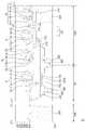
도 6은 본 발명의 다른 실시예에 따른 유기발광 표시장치의 배치도이다.6 is a layout view of an organic light emitting display device according to another exemplary embodiment of the present invention.
도 7은 도 6의 II1-II1’ 및 II2-II2’를 따라 자른 단면도이다.FIG. 7 is a cross-sectional view taken along line II1-II1 ′ and II2-II2 ′ of FIG. 6.
본 실시예에 따른 유기발광 표시장치(11) 비표시영역(NDA)의 양측에 게이트 구동부(GDC, GDC_2) 및 전원부(ELVSS, ELVSS_2)가 배치되는 점에서 도 4 및 도 5의 실시예와 차이가 있다.4 and 5 in that the gate driving units GDC and GDC_2 and the power supply units ELVSS and ELVSS_2 are disposed on both sides of the non-display area NDA of the organic light emitting
도 6 및 도 7을 참조하면, 비표시영역(NDA)의 일 측에는 제1 게이트 구동부(GDC) 및 제1 전원부(ELVSS)가 배치될 수 있다. 상기 측면과 대칭하는 측에는 제2 게이트 구동부(GDC_2) 및 제2 전원부(ELVSS_2)가 배치될 수 있다. 제1 게이트 구동부(GDC), 제1 전원부(ELVSS), 제2 게이트 구동부(GDC_2) 및 제2 전원부(ELVSS)는 시일 부재(220)와 중첩하는 부분을 포함 할 수 있다.6 and 7, a first gate driver GDC and a first power source ELVSS may be disposed on one side of the non-display area NDA. The second gate driver GDC_2 and the second power source ELVSS_2 may be disposed on a side symmetrical to the side surface. The first gate driver GDC, the first power source ELVSS, the second gate driver GDC_2, and the second power source ELVSS may include a portion overlapping the
본 실시예에 따른 유기발광 표시장치(11)는 표시 영역(DA)의 제2 방향(DR2)의 중심선을 따라 대칭 구조일 수 있다.The organic light emitting
제2 게이트 구동부(GDC_2)는 제1 게이트 구동부(GDC)와 동일 시점에서 좌우 방향만 바뀌었을 뿐. 수직 적층 구조는 동일하다. 마찬가지로, 제2 전원부(ELVSS_2)는 제1전원부(ELVSS)와 좌우 형상만 바뀌었을 뿐, 상하 적층 관계는 동일하다.The second gate driver GDC_2 only changes in the left and right directions at the same time as the first gate driver GDC. The vertical stacking structure is the same. Similarly, only the left and right shapes of the second power supply unit ELVSS_2 are changed from the first power supply unit ELVSS, and the vertical stacking relationship is the same.
시일 부재(220) 하부에 제1 게이트 구동부(GDC) 및 제2 게이트 구동부(GDC_2)에 각각 포함된 제4 박막 트랜지스터(Td)를 중첩되게 배치시키므로써, 본 실시예에 따른 유기발광 표시장치(11)는 도 4 및 도 5의 유기발광 표시장치(10)와 같이 데드 스페이스를 줄이는 효과가 있을 수 있다.The fourth thin film transistor Td included in the first gate driver GDC and the second gate driver GDC_2 is disposed under the
도 8은 본 발명의 다른 실시예에 따른 유기발광 표시장치의 배치도이다.8 is a layout view of an organic light emitting display device according to another exemplary embodiment of the present invention.
도 9은 도 8의 III-III’’을 따라 자른 단면도이다.FIG. 9 is a cross-sectional view taken along line III-III ′ ′ of FIG. 8.
본 실시예에 따른 유기발광 표시장치(12)는 비표시영역(NDA)에서 표시영역(DA)의 세 측면을 둘러싸는 게이트 구동부(GDC_3)가 배치되는 점에서 도 6 및 도 7의 실시예와 차이가 있다.In the organic light emitting
도 8을 및 도 9를 참조하면, 게이트 구동부(GDC_3)는 비표시영역(NDA)에서 표시영역(DA)를 감싸며 일체로 배치된다. 게이트 구동부 본 실시예의 유기발광 표시장치(12)의 구동부는 상기 세 측면 중 제1 전원부(ELVSS) 및 제2 전원부(ELVSS_2)가 배치된 양측면의 배치구조 및 적층구조는 도 6 및 도 7의 유기발광 표시장치(11)의 배치구조 및 적층구조와 동일할 수 있다.8 and 9, the gate driver GDC_3 is integrally disposed to surround the display area DA in the non-display area NDA. Gate driver The driving unit of the organic light emitting
다만, 상기 세 측면 중 제1 전원부(ELVSS) 및 제2 전원부(ELVSS_2)가 배치되지 않은 나머지 측면의 적층구조는 도 6 및 도 7의 유기발광 표시장치(11)의 적층구조와 달리 전원배선(213)이 생략될 수 있다.However, the stacked structure of the other side in which the first power source ELVSS and the second power source ELVSS_2 are not disposed among the three side surfaces is different from that of the organic light emitting
본 실시예의 유기발광 표시장치(12)는 제5 박막 트랜지스터(Te)를 더 포함할 수 있다. 일 실시예에 있어서 제5 박막 트랜지스터(Te)는 더미 전극을 포함할 수 있다.The organic light emitting
제5 박막 트랜지스터(Te)는 반도체층(A5), 게이트 전극(G5_1, G5_2), 소스 전극(S5), 드레인 전극(D5)을 포함한다. 제5 박막 트랜지스터(Te)는 제1 박막 트랜지스터(Ta)의 적층 구조와 동일하나, 이에 한정되는 것은 아니다.The fifth thin film transistor Te includes the semiconductor layer A5, the gate electrodes G5_1 and G5_2, the source electrode S5, and the drain electrode D5. The fifth thin film transistor Te is the same as the stacked structure of the first thin film transistor Ta, but is not limited thereto.
도 10은 본 발명의 다른 실시예에 따른 유기발광 표시장치의 배치도이다.10 is a layout view of an organic light emitting display device according to another exemplary embodiment of the present invention.
도 11은 도 10의 IV1-IV1’ 및 IV2-IV2’를 따라 자른 단면도이다.FIG. 11 is a cross-sectional view taken along lines IV1-IV1 ′ and IV2-IV2 ′ of FIG. 10.
본 실시예에 따른 유기발광 표시장치(13)는 직사각 형상의 시일 부재(220)가 유기발광 표시장치(13)의 테두리가 될 수 있는 점에서 도 4 및 도 5의 실시예와 차이가 있다.The organic light emitting
도 10을 참조하면, 직사각 형상의 시일 부재(220)는 유기발광 표시장치(13)의 테두리의 일부는 직사각 형상의 시일 부재(220)의 네 측면 중 세 측면에 대응될 수 있다.Referring to FIG. 10, a portion of an edge of the organic light emitting
도 11를 참조하면, 유기발광 표시장치(13)는 단면상 시일 부재(220)가 절단면을 이루며, 시일 부재(220)는 상, 하로 배치된 소자들과 정렬된 점을 제외하고, 도 5의 유기발광 표시장치(10)의 적층 구조와 동일할 수 있다.Referring to FIG. 11, in the organic light emitting
이상 첨부된 도면을 참조하여 본 발명의 실시예들을 설명하였지만, 본 발명이 속하는 기술분야에서 통상의 지식을 가진 자는 본 발명의 그 기술적 사상이나 필수적인 특징을 변경하지 않고서 다른 구체적인 형태로 실시될 수 있다는 것을 이해할 수 있을 것이다. 그러므로 이상에서 기술한 실시예들은 모든 면에서 예시적인 것이며 한정적이 아닌 것으로 이해해야만 한다.Although the embodiments of the present invention have been described above with reference to the accompanying drawings, those skilled in the art to which the present invention pertains may be embodied in other specific forms without changing the technical spirit or essential features of the present invention. I can understand that. Therefore, it should be understood that the embodiments described above are exemplary in all respects and not restrictive.
201: 제1 기판
202: 버퍼층
203: 게이트 절연막
204: 제1 층간 절연막
205: 제2 층간 절연막
206: 제3 층간 절연막
207: 보호막
208: 화소 정의막
209: 스페이서
210: 제2 기판
211: 회로 배선
213: 전원 배선
220: 시일 부재
232: 유기발광층201: first substrate
202: buffer layer
203: gate insulating film
204: first interlayer insulating film
205: second interlayer insulating film
206: third interlayer insulating film
207: shield
208: pixel defining layer
209: spacer
210: second substrate
211: circuit wiring
213: power wiring
220: seal member
232: organic light emitting layer
Claims (20)
Translated fromKorean복수의 박막 트랜지스터를 포함하는 제1 표시 기판;
상기 제1 표시 기판과 대향하는 제2 표시 기판; 및
상기 제1 표시 기판과 상기 제2 표시 기판 사이의 상기 비표시영역에 배치되어 상기 제1 표시 기판과 상기 제2 표시 기판을 접합시키는 시일 부재를 포함하되,
상기 각 박막 트랜지스터는 게이트 전극을 포함하고,
상기 복수의 박막 트랜지스터 중 적어도 하나의 박막 트랜지스터의 상기 게이트 전극은 상기 시일 부재와 두께 방향으로 중첩하는 표시장치.A display device comprising a display area and a non-display area,
A first display substrate including a plurality of thin film transistors;
A second display substrate facing the first display substrate; And
A seal member disposed in the non-display area between the first display substrate and the second display substrate to bond the first display substrate to the second display substrate,
Each thin film transistor includes a gate electrode,
And the gate electrode of at least one of the plurality of thin film transistors overlaps the seal member in a thickness direction.
상기 적어도 하나의 박막 트랜지스터는 제1 박막 트랜지스터이고,
상기 복수의 박막 트랜지스터는 상기 제1 박막 트랜지스터에 인접 배치되고 상기 비표시영역에 위치하는 제2 박막 트랜지스터를 더 포함하되,
상기 제1 박막 트랜지스터의 소스/드레인 전극은 제1 도전층으로 이루어지고,
상기 제2 박막 트랜지스터의 소스/드레인 전극은 상기 제1 도전층과 상이한 층에 위치하는 제2 도전층으로 이루어지는 표시장치.According to claim 1,
The at least one thin film transistor is a first thin film transistor,
The plurality of thin film transistors may further include a second thin film transistor disposed adjacent to the first thin film transistor and positioned in the non-display area.
The source / drain electrode of the first thin film transistor is formed of a first conductive layer,
And a source / drain electrode of the second thin film transistor is formed of a second conductive layer positioned on a different layer from the first conductive layer.
상기 제1 박막 트랜지스터의 게이트 전극 및 상기 제2 박막 트랜지스터의 게이트 전극은 상기 제1 도전층 및 상기 제2 도전층과 상이한 층에 위치하는 제3 도전층으로 이루어지는 표시장치.The method of claim 2,
And a gate electrode of the first thin film transistor and a gate electrode of the second thin film transistor are formed of a third conductive layer positioned on a different layer from the first conductive layer and the second conductive layer.
상기 복수의 박막 트랜지스터는 상기 표시영역에 배치된 제3 박막 트랜지스터를 더 포함하는 표시장치.The method of claim 3, wherein
The plurality of thin film transistors may further include a third thin film transistor disposed in the display area.
상기 제3 박막 트랜지스터의 상기 게이트 전극은 상기 제3 도전층으로 이루어지고, 상기 제3 박막 트랜지스터의 소스/드레인 전극은 상기 제2 도전층으로 이루어지는 표시장치.The method of claim 4, wherein
And the gate electrode of the third thin film transistor is formed of the third conductive layer, and the source / drain electrode of the third thin film transistor is formed of the second conductive layer.
상기 비표시 영역은 게이트 구동부를 포함하되,
상기 게이트 구동부는 상기 제1 박막 트랜지스터와 상기 제2 박막 트랜지스터를 포함하는 표시장치.The method of claim 3, wherein
The non-display area includes a gate driver,
The gate driver includes the first thin film transistor and the second thin film transistor.
상기 표시장치는 직사각형 형상을 갖고,
상기 게이트 구동부는 상기 표시장치의 제1 변 에지에 위치하는 표시장치.The method of claim 6,
The display device has a rectangular shape,
And the gate driver is positioned at an edge of the first side of the display device.
상기 제1 도전층은 몰리브덴(Mo)을 포함하고,
상기 제2 도전층은 알루미늄(Al)을 포함하는 표시장치.The method of claim 2,
The first conductive layer includes molybdenum (Mo),
The second conductive layer includes aluminum (Al).
상기 제1 박막 트랜지스터의 상기 드레인 전극과 연결되고, 상기 제2 도전층으로 이루어진 전원 배선을 더 포함하는 표시장치.The method of claim 2,
And a power line connected to the drain electrode of the first thin film transistor and formed of the second conductive layer.
상기 제2 박막 트랜지스터의 게이트 전극은 상기 시일 부재와 두께 방향으로 비중첩하는 표시장치.The method of claim 2,
And a gate electrode of the second thin film transistor that is not overlapped with the seal member in a thickness direction.
상기 표시장치는 직사각형 형상을 갖고,
상기 제1 박막 트랜지스터 및 상기 제2 박막 트랜지스터는 상기 표시장치의 제1 변 에지에 위치하는 표시장치.The method of claim 2,
The display device has a rectangular shape,
And the first thin film transistor and the second thin film transistor are positioned at edges of a first side of the display device.
상기 제1 변에 대향하는 상기 표시장치의 제2 변 에지에 위치하는 금속 패턴층을 더 포함하는 표시장치.The method of claim 11, wherein
And a metal pattern layer positioned at an edge of the second side of the display device opposite to the first side.
상기 금속 패턴층은 시일 부재와 두께 방향으로 중첩하는 표시장치.The method of claim 12,
The metal pattern layer overlaps the seal member in the thickness direction.
상기 제1 박막 트랜지스터 및 상기 제2 박막 트랜지스터는 각각 복수개이고,
상기 제1 박막 트랜지스터 및 상기 제2 박막 트랜지스터는 상기 제1 변에 대향하는 상기 표시장치의 제2 변 에지에 더 위치하는 표시장치.The method of claim 11, wherein
The first thin film transistor and the second thin film transistor are respectively plural,
And the first thin film transistor and the second thin film transistor are further disposed on an edge of a second side of the display device opposite to the first side.
상기 제1 박막 트랜지스터 및 상기 제2 박막 트랜지스터 사이에 배치된 클럭 배선을 더 포함하는 표시장치.The method of claim 2,
And a clock wire disposed between the first thin film transistor and the second thin film transistor.
상기 적어도 하나의 박막 트랜지스터는 제1 박막 트랜지스터이고,
상기 복수의 박막 트랜지스터는 상기 제1 박막 트랜지스터에 인접 배치되고 상기 비표시영역에 위치하는 제2 박막 트랜지스터 및 제3 박막 트랜지스터를 더 포함하되,
상기 제1 박막 트랜지스터 및 상기 제2 박막 트랜지스터의 소스/드레인 전극은 제1 도전층으로 이루어지고,
상기 제3 박막 트랜지스터의 소스/드레인 전극은 상기 제1 도전층과 상이한 층에 위치하는 제2 도전층으로 이루어지는 표시장치.According to claim 1,
The at least one thin film transistor is a first thin film transistor,
The plurality of thin film transistors may further include a second thin film transistor and a third thin film transistor disposed adjacent to the first thin film transistor and positioned in the non-display area.
The source / drain electrodes of the first thin film transistor and the second thin film transistor are formed of a first conductive layer,
And a source / drain electrode of the third thin film transistor is formed of a second conductive layer positioned on a different layer from the first conductive layer.
상기 기판 상의 제1 도전층;
상기 제1 도전층 상의 제1 절연층;
상기 제1 절연층 상의 제2 도전층;
상기 제2 도전층 상의 제2 절연층; 및
상기 제2 절연층 상의 제3 도전층을 포함하되,
상기 제3 도전층은 몰리브덴(Mo)을 포함하고,
상기 제3 도전층은 상기 표시영역에는 위치하지 않고, 상기 비표시영역에 위치하는 표시장치.A substrate including a display area and a non-display area;
A first conductive layer on the substrate;
A first insulating layer on the first conductive layer;
A second conductive layer on the first insulating layer;
A second insulating layer on the second conductive layer; And
A third conductive layer on the second insulating layer,
The third conductive layer includes molybdenum (Mo),
And the third conductive layer is not in the display area but in the non-display area.
상기 제3 도전층 상에 중첩 배치된 시일 부재를 더 포함하는 표시장치.The method of claim 17,
The display device further comprises a sealing member disposed on the third conductive layer.
상기 제3 도전층과 상기 시일 부재 사이에 배치된 전원 배선을 더 포함하는 표시장치.The method of claim 18,
And a power supply wiring arranged between the third conductive layer and the seal member.
상기 제2 도전층은 알루미늄(Al)을 포함하는 표시장치.The method of claim 17,
The second conductive layer includes aluminum (Al).
Priority Applications (2)
| Application Number | Priority Date | Filing Date | Title |
|---|---|---|---|
| KR1020180074767AKR102566157B1 (en) | 2018-06-28 | 2018-06-28 | Display device |
| US16/371,358US10937840B2 (en) | 2018-06-28 | 2019-04-01 | Display device |
Applications Claiming Priority (1)
| Application Number | Priority Date | Filing Date | Title |
|---|---|---|---|
| KR1020180074767AKR102566157B1 (en) | 2018-06-28 | 2018-06-28 | Display device |
Publications (2)
| Publication Number | Publication Date |
|---|---|
| KR20200002044Atrue KR20200002044A (en) | 2020-01-08 |
| KR102566157B1 KR102566157B1 (en) | 2023-08-11 |
Family
ID=69055436
Family Applications (1)
| Application Number | Title | Priority Date | Filing Date |
|---|---|---|---|
| KR1020180074767AActiveKR102566157B1 (en) | 2018-06-28 | 2018-06-28 | Display device |
Country Status (2)
| Country | Link |
|---|---|
| US (1) | US10937840B2 (en) |
| KR (1) | KR102566157B1 (en) |
Cited By (2)
| Publication number | Priority date | Publication date | Assignee | Title |
|---|---|---|---|---|
| US10937840B2 (en)* | 2018-06-28 | 2021-03-02 | Samsung Display Co., Ltd. | Display device |
| US11882742B2 (en) | 2021-09-03 | 2024-01-23 | Lg Display Co., Ltd. | Display panel and electronic device including same |
Families Citing this family (9)
| Publication number | Priority date | Publication date | Assignee | Title |
|---|---|---|---|---|
| CN108538240B (en)* | 2018-05-29 | 2020-03-10 | 京东方科技集团股份有限公司 | Pixel driving circuit, driving method thereof and display device |
| CN108877674A (en)* | 2018-07-27 | 2018-11-23 | 京东方科技集团股份有限公司 | A kind of pixel circuit and its driving method, display device |
| CN109243305B (en)* | 2018-09-17 | 2021-10-12 | 京东方科技集团股份有限公司 | Display panel, display device, and method for manufacturing display panel |
| CN109192140B (en)* | 2018-09-27 | 2020-11-24 | 武汉华星光电半导体显示技术有限公司 | Pixel driving circuit and display device |
| KR102663522B1 (en)* | 2018-11-05 | 2024-05-16 | 삼성디스플레이 주식회사 | Display device and method for manufacturing of the same |
| US11765935B2 (en) | 2019-07-04 | 2023-09-19 | Lg Display Co., Ltd. | Display apparatus |
| KR102851564B1 (en)* | 2019-12-10 | 2025-08-28 | 엘지디스플레이 주식회사 | Display Device |
| CN112509523B (en)* | 2021-02-04 | 2021-05-25 | 上海视涯技术有限公司 | A display panel, driving method and display device |
| WO2023279373A1 (en)* | 2021-07-09 | 2023-01-12 | 京东方科技集团股份有限公司 | Display substrate and display panel |
Citations (2)
| Publication number | Priority date | Publication date | Assignee | Title |
|---|---|---|---|---|
| KR20150049141A (en)* | 2013-10-29 | 2015-05-08 | 삼성디스플레이 주식회사 | Organic light emitting display devices and methods of manufacturing organic light emitting display devices |
| JP2017187782A (en)* | 2008-11-13 | 2017-10-12 | 株式会社半導体エネルギー研究所 | Semiconductor device and display device |
Family Cites Families (27)
| Publication number | Priority date | Publication date | Assignee | Title |
|---|---|---|---|---|
| JP3520396B2 (en)* | 1997-07-02 | 2004-04-19 | セイコーエプソン株式会社 | Active matrix substrate and display device |
| US6809481B2 (en)* | 2002-02-28 | 2004-10-26 | Semiconductor Energy Laboratory Co., Ltd. | Light emitting device and electric device using the same |
| KR101160822B1 (en) | 2004-07-27 | 2012-06-29 | 삼성전자주식회사 | Thin film transistor array panel and display apparatus including the same |
| US7462897B2 (en)* | 2005-01-31 | 2008-12-09 | Semiconductor Energy Laboratory Co., Ltd. | Light emitting device and electronic device |
| KR100700653B1 (en) | 2005-02-03 | 2007-03-27 | 삼성에스디아이 주식회사 | Organic light emitting display device |
| KR100685845B1 (en)* | 2005-10-21 | 2007-02-22 | 삼성에스디아이 주식회사 | Organic light emitting display device and manufacturing method thereof |
| JP5301080B2 (en)* | 2005-12-26 | 2013-09-25 | 株式会社ジャパンディスプレイ | Liquid crystal display |
| KR100673765B1 (en)* | 2006-01-20 | 2007-01-24 | 삼성에스디아이 주식회사 | Organic light emitting display device and manufacturing method |
| US8164257B2 (en)* | 2006-01-25 | 2012-04-24 | Samsung Mobile Display Co., Ltd. | Organic light emitting display and method of fabricating the same |
| KR100688791B1 (en)* | 2006-01-27 | 2007-03-02 | 삼성에스디아이 주식회사 | Organic electroluminescent display and manufacturing method thereof. |
| KR100688790B1 (en)* | 2006-01-27 | 2007-03-02 | 삼성에스디아이 주식회사 | Organic electroluminescent display and manufacturing method thereof |
| KR100671643B1 (en)* | 2006-01-27 | 2007-01-19 | 삼성에스디아이 주식회사 | Organic light emitting display device and manufacturing method thereof |
| KR100671639B1 (en)* | 2006-01-27 | 2007-01-19 | 삼성에스디아이 주식회사 | Organic electroluminescent display and manufacturing method thereof |
| KR100711882B1 (en)* | 2006-01-27 | 2007-04-25 | 삼성에스디아이 주식회사 | Organic electroluminescent display and manufacturing method thereof |
| KR101279296B1 (en)* | 2006-04-17 | 2013-06-26 | 엘지디스플레이 주식회사 | Organic semiconductor sturcture and methodd of manufacturing the same organic thin film transistor using the organic semiconductor sturcture and method of manufacturing the organic thin film transistor and display apparatus using the same |
| JP5177999B2 (en)* | 2006-12-05 | 2013-04-10 | 株式会社半導体エネルギー研究所 | Liquid crystal display |
| JP5520614B2 (en)* | 2010-01-15 | 2014-06-11 | 株式会社ジャパンディスプレイ | Liquid crystal display device and manufacturing method thereof |
| KR20150105523A (en)* | 2014-03-06 | 2015-09-17 | 삼성디스플레이 주식회사 | Liquid crystal display apparatus |
| KR102213223B1 (en) | 2014-05-23 | 2021-02-08 | 삼성디스플레이 주식회사 | Organic light-emitting display apparatus and manufacturing the same |
| KR102414810B1 (en)* | 2015-10-12 | 2022-06-30 | 삼성디스플레이 주식회사 | Liquid crystal display device and manufacturing method thereof |
| KR102522858B1 (en)* | 2016-02-17 | 2023-04-18 | 삼성디스플레이 주식회사 | Display device and manufacturing method thereof |
| KR102570551B1 (en)* | 2016-07-05 | 2023-08-25 | 삼성디스플레이 주식회사 | display device |
| CN109792105B (en)* | 2016-09-26 | 2021-02-26 | 夏普株式会社 | Liquid crystal cell and scanning antenna |
| KR102587728B1 (en)* | 2016-10-07 | 2023-10-12 | 삼성디스플레이 주식회사 | Thin film transistor array substrate and fabricating method thereof |
| KR102566157B1 (en)* | 2018-06-28 | 2023-08-11 | 삼성디스플레이 주식회사 | Display device |
| KR102847688B1 (en)* | 2019-02-26 | 2025-08-19 | 삼성디스플레이 주식회사 | Display device |
| KR102830391B1 (en)* | 2019-03-12 | 2025-07-07 | 삼성디스플레이 주식회사 | Display apparatus and method of manufacturing the same |
- 2018
- 2018-06-28KRKR1020180074767Apatent/KR102566157B1/enactiveActive
- 2019
- 2019-04-01USUS16/371,358patent/US10937840B2/ennot_activeExpired - Fee Related
Patent Citations (2)
| Publication number | Priority date | Publication date | Assignee | Title |
|---|---|---|---|---|
| JP2017187782A (en)* | 2008-11-13 | 2017-10-12 | 株式会社半導体エネルギー研究所 | Semiconductor device and display device |
| KR20150049141A (en)* | 2013-10-29 | 2015-05-08 | 삼성디스플레이 주식회사 | Organic light emitting display devices and methods of manufacturing organic light emitting display devices |
Cited By (2)
| Publication number | Priority date | Publication date | Assignee | Title |
|---|---|---|---|---|
| US10937840B2 (en)* | 2018-06-28 | 2021-03-02 | Samsung Display Co., Ltd. | Display device |
| US11882742B2 (en) | 2021-09-03 | 2024-01-23 | Lg Display Co., Ltd. | Display panel and electronic device including same |
Also Published As
| Publication number | Publication date |
|---|---|
| KR102566157B1 (en) | 2023-08-11 |
| US10937840B2 (en) | 2021-03-02 |
| US20200006446A1 (en) | 2020-01-02 |
Similar Documents
| Publication | Publication Date | Title |
|---|---|---|
| KR102566157B1 (en) | Display device | |
| JP7311562B2 (en) | Display device | |
| US10761632B2 (en) | Display device with touch sensor for suppressing deterioration of image quality caused by capacitor in touch sensor unit and method for manufacturing same | |
| US10866663B2 (en) | Display device with integrated touch screen and method for fabricating the same | |
| US9087800B2 (en) | Organic light emitting diode display | |
| US9619091B2 (en) | Display device and manufacturing method thereof | |
| EP3671413A1 (en) | Touch display panel, method for driving same, and electronic device | |
| US10976848B2 (en) | Display apparatus with touch sensor | |
| TWI818705B (en) | Display panel and electronic device including the same | |
| CN105742312A (en) | Organic light emitting display device | |
| KR102579307B1 (en) | Organic light emitting display device | |
| US10719153B2 (en) | Display panel including touch circuit, touch detection method thereof and display device | |
| CN220691380U (en) | Display device | |
| CN116963555A (en) | Display devices and display modules | |
| WO2025020510A1 (en) | Display panel and manufacturing method therefor, and display device | |
| CN114429752A (en) | Display device | |
| CN117631852A (en) | Touch detection module and display device including the same | |
| US20230209892A1 (en) | Display device | |
| KR102864587B1 (en) | Display device | |
| US20250037656A1 (en) | Display substrate and display apparatus | |
| CN115394201A (en) | Display panel and display device | |
| CN114664904A (en) | Array substrate and display panel | |
| CN219476306U (en) | Display apparatus | |
| TWI759047B (en) | Organic light-emitting display panel | |
| WO2023016335A1 (en) | Display substrate and display apparatus |
Legal Events
| Date | Code | Title | Description |
|---|---|---|---|
| PA0109 | Patent application | Patent event code:PA01091R01D Comment text:Patent Application Patent event date:20180628 | |
| PG1501 | Laying open of application | ||
| A201 | Request for examination | ||
| PA0201 | Request for examination | Patent event code:PA02012R01D Patent event date:20210504 Comment text:Request for Examination of Application Patent event code:PA02011R01I Patent event date:20180628 Comment text:Patent Application | |
| E902 | Notification of reason for refusal | ||
| PE0902 | Notice of grounds for rejection | Comment text:Notification of reason for refusal Patent event date:20221126 Patent event code:PE09021S01D | |
| E701 | Decision to grant or registration of patent right | ||
| PE0701 | Decision of registration | Patent event code:PE07011S01D Comment text:Decision to Grant Registration Patent event date:20230620 | |
| GRNT | Written decision to grant | ||
| PR0701 | Registration of establishment | Comment text:Registration of Establishment Patent event date:20230808 Patent event code:PR07011E01D | |
| PR1002 | Payment of registration fee | Payment date:20230808 End annual number:3 Start annual number:1 | |
| PG1601 | Publication of registration |