KR20190135426A - Process kit with adjustable tuning ring for edge uniformity control - Google Patents
Process kit with adjustable tuning ring for edge uniformity controlDownload PDFInfo
- Publication number
- KR20190135426A KR20190135426AKR1020190062161AKR20190062161AKR20190135426AKR 20190135426 AKR20190135426 AKR 20190135426AKR 1020190062161 AKR1020190062161 AKR 1020190062161AKR 20190062161 AKR20190062161 AKR 20190062161AKR 20190135426 AKR20190135426 AKR 20190135426A
- Authority
- KR
- South Korea
- Prior art keywords
- ring
- adjustable tuning
- ring component
- component
- coupling
- Prior art date
- Legal status (The legal status is an assumption and is not a legal conclusion. Google has not performed a legal analysis and makes no representation as to the accuracy of the status listed.)
- Withdrawn
Links
- 238000000034methodMethods0.000titleclaimsabstractdescription128
- 230000008569processEffects0.000titleclaimsabstractdescription104
- 230000008878couplingEffects0.000claimsabstractdescription192
- 238000010168coupling processMethods0.000claimsabstractdescription192
- 238000005859coupling reactionMethods0.000claimsabstractdescription192
- 239000000758substrateSubstances0.000claimsabstractdescription92
- 230000007246mechanismEffects0.000claimsabstractdescription55
- 238000001816coolingMethods0.000claimsdescription22
- 230000013011matingEffects0.000claimsdescription11
- 230000008859changeEffects0.000claimsdescription8
- 150000002500ionsChemical class0.000claimsdescription8
- 238000004891communicationMethods0.000claimsdescription2
- 210000002381plasmaAnatomy0.000description43
- 239000000463materialSubstances0.000description12
- 229910052782aluminiumInorganic materials0.000description6
- 239000011248coating agentSubstances0.000description6
- 238000000576coating methodMethods0.000description6
- 239000004020conductorSubstances0.000description6
- 229910000838Al alloyInorganic materials0.000description5
- VYPSYNLAJGMNEJ-UHFFFAOYSA-NSilicium dioxideChemical compoundO=[Si]=OVYPSYNLAJGMNEJ-UHFFFAOYSA-N0.000description5
- XAGFODPZIPBFFR-UHFFFAOYSA-NaluminiumChemical compound[Al]XAGFODPZIPBFFR-UHFFFAOYSA-N0.000description5
- 238000005530etchingMethods0.000description5
- 239000007789gasSubstances0.000description5
- HBMJWWWQQXIZIP-UHFFFAOYSA-Nsilicon carbideChemical compound[Si+]#[C-]HBMJWWWQQXIZIP-UHFFFAOYSA-N0.000description5
- 229910010271silicon carbideInorganic materials0.000description5
- 238000000151depositionMethods0.000description4
- 229920001343polytetrafluoroethylenePolymers0.000description4
- 239000004810polytetrafluoroethyleneSubstances0.000description4
- 239000010453quartzSubstances0.000description4
- 239000004065semiconductorSubstances0.000description4
- -1temperatureSubstances0.000description4
- 230000008021depositionEffects0.000description3
- 238000010438heat treatmentMethods0.000description3
- 230000008901benefitEffects0.000description2
- 230000000694effectsEffects0.000description2
- 230000005684electric fieldEffects0.000description2
- 230000006870functionEffects0.000description2
- 238000009616inductively coupled plasmaMethods0.000description2
- 239000011159matrix materialSubstances0.000description2
- 239000004793PolystyreneSubstances0.000description1
- XUIMIQQOPSSXEZ-UHFFFAOYSA-NSiliconChemical compound[Si]XUIMIQQOPSSXEZ-UHFFFAOYSA-N0.000description1
- 239000000853adhesiveSubstances0.000description1
- 230000001070adhesive effectEffects0.000description1
- 238000002048anodisation reactionMethods0.000description1
- 230000000712assemblyEffects0.000description1
- 238000000429assemblyMethods0.000description1
- 238000005452bendingMethods0.000description1
- 230000009286beneficial effectEffects0.000description1
- 239000003990capacitorSubstances0.000description1
- 239000000919ceramicSubstances0.000description1
- 238000006243chemical reactionMethods0.000description1
- 239000002826coolantSubstances0.000description1
- 238000009792diffusion processMethods0.000description1
- 239000012777electrically insulating materialSubstances0.000description1
- 238000005516engineering processMethods0.000description1
- 230000003628erosive effectEffects0.000description1
- 230000005484gravityEffects0.000description1
- 229910000449hafnium oxideInorganic materials0.000description1
- WIHZLLGSGQNAGK-UHFFFAOYSA-Nhafnium(4+);oxygen(2-)Chemical compound[O-2].[O-2].[Hf+4]WIHZLLGSGQNAGK-UHFFFAOYSA-N0.000description1
- 229930195733hydrocarbonNatural products0.000description1
- 150000002430hydrocarbonsChemical class0.000description1
- 239000007788liquidSubstances0.000description1
- QLOAVXSYZAJECW-UHFFFAOYSA-Nmethane;molecular fluorineChemical compoundC.FFQLOAVXSYZAJECW-UHFFFAOYSA-N0.000description1
- TWNQGVIAIRXVLR-UHFFFAOYSA-Noxo(oxoalumanyloxy)alumaneChemical compoundO=[Al]O[Al]=OTWNQGVIAIRXVLR-UHFFFAOYSA-N0.000description1
- SIWVEOZUMHYXCS-UHFFFAOYSA-Noxo(oxoyttriooxy)yttriumChemical compoundO=[Y]O[Y]=OSIWVEOZUMHYXCS-UHFFFAOYSA-N0.000description1
- 239000002245particleSubstances0.000description1
- 229920000642polymerPolymers0.000description1
- 229920002223polystyrenePolymers0.000description1
- 239000002243precursorSubstances0.000description1
- 229910052710siliconInorganic materials0.000description1
- 239000010703siliconSubstances0.000description1
- 229910052814silicon oxideInorganic materials0.000description1
- 229920001187thermosetting polymerPolymers0.000description1
- RUDFQVOCFDJEEF-UHFFFAOYSA-Nyttrium(III) oxideInorganic materials[O-2].[O-2].[O-2].[Y+3].[Y+3]RUDFQVOCFDJEEF-UHFFFAOYSA-N0.000description1
Images


Classifications
- H—ELECTRICITY
- H01—ELECTRIC ELEMENTS
- H01J—ELECTRIC DISCHARGE TUBES OR DISCHARGE LAMPS
- H01J37/00—Discharge tubes with provision for introducing objects or material to be exposed to the discharge, e.g. for the purpose of examination or processing thereof
- H01J37/32—Gas-filled discharge tubes
- H01J37/32009—Arrangements for generation of plasma specially adapted for examination or treatment of objects, e.g. plasma sources
- H01J37/32082—Radio frequency generated discharge
- H01J37/32091—Radio frequency generated discharge the radio frequency energy being capacitively coupled to the plasma
- H—ELECTRICITY
- H01—ELECTRIC ELEMENTS
- H01L—SEMICONDUCTOR DEVICES NOT COVERED BY CLASS H10
- H01L21/00—Processes or apparatus adapted for the manufacture or treatment of semiconductor or solid state devices or of parts thereof
- H01L21/67—Apparatus specially adapted for handling semiconductor or electric solid state devices during manufacture or treatment thereof; Apparatus specially adapted for handling wafers during manufacture or treatment of semiconductor or electric solid state devices or components ; Apparatus not specifically provided for elsewhere
- H01L21/683—Apparatus specially adapted for handling semiconductor or electric solid state devices during manufacture or treatment thereof; Apparatus specially adapted for handling wafers during manufacture or treatment of semiconductor or electric solid state devices or components ; Apparatus not specifically provided for elsewhere for supporting or gripping
- H01L21/687—Apparatus specially adapted for handling semiconductor or electric solid state devices during manufacture or treatment thereof; Apparatus specially adapted for handling wafers during manufacture or treatment of semiconductor or electric solid state devices or components ; Apparatus not specifically provided for elsewhere for supporting or gripping using mechanical means, e.g. chucks, clamps or pinches
- H01L21/68714—Apparatus specially adapted for handling semiconductor or electric solid state devices during manufacture or treatment thereof; Apparatus specially adapted for handling wafers during manufacture or treatment of semiconductor or electric solid state devices or components ; Apparatus not specifically provided for elsewhere for supporting or gripping using mechanical means, e.g. chucks, clamps or pinches the wafers being placed on a susceptor, stage or support
- H01L21/68721—Apparatus specially adapted for handling semiconductor or electric solid state devices during manufacture or treatment thereof; Apparatus specially adapted for handling wafers during manufacture or treatment of semiconductor or electric solid state devices or components ; Apparatus not specifically provided for elsewhere for supporting or gripping using mechanical means, e.g. chucks, clamps or pinches the wafers being placed on a susceptor, stage or support characterised by edge clamping, e.g. clamping ring
- H—ELECTRICITY
- H01—ELECTRIC ELEMENTS
- H01J—ELECTRIC DISCHARGE TUBES OR DISCHARGE LAMPS
- H01J37/00—Discharge tubes with provision for introducing objects or material to be exposed to the discharge, e.g. for the purpose of examination or processing thereof
- H01J37/02—Details
- H01J37/21—Means for adjusting the focus
- H—ELECTRICITY
- H01—ELECTRIC ELEMENTS
- H01J—ELECTRIC DISCHARGE TUBES OR DISCHARGE LAMPS
- H01J37/00—Discharge tubes with provision for introducing objects or material to be exposed to the discharge, e.g. for the purpose of examination or processing thereof
- H01J37/32—Gas-filled discharge tubes
- H01J37/32009—Arrangements for generation of plasma specially adapted for examination or treatment of objects, e.g. plasma sources
- H01J37/32082—Radio frequency generated discharge
- H01J37/321—Radio frequency generated discharge the radio frequency energy being inductively coupled to the plasma
- H—ELECTRICITY
- H01—ELECTRIC ELEMENTS
- H01J—ELECTRIC DISCHARGE TUBES OR DISCHARGE LAMPS
- H01J37/00—Discharge tubes with provision for introducing objects or material to be exposed to the discharge, e.g. for the purpose of examination or processing thereof
- H01J37/32—Gas-filled discharge tubes
- H01J37/32431—Constructional details of the reactor
- H01J37/32458—Vessel
- H01J37/32522—Temperature
- H—ELECTRICITY
- H01—ELECTRIC ELEMENTS
- H01J—ELECTRIC DISCHARGE TUBES OR DISCHARGE LAMPS
- H01J37/00—Discharge tubes with provision for introducing objects or material to be exposed to the discharge, e.g. for the purpose of examination or processing thereof
- H01J37/32—Gas-filled discharge tubes
- H01J37/32431—Constructional details of the reactor
- H01J37/32623—Mechanical discharge control means
- H01J37/32642—Focus rings
- H—ELECTRICITY
- H01—ELECTRIC ELEMENTS
- H01J—ELECTRIC DISCHARGE TUBES OR DISCHARGE LAMPS
- H01J37/00—Discharge tubes with provision for introducing objects or material to be exposed to the discharge, e.g. for the purpose of examination or processing thereof
- H01J37/32—Gas-filled discharge tubes
- H01J37/32431—Constructional details of the reactor
- H01J37/32715—Workpiece holder
- H01J37/32724—Temperature
- H—ELECTRICITY
- H01—ELECTRIC ELEMENTS
- H01L—SEMICONDUCTOR DEVICES NOT COVERED BY CLASS H10
- H01L21/00—Processes or apparatus adapted for the manufacture or treatment of semiconductor or solid state devices or of parts thereof
- H01L21/02—Manufacture or treatment of semiconductor devices or of parts thereof
- H01L21/04—Manufacture or treatment of semiconductor devices or of parts thereof the devices having potential barriers, e.g. a PN junction, depletion layer or carrier concentration layer
- H01L21/18—Manufacture or treatment of semiconductor devices or of parts thereof the devices having potential barriers, e.g. a PN junction, depletion layer or carrier concentration layer the devices having semiconductor bodies comprising elements of Group IV of the Periodic Table or AIIIBV compounds with or without impurities, e.g. doping materials
- H01L21/30—Treatment of semiconductor bodies using processes or apparatus not provided for in groups H01L21/20 - H01L21/26
- H01L21/302—Treatment of semiconductor bodies using processes or apparatus not provided for in groups H01L21/20 - H01L21/26 to change their surface-physical characteristics or shape, e.g. etching, polishing, cutting
- H01L21/306—Chemical or electrical treatment, e.g. electrolytic etching
- H01L21/3065—Plasma etching; Reactive-ion etching
- H—ELECTRICITY
- H01—ELECTRIC ELEMENTS
- H01L—SEMICONDUCTOR DEVICES NOT COVERED BY CLASS H10
- H01L21/00—Processes or apparatus adapted for the manufacture or treatment of semiconductor or solid state devices or of parts thereof
- H01L21/67—Apparatus specially adapted for handling semiconductor or electric solid state devices during manufacture or treatment thereof; Apparatus specially adapted for handling wafers during manufacture or treatment of semiconductor or electric solid state devices or components ; Apparatus not specifically provided for elsewhere
- H01L21/67005—Apparatus not specifically provided for elsewhere
- H01L21/67242—Apparatus for monitoring, sorting or marking
- H01L21/67276—Production flow monitoring, e.g. for increasing throughput
- H—ELECTRICITY
- H01—ELECTRIC ELEMENTS
- H01L—SEMICONDUCTOR DEVICES NOT COVERED BY CLASS H10
- H01L21/00—Processes or apparatus adapted for the manufacture or treatment of semiconductor or solid state devices or of parts thereof
- H01L21/67—Apparatus specially adapted for handling semiconductor or electric solid state devices during manufacture or treatment thereof; Apparatus specially adapted for handling wafers during manufacture or treatment of semiconductor or electric solid state devices or components ; Apparatus not specifically provided for elsewhere
- H01L21/68—Apparatus specially adapted for handling semiconductor or electric solid state devices during manufacture or treatment thereof; Apparatus specially adapted for handling wafers during manufacture or treatment of semiconductor or electric solid state devices or components ; Apparatus not specifically provided for elsewhere for positioning, orientation or alignment
- H—ELECTRICITY
- H01—ELECTRIC ELEMENTS
- H01L—SEMICONDUCTOR DEVICES NOT COVERED BY CLASS H10
- H01L21/00—Processes or apparatus adapted for the manufacture or treatment of semiconductor or solid state devices or of parts thereof
- H01L21/67—Apparatus specially adapted for handling semiconductor or electric solid state devices during manufacture or treatment thereof; Apparatus specially adapted for handling wafers during manufacture or treatment of semiconductor or electric solid state devices or components ; Apparatus not specifically provided for elsewhere
- H01L21/683—Apparatus specially adapted for handling semiconductor or electric solid state devices during manufacture or treatment thereof; Apparatus specially adapted for handling wafers during manufacture or treatment of semiconductor or electric solid state devices or components ; Apparatus not specifically provided for elsewhere for supporting or gripping
- H01L21/6831—Apparatus specially adapted for handling semiconductor or electric solid state devices during manufacture or treatment thereof; Apparatus specially adapted for handling wafers during manufacture or treatment of semiconductor or electric solid state devices or components ; Apparatus not specifically provided for elsewhere for supporting or gripping using electrostatic chucks
- H01L21/6833—Details of electrostatic chucks
- H—ELECTRICITY
- H01—ELECTRIC ELEMENTS
- H01L—SEMICONDUCTOR DEVICES NOT COVERED BY CLASS H10
- H01L21/00—Processes or apparatus adapted for the manufacture or treatment of semiconductor or solid state devices or of parts thereof
- H01L21/67—Apparatus specially adapted for handling semiconductor or electric solid state devices during manufacture or treatment thereof; Apparatus specially adapted for handling wafers during manufacture or treatment of semiconductor or electric solid state devices or components ; Apparatus not specifically provided for elsewhere
- H01L21/683—Apparatus specially adapted for handling semiconductor or electric solid state devices during manufacture or treatment thereof; Apparatus specially adapted for handling wafers during manufacture or treatment of semiconductor or electric solid state devices or components ; Apparatus not specifically provided for elsewhere for supporting or gripping
- H01L21/687—Apparatus specially adapted for handling semiconductor or electric solid state devices during manufacture or treatment thereof; Apparatus specially adapted for handling wafers during manufacture or treatment of semiconductor or electric solid state devices or components ; Apparatus not specifically provided for elsewhere for supporting or gripping using mechanical means, e.g. chucks, clamps or pinches
- H01L21/68714—Apparatus specially adapted for handling semiconductor or electric solid state devices during manufacture or treatment thereof; Apparatus specially adapted for handling wafers during manufacture or treatment of semiconductor or electric solid state devices or components ; Apparatus not specifically provided for elsewhere for supporting or gripping using mechanical means, e.g. chucks, clamps or pinches the wafers being placed on a susceptor, stage or support
- H01L21/68735—Apparatus specially adapted for handling semiconductor or electric solid state devices during manufacture or treatment thereof; Apparatus specially adapted for handling wafers during manufacture or treatment of semiconductor or electric solid state devices or components ; Apparatus not specifically provided for elsewhere for supporting or gripping using mechanical means, e.g. chucks, clamps or pinches the wafers being placed on a susceptor, stage or support characterised by edge profile or support profile
- H—ELECTRICITY
- H01—ELECTRIC ELEMENTS
- H01L—SEMICONDUCTOR DEVICES NOT COVERED BY CLASS H10
- H01L21/00—Processes or apparatus adapted for the manufacture or treatment of semiconductor or solid state devices or of parts thereof
- H01L21/67—Apparatus specially adapted for handling semiconductor or electric solid state devices during manufacture or treatment thereof; Apparatus specially adapted for handling wafers during manufacture or treatment of semiconductor or electric solid state devices or components ; Apparatus not specifically provided for elsewhere
- H01L21/683—Apparatus specially adapted for handling semiconductor or electric solid state devices during manufacture or treatment thereof; Apparatus specially adapted for handling wafers during manufacture or treatment of semiconductor or electric solid state devices or components ; Apparatus not specifically provided for elsewhere for supporting or gripping
- H01L21/687—Apparatus specially adapted for handling semiconductor or electric solid state devices during manufacture or treatment thereof; Apparatus specially adapted for handling wafers during manufacture or treatment of semiconductor or electric solid state devices or components ; Apparatus not specifically provided for elsewhere for supporting or gripping using mechanical means, e.g. chucks, clamps or pinches
- H01L21/68714—Apparatus specially adapted for handling semiconductor or electric solid state devices during manufacture or treatment thereof; Apparatus specially adapted for handling wafers during manufacture or treatment of semiconductor or electric solid state devices or components ; Apparatus not specifically provided for elsewhere for supporting or gripping using mechanical means, e.g. chucks, clamps or pinches the wafers being placed on a susceptor, stage or support
- H01L21/68742—Apparatus specially adapted for handling semiconductor or electric solid state devices during manufacture or treatment thereof; Apparatus specially adapted for handling wafers during manufacture or treatment of semiconductor or electric solid state devices or components ; Apparatus not specifically provided for elsewhere for supporting or gripping using mechanical means, e.g. chucks, clamps or pinches the wafers being placed on a susceptor, stage or support characterised by a lifting arrangement, e.g. lift pins
- H—ELECTRICITY
- H01—ELECTRIC ELEMENTS
- H01L—SEMICONDUCTOR DEVICES NOT COVERED BY CLASS H10
- H01L21/00—Processes or apparatus adapted for the manufacture or treatment of semiconductor or solid state devices or of parts thereof
- H01L21/67—Apparatus specially adapted for handling semiconductor or electric solid state devices during manufacture or treatment thereof; Apparatus specially adapted for handling wafers during manufacture or treatment of semiconductor or electric solid state devices or components ; Apparatus not specifically provided for elsewhere
- H01L21/683—Apparatus specially adapted for handling semiconductor or electric solid state devices during manufacture or treatment thereof; Apparatus specially adapted for handling wafers during manufacture or treatment of semiconductor or electric solid state devices or components ; Apparatus not specifically provided for elsewhere for supporting or gripping
- H01L21/687—Apparatus specially adapted for handling semiconductor or electric solid state devices during manufacture or treatment thereof; Apparatus specially adapted for handling wafers during manufacture or treatment of semiconductor or electric solid state devices or components ; Apparatus not specifically provided for elsewhere for supporting or gripping using mechanical means, e.g. chucks, clamps or pinches
- H01L21/68714—Apparatus specially adapted for handling semiconductor or electric solid state devices during manufacture or treatment thereof; Apparatus specially adapted for handling wafers during manufacture or treatment of semiconductor or electric solid state devices or components ; Apparatus not specifically provided for elsewhere for supporting or gripping using mechanical means, e.g. chucks, clamps or pinches the wafers being placed on a susceptor, stage or support
- H01L21/68764—Apparatus specially adapted for handling semiconductor or electric solid state devices during manufacture or treatment thereof; Apparatus specially adapted for handling wafers during manufacture or treatment of semiconductor or electric solid state devices or components ; Apparatus not specifically provided for elsewhere for supporting or gripping using mechanical means, e.g. chucks, clamps or pinches the wafers being placed on a susceptor, stage or support characterised by a movable susceptor, stage or support, others than those only rotating on their own vertical axis, e.g. susceptors on a rotating caroussel
- H—ELECTRICITY
- H01—ELECTRIC ELEMENTS
- H01L—SEMICONDUCTOR DEVICES NOT COVERED BY CLASS H10
- H01L21/00—Processes or apparatus adapted for the manufacture or treatment of semiconductor or solid state devices or of parts thereof
- H01L21/67—Apparatus specially adapted for handling semiconductor or electric solid state devices during manufacture or treatment thereof; Apparatus specially adapted for handling wafers during manufacture or treatment of semiconductor or electric solid state devices or components ; Apparatus not specifically provided for elsewhere
- H01L21/683—Apparatus specially adapted for handling semiconductor or electric solid state devices during manufacture or treatment thereof; Apparatus specially adapted for handling wafers during manufacture or treatment of semiconductor or electric solid state devices or components ; Apparatus not specifically provided for elsewhere for supporting or gripping
- H01L21/687—Apparatus specially adapted for handling semiconductor or electric solid state devices during manufacture or treatment thereof; Apparatus specially adapted for handling wafers during manufacture or treatment of semiconductor or electric solid state devices or components ; Apparatus not specifically provided for elsewhere for supporting or gripping using mechanical means, e.g. chucks, clamps or pinches
- H01L21/68714—Apparatus specially adapted for handling semiconductor or electric solid state devices during manufacture or treatment thereof; Apparatus specially adapted for handling wafers during manufacture or treatment of semiconductor or electric solid state devices or components ; Apparatus not specifically provided for elsewhere for supporting or gripping using mechanical means, e.g. chucks, clamps or pinches the wafers being placed on a susceptor, stage or support
- H01L21/68785—Apparatus specially adapted for handling semiconductor or electric solid state devices during manufacture or treatment thereof; Apparatus specially adapted for handling wafers during manufacture or treatment of semiconductor or electric solid state devices or components ; Apparatus not specifically provided for elsewhere for supporting or gripping using mechanical means, e.g. chucks, clamps or pinches the wafers being placed on a susceptor, stage or support characterised by the mechanical construction of the susceptor, stage or support
- H—ELECTRICITY
- H01—ELECTRIC ELEMENTS
- H01J—ELECTRIC DISCHARGE TUBES OR DISCHARGE LAMPS
- H01J2237/00—Discharge tubes exposing object to beam, e.g. for analysis treatment, etching, imaging
- H01J2237/002—Cooling arrangements
- H—ELECTRICITY
- H01—ELECTRIC ELEMENTS
- H01J—ELECTRIC DISCHARGE TUBES OR DISCHARGE LAMPS
- H01J2237/00—Discharge tubes exposing object to beam, e.g. for analysis treatment, etching, imaging
- H01J2237/20—Positioning, supporting, modifying or maintaining the physical state of objects being observed or treated
- H01J2237/2001—Maintaining constant desired temperature
- H—ELECTRICITY
- H01—ELECTRIC ELEMENTS
- H01J—ELECTRIC DISCHARGE TUBES OR DISCHARGE LAMPS
- H01J2237/00—Discharge tubes exposing object to beam, e.g. for analysis treatment, etching, imaging
- H01J2237/32—Processing objects by plasma generation
- H01J2237/33—Processing objects by plasma generation characterised by the type of processing
- H01J2237/334—Etching
- H01J2237/3343—Problems associated with etching
- H—ELECTRICITY
- H01—ELECTRIC ELEMENTS
- H01J—ELECTRIC DISCHARGE TUBES OR DISCHARGE LAMPS
- H01J37/00—Discharge tubes with provision for introducing objects or material to be exposed to the discharge, e.g. for the purpose of examination or processing thereof
- H01J37/32—Gas-filled discharge tubes
- H01J37/32431—Constructional details of the reactor
- H01J37/32458—Vessel
- H01J37/32513—Sealing means, e.g. sealing between different parts of the vessel
Landscapes
- Engineering & Computer Science (AREA)
- Physics & Mathematics (AREA)
- Plasma & Fusion (AREA)
- Chemical & Material Sciences (AREA)
- Analytical Chemistry (AREA)
- Computer Hardware Design (AREA)
- General Physics & Mathematics (AREA)
- Manufacturing & Machinery (AREA)
- Condensed Matter Physics & Semiconductors (AREA)
- Microelectronics & Electronic Packaging (AREA)
- Power Engineering (AREA)
- Automation & Control Theory (AREA)
- Drying Of Semiconductors (AREA)
- Plasma Technology (AREA)
- Chemical Vapour Deposition (AREA)
- Container, Conveyance, Adherence, Positioning, Of Wafer (AREA)
Abstract
Translated fromKoreanDescription
Translated fromKorean[0001]본원에서 설명되는 실시예들은 일반적으로, 기판 프로세싱 장치에 관한 것으로, 더 구체적으로는, 기판 프로세싱 장치를 위한 개선된 프로세스 키트(process kit)에 관한 것이다.[0001]Embodiments described herein generally relate to a substrate processing apparatus and, more particularly, to an improved process kit for a substrate processing apparatus.
[0002]반도체 기술 노드들이 감소된 크기의 디바이스 기하학적 구조들로 진보됨에 따라, 기판 에지 임계 치수 균일성 요건들은 더 엄격해지고 다이 수율들에 영향을 미친다. 상업용 플라즈마 리액터들은, 예컨대 온도, 가스 유동, RF 전력 등과 같은, 기판에 걸친 프로세스 균일성을 제어하기 위한 다수의 튜닝가능 노브(tunable knob)들을 포함한다. 전형적으로, 에칭 프로세스들에서, 실리콘 기판들은 정전 척에 정전기적으로 클램핑되어 있는 채로 에칭된다.[0002]As semiconductor technology nodes advance to reduced size device geometries, substrate edge critical dimension uniformity requirements become more stringent and affect die yields. Commercial plasma reactors include a number of tunable knobs for controlling process uniformity across the substrate, such as temperature, gas flow, RF power, and the like. Typically, in etching processes, the silicon substrates are etched while being electrostatically clamped to the electrostatic chuck.
[0003]프로세싱 동안에, 기판 지지부 상에 놓인 기판은, 종종 연속적으로 또는 교번하는 프로세스들에서, 기판 상에 재료를 증착하고 기판으로부터 재료의 부분들을 제거 또는 에칭하는 프로세스를 받을 수 있다. 전형적으로, 기판의 표면에 걸쳐 균일한 증착 및 에칭 레이트들을 갖는 것이 유익하다. 그러나, 기판의 표면에 걸쳐 프로세스 불-균일성들이 종종 존재하고, 기판의 둘레 또는 에지에서 현저할 수 있다. 둘레에서의 이러한 불-균일성들은 전기장 종단(electric field termination) 효과들에 기인할 수 있고, 종종 에지 효과(edge effect)들로 지칭된다. 증착 또는 에칭 동안, 본원에서 논의되고 설명되는 바와 같은 프로세스 키트들은 기판 둘레 또는 에지에서의 균일성에 유리하게 영향을 미치기 위해 제공된다. 플라즈마 시스는 에지 링 기하학적 구조에 따라 기판 에지에서 구부러질(bend) 수 있고, 따라서, 이온들은 플라즈마 시스에 수직하게 가속화된다. 이온들은 플라즈마 시스에서의 구부러짐에 의해 기판 에지에 집중되거나 편향될 수 있다.[0003]During processing, the substrate placed on the substrate support may be subjected to a process of depositing material on the substrate and removing or etching portions of the material from the substrate, often in successive or alternating processes. Typically, it is beneficial to have uniform deposition and etch rates across the surface of the substrate. However, process non-uniformities often exist across the surface of the substrate and can be significant at the perimeter or edge of the substrate. These non-uniformities in the circumference can be due to electric field termination effects, often referred to as edge effects. During deposition or etching, process kits as discussed and described herein are provided to advantageously affect uniformity around or around the substrate. The plasma sheath may bend at the substrate edge according to the edge ring geometry, thus ions are accelerated perpendicular to the plasma sheath. Ions may be concentrated or deflected at the substrate edge by bending in the plasma sheath.
[0004]따라서, 기판 프로세싱 장치를 위한 개선된 프로세스 키트가 계속해서 필요하다.[0004]Thus, there is a continuing need for improved process kits for substrate processing apparatus.
[0005]본원에서 설명되는 실시예들은 일반적으로, 기판 프로세싱 장치에 관한 것이다. 더 구체적으로, 기판을 프로세싱하기 위한 프로세스 키트들, 프로세싱 챔버들, 및 방법들이 제공된다. 하나 이상의 실시예들에서, 기판 프로세싱 챔버를 위한 프로세스 키트는 에지 링, 조정가능 튜닝 링, 및 작동 메커니즘을 포함한다. 에지 링은 제1 링 컴포넌트 및 제2 링 컴포넌트를 갖는다. 제1 링 컴포넌트는, 제2 링 컴포넌트가 제1 링 컴포넌트에 대해 이동가능하여 제1 링 컴포넌트와 제2 링 컴포넌트 사이에 갭을 형성하도록, 제2 링 컴포넌트와 인터페이싱된다. 제2 링 컴포넌트는, 제2 링 컴포넌트의 하부 표면이 상부 정렬 커플링을 포함하도록, 상부 표면 및 하부 표면을 갖는다. 조정가능 튜닝 링은 에지 링 아래에 포지셔닝되고, 상부 표면 및 하부 표면을 갖는다. 조정가능 튜닝 링의 상부 표면은 하부 정렬 커플링을 포함한다. 조정가능 튜닝 링의 상부 표면은 제2 링 컴포넌트의 하부 표면과 접촉하도록 구성되고, 조정가능 튜닝 링의 하부 정렬 커플링은 제2 링 컴포넌트의 상부 정렬 커플링과 정합(mate)하여 인터페이스를 형성하도록 구성된다. 작동 메커니즘은 조정가능 튜닝 링의 하부 표면과 인터페이싱된다. 작동 메커니즘은, 제1 링 컴포넌트와 제2 링 컴포넌트 사이의 갭이 변화되도록 조정가능 튜닝 링을 작동시키도록 구성된다.[0005]Embodiments described herein relate generally to substrate processing apparatus. More specifically, process kits, processing chambers, and methods for processing a substrate are provided. In one or more embodiments, the process kit for the substrate processing chamber includes an edge ring, an adjustable tuning ring, and an actuation mechanism. The edge ring has a first ring component and a second ring component. The first ring component is interfaced with the second ring component such that the second ring component is movable relative to the first ring component to form a gap between the first ring component and the second ring component. The second ring component has an upper surface and a lower surface such that the lower surface of the second ring component includes an upper alignment coupling. The adjustable tuning ring is positioned below the edge ring and has an upper surface and a lower surface. The upper surface of the adjustable tuning ring includes a lower alignment coupling. The upper surface of the adjustable tuning ring is configured to contact the lower surface of the second ring component, and the lower alignment coupling of the adjustable tuning ring mates with the upper alignment coupling of the second ring component to form an interface. It is composed. The actuation mechanism is interfaced with the lower surface of the adjustable tuning ring. The actuation mechanism is configured to actuate the adjustable tuning ring such that the gap between the first ring component and the second ring component is varied.
[0006]일부 예들에서, 상부 정렬 커플링은 수형(male) 커플링이고, 하부 정렬 커플링은 암형(female) 커플링이다. 대안적으로, 다른 예들에서, 상부 정렬 커플링은 암형 커플링이고, 하부 정렬 커플링은 수형 커플링이다. 수형 커플링과 암형 커플링에 의해 형성되는 인터페이스는 정합 프로파일(mating profile)을 갖고, 정합 프로파일은 더브테일(dovetail), 스플라인(spline), 핀형(finned), 삼각형(triangular), 직사각형(rectangular), 정사각형(square), 사다리꼴(trapezoidal), 아크형(arced), 또는 라운드형(rounded)의 기하학적 구조를 갖는다.[0006]In some examples, the upper alignment coupling is a male coupling and the lower alignment coupling is a female coupling. Alternatively, in other examples, the upper alignment coupling is a female coupling and the lower alignment coupling is a male coupling. The interface formed by the male and female couplings has a mating profile, the mating profile being dovetail, spline, finned, triangular, or rectangular. , Square, trapezoidal, arced, or rounded geometry.
[0007]다른 실시예들에서, 프로세싱 챔버는 기판을 지지하도록 구성된 기판 지지 부재, 및 기판 지지 부재에 의해 지지되는 프로세스 키트를 포함할 수 있다. 기판 지지 부재는, 베이스, 베이스에 의해 지지되는 냉각 플레이트, 및/또는 냉각 플레이트의 상부 표면 상에 포지셔닝되는 정전 척을 포함할 수 있다.[0007]In other embodiments, the processing chamber can include a substrate support member configured to support a substrate, and a process kit supported by the substrate support member. The substrate support member may comprise a base, a cooling plate supported by the base, and / or an electrostatic chuck positioned on the top surface of the cooling plate.
[0008]일부 실시예들에서, 기판을 프로세싱하기 위한 방법은 위에서 설명된 바와 같은 프로세스 키트를 갖는 프로세싱 챔버 내에 배치된 기판 지지 부재 상에 기판을 포지셔닝하는 단계를 포함할 수 있다. 방법은, 기판 위에 플라즈마를 형성하는 단계, 및 기판의 에지에서의 이온들의 방향을 변경하기 위해, 에지 링의 제2 링 컴포넌트와 인터페이싱되는 조정가능 튜닝 링을 작동시킴으로써 제2 링 컴포넌트의 높이를 조정하는 단계를 더 포함한다. 조정가능 튜닝 링의 하부 정렬 커플링과 제2 링 컴포넌트의 상부 정렬 커플링 사이에 갭이 배치된다. 방법은 또한, 조정가능 튜닝 링과 제2 링 컴포넌트 사이의 용량성 커플링을 변화시키기 위해 제2 링 컴포넌트를 이동시킴으로써 갭의 크기를 조정하는 단계를 포함한다.[0008]In some embodiments, a method for processing a substrate can include positioning a substrate on a substrate support member disposed in a processing chamber having a process kit as described above. The method adjusts the height of the second ring component by forming a plasma over the substrate and operating an adjustable tuning ring that interfaces with the second ring component of the edge ring to change the direction of the ions at the edge of the substrate. It further comprises the step. A gap is disposed between the lower alignment coupling of the adjustable tuning ring and the upper alignment coupling of the second ring component. The method also includes adjusting the size of the gap by moving the second ring component to change the capacitive coupling between the adjustable tuning ring and the second ring component.
[0009]본 개시내용의 상기 열거된 특징들이 상세히 이해될 수 있는 방식으로, 앞서 간략히 요약된 본 개시내용의 보다 구체적인 설명이 실시예들을 참조로 하여 이루어질 수 있는데, 이러한 실시예들의 일부는 첨부된 도면들에 예시되어 있다. 그러나, 첨부된 도면들은 본 개시내용의 단지 전형적인 실시예들을 예시하는 것이므로 본 개시내용의 범위를 제한하는 것으로 간주되지 않아야 한다는 것이 주목되어야 하는데, 이는 본 개시내용이 다른 균등하게 유효한 실시예들을 허용할 수 있기 때문이다.
[0010]도 1a는 하나 이상의 실시예들에 따른 프로세싱 챔버의 단면도를 도시한다.
[0011]도 1b-도 1d는 하나 이상의 실시예들에 따른, 도 1a의 프로세싱 챔버 내에 포함된 프로세스 키트의 확대된 부분 단면도들을 도시한다.
[0012]도 2a-도 2j는 하나 이상의 실시예들에 따른, 정렬 커플링들을 포함하는 다양한 에지 링들 및 조정가능 튜닝 링들을 포함하는 다수의 프로세스 키트들의 확대된 부분 단면도들을 도시한다.
[0013]도 3은 하나 이상의 실시예들에 따른, 안쪽으로 각이 진(angled) 상부 표면을 갖는 에지 링을 포함하는 프로세스 키트의 확대된 부분 단면도를 도시한다.
[0014]도 4a-도 4c는 하나 이상의 실시예들에 따른, 다른 안쪽으로 각이 진 또는 경사진(beveled) 상부 표면들을 갖는 에지 링들을 포함하는 다른 프로세스 키트들의 확대된 부분 단면도들을 도시한다.
[0015]도 5는 하나 이상의 실시예들에 따른, 에지 링, 슬라이딩 링, 및 조정가능 튜닝 링을 포함하는 다른 프로세스 키트의 확대된 부분 단면도를 도시한다.
[0016]도 6은 하나 이상의 실시예들에 따른, 조정가능 튜닝 링과 작동 메커니즘 사이에 배치된 전기 절연 지지 링을 포함하는 다른 프로세스 키트의 확대된 부분 단면도를 도시한다.
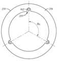
[0017]도 7a 및 도 7b는 하나 이상의 실시예들에 따른, 작동 메커니즘들을 위한 배치 위치들을 예시하는, 조정가능 튜닝 링의 저면도들을 도시한다.
[0018]도 8은 하나 이상의 실시예들에 따른, 작동 메커니즘들을 포함하기 위해 사용되는 슬롯들을 갖는 조정가능 튜닝 링을 포함하는 프로세스 키트의 확대된 부분 단면도를 도시한다.
[0019]도 9a 및 도 9b는 하나 이상의 실시예들에 따른, 도 8에 예시된 조정가능 튜닝 링의 저면도들을 도시한다.
[0020]명확성을 위해, 도면들 사이에서 공통적인 동일한 엘리먼트들을 가리키기 위해 적용가능한 경우 동일한 도면부호들이 사용되었다. 부가적으로, 일 실시예의 엘리먼트들은, 본원에서 설명되는 다른 실시예들에서의 활용을 위해 유리하게 적응될 수 있다.In a manner in which the above-listed features of the present disclosure may be understood in detail, a more specific description of the present disclosure briefly summarized above may be made with reference to embodiments, some of which are attached It is illustrated in the figures. It should be noted, however, that the appended drawings are merely illustrative of exemplary embodiments of the present disclosure and should not be considered as limiting the scope of the present disclosure, which may allow other equally effective embodiments of the present disclosure. Because it can.
1A shows a cross-sectional view of a processing chamber in accordance with one or more embodiments.
1B-1D show enlarged partial cross-sectional views of a process kit included in the processing chamber of FIG. 1A, in accordance with one or more embodiments. FIG.
2A-2J show enlarged partial cross-sectional views of multiple process kits including various edge rings and tunable tuning rings in accordance with one or more embodiments.
FIG. 3 shows an enlarged partial cross sectional view of a process kit including an edge ring having an inwardly angled upper surface, in accordance with one or more embodiments. FIG.
4A-4C show enlarged partial cross-sectional views of other process kits including edge rings with other inwardly angled or beveled top surfaces, in accordance with one or more embodiments.
FIG. 5 shows an enlarged partial cross-sectional view of another process kit that includes an edge ring, a sliding ring, and an adjustable tuning ring, in accordance with one or more embodiments.
FIG. 6 shows an enlarged partial cross sectional view of another process kit including an electrically insulating support ring disposed between an adjustable tuning ring and an actuation mechanism, in accordance with one or more embodiments. FIG.
7A and 7B show bottom views of an adjustable tuning ring, illustrating placement positions for actuation mechanisms, in accordance with one or more embodiments.
FIG. 8 shows an enlarged partial cross sectional view of a process kit including an adjustable tuning ring with slots used to include actuation mechanisms, in accordance with one or more embodiments. FIG.
9A and 9B show bottom views of the adjustable tuning ring illustrated in FIG. 8, in accordance with one or more embodiments.
For clarity, the same reference numerals have been used where applicable to refer to the same elements that are common among the figures. In addition, the elements of one embodiment may be advantageously adapted for use in other embodiments described herein.
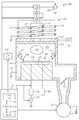
[0021]도 1a는 일 실시예에 따른, 조정가능 튜닝 링을 갖는 프로세싱 챔버(100)의 단면도이다. 도시된 바와 같이, 프로세싱 챔버(100)는 기판, 이를테면, 기판(150)을 에칭하기에 적절한 에칭 챔버이다. 본 개시내용으로부터 이익을 얻도록 적응될 수 있는 프로세싱 챔버들의 예들은 Sym3® 프로세싱 챔버, C3® 프로세싱 챔버, 및 Mesa™ 프로세싱 챔버이며, 이들은 캘리포니아, 산타클라라에 소재하는 Applied Materials, Inc.로부터 상업적으로 입수가능하다. 증착 챔버들 및 다른 제조자들로부터의 프로세싱 챔버들을 포함하는 다른 프로세싱 챔버가 본 개시내용으로부터 이익을 얻도록 적응될 수 있다는 것이 고려된다.1A is a cross-sectional view of a
[0022]프로세싱 챔버(100)는 챔버 바디(101) 및 챔버 바디(101) 상에 배치된 리드(103)를 포함하며, 챔버 바디(101)와 리드(103)는 함께 내측 볼륨(130)을 정의한다. 챔버 바디(101)는 전형적으로 전기 접지(107)에 커플링된다. 프로세싱 동안에 상부에 기판(150)을 지지하기 위해 기판 지지 부재(180)(예컨대, 기판 지지 어셈블리)가 내부 볼륨(130) 내에 배치된다. 프로세싱 챔버(100)는 또한, 프로세싱 챔버(100) 내에 플라즈마를 생성하기 위해 유도성으로 커플링된 플라즈마 장치(102), 및 프로세싱 챔버(100)의 예들을 제어하도록 적응된 제어기(155)를 포함한다.[0022]The
[0023]기판 지지 부재(180)는, 프로세싱 동안 기판(150)의 바이어싱을 가능하게 하기 위해 매칭 네트워크(120)를 통해 바이어스 소스(119)에 커플링되는 하나 이상의 전극들(153)을 포함한다. 바이어스 소스(119)는 예시적으로는, 예컨대 대략적으로 13.56 MHz의 주파수에서의 최대 대략 1,000 W(그러나, 대략 1,000 W로 제한되지는 않음)의 RF 에너지의 소스일 수 있지만, 특정 애플리케이션들에 대해 원하는 대로 다른 주파수들 및 전력들이 제공될 수 있다. 바이어스 소스(119)는, 연속적인 전력 또는 펄스형(pulsed) 전력 중 어느 하나 또는 둘 모두를 생성하는 것이 가능할 수 있다. 일부 예들에서, 바이어스 소스(119)는 DC 또는 펄스형 DC 소스일 수 있다. 일부 예들에서, 바이어스 소스(119)는 다수의 주파수들을 제공하는 것이 가능할 수 있다. 하나 이상의 전극들(153)은 프로세싱 동안의 기판(150)의 척킹(chucking)을 가능하게 하기 위해 척킹 전력 소스(160)에 커플링될 수 있다.[0023]The
[0024]유도성으로 커플링된 플라즈마 장치(102)는 리드(103) 위에 배치되며, 프로세싱 챔버(100) 내에 플라즈마를 생성하기 위해, RF 전력을 프로세싱 챔버(100)에 유도성으로 커플링시키도록 구성된다. 유도성으로 커플링된 플라즈마 장치(102)는, 리드(103) 위에 배치되는 제1 및 제2 코일들(110, 112)을 포함한다. 각각의 코일(110, 112)의 상대적인 포지션, 직경들의 비율, 및/또는 각각의 코일(110, 112)에서의 권취수(number of turns) 각각은, 형성되는 플라즈마의 프로파일 또는 밀도를 제어하기 위해 원하는 대로 조정될 수 있다. 제1 및 제2 코일들(110, 112) 각각은, RF 피드 구조(106)를 통해 매칭 네트워크(114)를 거쳐 RF 전력 공급부(108)에 커플링된다. RF 전력 공급부(108)는 예시적으로는, 50 kHz 내지 13.56 MHz의 범위 내의 튜닝가능 주파수(tunable frequency)에서 최대 대략 4,000 W(그러나, 대략 4,000 W로 제한되지는 않음)를 생성하는 것이 가능할 수 있지만, 특정 애플리케이션들에 대해 원하는 대로 다른 주파수들 및 전력들이 활용될 수 있다. 일부 예들에서, 개개의 제1 및 제2 코일들에 제공되는 RF 전력의 상대적인 양을 제어하기 위해, RF 피드 구조(feed structure)(106)와 RF 전력 공급부(108) 사이에 전력 분배기(105), 이를테면, 분배 커패시터가 제공될 수 있다. 일부 예들에서, 전력 분배기(105)는 매칭 네트워크(114)에 통합될 수 있다.[0024]An inductively coupled
[0025]프로세싱 챔버(100)의 내부를 가열하는 것을 가능하게 하기 위해 리드(103)의 정상에 가열기 엘리먼트(113)가 배치될 수 있다. 가열기 엘리먼트(113)는, 리드(103)와 제1 및 제2 코일들(110, 112) 사이에 배치될 수 있다. 일부 예들에서, 가열기 엘리먼트(113)는 저항성 가열 엘리먼트를 포함할 수 있고, 원하는 범위 내로 가열기 엘리먼트(113)의 온도를 제어하기에 충분한 에너지를 제공하도록 구성되는 전력 공급부(115), 이를테면, AC 전력 공급부에 커플링될 수 있다.[0025]A
[0026]동작 동안, 기판(150), 이를테면, 플라즈마 프로세싱에 적절한 반도체 웨이퍼 또는 다른 기판이 기판 지지 부재(180) 상에 배치되며, 가스 패널(116)로부터 진입 포트들(117)을 통해 챔버 바디(101)의 내부 볼륨(130) 내로 프로세스 가스들이 공급된다. 프로세스 가스들은, RF 전력 공급부(108)로부터의 전력을 제1 및 제2 코일들(110, 112)에 인가함으로써 프로세싱 챔버(100) 내에서 플라즈마(118)로 점화된다. 일부 예들에서, 바이어스 소스(119), 이를테면, RF 또는 DC 소스로부터의 전력이 또한 매칭 네트워크(120)를 통해 기판 지지 부재(180) 내의 전극들(153)에 제공될 수 있다. 프로세싱 챔버(100) 내부 내의 압력은 밸브(121) 및 진공 펌프(122)를 사용하여 제어될 수 있다. 챔버 바디(101)의 온도는, 챔버 바디(101)를 통해 이어지는 액체-함유 도관들(도시되지 않음)을 사용하여 제어될 수 있다.[0026]During operation, a
[0027]프로세싱 챔버(100)는 다양한 플라즈마 프로세스들을 위해 사용될 수 있다. 일 실시예에서, 프로세싱 챔버(100)는 하나 이상의 에칭제들을 이용하여 건식 에칭을 수행하기 위해 사용될 수 있다. 예컨대, 프로세싱 챔버(100)는 하나 이상의 전구체들 또는 프로세스 가스들, 이를테면, 하나 이상의 플루오로카본들(예컨대, CF4 또는 C2F6), O2, NF3, N2, Ar, He, 또는 이들의 조합들로부터 플라즈마의 점화를 위해 사용될 수 있다.The
[0028]프로세싱 챔버(100)는, 프로세싱 동안 프로세싱 챔버(100)의 동작을 제어하기 위해 제어기(155)를 포함한다. 제어기(155)는, 중앙 프로세싱 유닛(CPU; central processing unit)(123), 메모리(124), 및 CPU(123)를 위한 지원 회로들(125)을 포함할 수 있으며, 프로세싱 챔버(100)의 컴포넌트들의 제어를 가능하게 한다. 제어기(155)는, 다양한 챔버들 및 서브-프로세서들을 제어하기 위해 산업 현장(industrial setting)에서 사용될 수 있는 임의의 형태의 범용 컴퓨터 프로세서 중 하나일 수 있다. 메모리(124)는, 본원에서 설명되는 방식으로 프로세싱 챔버(100)의 동작을 제어하기 위해 실행 또는 인보크(invoke)될 수 있는 소프트웨어(소스 또는 오브젝트 코드)를 저장한다.[0028]The
[0029]프로세싱 챔버(100)의 제어를 가능하게 하기 위해, CPU(123)는, 다양한 챔버들 및 서브-프로세서들을 제어하기 위해 산업 현장에서 사용될 수 있는 임의의 형태의 범용 컴퓨터 프로세서 중 하나, 이를테면, 프로그램가능 로직 제어기(PLC; programmable logic controller)일 수 있다. 메모리(124)는 CPU(123)에 커플링되며, 메모리(124)는 비-일시적이며, 용이하게 이용가능한 메모리, 이를테면, 랜덤 액세스 메모리(RAM; random access memory), 판독 전용 메모리(ROM; read only memory), 플로피 디스크 드라이브, 하드 디스크, 또는 로컬 또는 원격의, 임의의 다른 형태의 디지털 저장소 중 하나 이상일 수 있다. 지원 회로들(125)은 통상적인 방식으로 프로세서를 지원하기 위해 CPU(123)에 커플링된다. 일반적으로, 대전 종 생성(charged species generation), 가열, 및 다른 프로세스들은, 전형적으로 소프트웨어 루틴으로서 메모리(124)에 저장된다. 소프트웨어 루틴은 또한, CPU(123)에 의해 제어되고 있는 프로세싱 챔버(100)로부터 원격으로 위치된 제2 CPU(도시되지 않음)에 의해 저장 및/또는 실행될 수 있다.[0029]To enable control of the
[0030]메모리(124)는, CPU(123)에 의해 실행될 때 프로세싱 챔버(100)의 동작을 가능하게 하는 명령들을 포함하는 컴퓨터-판독가능 저장 매체들의 형태이다. 메모리(124)에서의 명령들은 본 개시내용의 방법을 구현하는 프로그램과 같은 프로그램 제품의 형태이다. 프로그램 코드는, 다수의 상이한 프로그래밍 언어들 중 임의의 프로그래밍 언어를 준수할 수 있다. 일 예에서, 본 개시내용은 컴퓨터 시스템에 사용하기 위한 컴퓨터-판독가능 저장 매체들 상에 저장된 프로그램 제품으로서 구현될 수 있다. 프로그램 제품의 프로그램(들)은 (본원에서 설명되는 방법들을 포함한) 실시예들의 기능들을 정의한다. 예시적인 컴퓨터-판독가능 저장 매체들은, (i) 정보가 영구적으로 저장되는 비-기록가능 저장 매체들(예컨대, 컴퓨터 내의 판독-전용 메모리 디바이스들, 이를테면, CD-ROM 드라이브에 의해 판독가능한 CD-ROM 디스크들, 플래시 메모리, ROM 칩들, 또는 임의의 유형의 고체-상태 비-휘발성 반도체 메모리); 및 (ii) 변경가능한 정보가 저장되는 기록가능 저장 매체들(예컨대, 디스켓 드라이브 내의 플로피 디스크들, 또는 하드-디스크 드라이브, 또는 임의의 유형의 고체-상태 랜덤-액세스 반도체 메모리)을 포함한다(그러나 이에 제한되지는 않음). 이러한 컴퓨터-판독가능 저장 매체들은, 본원에서 설명되는 방법들의 기능들을 지시하는 컴퓨터-판독가능 명령들을 보유하는 경우, 본 개시내용의 실시예들이다.[0030]
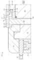
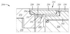
[0031]프로세싱 챔버(100)는 또한, 도 1a에 도시된 바와 같이 내부 볼륨(130) 내에, 이를테면, 기판 지지 부재(180) 상에 배치된 프로세스 키트(200)를 포함한다. 프로세스 키트(200) 및 다른 프로세스 키트들의 다양한 실시예들이 아래에서 설명된다. 프로세스 키트(200)는 기판(150)의 프로세싱 동작 동안, 이를테면, 플라즈마 프로세스 동안 사용된다. 도 1b 및 도 1c는 프로세싱 챔버(100) 내의 기판 지지 부재(180)를 포함하는 프로세스 키트(200)의 확대된 부분 단면도들을 도시한다.[0031]The
[0032]기판 지지 부재(180)는 정전 척(ESC; electrostatic chuck)(202), 냉각 플레이트(또는 캐소드)(204), 베이스(206), 및 캐소드 스택(212)을 포함한다. 냉각 플레이트(204)는 베이스(206) 상에 배치된다. 냉각 플레이트(204)는 복수의 냉각 채널들(도시되지 않음)을 포함할 수 있는데, 복수의 냉각 채널들은 그 복수의 냉각 채널들을 통해 냉각제를 순환시키기 위한 것이다. 냉각 플레이트(204)는 접착제 또는 다른 적절한 메커니즘에 의해 정전 척(202)과 맞물리거나 정전 척(202)에 본딩될 수 있다. 하나 이상의 전력 공급부들(208)이 냉각 플레이트(204)에 커플링될 수 있다. 전력 공급부들은 라디오 주파수(RF; radio frequency), 교류 전류(AC; alternating current), 및/또는 직류 전류(DC; direct current)를 위한 소스들 및/또는 피드(feed)들이거나 또는 이들을 포함할 수 있다. 정전 척(202)은 하나 이상의 가열기들(도시되지 않음)을 포함할 수 있다. 하나 이상의 가열기들은 독립적으로 제어가능할 수 있다. 하나 이상의 가열기들은 정전 척(202)이 기판(150)을 원하는 온도까지 가열하는 것을 가능하게 한다.[0032]The
[0033]프로세스 키트(200)는 환형 바디를 형성하는 제1 링 컴포넌트(220)와 제2 링 컴포넌트(230)를 포함하는 에지 링(210)을 포함한다. 제1 링 컴포넌트(220) 및 제2 링 컴포넌트(230)는 독립적으로, 하나 이상의 전기 절연 재료들, 이를테면, 실리콘 카바이드, 실리콘 옥사이드, 석영, 또는 이들의 임의의 조합으로 제조되거나 또는 이들을 포함할 수 있다. 2개의 링 컴포넌트들(220, 230)은, 제2 링 컴포넌트(230)가 제1 링 컴포넌트(220)에 대해 이동가능하도록 서로 인터페이싱될 수 있다.[0033]
[0034]도 1c에 도시된 바와 같이, 제1 링 컴포넌트(220)는 상부 표면(218), 하부 표면(219), 내측 에지(222), 및 외측 에지(224)를 포함한다. 상부 표면(218)은 하부 표면(219)에 실질적으로 평행하다. 내측 에지(222)는 외측 에지(224)에 실질적으로 평행하고, 하부 표면(219)에 실질적으로 수직이다. 제1 링 컴포넌트(220)는 제1 링 컴포넌트(220)에 정의된 계단형 표면(stepped surface)(226)을 더 포함한다. 도시된 실시예에서, 계단형 표면(226)은, 계단형 표면(226)이 하부 표면(219)에 실질적으로 평행하도록, 외측 에지(224)에 형성된다. 계단형 표면(226)은 제2 링 컴포넌트(230)를 수용하기 위한 리세스를 정의한다. 일반적으로, 제1 링 컴포넌트(220)의 높이는 정전 척(202)의 높이에 의해 제한된다. 예컨대, 제1 링 컴포넌트(220)의 내측 에지(222)는 정전 척(202)의 높이 위로 연장되지 않는다. 따라서, 제1 링 컴포넌트(220)는 정전 척(202)의 측면을 보호한다. 일부 실시예들에서, 기판(150)은, 정전 척(202) 상에 포지셔닝될 때, 제1 링 컴포넌트(220) 위로, 이를테면, 상부 표면(218) 위로 부분적으로 연장되어 있다.[0034]As shown in FIG. 1C, the
[0035]제2 링 컴포넌트(230)는 상부 표면(228), 하부 표면(231), 내측 에지(232), 및 외측 에지(234)를 포함한다. 상부 표면(228)은 하부 표면(231)에 실질적으로 평행하다. 내측 에지(232)는 외측 에지(234)에 실질적으로 평행하고, 하부 표면(231)에 실질적으로 수직이다. 일 실시예에서, 제2 링 컴포넌트(230)는 하부 표면(231)을 통해 제1 링 컴포넌트(220)와 인터페이싱된다. 예컨대, 제1 링 컴포넌트(220)의 계단형 표면(226)은 제2 링 컴포넌트(230)의 하부 표면(231)의 적어도 일부와 인터페이싱한다. 제1 링 컴포넌트(220)와 인터페이싱될 때, 제2 링 컴포넌트(230)의 내측 에지(232)는 기판(150)으로부터 이격된다. 예컨대, 제2 링 컴포넌트(230)의 내측 에지(232)는 기판(150)으로부터 대략 0.02 mm 내지 대략 0.1 mm 이격될 수 있다.[0035]The
[0036]다른 실시예들에서, 인터페이싱될 때, 제1 링 컴포넌트(220)와 제2 링 컴포넌트(230)는, 도 1c에 도시된 바와 같이, 연속적인 하부 표면 및 연속적인 상부 표면을 형성한다. 다른 실시예에서, 인터페이싱되지 않을 때, 제1 링 컴포넌트(220)와 제2 링 컴포넌트(230)는, 도 1d에 도시된 바와 같이, 연속적인 하부 표면 또는 연속적인 상부 표면을 형성하지 않는다. 오히려, 일부 실시예들에서, 제1 링 컴포넌트(220)의 상부 표면(218)은 제2 링 컴포넌트(230)의 상부 표면(228)보다 더 높을 수 있다. 다른 실시예들에서, 제2 링 컴포넌트(230)의 하부 표면(231)은 제1 링 컴포넌트(220)의 하부 표면(219) 아래에 놓일 수 있다. 따라서, 일부 실시예들에서, 제1 링 컴포넌트(220)와 제2 링 컴포넌트(230)는 연속적인 최상부 또는 하부 표면을 형성하지 않는다.[0036]In other embodiments, when interfaced, the
[0037]프로세스 키트(200)는 상부 표면(254) 및 하부 표면(256)을 갖는 조정가능 튜닝 링(250)을 더 포함한다. 조정가능 튜닝 링(250)은 하나 이상의 전기 전도성 재료들로 형성되거나 또는 이와 다르게 그 하나 이상의 전기 전도성 재료들을 포함할 수 있다. 예컨대, 전기 전도성 재료는 알루미늄 또는 하나 이상의 알루미늄 합금들이거나 또는 이들을 포함할 수 있다. 조정가능 튜닝 링(250)은 에지 링(210) 아래에 배치된다. 예컨대, 조정가능 튜닝 링(250)은 제2 링 컴포넌트(230) 아래에 배치된다. 조정가능 튜닝 링(250)은 제2 링 컴포넌트(230)의 하부 표면(231)과 접촉한다. 일 실시예에서, 조정가능 튜닝 링(250)은, 조정가능 튜닝 링(250)이 정전 척(202)과 냉각 플레이트(204)의 결합된 높이들과 실질적으로 동일한 높이를 갖도록, 정전 척(202)과 냉각 플레이트(204)의 길이를 따라 연장된다. 따라서, 조정가능 튜닝 링(250)은 냉각 플레이트(204)로부터의 전력을 에지 링(210)에 커플링시킬 수 있다.[0037]
[0038]조정가능 튜닝 링(250)은 냉각 플레이트(204)에 외접하여, 조정가능 튜닝 링(250)과 냉각 플레이트(204) 사이에 측방향으로 이격된 갭(258)을 형성할 수 있다. 일 예에서, 측방향으로 이격된 갭(258)은 0 인치 초과 내지 0.03 인치 이하의 폭을 갖는다. 다른 예들에서, 측방향으로 이격된 갭(258)은 대략 0.005 인치, 대략 0.007 인치, 또는 대략 0.009 인치 내지 대략 0.0010 인치, 대략 0.0013 인치, 대략 0.0015 인치, 또는 대략 0.0019 인치의 폭을 갖는다. 예컨대, 측방향으로 이격된 갭(258)은 대략 0.007 인치 내지 대략 0.0015 인치의 폭을 갖는다. 조정가능 튜닝 링(250)은 리프트 핀(260)과 인터페이싱한다. 예컨대, 리프트 핀(260)은 조정가능 튜닝 링(250)과 동작가능하게 커플링될 수 있다.[0038]The
[0039]하나 이상의 실시예들에서, 기판(150)의 에지에서의 플라즈마 시스(201)는, 제2 링 컴포넌트(230) 아래에 배치되고 그리고 측방향으로 이격된 갭(258)에서는 냉각 플레이트(204) 옆에 배치되는 조정가능 튜닝 링(250)에 의해 제2 링 컴포넌트(230)에 커플링되는 전력을 튜닝함으로써 조정될 수 있으며, 냉각 플레이트(204)와 용량성 커플링을 형성함으로써 조정가능 튜닝 링(250)에 추가의 RF 전력이 전달된다.[0039]In one or more embodiments, the
[0040]리프트 핀(260)은 리프트 또는 작동 메커니즘(280)에 의해 구동된다. 작동 메커니즘(280)은 하나 이상의 리프트 메커니즘들(282), 하나 이상의 밀봉형 벨로우즈(284), 하나 이상의 액추에이터들, 하나 이상의 제어기들, 및 다른 컴포넌트들을 포함할 수 있다. 리프트 메커니즘(282)은 하나 이상의 서보 드라이브(servo drive)들, 서보 모터들, 전기 모터들, 기어들, 또는 이들의 조합들이거나 또는 이들을 포함할 수 있다. 하나 이상의 구성들에서, 작동 메커니즘(280)은, 프로세싱 챔버(100)의 외측 또는 대기 측(atmospheric side) 상에 장착되고 그리고 내부 볼륨(130) 내의 진공을 밀봉하기 위해 벨로우즈를 사용하여 액추에이터들 또는 리프트 메커니즘들(282)에 연결되는 서보 드라이브들 및 액추에이터 어셈블리들을 포함한다.[0040]
[0041]하나 이상의 실시예들에서, 작동 메커니즘(280)은 2개, 3개, 4개 또는 그보다 많은 리프트 핀들(260)을 포함하고, 리프트 핀들(260) 각각은 제1 단부 및 제2 단부를 갖고, 리프트 핀(260)의 제1 단부는 조정가능 튜닝 링(250)의 하부 표면(256)과 접촉하고, 리프트 핀(260)의 제2 단부는 리프트 메커니즘(282)과 연통한다. 작동 메커니즘(280)은 조정가능 튜닝 링(250)이 프로세싱 챔버(100) 내에서 수직으로 이동되는 것을 가능하게 한다. 튜닝 링(250)의 수직 이동의 결과로, 작동 메커니즘(280)은 제2 링 컴포넌트(230)를 상승시키거나, 하강시키거나, 또는 이와 다르게 이동시킨다.[0041]In one or more embodiments, the
[0042]도 1d에 도시된 바와 같이, 제2 링 컴포넌트(230)가 제1 링 컴포넌트(220) 위로 상승되어, 제1 링 컴포넌트(220)의 계단형 표면(226)과 제2 링 컴포넌트(230)의 하부 표면(231) 사이에 갭(237)을 형성할 수 있다. 갭(237)은 대략 0 mm, 대략 1 mm, 대략 2 mm, 또는 대략 3 mm 내지 대략 5 mm, 대략 7 mm, 대략 10 mm, 또는 대략 12 mm일 수 있다. 작동 메커니즘(280)은 조정가능 튜닝 링(250)의 하부 표면(256)과 인터페이싱되며, 작동 메커니즘(280)은, 제1 링 컴포넌트(220)와 제2 링 컴포넌트(230) 사이의 갭(237)이 변화되도록 조정가능 튜닝 링(250)을 작동시키도록 구성된다.[0042]As shown in FIG. 1D, the
[0043]일 실시예에서, 조정가능 튜닝 링(250)은 조정가능 튜닝 링(250)의 상부 표면(254) 상에 형성되거나 또는 이와 다르게 배치되는 코팅을 포함할 수 있다. 예컨대, 코팅은 이트리아 옥사이드 코팅 또는 겔형 코팅이거나 또는 이를 포함할 수 있다. 코팅은 조정가능 튜닝 링(250)과 플라즈마 사이의 화학 반응을 제한하는 데 사용되며, 따라서, 입자 생성 및 링 손상을 제한한다. 다른 실시예에서, 하나 이상의 유전체 패드들(예컨대, 폴리테트라플루오로에틸렌을 함유하는 패드들)이 에지 링(210)과 정전 척(202) 사이에 포지셔닝된다.[0043]In one embodiment, the
[0044]프로세스 키트(200)는 또한, 커버 링 어셈블리(cover ring assembly)(270), 환형 바디(276), 및 커버 링 어셈블리(270)와 환형 바디(276) 사이에 배치된 플라즈마 스크린(278)을 포함한다. 커버 링 어셈블리(270)는 환형 형상을 갖고, 커버 링(272) 및 슬리브(274)를 포함한다. 커버 링(272) 및 슬리브(274)는 독립적으로, 석영 재료 또는 다른 내플라즈마성 재료로 제조되거나 또는 이를 포함할 수 있다. 예컨대, 커버 링(272)은 석영 링일 수 있고, 슬리브(274)는 석영 파이프일 수 있다.[0044]
[0045]하나 이상의 실시예들에서, 도 1c 및 도 1d에 도시된 바와 같이, 플라즈마 시스(201)는 프로세싱 챔버(100)의 프로세스 키트(200) 내의 에지 링(210) 및 기판(150)의 부분들 위에 형성된다. 전압(


[0046]여기에서,


[0047]에칭 리액터의 경우, 플라즈마 시스(201)는, 플라즈마와 접촉하는 프로세싱 챔버(100), 프로세스 키트(200)의 모든 각각의 다른 부분, 챔버 바디(101), 에칭되고 있는 기판(150)과 그러한 플라즈마 사이에 형성된다. 플라즈마에서 생성되는 이온들은 플라즈마 시스에서 가속화되고, 플라즈마 시스에 수직으로 이동한다.


[0048]도 1d는 도 1c의 프로세싱 챔버(100) 내의 프로세스 키트(200)의 부분을 예시하며, 제2 링 컴포넌트(230)는 상승된 포지션에 있다. 예시되는 바와 같이 그리고 도 1c에서 논의되는 바와 같이, 조정가능 튜닝 링(250)을 상승시키는 것은 제2 링 컴포넌트(230)를 상승시키고, 이는 결국 플라즈마 시스(201)를 상승시킨다. 거의 고정된 커패시턴스의 결과로 전위(

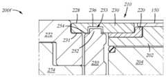
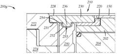
[0049]도 2a-도 2j는 하나 이상의 실시예들에 따른, 에지 링(210)의 인터페이스와 조정가능 튜닝 링(250) 사이에 배치된 정렬 커플링들을 포함하는 프로세스 키트들(200a-200j)의 확대된 부분 단면도들을 도시한다. 프로세스 키트들(200a-200j) 각각은 프로세스 키트(200)를 프로세스 키트들(200a-200j) 중 임의의 프로세스 키트로 완전히 또는 부분적으로 대체함으로써 프로세싱 챔버(100) 내에서 사용될 수 있다.[0049]2A-2J are enlarged views of
[0050]프로세스 키트들(200a-200j) 각각은, 제1 링 컴포넌트(220) 및 제2 링 컴포넌트(230)를 갖는 에지 링(210)을 포함한다. 제1 링 컴포넌트(220)는, 제2 링 컴포넌트(230)가 제1 링 컴포넌트(220)에 대해 이동가능하여 (도 1d에 도시된 바와 같이) 제1 링 컴포넌트(220)와 제2 링 컴포넌트(230) 사이에 갭(237)을 형성하도록, 제2 링 컴포넌트(230)와 인터페이싱될 수 있다. 예컨대, 갭(237)은 제1 링 컴포넌트(220)의 계단형 표면(226)과 제2 링 컴포넌트(230)의 하부 표면(231) 사이에 형성될 수 있다. 조정가능 튜닝 링(250)의 상부 표면(254)과 제2 링 컴포넌트(230)의 하부 표면(231)은 서로 맞물리거나 또는 이와 다르게 서로 접촉할 수 있다.[0050]Each of the
[0051]제2 링 컴포넌트(230)의 하부 표면(231)은 상부 정렬 커플링(236)을 포함하고, 조정가능 튜닝 링(250)의 상부 표면(254)은 하부 정렬 커플링(252)을 포함한다. 조정가능 튜닝 링(250)의 하부 정렬 커플링(252)은 제2 링 컴포넌트(230)의 상부 정렬 커플링(236)과 정합하여, 레시프로컬(reciprocal) 또는 정합(mating) 프로파일을 갖는 인터페이스를 형성할 수 있다.[0051]The
[0052]상부 정렬 커플링(236)은 수형 또는 암형 커플링일 수 있고, 하부 정렬 커플링(252)은 상부 정렬 커플링(236)과 반대되는 유형의 커플링이다. 예컨대, 상부 정렬 커플링(236)이 수형 커플링인 경우, 하부 정렬 커플링(252)은 암형 커플링이다. 대안적으로, 상부 정렬 커플링(236)이 암형 커플링인 경우, 하부 정렬 커플링(252)은 수형 커플링이다. 상부 정렬 커플링(236)과 하부 정렬 커플링(252) 사이에 형성된 레시프로컬 또는 정합 프로파일은, 더브테일, 스플라인, 핀형, 삼각형, 직사각형, 정사각형, 사다리꼴, 아크형, 라운드형의 기하학적 구조, 그러한 기하학적 구조들의 조합들뿐만 다른 기하학적 구조들을 가질 수 있다.[0052]The
[0053]프로세스 키트(200a)에서, 도 2a에 도시된 바와 같이, 상부 정렬 커플링(236)은 제2 링 컴포넌트(230)의 하부 표면(231)으로부터 연장되는 더브테일 또는 사다리꼴 기하학적 구조를 갖는 수형 커플링이다. 하부 정렬 커플링(252)은 조정가능 튜닝 링(250)의 상부 표면(254) 내로 형성되는 더브테일 또는 사다리꼴 기하학적 구조를 갖는 암형 커플링이다.[0053]In the
[0054]프로세스 키트(200b)에서, 도 2b에 도시된 바와 같이, 상부 정렬 커플링(236)은 제2 링 컴포넌트(230)의 하부 표면(231) 내로 형성되는 더브테일 또는 사다리꼴 기하학적 구조를 갖는 암형 커플링이다. 하부 정렬 커플링(252)은 조정가능 튜닝 링(250)의 상부 표면(254)으로부터 연장되는 더브테일 또는 사다리꼴 기하학적 구조를 갖는 수형 커플링이다.[0054]In the
[0055]프로세스 키트(200c)에서, 도 2c에 도시된 바와 같이, 상부 정렬 커플링(236)은 제2 링 컴포넌트(230)의 하부 표면(231)으로부터 연장되는 삼각형 기하학적 구조를 갖는 수형 커플링이다. 하부 정렬 커플링(252)은 조정가능 튜닝 링(250)의 상부 표면(254) 내로 형성되는 삼각형 기하학적 구조를 갖는 암형 커플링이다.[0055]In
[0056]프로세스 키트(200d)에서, 도 2d에 도시된 바와 같이, 상부 정렬 커플링(236)은 제2 링 컴포넌트(230)의 하부 표면(231) 내로 형성되는 삼각형 기하학적 구조를 갖는 암형 커플링이다. 하부 정렬 커플링(252)은 조정가능 튜닝 링(250)의 상부 표면(254)으로부터 연장되는 삼각형 기하학적 구조를 갖는 수형 커플링이다.[0056]In the
[0057]프로세스 키트(200e)에서, 도 2e에 도시된 바와 같이, 상부 정렬 커플링(236)은 제2 링 컴포넌트(230)의 하부 표면(231)으로부터 연장되는 정사각형 또는 직사각형 기하학적 구조를 갖는 수형 커플링이다. 하부 정렬 커플링(252)은 조정가능 튜닝 링(250)의 상부 표면(254) 내로 형성되는 정사각형 또는 직사각형 기하학적 구조를 갖는 암형 커플링이다.[0057]In the
[0058]프로세스 키트(200f)에서, 도 2f에 도시된 바와 같이, 상부 정렬 커플링(236)은 제2 링 컴포넌트(230)의 하부 표면(231) 내로 형성되는 정사각형 또는 직사각형 기하학적 구조를 갖는 암형 커플링이다. 하부 정렬 커플링(252)은 조정가능 튜닝 링(250)의 상부 표면(254)으로부터 연장되는 정사각형 또는 직사각형 기하학적 구조를 갖는 수형 커플링이다.[0058]In
[0059]프로세스 키트(200g)에서, 도 2g에 도시된 바와 같이, 상부 정렬 커플링(236)은 제2 링 컴포넌트(230)의 하부 표면(231)으로부터 연장되는 아크형 또는 라운드형 기하학적 구조를 갖는 수형 커플링이다. 하부 정렬 커플링(252)은 조정가능 튜닝 링(250)의 상부 표면(254) 내로 형성되는 아크형 또는 라운드형 기하학적 구조를 갖는 암형 커플링이다.[0059]In the
[0060]프로세스 키트(200h)에서, 도 2h에 도시된 바와 같이, 상부 정렬 커플링(236)은 제2 링 컴포넌트(230)의 하부 표면(231) 내로 형성되는 아크형 또는 라운드형 기하학적 구조를 갖는 암형 커플링이다. 하부 정렬 커플링(252)은 조정가능 튜닝 링(250)의 상부 표면(254)으로부터 연장되는 아크형 또는 라운드형 기하학적 구조를 갖는 수형 커플링이다.[0060]In the
[0061]프로세스 키트(200i)에서, 도 2i에 도시된 바와 같이, 상부 정렬 커플링(236)은 제2 링 컴포넌트(230)의 하부 표면(231)으로부터 연장되는 핀형 기하학적 구조를 갖는 수형 커플링이다. 하부 정렬 커플링(252)은 조정가능 튜닝 링(250)의 상부 표면(254) 내로 형성되는 핀형 기하학적 구조를 갖는 암형 커플링이다.[0061]In the
[0062]프로세스 키트(200j)에서, 도 2j에 도시된 바와 같이, 상부 정렬 커플링(236)은 제2 링 컴포넌트(230)의 하부 표면(231) 내로 형성되는 핀형 기하학적 구조를 갖는 암형 커플링이다. 하부 정렬 커플링(252)은 조정가능 튜닝 링(250)의 상부 표면(254)으로부터 연장되는 핀형 기하학적 구조를 갖는 수형 커플링이다.[0062]In
[0063]핀형 기하학적 구조들은 수형 커플링들 및/또는 암형 커플링들과 동일한 또는 상이한 기하학적 구조들인 2개, 3개 또는 그보다 많은 형상화된 프로파일들을 가질 수 있다. 핀형 기하학적 구조들은 도 2a-도 2j에 도시된 임의의 커플링뿐만 아니라 다른 기하학적 형상들일 수 있다. 예컨대, 핀형 기하학적 구조는 2개의 직사각형 기하학적 구조들(도 2i 및 도 2j에 도시된 바와 같음)을 포함할 수 있다. 대안적으로, 핀형 기하학적 구조는 2개의 삼각형 기하학적 구조들, 직사각형 기하학적 구조와 삼각형 기하학적 구조의 조합, 직사각형 기하학적 구조와 더브테일 기하학적 구조의 조합, 또는 임의의 다른 조합을 포함할 수 있다.[0063]The finned geometries may have two, three or more shaped profiles that are the same or different geometries as the male couplings and / or the female couplings. Finned geometries can be other geometric shapes as well as any coupling shown in FIGS. 2A-2J. For example, the finned geometry can include two rectangular geometries (as shown in FIGS. 2I and 2J). Alternatively, the finned geometry may comprise two triangular geometries, a combination of rectangular and triangular geometries, a combination of rectangular geometries and dovetail geometries, or any other combination.
[0064]도 2a-도 2j에 도시된 바와 같이, 갭(253)은 조정가능 튜닝 링(250)의 상부 표면(254)과 제2 링 컴포넌트(230)의 하부 표면(231) 사이에 배치될 수 있다. 더 구체적으로, 갭(253)은 조정가능 튜닝 링(250)의 하부 정렬 커플링(252)과 제2 링 컴포넌트의 상부 정렬 커플링(236) 사이에 배치된다. 조정가능 튜닝 링(250)은, 갭(253)의 크기를 조정하고 그리고 조정가능 튜닝 링(250)과 제2 링 컴포넌트(230) 사이의 용량성 커플링을 변화시키도록, 작동되거나, 조정되거나, 또는 이와 다르게 이동된다. 따라서, 조정가능 튜닝 링(250)과 제2 링 컴포넌트(230) 사이의 거리(예컨대, 갭(253)의 크기)를 변화시킴으로써, 조정가능 튜닝 링(250)과 제2 링 컴포넌트(230) 사이의 용량성 커플링이 비례적으로 변화된다.[0064]As shown in FIGS. 2A-2J, a
[0065]하나 이상의 실시예들에서, 플라즈마 시스(201)를 튜닝하기 위한 2개의 별개의 레짐(regime)들이 가능하다. 일 예에서, 갭(253)의 크기는 조정가능 튜닝 링(250)과 제2 링 컴포넌트(230) 사이에서 가변적으로 유지되거나 조정될 수 있다. 다른 예에서, 조정가능 튜닝 링(250)과 제2 링 컴포넌트(230)는 서로 터치하거나 접촉하며, 따라서 조정가능 튜닝 링(250)과 제2 링 컴포넌트(230) 사이에는 갭(253)이 존재하지 않는다.[0065]In one or more embodiments, two separate regimes for tuning the
[0066]도 3은 하나 이상의 실시예들에 따른, 안쪽으로 각이 진 상부 표면(228)을 갖는 에지 링(210)을 포함하는 프로세스 키트(300)의 확대된 부분 단면도를 도시한다. 도 4a는 하나 이상의 실시예들에 따른, 안쪽으로 경사진 상부 표면(228)을 갖는 에지 링(210)을 포함하는 프로세스 키트(400a)의 확대된 부분 단면도를 도시한다. 도 4b 및 도 4c는 안쪽으로 경사진 상부 표면들(228)을 갖는 에지 링(210)을 포함하는 프로세스 키트들(400b, 400c)의 확대된 부분 단면도들을 각각 도시한다. 프로세스 키트들(300 및 400a-400c)의 경우, 제1 링 컴포넌트(220)는, 제2 링 컴포넌트(230)가 제1 링 컴포넌트(220)에 대해 이동가능하여 제1 링 컴포넌트(220)와 제2 링 컴포넌트(230) 사이에 갭(253)을 형성하도록, 제2 링 컴포넌트(230)와 인터페이싱된다. 프로세스 키트들(300 및 400a-400c) 중 임의의 프로세스 키트는 프로세스 키트(200) 또는 프로세스 키트들(200a-200j) 중 임의의 프로세스 키트를 프로세스 키트들(300 또는 400a-400c) 중 임의의 프로세스 키트로 완전히 또는 부분적으로 대체함으로써 프로세싱 챔버(100)에서 사용될 수 있다.[0066]3 illustrates an enlarged partial cross-sectional view of a
[0067]하나 이상의 실시예들에서, 제2 링 컴포넌트(230)의 상부 표면(228)의 적어도 일부는 제1 링 컴포넌트(220)를 향해 안쪽으로 각이 진다. 일 실시예에서, 제2 링 컴포넌트(230)의 상부 표면(228)은, 도 3에 도시된 바와 같이, 외측 에지(234)로부터 내측 에지(232)로 안쪽으로 각이 진다. 다른 실시예에서, 도 4a에 도시된 바와 같이, 제2 링 컴포넌트(230)의 상부 표면(228)의 부분 또는 세그먼트는 외측 에지(234)로부터 떨어져서 내측 에지(232)를 향해 안쪽으로 각이 진다. 제2 링 컴포넌트(230)의 상부 표면(228)은 내측 상부 표면(229a)과 외측 상부 표면(229c) 사이에 배치된 경사진 상부 표면(229b)을 가질 수 있다. 경사진 상부 표면(229b)은 내측 에지(232)를 향해, 이를테면, 제1 링 컴포넌트(220) 및/또는 기판(150)을 향해 안쪽으로 각이 진다. 도 4a에 도시된 바와 같이, 내측 상부 표면(229a)과 외측 상부 표면(229c)은 서로 평행하거나 또는 실질적으로 평행할 수 있다. 대안적으로, 내측 상부 표면(229a)과 외측 상부 표면(229c)은 서로 평행하지 않다(도시되지 않음).[0067]In one or more embodiments, at least a portion of the
[0068]다른 실시예에서, 도 4b에 도시된 바와 같이, 제2 링 컴포넌트(230)의 상부 표면(228)의 부분 또는 세그먼트는 외측 에지(234)로부터 떨어져서 내측 에지(232)를 향해 안쪽으로 각이 진다. 제2 링 컴포넌트(230)의 상부 표면(228)은 외측 상부 표면(229c)과 인접하게 배치된 안쪽으로 각이 진 또는 경사진 상부 표면(229b)을 가질 수 있다. 다른 실시예에서, 도 4c에 도시된 바와 같이, 제2 링 컴포넌트(230)의 상부 표면(228)의 2개 이상의 부분들 또는 세그먼트들은 외측 에지(234)로부터 내측 에지(232)로 안쪽으로 각이 진다. 제2 링 컴포넌트(230)의 상부 표면(228)은, 내측 상부 표면(229a), 그 옆에 제1 안쪽으로 각이 진 또는 경사진 상부 표면(229b), 그 옆에 제1 외측 상부 표면(229c), 그 옆에 제2 안쪽으로 각이 진 또는 경사진 상부 표면(229b), 그 옆에 제2 외측 상부 표면(229c)을 가질 수 있다. 도 2b 및 도 2c에 도시된 바와 같이, 경사진 상부 표면들(229b)은 내측 에지(232)를 향해, 이를테면, 제1 링 컴포넌트(220) 및/또는 기판(150)을 향해 안쪽으로 각이 진다.[0068]In another embodiment, as shown in FIG. 4B, the portion or segment of the
[0069]프로세싱 동안에, 안쪽으로 각이 진 상부 표면(228)(도 3) 및 내측 상부 표면들(229a)(도 4a-도 4c)은 플라즈마를 제2 링 컴포넌트(230)의 내측 에지(232), 제1 링 컴포넌트(220)의 상부 표면(218), 및 기판(150)을 향해 퍼넬링(funnel)하거나 또는 이와 다르게 지향시킨다. 이와 같이, 안쪽으로 각이 진 상부 표면(228)(도 3) 및 내측 상부 표면들(229a)(도 4a-도 4c)은 플라즈마를 제2 링 컴포넌트(230)의 외측 에지(224) 및 커버 링(272)으로부터 멀리 지향시킨다.[0069]During processing, the inwardly angled top surface 228 (FIG. 3) and the inner
[0070]제2 링 컴포넌트(230)는 상부 표면(228)과 하부 표면(231) 사이에서 측정되는 내측 두께(D1) 및 외측 두께(D2)를 갖는다. 도 4a-도 4c에 도시된 제2 링 컴포넌트(230)의 경우, 내측 두께(D1)는 내측 상부 표면(229a)과 하부 표면(231) 사이에서 측정되고, 외측 두께(D2)는 외측 상부 표면(229c)과 하부 표면(231) 사이에서 측정된다. 도 3 및 도 4a-도 4c에 도시된 바와 같이, 내측 두께(D1)는 외측 두께(D2)보다 작다. 제2 링 컴포넌트(230)의 내측 두께(D1)는 대략 1 mm, 대략 1.8 mm, 대략 2 mm, 또는 대략 2.5 mm 내지 대략 3 mm, 대략 4 mm, 대략 5 mm, 또는 대략 6 mm이다. 제2 링 컴포넌트(230)의 외측 두께(D2)는 대략 1 mm, 대략 2 mm, 또는 대략 3 mm 내지 대략 5 mm, 대략 7 mm, 대략 10 mm, 대략 12 mm, 또는 대략 15 mm이다.[0070]The
[0071]도 5는 하나 이상의 실시예들에 따른, 에지 링(210), 슬라이딩 링(520), 및 조정가능 튜닝 링(250)을 포함하는 프로세스 키트(500)의 확대된 부분 단면도를 도시한다. 슬라이딩 링(520)은 에지 링(210) 아래에 포지셔닝된다. 슬라이딩 링(520)은 상부 표면(512) 및 하부 표면(514)을 갖는다. 슬라이딩 링(520)의 상부 표면(512)은 제2 링 컴포넌트(230)의 하부 표면(231)과 접촉한다. 조정가능 튜닝 링(250)은 슬라이딩 링(520) 아래에 포지셔닝된다. 조정가능 튜닝 링(250)의 상부 표면(254)은 슬라이딩 링(520)의 하부 표면(514)과 접촉한다.[0071]5 illustrates an enlarged partial cross-sectional view of a
[0072]하나 이상의 실시예들에서, 슬라이딩 링(520)의 부재 시에, 플라즈마는 프로세싱 동안에 조정가능 튜닝 링(250)의 부분들을 침식시킬 수 있다. 일단 제2 링 컴포넌트(230)와 조정가능 튜닝 링(250) 사이에 배치되면, 슬라이딩 링(520)은, 슬라이딩 링(520)을 포함하지 않고서 제2 링 컴포넌트(230)를 조정가능 튜닝 링(250)과 직접적으로 접촉시키는 것과 대조적으로, 제2 링 컴포넌트(230)와 조정가능 튜닝 링(250) 사이에 (플라즈마 침식으로부터) 형성되고 수집되는 미립자의 양을 감소시킨다.[0072]In one or more embodiments, in the absence of the sliding
[0073]에지 링(210)의 제1 링 컴포넌트(220)는, 에지 링(210)의 제2 링 컴포넌트(230)가 제1 링 컴포넌트(220)에 대해 이동가능하여 제1 링 컴포넌트(220)와 제2 링 컴포넌트(230) 사이에 갭(도 5에 도시되지 않음)을 형성하도록, 제2 링 컴포넌트(230)와 인터페이싱된다. 작동 메커니즘(280)은 조정가능 튜닝 링(250)의 하부 표면(256)과 인터페이싱된다. 작동 메커니즘(280)은, 슬라이딩 링(520)의 상부 표면(512)과 제2 링 컴포넌트(230)의 하부 표면(231) 사이의 갭(253)이 변화되도록, 조정가능 튜닝 링(250) 및 슬라이딩 링(520)을 이동시키거나 작동시킨다. 유사하게, 작동 메커니즘(280)은 조정가능 튜닝 링(250), 및 제2 링 컴포넌트(230)와 접촉하는 슬라이딩 링(520)을 이동시키거나 작동시켜서, 제2 링 컴포넌트(230)와의 사이의 갭의 크기를 변화시킨다.[0073]The
[0074]하나 이상의 실시예들에서, 슬라이딩 링(520)은 알루미늄 또는 알루미늄 합금으로 제조되거나 또는 함유하는 매트릭스 또는 바디를 포함할 수 있다. 슬라이딩 링(520)의 바디 또는 매트릭스는, 양극산화처리된 옥사이드(예컨대, 임의의 양극산화 프로세스에 의해 형성되는 알루미늄 옥사이드 층), 이트륨 옥사이드, 하프늄 옥사이드, 실리콘 카바이드, 이들의 옥사이드들, 또는 이들의 임의의 조합을 함유하는 내플라즈마성 코팅 또는 필름으로 완전히 또는 부분적으로 코팅될 수 있다. 다른 실시예들에서, 슬라이딩 링(520)은 다양한 재료들의 2개 이상의 세그먼트들 또는 부분들, 이를테면, 2개 이상의 링들을 포함하는 분할 구조를 포함할 수 있다. 예컨대, 슬라이딩 링(520)은 하나 이상의 내플라즈마성 재료들(예컨대, 실리콘 카바이드)로 제조되거나 또는 이를 함유하는 링을 포함하는 상부 세그먼트 및 하나 이상의 전기 전도성 재료들(예컨대, 알루미늄 또는 알루미늄 합금)로 제조되거나 또는 이를 함유하는 링을 포함하는 하부 세그먼트를 포함할 수 있다. 슬라이딩 링(520)의 하부 세그먼트는 정전 척(202)과의 RF 커플링을 제공한다. 슬라이딩 링(520)을 형성하는 2개 이상의 세그먼트들은 함께 본딩되거나 또는 중력에 의해 함께 홀딩될 수 있다. 하나 이상의 예들에서, 슬라이딩 링(520)의 상부 세그먼트(예컨대, 실리콘 카바이드)와 하부 세그먼트(예컨대, 알루미늄 또는 알루미늄 합금)는, 냉각 플레이트(204)와 RF 커플링될 수 있는 슬라이딩 링(520)을 형성하기 위해 확산 알루미늄 본딩에 의해 함께 본딩되거나 또는 이와 다르게 접합될 수 있다.[0074]In one or more embodiments, the sliding
[0075]도 6은 하나 이상의 실시예들에 따른, 조정가능 튜닝 링(250)과 작동 메커니즘(280) 사이에 배치된 전기 절연 지지 링(620)을 포함하는 프로세스 키트(600)의 확대된 부분 단면도를 도시한다. 각각의 작동 메커니즘들(280)은 리프트 핀(260)을 포함한다. 예컨대, 절연 지지 링(620)은 조정가능 튜닝 링(250)과 리프트 핀(260) 사이에 포지셔닝되거나 또는 이와 다르게 배치되고, 조정가능 튜닝 링(250) 및 리프트 핀(260)과 접촉한다. 일단 조정가능 튜닝 링(250)과 작동 메커니즘(280) 사이에 배치되면, 절연 지지 링(620)은, 절연 지지 링(620)이 사용되지 않고 대신에 리프트 핀(260)이 조정가능 튜닝 링(250)과 직접적으로 접촉 또는 연결되는 경우에 비해, 조정가능 튜닝 링(250)과 작동 메커니즘(280) 사이에서 형성되고 수집되는 미립자의 양을 감소시킨다.[0075]6 shows an enlarged partial cross-sectional view of a
[0076]절연 지지 링(620)은 상부 표면(622) 및 하부 표면(624)을 갖는다. 하나 이상의 실시예들에서, 도 6에 도시된 바와 같이, 상부 표면(622) 및 하부 표면(624) 각각은 독립적으로, 하나 이상의 정렬 커플링들(632 및 634)을 포함한다. 정렬 커플링(632)은 상부 표면(622) 상에 배치되는 수형 커플링이고, 정렬 커플링(634)은 하부 표면(624) 상에 배치되는 암형 커플링이다. 대안적으로, 도시되지 않았지만, 정렬 커플링(632)은 암형 커플링일 수 있고, 정렬 커플링(634)은 수형 커플링일 수 있다. 도 6에 도시된 바와 같이, 정렬 커플링(257)(도시된 암형 커플링)은 조정가능 튜닝 링(250)의 하부 표면(256) 상에 있고 정렬 커플링(632)은 절연 지지 링(620)의 상부 표면(622) 상에 배치되며, 이들이 정합하여 정렬 커플링(257)과 정렬 커플링(632) 사이에 레시프로컬 또는 정합 프로파일을 형성한다. 다른 실시예에서, 도시되지 않았지만, 조정가능 튜닝 링(250)도 정렬 커플링을 갖지 않고 절연 지지 링(620)도 정렬 커플링을 갖지 않으며, 절연 지지 링(620)의 상부 표면(622)은 조정가능 튜닝 링(250)의 하부 표면(256)과 접촉한다.[0076]Insulating
[0077]다른 실시예에서, 정렬 커플링(634)은 절연 지지 링(620)의 하부 표면(624) 내에 형성되는 1개, 2개, 3개, 4개 또는 그보다 많은 암형 커플링들, 이를테면, 슬롯들 또는 홀들이거나 이들을 포함할 수 있다. 암형 정렬 커플링들(634)은 리프트 핀(260)과 정합할 수 있다. 따라서, 일부 예들에서, 리프트 핀들(260)의 개수와 동일한 개수의 암형 정렬 커플링들(634)이 있다. 하나 이상의 예들에서, 절연 지지 링(620)은, 절연 지지 링(620)의 하부 표면(624)으로부터 절연 지지 링(620)의 상부 표면(622)을 향해 연장되는 슬롯들인 2개, 3개, 4개 또는 그보다 많은 정렬 커플링들(634)을 갖고, 각각의 슬롯은 각각의 슬롯 내에 배치된 리프트 핀(260)을 포함한다. 다른 실시예에서, 도시되지 않았지만, 절연 지지 링(620)은 정렬 커플링을 갖지 않아서, 절연 지지 링(620) 및 조정가능 튜닝 링(250)을 리프팅하거나 하강시킬 때 리프트 핀(260)이 절연 지지 링(620)의 하부 표면(624)에 직접적으로 접촉한다.[0077]In another embodiment, the
[0078]절연 지지 링(620)은 하나 이상의 폴리머성 재료들을 함유하며, 그 하나 이상의 폴리머성 재료들은 하나 이상의 플루오르화 카본들, 플루오르화 하이드로카본들, 열경화성 가교 폴리스티렌 코폴리머들(예컨대, REXOLITE® 폴리머), 세라믹들, 또는 이들의 임의의 조합이거나 이들을 포함할 수 있다. 하나 이상의 예들에서, 절연 지지 링(620)은 폴리테트라플루오로에틸렌(PTFE) 재료를 함유한다.[0078] isolated a
[0079]도 6이 제2 링 컴포넌트(230)의 하부 표면(231) 상의 수형 커플링인 상부 정렬 커플링 및 조정가능 튜닝 링(250)의 상부 표면(254) 상의 암형 커플링인 하부 정렬 커플링을 도시하지만, 하부 표면(231) 및 상부 표면(254) 각각은 독립적으로, 임의의 유형의 수형 또는 암형 커플링(도 2a-도 2j에 예시된 바와 같음)을 가질 수 있을 뿐만 아니라 커플링을 갖지 않을 수 있어서(도 1c 및 도 1d에 예시된 바와 같음), 제2 링 컴포넌트(230)의 하부 표면(231)과 조정가능 튜닝 링(250)의 상부 표면(254)은 커플링 없이 서로 접촉한다.[0079]6 shows an upper alignment coupling that is a male coupling on the
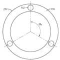
[0080]도 7a 및 도 7b는 하나 이상의 실시예들에 따른, 작동 메커니즘들(280)을 위한 배치 위치들을 예시하는, 조정가능 튜닝 링(250)의 저면도들을 도시한다. 도 7a는 조정가능 튜닝 링(250)의 하부 표면(256) 상에 배치되는 3개의 포지션들(702)을 도시한다. 일 예에서, 이러한 포지션들(702)은, 리프트 핀들(260)과 같은 작동 메커니즘들(280)의 상부 단부들이 하부 표면(256)과 접촉하는 위치들에 있다. 3개의 포지션들(702)은, 조정가능 튜닝 링(250)의 중심으로부터 측정될 때, 대략 110° 내지 대략 130°, 대략 115° 내지 대략 125°, 또는 대략 118° 내지 대략 122°, 예컨대 대략 120°의 각도(α1)만큼 서로 분리된다.[0080]7A and 7B show bottom views of
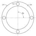
[0081]도 7b는 조정가능 튜닝 링(250)의 하부 표면(256) 상에 배치되는 4개의 포지션들(702)을 도시한다. 다른 예에서, 이러한 포지션들(702) 각각은, 리프트 핀(260)과 같은 작동 메커니즘들(280)의 상부 단부가 하부 표면(256)과 접촉하는 위치에 있다. 4개의 포지션들(702)은, 조정가능 튜닝 링(250)의 중심으로부터 측정될 때, 대략 80° 내지 대략 100°, 대략 85° 내지 대략 95°, 또는 대략 88° 내지 대략 92°, 예컨대 대략 90°의 각도(α2)만큼 서로 분리된다.[0081]7B shows four
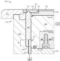
[0082]도 8은 하나 이상의 실시예들에 따른, 작동 메커니즘들(280)의 적어도 일부를 포함하는 데 사용되는 정렬 커플링들(259)을 갖는 조정가능 튜닝 링(250)을 포함하는 프로세스 키트(800)의 확대된 부분 단면도를 도시한다. 정렬 커플링들(259)은, 조정가능 튜닝 링(250)의 하부 표면(256) 내에 형성되는 1개, 2개, 3개, 4개 또는 그보다 많은 암형 커플링들, 이를테면, 슬롯들 또는 홀들이거나 이들을 포함할 수 있다.[0082]8 includes a
[0083]도 8에 도시된 바와 같이, 암형 정렬 커플링들(259)은 리프트 핀(260)과 정합할 수 있다. 따라서, 일부 예들에서, 리프트 핀들(260)의 개수와 동일한 개수의 암형 정렬 커플링들(259)이 있다. 하나 이상의 예들에서, 조정가능 튜닝 링(250)은, 조정가능 튜닝 링(250)의 하부 표면(256)으로부터 조정가능 튜닝 링(250)의 상부 표면(254)을 향해 연장되는 슬롯들인 2개, 3개, 4개 또는 그보다 많은 정렬 커플링들(259)을 갖고, 각각의 슬롯은 각각의 슬롯 내에 배치된 리프트 핀(260)을 포함한다. 정렬 커플링들(259)은 하부 표면(256)으로부터 조정가능 튜닝 링(250) 내로 거리(D3)만큼 연장될 수 있다. 예컨대, 거리(D3)는 대략 1 mm, 대략 2 mm, 대략 3 mm, 또는 대략 4 mm 내지 대략 5 mm, 대략 7 mm, 대략 10 mm, 대략 12 mm, 또는 대략 15 mm일 수 있다.[0083]As shown in FIG. 8, the
[0084]도 8이 제2 링 컴포넌트(230)의 하부 표면(231) 상의 암형 커플링인 상부 정렬 커플링 및 조정가능 튜닝 링(250)의 상부 표면(254) 상의 수형 커플링인 하부 정렬 커플링을 도시하지만, 하부 표면(231) 및 상부 표면(254) 각각은 독립적으로, 임의의 유형의 수형 또는 암형 커플링(도 2a-도 2j에 예시된 바와 같음)을 가질 수 있을 뿐만 아니라 커플링을 갖지 않을 수 있어서(도 1c 및 도 1d에 예시된 바와 같음), 제2 링 컴포넌트(230)의 하부 표면(231)과 조정가능 튜닝 링(250)의 상부 표면(254)은 커플링 없이 서로 접촉한다.[0084]FIG. 8 shows an upper alignment coupling that is a female coupling on the
[0085]도 9a 및 도 9b는 하나 이상의 실시예들에 따른, 도 8에서 예시되는 조정가능 튜닝 링(250)의 저면도들을 도시한다. 도 9a는, 조정가능 튜닝 링(250)에 형성되고 내부에 포인트들(902)을 포함하는 3개의 슬롯들 또는 암형 정렬 커플링들(259)을 도시한다. 일 예에서, 이러한 포인트들(902)은, 리프트 핀들(260)과 같은 작동 메커니즘들(280)이 암형 정렬 커플링들(259) 내로 삽입되거나 또는 이와 다르게 배치되는 위치들에 있다. 3개의 슬롯들 또는 암형 정렬 커플링들(259)은, 조정가능 튜닝 링(250)의 중심으로부터 측정될 때, 대략 110° 내지 대략 130°, 대략 115° 내지 대략 125°, 또는 대략 118° 내지 대략 122°, 예컨대 대략 120°의 각도(α3)만큼 서로 분리된다.[0085]9A and 9B show bottom views of the
[0086]도 9b는, 조정가능 튜닝 링(250)에 형성되고 내부에 포인트들(902)을 포함하는 4개의 슬롯들 또는 암형 정렬 커플링들(259)을 도시한다. 다른 예에서, 이러한 포인트들(902)은, 리프트 핀들(260)과 같은 작동 메커니즘들(280)이 암형 정렬 커플링들(259) 내로 삽입되거나 또는 이와 다르게 배치되는 위치들에 있다. 4개의 슬롯들 또는 암형 정렬 커플링들(259)은, 조정가능 튜닝 링(250)의 중심으로부터 측정될 때, 대략 80° 내지 대략 100°, 대략 85° 내지 대략 95°, 또는 대략 88° 내지 대략 92°, 예컨대 대략 90°의 각도(α4)만큼 서로 분리된다.[0086]9B shows four slots or
[0087]본 개시내용의 실시예들은 추가로, 다음의 단락1 내지 단락26 중 임의의 하나 이상과 관련된다.[0087]Embodiments of the present disclosure further relate to any one or more of the following paragraphs 1-26.
[0088]1. 기판 프로세싱 챔버를 위한 프로세스 키트로서, 프로세스 키트는: 제1 링 컴포넌트 및 제2 링 컴포넌트를 갖는 에지 링 ― 제1 링 컴포넌트는, 제2 링 컴포넌트가 제1 링 컴포넌트에 대해 이동가능하여 제1 링 컴포넌트와 제2 링 컴포넌트 사이에 갭을 형성하도록, 제2 링 컴포넌트와 인터페이싱되고, 제2 링 컴포넌트는 상부 표면 및 하부 표면을 갖고, 제2 링 컴포넌트의 하부 표면은 상부 정렬 커플링을 포함함 ―; 에지 링 아래에 포지셔닝된 조정가능 튜닝 링 ― 조정가능 튜닝 링은 상부 표면 및 하부 표면을 갖고, 조정가능 튜닝 링의 상부 표면은 하부 정렬 커플링을 포함하고, 조정가능 튜닝 링의 상부 표면은 제2 링 컴포넌트의 하부 표면과 접촉하도록 구성되고, 그리고 조정가능 튜닝 링의 하부 정렬 커플링은 제2 링 컴포넌트의 상부 정렬 커플링과 정합하여 인터페이스를 형성하도록 구성됨 ―; 및 조정가능 튜닝 링의 하부 표면과 인터페이싱되는 작동 메커니즘을 포함하며, 작동 메커니즘은, 제1 링 컴포넌트와 제2 링 컴포넌트 사이의 갭이 변화되도록 조정가능 튜닝 링을 작동시키도록 구성된다.[0088]1. A process kit for a substrate processing chamber, the process kit comprising: an edge ring having a first ring component and a second ring component, wherein the first ring component is configured such that the second ring component is movable relative to the first ring component; Interfacing with the second ring component to form a gap between the first ring component and the second ring component, the second ring component having an upper surface and a lower surface, wherein the lower surface of the second ring component comprises an upper alignment coupling To; Adjustable tuning ring positioned below the edge ring, the adjustable tuning ring having an upper surface and a lower surface, the upper surface of the adjustable tuning ring comprising a lower alignment coupling, and the upper surface of the adjustable tuning ring being the second Is configured to be in contact with the bottom surface of the ring component, and the bottom alignment coupling of the adjustable tuning ring is configured to mate with the top alignment coupling of the second ring component to form an interface; And an actuation mechanism that interfaces with the bottom surface of the adjustable tuning ring, the actuation mechanism configured to actuate the adjustable tuning ring such that the gap between the first ring component and the second ring component is varied.
[0089]2. 프로세싱 챔버로서, 프로세싱 챔버는: 기판을 지지하도록 구성된 기판 지지 부재; 및 기판 지지 부재에 의해 지지되는 프로세스 키트를 포함하며, 프로세스 키트는: 제1 링 컴포넌트 및 제2 링 컴포넌트를 갖는 에지 링 ― 제1 링 컴포넌트는, 제2 링 컴포넌트가 제1 링 컴포넌트에 대해 이동가능하여 제1 링 컴포넌트와 제2 링 컴포넌트 사이에 갭을 형성하도록, 제2 링 컴포넌트와 인터페이싱되고, 제2 링 컴포넌트는 상부 표면 및 하부 표면을 갖고, 제2 링 컴포넌트의 하부 표면은 상부 정렬 커플링을 포함함 ―; 에지 링 아래에 포지셔닝된 조정가능 튜닝 링 ― 조정가능 튜닝 링은 상부 표면 및 하부 표면을 갖고, 조정가능 튜닝 링의 상부 표면은 하부 정렬 커플링을 포함하고, 조정가능 튜닝 링의 상부 표면은 제2 링 컴포넌트의 하부 표면과 접촉하도록 구성되고, 그리고 조정가능 튜닝 링의 하부 정렬 커플링은 제2 링 컴포넌트의 상부 정렬 커플링과 정합하여 인터페이스를 형성하도록 구성됨 ―; 및 조정가능 튜닝 링의 하부 표면과 인터페이싱되는 작동 메커니즘을 포함하며, 작동 메커니즘은, 제1 링 컴포넌트와 제2 링 컴포넌트 사이의 갭이 변화되도록 조정가능 튜닝 링을 작동시키도록 구성된다.[0089]2. A processing chamber, comprising: a substrate support member configured to support a substrate; And a process kit supported by the substrate support member, the process kit comprising: an edge ring having a first ring component and a second ring component, the first ring component having a second ring component moved relative to the first ring component; Interfacing with the second ring component, possibly to form a gap between the first ring component and the second ring component, the second ring component having an upper surface and a lower surface, the lower surface of the second ring component being the upper alignment couple Including a ring; Adjustable tuning ring positioned below the edge ring, the adjustable tuning ring having an upper surface and a lower surface, the upper surface of the adjustable tuning ring comprising a lower alignment coupling, and the upper surface of the adjustable tuning ring being the second Is configured to be in contact with the bottom surface of the ring component, and the bottom alignment coupling of the adjustable tuning ring is configured to mate with the top alignment coupling of the second ring component to form an interface; And an actuation mechanism that interfaces with the bottom surface of the adjustable tuning ring, the actuation mechanism configured to actuate the adjustable tuning ring such that the gap between the first ring component and the second ring component is varied.
[0090]3. 단락2의 프로세싱 챔버에 있어서, 기판 지지 부재는: 베이스; 베이스에 의해 지지되는 냉각 플레이트; 및 냉각 플레이트의 상부 표면 상에 포지셔닝되는 정전 척을 포함한다.[0090]3. The processing chamber of paragraph 2, wherein the substrate support member comprises: a base; A cooling plate supported by the base; And an electrostatic chuck positioned on the top surface of the cooling plate.
[0091]4. 단락1 내지 단락3 중 어느 한 단락에 따른 프로세스 키트 또는 프로세싱 챔버에 있어서, 상부 정렬 커플링은 수형 커플링이고 그리고 하부 정렬 커플링은 암형 커플링이거나, 또는 상부 정렬 커플링은 암형 커플링이고 그리고 하부 정렬 커플링은 수형 커플링이다.[0091]4. The process kit or processing chamber according to any of paragraphs 1 to 3, wherein the upper alignment coupling is a male coupling and the lower alignment coupling is a female coupling, or the upper alignment coupling is a female coupling. And the lower alignment coupling is a male coupling.
[0092]5. 단락4의 프로세스 키트 또는 프로세싱 챔버에 있어서, 수형 커플링과 암형 커플링에 의해 형성되는 인터페이스는 정합 프로파일을 갖고, 그리고 정합 프로파일은, 더브테일, 스플라인, 핀형, 삼각형, 직사각형, 정사각형, 사다리꼴, 아크형, 및 라운드형으로 이루어진 그룹으로부터 선택된다.[0092]5. The process kit or processing chamber of paragraph 4, wherein the interface formed by the male coupling and the female coupling has a mating profile, and the mating profile is a dovetail, spline, pin, triangle, rectangle, square, trapezoid. , Arc, and round.
[0093]6. 단락1 내지 단락5 중 어느 한 단락에 따른 프로세스 키트 또는 프로세싱 챔버는, 조정가능 튜닝 링의 상부 표면과 제2 링 컴포넌트의 하부 표면 사이에 배치되고 그리고 조정가능 튜닝 링의 하부 정렬 커플링과 제2 링 컴포넌트의 상부 정렬 커플링 사이에 배치되는 갭을 더 포함한다.[0093]6. The process kit or processing chamber according to any of paragraphs 1 to 5, disposed between the upper surface of the adjustable tuning ring and the lower surface of the second ring component and with the lower alignment coupling of the adjustable tuning ring. And a gap disposed between the upper alignment coupling of the second ring component.
[0094]7. 단락6의 프로세스 키트 또는 프로세싱 챔버에 있어서, 작동 메커니즘은 하부 정렬 커플링과 상부 정렬 커플링 사이의 갭이 변화되도록 조정가능 튜닝 링을 작동시키도록 구성된다.[0094]7. The process kit or processing chamber of paragraph 6, wherein the actuation mechanism is configured to actuate the adjustable tuning ring such that the gap between the lower alignment coupling and the upper alignment coupling is varied.
[0095]8. 단락1 내지 단락7 중 어느 한 단락에 따른 프로세스 키트 또는 프로세싱 챔버는, 조정가능 튜닝 링과 작동 메커니즘 사이에 배치된 전기 절연 지지 링을 더 포함한다.[0095]8. The process kit or processing chamber according to any of paragraphs 1-7, further comprising an electrically insulating support ring disposed between the adjustable tuning ring and the actuation mechanism.
[0096]9. 단락8의 프로세스 키트 또는 프로세싱 챔버에 있어서, 절연 지지 링은 폴리테트라플루오로에틸렌 재료를 포함한다.[0096]9. The process kit or processing chamber of paragraph 8, wherein the insulating support ring comprises a polytetrafluoroethylene material.
[0097]10. 단락8의 프로세스 키트 또는 프로세싱 챔버에 있어서, 작동 메커니즘은 리프트 핀을 포함하고, 그리고 절연 지지 링은 조정가능 튜닝 링과 리프트 핀 사이에 있고 그리고 조정가능 튜닝 링 및 리프트 핀과 접촉한다.[0097]10. The process kit or processing chamber of paragraph 8, wherein the actuation mechanism comprises a lift pin, and the insulating support ring is between the adjustable tuning ring and the lift pin and contacts the adjustable tuning ring and the lift pin.
[0098]11. 단락10의 프로세스 키트 또는 프로세싱 챔버에 있어서, 조정가능 튜닝 링의 하부 표면 상의 정렬 커플링과 절연 지지 링의 상부 표면 상의 정렬 커플링은 정합하여 조정가능 튜닝 링의 하부 표면 상의 정렬 커플링과 절연 지지 링의 상부 표면 상의 정렬 커플링 사이에 정합 프로파일을 형성한다.[0098]11. The process kit or processing chamber of paragraph 10, wherein the alignment coupling on the bottom surface of the adjustable tuning ring and the alignment coupling on the top surface of the insulating support ring match with the alignment coupling on the bottom surface of the adjustable tuning ring. A mating profile is formed between the alignment coupling on the top surface of the insulating support ring.
[0099]12. 단락8의 프로세스 키트 또는 프로세싱 챔버에 있어서, 절연 지지 링은 절연 지지 링의 하부 표면으로부터 절연 지지 링의 상부 표면을 향해 연장되는 3개 이상의 슬롯들을 포함하고, 그리고 각각의 슬롯은 각각의 슬롯 내에 배치된 리프트 핀을 포함한다.[0099]12. The process kit or processing chamber of paragraph 8, wherein the insulated support ring comprises three or more slots extending from the bottom surface of the insulated support ring toward the top surface of the insulated support ring, wherein each slot is a respective slot. A lift pin disposed within.
[00100]13. 단락1 내지 단락12 중 어느 한 단락에 따른 프로세스 키트 또는 프로세싱 챔버에 있어서, 조정가능 튜닝 링은 전기 전도성 재료를 포함한다.[00100]13. The process kit or processing chamber according to any of paragraphs 1 to 12, wherein the adjustable tuning ring comprises an electrically conductive material.
[00101]14. 단락13의 프로세스 키트 또는 프로세싱 챔버에 있어서, 전기 전도성 재료는 알루미늄 또는 알루미늄 합금을 포함한다.[00101]14. The process kit or processing chamber of paragraph 13, wherein the electrically conductive material comprises aluminum or an aluminum alloy.
[00102]15. 단락1 내지 단락14 중 어느 한 단락에 따른 프로세스 키트 또는 프로세싱 챔버에 있어서, 제2 링 컴포넌트는 실리콘 카바이드를 포함한다.[00102]15. The process kit or processing chamber according to any of paragraphs 1 to 14, wherein the second ring component comprises silicon carbide.
[00103]16. 단락1 내지 단락15 중 어느 한 단락에 따른 프로세스 키트 또는 프로세싱 챔버에 있어서, 제1 링 컴포넌트는 제1 링 컴포넌트에 형성된 계단형 표면을 포함하고, 그리고 제1 링 컴포넌트의 계단형 표면은 제2 링 컴포넌트의 하부 표면의 일부와 인터페이싱한다.[00103]16. The process kit or processing chamber according to any of paragraphs 1 to 15, wherein the first ring component comprises a stepped surface formed on the first ring component, and the stepped surface of the first ring component is defined as 2 Interface with a portion of the lower surface of the ring component.
[00104]17. 단락1 내지 단락16 중 어느 한 단락에 따른 프로세스 키트 또는 프로세싱 챔버에 있어서, 조정가능 튜닝 링은 조정가능 튜닝 링의 하부 표면으로부터 조정가능 튜닝 링의 상부 표면을 향해 연장되는 3개 이상의 슬롯들을 포함하고, 그리고 각각의 슬롯은 각각의 슬롯 내에 배치된 리프트 핀을 포함한다.[00104]17. The process kit or processing chamber according to any of paragraphs 1-16, wherein the adjustable tuning ring comprises three or more slots extending from the bottom surface of the adjustable tuning ring toward the top surface of the adjustable tuning ring. And each slot includes a lift pin disposed within each slot.
[00105]18. 단락17의 프로세스 키트 또는 프로세싱 챔버에 있어서, 조정가능 튜닝 링은 조정가능 튜닝 링 둘레에 배치된 3개의 슬롯들을 포함하며, 그 3개의 슬롯들은 조정가능 튜닝 링의 중심으로부터 측정될 때 대략 110° 내지 대략 130°의 각도만큼 서로 분리된다.[00105]18. The process kit or processing chamber of paragraph 17, wherein the adjustable tuning ring includes three slots disposed around the adjustable tuning ring, wherein the three slots are approximately 110 when measured from the center of the adjustable tuning ring. Separated from each other by an angle of from about 130 °.
[00106]19. 단락17의 프로세스 키트 또는 프로세싱 챔버에 있어서, 조정가능 튜닝 링은 조정가능 튜닝 링 둘레에 배치된 4개의 슬롯들을 포함하며, 그 4개의 슬롯들은 조정가능 튜닝 링의 중심으로부터 측정될 때 대략 80° 내지 대략 100°의 각도만큼 서로 분리된다.[00106]19. The process kit or processing chamber of paragraph 17, wherein the adjustable tuning ring includes four slots disposed around the adjustable tuning ring, wherein the four slots are approximately 80 when measured from the center of the adjustable tuning ring. Separated from each other by an angle of from about 100 °.
[00107]20. 단락1 내지 단락19 중 어느 한 단락에 따른 프로세스 키트 또는 프로세싱 챔버에 있어서, 작동 메커니즘은 2개 이상의 리프트 핀들을 포함하고, 리프트 핀들 각각은 제1 단부 및 제2 단부를 갖고, 리프트 핀의 제1 단부는 조정가능 튜닝 링의 하부 표면과 접촉하고, 그리고 리프트 핀의 제2 단부는 리프트 메커니즘과 연통한다.[00107]20. The process kit or processing chamber according to any of paragraphs 1 to 19, wherein the actuation mechanism comprises two or more lift pins, each lift pin having a first end and a second end, The first end is in contact with the lower surface of the adjustable tuning ring, and the second end of the lift pin is in communication with the lift mechanism.
[00108]21. 단락20의 프로세스 키트 또는 프로세싱 챔버에 있어서, 작동 메커니즘은 4개의 리프트 핀들을 포함하고, 리프트 핀들의 제1 단부들 각각은 조정가능 튜닝 링의 하부 표면 상의 포인트와 접촉하고, 하부 표면 상의 포인트들은 조정가능 튜닝 링의 중심으로부터 측정될 때 대략 80° 내지 대략 100°의 각도만큼 서로 분리된다.[00108]21. The process kit or processing chamber of paragraph 20, wherein the actuation mechanism comprises four lift pins, each of the first ends of the lift pins contacting a point on the bottom surface of the adjustable tuning ring and a point on the bottom surface They are separated from each other by an angle of approximately 80 ° to approximately 100 ° when measured from the center of the adjustable tuning ring.
[00109]22. 단락20의 프로세스 키트 또는 프로세싱 챔버에 있어서, 리프트 메커니즘은 서보 드라이브를 포함한다.[00109]22. The process kit or processing chamber of paragraph 20, wherein the lift mechanism comprises a servo drive.
[00110]23. 기판을 프로세싱하기 위한 방법으로서, 방법은 단락1 내지 단락22 중 어느 한 단락에 따른 프로세스 키트 또는 프로세싱 챔버를 이용하여 수행된다.[00110]23. A method for processing a substrate, wherein the method is performed using a process kit or processing chamber according to any of paragraphs 1-22.
[00111]24. 기판을 프로세싱하기 위한 방법으로서, 방법은: 단락1 내지 단락22 중 어느 한 단락에 따른 프로세스 키트 또는 프로세싱 챔버 내에 배치된 기판 지지 부재 상에 기판을 포지셔닝하는 단계; 기판 위에 플라즈마를 형성하는 단계; 및 기판의 에지에서의 이온들의 방향을 변경하기 위해, 에지 링의 제2 링 컴포넌트와 인터페이싱되는 조정가능 튜닝 링을 작동시킴으로써 제2 링 컴포넌트의 높이를 조정하는 단계를 포함한다.[00111]24. A method for processing a substrate, the method comprising: positioning a substrate on a substrate support member disposed in a processing kit or processing chamber according to any of paragraphs 1-22; Forming a plasma over the substrate; And adjusting the height of the second ring component by actuating an adjustable tuning ring that interfaces with the second ring component of the edge ring to change the direction of the ions at the edge of the substrate.
[00112]25. 단락23 또는 단락24의 방법에 있어서, 갭은 조정가능 튜닝 링의 하부 정렬 커플링과 제2 링 컴포넌트의 상부 정렬 커플링 사이에 배치된다.[00112]25. The method of paragraph 23 or paragraph 24, wherein the gap is disposed between the lower alignment coupling of the adjustable tuning ring and the upper alignment coupling of the second ring component.
[00113]26. 단락23 내지 단락25 중 어느 한 단락에 따른 방법은, 갭의 크기를 조정하고 그리고 조정가능 튜닝 링과 제2 링 컴포넌트 사이의 용량성 커플링을 변화시키기 위해 조정가능 튜닝 링을 작동시키는 단계를 더 포함한다.[00113]26. The method according to any one of paragraphs 23 to 25, comprising actuating the adjustable tuning ring to adjust the size of the gap and to change the capacitive coupling between the adjustable tuning ring and the second ring component. It further includes.
[00114]전술한 바가 특정 실시예들에 관한 것이지만, 다른 그리고 추가적인 실시예들이, 본 발명의 기본 범위를 벗어나지 않으면서 고안될 수 있고, 본 발명의 범위는 다음의 청구항들에 의해 결정된다.[00114]While the foregoing is directed to specific embodiments, other and further embodiments may be devised without departing from the basic scope of the invention, the scope of the invention being determined by the following claims.
[00115]소정의 실시예들 및 특징들은 수치 상한들의 세트 및 수치 하한들의 세트를 사용하여 설명되었다. 달리 표시되지 않는 한, 임의의 2개의 값들의 조합, 예컨대 임의의 하위 값과 임의의 상위 값의 조합, 임의의 2개의 하위 값들의 조합, 및/또는 임의의 2개의 상위 값들의 조합을 포함하는 범위들이 고려된다는 것이 인지되어야 한다. 아래의 하나 이상의 청구항들에서 소정의 하한들, 상한들 및 범위들이 나타난다.[00115]Certain embodiments and features have been described using a set of upper and lower numerical limits. Unless indicated otherwise, a combination of any two values, such as a combination of any lower value and any higher value, a combination of any two lower values, and / or a combination of any two upper values It should be appreciated that the ranges are considered. Certain lower limits, upper limits and ranges appear in one or more claims below.
Claims (15)
Translated fromKorean제1 링 컴포넌트 및 제2 링 컴포넌트를 갖는 에지 링 ― 상기 제1 링 컴포넌트는, 상기 제2 링 컴포넌트가 상기 제1 링 컴포넌트에 대해 이동가능하여 상기 제1 링 컴포넌트와 상기 제2 링 컴포넌트 사이에 갭을 형성하도록, 상기 제2 링 컴포넌트와 인터페이싱되고, 상기 제2 링 컴포넌트는 상부 표면 및 하부 표면을 갖고, 상기 제2 링 컴포넌트의 하부 표면은 상부 정렬 커플링을 포함함 ―;
상기 에지 링 아래에 포지셔닝된 조정가능 튜닝 링 ― 상기 조정가능 튜닝 링은 상부 표면 및 하부 표면을 갖고, 상기 조정가능 튜닝 링의 상부 표면은 하부 정렬 커플링을 포함하고, 상기 조정가능 튜닝 링의 상부 표면은 상기 제2 링 컴포넌트의 하부 표면과 접촉하도록 구성되고, 그리고 상기 조정가능 튜닝 링의 하부 정렬 커플링은 상기 제2 링 컴포넌트의 상부 정렬 커플링과 정합(mate)하여 인터페이스를 형성하도록 구성됨 ―; 및
상기 조정가능 튜닝 링의 하부 표면과 인터페이싱되는 작동 메커니즘을 포함하며,
상기 작동 메커니즘은, 상기 제1 링 컴포넌트와 상기 제2 링 컴포넌트 사이의 갭이 변화되도록 상기 조정가능 튜닝 링을 작동시키도록 구성되는,
기판 프로세싱 챔버를 위한 프로세스 키트.A process kit for a substrate processing chamber,
An edge ring having a first ring component and a second ring component, wherein the first ring component is movable between the first ring component and the second ring component such that the second ring component is movable relative to the first ring component. Interface with the second ring component to form a gap, the second ring component having a top surface and a bottom surface, wherein the bottom surface of the second ring component includes an upper alignment coupling;
An adjustable tuning ring positioned below the edge ring, the adjustable tuning ring having an upper surface and a lower surface, the upper surface of the adjustable tuning ring comprising a lower alignment coupling, and an upper portion of the adjustable tuning ring A surface is configured to contact the bottom surface of the second ring component, and the bottom alignment coupling of the adjustable tuning ring is configured to mate with the top alignment coupling of the second ring component to form an interface; ; And
An actuation mechanism interfaced with a lower surface of the adjustable tuning ring,
The actuation mechanism is configured to actuate the adjustable tuning ring such that a gap between the first ring component and the second ring component is changed,
Process kit for substrate processing chamber.
상기 상부 정렬 커플링은 수형(male) 커플링이고 그리고 상기 하부 정렬 커플링은 암형(female) 커플링이거나, 또는 상기 상부 정렬 커플링은 암형 커플링이고 그리고 상기 하부 정렬 커플링은 수형 커플링이고; 그리고
상기 수형 커플링과 상기 암형 커플링에 의해 형성되는 인터페이스는 정합 프로파일(mating profile)을 갖고, 그리고 상기 정합 프로파일은, 더브테일(dovetail), 스플라인(spline), 핀형(finned), 삼각형(triangular), 직사각형(rectangular), 정사각형(square), 사다리꼴(trapezoidal), 아크형(arced), 및 라운드형(rounded)으로 이루어진 그룹으로부터 선택되는,
기판 프로세싱 챔버를 위한 프로세스 키트.According to claim 1,
The upper alignment coupling is a male coupling and the lower alignment coupling is a female coupling, or the upper alignment coupling is a female coupling and the lower alignment coupling is a male coupling ; And
The interface formed by the male coupling and the female coupling has a mating profile, and the mating profile is a dovetail, spline, finned, triangular. , Selected from the group consisting of rectangular, square, trapezoidal, arced, and rounded,
Process kit for substrate processing chamber.
상기 조정가능 튜닝 링의 상부 표면과 상기 제2 링 컴포넌트의 하부 표면 사이에 배치되고 그리고 상기 조정가능 튜닝 링의 하부 정렬 커플링과 상기 제2 링 컴포넌트의 상부 정렬 커플링 사이에 배치되는 갭을 더 포함하고; 그리고
상기 작동 메커니즘은 상기 하부 정렬 커플링과 상기 상부 정렬 커플링 사이의 갭이 변화되도록 상기 조정가능 튜닝 링을 작동시키도록 구성되는,
기판 프로세싱 챔버를 위한 프로세스 키트.According to claim 1,
A gap disposed between the upper surface of the adjustable tuning ring and the lower surface of the second ring component and further disposed between the lower alignment coupling of the adjustable tuning ring and the upper alignment coupling of the second ring component. Including; And
The actuation mechanism is configured to actuate the adjustable tuning ring such that a gap between the lower alignment coupling and the upper alignment coupling is changed;
Process kit for substrate processing chamber.
상기 조정가능 튜닝 링과 상기 작동 메커니즘 사이에 배치된 전기 절연 지지 링을 더 포함하는,
기판 프로세싱 챔버를 위한 프로세스 키트.According to claim 1,
Further comprising an electrically insulating support ring disposed between the adjustable tuning ring and the actuation mechanism,
Process kit for substrate processing chamber.
상기 작동 메커니즘은 리프트 핀을 포함하고, 그리고 상기 절연 지지 링은 상기 조정가능 튜닝 링과 상기 리프트 핀 사이에 있고 그리고 상기 조정가능 튜닝 링 및 상기 리프트 핀과 접촉하는,
기판 프로세싱 챔버를 위한 프로세스 키트.The method of claim 4, wherein
The actuation mechanism comprises a lift pin, and the insulating support ring is between the adjustable tuning ring and the lift pin and in contact with the adjustable tuning ring and the lift pin,
Process kit for substrate processing chamber.
상기 조정가능 튜닝 링의 하부 표면 상의 정렬 커플링과 상기 절연 지지 링의 상부 표면 상의 정렬 커플링은 정합하여 상기 조정가능 튜닝 링의 하부 표면 상의 정렬 커플링과 상기 절연 지지 링의 상부 표면 상의 정렬 커플링 사이에 정합 프로파일을 형성하는,
기판 프로세싱 챔버를 위한 프로세스 키트.The method of claim 5,
The alignment coupling on the bottom surface of the adjustable tuning ring and the alignment coupling on the top surface of the insulating support ring are aligned so that the alignment coupling on the bottom surface of the adjustable tuning ring and the alignment couple on the top surface of the insulating support ring Forming a mating profile between the rings,
Process kit for substrate processing chamber.
상기 절연 지지 링은 상기 절연 지지 링의 하부 표면으로부터 상기 절연 지지 링의 상부 표면을 향해 연장되는 3개 이상의 슬롯들을 포함하고, 그리고 각각의 슬롯은 상기 각각의 슬롯 내에 배치된 리프트 핀을 포함하는,
기판 프로세싱 챔버를 위한 프로세스 키트.The method of claim 4, wherein
The insulated support ring comprises three or more slots extending from the bottom surface of the insulated support ring toward the top surface of the insulated support ring, and each slot includes a lift pin disposed within the respective slot,
Process kit for substrate processing chamber.
상기 제1 링 컴포넌트는 상기 제1 링 컴포넌트에 형성된 계단형 표면(stepped surface)을 포함하고, 그리고 상기 제1 링 컴포넌트의 계단형 표면은 상기 제2 링 컴포넌트의 하부 표면의 일부와 인터페이싱하는,
기판 프로세싱 챔버를 위한 프로세스 키트.According to claim 1,
The first ring component comprises a stepped surface formed on the first ring component, and the stepped surface of the first ring component interfaces with a portion of the bottom surface of the second ring component,
Process kit for substrate processing chamber.
상기 조정가능 튜닝 링은 상기 조정가능 튜닝 링의 하부 표면으로부터 상기 조정가능 튜닝 링의 상부 표면을 향해 연장되는 3개 이상의 슬롯들을 포함하고, 그리고 각각의 슬롯은 상기 각각의 슬롯 내에 배치된 리프트 핀을 포함하는,
기판 프로세싱 챔버를 위한 프로세스 키트.According to claim 1,
The adjustable tuning ring includes three or more slots extending from the bottom surface of the adjustable tuning ring toward the top surface of the adjustable tuning ring, each slot receiving a lift pin disposed within the respective slot. Included,
Process kit for substrate processing chamber.
상기 조정가능 튜닝 링은 상기 조정가능 튜닝 링 둘레에 배치된 3개의 슬롯들 ― 상기 3개의 슬롯들은 상기 조정가능 튜닝 링의 중심으로부터 측정될 때 대략 110° 내지 대략 130°의 각도만큼 서로 분리됨 ― 을 포함하거나; 또는
상기 조정가능 튜닝 링은 상기 조정가능 튜닝 링 둘레에 배치된 4개의 슬롯들 ― 상기 4개의 슬롯들은 상기 조정가능 튜닝 링의 중심으로부터 측정될 때 대략 80° 내지 대략 100°의 각도만큼 서로 분리됨 ― 을 포함하는,
기판 프로세싱 챔버를 위한 프로세스 키트.The method of claim 9,
The adjustable tuning ring comprises three slots disposed around the adjustable tuning ring, the three slots being separated from each other by an angle of about 110 ° to about 130 ° as measured from the center of the adjustable tuning ring. Include; or
The adjustable tuning ring comprises four slots disposed about the adjustable tuning ring, the four slots being separated from each other by an angle of about 80 ° to about 100 ° as measured from the center of the adjustable tuning ring. Included,
Process kit for substrate processing chamber.
상기 작동 메커니즘은 2개 이상의 리프트 핀들을 포함하고, 상기 리프트 핀들 각각은 제1 단부 및 제2 단부를 갖고, 상기 리프트 핀의 제1 단부는 상기 조정가능 튜닝 링의 하부 표면과 접촉하고, 그리고 상기 리프트 핀의 제2 단부는 리프트 메커니즘과 연통하거나; 또는
상기 작동 메커니즘은 4개의 리프트 핀들을 포함하고, 상기 리프트 핀들의 제1 단부들 각각은 상기 조정가능 튜닝 링의 하부 표면 상의 포인트와 접촉하고, 상기 하부 표면 상의 포인트들은 상기 조정가능 튜닝 링의 중심으로부터 측정될 때 대략 80° 내지 대략 100°의 각도만큼 서로 분리되는,
기판 프로세싱 챔버를 위한 프로세스 키트.According to claim 1,
The actuation mechanism comprises two or more lift pins, each of the lift pins having a first end and a second end, the first end of the lift pin contacting a lower surface of the adjustable tuning ring, and The second end of the lift pin is in communication with the lift mechanism; or
The actuation mechanism comprises four lift pins, each of the first ends of the lift pins contacting a point on the bottom surface of the adjustable tuning ring, the points on the bottom surface from the center of the adjustable tuning ring. Separated from each other by an angle of about 80 ° to about 100 ° when measured,
Process kit for substrate processing chamber.
기판을 지지하도록 구성된 기판 지지 부재; 및
상기 기판 지지 부재에 의해 지지되는 프로세스 키트를 포함하며,
상기 프로세스 키트는,
제1 링 컴포넌트 및 제2 링 컴포넌트를 갖는 에지 링 ― 상기 제1 링 컴포넌트는, 상기 제2 링 컴포넌트가 상기 제1 링 컴포넌트에 대해 이동가능하여 상기 제1 링 컴포넌트와 상기 제2 링 컴포넌트 사이에 갭을 형성하도록, 상기 제2 링 컴포넌트와 인터페이싱되고, 상기 제2 링 컴포넌트는 상부 표면 및 하부 표면을 갖고, 상기 제2 링 컴포넌트의 하부 표면은 상부 정렬 커플링을 포함함 ―;
상기 에지 링 아래에 포지셔닝된 조정가능 튜닝 링 ― 상기 조정가능 튜닝 링은 상부 표면 및 하부 표면을 갖고, 상기 조정가능 튜닝 링의 상부 표면은 하부 정렬 커플링을 포함하고, 상기 조정가능 튜닝 링의 상부 표면은 상기 제2 링 컴포넌트의 하부 표면과 접촉하도록 구성되고, 그리고 상기 조정가능 튜닝 링의 하부 정렬 커플링은 상기 제2 링 컴포넌트의 상부 정렬 커플링과 정합하여 인터페이스를 형성하도록 구성됨 ―; 및
상기 조정가능 튜닝 링의 하부 표면과 인터페이싱되는 작동 메커니즘을 포함하며,
상기 작동 메커니즘은, 상기 제1 링 컴포넌트와 상기 제2 링 컴포넌트 사이의 갭이 변화되도록 상기 조정가능 튜닝 링을 작동시키도록 구성되는,
프로세싱 챔버.As a processing chamber,
A substrate support member configured to support a substrate; And
A process kit supported by the substrate support member,
The process kit,
An edge ring having a first ring component and a second ring component, wherein the first ring component is movable between the first ring component and the second ring component such that the second ring component is movable relative to the first ring component. Interface with the second ring component to form a gap, the second ring component having a top surface and a bottom surface, wherein the bottom surface of the second ring component includes an upper alignment coupling;
An adjustable tuning ring positioned below the edge ring, the adjustable tuning ring having an upper surface and a lower surface, the upper surface of the adjustable tuning ring comprising a lower alignment coupling, and an upper portion of the adjustable tuning ring A surface is configured to contact the bottom surface of the second ring component, and the bottom alignment coupling of the adjustable tuning ring is configured to mate with the top alignment coupling of the second ring component to form an interface; And
An actuation mechanism interfaced with a lower surface of the adjustable tuning ring,
The actuation mechanism is configured to actuate the adjustable tuning ring such that a gap between the first ring component and the second ring component is changed,
Processing chamber.
상기 기판 지지 부재는,
베이스;
상기 베이스에 의해 지지되는 냉각 플레이트; 및
상기 냉각 플레이트의 상부 표면 상에 포지셔닝되는 정전 척을 포함하는,
프로세싱 챔버.The method of claim 12,
The substrate support member,
Base;
A cooling plate supported by the base; And
An electrostatic chuck positioned on an upper surface of the cooling plate,
Processing chamber.
제12 항의 프로세싱 챔버 내에 배치된 상기 기판 지지 부재 상에 상기 기판을 포지셔닝하는 단계;
상기 기판 위에 플라즈마를 형성하는 단계; 및
상기 기판의 에지에서의 이온들의 방향을 변경하기 위해, 상기 에지 링의 제2 링 컴포넌트와 인터페이싱되는 상기 조정가능 튜닝 링을 작동시킴으로써 상기 제2 링 컴포넌트의 높이를 조정하는 단계를 포함하는,
기판을 프로세싱하기 위한 방법.A method for processing a substrate,
Positioning the substrate on the substrate support member disposed in the processing chamber of claim 12;
Forming a plasma on the substrate; And
Adjusting the height of the second ring component by actuating the adjustable tuning ring interfaced with the second ring component of the edge ring to change the direction of the ions at the edge of the substrate,
Method for processing a substrate.
상기 조정가능 튜닝 링의 하부 정렬 커플링과 상기 제2 링 컴포넌트의 상부 정렬 커플링 사이에 갭이 배치되고, 그리고
상기 방법은,
상기 갭의 크기를 조정하고 그리고 상기 조정가능 튜닝 링과 상기 제2 링 컴포넌트 사이의 용량성 커플링을 변화시키기 위해 상기 조정가능 튜닝 링을 작동시키는 단계를 더 포함하는,
기판을 프로세싱하기 위한 방법.The method of claim 14,
A gap is disposed between the lower alignment coupling of the adjustable tuning ring and the upper alignment coupling of the second ring component, and
The method,
Operating the adjustable tuning ring to adjust the size of the gap and to change the capacitive coupling between the adjustable tuning ring and the second ring component,
Method for processing a substrate.
Applications Claiming Priority (8)
| Application Number | Priority Date | Filing Date | Title |
|---|---|---|---|
| IN201841019829 | 2018-05-28 | ||
| IN201841019829 | 2018-05-28 | ||
| US16/131,909US10790123B2 (en) | 2018-05-28 | 2018-09-14 | Process kit with adjustable tuning ring for edge uniformity control |
| US16/131,893 | 2018-09-14 | ||
| US16/131,903 | 2018-09-14 | ||
| US16/131,893US11201037B2 (en) | 2018-05-28 | 2018-09-14 | Process kit with adjustable tuning ring for edge uniformity control |
| US16/131,903US10600623B2 (en) | 2018-05-28 | 2018-09-14 | Process kit with adjustable tuning ring for edge uniformity control |
| US16/131,909 | 2018-09-14 |
Publications (1)
| Publication Number | Publication Date |
|---|---|
| KR20190135426Atrue KR20190135426A (en) | 2019-12-06 |
Family
ID=68613513
Family Applications (3)
| Application Number | Title | Priority Date | Filing Date |
|---|---|---|---|
| KR1020190062168AWithdrawnKR20190135428A (en) | 2018-05-28 | 2019-05-27 | Process kit with adjustable tuning ring for edge uniformity control |
| KR1020190062161AWithdrawnKR20190135426A (en) | 2018-05-28 | 2019-05-27 | Process kit with adjustable tuning ring for edge uniformity control |
| KR1020190062171AWithdrawnKR20190135429A (en) | 2018-05-28 | 2019-05-27 | Process kit with adjustable tuning ring for edge uniformity control |
Family Applications Before (1)
| Application Number | Title | Priority Date | Filing Date |
|---|---|---|---|
| KR1020190062168AWithdrawnKR20190135428A (en) | 2018-05-28 | 2019-05-27 | Process kit with adjustable tuning ring for edge uniformity control |
Family Applications After (1)
| Application Number | Title | Priority Date | Filing Date |
|---|---|---|---|
| KR1020190062171AWithdrawnKR20190135429A (en) | 2018-05-28 | 2019-05-27 | Process kit with adjustable tuning ring for edge uniformity control |
Country Status (5)
| Country | Link |
|---|---|
| US (4) | US10600623B2 (en) |
| JP (3) | JP2019208023A (en) |
| KR (3) | KR20190135428A (en) |
| CN (6) | CN210123716U (en) |
| TW (6) | TW202004837A (en) |
Cited By (2)
| Publication number | Priority date | Publication date | Assignee | Title |
|---|---|---|---|---|
| KR20220016324A (en)* | 2020-07-30 | 2022-02-09 | 세메스 주식회사 | Load lock chamber, substrate processing apparatus including the same |
| KR20240015699A (en)* | 2018-12-12 | 2024-02-05 | 도쿄엘렉트론가부시키가이샤 | Substrate processing system, transfer method, transfer program, and holder |
Families Citing this family (64)
| Publication number | Priority date | Publication date | Assignee | Title |
|---|---|---|---|---|
| US9873180B2 (en) | 2014-10-17 | 2018-01-23 | Applied Materials, Inc. | CMP pad construction with composite material properties using additive manufacturing processes |
| US10875153B2 (en) | 2014-10-17 | 2020-12-29 | Applied Materials, Inc. | Advanced polishing pad materials and formulations |
| US9776361B2 (en) | 2014-10-17 | 2017-10-03 | Applied Materials, Inc. | Polishing articles and integrated system and methods for manufacturing chemical mechanical polishing articles |
| US11745302B2 (en) | 2014-10-17 | 2023-09-05 | Applied Materials, Inc. | Methods and precursor formulations for forming advanced polishing pads by use of an additive manufacturing process |
| KR20240015167A (en) | 2014-10-17 | 2024-02-02 | 어플라이드 머티어리얼스, 인코포레이티드 | Cmp pad construction with composite material properties using additive manufacturing processes |
| US10658222B2 (en) | 2015-01-16 | 2020-05-19 | Lam Research Corporation | Moveable edge coupling ring for edge process control during semiconductor wafer processing |
| WO2017074773A1 (en) | 2015-10-30 | 2017-05-04 | Applied Materials, Inc. | An apparatus and method of forming a polishing article that has a desired zeta potential |
| US10593574B2 (en) | 2015-11-06 | 2020-03-17 | Applied Materials, Inc. | Techniques for combining CMP process tracking data with 3D printed CMP consumables |
| US10391605B2 (en) | 2016-01-19 | 2019-08-27 | Applied Materials, Inc. | Method and apparatus for forming porous advanced polishing pads using an additive manufacturing process |
| CN108369922B (en) | 2016-01-26 | 2023-03-21 | 应用材料公司 | Wafer edge ring lifting solution |
| CN116110846A (en) | 2016-01-26 | 2023-05-12 | 应用材料公司 | Wafer edge ring lift solution |
| US10553404B2 (en) | 2017-02-01 | 2020-02-04 | Applied Materials, Inc. | Adjustable extended electrode for edge uniformity control |
| US11471999B2 (en) | 2017-07-26 | 2022-10-18 | Applied Materials, Inc. | Integrated abrasive polishing pads and manufacturing methods |
| WO2019032286A1 (en) | 2017-08-07 | 2019-02-14 | Applied Materials, Inc. | Abrasive delivery polishing pads and manufacturing methods thereof |
| US11075105B2 (en) | 2017-09-21 | 2021-07-27 | Applied Materials, Inc. | In-situ apparatus for semiconductor process module |
| CN118380371A (en) | 2017-11-21 | 2024-07-23 | 朗姆研究公司 | Bottom edge ring and middle edge ring |
| US10600623B2 (en)* | 2018-05-28 | 2020-03-24 | Applied Materials, Inc. | Process kit with adjustable tuning ring for edge uniformity control |
| US11935773B2 (en) | 2018-06-14 | 2024-03-19 | Applied Materials, Inc. | Calibration jig and calibration method |
| CN112654655A (en) | 2018-09-04 | 2021-04-13 | 应用材料公司 | Advanced polishing pad formulations |
| JP7105666B2 (en)* | 2018-09-26 | 2022-07-25 | 東京エレクトロン株式会社 | Plasma processing equipment |
| US11289310B2 (en) | 2018-11-21 | 2022-03-29 | Applied Materials, Inc. | Circuits for edge ring control in shaped DC pulsed plasma process device |
| US10903050B2 (en)* | 2018-12-10 | 2021-01-26 | Lam Research Corporation | Endpoint sensor based control including adjustment of an edge ring parameter for each substrate processed to maintain etch rate uniformity |
| US11328893B2 (en)* | 2018-12-13 | 2022-05-10 | Xia Tai Xin Semiconductor (Qing Dao) Ltd. | Plasma processing system |
| US12009236B2 (en) | 2019-04-22 | 2024-06-11 | Applied Materials, Inc. | Sensors and system for in-situ edge ring erosion monitor |
| JP7321026B2 (en)* | 2019-08-02 | 2023-08-04 | 東京エレクトロン株式会社 | EDGE RING, PLACE, SUBSTRATE PROCESSING APPARATUS, AND SUBSTRATE PROCESSING METHOD |
| CN112992631B (en)* | 2019-12-16 | 2023-09-29 | 中微半导体设备(上海)股份有限公司 | Lower electrode assembly, installation method thereof and plasma processing device |
| WO2021158451A1 (en)* | 2020-02-04 | 2021-08-12 | Lam Research Corporation | Radiofrequency signal filter arrangement for plasma processing system |
| TWI871435B (en)* | 2020-03-03 | 2025-02-01 | 日商東京威力科創股份有限公司 | Substrate support, and plasma processing system |
| CN115485809A (en)* | 2020-03-04 | 2022-12-16 | 朗姆研究公司 | Minimizing reflected power in tunable edge sheath systems |
| TW202213428A (en)* | 2020-06-05 | 2022-04-01 | 日商東京威力科創股份有限公司 | Plasma processing apparatus |
| US11492697B2 (en)* | 2020-06-22 | 2022-11-08 | Applied Materials, Inc. | Apparatus for improved anode-cathode ratio for rf chambers |
| KR20220005994A (en)* | 2020-07-07 | 2022-01-14 | 도쿄엘렉트론가부시키가이샤 | Edge ring and etching apparatus |
| JP7508693B2 (en)* | 2020-07-22 | 2024-07-01 | アプライド マテリアルズ インコーポレイテッド | Lift pin interface in substrate support |
| GB202012560D0 (en) | 2020-08-12 | 2020-09-23 | Spts Technologies Ltd | Apparatus and method |
| WO2022076227A1 (en)* | 2020-10-05 | 2022-04-14 | Lam Research Corporation | Moveable edge rings for plasma processing systems |
| CN114446862A (en)* | 2020-11-03 | 2022-05-06 | 中国科学院微电子研究所 | Pressure ring assembly for fixing wafer and wafer processing chamber |
| CN112397366B (en)* | 2020-11-05 | 2023-07-14 | 北京北方华创微电子装备有限公司 | Bearing device and semiconductor reaction chamber |
| KR20230027251A (en)* | 2020-11-19 | 2023-02-27 | 어플라이드 머티어리얼스, 인코포레이티드 | Rings for board extreme edge protection |
| CN114530361B (en)* | 2020-11-23 | 2024-08-06 | 中微半导体设备(上海)股份有限公司 | Lower electrode assembly, plasma processing apparatus, and method of replacing focus ring |
| US11878389B2 (en) | 2021-02-10 | 2024-01-23 | Applied Materials, Inc. | Structures formed using an additive manufacturing process for regenerating surface texture in situ |
| CN113097038B (en)* | 2021-02-25 | 2022-07-15 | 长江存储科技有限责任公司 | Etching device |
| US12286706B2 (en)* | 2021-02-26 | 2025-04-29 | Taiwan Semiconductor Manufacturing Co., Ltd. | Structures and methods for processing a semiconductor substrate |
| US20220293397A1 (en)* | 2021-03-10 | 2022-09-15 | Applied Materials, Inc. | Substrate edge ring that extends process environment beyond substrate diameter |
| CN117203751A (en)* | 2021-04-19 | 2023-12-08 | 朗姆研究公司 | Shadow ring alignment for substrate support |
| US20220349050A1 (en)* | 2021-04-30 | 2022-11-03 | Applied Materials, Inc. | Method and apparatus with high conductance components for chamber cleaning |
| US11721569B2 (en) | 2021-06-18 | 2023-08-08 | Applied Materials, Inc. | Method and apparatus for determining a position of a ring within a process kit |
| KR102572318B1 (en)* | 2021-07-06 | 2023-08-29 | (주)아이씨디 | Plasma Processing Device |
| CN120565385A (en)* | 2021-09-08 | 2025-08-29 | 北京屹唐半导体科技股份有限公司 | Conductive member for cleaning focus ring of plasma processing equipment |
| EP4148774A1 (en)* | 2021-09-08 | 2023-03-15 | Mattson Technology, Inc. | Conductive member for cleaning focus ring of a plasma processing apparatus |
| KR102767880B1 (en)* | 2021-11-02 | 2025-02-17 | 피에스케이 주식회사 | Substrate processing apparatus and substrate processing method |
| KR20230094576A (en) | 2021-12-21 | 2023-06-28 | 삼성전자주식회사 | Ring assembly, substrate support apparatus and plasma processing apparatus having the same |
| TW202341228A (en)* | 2021-12-28 | 2023-10-16 | 日商東京威力科創股份有限公司 | Plasma processing apparatus |
| USD1042374S1 (en) | 2022-03-18 | 2024-09-17 | Applied Materials, Inc. | Support pipe for an interlocking process kit for a substrate processing chamber |
| USD1055006S1 (en) | 2022-03-18 | 2024-12-24 | Applied Materials, Inc. | Support ring for an interlocking process kit for a substrate processing chamber |
| USD1042373S1 (en) | 2022-03-18 | 2024-09-17 | Applied Materials, Inc. | Sliding ring for an interlocking process kit for a substrate processing chamber |
| KR20250009527A (en)* | 2022-05-17 | 2025-01-17 | 램 리써치 코포레이션 | Edge ring system and corresponding intermediate ring, edge ring, moving ring, static ring and bottom ring |
| KR20250030453A (en)* | 2022-07-01 | 2025-03-05 | 램 리써치 코포레이션 | Movable edge ring for plasma processing system |
| KR20250073130A (en)* | 2022-09-23 | 2025-05-27 | 램 리써치 코포레이션 | Bellows seal for low penetration drive of temperature probe across vacuum interface |
| KR102760147B1 (en)* | 2022-11-09 | 2025-02-03 | 세메스 주식회사 | Substrate supporting unit, apparatus for processing substrate including the same, and ring transfer method |
| US20240429089A1 (en)* | 2023-06-21 | 2024-12-26 | Applied Materials, Inc. | Adjustable edge ring tilt for edge of wafer skew compensation |
| US20250014878A1 (en)* | 2023-07-05 | 2025-01-09 | Applied Materials, Inc. | Wafer edge profile control using connected edge ring hardware |
| JP2025014433A (en)* | 2023-07-18 | 2025-01-30 | 株式会社東芝 | Wafer support device and SiC epitaxial growth device |
| WO2025122347A1 (en)* | 2023-12-04 | 2025-06-12 | Lam Research Corporation | Azimuthal edge ring control to improve residual non-uniformity near substrate edges |
| US20250246415A1 (en)* | 2024-01-30 | 2025-07-31 | Applied Materials, Inc. | Extreme edge sheath tunability with non-movable edge ring |
Family Cites Families (142)
| Publication number | Priority date | Publication date | Assignee | Title |
|---|---|---|---|---|
| US5267607A (en) | 1991-05-28 | 1993-12-07 | Tokyo Electron Limited | Substrate processing apparatus |
| JP2638443B2 (en) | 1993-08-31 | 1997-08-06 | 日本電気株式会社 | Dry etching method and dry etching apparatus |
| US5730801A (en) | 1994-08-23 | 1998-03-24 | Applied Materials, Inc. | Compartnetalized substrate processing chamber |
| US5762714A (en) | 1994-10-18 | 1998-06-09 | Applied Materials, Inc. | Plasma guard for chamber equipped with electrostatic chuck |
| JP2713276B2 (en) | 1995-12-07 | 1998-02-16 | 日本電気株式会社 | Semiconductor device manufacturing apparatus and semiconductor device manufacturing method using the same |
| US5885428A (en) | 1996-12-04 | 1999-03-23 | Applied Materials, Inc. | Method and apparatus for both mechanically and electrostatically clamping a wafer to a pedestal within a semiconductor wafer processing system |
| US5851140A (en) | 1997-02-13 | 1998-12-22 | Integrated Process Equipment Corp. | Semiconductor wafer polishing apparatus with a flexible carrier plate |
| JP3020898B2 (en) | 1997-07-22 | 2000-03-15 | 株式会社エイ・ティ・アール人間情報通信研究所 | A linear estimation method of three-dimensional position by affine camera correction |
| ATE290252T1 (en) | 1997-12-23 | 2005-03-15 | Unaxis Balzers Ag | HOLDING DEVICE |
| US6773562B1 (en) | 1998-02-20 | 2004-08-10 | Applied Materials, Inc. | Shadow frame for substrate processing |
| JP2000049144A (en) | 1998-07-28 | 2000-02-18 | Hitachi Chem Co Ltd | Electrode plate in plasma treatment apparatus |
| JP3234576B2 (en)* | 1998-10-30 | 2001-12-04 | アプライド マテリアルズ インコーポレイテッド | Wafer support device in semiconductor manufacturing equipment |
| US6022809A (en) | 1998-12-03 | 2000-02-08 | Taiwan Semiconductor Manufacturing Company, Ltd. | Composite shadow ring for an etch chamber and method of using |
| US6709547B1 (en) | 1999-06-30 | 2004-03-23 | Lam Research Corporation | Moveable barrier for multiple etch processes |
| US6206976B1 (en) | 1999-08-27 | 2001-03-27 | Lucent Technologies Inc. | Deposition apparatus and related method with controllable edge exclusion |
| US6375748B1 (en)* | 1999-09-01 | 2002-04-23 | Applied Materials, Inc. | Method and apparatus for preventing edge deposition |
| US6589352B1 (en) | 1999-12-10 | 2003-07-08 | Applied Materials, Inc. | Self aligning non contact shadow ring process kit |
| US6383931B1 (en)* | 2000-02-11 | 2002-05-07 | Lam Research Corporation | Convertible hot edge ring to improve low-K dielectric etch |
| JP2001230239A (en) | 2000-02-15 | 2001-08-24 | Tokyo Electron Ltd | Apparatus and method for treating |
| US6521292B1 (en)* | 2000-08-04 | 2003-02-18 | Applied Materials, Inc. | Substrate support including purge ring having inner edge aligned to wafer edge |
| TW506234B (en) | 2000-09-18 | 2002-10-11 | Tokyo Electron Ltd | Tunable focus ring for plasma processing |
| US6391787B1 (en) | 2000-10-13 | 2002-05-21 | Lam Research Corporation | Stepped upper electrode for plasma processing uniformity |
| JP3388228B2 (en) | 2000-12-07 | 2003-03-17 | 株式会社半導体先端テクノロジーズ | Plasma etching apparatus and plasma etching method |
| JP4676074B2 (en)* | 2001-02-15 | 2011-04-27 | 東京エレクトロン株式会社 | Focus ring and plasma processing apparatus |
| US6554954B2 (en)* | 2001-04-03 | 2003-04-29 | Applied Materials Inc. | Conductive collar surrounding semiconductor workpiece in plasma chamber |
| US7138014B2 (en) | 2002-01-28 | 2006-11-21 | Applied Materials, Inc. | Electroless deposition apparatus |
| US6744212B2 (en) | 2002-02-14 | 2004-06-01 | Lam Research Corporation | Plasma processing apparatus and method for confining an RF plasma under very high gas flow and RF power density conditions |
| US6776849B2 (en) | 2002-03-15 | 2004-08-17 | Asm America, Inc. | Wafer holder with peripheral lift ring |
| US6896765B2 (en) | 2002-09-18 | 2005-05-24 | Lam Research Corporation | Method and apparatus for the compensation of edge ring wear in a plasma processing chamber |
| US7252738B2 (en) | 2002-09-20 | 2007-08-07 | Lam Research Corporation | Apparatus for reducing polymer deposition on a substrate and substrate support |
| US7311784B2 (en) | 2002-11-26 | 2007-12-25 | Tokyo Electron Limited | Plasma processing device |
| US6898558B2 (en) | 2002-12-31 | 2005-05-24 | Tokyo Electron Limited | Method and apparatus for monitoring a material processing system |
| US20040261946A1 (en) | 2003-04-24 | 2004-12-30 | Tokyo Electron Limited | Plasma processing apparatus, focus ring, and susceptor |
| TW200520632A (en) | 2003-09-05 | 2005-06-16 | Tokyo Electron Ltd | Focus ring and plasma processing apparatus |
| KR100578129B1 (en)* | 2003-09-19 | 2006-05-10 | 삼성전자주식회사 | Plasma etching device |
| US7244336B2 (en) | 2003-12-17 | 2007-07-17 | Lam Research Corporation | Temperature controlled hot edge ring assembly for reducing plasma reactor etch rate drift |
| US7338578B2 (en) | 2004-01-20 | 2008-03-04 | Taiwan Semiconductor Manufacturing Co., Ltd. | Step edge insert ring for etch chamber |
| US20050189068A1 (en) | 2004-02-27 | 2005-09-01 | Kawasaki Microelectronics, Inc. | Plasma processing apparatus and method of plasma processing |
| US20050263070A1 (en) | 2004-05-25 | 2005-12-01 | Tokyo Electron Limited | Pressure control and plasma confinement in a plasma processing chamber |
| US7138067B2 (en) | 2004-09-27 | 2006-11-21 | Lam Research Corporation | Methods and apparatus for tuning a set of plasma processing steps |
| JP4006004B2 (en) | 2004-12-28 | 2007-11-14 | 株式会社東芝 | Semiconductor manufacturing apparatus and semiconductor device manufacturing method |
| KR20060117537A (en) | 2005-05-11 | 2006-11-17 | 삼성전자주식회사 | Lift pin height alignment jig and lift pin height alignment method using the same |
| WO2007043528A1 (en) | 2005-10-12 | 2007-04-19 | Matsushita Electric Industrial Co., Ltd. | Plasma processing apparatus, plasma processing method and tray |
| US7846257B2 (en) | 2005-12-14 | 2010-12-07 | Tokyo Electron Limited | Method for cleaning substrate processing apparatus, substrate processing apparatus, program and recording medium having program recorded therein |
| WO2007088894A1 (en) | 2006-01-31 | 2007-08-09 | Tokyo Electron Limited | Substrate processing apparatus, substrate placing table used for same, and member exposed to plasma |
| US7572737B1 (en) | 2006-06-30 | 2009-08-11 | Lam Research Corporation | Apparatus and methods for adjusting an edge ring potential substrate processing |
| US20080066868A1 (en) | 2006-09-19 | 2008-03-20 | Tokyo Electron Limited | Focus ring and plasma processing apparatus |
| JP2008078208A (en) | 2006-09-19 | 2008-04-03 | Tokyo Electron Ltd | Focus ring and plasma processing apparatus |
| US7589950B2 (en) | 2006-10-13 | 2009-09-15 | Applied Materials, Inc. | Detachable electrostatic chuck having sealing assembly |
| WO2008089168A2 (en) | 2007-01-19 | 2008-07-24 | Applied Materials, Inc. | Plasma immersion chamber |
| US7943007B2 (en)* | 2007-01-26 | 2011-05-17 | Lam Research Corporation | Configurable bevel etcher |
| US7968469B2 (en) | 2007-01-30 | 2011-06-28 | Applied Materials, Inc. | Method of processing a workpiece in a plasma reactor with variable height ground return path to control plasma ion density uniformity |
| JP5317424B2 (en)* | 2007-03-28 | 2013-10-16 | 東京エレクトロン株式会社 | Plasma processing equipment |
| US20080289766A1 (en) | 2007-05-22 | 2008-11-27 | Samsung Austin Semiconductor Lp | Hot edge ring apparatus and method for increased etch rate uniformity and reduced polymer buildup |
| US8343305B2 (en) | 2007-09-04 | 2013-01-01 | Lam Research Corporation | Method and apparatus for diagnosing status of parts in real time in plasma processing equipment |
| KR100963297B1 (en) | 2007-09-04 | 2010-06-11 | 주식회사 유진테크 | Shower head and substrate processing apparatus comprising the same, Method for supplying plasma using shower head |
| US7824146B2 (en) | 2007-09-07 | 2010-11-02 | Advanced Technology Development Facility | Automated systems and methods for adapting semiconductor fabrication tools to process wafers of different diameters |
| US8999106B2 (en) | 2007-12-19 | 2015-04-07 | Applied Materials, Inc. | Apparatus and method for controlling edge performance in an inductively coupled plasma chamber |
| KR102025330B1 (en) | 2008-04-16 | 2019-09-25 | 어플라이드 머티어리얼스, 인코포레이티드 | Wafer processing deposition shielding components |
| US8441640B2 (en) | 2008-05-02 | 2013-05-14 | Applied Materials, Inc. | Non-contact substrate support position sensing system and corresponding adjustments |
| US20100101729A1 (en) | 2008-10-28 | 2010-04-29 | Applied Materials, Inc. | Process kit having reduced erosion sensitivity |
| JP5406067B2 (en) | 2009-02-16 | 2014-02-05 | キヤノンアネルバ株式会社 | Tray and vacuum processing equipment |
| US9435029B2 (en) | 2010-08-29 | 2016-09-06 | Advanced Energy Industries, Inc. | Wafer chucking system for advanced plasma ion energy processing systems |
| US20110011534A1 (en) | 2009-07-17 | 2011-01-20 | Rajinder Dhindsa | Apparatus for adjusting an edge ring potential during substrate processing |
| US8409995B2 (en) | 2009-08-07 | 2013-04-02 | Tokyo Electron Limited | Substrate processing apparatus, positioning method and focus ring installation method |
| JP5650935B2 (en) | 2009-08-07 | 2015-01-07 | 東京エレクトロン株式会社 | Substrate processing apparatus, positioning method, and focus ring arrangement method |
| WO2011026127A2 (en) | 2009-08-31 | 2011-03-03 | Lam Research Corporation | A local plasma confinement and pressure control arrangement and methods thereof |
| US8270141B2 (en) | 2009-11-20 | 2012-09-18 | Applied Materials, Inc. | Electrostatic chuck with reduced arcing |
| JP5584517B2 (en) | 2010-05-12 | 2014-09-03 | 東京エレクトロン株式会社 | Plasma processing apparatus and semiconductor device manufacturing method |
| JP5654297B2 (en) | 2010-09-14 | 2015-01-14 | 東京エレクトロン株式会社 | Plasma processing apparatus and plasma processing method |
| US8633423B2 (en) | 2010-10-14 | 2014-01-21 | Applied Materials, Inc. | Methods and apparatus for controlling substrate temperature in a process chamber |
| JP5690596B2 (en) | 2011-01-07 | 2015-03-25 | 東京エレクトロン株式会社 | Focus ring and substrate processing apparatus having the focus ring |
| WO2012133585A1 (en)* | 2011-03-29 | 2012-10-04 | 東京エレクトロン株式会社 | Plasma etching device, and plasma etching method |
| CN103650118B (en) | 2011-05-31 | 2016-08-24 | 应用材料公司 | Dynamic Ion Radical Sieve and Ion Radical Aperture in an Inductively Coupled Plasma (ICP) Reactor |
| JP5948026B2 (en) | 2011-08-17 | 2016-07-06 | 東京エレクトロン株式会社 | Semiconductor manufacturing apparatus and processing method |
| KR101267459B1 (en) | 2011-09-08 | 2013-05-31 | 한국과학기술연구원 | Plasma ion implantation apparatus and method thereof |
| US8933628B2 (en) | 2011-10-28 | 2015-01-13 | Applied Materials, Inc. | Inductively coupled plasma source with phase control |
| US8988848B2 (en) | 2011-12-15 | 2015-03-24 | Applied Materials, Inc. | Extended and independent RF powered cathode substrate for extreme edge tunability |
| US9783889B2 (en)* | 2012-03-26 | 2017-10-10 | Applied Materials, Inc. | Apparatus for variable substrate temperature control |
| US10099245B2 (en)* | 2013-03-14 | 2018-10-16 | Applied Materials, Inc. | Process kit for deposition and etching |
| US9287147B2 (en) | 2013-03-14 | 2016-03-15 | Applied Materials, Inc. | Substrate support with advanced edge control provisions |
| US9017526B2 (en) | 2013-07-08 | 2015-04-28 | Lam Research Corporation | Ion beam etching system |
| US9123661B2 (en) | 2013-08-07 | 2015-09-01 | Lam Research Corporation | Silicon containing confinement ring for plasma processing apparatus and method of forming thereof |
| JP2016529733A (en) | 2013-08-30 | 2016-09-23 | アプライド マテリアルズ インコーポレイテッドApplied Materials,Incorporated | Substrate support system |
| JP2015050156A (en) | 2013-09-04 | 2015-03-16 | 東京エレクトロン株式会社 | Substrate-mounting table and plasma processing apparatus |
| WO2015099892A1 (en) | 2013-12-23 | 2015-07-02 | Applied Materials, Inc. | Extreme edge and skew control in icp plasma reactor |
| US9410249B2 (en) | 2014-05-15 | 2016-08-09 | Infineon Technologies Ag | Wafer releasing |
| CN105336561B (en) | 2014-07-18 | 2017-07-21 | 中微半导体设备(上海)有限公司 | Plasma etching apparatus |
| JP6345030B2 (en)* | 2014-08-11 | 2018-06-20 | 東京エレクトロン株式会社 | Plasma processing apparatus and focus ring |
| KR20160022458A (en) | 2014-08-19 | 2016-03-02 | 삼성전자주식회사 | Plasma apparatus and methdo of operating the same |
| CN105789010B (en) | 2014-12-24 | 2017-11-10 | 中微半导体设备(上海)有限公司 | Plasma processing apparatus and the adjusting method of plasma distribution |
| US11605546B2 (en) | 2015-01-16 | 2023-03-14 | Lam Research Corporation | Moveable edge coupling ring for edge process control during semiconductor wafer processing |
| US10658222B2 (en) | 2015-01-16 | 2020-05-19 | Lam Research Corporation | Moveable edge coupling ring for edge process control during semiconductor wafer processing |
| US20170263478A1 (en) | 2015-01-16 | 2017-09-14 | Lam Research Corporation | Detection System for Tunable/Replaceable Edge Coupling Ring |
| JP6456177B2 (en) | 2015-02-12 | 2019-01-23 | 株式会社ディスコ | Wafer processing system |
| US10163610B2 (en) | 2015-07-13 | 2018-12-25 | Lam Research Corporation | Extreme edge sheath and wafer profile tuning through edge-localized ion trajectory control and plasma operation |
| US9761459B2 (en) | 2015-08-05 | 2017-09-12 | Lam Research Corporation | Systems and methods for reverse pulsing |
| US9620376B2 (en) | 2015-08-19 | 2017-04-11 | Lam Research Corporation | Self limiting lateral atomic layer etch |
| US9984858B2 (en) | 2015-09-04 | 2018-05-29 | Lam Research Corporation | ALE smoothness: in and outside semiconductor industry |
| US9761414B2 (en) | 2015-10-08 | 2017-09-12 | Lam Research Corporation | Uniformity control circuit for use within an impedance matching circuit |
| US10192751B2 (en) | 2015-10-15 | 2019-01-29 | Lam Research Corporation | Systems and methods for ultrahigh selective nitride etch |
| CN108140606B (en) | 2015-10-21 | 2022-05-24 | 住友大阪水泥股份有限公司 | Electrostatic chuck device |
| US10062599B2 (en) | 2015-10-22 | 2018-08-28 | Lam Research Corporation | Automated replacement of consumable parts using interfacing chambers |
| US10124492B2 (en) | 2015-10-22 | 2018-11-13 | Lam Research Corporation | Automated replacement of consumable parts using end effectors interfacing with plasma processing system |
| US20170115657A1 (en) | 2015-10-22 | 2017-04-27 | Lam Research Corporation | Systems for Removing and Replacing Consumable Parts from a Semiconductor Process Module in Situ |
| US9881820B2 (en) | 2015-10-22 | 2018-01-30 | Lam Research Corporation | Front opening ring pod |
| US10985078B2 (en) | 2015-11-06 | 2021-04-20 | Lam Research Corporation | Sensor and adjuster for a consumable |
| US9601319B1 (en) | 2016-01-07 | 2017-03-21 | Lam Research Corporation | Systems and methods for eliminating flourine residue in a substrate processing chamber using a plasma-based process |
| CN108369922B (en)* | 2016-01-26 | 2023-03-21 | 应用材料公司 | Wafer edge ring lifting solution |
| US10651015B2 (en) | 2016-02-12 | 2020-05-12 | Lam Research Corporation | Variable depth edge ring for etch uniformity control |
| US10699878B2 (en) | 2016-02-12 | 2020-06-30 | Lam Research Corporation | Chamber member of a plasma source and pedestal with radially outward positioned lift pins for translation of a substrate c-ring |
| US10438833B2 (en)* | 2016-02-16 | 2019-10-08 | Lam Research Corporation | Wafer lift ring system for wafer transfer |
| US9966231B2 (en) | 2016-02-29 | 2018-05-08 | Lam Research Corporation | Direct current pulsing plasma systems |
| US20170278679A1 (en) | 2016-03-24 | 2017-09-28 | Lam Research Corporation | Method and apparatus for controlling process within wafer uniformity |
| US11011353B2 (en) | 2016-03-29 | 2021-05-18 | Lam Research Corporation | Systems and methods for performing edge ring characterization |
| US10312121B2 (en) | 2016-03-29 | 2019-06-04 | Lam Research Corporation | Systems and methods for aligning measurement device in substrate processing systems |
| US10269566B2 (en) | 2016-04-29 | 2019-04-23 | Lam Research Corporation | Etching substrates using ale and selective deposition |
| US9852889B1 (en) | 2016-06-22 | 2017-12-26 | Lam Research Corporation | Systems and methods for controlling directionality of ions in an edge region by using an electrode within a coupling ring |
| JP6635888B2 (en) | 2016-07-14 | 2020-01-29 | 東京エレクトロン株式会社 | Plasma processing system |
| KR102604063B1 (en)* | 2016-08-18 | 2023-11-21 | 삼성전자주식회사 | Electrostatic chuck assembly and substrate treating apparatus including the assembly |
| US10921251B2 (en) | 2016-08-22 | 2021-02-16 | Applied Materials, Inc. | Chamber component part wear indicator and a system for detecting part wear |
| US20180061696A1 (en) | 2016-08-23 | 2018-03-01 | Applied Materials, Inc. | Edge ring or process kit for semiconductor process module |
| JP2018054500A (en) | 2016-09-29 | 2018-04-05 | 東京エレクトロン株式会社 | Position detection system and processing device |
| US10510516B2 (en)* | 2016-11-29 | 2019-12-17 | Taiwan Semiconductor Manufacturing Company, Ltd. | Moving focus ring for plasma etcher |
| JP6812224B2 (en) | 2016-12-08 | 2021-01-13 | 東京エレクトロン株式会社 | Board processing equipment and mounting table |
| US9947517B1 (en)* | 2016-12-16 | 2018-04-17 | Applied Materials, Inc. | Adjustable extended electrode for edge uniformity control |
| JP6869034B2 (en) | 2017-01-17 | 2021-05-12 | 東京エレクトロン株式会社 | Plasma processing equipment |
| US10553404B2 (en)* | 2017-02-01 | 2020-02-04 | Applied Materials, Inc. | Adjustable extended electrode for edge uniformity control |
| JP6812264B2 (en) | 2017-02-16 | 2021-01-13 | 東京エレクトロン株式会社 | Vacuum processing equipment and maintenance equipment |
| US11404249B2 (en)* | 2017-03-22 | 2022-08-02 | Tokyo Electron Limited | Substrate processing apparatus |
| JP6656200B2 (en) | 2017-04-12 | 2020-03-04 | 東京エレクトロン株式会社 | Position detection system and processing device |
| TWI843457B (en) | 2017-04-26 | 2024-05-21 | 日商東京威力科創股份有限公司 | Plasma processing apparatus |
| KR101927936B1 (en)* | 2017-06-09 | 2018-12-11 | 세메스 주식회사 | Substrate treating apparatus |
| US11075105B2 (en) | 2017-09-21 | 2021-07-27 | Applied Materials, Inc. | In-situ apparatus for semiconductor process module |
| JP7033441B2 (en) | 2017-12-01 | 2022-03-10 | 東京エレクトロン株式会社 | Plasma processing equipment |
| JP7326275B2 (en) | 2017-12-01 | 2023-08-15 | アプライド マテリアルズ インコーポレイテッド | Amorphous carbon film with high etching selectivity |
| US11043400B2 (en) | 2017-12-21 | 2021-06-22 | Applied Materials, Inc. | Movable and removable process kit |
| JP7055054B2 (en) | 2018-04-11 | 2022-04-15 | 東京エレクトロン株式会社 | Plasma processing equipment, plasma control method, and plasma control program |
| JP6995008B2 (en) | 2018-04-27 | 2022-01-14 | 東京エレクトロン株式会社 | Board processing equipment |
| US10600623B2 (en) | 2018-05-28 | 2020-03-24 | Applied Materials, Inc. | Process kit with adjustable tuning ring for edge uniformity control |
| US11935773B2 (en) | 2018-06-14 | 2024-03-19 | Applied Materials, Inc. | Calibration jig and calibration method |
| US11011351B2 (en) | 2018-07-13 | 2021-05-18 | Lam Research Corporation | Monoenergetic ion generation for controlled etch |
- 2018
- 2018-09-14USUS16/131,903patent/US10600623B2/enactiveActive
- 2018-09-14USUS16/131,909patent/US10790123B2/enactiveActive
- 2018-09-14USUS16/131,893patent/US11201037B2/enactiveActive
- 2019
- 2019-05-23TWTW108117819Apatent/TW202004837A/enunknown
- 2019-05-23TWTW108206463Upatent/TWM586869U/ennot_activeIP Right Cessation
- 2019-05-24TWTW108206552Upatent/TWM592160U/enunknown
- 2019-05-24TWTW108117965Apatent/TW202004985A/enunknown
- 2019-05-27JPJP2019098175Apatent/JP2019208023A/enactivePending
- 2019-05-27KRKR1020190062168Apatent/KR20190135428A/ennot_activeWithdrawn
- 2019-05-27KRKR1020190062161Apatent/KR20190135426A/ennot_activeWithdrawn
- 2019-05-27KRKR1020190062171Apatent/KR20190135429A/ennot_activeWithdrawn
- 2019-05-27JPJP2019098239Apatent/JP2019208024A/enactivePending
- 2019-05-27JPJP2019098356Apatent/JP2019208025A/enactivePending
- 2019-05-28TWTW108118385Apatent/TW202004956A/enunknown
- 2019-05-28TWTW108206713Upatent/TWM592162U/enunknown
- 2019-05-28CNCN201920784671.XUpatent/CN210123716U/enactiveActive
- 2019-05-28CNCN201910455516.8Apatent/CN110544611A/enactivePending
- 2019-05-28CNCN201920784482.2Upatent/CN210123715U/enactiveActive
- 2019-05-28CNCN201910454122.0Apatent/CN110544610A/enactivePending
- 2019-05-28CNCN201920786258.7Upatent/CN210120110U/enactiveActive
- 2019-05-28CNCN201910444975.6Apatent/CN110544609A/enactivePending
- 2020
- 2020-09-25USUS17/033,177patent/US11728143B2/enactiveActive
Cited By (3)
| Publication number | Priority date | Publication date | Assignee | Title |
|---|---|---|---|---|
| KR20240015699A (en)* | 2018-12-12 | 2024-02-05 | 도쿄엘렉트론가부시키가이샤 | Substrate processing system, transfer method, transfer program, and holder |
| KR20240144052A (en)* | 2018-12-12 | 2024-10-02 | 도쿄엘렉트론가부시키가이샤 | Substrate processing system, transfer method, transfer program, and holder |
| KR20220016324A (en)* | 2020-07-30 | 2022-02-09 | 세메스 주식회사 | Load lock chamber, substrate processing apparatus including the same |
Also Published As
| Publication number | Publication date |
|---|---|
| CN110544611A (en) | 2019-12-06 |
| US20190362948A1 (en) | 2019-11-28 |
| US20190362949A1 (en) | 2019-11-28 |
| JP2019208024A (en) | 2019-12-05 |
| CN210120110U (en) | 2020-02-28 |
| US11201037B2 (en) | 2021-12-14 |
| CN110544609A (en) | 2019-12-06 |
| JP2019208025A (en) | 2019-12-05 |
| US20210013014A1 (en) | 2021-01-14 |
| KR20190135429A (en) | 2019-12-06 |
| CN210123715U (en) | 2020-03-03 |
| US11728143B2 (en) | 2023-08-15 |
| US10600623B2 (en) | 2020-03-24 |
| TWM592162U (en) | 2020-03-11 |
| TWM592160U (en) | 2020-03-11 |
| US10790123B2 (en) | 2020-09-29 |
| CN210123716U (en) | 2020-03-03 |
| US20190363003A1 (en) | 2019-11-28 |
| TW202004985A (en) | 2020-01-16 |
| TW202004956A (en) | 2020-01-16 |
| CN110544610A (en) | 2019-12-06 |
| TWM586869U (en) | 2019-11-21 |
| KR20190135428A (en) | 2019-12-06 |
| JP2019208023A (en) | 2019-12-05 |
| TW202004837A (en) | 2020-01-16 |
Similar Documents
| Publication | Publication Date | Title |
|---|---|---|
| US11728143B2 (en) | Process kit with adjustable tuning ring for edge uniformity control | |
| KR102825082B1 (en) | Adjustable extended electrode for edge uniformity control | |
| KR200497481Y1 (en) | Adjustable extended electrode for edge uniformity control | |
| KR200479295Y1 (en) | A consumable isolation ring for movable substrate support assembly of a plasma processing chamber | |
| US20190088518A1 (en) | Substrate support with cooled and conducting pins | |
| CN116457931A (en) | High-temperature bipolar electrostatic chuck | |
| WO2025010106A1 (en) | Wafer edge profile control using connected edge ring hardware | |
| US20250246415A1 (en) | Extreme edge sheath tunability with non-movable edge ring | |
| WO2022245645A1 (en) | Low impedance current path for edge non-uniformity tuning |
Legal Events
| Date | Code | Title | Description |
|---|---|---|---|
| PA0109 | Patent application | Patent event code:PA01091R01D Comment text:Patent Application Patent event date:20190527 | |
| PG1501 | Laying open of application | ||
| PC1203 | Withdrawal of no request for examination |