KR20190133683A - Method of Making Electrically Conductive Structure on Carrier Material - Google Patents
Method of Making Electrically Conductive Structure on Carrier MaterialDownload PDFInfo
- Publication number
- KR20190133683A KR20190133683AKR1020197028590AKR20197028590AKR20190133683AKR 20190133683 AKR20190133683 AKR 20190133683AKR 1020197028590 AKR1020197028590 AKR 1020197028590AKR 20197028590 AKR20197028590 AKR 20197028590AKR 20190133683 AKR20190133683 AKR 20190133683A
- Authority
- KR
- South Korea
- Prior art keywords
- acid
- carrier material
- metal
- phosphate
- conductive
- Prior art date
- Legal status (The legal status is an assumption and is not a legal conclusion. Google has not performed a legal analysis and makes no representation as to the accuracy of the status listed.)
- Granted
Links
Images


Classifications
- C—CHEMISTRY; METALLURGY
- C08—ORGANIC MACROMOLECULAR COMPOUNDS; THEIR PREPARATION OR CHEMICAL WORKING-UP; COMPOSITIONS BASED THEREON
- C08K—Use of inorganic or non-macromolecular organic substances as compounding ingredients
- C08K3/00—Use of inorganic substances as compounding ingredients
- C08K3/01—Use of inorganic substances as compounding ingredients characterized by their specific function
- C—CHEMISTRY; METALLURGY
- C08—ORGANIC MACROMOLECULAR COMPOUNDS; THEIR PREPARATION OR CHEMICAL WORKING-UP; COMPOSITIONS BASED THEREON
- C08K—Use of inorganic or non-macromolecular organic substances as compounding ingredients
- C08K3/00—Use of inorganic substances as compounding ingredients
- C08K3/30—Sulfur-, selenium- or tellurium-containing compounds
- C—CHEMISTRY; METALLURGY
- C08—ORGANIC MACROMOLECULAR COMPOUNDS; THEIR PREPARATION OR CHEMICAL WORKING-UP; COMPOSITIONS BASED THEREON
- C08K—Use of inorganic or non-macromolecular organic substances as compounding ingredients
- C08K3/00—Use of inorganic substances as compounding ingredients
- C08K3/32—Phosphorus-containing compounds
- C—CHEMISTRY; METALLURGY
- C08—ORGANIC MACROMOLECULAR COMPOUNDS; THEIR PREPARATION OR CHEMICAL WORKING-UP; COMPOSITIONS BASED THEREON
- C08K—Use of inorganic or non-macromolecular organic substances as compounding ingredients
- C08K5/00—Use of organic ingredients
- C08K5/0008—Organic ingredients according to more than one of the "one dot" groups of C08K5/01 - C08K5/59
- C—CHEMISTRY; METALLURGY
- C23—COATING METALLIC MATERIAL; COATING MATERIAL WITH METALLIC MATERIAL; CHEMICAL SURFACE TREATMENT; DIFFUSION TREATMENT OF METALLIC MATERIAL; COATING BY VACUUM EVAPORATION, BY SPUTTERING, BY ION IMPLANTATION OR BY CHEMICAL VAPOUR DEPOSITION, IN GENERAL; INHIBITING CORROSION OF METALLIC MATERIAL OR INCRUSTATION IN GENERAL
- C23C—COATING METALLIC MATERIAL; COATING MATERIAL WITH METALLIC MATERIAL; SURFACE TREATMENT OF METALLIC MATERIAL BY DIFFUSION INTO THE SURFACE, BY CHEMICAL CONVERSION OR SUBSTITUTION; COATING BY VACUUM EVAPORATION, BY SPUTTERING, BY ION IMPLANTATION OR BY CHEMICAL VAPOUR DEPOSITION, IN GENERAL
- C23C18/00—Chemical coating by decomposition of either liquid compounds or solutions of the coating forming compounds, without leaving reaction products of surface material in the coating; Contact plating
- C23C18/16—Chemical coating by decomposition of either liquid compounds or solutions of the coating forming compounds, without leaving reaction products of surface material in the coating; Contact plating by reduction or substitution, e.g. electroless plating
- C23C18/1601—Process or apparatus
- C23C18/1603—Process or apparatus coating on selected surface areas
- C23C18/1607—Process or apparatus coating on selected surface areas by direct patterning
- C23C18/1612—Process or apparatus coating on selected surface areas by direct patterning through irradiation means
- C—CHEMISTRY; METALLURGY
- C23—COATING METALLIC MATERIAL; COATING MATERIAL WITH METALLIC MATERIAL; CHEMICAL SURFACE TREATMENT; DIFFUSION TREATMENT OF METALLIC MATERIAL; COATING BY VACUUM EVAPORATION, BY SPUTTERING, BY ION IMPLANTATION OR BY CHEMICAL VAPOUR DEPOSITION, IN GENERAL; INHIBITING CORROSION OF METALLIC MATERIAL OR INCRUSTATION IN GENERAL
- C23C—COATING METALLIC MATERIAL; COATING MATERIAL WITH METALLIC MATERIAL; SURFACE TREATMENT OF METALLIC MATERIAL BY DIFFUSION INTO THE SURFACE, BY CHEMICAL CONVERSION OR SUBSTITUTION; COATING BY VACUUM EVAPORATION, BY SPUTTERING, BY ION IMPLANTATION OR BY CHEMICAL VAPOUR DEPOSITION, IN GENERAL
- C23C18/00—Chemical coating by decomposition of either liquid compounds or solutions of the coating forming compounds, without leaving reaction products of surface material in the coating; Contact plating
- C23C18/16—Chemical coating by decomposition of either liquid compounds or solutions of the coating forming compounds, without leaving reaction products of surface material in the coating; Contact plating by reduction or substitution, e.g. electroless plating
- C23C18/1601—Process or apparatus
- C23C18/1633—Process of electroless plating
- C23C18/1635—Composition of the substrate
- C23C18/1639—Substrates other than metallic, e.g. inorganic or organic or non-conductive
- C23C18/1641—Organic substrates, e.g. resin, plastic
- C—CHEMISTRY; METALLURGY
- C23—COATING METALLIC MATERIAL; COATING MATERIAL WITH METALLIC MATERIAL; CHEMICAL SURFACE TREATMENT; DIFFUSION TREATMENT OF METALLIC MATERIAL; COATING BY VACUUM EVAPORATION, BY SPUTTERING, BY ION IMPLANTATION OR BY CHEMICAL VAPOUR DEPOSITION, IN GENERAL; INHIBITING CORROSION OF METALLIC MATERIAL OR INCRUSTATION IN GENERAL
- C23C—COATING METALLIC MATERIAL; COATING MATERIAL WITH METALLIC MATERIAL; SURFACE TREATMENT OF METALLIC MATERIAL BY DIFFUSION INTO THE SURFACE, BY CHEMICAL CONVERSION OR SUBSTITUTION; COATING BY VACUUM EVAPORATION, BY SPUTTERING, BY ION IMPLANTATION OR BY CHEMICAL VAPOUR DEPOSITION, IN GENERAL
- C23C18/00—Chemical coating by decomposition of either liquid compounds or solutions of the coating forming compounds, without leaving reaction products of surface material in the coating; Contact plating
- C23C18/16—Chemical coating by decomposition of either liquid compounds or solutions of the coating forming compounds, without leaving reaction products of surface material in the coating; Contact plating by reduction or substitution, e.g. electroless plating
- C23C18/18—Pretreatment of the material to be coated
- C23C18/1851—Pretreatment of the material to be coated of surfaces of non-metallic or semiconducting in organic material
- C23C18/1862—Pretreatment of the material to be coated of surfaces of non-metallic or semiconducting in organic material by radiant energy
- C23C18/1868—Radiation, e.g. UV, laser
- C—CHEMISTRY; METALLURGY
- C23—COATING METALLIC MATERIAL; COATING MATERIAL WITH METALLIC MATERIAL; CHEMICAL SURFACE TREATMENT; DIFFUSION TREATMENT OF METALLIC MATERIAL; COATING BY VACUUM EVAPORATION, BY SPUTTERING, BY ION IMPLANTATION OR BY CHEMICAL VAPOUR DEPOSITION, IN GENERAL; INHIBITING CORROSION OF METALLIC MATERIAL OR INCRUSTATION IN GENERAL
- C23C—COATING METALLIC MATERIAL; COATING MATERIAL WITH METALLIC MATERIAL; SURFACE TREATMENT OF METALLIC MATERIAL BY DIFFUSION INTO THE SURFACE, BY CHEMICAL CONVERSION OR SUBSTITUTION; COATING BY VACUUM EVAPORATION, BY SPUTTERING, BY ION IMPLANTATION OR BY CHEMICAL VAPOUR DEPOSITION, IN GENERAL
- C23C18/00—Chemical coating by decomposition of either liquid compounds or solutions of the coating forming compounds, without leaving reaction products of surface material in the coating; Contact plating
- C23C18/16—Chemical coating by decomposition of either liquid compounds or solutions of the coating forming compounds, without leaving reaction products of surface material in the coating; Contact plating by reduction or substitution, e.g. electroless plating
- C23C18/18—Pretreatment of the material to be coated
- C23C18/20—Pretreatment of the material to be coated of organic surfaces, e.g. resins
- C23C18/2006—Pretreatment of the material to be coated of organic surfaces, e.g. resins by other methods than those of C23C18/22 - C23C18/30
- C23C18/2026—Pretreatment of the material to be coated of organic surfaces, e.g. resins by other methods than those of C23C18/22 - C23C18/30 by radiant energy
- C23C18/204—Radiation, e.g. UV, laser
- C—CHEMISTRY; METALLURGY
- C25—ELECTROLYTIC OR ELECTROPHORETIC PROCESSES; APPARATUS THEREFOR
- C25D—PROCESSES FOR THE ELECTROLYTIC OR ELECTROPHORETIC PRODUCTION OF COATINGS; ELECTROFORMING; APPARATUS THEREFOR
- C25D5/00—Electroplating characterised by the process; Pretreatment or after-treatment of workpieces
- C25D5/54—Electroplating of non-metallic surfaces
- C25D5/56—Electroplating of non-metallic surfaces of plastics
- G—PHYSICS
- G03—PHOTOGRAPHY; CINEMATOGRAPHY; ANALOGOUS TECHNIQUES USING WAVES OTHER THAN OPTICAL WAVES; ELECTROGRAPHY; HOLOGRAPHY
- G03F—PHOTOMECHANICAL PRODUCTION OF TEXTURED OR PATTERNED SURFACES, e.g. FOR PRINTING, FOR PROCESSING OF SEMICONDUCTOR DEVICES; MATERIALS THEREFOR; ORIGINALS THEREFOR; APPARATUS SPECIALLY ADAPTED THEREFOR
- G03F7/00—Photomechanical, e.g. photolithographic, production of textured or patterned surfaces, e.g. printing surfaces; Materials therefor, e.g. comprising photoresists; Apparatus specially adapted therefor
- G03F7/20—Exposure; Apparatus therefor
- G03F7/2051—Exposure without an original mask, e.g. using a programmed deflection of a point source, by scanning, by drawing with a light beam, using an addressed light or corpuscular source
- G03F7/2053—Exposure without an original mask, e.g. using a programmed deflection of a point source, by scanning, by drawing with a light beam, using an addressed light or corpuscular source using a laser
- H—ELECTRICITY
- H05—ELECTRIC TECHNIQUES NOT OTHERWISE PROVIDED FOR
- H05K—PRINTED CIRCUITS; CASINGS OR CONSTRUCTIONAL DETAILS OF ELECTRIC APPARATUS; MANUFACTURE OF ASSEMBLAGES OF ELECTRICAL COMPONENTS
- H05K1/00—Printed circuits
- H05K1/02—Details
- H05K1/03—Use of materials for the substrate
- H05K1/0313—Organic insulating material
- H05K1/0353—Organic insulating material consisting of two or more materials, e.g. two or more polymers, polymer + filler, + reinforcement
- H05K1/0373—Organic insulating material consisting of two or more materials, e.g. two or more polymers, polymer + filler, + reinforcement containing additives, e.g. fillers
- H—ELECTRICITY
- H05—ELECTRIC TECHNIQUES NOT OTHERWISE PROVIDED FOR
- H05K—PRINTED CIRCUITS; CASINGS OR CONSTRUCTIONAL DETAILS OF ELECTRIC APPARATUS; MANUFACTURE OF ASSEMBLAGES OF ELECTRICAL COMPONENTS
- H05K3/00—Apparatus or processes for manufacturing printed circuits
- H05K3/10—Apparatus or processes for manufacturing printed circuits in which conductive material is applied to the insulating support in such a manner as to form the desired conductive pattern
- H05K3/105—Apparatus or processes for manufacturing printed circuits in which conductive material is applied to the insulating support in such a manner as to form the desired conductive pattern by conversion of non-conductive material on or in the support into conductive material, e.g. by using an energy beam
- C—CHEMISTRY; METALLURGY
- C08—ORGANIC MACROMOLECULAR COMPOUNDS; THEIR PREPARATION OR CHEMICAL WORKING-UP; COMPOSITIONS BASED THEREON
- C08K—Use of inorganic or non-macromolecular organic substances as compounding ingredients
- C08K3/00—Use of inorganic substances as compounding ingredients
- C08K3/30—Sulfur-, selenium- or tellurium-containing compounds
- C08K2003/3045—Sulfates
- C08K2003/3081—Aluminum sulfate
- C—CHEMISTRY; METALLURGY
- C08—ORGANIC MACROMOLECULAR COMPOUNDS; THEIR PREPARATION OR CHEMICAL WORKING-UP; COMPOSITIONS BASED THEREON
- C08K—Use of inorganic or non-macromolecular organic substances as compounding ingredients
- C08K3/00—Use of inorganic substances as compounding ingredients
- C08K3/32—Phosphorus-containing compounds
- C08K2003/321—Phosphates
- C—CHEMISTRY; METALLURGY
- C08—ORGANIC MACROMOLECULAR COMPOUNDS; THEIR PREPARATION OR CHEMICAL WORKING-UP; COMPOSITIONS BASED THEREON
- C08K—Use of inorganic or non-macromolecular organic substances as compounding ingredients
- C08K3/00—Use of inorganic substances as compounding ingredients
- C08K3/32—Phosphorus-containing compounds
- C08K2003/329—Phosphorus containing acids
- C—CHEMISTRY; METALLURGY
- C08—ORGANIC MACROMOLECULAR COMPOUNDS; THEIR PREPARATION OR CHEMICAL WORKING-UP; COMPOSITIONS BASED THEREON
- C08K—Use of inorganic or non-macromolecular organic substances as compounding ingredients
- C08K2201/00—Specific properties of additives
- C08K2201/014—Additives containing two or more different additives of the same subgroup in C08K
- H—ELECTRICITY
- H05—ELECTRIC TECHNIQUES NOT OTHERWISE PROVIDED FOR
- H05K—PRINTED CIRCUITS; CASINGS OR CONSTRUCTIONAL DETAILS OF ELECTRIC APPARATUS; MANUFACTURE OF ASSEMBLAGES OF ELECTRICAL COMPONENTS
- H05K2201/00—Indexing scheme relating to printed circuits covered by H05K1/00
- H05K2201/02—Fillers; Particles; Fibers; Reinforcement materials
- H05K2201/0203—Fillers and particles
- H05K2201/0206—Materials
- H05K2201/0236—Plating catalyst as filler in insulating material
- H—ELECTRICITY
- H05—ELECTRIC TECHNIQUES NOT OTHERWISE PROVIDED FOR
- H05K—PRINTED CIRCUITS; CASINGS OR CONSTRUCTIONAL DETAILS OF ELECTRIC APPARATUS; MANUFACTURE OF ASSEMBLAGES OF ELECTRICAL COMPONENTS
- H05K2203/00—Indexing scheme relating to apparatus or processes for manufacturing printed circuits covered by H05K3/00
- H05K2203/07—Treatments involving liquids, e.g. plating, rinsing
- H05K2203/0703—Plating
- H05K2203/0716—Metallic plating catalysts, e.g. for direct electroplating of through holes; Sensitising or activating metallic plating catalysts
- H—ELECTRICITY
- H05—ELECTRIC TECHNIQUES NOT OTHERWISE PROVIDED FOR
- H05K—PRINTED CIRCUITS; CASINGS OR CONSTRUCTIONAL DETAILS OF ELECTRIC APPARATUS; MANUFACTURE OF ASSEMBLAGES OF ELECTRICAL COMPONENTS
- H05K2203/00—Indexing scheme relating to apparatus or processes for manufacturing printed circuits covered by H05K3/00
- H05K2203/10—Using electric, magnetic and electromagnetic fields; Using laser light
- H05K2203/107—Using laser light
Landscapes
- Chemical & Material Sciences (AREA)
- Chemical Kinetics & Catalysis (AREA)
- Organic Chemistry (AREA)
- Engineering & Computer Science (AREA)
- Health & Medical Sciences (AREA)
- Materials Engineering (AREA)
- Metallurgy (AREA)
- Medicinal Chemistry (AREA)
- Polymers & Plastics (AREA)
- Mechanical Engineering (AREA)
- General Chemical & Material Sciences (AREA)
- Physics & Mathematics (AREA)
- Toxicology (AREA)
- Microelectronics & Electronic Packaging (AREA)
- Optics & Photonics (AREA)
- Inorganic Chemistry (AREA)
- Manufacturing & Machinery (AREA)
- Electrochemistry (AREA)
- General Physics & Mathematics (AREA)
- Compositions Of Macromolecular Compounds (AREA)
- Chemically Coating (AREA)
- Electroplating Methods And Accessories (AREA)
- Manufacturing Of Printed Wiring (AREA)
- Laminated Bodies (AREA)
- Conductive Materials (AREA)
- Manufacturing Of Electric Cables (AREA)
Abstract
Translated fromKoreanDescription
Translated fromKorean본 발명은 비-전도성 캐리어 물질 상에 레이저 빔을 사용하여 전기 전도성 금속 구조, 바람직하게는 전도성 경로 구조를 제조하는 방법뿐 아니라 이와 같은 방법에서 적어도 하나의 무기 금속 포스페이트 화합물 및 안정화제의 조합을 사용하는 방법에 관한 것이다.The present invention utilizes a combination of at least one inorganic metal phosphate compound and stabilizer in such a method as well as a method for producing an electrically conductive metal structure, preferably a conductive pathway structure using a laser beam on a non-conductive carrier material. It is about how to.
표면의 미세-구조화 금속화를 위한 다수의 상이한 방법이 문헌에 알려져 있다. 상기 방법은, 예를 들어 사출 성형 회로 캐리어 또는 성형 인터커넥트 디바이스 (MID) 를 제조하는 경우 사용된다. 캐리어 물질 상에, 전기 전도성 금속 구조, 특히 전도성 경로 구조를 적용하는 경우, 부가 기술 및 감산 기술 사이에는 차별점이 존재한다. 부가 기술의 경우, 전도성 금속, 일반적으로 구리는 도체 경로, 솔더 패드 등과 같은 요구된 지점 상에만 적용된다. 그러나, 감산 기술의 경우, 캐리어 물질의 전체 표면이 전도성 금속으로 코팅된 후, 에치 레지스트가 적용된다. 이러한 경우, 에치 레지스트는 예를 들어 스크린 프린팅을 이용하여 이미 구조적으로 적용되어 있거나, 완전히 적용된 후, 예를 들어 레이저 빔을 사용하여 조사함으로써 구조적으로 제거된다. 에치 레지스트로 커버되지 않은, 하부의 느슨해진 전도성 금속은, 목적하는 전도성 경로 구조가 유지되도록 에칭 제거 (etched away) 된다. 알려진 부가 기술의 경우, 금속화되지 않아야 하는 모든 영역은 스크린 프린팅 또는 포토 마스킹에 의해 먼저 커버되고, 이후 접착 및 활성화 층이 커버되지 않은 영역 상에 적용된 후, 외부 인가 전류 없이 커퍼링 (coppering) 이 수행된다.Many different methods for the micro-structured metallization of surfaces are known in the literature. The method is used, for example, when manufacturing injection molded circuit carriers or molded interconnect devices (MIDs). When applying an electrically conductive metal structure, in particular a conductive path structure, on a carrier material, there is a difference between addition and subtraction techniques. For additional technologies, conductive metals, generally copper, are applied only on the required points, such as conductor paths, solder pads, and the like. However, in the subtraction technique, the entire surface of the carrier material is coated with a conductive metal, followed by an etch resist. In this case, the etch resist has already been structurally applied, for example using screen printing, or after it has been completely applied, it is structurally removed by irradiating with a laser beam, for example. The underlying loosened conductive metal, not covered with etch resist, is etched away so that the desired conductive path structure is maintained. For known additional techniques, all areas that should not be metallized are first covered by screen printing or photomasking, then the adhesive and activation layers are applied on the uncovered areas, and then cupping is performed without external applied current. Is performed.
유리한 특성으로 인해 널리 사용되는 전도성 경로 구조의 제조를 위한 보다 현대적인 부가 방법은, 레이저 직접 구조화 (laser direct structuring; LDS) 이다. 방법은 레이저 조사 중, 열가소성 유전체 상에 또는 내에 금속화 핵을 방출하는 비-전도성 금속 착물 또는 금속 염의 적용 또는 도입을 포함하고, 금속 핵화를 개시하기 위해 레이저 빔을 사용하는 목적하는 구조의 후속 조사를 포함한다. 미세한, 접착 전도성 경로 구조가 후속 화학적 금속화에 따라 수득될 수 있다. 그러나, 이를 위해 선행 기술에 기재된 금속 착물은 흔히 열가소성 캐리어 물질의 제조를 위한 가공 작업, 예를 들어 가공 도구의 금속 표면 상에 침착물을 유도하는 사출 성형 압출에서 낮은 안정성을 갖는다. 주로 중금속-함유 착물의 사용은 대부분의 경우 생태학적 및 독성학적 문제를 또한 동반한다. 사용된 착물은 또한 예를 들어 플라스틱 분해와 같은 사용된 물질에서 목적하지 않은 2차 반응을 야기할 수 있거나, 이들은 강한 고유 색상을 가져, 캐리어 물질이 목적하지 않은 색상을 얻는다.A more modern addition method for the production of conductive pathway structures that are widely used because of their advantageous properties is laser direct structuring (LDS). The method includes the application or introduction of a non-conductive metal complex or metal salt that releases metallization nuclei on or in a thermoplastic dielectric during laser irradiation, and subsequent irradiation of the desired structure using the laser beam to initiate metal nucleation. It includes. Fine, adhesive conductive pathway structures can be obtained upon subsequent chemical metallization. However, the metal complexes described in the prior art for this purpose often have low stability in processing operations for the production of thermoplastic carrier materials, for example injection molding extrusion which leads to deposits on the metal surface of the processing tool. The use of mainly heavy metal-containing complexes is also accompanied by ecological and toxicological problems in most cases. The complexes used may also cause undesired secondary reactions in the materials used, for example plastic decomposition, or they have a strong intrinsic color so that the carrier material obtains an undesired color.
EP 0 917 597 B1 은 예를 들어 비-전도성 유기 중금속 착물, 특히 Pd-함유 중금속 착물이 비-전도성 캐리어 물질 상에 코팅으로서 적용되는 전도성 경로 구조의 제조 방법에 관한 것이다. 이러한 성분은 중금속 핵의 방출과 함께 UV 방사에 의해 발생되는 전도성 경로 구조의 영역에서 파괴되고, 이후 화학적으로 환원 금속화된다. 이러한 방법을 위한 캐리어 물질은 그 자체로 미세 다공성 구조를 가져야 하거나, 중금속 성분은 캐리어 물질 상에서 바인더의 도움으로 고정되어야 한다. 방법의 이점은, UV 조사의 과정에서, 융제성 (ablative) 입자가 발생하지 않고, 이로 인해 부가적인 세정 단계가 조사 후 요구되지 않는다는 점이다. 그러나, 불리한 점은, 생태학적 및 독성학적 이유로 인한 중금속의 사용뿐 아니라 중금속 착물의 유기 성분의 열적으로-제한된 안정성이다. 중금속 착물은 또한 다공성 캐리어 물질의 표면 상에 주로 매우-극성인 용매 중 용액으로서 적용되며, 이는 일반적으로 10 시간 초과의 긴 건조 과정 이후 레이저 구조화를 유발한다. 또한, Pd-함유 중금속 착물의 경우 사용된 용매, 예를 들어 디메틸포름아미드는 또한 독성학적 및 생태학적 관점으로부터 불리하다.
EP 1 191 127 B1 은 유전체가 접착제를 사용하여 전도성 물질의 활성화 층으로 커버되고, 구조화가 마스크 없이 레이저 조사에 의해 수득되는 유전체 물질의 선택적 금속화 방법을 개시한다. 이후, 이는 전해 또는 무전류 (currentlessly) 금속화된다. Pd 또는 Cu 핵으로 커버된 전도성 중합체, 금속 술파이드 또는 금속 폴리술파이드는 전도성 물질로서 사용된다. 이러한 방법의 주요 단점은 전도성 중합체와 같은 전기 전도성 물질의 비례적으로 높은 비용뿐 아니라, 중금속 화합물의 독성학적 및 생태학적 문제이다. 이는 또한 유전체에서 바람직하지 않은 분해 및 2차 반응을 야기할 수 있다. 이러한 매우 복잡한 방법은 또한 다루기 복잡한 화학물질, KMnO4, H2O2, H2SO4, H3BO3 를 사용하는 다수의 제조 단계, 예를 들어 컨디셔닝, 촉매 고정, 제거 등을 요구한다.EP 1 191 127 B1 discloses a method for selective metallization of dielectric materials in which the dielectric is covered with an active layer of conductive material using an adhesive and the structuring is obtained by laser irradiation without a mask. Thereafter, it is electrolytically or currentlessly metallized. Conductive polymers, metal sulfides or metal polysulfides covered with Pd or Cu nuclei are used as conductive materials. The main disadvantage of this method is the toxicological and ecological problems of heavy metal compounds, as well as the proportionately high cost of electrically conductive materials such as conductive polymers. It can also cause undesirable decomposition and secondary reactions in the dielectric. This very complex method also requires a number of manufacturing steps using complex chemicals, KMnO4 , H2 O2 , H2 SO4 , H3 BO3 , for example conditioning, catalyst fixation, removal and the like.
EP 1 274 288 B1 은 심지어 전도성 경로 구조 부근에서의 레이저 구조화 후에도, 캐리어 물질의 표면 상에서 변화되지 않은 채 유지될 수 있는, d- 및 f-블록의 중금속의 비-전도성, 열적으로 매우 안정한 착물을 핵-형성 성분으로서 사용하는 방법을 개시한다. 이들은 심지어 금속화를 위해 사용된 산 또는 알칼리 금속화 배쓰에서, 솔더 온도에 대한 노출 후에도 안정하다. 이러한 방법의 주요 단점은 가공 작업 과정 중 전이 금속 화합물로 인해 가능한 2차 반응뿐 아니라 전이 금속 화합물의 높은 비용과 이의 독성학적 및 생태학적 문제이다.EP 1 274 288 B1 provides for a non-conductive, thermally very stable complex of heavy metals of d- and f-blocks that can remain unchanged on the surface of the carrier material even after laser structuring near the conductive path structure. Disclosed are methods for use as nucleation-forming components. They are stable even after exposure to solder temperatures in acid or alkali metallization baths used for metallization. The main disadvantage of this method is the high cost of the transition metal compound and its toxicological and ecological problems, as well as possible secondary reactions due to the transition metal compound during processing operations.
본 발명의 목적은 선행 기술에 대해 개선되고, 특히 중금속 착물의 사용을 회피하거나 적어도 감소시켜, 알려진 방법에 비해 생태학적 및 독성학적 이유에 대해 덜 문제가 되고, 가공 도구 상에 침착물을 적게 야기하거나 야기하지 않고, 비교적 간단하고 비용-효율적인, 비-전도성 캐리어 물질 상에, 전기 전도성 금속 구조, 바람직하게는 전도성 경로 구조를 제조하는 방법을 제공하는 것이었다.It is an object of the present invention to improve on the prior art, in particular to avoid or at least reduce the use of heavy metal complexes, which is less problematic for ecological and toxicological reasons than known methods and causes less deposits on processing tools. It was to provide a method for producing an electrically conductive metal structure, preferably a conductive path structure, on a relatively simple and cost-effective, non-conductive carrier material, with or without causing.
이러한 목적은 하기를 특징으로 하는, 비-전도성 캐리어 물질 상에 레이저 빔을 사용하는 (LDS 방법), 전기 전도성 구조, 바람직하게는 전도성 경로 구조의 제조 방법으로서:This object is a method of producing an electrically conductive structure, preferably a conductive path structure, using a laser beam on a non-conductive carrier material (LDS method), characterized by:
-비-전도성 캐리어 물질이 제공되고, 이는 이에 미세하게 분포되거나 용해된 적어도 하나의 무기 금속 포스페이트 화합물 및 적어도 하나의 안정화제를 함유함,-A non-conductive carrier material is provided, which contains at least one inorganic metal phosphate compound and at least one stabilizer finely distributed or dissolved therein,
-캐리어 물질이 영역에서 레이저 빔을 사용하여 조사되어, 조사 영역에서 전기 전도성 구조를 생성함,-Carrier material is irradiated with a laser beam in the area, creating an electrically conductive structure in the irradiation area,
여기서, 적어도 하나의 무기 금속 포스페이트 화합물이 하기로 이루어지는 군으로부터 선택되고:Wherein at least one inorganic metal phosphate compound is selected from the group consisting of:
-일반식 Cu2(OH)PO4 의 구리 히드록시드 포스페이트,Copper hydroxide phosphate of the general formula Cu2 (OH) PO4 ,
-일반식 Fe3(PO4)2 의 결정 무수 철(II) 오르토포스페이트 또는Crystalline anhydrous iron (II) orthophosphate of the general formula Fe3 (PO4 )2 or
-일반식 FeaMetb(POc)d 의 결정 무수 철(II) 금속 오르토포스페이트, 철(II) 금속 포스포네이트, 철(II) 금속 피로포스페이트 또는 철(II) 금속 메타포스페이트 (식 중, a 는 1 내지 5 의 수이고, b 는 >0 내지 5 의 수이고, c 는 2.5 내지 5 의 수이고, d 는 0.5 내지 3 의 수이고, Met 은 Li, Na, K, Rb, Cs, Mg, Ca, Sr, Ba, 전이 금속 (d 블록), 특히 Sc, Y, La, Ti, Zr, Hf, Nb, Ta, Cr, Mo, W, Mn, Cu, Zn, Co, Ni, Ag, Au, 제 3, 제 4 및 제 5 주족의 금속 및 반금속, 특히 B, Al, Ga, In, Si, Sn, Sb, Bi 및 란타노이드로 이루어지는 군으로부터 선택된 하나 이상의 금속을 나타냄) 또는 상기 언급된 포스페이트의 조합,-Crystals of the general formula Fea Metb (POc )d anhydrous iron (II) metal orthophosphate, iron (II) metal phosphonate, iron (II) metal pyrophosphate or iron (II) metal metaphosphate, wherein , a is a number from 1 to 5, b is a number from> 0 to 5, c is a number from 2.5 to 5, d is a number from 0.5 to 3, Met is Li, Na, K, Rb, Cs, Mg, Ca, Sr, Ba, transition metals (d blocks), in particular Sc, Y, La, Ti, Zr, Hf, Nb, Ta, Cr, Mo, W, Mn, Cu, Zn, Co, Ni, Ag, Or at least one metal selected from the group consisting of Au, third, fourth and fifth main group metals and semimetals, in particular B, Al, Ga, In, Si, Sn, Sb, Bi and lanthanoids) Combination of phosphate,
적어도 하나의 안정화제가 브뢴스테드 산 및 루이스 산으로 이루어지는 군의 화합물로부터 선택되고, 여기서 브뢴스테드 산이 양성자-전이 화합물로서 정의되고, 루이스 산이 비-양성자-전이 전자-결핍 화합물로 정의되는 제조 방법에 의한 본 발명에 따라 달성된다.At least one stabilizer is selected from compounds of the group consisting of Bronsted acid and Lewis acid, wherein Bronsted acid is defined as proton-transition compound and Lewis acid is defined as non-proton-transition electron-deficient compound Is achieved according to the invention.
레이저 조사를 사용하여 발생된 전기 전도성 구조는 원소 금속, 전기 전도성 금속 옥시드, 전기 전도성 카본, 전기 전도성 카본 화합물 또는 상기의 조합일 수 있다.The electrically conductive structure generated using the laser irradiation can be an elemental metal, an electrically conductive metal oxide, an electrically conductive carbon, an electrically conductive carbon compound or a combination of the above.
놀랍게도, 본 발명에 따른 안정화제와 적어도 하나의 무기 금속 포스페이트 화합물을 조합하여 사용함으로써, 레이저 노출에 의해 전기 전도성 구조를 발생시키기 위한 특히 바람직한 반응 조건이 달성된다는 것이 밝혀졌다. 또한, 안정화제는 가공 과정에서, 가공 디바이스 (압출 스크류, 사출 성형 케이스 등) 상에 금속 침착물을 야기할 수 있는 열적 및 기계적 효과로 인한 분해 생성물을 방지하거나 적어도 감소시키는 것으로 결정되었다.Surprisingly, it has been found that by using the stabilizer according to the invention in combination with at least one inorganic metal phosphate compound, particularly preferred reaction conditions for generating an electrically conductive structure by laser exposure are achieved. In addition, stabilizers have been determined to prevent or at least reduce degradation products during processing, due to thermal and mechanical effects that can cause metal deposits on processing devices (extrusion screws, injection molded cases, etc.).
용어 브뢴스테드 산은 본 발명의 맥락에서 양성자 공여자로서 작용하고, 양성자를 두번째 반응 파트너, 소위 브뢴스테드 염기에게 전달할 수 있는 화합물을 의미한다. 이러한 경우, 브뢴스테드 산은 상기 반응 파트너보다 pKs 값이 더 적은 화합물로서 정의된다. 본 발명에 따른 맥락에서, 브뢴스테드 산의 pKs 값은 물의 pKs 값 (이는 14 임) 보다 더 적다.The term Bronsted acid refers to a compound which acts as a proton donor in the context of the present invention and can deliver the proton to a second reaction partner, the so-called Bronsted base. In this case, Bronsted acid is defined as a compound having a lower pKs value than the reaction partner. In the context of the present invention, probe pKs value of the acid water roenseu ted pKs value (14-It) less than.
용어 루이스 산은 본 발명의 맥락에서 친전자성 전자 쌍 수용체로서 작용하고, 이에 따라 전자 쌍을 부분 또는 전부 받아서 두번째 반응 파트너, 소위 루이스 염기로부터의 부가물을 형성하는 화합물을 의미한다. 본 발명의 맥락에서, 루이스 산은 하기를 포함한다: i) 불완전한 전자 옥텟, 예컨대 B(CH3)3, BF3, AlCl3, FeCl2 를 갖는 화합물, ii) 화학 착물의 중앙 원자로서 금속 양이온, iii) 편극된 다중 결합을 갖는 분자, iv) 불포화 배위를 갖는 할라이드, 예를 들어 SiCl4 또는 PF5, v) 기타 전자 쌍 수용체, 예를 들어 축합된 포스페이트.The term Lewis acid refers to a compound which acts as an electrophilic electron pair acceptor in the context of the present invention, thus receiving part or all of the electron pair to form an adduct from a second reaction partner, the so-called Lewis base. In the context of the present invention, Lewis acids include: i) compounds with incomplete electron octets, such as B (CH3 )3 , BF3 , AlCl3 , FeCl2 , ii) metal cations as central atoms of the chemical complex, iii) molecules with polarized multiple bonds, iv) halides with unsaturated coordination, for example SiCl4 or PF5 , v) other electron pair acceptors, for example condensed phosphates.
본 발명의 맥락에서 캐리어 물질은 미세하게 분포 또는 용해된 본 발명에 따른 방법의 안정화제 및 금속 포스페이트 화합물의 조합을 함유할 수 있는 임의의 유기 또는 무기 물질을 포함할 수 있다. 금속 포스페이트 화합물 및 안정화제는 본 발명의 한 구현예에서 캐리어 물질 중 균질하게 분포될 수 있다. 이는 제조 관점에서 이점을 갖는데, 이는 균질한 분포가 용융, 압출, 압출 가압 등과 같은 종래의 가공 방법의 도움으로 매우 쉽게 실행될 수 있기 때문이다. 본 발명의 하나의 추가의 구현예에서, 금속 포스페이트 화합물 및 안정화제는 다른 영역에 비해 캐리어 물질의 특정한 영역에서 더욱더 농축된다. 한 구현예에서, 금속 구조가 발생되는 캐리어 물질의 표면에서의 금속 포스페이트 화합물 및 안정화제는 보다 깊은 영역에 비해, 바람직하게는 10 ㎛ 내지 5 ㎜, 추가로 바람직하게는 50 ㎛ 내지 3 ㎜, 특히 바람직하게는 100 ㎛ 내지 1 ㎜ 의 특정한 침투 깊이까지 더욱더 매우 농축된다. 캐리어 물질의 주변-표면 영역에서의 표적화된 농축 (enrichment) 은 개선된 물질 특성뿐 아니라 개선된 전도성 경로 구조를 유도할 수 있는데, 이는 금속 포스페이트 화합물이 전기 전도성 구조를 발생시키기 위해 정확히 그 곳이도록 요구되기 때문이다. 또한, 캐리어 물질의 내부의 보다 깊은 영역에서의 전기 전도성 물질의 발생은 감소되거나 완전히 방지되고, 그 결과 보다 적은 정도로 캐리어 물질의 구조적 완전성에 불리하게 영향을 미친다.Carrier materials in the context of the present invention may comprise any organic or inorganic material which may contain a combination of metal phosphate compounds and stabilizers of the process according to the invention which are finely distributed or dissolved. Metal phosphate compounds and stabilizers may be homogeneously distributed in the carrier material in one embodiment of the invention. This has an advantage from a manufacturing standpoint, since a homogeneous distribution can be carried out very easily with the aid of conventional processing methods such as melting, extrusion, extrusion pressing and the like. In one further embodiment of the invention, the metal phosphate compound and stabilizer are more concentrated in certain areas of the carrier material than in other areas. In one embodiment, the metal phosphate compound and stabilizer at the surface of the carrier material from which the metal structure is generated is preferably 10 μm to 5 mm, further preferably 50 μm to 3 mm, in particular compared to deeper areas Preferably it is even more concentrated to a specific penetration depth of 100 μm to 1 mm. Targeted enrichment in the peri-surface region of the carrier material can lead to improved material properties as well as improved conductive pathway structure, which requires the metal phosphate compound to be exactly where to generate the electrically conductive structure. Because it becomes. In addition, the generation of electrically conductive material in deeper regions inside the carrier material is reduced or completely prevented, and as a result adversely affects the structural integrity of the carrier material to a lesser extent.
사용된 본 발명에 따른 방법의 무기 금속 포스페이트 화합물은 전도성 경로 구조를 가공하는 경우 사용되는 솔더 온도에 대한 노출 하에서 및 가공 작업에서 안정하게 유지되도록 온도 저항성이며, 이는 본 맥락에서 이들이 증가된 온도에서 전기 전도성이 아니고 분해하지 않는다는 것을 의미한다. 이는 전도성 구조의 제조 방법 중 심지어 그 이후에도 캐리어 물질에서 및 전도성 경로 주변에서 변화되지 않고 유지된다. 이러한 화합물을 제거하기 위한 부가적인 방법 단계는 필요하지 않다.The inorganic metal phosphate compounds of the process according to the invention used are temperature resistant so as to remain stable under the exposure to the solder temperatures used in processing conductive path structures and in machining operations, which in this context are electrically resistant at increased temperatures. It is not conductive and does not decompose. It remains unchanged in the carrier material and around the conductive path even after the method of making the conductive structure. No additional method steps are needed to remove these compounds.
본 발명의 바람직한 구현예에서, 사용된 적어도 하나의 금속 포스페이트 화합물은 일반식 FeaMetb(POc)d 의 결정 무수 철(II) 오르토포스페이트, 및/또는 일반식 FeaMetb(POc)d 의 결정 무수 철(II) 금속 오르토포스페이트, 철(II) 금속 포스포네이트, 철(II) 금속 피로포스페이트 또는 철(II) 금속 메타포스페이트이거나 이를 포함한다. 이러한 철 화합물은 알려진 LDS 방법에서 이에 사용된 금속 화합물에 대해 다수의 이점을 제공한다. 이들은 보다 경제적이고 비용-효율적으로 제조될 수 있고, 이는 본 발명에 따른 방법에 따른 전기 전도성 구조, 특히 회로 보드를 갖는 캐리어 물질의 제조 비용에 유리하게 영향을 미친다. 추가로, 이들은 NIR 범위에서 높은 수준의 흡수를 갖지만, 전자기 방사의 가시 범위에서는 단지 약한 수준의 흡수를 갖는다. 그 결과, 캐리어 물질의 색상은 현저하게 영향을 받지는 않지만, 동시에 NIR 범위에서 레이저 빔을 이용하여 효율적으로 활성화될 수 있다. NIR 범위에서의 높은 흡수 용량은 본 발명에 따른 화합물의 결정 구조에 의해 유발된다고 가정된다. 조사된 레이저 빔의 특히 높은 이용은 사용된 금속 포스페이트 화합물의 질량과 관련하여 달성된다. 이러한 특성은 캐리어 물질의 물질 특성에 연관된 불리한 영향을 가능한 낮게 유지하기 위해, 캐리어 물질에 첨가되는 이러한 (및 또한 기타) 응집물의 비율이 낮게 유지되도록 한다.In a preferred embodiment of the invention, the at least one metal phosphate compound used is a crystalline anhydrous iron (II) orthophosphate of the general formula Fea Metb (POc )d , and / or the general formula Fea Metb (POc) ) crystals of anhydrous iron (II)d of metal orthophosphate, iron (II) metal phosphonate, iron (II) metal pyrophosphate or an iron (II) metal meta-phosphates or comprises this. Such iron compounds provide a number of advantages over the metal compounds used therein in known LDS methods. They can be produced more economically and cost-effectively, which advantageously influences the production cost of the carrier material with the electrically conductive structure, in particular the circuit board, according to the method according to the invention. In addition, they have a high level of absorption in the NIR range, but only a weak level of absorption in the visible range of electromagnetic radiation. As a result, the color of the carrier material is not significantly affected, but at the same time can be efficiently activated using a laser beam in the NIR range. High absorption capacity in the NIR range is assumed to be caused by the crystal structure of the compound according to the invention. Particularly high utilization of the irradiated laser beam is achieved with respect to the mass of the metal phosphate compound used. This property allows the proportion of these (and also other) agglomerates added to the carrier material to be kept low in order to keep the adverse effects associated with the material properties of the carrier material as low as possible.
안정화제로서 본 발명에 따라 사용된 브뢴스테드 산 및/또는 루이스 산은, 가공 작업에서, 및 솔더 온도에 노출 후 안정하게 유지되고, 사용된 이러한 조건 및 다른 조건 하에서 분해되지 않도록 온도 저항성인 상기 산으로부터 편리하게 선택된다.The Bronsted acids and / or Lewis acids used according to the invention as stabilizers are said acids which are temperature resistant to remain stable in processing operations and after exposure to solder temperatures and do not decompose under these and other conditions used. Is conveniently selected from.
본 발명에 따른 안정화제로서 바람직하고 적합한 브뢴스테드 산은 산화 단계 +V, +IV, +III, +II 또는 +I 의 인을 갖는 인의 옥소산, 황산, 질산, 플루오르화수소산, 규산, 지방족 및 방향족 카르복실산 및 상기 언급된 산의 염을 포함한다. 인의 옥소산 및 이의 염은 바람직하게는 인산, 이인산, 폴리인산, 하이포이인산, 포스폰산, 디포스폰산, 하이포디포스폰산, 포스핀산 및 상기 언급된 산의 염으로부터 선택된다. 지방족 및 방향족 카르복실산 및 이의 염은 바람직하게는 아세트산, 포름산, 옥살산, 프탈산, 술폰산, 벤조산 및 상기 언급된 산의 염으로부터 선택된다. 캐리어 물질과 쉽게 혼합될 수 있고, 안정화제의 캐리어 물질로의 혼입 도중 분해되지 않고, 물질 특성에 영향을 주지 않거나 약간만 영향을 주는 산이 유리하다.Preferred and suitable Bronsted acids as stabilizers according to the invention are oxo acids, sulfuric acids, nitric acids, hydrofluoric acids, silicic acids, aliphatic and phosphorous acids having phosphorus in the oxidation steps + V, + IV, + III, + II or + I. Aromatic carboxylic acids and salts of the aforementioned acids. The oxo acids of phosphorus and salts thereof are preferably selected from phosphoric acid, diphosphoric acid, polyphosphoric acid, hypophosphoric acid, phosphonic acid, diphosphonic acid, hypodiphosphonic acid, phosphinic acid and salts of the aforementioned acids. Aliphatic and aromatic carboxylic acids and salts thereof are preferably selected from acetic acid, formic acid, oxalic acid, phthalic acid, sulfonic acid, benzoic acid and salts of the aforementioned acids. Acids that can be easily mixed with the carrier material, that do not degrade during incorporation of the stabilizer into the carrier material, do not affect or only slightly affect the material properties are advantageous.
본 발명에 따른 안정화제로서 바람직하고 적합한 루이스 산은 소듐 알루미늄 술페이트 (SAS), 모노칼슘 포스페이트 1수화물 (MCPM), 디칼슘 포스페이트 2수화물 (DCPD), 소듐 알루미늄 포스페이트 (SALP), 칼슘 마그네슘 알루미늄 포스페이트, 칼슘 폴리포스페이트, 알루미늄 클로라이드, 보론 트리플루오라이드, 마그네슘 폴리포스페이트, 알루미늄 히드록시드, 붕산, 알킬 보란, 알루미늄 알킬, 철(II) 염 및 상기의 혼합물을 포함한다. 루이스 산은 브뢴스테드 산에 대해 이점을 갖고, 이들은 캐리어 물질의 융제 (ablation), 발포 또는 크랙 형성 또는 금속 포스페이트 화합물의 산화 반응을 유도할 수 있는 가공 및 구조화 방법 중 분리되지 않고 물을 방출하지 않는다.Preferred and suitable Lewis acids as stabilizers according to the invention are sodium aluminum sulphate (SAS), monocalcium phosphate monohydrate (MCPM), dicalcium phosphate dihydrate (DCPD), sodium aluminum phosphate (SALP), calcium magnesium aluminum phosphate, Calcium polyphosphate, aluminum chloride, boron trifluoride, magnesium polyphosphate, aluminum hydroxide, boric acid, alkyl borane, aluminum alkyl, iron (II) salts and mixtures thereof. Lewis acids have an advantage over Bronsted acids, which do not separate and do not release water during processing and structuring methods that can induce ablation of the carrier material, foaming or cracking, or oxidation of metal phosphate compounds. .
본 발명의 한 구현예에서, 안정화제는 적어도 하나의 브뢴스테드 산 및 적어도 하나의 루이스 산의 조합을 포함한다. 이와 같은 조합은 전기 전도성 구조의 발생을 위한 유리한 조건의 이점, 및 금속 포스페이트 화합물의 증가된 안정성이 광범위하게 이용가능한 브뢴스테드 산의 일반적으로 매우 높은 안정성으로 인해 가공 단계에서 매우 쉽게 달성가능하다는 이점을 갖는다. 동시에, 적어도 하나의 루이스 산을 첨가함으로써, 레이저 구조화의 결과에 악영향을 줄 수 있는 가능하게는 방출되는 임의의 물이 수집될 수 있다.In one embodiment of the invention, the stabilizer comprises a combination of at least one Bronsted acid and at least one Lewis acid. Such a combination has the advantage of favorable conditions for the generation of electrically conductive structures, and that the increased stability of the metal phosphate compound is very easily achievable in the processing step due to the generally very high stability of Bronsted acid, which is widely available. Has At the same time, by adding at least one Lewis acid, any water that is possibly released can be collected which can adversely affect the results of the laser structuring.
본 발명에 따른 방법은, 선행 기술에 따른 알려진 방법에 대해 심지어 부가적인 화학적 환원 또는 전해 금속 침착 없이도 양호한 전도성 구조가 수득가능하다는 이점을 제공한다. 전기 전도성 구조를 갖는 캐리어 물질의 제조는 유의하게 간단화될 수 있고, 보다 비용-효율적으로 수행될 수 있다. 또한, 개별 전도성 경로 구조는 복잡한 캐리어 물질에서 매우 빠르고 경제적으로 제조될 수 있다. 본 발명에 따른 방법은 또한 마스크, 예컨대 스크린 프린팅 마스크 또는 포토마스크가 요구되지 않고, 부가적인 금속화 단계가 요건에 따라 생략될 수 있기 때문에, 발생된 전도성 경로 구조의 매우 유연한 제조 가능성 및 변화를 제공한다. 레지스트 물질의 사용은 또한 부가적인 화학물질 및 방법 단계가 유의하게 절약될 수 있도록 생략될 수 있다. 복잡하고 관리가 어려운 에칭 및 스트립 단계는 요구되지 않는다. 본 발명에 따른 레이저 구조화의 거부율 (reject rate) 은 다른 방법에 비해 낮아, 상당한 비용이 절감될 수 있다.The process according to the invention provides the advantage over the known methods according to the prior art that a good conductive structure is obtainable even without additional chemical reduction or electrolytic metal deposition. The production of a carrier material with an electrically conductive structure can be significantly simplified and can be performed more cost-effectively. In addition, individual conductive path structures can be produced very quickly and economically in complex carrier materials. The method according to the invention also provides a highly flexible manufacturability and variation of the resulting conductive path structure, since no mask, such as a screen printing mask or photomask, is required and additional metallization steps can be omitted as required. do. The use of resist materials can also be omitted so that additional chemical and method steps can be significantly saved. Complex and unmanageable etching and stripping steps are not required. The reject rate of the laser structuring according to the invention is low compared to other methods, which can result in significant cost savings.
본 발명에 따른 방법의 추가의 구현예에서, 금속은 레이저 빔을 이용하여 발생한 전기 전도성 구조 상에서 화학적 환원 또는 전해 분리된다. 구조의 전기 전도도는 추가로 증가될 수 있다. 화학적 환원 금속화는 유리하게는 금속 배쓰, 바람직하게는 구리, 니켈, 은 또는 금 배쓰, 특히 바람직하게는 구리 배쓰에서 습식-화학적으로 수행될 수 있다. 이를 위한 상응하는 기술 및 방법은 본 분야의 당업자에게 알려져 있다. 화학적 환원 금속화는 전해 금속화에 비해, 이러한 방법에서 분리된 도체 경로 영역 사이에서 전류 브릿지 역할을 하는 흔히-요구된 보조 도체가 요구되지 않고, 전해 금속화의 경우와 달리, 이후 추가 방법 단계에서 예를 들어 레이저 처리에 의해 다시 한 번 제거되지 않아도 된다는 이점을 갖는다.In a further embodiment of the method according to the invention, the metal is chemically reduced or electrolytically separated on the electrically conductive structure generated using the laser beam. The electrical conductivity of the structure can be further increased. Chemical reduction metallization can advantageously be carried out wet-chemically in metal baths, preferably copper, nickel, silver or gold baths, particularly preferably copper baths. Corresponding techniques and methods for this are known to those skilled in the art. Compared to electrolytic metallization, chemical reduction metallization does not require commonly-required auxiliary conductors to act as current bridges between the separated conductor path regions in this method, and unlike in the case of electrolytic metallization, in further method steps For example, it has the advantage that it does not need to be removed once again by laser treatment.
캐리어 물질 상에서 발생된 전기 전도성 구조를 갖는 캐리어 물질은 예를 들어 전기 회로용 회로 보드로서 사용하기에 적합하다. 또한, 전기 전도성 구조는 전자기 방사용 안테나로서 (예를 들어 모바일 라디오 디바이스에서) 사용될 수 있는 안테나 구조로서 고안될 수 있다. 두 경우 모두에서, 발생된 전기 전도성 구조는 부가적인 화학적 환원 또는 전해 금속 침착과 함께 또는 이들 없이 사용될 수 있다.Carrier materials having an electrically conductive structure developed on the carrier material are suitable for use as circuit boards for electrical circuits, for example. In addition, the electrically conductive structure can be designed as an antenna structure that can be used as an antenna for electromagnetic radiation (eg in mobile radio devices). In both cases, the resulting electrically conductive structure can be used with or without additional chemical reduction or electrolytic metal deposition.
본 발명의 바람직한 구현예에서, 비-전도성 캐리어 물질은 적어도 하나의 무기 금속 포스페이트 화합물을 비-전도성 캐리어 물질 및 첨가된 물질의 질량의 총합으로 이루어진 조성물의 총 질량에 대해 0.01 중량% 내지 45 중량%, 바람직하게는 0.1 중량% 내지 20 중량%, 특히 바람직하게는 1 중량% 내지 10 중량% 의 양으로 함유한다. 과도하게 낮은 비율은 과도하게 낮은 밀도의 금속 포스페이트 화합물을 보장하여 불량하게 형성된 도체 경로를 발달시킬 수 있는 반면, 과도하게 높은 비율의 금속 포스페이트 화합물은 비-전도성 캐리어 물질의 물질 특성의 감손을 야기할 수 있다.In a preferred embodiment of the invention, the non-conductive carrier material comprises from 0.01% to 45% by weight relative to the total mass of the composition consisting of at least one inorganic metal phosphate compound comprising the sum of the masses of the non-conductive carrier material and the added material. , Preferably from 0.1% to 20% by weight, particularly preferably from 1% to 10% by weight. Excessively low proportions may ensure excessively low density of metal phosphate compounds to develop poorly formed conductor pathways, whereas excessively high proportions of metal phosphate compounds may cause deterioration of the material properties of the non-conductive carrier material. Can be.
본 발명의 추가의 바람직한 구현예에서, 비-전도성 캐리어 물질은 적어도 하나의 안정화제를 비-전도성 캐리어 물질 및 첨가된 물질의 질량의 총합으로 이루어진 조성물의 총 질량에 대해 0.01 중량% 내지 25 중량%, 바람직하게는 0.1 중량% 내지 20 중량%, 특히 바람직하게는 1 중량% 내지 10 중량% 의 양으로 함유한다. 과도하게 낮은 비율은 과도하게 낮은 밀도의 안정화제를 보장하여 레이저 구조화 작업에서 도체 구조의 형성 및 가공 작업에서의 안정성에 대한 안정화제의 긍정적인 효과를 감소시킬 수 있는 반면, 과도하게 높은 비율의 안정화제는 비-전도성 캐리어 물질의 물질 특성의 감손을 야기할 수 있다.In a further preferred embodiment of the invention, the non-conductive carrier material comprises from 0.01% to 25% by weight relative to the total mass of the composition consisting of at least one stabilizer comprising the sum of the masses of the non-conductive carrier material and the added material. , Preferably from 0.1% to 20% by weight, particularly preferably from 1% to 10% by weight. Excessively low ratios ensure excessively low density stabilizers to reduce the positive effects of stabilizers on stability of the conductor structure formation and processing in laser structuring operations, while excessively high ratios of stability The topical agent may cause deterioration of the material properties of the non-conductive carrier material.
본 발명의 추가의 구현예에서, 비-전도성 캐리어 물질은 또한 금속 포스페이트, 금속 옥시드 또는 이의 혼합물로부터 선택되는 적어도 하나의 시너지스트를 함유한다. 금속 포스페이트, 금속 옥시드 또는 이의 혼합물의 금속 원자는 바람직하게는 Cu, Au, Ag, Pd, Pt, Fe, Zn, Sn, Ti, Al 로 이루어지는 군으로부터 선택된다. 놀랍게도, 시너지스트가 캐리어 물질의 표면 상의 금속 침착 및 금속 착물 분해 방법을 지지한다는 것이 밝혀졌다. 본 발명에 있어서, 적합한 시너지스트는 특히 바람직하게는 구리 포스페이트, 3구리 디포스페이트, 구리 피로포스페이트, 주석 포스페이트, 아연 포스페이트, 티타늄 옥시드, 아연 옥시드, 주석 옥시드 및 철 옥시드로 이루어지는 군으로부터 선택된다. 사용된 시너지스트는 가공 작업, 및 솔더 온도에 노출 후 안정하게 유지되고, 수행될 수 있는 금속화를 위해 사용된 배쓰에서 분해되지 않도록 온도 저항성의 관점에서 편리하게 선택된다.In a further embodiment of the invention, the non-conductive carrier material also contains at least one synergy selected from metal phosphates, metal oxides or mixtures thereof. The metal atoms of the metal phosphates, metal oxides or mixtures thereof are preferably selected from the group consisting of Cu, Au, Ag, Pd, Pt, Fe, Zn, Sn, Ti, Al. Surprisingly, it has been found that synergists support metal deposition and metal complex decomposition methods on the surface of carrier materials. In the present invention, suitable synergists are particularly preferably selected from the group consisting of copper phosphate, tricopper diphosphate, copper pyrophosphate, tin phosphate, zinc phosphate, titanium oxide, zinc oxide, tin oxide and iron oxide do. The synergists used are conveniently selected in terms of temperature resistance such that they remain stable after processing operations and exposure to solder temperatures and do not degrade in baths used for metallization that can be performed.
비-전도성 캐리어 물질은 편리하게는 적어도 하나의 시너지스트를 비-전도성 캐리어 물질 및 첨가된 물질의 질량의 총합으로 이루어진 조성물의 총 질량에 대해 0.01 중량% 내지 15 중량%, 바람직하게는 0.1 중량% 내지 10 중량%, 특히 바람직하게는 1 중량% 내지 5 중량% 의 양으로 함유한다. 과도하게 낮은 비율은 과도하게 낮은 밀도의 시너지스트를 보장하여 레이저 구조화 작업에서 도체 구조의 형성에 대한 시너지스트의 긍정적인 효과를 감소시킬 수 있는 반면, 과도하게 높은 비율의 시너지스트는 비-전도성 캐리어 물질의 물질 특성의 감손을 야기할 수 있다.The non-conductive carrier material conveniently comprises from 0.01% to 15% by weight, preferably 0.1% by weight, relative to the total mass of the composition consisting of at least one synergist of the sum of the masses of the non-conductive carrier material and the added material. To 10% by weight, particularly preferably 1% to 5% by weight. Excessively low ratios ensure excessively low density synergies, reducing the positive effects of synergy on the formation of conductor structures in laser structuring operations, while excessively high ratios of synergists are non-conductive carriers. May cause deterioration of the material properties of the material.
당업자는 간단한 시험을 통해 본 발명의 지식 내에 주어진 캐리어 물질에 대한 금속 포스페이트 화합물, 안정화제 및 가능하게는 시너지스트의 적합한 양 및 적합한 비를 결정할 수 있고, 이들은 특히 적용될 방법 조건 및 사용될 레이저를 고려하여 목적하는 도체 경로 구조화 및 사용된 캐리어 물질에 따른다.Those skilled in the art can, via simple tests, determine the appropriate amounts and suitable ratios of metal phosphate compounds, stabilizers and possibly synergists for a given carrier material within the knowledge of the present invention, in particular given the method conditions to be applied and the laser to be used. Depending on the desired conductor path structure and the carrier material used.
본 발명에 따른 비-전도성 캐리어 물질은 편리하게는 열가소성 플라스틱, 열경화성 플라스틱, 엘라스토머, 유리, 세라믹, 천연 또는 합성 바니시, 천연 또는 합성 수지, 실리콘 또는 이의 조합 또는 혼합물로 이루어지는 군으로부터 선택된다. 비-전도성 캐리어 물질은 바람직하게는 열가소성 또는 열경화성 중합체이다. 비-전도성 캐리어 물질은 폴리비닐 부티랄 (PVB), 폴리프로필렌 (PP), 폴리에틸렌 (PE), 폴리아미드 (PA), 폴리에스테르, 예컨대 폴리부틸렌 테레프탈레이트 (PBT), 폴리에틸렌 테레프탈레이트 (PET), 폴리페닐렌 옥시드, 폴리아세탈, 폴리메타크릴레이트, 폴리옥시메틸렌, 폴리비닐 아세탈, 폴리스티렌, 아크릴 부타디엔 스티렌 (ABS), 아크릴로니트릴 스티렌 아크릴레이트 (ASA), 폴리카르보네이트, 폴리에테르술폰, 폴리술포네이트, 폴리테트라플루오로에틸렌, 폴리우레아, 포름알데히드 수지, 멜라민 수지, 폴리에테르케톤, 폴리비닐 클로라이드, 폴리락티드, 폴리실록산, 페놀 수지, 에폭시드 수지, 폴리(이미드), 비스말레이미드-트리아진, 열가소성 폴리우레탄, 상기 언급된 중합체의 공중합체 및/또는 혼합물, 예를 들어 PC/ABS 공중합체로 이루어지는 군으로부터 선택된다.The non-conductive carrier material according to the invention is conveniently selected from the group consisting of thermoplastics, thermoset plastics, elastomers, glass, ceramics, natural or synthetic varnishes, natural or synthetic resins, silicones or combinations or mixtures thereof. The non-conductive carrier material is preferably a thermoplastic or thermoset polymer. Non-conductive carrier materials include polyvinyl butyral (PVB), polypropylene (PP), polyethylene (PE), polyamide (PA), polyesters such as polybutylene terephthalate (PBT), polyethylene terephthalate (PET) , Polyphenylene oxide, polyacetal, polymethacrylate, polyoxymethylene, polyvinyl acetal, polystyrene, acrylic butadiene styrene (ABS), acrylonitrile styrene acrylate (ASA), polycarbonate, polyethersulfone , Polysulfonate, polytetrafluoroethylene, polyurea, formaldehyde resin, melamine resin, polyetherketone, polyvinyl chloride, polylactide, polysiloxane, phenolic resin, epoxide resin, poly (imide), bismaleic Mid-triazines, thermoplastic polyurethanes, copolymers and / or mixtures of the aforementioned polymers, for example PC / ABS copolymers. It is selected.
비-전도성 캐리어 물질은 부가적인 첨가제 또는 응집물, 예를 들어 충전제, 예컨대 규산 및/또는 이의 유도체, 난연제, 유리 섬유, 방법 부형제, 색상 안료 등을 함유할 수 있고, 이러한 응집물은 가능한 한 전기 전도성 구조의 본 발명에 따른 제조 및 캐리어 물질의 물질 특성에 악영향을 미치지 않도록 선택되어야 한다.The non-conductive carrier material may contain additional additives or agglomerates, for example fillers such as silicic acid and / or derivatives thereof, flame retardants, glass fibers, process excipients, color pigments and the like, which agglomerates are as electrically conductive as possible. Should be chosen so as not to adversely affect the material properties of the preparation and carrier material according to the invention.
금속 포스페이트 화합물, 안정화제 및 가능하게는 시너지스트 및 가능하게는 응집물의 중합체 캐리어 물질로의 도입은 유리하게는 소위 마스터 배치를 통해 수행될 수 있다. 본 발명의 맥락에서 마스터 배치는 최종 적용분야에서 보다 더 큰 농도의 부가 물질을 함유하는 분말 또는 과립 형태의 중합체 매트릭스이다. 마스터 배치 또는 상이한 마스터 배치는 본 발명에 따른 캐리어 물질을 제조하기 위해, 최종 생성물에서 부가 물질의 목적하는 농도에 상응하는 상기 양 또는 비로 마스터 배치에 함유된 부가 물질 없이 부가 중합체 물질과 조합된다. 마스터 배치는 페이스트, 분말 또는 액체의 형태로 상이한 물질을 첨가하는 것에 비해, 이들이 높은 가공성을 보장하고, 가공 및 투여하기 매우 용이하다는 이점을 갖는다.The introduction of metal phosphate compounds, stabilizers and possibly synergists and possibly aggregates into the polymer carrier material can advantageously be carried out via so-called master batches. Master batches in the context of the present invention are polymer matrices in the form of powders or granules containing higher concentrations of additional material than in the final application. The master batch or different master batches are combined with the additive polymer material without the additive material contained in the master batch in the above amounts or ratios corresponding to the desired concentrations of the additive material in the final product to produce the carrier material according to the invention. Master batches have the advantage that they ensure high processability and are very easy to process and administer, compared to adding different materials in the form of pastes, powders or liquids.
비-전도성 캐리어 물질이 바니시인 경우, 단일-성분 바니시 (1K 바니시) 또는 2-성분 바니시 (2K 바니시) 가 예를 들어 본 발명에 따라 고려된다. 단일-성분 바니시 (1K 바니시) 는 수용액 중 분산액으로서 또는 유기 용매에 용해된 바인더를 함유한다. 2-성분 바니시 (2K 바니시) 의 경우, 바인더는 수지 및 경화제로 이루어진다. 이는 별도로 저장되고, 가공 직전 서로 혼합된다. 이는 화학적으로 반응하고 경화된다 (건조 없이). 일부 2K 바니시는 임의의 용매를 함유하지 않는다. 바인더는 천연 수지 및 오일 (오일 컬러), 식물 성분 (차이니즈 바니시, 저패니즈 바니시, 에그 (에그 템푸라), 아라비아 검 (워터컬러), 라임 (라임 컬러), 글루 (글루 컬러) 타르 또는 비투멘 (bitumen) 을 포함한다. 본 발명에 있어서, 적합한 바니시는 오일 바니시, 셀룰로오스 니트레이트 바니시, 알키드 수지 바니시, 예컨대 폴리비닐 아세테이트로 만들어진 분산액, 아크릴릭 수지 바니시, 예컨대 폴리아크릴레이트 바니시 및 폴리메타크릴레이트 바니시, 규소 수지 바니시, 에폭시 수지 바니시 및 폴리우레탄 바니시를 포함한다.If the non-conductive carrier material is a varnish, single-component varnishes (1K varnishes) or two-component varnishes (2K varnishes) are for example contemplated according to the invention. Single-component varnishes (1K varnishes) contain a binder dissolved in an aqueous solution or dissolved in an organic solvent. In the case of a two-component varnish (2K varnish), the binder consists of a resin and a curing agent. It is stored separately and mixed with each other just before processing. It reacts chemically and hardens (without drying). Some 2K varnishes do not contain any solvent. The binder is made of natural resins and oils (oil color), plant ingredients (Chinese varnishes, low varnish varnishes, eggs (egg tempura), gum arabic (water color), lime (lime color), glue (glue color) tar or bitumen In the present invention, suitable varnishes are oil varnishes, cellulose nitrate varnishes, dispersions made of alkyd resin varnishes such as polyvinyl acetate, acrylic resin varnishes such as polyacrylate varnishes and polymethacrylate varnishes. , Silicon resin varnishes, epoxy resin varnishes and polyurethane varnishes.
본 발명에 따른 방법을 수행하기 위한 레이저 빔은 200 ㎚ 내지 12,000 ㎚ 범위의 파장을 가질 수 있다. 700 ㎚ 내지 1500 ㎚ 범위의 파장이 바람직하고, 특히 바람직하게는 850 ㎚ 내지 1200 ㎚ 범위의 파장이 바람직하다. 근적외영역 레이저, 예를 들어 NdYag 레이저, IR 다이오드 레이저, VCSEL 레이저 및 엑시머 레이저가 바람직하다. 포토리쏘그래피 (photolithography) 로부터 알려진 엑시머 레이저의 사용이 이를 위해 적합하다. 적합한 엑시머 레이저는 ArF, KrF, XeCl, XeF 및 KrCl 레이저이다. 엑시머 레이저의 사용은 구조의 매우 샤프한 컨투어 형성을 허용한다. 248 ㎚ 파장의 KrF 엑시머 레이저의 사용이 특히 캐리어 물질이 열가소성 중합체 물질인 경우 특히 유리하다. 레이저는 유의한 가열 없이 및 기껏해야 레이저의 작동 영역에서 물질의 최소 용융으로 구조화를 허용한다. 매우 높은 제한 샤프니스 (sharpness) 가 또한 달성된다.The laser beam for carrying out the method according to the invention may have a wavelength in the range of 200 nm to 12,000 nm. Preference is given to wavelengths in the range from 700 nm to 1500 nm, particularly preferably in the range from 850 nm to 1200 nm. Near-infrared lasers are preferred, for example NdYag lasers, IR diode lasers, VCSEL lasers and excimer lasers. The use of known excimer lasers from photolithography is suitable for this. Suitable excimer lasers are ArF, KrF, XeCl, XeF and KrCl lasers. The use of excimer lasers allows for very sharp contour formation of the structure. The use of a KrF excimer laser of 248 nm wavelength is particularly advantageous when the carrier material is a thermoplastic polymer material. The laser allows structuring without significant heating and at best with minimal melting of the material in the laser's operating region. Very high limit sharpness is also achieved.
의학 기술로부터 알려진 Nd:YAG 레이저의 사용이 이를 위해 유리하다. 1064 ㎚, 946 ㎚, 532 ㎚ 또는 473 ㎚ 파장의 Nd:YAG 레이저가 특히 적합하고, 여기서 1064 ㎚ 파장의 Nd:YAG 레이저가 특히 바람직한데, 이는 레이저 구조화가 이에 의해 신중한 방식으로 수행될 수 있고, 캐리어 물질의 적은 탄소화 또는 유사한 분해 반응이 발생하기 때문이다.The use of Nd: YAG lasers known from medical technology is advantageous for this. Particularly suitable are Nd: YAG lasers of 1064 nm, 946 nm, 532 nm or 473 nm wavelengths, where Nd: YAG lasers of 1064 nm wavelength are particularly preferred, in which laser structuring can be carried out in a careful manner by this, This is because less carbonization or similar decomposition reactions of the carrier material occur.
본 발명에 있어서, VCSEL 레이저 (수직 캐비티 표면 방사 레이저 (vertical cavity surface emitting laser)) 가 또한 적합하다. 이러한 경우, 이들은 반도체 레이저, 특히 칩의 하나 또는 두 개의 플랭크에서 빛이 나가는 종래의 에지-방사체 (edge-emitter) 와는 달리, 반도체 칩의 면에 수직으로 빛을 방사하는 수직 캐비티 표면 방사 레이저이다. 상기 수직 캐비티 표면 방사 레이저의 이점은 한편으로는 낮은 제조 비용 및 낮은 전력 소비이다. 다른 한편으로는, 동시의 낮은 아웃풋과의 방사 프로파일이 에지-방사체에 대해 더 양호하다. VCSEL 은 단일-모드로 이용가능하고 파장이 조정가능한 것을 특징으로 한다. 이는 적합한 파장, 예를 들어 본 발명에 따라 사용된 금속 포스페이트 화합물이 가장 높은 흡수를 갖거나, 레이저 방사선의 파괴 효과가 특히 낮게 유지되는 파장이 구체적으로 선택되는 것을 허용한다. 매우 정밀한 레이저 구조화 결과가 본 발명에 따라 달성될 수 있다.In the present invention, VCSEL lasers (vertical cavity surface emitting lasers) are also suitable. In this case, they are vertical cavity surface emitting lasers that emit light perpendicular to the face of the semiconductor chip, unlike conventional lasers, in particular conventional edge-emitters, which emit light at one or two flanks of the chip. The advantages of the vertical cavity surface emitting lasers on the one hand are low manufacturing costs and low power consumption. On the other hand, the emission profile with the simultaneous low output is better for the edge-radiator. The VCSEL is characterized in that it is available in single-mode and the wavelength is adjustable. This allows the particular wavelength to be specifically selected, for example the metal phosphate compound used according to the invention having the highest absorption, or the wavelength at which the disruptive effect of laser radiation is kept particularly low. Very precise laser structuring results can be achieved according to the present invention.
본 발명은 또한 비-전도성 캐리어 물질 상에서 레이저 빔을 사용하여 전기 전도성 구조, 바람직하게는 전도성 경로 구조를 제조하기 위해, 본원에 기재되고 정의된 바와 같은, 적어도 하나의 무기 금속 포스페이트 화합물 및 안정화제뿐 아니라 가능하게는 적어도 하나의 시너지스트의 조합의 사용을 포함한다.The present invention also relates to at least one inorganic metal phosphate compound and stabilizer, as described and defined herein, for producing an electrically conductive structure, preferably a conductive pathway structure, using a laser beam on a non-conductive carrier material. Possibly possibly including the use of a combination of at least one synergy.
본 발명은 또한 표면 상에 전기 전도성 구조, 바람직하게는 전도성 경로 구조를 갖는 캐리어 물질을 포함하고, 여기서 캐리어 물질은 본원에 기재되고 정의된 것과 같은 이에 미세하게 분포되거나 용해된 적어도 하나의 무기 금속 포스페이트 화합물 및 적어도 하나의 안정화제뿐 아니라 가능하게는 적어도 하나의 시너지스트를 함유한다.The invention also includes a carrier material having an electrically conductive structure, preferably a conductive pathway structure, on the surface, wherein the carrier material is at least one inorganic metal phosphate finely distributed or dissolved therein as described and defined herein. It contains a compound and at least one stabilizer as well as possibly at least one synergy.
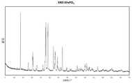
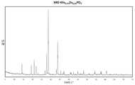
본 발명은 이제 금속 포스페이트 화합물로서 본 발명에 따라 적합한 일반식 Fe3(PO4)2 의 결정 무수 철 (II) 오르토포스페이트 및 일반식 FeaMetb(POc)d 의 결정 무수 철(II) 금속 오르토포스페이트, 철(II) 금속 포스포네이트, 철(II) 금속 피로포스페이트 또는 철 (II) 금속 메타포스페이트에 대한 예시적 구현예뿐 아니라 제조예를 기반으로 추가 설명될 것이다. 첨부된 도면은 제조예에 따라 제조된 금속 포스페이트 화합물의 X-선 회절 다이어그램을 보여준다.The present invention is now suitable as a metal phosphate compound, crystalline anhydrous iron (II) orthophosphate of the general formula Fe3 (PO4 )2 and crystalline anhydrous iron (II) of the general formula Fea Metb (POc )d . Further explanation will be made based on the preparation examples as well as exemplary embodiments for metal orthophosphates, iron (II) metal phosphonates, iron (II) metal pyrophosphates or iron (II) metal metaphosphates. The accompanying drawings show an X-ray diffraction diagram of the metal phosphate compound prepared according to the preparation example.
도 1 은 제조예 1 에 따라 본 발명에 따라 제조된 결정 무수 Fe2P2O7 의 x-선 회절도를 보여준다.
도 2 는 제조예 2 에 따라 본 발명에 따라 제조된 결정 무수 Mg1.5Fe1.5(PO4)2및 Fe3(PO4)2 의 상 혼합물의 x-선 회절도를 보여준다.
도 3 은 제조예 3 에 따라 본 발명에 따라 제조된 결정 무수 Fe3(PO4)2 의 x-선 회절도를 보여준다.
도 4 는 제조예 4 에 따라 본 발명에 따라 제조된 결정 무수 KFe(PO4) 의 x-선 회절도를 보여준다.
도 5 는 제조예 5 에 따라 본 발명에 따라 제조된 결정 무수 KFe0.90Zn0.10(PO4) 의 x-선 회절도를 보여준다.
도 6 은 제조예 6 에 따라 본 발명에 따라 제조된 결정 무수 KFe0.75Zn0.25(PO4) 의 x-선 회절도를 보여준다.
도 7 은 제조예 7 에 따라 본 발명에 따라 제조된 결정 무수 KFe0.75Zn0.25(PO4) 의 x-선 회절도를 보여준다.
도 8 은 제조예 8 에 따라 본 발명에 따라 제조된 결정 무수 BaFeP2O7 의 x-선 회절도를 보여준다.1 shows an x-ray diffraction diagram of crystalline anhydrous Fe2 P2 O7 prepared according to the present invention according to Preparation Example 1. FIG.
2 shows the x-ray diffractogram of a phase mixture of crystalline anhydrous Mg1.5 Fe1.5 (PO4 )2 and Fe3 (PO4 )2 prepared according to the present invention according to Preparation Example 2. FIG.
3 shows an x-ray diffractogram of crystalline anhydrous Fe3 (PO4 )2 prepared according to the present invention according to Preparation Example 3. FIG.
4 shows an x-ray diffractogram of crystalline anhydrous KFe (PO4 ) prepared according to the present invention according to Preparation Example 4. FIG.
5 shows an x-ray diffractogram of crystalline anhydrous KFe0.90 Zn0.10 (PO4 ) prepared according to the present invention according to Preparation Example 5. FIG.
6 shows the x-ray diffractogram of crystalline anhydrous KFe0.75 Zn0.25 (PO4 ) prepared according to the present invention according to Preparation Example 6. FIG.
7 shows the x-ray diffractogram of crystalline anhydrous KFe0.75 Zn0.25 (PO4 ) prepared according to the present invention according to Preparation Example 7. FIG.
8 shows the x-ray diffraction diagram of crystalline anhydrous BaFeP2 O7 prepared according to the present invention according to Preparation Example 8. FIG.
실시예Example
X-선 회절분석 (XRD)X-ray Diffraction (XRD)
하기 실시예에 따라 제조된 제품 중에서, x-선 회절 측정 (XRD) 은 D8 Advance A25-유형 회절계 (Bruker) 및 CuKα 방사를 사용하여 수행된다.Among the articles made according to the examples below, x-ray diffraction measurements (XRD) are performed using D8 Advance A25-type diffractometer (Bruker) and CuKα radiation.
제품 및 이들의 결정 구조는 이전에 JCPDS (Joint Committee on Powder Diffraction Standards) 데이터베이스에서 ICDD (International Centre for Diffraction Data) 로부터의 상응하는 참조 회절도 (Powder Diffraction Files; PDF) 에 기초하여 식별되었다. 제조된 제품에 대해 PDF 카드를 사용할 수 없는 경우, 이소형 화합물용 PDF 카드가 사용되었다 (= 동일한 구조 유형의 화합물).Products and their crystal structures were previously identified based on corresponding Powder Diffraction Files (PDF) from the International Center for Diffraction Data (ICDD) in the Joint Committee on Powder Diffraction Standards (JCPDS) database. If no PDF card was available for the product produced, a PDF card for isoform compounds was used (= compounds of the same structural type).
기초 분석Basic analysis
제조된 제품의 화학량론을 결정하고 확인하기 위해 Axios FAST 분광계 (PANalytical) 를 사용하여 x-선 형광 분석 (XRF) 에 의해 기초 분석을 수행하였다.Basic analysis was performed by x-ray fluorescence analysis (XRF) using an Axios FAST spectrometer (PANalytical) to determine and confirm the stoichiometry of the prepared product.
제조예 1 - 결정 무수 FePreparation Example 1-Crystalline Anhydrous Fe22PP22OO77
하기의 현탁액The following suspension
i) 35.5 kg 철 (III) 옥시드-히드록시드 [FeO(OH) 또는 Fe2O3 1H2O],i) 35.5 kg iron (III) oxide-hydroxy [FeO (OH) or Fe2 O3 1H2 O],
ii) 16.5 kg 98% 포스폰산 [H3PO3],ii) 16.5 kg 98% phosphonic acid [H3 PO3 ],
ii) 26.5 kg 75% 인산 [H3PO4] 및ii) 26.5
용매:220 kg 물menstruum:220 kg water
을 분무 과립화하였다. 이러한 방식으로 수득된 과립을 700℃ 에서 포밍 (forming) 기체 분위기 (5 부피% N2 중의 H2) 에서 4 시간의 평균 체류 시간 동안 회전 가마에서 온도 처리하였다. 거의 무색 내지 약간 분홍색인 생성물이 수득된다. 생성물의 x-선 회절도 (XRD) 를 도 1 에 나타낸다. 생성물은 PDF 카드 01-072-1516 을 사용하여 식별되었다.Was spray granulated. The granules obtained in this way were temperature treated in a rotary kiln at 700 ° C. for a mean residence time of 4 hours in a forming gas atmosphere (H2 in 5% by volume N2 ). A product that is almost colorless to slightly pink is obtained. The x-ray diffractogram (XRD) of the product is shown in FIG. 1. The product was identified using PDF card 01-072-1516.
제조예 2 - 결정 무수 MgPreparation Example 2-Crystalline Anhydrous Mg1.51.5FeFe1.51.5(PO(PO44))22 및 Fe And Fe33(PO(PO44))22 의 상 혼합물 Phase mixture
하기의 현탁액The following suspension
i) 8.45 kg 철 (III) 옥시드-히드록시드 [FeO(OH) 또는 Fe2O3 1H2O],i) 8.45 kg iron (III) oxide-hydroxy [FeO (OH) or Fe2 O3 1H2 O],
ii) 7.95 kg 98% 포스폰산 [H3PO3],ii) 7.95 kg 98% phosphonic acid [H3 PO3 ],
iii) 19.6 kg 철 (III) 포스페이트 2수화물 [FePO4 2H2O],iii) 19.6 kg iron (III) phosphate dihydrate [FePO4 2H2 O],
iv) 8.43 kg 마그네슘 카르보네이트 [MgCO3] 및iv) 8.43 kg magnesium carbonate [MgCO3 ] and
용매:160 kg 물menstruum:160 kg water
을 분무 과립화하였다. 이러한 방식으로 수득된 과립을 750℃ 에서 포밍 기체 분위기 (5 부피% N2 중의 H2) 에서 3 시간의 평균 체류 시간 동안 회전 가마에서 온도 처리하였다. 거의 무색인 생성물이 수득된다. 생성물의 x-선 회절도 (XRD) 를 도 2 에 나타낸다. 생성물은 주된 상 Mg1.5Fe1.5(PO4)2 (PDF 카드 01-071-6793) 및 부수 상 Fe3(PO4)2 (PDF 카드 00-49-1087) 의 상 혼합물로서 PDF 카드를 사용하여 확인되었다.Was spray granulated. The granules obtained in this way were temperature treated in a rotary kiln at 750 ° C. for a mean residence time of 3 hours in a forming gas atmosphere (H2 in 5% by volume N2 ). An almost colorless product is obtained. The x-ray diffractogram (XRD) of the product is shown in FIG. 2. The product was prepared using a PDF card as a phase mixture of the main phase Mg1.5 Fe1.5 (PO4 )2 (PDF card 01-071-6793) and the minor phase Fe3 (PO4 )2 (PDF card 00-49-1087). Confirmed.
제조예 3 - 결정 무수 FePreparation Example 3-Crystalline Anhydrous Fe33(PO(PO44))22
하기의 현탁액The following suspension
i) 21.75 kg 철 (III) 옥시드-히드록시드 [FeO(OH) 또는 Fe2O3 1H2O],i) 21.75 kg iron (III) oxide-hydroxy [FeO (OH) or Fe2 O3 1H2 O],
ii) 12.15 kg 98% 포스폰산 [H3PO3],ii) 12.15 kg 98% phosphonic acid [H3 PO3 ],
iii) 10.3 kg 철 (III) 포스페이트 2수화물 [FePO4 2H2O] 및iii) 10.3 kg iron (III) phosphate dihydrate [FePO4 2H2 O] and
용매:140 kg 물menstruum:140 kg water
을 분무 과립화하였다. 이러한 방식으로 수득된 과립을 750℃ 에서 포밍 기체 분위기 (5 부피% N2 중의 H2) 에서 90 분의 평균 체류 시간 동안 회전 가마에서 온도 처리하였다. 거의 무색인 생성물이 수득된다. 생성물의 x-선 회절도 (XRD) 를 도 3 에 나타낸다. 생성물은 그래프토나이트 구조로 결정화되고 PDF 카드 00-49-1087 을 사용하여 확인되었다. 생성물의 50 중량% 가 3 ㎛ 미만의 입자 크기를 갖도록 생성물을 분쇄하였다. 분쇄 생성물의 입자 크기 분포는 도 9 에 나타난다.Was spray granulated. The granules obtained in this way were temperature treated in a rotary kiln at 750 ° C. for 90 min average residence time in a forming gas atmosphere (H2 in 5% by volume N2 ). An almost colorless product is obtained. The x-ray diffractogram (XRD) of the product is shown in FIG. 3. The product crystallized into graftonite structure and identified using PDF card 00-49-1087. The product was ground so that 50% by weight of the product had a particle size of less than 3 μm. The particle size distribution of the milled product is shown in FIG. 9.
제조예 4 - 결정 무수 KFe(POPreparation Example 4-Crystalline Anhydrous KFe (PO44) 의 제조Manufacture of
하기의 현탁액The following suspension
i) 11.80 kg 철 (III) 옥시드-히드록시드 [FeO(OH) 또는 Fe2O3 1H2O],i) 11.80 kg iron (III) oxide-hydroxy [FeO (OH) or Fe2 O3 1H2 O],
ii) 10.70 kg 98% 포스폰산 [H3PO3],ii) 10.70 kg 98% phosphonic acid [H3 PO3 ],
iii) 24.8 kg 철 (III) 포스페이트 2수화물 [FePO4 2H2O]iii) 24.8 kg iron (III) phosphate dihydrate [FePO4 2H2 O]
IV) 29.8 kg 50% 잿물 (lye) [KOH]IV) 29.8
V) 1.0 kg 75% 인산 [H3PO4] 및V) 1.0
용매:110 kg 물menstruum:110 kg water
을 분무 과립화하였다. 이러한 방식으로 수득된 과립을 650℃ 에서 포밍 기체 분위기 (5 부피% N2 중의 H2) 에서 3 시간의 평균 체류 시간 동안 회전 가마에서 온도 처리하였다. 옅은 연녹색 생성물이 수득된다. 생성물의 x-선 회절도 (XRD) 를 도 4 에 나타낸다. 생성물은 PDF 카드 01-076-4615 을 사용하여 식별되었다.Was spray granulated. The granules obtained in this way were temperature treated in a rotary kiln at 650 ° C. for an average residence time of 3 hours in a forming gas atmosphere (H2 in 5% by volume N2 ). Pale pale green product is obtained. The x-ray diffractogram (XRD) of the product is shown in FIG. 4. The product was identified using PDF card 01-076-4615.
제조예 5 - 결정 무수 KFePreparation Example 5-Crystalline Anhydrous KFe0.900.90ZnZn0.100.10(PO(PO44))
하기의 현탁액The following suspension
i) 10.60 kg 철 (III) 옥시드-히드록시드 [FeO(OH) 또는 Fe2O3 1H2O],i) 10.60 kg iron (III) oxide-hydroxy [FeO (OH) or Fe2 O3 1H2 O],
ii) 9.65 kg 98% 포스폰산 [H3PO3],ii) 9.65 kg 98% phosphonic acid [H3 PO3 ],
iii) 22.30 kg 철 (III) 포스페이트 2수화물 [FePO4 2H2O]iii) 22.30 kg iron (III) phosphate dihydrate [FePO4 2H2 O]
IV) 2.15 kg 아연 옥시드 [ZnO]IV) 2.15 kg Zinc Oxide [ZnO]
IV) 29.8 kg 50% 잿물 [KOH]IV) 29.8
V) 4.15 kg 75% 인산 [H3PO4] 및V) 4.15
용매:120 kg 물menstruum:120 kg water
을 분무 과립화하였다. 이러한 방식으로 수득된 과립을 600℃ 에서 포밍 기체 분위기 (5 부피% N2 중의 H2) 에서 2 시간의 평균 체류 시간 동안 회전 가마에서 온도 처리하였다. 밝은 회색인 생성물이 수득된다. 생성물의 x-선 회절도 (XRD) 를 도 5 에 나타낸다. 이 제품은 새로운 구조 유형으로 PDF 카드 01-076-4615 에 따른 KFe(PO4) 구조에 가까이 연결되는 것으로 보인다.Was spray granulated. The granules obtained in this way were temperature treated in a rotary kiln at 600 ° C. for a mean residence time of 2 hours in a forming gas atmosphere (H2 in 5% by volume N2 ). A light gray product is obtained. The x-ray diffractogram (XRD) of the product is shown in FIG. 5. It is a new structure type which appears to be closely connected to the KFe (PO4 ) structure according to the PDF card 01-076-4615.
제조예 6 - 결정 무수 KFePreparation Example 6-Crystalline Anhydrous KFe0.750.75ZnZn0.250.25(PO(PO44))
하기의 현탁액The following suspension
i) 8.85 kg 철 (III) 옥시드-히드록시드 [FeO(OH) 또는 Fe2O3 1H2O],i) 8.85 kg iron (III) oxide-hydroxy [FeO (OH) or Fe2 O3 1H2 O],
ii) 8.05 kg 98% 포스폰산 [H3PO3],ii) 8.05 kg 98% phosphonic acid [H3 PO3 ],
iii) 18.60 kg 철 (III) 포스페이트 2수화물 [FePO4 2H2O]iii) 18.60 kg iron (III) phosphate dihydrate [FePO4 2H2 O]
IV) 5.40 kg 아연 옥시드 [ZnO]IV) 5.40 kg Zinc Oxide [ZnO]
IV) 29.8 kg 50% 포타쉬 (potash) 잿물 [KOH]IV) 29.8
V) 9.30 kg 75% 인산 [H3PO4] 및V) 9.30
용매:120 kg 물menstruum:120 kg water
을 분무 과립화하였다. 이러한 방식으로 수득된 과립을 600℃ 에서 포밍 기체 분위기 (5 부피% N2 중의 H2) 에서 2 시간의 평균 체류 시간 동안 회전 가마에서 온도 처리하였다. 밝은 회색인 생성물이 수득된다. 생성물의 x-선 회절도 (XRD) 를 도 6 에 나타낸다. 생성물은 문헌에 알려져 있지 않다. 이것은 이소형 방식으로 결정화되어 PDF 카드 01-081-1034 에 따라 KZn(PO4) 를 형성한다.Was spray granulated. The granules obtained in this way were temperature treated in a rotary kiln at 600 ° C. for a mean residence time of 2 hours in a forming gas atmosphere (H2 in 5% by volume N2 ). A light gray product is obtained. The x-ray diffractogram (XRD) of the product is shown in FIG. 6. The product is not known in the literature. It is crystallized in an isotropic manner to form KZn (PO4 ) according to PDF card 01-081-1034.
제조예 7 - 결정 무수 KFePreparation Example 7-Crystalline Anhydrous KFe0.750.75MnMn0.250.25(PO(PO44))
하기의 현탁액The following suspension
i) 8.85 kg 철 (III) 옥시드-히드록시드 [FeO(OH) 또는 Fe2O3 1H2O],i) 8.85 kg iron (III) oxide-hydroxy [FeO (OH) or Fe2 O3 1H2 O],
ii) 8.05 kg 98% 포스폰산 [H3PO3],ii) 8.05 kg 98% phosphonic acid [H3 PO3 ],
iii) 18.60 kg 철 (III) 포스페이트 2수화물 [FePO4 2H2O]iii) 18.60 kg iron (III) phosphate dihydrate [FePO4 2H2 O]
IV) 8.85 kg 망간 카르보네이트 수화물 [MnCO3 H2O]IV) 8.85 kg manganese carbonate hydrate [MnCO3 H2 O]
IV) 29.8 kg 50% 잿물 [KOH]IV) 29.8
V) 9.30 kg 75% 인산 [H3PO4] 및V) 9.30
용매:140 kg 물menstruum:140 kg water
을 분무 과립화하였다. 이러한 방식으로 수득된 과립을 600℃ 에서 포밍 기체 분위기 (5 부피% N2 중의 H2) 에서 2 시간의 평균 체류 시간 동안 회전 가마에서 온도 처리하였다. 밝은 회색인 생성물이 수득된다. 생성물의 x-선 회절도 (XRD) 를 도 7 에 나타낸다. 생성물은 문헌에 알려져 있지 않다. 이것은 PDF 카드 01-076-4615 에 따라 KZn(PO4) 로 이소형 방식으로 결정화된다.Was spray granulated. The granules obtained in this way were temperature treated in a rotary kiln at 600 ° C. for a mean residence time of 2 hours in a forming gas atmosphere (H2 in 5% by volume N2 ). A light gray product is obtained. The x-ray diffractogram (XRD) of the product is shown in FIG. 7. The product is not known in the literature. It is crystallized in an isoform fashion with KZn (PO4 ) according to PDF card 01-076-4615.
제조예 8 - 결정 무수 BaFePPreparation Example 8-Crystalline Anhydrous BaFeP22OO77
하기의 현탁액The following suspension
i) 8.70 kg 철 (III) 옥시드-히드록시드 [FeO(OH) 또는 Fe2O3 1H2O],i) 8.70 kg iron (III) oxide-hydroxy [FeO (OH) or Fe2 O3 1H2 O],
ii) 8.20 kg 98% 포스폰산 [H3PO3],ii) 8.20 kg 98% phosphonic acid [H3 PO3 ],
iii) 19.05 kg 철 (III) 포스페이트 2수화물 [FePO4 2H2O]iii) 19.05 kg iron (III) phosphate dihydrate [FePO4 2H2 O]
IV) 63.09 kg 바륨 히드록시드 8수화물 [Ba(OH)2 8H2O]IV) 63.09 kg barium hydroxide octahydrate [Ba (OH)2 8H2 O]
V) 26.15 kg 75% 인산 [H3PO4] 및V) 26.15
용매:250 kg 물menstruum:250 kg water
을 분무 과립화하였다. 이러한 방식으로 수득된 과립을 800℃ 에서 포밍 기체 분위기 (5 부피% N2 중의 H2) 에서 4 시간의 평균 체류 시간 동안 회전 가마에서 온도 처리하였다. 밝은 회색인 생성물이 수득된다. 생성물의 x-선 회절도 (XRD) 를 도 8 에 나타낸다. 이것은 이소형 방식으로 결정화되어 PDF 카드 01-084-1833 에 따라 BaCoP2O7 를 형성한다.Was spray granulated. The granules obtained in this way were temperature treated in a rotary kiln at 800 ° C. for a mean residence time of 4 hours in a forming gas atmosphere (H2 in 5% by volume N2 ). A light gray product is obtained. The x-ray diffractogram (XRD) of the product is shown in FIG. 8. It is crystallized in an isotropic manner to form BaCoP2 O7 according to PDF card 01-084-1833.
하기 실시예는 본 발명에 따른 방법을 설명한다.The following examples illustrate the method according to the invention.
실시예 1Example 1
1 kg 의 구리 히드록시드 포스페이트를 물이 있는 반응기에 100 g 티타늄 디옥시드와 두고 1 시간 동안 교반하였다. 수득된 제제를 여과하고 최대 0.5 중량% 의 물 함량까지 대략 120℃ 에서 건조하였다. 수득된 분말을 1 중량% 디소듐 디히드로겐 포스페이트, Na2H2P2O7 과 건조 혼합하였다. 5 중량% 의 혼합물을 압출기 (Coperion GmbH 사제 ZSK18-유형) 를 사용하여 Sabic 사제 PC/ABS 공중합체 (LNP™COLORCOMP™ Compound NX05467) 로 가공하였다. 이후, 플라스틱을 사출 성형기의 도움으로 대략 2 ㎜ 두께 플레이트를 형성하도록 가공하였다. 플레이트를 1064 ㎚ 의 파장의 Nd:YAG 레이저 (Trumpf) 로 조사하였고, 구조가 생성되었다. 균일한 금속 분리 (금속 핵) 가 발생하였고, 이는 전도성 경로 또는 전도성 경로의 전구체로서 적합하였다.1 kg of copper hydroxide phosphate was placed in a reactor with water and 100 g titanium dioxide and stirred for 1 hour. The resulting formulation was filtered and dried at approximately 120 ° C. up to a water content of up to 0.5% by weight. The powder obtained was dry mixed with 1 wt% disodium dihydrogen phosphate, Na2 H2 P2 O7 . 5% by weight of the mixture was processed with a Sabic PC / ABS copolymer (LNP ™ COLORCOMP ™ Compound NX05467) using an extruder (ZSK18-type from Cooperion GmbH). The plastic was then processed to form an approximately 2 mm thick plate with the aid of an injection molding machine. The plate was irradiated with a Nd: YAG laser (Trumpf) at a wavelength of 1064 nm and a structure was produced. Uniform metal separation (metal nucleus) occurred, which was suitable as a conductive pathway or precursor of a conductive pathway.
실시예 2Example 2
식 Fe2Mg(PO4)2 의 철(II) 마그네슘 포스페이트를 1 중량% 디소듐 디히드로겐 포스페이트, Na2H2P2O7 과 건조 혼합하였다. 5 중량% 의 혼합물을 압출기 (Coperion GmbH 사제 ZSK18-유형) 를 사용하여 폴리아미드 6.6 (BASF 사제 Ultramid™) 으로 가공하고, 과립을 제조하였다. 이후, 과립을 3 ㎝ × 4 ㎝ × 3 ㎜ 의 플레이트를 형성하도록 추가 가공하였다. 플레이트를 1064 ㎚ 의 파장의 Nd:YAG 레이저 (Trumpf) 로 조사하였고, 전기 전도성 구조가 생성되었다.Iron (II) magnesium phosphate of the formula Fe2 Mg (PO4 )2 was dry mixed with 1% by weight disodium dihydrogen phosphate, Na2 H2 P2 O7 . 5% by weight of the mixture was processed with polyamide 6.6 (Ultramid ™ from BASF) using an extruder (ZSK18-type from Cooperion GmbH) to prepare granules. The granules were then further processed to form plates of 3 cm × 4 cm × 3 mm. The plate was irradiated with a Nd: YAG laser (Trumpf) at a wavelength of 1064 nm and an electrically conductive structure was produced.
실시예 3 (비교)Example 3 (comparative)
3 중량% 의 구리 히드록시드 포스페이트를 압출기 (Coperion GmbH 사제 ZSK18-유형) 를 사용하여 폴리아미드 6.6 (BASF 사제 Ultramid™) 으로 가공하였다. 압출을 285℃ 에서 권장된 온도 범위의 최상단에서 수행하였다. 이러한 경우, 플라스틱의 목적하지 않은 변색이 존재하였다. 초기의 약간 녹색빛의 화합물의 색은 갈색으로 변하였다. 또한, 압출기의 샤프트 상에서의 금속성 구리의 약간의, 목적되지 않은 분리가 발견되었다.3% by weight of copper hydroxide phosphate was processed with polyamide 6.6 (Ultramid ™ from BASF) using an extruder (ZSK18-type from Cooperative GmbH). Extrusion was carried out at 285 ° C. at the top of the recommended temperature range. In this case, there was an undesired discoloration of the plastic. The color of the initial slightly greenish compound turned brown. In addition, some undesired separation of metallic copper on the shaft of the extruder was found.
실시예 4Example 4
4 중량% 구리 히드록시드 포스페이트 및 2 중량% 소듐 알루미늄 술페이트 (SAS) 를 압출기 (Coperion GmbH 사제 ZSK18-유형) 를 사용하여 폴리아미드 6.6 (BASF 사제 Ultramid™) 으로 가공하고, 과립을 제조하였다. 압출을 285℃ 에서 권장된 온도 범위의 최상단에서 수행하였다. 이후, 과립을 3 ㎝ × 4 ㎝ × 3 ㎜ 의 플레이트를 형성하도록 추가 가공하였다. 플라스틱에서 목적하지 않은 변색은 없었고, 압출기의 샤프트 상에서의 금속성 구리의 침착도 없었다. 플레이트를 1064 ㎚ 의 파장의 Nd:YAG 레이저 (Trumpf) 로 조사하였고, 구조가 생성되었다. 전도성 구조의 균질한 형성이 발생하였고, 이는 전도성 경로 또는 전도성 경로의 전구체로서 적합하였다.4 wt% copper hydroxide phosphate and 2 wt% sodium aluminum sulphate (SAS) were processed with polyamide 6.6 (Ultramid ™ from BASF) using an extruder (ZSK18-type from Cooperative GmbH) and granules were prepared. Extrusion was carried out at 285 ° C. at the top of the recommended temperature range. The granules were then further processed to form plates of 3 cm × 4 cm × 3 mm. There was no undesired discoloration in the plastic and no deposition of metallic copper on the shaft of the extruder. The plate was irradiated with an Nd: YAG laser (Trumpf) at a wavelength of 1064 nm and a structure was produced. Homogeneous formation of the conductive structure occurred, which was suitable as the conductive pathway or precursor of the conductive pathway.
실시예 5Example 5
40 중량% 철(II) 오르토포스페이트 Fe3(PO4)2 및 1 중량% 소듐 알루미늄 술페이트 (SAS) 를 압출기 (Coperion GmbH 사제 ZSK18-유형) 를 사용하여 LDPE (LyondellBasell 사제 Lupolen™ 1800 S) 로 가공하고, 과립을 제조하였다. 이후, 과립을 3 ㎝ × 4 ㎝ × 3 ㎜ 의 플레이트를 형성하도록 추가 가공하였다. 플라스틱에서 약간의 녹색 착색이 있었지만, 압출기의 샤프트 상에서의 침착은 없었다. 플레이트를 1064 ㎚ 의 파장의 Nd:YAG 레이저 (Trumpf) 로 조사하였고, 구조가 생성되었다. 전도성 구조의 균질한 형성이 발생하였고, 이는 전도성 경로 또는 전도성 경로의 전구체로서 적합하였다.40 wt.% Iron (II) orthophosphate Fe3 (PO4 )2 and 1 wt. Processed and granules were prepared. The granules were then further processed to form plates of 3 cm × 4 cm × 3 mm. There was some green coloration in the plastic, but no deposition on the shaft of the extruder. The plate was irradiated with a Nd: YAG laser (Trumpf) at a wavelength of 1064 nm and a structure was produced. Homogeneous formation of the conductive structure occurred, which was suitable as the conductive pathway or precursor of the conductive pathway.
Claims (14)
Translated fromKorean-비-전도성 캐리어 물질이 제공되고, 이는 이에 미세하게 분포되거나 용해된 적어도 하나의 무기 금속 포스페이트 화합물 및 적어도 하나의 안정화제를 함유함,
-캐리어 물질이 영역에서 레이저 빔을 이용하여 조사되어, 조사 영역에서 전기 전도성 구조를 생성함,
여기서, 적어도 하나의 무기 금속 포스페이트 화합물이 하기로 이루어지는 군으로부터 선택되고:
-일반식 Cu2(OH)PO4 의 구리 히드록시드 포스페이트,
-일반식 Fe3(PO4)2 의 결정 무수 철(II) 오르토포스페이트 또는
-일반식 FeaMetb(POc)d 의 결정 무수 철(II) 금속 오르토포스페이트, 철(II) 금속 포스포네이트, 철(II) 금속 피로포스페이트 또는 철(II) 금속 메타포스페이트 (식 중, a 는 1 내지 5 의 수이고, b 는 >0 내지 5 의 수이고, c 는 2.5 내지 5 의 수이고, d 는 0.5 내지 3 의 수이고, Met 은 Li, Na, K, Rb, Cs, Mg, Ca, Sr, Ba, 전이 금속 (d 블록), 특히 Sc, Y, La, Ti, Zr, Hf, Nb, Ta, Cr, Mo, W, Mn, Cu, Zn, Co, Ni, Ag, Au, 제 3, 제 4 및 제 5 주족의 금속 및 반금속, 특히 B, Al, Ga, In, Si, Sn, Sb, Bi 및 란타노이드로 이루어지는 군으로부터 선택된 하나 이상의 금속을 나타냄) 또는 상기 언급된 포스페이트의 조합,
적어도 하나의 안정화제가 브뢴스테드 산 및 루이스 산으로 이루어지는 군의 화합물로부터 선택되고, 여기서 브뢴스테드 산이 양성자-전이 화합물로서 정의되고, 루이스 산이 비-양성자-전이 전자-결핍 화합물로 정의되는, 제조 방법.A method of making an electrically conductive structure, preferably a conductive path structure, using a laser beam on a non-conductive carrier material (LDS method) characterized in that:
A non-conductive carrier material is provided, which contains at least one inorganic metal phosphate compound and at least one stabilizer finely distributed or dissolved therein,
The carrier material is irradiated with a laser beam in the region, producing an electrically conductive structure in the irradiation region,
Wherein at least one inorganic metal phosphate compound is selected from the group consisting of:
Copper hydroxide phosphate of the general formula Cu2 (OH) PO4 ,
Crystalline anhydrous iron (II) orthophosphate of the general formula Fe3 (PO4 )2 or
-Crystals of the general formula Fea Metb (POc )d anhydrous iron (II) metal orthophosphate, iron (II) metal phosphonate, iron (II) metal pyrophosphate or iron (II) metal metaphosphate, wherein , a is a number from 1 to 5, b is a number from> 0 to 5, c is a number from 2.5 to 5, d is a number from 0.5 to 3, Met is Li, Na, K, Rb, Cs, Mg, Ca, Sr, Ba, transition metals (d blocks), in particular Sc, Y, La, Ti, Zr, Hf, Nb, Ta, Cr, Mo, W, Mn, Cu, Zn, Co, Ni, Ag, Or at least one metal selected from the group consisting of Au, third, fourth and fifth main group metals and semimetals, in particular B, Al, Ga, In, Si, Sn, Sb, Bi and lanthanoids) Combination of phosphate,
At least one stabilizer is selected from compounds of the group consisting of Bronsted acid and Lewis acid, wherein Brönsted acid is defined as a proton-transition compound and Lewis acid is defined as a non-proton-transition electron-deficient compound Way.
Applications Claiming Priority (3)
| Application Number | Priority Date | Filing Date | Title |
|---|---|---|---|
| DE102017106913.5ADE102017106913A1 (en) | 2017-03-30 | 2017-03-30 | Process for the production of electrically conductive structures on a carrier material |
| DE102017106913.5 | 2017-03-30 | ||
| PCT/EP2018/057662WO2018178022A1 (en) | 2017-03-30 | 2018-03-26 | Method for producing electrically conductive structures on a carrier material |
Publications (2)
| Publication Number | Publication Date |
|---|---|
| KR20190133683Atrue KR20190133683A (en) | 2019-12-03 |
| KR102665005B1 KR102665005B1 (en) | 2024-05-10 |
Family
ID=61827734
Family Applications (1)
| Application Number | Title | Priority Date | Filing Date |
|---|---|---|---|
| KR1020197028590AActiveKR102665005B1 (en) | 2017-03-30 | 2018-03-26 | Method for fabricating electrically conductive structures on carrier materials |
Country Status (10)
| Country | Link |
|---|---|
| US (1) | US11718727B2 (en) |
| EP (1) | EP3601642A1 (en) |
| JP (2) | JP7213823B2 (en) |
| KR (1) | KR102665005B1 (en) |
| CN (1) | CN110475911A (en) |
| DE (1) | DE102017106913A1 (en) |
| EA (1) | EA201991999A1 (en) |
| MX (1) | MX2019011516A (en) |
| TW (1) | TWI757450B (en) |
| WO (1) | WO2018178022A1 (en) |
Families Citing this family (12)
| Publication number | Priority date | Publication date | Assignee | Title |
|---|---|---|---|---|
| DE102017106912A1 (en)* | 2017-03-30 | 2018-10-04 | Chemische Fabrik Budenheim Kg | Process for the preparation of Fe (II) P / Fe (II) MetP compounds |
| DE102017106913A1 (en) | 2017-03-30 | 2018-10-04 | Chemische Fabrik Budenheim Kg | Process for the production of electrically conductive structures on a carrier material |
| DE102017106911A1 (en) | 2017-03-30 | 2018-10-04 | Chemische Fabrik Budenheim Kg | Use of water-free Fe (II) compounds as radiation absorbers |
| DE102018124344A1 (en)* | 2018-10-02 | 2020-04-02 | Chemische Fabrik Budenheim Kg | Conductive textiles |
| CN110137183A (en) | 2019-04-23 | 2019-08-16 | 深圳市华星光电技术有限公司 | Array substrate and manufacturing method thereof |
| CN110029382B (en)* | 2019-05-22 | 2021-09-24 | 电子科技大学 | A surface treatment process for direct electroplating and related direct electroplating process |
| TWI706593B (en)* | 2019-10-02 | 2020-10-01 | 川升股份有限公司 | Antenna device |
| CN112636011A (en)* | 2019-10-08 | 2021-04-09 | 川升股份有限公司 | Radio frequency assembly combination and antenna device |
| DE102020111158A1 (en)* | 2020-04-23 | 2021-10-28 | Chemische Fabrik Budenheim Kg | Use of an additive in the production of copper (II) hydroxide phosphate |
| CN111805091A (en)* | 2020-06-09 | 2020-10-23 | 深圳市信维通信股份有限公司 | LAP laser etching process |
| CN113105054A (en)* | 2021-04-09 | 2021-07-13 | 瀚蓝工业服务(嘉兴)有限公司 | Method for comprehensively recycling phosphorus-containing waste acid and iron-containing etching waste liquid |
| CN114479410B (en)* | 2022-02-16 | 2023-08-04 | 无锡赢同新材料科技有限公司 | Low dielectric loss LDS engineering plastic and preparation method thereof |
Citations (2)
| Publication number | Priority date | Publication date | Assignee | Title |
|---|---|---|---|---|
| WO2016034001A1 (en)* | 2014-09-04 | 2016-03-10 | Byd Company Limited | Polymer product, method for selectively metallizing polymer substrate |
| JP2017508009A (en)* | 2014-12-01 | 2017-03-23 | エルジー・ケム・リミテッド | Polycarbonate resin composition and method for producing the same |
Family Cites Families (42)
| Publication number | Priority date | Publication date | Assignee | Title |
|---|---|---|---|---|
| DE3917294A1 (en) | 1989-05-27 | 1990-11-29 | Huels Chemische Werke Ag | HIGH POLYMERS MATERIALS LABELABLE WITH LASER LIGHT |
| US5063011A (en) | 1989-06-12 | 1991-11-05 | Hoeganaes Corporation | Doubly-coated iron particles |
| US5489639A (en) | 1994-08-18 | 1996-02-06 | General Electric Company | Copper salts for laser marking of thermoplastic compositions |
| US5939039A (en) | 1997-01-16 | 1999-08-17 | Orthovita, Inc. | Methods for production of calcium phosphate |
| DE19723734C2 (en) | 1997-06-06 | 2002-02-07 | Gerhard Naundorf | Conductor structures on a non-conductive carrier material and method for their production |
| US6383519B1 (en) | 1999-01-26 | 2002-05-07 | Vita Special Purpose Corporation | Inorganic shaped bodies and methods for their production and use |
| DE50008242D1 (en) | 2000-09-26 | 2004-11-18 | Enthone Omi Deutschland Gmbh | Process for the selective metallization of dielectric materials |
| DE10053639B4 (en) | 2000-10-28 | 2007-04-12 | Chemische Fabrik Budenheim Kg | Use of iron, cobalt, nickel or molybdenum salts |
| DE10132092A1 (en) | 2001-07-05 | 2003-01-23 | Lpkf Laser & Electronics Ag | Track structures and processes for their manufacture |
| DE10356334B4 (en)* | 2003-11-28 | 2016-02-11 | Sachtleben Chemie Gmbh | Use of thermoplastic, polymeric materials with high IR absorption |
| SI1790701T2 (en) | 2005-11-25 | 2012-05-31 | Sicpa Holding Sa | IR-absorbing intaglio ink |
| DE102006038043A1 (en)* | 2006-08-14 | 2008-02-21 | Chemische Fabrik Budenheim Kg | Laser inscribable polymer material |
| DE102007012725A1 (en) | 2007-03-16 | 2008-09-18 | Basf Se | Polynary metal oxide phosphate |
| DE102007012724A1 (en) | 2007-03-16 | 2008-09-18 | Basf Se | Polynary metal oxide phosphate |
| DE102007012723A1 (en) | 2007-03-16 | 2008-09-18 | Basf Se | Polynary vanadyl pyrophosphate |
| US8168329B2 (en) | 2007-06-18 | 2012-05-01 | Advanced Lithium Electrochemistry Co., Ltd. | Electrochemical composition and associated technology |
| US8309640B2 (en)* | 2008-05-23 | 2012-11-13 | Sabic Innovative Plastics Ip B.V. | High dielectric constant laser direct structuring materials |
| TWI474970B (en) | 2008-12-29 | 2015-03-01 | Basf Se | Synthesis of lithium-metal-phosphates under hydrothermal conditions |
| DE102009001335A1 (en) | 2009-03-04 | 2010-09-09 | Chemische Fabrik Budenheim Kg | Radiation absorbing material |
| EP2408865B2 (en)* | 2009-03-18 | 2017-10-11 | Merck Patent GmbH | Pigment for laser marking |
| CN101659406B (en) | 2009-09-25 | 2011-05-11 | 四川大学 | Method for preparing iron phosphate from ferrophosphorus |
| EP2516550B1 (en)* | 2009-12-21 | 2014-07-02 | Mitsubishi Chemical Europe GmbH | Aromatic Polycarbonate Composition |
| US9139429B2 (en) | 2010-03-02 | 2015-09-22 | Guiqing Huang | High performance cathode material LiFePO4, its precursors and methods of making thereof |
| DE102010003366A1 (en)* | 2010-03-26 | 2011-09-29 | Chemische Fabrik Budenheim Kg | Laser-induced plastic foams |
| EP2632689B2 (en)* | 2010-10-26 | 2022-03-23 | Basell Poliolefine Italia S.r.l. | Process for producing injection stretch blow molded polyolefin containers |
| CN103154135B (en)* | 2011-03-18 | 2014-10-15 | 三菱化学欧洲合资公司 | Process for producing circuit carrier |
| DE102011056815A1 (en) | 2011-12-21 | 2013-08-01 | Chemische Fabrik Budenheim Kg | Nutrient composition for biological systems |
| DE102013100583A1 (en) | 2013-01-21 | 2014-07-24 | Chemische Fabrik Budenheim Kg | Susceptor systems for packaging materials |
| US9944768B2 (en) | 2013-04-01 | 2018-04-17 | Sabic Global Technologies B.V. | High modulus laser direct structuring polycarbonate composites with enhanced plating performance and broad laser window and methods for the manufacture and use thereof |
| CN105492214A (en)* | 2013-06-21 | 2016-04-13 | 沙特基础全球技术有限公司 | Flame retardant laser direct structuring materials |
| DE102013112387B3 (en) | 2013-11-11 | 2014-12-24 | Chemische Fabrik Budenheim Kg | Doped copper II hydroxide phosphate, process for its preparation and use |
| WO2015079385A1 (en)* | 2013-11-27 | 2015-06-04 | Sabic Global Technologies B.V. | High modulus laser direct structuring polycarbonate composites with enhanced plating performance and broad laser window by reflection additives |
| EP2886605B2 (en) | 2013-12-20 | 2021-09-01 | Ems-Chemie Ag | Plastic moulding material and use of same |
| US9676927B2 (en)* | 2014-04-09 | 2017-06-13 | The Shepherd Color Company | Core-shell composite inorganic metal oxides and method of preparing for prevention of thermal oxidative degradation in polymer and resin compositions |
| KR101722744B1 (en) | 2014-10-23 | 2017-04-03 | 주식회사 엘지화학 | Composition for forming conductive pattern by irradiation of electromagnetic wave |
| CN104387738B (en)* | 2014-11-19 | 2016-08-17 | 东莞市三条化成实业有限公司 | A kind of preparation method of the laser powder of white laser straight forming material |
| WO2016092472A1 (en)* | 2014-12-12 | 2016-06-16 | Sabic Global Technologies B.V. | Laser-direct structuring of polymeric films and sheets and methods of making |
| WO2016189023A1 (en)* | 2015-05-28 | 2016-12-01 | Dsm Ip Assets B.V. | A thermoplastic polymer composition, an article made thereof and a process for preparing the same |
| JP6749174B2 (en) | 2015-09-03 | 2020-09-02 | 三菱エンジニアリングプラスチックス株式会社 | Polyester resin composition for laser direct structuring |
| DE102017106912A1 (en) | 2017-03-30 | 2018-10-04 | Chemische Fabrik Budenheim Kg | Process for the preparation of Fe (II) P / Fe (II) MetP compounds |
| DE102017106911A1 (en)* | 2017-03-30 | 2018-10-04 | Chemische Fabrik Budenheim Kg | Use of water-free Fe (II) compounds as radiation absorbers |
| DE102017106913A1 (en) | 2017-03-30 | 2018-10-04 | Chemische Fabrik Budenheim Kg | Process for the production of electrically conductive structures on a carrier material |
- 2017
- 2017-03-30DEDE102017106913.5Apatent/DE102017106913A1/ennot_activeWithdrawn
- 2018
- 2018-03-19TWTW107109229Apatent/TWI757450B/enactive
- 2018-03-26EAEA201991999Apatent/EA201991999A1/enunknown
- 2018-03-26USUS16/496,591patent/US11718727B2/enactiveActive
- 2018-03-26EPEP18714226.0Apatent/EP3601642A1/enactivePending
- 2018-03-26WOPCT/EP2018/057662patent/WO2018178022A1/ennot_activeCeased
- 2018-03-26MXMX2019011516Apatent/MX2019011516A/enunknown
- 2018-03-26JPJP2019553862Apatent/JP7213823B2/enactiveActive
- 2018-03-26KRKR1020197028590Apatent/KR102665005B1/enactiveActive
- 2018-03-26CNCN201880023260.7Apatent/CN110475911A/enactivePending
- 2022
- 2022-10-28JPJP2022173332Apatent/JP7376667B2/enactiveActive
Patent Citations (2)
| Publication number | Priority date | Publication date | Assignee | Title |
|---|---|---|---|---|
| WO2016034001A1 (en)* | 2014-09-04 | 2016-03-10 | Byd Company Limited | Polymer product, method for selectively metallizing polymer substrate |
| JP2017508009A (en)* | 2014-12-01 | 2017-03-23 | エルジー・ケム・リミテッド | Polycarbonate resin composition and method for producing the same |
Also Published As
| Publication number | Publication date |
|---|---|
| EA201991999A1 (en) | 2020-02-28 |
| US20200032028A1 (en) | 2020-01-30 |
| MX2019011516A (en) | 2020-02-05 |
| JP7376667B2 (en) | 2023-11-08 |
| TWI757450B (en) | 2022-03-11 |
| EP3601642A1 (en) | 2020-02-05 |
| US11718727B2 (en) | 2023-08-08 |
| JP2020515717A (en) | 2020-05-28 |
| TW201843029A (en) | 2018-12-16 |
| JP7213823B2 (en) | 2023-01-27 |
| WO2018178022A1 (en) | 2018-10-04 |
| KR102665005B1 (en) | 2024-05-10 |
| CN110475911A (en) | 2019-11-19 |
| JP2022187017A (en) | 2022-12-15 |
| DE102017106913A1 (en) | 2018-10-04 |
Similar Documents
| Publication | Publication Date | Title |
|---|---|---|
| JP7376667B2 (en) | Method of manufacturing conductive structures on carrier materials | |
| EP2958112B1 (en) | Composition for forming conductive pattern, method for forming conductive pattern using same, and resin structure having conductive pattern | |
| KR101717753B1 (en) | Composition and method for forming conductive pattern, and resin structure having conductive pattern thereon | |
| KR20150060555A (en) | Composition for forming conductive pattern and resin structure having conductive pattern thereon | |
| KR20150095834A (en) | Method for producing an electrically conductive structure on a non-conductive substrate material, and additive and substrate material intended therefor | |
| HK40015102A (en) | Method for producing electrically conductive structures on a carrier material | |
| JP2017531287A (en) | Conductive pattern forming composition and resin structure having conductive pattern | |
| JP6224842B2 (en) | Conductive pattern forming composition and resin structure having conductive pattern | |
| KR20040058182A (en) | Method for producing polyphosphates of organic bases | |
| US20210388532A1 (en) | Conductive textiles | |
| KR101983271B1 (en) | Composition for forming conductive pattern and resin structure having conductive pattern thereon | |
| EP3154064A1 (en) | Composition for forming conductive pattern, method for forming conductive pattern using same, and resin structure having conductive pattern | |
| EP3154066B1 (en) | Composition for forming conductive pattern and resin structure having conductive pattern | |
| US20230026070A1 (en) | Method for producing an electrically conductive structure | |
| WO2016043540A1 (en) | Composition for forming conductive patterns and resin structure having conductive pattern |
Legal Events
| Date | Code | Title | Description |
|---|---|---|---|
| PA0105 | International application | Patent event date:20190927 Patent event code:PA01051R01D Comment text:International Patent Application | |
| PG1501 | Laying open of application | ||
| PA0201 | Request for examination | Patent event code:PA02012R01D Patent event date:20210312 Comment text:Request for Examination of Application | |
| E902 | Notification of reason for refusal | ||
| PE0902 | Notice of grounds for rejection | Comment text:Notification of reason for refusal Patent event date:20230421 Patent event code:PE09021S01D | |
| E701 | Decision to grant or registration of patent right | ||
| PE0701 | Decision of registration | Patent event code:PE07011S01D Comment text:Decision to Grant Registration Patent event date:20231027 | |
| E701 | Decision to grant or registration of patent right | ||
| PE0701 | Decision of registration | Patent event code:PE07011S01D Comment text:Decision to Grant Registration Patent event date:20240222 | |
| GRNT | Written decision to grant | ||
| PR0701 | Registration of establishment | Comment text:Registration of Establishment Patent event date:20240507 Patent event code:PR07011E01D | |
| PR1002 | Payment of registration fee | Payment date:20240507 End annual number:3 Start annual number:1 | |
| PG1601 | Publication of registration |