KR20190132603A - Thin film transistor substrate, method of manufacturing the same, and display device including the same - Google Patents
Thin film transistor substrate, method of manufacturing the same, and display device including the sameDownload PDFInfo
- Publication number
- KR20190132603A KR20190132603AKR1020180057447AKR20180057447AKR20190132603AKR 20190132603 AKR20190132603 AKR 20190132603AKR 1020180057447 AKR1020180057447 AKR 1020180057447AKR 20180057447 AKR20180057447 AKR 20180057447AKR 20190132603 AKR20190132603 AKR 20190132603A
- Authority
- KR
- South Korea
- Prior art keywords
- electrode
- drain
- insulating layer
- source
- active pattern
- Prior art date
- Legal status (The legal status is an assumption and is not a legal conclusion. Google has not performed a legal analysis and makes no representation as to the accuracy of the status listed.)
- Granted
Links
- 239000010409thin filmSubstances0.000titleclaimsabstractdescription115
- 239000000758substrateSubstances0.000titleclaimsabstractdescription105
- 238000004519manufacturing processMethods0.000titledescription20
- 239000010410layerSubstances0.000claimsabstractdescription443
- 239000011229interlayerSubstances0.000claimsabstractdescription118
- 239000004065semiconductorSubstances0.000claimsdescription39
- 238000000034methodMethods0.000claimsdescription37
- 239000012044organic layerSubstances0.000claimsdescription31
- 238000005452bendingMethods0.000claimsdescription30
- 238000005530etchingMethods0.000claimsdescription14
- 239000003990capacitorSubstances0.000claimsdescription12
- 229910021420polycrystalline siliconInorganic materials0.000claimsdescription10
- 230000000149penetrating effectEffects0.000claimsdescription9
- 238000009413insulationMethods0.000abstractdescription17
- 229910052751metalInorganic materials0.000description16
- 239000002184metalSubstances0.000description16
- VYPSYNLAJGMNEJ-UHFFFAOYSA-Nsilicon dioxideInorganic materialsO=[Si]=OVYPSYNLAJGMNEJ-UHFFFAOYSA-N0.000description15
- XUIMIQQOPSSXEZ-UHFFFAOYSA-NSiliconChemical compound[Si]XUIMIQQOPSSXEZ-UHFFFAOYSA-N0.000description14
- 229910052710siliconInorganic materials0.000description14
- 239000010703siliconSubstances0.000description14
- 229910052814silicon oxideInorganic materials0.000description14
- 229910052581Si3N4Inorganic materials0.000description13
- HQVNEWCFYHHQES-UHFFFAOYSA-Nsilicon nitrideChemical compoundN12[Si]34N5[Si]62N3[Si]51N64HQVNEWCFYHHQES-UHFFFAOYSA-N0.000description13
- 239000010936titaniumSubstances0.000description12
- 229910044991metal oxideInorganic materials0.000description11
- 150000004706metal oxidesChemical class0.000description11
- 239000004925Acrylic resinSubstances0.000description10
- 229910045601alloyInorganic materials0.000description10
- 239000000956alloySubstances0.000description10
- 239000004020conductorSubstances0.000description10
- 150000004767nitridesChemical class0.000description10
- 229920002120photoresistant polymerPolymers0.000description10
- 239000012535impuritySubstances0.000description9
- XLOMVQKBTHCTTD-UHFFFAOYSA-NZinc monoxideChemical compound[Zn]=OXLOMVQKBTHCTTD-UHFFFAOYSA-N0.000description8
- 239000011651chromiumSubstances0.000description8
- RTAQQCXQSZGOHL-UHFFFAOYSA-NTitaniumChemical compound[Ti]RTAQQCXQSZGOHL-UHFFFAOYSA-N0.000description6
- 230000004888barrier functionEffects0.000description6
- 239000000463materialSubstances0.000description6
- 239000011368organic materialSubstances0.000description6
- 229920001721polyimidePolymers0.000description6
- 239000009719polyimide resinSubstances0.000description6
- 239000011347resinSubstances0.000description6
- 229920005989resinPolymers0.000description6
- 229910052719titaniumInorganic materials0.000description6
- 229920000178Acrylic resinPolymers0.000description5
- 229910052782aluminiumInorganic materials0.000description5
- XAGFODPZIPBFFR-UHFFFAOYSA-NaluminiumChemical compound[Al]XAGFODPZIPBFFR-UHFFFAOYSA-N0.000description5
- 238000000137annealingMethods0.000description5
- KPUWHANPEXNPJT-UHFFFAOYSA-NdisiloxaneChemical class[SiH3]O[SiH3]KPUWHANPEXNPJT-UHFFFAOYSA-N0.000description5
- 239000003822epoxy resinSubstances0.000description5
- 238000002161passivationMethods0.000description5
- 229920006122polyamide resinPolymers0.000description5
- 229920000647polyepoxidePolymers0.000description5
- VYZAMTAEIAYCRO-UHFFFAOYSA-NChromiumChemical compound[Cr]VYZAMTAEIAYCRO-UHFFFAOYSA-N0.000description4
- GYHNNYVSQQEPJS-UHFFFAOYSA-NGalliumChemical compound[Ga]GYHNNYVSQQEPJS-UHFFFAOYSA-N0.000description4
- ZOKXTWBITQBERF-UHFFFAOYSA-NMolybdenumChemical compound[Mo]ZOKXTWBITQBERF-UHFFFAOYSA-N0.000description4
- BQCADISMDOOEFD-UHFFFAOYSA-NSilverChemical compound[Ag]BQCADISMDOOEFD-UHFFFAOYSA-N0.000description4
- -1aluminum (Al)Chemical class0.000description4
- 229910052804chromiumInorganic materials0.000description4
- 229910052733galliumInorganic materials0.000description4
- 229910052738indiumInorganic materials0.000description4
- APFVFJFRJDLVQX-UHFFFAOYSA-Nindium atomChemical compound[In]APFVFJFRJDLVQX-UHFFFAOYSA-N0.000description4
- 239000011159matrix materialSubstances0.000description4
- 150000002739metalsChemical class0.000description4
- 229910052750molybdenumInorganic materials0.000description4
- 239000011733molybdenumSubstances0.000description4
- 239000002245particleSubstances0.000description4
- 229910052709silverInorganic materials0.000description4
- 239000004332silverSubstances0.000description4
- 229910052715tantalumInorganic materials0.000description4
- GUVRBAGPIYLISA-UHFFFAOYSA-Ntantalum atomChemical compound[Ta]GUVRBAGPIYLISA-UHFFFAOYSA-N0.000description4
- 239000011787zinc oxideSubstances0.000description4
- PXHVJJICTQNCMI-UHFFFAOYSA-NNickelChemical compound[Ni]PXHVJJICTQNCMI-UHFFFAOYSA-N0.000description3
- KDLHZDBZIXYQEI-UHFFFAOYSA-NPalladiumChemical compound[Pd]KDLHZDBZIXYQEI-UHFFFAOYSA-N0.000description3
- 238000004140cleaningMethods0.000description3
- 150000001875compoundsChemical class0.000description3
- 239000011241protective layerSubstances0.000description3
- IJGRMHOSHXDMSA-UHFFFAOYSA-NAtomic nitrogenChemical compoundN#NIJGRMHOSHXDMSA-UHFFFAOYSA-N0.000description2
- UFHFLCQGNIYNRP-UHFFFAOYSA-NHydrogenChemical compound[H][H]UFHFLCQGNIYNRP-UHFFFAOYSA-N0.000description2
- OAICVXFJPJFONN-UHFFFAOYSA-NPhosphorusChemical compound[P]OAICVXFJPJFONN-UHFFFAOYSA-N0.000description2
- ATJFFYVFTNAWJD-UHFFFAOYSA-NTinChemical compound[Sn]ATJFFYVFTNAWJD-UHFFFAOYSA-N0.000description2
- 239000010949copperSubstances0.000description2
- 238000010586diagramMethods0.000description2
- 230000000694effectsEffects0.000description2
- 239000011521glassSubstances0.000description2
- 229910052739hydrogenInorganic materials0.000description2
- 239000001257hydrogenSubstances0.000description2
- 150000002500ionsChemical class0.000description2
- 239000011777magnesiumSubstances0.000description2
- 239000011572manganeseSubstances0.000description2
- 229910052698phosphorusInorganic materials0.000description2
- 239000011574phosphorusSubstances0.000description2
- VSZWPYCFIRKVQL-UHFFFAOYSA-Nselanylidenegallium;seleniumChemical compound[Se].[Se]=[Ga].[Se]=[Ga]VSZWPYCFIRKVQL-UHFFFAOYSA-N0.000description2
- 239000011734sodiumSubstances0.000description2
- 229910001887tin oxideInorganic materials0.000description2
- ZOXJGFHDIHLPTG-UHFFFAOYSA-NBoronChemical compound[B]ZOXJGFHDIHLPTG-UHFFFAOYSA-N0.000description1
- OKTJSMMVPCPJKN-UHFFFAOYSA-NCarbonChemical compound[C]OKTJSMMVPCPJKN-UHFFFAOYSA-N0.000description1
- RYGMFSIKBFXOCR-UHFFFAOYSA-NCopperChemical compound[Cu]RYGMFSIKBFXOCR-UHFFFAOYSA-N0.000description1
- PXGOKWXKJXAPGV-UHFFFAOYSA-NFluorineChemical compoundFFPXGOKWXKJXAPGV-UHFFFAOYSA-N0.000description1
- DGAQECJNVWCQMB-PUAWFVPOSA-MIlexoside XXIXChemical compoundC[C@@H]1CC[C@@]2(CC[C@@]3(C(=CC[C@H]4[C@]3(CC[C@@H]5[C@@]4(CC[C@@H](C5(C)C)OS(=O)(=O)[O-])C)C)[C@@H]2[C@]1(C)O)C)C(=O)O[C@H]6[C@@H]([C@H]([C@@H]([C@H](O6)CO)O)O)O.[Na+]DGAQECJNVWCQMB-PUAWFVPOSA-M0.000description1
- WHXSMMKQMYFTQS-UHFFFAOYSA-NLithiumChemical group[Li]WHXSMMKQMYFTQS-UHFFFAOYSA-N0.000description1
- FYYHWMGAXLPEAU-UHFFFAOYSA-NMagnesiumChemical compound[Mg]FYYHWMGAXLPEAU-UHFFFAOYSA-N0.000description1
- PWHULOQIROXLJO-UHFFFAOYSA-NManganeseChemical compound[Mn]PWHULOQIROXLJO-UHFFFAOYSA-N0.000description1
- KJTLSVCANCCWHF-UHFFFAOYSA-NRutheniumChemical compound[Ru]KJTLSVCANCCWHF-UHFFFAOYSA-N0.000description1
- VGLYDBMDZXTCJA-UHFFFAOYSA-Naluminum zinc oxygen(2-) tin(4+)Chemical compound[O-2].[Al+3].[Sn+4].[Zn+2]VGLYDBMDZXTCJA-UHFFFAOYSA-N0.000description1
- QVGXLLKOCUKJST-UHFFFAOYSA-Natomic oxygenChemical compound[O]QVGXLLKOCUKJST-UHFFFAOYSA-N0.000description1
- 230000015572biosynthetic processEffects0.000description1
- 229910052796boronInorganic materials0.000description1
- 229910052799carbonInorganic materials0.000description1
- 229910052802copperInorganic materials0.000description1
- AJNVQOSZGJRYEI-UHFFFAOYSA-Ndigallium;oxygen(2-)Chemical compound[O-2].[O-2].[O-2].[Ga+3].[Ga+3]AJNVQOSZGJRYEI-UHFFFAOYSA-N0.000description1
- 239000011737fluorineSubstances0.000description1
- 229910052731fluorineInorganic materials0.000description1
- 229910001195gallium oxideInorganic materials0.000description1
- YZZNJYQZJKSEER-UHFFFAOYSA-Ngallium tinChemical compound[Ga].[Sn]YZZNJYQZJKSEER-UHFFFAOYSA-N0.000description1
- 229910052732germaniumInorganic materials0.000description1
- GNPVGFCGXDBREM-UHFFFAOYSA-Ngermanium atomChemical compound[Ge]GNPVGFCGXDBREM-UHFFFAOYSA-N0.000description1
- 229910052735hafniumInorganic materials0.000description1
- VBJZVLUMGGDVMO-UHFFFAOYSA-Nhafnium atomChemical compound[Hf]VBJZVLUMGGDVMO-UHFFFAOYSA-N0.000description1
- 229910000449hafnium oxideInorganic materials0.000description1
- WIHZLLGSGQNAGK-UHFFFAOYSA-Nhafnium(4+);oxygen(2-)Chemical compound[O-2].[O-2].[Hf+4]WIHZLLGSGQNAGK-UHFFFAOYSA-N0.000description1
- 229910003437indium oxideInorganic materials0.000description1
- PJXISJQVUVHSOJ-UHFFFAOYSA-Nindium(iii) oxideChemical compound[O-2].[O-2].[O-2].[In+3].[In+3]PJXISJQVUVHSOJ-UHFFFAOYSA-N0.000description1
- 229910010272inorganic materialInorganic materials0.000description1
- 239000011147inorganic materialSubstances0.000description1
- 239000004973liquid crystal related substanceSubstances0.000description1
- 229910052744lithiumInorganic materials0.000description1
- 229910052749magnesiumInorganic materials0.000description1
- PNHVEGMHOXTHMW-UHFFFAOYSA-Nmagnesium;zinc;oxygen(2-)Chemical compound[O-2].[O-2].[Mg+2].[Zn+2]PNHVEGMHOXTHMW-UHFFFAOYSA-N0.000description1
- 229910052748manganeseInorganic materials0.000description1
- 229910052759nickelInorganic materials0.000description1
- 229910052757nitrogenInorganic materials0.000description1
- KYKLWYKWCAYAJY-UHFFFAOYSA-Noxotin;zincChemical compound[Zn].[Sn]=OKYKLWYKWCAYAJY-UHFFFAOYSA-N0.000description1
- 229910052760oxygenInorganic materials0.000description1
- 239000001301oxygenSubstances0.000description1
- 229910052763palladiumInorganic materials0.000description1
- 229920003023plasticPolymers0.000description1
- 239000010453quartzSubstances0.000description1
- 229910052707rutheniumInorganic materials0.000description1
- 229910052708sodiumInorganic materials0.000description1
- JBQYATWDVHIOAR-UHFFFAOYSA-NtellanylidenegermaniumChemical compound[Te]=[Ge]JBQYATWDVHIOAR-UHFFFAOYSA-N0.000description1
- XOLBLPGZBRYERU-UHFFFAOYSA-Ntin dioxideChemical compoundO=[Sn]=OXOLBLPGZBRYERU-UHFFFAOYSA-N0.000description1
- LEONUFNNVUYDNQ-UHFFFAOYSA-Nvanadium atomChemical compound[V]LEONUFNNVUYDNQ-UHFFFAOYSA-N0.000description1
- YVTHLONGBIQYBO-UHFFFAOYSA-Nzinc indium(3+) oxygen(2-)Chemical compound[O--].[Zn++].[In+3]YVTHLONGBIQYBO-UHFFFAOYSA-N0.000description1
- TYHJXGDMRRJCRY-UHFFFAOYSA-Nzinc indium(3+) oxygen(2-) tin(4+)Chemical compound[O-2].[Zn+2].[Sn+4].[In+3]TYHJXGDMRRJCRY-UHFFFAOYSA-N0.000description1
- UPAJIVXVLIMMER-UHFFFAOYSA-Nzinc oxygen(2-) zirconium(4+)Chemical compound[O-2].[O-2].[O-2].[Zn+2].[Zr+4]UPAJIVXVLIMMER-UHFFFAOYSA-N0.000description1
Images


Classifications
- H01L29/78618—
- H—ELECTRICITY
- H10—SEMICONDUCTOR DEVICES; ELECTRIC SOLID-STATE DEVICES NOT OTHERWISE PROVIDED FOR
- H10D—INORGANIC ELECTRIC SEMICONDUCTOR DEVICES
- H10D30/00—Field-effect transistors [FET]
- H10D30/60—Insulated-gate field-effect transistors [IGFET]
- H10D30/67—Thin-film transistors [TFT]
- H10D30/6704—Thin-film transistors [TFT] having supplementary regions or layers in the thin films or in the insulated bulk substrates for controlling properties of the device
- H10D30/6713—Thin-film transistors [TFT] having supplementary regions or layers in the thin films or in the insulated bulk substrates for controlling properties of the device characterised by the properties of the source or drain regions, e.g. compositions or sectional shapes
- H01L27/3248—
- H01L27/3262—
- H01L27/3265—
- H01L29/66742—
- H01L29/78606—
- H01L29/7869—
- H—ELECTRICITY
- H10—SEMICONDUCTOR DEVICES; ELECTRIC SOLID-STATE DEVICES NOT OTHERWISE PROVIDED FOR
- H10D—INORGANIC ELECTRIC SEMICONDUCTOR DEVICES
- H10D30/00—Field-effect transistors [FET]
- H10D30/01—Manufacture or treatment
- H10D30/021—Manufacture or treatment of FETs having insulated gates [IGFET]
- H10D30/031—Manufacture or treatment of FETs having insulated gates [IGFET] of thin-film transistors [TFT]
- H—ELECTRICITY
- H10—SEMICONDUCTOR DEVICES; ELECTRIC SOLID-STATE DEVICES NOT OTHERWISE PROVIDED FOR
- H10D—INORGANIC ELECTRIC SEMICONDUCTOR DEVICES
- H10D30/00—Field-effect transistors [FET]
- H10D30/60—Insulated-gate field-effect transistors [IGFET]
- H10D30/67—Thin-film transistors [TFT]
- H10D30/6704—Thin-film transistors [TFT] having supplementary regions or layers in the thin films or in the insulated bulk substrates for controlling properties of the device
- H—ELECTRICITY
- H10—SEMICONDUCTOR DEVICES; ELECTRIC SOLID-STATE DEVICES NOT OTHERWISE PROVIDED FOR
- H10D—INORGANIC ELECTRIC SEMICONDUCTOR DEVICES
- H10D30/00—Field-effect transistors [FET]
- H10D30/60—Insulated-gate field-effect transistors [IGFET]
- H10D30/67—Thin-film transistors [TFT]
- H10D30/674—Thin-film transistors [TFT] characterised by the active materials
- H10D30/6755—Oxide semiconductors, e.g. zinc oxide, copper aluminium oxide or cadmium stannate
- H—ELECTRICITY
- H10—SEMICONDUCTOR DEVICES; ELECTRIC SOLID-STATE DEVICES NOT OTHERWISE PROVIDED FOR
- H10D—INORGANIC ELECTRIC SEMICONDUCTOR DEVICES
- H10D86/00—Integrated devices formed in or on insulating or conducting substrates, e.g. formed in silicon-on-insulator [SOI] substrates or on stainless steel or glass substrates
- H10D86/40—Integrated devices formed in or on insulating or conducting substrates, e.g. formed in silicon-on-insulator [SOI] substrates or on stainless steel or glass substrates characterised by multiple TFTs
- H10D86/421—Integrated devices formed in or on insulating or conducting substrates, e.g. formed in silicon-on-insulator [SOI] substrates or on stainless steel or glass substrates characterised by multiple TFTs having a particular composition, shape or crystalline structure of the active layer
- H—ELECTRICITY
- H10—SEMICONDUCTOR DEVICES; ELECTRIC SOLID-STATE DEVICES NOT OTHERWISE PROVIDED FOR
- H10K—ORGANIC ELECTRIC SOLID-STATE DEVICES
- H10K59/00—Integrated devices, or assemblies of multiple devices, comprising at least one organic light-emitting element covered by group H10K50/00
- H10K59/10—OLED displays
- H10K59/12—Active-matrix OLED [AMOLED] displays
- H10K59/121—Active-matrix OLED [AMOLED] displays characterised by the geometry or disposition of pixel elements
- H10K59/1213—Active-matrix OLED [AMOLED] displays characterised by the geometry or disposition of pixel elements the pixel elements being TFTs
- H—ELECTRICITY
- H10—SEMICONDUCTOR DEVICES; ELECTRIC SOLID-STATE DEVICES NOT OTHERWISE PROVIDED FOR
- H10K—ORGANIC ELECTRIC SOLID-STATE DEVICES
- H10K59/00—Integrated devices, or assemblies of multiple devices, comprising at least one organic light-emitting element covered by group H10K50/00
- H10K59/10—OLED displays
- H10K59/12—Active-matrix OLED [AMOLED] displays
- H10K59/121—Active-matrix OLED [AMOLED] displays characterised by the geometry or disposition of pixel elements
- H10K59/1216—Active-matrix OLED [AMOLED] displays characterised by the geometry or disposition of pixel elements the pixel elements being capacitors
- H—ELECTRICITY
- H10—SEMICONDUCTOR DEVICES; ELECTRIC SOLID-STATE DEVICES NOT OTHERWISE PROVIDED FOR
- H10K—ORGANIC ELECTRIC SOLID-STATE DEVICES
- H10K59/00—Integrated devices, or assemblies of multiple devices, comprising at least one organic light-emitting element covered by group H10K50/00
- H10K59/10—OLED displays
- H10K59/12—Active-matrix OLED [AMOLED] displays
- H10K59/123—Connection of the pixel electrodes to the thin film transistors [TFT]
- H—ELECTRICITY
- H10—SEMICONDUCTOR DEVICES; ELECTRIC SOLID-STATE DEVICES NOT OTHERWISE PROVIDED FOR
- H10K—ORGANIC ELECTRIC SOLID-STATE DEVICES
- H10K59/00—Integrated devices, or assemblies of multiple devices, comprising at least one organic light-emitting element covered by group H10K50/00
- H10K59/10—OLED displays
- H10K59/12—Active-matrix OLED [AMOLED] displays
- H10K59/124—Insulating layers formed between TFT elements and OLED elements
- H—ELECTRICITY
- H10—SEMICONDUCTOR DEVICES; ELECTRIC SOLID-STATE DEVICES NOT OTHERWISE PROVIDED FOR
- H10K—ORGANIC ELECTRIC SOLID-STATE DEVICES
- H10K59/00—Integrated devices, or assemblies of multiple devices, comprising at least one organic light-emitting element covered by group H10K50/00
- H10K59/10—OLED displays
- H10K59/12—Active-matrix OLED [AMOLED] displays
- H10K59/131—Interconnections, e.g. wiring lines or terminals
- H—ELECTRICITY
- H10—SEMICONDUCTOR DEVICES; ELECTRIC SOLID-STATE DEVICES NOT OTHERWISE PROVIDED FOR
- H10K—ORGANIC ELECTRIC SOLID-STATE DEVICES
- H10K77/00—Constructional details of devices covered by this subclass and not covered by groups H10K10/80, H10K30/80, H10K50/80 or H10K59/80
- H10K77/10—Substrates, e.g. flexible substrates
- H10K77/111—Flexible substrates
- H—ELECTRICITY
- H10—SEMICONDUCTOR DEVICES; ELECTRIC SOLID-STATE DEVICES NOT OTHERWISE PROVIDED FOR
- H10D—INORGANIC ELECTRIC SEMICONDUCTOR DEVICES
- H10D30/00—Field-effect transistors [FET]
- H10D30/01—Manufacture or treatment
- H10D30/021—Manufacture or treatment of FETs having insulated gates [IGFET]
- H10D30/031—Manufacture or treatment of FETs having insulated gates [IGFET] of thin-film transistors [TFT]
- H10D30/0312—Manufacture or treatment of FETs having insulated gates [IGFET] of thin-film transistors [TFT] characterised by the gate electrodes
- H10D30/0314—Manufacture or treatment of FETs having insulated gates [IGFET] of thin-film transistors [TFT] characterised by the gate electrodes of lateral top-gate TFTs comprising only a single gate
- H—ELECTRICITY
- H10—SEMICONDUCTOR DEVICES; ELECTRIC SOLID-STATE DEVICES NOT OTHERWISE PROVIDED FOR
- H10D—INORGANIC ELECTRIC SEMICONDUCTOR DEVICES
- H10D30/00—Field-effect transistors [FET]
- H10D30/01—Manufacture or treatment
- H10D30/021—Manufacture or treatment of FETs having insulated gates [IGFET]
- H10D30/031—Manufacture or treatment of FETs having insulated gates [IGFET] of thin-film transistors [TFT]
- H10D30/0321—Manufacture or treatment of FETs having insulated gates [IGFET] of thin-film transistors [TFT] comprising silicon, e.g. amorphous silicon or polysilicon
- H—ELECTRICITY
- H10—SEMICONDUCTOR DEVICES; ELECTRIC SOLID-STATE DEVICES NOT OTHERWISE PROVIDED FOR
- H10D—INORGANIC ELECTRIC SEMICONDUCTOR DEVICES
- H10D30/00—Field-effect transistors [FET]
- H10D30/60—Insulated-gate field-effect transistors [IGFET]
- H10D30/67—Thin-film transistors [TFT]
- H10D30/6729—Thin-film transistors [TFT] characterised by the electrodes
- H10D30/673—Thin-film transistors [TFT] characterised by the electrodes characterised by the shapes, relative sizes or dispositions of the gate electrodes
- H10D30/6731—Top-gate only TFTs
- H—ELECTRICITY
- H10—SEMICONDUCTOR DEVICES; ELECTRIC SOLID-STATE DEVICES NOT OTHERWISE PROVIDED FOR
- H10D—INORGANIC ELECTRIC SEMICONDUCTOR DEVICES
- H10D30/00—Field-effect transistors [FET]
- H10D30/60—Insulated-gate field-effect transistors [IGFET]
- H10D30/67—Thin-film transistors [TFT]
- H10D30/674—Thin-film transistors [TFT] characterised by the active materials
- H10D30/6741—Group IV materials, e.g. germanium or silicon carbide
- H10D30/6743—Silicon
- H10D30/6745—Polycrystalline or microcrystalline silicon
- H—ELECTRICITY
- H10—SEMICONDUCTOR DEVICES; ELECTRIC SOLID-STATE DEVICES NOT OTHERWISE PROVIDED FOR
- H10D—INORGANIC ELECTRIC SEMICONDUCTOR DEVICES
- H10D86/00—Integrated devices formed in or on insulating or conducting substrates, e.g. formed in silicon-on-insulator [SOI] substrates or on stainless steel or glass substrates
- H10D86/01—Manufacture or treatment
- H10D86/021—Manufacture or treatment of multiple TFTs
- H—ELECTRICITY
- H10—SEMICONDUCTOR DEVICES; ELECTRIC SOLID-STATE DEVICES NOT OTHERWISE PROVIDED FOR
- H10D—INORGANIC ELECTRIC SEMICONDUCTOR DEVICES
- H10D86/00—Integrated devices formed in or on insulating or conducting substrates, e.g. formed in silicon-on-insulator [SOI] substrates or on stainless steel or glass substrates
- H10D86/40—Integrated devices formed in or on insulating or conducting substrates, e.g. formed in silicon-on-insulator [SOI] substrates or on stainless steel or glass substrates characterised by multiple TFTs
- H10D86/421—Integrated devices formed in or on insulating or conducting substrates, e.g. formed in silicon-on-insulator [SOI] substrates or on stainless steel or glass substrates characterised by multiple TFTs having a particular composition, shape or crystalline structure of the active layer
- H10D86/423—Integrated devices formed in or on insulating or conducting substrates, e.g. formed in silicon-on-insulator [SOI] substrates or on stainless steel or glass substrates characterised by multiple TFTs having a particular composition, shape or crystalline structure of the active layer comprising semiconductor materials not belonging to the Group IV, e.g. InGaZnO
- H—ELECTRICITY
- H10—SEMICONDUCTOR DEVICES; ELECTRIC SOLID-STATE DEVICES NOT OTHERWISE PROVIDED FOR
- H10D—INORGANIC ELECTRIC SEMICONDUCTOR DEVICES
- H10D86/00—Integrated devices formed in or on insulating or conducting substrates, e.g. formed in silicon-on-insulator [SOI] substrates or on stainless steel or glass substrates
- H10D86/40—Integrated devices formed in or on insulating or conducting substrates, e.g. formed in silicon-on-insulator [SOI] substrates or on stainless steel or glass substrates characterised by multiple TFTs
- H10D86/441—Interconnections, e.g. scanning lines
- H—ELECTRICITY
- H10—SEMICONDUCTOR DEVICES; ELECTRIC SOLID-STATE DEVICES NOT OTHERWISE PROVIDED FOR
- H10D—INORGANIC ELECTRIC SEMICONDUCTOR DEVICES
- H10D86/00—Integrated devices formed in or on insulating or conducting substrates, e.g. formed in silicon-on-insulator [SOI] substrates or on stainless steel or glass substrates
- H10D86/40—Integrated devices formed in or on insulating or conducting substrates, e.g. formed in silicon-on-insulator [SOI] substrates or on stainless steel or glass substrates characterised by multiple TFTs
- H10D86/471—Integrated devices formed in or on insulating or conducting substrates, e.g. formed in silicon-on-insulator [SOI] substrates or on stainless steel or glass substrates characterised by multiple TFTs having different architectures, e.g. having both top-gate and bottom-gate TFTs
- H—ELECTRICITY
- H10—SEMICONDUCTOR DEVICES; ELECTRIC SOLID-STATE DEVICES NOT OTHERWISE PROVIDED FOR
- H10D—INORGANIC ELECTRIC SEMICONDUCTOR DEVICES
- H10D86/00—Integrated devices formed in or on insulating or conducting substrates, e.g. formed in silicon-on-insulator [SOI] substrates or on stainless steel or glass substrates
- H10D86/40—Integrated devices formed in or on insulating or conducting substrates, e.g. formed in silicon-on-insulator [SOI] substrates or on stainless steel or glass substrates characterised by multiple TFTs
- H10D86/481—Integrated devices formed in or on insulating or conducting substrates, e.g. formed in silicon-on-insulator [SOI] substrates or on stainless steel or glass substrates characterised by multiple TFTs integrated with passive devices, e.g. auxiliary capacitors
- H—ELECTRICITY
- H10—SEMICONDUCTOR DEVICES; ELECTRIC SOLID-STATE DEVICES NOT OTHERWISE PROVIDED FOR
- H10D—INORGANIC ELECTRIC SEMICONDUCTOR DEVICES
- H10D86/00—Integrated devices formed in or on insulating or conducting substrates, e.g. formed in silicon-on-insulator [SOI] substrates or on stainless steel or glass substrates
- H10D86/40—Integrated devices formed in or on insulating or conducting substrates, e.g. formed in silicon-on-insulator [SOI] substrates or on stainless steel or glass substrates characterised by multiple TFTs
- H10D86/60—Integrated devices formed in or on insulating or conducting substrates, e.g. formed in silicon-on-insulator [SOI] substrates or on stainless steel or glass substrates characterised by multiple TFTs wherein the TFTs are in active matrices
- H—ELECTRICITY
- H10—SEMICONDUCTOR DEVICES; ELECTRIC SOLID-STATE DEVICES NOT OTHERWISE PROVIDED FOR
- H10D—INORGANIC ELECTRIC SEMICONDUCTOR DEVICES
- H10D99/00—Subject matter not provided for in other groups of this subclass
- H—ELECTRICITY
- H10—SEMICONDUCTOR DEVICES; ELECTRIC SOLID-STATE DEVICES NOT OTHERWISE PROVIDED FOR
- H10K—ORGANIC ELECTRIC SOLID-STATE DEVICES
- H10K2102/00—Constructional details relating to the organic devices covered by this subclass
- H10K2102/301—Details of OLEDs
- H10K2102/311—Flexible OLED
- H—ELECTRICITY
- H10—SEMICONDUCTOR DEVICES; ELECTRIC SOLID-STATE DEVICES NOT OTHERWISE PROVIDED FOR
- H10K—ORGANIC ELECTRIC SOLID-STATE DEVICES
- H10K59/00—Integrated devices, or assemblies of multiple devices, comprising at least one organic light-emitting element covered by group H10K50/00
- H10K59/10—OLED displays
- H10K59/12—Active-matrix OLED [AMOLED] displays
- H10K59/1201—Manufacture or treatment
- Y—GENERAL TAGGING OF NEW TECHNOLOGICAL DEVELOPMENTS; GENERAL TAGGING OF CROSS-SECTIONAL TECHNOLOGIES SPANNING OVER SEVERAL SECTIONS OF THE IPC; TECHNICAL SUBJECTS COVERED BY FORMER USPC CROSS-REFERENCE ART COLLECTIONS [XRACs] AND DIGESTS
- Y02—TECHNOLOGIES OR APPLICATIONS FOR MITIGATION OR ADAPTATION AGAINST CLIMATE CHANGE
- Y02E—REDUCTION OF GREENHOUSE GAS [GHG] EMISSIONS, RELATED TO ENERGY GENERATION, TRANSMISSION OR DISTRIBUTION
- Y02E10/00—Energy generation through renewable energy sources
- Y02E10/50—Photovoltaic [PV] energy
- Y02E10/549—Organic PV cells
- Y—GENERAL TAGGING OF NEW TECHNOLOGICAL DEVELOPMENTS; GENERAL TAGGING OF CROSS-SECTIONAL TECHNOLOGIES SPANNING OVER SEVERAL SECTIONS OF THE IPC; TECHNICAL SUBJECTS COVERED BY FORMER USPC CROSS-REFERENCE ART COLLECTIONS [XRACs] AND DIGESTS
- Y02—TECHNOLOGIES OR APPLICATIONS FOR MITIGATION OR ADAPTATION AGAINST CLIMATE CHANGE
- Y02P—CLIMATE CHANGE MITIGATION TECHNOLOGIES IN THE PRODUCTION OR PROCESSING OF GOODS
- Y02P70/00—Climate change mitigation technologies in the production process for final industrial or consumer products
- Y02P70/50—Manufacturing or production processes characterised by the final manufactured product
Landscapes
- Engineering & Computer Science (AREA)
- Microelectronics & Electronic Packaging (AREA)
- Physics & Mathematics (AREA)
- Geometry (AREA)
- Thin Film Transistor (AREA)
- Electroluminescent Light Sources (AREA)
- Devices For Indicating Variable Information By Combining Individual Elements (AREA)
Abstract
Description
Translated fromKorean본 발명은 표시 장치에 관한 것이다. 보다 상세하게는, 박막 트랜지스터 기판, 박막 트랜지스터 기판의 제조 방법 및 박막 트랜지스터 기판을 포함하는 표시 장치에 관한 것이다.The present invention relates to a display device. More specifically, the present invention relates to a thin film transistor substrate, a method of manufacturing the thin film transistor substrate, and a display device including the thin film transistor substrate.
최근, 표시 장치로써 평판 표시 장치가 널리 사용되고 있다. 특히 평판 표시 장치 중에서 유기 발광 표시 장치는 상대적으로 얇고, 가벼우며, 소비전력이 낮고, 반응 속도가 빠르다는 장점 때문에 차세대 표시 장치로 주목 받고 있다. 유기 발광 표시 장치는 구동 방식에 따라 패시브 매트릭스 방식과 액티브 매트릭스 방식으로 나누어질 수 있다. 상기 액티브 매트릭스 방식에 의한 유기 발광 표시 장치는 박막 트랜지스터들을 포함하는 박막 트랜지스터 기판을 포함할 수 있다.Recently, flat panel displays have been widely used as display devices. Among the flat panel displays, the organic light emitting display is attracting attention as a next-generation display because of its relatively thin, light, low power consumption, and fast response speed. The organic light emitting diode display may be divided into a passive matrix method and an active matrix method according to a driving method. The OLED display according to the active matrix method may include a thin film transistor substrate including thin film transistors.
박막 트랜지스터는 일반적으로 반도체층을 포함할 수 있고, 상기 반도체층은 비정질 반도체, 다결정 반도체, 산화물 반도체 등으로 형성될 수 있다. 반도체층이 비정질 반도체로 형성되는 경우에 전하 이동도가 낮아서 고속으로 동작하는 표시 장치에 적합하지 않은 문제가 있다. 이에 따라, 최근에는 주로 다결정 반도체나 산화물 반도체로 반도체층을 형성하고 있다.The thin film transistor may generally include a semiconductor layer, and the semiconductor layer may be formed of an amorphous semiconductor, a polycrystalline semiconductor, an oxide semiconductor, or the like. When the semiconductor layer is formed of an amorphous semiconductor, there is a problem that the charge mobility is low, so that the semiconductor layer is not suitable for a display device operating at high speed. Accordingly, in recent years, semiconductor layers are mainly formed of polycrystalline semiconductors or oxide semiconductors.
반도체층이 다결정 반도체로 형성되는 경우에 전하 이동도는 높지만 다결정성에 기인하여 문턱 전압이 불균일하기 때문에 문턱 전압을 보상하기 위한 보상 회로가 필요하다는 단점이 있다. 또한, 반도체층이 산화물 반도체로 형성되는 경우에 문턱 전압 값이 상대적으로 작지만 전하 이동도가 다결정 실리콘에 비해 낮다는 단점이 있다.When the semiconductor layer is formed of a polycrystalline semiconductor, the charge mobility is high, but there is a disadvantage in that a compensation circuit for compensating the threshold voltage is required because the threshold voltage is nonuniform due to the polycrystalline property. In addition, when the semiconductor layer is formed of an oxide semiconductor, although the threshold voltage value is relatively small, the charge mobility is lower than that of polycrystalline silicon.
본 발명의 일 목적은 전기적 특성이 우수한 박막 트랜지스터 기판을 제공하는 것이다.One object of the present invention is to provide a thin film transistor substrate having excellent electrical characteristics.
본 발명의 다른 목적은 전기적 특성이 우수한 박막 트랜지스터 기판의 제조 방법을 제공하는 것이다.Another object of the present invention is to provide a method for manufacturing a thin film transistor substrate having excellent electrical characteristics.
본 발명의 또 다른 목적은 전기적 특성이 우수한 박막 트랜지스터 기판을 포함하는 표시 장치를 제공하는 것이다.Another object of the present invention is to provide a display device including a thin film transistor substrate having excellent electrical characteristics.
다만, 본 발명의 목적이 이와 같은 목적들에 한정되는 것은 아니며, 본 발명의 사상 및 영역으로부터 벗어나지 않는 범위에서 다양하게 확장될 수 있을 것이다.However, the object of the present invention is not limited to these objects, and may be variously expanded within a range without departing from the spirit and scope of the present invention.
전술한 본 발명의 일 목적을 달성하기 위하여, 실시예들에 따른 박막 트랜지스터 기판은 베이스 기판, 상기 베이스 기판 상에 배치되는 제1 액티브 패턴, 상기 제1 액티브 패턴을 덮는 제1 게이트 절연층, 상기 제1 게이트 절연층 상에 배치되고, 상기 제1 액티브 패턴과 제1 박막 트랜지스터를 형성하는 제1 게이트 전극, 상기 제1 게이트 전극을 덮는 제2 게이트 절연층, 상기 제2 게이트 절연층 상에 배치되고, 상기 제1 게이트 전극과 중첩하는 제2 게이트 전극, 상기 제1 게이트 전극 및 상기 제2 게이트 전극 중 하나와 동일한 층에 위치하고, 상기 제1 액티브 패턴의 소스 영역 및 드레인 영역과 각각 접촉하는 소스 연결 전극 및 드레인 연결 전극, 상기 제2 게이트 전극을 덮는 제1 층간 절연층, 상기 제1 층간 절연층 상에 배치되는 제2 액티브 패턴, 상기 제2 액티브 패턴을 덮는 제3 게이트 절연층, 상기 제3 게이트 절연층 상에 배치되고, 상기 제2 액티브 패턴과 제2 박막 트랜지스터를 형성하는 제3 게이트 전극, 상기 제3 게이트 전극을 덮는 제2 층간 절연층, 그리고 상기 제2 층간 절연층 상에 배치되고, 상기 소스 연결 전극 및 상기 드레인 연결 전극과 각각 접촉하는 제1 소스 전극 및 제1 드레인 전극, 및 상기 제2 액티브 패턴의 소스 영역 및 드레인 영역과 각각 접촉하는 제2 소스 전극 및 제2 드레인 전극을 포함할 수 있다.In order to achieve the above object of the present invention, a thin film transistor substrate according to an embodiment includes a base substrate, a first active pattern disposed on the base substrate, a first gate insulating layer covering the first active pattern, and A first gate electrode disposed on the first gate insulating layer, the first gate electrode forming the first active pattern and the first thin film transistor, a second gate insulating layer covering the first gate electrode, and the second gate insulating layer And a source disposed on the same layer as one of the second gate electrode, the first gate electrode, and the second gate electrode overlapping the first gate electrode, and contacting the source region and the drain region of the first active pattern, respectively. A connection electrode and a drain connection electrode, a first interlayer insulating layer covering the second gate electrode, a second active pattern disposed on the first interlayer insulating layer, and the second A third gate insulating layer covering the creative pattern, a third gate electrode disposed on the third gate insulating layer, the third gate electrode forming the second active pattern and the second thin film transistor, and a second interlayer insulating layer covering the third gate electrode A first source electrode and a first drain electrode disposed on the second interlayer insulating layer and in contact with the source connection electrode and the drain connection electrode, and a source region and a drain region of the second active pattern; It may include a second source electrode and a second drain electrode in contact with each other.
일 실시예에 있어서, 상기 소스 연결 전극 및 상기 드레인 연결 전극은 상기 제2 게이트 전극과 동일한 층에 위치할 수 있다.In example embodiments, the source connection electrode and the drain connection electrode may be positioned on the same layer as the second gate electrode.
일 실시예에 있어서, 상기 소스 연결 전극 및 상기 드레인 연결 전극은 상기 제1 게이트 전극과 동일한 층에 위치할 수 있다.In example embodiments, the source connection electrode and the drain connection electrode may be positioned on the same layer as the first gate electrode.
일 실시예에 있어서, 상기 소스 연결 전극은 상기 제1 액티브 패턴의 상기 소스 영역의 일부를 노출하는 제1 접촉 구멍을 통해 상기 제1 액티브 패턴의 상기 소스 영역과 연결되고, 상기 드레인 연결 전극은 상기 제1 액티브 패턴의 상기 드레인 영역의 일부를 노출하는 제2 접촉 구멍을 통해 상기 제1 액티브 패턴의 상기 드레인 영역과 연결될 수 있다.In example embodiments, the source connection electrode is connected to the source region of the first active pattern through a first contact hole exposing a portion of the source region of the first active pattern, and the drain connection electrode is connected to the source connection electrode. It may be connected to the drain region of the first active pattern through a second contact hole exposing a portion of the drain region of the first active pattern.
일 실시예에 있어서, 상기 제1 소스 전극은 상기 소스 연결 전극의 일부를 노출하는 제3 접촉 구멍을 통해 상기 소스 연결 전극과 연결되고, 상기 제1 드레인 전극은 상기 드레인 연결 전극의 일부를 노출하는 제4 접촉 구멍을 통해 상기 드레인 연결 전극과 연결될 수 있다.In example embodiments, the first source electrode is connected to the source connection electrode through a third contact hole exposing a portion of the source connection electrode, and the first drain electrode exposes a part of the drain connection electrode. It may be connected to the drain connection electrode through a fourth contact hole.
일 실시예에 있어서, 상기 제1 접촉 구멍의 폭 및 상기 제2 접촉 구멍의 폭은 각각 상기 제3 접촉 구멍의 폭 및 상기 제4 접촉 구멍의 폭보다 클 수 있다.The width of the first contact hole and the width of the second contact hole may be greater than the width of the third contact hole and the width of the fourth contact hole, respectively.
일 실시예에 있어서, 상기 제1 액티브 패턴 및 상기 제2 액티브 패턴 중 하나는 다결정 실리콘 반도체를 포함하고, 상기 제2 액티브 패턴 및 상기 제2 액티브 패턴 중 다른 하나는 산화물 반도체를 포함할 수 있다.In example embodiments, one of the first active pattern and the second active pattern may include a polycrystalline silicon semiconductor, and the other of the second active pattern and the second active pattern may include an oxide semiconductor.
전술한 본 발명의 다른 목적을 달성하기 위하여, 실시예들에 따른 박막 트랜지스터 기판의 제조 방법에 있어서, 베이스 기판 상에 제1 액티브 패턴을 형성하고, 상기 제1 액티브 패턴을 덮는 제1 게이트 절연층을 형성할 수 있다. 상기 제1 게이트 절연층 상에 상기 제1 액티브 패턴과 제1 박막 트랜지스터를 형성하는 제1 게이트 전극을 형성하고, 상기 제1 게이트 전극을 덮는 제2 게이트 절연층을 형성할 수 있다. 상기 제2 게이트 절연층 상에 상기 제1 게이트 전극과 중첩하는 제2 게이트 전극을 형성하고, 상기 제1 게이트 전극 및 상기 제2 게이트 전극 중 하나와 동일한 층에 상기 제1 액티브 패턴의 소스 영역 및 드레인 영역과 각각 접촉하는 소스 연결 전극 및 드레인 연결 전극을 형성할 수 있다. 상기 제2 게이트 전극을 덮는 제1 층간 절연층을 형성하고, 상기 제1 층간 절연층 상에 제2 액티브 패턴을 형성할 수 있다. 상기 제2 액티브 패턴을 덮는 제3 게이트 절연층을 형성하고, 상기 제3 게이트 절연층 상에 상기 제2 액티브 패턴과 제2 박막 트랜지스터를 형성하는 제3 게이트 전극을 형성할 수 있다. 상기 제3 게이트 전극을 덮는 제2 층간 절연층을 형성하고, 상기 제2 층간 절연층 상에 상기 소스 연결 전극 및 상기 드레인 연결 전극과 각각 접촉하는 제1 소스 전극 및 제1 드레인 전극, 및 상기 제2 액티브 패턴의 소스 영역 및 드레인 영역과 각각 접촉하는 제2 소스 전극 및 제2 드레인 전극을 형성할 수 있다.In order to achieve the above object of the present invention, in the method of manufacturing a thin film transistor substrate according to the embodiments, the first gate insulating layer forming a first active pattern on the base substrate, and covering the first active pattern Can be formed. A first gate electrode may be formed on the first gate insulating layer to form the first active pattern and the first thin film transistor, and a second gate insulating layer may be formed to cover the first gate electrode. A second gate electrode overlapping the first gate electrode is formed on the second gate insulating layer, and a source region of the first active pattern is formed on the same layer as one of the first gate electrode and the second gate electrode; A source connection electrode and a drain connection electrode may be formed in contact with the drain region, respectively. A first interlayer insulating layer may be formed to cover the second gate electrode, and a second active pattern may be formed on the first interlayer insulating layer. A third gate insulating layer may be formed to cover the second active pattern, and a third gate electrode may be formed on the third gate insulating layer to form the second active pattern and the second thin film transistor. A first interlayer insulating layer covering the third gate electrode, a first source electrode and a first drain electrode contacting the source connection electrode and the drain connection electrode, respectively, on the second interlayer insulating layer; A second source electrode and a second drain electrode contacting the source region and the drain region of the second active pattern may be formed.
일 실시예에 있어서, 상기 소스 연결 전극 및 상기 드레인 연결 전극은 상기 제2 게이트 전극과 동일한 층에 실질적으로 동시에 형성될 수 있다.In example embodiments, the source connection electrode and the drain connection electrode may be formed at substantially the same layer as the second gate electrode.
일 실시예에 있어서, 상기 제1 게이트 절연층 및 상기 제2 게이트 절연층을 관통하여 상기 제1 액티브 패턴의 상기 소스 영역의 일부 및 상기 드레인 영역의 일부를 각각 노출시키는 제1 접촉 구멍 및 제2 접촉 구멍을 형성하고, 상기 제2 게이트 절연층 상에 상기 제1 접촉 구멍 및 상기 제2 접촉 구멍을 통해 상기 제1 액티브 패턴의 상기 소스 영역 및 상기 드레인 영역과 각각 연결되는 도전층을 형성할 수 있다. 상기 도전층을 식각하여 상기 제2 게이트 전극, 상기 소스 연결 전극 및 상기 드레인 연결 전극을 형성할 수 있다.The first contact hole and the second contact hole exposing a portion of the source region and a portion of the drain region of the first active pattern through the first gate insulating layer and the second gate insulating layer, respectively. A contact hole may be formed, and a conductive layer may be formed on the second gate insulating layer and may be respectively connected to the source region and the drain region of the first active pattern through the first contact hole and the second contact hole. have. The conductive layer may be etched to form the second gate electrode, the source connection electrode, and the drain connection electrode.
일 실시예에 있어서, 상기 소스 연결 전극 및 상기 드레인 연결 전극은 상기 제1 게이트 전극과 동일한 층에 실질적으로 동시에 형성될 수 있다.In example embodiments, the source connection electrode and the drain connection electrode may be formed at substantially the same layer as the first gate electrode.
일 실시예에 있어서, 상기 제1 게이트 절연층을 관통하여 상기 제1 액티브 패턴의 상기 소스 영역의 일부 및 상기 드레인 영역의 일부를 각각 노출시키는 제1 접촉 구멍 및 제2 접촉 구멍을 형성하고, 상기 제1 게이트 절연층 상에 상기 제1 접촉 구멍 및 상기 제2 접촉 구멍을 통해 상기 제1 액티브 패턴의 상기 소스 영역 및 상기 드레인 영역과 각각 연결되는 도전층을 형성할 수 있다. 상기 도전층을 식각하여 상기 제1 게이트 전극, 상기 소스 연결 전극 및 상기 드레인 연결 전극을 형성할 수 있다.In example embodiments, a first contact hole and a second contact hole are formed through the first gate insulating layer to expose a portion of the source region and a portion of the drain region of the first active pattern. A conductive layer may be formed on the first gate insulating layer to be connected to the source region and the drain region of the first active pattern through the first contact hole and the second contact hole, respectively. The conductive layer may be etched to form the first gate electrode, the source connection electrode, and the drain connection electrode.
일 실시예에 있어서, 상기 소스 연결 전극의 일부 및 상기 드레인 연결 전극의 일부를 각각 노출시키는 제1 접촉 구멍 및 제2 접촉 구멍을 형성하고, 상기 제2 액티브 패턴의 상기 소스 영역의 일부 및 상기 드레인 영역의 일부를 각각 노출시키는 제3 접촉 구멍 및 제4 접촉 구멍을 형성할 수 있다. 상기 제2 층간 절연층 상에 상기 제1 접촉 구멍, 상기 제2 접촉 구멍, 상기 제3 접촉 구멍 및 상기 제4 접촉 구멍을 통해 상기 소스 연결 전극, 상기 드레인 연결 전극, 상기 제2 액티브 패턴의 상기 소스 영역 및 상기 드레인 영역과 각각 연결되는 도전층을 형성하고, 상기 도전층을 식각하여 상기 제1 소스 전극, 상기 제1 드레인 전극, 상기 제2 소스 전극 및 상기 제2 드레인 전극을 형성할 수 있다.In an embodiment, a first contact hole and a second contact hole are formed to expose a portion of the source connection electrode and a portion of the drain connection electrode, respectively, and a portion of the source region and the drain of the second active pattern. It is possible to form third contact holes and fourth contact holes that respectively expose portions of the area. The source connection electrode, the drain connection electrode, and the second active pattern through the first contact hole, the second contact hole, the third contact hole, and the fourth contact hole on the second interlayer insulating layer. A conductive layer connected to the source region and the drain region may be formed, and the conductive layer may be etched to form the first source electrode, the first drain electrode, the second source electrode, and the second drain electrode. .
일 실시예에 있어서, 상기 제3 접촉 구멍 및 상기 제4 접촉 구멍은 상기 제1 접촉 구멍 및 상기 제2 접촉 구멍을 형성한 후에 형성될 수 있다.In example embodiments, the third contact hole and the fourth contact hole may be formed after forming the first contact hole and the second contact hole.
일 실시예에 있어서, 상기 제3 접촉 구멍 및 상기 제4 접촉 구멍은 상기 제1 접촉 구멍 및 상기 제2 접촉 구멍과 실질적으로 동시에 형성될 수 있다.In example embodiments, the third contact hole and the fourth contact hole may be formed at substantially the same time as the first contact hole and the second contact hole.
전술한 본 발명의 또 다른 목적을 달성하기 위하여, 실시예들에 따른 표시 장치는 베이스 기판, 상기 베이스 기판 상에 배치되는 제1 액티브 패턴, 상기 제1 액티브 패턴을 덮는 제1 게이트 절연층, 상기 제1 게이트 절연층 상에 배치되고, 상기 제1 액티브 패턴과 제1 박막 트랜지스터를 형성하는 제1 게이트 전극, 상기 제1 게이트 전극을 덮는 제2 게이트 절연층, 상기 제2 게이트 절연층 상에 배치되고, 상기 제1 게이트 전극과 중첩하는 제2 게이트 전극, 상기 제1 게이트 전극 및 상기 제2 게이트 전극 중 하나와 동일한 층에 위치하고, 상기 제1 액티브 패턴의 소스 영역 및 드레인 영역과 각각 접촉하는 소스 연결 전극 및 드레인 연결 전극, 상기 제2 게이트 전극을 덮는 제1 층간 절연층, 상기 제1 층간 절연층 상에 배치되는 제2 액티브 패턴, 상기 제2 액티브 패턴을 덮는 제3 게이트 절연층, 상기 제3 게이트 절연층 상에 배치되고, 상기 제2 액티브 패턴과 제2 박막 트랜지스터를 형성하는 제3 게이트 전극, 상기 제3 게이트 전극을 덮는 제2 층간 절연층, 상기 제2 층간 절연층 상에 배치되고, 상기 소스 연결 전극 및 상기 드레인 연결 전극과 각각 접촉하는 제1 소스 전극 및 제1 드레인 전극, 및 상기 제2 액티브 패턴의 소스 영역 및 드레인 영역과 각각 접촉하는 제2 소스 전극 및 제2 드레인 전극을 포함하는 제1 소스-드레인 패턴, 상기 제1 소스-드레인 패턴을 덮는 제1 평탄화층, 그리고 상기 제1 평탄화층 상에 배치되고, 상기 제1 박막 트랜지스터와 전기적으로 연결되는 발광 구조물을 포함할 수 있다.In accordance with still another aspect of the present invention, there is provided a display device including a base substrate, a first active pattern disposed on the base substrate, a first gate insulating layer covering the first active pattern, A first gate electrode disposed on the first gate insulating layer, the first gate electrode forming the first active pattern and the first thin film transistor, a second gate insulating layer covering the first gate electrode, and the second gate insulating layer And a source disposed on the same layer as one of the second gate electrode, the first gate electrode, and the second gate electrode overlapping the first gate electrode, and contacting the source region and the drain region of the first active pattern, respectively. A connection electrode and a drain connection electrode, a first interlayer insulating layer covering the second gate electrode, a second active pattern disposed on the first interlayer insulating layer, and the second active A third gate insulating layer covering the pattern, a third gate electrode disposed on the third gate insulating layer and forming the second active pattern and the second thin film transistor, and a second interlayer insulating layer covering the third gate electrode. A first source electrode and a first drain electrode disposed on the second interlayer insulating layer and in contact with the source connection electrode and the drain connection electrode, and contacting the source region and the drain region of the second active pattern, respectively. A first source-drain pattern including a second source electrode and a second drain electrode, a first planarization layer covering the first source-drain pattern, and a first planarization layer; It may include a light emitting structure electrically connected with.
일 실시예에 있어서, 상기 소스 연결 전극 및 상기 드레인 연결 전극은 상기 제2 게이트 전극과 동일한 층에 위치할 수 있다.In example embodiments, the source connection electrode and the drain connection electrode may be positioned on the same layer as the second gate electrode.
일 실시예에 있어서, 상기 소스 연결 전극 및 상기 드레인 연결 전극은 상기 제1 게이트 전극과 동일한 층에 위치할 수 있다.In example embodiments, the source connection electrode and the drain connection electrode may be positioned on the same layer as the first gate electrode.
일 실시예에 있어서, 상기 제1 액티브 패턴 및 상기 제2 액티브 패턴 중 하나는 다결정 실리콘 반도체를 포함하고, 상기 제2 액티브 패턴 및 상기 제2 액티브 패턴 중 다른 하나는 산화물 반도체를 포함할 수 있다.In example embodiments, one of the first active pattern and the second active pattern may include a polycrystalline silicon semiconductor, and the other of the second active pattern and the second active pattern may include an oxide semiconductor.
일 실시예에 있어서, 상기 발광 구조물은 상기 제1 평탄화층 상에 배치되고, 상기 제1 드레인 전극과 전기적으로 연결되는 제1 전극, 상기 제1 전극 상에 배치되는 유기 발광층, 그리고 상기 유기 발광층 상에 배치되는 제2 전극을 포함할 수 있다.In example embodiments, the light emitting structure may be disposed on the first planarization layer, and may include a first electrode electrically connected to the first drain electrode, an organic light emitting layer disposed on the first electrode, and the organic light emitting layer. It may include a second electrode disposed in.
일 실시예에 있어서, 상기 기판은 상부에 상기 제1 박막 트랜지스터, 상기 제2 박막 트랜지스터, 상기 제1 게이트 전극 및 상기 제2 게이트 전극에 의해 형성되는 커패시터 및 상기 발광 구조물이 위치하는 제1 영역, 상기 제1 영역으로부터 이격되는 제2 영역, 그리고 상기 제1 영역과 상기 제2 영역 사이에 위치하는 벤딩 영역을 포함할 수 있다.The substrate may include a capacitor formed by the first thin film transistor, the second thin film transistor, the first gate electrode and the second gate electrode, and a first region in which the light emitting structure is disposed. It may include a second region spaced apart from the first region, and a bending region located between the first region and the second region.
일 실시예에 있어서, 상기 표시 장치는 상기 기판 상의 상기 벤딩 영역에 배치되는 유기층을 더 포함하고, 상기 제1 소스-드레인 패턴은 상기 유기층 상에 배치되는 제1 배선을 더 포함할 수 있다.In example embodiments, the display device may further include an organic layer disposed in the bending area on the substrate, and the first source-drain pattern may further include a first wiring disposed on the organic layer.
일 실시예에 있어서, 상기 표시 장치는 상기 제1 평탄화층과 상기 제1 전극 사이에 배치되는 제2 평탄화층, 그리고 상기 제1 평탄화층과 상기 제2 평탄화층 사이에 배치되고, 상기 제1 드레인 전극과 상기 제1 전극을 전기적으로 연결하는 화소 연결 전극 및 상기 벤딩 영역에 위치하며, 상기 제1 배선과 전기적으로 연결되는 제2 배선을 포함하는 제2 소스-드레인 패턴을 더 포함할 수 있다.The display device may include a second planarization layer disposed between the first planarization layer and the first electrode, and a portion between the first planarization layer and the second planarization layer. The display device may further include a second source-drain pattern including a pixel connection electrode electrically connecting the electrode and the first electrode, and a second wire positioned in the bending area and electrically connected to the first wire.
본 발명의 실시예들에 따른 박막 트랜지스터 기판은 제1 액티브 패턴의 제1 소스 영역 및 제1 드레인 영역에 각각 접촉하며, 제1 소스 전극 및 제2 소스 전극에 각각 연결되는 소스 연결 전극 및 드레인 연결 전극을 포함할 수 있다. 이에 따라, 제1 소스 전극과 제1 소스 영역 사이의 접촉 저항 및 제1 드레인 전극과 제1 드레인 영역 사이의 접촉 저항이 감소될 수 있다.The thin film transistor substrate according to the embodiments of the present invention contacts the first source region and the first drain region of the first active pattern, respectively, and the source connection electrode and the drain connection respectively connected to the first source electrode and the second source electrode. It may include an electrode. Accordingly, the contact resistance between the first source electrode and the first source region and the contact resistance between the first drain electrode and the first drain region can be reduced.
다만, 본 발명의 효과가 전술한 효과에 한정되는 것이 아니며, 본 발명의 사상 및 영역으로부터 벗어나지 않는 범위에서 다양하게 확장될 수 있을 것이다.However, the effects of the present invention are not limited to the above-described effects, and may be variously expanded within a range without departing from the spirit and scope of the present invention.
도 1은 본 발명의 일 실시예에 따른 표시 장치를 나타내는 평면도이다.
도 2는 도 1의 표시 장치가 구부러진 형상을 설명하기 위한 사시도이다.
도 3은 도 1의 표시 장치의 화소를 나타내는 등가 회로도이다.
도 4는 본 발명의 일 실시예에 따른 박막 트랜지스터 기판을 나타내는 단면도이다.
도 5 내지 도 15는 도 4의 박막 트랜지스터 기판의 제조 방법을 나타내는 단면도들이다.
도 16은 본 발명의 다른 실시예에 따른 박막 트랜지스터 기판을 나타내는 단면도이다.
도 17 내지 도 19는 도 16의 박막 트랜지스터 기판의 제조 방법을 나타내는 단면도들이다.
도 20은 본 발명의 일 실시예에 따른 표시 장치를 나타내는 단면도이다.1 is a plan view illustrating a display device according to an exemplary embodiment of the present invention.
FIG. 2 is a perspective view illustrating a shape in which the display device of FIG. 1 is bent.
3 is an equivalent circuit diagram illustrating a pixel of the display device of FIG. 1.
4 is a cross-sectional view illustrating a thin film transistor substrate according to an exemplary embodiment of the present invention.
5 to 15 are cross-sectional views illustrating a method of manufacturing the thin film transistor substrate of FIG. 4.
16 is a cross-sectional view illustrating a thin film transistor substrate according to another exemplary embodiment of the present invention.
17 to 19 are cross-sectional views illustrating a method of manufacturing the thin film transistor substrate of FIG. 16.
20 is a cross-sectional view of a display device according to an exemplary embodiment.
이하, 첨부한 도면들을 참조하여, 본 발명의 실시예들에 따른 박막 트랜지스터 기판들, 박막 트랜지스터 기판의 제조 방법들 및 박막 트랜지스터 기판을 포함하는 표시 장치들을 보다 상세하게 설명한다. 첨부된 도면들 상의 동일한 구성 요소들에 대해서는 동일하거나 유사한 참조 부호들을 사용한다.Hereinafter, thin film transistor substrates, methods of manufacturing the thin film transistor substrate, and display devices including the thin film transistor substrate according to embodiments of the present invention will be described in detail with reference to the accompanying drawings. The same or similar reference numerals are used for the same components on the accompanying drawings.
이하, 도 1 내지 도 3을 참조하여, 본 발명의 일 실시예에 따른 표시 장치를 개략적으로 설명한다.Hereinafter, a display device according to an exemplary embodiment of the present invention will be described with reference to FIGS. 1 to 3.
도 1은 본 발명의 일 실시예에 따른 표시 장치를 나타내는 평면도이다. 도 2는 도 1의 표시 장치가 구부러진 형상을 설명하기 위한 사시도이다.1 is a plan view illustrating a display device according to an exemplary embodiment of the present invention. FIG. 2 is a perspective view illustrating a shape in which the display device of FIG. 1 is bent.
도 1 및 도 2를 참조하면, 본 발명의 일 실시예에 따른 표시 장치는 제1 영역(DA), 제2 영역(PA) 및 벤딩 영역(BA)을 포함할 수 있다. 제1 영역(DA)에는 복수의 게이트 라인들(GL), 게이트 라인들(GL)과 교차하는 데이터 라인들(DL), 게이트 라인들(GL)과 데이터 라인들(DL)이 교차하는 영역들에 형성되는 복수의 화소들(PX)이 배치될 수 있다. 예를 들면, 제1 영역(DA)은 표시 영역에 해당할 수 있다. 제1 영역(DA)은 화소들(PX)이 방출하는 광에 의해 형성되는 영상을 표시할 수 있다. 예를 들면, 화소들(PX)은 매트릭스 형태로 배열될 수 있다.1 and 2, a display device according to an exemplary embodiment may include a first area DA, a second area PA, and a bending area BA. In the first area DA, a plurality of gate lines GL, data lines DL intersecting the gate lines GL, and regions in which the gate lines GL and the data lines DL intersect. A plurality of pixels PX may be disposed in the substrate. For example, the first area DA may correspond to the display area. The first area DA may display an image formed by light emitted from the pixels PX. For example, the pixels PX may be arranged in a matrix form.
화소들(PX)은 유기 발광층을 구비하는 발광 소자를 포함할 수 있으나, 본 발명은 이에 한정되는 것은 아니며, 화소들(PX)은 액정 소자, 전기 영동 소자, 전기 습윤 소자 등 영상 표시를 위한 다양한 소자를 포함할 수 있다.The pixels PX may include a light emitting device having an organic light emitting layer, but the present invention is not limited thereto, and the pixels PX may be used for displaying images such as liquid crystal devices, electrophoretic devices, and electrowetting devices. It may include a device.
제2 영역(PA)은 제1 영역(DA)으로부터 이격될 수 있다. 제2 영역(PA)에는 외부 장치와 전기적으로 연결되는 복수의 패드들이 배치될 수 있다. 예를 들면, 제2 영역(PA)은 패드 영역에 해당할 수 있다.The second area PA may be spaced apart from the first area DA. A plurality of pads may be arranged in the second area PA to be electrically connected to an external device. For example, the second area PA may correspond to a pad area.
벤딩 영역(BA)은 제1 영역(DA)과 제2 영역(PA) 사이에 위치할 수 있다. 벤딩 영역(BA)에는 제1 영역(DA)에 위치하는 화소들(PX)과 제2 영역(PA)에 위치하는 상기 패드들을 전기적으로 연결하는 복수의 배선들이 배치될 수 있다. 벤딩 영역(BA)은 구부러질 수 있다.The bending area BA may be located between the first area DA and the second area PA. In the bending area BA, a plurality of wires may be arranged to electrically connect the pixels PX in the first area DA and the pads in the second area PA. The bending area BA may be bent.
도 2에 도시된 바와 같이, 벤딩 영역(BA)이 벤딩 축을 따라 구부러지는 경우에, 제1 영역(DA)과 제2 영역(PA)이 서로 대향하도록 위치할 수 있다. 예를 들면, 제1 영역(DA)은 표시 장치의 전면에 위치하고, 제2 영역(PA)은 표시 장치의 배면에 위치할 수 있다. 벤딩 영역(BA)이 구부러짐에 따라 평면상 표시 장치의 비표시 영역(예를 들면, 데드 스페이스)의 면적이 감소할 수 있고, 표시 장치는 보다 개선된 심미감을 제공할 수 있다.As illustrated in FIG. 2, when the bending area BA is bent along the bending axis, the first area DA and the second area PA may be positioned to face each other. For example, the first area DA may be located in front of the display device, and the second area PA may be located in the back of the display device. As the bending area BA is bent, the area of the non-display area (eg, the dead space) of the planar display device may be reduced, and the display device may provide more improved aesthetics.
도 3은 도 1의 표시 장치의 화소(PX)를 나타내는 등가 회로도이다.3 is an equivalent circuit diagram illustrating the pixel PX of the display device of FIG. 1.
도 3을 참조하면, 화소(PX)는 게이트 라인(GL), 데이터 라인(DL), 구동 전압 라인(DVL) 등과 같은 배선들에 연결되는 박막 트랜지스터들(TR1, TR2), 커패시터(CST) 및 발광 소자(LE)를 포함할 수 있다.Referring to FIG. 3, the pixel PX includes the thin film transistors TR1 and TR2, the capacitor CST, and the like connected to wires such as a gate line GL, a data line DL, a driving voltage line DVL, and the like. It may include a light emitting device (LE).
박막 트랜지스터들(TR1, TR2)은 발광 소자(LE)를 제어하는 구동 박막 트랜지스터(TR1) 및 구동 박막 트랜지스터(TR1)를 제어하는 스위칭 박막 트랜지스터(TR2)를 포함할 수 있다. 본 발명의 일 실시예에서는 하나의 화소가 두 개의 박막 트랜지스터들(TR1, TR2)을 포함하는 것을 예시적으로 설명하지만, 본 발명은 이에 한정되는 것은 아니며, 하나의 화소가 하나의 박막 트랜지스터 및 하나의 커패시터, 또는 하나의 화소가 세 개 이상의 박막 트랜지스터들 및 두 개 이상의 커패시터들을 포함할 수도 있다. 예를 들면, 하나의 화소는 일곱 개의 박막 트랜지스터들, 발광 소자 및 커패시터를 포함할 수 있다.The thin film transistors TR1 and TR2 may include a driving thin film transistor TR1 controlling the light emitting device LE and a switching thin film transistor TR2 controlling the driving thin film transistor TR1. In an exemplary embodiment of the present invention, one pixel includes two thin film transistors TR1 and TR2, but the present invention is not limited thereto, and one pixel includes one thin film transistor and one thin film transistor. A capacitor, or one pixel may include three or more thin film transistors and two or more capacitors. For example, one pixel may include seven thin film transistors, a light emitting device, and a capacitor.
스위칭 박막 트랜지스터(TR2)는 게이트 전극, 소스 전극 및 드레인 전극을 포함할 수 있다. 스위칭 박막 트랜지스터(TR2)에 있어서, 상기 게이트 전극은 게이트 라인(GL)에 연결되고, 상기 소스 전극은 데이터 라인(DL)에 연결될 수 있다. 상기 드레인 전극은 구동 박막 트랜지스터(TR1)에 연결될 수 있다. 스위칭 박막 트랜지스터(TR2)는 게이트 라인(GL)에 인가되는 게이트 신호에 따라 데이터 라인(DL)에 인가되는 데이터 신호를 구동 박막 트랜지스터(TR1)에 전달할 수 있다.The switching thin film transistor TR2 may include a gate electrode, a source electrode, and a drain electrode. In the switching thin film transistor TR2, the gate electrode may be connected to the gate line GL, and the source electrode may be connected to the data line DL. The drain electrode may be connected to the driving thin film transistor TR1. The switching thin film transistor TR2 may transfer the data signal applied to the data line DL to the driving thin film transistor TR1 according to the gate signal applied to the gate line GL.
구동 박막 트랜지스터(TR1)는 게이트 전극, 소스 전극 및 드레인 전극을 포함할 수 있다. 구동 박막 트랜지스터(TR1)에 있어서, 상기 게이트 전극은 스위칭 박막 트랜지스터(TR2)에 연결되고, 상기 소스 전극은 구동 전압 라인(DVL)에 연결될 수 있다. 상기 드레인 전극은 발광 소자(LE)에 연결될 수 있다.The driving thin film transistor TR1 may include a gate electrode, a source electrode, and a drain electrode. In the driving thin film transistor TR1, the gate electrode may be connected to the switching thin film transistor TR2, and the source electrode may be connected to the driving voltage line DVL. The drain electrode may be connected to the light emitting device LE.
발광 소자(LE)는 유기 발광층과 상기 유기 발광층을 사이에 두고 서로 대향하는 제1 전극 및 제2 전극을 포함할 수 있다. 상기 제1 전극은 구동 박막 트랜지스터(TR1)의 상기 드레인 전극과 연결될 수 있다. 상기 제2 전극은 공통 전압 라인(미도시)에 연결되어 상기 제2 전극에 공통 전압이 인가될 수 있다. 상기 유기 발광층은 구동 박막 트랜지스터(TR1)의 출력 신호에 따라 발광함으로써 영상을 표시할 수 있다. 여기서, 상기 유기 발광층으로부터 방출되는 광은 상기 유기 발광층의 재료에 따라 달라질 수 있고, 컬러광 또는 백색광일 수 있다.The light emitting device LE may include a first electrode and a second electrode facing each other with the organic light emitting layer and the organic light emitting layer interposed therebetween. The first electrode may be connected to the drain electrode of the driving thin film transistor TR1. The second electrode may be connected to a common voltage line (not shown) to apply a common voltage to the second electrode. The organic light emitting layer may display an image by emitting light according to the output signal of the driving thin film transistor TR1. The light emitted from the organic light emitting layer may vary depending on the material of the organic light emitting layer, and may be colored light or white light.
커패시터(CST)는 구동 박막 트랜지스터(TR1)의 상기 게이트 전극과 상기 소스 전극 사이에 연결되고, 구동 박막 트랜지스터(TR1)의 상기 게이트 전극에 입력되는 데이터 신호를 충전하고 유지할 수 있다.The capacitor CST is connected between the gate electrode and the source electrode of the driving thin film transistor TR1 to charge and maintain a data signal input to the gate electrode of the driving thin film transistor TR1.
이하, 도 4를 참조하여, 본 발명의 일 실시예에 따른 표시 장치의 박막 트랜지스터 기판의 단면 구조를 설명한다.Hereinafter, a cross-sectional structure of a thin film transistor substrate of a display device according to an exemplary embodiment of the present invention will be described with reference to FIG. 4.
도 4는 본 발명의 일 실시예에 따른 박막 트랜지스터 기판을 나타내는 단면도이다. 도 4에 도시된 박막 트랜지스터 기판은 표시 장치의 구동 박막 트랜지스터(TR1), 스위칭 박막 트랜지스터(TR2) 및 커패시터(CST)를 포함할 수 있다.4 is a cross-sectional view illustrating a thin film transistor substrate according to an exemplary embodiment of the present invention. The thin film transistor substrate illustrated in FIG. 4 may include a driving thin film transistor TR1, a switching thin film transistor TR2, and a capacitor CST of the display device.
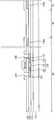
도 4를 참조하면, 본 발명의 일 실시예에 따른 박막 트랜지스터 기판은 베이스 기판(110) 상에 구비되는 제1 액티브 패턴(120), 제1 게이트 절연층(125), 제1 게이트 전극(131), 제2 게이트 절연층(135), 제2 게이트 전극(141), 소스 연결 전극(142), 드레인 연결 전극(143), 제1 층간 절연층(145), 제2 액티브 패턴(150), 제3 게이트 절연층(155), 제3 게이트 전극(160), 제2 층간 절연층(165), 제1 소스 전극(181), 제1 드레인 전극(182), 제2 소스 전극(183) 및 제2 드레인 전극(184)을 포함할 수 있다. 박막 트랜지스터 기판에는 표시 장치의 제1 영역(DA), 제2 영역(PA) 및 벤딩 영역(BA)이 정의될 수 있다.Referring to FIG. 4, the thin film transistor substrate according to the exemplary embodiment of the present invention may include a first
베이스 기판(110) 상에는 버퍼층(115)이 배치될 수 있다. 베이스 기판(110)은 투명 절연 기판을 포함할 수 있다. 예를 들면, 베이스 기판(110)은 유리 기판, 석영 기판, 투명 플라스틱 기판, 투명 금속 산화물 기판 등을 포함할 수 있다. 버퍼층(115)은 베이스 기판(110)으로부터 산소, 수분 등과 같은 불순물들이 확산되는 것을 방지하고, 베이스 기판(110) 전체의 평탄도를 향상시킬 수 있다. 또한, 버퍼층(115)은 제1 액티브 패턴(120)을 형성하기 위한 어닐링 공정에서 열의 전달 속도를 조절할 수 있다. 버퍼층(115)은 실리콘 산화물, 실리콘 질화물, 실리콘 산질화물 등을 포함할 수 있다.The
버퍼층(115) 상의 표시 영역(DA)에는 제1 액티브 패턴(120)이 배치될 수 있다. 일 실시예에 있어서, 제1 액티브 패턴(120)은 다결정(polycrystalline) 실리콘 반도체를 포함할 수 있다. 그러나, 본 발명은 이에 한정되지 아니하고, 제1 액티브 패턴(120)은 산화물(oxide) 반도체를 포함할 수도 있다.The first
제1 액티브 패턴(120)은 제1 채널 영역(121)과 제1 채널 영역(121)의 양측에 각각 형성되는 제1 소스 영역(122) 및 제1 드레인 영역(123)을 포함할 수 있다. 제1 채널 영역(121)은 불순물이 주입되지 않은 다결정 실리콘 반도체로 구성되고, 제1 소스 영역(122) 및 제1 드레인 영역(123)은 불순물이 주입되는 다결정 실리콘 반도체로 구성될 수 있다.The first
제1 액티브 패턴(120)은 N형 반도체 또는 P형 반도체일 수 있다. 일 실시예에 있어서, 제1 소스 영역(122) 및 제1 드레인 영역(123)에 주입되는 불순물은 N형 불순물일 수 있다. 예를 들면, 인(P) 이온과 같은 물질이 N형 불순물로 사용될 수 있다. 다른 실시예에 있어서, 제1 소스 영역(122) 및 제1 드레인 영역(123)에 주입되는 불순물은 P형 불순물일 수도 있다. 예를 들면, 붕소(B) 이온과 같은 물질이 P형 불순물로 사용될 수 있다.The first
버퍼층(115) 상에는 제1 액티브 패턴(120)을 덮는 제1 게이트 절연층(125)이 배치될 수 있다. 일 실시예에 있어서, 제1 게이트 절연층(125)은 버퍼층(115) 상에서 제1 액티브 패턴(120)을 덮으며 균일한 두께로 제1 액티브 패턴(120)의 프로파일을 따라 배치될 수 있다. 다른 실시예에 있어서, 제1 게이트 절연층(125)은 제1 액티브 패턴(120)을 충분히 덮을 수 있으며, 제1 액티브 패턴(120)의 주위에 단차를 생성시키지 않고 실질적으로 평탄한 상면을 가질 수 있다. 제1 게이트 절연층(125)은 실리콘 산화물, 실리콘 질화물, 실리콘 산질화물 등을 포함할 수 있다.The first
제1 게이트 절연층(125) 상에는 제1 게이트 패턴이 배치될 수 있다. 예를 들면, 상기 제1 게이트 패턴은 제1 게이트 전극(131)을 포함할 수 있다. 제1 게이트 전극(131)은 제1 액티브 패턴(120)의 제1 채널 영역(121)에 중첩할 수 있다. 제1 액티브 패턴(120)과 제1 게이트 전극(131)은 구동 박막 트랜지스터(TR1)를 형성할 수 있다. 상기 제1 게이트 패턴은 알루미늄(Al), 은(Ag), 크롬(Cr), 티타늄(Ti), 탄탈륨(Ta), 몰리브덴(Mo) 등과 같은 금속, 이들의 합금, 이들의 질화물, 도전성 금속 산화물, 투명 도전성 물질 등을 포함할 수 있다.The first gate pattern may be disposed on the first
제1 게이트 절연층(125) 상에는 상기 제1 게이트 패턴을 덮는 제2 게이트 절연층(135)이 배치될 수 있다. 일 실시예에 있어서, 제2 게이트 절연층(135)은 제1 게이트 절연층(125) 상에서 상기 제1 게이트 패턴을 덮으며 균일한 두께로 상기 제1 게이트 패턴의 프로파일을 따라 배치될 수 있다. 다른 실시예에 있어서, 제2 게이트 절연층(135)은 상기 제1 게이트 패턴을 충분히 덮을 수 있으며, 상기 제1 게이트 패턴의 주위에 단차를 생성시키지 않고 실질적으로 평탄한 상면을 가질 수 있다. 제2 게이트 절연층(135)은 실리콘 산화물, 실리콘 질화물, 실리콘 산질화물 등을 포함할 수 있다.The second
제2 게이트 절연층(135) 상에는 제2 게이트 패턴이 배치될 수 있다. 일 실시예에 있어서, 상기 제2 게이트 패턴은 제2 게이트 전극(141), 소스 연결 전극(142) 및 드레인 연결 전극(143)을 포함할 수 있다. 이 경우, 소스 연결 전극(142)과 드레인 연결 전극(143)은 제2 게이트 전극(141)과 동일한 층에 위치할 수 있다. 제2 게이트 전극(141)은 제1 게이트 전극(131)에 중첩할 수 있다. 제1 게이트 전극(131)과 제2 게이트 전극(141)은 커패시터(CST)를 형성할 수 있다.The second gate pattern may be disposed on the second
소스 연결 전극(142)은 제1 액티브 패턴(120)의 제1 소스 영역(122)에 접촉하고, 드레인 연결 전극(143)은 제1 액티브 패턴(120)의 제1 드레인 영역(123)에 접촉할 수 있다. 일 실시예에 있어서, 제1 게이트 절연층(125) 및 제2 게이트 절연층(135)에는 제1 소스 영역(122)의 일부를 노출하는 제1 접촉 구멍(CH1) 및 제1 드레인 영역(123)의 일부를 노출하는 제2 접촉 구멍(CH2)이 형성되고, 소스 연결 전극(142)은 제1 접촉 구멍(CH1)을 채우며, 드레인 연결 전극(143)은 제2 접촉 구멍(CH2)을 채울 수 있다. 예를 들면, 제1 접촉 구멍(CH1)에 의해 제1 소스 영역(122)의 상면이 노출되고, 제2 접촉 구멍(CH2)에 의해 제1 드레인 영역(123)의 상면이 노출될 수 있다. 이에 따라, 소스 연결 전극(142)의 하면은 제1 소스 영역(122)의 상면과 접촉하고, 드레인 연결 전극(143)의 하면은 제1 드레인 영역(123)의 상면과 접촉할 수 있다. 상기 제2 게이트 패턴은 알루미늄(Al), 은(Ag), 크롬(Cr), 티타늄(Ti), 탄탈륨(Ta), 몰리브덴(Mo) 등과 같은 금속, 이들의 합금, 이들의 질화물, 도전성 금속 산화물, 투명 도전성 물질 등을 포함할 수 있다.The
제2 게이트 절연층(135) 상에는 상기 제2 게이트 패턴을 덮는 제1 층간 절연층(145)이 배치될 수 있다. 일 실시예에 있어서, 제1 층간 절연층(145)은 제2 게이트 절연층(135) 상에서 상기 제2 게이트 패턴을 덮으며 균일한 두께로 상기 제2 게이트 패턴의 프로파일을 따라 배치될 수 있다. 다른 실시예에 있어서, 제1 층간 절연층(145)은 제2 게이트 절연층(135) 상에서 상기 제2 게이트 패턴을 충분히 덮을 수 있으며, 상기 제2 게이트 패턴의 주위에 단차를 생성시키지 않고 실질적으로 평탄한 상면을 가질 수 있다. 제1 층간 절연층(145)은 실리콘 산화물, 실리콘 질화물, 실리콘 산질화물 등을 포함할 수 있다.The first
제1 층간 절연층(145) 상의 제1 영역(DA)에는 제2 액티브 패턴(150)이 배치될 수 있다. 일 실시예에 있어서, 제2 액티브 패턴(150)은 산화물 반도체를 포함할 수 있다. 그러나, 본 발명은 이에 한정되지 아니하고, 제2 액티브 패턴(150)은 다결정 실리콘 반도체를 포함할 수도 있다. 제2 액티브 패턴(150)은 제2 채널 영역(151)과 제2 채널 영역(151)의 양측에 각각 형성되는 제2 소스 영역(152) 및 제2 드레인 영역(153)을 포함할 수 있다.The second
제2 액티브 패턴(150)은 인듐(In), 아연(Zn), 갈륨(Ga), 주석(Sn), 티타늄(Ti), 알루미늄(Al), 하프늄(Hf), 지르코늄(Zr), 마그네슘(Mg) 등을 함유하는 반도체 산화물을 포함할 수 있다. 제2 액티브 패턴(150)은 이성분계 화합물, 삼성분계 화합물 또는 사성분계 화합물 등을 포함할 수 있다. 예를 들면, 제2 액티브 패턴(150)은 인듐-갈륨-아연 산화물(Indium Gallium Zinc Oxide: IGZO), 인듐-주석-아연 산화물(Indium Tin Zinc Oxide: ITZO), 갈륨 아연 산화물(GaZnxOy), 인듐 아연 산화물(IZO), 아연 마그네슘 산화물(ZnMgxOy), 아연 주석 산화물(ZnSnxOy), 아연 지르코늄 산화물(ZnZrxOy), 아연 산화물(ZnOx), 갈륨 산화물(GaOx), 주석 산화물(SnOx), 인듐 산화물(InOx), 인듐-갈륨-하프늄 산화물(Indium Gallium Hafnium Oxide: IGHO), 주석-알루미늄-아연 산화물(Tin Aluminum Zinc Oxide: TAZO), 인듐-갈륨-주석 산화물(IGSO) 등을 포함할 수 있다. 이들은 단독으로 또는 서로 조합되어 사용될 수 있다. 일 실시예에 있어서, 상술한 반도체 산화물에 리튬(Li), 나트륨(Na), 망간(Mn), 니켈(Ni), 팔라듐(Pd), 구리(Cu), 탄소(C), 질소(N), 인(P), 티타늄(Ti), 지르코늄(Zr), 바나듐(V), 루테늄(Ru), 게르마늄(Ge), 주석(Sn), 불소(F) 등이 도핑될 수도 있다.The second
제1 층간 절연층(145) 상에는 제2 액티브 패턴(150)을 덮는 제3 게이트 절연층(155)이 배치될 수 있다. 일 실시예에 있어서, 제3 게이트 절연층(155)은 제2 액티브 패턴(150)의 제2 채널 영역(151)과 중첩하도록 배치될 수 있다. 제3 게이트 절연층(155)은 실리콘 산화물, 실리콘 질화물, 실리콘 산질화물 등을 포함할 수 있다.The third
제3 게이트 절연층(155) 상에는 제3 게이트 패턴이 배치될 수 있다. 예를 들면, 상기 제3 게이트 패턴은 제3 게이트 전극(160)을 포함할 수 있다. 제3 게이트 전극(160)은 제2 액티브 패턴(150)의 제2 채널 영역(151)에 중첩할 수 있다. 제2 액티브 패턴(150)과 제3 게이트 전극(160)은 스위칭 박막 트랜지스터(TR2)를 형성할 수 있다. 상기 제3 게이트 패턴은 알루미늄(Al), 은(Ag), 크롬(Cr), 티타늄(Ti), 탄탈륨(Ta), 몰리브덴(Mo) 등과 같은 금속, 이들의 합금, 이들의 질화물, 도전성 금속 산화물, 투명 도전성 물질 등을 포함할 수 있다.The third gate pattern may be disposed on the third
제1 층간 절연층(145) 상에는 상기 제3 게이트 패턴을 덮는 제2 층간 절연층(165)이 배치될 수 있다. 일 실시예에 있어서, 제2 층간 절연층(165)은 상기 제3 게이트 패턴을 충분히 덮을 수 있으며, 상기 제3 게이트 패턴의 주위에 단차를 생성시키지 않고 실질적으로 평탄한 상면을 가질 수 있다. 다른 실시예에 있어서, 제2 층간 절연층(165)은 제1 층간 절연층(145) 상에서 상기 제3 게이트 패턴을 덮으며 균일한 두께로 상기 제3 게이트 패턴의 프로파일을 따라 배치될 수 있다. 제2 층간 절연층(165)은 실리콘 산화물, 실리콘 질화물, 실리콘 산질화물 등을 포함할 수 있다.A second
제2 층간 절연층(165) 상에는 제1 소스-드레인 패턴이 배치될 수 있다. 일 실시예에 있어서, 상기 제1 소스-드레인 패턴은 제1 소스 전극(181), 제1 드레인 전극(182), 제2 소스 전극(183) 및 제2 드레인 전극(184)을 포함할 수 있다.The first source-drain pattern may be disposed on the second
제1 소스 전극(181)은 소스 연결 전극(142)에 접촉하고, 제1 드레인 전극(182)은 드레인 연결 전극(143)에 접촉할 수 있다. 일 실시예에 있어서, 제1 층간 절연층(145) 및 제2 층간 절연층(165)에는 소스 연결 전극(142)의 일부를 노출하는 제3 접촉 구멍(CH3) 및 드레인 연결 전극(143)의 일부를 노출하는 제4 접촉 구멍(CH4)이 형성되고, 제1 소스 전극(181)은 제3 접촉 구멍(CH3)을 채우며, 제1 드레인 전극(182)은 제4 접촉 구멍(CH4)을 채울 수 있다. 예를 들면, 제3 접촉 구멍(CH3)에 의해 소스 연결 전극(142)의 상면이 노출되고, 제4 접촉 구멍(CH4)에 의해 드레인 연결 전극(143)의 상면이 노출될 수 있다. 이에 따라, 제1 소스 전극(181)의 하면은 소스 연결 전극(142)의 상면과 접촉하고, 제1 드레인 전극(182)의 하면은 드레인 연결 전극(143)의 상면과 접촉할 수 있다.The
소스 연결 전극(142) 및 드레인 연결 전극(143)이 형성되지 않는 경우에, 제1 소스 전극(181) 및 제1 드레인 전극(182)이 각각 제1 액티브 패턴(120)의 제1 소스 영역(122) 및 제1 드레인 영역(123)에 직접 접촉할 수 있다. 이 경우, 제1 소스 영역(122) 및 제1 드레인 영역(123)을 각각 노출하는 접촉 구멍들의 깊이들이 증가함에 따라, 접촉 구멍들의 폭들이 감소할 수 있고, 이에 따라, 제1 소스 전극(181)과 제1 소스 영역(122)의 접촉 면적이 작아져서 제1 소스 전극(181)과 제1 소스 영역(122) 사이의 접촉 저항이 증가하고, 제1 드레인 전극(182)과 제1 드레인 영역(123)의 접촉 면적이 작아져서 제1 드레인 전극(182)과 제1 드레인 영역(123) 사이의 접촉 저항이 증가할 수 있다. 그러나, 본 발명의 일 실시예에 따른 박막 트랜지스터 기판은 제1 소스 영역(122)과 제1 소스 전극(181) 사이에 위치하는 소스 연결 전극(142) 및 제1 드레인 영역(123)과 제1 드레인 전극(182) 사이에 위치하는 드레인 연결 전극(143)을 포함함에 따라, 접촉 구멍의 깊이의 증가에 따른 접촉 저항의 증가를 방지할 수 있다.When the
일 실시예에 있어서, 제1 접촉 구멍(CH1)의 폭 및 제2 접촉 구멍(CH2)의 폭은 각각 제3 접촉 구멍(CH3)의 폭 및 제4 접촉 구멍(CH4)의 폭보다 클 수 있다. 여기서, 접촉 구멍의 폭은 베이스 기판(110)과 평행하는 방향으로의 접촉 구멍의 길이를 의미한다. 제1 접촉 구멍(CH1)의 폭이 제3 접촉 구멍(CH3)의 폭보다 큰 경우에, 소스 연결 전극(142)의 평면적이 제1 소스 전극(181)의 평면적보다 클 수 있고, 이에 따라, 제3 접촉 구멍(CH3)의 평면상 위치가 제1 접촉 구멍(CH1)의 평면상 위치와 약간 어긋나더라도, 제1 소스 전극(181)이 소스 연결 전극(142)에 용이하게 접촉할 수 있다. 또한, 제2 접촉 구멍(CH2)의 폭이 제4 접촉 구멍(CH4)의 폭보다 큰 경우에, 드레인 연결 전극(143)의 평면적이 제1 드레인 전극(182)의 평면적보다 클 수 있고, 이에 따라, 제4 접촉 구멍(CH4)의 평면상 위치가 제2 접촉 구멍(CH2)의 평면상 위치와 약간 어긋나더라도, 제1 드레인 전극(182)이 드레인 연결 전극(143)에 용이하게 접촉할 수 있다.In an embodiment, the width of the first contact hole CH1 and the width of the second contact hole CH2 may be greater than the width of the third contact hole CH3 and the width of the fourth contact hole CH4, respectively. . Here, the width of the contact hole means the length of the contact hole in the direction parallel to the
제2 소스 전극(183)은 제2 액티브 패턴(150)의 제2 소스 영역(152)에 접촉하고, 제2 드레인 전극(184)은 제2 액티브 패턴(150)의 제2 드레인 영역(153)에 접촉할 수 있다. 일 실시예에 있어서, 제2 층간 절연층(165)에는 제2 소스 영역(152)의 일부를 노출하는 제5 접촉 구멍(CH5) 및 제2 드레인 영역(153)의 일부를 노출하는 제6 접촉 구멍(CH6)이 형성되고, 제2 소스 전극(183)은 제5 접촉 구멍(CH5)을 채우며, 제2 드레인 전극(184)은 제6 접촉 구멍(CH6)을 채울 수 있다. 예를 들면, 제5 접촉 구멍(CH5)에 의해 제2 소스 영역(152)의 상면이 노출되고, 제6 접촉 구멍(CH6)에 의해 제2 드레인 영역(153)의 상면이 노출될 수 있다. 이에 따라, 제2 소스 전극(183)의 하면은 제2 소스 영역(152)의 상면과 접촉하고, 제2 드레인 전극(184)의 하면은 제2 드레인 영역(153)의 상면과 접촉할 수 있다. 상기 제3 게이트 패턴은 알루미늄(Al), 은(Ag), 크롬(Cr), 티타늄(Ti), 탄탈륨(Ta), 몰리브덴(Mo) 등과 같은 금속, 이들의 합금, 이들의 질화물, 도전성 금속 산화물, 투명 도전성 물질 등을 포함할 수 있다.The
베이스 기판(110) 상의 벤딩 영역(BA)에는 유기층(175)이 배치될 수 있다. 벤딩 영역(BA)의 버퍼층(115), 제1 게이트 절연층(125), 제2 게이트 절연층(135), 제1 층간 절연층(145) 및 제2 층간 절연층(165)에는 개구(OP1, OP2)가 형성되고, 유기층(175)은 개구(OP1, OP2)의 적어도 일부를 채우며 베이스 기판(110) 상의 벤딩 영역(BA)에 위치할 수 있다. 일 실시예에 있어서, 개구(OP1, OP2)는 제1 층간 절연층(145) 및 제2 층간 절연층(165)에 대응하는 제1 개구(OP1), 그리고 버퍼층(115), 제1 게이트 절연층(125) 및 제2 게이트 절연층(135)에 대응하는 제2 개구(OP2)를 포함할 수 있다. 일 실시예에 있어서, 유기층(175)은 개구(OP1, OP2)를 채우며 제2 층간 절연층(165) 상에 배치될 수 있다. 유기층(175)은 포토레지스트, 폴리아크릴계 수지, 폴리이미드계 수지, 폴리아미드계 수지, 실록산계 수지, 아크릴계 수지, 에폭시계 수지 등과 같은 유기 물질을 포함할 수 있다.The
상기 제1 소스-드레인 패턴은 유기층(175) 상에 배치되는 제1 배선(185)을 더 포함할 수 있다. 제1 배선(185)은 제1 영역(DA)에서 벤딩 영역(BA)을 거쳐 제2 영역(PA)으로 연장될 수 있다. 유기층(175)은 버퍼층(115), 제1 게이트 절연층(125), 제2 게이트 절연층(135), 제1 층간 절연층(145) 및 제2 층간 절연층(165)과 같은 무기층과 비교하여 경도가 낮기 때문에, 표시 장치의 벤딩에 의해 발생하는 인장 스트레스를 흡수할 수 있고, 이에 따라, 제1 배선(185)에 인장 스트레스가 집중되는 것을 효과적으로 방지할 수 있다.The first source-drain pattern may further include a
벤딩 영역(BA)에 인접하는 제1 영역(DA)의 단부 및 벤딩 영역(BA)에 인접하는 제2 영역(PA)의 단부에는 각각 도전층들(134a, 134b)이 배치될 수 있다. 일 실시예에 있어서, 도전층들(134a, 134b)은 제1 게이트 절연층(125)과 제2 게이트 절연층(135) 사이에 배치될 수 있고, 이 경우, 상기 제1 게이트 패턴은 도전층들(134a, 134b)을 더 포함할 수 있다. 제1 배선(185)은 절연층들에 형성되는 접촉 구멍을 통해 도전층들(134a, 134b)과 접촉할 수 있다. 베이스 기판(110)의 제1 영역(DA) 상에 위치하는 도전층(134a)은 제1 영역(DA) 내에 위치하는 소자(예를 들면, 화소)와 전기적으로 연결되고, 베이스 기판(110)의 제2 영역(DA) 상에 위치하는 도전층(134b)은 제2 영역(PA) 내에 위치하는 소자(예를 들면, 패드)와 전기적으로 연결될 수 있다. 이에 따라, 제1 배선(185)을 통해 제1 영역(DA) 내에 위치하는 소자와 제2 영역(PA) 내에 위치하는 소자가 서로 전기적으로 연결될 수 있다.The
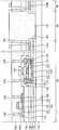
이하, 도 5 내지 도 15를 참조하여, 도 4의 박막 트랜지스터 기판의 제조 방법을 설명한다. 먼저, 도 5 내지 도 12를 참조하여 박막 트랜지스터 기판의 제조 방법의 일 예를 설명한다.Hereinafter, a method of manufacturing the thin film transistor substrate of FIG. 4 will be described with reference to FIGS. 5 to 15. First, an example of a method of manufacturing a thin film transistor substrate will be described with reference to FIGS. 5 through 12.
도 5 내지 도 12는 도 4의 박막 트랜지스터 기판의 제조 방법의 일 예를 나타내는 단면도들이다.5 to 12 are cross-sectional views illustrating an example of a method of manufacturing the thin film transistor substrate of FIG. 4.
도 5를 참조하면, 경질의 유리 기판(미도시) 상에 투명 또는 불투명한 재료들을 포함하는 베이스 기판(110)이 형성될 수 있다. 베이스 기판(110)은 연성을 갖는 투명 수지 기판을 사용하여 형성될 수 있다. 일 실시예에 있어서, 베이스 기판(110)은 순서대로 적층되는 제1 유기층, 제1 베리어층, 제2 유기층 및 제2 베리어층을 포함할 수 있다. 상기 제1 베리어층 및 상기 제2 베리어층은 무기 물질을 사용하여 형성될 수 있다. 또한, 상기 제1 유기층 및 상기 제2 유기층은 유기 물질을 사용하여 형성될 수 있다. 예를 들면, 상기 제1 및 제2 베리어층들은 실리콘 산화물을 포함할 수 있고, 상기 제1 및 제2 베리어층들은 상기 제1 및 제2 유기층들을 통해 침투하는 수분을 차단할 수 있다. 또한, 상기 제1 및 제2 유기층들은 폴리이미드계 수지를 포함할 수 있다.Referring to FIG. 5, a
베이스 기판(110) 상에는 예비 버퍼층(115')이 형성될 수 있다. 일 실시예에 있어서, 예비 버퍼층(115')은 베이스 기판(110) 상의 제1 영역(DA), 제2 영역(PA) 및 버퍼 영역(BA)에 전체적으로 형성될 수 있다. 예비 버퍼층(115')은 실리콘 산화물, 실리콘 질화물, 실리콘 산질화물 등을 사용하여 형성될 수 있다.The
예비 버퍼층(115') 상의 제1 영역(DA)에는 제1 액티브 패턴(120)이 형성될 수 있다. 일 실시예에 있어서, 제1 액티브 패턴(120)은 실리콘 반도체 등을 사용하여 형성될 수 있다. 예를 들면, 제1 반도체층이 예비 버퍼층(115') 상에 전체적으로 형성되고, 상기 제1 반도체층을 선택적으로 식각하여 제1 액티브 패턴(120)이 형성될 수 있다.The first
제1 액티브 패턴(120) 상에는 예비 제1 게이트 절연층(125')이 형성될 수 있다. 예비 제1 게이트 절연층(125')은 예비 버퍼층(115') 상의 제1 액티브 패턴(120)을 덮으며 예비 버퍼층(115') 상에 전체적으로 형성될 수 있다. 예를 들면, 예비 제1 게이트 절연층(125')은 예비 버퍼층(115') 상에서 제1 액티브 패턴(120)을 덮으며, 균일한 두께로 제1 액티브 패턴(120)의 프로파일을 따라 형성될 수 있다. 예비 제1 게이트 절연층(125')은 실리콘 산화물, 실리콘 질화물, 실리콘 산질화물 등을 사용하여 형성될 수 있다.The preliminary first
예비 제1 게이트 절연층(125') 상에는 제1 게이트 전극(131) 및 도전층들(134a, 134b)을 포함하는 상기 제1 게이트 패턴이 형성될 수 있다. 상기 제1 게이트 패턴은 금속, 합금, 금속 질화물, 도전성 금속 산화물, 투명 도전성 물질 등을 사용하여 형성될 수 있다. 예를 들면, 제1 도전층이 예비 제1 게이트 절연층(125') 상에 전체적으로 형성되고, 상기 제1 도전층을 선택적으로 식각하여 제1 액티브 패턴(120) 상에 제1 게이트 전극(131)이 형성되고, 제1 영역(DA)의 단부 및 제2 영역(PA)의 단부에 각각 도전층들(134a, 134b)이 형성될 수 있다. 제1 게이트 전극(131)이 형성됨에 따라, 제1 액티브 패턴(120) 및 제1 게이트 전극(131)을 포함하는 구동 박막 트랜지스터(TR1)가 형성될 수 있다.The first gate pattern including the
상기 제1 게이트 패턴 상에는 예비 제2 게이트 절연층(135')이 형성될 수 있다. 예비 제2 게이트 절연층(135')은 예비 제1 게이트 절연층(125') 상의 제1 게이트 전극(131) 및 도전층들(134a, 134b)을 덮으며 예비 제1 게이트 절연층(125') 상에 전체적으로 형성될 수 있다. 예를 들면, 예비 제2 게이트 절연층(135')은 예비 제1 게이트 절연층(125') 상에서 상기 제1 게이트 패턴을 덮으며, 균일한 두께로 상기 제1 게이트 패턴의 프로파일을 따라 형성될 수 있다. 예비 제2 게이트 절연층(135')은 실리콘 산화물, 실리콘 질화물, 실리콘 산질화물 등을 사용하여 형성될 수 있다.A preliminary second
제1 액티브 패턴(120)의 제1 소스 영역(122)의 일부를 노출시키는 제1 접촉 구멍(CH1) 및 제1 액티브 패턴(120)의 제1 드레인 영역(123)의 일부를 노출시키는 제2 접촉 구멍(CH2)을 형성할 수 있다. 예를 들면, 예비 제1 게이트 절연층(125') 및 예비 제2 게이트 절연층(135')을 선택적으로 식각하여 예비 제1 게이트 절연층(125') 및 예비 제2 게이트 절연층(135')을 관통하는 제1 접촉 구멍(CH1) 및 제2 접촉 구멍(CH2)이 형성될 수 있다. 제1 접촉 구멍(CH1)에 의해 제1 소스 영역(122)의 상면의 일부가 노출되고, 제2 접촉 구멍(CH2)에 의해 제1 드레인 영역(123)의 상면의 일부가 노출될 수 있다.The first contact hole CH1 exposing a part of the
제1 접촉 구멍(CH1) 및 제2 접촉 구멍(CH2)을 형성한 후에, 구동 박막 트랜지스터(TR1)의 특성을 향상시키기 위한 어닐링 공정을 수행할 수 있다. 예비 제1 게이트 절연층(125') 및/또는 예비 제2 게이트 절연층(135')에 포함된 수소가 제1 액티브 패턴(120)에 침투할 수 있고, 침투된 수소는 제1 액티브 패턴(120)을 구성하는 다결정 실리콘의 수소 결합이 끊어진 부분을 연결할 수 있다. 상기 연결에 의해 제1 액티브 패턴(120)의 제1 채널 영역(121)의 전달 특성이 개선되며, 결과적으로 구동 박막 트랜지스터(TR1)의 특성이 개선될 수 있다. 한편, 어닐링 공정 후에는 제1 접촉 구멍(CH1) 및 제2 접촉 구멍(CH2)에 대해 습식 세정 공정을 수행할 수 있다. 상기 습식 세정 공정은 BOE(buffered oxide etchant)를 사용하여 수행될 수 있다. 상기 습식 세정 공정에 의해 상기 어닐링 공정에서 형성된 산화물 등을 제거할 수 있다.After forming the first contact hole CH1 and the second contact hole CH2, an annealing process may be performed to improve characteristics of the driving thin film transistor TR1. Hydrogen included in the preliminary first
도 6을 참조하면, 예비 제2 게이트 절연층(135') 상에는 제1 접촉 구멍(CH1) 및 제2 접촉 구멍(CH2)을 채우는 제2 도전층(140)이 형성될 수 있다. 제2 도전층(140)은 제1 접촉 구멍(CH1)에 의해 노출된 제1 소스 영역(122)의 상면 및 제2 접촉 구멍(CH2)에 의해 노출된 제1 드레인 영역(123)의 상면에 접촉할 수 있다. 제2 도전층(140)은 금속, 합금, 금속 질화물, 도전성 금속 산화물, 투명 도전성 물질 등을 사용하여 형성될 수 있다. 예를 들면, 제2 도전층(140)은 예비 제2 게이트 절연층(135') 상에 전체적으로 형성될 수 있다.Referring to FIG. 6, a second
도 7을 참조하면, 제2 도전층(140)을 선택적으로 식각하여 제2 게이트 전극(141), 소스 연결 전극(142) 및 드레인 연결 전극(143)을 포함하는 상기 제2 게이트 패턴이 형성될 수 있다. 제1 게이트 전극(131) 상에 이에 중첩하도록 제2 게이트 전극(141)이 형성되고, 제1 액티브 패턴(120)의 제1 소스 영역(122) 및 제1 드레인 영역(123)에 각각 접촉하는 소스 연결 전극(142) 및 드레인 연결 전극(143)이 형성될 수 있다. 예를 들면, 소스 연결 전극(142)의 하면 및 드레인 연결 전극(143)의 하면은 각각 제1 소스 영역(122)의 상면 및 제1 드레인 영역(123)의 상면에 접촉할 수 있다. 제2 게이트 전극(141)이 형성됨에 따라, 제1 게이트 전극(131) 및 제2 게이트 전극(141)을 포함하는 커패시터(CST)가 형성될 수 있다.Referring to FIG. 7, the second gate pattern including the
도 8을 참조하면, 상기 제2 게이트 패턴 상에는 예비 제1 층간 절연층이 형성될 수 있다. 상기 예비 제1 층간 절연층은 예비 제2 게이트 절연층(135') 상의 제2 게이트 전극(141), 소스 연결 전극(142) 및 드레인 연결 전극(143)을 덮으며 예비 제2 게이트 절연층(135') 상에 전체적으로 형성될 수 있다. 예를 들면, 상기 예비 제1 층간 절연층은 예비 제2 게이트 절연층(135') 상에서 상기 제2 게이트 패턴을 덮으며 균일한 두께로 상기 제2 게이트 패턴의 프로파일을 따라 형성될 수 있다. 상기 예비 제1 층간 절연층은 실리콘 산화물, 실리콘 질화물, 실리콘 산질화물 등을 사용하여 형성될 수 있다.Referring to FIG. 8, a preliminary first interlayer insulating layer may be formed on the second gate pattern. The preliminary first interlayer insulating layer covers the
상기 예비 제1 층간 절연층 상의 제1 영역(DA)에는 제2 액티브 패턴(150)이 형성될 수 있다. 일 실시예에 있어서, 제2 액티브 패턴(150)은 산화물 반도체 등을 사용하여 형성될 수 있다. 예를 들면, 제2 반도체층이 상기 예비 제1 층간 절연층 상에 전체적으로 형성되고, 상기 제2 반도체층을 선택적으로 식각하여 제2 액티브 패턴(150)이 형성될 수 있다.A second
제2 액티브 패턴(150) 상에는 제3 게이트 절연층(155) 및 제3 게이트 전극(160)을 포함하는 상기 제3 게이트 패턴이 순차적으로 형성될 수 있다. 제3 게이트 절연층(155)은 실리콘 산화물, 실리콘 질화물, 실리콘 산질화물 등을 사용하여 형성되고, 상기 제3 게이트 패턴은 금속, 합금, 금속 질화물, 도전성 금속 산화물, 투명 도전성 물질 등을 사용하여 형성될 수 있다. 제3 게이트 절연층(155)은 제2 액티브 패턴(150)을 덮으며 제2 액티브 패턴(150)의 제2 채널 영역(151)과 중첩되도록 형성되고, 제3 게이트 전극(160)은 제3 게이트 절연층(155) 상에 제2 액티브 패턴(150)의 제2 채널 영역(151)과 중첩되도록 형성될 수 있다. 예를 들면, 예비 제3 게이트 절연층 및 제3 도전층이 제2 액티브 패턴(150)을 덮으며 상기 예비 제1 층간 절연층 상에 전체적으로 순차적으로 형성되고, 상기 예비 제3 게이트 절연층 및 상기 제3 도전층을 한번에 선택적으로 식각하여 제2 액티브 패턴(150)의 제2 채널 영역(151) 상에 제3 게이트 절연층(155)이 형성되고, 제3 게이트 절연층(155) 상에 제3 게이트 전극(160)이 형성될 수 있다. 제3 게이트 전극(160)이 형성됨에 따라, 제2 액티브 패턴(150) 및 제3 게이트 전극(160)을 포함하는 스위칭 박막 트랜지스터(TR2)가 형성될 수 있다.The third gate pattern including the third
상기 제3 게이트 패턴 상에는 예비 제2 층간 절연층이 형성될 수 있다. 상기 예비 제2 층간 절연층은 상기 예비 제1 층간 절연층 상의 제2 액티브 패턴(150) 및 제3 게이트 전극(160)을 덮으며 상기 예비 제1 층간 절연층 상에 전체적으로 형성될 수 있다. 예를 들면, 상기 예비 제2 층간 절연층은 상기 예비 제1 층간 절연층 상에서 제3 게이트 전극(160)을 충분히 덮을 수 있으며, 제3 게이트 전극(160)의 주위에 단차를 생성시키지 않고 실질적으로 평탄한 상면을 가질 수 있다. 상기 예비 제2 층간 절연층은 실리콘 산화물, 실리콘 질화물, 실리콘 산질화물 등을 사용하여 형성될 수 있다.A preliminary second interlayer insulating layer may be formed on the third gate pattern. The preliminary second interlayer insulating layer may be formed on the preliminary first interlayer insulating layer to cover the second
소스 연결 전극(142)의 일부를 노출시키는 제3 접촉 구멍(CH3) 및 드레인 연결 전극(143)의 일부를 노출시키는 제4 접촉 구멍(CH4)을 형성할 수 있다. 예를 들면, 상기 예비 제1 층간 절연층 및 상기 예비 제2 층간 절연층을 선택적으로 식각하여 상기 예비 제1 층간 절연층 및 상기 예비 제2 층간 절연층을 관통하는 제3 접촉 구멍(CH3) 및 제4 접촉 구멍(CH4)이 형성될 수 있다. 제3 접촉 구멍(CH3)에 의해 소스 연결 전극(142)의 상면의 일부가 노출되고, 제4 접촉 구멍(CH4)에 의해 드레인 연결 전극(143)의 상면의 일부가 노출될 수 있다. 제3 접촉 구멍(CH3) 및 제4 접촉 구멍(CH4)을 형성한 후에, 구동 박막 트랜지스터(TR1)의 특성 및 스위칭 박막 트랜지스터(TR1)의 특성을 향상시키기 위한 어닐링 공정을 수행할 수 있다.The third contact hole CH3 exposing a portion of the
일 실시예에 있어서, 제3 접촉 구멍(CH3)의 폭 및 제4 접촉 구멍(CH4)의 폭은 각각 제1 접촉 구멍(CH1)의 폭 및 제2 접촉 구멍(CH2)의 폭보다 작게 형성될 수 있다. 제3 접촉 구멍(CH3)의 폭이 제1 접촉 구멍(CH3)의 폭보다 작은 경우에, 제3 접촉 구멍(CH3)의 평면상 위치가 제1 접촉 구멍(CH1)의 평면상 위치와 약간 어긋나더라도, 후속 공정에서 형성되는 제1 소스 전극(181)이 소스 연결 전극(142)에 용이하게 접촉할 수 있다. 또한, 제4 접촉 구멍(CH4)의 폭이 제2 접촉 구멍(CH2)의 폭보다 작은 경우에, 제4 접촉 구멍(CH4)의 평면상 위치가 제2 접촉 구멍(CH2)의 평면상 위치와 약간 어긋나더라도, 후속 공정에서 형성되는 제1 드레인 전극(182)이 드레인 연결 전극(143)에 용이하게 접촉할 수 있다.In an embodiment, the width of the third contact hole CH3 and the width of the fourth contact hole CH4 may be smaller than the width of the first contact hole CH1 and the width of the second contact hole CH2, respectively. Can be. When the width of the third contact hole CH3 is smaller than the width of the first contact hole CH3, the planar position of the third contact hole CH3 slightly shifts from the planar position of the first contact hole CH1. However, the
상기 예비 제1 층간 절연층 및 상기 예비 제2 층간 절연층을 선택적으로 식각하여 제1 층간 절연층(145) 및 제2 층간 절연층(165)을 형성할 수 있다. 벤딩 영역(BA)에 상기 예비 제1 층간 절연층 및 상기 예비 제2 층간 절연층을 관통하는 제1 개구(OP1)를 형성할 수 있고, 이에 따라, 제1 층간 절연층(145) 및 제2 층간 절연층(165)은 베이스 기판(110) 상의 제1 영역(DA) 및 제2 영역(PA)에 선택적으로 위치할 수 있다. 일 실시예에 있어서, 제1 개구(OP1)는 제3 접촉 구멍(CH3) 및 제4 접촉 구멍(CH4)과 실질적으로 동시에 형성될 수 있다.The preliminary first interlayer insulating layer and the preliminary second interlayer insulating layer may be selectively etched to form a first
도 9를 참조하면, 예비 버퍼층(115'), 예비 제1 게이트 절연층(125') 및 예비 제2 게이트 절연층(135')을 선택적으로 식각하여 버퍼층(115), 제1 게이트 절연층(125) 및 제2 게이트 절연층(135)을 형성할 수 있다. 벤딩 영역(BA)에 예비 버퍼층(115'), 예비 제1 게이트 절연층(125') 및 예비 제2 게이트 절연층(135')을 관통하는 제2 개구(OP2)를 형성할 수 있고, 이에 따라, 버퍼층(115), 제1 게이트 절연층(125) 및 제2 게이트 절연층(135)은 베이스 기판(110) 상의 제1 영역(DA) 및 제2 영역(PA)에 선택적으로 위치할 수 있다. 일 실시예에 있어서, 제2 개구(OP2)의 폭은 제1 개구(OP1)의 폭보다 작게 형성될 수 있다.Referring to FIG. 9, the
도 10을 참조하면, 제1 개구(OP1) 및 제2 개구(OP2)에 의해 노출된 베이스 기판(110)의 벤딩 영역(BA) 상에 유기층(175)을 형성할 수 있다. 예를 들면, 예비 유기층이 제2 층간 절연층(165) 상에 전체적으로 형성되고, 상기 예비 유기층을 선택적으로 식각하여 유기층(175)이 형성될 수 있다. 일 실시예에 있어서, 유기층(175)은 제1 개구(OP1) 및 제2 개구(OP2)를 전체적으로 채우며 제2 층간 절연층(165)을 부분적으로 덮을 수 있다. 유기층(175)은 포토레지스트, 폴리아크릴계 수지, 폴리이미드계 수지, 폴리아미드계 수지, 실록산계 수지, 아크릴계 수지, 에폭시계 수지 등과 같은 유기 물질을 사용하여 형성될 수 있다.Referring to FIG. 10, an
도 11을 참조하면, 제2 액티브 패턴(150)의 제2 소스 영역(152)의 일부를 노출시키는 제5 접촉 구멍(CH5) 및 제2 액티브 패턴(150)의 제2 드레인 영역(153)의 일부를 노출시키는 제6 접촉 구멍(CH6)을 형성할 수 있다. 예를 들면, 제2 층간 절연층(165)을 선택적으로 식각하여 제2 층간 절연층(165)을 관통하는 제5 접촉 구멍(CH5) 및 제6 접촉 구멍(CH6)이 형성될 수 있다. 제5 접촉 구멍(CH5)에 의해 제2 소스 영역(152)의 상면의 일부가 노출되고, 제6 접촉 구멍(CH6)에 의해 제2 드레인 영역(153)의 상면의 일부가 노출될 수 있다. 한편, 제2 게이트 절연층(135), 제1 층간 절연층(145), 제2 층간 절연층(165) 및 유기층(175)에 도전층들(134a, 134b)을 각각 노출시키는 접촉 구멍들이 형성될 수 있다. 일 실시예에 있어서, 도전층들(134a, 134b)을 각각 노출시키는 상기 접촉 구멍들은 제5 접촉 구멍(CH5) 및 제6 접촉 구멍(CH6)과 실질적으로 동시에 형성될 수 있다.11, the fifth contact hole CH5 exposing a portion of the
도 12를 참조하면, 제2 층간 절연층(165) 및 유기층(175) 상에는 제3 접촉 구멍(CH3), 제4 접촉 구멍(CH4), 제5 접촉 구멍(CH5), 제6 접촉 구멍(CH6) 및 도전층들(134a, 134b)을 노출시키는 상기 접촉 구멍들을 채우는 제4 도전층(180)이 형성될 수 있다. 제4 도전층(180)은 금속, 합금, 금속 질화물, 도전성 금속 산화물, 투명 도전성 물질 등을 사용하여 형성될 수 있다. 예를 들면, 제4 도전층(180)은 제2 층간 절연층(165) 및 유기층(175) 상에 전체적으로 형성될 수 있다.12, a third contact hole CH3, a fourth contact hole CH4, a fifth contact hole CH5, and a sixth contact hole CH6 on the second
도 4를 참조하면, 제4 도전층(180)을 선택적으로 식각하여 제1 소스 전극(181), 제1 드레인 전극(182), 제2 소스 전극(183), 제2 드레인 전극(184) 및 제1 배선(185)을 포함하는 상기 제1 소스-드레인 패턴이 형성될 수 있다. 소스 연결 전극(142) 및 드레인 연결 전극(143)에 각각 접촉하는 제1 소스 전극(181) 및 제1 드레인 전극(182)이 형성되고, 제2 액티브 패턴(150)의 제2 소스 영역(152) 및 제2 드레인 영역(153)에 각각 접촉하는 제2 소스 전극(183) 및 제2 드레인 전극(184)이 형성되며, 도전층들(134a, 134b)에 접촉하는 제1 배선(185)이 실질적으로 동시에 형성될 수 있다.Referring to FIG. 4, the fourth
소스 연결 전극(142) 및 드레인 연결 전극(143)이 형성되지 않는 경우에, 제1 소스 전극(181) 및 제1 드레인 전극(182)이 각각 제1 액티브 패턴(120)의 제1 소스 영역(122) 및 제1 드레인 영역(123)에 직접 접촉할 수 있다. 이 경우, 제1 소스 영역(122) 및 제1 드레인 영역(123)을 각각 노출시키는 접촉 구멍들을 형성한 후에 포토레지스트를 이용하여 벤딩 영역(BA)의 절연층들을 식각하고, 제5 접촉 구멍(CH5) 및 제6 접촉 구멍(CH6)을 형성하는 과정에서 제1 소스 영역(122) 및 제1 드레인 영역(123)을 각각 노출시키는 상기 접촉 구멍들에 포토레지스트 입자가 접촉하거나 포토레지스트 입자가 잔류하여 제1 소스 영역(122)과 제1 소스 전극(181) 사이의 접촉 저항 및 제1 드레인 영역(123)과 제1 드레인 전극(182) 사이의 접촉 저항이 증가할 수 있다. 그러나, 본 발명의 일 실시예에 따른 박막 트랜지스터 기판의 제조 방법에 있어서, 제1 소스 영역(122)의 상면 및 제1 드레인 영역(123)의 상면에 각각 직접 접촉하는 소스 연결 전극(142) 및 드레인 연결 전극(143)이 형성됨에 따라, 포토레지스트 입자의 접촉 또는 포토레지스트 잔류 입자에 따른 접촉 저항의 증가를 방지할 수 있다.When the
아래의 표 1은 소스 연결 전극(142) 및 드레인 연결 전극(143)이 형성되지 않는 종래 기술에 있어서 제1 액티브 패턴(120)의 제1 소스 영역(122)과 제1 소스 전극(181) 사이의 접촉 저항들 및 소스 연결 전극(142) 및 드레인 연결 전극(143)이 형성되는 본 발명에 있어서 제1 액티브 패턴(120)의 제1 소스 영역(122)과 제1 소스 연결 전극(142) 사이의 접촉 저항들을 나타낸다.Table 1 below shows a gap between the
표 1을 참조하면, 소스 연결 전극(142) 및 드레인 연결 전극(143)이 형성되는 본 발명에 따른 박막 트랜지스터 기판에서의 제1 액티브 패턴(120)의 제1 소스 영역(122)과 제1 소스 연결 전극(142) 사이의 접촉 저항이 소스 연결 전극(142) 및 드레인 연결 전극(143)이 형성되지 않는 종래 기술에 따른 박막 트랜지스터에서의 제1 액티브 패턴(120)의 제1 소스 영역(122)과 제1 소스 전극(181) 사이의 접촉 저항보다 작을 수 있다.Referring to Table 1, the
이하, 도 13 내지 도 15를 참조하여 박막 트랜지스터 기판의 제조 방법의 다른 예를 설명한다.Hereinafter, another example of the manufacturing method of the thin film transistor substrate will be described with reference to FIGS. 13 to 15.
도 13 내지 도 15는 도 4의 박막 트랜지스터 기판의 제조 방법의 다른 예를 나타내는 단면도들이다. 도 13 내지 도 15를 참조하여 설명하는 박막 트랜지스터 기판의 제조 방법의 다른 예에 있어서, 도 5 내지 도 12를 참조하여 설명한 박막 트랜지스터 기판의 제조 방법의 일 예와 실질적으로 동일하거나 유사한 구성들에 대한 상세한 설명은 생략한다.13 to 15 are cross-sectional views illustrating another example of the method of manufacturing the thin film transistor substrate of FIG. 4. In another example of the method of manufacturing the thin film transistor substrate described with reference to FIGS. 13 to 15, the components substantially the same as or similar to the example of the method of the thin film transistor substrate described with reference to FIGS. Detailed description will be omitted.
도 13을 참조하면, 상기 예비 제2 층간 절연층이 형성된 박막 트랜지스터 기판에 있어서, 예비 버퍼층(115'), 예비 제1 게이트 절연층(125'), 예비 제2 게이트 절연층(135'), 상기 예비 제1 층간 절연층 및 상기 예비 제2 층간 절연층을 선택적으로 식각하여 버퍼층(115), 제1 게이트 절연층(125) 및 제2 게이트 절연층(135), 제1 층간 절연층(145) 및 제2 층간 절연층(165)을 형성할 수 있다. 벤딩 영역(BA)에 예비 버퍼층(115'), 예비 제1 게이트 절연층(125'), 예비 제2 게이트 절연층(135'), 상기 예비 제1 층간 절연층 및 상기 예비 제2 층간 절연층을 관통하는 개구(OP)를 형성할 수 있고, 이에 따라, 버퍼층(115), 제1 게이트 절연층(125) 및 제2 게이트 절연층(135), 제1 층간 절연층(145) 및 제2 층간 절연층(165)은 베이스 기판(110) 상의 제1 영역(DA) 및 제2 영역(PA)에 선택적으로 위치할 수 있다.Referring to FIG. 13, in the thin film transistor substrate on which the preliminary second interlayer insulating layer is formed, the preliminary buffer layer 115 ', the preliminary first gate insulating layer 125', the preliminary second gate insulating layer 135 ', The preliminary first interlayer insulating layer and the preliminary second interlayer insulating layer may be selectively etched to form a
도 14를 참조하면, 개구(OP)에 의해 노출된 베이스 기판(110)의 벤딩 영역(BA) 상에 유기층(175)을 형성할 수 있다. 예를 들면, 예비 유기층이 제2 층간 절연층(165) 상에 전체적으로 형성되고, 상기 예비 유기층을 선택적으로 식각하여 유기층(175)이 형성될 수 있다. 일 실시예에 있어서, 유기층(175)은 개구(OP)를 전체적으로 채우며 제2 층간 절연층(165)을 부분적으로 덮을 수 있다.Referring to FIG. 14, an
도 15를 참조하면, 소스 연결 전극(142)의 일부를 노출시키는 제3 접촉 구멍(CH3), 드레인 연결 전극(143)의 일부를 노출시키는 제4 접촉 구멍(CH4), 제2 액티브 패턴(150)의 제2 소스 영역(152)의 일부를 노출시키는 제5 접촉 구멍(CH5) 및 제2 액티브 패턴(150)의 제2 드레인 영역(153)의 일부를 노출시키는 제6 접촉 구멍(CH6)을 형성할 수 있다. 제3 접촉 구멍(CH3), 제4 접촉 구멍(CH4), 제5 접촉 구멍(CH5) 및 제6 접촉 구멍(CH6)은 실질적으로 동시에 형성될 수 있다. 예를 들면, 제1 층간 절연층(145) 및 제2 층간 절연층(165)을 선택적으로 식각하여 제1 층간 절연층(145) 및 제2 층간 절연층(165)을 관통하는 제3 접촉 구멍(CH3) 및 제4 접촉 구멍(CH4)이 형성되고, 제2 층간 절연층(165)을 선택적으로 식각하여 제2 층간 절연층(165)을 관통하는 제5 접촉 구멍(CH5) 및 제6 접촉 구멍(CH6)이 형성될 수 있다. 제3 접촉 구멍(CH3)에 의해 소스 연결 전극(142)의 상면의 일부가 노출되고, 제4 접촉 구멍(CH4)에 의해 드레인 연결 전극(143)의 상면의 일부가 노출될 수 있다. 또한, 제5 접촉 구멍(CH5)에 의해 제2 소스 영역(152)의 상면의 일부가 노출되고, 제6 접촉 구멍(CH6)에 의해 제2 드레인 영역(153)의 상면의 일부가 노출될 수 있다. 한편, 제2 게이트 절연층(135), 제1 층간 절연층(145), 제2 층간 절연층(165) 및 유기층(175)에 도전층들(134a, 134b)을 각각 노출시키는 접촉 구멍들이 형성될 수 있다. 일 실시예에 있어서, 도전층들(134a, 134b)을 각각 노출시키는 상기 접촉 구멍들은 제3 접촉 구멍(CH3), 제4 접촉 구멍(CH4), 제5 접촉 구멍(CH5) 및 제6 접촉 구멍(CH6)과 실질적으로 동시에 형성될 수 있다.Referring to FIG. 15, the third contact hole CH3 exposing a portion of the
이하, 도 16을 참조하여, 본 발명의 다른 실시예에 따른 표시 장치의 박막 트랜지스터 기판의 단면 구조를 설명한다.Hereinafter, a cross-sectional structure of a thin film transistor substrate of a display device according to another exemplary embodiment will be described with reference to FIG. 16.
도 16은 본 발명의 다른 실시예에 따른 박막 트랜지스터 기판을 나타내는 단면도이다. 도 16에 도시된 박막 트랜지스터 기판은 표시 장치의 구동 박막 트랜지스터(TR1), 스위칭 박막 트랜지스터(TR2) 및 커패시터(CST)를 포함할 수 있다.16 is a cross-sectional view illustrating a thin film transistor substrate according to another exemplary embodiment of the present invention. The thin film transistor substrate illustrated in FIG. 16 may include a driving thin film transistor TR1, a switching thin film transistor TR2, and a capacitor CST of the display device.
도 16을 참조하면, 본 발명의 다른 실시예에 따른 박막 트랜지스터 기판은 베이스 기판(110) 상에 구비되는 제1 액티브 패턴(120), 제1 게이트 절연층(125), 제1 게이트 전극(131), 소스 연결 전극(132), 드레인 연결 전극(133), 제2 게이트 절연층(135), 제2 게이트 전극(141), 제1 층간 절연층(145), 제2 액티브 패턴(150), 제3 게이트 절연층(155), 제3 게이트 전극(160), 제2 층간 절연층(165), 제1 소스 전극(181), 제1 드레인 전극(182), 제2 소스 전극(183) 및 제2 드레인 전극(184)을 포함할 수 있다. 박막 트랜지스터 기판에는 표시 장치의 제1 영역(DA), 제2 영역(PA) 및 벤딩 영역(BA)이 정의될 수 있다. 도 16을 참조하여 설명하는 다른 실시예에 따른 박막 트랜지스터 기판에 있어서, 도 4를 참조하여 설명한 일 실시예에 따른 박막 트랜지스터 기판과 실질적으로 동일하거나 유사한 구성들에 대한 상세한 설명은 생략한다.Referring to FIG. 16, a thin film transistor substrate according to another exemplary embodiment of the present invention may include a first
제1 게이트 절연층(125) 상에는 제1 게이트 패턴이 배치될 수 있다. 예를 들면, 상기 제1 게이트 패턴은 제1 게이트 전극(131), 소스 연결 전극(132) 및 드레인 연결 전극(133)을 포함할 수 있다. 이 경우, 소스 연결 전극(132)과 드레인 연결 전극(133)은 제1 게이트 전극(131)과 동일한 층에 위치할 수 있다.The first gate pattern may be disposed on the first
소스 연결 전극(132)은 제1 액티브 패턴(120)의 제1 소스 영역(122)에 접촉하고, 드레인 연결 전극(133)은 제1 액티브 패턴(120)의 제1 드레인 영역(123)에 접촉할 수 있다. 일 실시예에 있어서, 제1 게이트 절연층(125)에는 제1 소스 영역(122)의 일부를 노출하는 제1 접촉 구멍(CH1) 및 제1 드레인 영역(123)의 일부를 노출하는 제2 접촉 구멍(CH2)이 형성되고, 소스 연결 전극(132)은 제1 접촉 구멍(CH1)을 채우며, 드레인 연결 전극(133)은 제2 접촉 구멍(CH2)을 채울 수 있다.The
제2 게이트 절연층(135) 상에는 제2 게이트 패턴이 배치될 수 있다. 일 실시예에 있어서, 상기 제2 게이트 패턴은 제2 게이트 전극(141)을 포함할 수 있다. 제2 게이트 전극(141)은 제1 게이트 전극(131)에 중첩할 수 있다.The second gate pattern may be disposed on the second
제1 소스 전극(181)은 소스 연결 전극(132)에 접촉하고, 제1 드레인 전극(182)은 드레인 연결 전극(133)에 접촉할 수 있다. 일 실시예에 있어서, 제2 게이트 절연층(135), 제1 층간 절연층(145) 및 제2 층간 절연층(165)에는 소스 연결 전극(132)의 일부를 노출하는 제3 접촉 구멍(CH3) 및 드레인 연결 전극(133)의 일부를 노출하는 제4 접촉 구멍(CH4)이 형성되고, 제1 소스 전극(181)은 제3 접촉 구멍(CH3)을 채우며, 제1 드레인 전극(182)은 제4 접촉 구멍(CH4)을 채울 수 있다.The
이하, 도 17 내지 도 19를 참조하여, 도 16의 박막 트랜지스터 기판의 제조 방법을 설명한다.Hereinafter, a method of manufacturing the thin film transistor substrate of FIG. 16 will be described with reference to FIGS. 17 to 19.
도 17 내지 도 19는 도 16의 박막 트랜지스터 기판의 제조 방법을 나타내는 단면도들이다. 도 17 내지 도 19를 참조하여 설명하는 다른 실시예에 따른 박막 트랜지스터 기판의 제조 방법에 있어서, 도 5 내지 도 15를 참조하여 설명한 일 실시예에 따른 박막 트랜지스터 기판의 제조 방법과 실질적으로 동일하거나 유사한 구성들에 대한 상세한 설명은 생략한다.17 to 19 are cross-sectional views illustrating a method of manufacturing the thin film transistor substrate of FIG. 16. In the method of manufacturing the thin film transistor substrate according to another exemplary embodiment described with reference to FIGS. 17 to 19, the method of manufacturing the thin film transistor substrate according to the exemplary embodiment described with reference to FIGS. 5 to 15 may be substantially the same as or similar to that of the method of manufacturing the thin film transistor substrate. Detailed description of the components is omitted.
도 17을 참조하면, 제1 액티브 패턴(120)의 제1 소스 영역(122)의 일부를 노출시키는 제1 접촉 구멍(CH1) 및 제1 액티브 패턴(120)의 제1 드레인 영역(123)의 일부를 노출시키는 제2 접촉 구멍(CH2)을 형성할 수 있다. 예를 들면, 예비 제1 게이트 절연층(125')을 선택적으로 식각하여 예비 제1 게이트 절연층(125')을 관통하는 제1 접촉 구멍(CH1) 및 제2 접촉 구멍(CH2)이 형성될 수 있다. 제1 접촉 구멍(CH1)에 의해 제1 소스 영역(122)의 상면의 일부가 노출되고, 제2 접촉 구멍(CH2)에 의해 제1 드레인 영역(123)의 상면의 일부가 노출될 수 있다.Referring to FIG. 17, the first contact hole CH1 exposing a portion of the
도 18을 참조하면, 예비 제1 게이트 절연층(125') 상에는 제1 접촉 구멍(CH1) 및 제2 접촉 구멍(CH2)을 채우는 제1 도전층(130)이 형성될 수 있다. 제1 도전층(130)은 제1 접촉 구멍(CH1)에 의해 노출된 제1 소스 영역(122)의 상면 및 제2 접촉 구멍(CH2)에 의해 노출된 제1 드레인 영역(123)의 상면에 접촉할 수 있다.Referring to FIG. 18, a first
도 19를 참조하면, 제1 도전층(130)을 선택적으로 식각하여 제1 게이트 전극(131), 소스 연결 전극(132), 드레인 연결 전극(133) 및 도전층들(134a, 134b)을 포함하는 상기 제1 게이트 패턴이 형성될 수 있다. 제1 액티브 패턴(120) 상에 제1 게이트 전극(131)이 형성되고, 제1 액티브 패턴(120)의 제1 소스 영역(122) 및 제1 드레인 영역(123)에 각각 접촉하는 소스 연결 전극(132) 및 드레인 연결 전극(133)이 형성되며, 제1 영역(DA)의 단부 및 제2 영역(PA)의 단부에 각각 도전층들(134a, 134b)이 형성될 수 있다.Referring to FIG. 19, the first
이하, 도 20을 참조하여, 본 발명의 일 실시예에 따른 표시 장치의 단면 구조를 설명한다.Hereinafter, a cross-sectional structure of a display device according to an exemplary embodiment of the present invention will be described with reference to FIG. 20.
도 20은 본 발명의 일 실시예에 따른 표시 장치를 나타내는 단면도이다. 도 20에는 본 실시예에 따른 표시 장치가 도 4를 참조하여 설명한 일 실시예에 따른 박막 트랜지스터 기판을 포함하는 것으로 예시되어 있으나, 본 발명은 이에 한정되지 아니하고, 표시 장치는 도 16을 참조하여 설명한 다른 실시예에 따른 박막 트랜지스터 기판을 포함할 수도 있다.20 is a cross-sectional view of a display device according to an exemplary embodiment. 20 illustrates that the display device according to the present exemplary embodiment includes the thin film transistor substrate according to the exemplary embodiment described with reference to FIG. 4, but the present invention is not limited thereto and the display device described with reference to FIG. 16. It may also include a thin film transistor substrate according to another embodiment.
도 20을 참조하면, 본 발명의 일 실시예에 따른 표시 장치는 베이스 기판(110) 상에 구비되는 제1 액티브 패턴(120), 제1 게이트 절연층(125), 제1 게이트 전극(131), 제2 게이트 절연층(135), 제2 게이트 전극(141), 소스 연결 전극(142), 드레인 연결 전극(143), 제1 층간 절연층(145), 제2 액티브 패턴(150), 제3 게이트 절연층(155), 제3 게이트 전극(160), 제2 층간 절연층(165), 제1 소스 전극(181), 제1 드레인 전극(182), 제2 소스 전극(183) 및 제2 드레인 전극(184)을 포함하는 박막 트랜지스터 기판, 제1 평탄화층(220), 제2 평탄화층(240) 및 발광 구조물(LE)을 포함할 수 있다. 상기 박막 트랜지스터 기판에 대해서는 도 4 및 도 16을 참조하여 설명하였으므로, 이에 대한 상세한 설명은 생략한다.Referring to FIG. 20, in the display device according to the exemplary embodiment, the first
제2 층간 절연층(165) 상에는 상기 제1 소스-드레인 패턴을 덮는 보호층(210)이 배치될 수 있다. 일 실시예에 있어서, 보호층(210)은 제2 층간 절연층(165) 상에서 상기 제1 소스-드레인 패턴을 덮으며, 균일한 두께로 상기 제1 소스-드레인 패턴의 프로파일을 따라 배치될 수 있다. 보호층(210)은 실리콘 산화물, 실리콘 질화물, 실리콘 산질화물 등을 포함할 수 있다.The
보호층(210) 상에는 제1 평탄화층(220)이 배치될 수 있다. 일 실시예에 있어서, 제1 평탄화층(220)은 보호층(210)을 충분히 덮을 수 있으며, 실질적으로 평탄한 상면을 가질 수 있다. 벤딩 영역(BA)의 보호층(210)에는 개구가 형성될 수 있고, 제1 평탄화층(220)은 상기 개구를 채울 수 있다. 제1 평탄화층(220)은 포토레지스트, 폴리아크릴계 수지, 폴리이미드계 수지, 폴리아미드계 수지, 실록산계 수지, 아크릴계 수지, 에폭시계 수지 등과 같은 유기 물질을 포함할 수 있다.The
제1 평탄화층(220) 상에는 제2 소스-드레인 패턴이 배치될 수 있다. 일 실시예에 있어서, 상기 제2 소스-드레인 패턴은 화소 연결 전극(231) 및 제2 배선(232)을 포함할 수 있다. 화소 연결 전극(231)은 제1 드레인 전극(182)에 접촉할 수 있다. 일 실시예에 있어서, 보호층(210) 및 제1 평탄화층(220)에는 제1 드레인 전극(182)의 일부를 노출하는 접촉 구멍이 형성되고, 화소 연결 전극(231)은 상기 접촉 구멍을 채울 수 있다. 제2 배선(232)은 제1 배선(185)에 접촉하고, 제1 영역(DA)에서 벤딩 영역(BA)을 거쳐 제2 영역(PA)으로 연장될 수 있다. 일 실시예에 있어서, 보호층(210) 및 제1 평탄화층(220)에는 제1 배선(185)의 단부들을 각각 노출하는 접촉 구멍들이 형성될 수 있고, 제2 배선(232)은 상기 접촉 구멍들을 채워서 제1 배선(185)에 연결될 수 있다.The second source-drain pattern may be disposed on the
제1 평탄화층(220) 상에는 상기 제2 소스-드레인 패턴을 덮는 제2 평탄화층(240)이 배치될 수 있다. 일 실시예에 있어서, 제2 평탄화층(240)은 상기 제2 소스-드레인 패턴을 충분히 덮을 수 있으며, 상기 제2 소스-드레인 패턴의 주위에 단차를 생성시키지 않고 실질적으로 평탄한 상면을 가질 수 있다. 제2 평탄화층(240)은 포토레지스트, 폴리아크릴계 수지, 폴리이미드계 수지, 폴리아미드계 수지, 실록산계 수지, 아크릴계 수지, 에폭시계 수지 등과 같은 유기 물질을 포함할 수 있다.A
제2 평탄화층(240) 상의 제1 영역(DA)에는 제1 전극(250)이 배치될 수 있다. 제1 전극(250)은 제2 평탄화층(240)의 일부를 제거하여 형성된 접촉 구멍을 통해 화소 연결 전극(231)에 접촉할 수 있고, 제1 전극(250)은 구동 박막 트랜지스터(TR1)와 전기적으로 연결될 수 있다. 제1 전극(250)은 금속, 합금, 금속 질화물, 도전성 금속 산화물, 투명 도전성 물질 등을 포함할 수 있다.The
제2 평탄화층(240) 상에는 제1 전극(250)을 덮는 화소 정의막(260)이 배치될 수 있다. 화소 정의막(260)은 제1 전극(250)의 일부를 노출시킬 수 있다. 예를 들면, 화소 정의막(260)은 제1 전극(250)의 가장자리를 덮으며, 제1 전극(250)의 중심부를 노출하는 개구를 포함할 수 있다. 화소 정의막(260)은 포토레지스트, 폴리아크릴계 수지, 폴리이미드계 수지, 폴리아미드계 수지, 실록산계 수지, 아크릴계 수지, 에폭시계 수지 등과 같은 유기 물질을 포함할 수 있다.The
화소 정의막(260)의 상기 개구에 의해 일부가 노출된 제1 전극(250) 상에는 유기 발광층(270)이 배치될 수 있다. 유기 발광층(270)은 화소들에 따라 상이한 색광들(즉, 적색광, 녹색광, 청색광 등)을 방출시키는 발광 물질들 중 적어도 하나를 사용하여 형성될 수 있다. 이와 달리, 유기 발광층(270)은 적색광, 녹색광, 청색광 등의 다른 색광들을 발생시킬 수 있는 복수의 발광 물질들을 적층하여 전체적으로 백색광을 방출할 수도 있다. 이 경우, 유기 발광층(270) 상에 컬러 필터가 배치될 수 있다. 상기 컬러 필터는 적색 컬러 필터, 녹색 컬러 필터, 청색 컬러 필터 중 적어도 하나를 포함할 수 있다.The
화소 정의막(260) 및 유기 발광층(270) 상에는 제2 전극(280)이 배치될 수 있다. 제2 전극(280)은 금속, 합금, 금속 질화물, 도전성 금속 산화물, 투명 도전성 물질 등을 포함할 수 있다. 이에 따라, 제1 전극(250), 유기 발광층(270) 및 제2 전극(280)을 포함하는 발광 구조물(LE)이 제2 평탄화층(240) 상의 제1 영역(DA)에 배치될 수 있다.The
본 발명의 예시적인 실시예들에 따른 표시 장치는 컴퓨터, 노트북, 휴대폰, 스마트폰, 스마트패드, 피엠피(PMP), 피디에이(PDA), MP3 플레이어 등에 포함되는 표시 장치에 적용될 수 있다.The display device according to exemplary embodiments of the present invention may be applied to a display device included in a computer, a notebook, a mobile phone, a smart phone, a smart pad, a PMP, a PDA, an MP3 player, and the like.
이상, 본 발명의 예시적인 실시예들에 따른 박막 트랜지스터 기판들, 박막 트랜지스터 기판의 제조 방법들 및 박막 트랜지스터 기판을 포함하는 표시 장치들에 대하여 도면들을 참조하여 설명하였지만, 설시한 실시예들은 예시적인 것으로서 하기의 청구범위에 기재된 본 발명의 기술적 사상을 벗어나지 않는 범위에서 해당 기술 분야에서 통상의 지식을 가진 자에 의하여 수정 및 변경될 수 있을 것이다.The thin film transistor substrates, the manufacturing methods of the thin film transistor substrate, and the display devices including the thin film transistor substrate according to the exemplary embodiments of the present invention have been described above with reference to the drawings. As will be apparent to those skilled in the art without departing from the spirit of the present invention described in the claims below.
110: 베이스 기판120: 제1 액티브 패턴
125: 제1 게이트 절연층131: 제1 게이트 전극
132, 142: 소스 연결 전극133, 143: 드레인 연결 전극
135: 제2 게이트 절연층141: 제2 게이트 전극
145: 제1 층간 절연층150: 제2 액티브 패턴
155: 제3 게이트 절연층160: 제3 게이트 전극
181: 제1 소스 전극182: 제1 드레인 전극
183: 제2 소스 전극184: 제2 드레인 전극
220: 제1 평탄화층TR1: 구동 박막 트랜지스터
TR2: 스위칭 박막 트랜지스터CST: 커패시터
LE: 발광 구조물110: base substrate 120: first active pattern
125: first gate insulating layer 131: first gate electrode
132 and 142:
135: second gate insulating layer 141: second gate electrode
145: first interlayer insulating layer 150: second active pattern
155: third gate insulating layer 160: third gate electrode
181: first source electrode 182: first drain electrode
183: second source electrode 184: second drain electrode
220: first planarization layer TR1: driving thin film transistor
TR2: switching thin film transistor CST: capacitor
LE: light emitting structure
Claims (23)
Translated fromKorean상기 베이스 기판 상에 배치되는 제1 액티브 패턴;
상기 제1 액티브 패턴을 덮는 제1 게이트 절연층;
상기 제1 게이트 절연층 상에 배치되고, 상기 제1 액티브 패턴과 제1 박막 트랜지스터를 형성하는 제1 게이트 전극;
상기 제1 게이트 전극을 덮는 제2 게이트 절연층;
상기 제2 게이트 절연층 상에 배치되고, 상기 제1 게이트 전극과 중첩하는 제2 게이트 전극;
상기 제1 게이트 전극 및 상기 제2 게이트 전극 중 하나와 동일한 층에 위치하고, 상기 제1 액티브 패턴의 소스 영역 및 드레인 영역과 각각 접촉하는 소스 연결 전극 및 드레인 연결 전극;
상기 제2 게이트 전극을 덮는 제1 층간 절연층;
상기 제1 층간 절연층 상에 배치되는 제2 액티브 패턴;
상기 제2 액티브 패턴을 덮는 제3 게이트 절연층;
상기 제3 게이트 절연층 상에 배치되고, 상기 제2 액티브 패턴과 제2 박막 트랜지스터를 형성하는 제3 게이트 전극;
상기 제3 게이트 전극을 덮는 제2 층간 절연층; 및
상기 제2 층간 절연층 상에 배치되고, 상기 소스 연결 전극 및 상기 드레인 연결 전극과 각각 접촉하는 제1 소스 전극 및 제1 드레인 전극, 및 상기 제2 액티브 패턴의 소스 영역 및 드레인 영역과 각각 접촉하는 제2 소스 전극 및 제2 드레인 전극을 포함하는, 박막 트랜지스터 기판.A base substrate;
A first active pattern disposed on the base substrate;
A first gate insulating layer covering the first active pattern;
A first gate electrode disposed on the first gate insulating layer and forming the first active pattern and the first thin film transistor;
A second gate insulating layer covering the first gate electrode;
A second gate electrode disposed on the second gate insulating layer and overlapping the first gate electrode;
A source connection electrode and a drain connection electrode on the same layer as one of the first gate electrode and the second gate electrode and in contact with the source region and the drain region of the first active pattern, respectively;
A first interlayer insulating layer covering the second gate electrode;
A second active pattern disposed on the first interlayer insulating layer;
A third gate insulating layer covering the second active pattern;
A third gate electrode disposed on the third gate insulating layer and forming the second active pattern and the second thin film transistor;
A second interlayer insulating layer covering the third gate electrode; And
A first source electrode and a first drain electrode disposed on the second interlayer insulating layer and in contact with the source connection electrode and the drain connection electrode, and contacting the source region and the drain region of the second active pattern, respectively; A thin film transistor substrate comprising a second source electrode and a second drain electrode.
상기 소스 연결 전극 및 상기 드레인 연결 전극은 상기 제2 게이트 전극과 동일한 층에 위치하는, 박막 트랜지스터 기판.The method of claim 1,
And the source connection electrode and the drain connection electrode are on the same layer as the second gate electrode.
상기 소스 연결 전극 및 상기 드레인 연결 전극은 상기 제1 게이트 전극과 동일한 층에 위치하는, 박막 트랜지스터 기판.The method of claim 1,
And the source connection electrode and the drain connection electrode are on the same layer as the first gate electrode.
상기 소스 연결 전극은 상기 제1 액티브 패턴의 상기 소스 영역의 일부를 노출하는 제1 접촉 구멍을 통해 상기 제1 액티브 패턴의 상기 소스 영역에 연결되고,
상기 드레인 연결 전극은 상기 제1 액티브 패턴의 상기 드레인 영역의 일부를 노출하는 제2 접촉 구멍을 통해 상기 제1 액티브 패턴의 상기 드레인 영역에 연결되는, 박막 트랜지스터 기판.The method of claim 1,
The source connection electrode is connected to the source region of the first active pattern through a first contact hole exposing a portion of the source region of the first active pattern,
And the drain connection electrode is connected to the drain region of the first active pattern through a second contact hole exposing a portion of the drain region of the first active pattern.
상기 제1 소스 전극은 상기 소스 연결 전극의 일부를 노출하는 제3 접촉 구멍을 통해 상기 소스 연결 전극에 연결되고,
상기 제1 드레인 전극은 상기 드레인 연결 전극의 일부를 노출하는 제4 접촉 구멍을 통해 상기 드레인 연결 전극에 연결되는, 박막 트랜지스터 기판.The method of claim 4, wherein
The first source electrode is connected to the source connection electrode through a third contact hole exposing a portion of the source connection electrode,
And the first drain electrode is connected to the drain connection electrode through a fourth contact hole exposing a portion of the drain connection electrode.
상기 제1 접촉 구멍의 폭 및 상기 제2 접촉 구멍의 폭은 각각 상기 제3 접촉 구멍의 폭 및 상기 제4 접촉 구멍의 폭보다 큰, 박막 트랜지스터 기판.The method of claim 5,
And the width of the first contact hole and the width of the second contact hole are respectively greater than the width of the third contact hole and the width of the fourth contact hole.
상기 제1 액티브 패턴 및 상기 제2 액티브 패턴 중 하나는 다결정 실리콘 반도체를 포함하고,
상기 제2 액티브 패턴 및 상기 제2 액티브 패턴 중 다른 하나는 산화물 반도체를 포함하는, 박막 트랜지스터 기판.The method of claim 1,
One of the first active pattern and the second active pattern includes a polycrystalline silicon semiconductor,
And the other of the second active pattern and the second active pattern comprises an oxide semiconductor.
상기 제1 액티브 패턴을 덮는 제1 게이트 절연층을 형성하는 단계;
상기 제1 게이트 절연층 상에 상기 제1 액티브 패턴과 제1 박막 트랜지스터를 형성하는 제1 게이트 전극을 형성하는 단계;
상기 제1 게이트 전극을 덮는 제2 게이트 절연층을 형성하는 단계;
상기 제2 게이트 절연층 상에 상기 제1 게이트 전극과 중첩하는 제2 게이트 전극을 형성하는 단계;
상기 제1 게이트 전극 및 상기 제2 게이트 전극 중 하나와 동일한 층에 상기 제1 액티브 패턴의 소스 영역 및 드레인 영역과 각각 접촉하는 소스 연결 전극 및 드레인 연결 전극을 형성하는 단계;
상기 제2 게이트 전극을 덮는 제1 층간 절연층을 형성하는 단계;
상기 제1 층간 절연층 상에 제2 액티브 패턴을 형성하는 단계;
상기 제2 액티브 패턴을 덮는 제3 게이트 절연층을 형성하는 단계;
상기 제3 게이트 절연층 상에 상기 제2 액티브 패턴과 제2 박막 트랜지스터를 형성하는 제3 게이트 전극을 형성하는 단계;
상기 제3 게이트 전극을 덮는 제2 층간 절연층을 형성하는 단계; 및
상기 제2 층간 절연층 상에 상기 소스 연결 전극 및 상기 드레인 연결 전극과 각각 접촉하는 제1 소스 전극 및 제1 드레인 전극, 및 상기 제2 액티브 패턴의 소스 영역 및 드레인 영역과 각각 접촉하는 제2 소스 전극 및 제2 드레인 전극을 형성하는 단계를 포함하는, 박막 트랜지스터 기판의 제조 방법.Forming a first active pattern on the base substrate;
Forming a first gate insulating layer covering the first active pattern;
Forming a first gate electrode on the first gate insulating layer to form the first active pattern and the first thin film transistor;
Forming a second gate insulating layer covering the first gate electrode;
Forming a second gate electrode on the second gate insulating layer, the second gate electrode overlapping the first gate electrode;
Forming a source connection electrode and a drain connection electrode in contact with the source region and the drain region of the first active pattern, respectively, on the same layer as one of the first gate electrode and the second gate electrode;
Forming a first interlayer insulating layer covering the second gate electrode;
Forming a second active pattern on the first interlayer insulating layer;
Forming a third gate insulating layer covering the second active pattern;
Forming a third gate electrode on the third gate insulating layer to form the second active pattern and the second thin film transistor;
Forming a second interlayer insulating layer covering the third gate electrode; And
A first source electrode and a first drain electrode in contact with the source connection electrode and the drain connection electrode, respectively, on the second interlayer insulating layer, and a second source in contact with the source region and the drain region of the second active pattern, respectively. Forming an electrode and a second drain electrode.
상기 소스 연결 전극 및 상기 드레인 연결 전극은 상기 제2 게이트 전극과 동일한 층에 동시에 형성되는, 박막 트랜지스터 기판의 제조 방법.The method of claim 8,
And the source connection electrode and the drain connection electrode are simultaneously formed on the same layer as the second gate electrode.
상기 제2 게이트 전극을 형성하는 단계, 및 상기 소스 연결 전극 및 상기 드레인 연결 전극을 형성하는 단계는:
상기 제1 게이트 절연층 및 상기 제2 게이트 절연층을 관통하여 상기 제1 액티브 패턴의 상기 소스 영역의 일부 및 상기 드레인 영역의 일부를 각각 노출시키는 제1 접촉 구멍 및 제2 접촉 구멍을 형성하는 단계;
상기 제2 게이트 절연층 상에 상기 제1 접촉 구멍 및 상기 제2 접촉 구멍을 통해 상기 제1 액티브 패턴의 상기 소스 영역 및 상기 드레인 영역과 각각 연결되는 도전층을 형성하는 단계; 및
상기 도전층을 식각하여 상기 제2 게이트 전극, 상기 소스 연결 전극 및 상기 드레인 연결 전극을 형성하는 단계를 포함하는, 박막 트랜지스터 기판의 제조 방법.The method of claim 9,
Forming the second gate electrode and forming the source connection electrode and the drain connection electrode include:
Forming a first contact hole and a second contact hole penetrating the first gate insulating layer and the second gate insulating layer to expose a portion of the source region and a portion of the drain region of the first active pattern, respectively; ;
Forming a conductive layer on the second gate insulating layer, the conductive layer being connected to the source region and the drain region of the first active pattern through the first contact hole and the second contact hole, respectively; And
Etching the conductive layer to form the second gate electrode, the source connection electrode, and the drain connection electrode.
상기 소스 연결 전극 및 상기 드레인 연결 전극은 상기 제1 게이트 전극과 동일한 층에 동시에 형성되는, 박막 트랜지스터 기판의 제조 방법.The method of claim 8,
And the source connection electrode and the drain connection electrode are simultaneously formed on the same layer as the first gate electrode.
상기 제1 게이트 전극을 형성하는 단계, 및 상기 소스 연결 전극 및 상기 드레인 연결 전극을 형성하는 단계는:
상기 제1 게이트 절연층을 관통하여 상기 제1 액티브 패턴의 상기 소스 영역의 일부 및 상기 드레인 영역의 일부를 각각 노출시키는 제1 접촉 구멍 및 제2 접촉 구멍을 형성하는 단계;
상기 제1 게이트 절연층 상에 상기 제1 접촉 구멍 및 상기 제2 접촉 구멍을 통해 상기 제1 액티브 패턴의 상기 소스 영역 및 상기 드레인 영역과 각각 연결되는 도전층을 형성하는 단계; 및
상기 도전층을 식각하여 상기 제1 게이트 전극, 상기 소스 연결 전극 및 상기 드레인 연결 전극을 형성하는 단계를 포함하는, 박막 트랜지스터 기판의 제조 방법.The method of claim 11,
Forming the first gate electrode and forming the source connection electrode and the drain connection electrode include:
Forming a first contact hole and a second contact hole penetrating the first gate insulating layer to expose a portion of the source region and a portion of the drain region of the first active pattern, respectively;
Forming a conductive layer on the first gate insulating layer, the conductive layer being connected to the source region and the drain region of the first active pattern through the first contact hole and the second contact hole; And
Etching the conductive layer to form the first gate electrode, the source connection electrode, and the drain connection electrode.
상기 제1 소스 전극, 상기 제1 드레인 전극, 상기 제2 소스 전극 및 상기 제2 드레인 전극을 형성하는 단계는:
상기 소스 연결 전극의 일부 및 상기 드레인 연결 전극의 일부를 각각 노출시키는 제1 접촉 구멍 및 제2 접촉 구멍을 형성하는 단계;
상기 제2 액티브 패턴의 상기 소스 영역의 일부 및 상기 드레인 영역의 일부를 각각 노출시키는 제3 접촉 구멍 및 제4 접촉 구멍을 형성하는 단계;
상기 제2 층간 절연층 상에 상기 제1 접촉 구멍, 상기 제2 접촉 구멍, 상기 제3 접촉 구멍 및 상기 제4 접촉 구멍을 통해 상기 소스 연결 전극, 상기 드레인 연결 전극, 상기 제2 액티브 패턴의 상기 소스 영역 및 상기 드레인 영역과 각각 연결되는 도전층을 형성하는 단계; 및
상기 도전층을 식각하여 상기 제1 소스 전극, 상기 제1 드레인 전극, 상기 제2 소스 전극 및 상기 제2 드레인 전극을 형성하는 단계를 포함하는, 박막 트랜지스터 기판의 제조 방법.The method of claim 8,
The forming of the first source electrode, the first drain electrode, the second source electrode and the second drain electrode may include:
Forming a first contact hole and a second contact hole respectively exposing a portion of the source connection electrode and a portion of the drain connection electrode;
Forming a third contact hole and a fourth contact hole exposing a portion of the source region and a portion of the drain region of the second active pattern, respectively;
The source connection electrode, the drain connection electrode, and the second active pattern through the first contact hole, the second contact hole, the third contact hole, and the fourth contact hole on the second interlayer insulating layer. Forming a conductive layer respectively connected to the source region and the drain region; And
Etching the conductive layer to form the first source electrode, the first drain electrode, the second source electrode, and the second drain electrode.
상기 제3 접촉 구멍 및 상기 제4 접촉 구멍을 형성하는 단계는 상기 제1 접촉 구멍 및 상기 제2 접촉 구멍을 형성하는 단계 후에 수행되는, 박막 트랜지스터 기판의 제조 방법.The method of claim 13,
The forming of the third contact hole and the fourth contact hole is performed after the forming of the first contact hole and the second contact hole.
상기 제3 접촉 구멍 및 상기 제4 접촉 구멍을 형성하는 단계는 상기 제1 접촉 구멍 및 상기 제2 접촉 구멍을 형성하는 단계와 동시에 수행되는, 박막 트랜지스터 기판의 제조 방법.The method of claim 13,
And forming the third contact hole and the fourth contact hole are performed simultaneously with the forming of the first contact hole and the second contact hole.
상기 베이스 기판 상에 배치되는 제1 액티브 패턴;
상기 제1 액티브 패턴을 덮는 제1 게이트 절연층;
상기 제1 게이트 절연층 상에 배치되고, 상기 제1 액티브 패턴과 제1 박막 트랜지스터를 형성하는 제1 게이트 전극;
상기 제1 게이트 전극을 덮는 제2 게이트 절연층;
상기 제2 게이트 절연층 상에 배치되고, 상기 제1 게이트 전극과 중첩하는 제2 게이트 전극;
상기 제1 게이트 전극 및 상기 제2 게이트 전극 중 하나와 동일한 층에 위치하고, 상기 제1 액티브 패턴의 소스 영역 및 드레인 영역과 각각 접촉하는 소스 연결 전극 및 드레인 연결 전극;
상기 제2 게이트 전극을 덮는 제1 층간 절연층;
상기 제1 층간 절연층 상에 배치되는 제2 액티브 패턴;
상기 제2 액티브 패턴을 덮는 제3 게이트 절연층;
상기 제3 게이트 절연층 상에 배치되고, 상기 제2 액티브 패턴과 제2 박막 트랜지스터를 형성하는 제3 게이트 전극;
상기 제3 게이트 전극을 덮는 제2 층간 절연층;
상기 제2 층간 절연층 상에 배치되고, 상기 소스 연결 전극 및 상기 드레인 연결 전극과 각각 접촉하는 제1 소스 전극 및 제1 드레인 전극, 및 상기 제2 액티브 패턴의 소스 영역 및 드레인 영역과 각각 접촉하는 제2 소스 전극 및 제2 드레인 전극을 포함하는 제1 소스-드레인 패턴;
상기 제1 소스-드레인 패턴을 덮는 제1 평탄화층; 및
상기 제1 평탄화층 상에 배치되고, 상기 제1 박막 트랜지스터와 전기적으로 연결되는 발광 구조물을 포함하는, 표시 장치.A base substrate;
A first active pattern disposed on the base substrate;
A first gate insulating layer covering the first active pattern;
A first gate electrode disposed on the first gate insulating layer and forming the first active pattern and the first thin film transistor;
A second gate insulating layer covering the first gate electrode;
A second gate electrode disposed on the second gate insulating layer and overlapping the first gate electrode;
A source connection electrode and a drain connection electrode on the same layer as one of the first gate electrode and the second gate electrode and in contact with the source region and the drain region of the first active pattern, respectively;
A first interlayer insulating layer covering the second gate electrode;
A second active pattern disposed on the first interlayer insulating layer;
A third gate insulating layer covering the second active pattern;
A third gate electrode disposed on the third gate insulating layer and forming the second active pattern and the second thin film transistor;
A second interlayer insulating layer covering the third gate electrode;
A first source electrode and a first drain electrode disposed on the second interlayer insulating layer and in contact with the source connection electrode and the drain connection electrode, and contacting the source region and the drain region of the second active pattern, respectively; A first source-drain pattern including a second source electrode and a second drain electrode;
A first planarization layer covering the first source-drain pattern; And
And a light emitting structure disposed on the first planarization layer and electrically connected to the first thin film transistor.
상기 소스 연결 전극 및 상기 드레인 연결 전극은 상기 제2 게이트 전극과 동일한 층에 위치하는, 표시 장치.The method of claim 16,
And the source connection electrode and the drain connection electrode are on the same layer as the second gate electrode.
상기 소스 연결 전극 및 상기 드레인 연결 전극은 상기 제1 게이트 전극과 동일한 층에 위치하는, 표시 장치.The method of claim 16,
And the source connection electrode and the drain connection electrode are on the same layer as the first gate electrode.
상기 제1 액티브 패턴 및 상기 제2 액티브 패턴 중 하나는 다결정 실리콘 반도체를 포함하고,
상기 제2 액티브 패턴 및 상기 제2 액티브 패턴 중 다른 하나는 산화물 반도체를 포함하는, 표시 장치.The method of claim 16,
One of the first active pattern and the second active pattern includes a polycrystalline silicon semiconductor,
The other of the second active pattern and the second active pattern includes an oxide semiconductor.
상기 발광 구조물은:
상기 제1 평탄화층 상에 배치되고, 상기 제1 드레인 전극과 전기적으로 연결되는 제1 전극;
상기 제1 전극 상에 배치되는 유기 발광층; 및
상기 유기 발광층 상에 배치되는 제2 전극을 포함하는, 표시 장치.The method of claim 16,
The light emitting structure is:
A first electrode disposed on the first planarization layer and electrically connected to the first drain electrode;
An organic emission layer disposed on the first electrode; And
And a second electrode on the organic light emitting layer.
상기 기판은:
상부에 상기 제1 박막 트랜지스터, 상기 제2 박막 트랜지스터, 상기 제1 게이트 전극 및 상기 제2 게이트 전극에 의해 형성되는 커패시터 및 상기 발광 구조물이 위치하는 제1 영역;
상기 제1 영역으로부터 이격되는 제2 영역; 및
상기 제1 영역과 상기 제2 영역 사이에 위치하는 벤딩 영역을 포함하는, 표시 장치.The method of claim 20,
The substrate is:
A first region in which a capacitor formed by the first thin film transistor, the second thin film transistor, the first gate electrode and the second gate electrode, and the light emitting structure are positioned;
A second region spaced apart from the first region; And
And a bending area positioned between the first area and the second area.
상기 기판 상의 상기 벤딩 영역에 배치되는 유기층을 더 포함하고,
상기 제1 소스-드레인 패턴은 상기 유기층 상에 배치되는 제1 배선을 더 포함하는, 표시 장치.The method of claim 21,
Further comprising an organic layer disposed in the bending region on the substrate,
The first source-drain pattern further includes a first wiring disposed on the organic layer.
상기 제1 평탄화층과 상기 제1 전극 사이에 배치되는 제2 평탄화층; 및
상기 제1 평탄화층과 상기 제2 평탄화층 사이에 배치되고, 상기 제1 드레인 전극과 상기 제1 전극을 전기적으로 연결하는 화소 연결 전극 및 상기 벤딩 영역에 위치하며, 상기 제1 배선과 전기적으로 연결되는 제2 배선을 포함하는 제2 소스-드레인 패턴을 더 포함하는, 표시 장치.
The method of claim 22,
A second planarization layer disposed between the first planarization layer and the first electrode; And
A pixel connection electrode disposed between the first planarization layer and the second planarization layer, the pixel connection electrode electrically connecting the first drain electrode and the first electrode, and the bending area, and electrically connected to the first wiring; And a second source-drain pattern including a second wiring to be formed.
Priority Applications (3)
| Application Number | Priority Date | Filing Date | Title |
|---|---|---|---|
| KR1020180057447AKR102591811B1 (en) | 2018-05-18 | 2018-05-18 | Thin film transistor substrate, method of manufacturing the same, and display device including the same |
| US16/412,059US10861920B2 (en) | 2018-05-18 | 2019-05-14 | Thin film transistor substrate, method of manufacturing the same, and display device including the same |
| CN201910408531.7ACN110504276B (en) | 2018-05-18 | 2019-05-16 | Thin film transistor substrate, method for manufacturing the same, and display device including the same |
Applications Claiming Priority (1)
| Application Number | Priority Date | Filing Date | Title |
|---|---|---|---|
| KR1020180057447AKR102591811B1 (en) | 2018-05-18 | 2018-05-18 | Thin film transistor substrate, method of manufacturing the same, and display device including the same |
Publications (2)
| Publication Number | Publication Date |
|---|---|
| KR20190132603Atrue KR20190132603A (en) | 2019-11-28 |
| KR102591811B1 KR102591811B1 (en) | 2023-10-23 |
Family
ID=68532885
Family Applications (1)
| Application Number | Title | Priority Date | Filing Date |
|---|---|---|---|
| KR1020180057447AActiveKR102591811B1 (en) | 2018-05-18 | 2018-05-18 | Thin film transistor substrate, method of manufacturing the same, and display device including the same |
Country Status (3)
| Country | Link |
|---|---|
| US (1) | US10861920B2 (en) |
| KR (1) | KR102591811B1 (en) |
| CN (1) | CN110504276B (en) |
Cited By (6)
| Publication number | Priority date | Publication date | Assignee | Title |
|---|---|---|---|---|
| KR20210109090A (en)* | 2020-02-26 | 2021-09-06 | 삼성디스플레이 주식회사 | Display device and method for manufacturing the same |
| KR20220062212A (en)* | 2020-11-06 | 2022-05-16 | 삼성디스플레이 주식회사 | Display apparatus |
| US11825703B2 (en) | 2020-08-10 | 2023-11-21 | Samsung Display Co., Ltd. | Display device and method for manufacturing thereof |
| US11889720B2 (en) | 2020-08-31 | 2024-01-30 | Samsung Display Co., Ltd. | Display apparatus including a groove disposed in the middle area while surrounding the first hole in the transmission area |
| US11943982B2 (en) | 2020-11-18 | 2024-03-26 | Samsung Display Co., Ltd. | Display device and method of manufacturing display device |
| WO2025110488A1 (en)* | 2023-11-20 | 2025-05-30 | 고려대학교 산학협력단 | Light-emitting element-thin-film transistor integration structure based on step difference of substrate, and manufacturing method therefor |
Families Citing this family (44)
| Publication number | Priority date | Publication date | Assignee | Title |
|---|---|---|---|---|
| KR102465376B1 (en)* | 2017-06-16 | 2022-11-10 | 삼성디스플레이 주식회사 | Display apparatus and method for manufacturing the same |
| WO2019064436A1 (en)* | 2017-09-28 | 2019-04-04 | シャープ株式会社 | Display device |
| KR102706723B1 (en)* | 2018-03-07 | 2024-09-20 | 삼성디스플레이 주식회사 | Display panel and method of manufacturing of the same |
| WO2020059126A1 (en)* | 2018-09-21 | 2020-03-26 | シャープ株式会社 | Display device |
| CN109686758A (en)* | 2018-12-04 | 2019-04-26 | 武汉华星光电半导体显示技术有限公司 | A kind of flexible display panels and preparation method thereof |
| CN109935601B (en)* | 2019-04-04 | 2021-01-26 | 京东方科技集团股份有限公司 | Display panel and preparation method thereof |
| CN109873025B (en)* | 2019-04-11 | 2021-10-08 | 京东方科技集团股份有限公司 | Organic light emitting diode array substrate and display device |
| US11043546B2 (en)* | 2019-05-20 | 2021-06-22 | Wuhan China Star Optoelectronics Semiconductor Display Technology Co., Ltd. | Display panel, fabricating method thereof and display device |
| CN110349974A (en)* | 2019-06-25 | 2019-10-18 | 武汉华星光电半导体显示技术有限公司 | A kind of array substrate and preparation method thereof, display device |
| KR102833564B1 (en)* | 2019-07-09 | 2025-07-14 | 삼성디스플레이 주식회사 | Display device |
| CN110556404A (en)* | 2019-08-09 | 2019-12-10 | 武汉华星光电半导体显示技术有限公司 | display panel, preparation method thereof and display device |
| KR102846430B1 (en)* | 2019-08-23 | 2025-08-14 | 삼성디스플레이 주식회사 | Display device |
| CN110729328B (en)* | 2019-09-17 | 2022-03-08 | 武汉华星光电半导体显示技术有限公司 | Organic light emitting diode display panel and organic light emitting diode display device |
| KR20210046118A (en)* | 2019-10-17 | 2021-04-28 | 삼성디스플레이 주식회사 | Display device |
| CN110828690A (en)* | 2019-10-23 | 2020-02-21 | 武汉华星光电半导体显示技术有限公司 | OLED display panel and preparation method |
| KR20210060715A (en)* | 2019-11-18 | 2021-05-27 | 삼성디스플레이 주식회사 | Display apparatus and method of manufacturing the same |
| US11348975B2 (en)* | 2019-11-26 | 2022-05-31 | Shenzhen China Star Optoelectronics Semiconductor Display Technology Co., Ltd. | Organic light-emitting diode display substrate, manufacturing method of same and display device |
| CN110890409B (en)* | 2019-11-29 | 2022-11-04 | 京东方科技集团股份有限公司 | Display device, OLED panel thereof, and manufacturing method of OLED panel |
| CN111106154A (en)* | 2019-12-12 | 2020-05-05 | 武汉华星光电半导体显示技术有限公司 | A flexible display panel and its manufacturing method |
| CN110993680B (en)* | 2019-12-31 | 2022-06-17 | 厦门天马微电子有限公司 | Flexible display panel and electronic equipment |
| KR102827181B1 (en)* | 2020-01-02 | 2025-07-01 | 삼성디스플레이 주식회사 | Display apparatus and manufacturing the same |
| KR20210104213A (en)* | 2020-02-14 | 2021-08-25 | 삼성디스플레이 주식회사 | Display device and method for manufacturing the same |
| CN111834400B (en)* | 2020-02-26 | 2021-10-12 | 昆山国显光电有限公司 | Display panel, manufacturing method thereof and display device |
| CN114287059A (en)* | 2020-03-25 | 2022-04-05 | 京东方科技集团股份有限公司 | Flexible display substrate, manufacturing method thereof and display device |
| US11522031B2 (en)* | 2020-06-01 | 2022-12-06 | Wuhan China Star Optoelectronics Semiconductor Display Technology Co., Ltd. | Display panel, display device, and manufacturing method of display panel |
| CN111668239B (en)* | 2020-06-19 | 2022-11-08 | 武汉华星光电半导体显示技术有限公司 | OLED display panel and preparation method |
| WO2022003846A1 (en)* | 2020-07-01 | 2022-01-06 | シャープ株式会社 | Display device and method for manufacturing display device |
| CN111799280A (en) | 2020-07-20 | 2020-10-20 | 京东方科技集团股份有限公司 | Display substrate and preparation method thereof, and display device |
| CN112002702B (en)* | 2020-08-06 | 2022-09-27 | 武汉华星光电半导体显示技术有限公司 | Flexible display panel and rollable display device |
| CN114503274A (en)* | 2020-08-27 | 2022-05-13 | 京东方科技集团股份有限公司 | Display substrate and display device |
| US20220336676A1 (en)* | 2020-09-18 | 2022-10-20 | Chengdu Boe Optoelectronics Technology Co.,Ltd. | Display substrate, display panel and display device |
| CN112103322B (en)* | 2020-09-22 | 2022-12-09 | 京东方科技集团股份有限公司 | Display panel, manufacturing method thereof, and display device |
| KR20220045756A (en)* | 2020-10-06 | 2022-04-13 | 엘지디스플레이 주식회사 | Display device |
| CN112259579B (en)* | 2020-10-10 | 2024-06-07 | 深圳市华星光电半导体显示技术有限公司 | OLED display panel and manufacturing method thereof |
| CN112397559B (en)* | 2020-11-09 | 2024-02-02 | 武汉华星光电半导体显示技术有限公司 | Stretchable display module and preparation method thereof |
| KR20220077322A (en)* | 2020-12-01 | 2022-06-09 | 삼성디스플레이 주식회사 | Pixel circuit and display device including the same |
| KR20220092009A (en)* | 2020-12-24 | 2022-07-01 | 엘지디스플레이 주식회사 | Display apparatus having a substrate hole |
| CN113035912B (en)* | 2021-01-26 | 2022-02-25 | 维沃移动通信有限公司 | Display module, electronic equipment and preparation method of display module |
| KR20220131436A (en)* | 2021-03-18 | 2022-09-28 | 삼성디스플레이 주식회사 | display device |
| KR20230000510A (en)* | 2021-06-24 | 2023-01-03 | 삼성디스플레이 주식회사 | Display apparatus and method of manufacturing the same |
| WO2023278339A1 (en)* | 2021-06-28 | 2023-01-05 | Emagin Corporation | Monolithically integrated top-gate thin-film transistor and light-emitting diode and method of making |
| KR20230030088A (en)* | 2021-08-23 | 2023-03-06 | 삼성디스플레이 주식회사 | Display device and method of manufacturing the same |
| JP2023045215A (en)* | 2021-09-21 | 2023-04-03 | キオクシア株式会社 | Semiconductor device and semiconductor storage device |
| CN114203734B (en)* | 2021-12-11 | 2023-08-22 | 武汉华星光电半导体显示技术有限公司 | Display panel and preparation method thereof |
Citations (5)
| Publication number | Priority date | Publication date | Assignee | Title |
|---|---|---|---|---|
| KR20150019891A (en)* | 2013-08-16 | 2015-02-25 | 삼성디스플레이 주식회사 | Thin-film transistor array substrate, display apparatus including thereof and method for manufacturing of the thin-film transistor array substrate |
| KR20170104360A (en)* | 2016-03-07 | 2017-09-15 | 가부시키가이샤 재팬 디스프레이 | Semiconductor device, display device and method of fabricating the same |
| KR20170114223A (en)* | 2016-03-25 | 2017-10-13 | 삼성디스플레이 주식회사 | Display apparatus |
| KR20180025354A (en)* | 2016-08-29 | 2018-03-09 | 삼성디스플레이 주식회사 | Display apparatus and method of manufacturing the same |
| KR20180026610A (en)* | 2016-09-02 | 2018-03-13 | 삼성디스플레이 주식회사 | Display device and manufacturing method of the same |
Family Cites Families (20)
| Publication number | Priority date | Publication date | Assignee | Title |
|---|---|---|---|---|
| JPS6068349A (en) | 1984-07-16 | 1985-04-18 | Canon Inc | Apparatus for preparing amorphous photoconductive member |
| US7960838B2 (en)* | 2005-11-18 | 2011-06-14 | United Microelectronics Corp. | Interconnect structure |
| KR101065407B1 (en)* | 2009-08-25 | 2011-09-16 | 삼성모바일디스플레이주식회사 | Organic light emitting display and manufacturing method thereof |
| WO2011064819A1 (en)* | 2009-11-27 | 2011-06-03 | パナソニック株式会社 | Light-emitting display device |
| KR101768433B1 (en) | 2009-12-18 | 2017-08-16 | 가부시키가이샤 한도오따이 에네루기 켄큐쇼 | Method for manufacturing semiconductor device |
| CN103582952B (en)* | 2011-11-30 | 2016-08-03 | 株式会社日本有机雷特显示器 | Semiconductor device and display device |
| US9818765B2 (en)* | 2013-08-26 | 2017-11-14 | Apple Inc. | Displays with silicon and semiconducting oxide thin-film transistors |
| KR102207916B1 (en) | 2013-10-17 | 2021-01-27 | 삼성디스플레이 주식회사 | Thin film transistor array substrate, organic light-emitting display apparatus and manufacturing of the thin film transistor array substrate |
| KR102227474B1 (en)* | 2013-11-05 | 2021-03-15 | 삼성디스플레이 주식회사 | Thin film transistor array substrate, organic light-emitting display apparatus and manufacturing of the thin film transistor array substrate |
| KR102255199B1 (en)* | 2014-08-04 | 2021-05-25 | 삼성디스플레이 주식회사 | Organic light emitting display device |
| CN105390503B (en)* | 2014-08-29 | 2018-12-28 | 乐金显示有限公司 | Thin film transistor base plate and the display device for using thin film transistor base plate |
| KR101679252B1 (en)* | 2014-09-30 | 2016-12-07 | 엘지디스플레이 주식회사 | Thin film transistor substrate and method of manufacturing the same and Display Device using the same |
| KR102349283B1 (en)* | 2014-12-19 | 2022-01-11 | 삼성디스플레이 주식회사 | Thin film transistor array substrate and organic light-emitting display including the same |
| KR102408898B1 (en)* | 2015-06-19 | 2022-06-16 | 엘지디스플레이 주식회사 | Thin Film Transistor Substrate And Display Using The Same |
| KR102516054B1 (en)* | 2015-11-13 | 2023-03-31 | 삼성디스플레이 주식회사 | Organic light emitting display apparatus and method for manufacturing the same |
| KR20170080996A (en)* | 2015-12-31 | 2017-07-11 | 삼성디스플레이 주식회사 | Thin film transistor for display device and organic light emitting diode display device comprising the same |
| US10283574B2 (en)* | 2016-03-25 | 2019-05-07 | Samsung Display Co., Ltd. | Display apparatus with bending area capable of minimizing manufacturing defects |
| KR102587229B1 (en)* | 2016-04-22 | 2023-10-12 | 삼성디스플레이 주식회사 | Display device |
| KR102514412B1 (en)* | 2016-05-02 | 2023-03-28 | 삼성디스플레이 주식회사 | Semiconductor device and Display apparatus employing the same |
| KR102663140B1 (en)* | 2016-06-24 | 2024-05-08 | 삼성디스플레이 주식회사 | display device |
- 2018
- 2018-05-18KRKR1020180057447Apatent/KR102591811B1/enactiveActive
- 2019
- 2019-05-14USUS16/412,059patent/US10861920B2/enactiveActive
- 2019-05-16CNCN201910408531.7Apatent/CN110504276B/enactiveActive
Patent Citations (5)
| Publication number | Priority date | Publication date | Assignee | Title |
|---|---|---|---|---|
| KR20150019891A (en)* | 2013-08-16 | 2015-02-25 | 삼성디스플레이 주식회사 | Thin-film transistor array substrate, display apparatus including thereof and method for manufacturing of the thin-film transistor array substrate |
| KR20170104360A (en)* | 2016-03-07 | 2017-09-15 | 가부시키가이샤 재팬 디스프레이 | Semiconductor device, display device and method of fabricating the same |
| KR20170114223A (en)* | 2016-03-25 | 2017-10-13 | 삼성디스플레이 주식회사 | Display apparatus |
| KR20180025354A (en)* | 2016-08-29 | 2018-03-09 | 삼성디스플레이 주식회사 | Display apparatus and method of manufacturing the same |
| KR20180026610A (en)* | 2016-09-02 | 2018-03-13 | 삼성디스플레이 주식회사 | Display device and manufacturing method of the same |
Cited By (8)
| Publication number | Priority date | Publication date | Assignee | Title |
|---|---|---|---|---|
| KR20210109090A (en)* | 2020-02-26 | 2021-09-06 | 삼성디스플레이 주식회사 | Display device and method for manufacturing the same |
| US12120943B2 (en) | 2020-02-26 | 2024-10-15 | Samsung Display Co., Ltd. | Display device and method of manufacturing the same |
| US11825703B2 (en) | 2020-08-10 | 2023-11-21 | Samsung Display Co., Ltd. | Display device and method for manufacturing thereof |
| US11889720B2 (en) | 2020-08-31 | 2024-01-30 | Samsung Display Co., Ltd. | Display apparatus including a groove disposed in the middle area while surrounding the first hole in the transmission area |
| KR20220062212A (en)* | 2020-11-06 | 2022-05-16 | 삼성디스플레이 주식회사 | Display apparatus |
| US11943982B2 (en) | 2020-11-18 | 2024-03-26 | Samsung Display Co., Ltd. | Display device and method of manufacturing display device |
| US12256616B2 (en) | 2020-11-18 | 2025-03-18 | Samsung Display Co., Ltd. | Display device and method of manufacturing display device |
| WO2025110488A1 (en)* | 2023-11-20 | 2025-05-30 | 고려대학교 산학협력단 | Light-emitting element-thin-film transistor integration structure based on step difference of substrate, and manufacturing method therefor |
Also Published As
| Publication number | Publication date |
|---|---|
| US20190355799A1 (en) | 2019-11-21 |
| CN110504276A (en) | 2019-11-26 |
| US10861920B2 (en) | 2020-12-08 |
| KR102591811B1 (en) | 2023-10-23 |
| CN110504276B (en) | 2024-11-19 |
Similar Documents
| Publication | Publication Date | Title |
|---|---|---|
| KR102591811B1 (en) | Thin film transistor substrate, method of manufacturing the same, and display device including the same | |
| KR102565936B1 (en) | Display device | |
| CN107293570B (en) | Display panel and display device | |
| EP3176826B1 (en) | Display device and method for manufacturing the same | |
| CN107785405B (en) | Array substrate and preparation method thereof | |
| KR102713791B1 (en) | Organic light emitting diode display device | |
| CN110854156A (en) | Organic light emitting diode display device | |
| KR20200093718A (en) | Organic light emitting diode display device and method of manufacturing organic light emitting diode display device | |
| KR102740671B1 (en) | Display device and method for manufacturing of the same | |
| CN107302016A (en) | A kind of organic LED display panel and preparation method thereof | |
| JP4926483B2 (en) | Thin film transistor display panel | |
| KR20150011868A (en) | Organic light emiiting diode device and method of fabricating the same | |
| JP2018031976A (en) | Display device | |
| KR20200087912A (en) | Organic light emitting diode display device and method of manufacturing organic light emitting diode display device | |
| KR102782516B1 (en) | Display device and method of manufacturing display device | |
| CN109935580A (en) | Substrate, manufacturing method thereof and electronic device | |
| CN111933671B (en) | Display substrate, manufacturing method thereof and display panel | |
| CN112119498A (en) | Method for manufacturing array substrate, array substrate and display device | |
| KR20080076459A (en) | Method of manufacturing thin film transistor array panel and thin film transistor array panel | |
| KR20210149958A (en) | Display device | |
| US20140027761A1 (en) | Thin film transistor substrate, display thereof and manufacturing method thereof | |
| US11094774B2 (en) | Organic light emitting diode display device | |
| CN115548070A (en) | Display device | |
| KR102850343B1 (en) | Transistor and display device including the same | |
| KR101932514B1 (en) | Organic electro luminescent device |
Legal Events
| Date | Code | Title | Description |
|---|---|---|---|
| PA0109 | Patent application | Patent event code:PA01091R01D Comment text:Patent Application Patent event date:20180518 | |
| PG1501 | Laying open of application | ||
| PA0201 | Request for examination | Patent event code:PA02012R01D Patent event date:20210416 Comment text:Request for Examination of Application Patent event code:PA02011R01I Patent event date:20180518 Comment text:Patent Application | |
| E902 | Notification of reason for refusal | ||
| PE0902 | Notice of grounds for rejection | Comment text:Notification of reason for refusal Patent event date:20230119 Patent event code:PE09021S01D | |
| E701 | Decision to grant or registration of patent right | ||
| PE0701 | Decision of registration | Patent event code:PE07011S01D Comment text:Decision to Grant Registration Patent event date:20230724 | |
| GRNT | Written decision to grant | ||
| PR0701 | Registration of establishment | Comment text:Registration of Establishment Patent event date:20231017 Patent event code:PR07011E01D | |
| PR1002 | Payment of registration fee | Payment date:20231018 End annual number:3 Start annual number:1 | |
| PG1601 | Publication of registration |