KR20190130044A - High deposition rate, high quality silicon nitride made possible by remote nitrogen radical source - Google Patents
High deposition rate, high quality silicon nitride made possible by remote nitrogen radical sourceDownload PDFInfo
- Publication number
- KR20190130044A KR20190130044AKR1020197033073AKR20197033073AKR20190130044AKR 20190130044 AKR20190130044 AKR 20190130044AKR 1020197033073 AKR1020197033073 AKR 1020197033073AKR 20197033073 AKR20197033073 AKR 20197033073AKR 20190130044 AKR20190130044 AKR 20190130044A
- Authority
- KR
- South Korea
- Prior art keywords
- gas
- distribution plate
- plasma
- gas distribution
- processing system
- Prior art date
- Legal status (The legal status is an assumption and is not a legal conclusion. Google has not performed a legal analysis and makes no representation as to the accuracy of the status listed.)
- Ceased
Links
Images


Classifications
- H—ELECTRICITY
- H01—ELECTRIC ELEMENTS
- H01J—ELECTRIC DISCHARGE TUBES OR DISCHARGE LAMPS
- H01J37/00—Discharge tubes with provision for introducing objects or material to be exposed to the discharge, e.g. for the purpose of examination or processing thereof
- H01J37/32—Gas-filled discharge tubes
- H01J37/32009—Arrangements for generation of plasma specially adapted for examination or treatment of objects, e.g. plasma sources
- H01J37/32357—Generation remote from the workpiece, e.g. down-stream
- H—ELECTRICITY
- H01—ELECTRIC ELEMENTS
- H01J—ELECTRIC DISCHARGE TUBES OR DISCHARGE LAMPS
- H01J37/00—Discharge tubes with provision for introducing objects or material to be exposed to the discharge, e.g. for the purpose of examination or processing thereof
- H01J37/32—Gas-filled discharge tubes
- H01J37/32431—Constructional details of the reactor
- H01J37/3244—Gas supply means
- H01J37/32449—Gas control, e.g. control of the gas flow
- C—CHEMISTRY; METALLURGY
- C23—COATING METALLIC MATERIAL; COATING MATERIAL WITH METALLIC MATERIAL; CHEMICAL SURFACE TREATMENT; DIFFUSION TREATMENT OF METALLIC MATERIAL; COATING BY VACUUM EVAPORATION, BY SPUTTERING, BY ION IMPLANTATION OR BY CHEMICAL VAPOUR DEPOSITION, IN GENERAL; INHIBITING CORROSION OF METALLIC MATERIAL OR INCRUSTATION IN GENERAL
- C23C—COATING METALLIC MATERIAL; COATING MATERIAL WITH METALLIC MATERIAL; SURFACE TREATMENT OF METALLIC MATERIAL BY DIFFUSION INTO THE SURFACE, BY CHEMICAL CONVERSION OR SUBSTITUTION; COATING BY VACUUM EVAPORATION, BY SPUTTERING, BY ION IMPLANTATION OR BY CHEMICAL VAPOUR DEPOSITION, IN GENERAL
- C23C16/00—Chemical coating by decomposition of gaseous compounds, without leaving reaction products of surface material in the coating, i.e. chemical vapour deposition [CVD] processes
- C23C16/22—Chemical coating by decomposition of gaseous compounds, without leaving reaction products of surface material in the coating, i.e. chemical vapour deposition [CVD] processes characterised by the deposition of inorganic material, other than metallic material
- C23C16/30—Deposition of compounds, mixtures or solid solutions, e.g. borides, carbides, nitrides
- C23C16/34—Nitrides
- C23C16/345—Silicon nitride
- C—CHEMISTRY; METALLURGY
- C23—COATING METALLIC MATERIAL; COATING MATERIAL WITH METALLIC MATERIAL; CHEMICAL SURFACE TREATMENT; DIFFUSION TREATMENT OF METALLIC MATERIAL; COATING BY VACUUM EVAPORATION, BY SPUTTERING, BY ION IMPLANTATION OR BY CHEMICAL VAPOUR DEPOSITION, IN GENERAL; INHIBITING CORROSION OF METALLIC MATERIAL OR INCRUSTATION IN GENERAL
- C23C—COATING METALLIC MATERIAL; COATING MATERIAL WITH METALLIC MATERIAL; SURFACE TREATMENT OF METALLIC MATERIAL BY DIFFUSION INTO THE SURFACE, BY CHEMICAL CONVERSION OR SUBSTITUTION; COATING BY VACUUM EVAPORATION, BY SPUTTERING, BY ION IMPLANTATION OR BY CHEMICAL VAPOUR DEPOSITION, IN GENERAL
- C23C16/00—Chemical coating by decomposition of gaseous compounds, without leaving reaction products of surface material in the coating, i.e. chemical vapour deposition [CVD] processes
- C23C16/44—Chemical coating by decomposition of gaseous compounds, without leaving reaction products of surface material in the coating, i.e. chemical vapour deposition [CVD] processes characterised by the method of coating
- C23C16/4401—Means for minimising impurities, e.g. dust, moisture or residual gas, in the reaction chamber
- C23C16/4405—Cleaning of reactor or parts inside the reactor by using reactive gases
- C—CHEMISTRY; METALLURGY
- C23—COATING METALLIC MATERIAL; COATING MATERIAL WITH METALLIC MATERIAL; CHEMICAL SURFACE TREATMENT; DIFFUSION TREATMENT OF METALLIC MATERIAL; COATING BY VACUUM EVAPORATION, BY SPUTTERING, BY ION IMPLANTATION OR BY CHEMICAL VAPOUR DEPOSITION, IN GENERAL; INHIBITING CORROSION OF METALLIC MATERIAL OR INCRUSTATION IN GENERAL
- C23C—COATING METALLIC MATERIAL; COATING MATERIAL WITH METALLIC MATERIAL; SURFACE TREATMENT OF METALLIC MATERIAL BY DIFFUSION INTO THE SURFACE, BY CHEMICAL CONVERSION OR SUBSTITUTION; COATING BY VACUUM EVAPORATION, BY SPUTTERING, BY ION IMPLANTATION OR BY CHEMICAL VAPOUR DEPOSITION, IN GENERAL
- C23C16/00—Chemical coating by decomposition of gaseous compounds, without leaving reaction products of surface material in the coating, i.e. chemical vapour deposition [CVD] processes
- C23C16/44—Chemical coating by decomposition of gaseous compounds, without leaving reaction products of surface material in the coating, i.e. chemical vapour deposition [CVD] processes characterised by the method of coating
- C23C16/455—Chemical coating by decomposition of gaseous compounds, without leaving reaction products of surface material in the coating, i.e. chemical vapour deposition [CVD] processes characterised by the method of coating characterised by the method used for introducing gases into reaction chamber or for modifying gas flows in reaction chamber
- C23C16/45512—Premixing before introduction in the reaction chamber
- C—CHEMISTRY; METALLURGY
- C23—COATING METALLIC MATERIAL; COATING MATERIAL WITH METALLIC MATERIAL; CHEMICAL SURFACE TREATMENT; DIFFUSION TREATMENT OF METALLIC MATERIAL; COATING BY VACUUM EVAPORATION, BY SPUTTERING, BY ION IMPLANTATION OR BY CHEMICAL VAPOUR DEPOSITION, IN GENERAL; INHIBITING CORROSION OF METALLIC MATERIAL OR INCRUSTATION IN GENERAL
- C23C—COATING METALLIC MATERIAL; COATING MATERIAL WITH METALLIC MATERIAL; SURFACE TREATMENT OF METALLIC MATERIAL BY DIFFUSION INTO THE SURFACE, BY CHEMICAL CONVERSION OR SUBSTITUTION; COATING BY VACUUM EVAPORATION, BY SPUTTERING, BY ION IMPLANTATION OR BY CHEMICAL VAPOUR DEPOSITION, IN GENERAL
- C23C16/00—Chemical coating by decomposition of gaseous compounds, without leaving reaction products of surface material in the coating, i.e. chemical vapour deposition [CVD] processes
- C23C16/44—Chemical coating by decomposition of gaseous compounds, without leaving reaction products of surface material in the coating, i.e. chemical vapour deposition [CVD] processes characterised by the method of coating
- C23C16/455—Chemical coating by decomposition of gaseous compounds, without leaving reaction products of surface material in the coating, i.e. chemical vapour deposition [CVD] processes characterised by the method of coating characterised by the method used for introducing gases into reaction chamber or for modifying gas flows in reaction chamber
- C23C16/45561—Gas plumbing upstream of the reaction chamber
- C—CHEMISTRY; METALLURGY
- C23—COATING METALLIC MATERIAL; COATING MATERIAL WITH METALLIC MATERIAL; CHEMICAL SURFACE TREATMENT; DIFFUSION TREATMENT OF METALLIC MATERIAL; COATING BY VACUUM EVAPORATION, BY SPUTTERING, BY ION IMPLANTATION OR BY CHEMICAL VAPOUR DEPOSITION, IN GENERAL; INHIBITING CORROSION OF METALLIC MATERIAL OR INCRUSTATION IN GENERAL
- C23C—COATING METALLIC MATERIAL; COATING MATERIAL WITH METALLIC MATERIAL; SURFACE TREATMENT OF METALLIC MATERIAL BY DIFFUSION INTO THE SURFACE, BY CHEMICAL CONVERSION OR SUBSTITUTION; COATING BY VACUUM EVAPORATION, BY SPUTTERING, BY ION IMPLANTATION OR BY CHEMICAL VAPOUR DEPOSITION, IN GENERAL
- C23C16/00—Chemical coating by decomposition of gaseous compounds, without leaving reaction products of surface material in the coating, i.e. chemical vapour deposition [CVD] processes
- C23C16/44—Chemical coating by decomposition of gaseous compounds, without leaving reaction products of surface material in the coating, i.e. chemical vapour deposition [CVD] processes characterised by the method of coating
- C23C16/455—Chemical coating by decomposition of gaseous compounds, without leaving reaction products of surface material in the coating, i.e. chemical vapour deposition [CVD] processes characterised by the method of coating characterised by the method used for introducing gases into reaction chamber or for modifying gas flows in reaction chamber
- C23C16/45563—Gas nozzles
- C23C16/45565—Shower nozzles
- C—CHEMISTRY; METALLURGY
- C23—COATING METALLIC MATERIAL; COATING MATERIAL WITH METALLIC MATERIAL; CHEMICAL SURFACE TREATMENT; DIFFUSION TREATMENT OF METALLIC MATERIAL; COATING BY VACUUM EVAPORATION, BY SPUTTERING, BY ION IMPLANTATION OR BY CHEMICAL VAPOUR DEPOSITION, IN GENERAL; INHIBITING CORROSION OF METALLIC MATERIAL OR INCRUSTATION IN GENERAL
- C23C—COATING METALLIC MATERIAL; COATING MATERIAL WITH METALLIC MATERIAL; SURFACE TREATMENT OF METALLIC MATERIAL BY DIFFUSION INTO THE SURFACE, BY CHEMICAL CONVERSION OR SUBSTITUTION; COATING BY VACUUM EVAPORATION, BY SPUTTERING, BY ION IMPLANTATION OR BY CHEMICAL VAPOUR DEPOSITION, IN GENERAL
- C23C16/00—Chemical coating by decomposition of gaseous compounds, without leaving reaction products of surface material in the coating, i.e. chemical vapour deposition [CVD] processes
- C23C16/44—Chemical coating by decomposition of gaseous compounds, without leaving reaction products of surface material in the coating, i.e. chemical vapour deposition [CVD] processes characterised by the method of coating
- C23C16/50—Chemical coating by decomposition of gaseous compounds, without leaving reaction products of surface material in the coating, i.e. chemical vapour deposition [CVD] processes characterised by the method of coating using electric discharges
- C23C16/505—Chemical coating by decomposition of gaseous compounds, without leaving reaction products of surface material in the coating, i.e. chemical vapour deposition [CVD] processes characterised by the method of coating using electric discharges using radio frequency discharges
- C23C16/509—Chemical coating by decomposition of gaseous compounds, without leaving reaction products of surface material in the coating, i.e. chemical vapour deposition [CVD] processes characterised by the method of coating using electric discharges using radio frequency discharges using internal electrodes
- C23C16/5096—Flat-bed apparatus
- C—CHEMISTRY; METALLURGY
- C23—COATING METALLIC MATERIAL; COATING MATERIAL WITH METALLIC MATERIAL; CHEMICAL SURFACE TREATMENT; DIFFUSION TREATMENT OF METALLIC MATERIAL; COATING BY VACUUM EVAPORATION, BY SPUTTERING, BY ION IMPLANTATION OR BY CHEMICAL VAPOUR DEPOSITION, IN GENERAL; INHIBITING CORROSION OF METALLIC MATERIAL OR INCRUSTATION IN GENERAL
- C23C—COATING METALLIC MATERIAL; COATING MATERIAL WITH METALLIC MATERIAL; SURFACE TREATMENT OF METALLIC MATERIAL BY DIFFUSION INTO THE SURFACE, BY CHEMICAL CONVERSION OR SUBSTITUTION; COATING BY VACUUM EVAPORATION, BY SPUTTERING, BY ION IMPLANTATION OR BY CHEMICAL VAPOUR DEPOSITION, IN GENERAL
- C23C16/00—Chemical coating by decomposition of gaseous compounds, without leaving reaction products of surface material in the coating, i.e. chemical vapour deposition [CVD] processes
- C23C16/44—Chemical coating by decomposition of gaseous compounds, without leaving reaction products of surface material in the coating, i.e. chemical vapour deposition [CVD] processes characterised by the method of coating
- C23C16/50—Chemical coating by decomposition of gaseous compounds, without leaving reaction products of surface material in the coating, i.e. chemical vapour deposition [CVD] processes characterised by the method of coating using electric discharges
- C23C16/513—Chemical coating by decomposition of gaseous compounds, without leaving reaction products of surface material in the coating, i.e. chemical vapour deposition [CVD] processes characterised by the method of coating using electric discharges using plasma jets
- H—ELECTRICITY
- H01—ELECTRIC ELEMENTS
- H01J—ELECTRIC DISCHARGE TUBES OR DISCHARGE LAMPS
- H01J37/00—Discharge tubes with provision for introducing objects or material to be exposed to the discharge, e.g. for the purpose of examination or processing thereof
- H01J37/32—Gas-filled discharge tubes
- H01J37/32009—Arrangements for generation of plasma specially adapted for examination or treatment of objects, e.g. plasma sources
- H01J37/32082—Radio frequency generated discharge
- H01J37/32091—Radio frequency generated discharge the radio frequency energy being capacitively coupled to the plasma
- H—ELECTRICITY
- H01—ELECTRIC ELEMENTS
- H01J—ELECTRIC DISCHARGE TUBES OR DISCHARGE LAMPS
- H01J37/00—Discharge tubes with provision for introducing objects or material to be exposed to the discharge, e.g. for the purpose of examination or processing thereof
- H01J37/32—Gas-filled discharge tubes
- H01J37/32009—Arrangements for generation of plasma specially adapted for examination or treatment of objects, e.g. plasma sources
- H01J37/32422—Arrangement for selecting ions or species in the plasma
- H—ELECTRICITY
- H01—ELECTRIC ELEMENTS
- H01J—ELECTRIC DISCHARGE TUBES OR DISCHARGE LAMPS
- H01J37/00—Discharge tubes with provision for introducing objects or material to be exposed to the discharge, e.g. for the purpose of examination or processing thereof
- H01J37/32—Gas-filled discharge tubes
- H01J37/32431—Constructional details of the reactor
- H01J37/3244—Gas supply means
- H—ELECTRICITY
- H01—ELECTRIC ELEMENTS
- H01L—SEMICONDUCTOR DEVICES NOT COVERED BY CLASS H10
- H01L21/00—Processes or apparatus adapted for the manufacture or treatment of semiconductor or solid state devices or of parts thereof
- H01L21/02—Manufacture or treatment of semiconductor devices or of parts thereof
- H01L21/02104—Forming layers
- H01L21/02107—Forming insulating materials on a substrate
- H01L21/02109—Forming insulating materials on a substrate characterised by the type of layer, e.g. type of material, porous/non-porous, pre-cursors, mixtures or laminates
- H01L21/02112—Forming insulating materials on a substrate characterised by the type of layer, e.g. type of material, porous/non-porous, pre-cursors, mixtures or laminates characterised by the material of the layer
- H01L21/02123—Forming insulating materials on a substrate characterised by the type of layer, e.g. type of material, porous/non-porous, pre-cursors, mixtures or laminates characterised by the material of the layer the material containing silicon
- H01L21/0217—Forming insulating materials on a substrate characterised by the type of layer, e.g. type of material, porous/non-porous, pre-cursors, mixtures or laminates characterised by the material of the layer the material containing silicon the material being a silicon nitride not containing oxygen, e.g. SixNy or SixByNz
- H—ELECTRICITY
- H01—ELECTRIC ELEMENTS
- H01L—SEMICONDUCTOR DEVICES NOT COVERED BY CLASS H10
- H01L21/00—Processes or apparatus adapted for the manufacture or treatment of semiconductor or solid state devices or of parts thereof
- H01L21/02—Manufacture or treatment of semiconductor devices or of parts thereof
- H01L21/02104—Forming layers
- H01L21/02107—Forming insulating materials on a substrate
- H01L21/02109—Forming insulating materials on a substrate characterised by the type of layer, e.g. type of material, porous/non-porous, pre-cursors, mixtures or laminates
- H01L21/02205—Forming insulating materials on a substrate characterised by the type of layer, e.g. type of material, porous/non-porous, pre-cursors, mixtures or laminates the layer being characterised by the precursor material for deposition
- H01L21/02208—Forming insulating materials on a substrate characterised by the type of layer, e.g. type of material, porous/non-porous, pre-cursors, mixtures or laminates the layer being characterised by the precursor material for deposition the precursor containing a compound comprising Si
- H01L21/02211—Forming insulating materials on a substrate characterised by the type of layer, e.g. type of material, porous/non-porous, pre-cursors, mixtures or laminates the layer being characterised by the precursor material for deposition the precursor containing a compound comprising Si the compound being a silane, e.g. disilane, methylsilane or chlorosilane
- H—ELECTRICITY
- H01—ELECTRIC ELEMENTS
- H01L—SEMICONDUCTOR DEVICES NOT COVERED BY CLASS H10
- H01L21/00—Processes or apparatus adapted for the manufacture or treatment of semiconductor or solid state devices or of parts thereof
- H01L21/02—Manufacture or treatment of semiconductor devices or of parts thereof
- H01L21/02104—Forming layers
- H01L21/02107—Forming insulating materials on a substrate
- H01L21/02225—Forming insulating materials on a substrate characterised by the process for the formation of the insulating layer
- H01L21/0226—Forming insulating materials on a substrate characterised by the process for the formation of the insulating layer formation by a deposition process
- H01L21/02263—Forming insulating materials on a substrate characterised by the process for the formation of the insulating layer formation by a deposition process deposition from the gas or vapour phase
- H01L21/02271—Forming insulating materials on a substrate characterised by the process for the formation of the insulating layer formation by a deposition process deposition from the gas or vapour phase deposition by decomposition or reaction of gaseous or vapour phase compounds, i.e. chemical vapour deposition
- H01L21/02274—Forming insulating materials on a substrate characterised by the process for the formation of the insulating layer formation by a deposition process deposition from the gas or vapour phase deposition by decomposition or reaction of gaseous or vapour phase compounds, i.e. chemical vapour deposition in the presence of a plasma [PECVD]
- H—ELECTRICITY
- H01—ELECTRIC ELEMENTS
- H01J—ELECTRIC DISCHARGE TUBES OR DISCHARGE LAMPS
- H01J2237/00—Discharge tubes exposing object to beam, e.g. for analysis treatment, etching, imaging
- H01J2237/32—Processing objects by plasma generation
- H01J2237/33—Processing objects by plasma generation characterised by the type of processing
- H01J2237/332—Coating
Landscapes
- Chemical & Material Sciences (AREA)
- Engineering & Computer Science (AREA)
- Physics & Mathematics (AREA)
- Plasma & Fusion (AREA)
- Chemical Kinetics & Catalysis (AREA)
- General Chemical & Material Sciences (AREA)
- Materials Engineering (AREA)
- Mechanical Engineering (AREA)
- Metallurgy (AREA)
- Organic Chemistry (AREA)
- Analytical Chemistry (AREA)
- Condensed Matter Physics & Semiconductors (AREA)
- Manufacturing & Machinery (AREA)
- Computer Hardware Design (AREA)
- Microelectronics & Electronic Packaging (AREA)
- Power Engineering (AREA)
- General Physics & Mathematics (AREA)
- Inorganic Chemistry (AREA)
- Plasma Technology (AREA)
- Chemical Vapour Deposition (AREA)
- Drying Of Semiconductors (AREA)
Abstract
Translated fromKoreanDescription
Translated fromKorean[0001]본 개시내용의 구현들은 일반적으로 반도체 기판 프로세스 챔버 내에서 기판들을 처리하기 위한 장치에 관한 것이다.[0001]Implementations of the present disclosure generally relate to an apparatus for processing substrates in a semiconductor substrate process chamber.
[0002]3차원 수직 NAND(V-NAND: vertical NAND) 메모리 디바이스들과 같은 메모리 디바이스들은 실리콘 기판 상에 교번하는 산화물 및 질화물(ONON) 층들을 갖는 수직 구조물들을 포함할 수 있다. 수직 구조물들 각각 사이에 고 종횡비 개구들이 형성될 수 있다. 고 종횡비의 개구들은 금속으로 채워져 메모리 디바이스에 전기 접촉부들을 생성할 수 있다.[0002]Memory devices, such as three-dimensional vertical NAND (V-NAND) memory devices, may include vertical structures having alternating oxide and nitride (ONON) layers on a silicon substrate. High aspect ratio openings may be formed between each of the vertical structures. The high aspect ratio openings can be filled with metal to create electrical contacts in the memory device.
[0003]증착 챔버의 더 높은 스루풋 및 더 나은 이용을 위해 동일한 증착 챔버에서 산화물들 및 질화물들의 증착이 수행될 수 있다. 그러나 임의의 주어진 산화물들 또는 질화물들의 증착은 고유한 압력, 전극 간격, 플라즈마 전력, 가스 유량비 및 기판 온도를 수반한다. 그러므로 증착 동안 서로 다른 막들에 대한 파라미터들의 변화들 및 증착들 간의 전환 스테이지로 인해 전체 스루풋이 종종 감소된다. 특히, 실리콘 질화물들에 대한 증착 시간은 전체 스루풋의 감소에 대한 주요 원인인 것으로 관찰되었다.[0003]Deposition of oxides and nitrides can be performed in the same deposition chamber for higher throughput and better utilization of the deposition chamber. However, deposition of any given oxides or nitrides involves inherent pressure, electrode spacing, plasma power, gas flow rate and substrate temperature. Therefore, overall throughput is often reduced due to changes in parameters for different films during deposition and transition stage between depositions. In particular, the deposition time for silicon nitrides has been observed to be a major cause for the reduction in overall throughput.
[0004]따라서 원하는 막 특성들을 유지하면서 질화물들에 대한 증착률을 증가시킬 수 있는 개선된 장치에 대한 필요성이 당해 기술분야에 존재한다.[0004]There is therefore a need in the art for an improved device that can increase the deposition rate for nitrides while maintaining the desired film properties.
[0005]본 개시내용의 구현은 용량 결합 플라즈마(CCP: capacitively coupled plasma) 소스 또는 유도 결합 플라즈마(ICP: inductively coupled plasma) 소스와 같은 1차 플라즈마 소스 및 원격 플라즈마 소스(RPS: remote plasma source)와 같은 2차 플라즈마 소스를 결합하는 플라즈마 처리 시스템에 관한 것이다. 일 구현에서, 기판 처리 시스템이 제공된다. 처리 시스템은 리드(lid), 리드 아래에 배치된 가스 분배판 ― 가스 분배판은 가스 분배판의 직경을 가로질러 배열된 관통 홀들을 가짐 ―, 가스 분배판 아래에 배치된 페디스털(pedestal) ― 페디스털과 가스 분배판은 그 사이에 플라즈마 여기 영역을 한정함 ―, 리드에 배치된 제1 가스 유입구에 결합된 제1 가스 유출구를 갖는 제1 RPS 유닛 ― 제1 가스 유출구는 플라즈마 여기 영역과 유체 연통함 ―, 및 리드에 배치된 제2 가스 유입구에 결합된 제2 가스 유출구를 갖는 제2 RPS 유닛을 포함하며, 제2 가스 유출구는 플라즈마 여기 영역과 유체 연통하고, 제2 RPS 유닛은 제2 가스 유출구와 리드의 제2 가스 유입구 사이에 배치된 이온 필터를 갖는다.[0005]Implementations of the present disclosure may include primary plasma sources, such as capacitively coupled plasma (CCP) sources or inductively coupled plasma (ICP) sources, and secondary, such as remote plasma sources (RPS). A plasma processing system for coupling a plasma source. In one implementation, a substrate processing system is provided. The processing system includes a lid, a gas distribution plate disposed below the lid, the gas distribution plate having through holes arranged across the diameter of the gas distribution plate, a pedestal disposed below the gas distribution plate. The pedestal and the gas distribution plate define a plasma excitation region therebetween, the first RPS unit having a first gas outlet coupled to a first gas inlet disposed in the lid, the first gas outlet being a plasma excitation region. In fluid communication with a second RPS unit having a second gas outlet coupled to a second gas inlet disposed in the lid, wherein the second gas outlet is in fluid communication with the plasma excitation region; And an ion filter disposed between the second gas outlet and the second gas inlet of the lid.
[0006]다른 구현에서, 기판 처리 시스템은 리드 및 상대적으로 리드 아래에 배치된 이중 채널 가스 분배판을 포함하는 플라즈마 소스 유닛을 포함하며, 이중 채널 가스 분배판은 이중 채널 가스 분배판의 두께를 가로지르는 제1 세트의 채널들 ― 제1 세트의 채널들은 이중 채널 가스 분배판의 직경을 가로질러 배열됨 ―, 및 이중 채널 가스 분배판 내에 배치된 제2 세트의 채널들을 갖고, 제2 세트의 채널들은 이중 채널 가스 분배판의 두께의 일부를 가로지른다. 기판 처리 시스템은 또한, 이중 채널 가스 분배판 아래에 배치된 페디스털 ― 페디스털과 이중 채널 가스 분배판은 그 사이에 플라즈마 여기 영역을 한정함 ―, 리드에 배치된 제1 가스 유입구에 결합된 제1 가스 유출구를 갖는 제1 원격 플라즈마 소스(RPS) 유닛 ― 제1 가스 유출구는 플라즈마 여기 영역과 유체 연통함 ―, 및 리드에 배치된 제2 가스 유입구에 결합된 제2 가스 유출구를 갖는 제2 RPS 유닛을 포함하며, 제2 가스 유출구는 플라즈마 여기 영역과 유체 연통하고, 제2 RPS 유닛은 제2 가스 유출구와 리드의 제2 가스 유입구 사이에 배치된 이온 필터를 갖는다.[0006]In another implementation, the substrate processing system includes a plasma source unit that includes a lead and a dual channel gas distribution plate disposed relatively below the lead, wherein the dual channel gas distribution plate crosses a thickness of the dual channel gas distribution plate. Channels of the set, the first set of channels being arranged across the diameter of the dual channel gas distribution plate, and a second set of channels disposed in the dual channel gas distribution plate, the second set of channels being the dual channel Cross a part of the thickness of the gas distribution plate. The substrate processing system also includes a pedestal disposed below the dual channel gas distribution plate, the pedestal and the dual channel gas distribution plate defining a plasma excitation region therebetween, coupled to the first gas inlet disposed in the lid. A first remote plasma source (RPS) unit having a first gas outlet, wherein the first gas outlet is in fluid communication with the plasma excitation region; and a second gas outlet coupled to a second gas inlet disposed in the lid. 2 RPS units, wherein the second gas outlet is in fluid communication with the plasma excitation region, the second RPS unit having an ion filter disposed between the second gas outlet and the second gas inlet of the lid.
[0007]또 다른 구현에서, 기판 처리 시스템은 리드, 상대적으로 리드 아래에 배치된 가스 분배판 ― 가스 분배판은 가스 분배판의 직경을 가로질러 배열된 복수의 관통 홀들을 가짐 ―, 상대적으로 가스 분배판 아래에 배치된 이온 억제 엘리먼트 ― 이온 억제 엘리먼트는 테이퍼 부분 및 원통형 부분을 각각 갖는 복수의 관통 홀들을 가지며, 이온 억제 엘리먼트와 가스 분배판은 제1 플라즈마 여기 영역을 한정함 ―, 상대적으로 이온 억제 엘리먼트 아래에 배치된 이중 채널 가스 분배판을 포함하며, 이중 채널 가스 분배판은 이중 채널 가스 분배판의 두께를 가로지르는 제1 세트의 채널들 ― 제1 세트의 채널들은 이중 채널 가스 분배판의 직경을 가로질러 배열됨 ―, 이중 채널 가스 분배판 내에 배치된 제2 세트의 채널들을 갖고, 제2 세트의 채널들은 이중 채널 가스 분배판의 두께의 일부를 가로지른다.[0007]In another implementation, the substrate processing system includes a lid, a gas distribution plate disposed relatively below the lid, the gas distribution plate having a plurality of through holes arranged across the diameter of the gas distribution plate, relatively below the gas distribution plate. An ion suppression element disposed in the ion suppression element having a plurality of through holes each having a tapered portion and a cylindrical portion, the ion suppression element and the gas distribution plate defining a first plasma excitation region, relatively below the ion suppression element A dual channel gas distribution plate disposed in the first channel, the first set of channels traversing the diameter of the dual channel gas distribution plate, the first set of channels transverse to the diameter of the dual channel gas distribution plate. Arranged with the second channel having a second set of channels disposed in the dual channel gas distribution plate, the second set of channels being It traverses a portion of the gas distribution plate thickness.
[0008]기판 처리 시스템은 또한, 이온 억제 엘리먼트와 이중 채널 가스 분배판 사이에 배치된 플라즈마 억제기 ― 플라즈마 억제기는 플라즈마 억제기의 직경을 가로질러 배치된 복수의 관통 홀들을 가짐 ―, 이중 채널 가스 분배판 아래에 배치된 페디스털 ― 페디스털과 이중 채널 가스 분배판은 그 사이에 제2 플라즈마 여기 영역을 한정함 ―, 리드에 배치된 제1 가스 유입구에 결합된 제1 가스 소스 ― 제1 가스 유입구는 제1 플라즈마 여기 영역과 유체 연통함 ―, 및 기판 처리 시스템의 측벽에 배치된 제2 가스 유입구에 결합된 제2 가스 소스를 포함한다.[0008]The substrate processing system also includes a plasma suppressor disposed between the ion suppression element and the dual channel gas distribution plate, the plasma suppressor having a plurality of through holes disposed across the diameter of the plasma suppressor, below the dual channel gas distribution plate. A pedestal disposed in the pedestal and the dual channel gas distribution plate defining a second plasma excitation region therebetween, a first gas source coupled to a first gas inlet disposed in the lid, a first gas inlet Is in fluid communication with the first plasma excitation region, and a second gas source coupled to a second gas inlet disposed on the sidewall of the substrate processing system.
[0009]본 개시내용의 상기 열거된 특징들이 상세히 이해될 수 있는 방식으로, 앞서 간략히 요약된 본 개시내용의 보다 구체적인 설명이 구현들을 참조로 하여 이루어질 수 있는데, 이러한 구현들의 일부는 첨부된 도면들에 예시되어 있다. 그러나 첨부된 도면들은 본 개시내용의 단지 전형적인 구현들을 예시하는 것이므로 본 개시내용의 범위를 제한하는 것으로 간주되지 않아야 한다는 것이 주목되어야 하는데, 이는 본 개시내용이 다른 균등하게 유효한 구현들을 허용할 수 있기 때문이다.
[0010]도 1은 본 개시내용의 일 구현에 따른 처리 시스템의 개략적인 단면을 도시한다.
[0011]도 2는 본 개시내용의 다른 구현에 따른 처리 시스템의 개략적인 단면을 도시한다.
[0012]도 3은 본 개시내용의 또 다른 구현에 따른 처리 시스템의 개략적인 단면을 도시한다.
[0013]이해를 용이하게 하기 위해, 도면들에 대해 공통인 동일한 엘리먼트들을 가리키는 데, 가능한 경우, 동일한 참조 부호들이 사용되었다. 일 구현에서 개시된 엘리먼트들은 구체적인 언급 없이도 다른 구현들에서 유리하게 이용될 수 있다는 점이 고려된다.In a manner in which the above-listed features of the present disclosure may be understood in detail, a more specific description of the present disclosure briefly summarized above may be made with reference to implementations, some of which implementations are attached to the accompanying drawings Is illustrated in It should be noted, however, that the appended drawings illustrate only typical implementations of the disclosure and should not be considered as limiting the scope of the disclosure, as the disclosure may allow for other equally effective implementations. to be.
1 shows a schematic cross-section of a processing system according to one implementation of the disclosure.
FIG. 2 shows a schematic cross section of a processing system according to another implementation of the disclosure.
FIG. 3 shows a schematic cross section of a processing system according to another implementation of the disclosure.
To facilitate understanding, the same reference numerals have been used where possible to refer to the same elements that are common to the figures. It is contemplated that elements disclosed in one implementation may be advantageously used in other implementations without specific reference.
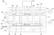
[0014]본 개시내용의 구현은 용량 결합 플라즈마(CCP) 소스 또는 유도 결합 플라즈마(ICP) 소스와 같은 1차 플라즈마 소스 및 원격 플라즈마 소스(RPS)와 같은 2차 플라즈마 소스를 결합하는 하이브리드 플라즈마 처리 시스템에 관한 것이다. 1차 플라즈마 소스는 기판 처리 영역에 인접하게 포지셔닝될 수 있고, 2차 플라즈마 소스는 기판 처리 영역으로부터 더 멀리 포지셔닝될 수 있다. 일 구현에서, 1차 플라즈마 소스는 기판 처리 영역과 2차 플라즈마 소스 사이에 포지셔닝된다. 본 개시내용에서는 CCP 유닛이 1차 플라즈마 소스에 대한 일례로 설명되지만, 유도 결합 플라즈마(ICP) 소스와 같이 저압 방전을 사용하거나, 용량성 방전과 같은 대기압 방전을 사용하는 임의의 플라즈마 소스, 또는 임의의 다른 적절한 플라즈마 소스가 본 명세서에서 설명되는 구현들에서 상호 교환 가능하게 사용될 수 있다. 본 개시내용의 세부사항들 및 다양한 구현들이 아래에서 논의된다.[0014]Implementations of the present disclosure relate to hybrid plasma processing systems that combine a primary plasma source, such as a capacitively coupled plasma (CCP) source or an inductively coupled plasma (ICP) source, and a secondary plasma source, such as a remote plasma source (RPS). . The primary plasma source may be positioned adjacent to the substrate processing region and the secondary plasma source may be positioned further away from the substrate processing region. In one implementation, the primary plasma source is positioned between the substrate processing region and the secondary plasma source. Although the CCP unit is described as an example for a primary plasma source in this disclosure, any plasma source uses low pressure discharge, such as an inductively coupled plasma (ICP) source, or an atmospheric pressure discharge such as capacitive discharge, or any Other suitable plasma sources of may be used interchangeably in the implementations described herein. Details of the disclosure and various implementations are discussed below.
[0015]도 1은 본 개시내용의 일 구현에 따른 처리 시스템(100)의 개략적인 단면을 도시한다. 처리 시스템(100)은 일반적으로 용량 결합 플라즈마(CCP) 유닛(102), CCP 유닛(102)에 결합된 제1 원격 플라즈마 소스(RPS) 유닛(114), 및 CCP 유닛(102)에 결합된 제2 RPS 유닛(105)을 포함한다. 처리 시스템(100)은 제조 설비의 주변 환경과는 다른 내부 압력을 유지할 수 있다. 예를 들어, 처리 시스템(100) 내부의 압력은 약 10mTorr 내지 약 20Torr일 수 있다.[0015]1 shows a schematic cross-section of a
[0016]CCP 유닛(102)은 처리 시스템(100) 내에서 제1 플라즈마 소스로서 기능하게 될 수 있다. CCP 유닛(102)은 일반적으로 리드(106) 및 상대적으로 리드(106) 아래에 배치된 가스 분배판(110)을 포함한다. 가스 분배판(110)은 플라즈마 여기 영역(112)으로의 가스의 균일한 전달을 가능하게 하도록 가스 분배판(110)의 직경을 가로질러 배열된 복수의 관통 홀들(109)을 갖는다. 리드(106) 및 가스 분배판(110)은 알루미늄, 스테인리스 스틸 등과 같은 고농도 도핑 실리콘 또는 금속으로 만들어질 수 있다. 리드(106) 및 가스 분배판(110)은 알루미나 또는 이트륨 산화물을 포함하는 보호 층으로 코팅될 수 있다. 일부 구현들에서, 리드(106)와 가스 분배판(110)은 서로에 대해 전기적으로 바이어싱되어 리드(106)와 가스 분배판(110) 사이의 가스들을 플라즈마로 이온화하기에 충분히 강한 전기장을 발생시킬 수 있는 전기 전도성 전극들이다.[0016]
[0017]플라즈마 발생 가스 혼합물이 가스 소스(137)로부터 제1 가스 유입구(107)를 통해 CCP 유닛(102)에 공급될 수 있다. 제1 가스 유입구(107)는 리드(106)에 배치될 수 있다. 실리콘 함유 층, 예를 들어 실리콘 질화물이 기판 상에 형성되는 일 구현에서, 가스 소스(137)는 실리콘 함유 전구체 및 질소 함유 전구체를 포함할 수 있다. 적절한 실리콘 함유 전구체는 실란들, 할로겐화 실란들, 유기 실란들 및 이들의 임의의 조합들을 포함할 수 있다. 실란들은 실란(SiH4) 및 실험식(SixH(2x+2))을 가진 더 고차의 실란들, 이를테면 디실란(Si2H6), 트리실란(Si3H8) 및 테트라실란(Si4H10), 또는 다른 더 고차의 실란들, 이를테면 폴리클로로실란을 포함할 수 있다. 적절한 질소 함유 전구체는 질소(N2), 아산화질소(N2O), 산화질소(NO), 이산화질소(NO2), 암모니아(NH3) 및 이들의 임의의 조합을 포함할 수 있다. 일 구현에서, 가스 소스(131)는 N2를 포함한다. 일 구현에서, 실리콘 함유 전구체는 SiH4이고 질소 함유 전구체는 N2이다.The plasma generating gas mixture may be supplied from the
[0018]처리 시스템(100)은 또한 기판(151)(예컨대, 웨이퍼 기판)을 지지하고 이동시키도록 동작 가능한 페디스털(150)을 포함한다. 페디스털(150)은 접지될 수 있다. 페디스털(150)과 가스 분배판(110) 간의 거리가 플라즈마 여기 영역(112)을 한정한다. 페디스털(150)은 플라즈마 여기 영역(112)을 증가 또는 감소시키고 가스 분배판(110)을 통과한 가스들에 대해 기판(151)을 재배치함으로써 기판의 증착 또는 에칭에 영향을 미치도록 처리 챔버(100) 내에서 수직으로 또는 축 방향으로 조정 가능할 수 있다. 어떤 경우들에, 페디스털(150)은 기판 상에서 증착/에칭 화학 물질의 균일한 분배를 돕도록 회전 가능할 수 있다. 페디스털(150)은 (도시되지 않은) 열 교환 채널을 갖는데, 이를 통해 열 교환 유체(예컨대, 물)가 흘러 기판의 온도를 제어한다. 열 교환 유체의 순환은 기판 온도가 비교적 낮은 온도들(예컨대, 약 -20℃ 내지 약 90℃)로 유지될 수 있게 한다. 페디스털(150)은 또한 기판을 원하는 가열 온도들(예컨대, 약 90℃ 내지 약 1100℃)로 유지하도록 안에 내장된 (저항성 가열 엘리먼트와 같은) 가열 엘리먼트로 구성될 수 있다.[0018]The
[0019]전기 절연체(108)가 리드(106)와 가스 분배판(110) 사이에 배치되어, 플라즈마가 발생될 때 리드(106)와 가스 분배판(110)이 단락되는 것을 막을 수 있다. 전원 공급 장치(140)가 CCP 유닛(102)에 전기적으로 결합되어, 플라즈마 여기 영역(112)에서 플라즈마를 발생시키도록 리드(106), 가스 분배판(110) 또는 이 둘 다에 전력(예컨대, RF 전력)을 제공한다. 전원 공급 장치(140)는 수행되는 프로세스에 따라 CCP 유닛(102)에 조정 가능한 양의 전력을 전달하도록 구성될 수 있다. 전원 공급 장치(140)는 가스 분배판(110)에 조정 가능한 전압을 생성하여 플라즈마 여기 영역(112)에서 활성화된 가스의 이온 농도를 조정하도록 동작 가능하다. 어떤 경우들에는, 가스 분배판(110)이 접지되는 동안 리드(106)에 전력이 인가될 수 있다.[0019]An
[0020]플라즈마 여기 영역(112)에서 플라즈마의 형성을 가능하게 하기 위해, 절연체(108)가 리드(106)와 가스 분배판(110)을 전기적으로 절연시킬 수 있다. 절연체(108)는 세라믹 재료로 만들어질 수 있으며, 스파킹을 피하도록 높은 항복 전압을 가질 수 있다. 원한다면, CCP 유닛(102)은 플라즈마에 노출된 챔버 컴포넌트들의 표면들을 순환 냉각제(예컨대, 물)로 냉각시키도록 하나 이상의 냉각 유체 채널들을 포함하는 (도시되지 않은) 냉각 유닛을 더 포함할 수 있다.[0020]
[0021]제1 RPS 유닛(114)은 처리 시스템(100) 내에서 제2 플라즈마 소스로서 기능하게 될 수 있다. 제1 RPS 유닛(114)은 이온들, 라디칼들 및 전자들의 플라즈마가 발생되는 컨테이너(117)를 포함한다. 컨테이너(117)는 컨테이너(117)의 한 단부에 배치된 가스 유입구(119) 및 컨테이너(117)의 다른 단부에 배치된 가스 유출구(121)를 갖는다. 가스 유입구(119)는 가스 소스(123)에 결합된다. 가스 소스(123)는 임의의 적절한 가스 또는 가스 혼합물을 함유할 수 있다. 챔버 세정이 요구되는 경우들에, 가스 소스(123)는 NF3, CF4, C2F6 또는 SF6 등과 같은 불소 함유 가스를 포함할 수 있다. 가스 유출구(121)는 제2 가스 유입구(116)를 통해 플라즈마 여기 영역(112)과 유체 연통한다. 제2 가스 유입구(116)는 리드(106)에 배치될 수 있다. 처리 중에, 플라즈마는 제1 RPS 유닛(114)으로부터 제2 가스 유입구(116)를 통해 플라즈마 여기 영역(112) 내로 이동할 수 있다.The
[0022]제1 RPS 유닛(114)은 (가스 소스(123)로부터의) 프로세스 가스를 플라즈마 내로 여기시키기 위한 여기 에너지를 제공하는 (도시되지 않은) 에너지 소스에 결합될 수 있다. 에너지 소스는 마이크로파, 열, UV, RF, 전자 싱크로트론 방사(electron synchrotron radiation) 또는 임의의 적절한 접근 방식에 의해 프로세스 가스를 에너지화할 수 있다. 제1 RPS 유닛(114)으로부터의 에너지화된 프로세스 가스(들)는 CCP 유닛(102) 내부의 프로세스 잔류물들을 세정하거나, 플라즈마 여기 영역(112)에서 플라즈마를 점화(strike)시키는 데 사용될 수 있거나, 플라즈마 여기 영역(112) 내에 이미 형성된 플라즈마를 유지할 수 있다. 일부 구현들에서, 프로세스 가스(들)는 가스 유입구(116)를 통해 CCP 유닛(102)으로 하류로 이동하기 전에 제1 RPS 유닛(114)에서 플라즈마 여기된 종로 이미 변환(또는 적어도 부분적으로 변환)되었을 수 있다. RPS 플라즈마 여기된 종은 이온 하전된 플라즈마 종뿐만 아니라 중성 및 라디칼 종을 포함할 수 있다. 플라즈마 여기된 종이 플라즈마 여기 영역(112)에 도달할 때, 이들은 CCP 유닛(102)에서 추가로 여기될 수 있거나, 플라즈마 여기된 종이 추가 여기 없이 가스 분배판(110)을 통해 플라즈마 여기 영역(112)으로 통과할 수 있다.[0022]The
[0023]선택적으로, 정전기 필터들, 와이어 또는 메시 필터들, 또는 자기 필터들과 같은 적절한 이온 필터(103)가 제1 RPS 유닛(114)과 CCP 유닛(102) 사이에 배치되어, 플라즈마의 라디칼들만이 CCP 유닛(102)으로 흐르도록 플라즈마 내의 대부분 또는 실질적으로 모든 이온들을 제거할 수 있다. 어떤 경우들에, CCP 유닛(102)은 유동 경로로 인한 라디칼 손실을 보상하기 위해 라디칼 재생을 촉진시키거나 서로 다른 RF 주파수 및 다른 파라미터들을 사용함으로써 라디칼 조성을 변경하도록 소량의 전력으로 턴 온될 수 있다. 대안으로, 제1 RPS 유닛(114)으로부터의 플라즈마의 라디칼들이 가스 분배판(110)을 우회하여, 플라즈마 여기 영역(112)에서 발생되는 바람직하지 않은 반응을 피하거나 최소화하도록 CCP 유닛(102)의 전극들에 전력이 공급되지 않을 수 있다.[0023]Optionally, a
[0024]제2 RPS 유닛(105)은 처리 시스템(100)에 대한 라디칼 소스로서 기능하게 된다. 일 실시예에서, 제2 RPS 유닛(105)은 질소 라디칼 소스를 제공하는 데 사용된다. CCP 유닛(102)으로의 질소 라디칼 소스(즉, 제2 RPS 유닛(105))의 통합은, 표면 반응을 위해 플라즈마 여기 영역(112)에 더 많은 라디칼 질소 종이 제공되므로 SiN 막의 증착률을 상당히 증가시킬 수 있다. 배경기술에서 앞서 논의한 바와 같이, 증착 동안 서로 다른 막들에 대한 파라미터들의 변화들 및 증착들 간의 전환 스테이지로 인해 전체 스루풋이 종종 손상을 받는다. 특히, 실리콘 질화물들에 대한 증착 시간은 전체 스루풋의 감소에 대한 주요 원인인 것으로 관찰되었다. 처리 가스(예컨대, SiH4)의 유동, 전력 및 압력을 증가시킴으로써 질화물 증착률이 증가될 수 있지만, 증착된 질화물들에서 Si-H 결합들의 증가된 농도로 인해 균일성과 같은 막 특성들이 악화되는데, 이들은 수소를 쉽게 잃어 댕글링 결합(dangling bond)을 형성하는 것으로 여겨진다.The
[0025]제2 RPS 유닛(105)을 처리 시스템(100)에 통합하는 것은 증착된 막 특성들의 품질을 희생시키지 않으면서 실리콘 질화물들에 대한 증착 시간을 증가시킬 수 있다. 특히, 증착된 SiN 막들은 낮은 Si-H 결합들(따라서 막들에서 낮은 수소 함량)로 형성될 수 있다. 증착된 SiN 막에서의 낮은 수소 함량은 감소된 고유 응력(델타 응력)으로 이어진다. 감소된 고유 응력으로 형성된 SiN 막들은 후속 열 프로세스 동안 막 수축을 방지할 수 있다. 대조적으로, 높은 고유 응력을 갖는 SiN 막들은 측정 가능한 정도로 하부의 얇은 기판을 수축시키고 구부릴 수 있으며, 이는 기판을 오목하게 또는 볼록하게 만든다. 제2 RPS 유닛(105)의 추가는 SiN 막에서 Si-H 결합들의 수를 감소시킬 수 있는데, 이는 제2 RPS 유닛(105)이 풍부한 질소 라디칼들을 제공하여 가스 혼합물로부터 실리콘 및 수소와의 우선 반응을 촉진함으로써, 증착된 막에서 Si-H 결합들을 감소시키기 때문이다. 예를 들어, 증착 중에, 가스 소스(137)로부터의 플라즈마 발생 가스 혼합물(예컨대, SiH4 및 NH3)이 제1 가스 유입구(107)를 통해 CCP 유닛(102)으로 흐르게 된다. 가스 혼합물의 여기는 플라즈마 여기 영역(112)에서 이온 상태로 SiH3, SiH2, SiH, NH2 및 NH 등을 생성할 수 있다. 제2 RPS 유닛(105)으로부터 생성된 라디칼 질소 종(예컨대, N 라디칼들)은 Si-N 결합 에너지들(343kJ/mol)에 비해 더 낮은 Si-Si 결합 에너지들(222kJ/mol)로 인해 실리콘과 우선적으로 반응할 수 있다. SiH3-H 결합 에너지들(378kJ/mol)이 NH2-H 결합 에너지들(435kJ/mol)보다 더 낮기 때문에 라디칼 질소 종은 또한 수소와 우선적으로 반응할 수 있다. 따라서 실리콘 질화물의 표면 반응에 이용 가능한 수소의 양이 감소된다. 따라서 증착 중에, 여기된 가스 혼합물에 라디칼 질소 종을 첨가하는 것은 Si-H 결합들을 Si-N 및 N-H 결합들로 대체하는 것을 촉진하고, 이는 결국 증착된 SiN 막에서 Si-H 결합들의 농도를 감소시킨다. 결과적으로, 증착된 SiN 막 표면에서의 댕글링 결합들의 수가 감소되기 때문에, 증착된 SiN 막이 개선된 막 품질로 형성될 수 있다.Integrating the
[0026]실리콘 질화물 막의 증착은 다음 프로세스 조건들에 의해 수행될 수 있다. 프로세스 챔버(예컨대, CCP 유닛(102))는 약 1Torr 내지 약 10Torr의 압력으로 유지될 수 있다. (가스 소스(131)로부터 플라즈마로 프로세스 가스를 여기시키기 위해 사용되는) 제2 RPS 유닛(105)에 결합된 에너지 소스로부터의 소스 전력은 약 1200와트(W) 내지 약 2500W로 제공될 수 있다. 소스 전력은 약 10㎒ 내지 약 60㎒의 무선 주파수(RF: radio frequency) 범위에서 적용될 수 있다. CCP 유닛(102)의 전극 간격은 약 600밀(mils) 내지 약 1200밀일 수 있다. CCP 유닛(102)에는 SiH4와 NH3의 플라즈마 발생 가스 혼합물이 도입될 수 있다. SiH4의 가스 유동은 약 100sccm 내지 약 500sccm일 수 있고, NH3의 가스 유동은 약 2000sccm 내지 약 5000sccm일 수 있다. 제2 RPS 유닛(105)에는 질소 함유 가스, 예를 들어 N2가 도입될 수 있다. N2의 가스 유동은 약 850sccm 내지 약 1800sccm일 수 있다. 헬륨과 같은 캐리어 가스는 플라즈마 발생 가스 혼합물과 함께 흐르게 될 수 있고, He의 가스 유동은 약 3500sccm 내지 약 8000sccm일 수 있다. 총 프로세스 유동은 약 8000sccm 내지 약 16000sccm일 수 있다. 증착률은 약 3500Å/분 이상, 예를 들어 약 3800Å/분 내지 약 5000Å/분이다.Deposition of the silicon nitride film may be performed by the following process conditions. The process chamber (eg, CCP unit 102) may be maintained at a pressure of about 1 Torr to about 10 Torr. Source power from an energy source coupled to the second RPS unit 105 (used to excite the process gas from the
[0027]하기 표 1은 실리콘 질화물 막들의 증착을 위한 세 가지 개별 프로세스 조건들을 열거한다. 막 #1 및 #2는 RPS(즉, 제2 RPS 유닛(105))가 턴 온된 상태에서 SiN 증착된다. 막 #3은 RPS가 턴 오프된 상태에서 SiN 증착된다. 하기 표 2는 증착된 막 #1, #2 및 #3의 응력 및 FTIR 스펙트럼들을 보여준다. FTIR 스펙트럼들은 Si-H 대 Si-N의 백분율을 나타낸다.[0027]Table 1 below lists three separate process conditions for the deposition of silicon nitride films. Films # 1 and # 2 are SiN deposited with RPS (i.e., second RPS unit 105) turned on. Film # 3 is SiN deposited with the RPS turned off. Table 2 below shows the stress and FTIR spectra of the deposited films # 1, # 2 and # 3. FTIR spectra represent the percentage of Si-H to Si-N.
(W)(W)
(Torr)(Torr)
(밀)(wheat)
(sccm)(sccm)
(sccm)(sccm)
(sccm)(sccm)
(sccm)(sccm)
(sccm)(sccm)
(중앙)(center)
(70㎜)(70 mm)
(140㎜)(140 mm)
[0028]표 1 및 표 2에서 확인될 수 있듯이, SiN 막 #1이 더 낮은 RF 전력 및 더 높은 질소 유량을 사용하여 증착되었다는 점을 제외하고는 유사한 프로세스 조건들 하에서 SiN 막 #1 및 #2가 증착되었다. SiN 막 #1 및 #2가 RPS 온으로 증착된 동안(즉, 제2 RPS 유닛(105)으로부터 라디칼 질소 종을 도입함), SiN 막 #2는 더 낮은 고유 응력을 갖는데, 이는 SiN 막 #1의 증착 동안 더 많은 질소가 제공되었더라도, 증가된 RF 전력이 증착된 SiN 막들에서 더 낮은 수소 함량을 야기할 수 있음을 시사한다. 또한, 표 2의 SiN 막 #2는 SiN 막 #3과 비교할 때 감소된 고유 응력을 보여주는데, 이는 제2 RPS 유닛(105)으로부터 라디칼 질소 종의 도입이 증착된 SiN 막에서 Si-H 결합들의 농도를 감소시킬 수 있음을 시사한다. 마찬가지로, 증착된 SiN 막의 다양한 위치들에서의 FTIR 스펙트럼들은 또한 SiN 막 #2가 SiN 막 #3에 비해 더 낮은 Si-H 대 Si-N의 백분율을 가짐을 보여준다.[0028]As can be seen from Table 1 and Table 2, SiN films # 1 and # 2 were deposited under similar process conditions except that SiN film # 1 was deposited using lower RF power and higher nitrogen flow rates. . While SiN films # 1 and # 2 were deposited on RPS on (i.e., introducing radical nitrogen species from the second RPS unit 105), SiN film # 2 had a lower intrinsic stress, which was SiN film # 1 Although more nitrogen was provided during the deposition of, it suggests that increased RF power may result in lower hydrogen content in the deposited SiN films. In addition, SiN film # 2 in Table 2 shows a reduced intrinsic stress compared to SiN film # 3, which indicates the concentration of Si—H bonds in the SiN film deposited with the introduction of radical nitrogen species from the
[0029]제2 RPS 유닛(105)은 이온들, 라디칼들 및 전자들의 플라즈마가 발생되는 컨테이너(125)를 포함할 수 있다. 컨테이너(125)는 컨테이너(125)의 한 단부에 배치된 가스 유입구(127) 및 컨테이너(125)의 다른 단부에 배치된 가스 유출구(129)를 가질 수 있다. 가스 유출구(129)는 제3 가스 유입구(133)를 통해 플라즈마 여기 영역(112)과 유체 연통한다. 제3 가스 유입구(133)는 리드(106)에 배치될 수 있다. 가스 유입구(127)는 가스 소스(131)에 결합된다. 가스 소스(131)는 임의의 적절한 가스 또는 가스 혼합물을 함유할 수 있다. 기판 상에 질소 함유 재료가 형성되는 경우들에, 가스 소스(131)는 질소(N2), 아산화질소(N2O), 산화질소(NO), 이산화질소(NO2), 암모니아(NH3) 및 이들의 임의의 조합과 같은 질소 함유 가스를 포함할 수 있다. 일 구현에서, 가스 소스(131)는 N2를 포함한다.The
[0030]제2 RPS 유닛(105)은 가스 소스(131)로부터의 프로세스 가스를 플라즈마 내로 여기시키기 위한 여기 에너지를 제공하는 (도시되지 않은) 에너지 소스에 결합될 수 있다. 에너지 소스는 마이크로파, 열, UV, RF, 전자 싱크로트론 방사 또는 임의의 적절한 접근 방식에 의해 프로세스 가스를 에너지화할 수 있다. 가스 소스(131)가 N2를 함유하는 경우들에, N2의 에너지 여기는 N* 라디칼들, 양으로 하전된 이온들, 이를테면 N+ 및 N2+, 그리고 전자들을 제2 RPS 유닛(105)에서 생성한다.The
[0031]이온 필터(135)가 제2 RPS 유닛(105)과 CCP 유닛(102) 사이에 배치된다. 이온 필터(135)는, 제3 가스 유입구(133)를 통해 흐르는 플라즈마에서 대부분의 또는 실질적으로 모든 이온들을 제거하여 플라즈마의 라디칼들만이 플라즈마 여기 영역(112)으로 흐르게 되도록 제3 가스 유입구(133)의 길이를 따라 임의의 위치에 배치될 수 있다. 이온 필터(135)는 정전기 필터들, 와이어 또는 메시 필터들, 또는 자기 필터들과 같은 임의의 적절한 이온 필터일 수 있다. 이온 필터(135)의 사용은 제2 RPS 유닛(105)이 제3 가스 유입구(133)를 통해 플라즈마 여기 영역(112) 내로 질소 함유 라디칼들과 같은 라디칼 함유 전구체를 제공할 수 있게 한다.[0031]An
[0032]처리 챔버(100)는 단일 CCP 유닛(102)으로 도시되어 있지만, 단일 CCP 유닛(102)은 탠덤(tandem) 처리 챔버로 대체될 수 있다는 점이 고려된다. 즉, CCP 유닛(102)은 제1 RPS 유닛(114) 및 제2 RPS 유닛(105)을 공유하는 2개의 개별 분리된 CCP 유닛들일 수 있다. 이러한 경우, 탠덤 CCP 유닛들 중 각각의 유닛을 커버하기 위해 하우징이 사용될 수 있다. 2개의 개별 CCP 유닛들은 대칭 또는 비대칭 방식으로 서로 인접하게 포지셔닝될 수 있다. 2개의 개별 CCP 유닛들과 제1 RPS 유닛(114) 및 제2 RPS 유닛(105)은 프로세스의 전체 스루풋을 더 증가시킨다.[0032]Although processing
[0033]도 2는 본 개시내용의 다른 구현에 따른 처리 시스템(200)의 개략적인 단면을 도시한다. 처리 시스템(200)은, 제1 가스 유입구(107)가 CCP 유닛(102)의 측벽(203)에 배치되도록 개조된다는 점을 제외하고는 처리 시스템(100)과 유사하다. 또한, 처리 시스템(100)의 가스 분배판(110)은 또한 이중 채널 가스 분배판(202)으로 대체된다. 이중 채널 가스 분배판(202)은 제1 RPS 유닛(114) 및 제2 RPS 유닛(105)으로부터 나오는 가스(들) 및 CCP 유닛(102)의 측벽에 배치된 측벽 가스 유입구(206)를 통해 가스 소스(204)로부터 나오는 가스(들)의 통과를 가능하게 하도록 구성된다. 마찬가지로, 처리 시스템(200)은 또한 CCP 유닛(102), CCP 유닛(102)에 결합된 제1 RPS 유닛(114), 및 CCP 유닛(102)에 결합된 제2 RPS 유닛(105)을 포함한다. CCP 유닛(102), 제1 RPS 유닛(114) 및 제2 RPS 유닛(105), 그리고 이들과 연관된 컴포넌트들의 상세한 설명들은 도 1과 관련하여 위에서 확인될 수 있다.[0033]2 shows a schematic cross-section of a
[0034]이 구현에서, 이중 채널 가스 분배판(202)은 상대적으로 리드(106) 아래에 배치된다. 이중 채널 가스 분배판(202)은 이중 채널 가스 분배판(202)의 두께를 가로지르는 제1 세트의 채널들(208)을 포함한다. 제1 세트의 채널들(208)은 플라즈마 여기 영역(112)으로 가스의 균일한 전달을 가능하게 하도록 이중 채널 가스 분배판(202)의 직경을 가로질러 배열된다. 이중 채널 가스 분배판(202)은 또한, 이중 채널 가스 분배판(202) 내에 배치된 제2 세트의 채널들(210)을 포함한다. 제2 세트의 채널들(210)은 이중 채널 가스 분배판(202)의 두께를 가로지르지 않을 수 있다. 따라서 제2 세트의 채널들(210)은 제1 RPS 유닛(114) 및 제2 RPS 유닛(105)과 유체 연통하지 않는다. 대신에, 제2 세트의 채널들(210)은 측벽 가스 유입구(206)를 통해 가스 소스(204)로 유체 결합된다.[0034]In this implementation, the dual channel
[0035]제1 세트 및 제2 세트의 채널들(208, 210)은 제2 RPS 유닛(105)으로부터의 라디칼 질소 종과 가스 소스(204)로부터의 가스/전구체 혼합물이 플라즈마 여기 영역(112)에 도달할 때까지 이들이 결합되는 것을 방지한다. 일부 구현들에서, 제2 세트의 채널들(210)은 플라즈마 여기 영역(112)을 향하는 개구에서 환형 형상을 가질 수 있고, 이러한 환형 개구들은 제1 세트의 채널들(208)의 원형 개구들 주위에 동심으로 정렬될 수 있다.[0035]The first and second sets of
[0036]실리콘 함유 층, 예를 들어 실리콘 질화물이 기판 상에 형성되는 경우들에, 가스 소스(204)는 실리콘 함유 전구체 및 질소 함유 전구체를 포함할 수 있다. 적절한 실리콘 함유 전구체 및 질소 함유 전구체는 도 1에 관해 위에서 논의된다. 일례로, 실리콘 함유 전구체는 실란이고 질소 함유 전구체는 NH3이다. 그러나 가스 소스들(123, 131, 204)의 함량은 수행되는 프로세스에 따라 달라질 수 있다.In cases where a silicon containing layer, such as silicon nitride, is formed on a substrate, the
[0037]증착 중에, 질소 함유 라디칼들과 같은 라디칼 함유 전구체가 제3 가스 유입구(133)를 통해 제2 RPS 유닛(105)으로부터 플라즈마 여기 영역(112)으로 도입된다. 순차적으로 또는 동시에, 실리콘 함유 전구체(예컨대, SiH4)와 질소 함유 전구체(예컨대, NH3)의 가스 혼합물과 같은 제2 가스가 측벽 가스 유입구(206) 및 제2 세트의 채널들(210)을 통해 가스 소스(204)로부터 플라즈마 여기 영역(112)으로 도입된다. 제2 가스의 여기는 플라즈마 여기 영역(112)에서 이온 상태로 SiH3, SiH2, SiH, NH2 및 NH 등을 생성할 수 있다. 제2 RPS 유닛(105)으로부터 생성된 라디칼 질소 종은 Si-N 결합 에너지들(343kJ/mol)에 비해 더 낮은 Si-Si 결합 에너지들(222kJ/mol)로 인해 실리콘과 우선적으로 반응한다. SiH3-H 결합 에너지들(378kJ/mol)이 NH2-H 결합 에너지들(435kJ/mol)보다 더 낮기 때문에 라디칼 질소 종은 또한 수소와 반응할 수 있다. 따라서 실리콘 질화물의 표면 반응에 이용 가능한 수소의 양이 감소된다. 도 2의 구성을 사용하여, 여기된 가스 혼합물에 라디칼 질소 종을 첨가하는 것은 또한 Si-H 결합들을 Si-N 및 N-H 결합들로 대체하는 것을 촉진할 수 있고, 이는 결국 증착된 SiN 막에서 Si-H 결합들의 농도를 감소시킨다. 결과적으로, 증착된 SiN 막은 더 낮은 고유 응력으로 형성된다. CCP 유닛(102)으로의 질소 라디칼 소스(즉, 제2 RPS 유닛(105))의 통합은, 표면 반응을 위해 플라즈마 여기 영역(112)에 더 많은 라디칼 질소 종이 제공되므로 SiN 막의 증착률을 상당히 증가시킨다.During deposition, a radical containing precursor, such as nitrogen containing radicals, is introduced from the
[0038]도 3은 본 개시내용의 또 다른 구현에 따른 처리 시스템(300)의 개략적인 단면을 도시한다. 처리 시스템(300)은 일반적으로 용량 결합 플라즈마(CCP) 유닛(302) 및 CCP 유닛(302) 위에 배치된 인-시튜(in-situ) 플라즈마 소스 유닛(304)을 포함한다. CCP 유닛(302)은 처리 시스템(300) 내에서 제1 플라즈마 소스를 생성하도록 기능한다. 인-시튜 플라즈마 소스 유닛(304)은 일반적으로 리드(306) 및 상대적으로 리드(306) 아래에 배치된 가스 분배판(308)을 포함한다. 가스 분배판(308)은 도 1에 관해 앞서 논의한 가스 분배판(110)과 유사한 구성을 갖는다.[0038]3 shows a schematic cross section of a
[0039]인-시튜 플라즈마 소스 유닛(304)은 또한 리드(306)에 배치될 수 있는 가스 유입구(303)를 통해 리드(306)에 결합된 가스 소스(301)를 갖는다. 가스 소스(301)는 임의의 적절한 가스 또는 가스 혼합물을 함유할 수 있다. 기판 상에 질소 함유 재료가 형성되는 경우들에, 가스 소스(301)는 질소(N2), 아산화질소(N2O), 산화질소(NO), 이산화질소(NO2), 암모니아(NH3) 및 이들의 임의의 조합과 같은 질소 함유 가스를 포함할 수 있다. 일 구현에서, 가스 소스(301)는 N2를 포함한다. 질소 함유 가스는 가스 분배판(308)과 이온 억제 엘리먼트(312) 사이에 한정된 제1 플라즈마 여기 영역(307)으로 가스 분배판(308)의 관통 홀들을 통해 흐른다.The in-situ
[0040]인-시튜 플라즈마 소스 유닛(304)은 상대적으로 가스 분배판(308) 아래에 배치된 이온 억제 엘리먼트(312)를 선택적으로 포함할 수 있다. 리드(306) 및/또는 가스 분배판(308)은 리드(306) 및/또는 가스 분배판(308)에 RF 전력을 제공하는 RF 발생기(313)에 결합될 수 있다. 이온 억제 엘리먼트(312)는 접지될 수 있다. RF 전력이 공급된 리드(306) 및/또는 가스 분배판(308)은 캐소드 전극으로서의 역할을 할 수 있는 한편, 접지된 이온 억제 엘리먼트(312)는 애노드 전극으로서의 역할을 할 수 있다. 리드(306) 및/또는 가스 분배판(308) 그리고 이온 억제 엘리먼트(312)는 제1 플라즈마 여기 영역(307)(즉, 가스 분배판(308)과 이온 억제 엘리먼트(312) 사이의 영역)에서 RF 전기장을 형성하도록 작동된다. RF 전기장은 가스 소스(301)로부터의 프로세스 가스(들)를 제1 플라즈마 여기 영역(307)에서 플라즈마로 이온화한다.[0040]The in-situ
[0041]이온 억제 엘리먼트(312)는 일반적으로, 하전되지 않은 중성 또는 라디칼 종이 이온 억제 엘리먼트(312)를 통해 제2 플라즈마 여기 영역(318) 내로 통과하는 것을 가능하게 하면서, 이온 하전된 종의 제1 플라즈마 여기 영역(307) 밖으로의 이동을 억제하도록 구성된 복수의 관통 홀들(322)을 포함한다. 이러한 하전되지 않은 종은 관통 홀들(322)을 통해 덜 반응성인 캐리어 가스로 이송되는 고 반응성 종을 포함할 수 있다. 따라서 관통 홀들(322)을 통한 이온 종의 이동이 감소될 수 있고, 일부 경우들에는 완전히 억제될 수 있다. 이온 억제 엘리먼트(312)를 통과하는 이온 종의 양을 제어하는 것은 하부 기판과 접촉하게 되는 가스 혼합물에 대한 증가된 제어를 제공하며, 이는 결국 가스 혼합물의 증착 특성들의 제어를 증가시킨다. 이온 억제 엘리먼트(312)는 알루미늄, 스테인리스 스틸 등과 같은 고농도 도핑 실리콘 또는 금속으로 만들어질 수 있다. 일 구현에서, 관통 홀들(322)은 제2 플라즈마 여기 영역(318)을 향하는 테이퍼 부분 및 제1 플라즈마 여기 영역(307)을 향하는 원통형 부분을 포함할 수 있다.[0041]The
[0042]도 1과 관련하여 위에서 논의된 바와 같은 전기 절연체(108)와 유사한 제1 전기 절연체(310)는 이온 억제 엘리먼트(312)와 가스 분배판(308) 사이에 배치된다.[0042]A first
[0043]도 2와 관련하여 위에서 논의된 바와 같은 이중 채널 가스 분배판(202)과 같은 이중 채널 가스 분배판(316)은 상대적으로 이온 억제 엘리먼트(312) 아래에 배치된다. 이중 채널 가스 분배판(316)은 CCP 유닛(302)의 일부로 간주될 수 있다. 이중 채널 가스 분배판(316)은 이중 채널 가스 분배판(316)의 두께를 가로지르는 제1 세트의 채널들(317)을 포함한다. 제1 세트의 채널들(317)은 제2 플라즈마 여기 영역(318)으로 가스의 균일한 전달을 가능하게 하도록 이중 채널 가스 분배판(316)의 직경을 가로질러 배열된다. 이중 채널 가스 분배판(316)은 또한, 이중 채널 가스 분배판(316) 내에 배치된 제2 세트의 채널들(319)을 포함한다. 제2 세트의 채널들(319)은 이중 채널 가스 분배판(316)의 두께를 가로지르지 않을 수 있다. 따라서 제2 세트의 채널들(319)은 제1 플라즈마 여기 영역(307)과 유체 연통하지 않는다. 대신에, 제2 세트의 채널들(319)은 CCP 유닛(302)의 측벽(354)에 배치된 측벽 가스 유입구(352)를 통해 가스 소스(337)에 유체 결합된다.[0043]A dual channel
[0044]제1 세트 및 제2 세트의 채널들(317, 319)은 제1 플라즈마 여기 영역(307)으로부터의 라디칼 질소 종과 가스 소스(337)로부터의 가스/전구체 혼합물이 제2 플라즈마 여기 영역(318)에 도달할 때까지 이들이 결합되는 것을 방지한다. 일부 구현들에서, 이온 억제 엘리먼트(312)의 관통 홀들(322) 중 하나 이상은, 플라즈마 여기된 종 중 적어도 일부가 이들의 유동 방향을 변경하지 않고도 관통 홀들(322), 제1 세트의 채널들(317) 및 관통 홀들(315)을 통과할 수 있게 하도록, 플라즈마 억제기(314)의 관통 홀들(315) 및 제1 세트의 채널들(317) 중 하나 이상과 정렬될 수 있다. 일부 구현들에서, 제2 세트의 채널들(319)은 제2 플라즈마 여기 영역(318)을 향하는 개구에서 환형 형상을 가질 수 있고, 이러한 환형 개구들은 제1 세트의 채널들(317)의 원형 개구들 주위에 동심으로 정렬될 수 있다.[0044]The first and second sets of
[0045]이온 억제 엘리먼트(312)와 이중 채널 가스 분배판(316) 사이에 플라즈마 억제기(314)가 선택적으로 배치된다. 플라즈마 억제기(314)는 플라즈마 억제기(314)의 직경을 가로질러 배치된 복수의 관통 홀들(315)을 갖는다. 관통 홀들(315) 각각의 치수 및 단면 기하학적 구조는 제2 플라즈마 여기 영역(318)으로부터 다시 제1 플라즈마 여기 영역(307)으로의 플라즈마의 상당한 역류를 방지하도록 구성된다. 특히, 관통 홀들(315)은 이중 채널 가스 분배판(316)으로의 가스의 통과를 가능하게 하도록 치수가 정해지지만, 그 안에서 플라즈마 방전의 발생을 방지하기에 충분히 작다. 예를 들어, 관통 홀들(315) 각각은 약 0.050"의 직경을 가질 수 있다. 이런 식으로, 일반적으로 플라즈마 억제기(314)를 지나 제1 세트의 채널들(317) 내에 플라즈마 방전이 존재하는 것이 방지된다.[0045]Plasma suppressor 314 is optionally disposed between
[0046]도 1과 관련하여 위에서 논의된 바와 같은 페디스털(150)과 같은 페디스털(350)은 상대적으로 이중 채널 가스 분배판(316) 아래에 배치된다. 페디스털(350)은 CCP 유닛(302)의 일부로 간주될 수 있다. 페디스털(350)은 접지될 수 있다. 이중 채널 가스 분배판(316)은 RF 발생기(320)에 결합될 수 있고 캐소드 전극으로서 기능하는 한편, 접지된 페디스털(350)은 애노드 전극으로서의 역할을 할 수 있다. 이중 채널 가스 분배판(316) 및 접지된 페디스털(350)은 플라즈마 여기 영역(318)(즉, 이중 채널 가스 분배판(316)과 페디스털(350) 사이의 영역)에 RF 전기장을 형성하도록 작동된다. RF 전기장은 가스 소스(337)로부터의 프로세스 가스(들)를 제2 플라즈마 여기 영역(318)에서 플라즈마로 이온화한다. 가스 소스(337)는 CCP 유닛(302)의 측벽(354)에 배치되는 측벽 가스 유입구(352)를 통해 제2 플라즈마 여기 영역(318)과 유체 연통한다. 제2 가스 유입구(352)는 이중 채널 가스 분배판(316)의 제2 세트의 채널들(319)에 연결된다.[0046]A pedestal 350, such as
[0047]실리콘 함유 층, 예를 들어 실리콘 질화물이 기판 상에 형성되는 일 구현에서, 가스 소스(337)는 실리콘 함유 전구체 및 질소 함유 전구체를 포함할 수 있다. 적절한 실리콘 함유 전구체는 실란들, 할로겐화 실란들, 유기 실란들 및 이들의 임의의 조합들을 포함할 수 있다. 실란(SiH4) 및 실험식(SixH(2x+2))을 가진 더 고차의 실란들, 이를테면 디실란(Si2H6), 트리실란(Si3H8) 및 테트라실란(Si4H10), 또는 다른 더 고차의 실란들, 이를테면 폴리클로로실란을 포함할 수 있다. 적절한 질소 함유 전구체는 질소(N2), 아산화질소(N2O), 산화질소(NO), 이산화질소(NO2), 암모니아(NH3) 및 이들의 임의의 조합을 포함할 수 있다. 일 구현에서, 실리콘 함유 전구체는 SiH4이고, 질소 함유 전구체는 NH3이다.In one implementation where a silicon containing layer, eg, silicon nitride, is formed on a substrate, the
[0048]도 1과 관련하여 위에서 논의된 전기 절연체(108)와 유사한 제2 전기 절연체(356)는 이중 채널 가스 분배판(316) 아래의 측벽(354)에 배치된다.[0048]A second electrical insulator 356 similar to the
[0049]마찬가지로, 질소 함유 라디칼들과 같은 라디칼 함유 전구체는 증착 중에 제2 플라즈마 여기 영역(318)으로 도입된다. 순차적으로 또는 동시에, 실리콘 함유 전구체(예컨대, SiH4)와 질소 함유 전구체(예컨대, NH3)의 가스 혼합물과 같은 제2 가스가 측벽 가스 유입구(352)를 통해 가스 소스(337)로부터 제2 플라즈마 여기 영역(318)으로 도입된다. 제2 가스의 여기는 제2 플라즈마 여기 영역(318)에서 이온 상태로 SiH3, SiH2, SiH, NH2 및 NH 등을 생성할 수 있다. 도 1 및 도 2와 관련하여 위에서 논의된 것들과 유사하게, 인-시튜 플라즈마 소스 유닛(304)으로부터 생성된 라디칼 질소 종은 Si-N 결합 에너지들에 비해 더 낮은 Si-Si 결합 에너지들로 인해 실리콘과 우선적으로 반응할 수 있다. SiH3-H 결합 에너지들이 NH2-H 결합 에너지들보다 더 낮기 때문에 라디칼 질소 종은 또한 수소와 반응할 수 있다. 따라서 실리콘 질화물의 표면 반응에 이용 가능한 수소의 양이 감소된다. 도 3의 구성을 사용하여, 여기된 가스 혼합물에 라디칼 질소 종을 첨가하는 것은 Si-H 결합들을 Si-N 및 N-H 결합들로 대체하는 것을 촉진할 수 있고, 이는 결국 증착된 SiN 막에서 Si-H 결합들의 농도를 감소시킨다. 결과적으로, 증착된 SiN 막은 더 낮은 고유 응력으로 형성될 수 있다. 처리 시스템(300) 내에서 CCP 유닛(302)으로의 질소 라디칼 소스(즉, 인-시튜 플라즈마 소스 유닛(304))의 통합은, 표면 반응을 위해 제2 플라즈마 여기 영역(318)에 더 많은 라디칼 질소 종이 제공되므로 SiN 막의 증착률을 상당히 증가시킬 수 있다.Likewise, radical containing precursors, such as nitrogen containing radicals, are introduced into the second
[0050]요약하면, 본 개시내용의 구현들은 기판 처리를 위해 RPS 유닛을 CCP 유닛과 통합한 개선된 플라즈마 처리 시스템을 제공한다. RPS 유닛을 사용하여 CCP 유닛 내의 플라즈마 여기 영역에서 여기된 가스 혼합물에 풍부한 질소 라디칼 종을 전달함으로써, Si-H 결합들이 Si-N 및 N-H 결합들로 대체될 수 있고, 이는 결국 증착된 SiN 막에서 Si-H 결합들의 농도를 감소시킨다. 더 낮은 Si-H 결합들은 증착된 SiN 막에서의 더 낮은 고유 응력으로 이어진다. 결과적으로, 증착된 SiN 막은 개선된 막 품질로 형성된다. 가스 반응에 질소 라디칼 종을 첨가하는 것은 또한, 표면 반응을 위해 플라즈마 여기 영역에 더 많은 라디칼 질소 종이 제공되므로 SiN 막의 증착률을 증가시킨다.[0050]In summary, implementations of the present disclosure provide an improved plasma processing system integrating an RPS unit with a CCP unit for substrate processing. By using the RPS unit to deliver abundant nitrogen radical species to the gas mixture excited in the plasma excitation region within the CCP unit, Si-H bonds can be replaced with Si-N and NH bonds, which in turn result in a deposited SiN film Reduce the concentration of Si-H bonds. Lower Si-H bonds lead to lower intrinsic stress in the deposited SiN film. As a result, the deposited SiN film is formed with improved film quality. Adding nitrogen radical species to the gas reaction also increases the deposition rate of the SiN film since more radical nitrogen species are provided in the plasma excitation region for the surface reaction.
[0051]전술한 내용은 본 개시내용의 구현들에 관한 것이지만, 본 개시내용의 기본 범위를 벗어나지 않으면서 본 개시내용의 다른 구현들 및 추가 구현들이 안출될 수 있으며, 본 개시내용의 범위는 하기의 청구항들에 의해 결정된다.[0051]While the foregoing is directed to implementations of the present disclosure, other and further implementations of the disclosure may be devised without departing from the basic scope thereof, and the scope of the disclosure is set forth in the claims below. Determined by
Claims (15)
Translated fromKorean플라즈마 소스 유닛 ― 상기 플라즈마 소스 유닛은,
리드(lid);
상기 리드 아래에 배치된 가스 분배판 ― 상기 가스 분배판은 상기 가스 분배판의 직경을 가로질러 배열된 복수의 관통 홀들을 가짐 ―; 및
상기 가스 분배판 아래에 배치된 페디스털(pedestal)을 포함하며,
상기 페디스털과 상기 가스 분배판은 그 사이에 플라즈마 여기 영역을 한정함 ―;
상기 리드에 배치된 제1 가스 유입구에 결합된 제1 가스 유출구를 갖는 제1 원격 플라즈마 소스(RPS: remote plasma source) 유닛 ― 상기 제1 가스 유출구는 상기 플라즈마 여기 영역과 유체 연통함 ―; 및
상기 리드에 배치된 제2 가스 유입구에 결합된 제2 가스 유출구를 갖는 제2 RPS 유닛을 포함하며,
상기 제2 가스 유출구는 상기 플라즈마 여기 영역과 유체 연통하고, 상기 제2 RPS 유닛은 상기 제2 가스 유출구와 상기 리드의 제2 가스 유입구 사이에 배치된 이온 필터를 갖는,
기판 처리 시스템.As a substrate processing system,
Plasma source unit—the plasma source unit,
Lid;
A gas distribution plate disposed below the lid, the gas distribution plate having a plurality of through holes arranged across the diameter of the gas distribution plate; And
A pedestal disposed below the gas distribution plate,
The pedestal and the gas distribution plate define a plasma excitation region therebetween;
A first remote plasma source (RPS) unit having a first gas outlet coupled to a first gas inlet disposed in the lid, the first gas outlet in fluid communication with the plasma excitation region; And
A second RPS unit having a second gas outlet coupled to a second gas inlet disposed in the lid,
The second gas outlet is in fluid communication with the plasma excitation region, and the second RPS unit has an ion filter disposed between the second gas outlet and the second gas inlet of the lid,
Substrate processing system.
상기 플라즈마 소스 유닛은 용량 결합 플라즈마(CCP: capacitively coupled plasma) 유닛, 유도 결합 플라즈마(ICP: inductively coupled plasma) 소스, 또는 저압 또는 대기압 방전을 사용하는 플라즈마 소스인,
기판 처리 시스템.According to claim 1,
The plasma source unit is a capacitively coupled plasma (CCP) unit, an inductively coupled plasma (ICP) source, or a plasma source using low pressure or atmospheric pressure discharge,
Substrate processing system.
상기 플라즈마 소스 유닛은 용량 결합 플라즈마(CCP) 유닛인,
기판 처리 시스템.The method of claim 2,
The plasma source unit is a capacitively coupled plasma (CCP) unit,
Substrate processing system.
상기 제1 RPS는 불소를 포함하는 제1 가스 소스에 연결되고, 상기 제2 RPS는 질소를 포함하는 제2 가스 소스에 연결되는,
기판 처리 시스템.According to claim 1,
Wherein the first RPS is connected to a first gas source comprising fluorine and the second RPS is connected to a second gas source comprising nitrogen
Substrate processing system.
상기 리드에 배치된 제3 가스 유입구를 더 포함하며,
상기 제3 가스 유입구는 실리콘 함유 전구체 및 질소 함유 전구체를 포함하는 제3 가스 소스와 유체 연통하는,
기판 처리 시스템.According to claim 1,
Further comprising a third gas inlet disposed in the lid,
The third gas inlet is in fluid communication with a third gas source comprising a silicon containing precursor and a nitrogen containing precursor,
Substrate processing system.
상기 실리콘 함유 전구체는 실란들, 할로겐화 실란들, 유기 실란들 또는 이들의 조합들을 포함하고,
상기 질소 함유 전구체는 질소(N2), 아산화질소(N2O), 산화질소(NO), 이산화질소(NO2), 암모니아(NH3) 또는 이들의 조합들을 포함하는,
기판 처리 시스템.The method of claim 5,
The silicon-containing precursor comprises silanes, halogenated silanes, organic silanes or combinations thereof,
The nitrogen-containing precursor includes nitrogen (N2 ), nitrous oxide (N2 O), nitrogen oxides (NO), nitrogen dioxide (NO2 ), ammonia (NH3 ) or combinations thereof
Substrate processing system.
플라즈마 소스 유닛 ― 상기 플라즈마 소스 유닛은,
리드; 및
상기 리드 아래에 배치된 이중 채널 가스 분배판을 포함하고,
상기 이중 채널 가스 분배판은,
상기 이중 채널 가스 분배판의 두께를 가로지르는 제1 세트의 채널들 ― 상기 제1 세트의 채널들은 이중 채널 가스 분배판의 직경을 가로질러 배열됨 ―; 및
상기 이중 채널 가스 분배판 내에 배치된 제2 세트의 채널들을 가지며,
상기 제2 세트의 채널들은 상기 이중 채널 가스 분배판의 두께의 일부를 가로지름 ―;
상기 이중 채널 가스 분배판 아래에 배치된 페디스털 ― 상기 페디스털과 상기 이중 채널 가스 분배판은 그 사이에 플라즈마 여기 영역을 한정함 ―;
상기 리드에 배치된 제1 가스 유입구에 결합된 제1 가스 유출구를 갖는 제1 원격 플라즈마 소스(RPS) 유닛 ― 상기 제1 가스 유출구는 상기 플라즈마 여기 영역과 유체 연통함 ―; 및
상기 리드에 배치된 제2 가스 유입구에 결합된 제2 가스 유출구를 갖는 제2 RPS 유닛을 포함하며,
상기 제2 가스 유출구는 상기 플라즈마 여기 영역과 유체 연통하고, 상기 제2 RPS 유닛은 상기 제2 가스 유출구와 상기 리드의 제2 가스 유입구 사이에 배치된 이온 필터를 갖는,
기판 처리 시스템.As a substrate processing system,
Plasma source unit—the plasma source unit,
lead; And
A dual channel gas distribution plate disposed below said lid,
The dual channel gas distribution plate,
A first set of channels across the thickness of the dual channel gas distribution plate, wherein the first set of channels are arranged across the diameter of the dual channel gas distribution plate; And
Having a second set of channels disposed within the dual channel gas distribution plate,
The second set of channels traverse a portion of the thickness of the dual channel gas distribution plate;
A pedestal disposed below the dual channel gas distribution plate, wherein the pedestal and the dual channel gas distribution plate define a plasma excitation region therebetween;
A first remote plasma source (RPS) unit having a first gas outlet coupled to a first gas inlet disposed in the lid, the first gas outlet in fluid communication with the plasma excitation region; And
A second RPS unit having a second gas outlet coupled to a second gas inlet disposed in the lid,
The second gas outlet is in fluid communication with the plasma excitation region, and the second RPS unit has an ion filter disposed between the second gas outlet and the second gas inlet of the lid,
Substrate processing system.
상기 플라즈마 소스 유닛은 용량 결합 플라즈마(CCP) 유닛, 유도 결합 플라즈마(ICP) 소스, 또는 저압 또는 대기압 방전을 사용하는 플라즈마 소스인,
기판 처리 시스템.The method of claim 7, wherein
The plasma source unit is a capacitively coupled plasma (CCP) unit, an inductively coupled plasma (ICP) source, or a plasma source using low or atmospheric pressure discharge,
Substrate processing system.
상기 제1 RPS는 불소를 포함하는 제1 가스 소스에 연결되고, 상기 제2 RPS는 질소를 포함하는 제2 가스 소스에 연결되는,
기판 처리 시스템.The method of claim 7, wherein
Wherein the first RPS is connected to a first gas source comprising fluorine and the second RPS is connected to a second gas source comprising nitrogen
Substrate processing system.
상기 제2 세트의 채널들은 상기 플라즈마 소스 유닛의 측벽에 배치된 측벽 가스 유입구를 통해 제3 가스 소스에 유체 결합되는,
기판 처리 시스템.The method of claim 7, wherein
Wherein the second set of channels are fluidly coupled to a third gas source through sidewall gas inlets disposed on the sidewalls of the plasma source unit.
Substrate processing system.
리드;
상대적으로 상기 리드 아래에 배치된 가스 분배판 ― 상기 가스 분배판은 상기 가스 분배판의 직경을 가로질러 배열된 복수의 관통 홀들을 가짐 ―;
상대적으로 상기 가스 분배판 아래에 배치된 이온 억제 엘리먼트 ― 상기 이온 억제 엘리먼트는 테이퍼 부분 및 원통형 부분을 각각 갖는 복수의 관통 홀들을 가지며, 상기 이온 억제 엘리먼트와 상기 가스 분배판은 제1 플라즈마 여기 영역을 한정함 ―;
상대적으로 상기 이온 억제 엘리먼트 아래에 배치된 이중 채널 가스 분배판 ― 상기 이중 채널 가스 분배판은,
상기 이중 채널 가스 분배판의 두께를 가로지르는 제1 세트의 채널들 ― 상기 제1 세트의 채널들은 이중 채널 가스 분배판의 직경을 가로질러 배열됨 ―; 및
상기 이중 채널 가스 분배판 내에 배치된 제2 세트의 채널들을 가지며,
상기 제2 세트의 채널들은 상기 이중 채널 가스 분배판의 두께의 일부를 가로지름 ―;
상기 이온 억제 엘리먼트와 상기 이중 채널 가스 분배판 사이에 배치된 플라즈마 억제기 ― 상기 플라즈마 억제기는 상기 플라즈마 억제기의 직경을 가로질러 배치된 복수의 관통 홀들을 가짐 ―;
상기 이중 채널 가스 분배판 아래에 배치된 페디스털 ― 상기 페디스털과 상기 이중 채널 가스 분배판은 그 사이에 제2 플라즈마 여기 영역을 한정함 ―;
상기 리드에 배치된 제1 가스 유입구에 결합된 제1 가스 소스 ― 상기 제1 가스 유입구는 상기 제1 플라즈마 여기 영역과 유체 연통함 ―; 및
상기 기판 처리 시스템의 측벽에 배치된 제2 가스 유입구에 결합된 제2 가스 소스를 포함하는,
기판 처리 시스템.As a substrate processing system,
lead;
A gas distribution plate disposed relatively below the lid, the gas distribution plate having a plurality of through holes arranged across the diameter of the gas distribution plate;
A ion suppression element disposed relatively below the gas distribution plate, wherein the ion suppression element has a plurality of through holes each having a tapered portion and a cylindrical portion, the ion suppression element and the gas distribution plate defining a first plasma excitation region; Limited;
A dual channel gas distribution plate disposed relatively below the ion suppression element, wherein the dual channel gas distribution plate comprises:
A first set of channels across the thickness of the dual channel gas distribution plate, wherein the first set of channels are arranged across the diameter of the dual channel gas distribution plate; And
Having a second set of channels disposed within the dual channel gas distribution plate,
The second set of channels traverse a portion of the thickness of the dual channel gas distribution plate;
A plasma suppressor disposed between the ion suppression element and the dual channel gas distribution plate, the plasma suppressor having a plurality of through holes disposed across the diameter of the plasma suppressor;
A pedestal disposed below the dual channel gas distribution plate, wherein the pedestal and the dual channel gas distribution plate define a second plasma excitation region therebetween;
A first gas source coupled to a first gas inlet disposed in the lid, the first gas inlet in fluid communication with the first plasma excitation region; And
A second gas source coupled to a second gas inlet disposed on a sidewall of the substrate processing system;
Substrate processing system.
상기 리드 및/또는 상기 가스 분배판은 RF 발생기에 결합되고, 상기 이온 억제 엘리먼트는 접지되는,
기판 처리 시스템.The method of claim 11, wherein
The lead and / or the gas distribution plate is coupled to an RF generator and the ion suppression element is grounded,
Substrate processing system.
상기 이중 채널 가스 분배판은 RF 발생기에 결합되고, 상기 페디스털은 접지되는,
기판 처리 시스템.The method of claim 11, wherein
The dual channel gas distribution plate is coupled to an RF generator and the pedestal is grounded,
Substrate processing system.
상기 제1 가스 소스는 질소를 포함하는,
기판 처리 시스템.The method of claim 11, wherein
Wherein the first gas source comprises nitrogen;
Substrate processing system.
상기 제2 가스 소스는 실리콘 함유 전구체 및 질소 함유 전구체를 포함하며,
상기 실리콘 함유 전구체는 실란들, 할로겐화 실란들, 유기 실란들 및 이들의 임의의 조합들을 포함하고,
상기 질소 함유 전구체는 질소(N2), 아산화질소(N2O), 산화질소(NO), 이산화질소(NO2), 암모니아(NH3) 및 이들의 임의의 조합들을 포함하는,
기판 처리 시스템.The method of claim 11, wherein
The second gas source comprises a silicon containing precursor and a nitrogen containing precursor,
The silicon containing precursor comprises silanes, halogenated silanes, organic silanes and any combination thereof,
The nitrogen-containing precursor includes nitrogen (N2 ), nitrous oxide (N2 O), nitrogen oxides (NO), nitrogen dioxide (NO2 ), ammonia (NH3 ), and any combination thereof.
Substrate processing system.
Applications Claiming Priority (3)
| Application Number | Priority Date | Filing Date | Title |
|---|---|---|---|
| US201762483798P | 2017-04-10 | 2017-04-10 | |
| US62/483,798 | 2017-04-10 | ||
| PCT/US2018/025038WO2018191021A1 (en) | 2017-04-10 | 2018-03-29 | High deposition rate high quality silicon nitride enabled by remote nitrogen radical source |
Publications (1)
| Publication Number | Publication Date |
|---|---|
| KR20190130044Atrue KR20190130044A (en) | 2019-11-20 |
Family
ID=63711763
Family Applications (1)
| Application Number | Title | Priority Date | Filing Date |
|---|---|---|---|
| KR1020197033073ACeasedKR20190130044A (en) | 2017-04-10 | 2018-03-29 | High deposition rate, high quality silicon nitride made possible by remote nitrogen radical source |
Country Status (5)
| Country | Link |
|---|---|
| US (1) | US20180294144A1 (en) |
| JP (1) | JP2020517103A (en) |
| KR (1) | KR20190130044A (en) |
| CN (1) | CN110494950A (en) |
| WO (1) | WO2018191021A1 (en) |
Cited By (3)
| Publication number | Priority date | Publication date | Assignee | Title |
|---|---|---|---|---|
| WO2024102586A1 (en)* | 2022-11-07 | 2024-05-16 | Lam Research Corporation | Chemical vapor deposition of silicon nitride using a remote plasma |
| KR20240103884A (en) | 2022-12-27 | 2024-07-04 | 세메스 주식회사 | Method of forming a pattern structure including a silicon nitride |
| KR20240104968A (en) | 2022-12-28 | 2024-07-05 | 세메스 주식회사 | Method of forming a pattern structure including a silicon nitride |
Families Citing this family (8)
| Publication number | Priority date | Publication date | Assignee | Title |
|---|---|---|---|---|
| US11967486B2 (en)* | 2019-01-23 | 2024-04-23 | Lam Research Corporation | Substrate processing system including dual ion filter for downstream plasma |
| CN119980191A (en)* | 2019-08-28 | 2025-05-13 | 朗姆研究公司 | Metal Deposition |
| JP2024517165A (en)* | 2021-05-06 | 2024-04-19 | アプライド マテリアルズ インコーポレイテッド | Processing system and method for forming void-free and seam-free tungsten features |
| KR20240005861A (en)* | 2021-05-06 | 2024-01-12 | 어플라이드 머티어리얼스, 인코포레이티드 | Processing systems and methods to improve productivity of void-free and gap-free tungsten gapfill processes |
| KR20230014339A (en)* | 2021-07-21 | 2023-01-30 | 세메스 주식회사 | Method and apparatus for treating substrate |
| JP2024538526A (en)* | 2021-09-23 | 2024-10-23 | ラム リサーチ コーポレーション | Remote plasma deposition with electrostatic clamping |
| US20230215702A1 (en)* | 2021-12-30 | 2023-07-06 | Applied Materials, Inc. | Uniformity control for plasma processing using wall recombination |
| TW202440991A (en)* | 2022-10-07 | 2024-10-16 | 美商應用材料股份有限公司 | Methods for clean rate improvement in multi-rpsc pecvd systems |
Family Cites Families (9)
| Publication number | Priority date | Publication date | Assignee | Title |
|---|---|---|---|---|
| US7588036B2 (en)* | 2002-07-01 | 2009-09-15 | Applied Materials, Inc. | Chamber clean method using remote and in situ plasma cleaning systems |
| EP2311065B1 (en)* | 2008-07-09 | 2014-09-10 | TEL Solar AG | Remote plasma cleaning method and apparatus for applying said method |
| US7935643B2 (en)* | 2009-08-06 | 2011-05-03 | Applied Materials, Inc. | Stress management for tensile films |
| US20120180954A1 (en)* | 2011-01-18 | 2012-07-19 | Applied Materials, Inc. | Semiconductor processing system and methods using capacitively coupled plasma |
| US10049881B2 (en)* | 2011-08-10 | 2018-08-14 | Applied Materials, Inc. | Method and apparatus for selective nitridation process |
| US20140099794A1 (en)* | 2012-09-21 | 2014-04-10 | Applied Materials, Inc. | Radical chemistry modulation and control using multiple flow pathways |
| US10256079B2 (en)* | 2013-02-08 | 2019-04-09 | Applied Materials, Inc. | Semiconductor processing systems having multiple plasma configurations |
| US9362130B2 (en)* | 2013-03-01 | 2016-06-07 | Applied Materials, Inc. | Enhanced etching processes using remote plasma sources |
| KR102247560B1 (en)* | 2014-07-14 | 2021-05-03 | 삼성전자 주식회사 | Plasma generating method in RPS(Remote Plasma Source) and method for fabricating semiconductor device comprising the same plasma generating method |
- 2018
- 2018-03-29JPJP2019554959Apatent/JP2020517103A/enactivePending
- 2018-03-29KRKR1020197033073Apatent/KR20190130044A/ennot_activeCeased
- 2018-03-29USUS15/939,363patent/US20180294144A1/ennot_activeAbandoned
- 2018-03-29WOPCT/US2018/025038patent/WO2018191021A1/ennot_activeCeased
- 2018-03-29CNCN201880024110.8Apatent/CN110494950A/enactivePending
Cited By (3)
| Publication number | Priority date | Publication date | Assignee | Title |
|---|---|---|---|---|
| WO2024102586A1 (en)* | 2022-11-07 | 2024-05-16 | Lam Research Corporation | Chemical vapor deposition of silicon nitride using a remote plasma |
| KR20240103884A (en) | 2022-12-27 | 2024-07-04 | 세메스 주식회사 | Method of forming a pattern structure including a silicon nitride |
| KR20240104968A (en) | 2022-12-28 | 2024-07-05 | 세메스 주식회사 | Method of forming a pattern structure including a silicon nitride |
Also Published As
| Publication number | Publication date |
|---|---|
| CN110494950A (en) | 2019-11-22 |
| US20180294144A1 (en) | 2018-10-11 |
| JP2020517103A (en) | 2020-06-11 |
| WO2018191021A1 (en) | 2018-10-18 |
Similar Documents
| Publication | Publication Date | Title |
|---|---|---|
| KR20190130044A (en) | High deposition rate, high quality silicon nitride made possible by remote nitrogen radical source | |
| US10056233B2 (en) | RPS assisted RF plasma source for semiconductor processing | |
| US11676812B2 (en) | Method for forming silicon nitride film selectively on top/bottom portions | |
| US10916407B2 (en) | Conditioning remote plasma source for enhanced performance having repeatable etch and deposition rates | |
| US7989365B2 (en) | Remote plasma source seasoning | |
| TWI697954B (en) | Semiconductor processing systems having multiple plasma configurations | |
| US8573151B2 (en) | Microwave plasma processing apparatus, dielectric window for use in the microwave plasma processing apparatus, and method for manufacturing the dielectric window | |
| KR101568944B1 (en) | Plasma generator and cvd device | |
| TWI523971B (en) | Radical gas generation system | |
| US20090277587A1 (en) | Flowable dielectric equipment and processes | |
| US6344420B1 (en) | Plasma processing method and plasma processing apparatus | |
| JP2017147444A (en) | Method for selectively forming a silicon nitride film on a sidewall or a flat surface of a trench | |
| KR20130114607A (en) | Plasma processing apparatus and plasma processing method | |
| WO2013019565A2 (en) | Inductive plasma sources for wafer processing and chamber cleaning | |
| KR102405729B1 (en) | Geometric Selective Deposition of Dielectric Films Using Low Frequency Bias | |
| CN108292588B (en) | Advanced coating method and material for preventing HDP-CVD chamber arcing | |
| CN101003033A (en) | Gas separation type showerhead | |
| KR102710534B1 (en) | Method for forming silicon nitride film selectively on sidewalls or flat surfaces of trenches | |
| JP4545107B2 (en) | Method of forming low dielectric constant film with stable film quality | |
| JP7564123B2 (en) | Increasing plasma density in the processing chamber | |
| TWI889667B (en) | Electrostatic chuck with powder coating | |
| JP2005260186A (en) | Plasma process equipment | |
| KR20140086607A (en) | Thin film deposition method with high speed and apparatus for the same | |
| KR20080004178A (en) | Chemical vapor deposition using plasma enhanced chemical vapor deposition | |
| JP2004296548A (en) | Surface treatment equipment |
Legal Events
| Date | Code | Title | Description |
|---|---|---|---|
| PA0105 | International application | Patent event date:20191107 Patent event code:PA01051R01D Comment text:International Patent Application | |
| PG1501 | Laying open of application | ||
| PA0201 | Request for examination | Patent event code:PA02012R01D Patent event date:20210305 Comment text:Request for Examination of Application | |
| E902 | Notification of reason for refusal | ||
| PE0902 | Notice of grounds for rejection | Comment text:Notification of reason for refusal Patent event date:20220519 Patent event code:PE09021S01D | |
| E601 | Decision to refuse application | ||
| PE0601 | Decision on rejection of patent | Patent event date:20220805 Comment text:Decision to Refuse Application Patent event code:PE06012S01D Patent event date:20220519 Comment text:Notification of reason for refusal Patent event code:PE06011S01I |