KR20190126073A - Metallic chemical vapor deposition approaches and resulting structures for fabricating wrap-around contacts - Google Patents
Metallic chemical vapor deposition approaches and resulting structures for fabricating wrap-around contactsDownload PDFInfo
- Publication number
- KR20190126073A KR20190126073AKR1020197025556AKR20197025556AKR20190126073AKR 20190126073 AKR20190126073 AKR 20190126073AKR 1020197025556 AKR1020197025556 AKR 1020197025556AKR 20197025556 AKR20197025556 AKR 20197025556AKR 20190126073 AKR20190126073 AKR 20190126073A
- Authority
- KR
- South Korea
- Prior art keywords
- semiconductor
- source
- drain structure
- integrated circuit
- semiconductor source
- Prior art date
- Legal status (The legal status is an assumption and is not a legal conclusion. Google has not performed a legal analysis and makes no representation as to the accuracy of the status listed.)
- Granted
Links
- 238000005229chemical vapour depositionMethods0.000titleclaimsabstractdescription26
- 238000013459approachMethods0.000titleabstractdescription15
- 239000004065semiconductorSubstances0.000claimsabstractdescription263
- 229910052751metalInorganic materials0.000claimsabstractdescription154
- 239000002184metalSubstances0.000claimsabstractdescription154
- 239000000463materialSubstances0.000claimsabstractdescription114
- 239000000758substrateSubstances0.000claimsabstractdescription68
- 238000012876topographyMethods0.000claimsabstractdescription64
- 239000000203mixtureSubstances0.000claimsabstractdescription35
- 238000000034methodMethods0.000claimsdescription44
- 239000010936titaniumSubstances0.000claimsdescription36
- 229910052719titaniumInorganic materials0.000claimsdescription34
- RTAQQCXQSZGOHL-UHFFFAOYSA-NTitaniumChemical compound[Ti]RTAQQCXQSZGOHL-UHFFFAOYSA-N0.000claimsdescription31
- 229910052710siliconInorganic materials0.000claimsdescription28
- 239000010703siliconSubstances0.000claimsdescription28
- 238000004519manufacturing processMethods0.000claimsdescription27
- 230000004888barrier functionEffects0.000claimsdescription22
- 239000000460chlorineSubstances0.000claimsdescription16
- 229910052801chlorineInorganic materials0.000claimsdescription16
- ZAMOUSCENKQFHK-UHFFFAOYSA-NChlorine atomChemical compound[Cl]ZAMOUSCENKQFHK-UHFFFAOYSA-N0.000claimsdescription15
- 229910052732germaniumInorganic materials0.000claimsdescription11
- GNPVGFCGXDBREM-UHFFFAOYSA-Ngermanium atomChemical compound[Ge]GNPVGFCGXDBREM-UHFFFAOYSA-N0.000claimsdescription11
- 238000001465metallisationMethods0.000claimsdescription9
- 238000006243chemical reactionMethods0.000claimsdescription3
- 229910052739hydrogenInorganic materials0.000claimsdescription3
- 239000001257hydrogenSubstances0.000claimsdescription3
- 125000004435hydrogen atomChemical class[H]*0.000claimsdescription3
- XJDNKRIXUMDJCW-UHFFFAOYSA-Jtitanium tetrachlorideChemical compoundCl[Ti](Cl)(Cl)ClXJDNKRIXUMDJCW-UHFFFAOYSA-J0.000claimsdescription3
- 239000010410layerSubstances0.000description155
- XUIMIQQOPSSXEZ-UHFFFAOYSA-NSiliconChemical compound[Si]XUIMIQQOPSSXEZ-UHFFFAOYSA-N0.000description26
- 238000004891communicationMethods0.000description15
- 238000012545processingMethods0.000description13
- 230000006870functionEffects0.000description10
- 238000001459lithographyMethods0.000description10
- 238000000151depositionMethods0.000description9
- 238000002955isolationMethods0.000description9
- 125000006850spacer groupChemical group0.000description9
- VYPSYNLAJGMNEJ-UHFFFAOYSA-NSilicium dioxideChemical compoundO=[Si]=OVYPSYNLAJGMNEJ-UHFFFAOYSA-N0.000description8
- 230000008021depositionEffects0.000description8
- 239000003989dielectric materialSubstances0.000description8
- 229910000577Silicon-germaniumInorganic materials0.000description7
- 239000004020conductorSubstances0.000description7
- 239000010949copperSubstances0.000description7
- 238000000059patterningMethods0.000description7
- 229910052721tungstenInorganic materials0.000description7
- 229910052581Si3N4Inorganic materials0.000description6
- 229910045601alloyInorganic materials0.000description6
- 239000000956alloySubstances0.000description6
- 229910052782aluminiumInorganic materials0.000description6
- 229910052802copperInorganic materials0.000description6
- 229910052735hafniumInorganic materials0.000description6
- HQVNEWCFYHHQES-UHFFFAOYSA-Nsilicon nitrideChemical compoundN12[Si]34N5[Si]62N3[Si]51N64HQVNEWCFYHHQES-UHFFFAOYSA-N0.000description6
- 239000010408filmSubstances0.000description5
- 239000011229interlayerSubstances0.000description5
- 150000002739metalsChemical class0.000description5
- PXHVJJICTQNCMI-UHFFFAOYSA-NnickelSubstances[Ni]PXHVJJICTQNCMI-UHFFFAOYSA-N0.000description5
- 229920002120photoresistant polymerPolymers0.000description5
- 238000004544sputter depositionMethods0.000description5
- LEVVHYCKPQWKOP-UHFFFAOYSA-N[Si].[Ge]Chemical compound[Si].[Ge]LEVVHYCKPQWKOP-UHFFFAOYSA-N0.000description4
- 239000006117anti-reflective coatingSubstances0.000description4
- 238000000231atomic layer depositionMethods0.000description4
- 239000003990capacitorSubstances0.000description4
- 239000011231conductive fillerSubstances0.000description4
- 238000004377microelectronicMethods0.000description4
- 229910052759nickelInorganic materials0.000description4
- 229910021420polycrystalline siliconInorganic materials0.000description4
- 235000012239silicon dioxideNutrition0.000description4
- 239000000377silicon dioxideSubstances0.000description4
- OKTJSMMVPCPJKN-UHFFFAOYSA-NCarbonChemical compound[C]OKTJSMMVPCPJKN-UHFFFAOYSA-N0.000description3
- 238000000137annealingMethods0.000description3
- 230000015572biosynthetic processEffects0.000description3
- -1but not limited toSubstances0.000description3
- 229910052799carbonInorganic materials0.000description3
- 238000005516engineering processMethods0.000description3
- 230000003628erosive effectEffects0.000description3
- 239000000945fillerSubstances0.000description3
- 229910052737goldInorganic materials0.000description3
- VBJZVLUMGGDVMO-UHFFFAOYSA-Nhafnium atomChemical compound[Hf]VBJZVLUMGGDVMO-UHFFFAOYSA-N0.000description3
- 239000012535impuritySubstances0.000description3
- 229910044991metal oxideInorganic materials0.000description3
- 150000004706metal oxidesChemical class0.000description3
- 229910052763palladiumInorganic materials0.000description3
- 238000000623plasma-assisted chemical vapour depositionMethods0.000description3
- 229910052697platinumInorganic materials0.000description3
- 229910052707rutheniumInorganic materials0.000description3
- 229910052709silverInorganic materials0.000description3
- 229910052720vanadiumInorganic materials0.000description3
- 235000012431wafersNutrition0.000description3
- 229910052726zirconiumInorganic materials0.000description3
- 229910005540GaPInorganic materials0.000description2
- NBIIXXVUZAFLBC-UHFFFAOYSA-NPhosphoric acidChemical compoundOP(O)(O)=ONBIIXXVUZAFLBC-UHFFFAOYSA-N0.000description2
- 229910021417amorphous siliconInorganic materials0.000description2
- 239000002800charge carrierSubstances0.000description2
- 238000005137deposition processMethods0.000description2
- 239000002019doping agentSubstances0.000description2
- 239000007772electrode materialSubstances0.000description2
- 239000003822epoxy resinSubstances0.000description2
- 238000005530etchingMethods0.000description2
- HZXMRANICFIONG-UHFFFAOYSA-Ngallium phosphideChemical compound[Ga]#PHZXMRANICFIONG-UHFFFAOYSA-N0.000description2
- 229910000449hafnium oxideInorganic materials0.000description2
- WIHZLLGSGQNAGK-UHFFFAOYSA-Nhafnium(4+);oxygen(2-)Chemical compound[O-2].[O-2].[Hf+4]WIHZLLGSGQNAGK-UHFFFAOYSA-N0.000description2
- 239000012212insulatorSubstances0.000description2
- 230000010354integrationEffects0.000description2
- MRELNEQAGSRDBK-UHFFFAOYSA-Nlanthanum(3+);oxygen(2-)Chemical compound[O-2].[O-2].[O-2].[La+3].[La+3]MRELNEQAGSRDBK-UHFFFAOYSA-N0.000description2
- 230000000873masking effectEffects0.000description2
- 238000012986modificationMethods0.000description2
- 230000004048modificationEffects0.000description2
- 239000010955niobiumSubstances0.000description2
- 238000005240physical vapour depositionMethods0.000description2
- 229920000647polyepoxidePolymers0.000description2
- WGTYBPLFGIVFAS-UHFFFAOYSA-Mtetramethylammonium hydroxideChemical compound[OH-].C[N+](C)(C)CWGTYBPLFGIVFAS-UHFFFAOYSA-M0.000description2
- WFKWXMTUELFFGS-UHFFFAOYSA-NtungstenChemical compound[W]WFKWXMTUELFFGS-UHFFFAOYSA-N0.000description2
- 239000010937tungstenSubstances0.000description2
- JBRZTFJDHDCESZ-UHFFFAOYSA-NAsGaChemical compound[As]#[Ga]JBRZTFJDHDCESZ-UHFFFAOYSA-N0.000description1
- 229910000952Be alloyInorganic materials0.000description1
- ZOXJGFHDIHLPTG-UHFFFAOYSA-NBoronChemical compound[B]ZOXJGFHDIHLPTG-UHFFFAOYSA-N0.000description1
- RYGMFSIKBFXOCR-UHFFFAOYSA-NCopperChemical compound[Cu]RYGMFSIKBFXOCR-UHFFFAOYSA-N0.000description1
- 229910002601GaNInorganic materials0.000description1
- GYHNNYVSQQEPJS-UHFFFAOYSA-NGalliumChemical compound[Ga]GYHNNYVSQQEPJS-UHFFFAOYSA-N0.000description1
- 229910001218Gallium arsenideInorganic materials0.000description1
- 229910000530Gallium indium arsenideInorganic materials0.000description1
- JMASRVWKEDWRBT-UHFFFAOYSA-NGallium nitrideChemical compound[Ga]#NJMASRVWKEDWRBT-UHFFFAOYSA-N0.000description1
- GPXJNWSHGFTCBW-UHFFFAOYSA-NIndium phosphideChemical compound[In]#PGPXJNWSHGFTCBW-UHFFFAOYSA-N0.000description1
- FYYHWMGAXLPEAU-UHFFFAOYSA-NMagnesiumChemical compound[Mg]FYYHWMGAXLPEAU-UHFFFAOYSA-N0.000description1
- BPQQTUXANYXVAA-UHFFFAOYSA-NOrthosilicateChemical compound[O-][Si]([O-])([O-])[O-]BPQQTUXANYXVAA-UHFFFAOYSA-N0.000description1
- 239000004642PolyimideSubstances0.000description1
- BUGBHKTXTAQXES-UHFFFAOYSA-NSeleniumChemical compound[Se]BUGBHKTXTAQXES-UHFFFAOYSA-N0.000description1
- 229910004298SiO 2Inorganic materials0.000description1
- NINIDFKCEFEMDL-UHFFFAOYSA-NSulfurChemical compound[S]NINIDFKCEFEMDL-UHFFFAOYSA-N0.000description1
- NRTOMJZYCJJWKI-UHFFFAOYSA-NTitanium nitrideChemical compound[Ti]#NNRTOMJZYCJJWKI-UHFFFAOYSA-N0.000description1
- HCHKCACWOHOZIP-UHFFFAOYSA-NZincChemical compound[Zn]HCHKCACWOHOZIP-UHFFFAOYSA-N0.000description1
- KXNLCSXBJCPWGL-UHFFFAOYSA-N[Ga].[As].[In]Chemical compound[Ga].[As].[In]KXNLCSXBJCPWGL-UHFFFAOYSA-N0.000description1
- XWCMFHPRATWWFO-UHFFFAOYSA-N[O-2].[Ta+5].[Sc+3].[O-2].[O-2].[O-2]Chemical compound[O-2].[Ta+5].[Sc+3].[O-2].[O-2].[O-2]XWCMFHPRATWWFO-UHFFFAOYSA-N0.000description1
- 238000010521absorption reactionMethods0.000description1
- FTWRSWRBSVXQPI-UHFFFAOYSA-Nalumanylidynearsane;gallanylidynearsaneChemical compound[As]#[Al].[As]#[Ga]FTWRSWRBSVXQPI-UHFFFAOYSA-N0.000description1
- XAGFODPZIPBFFR-UHFFFAOYSA-NaluminiumChemical compound[Al]XAGFODPZIPBFFR-UHFFFAOYSA-N0.000description1
- 229910000147aluminium phosphateInorganic materials0.000description1
- 229910052787antimonyInorganic materials0.000description1
- WATWJIUSRGPENY-UHFFFAOYSA-Nantimony atomChemical compound[Sb]WATWJIUSRGPENY-UHFFFAOYSA-N0.000description1
- 238000003491arrayMethods0.000description1
- 229910052785arsenicInorganic materials0.000description1
- RQNWIZPPADIBDY-UHFFFAOYSA-Narsenic atomChemical compound[As]RQNWIZPPADIBDY-UHFFFAOYSA-N0.000description1
- 125000004429atomChemical group0.000description1
- QVGXLLKOCUKJST-UHFFFAOYSA-Natomic oxygenChemical compound[O]QVGXLLKOCUKJST-UHFFFAOYSA-N0.000description1
- 229910052454barium strontium titanateInorganic materials0.000description1
- 229910002113barium titanateInorganic materials0.000description1
- JRPBQTZRNDNNOP-UHFFFAOYSA-Nbarium titanateChemical compound[Ba+2].[Ba+2].[O-][Ti]([O-])([O-])[O-]JRPBQTZRNDNNOP-UHFFFAOYSA-N0.000description1
- 229910052790berylliumInorganic materials0.000description1
- ATBAMAFKBVZNFJ-UHFFFAOYSA-Nberyllium atomChemical compound[Be]ATBAMAFKBVZNFJ-UHFFFAOYSA-N0.000description1
- 230000005540biological transmissionEffects0.000description1
- 229910052796boronInorganic materials0.000description1
- 230000001413cellular effectEffects0.000description1
- 229910010293ceramic materialInorganic materials0.000description1
- 229910017052cobaltInorganic materials0.000description1
- 239000010941cobaltSubstances0.000description1
- GUTLYIVDDKVIGB-UHFFFAOYSA-Ncobalt atomChemical compound[Co]GUTLYIVDDKVIGB-UHFFFAOYSA-N0.000description1
- 230000000295complement effectEffects0.000description1
- 238000007796conventional methodMethods0.000description1
- 239000013078crystalSubstances0.000description1
- 229910021419crystalline siliconInorganic materials0.000description1
- 230000001419dependent effectEffects0.000description1
- 230000009977dual effectEffects0.000description1
- 230000005670electromagnetic radiationEffects0.000description1
- 238000010894electron beam technologyMethods0.000description1
- 230000008030eliminationEffects0.000description1
- 238000003379elimination reactionMethods0.000description1
- 239000011152fibreglassSubstances0.000description1
- 238000011049fillingMethods0.000description1
- 229910052733galliumInorganic materials0.000description1
- BHEPBYXIRTUNPN-UHFFFAOYSA-Nhydridophosphorus(.) (triplet)Chemical compound[PH]BHEPBYXIRTUNPN-UHFFFAOYSA-N0.000description1
- 238000000671immersion lithographyMethods0.000description1
- 229910052738indiumInorganic materials0.000description1
- WPYVAWXEWQSOGY-UHFFFAOYSA-Nindium antimonideChemical compound[Sb]#[In]WPYVAWXEWQSOGY-UHFFFAOYSA-N0.000description1
- APFVFJFRJDLVQX-UHFFFAOYSA-Nindium atomChemical compound[In]APFVFJFRJDLVQX-UHFFFAOYSA-N0.000description1
- 239000011810insulating materialSubstances0.000description1
- JQJCSZOEVBFDKO-UHFFFAOYSA-Nlead zincChemical compound[Zn].[Pb]JQJCSZOEVBFDKO-UHFFFAOYSA-N0.000description1
- 230000007774longtermEffects0.000description1
- 229910052749magnesiumInorganic materials0.000description1
- 239000011777magnesiumSubstances0.000description1
- 229910001092metal group alloyInorganic materials0.000description1
- 229910021421monocrystalline siliconInorganic materials0.000description1
- 229910052758niobiumInorganic materials0.000description1
- GUCVJGMIXFAOAE-UHFFFAOYSA-Nniobium atomChemical compound[Nb]GUCVJGMIXFAOAE-UHFFFAOYSA-N0.000description1
- TWNQGVIAIRXVLR-UHFFFAOYSA-Noxo(oxoalumanyloxy)alumaneChemical compoundO=[Al]O[Al]=OTWNQGVIAIRXVLR-UHFFFAOYSA-N0.000description1
- SIWVEOZUMHYXCS-UHFFFAOYSA-Noxo(oxoyttriooxy)yttriumChemical compoundO=[Y]O[Y]=OSIWVEOZUMHYXCS-UHFFFAOYSA-N0.000description1
- 229910052760oxygenInorganic materials0.000description1
- 239000001301oxygenSubstances0.000description1
- BPUBBGLMJRNUCC-UHFFFAOYSA-Noxygen(2-);tantalum(5+)Chemical compound[O-2].[O-2].[O-2].[O-2].[O-2].[Ta+5].[Ta+5]BPUBBGLMJRNUCC-UHFFFAOYSA-N0.000description1
- RVTZCBVAJQQJTK-UHFFFAOYSA-Noxygen(2-);zirconium(4+)Chemical compound[O-2].[O-2].[Zr+4]RVTZCBVAJQQJTK-UHFFFAOYSA-N0.000description1
- 229920001721polyimidePolymers0.000description1
- 239000002861polymer materialSubstances0.000description1
- 229920005591polysiliconPolymers0.000description1
- 230000005855radiationEffects0.000description1
- VSZWPYCFIRKVQL-UHFFFAOYSA-Nselanylidenegallium;seleniumChemical compound[Se].[Se]=[Ga].[Se]=[Ga]VSZWPYCFIRKVQL-UHFFFAOYSA-N0.000description1
- 229910052711seleniumInorganic materials0.000description1
- 239000011669seleniumSubstances0.000description1
- 229910021332silicideInorganic materials0.000description1
- FVBUAEGBCNSCDD-UHFFFAOYSA-Nsilicide(4-)Chemical compound[Si-4]FVBUAEGBCNSCDD-UHFFFAOYSA-N0.000description1
- 239000007787solidSubstances0.000description1
- 238000003860storageMethods0.000description1
- VEALVRVVWBQVSL-UHFFFAOYSA-Nstrontium titanateChemical compound[Sr+2].[O-][Ti]([O-])=OVEALVRVVWBQVSL-UHFFFAOYSA-N0.000description1
- 229910052717sulfurInorganic materials0.000description1
- 239000011593sulfurSubstances0.000description1
- 229910052715tantalumInorganic materials0.000description1
- GUVRBAGPIYLISA-UHFFFAOYSA-Ntantalum atomChemical compound[Ta]GUVRBAGPIYLISA-UHFFFAOYSA-N0.000description1
- MZLGASXMSKOWSE-UHFFFAOYSA-Ntantalum nitrideChemical compound[Ta]#NMZLGASXMSKOWSE-UHFFFAOYSA-N0.000description1
- 229910001936tantalum oxideInorganic materials0.000description1
- 229910052714telluriumInorganic materials0.000description1
- PORWMNRCUJJQNO-UHFFFAOYSA-Ntellurium atomChemical compound[Te]PORWMNRCUJJQNO-UHFFFAOYSA-N0.000description1
- 239000010409thin filmSubstances0.000description1
- LEONUFNNVUYDNQ-UHFFFAOYSA-Nvanadium atomChemical compound[V]LEONUFNNVUYDNQ-UHFFFAOYSA-N0.000description1
- 229910052725zincInorganic materials0.000description1
- 239000011701zincSubstances0.000description1
- 229910001928zirconium oxideInorganic materials0.000description1
- GFQYVLUOOAAOGM-UHFFFAOYSA-Nzirconium(iv) silicateChemical compound[Zr+4].[O-][Si]([O-])([O-])[O-]GFQYVLUOOAAOGM-UHFFFAOYSA-N0.000description1
Images


Classifications
- H—ELECTRICITY
- H01—ELECTRIC ELEMENTS
- H01L—SEMICONDUCTOR DEVICES NOT COVERED BY CLASS H10
- H01L21/00—Processes or apparatus adapted for the manufacture or treatment of semiconductor or solid state devices or of parts thereof
- H01L21/02—Manufacture or treatment of semiconductor devices or of parts thereof
- H01L21/04—Manufacture or treatment of semiconductor devices or of parts thereof the devices having potential barriers, e.g. a PN junction, depletion layer or carrier concentration layer
- H01L21/18—Manufacture or treatment of semiconductor devices or of parts thereof the devices having potential barriers, e.g. a PN junction, depletion layer or carrier concentration layer the devices having semiconductor bodies comprising elements of Group IV of the Periodic Table or AIIIBV compounds with or without impurities, e.g. doping materials
- H01L21/28—Manufacture of electrodes on semiconductor bodies using processes or apparatus not provided for in groups H01L21/20 - H01L21/268
- H01L21/283—Deposition of conductive or insulating materials for electrodes conducting electric current
- H01L21/285—Deposition of conductive or insulating materials for electrodes conducting electric current from a gas or vapour, e.g. condensation
- H01L21/28506—Deposition of conductive or insulating materials for electrodes conducting electric current from a gas or vapour, e.g. condensation of conductive layers
- H01L21/28512—Deposition of conductive or insulating materials for electrodes conducting electric current from a gas or vapour, e.g. condensation of conductive layers on semiconductor bodies comprising elements of Group IV of the Periodic Table
- H01L21/28556—Deposition of conductive or insulating materials for electrodes conducting electric current from a gas or vapour, e.g. condensation of conductive layers on semiconductor bodies comprising elements of Group IV of the Periodic Table by chemical means, e.g. CVD, LPCVD, PECVD, laser CVD
- H—ELECTRICITY
- H10—SEMICONDUCTOR DEVICES; ELECTRIC SOLID-STATE DEVICES NOT OTHERWISE PROVIDED FOR
- H10D—INORGANIC ELECTRIC SEMICONDUCTOR DEVICES
- H10D30/00—Field-effect transistors [FET]
- H10D30/60—Insulated-gate field-effect transistors [IGFET]
- H10D30/62—Fin field-effect transistors [FinFET]
- H—ELECTRICITY
- H01—ELECTRIC ELEMENTS
- H01L—SEMICONDUCTOR DEVICES NOT COVERED BY CLASS H10
- H01L21/00—Processes or apparatus adapted for the manufacture or treatment of semiconductor or solid state devices or of parts thereof
- H01L21/02—Manufacture or treatment of semiconductor devices or of parts thereof
- H01L21/02104—Forming layers
- H01L21/02365—Forming inorganic semiconducting materials on a substrate
- H01L21/02518—Deposited layers
- H01L21/02521—Materials
- H01L21/02524—Group 14 semiconducting materials
- H01L21/02532—Silicon, silicon germanium, germanium
- H—ELECTRICITY
- H01—ELECTRIC ELEMENTS
- H01L—SEMICONDUCTOR DEVICES NOT COVERED BY CLASS H10
- H01L21/00—Processes or apparatus adapted for the manufacture or treatment of semiconductor or solid state devices or of parts thereof
- H01L21/02—Manufacture or treatment of semiconductor devices or of parts thereof
- H01L21/02104—Forming layers
- H01L21/02365—Forming inorganic semiconducting materials on a substrate
- H01L21/02612—Formation types
- H01L21/02617—Deposition types
- H01L21/0262—Reduction or decomposition of gaseous compounds, e.g. CVD
- H—ELECTRICITY
- H01—ELECTRIC ELEMENTS
- H01L—SEMICONDUCTOR DEVICES NOT COVERED BY CLASS H10
- H01L21/00—Processes or apparatus adapted for the manufacture or treatment of semiconductor or solid state devices or of parts thereof
- H01L21/02—Manufacture or treatment of semiconductor devices or of parts thereof
- H01L21/02104—Forming layers
- H01L21/02697—Forming conducting materials on a substrate
- H01L21/205—
- H—ELECTRICITY
- H01—ELECTRIC ELEMENTS
- H01L—SEMICONDUCTOR DEVICES NOT COVERED BY CLASS H10
- H01L21/00—Processes or apparatus adapted for the manufacture or treatment of semiconductor or solid state devices or of parts thereof
- H01L21/02—Manufacture or treatment of semiconductor devices or of parts thereof
- H01L21/04—Manufacture or treatment of semiconductor devices or of parts thereof the devices having potential barriers, e.g. a PN junction, depletion layer or carrier concentration layer
- H01L21/18—Manufacture or treatment of semiconductor devices or of parts thereof the devices having potential barriers, e.g. a PN junction, depletion layer or carrier concentration layer the devices having semiconductor bodies comprising elements of Group IV of the Periodic Table or AIIIBV compounds with or without impurities, e.g. doping materials
- H01L21/28—Manufacture of electrodes on semiconductor bodies using processes or apparatus not provided for in groups H01L21/20 - H01L21/268
- H01L21/283—Deposition of conductive or insulating materials for electrodes conducting electric current
- H01L21/285—Deposition of conductive or insulating materials for electrodes conducting electric current from a gas or vapour, e.g. condensation
- H01L21/28506—Deposition of conductive or insulating materials for electrodes conducting electric current from a gas or vapour, e.g. condensation of conductive layers
- H01L21/28512—Deposition of conductive or insulating materials for electrodes conducting electric current from a gas or vapour, e.g. condensation of conductive layers on semiconductor bodies comprising elements of Group IV of the Periodic Table
- H01L21/28568—Deposition of conductive or insulating materials for electrodes conducting electric current from a gas or vapour, e.g. condensation of conductive layers on semiconductor bodies comprising elements of Group IV of the Periodic Table the conductive layers comprising transition metals
- H—ELECTRICITY
- H01—ELECTRIC ELEMENTS
- H01L—SEMICONDUCTOR DEVICES NOT COVERED BY CLASS H10
- H01L21/00—Processes or apparatus adapted for the manufacture or treatment of semiconductor or solid state devices or of parts thereof
- H01L21/70—Manufacture or treatment of devices consisting of a plurality of solid state components formed in or on a common substrate or of parts thereof; Manufacture of integrated circuit devices or of parts thereof
- H01L21/71—Manufacture of specific parts of devices defined in group H01L21/70
- H01L21/768—Applying interconnections to be used for carrying current between separate components within a device comprising conductors and dielectrics
- H01L21/76801—Applying interconnections to be used for carrying current between separate components within a device comprising conductors and dielectrics characterised by the formation and the after-treatment of the dielectrics, e.g. smoothing
- H01L21/76802—Applying interconnections to be used for carrying current between separate components within a device comprising conductors and dielectrics characterised by the formation and the after-treatment of the dielectrics, e.g. smoothing by forming openings in dielectrics
- H01L21/76816—Aspects relating to the layout of the pattern or to the size of vias or trenches
- H—ELECTRICITY
- H01—ELECTRIC ELEMENTS
- H01L—SEMICONDUCTOR DEVICES NOT COVERED BY CLASS H10
- H01L21/00—Processes or apparatus adapted for the manufacture or treatment of semiconductor or solid state devices or of parts thereof
- H01L21/70—Manufacture or treatment of devices consisting of a plurality of solid state components formed in or on a common substrate or of parts thereof; Manufacture of integrated circuit devices or of parts thereof
- H01L21/71—Manufacture of specific parts of devices defined in group H01L21/70
- H01L21/768—Applying interconnections to be used for carrying current between separate components within a device comprising conductors and dielectrics
- H01L21/76838—Applying interconnections to be used for carrying current between separate components within a device comprising conductors and dielectrics characterised by the formation and the after-treatment of the conductors
- H01L21/76841—Barrier, adhesion or liner layers
- H01L21/76843—Barrier, adhesion or liner layers formed in openings in a dielectric
- H—ELECTRICITY
- H01—ELECTRIC ELEMENTS
- H01L—SEMICONDUCTOR DEVICES NOT COVERED BY CLASS H10
- H01L21/00—Processes or apparatus adapted for the manufacture or treatment of semiconductor or solid state devices or of parts thereof
- H01L21/70—Manufacture or treatment of devices consisting of a plurality of solid state components formed in or on a common substrate or of parts thereof; Manufacture of integrated circuit devices or of parts thereof
- H01L21/71—Manufacture of specific parts of devices defined in group H01L21/70
- H01L21/768—Applying interconnections to be used for carrying current between separate components within a device comprising conductors and dielectrics
- H01L21/76838—Applying interconnections to be used for carrying current between separate components within a device comprising conductors and dielectrics characterised by the formation and the after-treatment of the conductors
- H01L21/76841—Barrier, adhesion or liner layers
- H01L21/76871—Layers specifically deposited to enhance or enable the nucleation of further layers, i.e. seed layers
- H01L21/76876—Layers specifically deposited to enhance or enable the nucleation of further layers, i.e. seed layers for deposition from the gas phase, e.g. CVD
- H—ELECTRICITY
- H01—ELECTRIC ELEMENTS
- H01L—SEMICONDUCTOR DEVICES NOT COVERED BY CLASS H10
- H01L21/00—Processes or apparatus adapted for the manufacture or treatment of semiconductor or solid state devices or of parts thereof
- H01L21/70—Manufacture or treatment of devices consisting of a plurality of solid state components formed in or on a common substrate or of parts thereof; Manufacture of integrated circuit devices or of parts thereof
- H01L21/71—Manufacture of specific parts of devices defined in group H01L21/70
- H01L21/768—Applying interconnections to be used for carrying current between separate components within a device comprising conductors and dielectrics
- H01L21/76838—Applying interconnections to be used for carrying current between separate components within a device comprising conductors and dielectrics characterised by the formation and the after-treatment of the conductors
- H01L21/76877—Filling of holes, grooves or trenches, e.g. vias, with conductive material
- H—ELECTRICITY
- H01—ELECTRIC ELEMENTS
- H01L—SEMICONDUCTOR DEVICES NOT COVERED BY CLASS H10
- H01L21/00—Processes or apparatus adapted for the manufacture or treatment of semiconductor or solid state devices or of parts thereof
- H01L21/70—Manufacture or treatment of devices consisting of a plurality of solid state components formed in or on a common substrate or of parts thereof; Manufacture of integrated circuit devices or of parts thereof
- H01L21/71—Manufacture of specific parts of devices defined in group H01L21/70
- H01L21/768—Applying interconnections to be used for carrying current between separate components within a device comprising conductors and dielectrics
- H01L21/76897—Formation of self-aligned vias or contact plugs, i.e. involving a lithographically uncritical step
- H—ELECTRICITY
- H01—ELECTRIC ELEMENTS
- H01L—SEMICONDUCTOR DEVICES NOT COVERED BY CLASS H10
- H01L22/00—Testing or measuring during manufacture or treatment; Reliability measurements, i.e. testing of parts without further processing to modify the parts as such; Structural arrangements therefor
- H01L22/10—Measuring as part of the manufacturing process
- H01L22/12—Measuring as part of the manufacturing process for structural parameters, e.g. thickness, line width, refractive index, temperature, warp, bond strength, defects, optical inspection, electrical measurement of structural dimensions, metallurgic measurement of diffusions
- H—ELECTRICITY
- H01—ELECTRIC ELEMENTS
- H01L—SEMICONDUCTOR DEVICES NOT COVERED BY CLASS H10
- H01L23/00—Details of semiconductor or other solid state devices
- H01L23/52—Arrangements for conducting electric current within the device in operation from one component to another, i.e. interconnections, e.g. wires, lead frames
- H01L23/522—Arrangements for conducting electric current within the device in operation from one component to another, i.e. interconnections, e.g. wires, lead frames including external interconnections consisting of a multilayer structure of conductive and insulating layers inseparably formed on the semiconductor body
- H01L23/532—Arrangements for conducting electric current within the device in operation from one component to another, i.e. interconnections, e.g. wires, lead frames including external interconnections consisting of a multilayer structure of conductive and insulating layers inseparably formed on the semiconductor body characterised by the materials
- H01L23/53204—Conductive materials
- H01L23/53209—Conductive materials based on metals, e.g. alloys, metal silicides
- H01L23/53257—Conductive materials based on metals, e.g. alloys, metal silicides the principal metal being a refractory metal
- H01L23/53266—Additional layers associated with refractory-metal layers, e.g. adhesion, barrier, cladding layers
- H—ELECTRICITY
- H10—SEMICONDUCTOR DEVICES; ELECTRIC SOLID-STATE DEVICES NOT OTHERWISE PROVIDED FOR
- H10D—INORGANIC ELECTRIC SEMICONDUCTOR DEVICES
- H10D30/00—Field-effect transistors [FET]
- H10D30/01—Manufacture or treatment
- H10D30/021—Manufacture or treatment of FETs having insulated gates [IGFET]
- H10D30/024—Manufacture or treatment of FETs having insulated gates [IGFET] of fin field-effect transistors [FinFET]
- H—ELECTRICITY
- H10—SEMICONDUCTOR DEVICES; ELECTRIC SOLID-STATE DEVICES NOT OTHERWISE PROVIDED FOR
- H10D—INORGANIC ELECTRIC SEMICONDUCTOR DEVICES
- H10D84/00—Integrated devices formed in or on semiconductor substrates that comprise only semiconducting layers, e.g. on Si wafers or on GaAs-on-Si wafers
- H10D84/01—Manufacture or treatment
- H10D84/0123—Integrating together multiple components covered by H10D12/00 or H10D30/00, e.g. integrating multiple IGBTs
- H10D84/0126—Integrating together multiple components covered by H10D12/00 or H10D30/00, e.g. integrating multiple IGBTs the components including insulated gates, e.g. IGFETs
- H10D84/013—Manufacturing their source or drain regions, e.g. silicided source or drain regions
- H—ELECTRICITY
- H10—SEMICONDUCTOR DEVICES; ELECTRIC SOLID-STATE DEVICES NOT OTHERWISE PROVIDED FOR
- H10D—INORGANIC ELECTRIC SEMICONDUCTOR DEVICES
- H10D84/00—Integrated devices formed in or on semiconductor substrates that comprise only semiconducting layers, e.g. on Si wafers or on GaAs-on-Si wafers
- H10D84/01—Manufacture or treatment
- H10D84/0123—Integrating together multiple components covered by H10D12/00 or H10D30/00, e.g. integrating multiple IGBTs
- H10D84/0126—Integrating together multiple components covered by H10D12/00 or H10D30/00, e.g. integrating multiple IGBTs the components including insulated gates, e.g. IGFETs
- H10D84/0149—Manufacturing their interconnections or electrodes, e.g. source or drain electrodes
- H—ELECTRICITY
- H10—SEMICONDUCTOR DEVICES; ELECTRIC SOLID-STATE DEVICES NOT OTHERWISE PROVIDED FOR
- H10D—INORGANIC ELECTRIC SEMICONDUCTOR DEVICES
- H10D84/00—Integrated devices formed in or on semiconductor substrates that comprise only semiconducting layers, e.g. on Si wafers or on GaAs-on-Si wafers
- H10D84/01—Manufacture or treatment
- H10D84/0123—Integrating together multiple components covered by H10D12/00 or H10D30/00, e.g. integrating multiple IGBTs
- H10D84/0126—Integrating together multiple components covered by H10D12/00 or H10D30/00, e.g. integrating multiple IGBTs the components including insulated gates, e.g. IGFETs
- H10D84/0165—Integrating together multiple components covered by H10D12/00 or H10D30/00, e.g. integrating multiple IGBTs the components including insulated gates, e.g. IGFETs the components including complementary IGFETs, e.g. CMOS devices
- H10D84/017—Manufacturing their source or drain regions, e.g. silicided source or drain regions
- H—ELECTRICITY
- H10—SEMICONDUCTOR DEVICES; ELECTRIC SOLID-STATE DEVICES NOT OTHERWISE PROVIDED FOR
- H10D—INORGANIC ELECTRIC SEMICONDUCTOR DEVICES
- H10D84/00—Integrated devices formed in or on semiconductor substrates that comprise only semiconducting layers, e.g. on Si wafers or on GaAs-on-Si wafers
- H10D84/01—Manufacture or treatment
- H10D84/0123—Integrating together multiple components covered by H10D12/00 or H10D30/00, e.g. integrating multiple IGBTs
- H10D84/0126—Integrating together multiple components covered by H10D12/00 or H10D30/00, e.g. integrating multiple IGBTs the components including insulated gates, e.g. IGFETs
- H10D84/0165—Integrating together multiple components covered by H10D12/00 or H10D30/00, e.g. integrating multiple IGBTs the components including insulated gates, e.g. IGFETs the components including complementary IGFETs, e.g. CMOS devices
- H10D84/0186—Manufacturing their interconnections or electrodes, e.g. source or drain electrodes
- H—ELECTRICITY
- H10—SEMICONDUCTOR DEVICES; ELECTRIC SOLID-STATE DEVICES NOT OTHERWISE PROVIDED FOR
- H10D—INORGANIC ELECTRIC SEMICONDUCTOR DEVICES
- H10D84/00—Integrated devices formed in or on semiconductor substrates that comprise only semiconducting layers, e.g. on Si wafers or on GaAs-on-Si wafers
- H10D84/01—Manufacture or treatment
- H10D84/0123—Integrating together multiple components covered by H10D12/00 or H10D30/00, e.g. integrating multiple IGBTs
- H10D84/0126—Integrating together multiple components covered by H10D12/00 or H10D30/00, e.g. integrating multiple IGBTs the components including insulated gates, e.g. IGFETs
- H10D84/0165—Integrating together multiple components covered by H10D12/00 or H10D30/00, e.g. integrating multiple IGBTs the components including insulated gates, e.g. IGFETs the components including complementary IGFETs, e.g. CMOS devices
- H10D84/0193—Integrating together multiple components covered by H10D12/00 or H10D30/00, e.g. integrating multiple IGBTs the components including insulated gates, e.g. IGFETs the components including complementary IGFETs, e.g. CMOS devices the components including FinFETs
- H—ELECTRICITY
- H10—SEMICONDUCTOR DEVICES; ELECTRIC SOLID-STATE DEVICES NOT OTHERWISE PROVIDED FOR
- H10D—INORGANIC ELECTRIC SEMICONDUCTOR DEVICES
- H10D84/00—Integrated devices formed in or on semiconductor substrates that comprise only semiconducting layers, e.g. on Si wafers or on GaAs-on-Si wafers
- H10D84/01—Manufacture or treatment
- H10D84/02—Manufacture or treatment characterised by using material-based technologies
- H10D84/03—Manufacture or treatment characterised by using material-based technologies using Group IV technology, e.g. silicon technology or silicon-carbide [SiC] technology
- H10D84/038—Manufacture or treatment characterised by using material-based technologies using Group IV technology, e.g. silicon technology or silicon-carbide [SiC] technology using silicon technology, e.g. SiGe
- H—ELECTRICITY
- H10—SEMICONDUCTOR DEVICES; ELECTRIC SOLID-STATE DEVICES NOT OTHERWISE PROVIDED FOR
- H10D—INORGANIC ELECTRIC SEMICONDUCTOR DEVICES
- H10D84/00—Integrated devices formed in or on semiconductor substrates that comprise only semiconducting layers, e.g. on Si wafers or on GaAs-on-Si wafers
- H10D84/80—Integrated devices formed in or on semiconductor substrates that comprise only semiconducting layers, e.g. on Si wafers or on GaAs-on-Si wafers characterised by the integration of at least one component covered by groups H10D12/00 or H10D30/00, e.g. integration of IGFETs
- H10D84/82—Integrated devices formed in or on semiconductor substrates that comprise only semiconducting layers, e.g. on Si wafers or on GaAs-on-Si wafers characterised by the integration of at least one component covered by groups H10D12/00 or H10D30/00, e.g. integration of IGFETs of only field-effect components
- H10D84/83—Integrated devices formed in or on semiconductor substrates that comprise only semiconducting layers, e.g. on Si wafers or on GaAs-on-Si wafers characterised by the integration of at least one component covered by groups H10D12/00 or H10D30/00, e.g. integration of IGFETs of only field-effect components of only insulated-gate FETs [IGFET]
- H10D84/85—Complementary IGFETs, e.g. CMOS
- H10D84/853—Complementary IGFETs, e.g. CMOS comprising FinFETs
- H—ELECTRICITY
- H10—SEMICONDUCTOR DEVICES; ELECTRIC SOLID-STATE DEVICES NOT OTHERWISE PROVIDED FOR
- H10D—INORGANIC ELECTRIC SEMICONDUCTOR DEVICES
- H10D30/00—Field-effect transistors [FET]
- H10D30/60—Insulated-gate field-effect transistors [IGFET]
- H10D30/62—Fin field-effect transistors [FinFET]
- H10D30/6219—Fin field-effect transistors [FinFET] characterised by the source or drain electrodes
Landscapes
- Engineering & Computer Science (AREA)
- Computer Hardware Design (AREA)
- Power Engineering (AREA)
- Microelectronics & Electronic Packaging (AREA)
- General Physics & Mathematics (AREA)
- Physics & Mathematics (AREA)
- Condensed Matter Physics & Semiconductors (AREA)
- Manufacturing & Machinery (AREA)
- Chemical & Material Sciences (AREA)
- Chemical Kinetics & Catalysis (AREA)
- General Chemical & Material Sciences (AREA)
- Crystallography & Structural Chemistry (AREA)
- Electrodes Of Semiconductors (AREA)
- Insulated Gate Type Field-Effect Transistor (AREA)
Abstract
Translated fromKoreanDescription
Translated fromKorean본 개시내용의 실시예들은 집적 회로 구조들의 분야에 관한 것으로, 특히, 랩-어라운드 콘택들을 제조하기 위한 금속 화학 기상 증착 접근법들, 및 랩-어라운드 금속 콘택들을 갖는 반도체 구조들에 관한 것이다.Embodiments of the present disclosure relate to the field of integrated circuit structures, and more particularly, to metal chemical vapor deposition approaches for making wrap-around contacts, and semiconductor structures with wrap-around metal contacts.
지난 수십 년 동안, 집적 회로들에서의 피처들의 스케일링은 계속 성장하는 반도체 산업 배후의 추진력이 되어 왔다. 점점 더 작은 피처들로의 스케일링은 반도체 칩들의 제한된 면적(real estate) 상에서의 기능 유닛들의 증가된 밀도를 가능하게 한다.In the past decades, scaling of features in integrated circuits has been the driving force behind the ever-growing semiconductor industry. Scaling to smaller and smaller features enables increased density of functional units on the limited real estate of semiconductor chips.
예를 들어, 트랜지스터 크기를 축소하는 것은 칩 상에 증가된 수의 메모리 또는 로직 디바이스들의 통합을 허용하여, 증가된 용량을 갖는 제품들의 제조에 도움이 된다. 그러나, 점점 더 많은 용량에 대한 추진은 문제가 없지 않다. 각각의 디바이스의 성능을 최적화할 필요성이 점점 더 중요해지고 있다. 집적 회로 디바이스들의 제조에서, 디바이스 치수들이 계속해서 축소됨에 따라 트라이-게이트 트랜지스터들과 같은 멀티-게이트 트랜지스터들이 더 보편화되고 있다. 종래의 프로세스들에서, 트라이-게이트 트랜지스터들은 일반적으로 벌크 실리콘 기판들 또는 SOI(silicon-on-insulator) 기판들 상에 제조된다. 일부 경우들에서, 벌크 실리콘 기판들은 더 낮은 비용 및 기존의 고-수율 벌크 실리콘 기판 인프라스트럭처와의 호환성으로 인해 선호된다. 그러나, 멀티-게이트 트랜지스터들을 스케일링하는 것에는 대가가 없지 않다. 마이크로전자 회로의 이러한 기본 빌딩 블록들의 치수들이 감소됨에 따라, 그리고 주어진 영역에 제조되는 기본 빌딩 블록들의 수가 증가함에 따라, 이러한 빌딩 블록들을 제조하기 위해 사용되는 반도체 프로세스들에 대한 제약들이 압도적이 되었다.For example, reducing the transistor size allows the integration of an increased number of memory or logic devices on a chip, which helps in the manufacture of products with increased capacity. However, the push for more and more capacity is not without problems. The need to optimize the performance of each device is becoming increasingly important. In the manufacture of integrated circuit devices, multi-gate transistors, such as tri-gate transistors, are becoming more common as device dimensions continue to shrink. In conventional processes, tri-gate transistors are typically fabricated on bulk silicon substrates or silicon-on-insulator (SOI) substrates. In some cases, bulk silicon substrates are preferred because of their lower cost and compatibility with existing high-yield bulk silicon substrate infrastructure. However, there is no cost to scaling multi-gate transistors. As the dimensions of these basic building blocks of the microelectronic circuit are reduced, and as the number of basic building blocks manufactured in a given area increases, the constraints on the semiconductor processes used to manufacture these building blocks have become overwhelming.
집적 회로들은 통상적으로 본 기술분야에서 비아들이라고 알려져 있는 전기적 도전성 마이크로전자 구조들을 포함하여, 비아들 위의 금속 라인들 또는 다른 인터커넥트들을 비아들 아래의 금속 라인들 또는 다른 인터커넥트들에 전기적으로 접속한다. 비아들은 전형적으로 리소그래피 프로세스에 의해 형성된다. 대표적으로, 포토레지스트 층이 유전체 층 위에 스핀 코팅될 수 있고, 포토레지스트 층은 패터닝된 마스크를 통해 패터닝된 화학 방사선에 노출될 수 있고, 그 후 노출된 층은 포토레지스트 층에 개구를 형성하기 위해 현상될 수 있다. 다음으로, 포토레지스트 층 내의 개구를 에칭 마스크로서 이용함으로써 유전체 층에 비아를 위한 개구가 에칭될 수 있다. 이 개구는 비아 개구라고 지칭된다. 마지막으로, 비아 개구는 비아를 형성하기 위해 하나 이상의 금속 또는 다른 도전성 재료로 채워질 수 있다.Integrated circuits typically include electrically conductive microelectronic structures known in the art as vias to electrically connect metal lines or other interconnects over the vias to metal lines or other interconnects under the vias. . Vias are typically formed by a lithography process. Typically, a photoresist layer may be spin coated over the dielectric layer, the photoresist layer may be exposed to patterned actinic radiation through a patterned mask, and then the exposed layer may be formed to form openings in the photoresist layer. Can be developed. Next, openings for vias in the dielectric layer can be etched by using the openings in the photoresist layer as etching masks. This opening is referred to as the via opening. Finally, the via openings may be filled with one or more metal or other conductive material to form vias.
종래의 그리고 최신 제조 프로세스들에서의 가변성은, 이들을, 예를 들어, 10 nm 또는 10 nm 이하의 범위로 추가로 확장할 가능성을 제한할 수 있다. 결과적으로, 미래 기술 노드들에 필요한 기능 컴포넌트들의 제조는 현재 제조 프로세스들에서 또는 현재 제조 프로세스들 대신에 새로운 방법론들의 도입 또는 새로운 기술들의 통합을 요구할 수 있다.Variability in conventional and modern manufacturing processes can limit the possibility of further extending them to, for example, a range of 10 nm or 10 nm or less. As a result, the manufacture of the functional components needed for future technology nodes may require the introduction of new methodologies or the integration of new technologies in current manufacturing processes or instead of current manufacturing processes.
도 1a는 스퍼터 증착에 의해 그 위에 형성된 도전성 콘택을 갖는 반도체 핀의 단면도를 예시한다.
도 1b는 본 개시내용의 일 실시예에 따른, 화학 기상 증착(CVD)에 의해 그 위에 형성된 도전성 콘택을 갖는 반도체 핀의 단면도를 예시한다.
도 2a는 본 개시내용의 일 실시예에 따른, 소스 또는 드레인 영역 상에 도전성 콘택을 갖는 반도체 디바이스의 단면도를 예시한다.
도 2b는 본 개시내용의 일 실시예에 따른, 상승된 소스 또는 드레인 영역 상에 도전성인 것을 갖는 다른 반도체 디바이스의 단면도를 예시한다.
도 3은 본 개시내용의 일 실시예에 따른, 한 쌍의 반도체 핀 위의 복수의 게이트 라인의 평면도를 예시한다.
도 4a 내지 도 4c는 본 개시내용의 일 실시예에 따른, 집적 회로 구조를 제조하는 방법에서의 다양한 동작들에 대한, 도 3의 a-a' 축을 따라 취해진 단면도들을 도시한다.
도 5는 본 개시내용의 일 실시예에 따른, 집적 회로 구조에 대한, 도 3의 b-b' 축을 따라 취해진 단면도를 예시한다.
도 6은 본 개시내용의 일 실시예에 따른, 집적 회로 구조의 금속화 층의 평면도 및 대응하는 단면도를 예시한다.
도 7a는 본 개시내용의 일 실시예에 따른, 게이트 전극의 일함수 층으로서 CVD-증착된 층을 갖는 비평면 반도체 디바이스의 단면도를 예시한다.
도 7b는 본 개시내용의 일 실시예에 따른, 도 7a의 반도체 디바이스의 a-a' 축을 따라 취해진 평면도를 예시한다.
도 8은 본 개시내용의 일 실시예의 일 구현에 따른 컴퓨팅 디바이스를 예시한다.
도 9는 본 개시내용의 하나 이상의 실시예를 구현하는 인터포저이다.1A illustrates a cross-sectional view of a semiconductor fin with conductive contacts formed thereon by sputter deposition.
1B illustrates a cross-sectional view of a semiconductor fin having conductive contacts formed thereon by chemical vapor deposition (CVD), in accordance with an embodiment of the present disclosure.
2A illustrates a cross-sectional view of a semiconductor device having conductive contacts on a source or drain region, in accordance with an embodiment of the present disclosure.
2B illustrates a cross-sectional view of another semiconductor device having one that is conductive on an elevated source or drain region, in accordance with one embodiment of the present disclosure.
3 illustrates a top view of a plurality of gate lines over a pair of semiconductor fins, in accordance with an embodiment of the present disclosure.
4A-4C show cross-sectional views taken along the aa ′ axis of FIG. 3 for various operations in a method of manufacturing an integrated circuit structure, according to one embodiment of the disclosure.
FIG. 5 illustrates a cross-sectional view taken along the bb ′ axis of FIG. 3 for an integrated circuit structure, in accordance with an embodiment of the present disclosure.
6 illustrates a top view and corresponding cross-sectional view of a metallization layer of an integrated circuit structure, in accordance with an embodiment of the present disclosure.
7A illustrates a cross-sectional view of a non-planar semiconductor device having a CVD-deposited layer as the work function layer of the gate electrode, according to one embodiment of the disclosure.
FIG. 7B illustrates a top view taken along the aa ′ axis of the semiconductor device of FIG. 7A, in accordance with an embodiment of the present disclosure.
8 illustrates a computing device in accordance with one implementation of an embodiment of the disclosure.
9 is an interposer implementing one or more embodiments of the present disclosure.
랩-어라운드 콘택들을 제조하기 위한 금속 화학 기상 증착 접근법들, 및 랩-어라운드 금속 콘택들을 갖는 반도체 구조들을 포함하는 집적 회로 구조가 설명된다. 다음의 설명에서는, 본 개시내용의 실시예들의 철저한 이해를 제공하기 위해, 특정 재료 및 툴링 레짐들과 같은 다수의 특정 상세들이 제시된다. 본 개시내용의 실시예들은 이러한 특정 상세들 없이 실시될 수 있다는 점이 본 기술분야의 통상의 기술자에게 명백할 것이다. 다른 경우들에서, 단일 또는 듀얼 다마신 프로세싱과 같은 잘 알려진 특징들은 본 개시내용의 실시예들을 불필요하게 모호하게 하지 않기 위해 상세히 설명되지 않는다. 또한, 도면들에 도시된 다양한 실시예들은 예시적인 표현들이며, 반드시 축척대로 그려진 것은 아니라는 점을 이해해야 한다. 일부 경우들에서, 다양한 동작들은 다수의 개별 동작으로서, 차례로, 본 개시내용을 이해하는데 가장 도움이 되는 방식으로 설명될 것이지만, 설명의 순서는 이러한 동작들이 반드시 순서 의존적인 것을 암시하는 것으로 해석되어서는 안 된다. 특히, 이러한 동작들은 제시 순서로 수행될 필요는 없다.An integrated circuit structure is described that includes metal chemical vapor deposition approaches for making wrap-around contacts, and semiconductor structures with wrap-around metal contacts. In the following description, numerous specific details are set forth, such as specific materials and tooling regimes, to provide a thorough understanding of embodiments of the present disclosure. It will be apparent to those skilled in the art that embodiments of the present disclosure may be practiced without these specific details. In other instances, well known features such as single or dual damascene processing are not described in detail in order not to unnecessarily obscure embodiments of the present disclosure. In addition, it is to be understood that the various embodiments shown in the figures are illustrative representations and are not necessarily drawn to scale. In some cases, the various acts will be described as multiple individual acts, in turn, in a manner that is most helpful in understanding the present disclosure, but the order of description should be construed to imply that these acts are necessarily order dependent. Can not be done. In particular, these operations need not be performed in the order of presentation.
특정 용어는 또한 단지 참조의 목적을 위해 다음의 설명에서 사용될 수 있고, 따라서 제한하려는 의도는 아니다. 예를 들어, "상부(upper)", "하부(lower)", "위(above)", "아래(below)", "최하부(bottom)", 및 "최상부(top)"와 같은 용어들은 참조가 이루어지는 도면들에서의 방향들을 지칭한다. "앞(front)", "뒤(back)", "후방(rear)", 및 "측면(side)"과 같은 용어들은 일관되지만 임의의 기준 프레임 내에서 컴포넌트의 부분들의 배향 및/또는 위치를 기술하며, 기준 프레임은 논의 하에서 컴포넌트를 설명하는 텍스트 및 관련 도면들을 참조하여 명확해진다. 그러한 용어는 위에서 구체적으로 언급된 단어들, 그 파생물들, 및 유사한 의미의 단어들을 포함할 수 있다.Certain terms may also be used in the following description for purposes of reference only and are not intended to be limiting. For example, terms such as "upper", "lower", "above", "below", "bottom", and "top" Reference is made to the directions in the figures in which reference is made. Terms such as "front", "back", "rear", and "side" are consistent but determine the orientation and / or location of the parts of the component within any frame of reference. Described, the reference frame is clarified with reference to text and related drawings describing the component under discussion. Such terms may include the words specifically mentioned above, derivatives thereof, and words of similar meaning.
본 명세서에 설명된 실시예들은 FEOL(front-end-of-line) 반도체 프로세싱 및 구조들에 관한 것일 수 있다. FEOL은 반도체 기판 또는 층에 개별 디바이스들(예를 들어, 트랜지스터들, 커패시터들, 저항기들 등)이 패터닝되는 집적 회로(IC) 제조의 제1 부분이다. FEOL은 일반적으로 금속 인터커넥트 층들의 퇴적(그러나 이를 포함하지는 않음)까지 모든 것을 커버한다. 최종 FEOL 동작 후에, 결과는 전형적으로 격리된 트랜지스터들을 갖는(예를 들어, 어떠한 와이어도 없는) 웨이퍼이다.Embodiments described herein may relate to front-end-of-line semiconductor processing and structures. FEOL is a first part of integrated circuit (IC) fabrication in which individual devices (eg, transistors, capacitors, resistors, etc.) are patterned on a semiconductor substrate or layer. FEOL generally covers everything up to (but not including) deposition of metal interconnect layers. After the last FEOL operation, the result is typically a wafer with isolated transistors (eg, no wires).
본 명세서에 설명된 실시예들은 BEOL(back end of line) 반도체 프로세싱 및 구조들에 관한 것일 수 있다. BEOL은 개별 디바이스들(예를 들어, 트랜지스터들, 커패시터들, 저항기들 등)이 웨이퍼 상의 배선, 예를 들어, 금속화 층 또는 층들과 상호접속되는 IC 제조의 제2 부분이다. BEOL은 콘택들, 절연층들(유전체들), 금속 레벨들, 및 칩-대-패키지 접속들을 위한 본딩 사이트들을 포함한다. 제조 스테이지 콘택들(패드들)의 BEOL 부분에서, 인터커넥트 와이어들, 비아들 및 유전체 구조들이 형성된다. 현대의 IC 프로세스들에서는, BEOL에서 10개 초과의 금속 층들이 추가될 수 있다.Embodiments described herein may relate to back end of line semiconductor processing and structures. BEOL is the second part of IC fabrication in which individual devices (eg, transistors, capacitors, resistors, etc.) are interconnected with wiring on the wafer, eg, metallization layer or layers. BEOL includes bonding sites for contacts, insulating layers (dielectrics), metal levels, and chip-to-package connections. In the BEOL portion of the fabrication stage contacts (pads), interconnect wires, vias and dielectric structures are formed. In modern IC processes, more than 10 metal layers can be added in BEOL.
아래에 설명되는 실시예들은 FEOL 프로세싱 및 구조들, BEOL 프로세싱 및 구조들, 또는 FEOL 및 BEOL 프로세싱 및 구조들 둘 다에 적용가능할 수 있다. 특히, 예시적인 프로세싱 스킴은 FEOL 프로세싱 시나리오를 이용하여 예시될 수 있지만, 그러한 접근법들은 BEOL 프로세싱에도 적용가능할 수 있다. 마찬가지로, 예시적인 프로세싱 스킴은 BEOL 프로세싱 시나리오를 이용하여 예시될 수 있지만, 그러한 접근법들은 FEOL 프로세싱에도 적용가능할 수 있다.The embodiments described below may be applicable to FEOL processing and structures, BEOL processing and structures, or both FEOL and BEOL processing and structures. In particular, an example processing scheme may be illustrated using a FEOL processing scenario, but such approaches may be applicable to BEOL processing as well. Likewise, an example processing scheme may be illustrated using a BEOL processing scenario, but such approaches may be applicable to FEOL processing as well.
본 명세서에 설명된 하나 이상의 실시예는 랩-어라운드 반도체 콘택들을 위한 금속 화학 기상 증착의 사용에 관한 것이다. 실시예들은 화학 기상 증착(CVD), 플라즈마 강화 화학 기상 증착(PECVD), 원자층 증착(ALD), 도전성 콘택 제조, 또는 박막들 중 하나 이상에 적용가능하거나 이들을 포함할 수 있다.One or more embodiments described herein relate to the use of metal chemical vapor deposition for wrap-around semiconductor contacts. Embodiments may be applicable to or include one or more of chemical vapor deposition (CVD), plasma enhanced chemical vapor deposition (PECVD), atomic layer deposition (ALD), conductive contact fabrication, or thin films.
특정 실시예들은 등각(conformal) 소스/드레인 콘택을 제공하기 위해 콘택 금속의 저온(예를 들어, 섭씨 500도 미만, 또는 섭씨 400-500도 범위))의 화학 기상 증착을 이용하여 티타늄 또는 유사한 금속 층을 제조하는 것을 포함할 수 있다. 그러한 등각 소스/드레인 콘택의 구현은 3차원(3D) 트랜지스터 상보형 금속 산화물 반도체(CMOS) 성능을 개선할 수 있다.Certain embodiments utilize titanium or similar metals using chemical vapor deposition of low temperature (e.g., less than 500 degrees Celsius, or 400-500 degrees Celsius) contact metals to provide conformal source / drain contacts. Manufacturing a layer. Implementation of such conformal source / drain contacts may improve three dimensional (3D) transistor complementary metal oxide semiconductor (CMOS) performance.
컨텍스트를 제공하기 위해, 종래의 금속 대 반도체 콘택 층들이 스퍼터링을 이용하여 퇴적된다. 스퍼터링은 가시선(line of sight) 프로세스이며 3D 트랜지스터 제조에 적합하지 않을 수 있다. 공지된 스퍼터링 솔루션들은 퇴적의 입사에 대해 각도를 갖는 디바이스 콘택 표면들 상에 불량한 또는 불완전한 금속-반도체 접합들을 갖는다.To provide a context, conventional metal to semiconductor contact layers are deposited using sputtering. Sputtering is a line of sight process and may not be suitable for 3D transistor fabrication. Known sputtering solutions have poor or incomplete metal-semiconductor junctions on device contact surfaces that are angled to the incidence of deposition.
본 개시내용의 하나 이상의 실시예에 따르면, 3차원으로 등각성(conformality)을 제공하고 금속 반도체 접합 접촉 면적을 최대화하기 위해 콘택 금속의 제조를 위해 저온 화학 기상 증착 프로세스가 구현된다. 결과적인 더 큰 접촉 면적은 접합의 저항을 감소시킬 수 있다. 실시예들은 평평하지 않은 토포그래피를 갖는 반도체 표면들 상의 퇴적을 포함할 수 있으며, 영역의 토포그래피는 표면 형상들 및 피처들 자체를 지칭하고, 평평하지 않은 토포그래피는 평평하지 않은 표면 형상들 및 피처들 또는 평평하지 않은 표면 형상들 및 피처들의 부분들, 즉, 완전히 평평하지 않은 표면 형상들 및 피처들을 포함한다.In accordance with one or more embodiments of the present disclosure, a low temperature chemical vapor deposition process is implemented for the manufacture of contact metals to provide conformality in three dimensions and to maximize metal semiconductor junction contact area. The resulting larger contact area can reduce the resistance of the junction. Embodiments may include deposition on semiconductor surfaces with non-flat topography, wherein the topography of a region refers to the surface shapes and the features themselves, and the non-flat topography refers to non-flat surface shapes and Features or non-flat surface shapes and portions of features, ie, surface features and features that are not completely flat.
본 명세서에 설명된 실시예들은 랩-어라운드 콘택 구조들의 제조를 포함할 수 있다. 하나의 그러한 실시예에서, 화학 기상 증착, 플라즈마 강화 화학 기상 증착, 원자층 증착, 또는 플라즈마 강화 원자층 증착에 의해 트랜지스터 소스-드레인 콘택들 상에 등각으로 퇴적되는 순수 금속의 사용이 설명된다. 그러한 등각 퇴적은 금속 반도체 접촉의 가용 면적을 증가시키고 저항을 감소시켜, 트랜지스터 디바이스의 성능을 개선하기 위해 사용될 수 있다. 일 실시예에서, 퇴적의 비교적 낮은 온도는 단위 면적당 접합의 최소화된 저항으로 이어진다.Embodiments described herein can include fabrication of wrap-around contact structures. In one such embodiment, the use of pure metal deposited conformally on transistor source-drain contacts by chemical vapor deposition, plasma enhanced chemical vapor deposition, atomic layer deposition, or plasma enhanced atomic layer deposition is described. Such conformal deposition can be used to increase the usable area of metal semiconductor contacts and reduce resistance, thereby improving the performance of transistor devices. In one embodiment, the relatively low temperature of the deposition leads to a minimized resistance of the junction per unit area.
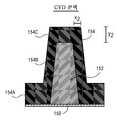
도 1a는 스퍼터 증착에 의해 그 위에 형성된 도전성 콘택을 갖는 반도체 핀의 단면도를 예시한다.1A illustrates a cross-sectional view of a semiconductor fin with conductive contacts formed thereon by sputter deposition.
도 1a를 참조하면, 기판(100) 위에 형성된 반도체 핀과 같은 반도체 피처(102) 위에 스퍼터링된 콘택(104)이 형성되어 있다. 스퍼터링된 콘택은 하부의 평평한 표면들을 커버하는 부분들(104A), 평평하지 않은 표면들을 커버하는 측벽 부분들(104B), 및 상부의 평평한 표면들을 커버하는 부분들(104C)을 포함한다. 평평하지 않은 표면들을 커버하는 부분들(104B)의 두께(X1)는 상부의 평평한 표면들을 커버하는 부분들(104C)의 두께(Y1)보다 실질적으로 더 얇고, 하부의 평평한 표면들을 커버하는 부분들(104A)보다 실질적으로 더 얇다.Referring to FIG. 1A, a sputtered
도 1b는 본 개시내용의 일 실시예에 따른, 화학 기상 증착(CVD)에 의해 그 위에 형성된 도전성 콘택을 갖는 반도체 핀의 단면도를 예시한다.1B illustrates a cross-sectional view of a semiconductor fin having conductive contacts formed thereon by chemical vapor deposition (CVD), in accordance with an embodiment of the present disclosure.
도 1b를 참조하면, 기판(150) 위에 형성된 반도체 핀과 같은 반도체 피처(152) 위에 화학 기상 증착(CVD) 콘택(154)이 형성되어 있다. CVD 콘택은 하부의 평평한 표면들을 커버하는 부분들(154A), 평평하지 않은 표면들을 커버하는 측벽 부분들(154B), 및 상부의 평평한 표면들을 커버하는 부분들(154C)을 포함한다. 평평하지 않은 표면들을 커버하는 부분들(154B)의 두께(X2)는 상부의 평평한 표면들을 커버하는 부분들(154C)의 두께(Y2)와 실질적으로 동일하고, 하부의 평평한 표면들을 커버하는 부분들(154A)과 실질적으로 동일하다.Referring to FIG. 1B, a chemical vapor deposition (CVD)
본 명세서에 설명된 금속 층 퇴적 프로세스를 수반하는 통합 스킴을 이용하여 다양한 집적 회로 구조가 제조될 수 있다는 것을 알아야 한다. 본 개시내용의 일 실시예에 따르면, 집적 회로 구조를 제조하는 방법은 RF 소스를 갖는 화학 기상 증착(CVD) 챔버 내에 기판을 제공하는 단계를 포함하고, 기판은 그 위에 피처를 갖는다. 방법은 또한 사염화 티타늄(TiCl4)과 수소(H2)를 반응시켜 기판의 피처 상에 티타늄(Ti) 층을 형성하는 단계를 포함한다. 일 실시예에서, 반응은 섭씨 400-500도 범위의 온도에서, 0.2-2 Torr 범위의 압력에서, 그리고 대략 400 kHz 또는 대략 13.56 MHz의 RF 주파수에서 수행된다.It should be appreciated that various integrated circuit structures can be fabricated using the integrated schemes involving the metal layer deposition process described herein. According to one embodiment of the present disclosure, a method of fabricating an integrated circuit structure includes providing a substrate in a chemical vapor deposition (CVD) chamber having an RF source, the substrate having features thereon. The method also includes reacting titanium tetrachloride (TiCl4 ) with hydrogen (H2 ) to form a titanium (Ti) layer on features of the substrate. In one embodiment, the reaction is performed at a temperature in the range 400-500 degrees Celsius, at a pressure in the range 0.2-2 Torr, and at an RF frequency of approximately 400 kHz or approximately 13.56 MHz.
일 실시예에서, 티타늄 층은 98% 이상의 티타늄 및 0.5-2%의 염소를 포함하는 총 원자 조성을 갖는다. 대안적인 실시예들에서, 지르코늄(Zr), 하프늄(Hf), 탄탈룸(Ta), 니오븀(Nb), 또는 바나듐(V)의 고순도 금속 층을 제조하기 위해 유사한 프로세스가 사용된다. 일 실시예에서, 비교적 적은 막 두께 변동이 있고, 예를 들어, 일 실시예에서는 모든 커버리지가 50%보다 크고 공칭은 70% 이상이다(즉, 30% 이하의 두께 변동). 일 실시예에서, 두께는 다른 표면들보다 실리콘(Si) 또는 실리콘 게르마늄(SiGe) 상에서 측정할 수 있을 정도로 더 두꺼운데, 그 이유는 Si 또는 SiGe는 퇴적 동안 반응하고 Ti의 흡수를 촉진시키기 때문이다. 일 실시예에서, 막 조성은 불순물로서 대략 0.5%의 Cl(또는 1% 미만)을 포함하며, 본질적으로 다른 관찰된 불순물은 없다. 일 실시예에서, 퇴적 프로세스는 스퍼터 증착 가시선에 의해 숨겨진 표면들과 같은 비-가시선 표면들 상의 금속 커버리지를 가능하게 한다. 본 명세서에 설명된 실시예들은 소스 및 드레인 콘택들을 통해 구동되는 전류의 외부 저항을 감소시킴으로써 트랜지스터 디바이스 드라이브를 개선하도록 구현될 수 있다.In one embodiment, the titanium layer has a total atomic composition comprising at least 98% titanium and 0.5-2% chlorine. In alternative embodiments, a similar process is used to fabricate a high purity metal layer of zirconium (Zr), hafnium (Hf), tantalum (Ta), niobium (Nb), or vanadium (V). In one embodiment, there is a relatively small film thickness variation, for example, in one embodiment all coverage is greater than 50% and nominal is greater than 70% (ie less than 30% thickness variation). In one embodiment, the thickness is thicker than can be measured on silicon (Si) or silicon germanium (SiGe) than other surfaces because Si or SiGe react during deposition and promote the absorption of Ti. . In one embodiment, the film composition comprises approximately 0.5% Cl (or less than 1%) as impurities, with essentially no other impurities observed. In one embodiment, the deposition process enables metal coverage on non-visible surfaces, such as surfaces hidden by sputter deposited line of sight. Embodiments described herein can be implemented to improve transistor device drive by reducing the external resistance of the current driven through the source and drain contacts.
본 개시내용의 일 실시예에 따르면, 기판의 피처는 반도체 소스/드레인 구조를 노출시키는 소스/드레인 콘택 트렌치이다. 티타늄 층(또는 다른 고순도 금속 층)은 반도체 소스/드레인 구조를 위한 도전성 콘택 층이다. 그러한 구현의 예시적 실시예들은 도 2a, 도 2b, 도 3, 도 4a 내지 도 4c 및 도 5와 관련하여 아래에 설명된다.According to one embodiment of the present disclosure, the feature of the substrate is a source / drain contact trench that exposes a semiconductor source / drain structure. The titanium layer (or other high purity metal layer) is a conductive contact layer for semiconductor source / drain structures. Exemplary embodiments of such an implementation are described below with respect to FIGS. 2A, 2B, 3, 4A-4C and 5.
본 개시내용의 다른 실시예에 따르면, 기판의 피처는 BEOL(back end-of-line) 금속화 층의 도전성 라인 트렌치이다. 티타늄 층(또는 다른 고순도 금속 층)은 도전성 라인에 대한 장벽 층이다. 그러한 구현의 예시적 실시예들은 도 6과 관련하여 아래에 설명된다.According to another embodiment of the present disclosure, the feature of the substrate is a conductive line trench of a back end-of-line metallization layer. The titanium layer (or other high purity metal layer) is a barrier layer for conductive lines. Exemplary embodiments of such an implementation are described below with respect to FIG. 6.
본 개시내용의 다른 실시예에 따르면, 기판의 피처는 반도체 디바이스의 게이트 트렌치이다. 티타늄 층(또는 다른 고순도 금속 층)은 반도체 디바이스의 금속 게이트 전극의 일함수 층이다. 그러한 구현의 예시적 실시예들은 도 7a 및 도 7b와 관련하여 아래에 설명된다.According to another embodiment of the present disclosure, the feature of the substrate is a gate trench of a semiconductor device. The titanium layer (or other high purity metal layer) is the work function layer of the metal gate electrode of the semiconductor device. Exemplary embodiments of such an implementation are described below with respect to FIGS. 7A and 7B.
아래에 설명되는 다양한 실시예들에 의해 예시되는 바와 같이, 집적 회로 구조는 기판 위에 반도체 피처를 포함할 수 있다. 상기 반도체 피처 위에 유전체 층이 있고, 상기 유전체 층은 상기 반도체 피처의 일부를 노출시키는 트렌치를 가지며, 그 일부는 평평하지 않은 토포그래피를 갖는다. 상기 반도체 피처의 일부 바로 위에 금속 콘택 재료가 있다. 상기 금속 콘택 재료는 상기 반도체 피처의 일부의 평평하지 않은 토포그래피와 등각이다. 하나의 그러한 실시예에서, 금속 콘택 재료는 95% 이상의 단일 금속 종을 포함하는 총 원자 조성을 갖는다.As illustrated by various embodiments described below, an integrated circuit structure can include a semiconductor feature over a substrate. There is a dielectric layer over the semiconductor feature, the dielectric layer having a trench that exposes a portion of the semiconductor feature, the portion having a non-flat topography. Just above a portion of the semiconductor feature is a metal contact material. The metal contact material is conformal to the non-flat topography of a portion of the semiconductor feature. In one such embodiment, the metal contact material has a total atomic composition comprising at least 95% single metal species.
일 실시예에서, 금속 콘택 재료는 98% 이상의 티타늄을 포함하는 총 원자 조성을 갖는다. 하나의 그러한 실시예에서, 금속 콘택 재료의 총 원자 조성은 0.5-2%의 염소를 추가로 포함한다. 일 실시예에서, 금속 콘택 재료는 반도체 피처의 일부의 평평하지 않은 토포그래피를 따라 30% 이하의 두께 변동을 갖는다. 일 실시예에서, 반도체 피처의 일부의 평평하지 않은 토포그래피는 상승된 중앙 부분 및 하부 측면 부분들을 포함한다. 일 실시예에서, 반도체 피처의 일부의 평평하지 않은 토포그래피는 안장 형상 부분을 포함한다.In one embodiment, the metal contact material has a total atomic composition comprising at least 98% titanium. In one such embodiment, the total atomic composition of the metal contact material further comprises 0.5-2% chlorine. In one embodiment, the metal contact material has a thickness variation of 30% or less along the non-flat topography of a portion of the semiconductor feature. In one embodiment, the non-flat topography of the portion of the semiconductor feature includes raised central portions and lower side portions. In one embodiment, the non-flat topography of the portion of the semiconductor feature includes a saddle shaped portion.
일 실시예에서, 반도체 피처는 실리콘을 포함한다. 하나의 그러한 실시예에서, 반도체 피처는 게르마늄을 추가로 포함한다. 일 실시예에서, 금속 콘택 재료는 또한 유전체 층 내의 트렌치의 측벽들을 따라 있다. 하나의 그러한 실시예에서, 트렌치의 측벽들을 따른 금속 콘택 재료의 두께는 반도체 피처의 일부로부터 반도체 피처의 일부 위의 위치까지 얇아진다. 일 실시예에서, 트렌치 내의 금속 콘택 재료 상에 도전성 충전 재료가 있다.In one embodiment, the semiconductor feature comprises silicon. In one such embodiment, the semiconductor feature further comprises germanium. In one embodiment, the metal contact material is also along the sidewalls of the trench in the dielectric layer. In one such embodiment, the thickness of the metal contact material along the sidewalls of the trench is thinned from a portion of the semiconductor feature to a location above the portion of the semiconductor feature. In one embodiment, there is a conductive fill material on the metal contact material in the trench.
도 2a는 본 개시내용의 일 실시예에 따른, 소스 또는 드레인 영역 상에 도전성 콘택을 갖는 반도체 디바이스의 단면도를 예시한다.2A illustrates a cross-sectional view of a semiconductor device having conductive contacts on a source or drain region, in accordance with an embodiment of the present disclosure.
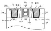
도 2a를 참조하면, 반도체 구조(200)는 기판(204) 위에 게이트 구조(202)를 포함한다. 게이트 구조(202)는 게이트 유전체 층(202A), 일함수 층(202B), 및 게이트 충전재(202C)를 포함한다. 게이트 구조(202)의 반대 측면들 상에 소스 영역(208) 및 드레인 영역(210)이 있다. 소스 또는 드레인 콘택들(212)이 소스 영역(208) 및 드레인 영역(210)에 전기적으로 접속되고, 층간 유전체 층(214) 또는 게이트 유전체 스페이서들(216) 중 하나 또는 둘 다에 의해 게이트 구조(202)에서 이격된다. 소스 영역(208) 및 드레인 영역(210)은 기판(204)의 영역들이다.Referring to FIG. 2A, the
일 실시예에서, 소스 또는 드레인 콘택들(212)은 위에 설명된 바와 같은 고순도 금속 층(212A), 및 도전성 트렌치 충전 재료(212B)를 포함한다. 일 실시예에서, 고순도 금속 층(212A)은 98% 이상의 티타늄을 포함하는 총 원자 조성을 갖는다. 하나의 그러한 실시예에서, 고순도 금속 층(212A)의 총 원자 조성은 0.5-2%의 염소를 추가로 포함한다. 일 실시예에서, 고순도 금속 층(212A)은 30% 이하의 두께 변동을 갖는다. 일 실시예에서, 도전성 트렌치 충전 재료(212B)는, 이에 제한되는 것은 아니지만, Cu, Al, W, 또는 이들의 합금들과 같은 도전성 재료로 구성된다.In one embodiment, source or
도 2b는 본 개시내용의 일 실시예에 따른, 상승된 소스 또는 드레인 영역 상에 도전성인 것을 갖는 다른 반도체 디바이스의 단면도를 예시한다.2B illustrates a cross-sectional view of another semiconductor device having one that is conductive on an elevated source or drain region, in accordance with one embodiment of the present disclosure.
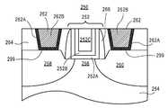
도 2b를 참조하면, 반도체 구조(250)는 기판(254) 위에 게이트 구조(252)를 포함한다. 게이트 구조(252)는 게이트 유전체 층(252A), 일함수 층(252B), 및 게이트 충전재(252C)를 포함한다. 게이트 구조(252)의 반대 측면들 상에 소스 영역(258) 및 드레인 영역(260)이 있다. 소스 또는 드레인 콘택들(262)이 소스 영역(258) 및 드레인 영역(260)에 전기적으로 접속되고, 층간 유전체 층(264) 또는 게이트 유전체 스페이서들(266) 중 하나 또는 둘 다에 의해 게이트 구조(252)에서 이격된다. 소스 영역(258) 및 드레인 영역(260)은 기판(254)의 에칭 제거된 영역들에 형성된 에피택셜 및/또는 임베디드 재료 영역들이다. 묘사된 바와 같이, 일 실시예에서, 소스 영역(258) 및 드레인 영역(260)은 상승된 소스 및 드레인 영역들이다. 특정한 그러한 실시예에서, 상승된 소스 및 드레인 영역들은 상승된 실리콘 소스 및 드레인 영역들 또는 상승된 실리콘 게르마늄 소스 및 드레인 영역들이다.Referring to FIG. 2B,
일 실시예에서, 소스 또는 드레인 콘택들(262)은 위에 설명된 바와 같은 고순도 금속 층(262A), 및 도전성 트렌치 충전 재료(262B)를 포함한다. 일 실시예에서, 고순도 금속 층(262A)은 98% 이상의 티타늄을 포함하는 총 원자 조성을 갖는다. 하나의 그러한 실시예에서, 고순도 금속 층(262A)의 총 원자 조성은 0.5-2%의 염소를 추가로 포함한다. 일 실시예에서, 고순도 금속 층(262A)은 30% 이하의 두께 변동을 갖는다. 일 실시예에서, 도전성 트렌치 충전 재료(262B)는, 이에 제한되는 것은 아니지만, Cu, Al, W, 또는 이들의 합금들과 같은 도전성 재료로 구성된다.In one embodiment, source or
따라서, 일 실시예에서, 도 2a 및 도 2b를 집합적으로 참조하면, 집적 회로 구조는 표면을 갖는 피처(반도체 소스 또는 드레인 구조를 노출시키는 소스 또는 드레인 콘택 트렌치)를 포함한다. 소스 또는 드레인 콘택 트렌치의 표면 상에 고순도 금속 층(212A 또는 262A)이 있다. 콘택 형성 프로세스들은 소스 또는 드레인 영역들의 노출된 실리콘 또는 게르마늄 또는 실리콘 게르마늄 재료의 소비를 수반할 수 있다는 것을 알아야 한다. 그러한 소비는 디바이스 성능을 저하시킬 수 있다. 대조적으로, 본 개시내용의 일 실시예에 따르면, 반도체 소스(208 또는 258) 또는 드레인(210 또는 260) 구조의 표면(249 또는 299)은 소스 또는 드레인 콘택 트렌치 아래에서 침식 또는 소모되지 않거나, 또는 실질적으로 침식 또는 소모되지 않는다. 하나의 그러한 실시예에서, 소모 또는 침식이 없는 것은 고순도 금속 콘택 층의 저온 증착으로 인해 발생한다.Thus, in one embodiment, referring collectively to FIGS. 2A and 2B, an integrated circuit structure includes a feature having a surface (a source or drain contact trench that exposes a semiconductor source or drain structure). There is a high
도 3은 본 개시내용의 일 실시예에 따른, 한 쌍의 반도체 핀 위의 복수의 게이트 라인의 평면도를 예시한다.3 illustrates a top view of a plurality of gate lines over a pair of semiconductor fins, in accordance with an embodiment of the present disclosure.
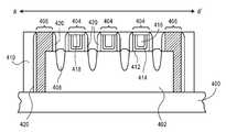
도 3을 참조하면, 복수의 반도체 핀(300) 위에 복수의 액티브 게이트 라인(304)이 형성된다. 복수의 반도체 핀(300)의 단부들에는 더미 게이트 라인들(306)이 있다. 게이트 라인들(304/306) 사이의 간격들(308)은 소스/드레인 영역들(351, 352, 353, 및 354)과 같은 소스/드레인 영역들에 대한 도전성 콘택들로서 트렌치 콘택들이 형성될 수 있는 위치들이다.Referring to FIG. 3, a plurality of
일 실시예에서, 복수의 게이트 라인(304/306)의 패턴 및/또는 복수의 반도체 핀(300)의 패턴은 격자 구조로서 기술된다. 일 실시예에서, 복수의 게이트 라인(304/306) 및/또는 복수의 반도체 핀(300)의 패턴에 대한 용어 "격자"는 본 명세서에서 조밀 피치 격자 구조를 지칭하기 위해 사용된다. 하나의 그러한 실시예에서, 조밀 피치는 종래의 리소그래피를 통해 직접 달성가능하지 않다. 예를 들어, 종래의 리소그래피에 기초한 패턴이 먼저 형성될 수 있지만, 본 기술분야에 공지된 바와 같이, 피치는 스페이서 마스크 패터닝의 사용에 의해 이등분될 수 있다. 더욱이, 원래 피치는 스페이서 마스크 패터닝의 제2 라운드에 의해 사등분될 수 있다. 따라서, 본 명세서에 설명된 격자형 패턴들은 일정한 피치로 이격되고 일정한 폭을 갖는 복수의 게이트 라인(304/306) 및/또는 복수의 반도체 핀(300)의 패턴을 가질 수 있다. 패턴은 피치 이등분 또는 피치 사등분, 또는 다른 피치 분할 접근법에 의해 제조될 수 있다.In one embodiment, the pattern of the plurality of
도 4a 내지 도 4c는 본 개시내용의 일 실시예에 따른, 집적 회로 구조를 제조하는 방법에서의 다양한 동작들에 대한, 도 3의 a-a' 축을 따라 취해진 단면도들을 도시한다.4A-4C show cross-sectional views taken along the a-a 'axis of FIG. 3 for various operations in a method of manufacturing an integrated circuit structure, according to one embodiment of the disclosure.
도 4a를 참조하면, 기판(400) 위에 형성된 반도체 핀(402) 위에 복수의 액티브 게이트 라인(404)이 형성된다. 복수의 반도체 핀(402)의 단부들에는 더미 게이트 라인들(406)이 있다. 액티브 게이트 라인들(404) 사이, 더미 게이트 라인들(406)과 액티브 게이트 라인들(404) 사이, 그리고 더미 게이트 라인들(406)의 외부에는 유전체 층(410)이 있다. 액티브 게이트 라인들(404) 사이 및 더미 게이트 라인들(406)과 액티브 게이트 라인들(404) 사이의 반도체 핀(402)에는 임베디드 소스/드레인 구조들(408)이 있다. 액티브 게이트 라인들(404)은 게이트 유전체 층(412), 일함수 게이트 전극 부분(414) 및 충전 게이트 전극 부분(416), 및 유전체 캡핑 층(418)을 포함한다. 유전체 스페이서들(420)이 액티브 게이트 라인들(404) 및 더미 게이트 라인들(406)의 측벽들을 라이닝한다.Referring to FIG. 4A, a plurality of
도 4b를 참조하면, 액티브 게이트 라인들(404) 사이 및 더미 게이트 라인들(406)과 액티브 게이트 라인들(404) 사이의 유전체 층(410)의 부분은 트렌치 콘택들이 형성될 위치들에 개구들(430)을 제공하기 위해 제거된다. 액티브 게이트 라인들(404) 사이 및 더미 게이트 라인들(406)과 액티브 게이트 라인들(404) 사이의 유전체 층(410)의 부분의 제거는 임베디드 소스/드레인 구조(408)의 침식으로 이어져서, 도 4b에 묘사된 바와 같이, 상부 안장 형상 토포그래피를 가질 수 있는 침식된 임베디드 소스/드레인 구조(432)를 제공할 수 있다.Referring to FIG. 4B, the portion of the
도 4c를 참조하면, 액티브 게이트 라인들(404) 사이 및 더미 게이트 라인들(406)과 액티브 게이트 라인들(404) 사이의 개구들(430)에 트렌치 콘택들(434)이 형성된다. 트렌치 콘택들(434) 각각은 금속 콘택 층(436) 및 도전성 충전 재료(438)를 포함할 수 있다.Referring to FIG. 4C,
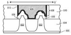
도 5는 본 개시내용의 일 실시예에 따른, 집적 회로 구조에 대한, 도 3의 b-b' 축을 따라 취해진 단면도를 예시한다.5 illustrates a cross-sectional view taken along the b-b 'axis of FIG. 3 for an integrated circuit structure, in accordance with an embodiment of the present disclosure.
도 5를 참조하면, 핀들(502)이 기판(504) 위에 묘사되어 있다. 핀들(502)의 하부 부분들은 트렌치 격리 재료(504)에 의해 둘러싸인다. 핀들(502)의 상부 부분들은 임베디드 소스 및 드레인 구조들(506)의 성장을 가능하게 하기 위해 제거되었다. 유전체 층(510)의 개구에 트렌치 콘택(508)이 형성되고, 개구는 임베디드 소스 및 드레인 구조들(506)을 노출시킨다. 트렌치 콘택은 금속 콘택 층(512) 및 도전성 충전 재료(514)를 포함한다. 일 실시예에 따르면, 도 5에 묘사된 바와 같이, 금속 콘택 층(512)은 트렌치 콘택(508)의 최상부까지 연장된다는 것을 알아야 한다. 그러나, 다른 실시예에서, 금속 콘택 층(512)은 트렌치 콘택(508)의 최상부까지 연장되지 않고, 예를 들어, 도 4c에서의 금속 콘택 층(436)의 묘사와 유사하게, 트렌치 콘택(508) 내에서 다소 리세스된다.Referring to FIG. 5, pins 502 are depicted over the
따라서, 도 3, 도 4a 내지 도 4c 및 도 5를 집합적으로 참조하면, 본 개시내용의 일 실시예에 따르면, 집적 회로 구조는 기판(400, 500) 위의 반도체 핀(300, 402, 502)을 포함한다. 반도체 핀(300, 402, 502)은 최상부 및 측벽들을 갖는다. 게이트 전극(304, 404)이 반도체 핀(300, 402, 502)의 일부의 측벽들에 인접하고 최상부 위에 있다. 게이트 전극(304, 404)은 반도체 핀(300, 402, 502) 내에 채널 영역을 정의한다. 게이트 전극(304, 404)의 제1 측면에 있는 채널 영역의 제1 단부에는 제1 반도체 소스/드레인 구조(351, 432, 506)가 있고, 제1 반도체 소스/드레인 구조(351, 432, 506)는 평평하지 않은 토포그래피를 갖는다. 게이트 전극(304, 404)의 제2 측면에 있는 채널 영역의 제2 단부에는 제2 반도체 소스/드레인 구조(352, 432, 506)가 있고, 제2 단부는 제1 단부의 반대편에 있고, 제2 측면은 제1 측면의 반대편에 있다. 제2 반도체 소스/드레인 구조(352, 432, 506)는 평평하지 않은 토포그래피를 갖는다. 제1 반도체 소스/드레인 구조(351, 432, 506) 바로 위에 그리고 제2 반도체 소스/드레인 구조(352, 432, 506) 바로 위에 금속 콘택 재료(436, 512)가 있다. 금속 콘택 재료(436, 512)는 제1 반도체 소스/드레인 구조(351, 432, 506)의 평평하지 않은 토포그래피와 등각이고 제2 반도체 소스/드레인 구조(352, 432, 506)의 평평하지 않은 토포그래피와 등각이다.Thus, referring collectively to FIGS. 3, 4A-4C, and 5, in accordance with one embodiment of the present disclosure, an integrated circuit structure may include
일 실시예에서, 금속 콘택 재료(436, 512)는 95% 이상의 단일 금속 종을 포함하는 총 원자 조성을 갖는다. 하나의 그러한 실시예에서, 금속 콘택 재료(436, 512)는 98% 이상의 티타늄을 포함하는 총 원자 조성을 갖는다. 특정한 그러한 실시예에서, 금속 콘택 재료(436, 512)의 총 원자 조성은 0.5-2%의 염소를 추가로 포함한다. 일 실시예에서, 금속 콘택 재료(436, 512)는 제1 반도체 소스/드레인 구조(351, 432, 506)의 평평하지 않은 토포그래피를 따라 그리고 제2 반도체 소스/드레인 구조(352, 432, 506)의 평평하지 않은 토포그래피를 따라 30% 이하의 두께 변동을 갖는다.In one embodiment, the
일 실시예에서, 제1 반도체 소스/드레인 구조(351, 432, 506)의 평평하지 않은 토포그래피 및 제2 반도체 소스/드레인 구조(352, 432, 506)의 평평하지 않은 토포그래피는 둘 다, 예를 들어, 도 5에 묘사된 바와 같이, 상승된 중앙 부분 및 하부 측면 부분들을 포함한다. 일 실시예에서, 제1 반도체 소스/드레인 구조(351, 432, 506)의 평평하지 않은 토포그래피 및 제2 반도체 소스/드레인 구조(352, 432, 506)의 평평하지 않은 토포그래피는 둘 다, 예를 들어, 도 4c에 묘사된 바와 같이, 안장 형상 부분들을 포함한다.In one embodiment, both the non-flat topography of the first semiconductor source /
일 실시예에서, 제1 반도체 소스/드레인 구조(351, 432, 506) 및 제2 반도체 소스/드레인 구조(352, 432, 506)는 둘 다 실리콘을 포함한다. 일 실시예에서, 제1 반도체 소스/드레인 구조(351, 432, 506) 및 제2 반도체 소스/드레인 구조(352, 432, 506)는 둘 다, 예를 들어, 실리콘 게르마늄의 형태로 게르마늄을 추가로 포함한다.In one embodiment, the first semiconductor source /
일 실시예에서, 제1 반도체 소스/드레인 구조(351, 432, 506) 바로 위에 있는 금속 콘택 재료(436, 512)는 또한 제1 반도체 소스/드레인 구조(351, 432, 506) 위의 유전체 층(420, 510) 내의 트렌치의 측벽들을 따라 있고, 트렌치는 제1 반도체 소스/드레인 구조(351, 432, 506)의 일부를 노출시킨다. 하나의 그러한 실시예에서, 트렌치의 측벽들을 따른 금속 콘택 재료(436)의 두께는 제1 반도체 소스/드레인 구조(432에서 436A)로부터 제1 반도체 소스/드레인 구조(432) 위의 위치(436B)까지 얇아지고, 그 예가 도 4c에 예시되어 있다. 일 실시예에서, 도 4c 및 5에 묘사된 바와 같이, 트렌치 내의 금속 콘택 재료(436, 512) 상에 도전성 충전 재료(438, 514)가 있다.In one embodiment, the
일 실시예에서, 집적 회로 구조는 최상부 및 측벽들을 갖는 제2 반도체 핀(예를 들어, 도 3의 상부 핀(300), 402, 502)을 추가로 포함한다. 게이트 전극(304, 404)은 또한 제2 반도체 핀의 일부의 측벽들에 인접하고 최상부 위에 있고, 게이트 전극은 제2 반도체 핀 내에 채널 영역을 정의한다. 게이트 전극(304, 404)의 제1 측면에 있는 제2 반도체 핀의 채널 영역의 제1 단부에는 제3 반도체 소스/드레인 구조(353, 432, 506)가 있고, 제3 반도체 소스/드레인 구조는 평평하지 않은 토포그래피를 갖는다. 게이트 전극(304, 404)의 제2 측면에 있는 제2 반도체 핀의 채널 영역의 제2 단부에는 제4 반도체 소스/드레인 구조(354, 432, 506)가 있고, 제2 단부는 제1 단부의 반대편에 있고, 제4 반도체 소스/드레인 구조(354, 432, 506)는 평평하지 않은 토포그래피를 갖는다. 금속 콘택 재료(436, 512)는 제3 반도체 소스/드레인 구조(353, 432, 506) 바로 위에 그리고 제4 반도체 소스/드레인 구조(354, 432, 506) 바로 위에 있고, 금속 콘택 재료(436, 512)는 제3 반도체 소스/드레인 구조(353, 432, 506)의 평평하지 않은 토포그래피와 등각이고 제4 반도체 소스/드레인 구조(354, 432, 506)의 평평하지 않은 토포그래피와 등각이다. 일 실시예에서, 금속 콘택 재료(436, 512)는 제1 반도체 소스/드레인 구조(351, 432, 좌측 506)와 제3 반도체 소스/드레인 구조(353, 432, 우측 506) 사이에서 연속적이고 제2 반도체 소스/드레인 구조(352)와 제4 반도체 소스/드레인 구조(354) 사이에서 연속적이다.In one embodiment, the integrated circuit structure further includes a second semiconductor fin (eg,
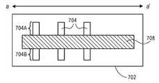
도 6은 본 개시내용의 일 실시예에 따른, 집적 회로 구조의 금속화 층의 평면도 및 대응하는 단면도를 예시한다.6 illustrates a top view and corresponding cross-sectional view of a metallization layer of an integrated circuit structure, in accordance with an embodiment of the present disclosure.
도 6을 참조하면, 금속화 층(600)은 도전성 라인들(602) 및 층간 유전체(ILD) 라인들(604)의 패턴을 포함한다. 도 6에 묘사된 바와 같이, 금속화 층(600)은 일정한 피치로 이격되고 일정한 폭을 갖는 도전성 라인들(602)을 갖는 격자형 패턴으로 패터닝될 수 있다. 도시되지는 않았지만, 도전성 라인들(602)은 라인들을 따라 다양한 위치에서 중단부들(즉, 컷들 또는 플러그들)을 가질 수 있다. 단면도에서 예로서 도시된 라인(602')과 같이, 도전성 라인들 중 일부는 기저의 비아들과 연관될 수 있다.Referring to FIG. 6, the metallization layer 600 includes a pattern of
일 실시예에서, 도전성 라인들(602) 및 ILD 라인들(604)에 대한 용어 "격자"는 본 명세서에서 조밀 피치 격자 구조를 지칭하기 위해 사용된다. 하나의 그러한 실시예에서, 조밀 피치는 종래의 리소그래피를 통해 직접 달성가능하지 않다. 예를 들어, 종래의 리소그래피에 기초한 패턴이 먼저 형성될 수 있지만, 본 기술분야에 공지된 바와 같이, 피치는 스페이서 마스크 패터닝의 사용에 의해 이등분될 수 있다. 더욱이, 원래 피치는 스페이서 마스크 패터닝의 제2 라운드에 의해 사등분될 수 있다. 따라서, 본 명세서에 설명된 격자형 패턴들은 일정한 피치로 이격되고 일정한 폭을 갖는 도전성 라인들(602) 및/또는 ILD 라인들(604)을 가질 수 있다. 패턴은 피치 이등분 또는 피치 사등분, 또는 다른 피치 분할 접근법에 의해 제조될 수 있다.In one embodiment, the term “lattice” for
일 실시예에서, 도전성 라인들(602)(및 어쩌면, 기저의 비아 구조들)은 하나 이상의 금속 또는 다른 도전성 구조로 구성된다. 도전성 라인들(602)은 또한 때때로 본 기술분야에서 트레이스들, 와이어들, 라인들, 금속, 인터커넥트 라인들 또는 단순히 인터커넥트들이라고 지칭된다. 특정 실시예에서, 도전성 라인들(602) 각각은 장벽 층(612) 및 도전성 충전 재료(610)를 포함한다.In one embodiment, conductive lines 602 (and possibly underlying via structures) are comprised of one or more metal or other conductive structures.
일 실시예에서, 장벽 층(612)은 위에 설명된 바와 같은 고순도 금속 층이다. 일 실시예에서, 고순도 금속 장벽 층(612)은 98% 이상의 티타늄을 포함하는 총 원자 조성을 갖는다. 하나의 그러한 실시예에서, 고순도 금속 장벽 층(612)의 총 원자 조성은 0.5-2%의 염소를 추가로 포함한다. 일 실시예에서, 고순도 금속 장벽 층(612)은 30% 이하의 두께 변동을 갖는다. 일 실시예에서, 도전성 충전 재료(610)는, 이에 제한되는 것은 아니지만, Cu, Al, Ti, Zr, Hf, V, Ru, Co, Ni, Pd, Pt, W, Ag, Au 또는 이들의 합금들과 같은 도전성 재료로 구성된다.In one embodiment,
따라서, 일 실시예에서, 집적 회로 구조는 표면을 갖는 피처(BEOL(back end-of-line) 금속화 층의 도전성 라인 트렌치)를 포함한다. 도전성 라인 트렌치의 표면 상에 고순도 금속 장벽 층(612)이 있다. 하나의 그러한 실시예에서, 고순도 금속 장벽 층(612)은 도전성 라인(602)에 대한 장벽 층이다.Thus, in one embodiment, the integrated circuit structure includes a surface-bearing feature (conductive line trench of a back end-of-line metallization layer). There is a high purity
일 실시예에서, ILD 라인들(604)은 유전체 또는 절연 재료의 층으로 구성되거나 이를 포함한다. 적합한 유전체 재료들의 예들은, 이에 제한되는 것은 아니지만, 실리콘의 산화물들(예를 들어, 실리콘 이산화물(SiO2)), 도핑된 실리콘의 산화물들, 실리콘의 플루오르화 산화물들, 탄소 도핑된 실리콘의 산화물들, 본 기술분야에 공지된 다양한 로우-k 유전체 재료들, 및 이들의 조합들을 포함한다. 층간 유전체 재료는, 예를 들어, 화학 기상 증착(CVD), 물리 기상 증착(PVD)과 같은 종래의 기법들에 의해, 또는 다른 퇴적 방법들에 의해 형성될 수 있다.In one embodiment,
도 6과 관련하여 설명된 층들 및 재료들은 전형적으로 집적 회로의 기저의 디바이스 층(들)과 같은 기저의 반도체 기판 또는 구조 상에 또는 위에 형성된다는 것을 알아야 한다. 일 실시예에서, 기저의 반도체 기판은 집적 회로들을 제조하기 위해 사용되는 일반적인 워크피스 오브젝트(workpiece object)를 표현한다. 반도체 기판은 종종 실리콘 또는 다른 반도체 재료의 웨이퍼 또는 다른 부분을 포함한다. 적합한 반도체 기판들은, 이에 제한되는 것은 아니지만, 단결정 실리콘, 다결정 실리콘 및 SOI(silicon on insulator) 뿐만 아니라, 다른 반도체 재료들로 형성된 유사한 기판들을 포함한다. 반도체 기판은, 제조의 스테이지에 따라, 종종 트랜지스터, 집적 회로 등을 포함한다. 기판은 반도체 재료들, 금속들, 유전체들, 도펀트들, 및 반도체 기판들에서 통상적으로 발견되는 다른 재료들을 또한 포함할 수 있다. 또한, 묘사되지는 않았지만, 도 6에 묘사된 구조는 기저의 하부 레벨 BEOL(back end of line) 인터커넥트 층들 상에 제조될 수 있다.It should be appreciated that the layers and materials described in connection with FIG. 6 are typically formed on or over an underlying semiconductor substrate or structure, such as the underlying device layer (s) of an integrated circuit. In one embodiment, the underlying semiconductor substrate represents a general workpiece object used to fabricate integrated circuits. Semiconductor substrates often include wafers or other portions of silicon or other semiconductor materials. Suitable semiconductor substrates include, but are not limited to, single crystal silicon, polycrystalline silicon and silicon on insulator (SOI), as well as similar substrates formed from other semiconductor materials. Semiconductor substrates often include transistors, integrated circuits, and the like, depending on the stage of manufacture. The substrate may also include semiconductor materials, metals, dielectrics, dopants, and other materials commonly found in semiconductor substrates. Also, although not depicted, the structure depicted in FIG. 6 can be fabricated on underlying lower level back end of line (BEOL) interconnect layers.
본 명세서에 설명된 하나 이상의 실시예는 금속 산화물 반도체(MOS) 디바이스 제조와 같은 반도체 디바이스들을 제조하는 것에 관한 것이다. 예로서, 도 7a는 본 개시내용의 일 실시예에 따른, 게이트 전극의 일함수 층으로서 CVD-증착된 층을 갖는 비평면 반도체 디바이스의 단면도를 예시한다. 도 7b는 본 개시내용의 일 실시예에 따른, 도 7a의 반도체 디바이스의 a-a' 축을 따라 취해진 평면도를 예시한다.One or more embodiments described herein relate to fabricating semiconductor devices such as metal oxide semiconductor (MOS) device fabrication. By way of example, FIG. 7A illustrates a cross-sectional view of a non-planar semiconductor device having a CVD-deposited layer as the work function layer of the gate electrode, according to one embodiment of the disclosure. FIG. 7B illustrates a top view taken along the a-a 'axis of the semiconductor device of FIG. 7A, in accordance with an embodiment of the present disclosure.
도 7a를 참조하면, 반도체 구조 또는 디바이스(700)는 기판(702)으로부터 그리고 격리 영역(706) 내에 형성된 비평면 액티브 영역(예를 들어, 돌출 핀 부분(704) 및 서브-핀 영역(705)을 포함하는 핀 구조)을 포함한다. 비평면 액티브 영역의 돌출 부분들(704) 위뿐만 아니라 격리 영역(706)의 일부 위에 게이트 라인(708)이 배치된다. 도시된 바와 같이, 게이트 라인(708)은 게이트 전극(750/799) 및 게이트 유전체 층(752)을 포함한다. 일 실시예에서, 게이트 라인(708)은 유전체 캡 층(754)을 또한 포함할 수 있다. 이 관점에서, 위에 가로놓인 금속 인터커넥트(760)와 함께, 게이트 콘택(714), 및 위에 가로놓인 게이트 콘택 비아(716)가 또한 보이고, 이들 모두는 층간 유전체 스택들 또는 층들(770)에 배치된다. 또한 도 7a의 관점에서, 게이트 콘택(714)은, 일 실시예에서, 격리 영역(706) 위에 배치되지만, 비평면 액티브 영역들 위에는 배치되지 않은 것이 보인다.Referring to FIG. 7A, a semiconductor structure or
본 개시내용의 일 실시예에 따르면, 게이트 전극(750/799)의 층(799)은 위에 설명된 바와 같은 고순도 금속 층이다. 일 실시예에서, 고순도 금속 층(799)은 게이트 트렌치 내에 있고, 게이트 유전체 층(752) 상에 또는 위에 있다. 하나의 그러한 실시예에서, 고순도 금속 층(799)은 집적 회로 구조의 트랜지스터(700)의 금속 게이트 전극의 일함수 층이다. 특정 실시예에서, 트랜지스터(700)는 N형(NMOS) 트랜지스터이고, 고순도 금속 층(799)은 N 형상 일함수를 갖는다. 다른 특정 실시예에서, 트랜지스터(700)는 P형(PMOS) 트랜지스터이고, 고순도 금속 층(799)은 P형 일함수를 갖는다.According to one embodiment of the present disclosure, the
따라서, 일 실시예에서, 반도체 구조 또는 디바이스(700)는 표면(게이트 유전체 층(752))을 갖는 피처(게이트 라인(708))를 갖는다. 게이트 유전체 층(752) 상에 또는 그에 근접하여 CVD-증착된 일함수-설정 층(799)(게이트 전극(750/799)의 층(799))이 형성된다. 일 실시예에서, CVD-증착된 일함수-설정 층(799)은 98% 이상의 티타늄을 포함하는 총 원자 조성을 갖는다. 하나의 그러한 실시예에서, CVD-증착된 일함수-설정 층(799)의 총 원자 조성은 0.5-2%의 염소를 추가로 포함한다. 일 실시예에서, CVD-증착된 일함수-설정 층(799)은 30% 이하의 두께 변동을 갖는다.Thus, in one embodiment, the semiconductor structure or
도 7b를 참조하면, 게이트 라인(708)은 돌출 핀 부분들(704) 위에 배치된 것으로서 도시되어 있다. 이 관점에서 돌출 핀 부분들(704)의 소스 및 드레인 영역들(704A 및 704B)이 보일 수 있다. 일 실시예에서, 소스 및 드레인 영역들(704A 및 704B)은 돌출 핀 부분들(704)의 원래 재료의 도핑된 부분들이다. 다른 실시예에서, 돌출 핀 부분들(704)의 재료는 제거되고, 예를 들어, 에피택셜 퇴적에 의해 다른 반도체 재료로 대체된다. 어느 경우든, 소스 및 드레인 영역들(704A 및 704B)은 유전체 층(706)의 높이 아래로, 즉, 서브-핀 영역(705) 내로 연장될 수 있다.Referring to FIG. 7B,
일 실시예에서, 반도체 구조 또는 디바이스(700)는, 이에 제한되는 것은 아니지만, fin-FET 또는 트라이-게이트 디바이스와 같은 비평면 디바이스이다. 그러한 실시예에서, 대응하는 반도체 채널 영역이 3차원 바디로 구성되거나 형성된다. 하나의 그러한 실시예에서, 게이트 라인들(708)의 게이트 전극 및 게이트 전극 재료들은 3차원 바디의 적어도 최상부 표면 및 한 쌍의 측벽을 둘러싼다.In one embodiment, the semiconductor structure or
기판(702)은 제조 프로세스를 견딜 수 있고 전하가 이동할 수 있는 반도체 재료로 구성될 수 있다. 일 실시예에서, 기판(702)은 액티브 영역(704)을 형성하기 위해, 이에 제한되는 것은 아니지만, 인, 비소, 안티몬, 붕소, 갈륨 또는 이들의 조합과 같은 전하 캐리어가 도핑된 결정 실리콘, 실리콘/게르마늄 또는 게르마늄 층으로 구성된 벌크 기판이다. 일 실시예에서, 벌크 기판(702) 내의 실리콘 원자들의 농도는 97%보다 크다. 다른 실시예에서, 벌크 기판(702)은 별개의 결정 기판 위에 성장된 에피택셜 층, 예를 들어 붕소-도핑된 벌크 실리콘 단결정 기판 위에 성장된 실리콘 에피택셜 층으로 구성된다. 벌크 기판(702)은 대안적으로 ⅢⅤ족 재료로 구성될 수 있다. 일 실시예에서, 벌크 기판(702)은, 이에 제한되는 것은 아니지만, 갈륨 질화물, 갈륨 인화물, 갈륨 비화물, 인듐 인화물, 인듐 안티몬화물, 인듐 갈륨 비화물, 알루미늄 갈륨 비화물, 인듐 갈륨 인화물, 또는 이들의 조합과 같은 III-V 족 재료로 구성된다. 일 실시예에서, 벌크 기판(702)은 III-V 재료로 구성되고 전하-캐리어 도펀트 불순물 원자들은, 이에 제한되는 것은 아니지만, 마그네슘, 베릴륨, 아연, 탄소, 실리콘, 게르마늄, 산소, 황, 셀레늄 또는 텔루륨과 같은 것들이다.
격리 영역(706)은 기저의 벌크 기판으로부터 영구 게이트 구조의 부분들을 궁극적으로 전기적으로 격리하거나 그의 격리에 기여하거나 또는 핀 액티브 영역들을 격리하는 것과 같이 기저의 벌크 기판 내에 형성된 액티브 영역들을 격리하기에 적합한 재료로 구성될 수 있다. 예를 들어, 일 실시예에서, 격리 영역(706)은, 이에 제한되는 것은 아니지만, 실리콘 이산화물, 실리콘 산질화물, 실리콘 질화물, 또는 탄소-도핑된 실리콘 질화물과 같은 유전체 재료로 구성된다.
일 실시예에서, 게이트 유전체 층(752)은 하이-K 재료로 구성된다. 예를 들어, 일 실시예에서, 게이트 유전체 층(752)은, 이에 제한되는 것은 아니지만, 하프늄 산화물, 하프늄 산질화물, 하프늄 실리케이트, 란타늄 산화물, 지르코늄 산화물, 지르코늄 실리케이트, 탄탈룸 산화물, 바륨 스트론튬 티타네이트, 바륨 티타네이트, 스트론튬 티타네이트, 이트륨 산화물, 알루미늄 산화물, 납 스칸듐 탄탈룸 산화물, 납 아연 니오브산염, 또는 이들의 조합과 같은 재료로 구성된다. 또한, 게이트 유전체 층의 일부는 기판(702)의 최상부 몇 개의 층으로 형성된 자연 산화물의 층을 포함할 수 있다. 일 실시예에서, 게이트 유전체 층은 최상부 하이-k 부분 및 반도체 재료의 산화물로 구성된 하부 부분으로 구성된다. 일 실시예에서, 게이트 유전체 층(752)은 하프늄 산화물의 최상부 부분 및 실리콘 이산화물 또는 실리콘 산질화물의 최하부 부분으로 구성된다.In one embodiment,
일 실시예에서, 게이트 전극(750/799)의 층(750)은 CVD-증착된 일함수 설정 층(799) 위에 형성된 비-일함수-설정 도전성 충전 재료로 구성된다. 하나의 그러한 실시예에서, 도전성 충전 재료(750)는, 이에 제한되는 것은 아니지만, 텅스텐(W), 알루미늄(Al), 또는 구리(Cu)와 같은 재료를 포함한다. 일 실시예에서, 게이트 전극의 층들(750 및 799) 사이에 하나 이상의 도전성 장벽 층(예컨대 티타늄 질화물 또는 탄탈룸 질화물)이 있다. 일부 구현들에서, 게이트 전극은, 기판의 표면에 실질적으로 평행한 최하부 부분 및 기판의 최상부 표면에 실질적으로 수직인 2개의 측벽 부분을 포함하는 "U" 형상 구조로 구성될 수 있다. 다른 구현에서, 게이트 전극을 형성하는 금속 층들 중 적어도 하나는 단순히 기판의 최상부 표면에 실질적으로 평행한 평면 층일 수 있고 기판의 최상부 표면에 실질적으로 수직인 측벽 부분들은 포함하지 않는다. 본 개시내용의 추가 구현들에서, 게이트 전극은 U 형상 구조들과 평면의 U 형상이 아닌 구조들의 조합으로 구성될 수 있다. 예를 들어, 게이트 전극은 하나 이상의 평면의 U 형상이 아닌 층 위에 형성된 하나 이상의 U 형상 금속 층으로 구성될 수 있다.In one embodiment,
일 실시예에서, 게이트 전극 스택들과 연관된 유전체 캡 층(754) 및/또는 유전체 스페이서들은 자기 정렬된 콘택들과 같은 인접한 또는 위에 가로놓인 도전성 콘택들로부터 영구 게이트 구조를 궁극적으로 전기적으로 격리하거나 그의 격리에 기여하기에 적합한 재료로 구성될 수 있다. 예를 들어, 일 실시예에서, 유전체 캡 층(754) 및/또는 유전체 스페이서들은, 이에 제한되는 것은 아니지만, 실리콘 이산화물, 실리콘 산질화물, 실리콘 질화물, 또는 탄소-도핑된 실리콘 질화물과 같은 유전체 재료로 구성된다.In one embodiment, the
게이트 콘택(714), 위에 가로놓인 게이트 콘택 비아(716), 및/또는 위에 가로놓인 금속 인터커넥트(760)는 도전성 재료로 구성될 수 있다. 일 실시예에서, 콘택들, 인터커넥트들 또는 비아들 중 하나 이상은 금속 종들로 구성된다. 금속 종들은 텅스텐, 니켈, 또는 코발트와 같은 순수 금속일 수 있거나, 금속-금속 합금 또는 금속-반도체 합금(예를 들어, 실리사이드 재료와 같은)과 같은 합금일 수 있다. 특정 실시예에서, 게이트 콘택(714), 위에 가로놓인 게이트 콘택 비아(716), 또는 위에 가로놓인 금속 인터커넥트(760) 중 하나 이상은 장벽 층 및 도전성 충전 재료를 포함한다. 하나의 그러한 실시예에서, 장벽 층은 위에 설명된 바와 같은 고순도 금속 층이다. 일 실시예에서, 고순도 금속 장벽 층은 98% 이상의 티타늄을 포함하는 총 원자 조성을 갖는다. 일 실시예에서, 고순도 금속 장벽 층의 총 원자 조성은 0.5-2%의 염소를 추가로 포함한다. 일 실시예에서, 고순도 금속 장벽 층은 30% 이하의 두께 변동을 갖는다. 일 실시예에서, 도전성 충전 재료는, 이에 제한되는 것은 아니지만, Cu, Al, Ti, Zr, Hf, V, Ru, Co, Ni, Pd, Pt, W, Ag, Au 또는 이들의 합금들과 같은 도전성 재료로 구성된다.The
일 실시예에서(도시되지 않았지만), 구조(700)를 제공하는 것은, 대단히 엄격한 레지스트레이션 예산(registration budget)을 갖는 리소그래피 단계의 사용을 제거하면서 기존의 게이트 패턴과 본질적으로 완벽하게 정렬되는 콘택 패턴의 형성을 수반한다. 하나의 그러한 실시예에서, 이러한 접근법은 콘택 개구들을 생성하기 위해 본질적으로 고도로 선택적인 습식 에칭(예를 들어, 관례적으로 구현된 건식 또는 플라즈마 에칭 대비)의 사용을 가능하게 한다. 일 실시예에서, 콘택 플러그 리소그래피 작업과 조합하여 기존의 게이트 패턴을 이용함으로써 콘택 패턴이 형성된다. 하나의 그러한 실시예에서, 이 접근법은, 종래의 접근법들에서 사용되는 바와 같이, 콘택 패턴을 생성하기 위해 달리 임계적인 리소그래피 작업에 대한 필요성의 제거를 가능하게 한다. 일 실시예에서, 트렌치 콘택 그리드가 별도로 패터닝되지 않고, 오히려 폴리 (게이트) 라인들 사이에 형성된다. 예를 들어, 하나의 그러한 실시예에서, 트렌치 콘택 그리드는 게이트 격자 패터닝 이후에 그러나 게이트 격자 컷들 이전에 형성된다.In one embodiment (not shown), providing
또한, 게이트 스택 구조(708)는 대체 게이트 프로세스에 의해 제조될 수 있다. 그러한 스킴에서, 폴리실리콘 또는 실리콘 질화물 필러 재료와 같은 더미 게이트 재료가 제거되고 영구 게이트 전극 재료로 대체될 수 있다. 하나의 그러한 실시예에서, 영구 게이트 유전체 층이 또한, 이전의 프로세싱으로부터 지속되는 것과는 대조적으로, 이 프로세스에서 형성된다. 일 실시예에서, 더미 게이트들은 건식 에칭 또는 습식 에칭 프로세스에 의해 제거된다. 일 실시예에서, 더미 게이트들은 다결정 실리콘 또는 비정질 실리콘으로 구성되고, SF6의 사용을 포함하는 건식 에칭 프로세스를 이용하여 제거된다. 다른 실시예에서, 더미 게이트들은 다결정 실리콘 또는 비정질 실리콘으로 구성되고, 수성 NH4OH 또는 테트라메틸암모늄 수산화물의 사용을 포함하는 습식 에칭 프로세스를 이용하여 제거된다. 일 실시예에서, 더미 게이트들은 실리콘 질화물로 구성되고, 수성 인산을 포함하는 습식 에칭을 이용하여 제거된다.In addition,
일 실시예에서, 본 명세서에 설명된 하나 이상의 접근법은 구조(700)에 도달하기 위해 본질적으로 더미 및 대체 게이트 프로세스를 더미 및 대체 콘택 프로세스와 조합하여 고려한다. 하나의 그러한 실시예에서, 대체 콘택 프로세스는 영구 게이트 스택의 적어도 일부의 고온 어닐링을 허용하기 위해 대체 게이트 프로세스 후에 수행된다. 예를 들어, 특정한 그러한 실시예에서, 예를 들어, 게이트 유전체 층이 형성된 후에, 영구 게이트 구조들의 적어도 일부의 어닐링은 대략 섭씨 600도보다 높은 온도에서 수행된다. 어닐링은 영구 콘택들의 형성 이전에 수행된다.In one embodiment, one or more approaches described herein consider essentially a dummy and alternate gate process in combination with a dummy and alternate contact process to reach
다시 도 7a를 참조하면, 반도체 구조 또는 디바이스(700)의 배열은 격리 영역들 위에 게이트 콘택을 배치한다. 그러한 배열은 특정 응용들에서 레이아웃 공간의 비효율적인 사용으로 간주될 수 있다. 그러나, 다른 실시예에서는, 반도체 디바이스가 액티브 영역 위에 형성된 게이트 전극의 부분들과 접촉하는 콘택 구조들을 갖는다. 일반적으로, 게이트의 액티브 부분 위에 그리고 트렌치 콘택 비아와 동일한 층 위에 게이트 콘택 구조(예컨대 비아)를 형성하는 것 이전에(예를 들어, 그에 더하여), 본 개시내용의 하나 이상의 실시예는 먼저 게이트 정렬된 트렌치 콘택 프로세스를 이용하는 것을 포함한다. 그러한 프로세스는 반도체 구조 제조를 위한, 예를 들어, 집적 회로 제조를 위한 트렌치 콘택 구조들을 형성하도록 구현될 수 있다. 일 실시예에서, 트렌치 콘택 패턴이 기존의 게이트 패턴에 정렬된 것으로서 형성된다. 대조적으로, 종래의 접근법들은 전형적으로 선택적 콘택 에칭들과 조합하여 기존의 게이트 패턴에 대한 리소그래피 콘택 패턴의 엄격한 레지스트레이션을 갖는 추가적인 리소그래피 프로세스를 수반한다. 예를 들어, 종래의 프로세스는 콘택 피처들의 별개의 패터닝을 갖는 폴리 (게이트) 그리드의 패터닝을 포함할 수 있다.Referring again to FIG. 7A, an arrangement of semiconductor structure or
특정 실시예에서, 트렌치 콘택들 각각은 장벽 층 및 도전성 충전 재료를 포함한다. 하나의 그러한 실시예에서, 장벽 층은 위에 설명된 바와 같은 고순도 금속 층이다. 일 실시예에서, 고순도 금속 장벽 층은 98% 이상의 티타늄을 포함하는 총 원자 조성을 갖는다. 일 실시예에서, 고순도 금속 장벽 층의 총 원자 조성은 0.5-2%의 염소를 추가로 포함한다. 일 실시예에서, 고순도 금속 장벽 층은 30% 이하의 두께 변동을 갖는다. 일 실시예에서, 도전성 충전 재료는, 이에 제한되는 것은 아니지만, Cu, Al, Ti, Zr, Hf, V, Ru, Co, Ni, Pd, Pt, W, Ag, Au 또는 이들의 합금들과 같은 도전성 재료로 구성된다.In a particular embodiment, each of the trench contacts includes a barrier layer and a conductive fill material. In one such embodiment, the barrier layer is a high purity metal layer as described above. In one embodiment, the high purity metal barrier layer has a total atomic composition comprising at least 98% titanium. In one embodiment, the total atomic composition of the high purity metal barrier layer further comprises 0.5-2% chlorine. In one embodiment, the high purity metal barrier layer has a thickness variation of 30% or less. In one embodiment, the conductive filler material is, but is not limited to, such as Cu, Al, Ti, Zr, Hf, V, Ru, Co, Ni, Pd, Pt, W, Ag, Au or alloys thereof. It is made of a conductive material.
위에 설명된 프로세스들의 모든 양태들이 본 개시내용의 실시예들의 사상 및 범위 내에 속하도록 실시될 필요가 있는 것은 아니라는 것을 알아야 한다. 예를 들어, 일 실시예에서, 더미 게이트들은 항상 게이트 스택들의 액티브 부분들 위에 게이트 콘택들을 제조하기 전에 형성될 필요는 없다. 위에 설명된 게이트 스택들은 실제로는 초기에 형성된 영구 게이트 스택들일 수 있다. 또한, 본 명세서에 설명된 프로세스들은 하나 또는 복수의 반도체 디바이스를 제조하는 데 사용될 수 있다. 반도체 디바이스들은 트랜지스터들 또는 유사한 디바이스들일 수 있다. 예를 들어, 일 실시예에서, 반도체 디바이스들은 로직 또는 메모리를 위한 금속 산화물 반도체(MOS) 트랜지스터들이거나, 또는 바이폴라 트랜지스터들이다. 또한, 일 실시예에서, 반도체 디바이스들은 트라이게이트 디바이스, 독립적으로 액세스된 더블 게이트 디바이스, 또는 FIN-FET와 같은 3차원 아키텍처를 갖는다. 하나 이상의 실시예는 10 나노미터(10 nm) 이하의 기술 노드에서 반도체 디바이스들을 제조하는 데 특히 유용할 수 있다.It should be understood that not all aspects of the processes described above need to be implemented to fall within the spirit and scope of the embodiments of the present disclosure. For example, in one embodiment, dummy gates need not always be formed prior to fabricating gate contacts over the active portions of the gate stacks. The gate stacks described above may actually be permanent gate stacks initially formed. In addition, the processes described herein may be used to manufacture one or a plurality of semiconductor devices. The semiconductor devices may be transistors or similar devices. For example, in one embodiment, the semiconductor devices are metal oxide semiconductor (MOS) transistors for logic or memory, or bipolar transistors. In addition, in one embodiment, the semiconductor devices have a three-dimensional architecture, such as a trigate device, an independently accessed double gate device, or a FIN-FET. One or more embodiments may be particularly useful for fabricating semiconductor devices at technology nodes of 10 nanometers (10 nm) or less.
일 실시예에서, 본 설명 전체에 걸쳐 또한 사용되는 바와 같이, 리소그래피 작업들은 193 nm 액침 리소그래피(immersion lithography)(i193), 극자외선(EUV) 및/또는 전자 빔 직접 기록(electron beam direct write, EBDW) 리소그래피 등을 이용하여 수행된다. 포지티브 톤 또는 네거티브 톤 레지스트가 사용될 수 있다. 일 실시예에서, 리소그래피 마스크는 토포그래피 마스킹 부분, 반사 방지 코팅(ARC) 층, 및 포토레지스트 층으로 구성된 삼중층 마스크이다. 특정한 그러한 실시예에서, 토포그래피 마스킹 부분은 탄소 하드마스크(CHM) 층이고, 반사 방지 코팅 층은 실리콘 ARC 층이다.In one embodiment, as also used throughout this description, lithography operations are performed using 193 nm immersion lithography (i193), extreme ultraviolet (EUV), and / or electron beam direct write (EDBW). ) Using lithography or the like. Positive tone or negative tone resists may be used. In one embodiment, the lithographic mask is a triple layer mask consisting of a topography masking portion, an antireflective coating (ARC) layer, and a photoresist layer. In certain such embodiments, the topographic masking portion is a carbon hardmask (CHM) layer and the antireflective coating layer is a silicon ARC layer.
본 명세서에 개시된 실시예들은 매우 다양한 상이한 유형들의 집적 회로들 및/또는 마이크로전자 디바이스들을 제조하는 데 사용될 수 있다. 그러한 집적 회로들의 예들은, 이에 제한되는 것은 아니지만, 프로세서들, 칩셋 컴포넌트들, 그래픽 프로세서들, 디지털 신호 프로세서들, 마이크로컨트롤러들 등을 포함한다. 다른 실시예들에서는, 반도체 메모리가 제조될 수 있다. 또한, 집적 회로들 또는 다른 마이크로전자 디바이스들은 본 기술분야에 공지된 매우 다양한 전자 디바이스들에서 사용될 수 있다. 예를 들어, 컴퓨터 시스템들(예를 들어, 데스크톱, 랩톱, 서버), 셀룰러 폰들, 개인용 전자기기 등에서. 집적 회로들은 시스템들 내의 버스 및 다른 컴포넌트들과 결합될 수 있다. 예를 들어, 프로세서는 하나 이상의 버스에 의해 메모리, 칩셋 등에 결합될 수 있다. 프로세서, 메모리, 및 칩셋 각각은 잠재적으로 본 명세서에 개시된 접근법들을 이용하여 제조될 수 있다.Embodiments disclosed herein may be used to fabricate a wide variety of different types of integrated circuits and / or microelectronic devices. Examples of such integrated circuits include, but are not limited to, processors, chipset components, graphics processors, digital signal processors, microcontrollers, and the like. In other embodiments, a semiconductor memory can be fabricated. In addition, integrated circuits or other microelectronic devices can be used in a wide variety of electronic devices known in the art. For example, in computer systems (eg, desktops, laptops, servers), cellular phones, personal electronics, and the like. Integrated circuits may be combined with buses and other components in systems. For example, the processor may be coupled to memory, chipset, or the like by one or more buses. Each of the processor, memory, and chipset can potentially be manufactured using the approaches disclosed herein.
도 8은 본 개시내용의 일 구현에 따른 컴퓨팅 디바이스(800)를 예시한다. 컴퓨팅 디바이스(800)는 보드(802)를 하우징한다. 보드(802)는 이에 제한되는 것은 아니지만 프로세서(804) 및 적어도 하나의 통신 칩(806)을 포함하는 다수의 컴포넌트들을 포함할 수 있다. 프로세서(804)는 보드(802)에 물리적으로 그리고 전기적으로 결합된다. 일부 구현들에서, 적어도 하나의 통신 칩(806)도 보드(802)에 물리적으로 그리고 전기적으로 결합된다. 추가 구현들에서, 통신 칩(806)은 프로세서(804)의 일부이다.8 illustrates a
그 응용들에 따라, 컴퓨팅 디바이스(800)는 보드(802)에 물리적으로 그리고 전기적으로 결합될 수 있는 또는 그렇지 않을 수 있는 다른 컴포넌트들을 포함할 수 있다. 이러한 다른 컴포넌트들은, 이에 제한되는 것은 아니지만, 휘발성 메모리(예를 들어, DRAM), 비휘발성 메모리(예를 들어, ROM), 플래시 메모리, 그래픽 프로세서, 디지털 신호 프로세서, 암호 프로세서, 칩셋, 안테나, 디스플레이, 터치스크린 디스플레이, 터치스크린 컨트롤러, 배터리, 오디오 코덱, 비디오 코덱, 전력 증폭기, 글로벌 포지셔닝 시스템(GPS) 디바이스, 나침반, 가속도계, 자이로스코프, 스피커, 카메라, 및 대용량 저장 디바이스(예컨대 하드 디스크 드라이브, 콤팩트 디스크(CD), 디지털 다기능 디스크(DVD) 등)을 포함한다.Depending on the applications,
통신 칩(806)은 컴퓨팅 디바이스(800)로의 그리고 그로부터의 데이터의 송신을 위한 무선 통신을 가능하게 한다. "무선(wireless)"이라는 용어 및 그 파생어들은, 비-고체 매체를 통한 변조된 전자기 방사(electromagnetic radiation)의 사용을 통해 데이터를 통신할 수 있는, 회로들, 디바이스들, 시스템들, 방법들, 기법들, 통신 채널들 등을 설명하는 데 사용될 수 있다. 그 용어는 연관된 디바이스들이 어떠한 와이어도 포함하지 않는다는 것을 암시하지 않지만, 일부 실시예들에서는 연관된 디바이스들이 어떠한 와이어도 포함하지 않을 수도 있다. 통신 칩(806)은, 이에 제한되는 것은 아니지만, Wi-Fi(IEEE 802.11 패밀리), WiMAX(IEEE 802.16 패밀리), IEEE 802.20, 롱 텀 에볼루션(LTE), Ev-DO, HSPA+, HSDPA+, HSUPA+, EDGE, GSM, GPRS, CDMA, TDMA, DECT, 블루투스, 이들의 파생물들뿐만 아니라, 3G, 4G, 5G 및 그 이상의 것으로 지정된 임의의 다른 무선 프로토콜들을 포함하는 다수의 무선 표준 또는 프로토콜 중 임의의 것을 구현할 수 있다. 컴퓨팅 디바이스(800)는 복수의 통신 칩(806)을 포함할 수 있다. 예를 들어, 제1 통신 칩(806)은 Wi-Fi 및 블루투스와 같은 더 짧은 거리의 무선 통신에 전용될 수 있고, 제2 통신 칩(806)은 GPS, EDGE, GPRS, CDMA, WiMAX, LTE, Ev-DO, 및 다른 것들과 같은 더 먼 거리의 무선 통신에 전용될 수 있다.The
컴퓨팅 디바이스(800)의 프로세서(804)는 프로세서(804) 내에 패키징된 집적 회로 다이를 포함한다. 본 개시내용의 일부 구현들에서, 프로세서의 집적 회로 다이는 본 개시내용의 실시예들의 구현들에 따른, CVD-증착된 금속 막을 포함하도록 제조된 하나 이상의 구조를 포함한다. "프로세서"라는 용어는 레지스터들 및/또는 메모리로부터의 전자 데이터를 프로세싱하여 그 전자 데이터를 레지스터들 및/또는 메모리에 저장될 수 있는 다른 전자 데이터로 변환하는 임의의 디바이스 또는 디바이스의 부분을 지칭할 수 있다.
통신 칩(806)은 또한 통신 칩(806) 내에 패키징된 집적 회로 다이를 포함한다. 본 개시내용의 실시예들의 다른 구현에 따르면, 통신 칩의 집적 회로 다이는 본 개시내용의 실시예들의 구현들에 따른, CVD-증착된 금속 막을 포함하도록 제조된 하나 이상의 구조를 포함한다.The
추가 구현들에서, 컴퓨팅 디바이스(800) 내에 하우징된 다른 컴포넌트는 본 개시내용의 실시예들의 구현들에 따른, CVD-증착된 금속 막을 포함하도록 제조된 하나 이상의 구조를 포함하는 집적 회로 다이를 포함할 수 있다.In further implementations, another component housed within
다양한 구현들에서, 컴퓨팅 디바이스(800)는 랩톱, 넷북, 노트북, 울트라북, 스마트폰, 태블릿, 개인 휴대 정보 단말(PDA), 울트라 모바일 PC, 모바일 폰, 데스크톱 컴퓨터, 서버, 프린터, 스캐너, 모니터, 셋톱 박스, 엔터테인먼트 제어 유닛, 디지털 카메라, 휴대용 음악 플레이어, 또는 디지털 비디오 레코더일 수 있다. 추가 구현들에서, 컴퓨팅 디바이스(800)는 데이터를 프로세싱하는 임의의 다른 전자 디바이스일 수 있다.In various implementations,
도 9는 본 개시내용의 하나 이상의 실시예를 포함하는 인터포저(900)를 예시한다. 인터포저(900)는 제1 기판(902)을 제2 기판(904)에 브리지하기 위해 사용되는 개재 기판이다. 제1 기판(902)은, 예를 들어, 집적 회로 다이일 수 있다. 제2 기판(904)은 예를 들어, 메모리 모듈, 컴퓨터 마더보드, 또는 다른 집적 회로 다이일 수 있다. 일반적으로, 인터포저(900)의 목적은 접속을 더 넓은 피치로 확장하거나 또는 접속을 상이한 접속으로 재라우팅하는 것이다. 예를 들어, 인터포저(900)는 집적 회로 다이를 볼 그리드 어레이(BGA)(906)에 결합할 수 있고, 후자는 그 후 제2 기판(904)에 결합될 수 있다. 일부 실시예들에서, 제1 및 제2 기판들(902/904)은 인터포저(900)의 반대 측면들에 부착된다. 다른 실시예들에서, 제1 및 제2 기판들(902/904)은 인터포저(900)의 동일한 측면에 부착된다. 그리고 추가 실시예들에서, 3개 이상의 기판이 인터포저(900)를 통해 상호접속된다.9 illustrates an
인터포저(900)는 에폭시 수지, 섬유유리 강화 에폭시 수지, 세라믹 재료, 또는 폴리이미드와 같은 폴리머 재료로 형성될 수 있다. 추가 구현들에서, 인터포저는 실리콘, 게르마늄, 및 다른 III-V 족 및 IV 족 재료들과 같은, 반도체 기판에서 사용하기 위해 위에 설명된 것과 동일한 재료들을 포함할 수 있는 대안적인 강성 또는 연성 재료들로 형성될 수 있다.
인터포저는 금속 인터커넥트들(908) 및 이에 제한되는 것은 아니지만 TSV들(through-silicon vias)(912)을 포함하는 비아들(910)을 포함할 수 있다. 인터포저(900)는 수동 및 능동 디바이스들 둘 다를 포함하는 임베디드 디바이스들(914)을 추가로 포함할 수 있다. 그러한 디바이스들은, 이에 제한되는 것은 아니지만, 커패시터들, 디커플링 커패시터들, 저항기들, 인덕터들, 퓨즈들, 다이오드들, 변압기들, 센서들, 및 정전기 방전(ESD) 디바이스들을 포함한다. 무선 주파수(RF) 디바이스들, 전력 증폭기들, 전력 관리 디바이스들, 안테나들, 어레이들, 센서들, 및 MEMS 디바이스들과 같은 더 복잡한 디바이스들이 또한 인터포저(900) 상에 형성될 수 있다. 본 개시내용의 실시예들에 따르면, 본 명세서에 개시된 장치들 또는 프로세스들이 인터포저(900)의 제조에 사용될 수 있다.The interposer may include
따라서, 본 명세서에 설명된 실시예들은 랩-어라운드 콘택들을 제조하기 위한 금속 화학 기상 증착 접근법들, 및 랩-어라운드 금속 콘택들을 갖는 반도체 구조들을 포함하는 집적 회로 구조를 포함한다.Thus, embodiments described herein include an integrated circuit structure including metal chemical vapor deposition approaches for making wrap-around contacts, and semiconductor structures with wrap-around metal contacts.
요약서에 설명된 것을 포함하여, 본 개시내용의 실시예들의 예시된 구현들에 대한 위의 설명은 철저하거나 개시된 정확한 형태들로 본 개시내용을 제한하려고 의도된 것이 아니다. 본 개시내용의 특정 구현들 및 본 개시내용에 대한 예들이 예시의 목적으로 본 명세서에 설명되어 있지만, 본 개시내용의 범위 내에서 다양한 등가의 수정들이 가능하고, 이는 관련 기술분야의 통상의 기술자들이라면 인식할 것이다.The above description of illustrated implementations of embodiments of the disclosure, including what is described in the Abstract, is not intended to be exhaustive or to limit the disclosure to the precise forms disclosed. While specific implementations of the disclosure and examples for the disclosure have been described herein for purposes of illustration, various equivalent modifications are possible within the scope of the disclosure, as long as those skilled in the art Will recognize.
이러한 수정들은 위의 상세한 설명에 비추어 본 개시내용에 대해 이루어질 수 있다. 이하의 청구항들에서 사용되는 용어들은 본 개시내용을 명세서 및 청구항들에 개시된 특정 구현들로 제한하는 것으로 해석되어서는 안 된다. 오히려, 본 개시내용의 범위는 전적으로 다음의 청구항들에 의해 결정되어야 하며, 청구항들은 청구항 해석의 확립된 원칙들에 따라 해석되어야 한다.Such modifications may be made to the disclosure in light of the above detailed description. The terms used in the following claims should not be construed to limit the disclosure to the specific implementations disclosed in the specification and the claims. Rather, the scope of the disclosure should be determined entirely by the following claims, which should be construed in accordance with the established principles of claim interpretation.
예시적 실시예 1: 집적 회로 구조가 기판 위의 반도체 피처를 포함한다. 상기 반도체 피처 위에 유전체 층이 있고, 상기 유전체 층은 상기 반도체 피처의 일부를 노출시키는 트렌치를 가지며, 그 일부는 평평하지 않은 토포그래피를 갖는다. 상기 반도체 피처의 일부 바로 위에 금속 콘택 재료가 있다. 상기 금속 콘택 재료는 상기 반도체 피처의 일부의 평평하지 않은 토포그래피와 등각(conformal)이다. 상기 금속 콘택 재료는 95% 이상의 단일 금속 종을 포함하는 총 원자 조성을 갖는다.Example Embodiment 1 An integrated circuit structure includes a semiconductor feature on a substrate. There is a dielectric layer over the semiconductor feature, the dielectric layer having a trench that exposes a portion of the semiconductor feature, the portion having a non-flat topography. Just above a portion of the semiconductor feature is a metal contact material. The metal contact material is conformal to the non-flat topography of a portion of the semiconductor feature. The metal contact material has a total atomic composition comprising at least 95% single metal species.
예시적 실시예 2: 예시적 실시예 1의 집적 회로 구조로서, 상기 금속 콘택 재료는 98% 이상의 티타늄을 포함하는 총 원자 조성을 갖는다.Exemplary Embodiment 2: The integrated circuit structure of Exemplary Embodiment 1, wherein the metal contact material has a total atomic composition comprising at least 98% titanium.
예시적 실시예 3: 예시적 실시예 1 또는 2의 집적 회로 구조로서, 상기 금속 콘택 재료의 총 원자 조성은 0.5-2%의 염소를 추가로 포함한다.Exemplary Embodiment 3: The integrated circuit structure of Exemplary Embodiment 1 or 2, wherein the total atomic composition of the metal contact material further comprises 0.5-2% of chlorine.
예시적 실시예 4: 예시적 실시예 1, 2 또는 3의 집적 회로 구조로서, 상기 금속 콘택 재료는 상기 반도체 피처의 일부의 평평하지 않은 토포그래피를 따라 30% 이하의 두께 변동을 갖는다.Exemplary Embodiment 4: The integrated circuit structure of Exemplary Embodiments 1, 2, or 3, wherein the metal contact material has a thickness variation of 30% or less along the non-flat topography of a portion of the semiconductor feature.
예시적 실시예 5: 예시적 실시예 1, 2, 3 또는 4의 집적 회로 구조로서, 상기 반도체 피처의 일부의 평평하지 않은 토포그래피는 상승된 중앙 부분 및 하부 측면 부분들을 포함한다.Exemplary Embodiment 5: The integrated circuit structure of Exemplary Embodiments 1, 2, 3, or 4, wherein the non-flat topography of the portion of the semiconductor feature includes raised central portions and lower side portions.
예시적 실시예 6: 예시적 실시예 1, 2, 3, 4 또는 5의 집적 회로 구조로서, 상기 반도체 피처의 일부의 평평하지 않은 토포그래피는 안장 형상 부분을 포함한다.Exemplary Embodiment 6: The integrated circuit structure of Exemplary Embodiments 1, 2, 3, 4 or 5, wherein the non-flat topography of the portion of the semiconductor feature includes a saddle shaped portion.
예시적 실시예 7: 예시적 실시예 1, 2, 3, 4, 5 또는 6의 집적 회로 구조로서, 상기 반도체 피처는 실리콘을 포함한다.Exemplary Embodiment 7: The integrated circuit structure of Exemplary Embodiment 1, 2, 3, 4, 5, or 6, wherein the semiconductor feature comprises silicon.
예시적 실시예 8: 예시적 실시예 1, 2, 3, 4, 5, 6 또는 7의 집적 회로 구조로서, 상기 반도체 피처는 게르마늄을 추가로 포함한다.Example Embodiment 8 The integrated circuit structure of Example Embodiments 1, 2, 3, 4, 5, 6, or 7, wherein the semiconductor features further include germanium.
예시적 실시예 9: 예시적 실시예 1, 2, 3, 4, 5, 6, 7 또는 8의 집적 회로 구조로서, 상기 금속 콘택 재료는 또한 상기 유전체 층 내의 상기 트렌치의 측벽들을 따라 있고, 상기 트렌치의 측벽들을 따른 상기 금속 콘택 재료의 두께는 상기 반도체 피처의 일부로부터 상기 반도체 피처의 일부 위의 위치까지 얇아진다.Example Embodiment 9 The integrated circuit structure of Example 1, 2, 3, 4, 5, 6, 7 or 8, wherein the metal contact material is also along sidewalls of the trench in the dielectric layer, and The thickness of the metal contact material along the sidewalls of the trench is thinned from a portion of the semiconductor feature to a position above a portion of the semiconductor feature.
예시적 실시예 10: 예시적 실시예 1, 2, 3, 4, 5, 6, 7, 8 또는 9의 집적 회로 구조로서, 상기 트렌치 내의 상기 금속 콘택 재료 상의 도전성 충전 재료를 추가로 포함한다.Exemplary Embodiment 10: The integrated circuit structure of Exemplary Embodiments 1, 2, 3, 4, 5, 6, 7, 8, or 9, further comprising a conductive fill material on the metal contact material in the trench.
예시적 실시예 11: 집적 회로 구조가 기판 위의 반도체 핀을 포함하고, 상기 반도체 핀은 최상부 및 측벽들을 갖는다. 게이트 전극이 상기 반도체 핀의 일부의 상기 측벽들에 인접하고 상기 최상부 위에 있고, 상기 게이트 전극은 상기 반도체 핀 내에 채널 영역을 정의한다. 상기 게이트 전극의 제1 측면에 있는 상기 채널 영역의 제1 단부에는 제1 반도체 소스/드레인 구조가 있고, 상기 제1 반도체 소스/드레인 구조는 평평하지 않은 토포그래피를 갖는다. 상기 게이트 전극의 제2 측면에 있는 상기 채널 영역의 제2 단부에는 제2 반도체 소스/드레인 구조가 있고, 상기 제2 단부는 상기 제1 단부의 반대편에 있고, 상기 제2 측면은 상기 제1 측면의 반대편에 있고, 상기 제2 반도체 소스/드레인 구조는 평평하지 않은 토포그래피를 갖는다. 상기 제1 반도체 소스/드레인 구조 바로 위에 그리고 상기 제2 반도체 소스/드레인 구조 바로 위에 금속 콘택 재료가 있다. 상기 금속 콘택 재료는 상기 제1 반도체 소스/드레인 구조의 평평하지 않은 토포그래피와 등각이고 상기 제2 반도체 소스/드레인 구조의 평평하지 않은 토포그래피와 등각이다. 상기 금속 콘택 재료는 95% 이상의 단일 금속 종을 포함하는 총 원자 조성을 갖는다.Exemplary Embodiment 11: The integrated circuit structure includes a semiconductor fin over a substrate, the semiconductor fin having a top and sidewalls. A gate electrode is adjacent to and above the top of the portion of the semiconductor fin, the gate electrode defining a channel region within the semiconductor fin. At a first end of the channel region at the first side of the gate electrode there is a first semiconductor source / drain structure, the first semiconductor source / drain structure having a non-flat topography. The second end of the channel region at the second side of the gate electrode has a second semiconductor source / drain structure, the second end is opposite the first end, and the second side is the first side Opposite of, the second semiconductor source / drain structure has a non-flat topography. There is a metal contact material directly above the first semiconductor source / drain structure and directly above the second semiconductor source / drain structure. The metal contact material is conformal to the non-flat topography of the first semiconductor source / drain structure and is conformal to the non-flat topography of the second semiconductor source / drain structure. The metal contact material has a total atomic composition comprising at least 95% single metal species.
예시적 실시예 12: 예시적 실시예 11의 집적 회로 구조로서, 상기 금속 콘택 재료는 98% 이상의 티타늄을 포함하는 총 원자 조성을 갖는다.Example 12 The integrated circuit structure of Example 11, wherein the metal contact material has a total atomic composition comprising at least 98% titanium.
예시적 실시예 13: 예시적 실시예 11 또는 12의 집적 회로 구조로서, 상기 금속 콘택 재료의 총 원자 조성은 0.5-2%의 염소를 추가로 포함한다.Exemplary Embodiment 13: The integrated circuit structure of Exemplary Embodiment 11 or 12, wherein the total atomic composition of the metal contact material further comprises 0.5-2% of chlorine.
예시적 실시예 14: 예시적 실시예 11, 12 또는 13의 집적 회로 구조로서, 상기 금속 콘택 재료는 상기 제1 반도체 소스/드레인 구조의 평평하지 않은 토포그래피를 따라 그리고 상기 제2 반도체 소스/드레인 구조의 평평하지 않은 토포그래피를 따라 30% 이하의 두께 변동을 갖는다.Exemplary Embodiment 14: The integrated circuit structure of Exemplary Embodiments 11, 12, or 13, wherein the metal contact material is along the non-flat topography of the first semiconductor source / drain structure and the second semiconductor source / drain It has a thickness variation of 30% or less along the non-flat topography of the structure.
예시적 실시예 15: 예시적 실시예 11, 12, 13 또는 14의 집적 회로 구조로서, 상기 제1 반도체 소스/드레인 구조의 평평하지 않은 토포그래피 및 상기 제2 반도체 소스/드레인 구조의 평평하지 않은 토포그래피는 둘 다 상승된 중앙 부분 및 하부 측면 부분들을 포함한다.Exemplary Embodiment 15: The integrated circuit structure of Exemplary Embodiments 11, 12, 13, or 14, wherein the non-flat topography of the first semiconductor source / drain structure and the non-flat of the second semiconductor source / drain structure Topography both includes raised central portions and lower side portions.
예시적 실시예 16: 예시적 실시예 11, 12, 13, 14 또는 15의 집적 회로 구조로서, 상기 제1 반도체 소스/드레인 구조의 평평하지 않은 토포그래피 및 상기 제2 반도체 소스/드레인 구조의 평평하지 않은 토포그래피는 둘 다 안장 형상 부분들을 포함한다.Example Embodiment 16 The integrated circuit structure of Example 11, 12, 13, 14, or 15, wherein the non-flat topography of the first semiconductor source / drain structure and the flattening of the second semiconductor source / drain structure Both topography does not include saddle shaped portions.
예시적 실시예 17: 예시적 실시예 11, 12, 13, 14, 15 또는 16의 집적 회로 구조로서, 상기 제1 반도체 소스/드레인 구조 및 상기 제2 반도체 소스/드레인 구조는 둘 다 실리콘을 포함한다.Example 17: The integrated circuit structure of Example 11, 12, 13, 14, 15, or 16, wherein both the first semiconductor source / drain structure and the second semiconductor source / drain structure comprise silicon. do.
예시적 실시예 18: 예시적 실시예 11, 12, 13, 14, 15, 16 또는 17의 집적 회로 구조로서, 상기 제1 반도체 소스/드레인 구조 및 상기 제2 반도체 소스/드레인 구조는 둘 다 게르마늄을 추가로 포함한다.Example 18: The integrated circuit structure of Example 11, 12, 13, 14, 15, 16, or 17, wherein both the first semiconductor source / drain structure and the second semiconductor source / drain structure are germanium. It further includes.
예시적 실시예 19: 예시적 실시예 11, 12, 13, 14, 15, 16, 17 또는 18의 집적 회로 구조로서, 상기 제1 반도체 소스/드레인 구조 바로 위에 있는 상기 금속 콘택 재료는 또한 상기 제1 반도체 소스/드레인 구조 위의 유전체 층 내의 트렌치의 측벽들을 따라 있고, 상기 트렌치는 상기 제1 반도체 소스/드레인 구조의 일부를 노출시키고, 상기 트렌치의 측벽들을 따른 상기 금속 콘택 재료의 두께는 상기 제1 반도체 소스/드레인 구조로부터 상기 제1 반도체 소스/드레인 구조 위의 위치까지 얇아진다.Exemplary Embodiment 19: The integrated circuit structure of Exemplary Embodiments 11, 12, 13, 14, 15, 16, 17, or 18, wherein the metal contact material directly over the first semiconductor source / drain structure is further comprised of the first 1 along the sidewalls of the trench in the dielectric layer over the semiconductor source / drain structure, the trench exposing a portion of the first semiconductor source / drain structure, the thickness of the metal contact material along the sidewalls of the trench It is thinned from one semiconductor source / drain structure to a position above the first semiconductor source / drain structure.
예시적 실시예 20: 예시적 실시예 19의 집적 회로 구조로서, 상기 트렌치 내의 상기 금속 콘택 재료 상의 도전성 충전 재료를 추가로 포함한다.Example 20 The integrated circuit structure of Example 19, further comprising a conductive fill material on the metal contact material in the trench.
예시적 실시예 21: 예시적 실시예 11, 12, 13, 14, 15, 16, 17, 18, 19 또는 20의 집적 회로 구조로서, 상기 집적 회로 구조는 최상부 및 측벽들을 갖는 제2 반도체 핀을 추가로 포함하고, 상기 게이트 전극은 또한 상기 제2 반도체 핀의 일부의 측벽들에 인접하고 상기 최상부 위에 있고, 상기 게이트 전극은 상기 제2 반도체 핀 내에 채널 영역을 정의한다. 상기 게이트 전극의 상기 제1 측면에 있는 상기 제2 반도체 핀의 채널 영역의 제1 단부에는 제3 반도체 소스/드레인 구조가 있고, 상기 제3 반도체 소스/드레인 구조는 평평하지 않은 토포그래피를 갖는다. 상기 게이트 전극의 상기 제2 측면에 있는 상기 제2 반도체 핀의 채널 영역의 제2 단부에는 제4 반도체 소스/드레인 구조가 있고, 상기 제2 단부는 상기 제1 단부의 반대편에 있고, 상기 제4 반도체 소스/드레인 구조는 평평하지 않은 토포그래피를 갖는다. 상기 금속 콘택 재료는 상기 제3 반도체 소스/드레인 구조 바로 위에 그리고 상기 제4 반도체 소스/드레인 구조 바로 위에 있고, 상기 금속 콘택 재료는 상기 제3 반도체 소스/드레인 구조의 평평하지 않은 토포그래피와 등각이고 상기 제4 반도체 소스/드레인 구조의 평평하지 않은 토포그래피와 등각이다. 상기 금속 콘택 재료는 상기 제1 반도체 소스/드레인 구조와 상기 제3 반도체 소스/드레인 구조 사이에서 연속적이고 상기 제2 반도체 소스/드레인 구조와 상기 제4 반도체 소스/드레인 구조 사이에서 연속적이다.Example 21: The integrated circuit structure of Exemplary Embodiments 11, 12, 13, 14, 15, 16, 17, 18, 19, or 20, wherein the integrated circuit structure includes a second semiconductor fin having a top and sidewalls. Further comprising, the gate electrode is also adjacent and over the sidewalls of a portion of the second semiconductor fin, the gate electrode defining a channel region within the second semiconductor fin. At the first end of the channel region of the second semiconductor fin at the first side of the gate electrode there is a third semiconductor source / drain structure, and the third semiconductor source / drain structure has a non-flat topography. The second end of the channel region of the second semiconductor fin at the second side of the gate electrode has a fourth semiconductor source / drain structure, the second end being opposite the first end, and the fourth Semiconductor source / drain structures have non-flat topography. The metal contact material is directly over the third semiconductor source / drain structure and directly above the fourth semiconductor source / drain structure, the metal contact material is conformal to the non-flat topography of the third semiconductor source / drain structure It is conformal to the non-flat topography of the fourth semiconductor source / drain structure. The metal contact material is continuous between the first semiconductor source / drain structure and the third semiconductor source / drain structure and is continuous between the second semiconductor source / drain structure and the fourth semiconductor source / drain structure.
예시적 실시예 22: 집적 회로 구조를 제조하는 방법은 RF 소스를 갖는 화학 기상 증착(CVD) 챔버 내에 기판을 제공하는 단계를 포함하고, 상기 기판은 그 위에 피처를 갖는다. 상기 방법은 또한 사염화 티타늄(TiCl4)과 수소(H2)를 반응시켜 상기 기판의 상기 피처 상에 티타늄 층을 형성하는 단계를 포함한다. 상기 반응은 섭씨 400-500도 범위의 온도에서, 0.2-2 Torr 범위의 압력에서, 그리고 대략 400 kHz 또는 대략 13.56 MHz의 RF 주파수에서 수행된다. 상기 티타늄 층은 98% 이상의 티타늄 및 0.5-2%의 염소를 포함하는 총 원자 조성을 갖는다.Example Embodiment 22 A method of fabricating an integrated circuit structure includes providing a substrate in a chemical vapor deposition (CVD) chamber having an RF source, the substrate having a feature thereon. The method also includes reacting titanium tetrachloride (TiCl4 ) with hydrogen (H2 ) to form a titanium layer on the feature of the substrate. The reaction is carried out at a temperature in the range 400-500 degrees Celsius, at a pressure in the range 0.2-2 Torr and at an RF frequency of approximately 400 kHz or approximately 13.56 MHz. The titanium layer has a total atomic composition comprising at least 98% titanium and 0.5-2% chlorine.
예시적 실시예 23: 예시적 실시예 22의 방법으로서, 상기 피처는 반도체 소스/드레인 구조를 노출시키는 소스/드레인 콘택 트렌치이고, 상기 티타늄 층은 상기 반도체 소스/드레인 구조를 위한 도전성 콘택 층이다.Exemplary Embodiment 23 The method of Exemplary Embodiment 22, wherein the feature is a source / drain contact trench that exposes a semiconductor source / drain structure, and the titanium layer is a conductive contact layer for the semiconductor source / drain structure.
예시적 실시예 24: 예시적 실시예 22의 방법으로서, 상기 피처는 BEOL(back end-of-line) 금속화 층의 도전성 라인 트렌치이고, 상기 티타늄 층은 도전성 라인에 대한 장벽 층이다.Exemplary Embodiment 24 The method of Exemplary Embodiment 22, wherein the feature is a conductive line trench of a back end-of-line metallization layer and the titanium layer is a barrier layer for conductive lines.
예시적 실시예 25: 예시적 실시예 22의 방법으로서, 상기 피처는 반도체 디바이스의 게이트 트렌치이고, 상기 티타늄 층은 상기 반도체 디바이스의 금속 게이트 전극의 일함수 층이다.Example 25 The method of example 22, wherein the feature is a gate trench of a semiconductor device and the titanium layer is a work function layer of a metal gate electrode of the semiconductor device.
Claims (25)
Translated fromKorean기판 위의 반도체 피처;
상기 반도체 피처 위의 유전체 층 - 상기 유전체 층은 상기 반도체 피처의 일부를 노출시키는 트렌치를 가지며, 상기 일부는 평평하지 않은 토포그래피를 가짐 -; 및
상기 반도체 피처의 일부 바로 위에 있는 금속 콘택 재료를 포함하고, 상기 금속 콘택 재료는 상기 반도체 피처의 일부의 평평하지 않은 토포그래피와 등각이고, 상기 금속 콘택 재료는 95% 이상의 단일 금속 종을 포함하는 총 원자 조성을 갖는, 집적 회로 구조.As an integrated circuit structure,
Semiconductor features on the substrate;
A dielectric layer over the semiconductor feature, the dielectric layer having a trench that exposes a portion of the semiconductor feature, the portion having a non-flat topography; And
A metal contact material directly over a portion of the semiconductor feature, the metal contact material being conformal to the non-flat topography of the portion of the semiconductor feature, the metal contact material comprising at least 95% of a single metal species Integrated circuit structure, having an atomic composition.
상기 트렌치 내의 상기 금속 콘택 재료 상의 도전성 충전 재료를 추가로 포함하는, 집적 회로 구조.The method of claim 9,
Further comprising a conductive fill material on the metal contact material in the trench.
기판 위의 반도체 핀 - 상기 반도체 핀은 최상부 및 측벽들을 가짐 -;
상기 반도체 핀의 일부의 상기 측벽들에 인접하고 상기 최상부 위에 있는 게이트 전극 - 상기 게이트 전극은 상기 반도체 핀 내에 채널 영역을 정의함 -;
상기 게이트 전극의 제1 측면에 있는 상기 채널 영역의 제1 단부에 있는 제1 반도체 소스/드레인 구조 - 상기 제1 반도체 소스/드레인 구조는 평평하지 않은 토포그래피를 가짐 -;
상기 게이트 전극의 제2 측면에 있는 상기 채널 영역의 제2 단부에 있는 제2 반도체 소스/드레인 구조 - 상기 제2 단부는 상기 제1 단부의 반대편에 있고, 상기 제2 측면은 상기 제1 측면의 반대편에 있고, 상기 제2 반도체 소스/드레인 구조는 평평하지 않은 토포그래피를 가짐 -; 및
상기 제1 반도체 소스/드레인 구조 바로 위에 그리고 상기 제2 반도체 소스/드레인 구조 바로 위에 있는 금속 콘택 재료를 포함하고, 상기 금속 콘택 재료는 상기 제1 반도체 소스/드레인 구조의 평평하지 않은 토포그래피와 등각이고 상기 제2 반도체 소스/드레인 구조의 평평하지 않은 토포그래피와 등각이고, 상기 금속 콘택 재료는 95% 이상의 단일 금속 종을 포함하는 총 원자 조성물을 갖는, 집적 회로 구조.As an integrated circuit structure,
A semiconductor fin over a substrate, the semiconductor fin having a top and sidewalls;
A gate electrode adjacent said top sidewalls of said portion of said semiconductor fin and above said top, said gate electrode defining a channel region within said semiconductor fin;
A first semiconductor source / drain structure at a first end of the channel region at the first side of the gate electrode, the first semiconductor source / drain structure having a non-flat topography;
A second semiconductor source / drain structure at a second end of the channel region at a second side of the gate electrode, the second end being opposite the first end, and the second side being of the first side Opposite, the second semiconductor source / drain structure has a non-flat topography; And
A metal contact material directly over the first semiconductor source / drain structure and directly over the second semiconductor source / drain structure, the metal contact material being conformal to the non-flat topography of the first semiconductor source / drain structure And is conformal to the non-flat topography of the second semiconductor source / drain structure, wherein the metal contact material has a total atomic composition comprising at least 95% single metal species.
상기 트렌치 내의 상기 금속 콘택 재료 상의 도전성 충전 재료를 추가로 포함하는, 집적 회로 구조.The method of claim 19,
Further comprising a conductive fill material on the metal contact material in the trench.
최상부 및 측벽들을 갖는 제2 반도체 핀 - 상기 게이트 전극은 또한 상기 제2 반도체 핀의 일부의 측벽들에 인접하고 상기 최상부 위에 있고, 상기 게이트 전극은 상기 제2 반도체 핀 내에 채널 영역을 정의함 -;
상기 게이트 전극의 상기 제1 측면에 있는 상기 제2 반도체 핀의 채널 영역의 제1 단부에 있는 제3 반도체 소스/드레인 구조 - 상기 제3 반도체 소스/드레인 구조는 평평하지 않은 토포그래피를 가짐 -; 및
상기 게이트 전극의 상기 제2 측면에 있는 상기 제2 반도체 핀의 채널 영역의 제2 단부에 있는 제4 반도체 소스/드레인 구조를 추가로 포함하고, 상기 제2 단부는 상기 제1 단부의 반대편에 있고, 상기 제4 반도체 소스/드레인 구조는 평평하지 않은 토포그래피를 갖고, 상기 금속 콘택 재료는 상기 제3 반도체 소스/드레인 구조 바로 위에 그리고 상기 제4 반도체 소스/드레인 구조 바로 위에 있고, 상기 금속 콘택 재료는 상기 제3 반도체 소스/드레인 구조의 평평하지 않은 토포그래피와 등각이고 상기 제4 반도체 소스/드레인 구조의 평평하지 않은 토포그래피와 등각이고, 상기 금속 콘택 재료는 상기 제1 반도체 소스/드레인 구조와 상기 제3 반도체 소스/드레인 구조 사이에서 연속적이고 상기 제2 반도체 소스/드레인 구조와 상기 제4 반도체 소스/드레인 구조 사이에서 연속적인, 집적 회로 구조.The method of claim 11,
A second semiconductor fin having a top and sidewalls, the gate electrode also adjacent and over the topwalls of a portion of the second semiconductor fin, the gate electrode defining a channel region within the second semiconductor fin;
A third semiconductor source / drain structure at a first end of a channel region of the second semiconductor fin at the first side of the gate electrode, the third semiconductor source / drain structure having a non-flat topography; And
And further comprising a fourth semiconductor source / drain structure at a second end of the channel region of the second semiconductor fin at the second side of the gate electrode, the second end being opposite the first end and Wherein the fourth semiconductor source / drain structure has a non-flat topography, the metal contact material is directly over the third semiconductor source / drain structure and directly above the fourth semiconductor source / drain structure, and the metal contact material Is conformal to the non-flat topography of the third semiconductor source / drain structure and is conformal to the non-flat topography of the fourth semiconductor source / drain structure, and the metal contact material is equivalent to the first semiconductor source / drain structure Continuous between the third semiconductor source / drain structure and between the second semiconductor source / drain structure and the fourth semiconductor source / drain sphere Continuous, integrated circuit structure between the jaws.
RF 소스를 갖는 화학 기상 증착(CVD) 챔버 내에 기판을 제공하는 단계 - 상기 기판은 그 위에 피처를 가짐 -; 및
사염화 티타늄(TiCl4)과 수소(H2)를 반응시켜 상기 기판의 상기 피처 상에 티타늄 층을 형성하는 단계를 포함하고, 상기 반응은 섭씨 400-500도 범위의 온도에서, 0.2-2 Torr 범위의 압력에서, 그리고 대략 400 kHz 또는 대략 13.56 MHz의 RF 주파수에서 수행되고, 상기 티타늄 층은 98% 이상의 티타늄 및 0.5-2%의 염소를 포함하는 총 원자 조성을 갖는, 방법.A method of manufacturing an integrated circuit structure, the method comprising:
Providing a substrate in a chemical vapor deposition (CVD) chamber having an RF source, the substrate having a feature thereon; And
Reacting titanium tetrachloride (TiCl4 ) with hydrogen (H2 ) to form a titanium layer on the feature of the substrate, the reaction at a temperature in the range of 400-500 degrees Celsius, in a range of 0.2-2 Torr And at an RF frequency of approximately 400 kHz or approximately 13.56 MHz, wherein the titanium layer has a total atomic composition comprising at least 98% titanium and 0.5-2% chlorine.
Priority Applications (1)
| Application Number | Priority Date | Filing Date | Title |
|---|---|---|---|
| KR1020227011286AKR102553784B1 (en) | 2017-03-30 | 2017-03-30 | Metal chemical vapor deposition approaches for fabricating wrap-around contacts and resulting structures |
Applications Claiming Priority (1)
| Application Number | Priority Date | Filing Date | Title |
|---|---|---|---|
| PCT/US2017/025002WO2018182614A1 (en) | 2017-03-30 | 2017-03-30 | Metal chemical vapor deposition approaches for fabricating wrap-around contacts and resulting structures |
Related Child Applications (1)
| Application Number | Title | Priority Date | Filing Date |
|---|---|---|---|
| KR1020227011286ADivisionKR102553784B1 (en) | 2017-03-30 | 2017-03-30 | Metal chemical vapor deposition approaches for fabricating wrap-around contacts and resulting structures |
Publications (2)
| Publication Number | Publication Date |
|---|---|
| KR20190126073Atrue KR20190126073A (en) | 2019-11-08 |
| KR102384805B1 KR102384805B1 (en) | 2022-04-08 |
Family
ID=63678118
Family Applications (2)
| Application Number | Title | Priority Date | Filing Date |
|---|---|---|---|
| KR1020227011286AActiveKR102553784B1 (en) | 2017-03-30 | 2017-03-30 | Metal chemical vapor deposition approaches for fabricating wrap-around contacts and resulting structures |
| KR1020197025556AActiveKR102384805B1 (en) | 2017-03-30 | 2017-03-30 | Metal Chemical Vapor Deposition Approaches and Results Structures for Fabricating Wrap-Around Contacts |
Family Applications Before (1)
| Application Number | Title | Priority Date | Filing Date |
|---|---|---|---|
| KR1020227011286AActiveKR102553784B1 (en) | 2017-03-30 | 2017-03-30 | Metal chemical vapor deposition approaches for fabricating wrap-around contacts and resulting structures |
Country Status (5)
| Country | Link |
|---|---|
| US (1) | US11063151B2 (en) |
| EP (1) | EP3602610B1 (en) |
| KR (2) | KR102553784B1 (en) |
| CN (1) | CN110326088B (en) |
| WO (1) | WO2018182614A1 (en) |
Families Citing this family (1)
| Publication number | Priority date | Publication date | Assignee | Title |
|---|---|---|---|---|
| KR20220090672A (en) | 2020-12-22 | 2022-06-30 | 삼성전자주식회사 | Semiconductor device |
Citations (2)
| Publication number | Priority date | Publication date | Assignee | Title |
|---|---|---|---|---|
| US20010018268A1 (en)* | 1999-02-12 | 2001-08-30 | Sujit Sharan | Method for PECVD deposition of selected material films |
| US8962490B1 (en)* | 2013-10-08 | 2015-02-24 | United Microelectronics Corp. | Method for fabricating semiconductor device |
Family Cites Families (19)
| Publication number | Priority date | Publication date | Assignee | Title |
|---|---|---|---|---|
| US5665640A (en)* | 1994-06-03 | 1997-09-09 | Sony Corporation | Method for producing titanium-containing thin films by low temperature plasma-enhanced chemical vapor deposition using a rotating susceptor reactor |
| US5946594A (en)* | 1996-01-02 | 1999-08-31 | Micron Technology, Inc. | Chemical vapor deposition of titanium from titanium tetrachloride and hydrocarbon reactants |
| JP3381774B2 (en)* | 1997-12-24 | 2003-03-04 | 東京エレクトロン株式会社 | Method of forming CVD-Ti film |
| JP4322347B2 (en)* | 1999-03-15 | 2009-08-26 | エルピーダメモリ株式会社 | Semiconductor device and manufacturing method thereof |
| JP4904815B2 (en)* | 2003-10-09 | 2012-03-28 | 日本電気株式会社 | Semiconductor device and manufacturing method thereof |
| KR100714269B1 (en)* | 2004-10-14 | 2007-05-02 | 삼성전자주식회사 | Metal layer formation method used in semiconductor device manufacturing |
| US7585773B2 (en)* | 2006-11-03 | 2009-09-08 | International Business Machines Corporation | Non-conformal stress liner for enhanced MOSFET performance |
| US7799674B2 (en)* | 2008-02-19 | 2010-09-21 | Asm Japan K.K. | Ruthenium alloy film for copper interconnects |
| TWI536451B (en)* | 2010-04-26 | 2016-06-01 | 應用材料股份有限公司 | N-type metal oxide semiconductor gate material using chemical vapor deposition and atomic layer deposition process with metal precursor, manufacturing method and equipment |
| US8629014B2 (en)* | 2010-09-20 | 2014-01-14 | International Business Machines Corporation | Replacement metal gate structures for effective work function control |
| US8377763B2 (en)* | 2010-12-06 | 2013-02-19 | International Business Machines Corporation | Poly resistor and metal gate fabrication and structure |
| US8415751B2 (en)* | 2010-12-30 | 2013-04-09 | Intel Corporation | Method to reduce contact resistance of N-channel transistors by using a III-V semiconductor interlayer in source and drain |
| WO2013101219A1 (en)* | 2011-12-30 | 2013-07-04 | Intel Corporation | Wrap-around trench contact structure and methods of fabrication |
| US8586487B2 (en) | 2012-01-18 | 2013-11-19 | Applied Materials, Inc. | Low temperature plasma enhanced chemical vapor deposition of conformal silicon carbon nitride and silicon nitride films |
| US9136340B2 (en)* | 2013-06-05 | 2015-09-15 | Taiwan Semiconductor Manufacturing Co., Ltd. | Doped protection layer for contact formation |
| US9466494B2 (en)* | 2014-11-18 | 2016-10-11 | Taiwan Semiconductor Manufacturing Company, Ltd. | Selective growth for high-aspect ration metal fill |
| KR102349421B1 (en)* | 2015-04-21 | 2022-01-10 | 삼성전자 주식회사 | Semiconductor Devices Including Source/Drain Regions Having SiC |
| EP3171409B1 (en)* | 2015-11-18 | 2020-12-30 | IMEC vzw | Method for forming a field effect transistor device having an electrical contact |
| US9589836B1 (en)* | 2016-03-11 | 2017-03-07 | Globalfoundries Inc. | Methods of forming ruthenium conductive structures in a metallization layer |
- 2017
- 2017-03-30USUS16/481,028patent/US11063151B2/enactiveActive
- 2017-03-30KRKR1020227011286Apatent/KR102553784B1/enactiveActive
- 2017-03-30EPEP17903305.5Apatent/EP3602610B1/enactiveActive
- 2017-03-30CNCN201780087776.3Apatent/CN110326088B/enactiveActive
- 2017-03-30WOPCT/US2017/025002patent/WO2018182614A1/ennot_activeCeased
- 2017-03-30KRKR1020197025556Apatent/KR102384805B1/enactiveActive
Patent Citations (2)
| Publication number | Priority date | Publication date | Assignee | Title |
|---|---|---|---|---|
| US20010018268A1 (en)* | 1999-02-12 | 2001-08-30 | Sujit Sharan | Method for PECVD deposition of selected material films |
| US8962490B1 (en)* | 2013-10-08 | 2015-02-24 | United Microelectronics Corp. | Method for fabricating semiconductor device |
Also Published As
| Publication number | Publication date |
|---|---|
| CN110326088B (en) | 2025-01-21 |
| KR102553784B1 (en) | 2023-07-12 |
| EP3602610A1 (en) | 2020-02-05 |
| CN110326088A (en) | 2019-10-11 |
| EP3602610B1 (en) | 2024-10-09 |
| US11063151B2 (en) | 2021-07-13 |
| KR20220047401A (en) | 2022-04-15 |
| US20190393336A1 (en) | 2019-12-26 |
| EP3602610A4 (en) | 2020-11-11 |
| WO2018182614A1 (en) | 2018-10-04 |
| KR102384805B1 (en) | 2022-04-08 |
Similar Documents
| Publication | Publication Date | Title |
|---|---|---|
| TWI868104B (en) | Self-aligned gate endcap (sage) architecture having gate or contact plugs | |
| TWI839470B (en) | Source or drain structures with vertical trenches | |
| CN107743653A (en) | Bottom-up filling (BUF) of metal features for semiconductor structures | |
| TW202101722A (en) | Self-aligned gate endcap (sage) architecture having local interconnects | |
| WO2018063259A1 (en) | Metal resistor and self-aligned gate edge (sage) architecture having a metal resistor | |
| US12119387B2 (en) | Low resistance approaches for fabricating contacts and the resulting structures | |
| US12328927B2 (en) | Low resistance and reduced reactivity approaches for fabricating contacts and the resulting structures | |
| EP4109515A1 (en) | Gate-all-around integrated circuit structures having uniform threshold voltages and tight gate endcap tolerances | |
| US12402387B2 (en) | Integrated circuit structures including a titanium silicide material | |
| US11984506B2 (en) | Field effect transistor having a gate dielectric with a dipole layer and having a gate stressor layer | |
| TW202242695A (en) | Integrated circuit structure, method of designing a layout thereof and library for a cell layout design | |
| US11735652B2 (en) | Field effect transistors having ferroelectric or antiferroelectric gate dielectric structure | |
| KR20230094963A (en) | Gate-all-around integrated circuit structures having source or drain structures with regrown central portions | |
| TWI851740B (en) | Integrated circuit structures having linerless self-forming barriers | |
| US11476164B2 (en) | Integrated circuit structures having differentiated workfunction layers | |
| JP2020501334A (en) | Semiconductor device with fin end stress induced features | |
| US12426307B2 (en) | Dual metal gate structures on nanoribbon semiconductor devices | |
| TW202101768A (en) | Self-aligned gate endcap (sage) architecture having gate contacts | |
| TW202114120A (en) | Self-aligned patterning with colored blocking and structures resulting therefrom | |
| KR20200010263A (en) | Internal Node Jumper for Memory Bit Cells | |
| KR102553784B1 (en) | Metal chemical vapor deposition approaches for fabricating wrap-around contacts and resulting structures | |
| TW202314841A (en) | Selectively thinned gate-all-around (gaa) structures |
Legal Events
| Date | Code | Title | Description |
|---|---|---|---|
| PA0105 | International application | Patent event date:20190830 Patent event code:PA01051R01D Comment text:International Patent Application | |
| PG1501 | Laying open of application | ||
| A201 | Request for examination | ||
| PA0201 | Request for examination | Patent event code:PA02012R01D Patent event date:20200330 Comment text:Request for Examination of Application | |
| E902 | Notification of reason for refusal | ||
| PE0902 | Notice of grounds for rejection | Comment text:Notification of reason for refusal Patent event date:20210723 Patent event code:PE09021S01D | |
| E701 | Decision to grant or registration of patent right | ||
| PE0701 | Decision of registration | Patent event code:PE07011S01D Comment text:Decision to Grant Registration Patent event date:20220105 | |
| GRNT | Written decision to grant | ||
| PA0104 | Divisional application for international application | Comment text:Divisional Application for International Patent Patent event code:PA01041R01D Patent event date:20220405 | |
| PR0701 | Registration of establishment | Comment text:Registration of Establishment Patent event date:20220405 Patent event code:PR07011E01D | |
| PR1002 | Payment of registration fee | Payment date:20220406 End annual number:3 Start annual number:1 | |
| PG1601 | Publication of registration | ||
| PR1001 | Payment of annual fee | Payment date:20241128 Start annual number:4 End annual number:4 |