KR20190119038A - Regeneration method of electrode plate for plasma processing device and electrode plate for plasma processing device - Google Patents
Regeneration method of electrode plate for plasma processing device and electrode plate for plasma processing deviceDownload PDFInfo
- Publication number
- KR20190119038A KR20190119038AKR1020197022839AKR20197022839AKR20190119038AKR 20190119038 AKR20190119038 AKR 20190119038AKR 1020197022839 AKR1020197022839 AKR 1020197022839AKR 20197022839 AKR20197022839 AKR 20197022839AKR 20190119038 AKR20190119038 AKR 20190119038A
- Authority
- KR
- South Korea
- Prior art keywords
- electrode plate
- plasma processing
- plasma
- processing apparatus
- coating layer
- Prior art date
- Legal status (The legal status is an assumption and is not a legal conclusion. Google has not performed a legal analysis and makes no representation as to the accuracy of the status listed.)
- Granted
Links
- 238000012545processingMethods0.000titleclaimsabstractdescription128
- 238000011069regeneration methodMethods0.000titleclaimsdescription29
- 239000000463materialSubstances0.000claimsabstractdescription96
- 239000011247coating layerSubstances0.000claimsabstractdescription73
- 229910010271silicon carbideInorganic materials0.000claimsdescription103
- HBMJWWWQQXIZIP-UHFFFAOYSA-Nsilicon carbideChemical compound[Si+]#[C-]HBMJWWWQQXIZIP-UHFFFAOYSA-N0.000claimsdescription92
- 239000000758substrateSubstances0.000claimsdescription39
- 238000000034methodMethods0.000claimsdescription35
- 239000010410layerSubstances0.000claimsdescription28
- 229910018072Al 2 O 3Inorganic materials0.000claimsdescription20
- 239000000203mixtureSubstances0.000claimsdescription14
- 238000005229chemical vapour depositionMethods0.000claimsdescription8
- 238000009423ventilationMethods0.000abstractdescription31
- 239000000843powderSubstances0.000description31
- 238000005530etchingMethods0.000description26
- 238000001020plasma etchingMethods0.000description20
- 239000011148porous materialSubstances0.000description15
- 238000004519manufacturing processMethods0.000description13
- 230000008929regenerationEffects0.000description10
- 239000007772electrode materialSubstances0.000description9
- 238000005245sinteringMethods0.000description8
- 230000000052comparative effectEffects0.000description7
- 230000000873masking effectEffects0.000description6
- 238000002156mixingMethods0.000description6
- 238000000576coating methodMethods0.000description5
- 238000010586diagramMethods0.000description5
- 239000002245particleSubstances0.000description5
- 238000001816coolingMethods0.000description4
- 239000011248coating agentSubstances0.000description3
- 238000011156evaluationMethods0.000description3
- 238000002474experimental methodMethods0.000description3
- 238000009832plasma treatmentMethods0.000description3
- 239000004065semiconductorSubstances0.000description3
- XUIMIQQOPSSXEZ-UHFFFAOYSA-NSiliconChemical compound[Si]XUIMIQQOPSSXEZ-UHFFFAOYSA-N0.000description2
- 238000009792diffusion processMethods0.000description2
- 239000012212insulatorSubstances0.000description2
- 238000000465mouldingMethods0.000description2
- 238000005268plasma chemical vapour depositionMethods0.000description2
- 239000011347resinSubstances0.000description2
- 229920005989resinPolymers0.000description2
- 238000007493shaping processMethods0.000description2
- 229910052710siliconInorganic materials0.000description2
- 239000010703siliconSubstances0.000description2
- 239000002344surface layerSubstances0.000description2
- 238000012360testing methodMethods0.000description2
- 229910017083AlNInorganic materials0.000description1
- 238000005273aerationMethods0.000description1
- 229910052782aluminiumInorganic materials0.000description1
- XAGFODPZIPBFFR-UHFFFAOYSA-NaluminiumChemical compound[Al]XAGFODPZIPBFFR-UHFFFAOYSA-N0.000description1
- 230000015572biosynthetic processEffects0.000description1
- 238000011109contaminationMethods0.000description1
- 230000000694effectsEffects0.000description1
- 238000000605extractionMethods0.000description1
- 238000000227grindingMethods0.000description1
- 230000002706hydrostatic effectEffects0.000description1
- 239000012535impuritySubstances0.000description1
- 238000011835investigationMethods0.000description1
- 230000001678irradiating effectEffects0.000description1
- 238000003754machiningMethods0.000description1
- 229910003465moissaniteInorganic materials0.000description1
- 230000002093peripheral effectEffects0.000description1
- 229920001296polysiloxanePolymers0.000description1
- 239000002994raw materialSubstances0.000description1
- 230000001172regenerating effectEffects0.000description1
- 230000009466transformationEffects0.000description1
- 238000001665triturationMethods0.000description1
Images


Classifications
- H—ELECTRICITY
- H01—ELECTRIC ELEMENTS
- H01J—ELECTRIC DISCHARGE TUBES OR DISCHARGE LAMPS
- H01J37/00—Discharge tubes with provision for introducing objects or material to be exposed to the discharge, e.g. for the purpose of examination or processing thereof
- H01J37/32—Gas-filled discharge tubes
- H01J37/32431—Constructional details of the reactor
- H01J37/32532—Electrodes
- H01J37/32541—Shape
- C—CHEMISTRY; METALLURGY
- C04—CEMENTS; CONCRETE; ARTIFICIAL STONE; CERAMICS; REFRACTORIES
- C04B—LIME, MAGNESIA; SLAG; CEMENTS; COMPOSITIONS THEREOF, e.g. MORTARS, CONCRETE OR LIKE BUILDING MATERIALS; ARTIFICIAL STONE; CERAMICS; REFRACTORIES; TREATMENT OF NATURAL STONE
- C04B41/00—After-treatment of mortars, concrete, artificial stone or ceramics; Treatment of natural stone
- C04B41/80—After-treatment of mortars, concrete, artificial stone or ceramics; Treatment of natural stone of only ceramics
- C04B41/81—Coating or impregnation
- C04B41/85—Coating or impregnation with inorganic materials
- C04B41/87—Ceramics
- C—CHEMISTRY; METALLURGY
- C23—COATING METALLIC MATERIAL; COATING MATERIAL WITH METALLIC MATERIAL; CHEMICAL SURFACE TREATMENT; DIFFUSION TREATMENT OF METALLIC MATERIAL; COATING BY VACUUM EVAPORATION, BY SPUTTERING, BY ION IMPLANTATION OR BY CHEMICAL VAPOUR DEPOSITION, IN GENERAL; INHIBITING CORROSION OF METALLIC MATERIAL OR INCRUSTATION IN GENERAL
- C23C—COATING METALLIC MATERIAL; COATING MATERIAL WITH METALLIC MATERIAL; SURFACE TREATMENT OF METALLIC MATERIAL BY DIFFUSION INTO THE SURFACE, BY CHEMICAL CONVERSION OR SUBSTITUTION; COATING BY VACUUM EVAPORATION, BY SPUTTERING, BY ION IMPLANTATION OR BY CHEMICAL VAPOUR DEPOSITION, IN GENERAL
- C23C16/00—Chemical coating by decomposition of gaseous compounds, without leaving reaction products of surface material in the coating, i.e. chemical vapour deposition [CVD] processes
- C23C16/22—Chemical coating by decomposition of gaseous compounds, without leaving reaction products of surface material in the coating, i.e. chemical vapour deposition [CVD] processes characterised by the deposition of inorganic material, other than metallic material
- C23C16/30—Deposition of compounds, mixtures or solid solutions, e.g. borides, carbides, nitrides
- C23C16/32—Carbides
- C23C16/325—Silicon carbide
- C—CHEMISTRY; METALLURGY
- C23—COATING METALLIC MATERIAL; COATING MATERIAL WITH METALLIC MATERIAL; CHEMICAL SURFACE TREATMENT; DIFFUSION TREATMENT OF METALLIC MATERIAL; COATING BY VACUUM EVAPORATION, BY SPUTTERING, BY ION IMPLANTATION OR BY CHEMICAL VAPOUR DEPOSITION, IN GENERAL; INHIBITING CORROSION OF METALLIC MATERIAL OR INCRUSTATION IN GENERAL
- C23C—COATING METALLIC MATERIAL; COATING MATERIAL WITH METALLIC MATERIAL; SURFACE TREATMENT OF METALLIC MATERIAL BY DIFFUSION INTO THE SURFACE, BY CHEMICAL CONVERSION OR SUBSTITUTION; COATING BY VACUUM EVAPORATION, BY SPUTTERING, BY ION IMPLANTATION OR BY CHEMICAL VAPOUR DEPOSITION, IN GENERAL
- C23C16/00—Chemical coating by decomposition of gaseous compounds, without leaving reaction products of surface material in the coating, i.e. chemical vapour deposition [CVD] processes
- C23C16/44—Chemical coating by decomposition of gaseous compounds, without leaving reaction products of surface material in the coating, i.e. chemical vapour deposition [CVD] processes characterised by the method of coating
- C23C16/4401—Means for minimising impurities, e.g. dust, moisture or residual gas, in the reaction chamber
- C23C16/4404—Coatings or surface treatment on the inside of the reaction chamber or on parts thereof
- H—ELECTRICITY
- H01—ELECTRIC ELEMENTS
- H01J—ELECTRIC DISCHARGE TUBES OR DISCHARGE LAMPS
- H01J37/00—Discharge tubes with provision for introducing objects or material to be exposed to the discharge, e.g. for the purpose of examination or processing thereof
- H01J37/32—Gas-filled discharge tubes
- H01J37/32431—Constructional details of the reactor
- H01J37/3244—Gas supply means
- H—ELECTRICITY
- H01—ELECTRIC ELEMENTS
- H01J—ELECTRIC DISCHARGE TUBES OR DISCHARGE LAMPS
- H01J37/00—Discharge tubes with provision for introducing objects or material to be exposed to the discharge, e.g. for the purpose of examination or processing thereof
- H01J37/32—Gas-filled discharge tubes
- H01J37/32431—Constructional details of the reactor
- H01J37/32532—Electrodes
- H01J37/3255—Material
- H—ELECTRICITY
- H01—ELECTRIC ELEMENTS
- H01L—SEMICONDUCTOR DEVICES NOT COVERED BY CLASS H10
- H01L21/00—Processes or apparatus adapted for the manufacture or treatment of semiconductor or solid state devices or of parts thereof
- H01L21/02—Manufacture or treatment of semiconductor devices or of parts thereof
- H01L21/04—Manufacture or treatment of semiconductor devices or of parts thereof the devices having potential barriers, e.g. a PN junction, depletion layer or carrier concentration layer
- H01L21/18—Manufacture or treatment of semiconductor devices or of parts thereof the devices having potential barriers, e.g. a PN junction, depletion layer or carrier concentration layer the devices having semiconductor bodies comprising elements of Group IV of the Periodic Table or AIIIBV compounds with or without impurities, e.g. doping materials
- H01L21/30—Treatment of semiconductor bodies using processes or apparatus not provided for in groups H01L21/20 - H01L21/26
- H01L21/302—Treatment of semiconductor bodies using processes or apparatus not provided for in groups H01L21/20 - H01L21/26 to change their surface-physical characteristics or shape, e.g. etching, polishing, cutting
- H01L21/306—Chemical or electrical treatment, e.g. electrolytic etching
- H01L21/3065—Plasma etching; Reactive-ion etching
- H—ELECTRICITY
- H01—ELECTRIC ELEMENTS
- H01L—SEMICONDUCTOR DEVICES NOT COVERED BY CLASS H10
- H01L21/00—Processes or apparatus adapted for the manufacture or treatment of semiconductor or solid state devices or of parts thereof
- H01L21/02—Manufacture or treatment of semiconductor devices or of parts thereof
- H01L21/04—Manufacture or treatment of semiconductor devices or of parts thereof the devices having potential barriers, e.g. a PN junction, depletion layer or carrier concentration layer
- H01L21/18—Manufacture or treatment of semiconductor devices or of parts thereof the devices having potential barriers, e.g. a PN junction, depletion layer or carrier concentration layer the devices having semiconductor bodies comprising elements of Group IV of the Periodic Table or AIIIBV compounds with or without impurities, e.g. doping materials
- H01L21/30—Treatment of semiconductor bodies using processes or apparatus not provided for in groups H01L21/20 - H01L21/26
- H01L21/31—Treatment of semiconductor bodies using processes or apparatus not provided for in groups H01L21/20 - H01L21/26 to form insulating layers thereon, e.g. for masking or by using photolithographic techniques; After treatment of these layers; Selection of materials for these layers
- H—ELECTRICITY
- H01—ELECTRIC ELEMENTS
- H01L—SEMICONDUCTOR DEVICES NOT COVERED BY CLASS H10
- H01L21/00—Processes or apparatus adapted for the manufacture or treatment of semiconductor or solid state devices or of parts thereof
- H01L21/67—Apparatus specially adapted for handling semiconductor or electric solid state devices during manufacture or treatment thereof; Apparatus specially adapted for handling wafers during manufacture or treatment of semiconductor or electric solid state devices or components ; Apparatus not specifically provided for elsewhere
- H01L21/67005—Apparatus not specifically provided for elsewhere
- H01L21/67011—Apparatus for manufacture or treatment
- H01L21/67017—Apparatus for fluid treatment
- H01L21/67063—Apparatus for fluid treatment for etching
- H01L21/67069—Apparatus for fluid treatment for etching for drying etching
- H—ELECTRICITY
- H01—ELECTRIC ELEMENTS
- H01J—ELECTRIC DISCHARGE TUBES OR DISCHARGE LAMPS
- H01J2237/00—Discharge tubes exposing object to beam, e.g. for analysis treatment, etching, imaging
- H01J2237/32—Processing objects by plasma generation
- H01J2237/33—Processing objects by plasma generation characterised by the type of processing
- H01J2237/332—Coating
- H01J2237/3321—CVD [Chemical Vapor Deposition]
- H—ELECTRICITY
- H01—ELECTRIC ELEMENTS
- H01J—ELECTRIC DISCHARGE TUBES OR DISCHARGE LAMPS
- H01J2237/00—Discharge tubes exposing object to beam, e.g. for analysis treatment, etching, imaging
- H01J2237/32—Processing objects by plasma generation
- H01J2237/33—Processing objects by plasma generation characterised by the type of processing
- H01J2237/334—Etching
Landscapes
- Chemical & Material Sciences (AREA)
- Engineering & Computer Science (AREA)
- Physics & Mathematics (AREA)
- Plasma & Fusion (AREA)
- Analytical Chemistry (AREA)
- Materials Engineering (AREA)
- Organic Chemistry (AREA)
- Mechanical Engineering (AREA)
- Metallurgy (AREA)
- Chemical Kinetics & Catalysis (AREA)
- General Chemical & Material Sciences (AREA)
- Inorganic Chemistry (AREA)
- Manufacturing & Machinery (AREA)
- General Physics & Mathematics (AREA)
- Condensed Matter Physics & Semiconductors (AREA)
- Computer Hardware Design (AREA)
- Microelectronics & Electronic Packaging (AREA)
- Power Engineering (AREA)
- Ceramic Engineering (AREA)
- Structural Engineering (AREA)
- Drying Of Semiconductors (AREA)
- Plasma Technology (AREA)
- Chemical Vapour Deposition (AREA)
Abstract
Translated fromKoreanDescription
Translated fromKorean본 발명은, 플라즈마 처리 장치용 전극판 및 플라즈마 처리 장치용 전극판의 재생 방법에 관한 것이다.The present invention relates to a method for reproducing an electrode plate for a plasma processing apparatus and an electrode plate for a plasma processing apparatus.
본원은, 2017년 2월 16일에, 일본에 출원된 일본 특허출원 2017-027039호에 기초하여 우선권을 주장하고, 그 내용을 여기에 원용한다.This application claims priority based on Japanese Patent Application No. 2017-027039 for which it applied to Japan on February 16, 2017, and uses the content here.
반도체 디바이스 제조 프로세스에 사용되는 플라즈마 에칭 장치나 플라즈마 CVD 장치 등의 플라즈마 처리 장치는, 진공 챔버 내에, 상하 방향으로 대향 배치된 1 쌍의 전극이 구비되어 있다. 일반적으로 상측의 전극에는, 플라즈마 생성용 가스를 통과시키기 위한 통기공이 형성되어 있다. 하측의 전극은, 가대로 되어 있고, 웨이퍼 등의 피처리 기판이 고정 가능하게 되어 있다. 그리고, 상측 전극의 통기공으로부터 플라즈마 생성용 가스를 하측 전극에 고정된 피처리 기판에 공급하면서, 그 상측 전극과 하측 전극 사이에 고주파 전압을 인가함으로써 플라즈마를 발생시켜, 피처리 기판에 에칭 등의 처리를 실시한다.The plasma processing apparatuses, such as a plasma etching apparatus and a plasma CVD apparatus used for a semiconductor device manufacturing process, are equipped with a pair of electrode opposingly arranged in the up-down direction in a vacuum chamber. In general, vent holes are formed in the upper electrode to allow gas for plasma generation to pass therethrough. The lower electrode is allowed to be fixed, and to-be-processed substrates, such as a wafer, can be fixed. The plasma is generated by applying a high frequency voltage between the upper electrode and the lower electrode while supplying the plasma generation gas from the vent of the upper electrode to the substrate to be fixed to the lower electrode. Perform the process.
상기의 구성의 플라즈마 처리 장치에서는, 전극이 에칭 처리시에 플라즈마의 조사를 받음으로써 서서히 소모된다. 이 때문에, 전극의 내플라즈마성을 향상시키기 위해서, 전극의 표면에 코팅층을 형성하는 것, 또 플라즈마의 조사에 의해 소모된 전극 표면의 코팅층을 재코팅하여, 전극을 재생시키는 것이 검토되고 있다.In the plasma processing apparatus of the above configuration, the electrode is gradually consumed by being irradiated with plasma during the etching process. For this reason, in order to improve the plasma resistance of an electrode, forming a coating layer on the surface of an electrode, and recoating the coating layer of the electrode surface consumed by the irradiation of plasma, and regenerating an electrode are examined.
특허문헌 1 에는, 플라즈마 에칭 장치용 전극 (가스 취출판 (吹出板)) 의 플라즈마 생성용 가스가 분출하는 측의 표면에, 치밀질 탄화규소층을 형성하는 것이 개시되어 있다. 이 특허문헌 1 에는, 치밀질 탄화규소층으로서, 화학 기상 성장법 (CVD 법) 에 의해 형성된 SiC (CVD-SiC) 와, 치밀한 탄화규소 소결체로 이루어지는 소결체층이 예시되어 있다.Patent Document 1 discloses that a dense silicon carbide layer is formed on the surface of the side on which the gas for plasma generation of the electrode for plasma etching apparatus (gas extraction plate) is ejected. As this dense silicon carbide layer, the sintered compact layer which consists of SiC (CVD-SiC) formed by the chemical vapor deposition method (CVD method) and a dense silicon carbide sintered compact is illustrated.
특허문헌 2 에는, 제 1 재료로 이루어지는 제 1 기판과, 상기 제 1 기판의 표면에 형성된 제 2 재료로 이루어지는 전극 표면층을 갖는 전극의 재생 방법으로서, 소모된 전극 표면층의 표면에, 제 2 재료를 사용하여 코팅하는 방법이 개시되어 있다. 이 특허문헌 2 에는, 제 1 재료의 예로서, 소결 SiC 가 기재되어 있고, 전극 표면층 (제 2 재료) 의 예로서, CVD-SiC 가 기재되어 있다.Patent Document 2 discloses a method for reproducing an electrode having a first substrate made of a first material and an electrode surface layer made of a second material formed on the surface of the first substrate. A method of coating is disclosed. In this patent document 2, sintered SiC is described as an example of a 1st material, and CVD-SiC is described as an example of an electrode surface layer (2nd material).
플라즈마 처리 장치용 전극판의 내플라즈마성을 향상시키기 위해서, 전극의 표면에 내플라즈마성이 높은 코팅층을 형성하는 것은 유효한 방법 중 하나이다. 그러나, 본 발명자의 검토에 의하면, 코팅층의 내플라즈마성이 높아도, 기재의 내플라즈마성이 낮은 경우에는, 플라즈마에 의해 코팅층이 소모되기 전에, 기재의 통기공의 내벽이 소모되는 경우가 있었다. 통기공의 내벽이 소모되어, 통기공의 공경 (孔徑) 이 확대되면, 플라즈마 생성용 가스의 유량이 변동되어, 안정적으로 에칭 처리를 실시하는 것이 곤란해질 우려가 있다.In order to improve the plasma resistance of the electrode plate for plasma processing apparatus, forming a coating layer with high plasma resistance on the surface of an electrode is one of the effective methods. However, according to the investigation by the inventors, even if the plasma resistance of the coating layer is high, when the plasma resistance of the substrate is low, the inner wall of the vent hole of the substrate may be consumed before the coating layer is consumed by plasma. When the inner wall of the air hole is exhausted and the pore size of the air hole is enlarged, the flow rate of the plasma generation gas may fluctuate, making it difficult to stably perform the etching process.
이 발명은, 전술한 사정을 감안하여 이루어진 것으로서, 통기공의 내벽이 잘 소모되지 않는 플라즈마 처리 장치용 전극판, 및 이 플라즈마 처리 장치용 전극판의 재생 방법을 제공하는 것에 있다.This invention is made in view of the above-mentioned situation, Comprising: It is providing the electrode plate for plasma processing apparatuses in which the inner wall of a ventilation hole is not consumed well, and the regeneration method of this electrode plate for plasma processing apparatuses.
상기의 과제를 해결하기 위해서, 본 발명의 일 양태인 플라즈마 처리 장치용 전극판은, 플라즈마 생성용 가스를 통과시키는 통기공을 갖는 플라즈마 처리 장치용 전극판으로서, 상기 플라즈마 처리 장치용 전극판은, 기재와, 상기 기재의 적어도 일방의 표면에 형성된 코팅층을 갖고, 상기 기재는, 상기 코팅층을 형성하고 있는 재료보다 내플라즈마성이 높은 재료에 의해 형성되어 있는 것을 특징으로 하고 있다.MEANS TO SOLVE THE PROBLEM In order to solve the said subject, the electrode plate for plasma processing apparatus which is one aspect of this invention is an electrode plate for plasma processing apparatuses which has a ventilation hole which allows the gas for plasma production to pass, The said electrode plate for plasma processing apparatuses, It has a base material and the coating layer formed in the at least one surface of the said base material, The said base material is formed by the material which is higher in plasma resistance than the material which forms the said coating layer.
이와 같은 구성으로 이루어진 본 발명의 일 양태인 플라즈마 처리 장치용 전극판에 있어서는, 기재가, 코팅층을 형성하고 있는 재료보다 내플라즈마성이 높은 재료에 의해 형성되어 있다. 그 때문에, 기재의 통기공의 내벽은, 코팅층보다 플라즈마에 의한 소모가 잘 일어나지 않게 된다. 따라서, 본 발명의 일 양태인 플라즈마 처리 장치용 전극판에서는, 플라즈마에 의한 에칭 처리 중에, 플라즈마 생성용 가스의 유량이 변동되는 것이 잘 일어나지 않아, 장시간에 걸쳐서 안정적으로 이용할 수 있다.In the electrode plate for plasma processing apparatus which is one aspect of this invention which consists of such a structure, the base material is formed with the material with plasma resistance higher than the material which forms a coating layer. Therefore, the inner wall of the ventilation hole of the base material is less likely to be consumed by the plasma than the coating layer. Therefore, in the electrode plate for plasma processing apparatus which is one aspect of this invention, it is hard to change the flow volume of the plasma generation gas during the etching process by plasma, and can use it stably for a long time.
여기서, 본 발명의 일 양태인 플라즈마 처리 장치용 전극판에 있어서는, 상기 기재를 형성하고 있는 재료가 Y2O3, Al2O3 및 AlN 으로 이루어지는 군에서 선택되는 1 종 혹은 2 종 이상의 혼합물, 또는 이들과 SiC 의 혼합물이고, 상기 코팅층을 형성하고 있는 재료가 치밀질 탄화규소인 것이 바람직하다.Here, in one aspect of the electrode plate for the plasma treatment apparatus of the present invention, a material that forms the base material at least one or two kinds selected from the group consisting ofY 2 O 3, Al 2 O 3 and AlN mixture, Or it is preferable that it is a mixture of these and SiC, and the material which forms the said coating layer is dense silicon carbide.
이 경우, 기재의 내플라즈마성을 코팅층의 내플라즈마성보다 확실하게 높게 할 수 있다. 또, 코팅층을 치밀질 탄화규소로 하고 있으므로, 기재의 재료가 웨이퍼에 전사되어 오염이 발생하는 것을 방지할 수 있다.In this case, the plasma resistance of a base material can be reliably made higher than the plasma resistance of a coating layer. In addition, since the coating layer is made of dense silicon carbide, it is possible to prevent the material of the substrate from being transferred to the wafer to cause contamination.
본 발명의 일 양태인 플라즈마 생성용 가스를 통과시키는 통기공을 갖는 플라즈마 처리 장치용 전극판의 재생 방법은, 상기 플라즈마 처리 장치용 전극판이, 기재와, 상기 기재의 적어도 일방의 표면에 형성된 코팅층을 갖고, 상기 코팅층은 치밀질 탄화규소에 의해 형성되고, 상기 기재는 상기 치밀질 탄화규소보다 내플라즈마성이 높은 재료에 의해 형성되어 있고, 상기 코팅층의 표면이 플라즈마에 의해 소모되고 있고, 플라즈마 처리 장치용 전극판의 재생 방법은, 상기 플라즈마 처리 장치용 전극판의 표면에, 화학적 기상 성장법에 의해 치밀질 탄화규소층을 재코팅하는 공정과, 상기 플라즈마 처리 장치용 전극판의 통기공의 표면에 코팅된 상기 치밀질 탄화규소층을 제거하는 공정을 구비하는 것을 특징으로 하고 있다.The regeneration method of the electrode plate for plasma processing apparatuses having the ventilation hole which passes the gas for plasma generation which is one aspect of this invention WHEREIN: The said electrode plate for plasma processing apparatuses has a base material and the coating layer formed in the at least one surface of the said base material. Wherein the coating layer is formed of dense silicon carbide, the substrate is formed of a material having higher plasma resistance than the dense silicon carbide, the surface of the coating layer is consumed by plasma, and the plasma processing apparatus The regeneration method of the electrode plate for the process is a step of recoating the dense silicon carbide layer by the chemical vapor deposition method on the surface of the electrode plate for plasma processing apparatus, and on the surface of the vent hole of the electrode plate for plasma processing apparatus And removing the coated dense silicon carbide layer.
이와 같은 구성으로 이루어진 본 발명의 일 양태인 플라즈마 처리 장치용 전극판의 재생 방법에 있어서는, 기재가, 코팅층을 형성하고 있는 치밀질 탄화규소보다 내플라즈마성이 높은 재료에 의해 형성되어 있으므로, 기재의 통기공의 내벽이 소모되기 전에, 플라즈마 처리 장치용 전극판을 재생할 수 있다. 따라서, 본 발명의 일 양태인 플라즈마 처리 장치용 전극판의 재생 방법에 의하면, 플라즈마 생성용 가스의 유량을 변동시키지 않고, 플라즈마 처리 장치용 전극판을 재생할 수 있다.In the regeneration method of the electrode plate for plasma processing apparatus which is one aspect of this invention which consists of such a structure, since the base material is formed with the material with higher plasma resistance than the dense silicon carbide which forms a coating layer, The electrode plate for the plasma processing apparatus can be regenerated before the inner wall of the vent is exhausted. Therefore, according to the regeneration method of the electrode plate for plasma processing apparatus which is one aspect of this invention, the electrode plate for plasma processing apparatus can be reproduced, without changing the flow volume of the plasma generation gas.
본 발명에 의하면, 통기공의 내벽이 잘 소모되지 않는 플라즈마 처리 장치용 전극판, 및 이 플라즈마 처리 장치용 전극판의 재생 방법을 제공하는 것이 가능해진다.According to the present invention, it becomes possible to provide an electrode plate for a plasma processing apparatus in which the inner wall of the vent hole is not consumed well, and a regeneration method of the electrode plate for a plasma processing apparatus.
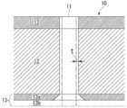
도 1a 는 본 실시형태에 관련된 플라즈마 처리 장치용 전극판의 개략 설명도이며, 전극판의 사시도이다.
도 1b 는 본 실시형태에 관련된 플라즈마 처리 장치용 전극판의 개략 설명도이며, 전극판의 단면도이다.
도 2 는 본 실시형태에 관련된 플라즈마 처리 장치용 전극판을 사용한 플라즈마 에칭 장치의 일례를 나타내는 개략 구성도이다.
도 3 은 도 2 의 플라즈마 에칭 장치를 사용하여, 웨이퍼의 에칭 처리를 실시한 후의 플라즈마 처리 장치용 전극판의 통기공의 개략 단면도이다.
도 4 는 코팅층을 형성하고 있는 재료가, 기재를 형성하고 있는 재료보다 내플라즈마성이 높은 플라즈마 처리 장치용 전극판에 대하여, 웨이퍼의 에칭 처리를 실시한 후의 상태를 나타내는 개략 단면도이다.
도 5 는 본 실시형태의 플라즈마 처리 장치용 전극판의 재생 방법에 있어서의 플라즈마 처리 장치용 전극판의 표면에 치밀질 탄화규소층을 재코팅하는 공정을 설명하는 단면도이다.
도 6 은 본 실시형태의 플라즈마 처리 장치용 전극판의 재생 방법에 있어서의 통기공의 표면에 형성된 치밀질 탄화규소층을 제거하는 공정을 설명하는 단면도이다.1A is a schematic explanatory diagram of an electrode plate for a plasma processing apparatus according to the present embodiment, and is a perspective view of the electrode plate.
1B is a schematic explanatory diagram of an electrode plate for a plasma processing apparatus according to the present embodiment, and is a cross-sectional view of the electrode plate.
2 is a schematic configuration diagram showing an example of a plasma etching apparatus using the electrode plate for plasma processing apparatus according to the present embodiment.
FIG. 3 is a schematic cross-sectional view of the air vent of the electrode plate for plasma processing apparatus after the wafer etching process is performed using the plasma etching apparatus of FIG. 2.
4 is a schematic cross-sectional view showing a state after the wafer is subjected to etching treatment with respect to an electrode plate for plasma processing apparatus in which the material forming the coating layer is higher in plasma resistance than the material forming the base material.
FIG. 5: is sectional drawing explaining the process of recoating a dense silicon-carbide layer on the surface of the electrode plate for plasma processing apparatuses in the regeneration method of the electrode plate for plasma processing apparatuses of this embodiment.
FIG. 6 is a cross-sectional view illustrating a step of removing the dense silicon carbide layer formed on the surface of the air vent in the regeneration method of the electrode plate for plasma processing apparatus of the present embodiment.
이하에 본 발명의 실시형태인 플라즈마 처리 장치용 전극판 및 플라즈마 처리 장치용 전극판의 재생 방법에 대해 첨부한 도면을 참조하여 설명한다.EMBODIMENT OF THE INVENTION Below, the reproduction | regeneration method of the electrode plate for plasma processing apparatuses and the electrode plate for plasma processing apparatuses which are embodiment of this invention is demonstrated with reference to attached drawing.
본 실시형태에 관련된 플라즈마 처리 장치용 전극판은, 예를 들어, 반도체 디바이스 제조 프로세스에 사용되는 플라즈마 에칭 장치나 플라즈마 CVD 장치 등의 플라즈마 처리 장치의 진공 챔버 내에 구비되는 1 쌍의 전극 중 상측 전극으로서 사용된다.The electrode plate for plasma processing apparatus which concerns on this embodiment is an upper electrode among a pair of electrodes provided in the vacuum chamber of plasma processing apparatuses, such as a plasma etching apparatus and a plasma CVD apparatus used for a semiconductor device manufacturing process, for example. Used.
도 1 은 본 실시형태에 관련된 플라즈마 처리 장치용 전극판의 개략 설명도이다. 도 1a 는 전극판의 사시도이고, 도 1b 는 전극판의 단면도이다.1 is a schematic explanatory diagram of an electrode plate for a plasma processing apparatus according to the present embodiment. 1A is a perspective view of an electrode plate, and FIG. 1B is a sectional view of the electrode plate.
도 1a 및 도 1b 에 있어서, 플라즈마 처리 장치용 전극판 (10) 은, 원판상으로 되어 있고, 플라즈마 생성용 가스를 통과시키는 통기공 (11) 이 복수 개 형성되어 있다. 플라즈마 처리 장치용 전극판 (10) 은, 기재 (12) 와, 기재 (12) 의 표면에 형성된 코팅층 (13) 을 갖는다.In FIGS. 1A and 1B, the
본 실시형태의 플라즈마 처리 장치용 전극판 (10) 에 있어서, 통기공 (11) 은, 직경이 0.1 ㎜ 이상 1.0 ㎜ 이하의 범위에 있는 것이 바람직하다. 기재 (12) 에 있어서의 통기공 (11) 의 애스펙트비 (기재 (12) 의 두께/통기공 (11) 의 직경) 는 3 이상인 것이 바람직하다. 통기공 (11) 의 애스펙트비가 3 이상이면, 플라즈마가 플라즈마 처리 장치용 전극판 (10) 의 배면까지 도달하기 어려워져, 플라즈마 처리 장치용 전극판 (10) 의 배면에 배치되는 부재 (예를 들어, 도 2 의 냉각판 (15)) 의 소모를 억제할 수 있다. 또, 플라즈마 생성용 가스의 역류를 방지하기 위해서는, 통기공 (11) 의 애스펙트비는 50 이하인 것이 바람직하다. 통기공 (11) 의 밀도는, 0.1 공/㎠ 이상 0.5 공/㎠ 이하여도 되는데, 이것에 한정되는 것은 아니다.In the
기재 (12) 의 두께는, 1 ㎜ 이상 20 ㎜ 이하의 범위에 있는 것이 바람직하다. 기재 (12) 의 두께가 이 범위에 있으면, 플라즈마 처리 장치용 전극판 (10) 의 강도가 강하여, 플라즈마에 의한 휨이나 변형이 잘 발생하지 않고, 또 플라즈마 생성용 가스를 통과시킬 수 있다.It is preferable that the thickness of the
코팅층 (13) 의 두께는, 0.3 ㎜ 이상 5.0 ㎜ 이하의 범위에 있는 것이 바람직하다. 코팅층 (13) 의 두께가 이 범위에 있음으로써, 코팅층 (13) 이 소모되어, 기재 (12) 가 노출될 때까지의 시간을 길게 할 수 있고, 플라즈마 처리 장치용 전극판 (10) 의 사용 시간을 길게 할 수 있다. 또한, 코팅층 (13) 의 두께가 5.0 ㎜ 를 초과하면, 코팅층 (13) 내의 통기공 (11) 의 공경이, 플라즈마에 의한 코팅층의 소모에 따라 변동되어, 플라즈마 생성용 가스의 유량의 조정이 어려워질 우려가 있다. 코팅층 (13) 의 두께는, 1.0 ㎜ 이상 3.0 ㎜ 이하의 범위에 있는 것이 보다 바람직하지만, 이것에 한정되지 않는다.It is preferable that the thickness of the
본 실시형태의 플라즈마 처리 장치용 전극판 (10) 에 있어서, 기재 (12) 는, 코팅층 (13) 을 형성하고 있는 재료보다 내플라즈마성이 높은 재료에 의해 형성되어 있다. 여기서, 내플라즈마성이 높다는 것은, 동일한 조건으로 플라즈마를 조사했을 때의 소모 비율이 낮은 것을 의미한다. 재료끼리의 내플라즈마성의 비교는, 후술하는 실험예로 나타내는 바와 같이 각 재료의 내플라즈마성을 평가함으로써 실시할 수 있다. 실제의 플라즈마 처리 장치용 전극판 (10) 으로는, 코팅층 (13) 의 소모량 (두께) 에 대해 기재 (12) 의 통기공 내벽의 소모량이 1/10 이하가 되는 내플라즈마성을 갖는 기재 (12) 와 코팅층 (13) 으로 형성되어 있는 것이 바람직하다.In the
본 실시형태의 플라즈마 처리 장치용 전극판 (10) 에서는, 기재 (12) 를 형성하고 있는 재료는, Y2O3, Al2O3 및 AlN 으로 이루어지는 군에서 선택되는 1 종 혹은 2 종 이상의 혼합물, 또는 이들과 SiC 의 혼합물로 되어 있다. 기재 (12) 를 형성하고 있는 재료는, Y2O3, Al2O3 및 AlN 으로 이루어지는 군에서 선택되는 1 종 혹은 2 종 이상과 SiC 의 혼합물인 것이 특히 바람직하다. 이 경우, Y2O3, Al2O3 및 AlN 의 함유량은, 합계로 3 질량% 이상 10 질량% 이하의 범위에 있는 것이 바람직하다. Y2O3, Al2O3 및 AlN 의 함유량이 3 질량% 보다 적으면 내플라즈마성이 불충분해질 우려가 있다. 한편, Y2O3, Al2O3 및 AlN 의 함유량이 10 질량% 이상을 초과하면, 웨이퍼에 전사되는 불순물량이 많아져 반도체 소자의 제조가 곤란해질 우려가 있다. Y2O3 의 함유량은, 3 질량% 이상 5 질량% 이하의 범위, Al2O3 의 함유량은, 3 질량% 이상 5 질량% 이하의 범위, AlN 의 함유량은, 3 질량% 이상 5 질량% 이하의 범위에 있는 것이 보다 바람직하지만, 이것에 한정되지 않는다.The plasma processing apparatus for the
기재 (12) 를 형성하고 있는 재료가 Y2O3, Al2O3 및 AlN 으로 이루어지는 군에서 선택되는 1 종 혹은 2 종 이상의 혼합물로 이루어지는 경우, 기재 (12) 의 두께는 4 ㎜ 이상 10 ㎜ 이하의 범위에 있는 것이 바람직하다. Y2O3 으로 이루어지는 기판을 제조할 때에는, 소결 온도는 1500 ℃ 이상 1700 ℃ 이하의 범위에 있는 것이 바람직하고, Al2O3 으로 이루어지는 기판을 제조할 때에는, 소결 온도는 1200 ℃ 이상 1400 ℃ 이하의 범위에 있는 것이 바람직하고, AlN 으로 이루어지는 기판을 제조할 때에는, 소결 온도는 1600 ℃ 이상 1800 ℃ 이하의 범위에 있는 것이 바람직하다. 또, 압력은 30 ㎫ 이상 40 ㎫ 이하의 범위에 있는 것이 바람직하지만, 이것에 한정되지 않는다.When the material forming the
기재 (12) 는, 상기 재료의 소결체인 것이 바람직하다. 기재 (12) 가 되는 소결체의 소재는 공공률이 2 % 이하인 것이 바람직하다.It is preferable that the
본 실시형태의 플라즈마 처리 장치용 전극판 (10) 에서는, 코팅층 (13) 을 형성하고 있는 재료는, 치밀질 탄화규소로 되어 있다. 치밀질 탄화규소는, 밀도 3.10 g/㎤ 이상의 탄화규소이다. 치밀질 탄화규소는, 화학적 기상 성장법 (CVD 법) 에 의해 성형된 CVD-SiC 인 것이 바람직하다. 치밀질 탄화규소의 밀도는, 3.20 g/㎤ 이상 3.21 g/㎤ 이하의 범위에 있는 것이 보다 바람직하지만, 이것에 한정되지 않는다.In the
본 실시형태의 플라즈마 처리 장치용 전극판 (10) 은, 예를 들어, 기재를 형성하는 재료를 소결시켜 소결체를 얻는 소결 공정, 소결체의 표면에 치밀질 탄화규소로 이루어지는 코팅층을 형성하는 코팅 공정, 코팅층이 형성된 소결체에 통기공을 형성하는 통기공 형성 공정을 구비하는 방법에 의해 제조할 수 있다.The
소결 공정에 있어서, 기재를 형성하는 재료로서, Y2O3, Al2O3 및 AlN 으로 이루어지는 군에서 선택되는 1 종 혹은 2 종 이상과 SiC 의 혼합물을 사용하는 경우, 이들 원료의 혼합 방법으로는 특별히 제한없다. 혼합은, 습식으로 실시해도 되고, 건식으로 실시해도 된다. 혼합에는, 볼밀 등의 분말의 혼합에 이용되고 있는 통상적인 혼합 장치를 사용할 수 있다.In the sintering step, in the case of using a mixture of one or two or more selected from the group consisting of Y2 O3 , Al2 O3 and AlN and SiC as a material for forming the substrate, Is not particularly limited. Mixing may be carried out wet or dry. For mixing, a conventional mixing device used for mixing powder such as a ball mill can be used.
기재를 형성하는 재료를 소결시키는 방법으로는, 핫 프레스, 상압 소결, 열간 정수압 프레스를 사용할 수 있다. 소결 온도는 1900 ℃ 이상 2000 ℃ 이하의 범위에 있는 것이 바람직하고, 소결 압력은 30 ㎫ 이상 40 ㎫ 이하의 범위에 있는 것이 바람직하지만, 이것에 한정되지 않는다.As a method of sintering the material which forms a base material, hot press, atmospheric pressure sintering, and hot hydrostatic press can be used. It is preferable to exist in the range of 1900 degreeC or more and 2000 degrees C or less, and it is preferable to exist in the range of 30 Mpa or more and 40 Mpa or less, but it is not limited to this.
코팅 공정에 있어서, 코팅층을 형성하는 방법으로는 CVD 법을 사용할 수 있다.In the coating process, the CVD method can be used as a method of forming a coating layer.
통기공 형성 공정에 있어서, 코팅층이 형성된 소결체에 통기공을 형성하는 방법으로는, 드릴 가공, 초음파 가공, 레이저 가공을 사용할 수 있다.In the ventilation hole forming step, as a method of forming the ventilation hole in the sintered compact in which the coating layer was formed, drill processing, ultrasonic processing, and laser processing can be used.
도 2 는 본 실시형태에 관련된 플라즈마 처리 장치용 전극판을 사용한 플라즈마 에칭 장치의 일례를 나타내는 개략 구성도이다.2 is a schematic configuration diagram showing an example of a plasma etching apparatus using the electrode plate for plasma processing apparatus according to the present embodiment.
플라즈마 에칭 장치 (100) 는, 도 2 에 나타내는 바와 같이, 진공 챔버 (30) 내의 상측에 본 실시형태에 관련된 플라즈마 처리 장치용 전극판 (10) (상측 전극) 이 형성됨과 함께, 하측에 상하동 가능한 가대 (하측 전극) (20) 가 플라즈마 처리 장치용 전극판 (10) 과 상호 간격을 두고 평행하게 형성된다. 이 경우, 상측의 플라즈마 처리 장치용 전극판 (10) 은, 절연체 (14) 에 의해 진공 챔버 (30) 의 벽에 대해 절연 상태로 지지되어 있다. 가대 (20) 상에는, 정전 척 (21) 과, 그 주위를 둘러싸는 실리콘제의 지지 링 (22) 이 형성되어 있다. 정전 척 (21) 상에는, 지지 링 (22) 에 의해 주연부를 지지한 상태로 웨이퍼 (피처리 기판) (40) 가 재치 (載置) 된다. 또, 진공 챔버 (30) 의 상측에는, 에칭 가스 공급관 (31) 이 형성되어 있다. 이 에칭 가스 공급관 (31) 으로부터 이송되어 온 에칭 가스는, 확산 부재 (32) 를 경유한 후, 플라즈마 처리 장치용 전극판 (10) 에 형성된 통기공 (11) 을 통해 웨이퍼 (40) 를 향하여 흐르고, 진공 챔버 (30) 의 측부의 배출구 (33) 로부터 외부로 배출된다. 한편, 플라즈마 처리 장치용 전극판 (10) 과 가대 (20) 사이에는, 고주파 전원 (50) 에 의해 고주파 전압이 인가된다.As shown in FIG. 2, the
또, 플라즈마 처리 장치용 전극판 (10) 의 배면에는, 열전도성이 우수한 알루미늄 등으로 이루어지는 냉각판 (15) 이 고정되어 있다. 이 냉각판 (15) 에도, 플라즈마 처리 장치용 전극판 (10) 의 통기공 (11) 에 연통하도록, 통기공 (11) 과 동일한 피치로 관통공 (16) 이 형성되어 있다. 그리고, 플라즈마 처리 장치용 전극판 (10) 은, 배면이 냉각판 (15) 에 접촉한 상태로 나사 고정 등에 의해 플라즈마 에칭 장치 (100) 내에 고정된다.Moreover, the cooling
도 3 은 상기 플라즈마 에칭 장치 (100) 를 사용하여, 웨이퍼 (40) 의 에칭 처리를 실시한 후의 플라즈마 처리 장치용 전극판 (10) 의 통기공 (11) 의 개략 단면도이다. 또한, 도 3 에 있어서, 파선은 에칭 처리를 실시하기 전의 상태를 나타내고, 실선은 에칭 처리를 실시한 후의 상태를 나타내고 있다. 또, 플라즈마 생성용 가스는, 통기공 (11) 을 상방으로부터 하방 (도 2 의 화살표 방향) 으로 통과하고, 플라즈마는 플라즈마 처리 장치용 전극판 (10) 의 하방에서 생성된다. 따라서, 도 3 에 있어서, 플라즈마 처리 장치용 전극판 (10) 은 하측의 코팅층 (13) 이 소모되고 있고, 13a 는 플라즈마에 의해 소모되지 않고 잔존한 코팅층의 잔존부를, 13b 는 플라즈마에 의해 소모된 코팅층의 소모부이다.3 is a schematic cross-sectional view of the
도 3 에 나타내는 바와 같이, 플라즈마 처리 장치용 전극판 (10) 의 코팅층 (13) 은, 에칭 처리에 의해 통기공 (11) 의 주위는 테이퍼상으로 소모된다. 기재 (12) 내의 통기공 (11) 의 내벽은, 실질적으로 소모되지 않은 것이 바람직하다. 예를 들어, 통기공 (11) 의 직경이 0.5 ㎜ 이고, 코팅층 (13) 의 두께가 3.0 ㎜ 인 경우, 통기공 (11) 의 기재 (12) 의 단면이 보일 때까지 에칭 처리했을 때에도, 기재 (12) 내의 통기공 (11) 의 내벽이 소모되는 두께 (t) 는, 0.005 ㎜ 이하인 것이 바람직하다.As shown in FIG. 3, the
도 4 는 코팅층을 형성하고 있는 재료가, 기재를 형성하고 있는 재료보다 내플라즈마성이 높은 플라즈마 처리 장치용 전극판에 대하여, 웨이퍼의 에칭 처리를 실시한 후의 상태를 나타내는 개략 단면도이다. 도 4 에 나타내는 플라즈마 처리 장치용 전극판 (110) 에 있어서, 기재 (112) 는 SiC 소결체이고, 코팅층 (113) 은 CVD-SiC 로 형성되어 있다. 또한, 도 4 에 있어서, 파선은 에칭 처리를 실시하기 전의 상태를 나타내고, 실선은 에칭 처리를 실시한 후의 상태를 나타내고 있다. 113a 는 플라즈마에 의해 소모되지 않고 잔존한 코팅층의 잔존부를, 113b 는 플라즈마에 의해 소모된 코팅층의 소모부이다.4 is a schematic cross-sectional view showing a state after the wafer is subjected to etching treatment with respect to an electrode plate for plasma processing apparatus in which the material forming the coating layer is higher in plasma resistance than the material forming the base material. In the
도 4 에 나타내는 바와 같이, 코팅층 (113) 을 형성하고 있는 재료가 기재 (112) 를 형성하고 있는 재료보다 내플라즈마성이 높은 플라즈마 처리 장치용 전극판 (110) 에서는, 플라즈마에 의해 기재 (112) 내의 통기공 (111) 의 내벽이 크게 소모된다. 이 때문에, 통기공 (111) 을 통과하는 플라즈마 생성용 가스의 유량이 크게 변동하여, 안정적으로 에칭 처리를 실시하는 것이 곤란해진다.As shown in FIG. 4, in the
다음으로, 본 실시형태의 플라즈마 처리 장치용 전극판의 재생 방법을 설명한다.Next, the regeneration method of the electrode plate for plasma processing apparatus of this embodiment is demonstrated.
본 실시형태의 플라즈마 처리 장치용 전극판의 재생 방법은, 예를 들어, 상기의 도 3 에 나타내는 바와 같이, 코팅층의 표면이 플라즈마에 의해 소모되고 있는 플라즈마 처리 장치용 전극판의 재생 방법이다. 본 실시형태의 플라즈마 처리 장치용 전극판의 재생 방법은, 플라즈마 처리 장치용 전극판의 표면에, 치밀질 탄화규소층을 재코팅하는 공정과, 플라즈마 처리 장치용 전극판의 통기공의 표면에 코팅된 치밀질 탄화규소층을 제거하는 공정을 구비한다. 코팅층 (13) 의 표면이 플라즈마에 의해 소모되고 있다고 판단되는 코팅층 (13) 의 두께는, 에칭 처리를 실시하기 전의 코팅층 (13) 두께에 대하여, 95 % 이하가 되었을 때의 두께여도 된다.The regeneration method of the electrode plate for plasma processing apparatus of this embodiment is a regeneration method of the electrode plate for plasma processing apparatus in which the surface of a coating layer is consumed by plasma, for example as shown in said FIG. The regeneration method of the electrode plate for plasma processing apparatus of this embodiment is a process of recoating a dense silicon carbide layer on the surface of the electrode plate for plasma processing apparatuses, and coating on the surface of the vent hole of the electrode plate for plasma processing apparatuses. And removing the dense silicon carbide layer. The thickness of the
도 5 는 플라즈마 처리 장치용 전극판의 표면에 치밀질 탄화규소층을 재코팅한 상태를 설명하는 단면도이다.5 is a cross-sectional view illustrating a state in which a dense silicon carbide layer is recoated on the surface of an electrode plate for plasma processing apparatus.
본 실시형태의 플라즈마 처리 장치용 전극판의 재생 방법에 있어서, 치밀질 탄화규소층 (13c) 은, CVD 법에 의해 형성된 CVD-SiC 로 이루어지는 층이다. 치밀질 탄화규소층 (13c) 은, 코팅층 (13) 의 소모부 (13b) 를 초과하는 두께로 형성되어 있고, 통기공 (11) 의 직경이 부분적으로 좁아져 있다. 치밀질 탄화규소층 (13c) 의 두께는, 1 ㎜ 이상 5 ㎜ 이하인 것이 바람직하지만, 이것에 한정되지 않는다.In the regeneration method of the electrode plate for plasma processing apparatus of this embodiment, the dense
도 6 은 통기공의 표면에 형성된 치밀질 탄화규소층 (13c) 을 제거한 상태를 설명하는 단면도이다.6 is a cross-sectional view illustrating a state in which the dense
본 실시형태의 플라즈마 처리 장치용 전극판의 재생 방법에서는, 플라즈마 처리 장치용 전극판의 통기공의 표면에 코팅된 치밀질 탄화규소층 (13c) 을 제거한다. 이로써, 통기공 (11) 의 직경을 재생 전의 상태로 되돌림과 함께, 기재 (12) 의 통기공 (11) 의 내벽을 내플라즈마성이 높은 기재 (12) 의 재료를 노출시킨다. 치밀질 탄화규소층 (13c) 이 기재 (12) 의 통기공 (11) 의 내벽에 치밀질 탄화규소층 (13c) 이 잔류하고 있으면, 플라즈마에 의한 에칭 처리 중에 통기공 (11) 의 내벽에 잔류하고 있던 치밀질 탄화규소층 (13c) 이 소모됨으로써, 통기공 (11) 의 공경이 확대되고, 이로써 플라즈마 생성용 가스의 유량이 변동되어, 안정적으로 에칭 처리를 실시하는 것이 곤란해질 우려가 있다. 치밀질 탄화규소층 (13c) 을 제거하는 방법으로는, 드릴 가공, 초음파 가공, 레이저 가공을 사용할 수 있다. 또, 코팅층 (13) 의 잔존부 (13) 의 표면에 형성된 치밀질 탄화규소층 (13c) 은, 에칭 처리를 실시하기 전의 상태의 코팅층 (13) 의 두께까지 제거한다. 치밀질 탄화규소층 (13c) 을 제거하는 방법으로는, 평면 연삭 가공을 사용할 수 있다.In the regeneration method of the electrode plate for plasma processing apparatus of this embodiment, the dense
이상과 같은 구성으로 이루어진 본 실시형태의 플라즈마 처리 장치용 전극판 (10) 에 있어서는, 기재 (12) 가, 코팅층 (13) 을 형성하고 있는 재료보다 내플라즈마성이 높은 재료에 의해 형성되어 있으므로, 기재 (12) 의 통기공 (11) 의 내벽은, 코팅층 (13) 보다 플라즈마에 의한 소모가 잘 일어나지 않게 된다. 따라서, 본 실시형태의 플라즈마 처리 장치용 전극판에서는, 플라즈마에 의한 에칭 처리 중에, 플라즈마 생성용 가스의 유량이 변동되는 것이 잘 일어나지 않아, 장시간에 걸쳐서 안정적으로 이용할 수 있다.In the
그리고, 본 실시형태의 플라즈마 처리 장치용 전극판 (10) 에 있어서는, 기재 (12) 를 형성하고 있는 재료가 Y2O3, Al2O3 및 AlN 으로 이루어지는 군에서 선택되는 1 종 혹은 2 종 이상의 혼합물, 또는 이들과 SiC 의 혼합물이고, 코팅층 (13) 을 형성하고 있는 재료가 치밀질 탄화규소로 되어 있으므로, 기재 (12) 의 내플라즈마성을 코팅층 (13) 의 내플라즈마성보다 확실하게 높게 할 수 있다.Then, in the plasma processing apparatus for the
본 실시형태의 플라즈마 처리 장치용 전극판의 재생 방법에 있어서는, 기재가, 코팅층을 형성하고 있는 치밀질 탄화규소보다 내플라즈마성이 높은 재료에 의해 형성되어 있으므로, 기재의 통기공의 내벽이 소모되기 전에, 플라즈마 처리 장치용 전극판을 재생할 수 있다. 따라서, 본 실시형태의 플라즈마 처리 장치용 전극판의 재생 방법에 의하면, 플라즈마 생성용 가스의 유량을 변동시키지 않고, 플라즈마 처리 장치용 전극판을 재생할 수 있다.In the method for reproducing the electrode plate for plasma processing apparatus of the present embodiment, since the substrate is made of a material having higher plasma resistance than the dense silicon carbide forming the coating layer, the inner wall of the vent hole of the substrate is consumed. Before, the electrode plate for plasma processing apparatus can be reproduced. Therefore, according to the regeneration method of the electrode plate for plasma processing apparatuses of this embodiment, the electrode plate for plasma processing apparatuses can be reproduced, without changing the flow volume of the plasma generation gas.
이상, 본 발명의 실시형태에 대해 설명했지만, 본 발명은 이것에 한정되지 않고, 그 발명의 기술적 사상을 일탈하지 않는 범위에서 적절히 변경 가능하다.As mentioned above, although embodiment of this invention was described, this invention is not limited to this, It can change suitably in the range which does not deviate from the technical idea of the invention.
예를 들어, 본 실시형태에서는, 플라즈마 처리 장치용 전극판 (10) 을 원판상으로 했지만, 플라즈마 처리 장치용 전극판 (10) 의 형상에는 특별히 제한은 없고, 각판상으로 해도 된다.For example, in this embodiment, although the
또, 본 실시형태에서는, 기재 (12) 를 형성하고 있는 재료는 Y2O3, Al2O3 및 AlN 으로 이루어지는 군에서 선택되는 1 종 혹은 2 종 이상의 혼합물, 또는 이것들과 SiC 의 혼합물이고, 코팅층 (13) 을 형성하고 있는 재료는 치밀질 탄화규소로서 설명했지만, 이것에 한정되지 않고, 기재 (12) 는, 코팅층 (13) 을 형성하고 있는 재료보다 내플라즈마성이 높은 재료에 의해 형성되어 있으면 된다. 기재 (12) 및 코팅층 (13) 의 재료는, 플라즈마 생성용 가스, 에칭 처리되는 웨이퍼 (피처리 기판) 의 재질에 따라 적절히 선택하는 것이 바람직하다.In this embodiment, the material that forms the base material (12) isY 2 O 3, Al 2 O 3 and one species or two or more kinds of mixtures selected from the group consisting of AlN, or a mixture of these and SiC, Although the material which forms the
실시예Example
이하에, 본 발명에 관련된 플라즈마 처리 장치용 전극판의 작용 효과에 대해 평가한 평가 시험의 결과에 대해 설명한다.Below, the result of the evaluation test evaluated about the effect of the electrode plate for plasma processing apparatus which concerns on this invention is demonstrated.
먼저, 예비 시험으로서 하기의 실험예 1 ∼ 7 에서 제조한 전극 재료의 내플라즈마성을 평가하였다.First, the plasma resistance of the electrode material manufactured by the following Experimental Examples 1-7 was evaluated as a preliminary test.
[실험예 1]Experimental Example 1
(SiC 소결체의 제조)(Manufacture of SiC Sintered Body)
SiC 분말 (순도:99.9 질량%, 평균 입자경:0.4 ㎛) 을 준비하였다. 준비한 SiC 분말을 성형형에 충전하고, 핫 프레스를 사용하여 2000 ℃, 40 ㎫ 의 조건으로 가압 소성하였다. 얻어진 소결체를 연마 가공하여, 직경 400 ㎜, 두께 10 ㎜ 의 SiC 소결체를 제조하였다. 얻어진 소결체는 기공률이 2 % 이하였다.SiC powder (purity: 99.9 mass%, average particle diameter: 0.4 micrometers) was prepared. The prepared SiC powder was filled into a shaping | molding die, and it baked under pressure at 2000 degreeC and 40 Mpa using the hot press. The obtained sintered compact was polished and the SiC sintered compact of diameter 400mm and thickness 10mm was manufactured. The porosity of the obtained sintered compact was 2% or less.
[실험예 2]Experimental Example 2
(CVD-SiC 의 제조)(Manufacture of CVD-SiC)
실리콘 기판 (직경:40 ㎜, 두께:5 ㎜) 을 준비하였다. 준비한 실리콘 기판의 표면에, CVD 장치를 사용하여 두께 10 ㎜ 의 CVD-SiC 를 제조하였다.A silicon substrate (diameter: 40 mm, thickness: 5 mm) was prepared. On the surface of the prepared silicon substrate, CVD-SiC of thickness 10mm was manufactured using the CVD apparatus.
[실험예 3]Experimental Example 3
(3 질량%-Y2O3 함유 SiC 소결체의 제조)(Manufacture of 3 mass% -Y2 O3 containing SiC sintered body)
Y2O3 분말 (순도:99.9 질량%, 평균 입자경:3 ㎛) 과 SiC 분말 (순도:99.9 질량%, 평균 입자경:4 ㎛) 을 준비하였다.Y2 O3 powder (purity: 99.9 mass%, average particle diameter: 3 ㎛) and SiC powder (purity: 99.9 mass%, average particle size: 4 ㎛) was prepared.
준비한 Y2O3 분말과 SiC 분말을, 질량비로 3:97 (Y2O3 분말:SiC 분말) 의 비율로 볼밀을 사용하여 혼합하여, 분말 혼합물을 얻었다. 얻어진 분말 혼합물을 성형형에 충전하고, 핫 프레스를 사용하여 2000 ℃, 40 ㎫ 의 조건으로 가압 소성하였다. 얻어진 소결체를 연마 가공하여, 직경 400 ㎜, 두께 10 ㎜ 의 3 질량%-Y2O3 함유 SiC 소결체를 제조하였다. 얻어진 소결체는, 기공률이 2 % 이하였다.The prepared Y2 O3 powder and SiC powder were mixed at a mass ratio of 3:97 (Y2 O3 powder: SiC powder) using a ball mill to obtain a powder mixture. The obtained powder mixture was filled in the shaping | molding die, and it baked under pressure on 2000 degreeC and 40 Mpa conditions using hot press. Trituration of the obtained sintered body machining, 400 ㎜ diameter, to prepare a 3 weight% -Y2 O3 containing SiC sintered body having a thickness of 10 ㎜. The porosity of the obtained sintered compact was 2% or less.
[실험예 4]Experimental Example 4
(5 질량%-Y2O3 함유 SiC 소결체의 제조)(Manufacture of 5 mass% -Y2 O3 containing SiC sintered body)
Y2O3 분말과 SiC 분말의 혼합 비율을, 질량비로 5:95 (Y2O3 분말:SiC 분말) 로 한 것 이외에는, 실험예 3 과 동일하게 하여, 5 질량%-Y2O3 함유 SiC 소결체를 제조하였다. 얻어진 소결체는, 기공률이 2 % 이하였다.Containing 5 mass% -Y2 O3 in the same manner as in Experiment 3 except that the mixing ratio of the Y2 O3 powder and the SiC powder was set to 5:95 (Y2 O3 powder: SiC powder) in a mass ratio. SiC sintered body was manufactured. The porosity of the obtained sintered compact was 2% or less.
[실험예 5]Experimental Example 5
(10 질량%-Y2O3 함유 SiC 소결체의 제조)(Manufacture of 10 mass% -Y2 O3 containing SiC sintered body)
Y2O3 분말과 SiC 분말의 혼합 비율을, 질량비로 10:90 (Y2O3 분말:SiC 분말) 으로 한 것 이외에는, 실험예 3 과 동일하게 하여, 10 질량%-Y2O3 함유 SiC 소결체를 얻었다. 얻어진 소결체는, 기공률이 2 % 이하였다.Containing 10 mass% -Y2 O3 in the same manner as in Experiment 3, except that the mixing ratio of the Y2 O3 powder and the SiC powder was 10:90 (Y2 O3 powder: SiC powder) in a mass ratio. SiC sintered compact was obtained. The porosity of the obtained sintered compact was 2% or less.
[실험예 6]Experimental Example 6
(3 질량% Al2O3 함유 SiC 소결체의 제조)(Manufacture of 3 mass% Al2 O3 containing SiC sintered body)
Al2O3 분말 (순도:99.9 질량%, 평균 입자경:0.3 ㎛) 을 준비하였다.Al2 O3 powder (purity: 99.9 mass%, average particle diameter: 0.3 micrometers) was prepared.
Y2O3 분말 대신에, Al2O3 분말과 SiC 분말을, 질량비로 3:97 (Al2O3 분말:SiC 분말) 의 비율로 볼밀을 사용하여 혼합한 것 이외에는, 실험예 3 과 동일하게 하여, 3 질량%-Al2O3 함유 SiC 소결체를 제조하였다. 얻어진 소결체는, 기공률이 2 % 이하였다.Instead of Y2 O3 powder, Al2 O3 powder and SiC powder were the same as Experimental Example 3 except that a ball mill was mixed in a ratio of 3:97 (Al2 O3 powder: SiC powder) by mass ratio. A 3 mass% -Al2 O3 containing SiC sintered compact was produced. The porosity of the obtained sintered compact was 2% or less.
[실험예 7]Experimental Example 7
(3 질량%-AlN 함유 SiC 소결체의 제조)(Manufacture of 3 mass% -AlN containing SiC sintered compact)
AlN 분말 (순도:99.9 질량%, 평균 입자경:0.5 ㎛) 을 준비하였다.AlN powder (purity: 99.9 mass%, average particle diameter: 0.5 micrometer) was prepared.
Y2O3 분말 대신에, AlN 분말과 SiC 분말을, 질량비로 3:97 (AlN 분말:SiC 분말) 의 비율로 볼밀을 사용하여 혼합한 것 이외에는, 실험예 3 과 동일하게 하여, 3 질량%-AlN 함유 SiC 소결체를 제조하였다. 얻어진 소결체는, 기공률이 2 % 이하였다.3 mass% of AlN powder and SiC powder instead of Y2 O3 powder in the same manner as in Experiment 3 except that a ball mill was mixed in a ratio of 3:97 (AlN powder: SiC powder) by mass ratio. A -AlN-containing SiC sintered body was produced. The porosity of the obtained sintered compact was 2% or less.
(내플라즈마성의 평가)(Evaluation of Plasma Resistance)
실험예 1 ∼ 7 에서 제조한 전극 재료의 표면의 일부에 마스킹을 실시하였다. 이 마스킹을 실시한 전극 재료를, RIE 플라즈마 에칭 장치에 장착하였다. 이어서, RIE 플라즈마 에칭 장치 내를 진공으로 한 후, SF4 가스를 50 sccm 의 유량으로 도입하고, 500 W 로, 1 시간 플라즈마를 전극 재료에 조사하였다. 플라즈마 조사 후, 전극 재료를 RIE 플라즈마 에칭 장치로부터 취출하였다. 전극 재료의 마스킹을 제거하고, 마스킹 부분과 마스킹하지 않았던 부분의 단차를 플라즈마 조사에 의한 소모량으로서 측정하였다. 측정한 전극 재료의 소모량을, 실험예 1 에서 제조한 SiC 소결체의 소모량을 1 로 한 소모 비율 (= 전극 재료의 소모량/SiC 소결체의 소모량) 로서 평가하였다. 그 결과를 표 1 에 나타낸다.Part of the surface of the electrode material produced in Experimental Examples 1 to 7 was masked. This masked electrode material was attached to a RIE plasma etching apparatus. Subsequently, after vacuuming inside the RIE plasma etching apparatus, SF4 gas was introduced at a flow rate of 50 sccm, and plasma was irradiated to the electrode material at 500 W for 1 hour. After the plasma irradiation, the electrode material was taken out from the RIE plasma etching apparatus. Masking of the electrode material was removed, and the step difference between the masked portion and the unmasked portion was measured as the consumption amount by plasma irradiation. The consumption amount of the measured electrode material was evaluated as a consumption ratio (= consumption amount of electrode material / consumption amount of SiC sintered body) in which the consumption amount of the SiC sintered body produced in Experimental Example 1 was 1. The results are shown in Table 1.

표 1 의 소모 비율로부터, 실험예 1 ∼ 7 에서 제조한 전극 재료의 내플라즈마성은, SiC 소결체, CVD-SiC, 3 질량%-AlN 함유 SiC 소결체, 3 질량%-Al2O3 함유 SiC 소결체, 3 질량%-Y2O3 함유 SiC 소결체, 5 질량%-Y2O3 함유 SiC 소결체, 10 질량%-Y2O3 함유 SiC 소결체의 순서로 높아지는 것이 확인되었다.From consumption rate shown in Table 1, the family of the plasma electrode material prepared in Experimental Example 1 ~ 7, sintered SiC, CVD-SiC, 3% by mass -AlN-containing SiC sintered body, and 3 mass% -Al2 O3 containing SiC sintered body, 3 mass% -Y2 O3 containing it has been confirmed that higher the order of the SiC sintered body, -Y2 O3 containing 5 wt.% SiC sintered body, 10 mass% -Y2 O3 containing SiC sintered body.
[본 발명예 1][Inventive Example 1]
상기 실험예 3 과 동일하게 하여, 직경 400 ㎜, 두께 10 ㎜ 의 3 질량%-Y2O3 함유 SiC 소결체를 제조하였다.A 3 mass% -Y2 O3 containing SiC sintered compact having a diameter of 400 mm and a thickness of 10 mm was prepared in the same manner as in Experimental Example 3.
얻어진 3 질량%-Y2O3 함유 SiC 소결체를 기재로 하고, 그 편측 표면에, CVD 장치를 사용하여 두께 2 ㎜ 의 CVD-SiC 층을 형성하였다. 이어서, 레이저 장치를 사용하여, 얻어진 적층체에 직경 0.5 ㎜ 가 목적인 통기공을 10 ㎜ 간격으로 균등하게 형성하여, 플라즈마 처리 장치용 전극판을 제조하였다.And a 3 wt% -Y2 O3 containing SiC sintered body obtained as a base material, and in that one side surface, using a CVD apparatus to form a CVD-SiC layer having a thickness of 2 ㎜. Subsequently, using the laser device, vent holes with a diameter of 0.5 mm were uniformly formed at intervals of 10 mm in the obtained laminate to prepare an electrode plate for a plasma processing apparatus.
[본 발명예 2][Inventive Example 2]
기재로서, 상기 실험예 4 와 동일하게 하여 제조한 5 질량%-Y2O3 함유 SiC 소결체를 사용한 것 이외에는, 본 발명예 1 과 동일하게 하여 플라즈마 처리 장치용 전극판을 제조하였다.As described, except that the Example 4 and the same one containing 5 weight% -Y2 O3 prepared by SiC sintered body, this was prepared to the same manner as Example 1 for a plasma processing apparatus with an electrode plate.
[본 발명예 3][Inventive Example 3]
기재로서, 상기 실험예 5 와 동일하게 하여 제조한 10 질량%-Y2O3 함유 SiC 소결체를 사용한 것 이외에는, 본 발명예 1 과 동일하게 하여 플라즈마 처리 장치용 전극판을 제조하였다.As the substrate, an electrode plate for a plasma processing apparatus was manufactured in the same manner as in Example 1 except that a 10 mass% -Y2 O3 -containing SiC sintered body manufactured in the same manner as in Experimental Example 5 was used.
[본 발명예 4][Inventive Example 4]
기재로서, 상기 실험예 6 과 동일하게 하여 제조한 3 질량%-Al2O3 함유 SiC 소결체를 사용한 것 이외에는, 본 발명예 1 과 동일하게 하여 플라즈마 처리 장치용 전극판을 제조하였다.As the substrate, an electrode plate for a plasma processing apparatus was manufactured in the same manner as in Example 1 except that a 3 mass% -Al2 O3 -containing SiC sintered body manufactured in the same manner as in Experimental Example 6 was used.
[본 발명예 5][Inventive Example 5]
기재로서, 상기 실험예 7 과 동일하게 하여 제조한 3 질량%-AlN 함유 SiC 소결체를 사용한 것 이외에는, 본 발명예 1 과 동일하게 하여 플라즈마 처리 장치용 전극판을 제조하였다.An electrode plate for a plasma processing apparatus was manufactured in the same manner as in Example 1 of the present invention except that a 3 mass% -AlN-containing SiC sintered body manufactured in the same manner as in Experimental Example 7 was used as the substrate.
[비교예 1]Comparative Example 1
기재로서, 상기 실험예 1 과 동일하게 하여 제조한 SiC 소결체를 사용한 것 이외에는, 본 발명예 1 과 동일하게 하여 플라즈마 처리 장치용 전극판을 제조하였다.Except having used the SiC sintered compact manufactured similarly to the said Experimental example 1 as a base material, it carried out similarly to Example 1 of this invention, and manufactured the electrode plate for plasma processing apparatuses.
본 발명예 1 ∼ 5 및 비교예 1 에서 제조한 플라즈마 처리 장치용 전극판에 대하여, 내플라즈마성과, 플라즈마 처리 후의 재생에 의한 통기공의 공경의 변화를 하기와 같이 하여 평가하였다.About the electrode plate for plasma processing apparatuses manufactured by Examples 1-5 and Comparative Example 1, the change of the plasma resistance and the pore size of the ventilation hole by the regeneration after a plasma process was evaluated as follows.
(내플라즈마성)(Plasma resistance)
제조한 플라즈마 처리 장치용 전극판의 표면의 일부에 마스킹을 실시하였다. 이 마스킹을 실시한 플라즈마 처리 장치용 전극판을, 도 2 에 나타낸 플라즈마 에칭 장치에 장착하고, 웨이퍼의 에칭 처리를 실시하였다. 진공 챔버 내를 진공으로 한 후, SF4 가스를 50 sccm 의 유량으로 도입하고, 500 W 로, 300 시간 에칭 처리를 실시하였다. 에칭 처리 후, 플라즈마 처리 장치용 전극판을, 플라즈마 에칭 장치로부터 취출하였다. 플라즈마 처리 장치용 전극판의 마스킹을 제거한 후, 통기공의 중심에서 절단한 시료를 수지 매립하고, 절단면을 연마하여 통기공의 단면을 노출시켰다. 통기공 및 코팅층의 단면을, SEM (주사형 전자 현미경) 을 사용하여 관찰하고, 플라즈마 처리 후의 통기공과 코팅층의 소모도를 다음과 같이 하여 구하였다.Part of the surface of the produced electrode plate for plasma processing apparatus was masked. This masked electrode plate for plasma processing apparatus was attached to the plasma etching apparatus shown in FIG. 2, and the wafer was etched. After vacuuming the inside of the vacuum chamber, SF4 gas was introduced at a flow rate of 50 sccm, and the etching treatment was performed at 500 W for 300 hours. After the etching treatment, the electrode plate for the plasma processing apparatus was taken out from the plasma etching apparatus. After the masking of the electrode plate for plasma processing apparatus was removed, the sample cut | disconnected in the center of the air hole was filled with resin, the cut surface was ground, and the cross section of the air hole was exposed. The cross section of the air hole and the coating layer was observed using SEM (scanning electron microscope), and the consumption degree of the air hole and the coating layer after plasma treatment was calculated | required as follows.
그 결과를 표 2 에 나타낸다.The results are shown in Table 2.
(통기공의 소모도)(Air consumption)
통기공의 소모도는, 기재의 통기공 내벽의 소모도 (도 3 의 t 에 상당) 로 하였다. 통기공의 깊이 방향의 중앙 부분 (플라즈마 처리 장치용 전극판의 두께 방향에 있어서의 기재의 중앙 부분) 에 있어서의 통기공의 공경 (플라즈마 처리 후의 공경) 을 측정하고, 하기의 식으로부터 산출하였다.The consumption degree of the ventilation hole was made into the consumption degree (equivalent to t of FIG. 3) of the inner wall of the ventilation hole of a base material. The pore diameter (pore diameter after the plasma treatment) of the vent hole in the center part of the depth direction of the vent hole (center part of the base material in the thickness direction of the electrode plate for plasma processing apparatuses) was measured, and it calculated from the following formula.
통기공의 소모도 = {에칭 처리 후의 공경 - 에칭 처리 전의 공경 (0.5 ㎜)}/2Consumption of Aeration Holes = {pore size after etching-pore size before etching (0.5 mm)} / 2
(코팅층의 소모도)(Consumption of Coating Layer)
코팅층의 소모도는, 플라즈마 처리로 소모된 부분의 두께 (도 3 의 소모부 (13b) 의 두께에 상당) 로 하였다. 전극판의 중심으로부터 100 ㎜ 의 부분과, 마스킹을 제거한 부분의 단차를 측정하고, 그 측정값을 코팅층의 소모도로 하였다.Consumption degree of the coating layer was made into the thickness (equivalent to the thickness of the

본 발명예 1 ∼ 5 와 비교예 1 을 비교하면, 코팅층의 소모도는 본 발명예 1 ∼ 5 와 비교예 1 은 동등하지만, 기재의 통기공 내벽의 소모도는 본 발명예 1 ∼ 5 가 현저하게 저감되어 있는 것이 확인되었다. 특히, 기재로서 Y2O3 을 함유하는 SiC 의 소결체를 사용한 본 발명예 1 ∼ 3 은, 비교예 1 과 비교하여, 기재의 통기공 내벽의 소모도가 1/2 이하로 저감되어 있는 것이 확인되었다.Comparing Inventive Examples 1 to 5 and Comparative Example 1, the consumption degree of the coating layer is equivalent to the Inventive Examples 1 to 5 and Comparative Example 1, but the Inventive Examples 1 to 5 are conspicuous on the degree of consumption of the inner wall of the vent hole of the substrate. It was confirmed that it was reduced. In particular, the invention examples using a sintered body of SiC which contained Y2 O3 as the base material 1-3 is compared with Comparative Example 1, and confirmed that the air hole inner wall of substrate consumption is also reduced to less than 1/2 It became.
(플라즈마 처리 후의 재생에 의한 통기공의 공경의 변화)(Change of pore size of air vent by regeneration after plasma processing)
제조한 플라즈마 처리 장치용 전극판을, 도 2 에 나타낸 플라즈마 에칭 장치에 장착하고, 상기의 내플라즈마성의 평가와 동일한 조건으로 웨이퍼의 에칭 처리를 실시하였다. 에칭 처리 후, 플라즈마 처리 장치용 전극판을, 플라즈마 에칭 장치로부터 취출하였다. 일부의 통기공의 개구부를 마스킹하였다. 마스킹한 플라즈마 처리 장치용 전극판의 표면에, CVD 장치를 사용하여, 두께 2 ㎜ 의 CVD-SiC 층으로 재코팅하였다. 이어서, 레이저 장치를 사용하여, 플라즈마 처리 장치용 전극판의 통기공의 내벽면을 코팅하고 있는 CVD-SiC 층을 제거하였다.The manufactured electrode plate for plasma processing apparatus was attached to the plasma etching apparatus shown in FIG. 2, and the wafer was etched on the same conditions as the above-mentioned evaluation of plasma resistance. After the etching treatment, the electrode plate for the plasma processing apparatus was taken out from the plasma etching apparatus. The openings of some of the vents were masked. The surface of the masked electrode plate for plasma processing apparatus was recoated with a CVD-SiC layer having a thickness of 2 mm using a CVD apparatus. Subsequently, the CVD-SiC layer coating the inner wall surface of the vent hole of the electrode plate for plasma processing apparatuses was removed using the laser apparatus.
재생한 플라즈마 처리 장치용 전극판의 마스킹을 제거한 후, 통기공의 중심에서 절단한 시료를 수지 매립하고, 절단면을 연마하여 통기공의 단면을 노출시켰다. 개구부를 마스킹한 통기공 (재생 전의 통기공) 과 개구부를 마스킹하고 있지 않은 통기공 (재생 후의 통기공) 에 대하여, 각각 단면을 SEM (주사형 전자 현미경) 을 사용하여 관찰하고, 통기공의 깊이 방향의 중앙 부분 (플라즈마 처리 장치용 전극판의 두께 방향에 있어서의 기재의 중앙 부분) 에 있어서의 통기공의 공경을 측정하였다. 그 결과를, 표 3 에 나타낸다.After masking of the regenerated electrode plate for plasma processing apparatus, the sample cut at the center of the air hole was filled with resin, and the cut surface was polished to expose the end surface of the air hole. For the ventilation holes (air vents before regeneration) masking the openings and the ventilation holes (air ventilation after regeneration) not masking the openings, the cross sections were observed using SEM (scanning electron microscope), respectively, and the depth of the ventilation holes The pore size of the vent hole in the center part of the direction (center part of the base material in the thickness direction of the electrode plate for plasma processing apparatuses) was measured. The results are shown in Table 3.

비교예 1 의 플라즈마 처리 장치용 전극판에서는, 재생 후의 통기공의 공경이, 에칭 처리 전의 통기공의 공경 (0.5 ㎜) 과 비교하여 0.01 ㎜ (2 %) 이상 확대되었다. 통기공의 공경이 0.5 ㎜ 이고, 애스펙트비가 20 (= 10 ㎜/0.5 ㎜) 인 플라즈마 처리 장치용 전극판에서는, 통기공의 공경이 0.01 ㎜ 를 초과하여 확대되면 통기공을 통해 흐르는 가스의 유량 제어가 곤란해진다. 따라서, 비교예 1 의 플라즈마 처리 장치용 전극판은, 재생 후의 사용이 어려운 것이 확인되었다.In the electrode plate for plasma processing apparatus of the comparative example 1, the pore size of the ventilation hole after regeneration was expanded by 0.01 mm (2%) or more compared with the pore size (0.5 mm) of the ventilation hole before etching process. In the electrode plate for a plasma processing apparatus having a pore size of 0.5 mm and an aspect ratio of 20 (= 10 mm / 0.5 mm), when the pore size of the air vent exceeds 0.01 mm, the flow rate control of the gas flowing through the air vent is controlled. Becomes difficult. Therefore, it was confirmed that the electrode plate for plasma processing apparatus of the comparative example 1 is difficult to use after regeneration.
이에 반하여, 본 발명예 1 ∼ 5 의 플라즈마 처리 장치용 전극판은, 재생 후의 통기공의 공경의 확대가 0.01 ㎜ 이하로 좁기 때문에, 재생 후의 사용이 용이하다.In contrast, the electrode plates for plasma processing apparatuses of Examples 1 to 5 of the present invention are easy to use after the regeneration because the enlargement of the pore size of the ventilation holes after the regeneration is narrow to 0.01 mm or less.
이상의 결과로부터, 본 발명예 1 ∼ 5 에 의하면, 통기공의 내벽이 잘 소모되지 않아, 재생 후의 사용이 용이한 플라즈마 처리 장치용 전극판을 제공할 수 있는 것이 확인되었다.From the above results, according to Examples 1 to 5 of the present invention, it was confirmed that the inner wall of the vent hole was not consumed well, and thus an electrode plate for plasma processing apparatus that could be easily used after regeneration could be provided.
산업상 이용가능성Industrial availability
본 발명에 의하면, 플라즈마에 의한 에칭 처리 중에, 플라즈마 생성용 가스의 유량의 변동이 잘 일어나지 않아, 장시간에 걸쳐서 안정적으로 이용할 수 있는 플라즈마 처리 장치용 전극판을 제공할 수 있다.According to the present invention, it is possible to provide an electrode plate for a plasma processing apparatus which can be used stably for a long time without fluctuations in the flow rate of the plasma generating gas during the etching treatment by plasma.
10 : 플라즈마 처리 장치용 전극판
11 : 통기공
12 : 기재
13 : 코팅층
13a : 잔존부
13b : 소모부
13c : 치밀질 탄화규소층
14 : 절연체
20 : 가대 (하측 전극)
21 : 정전 척
22 : 지지 링
30 : 진공 챔버
31 : 에칭 가스 공급관
32 : 확산 부재
33 : 배출구
40 : 웨이퍼 (피처리 기판)
50 : 고주파 전원
100 : 플라즈마 에칭 장치
110 : 플라즈마 처리 장치용 전극판
111 : 통기공
112 : 기재
113 : 코팅층
113a : 잔존부
113b : 소모부10: electrode plate for plasma processing apparatus
11: ventilator
12: description
13: coating layer
13a: remaining part
13b: Consumables
13c: dense silicon carbide layer
14: insulator
20: mount (lower electrode)
21: electrostatic chuck
22: support ring
30: vacuum chamber
31: etching gas supply pipe
32: diffusion member
33: outlet
40 wafer (processed substrate)
50: high frequency power supply
100: plasma etching apparatus
110: electrode plate for plasma processing apparatus
111: ventilator
112: description
113: coating layer
113a: remaining part
113b: Consumables
Claims (3)
Translated fromKorean상기 플라즈마 처리 장치용 전극판은, 기재와, 상기 기재의 적어도 일방의 표면에 형성된 코팅층을 갖고,
상기 기재는, 상기 코팅층을 형성하고 있는 재료보다 내플라즈마성이 높은 재료에 의해 형성되어 있는 것을 특징으로 하는 플라즈마 처리 장치용 전극판.An electrode plate for plasma processing apparatus having a vent hole for passing a gas for plasma generation,
The electrode plate for plasma processing apparatus has a substrate and a coating layer formed on at least one surface of the substrate,
The substrate is formed of a material having a higher plasma resistance than the material forming the coating layer.
상기 기재를 형성하고 있는 재료가 Y2O3, Al2O3 및 AlN 으로 이루어지는 군에서 선택되는 1 종 혹은 2 종 이상의 혼합물, 또는 이들과 SiC 의 혼합물이고,
상기 코팅층을 형성하고 있는 재료가 치밀질 탄화규소인 것을 특징으로 하는 플라즈마 처리 장치용 전극판.The method of claim 1,
The material forming the base material is one or a mixture of two or more selected from the group consisting of Y2 O3 , Al2 O3, and AlN, or a mixture of these and SiC,
The electrode plate for plasma processing apparatus characterized by the above-mentioned material which forms the coating layer is dense silicon carbide.
상기 플라즈마 처리 장치용 전극판은, 기재와, 상기 기재의 적어도 일방의 표면에 형성된 코팅층을 갖고,
상기 코팅층은 치밀질 탄화규소에 의해 형성되고, 상기 기재는 상기 치밀질 탄화규소보다 내플라즈마성이 높은 재료에 의해 형성되어 있고, 상기 코팅층의 표면이 플라즈마에 의해 소모되고 있고,
상기 플라즈마 처리 장치용 전극판의 재생 방법은,
상기 플라즈마 처리 장치용 전극판의 표면에, 화학적 기상 성장법에 의해 치밀질 탄화규소층을 재코팅하는 공정과,
상기 플라즈마 처리 장치용 전극판의 통기공의 표면에 코팅된 상기 치밀질 탄화규소층을 제거하는 공정을 구비하는 것을 특징으로 하는 플라즈마 처리 장치용 전극판의 재생 방법.A regeneration method of an electrode plate for a plasma processing apparatus having a vent hole for passing a gas for generating plasma,
The electrode plate for plasma processing apparatus has a substrate and a coating layer formed on at least one surface of the substrate,
The coating layer is formed of dense silicon carbide, the substrate is formed of a material having a higher plasma resistance than the dense silicon carbide, the surface of the coating layer is consumed by the plasma,
The regeneration method of the electrode plate for plasma processing apparatus,
Recoating the dense silicon carbide layer on the surface of the electrode plate for plasma processing apparatus by chemical vapor deposition;
And removing the dense silicon carbide layer coated on the surface of the vent hole of the electrode plate for plasma processing device.
Applications Claiming Priority (3)
| Application Number | Priority Date | Filing Date | Title |
|---|---|---|---|
| JPJP-P-2017-027039 | 2017-02-16 | ||
| JP2017027039AJP6950196B2 (en) | 2017-02-16 | 2017-02-16 | How to regenerate the electrode plate for plasma processing equipment and the electrode plate for plasma processing equipment |
| PCT/JP2018/005023WO2018151137A1 (en) | 2017-02-16 | 2018-02-14 | Electrode plate for plasma processing apparatuses and method for regenerating electrode plate for plasma processing apparatuses |
Publications (2)
| Publication Number | Publication Date |
|---|---|
| KR20190119038Atrue KR20190119038A (en) | 2019-10-21 |
| KR102409290B1 KR102409290B1 (en) | 2022-06-14 |
Family
ID=63170611
Family Applications (1)
| Application Number | Title | Priority Date | Filing Date |
|---|---|---|---|
| KR1020197022839AActiveKR102409290B1 (en) | 2017-02-16 | 2018-02-14 | Electrode plate for plasma processing apparatus and method of regenerating electrode plate for plasma processing apparatus |
Country Status (5)
| Country | Link |
|---|---|
| US (1) | US11133156B2 (en) |
| JP (1) | JP6950196B2 (en) |
| KR (1) | KR102409290B1 (en) |
| CN (1) | CN110291225B (en) |
| WO (1) | WO2018151137A1 (en) |
Families Citing this family (5)
| Publication number | Priority date | Publication date | Assignee | Title |
|---|---|---|---|---|
| US10755900B2 (en)* | 2017-05-10 | 2020-08-25 | Applied Materials, Inc. | Multi-layer plasma erosion protection for chamber components |
| JP7159074B2 (en)* | 2019-02-08 | 2022-10-24 | キオクシア株式会社 | GAS SUPPLY MEMBER, PLASMA PROCESSING APPARATUS, AND COATING FILM FORMATION METHOD |
| CN112133619B (en)* | 2020-09-22 | 2023-06-23 | 重庆臻宝科技股份有限公司 | Lower electrode plastic package clamp and plastic package process |
| JPWO2022080277A1 (en)* | 2020-10-16 | 2022-04-21 | ||
| CN114496690B (en)* | 2020-10-27 | 2024-12-13 | 中微半导体设备(上海)股份有限公司 | Plasma-resistant semiconductor component and forming method, plasma reaction device |
Citations (4)
| Publication number | Priority date | Publication date | Assignee | Title |
|---|---|---|---|---|
| JP2005285845A (en) | 2004-03-26 | 2005-10-13 | Ibiden Co Ltd | Gas-jetting board for plasma etching apparatus |
| US7030335B2 (en)* | 2000-03-17 | 2006-04-18 | Applied Materials, Inc. | Plasma reactor with overhead RF electrode tuned to the plasma with arcing suppression |
| WO2008146918A1 (en) | 2007-06-01 | 2008-12-04 | Mitsui Engineering & Shipbuilding Co., Ltd. | Methods for manufacturing and reclaiming electrode for plasma processing apparatus |
| US20130023062A1 (en)* | 2009-12-11 | 2013-01-24 | Takeshi Masuda | Thin film manufacturing apparatus, thin film manufacturing method and method for manufacturing semiconductor device |
Family Cites Families (11)
| Publication number | Priority date | Publication date | Assignee | Title |
|---|---|---|---|---|
| JP3808245B2 (en)* | 1999-07-30 | 2006-08-09 | 京セラ株式会社 | Chamber component for semiconductor manufacturing |
| JP4786782B2 (en)* | 1999-08-02 | 2011-10-05 | 東京エレクトロン株式会社 | CVD-SiC excellent in corrosion resistance, corrosion resistant member using the same, and processing apparatus |
| US6936102B1 (en) | 1999-08-02 | 2005-08-30 | Tokyo Electron Limited | SiC material, semiconductor processing equipment and method of preparing SiC material therefor |
| US6894245B2 (en)* | 2000-03-17 | 2005-05-17 | Applied Materials, Inc. | Merie plasma reactor with overhead RF electrode tuned to the plasma with arcing suppression |
| US7196283B2 (en) | 2000-03-17 | 2007-03-27 | Applied Materials, Inc. | Plasma reactor overhead source power electrode with low arcing tendency, cylindrical gas outlets and shaped surface |
| JP2003264169A (en) | 2002-03-11 | 2003-09-19 | Tokyo Electron Ltd | Plasma treatment device |
| JP4260450B2 (en)* | 2002-09-20 | 2009-04-30 | 東京エレクトロン株式会社 | Manufacturing method of electrostatic chuck in vacuum processing apparatus |
| JP2004356124A (en)* | 2003-05-27 | 2004-12-16 | Sumitomo Electric Ind Ltd | Parts for semiconductor manufacturing equipment and semiconductor manufacturing equipment using porous ceramics |
| CN100429756C (en) | 2003-10-27 | 2008-10-29 | 京瓷株式会社 | Composite material, wafer holding member and method for manufacturing the same |
| US9082593B2 (en)* | 2011-03-31 | 2015-07-14 | Tokyo Electron Limited | Electrode having gas discharge function and plasma processing apparatus |
| CN103794460B (en)* | 2012-10-29 | 2016-12-21 | 中微半导体设备(上海)有限公司 | The coating improved for performance of semiconductor devices |
- 2017
- 2017-02-16JPJP2017027039Apatent/JP6950196B2/enactiveActive
- 2018
- 2018-02-14CNCN201880011409.XApatent/CN110291225B/enactiveActive
- 2018-02-14KRKR1020197022839Apatent/KR102409290B1/enactiveActive
- 2018-02-14WOPCT/JP2018/005023patent/WO2018151137A1/ennot_activeCeased
- 2018-02-14USUS16/484,857patent/US11133156B2/enactiveActive
Patent Citations (4)
| Publication number | Priority date | Publication date | Assignee | Title |
|---|---|---|---|---|
| US7030335B2 (en)* | 2000-03-17 | 2006-04-18 | Applied Materials, Inc. | Plasma reactor with overhead RF electrode tuned to the plasma with arcing suppression |
| JP2005285845A (en) | 2004-03-26 | 2005-10-13 | Ibiden Co Ltd | Gas-jetting board for plasma etching apparatus |
| WO2008146918A1 (en) | 2007-06-01 | 2008-12-04 | Mitsui Engineering & Shipbuilding Co., Ltd. | Methods for manufacturing and reclaiming electrode for plasma processing apparatus |
| US20130023062A1 (en)* | 2009-12-11 | 2013-01-24 | Takeshi Masuda | Thin film manufacturing apparatus, thin film manufacturing method and method for manufacturing semiconductor device |
Also Published As
| Publication number | Publication date |
|---|---|
| US11133156B2 (en) | 2021-09-28 |
| CN110291225B (en) | 2021-10-26 |
| JP2018131664A (en) | 2018-08-23 |
| KR102409290B1 (en) | 2022-06-14 |
| JP6950196B2 (en) | 2021-10-13 |
| WO2018151137A1 (en) | 2018-08-23 |
| CN110291225A (en) | 2019-09-27 |
| US20200043707A1 (en) | 2020-02-06 |
Similar Documents
| Publication | Publication Date | Title |
|---|---|---|
| KR102409290B1 (en) | Electrode plate for plasma processing apparatus and method of regenerating electrode plate for plasma processing apparatus | |
| KR102453218B1 (en) | ceramic part for apparatus manufacturing a semiconductor device and method for manufacturing thereof | |
| JP6965313B2 (en) | Ring-shaped parts for etching equipment and substrate etching methods using these | |
| CN115210197B (en) | Ceramic component, method for preparing ceramic component, and plasma etching device | |
| JP4037956B2 (en) | Chamber inner wall protection member | |
| US20030198749A1 (en) | Coated silicon carbide cermet used in a plasma reactor | |
| EP3521264B1 (en) | Silicon carbide member for plasma processing apparatus | |
| CN115023412A (en) | Ceramic component and method for producing the same | |
| JP2005285845A (en) | Gas-jetting board for plasma etching apparatus | |
| JP6855958B2 (en) | Manufacturing method of electrode plate for plasma processing equipment and electrode plate for plasma processing equipment | |
| JP7054046B2 (en) | Manufacturing method of electrode plate for plasma processing equipment and electrode plate for plasma processing equipment | |
| JP2019106292A (en) | Electrode plate for plasma processing device, and method for manufacturing the same | |
| JP6665967B2 (en) | shower head | |
| JP7562482B2 (en) | Semiconductor manufacturing components and their manufacturing method | |
| KR102419533B1 (en) | Edge ring for semiconductor manufacturing process with dense boron carbide layer advantageous for minimizing particle generation, and the manufacturing method for the same | |
| TW202219015A (en) | Sintered yttrium oxide body of large dimension | |
| JP2005285846A (en) | Gas-jetting board of plasma etching apparatus | |
| JP2008174801A (en) | Components for plasma process equipment | |
| JPH07211700A (en) | Electrode for plasma generator and method of manufacturing the same | |
| TWI873380B (en) | Semiconductor manufacturing component and manufacturing method thereof | |
| JP2003059903A (en) | Gas blowout plate for plasma etching apparatus and method for manufacturing the same | |
| JP2013147390A (en) | Shower plate | |
| JP7638345B2 (en) | Sintered body and parts containing same | |
| JPH0722385A (en) | Rie electrode and manufacture thereof | |
| JP2007042672A (en) | Plasma process device chamber member and its manufacturing method |
Legal Events
| Date | Code | Title | Description |
|---|---|---|---|
| PA0105 | International application | Patent event date:20190802 Patent event code:PA01051R01D Comment text:International Patent Application | |
| PG1501 | Laying open of application | ||
| A201 | Request for examination | ||
| PA0201 | Request for examination | Patent event code:PA02012R01D Patent event date:20201019 Comment text:Request for Examination of Application | |
| E902 | Notification of reason for refusal | ||
| PE0902 | Notice of grounds for rejection | Comment text:Notification of reason for refusal Patent event date:20211117 Patent event code:PE09021S01D | |
| E701 | Decision to grant or registration of patent right | ||
| PE0701 | Decision of registration | Patent event code:PE07011S01D Comment text:Decision to Grant Registration Patent event date:20220502 | |
| GRNT | Written decision to grant | ||
| PR0701 | Registration of establishment | Comment text:Registration of Establishment Patent event date:20220610 Patent event code:PR07011E01D | |
| PR1002 | Payment of registration fee | Payment date:20220610 End annual number:3 Start annual number:1 | |
| PG1601 | Publication of registration |