KR20190105733A - Antenna structure and electronic device including the same - Google Patents
Antenna structure and electronic device including the sameDownload PDFInfo
- Publication number
- KR20190105733A KR20190105733AKR1020180026175AKR20180026175AKR20190105733AKR 20190105733 AKR20190105733 AKR 20190105733AKR 1020180026175 AKR1020180026175 AKR 1020180026175AKR 20180026175 AKR20180026175 AKR 20180026175AKR 20190105733 AKR20190105733 AKR 20190105733A
- Authority
- KR
- South Korea
- Prior art keywords
- conductive plate
- point
- conductive
- electronic device
- switch element
- Prior art date
- Legal status (The legal status is an assumption and is not a legal conclusion. Google has not performed a legal analysis and makes no representation as to the accuracy of the status listed.)
- Granted
Links
Images


Classifications
- H—ELECTRICITY
- H04—ELECTRIC COMMUNICATION TECHNIQUE
- H04M—TELEPHONIC COMMUNICATION
- H04M1/00—Substation equipment, e.g. for use by subscribers
- H04M1/02—Constructional features of telephone sets
- H04M1/0202—Portable telephone sets, e.g. cordless phones, mobile phones or bar type handsets
- H04M1/026—Details of the structure or mounting of specific components
- H—ELECTRICITY
- H01—ELECTRIC ELEMENTS
- H01Q—ANTENNAS, i.e. RADIO AERIALS
- H01Q1/00—Details of, or arrangements associated with, antennas
- H01Q1/36—Structural form of radiating elements, e.g. cone, spiral, umbrella; Particular materials used therewith
- H01Q1/38—Structural form of radiating elements, e.g. cone, spiral, umbrella; Particular materials used therewith formed by a conductive layer on an insulating support
- G—PHYSICS
- G06—COMPUTING OR CALCULATING; COUNTING
- G06F—ELECTRIC DIGITAL DATA PROCESSING
- G06F1/00—Details not covered by groups G06F3/00 - G06F13/00 and G06F21/00
- G06F1/16—Constructional details or arrangements
- G06F1/1613—Constructional details or arrangements for portable computers
- G06F1/1633—Constructional details or arrangements of portable computers not specific to the type of enclosures covered by groups G06F1/1615 - G06F1/1626
- G06F1/1684—Constructional details or arrangements related to integrated I/O peripherals not covered by groups G06F1/1635 - G06F1/1675
- G06F1/1698—Constructional details or arrangements related to integrated I/O peripherals not covered by groups G06F1/1635 - G06F1/1675 the I/O peripheral being a sending/receiving arrangement to establish a cordless communication link, e.g. radio or infrared link, integrated cellular phone
- H—ELECTRICITY
- H01—ELECTRIC ELEMENTS
- H01Q—ANTENNAS, i.e. RADIO AERIALS
- H01Q1/00—Details of, or arrangements associated with, antennas
- H01Q1/12—Supports; Mounting means
- H01Q1/22—Supports; Mounting means by structural association with other equipment or articles
- H01Q1/24—Supports; Mounting means by structural association with other equipment or articles with receiving set
- H01Q1/241—Supports; Mounting means by structural association with other equipment or articles with receiving set used in mobile communications, e.g. GSM
- H01Q1/242—Supports; Mounting means by structural association with other equipment or articles with receiving set used in mobile communications, e.g. GSM specially adapted for hand-held use
- H01Q1/243—Supports; Mounting means by structural association with other equipment or articles with receiving set used in mobile communications, e.g. GSM specially adapted for hand-held use with built-in antennas
- H—ELECTRICITY
- H01—ELECTRIC ELEMENTS
- H01Q—ANTENNAS, i.e. RADIO AERIALS
- H01Q1/00—Details of, or arrangements associated with, antennas
- H01Q1/27—Adaptation for use in or on movable bodies
- H01Q1/273—Adaptation for carrying or wearing by persons or animals
- H—ELECTRICITY
- H01—ELECTRIC ELEMENTS
- H01Q—ANTENNAS, i.e. RADIO AERIALS
- H01Q1/00—Details of, or arrangements associated with, antennas
- H01Q1/48—Earthing means; Earth screens; Counterpoises
- H—ELECTRICITY
- H01—ELECTRIC ELEMENTS
- H01Q—ANTENNAS, i.e. RADIO AERIALS
- H01Q9/00—Electrically-short antennas having dimensions not more than twice the operating wavelength and consisting of conductive active radiating elements
- H01Q9/04—Resonant antennas
- H01Q9/06—Details
- H—ELECTRICITY
- H01—ELECTRIC ELEMENTS
- H01Q—ANTENNAS, i.e. RADIO AERIALS
- H01Q9/00—Electrically-short antennas having dimensions not more than twice the operating wavelength and consisting of conductive active radiating elements
- H01Q9/04—Resonant antennas
- H01Q9/30—Resonant antennas with feed to end of elongated active element, e.g. unipole
- H—ELECTRICITY
- H05—ELECTRIC TECHNIQUES NOT OTHERWISE PROVIDED FOR
- H05K—PRINTED CIRCUITS; CASINGS OR CONSTRUCTIONAL DETAILS OF ELECTRIC APPARATUS; MANUFACTURE OF ASSEMBLAGES OF ELECTRICAL COMPONENTS
- H05K1/00—Printed circuits
- H05K1/02—Details
- H05K1/0296—Conductive pattern lay-out details not covered by sub groups H05K1/02 - H05K1/0295
- H—ELECTRICITY
- H05—ELECTRIC TECHNIQUES NOT OTHERWISE PROVIDED FOR
- H05K—PRINTED CIRCUITS; CASINGS OR CONSTRUCTIONAL DETAILS OF ELECTRIC APPARATUS; MANUFACTURE OF ASSEMBLAGES OF ELECTRICAL COMPONENTS
- H05K1/00—Printed circuits
- H05K1/16—Printed circuits incorporating printed electric components, e.g. printed resistor, capacitor, inductor
- H—ELECTRICITY
- H05—ELECTRIC TECHNIQUES NOT OTHERWISE PROVIDED FOR
- H05K—PRINTED CIRCUITS; CASINGS OR CONSTRUCTIONAL DETAILS OF ELECTRIC APPARATUS; MANUFACTURE OF ASSEMBLAGES OF ELECTRICAL COMPONENTS
- H05K2201/00—Indexing scheme relating to printed circuits covered by H05K1/00
- H05K2201/10—Details of components or other objects attached to or integrated in a printed circuit board
- H05K2201/10007—Types of components
- H05K2201/10098—Components for radio transmission, e.g. radio frequency identification [RFID] tag, printed or non-printed antennas
Landscapes
- Engineering & Computer Science (AREA)
- Computer Hardware Design (AREA)
- General Engineering & Computer Science (AREA)
- Theoretical Computer Science (AREA)
- Human Computer Interaction (AREA)
- Physics & Mathematics (AREA)
- General Physics & Mathematics (AREA)
- Microelectronics & Electronic Packaging (AREA)
- Signal Processing (AREA)
- Computer Networks & Wireless Communication (AREA)
- Support Of Aerials (AREA)
- Telephone Set Structure (AREA)
Abstract
Translated fromKoreanDescription
Translated fromKorean본 발명의 다양한 실시예들은 안테나의 구조 및 이를 포함하는 전자 장치와 관련된 것이다.Various embodiments of the present invention relate to an antenna structure and an electronic device including the same.
정보통신 기술과 반도체 기술의 발전에 힘입어 전자 장치의 보급과 이용이 급속도로 증가하고 있다. 이러한 전자 장치들은 각자의 고유 영역에 머무르지 않고 다양한 기능들을 컨버전스(convergence)하여 제공 하는 추세에 있다. 예를 들어, 전자 장치는 분산된 구성 요소들간에 정보를 주고 받아 처리할 수 있도록 무선 통신 기능을 제공할 수 있다.With the development of information and communication technology and semiconductor technology, the spread and use of electronic devices is increasing rapidly. Such electronic devices tend to converge and provide various functions without remaining in their own areas. For example, the electronic device may provide a wireless communication function to transmit and receive information between distributed components.
이러한 전자 장치들은 크기가 작은 사이즈로 구현될 수 있으며, 공간 상의 제약 및 낮은 소비 전력의 요구에 따른 안테나를 포함할 수 있다.Such electronic devices may be implemented in a small size, and may include an antenna due to space constraints and low power consumption.
전자 장치는 다양한 장치들, 예컨대, 자동차, 세탁기, 냉장고, 또는 TV와 무선 통신할 수 있다. 예컨대, 최근에 등장하는 전자 장치는 다양한 장치들과의 무선 통신을 지원하기 위해 다중 대역 무선 통신을 지원할 것 및 초고속 통신을 위한 광대역폭을 지원할 것이 요구된다.The electronic device may wirelessly communicate with various devices, such as a car, a washing machine, a refrigerator, or a TV. For example, recently emerging electronic devices are required to support multi-band wireless communication to support wireless communication with various devices and to support wide bandwidth for ultra-high speed communication.
이러한 요구로 하나의 전자 장치는 복수개의 안테나를 포함할 수 있지만, 전자 장치의 소형화, 경량화 추세에 따라 공간적인 제약 발생할 수 있다. 예를 들어, 전자 장치가 지원하고자 하는 주파수 대역이 낮아지면 낮아질수록 효과적인 무선 통신을 위해 더 길고 더 넓은 방사체 또는 그라운드 부를 실장하여야 하므로 어려움이 있을 수 있다.Due to this demand, one electronic device may include a plurality of antennas, but spatial constraints may occur due to the miniaturization and light weight of the electronic device. For example, the lower the frequency band that the electronic device intends to support, the more difficult it may be because the longer and wider radiator or ground portion needs to be mounted for effective wireless communication.
또한, 국가별로 허용하는 주파수 대역에는 차이가 있으므로, 전자 장치의 사용 환경이 변화함에 따라, 적응적으로 공진 주파수 대역을 시프팅하는 것이 필요할 수 있다.In addition, since there is a difference in frequency bands allowed for each country, it may be necessary to shift the resonant frequency band adaptively as the use environment of the electronic device changes.
본 발명의 다양한 실시예들에 따른, 전자 장치는, 제 2 도전 플레이트를 인쇄회로기판에 포함된 제 1 도전 플레이트와 연결하여 확장된 그라운드 부로 이용할 수 있다. 한 실시예에 따르면, 전자 장치는 인쇄회로기판에 포함된 스위치 엘리먼트를 이용하여 확장된 그라운드 부의 길이를 조정하고, 공진 주파수를 시프팅시킬 수 있다.According to various embodiments of the present disclosure, the electronic device may connect the second conductive plate to the first conductive plate included in the printed circuit board to use the extended ground portion. According to an embodiment of the present disclosure, the electronic device may adjust the length of the extended ground portion and shift the resonance frequency by using a switch element included in the printed circuit board.
본 발명의 다양한 실시예들에 따르면, 전자 장치 내 제한된 실장 공간 내 포함된 안테나 구조를 이용하여 방사 효율(Gain) 성능을 향상시키고, 공진주파수 대역을 시프팅시킬 수 있는 안테나 구조 및 이를 포함하는 전자 장치를 제공할 수 있다.According to various embodiments of the present disclosure, an antenna structure capable of improving radiation efficiency and shifting a resonance frequency band by using an antenna structure included in a limited mounting space in an electronic device, and an electronic device including the same A device can be provided.
다양한 실시예들에 따른 전자 장치는, 제 1 도전 플레이트, 상기 제 1 도전 플레이트와 간격을 두고, 상기 제 1 도전 플레이트와 실질적으로 평행하게 위치하며, 상기 제 1 도전 플레이트의 위에서 바라볼 때, 상기 제 1 도전 플레이트와 적어도 일부 겹쳐지는 제 2 도전 플레이트로서, 상기 제 1 도전 플레이트의 제 1 지점과 전기적으로 연결되는 상기 제 2 도전 플레이트, 상기 제 1 도전 플레이트와 간격을 두고, 상기 제 1 도전 플레이트와 실질적으로 평행하게 위치하며, 상기 제 1 도전 플레이트의 위에서 바라볼 때, 상기 제 1 도전 플레이트와 적어도 일부 겹쳐지는 도전 패턴, 상기 제 1 도전 플레이트는 상기 도전 패턴 및 상기 제 2 도전 플레이트 사이에 개재되고, 상기 제 1 도전 플레이트의 위에서 바라볼 때, 제 2 지점은 상기 제 1 도전 플레이트의 제 3 지점과 겹쳐지고, 상기 도전 패턴의 상기 제 2 지점과 전기적으로 연결되는 무선 통신 회로, 및 상기 제 1 도전 플레이트의 제 4 지점 및 상기 제 2 도전 플레이트의 제 5 지점 사이에 전기적으로 연결된 스위치 엘리먼트를 포함하고, 상기 제 4 지점은 상기 제 1 지점 보다 상기 제 3 지점에 가까울 수 있다.An electronic device according to various embodiments of the present disclosure may be positioned substantially parallel to the first conductive plate at a distance from the first conductive plate and the first conductive plate, and viewed from above the first conductive plate. A second conductive plate at least partially overlapping a first conductive plate, the second conductive plate electrically connected to the first point of the first conductive plate, the first conductive plate spaced apart from the first conductive plate A conductive pattern positioned substantially parallel to the first conductive plate, wherein the conductive pattern is at least partially overlapped with the first conductive plate when viewed from above the first conductive plate, wherein the first conductive plate is interposed between the conductive pattern and the second conductive plate And when viewed from above the first conductive plate, the second point is the third of the first conductive plate. A wireless communication circuit overlapping a point and electrically connected to the second point of the conductive pattern, and a switch element electrically connected between a fourth point of the first conductive plate and a fifth point of the second conductive plate; And the fourth point may be closer to the third point than the first point.
다양한 실시예들에 따른 전자 장치는, 제 1 도전 플레이트, 상기 제 1 도전 플레이트와 간격을 두고, 상기 제 1 도전 플레이트와 실질적으로 평행하게 위치하며, 상기 제 1 도전 플레이트의 위에서 바라볼 때, 상기 제 1 도전 플레이트와 적어도 일부 겹쳐지는 제 2 도전 플레이트, 상기 제 2 도전 플레이트는 상기 제 1 도전 플레이트의 제 1 지점과 전기적으로 연결되고, 상기 제 1 도전 플레이트와 간격을 두고, 상기 제 1 도전 플레이트와 실질적으로 평행하게 위치하며, 상기 제 1 도전 플레이트의 위에서 바라볼 때, 상기 제 1 도전 플레이트와 적어도 일부 겹쳐지는 도전 패턴, 상기 제 1 도전 플레이트는 상기 도전 패턴 및 상기 제 2 도전 플레이트 사이에 개재되고, 상기 도전 패턴의 제 2 지점과 전기적으로 연결되는 무선 통신 회로, 상기 제 1 도전 플레이트의 위에서 바라볼 때, 상기 제 2 지점은 상기 제 1 도전 플레이트의 제 3 지점과 겹쳐지고, 및 상기 제 1 도전 플레이트의 상기 제 4 지점 및 상기 제 2 도전 플레이트의 제 5 지점 사이에 전기적으로 연결된 스위치 엘리먼트, 상기 제 3 지점은 상기 제 4 지점 및 상기 제 1 지점 사이에 위치하며, 상기 도전 패턴의 적어도 일부는 비아 홀(via hole)을 통해 상기 제 1 도전 플레이트의 제 4 지점과 전기적으로 연결될 수 있다.An electronic device according to various embodiments of the present disclosure may be positioned substantially parallel to the first conductive plate at a distance from the first conductive plate and the first conductive plate, and viewed from above the first conductive plate. A second conductive plate at least partially overlapping a first conductive plate, the second conductive plate being electrically connected to a first point of the first conductive plate, spaced from the first conductive plate, and the first conductive plate A conductive pattern positioned substantially parallel to the first conductive plate, wherein the conductive pattern is at least partially overlapped with the first conductive plate when viewed from above the first conductive plate, wherein the first conductive plate is interposed between the conductive pattern and the second conductive plate And a wireless communication circuit electrically connected with a second point of the conductive pattern, the first conductive plate As viewed from above, the second point overlaps the third point of the first conductive plate and is electrically connected between the fourth point of the first conductive plate and the fifth point of the second conductive plate. The element, the third point is located between the fourth point and the first point, at least a portion of the conductive pattern may be electrically connected to the fourth point of the first conductive plate through a via hole. have.
다양한 실시예들에 따른 전자 장치는, 제 1 하우징 및 제 2 하우징을 포함하는 하우징, 제 1 도전 플레이트, 도전 패턴의 제 2 지점과 전기적으로 연결되는 무선 통신 회로, 및 상기 제 1 도전 플레이트의 제 4 지점 및 제 2 도전 플레이트의 제 5 지점 사이를 전기적으로 연결하는 스위치 엘리먼트를 포함하는 인쇄회로기판, 상기 인쇄회로기판과 상기 제 1 하우징 사이에 위치하며, 상기 제 1 도전 플레이트의 제 1 지점과 전기적으로 연결된 제 2 도전 플레이트를 포함하는 제 1 지지 부재, 상기 인쇄회로기판과 상기 제 2 하우징 사이에 위치하며, 도전 패턴을 포함하는 제 2 지지 부재, 및 프로세서를 포함하고, 상기 프로세서는, 상기 스위치 엘리먼트를 이용하여 상기 제 1 도전 플레이트의 상기 제 4 지점 및 상기 제 2 도전 플레이트의 상기 제 5 지점 사이의 연결을 제어하도록 설정되고, 상기 제 1 도전 플레이트의 위에서 바라볼 때, 상기 제 2 지점은 상기 제 1 도전 플레이트의 제 3 지점과 겹쳐지고, 상기 제 4 지점은 상기 제 1 지점 보다 상기 제 3 지점에 가까울 수 있다.According to various embodiments of the present disclosure, an electronic device may include a housing including a first housing and a second housing, a first conductive plate, a wireless communication circuit electrically connected to a second point of a conductive pattern, and a first conductive plate. A printed circuit board comprising a switch element electrically connecting between a fourth point and a fifth point of the second conductive plate, located between the printed circuit board and the first housing, the first point of the first conductive plate being A first support member comprising a second electrically conductive plate electrically connected, a second support member disposed between the printed circuit board and the second housing, the second support member comprising a conductive pattern, and a processor; Connection between the fourth point of the first conductive plate and the fifth point of the second conductive plate using a switch element And when viewed from above the first conductive plate, the second point overlaps the third point of the first conductive plate, and the fourth point is located at the third point rather than the first point. It may be close.
본 발명의 다양한 실시예에 따르면, 사용 환경이 변화하더라도 간편한 로밍을 지원할 수 있는 안테나 구조 및 이를 포함하는 전자 장치를 제공할 수 있다. 또 다른 예로, 다중 대역에서의 데이터 통신을 지원할 수 있다.According to various embodiments of the present disclosure, an antenna structure capable of supporting roaming easily even when a use environment is changed, and an electronic device including the same may be provided. As another example, data communication in multiple bands may be supported.
도 1은, 다양한 실시예들에 따른, 네트워크 환경 내의 전자 장치의 블럭도이다.
도 2 는 다양한 실시예들에 따른, 안테나 구조를 나타내는 개략도이다.
도 3은 다양한 실시예들에 따른, 안테나 구조를 나타내는 개략도이다.
도 4는 다양한 실시예들에 따른, 안테나 구조를 나타내는 개략도이다.
도 5는 다양한 실시예들에 따른, 안테나 구조를 나타내는 개략도이다.
도 6은 다양한 실시예들에 따른, 안테나 구조를 나타내는 개략도이다.
도 7은 본 발명의 다양한 실시예에 따른, 안테나 구조를 포함하는 전자 장치의 분해 사시도이다.
도 8a 내지 8c는 다양한 실시예들에 따른 전자 장치 내 안테나 구조의 실장 구조를 나타내는 도면이다.
도 9 및 도 10은 다양한 실시예들에 따른, 안테나 구조의 스위칭 ON/OFF 시의 결과를 비교 실험한 결과이다.
도 11은 다양한 실시예들에 따른, 안테나 구조의 스위칭 ON/OFF 시의 주파수 특성을 나타내는 도면이다.1 is a block diagram of an electronic device in a network environment according to various embodiments.
2 is a schematic diagram illustrating an antenna structure according to various embodiments.
3 is a schematic diagram illustrating an antenna structure according to various embodiments.
4 is a schematic diagram illustrating an antenna structure according to various embodiments.
5 is a schematic diagram illustrating an antenna structure according to various embodiments.
6 is a schematic diagram illustrating an antenna structure according to various embodiments.
7 is an exploded perspective view of an electronic device including an antenna structure according to various embodiments of the present disclosure.
8A through 8C are diagrams illustrating a mounting structure of an antenna structure in an electronic device according to various embodiments.
9 and 10 illustrate a result of comparing and experimenting a result of switching on / off an antenna structure according to various embodiments.
11 is a diagram illustrating a frequency characteristic at the time of switching ON / OFF of an antenna structure according to various embodiments.
도 1은, 다양한 실시예들에 따른, 네트워크 환경(100) 내의 전자 장치(101)의 블럭도이다. 도 1을 참조하면, 네트워크 환경(100)에서 전자 장치(101)는 제 1 네트워크(198)(예: 근거리 무선 통신 네트워크)를 통하여 전자 장치(102)와 통신하거나, 또는 제 2 네트워크(199)(예: 원거리 무선 통신 네트워크)를 통하여 전자 장치(104) 또는 서버(108)와 통신할 수 있다. 일실시예에 따르면, 전자 장치(101)는 서버(108)를 통하여 전자 장치(104)와 통신할 수 있다. 일실시예에 따르면, 전자 장치(101)는 프로세서(120), 메모리(130), 입력 장치(150), 음향 출력 장치(155), 표시 장치(160), 오디오 모듈(170), 센서 모듈(176), 인터페이스(177), 햅틱 모듈(179), 카메라 모듈(180), 전력 관리 모듈(188), 배터리(189), 통신 모듈(190), 가입자 식별 모듈(196), 또는 안테나 모듈(197)을 포함할 수 있다. 어떤 실시예에서는, 전자 장치(101)에는, 이 구성요소들 중 적어도 하나(예: 표시 장치(160) 또는 카메라 모듈(180))가 생략되거나, 하나 이상의 다른 구성 요소가 추가될 수 있다. 어떤 실시예에서는, 이 구성요소들 중 일부들은 하나의 통합된 회로로 구현될 수 있다. 예를 들면, 센서 모듈(176)(예: 지문 센서, 홍채 센서, 또는 조도 센서)은 표시 장치(160)(예: 디스플레이)에 임베디드된 채 구현될 수 있다1 is a block diagram of an
프로세서(120)는, 예를 들면, 소프트웨어(예: 프로그램(140))를 실행하여 프로세서(120)에 연결된 전자 장치(101)의 적어도 하나의 다른 구성요소(예: 하드웨어 또는 소프트웨어 구성요소)을 제어할 수 있고, 다양한 데이터 처리 또는 연산을 수행할 수 있다. 일실시예에 따르면, 데이터 처리 또는 연산의 적어도 일부로서, 프로세서(120)는 다른 구성요소(예: 센서 모듈(176) 또는 통신 모듈(190))로부터 수신된 명령 또는 데이터를 휘발성 메모리(132)에 로드하고, 휘발성 메모리(132)에 저장된 명령 또는 데이터를 처리하고, 결과 데이터를 비휘발성 메모리(134)에 저장할 수 있다. 일실시예에 따르면, 프로세서(120)는 메인 프로세서(121)(예: 중앙 처리 장치 또는 어플리케이션 프로세서), 및 이와는 독립적으로 또는 함께 운영 가능한 보조 프로세서(123)(예: 그래픽 처리 장치, 이미지 시그널 프로세서, 센서 허브 프로세서, 또는 커뮤니케이션 프로세서)를 포함할 수 있다. 추가적으로 또는 대체적으로, 보조 프로세서(123)은 메인 프로세서(121)보다 저전력을 사용하거나, 또는 지정된 기능에 특화되도록 설정될 수 있다. 보조 프로세서(123)는 메인 프로세서(121)와 별개로, 또는 그 일부로서 구현될 수 있다.The
보조 프로세서(123)는, 예를 들면, 메인 프로세서(121)가 인액티브(예: 슬립) 상태에 있는 동안 메인 프로세서(121)를 대신하여, 또는 메인 프로세서(121)가 액티브(예: 어플리케이션 실행) 상태에 있는 동안 메인 프로세서(121)와 함께, 전자 장치(101)의 구성요소들 중 적어도 하나의 구성요소(예: 표시 장치(160), 센서 모듈(176), 또는 통신 모듈(190))와 관련된 기능 또는 상태들의 적어도 일부를 제어할 수 있다. 일실시예에 따르면, 보조 프로세서(123)(예: 이미지 시그널 프로세서 또는 커뮤니케이션 프로세서)는 기능적으로 관련 있는 다른 구성 요소(예: 카메라 모듈(180) 또는 통신 모듈(190))의 일부로서 구현될 수 있다.The
메모리(130)는, 전자 장치(101)의 적어도 하나의 구성요소(예: 프로세서(120) 또는 센서모듈(176))에 의해 사용되는 다양한 데이터를 저장할 수 있다. 데이터는, 예를 들어, 소프트웨어(예: 프로그램(140)) 및, 이와 관련된 명령에 대한 입력 데이터 또는 출력 데이터를 포함할 수 있다. 메모리(130)는, 휘발성 메모리(132) 또는 비휘발성 메모리(134)를 포함할 수 있다.The
프로그램(140)은 메모리(130)에 소프트웨어로서 저장될 수 있으며, 예를 들면, 운영 체제(142), 미들 웨어(144) 또는 어플리케이션(146)을 포함할 수 있다.The
입력 장치(150)는, 전자 장치(101)의 구성요소(예: 프로세서(120))에 사용될 명령 또는 데이터를 전자 장치(101)의 외부(예: 사용자)로부터 수신할 수 있다. 입력 장치(150)은, 예를 들면, 마이크, 마우스, 또는 키보드를 포함할 수 있다.The
음향 출력 장치(155)는 음향 신호를 전자 장치(101)의 외부로 출력할 수 있다. 음향 출력 장치(155)는, 예를 들면, 스피커 또는 리시버를 포함할 수 있다. 스피커는 멀티미디어 재생 또는 녹음 재생과 같이 일반적인 용도로 사용될 수 있고, 리시버는 착신 전화를 수신하기 위해 사용될 수 있다. 일실시예에 따르면, 리시버는 스피커와 별개로, 또는 그 일부로서 구현될 수 있다.The
표시 장치(160)는 전자 장치(101)의 외부(예: 사용자)로 정보를 시각적으로 제공할 수 있다. 표시 장치(160)은, 예를 들면, 디스플레이, 홀로그램 장치, 또는 프로젝터 및 해당 장치를 제어하기 위한 제어 회로를 포함할 수 있다. 일실시예에 따르면, 표시 장치(160)는 터치를 감지하도록 설정된 터치 회로(touch circuitry), 또는 상기 터치에 의해 발생되는 힘의 세기를 측정하도록 설정된 센서 회로(예: 압력 센서)를 포함할 수 있다.The
오디오 모듈(170)은 소리를 전기 신호로 변환시키거나, 반대로 전기 신호를 소리로 변환시킬 수 있다. 일실시예에 따르면, 오디오 모듈(170)은, 입력 장치(150)를 통해 소리를 획득하거나, 음향 출력 장치(155), 또는 전자 장치(101)와 직접 또는 무선으로 연결된 외부 전자 장치(예: 전자 장치(102)) (예: 스피커 또는 헤드폰))를 통해 소리를 출력할 수 있다.The
센서 모듈(176)은 전자 장치(101)의 작동 상태(예: 전력 또는 온도), 또는 외부의 환경 상태(예: 사용자 상태)를 감지하고, 감지된 상태에 대응하는 전기 신호 또는 데이터 값을 생성할 수 있다. 일실시예에 따르면, 센서 모듈(176)은, 예를 들면, 제스처 센서, 자이로 센서, 기압 센서, 마그네틱 센서, 가속도 센서, 그립 센서, 근접 센서, 컬러 센서, IR(infrared) 센서, 생체 센서, 온도 센서, 습도 센서, 또는 조도 센서를 포함할 수 있다.The
인터페이스(177)는 전자 장치(101)이 외부 전자 장치(예: 전자 장치(102))와 직접 또는 무선으로 연결되기 위해 사용될 수 있는 하나 이상의 지정된 프로토콜들을 지원할 수 있다. 일실시예에 따르면, 인터페이스(177)는, 예를 들면, HDMI(high definition multimedia interface), USB(universal serial bus) 인터페이스, SD카드 인터페이스, 또는 오디오 인터페이스를 포함할 수 있다.The
연결 단자(178)는, 그를 통해서 전자 장치(101)가 외부 전자 장치(예: 전자 장치(102))와 물리적으로 연결될 수 있는 커넥터를 포함할 수 있다. 일실시예에 따르면, 연결 단자(178)은, 예를 들면, HDMI 커넥터, USB 커넥터, SD 카드 커넥터, 또는 오디오 커넥터(예: 헤드폰 커넥터)를 포함할 수 있다.The
햅틱 모듈(179)은 전기적 신호를 사용자가 촉각 또는 운동 감각을 통해서 인지할 수 있는 기계적인 자극(예: 진동 또는 움직임) 또는 전기적인 자극으로 변환할 수 있다. 일실시예에 따르면, 햅틱 모듈(179)은, 예를 들면, 모터, 압전 소자, 또는 전기 자극 장치를 포함할 수 있다.The
카메라 모듈(180)은 정지 영상 및 동영상을 촬영할 수 있다. 일실시예에 따르면, 카메라 모듈(180)은 하나 이상의 렌즈들, 이미지 센서들, 이미지 시그널 프로세서들, 또는 플래시들을 포함할 수 있다.The
전력 관리 모듈(188)은 전자 장치(101)에 공급되는 전력을 관리할 수 있다. 일실시예에 따르면, 전력 관리 모듈(388)은, 예를 들면, PMIC(power management integrated circuit)의 적어도 일부로서 구현될 수 있다.The
배터리(189)는 전자 장치(101)의 적어도 하나의 구성 요소에 전력을 공급할 수 있다. 일실시예에 따르면, 배터리(189)는, 예를 들면, 재충전 불가능한 1차 전지, 재충전 가능한 2차 전지 또는 연료 전지를 포함할 수 있다.The
통신 모듈(190)은 전자 장치(101)와 외부 전자 장치(예: 전자 장치(102), 전자 장치(104), 또는 서버(108))간의 직접(예: 유선) 통신 채널 또는 무선 통신 채널의 수립, 및 수립된 통신 채널을 통한 통신 수행을 지원할 수 있다. 통신 모듈(190)은 프로세서(120)(예: 어플리케이션 프로세서)와 독립적으로 운영되고, 직접(예: 유선) 통신 또는 무선 통신을 지원하는 하나 이상의 커뮤니케이션 프로세서를 포함할 수 있다. 일실시예에 따르면, 통신 모듈(190)은 무선 통신 모듈(192)(예: 셀룰러 통신 모듈, 근거리 무선 통신 모듈, 또는 GNSS(global navigation satellite system) 통신 모듈) 또는 유선 통신 모듈(194)(예: LAN(local area network) 통신 모듈, 또는 전력선 통신 모듈)을 포함할 수 있다. 이들 통신 모듈 중 해당하는 통신 모듈은 제 1 네트워크(198)(예: 블루투스, WiFi direct 또는 IrDA(infrared data association) 같은 근거리 통신 네트워크) 또는 제 2 네트워크(199)(예: 셀룰러 네트워크, 인터넷, 또는 컴퓨터 네트워크(예: LAN 또는 WAN)와 같은 원거리 통신 네트워크)를 통하여 외부 전자 장치와 통신할 수 있다. 이런 여러 종류의 통신 모듈들은 하나의 구성 요소(예: 단일 칩)으로 통합되거나, 또는 서로 별도의 복수의 구성 요소들(예: 복수 칩들)로 구현될 수 있다. 무선 통신 모듈(192)은 가입자 식별 모듈(196)에 저장된 가입자 정보(예: 국제 모바일 가입자 식별자(IMSI))를 이용하여 제 1 네트워크(198) 또는 제 2 네트워크(199)와 같은 통신 네트워크 내에서 전자 장치(101)를 확인 및 인증할 수 있다.The
안테나 모듈(197)은 신호 또는 전력을 외부(예: 외부 전자 장치)로 송신하거나 외부로부터 수신할 수 있다. 일실시예에 따르면, 안테나 모듈(197)은 하나 이상의 안테나들을 포함할 수 있고, 이로부터, 제 1 네트워크 198 또는 제 2 네트워크 199와 같은 통신 네트워크에서 사용되는 통신 방식에 적합한 적어도 하나의 안테나가, 예를 들면, 통신 모듈(190)에 의하여 선택될 수 있다. 신호 또는 전력은 상기 선택된 적어도 하나의 안테나를 통하여 통신 모듈(190)과 외부 전자 장치 간에 송신되거나 수신될 수 있다.The
상기 구성요소들 중 적어도 일부는 주변 기기들간 통신 방식(예: 버스, GPIO(general purpose input and output), SPI(serial peripheral interface), 또는 MIPI(mobile industry processor interface))를 통해 서로 연결되고 신호(예: 명령 또는 데이터)를 상호간에 교환할 수 있다.At least some of the components are connected to each other and connected to each other through a communication method between peripheral devices (eg, a bus, a general purpose input and output (GPIO), a serial peripheral interface (SPI), or a mobile industry processor interface (MIPI)). For example, commands or data).
일실시예에 따르면, 명령 또는 데이터는 제 2 네트워크(199)에 연결된 서버(108)를 통해서 전자 장치(101)와 외부의 전자 장치(104)간에 송신 또는 수신될 수 있다. 전자 장치(102, 104) 각각은 전자 장치(101)와 동일한 또는 다른 종류의 장치일 수 있다. 일실시예에 따르면, 전자 장치(101)에서 실행되는 동작들의 전부 또는 일부는 외부 전자 장치들(102, 104, or 108) 중 하나 이상의 외부 장치들에서 실행될 수 있다. 예를 들면, 전자 장치(101)가 어떤 기능이나 서비스를 자동으로, 또는 사용자 또는 다른 장치로부터의 요청에 반응하여 수행해야 할 경우에, 전자 장치(101)는 기능 또는 서비스를 자체적으로 실행시키는 대신에 또는 추가적으로, 하나 이상의 외부 전자 장치들에게 그 기능 또는 그 서비스의 적어도 일부를 수행하라고 요청할 수 있다. 상기 요청을 수신한 하나 이상의 외부 전자 장치들은 요청된 기능 또는 서비스의 적어도 일부, 또는 상기 요청과 관련된 추가 기능 또는 서비스를 실행하고, 그 실행의 결과를 전자 장치(101)로 전달할 수 있다. 전자 장치(101)는 상기 결과를, 그대로 또는 추가적으로 처리하여, 상기 요청에 대한 응답의 적어도 일부로서 제공할 수 있다.. 이를 위하여, 예를 들면, 클라우드 컴퓨팅, 분산 컴퓨팅, 또는 클라이언트-서버 컴퓨팅 기술이 이용될 수 있다.
According to an embodiment, the command or data may be transmitted or received between the
도 2 는 다양한 실시예들에 따른, 안테나 구조를 나타내는 개략도이다.2 is a schematic diagram illustrating an antenna structure according to various embodiments.
도 2를 참조하면, 안테나 구조(200)(예: 도 1 의 안테나 모듈(197))는 제 1 도전 플레이트(210), 제 2 도전 플레이트(220), 도전 패턴(230), 급전부(240), 및 스위치 엘리먼트(250)를 포함할 수 있다. 어떤 실시예에 따르면, 안테나 구조(200)는 상기 구성요소들 중 적어도 하나를 생략하거나 다른 구성 요소를 추가할 수 있다.Referring to FIG. 2, the antenna structure 200 (eg, the
다양한 실시예들에 따르면, 제 1 도전 플레이트(210)는 인쇄회로기판(printed circuit board, PCB, 215)에 포함될 수 있다. 예를 들어, 제 1 도전 플레이트(210)는 인쇄회로기판(215) 내에서 그라운드 부를 형성할 수 있다.According to various embodiments, the first
다양한 실시예들에 따르면, 제 2 도전 플레이트(220)는 제 1 도전 플레이트(210)와 간격을 두고, 상기 제 1 도전 플레이트(210)와 실질적으로 평행하게 위치하며, 상기 제 1 도전 플레이트(210)의 위에서 바라볼 때, 상기 제 1 도전 플레이트(210)와 적어도 일부 겹쳐지도록 형성될 수 있다. 제 2 도전 플레이트(220)는 상기 제 1 도전 플레이트(210)의 제 1 지점(211)과 전기적으로 연결될 수 있다. 다양한 실시예들에 따르면, 제 2 도전 플레이트(220)는 제 1 도전 플레이트(210)와 전기적으로 연결되어 인쇄회로기판(215)의 확장된 그라운드 부로 이용될 수 있다. 다양한 실시예들에 따르면, 제 1 지점(211)은 제 1 도전 플레이트(210)의 일 측단에 또는 일 측단 가까이에 있을 수 있다.According to various embodiments, the second
한 실시 예에 따르면, 제 2 도전 플레이트는 제 1 도전 플레이트(210)의 다른 일 측단을 향하는 방향으로 적어도 일부 연장될 수 있다. 예를 들어, 제 2 도전 플레이트(220)는 인쇄회로기판(215)의 일면에 부착 또는 실장되어 제 1 도전 플레이트(210)의 다른 일 측단을 향하는 방향으로 적어도 일부 연장될 수 있다. 또 다른 예로, 제 2 도전 플레이트(220)는 인쇄회로기판(215)과 분리된 다른 지지 부재에 포함되어, 제 1 도전 플레이트(210)의 다른 일 측단을 향하는 방향으로 적어도 일부 연장될 수 있다.According to one embodiment, the second conductive plate may extend at least partially in a direction toward the other side end of the first
다양한 실시예들에 따르면, 도전 패턴(230)은 제 1 도전 플레이트(210)와 간격을 두고, 상기 제 1 도전 플레이트(210)와 실질적으로 평행하게 위치하며, 상기 제 1 도전 플레이트(210)의 위에서 바라볼 때, 상기 제 1 도전 플레이트(210)와 적어도 일부 겹쳐질 수 있다. 제 1 도전 플레이트(210)는 상기 도전 패턴(230) 및 상기 제 2 도전 플레이트(220) 사이에 개재될 수 있다.According to various embodiments, the
다양한 실시예들에 따르면, 안테나 구조(200)는 도전 패턴의 길이 또는 형상을 다르게 하여 원하는 공진주파수 대역의 무선 통신을 지원하도록 설계될 수 있다. 예를 들어, 도전 패턴(230)은 제 1 단부(232) 및 제 2 단부(233)를 포함하는 도전성 라인을 포함할 수 있다. 도전성 라인의 길이는 지원하는 공진 주파수 및 급전 위치에 따라 결정될 수 있다.According to various embodiments, the
한 실시예에 따르면, 안테나 구조(200)는 도전 패턴(230)을 복수 개 포함할 수 있다. 이 경우, 복수의 도전 패턴(230) 각각은 서로 다른 길이 및 모양으로 형성될 수 있고, 복수의 도전 패턴(230)은 서로 다른 공진주파수 대역을 지원할 수 있다.According to an embodiment, the
다양한 실시예들에 따르면, 급전부(240)는 도전 패턴(230)의 제 2 지점(231)과 전기적으로 연결될 수 있다. 한 실시예에 따르면, 제 1 도전 플레이트(210)의 위에서 바라볼 때, 상기 제 2 지점(231)은 상기 제 1 도전 플레이트(210)의 제 3 지점(212)과 겹쳐질 수 있다.According to various embodiments, the
다양한 실시예에 따르면, 급전부(240)는 급전점과 급전선로를 포함하며, 방사 패턴과 연결부재(예: C-clip)를 통해 연결되어 급전 신호를 전달할 수 있다. 한 실시예에 따르면, 안테나 구조(200)는 급전부(240)와 연결되는 무선 통신 회로(예: 도 1의 통신 모듈(190))를 포함할 수 있다.According to various embodiments, the
다양한 실시예들에 따르면, 스위치 엘리먼트(250)는 제 1 도전 플레이트(210)의 제 4 지점(213) 및 상기 제 2 도전 플레이트(220)의 제 5 지점(221) 사이에 전기적으로 연결될 수 있다. 스위치 엘리먼트(250)를 통해 제 1 도전 플레이트(210)의 제 4 지점(213) 및 상기 제 2 도전 플레이트(220)의 제 5 지점(221)은 전기적으로 연결될 수 있다. 이 경우, 스위치 엘리먼트(250)를 이용하여 그라운드 부의 길이 변화가 발생하므로, 공진 주파수가 시프팅(shifting)될 수 있다. 예를 들어, 제 1 스위치 엘리먼트(250)의 개방 시, 안테나 구조(200)는 제 3 지점(212)로부터 제 1 지점(211)을 거쳐 제 2 도전 플레이트(220)의 길이만큼 연장된 부분을 모노폴(monopole) 안테나의 그라운드 부로 이용할 수 있다. 또 다른 예로, 스위치 엘리먼트(250)를 단락시키면, 모노폴 안테나의 그라운드 부가 짧아지게 되고, 공진 주파수가 시프팅(shifting)될 수 있다. 이 경우, 그라운드 부는 그 크기를 유지하므로, 공진 주파수가 시프팅되더라도 방사 효율 성능은 크게 열화되지 않을 수 있다.According to various embodiments, the
다양한 실시예들에 따르면, 스위치 엘리먼트(250)는 통신 회로(예: 통신 모듈(190))와 연결되며 컨트롤 신호에 따라 동작을 수행하는 다양한 구성 요소를 포함할 수 있다. 예를 들어, 스위치 엘리먼트(250)는 스위치(예: mems 스위치, SPDT) 및/또는 매칭 회로(251)(예: Lumped 소자 또는 튜너블(tunable) 회로)를 포함 할 수 있다.According to various embodiments, the
다양한 실시예들에 따르면, 매칭 회로(251)는 스위치 엘리먼트(250)에 포함되거나 스위치 엘리먼트(250) 및 제 1 도전 플레이트(210) 사이에 배치될 수 있다. 매칭 회로(251)는 스위치 엘리먼트(250)의 단락 또는 개방 시 발생하는 노이즈를 억제하여 회로의 안정성을 향상시킬 수 있다. 매칭 회로(251)는, 예를 들어, 캐패시터(capacitor) 또는 인덕터(inductor)를 포함할 수 있다. 매칭 회로(251) 내 캐패시턴스(capacitance) 값 또는 인덕턴스(inductance) 값이 조정되면, 안테나 구조를 통해 제공하고자 하는 공진 주파수가 시프팅될 수 있다.According to various embodiments, the
다양한 실시예들에 따른 전자 장치(예: 도 1의 전자 장치(101))는 제 1 도전 플레이트(210), 상기 제 1 도전 플레이트(210)와 간격을 두고, 상기 제 1 도전 플레이트(210)와 실질적으로 평행하게 위치하며, 상기 제 1 도전 플레이트(210)의 위에서 바라볼 때, 상기 제 1 도전 플레이트(210)와 적어도 일부 겹쳐지는 제 2 도전 플레이트(220)로서, 상기 제 1 도전 플레이트(210)의 제 1 지점(211)과 전기적으로 연결되는 상기 제 2 도전 플레이트(220), 상기 제 1 도전 플레이트(210)와 간격을 두고, 상기 제 1 도전 플레이트(210)와 실질적으로 평행하게 위치하며, 상기 제 1 도전 플레이트(210)의 위에서 바라볼 때, 상기 제 1 도전 플레이트(210)와 적어도 일부 겹쳐지는 도전 패턴(230), 상기 제 1 도전 플레이트(210)는 상기 도전 패턴(230) 및 상기 제 2 도전 플레이트(220) 사이에 개재되고, 상기 제 1 도전 플레이트(210)의 위에서 바라볼 때, 제 2 지점(231)은 상기 제 1 도전 플레이트(210)의 제 3 지점(212)과 겹쳐지고, 상기 도전 패턴(230)의 상기 제 2 지점(231)과 전기적으로 연결되는 무선 통신 회로, 및 상기 제 1 도전 플레이트(210)의 제 4 지점(213) 및 상기 제 2 도전 플레이트(220)의 제 5 지점(221) 사이에 전기적으로 연결된 스위치 엘리먼트(250)를 포함하고, 상기 제 4 지점(213)은 상기 제 1 지점(211) 보다 상기 제 3 지점(212)에 가까운 울 수 있다.An electronic device (eg, the
다양한 실시예들에 따르면, 안테나 구조(200)의 상기 도전 패턴(230)은 제 1 단부(232) 및 제 2 단부(233)를 포함하는 도전성 라인을 포함하고, 상기 제 2 지점(231) 은 상기 제 1 단부(232)에 또는 가까이에 있을 수 있다.According to various embodiments, the
다양한 실시예들에 따르면, 안테나 구조(200)의 도전성 라인은, 상기 제 1 도전 플레이트(210)의 위에서 바라볼 때, 제 1 지점(211)과 겹쳐지지 않을 수 있다.According to various embodiments, the conductive line of the
다양한 실시예들에 따르면, 안테나 구조(200)는 스위치 엘리먼트(250) 및 제 5 지점(221) 사이에 매칭 회로(251)를 더 포함할 수 있다.According to various embodiments, the
다양한 실시예들에 따르면, 안테나 구조(200)는 상기 제 1 도전 플레이트(210)를 포함하는 인쇄회로기판(PCB, 215)을 더 포함할 수 있다.
According to various embodiments, the
도 3은 다양한 실시예들에 따른, 안테나 구조를 나타내는 개략도이다.3 is a schematic diagram illustrating an antenna structure according to various embodiments.
도 3을 참조하면, 안테나 구조(300)(예: 도 1의 안테나 모듈(197) 또는 도 2의 안테나 구조(200))는 제 1 도전 플레이트(310), 제 2 도전 플레이트(320), 도전 패턴(330), 급전부(340), 제 1 스위치 엘리먼트(350), 제 3 도전 플레이트(360) 및 제 2 스위치 엘리먼트(370)를 포함할 수 있다. 어떤 실시예에 따르면, 안테나 구조(300)는 상기 구성요소들 중 적어도 하나를 생략하거나 다른 구성 요소를 추가할 수 있다.Referring to FIG. 3, the antenna structure 300 (eg, the
도 3을 참조하면, 제 1 도전 플레이트(310), 제 2 도전 플레이트(320), 도전 패턴(330), 급전부(340), 및 제 1 스위치 엘리먼트(350)는 도 2의 제 1 도전 플레이트(210), 제 2 도전 플레이트(220), 도전 패턴(230), 급전부(240), 및 스위치 엘리먼트(250)와 각각 실질적으로 동일한 구성요소이므로, 자세한 설명은 도 2에 대한 설명으로 대체한다. 예를 들어, 전자 장치(예: 도 1의 전자 장치(101))는 제 1 도전 플레이트(310) 및 상기 제 1 도전 플레이트(310)와 간격을 두고, 상기 제 1 도전 플레이트(310)와 실질적으로 평행하게 위치하며, 상기 제 1 도전 플레이트(310)의 위에서 바라볼 때, 상기 제 1 도전 플레이트(310)와 적어도 일부 겹쳐지는 제 2 도전 플레이트(320)를 포함할 수 있다. 상기 제 2 도전 플레이트(320)는 상기 제 1 도전 플레이트(310)의 제 1 지점(311)과 전기적으로 연결될 수 있다. 전자 장치는 상기 제 1 도전 플레이트(310)와 간격을 두고, 상기 제 1 도전 플레이트(310)와 실질적으로 평행하게 위치하며, 상기 제 1 도전 플레이트(310)의 위에서 바라볼 때, 상기 제 1 도전 플레이트(310)와 적어도 일부 겹쳐지는 도전 패턴(330)을 포함할 수 있다. 상기 제 1 도전 플레이트(310)는 상기 도전 패턴(330) 및 상기 제 2 도전 플레이트(320) 사이에 개재될 수 있다. 전자 장치는 상기 제 1 도전 플레이트(310)의 위에서 바라볼 때, 제 2 지점(331)은 상기 제 1 도전 플레이트(310)의 제 3 지점(312)과 겹쳐지고, 상기 도전 패턴(330)의 상기 제 2 지점(331)과 전기적으로 연결되는 무선 통신 회로(예: 도 1의 통신 모듈(190))를 포함할 수 있다. 전자 장치는 상기 제 1 도전 플레이트(310)의 제 4 지점(313) 및 상기 제 2 도전 플레이트(320)의 제 5 지점(321) 사이에 전기적으로 연결된 스위치 엘리먼트(350)를 포함할 수 있다. 상기 제 4 지점(313)은 상기 제 1 지점(311) 보다 상기 제 3 지점(312)에 가까울 수 있다.Referring to FIG. 3, the first
다양한 실시예에 따르면, 안테나 구조(300)는 제 3 도전 플레이트(360) 및 제 2 도전 플레이트(320)를 전기적으로 연결할 수 있는 제 2 스위치 엘리먼트(370)를 포함할 수 있다. 제 2 스위치 엘리먼트(370)를 통해 제 2 도전 플레이트(320)와 연결된 제 3 도전 플레이트(360)는 그라운드 부로 이용될 수 있다.According to various embodiments, the
다양한 실시예에 따르면, 제 3 도전 플레이트(360)는 안테나 구조(300)를 포함하는 전자 장치의 내부 부품 또는 상기 전자 장치의 하우징에 포함될 수 있다. 또 어떤 실시예에서는, 제 3 도전 플레이트(360)가 외부 장치에 포함될 수 있다. 이 경우, 상기 외부 장치를 전자 장치에 결합함으로써 하나의 안테나 구조(300)를 형성할 수 있다.According to various embodiments, the third
다양한 실시예들에 따르면, 안테나 구조(300)는 제 1 인쇄회로기판(315)과는 분리된 별도 영역(예: 제 2 인쇄회로기판(365))에 제 2 스위치 엘리먼트(370) 및 매칭 회로(371)를 포함할 수 있다. 한 실시 예에 따르면, 제2 인쇄회로기판(365)은 제 3 도전 플레이트(360)를 포함할 수 있다. 다양한 실시예들에 따르면, 제 2 스위치 엘리먼트(370)는 제 2 인쇄회로기판(365)에 실장되어 제 3 도전 플레이트(360)와 제 2 도전 플레이트(320) 사이의 연결을 제어할 수 있다. 예를 들어, 제 2 스위치 엘리먼트(370)는 상기 제 2 도전 플레이트(310)의 제 6 지점(322) 및 상기 제 3 도전 플레이트(320)의 제 7 지점(361) 사이를 전기적으로 연결할 수 있다.According to various embodiments, the
다양한 실시예들에 따른, 전자 장치(예: 도 1의 전자 장치(101))는, 상기 제 1 도전 플레이트(310)와 간격을 두고, 상기 제 1 도전 플레이트(310)와 실질적으로 평행하게 위치하며, 상기 제 1 도전 플레이트(310)의 위에서 바라볼 때, 상기 제 1 도전 플레이트(310)와 적어도 일부 겹쳐지는 제 3 도전 플레이트(360)로, 상기 제 2 도전 플레이트(320)는 상기 상기 제 1 도전 플레이트(310) 및 상기 제 3 도전 플레이트(360) 사이에 개재되는 것을 특징으로 하고, 및 상기 제 2 도전 플레이트(320)의 제 6 지점(322) 및 상기 제 3 도전 플레이트(360)의 제 7 지점(361) 사이에 전기적으로 연결된 제 2 스위치 엘리먼트(370)를 더 포함할 수 있다.
According to various embodiments of the present disclosure, an electronic device (eg, the
도 4는 다양한 실시예들에 따른, 안테나 구조를 나타내는 개략도이다.4 is a schematic diagram illustrating an antenna structure according to various embodiments.
도 4를 참조하면, 안테나 구조(400)(예: 도 1의 안테나 모듈(197) 또는 도 2의 안테나 구조(200))는 제 1 도전 플레이트(410), 제 2 도전 플레이트(420), 도전 패턴(430), 급전부(440), 스위치 엘리먼트(450), 및 외부 연결 구조(460)를 포함할 수 있다. 어떤 실시예에 따르면, 안테나 구조(400)는 상기 구성요소들 중 적어도 하나를 생략하거나 다른 구성 요소를 추가할 수 있다.Referring to FIG. 4, the antenna structure 400 (eg, the
도 4를 참조하면, 제 1 도전 플레이트(410), 제 2 도전 플레이트(420), 도전 패턴(430), 급전부(440) 및 스위치 엘리먼트(450)는 도 2의 제 1 도전 플레이트(210), 제 2 도전 플레이트(220), 도전 패턴(230), 급전부(240), 및 스위치 엘리먼트(250)와 각각 실질적으로 동일한 구성요소이므로, 자세한 설명은 도 2에 대한 설명으로 대체한다. 예를 들어, 전자 장치(예: 도 1의 전자 장치(101))는 제 1 도전 플레이트(410) 및 상기 제 1 도전 플레이트(410)와 간격을 두고, 상기 제 1 도전 플레이트(410)와 실질적으로 평행하게 위치하며, 상기 제 1 도전 플레이트(410)의 위에서 바라볼 때, 상기 제 1 도전 플레이트(410)와 적어도 일부 겹쳐지는 제 2 도전 플레이트(420)를 포함할 수 있다. 상기 제 2 도전 플레이트(420)는 상기 제 1 도전 플레이트(410)의 제 1 지점(411)과 전기적으로 연결될 수 있다. 전자 장치는 상기 제 1 도전 플레이트(410)와 간격을 두고, 상기 제 1 도전 플레이트(410)와 실질적으로 평행하게 위치하며, 상기 제 1 도전 플레이트(410)의 위에서 바라볼 때, 상기 제 1 도전 플레이트(410)와 적어도 일부 겹쳐지는 도전 패턴(430)을 포함할 수 있다. 상기 제 1 도전 플레이트(410)는 상기 도전 패턴(430) 및 상기 제 2 도전 플레이트(420) 사이에 개재될 수 있다. 전자 장치는 상기 제 1 도전 플레이트(410)의 위에서 바라볼 때, 제 2 지점(431)은 상기 제 1 도전 플레이트(410)의 제 3 지점(412)과 겹쳐지고, 상기 도전 패턴(430)의 상기 제 2 지점(431)과 전기적으로 연결되는 무선 통신 회로(예: 도 1의 통신 모듈(190))를 포함할 수 있다. 전자 장치는 상기 제 1 도전 플레이트(410)의 제 4 지점(413) 및 상기 제 2 도전 플레이트(420)의 제 5 지점(421) 사이에 전기적으로 연결된 스위치 엘리먼트(450)를 포함할 수 있다. 상기 제 4 지점(413)은 상기 제 1 지점(411) 보다 상기 제 3 지점(412)에 가까울 수 있다.Referring to FIG. 4, the first
다양한 실시예들에 따르면, 안테나 구조(400)는 제 2 도전 플레이트(420)를 외부 장치의 그라운드 부와 전기적으로 연결하는 외부 연결 구조(460)를 포함할 수 있다. 외부 장치의 그라운드 부는, 예를 들어, 이어잭의 그라운드 부, USB의 그라운드 영역 또는 시계 금속 줄의 연결 부분을 포함할 수 있다. 외부 연결 구조(460)를 통해 외부 장치의 그라운드 부가 안테나 구조(400)와 결합하면, 안테나 구조(400)는 제 1 도전 플레이트(410) 및 제 2 도전 플레이트(420)뿐만 아니라, 외부 장치의 그라운드 부를 모노폴(monopole) 안테나의 그라운드 부로 이용할 수 있다.According to various embodiments, the
다양한 실시예들에 따른, 안테나 구조(400) 상기 제 2 도전 플레이트(420)를 외부 장치의 그라운드 부와 전기적으로 연결하는 외부 연결 구조(460)를 더 포함할 수 있다.
According to various embodiments of the present disclosure, the
도 5는 다양한 실시예들에 따른, 안테나 구조를 나타내는 개략도이다.5 is a schematic diagram illustrating an antenna structure according to various embodiments.
도 5를 참조하면, 안테나 구조(500)(예: 도 1 의 안테나 모듈(197))는 제 1 도전 플레이트(510), 제 2 도전 플레이트(520), 도전 패턴(530), 급전부 (540), 스위치 엘리먼트(550), 제 3 도전 플레이트(560) 및 제 4 도전 플레이트(570)를 포함할 수 있다. 어떤 실시예에 따르면, 안테나 구조(500)는 상기 구성요소들 중 적어도 하나를 생략하거나 다른 구성 요소를 추가할 수 있다.Referring to FIG. 5, the antenna structure 500 (eg, the
도 5를 참조하면, 제 1 도전 플레이트(510), 제 2 도전 플레이트(520), 도전 패턴(530), 급전부(540), 및 스위치 엘리먼트(550)는 도 2의 제 1 도전 플레이트(210), 제 2 도전 플레이트(220), 도전 패턴(230), 급전부(240), 및 스위치 엘리먼트(250)와 각각 실질적으로 동일한 구성요소이므로, 자세한 설명은 도 2에 대한 설명으로 대체한다. 예를 들어, 전자 장치(예: 도 1의 전자 장치(101))는 제 1 도전 플레이트(510) 및 상기 제 1 도전 플레이트(510)와 간격을 두고, 상기 제 1 도전 플레이트(510)와 실질적으로 평행하게 위치하며, 상기 제 1 도전 플레이트(510)의 위에서 바라볼 때, 상기 제 1 도전 플레이트(510)와 적어도 일부 겹쳐지는 제 2 도전 플레이트(520)를 포함할 수 있다. 상기 제 2 도전 플레이트(520)는 상기 제 1 도전 플레이트(510)의 제 1 지점(511)과 전기적으로 연결될 수 있다. 전자 장치는 상기 제 1 도전 플레이트(510)와 간격을 두고, 상기 제 1 도전 플레이트(510)와 실질적으로 평행하게 위치하며, 상기 제 1 도전 플레이트(510)의 위에서 바라볼 때, 상기 제 1 도전 플레이트(510)와 적어도 일부 겹쳐지는 도전 패턴(530)을 포함할 수 있다. 상기 제 1 도전 플레이트(510)는 상기 도전 패턴(530) 및 상기 제 2 도전 플레이트(520) 사이에 개재될 수 있다. 전자 장치는 상기 제 1 도전 플레이트(510)의 위에서 바라볼 때, 제 2 지점(531)은 상기 제 1 도전 플레이트(510)의 제 3 지점(512)과 겹쳐지고, 상기 도전 패턴(530)의 상기 제 2 지점(531)과 전기적으로 연결되는 무선 통신 회로(예: 도 1의 통신 모듈(190))를 포함할 수 있다. 전자 장치는 상기 제 1 도전 플레이트(510)의 제 4 지점(513) 및 상기 제 2 도전 플레이트(520)의 제 5 지점(521) 사이에 전기적으로 연결된 스위치 엘리먼트(550)를 포함할 수 있다. 상기 제 4 지점(513)은 상기 제 1 지점(511) 보다 상기 제 3 지점(512)에 가까울 수 있다.Referring to FIG. 5, the first
다양한 실시예들에 따르면, 안테나 구조(500)는 제 3 도전 플레이트(560) 및/또는 제 4 도전 플레이트(570)를 포함할 수 있다. 한 실시예에 따르면, 제 3 도전 플레이트(560) 및 제 4 도전 플레이트(570)는 제 1 도전 플레이트(510)의 제 6 지점(514) 및 제 7 지점(515) 각각과 전기적으로 연결될 수 있다. 한 실시예에 따르면, 제 6 지점(514)은 제 1 지점(511)보다 제 4 지점(513)에서 멀 수 있다. 제 7 지점(515)는 제 6 지점(514)보다 제 4 지점(513)에서 멀 수 있다. 한 실시 예에 따르면, 제 3 도전 플레이트(560) 및/또는 제 4 도전 플레이트(570)는 제 1 도전 플레이트(510)과 평행하게, 제 4 지점(513)을 향하는 방향으로 적어도 일부 연장될 수 있다.According to various embodiments, the
다양한 실시예들에 따르면, 제 2 도전 플레이트(520), 상기 제 3 도전 플레이트(560) 또는 제 4 도전 플레이트(570)는 서로 다른 길이로 형성될 수 있다. 서로 다른 길이로 형성된 제 2 도전 플레이트(520), 상기 제 3 도전 플레이트(560) 또는 제 4 도전 플레이트(570))는 서로 다른 공진 주파수를 지원할 수 있다. 예를 들어, 제 2 도전 플레이트(520)는 제 3 도전 플레이트(560) 보다 고주파를 지원하고, 제 3 도전 플레이트(560)는 제 4 도전 플레이트(570)보다 고주파를 지원할 수 있다. 도시되지는 않았지만, 전파의 간섭을 방지하기 위하여, 제 2 도전 플레이트(520), 제 3 도전 플레이트(560) 또는 제 4 도전 플레이트(570)는 서로 다른 그라운드 부와 연결될 수 있다. 예를 들어, 인쇄회로기판(515)이 제 1 그라운드 부, 제 2 그라운드 부 및 제 3 그라운드 부를 포함하는 경우, 제 2 도전 플레이트(520)는 제 1 그라운드 부와 연결되고, 제 3 도전 플레이트(560)는 제 2 그라운드 부와 연결되고, 제 4 도전 플레이트(570)는 제 3 그라운드 부와 연결될 수 있다.According to various embodiments, the second
다양한 실시예들에 따르면, 스위치 엘리먼트(550)는, 제 2 도전 플레이트(520), 상기 제 3 도전 플레이트(560) 또는 제 4 도전 플레이트(570)를 선택적으로 연결시킬 수 있다.According to various embodiments, the
다양한 실시예들에 따르면, 스위치 엘리먼트(550)는 SPxT(예: SP4T) 스위치를 포함할 수 있다. 예를 들어, 하나의 입력 신호를 복수의 경로에 전달시킬 수 있는 SPxT 스위치를 이용하면, 제 2 도전 플레이트(520), 제 3 도전 플레이트(560) 또는 제 4 도전 플레이트(570)가 제 1 도전 플레이트(510)와 선택적으로 연결될 수 있다. 예를 들어, 스위치 엘리먼트(550)는 제 1 도전 플레이트(510)의 제 4 지점(513)과 제 2 도전 플레이트(520)의 제 5 지점(521), 제 3 도전 플레이트(560)의 제 8 지점(561), 또는 제 4 도전 플레이트(570)의 제 9 지점(571)을 전기적으로 연결할 수 있다.According to various embodiments, the
다양한 실시예들에 따른, 전자 장치(예: 도 1의 전자 장치(101))는, 상기 제 1 도전 플레이트(510)와 간격을 두고, 상기 제 1 도전 플레이트(510)와 실질적으로 평행하게 위치하며, 상기 제 1 도전 플레이트(510)의 위에서 바라볼 때, 상기 제 1 도전 플레이트(510)와 적어도 일부 겹쳐지는 제 3 도전 플레이트(520)를 더 포함하고, 상기 스위치 엘리먼트(550)는, 상기 제 2 도전 플레이트(520) 또는 상기 제 3 도전 플레이트(560) 중 하나를 선택적으로 연결시킬 수 있다.
According to various embodiments of the present disclosure, an electronic device (eg, the
도 6은 다양한 실시예들에 따른, 안테나 구조를 나타내는 개략도이다.6 is a schematic diagram illustrating an antenna structure according to various embodiments.
도 6을 참조하면, 안테나 구조(600)(예: 도 1 의 안테나 모듈(197))는 제 1 도전 플레이트(610), 제 2 도전 플레이트(620), 도전 패턴(630), 급전부(640), 스위치 엘리먼트(650), 및 비아 홀(via hole)(660)을 포함할 수 있다. 어떤 실시예에 따르면, 안테나 구조(600)는 상기 구성요소들 중 적어도 하나를 생략하거나 다른 구성 요소를 추가할 수 있다.Referring to FIG. 6, the antenna structure 600 (eg, the
도 6을 참조하면, 제 1 도전 플레이트(610), 제 2 도전 플레이트(620), 도전 패턴(630), 급전부(640), 및 스위치 엘리먼트(650)는 도 2의 제 1 도전 플레이트(210), 제 2 도전 플레이트(220), 도전 패턴(230), 급전부(240), 및 스위치 엘리먼트(250)와 각각 실질적으로 동일한 구성요소이므로, 자세한 설명은 도 2에 대한 설명으로 대체한다. 예를 들어, 전자 장치(예: 도 1의 전자 장치(101))는 제 1 도전 플레이트(610) 및 상기 제 1 도전 플레이트(610)와 간격을 두고, 상기 제 1 도전 플레이트(610)와 실질적으로 평행하게 위치하며, 상기 제 1 도전 플레이트(610)의 위에서 바라볼 때, 상기 제 1 도전 플레이트(610)와 적어도 일부 겹쳐지는 제 2 도전 플레이트(620)를 포함할 수 있다. 상기 제 2 도전 플레이트(620)는 상기 제 1 도전 플레이트(610)의 제 1 지점(611)과 전기적으로 연결될 수 있다. 전자 장치는 상기 제 1 도전 플레이트(610)와 간격을 두고, 상기 제 1 도전 플레이트(610)와 실질적으로 평행하게 위치하며, 상기 제 1 도전 플레이트(610)의 위에서 바라볼 때, 상기 제 1 도전 플레이트(610)와 적어도 일부 겹쳐지는 도전 패턴(630)을 포함할 수 있다. 상기 제 1 도전 플레이트(610)는 상기 도전 패턴(630) 및 상기 제 2 도전 플레이트(620) 사이에 개재될 수 있다. 전자 장치는 상기 제 1 도전 플레이트(610)의 위에서 바라볼 때, 제 2 지점(631)은 상기 제 1 도전 플레이트(610)의 제 3 지점(612)과 겹쳐지고, 상기 도전 패턴(630)의 상기 제 2 지점(631)과 전기적으로 연결되는 무선 통신 회로(예: 도 1의 통신 모듈(190))를 포함할 수 있다. 전자 장치는 상기 제 1 도전 플레이트(610)의 제 4 지점(613) 및 상기 제 2 도전 플레이트(620)의 제 5 지점(621) 사이에 전기적으로 연결된 스위치 엘리먼트(650)를 포함할 수 있다.Referring to FIG. 6, the first
다양한 실시예들에 따르면, 도전 패턴(630)의 일부(630a)는 제 1 도전 플레이트(610)와 전기적으로 연결될 수 있다. 도전 패턴(630)의 일부(630a)를 제 1 도전 플레이트(610)에 연결시킴으로써, 도전 패턴(630)은 접지부, 급전부 및 방사체를 포함하는 역 F 안테나(Inverted F Antenna, IFA) 또는 평면 역F 안테나(Planar Inverted F Antenna, PIFA)로 형성될 수 있다.According to various embodiments, a
다양한 실시예들에 따르면, 스위치 엘리먼트(650)는 상기 비아 홀(660)을 통해 도전 패턴(630)의 일부(630a) 및 제 2 도전 플레이트(620)의 제 5 지점(621)을 전기적으로 연결할 수 있다. 예를 들어, 인쇄회로기판(615)의 적어도 일부를 비아(via)들이 결합한 형태의 비아 홀로 형성하고, 상기 형성된 비아 홀을 통해 제 2 도전 플레이트(620)가 도전 패턴(630)의 일부(630a) 및/또는 제 1 도전 플레이트(610)와 연결되도록 할 수 있다. 스위치 엘리먼트(650)가 비아 홀(660)을 통해 도전 패턴(630)과 연결되면, 보다 큰 그라운드 부가 형성될 수 있다.According to various embodiments, the
다양한 실시예들에 따른, 전자 장치(예: 도 1의 전자 장치(101))는, 제 1 도전 플레이트(610), 상기 제 1 도전 플레이트(610)와 간격을 두고, 상기 제 1 도전 플레이트(610)와 실질적으로 평행하게 위치하며, 상기 제 1 도전 플레이트(610)의 위에서 바라볼 때, 상기 제 1 도전 플레이트(610)와 적어도 일부 겹쳐지는 제 2 도전 플레이트(620), 상기 제 2 도전 플레이트(620)는 상기 제 1 도전 플레이트(610)의 제 1 지점(611)과 전기적으로 연결되고, 상기 제 1 도전 플레이트(610)와 간격을 두고, 상기 제 1 도전 플레이트(610)와 실질적으로 평행하게 위치하며, 상기 제 1 도전 플레이트(610)의 위에서 바라볼 때, 상기 제 1 도전 플레이트(610)와 적어도 일부 겹쳐지는 도전 패턴(630), 상기 제 1 도전 플레이트(610)는 상기 도전 패턴(630) 및 상기 제 2 도전 플레이트(620) 사이에 개재되고, 상기 도전 패턴(630)의 제 2 지점(631)과 전기적으로 연결되는 무선 통신 회로(예: 도 1의 통신 모듈(190)), 상기 제 1 도전 플레이트(610)의 위에서 바라볼 때, 상기 제 2 지점(631)은 상기 제 1 도전 플레이트(610)의 제 3 지점(612)과 겹쳐지고, 및 상기 제 1 도전 플레이트(610)의 상기 제 4 지점(613) 및 상기 제 2 도전 플레이트(620)의 제 5 지점(621) 사이에 전기적으로 연결된 스위치 엘리먼트(650), 상기 제 3 지점(612)은 상기 제 4 지점(613) 및 상기 제 1 지점(611) 사이에 위치하며, 상기 도전 패턴(630)의 적어도 일부(630a)는 비아 홀(via hole, 660)을 통해 상기 제 1 도전 플레이트(610)의 제 4 지점(613)과 전기적으로 연결될 수 있다.
According to various embodiments of the present disclosure, the electronic device (eg, the
도 7은 본 발명의 다양한 실시예에 따른, 안테나 구조를 포함하는 전자 장치의 분해 사시도이다.7 is an exploded perspective view of an electronic device including an antenna structure according to various embodiments of the present disclosure.
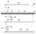
도 7을 참조하면, 본 발명의 다양한 실시예에 따른 전자 장치(700)(예: 도 1 의 전자 장치(101))는, 하우징(710), 인쇄회로기판(720), 제 1 지지 부재(731), 제 2 지지 부재(732), 배터리(740), 및 디스플레이(750), 및 조작키(760)를 포함할 수 있다. 어떤 실시예에 따르면, 전자 장치는 상기 구성요소들 중 적어도 하나를 생략하거나 다른 구성 요소를 추가할 수 있다.Referring to FIG. 7, the electronic device 700 (eg, the
다양한 실시예들에 따르면, 하우징(710)은 제 1 하우징(711) 및 제 2 하우징(712)을 포함할 수 있다. 예를 들어, 제 1 하우징(711)과 제 2 하우징(712)이 결합하여 하우징(710)을 형성하도록 할 수 있다. 한 실시예에 따르면, 하우징(710)은 제 1 하우징(711), 또는 제 2 하우징(712)을 포함할 수 있다. 예를 들면, 제 1 하우징(711)과 제 2 하우징(712)은 하우징 체결부(715)를 이용하여 결합될 수 있다. 어떤 실시예에 따르면, 하우징(710)은 상기 제 1 하우징(711) 및 제 2 하우징(712) 사이의 공간을 일부를 적어도 둘러싸는 측면 부재를 더 포함할 수 있다. 일 실시예에 따르면, 전자 장치(700)의 구성 요소들(예: 인쇄회로기판(720), 제 1 지지 부재(731), 제 2 지지 부재(732), 배터리(740), 및 조작 키(760))는 제 1 하우징(711) 및 제 2 하우징(712)의 내부에 위치할 수 있다. 제 1 하우징(711) 및 제 2 하우징(712)은, 예를 들어, 전자 장치(700)의 구성 요소들을 수용하고, 외부 충격으로부터 이러한 구성요소들을 보호할 수 있다. 한 실시예에 따르면, 제 1 하우징(711) 및 제 2 하우징(712)은, 메탈 프레임(metal frame)구조를 포함할 수 있다. 또 한 실시예에 따르면, 제 1 하우징(711) 및 제 2 하우징(712)은, 메탈 프레임 구조 사이에 형성되는 플라스틱 사출물을 포함할 수 있다.According to various embodiments, the
다양한 실시예들에 따르면, 인쇄회로기판(720)(예: 도 2의 인쇄회로기판(215))은 하우징(710) 내부에 위치할 수 있다. 예를 들면, 인쇄회로기판(720)은 제 1 하우징(711) 및 제 2 하우징(712) 사이에 위치할 수 있다. 일 실시예에 따르면, 인쇄회로기판(720)은 제 1 도전 플레이트(예: 도 2의 제 1 도전 플레이트(210)), 무선 통신 회로(예: 도 1의 통신 모듈(190)), 및 스위치 엘리먼트(예: 도 2의 스위치 엘리먼트(250))를 포함할 수 있다. 한 실시예에 따르면, 인쇄회로기판(720)은 진동자(721)를 포함할 수 있다. 예를 들어, 전자 장치(700)는 진동자(721)를 이용하여 진동 패턴을 발생시키고, 사용자에게 촉각 피드백(tactile feedback)을 제공할 수 있다. 한 실시예에 따르면, 인쇄회로기판(720)은 쉴드캔(722)를 포함할 수 있다. 쉴드캔(722)은, 예를 들어, 인쇄회로기판(720)에서 발생되는 다양한 전자파를 차폐하도록 형성될 수 있다.According to various embodiments, the printed circuit board 720 (eg, the printed
다양한 실시예들에 따르면, 제 1 지지 부재(731)는 인쇄회로기판(720)과 제 1 하우징(711) 사이에 위치하며, 인쇄회로기판(720)에 포함된 제 1 도전 플레이트(예: 도 2의 제 1 도전 플레이트(210))와 전기적으로 연결된 제 2 도전 플레이트(예: 도 2의 제 2 도전 플레이트(220))를 포함할 수 있다. 제 1 지지 부재(731)는 제 2 도전 플레이트를 금속 패턴으로 형성하기 위해 몸체로서의 기능을 할 수 있다. 제 1 지지 부재(731)의 적어도 일부는 유전체 재질로 이루어 질 수 있다. 또 다른 예로, 제 1 지지 부재(731)는 인쇄회로기판(720)과 결합 시, 인쇄회로기판(720)에 포함된 스위치 엘리먼트가 제 2 도전 플레이트와 연결되도록 할 수 있다.According to various embodiments, the
다양한 실시예들에 따르면, 제 2 지지 부재(732)는 인쇄회로기판(720)과 제 2 하우징(712) 사이에 위치하며, 인쇄회로기판(720)에 포함된 무선 통신 회로와 전기적으로 연결된 도전 패턴(예: 도 2의 도전 패턴(230))을 포함할 수 있다. 제 2 지지 부재(732)는 도전 패턴을 금속 패턴으로 형성하기 위해 몸체로서의 기능을 할 수 있다. 제 2 지지 부재(732)의 적어도 일부는 유전체 재질로 이루어 질 수 있다. 한 실시예에 따르면, 제 1 지지 부재(731)와 제 2 지지 부재(732)는 지지부재 체결부(735)를 이용하여 결합될 수 있다.According to various embodiments, the
다양한 실시예들에 따르면, 배터리(740)는 인쇄회로기판(720)과 제 2 지지 부재(732) 사이에 위치할 수 있다. 일 실시예에 따르면, 배터리(740)는, 충전식 전지 및/또는 태양 전지를 포함할 수 있다.According to various embodiments, the
다양한 실시예들에 따르면, 디스플레이(750)는, 제 1 하우징(711)과 제 1 지지 부재(731) 사이에 위치할 수 있다. 디스플레이(750)는, 예를 들어, 제 1 하우징(711)의 상당 부분을 통하여 노출될 수 있다. 어떤 실시예에서는, 디스플레이(750)는 상기 제 1 하우징(711)의 인접한 외곽 형상과 대체로 유사하게 형성될 수 있다. 다른 실시예(미도시)에서는, 디스플레이(750)가 노출되는 면적을 확장하기 위하여, 디스플레이(750)의 외곽과 제 1 하우징(711)의 외곽간의 간격이 대체로 동일하게 형성될 수 있다.According to various embodiments, the
한 실시예에 따르면, 조작 키(760)는, 전자 장치를 조작하기 위한 사용자 조작 버튼일 수 있다. 예를 들면, 조작 키(760)는, 물리 버튼 타입으로 형성되어 사용자의 푸시 입력을 감지하고, 사용자의 푸시 입력이 감지되면 푸시 정보를 프로세서에게 전송할 수 있다.According to an embodiment of the present disclosure, the
다양한 실시예들에 따른, 전자 장치(700)는, 제 1 하우징(711) 및 제 2 하우징(712)을 포함하는 하우징(710), 제 1 도전 플레이트(예: 도 2의 제 1 도전 플레이트(210)), 도전 패턴(예: 도 2의 도전 패턴(230))의 제 2 지점(예: 도 2의 제 2 지점(231))과 전기적으로 연결되는 무선 통신 회로((예: 도 1의 통신 모듈(190)), 및 상기 제 1 도전 플레이트(예: 도 2의 제 1 도전 플레이트(210))의 제 4 지점(예: 도 2의 제 4 지점(213)) 및 제 2 도전 플레이트(예: 도 2의 제 2 도전 플레이트(220))의 제 5 지점(예: 도 2의 제 5 지점(221)) 사이를 전기적으로 연결하는 스위치 엘리먼트(예: 도 2의 스위치 엘리먼트(250))를 포함하는 인쇄회로기판(720), 상기 인쇄회로기판(720)과 상기 제 1 하우징(711) 사이에 위치하며, 상기 제 1 도전 플레이트의 제 1 지점(예: 도 2의 제 1 지점(211))과 전기적으로 연결된 제 2 도전 플레이트를 포함하는 제 1 지지 부재(731), 상기 인쇄회로기판(720)과 상기 제 2 하우징(712) 사이에 위치하며, 도전 패턴을 포함하는 제 2 지지 부재(732), 및 프로세서(예: 도 1의 프로세서(120))를 포함하고, 상기 프로세서는, 상기 스위치 엘리먼트를 이용하여 상기 제 1 도전 플레이트의 상기 제 4 지점 및 상기 제 2 도전 플레이트의 상기 제 5 지점 사이의 연결을 제어하도록 설정되고, 상기 제 1 도전 플레이트의 위에서 바라볼 때, 상기 제 2 지점은 상기 제 1 도전 플레이트의 제 3 지점(예: 도 2의 제 3 지점(212))과 겹쳐지고, 상기 제 4 지점은 상기 제 1 지점 보다 상기 제 3 지점에 가까울 수 있다.According to various embodiments, the
다양한 실시예들에 따른, 전자 장치(700)의 상기 도전 패턴(예: 도 2의 도전 패턴(230))은 제 1 단부(예: 도 2의 제 1 단부(232)) 및 제 2 단부(예: 도 2의 제 1 단부(233))를 포함하는 도전성 라인을 포함하고, 상기 제 2 지점(예: 도 2의 제 2 지점(231))은 상기 제 1 단부에 또는 가까울 수 있다.According to various embodiments of the present disclosure, the conductive pattern (eg, the
다양한 실시예들에 따른, 전자 장치(700)의 상기 도전성 라인은, 상기 전자 장치의 위에서 바라볼 때, 제 1 지점(예: 도 2의 제 1 지점(211))과 겹쳐지지 않을 수 있다.According to various embodiments of the present disclosure, the conductive line of the
다양한 실시예들에 따른, 전자 장치(700)는 상기 스위치 엘리먼트(예: 도 2의 스위치 엘리먼트(250)) 및 상기 제 5 지점 사이에 매칭 회로(예: 도 2의 매칭회로(251))를 더 포함할 수 있다.According to various embodiments of the present disclosure, the
다양한 실시예들에 따른, 전자 장치(700)는 상기 제 1 도전 플레이트와 간격을 두고, 상기 제 1 도전 플레이트와 실질적으로 평행하게 위치하며, 상기 제 1 도전 플레이트의 위에서 바라볼 때, 상기 제 1 도전 플레이트와 적어도 일부 겹쳐지는 제 3 도전 플레이트(예: 도 3의 제 3 도전 플레이트(360))로, 상기 제 2 도전 플레이트는 상기 상기 제 1 도전 플레이트 및 상기 제 3 도전 플레이트 사이에 개재되는 것을 특징으로 하고, 및 상기 제 2 도전 플레이트의 제 6 지점(예: 도 3의 제 6 지점(322)) 및 상기 제 3 도전 플레이트의 제 7 지점(예: 도 3의 제 7 지점(361)) 사이에 전기적으로 연결된 제 2 스위치 엘리먼트(예: 도 3의 제 2 스위치 엘리먼트(370))를 더 포함할 수 있다.According to various embodiments of the present disclosure, the
다양한 실시예들에 따른, 전자 장치(700)의 상기 제 3 도전 플레이트는 상기 제 1 하우징(711) 또는 상기 제 2 하우징(712)에 포함될 수 있다.According to various embodiments, the third conductive plate of the
다양한 실시예들에 따른, 전자 장치(700)는 상기 제 2 도전 플레이트를 외부 장치의 그라운드 부와 전기적으로 연결하는 외부 연결 구조(예: 도 4의 외부 연결 구조(460))를 더 포함할 수 있다.According to various embodiments of the present disclosure, the
다양한 실시예들에 따른, 전자 장치(700)는 상기 제 1 도전 플레이트와 간격을 두고, 상기 제 1 도전 플레이트와 실질적으로 평행하게 위치하며, 상기 제 1 도전 플레이트의 위에서 바라볼 때, 상기 제 1 도전 플레이트와 적어도 일부 겹쳐지는 제 3 도전 플레이트(예: 도 5의 제 3 도전 플레이트(560)), 상기 제 1 스위치 엘리먼트는, 상기 제 2 도전 플레이트 또는 상기 제 3 도전 플레이트 중 적어도 하나를 선택적으로 연결시킬 수 있다.According to various embodiments of the present disclosure, the
다양한 실시예들에 따른, 전자 장치(700)의 상기 제 3 도전 플레이트는 상기 제 1 하우징(711) 또는 상기 제 2 하우징(712)에 포함 할 수 있다.According to various embodiments, the third conductive plate of the
다양한 실시예들에 따른, 전자 장치(700)는 디스플레이(750)를 포함하고, 상기 제 2 도전 플레이트는 상기 디스플레이의 그라운드 부와 전기적으로 연결될 수 있다.
According to various embodiments, the
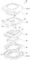
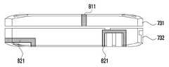
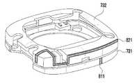
도 8a 내지 8c는 다양한 실시예들에 따른 전자 장치 내 안테나 구조의 실장 구조를 나타내는 도면이다.8A through 8C are diagrams illustrating a mounting structure of an antenna structure in an electronic device according to various embodiments.
도 8a는, 제 1 지지 부재(731)와 제 2 지지 부재(732)의 결합 시, 이를 측면에서 바라본 도면을 나타낸다. 도 8b는, 제 1 지지 부재(731)와 제 2 지지 부재(732)의 결합 시, 이를 제 1 지지 부재(731)의 상부에서 바라본 도면을 나타내며, 도 8c는 이의 사시도를 나타낸다.FIG. 8A shows a side view of the
일 실시 예에 따르면, 제 1 지지 부재(731)와 제 2 지지 부재(732)는 결합할 수 있다. 도시되지는 않았지만, 제 1 지지 부재(731)와 제 2 지지 부재(732)는 인쇄회로기판(예: 도 7의 인쇄회로기판(720)) 또는 배터리(예: 도 7의 배터리(740))를 포함하여 결합할 수 있다.According to one embodiment, the
다양한 실시예들에 따르면, 제 2 도전 플레이트(예: 도 2의 제 2 도전 플레이트(220))는 제 1 연결 부재(811), 제 2 연결 부재(814) 및 접지면(813)을 포함할 수 있다. 한 실시예에 따르면, 제 1 지지 부재(731)는 인쇄회로기판(720)에 포함된 스위치 엘리먼트(예: 도2 의 스위치 엘리먼트(250))가 제 1 지지 부재(731)에 형성된 접지면(813)과 전기적으로 연결되도록 제1 연결 부재(811)를 포함할 수 있다. 예를 들어, 스위치 엘리먼트가 단락되면, 인쇄회로기판(720)에 포함된 제 1 도전 플레이트는 제1 연결 부재(811)를 통해 접지면(813)과 전기적으로 연결될 수 있다.According to various embodiments, the second conductive plate (eg, the second
다양한 실시예들에 따르면, 제 2 지지 부재(732)는 인쇄회로기판(720)에 포함된 무선 통신 회로(예: 도 1의 통신 모듈(190))와 전기적으로 연결되는 도전 패턴(821)을 포함할 수 있다. 제 2 지지 부재(732)는 도전 패턴(821)을 금속 패턴으로 형성하기 위해서 몸체로서의 기능을 수행할 수 있다.According to various embodiments, the
다양한 실시예들에 따르면, 접지면(813)은 제1연결 부재(811)를 통해 인쇄회로기판(720)에 포함된 스위치 엘리먼트와 전기적으로 연결될 수 있다. 또 다른 예로, 상기 접지면(813)은 제 2 연결 부재(814)를 통해 인쇄회로기판(720)에 포함된 제 1 도전 플레이트(예: 도 2의 제 1 도전 플레이트(210))와 연결될 수 있다.
According to various embodiments, the
도 9 및 도 10은 다양한 실시예들에 따른, 안테나 구조의 스위칭 ON/OFF 시의 결과를 비교 실험한 결과이다.9 and 10 illustrate a result of comparing and experimenting a result of switching on / off an antenna structure according to various embodiments.
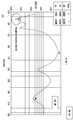
도 9를 참조하면, 스위치 엘리먼트(예: 도 2의 스위치 엘리먼트(250))를 개방시켰을 때의 공진주파수 특성을 나타내고 있다. 스위치 엘리먼트를 개방하면, 안테나 구조(예: 도 2의 안테나 구조(200))는 약 0.90GHz대역에서 공진 주파수(910)를 가짐을 확인할 수 있다. 스위치를 단락시킨 경우의 공진주파수 특성을 나타내는 도 10을 참조하면, 약 1GHz 대역에서 공진주파수(1010)를 가짐을 확인할 수 있다. 예컨대, 스위치 엘리먼트를 이용하여 무선송신출력의 저하를 줄이고, 공진주파수 대역이 시프팅될 수 있다.Referring to FIG. 9, the resonance frequency characteristics when the switch element (eg, the
도 11은 다양한 실시예들에 따른, 안테나 구조의 스위칭 ON/OFF 시의 주파수 특성을 나타내는 도면이다.11 is a diagram illustrating a frequency characteristic at the time of switching ON / OFF of an antenna structure according to various embodiments.
도 11을 참조하면, 스위치 엘리먼트(예: 도 2의 스위치 엘리먼트(250))를 개방시켰을 때의 주파수 특성(1110) 및 스위치 엘리먼트를 단락시켰을 때의 주파수 특성(1120)을 함께 나타내고 있다. 스위칭 ON/OFF 와 관계없이 무선송신출력의 저하는 거의 없지만, 공진주파수 대역이 시프팅될 수 있음을 확인할 수 있다.
Referring to FIG. 11, the frequency characteristic 1110 when the switch element (for example, the
본 문서에 개시된 다양한 실시예들에 따른 전자 장치는 다양한 형태의 장치가 될 수 있다. 전자 장치는, 예를 들면, 휴대용 통신 장치 (예: 스마트폰), 컴퓨터 장치, 휴대용 멀티미디어 장치, 휴대용 의료 기기, 카메라, 웨어러블 장치, 또는 가전 장치를 포함할 수 있다. 본 문서의 실시예에 따른 전자 장치는 전술한 기기들에 한정되지 않는다.Electronic devices according to various embodiments of the present disclosure may be various types of devices. The electronic device may include, for example, a portable communication device (eg, a smartphone), a computer device, a portable multimedia device, a portable medical device, a camera, a wearable device, or a home appliance device. Electronic devices according to embodiments of the present disclosure are not limited to the above-described devices.
본 문서의 다양한 실시예들 및 이에 사용된 용어들은 본 문서에 기재된 기술적 특징들을 특정한 실시예들로 한정하려는 것이 아니며, 해당 실시예의 다양한 변경, 균등물, 또는 대체물을 포함하는 것으로 이해되어야 한다. 도면의 설명과 관련하여, 유사한 또는 관련된 구성요소에 대해서는 유사한 참조 부호가 사용될 수 있다. 아이템에 대응하는 명사의 단수 형은 관련된 문맥상 명백하게 다르게 지시하지 않는 한, 상기 아이템 한 개 또는 복수 개를 포함할 수 있다. 본 문서에서, "A 또는 B", "A 및 B 중 적어도 하나", "A 또는 B 중 적어도 하나,""A, B 또는 C," "A, B 및 C 중 적어도 하나,"및 "A, B, 또는 C 중 적어도 하나"와 같은 문구들 각각은 그 문구들 중 해당하는 문구에 함께 나열된 항목들의 모든 가능한 조합을 포함할 수 있다. "제 1", "제 2", 또는 "첫째" 또는 "둘째"와 같은 용어들은 단순히 해당 구성요소를 다른 해당 구성요소와 구분하기 위해 사용될 수 있으며, 해당 구성요소들을 다른 측면(예: 중요성 또는 순서)에서 한정하지 않는다. 어떤(예: 제 1) 구성요소가 다른(예: 제 2) 구성요소에, "기능적으로" 또는 "통신적으로"라는 용어와 함께 또는 이런 용어 없이, "커플드" 또는 "커넥티드"라고 언급된 경우, 그것은 상기 어떤 구성요소가 상기 다른 구성요소에 직접적으로(예: 유선으로), 무선으로, 또는 제 3 구성요소를 통하여 연결될 수 있다는 것을 의미한다.Various embodiments of the present document and terminology used herein are not intended to limit the technical features described in the present specification to specific embodiments, but should be understood to include various changes, equivalents, or substitutes for the embodiments. In connection with the description of the drawings, similar reference numerals may be used for similar or related components. The singular form of the noun corresponding to the item may include one or more of the items, unless the context clearly indicates otherwise. In this document, "A or B", "At least one of A and B", "At least one of A or B," "A, B or C," "At least one of A, B and C," and "A And phrases such as "at least one of B, or C" may include all possible combinations of items listed together in the corresponding one of the phrases. Terms such as "first", "second", or "first" or "second" may be used merely to distinguish a component from other corresponding components, and to separate the components from other aspects (e.g. Order). Some (eg, first) component may be referred to as "coupled" or "connected" to another (eg, second) component, with or without the term "functionally" or "communicatively". When mentioned, it means that any component can be connected directly to the other component (eg, by wire), wirelessly, or via a third component.
본 문서에서 사용된 용어 "모듈"은 하드웨어, 소프트웨어 또는 펌웨어로 구현된 유닛을 포함할 수 있으며, 예를 들면, 로직, 논리 블록, 부품, 또는 회로 등의 용어와 상호 호환적으로 사용될 수 있다. 모듈은, 일체로 구성된 부품 또는 하나 또는 그 이상의 기능을 수행하는, 상기 부품의 최소 단위 또는 그 일부가 될 수 있다. 예를 들면, 일실시예에 따르면, 모듈은 ASIC(application-specific integrated circuit)의 형태로 구현될 수 있다.As used herein, the term "module" may include a unit implemented in hardware, software, or firmware, and may be used interchangeably with terms such as logic, logic block, component, or circuit. The module may be an integral part or a minimum unit or part of the component, which performs one or more functions. For example, according to one embodiment, the module may be implemented in the form of an application-specific integrated circuit (ASIC).
본 문서의 다양한 실시예들은 기기(machine)(예: 전자 장치(101)) 의해 읽을 수 있는 저장 매체(storage medium)(예: 내장 메모리(136) 또는 외장 메모리(138))에 저장된 하나 이상의 명령어들을 포함하는 소프트웨어(예: 프로그램(140))로서 구현될 수 있다. 예를 들면, 기기(예: 전자 장치(101))의 프로세서(예: 프로세서(120))는, 저장 매체로부터 저장된 하나 이상의 명령어들 중 적어도 하나의 명령을 호출하고, 그것을 실행할 수 있다. 이것은 기기가 상기 호출된 적어도 하나의 명령어에 따라 적어도 하나의 기능을 수행하도록 운영되는 것을 가능하게 한다. 상기 하나 이상의 명령어들은 컴파일러에 의해 생성된 코드 또는 인터프리터에 의해 실행될 수 있는 코드를 포함할 수 있다. 기기로 읽을 수 있는 저장매체 는, 비일시적(non-transitory) 저장매체의 형태로 제공될 수 있다. 여기서, ‘비일시적’은 저장매체가 실재(tangible)하는 장치이고, 신호(signal)(예: 전자기파)를 포함하지 않는다는 것을 의미할 뿐이며, 이 용어는 데이터가 저장매체에 반영구적으로 저장되는 경우와 임시적으로 저장되는 경우를 구분하지 않는다.Various embodiments of this document may include one or more instructions stored on a storage medium (eg,
일실시예에 따르면, 본 문서에 개시된 다양한 실시예들에 따른 방법은 컴퓨터 프로그램 제품(computer program product)에 포함되어 제공될 수 있다. 컴퓨터 프로그램 제품은 상품으로서 판매자 및 구매자 간에 거래될 수 있다. 컴퓨터 프로그램 제품은 기기로 읽을 수 있는 저장 매체(예: compact disc read only memory (CD-ROM))의 형태로 배포되거나, 또는 어플리케이션 스토어(예: 플레이 스토어TM)를 통해 또는 두개의 사용자 장치들(예: 스마트폰들) 간에 직접, 온라인으로 배포(예: 다운로드 또는 업로드)될 수 있다. 온라인 배포의 경우에, 컴퓨터 프로그램 제품의 적어도 일부는 제조사의 서버, 어플리케이션 스토어의 서버, 또는 중계 서버의 메모리와 같은 기기로 읽을 수 있는 저장 매체에 적어도 일시 저장되거나, 임시적으로 생성될 수 있다.According to one embodiment, a method according to various embodiments disclosed herein may be provided included in a computer program product. The computer program product may be traded between the seller and the buyer as a product. The computer program product may be distributed in the form of a device-readable storage medium (e.g. compact disc read only memory (CD-ROM)), or through an application store (e.g. Play StoreTM ) or two user devices ( Example: smartphones) can be distributed (eg downloaded or uploaded) directly or online. In the case of on-line distribution, at least a portion of the computer program product may be stored at least temporarily on a device-readable storage medium such as a server of a manufacturer, a server of an application store, or a relay server, or may be temporarily created.
다양한 실시예들에 따르면, 상기 기술한 구성요소들의 각각의 구성요소(예: 모듈 또는 프로그램)는 단수 또는 복수의 개체를 포함할 수 있다. 다양한 실시예들에 따르면, 전술한 해당 구성요소들 중 하나 이상의 구성요소들 또는 동작들이 생략되거나, 또는 하나 이상의 다른 구성요소들 또는 동작들이 추가될 수 있다. 대체적으로 또는 추가적으로, 복수의 구성요소들(예: 모듈 또는 프로그램)은 하나의 구성요소로 통합될 수 있다. 이런 경우, 통합된 구성요소는 상기 복수의 구성요소들 각각의 구성요소의 하나 이상의 기능들을 상기 통합 이전에 상기 복수의 구성요소들 중 해당 구성요소에 의해 수행되는 것과 동일 또는 유사하게 수행할 수 있다. 다양한 실시예들에 따르면, 모듈, 프로그램 또는 다른 구성요소에 의해 수행되는 동작들은 순차적으로, 병렬적으로, 반복적으로, 또는 휴리스틱하게 실행되거나, 상기 동작들 중 하나 이상이 다른 순서로 실행되거나, 생략되거나, 또는 하나 이상의 다른 동작들이 추가될 수 있다.According to various embodiments, each component (eg, module or program) of the above-described components may include a singular or plural entity. According to various embodiments, one or more of the aforementioned components or operations may be omitted, or one or more other components or operations may be added. Alternatively or additionally, a plurality of components (eg, a module or a program) may be integrated into one component. In this case, the integrated component may perform one or more functions of the component of each of the plurality of components the same as or similar to that performed by the corresponding component of the plurality of components before the integration. . According to various embodiments, operations performed by a module, program, or other component may be executed sequentially, in parallel, repeatedly, or heuristically, or one or more of the operations may be executed in a different order, or omitted. Or one or more other actions may be added.
Claims (20)
Translated fromKorean제 1 도전 플레이트;
상기 제 1 도전 플레이트와 간격을 두고, 상기 제 1 도전 플레이트와 실질적으로 평행하게 위치하며, 상기 제 1 도전 플레이트의 위에서 바라볼 때, 상기 제 1 도전 플레이트와 적어도 일부 겹쳐지는 제 2 도전 플레이트로서, 상기 제 1 도전 플레이트의 제 1 지점과 전기적으로 연결되는 상기 제 2 도전 플레이트;
상기 제 1 도전 플레이트와 간격을 두고, 상기 제 1 도전 플레이트와 실질적으로 평행하게 위치하며, 상기 제 1 도전 플레이트의 위에서 바라볼 때, 상기 제 1 도전 플레이트와 적어도 일부 겹쳐지는 도전 패턴, 상기 제 1 도전 플레이트는 상기 도전 패턴 및 상기 제 2 도전 플레이트 사이에 개재되고;
상기 제 1 도전 플레이트의 위에서 바라볼 때, 제 2 지점은 상기 제 1 도전 플레이트의 제 3 지점과 겹쳐지고, 상기 도전 패턴의 상기 제 2 지점과 전기적으로 연결되는 무선 통신 회로; 및
상기 제 1 도전 플레이트의 제 4 지점 및 상기 제 2 도전 플레이트의 제 5 지점 사이에 전기적으로 연결된 스위치 엘리먼트를 포함하고, 상기 제 4 지점은 상기 제 1 지점 보다 상기 제 3 지점에 가까운 것을 특징으로 하는 전자 장치.In an electronic device,
A first conductive plate;
A second conductive plate spaced apart from the first conductive plate and substantially parallel to the first conductive plate, the second conductive plate being at least partially overlapped with the first conductive plate when viewed from above the first conductive plate, The second conductive plate in electrical connection with the first point of the first conductive plate;
A conductive pattern spaced apart from the first conductive plate and substantially parallel to the first conductive plate, the conductive pattern being at least partially overlapped with the first conductive plate when viewed from above the first conductive plate, the first A conductive plate is interposed between the conductive pattern and the second conductive plate;
A wireless communication circuit, when viewed from above the first conductive plate, a second point overlaps with a third point of the first conductive plate and is electrically connected with the second point of the conductive pattern; And
A switch element electrically connected between a fourth point of the first conductive plate and a fifth point of the second conductive plate, the fourth point being closer to the third point than the first point Electronic devices.
상기 도전 패턴은 제 1 단부 및 제 2 단부를 포함하는 도전성 라인을 포함하고, 상기 제 2 지점은 상기 제 1 단부에 또는 가까이에 있는 것을 특징으로 하는 전자 장치.The method of claim 1,
And the conductive pattern comprises a conductive line comprising a first end and a second end, the second point being at or near the first end.
상기 도전성 라인은, 상기 제 1 도전 플레이트의 위에서 바라볼 때, 제 1 지점과 겹쳐지지 않는 것을 특징으로 하는 전자 장치.The method of claim 2,
And the conductive line does not overlap the first point when viewed from above the first conductive plate.
상기 스위치 엘리먼트 및 상기 제 5 지점 사이에 매칭 회로를 더 포함하는 전자 장치.The method of claim 2,
And a matching circuit between the switch element and the fifth point.
상기 제 1 도전 플레이트를 포함하는 인쇄회로기판(PCB)을 더 포함하는 전자 장치.The method of claim 1,
The electronic device of claim 1, further comprising a printed circuit board (PCB) including the first conductive plate.
상기 제 1 도전 플레이트와 간격을 두고, 상기 제 1 도전 플레이트와 실질적으로 평행하게 위치하며, 상기 제 1 도전 플레이트의 위에서 바라볼 때, 상기 제 1 도전 플레이트와 적어도 일부 겹쳐지는 제 3 도전 플레이트, 상기 제 2 도전 플레이트는 상기 상기 제 1 도전 플레이트 및 상기 제 3 도전 플레이트 사이에 개재되고; 및
상기 제 2 도전 플레이트의 제 6 지점 및 상기 제 3 도전 플레이트의 제 7 지점 사이에 전기적으로 연결된 제 2 스위치 엘리먼트를 더 포함하는 전자 장치.The method of claim 1,
A third conductive plate spaced apart from the first conductive plate and substantially parallel to the first conductive plate and overlapping the first conductive plate at least partially when viewed from above the first conductive plate, the A second conductive plate is interposed between the first conductive plate and the third conductive plate; And
And a second switch element electrically connected between the sixth point of the second conductive plate and the seventh point of the third conductive plate.
상기 제 2 도전 플레이트를 외부 장치의 그라운드 부와 전기적으로 연결하는 외부 연결 구조를 더 포함하는 전자 장치.The method of claim 1,
And an external connection structure for electrically connecting the second conductive plate to the ground portion of the external device.
상기 제 1 도전 플레이트와 간격을 두고, 상기 제 1 도전 플레이트와 실질적으로 평행하게 위치하며, 상기 제 1 도전 플레이트의 위에서 바라볼 때, 상기 제 1 도전 플레이트와 적어도 일부 겹쳐지는 제 3 도전 플레이트를 더 포함하고, 상기 스위치 엘리먼트는, 상기 제 2 도전 플레이트 또는 상기 제 3 도전 플레이트 중 하나를 선택적으로 연결시킬 수 있는 것을 특징으로 하는 전자 장치.The method of claim 1,
A third conductive plate spaced apart from the first conductive plate and substantially parallel to the first conductive plate, the third conductive plate being at least partially overlapped with the first conductive plate when viewed from above the first conductive plate; And the switch element is capable of selectively connecting one of the second conductive plate or the third conductive plate.
제 1 도전 플레이트;
상기 제 1 도전 플레이트와 간격을 두고, 상기 제 1 도전 플레이트와 실질적으로 평행하게 위치하며, 상기 제 1 도전 플레이트의 위에서 바라볼 때, 상기 제 1 도전 플레이트와 적어도 일부 겹쳐지는 제 2 도전 플레이트, 상기 제 2 도전 플레이트는 상기 제 1 도전 플레이트의 제 1 지점과 전기적으로 연결되고;
상기 제 1 도전 플레이트와 간격을 두고, 상기 제 1 도전 플레이트와 실질적으로 평행하게 위치하며, 상기 제 1 도전 플레이트의 위에서 바라볼 때, 상기 제 1 도전 플레이트와 적어도 일부 겹쳐지는 도전 패턴, 상기 제 1 도전 플레이트는 상기 도전 패턴 및 상기 제 2 도전 플레이트 사이에 개재되고;
상기 도전 패턴의 제 2 지점과 전기적으로 연결되는 무선 통신 회로, 상기 제 1 도전 플레이트의 위에서 바라볼 때, 상기 제 2 지점은 상기 제 1 도전 플레이트의 제 3 지점과 겹쳐지고; 및
상기 제 1 도전 플레이트의 상기 제 4 지점 및 상기 제 2 도전 플레이트의 제 5 지점 사이에 전기적으로 연결된 스위치 엘리먼트, 상기 제 3 지점은 상기 제 4 지점 및 상기 제 1 지점 사이에 위치하며,
상기 도전 패턴의 적어도 일부는 비아 홀(via hole)을 통해 상기 제 1 도전 플레이트의 제 4 지점과 전기적으로 연결된 전자 장치.In an electronic device,
A first conductive plate;
A second conductive plate spaced apart from the first conductive plate and substantially parallel to the first conductive plate and overlapping the first conductive plate at least partially when viewed from above the first conductive plate, the A second conductive plate is electrically connected with a first point of the first conductive plate;
A conductive pattern spaced apart from the first conductive plate and substantially parallel to the first conductive plate, the conductive pattern being at least partially overlapped with the first conductive plate when viewed from above the first conductive plate, the first A conductive plate is interposed between the conductive pattern and the second conductive plate;
Wireless communication circuitry electrically connected with a second point of the conductive pattern, the second point overlapping with a third point of the first conductive plate when viewed from above the first conductive plate; And
A switch element electrically connected between the fourth point of the first conductive plate and the fifth point of the second conductive plate, the third point is located between the fourth point and the first point,
At least a portion of the conductive pattern is electrically connected to a fourth point of the first conductive plate through a via hole.
상기 도전 패턴은 제 1 단부 및 제 2 단부를 포함하는 도전성 라인을 포함하고, 상기 제 4 지점은 상기 제 1 단부에 또는 가까이에 있는 것을 특징으로 하는 전자 장치.The method of claim 9,
The conductive pattern includes a conductive line comprising a first end and a second end, and the fourth point is at or near the first end.
제 1 하우징 및 제 2 하우징을 포함하는 하우징;
제 1 도전 플레이트, 도전 패턴의 제 2 지점과 전기적으로 연결되는 무선 통신 회로, 및 상기 제 1 도전 플레이트의 제 4 지점 및 제 2 도전 플레이트의 제 5 지점 사이를 전기적으로 연결하는 스위치 엘리먼트를 포함하는 인쇄회로기판;
상기 인쇄회로기판과 상기 제 1 하우징 사이에 위치하며, 상기 제 1 도전 플레이트의 제 1 지점과 전기적으로 연결된 제 2 도전 플레이트를 포함하는 제 1 지지 부재;
상기 인쇄회로기판과 상기 제 2 하우징 사이에 위치하며, 도전 패턴을 포함하는 제 2 지지 부재; 및
프로세서를 포함하고;
상기 프로세서는, 상기 스위치 엘리먼트를 이용하여 상기 제 1 도전 플레이트의 상기 제 4 지점 및 상기 제 2 도전 플레이트의 상기 제 5 지점 사이의 연결을 제어하도록 설정되고,
상기 제 1 도전 플레이트의 위에서 바라볼 때, 상기 제 2 지점은 상기 제 1 도전 플레이트의 제 3 지점과 겹쳐지고, 상기 제 4 지점은 상기 제 1 지점 보다 상기 제 3 지점에 가까운 것을 특징으로 하고 전자 장치.In an electronic device,
A housing including a first housing and a second housing;
A first conductive plate, a wireless communication circuit in electrical connection with a second point of the conductive pattern, and a switch element electrically connecting between the fourth point of the first conductive plate and the fifth point of the second conductive plate; Printed circuit board;
A first support member positioned between the printed circuit board and the first housing and including a second conductive plate electrically connected to a first point of the first conductive plate;
A second support member positioned between the printed circuit board and the second housing and including a conductive pattern; And
A processor;
The processor is configured to control a connection between the fourth point of the first conductive plate and the fifth point of the second conductive plate using the switch element,
When viewed from above the first conductive plate, the second point overlaps with the third point of the first conductive plate, and the fourth point is closer to the third point than the first point. Device.
상기 도전 패턴은 제 1 단부 및 제 2 단부를 포함하는 도전성 라인을 포함하고, 상기 제 2 지점은 상기 제 1 단부에 또는 가까이에 있는 것을 특징으로 하는 전자 장치.The method of claim 11,
And the conductive pattern comprises a conductive line comprising a first end and a second end, the second point being at or near the first end.
상기 도전성 라인은, 상기 전자 장치의 위에서 바라볼 때, 제 1 지점과 겹쳐지지 않는 것을 특징으로 하는 전자 장치.The method of claim 12,
And the conductive line does not overlap the first point when viewed from above the electronic device.
상기 스위치 엘리먼트 및 상기 제 5 지점 사이에 매칭 회로를 더 포함하는 전자 장치.The method of claim 12,
And a matching circuit between the switch element and the fifth point.
상기 제 1 도전 플레이트와 간격을 두고, 상기 제 1 도전 플레이트와 실질적으로 평행하게 위치하며, 상기 제 1 도전 플레이트의 위에서 바라볼 때, 상기 제 1 도전 플레이트와 적어도 일부 겹쳐지는 제 3 도전 플레이트, 상기 제 2 도전 플레이트는 상기 상기 제 1 도전 플레이트 및 상기 제 3 도전 플레이트 사이에 개재되고; 및
상기 제 2 도전 플레이트의 제 6 지점 및 상기 제 3 도전 플레이트의 제 7 지점 사이에 전기적으로 연결된 제 2 스위치 엘리먼트를 더 포함하는 전자 장치.The method of claim 11,
A third conductive plate spaced apart from the first conductive plate and substantially parallel to the first conductive plate and overlapping the first conductive plate at least partially when viewed from above the first conductive plate, the A second conductive plate is interposed between the first conductive plate and the third conductive plate; And
And a second switch element electrically connected between the sixth point of the second conductive plate and the seventh point of the third conductive plate.
상기 제 3 도전 플레이트는 상기 제 1 하우징 또는 상기 제 2 하우징에 포함되는 것을 특징으로 하는 전자 장치.The method of claim 15,
And the third conductive plate is included in the first housing or the second housing.
상기 제 2 도전 플레이트를 외부 장치의 그라운드 부와 전기적으로 연결하는 외부 연결 구조를 더 포함하는 전자 장치.The method of claim 11,
And an external connection structure for electrically connecting the second conductive plate to the ground portion of the external device.
상기 제 1 도전 플레이트와 간격을 두고, 상기 제 1 도전 플레이트와 실질적으로 평행하게 위치하며, 상기 제 1 도전 플레이트의 위에서 바라볼 때, 상기 제 1 도전 플레이트와 적어도 일부 겹쳐지는 제 3 도전 플레이트를 더 포함하고,
상기 스위치 엘리먼트는, 상기 제 2 도전 플레이트 또는 상기 제 3 도전 플레이트 중 적어도 하나를 선택적으로 연결시킬 수 있는 것을 특징으로 하는 전자 장치.The method of claim 11,
A third conductive plate spaced apart from the first conductive plate and substantially parallel to the first conductive plate, the third conductive plate being at least partially overlapped with the first conductive plate when viewed from above the first conductive plate; Including,
And the switch element may selectively connect at least one of the second conductive plate and the third conductive plate.
상기 제 3 도전 플레이트는 상기 제 1 하우징 또는 상기 제 2 하우징에 포함되는 것을 특징으로 하는 전자 장치.The method of claim 18,
And the third conductive plate is included in the first housing or the second housing.
디스플레이를 포함하고,
상기 제 2 도전 플레이트는 상기 디스플레이의 그라운드 부와 전기적으로 연결되는 것을 특징으로 하는 전자 장치.
The electronic device of claim 11, wherein the electronic device comprises:
Including a display,
And the second conductive plate is electrically connected to the ground portion of the display.
Priority Applications (5)
| Application Number | Priority Date | Filing Date | Title |
|---|---|---|---|
| KR1020180026175AKR102434773B1 (en) | 2018-03-06 | 2018-03-06 | Antenna structure and electronic device including the same |
| US16/292,665US10868361B2 (en) | 2018-03-06 | 2019-03-05 | Antenna structure and electronic device including same |
| EP19763447.0AEP3725064B1 (en) | 2018-03-06 | 2019-03-06 | Antenna structure and electronic device including same |
| PCT/KR2019/002562WO2019172628A1 (en) | 2018-03-06 | 2019-03-06 | Antenna structure and electronic device including same |
| CN201980016565.XACN111801930B (en) | 2018-03-06 | 2019-03-06 | Antenna structure and electronic device comprising same |
Applications Claiming Priority (1)
| Application Number | Priority Date | Filing Date | Title |
|---|---|---|---|
| KR1020180026175AKR102434773B1 (en) | 2018-03-06 | 2018-03-06 | Antenna structure and electronic device including the same |
Publications (2)
| Publication Number | Publication Date |
|---|---|
| KR20190105733Atrue KR20190105733A (en) | 2019-09-18 |
| KR102434773B1 KR102434773B1 (en) | 2022-08-22 |
Family
ID=67843562
Family Applications (1)
| Application Number | Title | Priority Date | Filing Date |
|---|---|---|---|
| KR1020180026175AActiveKR102434773B1 (en) | 2018-03-06 | 2018-03-06 | Antenna structure and electronic device including the same |
Country Status (5)
| Country | Link |
|---|---|
| US (1) | US10868361B2 (en) |
| EP (1) | EP3725064B1 (en) |
| KR (1) | KR102434773B1 (en) |
| CN (1) | CN111801930B (en) |
| WO (1) | WO2019172628A1 (en) |
Cited By (1)
| Publication number | Priority date | Publication date | Assignee | Title |
|---|---|---|---|---|
| WO2024014693A1 (en)* | 2022-07-11 | 2024-01-18 | 삼성전자주식회사 | Wearable device comprising printed circuit board including conductive pattern, and electronic device |
Families Citing this family (8)
| Publication number | Priority date | Publication date | Assignee | Title |
|---|---|---|---|---|
| KR102553177B1 (en)* | 2016-06-13 | 2023-07-10 | 삼성전자주식회사 | Electronic device comprising high frequency transmitting circuit |
| KR20220075597A (en)* | 2020-11-30 | 2022-06-08 | 주식회사 아모센스 | Smart tracker |
| CN117157827A (en)* | 2021-04-05 | 2023-12-01 | 三星电子株式会社 | Antenna and electronic device comprising same |
| US11704529B2 (en)* | 2021-10-27 | 2023-07-18 | Plume Design, Inc. | Tracker tag with dual-purpose antenna components |
| TW202406221A (en)* | 2022-04-19 | 2024-02-01 | 美商元平台技術有限公司 | Distributed monopole antenna for enhanced cross-body link |
| US12021319B2 (en)* | 2022-04-19 | 2024-06-25 | Meta Platforms Technologies, Llc | Distributed monopole antenna for enhanced cross-body link |
| EP4492569A4 (en)* | 2022-04-21 | 2025-06-11 | Samsung Electronics Co., Ltd. | ELECTRONIC DEVICE INCLUDING AN EMI ABSORBER |
| US20240146340A1 (en)* | 2022-10-26 | 2024-05-02 | Meta Platforms Technologies, Llc | Antenna system with conductive shielding and loss mitigation |
Citations (5)
| Publication number | Priority date | Publication date | Assignee | Title |
|---|---|---|---|---|
| US20120176278A1 (en)* | 2011-01-11 | 2012-07-12 | Merz Nicholas G L | Antenna structures with electrical connections to device housing members |
| KR20170020139A (en)* | 2015-08-13 | 2017-02-22 | 삼성전자주식회사 | Electronic Device Including Multi-Band Antenna |
| KR20170020138A (en)* | 2015-08-13 | 2017-02-22 | 삼성전자주식회사 | Electronic Device Including Multi-Band Antenna |
| KR20170019818A (en)* | 2015-08-12 | 2017-02-22 | 삼성전자주식회사 | An electronic device including an antenna apparatus |
| KR20180013203A (en)* | 2016-07-29 | 2018-02-07 | 삼성전자주식회사 | Electronic device comprising antenna |
Family Cites Families (24)
| Publication number | Priority date | Publication date | Assignee | Title |
|---|---|---|---|---|
| JPH1065437A (en)* | 1996-08-21 | 1998-03-06 | Saitama Nippon Denki Kk | Inverted-f plate antenna and radio equipment |
| JP2000114860A (en)* | 1999-05-13 | 2000-04-21 | Nec Saitama Ltd | Planar reversed f antenna and radio equipment |
| DE10245813A1 (en) | 2002-10-01 | 2004-04-15 | Lindenmeier, Heinz, Prof. Dr.-Ing. | Active broadband reception antenna with reception level control |
| US7129416B1 (en) | 2004-02-05 | 2006-10-31 | Apple Computer, Inc. | Hybrid ground grid for printed circuit board |
| KR100664216B1 (en) | 2005-09-06 | 2007-01-04 | 엘지전자 주식회사 | Multiband Antenna Structure, Apparatus and Method of Mobile Devices |
| US7439929B2 (en) | 2005-12-09 | 2008-10-21 | Sony Ericsson Mobile Communications Ab | Tuning antennas with finite ground plane |
| US8618990B2 (en)* | 2011-04-13 | 2013-12-31 | Pulse Finland Oy | Wideband antenna and methods |
| US7936307B2 (en)* | 2006-07-24 | 2011-05-03 | Nokia Corporation | Cover antennas |
| US8525470B2 (en) | 2007-03-13 | 2013-09-03 | Ford Global Technologies, Llc | Using a circuit rating to establish a charge rate for an electric storage battery of an electric vehicle |
| KR100972846B1 (en) | 2008-09-08 | 2010-07-28 | 삼성전기주식회사 | Multiband Antennas for Mobile Devices |
| US8223077B2 (en)* | 2009-03-10 | 2012-07-17 | Apple Inc. | Multisector parallel plate antenna for electronic devices |
| JP5478226B2 (en)* | 2009-12-04 | 2014-04-23 | 三星電子株式会社 | Antenna device |
| US8532584B2 (en) | 2010-04-30 | 2013-09-10 | Acco Semiconductor, Inc. | RF switches |
| KR101659024B1 (en) | 2010-05-31 | 2016-09-23 | 엘지전자 주식회사 | Mobile terminal |
| KR20130038515A (en) | 2011-10-10 | 2013-04-18 | 삼성전자주식회사 | Mobile terminal, and method for improving radiation performance and specific absorption rate of an antenna of a mobile terminal |
| KR101265096B1 (en) | 2011-12-29 | 2013-05-16 | 국민대학교산학협력단 | Antenna apparatus and vehicle having the same |
| US9136590B2 (en)* | 2012-10-10 | 2015-09-15 | Kabushiki Kaisha Toshiba | Electronic device provided with antenna device |
| US9276319B2 (en) | 2013-05-08 | 2016-03-01 | Apple Inc. | Electronic device antenna with multiple feeds for covering three communications bands |
| WO2015085553A1 (en)* | 2013-12-12 | 2015-06-18 | 华为终端有限公司 | Antenna, antenna device, terminal and method for adjusting operating frequency band of antenna |
| TW201537830A (en) | 2014-03-28 | 2015-10-01 | Ming-Hao Yeh | Frequency-switchable active antenna system and associated control method |
| CN105720382B (en) | 2014-12-05 | 2021-08-17 | 深圳富泰宏精密工业有限公司 | Antenna structure and wireless communication device having the same |
| KR102176368B1 (en)* | 2015-01-05 | 2020-11-09 | 엘지전자 주식회사 | Antenna module and mobile terminal having the same |
| KR102495241B1 (en) | 2015-08-10 | 2023-02-03 | 삼성전자주식회사 | Antenna and electronic device having the same |
| CN106887698A (en)* | 2017-03-30 | 2017-06-23 | 努比亚技术有限公司 | A kind of antenna structure and the mobile terminal with the antenna structure |
- 2018
- 2018-03-06KRKR1020180026175Apatent/KR102434773B1/enactiveActive
- 2019
- 2019-03-05USUS16/292,665patent/US10868361B2/enactiveActive
- 2019-03-06WOPCT/KR2019/002562patent/WO2019172628A1/ennot_activeCeased
- 2019-03-06CNCN201980016565.XApatent/CN111801930B/enactiveActive
- 2019-03-06EPEP19763447.0Apatent/EP3725064B1/enactiveActive
Patent Citations (5)
| Publication number | Priority date | Publication date | Assignee | Title |
|---|---|---|---|---|
| US20120176278A1 (en)* | 2011-01-11 | 2012-07-12 | Merz Nicholas G L | Antenna structures with electrical connections to device housing members |
| KR20170019818A (en)* | 2015-08-12 | 2017-02-22 | 삼성전자주식회사 | An electronic device including an antenna apparatus |
| KR20170020139A (en)* | 2015-08-13 | 2017-02-22 | 삼성전자주식회사 | Electronic Device Including Multi-Band Antenna |
| KR20170020138A (en)* | 2015-08-13 | 2017-02-22 | 삼성전자주식회사 | Electronic Device Including Multi-Band Antenna |
| KR20180013203A (en)* | 2016-07-29 | 2018-02-07 | 삼성전자주식회사 | Electronic device comprising antenna |
Cited By (1)
| Publication number | Priority date | Publication date | Assignee | Title |
|---|---|---|---|---|
| WO2024014693A1 (en)* | 2022-07-11 | 2024-01-18 | 삼성전자주식회사 | Wearable device comprising printed circuit board including conductive pattern, and electronic device |
Also Published As
| Publication number | Publication date |
|---|---|
| EP3725064B1 (en) | 2024-02-14 |
| US20190280375A1 (en) | 2019-09-12 |
| EP3725064A1 (en) | 2020-10-21 |
| KR102434773B1 (en) | 2022-08-22 |
| CN111801930B (en) | 2022-04-26 |
| WO2019172628A1 (en) | 2019-09-12 |
| EP3725064A4 (en) | 2021-01-20 |
| US10868361B2 (en) | 2020-12-15 |
| CN111801930A (en) | 2020-10-20 |
Similar Documents
| Publication | Publication Date | Title |
|---|---|---|
| KR102434773B1 (en) | Antenna structure and electronic device including the same | |
| US11962068B2 (en) | Antenna and electronic device comprising same | |
| US10971809B2 (en) | Electronic device including antenna connected with conductive sheet of display panel | |
| KR102737357B1 (en) | Antenna and foldable electronic device including the same | |
| KR102408139B1 (en) | Antenna device and electronic device including the same | |
| KR102526400B1 (en) | An electronic device comprising a 5g antenna module | |
| US11056769B2 (en) | Electronic device comprising antenna | |
| KR102341534B1 (en) | Electronic device that reduces antenna interference and enhances antenna performance | |
| KR20210054262A (en) | An antenna structure and an electronic device including the same | |
| KR20200058153A (en) | An electronic device comprising a antenna module | |
| KR20210031309A (en) | A foldable electronic device including an antenna | |
| KR20190141852A (en) | Electronic device for including flexible printed circuit board adjacent to antenna | |
| KR102664682B1 (en) | Antenna using conductive side member and electronic device including the same | |
| KR20220135454A (en) | An electronic device comprising an antenna | |
| KR102597392B1 (en) | Antenna module supporting dual bands and electronic device including the same | |
| KR102773459B1 (en) | Electronic device including antenna | |
| US20210066800A1 (en) | Antenna and electronic device including the same | |
| US20230268639A1 (en) | Electronic device comprising antenna | |
| US11916585B2 (en) | Electronic device including antenna | |
| KR102864057B1 (en) | Method for antenna switching and device thereof | |
| KR20200101197A (en) | Signal processing circuit and an electronic device having the signal processing circuit thereof | |
| KR102597872B1 (en) | Electronic device comprising antenna | |
| KR102758022B1 (en) | Antenna and electronic device having thereof | |
| KR20250038112A (en) | Electronic device including antenna | |
| KR20250043203A (en) | electronic device comprising antenna |
Legal Events
| Date | Code | Title | Description |
|---|---|---|---|
| PA0109 | Patent application | St.27 status event code:A-0-1-A10-A12-nap-PA0109 | |
| PG1501 | Laying open of application | St.27 status event code:A-1-1-Q10-Q12-nap-PG1501 | |
| A201 | Request for examination | ||
| PA0201 | Request for examination | St.27 status event code:A-1-2-D10-D11-exm-PA0201 | |
| D13-X000 | Search requested | St.27 status event code:A-1-2-D10-D13-srh-X000 | |
| D14-X000 | Search report completed | St.27 status event code:A-1-2-D10-D14-srh-X000 | |
| E902 | Notification of reason for refusal | ||
| PE0902 | Notice of grounds for rejection | St.27 status event code:A-1-2-D10-D21-exm-PE0902 | |
| P11-X000 | Amendment of application requested | St.27 status event code:A-2-2-P10-P11-nap-X000 | |
| P13-X000 | Application amended | St.27 status event code:A-2-2-P10-P13-nap-X000 | |
| E701 | Decision to grant or registration of patent right | ||
| PE0701 | Decision of registration | St.27 status event code:A-1-2-D10-D22-exm-PE0701 | |
| GRNT | Written decision to grant | ||
| PR0701 | Registration of establishment | St.27 status event code:A-2-4-F10-F11-exm-PR0701 | |
| PR1002 | Payment of registration fee | St.27 status event code:A-2-2-U10-U11-oth-PR1002 Fee payment year number:1 | |
| PG1601 | Publication of registration | St.27 status event code:A-4-4-Q10-Q13-nap-PG1601 | |
| PR1001 | Payment of annual fee | St.27 status event code:A-4-4-U10-U11-oth-PR1001 Fee payment year number:4 |