KR20190091370A - Semiconductor device, display device and electronic device including the same - Google Patents
Semiconductor device, display device and electronic device including the sameDownload PDFInfo
- Publication number
- KR20190091370A KR20190091370AKR1020197021889AKR20197021889AKR20190091370AKR 20190091370 AKR20190091370 AKR 20190091370AKR 1020197021889 AKR1020197021889 AKR 1020197021889AKR 20197021889 AKR20197021889 AKR 20197021889AKR 20190091370 AKR20190091370 AKR 20190091370A
- Authority
- KR
- South Korea
- Prior art keywords
- transistor
- wiring
- signal
- electrode
- gate
- Prior art date
- Legal status (The legal status is an assumption and is not a legal conclusion. Google has not performed a legal analysis and makes no representation as to the accuracy of the status listed.)
- Granted
Links
- 239000004065semiconductorSubstances0.000titleclaimsdescription237
- 239000003990capacitorSubstances0.000abstractdescription145
- 239000010410layerSubstances0.000description298
- 230000006870functionEffects0.000description199
- 239000000758substrateSubstances0.000description105
- 230000002829reductive effectEffects0.000description98
- 239000004973liquid crystal related substanceSubstances0.000description83
- 238000010586diagramMethods0.000description53
- 238000000034methodMethods0.000description45
- 239000010408filmSubstances0.000description44
- 230000003071parasitic effectEffects0.000description24
- 230000006866deteriorationEffects0.000description23
- 238000007667floatingMethods0.000description21
- 239000013078crystalSubstances0.000description20
- 239000000463materialSubstances0.000description19
- 230000007423decreaseEffects0.000description16
- XUIMIQQOPSSXEZ-UHFFFAOYSA-NSiliconChemical compound[Si]XUIMIQQOPSSXEZ-UHFFFAOYSA-N0.000description14
- 229910052710siliconInorganic materials0.000description14
- 239000010703siliconSubstances0.000description14
- 239000012535impuritySubstances0.000description13
- VYPSYNLAJGMNEJ-UHFFFAOYSA-Nsilicon dioxideInorganic materialsO=[Si]=OVYPSYNLAJGMNEJ-UHFFFAOYSA-N0.000description12
- 239000011521glassSubstances0.000description11
- 238000006243chemical reactionMethods0.000description10
- 150000001875compoundsChemical class0.000description10
- 229910052814silicon oxideInorganic materials0.000description10
- 229910052782aluminiumInorganic materials0.000description9
- XAGFODPZIPBFFR-UHFFFAOYSA-NaluminiumChemical compound[Al]XAGFODPZIPBFFR-UHFFFAOYSA-N0.000description9
- 238000009413insulationMethods0.000description9
- 238000004519manufacturing processMethods0.000description9
- 239000002356single layerSubstances0.000description9
- IJGRMHOSHXDMSA-UHFFFAOYSA-NAtomic nitrogenChemical compoundN#NIJGRMHOSHXDMSA-UHFFFAOYSA-N0.000description8
- 229910052581Si3N4Inorganic materials0.000description8
- 230000005684electric fieldEffects0.000description8
- HQVNEWCFYHHQES-UHFFFAOYSA-Nsilicon nitrideChemical compoundN12[Si]34N5[Si]62N3[Si]51N64HQVNEWCFYHHQES-UHFFFAOYSA-N0.000description8
- OKTJSMMVPCPJKN-UHFFFAOYSA-NCarbonChemical compound[C]OKTJSMMVPCPJKN-UHFFFAOYSA-N0.000description7
- PXHVJJICTQNCMI-UHFFFAOYSA-NNickelChemical compound[Ni]PXHVJJICTQNCMI-UHFFFAOYSA-N0.000description7
- XLOMVQKBTHCTTD-UHFFFAOYSA-NZinc monoxideChemical compound[Zn]=OXLOMVQKBTHCTTD-UHFFFAOYSA-N0.000description7
- 230000008569processEffects0.000description7
- 239000010936titaniumSubstances0.000description7
- -1a-InGaZnOInorganic materials0.000description6
- 229910052750molybdenumInorganic materials0.000description6
- 230000001360synchronised effectEffects0.000description6
- 229910052719titaniumInorganic materials0.000description6
- ZOKXTWBITQBERF-UHFFFAOYSA-NMolybdenumChemical compound[Mo]ZOKXTWBITQBERF-UHFFFAOYSA-N0.000description5
- RTAQQCXQSZGOHL-UHFFFAOYSA-NTitaniumChemical compound[Ti]RTAQQCXQSZGOHL-UHFFFAOYSA-N0.000description5
- 230000005540biological transmissionEffects0.000description5
- 230000008859changeEffects0.000description5
- 230000008878couplingEffects0.000description5
- 238000010168coupling processMethods0.000description5
- 238000005859coupling reactionMethods0.000description5
- 239000011159matrix materialSubstances0.000description5
- 229910052751metalInorganic materials0.000description5
- 239000002184metalSubstances0.000description5
- 239000011733molybdenumSubstances0.000description5
- 239000004983Polymer Dispersed Liquid CrystalSubstances0.000description4
- QVGXLLKOCUKJST-UHFFFAOYSA-Natomic oxygenChemical compound[O]QVGXLLKOCUKJST-UHFFFAOYSA-N0.000description4
- 230000008901benefitEffects0.000description4
- 239000002041carbon nanotubeSubstances0.000description4
- 229910021393carbon nanotubeInorganic materials0.000description4
- 230000006378damageEffects0.000description4
- 239000005262ferroelectric liquid crystals (FLCs)Substances0.000description4
- 238000002347injectionMethods0.000description4
- 239000007924injectionSubstances0.000description4
- 230000007257malfunctionEffects0.000description4
- 239000002071nanotubeSubstances0.000description4
- 229910052757nitrogenInorganic materials0.000description4
- 230000003287optical effectEffects0.000description4
- 229910052760oxygenInorganic materials0.000description4
- 239000001301oxygenSubstances0.000description4
- 230000002093peripheral effectEffects0.000description4
- 239000004033plasticSubstances0.000description4
- 229920003023plasticPolymers0.000description4
- 230000009467reductionEffects0.000description4
- 229910052779NeodymiumInorganic materials0.000description3
- KDLHZDBZIXYQEI-UHFFFAOYSA-NPalladiumChemical compound[Pd]KDLHZDBZIXYQEI-UHFFFAOYSA-N0.000description3
- OAICVXFJPJFONN-UHFFFAOYSA-NPhosphorusChemical compound[P]OAICVXFJPJFONN-UHFFFAOYSA-N0.000description3
- 230000009471actionEffects0.000description3
- 239000000956alloySubstances0.000description3
- 229910052799carbonInorganic materials0.000description3
- 238000004891communicationMethods0.000description3
- 239000010949copperSubstances0.000description3
- 230000000694effectsEffects0.000description3
- 230000007274generation of a signal involved in cell-cell signalingEffects0.000description3
- 239000003779heat-resistant materialSubstances0.000description3
- 230000006872improvementEffects0.000description3
- QEFYFXOXNSNQGX-UHFFFAOYSA-Nneodymium atomChemical compound[Nd]QEFYFXOXNSNQGX-UHFFFAOYSA-N0.000description3
- 229910052759nickelInorganic materials0.000description3
- 229910052698phosphorusInorganic materials0.000description3
- 239000011574phosphorusSubstances0.000description3
- BASFCYQUMIYNBI-UHFFFAOYSA-NplatinumChemical compound[Pt]BASFCYQUMIYNBI-UHFFFAOYSA-N0.000description3
- 239000010935stainless steelSubstances0.000description3
- 229910001220stainless steelInorganic materials0.000description3
- 239000000126substanceSubstances0.000description3
- 239000011787zinc oxideSubstances0.000description3
- JBRZTFJDHDCESZ-UHFFFAOYSA-NAsGaChemical compound[As]#[Ga]JBRZTFJDHDCESZ-UHFFFAOYSA-N0.000description2
- ZOXJGFHDIHLPTG-UHFFFAOYSA-NBoronChemical compound[B]ZOXJGFHDIHLPTG-UHFFFAOYSA-N0.000description2
- RYGMFSIKBFXOCR-UHFFFAOYSA-NCopperChemical compound[Cu]RYGMFSIKBFXOCR-UHFFFAOYSA-N0.000description2
- 239000005264High molar mass liquid crystalSubstances0.000description2
- 229910000583Nd alloyInorganic materials0.000description2
- 239000004952PolyamideSubstances0.000description2
- 230000002411adverseEffects0.000description2
- UBSJOWMHLJZVDJ-UHFFFAOYSA-Naluminum neodymiumChemical compound[Al].[Nd]UBSJOWMHLJZVDJ-UHFFFAOYSA-N0.000description2
- 229910052796boronInorganic materials0.000description2
- 239000003054catalystSubstances0.000description2
- 239000011651chromiumSubstances0.000description2
- 238000001816coolingMethods0.000description2
- 229910052802copperInorganic materials0.000description2
- 230000003247decreasing effectEffects0.000description2
- 239000000428dustSubstances0.000description2
- 239000010931goldSubstances0.000description2
- 230000005525hole transportEffects0.000description2
- AMGQUBHHOARCQH-UHFFFAOYSA-Nindium;oxotinChemical compound[In].[Sn]=OAMGQUBHHOARCQH-UHFFFAOYSA-N0.000description2
- 239000012212insulatorSubstances0.000description2
- 239000011572manganeseSubstances0.000description2
- 239000013081microcrystalSubstances0.000description2
- 229910021424microcrystalline siliconInorganic materials0.000description2
- DTSBBUTWIOVIBV-UHFFFAOYSA-Nmolybdenum niobiumChemical compound[Nb].[Mo]DTSBBUTWIOVIBV-UHFFFAOYSA-N0.000description2
- JZLMRQMUNCKZTP-UHFFFAOYSA-Nmolybdenum tantalumChemical compound[Mo].[Ta]JZLMRQMUNCKZTP-UHFFFAOYSA-N0.000description2
- 239000010955niobiumSubstances0.000description2
- 229920002647polyamidePolymers0.000description2
- 229910021420polycrystalline siliconInorganic materials0.000description2
- 229920000728polyesterPolymers0.000description2
- 229920000139polyethylene terephthalatePolymers0.000description2
- 239000005020polyethylene terephthalateSubstances0.000description2
- 238000012545processingMethods0.000description2
- 239000010453quartzSubstances0.000description2
- 230000004044responseEffects0.000description2
- 230000002441reversible effectEffects0.000description2
- 239000010409thin filmSubstances0.000description2
- 101100392125Caenorhabditis elegans gck-1 geneProteins0.000description1
- 239000004986Cholesteric liquid crystals (ChLC)Substances0.000description1
- VYZAMTAEIAYCRO-UHFFFAOYSA-NChromiumChemical compound[Cr]VYZAMTAEIAYCRO-UHFFFAOYSA-N0.000description1
- 208000032368Device malfunctionDiseases0.000description1
- 239000004985Discotic Liquid Crystal SubstanceSubstances0.000description1
- 239000004593EpoxySubstances0.000description1
- 102100022887GTP-binding nuclear protein RanHuman genes0.000description1
- GYHNNYVSQQEPJS-UHFFFAOYSA-NGalliumChemical compound[Ga]GYHNNYVSQQEPJS-UHFFFAOYSA-N0.000description1
- 229910001218Gallium arsenideInorganic materials0.000description1
- 101000774835Heteractis crispa PI-stichotoxin-Hcr2oProteins0.000description1
- 101000620756Homo sapiens GTP-binding nuclear protein RanProteins0.000description1
- XEEYBQQBJWHFJM-UHFFFAOYSA-NIronChemical compound[Fe]XEEYBQQBJWHFJM-UHFFFAOYSA-N0.000description1
- PWHULOQIROXLJO-UHFFFAOYSA-NManganeseChemical compound[Mn]PWHULOQIROXLJO-UHFFFAOYSA-N0.000description1
- 229910019015Mg-AgInorganic materials0.000description1
- 240000005561Musa balbisianaSpecies0.000description1
- 235000018290Musa x paradisiacaNutrition0.000description1
- 239000004988Nematic liquid crystalSubstances0.000description1
- 229920012266Poly(ether sulfone) PESPolymers0.000description1
- 229920001665Poly-4-vinylphenolPolymers0.000description1
- 239000004642PolyimideSubstances0.000description1
- 239000004743PolypropyleneSubstances0.000description1
- 101100393821Saccharomyces cerevisiae (strain ATCC 204508 / S288c) GSP2 geneProteins0.000description1
- 229910000577Silicon-germaniumInorganic materials0.000description1
- BQCADISMDOOEFD-UHFFFAOYSA-NSilverChemical compound[Ag]BQCADISMDOOEFD-UHFFFAOYSA-N0.000description1
- ATJFFYVFTNAWJD-UHFFFAOYSA-NTinChemical compound[Sn]ATJFFYVFTNAWJD-UHFFFAOYSA-N0.000description1
- NRTOMJZYCJJWKI-UHFFFAOYSA-NTitanium nitrideChemical compound[Ti]#NNRTOMJZYCJJWKI-UHFFFAOYSA-N0.000description1
- BZHJMEDXRYGGRV-UHFFFAOYSA-NVinyl chlorideChemical compoundClC=CBZHJMEDXRYGGRV-UHFFFAOYSA-N0.000description1
- HCHKCACWOHOZIP-UHFFFAOYSA-NZincChemical compound[Zn]HCHKCACWOHOZIP-UHFFFAOYSA-N0.000description1
- 230000001133accelerationEffects0.000description1
- NIXOWILDQLNWCW-UHFFFAOYSA-Nacrylic acid groupChemical groupC(C=C)(=O)ONIXOWILDQLNWCW-UHFFFAOYSA-N0.000description1
- 229910045601alloyInorganic materials0.000description1
- CSDREXVUYHZDNP-UHFFFAOYSA-NalumanylidynesiliconChemical compound[Al].[Si]CSDREXVUYHZDNP-UHFFFAOYSA-N0.000description1
- 239000005407aluminoborosilicate glassSubstances0.000description1
- 229910021417amorphous siliconInorganic materials0.000description1
- 230000003321amplificationEffects0.000description1
- 229910052785arsenicInorganic materials0.000description1
- RQNWIZPPADIBDY-UHFFFAOYSA-Narsenic atomChemical compound[As]RQNWIZPPADIBDY-UHFFFAOYSA-N0.000description1
- GPBUGPUPKAGMDK-UHFFFAOYSA-NazanylidynemolybdenumChemical compound[Mo]#NGPBUGPUPKAGMDK-UHFFFAOYSA-N0.000description1
- 229910052788bariumInorganic materials0.000description1
- DSAJWYNOEDNPEQ-UHFFFAOYSA-Nbarium atomChemical compound[Ba]DSAJWYNOEDNPEQ-UHFFFAOYSA-N0.000description1
- UMIVXZPTRXBADB-UHFFFAOYSA-NbenzocyclobuteneChemical compoundC1=CC=C2CCC2=C1UMIVXZPTRXBADB-UHFFFAOYSA-N0.000description1
- 230000004397blinkingEffects0.000description1
- 239000005388borosilicate glassSubstances0.000description1
- HEQWUWZWGPCGCD-UHFFFAOYSA-Ncadmium(2+) oxygen(2-) tin(4+)Chemical compound[O--].[O--].[O--].[Cd++].[Sn+4]HEQWUWZWGPCGCD-UHFFFAOYSA-N0.000description1
- 230000015556catabolic processEffects0.000description1
- 239000000919ceramicSubstances0.000description1
- 229910052804chromiumInorganic materials0.000description1
- 229910017052cobaltInorganic materials0.000description1
- 239000010941cobaltSubstances0.000description1
- GUTLYIVDDKVIGB-UHFFFAOYSA-Ncobalt atomChemical compound[Co]GUTLYIVDDKVIGB-UHFFFAOYSA-N0.000description1
- 230000008602contractionEffects0.000description1
- 238000012937correctionMethods0.000description1
- 238000002425crystallisationMethods0.000description1
- 230000008025crystallizationEffects0.000description1
- 230000003111delayed effectEffects0.000description1
- 230000002542deteriorative effectEffects0.000description1
- 238000009792diffusion processMethods0.000description1
- KPUWHANPEXNPJT-UHFFFAOYSA-NdisiloxaneChemical class[SiH3]O[SiH3]KPUWHANPEXNPJT-UHFFFAOYSA-N0.000description1
- 238000006073displacement reactionMethods0.000description1
- 238000005401electroluminescenceMethods0.000description1
- 238000005516engineering processMethods0.000description1
- 239000002657fibrous materialSubstances0.000description1
- 239000011888foilSubstances0.000description1
- 239000003205fragranceSubstances0.000description1
- 229910052733galliumInorganic materials0.000description1
- PCHJSUWPFVWCPO-UHFFFAOYSA-NgoldChemical compound[Au]PCHJSUWPFVWCPO-UHFFFAOYSA-N0.000description1
- 229910052737goldInorganic materials0.000description1
- 238000010438heat treatmentMethods0.000description1
- 238000005286illuminationMethods0.000description1
- 229910052738indiumInorganic materials0.000description1
- APFVFJFRJDLVQX-UHFFFAOYSA-Nindium atomChemical compound[In]APFVFJFRJDLVQX-UHFFFAOYSA-N0.000description1
- 230000010354integrationEffects0.000description1
- 239000011229interlayerSubstances0.000description1
- 230000001788irregularEffects0.000description1
- 238000002955isolationMethods0.000description1
- 239000007788liquidSubstances0.000description1
- 230000002535lyotropic effectEffects0.000description1
- SJCKRGFTWFGHGZ-UHFFFAOYSA-Nmagnesium silverChemical compound[Mg].[Ag]SJCKRGFTWFGHGZ-UHFFFAOYSA-N0.000description1
- 230000005389magnetismEffects0.000description1
- 229910052748manganeseInorganic materials0.000description1
- 238000005259measurementMethods0.000description1
- 239000012528membraneSubstances0.000description1
- QSHDDOUJBYECFT-UHFFFAOYSA-NmercuryChemical compound[Hg]QSHDDOUJBYECFT-UHFFFAOYSA-N0.000description1
- 229910052753mercuryInorganic materials0.000description1
- MGRWKWACZDFZJT-UHFFFAOYSA-Nmolybdenum tungstenChemical compound[Mo].[W]MGRWKWACZDFZJT-UHFFFAOYSA-N0.000description1
- GALOTNBSUVEISR-UHFFFAOYSA-Nmolybdenum;siliconChemical compound[Mo]#[Si]GALOTNBSUVEISR-UHFFFAOYSA-N0.000description1
- 229910021421monocrystalline siliconInorganic materials0.000description1
- 239000002159nanocrystalSubstances0.000description1
- RUFLMLWJRZAWLJ-UHFFFAOYSA-Nnickel silicideChemical compound[Ni]=[Si]=[Ni]RUFLMLWJRZAWLJ-UHFFFAOYSA-N0.000description1
- 229910021334nickel silicideInorganic materials0.000description1
- 229910052758niobiumInorganic materials0.000description1
- GUCVJGMIXFAOAE-UHFFFAOYSA-Nniobium atomChemical compound[Nb]GUCVJGMIXFAOAE-UHFFFAOYSA-N0.000description1
- 150000004767nitridesChemical class0.000description1
- 238000003199nucleic acid amplification methodMethods0.000description1
- 239000011368organic materialSubstances0.000description1
- 229910052763palladiumInorganic materials0.000description1
- 230000036961partial effectEffects0.000description1
- 229910052697platinumInorganic materials0.000description1
- 239000011112polyethylene naphthalateSubstances0.000description1
- 229920001721polyimidePolymers0.000description1
- 229920001155polypropylenePolymers0.000description1
- 229920002620polyvinyl fluoridePolymers0.000description1
- 238000007639printingMethods0.000description1
- 230000005855radiationEffects0.000description1
- 229920005989resinPolymers0.000description1
- 239000011347resinSubstances0.000description1
- 229910052706scandiumInorganic materials0.000description1
- SIXSYDAISGFNSX-UHFFFAOYSA-Nscandium atomChemical compound[Sc]SIXSYDAISGFNSX-UHFFFAOYSA-N0.000description1
- 229910021332silicideInorganic materials0.000description1
- FVBUAEGBCNSCDD-UHFFFAOYSA-Nsilicide(4-)Chemical compound[Si-4]FVBUAEGBCNSCDD-UHFFFAOYSA-N0.000description1
- 229910052709silverInorganic materials0.000description1
- 239000004332silverSubstances0.000description1
- 230000001629suppressionEffects0.000description1
- 229920003002synthetic resinPolymers0.000description1
- 239000000057synthetic resinSubstances0.000description1
- 229910052715tantalumInorganic materials0.000description1
- GUVRBAGPIYLISA-UHFFFAOYSA-Ntantalum atomChemical compound[Ta]GUVRBAGPIYLISA-UHFFFAOYSA-N0.000description1
- MZLGASXMSKOWSE-UHFFFAOYSA-Ntantalum nitrideChemical compound[Ta]#NMZLGASXMSKOWSE-UHFFFAOYSA-N0.000description1
- JBQYATWDVHIOAR-UHFFFAOYSA-NtellanylidenegermaniumChemical compound[Te]=[Ge]JBQYATWDVHIOAR-UHFFFAOYSA-N0.000description1
- XOLBLPGZBRYERU-UHFFFAOYSA-Ntin dioxideChemical compoundO=[Sn]=OXOLBLPGZBRYERU-UHFFFAOYSA-N0.000description1
- 229910001887tin oxideInorganic materials0.000description1
- 229910021341titanium silicideInorganic materials0.000description1
- 238000002834transmittanceMethods0.000description1
- WFKWXMTUELFFGS-UHFFFAOYSA-NtungstenChemical compound[W]WFKWXMTUELFFGS-UHFFFAOYSA-N0.000description1
- 229910052721tungstenInorganic materials0.000description1
- 239000010937tungstenSubstances0.000description1
- WQJQOUPTWCFRMM-UHFFFAOYSA-Ntungsten disilicideChemical compound[Si]#[W]#[Si]WQJQOUPTWCFRMM-UHFFFAOYSA-N0.000description1
- 229910021342tungsten silicideInorganic materials0.000description1
- 238000007740vapor depositionMethods0.000description1
- 125000000391vinyl groupChemical group[H]C([*])=C([H])[H]0.000description1
- 229920002554vinyl polymerPolymers0.000description1
- 239000011701zincSubstances0.000description1
- 229910052725zincInorganic materials0.000description1
- YVTHLONGBIQYBO-UHFFFAOYSA-Nzinc indium(3+) oxygen(2-)Chemical compound[O--].[Zn++].[In+3]YVTHLONGBIQYBO-UHFFFAOYSA-N0.000description1
Images


Classifications
- G—PHYSICS
- G09—EDUCATION; CRYPTOGRAPHY; DISPLAY; ADVERTISING; SEALS
- G09G—ARRANGEMENTS OR CIRCUITS FOR CONTROL OF INDICATING DEVICES USING STATIC MEANS TO PRESENT VARIABLE INFORMATION
- G09G3/00—Control arrangements or circuits, of interest only in connection with visual indicators other than cathode-ray tubes
- G09G3/20—Control arrangements or circuits, of interest only in connection with visual indicators other than cathode-ray tubes for presentation of an assembly of a number of characters, e.g. a page, by composing the assembly by combination of individual elements arranged in a matrix no fixed position being assigned to or needed to be assigned to the individual characters or partial characters
- G09G3/34—Control arrangements or circuits, of interest only in connection with visual indicators other than cathode-ray tubes for presentation of an assembly of a number of characters, e.g. a page, by composing the assembly by combination of individual elements arranged in a matrix no fixed position being assigned to or needed to be assigned to the individual characters or partial characters by control of light from an independent source
- G09G3/36—Control arrangements or circuits, of interest only in connection with visual indicators other than cathode-ray tubes for presentation of an assembly of a number of characters, e.g. a page, by composing the assembly by combination of individual elements arranged in a matrix no fixed position being assigned to or needed to be assigned to the individual characters or partial characters by control of light from an independent source using liquid crystals
- G09G3/3611—Control of matrices with row and column drivers
- G09G3/3648—Control of matrices with row and column drivers using an active matrix
- G—PHYSICS
- G09—EDUCATION; CRYPTOGRAPHY; DISPLAY; ADVERTISING; SEALS
- G09G—ARRANGEMENTS OR CIRCUITS FOR CONTROL OF INDICATING DEVICES USING STATIC MEANS TO PRESENT VARIABLE INFORMATION
- G09G3/00—Control arrangements or circuits, of interest only in connection with visual indicators other than cathode-ray tubes
- G09G3/20—Control arrangements or circuits, of interest only in connection with visual indicators other than cathode-ray tubes for presentation of an assembly of a number of characters, e.g. a page, by composing the assembly by combination of individual elements arranged in a matrix no fixed position being assigned to or needed to be assigned to the individual characters or partial characters
- G09G3/22—Control arrangements or circuits, of interest only in connection with visual indicators other than cathode-ray tubes for presentation of an assembly of a number of characters, e.g. a page, by composing the assembly by combination of individual elements arranged in a matrix no fixed position being assigned to or needed to be assigned to the individual characters or partial characters using controlled light sources
- G09G3/30—Control arrangements or circuits, of interest only in connection with visual indicators other than cathode-ray tubes for presentation of an assembly of a number of characters, e.g. a page, by composing the assembly by combination of individual elements arranged in a matrix no fixed position being assigned to or needed to be assigned to the individual characters or partial characters using controlled light sources using electroluminescent panels
- G09G3/32—Control arrangements or circuits, of interest only in connection with visual indicators other than cathode-ray tubes for presentation of an assembly of a number of characters, e.g. a page, by composing the assembly by combination of individual elements arranged in a matrix no fixed position being assigned to or needed to be assigned to the individual characters or partial characters using controlled light sources using electroluminescent panels semiconductive, e.g. using light-emitting diodes [LED]
- G09G3/3208—Control arrangements or circuits, of interest only in connection with visual indicators other than cathode-ray tubes for presentation of an assembly of a number of characters, e.g. a page, by composing the assembly by combination of individual elements arranged in a matrix no fixed position being assigned to or needed to be assigned to the individual characters or partial characters using controlled light sources using electroluminescent panels semiconductive, e.g. using light-emitting diodes [LED] organic, e.g. using organic light-emitting diodes [OLED]
- G09G3/3266—Details of drivers for scan electrodes
- G—PHYSICS
- G02—OPTICS
- G02F—OPTICAL DEVICES OR ARRANGEMENTS FOR THE CONTROL OF LIGHT BY MODIFICATION OF THE OPTICAL PROPERTIES OF THE MEDIA OF THE ELEMENTS INVOLVED THEREIN; NON-LINEAR OPTICS; FREQUENCY-CHANGING OF LIGHT; OPTICAL LOGIC ELEMENTS; OPTICAL ANALOGUE/DIGITAL CONVERTERS
- G02F1/00—Devices or arrangements for the control of the intensity, colour, phase, polarisation or direction of light arriving from an independent light source, e.g. switching, gating or modulating; Non-linear optics
- G02F1/01—Devices or arrangements for the control of the intensity, colour, phase, polarisation or direction of light arriving from an independent light source, e.g. switching, gating or modulating; Non-linear optics for the control of the intensity, phase, polarisation or colour
- G02F1/13—Devices or arrangements for the control of the intensity, colour, phase, polarisation or direction of light arriving from an independent light source, e.g. switching, gating or modulating; Non-linear optics for the control of the intensity, phase, polarisation or colour based on liquid crystals, e.g. single liquid crystal display cells
- G02F1/133—Constructional arrangements; Operation of liquid crystal cells; Circuit arrangements
- G02F1/136—Liquid crystal cells structurally associated with a semi-conducting layer or substrate, e.g. cells forming part of an integrated circuit
- G02F1/1362—Active matrix addressed cells
- G02F1/13624—Active matrix addressed cells having more than one switching element per pixel
- G—PHYSICS
- G02—OPTICS
- G02F—OPTICAL DEVICES OR ARRANGEMENTS FOR THE CONTROL OF LIGHT BY MODIFICATION OF THE OPTICAL PROPERTIES OF THE MEDIA OF THE ELEMENTS INVOLVED THEREIN; NON-LINEAR OPTICS; FREQUENCY-CHANGING OF LIGHT; OPTICAL LOGIC ELEMENTS; OPTICAL ANALOGUE/DIGITAL CONVERTERS
- G02F1/00—Devices or arrangements for the control of the intensity, colour, phase, polarisation or direction of light arriving from an independent light source, e.g. switching, gating or modulating; Non-linear optics
- G02F1/01—Devices or arrangements for the control of the intensity, colour, phase, polarisation or direction of light arriving from an independent light source, e.g. switching, gating or modulating; Non-linear optics for the control of the intensity, phase, polarisation or colour
- G02F1/13—Devices or arrangements for the control of the intensity, colour, phase, polarisation or direction of light arriving from an independent light source, e.g. switching, gating or modulating; Non-linear optics for the control of the intensity, phase, polarisation or colour based on liquid crystals, e.g. single liquid crystal display cells
- G02F1/133—Constructional arrangements; Operation of liquid crystal cells; Circuit arrangements
- G02F1/136—Liquid crystal cells structurally associated with a semi-conducting layer or substrate, e.g. cells forming part of an integrated circuit
- G02F1/1362—Active matrix addressed cells
- G02F1/136286—Wiring, e.g. gate line, drain line
- G—PHYSICS
- G09—EDUCATION; CRYPTOGRAPHY; DISPLAY; ADVERTISING; SEALS
- G09G—ARRANGEMENTS OR CIRCUITS FOR CONTROL OF INDICATING DEVICES USING STATIC MEANS TO PRESENT VARIABLE INFORMATION
- G09G3/00—Control arrangements or circuits, of interest only in connection with visual indicators other than cathode-ray tubes
- G09G3/20—Control arrangements or circuits, of interest only in connection with visual indicators other than cathode-ray tubes for presentation of an assembly of a number of characters, e.g. a page, by composing the assembly by combination of individual elements arranged in a matrix no fixed position being assigned to or needed to be assigned to the individual characters or partial characters
- G09G3/34—Control arrangements or circuits, of interest only in connection with visual indicators other than cathode-ray tubes for presentation of an assembly of a number of characters, e.g. a page, by composing the assembly by combination of individual elements arranged in a matrix no fixed position being assigned to or needed to be assigned to the individual characters or partial characters by control of light from an independent source
- G09G3/3406—Control of illumination source
- G09G3/3413—Details of control of colour illumination sources
- H01L27/0629—
- H—ELECTRICITY
- H10—SEMICONDUCTOR DEVICES; ELECTRIC SOLID-STATE DEVICES NOT OTHERWISE PROVIDED FOR
- H10D—INORGANIC ELECTRIC SEMICONDUCTOR DEVICES
- H10D84/00—Integrated devices formed in or on semiconductor substrates that comprise only semiconducting layers, e.g. on Si wafers or on GaAs-on-Si wafers
- H10D84/80—Integrated devices formed in or on semiconductor substrates that comprise only semiconducting layers, e.g. on Si wafers or on GaAs-on-Si wafers characterised by the integration of at least one component covered by groups H10D12/00 or H10D30/00, e.g. integration of IGFETs
- H10D84/811—Combinations of field-effect devices and one or more diodes, capacitors or resistors
- G—PHYSICS
- G09—EDUCATION; CRYPTOGRAPHY; DISPLAY; ADVERTISING; SEALS
- G09G—ARRANGEMENTS OR CIRCUITS FOR CONTROL OF INDICATING DEVICES USING STATIC MEANS TO PRESENT VARIABLE INFORMATION
- G09G2310/00—Command of the display device
- G09G2310/02—Addressing, scanning or driving the display screen or processing steps related thereto
- G09G2310/0235—Field-sequential colour display
- G—PHYSICS
- G09—EDUCATION; CRYPTOGRAPHY; DISPLAY; ADVERTISING; SEALS
- G09G—ARRANGEMENTS OR CIRCUITS FOR CONTROL OF INDICATING DEVICES USING STATIC MEANS TO PRESENT VARIABLE INFORMATION
- G09G2310/00—Command of the display device
- G09G2310/02—Addressing, scanning or driving the display screen or processing steps related thereto
- G09G2310/0264—Details of driving circuits
- G09G2310/0286—Details of a shift registers arranged for use in a driving circuit
- G—PHYSICS
- G09—EDUCATION; CRYPTOGRAPHY; DISPLAY; ADVERTISING; SEALS
- G09G—ARRANGEMENTS OR CIRCUITS FOR CONTROL OF INDICATING DEVICES USING STATIC MEANS TO PRESENT VARIABLE INFORMATION
- G09G2310/00—Command of the display device
- G09G2310/06—Details of flat display driving waveforms
- G09G2310/061—Details of flat display driving waveforms for resetting or blanking
- G—PHYSICS
- G09—EDUCATION; CRYPTOGRAPHY; DISPLAY; ADVERTISING; SEALS
- G09G—ARRANGEMENTS OR CIRCUITS FOR CONTROL OF INDICATING DEVICES USING STATIC MEANS TO PRESENT VARIABLE INFORMATION
- G09G2320/00—Control of display operating conditions
- G09G2320/02—Improving the quality of display appearance
- G09G2320/0252—Improving the response speed
Landscapes
- Physics & Mathematics (AREA)
- Engineering & Computer Science (AREA)
- General Physics & Mathematics (AREA)
- Nonlinear Science (AREA)
- Computer Hardware Design (AREA)
- Theoretical Computer Science (AREA)
- Chemical & Material Sciences (AREA)
- Crystallography & Structural Chemistry (AREA)
- Microelectronics & Electronic Packaging (AREA)
- Mathematical Physics (AREA)
- Optics & Photonics (AREA)
- Control Of Indicators Other Than Cathode Ray Tubes (AREA)
- Liquid Crystal Display Device Control (AREA)
- Shift Register Type Memory (AREA)
- Liquid Crystal (AREA)
- Thin Film Transistor (AREA)
- Electroluminescent Light Sources (AREA)
- Semiconductor Integrated Circuits (AREA)
- Metal-Oxide And Bipolar Metal-Oxide Semiconductor Integrated Circuits (AREA)
- Devices For Indicating Variable Information By Combining Individual Elements (AREA)
- Logic Circuits (AREA)
- Electronic Switches (AREA)
- Geometry (AREA)
- Vehicle Body Suspensions (AREA)
- Diaphragms For Electromechanical Transducers (AREA)
- Measuring Pulse, Heart Rate, Blood Pressure Or Blood Flow (AREA)
- Electrophonic Musical Instruments (AREA)
Abstract
Translated fromKoreanDescription
Translated fromKorean본 발명은 반도체 장치, 표시 장치, 액정 표시 장치, 이들의 구동 방법, 또는 이들의 제조 방법에 관한 것이다. 구체적으로, 본 발명은, 화소부와 같은 기판 위에 형성되는 구동 회로를 포함하는 반도체 장치, 표시 장치, 액정 표시 장치, 또는 해당 장치의 구동 방법에 관한 것이다. 또한, 본 발명은 해당 장치를 포함하는 전자 장치에 관한 것이다.The present invention relates to a semiconductor device, a display device, a liquid crystal display device, a driving method thereof, or a manufacturing method thereof. Specifically, the present invention relates to a semiconductor device, a display device, a liquid crystal display device, or a method of driving the device including a drive circuit formed on a substrate such as a pixel portion. The present invention also relates to an electronic device including the device.
최근 들어, 표시 장치는, 액정 텔레비전 등의 대형 표시 장치의 증가와 함께, 활발하게 개발되고 있다. 특히, 비단결정 반도체에 의해 구성되는 트랜지스터를 사용하여, 화소부와 같은 기판 위에 게이트 드라이버 등의 구동 회로를 형성하는 기술은, 비용 절감 및 신뢰성 향상에 크게 기여하기 때문에 활발하게 개발되고 있다.In recent years, display apparatuses are actively developed with the increase of large display apparatuses, such as a liquid crystal television. In particular, a technique for forming a driving circuit such as a gate driver on a substrate such as a pixel portion using a transistor composed of a non-single crystal semiconductor has been actively developed because it greatly contributes to cost reduction and improved reliability.
그러나, 비단결정 반도체에 의해 구성되는 트랜지스터에서는, 임계값 전압의 상승 또는 이동도의 감소 등의 열화가 발생한다. 트랜지스터의 열화가 진행되면, 구동 회로가 동작하기 어려워져, 화상을 표시할 수 없는 문제가 있다. 따라서, 특허문헌 1에서는, 트랜지스터의 열화를 억제할 수 있는 시프트 레지스터의 구조를 개시하고 있다. 특허문헌 1에서는, 용량 소자의 하나의 전극을 클록 신호가 입력되는 배선에 접속하고, 용량 소자의 나머지 하나의 전극을 2개의 트랜지스터의 게이트에 접속하고, 용량 소자의 나머지 하나의 전극의 전위를 클록 신호에 동기시켜 상승 또는 감소시킨다. 이러한 방식으로, 용량 소자의 용량 결합을 활용함으로써, 클록 신호에 동기한 신호를 2개의 트랜지스터의 게이트에 생성한다. 이어서, 클록 신호에 동기한 신호를 사용하여, 트랜지스터의 온과 오프를 제어한다. 이에 따라, 트랜지스터가 턴온되는 기간 및 트랜지스터가 턴오프되는 기간이 반복되므로, 트랜지스터의 열화를 억제할 수 있다.However, in a transistor made of a non-single crystal semiconductor, deterioration such as an increase in a threshold voltage or a decrease in mobility occurs. When the transistors deteriorate, the driving circuit becomes difficult to operate, and there is a problem that an image cannot be displayed. Therefore,
그러나, 특허문헌 1에서는, 용량 소자의 나머지 하나의 전극이 2개의 트랜지스터의 게이트에 접속되어 있으므로, 용량 소자에 접속되는 노드의 기생 용량이 크다는 문제가 있다. 이에 따라, 클록 신호에 동기한 신호의 H 레벨의 전위가 낮아지는 문제가 있다. 이 경우, 트랜지스터의 임계 전압이 증가하면 트랜지스터가 상태 변경될 수 있는 시간이 짧아지는 문제가 있다. 즉, 시프트 레지스터의 수명이 짧아지는 문제가 있다. 또는, 용량 소자에 접속되는 기생 용량이 크므로, 용량 소자의 용량값을 크게 해야 하는 문제가 있다. 이에 따라, 용량 소자의 하나의 전극과 용량 소자의 나머지 하나의 전극이 겹치는 면적을 크게 할 필요가 있으므로, 용량 소자의 레이아웃 면적이 커지는 문제가 있다.However, in
특허문헌 1에서는, 용량 소자의 면적을 크게 할 필요가 있으므로, 하나의 전극과 나머지 하나의 전극이 먼지 등으로 인해 단락되기 쉬운 문제가 있다. 그 결과, 수율이 감소되고 비용이 증가하는 문제가 있다.In
특허문헌 1에서는, 용량 소자의 용량 값을 크게 할 필요가 있으므로, 용량 소자에 공급되는 신호(예를 들어 클록 신호 또는 반전 클록 신호)의 지연 또는 왜곡이 커지는 문제가 있다. 또한, 소비 전력이 커지는 문제가 있다.In
용량 소자에 공급되는 신호를 출력하는 회로로서, 전류 구동 능력이 큰 회로를 사용하므로, 외측 회로(이하, 외부 회로라 칭함)가 커지는 문제가 있다. 또는, 표시 장치가 커지는 문제가 있다.Since a circuit having a large current driving capability is used as a circuit for outputting a signal supplied to the capacitor, there is a problem that the outer circuit (hereinafter referred to as an external circuit) becomes large. Another problem is that the display device becomes large.
특허문헌 1에서는, 풀업 트랜지스터 Tu의 게이트가 부유 상태에 있는 기간이 존재한다. 따라서, 풀업 트랜지스터 Tu의 게이트의 전위가 안정적이지 않기 때문에 노이즈 등이 발생한다. 따라서, 시프트 레지스터가 오동작하는 문제가 있다.In
전술한 문제들을 감안할 때, 용량 소자에 접속되는 트랜지스터의 수를 감소시키는 것이 목적이다. 또는, 용량 소자에 접속되는 트랜지스터의 기생 용량을 감소시키는 것이 목적이다. 또는, 클록 신호에 동기한 신호의 H 레벨의 전위를 증가시키는 것이 목적이다. 또는, 레이아웃 면적을 감소시키는 것이 목적이다. 또는, 수명을 연장하는 것이 목적이다. 또는, 신호의 지연 또는 왜곡을 감소시키는 것이 목적이다. 또는, 소비 전력을 저감하는 것이 목적이다. 또는, 노이즈의 악영향을 감소시키는 것이 목적이다. 또한, 트랜지스터의 열화를 억제 또는 완화하는 것이 목적이다. 또는, 오동작을 억제하는 것이 목적이다. 또는, 용량 소자의 하나의 전극과 용량 소자의 나머지 하나의 전극 간의 단락을 방지하는 것이 목적이다. 또는, 외부 회로의 전류 구동 능력을 감소시키는 것이 목적이다. 또는, 외부 회로의 크기를 저감하는 것이 목적이다. 또는, 표시 장치의 크기를 저감하는 것이 목적이다. 이러한 문제들의 설명이 다른 문제들의 존재를 방해하는 것은 아니라는 점에 주목한다.In view of the above problems, it is an object to reduce the number of transistors connected to the capacitor. Another object is to reduce the parasitic capacitance of a transistor connected to a capacitor. Another object is to increase the potential of the H level of a signal synchronized with a clock signal. Another object is to reduce the layout area. Another object is to extend the life. Alternatively, the purpose is to reduce the delay or distortion of the signal. Another object is to reduce power consumption. Another object is to reduce the adverse effects of noise. It is also an object to suppress or alleviate the deterioration of transistors. Another object is to suppress malfunction. Another object is to prevent a short circuit between one electrode of the capacitor and the other electrode of the capacitor. Another object is to reduce the current driving capability of an external circuit. Another object is to reduce the size of an external circuit. Another object is to reduce the size of the display device. Note that the description of these problems does not interfere with the existence of other problems.
구조에 있어서, 용량 소자와 하나의 트랜지스터를 포함하고, 용량 소자의 하나의 전극은 배선에 접속되고, 용량 소자의 나머지 하나의 전극은 트랜지스터의 게이트에 접속된다. 배선에는 클록 신호가 입력되므로, 클록 신호는 용량 소자를 통해 트랜지스터의 게이트에 입력된다. 이어서, 트랜지스터의 온/오프는 클록 신호에 동기하는 신호에 의해 제어되고, 트랜지스터가 턴온되는 기간과 트랜지스터가 턴오프되는 기간을 반복한다. 이러한 방식으로, 트랜지스터의 열화를 억제할 수 있다.In the structure, a capacitor includes a capacitor and one transistor, one electrode of the capacitor is connected to the wiring, and the other electrode of the capacitor is connected to the gate of the transistor. Since the clock signal is input to the wiring, the clock signal is input to the gate of the transistor through the capacitor. Subsequently, the on / off of the transistor is controlled by a signal synchronized with the clock signal, and the period in which the transistor is turned on and the period in which the transistor is turned off are repeated. In this way, deterioration of the transistor can be suppressed.
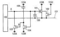
본 발명의 예시적인 일 실시 형태에 따르면, 액정 표시 장치는 구동 회로와 화소를 포함한다. 화소는 액정 소자를 포함한다. 구동 회로는 제1 트랜지스터, 제2 트랜지스터, 제3 트랜지스터, 제4 트랜지스터 및 용량 소자를 포함한다. 제1 트랜지스터의 제1 단자는 제1 배선에 전기적으로 접속된다. 제1 트랜지스터의 제2 단자는 제2 배선에 전기적으로 접속된다. 제2 트랜지스터의 제1 단자는 제2 배선에 전기적으로 접속된다. 제2 트랜지스터의 제2 단자는 제1 트랜지스터의 게이트에 전기적으로 접속된다. 제2 트랜지스터의 게이트는 제1 배선에 전기적으로 접속된다. 제3 트랜지스터의 제1 단자는 제3 배선에 전기적으로 접속된다. 제3 트랜지스터의 제2 단자는 제1 트랜지스터의 게이트에 전기적으로 접속된다. 제4 트랜지스터의 제1 단자는 제3 배선에 전기적으로 접속된다. 제4 트랜지스터의 제2 단자는 제3 트랜지스터의 게이트에 전기적으로 접속된다. 제4 트랜지스터의 게이트는 제1 트랜지스터의 게이트에 전기적으로 접속된다. 용량 소자의 하나의 전극은 제1 배선에 전기적으로 접속된다. 용량 소자의 나머지 하나의 전극은 제3 트랜지스터의 게이트에 전기적으로 접속된다.According to an exemplary embodiment of the present invention, the liquid crystal display device includes a driving circuit and a pixel. The pixel includes a liquid crystal element. The driving circuit includes a first transistor, a second transistor, a third transistor, a fourth transistor, and a capacitor. The first terminal of the first transistor is electrically connected to the first wiring. The second terminal of the first transistor is electrically connected to the second wiring. The first terminal of the second transistor is electrically connected to the second wiring. The second terminal of the second transistor is electrically connected to the gate of the first transistor. The gate of the second transistor is electrically connected to the first wiring. The first terminal of the third transistor is electrically connected to the third wiring. The second terminal of the third transistor is electrically connected to the gate of the first transistor. The first terminal of the fourth transistor is electrically connected to the third wiring. The second terminal of the fourth transistor is electrically connected to the gate of the third transistor. The gate of the fourth transistor is electrically connected to the gate of the first transistor. One electrode of the capacitor is electrically connected to the first wiring. The other electrode of the capacitor is electrically connected to the gate of the third transistor.
스위치로는 다양한 스위치를 사용할 수 있다는 점에 주목한다. 예를 들어, 전기적 스위치, 기계적 스위치 등을 사용할 수 있다. 즉, 전류 흐름을 제어할 수 있는 것이면 어떠한 소자를 사용해도 되며, 특정 소자로 한정되지 않는다. 예를 들어, 스위치로서, 트랜지스터(예를 들어, 바이폴라 트랜지스터 또는 MOS 트랜지스터), 다이오드(예를 들어, PN 다이오드, PIN 다이오드, 쇼트키 다이오드, MIM(Metal Insulator Metal) 다이오드, MIS(Metal Insulator Semiconductor) 다이오드, 다이오드 접속 트랜지스터) 등을 사용할 수 있다. 또는, 이러한 소자들을 조합한 논리 회로를 스위치로서 사용할 수 있다.Note that various switches can be used as the switch. For example, electrical switches, mechanical switches and the like can be used. In other words, any element may be used as long as the current flow can be controlled, and the element is not limited to a specific element. For example, as a switch, a transistor (eg, a bipolar transistor or a MOS transistor), a diode (eg, a PN diode, a PIN diode, a Schottky diode, a metal insulator metal (MIM) diode, a metal insulator semiconductor (MIS)) Diodes, diode-connected transistors) and the like. Alternatively, a logic circuit combining these elements can be used as a switch.
기계적 스위치의 예로는, 디지털 마이크로미러 장치(DMD)와 같이, MEMS(micro electro mechanical system) 기술을 사용하여 형성된 스위치가 있다.An example of a mechanical switch is a switch formed using micro electro mechanical system (MEMS) technology, such as a digital micromirror device (DMD).
또한, n채널 트랜지스터와 p채널 트랜지스터 모두를 사용하여 CMOS 스위치를 스위치로서 사용해도 좋다.In addition, a CMOS switch may be used as a switch using both n-channel transistors and p-channel transistors.
"A와 B가 접속된다"라고 명시적으로 기재하는 경우에는, A와 B가 전기적으로 접속되어 있는 경우, A와 B가 기능적으로 접속되어 있는 경우, A와 B가 직접 접속되어 있는 경우가 포함된다. 여기서, A와 B의 각각은 대상(예를 들어, 장치, 소자, 회로, 배선, 전극, 단자, 도전막, 또는 층)이다. 따라서, 소정의 접속 관계, 예를 들어, 도면과 텍스트에 나타낸 접속 관계로 한정되지 않고, 도면과 텍스트에 나타낸 접속 관계를 갖는 소자들 간에 다른 소자를 개재해도 된다.In the case of the explicit description that "A and B are connected" includes the case where A and B are electrically connected, when A and B are functionally connected, and A and B are directly connected. do. Here, each of A and B is an object (for example, an apparatus, an element, a circuit, a wiring, an electrode, a terminal, a conductive film, or a layer). Therefore, the element is not limited to a predetermined connection relationship, for example, the connection relationship shown in the drawings and the text, and may have other elements between the elements having the connection relationship shown in the drawings and the text.
예를 들어, A와 B가 전기적으로 접속되어 있는 경우에, A와 B 사이의 전기적인 접속을 가능하게 하는 하나 이상의 소자(예를 들어, 스위치, 트랜지스터, 용량 소자, 인덕터, 저항 소자, 및/또는 다이오드)가 A와 B 사이에 접속되어도 된다. 또는, A와 B가 기능적으로 접속되어 있는 경우에, A와 B 사이의 기능적인 접속을 가능하게 하는 하나 이상의 회로(예를 들어, 인버터, NAND 회로 또는 NOR 회로 등의 논리 회로, DA 변환 회로, AD 변환 회로, 감마 보정 회로 등의 신호 변환 회로, 전원 회로 또는 신호의 전위 레벨을 바꾸는 레벨 시프터 회로 등의 전위 레벨 변환 회로(예를 들어, dc-dc 컨버터, 스텝업 dc-dc 컨버터, 또는 스텝다운 dc-dc 컨버터), 전압원, 전류원, 스위칭 회로, 신호 진폭, 전류량 등을 증가시킬 수 있는 회로, 연산 증폭기, 차동 증폭 회로, 소스 폴로워 회로, 또는 버퍼 회로 등의 증폭 회로, 신호 생성 회로, 기억 회로, 및/또는 제어 회로)가, A와 B 사이에 접속되어 있어도 좋다. 예를 들어, A와 B 사이에 다른 회로를 끼우고 있어도, A로부터 출력된 신호가 B에 전달되는 경우에는, A와 B가 기능적으로 접속되어 있는 것으로 한다.For example, when A and B are electrically connected, one or more elements (eg, switches, transistors, capacitive elements, inductors, resistance elements, and / or the like) that enable electrical connection between A and B. Or a diode) may be connected between A and B. FIG. Or one or more circuits (e.g., logic circuits such as inverters, NAND circuits or NOR circuits, DA conversion circuits, etc.) that enable functional connection between A and B when A and B are functionally connected. Potential level conversion circuits (e.g., dc-dc converters, step-up dc-dc converters, or steps) such as signal conversion circuits such as AD conversion circuits, gamma correction circuits, power supply circuits, or level shifter circuits that change the potential levels of signals. Down-dc-dc converters), voltage sources, current sources, switching circuits, circuits capable of increasing signal amplitude, amperage, amplification circuits such as operational amplifiers, differential amplifier circuits, source follower circuits, or buffer circuits, signal generation circuits, Memory circuit and / or control circuit) may be connected between A and B. FIG. For example, it is assumed that A and B are functionally connected when a signal output from A is transmitted to B even if another circuit is inserted between A and B.
"A와 B가 전기적으로 접속된다"라고 명시적으로 기재하는 경우에는, A와 B가 전기적으로 접속되어 있는 경우(즉, A와 B 사이에 다른 소자나 다른 회로를 끼워서 접속되어 있는 경우), A와 B이 기능적으로 접속되어 있는 경우(즉, A와 B 사이에 다른 회로를 끼워서 기능적으로 접속되어 있는 경우), A와 B가 직접 접속되어 있는 경우(즉, A와 B 사이에 다른 소자나 다른 회로를 끼우지 않고 접속되어 있는 경우)가 포함된다. 즉, "A와 B가 전기적으로 접속된다"라고 명시적으로 기재하는 경우에는, "A와 B가 접속된다"라고만 명시적으로 기재되어 있는 경우와 동일하게 설명한다.In the case where it is stated explicitly that "A and B are electrically connected", when A and B are electrically connected (that is, when another element or another circuit is inserted between A and B), When A and B are functionally connected (i.e., functionally connected by inserting a different circuit between A and B), and when A and B are directly connected (i.e. other elements between A and B Is connected without other circuits). That is, in the case where it is explicitly described that "A and B are electrically connected", the same description as in the case where only "A and B are connected" is explicitly described.
표시 소자, 표시 소자를 갖는 장치인 표시 장치, 발광 소자, 발광 소자를 갖는 장치인 발광 장치는, 다양한 형태를 사용할 수 있고, 다양한 소자를 포함할 수 있다. 예를 들어, 표시 소자, 표시 장치, 발광 소자 또는 발광 장치로는, EL(일렉트로 루미네센스) 소자(예를 들어, 유기물 및 무기물을 포함하는 EL 소자, 유기 EL 소자, 또는 무기 EL 소자), LED(예를 들어, 백색 LED, 적색 LED, 녹색 LED, 또는 청색 LED), 트랜지스터(전류량에 따라 발광하는 트랜지스터), 전자 방출 소자, 액정 소자, 전자 잉크, 전기 영동 소자, 격자 라이트 밸브(GLV), 플라즈마 디스플레이(PDP), 디지털 마이크로미러 디바이스(DMD), 압전 세라믹 디스플레이, 또는 카본 나노튜브와 같이, 전자기적 작용에 의해, 콘트라스트, 휘도, 반사율, 투과율 등이 변화하는 표시 매체를 사용할 수 있다는 점에 주목한다. 또한, EL 소자를 사용한 표시 장치로는 EL 디스플레이, 전자 방출 소자를 사용한 표시 장치로는 필드 이미션 디스플레이(FED)가 있고, SED형 평면 패널 디스플레이(SED: surface-conduction electron-emitter display) 등이 있고, 액정 소자를 사용한 표시 장치로는 액정 디스플레이(예를 들어, 투과형 액정 디스플레이, 반투과형 액정 디스플레이, 반사형 액정 디스플레이, 직시형 액정 디스플레이, 또는 투사형 액정 디스플레이)가 있고, 전자 잉크나 전기 영동 소자를 사용한 표시 장치로는 전자 페이퍼가 있다는 점에 주목한다.The display device, the display device which is a device having a display element, the light emitting element, and the light emitting device which is a device having a light emitting element can use various forms and can include various elements. For example, as a display element, a display apparatus, a light emitting element, or a light emitting apparatus, EL (electroluminescence) element (for example, EL element containing organic substance and inorganic substance, organic electroluminescent element, or inorganic EL element), LEDs (e.g., white LEDs, red LEDs, green LEDs, or blue LEDs), transistors (transistors emitting light depending on the amount of current), electron emission devices, liquid crystal devices, electronic ink, electrophoretic devices, grating light valves (GLV) , Such as a plasma display (PDP), a digital micromirror device (DMD), a piezoelectric ceramic display, or carbon nanotubes, can be used as a display medium whose contrast, brightness, reflectance, transmittance, etc. are changed by electromagnetic action. Pay attention to In addition, a display device using an EL element includes an EL display, and a display device using an electron emission element includes a field emission display (FED), and an SED type flat panel display (SED: surface-conduction electron-emitter display) The display device using the liquid crystal element includes a liquid crystal display (for example, a transmissive liquid crystal display, a transflective liquid crystal display, a reflective liquid crystal display, a direct-view liquid crystal display, or a projection liquid crystal display), and an electronic ink or an electrophoretic element. Note that there is an electronic paper as a display device using.
액정 소자는, 액정의 광학적 변조 작용에 의해 광의 투과 또는 비투과를 제어하는 소자이며, 한 쌍의 전극 및 액정에 의해 구성된다는 점에 주목한다. 액정의 광학적 변조 작용은, 액정에 인가되는 전계(수평 방향의 전계, 수직 방향의 전계 및 경사 방향의 전계를 포함함)에 의해 제어된다는 점에 주목한다. 액정 소자로는, 네마틱 액정, 콜레스테릭 액정, 스메틱 액정, 디스코틱 액정, 사모트로픽 액정, 리오트로픽 액정, 저분자 액정, 고분자 액정, 고분자 분산형 액정(PDLC), 강유전 액정, 반강유전 액정, 주쇄형 액정, 측쇄형 고분자 액정, 플라즈마 어드레스 액정(PALC), 바나나형 액정 등이 가능하다는 점에 주목한다. 또한, 액정의 구동 방법으로는, TN(Twisted Nematic) 모드, STN(Super Twisted Nematic) 모드, IPS(In-Plane-Switching) 모드, FFS(Fringe Field Switching) 모드, MVA(Multi-domain Vertical Alignment) 모드, PVA(Patterned Vertical Alignment) 모드, ASV(Advanced Super View) 모드, ASM(Axially Symmetric aligned Microcell) 모드, OCB(Optically Compensated Birefringence) 모드, ECB(Electrically Controlled Birefringence) 모드, FLC(Ferroelectric Liquid Crystal) 모드, AFLC(Anti-Ferroelectric Liquid Crystal) 모드, PDLC(Polymer Dispersed Liquid Crystal) 모드, 게스트 호스트 모드, 블루상(Blue Phase) 모드 등을 사용할 수 있다. 본 발명은 이러한 예들로 한정되지 않고, 상기한 액정 소자 및 그 구동 방법으로는 다양한 액정 소자들 및 그 구동 방법들을 사용할 수 있다.Note that the liquid crystal element is an element which controls the transmission or non-transmission of light by the optical modulation action of the liquid crystal, and is composed of a pair of electrodes and the liquid crystal. Note that the optical modulation action of the liquid crystal is controlled by the electric field applied to the liquid crystal (including the electric field in the horizontal direction, the electric field in the vertical direction and the electric field in the oblique direction). As liquid crystal elements, nematic liquid crystals, cholesteric liquid crystals, smetic liquid crystals, discotic liquid crystals, samotropic liquid crystals, lyotropic liquid crystals, low molecular liquid crystals, polymer liquid crystals, polymer dispersed liquid crystal (PDLC), ferroelectric liquid crystals and antiferroelectric liquid crystals Note that a main chain type liquid crystal, a side chain type polymer liquid crystal, a plasma address liquid crystal (PALC), a banana type liquid crystal and the like are possible. In addition, as a driving method of the liquid crystal, TN (Twisted Nematic) mode, STN (Super Twisted Nematic) mode, IPS (In-Plane-Switching) mode, FFS (Fringe Field Switching) mode, MVA (Multi-domain Vertical Alignment) Mode, Patterned Vertical Alignment (PVA) Mode, Advanced Super View (ASV) Mode, Asymmetrically Symmetric Aligned Microcell (ASM) Mode, Optimally Compensated Birefringence (OCB) Mode, Electrically Controlled Birefringence (ECB) Mode, Ferroelectric Liquid Crystal (FLC) Mode An anti-ferroelectric liquid crystal (AFLC) mode, a polymer dispersed liquid crystal (PDLC) mode, a guest host mode, and a blue phase mode may be used. The present invention is not limited to these examples, and the above-described liquid crystal element and its driving method may use various liquid crystal elements and their driving methods.
광원을 필요로 하는 표시 장치, 예를 들어, 액정 디스플레이(예를 들어, 투과형 액정 디스플레이, 반투과형 액정 디스플레이, 반사형 액정 디스플레이, 직시형 액정 디스플레이, 또는 투사형 액정 디스플레이), 격자 라이트 밸브(GLV)를 사용한 표시 장치, 또는 디지털 마이크로미러 디바이스(DMD)를 사용한 표시 장치 등의 광원으로는, 일렉트로 루미네센스, 냉음극 형광 램프, 열음극 형광 램프, LED, 레이저 광원, 수은 램프 등을 사용할 수 있다는 점에 주목한다. 본 발명은 이것에 한정되지 않고, 광원으로서 다양한 것을 사용할 수 있다는 점에 주목한다.Display devices requiring light sources, such as liquid crystal displays (e.g., transmissive liquid crystal displays, transflective liquid crystal displays, reflective liquid crystal displays, direct view liquid crystal displays, or projection liquid crystal displays), grating light valves (GLV) Electroluminescent, cold cathode fluorescent lamps, hot cathode fluorescent lamps, LEDs, laser light sources, mercury lamps, and the like can be used as light sources, such as a display device using or a display device using a digital micromirror device (DMD). Pay attention to Note that the present invention is not limited to this, and various things can be used as the light source.
트랜지스터로는, 그 유형이 특별히 한정되지 않으며, 다양한 형태의 트랜지스터를 사용할 수 있다는 점에 주목한다. 예를 들어, 비정질 실리콘, 다결정 실리콘, 미결정(마이크로 크리스탈, 나노 크리스탈, 세미 아몰퍼스라고도 함) 실리콘 등으로 대표되는 비단결정 반도체막을 갖는 박막 트랜지스터(TFT) 등을 사용할 수 있다는 점에 주목한다.Note that the type of the transistor is not particularly limited, and various types of transistors can be used. Note, for example, that a thin film transistor (TFT) having a non-single-crystal semiconductor film represented by amorphous silicon, polycrystalline silicon, microcrystalline (micro crystal, nano crystal, semi-amorphous) silicon, or the like can be used.
미결정 실리콘을 형성할 때, 촉매(예를 들어, 니켈)를 사용함으로써, 결정성을 더욱 향상시켜, 전기적 특성이 뛰어난 트랜지스터를 제조할 수 있다는 점에 주목한다. 이때, 레이저 조사를 행하지 않고, 열처리만을 수행함으로써 결정성을 향상시킬 수 있다. 이에 따라, 소스 드라이버 회로의 일부(예를 들어, 아날로그 스위치) 및 게이트 드라이버 회로(예를 들어, 주사선 구동 회로)를 화소부와 동일한 기판을 이용하여 형성할 수 있다. 또한, 결정화를 위해 레이저 조사를 행하지 않는 경우에는, 실리콘의 결정성의 불균일을 억제할 수 있다. 따라서, 화질이 향상된 화상을 표시할 수 있다.Note that, when forming microcrystalline silicon, by using a catalyst (for example, nickel), it is possible to further improve crystallinity and to produce a transistor having excellent electrical characteristics. At this time, crystallinity can be improved by performing only heat treatment without performing laser irradiation. As a result, a part of the source driver circuit (for example, an analog switch) and a gate driver circuit (for example, a scan line driver circuit) can be formed using the same substrate as the pixel portion. In addition, when laser irradiation is not performed for crystallization, the nonuniformity of the crystallinity of silicon can be suppressed. Therefore, an image with improved image quality can be displayed.
촉매(예를 들어, 니켈)를 사용하지 않고, 다결정 실리콘 및 미결정 실리콘을 제조할 수 있다.It is possible to produce polycrystalline silicon and microcrystalline silicon without using a catalyst (eg nickel).
반도체 기판, SOI 기판 등을 사용해서 트랜지스터를 형성할 수 있다. 따라서, 특성, 크기, 형상 등의 편차가 적고, 전류 공급 능력이 높고, 크기가 작은 트랜지스터를 제조할 수 있다. 이러한 트랜지스터를 사용하면, 회로의 저소비 전력화 또는 회로의 고집적화를 도모할 수 있다.The transistor can be formed using a semiconductor substrate, an SOI substrate, or the like. Therefore, a transistor with little variation in characteristics, size, shape, etc., high current supply capability, and small size can be manufactured. By using such a transistor, it is possible to reduce the power consumption of the circuit or to increase the integration of the circuit.
ZnO, a-InGaZnO, SiGe, GaAs, IZO, ITO, SnO 등의 화합물 반도체 또는 산화물 반도체를 갖는 트랜지스터, 이러한 화합물 반도체 또는 산화물 반도체를 박막화한 박막 트랜지스터 등을 사용할 수 있다. 따라서, 제조 온도를 낮게 할 수 있고, 예를 들어, 실온에서 트랜지스터를 제조할 수 있다. 이에 따라, 내열성이 낮은 기판, 예를 들어, 플라스틱 기판이나 필름 기판 위에 직접 트랜지스터를 형성할 수 있다. 이러한 화합물 반도체 또는 산화물 반도체를, 트랜지스터의 채널 부분에 사용할 뿐만 아니라 그 이외의 용도에서 사용할 수도 있다는 점에 주목한다. 예를 들어, 이러한 화합물 반도체 또는 산화물 반도체를 저항 소자, 화소 전극, 또는 투광 전극을 위해 사용할 수 있다. 또한, 이러한 소자를 트랜지스터와 동시에 형성할 수 있으므로, 비용을 저감할 수 있다.A transistor having a compound semiconductor or an oxide semiconductor such as ZnO, a-InGaZnO, SiGe, GaAs, IZO, ITO, SnO, or a thin film transistor in which the compound semiconductor or oxide semiconductor is thinned can be used. Therefore, the manufacturing temperature can be lowered, for example, a transistor can be manufactured at room temperature. As a result, a transistor can be directly formed on a substrate having low heat resistance, for example, a plastic substrate or a film substrate. Note that such a compound semiconductor or an oxide semiconductor can be used not only for the channel portion of the transistor but also for other uses. For example, such a compound semiconductor or an oxide semiconductor can be used for the resistance element, the pixel electrode, or the light transmitting electrode. In addition, since such an element can be formed at the same time as the transistor, the cost can be reduced.
잉크젯이나 인쇄법을 사용해서 형성한 트랜지스터 등을 사용할 수 있다. 따라서, 트랜지스터를, 실온에서 제조할 수 있고, 저 진공에서 제조할 수 있고, 또는 대형 기판을 사용하여 제조할 수 있다. 마스크(레티클)를 사용하지 않아도 트랜지스터를 제조할 수 있으므로, 트랜지스터의 레이아웃을 용이하게 변경할 수 있다. 또한, 레지스트를 사용할 필요가 없기 때문에, 재료비가 저감되고, 공정 수를 저감할 수 있다. 또한, 필요한 부분에만 막을 형성하므로, 막을 전체 면에 걸쳐 성막한 후 에칭을 수행하는 제조 방법에 비해, 재료가 낭비되지 않고, 비용을 저감할 수 있다.The transistor formed using the inkjet or the printing method can be used. Thus, the transistor can be manufactured at room temperature, can be manufactured at low vacuum, or can be manufactured using a large substrate. Since the transistor can be manufactured without using a mask (reticle), the layout of the transistor can be easily changed. In addition, since there is no need to use a resist, the material cost can be reduced and the number of steps can be reduced. In addition, since the film is formed only in necessary portions, the material is not wasted and the cost can be reduced as compared with the manufacturing method in which the film is formed over the entire surface and then etched.
유기 반도체나 카본 나노튜브를 갖는 트랜지스터 등을 사용할 수 있다. 따라서, 이러한 트랜지스터를 가요성 기판 위에 형성할 수 있다. 이러한 기판을 사용하여 형성된 반도체 장치는 충격에 강할 수 있다.An organic semiconductor, a transistor having carbon nanotubes, or the like can be used. Thus, such a transistor can be formed on a flexible substrate. Semiconductor devices formed using such substrates can be impact resistant.
또한, 다양한 구조의 트랜지스터를 사용할 수 있다. 예를 들어, MOS형 트랜지스터, 접합형 트랜지스터, 바이폴라 트랜지스터 등을 트랜지스터로 해서 사용할 수 있다. MOS형 트랜지스터를 사용함으로써, 트랜지스터의 크기를 작게 할 수 있다. 따라서, 다수의 트랜지스터를 탑재할 수 있다. 바이폴라 트랜지스터를 사용함으로써, 큰 전류를 흘릴 수 있다. 따라서, 고속으로 회로를 동작시킬 수 있다.In addition, transistors of various structures can be used. For example, a MOS transistor, a junction transistor, a bipolar transistor, or the like can be used as the transistor. By using the MOS transistor, the size of the transistor can be reduced. Therefore, many transistors can be mounted. By using a bipolar transistor, a large current can flow. Therefore, the circuit can be operated at high speed.
MOS형 트랜지스터, 바이폴라 트랜지스터 등을 1개의 기판 위에 형성해도 된다는 점에 주목한다. 따라서, 저소비 전력, 소형화, 고속 동작 등을 실현할 수 있다.Note that a MOS transistor, a bipolar transistor, or the like may be formed on one substrate. Therefore, low power consumption, miniaturization, high speed operation, and the like can be realized.
게다가, 다양한 트랜지스터를 사용할 수 있다.In addition, various transistors can be used.
트랜지스터는, 종류가 특별히 한정되지 않는 다양한 기판을 사용해서 형성될 수 있다는 점에 주목한다. 예를 들어, 기판으로는, 단결정 기판, SOI 기판, 유리 기판, 석영 기판, 플라스틱 기판, 스테인리스 스틸 기판, 스테인리스 스틸 포일을 갖는 기판 등을 사용할 수 있다.Note that the transistor can be formed using a variety of substrates whose type is not particularly limited. For example, a single crystal substrate, an SOI substrate, a glass substrate, a quartz substrate, a plastic substrate, a stainless steel substrate, a substrate having a stainless steel foil, or the like can be used.
트랜지스터의 구조는 다양한 형태를 취할 수 있고, 특정한 구조로 한정되지 않는다는 점에 주목한다. 예를 들어, 2개 이상의 게이트 전극을 갖는 멀티 게이트 구조를 적용할 수 있다. 멀티 게이트 구조로 하면, 채널 영역들이 직렬로 접속되기 때문에, 복수의 트랜지스터가 직렬로 접속된 구조로 된다.Note that the structure of the transistor can take various forms and is not limited to a specific structure. For example, a multi-gate structure having two or more gate electrodes can be applied. In the multi-gate structure, since the channel regions are connected in series, a plurality of transistors are connected in series.
다른 예로, 채널의 상하에 게이트 전극이 배치되어 있는 구조를 적용할 수 있다. 채널의 상하에 게이트 전극이 배치되는 구성으로 함으로써, 복수의 트랜지스터가 병렬로 접속된 구조로 된다는 점에 주목한다.As another example, a structure in which a gate electrode is disposed above and below the channel may be applied. Note that the structure in which the gate electrodes are arranged above and below the channel results in a structure in which a plurality of transistors are connected in parallel.
채널 영역 위에 게이트 전극이 배치되어 있는 구조, 채널 영역 아래에 게이트 전극이 배치되어 있는 구조, 스태거(staggered) 구조, 역 스태거 구조, 채널 영역을 복수의 영역으로 나눈 구조, 채널 영역들을 병렬 또는 직렬로 접속한 구조도 적용할 수 있다. 또는, 채널 영역(혹은 그 일부)에 소스 전극이나 드레인 전극이 겹치는 구조도 적용할 수 있다. 또한, LDD 영역을 형성해도 된다.A structure in which the gate electrode is disposed above the channel region, a structure in which the gate electrode is disposed below the channel region, a staggered structure, an inverse stagger structure, a structure in which the channel region is divided into a plurality of regions, and the channel regions are parallel or The structure connected in series is also applicable. Alternatively, the structure in which the source electrode and the drain electrode overlap in the channel region (or part thereof) can also be applied. In addition, an LDD region may be formed.
트랜지스터로는, 다양한 트랜지스터를 사용할 수 있으며, 다양한 기판을 사용하여 형성될 수 있다는 점에 주목한다. 이에 따라, 소정의 기능을 실현하기 위해 필요한 모든 회로가, 동일한 기판을 사용하여 형성될 수 있다. 예를 들어, 소정의 기능을 실현하기 위해 필요한 모든 회로는, 유리 기판, 플라스틱 기판, 단결정 기판, SOI 기판, 또는 다른 임의의 기판을 사용해서 형성될 수 있다. 또는, 소정의 기능을 실현하기 위해 필요한 회로들 중 일부는 하나의 기판을 사용하여 형성될 수 있고, 소정의 기능을 실현하기 위해 필요한 회로들 중 일부는 다른 하나의 기판을 사용하여 형성될 수 있다. 즉, 소정의 기능을 실현하기 위해 필요한 회로들 모두가 동일한 기판을 사용해서 형성될 필요는 없다. 예를 들어, 소정의 기능을 실현하기 위해 필요한 회로들 중 일부는 유리 기판을 사용하여 트랜지스터에 의해 형성되고, 소정의 기능을 실현하기 위해 필요한 회로들 중 일부는 단결정 기판을 사용하여 형성되어, 단결정 기판을 사용해서 트랜지스터에 의해 형성된 IC 칩을 COG(Chip On Glass)에 의해 유리 기판에 접속하고, 유리 기판 위에 그 IC 칩을 배치해도 된다. 또는, IC 칩을 TAB(Tape Automated Bonding)이나 인쇄 배선 기판을 사용해서 유리 기판에 접속해도 된다. 또는, 소비 전력이 큰, 구동 전압이 높고 구동 주파수가 높은 회로를 동일한 기판을 사용하여 형성하는 것이 아니라 단결정 기판을 사용하여 형성하고 그 회로에 의해 형성된 IC 칩을 사용하도록 하면, 소비 전력의 증가를 방지할 수 있다.Note that as the transistor, various transistors can be used and can be formed using various substrates. Accordingly, all the circuits necessary for realizing the predetermined function can be formed using the same substrate. For example, all circuits necessary for realizing a predetermined function may be formed using a glass substrate, a plastic substrate, a single crystal substrate, an SOI substrate, or any other substrate. Alternatively, some of the circuits necessary for realizing the predetermined function may be formed using one substrate, and some of the circuits necessary for realizing the predetermined function may be formed using the other substrate. . In other words, not all of the circuits necessary to realize a given function need to be formed using the same substrate. For example, some of the circuits necessary for realizing a given function are formed by a transistor using a glass substrate, and some of the circuits necessary for realizing a predetermined function are formed using a single crystal substrate, so that a single crystal The IC chip formed by the transistor using the substrate may be connected to the glass substrate by COG (Chip On Glass), and the IC chip may be disposed on the glass substrate. Alternatively, the IC chip may be connected to the glass substrate using TAB (Tape Automated Bonding) or a printed wiring board. Alternatively, if a circuit having a high driving voltage and a high driving frequency having a high power consumption is formed using a single crystal substrate instead of using the same substrate, an IC chip formed by the circuit can be used to increase the power consumption. It can prevent.
트랜지스터는, 게이트, 드레인, 소스인 적어도 3개의 단자를 갖는 소자라는 점에 주목한다. 트랜지스터는 드레인 영역과 소스 영역 사이에 채널 영역을 갖고 있어, 드레인 영역, 채널 영역, 소스 영역을 통해 전류가 흐를 수 있다. 여기서, 트랜지스터의 소스와 드레인은, 구조, 동작 조건 등에 따라 변경되므로, 어느 것이 소스 또는 드레인인지를 판정하는 것은 어렵다. 따라서, 소스 및 드레인으로서 기능하는 영역을 소스 혹은 드레인이라 칭하지 않는 경우가 있다. 이러한 경우, 예를 들어, 소스와 드레인 중 하나를 제1 단자, 나머지 하나를 제2 단자로 표기해도 된다. 또는, 소스와 드레인 중 하나를 제1 전극, 소스와 드레인 중 나머지 하나를 제2 전극이라 표기해도 된다. 또는, 소스와 드레인 중 하나를 제1 영역, 소스와 드레인 중 나머지 하나를 제2 영역이라 표기해도 된다.Note that the transistor is an element having at least three terminals, that is, a gate, a drain, and a source. The transistor has a channel region between the drain region and the source region, so that current can flow through the drain region, the channel region, and the source region. Here, since the source and the drain of the transistor change depending on the structure, the operating conditions and the like, it is difficult to determine which is the source or the drain. Therefore, the area | region which functions as a source and a drain may not be called a source or a drain. In this case, for example, one of the source and the drain may be referred to as the first terminal and the other may be referred to as the second terminal. Alternatively, one of the source and the drain may be referred to as a first electrode, and the other of the source and the drain may be referred to as a second electrode. Alternatively, one of the source and the drain may be referred to as a first region, and the other of the source and the drain may be referred to as a second region.
트랜지스터는 베이스, 이미터, 컬렉터인 적어도 3개의 단자를 갖는 소자이어도 된다는 점에 주목한다. 이 경우에도, 마찬가지로, 이미터와 컬렉터 중 하나를 제1 단자, 이미터와 컬렉터 중 나머지 하나를 제2 단자로 표기해도 된다.Note that the transistor may be an element having at least three terminals, that is, a base, an emitter, and a collector. In this case, similarly, one of the emitter and the collector may be referred to as the first terminal, and the other of the emitter and the collector may be referred to as the second terminal.
반도체 장치는 반도체 소자(트랜지스터, 다이오드, 또는 사이리스터)를 포함하는 회로를 갖는 장치에 해당한다는 점에 주목한다. 또한, 반도체 장치는 반도체 특성을 이용함으로써 기능할 수 있는 장치 모두에 해당되어도 된다. 또한, 반도체 장치는 반도체 재료를 갖는 장치에 해당한다.Note that the semiconductor device corresponds to a device having a circuit including a semiconductor element (transistor, diode, or thyristor). The semiconductor device may correspond to any device that can function by using semiconductor characteristics. In addition, the semiconductor device corresponds to a device having a semiconductor material.
표시 장치는 표시 소자를 갖는 장치에 해당한다는 점에 주목한다. 표시 장치는 표시 소자를 각각 포함하는 복수의 화소를 포함해도 된다. 표시 장치는 복수의 화소를 구동하는 주변 구동 회로를 포함해도 된다는 점에 주목한다. 복수의 화소를 구동하는 주변 구동 회로는 복수의 화소와 동일한 기판 위에 형성되어도 된다는 점에 주목한다. 표시 장치는, 와이어 본딩이나 범프 본딩에 의해 기판 위에 배치된 주변 구동 회로, 소위, 칩 온 글라스(COG)에 의해 접속된 IC 칩 또는 TAB 등에 의해 접속된 IC 칩을 포함해도 된다. 표시 장치는, IC 칩, 저항 소자, 용량 소자, 인덕터, 트랜지스터 등이 설치된 가요성 인쇄 회로(FPC)를 포함해도 된다. 표시 장치는, 가요성 인쇄 회로(FPC) 등을 통하여 접속되고 IC 칩, 저항 소자, 용량 소자, 인덕터, 트랜지스터 등이 설치된 인쇄 배선 기판(PWB)을 포함해도 된다는 점에 주목한다. 표시 장치는 편광판 또는 위상차판 등의 광학 시트를 포함하고 있어도 된다. 표시 장치는, 조명 장치, 하우징, 음성 입출력 장치, 광 센서 등을 포함하고 있어도 된다.Note that the display device corresponds to a device having a display element. The display device may include a plurality of pixels each including a display element. Note that the display device may include a peripheral drive circuit for driving a plurality of pixels. Note that the peripheral drive circuit for driving the plurality of pixels may be formed on the same substrate as the plurality of pixels. The display device may include a peripheral drive circuit disposed on the substrate by wire bonding or bump bonding, an IC chip connected by a so-called chip on glass (COG), or an IC chip connected by TAB or the like. The display device may include a flexible printed circuit (FPC) provided with an IC chip, a resistor, a capacitor, an inductor, a transistor, and the like. Note that the display device may include a printed wiring board (PWB) connected through a flexible printed circuit (FPC) or the like and provided with an IC chip, a resistor, a capacitor, an inductor, a transistor, and the like. The display device may include an optical sheet such as a polarizing plate or a retardation plate. The display device may include a lighting device, a housing, an audio input / output device, an optical sensor, and the like.
조명 장치는, 백라이트 유닛, 도광판, 프리즘 시트, 확산 시트, 반사 시트, 광원(예를 들어, LED, 냉음극 형광 램프), 냉각 장치(예를 들어, 수냉식 또는 공냉식) 등을 포함해도 된다는 점에 주목한다.The lighting device may include a backlight unit, a light guide plate, a prism sheet, a diffusion sheet, a reflection sheet, a light source (for example, LED, cold cathode fluorescent lamp), a cooling device (for example, water-cooled or air-cooled), or the like. Pay attention.
발광 장치는 발광 소자 등을 갖는 장치에 해당한다는 점에 주목한다. 발광 장치가 표시 소자인 발광 소자를 갖고 있는 경우에, 발광 장치는 표시 장치의 구체적인 예들 중 일례이다.Note that the light emitting device corresponds to a device having a light emitting element or the like. In the case where the light emitting device has a light emitting element that is a display element, the light emitting device is an example of specific examples of the display device.
반사 장치는 광반사 소자, 광회절 소자, 광반사 전극 등을 갖고 있는 장치에 해당한다는 점에 주목한다.Note that the reflecting device corresponds to a device having a light reflection element, a light diffraction element, a light reflection electrode, and the like.
액정 표시 장치는 액정 소자를 갖고 있는 표시 장치에 해당한다는 점에 주목한다. 액정 표시 장치에는, 직시형 액정 표시 장치, 투사형 액정 표시 장치, 투과형 액정 표시 장치, 반사형 액정 표시 장치, 반투과형 액정 표시 장치 등이 있다.Note that the liquid crystal display device corresponds to a display device having a liquid crystal element. The liquid crystal display device includes a direct view type liquid crystal display device, a projection type liquid crystal display device, a transmissive liquid crystal display device, a reflective liquid crystal display device, a semi-transmissive liquid crystal display device, and the like.
구동 장치는 반도체 소자, 전기 회로, 전자 회로를 갖는 장치에 해당한다는 점에 주목한다. 예를 들어, 소스 신호선으로부터 화소로의 신호 입력을 제어하는 트랜지스터(선택용 트랜지스터, 스위칭용 트랜지스터 등이라고도 칭함), 화소 전극에 전압 또는 전류를 공급하는 트랜지스터, 발광 소자에 전압 또는 전류를 공급하는 트랜지스터 등은 구동 장치의 예들이다. 게이트 신호선에 신호를 공급하는 회로(게이트 드라이버, 게이트선 구동 회로 등이라고도 칭함), 소스 신호선에 신호를 공급하는 회로(소스 드라이버, 소스선 구동 회로 등이라고도 칭함) 등도 구동 장치의 예들이다.Note that the driving device corresponds to a device having a semiconductor element, an electric circuit, and an electronic circuit. For example, a transistor for controlling signal input from a source signal line to a pixel (also referred to as a selection transistor or a switching transistor), a transistor for supplying a voltage or a current to a pixel electrode, a transistor for supplying a voltage or a current to a light emitting element. Etc. are examples of the driving apparatus. Circuits for supplying signals to the gate signal lines (also called gate drivers, gate line driver circuits, etc.), and circuits for supplying signals to the source signal lines (also called source drivers, source line driver circuits, etc.) are examples of the driving apparatus.
표시 장치, 반도체 장치, 조명 장치, 냉각 장치, 발광 장치, 반사 장치, 구동 장치 등은 서로 중복되는 경우가 있다는 점에 주목한다. 예를 들어, 표시 장치가 반도체 장치 및 발광 장치를 갖고 있는 경우가 있다. 또는, 반도체 장치가 표시 장치 및 구동 장치를 갖고 있는 경우도 있다.Note that the display device, the semiconductor device, the lighting device, the cooling device, the light emitting device, the reflecting device, the driving device and the like may overlap each other. For example, the display device may have a semiconductor device and a light emitting device. Alternatively, the semiconductor device may have a display device and a drive device.
"A 위에 B가 형성된다" 또는 "B 위로 A가 형성된다"라고 명시적으로 기재하는 경우, 이는 반드시 B가 A와 직접 접하여 형성됨을 의미하는 것은 아니다. 이러한 설명에는, A와 B가 서로 직접 접하지 않는 경우, 즉, A와 B 사이에 다른 대상물이 개재되어 있는 경우가 포함된다. 여기서, A와 B의 각각은 대상물(예를 들어, 장치, 소자, 회로, 배선, 전극, 단자, 도전막, 층 등)이다.When explicitly stating "B is formed over A" or "A is formed over B", this does not necessarily mean that B is formed in direct contact with A. This description includes the case where A and B do not directly contact each other, that is, when another object is interposed between A and B. Here, each of A and B is an object (for example, an apparatus, an element, a circuit, a wiring, an electrode, a terminal, a conductive film, a layer, etc.).
이에 따라, 예를 들어, "층 A 위에 (혹은 층 A위로) 층 B가 형성된다"라고 명시적으로 기재되어 있는 경우, 이는 층 A 위에 층 B가 직접 접하여 형성되는 경우와, 다른 층(예를 들어, 층 C 또는 층 D)이 층 A에 직접 접하여 형성되고 층 B가 층 C나 층 D와 직접 접하여 형성되는 경우를 포함한다. 다른 층(예를 들어, 층 C나 층 D)은 단층이어도 되고 복층이어도 된다는 점에 주목한다.Thus, for example, if it is explicitly stated that "layer B is formed on (or above layer A)", this is different from the case where layer B is formed in direct contact with layer A, For example, layer C or layer D) is formed in direct contact with layer A and layer B is formed in direct contact with layer C or layer D. Note that the other layer (for example, layer C or layer D) may be a single layer or a multilayer.
마찬가지로, "A 위로 B가 형성된다"라고 명시적으로 기재되어 있는 경우에도, 이는 반드시 B가 A와 직접 접하여 형성되는 것을 의미하지 않으며, 이들 간에 다른 대상물이 개재되어도 된다. 따라서, 예를 들어, "층 A 위로 층 B가 형성된다"라고 설명하는 경우에, 이는 층 B가 층 A와 직접 접하여 형성되는 경우와, 다른 층(예를 들어, 층 C나 층 D)이 층 A와 직접 접하여 형성되고 층 B가 층 C나 층 D와 직접 접하여 형성되는 경우를 포함한다. 다른 층(예를 들어, 층 C나 층D)은 단층이어도 되고 복층이어도 된다는 점에 주목한다.Likewise, even when explicitly stated that "B is formed over A", this does not necessarily mean that B is formed in direct contact with A, and another object may be interposed therebetween. Thus, for example, when describing that "layer B is formed over layer A", this means that when layer B is formed in direct contact with layer A, another layer (e.g., layer C or layer D) It includes the case where it is formed in direct contact with layer A and the layer B is formed in direct contact with layer C or layer D. Note that the other layer (for example, layer C or layer D) may be a single layer or a multilayer.
"A 위에 B가 형성된다" 또는 "A 위로 B가 형성된다"라고 명시적으로 기재되는 경우에, 이는 B가 A 위로/위에 비스듬하게 형성되는 경우를 포함한다는 점에 주목한다.Note that when explicitly stated as "B is formed over A" or "B is formed over A", this includes the case where B is formed obliquely above / on A.
"A 밑에 B가 형성된다" 또는 "A 아래에 B가 형성된다"라고 설명하는 경우에도 마찬가지라는 점에 주목한다.Note that the same applies to the description of "B is formed under A" or "B is formed under A".
대상물이 명시적으로 단수로서 설명되는 경우에는, 그 대상물은 단수인 것이 바람직하다는 점에 주목한다. 본 발명은 이에 한정되지 않고, 대상물이 복수일 수도 있다는 점에 주목한다. 마찬가지 방식으로, 대상물이 명시적으로 복수로서 설명되는 경우에는, 대상물이 복수인 것이 바람직하다. 본 발명은 이에 한정되지 않고, 대상물이 단수일 수도 있다는 점에 주목한다.Note that when an object is explicitly described as singular, the object is preferably singular. Note that the present invention is not limited to this and that a plurality of objects may be provided. In a similar manner, when the objects are explicitly described as plural, it is preferable that the objects are plural. Note that the present invention is not limited to this, and that the object may be singular.
도면에서, 크기, 층의 두께, 또는 영역은 명료화를 위해 과장되는 경우도 있다. 따라서, 본 발명은 반드시 스케일에 한정되지 않는다.In the drawings, the size, thickness of layer, or region may be exaggerated for clarity. Therefore, the present invention is not necessarily limited to scale.
도면은 이상적인 예들을 개략적으로 나타낸 것이며, 형상 또는 값은 도면에 도시한 것으로 한정되지 않는다는 점에 주목한다. 예를 들어, 제조 기술이나 오차로 인한 형상의 편차, 노이즈나 타이밍 차로 인한 신호, 전압 값, 또는 전류 값의 편차를 포함할 수 있다.Note that the drawings schematically illustrate ideal examples, and that the shape or value is not limited to that shown in the drawings. For example, it may include variations in shape due to manufacturing techniques or errors, signals, voltage values, or current values due to noise or timing differences.
기술적 용어는 특정한 실시 형태 또는 실시예 등을 설명하기 위해 사용되며, 이에 한정되지 않는다는 점에 주목한다.Note that technical terms are used to describe specific embodiments, examples, and the like, but are not limited thereto.
정의되어 있지 않은 용어들(기술적 용어 또는 학술 용어 등의 과학 및 기술용으로 사용되는 용어들을 포함함)은, 당업자가 이해하는 일반적인 의미와 동등한 의미를 갖는 용어들로서 사용될 수 있다는 점에 주목한다. 사전 등에 의해 정의되어 있는 용어들은 배경 기술과 모순이 없는 의미로 해석되는 것이 바람직하다.It is noted that terms that are not defined (including terms used for scientific and technical purposes, such as technical terms or academic terms) may be used as terms having a meaning equivalent to a general meaning understood by those skilled in the art. Terms defined by dictionaries or the like are preferably interpreted in a meaning that does not conflict with the background art.
"제1", "제2", "제3" 등의 용어들은 다양한 요소, 부재, 영역, 층, 구역을 다른 것과 구별하도록 사용된다는 점에 주목한다. 따라서, "제1", "제2", "제3" 등의 용어들은 그 요소, 부재, 영역, 층, 구역 등의 개수를 한정하지 않는다. 또한, 예를 들어, "제1"을 "제2", "제3" 등으로 대체할 수 있다.It is noted that the terms "first", "second", "third", etc. are used to distinguish various elements, members, regions, layers, zones from others. Thus, terms such as "first", "second", "third", and the like do not limit the number of elements, members, regions, layers, zones, and the like. Also, for example, "first" may be replaced with "second", "third", and the like.
용량 소자에 접속되는 트랜지스터의 수를 감소시킬 수 있다. 또는, 로, 용량 소자에 접속되는 트랜지스터의 기생 용량을 감소시킬 수 있다. 또는, 로, 클록 신호에 동기하는 신호의 H 레벨의 전위를 증가시킬 수 있다. 또는, 레이아웃 면적을 저감할 수 있다. 또는, 수명을 길게 할 수 있다. 또는, 신호의 지연이나 왜곡을 감소시킬 수 있다. 또는, 소비 전력을 감소시킬 수 있다. 또는, 노이즈의 악영향을 감소시킬 수 있다. 또는, 트랜지스터의 열화를 억제 또는 완화할 수 있다. 또는, 오동작을 억제할 수 있다. 또는, 용량 소자의 하나의 전극과 용량 소자의 나머지 하나의 전극 간의 단락을 방지할 수 있다. 또는, 외부 회로의 전류 구동 능력을 감소시킬 수 있다. 또는, 외부 회로의 크기를 저감할 수 있다. 또는, 표시 장치의 크기를 저감할 수 있다.The number of transistors connected to the capacitor can be reduced. Alternatively, the parasitic capacitance of the transistor connected to the capacitor can be reduced. Alternatively, the potential of the H level of the signal synchronized with the clock signal can be increased. Alternatively, the layout area can be reduced. Alternatively, the life can be extended. Alternatively, the delay or distortion of the signal can be reduced. Alternatively, power consumption can be reduced. Alternatively, adverse effects of noise can be reduced. Alternatively, deterioration of the transistor can be suppressed or alleviated. Alternatively, malfunction can be suppressed. Alternatively, a short circuit between one electrode of the capacitor and the other electrode of the capacitor may be prevented. Alternatively, the current driving capability of the external circuit can be reduced. Alternatively, the size of the external circuit can be reduced. Alternatively, the size of the display device can be reduced.
도 1a는 반도체 장치의 회로도이며, 도 1b는 반도체 장치의 구동 방법을 도시하는 타이밍 차트.
도 2a 내지 도 2e는 반도체 장치의 구동 방법을 도시하는 개략도.
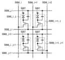
도 3a 내지 도 3e는 반도체 장치의 회로도.
도 4a 내지 도 4f는 반도체 장치의 회로도.
도 5a 내지 도 5e는 반도체 장치의 회로도.
도 6a는 반도체 장치의 회로도이고, 도 6b와 도 6c는 반도체 장치의 구동 방법을 각각 도시하는 타이밍 차트.
도 7a 내지 도 7c는 반도체 장치의 구동 방법을 도시하는 개략도.
도 8a와 도 8b는 반도체 장치의 구동 방법을 도시하는 개략도.
도 9a 내지 도 9c는 반도체 장치의 회로도.
도 10a 내지 도 10c는 반도체 장치의 회로도.
도 11a 내지 도 11c는 반도체 장치의 회로도.
도 12a 내지 도 12c는 반도체 장치의 회로도.
도 13a 내지 도 13c는 반도체 장치의 회로도.
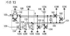
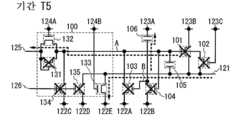
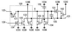
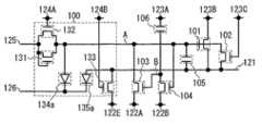
도 14a는 시프트 레지스터의 회로도이고, 도 14b는 시프트 레지스터의 구동 방법을 도시하는 타이밍 차트.
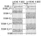
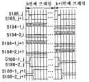
도 15는 시프트 레지스터의 회로도.
도 16은 시프트 레지스터의 회로도.
도 17a와 도 17b는 시프트 레지스터의 회로도.
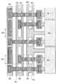
도 18은 시프트 레지스터의 레이아웃도.
도 19a는 반도체 장치의 회로도이고, 도 19b는 반도체 장치의 구동 방법을 도시하는 타이밍 차트.
도 20a와 도 20b는 반도체 장치의 회로도.
도 21은 시프트 레지스터의 회로도.
도 22a와 도 22b는 표시 장치의 시스템 블록도.
도 23a 내지 도 23e는 표시 장치의 구조를 도시하는 도면.
도 24는 시프트 레지스터의 회로도.
도 25a와 도 25b는 시프트 레지스터의 구동 방법을 도시하는 타이밍 차트.
도 26a는 신호선 구동 회로의 회로도이고, 도 26b는 신호선 구동 회로의 구동 방법을 도시하는 타이밍 차트.
도 27a 내지 도 27c, 도 27e, 도 27f는 화소의 회로도이고, 도 27d와 도 27g는 화소의 구동 방법을 각각 도시하는 타이밍 차트.
도 28a와 도 28b는 화소의 회로도, 도 28c 내지 도 28e 및 도 28g는 화소의 레이아웃도, 도 28f와 도 28h는 화소의 구동 방법을 각각 도시하는 타이밍 차트.
도 29a는 화소의 구동 방법을 도시하는 타이밍 차트이고, 도 29b는 화소의 회로도.
도 30은 시프트 레지스터의 레이아웃도.
도 31은 시프트 레지스터의 레이아웃도.
도 32a 내지 도 32c는 트랜지스터의 단면도.
도 33a 내지 도 33h는 전자 장치를 도시하는 도면.
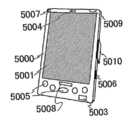
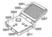
도 34a 내지 도 34h는 전자 장치를 도시하는 도면.1A is a circuit diagram of a semiconductor device, and FIG. 1B is a timing chart showing a method of driving a semiconductor device.
2A to 2E are schematic diagrams showing a method of driving a semiconductor device.
3A to 3E are circuit diagrams of a semiconductor device.
4A to 4F are circuit diagrams of a semiconductor device.
5A to 5E are circuit diagrams of a semiconductor device.
6A is a circuit diagram of a semiconductor device, and FIGS. 6B and 6C are timing charts respectively showing a method of driving a semiconductor device.
7A to 7C are schematic views showing a method of driving a semiconductor device.
8A and 8B are schematic views showing a method of driving a semiconductor device.
9A to 9C are circuit diagrams of a semiconductor device.
10A to 10C are circuit diagrams of a semiconductor device.
11A to 11C are circuit diagrams of a semiconductor device.
12A to 12C are circuit diagrams of a semiconductor device.
13A to 13C are circuit diagrams of a semiconductor device.
Fig. 14A is a circuit diagram of a shift register, and Fig. 14B is a timing chart showing a method of driving a shift register.
15 is a circuit diagram of a shift register.
16 is a circuit diagram of a shift register.
17A and 17B are circuit diagrams of a shift register.
18 is a layout diagram of a shift register.
19A is a circuit diagram of a semiconductor device, and FIG. 19B is a timing chart showing a method of driving a semiconductor device.
20A and 20B are circuit diagrams of a semiconductor device.
21 is a circuit diagram of a shift register.
22A and 22B are system block diagrams of a display device.
23A to 23E are diagrams showing the structure of a display device.
24 is a circuit diagram of a shift register.
25A and 25B are timing charts showing a method of driving a shift register.
FIG. 26A is a circuit diagram of a signal line driver circuit, and FIG. 26B is a timing chart showing a method of driving the signal line driver circuit.
27A to 27C, 27E, and 27F are circuit diagrams of pixels, and FIGS. 27D and 27G are timing charts each showing a driving method of the pixels.
28A and 28B are circuit diagrams of pixels, FIGS. 28C to 28E and 28G are layout diagrams of pixels, and FIGS. 28F and 28H are timing charts each showing a driving method of the pixels.
29A is a timing chart showing a method of driving a pixel, and FIG. 29B is a circuit diagram of the pixel.
30 is a layout diagram of a shift register.
Fig. 31 is a layout diagram of a shift register.
32A-32C are cross-sectional views of transistors.
33A-33H illustrate electronic devices.
34A-34H illustrate electronic devices.
이하, 실시 형태를 도면을 참조하여 설명한다. 단, 실시 형태는 다양한 모드로 구현될 수 있다. 본 발명의 사상과 범위로부터 일탈하지 않고 모드 및 상세를 다양함에 변경할 수 있는 것은 당업자라면 용이하게 이해할 것이다. 따라서, 본 발명을 본 실시 형태의 설명에 한정해서 해석해서는 안 된다. 이하에 설명하는 본 발명의 구조에 있어서, 유사한 기능을 갖는 부분이나 동일한 부분에는 동일한 참조 번호로 표시하고, 그 설명을 생략한다는 점에 주목한다.EMBODIMENT OF THE INVENTION Hereinafter, embodiment is described with reference to drawings. However, the embodiment may be implemented in various modes. It will be readily understood by those skilled in the art that various changes in mode and details may be made without departing from the spirit and scope of the invention. Therefore, this invention should not be interpreted limited to the description of this embodiment. Note that, in the structure of the present invention described below, parts having similar functions or the same parts are denoted by the same reference numerals, and the description thereof is omitted.
일 실시 형태에서 설명하는 내용(또는 그 내용의 일부이어도 됨)은, 그 실시 형태에서 설명하는 다른 내용(또는 그 다른 내용의 일부이어도 됨), 및/또는 하나 또는 복수의 다른 실시 형태에서 설명하는 내용(또는 그 내용의 일부이어도 됨)에 대하여, 적용, 조합, 또는 치환을 행할 수 있다는 점에 주목한다.The content (or part of the content) described in one embodiment may be described in the other content (or part of the other content) described in the embodiment, and / or described in one or a plurality of other embodiments. Note that the content (or a part of the content) may be applied, combined, or substituted.
각 실시 형태에서, 그 실시 형태에서 설명하는 내용은 다양한 도를 참조하여 설명하는 내용 또는 명세서에 기재되어 있는 단락을 사용해서 설명하는 내용이라는 점에 주목한다.In each of the embodiments, it is noted that the contents described in the embodiments are those described using the contents described with reference to the various figures or the paragraphs described in the specification.
일 실시 형태에서 설명하는 도(또는 그 도의 일부이어도 됨)를, 그 도가 다른 부분, 그 실시 형태에서 설명하는 다른 도(또는 그 다른 도의 일부이어도 됨), 및/또는 하나 또는 복수의 다른 실시 형태에서 설명하는 도(또는 그 도의 일부이어도 됨)와 조합함으로써, 많은 도를 형성할 수 있다는 점에 주목한다.A diagram (or part of a diagram) described in one embodiment may be a different portion of the diagram, another diagram (or may be part of another diagram) described in the embodiment, and / or one or a plurality of other embodiments. Note that many of the figures can be formed by combining with the figures described in (or part of the figures).
[실시 형태 1]
본 실시 형태에서는, 반도체 장치의 일례를 설명한다. 반도체 장치를 구동 회로 또는 플립플롭으로서 나타낼 수 있다는 점에 주목한다.In this embodiment, an example of a semiconductor device is demonstrated. Note that the semiconductor device can be represented as a driving circuit or flip-flop.
우선, 본 실시 형태의 반도체 장치의 일례에 대해서 도 1a를 참조하여 설명한다. 도 1a의 반도체 장치는, 회로(100), 트랜지스터(101), 트랜지스터(102), 트랜지스터(103), 트랜지스터(104), 용량 소자(105) 및 용량 소자(106)를 포함한다. 트랜지스터(101 내지 104)의 각각은 게이트와 소스 사이의 전위차(Vgs)가 임계값 전압(Vth)보다 큰 경우 턴온되는 n채널형 트랜지스터이다. 단, 본 실시 형태는 이에 한정되지 않는다. 트랜지스터(101 내지 104)의 각각은 p채널형 트랜지스터일 수 있다. p채널형 트랜지스터는 게이트와 소스 사이의 전위차(Vgs)가 임계값 전압(Vth)보다 낮은 경우에 턴온된다.First, an example of the semiconductor device of this embodiment is demonstrated with reference to FIG. 1A. The semiconductor device of FIG. 1A includes a
도 1a의 반도체 장치의 접속 관계에 대해서 설명한다. 트랜지스터(101)의 제1 단자는 배선(123B)에 접속된다. 트랜지스터(101)의 제2 단자는 배선(121)에 접속된다. 트랜지스터(102)의 제1 단자는 트랜지스터(101)의 게이트에 접속된다. 트랜지스터(102)의 제2 단자는 배선(121)에 접속된다. 트랜지스터(102)의 게이트는 배선(123C)에 접속된다. 트랜지스터(103)의 제1 단자는 배선(122A)에 접속된다. 트랜지스터(103)의 제2 단자는 트랜지스터(101)의 게이트에 접속된다. 트랜지스터(104)의 제1 단자는 배선(122B)에 접속된다. 트랜지스터(104)의 제2 단자는 트랜지스터(103)의 게이트에 접속된다. 용량 소자(105)의 하나의 전극은 트랜지스터(101)의 게이트에 접속된다. 용량 소자(105)의 나머지 하나의 전극은 배선(121)에 접속된다. 용량 소자(106)의 하나의 전극은 배선(123A)에 접속된다. 용량 소자(106)의 나머지 하나의 전극은 트랜지스터(103)의 게이트에 접속된다.The connection relationship of the semiconductor device of FIG. 1A is demonstrated. The first terminal of the
트랜지스터(101)의 게이트, 트랜지스터(102)의 제1 단자, 트랜지스터(103)의 제2 단자, 또는 트랜지스터(104)의 게이트의 접속부를 노드 A로 나타낸다는 점에 주목한다. 이어서, 트랜지스터(103)의 게이트, 트랜지스터(104)의 제2 단자, 또는 용량 소자(106)의 나머지 하나의 전극의 접속부를 노드 B로 나타낸다. 노드 A 및 노드 B를 배선으로서 나타낼 수도 있다는 점에 주목한다.Note that the connection portion of the gate of the
배선(121), 배선(123A), 배선(123B), 배선(123C), 배선(122A), 배선(122B)을 단자로서 나타낼 수 있다는 점에 주목한다.Note that the
각 배선(배선(121), 배선(122A와 122B), 배선(123A 내지 123C))에 입력될 수 있는 것(예를 들어 신호, 전압, 또는 전류)의 일례를 설명한다. 그러나, 후술하는 내용은 일례이며, 본 실시 형태가 이에 한정되지는 않는다. 후술하는 것 외에도 다양한 것들을 각 배선에 입력할 수 있다. 각 배선을 부유(floating) 상태로 할 수 있다.An example of what can be input (for example, a signal, a voltage, or a current) which can be input to each wiring (
예를 들어, 배선(121)으로부터 신호 S1이 출력된다. 이에 따라, 배선(121)은 신호선으로서 기능할 수 있다. 특히, 배선(121)이 화소에 접속되는 경우, 또는 배선(121)이 화소부에 연장되도록 배치되는 경우, 배선(121)은 게이트선, 주사선, 또는 용량선으로서 기능할 수 있다. 신호 S1은, 많은 경우에 반도체 장치의 출력 신호이며 H 레벨과 L 레벨을 갖는 디지털 신호이다. 신호 S1은, 출력 신호, 선택 신호, 게이트 신호, 또는 주사 신호로서 기능할 수 있다.For example, the signal S1 is output from the
예를 들어, 배선(122A와 122B)에는 전압 V1이 공급된다. 이에 따라, 배선(122A와 122B)은 전원선으로서 기능할 수 있다. 전압 V1은, 많은 경우에 신호 S1의 L 레벨과 대략 동일한 값을 갖고, 접지 전압, 전원 전압, 또는 마이너스 전원 전압으로서 기능할 수 있다. 그러나, 본 실시 형태는 이에 한정되지 않는다. 배선(122A와 122B)에는 클록 신호 등의 신호가 입력되는 것이 가능하다. 이 경우, 배선(122A와 122B)은 신호선, 또는 클록 신호선으로서 기능할 수 있다. 또는, 배선(122A와 122B)에는, 서로 다른 전압들 또는 서로 다른 신호들이 입력될 수 있다.For example, the voltage V1 is supplied to the
"대략"이라는 용어는 노이즈로 인한 오차, 프로세스의 편차로 인한 오차, 소자의 제작 공정의 편차로 인한 오차, 및/또는 측정 오차 등의 다양한 오차를 포함한다는 것을 의미한다는 점에 주목한다.Note that the term " approximately " means including various errors such as errors due to noise, errors due to process variations, errors due to variations in device fabrication processes, and / or measurement errors.
예를 들어, 배선(123A 내지 123C)에는 신호 S2가 입력된다. 이에 따라, 배선(123A 내지 123C)은 신호선으로서 기능할 수 있다. 신호 S2는, 많은 경우에 일정한 주기로 H 레벨과 L 레벨 간의 스위칭을 반복하는 디지털 신호이며, 클록 신호(CK)로서 기능할 수 있다. 그러나, 본 실시 형태는 이에 한정되지 않는다. 배선(123A 내지 123C)에는, 전원 전압이 공급될 수 있다. 이 경우, 배선(123A 내지 123C)은 전원선으로서 기능할 수 있다. 또는, 배선(123A 내지 123C)에는, 서로 다른 전압들 또는 서로 다른 신호들이 입력될 수 있다.For example, the signal S2 is input to the
본 실시 형태에서는, 일례로서, 신호의 L 레벨의 전위를 V1, 신호의 H 레벨의 전위를 V2로 하면, V2가 V1보다 크다는 점에 주목한다. 단, 본 실시 형태는 이에 한정되지 않는다.In this embodiment, as an example, it is noted that V2 is larger than V1 when the potential of the L level of the signal is V1 and the potential of the H level of the signal is V2. However, this embodiment is not limited to this.
전압은 많은 경우에 하나의 전위와 기준 전위(예를 들어, 접지 전위) 간의 전위차를 의미한다는 점에 주목한다. 이에 따라, 전압, 전위, 전위차를 전위, 전압, 전압차라고 각각 칭할 수 있다.Note that voltage in many cases means the potential difference between one potential and a reference potential (eg, ground potential). Accordingly, the voltage, potential, and potential difference can be referred to as potential, voltage, and voltage difference, respectively.
회로(100), 트랜지스터(101 내지 104), 용량 소자(105), 용량 소자(106)가 갖는 기능의 일례에 대해서 설명한다. 그러나, 후술하는 내용은 일례이며, 본 실시 형태는 이에 한정되지 않는다. 회로(100) 및 각 소자는 이하에서 설명하는 기능 외에도 다양한 기능을 갖는 것이 가능하다. 또는, 회로(100) 및 각 소자는 이하에서 설명하는 기능을 갖지 않을 수도 있다.An example of the functions of the
회로(100)는, 노드 A의 전위 또는 상태를 제어하는 기능과, 배선(121)의 전위 또는 상태를 제어하는 기능을 갖는다. 예를 들어, 회로(100)는, 노드 A의 전위 혹은 배선(121)의 전위를 상승시키는 기능, 노드 A의 전위 혹은 배선(121)의 전위를 감소시키는 기능, 및/또는 노드 A 혹은 배선(121)을 부유 상태로 하는 기능 등을 갖는다. 트랜지스터(101)는, 배선(123B)에 입력되는 신호(예를 들어 신호 S2)에 따라, 배선(121)의 전위를 상승시키는 기능을 갖는다. 트랜지스터(102)는, 배선(123C)에 입력되는 신호(예를 들어 신호 S2)에 따라, 배선(121)과 노드 A가 도통하는 타이밍을 제어하는 기능을 갖고, 스위치로서 기능한다. 트랜지스터(103)는, 노드 B의 전위에 따라 배선(122A)과 노드 A가 도통하는 타이밍을 제어하고, 스위치로서 기능한다. 트랜지스터(104)는, 노드 A의 전위에 따라 배선(122B)과 노드 B가 도통하는 타이밍을 제어하는 기능을 갖고, 스위치로서 기능한다. 용량 소자(105)는, 배선(126)의 전위에 따라 노드 A의 전위를 상승시키는 기능 및/또는 트랜지스터(101)의 게이트와 제2 단자 사이의 전위차를 유지하는 기능을 갖는다. 용량 소자(106)는, 배선(123A)에 입력되는 신호(예를 들어, 신호 S2)에 따라 노드 B의 전위를 제어하는 기능을 갖는다.The
이어서, 도 1a의 반도체 장치의 동작에 대해서 도 1b 및 도 2a 내지 도 2e를 참조하여 설명한다. 도 1b는 반도체 장치의 동작을 설명하기 위한 타이밍 차트의 일례이며, 기간 T1, 기간 T2, 기간 T3, 기간 T4 및 기간 T5가 존재한다. 또한, 도 1b는 신호 S1, 신호 S2, 노드 A의 전위 Va, 노드 B의 전위 Vb를 나타낸다. 도 2a는 기간 T1에서의 도 1a의 반도체 장치의 동작의 개략도이다. 도 2b는 기간 T2에서의 도 1a의 반도체 장치의 동작의 개략도이다. 도 2c는 기간 T3에서의 도 1a의 반도체 장치의 동작의 개략도이다. 도 2d는 기간 T4에서의 도 1a의 반도체 장치의 동작의 개략도이다. 도 2e는 기간 T5에서의 도 1a의 반도체 장치의 동작의 개략도이다.Next, the operation of the semiconductor device of FIG. 1A will be described with reference to FIGS. 1B and 2A to 2E. FIG. 1B is an example of a timing chart for explaining the operation of the semiconductor device, in which period T1, period T2, period T3, period T4 and period T5 exist. 1B shows the signal S1, the signal S2, the potential Va of the node A, and the potential Vb of the node B. FIG. FIG. 2A is a schematic diagram of the operation of the semiconductor device of FIG. 1A in the period T1. FIG. FIG. 2B is a schematic diagram of the operation of the semiconductor device of FIG. 1A in the period T2. FIG. FIG. 2C is a schematic diagram of the operation of the semiconductor device of FIG. 1A in the period T3. FIG. FIG. 2D is a schematic diagram of the operation of the semiconductor device of FIG. 1A in the period T4. FIG. FIG. 2E is a schematic diagram of the operation of the semiconductor device of FIG. 1A in a period T5. FIG.
노드 A의 전위가 상승하면, 반도체 장치는, 기간 T1에서의 동작, 기간 T2에서의 동작 및 기간 T3에서의 동작을 순서대로 행한다는 점에 주목한다. 그 후, 반도체 장치는, 노드 A의 전위가 다시 상승할 때까지 기간 T4에서의 동작과 기간 T5에서의 동작을 순서대로 반복한다.Note that when the potential of the node A rises, the semiconductor device performs the operation in the period T1, the operation in the period T2, and the operation in the period T3 in this order. Thereafter, the semiconductor device repeats the operation in the period T4 and the operation in the period T5 in order until the potential of the node A rises again.
우선, 기간 T1에서 신호 S2는 L 레벨로 된다. 이어서, 트랜지스터(102)가 오프로 되므로, 노드 A와 배선(121)은 비도통 상태로 된다. 동시에, 노드 B의 전위는 용량 소자(106)의 용량 결합으로 인해 감소한다. 이때의 노드 B의 전위가 배선(122A)의 전위(V1)와 트랜지스터(103)의 임계값 전압(Vth106)의 합(V1 + Vth106)보다 낮아지면, 트랜지스터(103)가 오프된다. 이에 따라, 배선(122A)과 노드 A는 비도통 상태로 된다. 반면에, 회로(100)는 노드 A의 전위를 상승시키기 시작한다. 이어서, 노드 A의 전위가 배선(122B)의 전위(V1) 및 트랜지스터(104)의 임계값 전압(Vth104)의 합(V1 + Vth104)과 동일하게 되면, 트랜지스터(104)가 턴온된다. 이에 따라, 배선(122B)과 노드 B가 도통 상태로 된다. 따라서, 전압 V1이 배선(122B)으로부터 노드 B에 공급되므로, 노드 B의 전위가 V1로 된다. 그 결과, 트랜지스터(103)가 오프 상태로 유지되므로, 배선(122A)과 노드 A는 비도통 상태를 유지한다. 마찬가지로, 노드 A의 전위가 배선(123B)의 전위(V1) 및 트랜지스터(101)의 임계값 전압(Vth101)의 합(V1 + Vth101)과 동일하게 되면, 트랜지스터(101)가 턴온된다. 이에 따라, 배선(123B)과 배선(121)이 도통 상태로 된다. 따라서, L 레벨의 신호 S2가 배선(123B)으로부터 배선(121)에 공급되므로, 배선(121)의 전위는 배선(123B)의 전위(신호 S2의 L 레벨 또는 V1)와 대략 동등해진다. 그 후, 회로(100)는, 노드 A의 전위가 소정의 값(예를 들어 V1 + Vth101 이상 V2 이하)으로 상승되면, 노드 A로의 신호 공급을 중단하므로, 회로(100)와 노드 A는 비도통 상태로 된다. 이에 따라, 노드 A는 부유 상태로 되어, 노드 A의 전위가 높은 값으로 유지된다. 이때의 노드 A와 배선(121) 간의 전위차가 용량 소자(105)에 유지된다.First, the signal S2 becomes L level in the period T1. Subsequently, since the
기간 T1에 있어서, 회로(100)는, 배선(121)에 전압 V1, L 레벨의 신호 등을 공급할 수 있다. 또는, 회로(100)가 배선(121)에 신호 등을 공급하지 않는다면 회로(100)와 배선(121)을 비도통 상태로 할 수 있다. 또한, 회로(100)는 배선(121)을 부유 상태로 할 수 있다.In the period T1, the
이어서, 기간 T2에 있어서, 노드 A의 전위는 높은 값으로 유지되므로, 트랜지스터(104)는 온 상태로 된다. 이에 따라, 배선(122B)과 노드 B가 도통 상태로 유지되므로, 노드 B의 전위는 V1로 유지된다. 그 결과, 트랜지스터(103)는 오프 상태로 되므로, 배선(122A)과 노드 A는 비도통 상태로 유지된다. 마찬가지로, 노드 A의 전위는 높은 값으로 유지되므로, 트랜지스터(101)는 온 상태로 된다. 이에 따라, 배선(123B)과 배선(121)은 도통 상태로 유지된다. 이때, 신호 S2가 L 레벨로부터 H 레벨로 상승한다. 이에 따라, 배선(123B)과 배선(121)은 도통 상태로 유지되므로, 배선(121)의 전위가 상승하기 시작한다. 동시에 트랜지스터(102)가 턴온되므로, 노드 A와 배선(121)이 도통 상태로 된다. 단, 배선(121)의 전위가 배선(123C)의 전위(V2)에서 트랜지스터(102)의 임계값 전압(Vth102)을 뺀 값(V2 - Vth102)까지 상승하면 트랜지스터(102)는 턴오프된다. 이에 따라, 배선(121)과 노드 A는 비도통 상태로 된다. 여기서, 용량 소자(105)는 기간 T1에서 배선(121)과 노드 A 간의 전위차를 유지하고 있다. 이에 따라, 배선(121)의 전위가 상승하면, 노드 A의 전위는 용량 소자(105)의 용량 결합에 의해 (V2 + Vth101 + α)(α는 양수)까지 상승한다. 소위, 부트스트랩 동작을 수행한다. 이에 따라, 배선(121)의 전위는 배선(123B)의 전위(신호 S2의 H 레벨 또는 V2)와 동등해질 때까지 상승한다.Subsequently, in the period T2, the potential of the node A is maintained at a high value, so that the
기간 T2에 있어서, 회로(100)가 노드 A에 신호 등을 공급하지 않는 경우가 많으므로, 회로(100)와 노드 A는 비도통 상태로 되는 경우가 많다는 점에 주목한다. 이러한 식으로, 회로(100)는 노드 A를 부유 상태로 하는 경우가 많다.Note that since the
기간 T2에 있어서, 회로(100)가 배선(121)에 신호 등을 공급하지 않는 경우가 많으므로, 회로(100)와 배선(121)은 비도통 상태로 되는 경우가 많다는 점에 주목한다.Note that since the
이어서, 기간 T3에 있어서, 신호 S2가 H 레벨로부터 L 레벨로 감소한 후에, 회로(100)는 노드 A의 전위를 V1로 되게 감소시킨다. 이에 따라, 노드 A의 전위가 배선(123B)의 전위(V1) 및 트랜지스터(101)의 임계값 전압(Vth101)의 합(V1 + Vth101)이 될 때까지, 트랜지스터(101)는 온 상태로 있다. 이에 따라, L 레벨의 신호 S2는 배선(123B)으로부터 배선(121)에 공급되므로, 배선(121)의 전위는 배선(123B)의 전위(V1)로 감소된다. 마찬가지로, 노드 A의 전위가 배선(122B)의 전위(V1) 및 트랜지스터(104)의 임계값 전압(Vth104)의 합(V1 + Vth104)이 될 때까지, 트랜지스터(104)는 온 상태로 있다. 이에 따라, 전압 V1이 배선(122B)으로부터 노드 B에 공급되므로, 노드 B의 전위는 V1로 유지된다. 그 결과, 트랜지스터(103)는 오프 상태로 되므로, 배선(122A)과 노드 A는 비도통 상태로 된다. 이때, 용량 소자(106)는, 배선(123A)의 전위(신호 S2의 L 레벨 또는 V1) 및 배선(122B)의 전위(V1) 간의 전위차를 유지한다.Then, in the period T3, after the signal S2 decreases from the H level to the L level, the
기간 T3에 있어서, 회로(100)는 배선(121)에 전압 V1, L 레벨의 신호 등을 공급할 수 있다는 점에 주목한다. 또는, 회로(100)가 배선(121)에 신호 등을 공급하지 않으면 회로(100)와 배선(121)을 비도통 상태로 할 수 있다. 또한, 회로(100)는 배선(121)을 부유 상태로 할 수 있다.Note that in the period T3, the
이어서, 기간 T4에 있어서, 신호 S2가 L 레벨로부터 H 레벨로 상승한다. 이때, 노드 A의 전위는 V1로 유지되므로, 트랜지스터(101) 및 트랜지스터(104)는 오프 상태에 있다. 이에 따라, 노드 B는 부유 상태에 있으므로, 노드 B의 전위는 용량 소자(106)의 용량 결합에 의해 상승한다. 노드 B의 전위가 배선(122A)의 전위(V1) 및 트랜지스터(103)의 임계값 전압(Vth103)의 합(V1 + Vth103)보다 높아지면, 트랜지스터(103)가 턴온된다. 이어서, 배선(122A)과 노드 A가 도통 상태로 된다. 이에 따라, 전압 V1이 배선(122A)으로부터 노드 A에 공급되므로, 노드 A의 전위는 V1로 유지된다. 동시에, 트랜지스터(102)가 턴온되므로, 배선(121)과 노드 A가 도통 상태로 된다. 이때, 노드 A에는 배선(122A)으로부터 전압 V1이 공급된다. 이에 따라, 전압 V1이 배선(122A)으로부터 배선(121)에 공급되므로, 배선(121)의 전위는 V1로 유지된다.Next, in the period T4, the signal S2 rises from the L level to the H level. At this time, since the potential of the node A is maintained at V1, the
기간 T4에 있어서, 회로(100)는 노드 A에 전압 V1, L 레벨의 신호 등을 공급할 수 있다는 점에 주목한다. 또는, 회로(100)가 노드 A에 신호 등을 공급하지 않으면 회로(100)와 배선(121)을 비도통 상태로 할 수 있다. 또한, 회로(100)는 노드 A를 부유 상태로 할 수 있다.Note that in the period T4, the
기간 T5에 있어서, 회로(100)는 배선(121)에 전압 V1, L 레벨의 신호 등을 공급할 수 있다는 점에 주목한다. 또는, 회로(100)가 배선(121)에 신호 등을 공급하지 않으면, 회로(100)와 배선(121)을 비도통 상태로 할 수 있다. 또한, 회로(100)는 배선(121)을 부유 상태로 할 수 있다.Note that in the period T5, the
이어서, 기간 T5에 있어서, 신호 S2가 H 레벨로부터 L 레벨로 감소한다. 이때, 노드 A의 전위는 V1로 유지되므로, 트랜지스터(101) 및 트랜지스터(104)는 오프 상태에 있다. 이에 따라, 노드 B의 전위는 용량 소자(106)의 용량 결합에 의해 감소한다. 노드 B의 전위가 배선(122A)의 배선(V1) 및 트랜지스터(103)의 임계값 전압(Vth103)의 합(V1 + Vth103)보다 낮아지면, 트랜지스터(103)가 턴오프된다. 따라서, 배선(122A)과 노드 A는 비도통 상태로 된다. 마찬가지로, 트랜지스터(102)가 턴오프되므로, 배선(121)과 노드 A는 비도통 상태로 된다. 이때, 회로(100)가 노드 A 및 배선(121)에 L 레벨 신호 또는 전압 V1을 공급하고 있으면, 노드 A의 전위 및 배선(121)의 전위는 V1로 유지된다. 그러나, 회로(100)가 노드 A 및 배선(121)에 L 레벨 신호 또는 전압 V1 등을 공급하지 않더라도, 노드 A 및 배선(121)은 부유 상태로 되므로, 노드 A의 전위 및 배선(121)의 전위는 V1로 유지된다.Then, in the period T5, the signal S2 decreases from the H level to the L level. At this time, since the potential of the node A is maintained at V1, the
도 1a의 반도체 장치에서는, 종래 기술과 비교할 때 용량 소자(106)의 나머지 하나의 전극에 접속되는 트랜지스터의 수를 저감할 수 있다. 따라서, 용량 소자(106)의 나머지 하나의 전극에 접속되는 기생 용량, 즉 노드 B의 기생 용량을 작게 할 수 있다. 기생 용량은, 트랜지스터의 게이트 용량, 트랜지스터의 게이트와 소스 사이의 기생 용량, 트랜지스터의 게이트와 드레인 사이의 기생 용량, 및/또는 배선 용량 등의 총 용량을 의미한다는 점에 주목한다. 그러나, 본 실시 형태는 이에 한정되지 않는다. 용량 소자(106)의 나머지 하나의 전극에는 복수의 트랜지스터를 접속할 수 있다.In the semiconductor device of FIG. 1A, the number of transistors connected to the other electrode of the
또는, 도 1a의 반도체 장치에서는 노드 B의 기생 용량을 저감할 수 있으므로, 용량 소자(106)의 용량 값을 종래 기술보다 작게 할 수 있다. 따라서, 용량 소자(106)의 하나의 전극과 용량 소자(106)의 나머지 하나의 전극이 겹치는 면적을 작게 할 수 있으므로, 용량 소자(106)의 레이아웃 면적을 작게 할 수 있다. 그 결과, 먼지 등으로 인한 용량 소자(106)의 하나의 전극과 용량 소자(106)의 나머지 하나의 전극 간의 단락을 방지할 수 있다. 따라서, 수율 향상 또는 비용 삭감을 도모할 수 있다. 또는, 배선(123A)의 부하를 저감할 수 있으므로, 배선(123A)에 입력되는 신호(예를 들어 신호 S2)의 왜곡, 지연 등을 억제할 수 있다. 또는, 배선(123A)에 신호를 공급하는 외부 회로의 전류 구동 능력을 작게 할 수 있으므로, 외부 회로의 크기를 저감할 수 있다.Alternatively, in the semiconductor device of FIG. 1A, since the parasitic capacitance of the node B can be reduced, the capacitance value of the
또는, 도 1a의 반도체 장치에서는 노드 B의 기생 용량을 저감할 수 있으므로, 배선(123A)의 전위가 변하는 경우에 노드 B의 진폭 전압을 크게 할 수 있다. 따라서, 기간 T4에 있어서, 종래 기술보다, 노드 B의 전위를 높게 할 수 있으므로, 트랜지스터(103)의 Vgs를 크게 할 수 있다. 즉, 트랜지스터(103)의 온 저항을 작게 할 수 있으므로, 기간 T4에 있어서 노드 B의 전위를 V1로 쉽게 유지할 수 있다. 또는, 트랜지스터(103)의 채널 폭(W)을 작게 할 수 있으므로, 레이아웃 면적의 축소를 도모할 수 있다.Alternatively, in the semiconductor device of FIG. 1A, since the parasitic capacitance of the node B can be reduced, the amplitude voltage of the node B can be increased when the potential of the
또는, 도 1a의 반도체 장치에서는, 기간 T2에 있어서, 트랜지스터(102)가 턴오프될 때까지 노드 A와 배선(121)이 도통 상태로 되는 경우가 많다. 따라서, 노드 A의 전위가 감소하므로, 트랜지스터(101) 및 트랜지스터(104)의 게이트 전압을 저감할 수 있다. 그 결과, 트랜지스터(101) 및 트랜지스터(104)의 특성 열화를 억제할 수 있다. 또는, 트랜지스터(101) 및 트랜지스터(104)의 파괴를 억제할 수 있다. 또는, 트랜지스터로서, 게이트 절연막을 박막화하여 이동도를 향상시킨 트랜지스터를 사용할 수 있다. 이러한 트랜지스터를 사용하는 경우, 트랜지스터의 채널 폭(W)을 저감할 수 있다. 따라서, 레이아웃 면적의 축소를 도모할 수 있다.In the semiconductor device of FIG. 1A, the node A and the
또는, 도 1a의 반도체 장치에서는, 모든 트랜지스터를 n채널형 또는 p채널형으로 할 수 있다. 따라서, CMOS 회로와 비교할 때, 공정 수의 삭감, 수율 향상 또는 비용 절감을 도모할 수 있다. 특히, 모든 트랜지스터가 n채널형일 경우, 트랜지스터의 반도체층으로서, 비단결정 반도체, 미결정 반도체, 유기 반도체, 또는 산화물 반도체를 사용할 수 있다. 따라서, 공정수의 삭감, 수율 향상 또는 비용 절감을 도모할 수 있다. 그러나, 본 실시 형태는 이에 한정되지 않는다. 도 1a의 반도체 장치를, p채널형 트랜지스터와 n채널형 트랜지스터를 조합한 CMOS 회로에 의해 구성할 수 있다.Alternatively, in the semiconductor device of FIG. 1A, all transistors can be n-channel type or p-channel type. Therefore, compared with a CMOS circuit, the number of processes can be reduced, yield improvement, or cost reduction can be aimed at. In particular, when all the transistors are n-channel type, a non-single crystal semiconductor, a microcrystalline semiconductor, an organic semiconductor, or an oxide semiconductor can be used as the semiconductor layer of the transistor. Therefore, the number of steps can be reduced, yield can be improved, or cost can be reduced. However, this embodiment is not limited to this. The semiconductor device of FIG. 1A can be configured by a CMOS circuit combining a p-channel transistor and an n-channel transistor.
또는, 도 1a의 반도체 장치에서는, 기간 T4와 기간 T5와 중 적어도 하나에서, 트랜지스터(101 내지 104)가 턴오프된다. 따라서, 트랜지스터가 하나의 동작 기간 동안에는 턴온되지 않으므로, 임계값 전압의 상승 또는 이동도의 감소 등의 트랜지스터의 특성 열화를 억제할 수 있다.Alternatively, in the semiconductor device of FIG. 1A, the
특히, 트랜지스터의 반도체층으로서, 비단결정 반도체, 미결정 반도체, 유기 반도체, 또는 산화물 반도체를 사용하는 경우, 트랜지스터의 특성 열화는 현저하게 나타난다. 그러나, 도 1a의 반도체 장치에서는, 트랜지스터의 특성 열화를 억제할 수 있으므로, 트랜지스터의 반도체층으로서, 비단결정 반도체, 미결정 반도체, 유기 반도체, 또는 산화물 반도체를 사용할 수 있다. 그러나, 본 실시 형태는 이에 한정되지 않는다. 반도체층으로서, 다결정 반도체 또는 단결정 반도체를 사용할 수 있다.In particular, when a non-single crystal semiconductor, a microcrystalline semiconductor, an organic semiconductor, or an oxide semiconductor is used as the semiconductor layer of the transistor, deterioration of the characteristics of the transistor is remarkable. However, in the semiconductor device of FIG. 1A, since deterioration of the characteristics of the transistor can be suppressed, a non-single crystal semiconductor, a microcrystalline semiconductor, an organic semiconductor, or an oxide semiconductor can be used as the semiconductor layer of the transistor. However, this embodiment is not limited to this. As the semiconductor layer, a polycrystalline semiconductor or a single crystal semiconductor can be used.
기간 T2를 선택 기간이라 칭하고, 기간 T2 이외의 기간(기간 T1, 기간 T3, 기간 T4 및 기간 T5)을 비선택 기간이라 칭할 수 있다는 점에 주목한다. 또는, 기간 T1, 기간 T2, 기간 T3, 기간 T4 및 기간 T5를, 각각 세트 기간, 출력 기간, 리셋 기간, 제1 비선택 기간, 제2 비선택 기간이라 칭할 수도 있다.Note that the period T2 may be referred to as a selection period, and periods other than the period T2 (period T1, period T3, period T4 and period T5) may be referred to as non-selection periods. Alternatively, the period T1, the period T2, the period T3, the period T4 and the period T5 may be referred to as a set period, an output period, a reset period, a first non-selection period, and a second non-selection period, respectively.
트랜지스터(101)의 채널 폭(W)은 트랜지스터(102), 트랜지스터(103), 및/또는 트랜지스터(104)의 채널 폭보다 큰 것이 가능하다는 점에 주목한다. 또는, 반도체 장치에 포함된 트랜지스터들 중에서, 트랜지스터(101)의 채널 폭이 가장 클 수 있다. 이 경우, 트랜지스터(101)의 온 저항이 작으므로, 배선(121)으로부터 출력되는 신호(예를 들어 신호 S1)의 상승 시간 및 하강 시간이 짧아진다. 따라서, 기간 T2에 있어서, 트랜지스터(102)가 턴오프되는 타이밍이 빨라진다. 따라서, 노드 A의 전위가 크게 감소함으로 인해 반도체 장치가 오동작하는 것을 억제할 수 있다. 그러나, 본 실시 형태는 이에 한정되지 않는다. 트랜지스터(101)의 채널 폭은, 트랜지스터(102 내지 104) 중 임의의 하나의 채널 폭 또는 반도체 장치에 포함된 트랜지스터들 중 임의의 하나의 채널 폭보다 작은 것이 가능하다.Note that the channel width W of the
트랜지스터의 채널 폭은 트랜지스터의 W/L 비(L: 채널 길이)라 칭할 수도 있다는 점에 주목한다.Note that the channel width of the transistor may be referred to as the W / L ratio (L: channel length) of the transistor.
배선(123A), 배선(123B), 및/또는 배선(123C)에 입력되는 신호의 L 레벨의 전위는 V1보다 낮은 것이 가능하다는 점에 주목한다. 이 경우, 트랜지스터에 역 바이어스를 인가하는 것이 가능하므로, 트랜지스터의 특성 열화를 억제할 수 있다. 특히, 트랜지스터(102)가 온으로 되는 시간이 길기 때문에, 배선(123C)에 입력되는 신호의 L 레벨의 전위는 V1보다 낮은 것이 바람직하다. 그러나, 본 실시 형태는 이에 한정되지 않는다. 배선(123A), 배선(123B), 및/또는 배선(123C)에 입력되는 신호의 L 레벨의 전위는 V1보다 높은 것이 가능하다.Note that the potential of the L level of the signal input to the
배선(123A), 배선(123B), 및/또는 배선(123C)에 입력되는 신호의 H 레벨의 전위는 V2보다 낮은 것이 가능하다는 점에 주목한다. 이 경우, 트랜지스터의 Vgs가 작아지므로, 트랜지스터의 특성 열화를 완화할 수 있다. 특히, 트랜지스터(102)가 온으로 되는 시간이 길므로, 배선(123C)에 입력되는 신호의 H 레벨의 전위는 V2보다 낮은 것이 바람직하다. 그러나, 본 실시 형태는 이에 한정되지 않는다. 배선(123A), 배선(123B), 및/또는 배선(123C)에 입력되는 신호의 H 레벨의 전위는 V2보다 높은 것이 가능하다.Note that the potential of the H level of the signal input to the
배선(123A), 배선(123B), 및/또는 배선(123C)에 입력되는 신호의 진폭 전압은 (V2-V1)보다 작은 것이 가능하다는 점에 주목한다. 특히, 트랜지스터(103)가 온으로 되는 시간은 길므로, 배선(123A)에 입력되는 신호의 진폭을 V2-V1보다 작게 하는 것이 바람직하다. 이러한 식으로, 트랜지스터(103)의 Vgs를 작게 할 수 있으므로, 트랜지스터(103)의 특성 열화를 억제할 수 있다. 그러나, 본 실시 형태는 이에 한정되지 않는다. 배선(123A), 배선(123B), 및/또는 배선(123C)에 입력되는 신호의 진폭 전압은 (V2-V1)보다 큰 것이 가능하다.Note that the amplitude voltage of the signal input to the
배선(122A) 및/또는 배선(122B)에 신호를 입력할 수 있다는 점에 주목한다. 이러한 식으로, 전압 V1을 생략할 수 있으므로, 전원 수를 저감할 수 있다. 또는, 트랜지스터에 역 바이어스를 인가할 수 있으므로, 트랜지스터의 특성 열화를 완화할 수 있다. 특히, 배선(122A)에는, 트랜지스터(103)가 온으로 되는 기간(예를 들어, 기간 T1, 기간 T3, 기간 T5) 동안 L 레벨로 되는 신호를 입력할 수 있다. 예를 들어, 신호 S2의 반전 신호(이하, 반전 클록 신호라고도 함)가 있다. 배선(122B)에는, 트랜지스터(104)가 온으로 되는 기간(예를 들어, 기간 T3, 기간 T4, 기간 T5) 동안 L 레벨로 되는 신호를 입력할 수 있다.Note that a signal can be input to the
배선(123A), 배선(123B), 및/또는 배선(123C)에 전압(예를 들어 전압 V2)을 공급할 수 있다는 점에 주목한다. 이에 따라, 반도체 장치는 인버터 회로 또는 버퍼 회로로서 기능할 수 있다.Note that a voltage (for example, voltage V2) can be supplied to the
도 3a에 도시한 바와 같이, 배선(122A)과 배선(122B)에는 동일한 전압(예를 들어 전압 V1)이 공급되는 경우가 많으므로, 배선(122A)과 배선(122B)을 공유할 수 있다는 점에 주목한다. 이에 따라, 트랜지스터(103)의 제1 단자 및 트랜지스터(104)의 제1 단자는 배선(122)에 접속된다. 배선(122)은 배선(122A) 또는 배선(122B)에 대응한다. 배선(122)에는, 배선(122A) 또는 배선(122B)에 입력되는 신호와 마찬가지의 신호가 입력될 수 있다.As shown in FIG. 3A, since the same voltage (for example, voltage V1) is often supplied to the
"복수의 배선이 공유된다"라는 표현은 복수의 배선에 접속되는 소자 또는 회로가 하나의 배선에 접속된다는 것을 의미한다는 점에 주목한다. 또는, "복수의 배선이 공유된다"라는 표현은 복수의 배선이 서로 접속됨을 의미한다.Note that the expression "multiple wirings are shared" means that an element or a circuit connected to a plurality of wirings is connected to one wiring. Alternatively, the expression "multiple wirings are shared" means that a plurality of wirings are connected to each other.
도 3b에 도시한 바와 같이, 배선(123A 내지 123C)에는 동일한 신호(예를 들어 신호 S2)가 입력되는 경우가 많으므로, 배선(123A 내지 123C)을 공유할 수 있다는 점에 주목한다. 이에 따라, 트랜지스터(101)의 제1 단자, 트랜지스터(102)의 게이트 및 용량 소자(106)의 하나의 전극은 배선(123)에 접속된다. 배선(123)은 배선(123A 내지 123C)에 대응한다. 배선(123)에는, 배선(123A 내지 123C)에 입력되는 신호와 마찬가지의 신호가 입력될 수 있다. 그러나, 본 실시 형태는 이에 한정되지 않는다. 배선(123A 내지 123C) 중 임의의 두 개 이상의 배선을 공유할 수 있다.As shown in Fig. 3B, since the same signal (for example, signal S2) is often input to the
도 3b에서와 같이, 도 3a에서 배선(123A 내지 123C)을 공유할 수 있다는 점에 주목한다.Note that, as in FIG. 3B, the
도 3c에 도시한 바와 같이, 도 3a와 도 3b를 조합함으로써, 배선(122A)과 배선(122B)을 공유할 수 있고, 또한, 배선(123A 내지 123C)을 공유할 수 있다. 예를 들어, 트랜지스터(103)의 제1 단자 및 트랜지스터(104)의 제1 단자는 배선(122)에 접속될 수 있다. 또한, 트랜지스터(101)의 제1 단자, 트랜지스터(102)의 게이트 및 용량 소자(106)의 하나의 전극은 배선(123)에 접속될 수 있다.As shown in Fig. 3C, by combining Figs. 3A and 3B, the
도 3d에 도시한 바와 같이, 트랜지스터(104)의 게이트는 배선(121)에 접속되는 것이 가능하다는 점에 주목한다. 트랜지스터(104)의 게이트를 배선(121)에 접속함으로써, 트랜지스터(104)가 턴온될 때의 게이트의 전압은 V1이고, 이는 도 1a에서 트랜지스터(104)가 턴온될 때의 게이트의 전압(V1 + Vth101 + α)보다 낮다. 따라서, 트랜지스터(104)의 절연 파괴 또는 트랜지스터(104)의 특성 열화를 억제할 수 있다.Note that as shown in FIG. 3D, the gate of the
도 3d에서와 같이, 도 3a 내지 도 3c의 트랜지스터(104)의 게이트가 배선(121)에 접속되는 것이 가능하다는 점에 주목한다.Note that, as in FIG. 3D, the gate of the
도 3e에 도시한 바와 같이, 트랜지스터(103)의 제2 단자는 배선(121)에 접속되는 것이 가능하다는 점에 주목한다. 트랜지스터(103)의 제2 단자를 배선(121)에 접속함으로써, 기간 T4에 있어서, 전압 V1이 배선(122A)으로부터 배선(121)에 공급되므로, 배선(121)의 전위를 V1로 쉽게 유지할 수 있다.As shown in FIG. 3E, it is noted that the second terminal of the
도 3e에서와 같이, 도 3a 내지 도 3d의 트랜지스터(103)의 제2 단자는 배선(121)에 접속되는 것이 가능하다는 점에 주목한다.Note that as in FIG. 3E, the second terminal of the
도 4a에 도시한 바와 같이, 용량 소자(105)를 생략할 수 있다는 점에 주목한다. 이 경우, 트랜지스터(101)의 게이트와 제2 단자 사이의 기생 용량을 용량 소자(105)로서 사용할 수 있다.Note that the
도 4a에서, 트랜지스터(101)의 게이트와 제2 단자 사이의 기생 용량을 용량 소자(105)로서 사용하는 경우, 트랜지스터(101)의 게이트와 제2 단자 사이의 기생 용량은, 트랜지스터(101)의 게이트와 제1 단자 사이의 기생 용량보다 큰 것이 바람직하다는 점에 주목한다. 따라서, 트랜지스터(101)에서, 게이트 전극으로서 기능하는 도전층 및 소스 전극 또는 드레인 전극으로서 기능하는 도전층이 겹치는 면적은, 제1 단자측보다 제2 단자측에서 큰 것이 바람직하다. 그러나, 본 실시 형태는 이에 한정되지 않는다.In FIG. 4A, when the parasitic capacitance between the gate and the second terminal of the
또한, 도 4a에서와 같이, 도 3a 내지 도 3e에서 용량 소자(105)를 생략할 수 있다는 점에 주목한다.It is also noted that, as in FIG. 4A, the
도 4b에 도시한 바와 같이, 용량 소자(105)로서, MOS 용량 소자를 사용할 수 있다는 점에 주목한다. 도 4b의 예에서는, 용량 소자(105)로서 트랜지스터(105a)를 사용한다. 트랜지스터(105a)는 n채널형 트랜지스터이다. 트랜지스터(105a)의 제1 단자와 제2 단자는 배선(121)에 접속된다. 트랜지스터(105a)의 게이트는 노드 A에 접속된다. 이러한 식으로, 용량 소자로서 기능할 필요가 있는 기간(예를 들어, 기간 T1 및 기간 T2)에서는, 노드 A의 전위가 높으므로, 트랜지스터(105a)의 게이트 용량을 크게 할 수 있다. 반면에, 용량 소자로서 기능할 필요가 없는 기간(예를 들어, 기간 T3, 기간 T4, 기간 T5)에서는, 노드 A의 전위가 낮으므로, 트랜지스터(105a)의 게이트 용량을 작게 할 수 있다. 그러나, 본 실시 형태는 이에 한정되지 않는다. 트랜지스터(105a)는 p채널형 트랜지스터일 수 있다. 또는, 트랜지스터(105a)의 제1 단자와 제2 단자 중 한쪽은 부유 상태인 것이 가능하다. 또는, 트랜지스터(105a)의 게이트는 배선(121)에 접속될 수 있다. 트랜지스터(105a)의 제1 단자와 제2 단자는 노드 A에 접속되는 것이 가능하다. 또는, 트랜지스터(105a)의 채널 영역에 불순물을 첨가할 수 있다.Note that as shown in FIG. 4B, a MOS capacitor can be used as the
도 4b에서와 같이, 도 3a 내지 도 3e 및 도 4a에서, 용량 소자(105)로서 트랜지스터(105a)를 사용하고, 트랜지스터(105a)의 제1 단자 및 제2 단자가 배선(121)에 접속되고, 트랜지스터(105a)의 게이트가 노드 A에 접속되는 것이 가능하다는 점에 주목한다.As shown in FIG. 4B, in FIGS. 3A to 3E and 4A, the
도 4c에 도시한 바와 같이, 용량 소자(106)로서 MOS 용량 소자를 사용할 수 있다는 점에 주목한다. 도 4c의 예에서는, 용량 소자(106)로서, 트랜지스터(106a)를 사용한다. 트랜지스터(106a)는 n채널형 트랜지스터이다. 트랜지스터(106a)의 제1 단자와 제2 단자는 노드 B에 접속된다. 트랜지스터(106a)의 게이트는 배선(123A)에 접속된다. 그러나, 본 실시 형태는 이에 한정되지 않는다. 트랜지스터(106a)는 p채널형 트랜지스터일 수 있다. 또는, 트랜지스터(106a)의 제1 단자와 제2 단자 중 한쪽은 부유 상태인 것이 가능하다. 또는, 트랜지스터(106a)의 게이트는 노드 B에 접속될 수 있다. 트랜지스터(106a)의 제1 단자와 제2 단자는 배선(123A)에 접속되는 것이 가능하다. 또는, 트랜지스터(106a)의 채널 영역에 불순물을 첨가할 수 있다.Note that as shown in FIG. 4C, a MOS capacitor can be used as the
도 4c에서와 같이, 도 3a 내지 도 3e 및 도 4a와 도 4b에서, 용량 소자(106)로서 트랜지스터(106a)를 사용하고, 트랜지스터(106a)의 제1 단자 및 제2 단자가 노드 B에 접속되고, 트랜지스터(106a)의 게이트가 배선(123A)에 접속되는 것이 가능하다는 점에 주목한다.As shown in Fig. 4C, in Figs. 3A to 3E and Figs. 4A and 4B, the
도 4d에 도시한 바와 같이, 트랜지스터(103)를 다이오드(103a)로 대체할 수 있다는 점에 주목한다. 다이오드(103a)는 트랜지스터(103)에 대응한다. 또한, 다이오드(103a)는, 노드 B의 전위가 노드 A의 전위보다 낮을 때 노드 A의 전위를 감소시키는 기능 및 노드 B의 전위가 노드 A의 전위보다 높을 때 노드 A와 노드 B를 비도통 상태로 하는 기능을 갖는다. 다이오드(103a)의 한쪽의 단자(이하, 입력 단자 또는 애노드라고도 함)는 노드 A에 접속된다. 다이오드(103a)의 다른 쪽의 단자(이하, 출력 단자 또는 캐소드라고도 함)는 노드 B에 접속된다.Note that the
도 4d에서 트랜지스터(103)를 다이오드(103a)로 대체하는 경우, 배선(122B)에는 전압 V2를 공급할 수 있다는 점에 주목한다. 또는, 신호 S2의 반전 신호(예를 들어, 반전 클록 신호)를 배선(123A)에 입력할 수 있다.Note that when the
도 4d에서와 같이, 도 3a 내지 도 3e 및 도 4a 내지 도 4c에서, 트랜지스터(103)를 다이오드(103a)로 대체하고, 다이오드(103a)의 한쪽의 단자가 노드 A에 접속되고, 다이오드(103a)의 다른 쪽의 단자가 노드 B에 접속되는 것이 가능하다는 점에 주목한다.As in FIG. 4D, in FIGS. 3A-3E and 4A-4C, the
도 4e에 도시한 바와 같이, 트랜지스터(104)를 다이오드(104a)로 대체할 수 있다는 점에 주목한다. 도 4e에서는, 트랜지스터(104)뿐만 아니라 트랜지스터(103)도 다이오드로 대체하는 경우의 일례를 나타낸다. 다이오드(104a)는 트랜지스터(104)에 대응한다. 또한, 다이오드(104a)는, 노드 A의 전위 노드가 B의 전위보다 높을 때 노드 B의 전위를 상승시키는 기능 및 노드 A의 전위가 노드 B의 전위보다 낮을 때 노드 A와 노드 B를 비도통 상태로 하는 기능을 갖는다. 다이오드(104a)의 한쪽의 단자는 노드 A에 접속된다. 다이오드(104a)의 다른 쪽의 단자는 노드 B에 접속된다.Note that the
도 4e에서와 같이, 도 3a 내지 도 3e 및 도 4a 내지 도 4d에서, 트랜지스터(104)를 다이오드(104a)로 대체하고, 다이오드(104a)의 한쪽의 단자가 노드 A에 접속되고, 다이오드(104a)의 다른 쪽의 단자가 노드 B에 접속되는 것이 가능하다는 점에 주목한다.As in FIG. 4E, in FIGS. 3A-3E and 4A-4D, the
도 4f에 도시한 바와 같이, 다이오드로서, 다이오드 접속된 트랜지스터를 사용할 수 있다는 점에 주목한다. 다이오드 접속된 트랜지스터(103) 및 다이오드 접속된 트랜지스터(104)는 다이오드(103a) 및 다이오드(104a)에 각각 대응한다. 트랜지스터(103)의 제1 단자는 노드 B에 접속된다. 트랜지스터(103)의 제2 단자 및 게이트는 노드 A에 접속된다. 트랜지스터(104)의 제1 단자 및 게이트는 노드 A에 접속된다. 트랜지스터(104)의 제2 단자는 노드 B에 접속된다. 그러나, 본 실시 형태는 이에 한정되지 않는다. 트랜지스터(103)의 게이트는 노드 B에 접속되고, 트랜지스터(104)의 게이트는 노드 B에 접속되는 것이 가능하다.Note that as shown in Fig. 4F, a diode-connected transistor can be used as the diode. Diode-connected
도 4f에서와 같이, 도 3a 내지 도 3e 및 도 4a 내지 도 4e에서, 트랜지스터(103)의 제1 단자가 노드 B에 접속되고, 트랜지스터(103)의 제2 단자가 노드 A에 접속되고, 트랜지스터(103)의 게이트가 노드 A에 접속되는 것이 가능하다는 점에 주목한다. 또는, 트랜지스터(104)의 제1 단자가 노드 A에 접속되고, 트랜지스터(104)의 제2 단자가 노드 B에 접속되고, 트랜지스터(104)의 게이트가 노드 A에 접속되는 것이 가능하다. 그러나, 본 실시 형태는 이에 한정되지 않는다. 트랜지스터(103)의 게이트가 노드 B에 접속되고, 트랜지스터(104)의 게이트가 노드 B에 접속되는 것이 가능하다.As in FIG. 4F, in FIGS. 3A-3E and 4A-4E, the first terminal of
도 5a에 도시한 바와 같이, 다이오드(107)를 추가 배치할 수 있다는 점에 주목한다. 다이오드(107)는, 배선(123A)에 L 레벨의 신호가 입력되는 경우에 노드 B의 전위를 감소시키는 기능 및 배선(123A)에 H 레벨의 신호가 입력되는 경우에 배선(123A)과 노드 B를 비도통 상태로 하는 기능을 갖는다. 다이오드(107)의 한쪽의 단자는 노드 B에 접속된다. 다이오드(107)의 다른 쪽의 단자는 배선(123A)에 접속된다. 그러나, 본 실시 형태는 이에 한정되지 않는다. 다이오드(107)의 다른 쪽의 단자는 배선(123A)과는 다른 배선에 접속되는 것이 가능하다.Note that the
도 5a와 마찬가지로, 도 3a 내지 도 3e 및 도 4a 내지 도 4f에서, 다이오드(107)를 추가하고, 다이오드(107)의 한쪽의 단자가 노드 B에 접속되고, 다이오드(107)의 다른 쪽의 단자가 배선(123A)에 접속되는 것이 가능하다.Similarly to FIG. 5A, in FIGS. 3A-3E and 4A-4F, a
도 5b에 도시한 바와 같이, 다이오드 접속된 트랜지스터(107a)를 추가할 수 있다는 점에 주목한다. 다이오드 접속된 트랜지스터(107a)는 다이오드(107)에 대응하고, n채널형 트랜지스터이다. 트랜지스터(107a)의 제1 단자는 배선(123A)에 접속된다. 트랜지스터(107a)의 제2 단자 및 게이트는 노드 B에 접속된다. 그러나, 본 실시 형태는 이에 한정되지 않는다. 트랜지스터(107a)는 p채널형 트랜지스터일 수 있다. 또는, 트랜지스터(107a)의 게이트는 배선(123A)에 접속되는 것이 가능하다.Note that the diode-connected
도 5b와 마찬가지로, 도 3a 내지 도 3e, 도 4a 내지 도 4f 및 도 5a에서, 트랜지스터(107a)를 추가하고, 트랜지스터(107a)의 제1 단자가 배선(123A)에 접속되고, 트랜지스터(107a)의 제2 단자 및 게이트가 노드 B에 접속되는 것이 가능하다. 그러나, 본 실시 형태는 이에 한정되지 않는다. 트랜지스터(107a)의 게이트가 노드 B에 접속되는 것이 가능하다.Similarly to FIG. 5B, in FIGS. 3A to 3E, 4A to 4F, and 5A, a
도 5c에 도시한 바와 같이, 트랜지스터(102)를 생략할 수 있다는 점에 주목한다.Note that the
도 5c와 마찬가지로, 도 3a 내지 도 3e, 도 4a 내지 도 4f 및 도 5a와 도 5b에서도, 트랜지스터(102)를 생략할 수 있다는 점에 주목한다.Note that the
도 5d에 도시한 바와 같이, 회로(100)를 생략할 수 있다는 점에 주목한다.Note that the
도 5d와 마찬가지로, 도 3a 내지 도 3e, 도 4a 내지 도 4f 및 도 5a 내지 도 5c에서도, 회로(100)를 생략할 수 있다는 점에 주목한다.Note that similarly to FIG. 5D, the
도 5e에 도시한 바와 같이, 트랜지스터(101), 트랜지스터(102), 트랜지스터(103) 및 트랜지스터(104)를 트랜지스터(101p), 트랜지스터(102p), 트랜지스터(103p) 및 트랜지스터(104p)로 각각 대체할 수 있다. 트랜지스터(101p 내지 104p)는 트랜지스터(101 내지 104)에 각각 대응하고, p채널형 트랜지스터라는 점에 주목한다.As shown in FIG. 5E, the
도 5e에서, 전위 관계는 도 1a의 반도체 장치에서의 전위 관계와 반대인 경우가 많다는 점에 주목한다. 예를 들어, 배선(122A와 122B)에는 전압 V2가 공급되고, 배선(123A와 123B)에는 신호 S2의 반전 신호가 입력되는 것이 가능하다. 마찬가지로, 배선(121)으로부터 신호 S1의 반전 신호가 출력되는 경우가 많다.Note that the potential relationship in FIG. 5E is often opposite to the potential relationship in the semiconductor device of FIG. 1A. For example, the voltage V2 is supplied to the
도 5e에서, 회로(100)는 기간 T1에 있어서 노드 A의 전위를 감소시키는 기능을 갖는 경우가 많다는 점에 주목한다. 또는, 회로(100)는 기간 T3에 있어서 노드 A의 전위를 V2까지 상승시키는 기능을 갖는 경우가 많다.Note that in FIG. 5E, the
도 5e와 마찬가지로, 도 3a 내지 도 3e, 도 4a 내지 도 4f 및 도 5a 내지 도 5d에서, 트랜지스터(101 내지 104)로서, p채널형 트랜지스터를 사용할 수 있다는 점에 주목한다.Note that similarly to Fig. 5E, in Figs. 3A to 3E, 4A to 4F, and 5A to 5D, as the
[실시 형태 2]
본 실시 형태에서는, 반도체 장치의 일례를 설명한다. 본 실시 형태의 반도체 장치는, 실시 형태 1에서 설명한 반도체 장치의 구체적인 예이다. 특히, 본 실시 형태에서는 회로(100)의 구체적인 예를 설명한다. 실시 형태 1에서 설명한 내용은 본 실시 형태의 반도체 장치에 적용할 수 있다는 점에 주목한다.In this embodiment, an example of a semiconductor device is demonstrated. The semiconductor device of this embodiment is a specific example of the semiconductor device described in the first embodiment. In particular, this embodiment describes a specific example of the
회로(100)의 구체적인 예를 도 6a를 참조하여 설명한다. 그러나, 도 6a는 일례이며, 본 실시 형태가 이에 한정되지는 않는다. 회로(100)로서는, 도 6a에 도시한 구조를 갖는 회로 외에도, 다양한 구조의 회로를 사용할 수 있다. 도 1a와 유사한 부분은 동일한 참조 부호로 나타내고, 그 설명을 생략한다는 점에 주목한다.A specific example of the
회로(100)는 트랜지스터(131), 트랜지스터(132), 트랜지스터(133), 트랜지스터(134) 및 트랜지스터(135)를 포함한다. 트랜지스터(131 내지 135)의 각각은 n채널형 트랜지스터이다. 그러나, 트랜지스터(131 내지 135)의 각각은 p채널형 트랜지스터일 수도 있다.The
회로(100)에 포함된 트랜지스터들의 접속 관계를 설명한다. 트랜지스터(131)의 제1 단자는 배선(125)에 접속된다. 트랜지스터(131)의 제2 단자는 노드 A에 접속된다. 트랜지스터(131)의 게이트는 배선(125)에 접속된다. 트랜지스터(132)의 제1 단자는 배선(125)에 접속된다. 트랜지스터(132)의 제2 단자는 노드 A에 접속된다. 트랜지스터(132)의 게이트는 배선(124A)에 접속된다. 트랜지스터(133)의 제1 단자는 배선(122E)에 접속된다. 트랜지스터(133)의 제2 단자는 배선(121)에 접속된다. 트랜지스터(133)의 게이트는 배선(124B)에 접속된다. 트랜지스터(134)의 제1 단자는 배선(122C)에 접속된다. 트랜지스터(134)의 제2 단자는 노드 A에 접속된다. 트랜지스터(134)의 게이트는 배선(126)에 접속된다. 트랜지스터(135)의 제1 단자는 배선(122D)에 접속된다. 트랜지스터(135)의 제2 단자는 배선(121)에 접속된다. 트랜지스터(135)의 게이트는 배선(126)에 접속된다.The connection relationship of the transistors included in the
배선(122C 내지 122E), 배선(124A와 124B), 배선(125) 및 배선(126)에 입력될 수 있는 것(예를 들어, 신호, 전압, 또는 전류)의 일례를 설명한다. 단, 이하에서 설명하는 내용은 일례이며, 본 실시 형태는 이에 한정되지 않는다. 각 배선에는 이하에서 설명하는 다양한 것들이 입력될 수 있다. 또한, 각 배선을 부유 상태로 할 수 있다.An example of what can be input to the wirings 122C to 122E, the
배선(122C 내지 122E)에는, 배선(122A와 122B)과 마찬가지로, 전압 V1이 공급된다. 따라서, 배선(122C 내지 122E)은 전원선으로서 기능할 수 있다. 그러나, 본 실시 형태는 이에 한정되지 않는다. 배선(122C 내지 122E)에 클록 신호 등의 신호를 입력할 수 있다. 이 경우, 배선(122C 내지 122E)은 신호선으로서 기능할 수 있다. 또는, 배선(122C 내지 122E)에는 서로 다른 전압들을 공급할 수 있다.The voltages V1 are supplied to the
예를 들어, 배선(124A와 124B)에는 신호 S3이 입력된다. 따라서, 배선(124A와 124B)은 신호선으로서 기능할 수 있다. 많은 경우에, 신호 S3은, 신호 S2의 반전 신호 또는 위상이 신호 S2와 대략 180° 어긋난 신호이며, 반전 클록 신호(CKB)로서 기능할 수 있다. 그러나, 본 실시 형태는 이에 한정되지 않는다. 배선(124A와 124B)에는 전압을 공급할 수 있다. 이 경우, 배선(124A와 124B)은 전원선으로서 기능할 수 있다. 또는, 배선(124A와 124B)에는 서로 다른 신호들을 입력할 수 있다.For example, the signal S3 is input to the
예를 들어, 배선(125)에는 신호 S4가 입력된다. 따라서, 배선(125)은 신호선으로서 기능할 수 있다. 신호 S4는, 많은 경우에, L 레벨과 H 레벨을 갖는 디지털 신호이며, 스타트 신호(SP), 다른 행(단)으로부터의 전송 신호, 또는 다른 행을 선택하기 위한 신호로서 기능할 수 있다. 그러나, 본 실시 형태는 이에 한정되지 않는다. 배선(125)에는 전압을 공급할 수 있다. 이 경우, 배선(125)은 전원선으로서 기능할 수 있다.For example, the signal S4 is input to the
예를 들어, 배선(126)에는 신호 S5가 입력된다. 따라서, 배선(126)은 신호선으로서 기능할 수 있다. 신호 S5는, 많은 경우에, L 레벨과 H 레벨을 갖는 디지털 신호이며, 리셋 신호(RE), 또는 다른 행을 선택하기 위한 신호로서 기능할 수 있다. 그러나, 본 실시 형태는 이에 한정되지 않는다. 배선(126)에는 전압을 공급할 수 있다. 이 경우, 배선(126)은 전원선으로서 기능할 수 있다.For example, the signal S5 is input to the
트랜지스터(131 내지 135)가 갖는 기능의 일례를 설명한다. 단, 이하에서 설명하는 내용은 일례이며, 본 실시 형태는 이에 한정되지 않는다. 트랜지스터(131 내지 135)는 이하에서 설명하는 기능 외에도 다양한 기능을 가질 수 있다. 또는, 트랜지스터(131 내지 135)가 이하에서 설명하는 기능을 갖지 않을 수도 있다.An example of the function of the
트랜지스터(131)는, 배선(125)에 입력되는 신호(예를 들어, 신호 S4)에 따라 노드 A의 전위를 상승시키는 기능을 갖고, 다이오드로서 기능한다. 트랜지스터(132)는, 배선(124A)에 입력되는 신호(예를 들어, 신호 S3)에 따라 배선(125)과 노드 A가 도통하는 타이밍을 제어하는 기능을 갖고, 스위치로서 기능한다. 트랜지스터(133)는, 배선(124B)에 입력되는 신호(예를 들어, 신호 S3)에 따라 배선(122E)과 배선(121)이 도통하는 타이밍을 제어하는 기능을 갖고, 스위치로서 기능한다. 트랜지스터(134)는, 배선(126)에 입력되는 신호(예를 들어, 신호 S5)에 따라 배선(122C)과 노드 A가 도통하는 타이밍을 제어하는 기능을 갖고, 스위치로서 기능한다. 트랜지스터(135)는, 배선(126)에 입력되는 신호(예를 들어, 신호 S5)에 따라 배선(122D)과 배선(121)이 도통하는 타이밍을 제어하는 기능을 갖고, 스위치로서 기능한다.The
이어서, 도 6a의 반도체 장치의 동작을, 도 6b, 도 7a 내지 도 7c 및 도 8a와 도 8b를 참조하여 설명한다. 도 6b는 반도체 장치의 동작을 설명하기 위한 타이밍 차트의 일례이며, 기간 T1, 기간 T2, 기간 T3, 기간 T4 및 기간 T5가 존재한다. 도 7a는 기간 T1에서의 도 6a의 반도체 장치의 동작의 개략도를 나타낸다. 도7b는 기간 T2에서의 도 6a의 반도체 장치의 동작의 개략도를 나타낸다. 도 7c는 기간 T3에서의 도 6a의 반도체 장치의 동작의 개략도를 나타낸다. 도 8a는 기간 T4에서의 도 6a의 반도체 장치의 동작의 개략도를 나타낸다. 도 8b는 기간 T5에서의 도 6a의 반도체 장치의 동작의 개략도를 나타낸다. 도 1a의 반도체 장치의 동작과 공통되는 설명은 생략한다.Next, the operation of the semiconductor device of FIG. 6A will be described with reference to FIGS. 6B, 7A to 7C, and 8A and 8B. 6B is an example of the timing chart for demonstrating the operation | movement of a semiconductor device, and there exist period T1, the period T2, the period T3, the period T4, and the period T5. 7A shows a schematic diagram of the operation of the semiconductor device of FIG. 6A in the period T1. FIG. 7B shows a schematic diagram of the operation of the semiconductor device of FIG. 6A in the period T2. 7C shows a schematic diagram of the operation of the semiconductor device of FIG. 6A in the period T3. 8A shows a schematic diagram of the operation of the semiconductor device of FIG. 6A in the period T4. 8B shows a schematic diagram of the operation of the semiconductor device of FIG. 6A in the period T5. Description common to the operation of the semiconductor device of FIG. 1A is omitted.
우선, 기간 T1에 있어서, 신호 S5는 L 레벨로 되므로, 트랜지스터(134) 및 트랜지스터(135)는 턴오프된다. 따라서, 배선(122C)과 노드 A는 비도통 상태로 되고, 배선(122D)과 배선(121)은 비도통 상태로 된다. 동시에, 신호 S3 및 신호 S4가 H 레벨로 되므로, 트랜지스터(131), 트랜지스터(132) 및 트랜지스터(133)가 턴온된다. 이어서, 배선(125)과 노드 A가 도통 상태로 되고, 배선(122E)과 배선(121)이 도통 상태로 된다. 따라서, 배선(125)에 입력되는 신호(H 레벨의 신호 S4)가 배선(125)으로부터 노드 A에 공급되므로, 노드 A의 전위는 상승하기 시작한다. 또한, 배선(122E)과 배선(121)이 도통 상태로 되므로, 전압 V1이 배선(122E)으로부터 배선(121)에 공급된다. 그 후, 노드 A의 전위가, 신호 S4의 H 레벨의 전위(V2)로부터 트랜지스터(131)의 임계값 전압(Vth131)을 감산하여 얻어지는 값(V2 - Vth131)까지 상승하면, 트랜지스터(131)가 턴오프된다. 마찬가지로, 노드 A의 전위가, 신호 S3의 H 레벨의 전위(V2)로부터 트랜지스터(132)의 임계값 전압(Vth132)을 감산하여 얻어지는 값(V2 - Vth132)까지 상승하면, 트랜지스터(132)가 턴오프된다. 트랜지스터(131) 및 트랜지스터(132)가 오프로 되면, 노드 A에는 전하가 공급되지 않는다. 따라서, 노드 A의 전위가 높은 값(적어도 V1 + Vth101 이상)으로 유지되고, 노드 A는 부유 상태로 된다. 여기에서는, 편의상, 노드 A의 전위가 (V2 - Vth131)로 되면, 트랜지스터(131) 및 트랜지스터(132)가 턴오프된다. 따라서, 배선(125)과 노드 A는 비도통 상태로 된다. 이때 노드 A의 전위는 (V1-Vth131)로 유지되며, 노드 A는 부유 상태로 된다.First, in the period T1, since the signal S5 is at the L level, the
이어서, 기간 T2에 있어서, 신호 S4가 L 레벨로 되므로, 트랜지스터(131)는 오프 상태로 유지된다. 이어서, 신호 S3이 L 레벨로 되므로, 트랜지스터(132)는 오프 상태로 되고, 트랜지스터(133)는 턴오프된다. 따라서, 배선(125)과 노드 A는 비도통 상태로 유지되고, 배선(122E)과 배선(121)은 비도통 상태로 된다. 이때, 신호 S5는 L 레벨이므로, 트랜지스터(134) 및 트랜지스터(135)는 오프 상태로 있다. 따라서, 배선(122C)과 노드 A는 비도통 상태에 있으며, 배선(122D)과 배선(121)은 비도통 상태에 있다.Subsequently, in the period T2, the signal S4 becomes L level, so that the
이어서, 기간 T3에 있어서, 신호 S4는 L 레벨이므로, 트랜지스터(131)는 오프 상태에 있다. 이어서, 신호 S5가 H 레벨로 되므로, 트랜지스터(134) 및 트랜지스터(135)가 턴온된다. 이에 따라, 배선(122C)과 노드 A가 도통 상태로 되고, 배선(122D)과 배선(121)이 도통 상태로 된다. 이에 따라, 전압 V1이 배선(122C)으로부터 노드 A에 공급되므로, 노드 A의 전위는 V1로 감소된다. 마찬가지로, 전압 V1이 배선(122D)으로부터 배선(121)에 공급되므로, 배선(121)의 전위가 V1로 감소된다. 동시에, 신호 S3이 H 레벨로 되므로, 트랜지스터(132) 및 트랜지스터(133)가 턴온된다. 따라서, 배선(125)과 노드 A가 도통 상태로 되고, 배선(122E)과 배선(121)이 도통 상태로 된다. 이에 따라, L 레벨의 신호 S4가 노드 A에 공급되므로, 노드 A의 전위는 V1로 감소된다. 마찬가지로, 전압 V1이 배선(121)에 공급되므로, 배선(121)의 전위는 V1로 감소된다.Subsequently, in the period T3, the signal S4 is at the L level, so the
이어서, 기간 T4에 있어서, 신호 S4는 L 레벨이므로, 트랜지스터(131)는 오프 상태에 있다. 이어서, 신호 S5가 L 레벨로 되므로, 트랜지스터(134) 및 트랜지스터(135)는 턴오프된다. 따라서, 배선(122C)과 노드 A는 비도통 상태로 되고, 배선(122D)과 배선(121)은 비도통 상태로 된다. 이때, 신호 S4가 L 레벨로 되므로, 트랜지스터(132) 및 트랜지스터(133)는 턴오프된다. 따라서, 배선(125)과 노드 A는 비도통 상태로 되고, 배선(122E)과 배선(121)은 비도통 상태로 된다.Subsequently, in the period T4, the signal S4 is at the L level, so the
이어서, 기간 T5에 있어서, 신호 S4는 L 레벨이므로, 트랜지스터(131)는 오프 상태에 있다. 이어서, 신호 S5는 L 레벨이므로, 트랜지스터(134) 및 트랜지스터(135)는 오프 상태에 있다. 따라서, 배선(122C)과 노드 A는 비도통 상태이며, 배선(122D)과 배선(121)은 비도통 상태에 있다. 이때, 신호 S3이 H 레벨로 되므로, 트랜지스터(132) 및 트랜지스터(133)가 턴온된다. 이에 따라, 배선(125)과 노드 A가 도통 상태로 되고, 배선(122E)과 배선(121)이 도통 상태로 된다. 따라서, L 레벨의 신호 S4가 배선(125)으로부터 노드 A에 공급되므로, 노드 A의 전위는 V1로 유지된다. 마찬가지로, 전압 V1이 배선(122E)으로부터 배선(121)에 공급되므로, 배선(121)의 전위는 V1로 유지된다.Subsequently, in the period T5, the signal S4 is at the L level, so the
도 6a의 반도체 장치에서는, 기간 T4 및 기간 T5에 있어서, 노드 A에 L 레벨의 신호 또는 전압 V1이 공급되므로, 노드 A의 노이즈를 저감할 수 있다. 따라서, 오동작을 방지할 수 있다.In the semiconductor device of FIG. 6A, since the L level signal or the voltage V1 is supplied to the node A in the periods T4 and T5, the noise of the node A can be reduced. Therefore, malfunction can be prevented.
또는, 도 6a의 반도체 장치에서는, 기간 T1에 있어서, 트랜지스터(131)와 트랜지스터(132) 모두가 턴온되므로, 노드 A의 전위를 빨리 상승시킬 수 있다. 또는, 트랜지스터(131)의 채널 폭 또는 트랜지스터(132)의 채널 폭을 작게 할 수 있다.In the semiconductor device of FIG. 6A, in the period T1, since both the
트랜지스터(131)의 채널 폭은 트랜지스터(134) 또는 트랜지스터(103)의 채널 폭보다 클 수 있다는 점에 주목한다. 마찬가지로, 트랜지스터(132)의 채널 폭은 트랜지스터(134) 또는 트랜지스터(103)의 채널 폭보다 큰 것이 가능하다. 이는, 기간 T2에서는 노드 A의 전위의 상승이 빠른 것이 바람직하고, 기간 T3에서는 노드 A의 전위의 감소가 느린 것이 바람직하기 때문이다. 즉, 기간 T2에 있어서 노드 A의 전위의 상승이 빠르면, 구동 주파수의 향상, 관통 전류의 억제, 소비 전력의 저감 등을 도모할 수 있다. 한편, 기간 T3에 있어서 노드 A의 전위의 감소가 늦으면, 트랜지스터(101)의 온 시간이 길어지므로, 배선(121)으로부터 출력되는 신호(예를 들어, 신호 S1)의 상승 시간을 짧게 할 수 있다. 따라서, 기간 T2에 있어서 노드 A의 전위를 상승시키는 기능을 갖는 트랜지스터의 채널 폭은, 기간 T3에 있어서 노드 A의 전위를 감소시키는 트랜지스터의 채널 폭보다 큰 것이 바람직하다. 그러나, 본 실시 형태는 이에 한정되지 않는다. 트랜지스터(131)의 채널 폭은 트랜지스터(134) 또는 트랜지스터(103)의 채널 폭보다 작은 것이 가능하다. 마찬가지로, 트랜지스터(132)의 채널 폭은 트랜지스터(134) 또는 트랜지스터(103)의 채널 폭보다 작은 것이 가능하다.Note that the channel width of
트랜지스터(131)의 채널 폭과 트랜지스터(134)의 채널 폭의 합은 트랜지스터(134)의 채널 폭 또는 트랜지스터(103)의 채널 폭보다 클 수 있다는 점에 주목한다. 이는, 기간 T2에 있어서, H 레벨의 신호 S4가, 병렬 접속된 트랜지스터(131)와 트랜지스터(132)인 두 개의 트랜지스터를 통해 배선(125)으로부터 노드 A에 공급되기 때문이다. 그러나, 본 실시 형태는 이에 한정되지 않는다. 트랜지스터(131)의 채널 폭과 트랜지스터(134)의 채널 폭의 합은 트랜지스터(134)의 채널 폭 또는 트랜지스터(103)의 채널 폭보다 작을 수 있다.Note that the sum of the channel width of
트랜지스터(134)의 채널 폭은 트랜지스터(133)의 채널 폭보다 작은 것이 가능하다는 점에 주목한다. 마찬가지로, 트랜지스터(132)의 채널 폭은 트랜지스터(133)의 채널 폭보다 작은 것이 가능하다. 마찬가지로, 트랜지스터(103)의 채널 폭은 트랜지스터(102)의 채널 폭보다 작은 것이 가능하다. 이는, 배선(121)의 부하(예를 들어, 배선 저항, 기생 용량, 접속되는 트랜지스터 등)가 노드 A의 부하보다 큰 경우가 많기 때문이다. 따라서, 노드 A에 신호 또는 전압을 공급하는 기능을 갖는 트랜지스터의 채널 폭은, 배선(121)에 신호 또는 전압을 공급하는 트랜지스터의 채널 폭보다 작은 것이 바람직하다. 그러나, 본 실시 형태는 이에 한정되지 않는다. 트랜지스터(134)의 채널 폭은 트랜지스터(133)의 채널 폭보다 큰 것이 가능하다. 마찬가지로, 트랜지스터(132)의 채널 폭은 트랜지스터(133)의 채널 폭보다 큰 것이 가능하다. 마찬가지로, 트랜지스터(103)의 채널 폭은 트랜지스터(102)의 채널 폭보다 큰 것이 가능하다.Note that the channel width of
트랜지스터(103)의 채널 폭은 트랜지스터(132)의 채널 폭보다 큰 것이 가능하다는 점에 주목한다. 이는, 트랜지스터(103)는, 기간 T4에 있어서 노드 A의 전위를 V1로 유지하는 기능을 갖는 한편, 트랜지스터(132)는, 기간 T5에 있어서 노드 A의 전위를 V1로 유지하는 기능을 갖기 때문이다. 구체적으로는, 기간 T4에서는, 배선(123B)에 입력되는 신호(예를 들어, 신호 S2)는 H 레벨로 된다. 이때, 노드 A의 전위가 상승하고 트랜지스터(101)가 턴온되면, 배선(121)의 전위가 상승한다. 따라서, 트랜지스터(103)는 노드 A의 전위를 V1로 유지하고 트랜지스터(101)를 오프 상태로 두어야 하므로, 트랜지스터(103)의 채널 폭은 큰 것이 바람직하다. 반면에, 기간 T5에서는, 배선(123B)에 입력되는 신호(예를 들어, 신호 S2)는 L 레벨이므로, 트랜지스터(101)가 턴온되어도 배선(121)의 전위는 상승하지 않는다. 즉, 노드 A의 전위가 V1로부터 상승 또는 감소해도, 배선(121)의 전위는 상승하지 않는다. 따라서, 트랜지스터(132)의 온 저항을 작게 할 필요성이 적으므로, 트랜지스터(132)의 채널 폭은 작은 것이 바람직하다. 그러나, 본 실시 형태는 이에 한정되지 않는다. 트랜지스터(103)의 채널 폭은 트랜지스터(132)의 채널 폭보다 작은 것이 가능하다. 이는, 트랜지스터(132)가 기간 T1에 있어서 노드 A의 전위를 상승시키는 기능을 갖고 있기 때문이다. 트랜지스터(132)의 채널 폭을 증가시킴으로써, 노드 A의 전위를 빨리 상승시킬 수 있다.Note that the channel width of the
트랜지스터(102)의 채널 폭은 트랜지스터(133)의 채널 폭보다 작은 것이 가능하다는 점에 주목한다. 이는, 트랜지스터(102)의 채널 폭을 너무 크게 하면, 기간 T2에 있어서 노드 A의 전위가 크게 감소하여, 반도체 장치가 오동작하기 때문이다. 구체적으로, 트랜지스터(102)와 트랜지스터(133) 모두는 배선(121)의 전위를 V1로 유지하는 기능을 갖는다. 그러나, 기간 T2에 있어서, 배선(121)의 전위가 배선(123C)의 전위(V2)에서 트랜지스터(102)의 임계값 전압(Vth102)을 감산함으로써 얻어지는 값(V2 - Vth102)으로 상승할 때까지, 트랜지스터(102)는 온 상태에 있다. 따라서, 기간 T2에 있어서 노드 A의 전위가 크게 감소하는 것을 방지하기 위해, 트랜지스터(102)의 채널 폭은 작은 것이 바람직하다. 반면에, 트랜지스터(133)의 채널 폭은 배선(121)의 전위를 V1로 유지하도록 큰 것이 바람직하다. 그러나, 본 실시 형태는 이에 한정되지 않는다. 트랜지스터(102)의 채널 폭은 트랜지스터(133)의 채널 폭보다 큰 것이 가능하다. 이는, 기간 T4에 있어서 신호 S2가 H 레벨로 될 때 배선(121)의 전위가 상승할 가능성이 높기 때문이다. 따라서, 트랜지스터(102)의 채널 폭을 크게 함으로써, 배선(121)의 전위 상승을 쉽게 억제할 수 있다.Note that the channel width of
실시 형태 1과 마찬가지로, 배선(124A), 배선(124B), 배선(125), 및/또는 배선(126)에 입력되는 신호의 L 레벨의 전위는 V1보다 낮은 것이 가능하다는 점에 주목한다. 특히, 트랜지스터(132) 및 트랜지스터(133)가 온으로 되는 시간이 길므로, 배선(124A) 및 배선(124B)에 입력되는 신호의 L 레벨의 전위는 V1보다 낮은 것이 바람직하다.Note that as in the first embodiment, the potential of the L level of the signal input to the
실시 형태 1과 마찬가지로, 배선(124A), 배선(124B), 배선(125), 및/또는 배선(126)에 입력되는 신호의 H 레벨의 전위는 V2보다 낮은 것이 가능하다는 점에 주목한다. 특히, 트랜지스터(132) 및 트랜지스터(133)는 열화되기 쉬우므로, 배선(124A) 및 배선(124B)에 입력되는 신호의 H 레벨의 전위는 V2보다 낮은 것이 바람직하다.Note that similarly to the first embodiment, the potential of the H level of the signal input to the
실시 형태 1과 마찬가지로, 배선(122C), 배선(122D), 또는 배선(122E)에 신호를 입력할 수 있다는 점에 주목한다. 예를 들어, 배선(122C)에는, 트랜지스터(134)가 온으로 되는 기간(예를 들어, 기간 T3)에 L 레벨로 되는 신호를 입력할 수 있다. 예를 들어, 그 신호로서, 신호 S2 또는 신호 S4가 가능하다. 배선(122D)에는, 트랜지스터(135)가 온으로 되는 기간(예를 들어, 기간 T3)에 L 레벨로 되는 신호를 입력할 수 있다. 예를 들어, 그 신호로서, 신호 S2 또는 신호 S4가 가능하다. 배선(122E)에는, 트랜지스터(133)가 온으로 되는 기간(예를 들어, 기간 T1, 기간 T3, 기간 T5)에 L 레벨로 되는 신호를 입력할 수 있다. 예를 들어, 그 신호로서, 신호 S2 또는 신호 S3이 가능하다.Note that similarly to the first embodiment, a signal can be input to the
도 13c는, 예를 들어, 트랜지스터(103)의 제1 단자가 배선(124B)에 접속되고, 트랜지스터(104)의 제1 단자가 배선(126)에 접속되고, 트랜지스터(133)의 제1 단자가 배선(123A)에 접속되고, 트랜지스터(134)의 제1 단자가 배선(123A)에 접속되고, 트랜지스터(135)의 제1 단자가 배선(123A)에 접속되는 구조를 도시한다는 점에 주목한다. 그러나, 본 실시 형태는 이에 한정되지 않는다. 트랜지스터(103)의 제1 단자는 배선(124A) 또는 배선(125)에 접속되는 것이 가능하다. 또는, 트랜지스터(133)의 제1 단자, 트랜지스터(134)의 제1 단자, 또는 트랜지스터(135)의 제1 단자는, 배선(121), 배선(123B), 배선(123C), 또는 배선(126)에 접속되는 것이 가능하다.For example, in FIG. 13C, the first terminal of the
실시 형태 1과 마찬가지로, 배선(124A), 배선(124B), 및/또는 배선(126)에는, 전압(예를 들어, 전압 V1 또는 전압 V2)을 공급할 수 있다는 점에 주목한다. 이러한 식으로, 반도체 장치는 인버터 회로 또는 버퍼 회로로서 기능할 수 있다.Note that similarly to the first embodiment, a voltage (for example, voltage V1 or voltage V2) can be supplied to the
도 9a에 도시한 바와 같이, 배선(124A) 및 배선(124B)에는 동일한 신호(예를 들어, 신호 S3)가 입력되므로, 배선(124A)과 배선(124B)을 공유할 수 있다는 점에 주목한다. 이에 따라, 트랜지스터(132)의 게이트 및 트랜지스터(133)의 게이트는 배선(124)에 접속된다. 배선(124)은 배선(124A) 또는 배선(124B)에 대응한다. 이러한 배선들에 입력되는 신호와 마찬가지의 신호를 배선(124)에 입력할 수 있다.As shown in Fig. 9A, since the same signal (for example, signal S3) is input to the
도 9c는 도 3c와 도 9a를 조합한 구조를 도시한다는 점에 주목한다. 예를 들어, 트랜지스터(101)의 제1 단자, 트랜지스터(102)의 게이트 및 용량 소자(106)의 하나의 전극은 배선(123)에 접속된다. 트랜지스터(132)의 게이트 및 트랜지스터(133)의 게이트는 배선(124)에 접속된다. 트랜지스터(103)의 제1 단자, 트랜지스터(104)의 제1 단자, 트랜지스터(133)의 제1 단자, 트랜지스터(134)의 제1 단자 및 트랜지스터(135)의 제1 단자는 배선(122)에 접속된다.It is to be noted that FIG. 9C shows the structure combining FIG. 3C and FIG. 9A. For example, the first terminal of the
도 9c에 도시한 바와 같이, 트랜지스터(131)의 게이트가 배선(127)에 접속되는 것이 가능하다는 점에 주목한다. 예를 들어, 배선(127)에는 전압 V2가 공급되는 것으로 하고, 배선(127)은 전원선으로서 기능할 수 있다. 그러나, 본 실시 형태는 이에 한정되지 않는다. 배선(127)에는, 전류, 전압, 신호 등의 다양한 것을 입력할 수 있다. 예를 들어, 배선(127)에 입력되는 신호는 기간 T1에 있어서 H 레벨로 되고 기간 T2에 있어서 L 레벨로 되는 것이 바람직하므로, 배선(127)에 신호 S3을 입력할 수 있다. 이 경우, 배선(127)은, 배선(124A) 또는 배선(124B)에 접속되는 것이 가능하고, 신호선으로서 기능할 수 있다.Note that as shown in FIG. 9C, the gate of the
도 9c에서는, 트랜지스터(131)의 게이트가 배선(127)에 접속되지만, 본 실시 형태는 이에 한정되지 않는다는 점에 주목한다. 예를 들어, 트랜지스터(131)의 제1 단자가 배선(127)에 접속되고 트랜지스터(131)의 게이트가 배선(125)에 접속되는 것이 가능하다.In FIG. 9C, although the gate of the
도 9c와 마찬가지로, 도 9a와 도 9b에서 트랜지스터(131)의 게이트가 배선(127)에 접속되는 것이 가능하다는 점에 주목한다.As in FIG. 9C, it is noted that the gate of the
도 10a에 도시한 바와 같이, 트랜지스터(131)를 생략할 수 있다는 점에 주목한다. 트랜지스터(131)를 생략해도, 기간 T1에 있어서 트랜지스터(132)가 온 상태에 있으므로, 노드 A의 전위는 상승한다.Note that the
도 10a와 마찬가지로, 도 9a 내지 도 9c에서 트랜지스터(131)를 생략할 수 있다는 점에 주목한다.As in FIG. 10A, it is noted that the
도 10b에 도시한 바와 같이, 트랜지스터(132)를 생략할 수 있다는 점에 주목한다. 트랜지스터(132)가 생략되어도, 기간 T5에 있어서 노드 A는 부유 상태로 되므로, 노드 A의 전위는 V1로 유지된다.Note that the
도 10b와 마찬가지로, 도 9a 내지 도 9c 및 도 10a에서 트랜지스터(132)를 생략할 수 있다는 점에 주목한다.Note that, like FIG. 10B, the
도 10c에 도시한 바와 같이, 트랜지스터(134) 및 트랜지스터(135)를 생략할 수 있다는 점에 주목한다. 또는, 트랜지스터(134)와 트랜지스터(135) 중 하나를 생략할 수 있다. 트랜지스터(134)가 생략되어도, 기간 T3에서 트랜지스터(132)가 턴온되므로, 노드 A의 전위는 V1로 감소한다. 마찬가지로, 트랜지스터(135)가 생략되어도, 기간 T3에서 트랜지스터(133)가 턴온되므로, 배선(121)의 전위는 V1로 감소한다.Note that the
도 10c와 마찬가지로, 도 9a 내지 도 9c 및 도 10a와 도 10b에서 트랜지스터(134) 및 트랜지스터(135)를 생략할 수 있다는 점에 주목한다.As in FIG. 10C, it is noted that the
도 11a에 도시한 바와 같이, 트랜지스터(133)를 생략할 수 있다는 점에 주목한다. 트랜지스터(133)가 생략되어도, 기간 T5에 있어서 배선(121)은 부유 상태로 되므로, 배선(121)의 전위는 V1로 유지된다.Note that the
도 11a와 마찬가지로, 도 9a 내지 도 9c 및 도 10a 내지 10c에서 트랜지스터(133)를 생략할 수 있다는 점에 주목한다.Note that, like FIG. 11A, the
도 11b에 도시한 바와 같이, 트랜지스터(102)를 생략할 수 있다는 점에 주목한다. 트랜지스터(102)가 생략되어도, 기간 T4에 있어서, 배선(121)은 부유 상태로 되므로, 배선(121)의 전위는 V1로 유지된다.Note that the
도 11b와 마찬가지로, 도 9a 내지 도 9c, 도 10a 내지 도 10c 및 도 11a에서, 트랜지스터(102)를 생략할 수 있다는 점에 주목한다.Note that similarly to Fig. 11B,
도 11c에 도시한 바와 같이, 트랜지스터(103), 트랜지스터(104) 및 용량 소자(106)를 생략할 수 있다는 점에 주목한다. 트랜지스터(103), 트랜지스터(104) 및 용량 소자(106)가 생략되어도, 기간 T4에 있어서, 배선(121)은 부유 상태로 되므로, 배선(121)의 전위는 V1로 유지된다.Note that the
도 11c와 마찬가지로, 도 9a 내지 도 9c, 도 10a 내지 도 10c 및 도 11a와 도 11b에서, 트랜지스터(103), 트랜지스터(104) 및 용량 소자(106)를 생략할 수 있다는 점에 주목한다.Note that similarly to Fig. 11C, in Figs. 9A to 9C, 10A to 10C, and Figs. 11A and 11B, the
도 12a에 도시한 바와 같이, 트랜지스터(133)를 다이오드(133a)로 대체할 수 있다는 점에 주목한다. 다이오드(133a)는 트랜지스터(133)에 대응한다. 다이오드(133a)는, 배선(124B)에 L 레벨의 신호가 입력될 때 배선(121)의 전위를 감소시키는 기능 및 배선(124B)에 H 레벨의 신호가 입력될 때 배선(124B)과 배선(121)을 비도통 상태로 하는 기능을 갖는다. 다이오드(133a)의 한쪽의 단자(이하, 입력 단자 또는 애노드라고도 칭함)은 배선(121)에 접속된다. 다이오드(133a)의 다른 쪽의 단자(이하, 출력 단자 또는 캐소드라고도 칭함)은 배선(124B)에 접속된다.Note that the
도 12a에 있어서, 트랜지스터(133)를 다이오드(133a)로 대체할 경우, 배선(124B)에는 신호 S2를 입력할 수 있다는 점에 주목한다. 따라서, 배선(124B)을 배선(123A 내지 123C)에 접속하고, 배선(124B)과 배선(123A 내지 123C)을 공유할 수 있다.12A, it is noted that when the
도 12a와 마찬가지로, 도 9a 내지 도 9c, 도 10a 내지 도 10c 및 도 11a 내지 도 11c에서, 트랜지스터(133)를 다이오드(133a)로 대체하고, 다이오드(133a)의 한쪽의 단자가 배선(121)에 접속되고, 다이오드(133a)의 다른 쪽의 단자가 배선(124B)에 접속되는 것이 가능하다는 점에 주목한다.As in FIG. 12A, in FIGS. 9A to 9C, 10A to 10C, and 11A to 11C, the
도 12b에 도시한 바와 같이, 트랜지스터(133)가 다이오드 접속형일 수 있다는 점에 주목한다. 다이오드 접속된 트랜지스터(133)는 다이오드(133a)에 대응한다. 트랜지스터(133)의 제1 단자는 배선(124B)에 접속된다. 트랜지스터(133)의 제2 단자는 배선(121)에 접속된다. 트랜지스터(133)의 게이트는 배선(121)에 접속된다. 그러나, 본 실시 형태는 이에 한정되지 않는다. 트랜지스터(133)의 게이트는 배선(124B)에 접속되는 것이 가능하다.Note that the
또한, 도 12b와 마찬가지로, 도 9a 내지 도 9c, 도 10a 내지 도 10c, 도 11a 내지 도 11c 및 도 12a에서, 트랜지스터(133)의 제1 단자가 배선(124B)에 접속되고, 트랜지스터(133)의 제2 단자가 배선(121)에 접속되고, 트랜지스터(133)의 게이트가 배선(121)에 접속되는 것이 가능하다는 점에 주목한다. 그러나, 본 실시 형태는 이에 한정되지 않는다. 트랜지스터(133)의 게이트는 배선(124B)에 접속되는 것이 가능하다.In addition, similarly to FIG. 12B, in FIGS. 9A to 9C, 10A to 10C, 11A to 11C, and 12A, the first terminal of the
도 12c에 도시한 바와 같이, 트랜지스터(134)를 다이오드(134a)로 대체하고, 트랜지스터(135)를 다이오드(135a)로 대체할 수 있다는 점에 주목한다. 다이오드(134a와 135a)는 트랜지스터(134와 135)에 각각 대응한다. 다이오드(134a)는, 배선(126)에 L 레벨의 신호가 입력될 때 노드 A의 전위를 감소시키는 기능 및 배선(126)에 H 레벨의 신호가 입력될 때 배선(126)과 노드 A를 비도통 상태로 하는 기능을 갖는다. 다이오드(135a)는, 배선(126)에 L 레벨의 신호가 입력될 때 배선(121)의 전위를 감소시키는 기능 및 배선(126)에 H 레벨의 신호가 입력될 때 배선(126)과 배선(121)을 비도통 상태로 하는 기능을 갖는다. 다이오드(134a)의 한쪽의 단자(이하, 입력 단자 또는 애노드라고도 칭함)는 노드 A에 접속된다. 다이오드(134a)의 다른 쪽의 단자(이하, 출력 단자 또는 캐소드라고도 칭함)는 배선(126)에 접속된다. 다이오드(135a)의 한쪽의 단자(이하, 입력 단자 또는 애노드라고도 칭함)는 배선(121)에 접속된다. 다이오드(135a)의 다른 쪽의 단자(이하, 출력 단자 또는 캐소드라고도 칭함)는 배선(126)에 접속된다.Note that the
도 12c에 있어서, 트랜지스터(134) 및 트랜지스터(135)를 다이오드로 대체할 경우, 배선(126)에는, 예를 들어, 신호 S5의 반전 신호가 입력되는 것이 가능하다는 점에 주목한다.12C, it is noted that when the
도 12c에 있어서, 트랜지스터(134)와 트랜지스터(135) 중 하나만을 다이오드로 대체할 수 있다는 점에 주목한다.Note that in FIG. 12C, only one of
도 12c와 마찬가지로, 도 9a 내지 도 9c, 도 10a 내지 도 10c, 도 11a 내지 도 11c 및 도 12a와 도 12b에서, 트랜지스터(134)를 다이오드(134a)로 대체하고, 다이오드(134a)의 한쪽의 단자가 노드 A에 접속되고, 다이오드(134a)의 다른 쪽의 단자가 배선(126)에 접속되는 것이 가능하다는 점에 주목한다. 또는, 트랜지스터(135)를 다이오드(135a)로 대체하고, 다이오드(135a)의 한쪽의 단자가 배선(121)에 접속되고, 다이오드(135a)의 다른 쪽의 단자가 배선(126)에 접속되는 것이 가능하다.As in FIG. 12C, in FIGS. 9A to 9C, 10A to 10C, 11A to 11C, and 12A and 12B, the
도 13a에 도시한 바와 같이, 트랜지스터(134) 및 트랜지스터(135)를 다이오드 접속할 수 있다는 점에 주목한다. 다이오드 접속된 트랜지스터(134) 및 다이오드 접속된 트랜지스터(135)는 다이오드(134a) 및 다이오드(135a)에 각각 대응한다. 트랜지스터(134)의 제1 단자는 배선(126)에 접속된다. 트랜지스터(134)의 제2 단자는 노드 A에 접속된다. 트랜지스터(134)의 게이트는 노드 A에 접속된다. 트랜지스터(135)의 제1 단자는 배선(126)에 접속된다. 트랜지스터(135)의 제2 단자는 배선(121)에 접속된다. 트랜지스터(135)의 게이트는 배선(121)에 접속된다. 그러나, 본 실시 형태는 이에 한정되지 않는다. 트랜지스터(134)의 게이트는 배선(126)에 접속되는 것이 가능하다. 트랜지스터(135)의 게이트는 배선(126)에 접속되는 것이 가능하다.Note that the
도 13a와 마찬가지로, 도 9a 내지 도 9c, 도 10a 내지 도 10c, 도 11a 내지 도 11c 및 도 12a 내지 도 12c에서, 트랜지스터(134)의 제1 단자가 배선(126)에 접속되고, 트랜지스터(134)의 제2 단자가 노드 A에 접속되고, 트랜지스터(134)의 게이트가 노드 A에 접속되는 것이 가능하다는 점에 주목한다. 또는, 트랜지스터(135)의 제1 단자가 배선(126)에 접속되고, 트랜지스터(135)의 제2 단자가 배선(121)에 접속되고, 트랜지스터(135)의 게이트가 배선(121)에 접속되는 것이 가능하다. 그러나, 본 실시 형태는 이에 한정되지 않는다. 트랜지스터(134)의 게이트는 배선(126)에 접속되는 것이 가능하다. 트랜지스터(135)의 게이트는 배선(126)에 접속되는 것이 가능하다.As in FIG. 13A, in FIGS. 9A to 9C, 10A to 10C, 11A to 11C, and 12A to 12C, the first terminal of the
도 13b에 도시한 바와 같이, 트랜지스터(137) 및 트랜지스터(138)를 추가할 수 있다는 점에 주목한다. 트랜지스터(137) 및 트랜지스터(138)는 n채널형 트랜지스터이다. 그러나, 본 실시 형태는 이에 한정되지 않는다. 트랜지스터(137) 및 트랜지스터(138)는 p채널형 트랜지스터일 수 있다. 트랜지스터(137)의 제1 단자는 배선(122F)에 접속된다. 트랜지스터(137)의 제2 단자는 배선(121)에 접속된다. 트랜지스터(137)의 게이트는 배선(128)에 접속된다. 트랜지스터(138)의 제1 단자는 배선(122G)에 접속된다. 트랜지스터(138)의 제2 단자는 노드 A에 접속된다. 트랜지스터(138)의 게이트는 배선(128)에 접속된다. 배선(128)에는, 일례로서, 신호 S6이 입력된다. 따라서, 배선(128)은 신호선으로서 기능할 수 있다. 신호 S6은, H 레벨과 L 레벨을 갖는 디지털 신호일 경우가 많다. 예를 들어, 신호 S6은 모든 단을 리셋하는 신호로서 기능할 수 있다. 예를 들어, 배선(122F) 및 배선(122G)에는 전압 V1이 공급된다. 따라서, 배선(122F) 및 배선(122G)은 전원선으로서 기능할 수 있다. 이에 따라, 배선(122A 내지 122G)을 공유할 수 있다. 이 경우, 트랜지스터(137)의 제1 단자 및 트랜지스터(138)의 제1 단자는, 도 11b에 도시한 바와 같이, 배선(122)에 접속될 수 있다. 그러나, 배선(128), 배선(122F) 및 배선(122G)에는, 전류, 전압, 신호 등 다양한 것을 입력할 수 있다.Note that a
도 13b에 있어서, 신호 S6은, 반도체 장치가 동작을 개시하는 전의 기간에 있어서 H 레벨로 될 수 있다는 점에 주목한다. 또는, 도 13b에 도시한 반도체 장치가 시프트 레지스터로서 사용되는 경우, 신호 S6은, 시프트 레지스터가 주사를 개시하는 전의 기간, 또는 시프트 레지스터가 주사를 종료한 후의 기간에 있어서, H 레벨로 되는 것이 가능하다. 따라서, 신호 S6으로서, 시프트 레지스터의 스타트 펄스, 시프트 레지스터의 최하위 단의 출력 신호 등을 사용할 수 있다. 그러나, 본 실시 형태의 일례는 이에 한정되지 않는다.Note that in FIG. 13B, the signal S6 can be brought to the H level in the period before the semiconductor device starts to operate. Alternatively, when the semiconductor device shown in Fig. 13B is used as the shift register, the signal S6 can be at the H level in the period before the shift register starts scanning or after the shift register finishes scanning. Do. Therefore, as the signal S6, a start pulse of the shift register, an output signal of the lowest stage of the shift register, or the like can be used. However, an example of this embodiment is not limited to this.
도 13b에 있어서, 트랜지스터(137)와 트랜지스터(138) 중 하나만을 추가할 수 있다는 점에 주목한다.Note that in FIG. 13B, only one of the
도 13b와 마찬가지로, 도 9a 내지 도 9c, 도 10a 내지 도 10c, 도 11a 내지 도 11c, 도 12a 내지 도 12c 및 도 13a에서, 트랜지스터(137)를 추가하고, 트랜지스터(137)의 제1 단자가 배선(122F)에 접속되고, 트랜지스터(137)의 제2 단자가 배선(121)에 접속되고, 트랜지스터(137)의 게이트가 배선(128)에 접속되는 것이 가능하다는 점에 주목한다. 또는, 트랜지스터(138)를 추가하고, 트랜지스터(138)의 제1 단자가 배선(122G)에 접속되고, 트랜지스터(138)의 제2 단자가 노드 A에 접속되고, 트랜지스터(138)의 게이트가 배선(128)에 접속되는 것이 가능하다.As in FIG. 13B, in FIGS. 9A to 9C, 10A to 10C, 11A to 11C, 12A to 12C, and 13A, the
[실시 형태 3]
본 실시 형태에서는, 시프트 레지스터의 일례를 설명한다. 본 실시 형태의 시프트 레지스터는 실시 형태 1 및 실시 형태 2의 반도체 장치를 갖는 것이 가능하다. 시프트 레지스터를 반도체 장치 또는 게이트 드라이버라 칭할 수도 있다는 점에 주목한다. 실시 형태 1 및 실시 형태 2에서 설명한 내용은 본 실시 형태의 시프트 레지스터에 적용할 수 있다는 점에 주목한다.In this embodiment, an example of a shift register is demonstrated. The shift register of the present embodiment can have the semiconductor devices of the first and second embodiments. Note that the shift register may be referred to as a semiconductor device or a gate driver. Note that the contents described in the first and second embodiments can be applied to the shift register of the present embodiment.
우선, 시프트 레지스터의 일례를 도 14a를 참조하여 설명한다. 시프트 레지스터(220)는, 배선(201_1 내지 201_N)(N은 자연수), 배선(202), 배선(203), 배선(204), 배선(205) 및 배선(206)에 접속된다.First, an example of a shift register is described with reference to FIG. 14A. The
배선(202)은, 실시 형태 1 및 실시 형태 2에서 설명한 배선(123)(배선(123A 내지 123C) 또는 배선(124)(배선(124A와 124B))에 대응하고, 신호선 또는 클록 신호선으로서 기능할 수 있다. 또한, 배선(202)에는 회로(221)로부터 신호 GS2가 입력된다. 신호 GS2는, 실시 형태 1 및 실시 형태 2에서 설명한 신호 S2 또는 신호 S3에 대응하고, 클록 신호로서 기능할 수 있다.The
배선(203)은, 실시 형태 1 및 실시 형태 2에서 설명한 배선(123)(배선(123A 내지 123C) 또는 배선(124)(배선(124A와 124B))에 대응하고, 신호선 또는 클록 신호선으로서 기능할 수 있다. 또한, 배선(203)에는, 회로(221)로부터 신호 GS3이 입력된다. 신호 GS3은, 실시 형태 1 및 실시 형태 2에서 설명한 신호 S2 또는 신호 S3에 대응하고, 반전 클록 신호로서 기능할 수 있다.The
배선(204)은, 실시 형태 1 및 실시 형태 2에서 설명한 배선(122)(배선(122A 내지 122G))에 대응하고, 전원선으로서 기능할 수 있다. 또한, 배선(204)에는, 회로(221)로부터 전압 V1이 공급된다.The
배선(205)은, 실시 형태 1 및 실시 형태 2에서 설명한 배선(125)에 대응하고, 신호선으로서 기능할 수 있다. 또한, 배선(205)에는, 회로(221)로부터 신호 GS4가 입력된다. 신호 GS4는, 실시 형태 1 및 실시 형태 2에서 설명한 신호 S4에 대응하고, 스타트 신호(이하, 스타트 펄스라 칭함) 또는 수직 동기 신호로서 기능할 수 있다.The
배선(206)은, 실시 형태 1 및 실시 형태 2에서 설명한 배선(126)에 대응하고, 신호선으로서 기능할 수 있다. 또한, 배선(206)에는, 회로(221)로부터 신호 GS5가 입력된다. 신호 GS5는, 실시 형태 1 및 실시 형태 2에서 설명한 신호 S5에 대응하고, 리셋 신호로서 기능할 수 있다.The
그러나, 본 실시 형태는 위 설명으로 한정되지 않는다. 배선(202 내지 206)에는, 신호, 전압, 또는 전류 등의 다양한 것을 입력할 수 있다. 각 배선을 부유 상태로 할 수 있다.However, the present embodiment is not limited to the above description. Various things such as a signal, a voltage, or a current can be input to the
도 6c에 도시한 바와 같이, 신호 S2 또는 신호 S3으로서, 불균형(unbalanced) 클록 신호를 사용할 수 있다는 점에 주목한다. 이 경우, 일례로서, 신호 S3은 신호 S2의 위상에 대하여 180° 어긋난 위상을 가질 수 있다. 이에 따라, 본 실시 형태의 반도체 장치가 시프트 레지스터로서 사용되는 경우에, 하나의 단에서의 선택 신호가 그 이전 단이나 다음 단에서의 선택 신호와 겹치는 것을 방지할 수 있다.Note that as shown in Fig. 6C, an unbalanced clock signal can be used as the signal S2 or the signal S3. In this case, as an example, the signal S3 may have a phase shifted by 180 ° with respect to the phase of the signal S2. Thus, when the semiconductor device of the present embodiment is used as a shift register, it is possible to prevent the selection signal at one stage from overlapping with the selection signal at the previous stage or the next stage.
배선(201_1 내지 201_N)은, 실시 형태 1 및 실시 형태 2에서 설명한 배선(121)에 대응하고, 각각은 게이트선 또는 주사선으로서 기능할 수 있다. 또한, 배선(201_1 내지 201_N)으로부터 신호 GS1_1 내지 GS1_N이 각각 출력된다. 신호 GS1_1 내지 GS1_N은, 실시 형태 1 및 실시 형태 2에서 설명한 신호 S1에 대응하고, 출력 신호, 선택 신호, 주사 신호, 또는 게이트 신호로서 기능할 수 있다.The wirings 201_1 to 201_N correspond to the
도 14b에 도시한 바와 같이, 신호 GS1_1 내지 GS1_N은 신호 GS1_1로부터 순차적으로 H 레벨로 된다는 점에 주목한다. 예를 들어, 신호 GS1_i-1(i는 1 내지 N 중 임의의 하나)이 H 레벨로 된다. 그 후, 신호 GS2 및 신호 GS3이 반전되면, 신호 GS1_i-1은 L 레벨로 되고, 신호 GS1_i는 H 레벨로 된다. 그 후, 다시 신호 GS2 및 신호 GS3이 다시 반전되면, 신호 GS1_i는 L 레벨로 되고, 신호 GS1_i+1은 H 레벨로 된다. 이러한 식으로, 신호 GS1_1 내지 GS1_N이 순차적으로 H 레벨로 된다. 다시 말하면, 배선(201_1 내지 201_N)은 순차적으로 선택된다.As shown in Fig. 14B, it is noted that the signals GS1_1 to GS1_N are at the H level sequentially from the signal GS1_1. For example, the signal GS1_i-1 (i is any one of 1 to N) becomes H level. Thereafter, when the signals GS2 and GS3 are inverted, the signal GS1_i-1 goes to the L level, and the signal GS1_i goes to the H level. Thereafter, when the signal GS2 and the signal GS3 are inverted again, the signal GS1_i becomes L level and the signal GS1_i + 1 becomes H level. In this way, the signals GS1_1 to GS1_N sequentially go to H level. In other words, the wirings 201_1 to 201_N are sequentially selected.
회로(221)는, 시프트 레지스터(220)에 신호, 전압 등을 공급하여 시프트 레지스터(220)를 제어하는 기능을 갖고, 제어 회로 또는 컨트롤러 등으로서 기능할 수 있다. 본 실시 형태에서, 회로(211)는, 배선(202), 배선(203), 배선(204), 배선(205) 및 배선(206)에, 신호 GS2, 신호 GS3, 전압 V1, 신호 GS4, 신호 GS5를 각각 공급한다. 그러나, 본 실시 형태는 이에 한정되지 않는다. 시프트 레지스터(220)는 이러한 배선들 외에도 다양한 회로에 신호, 전류, 전압 등을 공급하여 이러한 회로들을 제어할 수 있다. 예를 들어, 회로(221)는, 신호선 구동 회로, 주사선 구동 회로, 화소 및/또는 기타에 신호, 전압 등을 공급하여 이러한 회로들을 제어할 수 있다.The
회로(221)는, 일례로서, 회로(222) 및 회로(223)를 포함한다. 회로(222)는, 플러스 전원 전압, 마이너스 전원 전압, 접지 전압, 기준 전압 등의 전원 전압을 생성하는 기능을 갖고, 전원 회로 또는 레귤레이터로서 기능할 수 있다. 회로(223)는, 클록 신호, 반전 클록 신호, 스타트 신호, 리셋 신호, 및/또는 비디오 신호 등의 다양한 신호를 생성하는 기능을 갖고, 타이밍 제너레이터로서 기능할 수 있다. 그러나, 본 실시 형태는 이에 한정되지 않는다. 회로(221)는, 회로(222) 및 회로(223) 외에도, 다양한 회로 또는 다양한 소자를 포함할 수 있다. 예를 들어, 회로(221)는, 오실레이터, 레벨 시프트 회로, 인버터 회로, 버퍼 회로, DA 변환 회로, AD 변환 회로, 연산 증폭기, 시프트 레지스터, 룩업 테이블, 코일, 트랜지스터, 용량 소자, 저항 소자, 분주기 및/또는 기타를 포함할 수 있다.The
이어서, 시프트 레지스터(220)의 일례를 도 15를 참조하여 설명한다. 도 15의 시프트 레지스터는 플립플롭(200_1 내지 200_N)(N은 자연수)이라고 하는 복수의 플립플롭을 갖는다. 플립플롭(200_1 내지 200_N)은 각각 실시 형태 1 및 실시 형태 2에서 설명한 반도체 장치에 대응한다. 도 15에서는, 일례로서, 도 9b의 반도체 장치를 플립플롭으로서 사용하는 구조를 도시한다.Next, an example of the
시프트 레지스터의 접속 관계를 설명한다. 우선, 일례로서, 플립플롭(200_i)의 접속 관계를 설명한다. 플립플롭(200_i)에 있어서, 배선(121), 배선(122), 배선(123), 배선(124), 배선(126) 및 배선(127)은, 배선(201_i), 배선(204), 배선(202), 배선(203), 배선(201_i-1), 배선(201_i+1)에 각각 접속된다. 그러나, 배선(123) 및 배선(124)에 접속되는 배선들이 홀수 단의 플립플롭과 짝수 단의 플립플롭에서 전환되는 경우가 많다. 예를 들어, 홀수 단의 플립플롭에서 배선(123)이 배선(202)에 접속되고 배선(124)이 배선(203)에 접속되면, 짝수 단의 플립플롭에서는, 배선(123)이 배선(203)에 접속되고 배선(124)이 배선(202)에 접속된다. 반면에, 홀수 단의 플립플롭에서 배선(123)이 배선(203)에 접속되고 배선(124)이 배선(202)에 접속되면, 짝수 단의 플립플롭에서는, 배선(123)이 배선(202)에 접속되고 배선(124)이 배선(203)에 접속된다.The connection relationship between the shift registers will be described. First, as an example, the connection relationship of the flip-flop 200_i is demonstrated. In the flip-flop 200_i, the
플립플롭(200_1)에서, 배선(125)은 배선(205)에 접속된다는 점에 주목한다.Note that in the flip-flop 200_1, the
플립플롭(200_N)에서, 배선(126)은 배선(206)에 접속된다는 점에 주목한다.Note that in the flip-flop 200_N, the
이어서, 도 15에 도시한 시프트 레지스터의 동작의 일례를 도 14b에 도시한 타이밍 차트를 참조하여 설명한다. 실시 형태 1 및 실시 형태 2에서 설명한 반도체 장치의 동작과 동일한 동작의 설명은 생략한다는 점에 주목한다.Next, an example of the operation of the shift register shown in FIG. 15 will be described with reference to the timing chart shown in FIG. 14B. Note that the description of the same operation as that of the semiconductor device described in the first and second embodiments is omitted.
플립플롭(200_i)의 동작을 설명한다. 우선, 신호 GS1_i-1이 H 레벨로 된다. 이어서, 플립플롭(200_i)이 기간 T1에서의 동작을 개시하고, 신호 GS1_i는 L 레벨로 된다. 그 후, 신호 GS2 및 신호 GS3이 반전된다. 이어서, 플립플롭(200_i)은 기간 T2에서의 동작을 개시하고, 신호 GS1_i가 H 레벨로 된다. 신호 GS1_i는 플립플롭(200_i-1)에 리셋 신호로서 입력되고, 플립플롭(200_i+1)에 스타트 신호로서 입력된다. 따라서, 플립플롭(200_i-1)은 기간 T3에서의 동작을 개시하고, 플립플롭(200_i+1)은 기간 T1에서의 동작을 개시한다. 그 후, 신호 GS2 및 신호 GS3이 다시 반전된다. 이어서, 플립플롭(200_i+1)은 기간 T2에서의 동작을 개시하고, 신호 GS1_i+1이 H 레벨로 된다. 신호 GS1_i+1은 플립플롭(200_i)에 리셋 신호로서 입력된다. 따라서, 플립플롭(200_i)은 기간 T3에서의 동작을 개시하므로, 신호 GS1_i는 L 레벨로 된다. 그 후, 신호 GS1_i-1이 다시 H 레벨로 될 때까지, 플립플롭(200_i)은, 신호 GS2 및 신호 GS3이 반전될 때마다, 기간 T4에서의 동작과 기간 T5에서의 동작을 반복한다.The operation of the flip-flop 200_i will be described. First, the signal GS1_i-1 becomes H level. Subsequently, flip-flop 200_i starts operation in the period T1, and the signal GS1_i becomes L level. Thereafter, the signal GS2 and the signal GS3 are inverted. Then, the flip-flop 200_i starts operation in the period T2, and the signal GS1_i becomes H level. The signal GS1_i is input to the flip-flop 200_i-1 as a reset signal and input to the flip-flop 200_i + 1 as a start signal. Accordingly, the flip-flop 200_i-1 starts operation in the period T3, and the flip-flop 200_i + 1 starts operation in the period T1. Thereafter, the signal GS2 and the signal GS3 are inverted again. Then, the flip-flop 200_i + 1 starts operation in the period T2, and the signal GS1_i + 1 becomes H level. The signal GS1_i + 1 is input to the flip-flop 200_i as a reset signal. Therefore, since the flip-flop 200_i starts the operation in the period T3, the signal GS1_i becomes L level. Thereafter, the flip-flop 200_i repeats the operation in the period T4 and the operation in the period T5 each time the signal GS2 and the signal GS3 are inverted until the signal GS1_i-1 becomes H level again.
플립플롭(200_1)에는, 이전 단의 플립플롭의 출력 신호 대신에 신호 GS4가 외부 회로로부터 배선(205)을 통해 입력된다는 점에 주목한다. 따라서, 신호 GS4가 H 레벨로 되면, 플립플롭(200_1)은 기간 T1에서의 동작을 개시한다.Note that the signal GS4 is input to the flip-flop 200_1 through the
플립플롭(200_N)에는, 다음 단의 플립플롭의 출력 신호 대신에 신호 GS5가 외부 회로로부터 배선(206)을 통해 입력된다는 점에 주목한다. 따라서, 신호 GS5가 H 레벨로 되면, 플립플롭(200_N)은 기간 T3에서의 동작을 개시한다.Note that in the flip-flop 200_N, the signal GS5 is input from the external circuit through the
본 실시 형태의 시프트 레지스터로서, 실시 형태 1 및 실시 형태 2에서 설명한 반도체 장치를 사용함으로써, 실시 형태 1 및 실시 형태 2에서 설명한 반도체 장치와 동일한 이점을 얻을 수 있다.As the shift register of the present embodiment, the same advantages as those of the semiconductor devices described in the first and second embodiments can be obtained by using the semiconductor devices described in the first and second embodiments.
배선(206)을 생략할 수 있다는 점에 주목한다. 이 경우, 일례로서, 플립플롭(200_N)을 위해, 도 10c에 도시한 트랜지스터(134) 및 트랜지스터(135)를 생략하는 구조를 사용할 수 있다.Note that the
플립플롭(200_1 내지 200_N)에서, 전압 V1 대신에 신호를 사용하는 경우, 배선(204)을 생략할 수 있다는 점에 주목한다.Note that in the flip-flops 200_1 to 200_N, when the signal is used instead of the voltage V1, the
배선(206)에는, 배선(205)과 마찬가지로 신호 GS4가 입력되는 것이 가능하다는 점에 주목한다. 이 경우, 배선(206)을 배선(205)에 접속함으로써, 배선(205)과 배선(206)을 공유할 수 있다. 또는, 배선(206)에는, 배선(202)과 마찬가지로 신호 GS2가 입력되는 것이 가능하다. 이 경우, 배선(206)을 배선(202)에 접속함으로써, 배선(206)과 배선(202)을 공유할 수 있다. 또는, 배선(206)에는, 배선(203)과 마찬가지로 신호 GS3이 입력되는 것이 가능하다. 이 경우, 배선(206)을 배선(203)에 접속함으로써, 배선(206)과 배선(203)을 공유할 수 있다. 또는, 배선(206)에는, 배선(204)과 마찬가지로 전압 V1이 입력되는 것이 가능하다. 이 경우, 배선(206)을 배선(204)에 접속함으로써, 배선(206)과 배선(204)을 공유할 수 있다.Note that the signal GS4 can be input to the
플립플롭(200_1 내지 200_N)으로서, 도 13b와 같이 신호 GS6을 필요로 하는 구조를 사용하는 경우, 도 16에 도시한 바와 같이 배선(207)을 추가할 수 있다는 점에 주목한다. 배선(207)에는 신호 GS6이 입력된다. 신호 GS6은, 실시 형태 2에서 설명한 신호 S6에 대응하고, 모든 단에서의 리셋 신호로서 기능할 수 있다. 또한, 배선(207)은 도 13b의 배선(128)에 대응하고, 신호선으로서 기능할 수 있다.Note that when the flip-flops 200_1 to 200_N are used in the structure requiring the signal GS6 as shown in Fig. 13B, the
그러나, 본 실시 형태는 이에 한정되지 않는다. 배선(207) 및 다른 배선을 공유하게 함으로써, 배선의 수, 또는 신호 혹은 전원 전압의 수를 저감할 수 있다. 예를 들어, 배선(207)에는, 배선(205)과 마찬가지로 신호 GS4를 입력할 수 있다. 따라서, 배선(207)을 배선(205)에 접속함으로써, 배선(207)과 배선(205)을 공유할 수 있다. 또는, 배선(207)에는, 배선(206)과 마찬가지로 신호 GS5를 입력할 수 있다. 따라서, 배선(207)을 배선(206)에 접속함으로써, 배선(207)과 배선(206)을 공유할 수 있다. 또는, 배선(207)에는, 플립플롭(200_N)의 출력 신호인 신호 S1_N을 입력할 수 있다. 따라서, 배선(207)을 배선(201_N)에 접속함으로써, 배선(207)과 배선(201_N)을 공유할 수 있다.However, this embodiment is not limited to this. By sharing the
플립플롭(200_1 내지 200_N)으로서, 도 9c와 같이 전압 V2를 필요로 하는 구조를 사용하는 경우, 배선을 추가할 수 있다는 점에 주목한다. 추가 설치되는 배선에는 전압 V2가 공급된다. 또한, 그 배선은 도 9c의 배선(127)에 대응하고, 전원선으로서 기능할 수 있다.Note that, as the flip-flops 200_1 to 200_N, when a structure requiring the voltage V2 is used as shown in FIG. 9C, wiring can be added. The additionally installed wiring is supplied with voltage V2. In addition, the wiring corresponds to the
실시 형태 1 및 실시 형태 2에서 설명한 바와 같이, 트랜지스터의 특성 열화를 억제하기 위해, L 레벨의 전위가 V1보다 낮은 신호, H 레벨의 전위가 V2보다 낮은 신호, 또는 진폭 전압이 (V2-V1)보다 작은 신호 등을 플립플롭에 입력하는 경우, 배선을 추가할 수 있다는 점에 주목한다. 그 배선에는 신호가 입력된다. 그 배선은 신호선으로서 기능할 수 있다.As described in the first and second embodiments, in order to suppress the deterioration of the characteristics of the transistor, a signal having an L level potential lower than V1, a H level potential lower than V2 signal, or an amplitude voltage of (V2-V1) Note that when a smaller signal or the like is input to the flip-flop, wiring can be added. A signal is input to the wiring. The wiring can function as a signal line.
또한, 도 17a에 도시한 바와 같이, 시프트 레지스터는, 회로(212), 회로(213), 회로(214), 회로(215) 및/또는 회로(216)를 포함할 수 있다는 점에 주목한다. 회로(212 내지 216)의 각각은, 입력 신호의 진폭 전압 또는 입력 전압을 증가(또는 감소)시키는 기능을 갖고, 레벨 시프트 회로로서 기능할 수 있다. 또는, 회로(212 내지 216)는, 입력 신호를 반전해서 반전된 입력 신호를 출력하는 기능을 갖고, 인버터 회로 또는 버퍼 회로로서 기능할 수 있다. 배선(202)은 회로(212)를 통해 플립플롭에 접속된다. 배선(203)은 회로(213)를 통해 플립플롭에 접속된다. 배선(204)은 회로(214)를 통해 플립플롭에 접속된다. 배선(205)은 회로(215)를 통해 플립플롭에 접속된다. 배선(206)은 회로(216)를 통해 플립플롭에 접속된다. 이러한 방식으로, 진폭이 작은 신호를 시프트 레지스터에 입력할 수 있으므로, 외부 회로의 구동 전압을 저감할 수 있다. 따라서, 외부 회로의 비용 절감, 소비 전력의 저감 등을 도모할 수 있다.Note that, as shown in FIG. 17A, the shift register may include a
도 17a에서 도시한 바와 같이, 시프트 레지스터는 회로(212 내지 216) 중 임의의 한 개, 두 개, 또는 그 이상을 포함할 수 있다는 점에 주목한다.As shown in FIG. 17A, note that the shift register may include any one, two, or more of the circuits 212-216.
도 17b에 도시한 바와 같이, 시프트 레지스터는 회로(211_1 내지 211_N)를 포함할 수 있다는 점에 주목한다. 회로(211_1 내지 211_N)의 각각은, 입력 신호의 전류 능력을 증가시키는 기능, 입력 신호의 진폭 전압을 증가시키는 기능, 또는 입력 신호를 반전시키는 기능을 갖고, 버퍼 회로, 레벨 시프트 회로 또는 인버터 회로로서 기능할 수 있다. 회로(211_1 내지 211_N)는 각 플립플롭(200_1 내지 200_N)과 각 배선(201_1 내지 201_N) 사이에 접속된다. 예를 들어, 회로(211_i)는 플립플롭(200_i)과 배선(201_i) 사이에 접속된다. 이어서, 플립플롭(200_i)의 출력 신호인 신호 GS1_i는 회로(211_i)를 통해 배선(201_i)으로부터 출력된다. 이러한 방식으로, 각 플립플롭의 구동 전압을 작게 할 수 있으므로, 소비 전력의 저감, 트랜지스터의 특성 열화의 억제 등을 도모할 수 있다. 또는, 각 플립플롭에 포함된 트랜지스터(특히, 트랜지스터(101))의 채널 폭을 작게 할 수 있으므로, 레이아웃 면적의 축소를 도모할 수 있다.Note that as shown in FIG. 17B, the shift register may include circuits 211_1 to 211_N. Each of the circuits 211_1 to 211_N has a function of increasing the current capability of the input signal, a function of increasing the amplitude voltage of the input signal, or a function of inverting the input signal, and as a buffer circuit, a level shift circuit, or an inverter circuit. Can function. Circuits 211_1 to 211_N are connected between each flip-flop 200_1 to 200_N and each wiring 201_1 to 201_N. For example, the circuit 211_i is connected between the flip-flop 200_i and the wiring 201_i. Subsequently, the signal GS1_i, which is an output signal of the flip-flop 200_i, is output from the wiring 201_i through the circuit 211_i. In this manner, since the driving voltage of each flip-flop can be made small, it is possible to reduce power consumption, suppress transistor deterioration, and the like. Alternatively, the channel width of the transistors (particularly, the transistor 101) included in each flip-flop can be reduced, so that the layout area can be reduced.
도 17b에 도시한 일례에서, 플립플롭(200_i-1)에는, 리셋 신호로서, 신호 GS1_i가 회로(211_i)를 통해 입력된다는 점에 주목한다. 따라서, 플립플롭(200_i-1)에서는, 기간 T3에 있어서, 트랜지스터(101)가 온으로 되는 기간이 길어지므로, 플립플롭(200_i-1)의 출력 신호인 신호 GS_i-1의 하강시간을 짧게 할 수 있다. 한편, 플립플롭(200_i+1)에는, 스타트 신호로서, 신호 GS1_i가 회로(211_i)를 통하지 않고 입력된다. 따라서, 플립플롭(200_i+1)에서는, 기간 T1에 있어서, 노드 A의 전위를 빨리 상승시킬 수 있으므로, 구동 주파수의 증가를 도모할 수 있다. 그러나, 본 실시 형태는 이에 한정되지 않는다. 플립플롭(200_i-1)에는, 리셋 신호로서, 신호 GS1_i가 회로(211_i)를 통하지 않고 입력되는 것이 가능하다. 또는, 플립플롭(200_i+1)에는, 스타트 신호로서, 신호 GS1_i가 회로(211_i)를 통해 입력되는 것이 가능하다.Note that in the example shown in FIG. 17B, the signal GS1_i is input to the flip-flop 200_i-1 through the circuit 211_i as a reset signal. Therefore, in the flip-flop 200_i-1, the period in which the
도 14a에 도시한 시프트 레지스터에서는, 신호 GS1_1 내지 GS1_N의 주기가 신호 S2의 주기와 1/2 주기만큼 또는 신호 S3의 주기와 1/2 주기만큼 다르다는 점에 주목한다. 그러나, 본 실시 형태는 이에 한정되지 않는다. 신호 GS1_1 내지 GS1_N의 주기는 신호 S2의 주기의 1/2×M(M은 자연수) 주기만큼 또는 신호 S3의 1/2×M 주기만큼 다를 수 있다. 즉, 한 행의 신호 GS1_1 내지 GS1_N 중 신호가 H 레벨로 되는 기간과 다른 한 행의 신호 GS1_1 내지 GS1_N 중 신호가 H 레벨로 되는 기간이 겹칠 수 있다. 이를 실현하기 위해, 시프트 레지스터에 2×M 위상의 클록 신호를 입력할 수 있다.Note that, in the shift register shown in Fig. 14A, the periods of the signals GS1_1 to GS1_N differ from each other by half the period of the signal S2 or by one half of the period of the signal S3. However, this embodiment is not limited to this. The periods of the signals GS1_1 to GS1_N may differ by 1/2 × M (M is a natural number) period of the period of the signal S2 or by 1/2 × M periods of the signal S3. That is, the period in which the signal among the signals GS1_1 through GS1_N in one row becomes H level may overlap with the period in which the signal among the signals GS1_1 through GS1_N in another row becomes H level. To realize this, a clock signal of 2 x M phase can be input to the shift register.
구체적인 예를 도 24의 시프트 레지스터를 참조하여 설명한다. 도 24는 플립플롭(200_i+1 내지 200_i+2M+1)만을 도시한다. 플립플롭(200_i+1 내지 200_i+M)의 배선(123)은 배선(203_1 내지 203_M)에 각각 접속된다. 플립플롭(200_i+1 내지 200_i+M)의 배선(124)은 배선(204_1 내지 204_M)에 각각 접속된다. 플립플롭(200_i+M+1 내지 200_i+2M)의 배선(123)은 배선(204_1 내지 204_M)에 각각 접속된다. 플립플롭(200_i+M+1 내지 200_i+2M)의 배선(124)은 배선(203_1 내지 203_M)에 각각 접속된다. 또한, 플립플롭(200_i+1)의 배선(125)은 플립플롭(200_i)의 배선(121)에 접속된다. 플립플롭(200_i+1)의 배선(126)은 플립플롭(200_i+M+1)의 배선(121)에 접속된다. 배선(203_1 내지 203_M)은 배선(203)에 대응한다는 점에 주목한다. 배선(204_1 내지 204_M)은 배선(204)에 대응한다. 도 25a에 도시한 바와 같이, 배선(203_1 내지 203_M)에는 신호 GS2_1 내지 GS2_M이 각각 입력된다. 배선(204_1 내지 204_M)에는 신호 GS3_1 내지 GS3_M이 각각 입력된다. 신호 GS2_1 내지 GS2_M은 위상이 서로 1/2M 주기만큼 다른 M개의 클록 신호이며, 신호 GS2에 대응한다. 신호 GS3_1 내지 GS3_M은 신호 GS2_1 내지 GS2_M의 반전 신호이며, 신호 GS3에 대응한다. 이러한 방식으로, 신호 S1_1 내지 S1_N의 주기는 신호 S2의 주기와는 1/2×M(M은 자연수) 주기만큼 다르고 또는 신호 S3의 주기와는 1/2×M 주기만큼 다를 수 있다.A specific example is explained with reference to the shift register of FIG. 24 shows only flip-flops 200_i + 1 to 200_i + 2M + 1. The
도 24에서, 플립플롭(200_i+1)의 배선(125)은 플립플롭(200_i-M+1 내지 200_i-1) 중 임의의 하나의 배선(121)에 접속될 수 있다는 점에 주목한다. 이러한 방식으로, 플립플롭(200_i+1)에서 트랜지스터(131)가 온으로 되는 타이밍을 더욱 빨리 할 수 있으므로, 노드 A의 전위가 상승하는 타이밍을 더욱 빨리 할 수 있다. 따라서, 구동 주파수를 증가시킬 수 있다. 또는, 트랜지스터(131) 또는 트랜지스터(132)의 채널 폭을 저감할 수 있으므로, 레이아웃 면적의 축소를 도모할 수 있다.In FIG. 24, it is noted that the
도 24에서, 플립플롭(200_i+1)의 배선(126)은 플립플롭(200_i+M+2 내지 200_i+2M) 중 임의의 하나의 배선(121)에 접속되는 것이 가능하다는 점에 주목한다. 이러한 방식으로, 플립플롭(200_i+1)에서 트랜지스터(101)가 턴오프되는 타이밍을 늦게 할 수 있으므로, 신호 S1_i+1의 하강시간을 짧게 할 수 있다.In Fig. 24, it is noted that the
도 24에서, 플립플롭(200_i+1)의 배선(126)은 플립플롭(200_i+2 내지 200_i+M) 중 임의의 하나의 배선(121)에 접속되는 것이 가능하다는 점에 주목한다. 이러한 방식으로, 신호 S1_1 내지 S1_N의 펄스 폭을 클록 신호의 반 주기보다 작게 할 수 있다. 따라서, 소비 전력의 저감을 도모하면서 구동 주파수를 증가시킬 수 있다.In FIG. 24, it is noted that the
도 24에서, M≤4인 것이 바람직하다는 점에 주목한다. M≤2인 것이 더욱 바람직하다. 이는, 도 23a 내지 도 23e의 시프트 레지스터를 표시 장치의 주사선 구동 회로에 사용하는 경우, M이 너무 크면 화소에 복수 종류의 비디오 신호가 기입되기 때문이다. 따라서, 화소에 블규칙적인 비디오 신호가 입력되는 기간이 길어져, 표시 품질이 저하되는 경우가 있기 때문이다. 도 25b는, 일례로서, M=2일 경우의 타이밍 차트의 일례를 도시한다.In Fig. 24, it is noted that M≤4 is preferable. It is more preferable that M <= 2. This is because when the shift registers of Figs. 23A to 23E are used in the scan line driver circuit of the display device, when M is too large, a plurality of types of video signals are written to the pixels. This is because the period during which the irregular video signal is input to the pixel is long, and the display quality may be degraded. 25B shows an example of a timing chart when M = 2 as an example.
[실시 형태 4]
본 실시 형태에서는, 반도체 장치 및 해당 반도체 장치를 포함하는 시프트 레지스터의 일례를 설명한다. 실시 형태 1 내지 실시 형태 3에서 설명한 내용은 본 실시 형태의 반도체 장치 및 시프트 레지스터의 내용에 적용할 수 있다는 점에 주목한다.In this embodiment, an example of a shift register including a semiconductor device and the semiconductor device will be described. Note that the contents described in the first to third embodiments can be applied to the contents of the semiconductor device and the shift register of the present embodiment.
우선, 본 실시 형태의 반도체 장치를 도 19a를 참조하여 설명한다. 도 1a와 공통되는 곳은 동일한 참조 부호로 나타내고, 그 설명을 생략한다는 점에 주목한다.First, the semiconductor device of this embodiment is described with reference to FIG. 19A. Note that the places common to FIG. 1A are denoted by the same reference numerals and the description thereof will be omitted.
도 19a의 반도체 장치는, 회로(100), 트랜지스터(101), 트랜지스터(102), 트랜지스터(103), 트랜지스터(104), 용량 소자(105), 용량 소자(106) 및 트랜지스터(301)를 포함한다. 트랜지스터(301)는, 트랜지스터(101)에 대응하고, 트랜지스터(101)와 마찬가지의 기능을 갖는다. 또한, 트랜지스터(301)는 n채널형 트랜지스터이다. 트랜지스터(301)가 p채널형 트랜지스터일 수 있다는 점에 주목한다.The semiconductor device of FIG. 19A includes a
트랜지스터(301)의 제1 단자는 배선(123D)에 접속된다. 트랜지스터(301)의 제2 단자는 배선(311)에 접속된다. 트랜지스터(301)의 게이트는 노드 A에 접속된다.The first terminal of the
배선(123D)은 배선(123A 내지 123C)에 대응한다. 배선(123D)에는 신호 S2가 입력된다. 따라서, 도 3d와 마찬가지로, 배선(123D) 및 배선(123A 내지 123C)을 공유할 수 있다. 이 경우, 트랜지스터(301)의 제1 단자는 배선(123)에 접속된다. 신호 S7은 배선(311)으로부터 출력된다. 신호 S7은 신호 S1에 대응한다.The
이어서, 도 19a의 반도체 장치의 동작을 도 19b의 타이밍 차트를 참조하여 설명한다. 도 1a의 반도체 장치의 동작과 공통되는 동작의 설명은 생략한다는 점에 주목한다.Next, the operation of the semiconductor device of FIG. 19A will be described with reference to the timing chart of FIG. 19B. Note that description of operations common to those of the semiconductor device of FIG. 1A is omitted.
우선, 기간 T1에 있어서, 노드 A의 전위가 상승하기 시작한다. 이어서, 트랜지스터(101)와 마찬가지로, 노드 A의 전위가 배선(123D)의 전위(V1) 및 트랜지스터(301)의 임계값 전압(Vth301)의 합(V1 + Vth301)과 동일할 때, 트랜지스터(301)가 턴온된다. 이어서, 배선(123D)과 배선(311)이 도통 상태로 된다. 따라서, L 레벨의 신호 S2가 배선(123D)으로부터 배선(311)에 공급되므로, 배선(311)의 전위가 V1로 감소된다.First, in the period T1, the potential of the node A starts to rise. Subsequently, similarly to the
이어서, 기간 T2에 있어서, 노드 A의 전위가 (V1 + Vth101 + α)로 되므로, 트랜지스터(301)는 온 상태로 유지된다. 이에 따라, 배선(123D)과 배선(311)은 도통 상태로 유지된다. 따라서, H 레벨의 신호 S2가 배선(123D)으로부터 배선(311)에 공급되므로, 배선(311)의 전위는 V2로 상승한다.Subsequently, in the period T2, the potential of the node A becomes (V1 + Vth101 + α), so that the
이어서, 기간 T3에 있어서, 노드 A의 전위가 V1로 감소하기 시작한다. 트랜지스터(101)와 마찬가지로, 노드 A의 전위가 배선(123D)의 전위(V1) 및 트랜지스터(301)의 임계값 전압(Vth301)의 합(V1 + Vth301)과 동일해질 때까지, 트랜지스터(301)는 온 상태에 있다. 따라서, L 레벨의 신호 S1이 배선(123D)으로부터 배선(311)에 공급되므로, 배선(311)의 전위는 V1로 감소한다. 그 후, 노드 A의 전위가 (V1 + Vth301)까지 감소하면, 트랜지스터(301)가 턴오프된다.Then, in the period T3, the potential of the node A begins to decrease to V1. As with the
기간 T4 및 기간 T5에서는, 노드 A의 전위가 V1로서 유지되므로, 트랜지스터(301)는 오프 상태에 있다. 따라서, 배선(123D)과 배선(311)은 비도통 상태에 있다.In the period T4 and the period T5, since the potential of the node A is maintained as V1, the
도 19a의 반도체 장치에서는, 배선(121)과 배선(311)이 동일한 타이밍으로 신호를 출력할 수 있다. 따라서, 배선(121)으로부터 출력되는 신호 S1과 배선(311)으로부터 출력되는 신호 S7 중 하나를, 게이트선 또는 화소 등의 부하를 구동하도록 사용하고, 나머지 하나를 전송용 신호 등의 다른 회로를 구동하기 위한 신호로서 사용할 수 있다. 이러한 방식으로, 부하 등을 구동함으로써 발생하는 신호의 왜곡, 지연 등의 영향을 받지 않고, 다른 회로를 구동할 수 있다.In the semiconductor device of FIG. 19A, the
트랜지스터(301)의 게이트와 제2 단자 사이에 용량 소자를 접속할 수 있다는 점에 주목한다. 용량 소자는, 용량 소자(105)에 대응한다.Note that a capacitor can be connected between the gate of the
도 20a에 도시한 바와 같이, 도 6a의 반도체 장치에 트랜지스터(301)를 추가할 수 있다는 점에 주목한다.Note that the
도 20b에 도시한 바와 같이, 트랜지스터(302), 트랜지스터(303) 및/또는 트랜지스터(304)를 추가할 수 있다는 점에 주목한다. 트랜지스터(302), 트랜지스터(303) 및 트랜지스터(304)는 트랜지스터(134), 트랜지스터(102), 트랜지스터(133)에 각각 대응하고, 마찬가지의 기능을 각각 갖는다. 트랜지스터(302)의 제1 단자는 배선(122H)에 접속된다. 트랜지스터(302)의 제2 단자는 배선(331)에 접속된다. 트랜지스터(302)의 게이트는 배선(126)에 접속된다. 트랜지스터(303)의 제1 단자는 배선(331)에 접속된다. 트랜지스터(303)의 제2 단자는 노드 A에 접속된다. 트랜지스터(303)의 게이트는 배선(123E)에 접속된다. 트랜지스터(304)의 제1 단자는 배선(122I)에 접속된다. 트랜지스터(304)의 제2 단자는 배선(331)에 접속된다. 트랜지스터(304)의 게이트는 배선(124C)에 접속된다. 그러나, 본 실시 형태는 이에 한정되지 않는다. 트랜지스터(302), 트랜지스터(303), 트랜지스터(304) 중 한 개 또는 두 개만을 추가할 수 있다.Note that a
도 20b에서, 배선(123D) 및 배선(123E)에는, 배선(123A) 내지 123C)과 동일한 신호(신호 S2)가 입력되므로, 배선(123D), 배선(123E), 배선(123A 내지 123C)을 공유할 수 있다는 점에 주목한다. 이 경우, 트랜지스터(301)의 제1 단자 및 트랜지스터(303)의 게이트는 배선(123)에 접속된다.In FIG. 20B, since the same signal (signal S2) as the
도 20b에서, 배선(122H) 및 배선(122I)에는, 배선(122A 내지 122E)과 동일한 전압(예를 들어, 전압 V1)이 공급되므로, 배선(122H), 배선(122I), 배선(122A 내지 122E)을 공유할 수 있다는 점에 주목한다. 이 경우, 트랜지스터(302)의 제1 단자 및 트랜지스터(304)의 제1 단자는 배선(122)에 접속된다.In FIG. 20B, since the same voltage (for example, voltage V1) as that of the
도 20b에서, 트랜지스터(302)는, 트랜지스터(135)와 마찬가지로, 다이오드 또는 다이오드 접속된 트랜지스터로 대체될 수 있다는 점에 주목한다. 또는, 트랜지스터(304)는, 트랜지스터(133)와 마찬가지로, 다이오드 또는 다이오드 접속된 트랜지스터로 대체될 수 있다.In FIG. 20B, note that the
이어서, 상술한 반도체 장치를 포함하는 시프트 레지스터의 일례를 도 21을 참조하여 설명한다. 실시 형태 3에서 설명한 내용은 그 설명을 생략한다는 점에 주목한다. 또는 도 14와 동일한 부분들은 동일한 참조 부호로 나타내고, 그 설명을 생략한다.Next, an example of the shift register including the semiconductor device described above will be described with reference to FIG. 21. Note that the content described in the third embodiment omits the description. Or the same parts as in FIG. 14 are denoted by the same reference numerals, and description thereof is omitted.
시프트 레지스터는 플립플롭(320_1 내지 320_N)인 복수의 플립플롭을 포함한다. 플립플롭(320_1 내지 320_N)은 도 14의 플립플롭(200_1 내지 200_N)에 대응한다. 또는, 플립플롭(320_1 내지 320_N)은, 도 19a, 도 20a 또는 도 20b의 반도체 장치에 대응한다. 도 21은 도 20a의 반도체 장치를 사용하는 경우의 일례를 도시한다.The shift register includes a plurality of flip flops that are flip flops 320_1 to 320_N. Flip-flops 320_1 to 320_N correspond to flip-flops 200_1 to 200_N of FIG. 14. Alternatively, the flip-flops 320_1 to 320_N correspond to the semiconductor device of FIGS. 19A, 20A, or 20B. FIG. 21 shows an example in the case of using the semiconductor device of FIG. 20A.
플립플롭(320_i)에서, 배선(311)은 배선(321_i)에 접속된다. 이어서, 배선(126)은 배선(321_i-1)에 접속된다.In the flip-flop 320_i, the
신호 GS7_1 내지 GS7_N은 배선(321_1 내지 321_N)으로부터 각각 출력된다. 신호 GS7_1 내지 GS7_N은, 신호 S7에 대응하고, 전송용 신호, 출력 신호, 선택 신호, 주사 신호, 또는 게이트 신호로서 각각 기능할 수 있다. The signals GS7_1 to GS7_N are output from the wirings 321_1 to 321_N, respectively. The signals GS7_1 to GS7_N correspond to the signal S7 and can each function as a transmission signal, an output signal, a selection signal, a scanning signal, or a gate signal.
이어서, 도 21에 도시한 시프트 레지스터의 동작을 도 14b의 타이밍 차트를 참조하여 설명한다.Next, the operation of the shift register shown in FIG. 21 will be described with reference to the timing chart of FIG. 14B.
플립플롭(320_i)의 동작을 설명한다. 우선, 신호 GS7_i-1이 H 레벨로 된다. 이어서, 플립플롭(320_i)은 기간 T2에서의 동작을 개시하고, 신호 GS1_i 및 신호 GS7_i는 L 레벨로 된다. 그 후, 신호 GS2 및 신호 GS3이 반전된다. 이어서, 플립플롭(320_i)은 기간 T2에서의 동작을 개시하고, 신호 GS1_i 및 신호 GS7_i는 H 레벨로 된다. 신호 GS1_i는 플립플롭(320_i-1)에 리셋 신호로서 입력되고, 신호 GS7_i는 플립플롭(320_i+1)에 스타트 신호로서 입력된다. 따라서, 플립플롭(320_i-1)은 기간 T3에서의 동작을 개시하고, 플립플롭(320_i+1)은 기간 T1에서의 동작을 개시한다. 그 후, 신호 GS2 및 신호 GS3이 다시 반전된다. 이어서, 플립플롭(320_i+1)은 기간 T2에서의 동작을 개시하고, 신호 GS1_i+1이 H 레벨로 된다. 신호 GS1_i+1은 플립플롭(320_i)에 리셋 신호로서 입력된다. 따라서, 플립플롭(320_i)은 기간 T3에서의 동작을 개시하고, 신호 GS1_i 및 신호 GS7_i는 L 레벨로 된다. 그 후, 신호 GS7_i-1이 다시 H 레벨로 될 때까지, 플립플롭(320_i)은, 신호 GS2 및 신호 GS3이 반전될 때마다, 기간 T4에서의 동작과 기간 T5에서의 동작을 반복한다.The operation of the flip-flop 320_i will be described. First, the signal GS7_i-1 becomes H level. Subsequently, flip-flop 320_i starts operation in the period T2, and the signal GS1_i and the signal GS7_i become L level. Thereafter, the signal GS2 and the signal GS3 are inverted. Subsequently, flip-flop 320_i starts operation in the period T2, and signal GS1_i and signal GS7_i become H level. The signal GS1_i is input to the flip-flop 320_i-1 as a reset signal, and the signal GS7_i is input to the flip-flop 320_i + 1 as a start signal. Thus, flip-flop 320_i-1 starts operation in period T3, and flip-flop 320_i + 1 starts operation in period T1. Thereafter, the signal GS2 and the signal GS3 are inverted again. Then, the flip-flop 320_i + 1 starts operation in the period T2, and the signal GS1_i + 1 becomes H level. The signal GS1_i + 1 is input to the flip-flop 320_i as a reset signal. Accordingly, the flip-flop 320_i starts the operation in the period T3, and the signals GS1_i and GS7_i become L level. Thereafter, the flip-flop 320_i repeats the operation in the period T4 and the operation in the period T5 each time the signal GS2 and the signal GS3 are inverted until the signal GS7_i-1 becomes H level again.
본 실시 형태의 시프트 레지스터에서는, 신호 GS7_1 내지 GS7_N을 스타트 신호로서 사용하므로, 신호 S1_1 내지 S1_N의 지연시간을 짧게 할 수 있다. 이는, 신호 GS7_1 내지 GS7_N이 게이트선, 화소 등에 입력되지 않으므로, 신호 S1_1 내지 S1_N과 비교해서 신호 GS7_1 내지 GS7_N의 지연 또는 왜곡이 작기 때문이다.In the shift register of the present embodiment, the signals GS7_1 to GS7_N are used as the start signal, so that the delay time of the signals S1_1 to S1_N can be shortened. This is because the signals GS7_1 to GS7_N are not input to the gate line, the pixel, or the like, so that the delay or distortion of the signals GS7_1 to GS7_N is small compared to the signals S1_1 to S1_N.
또는, 본 실시 형태의 시프트 레지스터에서는, 신호 GS1_1 내지 GS1_N을 리셋 신호로서 사용하므로, 기간 T3에서의 각 플립플롭의 동작에서 트랜지스터(101)가 온으로 되는 시간을 길게 할 수 있다. 따라서, 신호 S1_1 내지 S1_N 및 신호 GS7_1 내지 GS7_N의 하강시간을 짧게 할 수 있다.Alternatively, in the shift register of the present embodiment, since the signals GS1_1 to GS1_N are used as the reset signal, the time for which the
신호 GS1_1 내지 GS1_N은, 스타트 신호로서, 다음 단의 플립플롭에 입력될 수 있다는 점에 주목한다. 예를 들어, 신호 GS1_i는 스타트 신호로서 플립플롭(320_i+1)에 입력되는 것이 가능하다.Note that the signals GS1_1 to GS1_N can be input to the flip-flop of the next stage as a start signal. For example, the signal GS1_i can be input to the flip-flop 320_i + 1 as a start signal.
신호 GS7_1 내지 GS7_N은, 리셋 신호로서, 이전 단의 플립플롭에 입력되는 것이 가능하다는 점에 주목한다. 예를 들어, 신호 GS7_i는 리셋 신호로서 플립플롭(320_i-1)에 입력되는 것이 가능하다.Note that the signals GS7_1 to GS7_N can be input to the flip-flop of the previous stage as the reset signal. For example, the signal GS7_i can be input to the flip-flop 320_i-1 as a reset signal.
[실시 형태 5][Embodiment 5]
본 실시 형태에서는, 표시 장치의 일례를 설명한다.In this embodiment, an example of a display apparatus is demonstrated.
우선, 액정 표시 장치의 시스템 블록의 일례를 도 22a를 참조하여 설명한다. 액정 표시 장치는, 회로(5361), 회로(5362), 회로(5363_1), 회로(5363_2), 화소부(5364), 회로(5365) 및 조명 장치(5366)를 포함한다. 화소부(5364)에는, 복수의 배선(5371)이 회로(5362)로부터 연장되어 배치되고, 복수의 배선(5372)이 회로(5363_1) 및 회로(5363_2)로부터 연장되어 배치되어 있다. 또한, 복수의 배선(5371)과 복수의 배선(5372)의 교차 영역에는, 각각, 액정 소자 등의 표시 소자를 갖는 화소(5367)가 매트릭스 형상으로 배치되어 있다.First, an example of a system block of the liquid crystal display will be described with reference to FIG. 22A. The liquid crystal display device includes a
회로(5361)는, 영상 신호(5360)에 따라, 회로(5362), 회로(5363_1), 회로(5363_2) 및 회로(5365)에, 신호, 전압 등을 출력하는 기능을 갖고, 컨트롤러, 제어 회로, 타이밍 제너레이터, 또는 레귤레이터 등으로서 기능할 수 있다.The
예를 들어, 회로(5361)는, 신호선 구동 회로용 스타트 신호(SSP), 신호선 구동 회로용 클록 신호(SCK), 신호선 구동 회로용 반전 클록 신호(SCKB), 비디오 신호용 데이터(DATA), 래치 신호(LAT) 등의 신호를 회로(5362)에 출력한다. 회로(5362)는, 이러한 신호에 응답하여 비디오 신호를 복수의 배선(5371)에 출력하는 기능을 갖고, 신호선 구동 회로로서 기능한다.For example, the
복수의 배선(5371)에 비디오 신호가 입력되는 경우, 복수의 배선(5371)은 신호선, 비디오 신호선, 소스선 등으로서 기능할 수 있다는 점에 주목한다.Note that when the video signals are input to the plurality of
예를 들어, 회로(5361)는, 주사선 구동 회로용 스타트 신호(GSP), 주사선 구동 회로용 클록 신호(GCK) 및 반전 주사선 구동 회로용 클록 신호(GCKB) 등의 신호를 회로(5363_1) 및 회로(5363_2)에 출력한다. 회로(5363_1) 및 회로(5363_2)의 각각은 이러한 신호에 응답하여 주사 신호를 복수의 배선(5372)에 출력하는 기능을 갖고, 주사선 구동 회로로서 기능한다.For example, the
복수의 배선(5372)에 주사 신호가 입력되는 경우, 복수의 배선(5372)은 신호선, 주사선, 게이트선 등으로서 기능할 수 있다는 점에 주목한다.Note that when the scan signals are input to the plurality of wirings 5172, the plurality of wirings 5172 can function as signal lines, scanning lines, gate lines, and the like.
회로(5363_1) 및 회로(5363_2)에는 동일한 신호가 회로(5361)로부터 입력되므로, 회로(5363_1)로부터 복수의 배선(5367)에 출력되는 주사 신호 및 회로(5363_2)로부터 복수의 배선(5367)에 출력되는 주사 신호는 대략 동일한 타이밍을 갖는 경우가 많다는 점에 주목한다. 따라서, 회로(5363_1) 및 회로(5363_2)의 구동에 의해 야기되는 부하를 저감할 수 있다. 따라서, 표시 장치를 크게 할 수 있다. 또는, 표시 장치는 더욱 높은 해상도를 가질 수 있다. 또는, 회로(5363_1) 및 회로(5363_2)에 포함된 트랜지스터의 채널 폭을 저감할 수 있으므로, 프레임이 더욱 좁은 표시 장치를 얻을 수 있다.Since the same signal is input from the
예를 들어, 회로(5361)는 백라이트 제어 신호(BLC)를 회로(5365)에 출력한다. 회로(5365)는, 백라이트 제어 신호(BLC)에 따라, 조명 장치(5366)에 공급하는 전력의 양, 조명 장치(5366)에 전력을 공급하는 시간 등을 제어함으로써, 조명 장치(5366)의 휘도(또는 평균 휘도)를 제어하는 기능을 갖고, 전원 회로로서 기능한다.For example, the
회로(5363_1)와 회로(5363_2) 중 하나를 생략할 수 있다는 점에 주목한다.Note that one of the circuit 5363_1 and the circuit 5363_2 can be omitted.
화소부(5364)에는, 용량선, 전원선, 주사선 등의 배선을 새롭게 배치할 수 있다는 점에 주목한다. 이어서, 회로(5361)는 이러한 배선에 신호, 전압 등을 출력할 수 있다. 또한, 회로(5363_1) 또는 회로(5363_2)와 마찬가지의 회로를 새롭게 추가할 수 있다. 새롭게 추가되는 회로는, 새롭게 추가되는 배선에 주사 신호 등의 신호를 출력할 수 있다.Note that, in the pixel portion 5164, wiring such as capacitor lines, power lines, and scanning lines can be newly arranged. Subsequently, the
화소(5367)는 표시 소자로서 EL 소자 등의 발광 소자를 포함할 수 있다는 점에 주목한다. 이 경우, 도 22b에 도시한 바와 같이, 표시 소자가 발광하므로, 회로(5365) 및 조명 장치(5366)를 생략할 수 있다. 또한, 표시 소자에 전력을 공급하기 위해, 전원선으로서 기능할 수 있는 복수의 배선(5373)을 화소부(5364)에 배치할 수 있다. 회로(5361)는, 전압(ANO)이라 칭하는 전원 전압을 배선(5373)에 공급할 수 있다. 배선(5373)은 색 요소에 따라 화소에 개별적으로 접속되거나 모든 화소에 접속될 수 있다.Note that the
도 22b는 회로(5361)가 회로(5363_1) 및 회로(5363_2)에 서로 다른 신호들을 공급하는 경우의 일례를 도시한다는 점에 주목한다. 회로(5361)는, 주사선 구동 회로용 스타트 신호(GSP1), 주사선 구동 회로용 클록 신호(GCK1) 및 주사선 구동 회로용 반전 클록 신호(GCKB1) 등의 신호를 회로(5363_1)에 출력한다. 또한, 회로(5361)는, 주사선 구동 회로용 스타트 신호(GSP2), 주사선 구동 회로용 클록 신호(GCK2) 및 주사선 구동 회로용 반전 클록 신호(GCKB2) 등의 신호를 회로(5363_2)에 출력한다. 이 경우, 회로(5363_1)는 복수의 배선(5372) 중 홀수 행의 배선만을 주사할 수 있고, 회로(5363_2)는 복수의 배선(5372) 중 짝수 행의 배선만을 주사할 수 있다. 따라서, 회로(5363_1) 및 회로(5363_2)의 구동 주파수를 작게 할 수 있으므로, 소비 전력의 저감을 도모할 수 있다. 또는, 하나의 단의 플립플롭을 레이아웃할 수 있는 면적을 더욱 크게 할 수 있다. 따라서, 표시 장치가 더 높은 해상도를 가질 수 있다. 또는, 표시 장치를 대형으로 할 수 있다.22B shows an example of the case where the
도 22b와 마찬가지로, 도 22a에서 회로(5361)는 회로(5363_1) 및 회로(5363_2)에 서로 다른 신호들을 공급할 수 있다.As in FIG. 22B, in FIG. 22A, the
이어서, 표시 장치의 구조의 일례를 도 23a 내지 도 23e를 참조하여 설명한다.Next, an example of the structure of the display device will be described with reference to FIGS. 23A to 23E.
도 23a에서는, 화소부(5364)에 신호를 출력하는 기능을 갖는 회로(예를 들어, 회로(5362), 회로(5363_1) 및 회로(5363_2))는 화소부(5364)도 형성되는 기판(5380) 위에 형성된다. 또한, 회로(5361)는 화소부(5364)와는 다른 기판 위에 형성된다. 이러한 방식으로, 외부 부품의 수가 저감되므로, 비용 절감을 도모할 수 있다. 또는, 기판(5380)에 입력되는 신호 또는 전압의 수가 저감되므로, 기판(5380)과 외부 부품 간의 접속 수를 저감할 수 있다. 따라서, 신뢰성의 향상 또는 수율 향상을 도모할 수 있다.In FIG. 23A, a circuit having a function of outputting a signal to the pixel portion 5386 (for example, the circuit 5312, the circuit 5303_1, and the circuit 5357_2) has a
회로가 화소부(5364)와는 다른 기판 위에 형성되는 경우에, 해당 기판은 TAB(Tape Automated Bonding) 방식에 의해 FPC(Flexible Printed Circuit) 위에 실장될 수 있다는 점에 주목한다. 또는, 해당 기판은 COG(Chip on Glass) 방식에 의해 화소부(5364)와 동일한 기판(5380) 위에 실장될 수 있다.Note that when the circuit is formed on a substrate different from the pixel portion 5164, the substrate may be mounted on a flexible printed circuit (FPC) by a tape automated bonding (TAB) method. Alternatively, the substrate may be mounted on the
회로가 화소부(5364)와는 다른 기판 위에 형성되는 경우, 해당 기판 위에는 단결정 반도체를 사용한 트랜지스터를 형성할 수 있다는 점에 주목한다. 따라서, 해당 기판 위에 형성되는 회로는, 구동 주파수의 향상, 구동 전압의 향상, 출력 신호의 편차 억제 등의 장점을 얻을 수 있다.Note that when the circuit is formed on a substrate different from the pixel portion 5164, a transistor using a single crystal semiconductor can be formed on the substrate. Therefore, the circuit formed on the said board | substrate can acquire the advantage of the improvement of a drive frequency, the drive voltage, the suppression of the deviation of an output signal.
외부 회로로부터 입력 단자(5381)를 통해 신호, 전압, 전류 등이 입력되는 경우가 많다는 점에 주목한다.Note that a signal, a voltage, a current, or the like is often input from an external circuit through the
도 23b에서는, 구동 주파수가 낮은 회로(예를 들어, 회로(5363_1) 및 회로(5363_2))는 화소부(5364)와 동일한 기판(5380) 위에 형성된다. 또한, 회로(5361) 및 회로(5362)는 화소부(5364)와는 다른 기판 위에 형성된다. 이러한 방식으로, 이동도가 작은 트랜지스터를 사용하여, 기판(5380) 위에 형성되는 회로를 구성할 수 있으므로, 트랜지스터의 반도체층으로서, 비단결정 반도체, 미결정 반도체, 유기 반도체, 또는 산화물 반도체 등을 사용할 수 있다. 따라서, 표시 장치의 대형화, 공정 수의 저감, 비용 절감, 수율 향상 등을 도모할 수 있다.In FIG. 23B, circuits having a low driving frequency (for example, the circuits 5363_1 and 5363_2) are formed on the
도 23c에 도시한 바와 같이, 회로(5362)의 일부(회로(5362a))를 화소부(5364)가 형성되는 기판(5380) 위에 형성하고, 회로(5362)의 나머지(회로(5362b))를 화소부(5364)와는 다른 기판 위에 형성할 수 있다는 점에 주목한다. 회로(5362a)는, 이동도가 낮은 트랜지스터를 사용하여 형성될 수 있는 회로(예를 들어, 시프트 레지스터, 셀렉터, 또는 스위치)를 포함하는 경우가 많다. 또한, 회로(5362b)는, 이동도가 높고 특성 편차가 작은 트랜지스터를 사용하여 형성되는 것이 바람직한 회로(예를 들어, 시프트 레지스터, 래치 회로, 버퍼 회로, DA 변환 회로, 또는 AD 변환 회로)를 포함하는 경우가 많다. 이러한 방식으로, 도 23b와 마찬가지로, 트랜지스터의 반도체층으로서, 비단결정 반도체, 미결정 반도체, 유기 반도체, 산화물 반도체 등을 사용할 수 있다. 또한, 외부 부품의 저감을 도모할 수 있다.As shown in FIG. 23C, a part (circuit 5312a) of the
도 23d에서는, 화소부(5364)에 신호를 출력하는 기능을 갖는 회로들(예를 들어, 회로(5362), 회로(5363_1) 및 회로(5363_2)) 및 이러한 회로들을 제어하는 기능을 갖는 회로(예를 들어, 회로(5361))는 화소부(5364)와는 다른 기판 위에 형성된다. 이러한 방식으로, 화소부와 그 주변 회로를 서로 다른 기판들 위에 형성할 수 있으므로, 수율 향상을 도모할 수 있다.In FIG. 23D, circuits having a function of outputting a signal to the pixel portion 5374 (for example, the
도 23e에서는, 회로(5361)의 일부(회로(5361a))가 화소부(5364)와 같은 기판(5380) 위에 형성되고, 회로(5361)의 나머지(회로(5361b))가 화소부(5364)와는 다른 기판 위에 형성된다. 회로(5361a)는 이동도가 작은 트랜지스터를 사용하여 형성될 수 있는 회로(예를 들어, 스위치, 셀렉터, 또는 레벨 시프트 회로)를 포함하는 경우가 많다. 또한, 회로(5361b)는 이동도가 높고 편차가 작은 트랜지스터를 사용하여 형성되는 것이 바람직한 회로(예를 들어, 시프트 레지스터, 타이밍 제너레이터, 오실레이터, 레귤레이터, 또는 아날로그 버퍼)를 포함하는 경우가 많다.In FIG. 23E, a part of the circuit 5361 (
회로(5363_1) 및 회로(5363_2)로서, 실시 형태 1 내지 실시 형태 4의 반도체 장치 또는 시프트 레지스터를 사용할 수 있다는 점에 주목한다. 이 경우, 회로(5363_1) 및 회로(5363_2)가 화소부와 같은 기판 위에 형성되는 경우, 해당 기판 위에 형성되는 모든 트랜지스터의 극성을 n형 또는 p형으로 할 수 있다. 따라서, 공정 수의 저감, 수율 향상 또는 비용 절감을 도모할 수 있다. 특히, 모든 트랜지스터의 극성을 n형으로 함으로써, 트랜지스터의 반도체층으로서, 비단결정 반도체, 미결정 반도체, 유기 반도체, 또는 산화물 반도체를 사용하는 것이 가능하게 된다. 따라서, 표시 장치의 대형화, 비용 절감, 수율 향상 등을 도모할 수 있다.Note that the semiconductor device or the shift register of the first to fourth embodiments can be used as the circuit 5363_1 and the circuit 5363_2. In this case, when the circuit 5363_1 and the circuit 5363_2 are formed on the same substrate as the pixel portion, the polarities of all the transistors formed on the substrate can be n-type or p-type. Therefore, the number of processes can be reduced, the yield can be improved, or the cost can be reduced. In particular, when the polarities of all the transistors are n-type, it is possible to use a non-single crystal semiconductor, a microcrystalline semiconductor, an organic semiconductor, or an oxide semiconductor as the semiconductor layer of the transistor. Therefore, the display device can be enlarged, reduced in cost, and improved in yield.
비단결정 반도체, 미결정 반도체, 유기 반도체, 산화물 반도체 등을 반도체층으로서 사용하는 트랜지스터에서는, 임계값 전압의 증가 또는 이동도의 저하 등의 특성 열화가 발생하는 경우가 많다는 점에 주목한다. 그러나, 실시 형태 1 내지 실시 형태 4의 반도체 장치 또는 시프트 레지스터에서는, 트랜지스터의 특성 열화를 억제할 수 있으므로, 표시 장치의 수명을 길게 할 수 있다.It is noted that in transistors using non-single crystal semiconductors, microcrystalline semiconductors, organic semiconductors, oxide semiconductors, or the like as semiconductor layers, deterioration of characteristics such as an increase in threshold voltage or a decrease in mobility often occurs. However, in the semiconductor devices or the shift registers of the first to fourth embodiments, the deterioration of the characteristics of the transistor can be suppressed, so that the life of the display device can be extended.
회로(5362)의 일부로서, 실시 형태 1 내지 실시 형태 4의 반도체 장치 또는 시프트 레지스터를 사용할 수 있다는 점에 주목한다. 예를 들어, 도 23c에 도시한 회로(5362a)는 실시 형태 1 내지 실시 형태 4의 반도체 장치 또는 시프트 레지스터를 포함할 수 있다.Note that the semiconductor device or the shift register of the first to fourth embodiments can be used as part of the
[실시 형태 6]Embodiment 6
본 실시 형태에서는, 시프트 레지스터의 레이아웃도(이하, 상면도라고도 함)를 설명한다. 본 실시 형태에서는, 일례로서, 도 15에 도시한 시프트 레지스터의 레이아웃도를 설명한다. 본 실시 형태에서 설명하는 내용은, 도 15의 시프트 레지스터 이외에도, 실시 형태 1 내지 실시 형태 5의 반도체 장치, 시프트 레지스터 또는 표시 장치에 적용할 수 있다는 점에 주목한다. 본 실시 형태의 레이아웃도는 일례이며, 본 실시 형태가 이에 한정되는 않는다는 점에 주목한다.In this embodiment, a layout diagram (hereinafter also referred to as a top view) of the shift register will be described. In this embodiment, the layout diagram of the shift register shown in FIG. 15 will be described as an example. Note that the contents described in this embodiment can be applied to the semiconductor devices, shift registers, or display devices of the first to fifth embodiments in addition to the shift register of FIG. 15. Note that the layout diagram of the present embodiment is an example, and the present embodiment is not limited thereto.
본 실시 형태의 레이아웃도를 도 30 및 도 31을 참조하여 설명한다. 도 30은 시프트 레지스터의 일부의 레이아웃도의 일례를 도시한다. 도 31은, 일례로서, 플립플롭(200_i)의 레이아웃도를 도시한다.The layout diagram of this embodiment is demonstrated with reference to FIG. 30 and FIG. 30 shows an example of a layout diagram of part of a shift register. 31 shows a layout diagram of the flip-flop 200_i as an example.
도 30 및 도 31에 도시한 트랜지스터, 용량 소자, 배선 등은 각각 도전층(401), 반도체층(402), 도전층(403), 도전층(404) 및 콘택트 홀(405)을 포함한다. 그러나, 본 실시 형태는 이에 한정되지 않는다. 다른 도전층, 절연막, 또는 다른 콘택트 홀을 새롭게 형성할 수 있다. 예를 들어, 도전층(401)을 도전층(403)에 접속하기 위한 콘택트 홀을 새롭게 추가할 수 있다.The transistors, capacitors, wirings, and the like shown in FIGS. 30 and 31 each include a
도전층(401)은 게이트 전극 또는 배선으로서 기능하는 부분을 포함할 수 있다. 반도체층(402)은 트랜지스터의 반도체층으로서 기능하는 부분을 포함할 수 있다. 도전층(403)은, 배선, 소스 또는 드레인으로서 기능하는 부분을 포함할 수 있다. 도전층(404)은 투명 전극, 화소 전극 또는 배선으로서 기능하는 부분을 포함할 수 있다. 콘택트 홀(405)은 도전층(401)과 도전층(404)을 접속하거나 도전층(403)과 도전층(404)을 접속하도록 사용될 수 있다.The
도 30의 예에서, 배선(202)은 개구부(411)를 포함하고, 배선(203)은 개구부(412)를 포함한다. 이러한 방식으로, 배선(202) 및 배선(203)이 개구부를 포함함으로써, 기생 용량을 저감할 수 있다. 또는, 정전 파괴로 인한 트랜지스터의 파괴를 억제할 수 있다. 그러나, 본 실시 형태는 이에 한정되지 않는다. 배선(204)과 마찬가지로, 개구부(411) 또는 개구부(412)를 생략할 수 있다. 또는, 배선(204)에, 배선(202) 또는 배선(203)과 마찬가지로, 개구부를 형성할 수 있다.In the example of FIG. 30, the
도 30의 예에서는, 배선(202) 또는 배선(203)과, 다른 배선의 교차부의 일부에, 개구부를 설치함으로써, 배선의 교차 용량을 저감할 수 있다. 따라서, 노이즈 저감 또는 신호의 지연이나 왜곡의 저감을 도모할 수 있다.In the example of FIG. 30, the cross capacitance of the wiring can be reduced by providing an opening in a part of the intersection of the
도 30의 예에서는, 배선(204)에 포함된 도전층(403)의 일부 위에 도전층(404)이 형성된다. 이어서, 도전층(404)은 콘택트 홀(405)을 통해 도전층(403)에 접속된다. 이러한 방식으로, 배선 저항을 작게 할 수 있으므로, 전압 강하의 억제 또는 신호의 지연이나 왜곡의 저감을 도모할 수 있다. 그러나, 본 실시 형태는 이에 한정되지 않는다. 도전층(404) 및 콘택트 홀(405)을 생략할 수 있다. 또는, 배선(204)과 마찬가지로, 배선(202) 또는 배선(203)에서, 도전층(403)의 일부 위에 도전층(404)이 형성되어, 도전층(404)이 도전층(403)에 접속될 수 있다.In the example of FIG. 30, the
여기서, 도 30의 예에서는, 배선(202)의 폭, 배선(203)의 폭 및 배선(204)의 폭을, 배선 폭(421), 배선 폭(422), 폭(423)이라고 각각 나타낸다. 이어서, 개구부(411)의 폭, 개구부(411)의 길이, 개구부(412)의 폭 및 개구부(412)의 길이를 폭(424), 길이(425), 폭(426), 길이(427)라고 각각 나타낸다.Here, in the example of FIG. 30, the width of the
배선(202) 및 배선(203)에 입력되는 신호들은 서로 반전된 신호일 경우가 많다는 점에 주목한다. 따라서, 배선(202)의 배선 저항 또는 기생 용량은 배선(203)의 배선 저항 또는 기생 용량과 대략 동등해지도록 설정되는 것이 바람직하다. 따라서, 배선(202)은 배선 폭(422)과 대략 동일한 부분을 포함하는 것이 바람직하다. 또는, 개구부(411)는, 개구부(412)의 폭(426) 또는 개구부(412)의 길이(427)와 대략 동일한 부분을 포함하는 것이 바람직하다. 그러나, 본 실시 형태는 이에 한정되지 않는다. 배선 폭(421), 배선 폭(422), 개구부(411)의 폭(424), 개구부(411)의 길이(425), 또는 개구부(412)의 길이(427)는 다양한 값을 가질 수 있다. 예를 들어, 배선(202)과 다른 배선과의 교차 용량이, 배선(203)과 다른 배선과의 교차 용량보다 큰 경우, 배선(202)의 배선 저항을 작게 함으로써, 배선(202) 및 배선(203)에 입력되는 신호의 지연 또는 왜곡을 대략 동일하게 할 수 있다. 따라서, 배선(202)은 배선 폭(422)보다 큰 부분을 포함할 수 있다. 또는, 개구부(411)는 개구부(412)의 폭(426)보다 작은 부분을 포함할 수 있다. 또는, 개구부(411)는 개구부(412)의 길이(427)보다 짧은 부분을 포함할 수 있다. 한편, 배선(202)과 다른 배선과의 교차 용량이 배선(203)과 다른 배선과의 교차 용량보다 작은 경우에, 배선(202)은 배선 폭(422)보다 작은 부분을 포함할 수 있다. 또는, 개구부(411)는 개구부(412)의 폭(426)보다 큰 부분을 포함할 수 있다. 또는, 개구부(411)는 개구부(412)의 길이(427)보다 긴 부분을 포함할 수 있다.Note that the signals input to the
배선(204)이 개구부를 포함하지 않는 경우에, 배선(204)은 배선 폭(421) 또는 배선 폭(422)보다 작은 부분을 포함하는 것이 바람직하다. 이는 배선(204)이 개구부를 포함하지 않고 배선(204)의 배선 저항이 작기 때문이다. 그러나, 본 실시 형태는 이에 한정되지 않는다. 배선(204)은 배선 폭(421) 또는 배선 폭(422)보다 큰 부분을 포함할 수 있다.In the case where the
도 31의 예에서는, 용량 소자(105) 및 용량 소자(106)의 각각의 하나의 전극은 도전층(401)을 사용하여 형성되고, 용량 소자(105) 및 용량 소자(106)의 각각의 나머지 하나의 전극은 도전층(403)을 사용하여 형성된다. 이에 따라, 단위 면적당 용량 값을 크게 할 수 있으므로, 레이아웃 면적의 축소를 도모할 수 있다. 그러나, 본 실시 형태는 이에 한정되지 않는다. 도전층(401)과 도전층(403) 사이에 반도체층(402)을 배치할 수 있다. 이러한 방식으로, 도전층(401)과 도전층(403) 간의 단락을 억제할 수 있다. 또는, 용량 소자(105) 또는 용량 소자(106)는 MOS 용량 소자일 수 있다.In the example of FIG. 31, one electrode of each of the
도 31의 예에서, 트랜지스터(101), 트랜지스터(103), 트랜지스터(104), 트랜지스터(131), 트랜지스터(132), 트랜지스터(133), 트랜지스터(134) 및 트랜지스터(135)에 있어서, 제2 단자의 도전층(401)과 도전층(403)이 서로 겹치는 면적은 제1 단자의 도전층(401)과 도전층(403)이 서로 겹치는 면적보다 작은 것이 바람직하다. 이러한 방식으로, 트랜지스터(101)의 게이트 또는 배선(201_i)의 노이즈의 저감을 도모할 수 있다. 또는, 제2 단자로의 전계 집중을 억제할 수 있으므로, 트랜지스터의 열화 또는 트랜지스터의 파괴를 억제할 수 있다.In the example of FIG. 31, in the
도전층(401)과 도전층(403)이 서로 겹치는 부분에는, 반도체층(402)을 형성할 수 있다는 점에 주목한다. 이러한 방식으로, 도전층(401)과 도전층(403) 사이의 기생 용량을 저감할 수 있으므로, 노이즈의 저감을 도모할 수 있다. 마찬가지 이유로, 도전층(401)과 도전층(404)이 서로 겹치는 부분에는, 반도체층(402) 또는 도전층(403)을 형성할 수 있다.Note that the
도전층(404)은 도전층(401)의 일부 위에 도전층(404)을 형성될 수 있고, 콘택트 홀(405)을 통해 도전층(401)에 접속될 수 있다는 점에 주목한다. 이에 따라, 배선 저항을 저감할 수 있다. 또는, 도전층(401)의 일부 위에 도전층(403) 및 도전층(404)을 형성할 수 있으며, 이에 따라 도전층(401)이 콘택트 홀(405)을 통해 도전층(404)에 접속되고, 도전층(403)이 다른 콘택트 홀(405)을 통해 도전층(404)에 접속될 수 있다. 이러한 방식으로, 배선 저항을 더욱 저감할 수 있다.Note that the
도전층(404)은 도전층(403)의 일부 위에 형성될 수 있고, 이에 따라 도전층(403)이 콘택트 홀(405)을 통해 도전층(404)에 접속될 수 있다는 점에 주목한다. 이러한 방식으로, 배선 저항을 저감할 수 있다.Note that the
도전층(404)의 일부 밑에 도전층(401) 또는 도전층(403)을 형성할 수 있고, 이에 따라 도전층(404)이 콘택트 홀(405)을 통해 도전층(401) 또는 도전층(403)에 접속될 수 있다는 점에 주목한다. 이러한 방식으로, 배선 저항을 저감할 수 있다.The
용량 소자(105)가 생략되는 경우, 실시 형태 1에서 설명한 바와 같이, 트랜지스터(101)의 게이트와 제1 단자 사이의 기생 용량보다 트랜지스터(101)의 게이트와 제2 단자 사이의 기생 용량을 크게 할 수 있다는 점에 주목한다. 이 경우의 트랜지스터(101)의 레이아웃도의 일례를 도 18에 도시한다. 도 18의 예에서, 트랜지스터(101)의 제1 전극으로서 기능할 수 있는 도전층(403)의 폭을 폭(431)으로 나타내고, 트랜지스터(101)의 제2 전극으로서 기능할 수 있는 도전층(403)의 폭을 폭(432)으로 나타낸다. 또한, 폭(431)은 폭(432)보다 클 수 있다. 이러한 방식으로, 실시 형태 1에서 설명한 바와 같이, 트랜지스터(101)의 게이트와 제1 단자 사이의 기생 용량보다 트랜지스터(101)의 게이트와 제2 단자 사이의 기생 용량을 크게 할 수 있다. 단, 본 실시 형태는 이에 한정되지 않는다.When the
[실시 형태 7][Embodiment 7]
본 실시 형태에서는, 신호선 구동 회로의 일례를 설명한다. 신호선 구동 회로를 반도체 장치 또는 신호 생성 회로라 칭할 수도 있다는 점에 주목한다.In this embodiment, an example of a signal line driver circuit will be described. Note that the signal line driver circuit may also be referred to as a semiconductor device or a signal generation circuit.
신호선 구동 회로의 일례를 도 26a를 참조하여 설명한다. 신호선 구동 회로는, 회로(502_1 내지 502_N)(N은 자연수)인 복수의 회로, 회로(500) 및 회로(501)를 포함한다. 또한, 회로(502_1 내지 502_N)의 각각은 트랜지스터(503_1 내지 503_k)(k은 자연수)인 복수의 트랜지스터를 포함한다. 트랜지스터(503_1 내지 503_k)는 n채널형 트랜지스터이다. 그러나, 본 실시 형태는 이에 한정되지 않는다. 트랜지스터(503_1 내지 503_k)는 p채널형 트랜지스터 또는 CMOS형 스위치일 수 있다.An example of the signal line driver circuit will be described with reference to FIG. 26A. The signal line driver circuit includes a plurality of circuits, a
신호선 구동 회로의 접속 관계를 회로(502_1)를 일례로 이용하여 설명한다. 트랜지스터(503_1 내지 503_k)의 제1 단자는 배선(505_1)에 접속된다. 트랜지스터(503_1 내지 503_k)의 제2 단자는 배선(S1 내지 Sk)에 각각 접속된다. 트랜지스터(503_1 내지 503_k)의 게이트는 배선(504_1 내지 504_k)에 각각 접속된다. 예를 들어, 트랜지스터(503_1)의 제1 단자는 배선(505_1)에 접속되고, 트랜지스터(503_1)의 제2 단자는 배선 S1에 접속되고, 트랜지스터(503_1)의 게이트는 배선(504_1)에 접속된다.The connection relationship of the signal line driver circuit will be described using the circuit 502_1 as an example. The first terminal of the transistors 503_1 to 503_k is connected to the wiring 505_1. The second terminals of the transistors 503_1 to 503_k are connected to the wirings S1 to Sk, respectively. Gates of the transistors 503_1 to 503_k are connected to the wirings 504_1 to 504_k, respectively. For example, the first terminal of the transistor 503_1 is connected to the wiring 505_1, the second terminal of the transistor 503_1 is connected to the wiring S1, and the gate of the transistor 503_1 is connected to the wiring 504_1. .
회로(500)는, 배선(504_1 내지 504_k)을 통해 신호를 회로(502_1 내지 502_N)에 공급하는 기능을 갖고, 시프트 레지스터, 디코더 등으로서 기능할 수 있다. 그 신호는 디지털 신호인 경우가 많으며, 선택 신호로서 기능할 수 있다. 또한, 배선(504_1 내지 504_k)은 신호선으로서 기능할 수 있다.The
회로(501)는, 신호를 회로(502_1 내지 502_N)에 출력하는 기능을 갖고, 비디오 신호 생성 회로 등으로서 기능할 수 있다. 예를 들어, 회로(501)는 배선(505_1)을 통해 신호를 회로(502_1)에 공급한다. 동시에, 회로(501)는 배선(505_2)을 통해 신호를 회로(502_2)에 공급한다. 그 신호는 아날로그 신호인 경우가 많고, 비디오 신호로서 기능할 수 있다. 또한, 배선(505_1 내지 505_N)은 신호선으로서 기능할 수 있다.The
회로(502_1 내지 502_k)의 각각은 회로(501)로부터의 출력 신호를 어느 배선에 출력할 것일지를 선택하는 기능을 갖고, 셀렉터 회로로서 기능할 수 있다. 예를 들어, 회로(502_1)는 회로(501)로부터의 신호를 배선(505_1)에 출력하도록 배선(S1 내지 Sk) 중 어느 하나를 선택하는 기능을 갖는다.Each of the circuits 502_1 to 502_k has a function of selecting which wiring to output the output signal from the
트랜지스터(503_1 내지 503_k)는 회로(500)로부터의 출력 신호에 따라 배선(505_1)과 배선(S1 내지 Sk) 간의 도통 상태를 제어하는 기능을 갖고, 스위치로서 기능한다.The transistors 503_1 to 503_k have a function of controlling a conduction state between the wiring 505_1 and the wirings S1 to Sk in accordance with an output signal from the
이어서, 도 26a에 도시한 신호선 구동 회로의 동작을 도 26b의 타이밍 차트를 참조하여 설명한다. 도 26b는 배선(504)_1에 입력되는 신호(514_1), 배선(504_2)에 입력되는 신호(514_2), 배선(504_k)에 입력되는 신호(514_k), 배선(505_1)에 입력되는 신호(515_1) 및 배선(505_2)에 입력되는 신호(515_2)의 일례를 도시한다.Next, the operation of the signal line driver circuit shown in FIG. 26A will be described with reference to the timing chart of FIG. 26B. 26B illustrates a signal 514_1 input to the wiring 504_1, a signal 514_2 input to the wiring 504_2, a signal 514_k input to the wiring 504_k, and a signal 515_1 input to the wiring 505_1. ) And an example of the signal 515_2 input to the wiring 505_2.
신호선 구동 회로의 하나의 동작 기간은 표시 장치에서의 하나의 게이트 선택 기간에 대응한다는 점에 주목한다. 하나의 게이트 선택 기간은, 하나의 행에 속하는 화소가 선택되고 그 화소에 비디오 신호를 기입할 수 있는 기간이다.Note that one operation period of the signal line driver circuit corresponds to one gate selection period in the display device. One gate selection period is a period in which a pixel belonging to one row is selected and a video signal can be written to the pixel.
하나의 게이트 선택 기간은 기간 T0, 기간 T1 내지 기간 Tk로 분할된다는 점에 주목한다. 기간 T0은 선택된 행에 속하는 화소들에 프리차지용 전압을 동시에 인가하기 위한 기간이며, 프리차지 기간으로서 사용될 수 있다. 기간 T1 내지 Tk의 각각은 선택된 행에 속하는 화소들에 비디오 신호를 기입하기 위한 기간이며, 기입 기간으로서 사용될 수 있다.Note that one gate selection period is divided into period T0, period T1 through period Tk. The period T0 is a period for simultaneously applying the precharge voltage to the pixels belonging to the selected row, and may be used as the precharge period. Each of the periods T1 to Tk is a period for writing a video signal to pixels belonging to the selected row, and can be used as the writing period.
편의상, 회로(502_1)의 동작을 일례로서 이용하여 신호선 구동 회로의 동작을 설명한다는 점에 주목한다.Note that for convenience, the operation of the signal line driver circuit will be described using the operation of the circuit 502_1 as an example.
우선, 기간 T0에 있어서, 회로(500)는 배선(504_1 내지 504_k)에 H 레벨의 신호를 출력한다. 이어서, 트랜지스터(503_1 내지 503_k)는 턴온되므로, 배선(505_1)과 배선 S1 내지 Sk가 도통 상태로 된다. 이때, 회로(501)는 배선(505_1)에 프리차지 전압 Vp를 공급하고 있으므로, 프리차지 전압 Vp는 트랜지스터(503_1 내지 503_k)를 통해 배선 S1 내지 Sk에 각각 출력된다. 이어서, 프리차지 전압 Vp는 선택된 행에 속하는 화소들에 기입되므로, 선택된 행에 속하는 화소들이 프리차지된다.First, in the period T0, the
이어서, 기간 T1에 있어서, 회로(500)는 H 레벨의 신호를 배선(504_1)에 출력한다. 이어서, 트랜지스터(503_1)가 턴온되므로, 배선(505_1)과 배선 S1이 도통 상태로 된다. 이어서, 배선(505_1)과 배선 S2 내지 Sk가 비도통 상태로 된다. 이때, 회로(501)는 신호 Data(S1)를 배선(505_1)에 공급하며, 이에 따라 신호 Data(S1)는 트랜지스터(503_1)를 통해 배선 S1에 출력된다. 이러한 방식으로, 신호 Data(S1)는 배선 S1에 접속되는 화소들 중 선택된 행에 속하는 화소들에 기입된다.Next, in the period T1, the
이어서, 기간 T2에 있어서, 회로(500)는 H 레벨의 신호를 배선(504_2)에 출력한다. 이어서, 트랜지스터(503_2)가 턴온되므로, 배선(505_2)과 배선 S2가 도통 상태로 된다. 이어서, 배선(505_1)과 배선 S1이 비도통 상태로 되는 한편 배선(505_1)과 배선 S3 내지 Sk가 비도통 상태로 유지된다. 이때, 회로(501)가 신호 Data(S2)를 배선(505_1)에 출력하면, 신호 Data(S2)는 트랜지스터(503_2)를 통해 배선 S2에 출력된다. 이러한 방식으로, 신호 Data(S2)는 배선 S2에 접속되는 화소들 중 선택된 행에 속하는 화소들에 기입된다.Next, in the period T2, the
그 후, 회로(500)는 기간 Tk의 종료까지 배선(504_1 내지 504_k)에 H 레벨의 신호를 순서대로 출력하므로, 회로(500)는 기간 T1 및 기간 T2와 마찬가지로, 기간 T3부터 기간 Tk까지, 배선(504_3 내지 504_k)에 H 레벨의 신호를 순서대로 출력한다. 따라서, 트랜지스터(503_3 내지 503_k)가 순서대로 턴온되므로, 트랜지스터(503_1 내지 503_k)가 순서대로 턴온된다. 따라서, 회로(501)로부터 출력되는 신호는 배선 S1 내지 Sk에 순서대로 출력된다. 이러한 방식으로, 선택된 행에 속하는 화소들에 신호를 기입할 수 있다.After that, the
본 실시 형태의 신호선 구동 회로는 셀렉터로서 기능하는 회로를 포함하므로, 신호의 수 또는 배선의 수를 저감할 수 있다. 또는, (기간 T0에서) 화소에 비디오 신호를 기입하기 전에, 프리차지를 위한 전압을 화소에 기입하므로, 비디오 신호의 기입 시간을 짧게 할 수 있다. 따라서, 표시 장치의 대형화 및 표시 장치의 고 해상도를 도모할 수 있다. 그러나, 본 실시 형태는 이에 한정되지 않는다. 기간 T0을 생략하여, 화소를 프리차지하지 않는 것도 가능하다.Since the signal line driver circuit of this embodiment includes a circuit functioning as a selector, the number of signals or the number of wirings can be reduced. Alternatively, before writing the video signal to the pixel (in the period T0), the voltage for precharging is written into the pixel, so that the writing time of the video signal can be shortened. Therefore, the size of the display device can be increased and the resolution of the display device can be increased. However, this embodiment is not limited to this. It is also possible not to precharge the pixel by omitting the period T0.
k가 너무 크면, 화소의 기입 시간이 짧아지므로, 화소에 비디오 신호를 기입하는 것이 기입 시간 내에 종료되지 않을 경우가 있다는 점에 주목한다. 따라서, k≤6인 것이 바람직하다. 보다 바람직하게는, k≤3이다. 더욱 바람직하게는, k=2이다.Note that if k is too large, the writing time of the pixel is shortened, so that writing a video signal to the pixel may not end in the writing time. Therefore, it is preferable that k≤6. More preferably, k≤3. More preferably, k = 2.
특히, 화소의 색 요소가 n(n은 자연수)개로 분할되는 경우, k=n으로 할 수 있다. 예를 들어, 화소의 색 요소가 적색(R), 녹색(G), 청색(B)으로 분할되는 경우, k=3인 것이 가능하다. 이 경우, 하나의 게이트 선택 기간은 기간 T0, 기간 T1, 기간 T2, 기간 T3으로 분할된다. 이어서, 기간 T1, 기간 T2, 기간 T3에서는, 적색(R)의 화소, 녹색(G)의 화소, 청색(B)의 화소에 비디오 신호를 각각 기입할 수 있다. 그러나, 본 실시 형태는 이에 한정되지 않는다. 기간 T1, 기간 T2, 기간 T3의 순서는 임의로 설정할 수 있다.In particular, when the color elements of the pixel are divided into n (n is a natural number), k = n. For example, when the color element of the pixel is divided into red (R), green (G), and blue (B), it is possible that k = 3. In this case, one gate selection period is divided into a period T0, a period T1, a period T2, and a period T3. Subsequently, in the period T1, the period T2, and the period T3, a video signal can be written into the red (R) pixel, the green (G) pixel, and the blue (B) pixel, respectively. However, this embodiment is not limited to this. The order of period T1, period T2, and period T3 can be set arbitrarily.
특히, 화소가 n(n은 자연수)개의 서브 화소로 분할되는 경우, k=n으로 할 수 있다. 예를 들어, 화소가 2개의 서브 화소로 분할되는 경우, k=2인 것이 가능하다. 이 경우, 하나의 게이트 선택 기간은 기간 T0, 기간 T1, 기간 T2로 분할된다. 이어서, 기간 T1에서는 2개의 서브 화소 중 하나에 비디오 신호를 기입하고, 기간 T2에서, 2개의 서브 화소 중 나머지 하나에 비디오 신호를 기입할 수 있다.In particular, when the pixel is divided into n (n is a natural number) sub-pixels, k = n. For example, when the pixel is divided into two sub pixels, it is possible that k = 2. In this case, one gate selection period is divided into period T0, period T1, and period T2. Subsequently, in a period T1, a video signal can be written in one of the two sub pixels, and in a period T2, a video signal can be written in the other one of the two sub pixels.
회로(500) 및 회로(502_1 내지 502_N)의 구동 주파수가 낮은 경우가 많으므로, 회로(500) 및 회로(502_1 내지 502_N)는 화소부와 동일한 기판 위에 형성할 수 있다는 점에 주목한다. 이러한 방식으로, 화소부가 형성되는 기판과 외부 회로 간의 접속 수를 저감할 수 있으므로, 수율 향상, 신뢰성의 향상 등을 도모할 수 있다. 또한, 도 23c에 도시한 바와 같이, 주사선 구동 회로도 화소부와 동일한 기판 위에 형성함으로써, 화소부가 형성되는 기판과 외부 회로 간의 접속 수를 더욱 저감할 수 있다.Note that since the driving frequencies of the
회로(500)로서, 실시 형태 1 내지 실시 형태 4에서 설명한 반도체 장치 또는 시프트 레지스터를 사용할 수 있다는 점에 주목한다. 이 경우, 회로(500)의 모든 트랜지스터의 극성을 n채널형으로 할 수 있거나 회로(500)의 모든 트랜지스터의 극성을 p채널형으로 할 수 있다. 따라서, 공정 수의 저감, 수율 향상 또는 비용 절감을 도모할 수 있다.Note that as the
회로(500)에 포함된 모든 트랜지스터뿐만 아니라 회로(502_1 내지 502_N)에 포함된 모든 트랜지스터의 극성도 n채널형으로 할 수 있거나 회로(502_1 내지 502_N)의 모든 트랜지스터의 극성을 p채널형으로 할 수 있다. 따라서, 회로(500) 및 회로(502_1 내지 502_N)가 화소부와 동일한 기판 위에 형성되는 경우, 공정 수의 저감, 수율 향상 또는 비용 절감을 도모할 수 있다. 특히, 모든 트랜지스터의 극성을 n채널형으로 설정함으로써, 트랜지스터의 반도체층으로서, 비단결정 반도체, 미결정 반도체, 유기 반도체, 또는 산화물 반도체를 사용할 수 있다. 이는 회로(500) 및 회로(502_1 내지 502_N)의 구동 주파수가 낮은 경우가 많기 때문이다.The polarities of all the transistors included in the
[실시 형태 8]
본 실시 형태에서는, 액정 표시 장치에 적용할 수 있는 화소의 구조 및 동작을 설명한다.In this embodiment, the structure and operation of the pixel applicable to the liquid crystal display device will be described.
도 27a는 액정 표시 장치에 적용할 수 있는 화소 구조의 일례를 도시한다. 화소(5080)는 트랜지스터(5081), 액정 소자(5082) 및 용량 소자(5083)를 포함한다. 트랜지스터(5081)의 게이트는 배선(5085)에 전기적으로 접속된다. 트랜지스터(5081)의 제1 단자는 배선(5084)에 전기적으로 접속된다. 트랜지스터(5081)의 제2 단자는 액정 소자(5082)의 제1 단자에 전기적으로 접속된다. 액정 소자(5082)의 제2 단자는 배선(5087)에 전기적으로 접속된다. 용량 소자(5083)의 제1 단자는 액정 소자(5082)의 제1 단자에 전기적으로 접속된다. 용량 소자(5083)의 제2 단자는 배선(5086)에 전기적으로 접속된다.27A shows an example of a pixel structure applicable to the liquid crystal display device. The
배선(5084)은 신호선으로서 기능할 수 있다. 신호선은, 화소의 외부로부터 입력된 신호 전압을 화소(5080)에 전달하기 위한 배선이다. 배선(5085)은 주사선으로서 기능할 수 있다. 주사선은 트랜지스터(5081)의 온 및 오프를 제어하기 위한 배선이다. 배선(5086)은 용량선으로서 기능할 수 있다. 용량선은 용량 소자(5083)의 제2 단자에 소정의 전압을 인가하기 위한 배선이다. 트랜지스터(5081)는 스위치로서 기능할 수 있다. 용량 소자(5083)는 유지 용량 소자로서 기능할 수 있다. 유지 용량 소자는 스위치가 오프 상태에 있어도 신호 전압이 액정 소자(5082)에 계속해서 인가되도록 하는 용량 소자이다. 배선(5087)은 대향 전극으로서 기능할 수 있다. 대향 전극은 액정 소자(5082)의 제2 단자에 소정의 전압을 인가하기 위한 배선이다. 각 배선의 기능은 이에 한정되지 않으며, 각 배선이 다양한 기능을 가질 수 있다는 점에 주목한다. 예를 들어, 용량선에 인가되는 전압을 변화시킴으로써, 액정 소자에 인가되는 전압을 조정할 수 있다. 트랜지스터(5081)는, 단지 스위치로서 기능하기 때문에, p채널형 트랜지스터 또는 n채널형 트랜지스터이어도 된다.The
도 27b는 액정 표시 장치에 적용할 수 있는 화소 구조의 일례를 도시한다. 도 27b에 도시한 화소 구조의 예는, 배선(5087)이 생략되고 액정 소자(5082)의 제2 단자와 용량 소자(5083)의 제2 단자가 서로 전기적으로 접속된다는 점을 제외하고는, 도 27a에 도시한 화소 구조의 예와 동일하다. 도 27b에 도시한 화소 구조의 예는, 특히, 횡전계 모드(IPS 모드 및 FFS 모드를 포함함)의 액정 소자를 사용하는 경우에 적용할 수 있다. 이는, 횡전계 모드의 액정 소자인 경우, 액정 소자(5082)의 제2 단자 및 용량 소자(5083)의 제2 단자를 하나의 기판 위에 형성할 수 있으며, 이에 따라 액정 소자(5082)의 제2 단자와 용량 소자(5083)의 제2 단자를 전기적으로 쉽게 접속할 수 있기 때문이다. 도 10b의 화소 구조를 이용함으로써, 배선(5087)을 생략할 수 있고, 이에 따라 제조 공정을 간략화할 수 있으며, 제조 비용을 저감할 수 있다.27B shows an example of a pixel structure applicable to the liquid crystal display device. The example of the pixel structure shown in FIG. 27B is except that the
도 27a 또는 도 27b에 도시한 복수의 화소 구조는 매트릭스 형상으로 배열될 수 있다. 이에 따라, 액정 표시 장치의 표시부가 형성되고, 다양한 화상을 표시할 수 있다. 도 27c는 도 27a에 도시한 복수의 화소 구조가 매트릭스 형상으로 배열된 경우의 회로 구성을 도시한다. 도 27c는 표시부에 포함된 복수의 화소 중 4개 화소를 도시하는 회로도이다. 제i 행 제j 열에 배치된(i와 j는 각각 자연수) 화소를, 화소(5080_i,j)로 표기하고, 화소(5080_i,j)에는, 배선(5084_i), 배선(5085_j), 배선(5086_j)이 전기적으로 접속된다. 마찬가지로, 화소(5080_i+1,j)에는, 배선(5084_i+1), 배선(5085_j), 배선(5086_j)이 전기적으로 접속된다. 마찬가지로, 화소(5080_i,j+1)에는, 배선(5084_i), 배선(5085_j+1), 배선(5086_j+1)이 접속된다. 마찬가지로, 화소(5080_i+1,j+1)에는, 배선(5084_i+1), 배선(5085_j+1), 배선(5086_j+1)이 전기적으로 접속된다. 각 배선은 동일한 열 또는 동일한 행에서의 복수의 화소와 함께 공통으로 사용될 수 있다는 점에 주목한다. 도 27c에 도시한 화소 구조에서, 배선(5087)은 모든 화소들에 의해 공통으로 사용되는 대향 전극이며, 따라서, 배선(5087)은 자연수 i 또는 j에 의해 표기되지 않는다. 또한, 본 실시 형태에서는 도 27b의 화소 구조를 사용하는 것도 가능하기 때문에, 배선(5087)이 기재되어 있는 구조에서도 배선(5087)은 필수적이지 않으며, 예를 들어, 다른 배선이 배선(5087)으로서 기능하는 경우 생략될 수 있다.The plurality of pixel structures shown in FIG. 27A or 27B may be arranged in a matrix shape. Thereby, the display part of a liquid crystal display device is formed and can display various images. FIG. 27C shows a circuit configuration when the plurality of pixel structures shown in FIG. 27A are arranged in a matrix. 27C is a circuit diagram illustrating four pixels of a plurality of pixels included in the display unit. Pixels arranged in the i th row j columns (i and j are natural numbers, respectively) are denoted by pixels 5080_i, j, and the pixels 5080_i, j have wiring 5084_i, wiring 5085_j, and wiring 5086_j. ) Is electrically connected. Similarly, the
도 27c에 도시한 화소 구조는 다양한 방법에 의해 구동될 수 있다. 특히, 화소들이 교류 구동이라 불리는 방법에 의해 구동되면, 액정 소자의 열화(번인(burn-in))를 억제할 수 있다. 도 27d는 교류 구동의 일종인 도트 반전 구동이 수행되는 경우에 도 27c의 화소 구조에서의 각 배선에 인가되는 전압의 타이밍 차트이다. 도트 반전 구동에 의해, 교류 구동이 행해지는 경우에 시인되는 플리커(깜박거림)를 억제할 수 있다. 도 27d는, 배선(5085_j)에 입력되는 신호(5185_j), 배선(5085_j+1)에 입력되는 신호(5185_j+1), 배선(5084_i)에 입력되는 신호(5184_i), 배선(5084_i+1)에 입력되는 신호(5184_i+1), 배선(5086_j)과 배선(5086_j+1)에 공급되는 전압(5186)을 도시한다.The pixel structure shown in FIG. 27C can be driven by various methods. In particular, when the pixels are driven by a method called alternating current driving, deterioration (burn-in) of the liquid crystal element can be suppressed. 27D is a timing chart of voltages applied to respective wirings in the pixel structure of FIG. 27C when dot inversion driving, which is a type of AC driving, is performed. By dot inversion driving, flicker (blinking) visually recognized when AC driving is performed can be suppressed. 27D shows a signal 5185_j input to the wiring 5085_j, a signal 5185_j + 1 input to the
도 27c의 화소 구조에서, 배선(5085_j)에 전기적으로 접속되어 있는 화소에서의 스위치는, 한 프레임 기간 중의 제j 게이트 선택 기간에 선택 상태(온 상태)로 되고, 그 외의 기간에는 비선택 상태(오프 상태)로 된다. 이어서, 제j 게이트 선택 기간 후에, 제j+1 게이트 선택 기간이 제공된다. 이러한 방식으로 순차 주사를 수행함으로써, 한 프레임 기간 내에 모든 화소들이 순서대로 선택 상태로 된다. 도 27d의 타이밍 차트에서는, 전압이 하이 레벨인 경우, 화소에서의 스위치가 선택 상태로 되고, 전압이 로우 레벨인 경우, 그 스위치가 비선택 상태로 된다. 이는 화소에서의 트랜지스터가 n채널형 트랜지스터인 경우에 해당되기 때문이라는 점에 주목한다. p채널형 트랜지스터가 사용되는 경우, 전압과 선택 상태 간의 관계는 n채널형 트랜지스터를 사용하는 경우와 반대로 된다.In the pixel structure of FIG. 27C, the switch in the pixel electrically connected to the wiring 5085_j enters the selection state (on state) in the j-th gate selection period in one frame period, and the non-selection state (in other periods). Off state). Then, after the jth gate selection period, a j + 1 gate selection period is provided. By performing the sequential scanning in this manner, all the pixels are selected in order within one frame period. In the timing chart of FIG. 27D, when the voltage is at the high level, the switch in the pixel is in the selected state, and when the voltage is at the low level, the switch is in the unselected state. Note that this is because the transistor in the pixel corresponds to an n-channel transistor. In the case where a p-channel transistor is used, the relationship between the voltage and the selection state is reversed from the case of using the n-channel transistor.
도 27d에 도시한 타이밍 차트에서, k번째 프레임(k은 자연수)에서의 제j 게이트 선택 기간에 있어서, 신호선으로서 사용되는 배선(5084_i)에 양의 신호 전압이 인가되며, 배선(5084_i+1)에 음의 신호 전압이 인가된다. 이어서, k번째 프레임에서의 제j+1 게이트 선택 기간에 있어서, 배선(5084_i)에 음의 신호 전압이 인가되고, 배선(5084_i+1)에 양의 신호 전압이 인가된다. 그 후, 신호선에는 게이트 선택 기간마다 극성이 반전된 신호가 교대로 인가된다. 따라서, k번째 프레임에서, 화소(5080_i,j) 및 화소(5080_i+1,j+1)에는 양의 신호 전압이 인가되고, 화소(5080_i+1,j) 및 화소(5080_i,j+1)에는 음의 신호 전압이 인가된다. 이어서, k+1번째 프레임에서, 각 화소에는 k번째 프레임에서 기입된 신호 전압과는 극성이 반대인 신호 전압이 기입된다. 따라서, k+1번째 프레임에서, 화소(5080_i+1,j) 및 화소(5080_i,j+1)에는 양의 신호 전압이 인가되고, 화소(5080_i,j) 및 화소(5080_i+1,j+1)에는 음의 신호 전압이 인가된다. 이러한 방식으로, 한 프레임에서 인접하는 화소들 간에 극성이 다른 신호 전압이 인가되고 각 프레임에서 화소를 위한 전압 신호의 극성이 반전되는 구동 방법이 도트 반전 구동이다. 도트 반전 구동에 의해, 액정 소자의 열화를 억제하면서, 표시되는 화상 전체 또는 일부가 균일할 경우에 시인되는 플리커를 억제할 수 있다. 배선(5086_j 및 5086_j+1)을 포함하는 모든 배선(5086)에 인가되는 전압은 일정한 전압일 수 있다는 점에 주목한다. 또한, 배선(5084)을 위한 신호 전압의 극성만이 타이밍 차트로 도시되어 있지만, 신호 전압은 표시된 극성에 있어서 다양한 값을 취할 수 있다. 여기에서는, 도트(화소)마다 극성이 반전되는 경우를 설명했지만, 본 실시 형태는 이에 한정되지 않고, 복수의 화소마다 극성을 반전시킬 수도 있다. 예를 들어, 2개의 게이트 선택 기간마다 기입되는 신호 전압의 극성을 반전함으로써, 신호 전압의 기입에 의해 소모되는 전력을 저감할 수 있다. 또는, 열마다 극성을 반전시키는 것(소스 라인 반전) 또는 행마다 극성을 반전시키는 것(게이트 라인 반전)도 가능하다.In the timing chart shown in FIG. 27D, in the j-th gate selection period in the k-th frame (k is a natural number), a positive signal voltage is applied to the wiring 5084_i used as the signal line, and the
화소(5080)에서의 용량 소자(5083)의 제2 단자에는 한 프레임 기간에 일정한 전압이 인가될 수 있다는 점에 주목한다. 주사선으로서 사용하는 배선(5085)에 인가되는 전압은 한 프레임 기간의 대부분에 있어서 로우 레벨이며, 이는 거의 일정한 전압이 배선(5085)에 인가됨을 의미하며, 따라서, 화소(5080)에서의 용량 소자(5083)의 제2 단자는 배선(5085)에 접속되어도 된다. 도 27e는 액정 표시 장치에 적용할 수 있는 화소 구조의 일례를 도시한다. 도 27e에 도시한 화소 구조는, 도 27c에 도시한 화소 구조와 비교할 때, 배선(5086)이 생략되고 화소(5080) 내의 용량 소자(5083)의 제2 단자와 이전 행의 배선(5085)이 서로 전기적으로 접속되어 있는 것을 특징으로 한다. 구체적으로, 도 27e에 도시한 범위에서, 화소(5080_i,j+1 및 5080_i+1,j+1)에서의 용량 소자(5083)의 제2 단자는 배선(5085_j)에 전기적으로 접속된다. 이러한 방식으로 화소(5080) 내의 용량 소자(5083)의 제2 단자와 이전 행의 배선(5085)을 전기적으로 접속함으로써, 배선(5086)을 생략할 수 있으므로, 화소의 개구율을 증가시킬 수 있다. 용량 소자(5083)의 제2 단자는 이전 행 대신에 다른 행의 배선(5085)에 접속되어도 된다는 점에 주목한다. 또한, 도 27e의 화소 구조는 도 27c의 화소 구조의 구동 방법과 마찬가지의 구동 방법에 의해 구동될 수 있다.Note that a constant voltage can be applied to the second terminal of the
용량 소자(5083) 및 용량 소자(5083)의 제2 단자에 전기적으로 접속되는 배선을 사용함으로써, 신호선으로서 사용하는 배선(5084)에 인가되는 전압을 작게 할 수 있다는 점에 주목한다. 이 경우의 화소 구조 및 구동 방법을 도 27f 및 도 27g를 참조하여 설명한다. 도 27f에 나타내는 화소 구조는, 도 27a에 나타내는 화소 구조와 비교할 때, 2개의 배선(5086)을 화소 행당 배치하고, 인접하는 화소들에서, 한 배선을 용량 소자(5083)의 하나 걸러 위치하는 제2 단자에 전기적으로 접속하고 다른 배선을 용량 소자(5083)의 나머지 하나 걸러 위치하는 제2 단자에 전기적으로 접속하는 것을 특징으로 하고 있다. 2개의 배선(5086)을 배선(5086-1) 및 배선(5086-2)이라 칭할 수 있다. 구체적으로, 도 27f에 표기되어 있는 범위에서, 화소(5080_i,j)에서의 용량 소자(5083)의 제2 단자는 배선(5086-1_j)에 전기적으로 접속되고, 화소(5080_i+1,j)에서의 용량 소자(5083)의 제2 단자는 배선(5086-2_j)에 전기적으로 접속되고, 화소(5080_i,j+1)에서의 용량 소자(5083)의 제2 단자는 배선(5086-2_j+1)에 전기적으로 접속되고, 화소(5080_i+1,j+1)에서의 용량 소자(5083)의 제2 단자는 배선(5086-1_j+1)에 전기적으로 접속된다. 도 27g는 배선(5085_j)에 입력되는 신호(5185_j), 배선(5085_j+1)에 입력되는 신호(5185_j+1), 배선(5084_i)에 입력되는 신호(5184_i), 배선(5084_i+1)에 입력되는 신호(5184_i+1), 배선(5086-1_j)에 입력되는 신호(5186-1_j), 배선(5086-2_j)에 입력되는 신호(5186-2_j), 배선(5086-1_j+1)에 입력되는 신호(5186-1_j+1), 배선(5086-2_j+1)에 입력되는 신호(5186-2_j+1)를 도시한다는 점에 주목한다.Note that by using the wiring electrically connected to the
예를 들어, 도 27g에 도시한 바와 같이, k번째 프레임에서 화소(5080_i,j)에 양의 신호 전압이 기입될 경우, 배선(5086-1_j)은 로우 레벨로 되고, 제j 게이트 선택 기간 후 하이 레벨로 변경된다. 이어서, 배선(5086-1_j)은 한 프레임 기간에는 하이 레벨을 유지하고, k+1번째 프레임에서 제j 게이트 선택 기간에 음의 신호 전압이 기입된 후, 배선(5086-1_j)은 하이 레벨로 변경된다. 이러한 방식으로, 양의 신호 전압이 화소에 기입된 후에, 용량 소자(5083)의 제2 단자에 전기적으로 접속되는 배선의 전압을 양의 방향으로 변화시킴으로써, 액정 소자에 인가되는 전압을 양의 방향으로 소정량만큼 변화시킬 수 있다. 즉, 그만큼 화소에 기입되는 신호 전압을 작게 할 수 있어서, 신호 기입에 의해 소비되는 전력을 저감할 수 있다. 제j 게이트 선택 기간에서 음의 신호 전압이 기입되는 경우에는, 음의 신호 전압이 화소에 기입된 후에 용량 소자(5083)의 제2 단자에 전기적으로 접속되는 배선의 전압을 음의 방향으로 변화시킨다는 점에 주목한다. 이에 따라, 액정 소자에 인가되는 전압을 음의 방향으로 소정량만큼 변화시킬 수 있고, 양의 극성의 경우와 마찬가지로, 화소에 기입하는 신호 전압을 저감할 수 있다. 즉, 용량 소자(5083)의 제2 단자에 전기적으로 접속되는 배선에 대해서는, 한 프레임의 동일한 행에서 양의 신호 전압이 인가되는 화소와 음의 신호 전압이 인가되는 화소를 위해 서로 다른 배선을 사용하는 것이 바람직하다. 도 27f는 k번째 프레임에서 양의 신호 전압이 기입되는 화소에는 배선(5086-1)이 전기적으로 접속되고, k번째 프레임에서 음의 신호 전압이 기입되는 화소에는 배선(5086-2)이 전기적으로 접속되는 예를 도시한다. 그러나, 이는 단지 일례이며, 예를 들어, 양의 신호 전압이 기입되는 화소와 음의 신호 전압이 기입되는 화소가 2개 화소마다 배치되는 구동 방법의 경우에는, 배선(5086-1 및 5086-2)도 이에 따라 2개 화소마다 교대로 전기적으로 접속되는 것이 바람직하다는 점에 주목한다. 또한, 한 행의 모든 화소에 같은 극성의 신호 전압이 기입되는 경우(게이트 라인 반전)에는, 행당 하나의 배선(5086)을 배치해도 된다. 즉, 도 27c에 나타내는 화소 구조에서, 도 27f 및 도 27g를 참조하여 설명하는 바와 같이, 화소에 기입하는 신호 전압을 저감하는 구동 방법을 이용할 수 있다.For example, as shown in Fig. 27G, when a positive signal voltage is written to the pixels 5080_i, j in the k-th frame, the wiring 5086-1_j goes low and after the j-th gate selection period. Change to high level. Subsequently, the wiring 5086-1_j maintains a high level in one frame period, and after a negative signal voltage is written in the j-th gate selection period in the k + 1th frame, the wiring 5086-1_j goes to a high level. Is changed. In this manner, after the positive signal voltage is written to the pixel, the voltage applied to the liquid crystal element is changed in the positive direction by changing the voltage of the wiring electrically connected to the second terminal of the
이어서, 액정 소자가 MVA 모드 또는 PVA 모드로 대표되는 수직 배향(VA) 모드를 사용하는 경우에 특히 바람직한 화소 구조 및 그 구동 방법을 설명한다. VA 모드는, 제조 시에 러빙 공정이 불필요하고, 흑색 표시 시의 광 누설이 적고, 구동 전압이 낮은 우수한 특징을 갖고 있지만, 화면을 비스듬한 각도로 보면 화질이 열화되는(시야각이 좁은) 문제점도 갖는다. VA 모드의 시야각을 넓게 하기 위해, 도 28a 및 도 28b에 도시한 바와 같이, 한 화소가 복수의 부화소(서브 픽셀)를 포함하는 화소 구조가 유효하다. 도 28a 및 도 28b에 도시한 화소 구조는 화소(5080)가 2개의 부화소(부화소(5080-1) 및 부화소(5080-2))를 포함하는 경우의 일례이다. 1개의 화소에서의 부화소의 수는 2개로 한정되지 않고, 다양한 수가 가능하다는 점에 주목한다. 부화소의 수가 증가할수록 시야각을 더욱 증가시킬 수 있다. 복수의 부화소는 동일한 회로 구성을 가질 수 있으며, 여기서는, 모든 부화소가 도 27a에 도시한 회로 구성을 갖는다. 제1 부화소(5080-1)는 트랜지스터(5081-1), 액정 소자(5082-1) 및 용량 소자(5083-1)를 포함한다. 접속 관계는 도 27a의 회로 구성에서의 접속 관계와 동일하다. 마찬가지로, 제2 부화소(5080-2)는 트랜지스터(5081-2), 액정 소자(5082-2) 및 용량 소자(5083-2)를 포함한다. 접속 관계는 도 27a의 회로 구성에서의 접속 관계와 동일하다.Next, especially preferable pixel structure and its driving method are demonstrated when a liquid crystal element uses the vertical alignment (VA) mode represented by MVA mode or PVA mode. The VA mode has an excellent feature of eliminating a rubbing process at the time of manufacturing, low light leakage at the time of black display, and low driving voltage. However, the VA mode also has a problem of deteriorating image quality (narrow viewing angle) when viewing the screen at an oblique angle. . In order to widen the viewing angle of the VA mode, as shown in Figs. 28A and 28B, a pixel structure in which one pixel includes a plurality of subpixels (sub pixels) is effective. The pixel structure shown in FIGS. 28A and 28B is an example in the case where the
도 28a의 화소 구조는, 1 화소를 형성하는 2개의 부화소에 대하여, 주사선으로서 사용하는 2개의 배선(5085)(배선(5085-1) 및 배선(5085-2)), 신호선으로서 사용하는 1개의 배선(5084), 용량선으로서 사용하는 1개의 배선(5086)을 포함한다. 이러한 방식으로 신호선 및 용량선을 2개의 부화소에서 공유함으로써, 개구율을 증가시킬 수 있다. 또한, 신호선 구동 회로를 간략화할 수 있으므로, 제조 비용을 저감할 수 있다. 또한, 액정 패널과 구동 회로 IC 간의 접속 수를 저감할 수 있고, 수율을 증가시킬 수 있다. 도 28B의 화소 구조는, 1 화소를 형성하는 2개의 부화소에 대하여, 주사선으로서 사용하는 1개의 배선(5085), 신호선으로서 사용하는 2개의 배선(5084)(배선(5084-1) 및 배선(5084-2)), 용량선으로서 사용하는 1개의 배선(5086)을 포함한다. 이러한 방식으로 주사선 및 용량선을 2개의 부화소에서 공유함으로써, 개구율을 증가시킬 수 있다. 또한, 주사선의 총 수를 저감할 수 있으므로, 고 해상도 액정 패널에서도 하나의 게이트선 선택 기간을 충분히 길게 할 수 있고, 각 화소에 적절한 신호 전압을 기입할 수 있다.In the pixel structure of FIG. 28A, two wirings 5085 (wiring 5085-1 and 5085-2) used as scanning lines and one used as signal lines for two sub-pixels forming one pixel.
도 28c와 도 28d는 도 28b의 화소 구조에서의 액정 소자를 화소 전극의 형상으로 대체하고 각 소자의 전기적 접속을 개략적으로 도시한 일례이다. 도 28c와 도 28d에서, 전극(5088-1)은 제1 화소 전극을 나타내고, 전극(5088-2)은 제2 화소 전극을 나타낸다. 도 28c에서, 제1 화소 전극(5088-1)은 도 28b의 액정 소자(5082-1)의 제1 단자에 상당하고, 제2 화소 전극(5088-2)은 도 28b의 액정 소자(5082-2)의 제1 단자에 상당한다. 즉, 제1 화소 전극(5088-1)은 트랜지스터(5081-1)의 소스와 드레인 중 한쪽에 전기적으로 접속되고, 제2 화소 전극(5088-2)은 트랜지스터(5081-2)의 소스와 드레인 중 한쪽에 전기적으로 접속된다. 도 28d에서는, 화소 전극과 트랜지스터 간의 접속 관계가 도 28c의 접속 관계와 반대로 된다. 즉, 제1 화소 전극(5088-1)은 트랜지스터(5081-2)의 소스와 드레인 중 한쪽에 전기적으로 접속되고, 제2 화소 전극(5088-2)은 트랜지스터(5081-1)의 소스와 드레인 중 한쪽에 전기적으로 접속된다.28C and 28D show an example in which the liquid crystal elements in the pixel structure of FIG. 28B are replaced with the shape of the pixel electrodes and the electrical connections of the respective elements are schematically shown. 28C and 28D, the electrode 5088-1 represents the first pixel electrode and the electrode 5088-2 represents the second pixel electrode. In FIG. 28C, the first pixel electrode 5088-1 corresponds to the first terminal of the liquid crystal element 5082-1 of FIG. 28B, and the second pixel electrode 5088-2 is the liquid crystal element 5082-FIG. 28B. It corresponds to the 1st terminal of 2). That is, the first pixel electrode 5088-1 is electrically connected to one of the source and the drain of the transistor 5081-1, and the second pixel electrode 5088-2 is the source and the drain of the transistor 5081-2. It is electrically connected to either side. In FIG. 28D, the connection relationship between the pixel electrode and the transistor is reversed from that of FIG. 28C. That is, the first pixel electrode 5088-1 is electrically connected to one of the source and the drain of the transistor 5011-2, and the second pixel electrode 5088-2 is the source and drain of the transistor 5010-1. It is electrically connected to either side.
도 28c 또는 도 28d에 도시한 바와 같이 복수의 화소 구조를 매트릭스 형상으로 배치함으로써, 특별한 효과를 얻을 수 있다. 이러한 화소 구조 및 그 구동 방법의 일례를 도 28e 및 도 28f에 도시한다. 도 28e의 화소 구조에서는, 화소(5080_i,j 및 5080_i+1,j+1)에 상당하는 부분이 도 28c에 도시한 구조를 갖고, 화소(5080_i+1,j 및 5080_i,j+1)에 상당하는 부분이 도 28d에 도시한 구조를 갖는다. 이러한 구조를 도 28f의 타이밍 차트에서 도시한 바와 같이 구동하면, 화소(5080_i,j)의 제1 화소 전극 및 화소(5080_i+1,j)의 제2 화소 전극에 양의 신호 전압이 기입되고, 화소(5080_i,j)의 제2 화소 전극 및 화소(5080_i+1,j)의 제1 화소 전극에 음의 신호 전압이 기입된다. 이어서, k번째 프레임의 제j+1 게이트 선택 기간에, 화소(5080_i,j+1)의 제2 화소 전극 및 화소(5080_i+1,j+1)의 제1 화소 전극에는 양의 신호 전압이 기입되고, 화소(5080_i,j+1)의 제1 화소 전극 및 화소(5080_i+1,j+1)의 제2 화소 전극에는 음의 신호 전압이 기입된다. k+1번째 프레임에서는, 각 화소에서 신호 전압의 극성이 반전된다. 이에 따라, 부화소를 포함하는 화소 구조에서 도트 반전 구동에 상당하는 구동을 실현하면서, 신호선에 인가되는 전압의 극성을 하나의 프레임 기간에서 동일하게 할 수 있으므로, 화소에 신호 전압을 기입함으로써 소비되는 전력을 대폭 저감할 수 있다. 배선(5086_j 및 5086_j+1)을 포함하는 모든 배선(5086)에 인가되는 전압은 일정한 전압일 수 있다는 점에 주목한다. 도 27f는 배선(5085_j)에 입력되는 신호(5185_j), 배선(5085_j+1)에 입력되는 신호(5185_j+1), 배선(5084-1_i)에 입력되는 신호(5184-1_i), 배선(5084-2_i)에 입력되는 신호(5184-2_i), 배선(5084-1_i+1)에 입력되는 신호(5184-1_i+1), 배선(5084-2_i+1)에 입력되는 신호(5184-2_i+1), 배선(5086_j 및 5086_j+1)에 공급되는 전압(5186)을 나타낸다.By arranging a plurality of pixel structures in a matrix form as shown in FIG. 28C or FIG. 28D, a special effect can be obtained. An example of such a pixel structure and its driving method is shown in Figs. 28E and 28F. In the pixel structure of FIG. 28E, portions corresponding to pixels 5080_i, j and 5080_i + 1, j + 1 have the structure shown in FIG. 28C, and the pixels 5080_i + 1, j and 5080_i, j + 1 Corresponding portions have the structure shown in Fig. 28D. When such a structure is driven as shown in the timing chart of FIG. 28F, a positive signal voltage is written to the first pixel electrode of the pixel 5080_i, j and the second pixel electrode of the
또한, 도 28g 및 도 28h에 도시한 화소 구조 및 그 구동 방법에 의해, 화소에 기입되는 신호 전압의 레벨을 저감할 수 있다. 이 구조에서는, 각 화소에 포함되는 복수의 부화소가 각 용량선에 전기적으로 접속된다. 즉, 도 28g 및 도 28h에 도시한 화소 구조 및 그 구동 방법에 따르면, 동일한 극성의 신호 전압들이 한 프레임에서 기입되는 한 행 내의 부화소를 하나의 용량선과 공유하고, 한 프레임에서 극성이 서로 다른 신호 전압들이 기입되는 부화소는 한 행의 서로 다른 용량선들을 사용한다. 이어서, 각 행의 기입이 종료되면, 용량선의 전압을, 양의 신호 전압이 기입된 부화소에서는 양의 방향으로, 음의 신호 전압이 기입된 부화소에서는 음의 방향으로 변화시킴으로써, 화소에 기입되는 신호 전압의 레벨을 저감할 수 있다. 구체적으로, 용량선으로서 사용하는 2개의 배선(5086)(배선(5086-1 및 5086-2))을 행마다 배치한다. 화소(5080_i,j)의 제1 화소 전극과 배선(5086-1_j)은 용량 소자를 통해 전기적으로 접속된다. 화소(5080_i,j)의 제2 화소 전극과 배선(5086-2_j)은 용량 소자를 통해 전기적으로 접속된다. 화소(5080_i+1,j)의 제1 화소 전극과 배선(5086-2_j)은 용량 소자를 통해 전기적으로 접속된다. 화소(5080_i+1,j)의 제2 화소 전극과 배선(5086-1_j)은 용량 소자를 통해 전기적으로 접속된다. 화소(5080_i,j+1)의 제1 화소 전극과 배선(5086-2_j+1)은 용량 소자를 통해 전기적으로 접속된다. 화소(5080_i,j+1)의 제2 화소 전극과 배선(5086-1_j+1)은 용량 소자를 통해 전기적으로 접속된다. 화소(5080_i+1,j+1)의 제1 화소 전극과 배선(5086-1_j+1)은 용량 소자를 통해 전기적으로 접속된다. 화소(5080_i+1,j+1)의 제2 화소 전극과 배선(5086-2_j+1)은 용량 소자를 통해 전기적으로 접속된다. 이는 단지 일례이며, 예를 들어, 양의 신호 전압이 기입되는 화소와 음의 신호 전압이 기입되는 화소가 2개 화소마다 배치되는 구동 방법을 사용하는 경우에는, 배선(5086-1) 및 배선(5086-2)의 전기적 접속도 이에 따라 2개 화소마다 교대로 행하는 것이 바람직하다. 또한, 한 행의 모든 화소에서 동일한 극성의 신호 전압이 기입되는 경우(게이트 라인 반전)에는, 해당 1개의 배선(5086)을 배치해도 된다. 즉, 도 28e의 화소 구조에서, 도 28g와 도 28h를 참조하여 설명한 바와 같이 화소에 기입하는 신호 전압을 저감하는 구동 방법을 사용할 수 있다. 도 28h는 배선(5085_j)에 입력되는 신호(5185_j), 배선(5085_j+1)에 입력되는 신호(5185_j+1), 배선(5084-1_i)에 입력되는 신호(5184-1_i), 배선(5084-2_i)에 입력되는 신호(5184-2_i), 배선(5084-1_i+1)에 입력되는 신호(5184-1_i+1), 배선(5084-2_i+1)에 입력되는 신호(5184-2_i+1), 배선(5086-1_j)에 입력되는 신호(5186-1_j), 배선(5086-2_j)에 입력되는 신호(5186-2_j), 배선(5086-1_j+1)에 입력되는 신호(5186-1_j+1), 배선(5086-2_j+1)에 입력되는 신호(5186-2_j+1)를 도시한다는 점에 주목한다.Further, the pixel structure and driving method thereof shown in Figs. 28G and 28H can reduce the level of the signal voltage written into the pixel. In this structure, a plurality of subpixels included in each pixel are electrically connected to each capacitor line. That is, according to the pixel structure and driving method thereof shown in Figs. 28G and 28H, the subpixels in a row in which signal voltages of the same polarity are written in one frame share with one capacitor line, and the polarities are different in one frame. The subpixel into which the signal voltages are written uses different capacitance lines in a row. Subsequently, when the writing of each row is completed, the voltage of the capacitor line is changed in the positive direction in the subpixel where the positive signal voltage is written, and in the negative direction in the subpixel where the negative signal voltage is written, thereby writing to the pixel. The level of the signal voltage to be reduced can be reduced. Specifically, two wirings 5086 (wiring 5086-1 and 5086-2) used as capacitor lines are arranged in rows. The first pixel electrode and the wiring 5086-1_j of the pixels 5080_i and j are electrically connected through the capacitor. The second pixel electrode and the wiring 5086-2_j of the pixels 5080_i and j are electrically connected through the capacitor. The first pixel electrode of the
본 실시 형태의 화소와, 실시 형태 1 내지 실시 형태 7의 반도체 장치, 시프트 레지스터 또는 표시 장치를 조합함으로써, 다양한 장점을 얻을 수 있다. 예를 들어, 서브 픽셀 구조의 화소를 사용하는 경우, 표시 장치를 구동하기 위해 필요한 신호의 수가 증가하므로, 게이트선의 수 또는 소스선의 수가 증가하는 경우가 있다. 그 결과, 화소부가 형성되는 기판과 외부 회로 간의 접속 수가 크게 증가하는 경우가 있다. 그러나, 게이트선의 수가 증가해도, 실시 형태 5에 도시한 바와 같이 주사선 구동 회로를 화소부와 동일한 기판 위에 형성할 수 있다. 따라서, 화소부가 형성되는 기판과 외부 회로 간의 접속 수를 크게 증가시키지 않고, 부화소 구조의 화소를 사용할 수 있다. 또는, 소스선의 수가 증가해도, 실시 형태 7의 신호선 구동 회로를 사용함으로써, 소스선의 수를 감소시킬 수 있다. 따라서, 화소부가 형성되는 기판과 외부 회로 간의 접속 수를 크게 증가시키지 않고, 부화소 구조의 화소를 사용할 수 있다.Various advantages can be obtained by combining the pixels of the present embodiment with the semiconductor devices, the shift registers, or the display devices of the first to seventh embodiments. For example, when the pixels of the sub pixel structure are used, the number of signals required for driving the display device increases, so that the number of gate lines or the number of source lines may increase. As a result, the number of connections between the substrate on which the pixel portion is formed and an external circuit may increase significantly. However, even if the number of gate lines increases, the scan line driver circuit can be formed on the same substrate as the pixel portion as shown in the fifth embodiment. Therefore, a pixel having a subpixel structure can be used without greatly increasing the number of connections between the substrate on which the pixel portion is formed and the external circuit. Alternatively, even if the number of source lines is increased, the number of source lines can be reduced by using the signal line driver circuit of the seventh embodiment. Therefore, a pixel having a subpixel structure can be used without greatly increasing the number of connections between the substrate on which the pixel portion is formed and the external circuit.
또는, 용량선에 신호를 입력하는 경우, 화소부가 형성되는 기판과 외부 회로 간의 접속 수가 크게 증가하는 경우가 있다. 따라서, 용량선에, 실시 형태 1 내지 실시 형태 4의 반도체 장치 또는 시프트 레지스터를 사용해서 신호를 공급할 수 있다. 또한, 실시 형태 1 내지 실시 형태 4의 반도체 장치 또는 시프트 레지스터는 화소부와 동일한 기판 위에 형성할 수 있다. 따라서, 화소부가 형성되는 기판과 외부 회로 간의 접속 수를 크게 증가시키지 않고, 용량선에 신호를 입력할 수 있다.Or when inputting a signal to a capacitor line, the connection number between the board | substrate in which a pixel part is formed, and an external circuit may increase large. Therefore, the signal can be supplied to the capacitor line using the semiconductor device or the shift register of the first to fourth embodiments. Note that the semiconductor devices or the shift registers of the first to fourth embodiments can be formed on the same substrate as the pixel portion. Therefore, a signal can be input to the capacitor line without greatly increasing the number of connections between the substrate on which the pixel portion is formed and the external circuit.
또는, 교류 구동을 사용하는 경우, 화소에 비디오 신호를 기입하는 시간이 길어진다. 그 결과, 화소에 비디오 신호를 기입하는 시간이 충분하지 못한 경우가 있다. 마찬가지로, 부화소 구조의 화소를 사용하는 경우, 화소에 비디오 신호를 기입하는 시간이 짧아진다. 그 결과, 화소에 비디오 신호를 기입하는 충분한 시간을 얻지 못하는 경우가 있다. 실시 형태 7의 신호선 구동 회로를 사용함으로써, 화소에 비디오 신호를 기입할 수 있다. 이 경우, 화소에 비디오 신호를 기입하기 전에 화소에 프리차지용 전압을 기입하므로, 화소에 비디오 신호를 짧은 시간에 기입할 수 있다. 또는, 도 24, 도 25a 및 도 25b에 도시한 바와 같이, 한 행이 선택되는 기간과 다른 한 행이 선택되는 기간을 겹치는 것에 의해, 다른 행의 비디오 신호를 프리차지용 전압으로서 사용할 수 있다.Alternatively, when AC drive is used, the time for writing a video signal to the pixels becomes long. As a result, there is a case where the time for writing a video signal into the pixel is not sufficient. Similarly, when using a pixel having a subpixel structure, the time for writing a video signal to the pixel is shortened. As a result, there is a case where a sufficient time for writing a video signal into the pixel is not obtained. By using the signal line driver circuit of the seventh embodiment, a video signal can be written into the pixel. In this case, since the precharge voltage is written to the pixel before the video signal is written to the pixel, the video signal can be written to the pixel in a short time. Alternatively, as shown in Figs. 24, 25A and 25B, by overlapping the period in which one row is selected with the period in which the other row is selected, the video signal in the other row can be used as the precharge voltage.
본 실시 형태의 화소의 구동 방법과, 도 24, 도 25a 및 도 25b의 구동 방법을 조합함으로써, 화소에의 비디오 신호의 기입 기간을 짧게 할 수 있다는 점에 주목한다. 이를 도 29a의 타이밍 차트 및 도 27c의 화소 구조를 참조하여 상세하게 설명한다. k번째 프레임에서는, 배선(5084_i)에는 양의 비디오 신호가 입력되고, 배선(5084_i+1)에는 음의 비디오 신호가 입력된다. 또한, k+1번째 프레임에서는, 배선(5084_i)에는 음의 비디오 신호가 입력되고, 배선(5084_i+1)에는 양의 비디오 신호가 입력된다. k+1번째 프레임에서는, 소위 소스 라인 반전 구동이 수행된다. 또한, 일례로서, 배선(5085_j)에 H 신호가 입력되는 기간의 후반과 배선(5085_j+1)에 H 신호가 입력되는 기간의 전반이 서로 겹친다. 또한, k-1번째 프레임에서, 화소(5080_i 및 5080_j+1)에는 음의 비디오 신호가 기입되어 유지된다. 화소(5080_i+1 및 5080_j+1)에는 양의 비디오 신호가 기입되어 유지된다. 도 29a는, 배선(5085_j)에 입력되는 신호(5185_j), 배선(5085_j+1)에 입력되는 신호(5185_j+1), 배선(5084_i)에 입력되는 신호(5184_i), 배선(5084_i+1)에 입력되는 신호(5184_i+1)를 도시한다는 점에 주목한다.Note that by combining the driving method of the pixel of the present embodiment and the driving method of FIGS. 24, 25A, and 25B, the writing period of the video signal to the pixel can be shortened. This will be described in detail with reference to the timing chart of FIG. 29A and the pixel structure of FIG. 27C. In the k-th frame, a positive video signal is input to the wiring 5084_i, and a negative video signal is input to the
우선, k번째 프레임에서, 배선(5085_j)에 H 신호가 입력되는 기간과 배선(5085_j+1)에 H 신호가 입력되는 기간이 서로 겹치는 기간에서는, 양의 비디오 신호가 화소(5080_i 및 5080_j)에 기입되고, 음의 비디오 신호가 화소(5080_i+1 및 5080_j)에 기입된다. 이때, 양의 비디오 신호는 화소(5080_i 및 5080_j+1)에도 기입되고, 음의 비디오 신호는 화소(5080_i+1 및 5080_j+1)에도 기입된다. 이러한 방식으로, 제j 행에 속하는 화소에 기입되는 비디오 신호를 사용하여, 제j+1 행에 속하는 화소가 프리차지된다. 그 후, k번째 프레임에서, 배선(5080_j+1)에 H 신호가 입력되는 기간의 후반에서는, 양의 비디오 신호가 화소(5080_i 및 5080_j+1)에 기입되고, 음의 비디오 신호가 화소(5080_i+1 및 5080_j+1)에 기입된다. 물론, 양의 비디오 신호가 화소(5080_i 및 5080_j+2)에 기입되므로, 화소(5080_i 및 5080_j+2)가 프리차지된다. 마찬가지로, 음의 비디오 신호가 화소(5080_i+1 및 5080_j+2)에 기입되므로, 화소(5080_i+1 및 5080_j+2)가 프리차지된다. 이러한 방식으로, 제j 행에 속하는 화소에 기입되는 비디오 신호를 사용하여, 제j+1 행에 속하는 화소를 프리차지함으로써, 제j+1 행에 속하는 화소에의 비디오 신호를 기입하는 시간을 짧게 할 수 있다.First, in a k-th frame, in a period where the period in which the H signal is input to the wiring 5085_j and the period in which the H signal is input to the wiring 5085_j + 1 overlap each other, a positive video signal is applied to the pixels 5080_i and 5080_j. The negative video signal is written to the pixels 5080_i + 1 and 5080_j. At this time, the positive video signal is also written to the pixels 5080_i and 5080_j + 1, and the negative video signal is also written to the pixels 5080_i + 1 and 5080_j + 1. In this way, using the video signal written to the pixels belonging to the jth row, the pixels belonging to the j + 1th row are precharged. Then, in the k-th frame, in the second half of the period during which the H signal is input to the
도 29a의 구동 방법과 도 29b의 화소 구조를 조합함으로써, 도트 반전 구동을 실현할 수 있다는 점에 주목한다. 도 29b의 화소 구조에서, 화소(5080_i 및 5080_j)는 배선(5084_i)에 접속된다. 한편, 화소(5080_i 및 5080_j+1)는 배선(5084_i+1)에 접속된다. 즉, 제i 열에 속하는 각 화소는, 한 행에 대하여 배선(5084_i) 또는 배선(5084_i+1)에 교대로 접속된다. 이러한 방식으로, 제i 열에 속하는 각 화소에는 양의 비디오 신호 또는 음의 비디오 신호가 교대로 기입되므로, 도트 반전 구동을 실현할 수 있다. 그러나, 본 실시 형태는 이에 한정되지 않는다. 제i 열에 속하는 각 화소는, 복수의 행(예를 들어, 2개 행이나 3개 행)에 대하여, 배선(5084_i) 또는 배선(5084_i+1)에 교대로 접속될 수 있다.Note that dot inversion driving can be realized by combining the driving method of Fig. 29A and the pixel structure of Fig. 29B. In the pixel structure of Fig. 29B, the pixels 5080_i and 5080_j are connected to the wiring 5084_i. On the other hand, the pixels 5080_i and 5080_j + 1 are connected to the
[실시 형태 9]Embodiment 9
본 실시 형태에서는, 트랜지스터의 구조의 예를 도 32a, 도 32b 및 도 32c를 참조하여 설명한다.In this embodiment, an example of the structure of a transistor will be described with reference to FIGS. 32A, 32B, and 32C.
도 32a는 톱 게이트형 트랜지스터의 구조의 일례를 도시한다. 도 32b는 보텀 게이트형 트랜지스터의 구조의 일례를 도시한다. 도 32c는 반도체 기판을 사용해서 형성되는 트랜지스터의 구조의 일례를 도시한다.32A shows an example of the structure of a top gate transistor. 32B shows an example of the structure of a bottom gate type transistor. 32C shows an example of the structure of a transistor formed using a semiconductor substrate.
도 32a는, 기판(5260), 기판(5260) 위에 형성되는 절연층(5261), 절연층(5261) 위에 형성되고 영역(5262a), 영역(5262b), 영역(5262c), 영역(5262d) 및 영역(5262e)을 갖는 반도체층(5262), 반도체층(5262)을 덮도록 형성되는 절연층(5263), 반도체층(5262) 및 절연층(5263) 위에 형성되는 도전층(5264), 절연층(5263) 및 도전층(5264) 위에 형성되고 개구부를 갖는 절연층(5265), 절연층(5265) 위 및 절연층(5265)의 개구부에 형성되는 도전층(5266), 도전층(5266) 및 절연층(5265)의 위에 형성되고 개구부를 갖는 절연층(5267), 절연층(5267) 및 절연층(5267)의 개구부에 형성되는 도전층(5268), 절연층(5267) 위 및 도전층(5268) 위에 형성되고 개구부를 갖는 절연층(5269), 절연층(5269) 위 및 절연층(5269)의 개구부에 형성되는 발광층(5270), 및 절연층(5269) 및 발광층(5270) 위에 형성되는 도전층(5271)을 도시한다.32A shows a
도 32b는, 기판(5300), 기판(5300) 위에 형성되는 도전층(5301), 도전층(5301)을 덮도록 형성되는 절연층(5302), 도전층(5301) 및 절연층(5302) 위에 형성되는 반도체층(5303a), 반도체층(5303a) 위에 형성되는 반도체층(5303b), 반도체층(5303b) 및 절연층(5302) 위에 형성되는 도전층(5304), 절연층(5302) 및 도전층(5304) 위에 형성되며 개구부를 갖는 절연층(5305), 절연층(5305) 위 및 절연층(5305)의 개구부에 형성되는 도전층(5306), 절연층(5305) 및 도전층(5306) 위에 형성되는 액정층(5307), 및 액정층(5307) 위에 형성되는 도전층(5308)을 도시한다.32B illustrates a
도 32c는, 영역(5353) 및 영역(5355)을 포함하는 반도체 기판(5352), 반도체 기판(5352) 위에 형성되는 절연층(5356), 반도체 기판(5352) 위에 형성되는 절연층(5354), 절연층(5356) 위에 형성되는 도전층(5357), 절연층(5354), 절연층(5356) 및 도전층(5357) 위에 형성되고 개구부를 갖는 절연층(5358), 및 절연층(5358) 위 및 절연층(5358)의 개구부에 형성되는 도전층(5359)을 도시한다. 따라서, 영역(5350) 및 영역(5351)의 각각에 트랜지스터가 형성된다.FIG. 32C shows a
절연층(5261)은 베이스막으로서 기능할 수 있다. 절연층(5354)은 소자 분리층(예를 들어 필드 산화막)으로서 기능한다. 절연층(5263), 절연층(5302) 및 절연층(5356)의 각각은 게이트 절연막으로서 기능할 수 있다. 도전층(5264), 도전층(5301) 및 도전층(5357)의 각각은 게이트 전극으로서 기능할 수 있다. 절연층(5265), 절연층(5267), 절연층(5305) 및 절연층(5358)의 각각은 층간막 또는 평탄화 막으로서 기능할 수 있다. 도전층(5266), 도전층(5304) 및 도전층(5359)의 각각은 배선, 트랜지스터의 전극, 용량 소자의 전극 등으로서 기능할 수 있다. 도전층(5268) 및 도전층(5306)의 각각은 화소 전극, 반사 전극 등으로서 기능할 수 있다. 절연층(5269)은 뱅크로서 기능할 수 있다. 도전층(5271) 및 도전층(5308)의 각각은 대향 전극, 공통 전극 등으로서 기능할 수 있다.The insulating layer 5251 can function as a base film. The insulating
기판(5260) 및 기판(5300)의 각각으로는, 예를 들어, 유리 기판, 석영 기판, 실리콘 기판, 금속 기판, 스테인리스 스틸 기판, 가요성 기판 등을 사용할 수 있다. 유리 기판으로는, 예를 들어, 바륨 붕규산 유리 기판, 알루미노 붕규산 유리 기판 등이 사용될 수 있다. 가요성 기판으로는, 예를 들어, 폴리에틸렌 테레프탈레이트(PET), 폴리에틸렌 나프탈레이트(PEN), 폴리에테르 술폰(PES)으로 대표되는 플라스틱, 또는 아크릴 등의 가요성을 갖는 합성 수지를 사용할 수 있다. 또는, 접합 필름(폴리프로필렌, 폴리에스테르, 비닐, 폴리불화비닐, 염화비닐 등을 사용하여 형성됨), 섬유 재질의 종이, 기재 필름(폴리에스테르, 폴리아미드, 무기 기상 증착 필름, 종이 등을 사용하여 형성됨) 등이 있다.As the
반도체 기판(5352)으로는, 예를 들어, n형 또는 p형 도전성을 갖는 단결정 실리콘 기판을 사용할 수 있다. 본 실시 형태는 이에 한정되지 않고, 기판(5260)과 마찬가지의 것을 사용할 수 있다는 점에 주목한다. 예를 들어, 영역(5353)은 반도체 기판(5352)에 불순물이 첨가된 영역이며, 웰로서 기능한다. 예를 들어, 반도체 기판(5352)이 p형 도전성을 갖는 경우, 영역(5353)은 n형 도전형을 갖고, n웰로서 기능한다. 반면에, 반도체 기판(5352)이 n형 도전성을 갖는 경우, 영역(5353)은 p형 도전성을 갖고, p웰로서 기능한다. 예를 들어, 영역(5355)은 불순물이 반도체 기판(5352)에 첨가된 영역이며, 소스 영역 또는 드레인 영역으로서 기능한다. 반도체 기판(5352)에 LDD 영역을 형성할 수 있다는 점에 주목한다.As the
절연층(5261)으로는, 산화 규소(SiOx), 질화 규소(SiNx), 산화 질화 규소(SiOxNy)(x>y) 또는 질화 산화 규소(SiNxOy)(x>y) 등의 산소 혹은 질소를 갖는 절연막의 단층 구조 또는 이러한 절연막의 적층 구조를 사용할 수 있다. 절연막(5261)이 2층 구조를 갖는 경우의 예에서는, 질화 규소막과 산화 규소막을 제1 절연막과 제2 절연막으로서 각각 형성할 수 있다. 절연층(5261)이 3층 구조를 갖는 경우의 예에서는, 산화 규소막, 질화 규소막, 산화 규소막을 제1 절연막, 제2 절연막, 제3 절연막으로서 각각 형성할 수 있다.As the insulating layer 5201, it has oxygen or nitrogen such as silicon oxide (SiOx), silicon nitride (SiNx), silicon oxynitride (SiOxNy) (x> y) or silicon nitride oxide (SiNxOy) (x> y). The single layer structure of an insulating film or the laminated structure of such an insulating film can be used. In the example where the insulating film 5251 has a two-layer structure, a silicon nitride film and a silicon oxide film can be formed as the first insulating film and the second insulating film, respectively. In the example where the insulating layer 5201 has a three-layer structure, a silicon oxide film, a silicon nitride film, and a silicon oxide film can be formed as the first insulating film, the second insulating film, and the third insulating film, respectively.
반도체층(5262), 반도체층(5303a) 및 반도체층(5303b)의 각각의 일례로는, 비정질 반도체, 미결정(마이크로 크리스탈) 반도체, 다결정 반도체, 단결정 반도체, 산화물 반도체(예를 들어, 산화아연(ZnO) 또는 IGZO(InGaZnO)),혹은 화합물 반도체(예를 들어, 비화 갈륨(GaAs) 등)의 단층 구조 또는 이들의 적층 구조가 가능하다.Examples of the
예를 들어, 영역(5262a)은 불순물이 반도체층(5262)에 첨가되지 않은 진성 영역이며, 채널 영역으로서 기능한다는 점에 주목한다. 그러나, 영역(5262a)에 소량의 불순물을 첨가할 수 있다. 영역(5262a)에 첨가되는 불순물의 농도는 영역(5262b), 영역(5262c), 영역(5262d) 또는 영역(5262e)에 첨가되는 불순물의 농도보다 낮은 것이 바람직하다. 영역(5262b) 및 영역(5262d)의 각각은 불순물이 저 농도로 첨가된 영역이며, LDD(Lightly Doped Drain: LDD) 영역으로서 기능한다. 영역(5262b) 및 영역(5262d)을 생략할 수 있다는 점에 주목한다. 영역(5262c) 및 영역(5262e)의 각각은 불순물이 고 농도로 첨가된 영역이며, 소스 영역 또는 드레인 영역으로서 기능한다.For example, note that the
반도체층(5262)을 트랜지스터에 사용하는 경우에는, 영역(5262c)의 도전형과 영역(5262e)의 도전형이 같은 것이 바람직하다는 점에 주목한다.Note that when the
반도체층(5303b)은 불순물 원소로서 인 등이 첨가된 반도체층이며, n형 도전성을 갖는다는 점에 주목한다.Note that the
반도체층(5303a)으로서, 산화물 반도체 또는 화합물 반도체가 사용되는 경우, 반도체층(5303b)을 생략할 수 있다는 점에 주목한다.Note that when the oxide semiconductor or the compound semiconductor is used as the
절연층(5263), 절연층(5302) 및 절연층(5356)의 각각에 대해서는, 산화 규소(SiOx), 질화 규소(SiNx), 산화 질화 규소(SiOxNy)(x>y), 또는 질화 산화 규소(SiNxOy)(x>y) 등의 산소 혹은 질소를 갖는 절연막의 단층 구조 또는 이들의 적층 구조를 사용할 수 있다.For each of the insulating layer 5203, the insulating
도전층(5264), 도전층(5266), 도전층(5268), 도전층(5271), 도전층(5301), 도전층(5304), 도전층(5306), 도전층(5308), 도전층(5357) 및 도전층(5359)의 각각에 대한 예로는, 단층 구조 또는 적층 구조 등의 도전막을 사용할 수 있다. 예를 들어, 도전막으로는, 알루미늄(Al), 탄탈(Ta), 티타늄(Ti), 몰리브덴(Mo), 텅스텐(W), 네오디뮴(Nd), 크롬(Cr), 니켈(Ni), 백금(Pt), 금(Au), 은(Ag), 구리(Cu), 망간(Mn), 코발트(Co), 니오븀(Nb), 실리콘(Si), 철(Fe), 팔라듐(Pd), 탄소(C), 스칸듐(Sc), 아연(Zn), 인(P), 붕소(B), 비소(As), 갈륨(Ga), 인듐(In), 주석(Sn), 산소(O)로 이루어지는 군에서 선택되는 하나의 원소를 갖는 단층막, 또는 상기 군에서 선택되는 하나 이상의 원소를 포함하는 화합물 등이 가능하다. 예를 들어, 화합물은, 상기 군에서 선택된 하나 이상의 원소를 포함하는 합금(예를 들어, 인듐 주석 산화물(ITO), 인듐 아연 산화물(IZO), 산화 규소를 포함하는 인듐 주석 산화물(ITSO), 산화아연(ZnO), 산화주석(SnO), 산화주석 카드뮴(CTO), 알루미늄 네오디뮴(Al-Nd), 마그네슘 은(Mg-Ag), 몰리브덴 니오븀(Mo-Nb), 몰리브덴 텅스텐(Mo-W), 몰리브덴 탄탈(Mo-Ta) 등의 합금 재료), 상기 군에서 선택된 하나 이상의 원소와 질소의 화합물(예를 들어, 질화티타늄, 질화 탄탈, 질화 몰리브덴 등의 질화막), 또는 상기 군에서 선택된 하나 이상의 원소와 실리콘의 화합물(예를 들어, 텅스텐 실리사이드, 티타늄 실리사이드, 니켈 실리사이드, 알루미늄 실리콘, 또는 몰리브덴 실리콘 등의 실리사이드막) 등이 있다. 또는, 카본 나노튜브, 유기 나노튜브, 무기 나노튜브, 또는 금속 나노튜브 등의 나노튜브 재료를 사용할 수 있다.
실리콘(Si)은 n형 불순물(예를 들어, 인) 또는 p형 불순물(예를 들어, 붕소)을 포함할 수 있다는 점에 주목한다.Note that silicon (Si) may include n-type impurities (eg phosphorus) or p-type impurities (eg boron).
구리가 도전층으로서 사용되는 경우, 부착성을 향상시키기 위해 적층 구조를 사용하는 것이 바람직하다는 점에 주목한다.Note that when copper is used as the conductive layer, it is preferable to use a laminated structure in order to improve adhesion.
산화물 반도체 또는 실리콘과 접촉하는 도전층으로는, 몰리브덴 또는 티타늄을 사용하는 것이 바람직하다는 점에 주목한다.Note that it is preferable to use molybdenum or titanium as the conductive layer in contact with the oxide semiconductor or silicon.
도전층으로서 네오디뮴과 알루미늄의 합금 재료를 사용함으로써, 알루미늄이 힐록을 쉽게 야기하지 않는다는 점에 주목한다.It is noted that by using an alloy material of neodymium and aluminum as the conductive layer, aluminum does not easily cause hillock.
도전층으로서, 실리콘 등의 반도체 재료를 사용하는 경우, 실리콘 등의 반도체 재료를 트랜지스터의 반도체층과 동시에 형성할 수 있다는 점에 주목한다.Note that when using a semiconductor material such as silicon as the conductive layer, a semiconductor material such as silicon can be formed simultaneously with the semiconductor layer of the transistor.
ITO, IZO, ITSO, ZnO, Si, SnO, CTO, 카본 나노튜브 등은 투광성을 갖고 있으므로, 이러한 재료를 화소 전극, 대향 전극, 또는 공통 전극 등의 광을 투과시키는 부분에 사용할 수 있다는 점에 주목한다.Note that ITO, IZO, ITSO, ZnO, Si, SnO, CTO, and carbon nanotubes are light-transmitting, so that these materials can be used for light transmitting parts such as pixel electrodes, counter electrodes, or common electrodes. do.
저 저항 재료(예를 들어, 알루미늄)를 함유하는 적층 구조를 사용함으로써, 배선 저항을 작게 할 수 있다는 점에 주목한다.Note that by using a laminated structure containing a low resistance material (for example, aluminum), the wiring resistance can be made small.
저 내열성의 재료(예를 들어, 알루미늄)를 고 내열성의 재료들(예를 들어, 몰리브덴, 티타늄 또는 네오디뮴 등) 사이에 끼우는 적층 구조를 사용함으로써, 저 내열성의 재료가 갖는 장점을 효과적으로 이용하면서 배선, 전극 등의 내열성을 증가시킬 수 있다는 점에 주목한다.By using a laminated structure in which a low heat resistant material (eg, aluminum) is sandwiched between high heat resistant materials (eg, molybdenum, titanium, or neodymium, etc.), the wiring can be effectively used while taking advantage of the low heat resistant material. Note that heat resistance of the electrode and the like can be increased.
다른 재료와의 반응에 의해 성질이 변화하는 재료를, 그 다른 재료와 쉽게 반응하지 않는 재료들 사이에 또는 이러한 재료들로 피복할 수 있다는 점에 주목한다. 예를 들어, ITO와 알루미늄을 서로 접속하는 경우에, ITO와 알루미늄 사이에 네오디뮴 합금, 티타늄, 또는 몰리브덴을 끼우는 것이 가능하다. 예를 들어, 실리콘과 알루미늄을 서로 접속하는 경우에는, 실리콘과 알루미늄 사이에 네오디뮴 합금, 티타늄, 또는 몰리브덴을 끼우는 것이 가능하다. 이러한 재료는 배선, 전극, 도전층, 도전막, 단자, 비아, 플러그 등에도 사용할 수 있다.Note that a material whose properties change by reaction with another material may be covered with or between materials that do not readily react with the other material. For example, when ITO and aluminum are connected to each other, it is possible to sandwich a neodymium alloy, titanium, or molybdenum between ITO and aluminum. For example, when silicon and aluminum are connected to each other, it is possible to sandwich a neodymium alloy, titanium, or molybdenum between silicon and aluminum. Such materials can also be used for wirings, electrodes, conductive layers, conductive films, terminals, vias, plugs, and the like.
상술한 도전막이 적층 구조를 갖도록 형성되는 경우에, 예를 들어, Al을 Mo, Ti 등 사이에 끼우는 구조가 바람직하다는 점에 주목한다. 따라서, Al의 열 또는 화학 반응에 대한 내성을 개선할 수 있다.Note that in the case where the above-described conductive film is formed to have a laminated structure, for example, a structure in which Al is sandwiched between Mo, Ti and the like is preferable. Thus, it is possible to improve the resistance of Al to heat or chemical reaction.
절연층(5265), 절연층(5267), 절연층(5269), 절연층(5305) 및 절연층(5358)의 각각의 예로는, 단층 구조 또는 적층 구조의 절연막 등을 사용할 수 있다. 예를 들어, 그 절연막으로는, 산화 규소(SiOx), 질화 규소(SiNx), 혹은 산화 질화 규소(SiOxNy)(x>y), 질화 산화 규소(SiNxOy)(x>y) 등의 산소 혹은 질소를 포함하는 절연막, DLC(다이아몬드-라이크 카본) 등의 탄소를 포함하는 막, 실록산 수지, 에폭시, 폴리이미드, 폴리아미드, 폴리비닐페놀, 벤조시클로부텐, 혹은 아크릴 등의 유기 재료를 사용할 수 있다.As an example of the insulating
발광층(5270)으로는, 유기 EL 소자, 무기 EL 소자 등이 가능하다. 유기 EL 소자로는, 예를 들어, 정공 주입 재료를 사용하여 형성된 정공 주입층, 정공 수송 재료를 사용하여 형성된 정공 수송층, 발광 재료를 사용하여 형성된 발광층, 전자 수송 재료를 사용하여 형성된 전자 수송층, 전자 주입 재료를 사용하여 형성된 전자 주입층, 또는 이러한 복수의 재료가 혼합된 층의 단층 구조 또는 적층 구조를 사용할 수 있다.As the
절연층(5305)과 도전층(5306) 위에는, 배향막으로서 기능하는 절연층, 돌기부로서 기능하는 절연층 등을 형성할 수 있다는 점에 주목한다.Note that an insulating layer functioning as an alignment film, an insulating layer functioning as a protrusion, and the like can be formed on the insulating
도전층(5308) 위에는, 컬러 필터, 블랙 매트릭스, 또는 돌기부로서 기능하는 절연층 등을 형성할 수 있다는 점에 주목한다. 도전층(5308) 아래에는 배향막으로서 기능하는 절연층을 형성할 수 있다.Note that, on the
도 32a의 단면 구조에서, 절연층(5269), 발광층(5270) 및 도전층(5271)을 생략하고, 도 32b에 도시한 액정층(5307)과 도전층(5308)을 절연층(5267) 및 도전층(5268) 위에 형성할 수 있다는 점에 주목한다.In the cross-sectional structure of FIG. 32A, the insulating
도 32b의 단면 구조에서, 액정층(5307)과 도전층(5308)을 생략하고, 도 32a에 도시한 절연층(5269), 발광층(5270) 및 도전층(5271)을 절연층(5305) 및 도전층(5306) 위에 형성할 수 있다는 점에 주목한다.In the cross-sectional structure of FIG. 32B, the
도 32c의 단면 구조에서, 절연층(5358) 및 도전층(5359) 위에 도 32a에 도시한 절연층(5269), 발광층(5270) 및 도전층(5271)을 형성할 수 있다는 점에 주목한다. 또는, 도 32b에 도시한 액정층(5307)과 도전층(5308)을 절연층(5267) 및 도전층(5268) 위에 형성할 수 있다.Note that in the cross-sectional structure of FIG. 32C, the insulating
본 실시 형태의 트랜지스터는 실시 형태 1 내지 실시 형태 8의 반도체 장치, 시프트 레지스터, 또는 표시 장치에 사용할 수 있다. 특히, 도 32b의 트랜지스터의 반도체층으로서, 비단결정 반도체, 미결정 반도체, 유기 반도체, 산화물 반도체 등을 사용하는 경우, 트랜지스터가 열화되는 경우가 있다. 이 경우에도, 실시 형태 1 내지 실시 형태 8의 반도체, 시프트 레지스터, 또는 표시 장치에서 트랜지스터의 열화를 억제할 수 있다.The transistor of the present embodiment can be used for the semiconductor device, the shift register, or the display device of the first to eighth embodiments. In particular, when a non-single crystal semiconductor, a microcrystalline semiconductor, an organic semiconductor, an oxide semiconductor, or the like is used as the semiconductor layer of the transistor of FIG. 32B, the transistor may deteriorate. Also in this case, deterioration of the transistor can be suppressed in the semiconductors, shift registers, or display devices of the first to eighth embodiments.
[실시 형태 10]Embodiment 10
본 실시 형태에서는, 전자 장치의 예를 설명한다.In this embodiment, an example of an electronic device will be described.
도 33a 내지 도 33h 및 도 34a 내지 도 34d는 전자 장치를 도시하는 도면이다. 이러한 전자 장치들 각각은 하우징(5000), 표시부(5001), 스피커(5003), LED 램프(5004), 조작 키(5005), 접속 단자(5006), 센서(5007)(힘, 변위, 위치, 속도, 가속도, 각속도, 회전수, 거리, 광, 액, 자기, 온도, 화학 물질, 음성, 시간, 경도, 전기장, 전류, 전압, 전력, 방사선, 유량, 습도, 경도, 진동, 향기 또는 적외선을 측정하는 기능을 갖는 센서), 마이크로폰(5008) 등을 포함할 수 있다.33A to 33H and 34A to 34D illustrate electronic devices. Each of these electronic devices includes a
도 33a는 스위치(5009), 적외선 포트(5010) 등을 포함할 수 있는 모바일 컴퓨터이다. 도 33b는, 제2 표시부(5002), 기록 매체 판독부(5011) 등을 포함할 수 있는, 기록 매체를 구비한 휴대형 화상 재생 장치(예를 들어, DVD 재생 장치)를 도시한다. 도 33c는 제2 표시부(5002), 지지부(5012), 이어폰(5013) 등을 포함할 수 있는 고글형 디스플레이를 도시한다. 도 33d는 상술한 것 외에도 기록 매체 판독부(5011) 등을 포함할 수 있는 휴대형 게임기를 도시한다. 도 33e는 상술한 것 외에도 광원(5033), 투사 렌즈(5034) 등을 포함할 수 있는 프로젝터를 도시한다. 도 33f는 상술한 것 외에도 제2 표시부(5002), 기록 매체 판독부(5011) 등을 포함할 수 있는 휴대형 게임기를 도시한다. 도 33g는 상술한 것 외에도 튜너, 화상 처리부 등을 포함할 수 있는 텔레비전 수상기이다. 도 33h는 상술한 것 외에도 신호를 송수신할 수 있는 충전기(5017) 등을 포함할 수 있는 휴대용 텔레비전 수상기이다. 도 34a는 상술한 것 외에도 지지대(5018) 등을 포함할 수 있는 디스플레이를 도시한다. 도 34b는 상술한 것 외에도 외부 접속 포트(5019), 셔터 버튼(5015), 수상부(5016) 등을 포함할 수 있는 카메라이다. 도 34c는 상술한 것 외에도 포인팅 디바이스(5020), 외부 접속 포트(5019), 리더/라이터(5021) 등을 포함할 수 있는 컴퓨터이다. 도 34d는 상술한 것 외에도 안테나(5014), 휴대 전화와 이동 단말기에 적합한 원 세그먼트 부분 수신 서비스용 튜너 등을 포함할 수 있는 휴대 전화를 도시한다.33A is a mobile computer that may include a
도 33a 내지 도 33h 및 도 34a 내지 도 34d에 도시한 전자 장치들은 다양한 기능을 구비할 수 있다. 예를 들어, 다양한 정보(정지 화상, 동화상, 텍스트 화상 등)을 표시부에 표시하는 기능, 터치 패널 기능, 캘린더, 일자, 시각 등을 표시하는 기능, 다양한 소프트웨어(프로그램)에 의해 처리를 제어하는 기능, 무선 통신 기능, 무선 통신 기능을 사용해서 다양한 컴퓨터 네트워크에 접속하는 기능, 무선 통신 기능을 사용해서 다양한 데이터의 송신 또는 수신을 행하는 기능, 기록 매체에 기록되어 있는 프로그램 또는 데이터를 판독해서 그 프로그램 또는 데이터를 표시부에 표시하는 기능 등을 구비할 수 있다. 또한, 복수의 표시부를 갖는 전자 장치는, 하나의 표시부를 주로 해서 화상 정보를 표시하는 한편 다른 하나의 표시부에 텍스트 정보를 표시하는 기능, 복수의 표시부에 시차를 고려한 화상을 표시함으로써 3차원 화상을 표시하는 기능 등을 구비할 수 있다. 또한, 수상부를 갖는 전자 장치는, 정지 화상을 촬영하는 기능, 동화상을 촬영하는 기능, 촬영한 화상을 자동 또는 수동으로 보정하는 기능, 촬영한 화상을 기록 매체(외부 기록 매체 또는 카메라에 내장된 기록 매체)에 기억하는 기능, 촬영한 화상을 표시부에 표시하는 기능 등을 구비할 수 있다. 도 33a 내지 도 33h 및 도 34a 내지 도 34d에 도시한 전자 장치들을 위해 제공될 수 있는 기능들은 이에 한정되지 않고, 전자 장치들은 다양한 기능들 구비할 수 있다는 점에 주목한다.The electronic devices illustrated in FIGS. 33A to 33H and 34A to 34D may have various functions. For example, a function of displaying various information (still images, moving images, text images, etc.) on the display unit, a touch panel function, a function of displaying a calendar, date, time, etc., and a function of controlling the processing by various software (programs). , A wireless communication function, a function of connecting to various computer networks using a wireless communication function, a function of transmitting or receiving various data using a wireless communication function, a program or data recorded on a recording medium, and the program or And a function of displaying data on the display unit. Further, an electronic device having a plurality of display units displays a three-dimensional image by displaying image information mainly on one display unit, displaying text information on the other display unit, and displaying an image considering parallax on the plurality of display units. It may be provided with a function to display. In addition, the electronic device having an image receiving unit includes a function of capturing still images, a function of capturing a moving image, a function of automatically or manually correcting a captured image, and recording a photographed image on an external recording medium or a camera. Media), a function of displaying a photographed image on a display unit, and the like. Note that the functions that may be provided for the electronic devices illustrated in FIGS. 33A to 33H and 34A to 34D are not limited thereto, and the electronic devices may include various functions.
본 실시 형태에서 설명한 전자 장치는 소정의 정보를 표시하기 위한 표시부를 갖는 것을 특징으로 한다. 본 실시 형태의 전자 장치와 실시 형태 1 내지 실시 형태 9의 반도체 장치, 시프트 레지스터, 또는 표시 장치를 조합함으로써, 신뢰성 향상, 수율 향상, 비용 절감, 표시부의 대형화, 표시부의 화질 증가 등을 도모할 수 있다.The electronic device described in this embodiment is characterized by having a display unit for displaying predetermined information. By combining the electronic device of the present embodiment with the semiconductor device, the shift register, or the display device of the first to ninth embodiments, it is possible to improve the reliability, improve the yield, reduce the cost, increase the size of the display, increase the image quality of the display, and the like. have.
이어서, 반도체 장치의 응용 예를 설명한다.Next, application examples of the semiconductor device will be described.
도 34e는 반도체 장치를 건물과 일체형으로 설치한 예를 도시한다. 도 34e에서는, 하우징(5022), 표시부(5023), 조작부인 리모콘 장치(5024), 스피커(5025) 등이 포함된다. 반도체 장치는 벽걸이형으로서 건물로 포함되며, 넓은 공간을 필요로 하지 않고 설치될 수 있다.34E shows an example in which the semiconductor device is installed integrally with the building. In FIG. 34E, the
도 34f는 건조물 내에 반도체 장치가 포함된 일례를 도시한다. 표시 패널(5026)은 조립식 욕조(5027)와 일체로 설치되어, 입욕자는 표시 패널(5026)을 시청할 수 있다.34F shows an example in which the semiconductor device is included in the building. The
본 실시 형태에서는 건조물로서 벽과 조립식 욕실을 예로 들고 있지만, 본 실시 형태는 이에 한정되지 않고, 다양한 건조물에 반도체 장치를 설치할 수 있다는 점에 주목한다.In this embodiment, a wall and a prefabricated bathroom are taken as an example, but this embodiment is not limited to this, Note that a semiconductor device can be installed in various buildings.
이어서, 반도체 장치를 이동체와 일체로 설치한 예를 설명한다.Next, an example in which the semiconductor device is provided integrally with the moving body will be described.
도 34g는 반도체 장치를 자동차에 설치한 예를 도시한다. 표시 패널(5028)은 자동차의 차체(5029)에 설치되고, 차체의 동작 또는 차체 외부에서 입력되는 정보를 요구시 표시할 수 있다. 내비게이션 기능을 가져도 된다는 점에 주목한다.34G shows an example in which the semiconductor device is installed in an automobile. The
도 34h는 반도체 장치를 여객용 비행기와 일체로 설치한 예를 도시한다. 도 34h는 여객용 비행기의 좌석 위의 천장(5030)에 표시 패널(5031)을 설치한 경우 사용 패턴을 도시한다. 표시 패널(5031)은 힌지부(5032)를 통해 천장(5030)과 일체로 설치되고, 승객은 힌지부(5032)의 신축에 의해 표시 패널(5031)을 시청할 수 있다. 표시 패널(5031)은 승객이 조작함으로써 정보를 표시하는 기능을 갖는다.34H shows an example in which the semiconductor device is installed integrally with the passenger plane. Fig. 34H shows a usage pattern when the
본 실시 형태에서는, 이동체로서, 자동차 차체, 비행기 차체를 예시하지만, 본 실시 형태는 이에 한정되지 않는다. 이륜 자동차, 4륜 자동차(자동차, 버스 등을 포함함), 기차(모노레일, 철도 등을 포함함), 선박 등의 다양한 이동체에 반도체 장치를 설치할 수 있다.In this embodiment, although an automobile body and an airplane body are illustrated as a movable body, this embodiment is not limited to this. Semiconductor devices can be installed in various moving bodies such as two-wheeled vehicles, four-wheeled vehicles (including automobiles, buses, etc.), trains (including monorails, railways, etc.) and ships.
본 출원은 2008년 11월 28일자로 출원된 일본 특허 출원 번호 제2008-304124호를 기초로 하며, 그 전체 내용은 본 명세서에 참고로 원용된다.The present application is based on Japanese Patent Application No. 2008-304124, filed November 28, 2008, the entire contents of which are incorporated herein by reference.
100 회로 101 트랜지스터
103 트랜지스터 104 트랜지스터
105 용량 소자 106 용량 소자
107 다이오드 121 배선
122 배선 123 배선
124 배선 125 배선
126 배선 127 배선
128 배선 131 트랜지스터
132 트랜지스터 133 트랜지스터
134 트랜지스터 135 트랜지스터
137 트랜지스터 138 트랜지스터
200 플립플롭 201 배선
202 배선 203 배선
204 배선 205 배선
206 배선 207 배선
211 회로 212 회로
213 회로 214 회로
215 회로 216 회로
220 시프트 레지스터 221 회로
222 회로 223 회로
301 트랜지스터 302 트랜지스터
303 트랜지스터 304 트랜지스터
311 배선 320 플립플롭
321 배선 401 도전층
402 반도체층 403 도전층
404 도전층 405 콘택트 홀
411 개구부 412 개구부
421 배선 폭 422 배선 폭
423 폭 424 폭
426 폭 431 폭
432 폭 500 회로
501 회로 502 회로
503 트랜지스터 504 배선
505 배선 514 신호
515 신호 101p 트랜지스터
102p 트랜지스터 103a 다이오드
103p 트랜지스터 104a 다이오드
104p 트랜지스터 105a 트랜지스터
106a 트랜지스터 107a 트랜지스터
122A 배선 122B 배선
122C 배선 122D 배선
122E 배선 122F 배선
122G 배선 122H 배선
122I 배선 123A 배선
123B 배선 123C 배선
123D 배선 123E 배선
124A 배선 124B 배선
124C 배선 133a 다이오드
134a 다이오드 135a 다이오드
5000 하우징 5001 표시부
5002 표시부 5003 스피커
5004 LED 램프 5005 조작 키
5006 접속 단자 5007 센서
5008 마이크로폰 5009 스위치
5010 적외선 포트 5011 기록 매체 판독부
5012 지지부 5013 이어폰
5014 안테나 5015 셔터 버튼
5016 수상부 5017 충전기
5018 지지대 5019 외부 접속 포트
5020 포인팅 디바이스 5021 리더/라이터
5022 하우징 5023 표시부
5024 리모콘 장치 5025 스피커
5026 표시 패널 5027 조립식 욕조
5028 표시 패널 5029 차체
5030 천장 5031 표시 패널
5032 힌지부 5033 광원
5034 투사 렌즈 5080 화소
5081 트랜지스터 5082 액정 소자
5083 용량 소자 5084 배선
5085 배선 5086 배선
5087 배선 5088 전극
5184 신호 5185 신호
5186 신호 5260 기판
5261 절연층 5262 반도체층
5263 절연층 5264 도전층
5265 절연층 5266 도전층
5267 절연층 5268 도전층
5269 절연층 5270 발광층
5271 도전층 5273 절연층
5300 기판 5301 도전층
5302 절연층 5304 도전층
5305 절연층 5305 절연층
5306 도전층 5307 액정층
5308 도전층 5350 영역
5351 영역 5352 기판
5353 영역 5354 절연층
5355 영역 5356 절연층
5357 도전층 5358 절연층
5359 도전층 5360 영상 신호
5361 회로 5362 회로
5363 회로 5364 화소부
5365 회로 5366 조명 장치
5367 화소 5371 배선
5372 배선 5373 배선
5380 기판 5381 입력 단자
5262a 영역 5262b 영역
5262c 영역 5262d 영역
5262e 영역 5303a 반도체층
5303b 반도체층 5361a 회로
536lb 회로 5362a 회로
5362b 회로100
103
105
122
124
126
128
132
134
137
200 flip-
202
204
206
211
213
215
220
222
301
303
311
321
402
404
411
421
423
426
432
501
503 transistor 504 wiring
505 wiring 514 signal
515
122A Wiring 122B Wiring
123B Wiring 123C Wiring
124A Wiring 124B Wiring
5000
5002
5004
5006
5008
5010
5012
5014
5016
5018
5020
5022
5024
5026
5028
5030
5032
5034
5081
5083
5085
5087 wiring 5088 electrode
5184 Signal 5185 Signal
5186
5261
5263 insulating
5265
5267
5269
5271 conductive layer 5273 insulating layer
5300
5302
5305
5306
5308 conductive layer 5350 region
5351
5353
5355
5357
5359
5361
5363
5365
5367
5372
5380
536
5362b circuit
Claims (6)
Translated fromKorean제1 트랜지스터, 제2 트랜지스터, 제3 트랜지스터, 제1 게이트선, 제2 게이트선, 및 제3 게이트선을 포함하고,
상기 제1 트랜지스터의 소스 전극 및 드레인 전극 중 하나는 상기 제1 게이트선과 전기적으로 접속되고,
상기 제2 트랜지스터의 소스 전극 및 드레인 전극 중 하나는 상기 제1 트랜지스터의 게이트 전극과 전기적으로 접속되고,
상기 제2 트랜지스터의 상기 소스 전극 및 상기 드레인 전극 중 다른 하나는 상기 제2 게이트선과 전기적으로 접속되고,
상기 제3 트랜지스터의 소스 전극 및 드레인 전극 중 하나는 상기 제1 트랜지스터의 상기 게이트 전극과 전기적으로 접속되고,
상기 제3 트랜지스터의 게이트 전극은 상기 제3 게이트선과 전기적으로 접속되고,
상기 제1 트랜지스터에 있어서, 상기 소스 전극 및 상기 드레인 전극 중 상기 하나와 상기 게이트 전극이 서로 겹치는 면적은 상기 소스 전극 및 상기 드레인 전극 중 상기 다른 하나와 상기 게이트 전극이 서로 겹치는 면적보다 크고,
상기 제2 트랜지스터에 있어서, 상기 소스 전극 및 상기 드레인 전극 중 상기 하나와 상기 게이트 전극이 서로 겹치는 면적은 상기 소스 전극 및 상기 드레인 전극 중 상기 다른 하나와 상기 게이트 전극이 서로 겹치는 면적보다 작고,
상기 제3 트랜지스터에 있어서, 상기 소스 전극 및 상기 드레인 전극 중 상기 하나와 상기 게이트 전극이 서로 겹치는 면적은 상기 소스 전극 및 상기 드레인 전극 중 상기 다른 하나와 상기 게이트 전극이 서로 겹치는 면적보다 작은, 반도체 장치.A semiconductor device comprising:
A first transistor, a second transistor, a third transistor, a first gate line, a second gate line, and a third gate line,
One of the source electrode and the drain electrode of the first transistor is electrically connected to the first gate line,
One of a source electrode and a drain electrode of the second transistor is electrically connected to a gate electrode of the first transistor,
The other of the source electrode and the drain electrode of the second transistor is electrically connected to the second gate line,
One of a source electrode and a drain electrode of the third transistor is electrically connected to the gate electrode of the first transistor,
A gate electrode of the third transistor is electrically connected to the third gate line,
In the first transistor, an area where the one of the source electrode and the drain electrode and the gate electrode overlap each other is larger than an area where the other of the source electrode and the drain electrode and the gate electrode overlap each other.
In the second transistor, an area where the one of the source electrode and the drain electrode and the gate electrode overlap each other is smaller than an area where the other of the source electrode and the drain electrode and the gate electrode overlap each other.
In the third transistor, an area in which the one of the source electrode and the drain electrode and the gate electrode overlap with each other is smaller than an area in which the other of the source electrode and the drain electrode and the gate electrode overlap with each other. .
제1 트랜지스터, 제2 트랜지스터, 제3 트랜지스터, 제1 게이트선, 제2 게이트선, 제3 게이트선, 클록 신호선, 및 전원선을 포함하고,
상기 제1 트랜지스터의 소스 전극 및 드레인 전극 중 하나는 상기 제1 게이트선과 전기적으로 접속되고,
상기 제1 트랜지스터의 상기 소스 전극 및 상기 드레인 전극 중 다른 하나는 상기 클록 신호선과 전기적으로 접속되고,
상기 제2 트랜지스터의 소스 전극 및 드레인 전극 중 하나는 상기 제1 트랜지스터의 게이트 전극과 전기적으로 접속되고,
상기 제2 트랜지스터의 상기 소스 전극 및 상기 드레인 전극 중 다른 하나는 상기 제2 게이트선과 전기적으로 접속되고,
상기 제3 트랜지스터의 소스 전극 및 드레인 전극 중 하나는 상기 제1 트랜지스터의 상기 게이트 전극과 전기적으로 접속되고,
상기 제3 트랜지스터의 상기 소스 전극 및 상기 드레인 전극 중 다른 하나는 상기 전원선과 전기적으로 접속되고,
상기 제3 트랜지스터의 게이트 전극은 상기 제3 게이트선과 전기적으로 접속되고,
상기 제1 트랜지스터에 있어서, 상기 소스 전극 및 상기 드레인 전극 중 상기 하나와 상기 게이트 전극이 서로 겹치는 면적은 상기 소스 전극 및 상기 드레인 전극 중 상기 다른 하나와 상기 게이트 전극이 서로 겹치는 면적보다 크고,
상기 제2 트랜지스터에 있어서, 상기 소스 전극 및 상기 드레인 전극 중 상기 하나와 상기 게이트 전극이 서로 겹치는 면적은 상기 소스 전극 및 상기 드레인 전극 중 상기 다른 하나와 상기 게이트 전극이 서로 겹치는 면적보다 작고,
상기 제3 트랜지스터에 있어서, 상기 소스 전극 및 상기 드레인 전극 중 상기 하나와 상기 게이트 전극이 서로 겹치는 면적은 상기 소스 전극 및 상기 드레인 전극 중 상기 다른 하나와 상기 게이트 전극이 서로 겹치는 면적보다 작은, 반도체 장치.A semiconductor device comprising:
A first transistor, a second transistor, a third transistor, a first gate line, a second gate line, a third gate line, a clock signal line, and a power supply line,
One of the source electrode and the drain electrode of the first transistor is electrically connected to the first gate line,
The other of the source electrode and the drain electrode of the first transistor is electrically connected to the clock signal line,
One of a source electrode and a drain electrode of the second transistor is electrically connected to a gate electrode of the first transistor,
The other of the source electrode and the drain electrode of the second transistor is electrically connected to the second gate line,
One of a source electrode and a drain electrode of the third transistor is electrically connected to the gate electrode of the first transistor,
The other of the source electrode and the drain electrode of the third transistor is electrically connected to the power supply line,
A gate electrode of the third transistor is electrically connected to the third gate line,
In the first transistor, an area where the one of the source electrode and the drain electrode and the gate electrode overlap each other is larger than an area where the other of the source electrode and the drain electrode and the gate electrode overlap each other.
In the second transistor, an area where the one of the source electrode and the drain electrode and the gate electrode overlap each other is smaller than an area where the other of the source electrode and the drain electrode and the gate electrode overlap each other.
In the third transistor, an area in which the one of the source electrode and the drain electrode and the gate electrode overlap with each other is smaller than an area in which the other of the source electrode and the drain electrode and the gate electrode overlap with each other. .
제1 트랜지스터, 제2 트랜지스터, 제3 트랜지스터, 제1 게이트선, 제2 게이트선, 제3 게이트선, 제1 클록 신호선, 제2 클록 신호선, 및 전원선을 포함하고,
상기 제1 트랜지스터의 소스 전극 및 드레인 전극 중 하나는 상기 제1 게이트선과 전기적으로 접속되고,
상기 제1 트랜지스터의 상기 소스 전극 및 상기 드레인 전극 중 다른 하나는 도전층을 통해 상기 제1 클록 신호선과 전기적으로 접속되고,
상기 제2 트랜지스터의 소스 전극 및 드레인 전극 중 하나는 상기 제1 트랜지스터의 게이트 전극과 전기적으로 접속되고,
상기 제2 트랜지스터의 상기 소스 전극 및 상기 드레인 전극 중 다른 하나는 상기 제2 게이트선과 전기적으로 접속되고,
상기 제2 트랜지스터의 게이트 전극은 상기 제2 클록 신호선과 전기적으로 접속되고,
상기 제3 트랜지스터의 소스 전극 및 드레인 전극 중 하나는 상기 제1 트랜지스터의 상기 게이트 전극과 전기적으로 접속되고,
상기 제3 트랜지스터의 상기 소스 전극 및 상기 드레인 전극 중 다른 하나는 상기 전원선과 전기적으로 접속되고,
상기 제3 트랜지스터의 게이트 전극은 상기 제3 게이트선과 전기적으로 접속되고,
상기 제1 트랜지스터에 있어서, 상기 소스 전극 및 상기 드레인 전극 중 상기 하나와 상기 게이트 전극이 서로 겹치는 면적은 상기 소스 전극 및 상기 드레인 전극 중 상기 다른 하나와 상기 게이트 전극이 서로 겹치는 면적보다 크고,
상기 제2 트랜지스터에 있어서, 상기 소스 전극 및 상기 드레인 전극 중 상기 하나와 상기 게이트 전극이 서로 겹치는 면적은 상기 소스 전극 및 상기 드레인 전극 중 상기 다른 하나와 상기 게이트 전극이 서로 겹치는 면적보다 작고,
상기 제3 트랜지스터에 있어서, 상기 소스 전극 및 상기 드레인 전극 중 상기 하나와 상기 게이트 전극이 서로 겹치는 면적은 상기 소스 전극 및 상기 드레인 전극 중 상기 다른 하나와 상기 게이트 전극이 서로 겹치는 면적보다 작고,
상기 도전층은 상기 제2 클록 신호선의 개구부와 겹치는 영역을 포함하는, 반도체 장치.A semiconductor device comprising:
A first transistor, a second transistor, a third transistor, a first gate line, a second gate line, a third gate line, a first clock signal line, a second clock signal line, and a power supply line,
One of the source electrode and the drain electrode of the first transistor is electrically connected to the first gate line,
The other of the source electrode and the drain electrode of the first transistor is electrically connected to the first clock signal line through a conductive layer,
One of a source electrode and a drain electrode of the second transistor is electrically connected to a gate electrode of the first transistor,
The other of the source electrode and the drain electrode of the second transistor is electrically connected to the second gate line,
A gate electrode of the second transistor is electrically connected to the second clock signal line,
One of a source electrode and a drain electrode of the third transistor is electrically connected to the gate electrode of the first transistor,
The other of the source electrode and the drain electrode of the third transistor is electrically connected to the power supply line,
A gate electrode of the third transistor is electrically connected to the third gate line,
In the first transistor, an area where the one of the source electrode and the drain electrode and the gate electrode overlap each other is larger than an area where the other of the source electrode and the drain electrode and the gate electrode overlap each other.
In the second transistor, an area where the one of the source electrode and the drain electrode and the gate electrode overlap each other is smaller than an area where the other of the source electrode and the drain electrode and the gate electrode overlap each other.
In the third transistor, an area where the one of the source electrode and the drain electrode and the gate electrode overlap each other is smaller than an area where the other of the source electrode and the drain electrode and the gate electrode overlap each other.
And the conductive layer includes a region overlapping with an opening of the second clock signal line.
제1 트랜지스터, 제2 트랜지스터, 제3 트랜지스터, 제4 트랜지스터, 제1 게이트선, 및 제2 게이트선을 포함하고,
상기 제1 트랜지스터의 소스 전극 및 드레인 전극 중 하나는 상기 제1 게이트선과 전기적으로 접속되고,
상기 제2 트랜지스터의 소스 전극 및 드레인 전극 중 하나는 상기 제1 트랜지스터의 게이트 전극과 전기적으로 접속되고,
상기 제2 트랜지스터의 상기 소스 전극 및 상기 드레인 전극 중 다른 하나는 상기 제2 게이트선과 전기적으로 접속되고,
상기 제3 트랜지스터의 소스 전극 및 드레인 전극 중 하나는 상기 제1 게이트선과 전기적으로 접속되고,
상기 제4 트랜지스터의 소스 전극 및 드레인 전극 중 하나는 상기 제1 트랜지스터의 상기 게이트 전극과 전기적으로 접속되고,
상기 제4 트랜지스터의 상기 소스 전극 및 상기 드레인 전극 중 다른 하나는 상기 제2 게이트선과 전기적으로 접속되고,
상기 제4 트랜지스터의 게이트 전극은 상기 제2 게이트선과 전기적으로 접속되고,
상기 제1 트랜지스터에 있어서, 상기 소스 전극 및 상기 드레인 전극 중 상기 하나와 상기 게이트 전극이 서로 겹치는 면적은 상기 소스 전극 및 상기 드레인 전극 중 상기 다른 하나와 상기 게이트 전극이 서로 겹치는 면적보다 크고,
상기 제2 트랜지스터에 있어서, 상기 소스 전극 및 상기 드레인 전극 중 상기 하나와 상기 게이트 전극이 서로 겹치는 면적은 상기 소스 전극 및 상기 드레인 전극 중 상기 다른 하나와 상기 게이트 전극이 서로 겹치는 면적보다 작고,
상기 제3 트랜지스터에 있어서, 상기 소스 전극 및 상기 드레인 전극 중 상기 하나와 상기 게이트 전극이 서로 겹치는 면적은 상기 소스 전극 및 상기 드레인 전극 중 상기 다른 하나와 상기 게이트 전극이 서로 겹치는 면적보다 작은, 반도체 장치.A semiconductor device comprising:
A first transistor, a second transistor, a third transistor, a fourth transistor, a first gate line, and a second gate line,
One of the source electrode and the drain electrode of the first transistor is electrically connected to the first gate line,
One of a source electrode and a drain electrode of the second transistor is electrically connected to a gate electrode of the first transistor,
The other of the source electrode and the drain electrode of the second transistor is electrically connected to the second gate line,
One of the source electrode and the drain electrode of the third transistor is electrically connected to the first gate line,
One of a source electrode and a drain electrode of the fourth transistor is electrically connected to the gate electrode of the first transistor,
The other of the source electrode and the drain electrode of the fourth transistor is electrically connected to the second gate line,
A gate electrode of the fourth transistor is electrically connected to the second gate line,
In the first transistor, an area where the one of the source electrode and the drain electrode and the gate electrode overlap each other is larger than an area where the other of the source electrode and the drain electrode and the gate electrode overlap each other.
In the second transistor, an area where the one of the source electrode and the drain electrode and the gate electrode overlap each other is smaller than an area where the other of the source electrode and the drain electrode and the gate electrode overlap each other.
In the third transistor, an area in which the one of the source electrode and the drain electrode and the gate electrode overlap with each other is smaller than an area in which the other of the source electrode and the drain electrode and the gate electrode overlap with each other. .
제1 트랜지스터, 제2 트랜지스터, 제3 트랜지스터, 제4 트랜지스터, 제1 게이트선, 제2 게이트선, 제1 클록 신호선, 제2 클록 신호선, 및 전원선을 포함하고,
상기 제1 트랜지스터의 소스 전극 및 드레인 전극 중 하나는 상기 제1 게이트선과 전기적으로 접속되고,
상기 제1 트랜지스터의 상기 소스 전극 및 상기 드레인 전극 중 다른 하나는 상기 제1 클록 신호선과 전기적으로 접속되고,
상기 제2 트랜지스터의 소스 전극 및 드레인 전극 중 하나는 상기 제1 트랜지스터의 게이트 전극과 전기적으로 접속되고,
상기 제2 트랜지스터의 상기 소스 전극 및 상기 드레인 전극 중 다른 하나는 상기 제2 게이트선과 전기적으로 접속되고,
상기 제2 트랜지스터의 게이트 전극은 상기 제2 클록 신호선과 전기적으로 접속되고,
상기 제3 트랜지스터의 소스 전극 및 드레인 전극 중 하나는 상기 제1 게이트선과 전기적으로 접속되고,
상기 제3 트랜지스터의 상기 소스 전극 및 상기 드레인 전극 중 다른 하나는 상기 전원선과 전기적으로 접속되고,
상기 제3 트랜지스터의 게이트 전극은 상기 제2 클록 신호선과 전기적으로 접속되고,
상기 제4 트랜지스터의 소스 전극 및 드레인 전극 중 하나는 상기 제1 트랜지스터의 상기 게이트 전극과 전기적으로 접속되고,
상기 제4 트랜지스터의 상기 소스 전극 및 상기 드레인 전극 중 다른 하나는 상기 제2 게이트선과 전기적으로 접속되고,
상기 제4 트랜지스터의 게이트 전극은 상기 제2 게이트선과 전기적으로 접속되고,
상기 제1 트랜지스터에 있어서, 상기 소스 전극 및 상기 드레인 전극 중 상기 하나와 상기 게이트 전극이 서로 겹치는 면적은 상기 소스 전극 및 상기 드레인 전극 중 상기 다른 하나와 상기 게이트 전극이 서로 겹치는 면적보다 크고,
상기 제2 트랜지스터에 있어서, 상기 소스 전극 및 상기 드레인 전극 중 상기 하나와 상기 게이트 전극이 서로 겹치는 면적은 상기 소스 전극 및 상기 드레인 전극 중 상기 다른 하나와 상기 게이트 전극이 서로 겹치는 면적보다 작고,
상기 제3 트랜지스터에 있어서, 상기 소스 전극 및 상기 드레인 전극 중 상기 하나와 상기 게이트 전극이 서로 겹치는 면적은 상기 소스 전극 및 상기 드레인 전극 중 상기 다른 하나와 상기 게이트 전극이 서로 겹치는 면적보다 작은, 반도체 장치.A semiconductor device comprising:
A first transistor, a second transistor, a third transistor, a fourth transistor, a first gate line, a second gate line, a first clock signal line, a second clock signal line, and a power supply line,
One of the source electrode and the drain electrode of the first transistor is electrically connected to the first gate line,
The other of the source electrode and the drain electrode of the first transistor is electrically connected to the first clock signal line,
One of a source electrode and a drain electrode of the second transistor is electrically connected to a gate electrode of the first transistor,
The other of the source electrode and the drain electrode of the second transistor is electrically connected to the second gate line,
A gate electrode of the second transistor is electrically connected to the second clock signal line,
One of the source electrode and the drain electrode of the third transistor is electrically connected to the first gate line,
The other of the source electrode and the drain electrode of the third transistor is electrically connected to the power supply line,
A gate electrode of the third transistor is electrically connected to the second clock signal line,
One of a source electrode and a drain electrode of the fourth transistor is electrically connected to the gate electrode of the first transistor,
The other of the source electrode and the drain electrode of the fourth transistor is electrically connected to the second gate line,
A gate electrode of the fourth transistor is electrically connected to the second gate line,
In the first transistor, an area where the one of the source electrode and the drain electrode and the gate electrode overlap each other is larger than an area where the other of the source electrode and the drain electrode and the gate electrode overlap each other.
In the second transistor, an area where the one of the source electrode and the drain electrode and the gate electrode overlap each other is smaller than an area where the other of the source electrode and the drain electrode and the gate electrode overlap each other.
In the third transistor, an area in which the one of the source electrode and the drain electrode and the gate electrode overlap with each other is smaller than an area in which the other of the source electrode and the drain electrode and the gate electrode overlap with each other. .
제1 트랜지스터, 제2 트랜지스터, 제3 트랜지스터, 제4 트랜지스터, 제1 게이트선, 제2 게이트선, 제1 클록 신호선, 제2 클록 신호선, 및 전원선을 포함하고,
상기 제1 트랜지스터의 소스 전극 및 드레인 전극 중 하나는 상기 제1 게이트선과 전기적으로 접속되고,
상기 제1 트랜지스터의 상기 소스 전극 및 상기 드레인 전극 중 다른 하나는 도전층을 통해 상기 제1 클록 신호선과 전기적으로 접속되고,
상기 제2 트랜지스터의 소스 전극 및 드레인 전극 중 하나는 상기 제1 트랜지스터의 게이트 전극과 전기적으로 접속되고,
상기 제2 트랜지스터의 상기 소스 전극 및 상기 드레인 전극 중 다른 하나는 상기 제2 게이트선과 전기적으로 접속되고,
상기 제2 트랜지스터의 게이트 전극은 상기 제2 클록 신호선과 전기적으로 접속되고,
상기 제3 트랜지스터의 소스 전극 및 드레인 전극 중 하나는 상기 제1 게이트선과 전기적으로 접속되고,
상기 제3 트랜지스터의 상기 소스 전극 및 상기 드레인 전극 중 다른 하나는 상기 전원선과 전기적으로 접속되고,
상기 제3 트랜지스터의 게이트 전극은 상기 제2 클록 신호선과 전기적으로 접속되고,
상기 제4 트랜지스터의 소스 전극 및 드레인 전극 중 하나는 상기 제1 트랜지스터의 상기 게이트 전극과 전기적으로 접속되고,
상기 제4 트랜지스터의 상기 소스 전극 및 상기 드레인 전극 중 다른 하나는 상기 제2 게이트선과 전기적으로 접속되고,
상기 제4 트랜지스터의 게이트 전극은 상기 제2 게이트선과 전기적으로 접속되고,
상기 제1 트랜지스터에 있어서, 상기 소스 전극 및 상기 드레인 전극 중 상기 하나와 상기 게이트 전극이 서로 겹치는 면적은 상기 소스 전극 및 상기 드레인 전극 중 상기 다른 하나와 상기 게이트 전극이 서로 겹치는 면적보다 크고,
상기 제2 트랜지스터에 있어서, 상기 소스 전극 및 상기 드레인 전극 중 상기 하나와 상기 게이트 전극이 서로 겹치는 면적은 상기 소스 전극 및 상기 드레인 전극 중 상기 다른 하나와 상기 게이트 전극이 서로 겹치는 면적보다 작고,
상기 제3 트랜지스터에 있어서, 상기 소스 전극 및 상기 드레인 전극 중 상기 하나와 상기 게이트 전극이 서로 겹치는 면적은 상기 소스 전극 및 상기 드레인 전극 중 상기 다른 하나와 상기 게이트 전극이 서로 겹치는 면적보다 작고,
상기 도전층은 상기 제2 클록 신호선의 개구부와 겹치는 영역을 포함하는, 반도체 장치.A semiconductor device comprising:
A first transistor, a second transistor, a third transistor, a fourth transistor, a first gate line, a second gate line, a first clock signal line, a second clock signal line, and a power supply line,
One of the source electrode and the drain electrode of the first transistor is electrically connected to the first gate line,
The other of the source electrode and the drain electrode of the first transistor is electrically connected to the first clock signal line through a conductive layer,
One of a source electrode and a drain electrode of the second transistor is electrically connected to a gate electrode of the first transistor,
The other of the source electrode and the drain electrode of the second transistor is electrically connected to the second gate line,
A gate electrode of the second transistor is electrically connected to the second clock signal line,
One of the source electrode and the drain electrode of the third transistor is electrically connected to the first gate line,
The other of the source electrode and the drain electrode of the third transistor is electrically connected to the power supply line,
A gate electrode of the third transistor is electrically connected to the second clock signal line,
One of a source electrode and a drain electrode of the fourth transistor is electrically connected to the gate electrode of the first transistor,
The other of the source electrode and the drain electrode of the fourth transistor is electrically connected to the second gate line,
A gate electrode of the fourth transistor is electrically connected to the second gate line,
In the first transistor, an area where the one of the source electrode and the drain electrode and the gate electrode overlap each other is larger than an area where the other of the source electrode and the drain electrode and the gate electrode overlap each other.
In the second transistor, an area where the one of the source electrode and the drain electrode and the gate electrode overlap each other is smaller than an area where the other of the source electrode and the drain electrode and the gate electrode overlap each other.
In the third transistor, an area where the one of the source electrode and the drain electrode and the gate electrode overlap each other is smaller than an area where the other of the source electrode and the drain electrode and the gate electrode overlap each other.
And the conductive layer includes a region overlapping with an opening of the second clock signal line.
Applications Claiming Priority (3)
| Application Number | Priority Date | Filing Date | Title |
|---|---|---|---|
| JP2008304124 | 2008-11-28 | ||
| JPJP-P-2008-304124 | 2008-11-28 | ||
| PCT/JP2009/069142WO2010061723A1 (en) | 2008-11-28 | 2009-11-04 | Display device and electronic device including the same |
Related Parent Applications (1)
| Application Number | Title | Priority Date | Filing Date |
|---|---|---|---|
| KR1020197006884ADivisionKR102006597B1 (en) | 2008-11-28 | 2009-11-04 | Semiconductor device, display device and electronic device including the same |
Related Child Applications (1)
| Application Number | Title | Priority Date | Filing Date |
|---|---|---|---|
| KR1020197035196ADivisionKR102099548B1 (en) | 2008-11-28 | 2009-11-04 | Semiconductor device, display device and electronic device including the same |
Publications (2)
| Publication Number | Publication Date |
|---|---|
| KR20190091370Atrue KR20190091370A (en) | 2019-08-05 |
| KR102052859B1 KR102052859B1 (en) | 2019-12-05 |
Family
ID=42222360
Family Applications (12)
| Application Number | Title | Priority Date | Filing Date |
|---|---|---|---|
| KR1020217039156AActiveKR102400984B1 (en) | 2008-11-28 | 2009-11-04 | Semiconductor device, display device and electronic device including the same |
| KR1020197006884AActiveKR102006597B1 (en) | 2008-11-28 | 2009-11-04 | Semiconductor device, display device and electronic device including the same |
| KR1020207009601AActiveKR102241160B1 (en) | 2008-11-28 | 2009-11-04 | Semiconductor device, display device and electronic device including the same |
| KR1020197021889AActiveKR102052859B1 (en) | 2008-11-28 | 2009-11-04 | Semiconductor device, display device and electronic device including the same |
| KR1020187026820AActiveKR101959185B1 (en) | 2008-11-28 | 2009-11-04 | Semiconductor device, display device and electronic device including the same |
| KR1020227016747AActiveKR102662348B1 (en) | 2008-11-28 | 2009-11-04 | Semiconductor device, display device and electronic device including the same |
| KR1020197035196AActiveKR102099548B1 (en) | 2008-11-28 | 2009-11-04 | Semiconductor device, display device and electronic device including the same |
| KR1020177027713AActiveKR101901542B1 (en) | 2008-11-28 | 2009-11-04 | Semiconductor device, display device and electronic device including the same |
| KR1020167011030AActiveKR101731772B1 (en) | 2008-11-28 | 2009-11-04 | Semiconductor device, display device and electronic device including the same |
| KR1020217010742AActiveKR102334634B1 (en) | 2008-11-28 | 2009-11-04 | Semiconductor device, display device and electronic device including the same |
| KR1020167025809AActiveKR101785236B1 (en) | 2008-11-28 | 2009-11-04 | Semiconductor device, display device and electronic device including the same |
| KR1020117014779AActiveKR101618913B1 (en) | 2008-11-28 | 2009-11-04 | Display device and electronic device including the same |
Family Applications Before (3)
| Application Number | Title | Priority Date | Filing Date |
|---|---|---|---|
| KR1020217039156AActiveKR102400984B1 (en) | 2008-11-28 | 2009-11-04 | Semiconductor device, display device and electronic device including the same |
| KR1020197006884AActiveKR102006597B1 (en) | 2008-11-28 | 2009-11-04 | Semiconductor device, display device and electronic device including the same |
| KR1020207009601AActiveKR102241160B1 (en) | 2008-11-28 | 2009-11-04 | Semiconductor device, display device and electronic device including the same |
Family Applications After (8)
| Application Number | Title | Priority Date | Filing Date |
|---|---|---|---|
| KR1020187026820AActiveKR101959185B1 (en) | 2008-11-28 | 2009-11-04 | Semiconductor device, display device and electronic device including the same |
| KR1020227016747AActiveKR102662348B1 (en) | 2008-11-28 | 2009-11-04 | Semiconductor device, display device and electronic device including the same |
| KR1020197035196AActiveKR102099548B1 (en) | 2008-11-28 | 2009-11-04 | Semiconductor device, display device and electronic device including the same |
| KR1020177027713AActiveKR101901542B1 (en) | 2008-11-28 | 2009-11-04 | Semiconductor device, display device and electronic device including the same |
| KR1020167011030AActiveKR101731772B1 (en) | 2008-11-28 | 2009-11-04 | Semiconductor device, display device and electronic device including the same |
| KR1020217010742AActiveKR102334634B1 (en) | 2008-11-28 | 2009-11-04 | Semiconductor device, display device and electronic device including the same |
| KR1020167025809AActiveKR101785236B1 (en) | 2008-11-28 | 2009-11-04 | Semiconductor device, display device and electronic device including the same |
| KR1020117014779AActiveKR101618913B1 (en) | 2008-11-28 | 2009-11-04 | Display device and electronic device including the same |
Country Status (6)
| Country | Link |
|---|---|
| US (14) | US8902144B2 (en) |
| JP (20) | JP5728156B2 (en) |
| KR (12) | KR102400984B1 (en) |
| CN (2) | CN102227765B (en) |
| TW (13) | TWI783558B (en) |
| WO (1) | WO2010061723A1 (en) |
Families Citing this family (74)
| Publication number | Priority date | Publication date | Assignee | Title |
|---|---|---|---|---|
| US7986378B2 (en)* | 2006-09-20 | 2011-07-26 | Sharp Kabushiki Kaisha | Liquid crystal display device, its drive method, liquid crystal panel drive device, and liquid crystal panel drive method |
| KR102400984B1 (en) | 2008-11-28 | 2022-05-24 | 가부시키가이샤 한도오따이 에네루기 켄큐쇼 | Semiconductor device, display device and electronic device including the same |
| US9741309B2 (en) | 2009-01-22 | 2017-08-22 | Semiconductor Energy Laboratory Co., Ltd. | Method for driving display device including first to fourth switches |
| KR101904811B1 (en) | 2009-07-24 | 2018-10-05 | 가부시키가이샤 한도오따이 에네루기 켄큐쇼 | Semiconductor device |
| TW202507679A (en)* | 2009-09-10 | 2025-02-16 | 日商半導體能源研究所股份有限公司 | Semiconductor device and display device |
| WO2011033909A1 (en) | 2009-09-16 | 2011-03-24 | Semiconductor Energy Laboratory Co., Ltd. | Driver circuit, display device including the driver circuit, and electronic device including the display device |
| KR101721850B1 (en) | 2009-11-13 | 2017-03-31 | 가부시키가이샤 한도오따이 에네루기 켄큐쇼 | Semiconductor device |
| WO2011070929A1 (en) | 2009-12-11 | 2011-06-16 | Semiconductor Energy Laboratory Co., Ltd. | Semiconductor device and electronic device |
| KR102139209B1 (en) | 2010-02-18 | 2020-07-29 | 가부시키가이샤 한도오따이 에네루기 켄큐쇼 | Display device and electronic device |
| US8854220B1 (en)* | 2010-08-30 | 2014-10-07 | Exelis, Inc. | Indicating desiccant in night vision goggles |
| US9024317B2 (en) | 2010-12-24 | 2015-05-05 | Semiconductor Energy Laboratory Co., Ltd. | Semiconductor circuit, method for driving the same, storage device, register circuit, display device, and electronic device |
| CN102540614B (en)* | 2010-12-27 | 2015-08-19 | 上海天马微电子有限公司 | Electronic paper and substrate thereof |
| US9466618B2 (en) | 2011-05-13 | 2016-10-11 | Semiconductor Energy Laboratory Co., Ltd. | Semiconductor device including two thin film transistors and method of manufacturing the same |
| US8988624B2 (en)* | 2011-06-23 | 2015-03-24 | Apple Inc. | Display pixel having oxide thin-film transistor (TFT) with reduced loading |
| KR101868528B1 (en) | 2011-07-05 | 2018-06-20 | 삼성디스플레이 주식회사 | Display panel |
| JP5970758B2 (en)* | 2011-08-10 | 2016-08-17 | セイコーエプソン株式会社 | Electro-optical device, driving method of electro-optical device, and electronic apparatus |
| US8736315B2 (en)* | 2011-09-30 | 2014-05-27 | Semiconductor Energy Laboratory Co., Ltd. | Semiconductor device |
| JP2013093565A (en) | 2011-10-07 | 2013-05-16 | Semiconductor Energy Lab Co Ltd | Semiconductor device |
| JP5494618B2 (en)* | 2011-10-28 | 2014-05-21 | 株式会社安川電機 | Power converter |
| CN104221072B (en)* | 2012-04-20 | 2016-09-07 | 夏普株式会社 | Display device |
| CN104285177B (en)* | 2012-05-16 | 2017-10-27 | 夏普株式会社 | Liquid crystal display |
| US9742378B2 (en) | 2012-06-29 | 2017-08-22 | Semiconductor Energy Laboratory Co., Ltd. | Pulse output circuit and semiconductor device |
| KR102107591B1 (en)* | 2012-07-18 | 2020-05-07 | 가부시키가이샤 한도오따이 에네루기 켄큐쇼 | Memory element and programmable logic device |
| TWI635501B (en)* | 2012-07-20 | 2018-09-11 | 半導體能源研究所股份有限公司 | Pulse output circuit, display device, and electronic device |
| KR20140020484A (en)* | 2012-08-08 | 2014-02-19 | 삼성디스플레이 주식회사 | Scan driving device and driving method thereof |
| US9070546B2 (en)* | 2012-09-07 | 2015-06-30 | Semiconductor Energy Laboratory Co., Ltd. | Semiconductor device |
| KR102099288B1 (en)* | 2013-05-29 | 2020-04-10 | 삼성디스플레이 주식회사 | Organic light emitting display device and method of manufacturing an organic light emitting display device |
| JP6475424B2 (en) | 2013-06-05 | 2019-02-27 | 株式会社半導体エネルギー研究所 | Semiconductor device |
| WO2014208123A1 (en)* | 2013-06-28 | 2014-12-31 | シャープ株式会社 | Unit shift register circuit, shift register circuit, method for controlling unit shift register circuit, and display device |
| CN103680452B (en)* | 2013-12-18 | 2016-01-20 | 合肥京东方光电科技有限公司 | A kind of shift register, gate driver circuit, array base palte and display device |
| CN104183219B (en) | 2013-12-30 | 2017-02-15 | 昆山工研院新型平板显示技术中心有限公司 | Scanning drive circuit and organic light-emitting displayer |
| KR102135928B1 (en)* | 2013-12-31 | 2020-07-20 | 엘지디스플레이 주식회사 | A shift register and method for manufacturing the same, and an image display device using the shift register |
| KR20150081872A (en) | 2014-01-07 | 2015-07-15 | 삼성디스플레이 주식회사 | Display device |
| CN103941391A (en)* | 2014-04-11 | 2014-07-23 | 京东方科技集团股份有限公司 | Grating structure and display device |
| US10199006B2 (en) | 2014-04-24 | 2019-02-05 | Semiconductor Energy Laboratory Co., Ltd. | Semiconductor device, display module, and electronic device |
| JP6521794B2 (en) | 2014-09-03 | 2019-05-29 | 株式会社半導体エネルギー研究所 | Semiconductor device and electronic device |
| US9571093B2 (en) | 2014-09-16 | 2017-02-14 | Navitas Semiconductor, Inc. | Half bridge driver circuits |
| US9401612B2 (en) | 2014-09-16 | 2016-07-26 | Navitas Semiconductor Inc. | Pulsed level shift and inverter circuits for GaN devices |
| CN104679376B (en)* | 2015-03-24 | 2017-07-28 | 京东方科技集团股份有限公司 | A kind of embedded capacitance touch display screen, display panel and display device |
| KR102371896B1 (en)* | 2015-06-29 | 2022-03-11 | 삼성디스플레이 주식회사 | Method of driving display panel and display apparatus for performing the same |
| CN105096866A (en)* | 2015-08-07 | 2015-11-25 | 深圳市华星光电技术有限公司 | Liquid crystal display and control method thereof |
| CN105070266B (en)* | 2015-09-11 | 2017-11-10 | 深圳市华星光电技术有限公司 | A kind of liquid crystal display panel and its array base palte |
| SG10201607278TA (en)* | 2015-09-18 | 2017-04-27 | Semiconductor Energy Lab Co Ltd | Semiconductor device and electronic device |
| JP6811084B2 (en)* | 2015-12-18 | 2021-01-13 | 株式会社半導体エネルギー研究所 | Semiconductor device |
| CN105680849B (en)* | 2015-12-28 | 2020-05-15 | 深圳市国微电子有限公司 | Lookup table, lookup table circuit and programmable device |
| JP6701781B2 (en)* | 2016-02-15 | 2020-05-27 | セイコーエプソン株式会社 | Electro-optical device and electronic device |
| US9831867B1 (en) | 2016-02-22 | 2017-11-28 | Navitas Semiconductor, Inc. | Half bridge driver circuits |
| CN107134264B (en) | 2016-02-26 | 2020-08-14 | 瀚宇彩晶股份有限公司 | Drive circuit and display device |
| US10126899B2 (en)* | 2016-04-04 | 2018-11-13 | Japan Display Inc. | Detection device and display device |
| CN205621414U (en)* | 2016-04-26 | 2016-10-05 | 京东方科技集团股份有限公司 | Electrostatic discharge circuit, array substrate and display device |
| KR102581490B1 (en)* | 2016-08-30 | 2023-09-21 | 삼성디스플레이 주식회사 | Display device |
| KR102389264B1 (en) | 2016-09-02 | 2022-04-22 | 삼성디스플레이 주식회사 | Display device and manufacturing method of the same |
| EP3477934B1 (en) | 2016-09-08 | 2021-03-10 | SZ DJI Technology Co., Ltd. | Imaging system |
| JP2018093483A (en)* | 2016-11-29 | 2018-06-14 | 株式会社半導体エネルギー研究所 | Semiconductor device, display device and electronic apparatus |
| JP6999272B2 (en) | 2017-01-20 | 2022-01-18 | 株式会社ジャパンディスプレイ | Display device |
| CN117993454A (en)* | 2017-06-21 | 2024-05-07 | 株式会社半导体能源研究所 | Semiconductor device including neural network |
| WO2019150224A1 (en) | 2018-02-01 | 2019-08-08 | 株式会社半導体エネルギー研究所 | Display device and electronic apparatus |
| CN209015701U (en)* | 2018-10-25 | 2019-06-21 | 惠科股份有限公司 | Power supply voltage control circuit of display panel and display device |
| TWI683114B (en)* | 2018-11-28 | 2020-01-21 | 友達光電股份有限公司 | Display panel |
| WO2020161552A1 (en) | 2019-02-05 | 2020-08-13 | 株式会社半導体エネルギー研究所 | Display apparatus and electronic equipment |
| CN111754948A (en) | 2019-03-29 | 2020-10-09 | 鸿富锦精密工业(深圳)有限公司 | Gate scanning unit circuit, gate scanning circuit and display panel |
| US11963416B2 (en)* | 2019-04-24 | 2024-04-16 | Sharp Kabushiki Kaisha | Display device |
| CN110232887B (en)* | 2019-06-04 | 2021-11-26 | 京东方科技集团股份有限公司 | Shift register and driving method thereof, grid driving circuit and display device |
| JP2022176415A (en)* | 2019-11-08 | 2022-11-29 | 株式会社 資生堂 | Information processing device and program |
| KR102137636B1 (en)* | 2019-12-18 | 2020-07-27 | 주식회사 사피엔반도체 | Pixel having less contacting point and digital driving method thereof |
| US11783746B2 (en) | 2019-12-18 | 2023-10-10 | Sapien Semiconductors Inc. | Pixel having reduced number of contact points, and digital driving method |
| KR20210086441A (en)* | 2019-12-30 | 2021-07-08 | 엘지디스플레이 주식회사 | Display panel and repair method thereof |
| CN111883083B (en)* | 2020-07-30 | 2021-11-09 | 惠科股份有限公司 | Grid driving circuit and display device |
| CN114694606B (en)* | 2020-12-25 | 2023-07-04 | 夏普株式会社 | Scanning signal line driving circuit and display device |
| CN112803720B (en)* | 2021-03-19 | 2021-06-22 | 中国电子科技集团公司第九研究所 | Power supply voltage monitoring circuit of multi-power supply system |
| CN113362770B (en)* | 2021-06-02 | 2022-10-28 | 合肥京东方卓印科技有限公司 | Display panel and display device |
| KR20230017386A (en)* | 2021-07-27 | 2023-02-06 | 삼성디스플레이 주식회사 | Display device |
| JP2023121168A (en) | 2022-02-19 | 2023-08-31 | 株式会社ツインバード | Cooking device |
| CN117953800A (en)* | 2024-02-08 | 2024-04-30 | 武汉华星光电半导体显示技术有限公司 | Display Panel |
Citations (8)
| Publication number | Priority date | Publication date | Assignee | Title |
|---|---|---|---|---|
| KR20060000960A (en)* | 2004-06-30 | 2006-01-06 | 엘지.필립스 엘시디 주식회사 | Horizontal field applied thin film transistor substrate and manufacturing method thereof |
| JP2006024350A (en) | 2004-06-30 | 2006-01-26 | Samsung Electronics Co Ltd | Shift register, display device having the same, and driving method of the shift register |
| KR20060012858A (en)* | 2004-08-05 | 2006-02-09 | 삼성전자주식회사 | Shift register, display device and shift register driving method having same |
| JP2006079041A (en)* | 2004-09-13 | 2006-03-23 | Samsung Electronics Co Ltd | Drive unit and display device having the same |
| JP2006309893A (en)* | 2005-04-28 | 2006-11-09 | Alps Electric Co Ltd | Shift register and liquid crystal drive circuit |
| KR20070042484A (en)* | 2005-10-18 | 2007-04-23 | 가부시키가이샤 한도오따이 에네루기 켄큐쇼 | Shift registers, semiconductor devices, display devices and electronics |
| JP2007151092A (en)* | 2005-10-18 | 2007-06-14 | Semiconductor Energy Lab Co Ltd | Shift register, semiconductor device, display device, and electronic device |
| KR20080098487A (en)* | 2006-01-07 | 2008-11-10 | 가부시키가이샤 한도오따이 에네루기 켄큐쇼 | A semiconductor device, a display device and an electronic device including the semiconductor device |
Family Cites Families (105)
| Publication number | Priority date | Publication date | Assignee | Title |
|---|---|---|---|---|
| JPS63302546A (en)* | 1987-06-03 | 1988-12-09 | Agency Of Ind Science & Technol | Gaas logic integrated circuit |
| US5327001A (en) | 1987-09-09 | 1994-07-05 | Casio Computer Co., Ltd. | Thin film transistor array having single light shield layer over transistors and gate and drain lines |
| US5229644A (en) | 1987-09-09 | 1993-07-20 | Casio Computer Co., Ltd. | Thin film transistor having a transparent electrode and substrate |
| US5032883A (en) | 1987-09-09 | 1991-07-16 | Casio Computer Co., Ltd. | Thin film transistor and method of manufacturing the same |
| US5166085A (en) | 1987-09-09 | 1992-11-24 | Casio Computer Co., Ltd. | Method of manufacturing a thin film transistor |
| JPS6482674A (en) | 1987-09-25 | 1989-03-28 | Casio Computer Co Ltd | Thin film transistor |
| JPH0590427A (en)* | 1991-09-25 | 1993-04-09 | Mitsubishi Electric Corp | Semiconductor integrated circuit device |
| TW354380B (en) | 1995-03-17 | 1999-03-11 | Hitachi Ltd | A liquid crystal device with a wide visual angle |
| JPH09307442A (en) | 1996-05-10 | 1997-11-28 | Sony Corp | Comparator |
| US5828262A (en)* | 1996-09-30 | 1998-10-27 | Cypress Semiconductor Corp. | Ultra low power pumped n-channel output buffer with self-bootstrap |
| US6420988B1 (en) | 1998-12-03 | 2002-07-16 | Semiconductor Energy Laboratory Co., Ltd. | Digital analog converter and electronic device using the same |
| TWI224806B (en) | 2000-05-12 | 2004-12-01 | Semiconductor Energy Lab | Semiconductor device and manufacturing method thereof |
| JP2002055660A (en)* | 2000-08-11 | 2002-02-20 | Casio Comput Co Ltd | Electronic device |
| EP1410292A1 (en)* | 2001-01-04 | 2004-04-21 | Roger Murphy | System for delivering goods |
| JP2002229061A (en) | 2001-02-01 | 2002-08-14 | Sony Corp | Thin film semiconductor device and reflective display device |
| TW525139B (en) | 2001-02-13 | 2003-03-21 | Samsung Electronics Co Ltd | Shift register, liquid crystal display using the same and method for driving gate line and data line blocks thereof |
| KR100752602B1 (en) | 2001-02-13 | 2007-08-29 | 삼성전자주식회사 | Shift resister and liquid crystal display using the same |
| JP5028714B2 (en)* | 2001-03-30 | 2012-09-19 | 富士通セミコンダクター株式会社 | Semiconductor integrated circuit device and wiring method |
| JP4869516B2 (en) | 2001-08-10 | 2012-02-08 | 株式会社半導体エネルギー研究所 | Semiconductor device |
| US20030169224A1 (en) | 2002-03-11 | 2003-09-11 | Mitsubishi Denki Kabushiki Kaisha | Amplitude conversion circuit for converting signal amplitude and semiconductor device using the amplitude conversion circuit |
| US6980194B2 (en) | 2002-03-11 | 2005-12-27 | Mitsubishi Denki Kabushiki Kaisha | Amplitude conversion circuit for converting signal amplitude |
| JP4087229B2 (en)* | 2002-03-11 | 2008-05-21 | 三菱電機株式会社 | Amplitude conversion circuit and semiconductor device using the same |
| JP4069648B2 (en)* | 2002-03-15 | 2008-04-02 | カシオ計算機株式会社 | Semiconductor device and display driving device |
| JP4302535B2 (en) | 2002-04-08 | 2009-07-29 | サムスン エレクトロニクス カンパニー リミテッド | Gate driving circuit and liquid crystal display device having the same |
| WO2003107314A2 (en) | 2002-06-01 | 2003-12-24 | Samsung Electronics Co., Ltd. | Method of driving a shift register, a shift register, a liquid crystal display device having the shift register |
| TWI240902B (en) | 2002-07-12 | 2005-10-01 | Rohm Co Ltd | Display element drive circuit and display device |
| KR100797522B1 (en) | 2002-09-05 | 2008-01-24 | 삼성전자주식회사 | Shift register and liquid crystal display having the same |
| JP3832415B2 (en) | 2002-10-11 | 2006-10-11 | ソニー株式会社 | Active matrix display device |
| GB2397710A (en)* | 2003-01-25 | 2004-07-28 | Sharp Kk | A shift register for an LCD driver, comprising reset-dominant RS flip-flops |
| KR100918180B1 (en) | 2003-03-04 | 2009-09-22 | 삼성전자주식회사 | Shift register |
| US7369111B2 (en) | 2003-04-29 | 2008-05-06 | Samsung Electronics Co., Ltd. | Gate driving circuit and display apparatus having the same |
| KR100913303B1 (en)* | 2003-05-06 | 2009-08-26 | 삼성전자주식회사 | LCD Display |
| JP3781736B2 (en) | 2003-05-09 | 2006-05-31 | ローム株式会社 | Semiconductor device and audio equipment using the same |
| US7486269B2 (en) | 2003-07-09 | 2009-02-03 | Samsung Electronics Co., Ltd. | Shift register, scan driving circuit and display apparatus having the same |
| KR100542234B1 (en) | 2003-10-16 | 2006-01-10 | 삼성에스디아이 주식회사 | Driving apparatus and driving method of plasma display panel |
| TWI236332B (en) | 2004-02-17 | 2005-07-11 | Via Tech Inc | Wiring structure for improving wiring response |
| US7289594B2 (en) | 2004-03-31 | 2007-10-30 | Lg.Philips Lcd Co., Ltd. | Shift registrer and driving method thereof |
| KR101010509B1 (en)* | 2004-05-31 | 2011-01-21 | 엘지디스플레이 주식회사 | LCD panel with integrated driving circuit |
| KR101026807B1 (en) | 2004-06-09 | 2011-04-04 | 삼성전자주식회사 | Drive device and display panel for display device |
| JP2005353455A (en)* | 2004-06-11 | 2005-12-22 | Nippon Hoso Kyokai <Nhk> | Plasma display panel |
| KR20050117964A (en)* | 2004-06-12 | 2005-12-15 | 삼성전자주식회사 | Shift register |
| KR101080352B1 (en) | 2004-07-26 | 2011-11-04 | 삼성전자주식회사 | Display device |
| KR101160822B1 (en)* | 2004-07-27 | 2012-06-29 | 삼성전자주식회사 | Thin film transistor array panel and display apparatus including the same |
| KR101090251B1 (en)* | 2004-09-24 | 2011-12-06 | 삼성전자주식회사 | Thin film transistor array panel and display device including same |
| TWI382264B (en) | 2004-07-27 | 2013-01-11 | Samsung Display Co Ltd | Thin film transistor array panel and display device including the same |
| KR101048365B1 (en)* | 2004-09-09 | 2011-07-11 | 삼성전자주식회사 | Transistors and Display Devices Having the Same |
| US20060056267A1 (en) | 2004-09-13 | 2006-03-16 | Samsung Electronics Co., Ltd. | Driving unit and display apparatus having the same |
| JP5152448B2 (en)* | 2004-09-21 | 2013-02-27 | カシオ計算機株式会社 | Pixel drive circuit and image display device |
| JP2006098536A (en)* | 2004-09-28 | 2006-04-13 | Sharp Corp | Liquid crystal display |
| JP4594215B2 (en)* | 2004-11-26 | 2010-12-08 | 三星モバイルディスプレイ株式會社 | Driving circuit for both progressive scanning and interlaced scanning |
| KR101085136B1 (en)* | 2004-12-04 | 2011-11-18 | 엘지디스플레이 주식회사 | Horizontal field thin film transistor substrate and its manufacturing method |
| KR101246023B1 (en) | 2005-01-06 | 2013-03-26 | 삼성디스플레이 주식회사 | Array substrate and display apparatus having the same |
| KR20060091824A (en)* | 2005-02-15 | 2006-08-22 | 삼성전자주식회사 | Thin Film Transistor Boards for Display Devices |
| JP2006286990A (en) | 2005-03-31 | 2006-10-19 | Toyota Industries Corp | Integrated circuit |
| KR101152129B1 (en)* | 2005-06-23 | 2012-06-15 | 삼성전자주식회사 | Shift register for display device and display device including shift register |
| US7203264B2 (en) | 2005-06-28 | 2007-04-10 | Wintek Corporation | High-stability shift circuit using amorphous silicon thin film transistors |
| KR101166819B1 (en) | 2005-06-30 | 2012-07-19 | 엘지디스플레이 주식회사 | A shift register |
| KR101217079B1 (en)* | 2005-07-05 | 2012-12-31 | 삼성디스플레이 주식회사 | Display apparatus |
| JP2007065243A (en)* | 2005-08-31 | 2007-03-15 | Sanyo Epson Imaging Devices Corp | Display device |
| EP1770788A3 (en) | 2005-09-29 | 2011-09-21 | Semiconductor Energy Laboratory Co., Ltd. | Semiconductor device having oxide semiconductor layer and manufacturing method thereof |
| JP5064747B2 (en)* | 2005-09-29 | 2012-10-31 | 株式会社半導体エネルギー研究所 | Semiconductor device, electrophoretic display device, display module, electronic device, and method for manufacturing semiconductor device |
| US8149346B2 (en) | 2005-10-14 | 2012-04-03 | Semiconductor Energy Laboratory Co., Ltd. | Display device and manufacturing method thereof |
| US8212953B2 (en) | 2005-12-26 | 2012-07-03 | Semiconductor Energy Laboratory Co., Ltd. | Semiconductor device and method for manufacturing the same |
| JP5164383B2 (en) | 2006-01-07 | 2013-03-21 | 株式会社半導体エネルギー研究所 | Semiconductor device, display device, liquid crystal display device, display module, and electronic apparatus |
| JP4654923B2 (en)* | 2006-01-26 | 2011-03-23 | カシオ計算機株式会社 | Shift register circuit and display driving device |
| CN100474087C (en)* | 2006-02-09 | 2009-04-01 | 胜华科技股份有限公司 | Pixel structure of thin film transistor liquid crystal display |
| KR100711516B1 (en)* | 2006-02-14 | 2007-04-27 | 한양대학교 산학협력단 | Low power and small area capacitively coupled level shift circuit |
| JP2007242129A (en)* | 2006-03-08 | 2007-09-20 | Mitsubishi Electric Corp | Shift register circuit and image display apparatus including the same |
| JP4912000B2 (en)* | 2006-03-15 | 2012-04-04 | 三菱電機株式会社 | Shift register circuit and image display apparatus including the same |
| CN101064085A (en)* | 2006-04-25 | 2007-10-31 | 三菱电机株式会社 | Shift register circuit and image display device provided with the same |
| JP5079350B2 (en) | 2006-04-25 | 2012-11-21 | 三菱電機株式会社 | Shift register circuit |
| JP2007317288A (en) | 2006-05-25 | 2007-12-06 | Mitsubishi Electric Corp | Shift register circuit and image display apparatus including the same |
| US8330492B2 (en)* | 2006-06-02 | 2012-12-11 | Semiconductor Energy Laboratory Co., Ltd. | Liquid crystal display device and electronic device |
| KR101232160B1 (en)* | 2006-06-16 | 2013-02-12 | 엘지디스플레이 주식회사 | Display device and method for fabricating of the same |
| KR101512338B1 (en)* | 2007-05-29 | 2015-04-15 | 삼성디스플레이 주식회사 | Gate driving circuit and display device having same |
| US7936332B2 (en) | 2006-06-21 | 2011-05-03 | Samsung Electronics Co., Ltd. | Gate driving circuit having reduced ripple effect and display apparatus having the same |
| KR20080008795A (en)* | 2006-07-21 | 2008-01-24 | 삼성전자주식회사 | Display substrate and display device having same |
| KR101300038B1 (en) | 2006-08-08 | 2013-08-29 | 삼성디스플레이 주식회사 | Gate driving circuit and display apparatus having the same |
| KR100811988B1 (en)* | 2006-08-31 | 2008-03-10 | 삼성에스디아이 주식회사 | Light emission control driver, light emission control signal driving method and organic light emitting display device using the same |
| EP1895545B1 (en) | 2006-08-31 | 2014-04-23 | Semiconductor Energy Laboratory Co., Ltd. | Liquid crystal display device |
| JP5079425B2 (en) | 2006-08-31 | 2012-11-21 | 株式会社半導体エネルギー研究所 | Semiconductor device, display device, liquid crystal display device, display module, and electronic apparatus |
| KR101272337B1 (en) | 2006-09-01 | 2013-06-07 | 삼성디스플레이 주식회사 | Display device capable of displaying partial picture and driving method of the same |
| KR20080026391A (en) | 2006-09-20 | 2008-03-25 | 삼성전자주식회사 | Thin film transistor for shift resist and shift register comprising same |
| JP5116277B2 (en) | 2006-09-29 | 2013-01-09 | 株式会社半導体エネルギー研究所 | Semiconductor device, display device, liquid crystal display device, display module, and electronic apparatus |
| JP4932415B2 (en) | 2006-09-29 | 2012-05-16 | 株式会社半導体エネルギー研究所 | Semiconductor device |
| TWI514347B (en) | 2006-09-29 | 2015-12-21 | Semiconductor Energy Lab | Display device and electronic device |
| JP4990034B2 (en) | 2006-10-03 | 2012-08-01 | 三菱電機株式会社 | Shift register circuit and image display apparatus including the same |
| KR101368822B1 (en)* | 2006-10-12 | 2014-03-04 | 삼성디스플레이 주식회사 | Gate driving circuit and display apparatus having the same |
| JP5216204B2 (en) | 2006-10-31 | 2013-06-19 | 株式会社半導体エネルギー研究所 | Liquid crystal display device and manufacturing method thereof |
| TWI383348B (en)* | 2006-12-05 | 2013-01-21 | Chunghwa Picture Tubes Ltd | Shift register, driving circuit, and display device thereof |
| JP2008159608A (en) | 2006-12-20 | 2008-07-10 | Fujitsu Ltd | Semiconductor device, semiconductor device manufacturing method, and semiconductor device design apparatus |
| US7947981B2 (en) | 2007-01-30 | 2011-05-24 | Semiconductor Energy Laboratory Co., Ltd. | Display device |
| KR101329284B1 (en)* | 2007-02-08 | 2013-11-14 | 삼성디스플레이 주식회사 | Display substrate and method for manufacturing the same |
| TWI355638B (en)* | 2007-02-12 | 2012-01-01 | Chimei Innolux Corp | Shift register and liquid crystal display device |
| KR100805124B1 (en)* | 2007-03-05 | 2008-02-21 | 삼성에스디아이 주식회사 | Manufacturing Method of Display Device and Display Device |
| KR101296645B1 (en) | 2007-03-12 | 2013-08-14 | 엘지디스플레이 주식회사 | Shift register |
| TWI453711B (en)* | 2007-03-21 | 2014-09-21 | Semiconductor Energy Lab | Display device |
| JP2008251094A (en) | 2007-03-30 | 2008-10-16 | Mitsubishi Electric Corp | Shift register circuit and image display apparatus including the same |
| US20080258138A1 (en)* | 2007-04-23 | 2008-10-23 | Samsung Electronics Co., Ltd. | Thin film transistor array panel and fabricating method thereof, and flat panel display with the same |
| US20090030417A1 (en) | 2007-07-17 | 2009-01-29 | Toshiaki Takahashi | Drill guide for anterior cruciate ligament reconstruction operation |
| JP4378405B2 (en)* | 2007-10-26 | 2009-12-09 | シャープ株式会社 | Scanning signal line driving circuit and display device |
| JP5413870B2 (en)* | 2008-02-26 | 2014-02-12 | 株式会社ジャパンディスプレイ | Shift register circuit, display device, and electronic device |
| KR102400984B1 (en)* | 2008-11-28 | 2022-05-24 | 가부시키가이샤 한도오따이 에네루기 켄큐쇼 | Semiconductor device, display device and electronic device including the same |
| KR101605391B1 (en)* | 2009-03-05 | 2016-03-23 | 삼성디스플레이 주식회사 | Device for driving gate and display device comprising the same |
| US10339250B2 (en)* | 2016-11-29 | 2019-07-02 | Taiwan Semiconductor Manufacturing Company, Ltd. | Method of generating engineering change order (ECO) layout of base cell and computer-readable medium comprising executable instructions for carrying out said method |
- 2009
- 2009-11-04KRKR1020217039156Apatent/KR102400984B1/enactiveActive
- 2009-11-04KRKR1020197006884Apatent/KR102006597B1/enactiveActive
- 2009-11-04WOPCT/JP2009/069142patent/WO2010061723A1/enactiveApplication Filing
- 2009-11-04CNCN200980147422.9Apatent/CN102227765B/enactiveActive
- 2009-11-04CNCN201410389911.8Apatent/CN104103242B/enactiveActive
- 2009-11-04KRKR1020207009601Apatent/KR102241160B1/enactiveActive
- 2009-11-04KRKR1020197021889Apatent/KR102052859B1/enactiveActive
- 2009-11-04KRKR1020187026820Apatent/KR101959185B1/enactiveActive
- 2009-11-04KRKR1020227016747Apatent/KR102662348B1/enactiveActive
- 2009-11-04KRKR1020197035196Apatent/KR102099548B1/enactiveActive
- 2009-11-04KRKR1020177027713Apatent/KR101901542B1/enactiveActive
- 2009-11-04KRKR1020167011030Apatent/KR101731772B1/enactiveActive
- 2009-11-04KRKR1020217010742Apatent/KR102334634B1/enactiveActive
- 2009-11-04KRKR1020167025809Apatent/KR101785236B1/enactiveActive
- 2009-11-04KRKR1020117014779Apatent/KR101618913B1/enactiveActive
- 2009-11-09USUS12/614,852patent/US8902144B2/enactiveActive
- 2009-11-23JPJP2009265806Apatent/JP5728156B2/enactiveActive
- 2009-11-26TWTW110123685Apatent/TWI783558B/enactive
- 2009-11-26TWTW105128943Apatent/TWI578304B/enactive
- 2009-11-26TWTW108131099Apatent/TWI713014B/enactive
- 2009-11-26TWTW106119122Apatent/TWI635479B/enactive
- 2009-11-26TWTW098140369Apatent/TWI496128B/enactive
- 2009-11-26TWTW104116465Apatent/TWI553624B/enactive
- 2009-11-26TWTW106140334Apatent/TWI630599B/enactive
- 2009-11-26TWTW106101017Apatent/TWI596597B/enactive
- 2009-11-26TWTW105122223Apatent/TWI570702B/enactive
- 2009-11-26TWTW111141945Apatent/TWI820999B/enactive
- 2009-11-26TWTW107120808Apatent/TWI681381B/enactive
- 2009-11-26TWTW109141516Apatent/TWI734650B/enactive
- 2009-11-26TWTW112138195Apatent/TWI888943B/enactive
- 2013
- 2013-02-19USUS13/769,999patent/US8902374B2/enactiveActive
- 2014
- 2014-02-10JPJP2014023432Apatent/JP5808443B2/enactiveActive
- 2014-11-25USUS14/552,547patent/US9337184B2/enactiveActive
- 2015
- 2015-05-25JPJP2015105518Apatent/JP5960323B2/enactiveActive
- 2016
- 2016-03-09JPJP2016045406Apatent/JP2016171320A/ennot_activeWithdrawn
- 2016-05-04USUS15/145,908patent/US9941308B2/enactiveActive
- 2016-06-22JPJP2016123125Apatent/JP6246268B2/enactiveActive
- 2016-10-31JPJP2016212501Apatent/JP6322684B2/enactiveActive
- 2017
- 2017-04-28JPJP2017089127Apatent/JP2017191628A/ennot_activeWithdrawn
- 2017-11-14JPJP2017218836Apatent/JP2018063435A/ennot_activeWithdrawn
- 2018
- 2018-01-18USUS15/874,245patent/US10008519B1/enactiveActive
- 2018-06-18USUS16/010,729patent/US10304873B2/enactiveActive
- 2019
- 2019-05-23USUS16/420,430patent/US10629134B2/enactiveActive
- 2019-06-03JPJP2019103538Apatent/JP2019159337A/ennot_activeWithdrawn
- 2020
- 2020-01-15JPJP2020004379Apatent/JP6748314B2/enactiveActive
- 2020-03-27USUS16/832,606patent/US10971075B2/enactiveActive
- 2020-08-06JPJP2020133771Apatent/JP6783410B1/enactiveActive
- 2020-10-21JPJP2020176465Apatent/JP6813709B1/enactiveActive
- 2020-12-17JPJP2020208887Apatent/JP2021064435A/ennot_activeWithdrawn
- 2021
- 2021-03-24USUS17/211,050patent/US11250785B2/enactiveActive
- 2022
- 2022-02-07USUS17/665,682patent/US11527208B2/enactiveActive
- 2022-04-19JPJP2022068807Apatent/JP7174182B2/enactiveActive
- 2022-11-04JPJP2022177149Apatent/JP7228744B1/enactiveActive
- 2022-12-05USUS18/074,584patent/US11776483B2/enactiveActive
- 2023
- 2023-02-13JPJP2023019853Apatent/JP7296529B1/enactiveActive
- 2023-06-12JPJP2023096055Apatent/JP7674416B2/enactiveActive
- 2023-09-22USUS18/371,540patent/US12046203B2/enactiveActive
- 2024
- 2024-02-19JPJP2024023043Apatent/JP2024079672A/enactivePending
- 2024-04-02USUS18/624,254patent/US12131706B2/enactiveActive
- 2024-10-16USUS18/916,783patent/US20250037669A1/enactivePending
- 2025
- 2025-04-24JPJP2025072089Apatent/JP7686175B1/enactiveActive
- 2025-05-20JPJP2025084193Apatent/JP7738211B2/enactiveActive
Patent Citations (8)
| Publication number | Priority date | Publication date | Assignee | Title |
|---|---|---|---|---|
| KR20060000960A (en)* | 2004-06-30 | 2006-01-06 | 엘지.필립스 엘시디 주식회사 | Horizontal field applied thin film transistor substrate and manufacturing method thereof |
| JP2006024350A (en) | 2004-06-30 | 2006-01-26 | Samsung Electronics Co Ltd | Shift register, display device having the same, and driving method of the shift register |
| KR20060012858A (en)* | 2004-08-05 | 2006-02-09 | 삼성전자주식회사 | Shift register, display device and shift register driving method having same |
| JP2006079041A (en)* | 2004-09-13 | 2006-03-23 | Samsung Electronics Co Ltd | Drive unit and display device having the same |
| JP2006309893A (en)* | 2005-04-28 | 2006-11-09 | Alps Electric Co Ltd | Shift register and liquid crystal drive circuit |
| KR20070042484A (en)* | 2005-10-18 | 2007-04-23 | 가부시키가이샤 한도오따이 에네루기 켄큐쇼 | Shift registers, semiconductor devices, display devices and electronics |
| JP2007151092A (en)* | 2005-10-18 | 2007-06-14 | Semiconductor Energy Lab Co Ltd | Shift register, semiconductor device, display device, and electronic device |
| KR20080098487A (en)* | 2006-01-07 | 2008-11-10 | 가부시키가이샤 한도오따이 에네루기 켄큐쇼 | A semiconductor device, a display device and an electronic device including the semiconductor device |
Also Published As
Similar Documents
| Publication | Publication Date | Title |
|---|---|---|
| JP7686175B1 (en) | display device |
Legal Events
| Date | Code | Title | Description |
|---|---|---|---|
| A107 | Divisional application of patent | ||
| A201 | Request for examination | ||
| PA0104 | Divisional application for international application | Comment text:Divisional Application for International Patent Patent event code:PA01041R01D Patent event date:20190725 Application number text:1020197006884 Filing date:20190308 | |
| PA0201 | Request for examination | ||
| PG1501 | Laying open of application | ||
| E701 | Decision to grant or registration of patent right | ||
| PE0701 | Decision of registration | Patent event code:PE07011S01D Comment text:Decision to Grant Registration Patent event date:20191017 | |
| PA0104 | Divisional application for international application | Comment text:Divisional Application for International Patent Patent event code:PA01041R01D Patent event date:20191128 Application number text:1020197006884 Filing date:20190308 | |
| PR0701 | Registration of establishment | Comment text:Registration of Establishment Patent event date:20191129 Patent event code:PR07011E01D | |
| PR1002 | Payment of registration fee | Payment date:20191129 End annual number:3 Start annual number:1 | |
| PG1601 | Publication of registration | ||
| PR1001 | Payment of annual fee | Payment date:20221017 Start annual number:4 End annual number:4 | |
| PR1001 | Payment of annual fee | Payment date:20231017 Start annual number:5 End annual number:5 | |
| PR1001 | Payment of annual fee | Payment date:20241016 Start annual number:6 End annual number:6 |