KR20190085196A - Display device - Google Patents
Display deviceDownload PDFInfo
- Publication number
- KR20190085196A KR20190085196AKR1020180002334AKR20180002334AKR20190085196AKR 20190085196 AKR20190085196 AKR 20190085196AKR 1020180002334 AKR1020180002334 AKR 1020180002334AKR 20180002334 AKR20180002334 AKR 20180002334AKR 20190085196 AKR20190085196 AKR 20190085196A
- Authority
- KR
- South Korea
- Prior art keywords
- film
- driving
- display panel
- display
- printed circuit
- Prior art date
- Legal status (The legal status is an assumption and is not a legal conclusion. Google has not performed a legal analysis and makes no representation as to the accuracy of the status listed.)
- Granted
Links
Images


Classifications
- G—PHYSICS
- G02—OPTICS
- G02F—OPTICAL DEVICES OR ARRANGEMENTS FOR THE CONTROL OF LIGHT BY MODIFICATION OF THE OPTICAL PROPERTIES OF THE MEDIA OF THE ELEMENTS INVOLVED THEREIN; NON-LINEAR OPTICS; FREQUENCY-CHANGING OF LIGHT; OPTICAL LOGIC ELEMENTS; OPTICAL ANALOGUE/DIGITAL CONVERTERS
- G02F1/00—Devices or arrangements for the control of the intensity, colour, phase, polarisation or direction of light arriving from an independent light source, e.g. switching, gating or modulating; Non-linear optics
- G02F1/01—Devices or arrangements for the control of the intensity, colour, phase, polarisation or direction of light arriving from an independent light source, e.g. switching, gating or modulating; Non-linear optics for the control of the intensity, phase, polarisation or colour
- G02F1/13—Devices or arrangements for the control of the intensity, colour, phase, polarisation or direction of light arriving from an independent light source, e.g. switching, gating or modulating; Non-linear optics for the control of the intensity, phase, polarisation or colour based on liquid crystals, e.g. single liquid crystal display cells
- G02F1/133—Constructional arrangements; Operation of liquid crystal cells; Circuit arrangements
- G02F1/1333—Constructional arrangements; Manufacturing methods
- G02F1/1345—Conductors connecting electrodes to cell terminals
- G02F1/13452—Conductors connecting driver circuitry and terminals of panels
- G—PHYSICS
- G02—OPTICS
- G02F—OPTICAL DEVICES OR ARRANGEMENTS FOR THE CONTROL OF LIGHT BY MODIFICATION OF THE OPTICAL PROPERTIES OF THE MEDIA OF THE ELEMENTS INVOLVED THEREIN; NON-LINEAR OPTICS; FREQUENCY-CHANGING OF LIGHT; OPTICAL LOGIC ELEMENTS; OPTICAL ANALOGUE/DIGITAL CONVERTERS
- G02F1/00—Devices or arrangements for the control of the intensity, colour, phase, polarisation or direction of light arriving from an independent light source, e.g. switching, gating or modulating; Non-linear optics
- G02F1/01—Devices or arrangements for the control of the intensity, colour, phase, polarisation or direction of light arriving from an independent light source, e.g. switching, gating or modulating; Non-linear optics for the control of the intensity, phase, polarisation or colour
- G02F1/13—Devices or arrangements for the control of the intensity, colour, phase, polarisation or direction of light arriving from an independent light source, e.g. switching, gating or modulating; Non-linear optics for the control of the intensity, phase, polarisation or colour based on liquid crystals, e.g. single liquid crystal display cells
- G02F1/133—Constructional arrangements; Operation of liquid crystal cells; Circuit arrangements
- G02F1/1333—Constructional arrangements; Manufacturing methods
- G02F1/133305—Flexible substrates, e.g. plastics, organic film
- G—PHYSICS
- G02—OPTICS
- G02F—OPTICAL DEVICES OR ARRANGEMENTS FOR THE CONTROL OF LIGHT BY MODIFICATION OF THE OPTICAL PROPERTIES OF THE MEDIA OF THE ELEMENTS INVOLVED THEREIN; NON-LINEAR OPTICS; FREQUENCY-CHANGING OF LIGHT; OPTICAL LOGIC ELEMENTS; OPTICAL ANALOGUE/DIGITAL CONVERTERS
- G02F1/00—Devices or arrangements for the control of the intensity, colour, phase, polarisation or direction of light arriving from an independent light source, e.g. switching, gating or modulating; Non-linear optics
- G02F1/01—Devices or arrangements for the control of the intensity, colour, phase, polarisation or direction of light arriving from an independent light source, e.g. switching, gating or modulating; Non-linear optics for the control of the intensity, phase, polarisation or colour
- G02F1/13—Devices or arrangements for the control of the intensity, colour, phase, polarisation or direction of light arriving from an independent light source, e.g. switching, gating or modulating; Non-linear optics for the control of the intensity, phase, polarisation or colour based on liquid crystals, e.g. single liquid crystal display cells
- G02F1/133—Constructional arrangements; Operation of liquid crystal cells; Circuit arrangements
- G02F1/1333—Constructional arrangements; Manufacturing methods
- G02F1/1345—Conductors connecting electrodes to cell terminals
- G02F1/13458—Terminal pads
- G—PHYSICS
- G02—OPTICS
- G02F—OPTICAL DEVICES OR ARRANGEMENTS FOR THE CONTROL OF LIGHT BY MODIFICATION OF THE OPTICAL PROPERTIES OF THE MEDIA OF THE ELEMENTS INVOLVED THEREIN; NON-LINEAR OPTICS; FREQUENCY-CHANGING OF LIGHT; OPTICAL LOGIC ELEMENTS; OPTICAL ANALOGUE/DIGITAL CONVERTERS
- G02F1/00—Devices or arrangements for the control of the intensity, colour, phase, polarisation or direction of light arriving from an independent light source, e.g. switching, gating or modulating; Non-linear optics
- G02F1/01—Devices or arrangements for the control of the intensity, colour, phase, polarisation or direction of light arriving from an independent light source, e.g. switching, gating or modulating; Non-linear optics for the control of the intensity, phase, polarisation or colour
- G02F1/13—Devices or arrangements for the control of the intensity, colour, phase, polarisation or direction of light arriving from an independent light source, e.g. switching, gating or modulating; Non-linear optics for the control of the intensity, phase, polarisation or colour based on liquid crystals, e.g. single liquid crystal display cells
- G02F1/133—Constructional arrangements; Operation of liquid crystal cells; Circuit arrangements
- G02F1/136—Liquid crystal cells structurally associated with a semi-conducting layer or substrate, e.g. cells forming part of an integrated circuit
- G02F1/1362—Active matrix addressed cells
- G02F1/136286—Wiring, e.g. gate line, drain line
- G—PHYSICS
- G09—EDUCATION; CRYPTOGRAPHY; DISPLAY; ADVERTISING; SEALS
- G09G—ARRANGEMENTS OR CIRCUITS FOR CONTROL OF INDICATING DEVICES USING STATIC MEANS TO PRESENT VARIABLE INFORMATION
- G09G3/00—Control arrangements or circuits, of interest only in connection with visual indicators other than cathode-ray tubes
- G09G3/20—Control arrangements or circuits, of interest only in connection with visual indicators other than cathode-ray tubes for presentation of an assembly of a number of characters, e.g. a page, by composing the assembly by combination of individual elements arranged in a matrix no fixed position being assigned to or needed to be assigned to the individual characters or partial characters
- G09G3/34—Control arrangements or circuits, of interest only in connection with visual indicators other than cathode-ray tubes for presentation of an assembly of a number of characters, e.g. a page, by composing the assembly by combination of individual elements arranged in a matrix no fixed position being assigned to or needed to be assigned to the individual characters or partial characters by control of light from an independent source
- G09G3/36—Control arrangements or circuits, of interest only in connection with visual indicators other than cathode-ray tubes for presentation of an assembly of a number of characters, e.g. a page, by composing the assembly by combination of individual elements arranged in a matrix no fixed position being assigned to or needed to be assigned to the individual characters or partial characters by control of light from an independent source using liquid crystals
- G09G3/3611—Control of matrices with row and column drivers
- G09G3/3685—Details of drivers for data electrodes
- G09G3/3688—Details of drivers for data electrodes suitable for active matrices only
- H—ELECTRICITY
- H05—ELECTRIC TECHNIQUES NOT OTHERWISE PROVIDED FOR
- H05K—PRINTED CIRCUITS; CASINGS OR CONSTRUCTIONAL DETAILS OF ELECTRIC APPARATUS; MANUFACTURE OF ASSEMBLAGES OF ELECTRICAL COMPONENTS
- H05K1/00—Printed circuits
- H05K1/02—Details
- H05K1/14—Structural association of two or more printed circuits
- H05K1/147—Structural association of two or more printed circuits at least one of the printed circuits being bent or folded, e.g. by using a flexible printed circuit
- H—ELECTRICITY
- H05—ELECTRIC TECHNIQUES NOT OTHERWISE PROVIDED FOR
- H05K—PRINTED CIRCUITS; CASINGS OR CONSTRUCTIONAL DETAILS OF ELECTRIC APPARATUS; MANUFACTURE OF ASSEMBLAGES OF ELECTRICAL COMPONENTS
- H05K1/00—Printed circuits
- H05K1/18—Printed circuits structurally associated with non-printed electric components
- H05K1/189—Printed circuits structurally associated with non-printed electric components characterised by the use of a flexible or folded printed circuit
- H—ELECTRICITY
- H05—ELECTRIC TECHNIQUES NOT OTHERWISE PROVIDED FOR
- H05K—PRINTED CIRCUITS; CASINGS OR CONSTRUCTIONAL DETAILS OF ELECTRIC APPARATUS; MANUFACTURE OF ASSEMBLAGES OF ELECTRICAL COMPONENTS
- H05K2201/00—Indexing scheme relating to printed circuits covered by H05K1/00
- H05K2201/10—Details of components or other objects attached to or integrated in a printed circuit board
- H05K2201/10007—Types of components
- H05K2201/10128—Display
- H05K2201/10136—Liquid Crystal display [LCD]
Landscapes
- Physics & Mathematics (AREA)
- Nonlinear Science (AREA)
- General Physics & Mathematics (AREA)
- Chemical & Material Sciences (AREA)
- Crystallography & Structural Chemistry (AREA)
- Optics & Photonics (AREA)
- Mathematical Physics (AREA)
- Engineering & Computer Science (AREA)
- Microelectronics & Electronic Packaging (AREA)
- Devices For Indicating Variable Information By Combining Individual Elements (AREA)
- Computer Hardware Design (AREA)
- Theoretical Computer Science (AREA)
- Liquid Crystal (AREA)
Abstract
Description
Translated fromKorean본 발명은 표시 장치에 관한 것이다. 보다 상세하게는, 본 발명은 인쇄 회로 기판을 포함하는 곡면형(curved) 표시 장치에 관한 것이다.The present invention relates to a display device. More particularly, the present invention relates to a curved display device comprising a printed circuit board.
최근 들어, 액정 표시 장치(Liquid Crystal Display), 전계 방출 표시 장치(Field Emission Display), 플라즈마 표시 패널(Plasma Display Panel), 유기 발광 표시 장치(Organic Light Emitting Display) 등과 같은 평판 표시 장치가 개발되고 있다.2. Description of the Related Art Recently, flat panel display devices such as a liquid crystal display, a field emission display, a plasma display panel, and an organic light emitting display have been developed .
평판 표시 장치가 텔레비전 수신기의 표시 장치로 사용되면서, 평판 표시 장치의 화면의 크기가 커지고 있다. 평판 표시 장치의 화면의 크기가 커짐에 따라, 시청자가 화면의 중앙부를 보는 경우와 화면의 좌우 양단을 보는 경우에 따라 시각차가 커질 수 있다. 이러한 시각차를 보상하기 위하여 평판 표시 장치를 오목형 또는 볼록형으로 굴곡시켜 곡면형으로 형성할 수 있다. 곡면형 평판 표시 장치는 시청자 기준으로, 가로 길이보다 세로 길이가 길고, 세로 방향으로 굴곡된 포트레이트(portrait) 타입일 수 있고, 가로 길이보다 세로 길이가 짧고, 가로 방향으로 굴곡된 랜드스케이프(landscape) 타입일 수도 있다.As the flat panel display device is used as a display device of a television receiver, the size of the screen of the flat panel display device increases. As the size of the screen of the flat panel display device increases, the visual difference may increase depending on whether the viewer views the center portion of the screen or both left and right sides of the screen. In order to compensate for this visual difference, the flat panel display device may be curved in a concave or convex shape to form a curved surface. The curved flat panel display may be a portrait type having a length longer than a horizontal length and being bent in a vertical direction on the basis of a viewer, a landscape having a shorter vertical length than the horizontal length, Type.
표시 장치는 일반적으로 영상을 표시하는 표시 패널 및 표시 패널에 신호를 공급 및 제어하는 인쇄 회로 기판을 포함할 수 있다. 표시 패널과 인쇄 회로 기판을 전기적으로 연결하기 위한 수단으로 구동 집적 회로가 실장되는 구동 필름이 사용될 수 있다. 구동 필름은 가요성 인쇄 회로(flexible printed circuit, FPC), 가요성 플랫 케이블(flexible flat cable, FFC) 등을 포함할 수 있다.The display device generally includes a display panel for displaying images and a printed circuit board for supplying and controlling signals to the display panel. A driving film on which a driving integrated circuit is mounted may be used as a means for electrically connecting the display panel and the printed circuit board. The driving film may include a flexible printed circuit (FPC), a flexible flat cable (FFC), and the like.
본 발명의 일 목적은 구동 필름이 뒤틀리는 것을 방지하는 표시 장치를 제공하는 것이다.It is an object of the present invention to provide a display device which prevents a driving film from being twisted.
다만, 본 발명의 목적이 이와 같은 목적들에 한정되는 것은 아니며, 본 발명의 사상 및 영역으로부터 벗어나지 않는 범위에서 다양하게 확장될 수 있을 것이다.It should be understood, however, that the present invention is not limited to the above-described embodiments, and various changes and modifications may be made without departing from the spirit and scope of the invention.
전술한 본 발명의 일 목적을 달성하기 위하여, 일 실시예에 따른 표시 장치는 표시 패널, 인쇄 회로 기판, 구동 필름 및 연결 필름을 포함할 수 있다. 상기 표시 패널은 표시 영역 및 상기 표시 영역으로부터 제1 방향에 위치하는 비표시 영역을 구비할 수 있다. 상기 인쇄 회로 기판은 상기 비표시 영역으로부터 상기 제1 방향에 위치하고, 신호를 생성할 수 있다. 상기 구동 필름은 상기 표시 패널의 상기 비표시 영역에 연결되고, 상기 신호에 기초하여 상기 표시 패널을 구동시키는 구동 집적 회로를 포함할 수 있다. 상기 연결 필름은 일단이 상기 표시 패널의 상기 비표시 영역에 연결되고, 타단이 상기 인쇄 회로 기판에 연결되며, 상기 인쇄 회로 기판과 상기 구동 필름을 전기적으로 연결할 수 있다.In order to accomplish one object of the present invention, a display device according to an embodiment may include a display panel, a printed circuit board, a driving film, and a connecting film. The display panel may include a display area and a non-display area located in the first direction from the display area. The printed circuit board is positioned in the first direction from the non-display area, and can generate a signal. The driving film may include a driving integrated circuit connected to the non-display region of the display panel and driving the display panel based on the signal. One end of the connection film is connected to the non-display area of the display panel, and the other end of the connection film is connected to the printed circuit board. The connection film can electrically connect the printed circuit board and the driving film.
일 실시예에 있어서, 상기 표시 패널은 상기 비표시 영역에 배치되고, 상기 연결 필름과 상기 구동 필름을 연결하는 연결 배선을 포함할 수 있다.In one embodiment, the display panel may include a connection wiring disposed in the non-display region and connecting the connection film and the driving film.
일 실시예에 있어서, 상기 신호는 상기 연결 필름 및 상기 연결 배선을 통해 상기 인쇄 회로 기판으로부터 상기 구동 필름에 전송될 수 있다.In one embodiment, the signal may be transmitted from the printed circuit board to the drive film through the connection film and the connection wiring.
일 실시예에 있어서, 상기 표시 패널은 상기 비표시 영역에 배치되고, 상기 구동 필름과 상기 표시 영역을 연결하는 팬아웃 배선을 더 포함할 수 있다.In one embodiment, the display panel may further include a fan-out wiring disposed in the non-display area and connecting the drive film and the display area.
일 실시예에 있어서, 상기 표시 패널은 상기 표시 영역에 배치되고, 서로 교차하는 게이트 배선 및 데이터 배선을 더 포함할 수 있다. 상기 연결 배선은 상기 게이트 배선과 동일한 층에 배치되며, 상기 팬아웃 배선은 상기 데이터 배선과 동일한 층에 배치될 수 있다.In one embodiment, the display panel may further include gate wirings and data wirings disposed in the display region and intersecting with each other. The connection wirings may be disposed in the same layer as the gate wirings, and the fanout wirings may be disposed in the same layer as the data wirings.
일 실시예에 있어서, 상기 구동 필름은 상기 인쇄 회로 기판과 이격될 수 있다.In one embodiment, the driving film may be spaced apart from the printed circuit board.
일 실시예에 있어서, 상기 구동 필름은 복수이고, 상기 복수의 구동 필름들은 상기 연결 필름에 전기적으로 연결될 수 있다.In one embodiment, the driving film is plural, and the plurality of driving films may be electrically connected to the connecting film.
일 실시예에 있어서, 상기 복수의 구동 필름들은 상기 제1 방향과 교차하는 제2 방향을 따라 상기 비표시 영역에 연결되며, 상기 연결 필름은 상기 비표시 영역의 중앙에 연결될 수 있다.In one embodiment, the plurality of driving films are connected to the non-display region along a second direction intersecting the first direction, and the connection film may be connected to the center of the non-display region.
일 실시예에 있어서, 상기 연결 필름은 구부러질 수 있다.In one embodiment, the connecting film can be bent.
일 실시예에 있어서, 상기 표시 패널에 광을 공급하는 백라이트 유닛을 더 포함할 수 있다. 상기 연결 필름은 상기 표시 패널의 제1 면에 배치되고, 상기 백라이트 유닛은 상기 표시 패널의 상기 제1 면에 대향하는 상기 제2 면에 배치될 수 있다.In one embodiment, the display panel may further include a backlight unit for supplying light to the display panel. The connection film may be disposed on the first surface of the display panel, and the backlight unit may be disposed on the second surface opposite the first surface of the display panel.
일 실시예에 있어서, 상기 연결 필름은 상기 백라이트 유닛을 중심으로 상기 표시 패널과 상기 인쇄 회로 기판이 대향하도록 구부러질 수 있다.In one embodiment, the connection film may be bent so that the display panel and the printed circuit board are opposed to each other with the backlight unit as a center.
일 실시예에 있어서, 상기 인쇄 회로 기판은 상기 연결 필름이 연결되는 커넥터를 포함할 수 있다.In one embodiment, the printed circuit board may include a connector to which the connection film is connected.
일 실시예에 있어서, 상기 연결 필름은 가요성 플랫 케이블(flexible flat cable, FFC) 및 가요성 인쇄 회로(flexible printed circuit, FPC) 중에서 어느 하나일 수 있다.In one embodiment, the connecting film may be any one of a flexible flat cable (FFC) and a flexible printed circuit (FPC).
일 실시예에 있어서, 상기 연결 필름의 상기 제1 방향으로의 길이는 상기 구동 필름의 상기 제1 방향으로의 길이보다 클 수 있다.In one embodiment, the length of the connecting film in the first direction may be greater than the length of the driving film in the first direction.
일 실시예에 있어서, 상기 구동 필름은 평평할 수 있다.In one embodiment, the driving film may be flat.
일 실시예에 있어서, 상기 구동 필름은 구부러질 수 있다.In one embodiment, the driving film may be bent.
일 실시예에 있어서, 상기 구동 집적 회로는 상기 구동 필름에 칩 온 필름(chip on film, COF) 방식으로 실장될 수 있다.In one embodiment, the driving integrated circuit may be mounted on the driving film by a chip on film (COF) method.
일 실시예에 있어서, 상기 표시 패널은 상기 제1 방향과 교차하는 제2 방향을 따라 곡면 형상을 가질 수 있다.In one embodiment, the display panel may have a curved shape along a second direction intersecting with the first direction.
본 발명의 일 실시예에 따른 표시 장치는 인쇄 회로 기판과 구동 필름이 부착된 표시 패널을 연결하는 연결 필름을 포함할 수 있다. 이에 따라, 인쇄 회로 기판이 구동 필름과 직접 연결되지 않음으로써, 표시 패널이 곡면 형상으로 휘어짐에 따라 구동 필름이 뒤틀어지는 현상을 방지할 수 있다.A display device according to an embodiment of the present invention may include a connection film connecting a printed circuit board and a display panel to which a driving film is attached. Accordingly, since the printed circuit board is not directly connected to the driving film, it is possible to prevent the driving film from being distorted as the display panel is curved in a curved shape.
다만, 본 발명의 효과가 전술한 효과에 한정되는 것이 아니며, 본 발명의 사상 및 영역으로부터 벗어나지 않는 범위에서 다양하게 확장될 수 있을 것이다.However, the effects of the present invention are not limited to the above-described effects, and can be variously extended without departing from the spirit and scope of the present invention.
도 1은 본 발명의 일 실시예에 따른 표시 장치를 나타내는 사시도이다.
도 2는 도 1의 표시 장치를 나타내는 평면도이다.
도 3은 도 2의 A 영역을 나타내는 평면도이다.
도 4는 도 3의 표시 장치를 I-I' 라인 및 II-II' 라인을 따라 자른 단면도이다.
도 5는 본 발명의 일 실시예에 따른 표시 장치를 나타내는 측면도이다.
도 6은 본 발명의 일 실시예에 따른 표시 장치를 나타내는 측면도이다.1 is a perspective view showing a display device according to an embodiment of the present invention.
2 is a plan view showing the display device of Fig.
3 is a plan view showing area A in Fig.
4 is a cross-sectional view of the display device of FIG. 3 taken along line II 'and II-II'.
5 is a side view showing a display device according to an embodiment of the present invention.
6 is a side view showing a display device according to an embodiment of the present invention.
이하, 첨부한 도면들을 참조하여, 본 발명의 실시예들에 따른 표시 장치들을 보다 상세하게 설명한다. 첨부된 도면들 상의 동일한 구성 요소들에 대해서는 동일하거나 유사한 참조 부호들을 사용한다.Hereinafter, display devices according to embodiments of the present invention will be described in more detail with reference to the accompanying drawings. The same or similar reference numerals are used for the same components in the accompanying drawings.
이하, 도 1 및 도 2를 참조하여 본 발명의 일 실시예에 따른 표시 장치의 구성들을 설명한다.Hereinafter, configurations of a display device according to an embodiment of the present invention will be described with reference to FIGS. 1 and 2. FIG.
도 1은 본 발명의 일 실시예에 따른 표시 장치를 나타내는 사시도이다. 도 2는 도 1의 표시 장치를 나타내는 평면도이다.1 is a perspective view showing a display device according to an embodiment of the present invention. 2 is a plan view showing the display device of Fig.
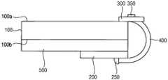
도 1 및 도 2를 참조하면, 본 발명의 일 실시예에 따른 표시 장치는 표시 패널(100), 인쇄 회로 기판(200), 구동 필름(300) 및 연결 필름(400)을 포함할 수 있다.1 and 2, a display device according to an exemplary embodiment of the present invention may include a
표시 패널(100)은 표시 영역(110) 및 비표시 영역(120)을 포함할 수 있다. 표시 영역(110)은 영상을 표시할 수 있다. 표시 영역(110)에는 광을 방출하여 상기 영상을 표시하는 화소들이 배치될 수 있다. 비표시 영역(120)은 표시 영역(110)으로부터 제1 방향(D1)에 위치할 수 있다. 비표시 영역(120)에는 인쇄 회로 기판(200) 또는 구동 필름(300)으로부터 신호를 전달받는 패드들이 배치될 수 있다.The
표시 패널(100)은 유리, 석영, 세라믹, 금속, 플라스틱 등을 포함하는 기판을 포함할 수 있다. 상기 기판은 폴리이미드(polyimide, PI) 등의 가요성 소재를 포함할 수 있고, 이에 따라, 표시 패널(100)은 휘어지거나(curved), 접히거나(folded), 늘어나거나(stretched) 또는 말릴 수 있는(rolled) 가요성을 가질 수 있다.The
본 발명의 일 실시예에 따른 표시 장치는 곡면형(curved) 표시 장치일 수 있다. 이 경우, 도 1에 도시된 바와 같이, 표시 패널(100)은 제1 방향(D1)과 교차하는 제2 방향(D2)을 따라 곡면 형상을 가질 수 있다.The display device according to an embodiment of the present invention may be a curved display device. In this case, as shown in FIG. 1, the
인쇄 회로 기판(200)은 표시 패널(100)과 이격하여 표시 패널(100)의 비표시 영역(120)으로부터 제1 방향(D1)에 위치할 수 있다. 인쇄 회로 기판(200)은 신호를 생성하는 타이밍 컨트롤러(timing controller)를 포함할 수 있다. 예를 들면, 상기 타이밍 컨트롤러는 데이터 신호 및 제어 신호를 생성할 수 있다.The printed
구동 필름(300)은 표시 패널(100)의 비표시 영역(120)에 연결될 수 있다. 구동 필름(300)은 구동 집적 회로(350)를 포함할 수 있다. 구동 집적 회로(350)는 상기 타이밍 컨트롤러가 생성한 상기 신호에 기초하여 표시 패널(100)을 구동시킬 수 있다. 예를 들면, 구동 집적 회로(350)는 상기 데이터 신호 및 상기 제어 신호에 기초하여 데이터 전압을 생성하고 상기 데이터 전압을 표시 패널(100)에 공급할 수 있다. 이 경우, 구동 집적 회로(350)는 데이터 구동 회로를 포함할 수 있다.The driving
구동 집적 회로(350)는 구동 필름(300)에 칩 온 필름(chip on film, COF) 방식으로 실장될 수 있다. 예를 들면, 폴리이미드(PI)와 같은 재질의 가요성 절연 필름 상에 구동 집적 회로(350)가 실장되고, 상기 절연 필름 상에 배치되는 배선들을 통해 구동 집적 회로(350)가 표시 패널(100)과 전기적으로 연결될 수 있다. 그러나, 본 발명은 이에 한정되는 것은 아니고, 구동 집적 회로(350)는 칩 온 글래스(chip on glass, COG) 방식으로도 실장될 수 있다.The driving
연결 필름(400)은 표시 패널(100)과 인쇄 회로 기판(200)을 연결할 수 있다. 연결 필름(400)의 일단(400a)은 표시 패널(100)의 비표시 영역(120)에 연결되고, 연결 필름(400)의 타단(400b)은 인쇄 회로 기판(200)에 연결될 수 있다. 연결 필름(400)은 인쇄 회로 기판(200)과 구동 필름(300)을 전기적으로 연결할 수 있다. 인쇄 회로 기판(200)과 구동 필름(300)의 전기적인 연결에 대해서는 아래에서 도 3을 참조하여 상세히 설명한다.The
인쇄 회로 기판(200)은 커넥터(connector)(250)를 포함할 수 있다. 연결 필름(400)은 인쇄 회로 기판(200)의 커넥터(250)에 연결될 수 있다. 그러나, 본 발명이 이에 한정되는 것은 아니고, 인쇄 회로 기판(200)과 연결 필름(400)은 솔더링 등을 통해 연결될 수도 있다.The printed
연결 필름(400)은 가요성 플랫 케이블(flexible flat cable, FFC) 또는 가요성 인쇄 회로(flexible printed circuit, FPC)일 수 있다. 이에 따라, 연결 필름(400)은 구부러지거나 접힐 수 있다.The
구동 필름(300)은 인쇄 회로 기판(200)과 이격될 수 있다. 다시 말해, 구동 필름(300)과 인쇄 회로 기판(200)은 직접적으로 연결되지 않을 수 있다. 그러나, 구동 필름(300)과 인쇄 회로 기판(200)이 이격되더라도, 연결 필름(400)을 통해 구동 필름(300)과 인쇄 회로 기판(200)이 전기적으로 연결되므로, 인쇄 회로 기판(200)으로부터 구동 필름(300)에 신호가 전송될 수 있다.The driving
연결 필름(400)의 제1 방향(D1)으로의 길이는 구동 필름(300)의 제1 방향(D1)으로의 길이보다 클 수 있다. 이에 따라, 인쇄 회로 기판(200)은 구동 필름(300)과 접촉되지 않고, 구동 필름(300)으로부터 제1 방향(D1)으로 이격될 수 있다.The length of the
표시 패널(100)의 비표시 영역(120)에는 하나의 연결 필름(400) 및 복수의 구동 필름들(300)이 배치될 수 있다. 구동 필름들(300)은 하나의 연결 필름(400)에 전기적으로 연결될 수 있다.One
구동 필름들(300)은 제2 방향(D2)을 따라 표시 패널(100)의 비표시 영역(120)에 연결될 수 있다. 연결 필름(400)은 표시 패널(100)의 비표시 영역(120)의 중앙에 연결될 수 있다. 예를 들면, 도 2에 도시된 바와 같이 연결 필름(400)을 기준으로 구동 필름들(300)은 제2 방향(D2)으로 대칭적으로 배열될 수 있다.The driving
본 실시예에 따른 표시 장치에 있어서, 표시 패널(100)과 인쇄 회로 기판(200)이 복수의 구동 필름들(300)을 통해 연결되지 않고, 하나의 연결 필름(400)을 통해 연결될 수 있다. 이에 따라, 표시 패널(100)이 제2 방향(D2)을 따라 곡면 형상을 가지더라도 구동 필름들(300)에 작용하는 서로 다른 응력들에 의해 구동 필름들(300)이 뒤틀리는 현상을 방지할 수 있다.The
이하, 도 3을 참조하여 구동 필름(300)과 연결 필름(400)의 전기적인 연결에 대해 설명한다.Hereinafter, the electrical connection between the driving
도 3은 도 2의 A 영역을 나타내는 평면도이다.3 is a plan view showing area A in Fig.
도 3에는 연결 필름(400)과 하나의 구동 필름(300)의 전기적인 연결만이 도시되어 있으나, 연결 필름(400)과 다른 구동 필름들(300)의 전기적인 연결도 이와 실질적으로 동일할 수 있다.Although only the electrical connection between the
도 3을 참조하면, 표시 패널(100)의 표시 영역(110)에는 게이트 배선들(111) 및 데이터 배선들(112)이 배치될 수 있다. 게이트 배선들(111)은 제1 방향(D1)을 따라 배열되고, 제2 방향(D2)과 평행하게 연장될 수 있다. 데이터 배선들(112)은 제2 방향(D2)을 따라 배열되고, 제1 방향(D1)과 평행하게 연장될 수 있다. 게이트 배선들(111)과 데이터 배선들(112)이 교차하는 지점들에서 상기 화소들이 정의될 수 있다.Referring to FIG. 3,
표시 패널(100)의 비표시 영역(120)에는 연결 배선들(121)이 배치될 수 있다. 연결 배선들(121)은 연결 필름(400)과 구동 필름(300)을 연결할 수 있다.The connection wirings 121 may be disposed in the
인쇄 회로 기판(200)은 연결 필름(400) 및 연결 배선들(121)을 통해 구동 필름(300)과 전기적으로 연결될 수 있다. 상기 타이밍 컨트롤러에서 생성된 상기 신호는 연결 필름(400) 및 연결 배선들(121)을 통해 구동 필름(300)에 전송될 수 있다. 예를 들면, 상기 타이밍 컨트롤러에서 생성된 상기 데이터 신호 및 제어 신호는 연결 필름(400) 및 연결 배선들(121)을 통해 구동 필름(300)에 실장되는 구동 집적 회로(350)에 전송될 수 있다.The printed
표시 패널(100)의 비표시 영역(120)에는 팬아웃 배선들(122)이 배치될 수 있다. 팬아웃 배선들(122)은 구동 필름(300)과 표시 패널(100)의 표시 영역(110)을 연결할 수 있다. 예를 들면, 팬아웃 배선들(122)은 데이터 배선들(112)과 연결될 수 있다. 구동 집적 회로(350)에서 생성된 신호는 팬아웃 배선들(122)을 통해 표시 영역(110)에 전송될 수 있다. 예를 들면, 구동 집적 회로(350)에서 생성된 데이터 전압은 팬아웃 배선들(122) 및 데이터 배선들(112)을 통해 상기 화소들에 전송될 수 있다.The
연결 배선들(121)과 팬아웃 배선들(122)은 서로 교차할 수 있다. 연결 배선들(121)과 팬아웃 배선들(122)은 서로 다른 층들에 위치할 수 있다. 이에 따라, 연결 배선들(121)과 팬아웃 배선들(122)은 서로 절연될 수 있다.The connection wirings 121 and the fan-out
도 4는 도 3의 표시 장치를 I-I' 라인 및 II-II' 라인을 따라 자른 단면도이다.FIG. 4 is a cross-sectional view of the display device of FIG. 3 taken along lines I-I 'and II-II'.
도 3 및 도 4를 참조하면, 표시 패널(100)은 서로 대향하는 제1 기판(101)과 제2 기판(102), 이들 사이에 위치하는 배선들 및 액정 소자를 포함할 수 있다. 본 실시예에 있어서, 표시 패널(100)은 액정 소자를 포함하는 액정 표시 패널로 예시되어 있으나, 본 발명은 이에 한정되지 아니하고, 표시 패널(100)은 유기 발광 소자를 포함하는 유기 발광 표시 패널 등과 같은 다양한 표시 패널일 수 있다.Referring to FIGS. 3 and 4, the
제1 기판(101)과 제2 기판(102)은 유리, 석영, 세라믹, 금속, 플라스틱 등으로 형성될 수 있다. 제1 기판(101)과 제2 기판(102)은 폴리이미드(PI) 등의 가요성 소재를 포함할 수 있고, 이에 따라, 표시 패널(100)은 휘어지거나(curved), 접히거나(folded), 늘어나거나(stretched) 또는 말릴 수 있는(rolled) 가요성을 가질 수 있다.The
제1 기판(101) 상의 표시 영역(110)에는 게이트 배선들(111)이 배치될 수 있다. 제1 기판(101) 상에는 게이트 배선들(111)을 덮는 게이트 절연막(103)이 배치될 수 있다. 게이트 배선들(111)은 게이트 구동 회로에서 생성된 게이트 신호를 상기 화소들에 전송할 수 있다.The gate lines 111 may be disposed in the
게이트 절연막(103) 상의 표시 영역(110)에는 게이트 배선들(111)과 교차하는 데이터 배선들(112)이 배치될 수 있다. 게이트 절연막(103) 상에는 데이터 배선들(112)을 덮는 보호막(104)이 배치될 수 있다. 데이터 배선들(112)은 구동 집적 회로(350)에서 생성된 상기 데이터 전압을 상기 화소들에 전송할 수 있다.
보호막(104) 상의 표시 영역(110)에는 제1 전극(105), 액정층(106) 및 제2 전극(107)을 포함하는 액정 소자가 위치할 수 있다. 각각의 상기 화소들은 게이트 배선들(111) 및 데이터 배선들(112)에 각각 연결되는 박막 트랜지스터 및 상기 박막 트랜지스터에 연결되는 상기 액정 소자를 포함할 수 있다. 상기 박막 트랜지스터는 게이트 배선(111)에 의해 전송되는 상기 게이트 신호에 의해 턴 온(turn-on)되어 데이터 배선(112)에 의해 전송되는 상기 데이터 전압을 상기 액정 소자에 공급하고, 상기 액정 소자는 상기 데이터 전압에 기초하여 광의 세기를 조절할 수 있다.The liquid crystal element including the
제1 기판(101) 상의 비표시 영역(120)에는 연결 배선들(121)이 배치될 수 있다. 연결 배선들(121)은 게이트 배선들(111)과 실질적으로 동일한 층에 배치될 수 있다. 연결 배선들(121)은 게이트 배선들(111)과 실질적으로 동시에 실질적으로 동일한 물질로 형성될 수 있다.The connection wirings 121 may be disposed in the
게이트 절연막(103) 상의 비표시 영역(120)에는 연결 배선들(121)과 교차하는 팬아웃 배선들(122)이 배치될 수 있다. 팬아웃 배선들(122)은 데이터 배선들(112)과 실질적으로 동일한 층에 배치될 수 있다. 팬아웃 배선들(122)은 데이터 배선들(112)과 실질적으로 동시에 실질적으로 동일한 물질로 형성될 수 있다.The
연결 필름(400)은 연결 배선(121)과 전기적으로 연결될 수 있다. 게이트 절연막(103)에는 연결 배선(121)의 일부를 노출시키는 접촉 구멍(CH)이 형성될 수 있고, 연결 필름(400)은 접촉 구멍(CH)을 통해 연결 배선(121)과 접촉할 수 있다.The
비표시 영역(120)의 제1 기판(101)과 제2 기판(102) 사이에는 실링 부재(108)가 배치될 수 있다. 실링 부재(108)는 표시 패널(100)의 측부를 밀봉하여 수분, 산소 등으로부터 상기 액정 소자를 보호할 수 있다.A sealing
이하, 도 5 및 도 6을 참조하여 연결 필름(400)이 구부러진 표시 장치를 설명한다.Hereinafter, a display device in which the
도 5는 본 발명의 일 실시예에 따른 표시 장치를 나타내는 측면도이다.5 is a side view showing a display device according to an embodiment of the present invention.
도 2 및 도 5를 참조하면, 본 발명의 일 실시예에 따른 표시 장치는 백라이트 유닛(500)을 더 포함할 수 있다. 백라이트 유닛(500)은 표시 패널(100)에 광을 공급할 수 있다. 표시 패널(100)에 포함된 상기 액정 소자는 백라이트 유닛(500)으로부터 공급된 광의 세기를 조절하여 영상을 표시할 수 있다.2 and 5, a display device according to an exemplary embodiment of the present invention may further include a
구동 필름(300)과 연결 필름(400)의 일단(400a)은 표시 패널(100)의 제1 면(100a)에 연결될 수 있다. 예를 들면, 표시 패널(100)의 제1 면(100a)은 표시 패널(100)의 상면일 수 있다.One
백라이트 유닛(500)은 표시 패널(100)의 제1 면(100a)에 대향하는 제2 면(100b)에 배치될 수 있다. 예를 들면, 표시 패널(100)의 제2 면(100b)은 표시 패널(100)의 하면일 수 있다.The
연결 필름(400)은 백라이트 유닛(500)을 중심으로 표시 패널(100)과 인쇄 회로 기판(200)이 대향하도록 구부러질 수 있다. 다시 말해, 연결 필름(400)은 연결 필름(400)의 일단(400a)이 표시 패널(100)의 상부에 위치하고, 연결 필름(400)의 타단(400b)이 표시 패널(100)의 하부에 위치하도록 구부러질 수 있다.The
종래의 곡면형 표시 장치는 표시 패널과 인쇄 회로 기판을 연결하는 복수의 구동 필름들을 포함할 수 있고, 인쇄 회로 기판이 표시 패널의 하부에 배치되도록 구동 필름들이 일정한 곡률을 가지며 구부러질 수 있다. 표시 패널이 곡면 형상을 가지는 경우에, 표시 패널과 인쇄 회로 기판을 연결하는 구동 필름들에는 서로 다른 응력들이 작용할 수 있고, 이러한 서로 다른 응력들로 인하여 구동 필름들이 뒤틀릴 수 있다. 그러나, 본 발명의 실시예들에 따른 표시 장치에 있어서, 구동 필름들(300)이 인쇄 회로 기판(200)과 직접 연결되지 않고, 하나의 연결 필름(400)을 통해 인쇄 회로 기판(200)과 구동 필름들(300)이 연결됨으로써, 구동 필름들(300)의 뒤틀림을 방지할 수 있다.A conventional curved display device may include a plurality of driving films connecting a display panel and a printed circuit board, and the driving films may be curved with a certain curvature so that the printed circuit board is disposed below the display panel. When the display panel has a curved shape, different stresses may act on the driving films connecting the display panel and the printed circuit board, and the driving films may be warped due to these different stresses. However, in the display device according to the embodiments of the present invention, the driving
일 실시예에 있어서, 구동 필름(300)은 평평할 수 있다. 다시 말해, 구부러지는 연결 필름(400)과 다르게 구동 필름(300)은 구부러지지 않을 수 있다. 전술한 바와 같이, 구동 필름(300)의 제1 방향(D1)으로의 길이는 연결 필름(400)의 제1 방향(D1)으로의 길이보다 작을 수 있고, 이에 따라, 구동 필름(300)이 구부러지지 않더라도 표시 장치의 데드 스페이스(dead space)의 면적이 과도하게 증가하지 않을 수 있다.In one embodiment, the driving
도 6은 본 발명의 일 실시예에 따른 표시 장치를 나타내는 측면도이다.6 is a side view showing a display device according to an embodiment of the present invention.
도 6을 참조하면, 일 실시예에 있어서, 구동 필름(300)은 구부러질 수 있다. 예를 들면, 도 6에 도시된 바와 같이 구동 필름(300)은 표시 패널(100)의 외주를 따라 하부 방향으로 구부러질 수 있다. 이 경우, 표시 장치의 데드 스페이스(dead space)의 면적이 감소될 수 있다.Referring to Fig. 6, in one embodiment, the driving
본 발명의 예시적인 실시예들에 따른 표시 장치는 컴퓨터, 노트북, 휴대폰, 스마트폰, 스마트패드, 피엠피(PMP), 피디에이(PDA), MP3 플레이어 등에 포함되는 표시 장치에 적용될 수 있다.The display device according to the exemplary embodiments of the present invention can be applied to a display device included in a computer, a notebook computer, a mobile phone, a smart phone, a smart pad, a PMP, a PDA, an MP3 player,
이상, 본 발명의 예시적인 실시예들에 따른 표시 장치들에 대하여 도면들을 참조하여 설명하였지만, 설시한 실시예들은 예시적인 것으로서 하기의 청구범위에 기재된 본 발명의 기술적 사상을 벗어나지 않는 범위에서 해당 기술 분야에서 통상의 지식을 가진 자에 의하여 수정 및 변경될 수 있을 것이다.While the present invention has been particularly shown and described with reference to exemplary embodiments thereof, the exemplary embodiments are illustrative and explanatory and are not restrictive of the invention, And may be modified and changed by those skilled in the art.
100: 표시 패널110: 표시 영역
111: 게이트 배선112: 데이터 배선
120: 비표시 영역121: 연결 배선
122: 팬아웃 배선200: 인쇄 회로 기판
250: 커넥터300: 구동 필름
350: 구동 집적 회로400: 연결 필름
500: 백라이트 유닛100: display panel 110: display area
111: gate wiring 112: data wiring
120: non-display area 121: connection wiring
122: fan-out wiring 200: printed circuit board
250: connector 300: driving film
350: driving integrated circuit 400: connection film
500: Backlight unit
Claims (18)
Translated fromKorean상기 비표시 영역으로부터 상기 제1 방향에 위치하고, 신호를 생성하는 인쇄 회로 기판;
상기 표시 패널의 상기 비표시 영역에 연결되고, 상기 신호에 기초하여 상기 표시 패널을 구동시키는 구동 집적 회로를 포함하는 구동 필름; 및
일단이 상기 표시 패널의 상기 비표시 영역에 연결되고, 타단이 상기 인쇄 회로 기판에 연결되며, 상기 인쇄 회로 기판과 상기 구동 필름을 전기적으로 연결하는 연결 필름을 포함하는, 표시 장치.A display panel having a display region and a non-display region located in the first direction from the display region;
A printed circuit board located in the first direction from the non-display area and generating a signal;
A driving film connected to the non-display region of the display panel and including a driving integrated circuit for driving the display panel based on the signal; And
And a connection film connected at one end to the non-display area of the display panel and at the other end to the printed circuit board, and electrically connecting the printed circuit board to the drive film.
상기 표시 패널은 상기 비표시 영역에 배치되고, 상기 연결 필름과 상기 구동 필름을 연결하는 연결 배선을 포함하는, 표시 장치.The method according to claim 1,
Wherein the display panel is disposed in the non-display area and includes a connection wiring connecting the connection film and the driving film.
상기 신호는 상기 연결 필름 및 상기 연결 배선을 통해 상기 인쇄 회로 기판으로부터 상기 구동 필름에 전송되는, 표시 장치.3. The method of claim 2,
And the signal is transmitted from the printed circuit board to the driving film through the connecting film and the connecting wiring.
상기 표시 패널은 상기 비표시 영역에 배치되고, 상기 구동 필름과 상기 표시 영역을 연결하는 팬아웃 배선을 더 포함하는, 표시 장치.3. The method of claim 2,
Wherein the display panel further comprises a fan-out wiring disposed in the non-display area and connecting the drive film and the display area.
상기 표시 패널은 상기 표시 영역에 배치되고, 서로 교차하는 게이트 배선 및 데이터 배선을 더 포함하고,
상기 연결 배선은 상기 게이트 배선과 동일한 층에 배치되며,
상기 팬아웃 배선은 상기 데이터 배선과 동일한 층에 배치되는, 표시 장치.5. The method of claim 4,
The display panel further includes a gate wiring and a data wiring which are arranged in the display region and cross each other,
The connection wiring is disposed in the same layer as the gate wiring,
And the fan-out wiring is disposed in the same layer as the data wiring.
상기 구동 필름은 상기 인쇄 회로 기판과 이격되는, 표시 장치.The method according to claim 1,
Wherein the driving film is spaced apart from the printed circuit board.
상기 구동 필름은 복수이고,
상기 복수의 구동 필름들은 상기 연결 필름에 전기적으로 연결되는, 표시 장치.The method according to claim 1,
Wherein the driving film is a plurality of films,
And the plurality of driving films are electrically connected to the connection film.
상기 복수의 구동 필름들은 상기 제1 방향과 교차하는 제2 방향을 따라 상기 비표시 영역에 연결되며,
상기 연결 필름은 상기 비표시 영역의 중앙에 연결되는, 표시 장치.8. The method of claim 7,
Wherein the plurality of driving films are connected to the non-display region along a second direction intersecting the first direction,
And the connection film is connected to the center of the non-display region.
상기 연결 필름은 구부러지는, 표시 장치.The method according to claim 1,
Wherein the connecting film is bent.
상기 표시 패널에 광을 공급하는 백라이트 유닛을 더 포함하고,
상기 연결 필름의 상기 일단은 상기 표시 패널의 제1 면에 배치되고,
상기 백라이트 유닛은 상기 표시 패널의 상기 제1 면에 대향하는 상기 제2 면에 배치되는, 표시 장치.The method according to claim 1,
Further comprising a backlight unit for supplying light to the display panel,
The one end of the connecting film is disposed on the first surface of the display panel,
Wherein the backlight unit is disposed on the second surface facing the first surface of the display panel.
상기 연결 필름은 상기 백라이트 유닛을 중심으로 상기 표시 패널과 상기 인쇄 회로 기판이 대향하도록 구부러지는, 표시 장치.11. The method of claim 10,
Wherein the connection film is bent so that the display panel and the printed circuit board are opposed to each other with the backlight unit as a center.
상기 인쇄 회로 기판은 상기 연결 필름이 연결되는 커넥터를 포함하는, 표시 장치.The method according to claim 1,
Wherein the printed circuit board includes a connector to which the connection film is connected.
상기 연결 필름은 가요성 플랫 케이블(flexible flat cable, FFC) 및 가요성 인쇄 회로(flexible printed circuit, FPC) 중에서 어느 하나인, 표시 장치.The method according to claim 1,
Wherein the connecting film is any one of a flexible flat cable (FFC) and a flexible printed circuit (FPC).
상기 연결 필름의 상기 제1 방향으로의 길이는 상기 구동 필름의 상기 제1 방향으로의 길이보다 큰, 표시 장치.The method according to claim 1,
Wherein the length of the connecting film in the first direction is longer than the length of the driving film in the first direction.
상기 구동 필름은 평평한, 표시 장치.The method according to claim 1,
Wherein the driving film is flat.
상기 구동 필름은 구부러지는, 표시 장치.The method according to claim 1,
Wherein the driving film is bent.
상기 구동 집적 회로는 상기 구동 필름에 칩 온 필름(chip on film, COF) 방식으로 실장되는, 표시 장치.The method according to claim 1,
Wherein the driving integrated circuit is mounted on the driving film by a chip on film (COF) method.
상기 표시 패널은 상기 제1 방향과 교차하는 제2 방향을 따라 곡면 형상을 가지는, 표시 장치.
The method according to claim 1,
Wherein the display panel has a curved shape along a second direction intersecting with the first direction.
Priority Applications (2)
| Application Number | Priority Date | Filing Date | Title |
|---|---|---|---|
| KR1020180002334AKR102631153B1 (en) | 2018-01-08 | 2018-01-08 | Display device |
| US16/241,699US11579496B2 (en) | 2018-01-08 | 2019-01-07 | Curved display device including a printed circuit board |
Applications Claiming Priority (1)
| Application Number | Priority Date | Filing Date | Title |
|---|---|---|---|
| KR1020180002334AKR102631153B1 (en) | 2018-01-08 | 2018-01-08 | Display device |
Publications (2)
| Publication Number | Publication Date |
|---|---|
| KR20190085196Atrue KR20190085196A (en) | 2019-07-18 |
| KR102631153B1 KR102631153B1 (en) | 2024-02-01 |
Family
ID=67139479
Family Applications (1)
| Application Number | Title | Priority Date | Filing Date |
|---|---|---|---|
| KR1020180002334AActiveKR102631153B1 (en) | 2018-01-08 | 2018-01-08 | Display device |
Country Status (2)
| Country | Link |
|---|---|
| US (1) | US11579496B2 (en) |
| KR (1) | KR102631153B1 (en) |
Cited By (2)
| Publication number | Priority date | Publication date | Assignee | Title |
|---|---|---|---|---|
| KR20230020627A (en)* | 2021-08-03 | 2023-02-13 | 삼성디스플레이 주식회사 | Display device |
| US12086350B2 (en) | 2020-10-28 | 2024-09-10 | Samsung Display Co., Ltd. | Display device |
Citations (3)
| Publication number | Priority date | Publication date | Assignee | Title |
|---|---|---|---|---|
| KR20110121918A (en)* | 2010-05-03 | 2011-11-09 | 삼성모바일디스플레이주식회사 | Display device and driving chip mounting film element provided in display device |
| US20140055702A1 (en)* | 2012-08-21 | 2014-02-27 | Young Bae Park | Displays with Bent Signal Lines |
| KR20160035696A (en)* | 2014-09-23 | 2016-04-01 | 삼성디스플레이 주식회사 | Curved display device |
Family Cites Families (6)
| Publication number | Priority date | Publication date | Assignee | Title |
|---|---|---|---|---|
| TWI476738B (en)* | 2010-09-07 | 2015-03-11 | Ind Tech Res Inst | Flexible display panel and assembly method thereof |
| RU2643679C2 (en)* | 2012-06-29 | 2018-02-05 | Сони Корпорейшн | Display |
| KR101871773B1 (en)* | 2012-07-25 | 2018-06-27 | 엘지디스플레이 주식회사 | Plastic panel and flat panel display device using the same |
| KR20170040435A (en)* | 2015-10-02 | 2017-04-13 | 삼성디스플레이 주식회사 | Display device |
| KR102556817B1 (en) | 2016-03-08 | 2023-07-19 | 삼성디스플레이 주식회사 | Display apparatus |
| CN107632477B (en)* | 2017-10-12 | 2024-06-28 | 惠科股份有限公司 | Array substrate and display panel using the same |
- 2018
- 2018-01-08KRKR1020180002334Apatent/KR102631153B1/enactiveActive
- 2019
- 2019-01-07USUS16/241,699patent/US11579496B2/enactiveActive
Patent Citations (3)
| Publication number | Priority date | Publication date | Assignee | Title |
|---|---|---|---|---|
| KR20110121918A (en)* | 2010-05-03 | 2011-11-09 | 삼성모바일디스플레이주식회사 | Display device and driving chip mounting film element provided in display device |
| US20140055702A1 (en)* | 2012-08-21 | 2014-02-27 | Young Bae Park | Displays with Bent Signal Lines |
| KR20160035696A (en)* | 2014-09-23 | 2016-04-01 | 삼성디스플레이 주식회사 | Curved display device |
Cited By (2)
| Publication number | Priority date | Publication date | Assignee | Title |
|---|---|---|---|---|
| US12086350B2 (en) | 2020-10-28 | 2024-09-10 | Samsung Display Co., Ltd. | Display device |
| KR20230020627A (en)* | 2021-08-03 | 2023-02-13 | 삼성디스플레이 주식회사 | Display device |
Also Published As
| Publication number | Publication date |
|---|---|
| US11579496B2 (en) | 2023-02-14 |
| KR102631153B1 (en) | 2024-02-01 |
| US20190212623A1 (en) | 2019-07-11 |
Similar Documents
| Publication | Publication Date | Title |
|---|---|---|
| US10910410B2 (en) | Flexible array substrate, flexible display device and method of assembling the same | |
| TWI767914B (en) | Display device having a bending region | |
| US10866469B2 (en) | Display module and display apparatus | |
| KR100840330B1 (en) | Liquid Crystal Display and Driving Integrated Circuit | |
| KR102379779B1 (en) | Chip on film and display device incluidng the same | |
| CN104021734A (en) | Flexible display device and method of manufacturing the same | |
| US9915842B2 (en) | Display panel, method of manufacturing the same and display device | |
| KR102773177B1 (en) | Display device | |
| KR102791710B1 (en) | Display device | |
| CN105511138A (en) | Flat panel display with narrow bezel area | |
| KR20180062269A (en) | Display device having a displayd panel and a back cover | |
| WO2019165889A1 (en) | Lcd display device and electronic apparatus | |
| CN110941122A (en) | Display panel and display device thereof | |
| CN114758583A (en) | Display device | |
| KR102524208B1 (en) | Chip on film and a display device having thereof | |
| KR102631153B1 (en) | Display device | |
| CN111880329B (en) | Display device and method of manufacturing the same | |
| KR102375895B1 (en) | Curved display device | |
| CN114677987B (en) | Display panel and display device | |
| KR102839062B1 (en) | Display Device | |
| KR102833524B1 (en) | Display device | |
| KR102513388B1 (en) | Flat Panel Display Having Narrow Bezel | |
| US20240284729A1 (en) | Array substrate, display apparatus, and method of fabricating array substrate | |
| KR20080008617A (en) | LCD Display | |
| KR20240120471A (en) | Display apparatus and multi screen display apparatus having the same |
Legal Events
| Date | Code | Title | Description |
|---|---|---|---|
| PA0109 | Patent application | St.27 status event code:A-0-1-A10-A12-nap-PA0109 | |
| R18-X000 | Changes to party contact information recorded | St.27 status event code:A-3-3-R10-R18-oth-X000 | |
| PG1501 | Laying open of application | St.27 status event code:A-1-1-Q10-Q12-nap-PG1501 | |
| PA0201 | Request for examination | St.27 status event code:A-1-2-D10-D11-exm-PA0201 | |
| D13-X000 | Search requested | St.27 status event code:A-1-2-D10-D13-srh-X000 | |
| D14-X000 | Search report completed | St.27 status event code:A-1-2-D10-D14-srh-X000 | |
| E902 | Notification of reason for refusal | ||
| PE0902 | Notice of grounds for rejection | St.27 status event code:A-1-2-D10-D21-exm-PE0902 | |
| P11-X000 | Amendment of application requested | St.27 status event code:A-2-2-P10-P11-nap-X000 | |
| P13-X000 | Application amended | St.27 status event code:A-2-2-P10-P13-nap-X000 | |
| E90F | Notification of reason for final refusal | ||
| PE0902 | Notice of grounds for rejection | St.27 status event code:A-1-2-D10-D21-exm-PE0902 | |
| E13-X000 | Pre-grant limitation requested | St.27 status event code:A-2-3-E10-E13-lim-X000 | |
| P11-X000 | Amendment of application requested | St.27 status event code:A-2-2-P10-P11-nap-X000 | |
| P13-X000 | Application amended | St.27 status event code:A-2-2-P10-P13-nap-X000 | |
| E701 | Decision to grant or registration of patent right | ||
| PE0701 | Decision of registration | St.27 status event code:A-1-2-D10-D22-exm-PE0701 | |
| PR0701 | Registration of establishment | St.27 status event code:A-2-4-F10-F11-exm-PR0701 | |
| PR1002 | Payment of registration fee | St.27 status event code:A-2-2-U10-U11-oth-PR1002 Fee payment year number:1 | |
| PG1601 | Publication of registration | St.27 status event code:A-4-4-Q10-Q13-nap-PG1601 |