KR20190035941A - Autostereoscopic 3d display - Google Patents
Autostereoscopic 3d displayDownload PDFInfo
- Publication number
- KR20190035941A KR20190035941AKR1020197008584AKR20197008584AKR20190035941AKR 20190035941 AKR20190035941 AKR 20190035941AKR 1020197008584 AKR1020197008584 AKR 1020197008584AKR 20197008584 AKR20197008584 AKR 20197008584AKR 20190035941 AKR20190035941 AKR 20190035941A
- Authority
- KR
- South Korea
- Prior art keywords
- light
- optical element
- display
- holographic optical
- holographic
- Prior art date
- Legal status (The legal status is an assumption and is not a legal conclusion. Google has not performed a legal analysis and makes no representation as to the accuracy of the status listed.)
- Ceased
Links
- 230000003287optical effectEffects0.000claimsabstractdescription143
- 238000005286illuminationMethods0.000claimsabstractdescription10
- 239000010408filmSubstances0.000claimsdescription22
- 238000000034methodMethods0.000claimsdescription13
- 239000012788optical filmSubstances0.000claimsdescription8
- 238000009792diffusion processMethods0.000claimsdescription3
- 238000009826distributionMethods0.000claimsdescription3
- 230000000694effectsEffects0.000description15
- 101100110007Neurospora crassa (strain ATCC 24698 / 74-OR23-1A / CBS 708.71 / DSM 1257 / FGSC 987) asd-1 geneProteins0.000description10
- 239000010410layerSubstances0.000description9
- 238000004049embossingMethods0.000description7
- 239000000463materialSubstances0.000description7
- 239000003086colorantSubstances0.000description6
- 238000013459approachMethods0.000description4
- 238000001746injection mouldingMethods0.000description4
- 230000009286beneficial effectEffects0.000description3
- 230000005540biological transmissionEffects0.000description3
- 230000008878couplingEffects0.000description3
- 238000010168coupling processMethods0.000description3
- 238000005859coupling reactionMethods0.000description3
- 238000013461designMethods0.000description3
- 238000001125extrusionMethods0.000description3
- 238000001093holographyMethods0.000description3
- 238000003384imaging methodMethods0.000description3
- 238000004519manufacturing processMethods0.000description3
- 230000008569processEffects0.000description3
- 238000000926separation methodMethods0.000description3
- 230000000007visual effectEffects0.000description3
- 239000004973liquid crystal related substanceSubstances0.000description2
- 230000004048modificationEffects0.000description2
- 238000012986modificationMethods0.000description2
- 238000000465mouldingMethods0.000description2
- 230000009467reductionEffects0.000description2
- 230000010076replicationEffects0.000description2
- 230000002123temporal effectEffects0.000description2
- 230000009466transformationEffects0.000description2
- 108010010803GelatinProteins0.000description1
- 239000006096absorbing agentSubstances0.000description1
- 208000003464asthenopiaDiseases0.000description1
- 230000004888barrier functionEffects0.000description1
- 230000008901benefitEffects0.000description1
- 230000008859changeEffects0.000description1
- 238000012822chemical developmentMethods0.000description1
- 239000003795chemical substances by applicationSubstances0.000description1
- 230000001427coherent effectEffects0.000description1
- 235000009508confectioneryNutrition0.000description1
- 238000007796conventional methodMethods0.000description1
- 230000007423decreaseEffects0.000description1
- 230000006735deficitEffects0.000description1
- 238000011161developmentMethods0.000description1
- SOCTUWSJJQCPFX-UHFFFAOYSA-Ndichromate(2-)Chemical compound[O-][Cr](=O)(=O)O[Cr]([O-])(=O)=OSOCTUWSJJQCPFX-UHFFFAOYSA-N0.000description1
- 238000000295emission spectrumMethods0.000description1
- 239000000839emulsionSubstances0.000description1
- 239000010419fine particleSubstances0.000description1
- 229920000159gelatinPolymers0.000description1
- 239000008273gelatinSubstances0.000description1
- 235000019322gelatineNutrition0.000description1
- 235000011852gelatine dessertsNutrition0.000description1
- 239000011521glassSubstances0.000description1
- 150000004820halidesChemical class0.000description1
- 238000000265homogenisationMethods0.000description1
- 230000006872improvementEffects0.000description1
- 230000003993interactionEffects0.000description1
- 238000001459lithographyMethods0.000description1
- 238000001465metallisationMethods0.000description1
- 238000005457optimizationMethods0.000description1
- 230000000737periodic effectEffects0.000description1
- 229920003023plasticPolymers0.000description1
- 229920003229poly(methyl methacrylate)Polymers0.000description1
- 239000004417polycarbonateSubstances0.000description1
- 229920000515polycarbonatePolymers0.000description1
- 239000004926polymethyl methacrylateSubstances0.000description1
- 238000007639printingMethods0.000description1
- 238000012545processingMethods0.000description1
- 230000005855radiationEffects0.000description1
- 239000002356single layerSubstances0.000description1
- 239000000243solutionSubstances0.000description1
- 238000001228spectrumMethods0.000description1
- 239000000126substanceSubstances0.000description1
- 230000001360synchronised effectEffects0.000description1
- 238000010792warmingMethods0.000description1
Images


Classifications
- G02B27/22—
- G—PHYSICS
- G02—OPTICS
- G02F—OPTICAL DEVICES OR ARRANGEMENTS FOR THE CONTROL OF LIGHT BY MODIFICATION OF THE OPTICAL PROPERTIES OF THE MEDIA OF THE ELEMENTS INVOLVED THEREIN; NON-LINEAR OPTICS; FREQUENCY-CHANGING OF LIGHT; OPTICAL LOGIC ELEMENTS; OPTICAL ANALOGUE/DIGITAL CONVERTERS
- G02F1/00—Devices or arrangements for the control of the intensity, colour, phase, polarisation or direction of light arriving from an independent light source, e.g. switching, gating or modulating; Non-linear optics
- G02F1/01—Devices or arrangements for the control of the intensity, colour, phase, polarisation or direction of light arriving from an independent light source, e.g. switching, gating or modulating; Non-linear optics for the control of the intensity, phase, polarisation or colour
- G02F1/13—Devices or arrangements for the control of the intensity, colour, phase, polarisation or direction of light arriving from an independent light source, e.g. switching, gating or modulating; Non-linear optics for the control of the intensity, phase, polarisation or colour based on liquid crystals, e.g. single liquid crystal display cells
- G02F1/133—Constructional arrangements; Operation of liquid crystal cells; Circuit arrangements
- G02F1/1333—Constructional arrangements; Manufacturing methods
- G02F1/1335—Structural association of cells with optical devices, e.g. polarisers or reflectors
- G02F1/1336—Illuminating devices
- G02F1/133615—Edge-illuminating devices, i.e. illuminating from the side
- G—PHYSICS
- G02—OPTICS
- G02B—OPTICAL ELEMENTS, SYSTEMS OR APPARATUS
- G02B30/00—Optical systems or apparatus for producing three-dimensional [3D] effects, e.g. stereoscopic images
- G02B27/2214—
- G—PHYSICS
- G02—OPTICS
- G02B—OPTICAL ELEMENTS, SYSTEMS OR APPARATUS
- G02B30/00—Optical systems or apparatus for producing three-dimensional [3D] effects, e.g. stereoscopic images
- G02B30/20—Optical systems or apparatus for producing three-dimensional [3D] effects, e.g. stereoscopic images by providing first and second parallax images to an observer's left and right eyes
- G02B30/26—Optical systems or apparatus for producing three-dimensional [3D] effects, e.g. stereoscopic images by providing first and second parallax images to an observer's left and right eyes of the autostereoscopic type
- G02B30/27—Optical systems or apparatus for producing three-dimensional [3D] effects, e.g. stereoscopic images by providing first and second parallax images to an observer's left and right eyes of the autostereoscopic type involving lenticular arrays
- G—PHYSICS
- G02—OPTICS
- G02B—OPTICAL ELEMENTS, SYSTEMS OR APPARATUS
- G02B30/00—Optical systems or apparatus for producing three-dimensional [3D] effects, e.g. stereoscopic images
- G02B30/20—Optical systems or apparatus for producing three-dimensional [3D] effects, e.g. stereoscopic images by providing first and second parallax images to an observer's left and right eyes
- G02B30/26—Optical systems or apparatus for producing three-dimensional [3D] effects, e.g. stereoscopic images by providing first and second parallax images to an observer's left and right eyes of the autostereoscopic type
- G02B30/33—Optical systems or apparatus for producing three-dimensional [3D] effects, e.g. stereoscopic images by providing first and second parallax images to an observer's left and right eyes of the autostereoscopic type involving directional light or back-light sources
- G—PHYSICS
- G02—OPTICS
- G02B—OPTICAL ELEMENTS, SYSTEMS OR APPARATUS
- G02B5/00—Optical elements other than lenses
- G02B5/18—Diffraction gratings
- G—PHYSICS
- G02—OPTICS
- G02B—OPTICAL ELEMENTS, SYSTEMS OR APPARATUS
- G02B5/00—Optical elements other than lenses
- G02B5/32—Holograms used as optical elements
- G—PHYSICS
- G02—OPTICS
- G02B—OPTICAL ELEMENTS, SYSTEMS OR APPARATUS
- G02B6/00—Light guides; Structural details of arrangements comprising light guides and other optical elements, e.g. couplings
- G02B6/0001—Light guides; Structural details of arrangements comprising light guides and other optical elements, e.g. couplings specially adapted for lighting devices or systems
- G02B6/0011—Light guides; Structural details of arrangements comprising light guides and other optical elements, e.g. couplings specially adapted for lighting devices or systems the light guides being planar or of plate-like form
- G02B6/0013—Means for improving the coupling-in of light from the light source into the light guide
- G02B6/0015—Means for improving the coupling-in of light from the light source into the light guide provided on the surface of the light guide or in the bulk of it
- G02B6/0016—Grooves, prisms, gratings, scattering particles or rough surfaces
Landscapes
- Physics & Mathematics (AREA)
- General Physics & Mathematics (AREA)
- Optics & Photonics (AREA)
- Nonlinear Science (AREA)
- Mathematical Physics (AREA)
- Chemical & Material Sciences (AREA)
- Crystallography & Structural Chemistry (AREA)
- Diffracting Gratings Or Hologram Optical Elements (AREA)
- Devices For Indicating Variable Information By Combining Individual Elements (AREA)
- Testing, Inspecting, Measuring Of Stereoscopic Televisions And Televisions (AREA)
- Holo Graphy (AREA)
- Planar Illumination Modules (AREA)
Abstract
Translated fromKoreanDescription
Translated fromKorean본 발명은 무안경식 3D 디스플레이(autostereoscopic 3D display)에 관한 것이다.The present invention relates to an autostereoscopic 3D display.
무안경식 3D 디스플레이 (ASD)는, 입체 영상, 즉, 한 명 이상의 사람에게 3차원으로 보이는 영상을 디스플레이할 수 있는 스크린이다. 3차원 영상은 종래의 2차원 영상에 비해 추가로 깊이 효과(depth effect)를 갖는 영상으로 이해된다. ASD의 경우, 종래의 입체 디스플레이와는 대조적으로, 관찰자는, 안경, 프리즘 뷰어 또는 기타의 광학적 보조물과 같은 보조물을 필요로 하지 않는다.The non-tight 3D display (ASD) is a screen capable of displaying a three-dimensional image, that is, a three-dimensional image to one or more persons. The three-dimensional image is understood as an image having a depth effect in addition to the conventional two-dimensional image. In the case of ASD, in contrast to conventional stereoscopic displays, the observer does not need ancillaries such as glasses, prism viewers or other optical aids.
3차원 느낌을 얻기 위하여, 무안경식 디스플레이에서는, 시차에 의해 각 육안이 상이한 영상을 보게 되도록 하는 방식으로 2개의 영상이 투사된다. 이 경우에, 2개의 상이한 방향에서의 투사는 영상들이 입체 쌍으로서 관찰자의 육안에 도달하도록 이루어져야 한다. 이 경우, 2개의 투사 방향은 대개는 디스플레이의 백라이트 유닛에서 생성된다.In order to obtain a three-dimensional feeling, two images are projected in such a manner that in the non-eye-warming display, the visual differences are seen by the parallax. In this case, projection in two different directions must be made so that the images arrive at the viewer's eyes as stereoscopic pairs. In this case, the two projection directions are usually generated in the backlight unit of the display.
ASD 및 그 개개 부품들의 개발자들은 영상이 가능한 한 사실적인 방식으로 공간적으로 표시될 수 있게 하고, 동시에 관찰자에 대해 높은 수준의 인체공학을 달성하는 것을 목표로 한다. 이 경우, 사실적이고 고품질의 영상을 위한 기본적인 전제조건으로는, 높은 영상 해상도 (공지된 고품질 2D 텔레비전-HDTV가 여기서 추구하는 표준임)와 높은 영상 주파수가 포함된다. 3D 코딩의 요소들이 추가로 포함된다. 우수한 인체공학은, 한 명 이상의 관찰자의 현재 위치에 대해 최적의 입체 효과를 주는 지점, 소위 스위트 스폿(sweet spot)을 조정함으로써 달성된다.Developers of ASD and its individual components aim to make the images as spatially as possible in a realistic way, while at the same time achieving a high level of ergonomics for the viewer. In this case, basic prerequisites for realistic and high-quality video include high image resolution (known high-quality 2D television-HDTV is the standard pursued here) and high image frequency. Elements of 3D coding are additionally included. Good ergonomics is achieved by adjusting the so-called sweet spot, which gives the optimal stereoscopic effect for the current position of one or more observers.
종래 기술에서 주로 이들 목표를 달성하기 위한 2개의 상이한 기술적 해결 접근법이 알려져 있다: 제1 접근법에 따르면, 2개의 투사 방향은, 예를 들어, 개개의 디스플레이 화소들의 광을 스크린으로부터 멀리 상이한 방향으로 편향시키는 렌즈나 프리즘 격자에 의해 달성될 수 있다. 이 경우, 수직 스트라이프 마스크(vertical strip mask)는 방향-선택적 방식으로 동작하는 개개의 수직 화소 스트라이프를 갖는다. 그러나, 이러한 ASD에는 좌측 및 우측 화소 스트라이프가 있기 때문에, 영상 해상도는 종래의 2D 디스플레이에 비해 절반이 된다. 또한, 액정 소자 (LCD)를 이용한 스트라이프 마스크의 대응하는 구성에 의해 원래의 해상도를 갖는 2D 영상을 표현하는 것은 기술적으로 어렵다. 2D 표현에 대한 추가 단점은, 스트라이프 마스크가 광선의 일부를 차단하여 영상을 어둡게 하는 시차 장벽(parallactic barrier)을 구성한다는 점이다.Two different technical solution approaches are known in the prior art to achieve these goals: According to a first approach, the two projection directions are, for example, to deflect the light of the individual display pixels away from the screen in different directions Or by a prism grating. In this case, the vertical strip mask has individual vertical pixel stripes that operate in a direction-selective manner. However, since there is left and right pixel stripes in such an ASD, the image resolution is half that of a conventional 2D display. Furthermore, it is technically difficult to represent a 2D image having an original resolution by a corresponding structure of a stripe mask using a liquid crystal element (LCD). A further drawback to the 2D representation is that the stripe mask constitutes a parallactic barrier that blocks some of the rays and darkens the image.
두 번째 접근법은, 최대 해상도를 유지하면서 시간-오프셋된 진동 영상을 디스플레이하는, 2개의 광원 및 동기화 유닛을 갖는 ASD에 관한 것이다. 이러한 투광성 ASD에서 깜빡임없는 영상을 위한 전제조건은 충분히 높은 교대 주파수이다. 그러나, 이것은 종래 기술에서 이제서야 실현되고 있다. 이 접근법의 구체적인 실시양태들이 이하에서 더 상세히 설명될 것이다.A second approach relates to an ASD with two light sources and a synchronization unit that displays a time-offsetted vibration image while maintaining a maximum resolution. The precondition for flicker-free imaging in this translucent ASD is a sufficiently high alternating frequency. However, this is only now realized in the prior art. Specific embodiments of this approach will be described in more detail below.
US 2006/0164862는, 프리즘식 굴절 편향 구조를 갖는 2개의 별개의 광 도파관을 포함하며, 또한 2개의 광원, 확산 필름, 투과형 디스플레이 패널, 광 흡수기 및 반사기를 포함하는, 무안경식 디스플레이를 개시하고 있다.US 2006/0164862 discloses a non-eye-safe display comprising two separate optical waveguides with a prismatic refractive-deflecting structure and also including two light sources, a diffusing film, a transmissive display panel, a light absorber and a reflector .
이어서 US 2005/0264717은, 프리즘식 굴절 편향 구조를 갖는 광 도파관 상에 2개의 별개의 광원을 가지며, 또한 프리즘식 굴절 편향 구조에서와 같이 제2 광학 필름을 가지며, 또한 투과형 디스플레이 패널을 갖는, 무안경식 디스플레이를 개시하고 있다.US 2005/0264717 subsequently discloses an optical element having two separate light sources on a light waveguide having a prismatic refractive deflecting structure and having a second optical film as in a prismatic refractive deflecting structure, And a light display is started.
마지막으로, US 2007/0276071은, 광 도파관의 양 측에 배치된 2개의 광원, 이중-프리즘식 굴절 광 소자, 및 투과형 디스플레이 패널을 갖는, 무안경식 디스플레이를 개시하고 있다. 이중-프리즘식 굴절 광 소자는, 광 도파관과 직면하는 삼각형 프리즘식 구조물과, 광 도파관으로부터 마주하지 않는 구면 렌즈 구조물로 구성된다. 2개의 광원은, 투과형 디스플레이 패널이 나타낼 3차원 영상 콘텐츠의 우측 및 좌측 입체 영상을 연속적으로 재생하도록 하는 방식으로, 동기화 유닛에 의해 교대로 구동된다.Finally, US 2007/0276071 discloses a non-eye-safe display having two light sources, a double-prismatic refractive optical element, and a transmissive display panel disposed on both sides of a light pipe. The double-prismatic refractive optical element is composed of a triangular prismatic structure facing the optical waveguide and a spherical lens structure not facing the optical waveguide. The two light sources are alternately driven by the synchronization unit in such a manner that the right and left stereoscopic images of the three-dimensional image content to be displayed by the transmissive display panel are successively reproduced.
전술된 무안경식 디스플레이 각각은 반사성 편향 구조물을 갖는 광 정향 소자(light directing element)를 갖는다. 그러나, 이러한 타입의 소자들이 사용될 때, 영상 품질의 손상이 발생하고, 이것은 굴절 교란 효과(refractive disturbing effects)에 기인한 것이다. 교란 효과는, 특히, 바람직하지 않은 2차 광 경로, 다중 반사, 또는 병렬의 굴절 광 구조물의 상호작용에 의해 초래되는 모아레 효과(Moire effect)에 의해 야기된다. 전체 시스템에서, 교란 효과는, 띠 변색(banding), 해상도 감소 및/또는 전반적 선명도 부족과 함께 3D 표현을 위한 채널들의 불충분한 분리를 야기할 수 있다. 이것은 차례로 관찰자의 육안이 더 큰 피로를 느끼게 할 수 있다. 또한, 시판중인 2D HDTV (고해상도 텔레비전)에 비해 명백한 시각적 품질 차이를 구분할 수 있어서, 이러한 무안경식 디스플레이의 시장 수용성을 저하시킨다.Each of the non-eye-safe displays described above has a light directing element with a reflective biasing structure. However, when these types of devices are used, impairment of image quality occurs, which is due to refractive disturbing effects. The disturbing effect is caused by the Moire effect, which is caused by the interaction of an undesired secondary optical path, multiple reflections, or refracting structures in parallel. In the overall system, disturbing effects can cause insufficient separation of channels for 3D representation with banding, resolution reduction, and / or lack of overall sharpness. This in turn allows the observer's visuals to feel more fatigued. In addition, it can distinguish apparent visual quality differences compared to commercially available 2D HDTVs (high definition televisions), thereby reducing the market acceptability of these no-viewing displays.
굴절 편향 구조물로 구성된 복수의 층을 갖는 광 정향 소자를 이용할 때의 추가의 단점은, 개개의 굴절 광학면 소자들의 서로에 관한 필요한 높은 측방향 위치 정확도를 보장하는데 있어서의 곤란성이다. 만일 여기서 극히 작은 편차가 발생하면, 3D 표현을 위한 2개 이상의 채널로의 분리는 크게 손상받는다. 게다가, 이 경우, 예를 들어, 모아레 효과와 같은 아마도 이미 존재하는 광 교란 효과가 더욱 심화된다.A further disadvantage when using a photo-alignment device having a plurality of layers comprised of a refractive-deflecting structure is the difficulty in ensuring the required high lateral positional accuracy of the respective refractive optical surface elements with respect to each other. If very small deviations occur here, the separation into two or more channels for 3D representation is greatly damaged. In addition, in this case, the already existing light disturbing effect, such as, for example, moire effect, is further exacerbated.
따라서, 본 발명의 목적은, 설명된 광학적 교란 효과를 갖지 않아 영상 품질에 관해 개선된 3D 표현이 얻어질 수 있는 무안경식 3D 디스플레이를 제공하는 것이다.Accordingly, it is an object of the present invention to provide an unshielded 3D display that does not have the optical disturbing effect described so that an improved 3D representation of the image quality can be obtained.
이 목적은, 2개의 광원을 갖는 조명 유닛, 광 도파관, 회절식 광학적 광 정향 소자로서의 홀로그래픽 광학 소자, 투명 디스플레이 패널, 및 광원을 각각 교대로 디스플레이 패널 상에 표시되는 우측 및 좌측 시차 영상과 동기화하기 위한 제어 유닛을 포함하는 무안경식 3D 디스플레이에 의해 달성되며, 여기서, 광원들은 상이한 방향으로부터 광 도파관 내로 각각 광을 방사하도록 배향되고, 홀로그래픽 광학 소자와 디스플레이 패널은, 광 도파관으로부터 방출된 광이 선호되는 방향에 따라 홀로그래픽 광학 소자에 의해 2개의 상이한 방향으로 회절되어 디스플레이 패널을 통과하도록 하는 방식으로 배치되며, 여기서 광 도파관의 적어도 한 표면은 굴절 표면을 갖는다.This object is achieved by a liquid crystal display device comprising: an illumination unit having two light sources; a light waveguide; a holographic optical element as a diffractive optical light-guiding element; a transparent display panel; and a light source respectively in synchronization with right and left parallax images displayed on the display panel Wherein the light sources are each directed to emit light from a different direction into the light pipe, the holographic optical element and the display panel are arranged such that light emitted from the light pipe In such a manner as to be diffracted by the holographic optical element in two different directions and to pass through the display panel in accordance with the preferred direction, wherein at least one surface of the optical waveguide has a refractive surface.
이 경우, 본 발명에 따른 무안경식 3D 디스플레이는 주로, 육안의 피로 상태의 위험이 상당히 줄어들게 하는 정도까지 굴절 광학 교란 효과를 피하거나 낮추고자 한다. 이것은, 특히, 무안경식에 요구되는 방향-특유의 채널 분할이 보장되게끔 광을 편향시키는 홀로그래픽 광학 소자의 사용을 통해 가능해진다. 이 경우, 채널의 개수는 2보다 크고 짝수이거나 홀수인 것으로 판명될 수 있다.In this case, the non-axial 3D display according to the present invention primarily attempts to avoid or reduce the refractive optical disturbance to such an extent that the risk of visual fatigue is significantly reduced. This is made possible through the use of a holographic optical element which deflects light, in particular to ensure the direction-specific channel splitting required for no aperture reduction. In this case, the number of channels can be determined to be greater than 2 and even or odd.
또한, 본 발명에 따른 무안경식 3D 디스플레이의 경우, 광학 소자들의 서로에 관한 측방향 위치 정확도로 이루어진 엄격한 요건을 피할 수 있어서, 이러한 타입의 디스플레이의 상당히 간소화된 생산성으로 이어진다.Also, in the case of an unshielded 3D display according to the present invention, it is possible to avoid the strict requirement of lateral positional accuracy of the optical elements with respect to each other, leading to a considerably simplified productivity of this type of display.
광 도파관의 굴절 표면은, 광 도파관으로부터 방출되어 홀로그래픽 광학 소자에 입사되는 광의 각도 대역폭이 좁아지는 효과를 갖는다. 이것은, 홀로그래픽 광학 소자의 회절 효율이 더욱 커지게 되어, 브래그(Bragg) 조건을 만족하는데 요구되는 커플링 각도 부근의 상기 각도 대역폭이 더 좁아지게 되기 때문에 유익하다. 따라서, 먼저, 체적 홀로그램에 기초한 홀로그래픽 광학 소자의 회절 효율이 커질수록, 체적 홀로그램의 층 두께가 더 커진다. 두 번째, 각도 선택성이 증가한다, 즉, 층 두께가 증가함에 따라 체적 홀로그램에 대해 브래그 조건 부근의 허용가능한 각도 대역폭이 감소한다. 따라서, 홀로그래픽 광학 소자에 입사하는 광의 각도 대역폭의 협소화는, 높은 회절 효율을 생성하기 위한 허용가능한 층 두께의 더 넓은 범위를 가능케 하기 때문에 유익하다. 이것이 도 10i 및 도 10ii에 개략적으로 도시되어 있다. 따라서, 도 10i는 방출된 광에 대한 좁은 각도 대역폭을 야기하는 적절한 프리즘 구조물을 갖는 광 도파관을 도시한다. 도 10ii는 대응하는 프리즘 구조물이 없는 광 도파관을 나타낸다. 광은 넓은 각도 대역폭과 함께 이 광 도파관으로부터 방출된다.The refractive surface of the light pipe has an effect of narrowing the angle bandwidth of light emitted from the light pipe and entering the holographic optical element. This is advantageous because the diffraction efficiency of the holographic optical element becomes larger, and the angular bandwidth around the coupling angle required to satisfy the Bragg condition becomes narrower. Therefore, first, the larger the diffraction efficiency of the holographic optical element based on the volume hologram, the larger the layer thickness of the volume hologram becomes. Second, the angular selectivity increases, that is, as the layer thickness increases, the allowable angular bandwidth around the Bragg condition for the volume hologram decreases. Thus, narrowing the angular bandwidth of the light incident on the holographic optical element is beneficial because it allows a wider range of permissible layer thicknesses to produce high diffraction efficiencies. This is schematically illustrated in Figs. 10i and 10ii. Thus, Figure 10i illustrates an optical waveguide having a suitable prism structure that results in a narrow angular bandwidth for the emitted light. Figure 10ii shows an optical waveguide without a corresponding prism structure. The light is emitted from this optical waveguide with a wide angular bandwidth.
굴절 표면은, 특히, 비산란 구조물과의 조합으로 전면적으로 또는 영역적으로 적용된, 선형 변환 불변 프리즘 구조물, 다차원 피라미드 프리즘 구조물, 타원체, 폴리노미얼(polynomial), 원추 세그먼트, 쌍곡선 또는 이들 기본체의 조합에 기초한 선형 변환 불변 렌즈 구조물, 타원체, 폴리노미얼, 원추 섹션, 쌍곡선 또는 이들 기본체의 조합에 기초한 다차원 반구형 렌즈 구조물, 비주기적 산란 표면 구조물을 가질 수 있다.The refractive surface may be a linear transformation invariant prism structure, a multidimensional pyramid prism structure, an ellipsoid, a polynomial, a cone segment, a hyperbola, or a combination thereof, all or part of which are applied in combination with an non- Dimensional non-periodic scattering surface structure based on a combination of linear transformation invariant lens structures, ellipsoids, polynomials, conic sections, hyperbolas or a combination of these primitives.
굴절 표면은, 엠보싱, 습식 엠보싱, 사출 성형, 압출, 프린팅, 레이저 스트럭쳐링 및 기타의 방법들을 통해 생성될 수 있다.Refractive surfaces can be created through embossing, wet embossing, injection molding, extrusion, printing, laser structuring, and other methods.
본 발명에 따른 무안경식 3D 디스플레이에 대해 추가로 적어도 하나의 광학 필름을 갖는 것도 가능하다. 광학 필름은, 특히, 확산 필름, 마이크로렌즈 필름, 프리즘 필름, 렌티큘라(lenticular) 필름 또는 반사 편광 필름일 수 있다. 디스플레이에는 이러한 필름이 복수개 존재할 수 있다는 것을 말할 필요도 없다.It is also possible to have at least one optical film in addition to the non-axial 3D display according to the present invention. The optical film may be, in particular, a diffusion film, a micro-lens film, a prism film, a lenticular film, or a reflective polarizing film. Needless to say, a plurality of such films may exist in the display.
또한, 홀로그래픽 광학 소자가 체적 홀로그램이라면, 특히 바람직하다.It is also particularly preferable if the holographic optical element is a volume hologram.
홀로그래픽 광학 소자는, 특히, 시준 또는 발산 각도 분포를 생성하도록 구현될 수 있다. 이러한 홀로그래픽 광학 소자는, 예를 들어, 관찰자의 위치에서 밝기를 증가시키거나, 상이한 관찰자를 어드레싱하거나, 3D 느낌을 강화하기 위해 사용될 수 있다.The holographic optical element may be embodied in particular to produce a collimated or divergent angle distribution. Such a holographic optical element can be used, for example, to increase brightness at the observer's position, address different observers, or enhance the 3D feel.
또한, 홀로그래픽 광학 소자가 투과 및/또는 반사 홀로그램 및/또는 투과 및/또는 반사 가장자리-발광(edge-lit) 홀로그램이라면, 더욱 바람직하다.It is further preferred that the holographic optical element is a transmissive and / or reflective hologram and / or a transmissive and / or reflective edge-lit hologram.
또한, 홀로그래픽 광학 소자가 서로 접속된 복수의 개별 홀로그램으로부터 구성되는 것이 가능하다. 이 경우, 개별 홀로그램은 특히, 바람직하게는 멀티플렉싱에 의해 얻을 수 있는, 특히 바람직하게는 각도 분할 멀티플렉싱 및/또는 파장 분할 멀티플렉싱에 의해 얻을 수 있는 체적 홀로그램일 수 있다. 이 경우, 개별 홀로그램은 좌측 및 우측 투사의 역할을 할 수 있다. 마찬가지로, 개별 홀로그램은 이 경우, 이들이 3원색, 즉, 적색, 녹색, 및 청색 중 하나의 방사만을 회절시키도록 특별히 구현될 수 있다. 또한, 예를 들어 4원색 (예를 들어, "적색", "녹색", "청색" 및 "황색")과 같은, 3개보다 많은 원색을 사용하는 것도 가능하다. 마지막으로, 예를 들어, 6개의 개별 홀로그램이 3원색 각각과 2개의 입체시 방향에 대해 이용되도록, 양쪽 효과가 결합될 수 있다.It is also possible that the holographic optical element is composed of a plurality of individual holograms connected to each other. In this case, the individual holograms may in particular be volume holograms obtainable, preferably by multiplexing, particularly preferably by angle division multiplexing and / or wavelength division multiplexing. In this case, the individual holograms can serve as left and right projections. Likewise, individual holograms may be specially implemented in this case to cause them to diffract only one of the three primary colors, i.e., red, green, and blue. It is also possible to use more than three primary colors, for example four primary colors (e.g., "red", "green", "blue" and "yellow" Finally, both effects can be combined such that, for example, six separate holograms are used for each of the three primary colors and the two stereoscopic directions.
이러한 체적 홀로그램의 생성이 공지되어 있으며 (문헌 [H. M. Smith in "Principles of Holography", Wiley-Interscience 1969]), 예를 들어, 2개 빔 간섭에 의해 달성될 수 있다 (문헌 [S. Benton, "Holographic Imaging", John Wiley & Sons, 2008]).The production of such volume holograms is known (HM Smith in " Principles of Holography ", Wiley-Interscience 1969), for example, by two beam interference (S. Benton, Holographic Imaging ", John Wiley & Sons, 2008).
반사 체적 홀로그램의 대량 복제를 위한 방법이 US 6,824,929에 설명되어 있으며, 여기서, 마스터 홀로그램 상에는 감광 재료가 놓여지고, 그 다음, 복사를 달성하기 위해 가간섭 광(coherent light)이 사용된다. 투과 홀로그램의 생성도 마찬가지로 알려져 있다. 따라서, 예로서, US 4,973,113은 롤 복제에 의한 방법을 설명하고 있다.A method for mass replication of a reflective volume hologram is described in US 6,824,929, wherein a photosensitive material is placed on the master hologram and then coherent light is used to achieve radiation. The generation of the transmission hologram is likewise known. Thus, for example, US 4,973,113 describes a method by roll replication.
특히, 특정한 노출 지오메트리를 요구하는 가장자리-발광 홀로그램의 생성을 참조해야 한다. 에스. 벤톤(S. Benton)에 의한 소개 (문헌 [S. Benton, "Holographic Imaging", John Wiley & Sons, 2008, Chapter 18])와 전통적인 2단 및 3단 생성 방법의 개관 (문헌 [Q. Huang, H. Caulfield, SPIE Vol. 1600, International Symposium on Display Holography (1991), page 182] 참조) 외에도, 가장자리 조명 및 도파 홀로그램(waveguiding hologram)을 설명하고 있는 WO 94/18603을 참조해야 한다. 또한, 특정한 광학적 어댑터 블록에 기초하는 방법을 설명하고 있는 WO 2006/111384에서의 특별 생성 방법을 참조해야 한다.In particular, you should refer to the creation of edge-emitting holograms that require a specific exposure geometry. s. (Benton, "Holographic Imaging", John Wiley & Sons, 2008, Chapter 18) and an overview of traditional two- and three-stage generation methods (Q. Huang, See, for example, WO 94/18603, which describes edge illumination and waveguiding holograms, in addition to the above-mentioned techniques (see H. Caulfield, SPIE Vol. 1600, International Symposium on Display Holography (1991), page 182). In addition, reference should be made to the special generation method in WO 2006/111384 which describes a method based on a specific optical adapter block.
체적 홀로그램의 생성에 대해 다양한 재료가 적절하다. 노광 후에 습식-화학적 현상 프로세스를 요구하는 미립자 은 할로겐화물 에멀젼 또는 디크로메이트 젤라틴이 적절하다. 또한, 열적 후처리를 요구하는 예를 들어, (듀폰 오브 네이무어스(DuPont of Neymours)으로부터 입수할 수 있는) 옴니덱스(Omnidex)® 광중합체 필름과, 홀로그램의 완전한 현상을 위해 화학적 또는 열적 후처리를 추가로 요구하지 않는 (바이엘 머티리얼사이언스 아게(Bayer MaterialScience AG)로부터 입수할 수 있는) 베이폴(Bayfol)® HX 광중합체 필름과 같은 광중합체가 적절하다. 이상적인 재료는 높은 투명도와 낮은 헤이즈(haze)를 나타낸다. 따라서, 이 응용에 대해서는 광중합체가 바람직하다. 열적 후처리를 요구하지 않는 광중합체가 특히 바람직하다.Various materials are suitable for the production of volume holograms. Halides emulsion or dichromate gelatin are suitable as fine particles requiring a wet-chemical development process after exposure. Further, an example that requires treatment after thermal example, (DuPont of Nei Moores (DuPont of Neymours) available from) Omni Dex (Omnidex)® photopolymer film, chemical, or after heat for full development of the hologram Photopolymerizable materials such as Bayfol占 HX photopolymer films (available from Bayer MaterialScience AG) which do not require further processing are suitable. The ideal material exhibits high transparency and low haze. Therefore, a photopolymerizable material is preferable for this application. A photopolymerizable material which does not require thermal post-treatment is particularly preferable.
홀로그래픽 광학 소자는 바람직하게는, 각도 분할 멀티플렉싱 또는 파장 분할 멀티플렉싱을 통해 노광에 의해 도입된 적어도 2개의 홀로그램을 갖는 한개 층으로 구성되거나, 각각이 적어도 하나의 홀로그램을 갖는 서로 라미네이팅된 적어도 2개의 층으로 구성될 수 있다. 이어서, 각도 분할 멀티플렉싱 또는 파장 분할 멀티플렉싱에 의해 층마다 복수의 홀로그램이 얻어질 수 있다.The holographic optical element preferably comprises a single layer having at least two holograms introduced by exposure through angle division multiplexing or wavelength division multiplexing or at least two layers laminated to each other with at least one hologram . Then, a plurality of holograms can be obtained per layer by angle division multiplexing or wavelength division multiplexing.
균질 조명을 최적화하기 위하여, 홀로그래픽 광학 소자의 폭에 걸쳐 층들 내의 개별 홀로그램의 회절 효율 및/또는 회절 각도를 변동시키는 것이 가능하다. 이러한 회절 효율 및/또는 회절 각도의 변동은 단계적으로 및/또는 지속적으로 달성될 수 있다.In order to optimize the homogeneous illumination, it is possible to vary the diffraction efficiency and / or the diffraction angle of the individual holograms in the layers over the width of the holographic optical element. This variation of the diffraction efficiency and / or the diffraction angle can be achieved stepwise and / or continuously.
추가의 바람직한 실시양태에 따르면, 광 도파관은 평행육면체이다.According to a further preferred embodiment, the light pipe is a parallelepiped.
광 도파관은 산업적 종래 방법에 의해 생성될 수 있다. 이 경우에 사출 성형 방법 및 시트 압출은 종래 방식이다. 재료로서 대개는, 폴리메틸 메타크릴레이트 및 폴리카르보네이트와 같은 광학적으로 투명한 플라스틱이 사용된다. 성형은 바람직하게는, 사출 성형 방법의 사출 성형에 의해, 또는 시트 압출 방법의 특정적으로 성형된 롤에 의한 다이 성형 및 아마도 고온 엠보싱 변형에 의해 구현된다.The optical waveguide can be produced by an industrial conventional method. In this case, the injection molding method and sheet extrusion are conventional. As materials, optically transparent plastics such as polymethylmethacrylate and polycarbonate are usually used. Molding is preferably accomplished by injection molding of an injection molding process or by die molding and possibly by high temperature embossing deformation by a specially shaped roll of a sheet extrusion process.
그러나, 광 도파관이 사면(bevelled edge)을 갖는 것도 역시 가능하다. 이것은 광의 커플링과 이렇게 얻어진 조명 각도의 최적화를 가능케 한다.However, it is also possible that the optical waveguide has a bevelled edge. This allows coupling of the light and optimization of the illumination angle thus obtained.
광원은, 특히, 가스 방전 램프, 바람직하게는, 저온 가스 방전 램프, 발광 다이오드, 바람직하게는 적색, 녹색, 청색, 황색 및/또는 백색 발광 다이오드 및/또는 레이저 다이오드일 수 있다.The light source may in particular be a gas discharge lamp, preferably a cold gas discharge lamp, a light emitting diode, preferably a red, green, blue, yellow and / or white light emitting diode and / or a laser diode.
광원에 의해 방출된 광은 넓은 스펙트럼 분포의 파장(백색광) 또는 대역 스펙트럼을 가질 수 있다. 극단적인 경우, 단색광도 포함될 수 있다. 그러나, 광원이 대역 방출 스펙트럼을 갖는 광을 방출한다면 바람직하다.The light emitted by the light source may have a broad spectrum distribution (white light) or band spectrum. In extreme cases, monochromatic light may also be included. However, it is preferable if the light source emits light having a band emission spectrum.
광원이 평행육면체의 반대되는 두 표면에 배치된다면 바람직하다.It is preferred if the light source is disposed on the opposite two surfaces of the parallelepiped.
광원은 평행육면체의 측면들 또는 그 부근에 (선형적으로 또는 전면적으로) 직접 접촉할 수 있다.The light source may be in direct contact (linearly or wholly) to or near the sides of the parallelepiped.
마찬가지로, 홀로그래픽 광학 소자 내로의 광의 광학적 커플링을 더욱 효율적으로 하고 및/또는 더욱 각도-선택적 또는 주파수-선택적으로 하기 위하여 광 도파관 상의 굴절 또는 회절 광학 소자를 조정하는 것도 가능하다.Likewise, it is also possible to adjust the refractive or diffractive optical element on the optical waveguide to make the optical coupling of the light into the holographic optical element more efficient and / or more angular-selective or frequency-selective.
따라서, 광 도파관과 동일한(또는 사실상 동일한) 굴절 계수를 갖는 프리즘 구조물도 역시 이 목적에 적합하다. 이 경우, 광원들은, 광이 가능한 한 부분 반사 또는 전반사를 피하는 방식으로 커플링되도록 배치된다. 굴절 광학 소자는 또한 바로 광 도파관 자체의 생성 동안에 부수적으로 생성될 수 있다. 회절 광학 소자는 체적 또는 엠보싱 홀로그램(엠보싱, 습식 엠보싱에 의해, 또는 리소그래피 공정에 의해 생성될 수 있는 얇은 투과 홀로그램)으로서 구현될 수 있다.Thus, a prism structure having the same (or substantially the same) refractive index as a light pipe is also suitable for this purpose. In this case, the light sources are arranged to be coupled in such a way that light is prevented from partial reflection or total reflection as far as possible. The refractive optical element can also be created incidentally during the production of the optical waveguide itself. The diffractive optical element may be embodied as a volume or embossing hologram (by thin embossing holograms that can be produced by embossing, wet embossing, or lithography processes).
한 바람직한 무안경식 3D 디스플레이에서, 홀로그래픽 광학 소자, 광 도파관, 및 디스플레이 패널은 다음과 같은 순서 중 하나로 배치된다고 가정된다: a) 홀로그래픽 광학 소자, 광 도파관, 및 디스플레이 패널, 또는 b) 광 도파관, 홀로그래픽 광학 소자, 디스플레이 패널. 이 경우, 홀로그래픽 광학 소자, 광 도파관, 및 디스플레이는 서로 전면적으로 이어질 수 있다.In one preferred non-axial 3D display, it is assumed that the holographic optical element, the optical waveguide, and the display panel are arranged in one of the following order: a) a holographic optical element, an optical waveguide, and a display panel, or b) , Holographic optical element, display panel. In this case, the holographic optical element, the optical waveguide, and the display can be connected to each other all over each other.
그러나, 홀로그래픽 광학 소자는 또한, 광 도파관에 직접 인접하거나, 자체 지지 방식으로 광 도파관으로부터 이격되어 배치될 수 있다.However, the holographic optical element may also be disposed directly adjacent to the optical waveguide, or spaced from the optical waveguide in a self-supporting manner.
마찬가지로, 디스플레이 패널은, 광 도파관에 직접 인접하거나, 자체 지지 방식으로 광 도파관으로부터 이격되어 배치될 수 있다.Likewise, the display panel may be disposed directly adjacent to the optical waveguide, or spaced apart from the optical waveguide in a self-supporting manner.
본 발명이 도면들을 참조하여 이하에서 상세히 설명된다. 이하의 도면에서:
도 1은 본 발명의 제1 실시양태의 개략적 평면도를 도시한다,
도 2는 본 발명의 제2 실시양태의 개략적 평면도를 도시한다,
도 3은 본 발명의 제3 실시양태의 개략적 평면도를 도시한다,
도 4a는 동작중인 본 발명의 제4 실시양태의 개략적 평면도를 도시한다,
도 4b는 동작중인 본 발명의 제4 실시양태의 개략적 평면도를 도시한다,
도 5a는 동작중인 본 발명의 제5 실시양태의 개략적 평면도를 도시한다,
도 5b는 동작중인 본 발명의 제5 실시양태의 개략적 평면도를 도시한다,
도 6a는 동작중인 본 발명의 제1 실시양태의 투시도를 도시한다,
도 6b는 동작중인 본 발명의 제1 실시양태의 추가의 투시도를 도시한다,
도 7a는 동작중인 본 발명의 제6 실시양태의 투시도를 도시한다,
도 7b는 동작중인 본 발명의 제6 실시양태의 추가의 투시도를 도시한다,
도 8a는 본 발명의 제7 실시양태의 개략적 평면도를 도시한다,
도 8b는 본 발명의 제8 실시양태의 개략적 평면도를 도시한다,
도 9는 본 발명의 제9 실시양태의 개략적 평면도를 도시한다.The present invention is described in detail below with reference to the drawings. In the following drawings:
Figure 1 shows a schematic plan view of a first embodiment of the present invention,
Figure 2 shows a schematic plan view of a second embodiment of the present invention,
Figure 3 shows a schematic plan view of a third embodiment of the present invention,
Figure 4a shows a schematic plan view of a fourth embodiment of the present invention in operation,
Figure 4b shows a schematic plan view of a fourth embodiment of the present invention in operation,
Figure 5a shows a schematic plan view of a fifth embodiment of the present invention in operation,
Figure 5b shows a schematic top view of a fifth embodiment of the present invention in operation,
Figure 6a shows a perspective view of a first embodiment of the present invention in operation,
Figure 6b shows a further perspective view of the first embodiment of the present invention in operation,
Figure 7a shows a perspective view of a sixth embodiment of the present invention in operation,
Figure 7b shows a further perspective view of a sixth embodiment of the present invention in operation,
Figure 8a shows a schematic plan view of a seventh embodiment of the present invention,
Figure 8b shows a schematic plan view of an eighth embodiment of the present invention,
Figure 9 shows a schematic plan view of a ninth embodiment of the present invention.
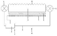
도 1은 본 발명에 따른 무안경식 3D 디스플레이(ASD)의 제1 실시양태를 평면도로 개략적으로 나타낸다. 여기서 도시된 ASD(1)는, 2개의 광원(3 및 4)을 갖는 조명 유닛(2), 평행육면형 광 도파관(5), 회절 광학 소자로서의 홀로그래픽 광학 소자(6), 투명 디스플레이 패널(7), 및 제어 유닛(8)을 포함한다. 디스플레이 패널(7)은, 예를 들어, 종래 기술에 공지된 투광형 LCD 디스플레이일 수 있다. 제어 유닛(8)은 전기 단자(9)를 통해 램프(3 및 4)와 디스플레이 패널(7)에 접속된다. 광원(3 및 4)은, 이들이 각각 상이한 방향으로부터, 즉, 한 번은 좌측으로부터, 그리고 한 번은 우측으로부터, 각각 이들과 마주 놓여 있는 평행육면형 광 도파관(5)의 측 표면 내로 광을 방사하도록 배향 및 배치되어 있다. 홀로그래픽 광학 소자(6)와 디스플레이 패널(7)이, 도면의 평면에서 이 순서대로 차례로, 광 도파관(5) 아래에서 평행하게 배치되어 있다. 홀로그래픽 광학 소자(6)는 여기서는 투과 홀로그램으로서 구현된다. 이러한 타입의 홀로그램은, 예를 들어, 문헌 [P. Hariharan, Optical Holography, Cambridge Studies in Modern Optics, Cambridge University Press, 1996]에 설명되어 있다.BRIEF DESCRIPTION OF THE DRAWINGS Figure 1 schematically shows a first embodiment of a non-limiting 3D display (ASD) according to the present invention in plan view. The ASD 1 shown here includes an
ASD(1)의 동작 동안에, 광원(3 및 4)은, 제어 유닛(8)에 의해 50 헤르쯔보다 높은 주파수로, 디스플레이 패널(7)에 의해 표시되는 우측 및 좌측 시차 영상과 동기화된다. 제어 유닛에 대한 최적화된 스위칭 사이클은, 예를 들어, WO 2008/003563에 설명되어 있다.During operation of the ASD 1 the
광원(3, 4)으로부터의 광은 광 도파관(5) 내로 들어가서, 도면의 평면의 상부에 나타낸 광 도파관(5)의 계면에서 반사되고, 광 도파관(5)의 반대쪽 밑면에서 커플링되어 나온다. 광 도파관(5)으로부터 홀로그래픽 광학 소자(6)의 방향으로 이렇게 방출된 광은 좌측 광원(3)으로부터 나온 것인지 또는 우측 광원(4)으로부터 나온 것인지에 따라 상이한 선호되는 방향을 가지며, 그 다음, 홀로그래픽 소자에 의해 2개의 상이한 방향으로 대응적으로 회절되어 디스플레이 패널(7) 상으로 정향된다.Light from the
이런 방식으로, ASD(1)는 2개의 시차 영상을 교대로 생성하고, 이들 각각은 관찰자의 우안 및 좌안에 의해 각각 인식되어, 그 결과, 상기 관찰자에 대해 풀 해상도의 고품질 3차원 영상이 발생한다.In this way, the ASD 1 alternately generates two parallax images, each of which is recognized by the observer's right eye and left eye respectively, resulting in a full resolution high-quality three-dimensional image for the observer .
마찬가지로, 홀로그래픽 광학 소자(6)가, 하나가 다른 하나의 상부에 놓이거나 서로 이격되어 놓인 층들 내에 위치한 복수의 개별 홀로그램으로부터 구성되는 것도 가능하다. 마찬가지로, 각 경우에 한 개 색상의 (즉, 인간에 대한 가시광의 특정 협소화된 주파수 범위의) 광만을 회절시키거나, 각 경우에 한 개 광원으로부터의 광만을 회절시키거나, 또는 한 개 색상 및/또는 한 개 방향으로부터의 광만을 회절시키도록 홀로그래픽 광학 소자(6)가 설계되는 것도 가능하다.Likewise, it is also possible for the holographic
도 2는 도 1로부터의 ASD(1)의 대안적 변형을 평면도로 도시한다. 차이점은, 여기서 홀로그래픽 광학 소자(6)는 광 도파관(5)과 디스플레이 패널(7) 사이가 아니라 도면의 평면에서 광 도파관(5) 위에 배치되어 있으며, 홀로그래픽 광학 소자(16)는 여기서는 투과 홀로그램 대신에 반사 홀로그램이라는 점이다.Figure 2 shows an alternative variant of the ASD 1 from Figure 1 in plan view. The difference is that the holographic
이 ASD(11)의 경우, 광 도파관(5)은 자신 내로 방사된 광을 홀로그래픽 광학 소자(6)의 방향으로 방출하고, 그 다음, 광은 광 도파관(5) 내로 다시 회절된다. 광은 광 도파관(5)을 통과한 다음, 디스플레이 패널(7) 상에 입사된다.In this
도 3은 도 1에 도시된 구성의 역시 또 다른 변형을 도시한다. 여기서, 2개의 홀로그래픽 광학 소자(6a 및 6b)가 존재하며, 홀로그래픽 광학 소자(6a)는 그 배치와 기능에 있어서 도 1의 ASD(1)의 홀로그래픽 광학 소자(6)에 대응하고, 홀로그래픽 광학 소자(6b)는 그 배치와 기능에 있어서 도 2의 ASD(1)의 홀로그래픽 광학 소자(16)에 대응한다. 결과적으로, 도 3의 ASD(21)는 투과 홀로그램(6a)과 반사 홀로그램(6b) 둘 다를 갖는다.Fig. 3 shows yet another variant of the arrangement shown in Fig. Here, there are two holographic
스위칭 사이클에서 도 3의 ASD(21)의 동작 동안에, 먼저 광은 광원(4)으로부터 나오는 반면, 광원(3)은 광을 방출하지 않는다. 광은 광 도파관(5) 내로 들어가서 이 곳으로부터 홀로그래픽 광학 소자(6a) 내로 들어가고, 그 곳에서 디스플레이 패널(7)의 방향으로 회절된다. 이제 제어 유닛(8)은 광원(4)을 오프한 다음, 동시에 또는 약간의 시간적 중복이나 시간적 분리와 함께 광원(3)을 온한다. 광원(3)으로부터 나오는 광은 광 도파관(5)을 경유해 홀로그래픽 광학 소자(6b)를 거쳐 디스플레이 패널(7)의 방향으로 회절되고, 여기서, 광은, 광 도파관(5)과 홀로그래픽 광학 소자(6a)에 의해 편향되지 않거나 별로 편향되지 않는다. 2개의 스위칭 사이클에서, ASD(21)로부터의 광은 각각 관찰자의 좌안 및 우안에 도달한다.During the operation of the
마찬가지로, 홀로그래픽 광학 소자(6a 및 6b)의 광 가이딩 순서를 바꾸는 것도 가능하다. 마찬가지로, 각각의 홀로그래픽 광학 소자(6a 및 6b)가 각 경우에 한 개의 색상만에 대해 또는 복수의 색상에 대해 회절 효과를 갖는 것도 가능하다, 즉, 예를 들어, "적색" 광에 대해서는 홀로그래픽 광학 소자(6a)에 의해, 그리고 "녹색" 및 "청색" 광에 대해서는 홀로그래픽 광학 소자(6b)에 의해 2개의 색상에 대한 광 가이드 순서가 달성된다. 마찬가지로 다른 조합도 가능하다. 여기서, 광원(3 및 4)이, 각각 원색을 방출하고 서로에 관하여 수직으로 약간 상이하게 위치한 상이한 구조의 유닛들로 구성된다면 유익할 수 있다. 또한, 2개의 홀로그래픽 광학 소자(6a 및 6b)가 광원(3 및 4)으로부터 광 도파관(5)을 통해 가이드된 광에 대해 회절 효과를 가지며 2개의 입체시 영상의 각각의 하나를 디스플레이 패널(5)을 통해 관찰자의 각 육안에 투사하는 것도 물론 가능하다. 이 절차는 더 높은 휘도 효율의 이점을 갖는다.Similarly, it is also possible to change the optical guiding order of the holographic
도 4a 및 도 4b는 동작 중인 도 1의 ASD(1)의 변형을 다시 한번 평면도로 도시하고 있다. 이 경우에, 도 4a는 우측 광원(3)이 광 도파관(5) 내에 광을 방출하는 스위칭 상태를 도시하고, 도 4b는 광원(4)이 작동된 상태를 도시한다.Figures 4A and 4B show again a top view of a variation of the ASD 1 of Figure 1 in operation. In this case, Fig. 4A shows a switching state in which the right
도 1의 ASD(1)와 도 4a 및 도 4b의 장치(31) 사이의 한 차이점은, ASD(31)의 경우, 홀로그래픽 광학 소자(36)가 광 도파관(5)에 직접 전면적으로 접속된다는 것이다. 게다가, ASD(31)의 경우, 홀로그래픽 광학 소자(36)는 투과 가장자리-발광 홀로그램으로서 구현된다.A difference between the ASD 1 in Figure 1 and the
마찬가지로, 홀로그래픽 광학 소자(36)가, 하나가 다른 하나의 상부에 놓이거나 서로 이격되어 놓인 층들 내에 위치한 복수의 개별 홀로그램으로부터 구성되는 것도 가능하다. 마찬가지로, 홀로그래픽 광학 소자가 각 경우에 한 개 색상의 (즉, 인간에 대한 가시광의 특정 협소화된 주파수 범위의) 광만을 회절시키거나, 각 경우에 한 개 광원으로부터의 광만을 회절시키거나, 또는 한 개 색상 및/또는 한 개 방향으로부터의 광만을 회절시키도록 설계되는 것도 가능하다.Likewise, it is also possible for the holographic
도 5a 및 도 5b는 도 4a 및 도 4b의 ASD(31)의 수정판을 도시한다. 여기서는, 첫 번째, 광원(3 및 4)은 도면의 평면에서 다소 더 위에 배치되어 있고, 두 번째, 방사된 광의 (전) 반사가 내부에서 좀처럼 발생하기 어렵고, 오히려, 상기 광이 직접 광 도파관(45)을 통해 홀로그래픽 광학 소자(46)로 가이드되는 광 도파관(45)이 사용된다. 홀로그래픽 광학 소자(46)(투과 가장자리-방출 홀로그램)는, 광 도파관(45)으로부터 나오는 광을 2개의 상이한 방향 중 선호되는 방향에 따라 다시 한번 회절시키고 광을 디스플레이 패널(7) 상으로 정향시키도록 구현된다.Figures 5A and 5B show a modification of the
도 6a 및 도 6b는 동작중인 도 4a 및 도 4b의 ASD(31)의 투시도이다. 도 6a는 작동된 광원(3)을 갖는 ASD(31)의 상태를 도시하고, 도 6b에서는 좌측 광원(4)이 활성이다. 광원 중 하나(3 또는 4)로부터 광 도파관(5)을 통해 홀로그래픽 광학 소자(36)까지의 광 빔의 경로와 홀로그래픽 광학 소자(36)에 의한 디스플레이 패널(7) 상으로의 회절에 의한 경로가 각 경우에 예로서 도시되어 있다. 홀로그래픽 광학 소자(6)는 이 경우에는, 디스플레이 패널(7)의 표면에 법선인 관찰자의 양 육안에 걸쳐 있는 평면에 평행하게 놓여 있는 평면에서 회절이 이루어지도록 설계된다.Figures 6A and 6B are perspective views of the
도 7a 및 도 7b는 본 발명의 제6 실시양태로서 동작중인 도 4a 및 도 4b의 ASD(31)의 변형을 투시적으로 나타내고 있다. 차이점은, 여기서, 광원(3 및 4)이 광 도파관(5)과 나란히 우측 및 좌측에 배치되는 것이 아니라 광 도파관의 위와 아래에 배치되어 있다는 것이다. 여기서, 또한, 홀로그래픽 광학 소자(56)는, 디스플레이 패널(7)의 표면에 법선인 관찰자의 양 육안에 걸쳐 있는 평면에 수직으로 놓여 있는 평면에서 회절이 이루어지도록 설계된다.Figs. 7A and 7B show perspective views of a variation of the
원칙적으로, 도 6a, 6b 및 도 7a, 7b의 실시양태들의 조합도 역시 가능하다.In principle, combinations of the embodiments of Figures 6a, 6b and Figures 7a, 7b are also possible.
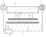
도 8a는 본 발명에 따른 ASD의 제7 실시양태를 도시한다. 이 ASD는 하나의 차이를 제외하고는 도 1의 ASD(1)에 대응한다. 유일한 차이점은, 광 도파관(5)에는 도면의 평면에서 위쪽에 굴절 표면 구조(10)가 제공된다는 것이다.8A shows a seventh embodiment of an ASD according to the present invention. This ASD corresponds to ASD (1) in Fig. 1, except for one difference. The only difference is that the
ASD(61)의 동작 동안에, 표면 구조(10)는, 방출되어 들어온 광의 훨씬 많은 부분이 광 도파관(5)에서 반사될 수 있고 그 다음 홀로그래픽 광학 소자(6)의 방향으로 방출될 수 있다는 효과를 갖는다.During operation of the
또한, 표면 구조(10)는, 예를 들어, ASD(61)의 더 균질한 조명 및/또는 개선된 밝기를 가능케하기 위하여, 예를 들어, 진공 금속화 방법에 의해 반사성으로 코팅되는 것이 유익할 수 있다.It is also advantageous for the
ASD(61)의 경우, 또한, 홀로그래픽 광학 소자(6)가 광 도파관(5)이나 디스플레이 패널(7)에 직접 인접하는 것이 가능하다.In the case of the
도 8b는 도 8a의 ASD(61)의 변형을 도시하며, 여기서는, 굴절 표면 구조(10)가 도면의 평면에서 광 도파관(5)의 아래쪽에 배치되어 있다. 이것은, 광이 광 도파관(5)으로부터 바깥으로 목표화된 방식으로 더욱 효과적으로 커플링된 다음 홀로그래픽 광학 소자(6)에 의해 편향된다는 효과를 갖는다. 이런 방식으로, ASD(71)의 밝기가 증가되고 ASD의 더 균질한 조명이 발생한다.Fig. 8b shows a modification of the
마지막으로, 본 발명에 따른 ASD의 제9 실시양태가 도 9에서 평면도로 개략적으로 도시되어 있다. 여기에 나타낸 ASD(81)는 그 구조의 관점에서 도 1의 장치에 기초하고 있다. 그러나, 여기서 2개의 광학 필름(11 및 12)이 추가로 존재하고, 여기서 한 필름은 광 도파관(5)과 홀로그래픽 광학 소자(6) 사이에 배치되고, 다른 한 필름은 홀로그래픽 광학 소자(6)와 디스플레이 패널(7) 사이에 배치되어 있다. 필름(11, 12)은, 서로 독립적으로, 확산 필름, 마이크로렌즈 필름, 프리즘 필름, 렌티큘라 필름, 또는 반사 편광 필름일 수 있다. 또한, ASD(81)의 광 도파관(5)은 도면의 평면에서 위쪽과 아래쪽 모두에서 굴절 표면 구조(10)가 제공된다는 점에서, 도 1의 ASD(1)와는 상이하다.Finally, a ninth embodiment of an ASD according to the present invention is schematically illustrated in plan view in Fig. The
광학 필름(11 및 12)의 이용과 굴절 표면(10)의 존재는, 휘도 효율의 균질화 또는 개선으로 이어진다.The use of the
ASD(1)의 설계와 이로부터 유도된 ASD(31, 41, 51, 61, 71 및 81)의 설계에서, 디스플레이 패널로부터 각각 떨어져 마주하고 있는 광 도파관의 해당 측이 주로 반사성 방식으로 구성되거나 반사성 코팅되는 것이 유익할 수 있다. 이것은 디스플레이 더 높은 밝기와 더 균질의 조명을 실현하는 것을 가능케 한다.In the design of the ASD 1 and the design of the
(1, 11, 21, 31, 41, 51, 61, 71, 81): ASD
(2): 조명 유닛
(3): 광원
(4): 광원
(5, 45): 광 도파관
(6, 6a, 6b, 16, 36, 46, 56): 홀로그래픽 광학 소자
(7): 디스플레이 패널
(8): 제어 유닛
(9): 전기 단자
(10): 굴절 표면
(11, 12): 광학 필름(1, 11, 21, 31, 41, 51, 61, 71, 81): ASD
(2): Lighting unit
(3): Light source
(4): Light source
(5, 45): optical waveguide
(6, 6a, 6b, 16, 36, 46, 56): a holographic optical element
(7): Display panel
(8): control unit
(9): electric terminal
(10): Refractive surface
(11, 12): optical film
Claims (12)
Translated fromKorean2개의 광원(3, 4)을 갖는 조명 유닛(2), 평행육면체인 광 도파관(5), 회절식 광학적 광 정향 소자(diffractive optical light directing element)로서의 홀로그래픽 광학 소자(6), 투명 디스플레이 패널(7), 및 광원(3, 4)을 각각 교대로 디스플레이 패널(7) 상에 표시되는 우측 및 좌측 시차 영상과 동기화하기 위한 제어 유닛(8)을 포함하고,
광원(3, 4)은 각각 상이한 방향으로부터 광 도파관(5) 내로 광을 방사하도록 배향되고, 여기서, 광원(3, 4)은 상기 평행육면체의 반대되는 두 표면에 배치되며,
홀로그래픽 광학 소자(6) 및 디스플레이 패널(7)은, 홀로그래픽 광학 소자(6)의 방향으로 광 도파관(5)으로부터 방출된 광이 좌측 광원(3)으로부터 나온 것인지 또는 우측 광원(4)으로부터 나온 것인지에 따라 상이한 선호되는 방향을 가지도록, 그리고, 선호되는 방향에 따라, 광 도파관(5)으로부터 방출된 광이 그 후에 홀로그래픽 소자(6)에 의해 2개의 상이한 방향으로 대응적으로 회절되어 디스플레이 패널(7)을 통과하도록 하는 방식으로 배치되며, 광 도파관(5)의 적어도 한 표면은 굴절 표면(10)을 갖는 것을 특징으로 하는 무안경식 3D 디스플레이(1).An autostereoscopic 3D display (1)
An illumination unit 2 having two light sources 3 and 4, a light waveguide 5 as a parallelepiped body, a holographic optical element 6 as a diffractive optical light directing element, And a control unit (8) for synchronizing the light sources (3, 4) with the right and left parallax images alternately displayed on the display panel (7)
The light sources 3 and 4 are each oriented to emit light into the optical waveguide 5 from different directions, wherein the light sources 3 and 4 are disposed on opposite surfaces of the parallelepiped,
The holographic optical element 6 and the display panel 7 are arranged such that the light emitted from the light pipe 5 in the direction of the holographic optical element 6 is emitted from the left light source 3 or from the right light source 4 The light emitted from the optical waveguide 5 is then correspondingly diffracted by the holographic element 6 in two different directions so as to have different preferred orientations depending on whether they are emitted or not, Wherein at least one surface of the optical waveguide (5) has a refractive surface (10).
Applications Claiming Priority (3)
| Application Number | Priority Date | Filing Date | Title |
|---|---|---|---|
| EP10177422AEP2431786A1 (en) | 2010-09-17 | 2010-09-17 | Autostereoscopic 3D display |
| EP10177422.2 | 2010-09-17 | ||
| PCT/EP2011/065926WO2012035058A1 (en) | 2010-09-17 | 2011-09-14 | Autostereoscopic 3d display |
Related Parent Applications (1)
| Application Number | Title | Priority Date | Filing Date |
|---|---|---|---|
| KR1020137009604ADivisionKR20130099969A (en) | 2010-09-17 | 2011-09-14 | Autostereoscopic 3d display |
Publications (1)
| Publication Number | Publication Date |
|---|---|
| KR20190035941Atrue KR20190035941A (en) | 2019-04-03 |
Family
ID=43466787
Family Applications (2)
| Application Number | Title | Priority Date | Filing Date |
|---|---|---|---|
| KR1020197008584ACeasedKR20190035941A (en) | 2010-09-17 | 2011-09-14 | Autostereoscopic 3d display |
| KR1020137009604ACeasedKR20130099969A (en) | 2010-09-17 | 2011-09-14 | Autostereoscopic 3d display |
Family Applications After (1)
| Application Number | Title | Priority Date | Filing Date |
|---|---|---|---|
| KR1020137009604ACeasedKR20130099969A (en) | 2010-09-17 | 2011-09-14 | Autostereoscopic 3d display |
Country Status (7)
| Country | Link |
|---|---|
| US (1) | US20130265625A1 (en) |
| EP (2) | EP2431786A1 (en) |
| JP (1) | JP5947796B2 (en) |
| KR (2) | KR20190035941A (en) |
| CN (2) | CN107976819A (en) |
| TW (1) | TWI556011B (en) |
| WO (1) | WO2012035058A1 (en) |
Cited By (2)
| Publication number | Priority date | Publication date | Assignee | Title |
|---|---|---|---|---|
| WO2022265226A1 (en)* | 2021-06-15 | 2022-12-22 | 삼성전자 주식회사 | Midair image displaying apparatus and electronic device comprising same |
| US12372787B2 (en) | 2021-06-15 | 2025-07-29 | Samsung Electronics Co., Ltd. | Floating image display device and electronic device including the same |
Families Citing this family (24)
| Publication number | Priority date | Publication date | Assignee | Title |
|---|---|---|---|---|
| US9552777B2 (en) | 2013-05-10 | 2017-01-24 | Microsoft Technology Licensing, Llc | Phase control backlight |
| TWI664447B (en)* | 2014-02-18 | 2019-07-01 | 德商拜耳材料科學股份有限公司 | Autostereoscopic 3d display device using holographic optical elements |
| SG11201608201PA (en) | 2014-04-01 | 2016-10-28 | 3M Innovative Properties Co | Asymmetric turning film with multiple light sources |
| CN106462004B (en) | 2014-05-30 | 2019-08-30 | 3M创新有限公司 | Time multiplexing backlight with asymmetric turning film |
| US10324245B2 (en) | 2014-07-29 | 2019-06-18 | Samsung Electronics Co., Ltd. | Backlight unit for holographic display |
| KR102262215B1 (en)* | 2014-09-01 | 2021-06-08 | 삼성전자주식회사 | Backlight unit and holographic display having the same |
| CN107001246B (en) | 2014-12-12 | 2021-02-02 | 科思创德国股份有限公司 | Naphthyl acrylates as writing monomers for photopolymers |
| RU2596062C1 (en) | 2015-03-20 | 2016-08-27 | Автономная Некоммерческая Образовательная Организация Высшего Профессионального Образования "Сколковский Институт Науки И Технологий" | Method for correction of eye image using machine learning and method of machine learning |
| WO2017030217A1 (en)* | 2015-08-18 | 2017-02-23 | 전자부품연구원 | Transparent 3d display system and method |
| WO2017118469A1 (en)* | 2016-01-04 | 2017-07-13 | Ultra-D Coöperatief U.A. | 3d display apparatus |
| CN114143495B (en) | 2016-01-05 | 2025-07-15 | 瑞尔D斯帕克有限责任公司 | Gaze Correction for Multi-View Images |
| CN105607454B (en) | 2016-01-25 | 2018-06-29 | 京东方科技集团股份有限公司 | Holographic display and holographic display methods |
| EP3458897B1 (en) | 2016-05-19 | 2025-04-02 | RealD Spark, LLC | Wide angle imaging directional backlights |
| US10425635B2 (en) | 2016-05-23 | 2019-09-24 | Reald Spark, Llc | Wide angle imaging directional backlights |
| CN106019674B (en)* | 2016-07-29 | 2021-09-14 | 京东方科技集团股份有限公司 | Optical waveguide display module and electronic equipment |
| KR102822335B1 (en) | 2016-11-11 | 2025-06-18 | 삼성전자주식회사 | Backlight unit, holographic display having the same and method of manufacturing holographic optical device |
| WO2018129059A1 (en) | 2017-01-04 | 2018-07-12 | Reald Spark, Llc | Optical stack for imaging directional backlights |
| EP3607387A4 (en) | 2017-04-03 | 2020-11-25 | RealD Spark, LLC | Segmented imaging directional backlights |
| CN111183405A (en) | 2017-08-08 | 2020-05-19 | 瑞尔D斯帕克有限责任公司 | Adjust the digital representation of the head area |
| KR20190036274A (en) | 2017-09-27 | 2019-04-04 | 심미희 | 3D spatial image output device and a folder device for 3D spatial image output using the same |
| WO2019090246A1 (en) | 2017-11-06 | 2019-05-09 | Reald Spark, Llc | Privacy display apparatus |
| KR102759510B1 (en) | 2018-01-25 | 2025-02-04 | 리얼디 스파크, 엘엘씨 | Touchscreen for privacy display |
| CN113325601B (en)* | 2021-08-03 | 2021-10-26 | 成都工业学院 | High-viewpoint and high-density light field stereoscopic display device |
| CN117590621A (en)* | 2022-08-12 | 2024-02-23 | 华为技术有限公司 | Stereoscopic display device, stereoscopic display equipment and stereoscopic display method |
Family Cites Families (40)
| Publication number | Priority date | Publication date | Assignee | Title |
|---|---|---|---|---|
| US4973113A (en) | 1989-04-20 | 1990-11-27 | E. I. Du Pont De Nemours And Company | Method and apparatus for making transmission holograms |
| US5359691A (en)* | 1992-10-08 | 1994-10-25 | Briteview Technologies | Backlighting system with a multi-reflection light injection system and using microprisms |
| WO1994018603A2 (en) | 1993-01-29 | 1994-08-18 | Imedge Technology, Inc. | Holography, particularly, edge illuminated holography |
| GB9411561D0 (en)* | 1994-06-07 | 1994-08-03 | Richmond Holographic Res | Stereoscopic display |
| US5886675A (en)* | 1995-07-05 | 1999-03-23 | Physical Optics Corporation | Autostereoscopic display system with fan-out multiplexer |
| JPH09178949A (en)* | 1995-12-25 | 1997-07-11 | Sharp Corp | Flat lighting device |
| EP1037123A3 (en) | 1999-03-16 | 2002-09-04 | E.I. Du Pont De Nemours & Company Incorporated | Method and element for holographic replication |
| TWI235270B (en)* | 1999-07-02 | 2005-07-01 | Keun-Chang Yang | Plane light source unit and method for manufacturing holographic light-guide plate used for flat panel display |
| US6975455B1 (en)* | 2000-04-18 | 2005-12-13 | 3M Innovative Properties Company | Transflective layer for displays |
| US6733147B2 (en)* | 2000-09-07 | 2004-05-11 | San Zhuang Wang | Backlighting system for displays |
| JP2003036713A (en)* | 2001-07-25 | 2003-02-07 | International Manufacturing & Engineering Services Co Ltd | Surface light source device |
| JP2005513885A (en)* | 2001-12-14 | 2005-05-12 | コーニンクレッカ フィリップス エレクトロニクス エヌ ヴィ | Stereoscopic display device and system |
| WO2003096104A1 (en)* | 2002-03-26 | 2003-11-20 | Maxsoft Co., Ltd | Multiview stereoscopic 3d display device using volume holographic optical element |
| JP4637827B2 (en)* | 2003-03-31 | 2011-02-23 | コーニンクレッカ フィリップス エレクトロニクス エヌ ヴィ | Display device and method for displaying data on display device |
| JP2005024737A (en)* | 2003-06-30 | 2005-01-27 | Optrex Corp | Liquid crystal display and its displaying method |
| GB2404991A (en)* | 2003-08-09 | 2005-02-16 | Sharp Kk | LCD device having at least one viewing window |
| FR2859814A1 (en) | 2003-09-12 | 2005-03-18 | Nexans | Electrically-insulating and heat-resistant composition, especially for use in security cables for power or telecommunications, contains organic polymer, phyllosilicate and refractory filler |
| US7418170B2 (en)* | 2004-03-29 | 2008-08-26 | Sony Corporation | Optical device and virtual image display device |
| US20050275942A1 (en)* | 2004-04-02 | 2005-12-15 | David Hartkop | Method and apparatus to retrofit a display device for autostereoscopic display of interactive computer graphics |
| TWI254166B (en) | 2004-05-25 | 2006-05-01 | Au Optronics Corp | 3D display system and method |
| JP3908241B2 (en)* | 2004-06-24 | 2007-04-25 | オリンパス株式会社 | Video display device |
| FR2874993B1 (en)* | 2004-09-07 | 2008-07-18 | Valeo Vision Sa | LIGHT GUIDE LIGHTING AND / OR SIGNALING DEVICE |
| TWI312883B (en) | 2005-01-24 | 2009-08-01 | Au Optronics Corp | Backlight module for 3d display device and method for displaying 3d images utilizing the same |
| JP4547276B2 (en)* | 2005-01-24 | 2010-09-22 | シチズン電子株式会社 | Planar light source |
| JP4600317B2 (en)* | 2005-03-31 | 2010-12-15 | カシオ計算機株式会社 | Illumination device that emits at least two illumination lights having directivity and display device using the same |
| DE102005018750A1 (en) | 2005-04-22 | 2006-10-26 | Marcus Werner | Method for producing angle-reduced holograms and the integrated reproduction of angle-reduced holograms |
| JP2007033633A (en)* | 2005-07-25 | 2007-02-08 | Olympus Corp | Video display device |
| CN100405164C (en)* | 2005-08-18 | 2008-07-23 | 鸿富锦精密工业(深圳)有限公司 | Light guide plate, backlight module and double-sided liquid crystal display device |
| US7518664B2 (en)* | 2005-09-12 | 2009-04-14 | Sharp Kabushiki Kaisha | Multiple-view directional display having parallax optic disposed within an image display element that has an image display layer sandwiched between TFT and color filter substrates |
| CA2649415C (en)* | 2006-04-19 | 2018-01-16 | Setred As | High speed display shutter for autostereoscopic display |
| DE102006030483B3 (en) | 2006-07-01 | 2007-12-06 | Seereal Technologies S.A. | Autostereoscopic display for time-sequential three dimensional illustration of images or image sequence for observer, has control unit determining temporal cross talk between control signals for lighting matrix and for image matrix |
| JP2008058777A (en)* | 2006-09-01 | 2008-03-13 | Sony Corp | Optical device and image display apparatus |
| JP2009058846A (en)* | 2007-09-03 | 2009-03-19 | Hitachi Displays Ltd | Liquid crystal display |
| EP2208106A1 (en)* | 2007-10-04 | 2010-07-21 | 3M Innovative Properties Company | Embedded stereoscopic 3d display and 2d display film stack |
| JP5358451B2 (en)* | 2007-10-25 | 2013-12-04 | パナソニック株式会社 | Planar illumination device and image display device |
| US20090174919A1 (en)* | 2007-12-28 | 2009-07-09 | Gaylord Moss | Directed illumination diffraction optics auto-stereo display |
| JP4518193B2 (en)* | 2008-06-10 | 2010-08-04 | ソニー株式会社 | Optical device and virtual image display device |
| US8068187B2 (en)* | 2008-06-18 | 2011-11-29 | 3M Innovative Properties Company | Stereoscopic 3D liquid crystal display apparatus having a double sided prism film comprising cylindrical lenses and non-contiguous prisms |
| KR101295146B1 (en)* | 2008-12-19 | 2013-08-09 | 엘지디스플레이 주식회사 | Liquid crystal display device |
| TWI404978B (en)* | 2009-08-13 | 2013-08-11 | Prism with optical layer and its making method |
- 2010
- 2010-09-17EPEP10177422Apatent/EP2431786A1/ennot_activeWithdrawn
- 2011
- 2011-09-14CNCN201710873825.8Apatent/CN107976819A/enactivePending
- 2011-09-14EPEP11755343.8Apatent/EP2616874B1/enactiveActive
- 2011-09-14KRKR1020197008584Apatent/KR20190035941A/ennot_activeCeased
- 2011-09-14JPJP2013528652Apatent/JP5947796B2/ennot_activeExpired - Fee Related
- 2011-09-14USUS13/823,098patent/US20130265625A1/ennot_activeAbandoned
- 2011-09-14KRKR1020137009604Apatent/KR20130099969A/ennot_activeCeased
- 2011-09-14CNCN2011800551649Apatent/CN103221873A/enactivePending
- 2011-09-14WOPCT/EP2011/065926patent/WO2012035058A1/enactiveApplication Filing
- 2011-09-16TWTW100133314Apatent/TWI556011B/ennot_activeIP Right Cessation
Cited By (2)
| Publication number | Priority date | Publication date | Assignee | Title |
|---|---|---|---|---|
| WO2022265226A1 (en)* | 2021-06-15 | 2022-12-22 | 삼성전자 주식회사 | Midair image displaying apparatus and electronic device comprising same |
| US12372787B2 (en) | 2021-06-15 | 2025-07-29 | Samsung Electronics Co., Ltd. | Floating image display device and electronic device including the same |
Also Published As
| Publication number | Publication date |
|---|---|
| EP2431786A1 (en) | 2012-03-21 |
| TWI556011B (en) | 2016-11-01 |
| CN107976819A (en) | 2018-05-01 |
| WO2012035058A1 (en) | 2012-03-22 |
| EP2616874B1 (en) | 2022-09-14 |
| JP5947796B2 (en) | 2016-07-06 |
| CN103221873A (en) | 2013-07-24 |
| TW201234048A (en) | 2012-08-16 |
| EP2616874A1 (en) | 2013-07-24 |
| US20130265625A1 (en) | 2013-10-10 |
| KR20130099969A (en) | 2013-09-06 |
| JP2013545120A (en) | 2013-12-19 |
Similar Documents
| Publication | Publication Date | Title |
|---|---|---|
| JP5947796B2 (en) | Autostereoscopic 3D display | |
| US10025160B2 (en) | Backlight unit and 3D image display apparatus | |
| KR102526753B1 (en) | Coherent backlight unit and three-dimensional image display device | |
| JP6714514B2 (en) | Autostereoscopic 3D display device using holographic optical element | |
| KR102581465B1 (en) | Three-dimensional image display apparatus including the diffractive color filter | |
| US7639210B2 (en) | Multi-depth displays | |
| US9176365B2 (en) | Illumination device, projection device, and projection-type image display device | |
| US20070296920A1 (en) | Rear Projection Screen and Associated Display System | |
| EP3444527B1 (en) | Light guide plate, backlight unit, and holographic display apparatus including the backlight unit | |
| WO2019179136A1 (en) | Display apparatus and display method | |
| JP2005533291A (en) | Autostereoscopic projection device | |
| CN105008984B (en) | Holographic display device | |
| JP2013076725A (en) | Light source device, display apparatus and electronic equipment | |
| KR20140114651A (en) | Holographic 3D Display apparatus and illumination unit for holographic 3D Display apparatus | |
| JP2010237416A (en) | 3D display device | |
| JP5069360B2 (en) | 3D display device | |
| JP4703477B2 (en) | 3D display device | |
| KR20180059205A (en) | Directional backlight unit, 3D image display apparatus having the same, and method of manufacturing the same | |
| KR102771620B1 (en) | Holographic display apparatus and method for providing expanded viewing window | |
| KR20130021868A (en) | Display apparatus for displaying three dimensional picture | |
| JP2021060564A (en) | Virtual image display device and display control device | |
| KR20130107606A (en) | 3 dimensional stereography image displayable system |
Legal Events
| Date | Code | Title | Description |
|---|---|---|---|
| A107 | Divisional application of patent | ||
| A201 | Request for examination | ||
| PA0104 | Divisional application for international application | Comment text:Divisional Application for International Patent Patent event code:PA01041R01D Patent event date:20190325 Application number text:1020137009604 Filing date:20130416 | |
| PA0201 | Request for examination | ||
| PG1501 | Laying open of application | ||
| E902 | Notification of reason for refusal | ||
| PE0902 | Notice of grounds for rejection | Comment text:Notification of reason for refusal Patent event date:20190617 Patent event code:PE09021S01D | |
| E601 | Decision to refuse application | ||
| PE0601 | Decision on rejection of patent | Patent event date:20200306 Comment text:Decision to Refuse Application Patent event code:PE06012S01D Patent event date:20190617 Comment text:Notification of reason for refusal Patent event code:PE06011S01I |