KR20190002963A - Curved image sensor - Google Patents
Curved image sensorDownload PDFInfo
- Publication number
- KR20190002963A KR20190002963AKR1020170083312AKR20170083312AKR20190002963AKR 20190002963 AKR20190002963 AKR 20190002963AKR 1020170083312 AKR1020170083312 AKR 1020170083312AKR 20170083312 AKR20170083312 AKR 20170083312AKR 20190002963 AKR20190002963 AKR 20190002963A
- Authority
- KR
- South Korea
- Prior art keywords
- image sensor
- curved
- sensor chip
- prevention film
- ghost prevention
- Prior art date
- Legal status (The legal status is an assumption and is not a legal conclusion. Google has not performed a legal analysis and makes no representation as to the accuracy of the status listed.)
- Granted
Links
Images


Classifications
- H—ELECTRICITY
- H10—SEMICONDUCTOR DEVICES; ELECTRIC SOLID-STATE DEVICES NOT OTHERWISE PROVIDED FOR
- H10F—INORGANIC SEMICONDUCTOR DEVICES SENSITIVE TO INFRARED RADIATION, LIGHT, ELECTROMAGNETIC RADIATION OF SHORTER WAVELENGTH OR CORPUSCULAR RADIATION
- H10F39/00—Integrated devices, or assemblies of multiple devices, comprising at least one element covered by group H10F30/00, e.g. radiation detectors comprising photodiode arrays
- H10F39/80—Constructional details of image sensors
- H10F39/806—Optical elements or arrangements associated with the image sensors
- H—ELECTRICITY
- H10—SEMICONDUCTOR DEVICES; ELECTRIC SOLID-STATE DEVICES NOT OTHERWISE PROVIDED FOR
- H10F—INORGANIC SEMICONDUCTOR DEVICES SENSITIVE TO INFRARED RADIATION, LIGHT, ELECTROMAGNETIC RADIATION OF SHORTER WAVELENGTH OR CORPUSCULAR RADIATION
- H10F39/00—Integrated devices, or assemblies of multiple devices, comprising at least one element covered by group H10F30/00, e.g. radiation detectors comprising photodiode arrays
- H10F39/80—Constructional details of image sensors
- H10F39/802—Geometry or disposition of elements in pixels, e.g. address-lines or gate electrodes
- H10F39/8027—Geometry of the photosensitive area
- H01L27/14625—
- H01L27/14632—
- H01L27/14685—
- H—ELECTRICITY
- H04—ELECTRIC COMMUNICATION TECHNIQUE
- H04N—PICTORIAL COMMUNICATION, e.g. TELEVISION
- H04N23/00—Cameras or camera modules comprising electronic image sensors; Control thereof
- H04N23/50—Constructional details
- H04N23/54—Mounting of pick-up tubes, electronic image sensors, deviation or focusing coils
- H—ELECTRICITY
- H04—ELECTRIC COMMUNICATION TECHNIQUE
- H04N—PICTORIAL COMMUNICATION, e.g. TELEVISION
- H04N23/00—Cameras or camera modules comprising electronic image sensors; Control thereof
- H04N23/50—Constructional details
- H04N23/55—Optical parts specially adapted for electronic image sensors; Mounting thereof
- H—ELECTRICITY
- H04—ELECTRIC COMMUNICATION TECHNIQUE
- H04N—PICTORIAL COMMUNICATION, e.g. TELEVISION
- H04N25/00—Circuitry of solid-state image sensors [SSIS]; Control thereof
- H04N25/70—SSIS architectures; Circuits associated therewith
- H—ELECTRICITY
- H04—ELECTRIC COMMUNICATION TECHNIQUE
- H04N—PICTORIAL COMMUNICATION, e.g. TELEVISION
- H04N25/00—Circuitry of solid-state image sensors [SSIS]; Control thereof
- H04N25/70—SSIS architectures; Circuits associated therewith
- H04N25/702—SSIS architectures characterised by non-identical, non-equidistant or non-planar pixel layout
- H—ELECTRICITY
- H04—ELECTRIC COMMUNICATION TECHNIQUE
- H04N—PICTORIAL COMMUNICATION, e.g. TELEVISION
- H04N25/00—Circuitry of solid-state image sensors [SSIS]; Control thereof
- H04N25/70—SSIS architectures; Circuits associated therewith
- H04N25/76—Addressed sensors, e.g. MOS or CMOS sensors
- H—ELECTRICITY
- H10—SEMICONDUCTOR DEVICES; ELECTRIC SOLID-STATE DEVICES NOT OTHERWISE PROVIDED FOR
- H10F—INORGANIC SEMICONDUCTOR DEVICES SENSITIVE TO INFRARED RADIATION, LIGHT, ELECTROMAGNETIC RADIATION OF SHORTER WAVELENGTH OR CORPUSCULAR RADIATION
- H10F39/00—Integrated devices, or assemblies of multiple devices, comprising at least one element covered by group H10F30/00, e.g. radiation detectors comprising photodiode arrays
- H10F39/011—Manufacture or treatment of image sensors covered by group H10F39/12
- H10F39/024—Manufacture or treatment of image sensors covered by group H10F39/12 of coatings or optical elements
- H—ELECTRICITY
- H10—SEMICONDUCTOR DEVICES; ELECTRIC SOLID-STATE DEVICES NOT OTHERWISE PROVIDED FOR
- H10F—INORGANIC SEMICONDUCTOR DEVICES SENSITIVE TO INFRARED RADIATION, LIGHT, ELECTROMAGNETIC RADIATION OF SHORTER WAVELENGTH OR CORPUSCULAR RADIATION
- H10F39/00—Integrated devices, or assemblies of multiple devices, comprising at least one element covered by group H10F30/00, e.g. radiation detectors comprising photodiode arrays
- H10F39/011—Manufacture or treatment of image sensors covered by group H10F39/12
- H10F39/026—Wafer-level processing
- H—ELECTRICITY
- H10—SEMICONDUCTOR DEVICES; ELECTRIC SOLID-STATE DEVICES NOT OTHERWISE PROVIDED FOR
- H10F—INORGANIC SEMICONDUCTOR DEVICES SENSITIVE TO INFRARED RADIATION, LIGHT, ELECTROMAGNETIC RADIATION OF SHORTER WAVELENGTH OR CORPUSCULAR RADIATION
- H10F39/00—Integrated devices, or assemblies of multiple devices, comprising at least one element covered by group H10F30/00, e.g. radiation detectors comprising photodiode arrays
- H10F39/80—Constructional details of image sensors
- H10F39/805—Coatings
Landscapes
- Engineering & Computer Science (AREA)
- Multimedia (AREA)
- Signal Processing (AREA)
- Solid State Image Pick-Up Elements (AREA)
- Transforming Light Signals Into Electric Signals (AREA)
Abstract
Translated fromKoreanDescription
Translated fromKorean본 발명은 반도체 장치에 관한 것으로, 보다 구체적으로는 커브드 이미지 센서에 관한 것이다.The present invention relates to a semiconductor device, and more particularly to a curved image sensor.
이미지 센서와 촬영 렌즈를 결합시킨 카메라 등의 촬영 장치는, 이미지 센서의 수광면측에 촬영 렌즈를 배치하여 구성된다. 이와 같은 촬영 장치에서는, 피사체를 촬영 렌즈로 결상시킬 때, 필드 곡률(field curvature)이라고 칭하여지는 렌즈 수차에 의해 촬영면의 중심부와 주변부에서 초점 위치의 어긋남(수차)이 발생하기 때문에 필드 곡률의 보정이 반드시 필요하다.A photographing apparatus such as a camera combining an image sensor and a photographing lens is constituted by disposing a photographing lens on the light receiving surface side of the image sensor. In such a photographing apparatus, when a subject is focused on a photographing lens, a shift of the focus position (aberration) occurs in the central portion and the peripheral portion of the photographing plane due to the lens aberration referred to as field curvature, Is necessary.
이를 개선하기 위해, 촬영 렌즈의 곡률에 대응하여 3차원으로 만곡시킨 만곡면을 형성하고, 이 만곡면을 이미지 센서의 촬영면(즉, 수광이면)으로하여 광전변환소자를 배열하는 커브드 이미지 센서가 제안되었다.In order to solve this problem, a curved image sensor that forms a curved surface curved in three dimensions corresponding to the curvature of the photographing lens and arranges the photoelectric conversion elements with the curved surface as a photographing surface (that is, .
하지만 이 경우, 상기 커브드 이미지 센서의 만곡면과 상부에 위치하는 촬영렌즈(혹은 적외선차단필터)에 의해 상호간 반사된 반사광이 이미지에 반영되는 플레어고스트(flare ghost)현상이 발생하곤 하였다.However, in this case, a flare ghost phenomenon occurs in which the reflected light reflected by the curved surface of the curved image sensor and the photographing lens (or the infrared cut filter) located on the upper side are reflected on the image.
본 발명의 실시예는 성능이 향상된 커브드 이미지 센서를 제공한다.Embodiments of the present invention provide a curved image sensor with improved performance.
본 발명의 실시예에 따른 커브드 이미지 센서는 지지기판; 상기 지지기판상에 형성되며, 오목하게 만곡된 상부표면을 갖는 이미지센서칩; 및 상기 이미지센서칩의 만곡된 상부표면 상에 형성되고, 평탄한 상부표면을 갖는 플레어고스트 방지막을 포함 할 수 있다.A curved image sensor according to an embodiment of the present invention includes a support substrate; An image sensor chip formed on the supporting substrate and having a concave curved upper surface; And a flare ghost prevention film formed on the curved upper surface of the image sensor chip and having a flat upper surface.
본 발명의 실시예에 따른 커브드 이미지 센는 서만곡된 광입사면을 갖는 이미지센서칩; 상기 이미지센서칩의 만곡된 광입사면을 덮고, 평탄한 상부표면을 갖는 플레어고스트 방지막; 및상기 플레어고스트 방지막의 평탄한 상부표면에 접하도록 형성된 적외선차단필터를 포함 할 수 있다.A curved image sensor according to an embodiment of the present invention includes: an image sensor chip having a curved light incidence surface; A flare ghost prevention film covering the curved light incident surface of the image sensor chip and having a flat upper surface; And an infrared cut filter formed to contact the flat upper surface of the flare ghost prevention film.
본 발명의 실시예에 따른 커브드 이미지 센서는 평탄한 상부표면을 갖는 플레어고스트 방지막을 제공하여, 반사광이 이미지센서칩 내부로 재입사되는 것을 방지하여, 플레어고스트(flare ghost) 현상을 방지할 수 있다.The curved image sensor according to the embodiment of the present invention provides a flare ghost prevention film having a flat upper surface to prevent the reflected light from being re-incident into the image sensor chip, thereby preventing a flare ghost phenomenon .
본 발명의 실시예에 따른 플레어고스트 방지막은 이미지센서칩의 만곡된 상부표면 상에 형성되고, 이미지센서칩의 상부표면과 동일한 곡률을 갖도록 형성되어, 이미지센서칩의 만곡 형상을 유지 시킬 수 있다. 또한 플레어고스트 방지막은 열경화 특성을 갖는 물질을 상기 이미지센서칩의 최하부 상부표면부터 최상부 상부표까지 채우는 형태로 형성함으로써, 이미지센서칩의 만곡 형상을 보다 더 효과적으로 유지 시킬 수 있다.The flare ghost prevention film according to the embodiment of the present invention is formed on the curved upper surface of the image sensor chip and formed to have the same curvature as the upper surface of the image sensor chip so as to maintain the curved shape of the image sensor chip. In addition, the flare ghost prevention film may be formed by filling a material having a thermosetting property from the lowermost upper surface to the uppermost uppermost surface of the image sensor chip, thereby more effectively maintaining the curved shape of the image sensor chip.
본 발명의 실시예에 따른 커브드 이미지 센서는 가시광선에 대해 투명성을 갖고 공기보다 굴절율이 큰 물질로 플레어고스트 방지막을 형성하여, 이미지센서칩으로 입사되는 빛의 집광력을 상승시켜 광학적 특성을 상승시킬 수 있다.The curved image sensor according to the embodiment of the present invention forms a flare ghost prevention film having a transparency with respect to visible light and a refractive index higher than that of air to raise the optical power of the light incident on the image sensor chip .
도 1은 본 발명의 실시예들에 따른 커브드 이미지 센서의 구성을 간략히 도시한 도면.
도 2a, 도 2b 및 도 2c는 본 발명의 실시예에 따른 커브드 이미지 센서를 도시한 도면.
도 3은 빛의 굴절율 및 반사율을 도시한 도면
도 4a 내지 도 4e는 본 발명의 실시예에 따른 커브드 이미지 센서의 제조방법을 도시한 도면.
도 5a 및 도 5b는 본 발명의 실시예에 따른 커브드 이미지 센서의 변형 예.
도 6는 본 발명의 실시예에 따른 커브드 이미지 센서를 구비한 전자장치를 간략히 도시한 도면.BRIEF DESCRIPTION OF THE DRAWINGS Fig. 1 is a view schematically illustrating a configuration of a curved image sensor according to embodiments of the present invention. Fig.
Figures 2a, 2b and 2c illustrate a curved image sensor according to an embodiment of the present invention.
3 is a view showing the refractive index and reflectance of light;
4A through 4E illustrate a method of manufacturing a curved image sensor according to an embodiment of the present invention.
5A and 5B are views showing a variation of the curved image sensor according to the embodiment of the present invention.
6 is a simplified illustration of an electronic device having a curved image sensor according to an embodiment of the present invention;
이하에서는, 첨부된 도면을 참조하여 다양한 실시예들이 상세히 설명된다.In the following, various embodiments are described in detail with reference to the accompanying drawings.
도면은 반드시 일정한 비율로 도시된 것이라 할 수 없으며, 몇몇 예시들에서, 실시예들의 특징을 명확히 보여주기 위하여 도면에 도시된 구조물 중 적어도 일부의 비례는 과장될 수도 있다. 도면 또는 상세한 설명에 둘 이상의 층을 갖는 다층 구조물이 개시된 경우, 도시된 것과 같은 층들의 상대적인 위치 관계나 배열 순서는 특정 실시예를 반영할 뿐이어서 본 발명이 이에 한정되는 것은 아니며, 층들의 상대적인 위치 관계나 배열 순서는 달라질 수도 있다. 또한, 다층 구조물의 도면 또는 상세한 설명은 특정 다층 구조물에 존재하는 모든 층들을 반영하지 않을 수도 있다(예를 들어, 도시된 두 개의 층 사이에 하나 이상의 추가 층이 존재할 수도 있다). 예컨대, 도면 또는 상세한 설명의 다층 구조물에서 제1층이 제2층 상에 있거나 또는 기판상에 있는 경우, 제1층이 제2층 상에 직접 형성되거나 또는 기판상에 직접 형성될 수 있음을 나타낼 뿐만 아니라, 하나 이상의 다른 층이 제1층과 제2층 사이 또는 제1층과 기판 사이에 존재하는 경우도 나타낼 수 있다.The drawings are not necessarily drawn to scale, and in some instances, proportions of at least some of the structures shown in the figures may be exaggerated to clearly show features of the embodiments. When a multi-layer structure having two or more layers is disclosed in the drawings or the detailed description, the relative positional relationship or arrangement order of the layers as shown is only a specific example and the present invention is not limited thereto. The order of relationships and arrangements may vary. In addition, a drawing or a detailed description of a multi-layer structure may not reflect all layers present in a particular multi-layer structure (e.g., there may be more than one additional layer between the two layers shown). For example, if the first layer is on the substrate or in the multilayer structure of the drawings or the detailed description, the first layer may be formed directly on the second layer or may be formed directly on the substrate As well as the case where more than one other layer is present between the first layer and the second layer or between the first layer and the substrate.
도 1은 본 발명의 실시예들에 따른 커브드 이미지 센서의 구성을 간략히 도시한 도면이다. 구체적으로, 도 1은 본 발명의 실시예들에 따른 커브드 이미지 센서에 적용할 수 있는 이미지 센서의 구성을 간략히 도시한 평면도이다.BRIEF DESCRIPTION OF THE DRAWINGS Fig. 1 is a view schematically showing a configuration of a curved image sensor according to embodiments of the present invention. Fig. 1 is a plan view schematically illustrating a configuration of an image sensor applicable to a curved image sensor according to embodiments of the present invention.
도 1에 도시된 바와 같이, 실시예들에 따른 이미지 센서는 광전변환소자를 포함하는 복수의 픽셀들이 2차원적으로 배열된 픽셀 어레이(2)를 포함할 수 있다. 픽셀 어레이(2)에 배열된 각 픽셀(1)에는 광전변환소자와 함께 복수의 트랜지스터 및 캐패시터 등으로 구성된 픽셀 회로(미도시)가 접속되어 있다. 또한, 복수의 광전변환소자는 픽셀 회로의 일부를 공유하고 있는 경우도 있다. 또한, 픽셀(1)에서 광전변환소자와 함께 배치되는 픽셀 회로는 광전변환소자가 마련된 표면(또는 광 광입사면)과는 반대측의 표면(또는, 광 광입사면의 대향면)에 마련될 수 있다.As shown in Fig. 1, the image sensor according to the embodiments may include a
픽셀 어레이(2)의 주변에는 수직구동회로(3), 컬럼신호처리회로(4), 수평구동회로(5) 및 시스템 제어회로(6)를 포함한 주변회로가 배치될 수 있다. 주변회로는 픽셀 어레이(2)와 동일한 기판에 형성될 수 있다. 한편, 주변회로는 픽셀 어레이(2)가 형성된 기판과 상이한 기판에 형성될 수도 있다. 수직구동회로(3)는 시프트 레지스터에 의해 구성되고, 픽셀 어레이(2)에 배선된 픽셀 구동선(7)를 선택하고, 선택된 픽셀 구동선(7)에 픽셀을 구동하기 위한 펄스신호를 공급하여 픽셀 어레이(2)에 배열된 픽셀을 행(row) 단위로 구동한다. 즉, 수직구동회로(3)는 픽셀 어레이(2)에 배열된 각 픽셀를 행 단위로 순차적으로 수직 방향으로 선택 주사한다. 그리고, 픽셀 구동선(7)에 대해 수직으로 배선된 수직 신호선(8)을 통하여, 각 픽셀에서 수광량에 응하여 생성한 신호 전하에 의거한 픽셀 신호를 컬럼신호처리회로(4)에 공급한다.Peripheral circuits including the
다이영역은 픽셀 어레이(2)가 형성되는 영역이다. 본 발명의 이미지센서칩은 다이영역에서 오목하게 만곡되며, 상기 다이영역 이외의 영역에 형성된 이미지센서칩은 만곡되지 않는다.The die area is an area where the
컬럼신호처리회로(4)는 픽셀의 열(column)마다 배치되어 있고, 1행분의 픽셀로부터 출력되는 신호를 픽셀열 마다 노이즈 제거 등의 신호 처리를 행한다. 즉 컬럼신호처리회로(4)는 픽셀 고유의 고정 패턴 노이즈를 제거하기 위한 상관 이중 샘플링(CDS, Correlated Double sampling)이나, 신호 증폭, 아날로그/디지털 변환(ADC, Analog/Digital Conversion) 등의 신호 처리를 행한다.The column
수평구동회로(5)는 시프트 레지스터에 의해 구성되고, 수평 주사 펄스를 순차적으로 출력함에 의해, 컬럼신호처리회로(4)의 각각을 순번대로 선택하고, 컬럼신호처리회로(4)의 각각으로부터 픽셀 신호를 출력시킨다. 출력 회로는 컬럼신호처리회로(4)의 각각으로부터 순차적으로 공급되는 신호에 대해, 신호 처리를 행하여 출력한다. 예를 들면, 버퍼링만 하는 경우도 있고, 다크 레벨 조정, 열(row) 편차 보정, 각종 디지털 신호 처리 등이 행하여지는 경우도 있다.The
시스템 제어회로(6)는 입력 클록과 동작 모드 등을 지령하는 데이터를 수취하고, 이미지 센서 내부 정보 등의 데이터를 출력한다. 즉, 시스템 제어회로(6)에서는 수직 동기 신호, 수평 동기 신호 및 마스터 클록에 의거하여 수직구동회로(3), 컬럼신호처리회로(4) 및 수평구동회로(5) 등의 동작에 기준이 되는 클록 신호나 제어 신호를 생성한다. 그리고, 이들의 신호를 수직구동회로(3), 컬럼신호처리회로(4) 및 수평구동회로(5) 등에 입력한다.The
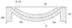
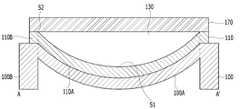
도 2a, 도 2b 및 도 2c는 본 발명에 따른 커브드 이미지 센서를 도시한 도면으로, 도 2a는 평면도이고, 도 2b 및 도 2c는 도 2a에 도시된 A-A'절취선을 따라 도시한 단면도이다.2A, 2B and 2C are views showing a curved image sensor according to the present invention, in which FIG. 2A is a plan view, FIGS. 2B and 2C are sectional views taken along line A-A ' to be.
도 2a 및 도 2b에 도시된 바와 같이, 제1실시예에 따른 커브드 이미지 센서는 지지기판(100), 상기 지지기판(100)상에 형성되며, 만곡된 광입사면을 갖는 이미지센서칩(110) 및 상기 이미지센서칩(110)의 만곡된 광입사면 상에 형성되고, 평탄한 상부표면을 갖는 플레어고스트 방지막(130)을 포함한다.2A and 2B, a curved image sensor according to the first embodiment includes a
상기 지지기판(100)은 캐리어 웨이퍼(carrier wafer) 또는 핸들 웨이퍼(handle wafer)일 수 있고, 이들에서 분리된 것일 수 있다. 이미지센서칩(110)은 디바이스 웨이퍼(device wafer)를 포함할 수 있고, 디바이스 웨이퍼에서 분리된 것일 수 있다. 지지기판(100) 및 이미지센서칩(110)은 반도체 기판을 포함할 수 있다. 반도체 기판은 단결정 상태(Single crystal state)일 수 있으며, 실리콘 함유 재료를 포함할 수 있다. 즉, 지지기판(100) 및 이미지센서칩(110)은 단결정의 실리콘 함유 재료를 포함할 수 있다. 일례로, 지지기판(100) 및 이미지센서칩(110)은 벌크 실리콘 기판일 수 있다. 실시예에 따른 이미지 센서가 후면 수광 타입인 경우에 이미지센서칩(110)의 상부표면은 광 광입사면으로 이미지센서칩(110)의 후면(Backside)일 수 있고, 상부표면에 대향하는 하부표면은 이미지센서칩(110)의 전면(Frontside)일 수 있다. 여기서, 도면에 도시하지는 않았지만, 제1실시예에 따른 커브드 이미지 센서는 이미지센서칩(110)의 전면 즉, 하부표면상에 형성되어 신호생성회로를 포함하는 층간절연막을 더 포함할 수 있다. 층간절연막은 산화막, 질화막 및 산화질화막으로 이루어진 그룹으로부터 선택된 어느 하나의 단일막 또는 둘 이상의 다중막일 수 있다. 층간절연막 내부에 형성된 신호생성회로는 복수의 트랜지스터, 다층의 금속배선 및 이들을 상호 연결하는 복수의 콘택플러그를 포함할 수 있다. 여기서, 신호생성회로는 도 1에서 설명한 픽셀 회로, 주변회로를 포함할 수 있다. 또한, 이미지센서칩(110)의 후면 즉, 상부표면상에는 각각의 광전변환소자에 대응하도록 형성된 컬러필터 및 컬러필터 상에 형성된 마이크로렌즈를 더 포함할 수 있다. 광전변환소자는 포토다이오드를 포함할 수 있다. 광전변환소자는 이미지센서칩(110)에 형성된 것일 수 있다. 예컨대, 광전변환소자는 이미지센서칩(110)에 형성되어 수직적으로 중첩되는 하나 이상의 광전변환부들을 포함할 수 있다. 광전변환부들 각각은 P형 불순물영역과 N형 불순물영역을 포함할 수 있다.The supporting
또한 상기 지지기판(100)은 다이영역의 중심을 향해 오목하게 만곡되는 만곡부(100A) 및 만곡부(100A)의 가장자리 측벽에 접하는 지지부(100B)를 포함 할 수 있으며, 상기 만곡부(100A)는 만곡된 하부표면 및 상부표면을 포함 할 수 있다.The supporting
상기 이미지센서칩(110)은 다이영역의 중심을 향해 오목하게 만곡되는 만곡부(110A)를 포함 할 수 있다. 그리고 상기 만곡부(110A)는 오목하게 만곡된 하부표면 및 상부표면을 포함하며, 만곡된 상부표면에는 광입사면이 형성된다. 또한 상기 이미지센서칩(110)은 상기 지지기판(100)의 지지부(110B)의 상부를 덮는 형태로 형성될 수도 있다.The
상기 플레어고스트 방지막(130)는 가시광선에 대해 투명성을 갖고, 공기보다 큰 굴절율을 갖는 열 경화성 물질로 구성될 수 있다. 예를들면, 플레어고스트 방지막(130)은 폴리이미드, 폴리스티렌, 폴리 하이드록시 스티렌계 물질을 포함할 수 있다. 플레어고스트 방지막(130)는 투명물질로 형성되기 때문에, 가시광선의 투과율 저하 및 산란으로 인한 광에너지의 손실 없이 이미지센서칩(110)으로 투과시킬 수 있다.The flare
또한 외부로부터 입사되어 이미지 센서칩(110)에 의해 반사된 반사광을 상기 이미지 센서칩(110)의 상부에 형성된 상기 플레어고스트 방지막(130)의 평탄한 상부표면을 통해 상기 이미지 센서칩(110)의 외곽으로 유도함으로써, 상기 반사광이 상기 이미지센서칩(110) 내부로 재입사됨에 따라 발생하는 플레어고스트 현상을 방지할 수 있다.The reflected light reflected by the
또한 도 3에 도시된 바와 같이, 입사각(θ1)을 갖는 입사광이 공기를 통해 공기보다 높은 굴절률을 갖는 플레어고스트 방지막(130)으로 입사되면, 입사광은 입사각(θ1)보다 작은 굴절각(θ2)을 갖고 법선쪽으로 굴절되어, 이미지센서칩(110)으로 투과된다. 이로 인해, 이미지센서칩(110)으로 입사되는 빛의 집광력이 상승하여, 입사광의 광학적 특성이 상승할 수 있다.As shown in FIG. 3, when incident light having an incident angle of? 1 is incident on the flare
또한 플레어고스트 방지막(130)은, 이미지센서칩(110)의 만곡된 상부표면 상에 형성되고, 이미지센서칩(110)의 상부표면과 동일한 곡률을 갖기 때문에, 이미지센서칩의 만곡 형상을 유지 시킬 수 있다. 또한 플레어고스트 방지막(130)은 열경화 특성을 갖는 물질로 형성되며, 상기 이미지센서칩(110)의 최하부 상부표면(S1)부터 최상부 상부표면(S2)까지 채우는 형태로 형성함으로써, 이미지센서칩(110)의 만곡 형상을 보다 더 효과적으로 유지 시킬 수 있다.The flare
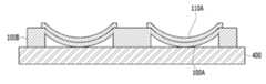
또한 도 2c에 도시된 바와 같이, 플레어고스트 방지막(130)은 상기 이미지센서칩(110)이 형성되지 않은 지지기판(100)의 상부를 덮는 형태로 형성될 수 있다. 그리고 상기 이미지센서칩(110)의 상부표면은 지지기판(100)의 만곡부(110A)의 상부표면과 동일레벨에 형성되거나 만곡부(110A)의 상부표면보다 낮게 형성될 수도 있다.2C, the flare
도 4a 내지 도 4e는 본 발명의 실시예에 따른 커브드 이미지 센서의 제조방법을 도시한 사시도이다. 여기서는, 도 2b에 도시되는 제1실시예에 따른 커브드 이미지 센서를 제조하는 방법에 대한 일례를 설명하기로 한다. 도 4a 내지 도 4e는 도 2a에 도시된 A-A'절취선에 따른 단면이 드러나도록 도시한 사시도이다.4A to 4E are perspective views illustrating a method of manufacturing a curved image sensor according to an embodiment of the present invention. Here, an example of a method of manufacturing a curved image sensor according to the first embodiment shown in Fig. 2B will be described. FIGS. 4A to 4E are perspective views illustrating a cross section taken along line A-A 'shown in FIG. 2A.
도 4a에 도시된 바와 같이, 복수의 다이영역 및 스크라이브레인을 갖는 지지기판(100) 상에 이미지센서칩(110)을 본딩하여 준비한다.As shown in FIG. 4A, the
도 4b에 도시된 바와 같이 지지기판(100)의 후면을 일부를 제거하여, 상기 이미지센서칩(110)과 중첩되는 홈(H)을 형성한다. 이때, 이미지센서칩(110)의 중심과 홈(H)의 중심이 일치하는 것이 바람직하다. 구체적으로, 홈(H)의 중심은 다이영역에서 복수의 픽셀들이 2차원 배열되는 픽셀 어레이의 센터에 위치하도록 형성할 수 있다. 이는, 후속 공정에서 일정한 곡률을 갖는 만곡된 광입사면을 형성하기 위함이다.A part of the back surface of the supporting
도 4c에 도시된 바와 같이, 도 4B에서 제조된 구조물을 진공챔버 내에 있는 챔버기판(400)상에 위치시키고, 챔버기판(400)과 지지기판(100)을 이용하여 홈(H)을 밀폐하여, 홈(H) 내부의 기압을 제1기압(예를들면, 대기압)상태로 유지시킨다.4B, the structure manufactured in Fig. 4B is placed on the
그 다음, 홈(H) 내부의 압력을 상기 제1기압 보다 낮은 제2기압으로 낮춤으로서, 상기 다이 영역에 위치하는 이미지센서칩(110) 및 지지기판(100) 영역 전체를 균일하게 반구면 형상으로 오목하게 만곡시킬 수 있다. 즉, 본 발명은 홈(H) 내부의 기압 및 진공챔버내의 기압을 제어하여, 이미지센서칩(110) 및 지지기판(100)의 만곡정도를 조절하여, 다이영역의 중심과 촬상 렌즈계의 광학 중심과의 맞춤 정밀도를 향상시키고, 촬상부표면을 만곡시켜서 렌즈 수차를 감소시킬 수 있다.Then, by lowering the pressure inside the groove H to a second atmospheric pressure lower than the first atmospheric pressure, the entire region of the
상기 과정을 통해, 지지기판(100)은 다이영역의 중심을 향해 오목하게 만곡되는 만곡부(100A) 및 만곡부(100A)의 가장자리 측벽에 접하는 지지부(100B)를 포함 할 수 있으며, 상기 만곡부(100A)는 만곡된 하부표면 및 상부표면을 포함 할 수 있다.The supporting
또한 상기 이미지센서칩(110)은 다이영역의 중심을 향해 오목하게 만곡되는 만곡부(110A)를 포함하며, 만곡된 상부표면에는 광입사면이 형성된다.Further, the
도 4d에 도시된 바와 같이, 만곡된 이미지센서칩(110) 상부에 예비-플레어고스트 방지막(130A)을 형성한다. 상기 예비-플레어고스트 방지막(130A)은 평탄화물질을 포함하며, 이미지센서칩(110) 및 지지기판(100)의 상부를 완전히 덮도록 스핀코팅 방식으로 형성된다. 또한 예비-플레어고스트 방지막(130A)의 형상을 고정시키기 위해 큐어링을 수행한다. 이로써, 상기 이미지센서칩(110)의 만곡된 입사면과 접착되고, 평탄한 상부표면을 갖는 플레어고스트 방지막(130)이 형성된다.A pre-flare ghost prevention film 130A is formed on the curved
상기 플레어고스트 방지막(130)는 가시광선에 대해 투명성을 갖고, 공기보다 큰 굴절율을 갖는 열 경화성 물질로 구성될 수 있다. 예를들면, 플레어고스트 방지막(130)은 폴리이미드, 폴리스티렌, 폴리 하이드록시 스티렌계 물질을 포함할 수 있다.The flare
다음 도 4e에 도시된 바와 같이, 스크라이브 레인을 따라 지지기판(100)를 분리시키는 쏘잉공정(sawing process)을 진행한다. 쏘잉공정은 지지기판(100) 및/또는 이미지센서칩(110)을 대상으로 진행할 수 있다. 그리고 쏘잉공정 이후, 챔버기판(400)을 제거한다. 이하, 쏘잉공정으로 분리된 지지기판(100) 및 이미지센서칩(110)를 포함하는 커브드 이미지 센서가 제조된다.Then, as shown in FIG. 4E, a sawing process is performed to separate the
또한 도면에 도시하지는 않았지만, 지지기판(100)의 후면에 형성된 홈(H)을 매립하는 충진제를 더 형성할 수도 있다.Further, although not shown in the drawing, a filler for filling the groove H formed on the back surface of the supporting
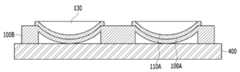
도 5a는 도 2b에 도시되는 본 발명의 제1실시예에 따른 커브드 이미지 센서의 변형 예로서, 적외선차단필터(170)를 상기 플레어고스트 방지막(130) 상부에 형성하여, 적외선차단필터(170)와 커브드 이미지 센서가 결합된 일체형을 도시한다.FIG. 5A is a modification of the curved image sensor according to the first embodiment of the present invention shown in FIG. 2B. The
상기 이미지센서칩(110)은 상기 지지기판(100)의 지지부(110B)의 상부를 덮도록 형성되며, 플레어고스트 방지막(130)의 상부표면은 이미지센서칩(110)의 상부표면(S2)과 동일레벨에 형성된다.The upper surface of the flare
상기 적외선차단필터(170)의 굴절률은 상기 플레어고스트 방지막(130)의 굴절률보다 큰 물질로 형성된다. 예를 들면, 상기 적외선차단필터(170)는 약 1.5 정도의 굴절률을 갖는 글래스로 형성될 수 있으며, 플레어고스트 방지막(130) 상부에 접촉하도록 형성하여, 본 발명의 커브드 이미지 센서를 포함하는 전자장치의 제조공정을 단순화 하여 비용절감 효과를 제공할 수 있다.The refractive index of the
또한, 본 발명의 제1실시예에 따른 커브드 이미지 센서의 변형 예는 적외선차단필터(170)과 플레어고스트 방지막(130)사이에 공기층을 형성하지 않음으로써, 공기층을 통과할 때보다 입사광이 통과하는 매질의 수를 줄일 수 있어, 입사광의 광학적 특성을 향상시킬 수 있다.In addition, a modified example of the curved image sensor according to the first embodiment of the present invention is characterized in that an air layer is not formed between the
그리고 도 5b는 도 2c에 도시되는 본 발명의 제1실시예에 따른 커브드 이미지 센서의 변형 예로서, 플레어고스트 방지막(130) 상부에 적외선차단필터(170)을 형성하여, 적외선차단필터(170)와 커브드 이미지 센서가 결합된 일체형을 포함 할 수 있다.5B is a modification of the curved image sensor according to the first embodiment of the present invention shown in FIG. 2C. The
상기 이미지센서칩(100)의 상부표면은 상기 지지기판(100)의 만곡부(100)의 상부표면과 동일레벨에 형성되거나 낮게 형성될 수 있다.The upper surface of the
또한 플레어고스트 방지막(130)은 상기 이미지센서칩(110)이 형성되지 않은 지지기판(100)의 상부를 덮는 형태로 형성될 수 있다. 그리고 상기 이미지센서칩(110)의 상부표면은 만곡부(110A)의 상부표면과 동일레벨에 형성되거나 만곡부(110A)의 상부표면보다 낮게 형성될 수도 있다.The flare
상기 도 5a 및 5b의 플레어고스트 방지막(130)는 가시광선에 대해 투명성을 갖고, 공기보다 큰 굴절율을 갖는 열 경화성 물질로 구성될 수 있으며, 바람직하게는 공기보다 크고 적외선차단필터보다 낮은 굴절율을 갖는 열 경화성 물질로 구성될 수 있다. 예를들면, 플레어고스트 방지막(130)은 폴리이미드, 폴리스티렌, 폴리 하이드록시 스티렌계 물질을 포함할 수 있다.The flare
상술한 본 발명의 실시예에 따른 커브드 이미지 센서는 다양한 전자장치 또는 시스템에 이용될 수 있다. 이하에서는, 도 6을 참조하여 카메라에 본 발명의 실시예에 따른 커브드 이미지 센서를 적용한 경우를 예시하여 설명하기로 한다.The curved image sensor according to the embodiment of the present invention described above can be used in various electronic devices or systems. Hereinafter, a case in which a curved image sensor according to an embodiment of the present invention is applied to a camera will be described with reference to FIG.
도 6는 본 발명의 실시예에 따른 커브드 이미지 센서를 구비한 전자장치를 간략히 도시한 도면이다.FIG. 6 is a schematic view of an electronic device having a curved image sensor according to an embodiment of the present invention.
도 6를 참조하여, 실시예에 따른 커브드 이미지 센서를 구비한 전자장치는 정지영상 또는 동영상을 촬영할 수 있는 카메라일 수 있다. 전자장치는 커브드 이미지 센서(300), 광학 시스템(또는, 광학 렌즈)(310), 셔터 유닛(311), 커브드 이미지 센서(300) 및 셔터 유닛(311)을 제어/구동하는 구동부(313) 및 신호 처리부(312)를 포함할 수 있다.Referring to FIG. 6, the electronic device having the curved image sensor according to the embodiment may be a camera capable of shooting a still image or a moving image. The electronic device includes a
광학 시스템(310)은 피사체로부터의 이미지 광(입사광)을 커브드 이미지 센서(300)의 픽셀 어레이(도 1의 도면부호 '2' 참조)로 안내한다. 광학 시스템(310)은 복수의 광학 렌즈로 구성될 수 있다. 셔터 유닛(311)은 커브드 이미지 센서(300)에 대한 광 조사 기간 및 차폐 기간을 제어한다. 구동부(313)는 커브드 이미지 센서(300)의 전송 동작과 셔터 유닛(311)의 셔터 동작을 제어한다. 신호 처리부(312)는 커브드 이미지 센서(300)로부터 출력된 신호에 관해 다양한 종류의 신호 처리를 수행한다. 신호 처리 후의 이미지 신호(Dout)는 메모리 등의 저장 매체에 저장되거나, 모니터 등에 출력된다.The
본 발명의 기술 사상은 상기 바람직한 실시예에 따라 구체적으로 기술되었으나, 상기 실시예는 그 설명을 위한 것이며, 그 제한을 위한 것이 아님을 주의하여야 한다. 또한, 본 발명의 기술분야의 통상의 전문가라면 본 발명의 기술사상의 범위내의 다양한 실시예가 가능함을 이해할 수 있을 것이다.The technical idea of the present invention has been specifically described according to the above preferred embodiments, but it should be noted that the above embodiments are intended to be illustrative and not restrictive. In addition, it will be understood by those of ordinary skill in the art that various embodiments within the scope of the technical idea of the present invention are possible.
110 : 이미지센서칩120 : 지지기판
130 : 플레어고스트 방지막 170 : 적외선차단필터110: image sensor chip 120: support substrate
130: flare ghost prevention film 170: infrared ray cut filter
Claims (19)
Translated fromKorean상기 지지기판상에 형성되며, 만곡된 광입사면을 갖는 이미지센서칩; 및
상기 이미지센서칩의 만곡된 광입사면 상에 형성되고, 평탄한 상부표면을 갖는 플레어고스트 방지막을 포함하는
커브드 이미지 센서.
A support substrate;
An image sensor chip formed on the supporting substrate and having a curved light incident surface; And
And a flare ghost prevention film formed on the curved light incident surface of the image sensor chip and having a flat upper surface,
Curved image sensor.
상기 플레어고스트 방지막의 하부표면은 상기 이미지센서칩의 상부표면과 동일한 곡률을 갖는 커브드 이미지 센서.
The method according to claim 1,
Wherein the lower surface of the flare ghost prevention film has the same curvature as the upper surface of the image sensor chip.
상기 플레어고스트 방지막은 상기 이미지센서칩의 최하부 상부표면부터 최상부 상부표면까지 채우는 커브드 이미지 센서.
The method according to claim 1,
Wherein the flare ghost prevention film fills the lowermost top surface to the uppermost upper surface of the image sensor chip.
상기 플레어고스트 방지막은 공기보다 큰 굴절율을 갖는 물질을 포함하는 커브드 이미지 센서.
The method according to claim 1,
Wherein the flare ghost prevention film comprises a material having a refractive index greater than air.
상기 플레어고스트 방지막은 열경화성 물질을 포함하는 커브드 이미지 센서.
The method according to claim 1,
Wherein the flare ghost prevention film comprises a thermosetting material.
상기 지지기판은 상기 이미지센서칩이 형성되며 중심이 오목하게 만곡되는 만곡부; 및
상기 만곡부의 가장자리 양측벽에 접하는 지지부
를 포함하는 커브드 이미지 센서.
The method according to claim 1,
Wherein the support substrate comprises: a curved portion formed with the image sensor chip and curved at a center thereof; And
A support portion contacting the both side walls of the curved portion
Wherein the curved image sensor comprises:
상기 이미지센서칩은 상기 만곡부 및 상기 지지부의 일부 상에 형성되는 커브드 이미지 센서.
The method according to claim 6,
Wherein the image sensor chip is formed on the curved part and a part of the supporting part.
상기 플레어고스트 방지막은 상기 이미지센서칩 및 상기 만곡부의 일부 상에 형성되는
커브드 이미지 센서.
The method according to claim 6,
Wherein the flare ghost prevention film is formed on a part of the image sensor chip and the curved portion
Curved image sensor.
상기 플레어고스트 방지막은 상기 이미지센서칩이 형성되지 않은 지지기판의 상부를 덮는 커브드 이미지 센서.
The method according to claim 6,
Wherein the flare ghost prevention film covers an upper portion of a supporting substrate on which the image sensor chip is not formed.
상기 이미지센서칩의 만곡된 광입사면을 덮고, 평탄한 상부표면을 갖는 플레어고스트 방지막; 및
상기 플레어고스트 방지막의 평탄한 상부표면에 접하도록 형성된 적외선차단필터
을 포함하는 커브드 이미지 센서.
An image sensor chip having a curved light incident surface;
A flare ghost prevention film covering the curved light incident surface of the image sensor chip and having a flat upper surface; And
An infrared cutoff filter formed to contact a flat upper surface of the flare ghost prevention film;
A curved image sensor.
상기 이미지센서칩 하부에 형성되며, 오목하게 만곡되는 지지기판을 더 포함하며, 상기 지지기판은 상기 이미지센서칩이 형성되며 중심이 오목하게 만곡되는 만곡부;
상기 만곡부의 가장자리 양측벽에 접하는 지지부
를 포함하는 커브드 이미지 센서.
11. The method of claim 10,
Further comprising: a support substrate formed on the lower portion of the image sensor chip and curved concavely, wherein the support substrate includes a curved portion formed with the image sensor chip and curved at a center thereof;
A support portion contacting the both side walls of the curved portion
Wherein the curved image sensor comprises:
상기 이미지센서칩은 상기 만곡부 및 상기 지지부의 일부 상에 형성되는 커브드 이미지 센서.
12. The method of claim 11,
Wherein the image sensor chip is formed on the curved part and a part of the supporting part.
상기 플레어고스트 방지막은 상기 이미지센서칩 및 상기 만곡부의 일부 상에 형성되는
커브드 이미지 센서.
12. The method of claim 11,
Wherein the flare ghost prevention film is formed on a part of the image sensor chip and the curved portion
Curved image sensor.
상기 플레어고스트 방지막은 상기 이미지센서칩이 형성되지 않은 지지기판의 상부를 덮는 커브드 이미지 센서.
12. The method of claim 11,
Wherein the flare ghost prevention film covers an upper portion of a supporting substrate on which the image sensor chip is not formed.
상기 적외선차단필터의 굴절률은 상기 플레어고스트 방지막의 굴절률보다 큰 커브드 이미지 센서.
11. The method of claim 10,
Wherein the refractive index of the infrared cut filter is larger than the refractive index of the flare ghost prevention film.
상기 플레어고스트 방지막의 하부표면은 상기 이미지센서칩의 만곡된 광입사면과 접착되어, 상기 이미지센서칩의 만곡된 광입사면이 상기 플레어고스트 방지막에 의해 고정되는 커브드 이미지 센서.
11. The method of claim 10,
Wherein the lower surface of the flare ghost prevention film is adhered to the curved light incident surface of the image sensor chip so that the curved light incident surface of the image sensor chip is fixed by the flare ghost prevention film.
상기 플레어고스트 방지막은 열경화성 물질을 포함하는 커브드 이미지 센서.
11. The method of claim 10,
Wherein the flare ghost prevention film comprises a thermosetting material.
상기 플레어고스트 방지막은 상기 이미지센서칩의 만곡된 광입사면 최하부 표면부터 최상부표면까지 채우는 형태를 갖는
커브드 이미지 센서.
11. The method of claim 10,
The flare ghost prevention film has a shape that fills from the lowermost surface to the uppermost surface of the curved light incident surface of the image sensor chip
Curved image sensor.
상기 플레어고스트 방지막은 공기보다 크고 상기 적외선차단필터보다 낮은 굴절률을 갖는 커브드 이미지 센서.
11. The method of claim 10,
Wherein the flare ghost prevention film is larger than air and has a refractive index lower than that of the infrared cut filter.
Priority Applications (2)
| Application Number | Priority Date | Filing Date | Title |
|---|---|---|---|
| KR1020170083312AKR102468262B1 (en) | 2017-06-30 | 2017-06-30 | Curved image sensor |
| US15/865,633US10304880B2 (en) | 2017-06-30 | 2018-01-09 | Curved image sensor |
Applications Claiming Priority (1)
| Application Number | Priority Date | Filing Date | Title |
|---|---|---|---|
| KR1020170083312AKR102468262B1 (en) | 2017-06-30 | 2017-06-30 | Curved image sensor |
Publications (2)
| Publication Number | Publication Date |
|---|---|
| KR20190002963Atrue KR20190002963A (en) | 2019-01-09 |
| KR102468262B1 KR102468262B1 (en) | 2022-11-18 |
Family
ID=64738313
Family Applications (1)
| Application Number | Title | Priority Date | Filing Date |
|---|---|---|---|
| KR1020170083312AActiveKR102468262B1 (en) | 2017-06-30 | 2017-06-30 | Curved image sensor |
Country Status (2)
| Country | Link |
|---|---|
| US (1) | US10304880B2 (en) |
| KR (1) | KR102468262B1 (en) |
Families Citing this family (10)
| Publication number | Priority date | Publication date | Assignee | Title |
|---|---|---|---|---|
| US12140855B2 (en) | 2008-05-19 | 2024-11-12 | Peter Lablans | Camera system with a plurality of image sensors |
| US9893058B2 (en)* | 2015-09-17 | 2018-02-13 | Semiconductor Components Industries, Llc | Method of manufacturing a semiconductor device having reduced on-state resistance and structure |
| FR3061990B1 (en)* | 2017-01-18 | 2019-04-19 | Commissariat A L'energie Atomique Et Aux Energies Alternatives | METHOD FOR COLLECTIVELY PRODUCING CURVED ELECTRONIC CIRCUITS |
| FR3073322B1 (en)* | 2017-11-07 | 2021-12-03 | Commissariat Energie Atomique | PROCESS FOR MAKING AT LEAST ONE CURVED ELECTRONIC CIRCUIT |
| JP2022002229A (en)* | 2018-09-05 | 2022-01-06 | ソニーセミコンダクタソリューションズ株式会社 | Image pickup device and image sensor |
| JP7401441B2 (en)* | 2018-09-07 | 2023-12-19 | ソニーセミコンダクタソリューションズ株式会社 | Imaging device and method for manufacturing the imaging device |
| FR3099290B1 (en)* | 2019-07-26 | 2021-07-02 | Commissariat Energie Atomique | Method of collective curvature of a set of electronic chips |
| SG10202002922RA (en) | 2020-03-30 | 2021-10-28 | Sharma Nishant | SVVRON Effect - 3D TV & Camera (without Glasses) |
| CN112532942B (en)* | 2020-11-30 | 2021-08-10 | 黑龙江合师惠教育科技有限公司 | Image sensor device, manufacturing method thereof, camera and educational behavior analysis monitoring equipment |
| CN112713159A (en)* | 2020-12-24 | 2021-04-27 | 深圳市汇顶科技股份有限公司 | Method for manufacturing image sensor, camera module and electronic equipment |
Citations (6)
| Publication number | Priority date | Publication date | Assignee | Title |
|---|---|---|---|---|
| JP2004119672A (en)* | 2002-09-26 | 2004-04-15 | Sony Corp | Solid-state imaging device and its manufacturing method |
| JP2007142058A (en)* | 2005-11-17 | 2007-06-07 | Matsushita Electric Ind Co Ltd | Semiconductor imaging device and manufacturing method thereof, and semiconductor imaging device and manufacturing method thereof |
| JP2012028620A (en)* | 2010-07-26 | 2012-02-09 | Sharp Corp | Solid state imaging apparatus, and method for manufacturing the same, and electronic device |
| KR20120056204A (en)* | 2010-11-24 | 2012-06-01 | 소니 주식회사 | Solid-state imaging device and manufacturing method thereof, and electronic apparatus |
| US20170005125A1 (en)* | 2013-12-09 | 2017-01-05 | Sony Corporation | Imaging unit, lens barrel, and portable terminal |
| JP2017022313A (en)* | 2015-07-14 | 2017-01-26 | 株式会社東芝 | Camera module |
Family Cites Families (9)
| Publication number | Priority date | Publication date | Assignee | Title |
|---|---|---|---|---|
| JP2007266380A (en) | 2006-03-29 | 2007-10-11 | Matsushita Electric Ind Co Ltd | Semiconductor imaging device and manufacturing method thereof |
| US7507944B1 (en)* | 2006-06-27 | 2009-03-24 | Cypress Semiconductor Corporation | Non-planar packaging of image sensor |
| KR101378418B1 (en)* | 2007-11-01 | 2014-03-27 | 삼성전자주식회사 | image sensor module and fabrication method thereof |
| JP2015070159A (en)* | 2013-09-30 | 2015-04-13 | ソニー株式会社 | Solid state image sensor and manufacturing method therefor, and electronic apparatus |
| JP2015192074A (en) | 2014-03-28 | 2015-11-02 | ソニー株式会社 | Solid-state imaging device, electronic apparatus, and manufacturing method of solid-state imaging device |
| US10373995B2 (en)* | 2014-09-19 | 2019-08-06 | Microsoft Technology Licensing, Llc | Image sensor bending using tension |
| US9998643B2 (en)* | 2015-03-24 | 2018-06-12 | Semiconductor Components Industries, Llc | Methods of forming curved image sensors |
| US9870927B2 (en)* | 2015-04-02 | 2018-01-16 | Microsoft Technology Licensing, Llc | Free-edge semiconductor chip bending |
| US10062727B2 (en)* | 2016-09-09 | 2018-08-28 | Microsoft Technology Licensing, Llc | Strain relieving die for curved image sensors |
- 2017
- 2017-06-30KRKR1020170083312Apatent/KR102468262B1/enactiveActive
- 2018
- 2018-01-09USUS15/865,633patent/US10304880B2/enactiveActive
Patent Citations (6)
| Publication number | Priority date | Publication date | Assignee | Title |
|---|---|---|---|---|
| JP2004119672A (en)* | 2002-09-26 | 2004-04-15 | Sony Corp | Solid-state imaging device and its manufacturing method |
| JP2007142058A (en)* | 2005-11-17 | 2007-06-07 | Matsushita Electric Ind Co Ltd | Semiconductor imaging device and manufacturing method thereof, and semiconductor imaging device and manufacturing method thereof |
| JP2012028620A (en)* | 2010-07-26 | 2012-02-09 | Sharp Corp | Solid state imaging apparatus, and method for manufacturing the same, and electronic device |
| KR20120056204A (en)* | 2010-11-24 | 2012-06-01 | 소니 주식회사 | Solid-state imaging device and manufacturing method thereof, and electronic apparatus |
| US20170005125A1 (en)* | 2013-12-09 | 2017-01-05 | Sony Corporation | Imaging unit, lens barrel, and portable terminal |
| JP2017022313A (en)* | 2015-07-14 | 2017-01-26 | 株式会社東芝 | Camera module |
Also Published As
| Publication number | Publication date |
|---|---|
| KR102468262B1 (en) | 2022-11-18 |
| US10304880B2 (en) | 2019-05-28 |
| US20190006401A1 (en) | 2019-01-03 |
Similar Documents
| Publication | Publication Date | Title |
|---|---|---|
| KR102468262B1 (en) | Curved image sensor | |
| US11600648B2 (en) | Apparatuses and packages including a semiconductor substrate with a plurality of photoelectronic conversion regions and a transparent substrate | |
| US7205526B2 (en) | Methods of fabricating layered lens structures | |
| JP5857399B2 (en) | Solid-state imaging device and electronic device | |
| CN104282706B (en) | Imaging sensor, manufacturing equipment, manufacturing method and electronic device | |
| JP2020136545A (en) | Solid-state imaging device and electronic apparatus | |
| KR20160050866A (en) | Curved image sensor, method for fabricating the same and electronic device having the same | |
| US20210005656A1 (en) | Imaging element and method of manufacturing imaging element | |
| US12402430B2 (en) | Image sensor | |
| JP7720301B2 (en) | Solid-state imaging device and electronic device | |
| US12324266B2 (en) | Solid-state imaging device and electronic device | |
| US12068347B2 (en) | Solid-state imaging device and electronic device |
Legal Events
| Date | Code | Title | Description |
|---|---|---|---|
| PA0109 | Patent application | Patent event code:PA01091R01D Comment text:Patent Application Patent event date:20170630 | |
| PG1501 | Laying open of application | ||
| A201 | Request for examination | ||
| PA0201 | Request for examination | Patent event code:PA02012R01D Patent event date:20200401 Comment text:Request for Examination of Application Patent event code:PA02011R01I Patent event date:20170630 Comment text:Patent Application | |
| E902 | Notification of reason for refusal | ||
| PE0902 | Notice of grounds for rejection | Comment text:Notification of reason for refusal Patent event date:20210914 Patent event code:PE09021S01D | |
| AMND | Amendment | ||
| E601 | Decision to refuse application | ||
| PE0601 | Decision on rejection of patent | Patent event date:20220329 Comment text:Decision to Refuse Application Patent event code:PE06012S01D Patent event date:20210914 Comment text:Notification of reason for refusal Patent event code:PE06011S01I | |
| X091 | Application refused [patent] | ||
| AMND | Amendment | ||
| PX0901 | Re-examination | Patent event code:PX09011S01I Patent event date:20220329 Comment text:Decision to Refuse Application Patent event code:PX09012R01I Patent event date:20211112 Comment text:Amendment to Specification, etc. | |
| E902 | Notification of reason for refusal | ||
| PE0902 | Notice of grounds for rejection | Comment text:Notification of reason for refusal Patent event date:20220509 Patent event code:PE09021S01D | |
| AMND | Amendment | ||
| PX0701 | Decision of registration after re-examination | Patent event date:20221020 Comment text:Decision to Grant Registration Patent event code:PX07013S01D Patent event date:20220711 Comment text:Amendment to Specification, etc. Patent event code:PX07012R01I Patent event date:20220427 Comment text:Amendment to Specification, etc. Patent event code:PX07012R01I Patent event date:20220329 Comment text:Decision to Refuse Application Patent event code:PX07011S01I Patent event date:20211112 Comment text:Amendment to Specification, etc. Patent event code:PX07012R01I | |
| X701 | Decision to grant (after re-examination) | ||
| GRNT | Written decision to grant | ||
| PR0701 | Registration of establishment | Comment text:Registration of Establishment Patent event date:20221114 Patent event code:PR07011E01D | |
| PR1002 | Payment of registration fee | Payment date:20221115 End annual number:3 Start annual number:1 | |
| PG1601 | Publication of registration |