KR20180132979A - Semiconductor device and method for manufacturing the same - Google Patents
Semiconductor device and method for manufacturing the sameDownload PDFInfo
- Publication number
- KR20180132979A KR20180132979AKR1020187035127AKR20187035127AKR20180132979AKR 20180132979 AKR20180132979 AKR 20180132979AKR 1020187035127 AKR1020187035127 AKR 1020187035127AKR 20187035127 AKR20187035127 AKR 20187035127AKR 20180132979 AKR20180132979 AKR 20180132979A
- Authority
- KR
- South Korea
- Prior art keywords
- layer
- insulating layer
- oxide semiconductor
- oxide
- oxygen
- Prior art date
- Legal status (The legal status is an assumption and is not a legal conclusion. Google has not performed a legal analysis and makes no representation as to the accuracy of the status listed.)
- Granted
Links
Images


Classifications
- H—ELECTRICITY
- H10—SEMICONDUCTOR DEVICES; ELECTRIC SOLID-STATE DEVICES NOT OTHERWISE PROVIDED FOR
- H10D—INORGANIC ELECTRIC SEMICONDUCTOR DEVICES
- H10D30/00—Field-effect transistors [FET]
- H10D30/60—Insulated-gate field-effect transistors [IGFET]
- H10D30/67—Thin-film transistors [TFT]
- H10D30/6704—Thin-film transistors [TFT] having supplementary regions or layers in the thin films or in the insulated bulk substrates for controlling properties of the device
- H01L29/78606—
- H—ELECTRICITY
- H01—ELECTRIC ELEMENTS
- H01L—SEMICONDUCTOR DEVICES NOT COVERED BY CLASS H10
- H01L21/00—Processes or apparatus adapted for the manufacture or treatment of semiconductor or solid state devices or of parts thereof
- H01L21/02—Manufacture or treatment of semiconductor devices or of parts thereof
- H01L21/02104—Forming layers
- H01L21/02107—Forming insulating materials on a substrate
- H01L21/02225—Forming insulating materials on a substrate characterised by the process for the formation of the insulating layer
- H01L21/0226—Forming insulating materials on a substrate characterised by the process for the formation of the insulating layer formation by a deposition process
- H01L21/02263—Forming insulating materials on a substrate characterised by the process for the formation of the insulating layer formation by a deposition process deposition from the gas or vapour phase
- H01L21/02266—Forming insulating materials on a substrate characterised by the process for the formation of the insulating layer formation by a deposition process deposition from the gas or vapour phase deposition by physical ablation of a target, e.g. sputtering, reactive sputtering, physical vapour deposition or pulsed laser deposition
- H01L27/1225—
- H01L29/66742—
- H01L29/7869—
- H01L29/78696—
- H—ELECTRICITY
- H10—SEMICONDUCTOR DEVICES; ELECTRIC SOLID-STATE DEVICES NOT OTHERWISE PROVIDED FOR
- H10D—INORGANIC ELECTRIC SEMICONDUCTOR DEVICES
- H10D30/00—Field-effect transistors [FET]
- H10D30/01—Manufacture or treatment
- H10D30/021—Manufacture or treatment of FETs having insulated gates [IGFET]
- H10D30/031—Manufacture or treatment of FETs having insulated gates [IGFET] of thin-film transistors [TFT]
- H—ELECTRICITY
- H10—SEMICONDUCTOR DEVICES; ELECTRIC SOLID-STATE DEVICES NOT OTHERWISE PROVIDED FOR
- H10D—INORGANIC ELECTRIC SEMICONDUCTOR DEVICES
- H10D30/00—Field-effect transistors [FET]
- H10D30/60—Insulated-gate field-effect transistors [IGFET]
- H10D30/67—Thin-film transistors [TFT]
- H10D30/6729—Thin-film transistors [TFT] characterised by the electrodes
- H10D30/673—Thin-film transistors [TFT] characterised by the electrodes characterised by the shapes, relative sizes or dispositions of the gate electrodes
- H—ELECTRICITY
- H10—SEMICONDUCTOR DEVICES; ELECTRIC SOLID-STATE DEVICES NOT OTHERWISE PROVIDED FOR
- H10D—INORGANIC ELECTRIC SEMICONDUCTOR DEVICES
- H10D30/00—Field-effect transistors [FET]
- H10D30/60—Insulated-gate field-effect transistors [IGFET]
- H10D30/67—Thin-film transistors [TFT]
- H10D30/674—Thin-film transistors [TFT] characterised by the active materials
- H10D30/6755—Oxide semiconductors, e.g. zinc oxide, copper aluminium oxide or cadmium stannate
- H—ELECTRICITY
- H10—SEMICONDUCTOR DEVICES; ELECTRIC SOLID-STATE DEVICES NOT OTHERWISE PROVIDED FOR
- H10D—INORGANIC ELECTRIC SEMICONDUCTOR DEVICES
- H10D30/00—Field-effect transistors [FET]
- H10D30/60—Insulated-gate field-effect transistors [IGFET]
- H10D30/67—Thin-film transistors [TFT]
- H10D30/6757—Thin-film transistors [TFT] characterised by the structure of the channel, e.g. transverse or longitudinal shape or doping profile
- H—ELECTRICITY
- H10—SEMICONDUCTOR DEVICES; ELECTRIC SOLID-STATE DEVICES NOT OTHERWISE PROVIDED FOR
- H10D—INORGANIC ELECTRIC SEMICONDUCTOR DEVICES
- H10D64/00—Electrodes of devices having potential barriers
- H10D64/20—Electrodes characterised by their shapes, relative sizes or dispositions
- H10D64/27—Electrodes not carrying the current to be rectified, amplified, oscillated or switched, e.g. gates
- H10D64/311—Gate electrodes for field-effect devices
- H10D64/411—Gate electrodes for field-effect devices for FETs
- H10D64/511—Gate electrodes for field-effect devices for FETs for IGFETs
- H10D64/514—Gate electrodes for field-effect devices for FETs for IGFETs characterised by the insulating layers
- H—ELECTRICITY
- H10—SEMICONDUCTOR DEVICES; ELECTRIC SOLID-STATE DEVICES NOT OTHERWISE PROVIDED FOR
- H10D—INORGANIC ELECTRIC SEMICONDUCTOR DEVICES
- H10D64/00—Electrodes of devices having potential barriers
- H10D64/60—Electrodes characterised by their materials
- H10D64/66—Electrodes having a conductor capacitively coupled to a semiconductor by an insulator, e.g. MIS electrodes
- H10D64/68—Electrodes having a conductor capacitively coupled to a semiconductor by an insulator, e.g. MIS electrodes characterised by the insulator, e.g. by the gate insulator
- H10D64/693—Electrodes having a conductor capacitively coupled to a semiconductor by an insulator, e.g. MIS electrodes characterised by the insulator, e.g. by the gate insulator the insulator comprising nitrogen, e.g. nitrides, oxynitrides or nitrogen-doped materials
- H—ELECTRICITY
- H10—SEMICONDUCTOR DEVICES; ELECTRIC SOLID-STATE DEVICES NOT OTHERWISE PROVIDED FOR
- H10D—INORGANIC ELECTRIC SEMICONDUCTOR DEVICES
- H10D86/00—Integrated devices formed in or on insulating or conducting substrates, e.g. formed in silicon-on-insulator [SOI] substrates or on stainless steel or glass substrates
- H10D86/40—Integrated devices formed in or on insulating or conducting substrates, e.g. formed in silicon-on-insulator [SOI] substrates or on stainless steel or glass substrates characterised by multiple TFTs
- H10D86/421—Integrated devices formed in or on insulating or conducting substrates, e.g. formed in silicon-on-insulator [SOI] substrates or on stainless steel or glass substrates characterised by multiple TFTs having a particular composition, shape or crystalline structure of the active layer
- H10D86/423—Integrated devices formed in or on insulating or conducting substrates, e.g. formed in silicon-on-insulator [SOI] substrates or on stainless steel or glass substrates characterised by multiple TFTs having a particular composition, shape or crystalline structure of the active layer comprising semiconductor materials not belonging to the Group IV, e.g. InGaZnO
- H—ELECTRICITY
- H10—SEMICONDUCTOR DEVICES; ELECTRIC SOLID-STATE DEVICES NOT OTHERWISE PROVIDED FOR
- H10D—INORGANIC ELECTRIC SEMICONDUCTOR DEVICES
- H10D86/00—Integrated devices formed in or on insulating or conducting substrates, e.g. formed in silicon-on-insulator [SOI] substrates or on stainless steel or glass substrates
- H10D86/40—Integrated devices formed in or on insulating or conducting substrates, e.g. formed in silicon-on-insulator [SOI] substrates or on stainless steel or glass substrates characterised by multiple TFTs
- H10D86/60—Integrated devices formed in or on insulating or conducting substrates, e.g. formed in silicon-on-insulator [SOI] substrates or on stainless steel or glass substrates characterised by multiple TFTs wherein the TFTs are in active matrices
- H—ELECTRICITY
- H10—SEMICONDUCTOR DEVICES; ELECTRIC SOLID-STATE DEVICES NOT OTHERWISE PROVIDED FOR
- H10D—INORGANIC ELECTRIC SEMICONDUCTOR DEVICES
- H10D99/00—Subject matter not provided for in other groups of this subclass
Landscapes
- Engineering & Computer Science (AREA)
- Physics & Mathematics (AREA)
- Power Engineering (AREA)
- Condensed Matter Physics & Semiconductors (AREA)
- General Physics & Mathematics (AREA)
- Manufacturing & Machinery (AREA)
- Computer Hardware Design (AREA)
- Microelectronics & Electronic Packaging (AREA)
- Optics & Photonics (AREA)
- Thin Film Transistor (AREA)
- Electroluminescent Light Sources (AREA)
- Physical Deposition Of Substances That Are Components Of Semiconductor Devices (AREA)
- Recrystallisation Techniques (AREA)
- Liquid Crystal (AREA)
- Devices For Indicating Variable Information By Combining Individual Elements (AREA)
- Formation Of Insulating Films (AREA)
- Physical Vapour Deposition (AREA)
- Dram (AREA)
Abstract
Translated fromKoreanDescription
Translated fromKorean산화물 반도체를 이용하는 반도체 장치 및 그 제작 방법에 관한 것이다.To a semiconductor device using an oxide semiconductor and a manufacturing method thereof.
아울러, 본 명세서 내에 있어서 반도체 장치란 반도체 특성을 이용함으로써 기능할 수 있는 장치 전반을 가리키며, 전기광학장치, 반도체 회로 및 전자기기는 모두 반도체 장치이다.In the present specification, the term "semiconductor device" refers to the entire device that can function by utilizing semiconductor characteristics, and the electro-optical device, the semiconductor circuit, and the electronic device are all semiconductor devices.
절연 표면을 갖는 기판 상에 형성된 반도체 박막을 이용하여 박막 트랜지스터(TFT)를 구성하는 기술이 주목을 받고 있다. 박막 트랜지스터는 액정 텔레비전으로 대표되는 표시장치에 이용되고 있다. 박막 트랜지스터에 적용 가능한 반도체 박막으로서 실리콘계 반도체 재료가 알려져 있으나, 그 외의 재료로서 산화물 반도체가 주목을 받고 있다.A technique of forming a thin film transistor (TFT) using a semiconductor thin film formed on a substrate having an insulating surface has attracted attention. The thin film transistor is used in a display device typified by a liquid crystal television. Silicon-based semiconductor materials are known as semiconductor thin films applicable to thin film transistors, but oxide semiconductors are attracting attention as other materials.
산화물 반도체의 재료로서는 산화 아연 또는 산화 아연을 성분으로 하는 것이 알려져 있다. 그리고, 전자 캐리어 농도가 1018/㎤ 미만인 비정질 산화물(산화물 반도체)로 형성된 박막 트랜지스터가 개시되어 있다(특허문헌 1 내지 3 참조).As the material of the oxide semiconductor, it is known that zinc oxide or zinc oxide is used as a component. A thin film transistor formed of an amorphous oxide (oxide semiconductor) having an electron carrier concentration of less than 1018 / cm 3 has been disclosed (see Patent Documents 1 to 3).
그러나, 산화물 반도체는 박막 형성 공정에 있어서 화학량론적 조성으로부터의 편차가 발생하게 된다. 예를 들어, 산소의 과부족에 의해 산화물 반도체의 전기전도도가 변화되어 버린다. 또한, 산화물 반도체의 박막 형성중에 혼입되는 수소나 수분이 산소(O)-수소(H) 결합을 형성하여 전자 공여체가 되고, 전기전도도를 변화시키는 요인이 된다. 아울러 O-H는 극성 분자이기 때문에, 산화물 반도체에 의해 제작되는 박막 트랜지스터와 같은 능동 디바이스에 대해 특성의 변동 요인이 된다.However, the oxide semiconductor deviates from the stoichiometric composition in the thin film forming process. For example, the electrical conductivity of the oxide semiconductor changes due to excess or deficiency of oxygen. Further, hydrogen or water mixed in the thin film formation of the oxide semiconductor forms an oxygen (O) -hydrogen (H) bond to become an electron donor, which is a factor for changing the electric conductivity. In addition, since O-H is a polar molecule, characteristics of the active device such as a thin film transistor fabricated by oxide semiconductors are varied.
이와 같은 문제를 감안하여 본 발명의 일 형태는 안정된 전기적 특성을 갖는 산화물 반도체를 이용한 반도체 장치를 제공하는 것을 목적으로 한다.In view of such a problem, an aspect of the present invention is to provide a semiconductor device using an oxide semiconductor having stable electrical characteristics.
산화물 반도체층을 이용하는 박막 트랜지스터의 전기적 특성 변동을 억제하기 위해 변동 요인이 되는 수소, 수분, 수산기 또는 수소화물(수소화합물이라고도 함) 등의 불순물을 산화물 반도체층으로부터 배제한다.Impurities such as hydrogen, moisture, hydroxyl groups, or hydrides (also referred to as hydrogen compounds), which are variable factors, are excluded from the oxide semiconductor layer in order to suppress variations in electrical characteristics of the thin film transistor using the oxide semiconductor layer.
댕글링 본드(dangling bonds)로 대표되는 결함을 많이 포함하는 절연층을 산소 과잉인 혼합 영역 또는 산소 과잉인 산화물 절연층을 사이에 두고 산화물 반도체층 상에 형성하고, 산화물 반도체층에 포함되는 수소나 수분(수소 원자나, H2O 등 수소 원자를 포함하는 화합물) 등의 불순물을 산소 과잉의 혼합 영역 또는 산소 과잉의 산화물 절연층을 통과시켜 결함을 포함하는 절연층으로 확산시켜, 상기 산화물 반도체층 내의 불순물 농도를 저감한다.An insulating layer containing a large amount of defects typified by dangling bonds is formed on the oxide semiconductor layer with an oxygen-excess mixed region or an oxygen-rich oxide insulating layer interposed therebetween, An impurity such as moisture (a hydrogen atom or a compound including a hydrogen atom such as H2 O) or the like is diffused into an insulating layer containing defects by passing through an excessive oxygen mixed region or an excess oxygen oxide insulating layer, Thereby reducing the concentration of impurities in the film.
결함을 많이 포함하는 절연층은 수소나 수분(수소 원자나, H2O 등 수소 원자를 포함하는 화합물)에 대하여 속박 에너지가 크고, 결함을 많이 포함하는 절연층에서 그 불순물은 안정화되므로 산화물 반도체층으로부터 결함을 포함하는 절연층으로 그 불순물을 확산시켜, 그 불순물을 산화물 반도체층으로부터 배제할 수 있다.Since the insulating layer containing a large amount of defects has a large bond energy with respect to hydrogen or water (a hydrogen atom or a compound containing hydrogen atoms such as H2 O) and the impurity is stabilized in an insulating layer containing many defects, It is possible to diffuse the impurity from the oxide semiconductor layer into the insulating layer containing the defect, and to remove the impurity from the oxide semiconductor layer.
나아가, 산화물 반도체층과 결함을 포함하는 절연층의 사이에 마련되는 혼합 영역 또는 산화물 절연층은 산소 과잉이기 때문에, 산소의 댕글링 본드를 결함으로서 많이 포함하고, 수소나 수분(수소 원자나, H2O 등 수소 원자를 포함하는 화합물) 등의 불순물에 대하여 속박 에너지가 크다. 따라서 산화물 반도체층으로부터 상기 불순물을 결함을 포함하는 절연층으로 확산시킬 때, 산소 과잉의 혼합 영역 또는 산소 과잉의 산화물 절연층이 확산을 용이하게 하도록 기능한다. 한편, 일단 산화물 반도체층으로부터 배제되어 결함을 포함하는 절연층으로 확산된 상기 불순물이 다시 산화물 반도체층으로 이동하려고 할 때, 상기 불순물을 속박하여 안정화시켜, 산화물 반도체층으로의 침입을 방지하는 보호층(배리어층)으로서 기능한다.Further, the mixed region or the oxide insulating layer provided between the oxide semiconductor layer and the insulating layer including the defect is excessively oxygen, so that the dangling bonds of oxygen are often included as defects, and hydrogen or moisture (hydrogen atoms or H2 O and the like), and the like. Therefore, when diffusing the impurity from the oxide semiconductor layer into the insulating layer containing defects, an excessive oxygen mixed region or an oxygen-rich oxide insulating layer functions to facilitate diffusion. On the other hand, when the impurity once excluded from the oxide semiconductor layer and diffused into the insulating layer including defects tries to move again to the oxide semiconductor layer, the impurity is stabilized by the impurity and is prevented from penetrating into the oxide semiconductor layer, (Barrier layer).
따라서, 산화물 반도체층 내의 수소나 수분(수소 원자나, H2O 등 수소 원자를 포함하는 화합물) 등의 불순물은 산소 과잉의 혼합 영역 또는 산소 과잉의 산화물 절연층으로 확산된다.Therefore, impurities such as hydrogen or moisture (hydrogen atom or a compound including hydrogen atom such as H2 O) in the oxide semiconductor layer are diffused into an oxygen-excess mixed region or an oxygen-excess oxide insulating layer.
그러므로, 산소 과잉의 혼합 영역 또는 산소 과잉의 산화물 절연층은 변동 요인이 되는 수소, 수분, 수산기 또는 수소화물(수소화합물이라고도 함) 등의 불순물을 산화물 반도체층에서 배제하고, 아울러 배리어층이 되어 결함을 포함하는 절연층으로 확산된 불순물이 다시 산화물 반도체층에 침입하는 것을 방지할 수 있다. 그 결과 산화물 반도체층 내의 불순물 농도를 저감시킨 상태로 유지할 수 있다.Therefore, the oxygen-excess mixed region or the oxygen-excess oxide insulating layer is removed from the oxide semiconductor layer, such as hydrogen, moisture, hydroxyl groups, or hydrides (also referred to as hydrogen compounds) It is possible to prevent the impurity diffused into the insulating layer including the oxide semiconductor layer from entering the oxide semiconductor layer again. As a result, the impurity concentration in the oxide semiconductor layer can be maintained in a reduced state.
따라서, 변동 요인이 되는 수소, 수분, 수산기 또는 수소화물(수소화합물이라고도 함) 등의 불순물이 저감된 산화물 반도체층을 이용한 박막 트랜지스터는 안정된 전기 특성을 가지며, 그 박막 트랜지스터를 포함하는 반도체 장치에 있어서는 높은 신뢰성을 달성할 수 있다.Therefore, a thin film transistor using an oxide semiconductor layer in which impurities such as hydrogen, moisture, hydroxyl groups, or hydrides (also referred to as hydrogen compounds), which are fluctuation factors, is reduced has stable electric characteristics, and in a semiconductor device including the thin film transistor High reliability can be achieved.
혼합 영역은 산화물 반도체층 및 적층하는 결함을 포함하는 절연층에 포함되는 재료의 혼합 영역으로, 산화물 반도체층과 결함을 포함하는 절연층의 계면을 명확하게 하지 않음으로써, 산화물 반도체층으로부터 결함을 포함하는 절연층으로의 수소의 확산이 보다 용이해진다. 예를 들어, 결함을 포함하는 절연층으로서 산화 실리콘층을 이용하는 경우, 혼합 영역에는 산소, 실리콘, 및 산화물 반도체층에 포함되는 금속 원소가 적어도 1종류 이상 포함된다. 산소 과잉인 산화물 절연층으로는 산화 실리콘층(SiO2+x, 바람직하게는 x가 0 이상 3 미만)을 이용할 수 있다. 혼합 영역 및 산화물 절연층은 막 두께 0.1㎚ 내지 30㎚(바람직하게는 2㎚ 내지 10㎚)일 수 있다.The mixed region is a mixed region of an oxide semiconductor layer and a material contained in the insulating layer including defects to be stacked and does not clearly define the interface of the oxide semiconductor layer and the insulating layer including defects, Diffusion of hydrogen into the insulating layer becomes easier. For example, when a silicon oxide layer is used as an insulating layer containing a defect, at least one kind of metal element included in oxygen, silicon, and oxide semiconductor layer is included in the mixed region. As the oxide insulating layer which is excessively oxygen, a silicon oxide layer (SiO2 + x , preferably x is 0 or more and less than 3) can be used. The mixed region and the oxide insulating layer may have a film thickness of 0.1 nm to 30 nm (preferably 2 nm to 10 nm).
또한, 산화물 반도체층, 산소 과잉의 혼합 영역, 산소 과잉인 산화물 절연층 또는 결함을 포함하는 절연층은 크라이오 펌프 등의 흡착형 진공 펌프를 이용해 배기하여 불순물 농도가 저감된 성막실(처리실) 내에서 성막하는 것이 바람직하다. 흡착형 진공 펌프로서는 예를 들어, 크라이오 펌프, 이온 펌프, 티타늄 승화 펌프를 이용하는 것이 바람직하다. 상기 흡착형 진공 펌프는 산화물 반도체층, 산소 과잉의 혼합 영역, 산소 과잉인 산화물 절연층 또는 결함을 포함하는 절연층에 포함되는 수소, 물, 수산기 또는 수소화물의 양을 저감시키도록 작용한다.Further, the insulating layer including the oxide semiconductor layer, the excess oxygen-containing mixed region, the excess oxygen-containing oxide insulating layer, or the defect is exhausted by using a vacuum pump such as a cryopump to remove impurities in the deposition chamber (treatment chamber) Is preferable. As the adsorption type vacuum pump, for example, a cryo pump, an ion pump, and a titanium sublimation pump are preferably used. The adsorption type vacuum pump serves to reduce the amount of hydrogen, water, hydroxyl or hydride contained in the insulating layer including the oxide semiconductor layer, the excess oxygen mixed region, the oxygen-rich oxide insulating layer or defects.
또한, 산화물 반도체층, 산소 과잉의 혼합 영역, 산소 과잉인 산화물 절연층, 또는 결함을 포함하는 절연층을 성막할 때에 이용하는 스퍼터링 가스도 수소, 물, 수산기 또는 수소화물 등의 불순물이 농도 ppm 정도, 농도 ppb 정도까지 제거된 고순도 가스를 이용하는 것이 바람직하다.The sputtering gas used for forming the oxide semiconductor layer, the oxygen-excess mixed region, the oxygen-excess oxide insulating layer, or the insulating layer containing defects may be impurities such as hydrogen, water, hydroxyl, or hydride, It is preferable to use a high purity gas which has been removed to a concentration of about ppb.
본 명세서에 개시하는 박막 트랜지스터는 산화물 반도체에 포함되는 수소가 5×10¹⁹/㎤ 이하, 바람직하게는 5×10¹⁸/㎤ 이하, 보다 바람직하게는 5×10¹⁷/㎤ 이하로, 산화물 반도체에 포함되는 수소 혹은 OH기를 제거하여 캐리어 농도를 5×10¹⁴/㎤ 이하, 바람직하게는 5×10¹²/㎤ 이하로 한 산화물 반도체층에서 채널 형성 영역이 형성되는 박막 트랜지스터이다.The thin film transistor disclosed in this specification is a thin film transistor in which the amount of hydrogen contained in the oxide semiconductor is 5 × 10¹⁹ / cm 3 or less, preferably 5 × 10¹⁸ / cm 3 or less, and more preferably 5 × 10¹⁷ / A channel formation region is formed in the oxide semiconductor layer in which the hydrogen or OH group contained therein is removed to reduce the carrier concentration to 5 × 10¹⁴ / cm 3 or less, preferably 5 × 10¹² / cm 3 or less.
산화물 반도체의 에너지 갭은 2eV 이상, 바람직하게는 2.5eV 이상, 보다 바람직하게는 3eV 이상으로, 도너를 형성하는 수소 등의 불순물을 가능한 한 저감시켜 캐리어 농도를 1×10¹⁴/㎤ 이하, 바람직하게는 1×10¹²/㎤ 이하가 되도록 한다.The energy gap of the oxide semiconductor is 2 eV or more, preferably 2.5 eV or more, more preferably 3 eV or more, impurities such as hydrogen forming the donor are reduced as much as possible and the carrier concentration is preferably 1 x 10¹⁴ / Lt;12 > / cm < 3 > or less.
이와 같이 고순도화된 산화물 반도체를 박막 트랜지스터의 채널 형성 영역에 이용함으로써, 채널 폭이 10㎜인 경우조차도, 드레인 전압이 1V 및 10V인 경우에 있어서, 게이트 전압이 -5V부터 -20V의 범위에 있어서, 드레인 전류가 1×10-13A 이하가 되도록 작용시킬 수 있다.By using the highly purified oxide semiconductor in the channel forming region of the thin film transistor, even when the channel width is 10 mm, when the drain voltage is 1 V and 10 V, the gate voltage is in the range of -5 V to -20 V , And a drain current of 1 x 10 <-13 > A or less.
본 명세서에서 개시하는 발명의 구성의 일 형태는 기판 상에 게이트 전극층과, 게이트 전극층 상의 게이트 절연층과, 게이트 절연층 상의 산화물 반도체층과, 산화물 반도체층 상의 소스 전극층 및 드레인 전극층과, 산화물 반도체층, 소스 전극층 및 드레인 전극층 상에 산화물 반도체층의 일부와 접하는 결함을 포함하는 절연층을 갖고, 산화물 반도체층과 결함을 포함하는 절연층의 사이에 산소 과잉의 산화물 절연층이 마련되는 반도체 장치이다.According to one aspect of the invention disclosed in this specification, there is provided a semiconductor device comprising a substrate, a gate electrode layer, a gate insulating layer on the gate electrode layer, an oxide semiconductor layer on the gate insulating layer, a source electrode layer and a drain electrode layer on the oxide semiconductor layer, , An insulating layer containing a defect which is in contact with a part of the oxide semiconductor layer on the source electrode layer and the drain electrode layer, and an oxygen-excess oxide insulating layer is provided between the oxide semiconductor layer and the insulating layer containing the defect.
본 명세서에서 개시하는 발명의 구성의 다른 일 형태는 기판 상에 게이트 전극층과, 게이트 전극층 상의 게이트 절연층과, 게이트 절연층 상의 산화물 반도체층과, 산화물 반도체층 상의 소스 전극층 및 드레인 전극층과, 소스 전극층 및 드레인 전극층 상에 산화물 반도체층의 일부와 접하는 결함을 포함하는 절연층을 갖고, 산화물 반도체층과 결함을 포함하는 절연층의 계면에 산소 과잉의 혼합 영역이 마련되고, 결함을 포함하는 절연층은 실리콘을 포함하며, 산소 과잉의 혼합 영역은 산소, 실리콘, 및 산화물 반도체층에 포함되는 금속 원소를 적어도 1종류 이상 포함하는 반도체 장치이다.According to another aspect of the invention disclosed in this specification, there is provided a semiconductor device comprising a substrate, a gate electrode layer, a gate insulating layer on the gate electrode layer, an oxide semiconductor layer on the gate insulating layer, a source electrode layer and a drain electrode layer on the oxide semiconductor layer, And an insulating layer containing a defect which is in contact with a part of the oxide semiconductor layer on the drain electrode layer, wherein an oxygen-excess mixed region is provided at an interface of the oxide semiconductor layer and the insulating layer containing the defect, Silicon, and an oxygen-excess mixed region is a semiconductor device including at least one or more metal elements contained in oxygen, silicon, and oxide semiconductor layers.
상기 구성에 있어서, 결함을 포함하는 절연층을 덮는 보호 절연층을 갖는 구성일 수도 있다.In the above configuration, the protective insulating layer may be provided to cover the insulating layer including defects.
본 명세서에서 개시하는 발명의 구성의 다른 일 형태는 기판 상에 게이트 전극층 및 그 게이트 전극층을 덮는 게이트 절연층을 형성한 후, 그 기판을 감압 상태로 유지된 처리실에 도입하고, 처리실 내의 잔류 수분을 제거하면서 수소 및 수분이 제거된 스퍼터링 가스를 도입하고, 처리실 내에 장착된 금속 산화물의 타겟을 이용하여 게이트 절연층 상에 산화물 반도체층을 형성하고, 산화물 반도체층 상에 소스 전극층 및 드레인 전극층을 형성하고, 소스 전극층 및 드레인 전극층 상에 산화물 반도체층에 접하는 산소 과잉의 산화물 절연층을 스퍼터링법으로 형성하고, 산소 과잉의 산화물 절연층 상에 결함을 포함하는 절연층을 스퍼터링법으로 형성하고, 그 기판을 가열하여 산화물 반도체층 내에 포함되는 수소 혹은 수분을 산소 과잉의 산화물 절연층을 통과시켜 결함을 포함하는 절연층 측으로 확산시키는 반도체 장치의 제작 방법이다.According to another aspect of the invention disclosed in this specification, a gate electrode layer and a gate insulating layer that covers the gate electrode layer are formed on a substrate, the substrate is introduced into a processing chamber maintained in a reduced pressure state, And an oxide semiconductor layer is formed on the gate insulating layer by using the target of the metal oxide placed in the process chamber to form a source electrode layer and a drain electrode layer on the oxide semiconductor layer , An oxygen excessive oxide insulating layer in contact with the oxide semiconductor layer is formed on the source electrode layer and the drain electrode layer by a sputtering method and an insulating layer containing defects is formed on the oxygen excess oxide insulating layer by a sputtering method, And the hydrogen or moisture contained in the oxide semiconductor layer is heated It is passed through a manufacturing method of the semiconductor device to diffuse toward the insulating layer including the defect.
본 명세서에서 개시하는 발명의 구성의 다른 일 형태는 기판 상에 게이트 전극층 및 그 게이트 전극층을 덮는 게이트 절연층을 형성한 후, 그 기판을 감압 상태로 유지된 처리실에 도입하고, 처리실 내의 잔류 수분을 제거하면서 수소 및 수분이 제거된 스퍼터링 가스를 도입하고, 처리실 내에 장착된 금속 산화물의 타겟을 이용하여 게이트 절연층 상에 산화물 반도체층을 형성하고, 산화물 반도체층 상에 소스 전극층 및 드레인 전극층을 형성하고, 소스 전극층 및 드레인 전극층 상에 산화물 반도체층에 접하는 산소 과잉의 혼합 영역, 및 그 혼합 영역을 사이에 두고 산화물 반도체층에 적층하는 결함을 포함하는 절연층을 스퍼터링법으로 형성하고, 그 기판을 가열하여 산화물 반도체층 내에 포함되는 수소 혹은 수분을 산소 과잉의 혼합 영역을 통과시켜 결함을 포함하는 절연층 측으로 확산시키는 반도체 장치의 제작 방법이다.According to another aspect of the invention disclosed in this specification, a gate electrode layer and a gate insulating layer that covers the gate electrode layer are formed on a substrate, the substrate is introduced into a processing chamber maintained in a reduced pressure state, And an oxide semiconductor layer is formed on the gate insulating layer by using the target of the metal oxide placed in the process chamber to form a source electrode layer and a drain electrode layer on the oxide semiconductor layer , An oxygen-excess mixed region in contact with the oxide semiconductor layer on the source electrode layer and the drain electrode layer, and an insulating layer containing defects which are stacked on the oxide semiconductor layer with the mixed region therebetween are formed by sputtering, Hydrogen or moisture contained in the oxide semiconductor layer is passed through an oxygen-excess mixed region A manufacturing method of a semiconductor device to diffuse toward the insulating layer including the defect on.
상기 구성에 있어서, 산화물 반도체층으로부터 산소 과잉의 혼합 영역 또는 산소 과잉의 산화물 절연층을 통과하여 결함을 포함하는 절연층으로 수소 혹은 수분 등의 불순물을 확산시키는 가열 처리는 결함을 포함하는 절연층 상(적어도 산화물 반도체층의 채널 형성 영역 상을 덮는)에 보호 절연층을 성막 후 또는 성막 중에 수행할 수도 있다. 그 가열 처리는 100℃ 내지 400℃(150℃ 내지 400℃)로 수행할 수 있다.In the above structure, the heat treatment for diffusing impurities such as hydrogen or moisture into the insulating layer including defects by passing through the oxide-rich region or the oxygen-excess oxide insulating layer from the oxide semiconductor layer may be performed on the insulating layer (At least covering the channel formation region of the oxide semiconductor layer) may be performed after or during the formation of the protective insulating layer. The heat treatment may be carried out at 100 캜 to 400 캜 (150 캜 to 400 캜).
상기 반도체 장치의 제작 방법에 있어서, 산화물 반도체막을 성막하기 위한 타겟은 산화 아연을 주성분으로 포함하는 것을 이용할 수 있다. 또한, 타겟으로서, 인듐, 갈륨, 아연을 포함하는 금속 산화물을 이용할 수 있다.In the above method of manufacturing a semiconductor device, a target containing zinc oxide as a main component may be used as a target for forming the oxide semiconductor film. As the target, a metal oxide including indium, gallium, and zinc can be used.
상기 반도체 장치의 제작 방법에 있어서, 결함을 포함하는 절연층은 산화 실리콘막일 수도 있다. 산화 실리콘막을 성막하기 위한 실리콘을 포함하는 타겟은 실리콘 타겟 또는 합성 석영 타겟을 이용할 수 있다.In the method of manufacturing the semiconductor device, the insulating layer including defects may be a silicon oxide film. A target containing silicon for forming a silicon oxide film can be a silicon target or a synthetic quartz target.
상기 각 구성은 상기 과제 중 적어도 하나를 해결한다.Each of the above configurations solves at least one of the above problems.
또한, 산화물 반도체층으로서는 InMO3(ZnO)m(m>0)으로 표기되는 박막이 있으며, 그 박막을 산화물 반도체층으로서 이용한 박막 트랜지스터를 제작한다. 또한, M은 Ga, Fe, Ni, Mn 및 Co로부터 선택된 하나의 금속 원소 또는 복수의 금속 원소를 나타낸다. 예를 들어 M으로서 Ga인 경우가 있을 뿐만 아니라, Ga와 Ni 또는 Ga와 Fe 등, Ga 이외의 상기 금속 원소가 포함되는 경우가 있다. 또한, 상기 산화물 반도체에 있어서, M으로서 포함되는 금속 원소 외에, 불순물 원소로서 Fe, Ni 그 외의 천이 금속 원소, 또는 그 천이 금속의 산화물이 포함되어 있는 것이 있다. 본 명세서에서는, InMO3(ZnO)m(m>0)으로 표기되는 구조의 산화물 반도체층 중, M으로서 Ga를 포함하는 구조의 산화물 반도체를 In-Ga-Zn-O계 산화물 반도체라 칭하고, 그 박막을 In-Ga-Zn-O계 막이라 칭하기도 한다.As the oxide semiconductor layer, there is a thin film denoted by InMO3 (ZnO)m (m > 0), and a thin film transistor using the thin film as an oxide semiconductor layer is manufactured. Further, M represents one metal element or a plurality of metal elements selected from Ga, Fe, Ni, Mn and Co. For example, Ga may be Ga as well as the above-mentioned metal elements other than Ga, such as Ga and Ni or Ga and Fe. In addition to the metal elements contained as M, the oxide semiconductor may contain Fe, Ni, or other transition metal element or an oxide of the transition metal as an impurity element. In the present specification, an oxide semiconductor having a structure containing Ga as M is referred to as an In-Ga-Zn-O-based oxide semiconductor among the oxide semiconductor layers having a structure represented by InMO3 (ZnO)m (m> 0) The thin film may also be referred to as an In-Ga-Zn-O-based film.
또한, 산화물 반도체층에 적용하는 금속 산화물로서 상기 외에도, In-Sn-O계, In-Sn-Zn-O계, In-Al-Zn-O계, Sn-Ga-Zn-O계, Al-Ga-Zn-O계, Sn-Al-Zn-O계, In-Zn-O계, Sn-Zn-O계, Al(Zn-O계, In-O계, Sn-O계, Zn-O계의 금속 산화물을 적용할 수 있다. 또한 상기 금속 산화물로 이루어지는 산화물 반도체층에 실리콘을 포함시킬 수도 있다.In addition, as the metal oxide to be applied to the oxide semiconductor layer, an In-Sn-O-based, In-Sn-Zn-O-based, In-Al- Zn-O-based, Sn-Al-Zn-O based, In-Zn-O based, Sn-Zn-O based, Al Based oxide semiconductor layer can be applied to the oxide semiconductor layer formed of the metal oxide.
산화물 반도체는, 바람직하게는 In을 함유하는 산화물 반도체, 더욱 바람직하게는 In 및 Ga를 함유하는 산화물 반도체이다. 산화물 반도체층을 I형(진성)으로 하기 위해 탈수화 또는 탈수소화의 공정을 거치는 것은 유효하다.The oxide semiconductor is preferably an oxide semiconductor containing In, and more preferably an oxide semiconductor containing In and Ga. In order to make the oxide semiconductor layer I-type (intrinsic), it is effective to pass the dehydration or dehydrogenation step.
또한, 산화물 반도체층과 소스 전극층 및 드레인 전극층의 사이에 산화물 도전층을 형성할 수도 있다. 산화물 도전층과 소스 전극 및 드레인 전극을 형성하기 위한 금속층은 연속 성막이 가능하다.Further, an oxide conductive layer may be formed between the oxide semiconductor layer and the source electrode layer and the drain electrode layer. The metal layer for forming the oxide conductive layer and the source electrode and the drain electrode can be continuously formed.
또한, 박막 트랜지스터는 정전기 등에 의해 파괴되기 쉽기 때문에, 화소부의 박막 트랜지스터 보호용 보호회로를 게이트선 또는 소스선과 동일 기판 상에 마련하는 것이 바람직하다. 보호회로는 산화물 반도체층을 이용한 비선형 소자를 이용하여 구성하는 것이 바람직하다.In addition, since the thin film transistor is likely to be broken by static electricity or the like, it is preferable that the protection circuit for protecting the thin film transistor of the pixel portion is provided on the same substrate as the gate line or the source line. It is preferable that the protection circuit is formed using a non-linear element using an oxide semiconductor layer.
또한, 제 1, 제 2로서 부여되는 서수사는 편의상 이용하는 것이며, 공정순서 또는 적층순서를 나타내는 것은 아니다. 또한, 본 명세서에 있어서 발명을 특정하기 위한 사항으로서 고유의 명칭을 나타내는 것은 아니다.The ordinal numbers assigned as the first and the second are used for convenience, and do not indicate a process order or a stacking order. In the present specification, the specific names are not shown as matters for specifying the invention.
안정된 전기적 특성을 갖는 산화물 반도체를 이용한 반도체 장치를 제공할 수 있다.A semiconductor device using an oxide semiconductor having stable electrical characteristics can be provided.
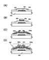
도 1(A) 내지 도 1(E)는 반도체 장치 및 반도체 장치의 제작 방법을 설명하는 도이다.
도 2(A) 내지 도 2(D)는 반도체 장치 및 반도체 장치의 제작 방법을 설명하는 도이다.
도 3(A) 내지 도 3(E)는 반도체 장치 및 반도체 장치의 제작 방법을 설명하는 도이다.
도 4(A) 내지 도 4(C)는 반도체 장치 및 반도체 장치의 제작 방법을 설명하는 도이다.
도 5(A) 내지 도 5(E)는 반도체 장치 및 반도체 장치의 제작 방법을 설명하는 도이다.
도 6(A) 내지 도 6(D)는 반도체 장치 및 반도체 장치의 제작 방법을 설명하는 도이다.
도 7은 반도체 장치를 설명하는 도이다.
도 8(A) 내지 도 8(C)는 반도체 장치를 설명하는 도이다.
도 9는 반도체 장치의 화소 등가회로를 설명하는 도이다.
도 10(A) 내지 도 10(C)는 반도체 장치를 설명하는 도이다.
도 11(A) 및 도 11(B)는 반도체 장치를 설명하는 도이다.
도 12는 반도체 장치를 설명하는 도이다.
도 13(A) 및 도 13(B)는 전자기기를 나타내는 도이다.
도 14(A) 및 도 14(B)는 전자기기를 나타내는 도이다.
도 15는 전자기기를 나타내는 도이다.
도 16은 전자기기를 나타내는 도이다.
도 17은 전자기기를 나타내는 도이다.
도 18은 반도체 장치를 설명하는 도이다.
도 19는 산화물 반도체를 이용한 역스태거형 박막 트랜지스터의 종단면도이다.
도 20(A) 및 도 20(B)는 도 19에 나타내는 A-A' 단면에 있어서의 에너지 밴드도(모식도)이다.
도 21(A)는 게이트(G1)에 양의 전위(+VG)가 인가된 상태를 나타내고, 도 21 (B)는 게이트(G1)에 음의 전위(-VG)가 인가된 상태를 나타내는 도이다.
도 22는 진공 준위와 금속의 일함수(φM), 산화물 반도체의 전자 친화력(χ)의 관계를 나타내는 도이다.1 (A) to 1 (E) illustrate a semiconductor device and a method of manufacturing the semiconductor device.
2 (A) to 2 (D) illustrate a semiconductor device and a method of manufacturing the semiconductor device.
3 (A) to 3 (E) illustrate a semiconductor device and a method of manufacturing the semiconductor device.
4 (A) to 4 (C) are diagrams for explaining a semiconductor device and a method of manufacturing the semiconductor device.
5 (A) to 5 (E) illustrate a semiconductor device and a method of manufacturing the semiconductor device.
6 (A) to 6 (D) are diagrams for explaining a semiconductor device and a method of manufacturing the semiconductor device.
7 is a view for explaining a semiconductor device.
8 (A) to 8 (C) are diagrams for explaining a semiconductor device.
9 is a diagram for explaining a pixel equivalent circuit of a semiconductor device.
10 (A) to 10 (C) illustrate a semiconductor device.
11 (A) and 11 (B) illustrate a semiconductor device.
12 is a view for explaining a semiconductor device.
13 (A) and 13 (B) show electronic devices.
14 (A) and 14 (B) are diagrams showing electronic devices.
15 is a diagram showing an electronic apparatus.
16 is a diagram showing an electronic apparatus.
17 is a diagram showing an electronic apparatus.
18 is a view for explaining a semiconductor device.
19 is a longitudinal sectional view of a reverse stagger type thin film transistor using an oxide semiconductor.
20 (A) and 20 (B) are energy band diagrams (schematic diagrams) taken along the line AA 'shown in FIG.
21A shows a state in which a positive potential (+ VG) is applied to the gate G1 and FIG. 21B shows a state in which a negative potential (-VG) is applied to the gate G1 to be.
22 is a graph showing the relationship between the vacuum level and the work function? M of the metal and the electron affinity (?) Of the oxide semiconductor.
이하에서는, 본 발명의 실시형태에 대해서 도면을 이용하여 상세하게 설명한다. 단, 본 발명은 이하의 설명에 한정되지 않으며, 그 형태 및 상세를 다양하게 변경할 수 있음은 당업자라면 용이하게 이해될 것이다. 또한, 본 발명은 이하에 나타내는 실시형태의 기재 내용에 한정하여 해석되는 것은 아니다.Hereinafter, embodiments of the present invention will be described in detail with reference to the drawings. However, it is to be understood by those skilled in the art that the present invention is not limited to the following description, and that various changes in form and details may be made therein. The present invention is not limited to the description of the embodiments described below.
(실시형태 1)(Embodiment 1)
본 실시형태의 반도체 장치 및 반도체 장치의 제작 방법의 일 형태를 도 1을 이용하여 설명한다. 본 실시형태에서 나타내는 반도체 장치는 박막 트랜지스터이다.One embodiment of the semiconductor device and the method of manufacturing the semiconductor device of the present embodiment will be described with reference to FIG. The semiconductor device shown in this embodiment mode is a thin film transistor.
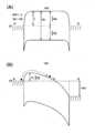
도 1(A) 내지 1(E)에 반도체 장치의 단면 구조의 일례를 나타낸다. 도 1(A) 내지 1(E)에 나타내는 박막 트랜지스터(110)는 보텀 게이트 구조의 하나로 역스태거형 박막 트랜지스터라고도 한다.1 (A) to 1 (E) show an example of a sectional structure of a semiconductor device. The
도 1(A) 내지 1(E)에 나타내는 박막 트랜지스터(110)는 절연 표면을 갖는 기판(100) 상에 게이트 전극층(111), 게이트 절연층(102), 산화물 반도체층(112), 산소 과잉의 혼합 영역(119), 소스 전극층(115a) 및 드레인 전극층(115b)을 포함한다. 또한, 박막 트랜지스터(110)를 덮고, 산화물 반도체층(112)에 산소 과잉의 혼합 영역(119)을 사이에 두고 적층하는 결함을 포함하는 절연층(116)이 마련되고, 아울러 그 위에 보호 절연층(103)이 적층되어 있다.The
산소 과잉의 혼합 영역(119), 결함을 포함하는 절연층(116)은 수소나 수분(수소 원자나, H2O 등 수소 원자를 포함하는 화합물)에 대하여 속박 에너지가 크고, 산소 과잉의 혼합 영역(119), 결함을 포함하는 절연층(116)에서 그 불순물은 안정화되므로, 산화물 반도체층(112)으로부터 산소 과잉의 혼합 영역(119), 결함을 포함하는 절연층(116)으로 그 불순물을 확산시켜, 그 불순물을 산화물 반도체층(112)으로부터 배제할 수 있다. 아울러, 산소 과잉의 혼합 영역(119)이 결함을 포함하는 절연층(116)으로 확산된 불순물에 대한 배리어층이 되어, 그 불순물이 다시 산화물 반도체층(112)으로 침입하는 것을 방지하므로 산화물 반도체층(112) 내의 불순물 농도를 저감시킨 상태로 유지할 수 있다. 따라서, 변동 요인이 되는 수소, 수분, 수산기 또는 수소화물(수소화합물이라고도 함) 등의 불순물을 저감시킨 산화물 반도체층(112)을 이용한 박막 트랜지스터(110)는 안정된 전기적 특성을 갖는 신뢰성이 높은 박막 트랜지스터가 된다.The oxygen-excess
도 19는 산화물 반도체를 이용한 역스태거형 박막 트랜지스터의 종단면도이다. 게이트 전극(GE1) 상에 게이트 절연막(GI)을 사이에 두고 산화물 반도체층(OS)이 마련되고, 그 위에 소스 전극(S) 및 드레인 전극(D)이 마련되어 있다.19 is a longitudinal sectional view of a reverse stagger type thin film transistor using an oxide semiconductor. An oxide semiconductor layer OS is provided on the gate electrode GE1 with a gate insulating film GI sandwiched therebetween and a source electrode S and a drain electrode D are provided thereon.
도 20(A) 및 도 20(B)는 도 19에 도시되어 있는 A-A' 단면에 있어서의 에너지 밴드도(모식도)이다. 도 20(A)는 소스와 드레인 사이의 전압을 등전위(VD=0V)로 한 경우를 나타내고, 도 20(B)는 소스에 대하여 드레인에 양의 전위(VD>0)를 인가한 경우를 나타낸다.20 (A) and 20 (B) are energy band diagrams (schematic diagrams) taken along the line A-A 'shown in FIG. 20A shows a case where the voltage between a source and a drain is set to an equal potential (VD = 0V), and FIG. 20B shows a case where a positive potential (VD> 0) .
도 21(A) 및 도 21(B)는 도 19에 도시되어 있는 B-B' 단면에 있어서의 에너지 밴드도(모식도)이다. 도 21(A)는 게이트(G1)에 양의 전위(+VG)가 인가된 상태로, 소스, 드레인 사이에 캐리어(전자)가 흐르는 온 상태를 나타내고 있다. 또한, 도 21(B)는 게이트(G1)에 음의 전위(-VG)가 인가된 상태로, 오프 상태(소수 캐리어는 흐르지 않는)인 경우를 나타낸다.Figs. 21A and 21B are energy band diagrams (schematic diagrams) of the cross section taken along the line B-B 'shown in Fig. 21A shows an ON state in which carriers (electrons) flow between a source and a drain with a positive potential (+ VG) applied to the gate G1. Fig. 21B shows a state in which the negative potential (-VG) is applied to the gate G1 and the off state (the minority carriers do not flow).
도 22는 진공 준위와 금속의 일함수(φM), 산화물 반도체의 전자 친화력(χ)의 관계를 나타낸다.22 shows the relationship between the vacuum level and the work function? M of the metal and the electron affinity (?) Of the oxide semiconductor.
상온에서 금속 내의 전자는 축퇴되어 있으므로 페르미 준위는 전도대 내에 위치한다. 한편, 종래의 산화물 반도체는 일반적으로 n형이며, 그 경우의 페르미 준위(Ef)는 밴드 갭 중앙에 위치하는 진성 페르미 준위(Ei)로부터 멀어져 전도대 가까이에 위치하고 있다. 또한, 종래의 산화물 반도체가 일반적으로 n형이 되는 것은, 함유한 수소의 일부가 전자를 공급하는 도너가 되는 것이 하나의 요인인 것이 알려져 있다.Since the electrons in the metal are degenerated at room temperature, the Fermi level is located within the conduction band. On the other hand, the conventional oxide semiconductor is generally n-type, and the Fermi level Ef in this case is located near the conduction band away from the intrinsic Fermi level Ei located at the center of the band gap. Further, it is known that the conventional oxide semiconductor is generally n-type in that a part of the contained hydrogen becomes a donor for supplying electrons.
이에 반해 본 발명에 따른 산화물 반도체는 n형 불순물인 수소를 산화물 반도체로부터 제거하여, 산화물 반도체의 주성분 이외의 불순물이 가능한 한 포함되지 않도록 고순도화함으로써 진성(i형)으로 하고, 또는 진성형으로 하고자 한 것이다. 즉, 불순물을 첨가하여 i형화하는 것이 아니라, 수소나 물 등의 불순물을 가능한 한 제거함으로써, 고순도화된 i형(진성 반도체) 또는 그에 가깝게 하는 것을 특징으로 하고 있다. 그렇게 함으로써, 페르미 준위(Ef)는 진성 페르미 준위(Ei)와 동일한 레벨까지, 혹은 거기에 한없이 가깝게 할 수 있다.On the other hand, the oxide semiconductor according to the present invention is an oxide semiconductor in which hydrogen, which is an n-type impurity, is removed from the oxide semiconductor and the impurity other than the main component of the oxide semiconductor is highly purified so as to be contained as much as possible, It is. That is, the present invention is characterized in that impurities such as hydrogen and water are removed as much as possible, instead of i-type by adding impurities, and i-type (intrinsic semiconductor) which is highly purified is brought close to the i-type. By doing so, the Fermi level Ef can be as close to the level as the intrinsic Fermi level Ei or as close as possible to it.
산화물 반도체의 밴드 갭(Eg)이 3.15eV인 경우, 전자 친화력(χ)은 4.3eV라고 알려져 있다. 소스 전극 및 드레인 전극을 구성하는 티타늄(Ti) 일함수는 상기 산화물 반도체의 전자 친화력(χ)과 거의 동일하다. 이 경우, 금속-산화물 반도체 계면에서 전자에 대하여 쇼트키형의 장벽은 형성되지 않는다.When the band gap Eg of the oxide semiconductor is 3.15 eV, the electron affinity (?) Is known to be 4.3 eV. The titanium (Ti) work function constituting the source electrode and the drain electrode is substantially equal to the electron affinity (x) of the oxide semiconductor. In this case, a Schottky barrier is not formed with respect to electrons at the metal-oxide semiconductor interface.
즉, 금속의 일함수(φM)와 산화물 반도체의 전자 친화력(χ)이 동일한 경우, 양자가 접촉하면 도 20(A)에서 나타낸 바와 같은 에너지 밴드도(모식도)가 나타난다.That is, when the work function? M of the metal and the electron affinity (?) Of the oxide semiconductor are the same, an energy band diagram (schematic diagram) as shown in FIG.
도 20(B)에서 검은 점(●)은 전자를 나타내고, 드레인에 양의 전위가 인가되면 전자는 배리어(h)를 넘어 산화물 반도체에 주입되고, 드레인을 향해 흐른다. 이 경우, 배리어(h)의 높이는 게이트 전압과 드레인 전압에 의존해 변화하지만, 양의 드레인 전압이 인가된 경우에는, 전압 인가가 없는 도 20(A)의 배리어의 높이 즉 밴드 갭(Eg)의 1/2보다 배리어의 높이(h)는 작은 값이 된다.In FIG. 20 (B), the black dot (●) represents electrons. When a positive potential is applied to the drain, electrons are injected into the oxide semiconductor over the barrier h and flow toward the drain. In this case, the height of the barrier h varies depending on the gate voltage and the drain voltage. However, when a positive drain voltage is applied, the height of the barrier shown in Fig. / 2, the height h of the barrier becomes smaller.
이때 전자는 도 21(A)에서 나타낸 바와 같이 게이트 절연막과 고순도화된 산화물 반도체와의 계면에서의 산화물 반도체 측의 에너지적으로 안정된 최저부를 따라 이동한다.At this time, the electrons move along the energy-stabilized lowest part of the oxide semiconductor side at the interface between the gate insulating film and the high-purity oxide semiconductor as shown in Fig. 21 (A).
또한, 도 21(B)에서 게이트 전극(G1)에 음의 전위(역바이어스)가 인가되면 소수 캐리어인 홀은 실질적으로 제로이기 때문에 전류는 한없이 제로에 가까운 값이 된다.21 (B), when a negative potential (reverse bias) is applied to the gate electrode G1, the hole serving as a minority carrier is substantially zero, so that the current becomes infinitely close to zero.
예를 들어, 박막 트랜지스터의 채널 폭(W)이 1×10⁴㎛이고, 채널 길이가 3㎛인 소자여도, 오프 전류가 10-13A 이하, 0.1V/dec.(게이트 절연막 두께 100㎚)의 서브스레숄드 스윙 값(S값)이 얻어진다.For example, even when the channel width W of the thin film transistor is 1 x 10⁴ 탆 and the channel length is 3 탆, the off current is 10-13 A or less, 0.1 V / dec. (Gate insulating
이와 같이, 산화물 반도체의 주성분 이외의 불순물이 가능한 한 포함되지 않도록 고순도화함으로써 박막 트랜지스터의 동작을 양호한 것으로 할 수 있다.Thus, the operation of the thin film transistor can be improved by making the impurity other than the main component of the oxide semiconductor high-purity so as not to include as much as possible.
또한, 박막 트랜지스터(110)는 싱글 게이트 구조의 박막 트랜지스터를 이용하여 설명했으나, 필요에 따라 채널 형성 영역을 복수 갖는 멀티 게이트 구조의 박막 트랜지스터도 형성할 수 있다.Though the
이하, 도 1(A) 내지 1(E)를 이용하여 기판(100) 상에 박막 트랜지스터(110)를 제작하는 공정을 설명한다.Hereinafter, a process for fabricating the
우선, 절연 표면을 갖는 기판(100) 상에 도전막을 형성한 후, 제 1 포토리소그래피 공정에 의해 게이트 전극층(111)을 형성한다. 형성된 게이트 전극층의 단부는 테이퍼 형상이면 위에 적층하는 게이트 절연층의 피복성이 향상되므로 바람직하다. 또한, 레지스트 마스크를 잉크젯법으로 형성할 수도 있다. 레지스트 마스크를 잉크젯법으로 형성하면 포토마스크를 사용하지 않으므로 제조 비용을 저감할 수 있다.First, a conductive film is formed on a
절연 표면을 갖는 기판(100)으로 사용할 수 있는 기판에 큰 제한은 없으나, 적어도 이후의 가열 처리에 견딜 수 있는 정도의 내열성을 가지고 있을 필요가 있다. 바륨 붕규산 유리나 알루미노 붕규산 유리 등의 유리 기판을 이용할 수 있다.There is no particular limitation on the substrate that can be used for the
또한, 유리 기판으로서는 이후의 가열 처리의 온도가 높은 경우에는 왜곡점이 730℃ 이상인 것을 이용할 수 있다. 또한, 유리 기판에는 예를 들어, 알루미노 규산염 유리, 알루미노 붕규산 유리, 바륨 붕규산 유리 등의 유리 재료가 이용되고 있다. 산화 붕소와 비교하여 산화 바륨(BaO)을 많이 포함시킴으로써 보다 실용적인 내열유리가 얻어진다. 그러므로, B2O3 보다 BaO를 많이 포함하는 유리 기판을 이용하는 것이 바람직하다.When the temperature of the subsequent heat treatment is high, the glass substrate may have a distortion point of 730 캜 or higher. Glass substrates such as aluminosilicate glass, aluminoborosilicate glass, and barium borosilicate glass are used for the glass substrate, for example. By containing a large amount of barium oxide (BaO) as compared with boron oxide, a more practical heat-resistant glass can be obtained. Therefore, it is preferable to use a glass substrate containing more BaO than B2 O3 .
또한, 상기의 유리 기판 대신에, 세라믹 기판, 석영 기판, 사파이어 기판 등의 절연체로 이루어지는 기판을 이용할 수도 있다. 그 외에도, 결정화 유리 등을 이용할 수 있다. 또한, 플라스틱 기판 등도 적절히 이용할 수 있다.Instead of the glass substrate, a substrate made of an insulator such as a ceramic substrate, a quartz substrate, or a sapphire substrate may be used. In addition, crystallized glass or the like can be used. A plastic substrate or the like can also be suitably used.
하지막이 되는 절연막을 기판(100)과 게이트 전극층(111) 사이에 마련할 수도 있다. 하지막은 기판(100)으로부터의 불순물 원소의 확산을 방지하는 기능이 있고, 질화 실리콘막, 산화 실리콘막, 질화산화 실리콘막, 또는 산화질화 실리콘막으로부터 선택된 하나 또는 복수의 막에 의한 적층 구조로 형성할 수 있다.An insulating film which becomes a base film may be provided between the
또한, 게이트 전극층(111)의 재료는 몰리브덴, 티타늄, 크롬, 탄탈, 텅스텐, 알루미늄, 구리, 네오디뮴, 스칸듐 등의 금속재료 또는 이들을 주성분으로 하는 합금 재료를 이용하여 단층으로 또는 적층해 형성할 수 있다.The material of the
예를 들어, 게이트 전극층(111)의 2층의 적층 구조로서는 알루미늄층 상에 몰리브덴층이 적층된 2층의 적층 구조, 구리층 상에 몰리브덴층이 적층된 2층의 적층 구조, 구리층 상에 질화 티타늄층 혹은 질화 탄탈층이 적층된 2층의 적층 구조, 또는 질화 티타늄층 상에 몰리브덴층이 적층된 2층의 적층 구조로 하는 것이 바람직하다. 3층의 적층 구조로서는 텅스텐층 또는 질화 텅스텐층과, 알루미늄과 실리콘의 합금 또는 알루미늄과 티타늄의 합금층과, 질화 티타늄층 또는 티타늄층을 적층한 적층으로 하는 것이 바람직하다. 또한, 투광성을 갖는 도전막을 이용하여 게이트 전극층을 형성할 수도 있다. 투광성을 갖는 도전막으로는 투광성 도전성 산화물 등을 그 예로 들 수 있다.For example, as the two-layer stacked structure of the
이어서, 게이트 전극층(111) 상에 게이트 절연층(102)을 형성한다.Subsequently, a
게이트 절연층(102)은 플라즈마 CVD법 또는 스퍼터링법 등을 이용하여, 산화 실리콘층, 질화 실리콘층, 산화질화 실리콘층, 질화산화 실리콘층, 산화 알루미늄층, 질화 알루미늄층, 산화질화 알루미늄층, 질화산화 알루미늄층, 또는 산화 하프늄층을 단층으로 또는 적층으로 형성할 수 있다. 또한, 게이트 절연층(102) 내에 수소가 다량으로 포함되지 않게 하기 위해서는 스퍼터링법으로 게이트 절연층(102)을 성막하는 것이 바람직하다. 스퍼터링법에 의해 산화 실리콘막을 성막하는 경우에는 타겟으로서 실리콘 타겟 또는 석영 타겟을 이용하고 스퍼터링 가스로서 산소 또는, 산소 및 아르곤의 혼합 가스를 이용하여 수행한다.The
게이트 절연층(102)은 게이트 전극층(111) 측으로부터 질화 실리콘층과 산화 실리콘층을 적층한 구조로 할 수도 있다. 예를 들어, 제 1 게이트 절연층으로서 스퍼터링법에 의해 막 두께 50㎚ 이상 200㎚ 이하의 질화 실리콘층(SiNy(y>0))을 형성하고, 제 1 게이트 절연층 상에 제 2 게이트 절연층으로서 막 두께 5㎚ 이상 300㎚ 이하의 산화 실리콘층(SiOx(x>0))을 적층하여, 막 두께 100㎚의 게이트 절연층으로 한다. 게이트 절연층의 막 두께는 박막 트랜지스터에 요구되는 특성에 따라 적절히 설정하면 되고 350㎚ 내지 400㎚ 정도일 수 있다.The
또한, 게이트 절연층(102), 산화물 반도체막(120)에 수소, 수산기 및 수분이 가능한 한 포함되지 않도록 하기 위해서, 성막의 전처리로서, 스퍼터링 장치의 예비 가열실에서 게이트 전극층(111)이 형성된 기판(100), 또는 게이트 절연층(102)까지 형성된 기판(100)을 예비 가열하여, 기판(100)에 흡착된 수소, 수분 등의 불순물을 탈리하여 배기하는 것이 바람직하다. 또한, 예비 가열의 온도는 100℃ 이상 400℃ 이하 바람직하게는 150℃ 이상 300℃ 이하이다. 또한, 예비 가열실에 마련하는 배기 수단은 크라이오 펌프가 바람직하다. 또한, 이 예비 가열의 처리는 생략할 수도 있다. 또한 이 예비 가열은 결함을 포함하는 절연층(116)의 성막 전에 소스 전극층(115a), 드레인 전극층(115b)까지 형성한 기판(100)에도 동일하게 수행할 수도 있다.In order to prevent hydrogen, hydroxyl, and moisture from being contained in the
이어서, 게이트 절연층(102) 상에 막 두께 2㎚ 이상 200㎚ 이하의 산화물 반도체막(120)을 형성한다(도 1(A) 참조).Then, an
또한, 산화물 반도체막(120)을 스퍼터링법에 의해 성막하기 전에, 아르곤 가스를 도입하여 플라즈마를 발생시키는 역스퍼터링을 수행하여, 게이트 절연층(102)의 표면에 부착되어 있는 먼지를 제거하는 것이 바람직하다. 역스퍼터링이란 타겟 측에 전압을 인가하지 않고 , 아르곤 분위기하에서 기판 측에 RF 전원을 이용하여 전압을 인가해 기판 근방에 플라즈마를 형성하여 표면을 개질하는 방법이다. 또한, 아르곤 분위기 대신에 질소, 헬륨, 산소 등을 이용할 수도 있다.Before the
산화물 반도체막(120)은 스퍼터링법에 의해 성막한다. 산화물 반도체막(120)은 In-Ga-Zn-O계 막, In-Sn-Zn-O계, In-Al-Zn-O계, Sn-Ga-Zn-O계, Al-Ga-Zn-O계, Sn-Al-Zn-O계, In-Zn-O계, Sn-Zn-O계, Al-Zn-O계, In-O계, Sn-O계, Zn-O계의 산화물 반도체막을 이용한다. 본 실시형태에서는, 산화물 반도체막(120)을 In-Ga-Zn-O계 금속 산화물 타겟을 이용하여 스퍼터링법에 의해 성막한다. 또한, 산화물 반도체막(120)은 희가스(대표적으로는 아르곤) 분위기하, 산소 분위기하, 또는 희가스(대표적으로는 아르곤) 및 산소 분위기하에서 스퍼터링법에 의해 형성할 수 있다. 또한, 스퍼터링법을 이용하는 경우, SiO2를 2중량% 이상 10중량% 이하 포함하는 타겟을 이용하여 성막을 수행할 수도 있다.The
산화물 반도체막(120)을 성막할 때에 이용하는 스퍼터링 가스는 수소, 물, 수산기 또는 수소화물 등의 불순물이 농도 ppm 정도, 농도 ppb 정도까지 제거된 고순도 가스를 이용하는 것이 바람직하다.As the sputtering gas used for forming the
산화물 반도체막(120)을 스퍼터링법으로 제작하기 위한 타겟으로서 산화 아연을 주성분으로 하는 금속 산화물 타겟을 이용할 수 있다. 또한, 금속 산화물 타겟의 다른 예로는 In, Ga 및 Zn을 포함하는 금속 산화물 타겟(조성비로서, In2O3:Ga2O3:ZnO=1:1:1[mol수비])을 이용할 수 있다. 또한, In, Ga 및 Zn을 포함하는 금속 산화물 타겟으로서, In2O3:Ga2O3:ZnO=1:1:2[mol수비], 또는 In2O3:Ga2O3:ZnO=1:1:4[mol수비]의 조성비를 갖는 타겟을 이용할 수도 있다. 금속 산화물 타겟의 충전율은 90% 이상 100% 이하, 바람직하게는 95% 이상 99.9% 이하이다. 충전율이 높은 금속 산화물 타겟을 이용함으로써 성막한 산화물 반도체막은 치밀한 막이 된다.A metal oxide target containing zinc oxide as a main component can be used as a target for manufacturing the
감압 상태로 설정된 처리실 내에 기판을 유지하고, 기판을 400℃ 미만의 온도로 가열한다. 그리고, 처리실 내의 잔류 수분을 제거하면서 수소 및 수분이 제거된 스퍼터링 가스를 도입하여, 금속 산화물을 타겟으로서 기판(100) 상에 산화물 반도체막(120)을 성막한다. 처리실 내의 잔류 수분을 제거하기 위해서는 흡착형 진공 펌프를 이용하는 것이 바람직하다. 예를 들어, 크라이오 펌프, 이온 펌프, 티타늄 승화 펌프를 이용하는 것이 바람직하다. 또한, 배기 수단은 터보 펌프에 콜드 트랩을 부가한 것일 수 있다. 크라이오 펌프를 이용하여 배기한 성막실은 예를 들어, 수소 원자나, H2O 등 수소 원자를 포함하는 화합물이나, 탄소 원자를 포함하는 화합물 등이 배기되므로 이 성막실에서 성막한 산화물 반도체막(120)에 포함되는 불순물의 농도를 저감할 수 있다.The substrate is held in a processing chamber set in a reduced pressure state, and the substrate is heated to a temperature of less than 400 캜. Then, the
산화물 반도체막(120)을 성막하는 경우, 산화물 반도체막(120)을 성막하는 처리실은 물론이고, 산화물 반도체막(120)에 접하는 막 및 산화물 반도체막(120)의 성막 전후의 공정에 있어서, 처리실 내에 잔류하는 수분이 불순물로서 혼입하지 않도록 크라이오 펌프 등의 배기 수단을 이용하는 것이 바람직하다.In the case where the
성막 조건의 일례로서는, 기판과 타겟 사이의 거리를 100㎜, 압력 0.6Pa, 직류(DC) 전원 0.5kW, 산소(산소 유량 비율 100%) 분위기하의 조건이 적용된다. 또한, 펄스 직류(DC) 전원을 이용하면 성막 시에 발생하는 분상 물질(파티클, 먼지라고도 함)을 경감할 수 있고, 막 두께 분포도 균일해지므로 바람직하다. 산화물 반도체막(120)은 바람직하게는 5㎚ 이상 30㎚ 이하로 한다. 또한, 적용하는 산화물 반도체 재료에 따라 적절한 두께는 다르므로, 재료에 따라 두께를 선택하면 된다.As an example of the film formation conditions, conditions are applied under the atmosphere of a distance of 100 mm between the substrate and the target, a pressure of 0.6 Pa, a direct current (DC) power of 0.5 kW, and oxygen (oxygen flow rate ratio of 100%). Use of a pulsed direct current (DC) power supply is also preferable because it can reduce the amount of dispersed substances (also referred to as particles and dust) generated during film formation and the film thickness distribution becomes uniform. The
상기와 같이 하여 산화물 반도체막(120)을 스퍼터링법으로 성막함으로써, 수소 농도가 낮은 산화물 반도체막(120)을 얻을 수 있다. 또한 본 명세서에 있어서 나타내어지는 수소 농도는 2차 이온 질량 분석(SIMS: Secondary Ion Mass Spectrometry)에 의해 측정할 수 있는 정량 결과이다.The
스퍼터링법에는 스퍼터용 전원에 고주파 전원을 이용하는 RF 스퍼터링법, 직류 전원을 이용하는 DC 스퍼터링법, 나아가 펄스적으로 바이어스를 주는 펄스 DC 스퍼터링법이 있다. RF 스퍼터링법은 주로 절연막을 성막하는 경우에 이용되고, DC 스퍼터링법은 주로 금속막을 성막하는 경우에 이용된다.As the sputtering method, there are an RF sputtering method using a high frequency power source as a power source for sputtering, a DC sputtering method using a DC power source, and a pulse DC sputtering method giving a pulse bias. The RF sputtering method is mainly used for forming an insulating film, and the DC sputtering method is mainly used for forming a metal film.
또한, 재료가 다른 타겟을 복수 설치할 수 있는 다원 스퍼터링 장치도 있다. 다원 스퍼터링 장치는 동일 챔버에서 서로 다른 재료막을 적층 성막할 수도 있고, 동일 챔버에서 복수 종류의 재료를 동시에 방전시켜 성막할 수도 있다.There is also a multi-sputtering apparatus in which a plurality of targets having different materials can be provided. The multi-sputtering apparatus may deposit a different material film in the same chamber, or may deposit a plurality of kinds of materials simultaneously in the same chamber.
또한, 챔버 내부에 자석 기구를 구비한 마그네트론 스퍼터링법을 이용하는 스퍼터링 장치나, 글로방전을 사용하지 않고 마이크로파를 사용하여 발생시킨 플라즈마를 이용하는 ECR 스퍼터링법을 이용하는 스퍼터링 장치가 있다.There is also a sputtering apparatus using a magnetron sputtering method having a magnet mechanism in a chamber or a sputtering apparatus using an ECR sputtering method using a plasma generated by using microwaves without using glow discharge.
또한, 스퍼터링법을 이용하는 성막 방법으로서, 성막 중에 타겟 물질과 스퍼터링 가스 성분을 화학반응시켜, 그들의 화합물 박막을 형성하는 리엑티브 스퍼터링법이나, 성막 중에 기판으로도 전압을 가하는 바이어스 스퍼터링법도 있다.As a film forming method using the sputtering method, there is also a reactive sputtering method in which a target material and a sputtering gas component are chemically reacted during film formation to form a compound thin film thereof, or a bias sputtering method in which a voltage is applied to a substrate during film formation.
이어서, 산화물 반도체막(120)을 제 2 포토리소그래피 공정에 의해 섬 형상의 산화물 반도체층(121)으로 가공한다(도 1(B) 참조). 또한, 섬 형상의 산화물 반도체층(121)을 형성하기 위한 레지스트 마스크를 잉크젯법으로 형성할 수도 있다. 레지스트 마스크를 잉크젯법으로 형성하면 포토마스크를 사용하지 않으므로 제조 비용을 저감시킬 수 있다.Then, the
또한, 게이트 절연층(102)에 콘택홀을 형성하는 경우, 그 공정은 산화물 반도체층(121)의 형성 시에 수행할 수 있다.In the case where the contact hole is formed in the
또한, 여기서의 산화물 반도체막(120)의 에칭은 드라이 에칭일 수도 있고, 웨트 에칭일 수도 있고, 양쪽 모두를 이용할 수도 있다.Here, the etching of the
드라이 에칭에 이용하는 에칭 가스로는, 염소를 포함하는 가스(염소계 가스, 예를 들어 염소(Cl2), 염화붕소(BCl3), 염화규소(SiCl4), 사염화탄소(CCl4) 등)가 바람직하다.As the etching gas used for dry etching, a gas containing chlorine (chlorine-based gas such as chlorine (Cl2 ), boron chloride (BCl3 ), silicon chloride (SiCl4 ), carbon tetrachloride (CCl4 ) .
또한, 불소를 포함하는 가스(불소계 가스, 예를 들어 사불화탄소(CF4), 육불화황(SF6), 삼불화질소(NF3), 트리플루오로메탄(CHF3) 등), 브롬화수소(HBr), 산소(O2), 이들 가스에 헬륨(He)이나 아르곤(Ar) 등의 희가스를 첨가한 가스 등을 이용할 수 있다.(Fluorine-based gas such as tetrafluorocarbon (CF4 ), sulfur hexafluoride (SF6 ), nitrogen trifluoride (NF3 ), trifluoromethane (CHF3 ) and the like), hydrogen bromide (HBr), oxygen (O2 ), and a gas obtained by adding a rare gas such as helium (He) or argon (Ar) to these gases.
드라이 에칭법으로는 평행 평판형 RIE(Reactive Ion Etching)법이나, ICP(Inductively Coupled Plasma: 유도 결합형 플라즈마) 에칭법을 사용할 수 있다. 원하는 가공 형상으로 에칭할 수 있도록 에칭 조건(코일형의 전극에 인가되는 전력량, 기판측의 전극에 인가되는 전력량, 기판 측의 전극 온도 등)을 적절히 조절한다.As the dry etching method, a parallel plate type RIE (Reactive Ion Etching) method or ICP (Inductively Coupled Plasma) etching method can be used. The etching conditions (the amount of power applied to the coil-shaped electrode, the amount of power applied to the electrode on the substrate side, the electrode temperature on the substrate side, and the like) are appropriately controlled so that etching can be performed with a desired processing shape.
웨트 에칭에 이용하는 에칭액으로서는 인산과 초산과 질산을 혼합한 용액, 암모니아과수(31중량% 과산화수소수:28중량% 암모니아수:물=5:2:2) 등을 이용할 수 있다. 또한, ITO07N(칸토화학사 제품)을 이용할 수도 있다.As the etching solution used for wet etching, a solution obtained by mixing phosphoric acid, acetic acid and nitric acid, ammonia and water (31 wt% hydrogen peroxide: 28 wt% ammonia water: water = 5: 2: 2) can be used. ITO07N (manufactured by Kanto Chemical) can also be used.
또한, 웨트 에칭 후의 에칭액은 에칭된 재료와 함께 세정에 의해 제거된다. 그 제거된 재료를 포함하는 에칭액의 폐액을 정제하여, 포함되는 재료를 재이용할 수도 있다. 그 에칭 후의 폐액으로부터 산화물 반도체층에 포함되는 인듐 등의 재료를 회수하여 재이용함으로써 자원을 유효 활용하여 제조 비용을 저감시킬 수 있다.Further, the etchant after the wet etching is removed by cleaning together with the etched material. The waste liquid of the etchant containing the removed material may be refined to reuse the contained material. And materials such as indium contained in the oxide semiconductor layer are recovered from the waste solution after the etching and reused, thereby making it possible to effectively utilize the resources and reduce the manufacturing cost.
원하는 가공 형상으로 에칭할 수 있도록 재료에 맞추어 에칭 조건(에칭액, 에칭 시간, 온도 등)을 적절히 조절한다.The etching conditions (etching solution, etching time, temperature, etc.) are appropriately adjusted according to the material so that the desired shape can be etched.
또한, 다음 공정의 도전막을 형성하기 전에 역스퍼터링을 수행하여 산화물 반도체층(121) 및 게이트 절연층(102)의 표면에 부착되어 있는 레지스트 잔사 등을 제거하는 것이 바람직하다.In addition, it is preferable that reverse sputtering is performed before the conductive film of the next step is formed to remove resist residues or the like attached to the surface of the
이어서, 게이트 절연층(102) 및 산화물 반도체층(121) 상에 도전막을 형성한다. 도전막은 스퍼터링법이나 진공 증착법으로 형성할 수 있다. 도전막의 재료로서는 알루미늄(Al), 크롬(Cr), 동(Cu), 탄탈(Ta), 티타늄(Ti), 몰리브덴(Mo), 텅스텐(W)으로부터 선택된 원소, 또는 상술한 원소를 성분으로 하는 합금이나, 상술한 원소를 조합한 합금 등을 들 수 있다. 또한, 망간(Mn), 마그네슘(Mg), 지르코늄(Zr), 베릴륨(Be), 토륨(Th) 중 어느 하나 또는 복수로부터 선택된 재료를 이용할 수도 있다. 또한, 금속 도전막은 단층 구조로 할 수도 있고, 2층 이상의 적층 구조로 할 수도 있다. 예를 들어, 실리콘을 포함하는 알루미늄막의 단층 구조, 알루미늄막 상에 티타늄막을 적층하는 2층 구조, Ti막과 그 Ti막 상에 중첩하여 알루미늄막을 적층하고, 나아가 그 위에 Ti막을 성막하는 3층 구조 등을 들 수 있다. 또한, 알루미늄(Al)에 티타늄(Ti), 탄탈(Ta), 텅스텐(W), 몰리브덴(Mo), 크롬(Cr), 네오디뮴(Nd), 스칸듐(Sc)으로부터 선택된 원소를 단수, 또는 복수 조합한 막, 합금막, 혹은 질화막을 이용할 수도 있다.Subsequently, a conductive film is formed on the
제 3 포토리소그래피 공정에 의해 도전막 상에 레지스트 마스크를 형성하고, 선택적으로 에칭을 수행하여 소스 전극층(115a), 드레인 전극층(115b)을 형성한 후, 레지스트 마스크를 제거한다(도 1(C) 참조).A resist mask is formed on the conductive film by a third photolithography process and selective etching is performed to form the
제 3 포토리소그래피 공정에서의 레지스트 마스크 형성시의 노광에는 자외선이나 KrF 레이저광이나 ArF 레이저광을 이용한다. 산화물 반도체층(121) 상에서 서로 이웃하는 소스 전극층의 하단부와 드레인 전극층의 하단부의 간격 폭에 의해 이후에 형성되는 박막 트랜지스터의 채널 길이(L)가 결정된다. 또한, 채널 길이 L=25㎚ 미만의 노광을 수행하는 경우에는 수 ㎚~수 10㎚로 극히 파장이 짧은 초자외선(Extreme Ultraviolet)을 이용하여 제 3 포토리소그래피 공정에서의 레지스트 마스크 형성시의 노광을 수행한다. 초자외선에 의한 노광은 해상도가 높고 초점심도도 크다. 따라서, 이후에 형성되는 박막 트랜지스터의 채널 길이(L)를 10㎚ 이상 1000㎚ 이하로 하는 것도 가능하고, 회로의 동작 속도를 고속화시킬 수 있으며, 아울러 오프 전류값이 극히 작으므로 저소비전력화도 도모할 수 있다.Ultraviolet light, KrF laser light or ArF laser light is used for exposure in forming the resist mask in the third photolithography step. The channel length L of the thin film transistor to be formed later is determined by the width of the gap between the lower end of the source electrode layer and the lower end of the drain electrode layer on the
또한, 도전막의 에칭시에 산화물 반도체층(121)은 제거되지 않도록 각각의 재료 및 에칭 조건을 적절히 조절한다.In addition, the respective materials and the etching conditions are appropriately adjusted so that the
본 실시형태에서는, 도전막으로서 Ti막을 이용하고, 산화물 반도체층(121)에는 In-Ga-Zn-O계 산화물을 이용하고, 에천트로서 암모니아과수(암모니아, 물, 과산화수소수의 혼합액)를 이용한다.In this embodiment, a Ti film is used as the conductive film, an In-Ga-Zn-O oxide is used as the
또한, 제 3 포토리소그래피 공정에서는 산화물 반도체층(121)은 일부만이 에칭되어 홈부(오목부)를 갖는 산화물 반도체층이 될 수도 있다. 또한, 소스 전극층(115a), 드레인 전극층(115b)을 형성하기 위한 레지스트 마스크를 잉크젯법으로 형성할 수도 있다. 레지스트 마스크를 잉크젯법으로 형성하면 포토마스크를 사용하지 않으므로 제조 비용을 저감시킬 수 있다.In the third photolithography step, the
또한, 포토리소그래피 공정에서 이용하는 포토마스크 수 및 공정 수를 삭감하기 위해서, 투과한 광이 복수의 강도가 되는 노광 마스크인 다계조 마스크에 의해 형성된 레지스트 마스크를 이용하여 에칭 공정을 수행할 수도 있다. 다계조 마스크를 이용하여 형성한 레지스트 마스크는 복수의 막 두께를 갖는 형상이 되고, 에칭을 수행함으로써 추가로 형상을 변형시킬 수 있으므로 서로 다른 패턴으로 가공하는 복수의 에칭 공정에 이용할 수 있다. 따라서, 한 장의 다계조 마스크에 의해, 적어도 2종류 이상의 서로 다른 패턴에 대응하는 레지스트 마스크를 형성할 수 있다. 따라서 노광 마스크 수를 삭감할 수 있고, 대응하는 포토리소그래피 공정도 삭감할 수 있으므로 공정의 간략화가 가능해진다.Further, in order to reduce the number of photomasks used in the photolithography process and the number of processes, an etching process may be performed using a resist mask formed by a multi-gradation mask which is an exposure mask having a plurality of intensities of transmitted light. A resist mask formed using a multi-gradation mask has a shape with a plurality of film thicknesses and can be further deformed by performing etching, so that the resist mask can be used for a plurality of etching processes for processing into different patterns. Therefore, a resist mask corresponding to at least two or more different patterns can be formed by a single multi-gradation mask. Therefore, the number of exposure masks can be reduced, and the corresponding photolithography process can also be reduced, so that the process can be simplified.
N2O, N2 또는 Ar 등의 가스를 이용한 플라즈마 처리에 의해 노출되어 있는 산화물 반도체층의 표면에 부착된 흡착수 등을 제거할 수도 있다. 또한, 산소와 아르곤의 혼합 가스를 이용하여 플라즈마 처리를 수행할 수도 있다.The adsorbed water or the like adhering to the surface of the oxide semiconductor layer exposed by the plasma treatment using a gas such as N2 O, N2 or Ar may be removed. In addition, a plasma treatment may be performed using a mixed gas of oxygen and argon.
대기에 접촉시키지 않고, 산화물 반도체층(121) 상에 결함을 포함하는 절연층(116)을 형성한다. 결함을 포함하는 절연층(116)의 형성 공정에 있어서, 산화물 반도체층(121)과 결함을 포함하는 절연층(116)의 사이에 산소 과잉의 혼합 영역(119)을 형성한다(도 1(D) 참조). 본 실시형태에서는, 산화물 반도체층(121)이 소스 전극층(115a), 드레인 전극층(115b)과 중첩되지 않는 영역에서, 산화물 반도체층(121)과 결함을 포함하는 절연층(116)이 산소 과잉의 혼합 영역(119)을 사이에 두고 적층하도록 형성한다.An insulating
혼합 영역(119)은 산화물 반도체층(121) 및 적층하는 결함을 포함하는 절연층(116)에 포함되는 재료의 혼합 영역(119)으로, 산화물 반도체층(121)과 결함을 포함하는 절연층(116)의 계면을 명확하게 하지 않음으로써 보다 산화물 반도체층(121)으로부터 결함을 포함하는 절연층(116)으로의 수소의 확산이 용이해진다. 예를 들어, 결함을 포함하는 절연층(116)으로서 산화 실리콘층을 이용하는 경우, 혼합 영역(119)에는 산소, 실리콘, 및 산화물 반도체층(121)에 포함되는 금속 원소가 적어도 1종류 이상 포함된다.The
본 실시형태와 같이, 결함을 포함하는 절연층(116)으로서 산화 실리콘, 산화물 반도체로서 In-Ga-Zn-O계 막을 이용하는 경우, 혼합 영역(119)에는 In, Ga 및 Zn 중 적어도 1종 이상의 금속 원소와, 산소 및 실리콘이 포함된다. 혼합 영역(119)에 있어서 산화물 반도체에 포함되는 금속을 M이라 하면, M-OH, M-H, M-O-Si-H, M-O-Si-OH 등 다양한 상태로 존재할 수 있고, 예를 들어 Zn-H나 Zn-OH 등을 생각할 수 있다.When an In-Ga-Zn-O-based film is used as the insulating
혼합 영역(119)은 막 두께 0.1㎚ 내지 30㎚(바람직하게는 2㎚ 내지 10㎚)일 수 있다. 혼합 영역(119)의 막 두께는 결함을 포함하는 절연층(116)을 형성할 시의 스퍼터링법의 성막 조건에 의해 제어할 수 있다. 스퍼터링법의 전원의 파워를 보다 강하게 하고, 기판과 타겟 사이의 거리를 보다 가깝게 하면 혼합 영역(119)을 두껍게 형성할 수 있다. 또한, 보다 강한 파워로 스퍼터링법을 수행함으로써, 산화물 반도체층(121) 표면에 부착된 흡착수 등을 제거할 수도 있다.The
혼합 영역(119)을 산화물 반도체층(121)과 결함을 포함하는 절연층(116)의 사이에 마련함으로써, 상기 산화물 반도체층(121)에 포함되는 수소 원자나, H2O 등 수소 원자를 포함하는 화합물이나, 탄소 원자를 포함하는 화합물 등이 결함을 포함하는 절연층(116)으로 보다 확산되기 쉬워진다.The
혼합 영역(119)은 산소 과잉으로 할 필요가 있으므로, 혼합 영역(119)의 형성시에는 산소 과잉이 될 수 있는 산소를 많이 포함하는 스퍼터링 가스를 사용하고, 혼합 영역(119)의 형성 후는 스퍼터링 가스 중의 산소량을 변화시키는 조정을 수행하여 결함을 포함하는 절연층(116)을 형성할 수도 있다.A sputtering gas containing a large amount of oxygen which can be excessively oxygen may be used to form the
따라서, 결함을 포함하는 절연층(116)은 산화 실리콘층 대신에, 산화질화 실리콘층, 산화 알루미늄층 또는 산화질화 알루미늄층 등을 이용할 수도 있다. 또한, 결함을 포함하는 절연층(116)으로서, 질화 실리콘층, 질화산화 실리콘층, 질화 알루미늄층, 질화산화 알루미늄층 등을 이용할 수도 있다.Therefore, instead of the silicon oxide layer, the insulating
본 실시형태에서는, 섬 형상의 산화물 반도체층(121), 소스 전극층(115a), 드레인 전극층(115b)까지 형성된 기판(100)을 실온 또는 100℃ 미만의 온도로 가열하고, 수소 및 수분이 제거된 고순도 산소를 포함하는 스퍼터링 가스를 도입하고, 실리콘 타겟을 이용하여 산소 과잉의 혼합 영역(119) 및 산화 실리콘층을 성막한다.In this embodiment, the
결함을 포함하는 절연층(116)을 성막할 때에 이용하는 스퍼터링 가스에는 수소, 물, 수산기 또는 수소화물 등의 불순물이 농도 ppm 정도, 농도 ppb 정도까지 제거된 고순도 가스를 이용하는 것이 바람직하다.It is preferable to use a high purity gas in which impurities such as hydrogen, water, hydroxyl, or hydride are removed to a concentration of about ppm and a concentration of about ppb to the sputtering gas used for forming the insulating
예를 들어, 순도가 6N이며, 붕소가 도프된 실리콘 타겟(저항값 0.01Ω㎝)을 이용하고, 기판과 타겟간의 거리(T-S간 거리)를 89㎜, 압력 0.4Pa, 직류(DC) 전원 6kW, 산소(산소 유량 비율 100%) 분위기하에서 펄스 DC 스퍼터링법에 의해 산화 실리콘막을 성막한다. 막 두께는 300㎚로 한다. 또한, 실리콘 타겟 대신에 석영(바람직하게는 합성 석영)을 산화 실리콘막의 성막을 위한 타겟으로서 이용할 수 있다. 또한, 스퍼터링 가스로서 산소 또는, 산소 및 아르곤의 혼합 가스를 이용하여 수행한다.For example, a silicon target doped with boron (with a resistance value of 0.01? Cm) having a purity of 6N and a distance (distance between TSs) of 89 mm, a pressure of 0.4 Pa, a DC power source of 6 kW , And a silicon oxide film is formed by a pulsed DC sputtering method in an oxygen (oxygen flow rate ratio: 100%) atmosphere. The film thickness is 300 nm. Further, quartz (preferably synthetic quartz) may be used as a target for forming a silicon oxide film instead of a silicon target. Also, the sputtering gas is performed using oxygen or a mixed gas of oxygen and argon.
또한, 처리실 내의 잔류 수분을 제거하면서 혼합 영역(119) 및 결함을 포함하는 절연층(116)을 성막하는 것이 바람직하다. 이는, 산화물 반도체층(121), 혼합 영역(119) 및 결함을 포함하는 절연층(116)에 수소, 수산기 또는 수분이 포함되지 않도록 하기 위함이다.It is also preferable to form the
또한, 혼합 영역(119)은 산화 실리콘 대신에, 산화질화 실리콘, 산화 알루미늄 또는 산화질화 알루미늄 등을 이용하여 형성할 수도 있다.The
이어서, 결함을 포함하는 절연층(116)과 산화물 반도체층(121)이 산소 과잉의 혼합 영역(119)을 사이에 두고 접한 상태로 100℃ 내지 400℃의 가열 처리를 수행한다. 이 가열 처리에 의해 산화물 반도체층(121) 내에 포함되는 수소 혹은 수분을 산소 과잉의 혼합 영역(119), 결함을 포함하는 절연층(116)으로 확산시킬 수 있다. 결함을 포함하는 절연층(116)과 산화물 반도체층(121)의 사이에 산소 과잉의 혼합 영역(119)이 마련되어 있으므로, 섬 형상의 산화물 반도체층(121)에 포함되는 수소, 수산기 및 수분 등의 불순물은 산화물 반도체층(121)으로부터 산소 과잉의 혼합 영역(119)으로, 또는 산소 과잉의 혼합 영역(119)을 통과하여 결함을 포함하는 절연층(116)으로 확산된다.Then, the insulating
산화물 반도체층(121)과 결함을 포함하는 절연층(116)의 사이에 마련되는 혼합 영역(119)은 산소 과잉이기 때문에, 산소의 댕글링 본드를 결함으로서 많이 포함하고, 수소, 수분, 수산기 또는 수소화물 등의 불순물에 대하여 속박 에너지가 크다. 따라서, 산소 과잉의 혼합 영역(119)을 마련함으로써, 산화물 반도체층(121)에 포함되는 수소, 수분, 수산기 또는 수소화물 등의 불순물이 결함을 포함하는 절연층(116)으로 확산, 이동하기 쉬워진다.Since the
아울러, 상기 불순물이 일단 산화물 반도체층(121)으로부터 배제되어 결함을 포함하는 절연층(116)으로 확산된 후, 다시 산화물 반도체층(121)으로 이동하려고 할 때는 산소 과잉의 혼합 영역(119)은 상기 불순물을 속박하여 안정화시켜, 산화물 반도체층(121)으로의 상기 불순물의 침입을 방지하는 보호층(배리어층)으로서 기능한다.When the impurity is once removed from the
이와 같이, 변동 요인이 되는 수소, 수분, 수산기 또는 수소화물 등의 불순물을 산화물 반도체층(121)으로부터 배제함으로써 상기 불순물이 저감된 산화물 반도체층(112)을 얻을 수 있다. 아울러, 배리어층이 되는 산소 과잉의 혼합 영역(119)이 결함을 포함하는 절연층(116)으로 확산된 불순물이 다시 산화물 반도체층(112)으로 침입하는 것을 방지함으로써, 산화물 반도체층(112) 내의 불순물 농도를 저감시킨 상태로 유지할 수 있다.Thus, the
산화물 반도체층과 결함을 포함하는 절연층의 사이에 마련되는 산소 과잉의 혼합 영역 또는 산소 과잉의 산화물 절연층은 산소 과잉이므로, 산소의 댕글링 본드를 결함으로서 많이 포함하는 결함을 포함한다. 산화물 반도체층으로부터 이러한 결함을 포함하는 절연층으로의 수소의 확산에 대해서, 수소 원자가 산화물 반도체층(아몰퍼스 IGZO) 내와 결함을 포함하는 절연층(아몰퍼스 SiOx) 내 중 어느 쪽에 존재하기 쉬운가를 계산했다.The excessive oxygen-rich mixed region or the excess oxygen-containing oxide layer provided between the oxide semiconductor layer and the insulating layer containing defects includes excessive defects including oxygen dangling bonds as defects. (Diffusion of hydrogen from the oxide semiconductor layer to the insulating layer including such defects), it is calculated whether the hydrogen atoms are likely to exist in the oxide semiconductor layer (amorphous IGZO) or in the insulating layer (amorphous SiOx ) did.
환경에 있어서의 수소 원자의 안정성을 평가하기 위해 수소 원자의 속박 에너지(E_bind)를 이하와 같이 정의하고 평가를 수행했다. E_bind={E(원래의 구조)+E(H)}-E(H를 부가한 구조). 이 속박 에너지(E_bind)가 큰 쪽이 수소 원자는 존재하기 쉽다고 할 수 있다. E(원래의 구조), E(H), E(H를 부가한 구조)는 각각 원래의 구조의 에너지, 수소 원자의 에너지, H를 부가한 구조의 에너지를 나타낸다. 이 속박 에너지를 아몰퍼스 IGZO, 댕글링 본드(이하, DB라고 약칭한다)가 없는 아몰퍼스 SiO2, DB가 있는 아몰퍼스 SiOx를 2종류, 합계 4개에 대하여 계산했다.In order to evaluate the stability of hydrogen atoms in the environment, the bond energies (E_bind) of hydrogen atoms were defined as follows and evaluated. E_bind = {E (original structure) + E (H)} - E (structure in which H is added). If this bond energy (E_bind) is large, the hydrogen atom is likely to exist. E (original structure), E (H) and E (H) represent the energy of the original structure, the energy of the hydrogen atom, and the energy of the structure added with H, respectively. These bond energies were calculated for two types of amorphous SiO2 without amorphous IGZO, dangling bond (abbreviated as DB hereinafter) and amorphous SiOx with DB, for a total of four.
계산에는 밀도범함수법의 프로그램인 CASTEP를 이용했다. 밀도범함수의 방법으로서 평면파 기저(基底) 의사 포텐셜법을 이용하고, 범함수는 LDA를 이용했다. 컷오프 에너지는 300eV를 이용했다. k점은 2×2×2의 그리드를 이용했다.Calculation used CASTEP, a program of density blind techniques. The plane wave basis potential method is used as the density function method and the LDA is used as the function. The cutoff energy was 300 eV. The k point was a grid of 2 × 2 × 2.
계산한 구조에 관하여 이하에 적는다. 먼저 원래의 구조에 관하여 이하에 적는다. 아몰퍼스 IGZO의 유닛셀은 In을 12 원자, Ga를 12 원자, Zn을 12 원자, O를 48 원자, 합계 84 원자를 포함한다. DB가 없는 아몰퍼스 SiO2의 유닛셀은 Si를 16 원자, O를 32 원자, 합계 48 원자를 포함한다. DB가 있는 아몰퍼스 SiOx(1)은 DB가 없는 아몰퍼스 SiO2로부터 O를 제거하고, 상기 O와 결합해 있던 Si 중 하나에 H를 결합시킨 구조이다. 즉, Si를 16 원자, O를 31 원자, H를 1 원자, 합계 48 원자를 포함한다. DB가 있는 아몰퍼스 SiOx(2)는, DB가 없는 아몰퍼스 SiO2로부터 Si를 제거하고, 상기 Si와 결합해 있던 O 중 3개에 H를 결합시킨 구조이다. 즉, Si를 15 원자, O를 32 원자, H를 3 원자, 합계 50 원자를 포함한다. H를 부가한 구조는 상기의 4개의 구조에 H를 부가한 구조이다. 또한, H는 아몰퍼스 IGZO에서는 O 원자, DB가 없는 아몰퍼스 SiO2에서는 Si, DB가 있는 아몰퍼스 SiOx에서는 DB를 갖는 원자에 부가했다. H를 계산한 구조는 유닛셀 내에 H를 1개 포함한다. 또한, 각 구조의 셀 사이즈를 표 1로 정리했다.The calculated structure is described below. First, write about the original structure below. The unit cell of amorphous IGZO includes 12 atoms of In, 12 atoms of Ga, 12 atoms of Zn, 48 atoms of O, 84 atoms in total. A unit cell of DB without amorphous SiO2 contains 16 atoms of Si and 32 atoms of O, totaling 48 atoms. Amorphous SiOx (1) with DB has a structure in which O is removed from DB-free amorphous SiO2 , and H is bonded to one of the Si bonded to O. That is, Si contains 16 atoms, O contains 31 atoms, H contains 1 atom, and a total of 48 atoms. Amorphous SiOx (2) with DB has a structure in which Si is removed from amorphous SiO2 without DB and H is bonded to 3 out of O bonded to Si. That is, it includes 15 atoms of Si, 32 atoms of O, 3 atoms of H, and a total of 50 atoms. The structure in which H is added is a structure in which H is added to the above four structures. Further, H was added to the atoms having O atoms in the amorphous IGZO, Si in the amorphous SiO2 without DB, and DB in the amorphous SiOx having DB. The structure for calculating H includes one H in the unit cell. Table 1 summarizes the cell size of each structure.
각도Cell size (nm)
Angle
α=β=γ=90°1.0197 x 1.0197 x 1.0197
α = β = γ = 90 °
DB가 있는 아몰퍼스 SiOx(1)
DB가 있는 아몰퍼스 SiOx(2)DB-free amorphous SiO2
Amorphous SiOx with DB (1)
Amorphous SiOx with DB (2)
α=β=γ=90°0.9127 x 0.9127 x 0.9127
α = β = γ = 90 °
α=β=γ=90°1.0000 占 1.0000 占 1.0000
α = β = γ = 90 °
계산 결과를 표 2에 나타낸다.Table 2 shows the calculation results.
아몰퍼스 SiO2Without DB
Amorphous SiO2
아몰퍼스 SiOx(1)With DB
Amorphous SiOx (1)
아몰퍼스 SiOx(2)With DB
Amorphous SiOx (2)
이상으로부터, Si를 제거하고 그 Si와 결합해 있던 O 중 3개에 H를 결합시킨 DB가 있는 경우의 아몰퍼스 SiOx(2)가 가장 속박 에너지가 크고, 다음으로 O를 제거하고 그 O와 결합해 있던 Si 중 하나에 H를 결합시킨 SiOx(1), 다음으로 IGZO, 가장 작은 것이 DB가 없는 아몰퍼스 SiO2순이 되었다. 따라서, 수소는 산소 과잉에 의한 DB가 있는 경우의 아몰퍼스 SiOx 중의 DB에 결합한 경우에 가장 안정이 된다.따라서, 다음과 같은 과정을 생각할 수 있다. 아몰퍼스 SiOx는 다량의 DB가 존재한다. 따라서, 아몰퍼스 IGZO-아몰퍼스 SiOx 계면으로 확산되는 수소 원자는 아몰퍼스 SiOx 내의 DB에 결합됨으로써 안정화된다. 따라서, 아몰퍼스 IGZO 내의 수소 원자는 아몰퍼스 SiOx 중의 DB로 이동한다.From the above, it can be seen that the amorphous SiOx (2) in the case of DB having H bonded to three out of the O atoms bonded to the Si has the greatest bond energy, and then the O is removed and bonded with O (1), followed by IGZO, and the smallest one was DB-free amorphous SiO2 . Therefore, hydrogen is most stable when bound to DB in amorphous SiOx in the case of DB due to oxygen excess. Therefore, the following process can be considered. Amorphous SiOx has a large amount of DB. Therefore, the hydrogen atoms diffused into the amorphous IGZO-amorphous SiOx interface are stabilized by being bonded to the DB in the amorphous SiOx. Therefore, the hydrogen atoms in amorphous IGZO migrate to DB in amorphous SiOx.
아울러, Si를 제거함으로써 댕글링 본드를 발생시킨 구조인 DB가 있는 경우의 아몰퍼스 SiOx(2)가 O를 제거함으로써 댕글링 본드를 발생시킨 구조인 DB가 있는 경우의 아몰퍼스 SiOx(1)보다 속박 에너지가 크기 때문에, SiOx에 있어서, 수소 원자는 O와 결합함으로써 보다 안정된다.In addition, amorphous SiOx (2) in the case of a DB having a structure in which dangling bonds are generated by removing Si has more bond energy than amorphous SiOx (1) in the case of DB having a structure in which dangling bonds are generated by removing O In SiOx, the hydrogen atom is more stable by bonding with O, since it is large.
결함을 포함하는 절연층에 있어서 산소의 댕글링 본드를 결함으로서 많이 포함하는 절연층이면, 수소에 대한 속박 에너지가 커지므로 보다 산화물 반도체층으로부터 수소 혹은 수소를 포함하는 불순물을 결함을 포함하는 절연층으로 확산시킬 수 있다. 따라서, 산화물 반도체층과 접하는 혼합 영역 또는 산화물 절연층은 산소 과잉인 것이 바람직하고, SiO2+x에 있어서 바람직하게는 x는 0 이상 3 미만인 것이 바람직하다.Since an insulating layer containing a large amount of dangling bonds of oxygen as defects in the insulating layer including defects increases the bond energy to hydrogen, the impurity containing hydrogen or hydrogen is more likely to be removed from the oxide semiconductor layer, . Therefore, it is preferable that the mixed region or the oxide insulating layer in contact with the oxide semiconductor layer is excess oxygen, and in SiO2 + x , it is preferable that x is 0 or more and less than 3.
이상의 공정으로 수소 및 수소화물의 농도가 저감된 산화물 반도체층(112)을 갖는 박막 트랜지스터(110)를 형성할 수 있다(도 1(E) 참조). 이와 같이 수소나 수분 등의 불순물을 극저농도로 함으로써, 산화물 반도체층 표층부의 백채널 측에서의 기생 채널의 발생을 억제할 수 있다.The
박막 트랜지스터(110)는 산화물 반도체에 포함되는 수소가 5×10¹⁹/㎤이하, 바람직하게는 5×10¹⁸/㎤ 이하, 보다 바람직하게는 5×10¹⁷/㎤ 이하로, 산화물 반도체에 포함되는 수소 혹은 OH기를 제거하여 캐리어 농도를 5×10¹⁴/㎤이하, 바람직하게는 5×10¹²/㎤ 이하로 한 산화물 반도체층에서 채널 형성 영역이 형성되는 박막 트랜지스터로 할 수 있다.The
산화물 반도체의 에너지 갭은 2eV 이상, 바람직하게는 2.5eV 이상, 보다 바람직하게는 3eV 이상으로, 도너를 형성하는 수소 등의 불순물을 가능한 한 저감시켜, 캐리어 농도를 1×10¹⁴/㎤ 이하, 바람직하게는 1×10¹²/㎤ 이하가 되도록 한다.The energy gap of the oxide semiconductor is 2 eV or more, preferably 2.5 eV or more, more preferably 3 eV or more, impurities such as hydrogen forming the donor are reduced as much as possible and the carrier concentration is preferably 1 x 10¹⁴ / Lt;12 > / cm < 3 > or less.
이와 같이 고순도화된 산화물 반도체를 박막 트랜지스터(110)의 채널 형성 영역에 이용함으로써, 채널 폭이 10㎜인 경우조차도, 드레인 전압이 1V 및 10V인 경우에 있어서, 게이트 전압이 -5V에서 -20V의 범위에 있어서, 드레인 전류는 1×10-13A 이하가 되도록 작용한다.By using the high-purity oxide semiconductor in the channel forming region of the
상기와 같이 산화물 반도체막을 성막하는데 있어서, 반응 분위기 중의 잔류 수분을 제거함으로써 그 산화물 반도체막 내의 수소 및 수소화물의 농도를 저감시킬 수 있다. 또한, 산화물 반도체층 상에 산소 과잉의 혼합 영역을 사이에 두고 결함을 포함하는 절연층을 마련함으로써 산화물 반도체층 내의 수소, 수분 등의 불순물을 결함을 포함하는 절연층으로 확산시켜 산화물 반도체층의 수소 및 수소화합물의 농도를 저감시킬 수 있다. 이에 따라 산화물 반도체층의 안정화를 도모할 수 있다.In forming the oxide semiconductor film as described above, the concentration of hydrogen and the hydride in the oxide semiconductor film can be reduced by removing the residual moisture in the reaction atmosphere. In addition, by providing an insulating layer containing defects on the oxide semiconductor layer with an oxygen-rich mixed region therebetween, it is possible to diffuse impurities such as hydrogen and moisture in the oxide semiconductor layer into an insulating layer containing defects, And the concentration of the hydrogen compound can be reduced. Thus, the oxide semiconductor layer can be stabilized.
결함을 포함하는 절연층 상에 보호 절연층을 마련할 수도 있다. 본 실시형태에서는 보호 절연층(103)을 결함을 포함하는 절연층(116) 상에 형성한다. 보호 절연층(103)으로는 질화 실리콘막, 질화산화 실리콘막 또는 질화 알루미늄막 등을 이용한다.A protective insulating layer may be provided on the insulating layer containing defects. In this embodiment, the protective insulating
보호 절연층(103)으로서, 결함을 포함하는 절연층(116)까지 형성된 기판(100)을 100℃~400℃의 온도로 가열하고, 수소 및 수분이 제거된 고순도 질소를 포함하는 스퍼터링 가스를 도입하고 실리콘 타겟을 이용하여 질화 실리콘막을 성막한다. 이 경우에도 결함을 포함하는 절연층(116)과 마찬가지로 처리실 내의 잔류 수분을 제거하면서 보호 절연층(103)을 성막하는 것이 바람직하다.The
보호 절연층(103)을 형성하는 경우, 보호 절연층(103)의 성막시에 100℃~400℃로 기판(100)을 가열함으로써 산화물 반도체층 내에 포함되는 수소 혹은 수분 등의 불순물을 결함을 포함하는 절연층(116)으로 확산시킬 수 있다. 이 경우, 상기 결함을 포함하는 절연층(116)의 형성 후에 가열 처리를 수행하지 않을 수도 있다.When the protective insulating
결함을 포함하는 절연층(116)으로서 산화 실리콘층을 형성하고, 보호 절연층(103)으로서 질화 실리콘층을 적층하는 경우, 산화 실리콘층과 질화 실리콘층을 같은 처리실에서 공통의 실리콘 타겟을 이용하여 성막할 수 있다. 먼저 산소를 포함하는 스퍼터링 가스를 도입하여, 처리실 내에 장착된 실리콘 타겟을 이용하여 산화 실리콘층을 형성하고, 이어서 스퍼터링 가스를 질소를 포함하는 스퍼터링 가스로 전환하여 동일한 실리콘 타겟을 이용하여 질화 실리콘층을 성막한다. 산화 실리콘층과 질화 실리콘층을 대기에 노출시키지 않고 연속해 형성할 수 있으므로, 산화 실리콘층 표면에 수소나 수분 등의 불순물이 흡착되는 것을 방지할 수 있다. 이 경우, 결함을 포함하는 절연층(116)으로서 산화 실리콘층을 형성하고, 보호 절연층(103)으로서 질화 실리콘층을 적층한 후, 산화물 반도체층 내에 포함되는 수소 혹은 수분을 결함을 포함하는 절연층으로 확산시키기 위한 가열 처리(온도 100℃ 내지 400℃)를 수행할 수 있다.In the case of forming a silicon oxide layer as the insulating
보호 절연층의 형성 후, 추가로 대기 중, 100℃ 이상 200℃ 이하, 1시간 이상 30시간 이하에서의 가열 처리를 수행할 수도 있다. 이 가열 처리는 일정한 가열 온도를 유지해 가열할 수도 있고, 실온으로부터 100℃ 이상 200℃ 이하의 가열 온도로의 승온과, 가열 온도로부터 실온까지의 강온을 여러 차례 반복하여 수행할 수도 있다. 또한, 이 가열 처리를 보호 절연층의 형성 전에, 감압하에서 수행할 수도 있다. 감압하에서 가열 처리를 수행하면 가열 시간을 단축할 수 있다. 이 가열 처리에 의해, 노멀리-오프가 되는 박막 트랜지스터를 얻을 수 있다. 따라서 반도체 장치의 신뢰성을 향상시킬 수 있다.After formation of the protective insulating layer, heat treatment may be further performed in the air at 100 ° C or more and 200 ° C or less for 1 hour or more and 30 hours or less. This heating treatment may be carried out by heating at a constant heating temperature, or from room temperature to a heating temperature of 100 ° C or more and 200 ° C or less, and from heating temperature to room temperature. This heat treatment may be performed under reduced pressure before formation of the protective insulating layer. If the heat treatment is performed under reduced pressure, the heating time can be shortened. By this heat treatment, a thin film transistor which becomes normally off can be obtained. Therefore, the reliability of the semiconductor device can be improved.
결함을 포함하는 절연층(116)으로 불순물을 확산시킨 후의 가열 공정에 의해, 불순물이 산화물 반도체층(112)으로 다시 이동했다고 해도, 배리어층이 되는 산소 과잉의 혼합 영역(119)이 상기 불순물의 산화물 반도체층(112)으로의 침입을 방지한다. 따라서, 산화물 반도체층(112) 내의 불순물 농도를 저감시킨 상태로 유지할 수 있다.Even if the impurity is moved back to the
상기의 공정은, 액정 표시 패널, 일렉트로 루미네센스 표시 패널, 전자 잉크를 이용한 표시장치 등의 백플랜(박막 트랜지스터가 형성된 기판)의 제조에 이용할 수 있다. 상기의 공정은 400℃ 이하의 온도로 수행하는 것이 가능하므로, 두께가 1㎜ 이하이고, 한 변이 1m를 넘는 유리 기판을 이용하는 제조 공정에 적합하게 적용할 수 있다.The above process can be used for manufacturing a back plan (substrate on which a thin film transistor is formed) such as a liquid crystal display panel, an electroluminescence display panel, or a display device using electronic ink. Since the above process can be performed at a temperature of 400 DEG C or lower, the process can be suitably applied to a manufacturing process using a glass substrate having a thickness of 1 mm or less and a side of 1 m or more.
이상과 같이, 산화물 반도체층을 이용하는 박막 트랜지스터를 갖는 반도체 장치에 있어서, 안정된 전기적 특성을 가지며 신뢰성이 높은 반도체 장치를 제공할 수 있다.As described above, in a semiconductor device having a thin film transistor using an oxide semiconductor layer, a semiconductor device having stable electrical characteristics and high reliability can be provided.
(실시형태 2)(Embodiment 2)
본 실시형태는 본 명세서에서 개시하는 반도체 장치에 적용할 수 있는 박막 트랜지스터의 다른 예를 나타낸다. 상기 실시형태와 동일 부분 또는 유사한 기능을 갖는 부분 및 공정은 상기 실시형태를 적용할 수 있으며, 반복 설명은 생략한다. 또한 동일한 부분의 상세한 설명은 생략한다.This embodiment shows another example of the thin film transistor applicable to the semiconductor device disclosed in this specification. The above embodiment can be applied to parts and processes having the same or similar functions as those of the above embodiment, and repeated description is omitted. The detailed description of the same portions is omitted.
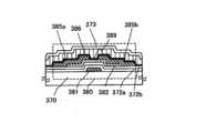
도 2(A) 내지 2(D)에 반도체 장치의 단면 구조의 일례를 나타낸다. 도 2(A) 내지 2(D)에 나타내는 박막 트랜지스터(130)는 보텀 게이트 구조의 하나로 역스태거형 박막 트랜지스터라고도 한다.2 (A) to 2 (D) show an example of the sectional structure of the semiconductor device. The
도 2(A) 내지 2(D)에 나타내는 박막 트랜지스터(130)는 절연 표면을 갖는 기판(100) 상에 게이트 전극층(111), 게이트 절연층(102), 산화물 반도체층(132), 소스 전극층(115a) 및 드레인 전극층(115b)을 포함한다. 또한, 박막 트랜지스터(130)를 덮고, 산화물 반도체층(132)에 접하여 산소 과잉인 산화물 절연층(139)이 마련되고, 산소 과잉인 산화물 절연층(139) 상에 결함을 포함하는 절연층(116)이 형성되어 있다. 아울러 결함을 포함하는 절연층(116) 상에 보호 절연층(103)이 적층되어 있다.The
산소 과잉인 산화물 절연층(139), 결함을 포함하는 절연층(116)은 수소나 수분(수소 원자나, H2O 등 수소 원자를 포함하는 화합물)에 대하여 속박 에너지가 크고, 산소 과잉인 산화물 절연층(139), 결함을 포함하는 절연층(116)에 있어서 그 불순물은 안정화되므로, 산화물 반도체층(121)으로부터 산소 과잉인 산화물 절연층(139), 결함을 포함하는 절연층(116)으로 그 불순물을 확산시켜, 그 불순물을 산화물 반도체층(132)으로부터 배제할 수 있다. 아울러, 산소 과잉인 산화물 절연층(139)이 결함을 포함하는 절연층(116)으로 확산된 불순물에 대한 배리어층이 되어, 그 불순물이 다시 산화물 반도체층(132)으로 침입하는 것을 방지하므로, 산화물 반도체층(132) 내의 불순물 농도는 저감된 상태로 유지될 수 있다. 따라서, 변동 요인이 되는 수소, 수분, 수산기 또는 수소화물(수소화합물이라고도 함) 등의 불순물이 저감된 산화물 반도체층(132)을 이용한 박막 트랜지스터(130)는 안정된 전기적 특성을 갖는 신뢰성이 높은 박막 트랜지스터가 된다.The
산소 과잉인 산화물 절연층(139)으로는 산화 실리콘층(SiO2+x, 바람직하게는 x는 0 이상 3 미만)을 이용할 수 있다. 산소 과잉인 산화물 절연층(139)은 막 두께 0.1㎚ 내지 30㎚(바람직하게는 2㎚ 내지 10㎚)일 수 있다.As the
또한, 박막 트랜지스터(130)는 싱글 게이트 구조의 박막 트랜지스터를 이용하여 설명했으나, 필요에 따라 채널 형성 영역을 복수 갖는 멀티 게이트 구조의 박막 트랜지스터도 형성할 수 있다.Though the
이하, 도 2(A) 내지 2(D)를 이용하여 기판(100) 상에 박막 트랜지스터(130)를 제작하는 공정을 설명한다.Hereinafter, the process of fabricating the
우선, 절연 표면을 갖는 기판(100) 상에 도전막을 형성한 후, 제 1 포토리소그래피 공정에 의해 게이트 전극층(111)을 형성한다.First, a conductive film is formed on a
이어서, 게이트 전극층(111) 상에 게이트 절연층(102)을 형성한다. 게이트 절연층(102)은 게이트 전극층(111) 측으로부터 질화 실리콘층과 산화 실리콘층의 적층 구조를 이용할 수 있다.Subsequently, a
이어서, 게이트 절연층(102) 상에 산화물 반도체막을 형성하고, 제 2 포토리소그래피 공정에 의해 섬 형상의 산화물 반도체층(121)으로 가공한다. 본 실시형태에서는 산화물 반도체막을 In-Ga-Zn-O계 금속 산화물 타겟을 이용하여 스퍼터링법에 의해 성막한다.Then, an oxide semiconductor film is formed on the
이어서, 게이트 절연층(102) 및 산화물 반도체층(121) 상에 도전막을 형성한다. 제 3 포토리소그래피 공정에 의해 도전막 상에 레지스트 마스크를 형성하고, 선택적으로 에칭을 수행하여 소스 전극층(115a), 드레인 전극층(115b)을 형성한 후, 레지스트 마스크를 제거한다(도 2(A) 참조).Subsequently, a conductive film is formed on the
이어서, 게이트 절연층(102), 산화물 반도체층(121), 소스 전극층(115a) 및 드레인 전극층(115b) 상에 산소 과잉의 산화물 절연층(139)을 형성한다(도 2(B) 참조). 본 실시형태에서는, 산화물 반도체층(121)이 소스 전극층(115a), 드레인 전극층(115b)과 중첩되지 않는 영역에 있어서, 산화물 반도체층(121)과 산소 과잉의 산화물 절연층(139)이 접하도록 형성한다.Then, an oxygen-excess
본 실시형태에서는, 산소 과잉의 산화물 절연층(139)으로서, 소스 전극층(115a) 및 드레인 전극층(115b)까지 형성된 기판(100)을 실온 또는 100℃ 미만의 온도로 가열하고, 수소 및 수분이 제거된 고순도 산소를 포함하는 스퍼터링 가스를 도입하고 실리콘 타겟을 이용하여 산화 실리콘층(SiO2+x, 바람직하게는 x는 0 이상 3 미만)을 성막한다. 산소 과잉의 산화물 절연층(139)은 막 두께 0.1㎚ 내지 30㎚(바람직하게는 2㎚ 내지 10㎚)일 수 있다.The
산소 과잉의 산화물 절연층(139)을 성막할 때에 이용하는 스퍼터링 가스는 수소, 물, 수산기 또는 수소화물 등의 불순물이 농도 ppm 정도, 농도 ppb 정도까지 제거된 고순도 가스를 이용하는 것이 바람직하다.It is preferable to use a high purity gas in which impurities such as hydrogen, water, hydroxyl groups, or hydrides are removed to a concentration of about ppm and a concentration of about ppb, as the sputtering gas used when forming the oxygen-excess
예를 들어, 순도가 6N이며, 붕소가 도프된 실리콘 타겟(저항값 0.01Ω㎝)을 이용하고, 기판과 타겟간의 거리(S-T간 거리)를 89㎜, 압력 0.4Pa, 직류(DC) 전원 6kW, 산소(산소 유량 비율 100%) 분위기하에서 펄스 DC 스퍼터링법에 의해 산화 실리콘층을 성막한다. 또한, 실리콘 타겟 대신에 석영(바람직하게는 합성 석영)을 산화 실리콘층을 성막하기 위한 타겟으로 이용할 수도 있다. 또한, 스퍼터링 가스로서 산소 또는, 산소 및 아르곤의 혼합 가스를 이용하여 수행한다.For example, a silicon target doped with boron (with a resistance value of 0.01? Cm) having a purity of 6N and a distance between the substrate and the target (distance between STs) of 89 mm, a pressure of 0.4 Pa, a direct current (DC) , And a silicon oxide layer is formed by a pulsed DC sputtering method in an atmosphere of oxygen (oxygen flow rate ratio: 100%). Further, instead of the silicon target, quartz (preferably, synthetic quartz) may be used as a target for forming a silicon oxide layer. Also, the sputtering gas is performed using oxygen or a mixed gas of oxygen and argon.
또한, 산소 과잉의 산화물 절연층(139)은 산화 실리콘층 대신에, 산화 질화 실리콘층, 산화 알루미늄층 또는 산화질화 알루미늄층 등을 이용할 수도 있다.In place of the silicon oxide layer, a silicon oxynitride layer, an aluminum oxide layer, an aluminum oxynitride layer, or the like may be used as the oxygen-excess
이어서, 대기에 접촉시키지 않고, 산소 과잉의 산화물 절연층(139) 상에 결함을 포함하는 절연층(116)을 형성한다.Then, an insulating
본 실시형태에서는, 섬 형상의 산화물 반도체층(121), 소스 전극층(115a), 드레인 전극층(115b), 산소 과잉의 산화물 절연층(139)까지 형성된 기판(100)을 실온 또는 100℃ 미만의 온도로 가열하고, 수소 및 수분이 제거된 고순도 산소를 포함하는 스퍼터링 가스를 도입하고 실리콘 타겟을 이용하여 결함을 포함하는 절연층(116)을 성막한다. 산소 과잉의 산화물 절연층(139) 및 결함을 포함하는 절연층(116)은 같은 처리실 및 타겟을 이용하여 형성할 수도 있다.In this embodiment, the
결함을 포함하는 절연층(116)을 성막할 때에 이용하는 스퍼터링 가스도 수소, 물, 수산기 또는 수소화물 등의 불순물이 농도 ppm 정도, 농도 ppb 정도까지 제거된 고순도 가스를 이용하는 것이 바람직하다.It is preferable to use a high purity gas in which impurities such as hydrogen, water, hydroxyl groups, or hydrides are removed to a concentration of about ppm and a concentration of about ppb, as a sputtering gas used in forming the insulating
산소 과잉의 산화물 절연층(139), 결함을 포함하는 절연층(116)을 성막하는 처리실 내의 잔류 수분을 제거하면서 산소 과잉의 산화물 절연층(139), 또는 결함을 포함하는 절연층(116)을 성막하는 것이 바람직하다. 이는 산화물 반도체층(121), 산소 과잉의 산화물 절연층(139) 및 결함을 포함하는 절연층(116)에 수소, 수산기 또는 수분이 포함되지 않도록 하기 위함이다.An oxygen excess
또한, 결함을 포함하는 절연층(116)은 산화 실리콘층 대신에, 산화 질화 실리콘층, 산화 알루미늄층, 또는 산화질화 알루미늄층 등을 이용할 수도 있다. 또한, 결함을 포함하는 절연층(116)으로서 질화 실리콘층, 질화산화 실리콘층, 질화 알루미늄층, 질화산화 알루미늄층 등을 이용할 수도 있다.The insulating
이어서, 결함을 포함하는 절연층(116)과 산화물 반도체층(121)을 산소 과잉의 산화물 절연층(139)을 사이에 갖고 접한 상태로 100℃ 내지 400℃의 가열 처리를 수행한다. 이 가열 처리에 의해 산화물 반도체층(121) 내에 포함되는 수소 혹은 수분을 산소 과잉의 산화물 절연층(139), 결함을 포함하는 절연층(116)으로 확산시킬 수 있다. 사이에 마련된 산소 과잉의 산화물 절연층(139)으로 인해, 섬 형상의 산화물 반도체층(121)에 포함되는 수소, 수산기 및 수분 등의 불순물은 산화물 반도체층(121)으로부터 산소 과잉의 산화물 절연층(139)으로, 또는 산소 과잉의 산화물 절연층(139)을 통과하여 결함을 포함하는 절연층(116)으로 확산된다.Then, the insulating
산화물 반도체층(121)과 결함을 포함하는 절연층(116)의 사이에 마련되는 산소 과잉의 산화물 절연층(139)은 산소의 댕글링 본드를 결함으로서 많이 포함하고, 수소, 수분, 수산기 또는 수소화물 등의 불순물에 대하여 속박 에너지가 크다. 따라서, 산소 과잉의 산화물 절연층(139)을 마련함으로써, 산화물 반도체층(121)에 포함되는 수소, 수분, 수산기 또는 수소화물 등의 불순물이 결함을 포함하는 절연층(116)으로 확산, 이동하기 쉬워진다.The oxygen-excess
아울러, 산소 과잉의 산화물 절연층(139)은 일단 산화물 반도체층(121)으로부터 배제되어 결함을 포함하는 절연층(116)으로 확산된 상기 불순물이 다시 산화물 반도체층으로 이동하려고 할 때는 상기 불순물을 속박해 안정화시켜, 산화물 반도체층으로의 침입을 방지하는 보호층(배리어층)으로서 기능한다.When the impurity diffused into the insulating
이와 같이, 변동 요인이 되는 수소, 수분, 수산기 또는 수소화물 등의 불순물을 산화물 반도체층으로부터 배제하여, 상기 불순물이 저감된 산화물 반도체층(121)을 얻을 수 있다. 아울러, 배리어층이 되는 산소 과잉의 산화물 절연층(139)이 결함을 포함하는 절연층(116)으로 확산된 불순물이 다시 산화물 반도체층(121)으로 침입하는 것을 방지함으로써, 산화물 반도체층(121) 내의 불순물 농도를 저감시킨 상태로 유지할 수 있다.In this manner, impurities such as hydrogen, moisture, hydroxyl groups, or hydrides, which are fluctuating factors, are removed from the oxide semiconductor layer, and the
이어서, 보호 절연층(103)을 결함을 포함하는 절연층(116) 상에 형성한다. 보호 절연층(103)으로는 질화 실리콘층, 질화산화 실리콘층, 질화 알루미늄층, 질화산화 알루미늄층 등을 이용할 수 있다. 본 실시형태에서는, 보호 절연층(103)으로서, 결함을 포함하는 절연층(116)까지 형성된 기판(100)을 100℃~400℃의 온도로 가열하고, 수소 및 수분이 제거된 고순도 질소를 포함하는 스퍼터링 가스를 도입하고 실리콘 타겟을 이용하여 질화 실리콘층을 성막한다.Then, a protective
이상의 공정으로, 수소나 수분 등의 불순물을 배제하고, 수소 및 수분 등의 불순물을 극저농도로 유지함으로써, 산화물 반도체층(132) 표층부의 백채널 측에서의 기생 채널의 발생을 억제할 수 있다.With the above steps, the generation of parasitic channels on the back channel side of the surface layer portion of the
따라서 수소 및 수소화물 등의 불순물 농도가 저감된 산화물 반도체층(132)을 갖는 박막 트랜지스터(130)를 형성할 수 있다(도 2(D) 참조).Therefore, the
또한, 결함을 포함하는 절연층(116)으로 불순물을 확산시킨 후의 공정에 있어서의 가열 처리에 의해 불순물이 산화물 반도체층(132)으로 다시 이동했다고 해도, 배리어층이 되는 산소 과잉의 산화물 절연층(139)이 상기 불순물의 산화물 반도체층(132)으로의 침입을 방지한다. 따라서, 산화물 반도체층(132) 내의 불순물 농도를 저감시킨 상태로 유지할 수 있다.Further, even if the impurity is moved back to the
박막 트랜지스터(130)는 산화물 반도체에 포함되는 수소가 5×10¹⁹/㎤ 이하, 바람직하게는 5×10¹⁸/㎤ 이하, 보다 바람직하게는 5×10¹⁷/㎤ 이하로서, 산화물 반도체에 포함되는 수소 혹은 OH기를 제거하여 캐리어 농도를 5×10¹⁴/㎤ 이하, 바람직하게는 5×10¹²/㎤ 이하로 한 산화물 반도체층(132)에서 채널 형성 영역이 형성되는 박막 트랜지스터(130)로 할 수 있다.The
산화물 반도체의 에너지 갭은 2eV 이상, 바람직하게는 2.5eV 이상, 보다 바람직하게는 3eV 이상으로, 도너를 형성하는 수소 등의 불순물을 가능한 한 저감시켜, 캐리어 농도를 1×10¹⁴/㎤ 이하, 바람직하게는 1×10¹²/㎤ 이하가 되도록 한다.The energy gap of the oxide semiconductor is 2 eV or more, preferably 2.5 eV or more, more preferably 3 eV or more, impurities such as hydrogen forming the donor are reduced as much as possible and the carrier concentration is preferably 1 x 10¹⁴ / Lt;12 > / cm < 3 > or less.
이와 같이 고순도화된 산화물 반도체를 박막 트랜지스터(130)의 채널 형성 영역에 이용함으로써, 채널 폭이 10㎜인 경우조차도, 드레인 전압이 1V 및 10V인 경우에 있어서, 게이트 전압이 -5V에서 -20V의 범위에 있어서, 드레인 전류는 1×10-13A 이하가 되도록 작용한다.By using the high-purity oxide semiconductor in the channel forming region of the
이상과 같이, 산화물 반도체층을 이용하는 박막 트랜지스터를 갖는 반도체 장치에 있어서, 안정된 전기 특성을 가지며 신뢰성이 높은 반도체 장치를 제공할 수 있다.As described above, in the semiconductor device having the thin film transistor using the oxide semiconductor layer, it is possible to provide a semiconductor device having stable electric characteristics and high reliability.
(실시형태 3)(Embodiment 3)
본 실시형태는 본 명세서에서 개시하는 반도체 장치에 적용할 수 있는 박막 트랜지스터의 다른 예를 나타낸다.This embodiment shows another example of the thin film transistor applicable to the semiconductor device disclosed in this specification.
본 실시형태의 반도체 장치 및 반도체 장치의 제작 방법의 한 형태를 도 3을 이용해 설명한다.One embodiment of the semiconductor device and the method of manufacturing the semiconductor device of the present embodiment will be described with reference to FIG.
도 3(A) 내지 3(E)에 반도체 장치의 단면 구조의 일례를 나타낸다. 도 3(A) 내지 3(E)에 나타내는 박막 트랜지스터(160)는 채널 보호형(채널 스톱형이라고도 함)으로 불리는 보텀 게이트 구조의 하나로 역스태거형 박막 트랜지스터라고도 한다.3 (A) to 3 (E) show an example of the sectional structure of the semiconductor device. The
또한, 박막 트랜지스터(160)에 있어서 싱글 게이트 구조의 박막 트랜지스터를 이용하여 설명하고 있으나, 필요에 따라 채널 형성 영역을 복수 갖는 멀티 게이트 구조의 박막 트랜지스터도 형성할 수 있다.Although the
이하, 도 3(A) 내지 3(E)를 이용하여 기판(150) 상에 박막 트랜지스터(160)를 제작하는 공정을 설명한다.Hereinafter, the process of fabricating the
우선, 절연 표면을 갖는 기판(150) 상에 도전막을 형성한 후, 제 1 포토리소그래피 공정에 의해 게이트 전극층(151)을 형성한다. 또한, 레지스트 마스크를 잉크젯법으로 형성할 수도 있다. 레지스트 마스크를 잉크젯법으로 형성하면 포토마스크를 사용하지 않으므로 제조 비용을 저감시킬 수 있다.First, a conductive film is formed on a
또한, 게이트 전극층(151)의 재료는 몰리브덴, 티타늄, 크롬, 탄탈, 텅스텐, 알루미늄, 구리, 네오디뮴, 스칸듐 등의 금속재료 또는 이들을 주성분으로 하는 합금 재료를 이용하여, 단층으로 또는 적층해 형성할 수 있다.The material of the
이어서, 게이트 전극층(151) 상에 게이트 절연층(152)을 형성한다.Then, a
본 실시형태에서는, 게이트 절연층(152)으로서 플라즈마 CVD법에 의해 막 두께 100㎚의 산화질화 실리콘층을 형성한다.In this embodiment, as the
이어서, 게이트 절연층(152) 상에 산화물 반도체막을 형성하고, 제 2 포토리소그래피 공정에 의해 섬 형상의 산화물 반도체층(171)으로 가공한다. 본 실시형태에서는 산화물 반도체막을 In-Ga-Zn-O계 금속 산화물 타겟을 이용하여 스퍼터링법에 의해 성막한다.Then, an oxide semiconductor film is formed on the
감압 상태로 유지된 처리실 내에 기판을 유지하고, 기판을 400℃ 미만의 온도로 가열한다. 그리고, 처리실 내의 잔류 수분을 제거하면서, 수소 및 수분이 제거된 스퍼터링 가스를 도입하고, 금속 산화물을 타겟으로 하여 기판(150) 상에 산화물 반도체막을 성막한다. 처리실 내의 잔류 수분을 제거하기 위해서는, 흡착형 진공 펌프를 이용하는 것이 바람직하다. 예를 들어, 크라이오 펌프, 이온 펌프, 티타늄 승화 펌프를 이용하는 것이 바람직하다. 또한, 배기 수단은 터보 펌프에 콜드 트랩을 부가한 것일 수도 있다. 크라이오 펌프를 이용하여 배기한 성막실은 예를 들어, 수소 원자나, H2O 등 수소 원자를 포함하는 화합물이나, 탄소 원자를 포함하는 화합물 등이 배기되므로, 이 성막실에서 성막한 산화물 반도체막에 포함되는 불순물의 농도를 저감할 수 있다.The substrate is held in a processing chamber kept in a reduced pressure state, and the substrate is heated to a temperature of less than 400 캜. Then, while the residual moisture in the treatment chamber is removed, hydrogen and moisture-free sputtering gas is introduced, and an oxide semiconductor film is formed on the
성막 조건의 일례로서는, 기판과 타겟 사이의 거리를 100㎜, 압력 0.6Pa, 직류(DC) 전원 0.5kW, 산소(산소 유량 비율 100%) 분위기하의 조건이 적용된다. 또한, 펄스 직류(DC) 전원을 이용하면, 성막시에 발생하는 분상 물질(파티클, 먼지라고도 함)을 경감할 수 있고, 막 두께 분포도 균일해지므로 바람직하다. 산화물 반도체막은 바람직하게는 5㎚ 이상 30㎚ 이하로 한다. 또한, 적용하는 산화물 반도체 재료에 따라 적절한 두께는 다르며, 재료에 따라 적절한 두께를 선택하면 된다.As an example of the film formation conditions, conditions are applied under the atmosphere of a distance of 100 mm between the substrate and the target, a pressure of 0.6 Pa, a direct current (DC) power of 0.5 kW, and oxygen (oxygen flow rate ratio of 100%). In addition, the use of a pulsed direct current (DC) power source is preferable because it is possible to reduce the amount of dispersed substances (also referred to as particles and dust) generated at the time of film formation and the film thickness distribution to be uniform. The oxide semiconductor film is preferably 5 nm or more and 30 nm or less. In addition, an appropriate thickness depends on the oxide semiconductor material to be applied, and an appropriate thickness may be selected depending on the material.
이어서, 게이트 절연층(152) 및 산화물 반도체층(171) 상에 결함을 포함하는 절연층(173)을 형성한다. 결함을 포함하는 절연층(173)의 형성 공정에 있어서, 산화물 반도체층(171)과 결함을 포함하는 절연층(173)의 사이에 산소 과잉의 혼합 영역(179)을 형성한다(도 3(B) 참조).Then, an insulating
혼합 영역(179)은 산화물 반도체층(171) 및 적층하는 결함을 포함하는 절연층(173)에 포함되는 재료의 혼합 영역(179)으로, 산화물 반도체층(171)과 결함을 포함하는 절연층(173)의 계면을 명확하게 하지 않음으로써, 보다 산화물 반도체층(171)으로부터 결함을 포함하는 절연층(173)으로의 수소의 확산이 용이해진다. 예를 들어, 결함을 포함하는 절연층(173)으로서 산화 실리콘층을 이용하는 경우, 혼합 영역(179)에는 산소, 실리콘, 및 산화물 반도체층(171)에 포함되는 금속 원소가 적어도 1종류 이상이 포함된다.The
본 실시형태와 같이, 결함을 포함하는 절연층(173)으로서 산화 실리콘, 산화물 반도체로서 In-Ga-Zn-O계 막을 이용하는 경우, 혼합 영역(179)에는 In, Ga 및 Zn 중 적어도 1종 이상의 금속 원소와 실리콘 및 산소가 포함된다.When an In-Ga-Zn-O-based film is used as the insulating
혼합 영역(179)은 막 두께 0.1㎚ 내지 30㎚(바람직하게는 2㎚ 내지 10㎚)일 수 있다. 혼합 영역(179)의 막 두께는 결함을 포함하는 절연층(173)을 형성할 때의 스퍼터링법의 성막 조건에 의해 제어할 수 있다. 스퍼터링법의 전원의 파워를 보다 강하게, 기판과 타겟간의 거리를 보다 가깝게 하면, 혼합 영역(179)을 두껍게 형성할 수 있다. 또한, 보다 강한 파워로 스퍼터링법을 수행함으로써 산화물 반도체층(171) 표면에 부착된 흡착수 등을 제거할 수도 있다.The
혼합 영역(179)을 산화물 반도체층(171)과 결함을 포함하는 절연층(173)의 사이에 마련함으로써, 상기 산화물 반도체층(171)에 포함되는 수소 원자나, H2O 등 수소 원자를 포함하는 화합물이나, 탄소 원자를 포함하는 화합물 등의 결함을 포함하는 절연층(173)으로 보다 확산하기 쉬워진다.The
혼합 영역(179)은 산소 과잉으로 할 필요가 있기 때문에, 혼합 영역(179)의 형성시에는 산소를 많이 포함하는 스퍼터링 가스를 이용하고, 혼합 영역(179)의 형성 후는 스퍼터링 가스 내의 산소량을 변화시키는 조정을 수행하여 결함을 포함하는 절연층(173)을 형성할 수도 있다.The sputtering gas containing a large amount of oxygen is used for forming the
따라서, 결함을 포함하는 절연층(173)은 산화 실리콘층 대신에, 산화질화 실리콘층, 산화 알루미늄층, 또는 산화질화 알루미늄층 등을 이용할 수도 있다. 또한, 결함을 포함하는 절연층(173)으로서, 질화 실리콘층, 질화산화 실리콘층, 질화 알루미늄층, 질화산화 알루미늄층 등을 이용할 수도 있다.Therefore, instead of the silicon oxide layer, the insulating
본 실시형태에서는, 섬 형상의 산화물 반도체층(171)까지 형성된 기판(100)을 실온 또는 100℃ 미만의 온도로 가열하고, 수소 및 수분이 제거된 고순도 산소를 포함하는 스퍼터링 가스를 도입하고, 실리콘 타겟을 이용하여 산소 과잉의 혼합 영역(179) 및 산화 실리콘층을 성막한다.In the present embodiment, the
결함을 포함하는 절연층(173)을 성막할 때에 이용하는 스퍼터링 가스에는 수소, 물, 수산기 또는 수소화물 등의 불순물이 농도 ppm 정도, 농도 ppb 정도까지 제거된 고순도 가스를 이용하는 것이 바람직하다.It is preferable to use a high purity gas in which impurities such as hydrogen, water, hydroxyl groups, or hydrides are removed to about ppm concentration and about ppb concentration as the sputtering gas used for forming the insulating
예를 들어, 순도가 6N이며, 붕소가 도프된 실리콘 타겟(저항값 0.01Ω㎝)을 이용하고, 기판과 타겟간의 거리(T-S간 거리)를 89㎜, 압력 0.4Pa, 직류(DC) 전원 6kW, 산소(산소 유량 비율 100%) 분위기하에서 펄스 DC 스퍼터링법에 의해 산화 실리콘막을 성막한다. 막 두께는 300㎚로 한다. 또한, 실리콘 타겟 대신에 석영(바람직하게는 합성 석영)을 산화 실리콘막의 성막을 위한 타겟으로서 이용할 수 있다. 또한, 스퍼터링 가스로서 산소 또는, 산소 및 아르곤의 혼합 가스를 이용하여 수행한다.For example, a silicon target doped with boron (with a resistance value of 0.01? Cm) having a purity of 6N and a distance (distance between TSs) of 89 mm, a pressure of 0.4 Pa, a DC power source of 6 kW , And a silicon oxide film is formed by a pulsed DC sputtering method in an oxygen (oxygen flow rate ratio: 100%) atmosphere. The film thickness is 300 nm. Further, quartz (preferably synthetic quartz) may be used as a target for forming a silicon oxide film instead of a silicon target. Also, the sputtering gas is performed using oxygen or a mixed gas of oxygen and argon.
이 경우, 처리실 내의 잔류 수분을 제거하면서 혼합 영역(179) 및 결함을 포함하는 절연층(173)을 성막하는 것이 바람직하다. 이는 산화물 반도체층(171), 혼합 영역(179) 및 결함을 포함하는 절연층(173)에 수소, 수산기 또는 수분이 포함되지 않도록 하기 위함이다.In this case, it is preferable to form the
또한, 혼합 영역(179)은 산화 실리콘 대신에, 산화질화 실리콘, 산화 알루미늄, 또는 산화질화 알루미늄 등을 이용하여 형성할 수도 있다.The
이어서, 결함을 포함하는 절연층(173)과 산화물 반도체층(171)이 산소 과잉의 혼합 영역(179)을 사이에 두고 접한 상태로 100℃ 내지 400℃의 가열 처리를 수행한다. 이 가열 처리에 의해 산화물 반도체층(171) 내에 포함되는 수소 혹은 수분을 산소 과잉의 혼합 영역(179), 결함을 포함하는 절연층(173)으로 확산시킬 수 있다. 결함을 포함하는 절연층(173)과 산화물 반도체층(171)의 사이에 산소 과잉의 혼합 영역(179)이 마련되어 있으므로, 섬 형상의 산화물 반도체층(171)에 포함되는 수소, 수산기 및 수분 등의 불순물은 산화물 반도체층(171)으로부터 산소 과잉의 혼합 영역(179)으로, 또는 산소 과잉의 혼합 영역(179)을 통과하여 결함을 포함하는 절연층(173)으로 확산된다.Then, a heat treatment is performed at a temperature of 100 ° C to 400 ° C in a state where the insulating
산화물 반도체층(171)과 결함을 포함하는 절연층(173)의 사이에 마련되는 혼합 영역(179)은 산소 과잉이기 때문에, 산소의 댕글링 본드를 결함으로서 많이 포함하고, 수소, 수분, 수산기 또는 수소화물 등의 불순물에 대하여 속박 에너지가 크다. 따라서, 산소 과잉의 혼합 영역(179)을 마련함으로써, 산화물 반도체층(171)에 포함되는 수소, 수분, 수산기 또는 수소화물 등의 불순물이 결함을 포함하는 절연층(173)으로 확산, 이동하기 쉬워진다.Since the
아울러, 상기 불순물이 일단 산화물 반도체층(171)으로부터 배제되어 결함을 포함하는 절연층(173)으로 확산한 후, 다시 산화물 반도체층(171)으로 이동하려고 할 때, 산소 과잉의 혼합 영역(179)은 상기 불순물을 속박해 안정화시켜, 산화물 반도체층(171)으로의 침입을 방지하는 보호층(배리어층)으로서 기능한다.When the impurity is once removed from the
이와 같이, 변동 요인이 되는 수소, 수분, 수산기 또는 수소화물 등의 불순물을 산화물 반도체층(171)으로부터 배제함으로써, 상기 불순물이 저감된 산화물 반도체층(162)을 얻을 수 있다. 아울러, 배리어층이 되는 산소 과잉의 혼합 영역(179)이 결함을 포함하는 절연층(173)으로 확산된 불순물이 다시 산화물 반도체층(162)으로 침입하는 것을 방지함으로써, 산화물 반도체층(162) 내의 불순물 농도를 저감시킨 상태로 유지할 수 있다.Thus, the
이상의 공정으로, 수소 및 수소화물의 농도가 저감된 산화물 반도체층(162)을 형성할 수 있다.With the above process, the
또한, 실시형태 2와 같이, 산소 과잉의 혼합 영역 대신에 산소 과잉의 산화물 절연층을 마련하는 구성으로 할 수도 있다. 산소 과잉의 산화물 절연층도 산소 과잉의 혼합 영역과 동일한 효과를 나타낸다.Further, as in the second embodiment, an oxygen-excess oxide insulating layer may be provided in place of the oxygen-excess mixed region. The oxygen-rich oxide insulating layer also exhibits the same effect as the oxygen-rich mixed region.
결함을 포함하는 절연층(173) 상에 제 3 포토리소그래피 공정에 의해 레지스트 마스크를 형성하고, 선택적으로 에칭을 수행하여 결함을 포함하는 절연층(166)을 형성한 후, 레지스트 마스크를 제거한다(도 3(C) 참조).A resist mask is formed on the insulating
이어서, 게이트 절연층(152), 산화물 반도체층(162) 및 결함을 포함하는 절연층(166) 상에 도전막을 형성한 후, 제 4 포토리소그래피 공정에 의해 레지스트 마스크를 형성하고, 선택적으로 에칭을 수행하여 전극층(165a), 드레인 전극층(166b)을 형성한 후, 레지스트 마스크를 제거한다.Subsequently, a conductive film is formed on the
소스 전극층(165a), 드레인 전극층(165b)의 재료로서는 Al, Cr, Cu, Ta, Ti, Mo, W로부터 선택된 원소, 또는 상술한 원소를 성분으로 하는 합금, 또는 상술한 원소를 조합한 합금 등을 들 수 있다. 또한, 금속 도전막은 단층 구조일 수도 있고, 2층 이상의 적층 구조일 수도 있다.As the material of the
이상의 공정으로, 수소 및 수소화물의 농도가 저감된 산화물 반도체층(162)을 갖는 박막 트랜지스터(160)를 형성할 수 있다(도 3(D) 참조).Through the above steps, the
상기와 같이 산화물 반도체막을 성막하는데 있어서, 반응 분위기 중의 잔류 수분을 제거함으로써 그 산화물 반도체막 내의 수소 및 수소화물의 농도를 저감시킬 수 있다. 또한, 산화물 반도체층 상에 산소 과잉의 혼합 영역을 사이에 두고 결함을 포함하는 절연층을 마련함으로써 산화물 반도체층 내의 수소, 수분 등의 불순물을 결함을 포함하는 절연층으로 확산시켜 산화물 반도체층의 수소 및 수소화합물의 농도를 저감시킬 수 있다. 이에 따라 산화물 반도체층의 안정화를 도모할 수 있다.In forming the oxide semiconductor film as described above, the concentration of hydrogen and the hydride in the oxide semiconductor film can be reduced by removing the residual moisture in the reaction atmosphere. In addition, by providing an insulating layer containing defects on the oxide semiconductor layer with an oxygen-rich mixed region therebetween, it is possible to diffuse impurities such as hydrogen and moisture in the oxide semiconductor layer into an insulating layer containing defects, And the concentration of the hydrogen compound can be reduced. Thus, the oxide semiconductor layer can be stabilized.
또한, 결함을 포함하는 절연층(173)으로 불순물을 확산시킨 후의 공정에 있어서의 가열 처리에 의해 불순물이 산화물 반도체층(162)으로 다시 이동했다고 해도, 배리어층이 되는 산소 과잉의 혼합 영역(179)이 상기 불순물의 산화물 반도체층(162)으로의 침입을 방지한다. 따라서, 산화물 반도체층(162) 내의 불순물 농도를 저감시킨 상태로 유지할 수 있다.Even if the impurity is moved back to the
결함을 포함하는 층 위에 보호 절연층을 마련할 수도 있다. 본 실시형태에서는 보호 절연층(153)을 결함을 포함하는 절연층(166), 소스 전극층(165a), 드레인 전극층(165b) 상에 형성한다. 보호 절연층(153)으로는 질화 실리콘막, 질화산화 실리콘막 또는 질화 알루미늄막 등을 이용한다. 본 실시형태에서는, 보호 절연층(153)을 질화 실리콘막을 이용하여 형성한다(도 3(E) 참조).A protective insulating layer may be provided on the layer containing the defect. In this embodiment, the protective insulating
또한, 소스 전극층(165a), 드레인 전극층(165b), 결함을 포함하는 절연층(166) 상에 산화물 절연층을 더 형성하고, 그 산화물 절연층 상에 보호 절연층(153)을 적층할 수도 있다. 또한, 보호 절연층(153) 상에 평탄화 절연층을 형성할 수도 있다.It is also possible to further form an oxide insulating layer on the insulating
본 실시형태는 다른 실시형태와 적절히 조합하여 실시하는 것이 가능하다.The present embodiment can be implemented in appropriate combination with other embodiments.
이상과 같이, 산화물 반도체층을 이용하는 박막 트랜지스터를 갖는 반도체 장치에 있어서, 안정된 전기 특성을 가지며 신뢰성이 높은 반도체 장치를 제공할 수 있다.As described above, in the semiconductor device having the thin film transistor using the oxide semiconductor layer, it is possible to provide a semiconductor device having stable electric characteristics and high reliability.
(실시형태 4)(Fourth Embodiment)
본 실시형태는 본 명세서에서 개시하는 반도체 장치에 적용할 수 있는 박막 트랜지스터의 다른 예를 나타낸다.This embodiment shows another example of the thin film transistor applicable to the semiconductor device disclosed in this specification.
본 실시형태의 반도체 장치 및 반도체 장치의 제작 방법의 일 형태를 도 4를 이용하여 설명한다.One embodiment of the semiconductor device and the method of manufacturing the semiconductor device of the present embodiment will be described with reference to FIG.
또한, 박막 트랜지스터(190)는 싱글 게이트 구조의 박막 트랜지스터를 이용하여 설명하지만, 필요에 따라 채널 형성 영역을 복수 갖는 멀티 게이트 구조의 박막 트랜지스터도 형성할 수 있다.Although the
이하, 도 4(A) 내지 4(C)를 이용하여 기판(140) 상에 박막 트랜지스터(190)를 제작하는 공정을 설명한다.Hereinafter, a process of manufacturing the
우선, 절연 표면을 갖는 기판(140) 상에 도전막을 형성한 후, 제 1 포토리소그래피 공정에 의해 게이트 전극층(181)을 형성한다. 본 실시형태에서는 게이트 전극층(181)으로서 막 두께 150㎚의 텅스텐막을 스퍼터링법을 이용하여 형성한다.First, a conductive film is formed on a
이어서, 게이트 전극층(181) 상에 게이트 절연층(142)을 형성한다. 본 실시형태에서는 게이트 절연층(142)으로서 플라즈마 CVD법에 의해 막 두께 100㎚의 산화질화 실리콘층을 형성한다.Then, a
이어서, 게이트 절연층(142)에 도전막을 형성하고, 제 2 포토리소그래피 공정에 의해 도전막 상에 레지스트 마스크를 형성하고, 선택적으로 에칭을 수행하여 소스 전극층(195a), 드레인 전극층(195b)을 형성한 후, 레지스트 마스크를 제거한다.Next, a conductive film is formed on the
이어서 산화물 반도체막을 형성하고, 제 3 포토리소그래피 공정에 의해 섬 형상의 산화물 반도체층(141)으로 가공한다(도 4(A) 참조). 본 실시형태에서는 산화물 반도체막으로서 In-Ga-Zn-O계 금속 산화물 타겟을 이용하여 스퍼터링법에 의해 성막한다.Then, an oxide semiconductor film is formed and processed into an island-shaped
산화물 반도체막은 감압 상태로 유지된 처리실 내에 기판을 유지하고, 기판을 400℃ 미만의 온도로 가열한다. 그리고, 처리실 내의 잔류 수분을 제거하면서 수소 및 수분이 제거된 스퍼터링 가스를 도입하고, 금속 산화물을 타겟으로 하여 기판(140) 상에 산화물 반도체막을 성막한다. 처리실 내의 잔류 수분을 제거하기 위해서는 흡착형 진공 펌프를 이용하는 것이 바람직하다. 예를 들어, 크라이오 펌프, 이온 펌프, 티타늄 승화 펌프를 이용하는 것이 바람직하다. 또한, 배기 수단은 터보 펌프에 콜드 트랩을 부가한 것일 수도 있다. 크라이오 펌프를 이용하여 배기한 성막실은 예를 들어, 수소 원자나, H2O 등 수소 원자를 포함하는 화합물이나, 탄소 원자를 포함하는 화합물 등이 배기되므로, 이 성막실에서 성막한 산화물 반도체막에 포함되는 불순물의 농도를 저감할 수 있다.The oxide semiconductor film holds the substrate in a treatment chamber kept in a reduced pressure state, and heats the substrate to a temperature of less than 400 캜. Then, sputtering gas from which hydrogen and moisture are removed is introduced while removing residual moisture in the treatment chamber, and an oxide semiconductor film is formed on the
성막 조건의 일례로서는, 기판과 타겟 사이의 거리를 100㎜, 압력 0.6Pa, 직류(DC) 전원 0.5kW, 산소(산소 유량 비율 100%) 분위기하의 조건이 적용된다. 또한, 펄스 직류(DC) 전원을 이용하면, 성막시에 발생하는 분상 물질(파티클, 먼지라고도 함)을 경감할 수 있고, 막 두께 분포도 균일해지므로 바람직하다. 산화물 반도체막은 바람직하게는 5㎚ 이상 30㎚ 이하로 한다. 또한, 적용하는 산화물 반도체 재료에 따라 적절한 두께는 다르며, 재료에 따라 적절한 두께를 선택하면 된다.As an example of the film formation conditions, conditions are applied under the atmosphere of a distance of 100 mm between the substrate and the target, a pressure of 0.6 Pa, a direct current (DC) power of 0.5 kW, and oxygen (oxygen flow rate ratio of 100%). In addition, the use of a pulsed direct current (DC) power source is preferable because it is possible to reduce the amount of dispersed substances (also referred to as particles and dust) generated at the time of film formation and the film thickness distribution to be uniform. The oxide semiconductor film is preferably 5 nm or more and 30 nm or less. In addition, an appropriate thickness depends on the oxide semiconductor material to be applied, and an appropriate thickness may be selected depending on the material.
이어서, 게이트 절연층(142), 산화물 반도체층(141), 소스 전극층(195a) 및 드레인 전극층(195b) 상에 결함을 포함하는 절연층(196)을 형성한다. 결함을 포함하는 절연층(196)의 형성 공정에 있어서, 산화물 반도체층(141)과 결함을 포함하는 절연층(196)의 사이에 산소 과잉의 혼합 영역(199)을 형성한다.Then, an insulating
혼합 영역(199)은 산화물 반도체층(192) 및 적층하는 결함을 포함하는 절연층(196)에 포함되는 재료의 혼합 영역(199)으로, 산화물 반도체층(192)과 결함을 포함하는 절연층(196)의 계면을 명확하게 하지 않음으로써, 보다 산화물 반도체층(192)으로부터 결함을 포함하는 절연층(196)으로의 수소의 확산이 용이해진다. 예를 들어, 결함을 포함하는 절연층(196)으로서 산화 실리콘층을 이용하는 경우, 혼합 영역(199)에는 산소, 실리콘, 및 산화물 반도체층(192)에 포함되는 금속 원소가 적어도 1종류 이상 포함된다.The
본 실시형태와 같이, 결함을 포함하는 절연층(196)으로서 산화 실리콘, 산화물 반도체로서 In-Ga-Zn-O계 산화물을 이용하는 경우, 혼합 영역(199)에는 In, Ga 및 Zn 중 적어도 1종 이상의 금속 원소와 산소 및 실리콘이 포함된다.When the In-Ga-Zn-O-based oxide is used as the insulating
혼합 영역(199)은 막 두께 0.1㎚ 내지 30㎚(바람직하게는 2㎚ 내지 10㎚)일 수 있다. 혼합 영역(199)의 막 두께는 결함을 포함하는 절연층(196)을 형성할 시의 스퍼터링법의 성막 조건에 의해 제어할 수 있다. 스퍼터링법의 전원의 파워를 보다 강하게, 기판과 타겟간의 거리를 보다 가깝게 하면 혼합 영역(199)을 두껍게 형성할 수 있다. 또한, 보다 강한 파워로 스퍼터링법을 수행함으로써, 산화물 반도체층(141) 표면에 부착된 흡착수 등을 제거할 수도 있다.The
혼합 영역(199)을 산화물 반도체층(141)과 결함을 포함하는 절연층(196)의 사이에 마련함으로써, 상기 산화물 반도체층(141)에 포함되는 수소 원자나, H2O 등 수소 원자를 포함하는 화합물이나, 탄소 원자를 포함하는 화합물 등이 결함을 포함하는 절연층(196)으로 보다 확산하기 쉬워진다.By providing the
혼합 영역(199)은 산소 과잉으로 할 필요가 있기 때문에, 혼합 영역(199)의 형성시에는 산소를 많이 포함하는 스퍼터링 가스를 이용하고, 혼합 영역(199)의 형성 후는 스퍼터링 가스 중의 산소량을 변화시키는 조정을 수행하여 결함을 포함하는 절연층(196)을 형성할 수도 있다.Since the
따라서, 결함을 포함하는 절연층(196)은 산화 실리콘층 대신에, 산화질화 실리콘층, 산화 알루미늄층 또는 산화질화 알루미늄층 등을 이용할 수도 있다. 또한, 결함을 포함하는 절연층(196)으로서, 질화 실리콘층, 질화산화 실리콘층, 질화 알루미늄층, 질화산화 알루미늄층 등을 이용할 수도 있다.Therefore, instead of the silicon oxide layer, the insulating
본 실시형태에서는 섬 형상의 산화물 반도체층(141), 소스 전극층(195a), 드레인 전극층(195b)까지 형성된 기판(140)을 실온 또는 100℃ 미만의 온도로 가열하고, 수소 및 수분이 제거된 고순도 산소를 포함하는 스퍼터링 가스를 도입하고, 실리콘 타겟을 이용하여 산소 과잉의 혼합 영역(199) 및 산화 실리콘층을 성막한다.In this embodiment, the
결함을 포함하는 절연층(196)을 성막할 때에 이용하는 스퍼터링 가스는 수소, 물, 수산기 또는 수소화물 등의 불순물이 농도 ppm 정도, 농도 ppb 정도까지 제거된 고순도 가스를 이용하는 것이 바람직하다.It is preferable to use a high purity gas in which impurities such as hydrogen, water, hydroxyl groups, or hydrides are removed to about ppm concentration and about ppb of concentration, as a sputtering gas used for forming the insulating
예를 들어, 순도가 6N이며, 붕소가 도프된 실리콘 타겟(저항값 0.01Ω㎝)을 이용하고, 기판과 타겟간의 거리(T-S간 거리)를 89㎜, 압력 0.4Pa, 직류(DC) 전원 6kW, 산소(산소 유량 비율 100%) 분위기하에서 펄스 DC 스퍼터링법에 의해 산화 실리콘막을 성막한다. 막 두께는 300㎚로 한다. 또한, 실리콘 타겟 대신에 석영(바람직하게는 합성 석영)을 산화 실리콘막의 성막을 위한 타겟으로서 이용할 수 있다. 또한, 스퍼터링 가스로서 산소 또는, 산소 및 아르곤의 혼합 가스를 이용하여 수행한다.For example, a silicon target doped with boron (with a resistance value of 0.01? Cm) having a purity of 6N and a distance (distance between TSs) of 89 mm, a pressure of 0.4 Pa, a DC power source of 6 kW , And a silicon oxide film is formed by a pulsed DC sputtering method in an oxygen (oxygen flow rate ratio: 100%) atmosphere. The film thickness is 300 nm. Further, quartz (preferably synthetic quartz) may be used as a target for forming a silicon oxide film instead of a silicon target. Also, the sputtering gas is performed using oxygen or a mixed gas of oxygen and argon.
또한, 처리실 내의 잔류 수분을 제거하면서 혼합 영역(199) 및 결함을 포함하는 절연층(196)을 성막하는 것이 바람직하다. 이는 산화물 반도체층(141), 혼합 영역(199) 및 결함을 포함하는 절연층(196)에 수소, 수산기 또는 수분이 포함되지 않도록 하기 위함이다.It is also preferable to form the
또한, 혼합 영역(199)은 산화 실리콘 대신에, 산화질화 실리콘, 산화 알루미늄 또는 산화질화 알루미늄 등을 이용하여 형성할 수도 있다.The
이어서, 보호 절연층(183)을 결함을 포함하는 절연층(196) 상에 형성한다. 보호 절연층(183)으로는 질화 실리콘막, 질화산화 실리콘막 또는 질화 알루미늄막 등을 이용한다. 보호 절연층(183)으로서, 결함을 포함하는 절연층(196)까지 형성된 기판(140)을 100℃~400℃의 온도로 가열하고, 수소 및 수분이 제거된 고순도 질소를 포함하는 스퍼터링 가스를 도입하고 실리콘 타겟을 이용하여 질화 실리콘막을 성막한다.Then, a protective
본 실시형태에서는 보호 절연층(183)의 성막시에 100℃~400℃로 기판(140)의 가열 처리를 수행한다.In the present embodiment, the heat treatment of the
이 가열 처리에 의해 산화물 반도체층(141) 내에 포함되는 수소 혹은 수분을 산소 과잉의 혼합 영역(199), 결함을 포함하는 절연층(196)으로 확산시킬 수 있다. 사이에 마련된 산소 과잉의 혼합 영역(199)으로 인해, 섬 형상의 산화물 반도체층(141)에 포함되는 수소, 수산기 또 수분 등의 불순물은 산화물 반도체층(141)으로부터 산소 과잉의 혼합 영역(199)으로, 또는 산소 과잉의 혼합 영역(199)을 통과하여 결함을 포함하는 절연층(196)으로 확산된다.By this heat treatment, hydrogen or moisture contained in the
산화물 반도체층(141)과 결함을 포함하는 절연층(196)의 사이에 마련되는 혼합 영역(199)은 산소 과잉이기 때문에, 산소의 댕글링 본드를 결함으로서 많이 포함하고, 수소, 수분, 수산기 또는 수소화물 등의 불순물에 대하여 속박 에너지가 크다. 따라서, 산소 과잉의 혼합 영역(199)을 마련함으로써, 산화물 반도체층(141)에 포함되는 수소, 수분, 수산기 또는 수소화물 등의 불순물이 결함을 포함하는 절연층(196)으로 확산, 이동하기 쉬워진다.Since the
아울러, 산소 과잉의 혼합 영역(199)은 일단 산화물 반도체층(141)으로부터 배제되어 결함을 포함하는 절연층(196)으로 확산된 상기 불순물이 다시 산화물 반도체층으로 이동하려고 할 때는 상기 불순물을 속박해 안정화시켜, 산화물 반도체층으로의 침입을 방지하는 보호층(배리어층)으로서 기능한다.In addition, the oxygen-rich
이와 같이, 변동 요인이 되는 수소, 수분, 수산기 또는 수소화물 등의 불순물을 산화물 반도체층으로부터 배제하여, 상기 불순물이 저감된 산화물 반도체층(192)을 얻을 수 있다. 아울러, 배리어층이 되는 산소 과잉의 혼합 영역(199)이 결함을 포함하는 절연층(196)으로 확산된 불순물이 다시 산화물 반도체층(192)으로 침입하는 것을 방지함으로써, 산화물 반도체층(192) 내의 불순물 농도를 저감시킨 상태로 유지할 수 있다.In this manner, impurities such as hydrogen, moisture, hydroxyl groups, or hydrides, which are fluctuation factors, are removed from the oxide semiconductor layer, and the
이상의 공정으로, 수소 및 수소화물의 농도가 저감된 산화물 반도체층(192)을 갖는 박막 트랜지스터(190)를 형성할 수 있다(도 4(C) 참조).Through the above process, the
또한, 실시형태 2와 같이, 산소 과잉의 혼합 영역 대신에 산소 과잉의 산화물 절연층을 마련하는 구성으로 할 수도 있다. 산소 과잉의 산화물 절연층도 산소 과잉의 혼합 영역과 동일한 효과를 나타낸다.Further, as in the second embodiment, an oxygen-excess oxide insulating layer may be provided in place of the oxygen-excess mixed region. The oxygen-rich oxide insulating layer also exhibits the same effect as the oxygen-rich mixed region.
상기와 같이 산화물 반도체막을 성막하는데 있어서, 반응 분위기 중의 잔류 수분을 제거함으로써 그 산화물 반도체막 내의 수소 및 수소화물의 농도를 저감시킬 수 있다. 또한, 산화물 반도체층 상에 산소 과잉의 혼합 영역을 사이에 두고 결함을 포함하는 절연층을 마련함으로써 산화물 반도체층 내의 수소, 수분 등의 불순물을 결함을 포함하는 절연층으로 확산시켜 산화물 반도체층의 수소 및 수소화합물의 농도를 저감시킬 수 있다. 이에 따라 산화물 반도체층의 안정화를 도모할 수 있다.In forming the oxide semiconductor film as described above, the concentration of hydrogen and the hydride in the oxide semiconductor film can be reduced by removing the residual moisture in the reaction atmosphere. In addition, by providing an insulating layer containing defects on the oxide semiconductor layer with an oxygen-rich mixed region therebetween, it is possible to diffuse impurities such as hydrogen and moisture in the oxide semiconductor layer into an insulating layer containing defects, And the concentration of the hydrogen compound can be reduced. Thus, the oxide semiconductor layer can be stabilized.
또한, 결함을 포함하는 절연층(196)으로 불순물을 확산시킨 후의 공정에 있어서의 가열 처리에 의해 불순물이 산화물 반도체층(192)으로 다시 이동했다고 해도, 배리어층이 되는 산소 과잉의 혼합 영역(199)이 상기 불순물의 산화물 반도체층(192)으로의 침입을 방지한다. 따라서, 산화물 반도체층(192) 내의 불순물 농도를 저감시킨 상태로 유지할 수 있다.Even if the impurity is moved back to the
본 실시형태는 다른 실시형태와 적절히 조합하여 실시하는 것이 가능하다.The present embodiment can be implemented in appropriate combination with other embodiments.
이상과 같이, 산화물 반도체층을 이용하는 박막 트랜지스터를 갖는 반도체 장치에 있어서, 안정된 전기 특성을 가지며 신뢰성이 높은 반도체 장치를 제공할 수 있다.As described above, in the semiconductor device having the thin film transistor using the oxide semiconductor layer, it is possible to provide a semiconductor device having stable electric characteristics and high reliability.
(실시형태 5)(Embodiment 5)
본 실시형태는 본 명세서에서 개시하는 반도체 장치에 적용할 수 있는 박막 트랜지스터의 다른 예를 나타낸다. 상기 실시형태와 동일 부분 또는 유사한 기능을 갖는 부분 및 공정은 상기 실시형태와 동일하게 수행할 수 있으며, 반복 설명은 생략한다. 또한 동일한 부분의 상세한 설명은 생략한다.This embodiment shows another example of the thin film transistor applicable to the semiconductor device disclosed in this specification. Portions and processes having the same or similar functions as those of the above-described embodiment can be performed in the same manner as in the above embodiment, and repetitive description will be omitted. The detailed description of the same portions is omitted.
본 실시형태의 반도체 장치 및 반도체 장치의 제작 방법의 일 형태를 도 5를 이용하여 설명한다.An embodiment of a semiconductor device and a manufacturing method of the semiconductor device of the present embodiment will be described with reference to FIG.
도 5(A) 내지 5(E)에 반도체 장치의 단면 구조의 일례를 나타낸다. 도 5(A) 내지 5(E)에 나타내는 박막 트랜지스터(310)는 보텀 게이트 구조의 하나로 역스태거형 박막 트랜지스터라고도 한다.5 (A) to 5 (E) show an example of the sectional structure of the semiconductor device. The
또한, 박막 트랜지스터(310)는 싱글 게이트 구조의 박막 트랜지스터를 이용하여 설명하지만, 필요에 따라 채널 형성 영역을 복수 갖는 멀티 게이트 구조의 박막 트랜지스터도 형성할 수 있다.Although the
이하, 도 5(A) 내지 5(E)를 이용하여 기판(300) 상에 박막 트랜지스터(310)를 제작하는 공정을 설명한다.Hereinafter, the process of fabricating the
우선, 절연 표면을 갖는 기판(300) 상에 도전막을 형성한 후, 제 1 포토리소그래피 공정에 의해 게이트 전극층(311)을 형성한다. 또한, 레지스트 마스크를 잉크젯법으로 형성할 수도 있다. 레지스트 마스크를 잉크젯법으로 형성하면 포토마스크를 사용하지 않으므로 제조 비용을 저감할 수 있다.First, a conductive film is formed on a
절연 표면을 갖는 기판(300)으로서 사용할 수 있는 기판에 큰 제한은 없지만, 적어도 이후의 가열 처리에 견딜 수 있는 정도의 내열성을 가지고 있을 필요가 있다. 바륨 붕규산 유리나 알루미노 붕규산 유리 등으로 이루어지는 유리 기판을 이용할 수 있다.There is no particular limitation on the substrate that can be used as the
또한, 유리 기판으로서는 이후의 가열 처리의 온도가 높은 경우에는 왜곡점이 730℃ 이상인 것을 이용할 수 있다. 또한, 유리 기판에는 예를 들어, 알루미노 규산염 유리, 알루미노 붕규산 유리, 바륨 붕규산 유리 등의 유리 재료가 이용되고 있다. 산화 붕소와 비교하여 산화 바륨(BaO)을 많이 포함시킴으로써 보다 실용적인 내열유리가 얻어진다. 그렇기 때문에, B2O3 보다 BaO를 많이 포함하는 유리 기판을 이용하는 것이 바람직하다.When the temperature of the subsequent heat treatment is high, the glass substrate may have a distortion point of 730 캜 or higher. Glass substrates such as aluminosilicate glass, aluminoborosilicate glass, and barium borosilicate glass are used for the glass substrate, for example. By containing a large amount of barium oxide (BaO) as compared with boron oxide, a more practical heat-resistant glass can be obtained. Therefore, it is preferable to use a glass substrate containing more BaO than B2 O3 .
또한, 상기의 유리 기판 대신에, 세라믹 기판, 석영 기판, 사파이어 기판 등의 절연체로 이루어지는 기판을 이용할 수도 있다. 그 외에도 결정화 유리 등을 이용할 수 있다.Instead of the glass substrate, a substrate made of an insulator such as a ceramic substrate, a quartz substrate, or a sapphire substrate may be used. In addition, crystallized glass or the like can be used.
하지막이 되는 절연막을 기판(300)과 게이트 전극층(311)의 사이에 마련할 수도 있다. 하지막은 기판(300)으로부터의 불순물 원소의 확산을 방지하는 기능이 있으며, 질화 실리콘층, 산화 실리콘층, 질화산화 실리콘층 또는 산화질화 실리콘층으로부터 선택된 하나 또는 복수의 막에 의한 적층 구조에 의해 형성할 수 있다.It is also possible to provide an insulating film between the
또한, 게이트 전극층(311)의 재료는 몰리브덴, 티타늄, 크롬, 탄탈, 텅스텐, 알루미늄, 구리, 네오디뮴, 스칸듐 등의 금속재료 또는 이들을 주성분으로 하는 합금 재료를 이용하여, 단층으로 또는 적층해 형성할 수 있다.The material of the
예를 들어, 게이트 전극층(311)의 2층의 적층 구조로서는 알루미늄층 상에 몰리브덴층이 적층된 2층의 적층 구조, 구리층 상에 몰리브덴층이 적층된 2층의 적층 구조, 구리층 상에 질화 티타늄층 혹은 질화 탄탈층이 적층된 2층의 적층 구조, 질화 티타늄층 상에 몰리브덴층이 적층된 2층의 적층 구조, 또는 질화 텅스텐층 상에 텅스텐층이 적층된 2층의 적층 구조로 하는 것이 바람직하다. 3층의 적층 구조로서는 텅스텐층 또는 질화 텅스텐층과, 알루미늄과 실리콘의 합금 또는 알루미늄과 티타늄의 합금층과, 질화 티타늄층 또는 티타늄층을 적층한 적층으로 하는 것이 바람직하다.For example, as the two-layered structure of the
이어서, 게이트 전극층(311) 상에 게이트 절연층(302)을 형성한다.Then, a
게이트 절연층(302)은 플라즈마 CVD법 또는 스퍼터링법 등을 이용하여 산화 실리콘층, 질화 실리콘층, 산화질화 실리콘층, 질화산화 실리콘층, 산화 알루미늄층 또는 산화 하프늄층을 단층으로 또는 적층하여 형성할 수 있다. 예를 들어, 성막 가스로서 SiH4, 산소 및 질소를 이용하여 플라즈마 CVD법에 의해 산화질화 실리콘층을 형성할 수 있다. 게이트 절연층(302)의 막 두께는 100㎚ 이상 500㎚ 이하로 하고, 적층 구조인 경우는 예를 들어, 막 두께 50㎚ 이상 200㎚ 이하의 제 1 게이트 절연층과, 제 1 게이트 절연층 상에 막 두께 5㎚ 이상 300㎚ 이하의 제 2 게이트 절연층의 적층으로 한다.The
본 실시형태에서는 게이트 절연층(302)으로서 플라즈마 CVD법에 의해 막 두께 100㎚의 산화질화 실리콘층을 형성한다.In the present embodiment, a silicon oxynitride layer having a thickness of 100 nm is formed as a
이어서, 게이트 절연층(302) 상에 막 두께 2㎚ 이상 200㎚ 이하의 산화물 반도체막(330)을 형성한다.Then, an
또한, 산화물 반도체막(330)을 스퍼터링법에 의해 성막하기 전에 아르곤 가스를 도입하여 플라즈마를 발생시키는 역스퍼터링을 수행하여, 게이트 절연층(302)의 표면에 부착되어 있는 먼지를 제거하는 것이 바람직하다. 또한, 아르곤 분위기 대신에 질소, 헬륨, 산소 등을 이용할 수도 있다.In addition, it is preferable to carry out inverse sputtering in which an argon gas is introduced and a plasma is generated before the
산화물 반도체막(330)으로서는 In-Ga-Zn-O계 막, In-Sn-Zn-O계, In-Al-Zn-O계, Sn-Ga-Zn-O계, Al-Ga-Zn-O계, Sn-Al-Zn-O계, In-Zn-O계, Sn-Zn-O계, Al-Zn-O계, In-O계, Sn-O계, Zn-O계의 산화물 반도체막을 이용한다. 본 실시형태에서는 산화물 반도체막(330)을 In-Ga-Zn-O계 금속 산화물 타겟을 이용하여 스퍼터링법에 의해 성막한다. 이 단계에서의 단면도가 도 5(A)에 상당한다. 또한, 산화물 반도체막(330)은 희가스(대표적으로는 아르곤) 분위기하, 산소 분위기하, 또는 희가스(대표적으로는 아르곤) 및 산소 분위기하에서 스퍼터링법에 의해 형성할 수 있다. 또한, 스퍼터링법을 이용하는 경우, SiO2를 2중량% 이상 10중량% 이하 포함하는 타겟을 이용하여 성막을 수행할 수도 있다.As the
산화물 반도체막(330)을 스퍼터링법으로 제작하기 위한 타겟으로서, 산화 아연을 주성분으로 하는 금속 산화물 타겟을 이용할 수 있다. 또한, 금속 산화물 타겟의 다른 예로는 In, Ga 및 Zn을 포함하는 금속 산화물 타겟(조성비로서 In2O3:Ga2O3:ZnO=1:1:1 [mol수비])을 이용할 수 있다. 또한, In, Ga 및 Zn을 포함하는 금속 산화물 타겟으로서 In2O3:Ga2O3:ZnO=1:1:2 [mol수비], 또는 In2O3:Ga2O3:ZnO=1:1:4 [mol수비]의 조성비를 갖는 타겟을 이용할 수도 있다. 금속 산화물 타겟의 충전율은 90% 이상 100% 이하, 바람직하게는 95% 이상 99.9% 이하이다. 충전율이 높은 금속 산화물 타겟을 이용함으로써, 성막한 산화물 반도체막은 치밀한 막이 된다.As a target for forming the
산화물 반도체막(330)을 성막할 때에 이용하는 스퍼터링 가스는 수소, 물, 수산기 또는 수소화물 등의 불순물이 농도 ppm 정도, 농도 ppb 정도까지 제거된 고순도 가스를 이용하는 것이 바람직하다.As the sputtering gas used for forming the
감압 상태로 유지된 처리실 내에 기판을 유지하고, 기판 온도를 100℃ 이상 600℃ 이하 바람직하게는 200℃ 이상 400℃ 이하로 한다. 기판을 가열하면서 성막함으로써, 성막한 산화물 반도체막에 포함되는 불순물 농도를 저감할 수 있다. 또한, 스퍼터링에 의한 손상이 경감된다. 그리고, 처리실 내의 잔류 수분을 제거하면서 수소 및 수분이 제거된 스퍼터링 가스를 도입하고, 금속 산화물을 타겟으로 하여 기판(300) 상에 산화물 반도체막(330)을 성막한다. 처리실 내의 잔류 수분을 제거하기 위해서는 흡착형 진공 펌프를 이용하는 것이 바람직하다. 예를 들어, 크라이오 펌프, 이온 펌프, 티타늄 승화 펌프를 이용하는 것이 바람직하다. 또한, 배기 수단은 터보 펌프에 콜드 트랩을 부가한 것일 수도 있다. 크라이오 펌프를 이용하여 배기한 성막실은 예를 들어, 수소 원자, 물(H2O) 등 수소 원자를 포함하는 화합물(보다 바람직하게는 탄소 원자를 포함하는 화합물도) 등이 배기되므로, 이 성막실에서 성막한 산화물 반도체막에 포함되는 불순물의 농도를 저감할 수 있다.The substrate is held in a treatment chamber kept in a reduced pressure state, and the substrate temperature is set to be not less than 100 ° C and not more than 600 ° C, preferably not less than 200 ° C and not more than 400 ° C. By forming the film while heating the substrate, the impurity concentration contained in the deposited oxide semiconductor film can be reduced. In addition, damage caused by sputtering is reduced. Then, a sputtering gas from which hydrogen and moisture are removed is introduced while removing residual moisture in the treatment chamber, and the
성막 조건의 일례로서는 기판과 타겟 사이의 거리를 100㎜, 압력 0.6Pa, 직류(DC) 전원 0.5kW, 산소(산소 유량 비율 100%) 분위기하의 조건이 적용된다. 또한, 펄스 직류(DC) 전원을 이용하면, 성막시에 발생하는 분상 물질(파티클, 먼지라고도 함)을 경감할 수 있고, 막 두께 분포도 균일해지므로 바람직하다. 산화물 반도체막은 바람직하게는 5㎚ 이상 30㎚ 이하로 한다. 또한, 적용하는 산화물 반도체 재료에 따라 적절한 두께는 다르며, 재료에 따라 적절한 두께를 선택하면 된다.As an example of film forming conditions, conditions are applied under the atmosphere of a distance of 100 mm between the substrate and the target, a pressure of 0.6 Pa, a direct current (DC) power of 0.5 kW, and oxygen (oxygen flow rate ratio of 100%). In addition, the use of a pulsed direct current (DC) power source is preferable because it is possible to reduce the amount of dispersed substances (also referred to as particles and dust) generated at the time of film formation and the film thickness distribution to be uniform. The oxide semiconductor film is preferably 5 nm or more and 30 nm or less. In addition, an appropriate thickness depends on the oxide semiconductor material to be applied, and an appropriate thickness may be selected depending on the material.
이어서, 산화물 반도체막(330)을 제 2 포토리소그래피 공정에 의해 섬 형상의 산화물 반도체층으로 가공한다. 또한, 섬 형상의 산화물 반도체층을 형성하기 위한 레지스트 마스크를 잉크젯법으로 형성할 수도 있다. 레지스트 마스크를 잉크젯법으로 형성하면 포토마스크를 사용하지 않으므로 제조 비용을 저감할 수 있다.Then, the
이어서, 산화물 반도체층에 제 1 가열 처리를 수행한다. 이 제 1 가열 처리에 의해 산화물 반도체층의 탈수화 또는 탈수소화를 수행할 수 있다. 제 1 가열 처리의 온도는 400℃ 이상 750℃ 이하, 바람직하게는 400℃ 이상 기판의 왜곡점 미만으로 한다. 여기서는, 가열 처리 장치의 하나인 전기로에 기판을 도입하고, 산화물 반도체층에 대하여 질소 분위기하 450℃에서 1시간의 가열 처리를 수행한 후 대기에 접촉시키지 않고 산화물 반도체층으로의 물이나 수소의 재혼입을 막아 산화물 반도체층(331)을 얻는다(도 5(B) 참조).Then, the first heat treatment is performed on the oxide semiconductor layer. This dehydration or dehydrogenation of the oxide semiconductor layer can be performed by this first heat treatment. The temperature of the first heat treatment is set to 400 ° C or more and 750 ° C or less, preferably 400 ° C or more, and less than the distortion point of the substrate. Here, a substrate is introduced into an electric furnace, which is one of the heat treatment apparatuses, and the oxide semiconductor layer is subjected to a heat treatment at 450 DEG C for 1 hour in a nitrogen atmosphere, and then the oxide semiconductor layer is subjected to heat treatment The
또한, 가열 처리 장치는 전기로에 한정되지 않으며, 저항 발열체 등의 발열체로부터의 열전도 또는 열복사에 의해 피처리물을 가열하는 장치를 구비하고 있을 수도 있다. 예를 들어, GRTA(Gas Rapid Thermal Anneal) 장치, LRTA(Lamp Rapid Thermal Anneal) 장치 등의 RTA(Rapid Thermal Anneal) 장치를 이용할 수 있다. LRTA 장치는 할로겐 램프, 메탈할라이드 램프, 크세논 아크 램프, 카본 아크 램프, 고압 나트륨 램프, 고압 수은 램프 등의 램프로부터 발하는 광(전자파)의 복사에 의해 피처리물을 가열하는 장치이다. GRTA 장치는 고온의 가스를 이용하여 가열 처리를 수행하는 장치이다. 기체로는 아르곤 등의 희가스, 또는 질소와 같은 가열 처리에 의해 피처리물과 반응하지 않는 불활성 기체가 이용된다.The heat treatment apparatus is not limited to an electric furnace but may be provided with a device for heating the object to be treated by thermal conduction from a heating element such as a resistance heating element or by thermal radiation. For example, an RTA (Rapid Thermal Anneal) device such as a GRTA (Gas Rapid Thermal Anneal) device or an LRTA (Lamp Rapid Thermal Anneal) device can be used. The LRTA apparatus is an apparatus for heating an object to be processed by radiating light (electromagnetic waves) emitted from a lamp such as a halogen lamp, a metal halide lamp, a xenon arc lamp, a carbon arc lamp, a high pressure sodium lamp, or a high pressure mercury lamp. The GRTA apparatus is a device for performing heat treatment using a high temperature gas. As the gas, a rare gas such as argon or an inert gas which does not react with the substance to be treated by a heat treatment such as nitrogen is used.
예를 들어, 제 1 가열 처리로서, 650℃~700℃의 고온으로 가열한 불활성 가스 중에 기판을 이동시켜 넣고 수분 간 가열한 후, 기판을 이동시켜 고온으로 가열한 불활성 가스 중에서 꺼내는 GRTA를 수행할 수도 있다. GRTA를 이용하면 단시간에서의 고온 가열 처리가 가능해진다.For example, as a first heat treatment, a substrate is moved into an inert gas heated to a high temperature of 650 ° C to 700 ° C, heated for several minutes, and then subjected to GRTA in which the substrate is moved and taken out from an inert gas heated at a high temperature It is possible. When GRTA is used, high-temperature heat treatment can be performed in a short time.
또한, 제 1 가열 처리에서는, 질소, 또는 헬륨, 네온, 아르곤 등의 희가스에 물, 수소 등이 포함되지 않는 것이 바람직하다. 또는, 가열 처리 장치에 도입하는 질소, 또는 헬륨, 네온, 아르곤 등의 희가스의 순도를 6N(99.9999%) 이상, 바람직하게는 7N(99.99999%) 이상(즉 불순물 농도를 1ppm 이하, 바람직하게는 0.1ppm 이하)으로 하는 것이 바람직다.In the first heat treatment, it is preferable that the rare gas such as nitrogen or helium, neon or argon does not contain water, hydrogen or the like. Nitrogen, or rare gas such as helium, neon, argon, or the like introduced into the heat treatment apparatus to a purity of 6N (99.9999%) or more, preferably 7N (99.99999%) or more (i.e., an impurity concentration of 1 ppm or less, ppm or less).
또한, 제 1 가열 처리의 조건 또는 산화물 반도체층의 재료에 따라서는 산화물 반도체가 결정화되어 미결정막 또는 다결정막이 되는 경우도 있다. 예를 들어, 결정화율이 90% 이상, 또는 80% 이상인 미결정의 산화물 반도체막이 되는 경우도 있다. 또한, 제 1 가열 처리의 조건 또는 산화물 반도체층의 재료에 따라서는 결정 성분을 포함하지 않는 비정질의 산화물 반도체막이 되는 경우도 있다. 또한, 비정질의 산화물 반도체 중에 미결정부(입경 1㎚ 이상 20㎚ 이하(대표적으로는 2㎚ 이상 4㎚ 이하))가 혼재하는 산화물 반도체막이 되는 경우도 있다.Depending on the conditions of the first heat treatment or the material of the oxide semiconductor layer, the oxide semiconductor may be crystallized into a microcrystalline film or a polycrystalline film. For example, the oxide semiconductor film may be a microcrystalline oxide semiconductor film having a crystallization rate of 90% or more, or 80% or more. Depending on the conditions of the first heat treatment or the material of the oxide semiconductor layer, there may be an amorphous oxide semiconductor film containing no crystal component. In some cases, an amorphous oxide semiconductor is an oxide semiconductor film in which an undoped portion (a grain size of 1 nm or more and 20 nm or less (typically 2 nm or more and 4 nm or less)) is mixed.
또한, 산화물 반도체층의 제 1 가열 처리는 섬 형상의 산화물 반도체층으로 가공하기 전의 산화물 반도체막(330)에 수행할 수도 있다. 그 경우에는, 제 1 가열 처리 후에 가열 장치로부터 기판을 꺼내 포토리소그래피 공정을 수행한다.Further, the first heat treatment of the oxide semiconductor layer may be performed on the
산화물 반도체층에 대한 탈수화, 탈수소화의 효과를 나타내는 가열 처리는 산화물 반도체층 성막 후, 산화물 반도체층 상에 소스 전극 및 드레인 전극을 적층시킨 후, 소스 전극 및 드레인 전극 상에 보호 절연막을 형성한 후 중 어느 것으로 수행해도 좋다.In the heat treatment showing the effect of dehydration and dehydrogenation on the oxide semiconductor layer, after the oxide semiconductor layer is formed, a source electrode and a drain electrode are laminated on the oxide semiconductor layer, and then a protective insulating film is formed on the source electrode and the drain electrode May be carried out by any of the following methods.
또한, 게이트 절연층(302)에 콘택홀을 형성하는 경우, 그 공정은 산화물 반도체막(330)에 탈수화 또는 탈수소화 처리를 수행하기 전 또는 수행한 후일 수도 있다.In the case where the contact hole is formed in the
또한, 여기서의 산화물 반도체막의 에칭은 웨트 에칭에 한정되지 않으며, 드라이 에칭을 이용할 수도 있다.Note that the etching of the oxide semiconductor film is not limited to the wet etching, and dry etching may also be used.
원하는 가공 형상으로 에칭할 수 있도록 재료에 맞추어 에칭 조건(에칭액, 에칭 시간, 온도 등)을 적절히 조절한다.The etching conditions (etching solution, etching time, temperature, etc.) are appropriately adjusted according to the material so that the desired shape can be etched.
이어서, 게이트 절연층(302) 및 산화물 반도체층(331) 상에 도전막을 형성한다. 도전막을 스퍼터링법이나 진공 증착법으로 형성할 수 있다. 도전막의 재료로서는 알루미늄(Al), 크롬(Cr), 구리(Cu), 탄탈(Ta), 티타늄(Ti), 몰리브덴(Mo), 텅스텐(W), 또는 상술한 원소를 성분으로 하는 합금, 또는 상술한 원소를 조합한 합금 등을 들 수 있다. 또한, 망간(Mn), 마그네슘(Mg), 지르코늄(Zr), 베릴륨(Be), 토륨(Th) 중 어느 하나 또는 복수로부터 선택된 재료를 이용할 수도 있다. 또한, 도전막은 단층 구조일 수도 있고, 2층 이상의 적층 구조로 할 수도 있다. 예를 들어, 실리콘을 포함하는 알루미늄막의 단층 구조, 알루미늄막 상에 티타늄막을 적층하는 2층 구조, Ti막과 그 Ti막 상에 중첩하여 알루미늄막을 적층하고, 추가로 그 위에 Ti막을 성막하는 3층 구조 등을 들 수 있다. 또한, 알루미늄(Al)에 티타늄(Ti), 탄탈(Ta), 텅스텐(W), 몰리브덴(Mo), 크롬(Cr), 네오디뮴(Nd), 스칸듐(Sc)으로부터 선택된 원소를 단수, 또는 복수 조합한 막, 합금막 혹은 질화막을 이용할 수도 있다.Subsequently, a conductive film is formed on the
도전막의 형성 후에 가열 처리를 수행하는 경우에는, 이 가열 처리에 견딜 수 있는 내열성을 도전막에 갖게 하는 것이 바람직하다.When the heat treatment is carried out after the formation of the conductive film, it is preferable that the conductive film has heat resistance capable of withstanding this heat treatment.
제 3 포토리소그래피 공정에 의해 도전막 상에 레지스트 마스크를 형성하고, 선택적으로 에칭을 수행하여 소스 전극층(315a), 드레인 전극층(315b)을 형성한 후 레지스트 마스크를 제거한다(도 5(C) 참조).A resist mask is formed on the conductive film by the third photolithography process and selectively etched to form the
제 3 포토리소그래피 공정에서의 레지스트 마스크 형성시의 노광에는 자외선이나 KrF 레이저광이나 ArF 레이저광을 이용한다. 산화물 반도체층(331) 상에서 서로 이웃하는 소스 전극층의 하단부와 드레인 전극층의 하단부의 간격 폭에 의해 이후에 형성되는 박막 트랜지스터의 채널 길이(L)가 결정된다. 또한, 채널 길이 L=25㎚ 미만의 노광을 수행하는 경우에는 수 ㎚~수 10㎚로 극히 파장이 짧은 초자외선(Extreme Ultraviolet)을 이용하여 제 3 포토리소그래피 공정에서의 레지스트 마스크 형성시의 노광을 수행한다. 초자외선에 의한 노광은 해상도가 높고 초점심도도 크다. 따라서, 이후에 형성되는 박막 트랜지스터의 채널 길이(L)를 10㎚ 이상 1000㎚ 이하로 하는 것도 가능하고, 회로의 동작 속도를 고속화시킬 수 있으며, 아울러 오프 전류값이 극히 작으므로 저소비전력화도 도모할 수 있다.Ultraviolet light, KrF laser light or ArF laser light is used for exposure in forming the resist mask in the third photolithography step. The channel length L of the thin film transistor to be formed later is determined on the
또한, 도전막의 에칭시에 산화물 반도체층(331)은 제거되지 않도록 각각의 재료 및 에칭 조건을 적절히 조절한다.Further, the respective materials and the etching conditions are appropriately adjusted so that the
본 실시형태에서는 도전막으로서 Ti막을 이용하고, 산화물 반도체층(331)으로는 In-Ga-Zn-O계 산화물을 이용하고, 에천트로서 암모니아과수(암모니아, 물, 과산화수소수의 혼합액)를 이용한다.In this embodiment mode, a Ti film is used as the conductive film, an In-Ga-Zn-O oxide is used as the
또한, 제 3 포토리소그래피 공정에서는, 산화물 반도체층(331)은 일부만이 에칭되어, 홈부(오목부)를 갖는 산화물 반도체층이 될 수도 있다. 또한, 소스 전극층(315a), 드레인 전극층(315b)을 형성하기 위한 레지스트 마스크를 잉크젯법으로 형성할 수도 있다. 레지스트 마스크를 잉크젯법으로 형성하면 포토마스크를 사용하지 않으므로 제조 비용을 저감할 수 있다.In the third photolithography step, the
또한, 산화물 반도체층(331)과 소스 전극층(315a) 및 드레인 전극층(315b)의 사이에 산화물 도전층을 형성할 수도 있다. 산화물 도전층과 소스 전극층 및 드레인 전극층을 형성하기 위한 금속층은 연속 성막이 가능하다. 산화물 도전층은 소스 영역 및 드레인 영역으로서 기능할 수 있다.An oxide conductive layer may be formed between the
소스 영역 및 드레인 영역으로서, 산화물 도전층을 산화물 반도체층(331)과 소스 전극층(315a) 및 드레인 전극층(315b)의 사이에 마련함으로써 소스 영역 및 드레인 영역의 저저항화를 도모할 수 있고, 트랜지스터가 고속 동작을 할 수 있다.The resistance of the source region and the drain region can be reduced by providing the oxide conductive layer as the source region and the drain region between the
또한, 포토리소그래피 공정에서 이용하는 포토마스크 수 및 공정 수를 삭감하기 위해 투과된 광이 복수의 강도가 되는 노광 마스크인 다계조 마스크에 의해 형성된 레지스트 마스크를 이용하여 에칭 공정을 수행할 수도 있다. 다계조 마스크를 이용하여 형성한 레지스트 마스크는 복수의 막 두께를 갖는 형상이 되고, 에칭을 수행함으로써 추가로 형상을 변형시킬 수 있으므로, 서로 다른 패턴으로 가공하는 복수의 에칭 공정에 이용할 수 있다. 따라서, 한 장의 다계조 마스크로 적어도 2종류 이상의 서로 다른 패턴에 대응하는 레지스트 마스크를 형성할 수 있다. 따라서 노광 마스크 수를 삭감할 수 있고, 대응하는 포토리소그래피 공정도 삭감할 수 있으므로 공정의 간략화가 가능해진다.Further, in order to reduce the number of photomasks and the number of processes used in the photolithography process, an etching process may be performed using a resist mask formed by a multi-gradation mask, which is an exposure mask having a plurality of intensities of transmitted light. A resist mask formed using a multi-gradation mask has a shape having a plurality of film thicknesses and can be further deformed by performing etching, so that the resist mask can be used in a plurality of etching processes for processing into different patterns. Therefore, a resist mask corresponding to at least two or more different patterns can be formed with a single multi-gradation mask. Therefore, the number of exposure masks can be reduced, and the corresponding photolithography process can also be reduced, so that the process can be simplified.
이어서, N2O, N2, 또는 Ar 등의 가스를 이용한 플라즈마 처리를 수행한다. 이 플라즈마 처리에 의해 노출되어 있는 산화물 반도체층의 표면에 부착된 흡착수 등을 제거한다. 또한, 산소와 아르곤의 혼합 가스를 이용하여 플라즈마 처리를 수행할 수도 있다.Then, a plasma process using a gas such as N2 O, N2 , or Ar is performed. And adsorbed water or the like adhering to the surface of the oxide semiconductor layer exposed by the plasma treatment is removed. In addition, a plasma treatment may be performed using a mixed gas of oxygen and argon.
이어서, 게이트 절연층(302), 산화물 반도체층(331), 소스 전극층(315a) 및 드레인 전극층(315b) 상에 산소 과잉의 산화물 절연층(319)을 형성한다. 본 실시형태에서는, 산화물 반도체층(331)이 소스 전극층(315a), 드레인 전극층(315b)과 중첩되지 않는 영역에서 산화물 반도체층(331)과 산소 과잉의 산화물 절연층(319)이 접하도록 형성한다.Then, an oxygen-excess
본 실시형태에서는 산소 과잉의 산화물 절연층(319)으로서, 소스 전극층(315a) 및 드레인 전극층(315b)까지 형성된 기판(300)을 실온 또는 100℃ 미만의 온도로 가열하고, 수소 및 수분이 제거된 고순도 산소를 포함하는 스퍼터링 가스를 도입하고 실리콘 타겟을 이용하여 산화 실리콘층(SiO2+x, 바람직하게는 x는 0 이상 3 미만)을 성막한다. 산소 과잉의 산화물 절연층(319)은 막 두께 0.1㎚ 내지 30㎚(바람직하게는 2㎚ 내지 10㎚)일 수 있다.The
산소 과잉의 산화물 절연층(319)을 성막할 때에 이용하는 스퍼터링 가스는 수소, 물, 수산기 또는 수소화물 등의 불순물이 농도 ppm 정도, 농도 ppb 정도까지 제거된 고순도 가스를 이용하는 것이 바람직하다.It is preferable to use a high purity gas in which impurities such as hydrogen, water, hydroxyl groups, or hydrides are removed to a concentration of about ppm and a concentration of about ppb, as the sputtering gas used for forming the oxygen-excess
예를 들어, 순도가 6N이며, 붕소가 도프된 실리콘 타겟(저항값 0.01Ω㎝)을 이용하고, 기판과 타겟간의 거리(T-S간 거리)를 89㎜, 압력 0.4Pa, 직류(DC) 전원 6kW, 산소(산소 유량 비율 100%) 분위기하에서 펄스 DC 스퍼터링법에 의해 산화 실리콘층을 성막한다. 또한, 실리콘 타겟 대신에 석영(바람직하게는 합성 석영)을 산화 실리콘층을 성막하기 위한 타겟으로서 이용할 수도 있다. 또한, 스퍼터링 가스로서 산소 또는, 산소 및 아르곤의 혼합 가스를 이용하여 수행한다.For example, a silicon target doped with boron (with a resistance value of 0.01? Cm) having a purity of 6N and a distance (distance between TSs) of 89 mm, a pressure of 0.4 Pa, a DC power source of 6 kW , And a silicon oxide layer is formed by a pulsed DC sputtering method in an atmosphere of oxygen (oxygen flow rate ratio: 100%). Further, quartz (preferably synthetic quartz) may be used as a target for forming a silicon oxide layer instead of a silicon target. Also, the sputtering gas is performed using oxygen or a mixed gas of oxygen and argon.
또한, 산소 과잉의 산화물 절연층(319)은 산화 실리콘층 대신에, 산화질화 실리콘층, 산화 알루미늄층 또는 산화질화 알루미늄층 등을 이용할 수도 있다.In place of the silicon oxide layer, a silicon oxynitride layer, an aluminum oxide layer, or an aluminum oxynitride layer may be used as the oxygen-excessive
이어서, 대기에 접촉시키지 않고, 산소 과잉의 산화물 절연층(319) 상에 결함을 포함하는 절연층(316)을 형성한다. 산소 과잉의 산화물 절연층(319) 및 결함을 포함하는 절연층(316)은 같은 처리실 및 타겟을 이용하여 형성할 수도 있다.Then, an insulating
본 실시형태에서는, 결함을 포함하는 절연층(316)으로서 막 두께 200㎚의 산화 실리콘층을 스퍼터링법을 이용하여 성막한다. 성막시의 기판 온도는 실온 이상 300℃ 이하일 수 있고, 본 실시형태에서는 100℃로 한다. 산화 실리콘막의 스퍼터링법에 의한 성막은 희가스(대표적으로는 아르곤) 분위기하, 산소 분위기하, 또는 희가스(대표적으로는 아르곤) 및 산소 분위기하에서 수행할 수 있다. 또한, 타겟으로서 산화 실리콘 타겟 또는 실리콘 타겟을 이용할 수 있다. 예를 들어, 실리콘 타겟을 이용하여, 산소 및 질소 분위기하에서 스퍼터링법에 의해 산화 실리콘층을 형성할 수 있다.In this embodiment mode, a silicon oxide layer having a thickness of 200 nm is formed as an insulating
또한, 결함을 포함하는 절연층(316)은 결함을 많이 포함하는 절연층일 수 있고, 수분이나 수소 이온이나 OH- 등의 불순물을 포함하지 않고, 이들이 외부로부터 침입하는 것을 블록하는 무기 절연막이 바람직하다. 대표적으로는 산화 실리콘층 대신에, 산화질화 실리콘층, 산화 알루미늄층 또는 산화질화 알루미늄층 등을 이용할 수도 있다. 또한, 결함을 포함하는 절연층(316)으로서 질화 실리콘층, 질화산화 실리콘층, 질화 알루미늄층, 질화산화 알루미늄층 등을 이용할 수도 있다.The insulating
이 경우에 있어서, 처리실 내의 잔류 수분을 제거하면서 결함을 포함하는 절연층(316)을 성막하는 것이 바람직하다. 산화물 반도체층(331) 및 결함을 포함하는 절연층(316)에 수소, 수산기 또는 수분이 포함되지 않도록 하기 위함이다.In this case, it is preferable to form the insulating
처리실 내의 잔류 수분을 제거하기 위해서는 흡착형 진공 펌프를 이용하는 것이 바람직하다. 예를 들어, 크라이오 펌프, 이온 펌프, 티타늄 승화 펌프를 이용하는 것이 바람직하다. 또한, 배기 수단은 터보 펌프에 콜드 트랩을 부가한 것일 수도 있다. 크라이오 펌프를 이용하여 배기한 성막실은 예를 들어, 수소 원자나, 물(H2O) 등 수소 원자를 포함하는 화합물 등이 배기되므로, 이 성막실에서 성막한 결함을 포함하는 절연층(316)에 포함되는 불순물의 농도를 저감할 수 있다.In order to remove the residual moisture in the treatment chamber, it is preferable to use an adsorption-type vacuum pump. For example, it is preferable to use a cryo pump, an ion pump, and a titanium sublimation pump. Further, the exhaust means may be one in which a cold trap is added to the turbo pump. Since a hydrogen atom or a compound containing a hydrogen atom such as water (H2 O) is exhausted from the film deposition chamber exhausted using the cryopump, the insulating
결함을 포함하는 절연층(316)을 성막할 때에 이용하는 스퍼터링 가스는 수소, 물, 수산기 또는 수소화물 등의 불순물이 농도 ppm 정도, 농도 ppb 정도까지 제거된 고순도 가스를 이용하는 것이 바람직하다.It is preferable to use a high purity gas in which impurities such as hydrogen, water, hydroxyl, or hydride are removed to about ppm concentration and about ppb concentration, as the sputtering gas used for forming the insulating
이어서, 불활성 가스 분위기하, 또는 산소 가스 분위기하에서 제 2 가열 처리(바람직하게는 200℃ 이상 400℃ 이하, 예를 들어 250℃ 이상 350℃ 이하)를 수행한다. 예를 들어, 질소 분위기하에서 250℃, 1시간의 제 2 가열 처리를 수행한다. 제 2 가열 처리를 수행하면, 산화물 반도체층의 일부(채널 형성 영역)가 산화물 절연층(319)과 접한 상태로 가열된다.Subsequently, the second heat treatment (preferably 200 deg. C or more and 400 deg. C or less, for example, 250 deg. C or more and 350 deg. C or less) is performed in an inert gas atmosphere or an oxygen gas atmosphere. For example, a second heat treatment is performed at 250 DEG C for 1 hour in a nitrogen atmosphere. When the second heat treatment is performed, a part (channel forming region) of the oxide semiconductor layer is heated in contact with the
이 가열 처리에 의해 산화물 반도체층(331) 내에 포함되는 수소 혹은 수분을 산소 과잉의 산화물 절연층(319), 결함을 포함하는 절연층(316)으로 확산시킬 수 있다. 사이에 마련된 산소 과잉의 산화물 절연층(319)으로 인해, 섬 형상의 산화물 반도체층(331)에 포함되는 수소, 수산기 또는 수분 등의 불순물은 산화물 반도체층(331)으로부터 산소 과잉의 산화물 절연층(319), 또는 산소 과잉의 산화물 절연층(319)을 통과하여 결함을 포함하는 절연층(316)으로 확산된다.By this heat treatment, hydrogen or water contained in the
산화물 반도체층(331)과 결함을 포함하는 절연층(316)의 사이에 마련되는 산화물 절연층(319)은 산소 과잉이기 때문에, 산소의 댕글링 본드를 결함으로서 많이 포함하고, 수소, 수분, 수산기 또는 수소화물 등의 불순물에 대하여 속박 에너지가 크다. 따라서, 산소 과잉의 산화물 절연층(319)을 마련함으로써, 산화물 반도체층(331)에 포함되는 수소, 수분, 수산기 또는 수소화물 등의 불순물이 결함을 포함하는 절연층(316)으로 확산, 이동하기 쉬워진다.Since the
아울러, 산소 과잉의 산화물 절연층(319)은 일단 산화물 반도체층(331)으로부터 배제되어 결함을 포함하는 절연층(316)으로 확산된 상기 불순물이 다시 산화물 반도체층으로 이동하려고 할 때는 상기 불순물을 속박해 안정화시켜, 산화물 반도체층으로의 침입을 방지하는 보호층(배리어층)으로서 기능한다.When the impurity diffused into the insulating
이와 같이, 변동 요인이 되는 수소, 수분, 수산기 또는 수소화물 등의 불순물을 산화물 반도체층으로부터 배제하여, 상기 불순물이 저감된 산화물 반도체층(312)을 얻을 수 있다. 아울러, 배리어층이 되는 산소 과잉의 산화물 절연층(319)이 결함을 포함하는 절연층(316)으로 확산된 불순물이 다시 산화물 반도체층으로 침입하는 것을 방지함으로써, 산화물 반도체층(312) 내의 불순물 농도를 저감시킨 상태로 유지할 수 있다.In this manner, impurities such as hydrogen, moisture, hydroxyl groups, or hydrides which are fluctuating factors are excluded from the oxide semiconductor layer, and the
또한, 산화물 반도체층으로부터 수소 등의 불순물을 결함을 포함하는 절연층으로 확산시키기 위한 가열 처리를 제 2 가열 처리와 겸하지 않고, 별도로 수행할 수도 있다.Further, the heat treatment for diffusing impurities such as hydrogen from the oxide semiconductor layer into an insulating layer containing defects may be performed separately as well as the second heat treatment.
또한, 이상의 공정을 거침으로써, 성막 후의 산화물 반도체막에 대하여 탈수화 또는 탈수소화를 위한 가열 처리를 수행함과 동시에 산소 결핍 상태가 되어 저저항화, 즉 N형화한 후, 산화물 반도체층에 접하는 산화물 절연막의 형성을 수행함으로써 산화물 반도체층의 일부가 선택적으로 산소 과잉인 상태가 된다. 그 결과, 게이트 전극층(311)과 중첩되는 채널 형성 영역(313)은 I형이 된다. 이때, 적어도 채널 형성 영역(313)에 비해 캐리어 농도가 높고, 소스 전극층(315a)에 중첩되는 고저항 소스 영역(314a)과, 적어도 채널 형성 영역(313)에 비해 캐리어 농도가 높고, 드레인 전극층(315b)에 중첩되는 고저항 드레인 영역 (314b)이 자기 정합적으로 형성된다. 이상의 공정으로 박막 트랜지스터(310)가 형성된다(도 5(D) 참조).Further, by performing the above-described steps, the oxide semiconductor film after film formation is subjected to a heat treatment for dehydration or dehydrogenation, and at the same time, an oxygen deficiency state is attained and the resistance is lowered, that is, the N type is formed. A part of the oxide semiconductor layer is selectively in an oxygen-excess state. As a result, the
또한, 본 실시형태에서는 산소 과잉의 산화물 절연층을 형성하는 예를 나타내지만, 실시형태 1과 같이, 산소 과잉의 산화물 절연층 대신에 산소 과잉의 혼합 영역을 마련하는 구성으로 할 수도 있다. 산소 과잉의 혼합 영역도 산소 과잉의 산화물 절연층과 동일한 효과를 나타낸다.In this embodiment, an example of forming an oxygen-excess oxide insulating layer is shown. However, as in the first embodiment, an oxygen-excess mixed region may be provided in place of the oxygen-excessive oxide insulating layer. The mixed region of oxygen excess shows the same effect as the oxygen excess oxide insulating layer.
아울러 대기중, 100℃ 이상 200℃ 이하, 1시간 이상 30시간 이하에서의 가열 처리를 수행할 수도 있다. 본 실시형태에서는 150℃에서 10시간 가열 처리를 수행한다. 이 가열 처리는 일정한 가열 온도를 유지해 가열할 수도 있고, 실온으로부터 100℃ 이상 200℃의 가열 온도로의 승온과, 가열 온도로부터 실온까지의 강온을 여러 차례 반복해 수행할 수도 있다. 또한, 이 가열 처리를 결함을 포함하는 절연층의 형성 전에 감압하에서 수행할 수도 있다. 감압하에서 가열 처리를 수행하면 가열 시간을 단축할 수 있다. 이 가열 처리에 의해, 산화물 반도체층으로부터 결함을 포함하는 절연층 내에 수소가 도입되어 노멀리-오프가 되는 박막 트랜지스터를 얻을 수 있다. 따라서 반도체 장치의 신뢰성을 향상시킬 수 있다.It is also possible to carry out heat treatment in the atmosphere at 100 ° C or more and 200 ° C or less for 1 hour or more and 30 hours or less. In this embodiment, heat treatment is performed at 150 占 폚 for 10 hours. This heating treatment may be carried out by heating at a constant heating temperature or by repeating the heating from room temperature to a heating temperature of 100 ° C or higher and 200 ° C and the cooling down from the heating temperature to room temperature several times. This heat treatment may also be performed under reduced pressure before formation of the insulating layer including defects. If the heat treatment is performed under reduced pressure, the heating time can be shortened. By this heat treatment, it is possible to obtain a thin film transistor in which hydrogen is introduced into the insulating layer including defects from the oxide semiconductor layer to become normally off. Therefore, the reliability of the semiconductor device can be improved.
또한, 드레인 전극층(315b)(및 소스 전극층(315a))과 중첩된 산화물 반도체층에 서 고저항 드레인 영역(314b)(또는 고저항 소스 영역(314a))을 형성함으로써 박막 트랜지스터의 신뢰성의 향상을 도모할 수 있다. 구체적으로는, 고저항 드레인 영역(314b)을 형성함으로써 드레인 전극층(315b)으로부터 고저항 드레인 영역(314b), 채널 형성 영역(313)에 걸쳐 도전성을 단계적으로 변화시킬 수 있는 구조로 할 수 있다. 그러므로, 드레인 전극층(315b)에 고전원 전위(VDD)를 공급하는 배선을 접속해 동작시키는 경우, 게이트 전극층(311)과 드레인 전극층(315b)의 사이에 고전계가 인가되어도 고저항 드레인 영역이 버퍼가 되어 국소적인 고전계가 인가되지 않고, 트랜지스터의 내압을 향상시킨 구성으로 할 수 있다.Further, by forming the high-
또한, 산화물 반도체층에서의 고저항 소스 영역 또는 고저항 드레인 영역은 산화물 반도체층의 막 두께가 15㎚ 이하로 얇은 경우는 막 두께 방향 전체에 걸쳐서 형성되지만, 산화물 반도체층의 막 두께가 30㎚ 이상 50㎚ 이하로 보다 두꺼운 경우는 산화물 반도체층의 일부, 소스 전극층 또는 드레인 전극층과 접하는 영역 및 그 근방이 저저항화된 고저항 소스 영역 또는 고저항 드레인 영역이 형성되고, 산화물 반도체층에서 게이트 절연막에 가까운 영역은 I형으로 할 수도 있다.The high-resistance source region or the high-resistance drain region in the oxide semiconductor layer is formed over the entire film thickness direction when the oxide semiconductor layer has a small thickness of 15 nm or less, but the oxide semiconductor layer has a thickness of 30 nm or more When the thickness is 50 nm or less, a portion of the oxide semiconductor layer, a region in contact with the source electrode layer or the drain electrode layer, and a high resistance source region or a high resistance drain region in the vicinity of the oxide semiconductor layer are formed. The near region may be I-shaped.
결함을 포함하는 절연층(316) 상에 보호 절연층을 더 형성할 수도 있다. 예를 들어, RF 스퍼터링법을 이용하여 질화 실리콘막을 형성한다. RF 스퍼터링법은 양산성이 좋기 때문에 보호 절연층의 성막 방법으로서 바람직하다. 보호 절연층은 수분이나 수소 이온이나 OH- 등의 불순물을 포함하지 않고, 이들이 외부로부터 침입하는 것을 블록하는 무기 절연막을 이용하고, 질화 실리콘막, 질화 알루미늄막, 질화산화 실리콘막, 질화산화 알루미늄막 등을 이용한다. 본 실시형태에서는 보호 절연층으로서 보호 절연층(303)을 질화 실리콘막을 이용하여 형성한다(도 5(E) 참조).A protective insulating layer may further be formed on the insulating
본 실시형태에서는 보호 절연층(303)으로서, 결함을 포함하는 절연층(316)까지 형성된 기판(300)을 100℃~400℃의 온도로 가열하고, 수소 및 수분이 제거된 고순도 질소를 포함하는 스퍼터링 가스를 도입하고 실리콘 타겟을 이용하여 질화 실리콘막을 성막한다. 이 경우에도 결함을 포함하는 절연층(316)과 마찬가지로 처리실 내의 잔류 수분을 제거하면서 보호 절연층(303)을 성막하는 것이 바람직하다.In this embodiment, as the protective insulating
보호 절연층(303) 상에 평탄화를 위한 평탄화 절연층을 마련할 수도 있다.A planarization insulating layer for planarization may be provided on the protective insulating
상기와 같이 산화물 반도체막을 성막하는데 있어서, 반응 분위기 중의 잔류 수분을 제거함으로써, 그 산화물 반도체막 내의 수소 및 수소화물의 농도를 저감할 수 있다. 또한, 산화물 반도체층 상에 산소 과잉의 혼합 영역을 사이에 두고 결함을 포함하는 절연층을 마련함으로써 산화물 반도체층 내의 수소, 수분 등의 불순물을 결함을 포함하는 절연층으로 확산시켜 산화물 반도체층의 수소 및 수소화합물의 농도를 저감할 수 있다. 이에 따라 산화물 반도체층의 안정화를 도모할 수 있다.In the above-described formation of the oxide semiconductor film, the concentration of hydrogen and the hydride in the oxide semiconductor film can be reduced by removing the residual moisture in the reaction atmosphere. In addition, by providing an insulating layer containing defects on the oxide semiconductor layer with an oxygen-rich mixed region therebetween, it is possible to diffuse impurities such as hydrogen and moisture in the oxide semiconductor layer into an insulating layer containing defects, And the concentration of the hydrogen compound can be reduced. Thus, the oxide semiconductor layer can be stabilized.
또한, 결함을 포함하는 절연층(316)에 불순물을 확산시킨 후의 공정에 있어서의 가열 처리에 의해 불순물이 산화물 반도체층(312)으로 다시 이동했다고 해도, 배리어층이 되는 산소 과잉의 산화물 절연층(319)이 상기 불순물의 산화물 반도체층(312)으로의 침입을 방지한다. 따라서, 산화물 반도체층(312) 내의 불순물 농도를 저감시킨 상태로 유지할 수 있다.Even if the impurity is moved back to the
본 실시형태는 다른 실시형태와 적절히 조합하여 실시하는 것이 가능하다.The present embodiment can be implemented in appropriate combination with other embodiments.
이상과 같이, 산화물 반도체층을 이용하는 박막 트랜지스터를 갖는 반도체 장치에 있어서, 안정된 전기 특성을 가지며 신뢰성이 높은 반도체 장치를 제공할 수 있다.As described above, in the semiconductor device having the thin film transistor using the oxide semiconductor layer, it is possible to provide a semiconductor device having stable electric characteristics and high reliability.
(실시형태 6)(Embodiment 6)
본 실시형태는 본 명세서에서 개시하는 반도체 장치에 적용할 수 있는 박막 트랜지스터의 다른 예를 나타낸다. 상기 실시형태와 동일 부분 또는 유사한 기능을 갖는 부분 및 공정은 상기 실시형태와 동일하게 수행할 수 있으며, 반복 설명은 생략한다. 또한 동일한 부분의 상세한 설명은 생략한다.This embodiment shows another example of the thin film transistor applicable to the semiconductor device disclosed in this specification. Portions and processes having the same or similar functions as those of the above-described embodiment can be performed in the same manner as in the above embodiment, and repetitive description will be omitted. The detailed description of the same portions is omitted.
본 실시형태의 반도체 장치 및 반도체 장치의 제작 방법의 일 형태를 도 6을 이용하여 설명한다.One embodiment of the semiconductor device and the method of manufacturing the semiconductor device of the present embodiment will be described with reference to FIG.
도 6(A) 내지 6(D)에 반도체 장치의 단면 구조의 일례를 나타낸다. 도 6(A) 내지 6(D)에 나타내는 박막 트랜지스터(360)는 채널 보호형(채널 스톱형이라고도 함)으로 불리는 보텀 게이트 구조의 하나로 역스태거형 박막 트랜지스터라고도 한다.6 (A) to 6 (D) show an example of the sectional structure of the semiconductor device. The
또한, 박막 트랜지스터(360)는 싱글 게이트 구조의 박막 트랜지스터를 이용하여 설명하지만, 필요에 따라 채널 형성 영역을 복수 갖는 멀티 게이트 구조의 박막 트랜지스터도 형성할 수 있다.Although the
이하, 도 6(A) 내지 6(D)를 이용하여 기판(320) 상에 박막 트랜지스터(360)를 제작하는 공정을 설명한다.Hereinafter, the process of fabricating the
우선, 절연 표면을 갖는 기판(320) 상에 도전막을 형성한 후, 제 1 포토리소그래피 공정에 의해 게이트 전극층(361)을 형성한다. 또한, 레지스트 마스크를 잉크젯법으로 형성할 수도 있다. 레지스트 마스크를 잉크젯법으로 형성하면 포토마스크를 사용하지 않으므로 제조 비용을 저감할 수 있다.First, a conductive film is formed on a
또한, 게이트 전극층(361)의 재료는 몰리브덴, 티타늄, 크롬, 탄탈, 텅스텐, 알루미늄, 구리, 네오디뮴, 스칸듐 등의 금속재료 또는 이들을 주성분으로 하는 합금 재료를 이용하여, 단층으로 또는 적층하여 형성할 수 있다.The material of the
이어서, 게이트 전극층(361) 상에 게이트 절연층(322)을 형성한다.Then, a
본 실시형태에서는 게이트 절연층(322)으로서 플라즈마 CVD법에 의해 막 두께 100㎚의 산화질화 실리콘층을 형성한다.In this embodiment, as the
이어서, 게이트 절연층(322) 상에 막 두께 2㎚ 이상 200㎚ 이하의 산화물 반도체막을 형성하고, 제 2 포토리소그래피 공정에 의해 섬 형상의 산화물 반도체층으로 가공한다. 본 실시형태에서는 산화물 반도체막을 In-Ga-Zn-O계 금속 산화물 타겟을 이용하여 스퍼터링법에 의해 성막한다.Next, an oxide semiconductor film having a film thickness of 2 nm to 200 nm is formed on the
이 경우에 있어서, 처리실 내의 잔류 수분을 제거하면서 산화물 반도체막을 성막하는 것이 바람직하다. 이는 산화물 반도체막에 수소, 수산기 또는 수분이 포함되지 않도록 하기 위함이다.In this case, it is preferable to form the oxide semiconductor film while removing residual moisture in the treatment chamber. This is to prevent the oxide semiconductor film from containing hydrogen, hydroxyl or moisture.
처리실 내의 잔류 수분을 제거하기 위해서는 흡착형 진공 펌프를 이용하는 것이 바람직하다. 예를 들어, 크라이오 펌프, 이온 펌프, 티타늄 승화 펌프를 이용하는 것이 바람직하다. 또한, 배기 수단은 터보 펌프에 콜드 트랩을 부가한 것일 수도 있다. 크라이오 펌프를 이용하여 배기한 성막실은 예를 들어, 수소 원자나, 물(H2O) 등 수소 원자를 포함하는 화합물 등이 배기되므로, 이 성막실에서 성막한 산화물 반도체막에 포함되는 불순물의 농도를 저감할 수 있다.In order to remove the residual moisture in the treatment chamber, it is preferable to use an adsorption-type vacuum pump. For example, it is preferable to use a cryo pump, an ion pump, and a titanium sublimation pump. Further, the exhaust means may be one in which a cold trap is added to the turbo pump. The film formation chamber exhausted using the cryopump is exhausted from, for example, a hydrogen atom or a compound containing a hydrogen atom such as water (H2 O), etc. Therefore, the impurity contained in the oxide semiconductor film formed in this film formation chamber The concentration can be reduced.
산화물 반도체막을 성막할 때에 이용하는 스퍼터링 가스는 수소, 물, 수산기 또는 수소화물 등의 불순물이 농도 ppm 정도, 농도 ppb 정도까지 제거된 고순도 가스를 이용하는 것이 바람직하다.As the sputtering gas used for forming the oxide semiconductor film, it is preferable to use a high purity gas in which impurities such as hydrogen, water, hydroxyl, or hydride are removed to about ppm concentration and about ppb.
이어서, 산화물 반도체층의 탈수화 또는 탈수소화를 수행한다. 탈수화 또는 탈수소화를 수행하는 제 1 가열 처리의 온도는 400℃ 이상 750℃ 이하, 바람직하게는 400℃ 이상 기판의 왜곡점 미만으로 한다. 여기서는, 가열 처리 장치의 하나인 전기로에 기판을 도입하고, 산화물 반도체층에 대하여 질소 분위기하 450℃에서 1시간의 가열 처리를 수행한 후 대기에 접촉시키지 않고 산화물 반도체층으로의 물이나 수소의 재혼입을 막아 산화물 반도체층(332)을 얻는다(도 6(A) 참조).Next, dehydration or dehydrogenation of the oxide semiconductor layer is performed. The temperature of the first heat treatment for performing the dehydration or dehydrogenation is set to 400 ° C or more and 750 ° C or less, preferably 400 ° C or more, and less than the distortion point of the substrate. Here, a substrate is introduced into an electric furnace, which is one of the heat treatment apparatuses, and the oxide semiconductor layer is subjected to a heat treatment at 450 DEG C for 1 hour in a nitrogen atmosphere, and then the oxide semiconductor layer is subjected to heat treatment The
이어서, N2O, N2 또는 Ar 등의 가스를 이용한 플라즈마 처리를 수행한다. 이 플라즈마 처리에 의해 노출되어 있는 산화물 반도체층의 표면에 부착된 흡착수 등을 제거한다. 또한, 산소와 아르곤의 혼합 가스를 이용하여 플라즈마 처리를 수행할 수도 있다.Then, a plasma process using a gas such as N2 O, N2, or Ar is performed. And adsorbed water or the like adhering to the surface of the oxide semiconductor layer exposed by the plasma treatment is removed. In addition, a plasma treatment may be performed using a mixed gas of oxygen and argon.
이어서, 게이트 절연층(322), 산화물 반도체층(332) 상에 산소 과잉의 산화물 절연층을 형성한다.Then, an oxygen-excess oxide insulating layer is formed on the
본 실시형태에서는 산소 과잉의 산화물 절연층(369)으로서, 수소 및 수분이 제거된 고순도 산소를 포함하는 스퍼터링 가스를 도입하고 실리콘 타겟을 이용하여 산화 실리콘층(SiO2+x, 바람직하게는 x는 0 이상 3 미만)을 성막한다. 산소 과잉의 산화물 절연층은 막 두께 0.1㎚ 내지 30㎚(바람직하게는 2㎚ 내지 10㎚)일 수 있다.In this embodiment, a sputtering gas containing hydrogen and highly pure oxygen from which moisture has been removed is introduced as the oxygen excess
또한, 산소 과잉의 산화물 절연층(369)은 산화 실리콘층 대신에, 산화질화 실리콘층, 산화 알루미늄층 또는 산화질화 알루미늄층 등을 이용할 수도 있다.In place of the silicon oxide layer, a silicon oxynitride layer, an aluminum oxide layer, an aluminum oxynitride layer, or the like may be used as the oxygen-excessive
이어서, 대기에 접촉시키지 않고, 산소 과잉의 산화물 절연층(369) 상에 결함을 포함하는 절연층(366)을 형성한다. 산소 과잉의 산화물 절연층(369) 및 결함을 포함하는 절연층(366)은 같은 처리실 및 타겟을 이용하여 형성할 수도 있다.Then, an insulating
본 실시형태에서는 결함을 포함하는 절연층(366)으로서 막 두께 200㎚의 산화 실리콘층을 스퍼터링법을 이용하여 성막한다.In this embodiment mode, a silicon oxide layer having a film thickness of 200 nm is formed as an insulating
이 경우에 있어서, 처리실 내의 잔류 수분을 제거하면서 산소 과잉의 산화물 절연층(369) 및 결함을 포함하는 절연층(366)을 성막하는 것이 바람직하다. 산화물 반도체층(332), 산소 과잉의 산화물 절연층(369) 및 결함을 포함하는 절연층(366)에 수소, 수산기 또는 수분이 포함되지 않도록 하기 위함이다.In this case, it is preferable to form an insulating
처리실 내의 잔류 수분을 제거하기 위해서는 흡착형 진공 펌프를 이용하는 것이 바람직하다. 예를 들어, 크라이오 펌프, 이온 펌프, 티타늄 승화 펌프를 이용하는 것이 바람직하다. 또한, 배기 수단은 터보 펌프에 콜드 트랩을 부가한 것일 수도 있다. 크라이오 펌프를 이용하여 배기한 성막실은 예를 들어, 수소 원자나, 물(H2O) 등 수소 원자를 포함하는 화합물 등이 배기되므로, 이 성막실에서 성막한 결함을 포함하는 절연층(366)에 포함되는 불순물의 농도를 저감할 수 있다.In order to remove the residual moisture in the treatment chamber, it is preferable to use an adsorption-type vacuum pump. For example, it is preferable to use a cryo pump, an ion pump, and a titanium sublimation pump. Further, the exhaust means may be one in which a cold trap is added to the turbo pump. Since the film forming chamber evacuated by using the cryo pump is exhausted from, for example, a hydrogen atom or a compound containing a hydrogen atom such as water (H2 O), the insulating
산소 과잉의 산화물 절연층(369) 및 결함을 포함하는 절연층(366)을 성막할 때에 이용하는 스퍼터링 가스는 수소, 물, 수산기 또는 수소화물 등의 불순물이 농도 ppm 정도, 농도 ppb 정도까지 제거된 고순도 가스를 이용하는 것이 바람직하다.The sputtering gas used for forming the oxygen-excessive
이어서, 결함을 포함하는 절연층(366)과 산화물 반도체층(332)을 산소 과잉의 산화물 절연층(369)을 사이에 갖고 접한 상태로 100℃ 내지 400℃로 가열 처리를 수행한다. 이 가열 처리에 의해 산화물 반도체층(332) 내에 포함되는 수소 혹은 수분을 산소 과잉의 산화물 절연층(369), 결함을 포함하는 절연층(366)으로 확산시킬 수 있다. 사이에 마련된 산소 과잉의 산화물 절연층(369)으로 인해, 섬 형상의 산화물 반도체층(332)에 포함되는 수소, 수산기 또 수분 등의 불순물은 산화물 반도체층(332)으로부터 산소 과잉의 산화물 절연층(369)으로, 또는 산소 과잉의 산화물 절연층(369)을 통과하여 결함을 포함하는 절연층(366)으로 확산된다.Subsequently, the insulating
산화물 반도체층(332)과 결함을 포함하는 절연층(366)의 사이에 마련되는 산화물 절연층(369)은 산소 과잉이기 때문에, 산소의 댕글링 본드를 결함으로서 많이 포함하며, 수소, 수분, 수산기 또는 수소화물 등의 불순물에 대하여 속박 에너지가 크다. 따라서, 산소 과잉의 산화물 절연층(369)을 마련함으로써, 산화물 반도체층(332)에 포함되는 수소, 수분, 수산기 또는 수소화물 등의 불순물이 결함을 포함하는 절연층(366)으로 확산, 이동하기 쉬워진다.Since the
아울러, 산소 과잉의 산화물 절연층(369)은 일단 산화물 반도체층(332)으로부터 배제되어 결함을 포함하는 절연층(366)으로 확산된 상기 불순물이 다시 산화물 반도체층(332)으로 이동하려고 할 때는 상기 불순물을 속박해 안정화시켜, 산화물 반도체층(332)으로의 침입을 방지하는 보호층(배리어층)으로서 기능한다.When the impurity diffused into the insulating
산소 과잉의 산화물 절연층(369) 및 결함을 포함하는 절연층(366) 상에 제 3 포토리소그래피 공정에 의해 레지스트 마스크를 형성하고, 선택적으로 에칭을 수행하여 산소 과잉의 산화물 절연층(369) 및 결함을 포함하는 절연층(366)을 형성한 후, 레지스트 마스크를 제거한다.A resist mask is formed by a third photolithography process on the oxygen excess
이와 같이, 변동 요인이 되는 수소, 수분, 수산기 또는 수소화물 등의 불순물을 산화물 반도체층으로부터 배제하여, 상기 불순물이 저감된 산화물 반도체층(362)을 얻을 수 있다. 아울러, 배리어층이 되는 산소 과잉의 산화물 절연층(369)이 결함을 포함하는 절연층(366)으로 확산된 불순물이 다시 산화물 반도체층으로 침입하는 것을 방지함으로써, 산화물 반도체층(362) 내의 불순물 농도는 저감시킨 상태로 유지할 수 있다.In this manner, impurities such as hydrogen, moisture, hydroxyl groups, or hydrides which are fluctuating factors are excluded from the oxide semiconductor layer, and the
또한, 본 실시형태에서는 산소 과잉의 산화물 절연층을 형성하는 예를 나타내지만, 실시형태 1 또는 실시형태 3과 같이, 산소 과잉의 산화물 절연층 대신에 산소 과잉의 혼합 영역을 마련하는 구성으로 할 수도 있다. 산소 과잉의 혼합 영역도 산소 과잉의 산화물 절연층과 동일한 효과를 나타낸다.Although an example of forming an oxygen-excessive oxide insulating layer is shown in this embodiment mode, as in Embodiment Mode 1 or Embodiment Mode 3, an oxygen-excess mixed oxide region may be provided instead of an oxygen- have. The mixed region of oxygen excess shows the same effect as the oxygen excess oxide insulating layer.
이어서, 불활성 가스 분위기하 또는 산소 가스 분위기하에서 제 2 가열 처리(바람직하게는 200℃ 이상 400℃ 이하, 예를 들어 250℃ 이상 350℃ 이하)를 수행할 수도 있다. 예를 들어, 질소 분위기하에서 250℃, 1시간의 제 2 가열 처리를 수행한다. 제 2 가열 처리를 수행하면, 산화물 반도체층의 일부(채널 형성 영역)가 산화물 절연층(369)과 접한 상태로 가열된다. 또한, 산화물 반도체층으로부터 수소 등의 불순물을 결함을 포함하는 절연층으로 확산시키기 위한 가열 처리를 제 2 가열 처리와 겸할 수도 있다.Subsequently, the second heat treatment (preferably 200 ° C or higher and 400 ° C or lower, for example, 250 ° C or higher and 350 ° C or lower) may be performed in an inert gas atmosphere or an oxygen gas atmosphere. For example, a second heat treatment is performed at 250 DEG C for 1 hour in a nitrogen atmosphere. When the second heat treatment is performed, a part (channel forming region) of the oxide semiconductor layer is heated in contact with the
본 실시형태는 나아가 산화물 절연층(369) 및 결함을 포함하는 절연층(366)이 마련되고 일부가 노출되어 있는 산화물 반도체층을 질소, 불활성 가스 분위기하 또는 감압하에서 가열 처리를 수행한다. 산화물 절연층(369) 및 결함을 포함하는 절연층(366)에 의해 덮여 있지 않은 노출된 산화물 반도체층의 영역은 질소, 불활성 가스 분위기하 또는 감압하에서 가열 처리를 수행하면, 산소 결핍 상태가 되어 저저항화, 즉 N형화할 수 있다. 예를 들어, 질소 분위기하에서 250℃, 1시간의 가열 처리를 수행한다.In this embodiment, the oxide semiconductor layer in which the
산화물 절연층(369) 및 결함을 포함하는 절연층(366)이 마련된 산화물 반도체층(332)에 대한 질소 분위기하의 가열 처리에 의해 산화물 반도체층의 노출 영역은 저저항화하고, 저항이 다른 영역(도 6(B)에 있어서 사선 영역 및 흰 바탕 영역으로 나타냄)을 갖는 산화물 반도체층(362)이 된다.The
이어서, 게이트 절연층(322), 산화물 반도체층(362), 산화물 절연층(369) 및 결함을 포함하는 절연층(366) 상에 도전막을 형성한 후, 제 4 포토리소그래피 공정에 의해 레지스트 마스크를 형성하고, 선택적으로 에칭을 수행하여 소스 전극층(365a), 드레인 전극층(365b)을 형성한 후, 레지스트 마스크를 제거한다(도 6(C) 참조).Subsequently, a conductive film is formed on the insulating
소스 전극층(365a), 드레인 전극층(365b)의 재료로는 Al, Cr, Cu, Ta, Ti, Mo, W로부터 선택된 원소, 또는 상술한 원소를 성분으로 하는 합금, 또는 상술한 원소를 조합한 합금 등을 들 수 있다. 또한, 금속 도전막은 단층 구조일 수도 있고, 2층 이상의 적층 구조로 할 수도 있다.As the material of the
이상의 공정을 거침으로써, 성막 후의 산화물 반도체막에 대하여 탈수화 또는 탈수소화를 위한 가열 처리를 수행함과 동시에 산소 결핍 상태가 되어 저저항화된 후, 산화물 반도체층에 접하는 산화물 절연층의 형성을 수행함으로써 산화물 반도체층의 일부를 선택적으로 산소 과잉인 상태로 한다. 그 결과, 게이트 전극층(361)과 중첩되는 채널 형성 영역(363)은 I형이 되고, 이때, 채널 형성 영역(363)에 비해 저저항인, 소스 전극층(365a)과 중첩되는 소스 영역(364a)과, 채널 형성 영역(363)에 비해 저저항인, 드레인 전극층(365b)과 중첩되는 드레인 영역(364b)이 자기 정합적으로 형성된다. 이상의 공정으로 박막 트랜지스터(360)가 형성된다.By performing the above steps, the oxide semiconductor film after the film formation is subjected to the heat treatment for dehydration or dehydrogenation, and at the same time, the oxide deficiency state is attained and the resistance is lowered. Thereafter, the oxide insulating layer in contact with the oxide semiconductor layer is formed A part of the oxide semiconductor layer is selectively made to be in an oxygen excess state. As a result, the
나아가 대기중, 100℃ 이상 200℃ 이하, 1시간 이상 30시간 이하에서의 가열 처리를 수행할 수도 있다. 본 실시형태에서는 150℃에서 10시간 가열 처리를 수행한다. 이 가열 처리는 일정한 가열 온도를 유지해 가열할 수도 있고, 실온으로부터 100℃ 이상 200℃의 가열 온도로의 승온과, 가열 온도로부터 실온까지의 강온을 여러 차례 반복해 수행할 수도 있다. 또한, 이 가열 처리를 결함을 포함하는 절연층의 형성 전에 감압하에서 수행할 수도 있다. 감압하에서 가열 처리를 수행하면 가열 시간을 단축할 수 있다. 이 가열 처리에 의해, 산화물 반도체층으로부터 결함을 포함하는 절연층 내로 수소가 도입되어 노멀리-오프가 되는 박막 트랜지스터를 얻을 수 있다. 따라서 반도체 장치의 신뢰성을 향상시킬 수 있다.Further, the heat treatment may be performed in the atmosphere at 100 ° C or more and 200 ° C or less for 1 hour or more and 30 hours or less. In this embodiment, heat treatment is performed at 150 占 폚 for 10 hours. This heating treatment may be carried out by heating at a constant heating temperature or by repeating the heating from room temperature to a heating temperature of 100 ° C or higher and 200 ° C and the cooling down from the heating temperature to room temperature several times. This heat treatment may also be performed under reduced pressure before formation of the insulating layer including defects. If the heat treatment is performed under reduced pressure, the heating time can be shortened. By this heat treatment, it is possible to obtain a thin film transistor in which hydrogen is introduced into the insulating layer containing defects from the oxide semiconductor layer to become normally off. Therefore, the reliability of the semiconductor device can be improved.
또한, 드레인 전극층(365b)(및 소스 전극층(365a))과 중첩된 산화물 반도체층에서 고저항 드레인 영역(364b)(또는 고저항 소스 영역(364a))을 형성함으로써 박막 트랜지스터의 신뢰성의 향상을 도모할 수 있다. 구체적으로는, 고저항 드레인 영역(364b)을 형성함으로써 드레인 전극층으로부터 고저항 드레인 영역(364b), 채널 형성 영역(363)에 걸쳐 도전성을 단계적으로 변화시킬 수 있는 구조로 할 수 있다. 그러므로, 드레인 전극층(365b)에 고전원 전위(VDD)를 공급하는 배선을 접속해 동작시키는 경우, 게이트 전극층(361)과 드레인 전극층(365b)의 사이에 고전계가 인가되어도 고저항 드레인 영역이 버퍼가 되어 국소적인 고전계가 인가되지 않고, 트랜지스터의 내압을 향상시킨 구성으로 할 수 있다.Further, the reliability of the thin film transistor is improved by forming the high
소스 전극층(365a), 드레인 전극층(365b), 산화물 절연층(369) 및 결함을 포함하는 절연층(366) 상에 보호 절연층(323)을 형성한다. 본 실시형태에서는 보호 절연층(323)을 질화 실리콘층을 이용하여 형성한다(도 6(D) 참조).A protective insulating
또한, 소스 전극층(365a), 드레인 전극층(365b), 산화물 절연층(369) 및 결함을 포함하는 절연층(366) 상에 산화물 절연층을 더 형성하고, 그 산화물 절연층 상에 보호 절연층(323)을 적층할 수도 있다.An oxide insulating layer is further formed on the insulating
상기와 같이 산화물 반도체막을 성막하는데 있어서, 반응 분위기 중의 잔류 수분을 제거함으로써, 그 산화물 반도체막 내의 수소 및 수소화물의 농도를 저감할 수 있다. 또한, 산화물 반도체층 상에 산소 과잉의 혼합 영역을 사이에 두고 결함을 포함하는 절연층을 마련함으로써 산화물 반도체층 내의 수소, 수분 등의 불순물을 결함을 포함하는 절연층으로 확산시켜 산화물 반도체층의 수소 및 수소화합물의 농도를 저감할 수 있다. 이에 따라 산화물 반도체층의 안정화를 도모할 수 있다.In the above-described formation of the oxide semiconductor film, the concentration of hydrogen and the hydride in the oxide semiconductor film can be reduced by removing the residual moisture in the reaction atmosphere. In addition, by providing an insulating layer containing defects on the oxide semiconductor layer with an oxygen-rich mixed region therebetween, it is possible to diffuse impurities such as hydrogen and moisture in the oxide semiconductor layer into an insulating layer containing defects, And the concentration of the hydrogen compound can be reduced. Thus, the oxide semiconductor layer can be stabilized.
또한, 결함을 포함하는 절연층(366)으로 불순물을 확산시킨 후의 공정에 있어서의 가열 처리에 의해 불순물이 산화물 반도체층(362)으로 다시 이동했다고 해도, 배리어층이 되는 산소 과잉의 산화물 절연층(369)이 상기 불순물의 산화물 반도체층(362)으로의 침입을 방지한다. 따라서, 산화물 반도체층(362) 내의 불순물 농도를 저감시킨 상태로 유지할 수 있다.Even if the impurity is moved back to the
본 실시형태는 다른 실시형태와 적절히 조합하여 실시하는 것이 가능하다.The present embodiment can be implemented in appropriate combination with other embodiments.
이상과 같이, 산화물 반도체층을 이용하는 박막 트랜지스터를 갖는 반도체 장치에 있어서, 안정된 전기 특성을 가지며 신뢰성이 높은 반도체 장치를 제공할 수 있다.As described above, in the semiconductor device having the thin film transistor using the oxide semiconductor layer, it is possible to provide a semiconductor device having stable electric characteristics and high reliability.
(실시형태 7)(Seventh Embodiment)
본 실시형태는 본 명세서에서 개시하는 반도체 장치에 적용할 수 있는 박막 트랜지스터의 다른 예를 나타낸다. 본 실시형태에서 나타내는 박막 트랜지스터(380)는 실시형태 1의 박막 트랜지스터(110)로서 이용할 수 있다.This embodiment shows another example of the thin film transistor applicable to the semiconductor device disclosed in this specification. The
본 실시형태에서는 박막 트랜지스터의 제작 공정의 일부가 실시형태 5와 다른 예를 도 7에 나타낸다. 도 7은, 도 5와 공정이 일부 다른 점 이외는 동일하므로, 동일한 부분에는 동일 부호를 이용하고, 동일한 부분의 상세한 설명은 생략한다.In this embodiment, an example in which a part of the manufacturing process of the thin film transistor is different from that of the fifth embodiment is shown in Fig. 7 is the same as FIG. 5 except for some differences from the process of FIG. 5, so that the same reference numerals are used for the same portions, and detailed description of the same portions is omitted.
실시형태 5에 따라, 기판(370) 상에 게이트 전극층(381)을 형성하고, 제 1 게이트 절연층(372a), 제 2 게이트 절연층(372b)을 적층한다. 본 실시형태에서는 게이트 절연층을 2층 구조로 하고, 제 1 게이트 절연층(372a)으로 질화물 절연층을 이용하고, 제 2 게이트 절연층(372b)으로 산화물 절연층을 이용한다.According to
산화 절연층으로서는 산화 실리콘층, 산화질화 실리콘층, 또는 산화 알루미늄층, 산화질화 알루미늄층, 또는 산화 하프늄층 등을 이용할 수 있다. 또한, 질화 절연층으로서는 질화 실리콘층, 질화산화 실리콘층, 질화 알루미늄층 또는 질화산화 알루미늄층 등을 이용할 수 있다.As the oxide insulating layer, a silicon oxide layer, a silicon oxynitride layer, an aluminum oxide layer, an aluminum oxynitride layer, a hafnium oxide layer, or the like can be used. As the nitride insulating layer, a silicon nitride layer, a silicon nitride oxide layer, an aluminum nitride layer, or an aluminum nitride oxide layer can be used.
본 실시형태에서는 게이트 전극층(381) 측으로부터 질화 실리콘층과 산화 실리콘층을 적층한 구조로 한다. 제 1 게이트 절연층(372a)으로서 스퍼터링법에 의해 막 두께 50㎚ 이상 200㎚ 이하(본 실시형태에서는 50㎚)의 질화 실리콘층(SiNy(y>0))을 형성하고, 제 1 게이트 절연층(372a) 상에 제 2 게이트 절연층(372b)으로서 막 두께 5㎚ 이상 300㎚ 이하(본 실시형태에서는 100㎚)의 산화 실리콘층(SiOx(x>0))을 적층하여, 막 두께 150㎚의 게이트 절연층으로 한다.In this embodiment, a structure in which a silicon nitride layer and a silicon oxide layer are stacked is formed from the
이어서 산화물 반도체막의 형성을 수행하고, 산화물 반도체막을 포토리소그래피 공정에 의해 섬 형상의 산화물 반도체층으로 가공한다. 본 실시형태에서는 산화물 반도체막을 In-Ga-Zn-O계 금속 산화물 타겟을 이용하여 스퍼터링법에 의해 성막한다.Subsequently, an oxide semiconductor film is formed, and the oxide semiconductor film is processed into an island-shaped oxide semiconductor layer by a photolithography process. In this embodiment mode, an oxide semiconductor film is formed by a sputtering method using an In-Ga-Zn-O-based metal oxide target.
이 경우에 있어서, 처리실 내의 잔류 수분을 제거하면서 산화물 반도체막을 성막하는 것이 바람직하다. 이는 산화물 반도체막에 수소, 수산기 또는 수분이 포함되지 않도록 하기 위함이다.In this case, it is preferable to form the oxide semiconductor film while removing residual moisture in the treatment chamber. This is to prevent the oxide semiconductor film from containing hydrogen, hydroxyl or moisture.
처리실 내의 잔류 수분을 제거하기 위해서는 흡착형 진공 펌프를 이용하는 것이 바람직하다. 예를 들어, 크라이오 펌프, 이온 펌프, 티타늄 승화 펌프를 이용하는 것이 바람직하다. 또한, 배기 수단은 터보 펌프에 콜드 트랩을 부가한 것일 수도 있다. 크라이오 펌프를 이용하여 배기한 성막실은 예를 들어, 수소 원자나, 물(H2O) 등 수소 원자를 포함하는 화합물 등이 배기되므로, 이 성막실에서 성막한 산화물 반도체막에 포함되는 불순물의 농도를 저감할 수 있다.In order to remove the residual moisture in the treatment chamber, it is preferable to use an adsorption-type vacuum pump. For example, it is preferable to use a cryo pump, an ion pump, and a titanium sublimation pump. Further, the exhaust means may be one in which a cold trap is added to the turbo pump. The film formation chamber exhausted using the cryopump is exhausted from, for example, a hydrogen atom or a compound containing a hydrogen atom such as water (H2 O), etc. Therefore, the impurity contained in the oxide semiconductor film formed in this film formation chamber The concentration can be reduced.
산화물 반도체막을 성막할 때에 이용하는 스퍼터링 가스는 수소, 물, 수산기 또는 수소화물 등의 불순물이 농도 ppm 정도, 농도 ppb 정도까지 제거된 고순도 가스를 이용하는 것이 바람직하다.As the sputtering gas used for forming the oxide semiconductor film, it is preferable to use a high purity gas in which impurities such as hydrogen, water, hydroxyl, or hydride are removed to about ppm concentration and about ppb.
이어서, 산화물 반도체층의 탈수화 또는 탈수소화를 수행한다. 탈수화 또는 탈수소화를 수행하는 제 1 가열 처리의 온도는 400℃ 이상 750℃ 이하, 바람직하게는 425℃ 이상 기판의 왜곡점 미만으로 한다. 또한, 425℃ 이상이면 가열 처리 시간은 1시간 이하일 수 있지만, 425℃ 미만이면 가열 처리 시간은 1시간보다 장시간 수행하는 것으로 한다. 여기서는, 가열 처리 장치의 하나인 전기로에 기판을 도입하고, 산화물 반도체층에 대하여 질소 분위기하에서 가열 처리를 수행한 후 대기에 접촉시키지 않고 산화물 반도체층으로의 물이나 수소의 재혼입을 막는다. 그 후, 동일한 로에 고순도의 산소 가스, 고순도의 N2O 가스, 또는 초건조 에어(노점이 -40℃ 이하, 바람직하게는 -60℃ 이하)를 도입하여 냉각을 수행한다. 산소 가스 또는 N2O 가스에 물, 수소 등이 포함되지 않는 것이 바람직하다. 또는, 가열 처리 장치에 도입하는 산소 가스 또는 N2O 가스의 순도를 6N(99.9999%) 이상, 바람직하게는 7N(99.99999%) 이상(즉 산소 가스 또는 N2O 가스 중의 불순물 농도를 1ppm 이하, 바람직하게는 0.1ppm 이하)으로 하는 것이 바람직하다.Next, dehydration or dehydrogenation of the oxide semiconductor layer is performed. The temperature of the first heat treatment for performing the dehydration or dehydrogenation is set to 400 ° C or more and 750 ° C or less, preferably 425 ° C or more, and less than the distortion point of the substrate. If the temperature is 425 DEG C or higher, the heat treatment time may be 1 hour or less. If the temperature is lower than 425 DEG C, the heat treatment time is longer than 1 hour. Here, a substrate is introduced into an electric furnace, which is one of the heat treatment apparatuses, and the oxide semiconductor layer is subjected to heat treatment in a nitrogen atmosphere, and then water and hydrogen are prevented from coming into contact with the oxide semiconductor layer without being brought into contact with the atmosphere. Thereafter, high-purity oxygen gas, high-purity N2 O gas, or super-drying air (dew point of -40 ° C or lower, preferably -60 ° C or lower) is introduced into the same furnace to perform cooling. It is preferable that oxygen gas or N2 O gas does not contain water, hydrogen or the like. Alternatively, the purity of the oxygen gas or the N2 O gas to be introduced into the heat treatment apparatus can be set to 6N (99.9999%) or more, preferably 7N (99.99999%) or more (that is, the impurity concentration in the oxygen gas or N2 O gas is 1ppm or less, Preferably 0.1 ppm or less).
또한, 가열 처리 장치는 전기로에 한정되지 않으며, 예를 들어, GRTA(Gas Rapid Thermal Anneal) 장치, LRTA(Lamp Rapid Thermal Anneal) 장치 등의 RTA(Rapid Thermal Anneal) 장치를 이용할 수 있다. LRTA 장치는, 할로겐 램프, 메탈할라이드 램프, 크세논 아크 램프, 카본 아크 램프, 고압 나트륨 램프, 고압 수은 램프 등의 램프로부터 발하는 광(전자파)의 복사에 의해 피처리물을 가열하는 장치이다. 또한, LRTA 장치는 램프뿐만 아니라, 저항 발열체 등의 발열체로부터의 열전도 또는 열복사에 의해 피처리물을 가열하는 장치를 구비할 수도 있다. GRTA란 고온의 가스를 이용하여 가열 처리를 수행하는 방법이다. 가스에는 아르곤 등의 희가스, 또는 질소와 같은 가열 처리에 의해 피처리물과 반응하지 않는 불활성 기체가 이용된다. RTA법을 이용하여 600℃~750℃로 수분간 가열 처리를 수행할 수도 있다.The heat treatment apparatus is not limited to an electric furnace. For example, an RTA (Rapid Thermal Anneal) apparatus such as a GRTA (Gas Rapid Thermal Anneal) apparatus or an LRTA (Lamp Rapid Thermal Anneal) apparatus may be used. The LRTA apparatus is an apparatus for heating a material to be irradiated by radiating light (electromagnetic waves) emitted from a lamp such as a halogen lamp, a metal halide lamp, a xenon arc lamp, a carbon arc lamp, a high pressure sodium lamp or a high pressure mercury lamp. Further, the LRTA apparatus may be provided with a device for heating the object to be processed by heat conduction or heat radiation from a heating element such as a resistance heating element, as well as a lamp. GRTA is a method of performing heat treatment using a high temperature gas. An inert gas which does not react with the object to be treated by a heating process such as nitrogen or a rare gas such as argon is used for the gas. The heat treatment may be performed at 600 ° C to 750 ° C for several minutes using the RTA method.
또한, 탈수화 또는 탈수소화를 수행하는 제 1 가열 처리 후에 200℃ 이상 400℃ 이하, 바람직하게는 200℃ 이상 300℃ 이하의 온도로 산소 가스 또는 N2O 가스 분위기하에서의 가열 처리를 수행할 수도 있다.After the first heat treatment for dehydration or dehydrogenation, a heat treatment may be carried out in an atmosphere of oxygen gas or N2 O gas at a temperature of 200 ° C to 400 ° C, preferably 200 ° C to 300 ° C .
또한, 산화물 반도체층의 제 1 가열 처리는 섬 형상의 산화물 반도체층으로 가공하기 전의 산화물 반도체막에 수행할 수도 있다. 그 경우에는, 제 1 가열 처리 후에 가열 장치로부터 기판을 꺼내어 포토리소그래피 공정을 수행한다.Further, the first heat treatment of the oxide semiconductor layer may be performed on the oxide semiconductor film before being processed into the island-shaped oxide semiconductor layer. In this case, the substrate is taken out of the heating device after the first heat treatment, and the photolithography process is performed.
이상의 공정을 거침으로써 산화물 반도체막 전체를 산소 과잉인 상태로 함으로써, 고저항화, 즉 I형화시킨다. 따라서, 전체가 I형화된 산화물 반도체층(382)을 얻는다.Through the above steps, the entire oxide semiconductor film is made to be in an excess oxygen state, thereby making it higher in resistance, i. Thus, the
이어서, 산화물 반도체층(382) 상에 포토리소그래피 공정에 의해 레지스트 마스크를 형성하고, 선택적으로 에칭을 수행하여 소스 전극층(385a), 드레인 전극층(385b)을 형성한다.Then, a resist mask is formed on the
본 실시형태에서는, 산소 과잉의 산화물 절연층(389)으로서, 수소 및 수분이 제거된 고순도 산소를 포함하는 스퍼터링 가스를 도입하고 실리콘 타겟을 이용하여, 산화 실리콘층(SiO2+x, 바람직하게는 x는 0 이상 3 미만)을 성막한다. 산소 과잉의 산화물 절연층(389)은 막 두께 0.1㎚ 내지 30㎚(바람직하게는 2㎚ 내지 10㎚)일 수 있다.In this embodiment, a sputtering gas containing hydrogen and highly pure oxygen from which moisture has been removed is introduced as the oxygen excess
또한, 산소 과잉의 산화물 절연층(389)은 산화 실리콘층 대신에, 산화질화 실리콘층, 산화 알루미늄층 또는 산화질화 알루미늄층 등을 이용할 수도 있다.In place of the silicon oxide layer, a silicon oxynitride layer, an aluminum oxide layer, or an aluminum oxynitride layer may be used as the oxygen-excessive
이어서, 대기에 접촉시키지 않고, 산소 과잉의 산화물 절연층(389) 상에 결함을 포함하는 절연층(386)을 형성한다. 산소 과잉의 산화물 절연층(389) 및 결함을 포함하는 절연층(386)은 같은 처리실 및 타겟을 이용하여 형성할 수도 있다.Then, an insulating
본 실시형태에서는 결함을 포함하는 절연층(386)으로서 막 두께 200㎚의 산화 실리콘층을 스퍼터링법을 이용하여 성막한다.In this embodiment mode, a silicon oxide layer having a film thickness of 200 nm is formed as an insulating
이 경우에 있어서, 처리실 내의 잔류 수분을 제거하면서 산소 과잉의 산화물 절연층(389) 및 결함을 포함하는 절연층(386)을 성막하는 것이 바람직하다. 이는 산화물 반도체층(382), 산소 과잉의 산화물 절연층(389) 및 결함을 포함하는 절연층(386)에 수소, 수산기 또는 수분이 포함되지 않도록 하기 위함이다.In this case, it is preferable to form an insulating
처리실 내의 잔류 수분을 제거하기 위해서는 흡착형 진공 펌프를 이용하는 것이 바람직하다. 예를 들어, 크라이오 펌프, 이온 펌프, 티타늄 승화 펌프를 이용하는 것이 바람직하다. 또한, 배기 수단은 터보 펌프에 콜드 트랩을 부가한 것일 수도 있다. 크라이오 펌프를 이용하여 배기한 성막실은 예를 들어, 수소 원자나, 물(H2O) 등 수소 원자를 포함하는 화합물 등이 배기되므로, 이 성막실에서 성막한 결함을 포함하는 절연층(386)에 포함되는 불순물의 농도를 저감할 수 있다.In order to remove the residual moisture in the treatment chamber, it is preferable to use an adsorption-type vacuum pump. For example, it is preferable to use a cryo pump, an ion pump, and a titanium sublimation pump. Further, the exhaust means may be one in which a cold trap is added to the turbo pump. Since a hydrogen atom or a compound containing a hydrogen atom such as water (H2 O) is exhausted from the film deposition chamber exhausted using the cryopump, an insulating
산소 과잉의 산화물 절연층(389) 및 결함을 포함하는 절연층(386)을 성막할 때에 이용하는 스퍼터링 가스는 수소, 물, 수산기 또는 수소화물 등의 불순물이 농도 ppm 정도, 농도 ppb 정도까지 제거된 고순도 가스를 이용하는 것이 바람직하다.The sputtering gas used when depositing the oxygen-excessive
이어서, 결함을 포함하는 절연층(386)과 산화물 반도체층을 산소 과잉의 산화물 절연층(389)을 사이에 갖고 접한 상태로 100℃ 내지 400℃로 가열 처리를 수행한다. 이 가열 처리에 의해 산화물 반도체층 내에 포함되는 수소 혹은 수분을 산소 과잉의 산화물 절연층(389), 결함을 포함하는 절연층(386)으로 확산시킬 수 있다. 사이에 마련된 산소 과잉의 산화물 절연층(389)으로 인해, 섬 형상의 산화물 반도체층에 포함되는 수소, 수산기 또 수분 등의 불순물은 산화물 반도체층으로부터 산소 과잉의 산화물 절연층(389), 또는 산소 과잉의 산화물 절연층(389)을 통과하여 결함을 포함하는 절연층(386)으로 확산된다.Then, the insulating
산화물 반도체층과 결함을 포함하는 절연층(386)의 사이에 마련되는 산화물 절연층(389)은 산소 과잉이기 때문에, 산소의 댕글링 본드를 결함으로서 많이 포함하고, 수소, 수분, 수산기 또는 수소화물 등의 불순물에 대하여 속박 에너지가 크다. 따라서, 산소 과잉의 산화물 절연층(389)을 마련함으로써, 산화물 반도체층에 포함되는 수소, 수분, 수산기 또는 수소화물 등의 불순물이 결함을 포함하는 절연층(386)으로 확산, 이동하기 쉬워진다.Since the
아울러, 산소 과잉의 산화물 절연층(389)은 일단 산화물 반도체층으로부터 배제되어 결함을 포함하는 절연층(386)으로 확산된 상기 불순물이 다시 산화물 반도체층으로 이동하려고 할 때는 상기 불순물을 속박해 안정화시켜, 산화물 반도체층으로의 침입을 방지하는 보호층(배리어층)으로서 기능한다.In addition, the oxygen-rich
이와 같이, 변동 요인이 되는 수소, 수분, 수산기 또는 수소화물 등의 불순물을 산화물 반도체층으로부터 배제하여, 상기 불순물이 저감된 산화물 반도체층(382)을 얻을 수 있다. 아울러, 배리어층이 되는 산소 과잉의 산화물 절연층(389)이 결함을 포함하는 절연층(386)으로 확산된 불순물이 다시 산화물 반도체층으로 침입하는 것을 방지함으로써, 산화물 반도체층(382) 내의 불순물 농도를 저감시킨 상태로 유지할 수 있다.In this manner, impurities such as hydrogen, moisture, hydroxyl groups, or hydrides which are fluctuating factors are excluded from the oxide semiconductor layer, and the
이상의 공정으로 박막 트랜지스터(380)를 형성할 수 있다.The
이어서, 박막 트랜지스터의 전기적 특성의 편차를 경감하기 위해서 불활성 가스 분위기하, 또는 질소 가스 분위기하에서 가열 처리(바람직하게는 150℃ 이상 350℃ 미만)를 수행할 수도 있다. 예를 들어, 질소 분위기하에서 250℃, 1시간의 가열 처리를 수행한다. 또한, 산화물 반도체층으로부터 수소 등의 불순물을 결함을 포함하는 절연층으로 확산시키기 위한 가열 처리를 이 가열 처리와 겸할 수도 있다.Subsequently, a heat treatment (preferably at 150 deg. C or more and less than 350 deg. C) may be performed in an inert gas atmosphere or in an atmosphere of nitrogen gas to reduce the variation in electrical characteristics of the thin film transistor. For example, heat treatment is performed at 250 DEG C for 1 hour in a nitrogen atmosphere. The heat treatment for diffusing impurities such as hydrogen from the oxide semiconductor layer into an insulating layer containing defects may also serve as this heat treatment.
또한, 대기중, 100℃ 이상 200℃ 이하, 1시간 이상 30시간 이하에서의 가열 처리를 수행할 수도 있다. 본 실시형태에서는 150℃에서 10시간 가열 처리를 수행한다. 이 가열 처리는 일정한 가열 온도를 유지하여 가열할 수도 있고, 실온으로부터 100℃ 이상 200℃의 가열 온도로의 승온과, 가열 온도로부터 실온까지의 강온을 여러 차례 반복해 수행할 수도 있다. 또한, 이 가열 처리를 산화물 절연층의 형성 전에 감압하에서 수행할 수도 있다. 감압하에서 가열 처리를 수행하면 가열 시간을 단축할 수 있다. 이 가열 처리에 의해 산화물 반도체층으로부터 산화물 절연층 내에 수소가 도입되어 노멀리-오프가 되는 박막 트랜지스터를 얻을 수 있다. 따라서 반도체 장치의 신뢰성을 향상시킬 수 있다.The heat treatment may be carried out in the atmosphere at 100 ° C or more and 200 ° C or less for 1 hour or more and 30 hours or less. In this embodiment, heat treatment is performed at 150 占 폚 for 10 hours. This heating treatment may be carried out by maintaining the heating temperature at a constant temperature, or by raising the temperature from room temperature to a heating temperature of 100 ° C or more and 200 ° C or repeatedly heating the room temperature to room temperature. Further, this heat treatment may be performed under reduced pressure before formation of the oxide insulating layer. If the heat treatment is performed under reduced pressure, the heating time can be shortened. By this heat treatment, a thin film transistor can be obtained in which hydrogen is introduced into the oxide insulating layer from the oxide semiconductor layer to become normally off. Therefore, the reliability of the semiconductor device can be improved.
결함을 포함하는 절연층(386) 상에 보호 절연층(373)을 형성한다. 본 실시형태에서는 보호 절연층(373)으로서 스퍼터링법을 이용하여 막 두께 100㎚의 질화 실리콘층을 형성한다.A protective insulating
질화물 절연층으로 이루어지는 보호 절연층(373) 및 제 1 게이트 절연층(372a)은 수분, 수소, 수소화물, 수산화물 등의 불순물을 포함하지 않고, 이들이 외부로부터 침입하는 것을 블록하는 효과가 있다.The protective
따라서, 보호 절연층(373) 형성 후의 제조 프로세스에 있어서, 외부로부터의 수분 등의 불순물의 침입을 막을 수 있다. 또한, 반도체 장치, 예를 들어 액정표시장치로서 디바이스가 완성된 후에도 장기적으로 외부로부터의 수분 등의 불순물의 침입을 막을 수 있어 디바이스의 장기적인 신뢰성을 향상시킬 수 있다.Therefore, in the manufacturing process after the formation of the protective insulating
또한, 질화물 절연층으로 이루어지는 보호 절연층(373)과 제 1 게이트 절연층(372a)의 사이에 마련되는 절연층을 제거하고, 보호 절연층(373)과 제 1 게이트 절연층(372a)이 접하는 구조로 할 수도 있다.The insulating layer provided between the protective insulating
따라서, 산화물 반도체층 내의 수분, 수소, 수소화물, 수산화물 등의 불순물을 가능한 한 많이 저감시키고, 또한 그 불순물의 재혼입을 방지하여, 산화물 반도체층 내의 불순물 농도를 낮게 유지할 수 있다.Therefore, impurities such as moisture, hydrogen, hydrides, and hydroxides in the oxide semiconductor layer can be reduced as much as possible, the impurities can be prevented from re-spiraling, and the impurity concentration in the oxide semiconductor layer can be kept low.
보호 절연층(373) 상에 평탄화를 위한 평탄화 절연층을 마련할 수도 있다.A planarization insulating layer for planarization may be provided on the protective insulating
상기와 같이 산화물 반도체막을 성막하는데 있어서, 반응 분위기 중의 잔류 수분을 제거함으로써, 그 산화물 반도체막 내의 수소 및 수소화물의 농도를 저감할 수 있다. 또한, 산화물 반도체층 상에 산소 과잉의 혼합 영역을 사이에 두고 결함을 포함하는 절연층을 마련함으로써 산화물 반도체층 내의 수소, 수분 등의 불순물을 결함을 포함하는 절연층으로 확산시켜 산화물 반도체층의 수소 및 수소화합물의 농도를 저감할 수 있다. 이에 따라 산화물 반도체층의 안정화를 도모할 수 있다.In the above-described formation of the oxide semiconductor film, the concentration of hydrogen and the hydride in the oxide semiconductor film can be reduced by removing the residual moisture in the reaction atmosphere. In addition, by providing an insulating layer containing defects on the oxide semiconductor layer with an oxygen-rich mixed region therebetween, it is possible to diffuse impurities such as hydrogen and moisture in the oxide semiconductor layer into an insulating layer containing defects, And the concentration of the hydrogen compound can be reduced. Thus, the oxide semiconductor layer can be stabilized.
또한, 결함을 포함하는 절연층(386)으로 불순물을 확산시킨 후의 공정에 있어서의 가열 처리에 의해 불순물이 산화물 반도체층(382)으로 다시 이동하려고 해도, 배리어층이 되는 산소 과잉의 산화물 절연층(389)이 상기 불순물의 산화물 반도체층(382)으로의 침입을 방지한다. 따라서, 산화물 반도체층(382) 내의 불순물 농도를 저감시킨 상태로 유지할 수 있다.Even if the impurity is moved again to the
본 실시형태는 다른 실시형태와 적절히 조합하여 실시하는 것이 가능하다.The present embodiment can be implemented in appropriate combination with other embodiments.
이상과 같이, 산화물 반도체층을 이용하는 박막 트랜지스터를 갖는 반도체 장치에 있어서, 안정된 전기 특성을 가지며 신뢰성이 높은 반도체 장치를 제공할 수 있다.As described above, in the semiconductor device having the thin film transistor using the oxide semiconductor layer, it is possible to provide a semiconductor device having stable electric characteristics and high reliability.
(실시형태 8)(Embodiment 8)
본 실시형태는 본 명세서에서 개시하는 반도체 장치에 적용할 수 있는 박막 트랜지스터의 예를 나타낸다.This embodiment shows an example of a thin film transistor applicable to the semiconductor device disclosed in this specification.
본 실시형태에서는 게이트 전극층, 소스 전극층 및 드레인 전극층에 투광성을 갖는 도전재료를 이용하는 예를 나타낸다. 따라서, 그 외는 상기 실시형태와 동일하게 수행할 수 있고, 상기 실시형태와 동일 부분 또는 유사한 기능을 갖는 부분 및 공정의 반복 설명은 생략한다. 또한 동일한 부분의 상세한 설명은 생략한다.In this embodiment mode, a conductive material having translucency is used for the gate electrode layer, the source electrode layer, and the drain electrode layer. Therefore, the rest can be performed in the same manner as in the above-described embodiment, and repetitive description of parts and processes having the same or similar functions as those in the above embodiment will be omitted. The detailed description of the same portions is omitted.
예를 들어, 게이트 전극층, 소스 전극층, 드레인 전극층의 재료로서, 가시광에 대하여 투광성을 갖는 도전재료, 예를 들어 In-Sn-O계, In-Sn-Zn-O계, In-Al-Zn-O계, Sn-Ga-Zn-O계, Al-Ga-Zn-O계, Sn-Al-Zn-O계, In-Zn-O계, Sn-Zn-O계, Al-Zn-O계, In-O계, Sn-O계, Zn-O계의 금속 산화물을 적용할 수 있고, 막 두께는 50㎚ 이상 300㎚ 이하의 범위 내에서 적절히 선택한다. 게이트 전극층, 소스 전극층, 드레인 전극층에 이용하는 금속 산화물의 성막 방법은 스퍼터링법이나 진공 증착법(전자빔 증착법 등)이나, 아크 방전 이온 플레이팅법이나, 스프레이법을 이용한다. 또한, 스퍼터링법을 이용하는 경우, SiO2를 2중량% 이상 10중량% 이하 포함하는 타겟을 이용하여 성막을 수행할 수도 있다.For example, as a material for the gate electrode layer, the source electrode layer, and the drain electrode layer, a conductive material having a light transmitting property with respect to visible light, for example, an In-Sn-O-based, In- O-based, Sn-Zn-O based, Al-Zn-O based, Sn-Al-Zn-O based, , In-O-based, Sn-O-based, and Zn-O-based metal oxides can be applied, and the film thickness is appropriately selected within the range of 50 nm to 300 nm. The metal oxide used for the gate electrode layer, the source electrode layer, and the drain electrode layer may be formed by a sputtering method, a vacuum evaporation method (electron beam evaporation method or the like), an arc discharge ion plating method, or a spray method. In addition, when the sputtering method is used, the film formation may be performed using a target containing SiO2 in an amount of 2 wt% or more and 10 wt% or less.
또한, 투광성을 갖는 도전막의 조성비의 단위는 원자%로 하고, 전자선 마이크로 애널라이저(EPMA: Electron Probe X-ray MicroAnalyzer)를 이용한 분석에 의해 평가하는 것으로 한다.In addition, the unit of the composition ratio of the light-transmitting conductive film is to be evaluated by analysis using an electron probe micro-analyzer (EPMA: Electron Probe X-ray Microanalyzer).
또한, 박막 트랜지스터가 배치되는 화소에는, 화소 전극층 또는 그 외의 전극층(용량 전극층 등)이나, 그 외의 배선층(용량 배선층 등)에 가시광에 대하여 투광성을 갖는 도전막을 이용하면 고개구율을 갖는 표시장치를 실현할 수 있다. 물론, 화소에 존재하는 게이트 절연층, 산화물 절연층, 보호 절연층, 평탄화 절연층도 가시광에 대하여 투광성을 갖는 막을 이용하는 것이 바람직하다.Further, a display device having a high aperture ratio can be realized by using a conductive film having transparency to visible light in a pixel electrode layer or other electrode layers (capacitive electrode layers, etc.) or other wiring layers (capacitive wiring layers, etc.) . Of course, it is preferable to use a film having transparency to visible light in the gate insulating layer, the oxide insulating layer, the protective insulating layer, and the planarization insulating layer present in the pixel.
본 명세서에 있어서, 가시광에 대하여 투광성을 갖는 막이란 가시광의 투과율이 75~100%인 막 두께를 갖는 막을 가리키며, 그 막이 도전성을 갖는 경우는 투명 도전막이라고도 부른다. 또한, 게이트 전극층, 소스 전극층, 드레인 전극층, 화소 전극층 또는 그 외의 전극층이나, 그 외의 배선층에 적용하는 금속 산화물로서, 가시광에 대하여 반투명의 도전막을 이용할 수도 있다. 가시광에 대하여 반투명이란 가시광의 투과율이 50~75%인 것을 가리킨다.In this specification, a film having transparency to visible light refers to a film having a film thickness with a transmittance of visible light of 75 to 100%, and when the film has conductivity, it is also referred to as a transparent conductive film. As the metal oxide to be applied to the gate electrode layer, the source electrode layer, the drain electrode layer, the pixel electrode layer or other electrode layers or other wiring layers, a translucent conductive film for visible light may also be used. The translucency with respect to visible light means that the transmittance of visible light is 50 to 75%.
박막 트랜지스터에 투광성을 갖게 하면 개구율을 향상시킬 수 있다. 특히 10인치 이하의 소형 액정 표시 패널에 있어서, 게이트 배선의 개수를 늘리거나 하여 표시 화상의 고정밀화를 도모하므로, 화소 치수를 미세화해도 높은 개구율을 실현할 수 있다. 또한, 박막 트랜지스터의 구성 부재에 투광성을 갖는 막을 이용함으로써 광시야각을 실현하므로, 1화소를 복수의 서브 픽셀로 분할해도 높은 개구율을 실현할 수 있다. 즉, 고밀도의 박막 트랜지스터군을 배치해도 개구율을 크게 취할 수 있어, 표시 영역의 면적을 충분히 확보할 수 있다. 예를 들어, 하나의 화소 내에 2~4개의 서브 픽셀을 갖는 경우, 박막 트랜지스터가 투광성을 가지므로 개구율을 향상시킬 수 있다. 또한, 박막 트랜지스터의 구성 부재와 동일 공정으로 동일 재료를 이용하여 유지 용량을 형성하면 유지 용량도 투광성으로 할 수 있으므로, 한층 더 개구율을 향상시킬 수 있다.Providing the thin film transistor with light transmittance can improve the aperture ratio. Particularly, in the case of a small liquid crystal display panel of 10 inches or less, since the number of gate wirings is increased to achieve high definition of a display image, a high aperture ratio can be realized even if the pixel size is reduced. Further, since the light viewing angle is realized by using a film having translucency for the constituent members of the thin film transistor, a high aperture ratio can be realized even if one pixel is divided into a plurality of subpixels. That is, even if a group of high-density thin film transistors is arranged, the aperture ratio can be increased, and the area of the display region can be sufficiently secured. For example, in the case of two to four subpixels in one pixel, the aperture ratio can be improved because the thin film transistor has transparency. Further, when the holding capacitor is formed by using the same material in the same process as the constituent members of the thin film transistor, the holding capacitor can be made to be translucent, further improving the aperture ratio.
본 실시형태는 다른 실시형태와 적절히 조합하여 실시하는 것이 가능하다.The present embodiment can be implemented in appropriate combination with other embodiments.
(실시형태 9)(Embodiment 9)
본 실시형태는 본 명세서에서 개시하는 반도체 장치에 적용할 수 있는 박막 트랜지스터의 예를 나타낸다.This embodiment shows an example of a thin film transistor applicable to the semiconductor device disclosed in this specification.
본 실시형태에서는, 단면에서 보아 산화물 반도체층을 질화물 절연층으로 둘러싸는 예를 도 18에 나타낸다. 도 18은 산화물 절연층의 상면 형상 및 단부의 위치가 도 1과 다른 점, 게이트 절연층의 구성이 다른 점 외에는 동일하므로, 동일한 부분에는 동일 부호를 이용하고, 동일한 부분의 상세한 설명은 생략한다.In this embodiment, an example in which the oxide semiconductor layer is surrounded by the nitride insulating layer in cross section is shown in Fig. 18 is the same except that the upper surface shape of the oxide insulating layer and the positions of the end portions are different from those of FIG. 1 and the gate insulating layer is different from that of the gate insulating layer. Therefore, the same reference numerals are used for the same portions and the detailed description of the same portions is omitted.
도 18에 나타내는 박막 트랜지스터(180)는 보텀 게이트형 박막 트랜지스터이며, 절연 표면을 갖는 기판(100) 상에 게이트 전극층(111), 질화물 절연층을 이용한 게이트 절연층(142a), 산화물 절연층을 이용한 게이트 절연층(142b), 산화물 반도체층(112), 산소 과잉의 혼합 영역(119), 소스 전극층(115a) 및 드레인 전극층(115b)을 포함한다. 또한, 박막 트랜지스터(180)을 덮고, 산화물 반도체층(112)에 혼합 영역(119)을 사이에 두고 적층하는 결함을 포함하는 절연층(146)이 마련되어 있다. 결함을 포함하는 절연층(146) 상에는 질화물 절연층을 이용한 보호 절연층(143)이 더 형성되어 있다. 보호 절연층(143)은 질화물 절연층인 게이트 절연층(142a)과 접하는 구성으로 한다.The
산소 과잉의 혼합 영역(119)은 수소나 수분(수소 원자나, H2O 등 수소 원자를 포함하는 화합물)에 대하여 속박 에너지가 크고, 산소 과잉의 혼합 영역(119), 결함을 포함하는 절연층(146)에서 그 불순물은 안정화되므로, 산화물 반도체층으로부터 산소 과잉의 혼합 영역, 결함을 포함하는 절연층(146)으로 그 불순물을 확산시켜, 그 불순물을 산화물 반도체층으로부터 배제할 수 있다. 아울러, 산소 과잉의 혼합 영역(119)이 결함을 포함하는 절연층(146)으로 확산된 불순물에 대한 배리어층이 되고, 그 불순물이 다시 산화물 반도체층(112)으로 침입하는 것을 방지하므로, 산화물 반도체층(112) 내의 불순물 농도를 저감시킨 상태로 유지할 수 있다. 따라서, 변동 요인이 되는 수소, 수분, 수산기 또는 수소화물(수소화합물이라고도 함) 등의 불순물이 저감된 산화물 반도체층(112)을 이용한 박막 트랜지스터(180)는 안정된 전기 특성을 갖는 신뢰성이 높은 박막 트랜지스터이다.The oxygen excess mixed
본 실시형태에서는, 박막 트랜지스터(180)에 있어서 게이트 절연층을 게이트 전극층 측으로부터 질화물 절연층과 산화물 절연층의 적층 구조로 한다. 또한, 질화물 절연층인 보호 절연층(143)의 형성 전에 결함을 포함하는 절연층(146)과 게이트 절연층(142b)을 선택적으로 제거하여, 질화물 절연층인 게이트 절연층(142a)이 노출되도록 가공한다.In the present embodiment, the gate insulating layer in the
적어도 결함을 포함하는 절연층(146), 게이트 절연층(142b)의 상면 형상은 산화물 반도체층(112)의 상면 형상보다 넓고, 박막 트랜지스터(180)를 덮는 상면 형상으로 하는 것이 바람직하다.It is preferable that the upper surface shape of the insulating
아울러 결함을 포함하는 절연층(146)의 상면과, 결함을 포함하는 절연층(146) 및 게이트 절연층(142b)의 측면을 덮고, 또한 질화물 절연층인 게이트 절연층(142a)에 접하여, 질화물 절연층인 보호 절연층(143)을 형성한다.The
질화물 절연층으로 이루어지는 보호 절연층(143) 및 게이트 절연층(142a)은 스퍼터링법이나 플라즈마 CVD법으로 얻어지는 질화 실리콘막, 질화산화 실리콘막, 질화 알루미늄막, 산화질화 알루미늄막 등의 수분이나 수소 이온이나 OH- 등의 불순물을 포함하지 않고, 이들이 외부로부터 침입하는 것을 블록하는 무기 절연막을 이용한다.The protective
본 실시형태에서는 질화물 절연층으로 이루어지는 보호 절연층(143)으로서, 산화물 반도체층(112)의 상면 및 측면을 둘러싸도록 RF 스퍼터링법을 이용하여 막 두께 100㎚의 질화 실리콘층을 마련한다.In this embodiment mode, a silicon nitride layer having a thickness of 100 nm is formed as a protective
도 18에 나타낸 구조로 함으로써, 산화물 반도체층은 접해 둘러싸도록 마련되는 게이트 절연층(142b) 및 결함을 포함하는 절연층(146)에 의해, 수소, 수분, 수산기 또는 수소화물 등의 불순물은 저감되고, 또한 질화물 절연층인 게이트 절연층(142a) 및 보호 절연층(143)에 의해 더욱 외부를 덮도록 둘러싸여 있으므로, 보호 절연층(143) 형성 후의 제조 프로세스에 있어서, 외부로부터의 수분의 침입을 막을 수 있다. 또한, 반도체 장치, 예를 들어 표시장치로서 디바이스가 완성된 후에도 장기적으로 외부로부터의 수분의 침입을 막을 수 있어 디바이스의 장기적인 신뢰성을 향상시킬 수 있다.18, impurities such as hydrogen, moisture, hydroxyl groups, or hydrides are reduced by the
또한, 본 실시형태에서는 하나의 박막 트랜지스터를 질화물 절연층으로 둘러싸는 구성을 나타냈으나 특별히 한정되지 않으며, 복수의 박막 트랜지스터를 질화물 절연층으로 둘러싸는 구성으로 할 수도 있고, 화소부의 복수의 박막 트랜지스터를 함께 질화물 절연층으로 둘러싸는 구성으로 할 수도 있다. 적어도 액티브 매트릭스 기판의 화소부의 가장자리를 둘러싸도록 보호 절연층(143)과 게이트 절연층(142a)이 접하는 영역을 마련하는 구성으로 할 수 있다.In the present embodiment, a structure in which one thin film transistor is surrounded by a nitride insulating layer is shown, but the present invention is not particularly limited, and a plurality of thin film transistors may be surrounded by a nitride insulating layer, May be enclosed by a nitride insulating layer. At least a region in which the protective insulating
본 실시형태는 다른 실시형태와 적절히 조합하여 실시하는 것이 가능하다.The present embodiment can be implemented in appropriate combination with other embodiments.
(실시형태 10)(Embodiment 10)
본 실시형태에서는, 실시형태 1 내지 9에 나타낸 반도체 장치에 있어서, 박막 트랜지스터와 일렉트로 루미네센스를 이용하는 발광소자를 이용하여, 액티브 매트릭스형 발광표시장치를 제작하는 일례를 나타낸다.In this embodiment, an example of manufacturing an active matrix type light emitting display device by using a thin film transistor and a light emitting element using electroluminescence in the semiconductor devices shown in Embodiments 1 to 9 is shown.
일렉트로 루미네센스를 이용하는 발광소자는 발광재료가 유기 화합물인지, 무기 화합물인지에 의해 구별되고, 일반적으로 전자는 유기 EL 소자, 후자는 무기 EL 소자라 불리고 있다.The light emitting element using the electroluminescence is distinguished by whether the light emitting material is an organic compound or an inorganic compound, and in general, the former is called an organic EL element and the latter is called an inorganic EL element.
유기 EL 소자는 발광소자에 전압을 인가함으로써, 한 쌍의 전극으로부터 전자 및 정공이 각각 발광성의 유기 화합물을 포함하는 층으로 주입되어 전류가 흐른다. 그리고, 그들 캐리어(전자 및 정공)가 재결합함으로써 발광한다. 이와 같은 메카니즘으로부터, 이러한 발광소자는 전류 여기형 발광소자라 불린다.In the organic EL element, electrons and holes are injected into a layer containing a luminescent organic compound from a pair of electrodes by applying a voltage to the luminescent element, and current flows. Then, the carriers (electrons and holes) recombine to emit light. From such a mechanism, such a light-emitting element is called a current-excited light-emitting element.
무기 EL 소자는 그 소자 구성에 따라, 분산형 무기 EL 소자와 박막형 무기 EL 소자로 분류된다. 분산형 무기 EL 소자는 발광재료의 입자를 바인더 중에 분산시킨 발광층을 갖는 것으로, 발광 메카니즘은 도너 준위와 억셉터 준위를 이용하는 도너-억셉터 재결합형 발광이다. 박막형 무기 EL 소자는 발광층을 유전체층 사이에 두고, 나아가 그것을 전극 사이에 둔 구조로, 발광 메카니즘은 금속 이온의 내각전자 천이를 이용하는 국재형 발광이다. 또한 여기서는, 발광소자로서 유기 EL 소자를 이용하여 설명한다.The inorganic EL element is classified into a dispersion-type inorganic EL element and a thin-film inorganic EL element according to its element structure. The dispersion-type inorganic EL device has a light-emitting layer in which particles of a light-emitting material are dispersed in a binder, and the light-emitting mechanism is a donor-acceptor recombination-type light-emission using a donor level and an acceptor level. The thin film inorganic EL device has a structure in which a light emitting layer is interposed between dielectric layers and further between the electrodes, and the light emitting mechanism is localized light emission using internal angle electron transition of metal ions. Here, an organic EL element is used as a light emitting element.
도 9는 반도체 장치의 예로서 디지털 시간 계조 구동을 적용할 수 있는 화소 구성의 일례를 나타내는 도이다.9 is a diagram showing an example of a pixel configuration to which digital time gradation driving can be applied as an example of a semiconductor device.
디지털 시간 계조 구동을 적용할 수 있는 화소의 구성 및 화소의 동작에 대해 설명한다. 여기서는 산화물 반도체층을 채널 형성 영역으로 이용하는 n채널형 트랜지스터를 하나의 화소에 2개 이용하는 예를 나타낸다.The structure of a pixel capable of applying digital time grayscale driving and the operation of a pixel will be described. Here, an example is shown in which two n-channel transistors using an oxide semiconductor layer as a channel forming region are used for one pixel.
화소(6400)는 스위칭용 트랜지스터(6401), 구동용 트랜지스터(6402), 발광소자(6404) 및 용량 소자(6403)를 갖고 있다. 스위칭용 트랜지스터(6401)는 게이트가 주사선(6406)에 접속되고, 제 1 전극(소스 전극 및 드레인 전극 중 한쪽)이 신호선(6405)에 접속되고, 제 2 전극(소스 전극 및 드레인 전극 중 다른 한쪽)이 구동용 트랜지스터(6402)의 게이트에 접속되어 있다. 구동용 트랜지스터(6402)는 게이트가 용량 소자(6403)를 통해 전원선(6407)에 접속되고, 제 1 전극이 전원선(6407)에 접속되고, 제 2 전극이 발광소자(6404)의 제 1 전극(화소 전극)에 접속되어 있다. 발광소자(6404)의 제 2 전극은 공통 전극(6408)에 상당한다. 공통 전극(6408)은 동일 기판 상에 형성되는 공통 전위선과 전기적으로 접속된다.The
또한, 발광소자(6404)의 제 2 전극(공통 전극(6408))에는 저전원 전위가 설정되어 있다. 또한, 저전원 전위란, 전원선(6407)에 설정되는 고전원 전위를 기준으로 하여 저전원 전위<고전원 전위를 만족하는 전위이며, 저전원 전위로서는 예를 들어 GND, 0V 등이 설정되어 있을 수도 있다. 이 고전원 전위와 저전원 전위와의 전위차를 발광소자(6404)에 인가하여, 발광소자(6404)에 전류를 흘려 발광소자(6404)를 발광시키므로, 고전원 전위와 저전원 전위간 전위차가 발광소자(6404)의 순방향 문턱값 전압 이상이 되도록 각각의 전위를 설정한다.Further, a low power source potential is set to the second electrode (common electrode 6408) of the
또한, 용량 소자(6403)는 구동용 트랜지스터(6402)의 게이트 용량을 대용하여 생략하는 것도 가능하다. 구동용 트랜지스터(6402)의 게이트 용량에 대해서는, 채널 영역과 게이트 전극의 사이에 용량이 형성되어 있을 수도 있다.It is also possible to omit the
여기서, 전압 입력 전압 구동 방식의 경우에는, 구동용 트랜지스터(6402)의 게이트에는 구동용 트랜지스터(6402)가 충분히 온되거나, 또는 오프되는 두 가지 상태가 될 수 있는 비디오 신호를 입력한다. 즉, 구동용 트랜지스터(6402)는 선형 영역에서 동작시킨다. 구동용 트랜지스터(6402)는 선형 영역에서 동작시키므로, 전원선(6407)의 전압보다 높은 전압을 구동용 트랜지스터(6402)의 게이트에 인가한다. 또한, 신호선(6405)에는 전원선전압+구동용 트랜지스터(6402)의 Vth 이상의 전압을 인가한다.Here, in the case of the voltage input voltage driving method, a video signal which can be in two states in which the
또한, 디지털 시간 계조 구동 대신에, 아날로그 계조 구동을 수행하는 경우, 신호의 입력을 다르게 함으로써, 도 9와 동일한 화소 구성을 이용할 수 있다.Further, in place of the digital time gradation driving, when the analog gradation driving is performed, the same pixel configuration as that of Fig. 9 can be used by changing the signal input.
아날로그 계조 구동을 수행하는 경우, 구동용 트랜지스터(6402)의 게이트에 발광소자(6404)의 순방향 전압+구동용 트랜지스터(6402)의 Vth 이상의 전압을 인가한다. 발광소자(6404)의 순방향 전압이란, 원하는 휘도로 하는 경우의 전압을 가리키며, 적어도 순방향 문턱값 전압을 포함한다. 또한, 구동용 트랜지스터(6402)가 포화 영역에서 동작할 수 있는 비디오 신호를 입력함으로써 발광소자(6404)에 전류를 흐르게 할 수 있다. 구동용 트랜지스터(6402)를 포화 영역에서 동작시키기 위해, 전원선(6407)의 전위는 구동용 트랜지스터(6402)의 게이트 전위보다 높게 한다. 아날로그 비디오 신호를 이용함으로써, 발광소자(6404)로 비디오 신호에 따른 전류를 흐르게 하여 아날로그 계조 구동을 수행할 수 있다.When analog gradation driving is performed, a forward voltage of the
또한, 도 9에 나타내는 화소 구성은 이에 한정되지 않는다. 예를 들어, 도 9에 나타내는 화소에 새롭게 스위치, 저항 소자, 용량 소자, 트랜지스터 또는 논리 회로 등을 추가할 수도 있다.The pixel configuration shown in Fig. 9 is not limited to this. For example, a switch, a resistance element, a capacitor, a transistor, a logic circuit, or the like may be newly added to the pixel shown in Fig.
이어서, 발광소자의 구성에 대해 도 10을 이용하여 설명한다. 여기서는, 구동용 TFT가 n형인 경우를 예로 들어, 화소의 단면 구조에 대해 설명한다. 도 10(A)(B)(C)의 반도체 장치에 이용되는 구동용 TFT(7011, 7021, 7001)는 실시형태 1 내지 실시형태 8에서 나타내는 박막 트랜지스터와 동일하게 제작할 수 있고, 산화물 반도체층을 포함하는 투광성 박막 트랜지스터를 이용하는 예를 나타낸다.Next, the structure of the light emitting element will be described with reference to Fig. Here, the cross-sectional structure of the pixel will be described taking the case where the driving TFT is n-type. The driving
발광소자는 발광을 추출하기 위해 적어도 양극 또는 음극 중 한쪽이 투명일 수 있다. 그리고, 기판 상에 박막 트랜지스터 및 발광소자를 형성하고, 기판과는 반대측 면으로부터 발광을 추출하는 상면 사출 구조나, 기판측 면으로부터 발광을 추출하는 하면 사출 구조나, 기판측 및 기판과는 반대측 면으로부터 발광을 추출하는 양면 사출 구조의 발광소자가 있으며, 화소 구성은 어느 사출 구조의 발광소자에도 적용할 수 있다.At least one of the anode and the cathode may be transparent for extracting luminescence from the light emitting element. In addition, a top emission structure for forming a thin film transistor and a light emitting element on a substrate and extracting light emission from the side opposite to the substrate, a bottom emission structure for extracting light emission from the substrate side, There is a light emitting element having a double-sided emission structure for extracting light emission from a light emitting element. The pixel structure can be applied to a light emitting element of any emission structure.
하면 사출 구조의 발광소자에 대해 도 10(A)를 이용하여 설명한다.A light emitting device having an injection structure will be described with reference to Fig. 10 (A).
구동용 TFT(7011)가 n형이고, 발광소자(7012)로부터 나오는 광이 제 1 전극(7013) 측으로 사출되는 경우의 화소의 단면도를 나타낸다. 도 10(A)에서는, 구동용 TFT(7011)의 드레인 전극층과 전기적으로 접속된 투광성을 갖는 도전막(7017) 상에 발광소자(7012)의 제 1 전극(7013)이 형성되어 있고, 제 1 전극(7013) 상에 EL층(7014), 제 2 전극(7015)이 차례로 적층되어 있다.Sectional view of a pixel in the case where the driving
투광성을 갖는 도전막(7017)으로는 산화 텅스텐을 포함하는 인듐 산화물, 산화 텅스텐을 포함하는 인듐 아연 산화물, 산화 티타늄을 포함하는 인듐 산화물, 산화 티타늄을 포함하는 인듐 주석 산화물, 인듐 주석 산화물, 인듐 아연 산화물, 산화 규소를 첨가한 인듐 주석 산화물 등의 투광성을 갖는 도전성 도전막을 이용할 수 있다.As the
또한, 발광소자의 제 1 전극(7013)은 다양한 재료를 이용할 수 있다. 예를 들어, 제 1 전극(7013)을 음극으로서 이용하는 경우에는, 일함수가 작은 재료, 구체적으로는 예를 들어, Li나 Cs 등의 알칼리 금속, 및 Mg, Ca, Sr 등의 알칼리 토류 금속, 및 이들을 포함하는 합금(Mg:Ag, Al:Li 등) 외에, Yb나 Er 등의 희토류 금속 등이 바람직하다. 도 10(A)에서는, 제 1 전극(7013)의 막 두께는 광을 투과시킬 정도(바람직하게는, 5㎚~30㎚ 정도)로 한다. 예를 들어 20㎚의 막 두께를 갖는 알루미늄막을 제 1 전극(7013)으로서 이용한다.Further, various materials can be used for the
또한, 투광성을 갖는 도전막과 알루미늄막을 적층 성막한 후, 선택적으로 에칭 하여 투광성을 갖는 도전막(7017)과 제 1 전극(7013)을 형성할 수도 있고, 이 경우, 동일한 마스크를 이용하여 에칭할 수 있으므로 바람직하다.Alternatively, a
또한, 제 1 전극(7013)의 가장자리부는 격벽(7019)으로 덮는다. 격벽(7019)은 폴리이미드, 아크릴, 폴리아미드, 에폭시 등의 유기 수지막, 무기 절연막 또는 유기 폴리실록산을 이용하여 형성한다. 격벽(7019)은 특히 감광성의 수지 재료를 이용하여, 제 1 전극(7013) 상에 개구부를 형성하고, 그 개구부의 측벽이 연속된 곡률로 형성되는 경사면이 되도록 형성하는 것이 바람직하다. 격벽(7019)으로서 감광성의 수지 재료를 이용하는 경우, 레지스트 마스크를 형성하는 공정을 생략할 수 있다.Further, the edge portion of the
또한, 제 1 전극(7013) 및 격벽(7019) 상에 형성하는 EL층(7014)은 적어도 발광층을 포함하면 되고, 단수의 층으로 구성될 수도 있고, 복수의 층이 적층되도록 구성될 수도 있다. EL층(7014)이 복수의 층으로 구성되어 있는 경우, 음극으로서 기능하는 제 1 전극(7013) 상에 전자 주입층, 전자 수송층, 발광층, 홀 수송층, 홀 주입층의 순서로 적층한다. 또한 이 층들을 모두 마련할 필요는 없다.In addition, the
또한, 상기 적층 순서에 한정되지 않으며, 제 1 전극(7013)을 양극으로서 기능시키고, 제 1 전극(7013) 상에 홀 주입층, 홀 수송층, 발광층, 전자 수송층, 전자 주입층의 순서로 적층할 수도 있다. 단, 소비 전력을 비교하는 경우, 제 1 전극(7013)을 음극으로서 기능시키고, 제 1 전극(7013) 상에 전자 주입층, 전자 수송층, 발광층, 홀 수송층, 홀 주입층의 순서로 적층하는 편이 구동회로부의 전압 상승을 억제할 수 있고 소비 전력을 줄일 수 있으므로 바람직하다.The
또한, EL층(7014) 상에 형성하는 제 2 전극(7015)에는 다양한 재료를 이용할 수 있다. 예를 들어, 제 2 전극(7015)을 양극으로서 이용하는 경우, 일함수가 큰 재료, 예를 들어, ZrN, Ti, W, Ni, Pt, Cr 등이나, ITO, IZO, ZnO 등의 투명 도전성 재료가 바람직하다. 또한, 제 2 전극(7015) 상에 차폐막(7016), 예를 들어 광을 차광하는 금속, 광을 반사하는 금속 등을 이용한다. 본 실시형태에서는 제 2 전극(7015)으로서 ITO막을 이용하고, 차폐막(7016)으로서 Ti막을 이용한다.Note that various materials can be used for the
제 1 전극(7013) 및 제 2 전극(7015)에서, 발광층을 포함하는 EL층(7014)을 사이에 두고 있는 영역이 발광소자(7012)에 상당한다. 도 10(A)에 나타낸 소자 구조의 경우, 발광소자(7012)로부터 나오는 광은 화살표로 나타낸 바와 같이 제 1 전극(7013) 측으로 사출된다.In the
또한, 도 10(A)에서는 게이트 전극층으로서 투광성을 갖는 도전막을 이용하고, 또한 소스 전극층 및 드레인 전극층에 투광성을 가질 수 있는 박막을 이용하는 예를 나타내고 있으며, 발광소자(7012)로부터 나오는 광은 컬러필터층(7033)을 통과하고, 기판을 통과해 사출시킬 수 있다.10A shows an example in which a conductive film having translucency is used as a gate electrode layer and a thin film capable of transmitting light is used for a source electrode layer and a drain electrode layer. Light emitted from the light- (7033), and can be injected through the substrate.
컬러필터층(7033)은 잉크젯법 등의 액적 토출법이나, 인쇄법, 포토리소그래피 기술을 이용한 에칭 방법 등으로 각각 형성한다.The
또한, 컬러필터층(7033)은 오버코트층(7034)으로 덮이고, 나아가 보호 절연층(7035)에 의해 덮인다. 또한, 도 10(A)에서는 오버코트층(7034)은 얇은 막 두께로 도시했으나, 오버코트층(7034)은 컬러필터층(7033)에 기인하는 요철을 평탄화하는 기능을 갖고 있다.In addition, the
또한, 보호 절연층(7035), 절연층(7032) 및 절연층(7031)에 형성됨과 아울러 드레인 전극층에 이르는 콘택홀은 격벽(7019)과 중첩되는 위치에 배치한다.In addition, the contact holes reaching the drain electrode layer are formed in the protective insulating
이어서, 양면 사출 구조의 발광소자에 대해 도 10(B)를 이용하여 설명한다.Next, a light emitting device having a double-sided injection structure will be described with reference to Fig. 10 (B).
도 10(B)에서는, 구동용 TFT(7021)의 드레인 전극층과 전기적으로 접속된 투광성을 갖는 도전막(7027) 상에 발광소자(7022)의 제 1 전극(7023)이 형성되어 있고, 제 1 전극(7023) 상에 EL층(7024), 제 2 전극(7025)이 차례로 적층되어 있다.10B, a
투광성을 갖는 도전막(7027)으로서는 산화 텅스텐을 포함하는 인듐 산화물, 산화 텅스텐을 포함하는 인듐 아연 산화물, 산화 티타늄을 포함하는 인듐 산화물, 산화 티타늄을 포함하는 인듐 주석 산화물, 인듐 주석 산화물, 인듐 아연 산화물, 산화 규소를 첨가한 인듐 주석 산화물 등의 투광성을 갖는 도전성 도전막을 이용할 수 있다.As the
또한, 제 1 전극(7023)은 다양한 재료를 이용할 수 있다. 예를 들어, 제 1 전극(7023)을 음극으로서 이용하는 경우, 일함수가 작은 재료, 구체적으로는 예를 들어, Li나 Cs 등의 알칼리 금속, 및 Mg, Ca, Sr 등의 알칼리 토류 금속, 및 이들을 포함하는 합금(Mg:Ag, Al:Li 등) 외에, Yb나 Er 등의 희토류 금속 등이 바람직하다. 본 실시형태에서는, 제 1 전극(7023)을 음극으로서 이용하고, 그 막 두께는 광을 투과시킬 정도(바람직하게는, 5㎚~30㎚ 정도)로 한다. 예를 들어 20㎚의 막 두께를 갖는 알루미늄막을 음극으로서 이용한다.Further, the
또한, 투광성을 갖는 도전막과 알루미늄막을 적층 성막한 후, 선택적으로 에칭 하여 투광성을 갖는 도전막(7027)과 제 1 전극(7023)을 형성할 수도 있고, 이 경우, 동일한 마스크를 이용하여 에칭할 수 있어 바람직하다.Alternatively, the
또한, 제 1 전극(7023)의 가장자리부는 격벽(7029)으로 덮는다. 격벽(7029)은 폴리이미드, 아크릴, 폴리아미드, 에폭시 등의 유기 수지막, 무기 절연막 또는 유기 폴리실록산을 이용하여 형성한다. 격벽(7029)은 특히 감광성의 수지 재료를 이용하여, 제 1 전극(7023) 상에 개구부를 형성하고, 그 개구부의 측벽이 연속된 곡률로 형성되는 경사면이 되도록 형성하는 것이 바람직하다. 격벽(7029)으로서 감광성의 수지 재료를 이용하는 경우, 레지스트 마스크를 형성하는 공정을 생략할 수 있다.Further, the edge portion of the
또한, 제 1 전극(7023) 및 격벽(7029) 상에 형성하는 EL층(7024)은 발광층을 포함하면 되고, 단수의 층으로 구성될 수도 있고, 복수의 층이 적층되도록 구성될 수도 있다. EL층(7024)이 복수의 층으로 구성되어 있는 경우, 음극으로서 기능하는 제 1 전극(7023) 상에 전자 주입층, 전자 수송층, 발광층, 홀 수송층, 홀 주입층의 순서로 적층한다. 또한 이 층들을 모두 마련할 필요는 없다.In addition, the
또한, 상기 적층에 한정되지 않으며, 제 1 전극(7023)을 양극으로서 이용하고, 양극 상에 홀 주입층, 홀 수송층, 발광층, 전자 수송층, 전자 주입층의 순서로 적층할 수도 있다. 단, 소비 전력을 비교하는 경우, 제 1 전극(7023)을 음극으로서 이용하고, 음극 상에 전자 주입층, 전자 수송층, 발광층, 홀 수송층, 홀 주입층의 순서로 적층하는 편이 소비 전력이 적으므로 바람직하다.The
또한, EL층(7024) 상에 형성하는 제 2 전극(7025)에는 다양한 재료를 이용할 수 있다. 예를 들어, 제 2 전극(7025)을 양극으로서 이용하는 경우, 일함수가 큰 재료, 예를 들어, ITO, IZO, ZnO 등의 투명 도전성 재료를 바람직하게 이용할 수 있다. 본 실시형태에서는 제 2 전극(7026)을 양극으로서 이용하고, 산화 실리콘을 포함하는 ITO막을 형성한다.A variety of materials can be used for the
제 1 전극(7023) 및 제 2 전극(7025)에서, 발광층을 포함하는 EL층(7024)을 사이에 두고 있는 영역이 발광소자(7022)에 상당한다. 도 10(B)에 나타낸 소자 구조의 경우, 발광소자(7022)로부터 나오는 광은 화살표로 나타낸 바와 같이 제 2 전극(7025) 측과 제 1 전극(7023) 측 모두로 사출된다.In the
또한, 도 10(B)에서는 게이트 전극층으로서 투광성을 갖는 도전막을 이용함과 아울러 소스 전극층 및 드레인 전극층에 투광성을 가질 수 있는 박막을 이용하는 예를 나타내고 있으며, 발광소자(7022)로부터 제 1 전극(7023)측으로 나오는 광은 컬러필터층(7043)을 통과하고, 기판을 통과하여 사출시킬 수 있다.10B shows an example in which a conductive film having translucency is used as the gate electrode layer and a thin film capable of transmitting light is used for the source electrode layer and the drain electrode layer. The
컬러필터층(7043)은 잉크젯법 등의 액적 토출법이나 인쇄법, 포토리소그래피 기술을 이용한 에칭 방법 등으로 각각 형성한다.The
또한, 컬러필터층(7043)은 오버코트층(7044)으로 덮이고, 나아가 보호 절연층(7045)에 의해 덮인다.Further, the
또한, 보호 절연층(7045), 절연층(7042) 및 절연층(7042)에 형성됨과 아울러 드레인 전극층에 이르는 콘택홀은 격벽(7029)과 중첩되는 위치에 배치한다.In addition, the contact holes reaching the drain electrode layer are formed in the
단, 양면 사출 구조의 발광소자를 이용하여, 양 표시면 모두 풀 컬러 표시로 하는 경우, 제 2 전극(7025)측으로부터의 광은 컬러필터층(7043)을 통과하지 않으므로, 별도의 컬러필터층을 구비한 봉지 기판을 제 2 전극(7025) 상측에 마련하는 것이 바람직하다.However, in the case of using full-color display on both display surfaces by using the light emitting element having a double-sided injection structure, light from the
이어서, 상면 사출 구조의 발광소자에 대해 도 10(C)를 이용하여 설명한다.Next, a light emitting device having a top emission structure will be described with reference to Fig. 10 (C).
도 10(C)에, 구동용 TFT(7001)가 n형이고, 발광소자(7002)로부터 나오는 광이 제 2 전극(7005)측으로 빠져나가는 경우의 화소의 단면도를 나타낸다. 도 10(C)에서는, 구동용 TFT(7001)의 드레인 전극층과 제 1 전극(7003)은 접하고 있고, 구동용 TFT(7001)와 발광소자(7002)의 제 1 전극(7003)을 전기적으로 접속하고 있다. 제 1 전극(7003) 상에 EL층(7004), 제 2 전극(7005)이 차례로 적층되어 있다.Fig. 10C is a cross-sectional view of a pixel in the case where the driving
또한, 제 1 전극(7003)은 다양한 재료를 이용할 수 있다. 예를 들어, 제 1 전극(7003)을 음극으로서 이용하는 경우, 일함수가 작은 재료, 구체적으로는 예를 들어, Li나 Cs 등의 알칼리 금속, 및 Mg, Ca, Sr 등의 알칼리 토류 금속, 및 이들을 포함하는 합금(Mg:Ag, Al:Li 등) 외에, Yb나 Er 등의 희토류 금속 등이 바람직하다.Also, the
또한, 제 1 전극(7003)의 가장자리부는 격벽(7009)으로 덮는다. 격벽(7009)은 폴리이미드, 아크릴, 폴리아미드, 에폭시 등의 유기 수지막, 무기 절연막 또는 유기 폴리실록산을 이용하여 형성한다. 격벽(7009)은 특히 감광성의 수지 재료를 이용하여, 제 1 전극(7003) 상에 개구부를 형성하고, 그 개구부의 측벽이 연속된 곡률로 형성되는 경사면이 되도록 형성하는 것이 바람직하다. 격벽(7009)으로서 감광성의 수지 재료를 이용하는 경우, 레지스트 마스크를 형성하는 공정을 생략할 수 있다.The edge of the
또한, 제 1 전극(7003) 및 격벽(7009) 상에 형성하는 EL층(7004)은 적어도 발광층을 포함하면 되고, 단수의 층으로 구성될 수도 있고, 복수의 층이 적층되도록 구성될 수도 있다. EL층(7004)이 복수의 층으로 구성되어 있는 경우, 음극으로서 이용하는 제 1 전극(7003) 상에 전자 주입층, 전자 수송층, 발광층, 홀 수송층, 홀 주입층의 순서로 적층한다. 또한 이 층들을 모두 마련할 필요는 없다.In addition, the
또한, 상기 적층 순서에 한정되지 않으며, 양극으로서 이용하는 제 1 전극(7003) 상에 홀 주입층, 홀 수송층, 발광층, 전자 수송층, 전자 주입층의 순서로 적층할 수도 있다.Further, the present invention is not limited to the above-described laminating sequence, and the hole injecting layer, the hole transporting layer, the light emitting layer, the electron transporting layer, and the electron injecting layer may be laminated in this order on the
도 10(C)에서는 Ti막, 알루미늄막, Ti막의 순서로 적층한 적층막 상에 홀 주입층, 홀 수송층, 발광층, 전자 수송층, 전자 주입층의 순서로 적층하고, 그 위에 Mg:Ag합금 박막과 ITO와의 적층을 형성한다.In FIG. 10 (C), a hole injection layer, a hole transporting layer, a light emitting layer, an electron transporting layer, and an electron injecting layer are laminated in this order on a laminated film in which a Ti film, an aluminum film and a Ti film are stacked in this order. And ITO.
단, 구동용 TFT(7001)가 n형인 경우, 제 1 전극(7003) 상에 전자 주입층, 전자 수송층, 발광층, 홀 수송층, 홀 주입층의 순서로 적층하는 편이 구동회로에 있어서의 전압 상승을 억제할 수 있고, 소비 전력을 줄일 수 있으므로 바람직하다.However, when the driving
제 2 전극(7005)은 광을 투과하는 투광성을 갖는 도전성 재료를 이용하여 형성하고, 예를 들어 산화 텅스텐을 포함하는 인듐 산화물, 산화 텅스텐을 포함하는 인듐 아연 산화물, 산화 티타늄을 포함하는 인듐 산화물, 산화 티타늄을 포함하는 인듐 주석 산화물, 인듐 주석 산화물, 인듐 아연 산화물, 산화 규소를 첨가한 인듐 주석 산화물 등의 투광성을 갖는 도전막을 이용할 수도 있다.The
제 1 전극(7003) 및 제 2 전극(7005)에서 발광층을 포함하는 EL층(7004)을 사이에 두고 있는 영역이 발광소자(7002)에 상당한다. 도 10(C)에 나타낸 화소의 경우, 발광소자(7002)로부터 나오는 광은 화살표로 나타낸 바와 같이 제 2 전극(7005) 측으로 사출된다.A region sandwiching the
또한, 도 10(C)에 있어서, 구동용 TFT(7001)의 드레인 전극층은 결함을 포함하는 절연층(7051), 보호 절연층(7052), 평탄화 절연층(7056), 평탄화 절연층(7053), 및 절연층(7055)에 마련된 콘택홀을 통해 제 1 전극(7003)과 전기적으로 접속한다. 평탄화 절연층(7036, 7046, 7053, 7056)은 폴리이미드, 아크릴, 벤조시클로부텐, 폴리아미드, 에폭시 등의 수지 재료를 이용할 수 있다. 또 상기 수지 재료 외에, 저유전율 재료(low-k 재료), 실록산계 수지, PSG(phosphosilicate glass), BPSG(borophosphosilicate glass) 등을 이용할 수 있다. 또한, 이러한 재료로 형성되는 절연막을 복수 적층시킴으로써, 평탄화 절연층(7036, 7046, 7053, 7056)을 형성할 수도 있다. 평탄화 절연층(7036, 7046, 7053, 7056)의 형성법은 특별히 한정되지 않으며, 그 재료에 따라, 스퍼터링법, SOG법, 스핀 코트, 딥, 스프레이 도포, 액적 토출법(잉크젯법, 스크린 인쇄, 오프셋 인쇄 등), 닥터 나이프, 롤 코터, 커텐 코터, 나이프 코터 등을 이용할 수 있다.10 (C), the drain electrode layer of the driving
또한, 제 1 전극(7003)과 서로 이웃하는 화소인 제 1 전극을 절연하기 위해 격벽(7009)을 마련한다. 격벽(7009)은 폴리이미드, 아크릴, 폴리아미드, 에폭시 등의 유기 수지막, 무기 절연막 또는 유기 폴리실록산을 이용하여 형성한다. 격벽(7009)은 특히 감광성의 수지 재료를 이용하여, 제 1 전극(7003) 상에 개구부를 형성하고, 그 개구부의 측벽이 연속된 곡률로 형성되는 경사면이 되도록 형성하는 것이 바람직하다. 격벽(7009)으로서 감광성의 수지 재료를 이용하는 경우, 레지스트 마스크를 형성하는 공정을 생략할 수 있다.Further, a
또한, 도 10(C)의 구조에 있어서는, 풀 컬러 표시를 수행하는 경우, 예를 들어 발광소자(7002)를 녹색 발광소자로 하고, 이웃하는 한쪽의 발광소자를 적색 발광소자로 하고, 다른 한쪽의 발광소자를 청색 발광소자로 한다. 또한, 3종류의 발광소자뿐만 아니라 백색 소자를 더한 4종류의 발광소자로 풀 컬러 표시를 할 수 있는 발광 표시장치를 제작할 수도 있다.In the structure of Fig. 10C, when full color display is performed, for example, the
또한, 도 10(C)의 구조에 있어서는, 배치하는 복수의 발광소자를 모두 백색 발광소자로 하고, 발광소자(7002) 위쪽에 컬러필터 등을 갖는 봉지 기판을 배치하는 구성으로 하여, 풀 컬러 표시를 할 수 있는 발광 표시장치를 제작할 수도 있다. 백색 등의 단색의 발광을 나타내는 재료를 형성하고, 컬러필터나 색 변환층을 조합시킴으로써 풀 컬러 표시를 수행할 수 있다.In the structure of Fig. 10C, a sealing substrate having a color filter or the like is arranged above the
반도체 장치에 이용되는 구동용 TFT(7001, 7011, 7021)로서는, 실시형태 1 내지 9 중 어느 하나의 박막 트랜지스터를 적절히 이용할 수 있고, 동일한 공정 및 재료로 형성할 수 있다. 구동용 TFT(7001, 7011, 7021)는 산화물 반도체층과 결함을 포함하는 절연층(7051, 7031, 7041)과의 사이에 산소 과잉의 혼합 영역을 갖는다. 또한, 실시형태 2와 같이, 산소 과잉의 혼합 영역 대신에 산소 과잉의 산화물 절연층을 마련하는 구성으로 할 수도 있다. 산소 과잉의 산화물 절연층도 산소 과잉의 혼합 영역과 동일한 효과를 나타낸다.As the driving
산소 과잉의 혼합 영역, 결함을 포함하는 절연층(7031, 7041, 7051)은 수소나 수분(수소 원자나, H2O 등 수소 원자를 포함하는 화합물)에 대하여 속박 에너지가 크고, 산소 과잉의 혼합 영역, 결함을 많이 포함하는 절연층에 있어서 그 불순물은 안정화되므로, 산화물 반도체층으로부터 산소 과잉의 혼합 영역, 결함을 포함하는 절연층(7031, 7041, 7051)으로 그 불순물을 확산시켜, 그 불순물을 산화물 반도체층으로부터 배제할 수 있다. 아울러, 산소 과잉의 혼합 영역이 결함을 포함하는 절연층(7031, 7041, 7051)으로 확산된 불순물에 대한 배리어층이 되어, 그 불순물이 다시 산화물 반도체층으로 침입하는 것을 방지하므로, 산화물 반도체층 내의 불순물 농도를 저감시킨 상태로 유지할 수 있다. 따라서, 변동 요인이 되는 수소, 수분, 수산기 또는 수소화물(수소화합물이라고도 함) 등의 불순물이 저감된 산화물 반도체층을 이용한 구동용 TFT(7001, 7011, 7021)는 안정된 전기 특성을 갖는 신뢰성이 높은 박막 트랜지스터이다.The insulating
물론 단색 발광의 표시를 수행할 수도 있다. 예를 들어, 백색 발광을 이용하여 조명 장치를 형성할 수도 있고, 단색 발광을 이용하여 에어리어 컬러 타입의 발광장치를 형성할 수도 있다.Of course, display of monochromatic light emission may also be performed. For example, an illumination device may be formed using white light emission, or a light emitting device of an area color type may be formed using monochromatic light emission.
또한, 필요하다면 원편광판 등의 편광 필름 등의 광학 필름을 마련할 수도 있다.If necessary, an optical film such as a polarizing film such as a circularly polarizing plate may be provided.
또한, 여기서는, 발광소자로서 유기 EL 소자에 대해 설명했으나, 발광소자로서 무기 EL 소자를 마련하는 것도 가능하다.Here, the organic EL element has been described as a light emitting element, but it is also possible to provide an inorganic EL element as the light emitting element.
또한, 발광소자의 구동을 제어하는 박막 트랜지스터(구동용 TFT)와 발광소자가 전기적으로 접속되어 있는 예를 나타냈으나, 구동용 TFT와 발광소자의 사이에 전류 제어용 TFT가 접속되어 있는 구성일 수도 있다.Although the example in which the thin film transistor (driving TFT) for controlling the driving of the light emitting element is electrically connected to the light emitting element has been described, the present invention is not limited to the configuration in which the current controlling TFT is connected between the driving TFT and the light emitting element have.
본 실시형태는 다른 실시형태와 적절히 조합하여 실시하는 것이 가능하다.The present embodiment can be implemented in appropriate combination with other embodiments.
(실시형태 11)(Embodiment 11)
본 실시형태에서는 발광 표시 패널(발광 패널이라고도 함)의 외관 및 단면에 대해 도 11(A)를 이용하여 설명한다. 도 11은 제 1 기판 상에 형성된 박막 트랜지스터 및 발광소자를 제 2 기판과의 사이에 시일재에 의해 봉지한 패널의 평면도이며, 도 11(B)는 도 11(A)의 H-I에 있어서의 단면도에 상당한다.In the present embodiment, the appearance and the cross section of the light-emitting display panel (also referred to as a light-emitting panel) will be described with reference to Fig. 11 (A). 11 is a plan view of a thin-film transistor formed on a first substrate and a panel sealed with a sealing material between the light-emitting element and the second substrate. Fig. 11 (B) .
제 1 기판(4501) 상에 마련된 화소부(4502), 신호선 구동회로(4503a, 4503b), 및 주사선 구동회로(4504a, 4504b)를 둘러싸도록 하여 시일재(4505)가 마련되어 있다. 또한 화소부(4502), 신호선 구동회로(4503a, 4503b) 및 주사선 구동회로(4504a, 4504b) 상에 제 2 기판(4506)이 마련되어 있다. 따라서 화소부(4502), 신호선 구동회로(4503a, 4503b) 및 주사선 구동회로(4504a, 4504b)는 제 1 기판(4501)과 시일재(4505)와 제 2 기판(4506)에 의해, 충전재(4507)와 함께 밀봉되어 있다. 이와 같이 외기에 노출되지 않도록 기밀성이 높고, 탈가스가 적은 보호 필름(접착 필름, 자외선 경화 수지 필름 등)이나 커버재로 패키징(봉입)하는 것이 바람직하다.A sealing
또한 제 1 기판(4501) 상에 마련된 화소부(4502), 신호선 구동회로(4503a, 4503b) 및 주사선 구동회로(4504a, 4504b)는 박막 트랜지스터를 복수 가지고 있고, 도 11(B)에서는 화소부(4502)에 포함되는 박막 트랜지스터(4510)와 신호선 구동회로(4503a)에 포함되는 박막 트랜지스터(4509)를 예시하고 있다.The
박막 트랜지스터(4509, 4510)는 실시형태 1 내지 9 중 어느 하나의 박막 트랜지스터를 적절히 이용할 수 있고, 동일한 공정 및 재료로 형성할 수 있다. 박막 트랜지스터(4509, 4510)는 산화물 반도체층과 결함을 포함하는 절연층(4542)의 사이에 산소 과잉의 혼합 영역(도시하지 않음)을 갖는다. 또한, 실시형태 2와 같이, 산소 과잉의 혼합 영역 대신에 산소 과잉의 산화물 절연층을 마련하는 구성으로 할 수도 있다. 산소 과잉의 산화물 절연층도 산소 과잉의 혼합 영역과 동일한 효과를 나타낸다.The
산소 과잉의 혼합 영역, 결함을 많이 포함하는 절연층은 수소나 수분(수소 원자나, H2O 등 수소 원자를 포함하는 화합물)에 대하여 속박 에너지가 크고, 산소 과잉의 혼합 영역, 결함을 많이 포함하는 절연층(4542)에 있어서 그 불순물은 안정화되므로, 가열 처리함으로써 산화물 반도체층으로부터 산소 과잉의 혼합 영역, 결함을 포함하는 절연층(4542)으로 그 불순물을 확산시켜, 그 불순물을 산화물 반도체층으로부터 배제할 수 있다. 아울러, 산소 과잉의 혼합 영역이 결함을 포함하는 절연층으로 확산된 불순물에 대한 배리어층이 되어, 그 불순물이 다시 산화물 반도체층으로 침입하는 것을 방지하므로, 산화물 반도체층 내의 불순물 농도를 저감시킨 상태로 유지할 수 있다. 따라서, 변동 요인이 되는 수소, 수분, 수산기 또는 수소화물 등의 불순물이 저감된 산화물 반도체층을 이용한 박막 트랜지스터(4509, 4510)는 안정된 전기 특성을 갖는 신뢰성이 높은 박막 트랜지스터이다.An insulating layer containing a large amount of oxygen and an excessive amount of defects has a large bondage energy to hydrogen or water (a compound containing a hydrogen atom or a hydrogen atom such as H2 O) The impurity is diffused from the oxide semiconductor layer into the insulating
또한, 구동회로용 박막 트랜지스터(4509)로서는, 박막 트랜지스터의 산화물 반도체층의 채널 형성 영역과 중첩되는 위치에 도전층을 마련한 구조로 한다. 본 실시형태에 있어서, 박막 트랜지스터(4509, 4510)는 n채널형 박막 트랜지스터이다.As the
결함을 포함하는 절연층(4542) 상에서 구동회로용 박막 트랜지스터(4509)의 산화물 반도체층의 채널 형성 영역과 중첩되는 위치에 도전층(4540)이 마련되어 있다. 도전층(4540)을 산화물 반도체층의 채널 형성 영역과 중첩되는 위치에 마련함으로써, BT 시험 전후에 있어서의 박막 트랜지스터(4509)의 문턱값 전압의 변화량을 저감할 수 있다. 또한, 도전층(4540)은 전위가 박막 트랜지스터(4509)의 게이트 전극층과 동일할 수도 다를 수도 있으며, 제 2 게이트 전극층으로서 기능시킬 수도 있다. 또한, 도전층(4540)의 전위가 GND, 0V 혹은 플로팅 상태일 수도 있다.A
또한, 도전층(4540)은 외부의 전기장을 차폐하는, 즉 외부의 전기장이 내부(박막 트랜지스터를 포함하는 회로부)에 작용하지 않도록 하는 기능(특히 정전기에 대한 정전 차폐 기능)도 갖는다. 도전층의(4540)의 차폐 기능에 의해, 정전기 등의 외부의 전기장의 영향에 의해 박막 트랜지스터의 전기적인 특성이 변동되는 것을 방지할 수 있다.The
또한, 박막 트랜지스터(4510)의 산화물 반도체층을 덮는 결함을 포함하는 절연층(4542)이 형성되어 있다. 박막 트랜지스터(4510)의 소스 전극층 또는 드레인 전극층은 박막 트랜지스터 상에 마련된 결함을 포함하는 절연층(4542) 및 절연층(4551)에 형성된 개구에서 배선층(4550)과 전기적으로 접속되어 있다. 배선층(4550)은 제 1 전극(4517)과 접해 형성되어 있고, 박막 트랜지스터(4510)와 제 1 전극(4517)과는 배선층(4550)을 통해 전기적으로 접속되어 있다.Further, an insulating
결함을 포함하는 절연층(4542)은 실시형태 1에서 나타낸 결함을 포함하는 절연층(116)과 동일한 재료 및 방법으로 형성할 수 있다.The insulating
발광소자(4511)의 발광 영역과 중첩되도록 컬러필터층(4545)이 절연층(4551) 상에 형성된다.A
또한, 컬러필터층(4545)의 표면 요철을 저감하기 위해 평탄화 절연막으로서 기능하는 오버코트층(4543)으로 덮는 구성으로 되어 있다.In addition, the
또한, 오버코트층(4543) 상에 절연층(4544)이 형성되어 있다. 절연층(4544)은 실시형태 1에서 나타낸 보호 절연층(103)과 동일하게 형성할 수 있고, 예를 들어 질화 실리콘층을 스퍼터링법으로 형성할 수 있다.An insulating
또한 4511은 발광소자에 상당하고, 발광소자(4511)가 갖는 화소 전극인 제 1 전극(4517)은 박막 트랜지스터(4510)의 소스 전극층 또는 드레인 전극층과 배선층(4550)을 통해 전기적으로 접속되어 있다. 또한 발광소자(4511)의 구성은 제 1 전극(4517), 전계 발광층(4512), 제 2 전극(4513)의 적층 구조이지만, 도시된 구성에 한정되지 않는다. 발광소자(4511)로부터 추출하는 광의 방향 등에 맞추어 발광소자(4511)의 구성은 적절히 변경할 수 있다.The first electrode 4517 which is a pixel electrode of the
격벽(4520)은 유기 수지막, 무기 절연막 또는 유기 폴리실록산을 이용하여 형성한다. 특히 감광성의 재료를 이용하여 제 1 전극(4517) 상에 개구부를 형성하고, 그 개구부의 측벽이 연속된 곡률로 형성되는 경사면이 되도록 형성하는 것이 바람직하다.The
전계 발광층(4512)은 단수의 층으로 구성되어 있을 수도, 복수의 층이 적층되도록 구성되어 있을 수도 있다.The electroluminescent layer 4512 may be composed of a single layer or a plurality of layers stacked.
발광소자(4511)에 산소, 수소, 수분, 이산화탄소 등이 침입하지 않도록 제 2 전극(4513) 및 격벽(4520) 상에 보호막을 형성할 수도 있다. 보호막으로는 질화 실리콘막, 질화산화 실리콘막, DLC막 등을 형성할 수 있다.A protective film may be formed on the
또한, 신호선 구동회로(4503a, 4503b), 주사선 구동회로(4504a, 4504b), 또는 화소부(4502)에 주어지는 각종 신호 및 전위는 FPC(4518a), 4518b)로부터 공급되고 있다.Various signals and potentials given to the signal
접속 단자 전극(4515)이 발광소자(4511)가 갖는 제 1 전극(4517)과 동일한 도전막으로 형성되고, 단자 전극(4516)은 박막 트랜지스터(4509)의 소스 전극층 및 드레인 전극층과 동일한 도전막으로 형성되어 있다.The
접속 단자 전극(4515)은 FPC(4518a)가 갖는 단자와 이방성 도전막(4519)을 통해 전기적으로 접속되어 있다.The
발광소자(4511)로부터의 광의 추출 방향에 위치하는 경우, 제 1 기판 및 제 2 기판은 투광성이어야만 한다. 이 경우에는, 유리판, 플라스틱판, 폴리에스테르 필름 또는 아크릴 필름과 같은 투광성을 갖는 재료를 이용한다.When positioned in the extraction direction of the light from the
또한, 충전재(4507)로서는 질소나 아르곤 등의 불활성인 기체 외에, 자외선 경화 수지 또는 열경화 수지를 이용할 수 있고, PVC(폴리비닐 클로라이드), 아크릴, 폴리이미드, 에폭시 수지, 실리콘 수지, PVB(폴리비닐 부티랄) 또는 EVA(에틸렌 비닐 아세테이트)를 이용할 수 있다. 예를 들어 충전재로서 질소를 이용할 수 있다.As the
또한, 필요시에는 발광소자의 사출면에 편광판 또는 원편광판(타원 편광판을 포함함), 위상차판(λ/4판, λ/2판) 등의 광학 필름을 적절히 마련할 수도 있다. 또한, 편광판 또는 원편광판에 반사 방지막을 마련할 수도 있다. 예를 들어, 표면의 요철에 의해 반사광을 확산하여, 눈부심을 저감할 수 있는 안티글레어 처리를 실시할 수 있다.If necessary, an optical film such as a polarizing plate or a circularly polarizing plate (including an elliptically polarizing plate), a retardation plate (? / 4 plate,? / 2 plate) or the like may be suitably provided on the emission surface of the light emitting element. An antireflection film may be provided on the polarizing plate or the circularly polarizing plate. For example, an anti-glare treatment capable of reducing glare can be performed by diffusing reflected light by unevenness of the surface.
시일재는 스크린 인쇄법, 잉크젯 장치 또는 디스펜싱 장치를 이용하여 형성할 수 있다. 시일재는 대표적으로는 가시광 경화성, 자외선 경화성 또는 열강화성의 수지를 포함하는 재료를 이용할 수 있다. 또한, 필러를 포함할 수도 있다.The sealing material can be formed using a screen printing method, an inkjet apparatus, or a dispensing apparatus. Typically, the sealing material may include a material including visible light curable resin, ultraviolet curable resin or thermosetting resin. It may also include a filler.
신호선 구동회로(4503a, 4503b) 및 주사선 구동회로(4504a, 4504b)는 별도 준비된 기판 상에 단결정 반도체막 또는 다결정 반도체막에 의해 형성된 구동회로로 실장되어 있을 수도 있다. 또한, 신호선 구동회로만, 혹은 일부, 또는 주사선 구동회로만, 혹은 일부만을 별도 형성하여 실장할 수도 있으며, 도 11의 구성에 한정되지 않는다.The signal
이상의 공정에 의해, 반도체 장치로서 신뢰성이 높은 발광표시장치(표시 패널)를 제작할 수 있다.Through the above steps, a light-emitting display device (display panel) having high reliability as a semiconductor device can be manufactured.
본 실시형태는 다른 실시형태와 적절히 조합하여 실시하는 것이 가능하다.The present embodiment can be implemented in appropriate combination with other embodiments.
(실시형태 12)(Embodiment 12)
반도체 장치의 일 형태에 상당하는 액정 표시 패널의 외관 및 단면에 대해 도 8을 이용하여 설명한다. 도 8은, 박막 트랜지스터(4010, 4011) 및 액정 소자(4013)를 제 1 기판(4001)과의 사이에 시일재(4005)에 의해 봉지한 패널의 평면도이며, 도 8(B)는, 도 8(A) 또는 도 8(C)의 M-N에 있어서의 단면도에 상당한다.The outer appearance and cross-section of the liquid crystal display panel corresponding to one form of the semiconductor device will be described with reference to FIG. 8 is a plan view of a panel in which the
제 1 기판(4001) 상에 마련된 화소부(4002)와 주사선 구동회로(4004)를 둘러싸도록 하여 시일재(4005)가 마련되어 있다. 또한 화소부(4002)와 주사선 구동회로(4004) 상에 제 2 기판(4006)이 마련되어 있다. 따라서 화소부(4002)와 주사선 구동회로(4004)는 제 1 기판(4001)과 시일재(4005)와 제 2 기판(4006)에 의해, 액정층(4008)과 함께 봉지되어 있다. 또한 제 1 기판(4001) 상의 시일재(4005)에 의해 둘러싸여 있는 영역과는 다른 영역에, 별도 준비된 기판 상에 단결정 반도체막 또는 다결정 반도체막으로 형성된 신호선 구동회로(4003)가 실장되어 있다.A sealing
또한, 별도 형성한 구동회로의 접속 방법은 특별히 한정되는 것은 아니며, COG 방법, 와이어 본딩 방법, 혹은 TAB 방법 등을 이용할 수 있다. 도 8(A)는 COG 방법에 의해 신호선 구동회로(4003)를 실장하는 예이며, 도 8(C)는 TAB 방법에 의해 신호선 구동회로(4003)를 실장하는 예이다.The connection method of the separately formed driver circuit is not particularly limited, and a COG method, a wire bonding method, a TAB method, or the like can be used. Fig. 8A shows an example in which the signal line driver circuit 4003 is mounted by the COG method, and Fig. 8C shows an example in which the signal line driver circuit 4003 is mounted by the TAB method.
또한 제 1 기판(4001) 상에 마련된 화소부(4002)와 주사선 구동회로(4004)는 박막 트랜지스터를 복수 가지고 있고, 도 8(B)에서는, 화소부(4002)에 포함되는 박막 트랜지스터(4010)와 주사선 구동회로(4004)에 포함되는 박막 트랜지스터(4011)를 예시하고 있다. 박막 트랜지스터(4010, 4011) 상에는 산소 과잉의 산화물 절연층(4043), 결함을 포함하는 절연층(4041), 보호 절연층(4042), 절연층(4021)이 마련되어 있다.The
박막 트랜지스터(4010, 4011)는 실시형태 1 내지 9 중 어느 하나의 박막 트랜지스터를 적절히 이용할 수 있고, 동일한 공정 및 재료로 형성할 수 있다. 산화물 반도체층과 결함을 포함하는 절연층의 사이에 산소 과잉의 산화물 절연층(4043)이 마련되어 있다. 또한, 실시형태 1과 같이, 산소 과잉의 산화물 절연층 대신에 산소 과잉의 혼합 영역을 마련하는 구성으로 할 수도 있다. 산소 과잉의 혼합 영역도 산소 과잉의 산화물 절연층과 동일한 효과를 나타낸다.The
산소 과잉의 산화물 절연층(4043), 결함을 포함하는 절연층(4041)은 수소나 수분(수소 원자나, H2O 등 수소 원자를 포함하는 화합물)에 대하여 속박 에너지가 크고, 산소 과잉의 산화물 절연층(4043), 결함을 포함하는 절연층(4041)에서 그 불순물은 안정되므로, 산화물 반도체층으로부터 산소 과잉의 산화물 절연층(4043), 결함을 포함하는 절연층(4041)으로 그 불순물을 확산시켜, 그 불순물을 산화물 반도체층으로부터 배제할 수 있다. 아울러, 산소 과잉의 산화물 절연층(4043)이 결함을 포함하는 절연층(4041)으로 확산된 불순물에 대한 배리어층이 되어, 그 불순물이 다시 산화물 반도체층으로 침입하는 것을 방지하므로, 산화물 반도체층 내의 불순물 농도를 저감시킨 상태로 유지할 수 있다. 따라서, 변동 요인이 되는 수소, 수분, 수산기 또는 수소화물 등의 불순물이 저감된 산화물 반도체층을 이용한 박막 트랜지스터(4010, 4011)는 안정된 전기 특성을 갖는 신뢰성이 높은 박막 트랜지스터이다. 또한, 본 실시형태에 있어서, 박막 트랜지스터(4010, 4011)는 n채널형 박막 트랜지스터이다.The oxygen excess
절연층(4021) 상에서 구동회로용 박막 트랜지스터(4011)의 산화물 반도체층의 채널 형성 영역과 중첩되는 위치에 도전층(4040)이 마련되어 있다. 도전층(4040)을 산화물 반도체층의 채널 형성 영역과 중첩되는 위치에 마련함으로써, BT 시험 전후에 있어서의 박막 트랜지스터(4011)의 문턱값 전압의 변화량을 저감할 수 있다. 또한, 도전층(4040)은 전위가 박막 트랜지스터(4011)의 게이트 전극층과 동일할 수도, 다를 수도 있고, 제 2 게이트 전극층으로서 기능시킬 수도 있다. 또한, 도전층(4040)의 전위가 GND, 0V 혹은 플로팅 상태일 수도 있다.A
또한, 도전층(4040)은 외부의 전기장을 차폐하는, 즉 외부의 전기장이 내부(박막 트랜지스터를 포함하는 회로부)에 작용하지 않도록 하는 기능(특히 정전기에 대한 정전 차폐 기능)도 갖는다. 도전층의(4040)의 차페 기능에 의해, 정전기 등의 외부의 전기장의 영향에 의해 박막 트랜지스터의 전기적인 특성이 변동되는 것을 방지할 수 있다.The
또한, 액정 소자(4013)가 갖는 화소 전극층(4030)은 박막 트랜지스터(4010)의 소스 전극층 또는 드레인 전극층과 전기적으로 접속되어 있다. 그리고 액정 소자(4013)의 대향 전극층(4031)은 제 2 기판(4006) 상에 형성되어 있다. 화소 전극층(4030)과 대향 전극층(4031)과 액정층(4008)이 중첩되어 있는 부분이 액정 소자(4013)에 상당한다. 또한, 화소 전극층(4030), 대향 전극층(4031)은 각각 배향막으로서 기능하는 절연층(4032, 4033)이 마련되고, 절연층(4032, 4033)을 사이에 두고 액정층(4008)을 개재하고 있다.The
또한, 제 1 기판(4001), 제 2 기판(4006)으로는 투광성 기판을 이용할 수 있고 유리, 세라믹스, 플라스틱을 이용할 수 있다. 플라스틱으로는 FRP(Fiberglass-Reinforced Plastics)판, PVF(폴리비닐 플루오라이드) 필름, 폴리에스테르 필름, 또는 아크릴 수지 필름을 이용할 수 있다.As the
또한 4035는 절연막을 선택적으로 에칭함으로써 얻어지는 기둥 모양의 스페이서이며, 화소 전극층(4030)과 대향 전극층(4031)의 사이의 거리(셀갭)를 제어하기 위해 마련되어 있다. 또한 구형의 스페이서를 이용할 수도 있다. 또한, 대향 전극층(4031)은 박막 트랜지스터(4010)와 동일 기판 상에 마련되는 공통 전위선과 전기적으로 접속된다. 공통 접속부를 이용하여, 한 쌍의 기판 사이에 배치되는 도전성 입자를 통해 대향 전극층(4031)과 공통 전위선을 전기적으로 접속할 수 있다. 또한, 도전성 입자는 시일재(4005)에 함유시킨다.
또한, 배향막을 이용하지 않는 블루상을 나타내는 액정을 이용할 수도 있다. 블루상은 액정상의 하나이며, 콜레스테릭 액정을 승온해 가면, 콜레스테릭상으로부터 등방상으로 전이하기 직전에 발현하는 상이다. 블루상은 좁은 온도 범위에서만 발현하므로, 온도 범위를 개선하기 위해 5중량% 이상의 카이럴제를 혼합시킨 액정 조성물을 이용하여 액정층(4008)에 이용한다. 블루상을 나타내는 액정과 카이럴제를 포함하는 액정 조성물은 응답 속도가 1msec 이하로 짧고, 광학적 등방성이므로 배향 처리가 필요하지 않고, 시야각 의존성이 작다. 또한 배향막을 마련하지 않아도 되므로 러빙 처리도 불필요해지므로, 러빙 처리에 의해 발생되는 정전 파괴를 방지할 수 있고, 제작 공정 중의 액정표시장치의 불량이나 파손을 경감할 수 있다. 따라서 액정표시장치의 생산성을 향상시키는 것이 가능해진다. 특히, 산화물 반도체층을 이용하는 박막 트랜지스터는 정전기의 영향에 의해 박막 트랜지스터의 전기적인 특성이 현저하게 변동되어 설계 범위를 벗어날 우려가 있다. 따라서 산화물 반도체층을 이용하는 박막 트랜지스터를 갖는 액정표시장치에 블루상의 액정 재료를 이용하는 것은 보다 효과적이다.A liquid crystal showing a blue phase without using an alignment film may also be used. The blue phase is a liquid crystal phase, and when the temperature of the cholesteric liquid crystal is raised, it is an image that is expressed just before the transition from the cholesteric phase to the isotropic phase. Since the blue phase appears only in a narrow temperature range, it is used in the
또한 투과형 액정표시장치 외에, 반투과형 액정표시장치에서도 적용할 수 있다.Further, the present invention can be applied to a transflective liquid crystal display device in addition to a transmissive liquid crystal display device.
또한, 액정표시장치에서는 기판의 외측(시인측)에 편광판을 마련하고, 내측에 착색층, 표시 소자에 이용하는 전극층의 순으로 마련하는 예를 나타냈으나, 편광판은 기판의 내측에 마련할 수도 있다. 또한, 편광판과 착색층의 적층 구조도 본 실시형태에 한정되지 않으며, 편광판 및 착색층의 재료나 제작 공정 조건에 따라 적절히 설정할 수 있다. 또한, 표시부 이외에 블랙 매트릭스로서 기능하는 차광막을 마련할 수도 있다.In the liquid crystal display device, the polarizing plate is provided on the outer side (viewing side) of the substrate, and the coloring layer and the electrode layer used for the display element are provided in that order on the inner side, but the polarizing plate may be provided on the inner side of the substrate . Further, the lamination structure of the polarizing plate and the colored layer is not limited to this embodiment, and can be suitably set in accordance with the material of the polarizing plate and the colored layer and the manufacturing process conditions. In addition to the display portion, a light-shielding film functioning as a black matrix may be provided.
박막 트랜지스터(4011, 4010) 상에는 산화물 반도체층에 접하여 산소 과잉의 산화물 절연층(4043), 결함을 포함하는 절연층(4041)이 적층되어 있다. 산소 과잉의 산화물 절연층(4043)은 실시형태 2에서 나타낸 산소 과잉의 산화물 절연층(139)과 동일한 재료 및 방법으로 형성할 수 있다. 결함을 포함하는 절연층(4041)은 실시형태 1에서 나타낸 결함을 포함하는 절연층(116)과 동일한 재료 및 방법으로 형성할 수 있다.On the
또한, 결함을 포함하는 절연층(4041) 상에 접하여 보호 절연층(4042)을 형성한다. 또한, 보호 절연층(4042)은 실시형태 1에서 나타낸 보호 절연층(103)과 동일하게 형성할 수 있고, 예를 들어 질화 실리콘막을 이용할 수 있다. 또한, 보호 절연층(4042) 상에 박막 트랜지스터의 표면 요철을 저감하기 위해 평탄화 절연막으로서 기능하는 절연층(4021)으로 덮는 구성으로 되어 있다.Further, a protective insulating
또한, 평탄화 절연막으로서 절연층(4021)을 형성한다. 절연층(4021)으로는 폴리이미드, 아크릴, 벤조시클로부텐, 폴리아미드, 에폭시 등의, 내열성을 갖는 유기 재료를 이용할 수 있다. 또한 상기 유기 재료 외에 저유전율 재료(low-k 재료), 실록산계 수지, PSG(phosphosilicate glass), BPSG(borophosphosilicate glass) 등을 이용할 수 있다. 또한, 이들 재료로 형성되는 절연막을 복수 적층시킴으로써 절연층(4021)을 형성할 수도 있다.Further, an insulating
절연층(4021)의 형성법은 특별히 한정되지 않으며, 그 재료에 따라 스퍼터링법, SOG법, 스핀 코트, 딥, 스프레이 도포, 액적 토출법(잉크젯법, 스크린 인쇄, 오프셋 인쇄 등), 닥터 나이프, 롤 코터, 커텐 코터, 나이프 코터 등을 이용할 수 있다. 절연층(4021)의 소성 공정과 반도체층의 어닐링을 겸함으로써 효율적으로 반도체 장치를 제작하는 것이 가능해진다.The method of forming the insulating
화소 전극층(4030), 대향 전극층(4031)은 산화 텅스텐을 포함하는 인듐 산화물, 산화 텅스텐을 포함하는 인듐 아연 산화물, 산화 티타늄을 포함하는 인듐 산화물, 산화 티타늄을 포함하는 인듐 주석 산화물, 인듐 주석 산화물(이하, ITO라 함.), 인듐 아연 산화물, 산화 규소를 첨가한 인듐 주석 산화물 등의 투광성을 갖는 투광성의 도전성 재료를 이용할 수 있다.The
또한, 화소 전극층(4030), 대향 전극층(4031)으로서 도전성 고분자(도전성 폴리머라고도 함)를 포함하는 도전성 조성물을 이용하여 형성할 수 있다. 도전성 조성물을 이용하여 형성한 화소 전극은 시트 저항이 10000Ω/□ 이하, 파장 550㎚에서의 투광율이 70% 이상인 것이 바람직하다. 또한, 도전성 조성물에 포함되는 도전성 고분자의 저항율이 0.1Ω·㎝ 이하인 것이 바람직하다.Further, the
도전성 고분자로서는 이른바 π전자공역계 도전성 고분자를 이용할 수 있다. 예를 들어, 폴리아닐린 또는 그 유도체, 폴리피롤 또는 그 유도체, 폴리티오펜 또는 그 유도체, 혹은 이들의 2종 이상의 공중합체 등을 들 수 있다.As the conductive polymer, a so-called? -Electron conjugated conductive polymer can be used. For example, polyaniline or a derivative thereof, polypyrrole or a derivative thereof, polythiophene or a derivative thereof, or a copolymer of two or more thereof.
또한 별도 형성된 신호선 구동회로(4003)와 주사선 구동회로(4004) 또는 화소부(4002)에 주어지는 각종 신호 및 전위는 FPC(4018)로부터 공급되고 있다.Various signals and potentials applied to the signal line driver circuit 4003 and the scanning
접속 단자 전극(4015)이 액정 소자(4013)가 갖는 화소 전극층(4030)과 동일한 도전막으로 형성되고, 단자 전극(4016)은 박막 트랜지스터(4010, 4011)의 소스 전극층 및 드레인 전극층과 동일한 도전막으로 형성되어 있다.The
접속 단자 전극(4015)은 FPC(4018)가 갖는 단자와 이방성 도전막(4019)을 통해 전기적으로 접속되어 있다.The
또한 도 8에서는 신호선 구동회로(4003)를 별도 형성하고, 제 1 기판(4001)에 실장되어 있는 예를 나타내고 있으나 이 구성에 한정되지 않는다. 주사선 구동회로를 별도 형성하여 실장할 수도 있고, 신호선 구동회로의 일부 또는 주사선 구동회로의 일부만을 별도 형성하여 실장할 수도 있다.8 shows an example in which the signal line driver circuit 4003 is separately formed and mounted on the
또한, 블랙 매트릭스(차광층), 편광 부재, 위상차 부재, 반사 방지 부재 등의 광학 부재(광학 기판) 등은 적절히 마련한다. 예를 들어, 편광 기판 및 위상차 기판에 의한 원편광을 이용할 수도 있다. 또한, 광원으로서 백라이트, 사이드 라이트 등을 이용할 수도 있다.Optical members (optical substrates) such as a black matrix (light-shielding layer), a polarizing member, a retardation member, an antireflection member, and the like are suitably provided. For example, circularly polarized light by a polarizing substrate and a phase difference substrate may be used. Further, a backlight, a sidelight, or the like may be used as the light source.
액티브 매트릭스형 액정표시장치에 있어서는, 매트릭스형으로 배치된 화소 전극을 구동함으로써 화면상에 표시 패턴이 형성된다. 상세하게는 선택된 화소 전극과 그 화소 전극에 대응하는 대향 전극의 사이에 전압이 인가됨으로써, 화소 전극과 대향 전극의 사이에 배치된 액정층의 광학 변조가 수행되고, 이 광학 변조가 표시 패턴으로서 관찰자에게 인식된다.In the active matrix liquid crystal display device, a display pattern is formed on the screen by driving the pixel electrodes arranged in a matrix. Specifically, by applying a voltage between the selected pixel electrode and the counter electrode corresponding to the pixel electrode, optical modulation of the liquid crystal layer disposed between the pixel electrode and the counter electrode is performed, and this optical modulation is performed as a display pattern Lt; / RTI >
액정표시장치의 동영상 표시에 있어서, 액정 분자 자체의 응답이 늦기 때문에 잔상이 생기는, 또는 동영상의 흐려짐이 발생하는 문제가 있다. 액정표시장치의 동영상 특성을 개선하기 위해 전면 흑 표시를 1 프레임 걸러 수행하는, 소위 흑 삽입으로 불리는 구동 기술이 있다.There is a problem that a residual image occurs or a blurred moving image occurs because the response of the liquid crystal molecule itself is delayed in the moving image display of the liquid crystal display device. There is a driving technique called so-called black insertion in which a front black display is performed for every one frame in order to improve the moving characteristics of the liquid crystal display device.
또한, 통상의 수직 동기 주파수를 1.5배 혹은 2배 이상으로 함으로써 응답 속도를 개선하는, 소위 배속 구동으로 불리는 구동 기술도 있다.There is also a driving technique called so-called double speed driving which improves the response speed by setting the normal vertical synchronizing frequency to 1.5 times or more than 2 times.
또한, 액정표시장치의 동영상 특성을 개선하기 위해, 백라이트로서 복수의 LED(발광 다이오드) 광원 또는 복수의 EL 광원 등을 이용하여 면광원을 구성하고, 면광원을 구성하고 있는 각 광원을 독립적으로 1 프레임 기간 내에서 간헐 점등 구동하는 구동 기술도 있다. 면광원으로서 3종류 이상의 LED를 이용할 수도 있고, 백색 발광의 LED를 이용할 수도 있다. 독립적으로 복수의 LED를 제어할 수 있으므로, 액정층의 광학 변조의 전환 타이밍에 맞추어 LED의 발광 타이밍을 동기시킬 수도 있다. 이 구동 기술은 LED를 부분적으로 소등할 수 있으므로, 특히 1화면을 차지하는 검은 표시 영역의 비율이 많은 영상 표시의 경우에는 소비 전력의 저감 효과를 도모할 수 있다.Further, in order to improve the moving image characteristic of the liquid crystal display device, a planar light source is constituted by using a plurality of LED (light emitting diode) light sources or a plurality of EL light sources as a backlight, and each light source constituting the planar light source is independently There is also a driving technique in which intermittent lighting is driven within a frame period. Three or more types of LEDs may be used as the surface light source, or white LEDs may be used. The plurality of LEDs can be independently controlled, so that the emission timing of the LEDs can be synchronized with the timing of switching the optical modulation of the liquid crystal layer. This driving technique can partially extinguish the LED, and in particular, in the case of an image display in which the ratio of the black display area occupying one screen is large, the power consumption can be reduced.
이러한 구동 기술을 조합함으로써 액정표시장치의 동영상 특성 등의 표시 특성을 종래보다 개선할 수 있다.By combining these driving techniques, display characteristics such as moving picture characteristics of the liquid crystal display device can be improved as compared with the related art.
또한, 박막 트랜지스터는 정전기 등에 의해 파괴되기 쉽기 때문에, 화소부 또는 구동회로와 동일 기판상에 보호회로를 더 마련하는 것이 바람직하다. 보호회로는 산화물 반도체층을 이용한 비선형 소자를 이용하여 구성하는 것이 바람직하다. 예를 들어, 보호회로는 화소부와, 주사선 입력 단자 및 신호선 입력 단자와의 사이에 배설되어 있다. 본 실시형태에서는 복수의 보호회로를 배설하여, 주사선, 신호선 및 용량 버스선에 정전기 등에 의해 서지(surge) 전압이 인가되어, 화소 트랜지스터 등이 파괴되지 않도록 구성되어 있다. 따라서, 보호회로에는 서지 전압이 인가된 때에, 공통 배선에 전하를 방출하도록 구성한다. 또한, 보호회로는 주사선에 대하여 병렬로 배치된 비선형 소자에 의해 구성되어 있다. 비선형 소자는 다이오드와 같은 2단자 소자 또는 트랜지스터와 같은 3단자 소자로 구성된다. 예를 들어, 화소부의 박막 트랜지스터와 동일한 공정으로 형성하는 것도 가능하고, 예를 들어 게이트 단자와 드레인 단자를 접속함으로써 다이오드와 같은 특성을 갖게 할 수 있다.Further, since the thin film transistor is easily broken by static electricity or the like, it is preferable to further provide a protection circuit on the same substrate as the pixel portion or the driving circuit. It is preferable that the protection circuit is formed using a non-linear element using an oxide semiconductor layer. For example, the protection circuit is disposed between the pixel portion and the scanning line input terminal and the signal line input terminal. In the present embodiment, a plurality of protection circuits are provided so that a surge voltage is applied to the scanning lines, the signal lines, and the capacitance bus lines by static electricity or the like to prevent the pixel transistors and the like from being destroyed. Therefore, when the surge voltage is applied to the protection circuit, the charge is discharged to the common wiring. Further, the protection circuit is constituted by a nonlinear element arranged in parallel with respect to the scanning line. A non-linear element is composed of a two-terminal element such as a diode or a three-terminal element such as a transistor. For example, it may be formed in the same process as the thin film transistor of the pixel portion. For example, by connecting the gate terminal and the drain terminal, the same characteristics as the diode can be obtained.
또한, 액정 표시 모듈에는 TN(Twisted Nematic) 모드, IPS(In-Plane-Switching) 모드, FFS(Fringe Field Switching) 모드, ASM(Axially Sy㎜etric aligned Micro-cell) 모드, OCB(Optical Compensated Birefringence) 모드, FLC(Ferroelectric Liquid Crystal) 모드, AFLC(AntiFerroelectric Liquid Crystal) 모드 등을 이용할 수 있다.In addition, the liquid crystal display module may be provided with a twisted nematic (TN) mode, an in-plane switching (IPS) mode, a fringe field switching (FFS) mode, an axially aligned micro-cell (ASM) mode, an optical compensated birefringence Mode, a ferroelectric liquid crystal (FLC) mode, and an anti-ferroelectric liquid crystal (AFLC) mode.
이와 같이, 본 명세서에 개시되는 반도체 장치로서는, 특별히 한정되지 않으며, TN 액정, OCB 액정, STN 액정, VA 액정, ECB형 액정, GH 액정, 고분자 분산형 액정, 디스코틱 액정 등을 이용할 수 있으나, 그 중에서도 노멀리-블랙형의 액정 패널, 예를 들어 수직 배향(VA) 모드를 채용한 투과형의 액정표시장치로 하는 것이 바람직하다. 수직 배향 모드로서는, 몇 가지 들 수 있으나, 예를 들어, MVA(Multi-Domain Vertical Alig㎚ent) 모드, PVA(Patterned Vertical Alig㎚ent) 모드, ASV 모드 등을 이용할 수 있다.As described above, the semiconductor device disclosed in this specification is not particularly limited and TN liquid crystal, OCB liquid crystal, STN liquid crystal, VA liquid crystal, ECB type liquid crystal, GH liquid crystal, polymer dispersed liquid crystal, discotic liquid crystal, Among them, a normally-black type liquid crystal panel, for example, a transmissive type liquid crystal display device employing a vertically aligned (VA) mode is preferable. For example, the vertical alignment mode may be a Multi-Domain Vertical Alignment (MVA) mode, a Patterned Vertical Alignment (PVA) mode, an ASV mode, or the like.
또한, VA형의 액정표시장치에도 적용할 수 있다. VA형 액정표시장치란, 액정 표시 패널의 액정 분자의 배열을 제어하는 방식의 일종이다. VA형 액정표시장치는 전압이 인가되지 않았을 때에 패널면에 대하여 액정 분자가 수직 방향을 향하는 방식이다. 또한, 화소(픽셀)를 몇 개의 영역(서브 픽셀)으로 나누고, 각각 다른 방향으로 분자를 쓰러뜨리도록 고안되어 있는 멀티 도메인화 혹은 멀티 도메인 설계라는 방법을 이용할 수 있다.The present invention can also be applied to VA type liquid crystal display devices. The VA type liquid crystal display device is a type of a method of controlling the arrangement of liquid crystal molecules in a liquid crystal display panel. The VA type liquid crystal display device is a type in which liquid crystal molecules are oriented in the vertical direction with respect to the panel surface when no voltage is applied. Also, a method of multi-domain or multi-domain design, which is designed to divide a pixel (pixel) into several regions (subpixels) and collapse the molecules in different directions, can be used.
본 실시형태는 다른 실시형태와 적절히 조합하여 실시하는 것이 가능하다.The present embodiment can be implemented in appropriate combination with other embodiments.
(실시형태 13)(Embodiment 13)
본 실시형태에서는 본 발명의 일 실시형태인 반도체 장치로서 전자 페이퍼의 예를 나타낸다.This embodiment shows an example of an electronic paper as a semiconductor device which is one embodiment of the present invention.
도 12는, 본 발명의 일 실시형태를 적용한 반도체 장치의 예로서 액티브 매트릭스형의 전자 페이퍼를 나타낸다. 반도체 장치에 이용되는 박막 트랜지스터(581)로서는 실시형태 1 내지 9 중 어느 하나의 박막 트랜지스터를 적절히 이용할 수 있고, 동일한 공정 및 재료로 형성할 수 있다. 박막 트랜지스터(581)는 산화물 반도체층과 결함을 포함하는 절연층(583)의 사이에 산소 과잉의 혼합 영역을 갖는다. 또한, 실시형태 2와 같이, 산소 과잉의 혼합 영역 대신에 산소 과잉의 산화물 절연층을 마련하는 구성으로 할 수도 있다. 산소 과잉의 산화물 절연층도 산소 과잉의 혼합 영역과 동일한 효과를 나타낸다.Fig. 12 shows an active matrix type electronic paper as an example of a semiconductor device to which an embodiment of the present invention is applied. As the
산소 과잉의 혼합 영역, 결함을 포함하는 절연층(583)은 수소나 수분(수소 원자나, H2O 등 수소 원자를 포함하는 화합물)에 대하여 속박 에너지가 크고, 산소 과잉의 혼합 영역, 결함을 많이 포함하는 절연층에서 그 불순물은 안정화되므로, 산화물 반도체층으로부터 산소 과잉의 혼합 영역, 결함을 포함하는 절연층(583)으로 그 불순물을 확산시켜, 그 불순물을 산화물 반도체층으로부터 배제할 수 있다. 아울러, 산소 과잉의 혼합 영역이 결함을 포함하는 절연층(583)으로 확산된 불순물에 대한 배리어층이 되어, 그 불순물이 다시 산화물 반도체층으로 침입하는 것을 방지하므로, 산화물 반도체층 내의 불순물 농도를 저감시킨 상태로 유지할 수 있다. 따라서, 변동 요인이 되는 수소, 수분, 수산기 또는 수소화물(수소화합물이라고도 함) 등의 불순물이 저감된 산화물 반도체층을 이용한 박막 트랜지스터(581)는 안정된 전기 특성을 갖는 신뢰성이 높은 박막 트랜지스터이다.The insulating
도 12의 전자 페이퍼는 트위스트 볼 표시 방식을 이용한 표시장치의 예이다. 트위스트 볼 표시 방식이란, 백색과 흑색으로 나뉘어 칠해진 구형 입자를 표시 소자로 이용하여 전극층인 제 1 전극층 및 제 2 전극층 사이에 배치하고, 제 1 전극층 및 제 2 전극층에 전위차를 발생시켜 구형 입자의 방향을 제어함으로써 표시를 수행하는 방법이다.The electronic paper of Fig. 12 is an example of a display device using a twisted ball display system. The twisted ball display method is a method in which spherical particles painted white and black are used as a display element and disposed between the first electrode layer and the second electrode layer as electrode layers to generate a potential difference between the first electrode layer and the second electrode layer, So that the display is performed.
기판(580) 상에 마련된 박막 트랜지스터(581)는 보텀 게이트 구조의 박막 트랜지스터로, 소스 전극층 또는 드레인 전극층은 결함을 포함하는 절연층(583), 보호 절연층(584), 절연층(585)에 형성되는 개구에서 제 1 전극층(587)과 접해 전기적으로 접속되어 있다.The
제 1 전극층(587)과 제 2 전극층(588)의 사이에는 흑색 영역(590a) 및 백색 영역(590b)을 가지며, 둘레가 액체로 채워져 있는 캐비티(594)를 포함하는 구형 입자가 마련되어 있고, 구형 입자의 주위는 수지 등의 충전재(595)로 충전되어 있다(도 12 참조). 본 실시형태에서는 제 1 전극층(587)이 화소 전극에 상당하고, 대향 기판(596)에 마련되는 제 2 전극층(588)이 공통 전극에 상당한다.A spherical particle including a
또한, 트위스트 볼 대신에 전기 영동 소자를 이용하는 것도 가능하다. 투명한 액체와, 양으로 대전된 흰 미립자와 음으로 대전된 검은 미립자를 봉입한 직경 10㎛~200㎛ 정도의 마이크로 캡슐을 이용한다. 제 1 전극층과 제 2 전극층의 사이에 마련되는 마이크로 캡슐은 제 1 전극층과 제 2 전극층에 의해 전기장이 가해지면 흰 미립자와 검은 미립자가 반대 방향으로 이동하여 흰색 또는 흑색을 표시할 수 있다. 이 원리를 응용한 표시 소자가 전기 영동 표시 소자이며, 일반적으로 전자 페이퍼라고 불리고 있다. 전기 영동 표시 소자는 액정 표시 소자에 비해 반사율이 높기 때문에, 보조 라이트는 필요하지 않고, 또한 소비 전력이 작고, 어두컴컴한 장소에서도 표시부를 인식하는 것이 가능하다. 또한, 표시부에 전원이 공급되지 않는 경우에도 한 번 표시한 상을 유지하는 것이 가능하므로 전파 발신원으로부터 표시 기능을 구비한 반도체 장치(단순히 표시장치, 또는 표시장치를 구비하는 반도체 장치라고도 함)를 분리한 경우에도 표시된 상을 유지시키는 것이 가능해진다.It is also possible to use an electrophoretic element instead of the twist ball. A microcapsule having a diameter of about 10 탆 to 200 탆 in which a transparent liquid, positively charged white fine particles and negatively charged black fine particles are enclosed is used. When the electric field is applied by the first electrode layer and the second electrode layer, the white microparticles and the black microparticles move in opposite directions to display white or black when the microcapsules are provided between the first electrode layer and the second electrode layer. A display element to which this principle is applied is an electrophoretic display element, which is generally called an electronic paper. Since the electrophoretic display element has a higher reflectance than a liquid crystal display element, it is possible to recognize the display portion even in a dark place where the auxiliary light is not necessary and power consumption is small. In addition, even when power is not supplied to the display unit, since the image can be displayed once, it is possible to separate the semiconductor device (simply referred to as a display device or a semiconductor device having a display device) having a display function from a radio wave source It is possible to maintain the displayed image.
이상의 공정에 의해 반도체 장치로서 신뢰성이 높은 전자 페이퍼를 제작할 수 있다.By the above steps, a highly reliable electronic paper can be manufactured as a semiconductor device.
본 실시형태는 다른 실시형태와 적절히 조합하여 실시하는 것이 가능하다.The present embodiment can be implemented in appropriate combination with other embodiments.
(실시형태 14)(Fourteenth Embodiment)
본 명세서에 개시하는 반도체 장치는 다양한 전자기기(게임기도 포함함)에 적용할 수 있다. 전자기기로서는, 예를 들어, 텔레비전 장치(텔레비전, 또는 텔레비전 수신기라고도 함), 컴퓨터용 등의 모니터, 디지털 카메라, 디지털 비디오 카메라 등의 카메라, 디지털 포토 프레임, 휴대전화기(휴대전화, 휴대전화 장치라고도 함), 휴대형 게임기, 휴대 정보 단말, 음향 재생장치, 파칭코기 등의 대형 게임기 등을 들 수 있다.The semiconductor device disclosed in this specification can be applied to various electronic devices (including game devices). Examples of the electronic device include a television (such as a television or a television receiver), a monitor for a computer, a camera such as a digital camera and a digital video camera, a digital photo frame, a mobile phone , Portable game machines, portable information terminals, sound reproducing devices, and pachinko machines.
도 13(A)는 휴대전화기(1600)를 나타내고 있다. 휴대전화기(1600)는 하우징(1601)에 내장된 표시부(1602) 외에, 조작 버튼(1603a, 1603b), 외부 접속 포트(1604), 스피커(1605), 마이크(1606) 등을 구비하고 있다.Fig. 13 (A) shows a
도 13(A)에 나타내는 휴대전화기(1600)는 표시부(1602)를 손가락 등으로 터치함으로써 정보를 입력할 수 있다. 또한, 전화를 걸거나 또는 메일을 작성하는 등의 조작은 표시부(1602)를 손가락 등으로 터치함으로써 수행할 수 있다.The
표시부(1602)의 화면은 주로 3가지 모드가 있다. 첫번째는 화상의 표시를 주로 하는 표시 모드이며, 두번째는 문자 등의 정보의 입력을 주로 하는 입력 모드이다. 세번째는 표시 모드와 입력 모드의 2가지 모드가 혼합된 표시+입력 모드이다.The screen of the
예를 들어, 전화를 걸거나 또는 메일을 작성하는 경우는, 표시부(1602)를 문자의 입력을 주로 하는 문자 입력 모드로 하여, 화면에 표시시킨 문자의 입력 조작을 수행할 수 있다. 이 경우, 표시부(1602)의 화면의 대부분에 키보드 또는 번호 버튼을 표시시키는 것이 바람직하다.For example, when making a call or composing a mail, the
또한, 휴대전화기(1600) 내부에 쟈이로, 가속도 센서 등의 기울기를 검출하는 센서를 갖는 검출 장치를 마련함으로써 휴대전화기(1600)의 방향(세로인지 가로인지)을 판단하여 표시부(1602)의 화면 표시를 자동적으로 전환하도록 할 수 있다.The
또한, 화면 모드의 전환은 표시부(1602)를 터치하는 것, 또는 하우징(1601)의 조작 버튼(1603)의 조작에 의해 수행된다. 또한, 표시부(1602)에 표시되는 화상의 종류에 따라 전환하도록 할 수도 있다. 예를 들어, 표시부에 표시하는 화상 신호가 동영상의 데이터이면 표시 모드, 텍스트 데이터이면 입력 모드로 전환한다.The switching of the screen mode is performed by touching the
또한, 입력 모드에서, 표시부(1602)의 광 센서로 검출되는 신호를 검지하여, 표시부(1602)의 터치 조작에 의한 입력이 일정기간 없는 경우에는 화면의 모드를 입력 모드에서 표시 모드로 전환하도록 제어할 수도 있다.Further, in the input mode, a signal detected by the optical sensor of the
표시부(1602)는 이미지 센서로서 기능시킬 수도 있다. 예를 들어, 표시부(1602)에 손바닥이나 손가락을 접촉시킴으로써 장문, 지문 등을 촬상하여 본인 인증을 수행할 수 있다. 또한, 표시부에 근적외광을 발광하는 백라이트 또는 근적외광을 발광하는 센싱용 광원을 이용하면, 손가락 정맥, 손바닥 정맥 등을 촬상할 수도 있다.The
표시부(1602)에는 상기 실시형태에 나타내는 반도체 장치를 적용할 수 있고, 예를 들어 화소의 스위칭 소자로서 상기 다른 실시형태에 나타낸 박막 트랜지스터를 복수 배치할 수 있다.The semiconductor device shown in the above embodiment mode can be applied to the
도 13(B)도 휴대전화기의 일례이다. 도 13(B)를 일례로 한 휴대형 정보 단말은 복수의 기능을 구비할 수 있다. 예를 들어 전화기능에 더하여, 컴퓨터를 내장하여 다양한 데이터 처리 기능을 구비할 수도 있다.13 (B) is an example of a mobile phone. The portable information terminal exemplified in Fig. 13 (B) can have a plurality of functions. For example, in addition to the telephone function, a computer may be incorporated to provide various data processing functions.
도 13(B)에 나타내는 휴대형 정보 단말은 하우징(1800) 및 하우징(1801)의 2개의 하우징으로 구성되어 있다. 하우징(1800)에는 표시 패널(1802), 스피커(1803), 마이크로폰(1804), 포인팅 디바이스(1806), 카메라용 렌즈(1807), 외부 접속 단자(1808) 등을 구비하고, 하우징(1801)에는 키보드(1810), 외부 메모리 슬롯(1811) 등을 구비하고 있다. 또한, 안테나는 하우징(1801) 내부에 내장되어 있다.The portable information terminal shown in Fig. 13 (B) is composed of two housings, i.e., a
또한, 표시 패널(1802)은 터치 패널을 구비하고 있으며, 도 13(B)에는 영상 표시되어 있는 복수의 조작 키(1805)를 점선으로 나타내고 있다.The
또한, 상기 구성에 더하여, 비접촉 IC 칩, 소형 기록 장치 등을 내장할 수도 있다.In addition to the above-described configuration, a noncontact IC chip, a small-sized recording device, and the like may be incorporated.
상기 실시형태에 나타내는 반도체 장치는 표시 패널(1802)에 이용할 수 있고, 사용 형태에 따라 표시의 방향이 적절히 변화된다. 또한, 표시 패널(1802)과 동일면 상에 카메라용 렌즈(1807)을 구비하므로 화상 전화가 가능하다. 스피커(1803) 및 마이크로폰(1804)은 음성 통화에 한정되지 않고, 화상 전화, 녹음, 재생 등이 가능하다. 또한, 하우징(1800)과 하우징(1801)은 슬라이드하여, 도 13(B)와 같이 전개된 상태에서 중첩된 상태로 할 수 있어 휴대폰에 적합한 소형화가 가능하다.The semiconductor device shown in the above embodiment can be used for the
외부 접속 단자(1808)는 AC 어댑터 및 USB 케이블 등의 각종 케이블과 접속 가능하여, 충전 및 퍼스널 컴퓨터 등과의 데이터 통신이 가능하다. 또한, 외부 메모리 슬롯(1811)에 기록매체를 삽입하여, 보다 대량의 데이터 보존 및 이동에 대응할 수 있다.The
또한, 상기 기능에 더해, 적외선 통신 기능, 텔레비전 수신 기능 등을 구비한 것일 수도 있다.In addition to the above functions, it may be equipped with an infrared communication function, a television receiving function, and the like.
도 14(A)는 텔레비전 장치(9600)를 나타내고 있다. 텔레비전 장치(9600)는 하우징(9601)에 표시부(9603)가 내장되어 있다. 표시부(9603)에 의해 영상을 표시하는 것이 가능하다. 또한, 여기서는 스탠드(9605)에 의해 하우징(9601)을 지지한 구성을 나타내고 있다.Fig. 14 (A) shows a
텔레비전 장치(9600)의 조작은 하우징(9601)이 구비하는 조작 스위치나, 별도의 리모콘 조작기(9610)에 의해 수행할 수 있다. 리모콘 조작기(9610)가 구비하는 조작 키(9609)에 의해 채널이나 음량의 조작을 수행할 수 있고 표시부(9603)에 표시되는 영상을 조작할 수 있다. 또한, 리모콘 조작기(9610)에 이 리모콘 조작기(9610)로부터 출력하는 정보를 표시하는 표시부(9607)를 마련하는 구성으로 할 수도 있다.The operation of the
또한, 텔레비전 장치(9600)는 수신기나 모뎀 등을 구비한 구성으로 한다. 수신기에 의해 일반적인 텔레비전 방송의 수신을 수행할 수 있고, 나아가 모뎀을 통해 유선 또는 무선에 의한 통신 네트워크에 접속함으로써, 일 방향(송신자로부터 수신자) 또는 쌍방향(송신자와 수신자간, 혹은 수신자들간 등)의 정보통신을 수행하는 것도 가능하다.Also, the
표시부(9603)에는 상기 실시형태에 나타내는 반도체 장치를 적용할 수 있고, 예를 들어 화소의 스위칭 소자로서 상기 다른 실시형태에 나타낸 박막 트랜지스터를 복수 배치할 수 있다.The semiconductor device shown in the above embodiment can be applied to the
도 14(B)는 디지털 포토 프레임(9700)을 나타내고 있다. 예를 들어, 디지털 포토 프레임(9700)은 하우징(9701)에 표시부(9703)가 내장되어 있다. 표시부(9703)는 각종 화상을 표시하는 것이 가능하고, 예를 들어 디지털 카메라 등으로 촬영한 화상 데이터를 표시시킴으로써 통상의 사진틀과 동일하게 기능시킬 수 있다.Fig. 14B shows a
표시부(9703)에는 상기 실시형태에 나타내는 반도체 장치를 적용할 수 있고, 예를 들어 화소의 스위칭 소자로서 상기 다른 실시형태에 나타낸 박막 트랜지스터를 복수 배치할 수 있다.The semiconductor device shown in the above embodiment can be applied to the
또한, 디지털 포토 프레임(9700)은 조작부, 외부 접속용 단자(USB 단자, USB 케이블 등의 각종 케이블과 접속 가능한 단자 등), 기록매체 삽입부 등을 구비하는 구성으로 한다. 이러한 구성은 표시부와 동일면에 배치할 수도 있으나, 측면이나 이면에 구비하면 디자인성이 향상되므로 바람직하다. 예를 들어, 디지털 포토 프레임의 기록매체 삽입부에, 디지털 카메라로 촬영한 화상 데이터를 기억한 메모리를 삽입하여 화상 데이터를 받아들이고, 그 화상 데이터를 표시부(9703)에 표시시킬 수 있다.The
또한, 디지털 포토 프레임(9700)은 무선으로 정보를 송수신할 수 있는 구성으로 할 수도 있다. 무선에 의해 원하는 화상 데이터를 받아 표시시키는 구성으로 할 수도 있다.In addition, the
도 15는 휴대형 게임이이며, 하우징(9881)과 하우징(9891)의 2개의 하우징으로 구성되어 있고, 연결부(9893)에 의해 개폐 가능하게 연결되어 있다. 하우징(9881)에는 표시부(9882)가 내장되고, 하우징(9891)에는 표시부(9883)가 내장되어 있다.15 is a portable game, which is composed of two
표시부(9883)에는 상기 실시형태에 나타낸 반도체 장치를 적용할 수 있고, 예를 들어 화소의 스위칭 소자로서, 상기 다른 실시형태에 나타낸 박막 트랜지스터를 복수 배치할 수 있다.The semiconductor device shown in the above embodiment mode can be applied to the
또한, 도 15에 나타내는 휴대형 게임기는, 그 외에 스피커부(9884), 기록매체 삽입부(9886), LED 램프(9890), 입력 수단(조작 키(9885), 접속 단자(9887), 센서(9888)(힘, 변위, 위치, 속도, 가속도, 각속도, 회전수, 거리, 광, 액, 자기, 온도, 화학물질, 음성, 시간, 경도, 전기장, 전류, 전압, 전력, 방사선, 유량, 습도, 경도, 진동, 냄새 또는 적외선을 측정하는 기능을 포함하는 것), 마이크로폰(9889) 등을 구비하고 있다. 물론, 휴대형 게임기의 구성은 상술한 것에 한정되지 않으며, 적어도 본 명세서에 개시하는 박막 트랜지스터를 구비한 구성이면 되고, 그 외 부속설비가 적절히 마련된 구성일 수 있다. 도 15에 나타내는 휴대형 게임기는 기록매체에 기록되어 있는 프로그램 또는 데이터를 읽어 표시부에 표시하는 기능이나, 다른 휴대형 게임기와 무선 통신을 수행하여 정보를 공유하는 기능을 갖는다. 또한, 도 15에 나타내는 휴대형 게임기가 갖는 기능은 이에 한정되지 않으며, 다양한 기능을 가질 수 있다.15 also includes a
도 17은 상기 실시형태를 적용하여 형성되는 반도체 장치의 일례인 발광장치를 실내의 조명장치(3001)로서 이용한 예이다. 본 명세서에 나타내는 발광장치는 대면적화도 가능하므로, 대면적의 조명 장치로서 이용할 수 있다. 또한, 상기 실시형태에서 나타낸 발광장치는 탁상 조명기구(3002)로서 이용하는 것도 가능하다. 또한, 조명기구에는 천정 고정형의 조명기구, 탁상 조명기구 외에도, 벽걸이형 조명기구, 차내용 조명, 유도등 등도 포함된다.17 shows an example in which the light emitting device, which is an example of a semiconductor device formed by applying the above-described embodiment, is used as a
이상과 같이, 실시형태 1 내지 9 중 어느 하나에서 나타낸 반도체 장치는 상기와 같은 다양한 전자기기의 표시 패널에 적용할 수 있고, 신뢰성이 높은 전자기기를 제공할 수 있다.As described above, the semiconductor device shown in any one of Embodiments 1 to 9 can be applied to a display panel of various electronic apparatuses as described above, and an electronic apparatus with high reliability can be provided.
(실시형태 15)(Embodiment 15)
본 명세서에 개시하는 반도체 장치는 전자 페이퍼로서 적용할 수 있다. 전자 페이퍼는 정보를 표시하는 것이면 모든 분야의 전자기기에 이용하는 것이 가능하다. 예를 들어, 전자 페이퍼를 이용하여, 전자서적(전자 북), 포스터, 전철 등의 교통수단의 차내 광고, 크레디트 카드 등의 각종 카드에서의 표시 등에 적용할 수 있다. 전자기기의 일례를 도 16에 나타낸다.The semiconductor device disclosed in this specification can be applied as an electronic paper. The electronic paper can be used for electronic devices in all fields as long as it displays information. For example, it can be applied to an in-vehicle advertisement of a transportation means such as an electronic book (electronic book), a poster, a train, etc., and a display on various cards such as a credit card by using an electronic paper. An example of the electronic apparatus is shown in Fig.
도 16은 전자서적(2700)을 나타내고 있다. 예를 들어, 전자서적(2700)은 하우징(2701) 및 하우징(2703)의 2개의 하우징으로 구성되어 있다. 하우징(2701) 및 하우징(2703)은 축부(2711)에 의해 일체로 되어 있으며, 그 축부(2711)를 축으로 하여 개폐 동작을 수행할 수 있다. 이러한 구성에 의해 종이의 서적과 같은 동작을 수행하는 것이 가능해진다.16 shows an
하우징(2701)에는 표시부(2705)가 내장되고, 하우징(2703)에는 표시부(2707)가 내장되어 있다. 표시부(2705) 및 표시부(2707)는 연속 화면을 표시하는 구성으로 할 수도 있고, 다른 화면을 표시하는 구성으로 할 수도 있다. 다른 화면을 표시하는 구성으로 함으로써, 예를 들어 우측의 표시부(도 16에서는 표시부(2705))에 문장을 표시하고, 좌측의 표시부(도 16에서는 표시부(2707))에 화상을 표시할 수 있다.A
또한, 도 16에서는 하우징(2701)에 조작부 등을 구비한 예를 나타내고 있다. 예를 들어, 하우징(2701)에서 전원(2721), 조작 키(2723), 스피커(2725) 등을 구비하고 있다. 조작 키(2723)에 의해 페이지를 넘길 수 있다. 또한, 하우징의 표시부와 동일면에 키보드나 포인팅 디바이스 등을 구비하는 구성으로 할 수도 있다. 또한, 하우징의 이면이나 측면에 외부 접속용 단자(이어 폰 단자, USB 단자, 또는 AC 어댑터 및 USB 케이블 등의 각종 케이블과 접속 가능한 단자 등), 기록매체 삽입부 등을 구비한 구성으로 할 수도 있다. 아울러, 전자서적(2700)은 전자 사전으로서의 기능을 갖게 한 구성으로 할 수도 있다.In Fig. 16, an example in which the
또한, 전자서적(2700)은 무선으로 정보를 송수신할 수 있는 구성으로 할 수도 있다. 무선에 의해, 전자서적 서버로부터 원하는 서적 데이터 등을 구입하여, 다운로드하는 구성으로 하는 것도 가능하다.Also, the
본 실시형태는 다른 실시형태와 적절히 조합하여 실시하는 것이 가능하다.The present embodiment can be implemented in appropriate combination with other embodiments.
100 : 기판102 : 게이트 절연층
103 : 보호 절연층110 : 박막 트랜지스터
111 : 게이트 전극층112 : 산화물 반도체층
116 : 절연층119 : 혼합 영역
120 : 산화물 반도체막121 : 산화물 반도체층
130 : 박막 트랜지스터132 : 산화물 반도체층
139 : 산화물 절연층140 : 기판
141 : 산화물 반도체층142 : 게이트 절연층
143 : 보호 절연층146 : 절연층
150 : 기판151 : 게이트 전극층
152 : 게이트 절연층153 : 보호 절연층
160 : 박막 트랜지스터162 : 산화물 반도체층
165b : 드레인 전극층166 : 절연층
171 : 산화물 반도체층173 : 절연층
179 : 혼합 영역180 : 박막 트랜지스터
181 : 게이트 전극층183 : 보호 절연층
190 : 박막 트랜지스터192 : 산화물 반도체층
196 : 절연층199 : 혼합 영역
300 : 기판302 : 게이트 절연층
303 : 보호 절연층310 : 박막 트랜지스터
311 : 게이트 전극층312 : 산화물 반도체층
313 : 채널 형성 영역316 : 절연층
319 : 산화물 절연층320 : 기판
322 : 게이트 절연층323 : 보호 절연층
330 : 산화물 반도체막331 : 산화물 반도체층
332 : 산화물 반도체층360 : 박막 트랜지스터
361 : 게이트 전극층362 : 산화물 반도체층
363 : 채널 형성 영역366 : 절연층
369 : 산화물 절연층370 : 기판
373 : 보호 절연층380 : 박막 트랜지스터
381 : 게이트 전극층382 : 산화물 반도체층
386 : 절연층389 : 산화물 절연층
580 : 기판581 : 박막 트랜지스터
583 : 절연층584 : 보호 절연층
585 : 절연층587 : 전극층
588 : 전극층594 : 캐비티
595 : 충전재596 : 대향 기판
115a : 소스 전극층115b : 드레인 전극층
142a : 게이트 절연층142b : 게이트 절연층
1600 : 휴대전화기1601 : 하우징
1602 : 표시부1603 : 조작 버튼
1604 : 외부 접속 포트1605 : 스피커
165a : 소스 전극층166b : 드레인 전극층
1800 : 하우징1801 : 하우징
1802 : 표시 패널1803 : 스피커
1804 : 마이크로폰1805 : 조작 키
1806 : 포인팅 디바이스1807 : 카메라용 렌즈
1808 : 외부 접속 단자1810 : 키보드
1811 : 외부 메모리 슬롯195a : 소스 전극층
195b : 드레인 전극층2700 : 전자서적
2701 : 하우징2703 : 하우징
2705 : 표시부2707 : 표시부
2711 : 축부2721 : 전원
2723 : 조작 키2725 : 스피커
3001 : 조명 장치3002 : 탁상 조명기구
314a : 고저항 소스 영역314b : 고저항 드레인 영역
315a : 소스 전극층315b : 드레인 전극층
364a : 고저항 소스 영역364b : 고저항 드레인 영역
365a : 소스 전극층365b : 드레인 전극층
372a : 게이트 절연층372b : 게이트 절연층
385a : 소스 전극층385b : 드레인 전극층
4001 : 기판4002 : 화소부
4003 : 신호선 구동회로4004 : 주사선 구동회로
4005 : 시일재4006 : 기판
4008 : 액정층4010 : 박막 트랜지스터
4011 : 박막 트랜지스터4013 : 액정 소자
4015 : 접속 단자 전극4016 : 단자 전극
4018 : FPC4019 : 이방성 도전막
4021 : 절연층4030 : 화소 전극층
4031 : 대향 전극층4032 : 절연층
4040 : 도전층4041 : 절연층
4042 : 보호 절연층4043 : 산화물 절연층
4501 : 기판4502 : 화소부
4505 : 시일재4506 : 기판
4507 : 충전재4509 : 박막 트랜지스터
4510 : 박막 트랜지스터4511 : 발광소자
4512 : 전계 발광층4513 : 전극
4515 : 접속 단자 전극4516 : 단자 전극
4517 : 전극4519 : 이방성 도전막
4520 : 격벽4540 : 도전층
4542 : 절연층4543 : 오버코트층
4544 : 절연층4545 : 컬러필터층
4550 : 배선층4551 : 절연층
590a : 흑색 영역590b : 백색 영역
1606 : 마이크6400 : 화소
6401 : 스위칭용 트랜지스터6402 : 구동용 트랜지스터
6403 : 용량 소자6404 : 발광소자
6405 : 신호선6406 : 주사선
6407 : 전원선6408 : 공통 전극
7001 : 구동용 TFT7002 : 발광소자
7003 : 전극7004 : EL층
7005 : 전극7009 : 격벽
7011 : 구동용 TFT7012 : 발광소자
7013 : 전극7014 : EL층
7015 : 전극7016 : 차폐막
7017 : 도전막7019 : 격벽
7021 : 구동용 TFT7022 : 발광소자
7023 : 전극7024 : EL층
7025 : 전극7026 : 전극
7027 : 도전막7029 : 격벽
7031 : 절연층7032 : 절연층
7033 : 컬러필터층7034 : 오버코트층
7035 : 보호 절연층7036 : 평탄화 절연층
7042 : 절연층7043 : 컬러필터층
7044 : 오버코트층7045 : 보호 절연층
7051 : 절연층7052 : 보호 절연층
7053 : 평탄화 절연층7055 : 절연층
7056 : 평탄화 절연층9600 : 텔레비전 장치
9601 : 하우징9603 : 표시부
9605 : 스탠드9607 : 표시부
9609 : 조작 키9610 : 리모콘 조작기
9700 : 디지털 포토 프레임9701 : 하우징
9703 : 표시부9881 : 하우징
9882 : 표시부9883 : 표시부
9884 : 스피커부9885 : 조작 키
9886 : 기록매체 삽입부9887 : 접속 단자
9888 : 센서9889 : 마이크로폰
9890 : LED 램프9891 : 하우징
9893 : 연결부1603a : 조작 버튼
4503a : 신호선 구동회로4504a : 주사선 구동회로
4518a : FPC100: substrate 102: gate insulating layer
103: protective insulating layer 110: thin film transistor
111: gate electrode layer 112: oxide semiconductor layer
116: insulating layer 119: mixed region
120: oxide semiconductor film 121: oxide semiconductor layer
130: thin film transistor 132: oxide semiconductor layer
139: oxide insulating layer 140: substrate
141: oxide semiconductor layer 142: gate insulating layer
143: protective insulating layer 146: insulating layer
150: substrate 151: gate electrode layer
152: gate insulating layer 153: protective insulating layer
160: thin film transistor 162: oxide semiconductor layer
165b: drain electrode layer 166: insulating layer
171: oxide semiconductor layer 173: insulating layer
179: Mixed region 180: Thin film transistor
181: gate electrode layer 183: protective insulating layer
190: thin film transistor 192: oxide semiconductor layer
196: insulating layer 199: mixed region
300: substrate 302: gate insulating layer
303: protective insulating layer 310: thin film transistor
311: gate electrode layer 312: oxide semiconductor layer
313: channel forming region 316: insulating layer
319: oxide insulating layer 320: substrate
322: gate insulating layer 323: protective insulating layer
330: oxide semiconductor film 331: oxide semiconductor layer
332: oxide semiconductor layer 360: thin film transistor
361: gate electrode layer 362: oxide semiconductor layer
363: channel forming region 366: insulating layer
369: oxide insulating layer 370: substrate
373: Protection insulating layer 380: Thin film transistor
381: gate electrode layer 382: oxide semiconductor layer
386: insulating layer 389: oxide insulating layer
580: substrate 581: thin film transistor
583: Insulation layer 584: Protective insulation layer
585: insulating layer 587: electrode layer
588: electrode layer 594: cavity
595: Filler 596: Opposite substrate
115a:
142a:
1600: cellular phone 1601: housing
1602: Display section 1603: Operation button
1604: External connection port 1605: Speaker
165a: source electrode layer 166b: drain electrode layer
1800: housing 1801: housing
1802: display panel 1803: speaker
1804: microphone 1805: operation key
1806: pointing device 1807: lens for camera
1808: external connection terminal 1810: keyboard
1811:
195b: drain electrode layer 2700: electronic book
2701: Housing 2703: Housing
2705: Display section 2707:
2711: Shaft 2721: Power supply
2723: Operation key 2725: Speaker
3001: Lighting device 3002: Desk lamp
314a: high
315a:
364a: high
365a:
372a:
385a:
4001: Substrate 4002:
4003: a signal line driver circuit 4004: a scanning line driver circuit
4005: seal material 4006: substrate
4008: liquid crystal layer 4010: thin film transistor
4011: Thin film transistor 4013: Liquid crystal element
4015: connection terminal electrode 4016: terminal electrode
4018: FPC 4019: Anisotropic conductive film
4021: insulating layer 4030: pixel electrode layer
4031: counter electrode layer 4032: insulating layer
4040: conductive layer 4041: insulating layer
4042: protective insulating layer 4043: oxide insulating layer
4501: Substrate 4502:
4505: seal material 4506: substrate
4507: Filler 4509: Thin film transistor
4510: Thin film transistor 4511: Light emitting element
4512: Electroluminescent layer 4513: Electrode
4515: connection terminal electrode 4516: terminal electrode
4517: Electrode 4519: Anisotropic conductive film
4520: partition wall 4540: conductive layer
4542: insulating layer 4543: overcoat layer
4544: insulating layer 4545: color filter layer
4550: wiring layer 4551: insulating layer
590a:
1606: Microphone 6400: Pixel
6401: switching transistor 6402: driving transistor
6403: Capacitive element 6404: Light emitting element
6405: Signal line 6406: Scanning line
6407: Power line 6408: Common electrode
7001: driving TFT 7002: light emitting element
7003: Electrode 7004: EL layer
7005: Electrode 7009:
7011: driving TFT 7012: light emitting element
7013: Electrode 7014: EL layer
7015: electrode 7016: shielding film
7017: conductive film 7019: barrier rib
7021: driving TFT 7022: light emitting element
7023: Electrode 7024: EL layer
7025: electrode 7026: electrode
7027: conductive film 7029: barrier rib
7031: Insulating layer 7032: Insulating layer
7033: Color filter layer 7034: Overcoat layer
7035: protective insulating layer 7036: planarization insulating layer
7042: Insulating layer 7043: Color filter layer
7044: overcoat layer 7045: protective insulating layer
7051: Insulation layer 7052: Protective insulation layer
7053: planarization insulating layer 7055: insulating layer
7056: planarization insulating layer 9600: television device
9601: Housing 9603: Display
9605: Stand 9607: Display
9609: Operation key 9610: Remote control operator
9700: Digital Photo Frame 9701: Housing
9703: Display portion 9881: Housing
9882: Display portion 9883: Display portion
9884: Speaker part 9885: Operation keys
9886: recording medium insertion portion 9887: connection terminal
9888: Sensor 9889: microphone
9890: LED lamp 9891: housing
9893:
4503a: a signal
4518a: FPC
Claims (5)
Translated fromKorean기판 위의 게이트 전극층;
상기 게이트 전극층 위의 게이트 절연층;
상기 게이트 절연층 위의 산화물 반도체층;
상기 산화물 반도체층과 전기적으로 접속된 소스 전극층;
상기 산화물 반도체층과 전기적으로 접속된 드레인 전극층; 및
상기 소스 전극층 및 드레인 전극층 위의 절연층을 포함하고,
상기 절연층과 상기 산화물 반도체층 사이에는 산소 과잉 영역을 포함하고,
상기 산소 과잉 영역은 실리콘을 포함하는, 반도체 장치.
A semiconductor device comprising:
A gate electrode layer on the substrate;
A gate insulating layer on the gate electrode layer;
An oxide semiconductor layer on the gate insulating layer;
A source electrode layer electrically connected to the oxide semiconductor layer;
A drain electrode layer electrically connected to the oxide semiconductor layer; And
And an insulating layer over the source electrode layer and the drain electrode layer,
And an oxygen excess region between the insulating layer and the oxide semiconductor layer,
Wherein the oxygen excess region comprises silicon.
기판 위의 게이트 전극층;
상기 게이트 전극층 위의 게이트 절연층;
상기 게이트 절연층 위의 산화물 반도체층;
상기 산화물 반도체층과 전기적으로 접속된 소스 전극층;
상기 산화물 반도체층과 전기적으로 접속된 드레인 전극층; 및
상기 소스 전극층 및 드레인 전극층 위의 절연층을 포함하고,
상기 절연층과 상기 산화물 반도체층 사이에는 산소 과잉 영역을 포함하고,
상기 산소 과잉 영역은 상기 절연층을 구성하는 실리콘과 상기 산화물 반도체층을 구성하는 하나 이상의 금속 원소를 포함하는, 반도체 장치.
A semiconductor device comprising:
A gate electrode layer on the substrate;
A gate insulating layer on the gate electrode layer;
An oxide semiconductor layer on the gate insulating layer;
A source electrode layer electrically connected to the oxide semiconductor layer;
A drain electrode layer electrically connected to the oxide semiconductor layer; And
And an insulating layer over the source electrode layer and the drain electrode layer,
And an oxygen excess region between the insulating layer and the oxide semiconductor layer,
Wherein the oxygen excess region includes silicon constituting the insulating layer and at least one metal element constituting the oxide semiconductor layer.
상기 절연층은 댕글링 본드를 포함하는, 반도체 장치.
3. The method according to claim 1 or 2,
Wherein the insulating layer comprises a dangling bond.
상기 절연층은 아몰퍼스 구조를 포함하는, 반도체 장치.
3. The method according to claim 1 or 2,
Wherein the insulating layer comprises an amorphous structure.
상기 절연층은 산화 실리콘을 포함하고,
상기 산화 실리콘은 SiO2+x(x는 0 이상 3 미만)로 표시되는, 반도체 장치.
3. The method according to claim 1 or 2,
Wherein the insulating layer comprises silicon oxide,
Wherein the silicon oxide is represented by SiO2 + x (x is 0 or more and less than 3).
Applications Claiming Priority (3)
| Application Number | Priority Date | Filing Date | Title |
|---|---|---|---|
| JP2009249876 | 2009-10-30 | ||
| JPJP-P-2009-249876 | 2009-10-30 | ||
| PCT/JP2010/067997WO2011052384A1 (en) | 2009-10-30 | 2010-10-06 | Semiconductor device and method for manufacturing the same |
Related Parent Applications (1)
| Application Number | Title | Priority Date | Filing Date |
|---|---|---|---|
| KR1020177036910ADivisionKR101928402B1 (en) | 2009-10-30 | 2010-10-06 | Semiconductor device and method for manufacturing the same |
Publications (2)
| Publication Number | Publication Date |
|---|---|
| KR20180132979Atrue KR20180132979A (en) | 2018-12-12 |
| KR102142450B1 KR102142450B1 (en) | 2020-08-10 |
Family
ID=43921810
Family Applications (3)
| Application Number | Title | Priority Date | Filing Date |
|---|---|---|---|
| KR1020177036910AExpired - Fee RelatedKR101928402B1 (en) | 2009-10-30 | 2010-10-06 | Semiconductor device and method for manufacturing the same |
| KR1020187035127AActiveKR102142450B1 (en) | 2009-10-30 | 2010-10-06 | Semiconductor device and method for manufacturing the same |
| KR1020127013500ACeasedKR20120102653A (en) | 2009-10-30 | 2010-10-06 | Semiconductor device and method for manufacturing the same |
Family Applications Before (1)
| Application Number | Title | Priority Date | Filing Date |
|---|---|---|---|
| KR1020177036910AExpired - Fee RelatedKR101928402B1 (en) | 2009-10-30 | 2010-10-06 | Semiconductor device and method for manufacturing the same |
Family Applications After (1)
| Application Number | Title | Priority Date | Filing Date |
|---|---|---|---|
| KR1020127013500ACeasedKR20120102653A (en) | 2009-10-30 | 2010-10-06 | Semiconductor device and method for manufacturing the same |
Country Status (7)
| Country | Link |
|---|---|
| US (3) | US20110101335A1 (en) |
| EP (1) | EP2494601A4 (en) |
| JP (5) | JP5639850B2 (en) |
| KR (3) | KR101928402B1 (en) |
| CN (2) | CN102668096B (en) |
| TW (2) | TWI544608B (en) |
| WO (1) | WO2011052384A1 (en) |
Cited By (1)
| Publication number | Priority date | Publication date | Assignee | Title |
|---|---|---|---|---|
| KR20210028064A (en)* | 2019-09-03 | 2021-03-11 | 한국전자통신연구원 | Memory device |
Families Citing this family (109)
| Publication number | Priority date | Publication date | Assignee | Title |
|---|---|---|---|---|
| WO2011037010A1 (en) | 2009-09-24 | 2011-03-31 | Semiconductor Energy Laboratory Co., Ltd. | Semiconductor element and method for manufacturing the same |
| WO2011043206A1 (en)* | 2009-10-09 | 2011-04-14 | Semiconductor Energy Laboratory Co., Ltd. | Semiconductor device |
| CN102822980B (en)* | 2010-03-26 | 2015-12-16 | 株式会社半导体能源研究所 | Manufacturing method of semiconductor device |
| US8895375B2 (en) | 2010-06-01 | 2014-11-25 | Semiconductor Energy Laboratory Co., Ltd. | Field effect transistor and method for manufacturing the same |
| KR101862808B1 (en)* | 2010-06-18 | 2018-05-30 | 가부시키가이샤 한도오따이 에네루기 켄큐쇼 | Semiconductor device |
| WO2012002040A1 (en) | 2010-07-01 | 2012-01-05 | Semiconductor Energy Laboratory Co., Ltd. | Driving method of liquid crystal display device |
| KR101995851B1 (en) | 2010-07-02 | 2019-07-03 | 가부시키가이샤 한도오따이 에네루기 켄큐쇼 | Semiconductor device |
| US8519387B2 (en) | 2010-07-26 | 2013-08-27 | Semiconductor Energy Laboratory Co., Ltd. | Semiconductor device and method for manufacturing |
| US8883555B2 (en) | 2010-08-25 | 2014-11-11 | Semiconductor Energy Laboratory Co., Ltd. | Electronic device, manufacturing method of electronic device, and sputtering target |
| CN103270601B (en)* | 2010-12-20 | 2016-02-24 | 夏普株式会社 | Semiconductor device and display unit |
| TWI521612B (en)* | 2011-03-11 | 2016-02-11 | 半導體能源研究所股份有限公司 | Semiconductor device manufacturing method |
| AT12749U1 (en) | 2011-04-01 | 2012-10-15 | Austria Tech & System Tech | PCB LIGHT ELEMENT WITH AT LEAST ONE LED |
| US20120298998A1 (en) | 2011-05-25 | 2012-11-29 | Semiconductor Energy Laboratory Co., Ltd. | Method for forming oxide semiconductor film, semiconductor device, and method for manufacturing semiconductor device |
| JP5827045B2 (en)* | 2011-06-29 | 2015-12-02 | 株式会社ジャパンディスプレイ | Manufacturing method of semiconductor device |
| JP4982619B1 (en) | 2011-07-29 | 2012-07-25 | 富士フイルム株式会社 | Manufacturing method of semiconductor element and manufacturing method of field effect transistor |
| KR101920712B1 (en)* | 2011-08-26 | 2018-11-22 | 삼성전자주식회사 | Graphene switching devece including tunable barrier |
| US9660092B2 (en)* | 2011-08-31 | 2017-05-23 | Semiconductor Energy Laboratory Co., Ltd. | Oxide semiconductor thin film transistor including oxygen release layer |
| JP6203727B2 (en) | 2011-09-07 | 2017-09-27 | アフトン・ケミカル・コーポレーションAfton Chemical Corporation | Pneumatic transport engine additive delivery system |
| WO2013054823A1 (en)* | 2011-10-14 | 2013-04-18 | Semiconductor Energy Laboratory Co., Ltd. | Semiconductor device and manufacturing method thereof |
| TWI567985B (en) | 2011-10-21 | 2017-01-21 | 半導體能源研究所股份有限公司 | Semiconductor device and method of manufacturing same |
| JP6125211B2 (en)* | 2011-11-25 | 2017-05-10 | 株式会社半導体エネルギー研究所 | Method for manufacturing semiconductor device |
| KR102100425B1 (en)* | 2011-12-27 | 2020-04-13 | 가부시키가이샤 한도오따이 에네루기 켄큐쇼 | Semiconductor device and method for manufacturing the same |
| JP5917385B2 (en)* | 2011-12-27 | 2016-05-11 | 株式会社半導体エネルギー研究所 | Method for manufacturing semiconductor device |
| TWI604609B (en) | 2012-02-02 | 2017-11-01 | 半導體能源研究所股份有限公司 | Semiconductor device |
| US9735280B2 (en) | 2012-03-02 | 2017-08-15 | Semiconductor Energy Laboratory Co., Ltd. | Semiconductor device, method for manufacturing semiconductor device, and method for forming oxide film |
| KR102069158B1 (en)* | 2012-05-10 | 2020-01-22 | 가부시키가이샤 한도오따이 에네루기 켄큐쇼 | Method for forming wiring, semiconductor device, and method for manufacturing semiconductor device |
| KR102099445B1 (en) | 2012-06-29 | 2020-04-09 | 가부시키가이샤 한도오따이 에네루기 켄큐쇼 | Semiconductor device and method for manufacturing semiconductor device |
| WO2014003086A1 (en)* | 2012-06-29 | 2014-01-03 | Semiconductor Energy Laboratory Co., Ltd. | Semiconductor device |
| WO2014002920A1 (en)* | 2012-06-29 | 2014-01-03 | Semiconductor Energy Laboratory Co., Ltd. | Semiconductor device |
| KR102343715B1 (en) | 2012-07-20 | 2021-12-27 | 가부시키가이샤 한도오따이 에네루기 켄큐쇼 | Semiconductor device and method for manufacturing semiconductor device |
| JP2014074908A (en)* | 2012-09-13 | 2014-04-24 | Semiconductor Energy Lab Co Ltd | Semiconductor device and method of driving semiconductor device |
| US9018624B2 (en) | 2012-09-13 | 2015-04-28 | Semiconductor Energy Laboratory Co., Ltd. | Display device and electronic appliance |
| US9132436B2 (en) | 2012-09-21 | 2015-09-15 | Applied Materials, Inc. | Chemical control features in wafer process equipment |
| CN103066017A (en)* | 2012-12-28 | 2013-04-24 | 北京京东方光电科技有限公司 | Preparing method of array substrate |
| CN103915508B (en)* | 2013-01-17 | 2017-05-17 | 上海天马微电子有限公司 | Oxide thin film transistor with bottom gate structure and manufacturing method thereof |
| CN103117224A (en)* | 2013-01-21 | 2013-05-22 | 京东方科技集团股份有限公司 | Manufacturing method of thin film transistor and array substrate |
| TWI614813B (en) | 2013-01-21 | 2018-02-11 | 半導體能源研究所股份有限公司 | Semiconductor device manufacturing method |
| US10256079B2 (en) | 2013-02-08 | 2019-04-09 | Applied Materials, Inc. | Semiconductor processing systems having multiple plasma configurations |
| JP2016519429A (en)* | 2013-03-19 | 2016-06-30 | アプライド マテリアルズ インコーポレイテッドApplied Materials,Incorporated | Multi-layer passivation or etch stop TFT |
| KR20160010487A (en) | 2013-05-21 | 2016-01-27 | 가부시키가이샤 한도오따이 에네루기 켄큐쇼 | Light-emitting device and camera |
| US9818765B2 (en)* | 2013-08-26 | 2017-11-14 | Apple Inc. | Displays with silicon and semiconducting oxide thin-film transistors |
| DE102014111140B4 (en)* | 2014-08-05 | 2019-08-14 | Infineon Technologies Austria Ag | Semiconductor device with field effect structures with different gate materials and method for the production thereof |
| JP6598436B2 (en)* | 2014-08-08 | 2019-10-30 | キヤノン株式会社 | Photoelectric conversion device, imaging system, and method of manufacturing photoelectric conversion device |
| US9722091B2 (en) | 2014-09-12 | 2017-08-01 | Semiconductor Energy Laboratory Co., Ltd. | Method for manufacturing semiconductor device |
| US9355922B2 (en) | 2014-10-14 | 2016-05-31 | Applied Materials, Inc. | Systems and methods for internal surface conditioning in plasma processing equipment |
| US9966240B2 (en) | 2014-10-14 | 2018-05-08 | Applied Materials, Inc. | Systems and methods for internal surface conditioning assessment in plasma processing equipment |
| US9704704B2 (en) | 2014-10-28 | 2017-07-11 | Semiconductor Energy Laboratory Co., Ltd. | Semiconductor device and display device including the same |
| US11637002B2 (en) | 2014-11-26 | 2023-04-25 | Applied Materials, Inc. | Methods and systems to enhance process uniformity |
| WO2016083952A1 (en)* | 2014-11-28 | 2016-06-02 | Semiconductor Energy Laboratory Co., Ltd. | Semiconductor device, module, and electronic device |
| US10573496B2 (en) | 2014-12-09 | 2020-02-25 | Applied Materials, Inc. | Direct outlet toroidal plasma source |
| US20160225652A1 (en) | 2015-02-03 | 2016-08-04 | Applied Materials, Inc. | Low temperature chuck for plasma processing systems |
| US9691645B2 (en) | 2015-08-06 | 2017-06-27 | Applied Materials, Inc. | Bolted wafer chuck thermal management systems and methods for wafer processing systems |
| US9741593B2 (en) | 2015-08-06 | 2017-08-22 | Applied Materials, Inc. | Thermal management systems and methods for wafer processing systems |
| US10504700B2 (en) | 2015-08-27 | 2019-12-10 | Applied Materials, Inc. | Plasma etching systems and methods with secondary plasma injection |
| WO2017081579A1 (en) | 2015-11-13 | 2017-05-18 | Semiconductor Energy Laboratory Co., Ltd. | Semiconductor device and method for manufacturing the same |
| JP6851814B2 (en) | 2015-12-29 | 2021-03-31 | 株式会社半導体エネルギー研究所 | Transistor |
| US10504754B2 (en) | 2016-05-19 | 2019-12-10 | Applied Materials, Inc. | Systems and methods for improved semiconductor etching and component protection |
| US9865484B1 (en) | 2016-06-29 | 2018-01-09 | Applied Materials, Inc. | Selective etch using material modification and RF pulsing |
| US10205008B2 (en) | 2016-08-03 | 2019-02-12 | Semiconductor Energy Laboratory Co., Ltd. | Manufacturing method of semiconductor device |
| US10629473B2 (en)* | 2016-09-09 | 2020-04-21 | Applied Materials, Inc. | Footing removal for nitride spacer |
| US10546729B2 (en) | 2016-10-04 | 2020-01-28 | Applied Materials, Inc. | Dual-channel showerhead with improved profile |
| US9934942B1 (en) | 2016-10-04 | 2018-04-03 | Applied Materials, Inc. | Chamber with flow-through source |
| US10163696B2 (en) | 2016-11-11 | 2018-12-25 | Applied Materials, Inc. | Selective cobalt removal for bottom up gapfill |
| US10026621B2 (en) | 2016-11-14 | 2018-07-17 | Applied Materials, Inc. | SiN spacer profile patterning |
| KR102593485B1 (en)* | 2016-12-02 | 2023-10-24 | 삼성디스플레이 주식회사 | Display device |
| JP7126823B2 (en) | 2016-12-23 | 2022-08-29 | 株式会社半導体エネルギー研究所 | Manufacturing method of semiconductor device |
| US10431429B2 (en) | 2017-02-03 | 2019-10-01 | Applied Materials, Inc. | Systems and methods for radial and azimuthal control of plasma uniformity |
| US10319739B2 (en) | 2017-02-08 | 2019-06-11 | Applied Materials, Inc. | Accommodating imperfectly aligned memory holes |
| JP2017108161A (en)* | 2017-02-20 | 2017-06-15 | 株式会社ジャパンディスプレイ | Semiconductor device and manufacturing method of semiconductor device |
| US10943834B2 (en) | 2017-03-13 | 2021-03-09 | Applied Materials, Inc. | Replacement contact process |
| US11276590B2 (en) | 2017-05-17 | 2022-03-15 | Applied Materials, Inc. | Multi-zone semiconductor substrate supports |
| JP7176860B6 (en) | 2017-05-17 | 2022-12-16 | アプライド マテリアルズ インコーポレイテッド | Semiconductor processing chamber to improve precursor flow |
| US11276559B2 (en) | 2017-05-17 | 2022-03-15 | Applied Materials, Inc. | Semiconductor processing chamber for multiple precursor flow |
| US10920320B2 (en) | 2017-06-16 | 2021-02-16 | Applied Materials, Inc. | Plasma health determination in semiconductor substrate processing reactors |
| US10541246B2 (en) | 2017-06-26 | 2020-01-21 | Applied Materials, Inc. | 3D flash memory cells which discourage cross-cell electrical tunneling |
| US10727080B2 (en) | 2017-07-07 | 2020-07-28 | Applied Materials, Inc. | Tantalum-containing material removal |
| US10043674B1 (en) | 2017-08-04 | 2018-08-07 | Applied Materials, Inc. | Germanium etching systems and methods |
| US10297458B2 (en) | 2017-08-07 | 2019-05-21 | Applied Materials, Inc. | Process window widening using coated parts in plasma etch processes |
| JP6782211B2 (en)* | 2017-09-08 | 2020-11-11 | 株式会社東芝 | Transparent electrodes, devices using them, and methods for manufacturing devices |
| CN107664889B (en)* | 2017-09-14 | 2020-05-22 | 深圳市华星光电半导体显示技术有限公司 | A TFT device and an electrostatic protection circuit for a liquid crystal display panel |
| US10903054B2 (en) | 2017-12-19 | 2021-01-26 | Applied Materials, Inc. | Multi-zone gas distribution systems and methods |
| US11328909B2 (en) | 2017-12-22 | 2022-05-10 | Applied Materials, Inc. | Chamber conditioning and removal processes |
| US10854426B2 (en) | 2018-01-08 | 2020-12-01 | Applied Materials, Inc. | Metal recess for semiconductor structures |
| US10964512B2 (en) | 2018-02-15 | 2021-03-30 | Applied Materials, Inc. | Semiconductor processing chamber multistage mixing apparatus and methods |
| US10679870B2 (en) | 2018-02-15 | 2020-06-09 | Applied Materials, Inc. | Semiconductor processing chamber multistage mixing apparatus |
| TWI766433B (en) | 2018-02-28 | 2022-06-01 | 美商應用材料股份有限公司 | Systems and methods to form airgaps |
| US10593560B2 (en) | 2018-03-01 | 2020-03-17 | Applied Materials, Inc. | Magnetic induction plasma source for semiconductor processes and equipment |
| US10319600B1 (en) | 2018-03-12 | 2019-06-11 | Applied Materials, Inc. | Thermal silicon etch |
| US10573527B2 (en) | 2018-04-06 | 2020-02-25 | Applied Materials, Inc. | Gas-phase selective etching systems and methods |
| US10699879B2 (en) | 2018-04-17 | 2020-06-30 | Applied Materials, Inc. | Two piece electrode assembly with gap for plasma control |
| US10886137B2 (en) | 2018-04-30 | 2021-01-05 | Applied Materials, Inc. | Selective nitride removal |
| US10872778B2 (en) | 2018-07-06 | 2020-12-22 | Applied Materials, Inc. | Systems and methods utilizing solid-phase etchants |
| US10755941B2 (en) | 2018-07-06 | 2020-08-25 | Applied Materials, Inc. | Self-limiting selective etching systems and methods |
| US10672642B2 (en) | 2018-07-24 | 2020-06-02 | Applied Materials, Inc. | Systems and methods for pedestal configuration |
| US10892198B2 (en) | 2018-09-14 | 2021-01-12 | Applied Materials, Inc. | Systems and methods for improved performance in semiconductor processing |
| US11049755B2 (en) | 2018-09-14 | 2021-06-29 | Applied Materials, Inc. | Semiconductor substrate supports with embedded RF shield |
| US11062887B2 (en) | 2018-09-17 | 2021-07-13 | Applied Materials, Inc. | High temperature RF heater pedestals |
| US11417534B2 (en) | 2018-09-21 | 2022-08-16 | Applied Materials, Inc. | Selective material removal |
| US11682560B2 (en) | 2018-10-11 | 2023-06-20 | Applied Materials, Inc. | Systems and methods for hafnium-containing film removal |
| US11121002B2 (en) | 2018-10-24 | 2021-09-14 | Applied Materials, Inc. | Systems and methods for etching metals and metal derivatives |
| US11437242B2 (en) | 2018-11-27 | 2022-09-06 | Applied Materials, Inc. | Selective removal of silicon-containing materials |
| US11211461B2 (en)* | 2018-12-28 | 2021-12-28 | Semiconductor Energy Laboratory Co., Ltd. | Semiconductor device and memory device |
| US11721527B2 (en) | 2019-01-07 | 2023-08-08 | Applied Materials, Inc. | Processing chamber mixing systems |
| US10920319B2 (en) | 2019-01-11 | 2021-02-16 | Applied Materials, Inc. | Ceramic showerheads with conductive electrodes |
| KR20210086342A (en) | 2019-12-31 | 2021-07-08 | 엘지디스플레이 주식회사 | Display apparatus having an oxide semiconductor pattern |
| CN111403425B (en)* | 2020-03-31 | 2023-04-14 | 成都京东方显示科技有限公司 | Array substrate, manufacturing method thereof, and display panel |
| TWI751867B (en)* | 2020-12-29 | 2022-01-01 | 李學能 | Semiconductor device |
| US11961854B2 (en)* | 2020-12-29 | 2024-04-16 | Sywe Neng Lee | Semiconductor device |
| CN115732571A (en)* | 2021-08-31 | 2023-03-03 | 福州京东方光电科技有限公司 | Metal oxide thin film transistor, manufacturing method thereof, and display panel |
Citations (10)
| Publication number | Priority date | Publication date | Assignee | Title |
|---|---|---|---|---|
| JP2004214683A (en)* | 2002-12-31 | 2004-07-29 | Samsung Electronics Co Ltd | Thin film semiconductor element having protective cap on flexible substrate, electronic device using the same, and method for manufacturing the same |
| JP2006165528A (en) | 2004-11-10 | 2006-06-22 | Canon Inc | Image display device |
| JP2006165527A (en) | 2004-11-10 | 2006-06-22 | Canon Inc | Field effect transistor |
| JP2006165529A (en) | 2004-11-10 | 2006-06-22 | Canon Inc | Amorphous oxide and field effect transistor |
| JP2007123861A (en)* | 2005-09-29 | 2007-05-17 | Semiconductor Energy Lab Co Ltd | Semiconductor device and manufacturing method thereof |
| JP2008166716A (en)* | 2006-12-05 | 2008-07-17 | Canon Inc | Bottom-gate thin film transistor, method for manufacturing bottom-gate thin film transistor, and display device |
| KR20080079906A (en)* | 2007-02-28 | 2008-09-02 | 삼성전자주식회사 | Thin film transistor and method of manufacturing the same |
| KR20080104588A (en)* | 2007-05-28 | 2008-12-03 | 삼성전자주식회사 | Method of manufacturing nano-type thin film transistor |
| JP2009141002A (en)* | 2007-12-04 | 2009-06-25 | Canon Inc | Oxide semiconductor element having insulating layer and display device using the same |
| KR20090089450A (en)* | 2006-12-05 | 2009-08-21 | 캐논 가부시끼가이샤 | Manufacturing method and display device of thin film transistor using oxide semiconductor |
Family Cites Families (228)
| Publication number | Priority date | Publication date | Assignee | Title |
|---|---|---|---|---|
| US704190A (en)* | 1902-04-15 | 1902-07-08 | Thomas Huberdeau | Rail-joint. |
| JPS60198861A (en) | 1984-03-23 | 1985-10-08 | Fujitsu Ltd | Thin film transistor |
| JPH0244256B2 (en) | 1987-01-28 | 1990-10-03 | Kagaku Gijutsucho Mukizaishitsu Kenkyushocho | INGAZN2O5DESHIMESARERUROTSUHOSHOKEINOSOJOKOZOOJUSURUKAGOBUTSUOYOBISONOSEIZOHO |
| JPH0244260B2 (en) | 1987-02-24 | 1990-10-03 | Kagaku Gijutsucho Mukizaishitsu Kenkyushocho | INGAZN5O8DESHIMESARERUROTSUHOSHOKEINOSOJOKOZOOJUSURUKAGOBUTSUOYOBISONOSEIZOHO |
| JPS63210023A (en) | 1987-02-24 | 1988-08-31 | Natl Inst For Res In Inorg Mater | Compound having a hexagonal layered structure represented by InGaZn↓4O↓7 and its manufacturing method |
| JPH0244258B2 (en) | 1987-02-24 | 1990-10-03 | Kagaku Gijutsucho Mukizaishitsu Kenkyushocho | INGAZN3O6DESHIMESARERUROTSUHOSHOKEINOSOJOKOZOOJUSURUKAGOBUTSUOYOBISONOSEIZOHO |
| JPH0244262B2 (en) | 1987-02-27 | 1990-10-03 | Kagaku Gijutsucho Mukizaishitsu Kenkyushocho | INGAZN6O9DESHIMESARERUROTSUHOSHOKEINOSOJOKOZOOJUSURUKAGOBUTSUOYOBISONOSEIZOHO |
| JPH0244263B2 (en) | 1987-04-22 | 1990-10-03 | Kagaku Gijutsucho Mukizaishitsu Kenkyushocho | INGAZN7O10DESHIMESARERUROTSUHOSHOKEINOSOJOKOZOOJUSURUKAGOBUTSUOYOBISONOSEIZOHO |
| EP0445535B1 (en) | 1990-02-06 | 1995-02-01 | Sel Semiconductor Energy Laboratory Co., Ltd. | Method of forming an oxide film |
| JP2585118B2 (en) | 1990-02-06 | 1997-02-26 | 株式会社半導体エネルギー研究所 | Method for manufacturing thin film transistor |
| US5210050A (en) | 1990-10-15 | 1993-05-11 | Semiconductor Energy Laboratory Co., Ltd. | Method for manufacturing a semiconductor device comprising a semiconductor film |
| JPH05251705A (en) | 1992-03-04 | 1993-09-28 | Fuji Xerox Co Ltd | Thin-film transistor |
| JPH05331619A (en) | 1992-05-29 | 1993-12-14 | Matsushita Electric Ind Co Ltd | Method and apparatus for forming thin film |
| JPH0685173A (en)* | 1992-07-17 | 1994-03-25 | Toshiba Corp | Capacitors for semiconductor integrated circuits |
| JP2900229B2 (en)* | 1994-12-27 | 1999-06-02 | 株式会社半導体エネルギー研究所 | Semiconductor device, manufacturing method thereof, and electro-optical device |
| JPH08298260A (en)* | 1995-02-28 | 1996-11-12 | Hitachi Ltd | Dielectric, manufacturing method thereof, and semiconductor device |
| TW302525B (en) | 1995-02-28 | 1997-04-11 | Hitachi Ltd | |
| JP3479375B2 (en) | 1995-03-27 | 2003-12-15 | 科学技術振興事業団 | Metal oxide semiconductor device in which a pn junction is formed with a thin film transistor made of a metal oxide semiconductor such as cuprous oxide, and methods for manufacturing the same |
| JP2780673B2 (en) | 1995-06-13 | 1998-07-30 | 日本電気株式会社 | Active matrix type liquid crystal display device and manufacturing method thereof |
| KR100394896B1 (en) | 1995-08-03 | 2003-11-28 | 코닌클리케 필립스 일렉트로닉스 엔.브이. | A semiconductor device including a transparent switching element |
| JPH0990331A (en)* | 1995-09-26 | 1997-04-04 | Toshiba Corp | Liquid crystal display |
| US5847410A (en) | 1995-11-24 | 1998-12-08 | Semiconductor Energy Laboratory Co. | Semiconductor electro-optical device |
| JP3625598B2 (en)* | 1995-12-30 | 2005-03-02 | 三星電子株式会社 | Manufacturing method of liquid crystal display device |
| JPH11274504A (en) | 1998-03-20 | 1999-10-08 | Advanced Display Inc | Tft and its manufacture |
| JP4170454B2 (en) | 1998-07-24 | 2008-10-22 | Hoya株式会社 | Article having transparent conductive oxide thin film and method for producing the same |
| JP4246298B2 (en) | 1998-09-30 | 2009-04-02 | インターナショナル・ビジネス・マシーンズ・コーポレーション | Manufacturing method of liquid crystal display panel |
| US7141821B1 (en) | 1998-11-10 | 2006-11-28 | Semiconductor Energy Laboratory Co., Ltd. | Semiconductor device having an impurity gradient in the impurity regions and method of manufacture |
| JP2000150861A (en)* | 1998-11-16 | 2000-05-30 | Tdk Corp | Oxide thin film |
| JP3276930B2 (en) | 1998-11-17 | 2002-04-22 | 科学技術振興事業団 | Transistor and semiconductor device |
| TW460731B (en) | 1999-09-03 | 2001-10-21 | Ind Tech Res Inst | Electrode structure and production method of wide viewing angle LCD |
| JP4089858B2 (en) | 2000-09-01 | 2008-05-28 | 国立大学法人東北大学 | Semiconductor device |
| JP4678933B2 (en) | 2000-11-07 | 2011-04-27 | 株式会社半導体エネルギー研究所 | Method for manufacturing semiconductor device |
| KR20020038482A (en) | 2000-11-15 | 2002-05-23 | 모리시타 요이찌 | Thin film transistor array, method for producing the same, and display panel using the same |
| JP3997731B2 (en)* | 2001-03-19 | 2007-10-24 | 富士ゼロックス株式会社 | Method for forming a crystalline semiconductor thin film on a substrate |
| JP2002289859A (en) | 2001-03-23 | 2002-10-04 | Minolta Co Ltd | Thin film transistor |
| JP3501793B2 (en) | 2001-05-16 | 2004-03-02 | Nec液晶テクノロジー株式会社 | Thin film transistor and method of manufacturing the same |
| JP3925839B2 (en) | 2001-09-10 | 2007-06-06 | シャープ株式会社 | Semiconductor memory device and test method thereof |
| JP4090716B2 (en)* | 2001-09-10 | 2008-05-28 | 雅司 川崎 | Thin film transistor and matrix display device |
| JP4164562B2 (en) | 2002-09-11 | 2008-10-15 | 独立行政法人科学技術振興機構 | Transparent thin film field effect transistor using homologous thin film as active layer |
| WO2003040441A1 (en)* | 2001-11-05 | 2003-05-15 | Japan Science And Technology Agency | Natural superlattice homologous single crystal thin film, method for preparation thereof, and device using said single crystal thin film |
| JP4016178B2 (en) | 2001-11-06 | 2007-12-05 | ソニー株式会社 | Display device and antireflection substrate |
| KR100415617B1 (en)* | 2001-12-06 | 2004-01-24 | 엘지.필립스 엘시디 주식회사 | Etchant and method of fabricating metal wiring and thin film transistor using the same |
| JP4083486B2 (en) | 2002-02-21 | 2008-04-30 | 独立行政法人科学技術振興機構 | Method for producing LnCuO (S, Se, Te) single crystal thin film |
| JP2003264148A (en)* | 2002-03-07 | 2003-09-19 | Nec Corp | Thin-film manufacturing method, semiconductor device manufacturing method, thin film of amorphous semiconductor, thin film of insulator, and semiconductor device |
| CN1445821A (en)* | 2002-03-15 | 2003-10-01 | 三洋电机株式会社 | Forming method of ZnO film and ZnO semiconductor layer, semiconductor element and manufacturing method thereof |
| JP3933591B2 (en) | 2002-03-26 | 2007-06-20 | 淳二 城戸 | Organic electroluminescent device |
| US7339187B2 (en) | 2002-05-21 | 2008-03-04 | State Of Oregon Acting By And Through The Oregon State Board Of Higher Education On Behalf Of Oregon State University | Transistor structures |
| JP2004022625A (en)* | 2002-06-13 | 2004-01-22 | Murata Mfg Co Ltd | Semiconductor device and method of manufacturing the semiconductor device |
| US7105868B2 (en) | 2002-06-24 | 2006-09-12 | Cermet, Inc. | High-electron mobility transistor with zinc oxide |
| EP1536291A4 (en) | 2002-08-22 | 2008-08-06 | Daikin Ind Ltd | DISTANCE SOLUTION |
| US7605023B2 (en) | 2002-08-29 | 2009-10-20 | Semiconductor Energy Laboratory Co., Ltd. | Manufacturing method for a semiconductor device and heat treatment method therefor |
| US7067843B2 (en)* | 2002-10-11 | 2006-06-27 | E. I. Du Pont De Nemours And Company | Transparent oxide semiconductor thin film transistors |
| JP3807550B2 (en)* | 2002-10-21 | 2006-08-09 | 株式会社半導体エネルギー研究所 | Active matrix display device |
| US20040099926A1 (en) | 2002-11-22 | 2004-05-27 | Semiconductor Energy Laboratory Co., Ltd. | Semiconductor device, display device, and light-emitting device, and methods of manufacturing the same |
| JP3878545B2 (en)* | 2002-12-13 | 2007-02-07 | 株式会社ルネサステクノロジ | Manufacturing method of semiconductor integrated circuit device |
| US20040112735A1 (en)* | 2002-12-17 | 2004-06-17 | Applied Materials, Inc. | Pulsed magnetron for sputter deposition |
| KR101061891B1 (en)* | 2003-02-05 | 2011-09-02 | 가부시키가이샤 한도오따이 에네루기 켄큐쇼 | How to make wiring |
| JP4166105B2 (en) | 2003-03-06 | 2008-10-15 | シャープ株式会社 | Semiconductor device and manufacturing method thereof |
| JP2004273732A (en) | 2003-03-07 | 2004-09-30 | Sharp Corp | Active matrix substrate and manufacturing method thereof |
| KR100470155B1 (en) | 2003-03-07 | 2005-02-04 | 광주과학기술원 | Manufacturing method of zinc oxide semiconductor |
| JP2004288864A (en) | 2003-03-20 | 2004-10-14 | Seiko Epson Corp | Thin film semiconductor, method of manufacturing thin film transistor, electro-optical device, and electronic equipment |
| JP4108633B2 (en) | 2003-06-20 | 2008-06-25 | シャープ株式会社 | THIN FILM TRANSISTOR, MANUFACTURING METHOD THEREOF, AND ELECTRONIC DEVICE |
| US7262463B2 (en)* | 2003-07-25 | 2007-08-28 | Hewlett-Packard Development Company, L.P. | Transistor including a deposited channel region having a doped portion |
| US7323358B1 (en)* | 2003-08-13 | 2008-01-29 | Hewlett-Packard Development Company, L.P. | Method and system for sizing a load plate |
| WO2005048354A1 (en) | 2003-11-14 | 2005-05-26 | Semiconductor Energy Laboratory Co., Ltd. | Semiconductor element, method for manufacturing the same, liquid crystal display device, and method for manufacturing the same |
| JP4710224B2 (en)* | 2003-12-24 | 2011-06-29 | ソニー株式会社 | Field effect transistor and manufacturing method thereof |
| US7297977B2 (en) | 2004-03-12 | 2007-11-20 | Hewlett-Packard Development Company, L.P. | Semiconductor device |
| CN1998087B (en) | 2004-03-12 | 2014-12-31 | 独立行政法人科学技术振兴机构 | Amorphous oxide and thin film transistor |
| US7145174B2 (en)* | 2004-03-12 | 2006-12-05 | Hewlett-Packard Development Company, Lp. | Semiconductor device |
| US7282782B2 (en) | 2004-03-12 | 2007-10-16 | Hewlett-Packard Development Company, L.P. | Combined binary oxide semiconductor device |
| US7211825B2 (en)* | 2004-06-14 | 2007-05-01 | Yi-Chi Shih | Indium oxide-based thin film transistors and circuits |
| JP2006100760A (en)* | 2004-09-02 | 2006-04-13 | Casio Comput Co Ltd | Thin film transistor and manufacturing method thereof |
| US7285501B2 (en)* | 2004-09-17 | 2007-10-23 | Hewlett-Packard Development Company, L.P. | Method of forming a solution processed device |
| US7298084B2 (en)* | 2004-11-02 | 2007-11-20 | 3M Innovative Properties Company | Methods and displays utilizing integrated zinc oxide row and column drivers in conjunction with organic light emitting diodes |
| AU2005302964B2 (en)* | 2004-11-10 | 2010-11-04 | Canon Kabushiki Kaisha | Field effect transistor employing an amorphous oxide |
| US7829444B2 (en) | 2004-11-10 | 2010-11-09 | Canon Kabushiki Kaisha | Field effect transistor manufacturing method |
| JP5126730B2 (en) | 2004-11-10 | 2013-01-23 | キヤノン株式会社 | Method for manufacturing field effect transistor |
| EP2453481B1 (en) | 2004-11-10 | 2017-01-11 | Canon Kabushiki Kaisha | Field effect transistor with amorphous oxide |
| US7453065B2 (en)* | 2004-11-10 | 2008-11-18 | Canon Kabushiki Kaisha | Sensor and image pickup device |
| US7863611B2 (en)* | 2004-11-10 | 2011-01-04 | Canon Kabushiki Kaisha | Integrated circuits utilizing amorphous oxides |
| KR100953596B1 (en)* | 2004-11-10 | 2010-04-21 | 캐논 가부시끼가이샤 | Light emitting device |
| US7791072B2 (en)* | 2004-11-10 | 2010-09-07 | Canon Kabushiki Kaisha | Display |
| US7253061B2 (en) | 2004-12-06 | 2007-08-07 | Tekcore Co., Ltd. | Method of forming a gate insulator in group III-V nitride semiconductor devices |
| US7579224B2 (en)* | 2005-01-21 | 2009-08-25 | Semiconductor Energy Laboratory Co., Ltd. | Method for manufacturing a thin film semiconductor device |
| TWI445178B (en)* | 2005-01-28 | 2014-07-11 | Semiconductor Energy Lab | Semiconductor device, electronic device, and method of manufacturing semiconductor device |
| TWI505473B (en)* | 2005-01-28 | 2015-10-21 | Semiconductor Energy Lab | Semiconductor device, electronic device, and method of manufacturing semiconductor device |
| US7858451B2 (en)* | 2005-02-03 | 2010-12-28 | Semiconductor Energy Laboratory Co., Ltd. | Electronic device, semiconductor device and manufacturing method thereof |
| US7948171B2 (en)* | 2005-02-18 | 2011-05-24 | Semiconductor Energy Laboratory Co., Ltd. | Light emitting device |
| US20060197092A1 (en)* | 2005-03-03 | 2006-09-07 | Randy Hoffman | System and method for forming conductive material on a substrate |
| US8681077B2 (en)* | 2005-03-18 | 2014-03-25 | Semiconductor Energy Laboratory Co., Ltd. | Semiconductor device, and display device, driving method and electronic apparatus thereof |
| US7544967B2 (en) | 2005-03-28 | 2009-06-09 | Massachusetts Institute Of Technology | Low voltage flexible organic/transparent transistor for selective gas sensing, photodetecting and CMOS device applications |
| US7645478B2 (en) | 2005-03-31 | 2010-01-12 | 3M Innovative Properties Company | Methods of making displays |
| US8300031B2 (en) | 2005-04-20 | 2012-10-30 | Semiconductor Energy Laboratory Co., Ltd. | Semiconductor device comprising transistor having gate and drain connected through a current-voltage conversion element |
| TWI271866B (en) | 2005-05-18 | 2007-01-21 | Au Optronics Corp | Thin film transistor and process thereof |
| JP2006344849A (en) | 2005-06-10 | 2006-12-21 | Casio Comput Co Ltd | Thin film transistor |
| US7691666B2 (en) | 2005-06-16 | 2010-04-06 | Eastman Kodak Company | Methods of making thin film transistors comprising zinc-oxide-based semiconductor materials and transistors made thereby |
| US7402506B2 (en)* | 2005-06-16 | 2008-07-22 | Eastman Kodak Company | Methods of making thin film transistors comprising zinc-oxide-based semiconductor materials and transistors made thereby |
| US7507618B2 (en) | 2005-06-27 | 2009-03-24 | 3M Innovative Properties Company | Method for making electronic devices using metal oxide nanoparticles |
| KR100711890B1 (en)* | 2005-07-28 | 2007-04-25 | 삼성에스디아이 주식회사 | OLED display and manufacturing method thereof |
| JP2007059128A (en)* | 2005-08-23 | 2007-03-08 | Canon Inc | Organic EL display device and manufacturing method thereof |
| JP4870404B2 (en) | 2005-09-02 | 2012-02-08 | 財団法人高知県産業振興センター | Thin film transistor manufacturing method |
| JP2007073698A (en) | 2005-09-06 | 2007-03-22 | Canon Inc | Transistor |
| JP5116225B2 (en)* | 2005-09-06 | 2013-01-09 | キヤノン株式会社 | Manufacturing method of oxide semiconductor device |
| JP4280736B2 (en)* | 2005-09-06 | 2009-06-17 | キヤノン株式会社 | Semiconductor element |
| JP4850457B2 (en) | 2005-09-06 | 2012-01-11 | キヤノン株式会社 | Thin film transistor and thin film diode |
| JP2007073705A (en)* | 2005-09-06 | 2007-03-22 | Canon Inc | Oxide semiconductor channel thin film transistor and method for manufacturing the same |
| CN101258607B (en) | 2005-09-06 | 2011-01-05 | 佳能株式会社 | Field-effect transistor using amorphous oxide film as channel layer, method for manufacturing field-effect transistor using amorphous oxide film as channel layer, and method for manufacturing amorphous oxide film |
| JP4560502B2 (en) | 2005-09-06 | 2010-10-13 | キヤノン株式会社 | Field effect transistor |
| JP5078246B2 (en) | 2005-09-29 | 2012-11-21 | 株式会社半導体エネルギー研究所 | Semiconductor device and manufacturing method of semiconductor device |
| EP1770788A3 (en) | 2005-09-29 | 2011-09-21 | Semiconductor Energy Laboratory Co., Ltd. | Semiconductor device having oxide semiconductor layer and manufacturing method thereof |
| CN101283388B (en) | 2005-10-05 | 2011-04-13 | 出光兴产株式会社 | TFT substrate and method for manufacturing TFT substrate |
| JP2007115808A (en)* | 2005-10-19 | 2007-05-10 | Toppan Printing Co Ltd | Transistor |
| JP5037808B2 (en)* | 2005-10-20 | 2012-10-03 | キヤノン株式会社 | Field effect transistor using amorphous oxide, and display device using the transistor |
| JP5224676B2 (en) | 2005-11-08 | 2013-07-03 | キヤノン株式会社 | Manufacturing method of display device |
| CN101577231B (en)* | 2005-11-15 | 2013-01-02 | 株式会社半导体能源研究所 | Semiconductor device and method of manufacturing the same |
| JP2007157916A (en) | 2005-12-02 | 2007-06-21 | Idemitsu Kosan Co Ltd | TFT substrate and manufacturing method of TFT substrate |
| JP5099740B2 (en) | 2005-12-19 | 2012-12-19 | 財団法人高知県産業振興センター | Thin film transistor |
| JP5244295B2 (en) | 2005-12-21 | 2013-07-24 | 出光興産株式会社 | TFT substrate and manufacturing method of TFT substrate |
| TWI292281B (en)* | 2005-12-29 | 2008-01-01 | Ind Tech Res Inst | Pixel structure of active organic light emitting diode and method of fabricating the same |
| US7867636B2 (en)* | 2006-01-11 | 2011-01-11 | Murata Manufacturing Co., Ltd. | Transparent conductive film and method for manufacturing the same |
| JP5154951B2 (en) | 2006-01-12 | 2013-02-27 | シャープ株式会社 | Semiconductor device and display device |
| JP4977478B2 (en)* | 2006-01-21 | 2012-07-18 | 三星電子株式会社 | ZnO film and method of manufacturing TFT using the same |
| US7576394B2 (en)* | 2006-02-02 | 2009-08-18 | Kochi Industrial Promotion Center | Thin film transistor including low resistance conductive thin films and manufacturing method thereof |
| US7977169B2 (en)* | 2006-02-15 | 2011-07-12 | Kochi Industrial Promotion Center | Semiconductor device including active layer made of zinc oxide with controlled orientations and manufacturing method thereof |
| JP5110803B2 (en) | 2006-03-17 | 2012-12-26 | キヤノン株式会社 | FIELD EFFECT TRANSISTOR USING OXIDE FILM FOR CHANNEL AND METHOD FOR MANUFACTURING THE SAME |
| JP2007250982A (en)* | 2006-03-17 | 2007-09-27 | Canon Inc | Thin film transistor and display device using oxide semiconductor |
| JP5084160B2 (en) | 2006-03-20 | 2012-11-28 | キヤノン株式会社 | Thin film transistor and display device |
| KR20070101595A (en) | 2006-04-11 | 2007-10-17 | 삼성전자주식회사 | ZnO TFT |
| US20070252928A1 (en) | 2006-04-28 | 2007-11-01 | Toppan Printing Co., Ltd. | Structure, transmission type liquid crystal display, reflection type display and manufacturing method thereof |
| KR101321251B1 (en) | 2006-05-09 | 2013-10-25 | 엘지디스플레이 주식회사 | liquid crystal display device and fabricating method of the same |
| JP2007311404A (en) | 2006-05-16 | 2007-11-29 | Fuji Electric Holdings Co Ltd | Thin film transistor manufacturing method |
| JP5028033B2 (en) | 2006-06-13 | 2012-09-19 | キヤノン株式会社 | Oxide semiconductor film dry etching method |
| JP4609797B2 (en)* | 2006-08-09 | 2011-01-12 | Nec液晶テクノロジー株式会社 | Thin film device and manufacturing method thereof |
| JP4999400B2 (en)* | 2006-08-09 | 2012-08-15 | キヤノン株式会社 | Oxide semiconductor film dry etching method |
| JP5127183B2 (en) | 2006-08-23 | 2013-01-23 | キヤノン株式会社 | Thin film transistor manufacturing method using amorphous oxide semiconductor film |
| JP5128792B2 (en)* | 2006-08-31 | 2013-01-23 | 財団法人高知県産業振興センター | Thin film transistor manufacturing method |
| US20080076653A1 (en)* | 2006-09-08 | 2008-03-27 | Shaw Kenneth L | Cushioning product, machine and method |
| US7960218B2 (en) | 2006-09-08 | 2011-06-14 | Wisconsin Alumni Research Foundation | Method for fabricating high-speed thin-film transistors |
| JP4332545B2 (en)* | 2006-09-15 | 2009-09-16 | キヤノン株式会社 | Field effect transistor and manufacturing method thereof |
| JP4274219B2 (en)* | 2006-09-27 | 2009-06-03 | セイコーエプソン株式会社 | Electronic devices, organic electroluminescence devices, organic thin film semiconductor devices |
| JP5164357B2 (en) | 2006-09-27 | 2013-03-21 | キヤノン株式会社 | Semiconductor device and manufacturing method of semiconductor device |
| KR20080029100A (en) | 2006-09-28 | 2008-04-03 | 삼성전자주식회사 | Thin film transistor substrate, manufacturing method thereof and liquid crystal display device having same |
| US7622371B2 (en)* | 2006-10-10 | 2009-11-24 | Hewlett-Packard Development Company, L.P. | Fused nanocrystal thin film semiconductor and method |
| JP2008121034A (en) | 2006-11-08 | 2008-05-29 | Kochi Prefecture Sangyo Shinko Center | Method and apparatus for forming a zinc oxide thin film |
| US7772021B2 (en)* | 2006-11-29 | 2010-08-10 | Samsung Electronics Co., Ltd. | Flat panel displays comprising a thin-film transistor having a semiconductive oxide in its channel and methods of fabricating the same for use in flat panel displays |
| JP2008140684A (en)* | 2006-12-04 | 2008-06-19 | Toppan Printing Co Ltd | Color EL display and manufacturing method thereof |
| WO2008069162A1 (en) | 2006-12-05 | 2008-06-12 | Semiconductor Energy Laboratory Co., Ltd. | Anti-reflection film and display device |
| JP5105842B2 (en) | 2006-12-05 | 2012-12-26 | キヤノン株式会社 | Display device using oxide semiconductor and manufacturing method thereof |
| WO2008069255A1 (en) | 2006-12-05 | 2008-06-12 | Canon Kabushiki Kaisha | Method for manufacturing thin film transistor using oxide semiconductor and display apparatus |
| KR101303578B1 (en)* | 2007-01-05 | 2013-09-09 | 삼성전자주식회사 | Etching method of thin film |
| WO2008088199A1 (en) | 2007-01-18 | 2008-07-24 | Terasemicon Corporation. | Method for fabricating semiconductor device |
| US8207063B2 (en)* | 2007-01-26 | 2012-06-26 | Eastman Kodak Company | Process for atomic layer deposition |
| JP5121254B2 (en) | 2007-02-28 | 2013-01-16 | キヤノン株式会社 | Thin film transistor and display device |
| KR100851215B1 (en) | 2007-03-14 | 2008-08-07 | 삼성에스디아이 주식회사 | Thin film transistor and organic light emitting display device using same |
| JP4727684B2 (en) | 2007-03-27 | 2011-07-20 | 富士フイルム株式会社 | Thin film field effect transistor and display device using the same |
| JP5197058B2 (en)* | 2007-04-09 | 2013-05-15 | キヤノン株式会社 | Light emitting device and manufacturing method thereof |
| WO2008126879A1 (en)* | 2007-04-09 | 2008-10-23 | Canon Kabushiki Kaisha | Light-emitting apparatus and production method thereof |
| US7795613B2 (en) | 2007-04-17 | 2010-09-14 | Toppan Printing Co., Ltd. | Structure with transistor |
| KR101325053B1 (en) | 2007-04-18 | 2013-11-05 | 삼성디스플레이 주식회사 | Thin film transistor substrate and manufacturing method thereof |
| KR20080094300A (en)* | 2007-04-19 | 2008-10-23 | 삼성전자주식회사 | Thin film transistors and methods of manufacturing the same and flat panel displays comprising thin film transistors |
| KR101334181B1 (en) | 2007-04-20 | 2013-11-28 | 삼성전자주식회사 | Thin Film Transistor having selectively crystallized channel layer and method of manufacturing the same |
| CN101663762B (en) | 2007-04-25 | 2011-09-21 | 佳能株式会社 | Oxynitride semiconductor |
| EP2141742A1 (en) | 2007-04-25 | 2010-01-06 | Sharp Kabushiki Kaisha | Semiconductor device, and its manufacturing method |
| JP2009194351A (en)* | 2007-04-27 | 2009-08-27 | Canon Inc | Thin film transistor and manufacturing method thereof |
| WO2008139859A1 (en) | 2007-04-27 | 2008-11-20 | Canon Kabushiki Kaisha | Thin-film transistor and process for its fabrication |
| KR101345376B1 (en) | 2007-05-29 | 2013-12-24 | 삼성전자주식회사 | Fabrication method of ZnO family Thin film transistor |
| JP5406449B2 (en)* | 2007-05-30 | 2014-02-05 | キヤノン株式会社 | Thin film transistor manufacturing method and display device using oxide semiconductor |
| EP2153468B1 (en) | 2007-05-31 | 2010-12-01 | Canon Kabushiki Kaisha | Manufacturing method of thin film transistor using oxide semiconductor |
| JP5242083B2 (en) | 2007-06-13 | 2013-07-24 | 出光興産株式会社 | Crystalline oxide semiconductor and thin film transistor using the same |
| JP5331407B2 (en) | 2007-08-17 | 2013-10-30 | 株式会社半導体エネルギー研究所 | Method for manufacturing semiconductor device |
| JP5393058B2 (en) | 2007-09-05 | 2014-01-22 | キヤノン株式会社 | Field effect transistor |
| JPWO2009034953A1 (en)* | 2007-09-10 | 2010-12-24 | 出光興産株式会社 | Thin film transistor |
| JP5354999B2 (en) | 2007-09-26 | 2013-11-27 | キヤノン株式会社 | Method for manufacturing field effect transistor |
| JP4759598B2 (en)* | 2007-09-28 | 2011-08-31 | キヤノン株式会社 | THIN FILM TRANSISTOR, MANUFACTURING METHOD THEREOF, AND DISPLAY DEVICE USING THE SAME |
| US20090090915A1 (en)* | 2007-10-05 | 2009-04-09 | Semiconductor Energy Laboratory Co., Ltd. | Thin film transistor, display device having thin film transistor, and method for manufacturing the same |
| JP5311955B2 (en) | 2007-11-01 | 2013-10-09 | 株式会社半導体エネルギー研究所 | Method for manufacturing display device |
| JP5377940B2 (en) | 2007-12-03 | 2013-12-25 | 株式会社半導体エネルギー研究所 | Semiconductor device |
| JP5213421B2 (en) | 2007-12-04 | 2013-06-19 | キヤノン株式会社 | Oxide semiconductor thin film transistor |
| CN101897031B (en) | 2007-12-13 | 2013-04-17 | 出光兴产株式会社 | Field-effect transistor using oxide semiconductor and manufacturing method thereof |
| US8202365B2 (en)* | 2007-12-17 | 2012-06-19 | Fujifilm Corporation | Process for producing oriented inorganic crystalline film, and semiconductor device using the oriented inorganic crystalline film |
| US8461583B2 (en) | 2007-12-25 | 2013-06-11 | Idemitsu Kosan Co., Ltd. | Oxide semiconductor field effect transistor and method for manufacturing the same |
| JP5291928B2 (en) | 2007-12-26 | 2013-09-18 | 株式会社日立製作所 | Oxide semiconductor device and manufacturing method thereof |
| WO2009084537A1 (en) | 2007-12-27 | 2009-07-09 | Nippon Mining & Metals Co., Ltd. | Process for producing thin film of a-igzo oxide |
| JP5213458B2 (en) | 2008-01-08 | 2013-06-19 | キヤノン株式会社 | Amorphous oxide and field effect transistor |
| TWI467761B (en) | 2008-01-17 | 2015-01-01 | Idemitsu Kosan Co | Field effect transistor, semiconductor device and manufacturing method thereof |
| JP5467728B2 (en) | 2008-03-14 | 2014-04-09 | 富士フイルム株式会社 | Thin film field effect transistor and method of manufacturing the same |
| JP4555358B2 (en) | 2008-03-24 | 2010-09-29 | 富士フイルム株式会社 | Thin film field effect transistor and display device |
| JP2009253204A (en)* | 2008-04-10 | 2009-10-29 | Idemitsu Kosan Co Ltd | Field-effect transistor using oxide semiconductor, and its manufacturing method |
| JP5325446B2 (en)* | 2008-04-16 | 2013-10-23 | 株式会社日立製作所 | Semiconductor device and manufacturing method thereof |
| KR100963027B1 (en) | 2008-06-30 | 2010-06-10 | 삼성모바일디스플레이주식회사 | Thin film transistor, its manufacturing method, and flat panel display device comprising thin film transistor |
| TWI627757B (en) | 2008-07-31 | 2018-06-21 | 半導體能源研究所股份有限公司 | Semiconductor device |
| TWI469354B (en)* | 2008-07-31 | 2015-01-11 | Semiconductor Energy Lab | Semiconductor device and method of manufacturing same |
| TWI424506B (en)* | 2008-08-08 | 2014-01-21 | Semiconductor Energy Lab | Semiconductor device manufacturing method |
| JP5345456B2 (en) | 2008-08-14 | 2013-11-20 | 富士フイルム株式会社 | Thin film field effect transistor |
| JP5627071B2 (en) | 2008-09-01 | 2014-11-19 | 株式会社半導体エネルギー研究所 | Method for manufacturing semiconductor device |
| JP5537787B2 (en) | 2008-09-01 | 2014-07-02 | 株式会社半導体エネルギー研究所 | Method for manufacturing semiconductor device |
| US9082857B2 (en)* | 2008-09-01 | 2015-07-14 | Semiconductor Energy Laboratory Co., Ltd. | Semiconductor device comprising an oxide semiconductor layer |
| WO2010029865A1 (en) | 2008-09-12 | 2010-03-18 | Semiconductor Energy Laboratory Co., Ltd. | Display device |
| JP4623179B2 (en)* | 2008-09-18 | 2011-02-02 | ソニー株式会社 | Thin film transistor and manufacturing method thereof |
| CN102160105B (en) | 2008-09-19 | 2014-06-11 | 株式会社半导体能源研究所 | Display device and manufacturing method thereof |
| CN102160184B (en) | 2008-09-19 | 2014-07-09 | 株式会社半导体能源研究所 | Display device |
| JP5451280B2 (en)* | 2008-10-09 | 2014-03-26 | キヤノン株式会社 | Wurtzite crystal growth substrate, manufacturing method thereof, and semiconductor device |
| KR20160072845A (en)* | 2008-10-24 | 2016-06-23 | 가부시키가이샤 한도오따이 에네루기 켄큐쇼 | Semiconductor device and method for manufacturing the same |
| KR101592201B1 (en)* | 2008-11-06 | 2016-02-05 | 삼성전자 주식회사 | Light emitting device and fabricating method thereof |
| KR20170021903A (en) | 2008-11-07 | 2017-02-28 | 가부시키가이샤 한도오따이 에네루기 켄큐쇼 | Method of manufacturing a semiconductor device |
| KR101914404B1 (en) | 2008-11-21 | 2018-11-01 | 가부시키가이샤 한도오따이 에네루기 켄큐쇼 | Semiconductor device |
| TWI749283B (en) | 2008-11-28 | 2021-12-11 | 日商半導體能源研究所股份有限公司 | Liquid crystal display device |
| WO2010071183A1 (en) | 2008-12-19 | 2010-06-24 | Semiconductor Energy Laboratory Co., Ltd. | Method for manufacturing semiconductor device |
| JP4752925B2 (en) | 2009-02-04 | 2011-08-17 | ソニー株式会社 | Thin film transistor and display device |
| CN101840936B (en)* | 2009-02-13 | 2014-10-08 | 株式会社半导体能源研究所 | Semiconductor device including a transistor, and manufacturing method of the semiconductor device |
| US8278657B2 (en)* | 2009-02-13 | 2012-10-02 | Semiconductor Energy Laboratory Co., Ltd. | Transistor, semiconductor device including the transistor, and manufacturing method of the transistor and the semiconductor device |
| US8247812B2 (en)* | 2009-02-13 | 2012-08-21 | Semiconductor Energy Laboratory Co., Ltd. | Transistor, semiconductor device including the transistor, and manufacturing method of the transistor and the semiconductor device |
| EP2284891B1 (en) | 2009-08-07 | 2019-07-24 | Semiconductor Energy Laboratory Co, Ltd. | Semiconductor device and manufacturing method thereof |
| KR20230165355A (en) | 2009-09-16 | 2023-12-05 | 가부시키가이샤 한도오따이 에네루기 켄큐쇼 | Display device |
| KR20120068772A (en) | 2009-09-16 | 2012-06-27 | 가부시키가이샤 한도오따이 에네루기 켄큐쇼 | Light-emitting device and manufacturing method thereof |
| CN102511082B (en)* | 2009-09-16 | 2016-04-27 | 株式会社半导体能源研究所 | Semiconductor device and manufacturing method thereof |
| WO2011037010A1 (en) | 2009-09-24 | 2011-03-31 | Semiconductor Energy Laboratory Co., Ltd. | Semiconductor element and method for manufacturing the same |
| WO2011037008A1 (en) | 2009-09-24 | 2011-03-31 | Semiconductor Energy Laboratory Co., Ltd. | Method for manufacturing oxide semiconductor film and method for manufacturing semiconductor device |
| KR102219095B1 (en) | 2009-09-24 | 2021-02-23 | 가부시키가이샤 한도오따이 에네루기 켄큐쇼 | Semiconductor device and method for manufacturing the same |
| KR101707260B1 (en) | 2009-09-24 | 2017-02-15 | 가부시키가이샤 한도오따이 에네루기 켄큐쇼 | Semiconductor device |
| KR20120084751A (en)* | 2009-10-05 | 2012-07-30 | 가부시키가이샤 한도오따이 에네루기 켄큐쇼 | Semiconductor device and manufacturing method thereof |
| WO2011043206A1 (en)* | 2009-10-09 | 2011-04-14 | Semiconductor Energy Laboratory Co., Ltd. | Semiconductor device |
| KR101291488B1 (en)* | 2009-10-21 | 2013-07-31 | 가부시키가이샤 한도오따이 에네루기 켄큐쇼 | Semiconductor device |
| KR101797253B1 (en)* | 2009-12-04 | 2017-11-13 | 가부시키가이샤 한도오따이 에네루기 켄큐쇼 | Semiconductor device and manufacturing method thereof |
| KR101806271B1 (en)* | 2010-05-14 | 2017-12-07 | 가부시키가이샤 한도오따이 에네루기 켄큐쇼 | Method for manufacturing semiconductor device |
| KR20130007426A (en)* | 2011-06-17 | 2013-01-18 | 가부시키가이샤 한도오따이 에네루기 켄큐쇼 | Semiconductor device and manufacturing method thereof |
| US9166055B2 (en)* | 2011-06-17 | 2015-10-20 | Semiconductor Energy Laboratory Co., Ltd. | Semiconductor device and method for manufacturing the same |
| KR20130040706A (en)* | 2011-10-14 | 2013-04-24 | 가부시키가이샤 한도오따이 에네루기 켄큐쇼 | Semiconductor device and method of manufacturing semiconductor device |
- 2010
- 2010-10-06WOPCT/JP2010/067997patent/WO2011052384A1/enactiveApplication Filing
- 2010-10-06CNCN201080048595.8Apatent/CN102668096B/enactiveActive
- 2010-10-06KRKR1020177036910Apatent/KR101928402B1/ennot_activeExpired - Fee Related
- 2010-10-06EPEP10826518.2Apatent/EP2494601A4/ennot_activeWithdrawn
- 2010-10-06KRKR1020187035127Apatent/KR102142450B1/enactiveActive
- 2010-10-06CNCN201510142874.5Apatent/CN104867982B/ennot_activeExpired - Fee Related
- 2010-10-06KRKR1020127013500Apatent/KR20120102653A/ennot_activeCeased
- 2010-10-26USUS12/912,196patent/US20110101335A1/ennot_activeAbandoned
- 2010-10-28TWTW099136939Apatent/TWI544608B/enactive
- 2010-10-28TWTW105114941Apatent/TWI605574B/ennot_activeIP Right Cessation
- 2010-10-29JPJP2010243369Apatent/JP5639850B2/enactiveActive
- 2014
- 2014-09-02USUS14/474,609patent/US20140367682A1/ennot_activeAbandoned
- 2014-09-30JPJP2014200900Apatent/JP5963825B2/enactiveActive
- 2016
- 2016-06-28JPJP2016127448Apatent/JP6277228B2/ennot_activeExpired - Fee Related
- 2017
- 2017-10-27USUS15/795,736patent/US10566459B2/enactiveActive
- 2018
- 2018-01-15JPJP2018004370Apatent/JP6674482B2/enactiveActive
- 2020
- 2020-03-06JPJP2020038528Apatent/JP6953570B2/enactiveActive
Patent Citations (10)
| Publication number | Priority date | Publication date | Assignee | Title |
|---|---|---|---|---|
| JP2004214683A (en)* | 2002-12-31 | 2004-07-29 | Samsung Electronics Co Ltd | Thin film semiconductor element having protective cap on flexible substrate, electronic device using the same, and method for manufacturing the same |
| JP2006165528A (en) | 2004-11-10 | 2006-06-22 | Canon Inc | Image display device |
| JP2006165527A (en) | 2004-11-10 | 2006-06-22 | Canon Inc | Field effect transistor |
| JP2006165529A (en) | 2004-11-10 | 2006-06-22 | Canon Inc | Amorphous oxide and field effect transistor |
| JP2007123861A (en)* | 2005-09-29 | 2007-05-17 | Semiconductor Energy Lab Co Ltd | Semiconductor device and manufacturing method thereof |
| JP2008166716A (en)* | 2006-12-05 | 2008-07-17 | Canon Inc | Bottom-gate thin film transistor, method for manufacturing bottom-gate thin film transistor, and display device |
| KR20090089450A (en)* | 2006-12-05 | 2009-08-21 | 캐논 가부시끼가이샤 | Manufacturing method and display device of thin film transistor using oxide semiconductor |
| KR20080079906A (en)* | 2007-02-28 | 2008-09-02 | 삼성전자주식회사 | Thin film transistor and method of manufacturing the same |
| KR20080104588A (en)* | 2007-05-28 | 2008-12-03 | 삼성전자주식회사 | Method of manufacturing nano-type thin film transistor |
| JP2009141002A (en)* | 2007-12-04 | 2009-06-25 | Canon Inc | Oxide semiconductor element having insulating layer and display device using the same |
Cited By (1)
| Publication number | Priority date | Publication date | Assignee | Title |
|---|---|---|---|---|
| KR20210028064A (en)* | 2019-09-03 | 2021-03-11 | 한국전자통신연구원 | Memory device |
Also Published As
| Publication number | Publication date |
|---|---|
| JP2011119706A (en) | 2011-06-16 |
| JP2018107454A (en) | 2018-07-05 |
| TWI544608B (en) | 2016-08-01 |
| JP2020115544A (en) | 2020-07-30 |
| JP6277228B2 (en) | 2018-02-07 |
| CN102668096A (en) | 2012-09-12 |
| CN104867982A (en) | 2015-08-26 |
| TWI605574B (en) | 2017-11-11 |
| US20180053857A1 (en) | 2018-02-22 |
| JP5963825B2 (en) | 2016-08-03 |
| US20140367682A1 (en) | 2014-12-18 |
| US20110101335A1 (en) | 2011-05-05 |
| US10566459B2 (en) | 2020-02-18 |
| JP6953570B2 (en) | 2021-10-27 |
| JP6674482B2 (en) | 2020-04-01 |
| EP2494601A1 (en) | 2012-09-05 |
| JP2015057832A (en) | 2015-03-26 |
| TW201133802A (en) | 2011-10-01 |
| TW201631746A (en) | 2016-09-01 |
| JP5639850B2 (en) | 2014-12-10 |
| KR20120102653A (en) | 2012-09-18 |
| KR102142450B1 (en) | 2020-08-10 |
| KR20180000744A (en) | 2018-01-03 |
| WO2011052384A1 (en) | 2011-05-05 |
| JP2016197735A (en) | 2016-11-24 |
| CN104867982B (en) | 2018-08-03 |
| EP2494601A4 (en) | 2016-09-07 |
| KR101928402B1 (en) | 2018-12-12 |
| CN102668096B (en) | 2015-04-29 |
Similar Documents
| Publication | Publication Date | Title |
|---|---|---|
| JP6953570B2 (en) | Manufacturing method of semiconductor device | |
| JP6612941B2 (en) | Method for manufacturing semiconductor device | |
| JP6669911B2 (en) | Television equipment | |
| JP6334033B2 (en) | Method for manufacturing semiconductor device |
Legal Events
| Date | Code | Title | Description |
|---|---|---|---|
| A107 | Divisional application of patent | ||
| A201 | Request for examination | ||
| PA0104 | Divisional application for international application | Comment text:Divisional Application for International Patent Patent event code:PA01041R01D Patent event date:20181204 Application number text:1020177036910 Filing date:20171221 | |
| PA0201 | Request for examination | ||
| PG1501 | Laying open of application | ||
| E902 | Notification of reason for refusal | ||
| PE0902 | Notice of grounds for rejection | Comment text:Notification of reason for refusal Patent event date:20190221 Patent event code:PE09021S01D | |
| AMND | Amendment | ||
| E90F | Notification of reason for final refusal | ||
| PE0902 | Notice of grounds for rejection | Comment text:Final Notice of Reason for Refusal Patent event date:20190828 Patent event code:PE09021S02D | |
| AMND | Amendment | ||
| E601 | Decision to refuse application | ||
| PE0601 | Decision on rejection of patent | Patent event date:20200129 Comment text:Decision to Refuse Application Patent event code:PE06012S01D Patent event date:20190828 Comment text:Final Notice of Reason for Refusal Patent event code:PE06011S02I Patent event date:20190221 Comment text:Notification of reason for refusal Patent event code:PE06011S01I | |
| AMND | Amendment | ||
| PX0901 | Re-examination | Patent event code:PX09011S01I Patent event date:20200129 Comment text:Decision to Refuse Application Patent event code:PX09012R01I Patent event date:20191028 Comment text:Amendment to Specification, etc. Patent event code:PX09012R01I Patent event date:20190419 Comment text:Amendment to Specification, etc. | |
| PX0701 | Decision of registration after re-examination | Patent event date:20200506 Comment text:Decision to Grant Registration Patent event code:PX07013S01D Patent event date:20200330 Comment text:Amendment to Specification, etc. Patent event code:PX07012R01I Patent event date:20200129 Comment text:Decision to Refuse Application Patent event code:PX07011S01I Patent event date:20191028 Comment text:Amendment to Specification, etc. Patent event code:PX07012R01I Patent event date:20190419 Comment text:Amendment to Specification, etc. Patent event code:PX07012R01I | |
| X701 | Decision to grant (after re-examination) | ||
| GRNT | Written decision to grant | ||
| PR0701 | Registration of establishment | Comment text:Registration of Establishment Patent event date:20200803 Patent event code:PR07011E01D | |
| PR1002 | Payment of registration fee | Payment date:20200804 End annual number:3 Start annual number:1 | |
| PG1601 | Publication of registration | ||
| PR1001 | Payment of annual fee | Payment date:20240619 Start annual number:5 End annual number:5 |