KR20180130740A - Controller and memory system and operating method of memory system - Google Patents
Controller and memory system and operating method of memory systemDownload PDFInfo
- Publication number
- KR20180130740A KR20180130740AKR1020170066696AKR20170066696AKR20180130740AKR 20180130740 AKR20180130740 AKR 20180130740AKR 1020170066696 AKR1020170066696 AKR 1020170066696AKR 20170066696 AKR20170066696 AKR 20170066696AKR 20180130740 AKR20180130740 AKR 20180130740A
- Authority
- KR
- South Korea
- Prior art keywords
- map data
- log
- memory
- memory device
- controller
- Prior art date
- Legal status (The legal status is an assumption and is not a legal conclusion. Google has not performed a legal analysis and makes no representation as to the accuracy of the status listed.)
- Granted
Links
Images


Classifications
- G—PHYSICS
- G06—COMPUTING OR CALCULATING; COUNTING
- G06F—ELECTRIC DIGITAL DATA PROCESSING
- G06F3/00—Input arrangements for transferring data to be processed into a form capable of being handled by the computer; Output arrangements for transferring data from processing unit to output unit, e.g. interface arrangements
- G06F3/06—Digital input from, or digital output to, record carriers, e.g. RAID, emulated record carriers or networked record carriers
- G06F3/0601—Interfaces specially adapted for storage systems
- G06F3/0602—Interfaces specially adapted for storage systems specifically adapted to achieve a particular effect
- G06F3/0614—Improving the reliability of storage systems
- G06F3/0619—Improving the reliability of storage systems in relation to data integrity, e.g. data losses, bit errors
- G—PHYSICS
- G06—COMPUTING OR CALCULATING; COUNTING
- G06F—ELECTRIC DIGITAL DATA PROCESSING
- G06F12/00—Accessing, addressing or allocating within memory systems or architectures
- G06F12/02—Addressing or allocation; Relocation
- G06F12/0223—User address space allocation, e.g. contiguous or non contiguous base addressing
- G06F12/023—Free address space management
- G06F12/0238—Memory management in non-volatile memory, e.g. resistive RAM or ferroelectric memory
- G06F12/0246—Memory management in non-volatile memory, e.g. resistive RAM or ferroelectric memory in block erasable memory, e.g. flash memory
- G—PHYSICS
- G06—COMPUTING OR CALCULATING; COUNTING
- G06F—ELECTRIC DIGITAL DATA PROCESSING
- G06F11/00—Error detection; Error correction; Monitoring
- G06F11/07—Responding to the occurrence of a fault, e.g. fault tolerance
- G06F11/14—Error detection or correction of the data by redundancy in operation
- G06F11/1402—Saving, restoring, recovering or retrying
- G06F11/1446—Point-in-time backing up or restoration of persistent data
- G06F11/1458—Management of the backup or restore process
- G06F11/1469—Backup restoration techniques
- G—PHYSICS
- G06—COMPUTING OR CALCULATING; COUNTING
- G06F—ELECTRIC DIGITAL DATA PROCESSING
- G06F11/00—Error detection; Error correction; Monitoring
- G06F11/07—Responding to the occurrence of a fault, e.g. fault tolerance
- G—PHYSICS
- G06—COMPUTING OR CALCULATING; COUNTING
- G06F—ELECTRIC DIGITAL DATA PROCESSING
- G06F11/00—Error detection; Error correction; Monitoring
- G06F11/07—Responding to the occurrence of a fault, e.g. fault tolerance
- G06F11/0703—Error or fault processing not based on redundancy, i.e. by taking additional measures to deal with the error or fault not making use of redundancy in operation, in hardware, or in data representation
- G06F11/0706—Error or fault processing not based on redundancy, i.e. by taking additional measures to deal with the error or fault not making use of redundancy in operation, in hardware, or in data representation the processing taking place on a specific hardware platform or in a specific software environment
- G06F11/073—Error or fault processing not based on redundancy, i.e. by taking additional measures to deal with the error or fault not making use of redundancy in operation, in hardware, or in data representation the processing taking place on a specific hardware platform or in a specific software environment in a memory management context, e.g. virtual memory or cache management
- G—PHYSICS
- G06—COMPUTING OR CALCULATING; COUNTING
- G06F—ELECTRIC DIGITAL DATA PROCESSING
- G06F11/00—Error detection; Error correction; Monitoring
- G06F11/07—Responding to the occurrence of a fault, e.g. fault tolerance
- G06F11/0703—Error or fault processing not based on redundancy, i.e. by taking additional measures to deal with the error or fault not making use of redundancy in operation, in hardware, or in data representation
- G06F11/0766—Error or fault reporting or storing
- G06F11/0772—Means for error signaling, e.g. using interrupts, exception flags, dedicated error registers
- G—PHYSICS
- G06—COMPUTING OR CALCULATING; COUNTING
- G06F—ELECTRIC DIGITAL DATA PROCESSING
- G06F11/00—Error detection; Error correction; Monitoring
- G06F11/07—Responding to the occurrence of a fault, e.g. fault tolerance
- G06F11/08—Error detection or correction by redundancy in data representation, e.g. by using checking codes
- G06F11/10—Adding special bits or symbols to the coded information, e.g. parity check, casting out 9's or 11's
- G06F11/1008—Adding special bits or symbols to the coded information, e.g. parity check, casting out 9's or 11's in individual solid state devices
- G06F11/1048—Adding special bits or symbols to the coded information, e.g. parity check, casting out 9's or 11's in individual solid state devices using arrangements adapted for a specific error detection or correction feature
- G—PHYSICS
- G06—COMPUTING OR CALCULATING; COUNTING
- G06F—ELECTRIC DIGITAL DATA PROCESSING
- G06F12/00—Accessing, addressing or allocating within memory systems or architectures
- G06F12/02—Addressing or allocation; Relocation
- G06F12/08—Addressing or allocation; Relocation in hierarchically structured memory systems, e.g. virtual memory systems
- G06F12/0802—Addressing of a memory level in which the access to the desired data or data block requires associative addressing means, e.g. caches
- G06F12/0877—Cache access modes
- G06F12/0882—Page mode
- G—PHYSICS
- G06—COMPUTING OR CALCULATING; COUNTING
- G06F—ELECTRIC DIGITAL DATA PROCESSING
- G06F12/00—Accessing, addressing or allocating within memory systems or architectures
- G06F12/02—Addressing or allocation; Relocation
- G06F12/08—Addressing or allocation; Relocation in hierarchically structured memory systems, e.g. virtual memory systems
- G06F12/12—Replacement control
- G06F12/121—Replacement control using replacement algorithms
- G—PHYSICS
- G06—COMPUTING OR CALCULATING; COUNTING
- G06F—ELECTRIC DIGITAL DATA PROCESSING
- G06F3/00—Input arrangements for transferring data to be processed into a form capable of being handled by the computer; Output arrangements for transferring data from processing unit to output unit, e.g. interface arrangements
- G06F3/06—Digital input from, or digital output to, record carriers, e.g. RAID, emulated record carriers or networked record carriers
- G06F3/0601—Interfaces specially adapted for storage systems
- G06F3/0628—Interfaces specially adapted for storage systems making use of a particular technique
- G06F3/0629—Configuration or reconfiguration of storage systems
- G06F3/0632—Configuration or reconfiguration of storage systems by initialisation or re-initialisation of storage systems
- G—PHYSICS
- G06—COMPUTING OR CALCULATING; COUNTING
- G06F—ELECTRIC DIGITAL DATA PROCESSING
- G06F3/00—Input arrangements for transferring data to be processed into a form capable of being handled by the computer; Output arrangements for transferring data from processing unit to output unit, e.g. interface arrangements
- G06F3/06—Digital input from, or digital output to, record carriers, e.g. RAID, emulated record carriers or networked record carriers
- G06F3/0601—Interfaces specially adapted for storage systems
- G06F3/0628—Interfaces specially adapted for storage systems making use of a particular technique
- G06F3/0638—Organizing or formatting or addressing of data
- G06F3/064—Management of blocks
- G—PHYSICS
- G06—COMPUTING OR CALCULATING; COUNTING
- G06F—ELECTRIC DIGITAL DATA PROCESSING
- G06F3/00—Input arrangements for transferring data to be processed into a form capable of being handled by the computer; Output arrangements for transferring data from processing unit to output unit, e.g. interface arrangements
- G06F3/06—Digital input from, or digital output to, record carriers, e.g. RAID, emulated record carriers or networked record carriers
- G06F3/0601—Interfaces specially adapted for storage systems
- G06F3/0628—Interfaces specially adapted for storage systems making use of a particular technique
- G06F3/0646—Horizontal data movement in storage systems, i.e. moving data in between storage devices or systems
- G06F3/065—Replication mechanisms
- G—PHYSICS
- G06—COMPUTING OR CALCULATING; COUNTING
- G06F—ELECTRIC DIGITAL DATA PROCESSING
- G06F3/00—Input arrangements for transferring data to be processed into a form capable of being handled by the computer; Output arrangements for transferring data from processing unit to output unit, e.g. interface arrangements
- G06F3/06—Digital input from, or digital output to, record carriers, e.g. RAID, emulated record carriers or networked record carriers
- G06F3/0601—Interfaces specially adapted for storage systems
- G06F3/0668—Interfaces specially adapted for storage systems adopting a particular infrastructure
- G06F3/0671—In-line storage system
- G06F3/0673—Single storage device
- G06F3/0679—Non-volatile semiconductor memory device, e.g. flash memory, one time programmable memory [OTP]
- G—PHYSICS
- G06—COMPUTING OR CALCULATING; COUNTING
- G06F—ELECTRIC DIGITAL DATA PROCESSING
- G06F3/00—Input arrangements for transferring data to be processed into a form capable of being handled by the computer; Output arrangements for transferring data from processing unit to output unit, e.g. interface arrangements
- G06F3/06—Digital input from, or digital output to, record carriers, e.g. RAID, emulated record carriers or networked record carriers
- G06F3/0601—Interfaces specially adapted for storage systems
- G06F3/0668—Interfaces specially adapted for storage systems adopting a particular infrastructure
- G06F3/0671—In-line storage system
- G06F3/0673—Single storage device
- G06F3/068—Hybrid storage device
- G—PHYSICS
- G11—INFORMATION STORAGE
- G11C—STATIC STORES
- G11C16/00—Erasable programmable read-only memories
- G11C16/02—Erasable programmable read-only memories electrically programmable
- G11C16/06—Auxiliary circuits, e.g. for writing into memory
- G11C16/10—Programming or data input circuits
- G11C16/14—Circuits for erasing electrically, e.g. erase voltage switching circuits
- G—PHYSICS
- G11—INFORMATION STORAGE
- G11C—STATIC STORES
- G11C16/00—Erasable programmable read-only memories
- G11C16/02—Erasable programmable read-only memories electrically programmable
- G11C16/06—Auxiliary circuits, e.g. for writing into memory
- G11C16/34—Determination of programming status, e.g. threshold voltage, overprogramming or underprogramming, retention
- G11C16/3436—Arrangements for verifying correct programming or erasure
- G11C16/344—Arrangements for verifying correct erasure or for detecting overerased cells
- G11C16/345—Circuits or methods to detect overerased nonvolatile memory cells, usually during erasure verification
- G—PHYSICS
- G11—INFORMATION STORAGE
- G11C—STATIC STORES
- G11C29/00—Checking stores for correct operation ; Subsequent repair; Testing stores during standby or offline operation
- G11C29/04—Detection or location of defective memory elements, e.g. cell constructio details, timing of test signals
- G11C29/08—Functional testing, e.g. testing during refresh, power-on self testing [POST] or distributed testing
- G11C29/12—Built-in arrangements for testing, e.g. built-in self testing [BIST] or interconnection details
- G11C29/38—Response verification devices
- G11C29/42—Response verification devices using error correcting codes [ECC] or parity check
Landscapes
- Engineering & Computer Science (AREA)
- Theoretical Computer Science (AREA)
- Physics & Mathematics (AREA)
- General Engineering & Computer Science (AREA)
- General Physics & Mathematics (AREA)
- Human Computer Interaction (AREA)
- Quality & Reliability (AREA)
- Computer Security & Cryptography (AREA)
- Techniques For Improving Reliability Of Storages (AREA)
Abstract
Translated fromKoreanDescription
Translated fromKorean본 발명은 메모리 시스템에 관한 것으로, 보다 구체적으로는 메모리 장치에 데이터를 저장하는 메모리 시스템 및 메모리 시스템의 동작 방법에 관한 것이다.The present invention relates to a memory system, and more particularly to a memory system for storing data in a memory device and a method of operating the memory system.
최근 컴퓨터 환경에 대한 패러다임(paradigm)이 언제, 어디서나 컴퓨터 시스템을 사용할 수 있도록 하는 유비쿼터스 컴퓨팅(ubiquitous computing)으로 전환되고 있다. 이로 인해 휴대폰, 디지털 카메라, 노트북 컴퓨터 등과 같은 휴대용 전자 장치의 사용이 급증하고 있다. 이와 같은 휴대용 전자 장치는 일반적으로 메모리 장치를 이용하는 메모리 시스템, 다시 말해 데이터 저장 장치를 사용한다. 데이터 저장 장치는 휴대용 전자 장치의 주 기억 장치 또는 보조 기억 장치로 사용된다.Recently, a paradigm for a computer environment has been transformed into ubiquitous computing, which enables a computer system to be used whenever and wherever. As a result, the use of portable electronic devices such as mobile phones, digital cameras, and notebook computers is rapidly increasing. Such portable electronic devices typically use memory systems that use memory devices, i. E., Data storage devices. The data storage device is used as a main storage device or an auxiliary storage device of a portable electronic device.
메모리 장치를 이용한 데이터 저장 장치는 기계적인 구동부가 없어서 안정성 및 내구성이 뛰어나며, 또한 정보의 액세스 속도가 매우 빠르고 전력 소모가 적다는 장점이 있다. 이러한 장점을 갖는 메모리 시스템의 일 예로 데이터 저장 장치는, USB(Universal Serial Bus) 메모리 장치, 다양한 인터페이스를 갖는 메모리 카드, 솔리드 스테이트 드라이브(SSD: Solid State Drive) 등을 포함한다.The data storage device using the memory device is advantageous in that it has excellent stability and durability because there is no mechanical driving part, and the access speed of information is very fast and power consumption is low. As an example of a memory system having such advantages, a data storage device includes a USB (Universal Serial Bus) memory device, a memory card having various interfaces, a solid state drive (SSD), and the like.
데이터 저장 장치는 전원 장치로부터 전원을 공급받는다. 하지만 전원 장치의 서든 파워 오프(Sudden Power Off, 이하 SPO)로 인해, 데이터 저장 장치는 치명적인 손상을 입을 수 있다. 예를 들면, 플래시 메모리 기반의 SSD 저장 장치에서는 메타 데이터나 캐시 데이터 등을 안전하게 보호해야 하는데 SPO로 인해 데이터를 잃을 수 있다. 이러한 문제점을 해결하기 위해 전원 장치의 서든 파워 오프를 대비한 서든 파워 오프 복구(Sudden Power Off Recovery, 이하 SPOR)에 대한 방법이 연구되고 있다.The data storage device is powered from the power supply. However, due to Sudden Power Off (SPO) of the power supply, the data storage device can be seriously damaged. For example, in a flash memory based SSD storage device, metadata or cache data must be safely protected, but data may be lost due to SPO. In order to solve such a problem, a method for Sudden Power Off Recovery (SPOR) in preparation for power-off of a power supply has been studied.
본 발명의 실시 예들은 SPOR에 대비하여, 맵 데이터를 효율적으로 플러쉬(flush)할 수 있는 컨트롤러와 이를 포함하는 메모리 시스템 및 메모리 시스템의 동작 방법을 제공할 수 있다.Embodiments of the present invention can provide a controller capable of flushing map data efficiently in preparation for SPOR, a memory system including the controller, and a method of operating the memory system.
본 발명의 실시 예들에 따른 메모리 시스템의 동작 방법은 맵 데이터가 저장된 메모리를 포함하는 컨트롤러와 메타 영역과 유저 데이터 영역이 나누어진 메모리 장치를 포함하는 메모리 시스템에 있어서, 상기 컨트롤러가 상기 메모리 장치의 제 1 메타 영역에 상기 컨트롤러의 로그를 저장하는 제 1 단계; 및 상기 메모리 장치의 제 2 메타 영역에 상기 메모리에 저장된 상기 맵 데이터를 사전 설정된 크기의 그룹으로 분할하여 플러쉬(flush)하는 제 2 단계를 포함하고, 상기 로그는 제 1 내지 제 6 로그를 포함하며, 상기 제 1 로그는 플러쉬 대상이 되는 맵 데이터 그룹에 대한 플러쉬 동작의 시작을 나타내고, 상기 제 2 로그는 플러쉬 대상이 되는 맵 데이터 그룹에 대한 플러쉬 동작의 종료를 나타내며, 상기 제 3 로그는 플러쉬되는 상기 맵 데이터를 저장하는 상기 메모리 장치의 첫 번째 페이지의 위치를 나타내고, 상기 제 4 로그는 플러쉬되는 상기 맵 데이터를 저장하는 상기 메모리 장치의 마지막 페이지의 위치를 나타내며, 상기 제 5 로그는 맵 데이터를 상기 메모리 장치의 상기 제 2 메타 영역에 프로그램하는 과정에서 프로그램 에러의 발생으로 인한 에러 관리의 동작의 시작을 나타내고, 상기 제 6 로그는 상기 프로그램 에러의 발생 전에 정상적으로 플러쉬된 맵 데이터를 저장한 마지막 페이지의 위치를 나타낼 수 있다.A method of operating a memory system according to embodiments of the present invention is a memory system including a controller including a memory in which map data is stored and a memory device in which a meta area and a user data area are divided, A first step of storing the log of the controller in a meta area; And a second step of dividing and flushing the map data stored in the memory into a group of a predetermined size in a second meta area of the memory device, wherein the log includes first to sixth logs, , The first log indicates the start of the flush operation for the map data group to be flushed, the second log indicates the end of the flush operation for the map data group to be flushed, and the third log is flushed Wherein the fourth log indicates the location of the last page of the memory device storing the map data to be flushed and the fifth log indicates the location of the first page of the memory device storing the map data, And a second meta area of the memory device, And the sixth log may indicate the position of the last page storing the map data normally flushed before the program error occurs.
바람직하게는, 상기 제 2 단계는 전체 맵 데이터를 세그먼트 단위로 분할하여 플러쉬(flush)할 수 있다.Preferably, the second step may divide the entire map data into segments and flush them.
바람직하게는, 상기 제 1 단계는 상기 맵 데이터의 플러쉬(flush)를 시작할 때, 상기 컨트롤러가 상기 제 1 로그 및 상기 제 3 로그를 상기 메모리 장치의 상기 제 1 메타 영역에 저장할 수 있다.Advantageously, the first step is to allow the controller to store the first log and the third log in the first meta area of the memory device when starting the flush of the map data.
바람직하게는, 상기 제 2 단계에서, 맵 데이터를 플러쉬(flush)하는 도중에 프로그램 에러가 발생된 경우, 상기 컨트롤러는 상기 제 5 로그 및 상기 제 6 로그를 상기 메모리 장치의 상기 제 1 메타 영역에 저장하는 제 3 단계; 상기 컨트롤러는 상기 프로그램 에러가 발생된 페이지부터 마지막 플러쉬(flush)된 페이지까지에 대응하는 맵 데이터를 상기 마지막 플러쉬(flush)된 페이지의 다음 페이지부터 순서대로 상기 제 2 메타 영역에 다시 플러쉬(re-flush)하는 제 4 단계를 더 포함할 수 있다.Preferably, in the second step, when a program error occurs during flushing of the map data, the controller stores the fifth log and the sixth log in the first meta area of the memory device A third step; The controller re-flushes the map data corresponding to the page from the page where the program error occurred to the last flush page to the second meta area in order from the next page of the last flush page, flush) a fourth step.
바람직하게는, 한 그룹의 맵 데이터의 플러쉬(flush)가 종료된 후, 상기 컨트롤러는 상기 제 2 로그 및 상기 제 4 로그를 상기 메모리 장치의 상기 제 1 메타 영역에 저장하는 제 5 단계를 더 포함할 수 있다.Preferably, after the flush of a group of map data is completed, the controller further includes a fifth step of storing the second log and the fourth log in the first meta area of the memory device can do.
바람직하게는, 서든 파워 오프(SPO)가 발생된 경우, 상기 컨트롤러는 상기 메모리 장치에 마지막으로 플러쉬(flush)된 페이지부터 역순으로 상기 맵 데이터를 리드하여 상기 메모리에 저장하는 단계를 더 포함할 수 있다.Preferably, when a Sudden Power Off (SPO) occurs, the controller may further include reading the map data in a reverse order from the last flushed page to the memory device and storing the map data in the memory have.
바람직하게는, 상기 컨트롤러는 상기 메모리 장치에 마지막으로 플러쉬(flush)된 페이지를 리드하지 않을 수 있다.Advantageously, the controller may not read a page that was last flushed to the memory device.
바람직하게는, 상기 컨트롤러는 상기 제 1 메타 영역에 저장된 상기 로그들에 기초하여 상기 맵 데이터를 리드할 수 있다.Advantageously, the controller is capable of reading the map data based on the logs stored in the first meta area.
본 발명의 일 실시 예에 따른 컨트롤러는 맵 데이터가 저장된 메모리를 포함하는 컨트롤러에 있어서, 컨트롤러의 로그를 메모리 장치의 제 1 메타 영역에 저장하고, 상기 맵 데이터를 사전 설정된 크기의 그룹으로 분할하여 상기 메모리 장치의 제 2 메타 영역에 플러쉬(flush)하고, 상기 로그는 제 1 내지 제 6 로그를 포함하며, 상기 제 1 로그는 플러쉬 대상이 되는 맵 데이터 그룹에 대한 플러쉬 동작의 시작을 나타내고, 상기 제 2 로그는 플러쉬 대상이 되는 맵 데이터 그룹에 대한 플러쉬 동작의 종료를 나타내며, 상기 제 3 로그는 플러쉬되는 상기 맵 데이터를 저장하는 상기 메모리 장치의 첫 번째 페이지의 위치를 나타내고, 상기 제 4 로그는 플러쉬되는 상기 맵 데이터를 저장하는 상기 메모리 장치의 마지막 페이지의 위치를 나타내며, 상기 제 5 로그는 맵 데이터를 상기 메모리 장치의 상기 제 2 메타 영역에 프로그램하는 과정에서 프로그램 에러의 발생으로 인한 에러 관리의 동작의 시작을 나타내고, 상기 제 6 로그는 상기 프로그램 에러의 발생 전에 정상적으로 플러쉬된 맵 데이터를 저장한 마지막 페이지의 위치를 나타낼 수 있다.According to an embodiment of the present invention, there is provided a controller including a memory that stores map data, the controller comprising: a controller for storing logs of the controller in a first meta area of the memory device, Flushes to a second meta area of the memory device, the log including first through sixth logs, wherein the first log indicates the start of a flush operation for a map data group to be flushed, 2 log indicates the end of the flush operation for the map data group to be flushed, the third log indicates the position of the first page of the memory device storing the map data to be flushed, The location of the last page of the memory device storing the map data, Indicates the start of an error management operation due to the occurrence of a program error in the process of programming the map data in the second meta area of the memory device, and the sixth log indicates that the map data normally flushed before the program error occurs You can indicate the position of the last page.
바람직하게는, 전체 맵 데이터를 세그먼트 단위로 분할하여 플러쉬(flush)할 수 있다.Preferably, the entire map data may be segmented and flushed.
바람직하게는, 상기 맵 데이터의 플러쉬(flush)를 시작할 때, 상기 제 1 로그 및 상기 제 3 로그를 상기 메모리 장치의 상기 제 1 메타 영역에 저장할 수 있다.Advantageously, when initiating a flush of the map data, the first log and the third log may be stored in the first meta area of the memory device.
바람직하게는, 맵 데이터를 플러쉬(flush)하는 도중에 프로그램 에러가 발생된 경우, 상기 제 5 로그 및 상기 제 6 로그를 상기 메모리 장치의 상기 제 1 메타 영역에 저장하고, 상기 프로그램 에러가 발생된 페이지부터 마지막 플러쉬(flush)된 페이지까지에 대응하는 맵 데이터를 상기 마지막 플러쉬(flush)된 페이지의 다음 페이지부터 순서대로 상기 제 2 메타 영역에 다시 플러쉬(re-flush)할 수 있다.Preferably, when a program error occurs during flushing of the map data, the fifth log and the sixth log are stored in the first meta area of the memory device, and the page where the program error occurs Flush the map data corresponding to the last flush page to the second meta area in order from the next page of the last flush page.
바람직하게는, 한 그룹의 맵 데이터의 플러쉬(flush)가 종료된 후, 상기 제 2 로그 및 상기 제 4 로그를 상기 메모리 장치의 상기 제 1 메타 영역에 저장할 수 있다.Advantageously, after the flush of a group of map data is completed, the second log and the fourth log may be stored in the first meta area of the memory device.
바람직하게는, 서든 파워 오프(SPO)가 발생된 경우, 상기 메모리 장치에 마지막으로 플러쉬(flush)된 페이지부터 역순으로 상기 맵 데이터를 리드하여 상기 메모리에 저장할 수 있다.Preferably, if a sudden power-off (SPO) occurs, the map data may be read from the last flush page to the memory device and stored in the memory.
바람직하게는, 상기 컨트롤러는 상기 메모리 장치에 마지막으로 플러쉬(flush)된 페이지를 리드하지 않을 수 있다.Advantageously, the controller may not read a page that was last flushed to the memory device.
바람직하게는, 상기 제 1 메타 영역에 저장된 상기 로그들에 기초하여 상기 맵 데이터를 리드할 수 있다.Preferably, the map data may be read based on the logs stored in the first meta area.
본 발명의 일 실시 예에 따른 메모리 시스템에 있어서, 맵 데이터가 저장된 메모리를 포함하는 컨트롤러; 및 메타 영역과 유저 데이터 영역을 포함하는 메모리 장치를 포함하고, 상기 컨트롤러는 컨트롤러의 로그를 메모리 장치의 제 1 메타 영역에 저장하고, 상기 메모리 장치의 제 2 메타 영역에 상기 맵 데이터를 사전 설정된 크기의 그룹으로 분할하여 플러쉬(flush)하며, 상기 로그는 제 1 내지 제 6 로그를 포함하며, 상기 제 1 로그는 플러쉬 대상이 되는 맵 데이터 그룹에 대한 플러쉬 동작의 시작을 나타내고, 상기 제 2 로그는 플러쉬 대상이 되는 맵 데이터 그룹에 대한 플러쉬 동작의 종료를 나타내며, 상기 제 3 로그는 플러쉬되는 상기 맵 데이터를 저장하는 상기 메모리 장치의 첫 번째 페이지의 위치를 나타내고, 상기 제 4 로그는 플러쉬되는 상기 맵 데이터를 저장하는 상기 메모리 장치의 마지막 페이지의 위치를 나타내며, 상기 제 5 로그는 맵 데이터를 상기 메모리 장치의 상기 제 2 메타 영역에 프로그램하는 과정에서 프로그램 에러의 발생으로 인한 에러 관리의 동작의 시작을 나타내고, 상기 제 6 로그는 상기 프로그램 에러의 발생 전에 정상적으로 플러쉬된 맵 데이터를 저장한 마지막 페이지의 위치를 나타낼 수 있다.According to an embodiment of the present invention, there is provided a memory system including: a controller including a memory storing map data; And a memory device including a meta area and a user data area, wherein the controller stores a log of the controller in a first meta area of the memory device and stores the map data in a second meta area of the memory device in a predetermined size Wherein the first log includes first to sixth logs, the first log represents a start of a flush operation for a map data group to be flushed, and the second log represents a start of a flush operation The third log indicating the end of the flush operation for the map data group to be flushed, the third log indicating the location of the first page of the memory device storing the map data to be flushed, Wherein the fifth log indicates a position of a last page of the memory device storing data, Wherein the sixth log indicates the start of an error management operation due to the occurrence of a program error in the process of programming the second meta area of the memory device, Can be represented.
바람직하게는, 상기 컨트롤러는 상기 맵 데이터의 플러쉬(flush)를 시작할 때, 상기 제 1 로그 및 상기 제 3 로그를 상기 메모리 장치의 상기 제 1 메타 영역에 저장할 수 있다.Advantageously, the controller may store the first log and the third log in the first meta area of the memory device when starting the flush of the map data.
바람직하게는, 플러쉬(flush) 도중에 프로그램 에러가 발생된 경우, 상기 컨트롤러는 상기 제 5 로그 및 상기 제 6 로그를 상기 메모리 장치의 상기 제 1 메타 영역에 저장하고, 상기 프로그램 에러가 발생된 페이지부터 마지막 플러쉬(flush)된 페이지까지에 대응하는 맵 데이터를 상기 마지막 플러쉬(flush)된 페이지의 다음 페이지부터 순서대로 상기 제 2 메타 영역에 다시 플러쉬(re-flush)하며, 세그먼트 단위로 분할된 맵 데이터의 플러쉬(flush)가 끝난 후, 상기 제 2 로그 및 상기 제 4 로그를 상기 메모리 장치의 상기 제 1 메타 영역에 저장할 수 있다.Preferably, if a program error occurs during a flush, the controller stores the fifth log and the sixth log in the first meta area of the memory device, and when the program error occurs from the page where the program error occurred Flushes the map data corresponding to the last flush page back to the second meta area in order from the next page of the last flush page, The second log and the fourth log may be stored in the first meta area of the memory device after the flush of the first meta area.
바람직하게는, 서든 파워 오프(SPO)가 발생된 경우, 상기 컨트롤러는 상기 메모리 장치에 마지막으로 플러쉬(flush)된 페이지부터 역순으로 상기 맵 데이터를 리드하여 상기 메모리에 저장할 수 있다.Preferably, when a sudden power-off (SPO) occurs, the controller may read the map data from the last flushed page to the memory device and store the read map data in the memory.
본 발명의 실시 예들에 따른, 메모리 시스템 및 메모리 시스템의 동작 방법은 맵 데이터를 순서대로 플러쉬할 수 있으며, 그 결과, SPOR 동작에 대한 높은 신뢰도를 가질 수 있다.In accordance with embodiments of the present invention, the memory system and method of operation of the memory system may flush the map data in order, resulting in a high degree of confidence in the SPOR operation.
도 1은 본 발명의 실시 예에 따른 메모리 시스템을 포함하는 데이터 처리 시스템의 일 예를 개략적으로 나타낸다.
도 2는 본 발명의 실시 예에 따른 메모리 시스템에서 메모리 장치의 일 예를 개략적으로 나타낸다.
도 3은 본 발명의 실시 예에 따른 메모리 장치에서 메모리 블록들의 메모리 셀 어레이 회로를 개략적으로 나타낸다.
도 4는 본 발명의 실시 예에 따른 메모리 시스템에서 메모리 장치 구조를 개략적으로 나타낸다.
도 5은 본 발명의 실시 예에 따른 메모리 장치의 구조를 개략적으로 나타낸다.
도 6은 본 발명의 실시 예에 따른 컨트롤러의 동작 과정을 개략적으로 나타낸 순서도다.
도 7은 SPO가 발생된 경우, SPOR을 위한 컨트롤러의 동작 과정을 개략적으로 나타낸 순서도다.
도 8 내지 도 16은 본 발명의 실시 예에 따른 메모리 시스템을 포함하는 데이터 처리 시스템의 다른 일 예들을 개략적으로 도시한 도면이다.1 schematically shows an example of a data processing system including a memory system according to an embodiment of the present invention.
2 schematically shows an example of a memory device in a memory system according to an embodiment of the present invention.
3 schematically shows a memory cell array circuit of memory blocks in a memory device according to an embodiment of the present invention.
4 schematically shows a memory device structure in a memory system according to an embodiment of the present invention.
5 schematically shows the structure of a memory device according to an embodiment of the present invention.
FIG. 6 is a flowchart schematically showing an operation process of the controller according to the embodiment of the present invention.
FIG. 7 is a flowchart schematically showing an operation procedure of the controller for SPOR when SPO is generated.
8 to 16 are diagrams schematically illustrating other examples of a data processing system including a memory system according to an embodiment of the present invention.
이하, 본 발명에 따른 바람직한 실시 예를 첨부한 도면을 참조하여 상세히 설명한다. 하기의 설명에서는 본 발명에 따른 동작을 이해하는데 필요한 부분만이 설명되며 그 이외 부분의 설명은 본 발명의 요지를 흩뜨리지 않도록 생략될 것이라는 것을 유의하여야 한다.Hereinafter, preferred embodiments of the present invention will be described in detail with reference to the accompanying drawings. In the following description, only parts necessary for understanding the operation according to the present invention will be described, and the description of other parts will be omitted so as not to disturb the gist of the present invention.
이하, 도면들을 참조하여 본 발명의 실시 예들에 대해서 보다 구체적으로 설명하기로 한다.Hereinafter, embodiments of the present invention will be described in more detail with reference to the drawings.
도 1은 본 발명의 실시 예에 따른 메모리 시스템을 포함하는 데이터 처리 시스템의 일 예를 개략적으로 도시한 도면이다.1 is a diagram schematically illustrating an example of a data processing system including a memory system according to an embodiment of the present invention.
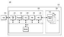
도 1을 참조하면, 데이터 처리 시스템(100)은, 호스트(Host)(102) 및 메모리 시스템(110)을 포함한다.Referring to FIG. 1, a
그리고, 호스트(102)는, 전자 장치, 예컨대 휴대폰, MP3 플레이어, 랩탑 컴퓨터 등과 같은 휴대용 전자 장치들, 또는 데스크탑 컴퓨터, 게임기, TV, 프로젝터 등과 같은 전자 장치들을 포함, 즉 유무선 전자 장치들을 포함한다.And the
또한, 호스트(102)는, 적어도 하나의 운영 시스템(OS: operating system)를 포함하며, 운영 시스템은, 호스트(102)의 기능 및 동작을 전반적으로 관리 및 제어하고, 데이터 처리 시스템(100) 또는 메모리 시스템(110)을 사용하는 사용자와 호스트(102) 간에 상호 동작을 제공한다. 여기서, 운영 시스템은, 사용자의 사용 목적 및 용도에 상응한 기능 및 동작을 지원하며, 예컨대, 호스트(102)의 이동성(mobility)에 따라 일반 운영 시스템과 모바일 운용 시스템으로 구분할 수 있다. 또한, 운영 시스템에서의 일반 운영 시스템 시스템은, 사용자의 사용 환경에 따라 개인용 운영 시스템과 기업용 운영 시스템으로 구분할 수 있으며, 일 예로, 개인용 운영 시스템은, 일반 사용자를 위한 서비스 제공 기능을 지원하도록 특성화된 시스템으로, 윈도우(windows) 및 크롬(chrome) 등을 포함하고, 기업용 운영 시스템은, 고성능을 확보 및 지원하도록 특성화된 시스템으로, 윈도 서버(windows server), 리눅스(linux) 및 유닉스(unix) 등을 포함할 수 있다. 아울러, 운영 시스템에서의 모바일 운영 시스템은, 사용자들에게 이동성 서비스 제공 기능 및 시스템의 절전 기능을 지원하도록 특성화된 시스템으로, 안드로이드(android), iOS, 윈도 모바일(windows mobile) 등을 포함할 수 있다. 이때, 호스트(102)는, 복수의 운영 시스템들을 포함할 수 있으며, 또한 사용자의 요청에 상응한 메모리 시스템(110)과의 동작 수행을 위해 운영 시스템을 실행한다.The
또한, 메모리 시스템(110)은, 호스트(102)의 요청에 응답하여 동작하며, 특히 호스트(102)에 의해서 액세스되는 데이터를 저장한다. 다시 말해, 메모리 시스템(110)은, 호스트(102)의 주 기억 장치 또는 보조 기억 장치로 사용될 수 있다. 여기서, 메모리 시스템(110)은 호스트(102)와 연결되는 호스트 인터페이스 프로토콜에 따라, 다양한 종류의 저장 장치들 중 어느 하나로 구현될 수 있다. 예를 들면, 메모리 시스템(110)은, 솔리드 스테이트 드라이브(SSD: Solid State Drive), MMC, eMMC(embedded MMC), RS-MMC(Reduced Size MMC), micro-MMC 형태의 멀티 미디어 카드(MMC: Multi Media Card), SD, mini-SD, micro-SD 형태의 시큐어 디지털(SD: Secure Digital) 카드, USB(Universal Storage Bus) 저장 장치, UFS(Universal Flash Storage) 장치, CF(Compact Flash) 카드, 스마트 미디어(Smart Media) 카드, 메모리 스틱(Memory Stick) 등과 같은 다양한 종류의 저장 장치들 중 어느 하나로 구현될 수 있다.The
아울러, 메모리 시스템(110)을 구현하는 저장 장치들은, DRAM(Dynamic Random Access Memory), SRAM(Static RAM) 등과 같은 휘발성 메모리 장치와, ROM(Read Only Memory), MROM(Mask ROM), PROM(Programmable ROM), EPROM(Erasable ROM), EEPROM(Electrically Erasable ROM), FRAM(Ferromagnetic ROM), PRAM(Phase change RAM), MRAM(Magnetic RAM), RRAM(Resistive RAM), 플래시 메모리 등과 같은 비휘발성 메모리 장치로 구현될 수 있다.In addition, the storage devices implementing the
그리고, 메모리 시스템(110)은, 호스트(102)에 의해서 액세스되는 데이터를 저장하는 메모리 장치(150), 및 메모리 장치(150)로의 데이터 저장을 제어하는 컨트롤러(130)를 포함한다.The
여기서, 컨트롤러(130) 및 메모리 장치(150)는 하나의 반도체 장치로 집적될 수 있다. 일 예로, 컨트롤러(130) 및 메모리 장치(150)는 하나의 반도체 장치로 집적되어 SSD를 구성할 수 있다. 메모리 시스템(110)이 SSD로 이용되는 경우, 메모리 시스템(110)에 연결되는 호스트(102)의 동작 속도는 보다 개선될 수 있다. 아울러, 컨트롤러(130) 및 메모리 장치(150)는, 하나의 반도체 장치로 집적되어 메모리 카드를 구성할 수도 있으며, 일 예로 PC 카드(PCMCIA: Personal Computer Memory Card International Association), 컴팩트 플래시 카드(CF), 스마트 미디어 카드(SM, SMC), 메모리 스틱, 멀티미디어 카드(MMC, RS-MMC, MMCmicro), SD 카드(SD, miniSD, microSD, SDHC), 유니버설 플래시 기억 장치(UFS) 등과 같은 메모리 카드를 구성할 수 있다.Here, the
또한, 다른 일 예로, 메모리 시스템(110)은, 컴퓨터, UMPC(Ultra Mobile PC), 워크스테이션, 넷북(net-book), PDA(Personal Digital Assistants), 포터블(portable) 컴퓨터, 웹 타블렛(web tablet), 태블릿 컴퓨터(tablet computer), 무선 전화기(wireless phone), 모바일 폰(mobile phone), 스마트폰(smart phone), e-북(e-book), PMP(portable multimedia player), 휴대용 게임기, 네비게이션(navigation) 장치, 블랙박스(black box), 디지털 카메라(digital camera), DMB(Digital Multimedia Broadcasting) 재생기, 3차원 텔레비전(3-dimensional television), 스마트 텔레비전(smart television), 디지털 음성 녹음기(digital audio recorder), 디지털 음성 재생기(digital audio player), 디지털 영상 녹화기(digital picture recorder), 디지털 영상 재생기(digital picture player), 디지털 동영상 녹화기(digital video recorder), 디지털 동영상 재생기(digital video player), 데이터 센터를 구성하는 스토리지, 정보를 무선 환경에서 송수신할 수 있는 장치, 홈 네트워크를 구성하는 다양한 전자 장치들 중 하나, 컴퓨터 네트워크를 구성하는 다양한 전자 장치들 중 하나, 텔레매틱스 네트워크를 구성하는 다양한 전자 장치들 중 하나, RFID(radio frequency identification) 장치, 또는 컴퓨팅 시스템을 구성하는 다양한 구성 요소들 중 하나 등을 구성할 수 있다.In another example,
한편, 메모리 시스템(110)에서의 메모리 장치(150)는, 전원이 공급되지 않아도 저장된 데이터를 유지할 수 있으며, 특히 라이트(write) 동작을 통해 호스트(102)로부터 제공된 데이터를 저장하고, 리드(read) 동작을 통해 저장된 데이터를 호스트(102)로 제공한다. 여기서, 메모리 장치(150)는, 복수의 메모리 블록(memory block)들(152 내지 156)을 포함하며, 각각의 메모리 블록들(152 내지 156)은, 복수의 페이지들(pages)을 포함하며, 또한 각각의 페이지들은, 복수의 워드라인(WL: Word Line)들이 연결된 복수의 메모리 셀들을 포함한다. 또한, 메모리 장치(150)는, 복수의 메모리 블록들(152 내지 156)이 각각 포함된 복수의 플래인들(plane)을 포함하며, 특히 복수의 플래인들이 각각 포함된 복수의 메모리 다이(memory die)들을 포함할 수 있다. 아울러, 메모리 장치(150)는, 비휘발성 메모리 장치, 일 예로 플래시 메모리가 될 수 있으며, 이때 플래시 메모리는 3차원(dimension) 입체 스택(stack) 구조가 될 수 있다.Meanwhile, the
여기서, 메모리 장치(150)의 구조 및 메모리 장치(150)의 3차원 입체 스택 구조에 대해서는, 이하 도 2 내지 도 4에서 보다 구체적으로 설명된다.Here, the structure of the
그리고, 메모리 시스템(110)에서의 컨트롤러(130)는, 호스트(102)로부터의 요청에 응답하여 메모리 장치(150)를 제어한다. 예컨대, 컨트롤러(130)는, 메모리 장치(150)로부터 리드된 데이터를 호스트(102)로 제공하고, 호스트(102)로부터 제공된 데이터를 메모리 장치(150)에 저장하며, 이를 위해 컨트롤러(130)는, 메모리 장치(150)의 리드, 라이트, 프로그램(program), 이레이즈(erase) 등의 동작을 제어한다.The
보다 구체적으로 설명하면, 컨트롤러(130)는, 호스트 인터페이스(Host I/F) 유닛(132), 프로세서(Processor)(134), 에러 정정 코드(ECC: Error Correction Code) 유닛(138), 파워 관리 유닛(PMU: Power Management Unit)(140), 낸드 플래시 컨트롤러(NFC: NAND Flash Controller)(142), 및 메모리(Memory)(144)를 포함한다.More specifically, the
또한, 호스트 인터페이스 유닛(132)은, 호스트(102)의 커맨드(command) 및 데이터를 처리하며, USB(Universal Serial Bus), MMC(Multi-Media Card), PCI-E(Peripheral Component Interconnect-Express), SAS(Serial-attached SCSI), SATA(Serial Advanced Technology Attachment), PATA(Parallel Advanced Technology Attachment), SCSI(Small Computer System Interface), ESDI(Enhanced Small Disk Interface), IDE(Integrated Drive Electronics), MIPI(Mobile Industry Processor Interface) 등과 같은 다양한 인터페이스 프로토콜들 중 적어도 하나를 통해 호스트(102)와 통신하도록 구성될 수 있다.In addition, the
아울러, ECC 유닛(138)은, 메모리 장치(150)에 저장된 데이터를 리드할 경우, 메모리 장치(150)로부터 리드된 데이터에 포함되는 에러를 검출 및 정정한다. 다시 말해, ECC 유닛(138)은, 메모리 장치(150)로부터 리드한 데이터에 대하여 에러 정정 디코딩을 수행한 후, 에러 정정 디코딩의 성공 여부를 판단하고, 판단 결과에 따라 지시 신호, 예컨대 에러 정정 성공(success)/실패(fail) 신호를 출력하며, ECC 인코딩 과정에서 생성된 패리티(parity) 비트를 사용하여 리드된 데이터의 에러 비트를 정정할 수 있다. 이때, ECC 유닛(138)은, 에러 비트 개수가 정정 가능한 에러 비트 한계치 이상 발생하면, 에러 비트를 정정할 수 없으며, 에러 비트를 정정하지 못함에 상응하는 에러 정정 실패 신호를 출력할 수 있다.In addition, when reading data stored in the
여기서, ECC 유닛(138)은, LDPC(low density parity check) code, BCH(Bose, Chaudhri, Hocquenghem) code, turbo code, 리드-솔로몬 코드(Reed-Solomon code), convolution code, RSC(recursive systematic code), TCM(trellis-coded modulation), BCM(Block coded modulation) 등의 코디드 모듈레이션(coded modulation)을 사용하여 에러 정정을 수행할 수 있으며, 이에 한정되는 것은 아니다. 또한, ECC 유닛(138)는 오류 정정을 위한 회로, 모듈, 시스템, 또는 장치를 모두 포함할 수 있다.Herein, the
그리고, PMU(140)는, 컨트롤러(130)의 파워, 즉 컨트롤러(130)에 포함된 구성 요소들의 파워를 제공 및 관리한다.The
또한, NFC(142)는, 컨트롤러(130)가 호스트(102)로부터의 요청에 응답하여 메모리 장치(150)를 제어하기 위해, 컨트롤러(130)와 메모리 장치(150) 간의 인터페이싱을 수행하는 메모리/스토리지(storage) 인터페이스로서, 메모리 장치(150)가 플래시 메모리, 특히 일 예로 메모리 장치(150)가 낸드 플래시 메모리일 경우에, 프로세서(134)의 제어에 따라, 메모리 장치(150)의 제어 신호를 생성하고 데이터를 처리한다. 여기서, NFC(142)는, 컨트롤러(130)와 메모리 장치(150) 간의 커맨드 및 데이터를 처리하는 인터페이스, 일 예로 낸드 플래시 인터페이스의 동작을 수행하며 수행하며, 특히 컨트롤러(130)와 메모리 장치(150) 간 데이터 입출력을 지원한다.The
아울러, 메모리(144)는, 메모리 시스템(110) 및 컨트롤러(130)의 동작 메모리로서, 메모리 시스템(110) 및 컨트롤러(130)의 구동을 위한 데이터를 저장한다. 보다 구체적으로 설명하면, 메모리(144)는, 컨트롤러(130)가 호스트(102)로부터의 요청에 응답하여 메모리 장치(150)를 제어, 예컨대 컨트롤러(130)가, 메모리 장치(150)로부터 리드된 데이터를 호스트(102)로 제공하고, 호스트(102)로부터 제공된 데이터를 메모리 장치(150)에 저장하며, 이를 위해 컨트롤러(130)가, 메모리 장치(150)의 리드, 라이트, 프로그램, 이레이즈(erase) 등의 동작을 제어할 경우, 이러한 동작을 메모리 시스템(110), 즉 컨트롤러(130)와 메모리 장치(150) 간이 수행하기 위해 필요한 데이터를 저장한다. 나아가, 주소 매핑(address mapping) 동작에 필요한 맵 데이터가 메모리(144)에 저장된다.The
여기서, 메모리(144)는, 휘발성 메모리로 구현될 수 있으며, 예컨대 정적 랜덤 액세스 메모리(SRAM: Static Random Access Memory), 또는 동적 랜덤 액세스 메모리(DRAM: Dynamic Random Access Memory) 등으로 구현될 수 있다. 아울러, 메모리(144)는, 도 1에서 도시한 바와 같이, 컨트롤러(130)의 내부에 존재하거나, 또는 컨트롤러(130)의 외부에 존재할 수 있으며, 이때 메모리 인터페이스를 통해 컨트롤러(130)로부터 데이터가 입출력되는 외부 휘발성 메모리로 구현될 수도 있다.The
또한, 메모리(144)는, 전술한 바와 같이, 호스트(102)와 메모리 장치(150) 간 데이터 라이트 및 리드 등의 동작을 수행하기 위해 필요한 데이터, 및 데이터 라이트 및 리드 등의 동작 수행 시의 데이터를 저장하며, 이러한 데이터 저장을 위해, 프로그램 메모리, 데이터 메모리, 라이트 버퍼(buffer)/캐시(cache), 리드 버퍼/캐시, 데이터 버퍼/캐시, 맵(map) 버퍼/캐시 등을 포함한다.The
그리고, 프로세서(134)는, 메모리 시스템(110)의 전체적인 동작을 제어하며, 특히 호스트(102)로부터의 라이트 요청 또는 리드 요청에 응답하여, 메모리 장치(150)에 대한 라이트 동작 또는 리드 동작을 제어한다. 여기서, 프로세서(134)는, 메모리 시스템(110)의 제반 동작을 제어하기 위해 플래시 변환 계층(FTL: Flash Translation Layer, 이하 'FTL'이라 칭하기로 함)이라 불리는 펌웨어(firmware)를 구동한다.The
FTL은 호스트(102)와 메모리 장치(150)간 인터페이싱 기능을 수행할 수 있다. 호스트(102)는 FTL을 통해서 메모리 장치(150)에 쓰기 및 읽기 동작을 요청할 수 있다.The FTL may perform an interfacing function between the
FTL은 주소 매핑(address mapping) 동작, 가비지 콜렉션(Garbage Collection), 웨어 레벨링(Wear-Leveling) 동작 등을 관리할 수 있다. 특히, FTL은 맵 데이터를 저장할 수 있다. 따라서, 컨트롤러(130)는 FTL의 맵 데이터를 통하여 호스트(150)으로부터 요청된 논리 주소(logical address)를 메모리 장치(150)의 물리 주소(physical address)로 매핑(mapping)할 수 있다. 주소 매핑 동작으로 메모리 장치(150)가 일반 디바이스처럼 동작될 수 있다. 또한, 맵 데이터에 기초한 주소 매핑 동작으로 인하여, 컨트롤러(130)가 플래시 메모리의 특성에 따라 특정 페이지의 데이터를 수정할 때, 새로운 데이터를 메모리 장치(150)의 다른 빈 페이지에 기록하고 이전 데이터를 무효화(invalidation)시킬 수 있다. 나아가, 컨트롤러(130)는 새로운 데이터의 맵 데이터를 FTL에 저장할 수 있다.The FTL can manage address mapping operations, garbage collection, and wear-leveling operations. In particular, the FTL can store map data. Accordingly, the
나아가, FTL은 SPOR 동작에서 맵 데이터를 재건(re-build)하는 동작할 수 있다. SPOR은 정상 종료 후 부팅, 비정상 종류 후 부팅 및 반복적인 비 정상 종료 후 부팅에서 발생될 수 있다. 본 발명의 실시 예에 따른 메모리 시스템의 동작 방법은 비정상 종료 후 부팅에서 맵 데이터를 복구할 수 있다.Furthermore, the FTL may operate to re-build the map data in the SPOR operation. SPOR can occur at boot after normal shutdown, boot after abnormal type, and boot after repeated abnormal shutdown. The method of operating a memory system according to an embodiment of the present invention may recover map data at boot after an abnormal termination.
또한, 프로세서(134)는, 마이크로프로세서 또는 중앙 처리 장치(CPU) 등으로 구현될 수 있다. The
일 예로, 컨트롤러(130)는, 마이크로프로세서 또는 중앙 처리 장치(CPU) 등으로 구현된 프로세서(134)를 통해, 호스트(102)로부터 요청된 동작을 메모리 장치(150)에서 수행, 다시 말해 호스트(102)로부터 수신된 커맨드에 해당하는 커맨드 동작을, 메모리 장치(150)와 수행한다. 여기서, 컨트롤러(130)는, 호스트(102)로부터 수신된 커맨드에 해당하는 커맨드 동작으로 포그라운드(foreground) 동작을 수행, 예컨대 라이트 커맨드에 해당하는 프로그램 동작, 리드 커맨드에 해당하는 리드 동작, 이레이즈 커맨드(erase command)에 해당하는 이레이즈 동작, 셋 커맨드(set command)로 셋 파라미터 커맨드(set parameter command) 또는 셋 픽쳐 커맨드(set feature command)에 해당하는 파라미터 셋 동작 등을 수행할 수 있다.The
그리고, 컨트롤러(130)는, 마이크로프로세서 또는 중앙 처리 장치(CPU) 등으로 구현된 프로세서(134)를 통해, 메모리 장치(150)에 대한 백그라운드(background) 동작을 수행할 수도 있다. 여기서, 메모리 장치(150)에 대한 백그라운드 동작은, 메모리 장치(150)의 메모리 블록들(152 내지 156)에서 임의의 메모리 블록에 저장된 데이터를 다른 임의의 메모리 블록으로 카피(copy)하여 처리하는 동작, 일 예로 가비지 컬렉션(GC: Garbage Collection) 동작, 메모리 장치(150)의 메모리 블록들(152 내지 156) 간 또는 메모리 블록들(152 내지 156)에 저장된 데이터 간을 스왑(swap)하여 처리하는 동작, 일 예로 웨어 레벨링(WL: Wear Leveling) 동작, 컨트롤러(130)에 저장된 맵 데이터를 메모리 장치(150)의 메모리 블록들(152 내지 156)로 저장하는 동작, 일 예로 맵 플러쉬(map flush) 동작, 또는 메모리 장치(150)에 대한 배드 관리(bad management)하는 동작, 일 예로 메모리 장치(150)에 포함된 복수의 메모리 블록들(152 내지 156)에서 배드 블록을 확인하여 처리하는 배드 블록 관리(bad block management) 동작 등을 포함한다.The
특히, 본 발명의 실시 예에 따른 메모리 시스템에서는, 컨트롤러(130)가 메모리(144)에 저장된 맵 데이터를 메모리 장치(150)의 메모리 블록들(152 내지 156)로 저장하는 동작 및 맵 데이터의 플러쉬 도중에 생기는 비 정상적인 상황, 일 예로, 맵 데이터의 플러쉬 도중에 프로그램 에러 혹은 SPO가 발생된 경우에, 맵 데이터를 저장하는 동작을 제공할 수 있다.In particular, in the memory system according to the embodiment of the present invention, the
아울러, 컨트롤러(130)의 프로세서(134)에는, 메모리 장치(150)의 배드 관리를 수행하기 위한 관리 유닛(도시하지 않음)이 포함될 수 있으며, 관리 유닛은, 메모리 장치(150)에 포함된 복수의 메모리 블록들(152 내지 156)에서 배드 블록을 확인한 후, 확인된 배드 블록을 배드 처리하는 배드 블록 관리를 수행한다. 여기서, 배드 관리는, 메모리 장치(150)가 플래시 메모리, 예컨대 낸드 플래시 메모리일 경우, 낸드의 특성으로 인해 데이터 라이트, 예컨대 데이터 프로그램(program) 시에 프로그램 실패(program fail)가 발생할 수 있으며, 프로그램 실패가 발생한 메모리 블록을 배드(bad) 처리한 후, 프로그램 실패된 데이터를 새로운 메모리 블록에 라이트, 즉 프로그램하는 것을 의미한다. 또한, 메모리 장치(150)가, 전술한 바와 같이, 3차원 입체 스택 구조를 가질 경우에는, 프로그램 실패에 따라 해당 블록을 배드 블록으로 처리하면, 메모리 장치(150)의 사용 효율 및 메모리 시스템(100)의 신뢰성이 급격하게 저하되므로, 보다 신뢰성 있는 배드 블록 관리 수행이 필요하다. 그러면 이하에서는, 도 2 내지 도 4를 참조하여 본 발명의 실시 예에 따른 메모리 시스템에서의 메모리 장치에 대해서 보다 구체적으로 설명하기로 한다.In addition, the
도 2는 본 발명의 실시 예에 따른 메모리 시스템에서 메모리 장치의 일 예를 개략적으로 도시한 도면이고, 도 3은 본 발명의 실시 예에 따른 메모리 장치에서 메모리 블록들의 메모리 셀 어레이 회로를 개략적으로 도시한 도면이며, 도 4는 본 발명의 실시 예에 따른 메모리 시스템에서 메모리 장치 구조를 개략적으로 도시한 도면으로, 메모리 장치가 3차원 비휘발성 메모리 장치로 구현될 경우의 구조를 개략적으로 도시한 도면이다.Figure 2 schematically illustrates an example of a memory device in a memory system according to an embodiment of the present invention, Figure 3 schematically illustrates a memory cell array circuit of memory blocks in a memory device according to an embodiment of the present invention. FIG. 4 is a view schematically showing a memory device structure in a memory system according to an embodiment of the present invention, and schematically shows a structure when the memory device is implemented as a three-dimensional nonvolatile memory device .
우선, 도 2를 참조하면, 메모리 장치(150)는, 복수의 메모리 블록들, 예컨대 블록0(BLK(Block)0)(210), 블록1(BLK1)(220), 블록2(BLK2)(230), 및 블록N-1(BLKN-1)(240)을 포함하며, 각각의 블록들(210,220,230,240)은, 복수의 페이지들(Pages), 예컨대 2M개의 페이지들(2MPages)을 포함한다. 여기서, 설명의 편의를 위해, 복수의 메모리 블록들이 각각 2M개의 페이지들을 포함하는 것을 일 예로 하여 설명하지만, 복수의 메모리들은, 각각 M개의 페이지들을 포함할 수도 있다. 그리고, 각각의 페이지들은, 복수의 워드라인(WL: Word Line)들이 연결된 복수의 메모리 셀들을 포함한다.2, the
또한, 메모리 장치(150)는, 복수의 메모리 블록들을, 하나의 메모리 셀에 저장 또는 표현할 수 있는 비트의 수에 따라, 단일 레벨 셀(SLC: Single Level Cell) 메모리 블록 및 멀티 레벨 셀(MLC: Multi Level Cell) 메모리 블록 등으로 포함할 수 있다. 여기서, SLC 메모리 블록은, 하나의 메모리 셀에 1 비트 데이터를 저장하는 메모리 셀들에 의해 구현된 복수의 페이지들을 포함하며, 데이터 연산 성능이 빠르며 내구성이 높다. 그리고, MLC 메모리 블록은, 하나의 메모리 셀에 멀티 비트 데이터(예를 들면, 2 비트 또는 그 이상의 비트)를 저장하는 메모리 셀들에 의해 구현된 복수의 페이지들을 포함하며, SLC 메모리 블록보다 큰 데이터 저장 공간을 가짐, 다시 말해 고집적화할 수 있다. 특히, 메모리 장치(150)는, MLC 메모리 블록으로, 하나의 메모리 셀에 2 비트 데이터를 저장할 수 있는 메모리 셀들에 의해 구현된 복수의 페이지들을 포함하는 MLC 메모리 블록 뿐만 아니라, 하나의 메모리 셀에 3 비트 데이터를 저장할 수 있는 메모리 셀들에 의해 구현된 복수의 페이지들을 포함하는 트리플 레벨 셀(TLC: Triple Level Cell) 메모리 블록, 하나의 메모리 셀에 4 비트 데이터를 저장할 수 있는 메모리 셀들에 의해 구현된 복수의 페이지들을 포함하는 쿼드러플 레벨 셀(QLC: Quadruple Level Cell) 메모리 블록, 또는 하나의 메모리 셀에 5 비트 또는 그 이상의 비트 데이터를 저장할 수 있는 메모리 셀들에 의해 구현된 복수의 페이지들을 포함하는 다중 레벨 셀(multiple level cell) 메모리 블록 등을 포함할 수 있다.In addition, the
그리고, 각각의 블록들(210,220,230,240)은, 라이트 동작을 통해 호스트(102)로부터 제공된 데이터를 저장하고, 리드 동작을 통해 저장된 데이터를 호스트(102)에게 제공한다.Each of the
다음으로, 도 3을 참조하면, 메모리 시스템(110)의 메모리 장치(150)에 포함된 복수의 메모리 블록들(152 내지 156)에서 각 메모리 블록(330), 메모리 셀 어레이로 구현되어 비트라인들(BL0 to BLm-1)에 각각 연결된 복수의 셀 스트링들(340)을 포함할 수 있다. 각 열(column)의 셀 스트링(340)은, 적어도 하나의 드레인 선택 트랜지스터(DST)와, 적어도 하나의 소스 선택 트랜지스터(SST)를 포함할 수 있다. 선택 트랜지스터들(DST, SST) 사이에는, 복수 개의 메모리 셀들, 또는 메모리 셀 트랜지스터들(MC0 to MCn-1)이 직렬로 연결될 수 있다. 각각의 메모리 셀(MC0 to MCn-1)은, 셀 당 복수의 비트들의 데이터 정보를 저장하는 MLC로 구성될 수 있다. 셀 스트링들(340)은 대응하는 비트라인들(BL0 to BLm-1)에 각각 전기적으로 연결될 수 있다.3, a plurality of memory blocks 152 to 156 included in the
여기서, 도 3은, 낸드 플래시 메모리 셀로 구성된 각 메모리 블록(330)을 일 예로 도시하고 있으나, 본 발명의 실시 예에 따른 메모리 장치(150)에 포함된 복수의 메모리 블록(152 내지 156)은, 낸드 플래시 메모리에만 국한되는 것은 아니라 노어 플래시 메모리(NOR-type Flash memory), 적어도 두 종류 이상의 메모리 셀들이 혼합된 하이브리드 플래시 메모리, 메모리 칩 내에 컨트롤러가 내장된 One-NAND 플래시 메모리 등으로도 구현될 수 있다. 아울러, 본 발명의 실시 예에 따른 메모리 장치(150)는, 전하 저장층이 전도성 부유 게이트로 구성된 플래시 메모리 장치는 물론, 전하 저장층이 절연막으로 구성된 차지 트랩형 플래시(Charge Trap Flash; CTF) 메모리 장치 등으로도 구현될 수 있다.3 illustrates each
그리고, 메모리 장치(150)의 전압 공급부(310)는, 동작 모드에 따라서 각각의 워드라인들로 공급될 워드라인 전압들(예를 들면, 프로그램 전압, 리드 전압, 패스 전압 등)과, 메모리 셀들이 형성된 벌크(예를 들면, 웰 영역)로 공급될 전압을 제공할 수 있으며, 이때 전압 공급 회로(310)의 전압 발생 동작은 제어 회로(도시하지 않음)의 제어에 의해 수행될 수 있다. 또한, 전압 공급부(310)는, 다수의 리드 데이터를 생성하기 위해 복수의 가변 리드 전압들을 생성할 수 있으며, 제어 회로의 제어에 응답하여 메모리 셀 어레이의 메모리 블록들(또는 섹터들) 중 하나를 선택하고, 선택된 메모리 블록의 워드라인들 중 하나를 선택할 수 있으며, 워드라인 전압을 선택된 워드라인 및 비선택된 워드라인들로 각각 제공할 수 있다.The
아울러, 메모리 장치(150)의 리드/라이트(read/write) 회로(320)는, 제어 회로에 의해서 제어되며, 동작 모드에 따라 감지 증폭기(sense amplifier)로서 또는 라이트 드라이버(write driver)로서 동작할 수 있다. 예를 들면, 검증/정상 리드 동작의 경우 리드/라이트 회로(320)는, 메모리 셀 어레이로부터 데이터를 리드하기 위한 감지 증폭기로서 동작할 수 있다. 또한, 프로그램 동작의 경우 리드/라이트 회로(320)는, 메모리 셀 어레이에 저장될 데이터에 따라 비트라인들을 구동하는 라이트 드라이버로서 동작할 수 있다. 리드/라이트 회로(320)는, 프로그램 동작 시 셀 어레이에 라이트될 데이터를 버퍼(미도시)로부터 수신하고, 입력된 데이터에 따라 비트라인들을 구동할 수 있다. 이를 위해, 리드/라이트 회로(320)는, 열(column)들(또는 비트라인들) 또는 열쌍(column pair)(또는 비트라인 쌍들)에 각각 대응되는 복수 개의 페이지 버퍼들(PB)(322,324,326)을 포함할 수 있으며, 각각의 페이지 버퍼(page buffer)(322,324,326)에는 복수의 래치들(도시하지 않음)이 포함될 수 있다.In addition, the read /
또한, 메모리 장치(150)는, 2차원 또는 3차원의 메모리 장치로 구현될 수 있으며, 특히 도 4에 도시한 바와 같이, 3차원 입체 스택 구조의 비휘발성 메모리 장치로 구현될 수 있으며, 3차원 구조로 구현될 경우, 복수의 메모리 블록들(BLK0 to BLKN-1)을 포함할 수 있다. 여기서, 도 4는, 도 1에 도시한 메모리 장치(150)의 메모리 블록들(152 내지 156)을 보여주는 블록도로서, 각각의 메모리 블록들(152 내지 156)은, 3차원 구조(또는 수직 구조)로 구현될 수 있다. 예를 들면, 각각의 메모리 블록들(152 내지 156)은 제1방향 내지 제3방향들, 예컨대 x-축 방향, y-축 방향, 및 z-축 방향을 따라 신장된 구조물들을 포함하여, 3차원 구조로 구현될 수 있다.In addition, the
그리고, 메모리 장치(150)에 포함된 각 메모리 블록(330)은, 제2방향을 따라 신장된 복수의 낸드 스트링들(NS)을 포함할 수 있으며, 제1방향 및 제3방향들을 따라 복수의 낸드 스트링들(NS)이 제공될 수 있다. 여기서, 각 낸드 스트링(NS)은, 비트라인(BL), 적어도 하나의 스트링 선택라인(SSL), 적어도 하나의 접지 선택라인(GSL), 복수의 워드라인들(WL), 적어도 하나의 더미 워드라인(DWL), 그리고 공통 소스라인(CSL)에 연결될 수 있으며, 복수의 트랜지스터 구조들(TS)을 포함할 수 있다.Each
즉, 메모리 장치(150)의 복수의 메모리 블록들(152 내지 156)에서 각 메모리 블록(330)은, 복수의 비트라인들(BL), 복수의 스트링 선택라인들(SSL), 복수의 접지 선택라인들(GSL), 복수의 워드라인들(WL), 복수의 더미 워드라인들(DWL), 그리고 복수의 공통 소스라인(CSL)에 연결될 수 있으며, 그에 따라 복수의 낸드 스트링들(NS)을 포함할 수 있다. 또한, 각 메모리 블록(330)에서, 하나의 비트라인(BL)에 복수의 낸드 스트링들(NS)이 연결되어, 하나의 낸드 스트링(NS)에 복수의 트랜지스터들이 구현될 수 있다. 아울러, 각 낸드 스트링(NS)의 스트링 선택 트랜지스터(SST)는, 대응하는 비트라인(BL)과 연결될 수 있으며, 각 낸드 스트링(NS)의 접지 선택 트랜지스터(GST)는, 공통 소스라인(CSL)과 연결될 수 있다. 여기서, 각 낸드 스트링(NS)의 스트링 선택 트랜지스터(SST) 및 접지 선택 트랜지스터(GST) 사이에 메모리 셀들(MC)이 제공, 즉 메모리 장치(150)의 복수의 메모리 블록들(152 내지 156)에서 각 메모리 블록(330)에는 복수의 메모리 셀들이 구현될 수 있다.That is, in the plurality of memory blocks 152 to 156 of the
도 5은 본 발명의 실시 예에 따른 메모리 장치(150)의 구조를 개략적으로 나타낸다.5 schematically illustrates the structure of a
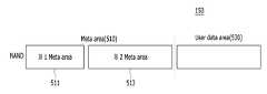
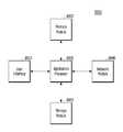
메모리 장치(150)는 메타 영역(510)과 유저 데이터 영역(530)을 포함할 수 있다. 메타 영역(510)은 다시 제 1 메타 영역(511)과 제 2 메타 영역(513)으로 나뉠 수 있다.The
컨트롤러(130)는 컨트롤러(130)의 복수의 운용 기록(log, 이하 로그)을 메모리 장치(150)의 제 1 메타 영역(511)에 저장할 수 있다. 본 발명의 일 실시 예에 따르면, 상기 복수의 로그들은 제 1 내지 6 로그를 포함할 수 있다. 상기 제 1 로그는 후술되는 복수의 맵 데이터 그룹들 중 플러쉬 대상이 되는 맵 데이터 그룹에 대한 플러쉬 동작의 시작을 나타낼 수 있다. 상기 제 2 로그는 상기 플러쉬 대상이 되는 맵 데이터 그룹에 대한 플러쉬 동작의 종료를 나타낼 수 있다. 상기 제 3 로그는 플러쉬되는 맵 데이터를 저장하는 메모리 장치(150)의 첫 번째 페이지의 위치를 나타낼 수 있다. 상기 제 4 로그는 플러쉬되는 맵 데이터를 저장하는 메모리 장치(150)의 마지막 페이지의 위치를 나타낼 수 있다. 상기 제 5 로그는 맵 데이터를 메모리 장치(150)의 제 2 메타 영역(513)에 프로그램하는 과정에서 프로그램 에러의 발생으로 인한 에러 관리의 동작의 시작을 나타낼 수 있다. 상기 제 6 로그는 상기 프로그램 에러의 발생 전에 정상적으로 플러쉬된 맵 데이터를 저장한 마지막 페이지의 위치를 나타낼 수 있다. 예를 들면, 컨트롤러(130)가 상기 플러쉬 대상이 되는 x번째 맵 데이터 그룹에 대하여 플러쉬 동작을 수행할 경우에 상기 x번째 맵 데이터 그룹에 대한 플러쉬 동작의 시작을 나타내는 상기 제 1 로그 및 상기 플러쉬 동작에 의해 상기 x번째 맵 데이터 그룹을 저장하는 메모리 장치(150)의 첫번째 페이지 위치를 나타내는 상기 제 3 로그를 제 1 메타 영역(511)에 저장할 수 있다.The
컨트롤러(130)는 맵 데이터를 메모리 장치(150)의 제 2 메타 영역(513)에 플러쉬할 수 있다. 즉, 컨트롤러(130)는 메모리(144)에 저장되는 맵 데이터를 메모리 장치(150)의 제 2 메타 영역(513)에 프로그램할 수 있다. 상기 플러쉬 동작도 프로그램 동작의 일종이며, 따라서 맵 데이터를 메모리 장치(130)의 제 2 메타 영역(513)에 프로그램하는 과정에서 프로그램 에러가 발생할 수 있다. 본 명세서에서 프로그램 에러는 맵 데이터가 메모리 장치(130)의 제 2 메타 영역(513)에 프로그램하는 과정에서 발생하는 에러를 나타낸다. 컨트롤러(130)는 정상적인 시스템 종료 상황에서 맵 데이터를 메모리 장치(150)에 플러쉬할 수 있으며, 또한 수시로 맵 데이터를 메모리 장치(150)에 플러쉬할 수 있다. 컨트롤러(130)는 전체 맵 데이터를 사전 설정된 크기(예를 들면, 세그먼트(segment) 단위)를 가지는 복수의 맵 데이터 그룹으로 분할한 후, 상기 복수의 맵 데이터 그룹을 순차적으로 플러쉬함으로써 제 2 메타 영역(513)에 저장할 수 있다. 사전 설정된 맵 데이터의 그룹의 크기에 의하여 맵 데이터를 플러쉬하는 컨트롤러의 성능 및 SPOR 수행 시간이 결정될 수 있다.The
컨트롤러(130)는 유저 데이터를 메모리 장치(150)의 유저 데이터 영역(530)에 저장할 수 있다.The
도 6 내지 도 7는 SPOR에 대비한 컨트롤러(130)의 맵 플러쉬 과정 및 SPO 발생에 따른 SPOR과정을 나타낸다.6 to 7 illustrate a map flushing process of the
SPOR은 맵 데이터가 최신 유효 데이터를 가리키도록 재건하는 과정이다. 종래 SPOR에서의 맵 데이터를 복구하는 방법에 따르면, 컨트롤러는 메모리 장치에 마지막으로 저장된 맵 데이터부터 역순으로 맵 데이터를 리드하여 전체 맵 데이터를 메모리에 재건할 수 있다. 따라서, 컨트롤러는 맵 데이터를 순서대로 플러쉬해야 한다. 하지만 컨트롤러가 맵 데이터를 플러쉬하는 도중에 프로그램 에러 혹은 SPO가 발생되면, 메모리 장치에 플러쉬된 맵 데이터의 순서에 대한 신뢰성이 낮아질 수 있다. 그래서, 종래에 컨트롤러는 해당 맵 데이터를 메모리 장치에 처음부터 다시 저장하였다. 하지만 이러한 종래의 방법은 파워 오프 시간을 증가시킬 수 있고, 메모리 장치의 블록에 맵 데이터를 라이트하는 양이 늘어나기 때문에 메모리 장치의 수명을 감소시킬 수 있으며, SPOR 시간을 증가시킬 수 있다.SPOR is the process of rebuilding map data to point to the most recent valid data. According to the method of restoring map data in the conventional SPOR, the controller can read the map data in the reverse order from the map data last stored in the memory device, and reconstruct the entire map data in the memory. Therefore, the controller must flush the map data in order. However, if a program error or SPO occurs while the controller is flushing the map data, the reliability of the order of the map data flushed to the memory device may be lowered. Thus, conventionally, the controller has stored the map data in the memory device from the beginning again. However, this conventional method can increase the power-off time and increase the amount of writing the map data in the block of the memory device, which can reduce the lifetime of the memory device and increase the SPOR time.
도 6은 본 발명의 실시 예에 따른 컨트롤러(130)의 동작 과정을 개략적으로 나타낸 순서도이다. 구체적으로, 컨트롤러(130)가 메모리 장치(150)에 맵 데이터를 플러쉬하는 일반적인 경우 및 맵 데이터를 플러쉬하는 도중에 프로그램 에러가 발생되는 경우에, 컨트롤러(130)의 맵 플러쉬 동작을 나타낸 순서도다. 설명의 편의를 위하여, 컨트롤러(130)가 사전 설정된 세그먼트(segment) 단위로 그룹화된 복수의 맵 데이터 그룹 중 하나의 맵 데이터 그룹을 메모리 장치(150)에 플러쉬한다고 가정한다.6 is a flowchart schematically illustrating an operation process of the
먼저, 단계 S611에서, 초기 인덱스 값(i = 1 및 j = 1)을 설정할 수 있다. 'i'는 상기 플러쉬 대상인 맵 데이터 그룹에 포함된 맵 데이터들의 순번을 의미하고, 'j'는 상기 플러쉬되는 맵 데이터가 저장되는 메모리 장치(150)의 페이지 순번을 의미한다.First, in step S611, an initial index value (i = 1 and j = 1) can be set. 'i' denotes the order of map data included in the map data group to be flushed, and 'j' denotes the page order number of the
단계 S613에서, 컨트롤러(130)는 메모리 장치(150)의 제 1 메타 영역(511)에 상기 플러쉬 대상인 맵 데이터 그룹에 대한 플러쉬 동작의 시작을 나타내는 제 1 로그 및 플러쉬되는 맵 데이터를 저장하는 메모리 장치(150)의 첫번째 페이지의 위치를 나타내는 제 3 로그를 저장할 수 있다.In step S613, the
단계 S615에서, 컨트롤러(130)는 맵 데이터를 메모리 장치(150)의 제 2 메타 영역(513)에 플러쉬할 수 있다. 예를 들면, 컨트롤러(130)는 상기 플러쉬 대상인 맵 데이터 그룹의 i번째 맵 데이터를 제 2 메타 영역(513)의 j번째 페이지에 플러쉬하여 프로그램할 수 있다.In step S615, the
단계 S617에서, 컨트롤러(130)는 메모리 장치(150)에서 맵 데이터를 플러쉬를 하는 도중에 발생되는 프로그램 에러를 검증(verify) 동작을 통하여 판단할 수 있다. 컨트롤러(130)는 맵 데이터를 플러쉬하는 동작과 프로그램 에러를 검증하는 동작을 교번하여 수행할 수 있다. 따라서, 맵 데이터를 플러쉬 동작의 대상이 되는 j번째 페이지와 프로그램 에러가 발생되는 k번째 페이지는 다를 수 있다. 나아가, k번째 페이지는 j번째 페이지와 같거나 j번째 페이지의 전 페이지일 수 있다. 상기 플러쉬 대상인 맵 데이터 그룹의 맵 데이터를 플러쉬하는 도중에 제 2 메타 영역(513)의 k 번째 페이지에서 프로그램 에러가 발생된 경우, 컨트롤러(130)는 단계 S619 내지 단계 S625의 동작을 수행할 수 있다. 반면에, 제 2 메타 영역(513)의 k번째 페이지에서 프로그램 에러가 발생되지 않은 경우, 컨트롤러(130)는 단계 S627의 동작을 수행할 수 있다.In step S617, the
맵 데이터를 플러쉬하는 도중에 k 번째 페이지에서 프로그램 에러가 발생된 경우(단계 S617에서 "YES"), 단계 S619에서 컨트롤러(130)는 메모리 장치(150)의 제 1 메타 영역(511)에 맵 데이터를 메모리 장치(150)의 제 2 메타 영역(513)에 맵 데이터를 플러쉬하는 과정에서 프로그램 에러의 발생으로 인한 에러 관리의 동작의 시작을 나타내는 제 5 로그 및 상기 프로그램 에러의 발생 전에 정상적으로 플러쉬된 맵 데이터를 저장한 마지막 페이지의 위치(예를 들어, 상기 프로그램 에러의 발생 전의 k-1번째 페이지)를 나타내는 제 6 로그를 저장할 수 있다. 예를 들어, 5번째 페이지에서 맵 데이터가 플러쉬되는 도중에, 3번째 페이지에서 프로그램 에러가 발생된 경우(즉, k = 3), 단계 S619에서 컨트롤러(130)는 에러 관리 동작의 시작을 나타내는 제 5 로그 및 2번째 페이지의 위치(즉, k-1 = 2)를 나타내는 제 6 로그를 저장할 수 있다.If a program error occurs in the kth page ("YES" in step S617) while flushing the map data, the
단계 S621에서, 컨트롤러(130)는 상기 페이지 인덱스 j의 값을 1 증가시킬 수 있다.In step S621, the
단계 S623에서, 컨트롤러(130)는 프로그램 에러가 발생된 페이지, 즉 k번째 페이지부터 에러 관리 동작의 시작 전에 맵 데이터를 저장한 마지막 페이지, 즉 j-1번째 페이지에 저장되어 있는 맵 데이터를 컨트롤러(130)의 메모리(144)로부터 플러쉬하여 메모리 장치(150)의 제 2 메타 영역(513)에 다시 기록함으로써 상기 k번째 페이지부터 j-1번째 페이지에 저장되어 있는 맵 데이터를 중복하여 저장할 수 있다.In step S623, the
예를 들어, 프로그램 에러가 발생된 페이지가 3번째 (k = 3)페이지이고, 에러 관리 동작의 시작 전에 맵 데이터를 저장한 마지막 페이지가 5번째 (j = 6, j-1 = 5) 페이지인 경우에, 컨트롤러(130)는 단계 S621 및 S623에서 상기 3 번째 내지 5번째의 3개 페이지에 저장되어 있는 맵 데이터를 6번째 내지 8번째의 3개 페이지에 중복하여 저장할 수 있다.For example, if the page where the program error occurred is the third page (k = 3) and the last page that stores the map data before the start of the error management operation is the fifth (j = 6, j-1 = In this case, the
단계 S623에 의해 중복 저장이 완료된 페이지의 다음 페이지(상기 예시의 경우에, 9번째 페이지)부터 맵 데이터를 플러쉬하기 위하여, 단계 S625에서 컨트롤러(130)는 상기 페이지 인덱스 j의 값을 '2j-k'만큼 증가시킬 수 있다. 상기 증가분 '2j-k'는 단계 S623에서 맵 데이터가 중복 저장되는 페이지의 개수 'j-k'(상기 예시의 경우에 j-k = 6-3 = 3), 에러 관리 동작의 시작 전까지 플러쉬된 맵 데이터를 저장하고 있는 페이지의 개수 'j-1'(상기 예시의 경우에 j-1 = 6-1 = 5), 및 단계 S623에 의해 중복 저장이 완료된 페이지의 다음 페이지를 지정하기 위한 증분 '1'의 합산을 나타낸다.In step S625, in order to flush the map data from the next page (the ninth page in the above example) of the page in which duplicate storage is completed in step S623, the
다음으로, 단계 S623에 의해 중복 저장이 완료된 페이지의 다음 페이지에 대하여 후술되는 단계 S629가 수행될 수 있다.Next, step S629, which will be described later, may be performed on the next page of the page for which overwriting has been completed by step S623.
반면에, 맵 데이터를 플러쉬하는 도중에 k 번째 페이지에서 프로그램 에러가 발생되지 않은 경우(단계 S617에서 "NO"), 단계 S627에서 컨트롤러(130)는 상기 페이지 인덱스 j의 값을 1 증가시킬 수 있다.On the other hand, if no program error has occurred in the kth page during the flushing of the map data ("NO" in step S617), the
단계 S629에서 컨트롤러(130)는 상기 맵 데이터 인덱스 i의 현재 값이 최대 값인지 여부를 판단함으로써 상기 플러쉬 대상인 맵 데이터 그룹의 모든 맵 데이터에 대하여 플러쉬 동작이 수행되었는지 여부를 판단할 수 있다.In step S629, the
단계 S629의 판단 결과, 상기 플러쉬 대상인 맵 데이터 그룹의 모든 맵 데이터에 대하여 플러쉬 동작이 수행되지 않은 경우에(단계 S629에서 "NO"), 단계 S631에서 컨트롤러(130)는 상기 맵 데이터 인덱스 i의 값을 1 증가시키고, 상기 증가된 값의 맵 데이터 인덱스 i가 나타내는 맵 데이터에 대하여 상기 단계 S615 내지 S629를 반복 수행할 수 있다.If it is determined in step S629 that the flush operation is not performed on all the map data of the map data group to be flushed ("NO" in step S629), the
단계 S629의 판단 결과, 상기 플러쉬 대상인 맵 데이터 그룹의 모든 맵 데이터에 대하여 플러쉬 동작이 수행된 경우에(단계 S629에서 "YES"), 단계 S633에서 컨트롤러(130)는 메모리 장치(150)의 제 1 메타 영역(511)에 상기 플러쉬 대상이 되는 맵 데이터 그룹에 대한 플러쉬 동작의 종료를 나타내는 제 2 로그 및 상기 플러쉬되는 맵 데이터를 저장하는 메모리 장치(150)의 마지막 페이지의 위치를 나타내는 제 4 로그를 저장할 수 있다.If it is determined in step S629 that the flush operation has been performed on all the map data of the map data group to be flushed (YES in step S629), the
이상에서 설명된 바와 같이, 본 발명의 일 실시 예에 따르면, 맵 데이터를 플러쉬하는 과정에서 프로그램 에러가 발생한 경우에, 상기 제 5 및 제 6 로그부터 상기 프로그램 에러에 대한 관리 동작의 시작 및 프로그램 에러의 발생 전에 정상적으로 플러쉬된 맵 데이터를 저장하는 마지막 페이지의 위치를 확인할 수 있다. 즉, 단계 S623에 의해 중복 저장된 맵 데이터 정보를 상기 제 5 및 제 6 로그로부터 확인할 수 있다. 이하 도 7은 상기 제 5 및 제 6 로그에 기초하여 간략화된 SPOR을 수행하는 컨트롤러(130)의 동작을 나타낸다.As described above, according to an embodiment of the present invention, when a program error occurs in the process of flushing map data, the start of the management operation for the program error from the fifth and sixth logs, It is possible to confirm the position of the last page storing map data that has been normally flushed before the occurrence of the map data. That is, map data information stored redundantly in step S623 can be confirmed from the fifth and sixth logs. 7 shows the operation of the
도 7은 SPO가 발생된 경우, SPOR을 위한 컨트롤러(130)의 동작 과정을 개략적으로 나타낸 순서도다. 구체적으로, 컨트롤러(130)가 메모리 장치(150)에 맵 데이터를 플러쉬하는 도중에 SPO가 발생된 경우, 데이터를 복구하기 위한 컨트롤러(130)의 동작이 도시된 순서도이다.FIG. 7 is a flowchart schematically showing the operation process of the
컨트롤러(130)의 메모리(144)는 도 1에서 설명된 것과 같이 비휘발성 메모리 혹은 휘발성 메모리로 구성될 수 있다. 특히, 휘발성 메모리는 전원 공급의 중단으로 저장된 데이터를 모두 소멸시킬 수 있다. 따라서, 소멸된 데이터를 복구하기 위한 동작이 필요하다. 이하에서는, 설명의 편의를 위하여 메모리(144)가 휘발성 메모리라고 가정한다.The
앞서 설명된 바와 같이, SPOR은 맵 데이터가 최신 유효 데이터를 가리키도록 재건하는 과정이다. 일반적인 SPOR 동작에서, 컨트롤러(130)는 메모리 장치(150)에 마지막으로 플러쉬된 페이지부터 역순으로 전체 맵 데이터를 메모리(144)로 리드할 수 있고, 맵 데이터에 반영되지 않은 유저 블록을 직접 스캔하여 맵 데이터를 업데이트할 수 있다.As described above, SPOR is a process of rebuilding map data to point to the latest valid data. In a typical SPOR operation, the
단계 S710에서 컨트롤러(130)는 도 6에서 설명된 단계 S601 내지 단계 S633에 따라 맵 데이터를 메모리 장치(150)로 플러쉬할 수 있다. 만약 SPO가 발생되지 않는다면, 정상적인 맵 플러쉬 동작을 수행할 수 있다.In step S710, the
반면에, 단계 S720에서 SPO는 정상적인 맵 플러쉬 과정 중에 발생될 수 있으며, 도 6에서 설명된 프로그램 에러가 발생된 경우, 컨트롤러(130)의 에러 관리 동작, 즉 단계 S619 내지 단계 S625 중에도 발생될 수 있다. SPO로 인하여 메모리(144)에 저장되어있던 데이터는 모두 소멸될 수 있다.On the other hand, in step S720, the SPO may occur during the normal map flush process, and may occur during the error management operation of the
따라서, 단계 S730 및 단계 S740에 따라, 컨트롤러(130)는 맵 데이터의 복구 동작, 즉 SPOR 동작을 수행할 수 있다.Accordingly, in accordance with steps S730 and S740, the
앞서 설명된 바와 같이, 일반적인 SPOR동작에서 컨트롤러(130)는 마지막으로 플러쉬된 페이지부터 맵 데이터를 역순으로 리드할 수 있다. 하지만, 단계 S730에서 SPO 발생 당시에 마지막으로 플러쉬된 페이지에 저장된 맵 데이터는 불안정할 수 있다. 그렇기 때문에, 컨트롤러(130)가 맵 데이터를 복구하는 경우, 불안정한 페이지는 사용하지 않을 수 있다. 즉, 컨트롤러(130)는 불안정한 페이지에 저장된 맵 데이터는 사용하지 않고, 연속되게 맵을 순서대로 리드할 수 있다. 예를 들면, 6번째 페이지에 맵 데이터를 플러쉬하는 도중에 SPO가 발생된 경우, 컨트롤러(130)는 SPOR동작 동안 6번째 페이지에 저장된 맵 데이터를 사용하지 않고, 5번째 페이지에 저장된 맵 데이터부터 사용할 수 있다.As described above, in a typical SPOR operation, the
단계 S740에서, 컨트롤러(130)는 불안정한 페이지는 사용하지 않고, 상기 제 1 로그 내지 제 6 로그에 기초하여 메모리 장치(150)에 저장된 맵 데이터를 리드할 수 있다. 나아가, 컨트롤러(130)는 맵 데이터에 반영되지 않은 유저 블록을 직접 스캔하여, 맵 데이터를 업데이트할 수 있다.In step S740, the
예를 들면, 컨트롤러(130)가 10개의 맵 데이터들로 구성된 한 그룹을 플러쉬한다고 가정한다. 또한, 5번 페이지에 제 5 맵 데이터를 플러쉬하는 도중에 제 3 페이지에서 프로그램 에러가 발생되었고, 제 3 내지 제 5 맵 데이터를 순서대로 대응하게 각각 제 6 내지 제 8 페이지에 중복 저장한 후, 제 7 맵 데이터를 제 10 페이지에 플러쉬하는 도중에 SPO가 발생되었다고 가정한다. 이 경우 SPOR은 다음과 같은 순서로 진행된다.For example, suppose the
먼저, 컨트롤러(130)는 단계 S730에서 설명된 바와 같이 SPO 발생으로 인하여 불안정한 제 10 페이지에 저장된 제 7 맵 데이터를 사용하지 않을 수 있다. 다음으로, 컨트롤러(130)는 제 9 내지 제 6 페이지에 대응하여 각각 저장된 제 6 내지 제 3 맵 데이터를 리드한다. 이제, 컨트롤러(130)는 제 5 로그 및 제 6 로그에 기초하여 에러 관리의 시작에 대한 정보 및 프로그램 에러가 발생하기 전 정상적으로 플러쉬된 마지막 페이지, 즉 제 2 페이지의 위치를 알 수 있다. 따라서, 컨트롤러(130)는 제 3 내지 제 5 페이지에 대응하여 각각 중복 저장된 제 3 내지 제 5 맵 데이터를 다시 리드하지 않을 수 있다. 나아가, 컨트롤러(130)는 제 2 내지 제 1 페이지에 대응하여 각각 저장된 제 2 내지 제 1 맵 데이터를 리드할 수 있다. 또한 컨트롤러(130)는 제 1 및 제 3 로그를 통하여 제 1 페이지에서 맵 플러쉬가 시작되었다는 것을 판단할 수 있고, 한 그룹의 맵 데이터의 복구를 종료할 수 있다.First, the
앞서 설명된 다른 예로써, 10개의 맵 데이터로 구성된 한 그룹의 맵 데이터가 정상적으로 플러쉬 된 경우(즉, 제 1 내지 제 10 맵 데이터가 제 1 내지 제 10 페이지에 대응하여 각각 플러쉬된 경우), 컨트롤러(130)는 제 2 및 제 4 로그를 통하여 제 10 페이지에서 플러쉬가 정상적으로 종료된 것을 판단할 수 있다. 그래서 컨트롤러(130)는 제 10 페이지에 저장된 제 10 맵 데이터부터 역순으로 리드할 수 있다. 또한, 컨트롤러(130)는 제 1 및 제 3 로그를 통하여 제 1 페이지에서 맵 플러쉬가 시작되었다는 것을 판단할 수 있고, 한 그룹의 맵 데이터의 복구를 종료할 수 있다.As another example described above, when a group of map data composed of 10 pieces of map data is normally flushed (that is, when the first to tenth map data are respectively flushed corresponding to the first to tenth pages) The
나아가, 컨트롤러(130)는 맵 데이터에 반영되지 않은 유저 블록을 직접 스캔하여, 맵 데이터를 업데이트할 수 있다.Furthermore, the
이로써, SPO가 발생되기 전에 메모리 장치(150)에 저장되어 있던 맵 데이터를 메모리(144) 재건할 수 있다.Thereby, the map data stored in the
본 발명 실시 예에 따른 메모리 시스템(110)에 있어서, 컨트롤러(130)가 맵 데이터를 플러쉬하는 도중에 프로그램 에러가 발생되더라도 맵 데이터를 순서대로 메모리 장치(150)의 제 2 메타 영역(513)에 플러쉬할 수 있다. 나아가 컨트롤러(130)는 맵 데이터를 플러쉬하는 도중에 SPO가 발생되더라도 메모리 장치(150)에 저장된 맵 데이터를 역순으로 리드하여 메모리(144)에 재건할 수 있다. 다만, 프로그램 에러가 발생된 경우 메모리 장치(150)에는 중복된 맵 데이터의 기록이 있을 수 있다. 하지만 컨트롤러(130)는 메모리 장치(150)의 제 1 메타 영역(511)에 저장된 에러 관리 시작에 대한 제 5 로그 및 에러 발생되기 전 정상적으로 맵 데이터를 저장한 마지막 페이지의 위치에 대한 제 6 로그에 기초하여 중복된 맵 데이터의 기록을 리드하지 않을 수 있다.The map data is sequentially flushed to the second
따라서, 프로그램 에러 혹은 SPO가 발생되더라도, 컨트롤러(130)는 메모리 장치(150)의 제 1 메타 영역(511)에 저장된 로그들에 기초하여 메모리 장치(150)에 저장된 맵 데이터를 역-순서로 리드할 수 있다. 나아가, 상기 리드를 통하여 컨트롤러(130)는 본래의 맵 데이터를 재건할 수 있다Thus, even if a program error or SPO occurs, the
그러면 이하에서는, 도 8 내지 도 16을 참조하여 본 발명의 실시 예에 따라 도 1 내지 도 7에서 설명된 메모리 장치(150) 및 컨트롤러(130)를 포함하는 메모리 시스템이 적용된 데이터 처리 시스템 및 전자 기기들에 대해서 보다 구체적으로 설명하기로 한다.8 to 16, a data processing system to which a memory system including a
도 8은 본 발명의 실시 예에 따른 메모리 시스템을 포함하는 데이터 처리 시스템의 다른 일 예를 개략적으로 도시한 도면이다. 여기서, 도 8은 본 발명의 실시 예에 따른 메모리 시스템이 적용된 메모리 카드 시스템을 개략적으로 도시한 도면이다.8 is a diagram schematically illustrating another example of a data processing system including a memory system according to an embodiment of the present invention. Here, FIG. 8 is a view schematically showing a memory card system to which a memory system according to an embodiment of the present invention is applied.
도 8을 참조하면, 메모리 카드 시스템(6100)은, 메모리 컨트롤러(6120), 메모리 장치(6130), 및 커넥터(6110)를 포함한다.8, the
보다 구체적으로 설명하면, 메모리 컨트롤러(6120)는, 불휘발성 메모리로 구현된 메모리 장치(6130)와 연결되며, 메모리 장치(6130)를 액세스하도록 구현된다. 예컨대, 메모리 컨트롤러(6120)는, 메모리 장치(6130)의 리드, 라이트, 이레이즈, 및 백그라운드(background) 동작 등을 제어하도록 구현된다. 그리고, 메모리 컨트롤러(6120)는, 메모리 장치(6130) 및 호스트(Host) 사이에 인터페이스를 제공하도록 구현되며, 메모리 장치(6130)를 제어하기 위한 펌웨어(firmware)를 구동하도록 구현된다. 즉, 메모리 컨트롤러(6120)는, 도 1에서 설명한 메모리 시스템(110)에서의 컨트롤러(130)에 대응되며, 메모리 장치(6130)는, 도 1에서 설명한 메모리 시스템(110)에서의 메모리 장치(150)에 대응될 수 있다.More specifically, the
그에 따라, 메모리 컨트롤러(6120)는, 램(RAM: Random Access Memory), 프로세싱 유닛(processing unit), 호스트 인터페이스(host interface), 메모리 인터페이스(memory interface), 에러 정정부와 같은 구성 요소들을 포함할 수 있다.Accordingly, the
아울러, 메모리 컨트롤러(6120)는, 커넥터(6110)를 통해 외부 장치, 예컨대 도 1에서 설명한 호스트(102)와 통신할 수 있다. 예컨대, 메모리 컨트롤러(6120)는, 도 1에서 설명한 바와 같이, USB(Universal Serial Bus), MMC(multimedia card), eMMC(embeded MMC), PCI(peripheral component interconnection), PCIe(PCI express), ATA(Advanced Technology Attachment), Serial-ATA, Parallel-ATA, SCSI(small computer small interface), ESDI(enhanced small disk interface), IDE(Integrated Drive Electronics), 파이어와이어(Firewire), UFS(Universal Flash Storage), WIFI, Bluetooth 등과 같은 다양한 통신 규격들 중 적어도 하나를 통해 외부 장치와 통신하도록 구성될 수 있으며, 그에 따라 유선/무선 전자 기기들, 특히 모바일 전자 기기 등에 본 발명의 실시 예에 따른 메모리 시스템 및 데이터 처리 시스템이 적용될 수 있다.In addition, the
그리고, 메모리 장치(6130)는, 불휘발성 메모리로 구현, 예컨대 EPROM(Electrically Erasable and Programmable ROM), 낸드 플래시 메모리, 노어 플래시 메모리, PRAM(Phase-change RAM), ReRAM(Resistive RAM), FRAM(Ferroelectric RAM), STT-MRAM(Spin-Torque Magnetic RAM) 등과 같은 다양한 불휘발성 메모리 소자들로 구현될 수 있다.The
아울러, 메모리 컨트롤러(6120) 및 메모리 장치(6130)는, 하나의 반도체 장치로 집적될 수 있으며, 일 예로 하나의 반도체 장치로 집적되어 솔리드 스테이트 드라이브(SSD: Solid State Drive)를 구성할 수 있으며, PC 카드(PCMCIA), 컴팩트 플래시 카드(CF), 스마트 미디어 카드(SM, SMC), 메모리 스틱, 멀티미디어 카드(MMC, RS-MMC, MMCmicro, eMMC), SD 카드(SD, miniSD, microSD, SDHC), 유니버설 플래시 기억장치(UFS) 등과 같은 메모리 카드를 구성할 수 있다.In addition, the
도 9은 본 발명의 실시 예에 따른 메모리 시스템을 포함하는 데이터 처리 시스템의 다른 일 예를 개략적으로 도시한 도면이다.9 is a diagram schematically illustrating another example of a data processing system including a memory system according to an embodiment of the present invention.
도 9을 참조하면, 데이터 처리 시스템(6200)은, 적어도 하나의 불휘발성 메모리로 구현된 메모리 장치(6230), 및 메모리 장치(6230)를 제어하는 메모리 컨트롤러(6220)를 포함한다. 여기서, 도 9에 도시한 데이터 처리 시스템(6200)은, 도 1에서 설명한 바와 같이, 메모리 카드(CF, SD, microSD, 등), USB 저장 장치 등과 같은 저장 매체가 될 수 있으며, 메모리 장치(6230)는, 도 1에서 설명한 메모리 시스템(110)에서의 메모리 장치(150)에 대응되고, 메모리 컨트롤러(6220)는, 도 1에서 설명한 메모리 시스템(110)에서의 컨트롤러(130)에 대응될 수 있다.9,
그리고, 메모리 컨트롤러(6220)는, 호스트(6210)의 요청에 응답하여 메모리 장치(6230)에 대한 리드, 라이트, 이레이즈 동작 등을 제어하며, 메모리 컨트롤러(6220)는 적어도 하나의 CPU(6221), 버퍼 메모리, 예컨대 RAM(6222), ECC 회로(6223), 호스트 인터페이스(6224), 및 메모리 인터페이스, 예컨대 NVM 인터페이스(6225)를 포함한다.The
여기서, CPU(6221)는, 메모리 장치(6230)에 대한 전반적인 동작, 예컨대 읽기, 쓰기, 파일 시스템 관리, 배드 페이지 관리 등)을 제어할 수 있다. 그리고, RAM(6222)는, CPU(6221)의 제어에 따라 동작하며, 워크 메모리(work memory), 버퍼 메모리(buffer memory), 캐시 메모리(cache memory) 등으로 사용될 수 있다. 여기서, RAM(6222)이 워크 메모리로 사용되는 경우에, CPU(6221)에에서 처리된 데이터가 임시 저장되며, RAM(6222)이 버퍼 메모리로 사용되는 경우에는, 호스트(6210)에서 메모리 장치(6230)로 또는 메모리 장치(6230)에서 호스트(6210)로 전송되는 데이터의 버퍼링을 위해 사용되며, RAM(6222)이 캐시 메모리로 사용되는 경우에는 저속의 메모리 장치(6230)가 고속으로 동작하도록 사용될 수 있다.Here, the
아울러, ECC 회로(6223)는, 도 1에서 설명한 컨트롤러(130)의 ECC 유닛(138)에 대응하며, 도 1에서 설명한 바와 같이, 메모리 장치(6230)로부터 수신된 데이터의 페일 비트(fail bit) 또는 에러 비트(error bit)를 정정하기 위한 에러 정정 코드(ECC: Error Correction Code)를 생성한다. 또한, ECC 회로(6223)는, 메모리 장치(6230)로 제공되는 데이터의 에러 정정 인코딩을 수행하여, 패리티(parity) 비트가 부가된 데이터를 형성한다. 여기서, 패리티 비트는, 메모리 장치(6230)에 저장될 수 있다. 또한, ECC 회로(6223)는, 메모리 장치(6230)로부터 출력된 데이터에 대하여 에러 정정 디코딩을 수행할 수 있으며, 이때 ECC 회로(6223)는 패리티(parity)를 사용하여 에러를 정정할 수 있다. 예컨대, ECC 회로(6223)는, 도 1에서 설명한 바와 같이, LDPC code, BCH code, turbo code, 리드-솔로몬 코드, convolution code, RSC, TCM, BCM 등의 다양한 코디드 모듈레이션(coded modulation)을 사용하여 에러를 정정할 수 있다.The
그리고, 메모리 컨트롤러(6220)는, 호스트 인터페이스(6224)를 통해 호스트(6210)와 데이터 등을 송수신하며, NVM 인터페이스(6225)를 통해 메모리 장치(6230)와 데이터 등을 송수신한다. 여기서, 호스트 인터페이스(6224)는, PATA 버스, SATA 버스, SCSI, USB, PCIe, 낸드 인터페이스 등을 통해 호스트(6210)와 연결될 수 있다. 또한, 메모리 컨트롤러(6220)는, 무선 통신 기능, 모바일 통신 규격으로 WiFi 또는 LTE(Long Term Evolution) 등이 구현되어, 외부 장치, 예컨대 호스트(6210) 또는 호스트(6210) 이외의 다른 외부 장치와 연결된 후, 데이터 등을 송수신할 수 있으며, 특히 다양한 통신 규격들 중 적어도 하나를 통해 외부 장치와 통신하도록 구성됨에 따라, 유선/무선 전자 기기들, 특히 모바일 전자 기기 등에 본 발명의 실시 예에 따른 메모리 시스템 및 데이터 처리 시스템이 적용될 수 있다.The
도 10은 본 발명의 실시 예에 따른 메모리 시스템을 포함하는 데이터 처리 시스템의 다른 일 예를 개략적으로 도시한 도면이다. 여기서, 도 10은 본 발명의 실시 예에 따른 메모리 시스템이 적용된 솔리드 스테이트 드라이브(SSD: Solid State Drive)를 개략적으로 도시한 도면이다.10 is a diagram schematically illustrating another example of a data processing system including a memory system according to an embodiment of the present invention. Here, FIG. 10 is a schematic view of a solid state drive (SSD) to which a memory system according to an embodiment of the present invention is applied.
도 10을 참조하면, SSD(6300)는, 복수의 불휘발성 메모리들을 포함하는 메모리 장치(6340) 및 컨트롤러(6320)를 포함한다. 여기서, 컨트롤러(6320)는, 도 1에서 설명한 메모리 시스템(110)에서의 컨트롤러(130)에 대응되며, 메모리 장치(6340)는, 도 1에서 설명한 메모리 시스템(110)에서의 메모리 장치(150)에 대응될 수 있다.10, the
보다 구체적으로 설명하면, 컨트롤러(6320)는, 복수의 채널들(CH1 내지 CHi)을 통해 메모리 장치(6340)와 연결된다. 그리고, 컨트롤러(6320)는, 적어도 하나의 프로세서(6321), 버퍼 메모리(6325), ECC 회로(6322), 호스트 인터페이스(6324), 및 메모리 인터페이스, 예컨대 불휘발성 메모리 인터페이스(6326)를 포함한다.More specifically, the
여기서, 버퍼 메모리(6325)는, 호스트(6310)로부터 수신된 데이터 또는 메모리 장치(6340)에 포함된 복수의 플래시 메모리들(NVMs)로부터 수신된 데이터를 임시 저장하거나, 복수의 플래시 메모리들(NVMs)의 메타 데이터, 예컨대 매핑 테이블을 포함함 맵 데이터를 임시 저장한다. 또한, 버퍼 메모리(6325)는, DRAM, SDRAM, DDR SDRAM, LPDDR SDRAM, GRAM 등과 같은 휘발성 메모리 또는 FRAM, ReRAM, STT-MRAM, PRAM 등과 같은 불휘발성 메모리들로 구현될 수 있으며, 도 10에서는 설명의 편의를 위해 컨트롤러(6320) 내부에 존재하지만, 컨트롤러(6320) 외부에도 존재할 수 있다.Here, the
그리고, ECC 회로(6322)는, 프로그램 동작에서 메모리 장치(6340)로 프로그램될 데이터의 에러 정정 코드 값을 계산하고, 리드 동작에서 메모리 장치(6340)로부터 리드된 데이터를 에러 정정 코드 값에 근거로 하여 에러 정정 동작을 수행하며, 페일된 데이터의 복구 동작에서 메모리 장치(6340)로부터 복구된 데이터의 에러 정정 동작을 수행한다.The
또한, 호스트 인터페이스(6324)는, 외부의 장치, 예컨대 호스트(6310)와 인터페이스 기능을 제공하며, 불휘발성 메모리 인터페이스(6326)는, 복수의 채널들을 통해 연결된 메모리 장치(6340)와 인터페이스 기능을 제공한다.The
아울러, 도 1에서 설명한 메모리 시스템(110)이 적용된 SSD(6300)는, 복수개가 적용되어 데이터 처리 시스템, 예컨대 RAID(Redundant Array of Independent Disks) 시스템을 구현할 수 있으며, 이때 RAID 시스템에는, 복수의 SSD(6300)들과, 복수의 SSD(6300)들을 제어하는 RAID 컨트롤러가 포함될 수 있다. 여기서, RAID 컨트롤러는, 호스트(6310)로부터 라이트 커맨드를 수신하여, 프로그램 동작을 수행할 경우, 라이트 커맨드에 해당하는 데이터를, 복수의 RAID 레벨들, 즉 복수의 SSD(6300)들에서 호스트(6310)로부터 수신된 라이트 커맨드의 RAID 레벨 정보에 상응하여, 적어도 하나의 메모리 시스템, 다시 말해 SSD(6300)을 선택한 후, 선택한 SSD(6300)로 출력할 수 있다. 또한, RAID 컨트롤러는, 호스트(6310)로부터 리드 커맨드를 수신하여 리드 동작을 수행할 경우, 복수의 RAID 레벨들, 즉 복수의 SSD(6300)들에서 호스트(6310)로부터 수신된 리드 커맨드의 RAID 레벨 정보에 상응하여, 적어도 하나의 메모리 시스템, 다시 말해 SSD(6300)을 선택한 후, 선택한 SSD(6300)로부터 데이터를 호스트(6310)로 제공할 수 있다.A plurality of SSDs 6300 to which the
도 11는 본 발명의 실시 예에 따른 메모리 시스템을 포함하는 데이터 처리 시스템의 다른 일 예를 개략적으로 도시한 도면이다. 여기서, 도 11는 본 발명의 실시 예에 따른 메모리 시스템이 적용된 eMMC(embedded multimedia card)를 개략적으로 도시한 도면이다.11 is a diagram schematically illustrating another example of a data processing system including a memory system according to an embodiment of the present invention. Here, FIG. 11 is a view schematically showing an embedded multimedia card (eMMC) to which a memory system according to an embodiment of the present invention is applied.
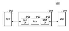
도 11를 참조하면, eMMC(6400)는, 적어도 하나의 낸드 플래시 메모리로 구현된 메모리 장치(6440), 및 컨트롤러(6430)를 포함한다. 여기서, 컨트롤러(6430)는, 도 1에서 설명한 메모리 시스템(110)에서의 컨트롤러(130)에 대응되며, 메모리 장치(6440)는, 도 1에서 설명한 메모리 시스템(110)에서의 메모리 장치(150)에 대응될 수 있다.Referring to FIG. 11, the
보다 구체적으로 설명하면, 컨트롤러(6430)는, 복수의 채널들을 통해, 메모리 장치(2100)와 연결된다. 그리고, 컨트롤러(6430)는, 적어도 하나의 코어(6432), 호스트 인터페이스(6431), 및 메모리 인터페이스, 예컨대 낸드 인터페이스(6433)를 포함한다.More specifically, the
여기서, 코어(6432)는, eMMC(6400)의 전반적인 동작을 제어하며, 호스트 인터페이스(6431)는, 컨트롤러(6430)와 호스트(6410) 간의 인터페이스 기능을 제공하며, 낸드 인터페이스(6433)는, 메모리 장치(6440)와 컨트롤러(6430) 간의 인터페이스 기능을 제공한다. 예컨대, 호스트 인터페이스(6431)는, 도 1에서 설명한 바와 같이, 병렬 인터페이스, 일 예로 MMC 인터페이스가 될 수 있으며, 아울러 직렬 인터페이스, 일 예로 UHS((Ultra High Speed)-/UHS-Ⅱ, UFS 인터페이스가 될 수 있다.Here, the
도 12 내지 도 15은 본 발명의 실시 예에 따른 메모리 시스템을 포함하는 데이터 처리 시스템의 다른 일 예를 개략적으로 도시한 도면이다. 여기서, 도 12 내지 도 15은 본 발명의 실시 예에 따른 메모리 시스템이 적용된 UFS(Universal Flash Storage)를 개략적으로 도시한 도면이다.FIGS. 12 to 15 are diagrams schematically illustrating another example of a data processing system including a memory system according to an embodiment of the present invention. 12 to 15 are views schematically showing a UFS (Universal Flash Storage) to which a memory system according to an embodiment of the present invention is applied.
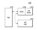
도 12 내지 도 15을 참조하면, 각각의 UFS 시스템들(6500,6600,6700,6800)은, 호스트들(6510,6610,6710,6810), UFS 장치들(6520,6620,6720,6820), 및 UFS 카드들(6530,6630,6730,6830)을 각각 포함할 수 있다. 여기서, 각각의 호스트(6510,6610,6710,6810)은, 유선/무선 전자 기기들, 특히 모바일 전자 기기 등의 어플리케이션 프로세서가 될 수 있으며, 또한 각각의 UFS 장치들(6520,6620,6720,6820)은, 임베디드 UFS(Embedded UFS) 장치들이 되고, 아울러 각각의 UFS 카드들(6530,6630,6730,6830)은, 외부 임베디드 UFS(External Embedded UFS) 장치 또는 리무벌 UFS 카드(Removable UFS Card)가 될 수 있다.12-15, each of the
또한, 각 UFS 시스템들(6500,6600,6700,6800)에서, 각각의 호스트들(6510,6610,6710,6810), UFS 장치들(6520,6620,6720,6820), 및 UFS 카드들(6530,6630,6730,6830) 간은, 각각 UFS 프로토콜을 통해 외부의 장치들, 예컨대 유선/무선 전자 기기들, 특히 모바일 전자 기기 등과 통신할 수 있으며, UFS 장치들(6520,6620,6720,6820)과 UFS 카드들(6530,6630,6730,6830)은, 도 1에서 설명한 메모리 시스템(110)으로 구현될 수 있다. 예컨대, 각 UFS 시스템들(6500,6600,6700,6800)에서, UFS 장치들(6520,6620,6720,6820)은, 도 9 내지 도 11에서 설명한 데이터 처리 시스템(6200), SSD(6300), 또는 eMMC(6400) 형태로 구현될 수 있으며, UFS 카드들(6530,6630,6730,6830)은, 도 8에서 설명한 메모리 카드 시스템(6100) 형태로 구현될 수 있다.Also, in each of the
아울러, 각 UFS 시스템들(6500,6600,6700,6800)에서, 각각의 호스트들(6510,6610,6710,6810), UFS 장치들(6520,6620,6720,6820), 및 UFS 카드들(6530,6630,6730,6830) 간은, UFS(Universal Flash Storage) 인터페이스, 예컨대 MIPI(Mobile Industry Processor Interface)에서의 MIPI M-PHY 및 MIPI UniPro(Unified Protocol)을 통해 통신을 수행할 수 있으며, 아울러 UFS 장치들(6520,6620,6720,6820)과 UFS 카드들(6530,6630,6730,6830) 간은, UFS 프로토콜이 아닌 다른 프로토콜을 통해 통신할 수 있으며, 예컨대 다양한 카드 프로토콜, 일 예로 UFDs, MMC, SD(secure digital), mini SD, Micro SD 등을 통해 통신할 수 있다.In addition, in each of the
그리고, 도 12에 도시한 UFS 시스템(6500)에서, 호스트(6510), UFS 장치(6520), 및 UFS 카드(6530)에는, UniPro이 각각 존재하며, 호스트(6510)는, UFS 장치(6520) 및 UFS 카드(6530)와 각각 통신을 수행하기 위해, 스위칭(swtiching) 동작을 수행하며, 특히 호스트(6510)는, UniPro에서의 링크 레이어(Link Layer) 스위칭, 예컨대 L3 스위칭을 통해, UFS 장치(6520)와 통신을 수행하거나 또는 UFS 카드(6530)와 통신을 수행한다. 이때, UFS 장치(6520)와 UFS 카드(6530) 간은, 호스트(6510)의 UniPro에서 링크 레이어 스위칭을 통해, 통신을 수행할 수도 있다. 여기서, 본 발명의 실시 예에서는, 설명의 편의를 위해, 호스트(6510)에 각각 하나의 UFS 장치(6520) 및 UFS 카드(6530)가 연결되는 것을 일 예로 하여 설명하였지만, 복수의 UFS 장치들과 UFS 카드들이, 호스트(6410)에 병렬 형태 또는 스타 형태로 연결될 수도 있으며, 또한 복수의 UFS 카드들이, UFS 장치(6520)에, 병렬 형태 또는 스타 형태로 연결되거나 직렬 형태 또는 체인 형태로 연결될 수도 있다.UniPro is present in each of the
또한, 도 13에 도시한 UFS 시스템(6600)에서, 호스트(6610), UFS 장치(6620), 및 UFS 카드(6630)에는, UniPro이 각각 존재하며, 스위칭 동작을 수행하는 스위칭 모듈(6640), 특히 UniPro에서의 링크 레이어 스위칭, 예컨대 L3 스위칭 동작을 수행하는 스위칭 모듈(6640)을 통해, 호스트(6610)는, UFS 장치(6620)와 통신을 수행하거나 또는 UFS 카드(6630)와 통신을 수행한다. 이때, UFS 장치(6520)와 UFS 카드(6530) 간은, 스위칭 모듈(6640)의 UniPro에서 링크 레이어 스위칭을 통해, 통신을 수행할 수도 있다. 여기서, 본 발명의 실시 예에서는, 설명의 편의를 위해, 스위칭 모듈(6640)에 각각 하나의 UFS 장치(6620) 및 UFS 카드(6630)가 연결되는 것을 일 예로 하여 설명하였지만, 복수의 UFS 장치들과 UFS 카드들이, 스위칭 모듈(6640)에 병렬 형태 또는 스타 형태로 연결될 수도 있으며, 또한 복수의 UFS 카드들이, UFS 장치(6620)에, 병렬 형태 또는 스타 형태로 연결되거나 직렬 형태 또는 체인 형태로 연결될 수도 있다.In the
아울러, 도 14에 도시한 UFS 시스템(6700)에서, 호스트(6710), UFS 장치(6720), 및 UFS 카드(6730)에는, UniPro이 각각 존재하며, 스위칭 동작을 수행하는 스위칭 모듈(6740), 특히 UniPro에서의 링크 레이어 스위칭, 예컨대 L3 스위칭 동작을 수행하는 스위칭 모듈(6740)을 통해, 호스트(6710)는, UFS 장치(6720)와 통신을 수행하거나 또는 UFS 카드(6730)와 통신을 수행한다. 이때, UFS 장치(6720)와 UFS 카드(6730) 간은, 스위칭 모듈(6740)의 UniPro에서 링크 레이어 스위칭을 통해, 통신을 수행할 수도 있으며, 스위칭 모듈(6740)은, UFS 장치(6720)의 내부 또는 외부에서 UFS 장치(6720)와 하나의 모듈로 구현될 수 있다. 여기서, 본 발명의 실시 예에서는, 설명의 편의를 위해, 스위칭 모듈(6740)에 각각 하나의 UFS 장치(6620) 및 UFS 카드(6630)가 연결되는 것을 일 예로 하여 설명하였지만, 스위칭 모듈(6740)과 UFS 장치(6720)가 각각 구현된 복수의 모듈들이, 호스트(6710)에 병렬 형태 또는 스타 형태로 연결되거나, 각각의 모듈들 간이 직렬 형태 또는 체인 형태로 연결될 수도 있으며, 또한 복수의 UFS 카드들이 스위칭 모듈(6740)에 병렬 형태 또는 스타 형태로 연결될 수도 있다.In addition, in the
그리고, 도 15에 도시한 UFS 시스템(6800)에서, 호스트(6810), UFS 장치(6820), 및 UFS 카드(6830)에는, M-PHY 및 UniPro이 각각 존재하며, UFS 장치(6820)는, 호스트(6810) 및 UFS 카드(6830)와 각각 통신을 수행하기 위해, 스위칭 동작을 수행하며, 특히 UFS 장치(6820)는, 호스트(6810)와의 통신을 위한 M-PHY 및 UniPro 모듈과, UFS 카드(6830)와의 통신을 위한 M-PHY 및 UniPro 모듈 간, 스위칭, 예컨대 타겟(Target) ID(identifier) 스위칭을 통해, 호스트(6810)와 통신을 수행하거나 또는 UFS 카드(6830)와 통신을 수행한다. 이때, 호스트(6810)와 UFS 카드(6530) 간은, UFS 장치(6820)의 M-PHY 및 UniPro 모듈 간 타겟 ID 스위칭을 통해, 통신을 수행할 수도 있다. 여기서, 본 발명의 실시 예에서는, 설명의 편의를 위해, 호스트(6810)에 하나의 UFS 장치(6820)가 연결되고, 또한 하나의 UFS 장치(6820)에 하나의 UFS 카드(6830)가 연결되는 것을 일 예로 하여 설명하였지만, 호스트(6810)에 복수의 UFS 장치들이 병렬 형태 또는 스타 형태로 연결되거나 직렬 형태 또는 체인 형태로 연결될 수도 있으며, 하나의 UFS 장치(6820)에 복수의 UFS 카드들이 병렬 형태 또는 스타 형태로 연결되거나 직렬 형태 또는 체인 형태로 연결될 수도 있다.In the
도 16은 본 발명의 실시 예에 따른 메모리 시스템을 포함하는 데이터 처리 시스템의 또 다른 일 예를 개략적으로 도시한 도면이다. 여기서, 도 16은 본 발명에 따른 메모리 시스템이 적용된 사용자 시스템을 개략적으로 도시한 도면이다.16 is a diagram schematically illustrating another example of a data processing system including a memory system according to an embodiment of the present invention. Here, FIG. 16 is a view schematically showing a user system to which the memory system according to the present invention is applied.
도 16을 참조하면, 사용자 시스템(6900)은, 애플리케이션 프로세서(6930), 메모리 모듈(6920), 네트워크 모듈(6940), 스토리지 모듈(6950), 및 사용자 인터페이스(6910)를 포함한다.16, a
보다 구체적으로 설명하면, 애플리케이션 프로세서(6930)는, 사용자 시스템(6900)에 포함된 구성 요소들, 운영 시스템(OS: Operating System)을 구동시키며, 일 예로 사용자 시스템(6900)에 포함된 구성 요소들을 제어하는 컨트롤러들, 인터페이스들, 그래픽 엔진 등을 포함할 수 있다. 여기서, 애플리케이션 프로세서(6930)는 시스템-온-칩(SoC: System-on-Chip)으로 제공될 수 있다.More specifically, the
그리고, 메모리 모듈(6920)은, 사용자 시스템(6900)의 메인 메모리, 동작 메모리, 버퍼 메모리, 또는 캐시 메모리로 동작할 수 있다. 여기서, 메모리 모듈(6920)은, DRAM, SDRAM, DDR SDRAM, DDR2 SDRAM, DDR3 SDRAM, LPDDR SDARM, LPDDR3 SDRAM, LPDDR3 SDRAM 등과 같은 휘발성 랜덤 액세스 메모리 또는 PRAM, ReRAM, MRAM, FRAM 등과 같은 불휘발성 랜덤 액세스 메모리를 포함할 수 있다. 예컨대, 애플리케이션 프로세서(6930) 및 메모리 모듈(6920)은, POP(Package on Package)를 기반으로 패키지화되어 실장될 수 있다.The
또한, 네트워크 모듈(6940)은, 외부 장치들과 통신을 수행할 수 있다. 예를 들어, 네트워크 모듈(6940)은, 유선 통신을 지원할뿐만 아니라, CDMA(Code Division Multiple Access), GSM(Global System for Mobile communication), WCDMA(wideband CDMA), CDMA-2000, TDMA(Time Dvision Multiple Access), LTE(Long Term Evolution), Wimax, WLAN, UWB, 블루투스, WI-DI 등과 같은 다양한 무선 통신을 지원함으로써, 유선/무선 전자 기기들, 특히 모바일 전자 기기 등과 통신을 수행할 수 있으며, 그에 따라 본 발명의 실시 예에 따른 메모리 시스템 및 데이터 처리 시스템이 유선/무선 전자 기기들에 적용될 수 있다. 여기서, 네트워크 모듈(6940)은, 애플리케이션 프로세서(6930)에 포함될 수 있다.Also, the
아울러, 스토리지 모듈(6950)은, 데이터를 저장, 예컨대 애플리케이션 프로세서(6930)로부터 수신한 데이터를 저장한 후, 스토리지 모듈(6950)에 저장된 데이터를 애플리케이션 프로세서(6930)로 전송할 수 있다. 여기서, 스토리지 모듈(6950)은, PRAM(Phasechange RAM), MRAM(Magnetic RAM), RRAM(Resistive RAM), NAND flash, NOR flash, 3차원 구조의 NAND 플래시 등과 같은 불휘발성 반도체 메모리 소자 등으로 구현될 수 있으며, 또한 사용자 시스템(6900)의 메모리 카드, 외장형 드라이브 등과 같은 탈착식 저장 매체(removable drive)로 제공될 수 있다. 즉, 스토리지 모듈(6950)은, 도 1에서 설명한 메모리 시스템(110)에 대응될 수 있으며, 아울러 도 10 내지 도 15에서 설명한 SSD, eMMC, UFS로 구현될 수도 있다.In addition, the
그리고, 사용자 인터페이스(6910)는, 애플리케이션 프로세서(6930)에 데이터 또는 명령어를 입력하거나 또는 외부 장치로 데이터를 출력하는 인터페이스들을 포함할 수 있다. 예컨대, 사용자 인터페이스(6910)는, 키보드, 키패드, 버튼, 터치 패널, 터치 스크린, 터치 패드, 터치 볼, 카메라, 마이크, 자이로스코프 센서, 진동 센서, 압전 소자 등과 같은 사용자 입력 인터페이스들을 포함할 수 있으며, 아울러 LCD(Liquid Crystal Display), OLED(Organic Light Emitting Diode) 표시 장치, AMOLED(Active Matrix OLED) 표시 장치, LED, 스피커, 모터 등과 같은 사용자 출력 인터페이스들을 포함할 수 있다.The
또한, 본 발명의 실시 예에 따라 도 1에서 설명한 메모리 시스템(110)이, 사용자 시스템(6900)의 모바일 전자 기기에 적용될 경우, 어플리케이션 프로세서(6930)는, 모바일 전자 기기의 전반적인 동작을 제어하며, 네트워크 모듈(6940)은, 통신 모듈로서, 전술한 바와 같이 외부 장치와의 유선/무선 통신을 제어한다. 아울러, 사용자 인터페이스(6910)는, 모바일 전자 기기의 디스플레이/터치 모듈로 어플리케이션 프로세서(6930)에서 처리된 데이터를 디스플레이하거나, 터치 패널로부터 데이터를 입력 받도록 지원한다.1 is applied to a mobile electronic device of a
한편, 본 발명의 상세한 설명에서는 구체적인 실시 예에 관해 설명하였으나, 본 발명의 범위에서 벗어나지 않는 한도 내에서 여러 가지 변형이 가능함은 물론이다. 그러므로, 본 발명의 범위는 설명된 실시 예에 국한되어 정해져서는 안되며 후술하는 특허청구의 범위뿐만 아니라 이 특허청구의 범위와 균등한 것들에 의해 정해져야 한다.While the invention has been shown and described with reference to certain preferred embodiments thereof, it will be understood by those skilled in the art that various changes and modifications may be made without departing from the spirit and scope of the invention. Therefore, the scope of the present invention should not be limited by the described embodiments, but should be determined by the scope of the appended claims, as well as the appended claims.
Claims (20)
Translated fromKorean메타 영역과 유저 데이터 영역이 나누어진 메모리 장치를 포함하는
메모리 시스템에 있어서,
상기 컨트롤러가
상기 메모리 장치의 제 1 메타 영역에 상기 컨트롤러의 로그를 저장하는 제 1 단계; 및
상기 메모리 장치의 제 2 메타 영역에 상기 메모리에 저장된 상기 맵 데이터를 사전 설정된 크기의 그룹으로 분할하여 플러쉬(flush)하는 제 2 단계
를 포함하고,
상기 로그는 제 1 내지 제 6 로그를 포함하며,
상기 제 1 로그는 플러쉬 대상이 되는 맵 데이터 그룹에 대한 플러쉬 동작의 시작을 나타내고, 상기 제 2 로그는 플러쉬 대상이 되는 맵 데이터 그룹에 대한 플러쉬 동작의 종료를 나타내며, 상기 제 3 로그는 플러쉬되는 상기 맵 데이터를 저장하는 상기 메모리 장치의 첫 번째 페이지의 위치를 나타내고, 상기 제 4 로그는 플러쉬되는 상기 맵 데이터를 저장하는 상기 메모리 장치의 마지막 페이지의 위치를 나타내며, 상기 제 5 로그는 맵 데이터를 상기 메모리 장치의 상기 제 2 메타 영역에 프로그램하는 과정에서 프로그램 에러의 발생으로 인한 에러 관리의 동작의 시작을 나타내고, 상기 제 6 로그는 상기 프로그램 에러의 발생 전에 정상적으로 플러쉬된 맵 데이터를 저장한 마지막 페이지의 위치를 나타내는
메모리 시스템의 동작방법.
A controller including a memory in which map data is stored;
A memory device comprising a meta area and a user data area
In a memory system,
The controller
A first step of storing the log of the controller in a first meta area of the memory device; And
A second step of dividing and flushing the map data stored in the memory into a group of a predetermined size in a second meta area of the memory device,
Lt; / RTI >
Wherein the log includes first through sixth logs,
Wherein the first log indicates a start of a flush operation for a map data group to be flushed, the second log indicates an end of a flush operation for a map data group to be flushed, Wherein the fourth log represents a position of a last page of the memory device storing the map data to be flushed, the fifth log represents a position of a first page of the memory device storing map data, Wherein the sixth log indicates the start of an error management operation due to the occurrence of a program error in the process of programming the second meta area of the memory device and the sixth log indicates the start of the operation of the last page storing the map data normally flushed before the program error Indicating the location
A method of operating a memory system.
상기 제 2 단계는,
전체 맵 데이터를 세그먼트 단위로 분할하여 플러쉬(flush)하는
메모리 시스템의 동작방법.
The method according to claim 1,
The second step comprises:
The entire map data is segmented and flushed.
A method of operating a memory system.
상기 제 1 단계는,
상기 맵 데이터의 플러쉬(flush)를 시작할 때,
상기 컨트롤러가 상기 제 1 로그 및 상기 제 3 로그를 상기 메모리 장치의 상기 제 1 메타 영역에 저장하는
메모리 시스템의 동작방법.
3. The method of claim 2,
In the first step,
When starting the flush of the map data,
Wherein the controller stores the first log and the third log in the first meta area of the memory device
A method of operating a memory system.
상기 제 2 단계에서,
맵 데이터를 플러쉬(flush)하는 도중에 프로그램 에러가 발생된 경우,
상기 컨트롤러는 상기 제 5 로그 및 상기 제 6 로그를 상기 메모리 장치의 상기 제 1 메타 영역에 저장하는 제 3 단계;
상기 컨트롤러는 상기 프로그램 에러가 발생된 페이지부터 마지막 플러쉬(flush)된 페이지까지에 대응하는 맵 데이터를 상기 마지막 플러쉬(flush)된 페이지의 다음 페이지부터 순서대로 상기 제 2 메타 영역에 다시 플러쉬(re-flush)하는 제 4 단계
를 더 포함하는 메모리 시스템의 동작방법.
The method of claim 3,
In the second step,
If a program error occurs while flushing the map data,
The controller storing the fifth log and the sixth log in the first meta area of the memory device;
The controller re-flushes the map data corresponding to the page from the page where the program error occurred to the last flush page to the second meta area in order from the next page of the last flush page, flush)
≪ / RTI >
한 그룹의 맵 데이터의 플러쉬(flush)가 종료된 후,
상기 컨트롤러는 상기 제 2 로그 및 상기 제 4 로그를 상기 메모리 장치의 상기 제 1 메타 영역에 저장하는 제 5 단계
를 더 포함하는 메모리 시스템의 동작 방법.
The method according to claim 3 or 4,
After the flush of a group of map data ends,
Wherein the controller stores the second log and the fourth log in the first meta area of the memory device
≪ / RTI >
서든 파워 오프(SPO)가 발생된 경우,
상기 컨트롤러는 상기 메모리 장치에 마지막으로 플러쉬(flush)된 페이지부터 역순으로 상기 맵 데이터를 리드하여 상기 메모리에 저장하는 단계
를 더 포함하는 메모리 시스템의 동작 방법.
The method according to claim 1,
When a sudden power-off (SPO) occurs,
Wherein the controller reads the map data in a reverse order from the last flushed page to the memory device and stores the read map data in the memory
≪ / RTI >
상기 컨트롤러는 상기 메모리 장치에 마지막으로 플러쉬(flush)된 페이지를 리드하지 않는
메모리 시스템의 동작 방법.
The method according to claim 6,
Wherein the controller does not read a page that was last flushed to the memory device
A method of operating a memory system.
상기 컨트롤러는 상기 제 1 메타 영역에 저장된 상기 로그들에 기초하여 상기 맵 데이터를 리드하는
메모리 시스템의 동작 방법.
8. The method of claim 7,
The controller reads the map data based on the logs stored in the first meta area
A method of operating a memory system.
컨트롤러의 로그를 메모리 장치의 제 1 메타 영역에 저장하고, 상기 맵 데이터를 사전 설정된 크기의 그룹으로 분할하여 상기 메모리 장치의 제 2 메타 영역에 플러쉬(flush)하고,
상기 로그는 제 1 내지 제 6 로그를 포함하며,
상기 제 1 로그는 플러쉬 대상이 되는 맵 데이터 그룹에 대한 플러쉬 동작의 시작을 나타내고, 상기 제 2 로그는 플러쉬 대상이 되는 맵 데이터 그룹에 대한 플러쉬 동작의 종료를 나타내며, 상기 제 3 로그는 플러쉬되는 상기 맵 데이터를 저장하는 상기 메모리 장치의 첫 번째 페이지의 위치를 나타내고, 상기 제 4 로그는 플러쉬되는 상기 맵 데이터를 저장하는 상기 메모리 장치의 마지막 페이지의 위치를 나타내며, 상기 제 5 로그는 맵 데이터를 상기 메모리 장치의 상기 제 2 메타 영역에 프로그램하는 과정에서 프로그램 에러의 발생으로 인한 에러 관리의 동작의 시작을 나타내고, 상기 제 6 로그는 상기 프로그램 에러의 발생 전에 정상적으로 플러쉬된 맵 데이터를 저장한 마지막 페이지의 위치를 나타내는
컨트롤러.
A controller including a memory in which map data is stored,
Storing a log of the controller in a first meta area of the memory device, dividing the map data into groups of a predetermined size and flushing the second meta area of the memory device,
Wherein the log includes first through sixth logs,
Wherein the first log indicates a start of a flush operation for a map data group to be flushed, the second log indicates an end of a flush operation for a map data group to be flushed, Wherein the fourth log represents a position of a last page of the memory device storing the map data to be flushed, the fifth log represents a position of a first page of the memory device storing map data, Wherein the sixth log indicates the start of an error management operation due to the occurrence of a program error in the process of programming the second meta area of the memory device and the sixth log indicates the start of the operation of the last page storing the map data normally flushed before the program error Indicating the location
controller.
전체 맵 데이터를 세그먼트 단위로 분할하여 플러쉬(flush)하는
컨트롤러.
10. The method of claim 9,
The entire map data is segmented and flushed.
controller.
상기 맵 데이터의 플러쉬(flush)를 시작할 때,
상기 제 1 로그 및 상기 제 3 로그를 상기 메모리 장치의 상기 제 1 메타 영역에 저장하는
컨트롤러.
11. The method of claim 10,
When starting the flush of the map data,
Storing the first log and the third log in the first meta area of the memory device
controller.
맵 데이터를 플러쉬(flush)하는 도중에 프로그램 에러가 발생된 경우,
상기 제 5 로그 및 상기 제 6 로그를 상기 메모리 장치의 상기 제 1 메타 영역에 저장하고,
상기 프로그램 에러가 발생된 페이지부터 마지막 플러쉬(flush)된 페이지까지에 대응하는 맵 데이터를 상기 마지막 플러쉬(flush)된 페이지의 다음 페이지부터 순서대로 상기 제 2 메타 영역에 다시 플러쉬(re-flush)하는
컨트롤러.
12. The method of claim 11,
If a program error occurs while flushing the map data,
Storing the fifth log and the sixth log in the first meta area of the memory device,
Flushes the map data corresponding to the last flush page from the page where the program error occurred to the second meta area in order from the next page of the last flush page
controller.
한 그룹의 맵 데이터의 플러쉬(flush)가 종료된 후,
상기 제 2 로그 및 상기 제 4 로그를 상기 메모리 장치의 상기 제 1 메타 영역에 저장하는
컨트롤러.13. The method according to claim 11 or 12,
After the flush of a group of map data ends,
Storing the second log and the fourth log in the first meta area of the memory device
controller.
서든 파워 오프(SPO)가 발생된 경우,
상기 메모리 장치에 마지막으로 플러쉬(flush)된 페이지부터 역순으로 상기 맵 데이터를 리드하여 상기 메모리에 저장하는
컨트롤러.
10. The method of claim 9,
When a sudden power-off (SPO) occurs,
Reads the map data in the reverse order from the last flush page to the memory device, and stores the read map data in the memory
controller.
상기 컨트롤러는 상기 메모리 장치에 마지막으로 플러쉬(flush)된 페이지를 리드하지 않는
컨트롤러.
15. The method of claim 14,
Wherein the controller does not read a page that was last flushed to the memory device
controller.
상기 제 1 메타 영역에 저장된 상기 로그들에 기초하여 상기 맵 데이터를 리드하는
컨트롤러.
16. The method of claim 15,
Reads the map data based on the logs stored in the first meta area
controller.
맵 데이터가 저장된 메모리를 포함하는 컨트롤러; 및
메타 영역과 유저 데이터 영역을 포함하는 메모리 장치를 포함하고,
상기 컨트롤러는 컨트롤러의 로그를 메모리 장치의 제 1 메타 영역에 저장하고, 상기 메모리 장치의 제 2 메타 영역에 상기 맵 데이터를 사전 설정된 크기의 그룹으로 분할하여 플러쉬(flush)하며,
상기 로그는 제 1 내지 제 6 로그를 포함하며,
상기 제 1 로그는 플러쉬 대상이 되는 맵 데이터 그룹에 대한 플러쉬 동작의 시작을 나타내고, 상기 제 2 로그는 플러쉬 대상이 되는 맵 데이터 그룹에 대한 플러쉬 동작의 종료를 나타내며, 상기 제 3 로그는 플러쉬되는 상기 맵 데이터를 저장하는 상기 메모리 장치의 첫 번째 페이지의 위치를 나타내고, 상기 제 4 로그는 플러쉬되는 상기 맵 데이터를 저장하는 상기 메모리 장치의 마지막 페이지의 위치를 나타내며, 상기 제 5 로그는 맵 데이터를 상기 메모리 장치의 상기 제 2 메타 영역에 프로그램하는 과정에서 프로그램 에러의 발생으로 인한 에러 관리의 동작의 시작을 나타내고, 상기 제 6 로그는 상기 프로그램 에러의 발생 전에 정상적으로 플러쉬된 맵 데이터를 저장한 마지막 페이지의 위치를 나타내는
메모리 시스템.
In a memory system,
A controller including a memory in which map data is stored; And
A memory device including a meta area and a user data area,
Wherein the controller stores the log of the controller in a first meta area of the memory device, divides the map data into a second meta area of the memory device into a group of predetermined sizes,
Wherein the log includes first through sixth logs,
Wherein the first log represents a start of a flush operation for a map data group to be flushed, the second log represents an end of a flush operation for a map data group to be flushed, Wherein the fourth log represents a position of a last page of the memory device storing the map data to be flushed, the fifth log represents a position of a first page of the memory device storing map data, Wherein the sixth log indicates the start of an error management operation due to the occurrence of a program error in the process of programming the second meta area of the memory device and the sixth log indicates the start of the operation of the last page storing the map data normally flushed before the program error Indicating the location
Memory system.
상기 컨트롤러는,
상기 맵 데이터의 플러쉬(flush)를 시작할 때,
상기 제 1 로그 및 상기 제 3 로그를 상기 메모리 장치의 상기 제 1 메타 영역에 저장하는
메모리 시스템.
18. The method of claim 17,
The controller comprising:
When starting the flush of the map data,
Storing the first log and the third log in the first meta area of the memory device
Memory system.
플러쉬(flush) 도중에 프로그램 에러가 발생된 경우,
상기 컨트롤러는
상기 제 5 로그 및 상기 제 6 로그를 상기 메모리 장치의 상기 제 1 메타 영역에 저장하고,
상기 프로그램 에러가 발생된 페이지부터 마지막 플러쉬(flush)된 페이지까지에 대응하는 맵 데이터를 상기 마지막 플러쉬(flush)된 페이지의 다음 페이지부터 순서대로 상기 제 2 메타 영역에 다시 플러쉬(re-flush)하며,
세그먼트 단위로 분할된 맵 데이터의 플러쉬(flush)가 끝난 후, 상기 제 2 로그 및 상기 제 4 로그를 상기 메모리 장치의 상기 제 1 메타 영역에 저장하는
메모리 시스템.
19. The method of claim 18,
If a program error occurs during a flush,
The controller
Storing the fifth log and the sixth log in the first meta area of the memory device,
Flushes the map data corresponding to the page from the page where the program error occurred to the last flush to the second meta area in order from the next page of the last flush page ,
After the flush of the segmented map data is completed, storing the second log and the fourth log in the first meta area of the memory device
Memory system.
서든 파워 오프(SPO)가 발생된 경우,
상기 컨트롤러는 상기 메모리 장치에 마지막으로 플러쉬(flush)된 페이지부터 역순으로 상기 맵 데이터를 리드하여 상기 메모리에 저장하는
메모리 시스템.
19. The method of claim 18,
When a sudden power-off (SPO) occurs,
The controller reads the map data in the reverse order from the last flushed page to the memory device and stores the read map data in the memory
Memory system.
Priority Applications (3)
| Application Number | Priority Date | Filing Date | Title |
|---|---|---|---|
| KR1020170066696AKR102234725B1 (en) | 2017-05-30 | 2017-05-30 | Controller and memory system and operating method of memory system |
| US15/837,482US10521138B2 (en) | 2017-05-30 | 2017-12-11 | Memory system and operating method for re-building map data according to operation logs |
| CN201711462742.6ACN108986864B (en) | 2017-05-30 | 2017-12-28 | Controller and memory system and operating method of memory system |
Applications Claiming Priority (1)
| Application Number | Priority Date | Filing Date | Title |
|---|---|---|---|
| KR1020170066696AKR102234725B1 (en) | 2017-05-30 | 2017-05-30 | Controller and memory system and operating method of memory system |
Publications (2)
| Publication Number | Publication Date |
|---|---|
| KR20180130740Atrue KR20180130740A (en) | 2018-12-10 |
| KR102234725B1 KR102234725B1 (en) | 2021-04-02 |
Family
ID=64460076
Family Applications (1)
| Application Number | Title | Priority Date | Filing Date |
|---|---|---|---|
| KR1020170066696AActiveKR102234725B1 (en) | 2017-05-30 | 2017-05-30 | Controller and memory system and operating method of memory system |
Country Status (3)
| Country | Link |
|---|---|
| US (1) | US10521138B2 (en) |
| KR (1) | KR102234725B1 (en) |
| CN (1) | CN108986864B (en) |
Cited By (1)
| Publication number | Priority date | Publication date | Assignee | Title |
|---|---|---|---|---|
| KR20200114216A (en)* | 2019-03-28 | 2020-10-07 | 에스케이하이닉스 주식회사 | Data Storage Device, Operation Method Thereof |
Families Citing this family (3)
| Publication number | Priority date | Publication date | Assignee | Title |
|---|---|---|---|---|
| KR102858410B1 (en)* | 2019-07-23 | 2025-09-15 | 삼성전자주식회사 | Storage device for improving journal replay, operating method thereof, and electronic device comprising storage device |
| KR20220005832A (en)* | 2020-07-07 | 2022-01-14 | 에스케이하이닉스 주식회사 | Apparatus and method for managing meta data |
| US11409470B2 (en)* | 2020-06-22 | 2022-08-09 | SK Hynix Inc. | Memory system, memory controller, and method of operating memory system |
Citations (4)
| Publication number | Priority date | Publication date | Assignee | Title |
|---|---|---|---|---|
| KR20090012821A (en)* | 2007-07-31 | 2009-02-04 | 삼성전자주식회사 | I / O control method and device optimized for flash memory |
| JP2013174976A (en)* | 2012-02-23 | 2013-09-05 | Toshiba Corp | Memory system and update method for control program |
| KR20130111228A (en)* | 2010-05-25 | 2013-10-10 | 마벨 월드 트레이드 리미티드 | Memory access table saving and restoring system and methods |
| KR20130132662A (en)* | 2011-10-05 | 2013-12-04 | 엘에스아이 코포레이션 | Self-journaling and hierarchical consistency for non-volatile storage |
Family Cites Families (14)
| Publication number | Priority date | Publication date | Assignee | Title |
|---|---|---|---|---|
| US8019938B2 (en)* | 2006-12-06 | 2011-09-13 | Fusion-I0, Inc. | Apparatus, system, and method for solid-state storage as cache for high-capacity, non-volatile storage |
| CN101276302B (en)* | 2007-03-29 | 2010-10-06 | 中国科学院计算技术研究所 | Magnetic disc fault processing and data restructuring method in magnetic disc array system |
| US8880778B2 (en) | 2010-05-13 | 2014-11-04 | Micron Technology, Inc. | Memory buffer having accessible information after a program-fail |
| US8904161B2 (en)* | 2010-10-20 | 2014-12-02 | Samsung Electronics Co., Ltd. | Memory system and reset method thereof to prevent nonvolatile memory corruption due to premature power loss |
| CN102737715B (en)* | 2011-04-02 | 2015-10-21 | 航天信息股份有限公司 | For the method for power fail safeguard of data of NOR flash memory |
| CN102609335B (en)* | 2012-01-12 | 2014-07-02 | 浪潮(北京)电子信息产业有限公司 | Device and method for protecting metadata by copy-on-write |
| US9170932B1 (en)* | 2012-05-22 | 2015-10-27 | Western Digital Technologies, Inc. | System data storage mechanism providing coherency and segmented data loading |
| KR101993704B1 (en)* | 2012-08-24 | 2019-06-27 | 삼성전자주식회사 | Storage device based on a flash memory and method for allocatting write memory block of memory controller controlling a flash memory |
| US8954694B2 (en)* | 2012-11-15 | 2015-02-10 | Western Digital Technologies, Inc. | Methods, data storage devices and systems for fragmented firmware table rebuild in a solid state drive |
| KR102094393B1 (en)* | 2013-11-18 | 2020-03-27 | 삼성전자주식회사 | Nonvolatile memory system and operation method thereof |
| KR102403202B1 (en)* | 2015-03-13 | 2022-05-30 | 삼성전자주식회사 | Memory system and operating method having meta data manager |
| KR20160111222A (en)* | 2015-03-16 | 2016-09-26 | 에스케이하이닉스 주식회사 | Memory system including semiconductor memory device and memory controller, and operating method thereof |
| US10180805B2 (en)* | 2015-03-25 | 2019-01-15 | SK Hynix Inc. | Memory system and operating method thereof |
| US9997251B2 (en) | 2015-03-26 | 2018-06-12 | Burlywood, LLC | Medium defect management method for storage systems requiring an integrated controller |
- 2017
- 2017-05-30KRKR1020170066696Apatent/KR102234725B1/enactiveActive
- 2017-12-11USUS15/837,482patent/US10521138B2/enactiveActive
- 2017-12-28CNCN201711462742.6Apatent/CN108986864B/enactiveActive
Patent Citations (4)
| Publication number | Priority date | Publication date | Assignee | Title |
|---|---|---|---|---|
| KR20090012821A (en)* | 2007-07-31 | 2009-02-04 | 삼성전자주식회사 | I / O control method and device optimized for flash memory |
| KR20130111228A (en)* | 2010-05-25 | 2013-10-10 | 마벨 월드 트레이드 리미티드 | Memory access table saving and restoring system and methods |
| KR20130132662A (en)* | 2011-10-05 | 2013-12-04 | 엘에스아이 코포레이션 | Self-journaling and hierarchical consistency for non-volatile storage |
| JP2013174976A (en)* | 2012-02-23 | 2013-09-05 | Toshiba Corp | Memory system and update method for control program |
Cited By (1)
| Publication number | Priority date | Publication date | Assignee | Title |
|---|---|---|---|---|
| KR20200114216A (en)* | 2019-03-28 | 2020-10-07 | 에스케이하이닉스 주식회사 | Data Storage Device, Operation Method Thereof |
Also Published As
| Publication number | Publication date |
|---|---|
| US10521138B2 (en) | 2019-12-31 |
| CN108986864A (en) | 2018-12-11 |
| US20180349045A1 (en) | 2018-12-06 |
| CN108986864B (en) | 2022-06-28 |
| KR102234725B1 (en) | 2021-04-02 |
Similar Documents
| Publication | Publication Date | Title |
|---|---|---|
| KR102727958B1 (en) | Memory system and operating method of memory system | |
| KR102730871B1 (en) | Memory system and operating method of memory system | |
| KR102430791B1 (en) | Controller and operation method thereof | |
| KR102711037B1 (en) | Memory system and operating method of memory system | |
| KR20190017550A (en) | Memory system and operating method of memory system | |
| KR20180030319A (en) | Memory system and operation method for the same | |
| KR20190074677A (en) | Memory system and operating method of memory system | |
| KR20190040604A (en) | Memory system and operating method of memory system | |
| KR20180079584A (en) | Controller and operating method of controller | |
| KR102468737B1 (en) | Memory system and operating method thereof | |
| KR20180135188A (en) | Memory system and operating method of memory system | |
| KR20190128392A (en) | Memory system and operation method thereof | |
| KR20190115310A (en) | Memory system and operating method of memory system | |
| KR20200012494A (en) | Controller and operation method thereof | |
| KR20200008273A (en) | Memory system and operation method thereof | |
| KR20180111157A (en) | Controller and operating method of controller | |
| KR20190040602A (en) | Memory system and operating method of memory system | |
| KR20180003715A (en) | Memory system and operating method of memory system | |
| KR20180118926A (en) | Controller including multi processor and operation method thereof | |
| KR20180029124A (en) | Memory system and operating method of memory system | |
| KR20180008966A (en) | Memory system and operating method of memory system | |
| KR20180128588A (en) | Memory system and method thereof | |
| KR20190040607A (en) | Memory system and operating method of memory system | |
| KR20180094391A (en) | Memory system and operating method thereof | |
| KR20190001300A (en) | Controller and memory system and operating method of memory system |
Legal Events
| Date | Code | Title | Description |
|---|---|---|---|
| PA0109 | Patent application | Patent event code:PA01091R01D Comment text:Patent Application Patent event date:20170530 | |
| PG1501 | Laying open of application | ||
| A201 | Request for examination | ||
| PA0201 | Request for examination | Patent event code:PA02012R01D Patent event date:20200528 Comment text:Request for Examination of Application Patent event code:PA02011R01I Patent event date:20170530 Comment text:Patent Application | |
| E701 | Decision to grant or registration of patent right | ||
| PE0701 | Decision of registration | Patent event code:PE07011S01D Comment text:Decision to Grant Registration Patent event date:20210303 | |
| PR0701 | Registration of establishment | Comment text:Registration of Establishment Patent event date:20210326 Patent event code:PR07011E01D | |
| PR1002 | Payment of registration fee | Payment date:20210329 End annual number:3 Start annual number:1 | |
| PG1601 | Publication of registration | ||
| PR1001 | Payment of annual fee | Payment date:20240226 Start annual number:4 End annual number:4 | |
| PR1001 | Payment of annual fee | Payment date:20241205 Start annual number:5 End annual number:5 |