KR20180129672A - Charging/discharging control circuit and battery device provided with the same - Google Patents
Charging/discharging control circuit and battery device provided with the sameDownload PDFInfo
- Publication number
- KR20180129672A KR20180129672AKR1020180059013AKR20180059013AKR20180129672AKR 20180129672 AKR20180129672 AKR 20180129672AKR 1020180059013 AKR1020180059013 AKR 1020180059013AKR 20180059013 AKR20180059013 AKR 20180059013AKR 20180129672 AKR20180129672 AKR 20180129672A
- Authority
- KR
- South Korea
- Prior art keywords
- terminal
- voltage
- signal
- output
- secondary battery
- Prior art date
- Legal status (The legal status is an assumption and is not a legal conclusion. Google has not performed a legal analysis and makes no representation as to the accuracy of the status listed.)
- Withdrawn
Links
Images


Classifications
- H—ELECTRICITY
- H02—GENERATION; CONVERSION OR DISTRIBUTION OF ELECTRIC POWER
- H02J—CIRCUIT ARRANGEMENTS OR SYSTEMS FOR SUPPLYING OR DISTRIBUTING ELECTRIC POWER; SYSTEMS FOR STORING ELECTRIC ENERGY
- H02J7/00—Circuit arrangements for charging or depolarising batteries or for supplying loads from batteries
- H02J7/0013—Circuit arrangements for charging or depolarising batteries or for supplying loads from batteries acting upon several batteries simultaneously or sequentially
- H02J7/0014—Circuits for equalisation of charge between batteries
- H02J7/0019—Circuits for equalisation of charge between batteries using switched or multiplexed charge circuits
- Y—GENERAL TAGGING OF NEW TECHNOLOGICAL DEVELOPMENTS; GENERAL TAGGING OF CROSS-SECTIONAL TECHNOLOGIES SPANNING OVER SEVERAL SECTIONS OF THE IPC; TECHNICAL SUBJECTS COVERED BY FORMER USPC CROSS-REFERENCE ART COLLECTIONS [XRACs] AND DIGESTS
- Y02—TECHNOLOGIES OR APPLICATIONS FOR MITIGATION OR ADAPTATION AGAINST CLIMATE CHANGE
- Y02E—REDUCTION OF GREENHOUSE GAS [GHG] EMISSIONS, RELATED TO ENERGY GENERATION, TRANSMISSION OR DISTRIBUTION
- Y02E60/00—Enabling technologies; Technologies with a potential or indirect contribution to GHG emissions mitigation
- Y02E60/10—Energy storage using batteries
Landscapes
- Charge And Discharge Circuits For Batteries Or The Like (AREA)
- Secondary Cells (AREA)
- Engineering & Computer Science (AREA)
- Power Engineering (AREA)
Abstract
Translated fromKorean
Description
Translated fromKorean본 발명은, 충방전 제어 회로 및 이것을 구비한 배터리 장치에 관한 것이다.The present invention relates to a charge-discharge control circuit and a battery device having the same.
종래의 복수의 이차 전지가 병렬로 접속된 배터리 장치의 보호 회로는, 이차 전지를 병렬로 접속할 때에 전압이 높은 이차 전지로부터 전압이 낮은 이차 전지에 흐르는 돌입 전류를 방지하고, 이차 전지를 보호하도록 구성되어 있다(예를 들어, 특허 문헌 1 일본국 특허 공개 2006-345660호 참조).The protection circuit of a battery device in which a plurality of conventional secondary batteries are connected in parallel is configured to prevent an inrush current flowing from a secondary battery having a high voltage to a secondary battery having a low voltage when the secondary batteries are connected in parallel, (See, for example, Patent Document 1: Japanese Patent Application Laid-Open No. 2006-345660).
그러나, 종래의 배터리 장치의 보호 회로에 있어서는, 이차 전지를 과전류로부터 보호하는 것은 가능하나, 병렬로 접속된 복수의 이차 전지를 각각 적정한 충전 전류로 충전하는 것에 대해서는 고려되어 있지 않다.However, in the protection circuit of the conventional battery device, it is possible to protect the secondary battery from the overcurrent, but it is not considered to charge each of the plurality of secondary batteries connected in parallel with a proper charging current.
본 발명은, 상기 과제를 감안하여 이루어진 것이며, 병렬로 접속된 복수의 이차 전지에 용량값이나 임피던스값에 차가 있었다고 하더라도, 균등한 충전 전류로 충전하는 것이 가능한 충방전 제어 회로 및 이것을 구비한 배터리 장치를 제공하는 것을 목적으로 하고 있다.SUMMARY OF THE INVENTION The present invention has been made in view of the above problems, and it is an object of the present invention to provide a charge / discharge control circuit capable of charging with equal charge current even when a plurality of secondary batteries connected in parallel differ in capacitance value or impedance value, And to provide the above-mentioned objects.
상기 과제를 해결하기 위해서, 본 발명의 실시예에 따르는 충방전 제어 회로는, 병렬로 접속된 제1 및 제2 이차 전지의 충방전을 제어하기 위한 충방전 제어 회로로서, 상기 제1 및 제2 이차 전지의 양극 단자가 접속되는 양극 전원 단자와, 상기 제1 이차 전지의 음극 단자가 접속되는 제1 음극 전원 단자와, 상기 제2 이차 전지의 음극 단자가 접속되는 제2 음극 전원 단자와, 상기 제1 이차 전지의 충전을 제어하는 신호가 출력되는 제1 충전 제어 단자와, 상기 제2 이차 전지의 충전을 제어하는 신호가 출력되는 제2 충전 제어 단자와, 부하 및 충전기의 음극이 접속되는 외부 음극 단자에 접속되는 전압 모니터 단자와, 일단이 상기 외부 음극 단자에 접속되고, 상기 제1 이차 전지의 전류가 흐르는 제1 저항의 타단과 접속되는 제1 전압 입력 단자와, 일단이 상기 외부 음극 단자에 접속되고, 상기 제2 이차 전지의 전류가 흐르는 제2 저항의 타단과 접속되는 제2 전압 입력 단자와, 상기 양극 전원 단자, 제1 음극 전원 단자, 제2 음극 전원 단자의 전압에 의해서 충방전을 제어하는 제어 신호를 출력하는 전압 검출 회로와, 상기 제1 전압 입력 단자가 제1 입력 단자에 접속되고, 상기 제2 전압 입력 단자가 제2 입력 단자에 접속되는 차동 앰프와, 상기 차동 앰프의 출력 단자가 입력 단자에 접속되고, 상기 제1 충전 제어 단자에 출력하는 제1 신호와 상기 제2 충전 제어 단자에 출력하는 제2 신호를 출력하는 출력 회로와, 상기 출력 회로가 출력하는 제1 신호 및 제2 신호와 상기 전압 검출 회로가 출력하는 제어 신호에 의거하여, 상기 제1 충전 제어 단자 및 상기 제2 충전 제어 단자에 상기 제1 및 제2 신호를 출력하는 충전 제어 회로를 구비하며, 상기 충전 제어 회로는, 상기 전압 검출 회로로부터 충전을 허가하는 제어 신호를 받고, 또한 상기 전압 모니터 단자의 전압에 의해서 충전기가 접속되어 있는 것을 검출하면, 상기 제1 충전 제어 단자에 상기 출력 회로가 출력하는 상기 제1 신호를 출력하며, 상기 제2 충전 제어 단자에 상기 출력 회로가 출력하는 상기 제2 신호를 출력하는 것을 특징으로 한다.In order to solve the above problems, a charge / discharge control circuit according to an embodiment of the present invention is a charge / discharge control circuit for controlling charge / discharge of first and second secondary batteries connected in parallel, A second negative electrode power supply terminal to which a negative electrode terminal of the second secondary battery is connected; and a second negative electrode power supply terminal to which the negative electrode of the first secondary battery is connected, A first charge control terminal for outputting a signal for controlling charging of the first secondary battery, a second charge control terminal for outputting a signal for controlling charging of the second secondary battery, A first voltage input terminal connected to the other terminal of the first resistor through which the current flows in the first secondary battery, A second voltage input terminal connected to the external negative terminal and connected to the other end of the second resistor through which the current flows in the second secondary battery, and a second voltage input terminal connected to the positive electrode power terminal, the first negative electrode power terminal, A differential amplifier in which the first voltage input terminal is connected to the first input terminal and the second voltage input terminal is connected to the second input terminal; An output circuit for outputting a first signal to be output to the first charge control terminal and a second signal to be output to the second charge control terminal, the output circuit being connected to the input terminal of the differential amplifier, An output terminal for outputting the first and second signals to the first charge control terminal and the second charge control terminal based on the first signal and the second signal and the control signal outputted by the voltage detection circuit, Wherein when the charging control circuit receives a control signal for permitting charging from the voltage detection circuit and detects that the charging device is connected by the voltage of the voltage monitor terminal, And outputs the first signal outputted by the output circuit to the second charge control terminal.
또, 본 발명의 실시예에 따르는 배터리 장치는, 병렬로 접속된 제1 및 제2 이차 전지와, 상기 제1 및 제2 이차 전지의 충방전을 제어하는 청구항 1에 기재된 충방전 제어 회로와, 상기 충방전 제어 회로에 의해서 제어되는 상기 제1 이차 전지의 충전을 제어하는 제1 충전 제어 FET와, 상기 충방전 제어 회로에 의해서 제어되는 상기 제2 이차 전지의 충전을 제어하는 제2 충전 제어 FET를 구비한 것을 특징으로 한다.A battery device according to an embodiment of the present invention includes first and second secondary batteries connected in parallel, a charge / discharge control circuit according to
본 발명의 충방전 제어 회로 및 이것을 구비한 배터리 장치에 의하면, 병렬로 접속된 복수의 이차 전지에 임피던스값에 차가 있었다고 하더라도, 원하는 충전 전류로 충전하는 것이 가능해진다. 또, 병렬로 접속된 복수의 이차 전지에 그 용량값에 따른 충전 전류로 충전할 수 있다.According to the charge / discharge control circuit of the present invention and the battery device having the same, it is possible to charge with a desired charge current even if there is a difference in the impedance value between a plurality of secondary batteries connected in parallel. In addition, a plurality of secondary batteries connected in parallel can be charged with a charging current corresponding to the capacity value.
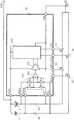
도 1은 본 발명의 제1 실시 형태의 배터리 장치를 도시하는 블럭도이다.
도 2는 본 발명의 제2 실시 형태의 배터리 장치를 도시하는 블럭도이다.
도 3은 본 발명의 제2 실시 형태의 제2 예의 배터리 장치를 도시하는 블럭도이다.1 is a block diagram showing a battery device according to a first embodiment of the present invention.
2 is a block diagram showing a battery device according to a second embodiment of the present invention.
3 is a block diagram showing a battery device of a second example of the second embodiment of the present invention.
이하, 본 발명의 실시 형태에 대해 도면을 참조하여 설명한다.BEST MODE FOR CARRYING OUT THE INVENTION Hereinafter, embodiments of the present invention will be described with reference to the drawings.
도 1은, 본 발명의 제1 실시 형태의 배터리 장치를 도시하는 블럭도이다.1 is a block diagram showing a battery device according to a first embodiment of the present invention.
본 실시 형태의 배터리 장치는, 이차 전지(1 및 2)와, 충방전 제어 회로(10)와, 방전 제어 FET(11 및 12)와, 충전 제어 FET(13 및 14)와, 저항(15 및 16)과, 충전기 및 부하(모두 도시 생략)가 접속되는 외부 양극 단자(EB+) 및 외부 음극 단자(EB-)를 구비하고 있다.The battery device of the present embodiment is provided with the
충방전 제어 회로(10)는, 전압 검출 회로(101)와, 방전 제어 회로(102)와, 충전 제어 회로(103)와, 차동 앰프(105)와, 출력 회로(104)와, 양극 전원 단자(VDD)와, 음극 전원 단자(VSS1 및 VSS2)와, 방전 제어 단자(DO1 및 DO2)와, 충전 제어 단자(CO1 및 CO2)와, 전압 입력 단자(VI1 및 VI2), 전압 모니터 단자(VM)를 구비하고 있다.The charge /
전압 검출 회로(101)는, 양극 전원 단자(VDD)와 음극 전원 단자(VSS1 및 VSS2)의 전압으로부터 이차 전지(1 및 2)의 과충전 및 과방전을 감시한다. 방전 제어 회로(102)는, 전압 검출 회로(101)로부터 입력되는 신호에 의거하여, 양극 전원 단자(VDD)의 전압과 음극 전원 단자(VSS1 및 VSS2)의 전압에 의해서 방전 제어 FET(11 및 12)를 제어한다. 충전 제어 회로(103)는, 전압 검출 회로(101)로부터 입력되는 신호에 의거하여, 양극 전원 단자(VDD)의 전압과 전압 모니터 단자(VM)의 전압에 의해서 충전 제어 단자(CO1 및 CO2)를 제어한다.The
여기서, 방전 제어 FET(11 및 12)를 제어하는 방전 제어 회로(102)가 출력하는 신호는, 공통되어도, 상이해도 된다.Here, the signals output by the
다음으로, 배터리 장치의 충전 동작에 대해 이하에 설명한다.Next, charging operation of the battery device will be described below.
외부 양극 단자(EB+)와 외부 음극 단자(EB-)의 사이에 충전기가 접속되고, 충전 제어 FET(13 및 14), 방전 제어 FET(11 및 12)가 모두 온이며, 이차 전지(1)와 이차 전지(2)에 충전 전류가 흐른다. 이차 전지(1)에 흐르는 충전 전류는, 일단이 외부 음극 단자(EB-)에 접속된 저항(15)을 흐르고, 저항(15)의 타단에 전압을 발생시킨다. 이차 전지(2)에 흐르는 충전 전류는, 일단이 외부 음극 단자(EB-)에 접속된 저항(16)을 흐르고, 저항(16)의 타단에 전압을 발생시킨다. 이때, 저항(15)과 저항(16)의 일단은 공통으로 접속되어 있으므로, 그들의 타단에 발생한 전압의 차는 충전 전류의 차와 동일하다.The charger is connected between the external positive terminal EB + and the external negative terminal EB- and the
저항(15)의 타단에 발생한 전압은, 전압 입력 단자(VI1), 즉 차동 앰프(105)의 비반전 입력 단자에 입력된다. 저항(16)의 타단에 발생한 전압은, 전압 입력 단자(VI2), 즉 차동 앰프(105)의 반전 입력 단자에 입력된다. 차동 앰프(105)는, 전압 입력 단자(VI1)의 전압과 전압 입력 단자(VI2)의 전압의 차를 증폭하여, 출력 회로(104)에 출력한다. 출력 회로(104)는, 차동 앰프(105)로부터 입력된 신호의 극성에 따라, 양이면 충전 제어 FET(14)의 제어 신호를 출력하고, 음이면 충전 제어 FET(13)의 제어 신호를 출력한다.The voltage generated at the other end of the
충전 제어 회로(103)는, 전압 검출 회로(101)로부터 충전 허가의 신호가 입력되면, 양극 전원 단자(VDD)의 전압을 충전 제어 단자(CO1 및 CO2)에 출력하고, 충전 제어 FET(13) 및 충전 제어 FET(14)를 온한다.The
이때, 외부 양극 단자(EB+)와 외부 음극 단자(EB-)의 사이에 충전기가 접속되어 있으면, 충전 제어 회로(103)는, 양극 전원 단자(VDD)의 전압으로부터 출력 회로(104)로부터 입력된 제어 신호로 바꾸어 출력 충전 제어 단자(CO1 및 CO2)에 출력한다.At this time, when the charger is connected between the external positive terminal EB + and the external negative terminal EB-, the
즉, 출력 회로(104)가 출력하는 이차 전지(1) 및 이차 전지(2)에 흐르는 충전 전류에 의거한 제어 신호에 의해서 충전 제어 FET(13) 및 충전 제어 FET(14)가 제어되므로, 이차 전지(1) 및 이차 전지(2)에 흐르는 충전 전류는 동일해진다.That is, since the
또, 충전 제어 회로(103)는, 전압 검출 회로(101)로부터 충전 금지의 신호가 입력되면, 전압 모니터 단자(VM)의 전압을 충전 제어 단자(CO1 및 CO2)에 출력하고, 충전 제어 FET(13) 및 충전 제어 FET(14)를 오프한다.The
이상 설명한 바와 같이, 본 실시 형태에 의하면, 출력 회로(104)가 출력하는 이차 전지(1) 및 이차 전지(2)에 흐르는 충전 전류에 의거한 제어 신호에 의해서 충전 제어 FET(13) 및 충전 제어 FET(14)를 제어하도록 했으므로, 병렬로 접속된 이차 전지에 용량값이나 임피던스값에 차가 있었다고 하더라도, 균등한 충전 전류로 충전하는 것이 가능해진다. 따라서, 어느 이차 전지의 충전 전류가 정격을 초과해 버린다고 하는 문제점이 발생하지 않는, 안전한 배터리 장치를 제공할 수 있다.As described above, according to the present embodiment, by the control signal based on the charging current flowing in the
또한, 본 실시 형태에 있어서, 차동 앰프(105)가 전압 입력 단자(VI1)와 전압 입력 단자(VI2)의 전압의 차를 증폭하여 출력하도록 했는데, 예를 들어, 컴퍼레이터를 이용할 수도 있다.In the present embodiment, the
도 2는, 본 발명의 제2 실시 형태의 배터리 장치를 도시하는 블럭도이다.2 is a block diagram showing a battery device according to a second embodiment of the present invention.
본 실시 형태의 배터리 장치는, 제1 실시 형태의 배터리 장치에 대해, 이하의 점이 상이하다.The battery device of the present embodiment is different from the battery device of the first embodiment in the following points.
제2 실시 형태의 배터리 장치는, 저항(25)이 이차 전지(1)와 방전 제어 FET(11)의 사이에 접속되고, 저항(26)이 이차 전지(2)와 방전 제어 FET(12)의 사이에 접속되어 있다.The battery device of the second embodiment is characterized in that the
그 외의 구성에 대해서는, 도 1의 배터리 장치와 동일하기 때문에, 동일한 구성 요소에는 동일한 부호를 붙이고, 중복하는 설명은 생략한다. 또, 방전 제어 회로(102)에 대해서도 생략한다.The other constitution is the same as that of the battery device of Fig. 1, so that the same constituent elements are denoted by the same reference numerals, and redundant explanations are omitted. The
동작에 대해서도, 제1 실시 형태의 배터리 장치와 거의 동일하나, 저항(25)과 저항(26)이 공통으로 접속된 단자가 없으므로, 그들의 양단에 발생한 전압의 차를 출력 회로(104)에 출력하는 회로가 제1 실시 형태와 상이하다.Since there is no terminal to which the
충방전 제어 회로(20)는, 아날로그 가산 처리 회로인, 차동 앰프(201)와, 차동 앰프(202)와, 가산 회로(203)를 구비하고 있다. 차동 앰프(201)는, 저항(25)의 양단의 전압의 차를 증폭하여 출력한다. 차동 앰프(202)는, 저항(26)의 양단의 전압의 차를 증폭하여 출력한다. 가산 회로(203)는, 차동 앰프(201)의 출력 전압으로부터 차동 앰프(202)의 출력 전압을 감산하여, 출력 회로(104)에 출력한다. 이후의 동작은, 제1 실시 형태의 배터리 장치와 동일하다.
이러한 구성에 의해, 병렬로 접속된 이차 전지에 용량값이나 임피던스값에 차가 있었다고 하더라도, 균등한 충전 전류로 충전하는 것이 가능해진다.With this configuration, even if there is a difference between the capacitance value and the impedance value in the secondary batteries connected in parallel, it becomes possible to charge the secondary batteries with an equal charging current.
이상과 같이, 본 실시 형태에 있어서도, 제1 실시 형태와 동일한 효과가 얻어진다.As described above, also in this embodiment, the same effects as those of the first embodiment can be obtained.
도 3에, 제2 실시 형태의 제2 예의 배터리 장치의 블럭도를 도시한다.Fig. 3 shows a block diagram of the battery device of the second example of the second embodiment.
도 3의 배터리 장치는, 도 2의 배터리 장치에 대해, 이하의 점이 상이하다. 또한, 이하의 점 이외의 구성에 대해서는, 도 2의 배터리 장치와 동일하기 때문에, 동일한 구성 요소에는 동일한 부호를 붙이고, 중복하는 설명은 생략한다.The battery device of FIG. 3 differs from the battery device of FIG. 2 in the following points. The configuration other than the following points is the same as that of the battery device of Fig. 2, so that the same constituent elements are denoted by the same reference numerals, and redundant explanations are omitted.
충방전 제어 회로(30)는, 전압차 검출 회로(301)를 구비하고 있다. 전압차 검출 회로(301)는, 음극 전원 단자(VSS1)와 전압 입력 단자(VI2)의 사이에 직렬로 접속된 저항(R1 및 R2)과, 음극 전원 단자(VSS2)와 전압 입력 단자(VI1)의 사이에 직렬로 접속된 저항(R3 및 R4)과, 저항(R1)과 저항(R2)의 접속점인 제1 출력 단자와, 저항(R3)과 저항(R4)의 접속점인 제2 출력 단자를 구비하고 있다. 제1 출력 단자는, 차동 앰프(105)의 반전 입력 단자에 접속되고, 제2 출력 단자는, 차동 앰프(105)의 비반전 입력 단자에 접속된다.The charge /
이상과 같이 구성된 전압차 검출 회로(301)는, 4개의 저항의 저항값은 모두 동일하고, 그 저항값은 저항(25 및 26)의 저항보다 충분히 크게 하면, 제1 출력 단자와 제2 출력 단자의 사이의 전압(V301)은, 다음식으로 표시된다.When the resistance values of the four resistors are all the same and the resistance value thereof is sufficiently larger than the resistances of the
V301≒(V25-V26)/2V301? (V25-V26) / 2
단, V25는 저항(25)의 양단의 전압, V26은 저항(26)의 양단의 전압이다.V25 is the voltage across the
따라서, 도 3의 전압차 검출 회로(301)에 의하면, 도 2보다 간편한 회로 구성에 의해서, 동일한 기능을 얻을 수 있고, 회로 규모를 축소할 수 있다고 하는 효과가 있다.Therefore, according to the voltage
이상, 본 발명의 실시 형태에 대해 설명했는데, 본 발명은 상기 실시 형태에 한정되지 않으며, 본 발명의 취지를 일탈하지 않는 범위에 있어서 여러 가지의 변경이 가능한 것은 말할 필요도 없다.Although the embodiment of the present invention has been described above, the present invention is not limited to the above embodiment, and it goes without saying that various modifications are possible within the scope of the present invention.
예를 들어, 이차 전지(1)와 이차 전지(2)의 용량의 비가 1:2였던 경우에는, 저항(25)과 저항(26)의 비를 2:1로 함으로써, 충전 레이트를 동일하게 할 수 있다.For example, when the ratio of the capacity of the
1, 2 이차 전지
10, 20, 30 충방전 제어 회로
11, 12 방전 제어 FET
13, 14 충전 제어 FET
101 전압 검출 회로
102 방전 제어 회로
103 충전 제어 회로
104 출력 회로
105, 201, 202 차동 앰프
203 가산 회로
301 전압차 검출 회로
CO1, CO2 충전 제어 단자
DO1, DO2 방전 제어 단자
EB+ 외부 양극 단자
EB- 외부 음극 단자
VDD 양극 전원 단자
VSS1, VSS2 음극 전원 단자
VI1, VI2 전압 입력 단자
VM 전압 모니터 단자1, 2 secondary battery
10, 20, 30 charge / discharge control circuit
11, 12 Discharge control FET
13, 14 charge control FET
101 voltage detection circuit
102 discharge control circuit
103 charge control circuit
104 Output Circuit
105, 201, 202 differential amplifier
203 addition circuit
301 voltage difference detection circuit
CO1, CO2 charge control terminal
DO1, DO2 discharge control terminal
EB + external positive terminal
EB-external negative terminal
VDD positive power terminal
VSS1, VSS2 cathode power terminal
VI1, VI2 voltage input terminal
VM voltage monitor terminal
Claims (4)
Translated fromKorean상기 제1 및 제2 이차 전지의 양극 단자가 접속되는 양극 전원 단자와,
상기 제1 이차 전지의 음극 단자가 접속되는 제1 음극 전원 단자와,
상기 제2 이차 전지의 음극 단자가 접속되는 제2 음극 전원 단자와,
상기 제1 이차 전지의 충전을 제어하는 신호가 출력되는 제1 충전 제어 단자와,
상기 제2 이차 전지의 충전을 제어하는 신호가 출력되는 제2 충전 제어 단자와,
부하 및 충전기의 음극이 접속되는 외부 음극 단자에 접속되는 전압 모니터 단자와,
일단이 상기 외부 음극 단자에 접속되고, 상기 제1 이차 전지의 전류가 흐르는 제1 저항의 타단과 접속되는 제1 전압 입력 단자와,
일단이 상기 외부 음극 단자에 접속되고, 상기 제2 이차 전지의 전류가 흐르는 제2 저항의 타단과 접속되는 제2 전압 입력 단자와,
상기 양극 전원 단자, 제1 음극 전원 단자, 제2 음극 전원 단자의 전압에 의해서 충방전을 제어하는 제어 신호를 출력하는 전압 검출 회로와,
상기 제1 전압 입력 단자가 제1 입력 단자에 접속되고, 상기 제2 전압 입력 단자가 제2 입력 단자에 접속되는 차동 앰프와,
상기 차동 앰프의 출력 단자가 입력 단자에 접속되고, 상기 제1 충전 제어 단자에 출력하는 제1 신호와 상기 제2 충전 제어 단자에 출력하는 제2 신호를 출력하는 출력 회로와,
상기 출력 회로가 출력하는 제1 신호 및 제2 신호와 상기 전압 검출 회로가 출력하는 제어 신호에 의거하여, 상기 제1 충전 제어 단자 및 상기 제2 충전 제어 단자에 상기 제1 및 제2 신호를 출력하는 충전 제어 회로를 구비하며,
상기 충전 제어 회로는, 상기 전압 검출 회로로부터 충전을 허가하는 제어 신호를 받고, 또한 상기 전압 모니터 단자의 전압에 의해서 충전기가 접속되어 있는 것을 검출하면, 상기 제1 충전 제어 단자에 상기 출력 회로가 출력하는 상기 제1 신호를 출력하며, 상기 제2 충전 제어 단자에 상기 출력 회로가 출력하는 상기 제2 신호를 출력하는 것을 특징으로 하는 충방전 제어 회로.A charge / discharge control circuit for controlling charging and discharging of first and second secondary batteries connected in parallel,
A positive electrode power source terminal to which the positive electrode terminals of the first and second secondary batteries are connected,
A first negative electrode power source terminal to which a negative electrode terminal of the first secondary battery is connected,
A second negative electrode power supply terminal to which the negative electrode terminal of the second secondary battery is connected,
A first charge control terminal for outputting a signal for controlling charging of the first secondary battery,
A second charge control terminal for outputting a signal for controlling charging of the second secondary battery,
A voltage monitor terminal connected to an external cathode terminal to which the load and the cathode of the charger are connected,
A first voltage input terminal connected to the external negative terminal at one end and connected to the other end of the first resistor through which the current of the first secondary battery flows,
A second voltage input terminal connected to the external negative terminal at one end and connected to the other end of a second resistor through which the current flows in the second secondary battery,
A voltage detecting circuit for outputting a control signal for controlling charging and discharging by the voltages of the positive electrode power source terminal, the first negative electrode power source terminal, and the second negative electrode power source terminal,
A differential amplifier in which the first voltage input terminal is connected to the first input terminal and the second voltage input terminal is connected to the second input terminal;
An output circuit connected to an input terminal of the differential amplifier for outputting a first signal to be output to the first charge control terminal and a second signal to be output to the second charge control terminal;
Outputting the first and second signals to the first charge control terminal and the second charge control terminal based on a first signal and a second signal output from the output circuit and a control signal output from the voltage detection circuit And a charging control circuit
When the charging control circuit receives a control signal for permitting charging from the voltage detecting circuit and detects that the charger is connected by the voltage of the voltage monitor terminal, And outputs the second signal outputted from the output circuit to the second charge control terminal.
상기 제1 및 제2 이차 전지의 양극 단자가 접속되는 양극 전원 단자와,
상기 제1 이차 전지의 음극 단자가 접속되는 제1 음극 전원 단자와,
상기 제2 이차 전지의 음극 단자가 접속되는 제2 음극 전원 단자와,
상기 제1 이차 전지의 충전을 제어하는 신호가 출력되는 제1 충전 제어 단자와,
상기 제2 이차 전지의 충전을 제어하는 신호가 출력되는 제2 충전 제어 단자와,
부하 및 충전기의 음극이 접속되는 외부 음극 단자에 접속되는 전압 모니터 단자와,
일단이 상기 제1 음극 전원 단자에 접속되고, 상기 제1 이차 전지의 전류가 흐르는 제1 저항의 타단과 접속되는 제1 전압 입력 단자와,
일단이 상기 제2 음극 전원 단자에 접속되고, 상기 제2 이차 전지의 전류가 흐르는 제2 저항의 타단과 접속되는 제2 전압 입력 단자와,
상기 양극 전원 단자, 제1 음극 전원 단자, 제2 음극 전원 단자의 전압에 의해서 충방전을 제어하는 제어 신호를 출력하는 전압 검출 회로와,
상기 제1 음극 전원 단자가 제1 입력 단자에 접속되고, 상기 제1 전압 입력 단자가 제2 입력 단자에 접속된 제1 차동 앰프와,
상기 제2 음극 전원 단자가 제1 입력 단자에 접속되고, 상기 제2 전압 입력 단자가 제2 입력 단자에 접속된 제2 차동 앰프와,
상기 제1 차동 앰프의 출력 전압과 상기 제2 차동 앰프의 출력 전압의 차를 출력하는 가산 회로와,
상기 가산 회로의 출력 단자가 입력 단자에 접속되고, 상기 제1 충전 제어 단자에 출력하는 제1 신호와 상기 제2 충전 제어 단자에 출력하는 제2 신호를 출력하는 출력 회로와,
상기 출력 회로가 출력하는 제1 신호 및 제2 신호와 상기 전압 검출 회로가 출력하는 제어 신호에 의거하여, 상기 제1 충전 제어 단자 및 상기 제2 충전 제어 단자에 상기 제1 및 제2 신호를 출력하는 충전 제어 회로를 구비하며,
상기 충전 제어 회로는, 상기 전압 검출 회로로부터 충전을 허가하는 제어 신호를 받고, 또한 상기 전압 모니터 단자의 전압에 의해서 충전기가 접속되어 있는 것을 검출하면, 상기 제1 충전 제어 단자에 상기 출력 회로가 출력하는 상기 제1 신호를 출력하며, 상기 제2 충전 제어 단자에 상기 출력 회로가 출력하는 상기 제2 신호를 출력하는 것을 특징으로 하는 충방전 제어 회로.A charge / discharge control circuit for controlling charging and discharging of first and second secondary batteries connected in parallel,
A positive electrode power source terminal to which the positive electrode terminals of the first and second secondary batteries are connected,
A first negative electrode power source terminal to which a negative electrode terminal of the first secondary battery is connected,
A second negative electrode power supply terminal to which the negative electrode terminal of the second secondary battery is connected,
A first charge control terminal for outputting a signal for controlling charging of the first secondary battery,
A second charge control terminal for outputting a signal for controlling charging of the second secondary battery,
A voltage monitor terminal connected to an external cathode terminal to which the load and the cathode of the charger are connected,
A first voltage input terminal connected to the first negative electrode power source terminal and connected to the other end of a first resistor through which the current of the first secondary battery flows,
A second voltage input terminal connected to the second negative electrode power supply terminal at one end and connected to the other end of a second resistor through which the current flows in the second secondary battery,
A voltage detecting circuit for outputting a control signal for controlling charging and discharging by the voltages of the positive electrode power source terminal, the first negative electrode power source terminal, and the second negative electrode power source terminal,
A first differential amplifier in which the first negative power terminal is connected to a first input terminal and the first voltage input terminal is connected to a second input terminal;
A second differential amplifier in which the second negative power terminal is connected to a first input terminal and the second voltage input terminal is connected to a second input terminal;
An adding circuit for outputting a difference between an output voltage of the first differential amplifier and an output voltage of the second differential amplifier,
An output circuit for outputting a first signal to be output to the first charge control terminal and a second signal to be output to the second charge control terminal,
Outputting the first and second signals to the first charge control terminal and the second charge control terminal based on a first signal and a second signal output from the output circuit and a control signal output from the voltage detection circuit And a charging control circuit
When the charging control circuit receives a control signal for permitting charging from the voltage detecting circuit and detects that the charger is connected by the voltage of the voltage monitor terminal, And outputs the second signal outputted from the output circuit to the second charge control terminal.
상기 제1 및 제2 이차 전지의 양극 단자가 접속되는 양극 전원 단자와,
상기 제1 이차 전지의 음극 단자가 접속되는 제1 음극 전원 단자와,
상기 제2 이차 전지의 음극 단자가 접속되는 제2 음극 전원 단자와,
상기 제1 이차 전지의 충전을 제어하는 신호가 출력되는 제1 충전 제어 단자와,
상기 제2 이차 전지의 충전을 제어하는 신호가 출력되는 제2 충전 제어 단자와,
부하 및 충전기의 음극이 접속되는 외부 음극 단자에 접속되는 전압 모니터 단자와,
일단이 상기 제1 음극 전원 단자에 접속되고, 상기 제1 이차 전지의 전류가 흐르는 제1 저항의 타단과 접속되는 제1 전압 입력 단자와,
일단이 상기 제2 음극 전원 단자에 접속되고, 상기 제2 이차 전지의 전류가 흐르는 제2 저항의 타단과 접속되는 제2 전압 입력 단자와,
상기 양극 전원 단자, 제1 음극 전원 단자, 제2 음극 전원 단자의 전압에 의해서 충방전을 제어하는 제어 신호를 출력하는 전압 검출 회로와,
일단이 상기 제1 음극 전원 단자에 접속된 제1 저항과 일단이 상기 제2 전압 입력 단자에 접속된 제2 저항의 타단들을 접속하여 제1 출력 단자로 하고, 일단이 상기 제2 음극 전원 단자에 접속된 제3 저항과 일단이 상기 제1 전압 입력 단자에 접속된 제4 저항의 타단들을 접속하여 제2 출력 단자로 한 전압차 검출 회로와,
상기 제1 출력 단자가 제1 입력 단자에 접속되고, 상기 제2 출력 단자가 제2 입력 단자에 접속된 차동 앰프와,
상기 차동 앰프의 출력 단자가 입력 단자에 접속되고, 상기 제1 충전 제어 단자에 출력하는 제1 신호와 상기 제2 충전 제어 단자에 출력하는 제2 신호를 출력하는 출력 회로와,
상기 출력 회로가 출력하는 제1 신호 및 제2 신호와 상기 전압 검출 회로가 출력하는 제어 신호에 의거하여, 상기 제1 충전 제어 단자 및 상기 제2 충전 제어 단자에 상기 제1 및 제2 신호를 출력하는 충전 제어 회로를 구비하며,
상기 충전 제어 회로는, 상기 전압 검출 회로로부터 충전을 허가하는 제어 신호를 받고, 또한 상기 전압 모니터 단자의 전압에 의해서 충전기가 접속되어 있는 것을 검출하면, 상기 제1 충전 제어 단자에 상기 출력 회로가 출력하는 상기 제1 신호를 출력하며, 상기 제2 충전 제어 단자에 상기 출력 회로가 출력하는 상기 제2 신호를 출력하는 것을 특징으로 하는 충방전 제어 회로.A charge / discharge control circuit for controlling charging and discharging of first and second secondary batteries connected in parallel,
A positive electrode power source terminal to which the positive electrode terminals of the first and second secondary batteries are connected,
A first negative electrode power source terminal to which a negative electrode terminal of the first secondary battery is connected,
A second negative electrode power supply terminal to which the negative electrode terminal of the second secondary battery is connected,
A first charge control terminal for outputting a signal for controlling charging of the first secondary battery,
A second charge control terminal for outputting a signal for controlling charging of the second secondary battery,
A voltage monitor terminal connected to an external cathode terminal to which the load and the cathode of the charger are connected,
A first voltage input terminal connected to the first negative electrode power source terminal and connected to the other end of a first resistor through which the current of the first secondary battery flows,
A second voltage input terminal connected to the second negative electrode power supply terminal at one end and connected to the other end of a second resistor through which the current flows in the second secondary battery,
A voltage detecting circuit for outputting a control signal for controlling charging and discharging by the voltages of the positive electrode power source terminal, the first negative electrode power source terminal, and the second negative electrode power source terminal,
One end of which is connected to the first negative electrode power source terminal and the other end of which is connected to the other end of the second resistor whose one end is connected to the second voltage input terminal, A voltage difference detection circuit that connects the other end of the fourth resistor connected to the first voltage input terminal and the other end thereof as a second output terminal,
A differential amplifier in which the first output terminal is connected to the first input terminal and the second output terminal is connected to the second input terminal;
An output circuit connected to an input terminal of the differential amplifier for outputting a first signal to be output to the first charge control terminal and a second signal to be output to the second charge control terminal;
Outputting the first and second signals to the first charge control terminal and the second charge control terminal based on a first signal and a second signal output from the output circuit and a control signal output from the voltage detection circuit And a charging control circuit
When the charging control circuit receives a control signal for permitting charging from the voltage detecting circuit and detects that the charger is connected by the voltage of the voltage monitor terminal, And outputs the second signal outputted from the output circuit to the second charge control terminal.
상기 제1 및 제2 이차 전지의 충방전을 제어하는 청구항 1 내지 청구항 3 중 어느 한 항에 기재된 충방전 제어 회로와,
상기 충방전 제어 회로에 의해서 제어되고, 상기 제1 이차 전지의 충전을 제어하는 제1 충전 제어 FET와,
상기 충방전 제어 회로에 의해서 제어되고, 상기 제2 이차 전지의 충전을 제어하는 제2 충전 제어 FET를 구비한 것을 특징으로 하는 배터리 장치.First and second secondary batteries connected in parallel,
Discharge control circuit according to any one of claims 1 to 3 for controlling charging and discharging of said first and second secondary batteries,
A first charge control FET controlled by the charge / discharge control circuit and controlling charging of the first secondary battery,
And a second charge control FET controlled by the charge / discharge control circuit and controlling charging of the second secondary battery.
Applications Claiming Priority (4)
| Application Number | Priority Date | Filing Date | Title |
|---|---|---|---|
| JP2017105059 | 2017-05-26 | ||
| JPJP-P-2017-105059 | 2017-05-26 | ||
| JP2018060316AJP7051529B2 (en) | 2017-05-26 | 2018-03-27 | Charge / discharge control circuit and battery device equipped with this |
| JPJP-P-2018-060316 | 2018-03-27 |
Publications (1)
| Publication Number | Publication Date |
|---|---|
| KR20180129672Atrue KR20180129672A (en) | 2018-12-05 |
Family
ID=64667418
Family Applications (1)
| Application Number | Title | Priority Date | Filing Date |
|---|---|---|---|
| KR1020180059013AWithdrawnKR20180129672A (en) | 2017-05-26 | 2018-05-24 | Charging/discharging control circuit and battery device provided with the same |
Country Status (3)
| Country | Link |
|---|---|
| JP (1) | JP7051529B2 (en) |
| KR (1) | KR20180129672A (en) |
| TW (1) | TW201902018A (en) |
Families Citing this family (1)
| Publication number | Priority date | Publication date | Assignee | Title |
|---|---|---|---|---|
| JP6947999B1 (en)* | 2021-05-11 | 2021-10-13 | ミツミ電機株式会社 | Secondary battery protection circuit, battery pack, battery system and secondary battery protection method |
Family Cites Families (3)
| Publication number | Priority date | Publication date | Assignee | Title |
|---|---|---|---|---|
| JP6245094B2 (en)* | 2014-06-30 | 2017-12-13 | 日立化成株式会社 | Battery system |
| US10790679B2 (en)* | 2014-09-26 | 2020-09-29 | Mitsumi Electric Co., Ltd. | Battery protection circuit and device, battery pack, and battery protection method |
| JP6558072B2 (en)* | 2015-05-21 | 2019-08-14 | ミツミ電機株式会社 | Battery protection integrated circuit, battery protection device, and battery pack |
- 2018
- 2018-03-27JPJP2018060316Apatent/JP7051529B2/enactiveActive
- 2018-05-09TWTW107115737Apatent/TW201902018A/enunknown
- 2018-05-24KRKR1020180059013Apatent/KR20180129672A/ennot_activeWithdrawn
Also Published As
| Publication number | Publication date |
|---|---|
| TW201902018A (en) | 2019-01-01 |
| JP2018201323A (en) | 2018-12-20 |
| JP7051529B2 (en) | 2022-04-11 |
Similar Documents
| Publication | Publication Date | Title |
|---|---|---|
| JP7174285B2 (en) | Secondary battery protection circuit, secondary battery protection integrated circuit and battery pack | |
| JP4932975B2 (en) | Overcurrent detection circuit and battery pack | |
| JP4598815B2 (en) | Secondary battery charging circuit | |
| US10594146B2 (en) | Battery control circuit for multiple cells employing level shift circuits to avoid fault | |
| JP3157127B2 (en) | Charge / discharge control circuit with charge / discharge current detection function and rechargeable power supply | |
| CN108736536B (en) | Charge-discharge control circuit and battery device | |
| US7550947B2 (en) | Battery state monitoring circuit and battery device | |
| US9774194B2 (en) | Charge and discharge control circuit and battery device | |
| JP2019106880A (en) | Secondary battery protection integrated circuit, secondary battery protection device and battery pack | |
| WO2013161512A1 (en) | Charge control apparatus and charge control method | |
| KR102365804B1 (en) | Charging/discharging control circuit and battery apparatus including the same | |
| KR102439642B1 (en) | battery device | |
| US10686323B2 (en) | Charge/discharge control circuit and battery device including the same | |
| CN106936175B (en) | Charge and discharge control circuit and battery device | |
| JP2007085847A (en) | Abnormality detection system for cell balance circuit | |
| KR102785018B1 (en) | Secondary battery protection circuit, battery pack, battery system and method for protecting secondary battery | |
| US10615614B2 (en) | Charge/discharge control circuit and battery apparatus having the same | |
| KR20180129672A (en) | Charging/discharging control circuit and battery device provided with the same | |
| WO2012039209A1 (en) | Rechargeable electric apparatus | |
| WO2020115990A1 (en) | Battery polarity determination circuit, charger, and electronic device | |
| JP2010068618A (en) | Protection semiconductor apparatus, battery pack, and charging device | |
| JP2005287141A (en) | Overcurrent protecting circuit of battery |
Legal Events
| Date | Code | Title | Description |
|---|---|---|---|
| PA0109 | Patent application | Patent event code:PA01091R01D Comment text:Patent Application Patent event date:20180524 | |
| PG1501 | Laying open of application | ||
| PC1203 | Withdrawal of no request for examination |