KR20180127151A - Semiconductor device and semiconductor device package including the same - Google Patents
Semiconductor device and semiconductor device package including the sameDownload PDFInfo
- Publication number
- KR20180127151A KR20180127151AKR1020170143943AKR20170143943AKR20180127151AKR 20180127151 AKR20180127151 AKR 20180127151AKR 1020170143943 AKR1020170143943 AKR 1020170143943AKR 20170143943 AKR20170143943 AKR 20170143943AKR 20180127151 AKR20180127151 AKR 20180127151A
- Authority
- KR
- South Korea
- Prior art keywords
- layer
- semiconductor layer
- semiconductor
- peak
- active layer
- Prior art date
- Legal status (The legal status is an assumption and is not a legal conclusion. Google has not performed a legal analysis and makes no representation as to the accuracy of the status listed.)
- Granted
Links
- 239000004065semiconductorSubstances0.000titleclaimsabstractdescription462
- 229910052738indiumInorganic materials0.000claimsabstractdescription45
- APFVFJFRJDLVQX-UHFFFAOYSA-Nindium atomChemical compound[In]APFVFJFRJDLVQX-UHFFFAOYSA-N0.000claimsabstractdescription43
- 239000000758substrateSubstances0.000claimsabstractdescription42
- 150000002500ionsChemical group0.000claimsdescription121
- 239000000203mixtureSubstances0.000claimsdescription19
- 238000000034methodMethods0.000claimsdescription15
- 238000005011time of flight secondary ion mass spectroscopyMethods0.000claimsdescription7
- 238000002042time-of-flight secondary ion mass spectrometryMethods0.000claimsdescription7
- 239000010410layerSubstances0.000description543
- 125000004429atomChemical group0.000description51
- 239000000463materialSubstances0.000description31
- 230000003287optical effectEffects0.000description19
- 238000001228spectrumMethods0.000description15
- 239000002019doping agentSubstances0.000description13
- XLOMVQKBTHCTTD-UHFFFAOYSA-NZinc monoxideChemical compound[Zn]=OXLOMVQKBTHCTTD-UHFFFAOYSA-N0.000description12
- 238000002347injectionMethods0.000description10
- 239000007924injectionSubstances0.000description10
- 150000001875compoundsChemical class0.000description9
- 238000009792diffusion processMethods0.000description9
- 230000004888barrier functionEffects0.000description8
- 125000004432carbon atomChemical groupC*0.000description8
- 229910002704AlGaNInorganic materials0.000description6
- 230000000903blocking effectEffects0.000description6
- 230000006798recombinationEffects0.000description6
- 238000005215recombinationMethods0.000description6
- 229910052710siliconInorganic materials0.000description6
- 239000011787zinc oxideSubstances0.000description6
- 229910001218Gallium arsenideInorganic materials0.000description4
- 230000007547defectEffects0.000description4
- 229910052733galliumInorganic materials0.000description4
- 229910052751metalInorganic materials0.000description4
- 239000002184metalSubstances0.000description4
- 150000004767nitridesChemical class0.000description4
- 229910052725zincInorganic materials0.000description4
- 239000011701zincSubstances0.000description4
- 229910000980Aluminium gallium arsenideInorganic materials0.000description3
- 229910005540GaPInorganic materials0.000description3
- 229910052782aluminiumInorganic materials0.000description3
- 238000005229chemical vapour depositionMethods0.000description3
- 230000007423decreaseEffects0.000description3
- 238000005401electroluminescenceMethods0.000description3
- 229910052737goldInorganic materials0.000description3
- VRIVJOXICYMTAG-IYEMJOQQSA-Liron(ii) gluconateChemical compound[Fe+2].OC[C@@H](O)[C@@H](O)[C@H](O)[C@@H](O)C([O-])=O.OC[C@@H](O)[C@@H](O)[C@H](O)[C@@H](O)C([O-])=OVRIVJOXICYMTAG-IYEMJOQQSA-L0.000description3
- 238000000465mouldingMethods0.000description3
- 229910052594sapphireInorganic materials0.000description3
- 239000010980sapphireSubstances0.000description3
- 230000007704transitionEffects0.000description3
- GYHNNYVSQQEPJS-UHFFFAOYSA-NGalliumChemical compound[Ga]GYHNNYVSQQEPJS-UHFFFAOYSA-N0.000description2
- 229910019897RuOxInorganic materials0.000description2
- 238000004458analytical methodMethods0.000description2
- 238000001675atomic spectrumMethods0.000description2
- 230000008859changeEffects0.000description2
- 238000005253claddingMethods0.000description2
- 238000004891communicationMethods0.000description2
- 239000004020conductorSubstances0.000description2
- 238000011161developmentMethods0.000description2
- JAONJTDQXUSBGG-UHFFFAOYSA-Ndialuminum;dizinc;oxygen(2-)Chemical compound[O-2].[O-2].[O-2].[O-2].[O-2].[Al+3].[Al+3].[Zn+2].[Zn+2]JAONJTDQXUSBGG-UHFFFAOYSA-N0.000description2
- 230000007613environmental effectEffects0.000description2
- 229910052732germaniumInorganic materials0.000description2
- 229910052735hafniumInorganic materials0.000description2
- 229910052741iridiumInorganic materials0.000description2
- 229910052749magnesiumInorganic materials0.000description2
- 239000007769metal materialSubstances0.000description2
- 238000012986modificationMethods0.000description2
- 230000004048modificationEffects0.000description2
- 229910052759nickelInorganic materials0.000description2
- 229910052763palladiumInorganic materials0.000description2
- 238000005240physical vapour depositionMethods0.000description2
- 229910052697platinumInorganic materials0.000description2
- 229910052711seleniumInorganic materials0.000description2
- 239000011669seleniumSubstances0.000description2
- 229910052709silverInorganic materials0.000description2
- 230000003595spectral effectEffects0.000description2
- SKRWFPLZQAAQSU-UHFFFAOYSA-Nstibanylidynetin;hydrateChemical compoundO.[Sn].[Sb]SKRWFPLZQAAQSU-UHFFFAOYSA-N0.000description2
- 229910052719titaniumInorganic materials0.000description2
- WUPHOULIZUERAE-UHFFFAOYSA-N3-(oxolan-2-yl)propanoic acidChemical compoundOC(=O)CCC1CCCO1WUPHOULIZUERAE-UHFFFAOYSA-N0.000description1
- 229910018229Al—GaInorganic materials0.000description1
- 229910005191Ga 2 O 3Inorganic materials0.000description1
- 229910002601GaNInorganic materials0.000description1
- OAICVXFJPJFONN-UHFFFAOYSA-NPhosphorusChemical compound[P]OAICVXFJPJFONN-UHFFFAOYSA-N0.000description1
- BUGBHKTXTAQXES-UHFFFAOYSA-NSeleniumChemical compound[Se]BUGBHKTXTAQXES-UHFFFAOYSA-N0.000description1
- XUIMIQQOPSSXEZ-UHFFFAOYSA-NSiliconChemical compound[Si]XUIMIQQOPSSXEZ-UHFFFAOYSA-N0.000description1
- 230000001133accelerationEffects0.000description1
- 229910052980cadmium sulfideInorganic materials0.000description1
- UHYPYGJEEGLRJD-UHFFFAOYSA-Ncadmium(2+);selenium(2-)Chemical compound[Se-2].[Cd+2]UHYPYGJEEGLRJD-UHFFFAOYSA-N0.000description1
- 229910052799carbonInorganic materials0.000description1
- 238000006243chemical reactionMethods0.000description1
- 229910052804chromiumInorganic materials0.000description1
- 239000003086colorantSubstances0.000description1
- 230000003247decreasing effectEffects0.000description1
- 238000000151depositionMethods0.000description1
- 230000008021depositionEffects0.000description1
- 230000002542deteriorative effectEffects0.000description1
- 230000000694effectsEffects0.000description1
- 238000010894electron beam technologyMethods0.000description1
- 238000000605extractionMethods0.000description1
- YZZNJYQZJKSEER-UHFFFAOYSA-Ngallium tinChemical compound[Ga].[Sn]YZZNJYQZJKSEER-UHFFFAOYSA-N0.000description1
- 230000005251gamma rayEffects0.000description1
- 238000005286illuminationMethods0.000description1
- 238000002513implantationMethods0.000description1
- AMGQUBHHOARCQH-UHFFFAOYSA-Nindium;oxotinChemical compound[In].[Sn]=OAMGQUBHHOARCQH-UHFFFAOYSA-N0.000description1
- HRHKULZDDYWVBE-UHFFFAOYSA-Nindium;oxozinc;tinChemical compound[In].[Sn].[Zn]=OHRHKULZDDYWVBE-UHFFFAOYSA-N0.000description1
- 230000001678irradiating effectEffects0.000description1
- 238000004519manufacturing processMethods0.000description1
- 239000011159matrix materialSubstances0.000description1
- 238000005259measurementMethods0.000description1
- 229910001092metal group alloyInorganic materials0.000description1
- 229910044991metal oxideInorganic materials0.000description1
- 150000004706metal oxidesChemical class0.000description1
- GNRSAWUEBMWBQH-UHFFFAOYSA-Nnickel(II) oxideInorganic materials[Ni]=OGNRSAWUEBMWBQH-UHFFFAOYSA-N0.000description1
- 229910052757nitrogenInorganic materials0.000description1
- 230000010355oscillationEffects0.000description1
- TWNQGVIAIRXVLR-UHFFFAOYSA-Noxo(oxoalumanyloxy)alumaneChemical compoundO=[Al]O[Al]=OTWNQGVIAIRXVLR-UHFFFAOYSA-N0.000description1
- 238000005424photoluminescenceMethods0.000description1
- 230000010287polarizationEffects0.000description1
- 229920000642polymerPolymers0.000description1
- 230000008569processEffects0.000description1
- 238000012545processingMethods0.000description1
- 239000002096quantum dotSubstances0.000description1
- 230000002040relaxant effectEffects0.000description1
- 230000004044responseEffects0.000description1
- 229910052703rhodiumInorganic materials0.000description1
- 238000001004secondary ion mass spectrometryMethods0.000description1
- 239000010703siliconSubstances0.000description1
- 239000002210silicon-based materialSubstances0.000description1
- 238000004088simulationMethods0.000description1
- 239000002356single layerSubstances0.000description1
- 230000007480spreadingEffects0.000description1
- 238000003892spreadingMethods0.000description1
- 238000004544sputter depositionMethods0.000description1
- 229920003002synthetic resinPolymers0.000description1
- 239000000057synthetic resinSubstances0.000description1
- 229910052718tinInorganic materials0.000description1
- 229910001887tin oxideInorganic materials0.000description1
- 238000009827uniform distributionMethods0.000description1
- YVTHLONGBIQYBO-UHFFFAOYSA-Nzinc indium(3+) oxygen(2-)Chemical compound[O--].[Zn++].[In+3]YVTHLONGBIQYBO-UHFFFAOYSA-N0.000description1
Images


Classifications
- H01L33/02—
- H—ELECTRICITY
- H10—SEMICONDUCTOR DEVICES; ELECTRIC SOLID-STATE DEVICES NOT OTHERWISE PROVIDED FOR
- H10H—INORGANIC LIGHT-EMITTING SEMICONDUCTOR DEVICES HAVING POTENTIAL BARRIERS
- H10H20/00—Individual inorganic light-emitting semiconductor devices having potential barriers, e.g. light-emitting diodes [LED]
- H10H20/80—Constructional details
- H10H20/81—Bodies
- H—ELECTRICITY
- H01—ELECTRIC ELEMENTS
- H01S—DEVICES USING THE PROCESS OF LIGHT AMPLIFICATION BY STIMULATED EMISSION OF RADIATION [LASER] TO AMPLIFY OR GENERATE LIGHT; DEVICES USING STIMULATED EMISSION OF ELECTROMAGNETIC RADIATION IN WAVE RANGES OTHER THAN OPTICAL
- H01S5/00—Semiconductor lasers
- H01S5/20—Structure or shape of the semiconductor body to guide the optical wave ; Confining structures perpendicular to the optical axis, e.g. index or gain guiding, stripe geometry, broad area lasers, gain tailoring, transverse or lateral reflectors, special cladding structures, MQW barrier reflection layers
- H01S5/2004—Confining in the direction perpendicular to the layer structure
- H01S5/2009—Confining in the direction perpendicular to the layer structure by using electron barrier layers
- H01L33/06—
- H01L33/28—
- H01L33/32—
- H—ELECTRICITY
- H01—ELECTRIC ELEMENTS
- H01S—DEVICES USING THE PROCESS OF LIGHT AMPLIFICATION BY STIMULATED EMISSION OF RADIATION [LASER] TO AMPLIFY OR GENERATE LIGHT; DEVICES USING STIMULATED EMISSION OF ELECTROMAGNETIC RADIATION IN WAVE RANGES OTHER THAN OPTICAL
- H01S5/00—Semiconductor lasers
- H01S5/30—Structure or shape of the active region; Materials used for the active region
- H01S5/32—Structure or shape of the active region; Materials used for the active region comprising PN junctions, e.g. hetero- or double- heterostructures
- H01S5/3211—Structure or shape of the active region; Materials used for the active region comprising PN junctions, e.g. hetero- or double- heterostructures characterised by special cladding layers, e.g. details on band-discontinuities
- H01S5/3215—Structure or shape of the active region; Materials used for the active region comprising PN junctions, e.g. hetero- or double- heterostructures characterised by special cladding layers, e.g. details on band-discontinuities graded composition cladding layers
- H—ELECTRICITY
- H10—SEMICONDUCTOR DEVICES; ELECTRIC SOLID-STATE DEVICES NOT OTHERWISE PROVIDED FOR
- H10H—INORGANIC LIGHT-EMITTING SEMICONDUCTOR DEVICES HAVING POTENTIAL BARRIERS
- H10H20/00—Individual inorganic light-emitting semiconductor devices having potential barriers, e.g. light-emitting diodes [LED]
- H10H20/80—Constructional details
- H10H20/81—Bodies
- H10H20/811—Bodies having quantum effect structures or superlattices, e.g. tunnel junctions
- H10H20/812—Bodies having quantum effect structures or superlattices, e.g. tunnel junctions within the light-emitting regions, e.g. having quantum confinement structures
- H—ELECTRICITY
- H10—SEMICONDUCTOR DEVICES; ELECTRIC SOLID-STATE DEVICES NOT OTHERWISE PROVIDED FOR
- H10H—INORGANIC LIGHT-EMITTING SEMICONDUCTOR DEVICES HAVING POTENTIAL BARRIERS
- H10H20/00—Individual inorganic light-emitting semiconductor devices having potential barriers, e.g. light-emitting diodes [LED]
- H10H20/80—Constructional details
- H10H20/81—Bodies
- H10H20/822—Materials of the light-emitting regions
- H10H20/823—Materials of the light-emitting regions comprising only Group II-VI materials, e.g. ZnO
- H—ELECTRICITY
- H10—SEMICONDUCTOR DEVICES; ELECTRIC SOLID-STATE DEVICES NOT OTHERWISE PROVIDED FOR
- H10H—INORGANIC LIGHT-EMITTING SEMICONDUCTOR DEVICES HAVING POTENTIAL BARRIERS
- H10H20/00—Individual inorganic light-emitting semiconductor devices having potential barriers, e.g. light-emitting diodes [LED]
- H10H20/80—Constructional details
- H10H20/81—Bodies
- H10H20/822—Materials of the light-emitting regions
- H10H20/824—Materials of the light-emitting regions comprising only Group III-V materials, e.g. GaP
- H10H20/825—Materials of the light-emitting regions comprising only Group III-V materials, e.g. GaP containing nitrogen, e.g. GaN
- H—ELECTRICITY
- H01—ELECTRIC ELEMENTS
- H01S—DEVICES USING THE PROCESS OF LIGHT AMPLIFICATION BY STIMULATED EMISSION OF RADIATION [LASER] TO AMPLIFY OR GENERATE LIGHT; DEVICES USING STIMULATED EMISSION OF ELECTROMAGNETIC RADIATION IN WAVE RANGES OTHER THAN OPTICAL
- H01S5/00—Semiconductor lasers
- H01S5/04—Processes or apparatus for excitation, e.g. pumping, e.g. by electron beams
- H01S5/042—Electrical excitation ; Circuits therefor
- H01S5/0425—Electrodes, e.g. characterised by the structure
- H01S5/04256—Electrodes, e.g. characterised by the structure characterised by the configuration
- H01S5/04257—Electrodes, e.g. characterised by the structure characterised by the configuration having positive and negative electrodes on the same side of the substrate
- H—ELECTRICITY
- H01—ELECTRIC ELEMENTS
- H01S—DEVICES USING THE PROCESS OF LIGHT AMPLIFICATION BY STIMULATED EMISSION OF RADIATION [LASER] TO AMPLIFY OR GENERATE LIGHT; DEVICES USING STIMULATED EMISSION OF ELECTROMAGNETIC RADIATION IN WAVE RANGES OTHER THAN OPTICAL
- H01S5/00—Semiconductor lasers
- H01S5/20—Structure or shape of the semiconductor body to guide the optical wave ; Confining structures perpendicular to the optical axis, e.g. index or gain guiding, stripe geometry, broad area lasers, gain tailoring, transverse or lateral reflectors, special cladding structures, MQW barrier reflection layers
- H01S5/2004—Confining in the direction perpendicular to the layer structure
- H—ELECTRICITY
- H01—ELECTRIC ELEMENTS
- H01S—DEVICES USING THE PROCESS OF LIGHT AMPLIFICATION BY STIMULATED EMISSION OF RADIATION [LASER] TO AMPLIFY OR GENERATE LIGHT; DEVICES USING STIMULATED EMISSION OF ELECTROMAGNETIC RADIATION IN WAVE RANGES OTHER THAN OPTICAL
- H01S5/00—Semiconductor lasers
- H01S5/30—Structure or shape of the active region; Materials used for the active region
- H01S5/32—Structure or shape of the active region; Materials used for the active region comprising PN junctions, e.g. hetero- or double- heterostructures
- H01S5/3211—Structure or shape of the active region; Materials used for the active region comprising PN junctions, e.g. hetero- or double- heterostructures characterised by special cladding layers, e.g. details on band-discontinuities
- H01S5/3216—Structure or shape of the active region; Materials used for the active region comprising PN junctions, e.g. hetero- or double- heterostructures characterised by special cladding layers, e.g. details on band-discontinuities quantum well or superlattice cladding layers
- H—ELECTRICITY
- H01—ELECTRIC ELEMENTS
- H01S—DEVICES USING THE PROCESS OF LIGHT AMPLIFICATION BY STIMULATED EMISSION OF RADIATION [LASER] TO AMPLIFY OR GENERATE LIGHT; DEVICES USING STIMULATED EMISSION OF ELECTROMAGNETIC RADIATION IN WAVE RANGES OTHER THAN OPTICAL
- H01S5/00—Semiconductor lasers
- H01S5/30—Structure or shape of the active region; Materials used for the active region
- H01S5/34—Structure or shape of the active region; Materials used for the active region comprising quantum well or superlattice structures, e.g. single quantum well [SQW] lasers, multiple quantum well [MQW] lasers or graded index separate confinement heterostructure [GRINSCH] lasers
- H01S5/3403—Structure or shape of the active region; Materials used for the active region comprising quantum well or superlattice structures, e.g. single quantum well [SQW] lasers, multiple quantum well [MQW] lasers or graded index separate confinement heterostructure [GRINSCH] lasers having a strained layer structure in which the strain performs a special function, e.g. general strain effects, strain versus polarisation
- H—ELECTRICITY
- H01—ELECTRIC ELEMENTS
- H01S—DEVICES USING THE PROCESS OF LIGHT AMPLIFICATION BY STIMULATED EMISSION OF RADIATION [LASER] TO AMPLIFY OR GENERATE LIGHT; DEVICES USING STIMULATED EMISSION OF ELECTROMAGNETIC RADIATION IN WAVE RANGES OTHER THAN OPTICAL
- H01S5/00—Semiconductor lasers
- H01S5/30—Structure or shape of the active region; Materials used for the active region
- H01S5/34—Structure or shape of the active region; Materials used for the active region comprising quantum well or superlattice structures, e.g. single quantum well [SQW] lasers, multiple quantum well [MQW] lasers or graded index separate confinement heterostructure [GRINSCH] lasers
- H01S5/343—Structure or shape of the active region; Materials used for the active region comprising quantum well or superlattice structures, e.g. single quantum well [SQW] lasers, multiple quantum well [MQW] lasers or graded index separate confinement heterostructure [GRINSCH] lasers in AIIIBV compounds, e.g. AlGaAs-laser, InP-based laser
- H01S5/34333—Structure or shape of the active region; Materials used for the active region comprising quantum well or superlattice structures, e.g. single quantum well [SQW] lasers, multiple quantum well [MQW] lasers or graded index separate confinement heterostructure [GRINSCH] lasers in AIIIBV compounds, e.g. AlGaAs-laser, InP-based laser with a well layer based on Ga(In)N or Ga(In)P, e.g. blue laser
- H—ELECTRICITY
- H10—SEMICONDUCTOR DEVICES; ELECTRIC SOLID-STATE DEVICES NOT OTHERWISE PROVIDED FOR
- H10H—INORGANIC LIGHT-EMITTING SEMICONDUCTOR DEVICES HAVING POTENTIAL BARRIERS
- H10H20/00—Individual inorganic light-emitting semiconductor devices having potential barriers, e.g. light-emitting diodes [LED]
- H10H20/80—Constructional details
- H10H20/85—Packages
- H10H20/8506—Containers
- H—ELECTRICITY
- H10—SEMICONDUCTOR DEVICES; ELECTRIC SOLID-STATE DEVICES NOT OTHERWISE PROVIDED FOR
- H10H—INORGANIC LIGHT-EMITTING SEMICONDUCTOR DEVICES HAVING POTENTIAL BARRIERS
- H10H20/00—Individual inorganic light-emitting semiconductor devices having potential barriers, e.g. light-emitting diodes [LED]
- H10H20/80—Constructional details
- H10H20/85—Packages
- H10H20/851—Wavelength conversion means
- H10H20/8515—Wavelength conversion means not being in contact with the bodies
- H—ELECTRICITY
- H10—SEMICONDUCTOR DEVICES; ELECTRIC SOLID-STATE DEVICES NOT OTHERWISE PROVIDED FOR
- H10H—INORGANIC LIGHT-EMITTING SEMICONDUCTOR DEVICES HAVING POTENTIAL BARRIERS
- H10H20/00—Individual inorganic light-emitting semiconductor devices having potential barriers, e.g. light-emitting diodes [LED]
- H10H20/80—Constructional details
- H10H20/85—Packages
- H10H20/852—Encapsulations
Landscapes
- Physics & Mathematics (AREA)
- Condensed Matter Physics & Semiconductors (AREA)
- General Physics & Mathematics (AREA)
- Electromagnetism (AREA)
- Optics & Photonics (AREA)
- Geometry (AREA)
- Led Devices (AREA)
- Light Receiving Elements (AREA)
Abstract
Translated fromKoreanDescription
Translated fromKorean실시 예는 반도체 소자 및 이를 포함하는 반도체 소자 패키지에 관한 것으로, 보다 상세하게는 반도체 소자의 결정성을 개선하여 광특성, 전기적 특성 및 신뢰성을 향상시키고 청색변이를 방지할 수 있는 반도체 소자 및 이를 포함하는 반도체 소자에 관한 것이다.BACKGROUND OF THE INVENTION 1. Field of the Invention The present invention relates to a semiconductor device and a semiconductor device package including the same, and more particularly to a semiconductor device which improves the crystallinity of a semiconductor device to improve optical characteristics, electrical characteristics and reliability, To a semiconductor device.
GaN, AlGaN 등의 화합물을 포함하는 질화물 반도체는 넓고 조정이 용이한 밴드 갭 에너지를 가지는 등의 많은 장점을 가져서 반도체 소자, 수광 소자 및 각종 다이오드 등으로 다양하게 사용될 수 있다.GaN, AlGaN and the like have many advantages such as having a wide and easily adjustable band gap energy and can be used variously as a semiconductor device, a light receiving device and various diodes.
특히, 반도체의 3-5족 또는 2-6족 화합물 반도체 물질을 이용한 발광 다이오드(Light Emitting Diode)나 레이저 다이오드(Laser Diode)와 같은 발광소자는 박막 성장 기술 및 소자 재료의 개발로 적색, 녹색, 청색 및 자외선 등 다양한 색을 구현할 수 있으며, 형광 물질을 이용하거나 색을 조합함으로써 효율이 좋은 백색 광선도 구현이 가능하며, 형광등, 백열등 등 기존의 광원에 비해 저소비전력, 반영구적인 수명, 빠른 응답속도, 안전성, 환경 친화성의 장점을 가진다.Particularly, a light emitting device such as a light emitting diode or a laser diode using a semiconductor material of Group 3-5 or 2-6 group semiconductors can be applied to various devices such as a red, Blue, and ultraviolet rays. By using fluorescent materials or combining colors, it is possible to realize a white light beam with high efficiency. Also, compared to conventional light sources such as fluorescent lamps and incandescent lamps, low power consumption, , Safety, and environmental friendliness.
예를 들어, 질화물 반도체는 높은 열적 안정성과 폭넓은 밴드갭 에너지에 의해 광소자 및 고출력 전자소자 개발 분야에서 큰 관심을 받고 있다. 특히, 질화물 반도체를 이용한 청색(Blue) 발광소자, 녹색(Green) 발광소자, 자외선(UV) 발광소자 등은 상용화되어 널리 사용되고 있다.For example, nitride semiconductors have received great interest in the development of optical devices and high power electronic devices due to their high thermal stability and wide bandgap energy. Particularly, blue light emitting devices, green light emitting devices, ultraviolet (UV) light emitting devices, and the like using nitride semiconductors have been commercialized and widely used.
뿐만 아니라, 광검출기나 태양 전지와 같은 수광 소자도 반도체의 3-5족 또는 2-6족 화합물 반도체 물질을 이용하여 제작하는 경우 소자 재료의 개발로 다양한 파장 영역의 빛을 흡수하여 광 전류를 생성함으로써 감마선부터 라디오 파장 영역까지 다양한 파장 영역의 빛을 이용할 수 있다. 또한 빠른 응답속도, 안전성, 환경 친화성 및 소자 재료의 용이한 조절의 장점을 가져 전력 제어 또는 초고주파 회로나 통신용 모듈에도 용이하게 이용할 수 있다.In addition, when a light-receiving element such as a photodetector or a solar cell is manufactured using a semiconductor material of Group 3-5 or Group 2-6 compound semiconductor, development of a device material absorbs light of various wavelength regions to generate a photocurrent , It is possible to use light in various wavelength ranges from the gamma ray to the radio wave region. It also has advantages of fast response speed, safety, environmental friendliness and easy control of device materials, so it can be easily used for power control or microwave circuit or communication module.
최근 고효율 LED 수요가 증가함에 광도 개선이 이슈가 되고 있다. 발광소자의 광도를 개선하는 방법으로 활성층에 캐리어 집중시키는 것이 중요하다. 모빌리티가 높은 전자를 활성층 내에 트랩하기 위해 에너지 준위가 높은 전자차단층(EBL)을 도입하는 기술이 제안되었다.Recently, demand for high-efficiency LEDs has been on the rise. It is important to focus the carrier on the active layer by a method of improving the luminous intensity of the light emitting element. A technique of introducing an electron blocking layer (EBL) having a high energy level to trap electrons having high mobility in the active layer has been proposed.
하지만, 여전히 청색변이(blue shift) 현상에 때문에 효율이 저하되는 등의 문제점이 있다.However, there is still a problem that the efficiency is lowered due to the blue shift phenomenon.
실시 예는 청색 변이 현상을 방지할 수 있는 반도체 소자를 공하고자 한다.The embodiment is intended to provide a semiconductor device capable of preventing blue transition phenomenon.
또한, 실시 예는 활성층에 가해지는 응력을 점진적으로 감소시킬 수 있는 반도체 소자를 제공하여 상기 반도체 소자의 광학적, 전기적 특성 및 신뢰성을 개선하고자 한다.In addition, the embodiment attempts to improve the optical and electrical characteristics and reliability of the semiconductor device by providing a semiconductor device capable of gradually reducing the stress applied to the active layer.
실시 예에 따른 반도체 소자는 기판, 기판, 상기 기판 상에 배치되는 제1 도전형 반도체층, 상기 제1 도전형 반도체층 상에 배치되는 활성층 및 상기 활성층 상에 배치되는 제2 도전형 반도체층을 포함하고, 상기 제1 도전형 반도체층은 인듐(In) 조성비가 서로 상이한 제1층, 제2층, 및 제3층을 포함하고, 비행 시간형 2차 이온 질량분석법(TOF-SIMS)에 의해 상기 제1 도전형 반도체층 및 상기 활성층을 측정 시, 인듐(In) 이온의 규격화된 2차 이온 강도가 복수의 변곡점을 포함하고, 상기 변곡점은 상기 활성층에 나타나는 제1 고점과 제1 저점, 상기 제1층에 나타나는 제2 고점과 제2 저점, 상기 제2층에 나타나는 제3 고점과 제3 저점, 및 상기 제3층에 나타나는 제4 고점과 제4 저점을 포함하고, 상기 제1 고점은 상기 제2 고점보다 높고, 상기 제2 고점은 상기 제3 고점보다 높고, 상기 제3 고점은 상기 제4 고점보다 높다.A semiconductor device according to an embodiment includes a substrate, a substrate, a first conductive semiconductor layer disposed on the substrate, an active layer disposed on the first conductive semiconductor layer, and a second conductive semiconductor layer disposed on the active layer, Wherein the first conductivity type semiconductor layer includes a first layer, a second layer and a third layer having indium (In) composition ratios which are different from each other, and the first conductivity type semiconductor layer is formed by a time-of-flight secondary ion mass spectrometry (TOF-SIMS) Wherein when measuring the first conductivity type semiconductor layer and the active layer, a normalized secondary ion intensity of indium (In) ions includes a plurality of inflection points, the inflection point being a first peak and a first base point appearing in the active layer, A second peak and a second peak appearing in the first layer, a third peak and a third peak appearing in the second layer, and a fourth peak and a fourth peak appearing in the third layer, Is higher than the second peak, and the second peak is higher than the third peak It is high, and the third peak is higher than that of the fourth peak.
실시 예에서, 상기 제1 층의 제2 고점은 상기 활성층의 제1 저점보다 인듐(In) 이온의 규격화된 2차 이온의 강도가 높고, 상기 제2층의 제3 고점은 상기 제1층의 제2 저점보다 인듐(In) 이온의 규격화된 2차 이온 강도가 높고, 상기 제3층의 제4 고점은 상기 제2층의 제3 저점보다 인듐(In) 이온의 규격화된 2차 이온 강도가 높을 수 있다.In an embodiment, the second peak of the first layer has a higher intensity of normalized secondary ions of indium (In) than the first point of the active layer, and the third peak of the second layer has a higher intensity The normalized secondary ion intensity of the indium (In) ion is higher than the second lowest point and the fourth peak of the third layer is higher than the standardized secondary ion intensity of the indium (In) ion at the third lowest point of the second layer Can be high.
실시 예에서, 상기 제1층의 인듐 함유량은 상기 활성층 인듐 함유량의 60% 내지 80%일 수 있다.In an embodiment, the indium content of the first layer may be between 60% and 80% of the indium content of the active layer.
실시 예에서, 상기 제2층의 인듐 함유량은 상기 활성층 인듐 함유량의 20% 내지 30% 이거나, 제1층 인듐 함유량의 30% 내지 40% 일 수 있다.In an embodiment, the indium content of the second layer may be 20% to 30% of the indium content of the active layer, or 30% to 40% of the indium content of the first layer.
실시 예에서, 상기 제3층의 인듐 함유량은 상기 활성층 인듐 함유량의 5% 내지 10% 이거나, 제2층 인듐 함유량의 20% 내지 30%일 수 있다.In an embodiment, the indium content of the third layer may be 5% to 10% of the indium content of the active layer, or 20% to 30% of the indium content of the second layer.
실시 예에서, 상기 활성층의 제1 고점을 기준으로, 상기 제2층의 제3고점과 상기 활성층의 제1고점과의 차이는 상기 제3층의 제4 고점과 상기 활성층의 제1고점과의 차이의 0.5배일 수 있다.The difference between the third highest point of the second layer and the first peak of the active layer is greater than the difference between the fourth peak of the third layer and the first peak of the active layer, Can be 0.5 times the difference.
실시 예에서, 상기 활성층은 InGaN/GaN의 초격자 구조이고, 인듐(In) 조성비는 14%일 수 있다.In an embodiment, the active layer is a superlattice structure of InGaN / GaN and the indium (In) composition ratio may be 14%.
실시 예에서, 상기 제1층은 InGaN/GaN의 초격자 구조이고, 인듐(In) 조성비는 6% 내지 9%일 수 있다.In an embodiment, the first layer is a superlattice structure of InGaN / GaN and the composition ratio of indium (In) may be between 6% and 9%.
실시 예에서, 상기 제2층은 InGaN/GaN의 초격자 구조이고, 인듐(In) 조성비는 3% 내지 6%일 수 있다.In an embodiment, the second layer is a superlattice structure of InGaN / GaN and the composition ratio of indium (In) may be 3% to 6%.
실시 예에서, 상기 제3층은 InGaN/GaN의 초격자 구조이고, 인듐(In)의 조성비는 1% 내지 3%일 수 있다.In an embodiment, the third layer is a superlattice structure of InGaN / GaN, and the composition ratio of indium (In) may be 1% to 3%.
실시 예에 따른 반도체 소자는 활성층에 가하지는 응력을 점진적으로 감소시켜 광출력을 개선하고 광효율을 향상시킬 수 있다.The semiconductor device according to the embodiment can gradually reduce the stress applied to the active layer to improve the light output and improve the light efficiency.
또한, 실시 예에 따른 반도체 소자는 청색변이를 방지하여 광효율을 향상시킬 수 있다.In addition, the semiconductor device according to the embodiment can prevent the blue transition and improve the light efficiency.
또한, 실시 예에 따른 반도체 소자는 응력을 점진적으로 감소시켜 전기적 특성 및 반도체 소자의 신뢰성을 개선할 수 있다.In addition, the semiconductor device according to the embodiment can gradually reduce the stress to improve the electrical characteristics and the reliability of the semiconductor device.
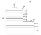
도 1은 본 발명의 실시 예에 따른 반도체 소자의 단면도이다.
도 2는 본 발명의 실시 예에 따른 반도체 소자의 제1층의 단면도이다.
도 3은 본 발명의 실시 예에 따른 반도체 소자의 제2층의 단면도이다.
도 4는 본 발명의 실시 예에 따른 반도체 소자의 제3층의 단면도이다.
도 5는 본 발명의 다른 실시 예에 따른 반도체 소자의 단면도이다.
도 6은 본 발명의 실시 예에 따른 반도체 소자에서, 활성층(150)부터 제3층까지의 인듐 함유량을 비율로 나타낸 것이다.
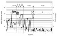
도 7 및 도 8은 본 발명의 실시 예에 따른 반도체 소자의 비행시간형 이차이온질량분석(Time of Flight Secondary Ion Mass Spectrometry, SIMS) 결과를 나타낸 것이다.
도 9는 본 발명의 실시 예에 따른 반도체 소자 패키지의 단면도이다.1 is a cross-sectional view of a semiconductor device according to an embodiment of the present invention.
2 is a cross-sectional view of a first layer of a semiconductor device in accordance with an embodiment of the present invention.
3 is a cross-sectional view of a second layer of a semiconductor device according to an embodiment of the present invention.
4 is a cross-sectional view of a third layer of a semiconductor device in accordance with an embodiment of the present invention.
5 is a cross-sectional view of a semiconductor device according to another embodiment of the present invention.
6 is a graph showing the indium content of the
FIGS. 7 and 8 are time-of-flight secondary ion mass spectrometry (SIMS) results of a semiconductor device according to an embodiment of the present invention.
9 is a cross-sectional view of a semiconductor device package according to an embodiment of the present invention.
본 실시 예들은 다른 형태로 변형되거나 여러 실시 예가 서로 조합될 수 있으며, 본 발명의 범위가 이하 설명하는 각각의 실시 예로 한정되는 것은 아니다.The embodiments may be modified in other forms or various embodiments may be combined with each other, and the scope of the present invention is not limited to each embodiment described below.
특정 실시 예에서 설명된 사항이 다른 실시 예에서 설명되어 있지 않더라도, 다른 실시 예에서 그 사항과 반대되거나 모순되는 설명이 없는 한, 다른 실시 예에 관련된 설명으로 이해될 수 있다.Although not described in the context of another embodiment, unless otherwise described or contradicted by the description in another embodiment, the description in relation to another embodiment may be understood.
예를 들어, 특정 실시 예에서 구성 A에 대한 특징을 설명하고 다른 실시 예에서 구성 B에 대한 특징을 설명하였다면, 구성 A와 구성 B가 결합된 실시 예가 명시적으로 기재되지 않더라도 반대되거나 모순되는 설명이 없는 한, 본 발명의 권리범위에 속하는 것으로 이해되어야 한다.For example, if the features of configuration A are described in a particular embodiment, and the features of configuration B are described in another embodiment, even if the embodiment in which configuration A and configuration B are combined is not explicitly described, It is to be understood that they fall within the scope of the present invention.
이하 상기의 목적을 구체적으로 실현할 수 있는 본 발명의 실시 예를 첨부한 도면을 참조하여 설명한다.BRIEF DESCRIPTION OF THE DRAWINGS The above and other objects, features and advantages of the present invention will be more apparent from the following detailed description taken in conjunction with the accompanying drawings, in which: FIG.
본 발명에 따른 실시 예의 설명에 있어서, 각 element의 " 상(위) 또는 하(아래)(on or under)"에 형성되는 것으로 기재되는 경우에 있어, 상(위) 또는 하(아래)(on or under)는 두 개의 element가 서로 직접(directly)접촉되거나 하나 이상의 다른 element가 상기 두 element사이에 배치되어(indirectly) 형성되는 것을 모두 포함한다. 또한 "상(위) 또는 하(아래)(on or under)"으로 표현되는 경우 하나의 element를 기준으로 위쪽 방향뿐만 아니라 아래쪽 방향의 의미도 포함할 수 있다.In the description of the embodiment according to the present invention, in the case of being described as being formed "on or under" of each element, the upper (upper) or lower (lower) or under are all such that two elements are in direct contact with each other or one or more other elements are indirectly formed between the two elements. Also, when expressed as "on or under", it may include not only an upward direction but also a downward direction with respect to one element.
도 1은 본 발명의 일실시 예에 따른 반도체 소자(100)의 단면도이다.1 is a cross-sectional view of a
도 1을 참조하면, 반도체 소자(100)는 기판(110), 기판상에 배치되며 제1 도전형 반도체층(130), 제2 도전형 반도체층(170), 및 제1 도전형 반도체층(130)과 제2 도전형 반도체층(170) 사이에 배치되는 활성층(150)을 포함하는 반도체 구조물(200), 반도체 구조물(200)과 전기적으로 연결되는 제1 전극(192) 및 제2 전극(194)을 포함할 수 있다.Referring to FIG. 1, a
그리고 제1 도전형 반도체층(130)과 활성층 사이에는 다수의 반도체층이 배치될 수 있고, 활성층(150)과 제2 도전형 반도체층(170)에는 차단층(160)이 배치될 수 있으며, 제1 도전형 반도체층(130) 상에는 제1 전극(192)이 배치될 수 있으며, 제2 도전형 반도체층(170) 상에는 투광성 전극층(180) 및 제2전극(194)이 배치될 수 있다.A plurality of semiconductor layers may be disposed between the first
기판(110)은 열전도성이 뛰어난 물질로 형성될 수 있으며, 전도성 기판 또는 절연성 기판일 수 있다. 예를 들어, 기판(110)은 사파이어(Al2O3), SiC, Si, GaAs, GaN, ZnO, GaP, InP, Ge, and Ga203 중 적어도 하나를 사용할 수 있다. 기판(110)은 예컨대, AlN 템플리트(template)일 수 있다. 기판(110)의 상면 및/또는 하면에는 복수의 돌출부(미도시)가 형성될 수 있으며, 복수의 돌출부 각각은 측 단면이, 반구형 형상, 다각형 형상, 타원 형상 중 적어도 하나를 포함하며 스트라이프 형태 또는 매트릭스 형태로 배열될 수 있다. 돌출부는 광 추출 효율을 개선시켜 줄 수 있다. The
기판(110) 위에는 발광 구조물(200)이 배치될 수 있으며, 발광 구조물(200)을 배치하기 위한 장비는 전자빔 증착기, PVD(physical vapor deposition), CVD(chemical vapor deposition), PLD(plasma laser deposition), 이중형의 열증착기(dual-type thermal evaporator) 스퍼터링(sputtering), MOCVD(metal organic chemical vapor deposition) 등이 있으나, 이에 대해 한정하지는 않는다. The
한편, 발광 구조물(200)은 버퍼층(120), 제1 도전형 반도체층(130), 제1 반도체층(142), 제2 반도체층(144), 제3 반도체층(146), 활성층(150), 제2 도전형 반도체층(170) 및 차단층(160)을 포함할 수 있으나, 이들 구성에 대해서는 후술하도록 한다.The
기판(110) 상에는 버퍼층(120)이 배치될 수 있다. A
버퍼층(120)은 기판(110)과 제1 도전형 반도체층(130) 간의 격자 부정합을 완화하고 도전형 반도체들이 용이하게 성장될 수 있도록 한다. 버퍼층(110)은 3족-5족 화합물 반도체 예컨대, GaN, InN, AlN, InGaN, AlGaN, InAlGaN, AlInN 중 적어도 하나로 형성될 수 있다. 버퍼층 위에는 언도프드(undoped) 반도체층(미도시)이 형성될 수 있다. The
버퍼층(120) 상에는 제1 도전형 반도체층(130)이 배치될 수 있다. The first
제1 도전형 반도체층(130)은 -Ⅴ족, -Ⅵ족 등의 화합물 반도체로 구현될 수 있으며, 제1도펀트가 도핑될 수 있다. 제1 도전형 반도체층(130)은 AlxGa1-xN (0≤x≤1)의 조성식을 갖는 반도체 재료로 구현될 수 있다. 제1 도전형 반도체층(130)은, 예를 들어 GaN, AlN, AlGaN, InGaN, InN, InAlGaN, AlInN, AlGaAs, GaP, GaAs, GaAsP, AlGaInP 등에서 선택될 수 있다. 그리고 제1 도펀트는 Si, Ge, Sn, Se, Te 와 같은 n형 도펀트일 수 있다. 제1 도펀트가 n형 도펀트일 경우, 제1 도전형 반도체층(130)은 n형 반도체층일 수 있다. The first
제1 도전형 반도체층 130) 상에는 활성층(150)이 배치될 수 있다. The
활성층(150)은 제1도전형 반도체층(130)을 통해서 주입되는 전자(또는 정공)와 제2도전형 반도체층(170)을 통해서 주입되는 정공(또는 전자)이 만나는 층이다. 활성층(150)은 전자와 정공이 재결합함에 따라 낮은 에너지 준위로 천이하며, 특정 파장을 가지는 빛을 생성할 수 있다. The
활성층(150)은 단일 우물 구조, 다중 우물 구조, 단일 양자 우물 구조, 다중 양자 우물(Multi Quantum Well; MQW) 구조, 양자점 구조 또는 양자선 구조 중 어느 하나의 구조를 가질 수 있으며, 활성층(150)의 구조는 이에 한정하지 않는다.The
활성층(150)은 화합물 반도체로 구현될 수 있다. 활성층(150)은 예로서 II족-VI족 및 III족-V족 화합물 반도체 중에서 적어도 하나로 구현될 수 있다. The
활성층(150)이 다중 우물 구조로 구현된 경우, 활성층(150)은 복수의 우물층과 복수의 장벽층을 포함한다. 이때 우물층과 장벽층이 교대로 배치될 수 있고, 우물층과 장벽층의 페어는 2~30주기로 형성될 수 있다. 활성층(150)은 InGaN/GaN, InAlGaN/GaN, GaAs(InGaAs)/AlGaAs, GaP(InGaP)/AlGaP 중 어느 하나 이상의 페어 구조일 수 있다. 활성층(150)은 InGaN/GaN 적층 구조 또는 InGaN/InGaN 적층 구조일 수 있고, InGaN의 인듐(In)의 함량은 9% 이상 내지 14%이하일 수 있다. 활성층(150)은 발광하고자 하는 광의 파장에 대응되는 인듐 함량을 포함할 수 있다. 실시 예에서는 photo luminescence (이하 PL) 또는 적분구 등과 같은 광 검출기로 발광 구조물을 측정 시, 410 nm 이상 내지 470 nm 이하의 파장에서 광의 상대적인 세기 (Intensity)가 가장 높은 주파장 (Main peak wavelength)을 갖는 반도체 구조물(200)을 예시로, 다른 구성 요소와의 관계를 설명한다. When the
제1 도전형 반도체층(130)과 활성층(150) 사이에는 다수의 반도체층이 배치될 수 있다. 활성층(150)에 인접하여 제1 반도체층(142)이 배치될 수 있고, 제1 반도체층 아래에 제2 반도체층(144)이 배치될 수 있으며, 제2 반도체층 아래에 제3 반도체층(146)이 배치될 수 있다. 제1 반도체층, 제2 반도체층, 제3 반도체층은 초격자층일 수 있으며, AlGaN, InGaN층과 GaN층이 반복적으로 적층된 InGaN/GaN, AlGaN/GaN, InGaN/AlGaN 구조를 포함할 수 있고, 이에 한정하지 않는다. A plurality of semiconductor layers may be disposed between the first
반도체 구조물(200)은 인듐(In)을 포함할 수 있으며, In의 함량은 기판(110)에서 반도체 구조물(200)의 표면 방향으로 향할수록 점차적으로 증가할 수 있다. 예를 들어, 반도체 구조물(200)의 하부에서 상부로 향할수록 In의 함량은 증가되어 제1 반도체층(142)의 In 함량이 제3 반도체층(146)의 In 함량보다 많을 수 있다. 반도체 구조물(200)이 GaN 기반으로 구성되는 물질일 경우, 전자의 이동도와 정공의 이동도가 서로 상이할 수 있다. 전자의 이동도가 정공의 이동도보다 10배 이상 내지 1000배 이하로 높을 수 있다. 예를 들어, 제1 도전형 반도체층(130)이 n 형 도펀트를 포함하는 n 형 반도체이고 제2 도전형 반도체층(170)이 p 형 도펀트를 포함하는 p형 반도체일 경우, 제1 도전형 반도체층(130)에서 활성층(150)으로 주입되는 전자의 이동도가 제2 도전형 반도체층(170)에서 활성층(150)으로 주입되는 정공의 이동도보다 높기 때문에 전자가 활성층(150)에서 발광성 재결합하는 확률에 비해 활성층(150)을 지나 제2 도전형 반도체층(170)으로 주입되어 비발광성 재결합하는 확률이 높을 수 있고, 활성층(150) 내로 주입되는 전자와 정공의 균형이 맞지 않을 수 있는바, 그에 따라 반도체 소자(100)의 광학적 특성이 저하될 수 있다. 또한, GaN 기반의 물질로 구성되는 반도체 물질은 In을 많이 포함할수록 전도대(Ec)와 가전도대(Ev)의 차이인 에너지 밴드갭(Eg)이 작아질 수 있다. 따라서, 기판(110)에서 활성층(150)으로 향하는 제1 방향으로 향할수록 In 함량이 많아진다는 것은 제1 방향을 따라 에너지 밴드갭(Eg)이 작아진다는 의미를 포함할 수 있다. 실시 예에서 반도체 구조물(200)이 GaN 기반의 물질로 구성되는 경우 전자의 이동도는 정공의 이동도에 비해 크기 때문에 제1 방향을 따라 작아지는 에너지 밴드갭(Eg)를 따라 기판(110)과 활성층(150) 사이의 응력도 커질 수 있다. 따라서, 본 실시 예에서는 기판(110)에서 활성층(150)으로 향할수록 In 함량이 많아지도록 복수의 반도체층을 배치함으로써 제1 방향을 따라서 전자가 갖는 에너지가 낮아질 수 있고, 이로 인해 전자의 이동도와 정공의 이동도에 균형을 맞출 수 있으며, 활성층(150)에서 발광성 재결합을 하는 확률을 높일 수 있다. 또한, 활성층(150)에 직접 인가되는 응력을 복수의 반도체층으로 분산함으로써 활성층(150)의 결정성을 개선해줄 수도 있다. The
활성층(150)의 In 함량이 9% 이상 내지 14% 이하일 경우, 제1 반도체층(142)의 In 함량은 6% 이상 내지 9% 이하, 제2 반도체층(144)의 In ?t량은 3% 이상 내지 6% 이하, 제3 반도체층(146)의 In ?t량은 1% 이상 내지 3% 이하일 수 있다. 앞서 설명한 바와 같이 활성층(150)을 기준으로 제1 반도체층(142), 제2 반도체층(144) 및 제3 반도체층(146)의 In 함량은 적어야 한다. When the In content of the
제1 반도체층(142)은 제2 반도체층(144), 제3 반도체층(146)에 비해 활성층(150)과 가장 가까이 배치될 수 있다. 활성층(150)의 In 함량이 9% 이상 내지 14% 이하일 경우, 제1 반도체층(142)의 In 함량이 6% 이상이 되어야 활성층(150)과 제1 도전형 반도체층(130) 사이에 발생한 응력을 완화시켜 활성층(150)에서 발광하는 광의 파장이 인가하는 전류나 전압에 따라 변하는 현상을 방지할 수 있다. 또한, PL 또는 적분구 등과 같은 광 검출기로 반도체 구조물(200)을 측정 시, 활성층(150)에서 발광하는 광의 상대적인 세기가 가장 강할 수 있는데 제1 반도체층(142)의 In 함량이 9% 이하일 때 활성층(150)에서 발광하는 광의 세기에 비해 제1 반도체층(142)의 상대적인 광의 세기가 약할 수 있다. 제1 반도체층(142)의 상대적인 광의 세기가 활성층(150)에서 발광하는 광의 세기에 비해 클 경우 반도체 구조물(200)을 PL 또는 적분구 등과 같은 광 검출기로 측정 시 활성층(150)에서 발광하는 주파장보다 짧은 파장 영역에서 변곡점을 가질 수 있다. 변곡점이 활성층(150)에서 발광하는 파장의 반치폭(FWHM:Full Width at Half Maximum)에 해당하는 파장보다 상대적으로 강한 광의 세기(Intensity)를 가질 경우 반도체 소자(100)의 색재현률이 저하될 수 있다. 따라서, 활성층(150)의 In 함량이 9% 이상 내지 14% 이하일 때 제1 반도체층(142)의 In 함량은 6% 이상 내지 9% 이하로 배치되어야 반도체 구조물(200)의 응력을 완화할 수 있고, 반도체 소자(100)의 색재현률을 확보할 수 있다. The
제2 반도체층(144)은 초격자층으로 배치될 수 있다. 제2 반도체층(144)은 활성층(150)과 제1 도전형 반도체층(130) 사이의 응력을 완화하기 위해서, 활성층(150)의 In 함량이 9% 이상 내지 14% 이하일 때 제2 반도체층(144)의 In 함량은3% 이상 내지 6% 이하일 수 있다. 기판(110)이 반도체 구조물(200)과 같은 물질로 구성되는 경우가 아니라면 기판(110)과 반도체 구조물(200) 사이에는 격자 상수 차이에 의한 응력이 발생할 수 있다. 예를 들어, 기판(110)이 사파이어 기판이 사용되고 반도체 구조물(200)이 GaN 기반의 물질로 구성되는 경우 반도체 구조물(200)과 기판 사이에는 큰 응력이 발생하게 된다. 따라서, 반도체 구조물(200)에서 가장 높은 In 함량을 갖는 활성층(150)은 반도체 구조물(200)에서 격자 상수가 클 수 있고, 기판(110)과 활성층(150) 사이에서는 큰 응력이 발생할 수 있다. 따라서, 제2 반도체층(144)이 3% 이상 내지 6% 이하의 In을 포함하도록 하여 활성층(150)과 기판(110) 사이의 응력을 완화할 수 있다. 제2 반도체층(144)은 앞서 설명한 바와 같이 3% 이상의 In 조성을 포함하여야 응력을 완화할 수 있다. 또한, 6% 초과일 경우 제1 반도체층(142)의 In 조성보다 높을 수 있기 때문에 제2 반도체층(144)의 에너지 밴드갭(Eg)이 제1 반도체층(142)의 에너지 밴드갭(Eg)보다 클 수 있다. 제2 반도체층(144)의 에너지 밴드갭(Eg)이 제1 반도체층(142)의 에너지 밴드갭(Eg)보다 클 경우, 에너지 밴드갭(Eg)에 대응되는 전도대(Ec) 이상의 에너지를 갖는 전자가 제2 반도체층(144)에서 제1 반도체층(142)으로 주입되지 못할 수 있다. 따라서 반도체 소자(100)의 광학적 및/또는 전기적 특성을 확보하기 위해서 활성층(150)의 In 함량이 9% 이상 내지 14% 이하일 때 제2 반도체층(144)의 In 조성은 3% 이상 내지 6% 이하일 수 있다. The
52 활성층(150)의 In 함량이 9% 이상 내지 14% 이하일 때 제3 반도체층(146)의 In 조성은 1% 이상 내지 3% 이하일 수 있다. 제3 반도체층의 In 조성이 1% 이상일 때 활성층(150)과 제1 도전형 반도체층(130) 사이의 응력을 완화할 수 있다. 또한, 3% 이하일 경우 제2 반도체층(144)으로의 전자 주입 특성을 확보할 수 있어 반도체 소자(100)의 광학적 및/또는 전기적 특성을 확보할 수 있다.52 When the In content of the
도 2 내지 도 4은 제1 내지 제3 반도체층(142, 144, 146)을 보다 상세히 나타낸 단면도이다.2 to 4 are cross-sectional views showing the first to third semiconductor layers 142, 144, and 146 in more detail.
도 2를 참조하면, 제1 반도체층(142)은 InGaN/GaN 이 1 페어(pair) 이상 내지 4페어(pair) 이하로 적층된 구조일 수 있고, InGaN층(142a)과 GaN(142b)층의 두께는 서로 다를 수 있다. 제1 반도체층(142)이 1 페어(pair) 이상일 때, 활성층(150)과 기판(110) 사이의 응력을 완화할 수 있고, 4 페어(pair) 이하일 때 활성층(150)에서 발광하는 광의 반치폭(FWHM:Full Width at Half Maximum)에 해당하는 광의 상대적인 세기보다 큰 상대적인 세기를 갖는 광의 발생을 방지하여 반도체 소자(100)의 색재현율을 확보할 수 있다. 앞서 설명한 바와 같이 광의 상대적인 세기와 반치폭(FWHM:Full Width at Half Maximum)은 PL 또는 적분구 등과 같은 광 검출기로 반도체 구조물(200)을 측정하였을 때 반도체 소자(100)가 방출하는 광의 파장에서 상대적으로 가장 큰 세기를 갖는 파장 영역일 수 있다.Referring to FIG. 2, the
InGaN층(142a)의 두께(T1)와 GaN층(142b)의 두께(T2)의 비율(ratio)은 1:7 내지 1:25 비율 범위 내에서 형성될 수 있다. 예를 들어, InGaN층의 두께(T1)는 2nm 내지 3nm일 수 있으며, GaN층의 두께(T2)는 20nm 내지 50nm 일 수 있다. 제1 반도체층(142)의 InGaN층(142a)의 두께(T1)와 GaN층(142b)의 두께(T2)의 비율(ratio)이 1:7 이상일 때, 활성층(150)에 인가되는 압전 분극(piezoelectric field)을 줄일 수 있고, 활성층(150)의 발광 파장의 파장 변화 현상을 억제할 수 있다. 또한, 1:25 이하일 때, 활성층(150)으로 주입되는 전류 확산(spreading) 특성을 확보하여 반도체 소자(100)의 전기적 및/또는 광학적 특성을 확보할 수 있다.The ratio of the thickness T1 of the
도 3을 참조하면, 제2 반도체층(144)은 InGaN/GaN 이 적층된 초격자 구조일 수 있다. 제2 반도체층(144)의 InGaN층과 GaN의 두께는 동일하거나, GaN층이 더 두껍게 형성될 수 있다. InGaN층(144a)의 두께(T3)와 GaN층(144b)의 두께(T4)의 비율는 1:1 내지 1:2 비율 범위 내에서 형성될 수 있다. 예를 들어, InGaN층(144a)의 두께(T3)는 2nm 내지 3nm일 수 있으며, GaN(144b)층의 두께(T4)는 2nm 내지 6nm 일 수 있다. 제2 반도체층(144)의 InGaN층(144a)의 두께(T3)와 GaN층(144b)의 두께(T4)의 비율이 1:1 이상일 때, 활성층(150)에 가해지는 응력 완화 특성을 확보할 수 있고, InGaN층(144a)의 두께(T3)와 GaN층(144b)의 두께(T4)의 비율이 1:2 이하일 때 활성층(150)과 기판(110) 사이의 격자 불일치에 기인한 응력을 효과적으로 완화시킬 수 있다. 제2 반도체층(144)은 InGaN/GaN이 3 페어(pair) 이상 내지 20 페어(pair) 이하로 배치될 수 있다. 제2 반도체층(144)의 InGaN/GaN 적층 구조가 3 페어(pair) 이상 배치되어야 활성층(150)과 기판(110) 사이의 응력을 완화할 수 있고, 기판(110)과 반도체 구조물(200) 사이에서 격자 상수 차이에 의한 전위 결함이 활성층(150)까지 연장되는 문제를 억제하는 기능을 확보할 수 있다. 전위 결함은 반도체 소자(100)의 전기적, 광학적 특성 및 신뢰성을 저하시키는 문제를 갖고 있다. 제2 반도체층(144)의 InGaN/GaN 적층 구조가 3 페어(pair) 이상일 때 전위 결함 문제를 해결할 수 있지만, 20 페어(pair)를 초과하게 될 경우 제2 반도체층(144)의 저항이 커질 수 있기 때문에 반도체 소자(100)의 광학적, 전기적 특성을 확보하기 어려울 수 있다. 따라서, 제2 반도체층(144)이 InGaN/GaN 적층 구조로 배치될 경우, 제2 반도체층(144)의 InGaN/GaN 적층 구조는 3 페어(pair) 이상 내지 20페어(pair)로 배치하는 것이 바람직할 수 있다.Referring to FIG. 3, the
도 4를 참조하면, 제3 반도체층(146)은 InGaN/GaN 구조가 적층될 수 있고, InGaN/GaN 구조가 적층되는 경우 1 페어(pair) 이상 내지 5 페어(pair)이하로 배치될 수 있다. InGaN층과 GaN의 두께는 서로 다를 수 있고, GaN층이 InGaN층 보다 두껍게 형성될 수 있다.Referring to FIG. 4, the
InGaN층(146a)의 두께(T5)와 GaN층(146b)의 두께(T6)의 비율은 1:3 내지 1:8 비율 범위 내에서 형성될 수 있다. 예를 들어, 제2 반도체층(146)의 InGaN층(146a)의 두께(T5)는 2nm 내지 3nm일 수 있으며, GaN층(146b)의 두께(T6)는 10nm 내지 15nm 일 수 있다. 제3 반도체층(146)을 배치하는 공정에 있어서, 제3 반도체층(146)의 InGaN층(146a)의 두께(T5)와 GaN층(146b)의 두께(T6)의 비율이 1:3 이상일 때 제3 반도체층(146)의 상면과 측면 사이의 경사면의 성장 비율을 제어하여 리세스 구성을 용이하게 할 수 있다. 리세스는 제3 반도체층(146)의 상면과 저면 사이에서 저점과 경사면을 포함하여 계곡을 구성하는 형상일 수 있으며, 제3 반도체층(146)의 단위 면적에 대한 리세스의 밀도는 기판(110)과 활성층(150) 사이의 응력을 완화시킬 수 있고, 발광 구조물(200)의 결정성을 개선할 수 있을 정도, 그에 따라 반도체 소자(100)가 발광하는 파장의 변이 방지 및 반도체 소자(100)의 광특성, 전기적 특성 및 신뢰성을 향상시킬 수 있을 정도의 밀도라면 당업자에게 공지된 밀도라도 무방하다.The ratio of the thickness T5 of the
도 5는 리세스가 포함된 반도체 소자(100)의 단면도를 나타낸 것이다.5 is a cross-sectional view of the
리세스(R)는 제2 반도체층(144), 제1 반도체층(142) 및 활성층(150)까지 연장될 수 있고, 리세스는 반도체 소자(100)의 광학적, 전기적 특성을 개선할 수 있지만 너무 많이 배치되는 경우 반도체 소자(100)의 전기적, 광학적 특성 및 신뢰성이 저하될 수 있다. 또한, 제3 반도체층(146)의 InGaN층(146a)의 두께(T5)와 GaN층(146b)의 두께(T6)의 비율이 1:8 이하로 배치되는 경우 제1 도전형 반도체층(130)에서 제3 반도체층(146)을 통하여 활성층(150)으로 주입되는 전류의 전류 주입 특성을 확보할 수 있다. The recess R may extend to the
이상 살펴본 바와 같이 In 함량은 제1 반도체층(142), 제2 반도체층(144), 제3 반도체층(146), 및 활성층(150)으로 갈수록 서서히 감소하는 구조이다. 이와 같이 In 함량을 조절함으로써 응력을 조절하고 청색변이를 방지할 수 있다. 활성층(150)이 In 함유량을 9% 이상 내지 14% 이하로 포함함으로써, 활성층(150)은 410nm 이상 내지 470 nm 이하의 파장에서 상대적인 광의 세기가 가장 큰 청색 파장을 방출할 수 있다. 또한, 제1 반도체층(142), 제2 반도체층(144), 제3 반도체층(146)의 In 함유량이 활성층으로 향할수록 높아짐으로써 활성층(150) 내에 걸리는 응력을 점진적으로 감소시킬 수 있고, 제1 도전형 반도체층(130)에서 활성층(150)으로 주입되는 전자의 이동도와 제2 도전형 반도체층(170)에서 활성층(150)으로 주입되는 정공의 이동도의 균형을 맞추어 반도체 소자(100)의 광학적, 전기적 특성을 확보할 수 있다.As described above, the In content gradually decreases toward the
활성층(150)은 410nm 이상 내지 470 nm 이하의 파장에서 상대적인 광의 세기가 가장 큰 청색 파장을 발광하는 것이 한정하지 않을 수 있다. 따라서, 활성층(150)의 In 함량을 100%라고 하면, 제1 반도체층(142)의 In 함량은 활성층(150) In 함량의 60% 내지 80%로 구성될 수 있고, 제2 반도체층(144)의 In 함량은 제1 반도체층(146)의 In 함량의 대비 30% 내지 40%로 구성될 수 있고, 활성층(150) In 함량의 20% 내지 30%로 구성될 수 있다. The
제3 반도체층(142)의 In 함량은 제2 반도체층(144)의 In 함량의 20~30%로 구성될 수 있고, 활성층(150)의 In 함량의 5% 내지 10%로 구성될 수 있다. The In content of the
제1 반도체층(146), 제2 반도체층(144) 및 제3 반도체층(142)의 In 함량은 활성층(150)을 기준으로 범위 내로 포함할 수 있고, 그에 대한 효과는 앞서 설명한 바와 같을 수 있다. The In content of the
도 6은 활성층(150)부터 제3 반도체층(146)까지의 In 함유량을 비율로 나타낸 것이다.6 shows the In content from the
도 6을 참조하면, 활성층의 In 함량을 100%라고 할 때, 활성층을 기준으로 제1 반도체층, 제2 반도체층, 및 제3 반도체층의 In 함량이 60% 내지 80%, 20% 내지 30%, 5% 내지 10%로 점진적으로 줄어드는 것을 확인할 수 있다.Referring to FIG. 6, when the In content of the active layer is 100%, the In content of the first semiconductor layer, the second semiconductor layer, and the third semiconductor layer is 60% to 80%, 20% to 30% %, And 5% to 10%, respectively.
또한, 반도체 구조물(200)이 GaN 기반의 물질로 구성되는 경우, 활성층(150) 과 제2 도전형 반도체층(170) 사이에는 차단층(160)이 배치될 수 있다.In addition, when the
반도체 구조물(200)이 GaN 기반의 물질로 구성되는 경우, 전자의 이동도와 정공의 이동도가 서로 상이하고, 전자의 이동도가 정공의 이동도보다 높기 때문에 차단층(160)은 전자 차단(electron blocking) 및 활성층의 클래딩(MQW cladding) 역할을 할 수 있고, 이로 인해 발광 효율을 향상시킬 수 있다. 다만, 이에 한정하지 않고, 차단층(160)은 이동도가 상대적으로 높은 반송자가 활성층(150)을 지나 제1 도전형 반도체층(130) 또는 제2 도전형 반도체층(170)으로 주입되는 것을 방지할 수 있으며, 여기서 반송자는 전자 또는 정공일 수 있으나, 이에 한정하지 않고 이동도가 높은 반송자를 선택할 수 있음은 물론이다. 차단층(160)은 InAIN /GaN층이 적어도 1 페어(pair) 이상이 적층된 구조로 구성될 수 있다. 차단층(160)의 InAlN 층에는 제2 도전형 도펀트가 포함될 수 있다. 차단층(160)은 In의 조성을 제어함으로써, 격자 부조화에 의한 응력을 제어할 수 있다. In the case where the
제2도전형 반도체층(170)은 활성층(150) 상에 형성되며, -Ⅴ족, -Ⅵ족 등의 화합물 반도체로 구현될 수 있으며, 제2도전형 반도체층(170)에 제2도펀트가 도핑될 수 있다. 제2도전형 반도체층(170)은 AlxGa1-xN (0≤x≤1)의 조성식을 갖는 반도체 물질 또는 AlInN, AlGaAs, GaP, GaAs, GaAsP, AlGaInP 중 선택된 물질로 형성될 수 있다. 제2도펀트가 Mg, Zn, Ca, Sr, Ba 등과 같은 p형 도펀트인 경우, 제2도펀트가 도핑된 제2도전형 반도체층(170)은 p형 반도체층일 수 있다. The second conductivity
제2 도전형 반도체층(170) 상에는 투광성 전극층(180)이 배치될 수 있다. The light-transmitting
투광성 전극층(180)은 캐리어 주입을 효율적으로 할 수 있고, 활성층(150)에서 방출하는 광이 투과될 수 있도록 단일 금속 또는 금속합금, 금속 산화물 및 금속 질화물 등을 다중으로 적층할 수도 있다. 예컨대, 투광성 전극층(180)은 반도체와 전기적인 접촉이 우수한 물질로 형성될 수 있으며, 투광성 전극층(180)으로는 ITO(indium tin oxide), IZO(indium zinc oxide), IZTO(indium zinc tin oxide), IAZO(indium aluminum zinc oxide), IGZO(indium gallium zinc oxide), IGTO(indium gallium tin oxide), AZO(aluminum zinc oxide), ATO(antimony tin oxide), GZO(gallium zinc oxide), IZON(IZO Nitride), AGZO(Al-Ga ZnO), IGZO(In-Ga ZnO), ZnO, IrOx, RuOx, NiO, RuOx/ITO, Ni/IrOx/Au, 및 Ni/IrOx/Au/ITO, Ag, Ni, Cr, Ti, Al, Rh, Pd, Ir, Ru, Mg, Zn, Pt, Au, Hf 중 적어도 하나를 포함하여 형성될 수 있으며, 이러한 재료에 한정되는 않는다.The
투광성 전극층(180) 상에는 제2 전극(194)이 배치되며, 상부 일부가 노출된 제1 도전형 반도체층(120) 상에는 제1 전극(192)이 배치된다. 제1 전극(160) 및 제2 전극(170)으로는 예컨대, Cr, Ti, Ag, Ni, RH, Pd, Ir, Ru, Mg, Zn, Pt, Cu, Au. Hf 중 어느 하나를 포함하는 금속 또는 합금으로 형성될 수 있다. 이후, 최종적으로 제1전극(192) 및 제2 전극(194)이 서로 전기적으로 연결됨으로써 발광 소자의 제작이 완료될 수 있다. A
도 7및 도 8은 본 발명의 또 다른 실시 예에 대한 도면으로서, 반도체 구조물(200)을 비행 시간형 2차 이온 질량 분석(Time Of Flight - Secondary Ion Mass Spectroscopy, TOF-SIMS, 이하 심스)을 통해 두께에 대한 2차 이온의 상대적인 강도를 나타낸 스펙트럼이다. 심스 데이터는 1차 이온을 발광 구조물 표면에 조사하고 방출되는 2차 이온의 개수를 카운팅하여 분석할 수 있으며, 이 때, 1차 이온은 O2+, Cs+, Bi+ 등에서 선택될 수 있고, 가속 전압은 20 내지 30keV 내에서, 조사 전류는 0.1 pA 내지 5.0pA 내에서 조절될 수 있으며, 조사 면적은 20nmX20nm일 수 있다. 2차 이온은 발광 구조물(200)을 구성하는 물질이 방출되는 것으로써, In, Al, Ga, Si, Mg, C 등의 물질을 지칭할 수 있다. 상기된 분석 조건은 질화물계 화합물 반도체로 구성되는 구조물을 분석하기 위한 조건이지만, 이에 한정하지 않고 반도체로 구성되는 구조물을 분석하기 위한 측정 조건이라면 어떠한 것이라도 자유롭게 이용할 수 있다.FIGS. 7 and 8 illustrate another embodiment of the present invention, in which the
도 7 및 도 8을 참조하면, 좌측 세로축은 2차 이온으로 검출되는 In 이온의 세기를 상대적으로 나타낸 것이며, 우측 세로축은 2차 이온으로 검출되는 Si 및 C 원자의 농도를 상대적으로 나타낸 것이고, 좌측과 우측의 세로축은 모두 로그 스케일(log scale)을 기준으로 한다. 우선 도 7에 도시된 심스 데이터를 기초로 한 제1 실시 예를 설명하도록 한다. 제1 실시 예는 반도체 구조물(200)을 기초로 하며, 그에 따른 반도체 구조물(200)은 Si 원자 및/또는 C 원자를 포함할 수 있는 제1 도전형 반도체층(130), 제1 반도체층(142), 제2 반도체층(144), 제3 반도체층(146), 활성층(150) 및 제2 도전형 반도체층(170)을 포함할 수 있다. 7 and 8, the left ordinate axis represents the relative intensity of In ions detected as secondary ions, and the right ordinate axis represents the relative concentrations of Si and C atoms detected as secondary ions. And the vertical axis on the right side are based on a log scale. First, the first embodiment based on the sims data shown in Fig. 7 will be described. The first embodiment is based on a
제3 반도체층(146)의 Si 원자량은 제1 도전형 반도체층(130)의 Si 원자량의 0.05배 이상 내지 0.2 배 이하일 수 있다. 제3 반도체층(146)의 Si 원자량이 제1 도전형 반도체층(130)의 Si 원자량의 0.05배 이상일 때 제1 도전형 반도체층(130)에서 제3 반도체층(146)을 통하여 활성층(150)으로의 전류 주입 특성을 확보할 수 있고, 제3 반도체층(146)의 Si 원자량이 제1 도전형 반도체층(130)의 Si 원자량의 0.2배 이하일 때 제3 반도체층(146)의 전류 확산 특성을 확보할 수 있다. 전류 주입 특성 및 전류 확산 특성을 확보할 때, 반도체 소자(100)의 전기적, 광학적 특성도 확보할 수 있기 때문에 제3 반도체층(146)의 Si 원자량은 제1 도전형 반도체층(130)의 Si 원자량의 0.05 배 이상 내지 0.2 배 이하의 범위를 포함하는 것이 바람직하다. 또한, 제3 반도체층(146)의 C 원자량이 제1 도전형 반도체층(130)의 C 원자량보다 높을 수 있다. 반도체 구조물(200)이 GaN 기반의 물질로 구성되는 경우, C 원자를 많이 함유할수록 저항이 높아지는 특성을 갖는다. 따라서, 제3 반도체층(146)의 C 원자량이 제1 도전형 반도체층(130)의 C 원자량보다 많고, Si 원자량이 제1 도전형 반도체층(130)의 Si 원자량보다 적을 경우, 제3 반도체층(146)의 저항이 높아질 수 있고, 전류 확산 특성을 확보할 수 있다. 또한, 앞서 설명한 바와 같이 제3 반도체층(146)의 Si 원자량이 범위 내에 포함되어야 제1 도전형 반도체층(130)에서 제3 반도체층(146)을 통하여 활성층(150)으로의 전류 주입 특성을 확보할 수 있다.The Si atomic amount of the
활성층(150), 제1 반도체층(142), 제2 반도체층(144) 및 제3 반도체층(146)의 In 이온의 함량은 서로 상이하므로 심스에 의한 이온 강도가 상이하게 나타날 수 있다. Since the contents of In ions in the
Si 원자의 농도는 제1 도전형 반도체층(130)에서의 Si 원자의 농도를 기준으로 제2 도전형 반도체층(170)으로 향할수록 낮아질 수 있다. Si 원자는 제1 도전형 반도체층(130) 내에서 도펀트로 작용하여 제1 도전형 반도체층(130)의 극성이 n 형이 되도록 구성할 수 있고, 반도체 구조물(200)의 결정질을 향상시키는 기능도 할 수 있기 때문에, Si 원자는 반도체 구조물(200) 내에서 전체적으로 분포할 수 있다. 다만, 실시 예와 같이 제1 도전형 반도체층(130)이 n 형 반도체층으로 구성될 경우, 제1 도전형 반도체층(130)이 포함하는 Si 원자의 농도는, 반도체 구조물(200) 내에서 가장 높을 수 있다. The concentration of Si atoms may be lowered toward the second conductivity
제3 반도체층(146)이 포함하는 Si 원자의 농도는 제1 도전형 반도체층(130)보다 낮고, 활성층(150)이 포함하는 Si 원자의 농도보다는 높아야 제1 도전형 반도체층(130)에서 제3 반도체층(146)을 통하여 활성층(150)으로 전류를 주입하는 특성을 확보할 수 있다. 또한, 제2 반도체층(144)은 반도체 구조물(200) 내에서 Si 원자를 가장 적게 포함할 수 있다. 따라서, 제3 반도체층(146)의 Si 원자의 농도와 제1 반도체층(142)의 Si 원자의 및 제2 반도체층(144)의 Si 원자의 농도에 대한 스펙트럼이 제2 반도체층(144) 내에서 변곡점을 가질 수 있다. 제2 반도체층(144)이 앞서 서술된 구조와 같이 InGaN/GaN 이 적층된 구조로 구성된 경우, 제2 반도체층(144)은 전류 확산 특성을 확보하기 위해 반도체 구조물(200) 내에서 Si 원자의 농도가 가장 낮게 배치될 수 있다. The concentration of Si atoms contained in the
활성층(150), 제1 반도체층(142), 제2 반도체층(144) 및 제3 반도체층(146)의 In 이온의 농도는 서로 상이하므로 심스에 의한 In 이온의 강도가 상이하게 나타난다. 즉, 활성층(150)에서의 In 이온의 함유량이 가장 높으므로 In 이온의 강도 역시 활성층(150)에서 가장 높게 나타나고, 제1 반도체층(142), 제2 반도체층(144), 제3 반도체층(146)으로 갈수록 점차적으로 낮아진다. 활성층(150), 제1 반도체층(142), 제2 반도체층(144) 및 제3 반도체층(146)은 In 이온을 포함하는 층과 포함하지 않는 층이 교차 적층되어 다수의 변곡점이 구성될 수 있다. In 이온의 강도는 1차 이온이 반도체 소자에 조사될 때 2차 이온으로 방출되는 In 이온의 강도를 의미한다. 즉, In 이온의 강도는 In 2차 이온의 강도이다. 각각의 층들에는 다수의 In 이온의 강도에 대한 변곡점을 포함할 수 있고, 다수의 돌출부(peak)가 형성되는 있는 것을 확인할 수 있다.Since the concentrations of In ions in the
변곡점은 In 이온의 강도가 주위 지점보다 높은 고점과 In 이온의 강도가 주위 지점보다 낮은 저점을 포함할 수 있다. 고점/저점은 주위의 In 이온의 강도 보다 높거나 낮아 그래프의 기울기가 변하는 지점이다. 따라서 하나의 층에서는 다수의 고점과 저점이 나타날 수 있다. 즉, 활성층(150), 제1 반도체층(142), 제2 반도체층(144) 및 제3 반도체층(146)은 다수의 고점과 저점을 포함할 수 있으며 동일층에 포함된 다수의 고점은 각각 이온 강도가 상이할 수 있다. 마찬가지로 동일층에 포함된 다수의 저점은 각각 이온 강도가 상이할 수 있다. The inflection point may include a high point where the intensity of the In ions is higher than the ambient point and a low point where the intensity of the In ions is lower than the ambient point. The high / low point is the point where the slope of the graph changes because it is higher or lower than the intensity of the surrounding In ions. Thus, multiple troughs and troughs may appear in one layer. That is, the
고점과 저점은 활성층(150), 제1 반도체층(142), 제2 반도체층(144) 및 제3 반도체층(146) 영역에 나타나는 변곡점을 의미하고, 각 층들 사이의 경계에서 나타나는 변곡점은 포함되지 않는다. 예를 들어, 제1 반도체층(142)과 제2 반도체층(144) 사이의 경계면에서 In 이온의 강도의 기울기가 주변의 다른 지점보다 낮은 아래로 지점이 나타날 수 있으나, 이는 실시 예에서 정의하는 저점에 포함되지 않는다. The high and low points indicate inflection points appearing in the
활성층(150) 의 In 이온의 함유량이 가장 많으므로 이온화 강도 역시 활성층에서 가장 강하게 나타난다. 즉, 활성층에 나타나는 고점이 제1 반도체층, 제2 반도체층, 제3 반도체층의 고점보다 높고, 활성층에 나타나는 저점이 고점이 제1 반도체층, 제2 반도체층, 제3 반도체층의 저점보다 높을 수 있다. Since the content of In ions in the
활성층(150)에는 다수의 제1 고점과 다수의 제1 저점이 나타나며, 제1 반도체층(142)에는 다수의 제2 고점과 다수의 제2 저점이 나타나고, 제2 반도체층(144)에는 다수의 제3 고점과 다수의 제3 저점이 나타나며, 제3 반도체층(146)에는 다수의 제4 고점과 다수의 제4 저점이 나타날 수 있다. A plurality of first peaks and a plurality of first peaks appear in the
제2 고점은 제1 고점보다 낮으며, 제3 고점은 제2 고점보다 낮으며, 제4 고점은 제3 고점보다 낮게 나타날 수 있다.The second peak is lower than the first peak, the third peak is lower than the second peak, and the fourth peak may be lower than the third peak.
제2 고점은 제1 저점보다 높으며, 제3 고점은 제2 저점보다 높으며, 제4 고점은 제3 저점보다 높게 나타날 수 있다.The second peak may be higher than the first low point, the third peak may be higher than the second low point, and the fourth peak may be higher than the third low point.
제1 반도체층(142)의 In 이온의 함량은 활성층 대비 60% 내지 80%이고, 제2 반도체층(144)의 In 이온의 함량은 활성층 대비 30% 내지 40%이고, 제3 반도체층(146)의 In 이온의 함량은 활성층 대비 20% 내지 30%이므로, 심스 분석치도 비슷한 수치가 나타나는 것을 확인할 수 있다. The content of In ions in the
활성층(150)의 In 이온의 강도를 기준으로, 제1 반도체층(142)의 In 이온의 강도는 활성층(150) 대비 60% 이상이 되어야 활성층(150)과 제1 도전형 반도체층(130) 사이에 발생한 응력을 완화시켜 활성층(150)에서 발광하는 광의 파장이 인가하는 전류나 전압에 따라 변하는 현상을 방지할 수 있다. 또한, PL 또는 적분구 등과 같은 광 검출기로 반도체 구조물(200)을 측정 시, 활성층(150)에서 발광하는 광의 상대적인 세기가 가장 강할 수 있는데 제1 반도체층(142)의 In 이온의 강도가 활성층(150) 대비 80% 이하일 때 활성층(150)에서 발광하는 광의 세기에 비해 제1 반도체층(142)의 상대적인 광의 세기가 약할 수 있다. 제1 반도체층(142)의 상대적인 광의 세기가 활성층(150)에서 발광하는 광의 세기에 비해 클 경우, 반도체 구조물(200)을 PL 또는 적분구 등과 같은 광 검출기로 측정 시 활성층(150)에서 발광하는 주파장보다 짧은 파장 영역에서 변곡점을 가질 수 있다. 변곡점이 활성층(150)에서 발광하는 파장의 반치폭(FWHM:Full Width at Half Maximum)에 해당하는 파장보다 상대적으로 강한 광의 세기(Intensity)를 가질 경우 반도체 소자(100)의 색재현률이 저하될 수 있다. 따라서, 활성층(150)의 In 이온의 강도를 기준으로, 제1 반도체층(142)의 In 이온의 강도가 60% 이상 내지 80% 이하로 나타나야 반도체 구조물(200)의 응력을 완화할 수 있고, 반도체 소자(100)의 색재현률을 확보할 수 있다. The intensity of the In ions in the
제2 반도체층(144)은 활성층(150)과 제1 도전형 반도체층(130) 사이의 응력을 완화하기 위해서, 제2 반도체층(144)의 In 이온의 강도는 활성층(150)의 In 이온의 강도 대비 30% 이상 내지 40% 이하일 수 있다. 기판(110)이 반도체 구조물(200)과 같은 물질로 구성되는 경우가 아니라면 기판(110)과 반도체 구조물(200) 사이에는 격자 상수 차이에 의한 응력이 발생할 수 있다. 예를 들어, 기판(110)이 사파이어 기판이 사용되고 반도체 구조물(200)이 GaN 기반의 물질로 구성되는 경우 반도체 구조물(200)과 기판 사이에는 큰 응력이 발생하게 된다. 따라서, 반도체 구조물(200)에서 가장 높은 In 이온의 강도 갖는 활성층(150)은 반도체 구조물(200)에서 격자 상수가 클 수 있고, 기판(110)과 활성층(150) 사이에서는 큰 응력이 발생할 수 있다. 따라서, 제2 반도체층(144)이 활성층(150) 대비 30% 이상 내지 40% 이하의 In 이온의 강도가 되도록 하여 활성층(150)과 기판(110) 사이의 응력을 완화할 수 있다. 제2 반도체층(144)은 앞서 설명한 바와 같이 활성층 대비 30% 이상의 In 이온의 강도가 되어야 응력을 완화할 수 있다. 또한, 활성층(150) 대비, In 이온의 강도가 40%를 초과일 경우 제1 반도체층(142)의 In 이온의 강도보다 높을 수 있기 때문에 제2 반도체층(144)의 에너지 밴드갭(Eg)이 제1 반도체층(142)의 에너지 밴드갭(Eg)보다 클 수 있다. 제2 반도체층(144)의 에너지 밴드갭(Eg)이 제1 반도체층(142)의 에너지 밴드갭(Eg)보다 클 경우, 에너지 밴드갭(Eg)에 대응되는 전도대(Ec) 이상의 에너지를 갖는 전자가 제2 반도체층(144)에서 제1 반도체층(142)으로 주입되지 못할 수 있다. 따라서 반도체 소자(100)의 광학적 및/또는 전기적 특성을 확보하기 위해서 활성층(150)의 을 기준으로, 제2 반도체층(144)의 In 이온의 강도는 30% 이상 내지 40% 이하일 수 있다. The intensity of the In ions in the
제3 반도체층(146)의 In 이온의 강도는 강도는 활성층(150)의 In 이온의 강도 대비 20% 이상 내지 30% 이하일 수 있다. 제3 반도체층의 In 이온의 강도가 활성층(150) 대비 20% 이상일 때 활성층(150)과 제1 도전형 반도체층(130) 사이의 응력을 완화할 수 있다. 또한, 활성층(150) 대비 30% 이하일 경우 제2 반도체층(144)으로의 전자 주입 특성을 확보할 수 있어 반도체 소자(100)의 광학적 및/또는 전기적 특성을 확보할 수 있다. The intensity of the In ion of the
활성층(150)의 제1고점과 제2 반도체층(144)의 제2 고점과의 차이(D1)는 활성층의 제1 고점과 제3 반도체층(146)의 차이(D2)의 0.5 배일 수 있다. 즉, D1=0.5D2의 관계가 성립할 수 있다.The difference D1 between the first peak of the
이하, 도 8에 도시된 심스 데이터를 기초로 한 제2 실시 예를 설명하도록 한다.Hereinafter, a second embodiment based on the sims data shown in Fig. 8 will be described.
제2 실시 예는 반도체 구조물(200)을 기초로 할 수도 있으나, 반드시 그래야만 하는 것은 아니며, 이 경우 반도체로 구성되는 모든 구조물에 보편적으로 적용될 수 있다. 따라서, 제1 실시 예에서 설명을 위해 사용한 용어인 제1 도전형 반도체층(130), 제1 반도체층(142), 제2 반도체층(144), 제3 반도체층(146), 활성층(150), 제2 도전형 반도체층(170) 및 반도체 구조물(200) 등은 제2 실시 예에 대한 설명에서 사용하지 않기로 하며, 반도체 구조물(200)을 대체할 수 있는 용어로 발광 구조물이란 용어를 사용하도록 한다. 따라서, 발광 구조물은 반도체 구조물(200)이 될 수 있으며, 더 넓게 반도체 소자(100)가 될 수도 있다.The second embodiment may be based on the
발광 구조물은 Si 원자의 농도가 발광 구조물 내에서 상대적으로 가장 높은 제1 영역을 포함할 수 있으며, 제1 영역으로부터 제1 방향으로 가장 가까운 거리에는Si 원자의 농도가 제1 영역의 0.05배 이상 내지 0.2배 이하인 제2 영역이 배치될 수 있다. 여기서, 제1 방향은 제1 영역으로부터 발광 구조물의 표면을 향하는 방향일 수 있다. 제2 영역의 Si 원자의 농도가 제1 영역의 0.05배 이상일 때 제1 영역에서 제2 영역을 통하여 활성영역으로 주입되는 전류 주입 효율을 확보할 수 있고, 제2 영역의 Si 농도가 제1 영역의 0.2배 이하일 때 제2 영역의 전류 확산 특성을 확보할 수 있다. 전류 주입 특성 및 전류 확산 특성을 확보할 때 발광 구조물의 전기적, 광학적 특성도 확보할 수 있기 때문에 제2 영역의 Si 원자의 농도는 제1 영역의 Si 농도의 0.05 배 이상 내지 0.2 배 이하의 범위를 갖는 것이 바람직하다. 또한, 제1 영역과 제2 영역 각각은 Si 원자의 농도가 가장 낮은 지점을 기준으로10% 이내의 비교적 균일한 농도를 가질 수 있고, 제1 영역과 제2 영역의 Si 원자의 농도가 서로 다르기 때문에 제1 영역과 제2 영역이 접하는 영역에서 Si 원자의 농도가 급격히 저하될 수 있다. 본 실시 예에서 제1 영역 및 제2 영역은 상술한 바와 같이 Si 원자의 농도가 가장 낮은 지점을 기준으로 10% 이내인 비교적 균일한 농도를 갖는 경우를 기준으로 하여 설명한다.The concentration of Si atoms may include the relatively highest first region in the light emitting structure and the concentration of Si atoms may be 0.05 times or more of the first region to the nearest distance from the first region to the first direction. And a second area of 0.2 times or less may be disposed. Here, the first direction may be a direction from the first region toward the surface of the light emitting structure. The current injection efficiency to be injected from the first region to the active region through the second region can be ensured when the concentration of Si atoms in the second region is 0.05 times or more of the first region, The current diffusion characteristics of the second region can be ensured. The electrical and optical characteristics of the light emitting structure can be ensured when securing the current injection characteristic and the current diffusion property. Therefore, the concentration of Si atoms in the second region is in the range of 0.05 to 0.2 times the Si concentration in the first region . Each of the first region and the second region may have a relatively uniform concentration within 10% based on the lowest concentration of Si atoms, and the concentration of Si atoms in the first region and the second region may be different from each other Therefore, the concentration of Si atoms in the region where the first region and the second region are in contact with each other can be rapidly lowered. In the present embodiment, the first region and the second region will be described based on a case where the concentration is relatively uniform within 10% based on the point where the concentration of Si atoms is lowest as described above.
또한, 제2 영역의 C원자의 농도는 제1 영역의 C 원자의 농도보다 높을 수 있다. 발광 구조물이 GaN 기반의 물질로 구성되는 경우, C 원자를 많이 함유할수록 저항이 높아지는 특성을 갖는바, 제2 영역의 C 원자의 농도가 제1 영역의 C 원자의 농도보다 높고, Si 원자의 농도가 제1 영역의 Si 원자의 농도보다 낮을 경우, 제2 영역의 저항이 높아지도록 제어할 수 있으며, 그에 따라 전류 확산 특성을 확보할 수 있다. 또한, 앞서 설명한 바와 같이 제2 영역의 Si 원자의 농도가 상기된 범위 내에 포함되어야 활성영역으로의 전류 주입 특성을 확보할 수 있다.Also, the concentration of C atoms in the second region may be higher than the concentration of C atoms in the first region. When the light emitting structure is made of a GaN-based material, the resistance increases with an increase in the number of C atoms, so that the concentration of C atoms in the second region is higher than the concentration of C atoms in the first region, Is lower than the concentration of Si atoms in the first region, it is possible to control the resistance of the second region to be higher, thereby ensuring the current diffusion characteristic. In addition, as described above, the current injection characteristic to the active region can be ensured if the concentration of Si atoms in the second region is within the above range.
상술한 제2 영역에서 제1 방향으로 가장 가까이 제3 영역, 제4 영역이 순차적으로 배치될 수 있다. 또한, 제4 영역에서 제1 방향으로 가장 가까이 활성영역이 배치될 수 있고, 활성영역과 표면 사이에는 제2 도전형 반도체 영역이 배치될 수 있다. 또한, 제1 영역 내지 제4 영역은 활성영역으로 전류를 주입하기 위한 제1 도전형 반도체 영역일 수 있다. 따라서, 본 실시 예에 따른 발광 구조물도 상술된 제1 실시 예에 따른 반도체 구조물(200)과 같이 제1 도전형 반도체층의 역할을 수행하는 제1 도전형 반도체 영역과 제2 도전형 반도체층의 역할을 수행하는 제2 도전형 반도체 영역 그리고 제1 도전형 반도체층과 제2 도전형 반도체층 사이의 활성층(150) 역할을 수행하는 활성영역을 포함할 수 있고, 제1 도전형 반도체층에서 활성영역으로 주입되는 전자와 제2 도전형 반도체층에서 활성영역으로 주입되는 정공의 재결합을 통해 광을 방출하는 발광 소자를 구성할 수 있다.The third region and the fourth region may be sequentially disposed in the second region closest to the first direction. In addition, the active region may be disposed closest to the first direction in the fourth region, and the second conductive type semiconductor region may be disposed between the active region and the surface. Also, the first to fourth regions may be the first conductivity type semiconductor region for injecting a current into the active region. Therefore, the light emitting structure according to the present embodiment is also applicable to the first conductive type semiconductor region and the second conductive type semiconductor layer, which function as the first conductive type semiconductor layer, like the
제2 영역에서 제1 방향으로 이격되며, 제2 영역의 Si 원자의 농도 중 가장 낮은 농도와 동일한 Si 원자의 농도를 갖는 제1 지점이 배치될 수 있고, 제2 영역과 제1 지점 사이에 제3 영역이 배치될 수 있다. 제3 영역은 제1 방향으로 Si 원자의 농도가 감소하는 구간과 Si 원자의 농도가 증가하는 구간을 포함할 수 있고, 두 구간 사이에 Si 원자의 농도가 가장 낮은 제2 지점을 더 포함할 수 있다. 제2 지점은 발광 구조물 내에서 가장 낮은 Si 원자의 농도일 수 있다. 제3 영역이 제2 지점을 포함함으로써 활성영역으로 주입되는 전류가 일부 영역에 밀집되는 것을 방지하여 전류의 확산 특성을 더 크게 확보할 수 있고, 이로 인해 발광 구조물이 열화되는 문제를 해결할 수 있다. 또한, 발광 구조물의 광학적 전기적 특성도 개선할 수 있다.A first point spaced apart from the second region in the first direction and having the same concentration of Si atoms as the lowest concentration of the concentration of Si atoms in the second region can be disposed, Three regions can be arranged. The third region may include a region where the concentration of Si atoms is decreased in the first direction and a region where the concentration of Si atoms is increased. The third region may further include a second point having the lowest concentration of Si atoms between the two regions have. The second point may be the lowest concentration of Si atoms in the light emitting structure. By including the second point, the third region can prevent the current injected into the active region from being concentrated in a certain region, thereby further securing the diffusion property of the current, thereby solving the problem that the light emitting structure is deteriorated. Also, the optical and electrical characteristics of the light emitting structure can be improved.
제1 지점에서 제1 방향으로 이격되며, 제1 지점의 Si 원자의 농도와 동일한 Si 원자의 농도를 갖는 제3 지점이 배치될 수 있고, 제1 지점과 제3 지점 사이에는 제4 영역이 배치될 수 있다. 제4 영역은 제2 영역의 Si 원자의 농도보다 높고, 제1 영역의 Si 원자의 농도보다 낮은 Si 원자의 농도를 가질 수 있다. 또한, 제1 방향으로 Si 원자의 농도가 증가하는 구간과 감소하는 구간을 더 포함할 수 있다. 제4 영역은 전류 확산 특성을 확보하기 위해 제1 내지 제3 영역에서 활성영역으로 주입하기 위한 전자의 주입 효율을 보상하기 위해 제3 영역과 활성영역 사이에 배치될 수 있다.A third point spaced apart from the first point in the first direction and having a concentration of Si atoms equal to the concentration of the Si atoms at the first point may be disposed and a fourth region disposed between the first point and the third point . The fourth region may have a concentration of Si atoms higher than the concentration of Si atoms in the second region and lower than the concentration of Si atoms in the first region. In addition, it may further include a period in which the concentration of Si atoms in the first direction increases and a period in which the concentration decreases. The fourth region may be disposed between the third region and the active region to compensate for the injection efficiency of electrons for implantation into the active region in the first to third regions to secure current diffusion characteristics.
이제 심스로 검출한 2차 이온이 In 이온일 경우, 상술한 제1 내지 제4 영역과 활성영역의 In 이온의 세기를 설명하기로 한다.Now, the intensity of In ions in the first to fourth regions and the active region will be described when the secondary ion detected by Sims is In ion.
발광 구조물 내에서 In 이온의 세기는 활성영역에서 가장 클 수 있다. 활성영역의 In 이온의 세기는 발광하는 광의 파장에 따라 다를 수 있으나, 발광 구조물과 기판 각각의 격자 상수가 상이한 경우 활성영역에 인가되는 응력을 완화하고 발광 구조물의 결정질을 개선하기 위해 활성영역과 기판 사이에 In 이온의 세기가 서로 다른 복수의 반도체 영역이 배치될 수 있다. 보다 구체적으로, 발광 구조물이 GaN 기반의 화합물 반도체로 구성되고, 기판이 사파이어 등의 물질로 구성되는 경우, 발광 구조물과 기판 각각의 격자 상수는 서로 상이할 수 있고 발광 구조물에 응력이 인가될 수 있다. 이 때, 발광 구조물이 포함하는 반도체 영역 간의In 이온의 세기가 상이할 경우 각 반도체 영역의 격자 상수도 서로 상이해질 수 있고, 활성영역에도 응력이 인가될 수 있다. 활성영역에 응력이 인가되는 경우 발광하는 광의 파장이 천이될 수 있다. 즉, GaN 기반의 화합물 반도체층으로 구성되는 발광 구조물이 활성영역에서만 In 이온의 세기를 갖는 경우, 활성영역의 결정질이 저하되거나 활성영역에서 발광하는 광의 파장이 변이되는 등 광학적, 전기적 특성과 발광 구조물의 신뢰성이 저하될 수 있다. 따라서, 활성영역의 In 이온의 세기보다 낮은 In 이온의 세기를 갖는 반도체 영역을 활성영역과 기판 사이에 배치함으로써 활성영역에 인가되는 응력의 크기를 줄이고, 활성영역의 결정성을 확보함으로써 발광 구조물의 광학적, 전기적 특성과 신뢰성을 개선할 수 있다.The intensities of In ions in the light emitting structure can be greatest in the active region. The intensities of In ions in the active region may vary depending on the wavelength of the emitted light. However, when the lattice constants of the light emitting structure and the substrate are different from each other, in order to relax the stress applied to the active region and improve the crystallinity of the light emitting structure, A plurality of semiconductor regions having different intensities of In ions may be disposed. More specifically, when the light emitting structure is made of a GaN-based compound semiconductor and the substrate is made of a material such as sapphire, the lattice constants of the light emitting structure and the substrate may be different from each other and stress can be applied to the light emitting structure . At this time, when the intensities of In ions between the semiconductor regions included in the light emitting structure are different, the lattice constants of the respective semiconductor regions may be different from each other, and stress may be applied to the active region. When stress is applied to the active region, the wavelength of the light emitted can be shifted. That is, when the light-emitting structure composed of the GaN-based compound semiconductor layer has the intensity of In ions only in the active region, there is a problem that the crystallinity of the active region is lowered or the wavelength of light emitted in the active region is changed, May be reduced. Accordingly, by arranging a semiconductor region having an intensity of In ions lower than the intensity of In ions in the active region between the active region and the substrate, the magnitude of the stress applied to the active region is reduced and the crystallinity of the active region is secured, Optical and electrical characteristics and reliability can be improved.
활성영역의 In 이온의 세기는 발광 구조물 내에서 가장 높은 In 이온의 세기를 가질 수 있다. 또한, 제1 방향으로 향할수록 In 이온의 세기가 낮아지는 영역과 높아지는 영역이 복수 개 배치될 수 있다. 따라서, 활성영역의 In 이온의 세기는 복수 개의 변곡점을 가질 수 있고, 복수 개의 변곡점은 복수 개의 제1 고점과 복수 개의 제1 저점을 가질 수 있다. In 이온의 세기가 가장 강한 제1 고점은 전자와 정공이 발광성 재결합을 하는 우물층일 수 있다. 여기서 복수 개의 제1 고점은 서로 같은 In 이온의 세기를 가질 수 있으나 이에 한정하지 않으며, 서로 상이할 수도 있다. 그러나 복수 개의 제1 고점이 서로 같은 In 이온의 세기를 갖는 경우 공정 편차에 의해 5% 이내의 상이한 In 이온의 세기를 가질 수 있고, 서로 다른 In 이온의 세기를 갖는 경우 제1 방향에 따라 In 이온의 세기가 높아지거나 또는 낮아질 수 있으나, 이에 한정하지 않는다.The intensity of In ions in the active region can have the highest intensity of In ions in the light emitting structure. In addition, a plurality of regions in which the intensity of In ions is lowered and regions in which the intensity of In ions is higher toward the first direction can be arranged. Accordingly, the intensity of In ions in the active region may have a plurality of inflection points, and the plurality of inflection points may have a plurality of first high points and a plurality of first low points. The first peak having the strongest intensity of In ions may be a well layer in which electrons and holes recombine with each other. Here, the plurality of first peaks may have the same intensity of In ions but are not limited thereto and may be different from each other. However, when a plurality of first peaks have the same intensity of In ions, the intensity of In ions may be less than 5% due to process variations. If the first peaks have different intensities of In ions, But the present invention is not limited thereto.
활성영역은 복수 개의 고점 사이에 복수 개의 제1 저점을 가질 수 있다. 복수 개의 제1 저점은 In 이온의 함량이 비교적 적은 영역일 수 있고, 장벽층으로 작용할 수 있다. 또한, 복수 개의 제1 저점은 제1 방향으로 향할수록 점진적으로 낮아질 수 있고, 서로 동일한 In 이온의 세기를 가질 수 있다. 제1 방향으로 향할수록 점진적으로 낮아지는 경우, 제1 영역으로부터 주입되는 전자와 활성영역으로 주입되는 정공 간의 이동도 차이 때문에 전자가 활성영역 내에서 발광성 재결합을 하지 않고 표면방향으로 지나칠 수 있는데, 복수의 제1 저점이 제1 방향으로 향할수록 점진적으로 낮아짐으로써 활성영역으로 주입된 전자의 에너지를 낮추어 활성영역 내에서 발광성 재결합률을 높일 수 있다.The active region may have a plurality of first troughs between the plurality of troughs. The plurality of first low points may be a region where the content of In ions is relatively small, and may act as a barrier layer. Further, the plurality of first troughs can be gradually lowered toward the first direction, and they can have the same intensity of In ions. Electrons may pass in the direction of the surface without performing electroluminescence recombination in the active region due to the difference in the mobility between the electrons injected from the first region and the holes injected into the active region when the electrons are progressively lowered toward the first direction, The energy of the electrons injected into the active region is lowered and the recombination efficiency in the active region can be increased by lowering the first low point toward the first direction.
활성영역의 제1 고점 중 표면에서 제2 방향으로 가장 멀리 떨어진 고점과 제4 영역 사이에는 제5 영역이 배치될 수 있으며, 여기서 제2 방향은 제1 방향과 반대되는 방향일 수 있다. 제5 영역은 제4 영역에서 제1 방향으로 향할수록 In 이온의 세기가 높아지는 영역과 낮아지는 영역을 포함할 수 있고, 두 영역이 접하는 영역에서 복수의 변곡점이 배치될 수 있다. 복수의 변곡점은 복수의 제2 고점과 복수의 제2 저점으로 구성될 수 있다. 제5 영역의 제2 고점의 In 이온의 세기는 활성층의 제1 저점의 In 이온 의 세기보다 클 수 있고, 제1 고점의 In 이온의 세기보다 작을 수 있다. 발광하고자 하는 광의 파장에 따라 활성영역의 In 이온의 세기가 결정될 수 있고, 제5 영역은 활성영역의 In 이온의 세기에 의해 활성영역에 응력이 인가되거나, 결정성이 저하되거나, 활성영역으로 주입되는 전자가 하나의 층에 최대한 균일하게 분포되도록 하기 위해 제1 고점보다 낮고 제1 저점보다 높은 제2 고점을 포함할 수 있다.A fifth region may be disposed between the fourth region and the highest point farthest away from the surface of the first peak of the active region in the second direction, wherein the second direction may be a direction opposite to the first direction. The fifth region may include a region where the intensity of In ions increases and a region which becomes lower toward the first direction in the fourth region, and a plurality of inflection points may be disposed in the region where the two regions are in contact with each other. The plurality of inflection points may be composed of a plurality of second highest points and a plurality of second lowest points. The intensity of In ions at the second peak of the fifth region may be greater than the intensity of In ions at the first low point of the active layer and may be less than the intensity of In ions at the first peak. The intensity of In ions in the active region can be determined according to the wavelength of the light to be emitted, and the fifth region can be determined by applying stress to the active region due to intensity of In ions in the active region, And a second peak that is lower than the first peak and higher than the first peak so as to maximize the uniform distribution of the electrons in the single layer.
제4 영역은 제1 방향을 따라 낮아지는 구간과 다시 높아지는 구간을 가질 수 있고, 그 사이에 배치되는 변곡점을 포함할 수 있다. 변곡점은 고점이 없이 제3 저점만을 가질 수 있다. 제3저점은 제4 영역의 In 이온의 조성을 낮추어 제1 영역을 구성하는 반도체 물질과 최대한 유사하도록 배치한 구간일 수 있다. 제4 영역은 상술한 바와 같이 활성영역으로 전자를 주입하는 역할을 수행할 수 있고, 이 때 In 이온의 세기에 의한 응력을 완화해주기 위해 제3 저점을 갖도록 배치할 수 있다.The fourth region may have a section that is lowered along the first direction and a section that becomes higher again, and may include an inflection point disposed therebetween. The inflection point can have only the third bottom point without a peak. And the third low point may be a region where the composition of In ions in the fourth region is lowered to be maximally similar to the semiconductor material constituting the first region. The fourth region may function to inject electrons into the active region as described above, and may be arranged to have a third low point to relax the stress due to the intensity of In ions.
제3 영역은 제2 영역에 인접한 영역에서 제1 방향을 따라 In 이온의 세기가 높아지는 영역과 낮아지는 영역을 포함할 수 있고, 두 영역 사이에 배치되는 복수 개의 변곡점을 포함할 수 있다. 복수 개의 변곡점은 적어도 하나 이상의 제4 고점과 적어도 하나 이상의 제4 저점으로 구성될 수 있고, 하나의 제4 고점만을 가질 수도 있다. 제3 영역의 In 이온의 세기는 제5 영역과 제1 영역 사이의 응력을 제어하고, 제1 영역에서 제1 방향을 따라 연장되는 결함 (Threading Dislocation)을 막는 기능을 가질 수 있다. 제4 고점의 In 이온의 세기는 서로 상이할 수 있고, 서로 동일할 수도 있으나, 이에 한정하지는 않는다. 제4 고점은 상술한 제5 영역의 제2 저점 중 가장 낮은 저점보다 높고, 제2 고점보다 낮은 In 이온의 세기를 가짐으로써 활성영역에 인가되는 응력을 제어할 수 있다. 제4 고점과 제4 저점 사이의 간격은 활성영역의 제1 고점과 제1 저점 사이의 최소 간격, 제5 영역의 제2 고점과 제2 저점 사이의 최소 간격 보다 좁을 수 있다. 따라서, 제3 영역은 격자 상수의 차이를 갖는 매우 얇은 반도체 물질이 적층된 구조일 수 있고, 예를 들어, 초격자층일 수 있다. 제3 영역이 초격자층으로 구성되는 경우 전류 확산 특성을 개선하고, 제1 영역에서 활성영역으로 연장되는 결함 밀도를 줄이는 기능을 가질 수 있다.The third region may include a region where the intensity of In ions is increased and a region which is lowered along the first direction in the region adjacent to the second region, and may include a plurality of inflection points disposed between the two regions. The plurality of inflection points may be composed of at least one fourth highest point and at least one fourth lowest point, and may have only one fourth highest point. The intensity of the In ions in the third region may have a function of controlling stress between the fifth region and the first region and preventing a threading dislocation extending in the first direction in the first region. The intensities of the In ions at the fourth peak may be different from each other and may be equal to each other, but are not limited thereto. The fourth peak is higher than the lowest point of the second lowest point of the fifth region and is lower than the second peak, so that the stress applied to the active region can be controlled. The interval between the fourth peak and the fourth low point may be smaller than the minimum interval between the first peak and the first low point of the active region and the minimum interval between the second peak and the second low point of the fifth region. Thus, the third region may be a structure in which a very thin semiconductor material having a difference in lattice constant is stacked, for example, a superlattice layer. The third region may have a function of improving the current diffusion property when the superlattice layer is formed and reducing the defect density extending to the active region in the first region.
제2 영역은 제1 영역에 인접한 영역에서 제1 방향을 따라 In 이온의 세기가 높아지는 구간과 낮아지는 구간을 가질 수 있고, 복수 개의 변곡점을 가질 수 있으며 복수 개의 변곡점은 제5 고점과 제5 저점으로 구성될 수 있다. 제2 영역은 활성영역에 인가되는 응력을 완화하고 결정성을 확보하기 위해 복수 개의 제5 고점을 가질 수 있고, 제5 고점은 상술한 제1 내지 제4 고점보다 낮은 In 이온의 세기를 가질 수 있다. 제5 고점은 Si 원자의 농도가 균일한 영역 내에 배치될 수 있다.The second region may have a section where the intensity of In ions is increased along a first direction in a region adjacent to the first region and a region where the intensity of the ion is lowered and may have a plurality of inflection points and a plurality of inflection points may have a fifth highest point and a fifth lowest point . The second region may have a plurality of fifth peaks to relax the stress applied to the active region and ensure crystallinity and the fifth peak may have a lower intensity of In ions than the first to fourth peaks have. The fifth peak can be arranged in a region where the concentration of Si atoms is uniform.
제1 고점은 활성영역이 발광하는 광의 파장에 따라 결정될 수 있고, 제2 내지 제5 고점은 활성영역으로 인가되는 응력을 완화하고 결정성을 개선하기 위해 제2 방향으로 점진적으로 낮은 In 이온의 세기를 가질 수 있다. 활성영역의 제1 고점에 대한 제3 영역의 제4 고점 사이의 In 이온의 세기의 제1 비율은 0.3배 이상 내지 0.4배 이하 일수 있다. 제4 고점의 In 이온의 세기가 0.3배 보다 낮을 경우 활성영역으로 인가되는 응력이 커질 수 있고, 활성영역의 결정성도 저하될 수 있다. 또한, 0.4배 보다 높을 경우 제3 영역의 결정성이 저하되어 제3 영역에서 제1 방향으로 배치되는 복수의 반도체층의 결정성이 모두 저하되는 문제가 발생할 수 있다.The first to eleventh points may be determined according to the wavelength of the light emitted by the active region and the second to fifth peaks may be determined by gradually increasing the intensity of In ions in the second direction to relax stress applied to the active region and improve crystallinity Lt; / RTI > The first ratio of the intensity of the In ions between the fourth peak of the third region to the first peak of the active region may be 0.3 times or more and 0.4 times or less. When the intensity of the In ion at the fourth peak is lower than 0.3 times, the stress applied to the active region may become large, and the crystallinity of the active region may also deteriorate. On the other hand, if it is higher than 0.4, the crystallinity of the third region is lowered, and crystallinity of the plurality of semiconductor layers arranged in the first direction in the third region may be lowered.
활성영역의 제1 고점에 대한 제2 영역의 제5 고점의 제2 비율은 0.2배 이상 내지 0.3배 이하 일 수 있다. 제5 고점의 In 이온의 세기가 0.2배 보다 낮을 경우 활성영역으로 인가되는 응력이 커질 수 있고, 활성영역의 결정성도 저하될 수 있다. 또한, 0.3배 보다 높을 경우 제2 영역의 결정성이 저하되어, 제2 영역에서 제1 방향으로 배치되는 복수의 반도체층의 결정성이 모두 저하되는 문제가 발생할 수 있다.The second ratio of the fifth peak of the second region to the first peak of the active region may be 0.2 to 0.3 times. If the intensity of the In ion at the fifth peak is lower than 0.2 times, the stress applied to the active region may become large, and the crystallinity of the active region may also be deteriorated. On the other hand, if it is higher than 0.3 times, the crystallinity of the second region is lowered, and crystallinity of the plurality of semiconductor layers arranged in the first direction in the second region may be lowered.
지금까지 도 7 및 도 8에 도시된 심스 데이터를 기초로 한 제1 실시 예 및 제2 실시 예를 설명하였다. 여기서 제1 실시 예는 반도체 구조물(200)을 기초로 설명하였으며, 제2 실시 예는 발광 구조물을 기초로 설명하였으나, 앞서 언급한 바와 같이 제2 실시 예 역시 반도체 구조물(200)에 적용될 수 있음은 물론이다.The first embodiment and the second embodiment based on the sims data shown in Figs. 7 and 8 have been described so far. Although the first embodiment has been described on the basis of the
이하, 도 7 및 도 8에 도시된 심스 데이터를 기초로 각 층에 대한 도면 부호와 영역이 표시되어 있지 않다는 가정을 하여, 심스 데이터를 통해 각 층을 구분하는 방법에 대하여 설명하도록 한다.Hereinafter, a method of dividing each layer using the sims data will be described on the assumption that reference numerals and areas for the respective layers are not displayed on the basis of the sims data shown in FIGS. 7 and 8. FIG.
한편, 설명의 편의를 위해 도 7을 설명하면서 사용한 용어를 동일하게 사용하기로 하나, 이는 도 8을 설명하면서 사용한 용어에 동일하게 적용될 수 있음은 물론이다.For convenience of explanation, the terms used in describing FIG. 7 will be used equally, but it goes without saying that they can be equally applied to terms used in describing FIG.
활성층(150)은 In 이온의 상대적 강도 스펙트럼을 통해 구분할 수 있다. 보다 구체적으로 In 이온의 상대적 강도가 가장 높은 지점으로부터 세로축을 기준으로 약 -70% 내지 -90%, 바람직하게 약 -80% 내에 속하는 지점들 중, 상대적 강도가 가장 낮은 지점에서 표면 방향(좌측)을 따라 이동하였을 때 최초로 만나는 상대적 강도가 동일한 지점과 깊이 방향(우측)을 따라 이동하였을 때 최초로 만나는 상대적 강도가 동일한 지점 사이에 활성층(150)이 위치할 수 있다.The
예를 들어, In 이온의 상대적 강도가 가장 높은 지점으로부터 세로축을 기준으로 약 -80%에 속하는 지점들 중, 상대적 강도가 가장 낮은 지점을 a 지점이라 하였을 때, a 지점에서의 In 이온의 상대적인 강도와 동일한 상대적 강도를 갖는 최초의 표면 방향 지점과 깊이 방향 지점 사이에 활성층(150)이 위치할 수 있다.For example, when the point at which the relative intensity of In ions is the highest and the point at which the relative intensity is lowest among the points belonging to about -80% relative to the ordinate is defined as point a, the relative intensity of In ions at point a The
도 7을 기준으로 설명하면, In 이온의 상대적 강도가 가장 높은 지점은 In이라는 문자 우측의 두 번째 고점이며, 해당 고점으로부터 세로축을 기준으로 약 -80% 내에 속하는 지점들 중, 상대적 강도가 가장 낮은 지점은 In이라는 문자 우측의 아홉 번째 저점이다. 따라서 해당 저점을 기준으로 표면 방향을 따라 그리고 깊이 방향을 따라 이동하였을 때 최초로 만나는 상대적 강도가 동일한 지점 사이에 활성층(150)이 위치할 수 있으며, 이는 해당 지점들 사이에 도 7에 함께 도시된 활성층(150)이 포함되는 것을 통해 확인할 수 있다.Referring to FIG. 7, the point at which the relative intensity of In ions is highest is the second highest point on the right side of the letter In, and among the points within about -80% of the vertical point from the corresponding point, The point is the ninth trough on the right side of the letter In. Therefore, the
한편, In 이온의 상대적 강도가 가장 높은 지점으로부터 세로축을 기준으로 약 -80% 내에 속하는 지점들 중, 상대적 강도가 가장 낮은 지점을 선택하는 경우, 심스 데이터의 세로축이 로그 스케일로 나타나 있음을 명심해야 할 것이다. 따라서 세로축을 기준으로 약 -80% 내에 속하는 지점이라 할지라도, 스펙트럼 상에서 In 이온의 상대적 강도가 가장 높은 지점으로부터 크게 밑으로 내려가지 않을 수도 있다.On the other hand, when selecting the point with the lowest relative intensity among the points belonging to about -80% from the point where the relative intensity of In ions is the highest, the vertical axis of the Sims data appears as a logarithmic scale something to do. Therefore, even at a point within about -80% of the vertical axis, the relative intensity of In ions on the spectrum may not drop significantly below the highest point.
제3 반도체층(146)은 In 이온의 상대적 강도 스펙트럼과 Si 원자의 상대적 농도 스펙트럼을 통해 구분할 수 있다. 보다 구체적으로, Si 원자의 상대적 농도 스펙트럼은 깊이 방향에서 높게 나타나는 것을 확인할 수 있으며, Si 원자의 상대적 농도가 가장 높은 지점으로부터 세로축을 기준으로 약 -80% 내지 -90%, 바람직하게 약 -87% 내에 속하는 지점들 중, 그리고 상대적 농도가 가장 낮은 지점 중 깊이 방향으로 가장 깊은 지점과 해당 지점에서 가로축을 기준으로 약 -20% 내지 -30%, 바람직하게 약 -25% 내에 속하는 In 이온의 상대적 강도가 가장 높은 지점에서 표면 방향을 따라 이동하였을 때 최초로 만나는 상대적 강도가 동일한 지점 사이에 제3 반도체층(146)이 위치할 수 있다.The
예를 들어, Si 원자의 상대적 농도가 가장 높은 지점으로부터 세로축을 기준으로 약 -87%에 속하는 지점들 중, 상대적 강도가 가장 낮은 지점 중 깊이 방향으로 가장 깊은 지점을 b 지점이라 하고, b 지점에서 가로축을 기준으로 약 -25% 내에 속하는 In 이온의 상대적 강도가 가장 높은 지점을 c 지점이라 하며, c 지점에서의 In 이온의 상대적인 강도와 동일한 상대적 강도를 갖는 최초의 표면 방향 지점 사이에 제3 반도체층(146)이 위치할 수 있다.For example, of the points having the relative relative concentration of Si atoms of about -87% relative to the vertical axis, the deepest point in the depth direction among the points having the lowest relative intensity is referred to as point b, The point at which the relative intensities of the In ions belonging to about -25% relative to the abscissa axis are the highest is referred to as point c, and the point where the relative intensity of the In ions at the point c is equal to the
도 7을 기준으로 설명하면, Si 원자의 상대적 농도가 가장 높은 지점은 Si라는 문자가 기재된 지점이며, 해당 지점으로부터 세로축을 기준으로 약 -87% 내에 속하는 지점들 중, 상대적 강도가 가장 낮은 지점 중 깊이 방향으로 가장 깊은 지점은 D2의 아래쪽 화살표가 위치하는 부분과 Si 원자의 스펙트럼이 만나는 지점이다. 또한, 해당 지점에서 가로축을 기준으로 약 -25% 내이 속하는 In 이온의 상대적 강도가 가장 높은 지점은 D2의 아래쪽 화살표가 위치하는 부분과 In 이온의 스펙트럼이 만나는 지점이며, 해당 지점에서의 In 이온의 상대적인 강도와 동일한 상대적 강도를 갖는 최초의 표면 방향의 지점은 도면부호 144의 마지막 4가 위치하는 지점이며, 이들 사이에 제3 반도체층(146)이 위치할 수 있고, 이는 해당 지점들 사이에 도 7에 함께 도시된 제3 반도체층(146)이 포함되는 것을 통해 확인할 수 있으며, 제3 반도체층(146)은 MT-GaN으로 볼 수도 있다.7, the point at which the relative concentration of Si atoms is highest is the point at which the letter "Si" is written. Among the points belonging to about -87% relative to the vertical axis from the point, The deepest point in the depth direction is the point where the downward arrow of D2 is located and the spectrum of the Si atom meets. The point where the relative intensity of the In ions belonging to about -25% relative to the horizontal axis at the point is highest is the point where the down arrow of D2 and the spectrum of the In ion meet, The first point in the surface direction having the same relative intensity as the relative intensity is the point at which the last 4 of the
한편, Si 원자의 상대적 농도가 가장 높은 지점으로부터 세로축을 기준으로 약 -87% 내에 속하는 지점들 중, 상대적 강도가 가장 낮은 지점을 선택하는 경우, 심스 데이터의 세로축이 로그 스케일로 나타나 있음을 명심해야 할 것이다. 따라서 세로축을 기준으로 약 -87% 내에 속하는 지점이라 할지라도, 스펙트럼 상에서 Si 원자의 상대적 농도가 가장 높은 지점으로부터 크게 밑으로 내려가지 않을 수도 있다.On the other hand, when selecting the point with the lowest relative intensity among the points within about -87% of the vertical axis from the point where the relative concentration of Si atoms is highest, it is important to keep in mind that the vertical axis of the Sims data appears as a logarithmic scale something to do. Therefore, even at a point within about -87% of the vertical axis, the relative concentration of Si atoms on the spectrum may not drop significantly from the highest point.
제1 반도체층(142)은 Si 원자의 상대적 농도 스펙트럼을 통해 구분할 수 있다. 보다 구체적으로, 앞서 구분한 제3 반도체층(146)에서의 Si 원자의 상대적 농도가 가장 높은 지점에서 표면 방향을 따라 이동하였을 때 활성층(150)을 제외하고 표면 방향으로 가장 가까운 지점과 해당 지점으로부터 깊이 방향을 따라 이동하였을 때 최초로 만나는 상대적 농도가 동일한 지점 사이에 제1 반도체층(142)이 위치할 수 있다.The
예를 들어, 제3 반도체층(146)에서 Si 원자의 상대적 농도가 가장 높은 지점을 d 지점이라 하고, d 지점에서 표면 방향을 따라 이동하였을 때 활성층(150)을 제외하고 표면 방향으로 가장 가까운 지점을 e 지점, e 지점에서의 Si 원자의 상대적 농도와 동일한 상대적 농도를 갖는 최초의 깊이 방향의 지점 사이에 제1 반도체층(142)이 위치할 수 있다.For example, the point where the relative concentration of Si atoms in the
도 7을 기준으로 설명하면, 제3 반도체층(146)에서 Si 원자의 상대적 농도가 가장 높은 지점은 In 이온 스펙트럼의 제일 우측 고점에 해당하며, 해당 고점을 기준으로 표면 방향을 따라 이동하였을 때 활성층(150)을 제외하고 표면 방향으로 가장 가까운 지점은 In 이온 스펙트럼과 Si 원자 스펙트럼이 교차하는 지점이다. 또한 해당 지점에서의 Si 원자의 상대적 농도와 동일한 상대적 농도를 갖는 최초의 깊이 방향의 지점은 해당 지점 최우측의 In 이온 스펙트럼과 Si 원자 스펙트럼이 교차하는 지점인바, 이들 사이에 제1 반도체층(142)이 위치할 수 있으며, 이는 도 7에 함께 도시된 제1 반도체층(142)이 포함되는 것을 통해 확인할 수 있고, 제1 반도체층(142)은 n-injector로 볼 수도 있다..Referring to FIG. 7, the point at which the relative concentration of Si atoms in the
지금까지 심스 데이터에 나타난 스펙트럼으로 실시 예에 따른 반도체 구조물(200)의 각 층들, 보다 구체적으로 활성층(150), 제1 반도체층(142) 및 제3 반도체층(146)을 구분하는 방법에 대하여 설명하였으며, 제1 반도체층(142)과 제3 반도체층(146)의 사이는 제2 반도체층(144)으로 볼 수 있고, 제2 반도체층(144)은 Si 원자가 거의 존재하지 않는 un-InGaN으로 볼 수 있다.As to the method of dividing each layer of the
한편, 활성층(150), 제1 반도체층(142) 및 제3 반도체층(146)의 구분을 도 7을 기준으로 설명하는 부분에서 각 층들의 깊이가 도 7에 함께 도시된 활성층(150), 제1 반도체층(142) 및 제3 반도체층(146)의 깊이와 일부 차이가 있으나, 이는 도 7에 함께 도시된 각 층들의 깊이가 예시적인 것이기 때문에 발생한 것이며, 실시 예에 따른 반도체 구조물(200)의 각 층들은 앞서 설명한 방법을 통해 구분할 수 있고, 이는 다른 반도체 구조물 등에도 보편적으로 적용될 수 있다.7, the
도 9는 본 발명의 실시 예에 따른 반도체 소자(100)가 구비된 반도체 소자 패키지를 나타낸 단면도이다.9 is a cross-sectional view of a semiconductor device package including a
도 9를 참조하면, 반도체 소자 패키지(10)는 패키지 몸체부(1), 패키지 몸체부(1) 에 설치된 제1 리드전극(2) 및 제2 리드전(3), 제1 리드전극(2) 및 제2 리드전(3)과 전기적으로 연결되는 반도체 소자(100), 및 반도체 소자(100)를 포위하는 몰딩부재(4)가 포함된다.9, the
패키지 몸체부(1)는 실리콘 재질, 합성수지 재질, 또는 금속 재질을 포함하여 형성될 수 있으며, 반도체 소자(100)의 주상에 경사면이 형성될 수 있다. The package body 1 may be formed of a silicon material, a synthetic resin material, or a metal material, and the inclined surface may be formed on the main surface of the
제1 리드전극(2) 및 제2 리드전극(3)은 서로 전기적으로 분리되며, 반도체 소자(100)에 전원을 제공하는 역할을 한다. 또한, 제3 리드전전(2) 및 제2 리드전극(3)은 반도체 소자(100)에서 발생된 빛을 반사시켜 광 효율을 증가시키는 역할을 할 수 있으며, 반도체 소자(100)에서 발생된 열을 외부로 배출시키는 역할을 할 수도 있다. The first
반도체 소자(100)는 패키지 몸체부(1) 상에 배치되거나 제3 리드전극(2) 또는 제2 전극층(3) 상에 배치될 수 있다. The
반도체 소자(100)는 제1 리드전극(2) 및 제2 리드전극(3)과 와이어 방식, 플립칩 방식 또는 다이 본딩 방식 중 어느 하나에 의해 전기적으로 연결될 수도 있다. 실시 예에서는 반도체 소자(100)가 제1 리드전극(2) 및 제2 리드전극(3)과 각각 와이어를 통해 전기적으로 연결된 것이 예시되어 있으나 이에 한정되는 것은 아니다. The
몰딩부재(4)는 반도체 소자(100)를 포위하여 반도체 소자(100)를 보호할 수 있다. 또한, 몰딩부재(4)에는 형광체(5)가 포함되어 반도체 소자(100)에서 방출된 광의 파장을 변화시킬 수 있다. The molding member 4 can surround the
상술한 반도체 소자는 발광소자 패키지로 구성되어, 조명 시스템의 광원으로 사용될 수 있는데, 예를 들어 영상표시장치의 광원이나 조명 장치 등의 광원으로 사용될 수 있다.The above-described semiconductor device is composed of a light emitting device package and can be used as a light source of an illumination system, for example, as a light source of a video display device or a lighting device.
영상표시장치의 백라이트 유닛으로 사용될 때 에지 타입의 백라이트 유닛으로 사용되거나 직하 타입의 백라이트 유닛으로 사용될 수 있고, 조명 장치의 광원으로 사용될 때 등기구나 벌브 타입으로 사용될 수도 있으며, 또한 이동 단말기의 광원으로 사용될 수도 있다.When used as a backlight unit of a video display device, it can be used as an edge type backlight unit or as a direct-type backlight unit. When used as a light source of a lighting device, it can be used as a regulator or a bulb type. It is possible.
발광 소자는 상술한 발광 다이오드 외에 레이저 다이오드가 있다.The light emitting element includes a laser diode in addition to the light emitting diode described above.
레이저 다이오드는, 발광소자와 동일하게, 상술한 구조의 제1 도전형 반도체층과 활성층 및 제2 도전형 반도체층을 포함할 수 있다. 그리고, p-형의 제1 도전형 반도체와 n-형의 제2 도전형 반도체를 접합시킨 뒤 전류를 흘러주었을 때 빛이 방출되는 electro-luminescence(전계발광) 현상을 이용하나, 방출되는 광의 방향성과 위상에서 차이점이 있다. 즉, 레이저 다이오드는 여기 방출(stimulated emission)이라는 현상과 보강간섭 현상 등을 이용하여 하나의 특정한 파장(단색광, monochromatic beam)을 가지는 빛이 동일한 위상을 가지고 동일한 방향으로 방출될 수 있으며, 이러한 특성으로 인하여 광통신이나 의료용 장비 및 반도체 공정 장비 등에 사용될 수 있다.The laser diode may include the first conductivity type semiconductor layer, the active layer and the second conductivity type semiconductor layer having the above-described structure, like the light emitting element. Then, electro-luminescence (electroluminescence) phenomenon in which light is emitted when an electric current is applied after bonding the p-type first conductivity type semiconductor and the n-type second conductivity type semiconductor is used, And phase. That is, the laser diode can emit light having one specific wavelength (monochromatic beam) with the same phase and in the same direction by using a phenomenon called stimulated emission and a constructive interference phenomenon. It can be used for optical communication, medical equipment and semiconductor processing equipment.
수광 소자로는 빛을 검출하여 그 강도를 전기 신호로 변환하는 일종의 트랜스듀서인 광 검출기(photodetector)를 예로 들 수 있다. 이러한 광 검출기로서, 광전지(실리콘, 셀렌), 광도전 소자(황화 카드뮴, 셀렌화 카드뮴), 포토 다이오드(예를 들어, visible blind spectral region이나 true blind spectral region에서 피크 파장을 갖는 PD), 포토 트랜지스터, 광전자 증배관, 광전관(진공, 가스 봉입), IR(Infra-Red) 검출기 등이 있으나, 실시 예는 이에 국한되지 않는다.As the light receiving element, a photodetector, which is a kind of transducer that detects light and converts the intensity of the light into an electric signal, is exemplified. As such a photodetector, a photodiode (e.g., a PD with a peak wavelength in a visible blind spectral region or a true blind spectral region), a photodiode (e.g., a photodiode such as a photodiode (silicon, selenium), a photoconductive element (cadmium sulfide, cadmium selenide) , Photomultiplier tube, phototube (vacuum, gas-filled), IR (Infra-Red) detector, and the like.
또한, 광검출기와 같은 반도체 소자는 일반적으로 광변환 효율이 우수한 직접 천이 반도체(direct bandgap semiconductor)를 이용하여 제작될 수 있다. 또는, 광검출기는 구조가 다양하여 가장 일반적인 구조로는 p-n 접합을 이용하는 pin형 광검출기와, 쇼트키접합(Schottky junction)을 이용하는 쇼트키형 광검출기와, MSM(Metal Semiconductor Metal)형 광검출기 등이 있다.In addition, a semiconductor device such as a photodetector may be fabricated using a direct bandgap semiconductor, which is generally excellent in photo-conversion efficiency. Alternatively, the photodetector has a variety of structures, and the most general structure includes a pinned photodetector using a pn junction, a Schottky photodetector using a Schottky junction, and a metal-semiconductor metal (MSM) photodetector have.
포토 다이오드(Photodiode)는 발광소자와 동일하게, 상술한 구조의 제1 도전형 반도체층과 활성층 및 제2 도전형 반도체층을 포함할 수 있고, pn접합 또는 pin 구조로 이루어진다. 포토 다이오드는 역바이어스 혹은 제로바이어스를 가하여 동작하게 되며, 광이 포토 다이오드에 입사되면 전자와 정공이 생성되어 전류가 흐른다. 이때 전류의 크기는 포토 다이오드에 입사되는 광의 강도에 거의 비례할 수 있다.The photodiode, like the light emitting device, may include the first conductivity type semiconductor layer having the structure described above, the active layer, and the second conductivity type semiconductor layer, and may have a pn junction or a pin structure. The photodiode operates by applying reverse bias or zero bias. When light is incident on the photodiode, electrons and holes are generated and a current flows. At this time, the magnitude of the current may be approximately proportional to the intensity of the light incident on the photodiode.
광전지 또는 태양 전지(solar cell)는 포토 다이오드의 일종으로, 광을 전류로 변환할 수 있다. 태양 전지는, 발광소자와 동일하게, 상술한 구조의 제1 도전형 반도체층과 활성층 및 제2 도전형 반도체층을 포함할 수 있다.A photovoltaic cell or a solar cell is a type of photodiode that can convert light into current. The solar cell, like the light emitting device, may include the first conductivity type semiconductor layer, the active layer and the second conductivity type semiconductor layer having the above-described structure.
또한, p-n 접합을 이용한 일반적인 다이오드의 정류 특성을 통하여 전자 회로의 정류기로 이용될 수도 있으며, 초고주파 회로에 적용되어 발진 회로 등에 적용될 수 있다.In addition, it can be used as a rectifier of an electronic circuit through a rectifying characteristic of a general diode using a p-n junction, and can be applied to an oscillation circuit or the like by being applied to a microwave circuit.
또한, 상술한 반도체 소자는 반드시 반도체로만 구현되지 않으며 경우에 따라 금속 물질을 더 포함할 수도 있다. 예를 들어, 수광 소자와 같은 반도체 소자는 Ag, Al, Au, In, Ga, N, Zn, Se, P, 또는 As 중 적어도 하나를 이용하여 구현될 수 있으며, p형이나 n형 도펀트에 의해 도핑된 반도체 물질이나 진성 반도체 물질을 이용하여 구현될 수도 있다. 이상에서 실시 예를 중심으로 설명하였으나 이는 단지 예시일 뿐 본 발명을 한정하는 것이 아니며, 본 발명이 속하는 분야의 통상의 지식을 가진 자라면 본 실시 예의 본질적인 특성을 벗어나지 않는 범위에서 이상에 예시되지 않은 여러 가지의 변형과 응용이 가능함을 알 수 있을 것이다. 예를 들어, 실시 예에 구체적으로 나타난 각 구성 요소는 변형하여 실시할 수 있는 것이다. 그리고 이러한 변형과 응용에 관계된 차이점들은 첨부된 청구 범위에서 규정하는 본 발명의 범위에 포함되는 것으로 해석되어야 할 것이다.In addition, the above-described semiconductor element is not necessarily implemented as a semiconductor, and may further include a metal material as the case may be. For example, a semiconductor device such as a light receiving element may be implemented using at least one of Ag, Al, Au, In, Ga, N, Zn, Se, P, or As, Or may be implemented using a doped semiconductor material or an intrinsic semiconductor material. While the present invention has been particularly shown and described with reference to exemplary embodiments thereof, it is to be understood that the invention is not limited to the disclosed exemplary embodiments, but, on the contrary, It will be understood that various modifications and applications are possible. For example, each component specifically shown in the embodiments can be modified and implemented. It is to be understood that all changes and modifications that come within the meaning and range of equivalency of the claims are therefore intended to be embraced therein.
100: 반도체 소자
110: 기판120: 버퍼층
130: 제1 도전형 반도체층142: 제1 반도체층
144: 제2 반도체층146: 제3 반도체층
150: 활성층160: 차단층
170: 제2 도전형 반도체층180: 투광성 전극층
192: 제1 전극 194: 제2 전극
200: 반도체 구조물100: semiconductor element
110: substrate 120: buffer layer
130: first conductivity type semiconductor layer 142: first semiconductor layer
144: second semiconductor layer 146: third semiconductor layer
150: active layer 160: blocking layer
170: second conductivity type semiconductor layer 180: translucent electrode layer
192: first electrode 194: second electrode
200: semiconductor structure
Claims (10)
Translated fromKorean상기 기판 상에 배치되는 제1 도전형 반도체층;
상기 제1 도전형 반도체층 상에 배치되는 활성층; 및
상기 활성층 상에 배치되는 제2 도전형 반도체층;을 포함하고,
상기 제1 도전형 반도체층은 인듐(In) 조성비가 서로 상이한 제1층, 제2층, 및 제3층을 포함하고,
비행 시간형 2차 이온 질량분석법(TOF-SIMS)에 의해 상기 제1 도전형 반도체층 및 상기 활성층을 측정 시, 인듐(In) 이온의 규격화된 2차 이온 강도가 복수의 변곡점을 포함하고,
상기 변곡점은 상기 활성층에 나타나는 제1 고점과 제1 저점, 상기 제1층에 나타나는 제2 고점과 제2 저점, 상기 제2층에 나타나는 제3 고점과 제3 저점, 및 상기 제3층에 나타나는 제4 고점과 제4 저점을 포함하고,
상기 제1 고점은 상기 제2 고점보다 높고, 상기 제2 고점은 상기 제3 고점보다 높고, 상기 제3 고점은 상기 제4 고점보다 높은 반도체 소자.Board;
A first conductive semiconductor layer disposed on the substrate;
An active layer disposed on the first conductive semiconductor layer; And
And a second conductive type semiconductor layer disposed on the active layer,
Wherein the first conductive semiconductor layer includes a first layer, a second layer, and a third layer having indium (In) composition ratios different from each other,
Wherein when the first conductivity type semiconductor layer and the active layer are measured by time-of-flight secondary ion mass spectrometry (TOF-SIMS), the normalized secondary ion intensity of indium (In) ions includes a plurality of inflection points,
Wherein the inflection point has a first peak and a first low point appearing in the active layer, a second peak and a second low point appearing in the first layer, a third peak and a third low point appearing in the second layer, A fourth peak, and a fourth peak,
Wherein the first peak is higher than the second peak, the second peak is higher than the third peak, and the third peak is higher than the fourth peak.
상기 제1 층의 제2 고점은 상기 활성층의 제1 저점보다 인듐(In) 이온의 규격화된 2차 이온의 강도가 높고,
상기 제2층의 제3 고점은 상기 제1층의 제2 저점보다 인듐(In) 이온의 규격화된 2차 이온 강도가 높고,
상기 제3층의 제4 고점은 상기 제2층의 제3 저점보다 인듐(In) 이온의 규격화된 2차 이온 강도가 높은 반도체 소자.The method according to claim 1,
The second peak of the first layer has a higher intensity of normalized secondary ions of indium (In) ions than the first low point of the active layer,
The third peak of the second layer has a higher normalized secondary ion intensity of indium (In) ions than the second lowest point of the first layer,
And the fourth peak of the third layer is higher in normalized secondary ion intensity of indium (In) ions than the third bottom of the second layer.
상기 제1층의 인듐 함유량은 상기 활성층 인듐 함유량의 60% 내지 80%인 반도체 소자The method according to claim 1,
Wherein the indium content of the first layer is 60% to 80% of the indium content of the active layer
상기 제2층의 인듐 함유량은 상기 활성층 인듐 함유량의 20% 내지 30% 이거나, 제1층 인듐 함유량의 30% 내지 40% 인 반도체 소자.The method according to claim 1,
Wherein the indium content of the second layer is 20% to 30% of the indium content of the active layer, or 30% to 40% of the indium content of the first layer.
상기 제3층의 인듐 함유량은 상기 활성층 인듐 함유량의 5% 내지 10% 이거나, 제2층 인듐 함유량의 20% 내지 30%인 반도체 소자.The method according to claim 1,
Wherein the indium content of the third layer is 5% to 10% of the indium content of the active layer, or 20% to 30% of the indium content of the second layer.
상기 활성층의 제1 고점을 기준으로, 상기 2층의 제3고점과 상기 제1고점과의 차이는 상기 제3층의 제4 고점과 상기 제1고점과의 차이의 0.5배인 반도체 소자.3. The method according to claim 1 or 2,
Wherein the difference between the third peak of the two layers and the first peak is 0.5 times the difference between the fourth peak and the first peak of the third layer based on the first peak of the active layer.
상기 활성층은 InGaN/GaN의 초격자 구조이고, 인듐(In) 조성비는 14%인 반도체 소자.The method according to claim 1,
Wherein the active layer is a superlattice structure of InGaN / GaN and the indium (In) composition ratio is 14%.
상기 제1층의 InGaN/GaN의 초격자 구조이고, 인듐(In) 조성비는 6% 내지 9%인 반도체 소자.The method according to claim 1,
Wherein the first layer is a superlattice structure of InGaN / GaN and the composition ratio of indium (In) is 6% to 9%.
상기 제2층의 InGaN/GaN의 초격자 구조이고, 인듐(In) 조성비는 3% 내지 6%인 반도체 소자.The method according to claim 1,
Wherein the second layer is a super lattice structure of InGaN / GaN, and the composition ratio of indium (In) is 3% to 6%.
상기 제3층은 InGaN/GaN의 초격자 구조이고, 인듐(In)의 조성비는 1% 내지 3%인 반도체 소자.The method according to claim 1,
Wherein the third layer is a superlattice structure of InGaN / GaN and the composition ratio of indium (In) is 1% to 3%.
Applications Claiming Priority (2)
| Application Number | Priority Date | Filing Date | Title |
|---|---|---|---|
| KR1020170062513 | 2017-05-19 | ||
| KR20170062513 | 2017-05-19 |
Publications (2)
| Publication Number | Publication Date |
|---|---|
| KR20180127151Atrue KR20180127151A (en) | 2018-11-28 |
| KR102377550B1 KR102377550B1 (en) | 2022-03-23 |
Family
ID=64274263
Family Applications (1)
| Application Number | Title | Priority Date | Filing Date |
|---|---|---|---|
| KR1020170143943AActiveKR102377550B1 (en) | 2017-05-19 | 2017-10-31 | Semiconductor device and semiconductor device package including the same |
Country Status (6)
| Country | Link |
|---|---|
| US (1) | US10446715B2 (en) |
| EP (1) | EP3428976A4 (en) |
| JP (1) | JP7209338B2 (en) |
| KR (1) | KR102377550B1 (en) |
| CN (1) | CN109417110B (en) |
| WO (1) | WO2018212416A1 (en) |
Cited By (6)
| Publication number | Priority date | Publication date | Assignee | Title |
|---|---|---|---|---|
| KR20200084637A (en)* | 2019-01-03 | 2020-07-13 | 엘지이노텍 주식회사 | Semiconductor device |
| KR20200084636A (en)* | 2019-01-03 | 2020-07-13 | 엘지이노텍 주식회사 | Semiconductor device |
| KR20200086973A (en)* | 2019-01-10 | 2020-07-20 | 엘지이노텍 주식회사 | Semiconductor device |
| KR20200090049A (en)* | 2019-01-18 | 2020-07-28 | 엘지이노텍 주식회사 | Semiconductor device |
| KR20210030718A (en)* | 2019-09-10 | 2021-03-18 | 엘지이노텍 주식회사 | Semiconductor device |
| WO2025159479A1 (en)* | 2024-01-22 | 2025-07-31 | 주성엔지니어링(주) | Electronic element including light-receiving element and light-emitting element, and display device including same |
Families Citing this family (6)
| Publication number | Priority date | Publication date | Assignee | Title |
|---|---|---|---|---|
| CN110048008B (en)* | 2019-04-26 | 2021-06-25 | 纳晶科技股份有限公司 | Light emitting diode structure and photoelectric device |
| CN111697427B (en)* | 2020-06-12 | 2021-11-23 | 东莞理工学院 | Laser diode based on gallium nitride substrate and preparation method thereof |
| JP7428627B2 (en)* | 2020-10-27 | 2024-02-06 | 日機装株式会社 | Nitride semiconductor light emitting device and method for manufacturing the nitride semiconductor light emitting device |
| JP7194720B2 (en)* | 2020-10-30 | 2022-12-22 | 日機装株式会社 | Nitride semiconductor light emitting device |
| EP4250380B1 (en) | 2022-02-16 | 2025-07-30 | Nichia Corporation | Light emitting element |
| CN115986015B (en)* | 2022-11-25 | 2024-04-12 | 淮安澳洋顺昌光电技术有限公司 | Epitaxial wafer with insertion layer and light-emitting diode comprising epitaxial wafer |
Citations (4)
| Publication number | Priority date | Publication date | Assignee | Title |
|---|---|---|---|---|
| US8669585B1 (en)* | 2011-09-03 | 2014-03-11 | Toshiba Techno Center Inc. | LED that has bounding silicon-doped regions on either side of a strain release layer |
| US20140138616A1 (en)* | 2012-11-19 | 2014-05-22 | Genesis Photonics Inc. | Nitride semiconductor structure and semiconductor light emitting device including the same |
| US20170294554A1 (en)* | 2014-09-22 | 2017-10-12 | Sharp Kabushiki Kaisha | Nitride semiconductor light-emitting element |
| US20170317235A1 (en)* | 2014-11-06 | 2017-11-02 | Sharp Kabushiki Kaisha | Nitride semiconductor light-emitting element |
Family Cites Families (14)
| Publication number | Priority date | Publication date | Assignee | Title |
|---|---|---|---|---|
| US6635904B2 (en)* | 2001-03-29 | 2003-10-21 | Lumileds Lighting U.S., Llc | Indium gallium nitride smoothing structures for III-nitride devices |
| KR100664985B1 (en)* | 2004-10-26 | 2007-01-09 | 삼성전기주식회사 | Nitride-based semiconductor device |
| KR100837404B1 (en)* | 2006-10-18 | 2008-06-12 | 삼성전자주식회사 | Semiconductor photoelectric device |
| US7629532B2 (en)* | 2006-12-29 | 2009-12-08 | Sundiode, Inc. | Solar cell having active region with nanostructures having energy wells |
| JP5044704B2 (en)* | 2010-08-26 | 2012-10-10 | 株式会社東芝 | Semiconductor light emitting device |
| KR20120087033A (en)* | 2011-01-27 | 2012-08-06 | 엘지이노텍 주식회사 | Light emitting device |
| JP2013008931A (en)* | 2011-06-27 | 2013-01-10 | Rohm Co Ltd | Semiconductor light-emitting element |
| KR101936312B1 (en)* | 2012-10-09 | 2019-01-08 | 엘지이노텍 주식회사 | Light emitting device |
| KR20140062944A (en)* | 2012-11-15 | 2014-05-27 | 엘지이노텍 주식회사 | Light emitting device |
| CN103227253B (en)* | 2013-04-10 | 2015-10-28 | 湘能华磊光电股份有限公司 | A kind of quanta trap semiconductor and manufacture method thereof |
| KR102098295B1 (en)* | 2013-07-29 | 2020-04-07 | 엘지이노텍 주식회사 | Light emitting device and lighting system |
| JP6124740B2 (en)* | 2013-08-30 | 2017-05-10 | シャープ株式会社 | Nitride semiconductor light emitting device manufacturing method, nitride semiconductor light emitting device, and base substrate for nitride semiconductor light emitting device |
| KR20150046666A (en)* | 2013-10-22 | 2015-04-30 | 일진엘이디(주) | NITRIDE SEMICONDUCTOR LIGHT EMITTING DEVICE USING InGaN RELAXATION LAYER |
| CN103972334B (en)* | 2014-05-14 | 2017-01-18 | 湘能华磊光电股份有限公司 | LED epitaxial layer structure, growing method and LED chip with structure |
- 2017
- 2017-10-31KRKR1020170143943Apatent/KR102377550B1/enactiveActive
- 2017-11-02USUS15/751,264patent/US10446715B2/enactiveActive
- 2017-11-02JPJP2018530837Apatent/JP7209338B2/enactiveActive
- 2017-11-02CNCN201780004004.9Apatent/CN109417110B/enactiveActive
- 2017-11-02WOPCT/KR2017/012345patent/WO2018212416A1/ennot_activeCeased
- 2017-11-02EPEP17882283.9Apatent/EP3428976A4/enactivePending
Patent Citations (4)
| Publication number | Priority date | Publication date | Assignee | Title |
|---|---|---|---|---|
| US8669585B1 (en)* | 2011-09-03 | 2014-03-11 | Toshiba Techno Center Inc. | LED that has bounding silicon-doped regions on either side of a strain release layer |
| US20140138616A1 (en)* | 2012-11-19 | 2014-05-22 | Genesis Photonics Inc. | Nitride semiconductor structure and semiconductor light emitting device including the same |
| US20170294554A1 (en)* | 2014-09-22 | 2017-10-12 | Sharp Kabushiki Kaisha | Nitride semiconductor light-emitting element |
| US20170317235A1 (en)* | 2014-11-06 | 2017-11-02 | Sharp Kabushiki Kaisha | Nitride semiconductor light-emitting element |
Cited By (6)
| Publication number | Priority date | Publication date | Assignee | Title |
|---|---|---|---|---|
| KR20200084637A (en)* | 2019-01-03 | 2020-07-13 | 엘지이노텍 주식회사 | Semiconductor device |
| KR20200084636A (en)* | 2019-01-03 | 2020-07-13 | 엘지이노텍 주식회사 | Semiconductor device |
| KR20200086973A (en)* | 2019-01-10 | 2020-07-20 | 엘지이노텍 주식회사 | Semiconductor device |
| KR20200090049A (en)* | 2019-01-18 | 2020-07-28 | 엘지이노텍 주식회사 | Semiconductor device |
| KR20210030718A (en)* | 2019-09-10 | 2021-03-18 | 엘지이노텍 주식회사 | Semiconductor device |
| WO2025159479A1 (en)* | 2024-01-22 | 2025-07-31 | 주성엔지니어링(주) | Electronic element including light-receiving element and light-emitting element, and display device including same |
Also Published As
| Publication number | Publication date |
|---|---|
| JP2020521312A (en) | 2020-07-16 |
| WO2018212416A1 (en) | 2018-11-22 |
| US10446715B2 (en) | 2019-10-15 |
| KR102377550B1 (en) | 2022-03-23 |
| EP3428976A1 (en) | 2019-01-16 |
| JP7209338B2 (en) | 2023-01-20 |
| EP3428976A4 (en) | 2019-12-11 |
| CN109417110A (en) | 2019-03-01 |
| US20190259913A1 (en) | 2019-08-22 |
| CN109417110B (en) | 2023-08-18 |
Similar Documents
| Publication | Publication Date | Title |
|---|---|---|
| KR102377550B1 (en) | Semiconductor device and semiconductor device package including the same | |
| KR102432227B1 (en) | Semiconductor device and semiconductor device package | |
| US20250142912A1 (en) | Semiconductor device | |
| KR20180016906A (en) | Semiconductor device and light emitting device package having thereof | |
| US11121284B2 (en) | Semiconductor device and semiconductor device package comprising same | |
| KR102358690B1 (en) | Semiconductor device and semiconductor device package and light unit including the same | |
| KR102733181B1 (en) | Semiconductor device | |
| KR20170137393A (en) | Semiconductor device and light emitting device package having thereof | |
| KR102643093B1 (en) | Semiconductor Device And Light Apparatus | |
| KR102752937B1 (en) | Semiconductor device | |
| KR20180082915A (en) | Semiconductor Device And Light Apparatus | |
| KR102466006B1 (en) | Semiconductor device | |
| KR102632201B1 (en) | Semiconductor device | |
| KR20180057144A (en) | Semiconductor device and semiconductor package having the same | |
| KR20190000089A (en) | Semiconductor device and semiconductor device package and light unit including the same | |
| KR20180129040A (en) | Semiconductor device | |
| KR20180080854A (en) | Semiconductor device and semiconductor device package including the same | |
| KR20210030718A (en) | Semiconductor device | |
| KR20180087677A (en) | Semiconductor Device And Light Apparatus | |
| KR20200090048A (en) | Semiconductor device | |
| KR20200084636A (en) | Semiconductor device | |
| KR20190015036A (en) | Semiconductor device and semiconductor device package including the same | |
| KR20180067364A (en) | Semiconductor device and lighting apparatus | |
| KR20180082733A (en) | Semiconductor device and semiconductor package having the same | |
| KR20180063716A (en) | Semiconductor device |
Legal Events
| Date | Code | Title | Description |
|---|---|---|---|
| PA0109 | Patent application | Patent event code:PA01091R01D Comment text:Patent Application Patent event date:20171031 | |
| PG1501 | Laying open of application | ||
| A201 | Request for examination | ||
| PA0201 | Request for examination | Patent event code:PA02012R01D Patent event date:20200907 Comment text:Request for Examination of Application Patent event code:PA02011R01I Patent event date:20171031 Comment text:Patent Application | |
| PN2301 | Change of applicant | Patent event date:20210702 Comment text:Notification of Change of Applicant Patent event code:PN23011R01D | |
| E902 | Notification of reason for refusal | ||
| PE0902 | Notice of grounds for rejection | Comment text:Notification of reason for refusal Patent event date:20211101 Patent event code:PE09021S01D | |
| E701 | Decision to grant or registration of patent right | ||
| PE0701 | Decision of registration | Patent event code:PE07011S01D Comment text:Decision to Grant Registration Patent event date:20220119 | |
| PR0701 | Registration of establishment | Comment text:Registration of Establishment Patent event date:20220317 Patent event code:PR07011E01D | |
| PR1002 | Payment of registration fee | Payment date:20220318 End annual number:3 Start annual number:1 | |
| PG1601 | Publication of registration |