KR20180122297A - Methods of forming tungsten pillars - Google Patents
Methods of forming tungsten pillarsDownload PDFInfo
- Publication number
- KR20180122297A KR20180122297AKR1020180050715AKR20180050715AKR20180122297AKR 20180122297 AKR20180122297 AKR 20180122297AKR 1020180050715 AKR1020180050715 AKR 1020180050715AKR 20180050715 AKR20180050715 AKR 20180050715AKR 20180122297 AKR20180122297 AKR 20180122297A
- Authority
- KR
- South Korea
- Prior art keywords
- film
- substrate
- tungsten
- patterned
- depositing
- Prior art date
- Legal status (The legal status is an assumption and is not a legal conclusion. Google has not performed a legal analysis and makes no representation as to the accuracy of the status listed.)
- Granted
Links
- 238000000034methodMethods0.000titleclaimsabstractdescription41
- WFKWXMTUELFFGS-UHFFFAOYSA-NtungstenChemical compound[W]WFKWXMTUELFFGS-UHFFFAOYSA-N0.000titleclaimsdescription49
- 229910052721tungstenInorganic materials0.000titleclaimsdescription49
- 239000010937tungstenSubstances0.000titleclaimsdescription49
- 239000002243precursorSubstances0.000claimsabstractdescription26
- 239000000758substrateSubstances0.000claimsdescription77
- 229910021417amorphous siliconInorganic materials0.000claimsdescription30
- 238000000151depositionMethods0.000claimsdescription29
- 239000000376reactantSubstances0.000claimsdescription11
- 239000001257hydrogenSubstances0.000claimsdescription10
- 229910052739hydrogenInorganic materials0.000claimsdescription10
- 238000005530etchingMethods0.000claimsdescription7
- UFHFLCQGNIYNRP-UHFFFAOYSA-NHydrogenChemical compound[H][H]UFHFLCQGNIYNRP-UHFFFAOYSA-N0.000claimsdescription5
- BLRPTPMANUNPDV-UHFFFAOYSA-NSilaneChemical compound[SiH4]BLRPTPMANUNPDV-UHFFFAOYSA-N0.000claimsdescription5
- PZPGRFITIJYNEJ-UHFFFAOYSA-NdisilaneChemical compound[SiH3][SiH3]PZPGRFITIJYNEJ-UHFFFAOYSA-N0.000claimsdescription5
- 229910000077silaneInorganic materials0.000claimsdescription5
- VEDJZFSRVVQBIL-UHFFFAOYSA-NtrisilaneChemical compound[SiH3][SiH2][SiH3]VEDJZFSRVVQBIL-UHFFFAOYSA-N0.000claimsdescription5
- 238000003672processing methodMethods0.000claimsdescription4
- WKBOTKDWSSQWDR-UHFFFAOYSA-NBromine atomChemical compound[Br]WKBOTKDWSSQWDR-UHFFFAOYSA-N0.000claims1
- GDTBXPJZTBHREO-UHFFFAOYSA-NbromineSubstancesBrBrGDTBXPJZTBHREO-UHFFFAOYSA-N0.000claims1
- 229910052794bromiumInorganic materials0.000claims1
- 230000001590oxidative effectEffects0.000claims1
- 238000001020plasma etchingMethods0.000claims1
- 239000000463materialSubstances0.000abstractdescription11
- 229910052751metalInorganic materials0.000abstractdescription10
- 239000002184metalSubstances0.000abstractdescription10
- 239000010408filmSubstances0.000description143
- 238000012545processingMethods0.000description28
- 230000008021depositionEffects0.000description14
- 239000007789gasSubstances0.000description13
- 238000012546transferMethods0.000description8
- 238000005137deposition processMethods0.000description7
- 238000005979thermal decomposition reactionMethods0.000description7
- XUIMIQQOPSSXEZ-UHFFFAOYSA-NSiliconChemical compound[Si]XUIMIQQOPSSXEZ-UHFFFAOYSA-N0.000description6
- 238000000231atomic layer depositionMethods0.000description6
- 239000000945fillerSubstances0.000description6
- 239000011261inert gasSubstances0.000description6
- 229910052710siliconInorganic materials0.000description6
- 239000010703siliconSubstances0.000description6
- 239000012686silicon precursorSubstances0.000description6
- 239000003795chemical substances by applicationSubstances0.000description5
- 229910052732germaniumInorganic materials0.000description5
- GNPVGFCGXDBREM-UHFFFAOYSA-Ngermanium atomChemical compound[Ge]GNPVGFCGXDBREM-UHFFFAOYSA-N0.000description5
- 239000012528membraneSubstances0.000description5
- 238000006243chemical reactionMethods0.000description4
- -1fiveChemical class0.000description4
- 238000009616inductively coupled plasmaMethods0.000description4
- 229910052799carbonInorganic materials0.000description3
- 238000005229chemical vapour depositionMethods0.000description3
- 239000002019doping agentSubstances0.000description3
- 230000009969flowable effectEffects0.000description3
- 229910044991metal oxideInorganic materials0.000description3
- 150000004706metal oxidesChemical class0.000description3
- 238000000059patterningMethods0.000description3
- 238000005240physical vapour depositionMethods0.000description3
- 238000010926purgeMethods0.000description3
- XKRFYHLGVUSROY-UHFFFAOYSA-NArgonChemical compound[Ar]XKRFYHLGVUSROY-UHFFFAOYSA-N0.000description2
- 238000000137annealingMethods0.000description2
- 230000015572biosynthetic processEffects0.000description2
- 239000012159carrier gasSubstances0.000description2
- 150000001875compoundsChemical class0.000description2
- 238000007872degassingMethods0.000description2
- 239000003085diluting agentSubstances0.000description2
- 230000004048modificationEffects0.000description2
- 238000012986modificationMethods0.000description2
- 239000004065semiconductorSubstances0.000description2
- 229910052814silicon oxideInorganic materials0.000description2
- 125000006850spacer groupChemical group0.000description2
- YLAFGLJNWFUJLU-UHFFFAOYSA-N$l^{2}-germane;$l^{3}-germaneChemical compound[GeH2].[GeH2].[GeH2].[GeH3].[GeH3]YLAFGLJNWFUJLU-UHFFFAOYSA-N0.000description1
- JBRZTFJDHDCESZ-UHFFFAOYSA-NAsGaChemical compound[As]#[Ga]JBRZTFJDHDCESZ-UHFFFAOYSA-N0.000description1
- OKTJSMMVPCPJKN-UHFFFAOYSA-NCarbonChemical compound[C]OKTJSMMVPCPJKN-UHFFFAOYSA-N0.000description1
- 229910001218Gallium arsenideInorganic materials0.000description1
- VYPSYNLAJGMNEJ-UHFFFAOYSA-NSilicium dioxideChemical compoundO=[Si]=OVYPSYNLAJGMNEJ-UHFFFAOYSA-N0.000description1
- OFZCMPKIAFHGRP-UHFFFAOYSA-N[GeH3][GeH2][GeH2][GeH2][GeH2][GeH3]Chemical compound[GeH3][GeH2][GeH2][GeH2][GeH2][GeH3]OFZCMPKIAFHGRP-UHFFFAOYSA-N0.000description1
- 239000012080ambient airSubstances0.000description1
- 229910052786argonInorganic materials0.000description1
- LUXIMSHPDKSEDK-UHFFFAOYSA-Nbis(disilanyl)silaneChemical compound[SiH3][SiH2][SiH2][SiH2][SiH3]LUXIMSHPDKSEDK-UHFFFAOYSA-N0.000description1
- WYEMLYFITZORAB-UHFFFAOYSA-NboscalidChemical compoundC1=CC(Cl)=CC=C1C1=CC=CC=C1NC(=O)C1=CC=CN=C1ClWYEMLYFITZORAB-UHFFFAOYSA-N0.000description1
- 238000004140cleaningMethods0.000description1
- 238000004891communicationMethods0.000description1
- 239000004020conductorSubstances0.000description1
- 238000010276constructionMethods0.000description1
- 238000011109contaminationMethods0.000description1
- 238000001816coolingMethods0.000description1
- 239000003989dielectric materialSubstances0.000description1
- LICVGLCXGGVLPA-UHFFFAOYSA-Ndisilanyl(disilanylsilyl)silaneChemical compound[SiH3][SiH2][SiH2][SiH2][SiH2][SiH3]LICVGLCXGGVLPA-UHFFFAOYSA-N0.000description1
- 230000000694effectsEffects0.000description1
- 238000005429filling processMethods0.000description1
- 239000012530fluidSubstances0.000description1
- 239000011521glassSubstances0.000description1
- 238000010438heat treatmentMethods0.000description1
- 230000033444hydroxylationEffects0.000description1
- 238000005805hydroxylation reactionMethods0.000description1
- 239000012535impuritySubstances0.000description1
- 239000012212insulatorSubstances0.000description1
- 150000002500ionsChemical class0.000description1
- 238000004519manufacturing processMethods0.000description1
- 229910001092metal group alloyInorganic materials0.000description1
- 150000002739metalsChemical class0.000description1
- 239000000203mixtureSubstances0.000description1
- 150000004767nitridesChemical class0.000description1
- 230000003647oxidationEffects0.000description1
- 238000007254oxidation reactionMethods0.000description1
- 238000000623plasma-assisted chemical vapour depositionMethods0.000description1
- 229910052594sapphireInorganic materials0.000description1
- 239000010980sapphireSubstances0.000description1
- 150000004756silanesChemical class0.000description1
- 229910021332silicideInorganic materials0.000description1
- FVBUAEGBCNSCDD-UHFFFAOYSA-Nsilicide(4-)Chemical compound[Si-4]FVBUAEGBCNSCDD-UHFFFAOYSA-N0.000description1
- LIVNPJMFVYWSIS-UHFFFAOYSA-Nsilicon monoxideChemical class[Si-]#[O+]LIVNPJMFVYWSIS-UHFFFAOYSA-N0.000description1
- 239000010409thin filmSubstances0.000description1
- WLKSSWJSFRCZKL-UHFFFAOYSA-NtrimethylgermaniumChemical compoundC[Ge](C)CWLKSSWJSFRCZKL-UHFFFAOYSA-N0.000description1
- PQDJYEQOELDLCP-UHFFFAOYSA-NtrimethylsilaneChemical compoundC[SiH](C)CPQDJYEQOELDLCP-UHFFFAOYSA-N0.000description1
- 125000000026trimethylsilyl groupChemical group[H]C([H])([H])[Si]([*])(C([H])([H])[H])C([H])([H])[H]0.000description1
- 239000011800void materialSubstances0.000description1
- 235000012431wafersNutrition0.000description1
Images


Classifications
- H—ELECTRICITY
- H01—ELECTRIC ELEMENTS
- H01L—SEMICONDUCTOR DEVICES NOT COVERED BY CLASS H10
- H01L21/00—Processes or apparatus adapted for the manufacture or treatment of semiconductor or solid state devices or of parts thereof
- H01L21/70—Manufacture or treatment of devices consisting of a plurality of solid state components formed in or on a common substrate or of parts thereof; Manufacture of integrated circuit devices or of parts thereof
- H01L21/71—Manufacture of specific parts of devices defined in group H01L21/70
- H01L21/768—Applying interconnections to be used for carrying current between separate components within a device comprising conductors and dielectrics
- H01L21/76838—Applying interconnections to be used for carrying current between separate components within a device comprising conductors and dielectrics characterised by the formation and the after-treatment of the conductors
- H01L21/76877—Filling of holes, grooves or trenches, e.g. vias, with conductive material
- H—ELECTRICITY
- H01—ELECTRIC ELEMENTS
- H01L—SEMICONDUCTOR DEVICES NOT COVERED BY CLASS H10
- H01L21/00—Processes or apparatus adapted for the manufacture or treatment of semiconductor or solid state devices or of parts thereof
- H01L21/70—Manufacture or treatment of devices consisting of a plurality of solid state components formed in or on a common substrate or of parts thereof; Manufacture of integrated circuit devices or of parts thereof
- H01L21/71—Manufacture of specific parts of devices defined in group H01L21/70
- H01L21/768—Applying interconnections to be used for carrying current between separate components within a device comprising conductors and dielectrics
- H01L21/76801—Applying interconnections to be used for carrying current between separate components within a device comprising conductors and dielectrics characterised by the formation and the after-treatment of the dielectrics, e.g. smoothing
- H01L21/76802—Applying interconnections to be used for carrying current between separate components within a device comprising conductors and dielectrics characterised by the formation and the after-treatment of the dielectrics, e.g. smoothing by forming openings in dielectrics
- H—ELECTRICITY
- H01—ELECTRIC ELEMENTS
- H01L—SEMICONDUCTOR DEVICES NOT COVERED BY CLASS H10
- H01L21/00—Processes or apparatus adapted for the manufacture or treatment of semiconductor or solid state devices or of parts thereof
- H01L21/02—Manufacture or treatment of semiconductor devices or of parts thereof
- H01L21/027—Making masks on semiconductor bodies for further photolithographic processing not provided for in group H01L21/18 or H01L21/34
- H01L21/033—Making masks on semiconductor bodies for further photolithographic processing not provided for in group H01L21/18 or H01L21/34 comprising inorganic layers
- H01L21/0334—Making masks on semiconductor bodies for further photolithographic processing not provided for in group H01L21/18 or H01L21/34 comprising inorganic layers characterised by their size, orientation, disposition, behaviour, shape, in horizontal or vertical plane
- H01L21/0338—Process specially adapted to improve the resolution of the mask
- H—ELECTRICITY
- H01—ELECTRIC ELEMENTS
- H01L—SEMICONDUCTOR DEVICES NOT COVERED BY CLASS H10
- H01L21/00—Processes or apparatus adapted for the manufacture or treatment of semiconductor or solid state devices or of parts thereof
- H01L21/02—Manufacture or treatment of semiconductor devices or of parts thereof
- H01L21/02104—Forming layers
- H01L21/02107—Forming insulating materials on a substrate
- H01L21/02109—Forming insulating materials on a substrate characterised by the type of layer, e.g. type of material, porous/non-porous, pre-cursors, mixtures or laminates
- H01L21/02205—Forming insulating materials on a substrate characterised by the type of layer, e.g. type of material, porous/non-porous, pre-cursors, mixtures or laminates the layer being characterised by the precursor material for deposition
- H—ELECTRICITY
- H01—ELECTRIC ELEMENTS
- H01L—SEMICONDUCTOR DEVICES NOT COVERED BY CLASS H10
- H01L21/00—Processes or apparatus adapted for the manufacture or treatment of semiconductor or solid state devices or of parts thereof
- H01L21/02—Manufacture or treatment of semiconductor devices or of parts thereof
- H01L21/02104—Forming layers
- H01L21/02365—Forming inorganic semiconducting materials on a substrate
- H01L21/02518—Deposited layers
- H01L21/02587—Structure
- H01L21/0259—Microstructure
- H01L21/02592—Microstructure amorphous
- H—ELECTRICITY
- H01—ELECTRIC ELEMENTS
- H01L—SEMICONDUCTOR DEVICES NOT COVERED BY CLASS H10
- H01L21/00—Processes or apparatus adapted for the manufacture or treatment of semiconductor or solid state devices or of parts thereof
- H01L21/02—Manufacture or treatment of semiconductor devices or of parts thereof
- H01L21/027—Making masks on semiconductor bodies for further photolithographic processing not provided for in group H01L21/18 or H01L21/34
- H01L21/033—Making masks on semiconductor bodies for further photolithographic processing not provided for in group H01L21/18 or H01L21/34 comprising inorganic layers
- H01L21/0332—Making masks on semiconductor bodies for further photolithographic processing not provided for in group H01L21/18 or H01L21/34 comprising inorganic layers characterised by their composition, e.g. multilayer masks, materials
- H—ELECTRICITY
- H01—ELECTRIC ELEMENTS
- H01L—SEMICONDUCTOR DEVICES NOT COVERED BY CLASS H10
- H01L21/00—Processes or apparatus adapted for the manufacture or treatment of semiconductor or solid state devices or of parts thereof
- H01L21/02—Manufacture or treatment of semiconductor devices or of parts thereof
- H01L21/027—Making masks on semiconductor bodies for further photolithographic processing not provided for in group H01L21/18 or H01L21/34
- H01L21/033—Making masks on semiconductor bodies for further photolithographic processing not provided for in group H01L21/18 or H01L21/34 comprising inorganic layers
- H01L21/0334—Making masks on semiconductor bodies for further photolithographic processing not provided for in group H01L21/18 or H01L21/34 comprising inorganic layers characterised by their size, orientation, disposition, behaviour, shape, in horizontal or vertical plane
- H01L21/0335—Making masks on semiconductor bodies for further photolithographic processing not provided for in group H01L21/18 or H01L21/34 comprising inorganic layers characterised by their size, orientation, disposition, behaviour, shape, in horizontal or vertical plane characterised by their behaviour during the process, e.g. soluble masks, redeposited masks
- H—ELECTRICITY
- H01—ELECTRIC ELEMENTS
- H01L—SEMICONDUCTOR DEVICES NOT COVERED BY CLASS H10
- H01L21/00—Processes or apparatus adapted for the manufacture or treatment of semiconductor or solid state devices or of parts thereof
- H01L21/02—Manufacture or treatment of semiconductor devices or of parts thereof
- H01L21/027—Making masks on semiconductor bodies for further photolithographic processing not provided for in group H01L21/18 or H01L21/34
- H01L21/033—Making masks on semiconductor bodies for further photolithographic processing not provided for in group H01L21/18 or H01L21/34 comprising inorganic layers
- H01L21/0334—Making masks on semiconductor bodies for further photolithographic processing not provided for in group H01L21/18 or H01L21/34 comprising inorganic layers characterised by their size, orientation, disposition, behaviour, shape, in horizontal or vertical plane
- H01L21/0337—Making masks on semiconductor bodies for further photolithographic processing not provided for in group H01L21/18 or H01L21/34 comprising inorganic layers characterised by their size, orientation, disposition, behaviour, shape, in horizontal or vertical plane characterised by the process involved to create the mask, e.g. lift-off masks, sidewalls, or to modify the mask, e.g. pre-treatment, post-treatment
- H—ELECTRICITY
- H01—ELECTRIC ELEMENTS
- H01L—SEMICONDUCTOR DEVICES NOT COVERED BY CLASS H10
- H01L21/00—Processes or apparatus adapted for the manufacture or treatment of semiconductor or solid state devices or of parts thereof
- H01L21/02—Manufacture or treatment of semiconductor devices or of parts thereof
- H01L21/04—Manufacture or treatment of semiconductor devices or of parts thereof the devices having potential barriers, e.g. a PN junction, depletion layer or carrier concentration layer
- H01L21/18—Manufacture or treatment of semiconductor devices or of parts thereof the devices having potential barriers, e.g. a PN junction, depletion layer or carrier concentration layer the devices having semiconductor bodies comprising elements of Group IV of the Periodic Table or AIIIBV compounds with or without impurities, e.g. doping materials
- H01L21/28—Manufacture of electrodes on semiconductor bodies using processes or apparatus not provided for in groups H01L21/20 - H01L21/268
- H01L21/283—Deposition of conductive or insulating materials for electrodes conducting electric current
- H01L21/285—Deposition of conductive or insulating materials for electrodes conducting electric current from a gas or vapour, e.g. condensation
- H01L21/28506—Deposition of conductive or insulating materials for electrodes conducting electric current from a gas or vapour, e.g. condensation of conductive layers
- H01L21/28512—Deposition of conductive or insulating materials for electrodes conducting electric current from a gas or vapour, e.g. condensation of conductive layers on semiconductor bodies comprising elements of Group IV of the Periodic Table
- H01L21/28556—Deposition of conductive or insulating materials for electrodes conducting electric current from a gas or vapour, e.g. condensation of conductive layers on semiconductor bodies comprising elements of Group IV of the Periodic Table by chemical means, e.g. CVD, LPCVD, PECVD, laser CVD
- H01L21/28562—Selective deposition
- H—ELECTRICITY
- H01—ELECTRIC ELEMENTS
- H01L—SEMICONDUCTOR DEVICES NOT COVERED BY CLASS H10
- H01L21/00—Processes or apparatus adapted for the manufacture or treatment of semiconductor or solid state devices or of parts thereof
- H01L21/70—Manufacture or treatment of devices consisting of a plurality of solid state components formed in or on a common substrate or of parts thereof; Manufacture of integrated circuit devices or of parts thereof
- H01L21/71—Manufacture of specific parts of devices defined in group H01L21/70
- H01L21/768—Applying interconnections to be used for carrying current between separate components within a device comprising conductors and dielectrics
- H01L21/76801—Applying interconnections to be used for carrying current between separate components within a device comprising conductors and dielectrics characterised by the formation and the after-treatment of the dielectrics, e.g. smoothing
- H01L21/76802—Applying interconnections to be used for carrying current between separate components within a device comprising conductors and dielectrics characterised by the formation and the after-treatment of the dielectrics, e.g. smoothing by forming openings in dielectrics
- H01L21/76816—Aspects relating to the layout of the pattern or to the size of vias or trenches
- H—ELECTRICITY
- H01—ELECTRIC ELEMENTS
- H01L—SEMICONDUCTOR DEVICES NOT COVERED BY CLASS H10
- H01L21/00—Processes or apparatus adapted for the manufacture or treatment of semiconductor or solid state devices or of parts thereof
- H01L21/70—Manufacture or treatment of devices consisting of a plurality of solid state components formed in or on a common substrate or of parts thereof; Manufacture of integrated circuit devices or of parts thereof
- H01L21/71—Manufacture of specific parts of devices defined in group H01L21/70
- H01L21/768—Applying interconnections to be used for carrying current between separate components within a device comprising conductors and dielectrics
- H01L21/76838—Applying interconnections to be used for carrying current between separate components within a device comprising conductors and dielectrics characterised by the formation and the after-treatment of the conductors
- H01L21/76841—Barrier, adhesion or liner layers
- H01L21/76853—Barrier, adhesion or liner layers characterized by particular after-treatment steps
- H01L21/76861—Post-treatment or after-treatment not introducing additional chemical elements into the layer
- H01L21/76864—Thermal treatment
- H—ELECTRICITY
- H01—ELECTRIC ELEMENTS
- H01L—SEMICONDUCTOR DEVICES NOT COVERED BY CLASS H10
- H01L21/00—Processes or apparatus adapted for the manufacture or treatment of semiconductor or solid state devices or of parts thereof
- H01L21/70—Manufacture or treatment of devices consisting of a plurality of solid state components formed in or on a common substrate or of parts thereof; Manufacture of integrated circuit devices or of parts thereof
- H01L21/71—Manufacture of specific parts of devices defined in group H01L21/70
- H01L21/768—Applying interconnections to be used for carrying current between separate components within a device comprising conductors and dielectrics
- H01L21/76838—Applying interconnections to be used for carrying current between separate components within a device comprising conductors and dielectrics characterised by the formation and the after-treatment of the conductors
- H01L21/76885—By forming conductive members before deposition of protective insulating material, e.g. pillars, studs
- H—ELECTRICITY
- H01—ELECTRIC ELEMENTS
- H01L—SEMICONDUCTOR DEVICES NOT COVERED BY CLASS H10
- H01L21/00—Processes or apparatus adapted for the manufacture or treatment of semiconductor or solid state devices or of parts thereof
- H01L21/70—Manufacture or treatment of devices consisting of a plurality of solid state components formed in or on a common substrate or of parts thereof; Manufacture of integrated circuit devices or of parts thereof
- H01L21/71—Manufacture of specific parts of devices defined in group H01L21/70
- H01L21/768—Applying interconnections to be used for carrying current between separate components within a device comprising conductors and dielectrics
- H01L21/76838—Applying interconnections to be used for carrying current between separate components within a device comprising conductors and dielectrics characterised by the formation and the after-treatment of the conductors
- H01L21/76886—Modifying permanently or temporarily the pattern or the conductivity of conductive members, e.g. formation of alloys, reduction of contact resistances
- H01L21/76889—Modifying permanently or temporarily the pattern or the conductivity of conductive members, e.g. formation of alloys, reduction of contact resistances by forming silicides of refractory metals
- H—ELECTRICITY
- H01—ELECTRIC ELEMENTS
- H01L—SEMICONDUCTOR DEVICES NOT COVERED BY CLASS H10
- H01L21/00—Processes or apparatus adapted for the manufacture or treatment of semiconductor or solid state devices or of parts thereof
- H01L21/02—Manufacture or treatment of semiconductor devices or of parts thereof
- H01L21/04—Manufacture or treatment of semiconductor devices or of parts thereof the devices having potential barriers, e.g. a PN junction, depletion layer or carrier concentration layer
- H01L21/18—Manufacture or treatment of semiconductor devices or of parts thereof the devices having potential barriers, e.g. a PN junction, depletion layer or carrier concentration layer the devices having semiconductor bodies comprising elements of Group IV of the Periodic Table or AIIIBV compounds with or without impurities, e.g. doping materials
- H01L21/30—Treatment of semiconductor bodies using processes or apparatus not provided for in groups H01L21/20 - H01L21/26
- H01L21/31—Treatment of semiconductor bodies using processes or apparatus not provided for in groups H01L21/20 - H01L21/26 to form insulating layers thereon, e.g. for masking or by using photolithographic techniques; After treatment of these layers; Selection of materials for these layers
- H01L21/3205—Deposition of non-insulating-, e.g. conductive- or resistive-, layers on insulating layers; After-treatment of these layers
- H01L21/321—After treatment
- H01L21/3215—Doping the layers
- H—ELECTRICITY
- H01—ELECTRIC ELEMENTS
- H01L—SEMICONDUCTOR DEVICES NOT COVERED BY CLASS H10
- H01L2924/00—Indexing scheme for arrangements or methods for connecting or disconnecting semiconductor or solid-state bodies as covered by H01L24/00
- H01L2924/01—Chemical elements
- H01L2924/01074—Tungsten [W]
Landscapes
- Engineering & Computer Science (AREA)
- Computer Hardware Design (AREA)
- Power Engineering (AREA)
- Physics & Mathematics (AREA)
- Microelectronics & Electronic Packaging (AREA)
- Condensed Matter Physics & Semiconductors (AREA)
- General Physics & Mathematics (AREA)
- Manufacturing & Machinery (AREA)
- Chemical & Material Sciences (AREA)
- Inorganic Chemistry (AREA)
- Crystallography & Structural Chemistry (AREA)
- General Chemical & Material Sciences (AREA)
- Chemical Kinetics & Catalysis (AREA)
- Chemical Vapour Deposition (AREA)
- Electrodes Of Semiconductors (AREA)
- Inorganic Compounds Of Heavy Metals (AREA)
- Physical Vapour Deposition (AREA)
Abstract
Translated fromKoreanDescription
Translated fromKorean[0001]본 개시내용은 일반적으로, 박막(thin film)들을 증착하고 프로세싱하는 방법들에 관한 것이다. 특히, 본 개시내용은, 기판들의 트렌치(trench)들을 충전(fill)하기 위한 프로세스들에 관한 것이다.[0001]This disclosure generally relates to methods for depositing and processing thin films. In particular, this disclosure relates to processes for filling trenches of substrates.
[0002]반도체 산업은, 단위 면적당 더 많은 기능을 얻기 위해 점점 더 작은 트랜지스터 치수들을 갖는 칩들을 빠르게 개발하고 있다. 디바이스들의 치수들이 계속 줄어듬에 따라, 디바이스들 간의 갭(gap)/공간도 줄어들어서, 디바이스들을 서로 물리적으로 격리시키는 데 있어 어려움이 증가한다. 고품질의 유전체 재료들로 종종 불규칙적으로 형상화되는 디바이스들 간의 고 종횡비 트렌치들/공간들/갭들을 충전하는 것은, 갭충전(gapfill), 하드마스크(hardmask)들, 및 스페이서(spacer) 애플리케이션들을 포함하는 기존의 방법들로 구현하는 데 있어 점점 더 난제가 되고 있다. 선택적 증착 방법들은 통상적으로, 기판 상에 마스크 재료를 증착하고 마스크 재료를 패터닝(pattern)하여 패터닝된 마스크를 형성하는 것을 포함한다. 그런 다음, 기판의 영역들은, 마스크의 패터닝 후의 패터닝된 마스크를 통해 노출될 수 있다. 기판의 비-주입 영역(non-implanted region)들을 노출시키기 위해 패터닝된 마스크가 기판으로부터 제거될 수 있으며, 기판의 선택된 영역들 상에 재료가 선택적으로 증착될 수 있다.[0002]The semiconductor industry is rapidly developing chips with smaller and smaller transistor dimensions to get more functionality per unit area. As the dimensions of the devices continue to shrink, the gap / space between the devices is also reduced, increasing the difficulty in physically isolating the devices from each other. Charging high aspect ratio trenches / spaces / gaps between devices that are often irregularly shaped with high-quality dielectric materials may include gapfill, hardmasks, and spacer applications It is becoming increasingly difficult to implement the existing methods. Selective deposition methods typically involve depositing a mask material on a substrate and patterning the mask material to form a patterned mask. The regions of the substrate can then be exposed through the patterned mask after patterning of the mask. The patterned mask may be removed from the substrate to expose non-implanted regions of the substrate, and materials may be selectively deposited on selected regions of the substrate.
[0003]더 작은 임계 치수들을 갖는 칩 설계들을 위한 새로운 방법들에 대한 당업계의 요구가 존재한다. 부가적으로, 기판들 상에 패터닝된 막들을 형성하기 위한 방법들뿐만 아니라 하드마스크들 및 스페이서 애플리케이션들을 위한 고품질의 금속 산화물 막들에 대한 계속되는 요구가 존재한다.[0003]There is a need in the art for new methods for chip designs with smaller critical dimensions. Additionally, there is a continuing need for high quality metal oxide films for hardmask and spacer applications as well as methods for forming patterned films on substrates.
[0004]본 개시내용의 하나 이상의 실시예들은, 적어도 하나의 피쳐(feature)를 형성하는 패터닝된 막을 기판 표면에 제공하는 단계를 포함하는 프로세싱 방법들에 관한 것이다. 적어도 하나의 피쳐는, 패터닝된 막의 최상부 표면으로부터 최하부 표면으로 깊이가 연장된다. 적어도 하나의 피쳐는, 제1 측벽 및 제2 측벽에 의해 정의되는 폭을 갖는다. 적어도 하나의 피쳐를 충전하고 그리고 패터닝된 막의 최상부 표면 위로 연장되도록, 패터닝된 막 상에 막이 증착될 수 있다. 그 막은, 리세스(recess)된 막을 형성하기 위해, 패터닝된 막의 최상부 표면과 동일하거나 그 미만의 높이로 막의 최상부를 낮추도록 리세스된다. 리세스된 막은 텅스텐 막으로 변환된다. 텅스텐 막은, 적어도 하나의 피쳐로부터 연장되는 필러(pillar)들을 형성하도록 팽창(expand)된다.[0004]One or more embodiments of the present disclosure are directed to processing methods that include providing a patterned film on a substrate surface to form at least one feature. At least one feature extends depth from the top surface to the bottom surface of the patterned film. The at least one feature has a width defined by the first sidewall and the second sidewall. The film may be deposited on the patterned film so as to fill at least one feature and extend over the top surface of the patterned film. The film is recessed to lower the top of the film to a height equal to or less than the top surface of the patterned film to form a recessed film. The recessed film is converted into a tungsten film. The tungsten film expands to form pillars extending from at least one feature.
[0005]본 개시내용의 부가적인 실시예들은, 적어도 하나의 피쳐를 형성하는 패터닝된 막을 기판 표면에 제공하는 단계를 포함하는 프로세싱 방법들에 관한 것이다. 적어도 하나의 피쳐는, 최상부 표면으로부터 최하부 표면으로 깊이가 연장되고 그리고 제1 측벽 및 제2 측벽에 의해 정의되는 폭을 갖는다. 기판 표면은, 적어도 하나의 피쳐를 충전하고 그리고 기판 표면 위로 연장되도록 열 분해(thermal decomposition)에 의해 비정질(amorphous) 실리콘 막을 기판 표면 상에 증착하기 위해, 실란, 디실란, 트리실란, 또는 테트라실란 중 하나 이상을 포함하는 실리콘 전구체(precursor)에 노출된다. 비정질 실리콘 막은, 리세스된 비정질 실리콘 막을 형성하기 위해, 비정질 실리콘 막을 리세스하여, 패터닝된 막의 최상부 표면과 동일하거나 그 미만의 높이로 막의 최상부를 낮추도록, 수소 플라즈마 또는 수소 라디칼(radical)들로 에칭된다. 리세스된 비정질 실리콘 막은, 리세스된 비정질 실리콘 막과 반응하여 실질적으로 모든 비정질 실리콘 막을 텅스텐 막으로 변환시키도록 텅스텐 전구체에 노출된다. 텅스텐 막은 산화되어, 텅스텐 막을 팽창시켜 적어도 하나의 피쳐로부터 실질적으로 직선으로 위로(straight up) 연장되는 텅스텐 필러들을 형성한다.[0005]Additional embodiments of the present disclosure are directed to processing methods that include providing a patterned film on a substrate surface that forms at least one feature. The at least one feature has a depth extending from the top surface to the bottom surface and a width defined by the first sidewall and the second sidewall. The substrate surface may be treated with a silane, disilane, trisilane, or tetrasilane to deposit an amorphous silicon film on the substrate surface by thermal decomposition to fill at least one feature and extend over the substrate surface. Or a silicon precursor containing one or more of the following. The amorphous silicon film is formed by hydrogen plasma or hydrogen radicals so as to recess the amorphous silicon film and lower the top of the film to a height equal to or less than the top surface of the patterned film to form a recessed amorphous silicon film Is etched. The recessed amorphous silicon film is exposed to the tungsten precursor to react with the recessed amorphous silicon film to convert substantially all of the amorphous silicon film to a tungsten film. The tungsten film is oxidized to expand the tungsten film to form tungsten fillers that extend substantially straight up from the at least one feature.
[0006]본 개시내용의 추가적인 실시예들은, 적어도 하나의 피쳐를 형성하는 패터닝된 막을 기판 표면에 제공하는 단계를 포함하는 프로세싱 방법들에 관한 것이다. 적어도 하나의 피쳐는, 최상부 표면으로부터 최하부 표면으로 깊이가 연장되고 그리고 제1 측벽 및 제2 측벽에 의해 정의되는 폭을 갖는다. 기판 표면은, 적어도 하나의 피쳐를 충전하고 그리고 패터닝된 막의 최상부 표면 위로 연장되도록 열 분해에 의해 비정질 실리콘 막을 기판 표면 상에 증착하기 위해, 실란, 디실란, 트리실란, 또는 테트라실란 중 하나 이상을 포함하는 실리콘 전구체에 노출된다. 열 분해는, 실리콘 공반응물(co-reactant) 없이 그리고 약 300 ℃ 내지 약 550 ℃의 범위 내의 온도에서 플라즈마 없이 또는 약 -100 ℃ 내지 약 50 ℃의 범위 내의 온도에서 플라즈마를 이용하여 발생한다. 비정질 실리콘 막은, 리세스된 비정질 실리콘 막을 형성하기 위해, 비정질 실리콘 막을 리세스하여, 패터닝된 막의 최상부 표면과 동일하거나 그 미만의 높이로 막의 최상부를 낮추도록, 수소 플라즈마 또는 수소 라디칼들로 에칭된다. 리세스된 비정질 실리콘 막은, 리세스된 비정질 실리콘 막과 반응하여 실질적으로 비정질 실리콘 막 전부를 텅스텐 막으로 변환시키도록, 약 300 ℃ 내지 약 550 ℃의 범위 내의 온도에서, WF6을 포함하는 텅스텐 전구체에 노출된다. 텅스텐 막은 산화되어, 텅스텐 막을 팽창시켜 적어도 하나의 피쳐로부터 실질적으로 직선으로 위로 연장되는 텅스텐 필러들을 형성한다.[0006] Additional embodiments of the present disclosure are directed to processing methods that include providing a patterned film on a substrate surface to form at least one feature. The at least one feature has a depth extending from the top surface to the bottom surface and a width defined by the first sidewall and the second sidewall. The substrate surface may include one or more of silane, disilane, trisilane, or tetrasilane to deposit the amorphous silicon film on the substrate surface by thermal decomposition to fill at least one feature and extend over the top surface of the patterned film Lt; RTI ID = 0.0 > silicon precursor. Thermal decomposition occurs without plasma and at temperatures in the range of about 300 캜 to about 550 캜, or in the range of about -100 캜 to about 50 캜, without a silicon co-reactant. The amorphous silicon film is etched with hydrogen plasma or hydrogen radicals to recess the amorphous silicon film to lower the top of the film to a height equal to or less than the top surface of the patterned film to form a recessed amorphous silicon film. The recessed amorphous silicon film is formed from a tungsten precursor containing WF6 at a temperature in the range of from about 300 캜 to about 550 캜 so as to react with the recessed amorphous silicon film and convert substantially all of the amorphous silicon film into a tungsten film. Lt; / RTI > The tungsten film is oxidized to expand the tungsten film to form tungsten fillers that extend substantially straight up from the at least one feature.
[0007]본 개시내용의 상기 인용된 특징들이 상세하게 이해될 수 있는 방식으로, 위에서 간략하게 요약된 본 개시내용의 보다 구체적인 설명이 실시예들을 참조하여 이루어질 수 있으며, 이러한 실시예들 중 일부가 첨부된 도면들에 예시되어 있다. 하지만, 첨부된 도면들은 본 개시내용의 단지 통상적인 실시예들을 예시하는 것이므로 본 개시내용의 범위를 제한하는 것으로 간주되지 않아야 한다는 것이 유의되어야 하는데, 이는 본 개시내용이 다른 균등하게 유효한 실시예들을 허용할 수 있기 때문이다.
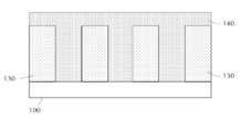
[0008]도 1은, 본 개시내용의 하나 이상의 실시예들에 따른 기판 피쳐의 횡단면도를 도시한다.
[0009]도 2a 내지 도 2e는 본 개시내용의 하나 이상의 실시예들에 따른 갭충전 프로세스의 횡단면 개략도를 도시한다.[0007] In the manner in which the recited features of the present disclosure can be understood in detail, a more particular description of the invention, briefly summarized above, may be had by reference to embodiments, some of which, Are illustrated in the accompanying drawings. It should be noted, however, that the appended drawings illustrate only typical embodiments of the present disclosure and, therefore, should not be construed as limiting the scope of the present disclosure, which is not intended to limit the scope of the present disclosure to other equally effective embodiments I can do it.
[0008] FIG. 1 illustrates a cross-sectional view of a substrate feature in accordance with one or more embodiments of the present disclosure.
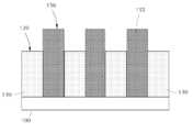
[0009] Figures 2A-2E illustrate a cross-sectional schematic of a gap filling process in accordance with one or more embodiments of the present disclosure.
[0010]본 개시내용의 몇몇 예시적인 실시예들을 설명하기 전에, 본 개시내용은 하기의 설명에서 기술되는 구성 또는 프로세스 단계들의 세부사항들로 제한되지 않음이 이해되어야 한다. 본 개시내용은 다른 실시예들이 가능하며, 다양한 방식들로 실시되거나 수행될 수 있다.[0010]Before describing some exemplary embodiments of the present disclosure, it should be understood that this disclosure is not limited to the details of construction or process steps set forth in the following description. The present disclosure is capable of other embodiments and of being practiced or carried out in various ways.
[0011]본원에서 사용되는 바와 같은 "기판"은, 제조 프로세스 동안 막 프로세싱이 수행되는, 임의의 기판, 또는 기판 상에 형성된 재료 표면을 지칭한다. 예컨대, 프로세싱이 수행될 수 있는 기판 표면은, 애플리케이션에 의존하여, 실리콘, 실리콘 산화물, 스트레인드 실리콘(strained silicon), SOI(silicon on insulator), 탄소 도핑된 실리콘 산화물들, 비정질 실리콘, 도핑된 실리콘, 게르마늄, 갈륨 비소, 유리, 사파이어와 같은 재료들, 및 임의의 다른 재료들, 이를테면 금속들, 금속 질화물들, 금속 합금들, 및 다른 전도성 재료들을 포함한다. 기판들은, 비제한적으로 반도체 웨이퍼들을 포함한다. 기판들은, 기판 표면을 연마(polish), 에칭, 환원, 산화, 히드록실화(hydroxylate), 어닐링(anneal), UV 경화(cure), e-빔(e-beam) 경화, 및/또는 베이킹(bake)하기 위해 전처리 프로세스에 노출될 수 있다. 본 개시내용에서, 기판 자체의 표면 상에 직접적으로 막 프로세싱을 하는 것에 부가하여, 개시되는 막 프로세싱 단계들 중 임의의 막 프로세싱 단계는 또한, 아래에서 더 상세히 개시되는 바와 같이, 기판 상에 형성된 하부층 상에 수행될 수 있으며, "기판 표면"이라는 용어는 문맥이 표시하는 바에 따라 그러한 하부층을 포함하도록 의도된다. 따라서, 예컨대, 막/층 또는 부분적인 막/층이 기판 표면 상에 증착된 경우, 새롭게 증착된 막/층의 노출된 표면이 기판 표면이 된다.[0011]A "substrate " as used herein refers to any substrate, or material surface formed on a substrate, during which the film processing is performed during the manufacturing process. For example, the substrate surface on which processing may be performed may be a silicon substrate, a silicon oxide, strained silicon, silicon on insulator (SOI), carbon doped silicon oxides, amorphous silicon, doped silicon , Germanium, gallium arsenide, glass, sapphire, and any other materials such as metals, metal nitrides, metal alloys, and other conductive materials. The substrates include, but are not limited to, semiconductor wafers. The substrates may be polished, etched, reduced, oxidized, hydroxylated, annealed, UV cured, e-beam cured, and / or baked bake) to the pretreatment process. In this disclosure, in addition to performing film processing directly on the surface of the substrate itself, any of the disclosed film processing steps may also include, as described in more detail below, , And the term "substrate surface" is intended to include such an underlayer as the context indicates. Thus, for example, when a film / layer or a partial film / layer is deposited on a substrate surface, the exposed surface of the newly deposited film / layer becomes the substrate surface.
[0012]본 개시내용의 하나 이상의 실시예들은, 임의의 컨포멀(conformal)한, 비컨포멀(nonconformal)한, 그리고/또는 낮은 종횡비 내지 고 종횡비 자기-정렬(self-aligned) 패터닝 또는 갭/트렌치/보이드(void) 충전 애플리케이션들에 대한, 금속 산화물 막들을 증착하기 위한 방법들에 관한 것이다. 본 개시내용의 실시예들은 유리하게, 작은 치수들을 갖는 고 종횡비(AR; aspect ratio) 구조들에서 막(예컨대, 금속 산화물 막)을 증착하는 방법들을 제공한다. 본 개시내용의 일부 실시예들은 유리하게, 갭에 시임(seam)을 형성함이 없이 갭들을 충전하는 방법들을 제공한다. 본 개시내용의 하나 이상의 실시예들은 유리하게, 자기-정렬 패턴들을 형성하는 방법들을 제공한다.[0012]One or more embodiments of the present disclosure may include any conformal, nonconformal, and / or low aspect ratio to high aspect ratio self-aligned patterning or gap / trench / void charging applications for depositing metal oxide films. Embodiments of the present disclosure advantageously provide methods for depositing a film (e.g., a metal oxide film) in high aspect ratio (AR) structures having small dimensions. Some embodiments of the present disclosure advantageously provide methods of filling gaps without forming a seam in the gap. One or more embodiments of the present disclosure advantageously provide methods of forming self-aligned patterns.
[0013]도 1은, 피쳐(110)를 갖는 기판(100)의 부분 횡단면도를 도시한다. 도면들은 예시적인 목적들을 위해 단일 피쳐를 갖는 기판들을 도시하지만, 당업자들은, 하나 초과의 피쳐가 존재할 수 있음을 이해할 것이다. 피쳐(110)의 형상은, 트렌치들 및 원통형 비아(via)들을 포함하는(그러나 이들로 제한되지 않음) 임의의 적절한 형상일 수 있다. 특정 실시예들에서, 피쳐(110)는 트렌치이다. 이와 관련하여 사용되는 바와 같이, "피쳐"라는 용어는 임의의 의도적인 표면 불규칙성을 의미한다. 피쳐들의 적절한 예들은, 최상부, 2개의 측벽들 및 최하부를 갖는 트렌치들, 최상부 및 표면으로부터 상향으로 연장되는 2개의 측벽들을 갖는 피크(peak)들, 및 개방된 최하부와 함께, 표면으로부터 아래로 연장되는 측벽들을 갖는 비아들을 포함하지만 이들로 제한되지 않는다. 피쳐들 또는 트렌치들은 임의의 적절한 종횡비(피쳐의 깊이 대 피쳐의 폭의 비)를 가질 수 있다. 일부 실시예들에서, 종횡비는 약 5:1, 10:1, 15:1, 20:1, 25:1, 30:1, 35:1 또는 40:1과 동일하거나 그 초과이다.[0013]FIG. 1 shows a partial cross-sectional view of a
[0014]기판(100)은 최상부 표면(120)을 갖는다. 적어도 하나의 피쳐(110)는 최상부 표면(120)에 개구를 형성한다. 피쳐(110)는, 최상부 표면(120)으로부터 깊이 D까지 최하부 표면(112)으로 연장된다. 피쳐(110)는, 피쳐(110)의 폭(W)을 정의하는 제1 측벽(114) 및 제2 측벽(116)을 갖는다. 측벽들 및 최하부에 의해 형성되는 개방 영역은 갭으로 또한 지칭된다. 단일 컴포넌트 기판(100)에 형성된 트렌치로서 피쳐(110)가 예시되어 있지만, 당업자들은, 피쳐(110)가 기판(100) 상의 패터닝된 막에 의해 형성될 수 있음을 인지할 것이다. 도 2a는, 패터닝된 막(130)에 의해 또는 패터닝된 막(130) 내에 형성된 트렌치들 또는 비아들로서 피쳐들(110)이 형성되는 실시예를 도시한다.[0014]The
[0015]도 2a 내지 도 2c를 참조하여 본 개시내용의 예시적인 실시예가 설명된다. 기판(100)은, 기판(100) 상에 형성된 패터닝된 막(130)이 있거나 그러한 막이 없이 프로세싱을 위해 제공된다. 이와 관련하여 사용되는 바와 같이, "제공된다"라는 용어는, 기판이 추가적인 프로세싱을 위한 포지션(position)으로 또는 추가적인 프로세싱을 위한 환경에 배치됨을 의미한다. 일부 실시예들에서, 패터닝된 막(130)은, 적어도 하나의 피쳐(110)를 제공하도록 기판(100) 상에 형성된다. 일부 실시예들에서, 기판(100)에는 이미 존재하는 패터닝된 막(130)이 제공된다.[0015]An exemplary embodiment of the present disclosure is described with reference to Figures 2A-2C. The
[0016]도 2a에 예시된 바와 같이, 패터닝된 막은, 제1 표면(132), 및 제1 표면(132)과 상이한 제2 표면(134)이 존재하도록, 기판(100)과 상이한 재료일 수 있다. 피쳐들(110)은, 피쳐(110)의 최하부(112)가 제1 표면(132)을 제공하고 그리고 피쳐(110)의 측벽들(114, 116) 및 최상부 표면(120)이 제2 표면(134)을 제공하도록, 패터닝된 막(130)에 형성된다. 패터닝된 막(130)은 임의의 적절한 재료일 수 있다. 일부 실시예들의 패터닝된 막(130)은 낮은-k 유전체(예컨대, SiOC)를 포함한다. 패터닝된 막(130)은, 후속하는 프로세싱 조건들과 호환가능하도록 선택될 수 있다.[0016]2A, the patterned film may be a different material than the
[0017]도 2b에서, 피쳐들(110)을 충전하고 그리고 패터닝된 막(130)의 최상부 표면(120) 위로 연장되도록 기판(100) 표면 상에 막(140)이 증착 또는 형성된다. 막(140)은, 화학 기상 증착, 플라즈마 강화 화학 기상 증착, 원자 층 증착, 플라즈마 강화 원자 층 증착, 및/또는 물리 기상 증착을 포함하는(그러나 이들로 제한되지 않음) 임의의 적절한 프로세스에 의해 형성되는 임의의 적절한 막일 수 있다. 일부 실시예들에서, 막(140)은, 원자 층 증착 또는 플라즈마 강화 원자 층 증착에 의해 형성된다.[0017]2B, a
[0018]일부 실시예들에서, 전구체는, 불활성 가스, 캐리어 가스, 및/또는 희석(diluent) 가스로, 기판(100)을 포함하는 프로세싱 챔버 내로 유동된다. 전구체는, 기판(100) 또는 패터닝된 막(130)에 화학 흡착(chemisorb)되어 기판 또는 패터닝된 막 상에 화학 흡착된 전구체를 남길 수 있다. 그런 다음, 화학 흡착된 전구체와 반응하여 막(140)을 증착할 공반응물이 프로세싱 챔버 내로 유동될 수 있다. 일부 실시예들에서, 전구체는 공반응물과 함께 프로세싱 챔버 내로 공동-유동(co-flow)된다. 전구체 및 공반응물이 가스상(gas phase)에서 반응하여, 기판 또는 패터닝된 막 상에 증착되어 막(140)을 성장시킬 종(species)을 형성한다.[0018]In some embodiments, the precursor is flowed into a processing chamber that includes the
[0019]일부 실시예들에서, 막(140)은 전구체의 열 분해에 의해 증착된다. 일부 실시예들에서, 열 분해는, 막(140)을 증착함에 있어 전구체와의 공반응물을 포함하지 않는다. 예컨대, 실리콘 전구체가 기판에 노출되어 기판(100) 상에 그리고 피쳐들(110) 내에 막(140)을 증착 또는 형성할 수 있다.[0019]In some embodiments, the
[0020]일부 실시예들에서, 막(140)은 비정질 실리콘을 포함한다. 하나 이상의 실시예들에서, 막(140)은 본질적으로 비정질 실리콘으로 이루어진다. 이와 관련하여 사용되는 바와 같이, "본질적으로 ~로 이루어진다"라는 용어는, 막이 몰 기준으로 약 95 %, 98 %, 또는 99 %와 동일하거나 그 초과의 비정질 실리콘임을 의미한다.[0020]In some embodiments, the
[0021]비정질 실리콘 막을 형성하는 것은 임의의 적절한 기법에 의해 달성될 수 있다. 일부 실시예들에서, 비정질 실리콘 막을 형성하는 것은, 공반응물 없이 또는 실질적으로 공반응물 없이 실리콘 전구체의 열 분해에 의해 달성된다. 이와 관련하여 사용되는 바와 같이, "실질적으로 공반응물이 없다"는 용어는, 실리콘 전구체 또는 흡착된 전구체 분자들과 반응하는 임의의 종이, 반응을 위한 화학량적(stoichiometric) 양의 약 50 %, 40 %, 30 %, 20 %, 10 % 또는 5 %와 동일하거나 그 미만의 양으로 존재함을 의미한다.[0021]The formation of the amorphous silicon film can be accomplished by any suitable technique. In some embodiments, forming an amorphous silicon film is accomplished by thermal decomposition of the silicon precursor without, or substantially without, co-reactants. The term "substantially free of reactants ", as used in this connection, refers to any species that reacts with silicon precursors or adsorbed precursor molecules, about 50% of the stoichiometric amount for the reaction, 40 %, 30%, 20%, 10%, or 5%.
[0022]일부 실시예들에서, 비정질 실리콘 막은, 실란, 디실란, 트리실란, 또는 테트라실란 중 하나 이상을 사용하여 증착된다. 일부 실시예들에서, 더 고차의 실란(예컨대, 5개, 6개, 7개, 8개, 9개, 또는 10개와 동일하거나 그 초과의 실리콘 원자들)이 비정질 실리콘 막을 증착하는 데 사용될 수 있다.[0022]In some embodiments, the amorphous silicon film is deposited using one or more of silane, disilane, trisilane, or tetrasilane. In some embodiments, higher order silanes (e.g., five, six, seven, eight, nine, or ten or more silicon atoms) can be used to deposit the amorphous silicon film .
[0023]일부 실시예들에서, 비정질 실리콘 막은, 전구체의 열 분해를 촉진시키기에 충분한 온도들 및 압력들에서 실리콘 전구체가 기판(100) 및 임의의 패터닝된 막(130)에 노출되는 컨포멀 증착 프로세스에 의해 증착된다. 일부 실시예들에서, 증착 동안의 온도는, 약 300 ℃ 내지 약 550 ℃의 범위 내에 또는 약 350 ℃ 내지 약 500 ℃의 범위 내에 있다. 일부 실시예들에서, 증착 동안의 압력은, 약 10 T 내지 약 600 T의 범위 내에, 또는 약 50 T 내지 약 500 T의 범위 내에, 또는 약 100 T 내지 약 400 T의 범위 내에 있다. 컨포멀 증착 프로세스에 의한 비정질 실리콘 막의 증착은 플라즈마 노출을 이용하여 또는 플라즈마 노출 없이 발생할 수 있다. 일부 실시예들에서, 컨포멀 증착 프로세스는 플라즈마 노출 없이 발생한다.[0023]In some embodiments, the amorphous silicon film is deposited by a conformal deposition process in which the silicon precursor is exposed to the
[0024]일부 실시예들에서, 비정질 실리콘 막은 유동성(flowable) 막 증착 프로세스에 의해 증착된다. 유동성 막 증착 프로세스 동안의 온도는, 약 -100 ℃ 내지 약 50 ℃의 범위 내에 또는 약 -50 ℃ 내지 약 25 ℃의 범위 내에 있을 수 있다. 일부 실시예들에서, 유동성 막 증착 프로세스는, 약 1 T 내지 약 10 T의 범위 내의 압력에서 발생한다. 하나 이상의 실시예들에서, 유동성 막 증착 프로세스는, 약 10 W 내지 약 200 W의 범위 내의 전력으로 RF 플라즈마를 사용하는 플라즈마 노출을 포함한다. 플라즈마는, 전도성으로 커플링된 플라즈마(CCP; conductively coupled plasma) 또는 유도성으로 커플링된 플라즈마(ICP; inductively coupled plasma)일 수 있다.[0024]In some embodiments, the amorphous silicon film is deposited by a flowable film deposition process. The temperature during the fluid film deposition process may be in the range of about -100 DEG C to about 50 DEG C or in the range of about -50 DEG C to about 25 DEG C. [ In some embodiments, the flowable film deposition process occurs at a pressure in the range of about 1 T to about 10 T. In one or more embodiments, the flowable film deposition process includes plasma exposure using RF plasma at a power in the range of about 10 W to about 200 W. The plasma may be a conductively coupled plasma (CCP) or an inductively coupled plasma (ICP).
[0025]도 2c에 도시된 바와 같이, 증착 후에, 최상부(141)를 갖는 리세스된 막(145)을 형성하도록 막(140)이 리세스된다. 최상부(141)는, 패터닝된 막(130)의 최상부 표면(120)과 동일하거나 그 미만의 높이로 낮아진다. 일부 실시예들에서, 리세스된 막(145)은, 패터닝된 막(130)의 최상부 표면(120)과 실질적으로 동일 평면(coplanar) 상에 있는 최상부(141)를 갖는다. 이러한 방식으로 사용되는 바와 같이, "실질적으로 동일 평면"이라는 용어는, 최상부(141)가 패터닝된 막(130)의 최상부 표면(120)의 1 Å 내에 있음을 의미한다. 일부 실시예들에서, 리세스된 막(145)의 최상부(141)는, 패터닝된 막(130)의 높이의 약 20 % 내지 약 98 %의 범위 내에 있다. 일부 실시예들에서, 리세스된 막(145)의 최상부(141)는, 패터닝된 막(130)의 높이의 약 30 % 내지 약 95 %의 범위 내에, 또는 약 40 % 내지 약 90 %의 범위 내에, 또는 약 50% 내지 약 85 %의 범위 내에 있다.[0025]After deposition, the
[0026]리세스된 막(145)을 형성하기 위해 막(140)을 리세스하는 것은 임의의 적절한 기법에 의해 달성될 수 있다. 일부 실시예들에서, 막(140)을 리세스하는 것은 막(140)을 에칭하는 것을 포함한다. 일부 실시예들에서, 에칭은 반응성 이온 에칭(RIE; reactive ion etch) 프로세스를 포함한다. 일부 실시예들에서, RIE는 브롬계 에천트(etchant)를 사용한다. 하나 이상의 실시예들에서, 막(140)을 에칭하는 것은, 수소 플라즈마 또는 수소 라디칼들에 막(140)을 노출시키는 것을 포함한다. 수소 플라즈마는, 원격 플라즈마 또는 다이렉트(direct) 플라즈마일 수 있고 그리고 CCP 또는 ICP일 수 있다. 수소 라디칼들은, 플라즈마 생성을 포함하는 임의의 적절한 수단에 의해 또는 라디칼들을 생성하기 위해 핫 와이어(hot wire)를 통해 에천트를 유동시킴으로써 생성될 수 있다.[0026]Recessing the
[0027]도 2d에 예시된 바와 같이, 리세스된 막(145)은 텅스텐 막(150)으로 변환된다. 리세스된 막의 변환은 임의의 적절한 반응에 의해 달성될 수 있다. 일부 실시예들에서, 리세스된 막은, 텅스텐 전구체에 대한 노출에 의해 텅스텐 막으로 변환된다. 텅스텐 전구체는, 예컨대, 실리콘 원자들과 텅스텐 원자들을 교환하도록 리세스된 막과 반응할 수 있는 텅스텐 할로겐화물일 수 있다.[0027]As illustrated in Figure 2D, the recessed
[0028]일부 실시예들에서, 텅스텐 전구체는 WF6을 포함한다. 일부 실시예들에서, 텅스텐 전구체에 대한 노출은, 약 300 ℃ 내지 약 550 ℃의 범위 내의 온도 및 약 10 T 내지 약 100 T의 범위 내의 압력에서 발생한다. 텅스텐 전구체는, 희석 가스, 캐리어 가스 또는 불활성 가스(예컨대, 아르곤) 또는 반응성 가스들(예컨대, H2)일 수 있는 다른 가스들과 공동-유동될 수 있다. 일부 실시예들에서, 텅스텐 전구체는, 리세스된 막과 텅스텐 전구체의 반응을 촉진시키는 반응성 가스와 공동-유동된다.[0028] In some embodiments, the tungsten precursor comprises WF6 . In some embodiments, the exposure to the tungsten precursor occurs at a temperature in the range of about 300 ° C to about 550 ° C and a pressure in the range of about 10 T to about 100 T. The tungsten precursor may be co-flow with other gases, which may be a diluent gas, a carrier gas or an inert gas (e.g., argon) or reactive gases (e.g., H2 ). In some embodiments, the tungsten precursor is co-flowed with a reactive gas that promotes the reaction of the recessed film with the tungsten precursor.
[0029]예시적인 실시예에서, 리세스된 막(145)은 비정질 실리콘을 포함하거나 본질적으로 비정질 실리콘으로 이루어지며, 텅스텐 전구체는 WF6을 포함한다. 텅스텐 전구체는, 약 550 ℃의 온도 및 약 20 Torr의 압력에서 비정질 실리콘 막에 노출된다.[0029] In an exemplary embodiment, the recessed
[0030]일부 실시예들에서, 실질적으로 모든 리세스된 막이 텅스텐으로 변환된다. 이와 관련하여 사용되는 바와 같이, "실질적으로 모든"이라는 용어는, 약 95 %, 98 %, 또는 99 %와 동일하거나 그 초과의 리세스된 막이 텅스텐으로 변환됨을 의미한다. 실질적으로 모든 리세스된 막을 변환하는 데 이용되는 시간량은, 예컨대, 온도, 압력, 막 조성, 막 두께, 및 텅스텐 전구체에 의존한다. 일부 실시예들에서, 200-300 Å의 비정질 실리콘은, 550 ℃ 및 20 Torr에서 약 4분 미만 내에 텅스텐으로 변환될 수 있다.[0030]In some embodiments, substantially all of the recessed film is converted to tungsten. As used in this connection, the term "substantially all" means that a recessed film that is equal to or greater than about 95%, 98%, or 99% is converted to tungsten. The amount of time used to convert substantially all recessed films depends on, for example, temperature, pressure, film composition, film thickness, and tungsten precursor. In some embodiments, 200-300 A amorphous silicon can be converted to tungsten in less than about 4 minutes at 550 [deg.] C and 20 Torr.
[0031]리세스된 막(145)을 텅스텐(150)으로 변환한 후, 텅스텐 막(150)의 최상부(151)의 높이는 리세스된 막의 높이와 동일하거나 상이할 수 있다. 리세스된 막에 대한 텅스텐 막(150)의 높이는, 예컨대, 막들에 존재하는 종 및 그 종의 원자 반경들에 의존한다. 일부 실시예들에서, 텅스텐 막(150)의 높이는, 막(150)의 최상부(151)가 패터닝된 막(130)의 최상부 표면(120)과 동일하거나 그 아래에 있는 그러한 높이이다.[0031]The height of the
[0032]도 2e에 도시된 바와 같이, 텅스텐 막(150)이 팽창되어 텅스텐 막(150)의 부피 팽창(volumetric expansion)을 야기함으로써, 최상부 표면(120)으로부터 연장되는 텅스텐 필러들(155)을 형성할 수 있다. 일부 실시예들의 텅스텐 필러들(155)은 표면(120)으로부터 직선으로 위로 연장된다. 막(150)의 팽창은, 약 10 % 내지 약 1000 %의 범위 내에, 또는 약 50 % 내지 약 800 %의 범위 내에, 또는 약 100 % 내지 약 700 %의 범위 내에 있을 수 있다. 일부 실시예들에서, 막(130)은, 약 150 %, 200 %, 250 %, 300 %, 또는 350 %와 동일하거나 그 초과의 양만큼 팽창된다. 일부 실시예들에서, 막(150)은, 약 300 % 내지 약 400 %의 범위 내의 양이 팽창된다. 일부 실시예들에서, 텅스텐 필러들(155)은, 텅스텐 막(150)의 높이의 약 50 %, 60 %, 70 %, 80 %, 90 %, 100 %, 125 %, 150 %, 175 % 또는 200 %와 동일하거나 그 초과의 양만큼 텅스텐 막(150)보다 더 큰 높이를 갖는다.[0032]The
[0033]일부 실시예들에서, 막(150)은, 금속 또는 금속 함유 막을 금속 실리사이드 막으로 변환하기 위한 실리사이딩(siliciding) 조건들 또는 실리사이딩제(siliciding agent)에 대한 노출에 의해 팽창된다. 실리사이딩제는, 실란, 디실란, 트리실란, 테트라실란, 펜타실란, 헥사실란, 트리메틸 실란, 트리메틸실릴 치환체들을 갖는 화합물들, 및 이들의 조합들을 포함하지만 이에 제한되지 않는 임의의 적절한 실리사이딩제일 수 있다. 일부 실시예들에서, 실리사이딩 조건들은, 열적 실리사이딩, 플라즈마 강화 실리사이딩, 원격 플라즈마 실리사이딩, 마이크로파 및 라디오-주파수(예컨대, ICP, CCP)를 포함한다.[0033]In some embodiments, the
[0034]일부 실시예들에서, 막(150)은, 금속 또는 금속 함유 막을 금속 게르마니사이드(germanicide) 막으로 변환하기 위한 게르마니사이딩(germaniciding) 조건들 또는 게르마늄제(germanium agent)에 대한 노출에 의해 팽창된다. 게르마니사이딩제(germaniciding agent)는, 게르만, 디게르만, 트리게르만, 테트라게르만, 펜타게르만, 헥사게르만, 트리메틸 게르마늄, 트리메틸 게르마닐 치환체들을 갖는 화합물들 및 이들의 조합들을 포함하지만 이에 제한되지 않는 임의의 적절한 게르마니사이딩제일 수 있다. 일부 실시예들에서, 게르마니사이딩 조건들은, 열적 게르마니사이딩, 플라즈마 강화 게르마니사이딩, 원격 플라즈마 게르마니사이딩, 마이크로파 및 라디오-주파수(예컨대, ICP, CCP)를 포함한다.[0034]In some embodiments, the
[0035]도 2e에 도시된 바와 같이, 팽창 동안, 피쳐 형상의 충실도(fidelity)는, 막(150)이 피쳐(110)로부터 직선으로 위로 성장하도록, 피쳐의 최상부 상에 유지된다. 이와 관련하여 사용되는 바와 같이, "직선으로 위로"는, 팽창된 막 또는 필러들(155)의 측부들이 피쳐(110)의 측벽(114, 116)과 실질적으로 동일 평면 상에 있음을 의미한다. 표면은 측벽(114)과 동일 평면 상에 있으며, 측벽(114)과 표면의 접합부에 형성된 각도는 ±10°이다.[0035]During the expansion, the fidelity of the feature shape is maintained on top of the feature so that the
[0036]일부 실시예들에서, 텅스텐 막(150)은 팽창 전에 도펀트(dopant)로 도핑된다. 도펀트는, 텅스텐 막(150)의 형성과 동시에 또는 막 증착과 순차적으로 별개의 프로세스에서, 텅스텐 막(150)에 혼입(incorporate)될 수 있다. 예컨대, 텅스텐 막(150)을 증착하는 것이 발생한 이후에, 동일한 프로세스 챔버 또는 상이한 프로세스 챔버 중 어느 하나에서 별개의 프로세스로, 텅스텐 막(150)을 도펀트로 도핑하는 것이 후속될 수 있다.[0036]In some embodiments, the
[0037]하나 이상의 실시예들에 따르면, 기판은, 층을 형성하기 전에 그리고/또는 층을 형성한 후에, 프로세싱을 겪는다. 이러한 프로세싱은, 동일한 챔버에서 또는 하나 이상의 별개의 프로세싱 챔버들에서 수행될 수 있다. 일부 실시예들에서, 기판은, 추가적인 프로세싱을 위해, 제1 챔버로부터 별개의 제2 챔버로 이동된다. 기판은, 제1 챔버로부터 별개의 프로세싱 챔버로 직접적으로 이동될 수 있거나, 또는 기판은, 제1 챔버로부터 하나 이상의 이송 챔버들로 이동될 수 있고, 그 후에, 별개의 프로세싱 챔버로 이동될 수 있다. 따라서, 프로세싱 장치는 이송 스테이션과 통신하는 다수의 챔버들을 포함할 수 있다. 이러한 종류의 장치는 "클러스터 툴(cluster tool)" 또는 "클러스터링된 시스템" 등으로 지칭될 수 있다.[0037]According to one or more embodiments, the substrate undergoes processing before forming the layer and / or after forming the layer. Such processing may be performed in the same chamber or in one or more separate processing chambers. In some embodiments, the substrate is moved from the first chamber to a separate second chamber for further processing. The substrate can be moved directly from the first chamber to a separate processing chamber or the substrate can be moved from the first chamber to one or more transfer chambers and then moved to a separate processing chamber . Thus, the processing device may include a plurality of chambers in communication with the transfer station. Devices of this kind may be referred to as "cluster tools" or "clustered systems ".
[0038]일반적으로, 클러스터 툴은, 기판 중심-발견 및 배향, 탈기, 어닐링, 증착, 및/또는 에칭을 포함하는 다양한 기능들을 수행하는 다수의 챔버들을 포함하는 모듈러 시스템이다. 하나 이상의 실시예들에 따르면, 클러스터 툴은, 적어도 제1 챔버 및 중앙 이송 챔버를 포함한다. 중앙 이송 챔버는, 로드 록 챔버들과 프로세싱 챔버들 사이에서 그리고 이들 간에서 기판들을 셔틀링(shuttle)할 수 있는 로봇을 하우징(house)할 수 있다. 이송 챔버는 통상적으로, 진공 조건에서 유지되고, 기판들을, 하나의 챔버로부터 다른 챔버로, 그리고/또는 클러스터 툴의 전방 단부에 포지셔닝된 로드 록 챔버로 셔틀링하기 위한 중간 스테이지를 제공한다. 본 발명에 대해 적응될 수 있는 2개의 잘-알려진 클러스터 툴들은 Centura® 및 Endura®이고, 이들 둘 모두는, 캘리포니아 주 Santa Clara의 Applied Materials, Inc.로부터 입수가능하다. 하지만, 챔버들의 정확한 어레인지먼트(arrangement) 및 조합은, 본원에서 설명되는 바와 같은 프로세스의 특정 단계들을 수행하는 목적들을 위해 변경될 수 있다. 사용될 수 있는 다른 프로세싱 챔버들은, CLD(cyclical layer deposition), ALD(atomic layer deposition), CVD(chemical vapor deposition), PVD(physical vapor deposition), 에칭, 사전-세정, 화학 세정, RTP와 같은 열 처리, 플라즈마 질화(nitridation), 탈기, 배향, 히드록실화(hydroxylation), 및 다른 기판 프로세스들을 포함하지만 이들로 제한되지 않는다. 클러스터 툴 상의 챔버에서 프로세스들을 수행함으로써, 대기 불순물들에 의한 기판의 표면 오염이, 후속 막을 증착하기 전의 산화 없이, 회피될 수 있다.[0038]Generally, a cluster tool is a modular system that includes a number of chambers that perform various functions including substrate center-finding and orientation, degassing, annealing, deposition, and / or etching. According to one or more embodiments, the cluster tool comprises at least a first chamber and a central transfer chamber. The central transfer chamber may house a robot capable of shuttling the substrates between and between the load lock chambers and the processing chambers. The transfer chamber is typically maintained in a vacuum condition and provides an intermediate stage for shuttling the substrates from one chamber to another and / or to a load lock chamber positioned at the front end of the cluster tool. Two well-known cluster tools that can be adapted for the present invention are Centura® and Endura®, both available from Applied Materials, Inc. of Santa Clara, Calif. However, the exact arrangement and combination of chambers may be varied for purposes of performing certain steps of the process as described herein. Other processing chambers that may be used include thermal processing such as cyclical layer deposition (CLD), atomic layer deposition (ALD), chemical vapor deposition (CVD), physical vapor deposition (PVD), etching, pre- , Plasma nitridation, degassing, orientation, hydroxylation, and other substrate processes. By performing processes in a chamber on a cluster tool, surface contamination of the substrate by atmospheric impurities can be avoided without oxidation prior to deposition of the subsequent film.
[0039]하나 이상의 실시예들에 따르면, 기판은 지속적으로 진공 또는 "로드 록" 조건들 하에 있고, 하나의 챔버로부터 다음 챔버로 이동될 때, 주변 공기에 노출되지 않는다. 따라서, 이송 챔버들은 진공 하에 있고, 진공 압력 하에서 "펌핑 다운(pump down)"된다. 불활성 가스들이 프로세싱 챔버들 또는 이송 챔버들에 존재할 수 있다. 일부 실시예들에서, 불활성 가스는, 반응물들의 일부 또는 전부를 제거하기 위해, 퍼지 가스로서 사용된다. 하나 이상의 실시예들에 따르면, 퍼지 가스는, 반응물들이 증착 챔버로부터 이송 챔버로 그리고/또는 부가적인 프로세싱 챔버로 이동하는 것을 방지하기 위해, 증착 챔버의 출구에서 주입된다. 따라서, 불활성 가스의 유동은 챔버의 출구에서 커튼을 형성한다.[0039]According to one or more embodiments, the substrate is under constant vacuum or "load lock" conditions and is not exposed to ambient air when moved from one chamber to the next. Thus, the transfer chambers are under vacuum and are "pumped down" under vacuum pressure. Inert gases may be present in the processing chambers or transfer chambers. In some embodiments, the inert gas is used as a purge gas to remove some or all of the reactants. According to one or more embodiments, the purge gas is injected at the outlet of the deposition chamber to prevent reactants from moving from the deposition chamber to the transfer chamber and / or to the additional processing chamber. Thus, the flow of the inert gas forms a curtain at the outlet of the chamber.
[0040]기판은, 단일 기판이 로딩되고, 프로세싱되고, 그리고 다른 기판이 프로세싱되기 전에 언로딩되는, 단일 기판 증착 챔버들에서 프로세싱될 수 있다. 기판은 또한, 다수의 기판이 챔버의 제1 부분 내로 개별적으로 로딩되고, 챔버를 통해 이동하고, 그리고 챔버의 제2 부분으로부터 언로딩되는, 컨베이어 시스템과 유사하게, 연속적인 방식으로 프로세싱될 수 있다. 챔버 및 연관된 컨베이어 시스템의 형상은 직선 경로 또는 곡선 경로를 형성할 수 있다. 부가적으로, 프로세싱 챔버는, 다수의 기판들이 중심 축을 중심으로 이동되고 그리고 캐러셀(carousel) 경로 전반에 걸쳐 증착, 에칭, 어닐링, 세정 등의 프로세스들에 노출되는, 캐러셀일 수 있다.[0040]The substrate may be processed in a single substrate deposition chamber, where a single substrate is loaded, processed, and unloaded before the other substrate is processed. The substrate can also be processed in a continuous manner, similar to a conveyor system in which a plurality of substrates are individually loaded into a first portion of a chamber, moved through a chamber, and unloaded from a second portion of the chamber . The shape of the chamber and associated conveyor system may form a straight or curved path. Additionally, the processing chamber may be a carousel in which a plurality of substrates are moved about a central axis and exposed to processes such as deposition, etching, annealing, cleaning, etc. throughout the carousel path.
[0041]프로세싱 동안, 기판은 가열 또는 냉각될 수 있다. 그러한 가열 또는 냉각은, 기판 지지부의 온도를 변화시키는 것 및 가열된 또는 냉각된 가스들을 기판 표면으로 유동시키는 것을 포함하는(그러나 이에 제한되지 않음) 임의의 적절한 수단에 의해 달성될 수 있다. 일부 실시예들에서, 기판 지지부는, 기판 온도를 전도성으로 변화시키도록 제어될 수 있는 가열기/냉각기를 포함한다. 하나 이상의 실시예들에서, 이용되는 가스들(반응성 가스들 또는 불활성 가스들)은, 기판 온도를 국부적으로 변화시키도록 가열 또는 냉각된다. 일부 실시예들에서, 가열기/냉각기는, 기판 온도를 대류성으로(convectively) 변화시키기 위해, 챔버 내에서 기판 표면에 인접하게 포지셔닝된다.[0041]During processing, the substrate may be heated or cooled. Such heating or cooling may be accomplished by any suitable means including, but not limited to, changing the temperature of the substrate support and flowing heated or cooled gases to the substrate surface. In some embodiments, the substrate support includes a heater / cooler that can be controlled to conductively change the substrate temperature. In one or more embodiments, the gases used (reactive gases or inert gases) are heated or cooled to locally vary the substrate temperature. In some embodiments, the heater / cooler is positioned adjacent to the substrate surface within the chamber to change the substrate temperature convectively.
[0042]기판은 또한, 프로세싱 동안, 정적일 수 있거나 또는 회전될 수 있다. 회전되는 기판은, 연속적으로 또는 불연속적인 단계들로 회전될 수 있다. 예컨대, 기판은 전체 프로세스 전체에 걸쳐 회전될 수 있거나, 또는 기판은, 상이한 반응성 또는 퍼지 가스들에 대한 노출들 사이에서 작은 양만큼 회전될 수 있다. (연속적으로 또는 단계들로) 프로세싱 동안 기판을 회전시키는 것은, 예컨대, 가스 유동 기하학적 구조들에서의 국부적인 변동성의 영향을 최소화함으로써, 더 균일한 증착 또는 에칭을 생성하는 것을 도울 수 있다.[0042]The substrate may also be stationary or rotated during processing. The substrate to be rotated can be rotated in successive or discontinuous steps. For example, the substrate may be rotated throughout the entire process, or the substrate may be rotated by a small amount between exposures to different reactive or purge gases. Rotating the substrate during processing (successively or in steps) may help to produce a more uniform deposition or etch, for example, by minimizing the effect of local variations in gas flow geometries.
[0043]본 명세서 전반에 걸쳐 "일 실시예", "특정 실시예들", "하나 이상의 실시예들" 또는 "실시예"에 대한 언급은, 실시예와 관련하여 설명되는 특정 피처, 구조, 재료, 또는 특징이 본 개시내용의 적어도 하나의 실시예에 포함된다는 것을 의미한다. 따라서, 본 명세서 전반에 걸쳐 다양한 위치들에서의 "하나 이상의 실시예들에서", "특정 실시예들에서", "일 실시예에서" 또는 "실시예에서"와 같은 문구들의 출현들은 반드시 본 개시내용의 동일한 실시예를 지칭하는 것은 아니다. 또한, 특정 피쳐들, 구조들, 재료들, 또는 특징들은 하나 이상의 실시예들에서 임의의 적절한 방식으로 조합될 수 있다.[0043]Reference throughout this specification to "one embodiment," " certain embodiments, "" one or more embodiments," or "an embodiment" means that a particular feature, And that the features are included in at least one embodiment of the present disclosure. Thus, the appearances of the phrases "in one or more embodiments," in certain embodiments, "in one embodiment," or "in an embodiment," But not to the same embodiment of the content. In addition, certain features, structures, materials, or features may be combined in any suitable manner in one or more embodiments.
[0044]본원에서의 개시내용이 특정 실시예들을 참조하여 설명되었지만, 이러한 실시예들은 단지 본 개시내용의 원리들 및 애플리케이션들을 예시하는 것임이 이해되어야 한다. 본 개시내용의 사상 및 범위를 벗어나지 않으면서 본 개시내용의 방법 및 장치에 대해 다양한 수정들 및 변형들이 이루어질 수 있음이 당업자에게 자명할 것이다. 따라서, 본 개시내용은 첨부된 청구항들 및 그 등가물들의 범위 내에 있는 수정들 및 변형들을 포함하는 것으로 의도된다.[0044]While the disclosure herein has been described with reference to particular embodiments, it should be understood that these embodiments are merely illustrative of the principles and applications of the present disclosure. It will be apparent to those skilled in the art that various modifications and variations can be made in the method and apparatus of the present disclosure without departing from the spirit and scope of the disclosure. It is therefore intended that the present disclosure cover all such modifications and variations as fall within the scope of the appended claims and their equivalents.
Claims (15)
Translated fromKorean적어도 하나의 피쳐(feature)를 형성하는 패터닝(pattern)된 막을 기판 표면에 제공하는 단계 ― 상기 적어도 하나의 피쳐는 상기 패터닝된 막의 최상부 표면으로부터 최하부 표면으로 깊이가 연장되고, 상기 적어도 하나의 피쳐는, 제1 측벽 및 제2 측벽에 의해 정의되는 폭을 가짐 ―;
상기 적어도 하나의 피쳐를 충전(fill)하고 그리고 상기 패터닝된 막의 최상부 표면 위로 연장되도록, 상기 패터닝된 막 상에 막을 증착하는 단계;
리세스(recess)된 막을 형성하기 위해, 상기 패터닝된 막의 최상부 표면과 동일하거나 그 미만의 높이로 상기 막의 최상부를 낮추도록 상기 막을 리세스하는 단계;
상기 리세스된 막을 텅스텐 막으로 변환하는 단계; 및
상기 적어도 하나의 피쳐로부터 연장되는 필러(pillar)들을 형성하기 위해 상기 텅스텐 막을 팽창시키는 단계를 포함하는, 프로세싱 방법.As a processing method,
Providing a patterned film on a substrate surface forming at least one feature wherein the at least one feature extends from a top surface to a bottom surface of the patterned film and the at least one feature A width defined by the first sidewall and the second sidewall;
Depositing a film on the patterned film to fill the at least one feature and extend over the top surface of the patterned film;
Recessing the film to lower the top of the film to a height equal to or less than the top surface of the patterned film to form a recessed film;
Converting the recessed film into a tungsten film; And
And expanding the tungsten film to form pillars extending from the at least one feature.
상기 막은 비정질 실리콘을 포함하는, 프로세싱 방법.The method according to claim 1,
Wherein the film comprises amorphous silicon.
상기 막을 증착하는 단계는, 실란, 디실란, 트리실란, 또는 테트라실란 중 하나 이상을 포함하는 전구체(precursor)에 기판을 노출시키는 단계를 포함하는, 프로세싱 방법.3. The method of claim 2,
Wherein depositing the film comprises exposing the substrate to a precursor comprising at least one of silane, disilane, trisilane, or tetrasilane.
상기 막을 증착하는 단계는, 약 300 ℃ 내지 약 550 ℃의 범위 내의 온도에서 발생하는, 프로세싱 방법.The method of claim 3,
Wherein depositing the film occurs at a temperature in the range of from about 300 < 0 > C to about 550 < 0 > C.
상기 막을 증착하는 단계는, 약 10 T 내지 약 600 T의 범위 내의 압력에서 발생하는, 프로세싱 방법.5. The method of claim 4,
Wherein depositing the film occurs at a pressure in the range of about 10 < RTI ID = 0.0 > T < / RTI >
상기 막을 증착하는 단계는, 상기 전구체에 대한 공반응물(co-reactant) 없이 발생하는, 프로세싱 방법.6. The method of claim 5,
Wherein depositing the film occurs without a co-reactant to the precursor.
상기 막을 증착하는 단계는, 약 -100 ℃ 내지 약 50 ℃의 범위 내의 온도에서 발생하는, 프로세싱 방법.The method of claim 3,
Wherein depositing the film occurs at a temperature in the range of about -100 [deg.] C to about 50 [deg.] C.
상기 막을 증착하는 단계는, 약 1 T 내지 약 10 T의 범위 내의 압력에서 발생하는, 프로세싱 방법.8. The method of claim 7,
Wherein depositing the film occurs at a pressure in the range of about 1 T to about 10 T.
상기 막을 증착하는 단계는, 약 10 W 내지 약 200 W의 범위 내의 전력을 갖는 RF 플라즈마로 발생하는, 프로세싱 방법.9. The method of claim 8,
Wherein depositing the film occurs with an RF plasma having a power in the range of about 10 W to about 200 W.
상기 막을 증착하는 단계는, 상기 전구체에 대한 공반응물 없이 발생하는, 프로세싱 방법.10. The method of claim 9,
Wherein depositing the film occurs without co-reactants to the precursor.
상기 막을 리세스하는 단계는, 상기 막을 에칭하는 단계를 포함하는, 프로세싱 방법.The method according to claim 1,
Wherein the step of recessing the film comprises etching the film.
상기 막을 에칭하는 단계는, 브롬계 에천트(etchant)를 사용하는 반응성 이온 에칭 프로세스를 포함하는, 프로세싱 방법.12. The method of claim 11,
Wherein the step of etching the film comprises a reactive ion etching process using a bromine etchant.
상기 막을 리세스하는 단계는, 수소 플라즈마 또는 수소 라디칼(radical)들에 상기 막을 노출시키는 단계를 포함하는, 프로세싱 방법.12. The method of claim 11,
Wherein the step of recessing the film comprises exposing the film to hydrogen plasma or hydrogen radicals.
상기 리세스된 막을 텅스텐 막으로 변환하는 단계는, WF6에 상기 리세스된 막을 노출시키는 단계를 포함하는, 프로세싱 방법.The method according to claim 1,
Wherein converting the recessed film to a tungsten film comprises exposing the recessed film to WF6 .
상기 텅스텐 막을 팽창시키는 단계는, 상기 텅스텐 막을 산화시키는 단계를 포함하는, 프로세싱 방법.The method according to claim 1,
Wherein the step of expanding the tungsten film comprises oxidizing the tungsten film.
Priority Applications (1)
| Application Number | Priority Date | Filing Date | Title |
|---|---|---|---|
| KR1020240127276AKR20240141699A (en) | 2017-05-02 | 2024-09-20 | Methods of forming tungsten pillars |
Applications Claiming Priority (2)
| Application Number | Priority Date | Filing Date | Title |
|---|---|---|---|
| US201762500213P | 2017-05-02 | 2017-05-02 | |
| US62/500,213 | 2017-05-02 |
Related Child Applications (1)
| Application Number | Title | Priority Date | Filing Date |
|---|---|---|---|
| KR1020240127276ADivisionKR20240141699A (en) | 2017-05-02 | 2024-09-20 | Methods of forming tungsten pillars |
Publications (2)
| Publication Number | Publication Date |
|---|---|
| KR20180122297Atrue KR20180122297A (en) | 2018-11-12 |
| KR102710607B1 KR102710607B1 (en) | 2024-09-25 |
Family
ID=64014928
Family Applications (2)
| Application Number | Title | Priority Date | Filing Date |
|---|---|---|---|
| KR1020180050715AActiveKR102710607B1 (en) | 2017-05-02 | 2018-05-02 | Methods of forming tungsten pillars |
| KR1020240127276APendingKR20240141699A (en) | 2017-05-02 | 2024-09-20 | Methods of forming tungsten pillars |
Family Applications After (1)
| Application Number | Title | Priority Date | Filing Date |
|---|---|---|---|
| KR1020240127276APendingKR20240141699A (en) | 2017-05-02 | 2024-09-20 | Methods of forming tungsten pillars |
Country Status (5)
| Country | Link |
|---|---|
| US (2) | US10784107B2 (en) |
| JP (2) | JP2018199863A (en) |
| KR (2) | KR102710607B1 (en) |
| CN (2) | CN116978862A (en) |
| TW (2) | TWI780922B (en) |
Cited By (1)
| Publication number | Priority date | Publication date | Assignee | Title |
|---|---|---|---|---|
| KR20210082260A (en)* | 2018-11-23 | 2021-07-02 | 어플라이드 머티어리얼스, 인코포레이티드 | Selective deposition of carbon films and their uses |
Families Citing this family (1)
| Publication number | Priority date | Publication date | Assignee | Title |
|---|---|---|---|---|
| US20240304495A1 (en)* | 2023-03-06 | 2024-09-12 | Applied Materials, Inc. | Hydrogen plasma treatment for forming logic devices |
Citations (8)
| Publication number | Priority date | Publication date | Assignee | Title |
|---|---|---|---|---|
| JPH0290518A (en)* | 1988-09-28 | 1990-03-30 | Hitachi Ltd | Semiconductor device and its manufacturing method |
| JPH0794491A (en)* | 1993-09-22 | 1995-04-07 | Hiroshi Nagayoshi | Dry etching method and dry etching treatment apparatus |
| JPH07147321A (en)* | 1993-11-26 | 1995-06-06 | Nec Corp | Manufacture of semiconductor device |
| JPH0837145A (en)* | 1994-07-26 | 1996-02-06 | Hitachi Ltd | Method for manufacturing semiconductor integrated circuit device |
| US6015986A (en)* | 1995-12-22 | 2000-01-18 | Micron Technology, Inc. | Rugged metal electrodes for metal-insulator-metal capacitors |
| JP2011109099A (en)* | 2009-11-17 | 2011-06-02 | Samsung Electronics Co Ltd | Semiconductor device including conductive structure, and method of manufacturing the same |
| JP2014027294A (en)* | 2002-10-18 | 2014-02-06 | Applied Materials Inc | Silicon-containing layer deposition with silicon compounds |
| JP2016001760A (en)* | 2015-09-24 | 2016-01-07 | 株式会社日立国際電気 | Semiconductor device manufacturing method, substrate processing method, substrate processing apparatus, and gas supply system |
Family Cites Families (34)
| Publication number | Priority date | Publication date | Assignee | Title |
|---|---|---|---|---|
| JPS62298110A (en)* | 1986-06-18 | 1987-12-25 | Matsushita Electric Ind Co Ltd | Manufacturing method of semiconductor integrated circuit |
| US4948755A (en)* | 1987-10-08 | 1990-08-14 | Standard Microsystems Corporation | Method of manufacturing self-aligned conformal metallization of semiconductor wafer by selective metal deposition |
| JPH06112155A (en)* | 1992-09-25 | 1994-04-22 | Matsushita Electron Corp | Formation of contact plug |
| US5872052A (en)* | 1996-02-12 | 1999-02-16 | Micron Technology, Inc. | Planarization using plasma oxidized amorphous silicon |
| JP2812288B2 (en)* | 1996-02-28 | 1998-10-22 | 日本電気株式会社 | Method for manufacturing semiconductor device |
| US6383951B1 (en)* | 1998-09-03 | 2002-05-07 | Micron Technology, Inc. | Low dielectric constant material for integrated circuit fabrication |
| KR100304962B1 (en)* | 1998-11-24 | 2001-10-20 | 김영환 | Method for making a Tungsten-bit line |
| TW406370B (en)* | 1998-12-19 | 2000-09-21 | Vanguard Int Semiconduct Corp | Process of PECVD tungsten and tungsten compound deposition |
| US6319832B1 (en)* | 1999-02-19 | 2001-11-20 | Micron Technology, Inc. | Methods of making semiconductor devices |
| KR100351238B1 (en)* | 1999-09-14 | 2002-09-09 | 주식회사 하이닉스반도체 | Method of manufacturing a capacitor in a semiconductor device |
| TW457684B (en)* | 2000-10-11 | 2001-10-01 | Promos Technologies Inc | Manufacturing method of tungsten plug |
| AU2002306436A1 (en)* | 2001-02-12 | 2002-10-15 | Asm America, Inc. | Improved process for deposition of semiconductor films |
| US20020197852A1 (en)* | 2001-06-21 | 2002-12-26 | Ming-Shi Yeh | Method of fabricating a barrier layer with high tensile strength |
| FR2851258B1 (en)* | 2003-02-17 | 2007-03-30 | Commissariat Energie Atomique | METHOD OF COATING A SURFACE, FABRICATION OF MICROELECTRONIC INTERCONNECTION USING THE SAME, AND INTEGRATED CIRCUITS |
| KR100680946B1 (en)* | 2004-04-28 | 2007-02-08 | 주식회사 하이닉스반도체 | Method for forming contact plug of semiconductor device |
| US6987961B1 (en)* | 2004-06-28 | 2006-01-17 | Neomagic Corp. | Ethernet emulation using a shared mailbox between two processors in a feature phone |
| TWI234288B (en)* | 2004-07-27 | 2005-06-11 | Au Optronics Corp | Method for fabricating a thin film transistor and related circuits |
| US8288828B2 (en)* | 2004-09-09 | 2012-10-16 | International Business Machines Corporation | Via contact structure having dual silicide layers |
| KR100705397B1 (en)* | 2005-07-13 | 2007-04-10 | 삼성전자주식회사 | Low resistance tungsten film formation method |
| KR101534678B1 (en) | 2009-02-12 | 2015-07-08 | 삼성전자주식회사 | A method of manufacturing a semiconductor device in which a tungsten contact plug is subjected to an RTA treatment in an oxygen atmosphere and a tungsten plug subjected to an RTO treatment is reduced in a hydrogen atmosphere |
| US8168538B2 (en)* | 2009-05-26 | 2012-05-01 | Macronix International Co., Ltd. | Buried silicide structure and method for making |
| US8575753B2 (en) | 2009-05-27 | 2013-11-05 | Samsung Electronics Co., Ltd. | Semiconductor device having a conductive structure including oxide and non oxide portions |
| US8535760B2 (en)* | 2009-09-11 | 2013-09-17 | Air Products And Chemicals, Inc. | Additives to silane for thin film silicon photovoltaic devices |
| JP5511308B2 (en)* | 2009-10-26 | 2014-06-04 | 三菱電機株式会社 | Semiconductor device and manufacturing method thereof |
| JP5696530B2 (en)* | 2010-05-01 | 2015-04-08 | 東京エレクトロン株式会社 | Thin film forming method and film forming apparatus |
| US8048782B1 (en)* | 2010-08-12 | 2011-11-01 | Ovshinsky Innovation Llc | Plasma deposition of amorphous semiconductors at microwave frequencies |
| KR101908358B1 (en)* | 2011-05-24 | 2018-12-11 | 삼성전자주식회사 | Semiconductor device having metal plug and method of forming the same |
| TWI602283B (en)* | 2012-03-27 | 2017-10-11 | 諾發系統有限公司 | Tungsten feature fill |
| US20140273436A1 (en)* | 2013-03-15 | 2014-09-18 | Globalfoundries Inc. | Methods of forming barrier layers for conductive copper structures |
| JP6297884B2 (en)* | 2014-03-28 | 2018-03-20 | 東京エレクトロン株式会社 | Method for forming tungsten film |
| CN105336662B (en)* | 2014-05-29 | 2018-06-01 | 中芯国际集成电路制造(上海)有限公司 | The forming method of semiconductor structure |
| US9716097B2 (en)* | 2015-01-14 | 2017-07-25 | Taiwan Semiconductor Manufacturing Co., Ltd. | Techniques to avoid or limit implant punch through in split gate flash memory devices |
| US9484251B1 (en)* | 2015-10-30 | 2016-11-01 | Lam Research Corporation | Contact integration for reduced interface and series contact resistance |
| TWI687978B (en) | 2016-11-08 | 2020-03-11 | 美商應用材料股份有限公司 | Geometric control of bottom-up pillars for patterning applications |
- 2018
- 2018-05-02CNCN202311135956.8Apatent/CN116978862A/enactivePending
- 2018-05-02TWTW110135272Apatent/TWI780922B/enactive
- 2018-05-02KRKR1020180050715Apatent/KR102710607B1/enactiveActive
- 2018-05-02USUS15/969,119patent/US10784107B2/enactiveActive
- 2018-05-02JPJP2018088620Apatent/JP2018199863A/enactivePending
- 2018-05-02CNCN201810410364.5Apatent/CN108807264B/enactiveActive
- 2018-05-02TWTW107114805Apatent/TWI757478B/enactive
- 2020
- 2020-09-22USUS17/028,984patent/US20210013038A1/ennot_activeAbandoned
- 2022
- 2022-11-22JPJP2022186147Apatent/JP7591018B2/enactiveActive
- 2024
- 2024-09-20KRKR1020240127276Apatent/KR20240141699A/enactivePending
Patent Citations (8)
| Publication number | Priority date | Publication date | Assignee | Title |
|---|---|---|---|---|
| JPH0290518A (en)* | 1988-09-28 | 1990-03-30 | Hitachi Ltd | Semiconductor device and its manufacturing method |
| JPH0794491A (en)* | 1993-09-22 | 1995-04-07 | Hiroshi Nagayoshi | Dry etching method and dry etching treatment apparatus |
| JPH07147321A (en)* | 1993-11-26 | 1995-06-06 | Nec Corp | Manufacture of semiconductor device |
| JPH0837145A (en)* | 1994-07-26 | 1996-02-06 | Hitachi Ltd | Method for manufacturing semiconductor integrated circuit device |
| US6015986A (en)* | 1995-12-22 | 2000-01-18 | Micron Technology, Inc. | Rugged metal electrodes for metal-insulator-metal capacitors |
| JP2014027294A (en)* | 2002-10-18 | 2014-02-06 | Applied Materials Inc | Silicon-containing layer deposition with silicon compounds |
| JP2011109099A (en)* | 2009-11-17 | 2011-06-02 | Samsung Electronics Co Ltd | Semiconductor device including conductive structure, and method of manufacturing the same |
| JP2016001760A (en)* | 2015-09-24 | 2016-01-07 | 株式会社日立国際電気 | Semiconductor device manufacturing method, substrate processing method, substrate processing apparatus, and gas supply system |
Cited By (1)
| Publication number | Priority date | Publication date | Assignee | Title |
|---|---|---|---|---|
| KR20210082260A (en)* | 2018-11-23 | 2021-07-02 | 어플라이드 머티어리얼스, 인코포레이티드 | Selective deposition of carbon films and their uses |
Also Published As
| Publication number | Publication date |
|---|---|
| US20210013038A1 (en) | 2021-01-14 |
| TW202207278A (en) | 2022-02-16 |
| TW201843708A (en) | 2018-12-16 |
| JP7591018B2 (en) | 2024-11-27 |
| TWI780922B (en) | 2022-10-11 |
| CN108807264A (en) | 2018-11-13 |
| TWI757478B (en) | 2022-03-11 |
| CN108807264B (en) | 2023-09-12 |
| US20180323068A1 (en) | 2018-11-08 |
| US10784107B2 (en) | 2020-09-22 |
| JP2023029868A (en) | 2023-03-07 |
| KR20240141699A (en) | 2024-09-27 |
| JP2018199863A (en) | 2018-12-20 |
| KR102710607B1 (en) | 2024-09-25 |
| CN116978862A (en) | 2023-10-31 |
Similar Documents
| Publication | Publication Date | Title |
|---|---|---|
| US10741435B2 (en) | Oxidative volumetric expansion of metals and metal containing compounds | |
| US10319636B2 (en) | Deposition and treatment of films for patterning | |
| JP2019530242A (en) | Method for forming self-aligned vias | |
| KR20190067942A (en) | Methods for self-aligned patterning | |
| KR20240141699A (en) | Methods of forming tungsten pillars | |
| US10636659B2 (en) | Selective deposition for simplified process flow of pillar formation | |
| US11462438B2 (en) | Volumetric expansion of metal-containing films by silicidation | |
| US11414751B2 (en) | Self-aligned structures from sub-oxides |
Legal Events
| Date | Code | Title | Description |
|---|---|---|---|
| PA0109 | Patent application | Patent event code:PA01091R01D Comment text:Patent Application Patent event date:20180502 | |
| PG1501 | Laying open of application | ||
| PA0201 | Request for examination | Patent event code:PA02012R01D Patent event date:20210416 Comment text:Request for Examination of Application Patent event code:PA02011R01I Patent event date:20180502 Comment text:Patent Application | |
| E902 | Notification of reason for refusal | ||
| PE0902 | Notice of grounds for rejection | Comment text:Notification of reason for refusal Patent event date:20230202 Patent event code:PE09021S01D | |
| E902 | Notification of reason for refusal | ||
| PE0902 | Notice of grounds for rejection | Comment text:Notification of reason for refusal Patent event date:20230906 Patent event code:PE09021S01D | |
| PE0701 | Decision of registration | Patent event code:PE07011S01D Comment text:Decision to Grant Registration Patent event date:20240624 Patent event code:PE09021S01D Comment text:Notification of reason for refusal Patent event date:20230906 | |
| GRNT | Written decision to grant | ||
| PR0701 | Registration of establishment | Comment text:Registration of Establishment Patent event date:20240923 Patent event code:PR07011E01D | |
| PR1002 | Payment of registration fee | Payment date:20240923 End annual number:3 Start annual number:1 | |
| PG1601 | Publication of registration |