KR20180116456A - Selective Deposition of Silicon Nitride Films for Spacer Applications - Google Patents
Selective Deposition of Silicon Nitride Films for Spacer ApplicationsDownload PDFInfo
- Publication number
- KR20180116456A KR20180116456AKR1020187029608AKR20187029608AKR20180116456AKR 20180116456 AKR20180116456 AKR 20180116456AKR 1020187029608 AKR1020187029608 AKR 1020187029608AKR 20187029608 AKR20187029608 AKR 20187029608AKR 20180116456 AKR20180116456 AKR 20180116456A
- Authority
- KR
- South Korea
- Prior art keywords
- film
- plasma
- substrate surface
- feature
- substrate
- Prior art date
- Legal status (The legal status is an assumption and is not a legal conclusion. Google has not performed a legal analysis and makes no representation as to the accuracy of the status listed.)
- Granted
Links
Images


Classifications
- H—ELECTRICITY
- H01—ELECTRIC ELEMENTS
- H01L—SEMICONDUCTOR DEVICES NOT COVERED BY CLASS H10
- H01L21/00—Processes or apparatus adapted for the manufacture or treatment of semiconductor or solid state devices or of parts thereof
- H01L21/02—Manufacture or treatment of semiconductor devices or of parts thereof
- H01L21/02104—Forming layers
- H01L21/02107—Forming insulating materials on a substrate
- H01L21/02109—Forming insulating materials on a substrate characterised by the type of layer, e.g. type of material, porous/non-porous, pre-cursors, mixtures or laminates
- H01L21/02112—Forming insulating materials on a substrate characterised by the type of layer, e.g. type of material, porous/non-porous, pre-cursors, mixtures or laminates characterised by the material of the layer
- H01L21/02123—Forming insulating materials on a substrate characterised by the type of layer, e.g. type of material, porous/non-porous, pre-cursors, mixtures or laminates characterised by the material of the layer the material containing silicon
- H01L21/0217—Forming insulating materials on a substrate characterised by the type of layer, e.g. type of material, porous/non-porous, pre-cursors, mixtures or laminates characterised by the material of the layer the material containing silicon the material being a silicon nitride not containing oxygen, e.g. SixNy or SixByNz
- H—ELECTRICITY
- H01—ELECTRIC ELEMENTS
- H01L—SEMICONDUCTOR DEVICES NOT COVERED BY CLASS H10
- H01L21/00—Processes or apparatus adapted for the manufacture or treatment of semiconductor or solid state devices or of parts thereof
- H01L21/02—Manufacture or treatment of semiconductor devices or of parts thereof
- H01L21/02104—Forming layers
- H01L21/02107—Forming insulating materials on a substrate
- H01L21/02225—Forming insulating materials on a substrate characterised by the process for the formation of the insulating layer
- H01L21/0226—Forming insulating materials on a substrate characterised by the process for the formation of the insulating layer formation by a deposition process
- H01L21/02263—Forming insulating materials on a substrate characterised by the process for the formation of the insulating layer formation by a deposition process deposition from the gas or vapour phase
- H01L21/02271—Forming insulating materials on a substrate characterised by the process for the formation of the insulating layer formation by a deposition process deposition from the gas or vapour phase deposition by decomposition or reaction of gaseous or vapour phase compounds, i.e. chemical vapour deposition
- H01L21/0228—Forming insulating materials on a substrate characterised by the process for the formation of the insulating layer formation by a deposition process deposition from the gas or vapour phase deposition by decomposition or reaction of gaseous or vapour phase compounds, i.e. chemical vapour deposition deposition by cyclic CVD, e.g. ALD, ALE, pulsed CVD
- C—CHEMISTRY; METALLURGY
- C23—COATING METALLIC MATERIAL; COATING MATERIAL WITH METALLIC MATERIAL; CHEMICAL SURFACE TREATMENT; DIFFUSION TREATMENT OF METALLIC MATERIAL; COATING BY VACUUM EVAPORATION, BY SPUTTERING, BY ION IMPLANTATION OR BY CHEMICAL VAPOUR DEPOSITION, IN GENERAL; INHIBITING CORROSION OF METALLIC MATERIAL OR INCRUSTATION IN GENERAL
- C23C—COATING METALLIC MATERIAL; COATING MATERIAL WITH METALLIC MATERIAL; SURFACE TREATMENT OF METALLIC MATERIAL BY DIFFUSION INTO THE SURFACE, BY CHEMICAL CONVERSION OR SUBSTITUTION; COATING BY VACUUM EVAPORATION, BY SPUTTERING, BY ION IMPLANTATION OR BY CHEMICAL VAPOUR DEPOSITION, IN GENERAL
- C23C16/00—Chemical coating by decomposition of gaseous compounds, without leaving reaction products of surface material in the coating, i.e. chemical vapour deposition [CVD] processes
- C23C16/04—Coating on selected surface areas, e.g. using masks
- C23C16/045—Coating cavities or hollow spaces, e.g. interior of tubes; Infiltration of porous substrates
- C—CHEMISTRY; METALLURGY
- C23—COATING METALLIC MATERIAL; COATING MATERIAL WITH METALLIC MATERIAL; CHEMICAL SURFACE TREATMENT; DIFFUSION TREATMENT OF METALLIC MATERIAL; COATING BY VACUUM EVAPORATION, BY SPUTTERING, BY ION IMPLANTATION OR BY CHEMICAL VAPOUR DEPOSITION, IN GENERAL; INHIBITING CORROSION OF METALLIC MATERIAL OR INCRUSTATION IN GENERAL
- C23C—COATING METALLIC MATERIAL; COATING MATERIAL WITH METALLIC MATERIAL; SURFACE TREATMENT OF METALLIC MATERIAL BY DIFFUSION INTO THE SURFACE, BY CHEMICAL CONVERSION OR SUBSTITUTION; COATING BY VACUUM EVAPORATION, BY SPUTTERING, BY ION IMPLANTATION OR BY CHEMICAL VAPOUR DEPOSITION, IN GENERAL
- C23C16/00—Chemical coating by decomposition of gaseous compounds, without leaving reaction products of surface material in the coating, i.e. chemical vapour deposition [CVD] processes
- C23C16/22—Chemical coating by decomposition of gaseous compounds, without leaving reaction products of surface material in the coating, i.e. chemical vapour deposition [CVD] processes characterised by the deposition of inorganic material, other than metallic material
- C23C16/30—Deposition of compounds, mixtures or solid solutions, e.g. borides, carbides, nitrides
- C23C16/34—Nitrides
- C23C16/345—Silicon nitride
- C—CHEMISTRY; METALLURGY
- C23—COATING METALLIC MATERIAL; COATING MATERIAL WITH METALLIC MATERIAL; CHEMICAL SURFACE TREATMENT; DIFFUSION TREATMENT OF METALLIC MATERIAL; COATING BY VACUUM EVAPORATION, BY SPUTTERING, BY ION IMPLANTATION OR BY CHEMICAL VAPOUR DEPOSITION, IN GENERAL; INHIBITING CORROSION OF METALLIC MATERIAL OR INCRUSTATION IN GENERAL
- C23C—COATING METALLIC MATERIAL; COATING MATERIAL WITH METALLIC MATERIAL; SURFACE TREATMENT OF METALLIC MATERIAL BY DIFFUSION INTO THE SURFACE, BY CHEMICAL CONVERSION OR SUBSTITUTION; COATING BY VACUUM EVAPORATION, BY SPUTTERING, BY ION IMPLANTATION OR BY CHEMICAL VAPOUR DEPOSITION, IN GENERAL
- C23C16/00—Chemical coating by decomposition of gaseous compounds, without leaving reaction products of surface material in the coating, i.e. chemical vapour deposition [CVD] processes
- C23C16/44—Chemical coating by decomposition of gaseous compounds, without leaving reaction products of surface material in the coating, i.e. chemical vapour deposition [CVD] processes characterised by the method of coating
- C23C16/455—Chemical coating by decomposition of gaseous compounds, without leaving reaction products of surface material in the coating, i.e. chemical vapour deposition [CVD] processes characterised by the method of coating characterised by the method used for introducing gases into reaction chamber or for modifying gas flows in reaction chamber
- C23C16/45519—Inert gas curtains
- C—CHEMISTRY; METALLURGY
- C23—COATING METALLIC MATERIAL; COATING MATERIAL WITH METALLIC MATERIAL; CHEMICAL SURFACE TREATMENT; DIFFUSION TREATMENT OF METALLIC MATERIAL; COATING BY VACUUM EVAPORATION, BY SPUTTERING, BY ION IMPLANTATION OR BY CHEMICAL VAPOUR DEPOSITION, IN GENERAL; INHIBITING CORROSION OF METALLIC MATERIAL OR INCRUSTATION IN GENERAL
- C23C—COATING METALLIC MATERIAL; COATING MATERIAL WITH METALLIC MATERIAL; SURFACE TREATMENT OF METALLIC MATERIAL BY DIFFUSION INTO THE SURFACE, BY CHEMICAL CONVERSION OR SUBSTITUTION; COATING BY VACUUM EVAPORATION, BY SPUTTERING, BY ION IMPLANTATION OR BY CHEMICAL VAPOUR DEPOSITION, IN GENERAL
- C23C16/00—Chemical coating by decomposition of gaseous compounds, without leaving reaction products of surface material in the coating, i.e. chemical vapour deposition [CVD] processes
- C23C16/44—Chemical coating by decomposition of gaseous compounds, without leaving reaction products of surface material in the coating, i.e. chemical vapour deposition [CVD] processes characterised by the method of coating
- C23C16/455—Chemical coating by decomposition of gaseous compounds, without leaving reaction products of surface material in the coating, i.e. chemical vapour deposition [CVD] processes characterised by the method of coating characterised by the method used for introducing gases into reaction chamber or for modifying gas flows in reaction chamber
- C23C16/45523—Pulsed gas flow or change of composition over time
- C23C16/45525—Atomic layer deposition [ALD]
- C23C16/45527—Atomic layer deposition [ALD] characterized by the ALD cycle, e.g. different flows or temperatures during half-reactions, unusual pulsing sequence, use of precursor mixtures or auxiliary reactants or activations
- C23C16/45536—Use of plasma, radiation or electromagnetic fields
- C—CHEMISTRY; METALLURGY
- C23—COATING METALLIC MATERIAL; COATING MATERIAL WITH METALLIC MATERIAL; CHEMICAL SURFACE TREATMENT; DIFFUSION TREATMENT OF METALLIC MATERIAL; COATING BY VACUUM EVAPORATION, BY SPUTTERING, BY ION IMPLANTATION OR BY CHEMICAL VAPOUR DEPOSITION, IN GENERAL; INHIBITING CORROSION OF METALLIC MATERIAL OR INCRUSTATION IN GENERAL
- C23C—COATING METALLIC MATERIAL; COATING MATERIAL WITH METALLIC MATERIAL; SURFACE TREATMENT OF METALLIC MATERIAL BY DIFFUSION INTO THE SURFACE, BY CHEMICAL CONVERSION OR SUBSTITUTION; COATING BY VACUUM EVAPORATION, BY SPUTTERING, BY ION IMPLANTATION OR BY CHEMICAL VAPOUR DEPOSITION, IN GENERAL
- C23C16/00—Chemical coating by decomposition of gaseous compounds, without leaving reaction products of surface material in the coating, i.e. chemical vapour deposition [CVD] processes
- C23C16/44—Chemical coating by decomposition of gaseous compounds, without leaving reaction products of surface material in the coating, i.e. chemical vapour deposition [CVD] processes characterised by the method of coating
- C23C16/455—Chemical coating by decomposition of gaseous compounds, without leaving reaction products of surface material in the coating, i.e. chemical vapour deposition [CVD] processes characterised by the method of coating characterised by the method used for introducing gases into reaction chamber or for modifying gas flows in reaction chamber
- C23C16/45523—Pulsed gas flow or change of composition over time
- C23C16/45525—Atomic layer deposition [ALD]
- C23C16/45544—Atomic layer deposition [ALD] characterized by the apparatus
- C23C16/45548—Atomic layer deposition [ALD] characterized by the apparatus having arrangements for gas injection at different locations of the reactor for each ALD half-reaction
- C23C16/45551—Atomic layer deposition [ALD] characterized by the apparatus having arrangements for gas injection at different locations of the reactor for each ALD half-reaction for relative movement of the substrate and the gas injectors or half-reaction reactor compartments
- C—CHEMISTRY; METALLURGY
- C23—COATING METALLIC MATERIAL; COATING MATERIAL WITH METALLIC MATERIAL; CHEMICAL SURFACE TREATMENT; DIFFUSION TREATMENT OF METALLIC MATERIAL; COATING BY VACUUM EVAPORATION, BY SPUTTERING, BY ION IMPLANTATION OR BY CHEMICAL VAPOUR DEPOSITION, IN GENERAL; INHIBITING CORROSION OF METALLIC MATERIAL OR INCRUSTATION IN GENERAL
- C23C—COATING METALLIC MATERIAL; COATING MATERIAL WITH METALLIC MATERIAL; SURFACE TREATMENT OF METALLIC MATERIAL BY DIFFUSION INTO THE SURFACE, BY CHEMICAL CONVERSION OR SUBSTITUTION; COATING BY VACUUM EVAPORATION, BY SPUTTERING, BY ION IMPLANTATION OR BY CHEMICAL VAPOUR DEPOSITION, IN GENERAL
- C23C16/00—Chemical coating by decomposition of gaseous compounds, without leaving reaction products of surface material in the coating, i.e. chemical vapour deposition [CVD] processes
- C23C16/56—After-treatment
- H—ELECTRICITY
- H01—ELECTRIC ELEMENTS
- H01L—SEMICONDUCTOR DEVICES NOT COVERED BY CLASS H10
- H01L21/00—Processes or apparatus adapted for the manufacture or treatment of semiconductor or solid state devices or of parts thereof
- H01L21/02—Manufacture or treatment of semiconductor devices or of parts thereof
- H01L21/02104—Forming layers
- H01L21/02107—Forming insulating materials on a substrate
- H01L21/02109—Forming insulating materials on a substrate characterised by the type of layer, e.g. type of material, porous/non-porous, pre-cursors, mixtures or laminates
- H01L21/02205—Forming insulating materials on a substrate characterised by the type of layer, e.g. type of material, porous/non-porous, pre-cursors, mixtures or laminates the layer being characterised by the precursor material for deposition
- H01L21/02208—Forming insulating materials on a substrate characterised by the type of layer, e.g. type of material, porous/non-porous, pre-cursors, mixtures or laminates the layer being characterised by the precursor material for deposition the precursor containing a compound comprising Si
- H01L21/02211—Forming insulating materials on a substrate characterised by the type of layer, e.g. type of material, porous/non-porous, pre-cursors, mixtures or laminates the layer being characterised by the precursor material for deposition the precursor containing a compound comprising Si the compound being a silane, e.g. disilane, methylsilane or chlorosilane
- H—ELECTRICITY
- H01—ELECTRIC ELEMENTS
- H01L—SEMICONDUCTOR DEVICES NOT COVERED BY CLASS H10
- H01L21/00—Processes or apparatus adapted for the manufacture or treatment of semiconductor or solid state devices or of parts thereof
- H01L21/02—Manufacture or treatment of semiconductor devices or of parts thereof
- H01L21/02104—Forming layers
- H01L21/02107—Forming insulating materials on a substrate
- H01L21/02109—Forming insulating materials on a substrate characterised by the type of layer, e.g. type of material, porous/non-porous, pre-cursors, mixtures or laminates
- H01L21/02205—Forming insulating materials on a substrate characterised by the type of layer, e.g. type of material, porous/non-porous, pre-cursors, mixtures or laminates the layer being characterised by the precursor material for deposition
- H01L21/02208—Forming insulating materials on a substrate characterised by the type of layer, e.g. type of material, porous/non-porous, pre-cursors, mixtures or laminates the layer being characterised by the precursor material for deposition the precursor containing a compound comprising Si
- H01L21/02219—Forming insulating materials on a substrate characterised by the type of layer, e.g. type of material, porous/non-porous, pre-cursors, mixtures or laminates the layer being characterised by the precursor material for deposition the precursor containing a compound comprising Si the compound comprising silicon and nitrogen
- H—ELECTRICITY
- H01—ELECTRIC ELEMENTS
- H01L—SEMICONDUCTOR DEVICES NOT COVERED BY CLASS H10
- H01L21/00—Processes or apparatus adapted for the manufacture or treatment of semiconductor or solid state devices or of parts thereof
- H01L21/02—Manufacture or treatment of semiconductor devices or of parts thereof
- H01L21/02104—Forming layers
- H01L21/02107—Forming insulating materials on a substrate
- H01L21/02225—Forming insulating materials on a substrate characterised by the process for the formation of the insulating layer
- H01L21/0226—Forming insulating materials on a substrate characterised by the process for the formation of the insulating layer formation by a deposition process
- H01L21/02263—Forming insulating materials on a substrate characterised by the process for the formation of the insulating layer formation by a deposition process deposition from the gas or vapour phase
- H01L21/02271—Forming insulating materials on a substrate characterised by the process for the formation of the insulating layer formation by a deposition process deposition from the gas or vapour phase deposition by decomposition or reaction of gaseous or vapour phase compounds, i.e. chemical vapour deposition
- H01L21/02274—Forming insulating materials on a substrate characterised by the process for the formation of the insulating layer formation by a deposition process deposition from the gas or vapour phase deposition by decomposition or reaction of gaseous or vapour phase compounds, i.e. chemical vapour deposition in the presence of a plasma [PECVD]
- H—ELECTRICITY
- H01—ELECTRIC ELEMENTS
- H01L—SEMICONDUCTOR DEVICES NOT COVERED BY CLASS H10
- H01L21/00—Processes or apparatus adapted for the manufacture or treatment of semiconductor or solid state devices or of parts thereof
- H01L21/02—Manufacture or treatment of semiconductor devices or of parts thereof
- H01L21/02104—Forming layers
- H01L21/02107—Forming insulating materials on a substrate
- H01L21/02296—Forming insulating materials on a substrate characterised by the treatment performed before or after the formation of the layer
- H01L21/02318—Forming insulating materials on a substrate characterised by the treatment performed before or after the formation of the layer post-treatment
- H01L21/02337—Forming insulating materials on a substrate characterised by the treatment performed before or after the formation of the layer post-treatment treatment by exposure to a gas or vapour
- H01L21/0234—Forming insulating materials on a substrate characterised by the treatment performed before or after the formation of the layer post-treatment treatment by exposure to a gas or vapour treatment by exposure to a plasma
- H—ELECTRICITY
- H01—ELECTRIC ELEMENTS
- H01L—SEMICONDUCTOR DEVICES NOT COVERED BY CLASS H10
- H01L21/00—Processes or apparatus adapted for the manufacture or treatment of semiconductor or solid state devices or of parts thereof
- H01L21/02—Manufacture or treatment of semiconductor devices or of parts thereof
- H01L21/02104—Forming layers
- H01L21/02365—Forming inorganic semiconducting materials on a substrate
- H01L21/02612—Formation types
- H01L21/02617—Deposition types
- H01L21/0262—Reduction or decomposition of gaseous compounds, e.g. CVD
- H01L21/205—
- H—ELECTRICITY
- H01—ELECTRIC ELEMENTS
- H01L—SEMICONDUCTOR DEVICES NOT COVERED BY CLASS H10
- H01L21/00—Processes or apparatus adapted for the manufacture or treatment of semiconductor or solid state devices or of parts thereof
- H01L21/02—Manufacture or treatment of semiconductor devices or of parts thereof
- H01L21/04—Manufacture or treatment of semiconductor devices or of parts thereof the devices having potential barriers, e.g. a PN junction, depletion layer or carrier concentration layer
- H01L21/18—Manufacture or treatment of semiconductor devices or of parts thereof the devices having potential barriers, e.g. a PN junction, depletion layer or carrier concentration layer the devices having semiconductor bodies comprising elements of Group IV of the Periodic Table or AIIIBV compounds with or without impurities, e.g. doping materials
- H01L21/30—Treatment of semiconductor bodies using processes or apparatus not provided for in groups H01L21/20 - H01L21/26
- H01L21/302—Treatment of semiconductor bodies using processes or apparatus not provided for in groups H01L21/20 - H01L21/26 to change their surface-physical characteristics or shape, e.g. etching, polishing, cutting
- H01L21/306—Chemical or electrical treatment, e.g. electrolytic etching
- H01L21/3065—Plasma etching; Reactive-ion etching
- H—ELECTRICITY
- H01—ELECTRIC ELEMENTS
- H01L—SEMICONDUCTOR DEVICES NOT COVERED BY CLASS H10
- H01L21/00—Processes or apparatus adapted for the manufacture or treatment of semiconductor or solid state devices or of parts thereof
- H01L21/02—Manufacture or treatment of semiconductor devices or of parts thereof
- H01L21/04—Manufacture or treatment of semiconductor devices or of parts thereof the devices having potential barriers, e.g. a PN junction, depletion layer or carrier concentration layer
- H01L21/18—Manufacture or treatment of semiconductor devices or of parts thereof the devices having potential barriers, e.g. a PN junction, depletion layer or carrier concentration layer the devices having semiconductor bodies comprising elements of Group IV of the Periodic Table or AIIIBV compounds with or without impurities, e.g. doping materials
- H01L21/30—Treatment of semiconductor bodies using processes or apparatus not provided for in groups H01L21/20 - H01L21/26
- H01L21/31—Treatment of semiconductor bodies using processes or apparatus not provided for in groups H01L21/20 - H01L21/26 to form insulating layers thereon, e.g. for masking or by using photolithographic techniques; After treatment of these layers; Selection of materials for these layers
- H01L21/3105—After-treatment
- H01L21/311—Etching the insulating layers by chemical or physical means
- H01L21/31105—Etching inorganic layers
- H01L21/31111—Etching inorganic layers by chemical means
Landscapes
- Engineering & Computer Science (AREA)
- Chemical & Material Sciences (AREA)
- Physics & Mathematics (AREA)
- Condensed Matter Physics & Semiconductors (AREA)
- General Physics & Mathematics (AREA)
- Manufacturing & Machinery (AREA)
- Computer Hardware Design (AREA)
- Microelectronics & Electronic Packaging (AREA)
- Power Engineering (AREA)
- Chemical Kinetics & Catalysis (AREA)
- General Chemical & Material Sciences (AREA)
- Materials Engineering (AREA)
- Mechanical Engineering (AREA)
- Metallurgy (AREA)
- Organic Chemistry (AREA)
- Plasma & Fusion (AREA)
- Inorganic Chemistry (AREA)
- Electromagnetism (AREA)
- Chemical Vapour Deposition (AREA)
- Formation Of Insulating Films (AREA)
Abstract
Translated fromKoreanDescription
Translated fromKorean[0001]본 개시내용은 일반적으로, 박막(thin film)들을 증착하는 방법들에 관한 것이다. 특히, 본 개시내용은, 공간적 ALD에 의한 실리콘 질화물 막들의 선택적 증착을 위한 프로세스들에 관한 것이다.[0001]The present disclosure generally relates to methods for depositing thin films. In particular, this disclosure relates to processes for selective deposition of silicon nitride films by spatial ALD.
[0002]유전체 층과 같은 실리콘 질화물 박막들은 반도체 제조 프로세스들에서 널리 사용되어 왔다. 예컨대, SiN 막들은, 가장 비싼 EUV 리소그래피 기술을 이용하지 않고도 더 작은 디바이스 치수들을 달성하기 위한 스페이서(spacer) 재료들로서 다중-패터닝 프로세스들에 사용된다. 부가적으로, SiN은, 잠재적 누설 전류를 최소화하기 위해 게이트 구조 및 접촉 영역들을 격리시키기 위한 게이트 스페이서 재료로서 사용될 수 있다.[0002]Silicon nitride thin films, such as dielectric layers, have been widely used in semiconductor fabrication processes. For example, SiN films are used in multi-patterning processes as spacer materials to achieve smaller device dimensions without using the most expensive EUV lithography techniques. Additionally, the SiN can be used as a gate spacer material to isolate the gate structure and contact regions to minimize potential leakage current.
[0003]종래의 실리콘 질화물 스페이서 제조 프로세스들은, 3D 구조들(예컨대, 핀(fin)들) 상의 컨포멀한(conformal) SiN 막 증착, 및 이에 후속하는, 스페이서로서 측벽 막을 유지하면서 최상부 및 최하부 층을 제거하기 위한 지향성(directional) 플라즈마 건식 에칭을 포함한다. 그러나, 건식 에칭 프로세스는 측벽 표면을 암암리에 손상시키고 막 특성들을 변화시켜 결국에는 디바이스 성능 및 수율에 영향을 미칠 수 있다는 것이 밝혀졌다.[0003]Conventional silicon nitride spacer manufacturing processes include conformal SiN film deposition on 3D structures (e.g., fins), followed by removal of the top and bottom layers while maintaining the sidewall films as spacers Lt; RTI ID = 0.0 > directional < / RTI > plasma dry etching. However, it has been found that the dry etch process can damage the sidewall surface and change the film properties, eventually affecting device performance and yield.
[0004]따라서, 선택적 스페이서 막들을 증착하는 프로세스들에 대한 필요성이 당업계에 존재한다.[0004]Thus, there is a need in the art for processes for depositing selective spacer films.
[0005]본 개시내용의 하나 이상의 실시예들은, 프로세싱 방법들에 관한 것이다. 상부에 적어도 하나의 피쳐(feature)를 갖는 기판 표면이 제공된다. 적어도 하나의 피쳐는, 최상부, 최하부, 및 측벽을 포함한다. 최상부, 최하부, 및 측벽 상에 막이 형성되도록 적어도 하나의 피쳐 상에 막이 형성된다. 막은, 피쳐의 최상부 및 최하부가 측벽 상의 막보다 높은 습식 에칭률들을 갖도록 피쳐의 최상부 및 최하부 상의 막의 특성을 변화시키기 위해 플라즈마로 처리된다.[0005]One or more embodiments of the present disclosure relate to processing methods. A substrate surface is provided having at least one feature on top. The at least one feature includes top, bottom, and sidewalls. A film is formed on at least one feature to form a film on the top, bottom, and sidewalls. The film is treated with a plasma to change the properties of the film on the top and bottom of the feature such that the top and bottom of the feature have higher wet etch rates than the film on the sidewalls.
[0006]본 개시내용의 부가적인 실시예들은, 프로세싱 챔버 내에 기판 표면을 포지셔닝(position)하는 단계를 포함하는 프로세싱 방법들에 관한 것이다. 기판 표면은, 상부에 적어도 하나의 피쳐를 갖는다. 적어도 하나의 피쳐는, 최상부, 최하부, 및 측벽들을 갖는다. 기판 표면은, 적어도 하나의 증착 사이클을 포함하는 증착 환경에 노출된다. 증착 사이클은, 적어도 하나의 피쳐의 최상부, 최하부, 및 측벽들 상에 실리콘 질화물 막을 형성하기 위한 실리콘 전구체 및 질소 함유 반응물에 대한 순차적 노출을 포함한다. 실리콘 질화물 막은, 최상부 및 최하부 상의 막이 측벽들 상의 막보다 높은 습식 에칭률을 갖도록 적어도 하나의 피쳐의 최상부 및 최하부 상에 증착되는 실리콘 질화물 막을 개질(modify)시키기 위해 처리 환경에 노출된다. 처리 환경은, 높은 이온 농도를 갖는 플라즈마를 포함한다.[0006]Additional embodiments of the present disclosure are directed to processing methods that include positioning a substrate surface within a processing chamber. The substrate surface has at least one feature on top. The at least one feature has a top, bottom, and sidewalls. The substrate surface is exposed to a deposition environment comprising at least one deposition cycle. The deposition cycle includes sequential exposure to a silicon precursor and a nitrogen containing reactant to form a silicon nitride film on top, bottom, and sidewalls of at least one feature. The silicon nitride film is exposed to the processing environment to modify the silicon nitride film deposited on the top and bottom of at least one feature such that the film on the top and bottom has a higher wet etch rate than the film on the sidewalls. The processing environment includes a plasma having a high ion concentration.
[0007]본 개시내용의 추가적인 실시예들은, 복수의 프로세스 구역들을 포함하는 프로세싱 챔버 내에, 피쳐가 있는 기판 표면을 갖는 기판을 배치하는 단계를 포함하는 프로세싱 방법들에 관한 것이다. 각각의 프로세스 구역은, 가스 커튼(gas curtain)에 의해 인접 프로세스 구역들로부터 분리된다. 피쳐는, 최상부, 최하부, 및 측벽을 포함한다. 기판 표면의 적어도 일부분은, 프로세싱 챔버의 제1 프로세스 구역에서 제1 프로세스 조건에 노출된다. 제1 프로세스 조건은 실리콘 전구체를 포함한다. 기판 표면은, 가스 커튼을 통해 프로세싱 챔버의 제2 프로세스 구역으로 측방향으로 이동된다. 기판 표면은, 프로세싱 챔버의 제2 프로세스 구역에서 제2 프로세스 조건에 노출된다. 제2 프로세스 조건은 질소 전구체를 포함한다. 기판 표면은, 가스 커튼을 통해 프로세싱 챔버의 제3 프로세스 구역으로 측방향으로 이동된다. 기판 표면은, 프로세싱 챔버의 제3 프로세스 구역에서 제3 프로세스 조건에 노출된다. 제3 프로세스 조건은, 피쳐의 최상부, 최하부, 및 측벽들 상에 실리콘 질화물 막을 형성하기 위한 질소 반응물을 포함한다. 제1 프로세스 조건, 제2 프로세스 조건, 및 제3 프로세스 조건에 대한 노출은, 미리결정된 두께를 갖는 실리콘 질화물 막을 형성하기 위해 반복된다. 기판 표면은, 프로세싱 챔버의 제4 프로세스 구역으로 이동된다. 제4 프로세스 구역은, 피쳐의 최상부 및 최하부 상의 실리콘 질화물 막의 습식 에칭률을 선택적으로 감소시키는 높은 이온 농도 플라즈마를 포함하는 처리 환경을 포함한다.[0007]Additional embodiments of the present disclosure are directed to processing methods that include disposing a substrate having a substrate surface with a feature in a processing chamber including a plurality of process regions. Each process zone is separated from adjacent process zones by a gas curtain. The features include top, bottom, and sidewalls. At least a portion of the substrate surface is exposed to a first process condition in a first process zone of the processing chamber. The first process condition includes a silicon precursor. The substrate surface is laterally moved through the gas curtain to the second process zone of the processing chamber. The substrate surface is exposed to a second process condition in a second process zone of the processing chamber. The second process condition comprises a nitrogen precursor. The substrate surface is laterally moved through the gas curtain to the third process zone of the processing chamber. The substrate surface is exposed to a third process condition in a third process zone of the processing chamber. The third process condition includes a nitrogen reactant to form a silicon nitride film on top, bottom, and sidewalls of the feature. Exposure to the first process condition, the second process condition, and the third process condition is repeated to form a silicon nitride film having a predetermined thickness. The substrate surface is moved to the fourth process zone of the processing chamber. The fourth process zone includes a processing environment that includes a high ion concentration plasma that selectively reduces the wet etch rate of the silicon nitride film on the top and bottom of the feature.
[0008]본 개시내용의 상기 인용된 특징들이 상세하게 이해될 수 있는 방식으로, 위에서 간략하게 요약된 본 개시내용의 보다 구체적인 설명이 실시예들을 참조하여 이루어질 수 있으며, 이러한 실시예들 중 일부가 첨부된 도면들에 예시되어 있다. 하지만, 첨부된 도면들은 본 개시내용의 단지 통상적인 실시예들을 예시하는 것이므로 본 개시내용의 범위를 제한하는 것으로 간주되지 않아야 한다는 것이 유의되어야 하는데, 이는 본 개시내용이 다른 균등하게 유효한 실시예들을 허용할 수 있기 때문이다.
[0009]도 1은 본 개시내용의 하나 이상의 실시예에 따른 배치(batch) 프로세싱 챔버의 횡단면도를 도시한다.
[0010]도 2는 본 개시내용의 하나 이상의 실시예에 따른 배치 프로세싱 챔버의 부분 사시도를 도시한다.
[0011]도 3은 본 개시내용의 하나 이상의 실시예에 따른 배치 프로세싱 챔버의 개략도를 도시한다.
[0012]도 4는 본 개시내용의 하나 이상의 실시예에 따른, 배치 프로세싱 챔버에서 사용하기 위한 웨지 형상(wedge shaped) 가스 분배 어셈블리(assembly)의 부분의 개략도를 도시한다.
[0013]도 5는 본 개시내용의 하나 이상의 실시예에 따른 배치 프로세싱 챔버의 개략도를 도시한다.
[0014]도 6a 내지 도 6e는 본 개시내용의 하나 이상의 실시예에 따른 프로세싱 방법을 도시한다.
[0015]도 7은 본 개시내용의 하나 이상의 실시예에 따른, 슬롯을 갖는 플라즈마 어셈블리의 횡단면의 개략도를 도시한다.[0008] In the manner in which the recited features of the present disclosure can be understood in detail, a more particular description of the invention, briefly summarized above, may be had by reference to embodiments, some of which, Are illustrated in the accompanying drawings. It should be noted, however, that the appended drawings illustrate only typical embodiments of the present disclosure and, therefore, should not be construed as limiting the scope of the present disclosure, which is not intended to limit the scope of the present disclosure to other equally effective embodiments I can do it.
[0009] FIG. 1 illustrates a cross-sectional view of a batch processing chamber in accordance with one or more embodiments of the present disclosure.
[0010] FIG. 2 illustrates a partial perspective view of a batch processing chamber in accordance with one or more embodiments of the present disclosure.
[0011] FIG. 3 illustrates a schematic diagram of a batch processing chamber in accordance with one or more embodiments of the present disclosure.
[0012] FIG. 4 depicts a schematic view of a portion of a wedge shaped gas distribution assembly for use in a batch processing chamber, in accordance with one or more embodiments of the present disclosure.
[0013] FIG. 5 illustrates a schematic diagram of a batch processing chamber in accordance with one or more embodiments of the present disclosure.
[0014] Figures 6A-6E illustrate a method of processing according to one or more embodiments of the present disclosure.
[0015] FIG. 7 illustrates a schematic diagram of a cross-section of a plasma assembly having slots, in accordance with one or more embodiments of the present disclosure.
[0016]본 개시내용의 몇몇 예시적인 실시예들을 설명하기 전에, 본 개시내용은 하기의 설명에서 기술되는 구성 또는 프로세스 단계들의 세부사항들로 제한되지 않음이 이해되어야 한다. 본 개시내용은 다른 실시예들이 가능하며, 다양한 방식들로 실시되거나 수행될 수 있다.[0016]Before describing some exemplary embodiments of the present disclosure, it should be understood that this disclosure is not limited to the details of construction or process steps set forth in the following description. The present disclosure is capable of other embodiments and of being practiced or carried out in various ways.
[0017]본원에서 사용되는 바와 같은 "기판"은, 제조 프로세스 동안 막 프로세싱이 수행되는, 임의의 기판, 또는 기판 상에 형성된 재료 표면을 지칭한다. 예컨대, 프로세싱이 수행될 수 있는 기판 표면은, 애플리케이션에 의존하여, 실리콘, 실리콘 산화물, 스트레인드 실리콘(strained silicon), SOI(silicon on insulator), 탄소 도핑된 실리콘 산화물들, 비정질 실리콘, 도핑된 실리콘, 게르마늄, 갈륨 비소, 유리, 사파이어와 같은 재료들, 및 임의의 다른 재료들, 이를테면 금속들, 금속 질화물들, 금속 합금들, 및 다른 전도성 재료들을 포함한다. 기판들은, 비제한적으로 반도체 웨이퍼들을 포함한다. 기판들은, 기판 표면을 연마(polish), 에칭, 환원, 산화, 히드록실화(hydroxylate), 어닐링(anneal) 및/또는 베이킹(bake)하기 위해 전처리 프로세스에 노출될 수 있다. 본 개시내용에서, 기판 자체의 표면 상에 직접적으로 막 프로세싱을 하는 것에 부가하여, 개시되는 막 프로세싱 단계들 중 임의의 막 프로세싱 단계는 또한, 아래에서 더 상세히 개시되는 바와 같이, 기판 상에 형성된 하부-층 상에서 수행될 수 있으며, "기판 표면"이라는 용어는 문맥이 표시하는 바에 따라 그러한 하부-층을 포함하도록 의도된다. 따라서, 예컨대, 막/층 또는 부분적인 막/층이 기판 표면 상에 증착된 경우, 새롭게 증착된 막/층의 노출된 표면이 기판 표면이 된다.[0017]A "substrate " as used herein refers to any substrate, or material surface formed on a substrate, during which the film processing is performed during the manufacturing process. For example, the substrate surface on which processing may be performed may be a silicon substrate, a silicon oxide, strained silicon, silicon on insulator (SOI), carbon doped silicon oxides, amorphous silicon, doped silicon , Germanium, gallium arsenide, glass, sapphire, and any other materials such as metals, metal nitrides, metal alloys, and other conductive materials. The substrates include, but are not limited to, semiconductor wafers. The substrates may be exposed to a pretreatment process to polish, etch, reduce, oxidize, hydroxylate, anneal and / or bake the substrate surface. In this disclosure, in addition to performing film processing directly on the surface of the substrate itself, any of the film processing steps of the disclosed film processing steps may also be performed on a substrate Layer, and the term "substrate surface" is intended to include such sub-layers as the context indicates. Thus, for example, when a film / layer or a partial film / layer is deposited on a substrate surface, the exposed surface of the newly deposited film / layer becomes the substrate surface.
[0018]본 명세서 및 첨부된 청구항들에서 사용되는 바와 같이, "전구체", "반응물", "반응성 가스" 등과 같은 용어들은, 기판 표면과 반응할 수 있는 임의의 가스상 종(gaseous species)을 지칭하기 위해 상호교환가능하게 사용된다.[0018]As used herein and in the appended claims, terms such as "precursor "," reactant ", "reactive gas ", and the like refer to any gaseous species capable of reacting with a substrate surface. It is used interchangeably.
[0019]본 개시내용의 일부 실시예들은, 상이한 화학물질(chemical)들 또는 플라즈마 가스들의 도입에 사용될 수 있는 다수의 가스 유입 채널들을 갖는 반응 챔버를 사용하는 프로세스들에 관한 것이다. 공간적으로, 이러한 채널들은, 원치 않는 가스 상(gas phase) 반응들을 피하기 위해, 상이한 채널들로부터의 가스들의 혼합을 최소화하거나 제거하는 가스 커튼을 생성하기 위한 불활성 퍼징 가스(inert purging gas)들 및/또는 진공 펌핑 홀(pumping hole)들에 의해 분리된다. 이러한 상이한 공간적으로 분리된 채널들을 통해 이동하는 웨이퍼들에, 상이한 화학적 환경 또는 플라즈마 환경에 대한 순차적인 여러 번의 표면 노출들이 이루어짐으로써, 공간적 ALD 모드 또는 표면 에칭 프로세스에서 층단위(layer by layer) 막 성장이 발생한다. 일부 실시예들에서, 프로세싱 챔버는 가스 분배 컴포넌트들 상에 모듈러(modular) 아키텍쳐들을 가지며, 각각의 모듈러 컴포넌트는, 예컨대, 가스 유동 및/또는 RF 노출을 제어함에 있어 유연성을 제공하도록 파라미터(예컨대, RF 또는 가스 유동)를 독립적으로 제어한다.[0019]Some embodiments of the present disclosure relate to processes employing a reaction chamber having a plurality of gas inlet channels that can be used to introduce different chemicals or plasma gases. Spatially, these channels include inert purging gases to generate gas curtains to minimize or eliminate mixing of gases from different channels and / or to remove unwanted gas phase reactions and / Or by vacuum pumping holes. By performing sequential multiple surface exposures to different chemical or plasma environments on wafers moving through these different spatially separated channels, layer-by-layer film growth in the spatial ALD mode or surface etching process Lt; / RTI > In some embodiments, the processing chamber has modular architectures on the gas distribution components, each modular component having a parameter (e. G., A < / RTI > RF or gas flow).
[0020]본 개시내용의 일부 실시예들은 공간적 아키텍쳐들을 사용하며, 기판 표면 상의 제1 화학물 도우징(dosing), 이에 후속하는, 도우징된 화학물과 반응하여 막을 형성하기 위한 제2 화학물질 노출, 및 이에 후속하는, 제3 부가적인 사후 처리 프로세스를 포함한다. 사용 시, 본 개시내용의 실시예들은, 인-시튜(in-situ) 사후 처리에 노출될 수 있는 ALD 층을 갖는다. 일부 실시예들에서, 그러한 처리는 한 번 이루어진다. 일부 실시예들에서, 그러한 처리는 매 사이클마다 이용될 수 있다. 처리의 최소량은 매 1 내지 100 증착 사이클들 또는 그 초과의 범위 내에 있을 수 있다.[0020]Some embodiments of the present disclosure use spatial architectures and include a first chemical dosing on the substrate surface followed by a second chemical exposure to form a film by reacting with the dosed chemical, Followed by a third additional post-processing process. In use, embodiments of the present disclosure have an ALD layer that can be exposed to in-situ post-processing. In some embodiments, such processing is performed once. In some embodiments, such processing may be used every cycle. The minimum amount of treatment may be in the range of every 1 to 100 deposition cycles or more.
[0021]본 개시내용의 일부 실시예들은, 3D 구조 상의 증착 위치에 기반하여 상이한 막 특성들을 허용하는 선택적 SiN 증착 방법들에 관한 것이다. 예컨대, 구조의 최상부 및 최하부 상에 증착되는 막은, 구조의 측벽 상에 증착되는 막과 상이한 막 특성들을 갖도록 처리될 수 있다. 본 개시내용의 일부 실시예들은 유리하게, 습식 에칭이 스페이서로서의 막의 다른 부분들(예컨대, 측벽)을 남기면서 막의 부분들(예컨대, 최상부 및 최하부)을 선택적으로 제거할 수 있는 막을 형성하는 방법들을 제공한다. 본 개시내용의 일부 실시예들은 유리하게, 단일 프로세싱 챔버에서 수행된다.[0021]Some embodiments of the present disclosure relate to selective SiN deposition methods that allow for different film properties based on deposition locations on 3D structures. For example, a film deposited on the top and bottom of the structure may be treated to have different film properties than the film deposited on the sidewalls of the structure. Some embodiments of the present disclosure advantageously provide methods of forming a film that can selectively remove portions of the film (e.g., top and bottom) while leaving other portions of the film as spacers (e.g., sidewalls) to provide. Some embodiments of the present disclosure are advantageously performed in a single processing chamber.
[0022]본 개시내용의 다양한 실시예들이 실리콘 질화물 막들의 증착과 관련하여 설명되었지만, 당업자들은, 본 개시내용이 그렇게 제한되지 않음을 이해할 것이다. 다른 막들이 증착되고, 처리되고, 그리고 스페이서를 남기도록 에칭될 수 있다.[0022]While various embodiments of the present disclosure have been described with reference to the deposition of silicon nitride films, those skilled in the art will appreciate that the present disclosure is not so limited. Other films may be deposited, processed, and etched to leave spacers.
[0023]일부 실시예들에서, 실리콘 질화물 선택적 증착은, 단일 프로세싱 챔버에서의 2개의 프로세스들: SiN 막 증착 및 플라즈마 처리를 포함한다. 배치 프로세싱 챔버는, 공간적 원자 층 증착(ALD) 시퀀스: 실리콘 전구체 노출; 질소 전구체 노출(열 또는 플라즈마); 예컨대, (Ar 또는 He와 같은 불활성 가스들과 혼합될 수 있는) N2, NH3, H2, 또는 O2 가스들로의 RF 플라즈마 처리를 프로세싱하는 데 사용될 수 있다. 실리콘 및 질소 전구체들은 컨포멀한 SiN 막을 형성하고, 플라즈마 처리는 피쳐의 최상부 및 최하부 상의 막을 개질시킨다. 일부 실시예들에서, RF 플라즈마 처리는, 막에 대한 지향성 처리 효과를 갖도록 구성되는 하드웨어를 사용한다. 플라즈마 처리 프로세스는, 막 표면 상에 N-H 또는 Si-O 본드들을 형성하고 그리고 처리 시간 및 RF 전력에 기반하는 깊이로 막 내로 침투(penetrate)할 수 있다. 이는, 피쳐의 최상부 및 최하부에 대한 더 높은 습식 에칭률들을 생성하는 것으로 밝혀졌다. 증착 층 두께 및 플라즈마 처리 레벨은, 습식 에칭률 선택성을 증가시키기 위해 조정될 수 있다. 선택적 증착은, 일부 실시예들에서, 약 200 ℃ 내지 약 550 ℃의 범위 내의 웨이퍼 온도들에서 수행된다. 하나 이상의 실시예들은 유리하게, 증착 직후(as deposited) 막이 피쳐들의 최상부/최하부에서 피쳐들의 측벽들과 상이한 막 특성들을 나타내고 컨포멀한 건식 에칭이 막의 최상부/최하부를 선택적으로 제거할 수 있기 때문에, 물리적 충격(bombardment)과 같은 지향성 건식 에칭 방법이 선택적인 막들을 제공한다.[0023] In some embodiments, the silicon nitride selective deposition includes two processes in a single processing chamber: SiN film deposition and plasma processing. The batch processing chamber includes a spatial atomic layer deposition (ALD) sequence: a silicon precursor exposure; Nitrogen precursor exposure (heat or plasma); For example, it can be used to process RF plasma processing into N2 , NH3 , H2 , or O2 gases (which can be mixed with inert gases such as Ar or He). The silicon and nitrogen precursors form a conformal SiN film, and the plasma treatment modifies the film on the top and bottom of the feature. In some embodiments, the RF plasma processing uses hardware configured to have a directional processing effect on the film. The plasma treatment process can form NH or Si-O bonds on the film surface and penetrate into the film at a depth based on processing time and RF power. This has been found to produce higher wet etch rates for the top and bottom of the feature. The deposition layer thickness and plasma treatment level can be adjusted to increase the wet etch rate selectivity. Selective deposition, in some embodiments, is performed at wafer temperatures in the range of about 200 [deg.] C to about 550 [deg.] C. One or more embodiments advantageously allow the as deposited film to exhibit different film properties than the sidewalls of the features at the top / bottom of the features, and because the conformal dry etching can selectively remove the top / bottom portions of the film, Directional dry etching methods such as physical bombardment provide selective films.
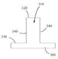
[0024]도 6a 내지 도 6e를 참조하면, 본 개시내용의 하나 이상의 실시예들은, 상부에 피쳐(310)를 갖는 기판 표면(300) 상에 스페이서 막을 증착하기 위한 프로세싱 방법들에 관한 것이다. 피쳐(310)는 막이 그 위에 증착될 수 있는 임의의 3-차원 구조일 수 있다. 도면들에 도시된 피쳐(310)는 맨드릴(mandrel)이지만, 당업자들은, 이는 단지 하나의 가능한 구조를 나타낸다는 것을 이해할 것이다. 적절한 피쳐들(310)은, 리지(ridge)들, 트렌치(trench)들, 및 비아(via)들을 포함하지만 이들로 제한되지 않는다.[0024]6A-6E, one or more embodiments of the present disclosure relate to processing methods for depositing a spacer film on a
[0025]피쳐(310)는, 최상부(320), 최하부(330), 및 측벽(340)을 포함한다. 도시된 실시예에서, 피쳐(310)는, 피쳐(310)의 양측 상에 2개의 측벽들(340)을 갖는다. 피쳐(310)는, 최상부(320) 및 최하부(330)에 의해 정의되는 높이, 및 측벽들(340) 사이의 거리에 의해 정의되는 폭을 갖는다.[0025]The
[0026]기판 표면(300)에는, 적어도 하나의 피쳐(310)가 상부에 제공된다. 본 명세서 및 첨부된 청구항들에서 사용되는 바와 같이, 이러한 방식으로 사용되는 "제공된다"라는 용어는, 기판 표면(300)이 프로세싱을 위한 환경에 배치 또는 포지셔닝된다는 것을 의미한다.[0026]On the
[0027]도 6b에 도시된 바와 같이, 적어도 하나의 피쳐(310) 상에 막이 형성되도록 기판 표면(300) 상에 막(350)이 형성된다. 막(350)은, 피쳐(310)의 최상부(320), 최하부(330), 및 측벽들(340) 상에 형성된다. 일부 실시예들에서, 막(350)은, 피쳐(310) 상에 컨포멀하게 형성된다. 본원에서 사용되는 바와 같이, "컨포멀한" 또는 "컨포멀하게"라는 용어는, 막의 평균 두께에 대하여 1 % 미만의 변동을 갖는 두께로, 노출된 표면들에 접착되고 노출된 표면들을 균일하게 덮는 층을 지칭한다. 예컨대, 1000 Å 두께의 막은 10 Å 미만의 두께 변동을 가질 것이다. 이러한 두께 및 변동은 리세스들의 에지들, 코너들, 측부들, 및 최하부를 포함한다. 예컨대, 본 개시내용의 다양한 실시예들에서 ALD에 의해 증착되는 컨포멀한 층은 복잡한 표면들 상에 본질적으로 균일한 두께의 증착된 구역에 걸친 커버리지를 제공할 것이다.[0027]As shown in FIG. 6B, a
[0028]일부 실시예들에서, 막(350)은 SiN을 포함한다. SiN의 형성은, 원자 층 증착(ALD), 플라즈마 강화 원자 층 증착(PEALD; plasma-enhanced atomic layer deposition), 화학 기상 증착(CVD; chemical vapor deposition) 및 플라즈마 강화 화학 기상 증착(PECVD; plasma-enhanced chemical vapor deposition)을 포함하는(그러나 이들로 제한되지 않음) 임의의 적절한 방법에 의해 수행될 수 있다. 일부 실시예들에서, 막(350)은, 기판 표면(300)이 실리콘 전구체 및 질소 반응물에 순차적으로 노출되는 ALD 프로세스에 의해 형성되는 SiN이다. 이와 관련하여 사용되는 바와 같이, "실리콘 전구체"는, 실리콘 분자들이 기판 표면 상에 남아 있도록 기판의 표면과 반응한다. 이와 관련하여 사용되는 바와 같이, "질소 반응물"은, 기판 표면 상의 실리콘 분자들과 반응한다.[0028]In some embodiments, the
[0029]일부 실시예들에서, SiN 막은, 실리콘 전구체에 대한 노출과 질소 반응물에 대한 노출 사이에서의 질소 전구체에 대한 노출로 기판 표면(300) 상에 형성된다. 이와 관련하여 사용되는 바와 같이, "질소 전구체"는, 기판 표면과 반응하고 이미 기판 표면 상에 있는 실리콘 종(species)과 최소로 반응한다. 달리 언급하자면, 질소 전구체는, 기판 표면 상의 실리콘 전구체 분자들과 반응하지 않는 종을 포함한다. 질소 전구체에 대한 노출은, 질소 전구체 종 및 실리콘 전구체 종 둘 모두가 기판 표면과 반응하고 서로 최소로 반응하기 때문에, 실리콘 전구체에 대한 노출 이전에, 그 동안에, 또는 그 이후에 발생할 수 있다.[0029]In some embodiments, the SiN film is formed on the
[0030]적절한 실리콘 전구체들은, 실란, 디실란, 디클로로실란(DCS), 비스(디에틸아미노)실란(BDEAS), 테트라키스(디메틸아미노)실란(TDMAS), 및/또는 비스(3차-부틸아미노)실란(BTBAS)을 포함하지만 이들로 제한되지 않는다. 일부 실시예들에서, 실리콘 전구체는 디클로로실란을 포함한다. 하나 이상의 실시예들에서, 실리콘 전구체는 본질적으로 디클로로실란으로 이루어지며, 이는, 디클로로실란 이외의 실리콘 종이 원자 기준으로 1 % 미만이 존재함을 의미한다.[0030]Suitable silicon precursors include silane, disilane, dichlorosilane (DCS), bis (diethylamino) silane (BDEAS), tetrakis (dimethylamino) silane (TDMAS), and / or bis (tert- butylamino) silane (BTBAS). ≪ / RTI > In some embodiments, the silicon precursor comprises dichlorosilane. In one or more embodiments, the silicon precursor consists essentially of dichlorosilane, which means that less than 1% of silicon species other than dichlorosilane are present.
[0031]적절한 질소 전구체들은, 분자 질소 및 암모니아를 포함하지만 이들로 제한되지 않는다. 질소 전구체 노출 동안 이용되는 프로세스 조건들은, 표면 상의 실리콘 종과의 질소 종의 반응성에 영향을 미칠 수 있다. 일부 실시예들에서, 프로세스 조건들은, 질소 전구체가 실질적으로 기판 표면과만 반응하도록 구성된다. 이와 관련하여 사용되는 바와 같이, "실질적으로 ~만"이라는 용어는, 질소 전구체가 표면 실리콘 종의 약 10 % 미만과 반응함을 의미한다.[0031]Suitable nitrogen precursors include, but are not limited to, molecular nitrogen and ammonia. The process conditions used during nitrogen precursor exposure can affect the reactivity of the nitrogen species with the silicon species on the surface. In some embodiments, the process conditions are such that the nitrogen precursor reacts substantially only with the substrate surface. As used in this context, the term " substantially only "means that the nitrogen precursor reacts with less than about 10% of the surface silicon species.
[0032]질소 반응물은, 기판 표면 상에 실리콘 질화물 막을 형성하는 종이다. 일부 실시예들에서, 질소 반응물은, 질화물 막(예컨대, SiN)의 형성을 위한 질소 원자들을 제공한다. 하나 이상의 실시예들에서, 질소 반응물은 질소-함유 종을 포함하지 않으며, 표면 종 사이의 반응을 촉진시킴으로써 질화물 막을 형성한다. 적절한 질소 반응물은, 질소 플라즈마, 암모니아 플라즈마, 수소, 질소, 암모니아, 헬륨, 아르곤, 또는 산소 중 2개 이상의 혼합물을 포함하는 플라즈마를 포함하지만 이들로 제한되지 않는다. 일부 실시예들에서, 질소 반응물은, 아르곤 및 암모니아의 플라즈마, 또는 아르곤 및 질소의 플라즈마, 또는 아르곤 및 산소의 플라즈마, 또는 헬륨 및 암모니아의 플라즈마를 포함한다. 일부 실시예들에서, 질소 반응물은, 표면 상의 질소 종과 반응하는 질소가 없는 플라즈마를 포함한다. 일부 실시예들에서, 질소 반응물은, 수소 및 아르곤의 플라즈마, 또는 수소 및 질소의 플라즈마, 또는 수소 및 헬륨의 플라즈마, 또는 수소 및 암모니아의 플라즈마, 또는 수소 및 산소의 플라즈마를 포함한다.[0032]The nitrogen reactant is a species that forms a silicon nitride film on the substrate surface. In some embodiments, the nitrogen reactant provides nitrogen atoms for the formation of a nitride film (e.g., SiN). In one or more embodiments, the nitrogen reactant does not include a nitrogen-containing species and forms a nitride film by promoting a reaction between surface species. Suitable nitrogen reactants include, but are not limited to, a plasma comprising a mixture of two or more of nitrogen plasma, ammonia plasma, hydrogen, nitrogen, ammonia, helium, argon, or oxygen. In some embodiments, the nitrogen reactant comprises a plasma of argon and ammonia, or a plasma of argon and nitrogen, or a plasma of argon and oxygen, or a plasma of helium and ammonia. In some embodiments, the nitrogen reactant comprises a nitrogen-free plasma that reacts with nitrogen species on the surface. In some embodiments, the nitrogen reactant comprises a plasma of hydrogen and argon, or a plasma of hydrogen and nitrogen, or a plasma of hydrogen and helium, or a plasma of hydrogen and ammonia, or a plasma of hydrogen and oxygen.
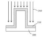
[0033]도 6c에 도시된 바와 같이, 막(350)(예컨대, 실리콘 질화물)의 형성 이후에, 막(350)은, 높은 이온 농도를 갖는 플라즈마(360)로 처리된다. 플라즈마(360)는 지향성 플라즈마일 수 있다. 본 명세서 및 첨부된 청구항들에서 사용되는 바와 같이, "지향성 플라즈마"라는 용어는, 플라즈마에 존재하는 에너제틱(energetic) 종(이온들 및 라디칼(radical)들)이 특정된 방향으로 이동하는 것을 의미한다. 예컨대, 도 6c에서, 에너제틱 종이 최상부 표면(320) 및 최하부 표면(330) 상의 막(350)과 접촉할 수 있지만 측벽들(340) 상의 막(350)과는 최소의 접촉을 갖도록 하향으로 이동하는 플라즈마(360)가 예시된다.[0033]6C, after formation of the film 350 (e.g., silicon nitride), the
[0034]높은 이온 농도를 갖는 플라즈마는, 약 1010/cm3보다 크거나 같은 농도를 갖는다. 하나 이상의 실시예들에서, 높은 이온 농도를 갖는 플라즈마는, 약 109/cm3, 1011/cm3, 1012/cm3, 1013/cm3 또는 1014/cm3보다 크거나 같은 농도를 갖는다.[0034] Plasmas having a high ion concentration have a concentration greater than or equal to about 1010 / cm3 . In one or more embodiments, the plasma having a high ion concentration, about10 9 / cm 3, 10 11 / cm 3, 10 12 / cm 3, 10 13 / cm 3 or 1014 / cm greater than3, or the same concentration .
[0035]지향성 플라즈마는, 플라즈마 종이 기판 표면으로부터 원격으로 여기(excite)되어 기판 표면을 향해 유동하는 원격 플라즈마로서 형성될 수 있다. 기판 및 기판 지지부는, 플라즈마를 생성하는 데 사용되는 전기 경로의 일부가 아닐 수 있다. 지향성 플라즈마는 또한, 기판 또는 기판 지지부가 플라즈마 형성에서 전극으로서 기능하는 직접 플라즈마로서 형성될 수 있다. 직접 플라즈마는 일반적으로 확산 플라즈마이고, 이온들이 기판으로 끌어당겨져 기판을 향해 이동하도록 기판에 바이어스를 인가함으로써 지향성으로 만들어질 수 있다.[0035]The directional plasma can be formed as a remote plasma that is excited remotely from the plasma surface of the substrate to flow toward the substrate surface. The substrate and substrate support may not be part of the electrical path used to generate the plasma. The directional plasma may also be formed as a direct plasma in which the substrate or substrate support serves as an electrode in plasma formation. A direct plasma is generally a diffusion plasma and can be made directive by applying a bias to the substrate such that the ions are attracted to the substrate and directed toward the substrate.
[0036]도 6d에 도시된 바와 같이, 높은 이온 농도를 갖는 플라즈마로 막(350)을 처리하는 것은, 최상부(320) 및 최하부(330)에서 막(350)의 특성을 개질시킨다. 일부 실시예들에서, 개질된 최상부 막(352) 및 개질된 최하부 막(353)을 형성하도록 변경되는 막(350)의 특성은, 희석된 HF(1 %)에서의 습식 에칭률에 영향을 미쳐서, 개질된 최상부 막(352) 및 개질된 최하부 막(353)이 실질적으로 측벽 막(354)에 영향을 미침이 없이 피쳐(310)로부터 에칭될 수 있다. 일부 실시예들에서, 그러한 처리는 피쳐(310)의 최상부 및 최하부 상의 막(350)을 손상시켜서, 막이 측벽에 대하여 선택적으로 에칭될 수 있다.[0036]6D, processing the
[0037]일부 실시예들에서, 개질된 최상부 막(352) 및 개질된 최하부 막(353)의 습식 에칭률은 약 15 Å/min보다 크거나 같다. 일부 실시예들에서, 개질된 최상부 막(352) 및 개질된 최하부 막(353)의 습식 에칭률은 약 20 Å/min 또는 약 25 Å/min보다 크거나 같다. 일부 실시예들에서, 개질된 최상부 막(352) 및 개질된 최하부 막(353)의 습식 에칭률은 측벽 막(354)의 습식 에칭률의 2 배보다 크거나, 3, 4, 5, 6, 7, 8, 9, 10, 11, 12, 13, 14, 15 배보다 크다.[0037]In some embodiments, the wet etch rate of the modified
[0038]처리에서 사용되는 플라즈마는, 막 특성들을 개질시킬 수 있는 임의의 적절한 플라즈마(예컨대, 직접 또는 원격)일 수 있다. 일부 실시예들에서, 처리는, 수소, 아르곤, 질소, 암모니아, 산소, 또는 헬륨 중 하나 이상을 포함한다.[0038]The plasma used in the process may be any suitable plasma (e.g., direct or remote) capable of modifying the film properties. In some embodiments, the treatment comprises at least one of hydrogen, argon, nitrogen, ammonia, oxygen, or helium.
[0039]처리에 사용되는 시간량은, 피쳐의 최상부 및 최하부 상의 막에 야기되는 손상량에 영향을 미칠 수 있다. 플라즈마 종 및 전력은, 막에 야기되는 손상의 깊이에 영향을 미칠 수 있다. 막에 대한 더 깊은 손상을 야기하는 처리 프로세스는, 막에 대한 더 얕은 손상을 야기하는 처리 프로세스보다 덜 자주 반복될 수 있다. 예컨대, He/NH3 플라즈마는 Ar/NH3 플라즈마보다 더 깊은 손상을 야기할 수 있어서, He/NH3 플라즈마로 처리하기 전에, 증착된 막이 더 두꺼울 수 있다.[0039] The amount of time used in the treatment can affect the amount of damage caused to the film on the top and bottom of the feature. The plasma species and power can affect the depth of damage caused to the film. A treatment process that causes deeper damage to the film may be repeated less frequently than a treatment process that results in shallower damage to the film. For example, a He / NH3 plasma can cause deeper damage than an Ar / NH3 plasma, so the deposited film may be thicker before being treated with a He / NH3 plasma.
[0040]막(350)의 형성 및 처리는, 미리결정된 총 두께를 갖는 막이 형성될 때까지 반복될 수 있다. 막 형성 프로세스에서의 각각의 단계는, 처리를 위한 막을 형성하도록 순차적으로 반복될 수 있다. 그런 다음 막이 처리될 수 있고 프로세스가 반복된다. 일부 실시예들에서, 플라즈마(360)로 막(350)을 처리하는 것은, 약 1 Å 내지 약 50 Å의 범위 내의 두께를 갖는 막이 증착된 이후에 발생한다. 달리 언급하자면, 막(350)은, 약 1 Å 내지 약 50 Å가 증착된 이후에 처리된다.[0040]The formation and processing of the
[0041]방법의 일부 실시예들에서, 막(350)은 에칭된다. 개질된 최상부 막(352) 및 개질된 최하부 막(353)은 측벽 막(354)에 대하여 선택적으로 에칭된다. 이와 관련하여 사용되는 바와 같이, 선택적으로 에칭한다는 것은, 최상부 및 최하부에 대한 에칭량, 에칭률, 또는 에칭의 정도가 측벽에 대한 에칭보다 크다는 것을 의미한다. 일부 실시예들에서, 피쳐의 최상부 및 최하부로부터 막을 선택적으로 제거하기 위해 희석된 HF로 막이 에칭된다. 도 6e는 에칭 프로세스의 결과를 도시한다. 도면은 피쳐(310)의 최상부 및 최하부 및 측벽 막(354)에 대해 정사각형 코너들을 도시하지만, 당업자들은, 이는 단지 예시적인 것이고 에지들 및 코너들이 완벽하게 직선 또는 정사각형이 아니라는 것을 이해할 것이다.[0041]In some embodiments of the method, the
[0042]본 개시내용의 일부 실시예들은, 공간적 프로세싱 챔버로 또한 지칭되는 배치 프로세싱 챔버를 사용하여 스페이서 재료를 증착하는 프로세스들에 관한 것이다. 도 1은, 주입기들 또는 주입기 어셈블리로 또한 지칭되는 가스 분배 어셈블리(120), 및 서셉터(susceptor) 어셈블리(140)를 포함하는 프로세싱 챔버(100)의 횡단면을 도시한다. 가스 분배 어셈블리(120)는, 프로세싱 챔버에서 사용되는 임의의 타입의 가스 전달 디바이스이다. 가스 분배 어셈블리(120)는, 서셉터 어셈블리(140)에 대면하는 전방 표면(121)을 포함한다. 전방 표면(121)은, 서셉터 어셈블리(140)를 향해 가스들의 유동을 전달하기 위해 임의의 수의 또는 다양한 개구(opening)들을 가질 수 있다. 가스 분배 어셈블리(120)는 또한, 도시된 실시예들에서는 실질적으로 원형(round)인 외측 에지(outer edge)(124)를 포함한다.[0042]Some embodiments of the present disclosure relate to processes for depositing spacer material using a batch processing chamber, also referred to as a spatial processing chamber. Figure 1 illustrates a cross-sectional view of a
[0043]사용되는 가스 분배 어셈블리(120)의 특정 타입은, 사용되는 특정 프로세스에 의존하여 변할 수 있다. 본 개시내용의 실시예들은, 서셉터와 가스 분배 어셈블리 사이의 갭이 제어되는 임의의 타입의 프로세싱 시스템에 사용될 수 있다. 다양한 타입들의 가스 분배 어셈블리들(예컨대, 샤워헤드(showerhead)들)이 이용될 수 있지만, 본 개시내용의 실시예들은 특히, 복수의 실질적으로 평행한 가스 채널들을 갖는 공간적 가스 분배 어셈블리들에 유용할 수 있다. 본 명세서 및 첨부된 청구항들에서 사용되는 바와 같이, "실질적으로 평행한"이라는 용어는, 가스 채널들의 세장형 축(elongate axis)이 동일한 일반적인 방향으로 연장됨을 의미한다. 가스 채널들의 평행도(parallelism)에 약간의 불완전성들이 존재할 수 있다. 바이너리 반응에서, 복수의 실질적으로 평행한 가스 채널들은, 적어도 하나의 제1 반응성 가스 A 채널, 적어도 하나의 제2 반응성 가스 B 채널, 적어도 하나의 퍼지(purge) 가스 P 채널 및/또는 적어도 하나의 진공 V 채널을 포함할 수 있다. 제1 반응성 가스 A 채널(들), 제2 반응성 가스 B 채널(들) 및 퍼지 가스 P 채널(들)로부터 유동하는 가스들은 웨이퍼의 최상부 표면을 향해 지향된다. 가스 유동 중 일부는, 웨이퍼의 표면을 가로질러 수평으로 이동하여, 퍼지 가스 P 채널(들)을 통해 프로세스 구역 밖으로 이동한다. 가스 분배 어셈블리의 일 단부로부터 다른 단부로 이동하는 기판은, 프로세스 가스들 각각에 차례로 노출되어, 기판 표면 상에 층을 형성할 것이다.[0043]The particular type of
[0044]일부 실시예들에서, 가스 분배 어셈블리(120)는, 단일 주입기 유닛으로 제조되는 강성의 고정식 바디(rigid stationary body)이다. 하나 이상의 실시예들에서, 도 2에 도시된 바와 같이, 가스 분배 어셈블리(120)는 복수의 개별적인 섹터(sector)들(예컨대, 주입기 유닛들(122))로 구성된다. 설명되는 본 개시내용의 다양한 실시예들에 단일 피스(piece) 바디 또는 다중-섹터 바디가 사용될 수 있다.[0044]In some embodiments, the
[0045]서셉터 어셈블리(140)는 가스 분배 어셈블리(120) 아래에 포지셔닝된다. 서셉터 어셈블리(140)는, 최상부 표면(141), 및 최상부 표면(141)에 있는 적어도 하나의 리세스(142)를 포함한다. 서셉터 어셈블리(140)는 또한 최하부 표면(143) 및 에지(144)를 갖는다. 리세스(142)는, 프로세싱되는 기판들(60)의 형상 및 사이즈에 의존하여, 임의의 적절한 형상 및 사이즈일 수 있다. 도 1에 도시된 실시예에서, 리세스(142)는 웨이퍼의 최하부를 지지하기 위한 평평한 최하부를 갖지만, 리세스의 최하부는 변할 수 있다. 일부 실시예들에서, 리세스는 리세스의 외측 둘레 에지 주위에 스텝 구역(step region)들을 가지며, 이 스텝 구역들은 웨이퍼의 외측 둘레 에지를 지지하도록 사이즈가 정해진다. 스텝들에 의해 지지되는, 웨이퍼의 외측 둘레 에지의 양(amount)은, 예컨대, 웨이퍼의 후면측 상에 이미 존재하는 피쳐들의 존재, 및 웨이퍼의 두께에 의존하여 변할 수 있다.[0045]The
[0046]일부 실시예들에서, 도 1에 도시된 바와 같이, 서셉터 어셈블리(140)의 최상부 표면(141)의 리세스(142)는, 리세스(142) 내에 지지되는 기판(60)이 서셉터(140)의 최상부 표면(141)과 실질적으로 동일 평면 상에 있는 최상부 표면(61)을 갖도록, 사이즈가 정해진다. 본 명세서 및 첨부된 청구항들에서 사용되는 바와 같이, "실질적으로 동일 평면 상에 있는"이라는 용어는, 웨이퍼의 최상부 표면과 서셉터 어셈블리의 최상부 표면이 ±0.2 mm 내에서 동일 평면 상에 있다는 것을 의미한다. 일부 실시예들에서, 최상부 표면들은, ±0.15 mm, ±0.10 mm, 또는 ±0.05 mm 내에서 동일 평면 상에 있다.[0046]1, the
[0047]도 1의 서셉터 어셈블리(140)는, 서셉터 어셈블리(140)를 상승, 하강, 및 회전시킬 수 있는 지지 포스트(post)(160)를 포함한다. 서셉터 어셈블리는, 지지 포스트(160)의 중심 내에 가열기, 또는 가스 라인들, 또는 전기 컴포넌트들을 포함할 수 있다. 지지 포스트(160)는, 서셉터 어셈블리(140)와 가스 분배 어셈블리(120) 사이의 갭을 증가시키거나 감소시켜서 서셉터 어셈블리(140)를 적절한 포지션으로 이동시키는 주요 수단일 수 있다. 서셉터 어셈블리(140)는 또한, 서셉터 어셈블리(140)와 가스 분배 어셈블리(120) 사이에 미리결정된 갭(170)을 생성하기 위해 서셉터 어셈블리(140)에 대해 미세-조정(micro-adjustment)들을 행할 수 있는 정밀 튜닝 액추에이터(fine tuning actuator)들(162)을 포함할 수 있다.[0047]The
[0048]일부 실시예들에서, 갭(170) 거리는, 약 0.1 mm 내지 약 5.0 mm의 범위, 또는 약 0.1 mm 내지 약 3.0 mm의 범위, 또는 약 0.1 mm 내지 약 2.0 mm의 범위, 또는 약 0.2 mm 내지 약 1.8 mm의 범위, 또는 약 0.3 mm 내지 약 1.7 mm의 범위, 또는 약 0.4 mm 내지 약 1.6 mm의 범위, 또는 약 0.5 mm 내지 약 1.5 mm의 범위, 또는 약 0.6 mm 내지 약 1.4 mm의 범위, 또는 약 0.7 mm 내지 약 1.3 mm의 범위, 또는 약 0.8 mm 내지 약 1.2 mm의 범위, 또는 약 0.9 mm 내지 약 1.1 mm의 범위 내에 있거나, 약 1 mm 이다.[0048]In some embodiments, the
[0049]도면들에 도시된 프로세싱 챔버(100)는, 서셉터 어셈블리(140)가 복수의 기판들(60)을 홀딩(hold)할 수 있는 캐러셀-타입 챔버(carousel-type chamber)이다. 도 2에 도시된 바와 같이, 가스 분배 어셈블리(120)는 복수의 별개의 주입기 유닛들(122)을 포함할 수 있고, 각각의 주입기 유닛(122)은, 웨이퍼가 주입기 유닛 아래로 이동됨에 따라, 웨이퍼 상에 막을 증착할 수 있다. 2개의 파이-형상(pie-shaped) 주입기 유닛들(122)이, 서셉터 어셈블리(140) 위에 그리고 서셉터 어셈블리(140)의 대략적 대향 측들 상에 포지셔닝된 것으로 도시된다. 이러한 수의 주입기 유닛들(122)은 단지 예시적인 목적들을 위해 도시된다. 더 많거나 더 적은 주입기 유닛들(122)이 포함될 수 있다는 것이 이해될 것이다. 일부 실시예들에서, 서셉터 어셈블리(140)의 형상과 일치하는 형상을 형성하기에 충분한 수의 파이-형상 주입기 유닛들(122)이 존재한다. 일부 실시예들에서, 개별적 파이-형상 주입기 유닛들(122) 각각은, 다른 주입기 유닛들(122) 중 어느 것에도 영향을 미치지 않으면서, 독립적으로 이동, 제거, 및/또는 교체될 수 있다. 예컨대, 로봇이 기판들(60)을 로딩(load)/언로딩(unload)하기 위해 서셉터 어셈블리(140)와 가스 분배 어셈블리(120) 사이의 구역에 액세스하는 것을 허용하기 위하여, 하나의 세그먼트(segment)가 상승될 수 있다.[0049]The
[0050]웨이퍼들이 동일한 프로세스 흐름을 경험하도록, 다수의 웨이퍼들을 동시에 프로세싱하기 위해, 다수의 가스 주입기들을 갖는 프로세싱 챔버들이 사용될 수 있다. 예컨대, 도 3에 도시된 바와 같이, 프로세싱 챔버(100)는 4개의 가스 주입기 어셈블리들 및 4개의 기판들(60)을 갖는다. 프로세싱의 착수 시에, 기판들(60)은 주입기 어셈블리들(30) 사이에 포지셔닝될 수 있다. 서셉터 어셈블리(140)를 45°만큼 회전시키는 것(17)은, 가스 분배 어셈블리들(120) 아래의 점선 원에 의해 예시된 바와 같이, 가스 분배 어셈블리들(120) 사이에 있는 각각의 기판(60)이, 막 증착을 위해 가스 분배 어셈블리(120)로 이동되는 것을 초래할 것이다. 부가적인 45° 회전은 기판들(60)을 주입기 어셈블리들(30)로부터 멀어지게 이동시킬 것이다. 기판들(60) 및 가스 분배 어셈블리들(120)의 수는 동일하거나 상이할 수 있다. 일부 실시예들에서, 존재하는 가스 분배 어셈블리들과 동일한 수의 프로세싱되는 웨이퍼들이 존재한다. 하나 이상의 실시예들에서, 프로세싱되는 웨이퍼들의 수는, 가스 분배 어셈블리들의 수의 분율(fraction) 또는 정수배이다. 예컨대, 4개의 가스 분배 어셈블리들이 존재하는 경우, 프로세싱되는 4x개의 웨이퍼들이 존재하며, 여기서, x는 1과 동일하거나 그 초과인 정수 값이다. 일 예시적인 실시예에서, 가스 분배 어셈블리(120)는 가스 커튼들에 의해 분리되는 8개의 프로세스 구역들을 포함하며, 서셉터 어셈블리(140)는 6개의 웨이퍼들을 홀딩할 수 있다.[0050]Processing chambers with multiple gas injectors can be used to process multiple wafers simultaneously, so that the wafers experience the same process flow. For example, as shown in FIG. 3, the
[0051]도 3에 도시된 프로세싱 챔버(100)는 단지 하나의 가능한 구성을 나타낼 뿐이며, 본 개시내용의 범위를 제한하는 것으로 고려되지 않아야 한다. 여기서, 프로세싱 챔버(100)는 복수의 가스 분배 어셈블리들(120)을 포함한다. 도시된 실시예에서, 프로세싱 챔버(100) 둘레에 균등하게 이격된 4개의 가스 분배 어셈블리들(주입기 어셈블리들(30)로 또한 지칭됨)이 존재한다. 도시된 프로세싱 챔버(100)는 팔각형이지만, 이는 하나의 가능한 형상이고, 본 개시내용의 범위를 제한하는 것으로 고려되지 않아야 한다는 것을 당업자들은 이해할 것이다. 도시된 가스 분배 어셈블리들(120)은 사다리꼴이지만, 단일 원형 컴포넌트이거나 또는 도 2에 도시된 것과 같이 복수의 파이-형상 세그먼트들로 구성될 수 있다.[0051]The
[0052]도 3에 도시된 실시예는 로드 록(load lock) 챔버(180), 또는 버퍼 스테이션과 같은 보조 챔버를 포함한다. 이러한 챔버(180)는, 예컨대 기판들(기판들(60)로 또한 지칭됨)이 챔버(100)로 로딩되는 것/챔버(100)로부터 언로딩되는 것을 허용하기 위해, 프로세싱 챔버(100)의 측면에 연결된다. 기판을 서셉터 상으로 이동시키기 위해, 웨이퍼 로봇이 챔버(180)에 포지셔닝될 수 있다.[0052]The embodiment shown in FIG. 3 includes a
[0053]캐러셀(예컨대, 서셉터 어셈블리(140))의 회전은 연속적이거나 단속적(intermittent)(불연속적)일 수 있다. 연속적인 프로세싱에서, 웨이퍼들은, 웨이퍼들이 주입기들 각각에 차례로 노출되도록, 끊임없이 회전한다. 불연속적인 프로세싱에서, 웨이퍼들은, 주입기 구역으로 이동되어 정지될 수 있으며, 그런 다음, 주입기들 사이의 구역(84)으로 이동되어 정지될 수 있다. 예컨대, 캐러셀은, 웨이퍼들이 주입기를 가로질러 주입기-간(inter-injector) 구역으로부터 이동하고(또는, 주입기 근처에서 정지함) 그리고 캐러셀이 다시 일시정지될 수 있는 다음 주입기-간 구역으로 이동하도록, 회전할 수 있다. 주입기들 사이에서 일시정지되는 것은, 각각의 층 증착 사이의 부가적인 프로세싱 단계들(예컨대, 플라즈마에 대한 노출)을 위한 시간을 제공할 수 있다.[0053]The rotation of the carousel (e.g., the susceptor assembly 140) may be continuous or intermittent (discontinuous). In continuous processing, the wafers are constantly rotated so that the wafers are sequentially exposed to each of the implanters. In discrete processing, the wafers can be moved to the injector section and stopped, and then moved to the
[0054]도 4는, 주입기 유닛(122)으로 지칭될 수 있는 가스 분배 어셈블리(220)의 섹터 또는 부분을 도시한다. 주입기 유닛들(122)은 개별적으로 또는 다른 주입기 유닛들과 결합되어 사용될 수 있다. 예컨대, 도 5에 도시된 바와 같이, 도 4의 주입기 유닛(122)들 4개가 결합되어, 단일 가스 분배 어셈블리(220)를 형성한다. (명확성을 위해, 4개의 주입기 유닛들을 분리하는 라인들은 도시되지 않음) 도 4의 주입기 유닛(122)이, 퍼지 가스 포트들(155) 및 진공 포트들(145)에 부가하여, 제1 반응성 가스 포트(125) 및 제2 가스 포트(135) 둘 모두를 갖지만, 주입기 유닛(122)이 이들 컴포넌트들 전부를 필요로 하지는 않는다.[0054]FIG. 4 illustrates a sector or portion of a gas distribution assembly 220 that may be referred to as an
[0055]도 4 및 도 5 둘 모두를 참조하면, 하나 이상의 실시예에 따른 가스 분배 어셈블리(220)는, 복수의 섹터들(또는 주입기 유닛들(122))을 포함할 수 있고, 각각의 섹터는 동일하거나 상이하다. 가스 분배 어셈블리(220)는 프로세싱 챔버 내에 포지셔닝되며, 가스 분배 어셈블리(220)의 전방 표면(121)에 복수의 세장형 가스 포트들(125, 135, 145)을 포함한다. 복수의 세장형 가스 포트들(125, 135, 145, 155)은, 가스 분배 어셈블리(220)의 내측 둘레 에지(123)에 인접한 영역으로부터 외측 둘레 에지(124)에 인접한 영역을 향해 연장된다. 도시된 복수의 가스 포트들은, 제1 반응성 가스 포트(125), 제2 가스 포트(135), 제1 반응성 가스 포트들 및 제2 반응성 가스 포트들 각각을 둘러싸는 진공 포트(145), 및 퍼지 가스 포트(155)를 포함한다.[0055]4 and 5, the gas distribution assembly 220 according to one or more embodiments may include a plurality of sectors (or syringe units 122), wherein each sector is the same It is different. The gas distribution assembly 220 is positioned within the processing chamber and includes a plurality of
[0056]도 4 또는 도 5에 도시된 실시예들을 참조하면, 포트들이 적어도 내측 둘레 구역 주위로부터 적어도 외측 둘레 구역 주위로 연장되는 것으로 서술되지만, 포트들은 내측 구역으로부터 외측 구역으로 단지 방사상으로 연장되는 것 이상으로 연장될 수 있다. 포트들은, 진공 포트(145)가 반응성 가스 포트(125) 및 반응성 가스 포트(135)를 둘러쌈에 따라, 접선방향으로(tangentially) 연장될 수 있다. 도 4 및 도 5에 도시된 실시예에서, 웨지 형상 반응성 가스 포트들(125, 135)은, 내측 둘레 구역 및 외측 둘레 구역에 인접해 있는 것을 포함하는 모든 에지들이 진공 포트(145)에 의해 둘러싸인다.[0056]4 or 5, the ports are described as extending from at least around the inner perimeter area to at least around the outer perimeter area, but the ports are more than just radially extending from the inner area to the outer area Can be extended. The ports can extend tangentially as the
[0057]도 4를 참조하면, 기판이 경로(127)를 따라 이동함에 따라, 기판 표면의 각각의 부분은 다양한 반응성 가스들에 노출된다. 경로(127)를 따르기 위해, 기판은, 퍼지 가스 포트(155), 진공 포트(145), 제1 반응성 가스 포트(125), 진공 포트(145), 퍼지 가스 포트(155), 진공 포트(145), 제2 가스 포트(135) 및 진공 포트(145)에 노출되거나 또는 이들을 "만날(see)" 것이다. 따라서, 도 4에 도시된 경로(127)의 종단에서, 기판은 제1 반응성 가스(125) 및 제2 반응성 가스(135)에 노출되어 층을 형성한다. 도시된 주입기 유닛(122)은 사분원(quarter circle)을 구성하지만, 더 크거나 더 작을 수 있다. 도 5에 도시된 가스 분배 어셈블리(220)는, 도 4의 주입기 유닛(122) 4개가 연속해서 연결되어 결합된 것으로 고려될 수 있다.[0057]Referring to FIG. 4, as the substrate moves along
[0058]도 4의 주입기 유닛(122)은, 반응성 가스들을 분리하는 가스 커튼(150)을 도시한다. "가스 커튼"이라는 용어는, 혼합으로부터 반응성 가스들을 분리하는, 가스 유동들 또는 진공의 임의의 조합을 설명하기 위해 사용된다. 도 4에 도시된 가스 커튼(150)은, 제1 반응성 가스 포트(125) 옆의 진공 포트(145)의 부분, 중간의 퍼지 가스 포트(155), 및 제2 가스 포트(135) 옆의 진공 포트(145)의 부분을 포함한다. 가스 유동과 진공의 이러한 조합은, 제1 반응성 가스와 제2 반응성 가스의 가스 상 반응들을 방지하거나 최소화하는 데 사용될 수 있다.[0058]The
[0059]도 5를 참조하면, 가스 분배 어셈블리(220)로부터의 가스 유동들과 진공의 조합은, 복수의 프로세스 구역들(250)로의 분리를 형성한다. 프로세스 구역들은, 프로세스 구역들(250) 사이의 가스 커튼(150)과 함께, 개별적인 가스 포트들(125, 135) 주위에 개략적으로 정의된다. 도 5에 도시된 실시예는 8개의 별개의 프로세스 구역들(250)을 구성하며, 이들 사이에 8개의 별개의 가스 커튼들(150)이 있다. 프로세싱 챔버는 적어도 2개의 프로세스 구역을 가질 수 있다. 일부 실시예들에서, 적어도 3개, 4개, 5개, 6개, 7개, 8개, 9개, 10개, 11개 또는 12개의 프로세스 구역들이 존재한다.[0059]Referring to FIG. 5, the combination of gas flows and vacuum from the gas distribution assembly 220 forms a separation into a plurality of
[0060]프로세싱 동안, 기판은 임의의 주어진 시간에서 하나 초과의 프로세스 구역(250)에 노출될 수 있다. 그러나, 상이한 프로세스 구역들에 노출되는 부분들은 그 둘을 분리하는 가스 커튼을 가질 것이다. 예컨대, 기판의 리딩 에지(leading edge)가, 제2 가스 포트(135)를 포함하는 프로세스 구역에 진입하는 경우, 기판의 중간 부분은 가스 커튼(150) 아래에 있을 것이며, 기판의 트레일링 에지(trailing edge)는 제1 반응성 가스 포트(125)를 포함하는 프로세스 구역 내에 있을 것이다.[0060]During processing, the substrate may be exposed to more than one
[0061]예컨대, 로드 록 챔버일 수 있는 팩토리 인터페이스(factory interface)(280)가 프로세싱 챔버(100)에 연결된 것으로 도시되어 있다. 기판(60)은, 레퍼런스 프레임(frame of reference)을 제공하기 위해 가스 분배 어셈블리(220) 위에 겹쳐져 있는 것으로 도시된다. 기판(60)은 종종, 가스 분배 플레이트(120)의 전방 표면(121) 근처에 홀딩될 서셉터 어셈블리 상에 놓일 수 있다. 기판(60)은, 팩토리 인터페이스(280)를 통해 프로세싱 챔버(100) 내로, 기판 지지부 또는 서셉터 어셈블리(도 3 참조) 상에 로딩된다. 기판(60)은 프로세스 구역 내에 포지셔닝되는 것으로 도시될 수 있는데, 이는, 기판이 제1 반응성 가스 포트(125)에 인접하게 그리고 2개의 가스 커튼들(150a, 150b) 사이에 로케이팅되기 때문이다. 경로(127)를 따라 기판(60)을 회전시키는 것은, 기판을 프로세싱 챔버(100) 주위로 반시계방향으로 이동시킬 것이다. 따라서, 기판(60)은 제1 프로세스 구역(250a) 내지 제8 프로세스 구역(250h)(이들 사이의 모든 프로세스 구역들을 포함함)에 노출될 것이다.[0061]For example, a
[0062]본 개시내용의 실시예들은, 복수의 프로세스 구역들(250a 내지 250h)을 갖는 프로세싱 챔버(100)를 포함하는 프로세싱 방법들에 관한 것이며, 각각의 프로세스 구역은 가스 커튼(150)에 의해 인접 구역으로부터 분리된다. 예컨대, 프로세싱 챔버는 도 5에 도시된다. 프로세싱 챔버 내의 가스 커튼들 및 프로세스 구역들의 수는, 가스 유동들의 어레인지먼트(arrangement)에 따라 임의의 적절한 수일 수 있다. 도 5에 도시된 실시예는 8개의 가스 커튼들(150) 및 8개의 프로세스 구역들(250a-250h)을 갖는다.[0062]Embodiments of the present disclosure are directed to processing methods that include a
[0063]복수의 기판들(60)이, 기판 지지부, 예컨대, 도 1 및 도 2에 도시된 서셉터 어셈블리(140) 상에 포지셔닝된다. 복수의 기판들(60)은 프로세싱을 위해 프로세스 구역들 주위로 회전된다. 일반적으로, 가스 커튼들(150)은, 챔버 내로 어떠한 반응성 가스도 유동하지 않는 기간들을 포함하여 프로세싱 전반에 걸쳐 인게이징(engage)된다(가스가 유동하고 진공이 온(on) 됨).[0063]A plurality of
[0064]따라서, 본 개시내용의 하나 이상의 실시예들은, 도 5에 도시된 것과 같은 배치 프로세싱 챔버를 활용하는 프로세싱 방법들에 관한 것이다. 기판(60)은 복수의 섹션들(250)을 갖는 프로세싱 챔버 내에 배치되며, 각각의 섹션은 가스 커튼(150)에 의해 인접 섹션으로부터 분리된다.[0064]Accordingly, one or more embodiments of the present disclosure relate to processing methods that utilize a batch processing chamber as shown in FIG. The
[0065]본 방법의 일부 실시예들은, 그 위에 피쳐를 갖는 기판 표면을, 막을 증착하기 위한 증착 환경에 노출시키는 단계를 포함한다. 이와 관련하여 사용되는 바와 같이, "증착 환경"은, 막을 개별적으로 또는 순차적으로 증착하는 하나 이상의 프로세스 구역들 또는 프로세스 조건들을 포함한다.[0065]Some embodiments of the method include exposing a substrate surface having features thereon to a deposition environment for depositing the film. As used in this regard, the "deposition environment" includes one or more process zones or process conditions for depositing the films individually or sequentially.
[0066]예시적인 프로세스에서, 기판 표면의 적어도 일부분은 프로세싱 챔버의 제1 섹션(250a)에서 제1 프로세스 조건에 노출된다. 일부 실시예들의 제1 프로세스 조건은, 실리콘 막을 형성하기 위한 실리콘 전구체를 포함한다. 하나 이상의 실시예들에서, 제1 프로세스 조건은 디클로로실란을 포함한다.[0066]In an exemplary process, at least a portion of the substrate surface is exposed to a first process condition in a
[0067]기판 표면은, 가스 커튼(150)을 통해 제2 섹션(250b)으로 측방향으로 이동된다. 실리콘 층은 제2 섹션(250b)에서 제2 프로세스 조건에 노출된다. 일부 실시예들의 제2 프로세스 조건은, 질소 막을 형성하기 위한 질소 전구체를 포함한다. 하나 이상의 실시예들에서, 제2 프로세스 조건은 암모니아를 포함한다.[0067]The substrate surface is laterally moved to the second section 250b through the
[0068]기판 표면은, 제2 프로세스 구역으로부터 제3 섹션(250c)으로 측방향으로 이동된다. 일부 실시예들의 제3 섹션(250c)은, 피쳐의 최상부, 최하부, 및 측벽들 상의 막을 형성하기 위한 반응물을 포함하는 제3 프로세스 조건을 포함한다. 제4 섹션(250d)은 불활성 환경을 포함할 수 있다. 일부 실시예들에서, 제3 섹션(250c)이 불활성 환경을 포함함으로써, 실질적으로 표면 반응이 존재하지 않고, 제4 섹션(250d)은 제3 프로세스 조건을 포함한다. 하나 이상의 실시예들에서, 제3 프로세스 조건은 N2/Ar 플라즈마를 포함한다.[0068] The substrate surface is moved laterally from the second process zone to the
[0069]제1 프로세스 조건, 제2 프로세스 조건, 및 제3 프로세스 조건에 대한 노출은, 미리결정된 두께를 갖는 막을 형성하도록 반복될 수 있다. 예컨대, 도 5를 참조하면, 제1 섹션(250a) 및 제5 섹션(250e)은 제1 프로세스 조건을 포함할 수 있고; 제2 섹션(250b) 및 제6 섹션(250f)은 제2 프로세스 조건을 포함할 수 있고; 제3 섹션(250c) 및 제7 섹션(250g)은 불활성 환경을 포함할 수 있고; 그리고 제4 섹션(250d) 및 제8 섹션(250h)은 제3 프로세스 조건을 포함할 수 있다. 이러한 어레인지먼트에서, 기판의 각각의 회전은 2개의 층들을 형성한다. 프로세스 구역들을 설명하기 위해 "제1" 및 "제2"와 같은 서수들을 사용하는 것이 프로세싱 챔버 내의 특정 위치 또는 프로세싱 챔버 내에서의 노출 순서를 암시하지 않음을 당업자들은 이해할 것이다.[0069]Exposure to the first process condition, the second process condition, and the third process condition may be repeated to form a film having a predetermined thickness. For example, referring to FIG. 5, the
[0070]일단 미리결정된 두께의 층이 형성되었으면, 제1 프로세스 조건, 제2 프로세스 조건, 및 제3 프로세스 조건은 불활성 환경들로 변경될 수 있다. 제3 섹션(250c)에서의 불활성 환경은, 예컨대, 피쳐의 최상부 및 최하부 상의 실리콘 질화물 막의 습식 에칭률을 선택적으로 감소시키는 높은 이온 농도 플라즈마를 포함하는 처리 환경으로 변경될 수 있다. 예컨대, 높은 이온 농도 플라즈마는 He/NH3을 포함할 수 있다. 처리 환경에 대한 노출 이후에, 프로세싱 챔버의 개별 섹션들이 다시 이전 셋팅들로 변경될 수 있거나 프로세스가 중단될 수 있다.Once the layer of predetermined thickness has been formed, the first process condition, the second process condition, and the third process condition may be changed to inert environments. The inert environment in the
[0071]도 7을 참조하면, 일부 실시예들은, 슬롯(382)을 갖는 플라즈마 어셈블리(380)를 사용한다. 플라즈마는, 플라즈마 캐비티(cavity)(384) 내에 형성되고 슬롯(382)을 통해 기판 표면(300)을 향해 유동한다. 도 7에 도시된 도면은, 슬롯(382)이 페이지 밖으로 연장되는 횡단면도이다. 슬롯(382)은 에지들(386)을 가지며, 슬롯(382)을 통해, 플라즈마 캐비티(384) 내에 형성된 플라즈마가 유동한다. 일부 실시예들에서, 플라즈마는, 슬롯(382)의 에지들(386) 근처에서 높은 이온 에너지 및 농도를 갖는다.[0071]Referring to FIG. 7, some embodiments use a plasma assembly 380 having a
[0072]하나 이상의 실시예들에 따르면, 기판은, 층을 형성하기 전에 그리고/또는 층을 형성한 후에, 프로세싱을 겪는다. 이러한 프로세싱은, 동일한 챔버에서 또는 하나 이상의 별개의 프로세싱 챔버들에서 수행될 수 있다. 일부 실시예들에서, 기판은, 추가적인 프로세싱을 위해, 제1 챔버로부터 별개의 제2 챔버로 이동된다. 기판은, 제1 챔버로부터 별개의 프로세싱 챔버로 직접적으로 이동될 수 있거나, 또는 기판은, 제1 챔버로부터 하나 이상의 이송 챔버들로 이동될 수 있고, 그 후에, 별개의 프로세싱 챔버로 이동될 수 있다. 따라서, 프로세싱 장치는 이송 스테이션과 통신하는 다수의 챔버들을 포함할 수 있다. 이러한 종류의 장치는 "클러스터 툴(cluster tool)" 또는 "클러스터형 시스템" 등으로 지칭될 수 있다.[0072]According to one or more embodiments, the substrate undergoes processing before forming the layer and / or after forming the layer. Such processing may be performed in the same chamber or in one or more separate processing chambers. In some embodiments, the substrate is moved from the first chamber to a separate second chamber for further processing. The substrate can be moved directly from the first chamber to a separate processing chamber or the substrate can be moved from the first chamber to one or more transfer chambers and then moved to a separate processing chamber . Thus, the processing device may include a plurality of chambers in communication with the transfer station. Devices of this kind may be referred to as "cluster tools" or "clustered systems ".
[0073]일반적으로, 클러스터 툴은, 기판 중심-발견 및 배향, 어닐링, 어닐링, 증착, 및/또는 에칭을 포함하는 다양한 기능들을 수행하는 다수의 챔버들을 포함하는 모듈러 시스템이다. 하나 이상의 실시예들에 따르면, 클러스터 툴은, 적어도 제1 챔버 및 중앙 이송 챔버를 포함한다. 중앙 이송 챔버는, 로드 록 챔버들과 프로세싱 챔버들 사이에서 그리고 이들 간에서 기판들을 셔틀링(shuttle)할 수 있는 로봇을 하우징(house)할 수 있다. 이송 챔버는 통상적으로, 진공 조건에서 유지되고, 기판들을, 하나의 챔버로부터 다른 챔버로, 그리고/또는 클러스터 툴의 전방 단부에 포지셔닝된(positioned) 로드 록 챔버로 셔틀링하기 위한 중간 스테이지를 제공한다. 본 개시내용에 대해 적응될 수 있는 2개의 잘-알려진 클러스터 툴들은 Centura® 및 Endura®이고, 이들 둘 모두는, 캘리포니아 주 Santa Clara의 Applied Materials, Inc.로부터 입수가능하다. 하지만, 챔버들의 정확한 어레인지먼트 및 조합은, 본원에서 설명되는 바와 같은 프로세스의 특정 단계들을 수행하는 목적들을 위해 변경될 수 있다. 사용될 수 있는 다른 프로세싱 챔버들은, 주기적 층 증착(CLD; cyclical layer deposition), 원자 층 증착(ALD), 화학 기상 증착(CVD; chemical vapor deposition), 물리 기상 증착(PVD; physical vapor deposition), 에칭, 사전-세정, 화학 세정, RTP와 같은 열 처리, 플라즈마 질화(nitridation), 어닐링, 배향, 히드록실화(hydroxylation), 및 다른 기판 프로세스들을 포함하지만 이들로 제한되지 않는다. 클러스터 툴 상의 챔버에서 프로세스들을 수행함으로써, 대기 불순물들에 의한 기판의 표면 오염이, 후속 막을 증착하기 전의 산화 없이, 회피될 수 있다.[0073]Generally, a cluster tool is a modular system that includes a number of chambers that perform various functions including substrate center-finding and orientation, annealing, annealing, deposition, and / or etching. According to one or more embodiments, the cluster tool comprises at least a first chamber and a central transfer chamber. The central transfer chamber may house a robot capable of shuttling the substrates between and between the load lock chambers and the processing chambers. The transfer chamber is typically maintained in a vacuum condition and provides an intermediate stage for shuttling the substrates from one chamber to another and / or to a load lock chamber positioned at the front end of the cluster tool . Two well-known cluster tools that can be adapted for this disclosure are Centura® and Endura®, both of which are available from Applied Materials, Inc. of Santa Clara, Calif. However, the precise arrangement and combination of chambers may be modified for purposes of performing certain steps of the process as described herein. Other processing chambers that may be used include, but are not limited to, cyclical layer deposition (CLD), atomic layer deposition (ALD), chemical vapor deposition (CVD), physical vapor deposition (PVD) But are not limited to, pre-cleaning, chemical cleaning, thermal processing such as RTP, plasma nitridation, annealing, orientation, hydroxylation, and other substrate processes. By performing processes in a chamber on a cluster tool, surface contamination of the substrate by atmospheric impurities can be avoided without oxidation prior to deposition of the subsequent film.
[0074]하나 이상의 실시예들에 따르면, 기판은 지속적으로 진공 또는 "로드 록" 조건들 하에 있고, 하나의 챔버로부터 다음 챔버로 이동될 때, 주변 공기에 노출되지 않는다. 따라서, 이송 챔버들은 진공 하에 있고, 진공 압력 하에서 "펌핑 다운(pump down)"된다. 불활성 가스들이 프로세싱 챔버들 또는 이송 챔버들에 존재할 수 있다. 일부 실시예들에서, 불활성 가스는, 반응물들의 일부 또는 전부를 제거하기 위해, 퍼지(purge) 가스로서 사용된다. 하나 이상의 실시예들에 따르면, 퍼지 가스는, 반응물들이 증착 챔버로부터 이송 챔버로 그리고/또는 부가적인 프로세싱 챔버로 이동하는 것을 방지하기 위해, 증착 챔버의 출구에서 주입된다. 따라서, 불활성 가스의 유동은 챔버의 출구에서 커튼을 형성한다.[0074]According to one or more embodiments, the substrate is under constant vacuum or "load lock" conditions and is not exposed to ambient air when moved from one chamber to the next. Thus, the transfer chambers are under vacuum and are "pumped down" under vacuum pressure. Inert gases may be present in the processing chambers or transfer chambers. In some embodiments, the inert gas is used as a purge gas to remove some or all of the reactants. According to one or more embodiments, the purge gas is injected at the outlet of the deposition chamber to prevent reactants from moving from the deposition chamber to the transfer chamber and / or to the additional processing chamber. Thus, the flow of the inert gas forms a curtain at the outlet of the chamber.
[0075]기판은, 단일 기판이 로딩되고, 프로세싱되고, 그리고 다른 기판이 프로세싱되기 전에 언로딩되는, 단일 기판 증착 챔버들에서 프로세싱될 수 있다. 기판은 또한, 다수의 기판이 챔버의 제1 부분 내로 개별적으로 로딩되고, 챔버를 통해 이동하고, 그리고 챔버의 제2 부분으로부터 언로딩되는, 컨베이어 시스템과 유사하게, 연속적인 방식으로 프로세싱될 수 있다. 챔버 및 연관된 컨베이어 시스템의 형상은 직선 경로 또는 곡선 경로를 형성할 수 있다. 부가적으로, 프로세싱 챔버는, 다수의 기판들이 중심 축을 중심으로 이동되고 그리고 캐러셀(carousel) 경로 전반에 걸쳐 증착, 에칭, 어닐링, 세정 등의 프로세스들에 노출되는 캐러셀일 수 있다.[0075]The substrate may be processed in a single substrate deposition chamber, where a single substrate is loaded, processed, and unloaded before the other substrate is processed. The substrate can also be processed in a continuous manner, similar to a conveyor system in which a plurality of substrates are individually loaded into a first portion of a chamber, moved through a chamber, and unloaded from a second portion of the chamber . The shape of the chamber and associated conveyor system may form a straight or curved path. Additionally, the processing chamber may be a carousel in which a plurality of substrates are moved about a central axis and exposed to processes such as deposition, etching, annealing, cleaning, etc. throughout the carousel path.
[0076]프로세싱 동안, 기판은 가열 또는 냉각될 수 있다. 그러한 가열 또는 냉각은, 기판 지지부의 온도를 변화시키는 것 및 가열된 또는 냉각된 가스들을 기판 표면으로 유동시키는 것을 포함하는(그러나 이들로 제한되지 않음) 임의의 적절한 수단에 의해 달성될 수 있다. 일부 실시예들에서, 기판 지지부는, 기판 온도를 전도식으로(conductively) 변화시키도록 제어될 수 있는 가열기/냉각기를 포함한다. 하나 이상의 실시예들에서, 이용되는 가스들(반응성 가스들 또는 불활성 가스들)은, 기판 온도를 국부적으로 변화시키도록 가열 또는 냉각된다. 일부 실시예들에서, 가열기/냉각기는, 기판 온도를 대류식으로(convectively) 변화시키기 위해, 챔버 내에서 기판 표면에 인접하게 포지셔닝된다.[0076]During processing, the substrate may be heated or cooled. Such heating or cooling may be accomplished by any suitable means including, but not limited to, changing the temperature of the substrate support and flowing heated or cooled gases to the substrate surface. In some embodiments, the substrate support includes a heater / cooler that can be controlled to conductively vary the substrate temperature. In one or more embodiments, the gases used (reactive gases or inert gases) are heated or cooled to locally vary the substrate temperature. In some embodiments, the heater / cooler is positioned adjacent to the substrate surface within the chamber to convectively vary the substrate temperature.
[0077]기판은 또한, 프로세싱 동안, 고정식일 수 있거나 또는 회전될 수 있다. 회전되는 기판은, 연속적으로 또는 불연속적인 단계들로 회전될 수 있다. 예컨대, 기판은 전체 프로세스 전반에 걸쳐 회전될 수 있거나, 또는 기판은, 상이한 반응성 또는 퍼지 가스들에 대한 노출들 사이에서 작은 양만큼 회전될 수 있다. (연속적으로 또는 단계들로) 프로세싱 동안 기판을 회전시키는 것은, 예컨대, 가스 유동 기하학적 구조들에서의 국부적인 변동성의 영향을 최소화함으로써, 더 균일한 증착 또는 에칭을 생성하는 것을 도울 수 있다.[0077]The substrate may also be stationary or rotated during processing. The substrate to be rotated can be rotated in successive or discontinuous steps. For example, the substrate may be rotated throughout the entire process, or the substrate may be rotated by a small amount between exposures to different reactive or purge gases. Rotating the substrate during processing (successively or in steps) may help to produce a more uniform deposition or etch, for example, by minimizing the effect of local variations in gas flow geometries.
[0078]원자 층 증착 타입 챔버들에서, 기판은, 공간적으로 또는 시간적으로 분리된 프로세스들에서 제1 및 제2 전구체들에 노출될 수 있다. 시간적(temporal) ALD는, 제1 전구체가 챔버 내로 유동하여 표면과 반응하는 전통적인 프로세스이다. 제2 전구체를 유동시키기 전에, 제1 전구체가 챔버로부터 퍼지된다. 공간적 ALD에서, 제1 및 제2 전구체들 둘 모두가 동시에 챔버로 유동되지만, 전구체들의 혼합을 방지하는 구역이 유동들 사이에 존재하도록 공간적으로 분리된다. 공간적 ALD에서, 기판이 가스 분배 플레이트에 대하여 이동되거나, 또는 그 반대도 가능하다.[0078]In atomic layer deposition type chambers, the substrate may be exposed to the first and second precursors in spatially or temporally separate processes. Temporal ALD is a traditional process in which the first precursor flows into the chamber and reacts with the surface. Before flowing the second precursor, the first precursor is purged from the chamber. In spatial ALD, both the first and second precursors flow into the chamber simultaneously, but the zones that prevent mixing of the precursors are spatially separated between the flows. In spatial ALD, the substrate may be moved relative to the gas distribution plate, or vice versa.
[0079]방법들의 부분들 중 하나 이상이 하나의 챔버에서 발생하는 실시예들에서, 프로세스는 공간적 ALD 프로세스일 수 있다. 위에서 설명된 화학물들 중 하나 이상이 호환가능하지 않을 수 있지만(즉, 챔버 상에서의 증착 및/또는 기판 표면 상에서가 아닌 반응을 초래함), 공간적 분리는 시약들이 가스 상에서 서로에 노출되지 않는다는 것을 보장한다. 예컨대, 시간적 ALD는 증착 챔버를 퍼지하는 것을 수반한다. 그러나, 실제로, 추가의 시약을 유동시키기 전에 과잉 시약을 챔버로부터 퍼지하는 것은 때때로 불가능하다. 따라서, 챔버 내의 임의의 남아있는 시약이 반응할 수 있다. 공간적 분리를 이용하면, 과잉 시약이 퍼지될 필요가 없으며, 교차-오염이 제한된다. 또한, 챔버를 퍼지하기 위해서는 많은 시간이 사용될 수 있으며, 따라서, 퍼지 단계를 제거함으로써 스루풋이 증가될 수 있다.[0079]In embodiments in which one or more of the portions of the methods occur in one chamber, the process may be a spatial ALD process. While one or more of the chemistries described above may not be compatible (i.e., result in deposition on the chamber and / or reaction not on the substrate surface), spatial separation ensures that the reagents are not exposed to each other in the gas do. For example, temporal ALD involves purging the deposition chamber. However, in practice, it is sometimes impossible to purge the excess reagent from the chamber before flowing the additional reagent. Thus, any remaining reagent in the chamber can react. With spatial separation, the excess reagent does not need to be purged and cross-contamination is limited. Also, a large amount of time can be used to purge the chamber, and therefore throughput can be increased by eliminating the purge step.
[0080]본 명세서 전반에 걸쳐 "일 실시예", "특정 실시예들", "하나 이상의 실시예들" 또는 "실시예"에 대한 언급은, 실시예와 관련하여 설명되는 특정 피쳐, 구조, 재료, 또는 특징이 본 개시내용의 적어도 하나의 실시예에 포함된다는 것을 의미한다. 따라서, 본 명세서 전반에 걸쳐 다양한 위치들에서의 "하나 이상의 실시예들에서", "특정 실시예들에서", "일 실시예에서" 또는 "실시예에서"와 같은 문구들의 출현들은 반드시 본 개시내용의 동일한 실시예를 지칭하는 것은 아니다. 또한, 특정 피쳐들, 구조들, 재료들, 또는 특징들은 하나 이상의 실시예들에서 임의의 적절한 방식으로 조합될 수 있다.[0080]Reference throughout this specification to "one embodiment," " certain embodiments, "" one or more embodiments," or "an embodiment" means that a particular feature, And that the features are included in at least one embodiment of the present disclosure. Thus, the appearances of the phrases "in one or more embodiments," in certain embodiments, "in one embodiment," or "in an embodiment," But not to the same embodiment of the content. In addition, certain features, structures, materials, or features may be combined in any suitable manner in one or more embodiments.
[0081]본원에서의 개시내용이 특정 실시예들을 참조하여 설명되었지만, 이러한 실시예들은 단지 본 개시내용의 원리들 및 애플리케이션들을 예시하는 것임이 이해되어야 한다. 본 개시내용의 사상 및 범위를 벗어나지 않으면서 본 개시내용의 방법 및 장치에 대해 다양한 수정들 및 변형들이 이루어질 수 있음이 당업자에게 자명할 것이다. 따라서, 본 개시내용은 첨부된 청구항들 및 그 등가물들의 범위 내에 있는 수정들 및 변형들을 포함하는 것으로 의도된다.[0081]While the disclosure herein has been described with reference to particular embodiments, it should be understood that these embodiments are merely illustrative of the principles and applications of the present disclosure. It will be apparent to those skilled in the art that various modifications and variations can be made in the method and apparatus of the present disclosure without departing from the spirit and scope of the disclosure. It is therefore intended that the present disclosure cover all such modifications and variations as fall within the scope of the appended claims and their equivalents.
Claims (15)
Translated fromKorean상부에 적어도 하나의 피쳐(feature)를 갖는 기판 표면을 제공하는 단계 ― 상기 적어도 하나의 피쳐는, 최상부, 최하부, 및 측벽을 포함함 ―;
상기 최상부, 상기 최하부, 및 상기 측벽 상에 막이 형성되도록 상기 적어도 하나의 피쳐 상에 상기 막을 형성하는 단계; 및
상기 피쳐의 최상부 및 최하부가 상기 측벽 상의 막보다 높은 습식 에칭률들을 갖도록 상기 피쳐의 최상부 및 최하부 상의 막의 특성을 변화시키기 위해 플라즈마로 상기 막을 처리하는 단계를 포함하는, 프로세싱 방법.As a processing method,
Providing a substrate surface having at least one feature thereon, the at least one feature including a top, bottom, and sidewalls;
Forming the film on the at least one feature such that a film is formed on the top, bottom, and sidewalls; And
And treating the film with a plasma to change the properties of the film on the top and bottom of the feature such that the top and bottom of the feature have higher wet etch rates than the film on the sidewall.
총 두께의 막을 증착하기 위해 상기 막을 반복적으로 형성하고 순차적으로 상기 막을 처리하는 단계를 더 포함하는, 프로세싱 방법.The method according to claim 1,
Further comprising the step of repeatedly forming said film and subsequently processing said film to deposit a film of total thickness.
상기 막은 SiN을 포함하는, 프로세싱 방법.The method according to claim 1,
Wherein the film comprises SiN.
상기 막을 처리하는 단계는, 높은 이온 농도를 갖는 지향성(directional) 플라즈마에 상기 막을 노출시키는 단계를 포함하는, 프로세싱 방법.The method according to claim 1,
Wherein the step of treating the film comprises exposing the film to a directional plasma having a high ion concentration.
상기 플라즈마는, 수소, 아르곤, 질소, 암모니아, 산소, 또는 헬륨 중 하나 이상을 포함하는, 프로세싱 방법.5. The method of claim 4,
Wherein the plasma comprises at least one of hydrogen, argon, nitrogen, ammonia, oxygen, or helium.
상기 지향성 플라즈마는, 에지들이 있는 슬롯을 갖는 플라즈마 어셈블리에서 형성되는 원격 플라즈마이며,
상기 슬롯을 통해 상기 플라즈마가 유동하는, 프로세싱 방법.5. The method of claim 4,
Wherein the directional plasma is a remote plasma formed in a plasma assembly having slots with edges thereon,
Wherein the plasma flows through the slot.
상기 플라즈마는, 상기 슬롯의 에지들 근처에서 높은 이온 에너지 및 농도를 갖는, 프로세싱 방법.The method according to claim 6,
Wherein the plasma has high ion energy and concentration near the edges of the slot.
상기 막을 형성하는 단계는, 실리콘 질화물 막을 형성하기 위해 실리콘 전구체 및 질소 반응물에 상기 기판 표면을 순차적으로 노출시키는 단계를 포함하는, 프로세싱 방법.The method according to claim 1,
Wherein forming the film comprises sequentially exposing the substrate surface to a silicon precursor and a nitrogen reactant to form a silicon nitride film.
상기 기판 표면은, 상기 실리콘 전구체에 대한 노출과 상기 질소 반응물에 대한 노출 사이에서 질소 전구체에 노출되며,
상기 질소 전구체는, 상기 기판 표면 상의 실리콘 전구체 분자들과 반응하지 않는 종을 포함하는, 프로세싱 방법.9. The method of claim 8,
Wherein the substrate surface is exposed to a nitrogen precursor between an exposure to the silicon precursor and an exposure to the nitrogen reactant,
Wherein the nitrogen precursor comprises a species that does not react with silicon precursor molecules on the surface of the substrate.
상기 막을 형성하는 단계는, 디클로로실란을 포함하는 실리콘 전구체, 암모니아를 포함하는 질소 전구체, 및 N2/Ar 플라즈마를 포함하는 질소 반응물에 상기 기판 표면을 순차적으로 노출시키는 단계를 포함하는, 프로세싱 방법.10. The method of claim 9,
Wherein the forming of the film comprises sequentially exposing the substrate surface to a nitrogen precursor comprising a dichlorosilane, a nitrogen precursor comprising ammonia, and a nitrogen reactant comprising an N2 / Ar plasma.
상기 플라즈마를 처리하는 것은 암모니아 및 헬륨을 포함하는, 프로세싱 방법.10. The method of claim 9,
Wherein the processing the plasma comprises ammonia and helium.
상기 피쳐의 최상부 및 최하부의 습식 에칭률은, 약 20 Å/min보다 크거나 같은, 프로세싱 방법.12. The method of claim 11,
Wherein a wet etch rate at the top and bottom of the feature is greater than or equal to about 20 A / min.
상기 막을 처리하는 단계는, 약 1 Å 내지 약 50 Å의 범위 내의 두께를 갖는 막이 증착된 이후에 발생하는, 프로세싱 방법.The method according to claim 1,
Wherein the step of treating the film occurs after a film having a thickness within the range of about 1 A to about 50 A is deposited.
상기 피쳐의 최상부 및 최하부로부터 상기 막을 선택적으로 제거하기 위해, 희석된 HF로 상기 막을 에칭하는 단계를 더 포함하는, 프로세싱 방법.The method according to claim 1,
Further comprising etching the film with dilute HF to selectively remove the film from the top and bottom portions of the feature.
피쳐가 있는 기판 표면을 갖는 기판을 복수의 프로세스 구역들을 포함하는 프로세싱 챔버 내에 배치하는 단계 ― 각각의 프로세스 구역은 가스 커튼(gas curtain)에 의해 인접 프로세스 구역들로부터 분리되고, 상기 피쳐는 최상부, 최하부, 및 측벽을 포함함 ―;
상기 프로세싱 챔버의 제1 프로세스 구역에서 상기 기판 표면의 적어도 일부분을 제1 프로세스 조건에 노출시키는 단계 ― 상기 제1 프로세스 조건은 실리콘 전구체를 포함함 ―;
상기 기판 표면을 가스 커튼을 통해 상기 프로세싱 챔버의 제2 프로세스 구역으로 측방향으로 이동시키는 단계;
상기 프로세싱 챔버의 상기 제2 프로세스 구역에서 상기 기판 표면을 제2 프로세스 조건에 노출시키는 단계 ― 상기 제2 프로세스 조건은 질소 전구체를 포함함 ―;
상기 기판 표면을 가스 커튼을 통해 상기 프로세싱 챔버의 제3 프로세스 구역으로 측방향으로 이동시키는 단계;
상기 프로세싱 챔버의 상기 제3 프로세스 구역에서 상기 기판 표면을 제3 프로세스 조건에 노출시키는 단계 ― 상기 제3 프로세스 조건은, 상기 피쳐의 최상부, 최하부, 및 측벽들 상에 실리콘 질화물 막을 형성하기 위한 질소 반응물을 포함함 ―;
미리결정된 두께를 갖는 실리콘 질화물 막을 형성하기 위해, 상기 제1 프로세스 조건, 상기 제2 프로세스 조건, 및 상기 제3 프로세스 조건에 대한 노출을 반복하는 단계; 및
상기 기판 표면을 상기 프로세싱 챔버의 제4 프로세스 구역으로 이동시키는 단계를 포함하며,
상기 제4 프로세스 구역은, 상기 피쳐의 최상부 및 최하부 상의 실리콘 질화물 막의 습식 에칭률을 선택적으로 감소시키는 높은 이온 농도 플라즈마를 포함하는 처리 환경을 포함하는, 프로세싱 방법.As a processing method,
Disposing a substrate having a substrate surface with features in a processing chamber including a plurality of process zones, each process zone being separated from adjacent process zones by a gas curtain, And a sidewall;
Exposing at least a portion of the substrate surface to a first process condition in a first process zone of the processing chamber, the first process condition comprising a silicon precursor;
Moving the substrate surface laterally through a gas curtain to a second process zone of the processing chamber;
Exposing the substrate surface to a second process condition in the second process zone of the processing chamber, the second process condition comprising a nitrogen precursor;
Moving the substrate surface laterally through a gas curtain to a third process zone of the processing chamber;
Exposing the substrate surface to a third process condition in the third process zone of the processing chamber, the third process condition comprising: providing a nitrogen reactant for forming a silicon nitride film on top, bottom, and sidewalls of the feature, ≪ / RTI >
Repeating the exposure for the first process condition, the second process condition, and the third process condition to form a silicon nitride film having a predetermined thickness; And
And moving the substrate surface to a fourth process zone of the processing chamber,
Wherein the fourth process zone comprises a processing environment comprising a high ion concentration plasma that selectively reduces the wet etch rate of the silicon nitride film on the top and bottom of the feature.
Applications Claiming Priority (3)
| Application Number | Priority Date | Filing Date | Title |
|---|---|---|---|
| US201662307537P | 2016-03-13 | 2016-03-13 | |
| US62/307,537 | 2016-03-13 | ||
| PCT/US2017/021852WO2017160647A1 (en) | 2016-03-13 | 2017-03-10 | Selective deposition of silicon nitride films for spacer applications |
Publications (2)
| Publication Number | Publication Date |
|---|---|
| KR20180116456Atrue KR20180116456A (en) | 2018-10-24 |
| KR102293218B1 KR102293218B1 (en) | 2021-08-23 |
Family
ID=59787037
Family Applications (1)
| Application Number | Title | Priority Date | Filing Date |
|---|---|---|---|
| KR1020187029608AActiveKR102293218B1 (en) | 2016-03-13 | 2017-03-10 | Selective Deposition of Silicon Nitride Films for Spacer Applications |
Country Status (6)
| Country | Link |
|---|---|
| US (1) | US10319583B2 (en) |
| JP (1) | JP6946320B2 (en) |
| KR (1) | KR102293218B1 (en) |
| CN (1) | CN108780735B (en) |
| TW (1) | TWI722132B (en) |
| WO (1) | WO2017160647A1 (en) |
Cited By (4)
| Publication number | Priority date | Publication date | Assignee | Title |
|---|---|---|---|---|
| KR20200116855A (en)* | 2019-04-01 | 2020-10-13 | 에이에스엠 아이피 홀딩 비.브이. | Method of manufacturing semiconductor device |
| KR20210078663A (en)* | 2019-12-19 | 2021-06-29 | 주식회사 원익아이피에스 | Thin film deposition method, substrate processing method and semiconductor manufactured by the same method |
| KR20210110750A (en)* | 2019-02-01 | 2021-09-08 | 레르 리키드 쏘시에떼 아노님 뿌르 레뜌드 에렉스뿔라따시옹 데 프로세데 조르즈 클로드 | Method to Improve Profile Control During Selective Etching of Silicon Nitride Spacers |
| KR20240090473A (en)* | 2021-10-18 | 2024-06-21 | 어플라이드 머티어리얼스, 인코포레이티드 | Methods of Forming Metal Nitride Films |
Families Citing this family (365)
| Publication number | Priority date | Publication date | Assignee | Title |
|---|---|---|---|---|
| US10378106B2 (en) | 2008-11-14 | 2019-08-13 | Asm Ip Holding B.V. | Method of forming insulation film by modified PEALD |
| US9394608B2 (en) | 2009-04-06 | 2016-07-19 | Asm America, Inc. | Semiconductor processing reactor and components thereof |
| US8802201B2 (en) | 2009-08-14 | 2014-08-12 | Asm America, Inc. | Systems and methods for thin-film deposition of metal oxides using excited nitrogen-oxygen species |
| US9257274B2 (en) | 2010-04-15 | 2016-02-09 | Lam Research Corporation | Gapfill of variable aspect ratio features with a composite PEALD and PECVD method |
| US9312155B2 (en) | 2011-06-06 | 2016-04-12 | Asm Japan K.K. | High-throughput semiconductor-processing apparatus equipped with multiple dual-chamber modules |
| US10364496B2 (en) | 2011-06-27 | 2019-07-30 | Asm Ip Holding B.V. | Dual section module having shared and unshared mass flow controllers |
| US10854498B2 (en) | 2011-07-15 | 2020-12-01 | Asm Ip Holding B.V. | Wafer-supporting device and method for producing same |
| US20130023129A1 (en) | 2011-07-20 | 2013-01-24 | Asm America, Inc. | Pressure transmitter for a semiconductor processing environment |
| US9017481B1 (en) | 2011-10-28 | 2015-04-28 | Asm America, Inc. | Process feed management for semiconductor substrate processing |
| US9659799B2 (en) | 2012-08-28 | 2017-05-23 | Asm Ip Holding B.V. | Systems and methods for dynamic semiconductor process scheduling |
| US10714315B2 (en) | 2012-10-12 | 2020-07-14 | Asm Ip Holdings B.V. | Semiconductor reaction chamber showerhead |
| US20160376700A1 (en) | 2013-02-01 | 2016-12-29 | Asm Ip Holding B.V. | System for treatment of deposition reactor |
| US9484191B2 (en) | 2013-03-08 | 2016-11-01 | Asm Ip Holding B.V. | Pulsed remote plasma method and system |
| US9589770B2 (en) | 2013-03-08 | 2017-03-07 | Asm Ip Holding B.V. | Method and systems for in-situ formation of intermediate reactive species |
| US9240412B2 (en) | 2013-09-27 | 2016-01-19 | Asm Ip Holding B.V. | Semiconductor structure and device and methods of forming same using selective epitaxial process |
| US10683571B2 (en) | 2014-02-25 | 2020-06-16 | Asm Ip Holding B.V. | Gas supply manifold and method of supplying gases to chamber using same |
| US10167557B2 (en) | 2014-03-18 | 2019-01-01 | Asm Ip Holding B.V. | Gas distribution system, reactor including the system, and methods of using the same |
| US11015245B2 (en) | 2014-03-19 | 2021-05-25 | Asm Ip Holding B.V. | Gas-phase reactor and system having exhaust plenum and components thereof |
| US10858737B2 (en) | 2014-07-28 | 2020-12-08 | Asm Ip Holding B.V. | Showerhead assembly and components thereof |
| US9890456B2 (en) | 2014-08-21 | 2018-02-13 | Asm Ip Holding B.V. | Method and system for in situ formation of gas-phase compounds |
| US9657845B2 (en) | 2014-10-07 | 2017-05-23 | Asm Ip Holding B.V. | Variable conductance gas distribution apparatus and method |
| US10941490B2 (en) | 2014-10-07 | 2021-03-09 | Asm Ip Holding B.V. | Multiple temperature range susceptor, assembly, reactor and system including the susceptor, and methods of using the same |
| KR102263121B1 (en) | 2014-12-22 | 2021-06-09 | 에이에스엠 아이피 홀딩 비.브이. | Semiconductor device and manufacuring method thereof |
| US10529542B2 (en) | 2015-03-11 | 2020-01-07 | Asm Ip Holdings B.V. | Cross-flow reactor and method |
| US10276355B2 (en) | 2015-03-12 | 2019-04-30 | Asm Ip Holding B.V. | Multi-zone reactor, system including the reactor, and method of using the same |
| US10458018B2 (en) | 2015-06-26 | 2019-10-29 | Asm Ip Holding B.V. | Structures including metal carbide material, devices including the structures, and methods of forming same |
| US10600673B2 (en) | 2015-07-07 | 2020-03-24 | Asm Ip Holding B.V. | Magnetic susceptor to baseplate seal |
| US9960072B2 (en) | 2015-09-29 | 2018-05-01 | Asm Ip Holding B.V. | Variable adjustment for precise matching of multiple chamber cavity housings |
| US10211308B2 (en) | 2015-10-21 | 2019-02-19 | Asm Ip Holding B.V. | NbMC layers |
| US10322384B2 (en) | 2015-11-09 | 2019-06-18 | Asm Ip Holding B.V. | Counter flow mixer for process chamber |
| US11139308B2 (en) | 2015-12-29 | 2021-10-05 | Asm Ip Holding B.V. | Atomic layer deposition of III-V compounds to form V-NAND devices |
| US20170218517A1 (en)* | 2016-02-01 | 2017-08-03 | Tokyo Electron Limited | Method of forming nitride film |
| JP6548586B2 (en) | 2016-02-03 | 2019-07-24 | 東京エレクトロン株式会社 | Deposition method |
| US10468251B2 (en) | 2016-02-19 | 2019-11-05 | Asm Ip Holding B.V. | Method for forming spacers using silicon nitride film for spacer-defined multiple patterning |
| US10529554B2 (en) | 2016-02-19 | 2020-01-07 | Asm Ip Holding B.V. | Method for forming silicon nitride film selectively on sidewalls or flat surfaces of trenches |
| JP6584347B2 (en)* | 2016-03-02 | 2019-10-02 | 東京エレクトロン株式会社 | Deposition method |
| US10501866B2 (en) | 2016-03-09 | 2019-12-10 | Asm Ip Holding B.V. | Gas distribution apparatus for improved film uniformity in an epitaxial system |
| US10343920B2 (en) | 2016-03-18 | 2019-07-09 | Asm Ip Holding B.V. | Aligned carbon nanotubes |
| US9892913B2 (en) | 2016-03-24 | 2018-02-13 | Asm Ip Holding B.V. | Radial and thickness control via biased multi-port injection settings |
| US10865475B2 (en) | 2016-04-21 | 2020-12-15 | Asm Ip Holding B.V. | Deposition of metal borides and silicides |
| US10190213B2 (en) | 2016-04-21 | 2019-01-29 | Asm Ip Holding B.V. | Deposition of metal borides |
| US10367080B2 (en) | 2016-05-02 | 2019-07-30 | Asm Ip Holding B.V. | Method of forming a germanium oxynitride film |
| US10032628B2 (en) | 2016-05-02 | 2018-07-24 | Asm Ip Holding B.V. | Source/drain performance through conformal solid state doping |
| KR102592471B1 (en) | 2016-05-17 | 2023-10-20 | 에이에스엠 아이피 홀딩 비.브이. | Method of forming metal interconnection and method of fabricating semiconductor device using the same |
| US11453943B2 (en) | 2016-05-25 | 2022-09-27 | Asm Ip Holding B.V. | Method for forming carbon-containing silicon/metal oxide or nitride film by ALD using silicon precursor and hydrocarbon precursor |
| US10388509B2 (en) | 2016-06-28 | 2019-08-20 | Asm Ip Holding B.V. | Formation of epitaxial layers via dislocation filtering |
| US9859151B1 (en) | 2016-07-08 | 2018-01-02 | Asm Ip Holding B.V. | Selective film deposition method to form air gaps |
| US10612137B2 (en) | 2016-07-08 | 2020-04-07 | Asm Ip Holdings B.V. | Organic reactants for atomic layer deposition |
| US10714385B2 (en) | 2016-07-19 | 2020-07-14 | Asm Ip Holding B.V. | Selective deposition of tungsten |
| KR102354490B1 (en) | 2016-07-27 | 2022-01-21 | 에이에스엠 아이피 홀딩 비.브이. | Method of processing a substrate |
| KR102532607B1 (en) | 2016-07-28 | 2023-05-15 | 에이에스엠 아이피 홀딩 비.브이. | Substrate processing apparatus and method of operating the same |
| US10395919B2 (en) | 2016-07-28 | 2019-08-27 | Asm Ip Holding B.V. | Method and apparatus for filling a gap |
| US9812320B1 (en) | 2016-07-28 | 2017-11-07 | Asm Ip Holding B.V. | Method and apparatus for filling a gap |
| US9887082B1 (en) | 2016-07-28 | 2018-02-06 | Asm Ip Holding B.V. | Method and apparatus for filling a gap |
| KR102613349B1 (en) | 2016-08-25 | 2023-12-14 | 에이에스엠 아이피 홀딩 비.브이. | Exhaust apparatus and substrate processing apparatus and thin film fabricating method using the same |
| US10410943B2 (en) | 2016-10-13 | 2019-09-10 | Asm Ip Holding B.V. | Method for passivating a surface of a semiconductor and related systems |
| US10643826B2 (en) | 2016-10-26 | 2020-05-05 | Asm Ip Holdings B.V. | Methods for thermally calibrating reaction chambers |
| US11532757B2 (en) | 2016-10-27 | 2022-12-20 | Asm Ip Holding B.V. | Deposition of charge trapping layers |
| US10643904B2 (en) | 2016-11-01 | 2020-05-05 | Asm Ip Holdings B.V. | Methods for forming a semiconductor device and related semiconductor device structures |
| US10229833B2 (en) | 2016-11-01 | 2019-03-12 | Asm Ip Holding B.V. | Methods for forming a transition metal nitride film on a substrate by atomic layer deposition and related semiconductor device structures |
| US10435790B2 (en) | 2016-11-01 | 2019-10-08 | Asm Ip Holding B.V. | Method of subatmospheric plasma-enhanced ALD using capacitively coupled electrodes with narrow gap |
| US10714350B2 (en) | 2016-11-01 | 2020-07-14 | ASM IP Holdings, B.V. | Methods for forming a transition metal niobium nitride film on a substrate by atomic layer deposition and related semiconductor device structures |
| US10134757B2 (en)* | 2016-11-07 | 2018-11-20 | Asm Ip Holding B.V. | Method of processing a substrate and a device manufactured by using the method |
| KR102546317B1 (en) | 2016-11-15 | 2023-06-21 | 에이에스엠 아이피 홀딩 비.브이. | Gas supply unit and substrate processing apparatus including the same |
| JP6733516B2 (en) | 2016-11-21 | 2020-08-05 | 東京エレクトロン株式会社 | Method of manufacturing semiconductor device |
| US10340135B2 (en) | 2016-11-28 | 2019-07-02 | Asm Ip Holding B.V. | Method of topologically restricted plasma-enhanced cyclic deposition of silicon or metal nitride |
| KR102762543B1 (en) | 2016-12-14 | 2025-02-05 | 에이에스엠 아이피 홀딩 비.브이. | Substrate processing apparatus |
| US11581186B2 (en) | 2016-12-15 | 2023-02-14 | Asm Ip Holding B.V. | Sequential infiltration synthesis apparatus |
| US11447861B2 (en) | 2016-12-15 | 2022-09-20 | Asm Ip Holding B.V. | Sequential infiltration synthesis apparatus and a method of forming a patterned structure |
| KR102700194B1 (en) | 2016-12-19 | 2024-08-28 | 에이에스엠 아이피 홀딩 비.브이. | Substrate processing apparatus |
| US10269558B2 (en) | 2016-12-22 | 2019-04-23 | Asm Ip Holding B.V. | Method of forming a structure on a substrate |
| US10867788B2 (en) | 2016-12-28 | 2020-12-15 | Asm Ip Holding B.V. | Method of forming a structure on a substrate |
| US11390950B2 (en) | 2017-01-10 | 2022-07-19 | Asm Ip Holding B.V. | Reactor system and method to reduce residue buildup during a film deposition process |
| US10655221B2 (en) | 2017-02-09 | 2020-05-19 | Asm Ip Holding B.V. | Method for depositing oxide film by thermal ALD and PEALD |
| US10468261B2 (en) | 2017-02-15 | 2019-11-05 | Asm Ip Holding B.V. | Methods for forming a metallic film on a substrate by cyclical deposition and related semiconductor device structures |
| US10283353B2 (en) | 2017-03-29 | 2019-05-07 | Asm Ip Holding B.V. | Method of reforming insulating film deposited on substrate with recess pattern |
| US10529563B2 (en) | 2017-03-29 | 2020-01-07 | Asm Ip Holdings B.V. | Method for forming doped metal oxide films on a substrate by cyclical deposition and related semiconductor device structures |
| KR102457289B1 (en) | 2017-04-25 | 2022-10-21 | 에이에스엠 아이피 홀딩 비.브이. | Method for depositing a thin film and manufacturing a semiconductor device |
| US10770286B2 (en) | 2017-05-08 | 2020-09-08 | Asm Ip Holdings B.V. | Methods for selectively forming a silicon nitride film on a substrate and related semiconductor device structures |
| US10446393B2 (en) | 2017-05-08 | 2019-10-15 | Asm Ip Holding B.V. | Methods for forming silicon-containing epitaxial layers and related semiconductor device structures |
| US10892156B2 (en) | 2017-05-08 | 2021-01-12 | Asm Ip Holding B.V. | Methods for forming a silicon nitride film on a substrate and related semiconductor device structures |
| US10504742B2 (en) | 2017-05-31 | 2019-12-10 | Asm Ip Holding B.V. | Method of atomic layer etching using hydrogen plasma |
| US10886123B2 (en) | 2017-06-02 | 2021-01-05 | Asm Ip Holding B.V. | Methods for forming low temperature semiconductor layers and related semiconductor device structures |
| US12040200B2 (en) | 2017-06-20 | 2024-07-16 | Asm Ip Holding B.V. | Semiconductor processing apparatus and methods for calibrating a semiconductor processing apparatus |
| US11306395B2 (en) | 2017-06-28 | 2022-04-19 | Asm Ip Holding B.V. | Methods for depositing a transition metal nitride film on a substrate by atomic layer deposition and related deposition apparatus |
| US10685834B2 (en) | 2017-07-05 | 2020-06-16 | Asm Ip Holdings B.V. | Methods for forming a silicon germanium tin layer and related semiconductor device structures |
| KR20190009245A (en) | 2017-07-18 | 2019-01-28 | 에이에스엠 아이피 홀딩 비.브이. | Methods for forming a semiconductor device structure and related semiconductor device structures |
| US11018002B2 (en) | 2017-07-19 | 2021-05-25 | Asm Ip Holding B.V. | Method for selectively depositing a Group IV semiconductor and related semiconductor device structures |
| US10541333B2 (en) | 2017-07-19 | 2020-01-21 | Asm Ip Holding B.V. | Method for depositing a group IV semiconductor and related semiconductor device structures |
| US11374112B2 (en) | 2017-07-19 | 2022-06-28 | Asm Ip Holding B.V. | Method for depositing a group IV semiconductor and related semiconductor device structures |
| US10312055B2 (en) | 2017-07-26 | 2019-06-04 | Asm Ip Holding B.V. | Method of depositing film by PEALD using negative bias |
| US10590535B2 (en) | 2017-07-26 | 2020-03-17 | Asm Ip Holdings B.V. | Chemical treatment, deposition and/or infiltration apparatus and method for using the same |
| US10605530B2 (en) | 2017-07-26 | 2020-03-31 | Asm Ip Holding B.V. | Assembly of a liner and a flange for a vertical furnace as well as the liner and the vertical furnace |
| TWI815813B (en) | 2017-08-04 | 2023-09-21 | 荷蘭商Asm智慧財產控股公司 | Showerhead assembly for distributing a gas within a reaction chamber |
| US10692741B2 (en) | 2017-08-08 | 2020-06-23 | Asm Ip Holdings B.V. | Radiation shield |
| US10770336B2 (en) | 2017-08-08 | 2020-09-08 | Asm Ip Holding B.V. | Substrate lift mechanism and reactor including same |
| US11769682B2 (en) | 2017-08-09 | 2023-09-26 | Asm Ip Holding B.V. | Storage apparatus for storing cassettes for substrates and processing apparatus equipped therewith |
| US10249524B2 (en) | 2017-08-09 | 2019-04-02 | Asm Ip Holding B.V. | Cassette holder assembly for a substrate cassette and holding member for use in such assembly |
| US11139191B2 (en) | 2017-08-09 | 2021-10-05 | Asm Ip Holding B.V. | Storage apparatus for storing cassettes for substrates and processing apparatus equipped therewith |
| US10763108B2 (en)* | 2017-08-18 | 2020-09-01 | Lam Research Corporation | Geometrically selective deposition of a dielectric film |
| USD900036S1 (en) | 2017-08-24 | 2020-10-27 | Asm Ip Holding B.V. | Heater electrical connector and adapter |
| US11830730B2 (en) | 2017-08-29 | 2023-11-28 | Asm Ip Holding B.V. | Layer forming method and apparatus |
| US11056344B2 (en) | 2017-08-30 | 2021-07-06 | Asm Ip Holding B.V. | Layer forming method |
| KR102491945B1 (en) | 2017-08-30 | 2023-01-26 | 에이에스엠 아이피 홀딩 비.브이. | Substrate processing apparatus |
| US11295980B2 (en) | 2017-08-30 | 2022-04-05 | Asm Ip Holding B.V. | Methods for depositing a molybdenum metal film over a dielectric surface of a substrate by a cyclical deposition process and related semiconductor device structures |
| KR102401446B1 (en) | 2017-08-31 | 2022-05-24 | 에이에스엠 아이피 홀딩 비.브이. | Substrate processing apparatus |
| US10607895B2 (en) | 2017-09-18 | 2020-03-31 | Asm Ip Holdings B.V. | Method for forming a semiconductor device structure comprising a gate fill metal |
| KR102630301B1 (en) | 2017-09-21 | 2024-01-29 | 에이에스엠 아이피 홀딩 비.브이. | Method of sequential infiltration synthesis treatment of infiltrateable material and structures and devices formed using same |
| US10844484B2 (en) | 2017-09-22 | 2020-11-24 | Asm Ip Holding B.V. | Apparatus for dispensing a vapor phase reactant to a reaction chamber and related methods |
| US10658205B2 (en) | 2017-09-28 | 2020-05-19 | Asm Ip Holdings B.V. | Chemical dispensing apparatus and methods for dispensing a chemical to a reaction chamber |
| US10403504B2 (en) | 2017-10-05 | 2019-09-03 | Asm Ip Holding B.V. | Method for selectively depositing a metallic film on a substrate |
| US10319588B2 (en) | 2017-10-10 | 2019-06-11 | Asm Ip Holding B.V. | Method for depositing a metal chalcogenide on a substrate by cyclical deposition |
| US10923344B2 (en) | 2017-10-30 | 2021-02-16 | Asm Ip Holding B.V. | Methods for forming a semiconductor structure and related semiconductor structures |
| KR102443047B1 (en) | 2017-11-16 | 2022-09-14 | 에이에스엠 아이피 홀딩 비.브이. | Method of processing a substrate and a device manufactured by the same |
| US10910262B2 (en) | 2017-11-16 | 2021-02-02 | Asm Ip Holding B.V. | Method of selectively depositing a capping layer structure on a semiconductor device structure |
| US11022879B2 (en) | 2017-11-24 | 2021-06-01 | Asm Ip Holding B.V. | Method of forming an enhanced unexposed photoresist layer |
| CN111344522B (en) | 2017-11-27 | 2022-04-12 | 阿斯莫Ip控股公司 | Including clean mini-environment device |
| WO2019103613A1 (en) | 2017-11-27 | 2019-05-31 | Asm Ip Holding B.V. | A storage device for storing wafer cassettes for use with a batch furnace |
| US10290508B1 (en) | 2017-12-05 | 2019-05-14 | Asm Ip Holding B.V. | Method for forming vertical spacers for spacer-defined patterning |
| TWI793218B (en)* | 2017-12-16 | 2023-02-21 | 美商應用材料股份有限公司 | Processing chamber and method for geometrically selective deposition of dielectric films utilizing low frequency bias |
| US10872771B2 (en) | 2018-01-16 | 2020-12-22 | Asm Ip Holding B. V. | Method for depositing a material film on a substrate within a reaction chamber by a cyclical deposition process and related device structures |
| TWI799494B (en) | 2018-01-19 | 2023-04-21 | 荷蘭商Asm 智慧財產控股公司 | Deposition method |
| KR102695659B1 (en) | 2018-01-19 | 2024-08-14 | 에이에스엠 아이피 홀딩 비.브이. | Method for depositing a gap filling layer by plasma assisted deposition |
| USD903477S1 (en) | 2018-01-24 | 2020-12-01 | Asm Ip Holdings B.V. | Metal clamp |
| US11018047B2 (en) | 2018-01-25 | 2021-05-25 | Asm Ip Holding B.V. | Hybrid lift pin |
| USD880437S1 (en) | 2018-02-01 | 2020-04-07 | Asm Ip Holding B.V. | Gas supply plate for semiconductor manufacturing apparatus |
| US10535516B2 (en) | 2018-02-01 | 2020-01-14 | Asm Ip Holdings B.V. | Method for depositing a semiconductor structure on a surface of a substrate and related semiconductor structures |
| US11081345B2 (en) | 2018-02-06 | 2021-08-03 | Asm Ip Holding B.V. | Method of post-deposition treatment for silicon oxide film |
| WO2019158960A1 (en) | 2018-02-14 | 2019-08-22 | Asm Ip Holding B.V. | A method for depositing a ruthenium-containing film on a substrate by a cyclical deposition process |
| US10896820B2 (en) | 2018-02-14 | 2021-01-19 | Asm Ip Holding B.V. | Method for depositing a ruthenium-containing film on a substrate by a cyclical deposition process |
| US10731249B2 (en) | 2018-02-15 | 2020-08-04 | Asm Ip Holding B.V. | Method of forming a transition metal containing film on a substrate by a cyclical deposition process, a method for supplying a transition metal halide compound to a reaction chamber, and related vapor deposition apparatus |
| KR102636427B1 (en) | 2018-02-20 | 2024-02-13 | 에이에스엠 아이피 홀딩 비.브이. | Substrate processing method and apparatus |
| US10658181B2 (en) | 2018-02-20 | 2020-05-19 | Asm Ip Holding B.V. | Method of spacer-defined direct patterning in semiconductor fabrication |
| US10975470B2 (en) | 2018-02-23 | 2021-04-13 | Asm Ip Holding B.V. | Apparatus for detecting or monitoring for a chemical precursor in a high temperature environment |
| US11473195B2 (en) | 2018-03-01 | 2022-10-18 | Asm Ip Holding B.V. | Semiconductor processing apparatus and a method for processing a substrate |
| US11629406B2 (en) | 2018-03-09 | 2023-04-18 | Asm Ip Holding B.V. | Semiconductor processing apparatus comprising one or more pyrometers for measuring a temperature of a substrate during transfer of the substrate |
| US11114283B2 (en) | 2018-03-16 | 2021-09-07 | Asm Ip Holding B.V. | Reactor, system including the reactor, and methods of manufacturing and using same |
| KR102646467B1 (en) | 2018-03-27 | 2024-03-11 | 에이에스엠 아이피 홀딩 비.브이. | Method of forming an electrode on a substrate and a semiconductor device structure including an electrode |
| US11230766B2 (en) | 2018-03-29 | 2022-01-25 | Asm Ip Holding B.V. | Substrate processing apparatus and method |
| US11088002B2 (en) | 2018-03-29 | 2021-08-10 | Asm Ip Holding B.V. | Substrate rack and a substrate processing system and method |
| US10510536B2 (en) | 2018-03-29 | 2019-12-17 | Asm Ip Holding B.V. | Method of depositing a co-doped polysilicon film on a surface of a substrate within a reaction chamber |
| KR102501472B1 (en) | 2018-03-30 | 2023-02-20 | 에이에스엠 아이피 홀딩 비.브이. | Substrate processing method |
| KR102600229B1 (en) | 2018-04-09 | 2023-11-10 | 에이에스엠 아이피 홀딩 비.브이. | Substrate supporting device, substrate processing apparatus including the same and substrate processing method |
| US12025484B2 (en) | 2018-05-08 | 2024-07-02 | Asm Ip Holding B.V. | Thin film forming method |
| TWI811348B (en) | 2018-05-08 | 2023-08-11 | 荷蘭商Asm 智慧財產控股公司 | Methods for depositing an oxide film on a substrate by a cyclical deposition process and related device structures |
| US12272527B2 (en) | 2018-05-09 | 2025-04-08 | Asm Ip Holding B.V. | Apparatus for use with hydrogen radicals and method of using same |
| KR20190129718A (en) | 2018-05-11 | 2019-11-20 | 에이에스엠 아이피 홀딩 비.브이. | Methods for forming a doped metal carbide film on a substrate and related semiconductor device structures |
| KR102596988B1 (en) | 2018-05-28 | 2023-10-31 | 에이에스엠 아이피 홀딩 비.브이. | Method of processing a substrate and a device manufactured by the same |
| TWI840362B (en) | 2018-06-04 | 2024-05-01 | 荷蘭商Asm Ip私人控股有限公司 | Wafer handling chamber with moisture reduction |
| US11718913B2 (en) | 2018-06-04 | 2023-08-08 | Asm Ip Holding B.V. | Gas distribution system and reactor system including same |
| US11286562B2 (en) | 2018-06-08 | 2022-03-29 | Asm Ip Holding B.V. | Gas-phase chemical reactor and method of using same |
| US10797133B2 (en) | 2018-06-21 | 2020-10-06 | Asm Ip Holding B.V. | Method for depositing a phosphorus doped silicon arsenide film and related semiconductor device structures |
| KR102568797B1 (en) | 2018-06-21 | 2023-08-21 | 에이에스엠 아이피 홀딩 비.브이. | Substrate processing system |
| TWI873894B (en) | 2018-06-27 | 2025-02-21 | 荷蘭商Asm Ip私人控股有限公司 | Cyclic deposition methods for forming metal-containing material and films and structures including the metal-containing material |
| KR102854019B1 (en) | 2018-06-27 | 2025-09-02 | 에이에스엠 아이피 홀딩 비.브이. | Periodic deposition method for forming a metal-containing material and films and structures comprising the metal-containing material |
| US10612136B2 (en) | 2018-06-29 | 2020-04-07 | ASM IP Holding, B.V. | Temperature-controlled flange and reactor system including same |
| KR102686758B1 (en) | 2018-06-29 | 2024-07-18 | 에이에스엠 아이피 홀딩 비.브이. | Method for depositing a thin film and manufacturing a semiconductor device |
| US10755922B2 (en) | 2018-07-03 | 2020-08-25 | Asm Ip Holding B.V. | Method for depositing silicon-free carbon-containing film as gap-fill layer by pulse plasma-assisted deposition |
| US10388513B1 (en) | 2018-07-03 | 2019-08-20 | Asm Ip Holding B.V. | Method for depositing silicon-free carbon-containing film as gap-fill layer by pulse plasma-assisted deposition |
| US10767789B2 (en) | 2018-07-16 | 2020-09-08 | Asm Ip Holding B.V. | Diaphragm valves, valve components, and methods for forming valve components |
| US10483099B1 (en) | 2018-07-26 | 2019-11-19 | Asm Ip Holding B.V. | Method for forming thermally stable organosilicon polymer film |
| US11053591B2 (en) | 2018-08-06 | 2021-07-06 | Asm Ip Holding B.V. | Multi-port gas injection system and reactor system including same |
| US10883175B2 (en) | 2018-08-09 | 2021-01-05 | Asm Ip Holding B.V. | Vertical furnace for processing substrates and a liner for use therein |
| US10829852B2 (en) | 2018-08-16 | 2020-11-10 | Asm Ip Holding B.V. | Gas distribution device for a wafer processing apparatus |
| US11430674B2 (en) | 2018-08-22 | 2022-08-30 | Asm Ip Holding B.V. | Sensor array, apparatus for dispensing a vapor phase reactant to a reaction chamber and related methods |
| KR102707956B1 (en) | 2018-09-11 | 2024-09-19 | 에이에스엠 아이피 홀딩 비.브이. | Method for deposition of a thin film |
| US11024523B2 (en) | 2018-09-11 | 2021-06-01 | Asm Ip Holding B.V. | Substrate processing apparatus and method |
| US11049751B2 (en) | 2018-09-14 | 2021-06-29 | Asm Ip Holding B.V. | Cassette supply system to store and handle cassettes and processing apparatus equipped therewith |
| TWI781346B (en)* | 2018-09-29 | 2022-10-21 | 美商應用材料股份有限公司 | Multi-station chamber lid with precise temperature and flow control |
| CN110970344B (en) | 2018-10-01 | 2024-10-25 | Asmip控股有限公司 | Substrate holding apparatus, system comprising the same and method of using the same |
| US11232963B2 (en) | 2018-10-03 | 2022-01-25 | Asm Ip Holding B.V. | Substrate processing apparatus and method |
| KR102592699B1 (en) | 2018-10-08 | 2023-10-23 | 에이에스엠 아이피 홀딩 비.브이. | Substrate support unit and apparatuses for depositing thin film and processing the substrate including the same |
| US10847365B2 (en) | 2018-10-11 | 2020-11-24 | Asm Ip Holding B.V. | Method of forming conformal silicon carbide film by cyclic CVD |
| US10811256B2 (en) | 2018-10-16 | 2020-10-20 | Asm Ip Holding B.V. | Method for etching a carbon-containing feature |
| KR102605121B1 (en) | 2018-10-19 | 2023-11-23 | 에이에스엠 아이피 홀딩 비.브이. | Substrate processing apparatus and substrate processing method |
| KR102546322B1 (en) | 2018-10-19 | 2023-06-21 | 에이에스엠 아이피 홀딩 비.브이. | Substrate processing apparatus and substrate processing method |
| USD948463S1 (en) | 2018-10-24 | 2022-04-12 | Asm Ip Holding B.V. | Susceptor for semiconductor substrate supporting apparatus |
| US10381219B1 (en) | 2018-10-25 | 2019-08-13 | Asm Ip Holding B.V. | Methods for forming a silicon nitride film |
| US12378665B2 (en) | 2018-10-26 | 2025-08-05 | Asm Ip Holding B.V. | High temperature coatings for a preclean and etch apparatus and related methods |
| US11087997B2 (en) | 2018-10-31 | 2021-08-10 | Asm Ip Holding B.V. | Substrate processing apparatus for processing substrates |
| KR102748291B1 (en) | 2018-11-02 | 2024-12-31 | 에이에스엠 아이피 홀딩 비.브이. | Substrate support unit and substrate processing apparatus including the same |
| US11572620B2 (en) | 2018-11-06 | 2023-02-07 | Asm Ip Holding B.V. | Methods for selectively depositing an amorphous silicon film on a substrate |
| US11031242B2 (en) | 2018-11-07 | 2021-06-08 | Asm Ip Holding B.V. | Methods for depositing a boron doped silicon germanium film |
| US10847366B2 (en) | 2018-11-16 | 2020-11-24 | Asm Ip Holding B.V. | Methods for depositing a transition metal chalcogenide film on a substrate by a cyclical deposition process |
| US10818758B2 (en) | 2018-11-16 | 2020-10-27 | Asm Ip Holding B.V. | Methods for forming a metal silicate film on a substrate in a reaction chamber and related semiconductor device structures |
| US10559458B1 (en) | 2018-11-26 | 2020-02-11 | Asm Ip Holding B.V. | Method of forming oxynitride film |
| US12040199B2 (en) | 2018-11-28 | 2024-07-16 | Asm Ip Holding B.V. | Substrate processing apparatus for processing substrates |
| US11217444B2 (en) | 2018-11-30 | 2022-01-04 | Asm Ip Holding B.V. | Method for forming an ultraviolet radiation responsive metal oxide-containing film |
| KR102636428B1 (en) | 2018-12-04 | 2024-02-13 | 에이에스엠 아이피 홀딩 비.브이. | A method for cleaning a substrate processing apparatus |
| US11158513B2 (en) | 2018-12-13 | 2021-10-26 | Asm Ip Holding B.V. | Methods for forming a rhenium-containing film on a substrate by a cyclical deposition process and related semiconductor device structures |
| TWI874340B (en) | 2018-12-14 | 2025-03-01 | 荷蘭商Asm Ip私人控股有限公司 | Method of forming device structure, structure formed by the method and system for performing the method |
| TWI866480B (en) | 2019-01-17 | 2024-12-11 | 荷蘭商Asm Ip 私人控股有限公司 | Methods of forming a transition metal containing film on a substrate by a cyclical deposition process |
| KR102727227B1 (en) | 2019-01-22 | 2024-11-07 | 에이에스엠 아이피 홀딩 비.브이. | Semiconductor processing device |
| CN111524788B (en) | 2019-02-01 | 2023-11-24 | Asm Ip私人控股有限公司 | Method for forming topologically selective films of silicon oxide |
| KR102626263B1 (en) | 2019-02-20 | 2024-01-16 | 에이에스엠 아이피 홀딩 비.브이. | Cyclical deposition method including treatment step and apparatus for same |
| TWI838458B (en) | 2019-02-20 | 2024-04-11 | 荷蘭商Asm Ip私人控股有限公司 | Apparatus and methods for plug fill deposition in 3-d nand applications |
| TWI845607B (en) | 2019-02-20 | 2024-06-21 | 荷蘭商Asm Ip私人控股有限公司 | Cyclical deposition method and apparatus for filling a recess formed within a substrate surface |
| TWI873122B (en) | 2019-02-20 | 2025-02-21 | 荷蘭商Asm Ip私人控股有限公司 | Method of filling a recess formed within a surface of a substrate, semiconductor structure formed according to the method, and semiconductor processing apparatus |
| TWI842826B (en) | 2019-02-22 | 2024-05-21 | 荷蘭商Asm Ip私人控股有限公司 | Substrate processing apparatus and method for processing substrate |
| US11742198B2 (en) | 2019-03-08 | 2023-08-29 | Asm Ip Holding B.V. | Structure including SiOCN layer and method of forming same |
| KR102858005B1 (en) | 2019-03-08 | 2025-09-09 | 에이에스엠 아이피 홀딩 비.브이. | Method for Selective Deposition of Silicon Nitride Layer and Structure Including Selectively-Deposited Silicon Nitride Layer |
| KR102782593B1 (en) | 2019-03-08 | 2025-03-14 | 에이에스엠 아이피 홀딩 비.브이. | Structure Including SiOC Layer and Method of Forming Same |
| JP2020167398A (en) | 2019-03-28 | 2020-10-08 | エーエスエム・アイピー・ホールディング・ベー・フェー | Door openers and substrate processing equipment provided with door openers |
| US12087572B2 (en) | 2019-03-28 | 2024-09-10 | Lam Research Corporation | Etch stop layer |
| KR20200123380A (en) | 2019-04-19 | 2020-10-29 | 에이에스엠 아이피 홀딩 비.브이. | Layer forming method and apparatus |
| KR20200125453A (en) | 2019-04-24 | 2020-11-04 | 에이에스엠 아이피 홀딩 비.브이. | Gas-phase reactor system and method of using same |
| KR20200130121A (en) | 2019-05-07 | 2020-11-18 | 에이에스엠 아이피 홀딩 비.브이. | Chemical source vessel with dip tube |
| US11289326B2 (en) | 2019-05-07 | 2022-03-29 | Asm Ip Holding B.V. | Method for reforming amorphous carbon polymer film |
| KR20200130652A (en) | 2019-05-10 | 2020-11-19 | 에이에스엠 아이피 홀딩 비.브이. | Method of depositing material onto a surface and structure formed according to the method |
| JP7598201B2 (en) | 2019-05-16 | 2024-12-11 | エーエスエム・アイピー・ホールディング・ベー・フェー | Wafer boat handling apparatus, vertical batch furnace and method |
| JP7612342B2 (en) | 2019-05-16 | 2025-01-14 | エーエスエム・アイピー・ホールディング・ベー・フェー | Wafer boat handling apparatus, vertical batch furnace and method |
| USD947913S1 (en) | 2019-05-17 | 2022-04-05 | Asm Ip Holding B.V. | Susceptor shaft |
| USD975665S1 (en) | 2019-05-17 | 2023-01-17 | Asm Ip Holding B.V. | Susceptor shaft |
| USD935572S1 (en) | 2019-05-24 | 2021-11-09 | Asm Ip Holding B.V. | Gas channel plate |
| USD922229S1 (en) | 2019-06-05 | 2021-06-15 | Asm Ip Holding B.V. | Device for controlling a temperature of a gas supply unit |
| KR20200141002A (en) | 2019-06-06 | 2020-12-17 | 에이에스엠 아이피 홀딩 비.브이. | Method of using a gas-phase reactor system including analyzing exhausted gas |
| KR20200141931A (en) | 2019-06-10 | 2020-12-21 | 에이에스엠 아이피 홀딩 비.브이. | Method for cleaning quartz epitaxial chambers |
| KR20200143254A (en) | 2019-06-11 | 2020-12-23 | 에이에스엠 아이피 홀딩 비.브이. | Method of forming an electronic structure using an reforming gas, system for performing the method, and structure formed using the method |
| USD944946S1 (en) | 2019-06-14 | 2022-03-01 | Asm Ip Holding B.V. | Shower plate |
| USD931978S1 (en) | 2019-06-27 | 2021-09-28 | Asm Ip Holding B.V. | Showerhead vacuum transport |
| KR20210005515A (en) | 2019-07-03 | 2021-01-14 | 에이에스엠 아이피 홀딩 비.브이. | Temperature control assembly for substrate processing apparatus and method of using same |
| JP7499079B2 (en) | 2019-07-09 | 2024-06-13 | エーエスエム・アイピー・ホールディング・ベー・フェー | Plasma device using coaxial waveguide and substrate processing method |
| CN112216646A (en) | 2019-07-10 | 2021-01-12 | Asm Ip私人控股有限公司 | Substrate supporting assembly and substrate processing device comprising same |
| KR20210010307A (en) | 2019-07-16 | 2021-01-27 | 에이에스엠 아이피 홀딩 비.브이. | Substrate processing apparatus |
| KR102860110B1 (en) | 2019-07-17 | 2025-09-16 | 에이에스엠 아이피 홀딩 비.브이. | Methods of forming silicon germanium structures |
| KR20210010816A (en) | 2019-07-17 | 2021-01-28 | 에이에스엠 아이피 홀딩 비.브이. | Radical assist ignition plasma system and method |
| US11643724B2 (en) | 2019-07-18 | 2023-05-09 | Asm Ip Holding B.V. | Method of forming structures using a neutral beam |
| TWI839544B (en) | 2019-07-19 | 2024-04-21 | 荷蘭商Asm Ip私人控股有限公司 | Method of forming topology-controlled amorphous carbon polymer film |
| KR20210010817A (en) | 2019-07-19 | 2021-01-28 | 에이에스엠 아이피 홀딩 비.브이. | Method of Forming Topology-Controlled Amorphous Carbon Polymer Film |
| TWI851767B (en) | 2019-07-29 | 2024-08-11 | 荷蘭商Asm Ip私人控股有限公司 | Methods for selective deposition utilizing n-type dopants and/or alternative dopants to achieve high dopant incorporation |
| US12169361B2 (en) | 2019-07-30 | 2024-12-17 | Asm Ip Holding B.V. | Substrate processing apparatus and method |
| CN112309899A (en) | 2019-07-30 | 2021-02-02 | Asm Ip私人控股有限公司 | Substrate processing apparatus |
| CN112309900A (en) | 2019-07-30 | 2021-02-02 | Asm Ip私人控股有限公司 | Substrate processing apparatus |
| US11227782B2 (en) | 2019-07-31 | 2022-01-18 | Asm Ip Holding B.V. | Vertical batch furnace assembly |
| US11587815B2 (en) | 2019-07-31 | 2023-02-21 | Asm Ip Holding B.V. | Vertical batch furnace assembly |
| US11587814B2 (en) | 2019-07-31 | 2023-02-21 | Asm Ip Holding B.V. | Vertical batch furnace assembly |
| CN112323048B (en) | 2019-08-05 | 2024-02-09 | Asm Ip私人控股有限公司 | Liquid level sensor for chemical source container |
| CN112342526A (en) | 2019-08-09 | 2021-02-09 | Asm Ip私人控股有限公司 | Heater assembly including cooling device and method of using same |
| USD965524S1 (en) | 2019-08-19 | 2022-10-04 | Asm Ip Holding B.V. | Susceptor support |
| USD965044S1 (en) | 2019-08-19 | 2022-09-27 | Asm Ip Holding B.V. | Susceptor shaft |
| JP2021031769A (en) | 2019-08-21 | 2021-03-01 | エーエスエム アイピー ホールディング ビー.ブイ. | Production apparatus of mixed gas of film deposition raw material and film deposition apparatus |
| USD940837S1 (en) | 2019-08-22 | 2022-01-11 | Asm Ip Holding B.V. | Electrode |
| USD930782S1 (en) | 2019-08-22 | 2021-09-14 | Asm Ip Holding B.V. | Gas distributor |
| USD949319S1 (en) | 2019-08-22 | 2022-04-19 | Asm Ip Holding B.V. | Exhaust duct |
| KR20210024423A (en) | 2019-08-22 | 2021-03-05 | 에이에스엠 아이피 홀딩 비.브이. | Method for forming a structure with a hole |
| USD979506S1 (en) | 2019-08-22 | 2023-02-28 | Asm Ip Holding B.V. | Insulator |
| US11286558B2 (en) | 2019-08-23 | 2022-03-29 | Asm Ip Holding B.V. | Methods for depositing a molybdenum nitride film on a surface of a substrate by a cyclical deposition process and related semiconductor device structures including a molybdenum nitride film |
| KR20210024420A (en) | 2019-08-23 | 2021-03-05 | 에이에스엠 아이피 홀딩 비.브이. | Method for depositing silicon oxide film having improved quality by peald using bis(diethylamino)silane |
| KR102806450B1 (en) | 2019-09-04 | 2025-05-12 | 에이에스엠 아이피 홀딩 비.브이. | Methods for selective deposition using a sacrificial capping layer |
| KR102733104B1 (en) | 2019-09-05 | 2024-11-22 | 에이에스엠 아이피 홀딩 비.브이. | Substrate processing apparatus |
| US11562901B2 (en) | 2019-09-25 | 2023-01-24 | Asm Ip Holding B.V. | Substrate processing method |
| CN112593212B (en) | 2019-10-02 | 2023-12-22 | Asm Ip私人控股有限公司 | Method for forming topologically selective silicon oxide film by cyclic plasma enhanced deposition process |
| TWI846953B (en) | 2019-10-08 | 2024-07-01 | 荷蘭商Asm Ip私人控股有限公司 | Substrate processing device |
| KR20210042810A (en) | 2019-10-08 | 2021-04-20 | 에이에스엠 아이피 홀딩 비.브이. | Reactor system including a gas distribution assembly for use with activated species and method of using same |
| TW202128273A (en) | 2019-10-08 | 2021-08-01 | 荷蘭商Asm Ip私人控股有限公司 | Gas injection system, reactor system, and method of depositing material on surface of substratewithin reaction chamber |
| TWI846966B (en) | 2019-10-10 | 2024-07-01 | 荷蘭商Asm Ip私人控股有限公司 | Method of forming a photoresist underlayer and structure including same |
| US12009241B2 (en) | 2019-10-14 | 2024-06-11 | Asm Ip Holding B.V. | Vertical batch furnace assembly with detector to detect cassette |
| TWI834919B (en) | 2019-10-16 | 2024-03-11 | 荷蘭商Asm Ip私人控股有限公司 | Method of topology-selective film formation of silicon oxide |
| US11637014B2 (en) | 2019-10-17 | 2023-04-25 | Asm Ip Holding B.V. | Methods for selective deposition of doped semiconductor material |
| KR102845724B1 (en) | 2019-10-21 | 2025-08-13 | 에이에스엠 아이피 홀딩 비.브이. | Apparatus and methods for selectively etching films |
| KR20210050453A (en) | 2019-10-25 | 2021-05-07 | 에이에스엠 아이피 홀딩 비.브이. | Methods for filling a gap feature on a substrate surface and related semiconductor structures |
| US11646205B2 (en) | 2019-10-29 | 2023-05-09 | Asm Ip Holding B.V. | Methods of selectively forming n-type doped material on a surface, systems for selectively forming n-type doped material, and structures formed using same |
| KR20210054983A (en) | 2019-11-05 | 2021-05-14 | 에이에스엠 아이피 홀딩 비.브이. | Structures with doped semiconductor layers and methods and systems for forming same |
| US11501968B2 (en) | 2019-11-15 | 2022-11-15 | Asm Ip Holding B.V. | Method for providing a semiconductor device with silicon filled gaps |
| KR102861314B1 (en) | 2019-11-20 | 2025-09-17 | 에이에스엠 아이피 홀딩 비.브이. | Method of depositing carbon-containing material on a surface of a substrate, structure formed using the method, and system for forming the structure |
| CN112951697B (en) | 2019-11-26 | 2025-07-29 | Asmip私人控股有限公司 | Substrate processing apparatus |
| US11450529B2 (en) | 2019-11-26 | 2022-09-20 | Asm Ip Holding B.V. | Methods for selectively forming a target film on a substrate comprising a first dielectric surface and a second metallic surface |
| CN112885692B (en) | 2019-11-29 | 2025-08-15 | Asmip私人控股有限公司 | Substrate processing apparatus |
| CN120432376A (en) | 2019-11-29 | 2025-08-05 | Asm Ip私人控股有限公司 | Substrate processing apparatus |
| JP7527928B2 (en) | 2019-12-02 | 2024-08-05 | エーエスエム・アイピー・ホールディング・ベー・フェー | Substrate processing apparatus and substrate processing method |
| KR20210070898A (en) | 2019-12-04 | 2021-06-15 | 에이에스엠 아이피 홀딩 비.브이. | Substrate processing apparatus |
| KR20210078405A (en) | 2019-12-17 | 2021-06-28 | 에이에스엠 아이피 홀딩 비.브이. | Method of forming vanadium nitride layer and structure including the vanadium nitride layer |
| KR20210080214A (en) | 2019-12-19 | 2021-06-30 | 에이에스엠 아이피 홀딩 비.브이. | Methods for filling a gap feature on a substrate and related semiconductor structures |
| JP7636892B2 (en) | 2020-01-06 | 2025-02-27 | エーエスエム・アイピー・ホールディング・ベー・フェー | Channeled Lift Pins |
| JP7730637B2 (en) | 2020-01-06 | 2025-08-28 | エーエスエム・アイピー・ホールディング・ベー・フェー | Gas delivery assembly, components thereof, and reactor system including same |
| US11993847B2 (en) | 2020-01-08 | 2024-05-28 | Asm Ip Holding B.V. | Injector |
| KR20210093163A (en) | 2020-01-16 | 2021-07-27 | 에이에스엠 아이피 홀딩 비.브이. | Method of forming high aspect ratio features |
| KR102675856B1 (en) | 2020-01-20 | 2024-06-17 | 에이에스엠 아이피 홀딩 비.브이. | Method of forming thin film and method of modifying surface of thin film |
| TWI889744B (en) | 2020-01-29 | 2025-07-11 | 荷蘭商Asm Ip私人控股有限公司 | Contaminant trap system, and baffle plate stack |
| TW202513845A (en) | 2020-02-03 | 2025-04-01 | 荷蘭商Asm Ip私人控股有限公司 | Semiconductor structures and methods for forming the same |
| KR20210100010A (en) | 2020-02-04 | 2021-08-13 | 에이에스엠 아이피 홀딩 비.브이. | Method and apparatus for transmittance measurements of large articles |
| US11776846B2 (en) | 2020-02-07 | 2023-10-03 | Asm Ip Holding B.V. | Methods for depositing gap filling fluids and related systems and devices |
| KR20210103956A (en) | 2020-02-13 | 2021-08-24 | 에이에스엠 아이피 홀딩 비.브이. | Substrate processing apparatus including light receiving device and calibration method of light receiving device |
| TW202146691A (en) | 2020-02-13 | 2021-12-16 | 荷蘭商Asm Ip私人控股有限公司 | Gas distribution assembly, shower plate assembly, and method of adjusting conductance of gas to reaction chamber |
| TWI855223B (en) | 2020-02-17 | 2024-09-11 | 荷蘭商Asm Ip私人控股有限公司 | Method for growing phosphorous-doped silicon layer |
| CN113410160A (en) | 2020-02-28 | 2021-09-17 | Asm Ip私人控股有限公司 | System specially used for cleaning parts |
| KR20210113043A (en) | 2020-03-04 | 2021-09-15 | 에이에스엠 아이피 홀딩 비.브이. | Alignment fixture for a reactor system |
| US11876356B2 (en) | 2020-03-11 | 2024-01-16 | Asm Ip Holding B.V. | Lockout tagout assembly and system and method of using same |
| KR20210116240A (en) | 2020-03-11 | 2021-09-27 | 에이에스엠 아이피 홀딩 비.브이. | Substrate handling device with adjustable joints |
| KR102775390B1 (en) | 2020-03-12 | 2025-02-28 | 에이에스엠 아이피 홀딩 비.브이. | Method for Fabricating Layer Structure Having Target Topological Profile |
| US12371618B2 (en) | 2020-03-13 | 2025-07-29 | Central Glass Company, Limited | Dry etching method, method for producing semiconductor device, and dry etching gas composition |
| US12173404B2 (en) | 2020-03-17 | 2024-12-24 | Asm Ip Holding B.V. | Method of depositing epitaxial material, structure formed using the method, and system for performing the method |
| KR102755229B1 (en) | 2020-04-02 | 2025-01-14 | 에이에스엠 아이피 홀딩 비.브이. | Thin film forming method |
| TWI887376B (en) | 2020-04-03 | 2025-06-21 | 荷蘭商Asm Ip私人控股有限公司 | Method for manufacturing semiconductor device |
| TWI888525B (en) | 2020-04-08 | 2025-07-01 | 荷蘭商Asm Ip私人控股有限公司 | Apparatus and methods for selectively etching silcon oxide films |
| KR20210128343A (en) | 2020-04-15 | 2021-10-26 | 에이에스엠 아이피 홀딩 비.브이. | Method of forming chromium nitride layer and structure including the chromium nitride layer |
| US11821078B2 (en) | 2020-04-15 | 2023-11-21 | Asm Ip Holding B.V. | Method for forming precoat film and method for forming silicon-containing film |
| US11996289B2 (en) | 2020-04-16 | 2024-05-28 | Asm Ip Holding B.V. | Methods of forming structures including silicon germanium and silicon layers, devices formed using the methods, and systems for performing the methods |
| KR20210130646A (en) | 2020-04-21 | 2021-11-01 | 에이에스엠 아이피 홀딩 비.브이. | Method for processing a substrate |
| TW202208671A (en) | 2020-04-24 | 2022-03-01 | 荷蘭商Asm Ip私人控股有限公司 | Methods of forming structures including vanadium boride and vanadium phosphide layers |
| KR20210132600A (en) | 2020-04-24 | 2021-11-04 | 에이에스엠 아이피 홀딩 비.브이. | Methods and systems for depositing a layer comprising vanadium, nitrogen, and a further element |
| KR102866804B1 (en) | 2020-04-24 | 2025-09-30 | 에이에스엠 아이피 홀딩 비.브이. | Vertical batch furnace assembly comprising a cooling gas supply |
| KR20210132612A (en) | 2020-04-24 | 2021-11-04 | 에이에스엠 아이피 홀딩 비.브이. | Methods and apparatus for stabilizing vanadium compounds |
| CN113555279A (en) | 2020-04-24 | 2021-10-26 | Asm Ip私人控股有限公司 | Methods of forming vanadium nitride-containing layers and structures comprising the same |
| KR102783898B1 (en) | 2020-04-29 | 2025-03-18 | 에이에스엠 아이피 홀딩 비.브이. | Solid source precursor vessel |
| KR20210134869A (en) | 2020-05-01 | 2021-11-11 | 에이에스엠 아이피 홀딩 비.브이. | Fast FOUP swapping with a FOUP handler |
| JP7726664B2 (en) | 2020-05-04 | 2025-08-20 | エーエスエム・アイピー・ホールディング・ベー・フェー | Substrate processing system for processing a substrate |
| KR102788543B1 (en) | 2020-05-13 | 2025-03-27 | 에이에스엠 아이피 홀딩 비.브이. | Laser alignment fixture for a reactor system |
| TW202146699A (en) | 2020-05-15 | 2021-12-16 | 荷蘭商Asm Ip私人控股有限公司 | Method of forming a silicon germanium layer, semiconductor structure, semiconductor device, method of forming a deposition layer, and deposition system |
| KR20210143653A (en) | 2020-05-19 | 2021-11-29 | 에이에스엠 아이피 홀딩 비.브이. | Substrate processing apparatus |
| KR20210145079A (en) | 2020-05-21 | 2021-12-01 | 에이에스엠 아이피 홀딩 비.브이. | Flange and apparatus for processing substrates |
| KR102795476B1 (en) | 2020-05-21 | 2025-04-11 | 에이에스엠 아이피 홀딩 비.브이. | Structures including multiple carbon layers and methods of forming and using same |
| TWI873343B (en) | 2020-05-22 | 2025-02-21 | 荷蘭商Asm Ip私人控股有限公司 | Reaction system for forming thin film on substrate |
| KR20210146802A (en) | 2020-05-26 | 2021-12-06 | 에이에스엠 아이피 홀딩 비.브이. | Method for depositing boron and gallium containing silicon germanium layers |
| TWI876048B (en) | 2020-05-29 | 2025-03-11 | 荷蘭商Asm Ip私人控股有限公司 | Substrate processing device |
| TW202212620A (en) | 2020-06-02 | 2022-04-01 | 荷蘭商Asm Ip私人控股有限公司 | Apparatus for processing substrate, method of forming film, and method of controlling apparatus for processing substrate |
| TW202208659A (en) | 2020-06-16 | 2022-03-01 | 荷蘭商Asm Ip私人控股有限公司 | Method for depositing boron containing silicon germanium layers |
| US11930637B2 (en) | 2020-06-19 | 2024-03-12 | Applied Materials, Inc. | Confined charge trap layer |
| TW202218133A (en) | 2020-06-24 | 2022-05-01 | 荷蘭商Asm Ip私人控股有限公司 | Method for forming a layer provided with silicon |
| TWI873359B (en) | 2020-06-30 | 2025-02-21 | 荷蘭商Asm Ip私人控股有限公司 | Substrate processing method |
| US12431354B2 (en) | 2020-07-01 | 2025-09-30 | Asm Ip Holding B.V. | Silicon nitride and silicon oxide deposition methods using fluorine inhibitor |
| TW202202649A (en) | 2020-07-08 | 2022-01-16 | 荷蘭商Asm Ip私人控股有限公司 | Substrate processing method |
| KR20220010438A (en) | 2020-07-17 | 2022-01-25 | 에이에스엠 아이피 홀딩 비.브이. | Structures and methods for use in photolithography |
| TWI878570B (en) | 2020-07-20 | 2025-04-01 | 荷蘭商Asm Ip私人控股有限公司 | Method and system for depositing molybdenum layers |
| KR20220011092A (en) | 2020-07-20 | 2022-01-27 | 에이에스엠 아이피 홀딩 비.브이. | Method and system for forming structures including transition metal layers |
| US11276570B2 (en)* | 2020-07-22 | 2022-03-15 | Applied Materials, Inc. | Multi-layer deposition and treatment of silicon nitride films |
| US12322591B2 (en) | 2020-07-27 | 2025-06-03 | Asm Ip Holding B.V. | Thin film deposition process |
| KR20220021863A (en) | 2020-08-14 | 2022-02-22 | 에이에스엠 아이피 홀딩 비.브이. | Method for processing a substrate |
| US12040177B2 (en) | 2020-08-18 | 2024-07-16 | Asm Ip Holding B.V. | Methods for forming a laminate film by cyclical plasma-enhanced deposition processes |
| TW202228863A (en) | 2020-08-25 | 2022-08-01 | 荷蘭商Asm Ip私人控股有限公司 | Method for cleaning a substrate, method for selectively depositing, and reaction system |
| US11725280B2 (en) | 2020-08-26 | 2023-08-15 | Asm Ip Holding B.V. | Method for forming metal silicon oxide and metal silicon oxynitride layers |
| TW202229601A (en) | 2020-08-27 | 2022-08-01 | 荷蘭商Asm Ip私人控股有限公司 | Method of forming patterned structures, method of manipulating mechanical property, device structure, and substrate processing system |
| TW202217045A (en) | 2020-09-10 | 2022-05-01 | 荷蘭商Asm Ip私人控股有限公司 | Methods for depositing gap filing fluids and related systems and devices |
| US11515145B2 (en)* | 2020-09-11 | 2022-11-29 | Applied Materials, Inc. | Deposition of silicon boron nitride films |
| USD990534S1 (en) | 2020-09-11 | 2023-06-27 | Asm Ip Holding B.V. | Weighted lift pin |
| KR20220036866A (en) | 2020-09-16 | 2022-03-23 | 에이에스엠 아이피 홀딩 비.브이. | Silicon oxide deposition method |
| USD1012873S1 (en) | 2020-09-24 | 2024-01-30 | Asm Ip Holding B.V. | Electrode for semiconductor processing apparatus |
| TWI889903B (en) | 2020-09-25 | 2025-07-11 | 荷蘭商Asm Ip私人控股有限公司 | Semiconductor processing method |
| US12009224B2 (en) | 2020-09-29 | 2024-06-11 | Asm Ip Holding B.V. | Apparatus and method for etching metal nitrides |
| KR20220045900A (en) | 2020-10-06 | 2022-04-13 | 에이에스엠 아이피 홀딩 비.브이. | Deposition method and an apparatus for depositing a silicon-containing material |
| CN114293174A (en) | 2020-10-07 | 2022-04-08 | Asm Ip私人控股有限公司 | Gas supply unit and substrate processing apparatus including the same |
| US11979171B2 (en) | 2020-10-13 | 2024-05-07 | Microchip Technology Incorporated | Reduced complexity encoders and related systems, methods, and devices |
| TW202229613A (en) | 2020-10-14 | 2022-08-01 | 荷蘭商Asm Ip私人控股有限公司 | Method of depositing material on stepped structure |
| TW202232565A (en) | 2020-10-15 | 2022-08-16 | 荷蘭商Asm Ip私人控股有限公司 | Method of manufacturing semiconductor device, and substrate treatment apparatus using ether-cat |
| TW202217037A (en) | 2020-10-22 | 2022-05-01 | 荷蘭商Asm Ip私人控股有限公司 | Method of depositing vanadium metal, structure, device and a deposition assembly |
| TW202223136A (en) | 2020-10-28 | 2022-06-16 | 荷蘭商Asm Ip私人控股有限公司 | Method for forming layer on substrate, and semiconductor processing system |
| TW202229620A (en) | 2020-11-12 | 2022-08-01 | 特文特大學 | Deposition system, method for controlling reaction condition, method for depositing |
| TW202229795A (en) | 2020-11-23 | 2022-08-01 | 荷蘭商Asm Ip私人控股有限公司 | A substrate processing apparatus with an injector |
| TW202235649A (en) | 2020-11-24 | 2022-09-16 | 荷蘭商Asm Ip私人控股有限公司 | Methods for filling a gap and related systems and devices |
| TW202235675A (en) | 2020-11-30 | 2022-09-16 | 荷蘭商Asm Ip私人控股有限公司 | Injector, and substrate processing apparatus |
| US12255053B2 (en) | 2020-12-10 | 2025-03-18 | Asm Ip Holding B.V. | Methods and systems for depositing a layer |
| TW202233884A (en) | 2020-12-14 | 2022-09-01 | 荷蘭商Asm Ip私人控股有限公司 | Method of forming structures for threshold voltage control |
| US11946137B2 (en) | 2020-12-16 | 2024-04-02 | Asm Ip Holding B.V. | Runout and wobble measurement fixtures |
| TW202232639A (en) | 2020-12-18 | 2022-08-16 | 荷蘭商Asm Ip私人控股有限公司 | Wafer processing apparatus with a rotatable table |
| TW202242184A (en) | 2020-12-22 | 2022-11-01 | 荷蘭商Asm Ip私人控股有限公司 | Precursor capsule, precursor vessel, vapor deposition assembly, and method of loading solid precursor into precursor vessel |
| TW202226899A (en) | 2020-12-22 | 2022-07-01 | 荷蘭商Asm Ip私人控股有限公司 | Plasma treatment device having matching box |
| TW202231903A (en) | 2020-12-22 | 2022-08-16 | 荷蘭商Asm Ip私人控股有限公司 | Transition metal deposition method, transition metal layer, and deposition assembly for depositing transition metal on substrate |
| US11551926B2 (en) | 2021-01-22 | 2023-01-10 | Micron Technology, Inc. | Methods of forming a microelectronic device, and related systems and additional methods |
| USD980814S1 (en) | 2021-05-11 | 2023-03-14 | Asm Ip Holding B.V. | Gas distributor for substrate processing apparatus |
| USD981973S1 (en) | 2021-05-11 | 2023-03-28 | Asm Ip Holding B.V. | Reactor wall for substrate processing apparatus |
| USD1023959S1 (en) | 2021-05-11 | 2024-04-23 | Asm Ip Holding B.V. | Electrode for substrate processing apparatus |
| USD980813S1 (en) | 2021-05-11 | 2023-03-14 | Asm Ip Holding B.V. | Gas flow control plate for substrate processing apparatus |
| USD990441S1 (en) | 2021-09-07 | 2023-06-27 | Asm Ip Holding B.V. | Gas flow control plate |
| USD1060598S1 (en) | 2021-12-03 | 2025-02-04 | Asm Ip Holding B.V. | Split showerhead cover |
| US12224160B2 (en) | 2023-05-23 | 2025-02-11 | Tokyo Electron Limited | Topographic selective deposition |
Citations (7)
| Publication number | Priority date | Publication date | Assignee | Title |
|---|---|---|---|---|
| KR20060053784A (en)* | 2004-11-17 | 2006-05-22 | 삼성전자주식회사 | Method for manufacturing semiconductor device capable of improving spacer nitride film quality |
| KR20130050918A (en)* | 2010-03-15 | 2013-05-16 | 어플라이드 머티어리얼스, 인코포레이티드 | Silicon nitride passivation layer for covering high aspect ratio features |
| KR20140015421A (en)* | 2011-03-04 | 2014-02-06 | 어플라이드 머티어리얼스, 인코포레이티드 | Reduced pattern loading using silicon oxide multi-layers |
| US8871651B1 (en)* | 2013-07-12 | 2014-10-28 | Globalfoundries Inc. | Mask formation processing |
| KR20140143151A (en)* | 2012-03-15 | 2014-12-15 | 도쿄엘렉트론가부시키가이샤 | Film forming process and film forming apparatus |
| US20150162185A1 (en)* | 2013-12-11 | 2015-06-11 | Asm Ip Holding B.V. | Atomic layer deposition of silicon carbon nitride based materials |
| US20150249017A1 (en)* | 2014-03-03 | 2015-09-03 | Tokyo Electron Limited | Spacer material modification to improve k-value and etch properties |
Family Cites Families (23)
| Publication number | Priority date | Publication date | Assignee | Title |
|---|---|---|---|---|
| JPH02133926A (en)* | 1988-11-15 | 1990-05-23 | Sanyo Electric Co Ltd | Manufacture of semiconductor device |
| JP2000294537A (en)* | 1999-04-07 | 2000-10-20 | Mitsubishi Electric Corp | Etching apparatus and etching method |
| US6461923B1 (en)* | 1999-08-18 | 2002-10-08 | Advanced Micro Devices, Inc. | Sidewall spacer etch process for improved silicide formation |
| US7972663B2 (en)* | 2002-12-20 | 2011-07-05 | Applied Materials, Inc. | Method and apparatus for forming a high quality low temperature silicon nitride layer |
| JP2008084899A (en)* | 2006-09-26 | 2008-04-10 | Elpida Memory Inc | Process for fabricating semiconductor device |
| US7709396B2 (en)* | 2008-09-19 | 2010-05-04 | Applied Materials, Inc. | Integral patterning of large features along with array using spacer mask patterning process flow |
| US7994002B2 (en)* | 2008-11-24 | 2011-08-09 | Applied Materials, Inc. | Method and apparatus for trench and via profile modification |
| US8637411B2 (en)* | 2010-04-15 | 2014-01-28 | Novellus Systems, Inc. | Plasma activated conformal dielectric film deposition |
| US9390909B2 (en)* | 2013-11-07 | 2016-07-12 | Novellus Systems, Inc. | Soft landing nanolaminates for advanced patterning |
| KR101975071B1 (en)* | 2011-09-23 | 2019-05-03 | 노벨러스 시스템즈, 인코포레이티드 | Plasma activated conformal dielectric film deposition |
| JP2013093451A (en)* | 2011-10-26 | 2013-05-16 | Elpida Memory Inc | Semiconductor device manufacturing method |
| US20140023794A1 (en)* | 2012-07-23 | 2014-01-23 | Maitreyee Mahajani | Method And Apparatus For Low Temperature ALD Deposition |
| US8946014B2 (en)* | 2012-12-28 | 2015-02-03 | Taiwan Semiconductor Manufacturing Company, Ltd. | FinFET device structure and methods of making same |
| US9824881B2 (en)* | 2013-03-14 | 2017-11-21 | Asm Ip Holding B.V. | Si precursors for deposition of SiN at low temperatures |
| US20140273530A1 (en)* | 2013-03-15 | 2014-09-18 | Victor Nguyen | Post-Deposition Treatment Methods For Silicon Nitride |
| US9184029B2 (en)* | 2013-09-03 | 2015-11-10 | Lam Research Corporation | System, method and apparatus for coordinating pressure pulses and RF modulation in a small volume confined process reactor |
| US9379021B2 (en)* | 2013-10-03 | 2016-06-28 | Applied Materials, Inc. | Method to reduce K value of dielectric layer for advanced FinFET formation |
| US9905415B2 (en)* | 2013-10-03 | 2018-02-27 | Versum Materials Us, Llc | Methods for depositing silicon nitride films |
| JP2017503079A (en)* | 2014-01-05 | 2017-01-26 | アプライド マテリアルズ インコーポレイテッドApplied Materials,Incorporated | Film deposition using spatial atomic layer deposition or pulsed chemical vapor deposition |
| US20150200042A1 (en)* | 2014-01-10 | 2015-07-16 | Applied Materials, Inc. | Recessing ultra-low k dielectric using remote plasma source |
| WO2015106261A1 (en)* | 2014-01-13 | 2015-07-16 | Applied Materials, Inc. | Self-aligned double patterning with spatial atomic layer deposition |
| TWI696724B (en)* | 2014-09-10 | 2020-06-21 | 美商應用材料股份有限公司 | Gas separation control in spatial atomic layer deposition |
| US10134581B2 (en)* | 2016-03-13 | 2018-11-20 | Applied Materials, Inc. | Methods and apparatus for selective dry etch |
- 2017
- 2017-03-10TWTW106107925Apatent/TWI722132B/enactive
- 2017-03-10CNCN201780015644.XApatent/CN108780735B/enactiveActive
- 2017-03-10KRKR1020187029608Apatent/KR102293218B1/enactiveActive
- 2017-03-10USUS15/455,744patent/US10319583B2/enactiveActive
- 2017-03-10JPJP2018548122Apatent/JP6946320B2/enactiveActive
- 2017-03-10WOPCT/US2017/021852patent/WO2017160647A1/ennot_activeCeased
Patent Citations (7)
| Publication number | Priority date | Publication date | Assignee | Title |
|---|---|---|---|---|
| KR20060053784A (en)* | 2004-11-17 | 2006-05-22 | 삼성전자주식회사 | Method for manufacturing semiconductor device capable of improving spacer nitride film quality |
| KR20130050918A (en)* | 2010-03-15 | 2013-05-16 | 어플라이드 머티어리얼스, 인코포레이티드 | Silicon nitride passivation layer for covering high aspect ratio features |
| KR20140015421A (en)* | 2011-03-04 | 2014-02-06 | 어플라이드 머티어리얼스, 인코포레이티드 | Reduced pattern loading using silicon oxide multi-layers |
| KR20140143151A (en)* | 2012-03-15 | 2014-12-15 | 도쿄엘렉트론가부시키가이샤 | Film forming process and film forming apparatus |
| US8871651B1 (en)* | 2013-07-12 | 2014-10-28 | Globalfoundries Inc. | Mask formation processing |
| US20150162185A1 (en)* | 2013-12-11 | 2015-06-11 | Asm Ip Holding B.V. | Atomic layer deposition of silicon carbon nitride based materials |
| US20150249017A1 (en)* | 2014-03-03 | 2015-09-03 | Tokyo Electron Limited | Spacer material modification to improve k-value and etch properties |
Cited By (7)
| Publication number | Priority date | Publication date | Assignee | Title |
|---|---|---|---|---|
| KR20210110750A (en)* | 2019-02-01 | 2021-09-08 | 레르 리키드 쏘시에떼 아노님 뿌르 레뜌드 에렉스뿔라따시옹 데 프로세데 조르즈 클로드 | Method to Improve Profile Control During Selective Etching of Silicon Nitride Spacers |
| KR20230135156A (en)* | 2019-02-01 | 2023-09-22 | 레르 리키드 쏘시에떼 아노님 뿌르 레뜌드 에렉스뿔라따시옹 데 프로세데 조르즈 클로드 | Method to improve profile control during selectively etching of silicon nitride spacers |
| KR20240074902A (en)* | 2019-02-01 | 2024-05-28 | 레르 리키드 쏘시에떼 아노님 뿌르 레뜌드 에렉스뿔라따시옹 데 프로세데 조르즈 클로드 | Method to improve profile control during selectively etching of silicon nitride spacers |
| KR20240074901A (en)* | 2019-02-01 | 2024-05-28 | 레르 리키드 쏘시에떼 아노님 뿌르 레뜌드 에렉스뿔라따시옹 데 프로세데 조르즈 클로드 | Method to improve profile control during selectively etching of silicon nitride spacers |
| KR20200116855A (en)* | 2019-04-01 | 2020-10-13 | 에이에스엠 아이피 홀딩 비.브이. | Method of manufacturing semiconductor device |
| KR20210078663A (en)* | 2019-12-19 | 2021-06-29 | 주식회사 원익아이피에스 | Thin film deposition method, substrate processing method and semiconductor manufactured by the same method |
| KR20240090473A (en)* | 2021-10-18 | 2024-06-21 | 어플라이드 머티어리얼스, 인코포레이티드 | Methods of Forming Metal Nitride Films |
Also Published As
| Publication number | Publication date |
|---|---|
| CN108780735A (en) | 2018-11-09 |
| US10319583B2 (en) | 2019-06-11 |
| JP6946320B2 (en) | 2021-10-06 |
| CN108780735B (en) | 2023-04-21 |
| TWI722132B (en) | 2021-03-21 |
| US20170263437A1 (en) | 2017-09-14 |
| TW201800598A (en) | 2018-01-01 |
| JP2019511118A (en) | 2019-04-18 |
| KR102293218B1 (en) | 2021-08-23 |
| WO2017160647A1 (en) | 2017-09-21 |
Similar Documents
| Publication | Publication Date | Title |
|---|---|---|
| KR102293218B1 (en) | Selective Deposition of Silicon Nitride Films for Spacer Applications | |
| US10134581B2 (en) | Methods and apparatus for selective dry etch | |
| CN105917445B (en) | Self-aligned double patterning with spatial atomic layer deposition | |
| US11028477B2 (en) | Bottom-up gap-fill by surface poisoning treatment | |
| US20170053792A1 (en) | High Temperature Thermal ALD Silicon Nitride Films | |
| KR102769075B1 (en) | Deposition of silicon boron nitride films | |
| KR102829856B1 (en) | Methods for forming metal nitride films | |
| US11515144B2 (en) | In-situ film annealing with spatial atomic layer deposition | |
| US11015246B2 (en) | Apparatus and methods for depositing ALD films with enhanced chemical exchange |
Legal Events
| Date | Code | Title | Description |
|---|---|---|---|
| PA0105 | International application | St.27 status event code:A-0-1-A10-A15-nap-PA0105 | |
| PG1501 | Laying open of application | St.27 status event code:A-1-1-Q10-Q12-nap-PG1501 | |
| A201 | Request for examination | ||
| PA0201 | Request for examination | St.27 status event code:A-1-2-D10-D11-exm-PA0201 | |
| E902 | Notification of reason for refusal | ||
| PE0902 | Notice of grounds for rejection | St.27 status event code:A-1-2-D10-D21-exm-PE0902 | |
| E13-X000 | Pre-grant limitation requested | St.27 status event code:A-2-3-E10-E13-lim-X000 | |
| P11-X000 | Amendment of application requested | St.27 status event code:A-2-2-P10-P11-nap-X000 | |
| P13-X000 | Application amended | St.27 status event code:A-2-2-P10-P13-nap-X000 | |
| E701 | Decision to grant or registration of patent right | ||
| PE0701 | Decision of registration | St.27 status event code:A-1-2-D10-D22-exm-PE0701 | |
| GRNT | Written decision to grant | ||
| PR0701 | Registration of establishment | St.27 status event code:A-2-4-F10-F11-exm-PR0701 | |
| PR1002 | Payment of registration fee | St.27 status event code:A-2-2-U10-U12-oth-PR1002 Fee payment year number:1 | |
| PG1601 | Publication of registration | St.27 status event code:A-4-4-Q10-Q13-nap-PG1601 | |
| P22-X000 | Classification modified | St.27 status event code:A-4-4-P10-P22-nap-X000 | |
| PR1001 | Payment of annual fee | St.27 status event code:A-4-4-U10-U11-oth-PR1001 Fee payment year number:4 | |
| R17-X000 | Change to representative recorded | St.27 status event code:A-5-5-R10-R17-oth-X000 |