KR20180114419A - Semiconductor memory device and operating method thereof - Google Patents
Semiconductor memory device and operating method thereofDownload PDFInfo
- Publication number
- KR20180114419A KR20180114419AKR1020170046141AKR20170046141AKR20180114419AKR 20180114419 AKR20180114419 AKR 20180114419AKR 1020170046141 AKR1020170046141 AKR 1020170046141AKR 20170046141 AKR20170046141 AKR 20170046141AKR 20180114419 AKR20180114419 AKR 20180114419A
- Authority
- KR
- South Korea
- Prior art keywords
- voltage
- source line
- source
- control
- select transistor
- Prior art date
- Legal status (The legal status is an assumption and is not a legal conclusion. Google has not performed a legal analysis and makes no representation as to the accuracy of the status listed.)
- Granted
Links
Images


Classifications
- G—PHYSICS
- G11—INFORMATION STORAGE
- G11C—STATIC STORES
- G11C16/00—Erasable programmable read-only memories
- G11C16/02—Erasable programmable read-only memories electrically programmable
- G11C16/06—Auxiliary circuits, e.g. for writing into memory
- G11C16/10—Programming or data input circuits
- G11C16/14—Circuits for erasing electrically, e.g. erase voltage switching circuits
- G11C16/16—Circuits for erasing electrically, e.g. erase voltage switching circuits for erasing blocks, e.g. arrays, words, groups
- G—PHYSICS
- G11—INFORMATION STORAGE
- G11C—STATIC STORES
- G11C16/00—Erasable programmable read-only memories
- G11C16/02—Erasable programmable read-only memories electrically programmable
- G11C16/04—Erasable programmable read-only memories electrically programmable using variable threshold transistors, e.g. FAMOS
- G11C16/0483—Erasable programmable read-only memories electrically programmable using variable threshold transistors, e.g. FAMOS comprising cells having several storage transistors connected in series
- G—PHYSICS
- G11—INFORMATION STORAGE
- G11C—STATIC STORES
- G11C16/00—Erasable programmable read-only memories
- G11C16/02—Erasable programmable read-only memories electrically programmable
- G11C16/06—Auxiliary circuits, e.g. for writing into memory
- G11C16/08—Address circuits; Decoders; Word-line control circuits
- G—PHYSICS
- G11—INFORMATION STORAGE
- G11C—STATIC STORES
- G11C16/00—Erasable programmable read-only memories
- G11C16/02—Erasable programmable read-only memories electrically programmable
- G11C16/06—Auxiliary circuits, e.g. for writing into memory
- G11C16/24—Bit-line control circuits
- G—PHYSICS
- G11—INFORMATION STORAGE
- G11C—STATIC STORES
- G11C16/00—Erasable programmable read-only memories
- G11C16/02—Erasable programmable read-only memories electrically programmable
- G11C16/06—Auxiliary circuits, e.g. for writing into memory
- G11C16/26—Sensing or reading circuits; Data output circuits
- G—PHYSICS
- G11—INFORMATION STORAGE
- G11C—STATIC STORES
- G11C16/00—Erasable programmable read-only memories
- G11C16/02—Erasable programmable read-only memories electrically programmable
- G11C16/06—Auxiliary circuits, e.g. for writing into memory
- G11C16/30—Power supply circuits
- G—PHYSICS
- G11—INFORMATION STORAGE
- G11C—STATIC STORES
- G11C16/00—Erasable programmable read-only memories
- G11C16/02—Erasable programmable read-only memories electrically programmable
- G11C16/06—Auxiliary circuits, e.g. for writing into memory
- G11C16/32—Timing circuits
- G—PHYSICS
- G11—INFORMATION STORAGE
- G11C—STATIC STORES
- G11C16/00—Erasable programmable read-only memories
- G11C16/02—Erasable programmable read-only memories electrically programmable
- G11C16/04—Erasable programmable read-only memories electrically programmable using variable threshold transistors, e.g. FAMOS
- G11C16/0466—Erasable programmable read-only memories electrically programmable using variable threshold transistors, e.g. FAMOS comprising cells with charge storage in an insulating layer, e.g. metal-nitride-oxide-silicon [MNOS], silicon-oxide-nitride-oxide-silicon [SONOS]
Landscapes
- Engineering & Computer Science (AREA)
- Microelectronics & Electronic Packaging (AREA)
- Non-Volatile Memory (AREA)
- Semiconductor Memories (AREA)
- Read Only Memory (AREA)
Abstract
Description
Translated fromKorean본 발명은 전자 장치에 관한 것으로, 특히 반도체 메모리 장치 및 이의 동작 방법에 관한 것이다.The present invention relates to an electronic device, and more particularly, to a semiconductor memory device and a method of operating the same.
반도체 메모리 장치는 크게 휘발성 메모리 장치(Volatile memory device)와 불휘발성 메모리 장치(Nonvolatile memory device)로 구분된다.Semiconductor memory devices are classified into a volatile memory device and a nonvolatile memory device.
불휘발성 메모리 장치는 쓰기 및 읽기 속도가 상대적으로 느리지만 전원 공급이 차단되더라도 저장 데이터를 유지한다. 따라서 전원 공급 여부와 관계없이 유지되어야 할 데이터를 저장하기 위해 불휘발성 메모리 장치가 사용된다. 불휘발성 메모리 장치에는 ROM(Read Only Memory), MROM(Mask ROM), PROM(Programmable ROM), EPROM(Erasable Programmable ROM), EEPROM(Electrically Erasable Programmable ROM), 플래시 메모리(Flash memory), PRAM(Phase change Random Access Memory), MRAM(Magnetic RAM), RRAM(Resistive RAM), FRAM(Ferroelectric RAM) 등이 있다. 플래시 메모리는 노어 타입과 낸드 타입으로 구분된다.The nonvolatile memory device maintains the stored data even if the writing and reading speed is relatively slow, but the power supply is interrupted. Therefore, a nonvolatile memory device is used to store data to be maintained regardless of power supply. A nonvolatile memory device includes a ROM (Read Only Memory), an MROM (Mask ROM), a PROM (Programmable ROM), an EPROM (Erasable Programmable ROM), an EEPROM (Electrically Erasable Programmable ROM), a Flash memory, Random Access Memory (MRAM), Resistive RAM (RRAM), and Ferroelectric RAM (FRAM). Flash memory is divided into NOR type and NOR type.
플래시 메모리는 데이터의 프로그램과 소거가 자유로운 RAM의 장점과 전원 공급이 차단되어도 저장된 데이터를 보존할 수 있는 ROM의 장점을 가진다. 플래시 메모리는 디지털 카메라, PDA(Personal Digital Assistant) 및 MP3 플레이어와 같은 휴대용 전자기기의 저장 매체로 널리 사용되고 있다.Flash memory has the advantages of RAM, which is free to program and erase data, and ROM, which can save stored data even when power supply is cut off. Flash memories are widely used as storage media for portable electronic devices such as digital cameras, PDAs (Personal Digital Assistants) and MP3 players.
본 발명의 실시 예는 반도체 메모리 장치의 소거 동작 시 소거 효율을 개선시킬 수 있는 반도체 메모리 장치 및 이의 동작 방법을 제공한다.An embodiment of the present invention provides a semiconductor memory device and an operation method thereof capable of improving erase efficiency in erasing operation of a semiconductor memory device.
본 발명의 실시 예에 따른 반도체 메모리 장치는 다수의 메모리 블럭들을 포함하는 메모리 셀 어레이와, 소거 동작 시 상기 다수의 메모리 블럭들 중 선택된 메모리 블럭의 소스 라인 및 복수의 선택 라인들에 동작 전압들을 인가하기 위한 주변 회로, 및 상기 동작 전압들 중 소거 전압이 상기 선택된 메모리 블럭에 인가되기 이전에 상기 선택된 메모리 블럭에 포함된 소스 선택 트랜지스터 하부 영역에 트랩이 형성되도록 상기 주변 회로를 제어하는 제어 로직을 포함한다.A semiconductor memory device according to an embodiment of the present invention includes a memory cell array including a plurality of memory blocks, and a memory cell array including a plurality of memory cells, And a control logic for controlling the peripheral circuit so that a trap is formed in a lower region of the source select transistor included in the selected memory block before an erase voltage of the operation voltages is applied to the selected memory block do.
본 발명의 실시 예에 따른 반도체 메모리 장치는 소스 라인과 비트라인 사이에 소스 선택 트랜지스터, 다수의 메모리 셀들, 드레인 선택 트랜지스터가 직렬 연결된 메모리 스트링과, 상기 비트라인에 연결된 페이지 버퍼와, 상기 소스 라인에 제1 및 제2 소스 라인 제어 전압, 프리 소거 전압, 및 소거 전압을 인가하기 위한 전압 생성 회로, 및 상기 전압 생성 회로에서 생성된 제1 및 제2 설정 전압을 상기 소스 선택 트랜지스터에 인가하기 위한 어드레스 디코더를 포함하며, 상기 프리 소거 전압 및 상기 소거 전압이 상기 소스 라인에 인가되기 이전에 상기 제1 소스 라인 제어 전압은 상기 소스 라인에 인가되고 상기 제1 설정 전압을 상기 소스 선택 트랜지스터에 인가된다.A semiconductor memory device according to an embodiment of the present invention includes a memory string in which a source select transistor, a plurality of memory cells, and a drain select transistor are serially connected between a source line and a bit line, a page buffer connected to the bit line, A voltage generation circuit for applying first and second source line control voltages, a pre-erase voltage, and an erase voltage, and an address for applying the first and second set voltages generated in the voltage generation circuit to the source selection transistor Decoder, wherein the first source line control voltage is applied to the source line and the first set voltage is applied to the source select transistor before the pre-erase voltage and the erase voltage are applied to the source line.
본 발명의 실시 예에 따른 반도체 메모리 장치의 동작 방법은 다수의 메모리 블럭들 중 선택된 메모리 블럭의 소스 라인에 제1 소스 라인 제어 전압을 인가하고 상기 선택된 메모리 블럭의 복수의 소스 선택 트랜지스터 중 최외각에 배치된 적어도 하나 이상의 제1 소스 선택 트랜지스터에 제1 설정 전압을 인가하여 상기 소스 선택 트랜지스터의 하부 채널 영역에 인터페이스 트랩을 형성하는 단계와, 상기 인터페이스 트랩을 형성한 후, 상기 소스 라인에 제2 소스 라인 제어 전압을 인가하고 상기 제1 소스 선택 트랜지스터 및 상기 제1 소스 선택 트랜지스터와 인접한 제2 소스 선택 트랜지스터 또는 메모리 셀에 제2 설정 전압을 인가하여 상기 채널 영역에 파일 업된 홀들을 제거하는 단계, 및 파일 업된 상기 홀들을 제거한 후 상기 소스 라인에 소거 전압을 인가하고 상기 선택된 메모리 블럭의 워드라인들을 플로팅 상태에서 접지 전압 상태로 제어하여 상기 선택된 메모리 블럭을 소거하는 단계를 포함한다.A method of operating a semiconductor memory device according to an embodiment of the present invention includes applying a first source line control voltage to a source line of a selected one of a plurality of memory blocks and applying a first source line control voltage to an outermost one of a plurality of source select transistors of the selected memory block Applying a first set voltage to at least one or more first source select transistors disposed to form an interface trap in a lower channel region of the source select transistor; Applying a line control voltage and applying a second set voltage to a second source select transistor or memory cell adjacent to the first source select transistor and the first source select transistor to remove holes raised in the channel region; After removing the punched-up holes, To be applied includes the step of erasing the selected memory blocks by controlling the word lines of the selected memory blocks at the ground voltage state in the floating state.
본 기술에 따르면, 반도체 메모리 장치의 소거 동작시 채널과 터널 절연막 사이의 계면에 트랩을 형성함으로써, 게이트 유기 전류(GIDL: Gate Induce Drain Leakage) 발생을 용이하게 하여 소거 동작의 효율을 증대시킬 수 있다. 이로 인하여 소거 동작 시간 및 소거 전압을 감소시킬 수 있어 전기적 특성을 개선할 수 있다.According to the present invention, by forming a trap at the interface between the channel and the tunnel insulating film in the erase operation of the semiconductor memory device, generation of Gate Induce Drain Leakage (GIDL) can be facilitated and the efficiency of the erase operation can be increased . Accordingly, the erase operation time and the erase voltage can be reduced, and the electrical characteristics can be improved.
도 1은 본 발명의 실시 예에 따른 반도체 메모리 장치를 설명하기 위한 블럭도이다.
도 2는 도 1의 메모리 셀 어레이의 실시 예를 보여주는 블럭도이다.
도 3은 본 발명에 따른 메모리 블럭에 포함된 메모리 스트링을 설명하기 위한 입체도이다.
도 4는 도 3에 도시된 메모리 스트링을 설명하기 위한 회로도이다.
도 5는 도 1의 제어 로직의 실시 예를 설명하기 위한 블럭도이다.
도 6은 본 발명의 실시 예에 따른 반도체 메모리 장치의 동작을 설명하기 위한 순서도이다.
도 7은 본 발명의 실시 예에 따른 반도체 메모리 장치의 동작을 설명하기 위한 신호들의 파형도이다.
도 8은 도 7의 t1 구간에서의 동작을 설명하기 위한 메모리 스트링의 단면도이다.
도 9는 본 7의 t2 구간에서의 동작을 설명하기 위한 메모리 스트링의 단면도이다.
도 10은 도 1의 반도체 메모리 장치를 포함하는 메모리 시스템을 보여주는 블럭도이다.
도 11은 도 7의 메모리 시스템의 응용 예를 보여주는 블럭도이다.
도 12는 도 11 참조하여 설명된 메모리 시스템을 포함하는 컴퓨팅 시스템을 보여주는 블럭도이다.1 is a block diagram for explaining a semiconductor memory device according to an embodiment of the present invention.
2 is a block diagram showing an embodiment of the memory cell array of FIG.
3 is a perspective view for explaining a memory string included in a memory block according to the present invention.
4 is a circuit diagram for explaining the memory string shown in FIG.
5 is a block diagram illustrating an embodiment of the control logic of FIG.
6 is a flowchart for explaining the operation of the semiconductor memory device according to the embodiment of the present invention.
7 is a waveform diagram of signals for explaining the operation of the semiconductor memory device according to the embodiment of the present invention.
8 is a cross-sectional view of a memory string for explaining the operation in the t1 section of FIG.
9 is a sectional view of a memory string for explaining the operation in the t2 section of FIG.
10 is a block diagram showing a memory system including the semiconductor memory device of FIG.
11 is a block diagram showing an application example of the memory system of FIG.
12 is a block diagram illustrating a computing system including the memory system described with reference to FIG.
본 발명의 이점 및 특징, 그리고 그것을 달성하는 방법은 첨부되는 도면과 함께 상세하게 후술되어 있는 실시 예들을 통해 설명될 것이다. 그러나 본 발명은 여기에서 설명되는 실시 예들에 한정되지 않고 다른 형태로 구체화될 수도 있다. 단지, 본 실시 예들은 본 발명이 속하는 기술분야에서 통상의 지식을 가진 자에게 본 발명의 기술적 사상을 용이하게 실시할 수 있을 정도로 상세히 설명하기 위하여 제공되는 것이다.BRIEF DESCRIPTION OF THE DRAWINGS The advantages and features of the present invention, and how to accomplish it, will be described with reference to the embodiments described in detail below with reference to the accompanying drawings. However, the present invention is not limited to the embodiments described herein but may be embodied in other forms. The embodiments are provided so that those skilled in the art can easily carry out the technical idea of the present invention to those skilled in the art.
명세서 전체에서, 어떤 부분이 다른 부분과 "연결"되어 있다고 할 때, 이는 "직접적으로 연결"되어 있는 경우뿐 아니라, 그 중간에 다른 소자를 사이에 두고 "간접적으로 연결"되어 있는 경우도 포함한다. 명세서 전체에서, 어떤 부분이 어떤 구성요소를 "포함"한다고 할 때, 이는 특별히 반대되는 기재가 없는 한 다른 구성요소를 제외하는 것이 아니라 다른 구성요소를 더 포함할 수 있는 것을 의미한다.Throughout the specification, when a part is referred to as being "connected" to another part, it includes not only "directly connected" but also "indirectly connected" . Throughout the specification, when an element is referred to as "comprising ", it means that it can include other elements as well, without excluding other elements unless specifically stated otherwise.
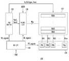
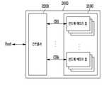
도 1은 본 발명에 따른 반도체 메모리 장치를 설명하기 위한 블럭도이다.1 is a block diagram for explaining a semiconductor memory device according to the present invention.
도 1을 참조하면, 반도체 메모리 장치(100)는 메모리 셀 어레이(110), 어드레스 디코더(120), 읽기 및 쓰기 회로(130), 제어 로직(140), 그리고 전압 생성 회로(150)를 포함한다.1, a
어드레스 디코더(120), 읽기 및 쓰기 회로(130) 및 전압 생성 회로(150)는 메모리 셀 어레이(110)에 대한 소거 동작을 수행하기 위한 주변 회로로 정의될 수 있다.The
메모리 셀 어레이(110)는 복수의 메모리 블럭들(BLK1~BLKz)을 포함한다. 복수의 메모리 블럭들(BLK1~BLKz)은 워드라인들(WLs)을 통해 어드레스 디코더(120)에 연결된다. 복수의 메모리 블럭들(BLK1~BLKz)은 비트라인들(BL1 내지 BLm)을 통해 읽기 및 쓰기 회로(130)에 연결된다. 복수의 메모리 블럭들(BLK1~BLKz) 각각은 복수의 메모리 셀들을 포함한다. 실시 예로서, 복수의 메모리 셀들은 불휘발성 메모리 셀들이며, 보다 상세하게 복수의 메모리 셀들은 차지 트랩 디바이스(charge trap device) 기반의 불휘발성 메모리 셀들일 수 있다. 하나의 워드라인에 공통적으로 연결된 다수의 메모리 셀들은 하나의 페이지로 정의될 수 있다. 메모리 셀 어레이(110)는 복수의 페이지로 구성된다. 또한 메모리 셀 어레이(110)의 복수의 메모리 블럭들(BLK1~BLKz) 각각은 복수의 메모리 스트링을 포함한다. 복수의 메모리 스트링 각각은 비트라인과 소스 라인 사이에 직렬 연결된 적어도 하나 이상의 드레인 선택 트랜지스터, 복수의 메모리 셀들 및 적어도 하나 이상의 소스 선택 트랜지스터를 포함한다.The
어드레스 디코더(120)는 워드라인들(WLs)을 통해 메모리 셀 어레이(110)에 연결된다. 어드레스 디코더(120)는 어드레스 신호(ADDR) 및 제어 로직(140)에서 출력되는 제어 신호들(AD_signals)에 응답하여 동작하도록 구성된다. 어드레스 디코더(120)는 반도체 메모리 장치(100) 내부의 입출력 버퍼(미도시)를 통해 어드레스 신호(ADDR)를 수신한다.The
반도체 메모리 장치(100)의 소거 동작은 메모리 블럭 단위로 수행될 수 있으며, 복수의 메모리 블럭들(BLK1~BLKz)을 동시에 소거시키거나, 복수의 메모리 블럭들(BLK1~BLKz) 중 선택된 적어도 하나의 메모리 블럭을 소거시킬 수 있다.The erasing operation of the
반도체 메모리 장치의 소거 동작 요청 시에 수신되는 어드레스 신호(ADDR)는 블록 어드레스를 포함하며, 어드레스 디코더(120)는 블록 어드레스에 따라 적어도 하나의 메모리 블럭을 선택할 수 있다.The address signal ADDR received at the time of the erase operation request of the semiconductor memory device includes the block address and the
어드레스 디코더(120)는 소거 동작 시 어드레스 신호(ADDR)에 포함된 블록 어드레스에 따라 전압 생성 회로에서 생성되는 제1 설정 전압(Vset1) 및 제2 설정 전압(Vset2)을 선택된 메모리 블럭의 선택 라인들 중 선택된 선택라인들에 인가하고, 선택된 메모리 블럭의 워드라인들 또는 선택 라인들이 플로팅 상태(floating)가 되도록 제어할 수 있다.The
읽기 및 쓰기 회로(130)는 복수의 페이지 버퍼들(PB1~PBm)을 포함한다. 복수의 페이지 버퍼들(PB1~PBm)은 비트라인들(BL1 내지 BLm)을 통해 메모리 셀 어레이(110)에 연결된다. 복수의 페이지 버퍼들(PB1~PBm) 각각은 소거 동작시 선택된 메모리 블럭의 비트라인들(BL1 내지 BLm)을 플로팅 상태로 제어할 수 있다.The read and write
읽기 및 쓰기 회로(130)는 제어 로직(140)에서 출력되는 제어 신호들(PB_signals)에 응답하여 동작한다.The read and
제어 로직(140)은 어드레스 디코더(120), 읽기 및 쓰기 회로(130), 및 전압 생성 회로(150)에 연결된다. 제어 로직(140)은 반도체 메모리 장치(100)의 입출력 버퍼(미도시)를 통해 커맨드(CMD)를 수신한다. 제어 로직(140)은 커맨드(CMD)에 응답하여 반도체 메모리 장치(100)의 제반 동작을 제어하도록 구성된다.
제어 로직(140)은 소거 동작에 대응하는 커맨드(CMD)가 입력될 경우, 내부에 저장된 소거 알고리즘에 따라 선택된 적어도 하나의 메모리 블럭을 소거하기 위해 제어 신호들(AD_signals, PB_signals, 및 VG_signals)을 생성하여 출력한다.
특히, 제어 로직(140)은 소거 동작 시 선택된 메모리 블럭의 선택 트랜지스터 하부에 인터페이스(interface) 트랩(trap)이 생성되도록 선택된 메모리 블럭의 선택 라인에 인가되는 제1 및 제2 설정 전압(Vset1 및 Vset2) 및 선택된 메모리 블럭의 소스 라인에 인가되는 제1 및 제2 소스 라인 제어 전압(Va, Vb)을 생성하도록 전압 생성 회로(150)를 제어하기 위한 제어 신호들(VG_signals)을 생성하여 출력한다.In particular, the
또한 본 발명의 다른 실시 예에 따른 제어 로직(140)은 소거 동작시 소스 라인에 인가되는 프리 소거 전압(Vepre) 및 소거 전압(Vera)을 비트라인들(BL1 내지 BLm)에도 인가하도록 읽기 및 쓰기 회로(130)를 제어할 수 있다. 이때 프리 소거 전압(Vepre) 및 소거 전압(Vera)은 소스 라인 대신에 비트라인들(BL1 내지 BLm)에 인가되거나 소스 라인과 비트라인들(BL1 내지 BLm)에 동시에 인가될 수 있다.The
전압 생성 회로(150)는 제어 로직(140)에서 출력되는 제어 신호들(VG_signals)에 응답하여 동작한다.The
전압 생성 회로(150)는 소거 동작 시 제어 로직(140)의 제어에 따라 선택된 메모리 블럭의 선택 라인에 인가하기 위한 제1 및 제2 설정 전압(Vset1 및 Vset2)을 생성하고, 메모리 셀 어레이(110)의 소스 라인에 인가하기 위한 제1 및 제2 소스 라인 제어 전압(Va, Vb), 프리 소거 전압(Vepre) 및 소거 전압(Vera)을 순차적으로 생성하여 메모리 셀 어레이(110)의 소스 라인에 제공한다.The
도 2는 도 1의 메모리 셀 어레이(110)의 일 실시 예를 보여주는 블록도이다.2 is a block diagram illustrating one embodiment of the
도 2를 참조하면, 메모리 셀 어레이(110)는 복수의 메모리 블럭들(BLK1~BLKz)을 포함한다. 각 메모리 블럭은 3차원 구조를 갖는다. 각 메모리 블럭은 기판 위에 적층된 복수의 메모리 셀들을 포함한다. 이러한 복수의 메모리 셀들은 +X 방향, +Y 방향 및 +Z 방향을 따라 배열된다. 각 메모리 블럭의 구조는 도 3 및 도 4를 참조하여 더 상세히 설명된다.Referring to FIG. 2, the
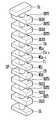
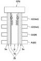
도 3은 본 발명에 따른 메모리 블럭에 포함된 메모리 스트링을 설명하기 위한 입체도이다. 도 4는 메모리 스트링을 설명하기 위한 회로도이다.3 is a perspective view for explaining a memory string included in a memory block according to the present invention. 4 is a circuit diagram for explaining a memory string.
도 3 및 도 4를 참조하면, 반도체 기판 상에 소스 라인(SL)이 형성된다. 소스 라인(SL) 상에는 수직 채널층(SP)이 형성된다. 수직 채널층(SP)의 상부는 비트라인(BL)과 연결된다. 수직 채널층(SP)은 폴리실리콘으로 형성될 수 있다. 수직 채널층(SP)의 서로 다른 높이에서 수직 채널층(SP)을 감싸도록 복수의 도전막들(SGS1, SGS2, SGS3, WL0~WLn, SGD3, SGD2, SGD1)이 형성된다. 수직 채널층(SP)의 표면에는 터널 절연막 및 전하 저장막을 포함하는 다층막(미도시)이 형성되며, 다층막은 수직 채널층(SP)과 도전막들(SGS1, SGS2, SGS3, WL0~WLn, SGD3, SGD2, SGD1) 사이에도 위치한다. 다층막은 산화막, 질화막, 및 산화막이 순차적으로 적층된 ONO 구조로 형성될 수 있다. 복수의 도전막들(WL0~WLn)은 워드라인이며 도전막들(SGS1, SGS2, SGS3)는 소스 선택 트랜지스터들(SST1, SST2, SST3)와 연결된 소스 선택 라인들, 도전막(SGD1, SGD2, SGD3)는 드레인 선택 트랜지스터들(SDT1, SDT2, SDT3)와 연결된 드레인 선택 라인으로 정의할 수 있다.Referring to FIGS. 3 and 4, a source line SL is formed on a semiconductor substrate. A vertical channel layer SP is formed on the source line SL. The upper part of the vertical channel layer SP is connected to the bit line BL. The vertical channel layer SP may be formed of polysilicon. A plurality of conductive films SGS1, SGS2, SGS3, WL0 to WLn, SGD3, SGD2 and SGD1 are formed to surround the vertical channel layer SP at different heights of the vertical channel layer SP. A multilayer film (not shown) including a tunnel insulating film and a charge storage film is formed on the surface of the vertical channel layer SP and the multilayer film includes a vertical channel layer SP and conductive films SGS1, SGS2, SGS3, WL0 to WLn, SGD3 , SGD2, SGD1. The multilayer film may be formed of an ONO structure in which an oxide film, a nitride film, and an oxide film are sequentially laminated. The plurality of conductive films WL0 to WLn are word lines and the conductive films SGS1, SGS2 and SGS3 are source selection lines connected to the source selection transistors SST1, SST2 and SST3, conductive films SGD1, SGD2, SGD3 may be defined as a drain select line connected to the drain select transistors SDT1, SDT2, SDT3.
최하부 도전막은 소스 선택 라인(SGS1)이 되고, 최상부 도전막은 드레인 선택 라인(SGD1)이 된다. 선택 라인들(SGS3, SGD3) 사이의 도전막들은 워드라인들(WL0~WLn)이 된다. 다시 말해, 반도체 기판 상에는 도전막들(SGS1, SGS2, SGS3, WL0~WLn, SGD3, SGD2, SGD1)이 다층으로 형성되고, 도전막들(SGS1, SGS2, SGS3, WL0~WLn, SGD3, SGD2, SGD1)을 관통하는 수직 채널층(SP)이 비트라인(BL)과 반도체 기판에 형성된 소스 라인(SL) 사이에 수직으로 연결된다.The lowermost conductive film becomes the source selection line SGS1 and the uppermost conductive film becomes the drain selection line SGD1. The conductive films between the selection lines SGS3 and SGD3 become the word lines WL0 to WLn. In other words, the conductive films SGS1, SGS2, SGS3, WL0 to WLn, SGD3, SGD2 and SGD1 are formed in multiple layers on the semiconductor substrate and the conductive films SGS1, SGS2, SGS3, WL0 to WLn, SGD3, SGD2, A vertical channel layer SP penetrating through the bit lines BL and SGD1 is vertically connected between the bit line BL and the source line SL formed in the semiconductor substrate.
상부 도전막(SGD1 내지 SGD3)이 수직 채널층(SP)을 감싸는 부분에서 드레인 선택 트랜지스터들(SDT1 내지 SDT3)가 형성되고, 하부 도전막(SGS1 내지 SGS3)이 수직 채널층(SP)을 감싸는 부분에서 소스 선택 트랜지스터(SST1 내지 SST3)가 형성된다. 중간 도전막들(WL0~WLn)이 수직 채널층(SP)을 감싸는 부분들에서 메모리 셀들(C0~Cn)이 형성된다.The drain select transistors SDT1 to SDT3 are formed at the portions where the upper conductive films SGD1 to SGD3 surround the vertical channel layer SP and the portions at which the lower conductive films SGS1 to SGS3 surround the vertical channel layer SP The source select transistors SST1 to SST3 are formed. The memory cells C0 to Cn are formed in portions where the intermediate conductive layers WL0 to WLn surround the vertical channel layer SP.
상기의 구조에 의해, 메모리 스트링은 소스 라인(SL)과 비트라인(BL) 사이에 기판과 수직으로 연결되는 복수의 소스 선택 트랜지스터(SST1 내지 SST3), 메모리 셀들(C0~Cn) 및 복수의 드레인 선택 트랜지스터(SDT1 내지 SDT3)를 포함한다.According to the above structure, the memory string includes a plurality of source select transistors SST1 to SST3, memory cells C0 to Cn, and a plurality of drains (not shown) connected vertically to the substrate between the source line SL and the bit line BL. And selection transistors SDT1 to SDT3.
본 발명의 실시 예에서는 소스 선택 트랜지스터 및 드레인 선택 트랜지스터가 각각 3개씩 배치된 구조를 설명하였으나, 소스 선택 트랜지스터 및 드레인 선택 트랜지스터는 각각 적어도 하나 이상씩 배치될 수 있다.In the embodiment of the present invention, three source select transistors and three drain select transistors are disposed. However, at least one source select transistor and at least one drain select transistor may be arranged.
도 5는 도 1의 제어 로직의 실시 예를 설명하기 위한 블럭도이다.5 is a block diagram illustrating an embodiment of the control logic of FIG.
도 5를 참조하면, 제어 로직(140)은 롬(ROM; 141), 카운터(142), 내부 제어 신호 생성 회로(143, 전압 생성 제어 회로(144), 어드레스 디코더 제어 회로(145) 및 페이지 버퍼 제어 회로(146)를 포함하여 구성될 수 있다.5, the
롬(141)은 반도체 메모리 장치의 제반 동작을 수행하기 위한 알고리즘이 저장되어 있으며, 외부에서 예를 들어 반도체 메모리 장치와 연결된 호스트(Host)로 부터 입력되는 커맨드(CMD)에 대응하는 제반 동작의 알고리즘 데이터(Algo_DATA)를 출력한다.The
카운터(142)는 인에이블 신호(EN)에 응답하여 내부 클럭을 카운팅하여 카운트 클럭(count_CK)을 생성하여 출력한다.The
내부 제어 신호 생성 회로(143)는 롬(141)에서 출력되는 알고리즘 데이터(Algo_DATA)와 카운터(142)에서 출력되는 카운트 클럭(count_CK)에 응답하여 제1 내지 제5 내부 제어 신호들(int_CS1 내지 int_CS5)을 생성하여 출력한다.The internal control
전압 생성 제어 회로(144)는 제1 내지 제3 내부 제어 신호들(int_CS1 내지 int_CS3)에 응답하여 제1 내지 제3 제어 신호들(VG_signals1, VG_signals2, VG_signals3)을 생성하여 출력한다. 제1 내지 제3 제어 신호들(VG_signals1, VG_signals2, VG_signals3)은 도 1의 전압 생성 회로(150)를 제어하기 위한 제어 신호들(VG_signals)에 포함된 신호들이다.The voltage
전압 생성 제어 회로(144)는 선택 라인 전압 제어부(144A), 워드라인 전압 제어부(144B), 및 소스 라인 전압 제어부(144C)를 포함하여 구성될 수 있다.The voltage
선택 라인 전압 제어부(144A)는 제1 내부 제어 신호(int_CS1)에 응답하여 제1 제어 신호들(VG_signals1)을 생성하여 출력한다. 제1 제어 신호들(VG_signals1)은 도 1의 전압 생성 회로(150)가 선택된 메모리 블럭의 복수의 드레인 선택 라인 및 복수의 소스 선택 라인들에 인가되는 전압들을 생성하도록 제어하기 위한 신호들이다.The selection
워드라인 전압 제어부(144B)는 제2 내부 제어 신호(int_CS2)에 응답하여 제2 제어 신호들(VG_signals2)을 생성하여 출력한다. 제2 제어 신호들(VG_signals2)은 도 1의 전압 생성 회로(150)가 선택된 메모리 블럭의 복수의 워드라인들에 인가되는 전압들을 생성하도록 제어하기 위한 신호들이다.The word
소스 라인 전압 제어부(144C)는 제3 내부 제어 신호(int_CS3)에 응답하여 제3 제어 신호들(VG_signals3)을 생성하여 출력한다. 제3 제어 신호들(VG_signals3)은 도 1의 전압 생성 회로(150)가 메모리 셀 어레이(110)와 연결된 소스 라인에 인가되는 전압, 예를 들어 제1 및 제2 소스 라인 제어 전압(Va, Vb), 프리 소거 전압(Vepre) 및 소거 전압(Vera)을 생성하도록 제어하기 위한 신호들이다.The source
도 6은 본 발명의 실시 예에 따른 반도체 메모리 장치의 동작을 설명하기 위한 순서도이다.6 is a flowchart for explaining the operation of the semiconductor memory device according to the embodiment of the present invention.
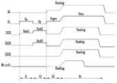
도 7은 본 발명의 실시 예에 따른 반도체 메모리 장치의 동작을 설명하기 위한 신호들의 파형도이다.7 is a waveform diagram of signals for explaining the operation of the semiconductor memory device according to the embodiment of the present invention.
도 8은 도 7의 t1 구간에서의 동작을 설명하기 위한 메모리 스트링의 단면도이다.8 is a cross-sectional view of a memory string for explaining the operation in the t1 section of FIG.
도 9는 본 7의 t2 구간에서의 동작을 설명하기 위한 메모리 스트링의 단면도이다.9 is a sectional view of a memory string for explaining the operation in the t2 section of FIG.
도 1 내지 도 9를 참조하여 본 발명의 실시 예에 따른 반도체 메모리 장치의 소거 동작을 설명하면 다음과 같다.The erase operation of the semiconductor memory device according to the embodiment of the present invention will be described with reference to FIGS. 1 to 9 as follows.
외부로부터 소거 명령에 대한 커맨드(CMD)가 입력되면(S610), 제어 로직(140)은 반도체 메모리 장치(100)의 소거 동작을 수행하기 위하여 주변 회로들을 제어한다.When the command CMD for the erase command is input from the outside (S610), the
제어 로직(140)의 롬(141)은 소거 명령에 대한 커맨드(CMD)에 응답하여 소거 알고리즘에 대응하는 알고리즘 데이터(Algo_DATA)를 출력한다. 내부 제어 신호 생성 회로(143)는 알고리즘 데이터(Algo_DATA)와 카운트 클럭(count_CK)에 응답하여 제1 내지 제5 내부 제어 신호들(int_CS1 내지 int_CS5)을 생성하여 출력한다. 전압 생성 제어 회로(144)는 제1 내지 제3 내부 제어 신호들(int_CS1 내지 int_CS3)에 응답하여 제1 내지 제3 제어 신호들(VG_signals1, VG_signals2, VG_signals3)을 생성하여 출력한다.The
도 7의 t1 구간에서 전압 생성 회로(150)는 제1 내지 제3 제어 신호들(VG_signals1, VG_signals2, VG_signals3)에 응답하여 메모리 셀 어레이(110)의 소스 라인(SL)에 인가하기 위한 제1 소스 라인 전압(Va) 및 복수의 소스 선택 트랜지스터(SST1 내지 SST) 중 최외각에 배치된 소스 선택 트랜지스터(SST1)와 연결된 소스 선택 라인(SGS1)에 인가하기 위한 제1 설정 전압(Vset1)을 생성하여 출력한다. 본원 발명의 실시 예에서는 하나의 소스 선택 트랜지스터(SST1)에 제1 설정 전압(Vset1)을 인가하는 것을 일예로 설명하였으나, 최외각에 배치된 두 개의 소스 선택 트랜지스터(SST1, SST2) 또는 세 개의 소스 선택 트랜지스터(SST1, SST2, SST3)에 제1 설정 전압(Vset1)을 인가할 수 있다. 제1 소스 라인 전압(Va)은 3V 내지 5V의 전위 레벨을 가지며, 제1 설정 전압(Vset1)은 0.1V 내지 0.5V의 전위 레벨을 가질 수 있다.7, the
도 8을 참조하면, 수직 채널층(SP)은 터널 절연막(Tox), 전하 저장막(CTN), 블러킹 절연막(Box)이 순차적으로 감싸고 있다. 반도체 메모리 장치의 소거 동작 시 t1 구간에서 소스 라인(SL)에 제1 소스 라인 전압(Va)이 인가되고, 최외각 소스 선택 트랜지스터(SST1)와 연결된 소스 선택 라인(SGS1)에 제1 설정 전압(Vset1)이 인가되면, 수직 채널층(SP)에서 터널 절연막(Tox)로 이동하는 이온에 의하여 수직 채널층(SP)과 터널 절연막(Tox) 사이의 계면(interface) 영역에 트랩(trap)이 형성되고(S620), 제1 소스 선택 트랜지스터(SST1) 하부의 수직 채널층(SP) 주변에는 홀들이 파일 업(pile-up)된다. 이때, 소스 선택 라인(SGS2, SGS3) 및 복수의 워드라인들(WL0 내지 WLn)에는 소스 선택 트랜지스터(SST2, SST3) 및 메모리 셀들(C0 내지 Cn)을 턴오프 상태로 유지시키기 위한 0V가 인가될 수 있다.Referring to FIG. 8, the vertical channel layer SP sequentially surrounds a tunnel insulating film Tox, a charge storage film CTN, and a blocking insulating film Box. The first source line voltage Va is applied to the source line SL in the t1 period in the erase operation of the semiconductor memory device and the first set voltage Vs is applied to the source select line SGS1 connected to the outermost source select transistor SST1. A trap is formed in the interface region between the vertical channel layer SP and the tunnel insulating film Tox by the ions moving from the vertical channel layer SP to the tunnel insulating film Tox, The holes are piled up around the vertical channel layer SP under the first source selection transistor SST1 in operation S620. At this time, 0V is applied to the source select lines SGS2 and SGS3 and the plurality of word lines WL0 to WLn to maintain the source select transistors SST2 and SST3 and the memory cells C0 to Cn in the turn off state .
도 7의 t2 구간에서 전압 생성 회로(150)는 제1 내지 제3 제어 신호들(VG_signals1, VG_signals2, VG_signals3)에 응답하여 메모리 셀 어레이(110)의 소스 라인(SL)에 인가하기 위한 제2 소스 라인 전압(Vb) 및 복수의 소스 선택 트랜지스터(SST1 내지 SST) 중 최외각에 배치된 소스 선택 트랜지스터(SST1 및 SST2)와 연결된 소스 선택 라인(SGS1 및 SGS2)에 인가하기 위한 제2 설정 전압(Vset2)을 생성하여 출력한다. 이때 제2 설정 전압(Vset2)은 제1 설정 전압(Vset1)이 인가된 소스 선택 트랜지스터(SST1)와 소스 선택 트랜지스터(SST1)와 인접하게 배치된 소스 선택 트랜지스터(SST2)에 인가되는 것이 바람직하다. 예를 들어 제1 설정 전압(Vset1)이 소스 선택 트랜지스터(SST1 및 SST2)에 인가된 경우 제2 설정 전압(Vset2)은 소스 선택 트랜지스터(SST1 내지 SST3)에 인가될 수 있다. 제1 설정 전압(Vset1)이 소스 선택 트랜지스터(SST1 내지 SST3)에 인가된 경우 제2 설정 전압(Vset2)은 소스 선택 트랜지스터(SST1 내지 SST3) 및 메모리 셀(C0)에 인가될 수 있다. 소스 선택 트랜지스터(SST1 및 SST2)는 제2 설정 전압(Vset2)에 의해 턴온 상태가 되며, 제2 설정 전압(Vset2)은 3V 내지 5V의 전위 레벨을 가질 수 있다. 즉, 제2 설정 전압(Vset2)은 소스 선택 트랜지스터(SST1 및 SST2)를 턴온시키기 위한 턴온 전압이다. 제2 소스 라인 전압(Vb)은 0V의 접지 전압일 수 있다.7, the
도 9을 참조하면, t2 구간에서 소스 라인(SL)에 제2 소스 라인 전압(Va)이 인가되고, 소스 선택 트랜지스터(SST1 및 SST2)와 연결된 소스 선택 라인(SGS1 및 SGS2)에 제2 설정 전압(Vset2)이 인가되면, 제1 소스 선택 트랜지스터(SST1) 하부의 수직 채널층(SP) 주변에 파일 업된 홀들이 제2 소스 라인 전압(Vb)이 인가되는 소스 라인(SL)을 통해 제거된다(S630).9, the second source line voltage Va is applied to the source line SL in the t2 section, and the source select lines SGS1 and SGS2 connected to the source select transistors SST1 and SST2 are applied with the second set voltage Holes raised around the vertical channel layer SP under the first source select transistor SST1 are removed through the source line SL to which the second source line voltage Vb is applied S630).
어드레스 디코더(120)는 t3 구간에서 제어 신호들(AD_signals)에 응답하여 복수의 워드라인들(WL0 내지 WLn)을 플로팅 상태(floating)로 제어한다. 읽기 및 쓰기 회로(130)는 제어 신호들(PB_signals)에 응답하여 비트라인들(BL1 내지 BLm)을 플로팅 상태(floating)로 제어한다.The
전압 생성 회로(150)는 t3 구간에서 제어 신호들(VG_signals3)에 응답하여 프리 소거 전압(Vepre)을 생성하여 소스 라인(SL)에 인가한다(S640). 소스 라인(SL)에 인가된 프리 소거 전압(Vepre)에 의해 게이트 유기 전류(GIDL: Gate Induce Drain Leakage)가 소스 선택 트랜지스터(SST1) 하부 채널에서 생성되어 채널 방향으로 흐르게 된다. 즉, 소스 선택 트랜지스터(SST1)의 드레인 영역에서 핫홀이 발생되어 수직 채널층(SP) 방향으로 유입되어 수직 채널층(SP)의 전위가 상승하게 된다. 이때 소스 선택 트랜지스터(SST1)의 하부에는 트랩이 형성되어 있어 게이트 유기 전류가 용이하게 발생되며, 전류량도 증가하게 된다. 또한 플로팅 상태(floating)의 비트라인들(BL1 내지 BLm)은 소스 라인(SL)에 인가되는 프리 소거 전압(Vepre)에 의한 커플링 현상에 의해 상승할 수 있다.The
이 후, t4 구간에서부터 전압 생성 회로(150)는 제어 신호들(VG_signals3)에 응답하여 프리 소거 전압(Vepre) 보다 높은 소거 전압(Vera)을 생성하여 선택된 메모리 블럭의 소스 라인(SL)에 인가한다(S650). 이로 인하여 수직 채널층(SP)의 전위 레벨은 더욱 상승하게 된다.Subsequently, from time t4, the
이때 비트라인들(BL1 내지 BLm)의 전위 레벨은 소스 라인(SL)에 인가되는 소거 전압(Vera)에 의한 커플링 현상에 의해 더욱 상승할 수 있다.At this time, the potential level of the bit lines BL1 to BLm can be further raised by the coupling phenomenon due to the erase voltage Vera applied to the source line SL.
어드레스 디코더(120)는 t4 구간에서 제어 신호들(AD_signals)에 응답하여 복수의 소스 선택 라인들(SGS1 내지 SGS3)을 플로팅 상태(floating)로 제어한다. 이 후, 어드레스 디코더(120)는 제어 신호들(AD_signals)에 응답하여 t4 구간에서 워드라인들(WL<n:0>)을 플로팅 상태(floating)에서 접지 전압 레벨로 제어한다. 이로 인하여 메모리 셀들(C0 내지 Cn)의 전하 저장층(CTN)에 저장된 전자들은 높은 전위 레벨을 갖는 수직 채널층(SP)과 접지 전압 레벨의 워드라인들(WL<n:0>)에 의해 디트랩된다. 즉, 메모리 셀들(C0 내지 Cn)에 저장된 데이터들이 소거된다.The
이 후, 소스 선택 라인(SGS1 내지 SGS3)은 플로팅 상태(floating)에서 접지 전압 레벨로 제어되어 소스 선택 트랜지스터(SST1 내지 SST3)가 턴오프되어 소거 동작이 종료된다.Thereafter, the source select lines SGS1 to SGS3 are controlled from the floating state to the ground voltage level, and the source select transistors SST1 to SST3 are turned off to complete the erase operation.
상술한 바와 같이 본원 발명의 실시 예에서는 소스 라인(SL)을 통해 프리 소거 전압(Vepre) 및 소거 전압(Vera)을 인가하는 방식으로 소거 동작을 수행할 경우, 프리 소거 전압(Vepre) 인가 동작을 수행하기 이전에 소스 선택 라인(SGS1)에 제1 설정 전압(Vset1)을 인가하고 소스 라인(SL)에 제1 소스 라인 제어 전압(Va)을 인가하여 소스 선택 트랜지스터(SST1) 하부의 수직 채널층(SP)과 터널 절연막(Tox) 계면 영역에 트랩을 형성하여 게이트 유기 전류(GIDL)의 발생이 용이해지도록 트랩을 형성할 수 있다.As described above, in the embodiment of the present invention, when the erase operation is performed by applying the pre-erase voltage Vepre and the erase voltage Vera through the source line SL, the operation of applying the pre-erase voltage Vepre A first set voltage Vset1 is applied to the source select line SGS1 and a first source line control voltage Va is applied to the source line SL to form a vertical channel layer under the source select transistor SST1, A trap can be formed in the interface region of the tunnel insulating film SP and the tunnel insulating film (Tox) to form a trap so that the generation of the gate organic current GIDL can be facilitated.
이때 다른 실시 예로 소스 라인(SL) 대신 비트라인들(BL1 내지 BLm)을 통해 프리 소거 전압(Vepre) 및 소거 전압(Vera)을 인가하는 방식으로 소거 동작을 수행할 경우, 프리 소거 전압(Vepre) 인가 동작을 수행하기 이전에 드레인 선택 라인(SGD1)에 제1 설정 전압(Vset1)을 인가하고 비트라인들(BL1 내지 BLm)에 제1 소스 라인 제어 전압(Va)을 인가하여 드레인 선택 트랜지스터(SDT1) 하부의 수직 채널층(SP)과 터널 절연막(Tox) 계면 영역에 트랩을 형성하여 게이트 유기 전류(GIDL)의 발생이 용이해지도록 트랩을 형성하여 상술한 실시 예와 유사한 효과를 얻을 수 있다.In this case, when the erase operation is performed by applying the pre-erase voltage Vepre and the erase voltage Vera through the bit lines BL1 to BLm instead of the source line SL, A first set voltage Vset1 is applied to the drain select line SGD1 and a first source line control voltage Va is applied to the bit lines BL1 to BLm before the application of the drain select transistor SDT1 A trap is formed in the interface region between the vertical channel layer SP and the tunnel insulating film Tox to form a trap to facilitate the generation of the gate organic current GIDL, thereby obtaining an effect similar to that of the above-described embodiment.
도 10은 도 1의 반도체 메모리 장치를 포함하는 메모리 시스템을 보여주는 블럭도이다.10 is a block diagram showing a memory system including the semiconductor memory device of FIG.
도 10을 참조하면, 메모리 시스템(1000)은 반도체 메모리 장치(100) 및 컨트롤러(1100)를 포함한다.10, a
반도체 메모리 장치(100)는 도 1을 참조하여 설명된 바와 마찬가지로 구성되고, 동작할 수 있다. 이하, 중복되는 설명은 생략된다.The
컨트롤러(1100)는 호스트(Host) 및 반도체 메모리 장치(100)에 연결된다. 호스트(Host)로부터의 요청에 응답하여, 컨트롤러(1100)는 반도체 메모리 장치(100)를 액세스하도록 구성된다. 예를 들면, 컨트롤러(1100)는 반도체 메모리 장치(100)의 읽기, 쓰기, 소거, 그리고 배경(background) 동작을 제어하도록 구성된다. 컨트롤러(1100)는 반도체 메모리 장치(100) 및 호스트(Host) 사이에 인터페이스를 제공하도록 구성된다. 컨트롤러(1100)는 반도체 메모리 장치(100)를 제어하기 위한 펌웨어(firmware)를 구동하도록 구성된다.The
컨트롤러(1100)는 램(1110, Random Access Memory), 프로세싱 유닛(1120, processing unit), 호스트 인터페이스(1130, host interface), 메모리 인터페이스(1140, memory interface) 및 에러 정정 블록(1150)을 포함한다. 램(1110)은 프로세싱 유닛(1120)의 동작 메모리, 반도체 메모리 장치(100) 및 호스트(Host) 사이의 캐시 메모리, 그리고 반도체 메모리 장치(100) 및 호스트(Host) 사이의 버퍼 메모리 중 적어도 하나로서 이용된다. 프로세싱 유닛(1120)은 컨트롤러(1100)의 제반 동작을 제어한다. 또한 컨트롤러(1100)는 쓰기 동작시 호스트(Host)로 부터 제공되는 프로그램 데이터를 임시 저장할 수 있다.The
호스트 인터페이스(1130)는 호스트(Host) 및 컨트롤러(1100) 사이의 데이터 교환을 수행하기 위한 프로토콜을 포함한다. 예시적인 실시 예로서, 컨트롤러(1100)는 USB (Universal Serial Bus) 프로토콜, MMC (multimedia card) 프로토콜, PCI (peripheral component interconnection) 프로토콜, PCI-E (PCI-express) 프로토콜, ATA (Advanced Technology Attachment) 프로토콜, Serial-ATA 프로토콜, Parallel-ATA 프로토콜, SCSI (small computer small interface) 프로토콜, ESDI (enhanced small disk interface) 프로토콜, 그리고 IDE (Integrated Drive Electronics) 프로토콜, 사유(private) 프로토콜 등과 같은 다양한 인터페이스 프로토콜들 중 적어도 하나를 통해 호스트(Host)와 통신하도록 구성된다.The
메모리 인터페이스(1140)는 반도체 메모리 장치(100)와 인터페이싱한다. 예를 들면, 메모리 인터페이스는 낸드 인터페이스 또는 노어 인터페이스를 포함한다.The
에러 정정 블록(1150)은 에러 정정 코드(ECC, Error Correcting Code)를 이용하여 반도체 메모리 장치(100)로부터 수신된 데이터의 에러를 검출하고, 정정하도록 구성된다. 프로세싱 유닛(1120)은 에러 정정 블록(1150)의 에러 검출 결과에 따라 읽기 전압을 조절하고, 재 읽기를 수행하도록 반도체 메모리 장치(100)를 제어할 것이다. 예시적인 실시 예로서, 에러 정정 블록은 컨트롤러(1100)의 구성 요소로서 제공될 수 있다.The
컨트롤러(1100) 및 반도체 메모리 장치(100)는 하나의 반도체 장치로 집적될 수 있다. 예시적인 실시 예로서, 컨트롤러(1100) 및 반도체 메모리 장치(100)는 하나의 반도체 장치로 집적되어, 메모리 카드를 구성할 수 있다. 예를 들면, 컨트롤러(1100) 및 반도체 메모리 장치(100)는 하나의 반도체 장치로 집적되어 PC 카드(PCMCIA, personal computer memory card international association), 컴팩트 플래시 카드(CF), 스마트 미디어 카드(SM, SMC), 메모리 스틱, 멀티미디어 카드(MMC, RS-MMC, MMCmicro), SD 카드(SD, miniSD, microSD, SDHC), 유니버설 플래시 기억장치(UFS) 등과 같은 메모리 카드를 구성할 것이다.The
컨트롤러(1100) 및 반도체 메모리 장치(100)는 하나의 반도체 장치로 집적되어 반도체 드라이브(SSD, Solid State Drive)를 구성할 수 있다. 반도체 드라이브(SSD)는 반도체 메모리에 데이터를 저장하도록 구성되는 저장 장치를 포함한다. 메모리 시스템(1000)이 반도체 드라이브(SSD)로 이용되는 경우, 메모리 시스템(2000)에 연결된 호스트(Host)의 동작 속도는 획기적으로 개선된다.The
다른 예로서, 메모리 시스템(1000)은 컴퓨터, UMPC (Ultra Mobile PC), 워크스테이션, 넷북(net-book), PDA (Personal Digital Assistants), 포터블(portable) 컴퓨터, 웹 타블렛(web tablet), 무선 전화기(wireless phone), 모바일 폰(mobile phone), 스마트폰(smart phone), e-북(e-book), PMP(portable multimedia player), 휴대용 게임기, 네비게이션(navigation) 장치, 블랙박스(black box), 디지털 카메라(digital camera), 3차원 수상기(3-dimensional television), 디지털 음성 녹음기(digital audio recorder), 디지털 음성 재생기(digital audio player), 디지털 영상 녹화기(digital picture recorder), 디지털 영상 재생기(digital picture player), 디지털 동영상 녹화기(digital video recorder), 디지털 동영상 재생기(digital video player), 정보를 무선 환경에서 송수신할 수 있는 장치, 홈 네트워크를 구성하는 다양한 전자 장치들 중 하나, 컴퓨터 네트워크를 구성하는 다양한 전자 장치들 중 하나, 텔레매틱스 네트워크를 구성하는 다양한 전자 장치들 중 하나, RFID 장치, 또는 컴퓨팅 시스템을 구성하는 다양한 구성 요소들 중 하나 등과 같은 전자 장치의 다양한 구성 요소들 중 하나로 제공된다.As another example, the
예시적인 실시 예로서, 반도체 메모리 장치(100) 또는 메모리 시스템(1000)은 다양한 형태들의 패키지로 실장될 수 있다. 예를 들면, 반도체 메모리 장치(100) 또는 메모리 시스템(2000)은 PoP(Package on Package), Ball grid arrays(BGAs), Chip scale packages(CSPs), Plastic Leaded Chip Carrier(PLCC), Plastic Dual In Line Package(PDIP), Die in Waffle Pack, Die in Wafer Form, Chip On Board(COB), Ceramic Dual In Line Package(CERDIP), Plastic Metric Quad Flat Pack(MQFP), Thin Quad Flatpack(TQFP), Small Outline(SOIC), Shrink Small Outline Package(SSOP), Thin Small Outline(TSOP), Thin Quad Flatpack(TQFP), System In Package(SIP), Multi Chip Package(MCP), Wafer-level Fabricated Package(WFP), Wafer-Level Processed Stack Package(WSP) 등과 같은 방식으로 패키지화되어 실장될 수 있다.As an exemplary embodiment,
도 11은 도 10의 메모리 시스템의 응용 예를 보여주는 블럭도이다.11 is a block diagram showing an application example of the memory system of FIG.
도 11을 참조하면, 메모리 시스템(2000)은 반도체 메모리 장치(2100) 및 컨트롤러(2200)를 포함한다. 반도체 메모리 장치(2100)는 복수의 반도체 메모리 칩들을 포함한다. 복수의 반도체 메모리 칩들은 복수의 그룹들로 분할된다.11, the
도 11에서, 복수의 그룹들은 각각 제 1 내지 제 k 채널들(CH1~CHk)을 통해 컨트롤러(2200)와 통신하는 것으로 도시되어 있다. 각 반도체 메모리 칩은 도 1을 참조하여 설명된 반도체 메모리 장치(100) 중 하나와 마찬가지로 구성되고, 동작할 것이다.In Fig. 11, the plurality of groups are shown as communicating with the
각 그룹은 하나의 공통 채널을 통해 컨트롤러(2200)와 통신하도록 구성된다. 컨트롤러(2200)는 도 10을 참조하여 설명된 컨트롤러(1100)와 마찬가지로 구성되고, 복수의 채널들(CH1~CHk)을 통해 반도체 메모리 장치(2100)의 복수의 메모리 칩들을 제어하도록 구성된다.Each group is configured to communicate with the
도 12는 도 11을 참조하여 설명된 메모리 시스템을 포함하는 컴퓨팅 시스템을 보여주는 블럭도이다.12 is a block diagram illustrating a computing system including the memory system described with reference to FIG.
도 12를 참조하면, 컴퓨팅 시스템(3000)은 중앙 처리 장치(3100), 램(3200, RAM, Random Access Memory), 사용자 인터페이스(3300), 전원(3400), 시스템 버스(3500), 그리고 메모리 시스템(2000)을 포함한다.12, a
메모리 시스템(2000)은 시스템 버스(3500)를 통해, 중앙처리장치(3100), 램(3200), 사용자 인터페이스(3300), 그리고 전원(3400)에 전기적으로 연결된다. 사용자 인터페이스(3300)를 통해 제공되거나, 중앙 처리 장치(3100)에 의해서 처리된 데이터는 메모리 시스템(2000)에 저장된다.The
도 12에서, 반도체 메모리 장치(2100)는 컨트롤러(2200)를 통해 시스템 버스(3500)에 연결되는 것으로 도시되어 있다. 그러나, 반도체 메모리 장치(2100)는 시스템 버스(3500)에 직접 연결되도록 구성될 수 있다. 이때, 컨트롤러(2200)의 기능은 중앙 처리 장치(3100) 및 램(3200)에 의해 수행될 것이다.In FIG. 12, the
도 12에서, 도 11을 참조하여 설명된 메모리 시스템(2000)이 제공되는 것으로 도시되어 있다. 그러나, 메모리 시스템(2000)은 도 10을 참조하여 설명된 메모리 시스템(1000)으로 대체될 수 있다. 예시적인 실시 예로서, 컴퓨팅 시스템(3000)은 도 10 및 도 11을 참조하여 설명된 메모리 시스템들(1000, 2000)을 모두 포함하도록 구성될 수 있다.In Fig. 12, it is shown that the
본 발명의 상세한 설명에서는 구체적인 실시 예에 관하여 설명하였으나, 본 발명의 범위와 기술적 사상에서 벗어나지 않는 한도 내에서 다양한 변경이 가능하다. 그러므로 본 발명의 범위는 상술한 실시 예에 국한되어 정해져서는 안되며 후술하는 특허청구범위뿐만 아니라 이 발명의 특허청구범위와 균등한 것들에 의해 정해져야 한다.While the invention has been shown and described with reference to certain preferred embodiments thereof, it will be understood by those skilled in the art that various changes and modifications may be made without departing from the spirit and scope of the invention. Therefore, the scope of the present invention should not be limited to the above-described embodiments, but should be determined by the equivalents of the claims of the present invention as well as the claims of the following.
100: 반도체 메모리 장치
110: 메모리 셀 어레이
120: 어드레스 디코더
130: 읽기 및 쓰기 회로
140: 제어 로직
150: 전압 생성 회로100: semiconductor memory device
110: memory cell array
120: address decoder
130: Read and Write Circuit
140: control logic
150: voltage generating circuit
Claims (20)
Translated fromKorean소거 동작 시 상기 다수의 메모리 블럭들 중 선택된 메모리 블럭의 소스 라인 및 복수의 선택 라인들에 동작 전압들을 인가하기 위한 주변 회로; 및
상기 동작 전압들 중 소거 전압이 상기 선택된 메모리 블럭에 인가되기 이전에 상기 선택된 메모리 블럭에 포함된 소스 선택 트랜지스터 하부 영역에 트랩이 형성되도록 상기 주변 회로를 제어하는 제어 로직을 포함하는 반도체 메모리 장치.
A memory cell array including a plurality of memory blocks;
A peripheral circuit for applying operating voltages to a source line and a plurality of select lines of a selected memory block among the plurality of memory blocks in an erase operation; And
And control logic to control the peripheral circuit so that a trap is formed in a lower region of a source select transistor included in the selected memory block before an erase voltage of the operation voltages is applied to the selected memory block.
상기 메모리 블럭들 각각은 비트라인들과 상기 소스 라인 사이에 병렬 연결된 복수의 메모리 스트링들을 포함하며,
상기 복수의 메모리 스트링들 각각은 상기 비트라인들 중 하나와 상기 소스 라인 사이에 직렬 연결된 적어도 하나 이상의 드레인 선택 트랜지스터, 복수의 메모리 셀들 및 적어도 하나 이상의 상기 소스 선택 트랜지스터를 포함하는 반도체 메모리 장치.
The method according to claim 1,
Each of the memory blocks including a plurality of memory strings connected in parallel between bit lines and the source line,
Wherein each of the plurality of memory strings includes at least one drain select transistor connected in series between one of the bit lines and the source line, a plurality of memory cells, and at least one or more of the source select transistors.
상기 주변 회로는 제1 및 제2 소스 라인 제어 전압, 프리 소거 전압 및 상기 소거 전압을 생성하여 상기 소스 라인에 인가하고, 제1 및 제2 설정 전압을 생성하여 출력하기 위한 전압 생성 회로;
상기 제1 및 제2 설정 전압을 상기 복수의 선택 라인들 중 적어도 하나 이상의 소스 선택 라인에 인가하고, 상기 선택된 메모리 블럭의 워드라인들을 플로팅 상태로 제어하기 위한 어드레스 디코더; 및
상기 메모리 셀 어레이의 비트라인들에 연결되어, 상기 소거 동작시 상기 비트라인들을 플로팅 상태로 제어하기 위한 읽기 및 쓰기 회로를 포함하는 반도체 메모리 장치.
The method according to claim 1,
The peripheral circuit generates a first and a second source line control voltage, a pre-erase voltage, and the erase voltage, applies the generated erase voltage to the source line, and generates and outputs first and second set voltages;
An address decoder for applying the first and second set voltages to at least one source select line of the plurality of select lines and for controlling the word lines of the selected memory block to a floating state; And
And a read and write circuit coupled to bit lines of the memory cell array for controlling the bit lines to a floating state during the erase operation.
상기 어드레스 디코더는 상기 제1 설정 전압을 상기 선택된 메모리 블럭에 포함된 복수의 소스 선택 트랜지스터들 중 최외각에 배치된 적어도 하나 이상의 제1 소스 선택 트랜지스터에 인가하고,
상기 제2 설정 전압을 상기 적어도 하나 이상의 제1 소스 선택 트랜지스터 및 상기 제1 소스 선택 트랜지스터와 인접한 제2 소스 선택 트랜지스터 또는 메모리 셀에 인가하는 반도체 메모리 장치.
The method of claim 3,
Wherein the address decoder applies the first set voltage to at least one or more first source select transistors arranged at an outermost one of a plurality of source select transistors included in the selected memory block,
And the second set voltage is applied to the at least one or more first source select transistors and the second source select transistor or memory cell adjacent to the first source select transistor.
상기 전압 생성 회로는 상기 제1 소스 라인 제어 전압을 생성하여 상기 소스 라인에 인가하고, 상기 어드레스 디코더는 상기 전압 생성 회로에서 생성된 상기 제1 설정 전압을 상기 적어도 하나 이상의 제1 소스 선택 트랜지스터에 인가하여 상기 적어도 하나 이상의 제1 소스 선택 트랜지스터 하부의 채널층과 터널 절연막 사이의 계면에 상기 트랩을 형성하는 반도체 메모리 장치.
5. The method of claim 4,
The voltage generating circuit generates and applies the first source line control voltage to the source line, and the address decoder applies the first set voltage generated in the voltage generating circuit to the at least one first source select transistor Wherein said trap is formed at an interface between a channel layer under said at least one first source select transistor and a tunnel insulating film.
상기 트랩이 형성된 이 후, 상기 전압 생성 회로는 상기 제2 소스 라인 제어 전압을 생성하여 상기 소스 라인에 인가하고, 상기 어드레스 디코더는 상기 전압 생성 회로에서 생성된 상기 제2 설정 전압을 상기 적어도 하나 이상의 제1 소스 선택 트랜지스터 및 상기 제2 소스 선택 트랜지스터 또는 상기 메모리 셀에 인가하여 상기 채널층에 파일업된 홀들을 상기 소스 라인을 통해 제거하는 반도체 메모리 장치.
5. The method of claim 4,
After the trap is formed, the voltage generation circuit generates and applies the second source line control voltage to the source line, and the address decoder outputs the second set voltage generated in the voltage generation circuit to the at least one The first source select transistor and the second source select transistor or the memory cell to remove through the source line the holes raised up in the channel layer.
상기 제2 소스 라인 제어 전압은 접지 전압이며, 상기 제2 설정 전압은 상기 제1 소스 선택 트랜지스터, 상기 제2 소스 선택 트랜지스터 및 상기 메모리 셀을 턴온시키기 위한 턴온 전압인 반도체 메모리 장치.
5. The method of claim 4,
Wherein the second source line control voltage is a ground voltage and the second set voltage is a turn-on voltage for turning on the first source select transistor, the second source select transistor, and the memory cell.
상기 전압 생성 회로는 상기 제2 소스 라인 제어 전압을 상기 소스 라인에 인가한 이 후, 상기 프리 소거 전압을 생성하여 상기 소스 라인에 인가하고, 상기 어드레스 디코더는 상기 선택된 메모리 블럭의 상기 워드라인들을 상기 플로팅 상태로 제어하는 반도체 메모리 장치.
The method of claim 3,
Wherein the voltage generation circuit generates the pre-erase voltage and applies the pre-erase voltage to the source line after applying the second source line control voltage to the source line, and the address decoder converts the word lines of the selected memory block And controls the semiconductor memory device in a floating state.
상기 전압 생성 회로는 상기 프리 소거 전압을 상기 소스 라인에 인가한 이 후, 상기 소거 전압을 생성하여 상기 소스 라인에 인가하고, 상기 어드레스 디코더는 상기 선택된 메모리 블럭의 상기 워드라인들 및 상기 적어도 하나 이상의 소스 선택 라인을 상기 플로팅 상태로 일정 시간 유지한 후 상기 워드라인들을 접지 전압 레벨로 제어하는 반도체 메모리 장치.
The method of claim 3,
Wherein the voltage generating circuit generates and applies the erase voltage to the source line after applying the pre-erase voltage to the source line, and wherein the address decoder is operable to apply the erase voltage to the word lines of the selected memory block, And the word lines are controlled to a ground voltage level after the source selection line is maintained in the floating state for a predetermined time.
상기 제어 로직은 알고리즘을 저장하며, 입력되는 커맨드에 응답하여 상기 커맨드에 대응하는 알고리즘 데이터를 출력하는 롬;
인에이블 신호에 응답하여 카운트 클럭을 출력하는 카운터;
상기 알고리즘 데이터와 상기 카운트 클럭에 응답하여 제1 내지 제3 내부 제어 신호들을 출력하기 위한 내부 제어 신호 생성 회로;
상기 제1 내지 제3 내부 제어 신호들에 응답하여 상기 전압 생성 회로를 제어하기 위한 제1 내지 제3 제어 신호들을 생성하기 위한 전압 생성 제어 회로를 포함하는 반도체 메모리 장치.
The method of claim 3,
The control logic storing an algorithm and outputting algorithm data corresponding to the command in response to an input command;
A counter for outputting a count clock in response to an enable signal;
An internal control signal generation circuit for outputting the first to third internal control signals in response to the algorithm data and the count clock;
And a voltage generation control circuit for generating first to third control signals for controlling the voltage generation circuit in response to the first to third internal control signals.
상기 전압 생성 제어 회로는 상기 제1 내부 제어 신호들에 응답하여 상기 전압 생성 회로가 상기 제1 및 제2 설정 전압을 생성하도록 제어하기 위한 제1 제어 신호들을 생성하는 선택 라인 전압 제어부;
상기 제2 내부 제어 신호들에 응답하여 상기 전압 생성 회로가 상기 선택된 메모리 블럭의 상기 워드라인들에 인가되는 전압을 생성하도록 제어하기 위한 제2 제어 신호들을 생성하는 워드라인 전압 제어부; 및
상기 제3 내부 제어 신호들에 응답하여 상기 전압 생성 회로가 상기 제1 및 제2 소스 라인 제어 전압, 상기 프리 소거 전압, 및 상기 소거 전압을 생성하도록 제어하기 위한 제3 제어 신호들을 생성하는 소스 라인 전압 제어부를 포함하는 반도체 메모리 장치.
11. The method of claim 10,
The voltage generation control circuit generates a first control signals for controlling the voltage generation circuit to generate the first and second set voltages in response to the first internal control signals;
A word line voltage control for generating second control signals for controlling the voltage generating circuit to generate a voltage applied to the word lines of the selected memory block in response to the second internal control signals; And
Generating a first control signal for controlling the voltage generation circuit to generate the first and second source line control voltages, the pre-erase voltage, and the erase voltage in response to the third internal control signals; And a voltage control unit.
상기 비트라인에 연결된 페이지 버퍼;
상기 소스 라인에 제1 및 제2 소스 라인 제어 전압, 프리 소거 전압, 및 소거 전압을 인가하기 위한 전압 생성 회로; 및
상기 전압 생성 회로에서 생성된 제1 및 제2 설정 전압을 상기 소스 선택 트랜지스터에 인가하기 위한 어드레스 디코더를 포함하며,
상기 프리 소거 전압 및 상기 소거 전압이 상기 소스 라인에 인가되기 이전에 상기 제1 소스 라인 제어 전압은 상기 소스 라인에 인가되고 상기 제1 설정 전압을 상기 소스 선택 트랜지스터에 인가되는 반도체 메모리 장치.
A memory string in which a source select transistor, a plurality of memory cells, and a drain select transistor are serially connected between a source line and a bit line;
A page buffer coupled to the bit line;
A voltage generating circuit for applying first and second source line control voltages, a pre-erase voltage, and an erase voltage to the source line; And
And an address decoder for applying the first and second set voltages generated in the voltage generation circuit to the source selection transistor,
Wherein the first source line control voltage is applied to the source line and the first set voltage is applied to the source select transistor before the pre-erase voltage and the erase voltage are applied to the source line.
상기 소스 라인에 상기 제1 소스 라인 제어 전압이 인가되고 상기 소스 선택 트랜지스터에 상기 제1 설정 전압이 인가되어 상기 소스 선택 트랜지스터 하부 영역의 수직 채널층과 터널 절연막 사이의 계면에 트랩이 형성되는 반도체 메모리 장치.
13. The method of claim 12,
In which the first source line control voltage is applied to the source line and the first set voltage is applied to the source select transistor to form a trap at an interface between the vertical channel layer of the source select transistor lower region and the tunnel insulating film, Device.
상기 제1 소스 라인 제어 전압이 상기 소스 라인에 인가된 후,
상기 전압 생성 회로는 상기 제2 소스 라인 제어 전압을 생성하여 상기 소스 라인에 인가하고, 상기 어드레스 디코더는 상기 전압 생성 회로에서 생성된 상기 제2 설정 전압을 상기 소스 선택 트랜지스터에 인가하여 상기 수직 채널층 내에 파일 업된 홀들을 제거하는 반도체 메모리 장치.
13. The method of claim 12,
After the first source line control voltage is applied to the source line,
Wherein the voltage generating circuit generates and applies the second source line control voltage to the source line, and the address decoder applies the second set voltage generated in the voltage generating circuit to the source select transistor, And removing holes raised in the semiconductor memory device.
상기 제2 소스 라인 제어 전압은 접지 전압이며, 상기 제2 설정 전압은 상기 소스 선택 트랜지스터를 턴온시키기 위한 턴온 전압인 반도체 메모리 장치.
15. The method of claim 14,
Wherein the second source line control voltage is a ground voltage and the second set voltage is a turn-on voltage for turning on the source select transistor.
상기 페이지 버퍼, 상기 전압 생성 회로 및 상기 어드레스 디코더를 제어하기 위한 제어 로직을 더 포함하며,
상기 제어 로직은 알고리즘을 저장하며, 입력되는 커맨드에 응답하여 상기 커맨드에 대응하는 알고리즘 데이터를 출력하는 롬;
인에이블 신호에 응답하여 카운트 클럭을 출력하는 카운터;
상기 알고리즘 데이터와 상기 카운트 클럭에 응답하여 제1 내지 제3 내부 제어 신호들을 출력하기 위한 내부 제어 신호 생성 회로;
상기 제1 내지 제3 내부 제어 신호들에 응답하여 상기 전압 생성 회로를 제어하기 위한 제1 내지 제3 제어 신호들을 생성하기 위한 전압 생성 제어 회로를 포함하는 반도체 메모리 장치.
13. The method of claim 12,
Further comprising control logic for controlling said page buffer, said voltage generating circuit and said address decoder,
The control logic storing an algorithm and outputting algorithm data corresponding to the command in response to an input command;
A counter for outputting a count clock in response to an enable signal;
An internal control signal generation circuit for outputting the first to third internal control signals in response to the algorithm data and the count clock;
And a voltage generation control circuit for generating first to third control signals for controlling the voltage generation circuit in response to the first to third internal control signals.
상기 전압 생성 제어 회로는 상기 제1 내부 제어 신호들에 응답하여 상기 전압 생성 회로가 상기 제1 및 제2 설정 전압을 생성하도록 제어하기 위한 제1 제어 신호들을 생성하는 선택 라인 전압 제어부;
상기 제2 내부 제어 신호들에 응답하여 상기 전압 생성 회로가 상기 메모리 셀들에 인가되는 전압을 생성하도록 제어하기 위한 제2 제어 신호들을 생성하는 워드라인 전압 제어부; 및
상기 제3 내부 제어 신호들에 응답하여 상기 전압 생성 회로가 상기 제1 및 제2 소스 라인 제어 전압, 상기 프리 소거 전압, 및 상기 소거 전압을 생성하도록 제어하기 위한 제3 제어 신호들을 생성하는 소스 라인 전압 제어부를 포함하는 반도체 메모리 장치.
17. The method of claim 16,
The voltage generation control circuit generates a first control signals for controlling the voltage generation circuit to generate the first and second set voltages in response to the first internal control signals;
A word line voltage control for generating second control signals for controlling the voltage generating circuit to generate a voltage applied to the memory cells in response to the second internal control signals; And
Generating a first control signal for controlling the voltage generation circuit to generate the first and second source line control voltages, the pre-erase voltage, and the erase voltage in response to the third internal control signals; And a voltage control unit.
상기 인터페이스 트랩을 형성한 후, 상기 소스 라인에 제2 소스 라인 제어 전압을 인가하고 상기 제1 소스 선택 트랜지스터 및 상기 제1 소스 선택 트랜지스터와 인접한 제2 소스 선택 트랜지스터 또는 메모리 셀에 제2 설정 전압을 인가하여 상기 채널 영역에 파일 업된 홀들을 제거하는 단계; 및
파일 업된 상기 홀들을 제거한 후 상기 소스 라인에 소거 전압을 인가하고 상기 선택된 메모리 블럭의 워드라인들을 플로팅 상태에서 접지 전압 상태로 제어하여 상기 선택된 메모리 블럭을 소거하는 단계를 포함하는 반도체 메모리 장치의 동작 방법.
Applying a first source line control voltage to a source line of a selected one of a plurality of memory blocks and supplying a first source line control voltage to at least one or more first source select transistors arranged at an outermost one of a plurality of source select transistors of the selected memory block Applying a voltage to form an interface trap in a lower channel region of the source select transistor;
After forming the interface trap, applying a second source line control voltage to the source line and applying a second set voltage to the second source select transistor or memory cell adjacent to the first source select transistor and the first source select transistor Removing holes raised in the channel region by applying a voltage to the channel region; And
And erasing the selected memory block by removing the padded holes and applying an erase voltage to the source line and controlling the word lines of the selected memory block from a floating state to a ground voltage state. .
파일 업된 상기 홀들을 제거한 후, 상기 소스 라인에 소거 전압을 인가하기 이전에 상기 소스 라인에 프리 소거 전압을 인가하는 단계를 더 포함하는 반도체 메모리 장치의 동작 방법.
19. The method of claim 18,
Further comprising applying a pre-erase voltage to the source line after applying the erase voltage to the source line after removing the raised-up holes.
상기 제2 소스 라인 제어 전압은 접지 전압이며, 상기 제2 설정 전압은 상기 제1 소스 선택 트랜지스터, 상기 제2 소스 선택 트랜지스터 및 상기 메모리 셀을 턴온시키기 위한 턴온 전압인 반도체 메모리 장치의 동작 방법.19. The method of claim 18,
Wherein the second source line control voltage is a ground voltage and the second set voltage is a turn-on voltage for turning on the first source select transistor, the second source select transistor, and the memory cell.
Priority Applications (4)
| Application Number | Priority Date | Filing Date | Title |
|---|---|---|---|
| KR1020170046141AKR102277560B1 (en) | 2017-04-10 | 2017-04-10 | Semiconductor memory device and operating method thereof |
| US15/798,525US10600486B2 (en) | 2017-04-10 | 2017-10-31 | Semiconductor memory device and method of operating the same |
| CN201711179573.5ACN108694981B (en) | 2017-04-10 | 2017-11-23 | Semiconductor memory device and method of operating the same |
| US16/797,828US11361828B2 (en) | 2017-04-10 | 2020-02-21 | Semiconductor memory device and method of operating the same |
Applications Claiming Priority (1)
| Application Number | Priority Date | Filing Date | Title |
|---|---|---|---|
| KR1020170046141AKR102277560B1 (en) | 2017-04-10 | 2017-04-10 | Semiconductor memory device and operating method thereof |
Publications (2)
| Publication Number | Publication Date |
|---|---|
| KR20180114419Atrue KR20180114419A (en) | 2018-10-18 |
| KR102277560B1 KR102277560B1 (en) | 2021-07-15 |
Family
ID=63711831
Family Applications (1)
| Application Number | Title | Priority Date | Filing Date |
|---|---|---|---|
| KR1020170046141AActiveKR102277560B1 (en) | 2017-04-10 | 2017-04-10 | Semiconductor memory device and operating method thereof |
Country Status (3)
| Country | Link |
|---|---|
| US (2) | US10600486B2 (en) |
| KR (1) | KR102277560B1 (en) |
| CN (1) | CN108694981B (en) |
Families Citing this family (5)
| Publication number | Priority date | Publication date | Assignee | Title |
|---|---|---|---|---|
| KR102277560B1 (en)* | 2017-04-10 | 2021-07-15 | 에스케이하이닉스 주식회사 | Semiconductor memory device and operating method thereof |
| KR102680867B1 (en) | 2019-09-03 | 2024-07-04 | 삼성전자주식회사 | Semiconductor devices and operating methods of the same |
| KR102735053B1 (en)* | 2020-02-21 | 2024-11-28 | 에스케이하이닉스 주식회사 | Semiconductor memory device and method for operating the same |
| KR20220031464A (en)* | 2020-09-04 | 2022-03-11 | 에스케이하이닉스 주식회사 | Semiconductor device and operating method thereof |
| KR20230138142A (en)* | 2022-03-23 | 2023-10-05 | 에스케이하이닉스 주식회사 | Memory system and operating method thereof |
Citations (2)
| Publication number | Priority date | Publication date | Assignee | Title |
|---|---|---|---|---|
| KR20130107557A (en)* | 2012-03-22 | 2013-10-02 | 에스케이하이닉스 주식회사 | Semiconductor memory device and method of operating the same |
| KR20160039486A (en)* | 2014-10-01 | 2016-04-11 | 에스케이하이닉스 주식회사 | Semiconductor apparatus |
Family Cites Families (11)
| Publication number | Priority date | Publication date | Assignee | Title |
|---|---|---|---|---|
| JP2010118580A (en)* | 2008-11-14 | 2010-05-27 | Toshiba Corp | Non-volatile semiconductor memory device |
| KR101177215B1 (en)* | 2010-10-26 | 2012-08-24 | 에스케이하이닉스 주식회사 | Semiconductor memory apparatus and method of operating the same |
| KR101149619B1 (en) | 2010-11-19 | 2012-05-25 | 에스케이하이닉스 주식회사 | 3d structured non-volatile memory device and method for manufacturing the same |
| KR101868799B1 (en) | 2011-05-26 | 2018-06-21 | 에스케이하이닉스 주식회사 | Nonvolatile memory device and method for fabricating the same |
| KR20130072076A (en) | 2011-12-21 | 2013-07-01 | 에스케이하이닉스 주식회사 | Nonvolatile memory device and method for fabricating the same |
| KR20150063851A (en)* | 2013-12-02 | 2015-06-10 | 에스케이하이닉스 주식회사 | Semiconductor memory device and erasing method thereof |
| KR20150137858A (en)* | 2014-05-30 | 2015-12-09 | 에스케이하이닉스 주식회사 | Semiconductor memory device, memory system including the same and operating method thereof |
| US9536894B2 (en) | 2014-08-04 | 2017-01-03 | Kabushiki Kaisha Toshiba | Non-volatile memory device |
| US9558835B2 (en)* | 2015-06-22 | 2017-01-31 | SK Hynix Inc. | Semiconductor device and operating method thereof |
| KR102618289B1 (en)* | 2016-11-28 | 2023-12-27 | 에스케이하이닉스 주식회사 | Semiconductor memory device and operating method thereof |
| KR102277560B1 (en)* | 2017-04-10 | 2021-07-15 | 에스케이하이닉스 주식회사 | Semiconductor memory device and operating method thereof |
- 2017
- 2017-04-10KRKR1020170046141Apatent/KR102277560B1/enactiveActive
- 2017-10-31USUS15/798,525patent/US10600486B2/enactiveActive
- 2017-11-23CNCN201711179573.5Apatent/CN108694981B/enactiveActive
- 2020
- 2020-02-21USUS16/797,828patent/US11361828B2/enactiveActive
Patent Citations (2)
| Publication number | Priority date | Publication date | Assignee | Title |
|---|---|---|---|---|
| KR20130107557A (en)* | 2012-03-22 | 2013-10-02 | 에스케이하이닉스 주식회사 | Semiconductor memory device and method of operating the same |
| KR20160039486A (en)* | 2014-10-01 | 2016-04-11 | 에스케이하이닉스 주식회사 | Semiconductor apparatus |
Also Published As
| Publication number | Publication date |
|---|---|
| KR102277560B1 (en) | 2021-07-15 |
| US20200194081A1 (en) | 2020-06-18 |
| US20180294034A1 (en) | 2018-10-11 |
| CN108694981B (en) | 2022-02-25 |
| US11361828B2 (en) | 2022-06-14 |
| US10600486B2 (en) | 2020-03-24 |
| CN108694981A (en) | 2018-10-23 |
Similar Documents
| Publication | Publication Date | Title |
|---|---|---|
| US10916309B2 (en) | Semiconductor memory device and operating method thereof | |
| US10296226B2 (en) | Control logic, semiconductor memory device, and operating method | |
| KR102572610B1 (en) | Semiconductor memory device and operating method thereof | |
| US10388381B2 (en) | Semiconductor memory device and operating method thereof | |
| US10032518B2 (en) | Two part programming and erase methods for non-volatile charge trap memory devices | |
| US20150221385A1 (en) | Semiconductor memory device and system including the same | |
| US10360978B2 (en) | Semiconductor memory device for performing coding program and operating method thereof | |
| KR102452993B1 (en) | Semiconductor memory device and operating method thereof | |
| KR20150063851A (en) | Semiconductor memory device and erasing method thereof | |
| US11361828B2 (en) | Semiconductor memory device and method of operating the same | |
| KR20180099015A (en) | Semiconductor memory device and operating method thereof | |
| US20150348634A1 (en) | Semiconductor memory device, memory system including the same, and operating method thereof | |
| KR20160138757A (en) | Semiconductor memory device and operating method thereof | |
| KR20180013127A (en) | Semiconductor memory device and operating method thereof | |
| KR20170111653A (en) | Semiconductor memory device and operating method thereof | |
| KR20170083346A (en) | Semiconductor memory device and operating method thereof | |
| KR20170037078A (en) | Semiconductor memory device | |
| US10468106B2 (en) | Semiconductor memory device and operating method thereof | |
| KR20190038049A (en) | Memory system and operating method thereof | |
| KR102348094B1 (en) | Semiconductor memory device and operating method thereof | |
| KR20160004068A (en) | Semiconductor memory device and operating method thereof |
Legal Events
| Date | Code | Title | Description |
|---|---|---|---|
| PA0109 | Patent application | Patent event code:PA01091R01D Comment text:Patent Application Patent event date:20170410 | |
| PG1501 | Laying open of application | ||
| PA0201 | Request for examination | Patent event code:PA02012R01D Patent event date:20200327 Comment text:Request for Examination of Application Patent event code:PA02011R01I Patent event date:20170410 Comment text:Patent Application | |
| E902 | Notification of reason for refusal | ||
| PE0902 | Notice of grounds for rejection | Comment text:Notification of reason for refusal Patent event date:20210216 Patent event code:PE09021S01D | |
| E701 | Decision to grant or registration of patent right | ||
| PE0701 | Decision of registration | Patent event code:PE07011S01D Comment text:Decision to Grant Registration Patent event date:20210706 | |
| PR0701 | Registration of establishment | Comment text:Registration of Establishment Patent event date:20210708 Patent event code:PR07011E01D | |
| PR1002 | Payment of registration fee | Payment date:20210709 End annual number:3 Start annual number:1 | |
| PG1601 | Publication of registration | ||
| PR1001 | Payment of annual fee | Payment date:20240625 Start annual number:4 End annual number:4 | |
| PR1001 | Payment of annual fee | Payment date:20250624 Start annual number:5 End annual number:5 |