KR20180106291A - Electron emission source unit and digital x-ray source - Google Patents
Electron emission source unit and digital x-ray sourceDownload PDFInfo
- Publication number
- KR20180106291A KR20180106291AKR1020170034382AKR20170034382AKR20180106291AKR 20180106291 AKR20180106291 AKR 20180106291AKR 1020170034382 AKR1020170034382 AKR 1020170034382AKR 20170034382 AKR20170034382 AKR 20170034382AKR 20180106291 AKR20180106291 AKR 20180106291A
- Authority
- KR
- South Korea
- Prior art keywords
- unit
- gate
- patterning
- emitter
- mesh
- Prior art date
- Legal status (The legal status is an assumption and is not a legal conclusion. Google has not performed a legal analysis and makes no representation as to the accuracy of the status listed.)
- Granted
Links
Images


Classifications
- H—ELECTRICITY
- H01—ELECTRIC ELEMENTS
- H01J—ELECTRIC DISCHARGE TUBES OR DISCHARGE LAMPS
- H01J1/00—Details of electrodes, of magnetic control means, of screens, or of the mounting or spacing thereof, common to two or more basic types of discharge tubes or lamps
- H01J1/02—Main electrodes
- H01J1/30—Cold cathodes, e.g. field-emissive cathode
- H01J1/304—Field-emissive cathodes
- H—ELECTRICITY
- H01—ELECTRIC ELEMENTS
- H01J—ELECTRIC DISCHARGE TUBES OR DISCHARGE LAMPS
- H01J3/00—Details of electron-optical or ion-optical arrangements or of ion traps common to two or more basic types of discharge tubes or lamps
- H01J3/02—Electron guns
- H01J3/021—Electron guns using a field emission, photo emission, or secondary emission electron source
- H—ELECTRICITY
- H01—ELECTRIC ELEMENTS
- H01J—ELECTRIC DISCHARGE TUBES OR DISCHARGE LAMPS
- H01J35/00—X-ray tubes
- H01J35/02—Details
- H01J35/04—Electrodes ; Mutual position thereof; Constructional adaptations therefor
- H01J35/06—Cathodes
- H01J35/065—Field emission, photo emission or secondary emission cathodes
- B—PERFORMING OPERATIONS; TRANSPORTING
- B82—NANOTECHNOLOGY
- B82Y—SPECIFIC USES OR APPLICATIONS OF NANOSTRUCTURES; MEASUREMENT OR ANALYSIS OF NANOSTRUCTURES; MANUFACTURE OR TREATMENT OF NANOSTRUCTURES
- B82Y10/00—Nanotechnology for information processing, storage or transmission, e.g. quantum computing or single electron logic
Landscapes
- Cold Cathode And The Manufacture (AREA)
Abstract
Description
Translated fromKorean본 발명은 전자방출 소스유닛 및 이를 구비하는 디지털 엑스레이 소스에 관한 것으로서, 보다 구체적으로는 전자 방출을 위해 성장되는 탄소나노튜브의 패터닝 품질 개선을 통해 선량 품질을 향상시킬 수 있는 전자방출 소스유닛 및 이를 구비하는 디지털 엑스레이 소스에 관한 것이다.
The present invention relates to an electron emission source unit and a digital x-ray source having the electron emission source unit, and more particularly, to an electron emission source unit capable of improving dose quality by improving the patterning quality of carbon nanotubes grown for electron emission, And a digital X-ray source.
일반적으로 X선관(X-ray tube)은 X선을 발생시키기 위한 진공관이다. 이러한 X선관의 음극은 텅스텐 필라멘트로 형성되며, 전류에 의해 가열되어 열 전자를 방출시킨다. 이에 대하여, 수만 볼트 이상의 고전압이 X선관의 양극에 인가되면, 음극에서 방출된 전자류가 고속으로 양극을 향해서 운동한다. 이때, 전자류가 양극의 텅스텐, 몰리브덴 등으로 만든 대항극에 충돌하였을 때 가지고 있는 에너지를 X선으로 방출한다.Generally, an X-ray tube is a tube for generating X-rays. The cathode of such an X-ray tube is formed of a tungsten filament and is heated by an electric current to emit thermal electrons. On the other hand, when a high voltage of tens of thousands of volts or more is applied to the anode of the X-ray tube, the electron currents emitted from the cathode move toward the anode at high speed. At this time, the energy that the electron current has when it collides with the counter electrode made of tungsten or molybdenum of the anode is emitted as X-rays.
방사선학적 접근법을 이용한 인간의 인체 조직 관측은 비침습성 등의 장점으로 인류 문명에 큰 혜택을 주고 있다. 또한, 생명 공학 및 의학 계열의 방사선학적 접근법으로 인해, 수 밀리미터부터 수 마이크로미터 크기 조직의 관찰은 많은 연구 개발 활동 및 인류 보건 향상에 큰 기여를 하고 있다.The observation of human body tissue using radiological approach is very beneficial to human civilization because of advantages such as non - invasiveness. In addition, due to the radiological approach of biotechnology and medical science, observation of tissues ranging in size from a few millimeters to several micrometers has made a significant contribution to many R & D activities and human health improvement.
그러나, 종래의 마이크로미터 크기의 해상도를 갖는 방사선기기는 공간 분해능의 부족으로 미세 조직의 관측이 어려워 입자가속기를 활용한 거대한 방사광을 이용하여 관측해야 하는 한계가 있었다. 또한, 종래의 마이크로 엑스레이 장치는 필라멘트 기반의 전자 방출원을 사용함으로써, 방출 엑스레이 선량(flux)이 부족하여 다양한 영상 기기로의 응용에 한계가 있었다.However, conventional radiation apparatuses having a micrometer-sized resolution have difficulties in observing microstructures due to a lack of spatial resolution, and thus, there has been a limitation in observing them using giant synchrotron radiation utilizing particle accelerators. In addition, since the conventional micro-X-ray apparatus uses a filament-based electron emission source, the emission x-ray dose is insufficient to be applied to various imaging apparatuses.
이에 따라, 근래에는 디지털 신호를 이용해 엑스레이를 촬영할 수 있는 다양한 연구가 지속적으로 이루어지고 있는 추세이다.
Accordingly, in recent years, a variety of researches for photographing x-rays using digital signals have been continuously carried out.
본 발명의 목적은 전자 방출을 위해 성장되는 탄소나노튜브의 패터닝이 용이한 전자방출 소스유닛을 제공하는데 그 목적이 있다.It is an object of the present invention to provide an electron emission source unit which is easy to pattern carbon nanotubes grown for electron emission.
본 발명의 다른 목적은 원하는 패턴으로 성장되는 탄소나노튜브로부터 방출되는 전자로 인한 고품질의 X선 방출이 가능한 디지털 엑스레이 소스를 제공하는데 그 목적이 있다.
It is another object of the present invention to provide a digital X-ray source capable of emitting high-quality X-rays due to electrons emitted from carbon nanotubes grown in a desired pattern.
상기 목적을 달성하기 위한 본 발명에 의한 전자방출 소스유닛은, 음극의 전극을 인가시키는 음극부, 상기 음극부에 적층되도록 마련되어 전자를 방출하는 에미터부, 상기 에미터부로부터 성장하는 탄소나노튜브를 패터닝시키는 패터닝부, 상기 에미터부로부터 방출된 상기 전자를 추출하는 게이트부 및, 상기 게이트부에서 추출된 상기 전자를 포커싱하여 외부로 방출시키는 포커싱부를 포함한다.According to an aspect of the present invention, there is provided an electron emission source unit comprising: a cathode portion for applying a cathode electrode; an emitter portion provided on the cathode portion to emit electrons; A gate for extracting the electrons emitted from the emitter; and a focusing unit for focusing the electrons extracted from the gate and discharging the electrons to the outside.
일측에 의하면, 상기 패터닝부는, 상기 에미터부를 수평 방향으로 정렬시키는 정렬 가이더 및 상기 에미터부와 마주하는 복수의 패터닝 메쉬홀이 관통 형성되는 금속성 재질의 박판 형상을 가지고 상기 에미터부에 대해 면방향으로 밀착되도록 적층되는 패터닝 메쉬를 포함할 수 있다.According to one aspect of the present invention, the patterning portion has a thin plate shape of a metallic material through which an alignment guider aligning the emitter portion in the horizontal direction and a plurality of patterning mesh holes facing the emitter portion are formed, And may include a patterning mesh laminated to be in close contact.
일측에 의하면, 상기 게이트부는, 상기 패터닝부에 적층되며 금속성 재질로 형성되는 게이트 전극 및 상기 패터닝 메쉬와 마주하도록 상기 게이트 전극에 마련되되, 복수의 게이트 메쉬홀이 관통 형성되는 게이트 메쉬를 포함하며, 상기 패터닝 메쉬홀은 상기 게이트 메쉬홀보다 크게 형성될 수 있다.According to one aspect of the present invention, the gate unit includes a gate electrode formed of a metallic material and stacked on the patterning unit, and a gate mesh provided on the gate electrode to face the patterning mesh, the gate mesh having a plurality of gate mesh holes formed therethrough, The patterning mesh hole may be formed larger than the gate mesh hole.
일측에 의하면, 상기 패터닝 메쉬홀 및 게이트 메쉬홀은 원형, 사격형 또는 벌집 형상을 가지고 상기 전자를 추출할 수 있다.According to one aspect, the patterning mesh hole and the gate mesh hole may have a circular shape, a shooting shape, or a honeycomb shape to extract the electrons.
일측에 의하면, 상기 에미터부는 상호 적층 가능한 적어도 하나의 에미터를 포함할 수 있다.According to one aspect, the emitter section may include at least one emitter that can be stacked one upon the other.
일측에 의하면, 상기 음극부와 상기 게이트부 사이를 상호 절연시키는 제1절연부재 및 상기 게이트부와 상기 포커싱부 사이를 상호 절연시키는 제2절연부재를 포함하는 절연부를 포함할 수 있다.According to one aspect of the present invention, an insulating portion may include a first insulating member for insulating the cathode portion and the gate portion from each other, and a second insulating member for insulating the gate portion and the focusing portion from each other.
일측에 의하면, 상기 제1절연부재는 상기 패터닝부와 상기 게이트부 사이에 적층되는 박판 형상을 가지며, 상기 제2절연부재는 상기 게이트부와 상기 포커싱부 사이에 적층되는 박판 형상을 가질 수 있다.According to one aspect, the first insulating member has a thin plate shape laminated between the patterning portion and the gate portion, and the second insulating member may have a thin plate shape laminated between the gate portion and the focusing portion.
일측에 의하면, 상기 포커싱부는, 상기 전자를 포커싱시키는 포커싱홀을 가지는 포커싱 전극 및 상기 포커싱 전극으로부터 연장되어 외부 전원과 연결되는 전원 연결부를 포함할 수 있다.According to one aspect, the focusing unit may include a focusing electrode having a focusing hole for focusing the electrons, and a power connection unit extending from the focusing electrode and connected to an external power source.
일측에 의하면, 상기 전원 연결부는, 상기 포커싱 전극으로부터 수직 하방향으로 연장되는 전원 보호부재 및 상기 전원 보호부재의 내부를 통해 연장되어 외부의 전원과 연결되는 전원 라인을 포함하며, 상기 전원 보호부는 상기 게이트부, 패터닝부, 에미터부 및 음극부를 순차적으로 관통하여 상기 외부의 전원과 연결될 수 있다.According to one aspect of the present invention, the power connection unit includes a power supply protection member extending vertically downward from the focusing electrode, and a power supply line extending through the inside of the power supply protection member and connected to an external power supply, The gate portion, the patterning portion, the emitter portion, and the cathode portion, and may be connected to the external power source.
본 발명의 바람직한 일 실시예에 의한 디지털 엑스레이 소스는, 내부에 공간을 가지는 중공의 몸체유닛, 상기 몸체유닛의 내부에서 전자를 방출하는 전자방출 소스유닛 및, 상기 전자방출 소스유닛으로부터 방출된 상기 전자와의 충돌에 의해 광을 발생시켜 상기 몸체유닛의 외부로 안내하는 애노드유닛을 포함하며, 상기 전자방출 소스유닛은 복수의 패터닝 메쉬홀을 가지고 전자를 방출하는 에미터부의 상부에 적층되어, 상기 에미터부로부터 성장되는 탄소나노튜브를 패터닝시키는 패터닝부를 포함한다.A digital X-ray source according to a preferred embodiment of the present invention includes: a hollow body unit having a space therein; an electron emission source unit for emitting electrons inside the body unit; Wherein the electron emission source unit is stacked on an emitter portion having a plurality of patterning mesh holes and emitting electrons, the emitter portion having a plurality of patterning mesh holes, And a patterning portion for patterning the carbon nanotubes grown from the trough portion.
일측에 의하면, 상기 전자방출 소스유닛은, 음극의 전극을 인가시키며 상부에 상기 에미터부가 적층되는 음극부, 상기 에미터부로부터 방출된 상기 전자를 추출하는 게이트부 및, 상기 게이트부에서 추출된 상기 전자를 포커싱하여 외부로 방출시키는 포커싱부를 포함할 수 있다.According to one aspect of the present invention, the electron emission source unit includes a cathode portion for applying an electrode of a cathode and having the emitter portion stacked thereon, a gate portion for extracting the electrons emitted from the emitter portion, And a focusing unit for focusing electrons and emitting the electrons to the outside.
일측에 의하면, 기 패터닝부는, 상기 에미터부를 수평 방향으로 정렬시키는 정렬 가이더 및 상기 에미터부와 마주하는 복수의 패터닝 메쉬홀이 관통 형성되는 금속성 재질의 박판 형상을 가지고 상기 에미터부에 대해 면방향으로 밀착되도록 적층되는 패터닝 메쉬를 포함할 수 있다.According to one aspect of the present invention, the base patterning section has a thin plate shape of a metallic material through which an alignment guider aligning the emitter section in the horizontal direction and a plurality of patterning mesh holes facing the emitter section are formed, And may include a patterning mesh laminated to be in close contact.
일측에 의하면, 상기 게이트부는, 상기 패터닝부에 적층되며 금속성 재질로 형성되는 게이트 전극 및 상기 패터닝 메쉬와 마주하도록 상기 게이트 전극에 마련되되, 복수의 게이트 메쉬홀이 관통 형성되는 게이트 메쉬를 포함하며, 상기 패터닝 메쉬홀은 상기 게이트 메쉬홀보다 크게 형성될 수 있다.According to one aspect of the present invention, the gate unit includes a gate electrode formed of a metallic material and stacked on the patterning unit, and a gate mesh provided on the gate electrode to face the patterning mesh, the gate mesh having a plurality of gate mesh holes formed therethrough, The patterning mesh hole may be formed larger than the gate mesh hole.
일측에 의하면, 상기 패터닝 메쉬홀 및 게이트 메쉬홀은 원형, 사격형 또는 벌집 형상을 가지고 상기 전자를 추출할 수 있다.
According to one aspect, the patterning mesh hole and the gate mesh hole may have a circular shape, a shooting shape, or a honeycomb shape to extract the electrons.
상기와 같은 구성을 가지는 본 발명에 의하면, 첫째, 에미터부에 밀착되는 패터닝부를 구비함으로써, 성장되는 탄소나노튜브의 패터닝이 용이해진다.According to the present invention having the above-described structure, firstly, the provision of the patterning portion which is in close contact with the emitter portion facilitates the patterning of the carbon nanotube to be grown.
둘째, 원하는 패턴으로 성장 가능한 탄소나노튜브로 인해, 에미터부로부터 방출되는 전자의 품질 향상에 따른 고품질의 X선 방출이 가능해진다.Second, high-quality X-ray emission can be achieved due to the improvement in the quality of electrons emitted from the emitter portion due to the carbon nanotubes capable of growing in a desired pattern.
셋째, 에미터부의 상면에 복수의 패터닝 메쉬홀을 구비하는 패터닝 메쉬가 적층됨으로써, 탄소나노튜브의 성장 패터닝 제어가 용이하다.Third, the patterning mesh having a plurality of patterning mesh holes is laminated on the upper surface of the emitter layer, so that growth and patterning control of the carbon nanotubes is easy.
넷째, 패터닝 메쉬홀의 크기가 게이트 메쉬홀의 크기보다 크게 형성됨으로써, 방출되는 전자의 진행을 방해하지 않아, 품질 향상에 기여할 수 있다.
Fourth, since the size of the patterning mesh hole is formed larger than the size of the gate mesh hole, it does not interfere with the progress of the emitted electrons, thereby contributing to quality improvement.
도 1은 본 발명의 바람직한 일 실시예에 디지털 엑스레이 소스를 개략적으로 도시한 사시도이다.
도 2는 도 1에 도시된 Ⅱ-Ⅱ'선을 따라 절단하여 개략적으로 도시한 단면도이다.
도 3은 도 2에 도시된 전자방출 소스유닛을 개략적으로 분해 도시한 분해 사시도이다.
도 4는 도 3에 도시된 전자방출 소스유닛을 개략적으로 도시한 단면 사시도이다. 그리고,
도 5는 도 4에 도시된 전자방출 소스유닛을 개략적으로 도시한 단면도이다.1 is a perspective view schematically illustrating a digital X-ray source according to a preferred embodiment of the present invention.
FIG. 2 is a cross-sectional view schematically taken along the line II-II 'shown in FIG. 1. FIG.
3 is an exploded perspective view schematically illustrating the electron emission source unit shown in Fig.
4 is a cross-sectional perspective view schematically showing the electron emission source unit shown in FIG. And,
5 is a cross-sectional view schematically showing the electron emission source unit shown in Fig.
이하, 본 발명의 바람직한 일 실시예를 첨부된 도면을 참고하여 설명한다.
Hereinafter, a preferred embodiment of the present invention will be described with reference to the accompanying drawings.
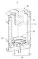
도 1은 본 발명의 바람직한 일 실시예에 의한 디지털 엑스레이 소스(1)를 개략적으로 도시한 사시도이고, 도 2는 디지털 엑스레이 소스(1)의 내부를 설명하기 위해 도 1의 Ⅱ-Ⅱ'선을 따라 절단하여 개략적으로 도시한 단면도이다.1 is a perspective view schematically showing a
도 1 및 도 2를 참고하면, 본 발명의 바람직한 일 실시예에 의한 디지털 엑스레이 소스(1)는 몸체유닛(10), 전자방출 소스유닛(20) 및 애노드유닛(30)을 포함한다.
1 and 2, a
참고로, 본 발명에서 설명하는 디지털 엑스레이 소스(1)는 디지털 엑스레이 장치의 광원인 것으로 도시 및 예시한다. 그러나, 꼭 이에 한정되지 않으며, 전자신호로 빛 에너지를 발생시키는 다양한 디지털 광원분야에 본 발명에 의한 디지털 엑스레이 소스(1)가 적용될 수 있음은 당연하다.
For reference, the
상기 몸체유닛(10)는 원통형 몸체로 형성되며, 내부가 진공인 중공으로 형성된다. 상기 몸체유닛(10)의 원반 형상을 가지는 바닥부(11)와, 바닥부(11)에 대해 수직 상방향으로 연장되는 형상을 가지는 측부(12)를 가진다.The
상기 몸체유닛(10)의 측부(12)에는 몸체유닛(10)의 내부에서 외부로 방출되는 엑스선(L)(도 2 참고)의 출입구인 윈도우(13)가 마련된다 또한 그 사용목적에 따라 윈도우 없이도 제공될 수 있다. 상기 윈도우(13)는 베릴륨, 알루미늄 등의 금속재질 또는 형광물질이 도포된 유리재질로 형성될 수 있다. 상기 윈도우(13)가 베릴륨 등의 금속 재질로 형성되는 경우에는, 소정 파장 이하의 엑스선(L)만 방출되도록 필터링될 수 있다. 또한, 상기 원도우(13)가 형광물질이 도포된 유리재질로 형성되는 경우에는 윈도우(13)를 통하여 가시광선이 방출될 수 있다.A
참고로, 상기 몸체유닛(10)은 세라믹과 같은 비금속성 재질로 형성됨으로써, 후술할 전자방출 소스유닛(20)으로부터 발생되는 전자(E)와의 전기적 간섭을 방지함이 좋다.The
상기 전자방출 소스유닛(20)은 몸체유닛(10)의 내부에서 전자(E)를 방출한다. 상기 전자방출 소스유닛(20)은 엑스선(L)을 발생시키기 위해 전자(E)를 방출하는 전자방출 모듈 내지 전자총을 포함한다. 이러한 전자방출 소스유닛(20)은 몸체유닛(10)의 바닥부(11)에 설치되어 상부에 위치하는 애노드유닛(30)을 향해 전자(E)를 방출한다. 이러한 전자방출 소스유닛(20)의 구성은 도 3 내지 도 5를 참고하여, 보다 자세히 후술한다.The electron
상기 애노드유닛(30)은 전자방출 소스유닛(20)으로부터 방출된 전자(E)와 충돌하여 광 일례로, 엑스선(L)을 발생시켜 몸체유닛(10)의 외부로 안내한다. 이를 위해, 상기 애노드유닛(30)은 전자(E)와의 충돌에 의해 엑스선(L)을 발생시켜 외부로 안내하는 반사면(31)을 구비한다. 이때, 상기 반사면(31)은 엑스선(L)을 포함하는 광을 방향 전환시켜 안내하기 위한 것으로써, 몸체유닛(10)에 마련된 엑스선(L)의 출입구인 윈도우(13)와 마주하도록 일직선 상에 배치된다.The
한편, 상기 애노드유닛(30)에서 발생하는 엑스선(L)을 포함하는 광은 애노드유닛(30)의 재질과 디지털 엑스레이 소스(1)에 인가되는 전압의 크기에 따라서 달라질 수 있으며, 엑스선, 가시광선, 적외선, 자외선 가운데 어느 하나가 될 수 있다. 본 실시예에서는 상기 애노드유닛(30)이 구리, 텡스텐, 망간, 몰리브덴 및 이의 조합으로 이루어진 금속 중 어느 하나의 재질로 형성되어 엑스선(L)을 발생시키는 것으로 예시한다.The light including the X-ray L generated in the
참고로, 상기 반사면(31)이 금속이 아닌 유리와 같은 재질로 형성될 경우, 전자(E)와의 충돌에 의해 조명을 위한 광(L)을 발생시키는 변형예도 가능하다.
For example, when the
이하에서는, 도 3 내지 도 5를 참고하여 상술한 전자방출 소스유닛(20)의 구성을 보다 자세히 설명한다.Hereinafter, the configuration of the electron
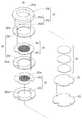
도 3의 도시와 같이, 상기 전자방출 소스유닛(20)은 음극부(21), 에미터부(22), 패터닝부(23), 게이트부(24), 포커싱부(25) 및 절연부(26)를 포함한다.3, the electron
상기 음극부(21)는 음극의 전자(E)을 발생시킨다. 이러한 음극부(21)는 얇은 판상인 박판으로 형성되며, 지지부재(211)에 적층되어 지지된다. 또한, 상기 음극부(21)는 금속 재질로 형성되는 음극기판을 포함할 수 있다.The
이러한 음극부(21)는 음극, 즉 (-)전극으로 캐소드(cathode) 전극으로 칭할 수 있다. 본 발명에 의한 디지털 엑스레이 소스(1)는 진공에서 작동하기 때문에, 캐소드 전극의 재료에는 니켈, 철, 코발트 등의 합금이나 단일 전이금속을 포함할 수 있다.The
참고로, 자세히 도시되지 않았으나, 상기 음극부(21)는 외부 전원과 연결되어 전원이 인가될 수 있다.For reference, although not shown in detail, the
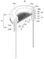
상기 에미터부(22)는 음극부(21)의 상부에 위치하여, 음극부(21)로부터 인가된 음극의 전극으로부터 전자(E)를 방출한다. 이러한 에미터부(22)는 전자를 발생하며, 나노 소재인 탄소나노튜브(C)(Carbon Nano Tube, CNT)(도 5 참고)와 같은 금속, 탄소계열 물질로 구성되는 물질을 포함한다. 이때, 상기 에미터부(22)가 나노 소재인 탄소나노튜브(C)를 포함함으로써, 단위 면적당 높은 전류 방출이 가능하다.The
참고로, 상기 에미터부(22)는 박판 형상을 가지고 마련되어 복수개가 상호 적층되어 마련될 수 있다. 이러한 에미터부(22)는 상호 동일한 형상을 가지고 상호 적층됨이 바람직하며, 본 실시예에서는 원형의 플레이트 형상을 가지는 것으로 예시한다.For reference, the
상기 패터닝부(23)는 에미터부(22)로부터 성장하는 탄소나노튜브(C)(도 5 참고)를 패터닝시킨다. 이를 위해, 상기 패터닝부(23)는 정렬 가이더(231)와 패터닝 메쉬(232)를 포함한다.The
상기 정렬 가이더(231)는 에미터부(22)를 정렬시킨다. 이러한 정렬 가이더(231)는 에미터부(22)가 삽입 가능한 가이더홀(231a)을 구비하여, 박판 형상을 가지는 음극부(21)의 상부에 적층된다. 상기 정렬 가이더(231)의 가이더홀(231a) 내부에 에미터부(22)가 삽입됨으로써, 에미터부(22)는 가이더홀(231a) 내에서 수평방향으로 자가 정렬될 수 있다.The
참고로, 상기 정렬 가이더(231)는 가이더홀(231a)에 정렬되는 에미터부(22)의 적층 높이에 대응되는 높이를 가지고 마련될 수 있다. 본 실시예에서는 상기 에미터부(22)가 3개 적층되는 것으로 도시 및 예시하나, 꼭 도시된 예로 한정되지 않음은 당연하다.For reference, the
상기 패터닝 메쉬(232)는 정렬 가이더(231)에 적층되어 에미터부(22)로 대해 면방향으로 가압된다. 또한, 상기 패터닝 메시(232)는 에미터부(22)와 마주하도록 관통된 복수의 패터닝 메쉬홀(232a)이 형성된다. 이러한 패터닝 메쉬(232)는 금속성 재질로 형성되되, 중앙 영역에 복수의 패터닝 메쉬홀(232a)이 형성됨으로써, 테두리 인근은 패터닝 메쉬홀(232a)이 형성되지 않는다. 그로 인해, 상기 패터닝 메쉬(232)의 테두리는 에미터부(22)의 테두리를 가압함으로써, 에지효과(Edge effect)를 방지할 수 있게 된다.The
상기 패터닝 메쉬(232)에 관통 형성되는 복수의 패터닝 메쉬홀(232a)은 대략 육각형의 벌집 형상으로 형성되며, 직경이 대략 0.05mm인 것으로 예시한다. 이러한 복수의 패터닝 메쉬홀(232a)을 구비하는 패터닝 메쉬(232)는 도 4 및 도 5의 도시와 같이, 에미터부(22)의 상면에 밀착되도록 적층된다.The plurality of
그로 인해, 도 5의 도시와 같이, 상기 패터닝 메쉬홀(232a)을 통해 에미터부(22)로부터 성장되는 탄소나노튜브(C)가 관통된 패터닝 메쉬홀(232a)의 내부에서만 성장되도록 패터닝된다. 즉, 상기 에미터부(22)로부터 성장되는 탄소나노튜브(C)는 금속성 재질의 패터닝 메쉬(232)와 부딪혀 성장되지 않으며, 관통된 패터닝 메쉬홀(232a) 내에서 성장되는 것이다.As a result, as shown in FIG. 5, the carbon nanotube C grown from the
상기 게이트부(24)는 에미터부(22)의 상부에서 에미터부(22)로부터 방출되는 전자(E)를 추출한다. 상기 게이트부(24)는 에미터부(22)의 상부에 배치되며, 보다 구체적으로는 에미터부(22)를 정렬시키며 탄소나노튜브(C)의 성장을 패터닝하는 패터닝부(23)의 상부에 적층된다. 이러한 게이트부(24)는 게이트 전극(241)과 게이트 메쉬(242)를 포함한다.The
상기 게이트 전극(241)은 에미터부(22)의 상부에 적층된 패터닝부(23)에 적층 가능한 박판 형상을 가지며, 금속성 재질로 형성될 수 있다. 이러한 게이트 전극(24)은 에미터부(22)로부터 전자를 추출할 수 있다.The
상기 게이트 메쉬(242)는 게이트 전극(241)에 마련되되, 패터닝 메쉬(232)와 마주하도록 마련된다. 이러한 게이트 메쉬(242)는 복수의 게이트 메쉬홀(242a)을 구비하여, 에미터부(22)로부터 발생된 전자(E)를 추출한다. 상기 게이트 메쉬(242)는 에미터부(22)의 상면과 기설정된 간격만큼 이격될 수 있고, 에미터부(22)의 가운데 부분까지 전기장이 잘 인가될 수 있도록 가이드하여 에미터부(22)에서 전자(E) 추출이 균일하게 되도록 하는 역할을 한다.The
상기 게이트 메쉬(242)의 게이트 메쉬홀(242a)은 패터닝 메쉬홀(232a)과 마찬가지로 육각형의 벌집 형상으로 형성되는 것으로 도시 및 예시한다. 상기 게이트 메쉬(242)의 개구의 형상이 육각형으로 형성됨에 따라, 게이트 메쉬(242)가 전자를 효율적으로 추출하면서, 전자(E)가 금속망에 의하여 충돌되지 않고 안정적으로 배출되는 개구율이 극대화될 수 있다.The
이러한 게이트 메쉬홀(242a)과 패터닝 메쉬홀(232a)의 형상은 육각형의 벌집 형상으로 한정되지 않으며, 전자(E)의 진행을 방해하지 않는 범위 내에서 원형, 사각형을 비롯한 다양한 개구 형상을 가지도록 변형 가능하다.The shapes of the
한편, 상호 마주하는 패터닝 메쉬홀(232a)과 게이트 메쉬홀(242a) 중, 패터닝 메쉬홀(232a)의 크기가 게이트 메쉬홀(242a)의 크기보다 크게 형성될 수 있다. 이렇게 패터닝 메쉬홀(232a)의 크기가 게이트 메쉬홀(242a)보다 상대적으로 크게 형성됨으로써, 패터닝 메쉬홀(232a)에 의해 패터닝되어 성장된 탄소나노튜브(C)로부터 발생된 전자(E)가 금속성 재질의 패터닝 메쉬(232)와 충돌됨 없이, 게이트 메쉬홀(242a)을 통과하여 추출될 수 있다.In the
상기 포커싱부(25)는 게이트부(24)의 상부에서 방출되는 전자(E)를 포커싱시킨다. 상기 포커싱부(25)는 전자(E)를 포커싱시키는 포커싱홀(251a)을 가지는 포커싱 전극(251)과, 포커싱 전극(251)으로부터 연장되어 외부의 전원과 연결되는 전원 연결부(252)를 포함한다.The focusing
상기 포커싱 전극(251)은 포커싱홀(251a)을 구비하여 전자방출 소스유닛(20)의 최상단, 즉 에미터부(22)와 애노드유닛(30)의 사이에 위치한다. 이러한 포커싱 전극(251)은 에미터부(22)으로부터 방출된 전자(E)가 퍼지거나 산란되지 않고 애노드유닛(30)을 향하여 이동할 수 있도록 포커싱한다.The focusing
상기 전원 연결부(252)는 포커싱 전극(251)으로부터 수직 하방향으로 원통 형상으로 연장되는 전원 보호부재(252a)와 전원 보호부재(252a)의 내부를 통해 연장되어 외부의 전원과 연결되는 전원 라인(252b)을 포함한다. 이러한 전원 전극부(21)를 순차적으로 관통하여 외부의 전원과 연결될 수 있다.The
상기 절연부(26)는 음극부(21), 게이트부(24) 및 포커싱부(25)를 상호 절연시키기 위한 것으로서, 제1 및 제2절연부재(261)(262)를 포함한다.The insulating
상기 제1절연부재(261)는 음극부(21)와 게이트부(24)의 사이를 상호 절연시키며, 제2절연부재(262)는 게이트부(24)와 포커싱부(25)의 사이를 상호 절연시킨다. 보다 구체적으로, 상기 제1절연부재(261)는 박판 형상을 가지고, 음극부(21)에 적층되어 에미터부(22)를 커버하는 패터닝부(23)와 게이트부(24)의 사이에 적층된다.The first insulating
또한, 상기 제2절연부재(262)는 박판 형상을 가지고, 게이트부(24)와 포커싱부(25)의 사이에 적층된다. 그로 인해, 상기 제1 및 제2절연부재(262)는 금속성 재질로 형성되는 음극부(21)와 게이트 전극(241)의 사이 및, 게이트 전극(241)과 포커싱 전극(251)의 사이를 각각 개별적으로 절연시킬 수 있게 된다.Further, the second insulating
한편, 상술한 패터닝부(23), 포커싱부(25) 및 절연부(26)에는 모두 에미터부(22)로부터 발생되는 전자(E)의 진행 경로를 위해 모두 관통된 가이더홀(231a), 포커싱홀(251a), 제1절연홀(261a) 및 제2절연홀(262a)을 가진다. 이러한 가이더홀(231a), 포커싱홀(251a), 제1절연홀(261a) 및 제2절연홀(262a)은 모두 상호 연통 가능하도록 마련됨이 좋다The
또한, 자세히 도시되지 않았으나, 상술한 음극부(21), 에미터부(22), 패터닝부(23), 게이트부(24), 포커싱부(25) 및 절연부(26)는 미도시된 절연기둥과 같은 결합 가이드 수단에 의해 상호 정렬된 상태로 밀착되어 결합된다.Although not shown in detail, the
참고로, 상기 전자방출 소스유닛(20)은 진공 상태에서 작동된다. 이를 위해, 도 2의 도시와 같이, 상기 몸체유닛(10) 내부에 마련된 전자방출 소스유닛(20)의 일측에는 산소, 질소 등과 같은 불순물을 화학적으로 흡착시켜 진공시키는 진공부(27)가 마련된다. 상기 진공부(27)는 전자(E)의 진행방향을 방해하는 것을 방지하기 위해 전자방출 소스유닛(20)의 하부에 배치됨이 좋다.
For reference, the electron
상기와 같은 구성을 가지는 본 발명에 의한 디지털 엑스레이 소스(1)의 동작을 도 2를 참고하여 설명한다.The operation of the
도 2의 도시와 같이, 상기 몸체유닛(10)의 내부 바닥면(11)에 설치되는 전자방출 소스유닛(20)으로부터 전자(E)가 방출되어 가속된다. 이렇게 가속된 전자(E)는 애노드유닛(30)의 반사면(31)에 충돌함으로써 가지고 있는 에너지를 빛으로 방출하며, 반사면(31)의 재질 특성에 의해 엑스선(L)으로 방출한다. 상기 방출된 엑스선(L)은 반사면(31)의 반사각도에 의해 몸체유닛(10)의 측벽(12)에 마련된 윈도우(13)(도 1 참고)를 통해 외부로 안내된다.As shown in FIG. 2, electrons E are emitted from the electron
한편, 도 4의 도시와 같이, 상기 전자방출 소스유닛(20)은 전자를 방출하는 에미터부(22)가 정렬 가이더(231)의 가이더홀(231a)에 의해 수평방향으로 위치 정렬되며, 패터닝 메쉬(232)에 의해 수직방향으로 가압된 상태이다. 이때, 상기 패터닝 메쉬(232)의 테두리에 의해 에미터부(22)의 테두리가 커버됨으로써, 에지 효과가 방지된다.4, the
아울러, 상기 패터닝 메쉬(232)는 에미터부(22)에 밀착되도록 적층됨으로써, 도 5에 도시된 바와 같이, 패터닝 메쉬홀(232a)에 의해 에미터부(22)로부터 성장되는 탄소나노튜브(C)의 성장이 패터닝된다. 이렇게 정밀 제어된 패턴으로 성장되는 탄소나노튜브(C)로부터 방출되는 전자(E)는 게이트 메쉬홀(242a)을 통해 추출되어 포커싱부(25)를 통해 외부로 포커싱된다.
5, the
상술한 바와 같이, 본 발명의 바람직한 실시예를 참조하여 설명하였지만 해당 기술분야의 숙련된 당업자라면 하기의 청구범위에 기재된 본 발명의 사상 및 영역으로부터 벗어나지 않는 범위 내에서 본 발명을 다양하게 수정 및 변경시킬 수 있음을 이해할 수 있을 것이다.
Although the present invention has been described with reference to the preferred embodiments thereof, it will be apparent to those skilled in the art that various modifications and variations can be made in the present invention without departing from the spirit and scope of the invention as defined in the following claims. It can be understood that
1: 디지털 엑스레이 소스10: 몸체유닛
20: 전자방출 소스유닛21: 음극부
22: 에미터부23: 패터닝부
24: 게이트부25: 포커싱부
26: 절연부27: 진공부
30: 애노드유닛31: 반사면1: Digital X-ray source 10: Body unit
20: electron emission source unit 21: cathode part
22: emitter part 23: patterning part
24: gate part 25: focusing part
26: insulation part 27:
30: anode unit 31: reflective surface
Claims (15)
Translated fromKorean상기 음극부에 적층되도록 마련되어 전자를 방출하는 에미터부;
상기 에미터부로부터 성장하는 탄소나노튜브를 패터닝시키는 패터닝부;
상기 에미터부로부터 방출된 상기 전자를 추출하는 게이트부; 및
상기 게이트부에서 추출된 상기 전자를 포커싱하여 외부로 방출시키는 포커싱부;
를 포함하는 전자방출 소스유닛.
A cathode portion to which an electrode of a cathode is applied;
An emitter section provided to be laminated on the cathode section to emit electrons;
A patterning part for patterning the carbon nanotubes growing from the emitter part;
A gate for extracting the electrons emitted from the emitter; And
A focusing unit for focusing the electrons extracted from the gate unit and discharging the electrons to the outside;
And an electron emission source unit.
상기 패터닝부는,
상기 에미터부를 수평 방향으로 정렬시키는 정렬 가이더; 및
상기 에미터부와 마주하는 복수의 패터닝 메쉬홀이 관통 형성되는 금속성 재질의 박판 형상을 가지고 상기 에미터부에 대해 면방향으로 밀착되도록 적층되는 패터닝 메쉬;
를 포함하는 전자방출 소스유닛.
The method according to claim 1,
Wherein the patterning portion comprises:
An aligning guider for horizontally aligning the emitter portion; And
A patterning mesh having a thin plate shape of a metallic material through which a plurality of patterning mesh holes facing the emitter unit are formed and which is laminated so as to be in close contact with the emitter unit in a planar direction;
And an electron emission source unit.
상기 게이트부는,
상기 패터닝부에 적층되며 금속성 재질로 형성되는 게이트 전극; 및
상기 패터닝 메쉬와 마주하도록 상기 게이트 전극에 마련되되, 복수의 게이트 메쉬홀이 관통 형성되는 게이트 메쉬;
를 포함하며,
상기 패터닝 메쉬홀은 상기 게이트 메쉬홀보다 크게 형성되는 전자방출 소스유닛.
3. The method of claim 2,
The gate unit includes:
A gate electrode formed on the patterning portion and formed of a metallic material; And
A gate mesh provided on the gate electrode to face the patterning mesh, the gate mesh having a plurality of gate mesh holes formed therein;
/ RTI >
Wherein the patterning mesh hole is formed larger than the gate mesh hole.
상기 패터닝 메쉬홀 및 게이트 메쉬홀은 원형, 사격형 또는 벌집 형상을 가지고 상기 전자를 추출하는 전자방출 소스유닛.
The method of claim 3,
Wherein the patterning mesh hole and the gate mesh hole have a circular shape, a shooting shape, or a honeycomb shape and extract the electrons.
상기 에미터부는 상호 적층 가능한 적어도 하나의 에미터를 포함하는 전자방출 소스유닛.
The method according to claim 1,
Wherein the emitter section comprises at least one emitter that is stackable with respect to one another.
상기 음극부와 상기 게이트부 사이를 상호 절연시키는 제1절연부재 및 상기 게이트부와 상기 포커싱부 사이를 상호 절연시키는 제2절연부재를 포함하는 절연부;
를 포함하는 전자방출 소스유닛.
The method according to claim 1,
An insulating portion including a first insulating member for insulating the cathode portion and the gate portion from each other, and a second insulating member for insulating the gate portion and the focusing portion from each other;
And an electron emission source unit.
상기 제1절연부재는 상기 패터닝부와 상기 게이트부 사이에 적층되는 박판 형상을 가지며,
상기 제2절연부재는 상기 게이트부와 상기 포커싱부 사이에 적층되는 박판 형상을 가지는 전자방출 소스유닛.
The method according to claim 6,
Wherein the first insulating member has a thin plate shape laminated between the patterning portion and the gate portion,
And the second insulating member has a thin plate shape laminated between the gate portion and the focusing portion.
상기 포커싱부는,
상기 전자를 포커싱시키는 포커싱홀을 가지는 포커싱 전극; 및
상기 포커싱 전극으로부터 연장되어 외부 전원과 연결되는 전원 연결부;
를 포함하는 전자방출 소스유닛.
The method according to claim 1,
The focusing unit includes:
A focusing electrode having a focusing hole for focusing the electrons; And
A power connection part extending from the focusing electrode and connected to an external power source;
And an electron emission source unit.
상기 전원 연결부는,
상기 포커싱 전극으로부터 수직 하방향으로 연장되는 전원 보호부재; 및
상기 전원 보호부재의 내부를 통해 연장되어 외부의 전원과 연결되는 전원 라인;
을 포함하며,
상기 전원 보호부는 상기 게이트부, 패터닝부, 에미터부 및 음극부를 순차적으로 관통하여 상기 외부의 전원과 연결되는 전자방출 소스유닛.
9. The method of claim 8,
The power connection unit includes:
A power protection member extending vertically downward from the focusing electrode; And
A power supply line extending through the inside of the power protection member and connected to an external power source;
/ RTI >
Wherein the power source protection unit sequentially passes through the gate unit, the patterning unit, the emitter unit, and the cathode unit, and is connected to the external power source.
상기 몸체유닛의 내부에서 전자를 방출하는 상기 제1항 내지 제9항 중 어느 한 항에 기재된 전자방출 소스유닛;
상기 전자방출 소스유닛으로부터 방출된 상기 전자와의 충돌에 의해 광을 발생시켜 상기 몸체유닛의 외부로 안내하는 애노드유닛;
을 포함하는 디지털 엑스레이 소스.
A hollow body unit having a space therein;
The electron emission source unit according to any one of claims 1 to 9, which emits electrons within the body unit.
An anode unit for generating light by collision with the electrons emitted from the electron emission source unit and guiding the light to the outside of the body unit;
A digital x-ray source containing.
상기 몸체유닛의 내부에서 전자를 방출하는 전자방출 소스유닛; 및
상기 전자방출 소스유닛으로부터 방출된 상기 전자와의 충돌에 의해 광을 발생시켜 상기 몸체유닛의 외부로 안내하는 애노드유닛;
을 포함하며,
상기 전자방출 소스유닛은 복수의 패터닝 메쉬홀을 가지고 전자를 방출하는 에미터부의 상부에 적층되어, 상기 에미터부로부터 성장되는 탄소나노튜브를 패터닝시키는 패터닝부를 포함하는 디지털 엑스레이 소스.
A hollow body unit having a space therein;
An electron emission source unit for emitting electrons within the body unit; And
An anode unit for generating light by collision with the electrons emitted from the electron emission source unit and guiding the light to the outside of the body unit;
/ RTI >
Wherein the electron emission source unit includes a patterning portion laminated on an emitter portion for emitting electrons with a plurality of patterning mesh holes, and patterning the carbon nanotubes grown from the emitter portion.
상기 전자방출 소스유닛은,
음극의 전극을 인가시키며 상부에 상기 에미터부가 적층되는 음극부;
상기 에미터부로부터 방출된 상기 전자를 추출하는 게이트부; 및
상기 게이트부에서 추출된 상기 전자를 포커싱하여 외부로 방출시키는 포커싱부;
를 포함하는 디지털 엑스레이 소스.
12. The method of claim 11,
The electron emission source unit includes:
A cathode portion on which the emitter portion is stacked by applying an electrode of a cathode;
A gate for extracting the electrons emitted from the emitter; And
A focusing unit for focusing the electrons extracted from the gate unit and discharging the electrons to the outside;
A digital x-ray source containing.
상기 패터닝부는,
상기 에미터부를 수평 방향으로 정렬시키는 정렬 가이더; 및
상기 에미터부와 마주하는 복수의 패터닝 메쉬홀이 관통 형성되는 금속성 재질의 박판 형상을 가지고 상기 에미터부에 대해 면방향으로 밀착되도록 적층되는 패터닝 메쉬;
를 포함하는 디지털 엑스레이 소스.
12. The method of claim 11,
Wherein the patterning portion comprises:
An aligning guider for horizontally aligning the emitter portion; And
A patterning mesh having a thin plate shape of a metallic material through which a plurality of patterning mesh holes facing the emitter unit are formed and which is laminated so as to be in close contact with the emitter unit in a planar direction;
A digital x-ray source containing.
상기 게이트부는,
상기 패터닝부에 적층되며 금속성 재질로 형성되는 게이트 전극; 및
상기 패터닝 메쉬와 마주하도록 상기 게이트 전극에 마련되되, 복수의 게이트 메쉬홀이 관통 형성되는 게이트 메쉬;
를 포함하며,
상기 패터닝 메쉬홀은 상기 게이트 메쉬홀보다 크게 형성되는 디지털 엑스레이 소스.
14. The method of claim 13,
The gate unit includes:
A gate electrode formed on the patterning portion and formed of a metallic material; And
A gate mesh provided on the gate electrode to face the patterning mesh, the gate mesh having a plurality of gate mesh holes formed therein;
/ RTI >
Wherein the patterning mesh hole is formed larger than the gate mesh hole.
상기 패터닝 메쉬홀 및 게이트 메쉬홀은 원형, 사격형 또는 벌집 형상을 가지고 상기 전자를 추출하는 디지털 엑스레이 소스.15. The method of claim 14,
Wherein the patterning mesh hole and the gate mesh hole have a circular shape, a shooting shape, or a honeycomb shape, and extract the electron.
Priority Applications (1)
| Application Number | Priority Date | Filing Date | Title |
|---|---|---|---|
| KR1020170034382AKR101986413B1 (en) | 2017-03-20 | 2017-03-20 | Electron emission source unit and digital x-ray source |
Applications Claiming Priority (1)
| Application Number | Priority Date | Filing Date | Title |
|---|---|---|---|
| KR1020170034382AKR101986413B1 (en) | 2017-03-20 | 2017-03-20 | Electron emission source unit and digital x-ray source |
Publications (2)
| Publication Number | Publication Date |
|---|---|
| KR20180106291Atrue KR20180106291A (en) | 2018-10-01 |
| KR101986413B1 KR101986413B1 (en) | 2019-09-30 |
Family
ID=63877481
Family Applications (1)
| Application Number | Title | Priority Date | Filing Date |
|---|---|---|---|
| KR1020170034382AActiveKR101986413B1 (en) | 2017-03-20 | 2017-03-20 | Electron emission source unit and digital x-ray source |
Country Status (1)
| Country | Link |
|---|---|
| KR (1) | KR101986413B1 (en) |
Cited By (3)
| Publication number | Priority date | Publication date | Assignee | Title |
|---|---|---|---|---|
| KR20210017127A (en)* | 2019-08-07 | 2021-02-17 | (주) 브이에스아이 | A large X-RAY Generator |
| KR20210081951A (en)* | 2019-12-24 | 2021-07-02 | 주식회사 씨에이티빔텍 | Emitter and electron emitting source having the same |
| KR20210083531A (en)* | 2019-12-27 | 2021-07-07 | 주식회사 씨에이티빔텍 | Electron emitting element and manufacturing method thereof |
Families Citing this family (1)
| Publication number | Priority date | Publication date | Assignee | Title |
|---|---|---|---|---|
| KR102351800B1 (en)* | 2020-01-02 | 2022-01-18 | 경희대학교 산학협력단 | Analytical device and method for operation specimen |
Citations (6)
| Publication number | Priority date | Publication date | Assignee | Title |
|---|---|---|---|---|
| JP2003502798A (en)* | 1999-06-10 | 2003-01-21 | ライトラブ アーベー | Field emission cathode and method of manufacturing light source including the same |
| KR20050074283A (en)* | 2004-12-27 | 2005-07-18 | 진텍, 인크. | Fabrication and activation processes for nanostructure composite field emission cathodes |
| KR20070028000A (en)* | 2005-08-30 | 2007-03-12 | 삼성에스디아이 주식회사 | Electron Emission Device and Electron Emission Display Device Using The Same |
| KR101070091B1 (en) | 2010-11-16 | 2011-10-04 | 경희대학교 산학협력단 | X-ray source with insulated pillar |
| KR101211639B1 (en) | 2012-02-02 | 2012-12-18 | 테크밸리 주식회사 | Electron gun having electrode suporter and x-ray tube having the same |
| KR20170006810A (en)* | 2015-07-09 | 2017-01-18 | 경희대학교 산학협력단 | Digital x-ray source |
- 2017
- 2017-03-20KRKR1020170034382Apatent/KR101986413B1/enactiveActive
Patent Citations (6)
| Publication number | Priority date | Publication date | Assignee | Title |
|---|---|---|---|---|
| JP2003502798A (en)* | 1999-06-10 | 2003-01-21 | ライトラブ アーベー | Field emission cathode and method of manufacturing light source including the same |
| KR20050074283A (en)* | 2004-12-27 | 2005-07-18 | 진텍, 인크. | Fabrication and activation processes for nanostructure composite field emission cathodes |
| KR20070028000A (en)* | 2005-08-30 | 2007-03-12 | 삼성에스디아이 주식회사 | Electron Emission Device and Electron Emission Display Device Using The Same |
| KR101070091B1 (en) | 2010-11-16 | 2011-10-04 | 경희대학교 산학협력단 | X-ray source with insulated pillar |
| KR101211639B1 (en) | 2012-02-02 | 2012-12-18 | 테크밸리 주식회사 | Electron gun having electrode suporter and x-ray tube having the same |
| KR20170006810A (en)* | 2015-07-09 | 2017-01-18 | 경희대학교 산학협력단 | Digital x-ray source |
Cited By (3)
| Publication number | Priority date | Publication date | Assignee | Title |
|---|---|---|---|---|
| KR20210017127A (en)* | 2019-08-07 | 2021-02-17 | (주) 브이에스아이 | A large X-RAY Generator |
| KR20210081951A (en)* | 2019-12-24 | 2021-07-02 | 주식회사 씨에이티빔텍 | Emitter and electron emitting source having the same |
| KR20210083531A (en)* | 2019-12-27 | 2021-07-07 | 주식회사 씨에이티빔텍 | Electron emitting element and manufacturing method thereof |
Also Published As
| Publication number | Publication date |
|---|---|
| KR101986413B1 (en) | 2019-09-30 |
Similar Documents
| Publication | Publication Date | Title |
|---|---|---|
| US10741353B2 (en) | Electron emitting construct configured with ion bombardment resistant | |
| KR101341672B1 (en) | A digital x-ray source | |
| RU2668268C2 (en) | Source of electrons, source of x-ray radiation and device using source of x-ray radiation | |
| US9991085B2 (en) | Apparatuses and methods for generating distributed x-rays in a scanning manner | |
| KR20180106291A (en) | Electron emission source unit and digital x-ray source | |
| US8295440B2 (en) | Super miniature X-ray tube using NANO material field emitter | |
| KR102005638B1 (en) | Bipolar digital x-ray apparatus | |
| US7706506B1 (en) | X-ray system for irradiating material used in transfusions | |
| US8350226B2 (en) | Methods and systems for treating cancer using external beam radiation | |
| KR101701047B1 (en) | Digital x-ray source | |
| KR20180055090A (en) | Apparatus for digital light source | |
| KR102316133B1 (en) | Apparatus for generating x-ray using replaceable x-ray source cartridge | |
| KR101247453B1 (en) | A X-ray source having the cooling and shielding function | |
| KR102047436B1 (en) | X-ray source unit and x-ray apparatus | |
| KR101862939B1 (en) | Electron emission source unit and digital x-ray source | |
| US9508523B2 (en) | Forward flux channel X-ray source | |
| CN111328176B (en) | Suspended grid cathode structure, electron gun, electron accelerator and irradiation device | |
| KR102746126B1 (en) | Electron emitting element and x-ray apparatus having the same | |
| KR102131665B1 (en) | Dual x-ray source unit and dual x-ray apparatus | |
| KR101205603B1 (en) | Multi beam x-ray device | |
| KR101749858B1 (en) | Apparatus for intergral digital light source | |
| JP2004335419A (en) | X-ray generator | |
| KR102136062B1 (en) | Field emission type tomosynthesis system | |
| KR20240108299A (en) | Radioactice-rays irradiating device | |
| KR20240048994A (en) | X-ray generator |
Legal Events
| Date | Code | Title | Description |
|---|---|---|---|
| A201 | Request for examination | ||
| PA0109 | Patent application | Patent event code:PA01091R01D Comment text:Patent Application Patent event date:20170320 | |
| PA0201 | Request for examination | ||
| E902 | Notification of reason for refusal | ||
| PE0902 | Notice of grounds for rejection | Comment text:Notification of reason for refusal Patent event date:20180219 Patent event code:PE09021S01D | |
| AMND | Amendment | ||
| E90F | Notification of reason for final refusal | ||
| PE0902 | Notice of grounds for rejection | Comment text:Final Notice of Reason for Refusal Patent event date:20180820 Patent event code:PE09021S02D | |
| PG1501 | Laying open of application | ||
| AMND | Amendment | ||
| E601 | Decision to refuse application | ||
| E801 | Decision on dismissal of amendment | ||
| PE0601 | Decision on rejection of patent | Patent event date:20190222 Comment text:Decision to Refuse Application Patent event code:PE06012S01D Patent event date:20180820 Comment text:Final Notice of Reason for Refusal Patent event code:PE06011S02I Patent event date:20180219 Comment text:Notification of reason for refusal Patent event code:PE06011S01I | |
| PE0801 | Dismissal of amendment | Patent event code:PE08012E01D Comment text:Decision on Dismissal of Amendment Patent event date:20190222 Patent event code:PE08011R01I Comment text:Amendment to Specification, etc. Patent event date:20181022 Patent event code:PE08011R01I Comment text:Amendment to Specification, etc. Patent event date:20180418 | |
| AMND | Amendment | ||
| PX0901 | Re-examination | Patent event code:PX09011S01I Patent event date:20190222 Comment text:Decision to Refuse Application Patent event code:PX09012R01I Patent event date:20181022 Comment text:Amendment to Specification, etc. Patent event code:PX09012R01I Patent event date:20180418 Comment text:Amendment to Specification, etc. | |
| PX0701 | Decision of registration after re-examination | Patent event date:20190528 Comment text:Decision to Grant Registration Patent event code:PX07013S01D Patent event date:20190426 Comment text:Amendment to Specification, etc. Patent event code:PX07012R01I Patent event date:20190222 Comment text:Decision to Refuse Application Patent event code:PX07011S01I Patent event date:20181022 Comment text:Amendment to Specification, etc. Patent event code:PX07012R01I Patent event date:20180418 Comment text:Amendment to Specification, etc. Patent event code:PX07012R01I | |
| X701 | Decision to grant (after re-examination) | ||
| GRNT | Written decision to grant | ||
| PR0701 | Registration of establishment | Comment text:Registration of Establishment Patent event date:20190530 Patent event code:PR07011E01D | |
| PR1002 | Payment of registration fee | Payment date:20190530 End annual number:3 Start annual number:1 | |
| PG1601 | Publication of registration | ||
| PR1001 | Payment of annual fee | Payment date:20220401 Start annual number:4 End annual number:4 | |
| PR1001 | Payment of annual fee | Payment date:20230404 Start annual number:5 End annual number:5 | |
| PR1001 | Payment of annual fee | Payment date:20240401 Start annual number:6 End annual number:6 |