KR20180102936A - Imprint template with alignment mark and methods of forming imprint patterns - Google Patents
Imprint template with alignment mark and methods of forming imprint patternsDownload PDFInfo
- Publication number
- KR20180102936A KR20180102936AKR1020170029695AKR20170029695AKR20180102936AKR 20180102936 AKR20180102936 AKR 20180102936AKR 1020170029695 AKR1020170029695 AKR 1020170029695AKR 20170029695 AKR20170029695 AKR 20170029695AKR 20180102936 AKR20180102936 AKR 20180102936A
- Authority
- KR
- South Korea
- Prior art keywords
- template
- alignment mark
- pattern
- resist layer
- imprint
- Prior art date
- Legal status (The legal status is an assumption and is not a legal conclusion. Google has not performed a legal analysis and makes no representation as to the accuracy of the status listed.)
- Granted
Links
Images


Classifications
- G—PHYSICS
- G03—PHOTOGRAPHY; CINEMATOGRAPHY; ANALOGOUS TECHNIQUES USING WAVES OTHER THAN OPTICAL WAVES; ELECTROGRAPHY; HOLOGRAPHY
- G03F—PHOTOMECHANICAL PRODUCTION OF TEXTURED OR PATTERNED SURFACES, e.g. FOR PRINTING, FOR PROCESSING OF SEMICONDUCTOR DEVICES; MATERIALS THEREFOR; ORIGINALS THEREFOR; APPARATUS SPECIALLY ADAPTED THEREFOR
- G03F9/00—Registration or positioning of originals, masks, frames, photographic sheets or textured or patterned surfaces, e.g. automatically
- G03F9/70—Registration or positioning of originals, masks, frames, photographic sheets or textured or patterned surfaces, e.g. automatically for microlithography
- G03F9/7003—Alignment type or strategy, e.g. leveling, global alignment
- G03F9/7042—Alignment for lithographic apparatus using patterning methods other than those involving the exposure to radiation, e.g. by stamping or imprinting
- G—PHYSICS
- G03—PHOTOGRAPHY; CINEMATOGRAPHY; ANALOGOUS TECHNIQUES USING WAVES OTHER THAN OPTICAL WAVES; ELECTROGRAPHY; HOLOGRAPHY
- G03F—PHOTOMECHANICAL PRODUCTION OF TEXTURED OR PATTERNED SURFACES, e.g. FOR PRINTING, FOR PROCESSING OF SEMICONDUCTOR DEVICES; MATERIALS THEREFOR; ORIGINALS THEREFOR; APPARATUS SPECIALLY ADAPTED THEREFOR
- G03F7/00—Photomechanical, e.g. photolithographic, production of textured or patterned surfaces, e.g. printing surfaces; Materials therefor, e.g. comprising photoresists; Apparatus specially adapted therefor
- G03F7/0002—Lithographic processes using patterning methods other than those involving the exposure to radiation, e.g. by stamping
- G—PHYSICS
- G03—PHOTOGRAPHY; CINEMATOGRAPHY; ANALOGOUS TECHNIQUES USING WAVES OTHER THAN OPTICAL WAVES; ELECTROGRAPHY; HOLOGRAPHY
- G03F—PHOTOMECHANICAL PRODUCTION OF TEXTURED OR PATTERNED SURFACES, e.g. FOR PRINTING, FOR PROCESSING OF SEMICONDUCTOR DEVICES; MATERIALS THEREFOR; ORIGINALS THEREFOR; APPARATUS SPECIALLY ADAPTED THEREFOR
- G03F1/00—Originals for photomechanical production of textured or patterned surfaces, e.g., masks, photo-masks, reticles; Mask blanks or pellicles therefor; Containers specially adapted therefor; Preparation thereof
- G03F1/38—Masks having auxiliary features, e.g. special coatings or marks for alignment or testing; Preparation thereof
- G03F1/42—Alignment or registration features, e.g. alignment marks on the mask substrates
- G—PHYSICS
- G03—PHOTOGRAPHY; CINEMATOGRAPHY; ANALOGOUS TECHNIQUES USING WAVES OTHER THAN OPTICAL WAVES; ELECTROGRAPHY; HOLOGRAPHY
- G03F—PHOTOMECHANICAL PRODUCTION OF TEXTURED OR PATTERNED SURFACES, e.g. FOR PRINTING, FOR PROCESSING OF SEMICONDUCTOR DEVICES; MATERIALS THEREFOR; ORIGINALS THEREFOR; APPARATUS SPECIALLY ADAPTED THEREFOR
- G03F7/00—Photomechanical, e.g. photolithographic, production of textured or patterned surfaces, e.g. printing surfaces; Materials therefor, e.g. comprising photoresists; Apparatus specially adapted therefor
- G03F7/20—Exposure; Apparatus therefor
- G03F7/2045—Exposure; Apparatus therefor using originals with apertures, e.g. stencil exposure masks
- G03F7/2047—Exposure with radiation other than visible light or UV light, e.g. shadow printing, proximity printing
- G—PHYSICS
- G03—PHOTOGRAPHY; CINEMATOGRAPHY; ANALOGOUS TECHNIQUES USING WAVES OTHER THAN OPTICAL WAVES; ELECTROGRAPHY; HOLOGRAPHY
- G03F—PHOTOMECHANICAL PRODUCTION OF TEXTURED OR PATTERNED SURFACES, e.g. FOR PRINTING, FOR PROCESSING OF SEMICONDUCTOR DEVICES; MATERIALS THEREFOR; ORIGINALS THEREFOR; APPARATUS SPECIALLY ADAPTED THEREFOR
- G03F7/00—Photomechanical, e.g. photolithographic, production of textured or patterned surfaces, e.g. printing surfaces; Materials therefor, e.g. comprising photoresists; Apparatus specially adapted therefor
- G03F7/70—Microphotolithographic exposure; Apparatus therefor
- G03F7/70008—Production of exposure light, i.e. light sources
- G03F7/70025—Production of exposure light, i.e. light sources by lasers
- G—PHYSICS
- G03—PHOTOGRAPHY; CINEMATOGRAPHY; ANALOGOUS TECHNIQUES USING WAVES OTHER THAN OPTICAL WAVES; ELECTROGRAPHY; HOLOGRAPHY
- G03F—PHOTOMECHANICAL PRODUCTION OF TEXTURED OR PATTERNED SURFACES, e.g. FOR PRINTING, FOR PROCESSING OF SEMICONDUCTOR DEVICES; MATERIALS THEREFOR; ORIGINALS THEREFOR; APPARATUS SPECIALLY ADAPTED THEREFOR
- G03F9/00—Registration or positioning of originals, masks, frames, photographic sheets or textured or patterned surfaces, e.g. automatically
- G03F9/70—Registration or positioning of originals, masks, frames, photographic sheets or textured or patterned surfaces, e.g. automatically for microlithography
- G03F9/7003—Alignment type or strategy, e.g. leveling, global alignment
- G03F9/7007—Alignment other than original with workpiece
- G03F9/7015—Reference, i.e. alignment of original or workpiece with respect to a reference not on the original or workpiece
- G—PHYSICS
- G03—PHOTOGRAPHY; CINEMATOGRAPHY; ANALOGOUS TECHNIQUES USING WAVES OTHER THAN OPTICAL WAVES; ELECTROGRAPHY; HOLOGRAPHY
- G03F—PHOTOMECHANICAL PRODUCTION OF TEXTURED OR PATTERNED SURFACES, e.g. FOR PRINTING, FOR PROCESSING OF SEMICONDUCTOR DEVICES; MATERIALS THEREFOR; ORIGINALS THEREFOR; APPARATUS SPECIALLY ADAPTED THEREFOR
- G03F9/00—Registration or positioning of originals, masks, frames, photographic sheets or textured or patterned surfaces, e.g. automatically
- G03F9/70—Registration or positioning of originals, masks, frames, photographic sheets or textured or patterned surfaces, e.g. automatically for microlithography
- G03F9/7073—Alignment marks and their environment
- H—ELECTRICITY
- H01—ELECTRIC ELEMENTS
- H01L—SEMICONDUCTOR DEVICES NOT COVERED BY CLASS H10
- H01L21/00—Processes or apparatus adapted for the manufacture or treatment of semiconductor or solid state devices or of parts thereof
- H01L21/02—Manufacture or treatment of semiconductor devices or of parts thereof
- H01L21/027—Making masks on semiconductor bodies for further photolithographic processing not provided for in group H01L21/18 or H01L21/34
- H01L21/0271—Making masks on semiconductor bodies for further photolithographic processing not provided for in group H01L21/18 or H01L21/34 comprising organic layers
- H01L21/0273—Making masks on semiconductor bodies for further photolithographic processing not provided for in group H01L21/18 or H01L21/34 comprising organic layers characterised by the treatment of photoresist layers
- H01L21/0274—Photolithographic processes
Landscapes
- Physics & Mathematics (AREA)
- General Physics & Mathematics (AREA)
- Engineering & Computer Science (AREA)
- Optics & Photonics (AREA)
- Plasma & Fusion (AREA)
- Condensed Matter Physics & Semiconductors (AREA)
- Manufacturing & Machinery (AREA)
- Computer Hardware Design (AREA)
- Microelectronics & Electronic Packaging (AREA)
- Power Engineering (AREA)
- Health & Medical Sciences (AREA)
- Toxicology (AREA)
- Shaping Of Tube Ends By Bending Or Straightening (AREA)
- Exposure Of Semiconductors, Excluding Electron Or Ion Beam Exposure (AREA)
Abstract
Translated fromKoreanDescription
Translated fromKorean본 출원은 미세 패턴(fine patterns) 형성 기술에 관한 것으로, 특히, 나노임프린트 리소그래피(NIL: NanoImprint Lithography)에 사용되는 얼라인먼트 마크(alignment mark)를 가지는 임프린트 템플레이트(imprint template) 및 이를 이용한 임프린트 패턴 형성 방법에 관한 것이다.The present invention relates to a fine pattern formation technique, and more particularly to an imprint template having an alignment mark used for Nanoimprint Lithography (NIL) .
반도체 산업에서 보다 높은 소자 밀도를 갖는 집적 회로를 구현하기 위해서, 미세한 크기의 패턴들을 웨이퍼(wafer) 상에 전사(transferring)하는 기술을 개발하기 위해 많은 시도들이 이루어지고 있다. 나노 임프린트 리소그래피(NIL) 기술은 경제적이고도 효과적으로 나노 구조물을 제작할 수 있는 기술로 평가되고 있다. 나노 구조물(nanostructure)이 각인된 스탬프(stamp) 또는 템플레이트(template), 몰드(mold)를, 기판(substrate) 또는 웨이퍼(wafer) 상에 스핀 코팅(spin coating) 또는 디스펜싱(dispensing)된 레지스트(resist)의 표면에 눌러 나노 구조물을 전사하는 기술이 나노 임프린트 리소그래피 기술로 알려져 있다.[0003] In order to realize an integrated circuit having a higher device density in the semiconductor industry, many attempts have been made to develop a technique of transferring patterns of fine sizes onto wafers. Nanoimprint lithography (NIL) technology has been evaluated as a technology capable of producing nanostructures economically and effectively. A stamp or template imprinted with a nanostructure or a mold may be formed on a substrate or a resist by spin coating or dispensing on a wafer a technique of transferring a nano structure onto a surface of a resist is known as a nanoimprint lithography technique.
전형적인 포토 리소그래피의 레티클(reticle)과 유사하게 NIL 공정에 사용되는 임프린트 템플레이트는 전사할 필드 패턴(field pattern) 부분과, 공정 진행을 위한 얼라인먼트 마크, 오버레이 버니어(overlay vernier)와 같은 보조 패턴(assist pattern)을 포함하여 구성될 수 있다. 임프린트 템플레이트는 웨이퍼 상의 레지스트층에 직접 접촉하여 패턴을 전사하고 있어, 필드 패턴 이외에도 보조 패턴들이 레지스트층에 패턴 전사될 수 있다. 레지스트층에 패턴 전사된 보조 패턴들은 임프린트 공정에 결함을 유발하는 요인으로 작용하거나 또는 후속 공정에 원하지 않는 나쁜 영향을 미치는 요소로 작용할 수 있다.An imprint template used in a NIL process, similar to a typical photolithographic reticle, has a field pattern portion to be transferred, an alignment mark for process progression, an assist pattern such as an overlay vernier ). ≪ / RTI > The imprint template directly contacts the resist layer on the wafer to transfer the pattern, so that in addition to the field pattern, the auxiliary patterns can be pattern transferred to the resist layer. The assist patterns pattern-transferred to the resist layer may act as factors that cause defects in the imprint process, or may act as undesirable bad influences in subsequent processes.
본 출원은 레지스트층에 요철 패턴(concave & convex pattern)으로 임프린트되지 않는 얼라인먼트 마크를 가지는 임프린트 템플레이트 구조를 제시하고자 한다.This application proposes an imprint template structure having an alignment mark that is not imprinted with a concave & convex pattern on a resist layer.
본 출원은 레지스트층에 요철 패턴(concave & convex pattern)으로 임프린트되지 않는 얼라인먼트 마크를 가지는 임프린트 템플레이트 구조를 사용한 임프린트 방법을 제시하고자 한다.This application proposes an imprint method using an imprint template structure having an alignment mark that is not imprinted with a concave & convex pattern on a resist layer.
본 출원의 일 관점은, 필드 영역(field region)에 요철 형상의 필드 패턴들 및 경계 영역(boundary region)에 몸체부 내에 내장된 얼라인먼트 마크(alignment mark)를 포함하는 템플레이트를 형성하는 단계; 레퍼런스 마크(reference mark)가 형성된 기판 상에 레지스트층(resist layer)을 형성하는 단계; 및 상기 레퍼런스 마크에 대한 상기 얼라인먼트 마크의 위치를 이용하여 상기 기판에 상기 템플레이트를 정렬하고 상기 레지스트층에 상기 템플레이트의 상기 필드 패턴들이 묻히도록 하는 임프린트(imprint) 단계;를 포함하는 임프린트 방법을 제시한다.According to an aspect of the present invention, there is provided a method of manufacturing a semiconductor device, comprising: forming a template including field patterns of concavo-convex shapes in a field region and alignment marks embedded in a body region in a boundary region; Forming a resist layer on a substrate on which a reference mark is formed; And an imprint step of aligning the template on the substrate using the position of the alignment mark with respect to the reference mark and allowing the resist pattern to have the field patterns of the template embedded therein .
본 출원의 일 관점은, 요철 형상의 제1필드 패턴들 및 몸체부 내에 내장된 제1얼라인먼트 마크(alignment mark)를 포함하는 제1템플레이트를 형성하는 단계; 레퍼런스 마크(reference mark)가 형성된 기판 상에 제1대상층을 및 제1레지스트층(resist layer)을 형성하는 단계; 상기 레퍼런스 마크에 대한 상기 제1얼라인먼트 마크의 위치를 이용하여 상기 기판에 상기 제1템플레이트를 정렬하고 상기 제1레지스트층에 상기 제1템플레이트의 상기 제1필드 패턴들이 묻히도록 하는 제1임프린트(imprint) 단계; 상기 제1임프린트에 의해 상기 제1레지스트층에 형성된 제1레지스트 패턴을 이용하여 상기 제1대상층을 식각하여 제1대상층 패턴을 형성하는 단계; 상기 제1대상층 패턴 상에 제2레지스트층(resist layer)을 형성하는 단계; 제2필드 패턴들 및 몸체부 내에 내장된 제2얼라인먼트 마크(alignment mark)를 포함하는 제2템플레이트를 상기 제2레지스트층 상에 도입하는 단계; 및 상기 레퍼런스 마크(reference mark)에 대한 상기 제2얼라인먼트 마크의 위치를 이용하여 상기 기판에 상기 제2템플레이트를 정렬하고 상기 제2레지스트층에 상기 제2템플레이트의 상기 제2필드 패턴들이 묻히도록 하는 제2임프린트(imprint) 단계; 를 포함하는 임프린트 방법을 제시한다.One aspect of the present application relates to a method of manufacturing a semiconductor device, comprising: forming a first template including first field patterns of a concave-convex shape and a first alignment mark embedded in the body portion; Forming a first object layer and a first resist layer on a substrate on which a reference mark is formed; A first imprint for aligning the first template on the substrate using the position of the first alignment mark with respect to the reference mark and for allowing the first field patterns of the first template to be embedded in the first resist layer; ) step; Forming a first target layer pattern by etching the first target layer using a first resist pattern formed on the first resist layer by the first imprint; Forming a second resist layer on the first target layer pattern; Introducing a second template onto the second resist layer, the second template including second field patterns and a second alignment mark embedded in the body portion; And aligning the second template with the substrate using the position of the second alignment mark with respect to the reference mark so that the second field patterns of the second template are embedded in the second resist layer A second imprinting step; And the like.
본 출원의 일 관점은, 필드 영역(field region)에 요철 형상의 필드 패턴들; 및 경계 영역(boundary region)에 몸체부 내에 내장되고 상기 몸체부 보다 낮은 광 투과율을 가지는 얼라인먼트 마크(alignment mark)를 포함하는 임프린트 템플레이트를 제시한다.One aspect of the present application relates to a method of manufacturing a semiconductor device, And an alignment mark embedded in the body part at a boundary region and having an optical transmittance lower than that of the body part.
본 출원의 실시예들에 따르면, 레지스트층에 요철 패턴(concave & convex pattern)으로 임프린트되지 않는 얼라인먼트 마크를 가지는 임프린트 템플레이트 구조를 제시할 수 있다.According to the embodiments of the present application, an imprint template structure having an alignment mark not imprinted with a concave & convex pattern on a resist layer can be presented.
본 출원은 레지스트층에 요철 패턴(concave & convex pattern)으로 임프린트되지 않는 얼라인먼트 마크를 가지는 임프린트 템플레이트 구조를 사용한 임프린트 방법을 제시할 수 있다.The present application can suggest an imprint method using an imprint template structure having an alignment mark that is not imprinted with a concave & convex pattern on a resist layer.
도 1은 일 예에 따른 임프린트(imprint)를 위한 템플레이트(template)의 단면 구조를 보여주는 단면도이다.
도 2 및 도 3은 일 예에 따른 얼라인먼트 마크(alignment mark)를 임프린트 템플레이트에 형성하는 과정을 보여주는 단면도들이다.
도 4는 일 예에 따라 임프린트 템플레이트에 형성된 얼라인먼트 마크의 평면 형상을 보여주는 평면도이다.
도 5는 비교예에 따른 임프린트 템플레이트에 형성된 얼라인먼트 마크를 보여주는 단면도이다.
도 6 내지 도 12는 일 예에 따른 임프린트 템플레이트들을 사용한 임프린트 과정을 보여주는 단면도들이다.
도 13 및 도 14는 일 예들에 따라 임프린트 템플레이트에 형성된 얼라인먼트 마크들을 보여주는 단면도들이다.1 is a cross-sectional view showing a cross-sectional structure of a template for an imprint according to an example.
FIGS. 2 and 3 are cross-sectional views illustrating a process of forming an alignment mark according to an exemplary embodiment of the present invention on an imprint template.
4 is a plan view showing a planar shape of an alignment mark formed on an imprint template according to an example.
5 is a cross-sectional view showing an alignment mark formed on an imprint template according to a comparative example.
FIGS. 6 to 12 are cross-sectional views illustrating an imprint process using imprint templates according to an example.
13 and 14 are cross-sectional views showing alignment marks formed in an imprint template according to one example.
본 출원의 예의 기재에서 사용하는 용어들은 제시된 실시예에서의 기능을 고려하여 선택된 용어들로서, 그 용어의 의미는 기술 분야에서의 사용자, 운용자의 의도 또는 관례 등에 따라 달라질 수 있다. 사용된 용어의 의미는 본 명세서에 구체적으로 정의된 경우 정의된 정의에 따르며, 구체적인 정의가 없는 경우 당업자들이 일반적으로 인식하는 의미로 해석될 수 있다. 본 출원의 예의 기재에서 "제1" 및 "제2", "상부(top)"및 "하부(bottom or lower)"와 같은 기재는 부재를 구분하기 위한 것이며, 부재 자체를 한정하거나 특정한 순서를 의미하는 것으로 사용된 것은 아니고, 상대적인 위치 관계를 의미하는 것이지 그 부재에 직접 접촉하거나 또는 사이 계면에 다른 부재가 더 도입되는 특정한 경우를 한정하는 것은 아니다. 구성 요소들 간의 관계를 설명하는 다른 표현들에서도 마찬가지의 해석이 적용될 수 있다.The terms used in describing the example of the present application are selected in consideration of the functions in the illustrated embodiments, and the meaning of the terms may be changed according to the intentions or customs of the user, the operator in the technical field, and so on. The meaning of the term used is in accordance with the defined definition when specifically defined in this specification and can be interpreted in a sense generally recognized by those skilled in the art without specific definition. In the description of the examples of the present application, a substrate such as "first" and "second", "top" and "bottom" It is not meant to be taken to be a meaning but to mean a relative positional relationship and not to a specific case in which the member is directly contacted or further members are introduced into the interface between the members. The same interpretation can be applied to other expressions that describe the relationship between the components.
본 출원의 실시예들은 DRAM 소자나, PcRAM 소자나 ReRAM 소자와 같은 집적 회로들을 구현하는 데 적용될 수 있다. 또한, 본 출원의 실시예들은 SRAM, FLASH, MRAM 또는 FeRAM과 같은 메모리 소자나, 논리 집적회로가 집적된 로직(logic) 소자에도 적용될 수 있다.Embodiments of the present application can be applied to implement DRAM devices or integrated circuits such as PcRAM devices or ReRAM devices. Embodiments of the present application can also be applied to memory elements such as SRAM, FLASH, MRAM, or FeRAM, or logic elements in which logic integrated circuits are integrated.
명세서 전문에 걸쳐 동일한 참조 부호는 동일한 구성 요소를 지칭할 수 있다. 동일한 참조 부호 또는 유사한 참조 부호들은 해당 도면에서 언급 또는 설명되지 않았더라도, 다른 도면을 참조하여 설명될 수 있다. 또한, 참조 부호가 표시되지 않았더라도, 다른 도면들을 참조하여 설명될 수 있다.Like reference characters throughout the specification may refer to the same elements. The same reference numerals or similar reference numerals can be described with reference to other drawings, even if they are not mentioned or described in the drawings. Further, even if the reference numerals are not shown, they can be described with reference to other drawings.
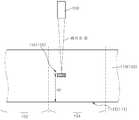
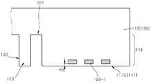
도 1은 일 예에 따른 임프린트(imprint)를 위한 템플레이트(template: 100)의 단면 구조를 보여주는 단면도이다.1 is a cross-sectional view showing a cross-sectional structure of a
도 1을 참조하면, 나노 임프린트를 위한 임프린트 템플레이트(100)는 실질적으로 평탄한 패턴면(111)에 패턴 전사(pattern transferring)될 필드 패턴(field pattern: 120)들을 구비할 수 있다. 필드 패턴(120)들을 기판이나 웨이퍼(wafer) 상에 임프린트 매질층으로 위치하는 레지스트층(resist layer)에 임프린트될 구조물로 구비될 수 있다. 필드 패턴(120)들은 요철 패턴(concave & convex pattern)과 같은 나노 크기의 돌출 구조물들로 패턴면(111)에 형성될 수 있다. 임프린트 템플레이트(100)는 필드 패턴(120)들이 형성된 패턴면(111)을 제공하도록 돌출된 메사부(mesa potion: 110)와 메사부(110)를 지지하는 템플레이트 몸체부(130)를 포함할 수 있다. 템플레이트 몸체부(130)는 메사부(110)와 단차를 가지며 연장된 부분으로 구성될 수 있다.Referring to FIG. 1, an
패턴면(111) 내에는 필드 패턴(120)들이 위치하는 필드 영역(102)이 배치될 수 있다. 패턴면(111)은 한 번의 임프린트 샷(imprint shot)이 진행될 영역으로 구비되므로, 패턴면(111) 내에는 한 번의 임프린트 샷에 의해 임프린트될 필드 패턴(120)들이 구비될 수 있다. 패턴면(111) 내에는 하나의 필드 영역(102)이 구비될 수 있지만, 다수의 필드 영역(102)들이 경계 영역(boundary region: 104)에 의해서 구획되어 배치될 수 있다. 필드 영역(102) 내에는 필드 패턴(120)들이 배치되고, 경계 영역(104) 내에는 얼라인먼트 마크(150)나 오버레이 버니어(도시되지 않음)와 같은 공정 진행에 요구되는 여러 보조 패턴들이 구비될 수 있다. 경계 영역(104)은 패턴면(111)의 테두리 경계를 구획하는 테두리 영역(104E)으로 설정될 수 있다. 경계 영역(104)은 필드 영역(102)과 필드 영역(102)를 구획지어 나누는 중간 영역(104I)일 수 있다. 필드 영역(102)이 반도체 소자의 셀 영역(cell region)에 해당될 경우, 경계 영역(104)은 스크라이브 레인 영역(scribe lane region)일 수 있다.In the
얼라인먼트 마크(150)는 경계 영역(104) 내의 임프린트 템플레이트(100)의 몸체부(110) 부분 내에 내장된 패턴들로 구비될 수 있다. 얼라인먼트 마크(150)가 임프린트 템플레이트(100)의 몸체부(110) 부분 내에 내장되므로, 얼라인먼트 마크(150)가 위치한 부분에 중첩된 표면 부분(111S)은 플랫(flat)한 표면으로 구비될 수 있다. 얼라인먼트 마크(150)가 필드 패턴(120)과 달리 요철 패턴 형상 또는 단차를 유발하는 형상으로 구비되지 않으므로, 얼라인먼트 마크(150)에 중첩되는 표면 부분(111S)에 요철 패턴 형상이 구비되지 않는다. 이에 따라, 임프린트 과정에서 필드 패턴(120)이 레지스트층(도시되지 않음)에 임프린트될 때, 얼라인먼트 마크(150)는 레지스트층에 요철 패턴 형상으로 패턴 전사되지 않는다.The
얼라인먼트 마크(150)는 임프린트 템플레이트(100)의 몸체부(110) 부분과 다른 광 투과율을 가지는 패턴들로 구비될 수 있다. 임프린트 템플레이트(100) 및 몸체부(110)는 자외선광 또는 가시광과 같은 광이 투과할 수 있는 실질적으로 투명한 재질로 이루어질 수 있다. 예컨대, 임프린트 템플레이트(100) 및 몸체부(110)는 쿼츠(quartz) 재질로 구성될 수 있다. 얼라인먼트 마크(150)는 임프린트 템플레이트(100)의 몸체부(110)에 비해 낮은 광 투과율을 가지는 패턴 영역으로 이루어질 수 있다. 얼라인먼트 마크(150)는 임프린트 템플레이트(100)의 몸체부(110)의 광 투과율 대비 대략 10% 내지 80%의 광 투과율을 가지는 영역으로 설정될 수 있다. 얼라인먼트 마크(150)는 임프린트 템플레이트(100)의 몸체부(110)의 투명한 재질 내에 형성된 미세한 크기의 결정상(crystalline phase)들의 영역으로 형성될 수 있다. 임프린트 템플레이트(100)의 몸체부(110)는 실질적으로 비정질 재질로 이루어지는 데, 비정질 재질 내에 형성된 미세한 크기의 결정상들은 미세한 스크래치(scratch)로 보일 수 있다. 즉, 비정질 재질 내에 형성된 미세한 크기의 결정상들은 비정질 재질에 비해 상대적으로 낮은 광 투과율을 나타내는 영역을 이룰 수 있다. 미세한 크기의 결정상들이 모여 얼라인먼트 마크(150)를 이룰 수 있다.The
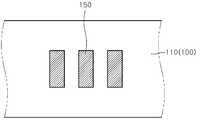
도 2 및 도 3은 일 예에 따른 얼라인먼트 마크(150)를 임프린트 템플레이트(100)에 형성하는 과정을 보여주는 단면도들이고, 도 4는 일 예에 따라 임프린트 템플레이트(100)에 형성된 얼라인먼트 마크(150)의 평면 형상을 보여주는 평면도이다. 도 5는 비교예에 따른 임프린트 템플레이트(10R)에 형성된 얼라인먼트 마크(15R)를 보여주는 단면도이다.2 and 3 are cross-sectional views illustrating a process of forming the
도 2를 참조하면, 임프린트 템플레이트(100)의 몸체부(110) 내에 레이저 광을 조사하여 얼라인먼트 마크(150)를 형성할 수 있다. 임프린트 템플레이트(100)의 몸체부(110) 내부의 일정 지점, 예컨대, 얼라인먼트 마크(150)에 중첩되는 표면 부분(111S)으로부터 반대측 표면인 후면으로 향해 제1깊이(H1)에 레이저 광의 초점이 맞춰지도록 레이저 광을 포커스(focus)하여, 임프린트 템플레이트(100)의 몸체부(110) 내부 일부 영역에 레이저 광의 조사에 의한 상(phase) 변화를 유도할 수 있다. 쿼츠 재질은 비정질 상태이므로, 레이저 광이 포커스된 위치에서 결정질로의 상변화가 유도될 수 있다. 레이저 광의 조사에 의해서 상변화된 결정질 상들이 모여 하나의 비투명한 패턴(151)이 형성될 수 있다. 결정상들은 미세한 크기를 가질 수 있고, 이러한 결정상들은 광의 산란을 유도할 수 있어, 비투명한 패턴(151)이 몸체부(110)의 비정질 상태에 비해 낮은 광 투과율을 가지도록 유도할 수 있다. 레이저 조사부(159)는 레이저 광을 생성시키고, 비투명한 패턴(151)이 위치할 부분에 레이저 광을 포커스하는 동작을 수행할 수 있다. 레이저 광이 포커스되는 위치에 따라 비투명한 패턴(151), 즉, 얼라인먼트 마크(150)의 위치가 설정될 수 있다. 따라서, 레이저 광의 포커스 위치를 조절함으로써, 얼라인먼트 마크(150)가 형성되는 위치 또는 깊이가 자유롭게 조절될 수 있다.Referring to FIG. 2, the
도 3을 참조하면, 다수의 비투명한 패턴(151)들이 서로 이격되며 형성되도록 레이저 광을 순차적으로 조사하여, 다수의 비투명한 패턴(151)들로 이루어지는 얼라인먼트 마크(150)를 형성할 수 있다. 얼라인먼트 마크(150)는 평면 상에서 볼 때, 도 4에 보이듯이, 장방형 패드(pad) 형상 또는 바(bar) 형상들이 나란히 배치된 배열로 구비될 수 있다. 레이저 광은 얼라인먼트 마크(150)가 바 형상들의 배열을 가지도록, 임프린트 템플레이트(100)의 몸체부(110)의 영역들을 스캔(scan)할 수 있다.Referring to FIG. 3, laser light is sequentially irradiated so that a plurality of
얼라인먼트 마크(150)는 경계 영역(104) 내에 위치하도록 형성될 수 있다. 필드 영역(102)의 패턴면(111) 부분에는 요철 패턴으로 필드 패턴(120)들이 형성될 수 있다. 필드 영역(102)의 패턴면(111)에 제2깊이(H2)를 가지는 오목한 부분(121)을 선택적 식각할 수 있다. 필드 패턴(120)의 오목한 부분(121)의 제2깊이(H2)에 대등한 제1깊이(H1)에 얼라인먼트 마크(150)들이 형성될 수 있다. 얼라인먼트 마크(150)에 중첩되는 표면(111S)은 플랫한 표면으로 유지될 수 있다. 얼라인먼트 마크(150)에 중첩되는 표면(111S)은 필드 패턴(120)이 돌출된 단부(123)와 실질적으로 동일한 높이 수준을 가지는 표면일 수 있다.The
얼라인먼트 마크(150)를 형성하는 공정 단계는 필드 영역(102)에 필드 패턴(120)들을 형성하는 단계 이전에 수행될 수 있다. 선택적으로(optionally) 얼라인먼트 마크(150)를 형성하는 공정 단계는 필드 영역(102)에 필드 패턴(120)들을 형성하는 단계 이후에 수행될 수 있다. 얼라인먼트 마크(150)를 형성하는 공정 단계는 레이저 광의 조사에 의해서 이루어지므로, 필드 패턴(120)을 형성하는 식각 단계에 의존하지 않고 독립적으로 수행될 수 있다.The process step of forming the
도 3에 제시된 임프린트 템플레이트(100)는 경계 영역(104)의 몸체부(110) 부분 내부에 내장된 얼라인먼트 마크(150)를 구비하고 있다. 이에 비해, 도 5에 제시된 전형적인 임프린트 템플레이트(10R)의 얼라인먼트 마크는, 패턴면(11R)에 식각된 요철 패턴(14R)들과 요철 패턴(14R)의 오목한 부분 내에 위치하는 차광 패턴(15R)들을 포함하여 구비될 수 있다. 차광 패턴(15R)은 크롬(Cr)층과 같이 자외선 광 또는 가시광을 차광하는 매질층으로 이루어질 수 있다. 전형적인 얼라인먼트 마크(14R, 15R)가 요철 패턴(14R)을 포함하고 있는 것과 달리, 본 출원에서 제시하는 얼라인먼트 마크(도 3의 150)는 템플레이트(100)의 몸체부(110) 내에 내장될 수 있다. 이에 따라, 본 출원에서 제시하는 얼라인먼트 마크(도 3의 150)는 패턴면(111)에 요철 패턴과 같이 단차를 수반하는 형상을 수반하지 않는다. 이에 따라, 본 출원에서 제시하는 얼라인먼트 마크(도 3의 150)를 포함하는 임프린트 템플레이트(100)를 사용하는 임프린트 공정은, 요철 패턴(도 5의 14R)에 의해서 야기될 수 있는 공정 불량들을 원천적으로 배제할 수 있다.The
도 6 내지 도 12는 일 예에 따른 임프린트 템플레이트들을 사용한 임프린트 과정을 보여주는 단면도들이다.FIGS. 6 to 12 are cross-sectional views illustrating an imprint process using imprint templates according to an example.
도 6을 참조하면, 기판(200) 상의 제1레지스트층(600)에 제1임프린트 공정을 수행하기 위해서 임프린트 제1템플레이트(100)를 도입할 수 있다. 임프린트 제1템플레이트(100)는 도 2 및 도 3을 인용하여 설명한 바와 같이 레이저 광의 조사에 의해서 형성된 제1얼라인먼트 마크(150)를 구비하고 있을 수 있다.Referring to FIG. 6, the
기판(200)은 반도체 집적 회로가 형성될 반도체 웨이퍼 또는 웨이퍼와 다른 형상을 가질 수 있는 다양한 재질의 기판일 수 있다. 기판(200) 상에는 하부층(300)이 형성되어 있을 수 있다. 하부층(300)은 임프린트 템플레이트(100)의 얼라인먼트를 위한 기준으로 레퍼런스 마크(reference mark: 350)가 형성된 층일 수 있다. 레퍼런스 마크(350)에 얼라인먼트 마크(150)가 정렬됨으로써 얼라인먼트 동작이 이루어질 수 있다. 레퍼런스 마크(350)는 요철 패턴 형상으로 하부층(300)에 패터닝될 수 있다. 하부층(300)은 레퍼런스 마크(350) 이외에 하부 패턴들이 패터닝된 층일 수 있다.The
하부층(300) 상에 패터닝 제1대상층(400)이 형성될 수 있다. 패터닝 제1대상층(400)은 임프린트 제1템플레이트(100)에 구비된 제1필드 패턴(120)이 최종적으로 패턴 전사될 층으로 형성될 수 있다. 패터닝 제1대상층(400)은 레퍼런스 마크(350)의 오목한 부분을 채우도록 형성될 수 있다.The patterning
패터닝 제1대상층(400) 상에 제1하드 마스크층(hard mask layer: 500)가 형성될 수 있다. 제1레지스트층(600)에 의해 제공될 수 있는 식각 선택비(etch selectivity) 보다 더 높은 식각 선택비가 패터닝 제1대상층(400)을 선택적으로 식각하는 패터닝 과정에서 요구될 때, 제1하드 마스크층(500)은 선별적으로 도입될 수 있다. 제1하드 마스크층(500)은 실리콘 질화물(Si3N4)층이나 실리콘 산화물(SiO2)층 또는 실리콘 산질화물(SiON)층, 또는 폴리실리콘층(polycrystalline silicon layer) 등을 포함할 수 있다. 제1하드 마스크층(500)은 스핀온카본(SOC: Spin On Carbon)층을 포함하여 형성될 수 있다.A first
제1하드 마스크층(500) 상에 제1레지스트층(600)이 형성될 수 있다. 제1레지스트층(600)과 제1하드 마스크층(500) 사이 계면에 제1레지스트층(600)의 하부층으로 버퍼층(buffer layer)가 실리콘 산질화물층을 포함하여 형성될 수 있다. 제1레지스트층(600)은 레지스트 물질(resist material)을 스핀 코팅(spin coating) 또는 잉크젯팅(Ink-jetting), 드랍 분사(Drop dispense)등을 하여 기판(200) 상에 형성될 수 있다.A first resist
제1레지스트층(600)은 제1템플레이트(100)의 나노 구조물인 제1필드 패턴(120)들이 임프린트될 매질층으로 형성될 수 있다. 제1레지스트층(600)은 임프린팅이 가능한 매질(imprintable medium)로 알려진 레진 물질(resin material)을 포함하여 형성될 수 있다. 제1레지스트층(600)은 자외선(UV)과 같은 노광 광에 의해서 큐어링(curing)이 가능한 큐어러블 코팅층(curable coating layer)으로 형성될 수 있다. 제1레지스트층(600)은 감광성 요소(photosensitizer)들을 포함하는 레진(resin) 또는 레지스트 물질로 형성될 수 있다.The first resist
제1레지스트층(600)의 제1표면(611)에 제1패턴면(111)이 대면되도록 임프린트 제1템플레이트(100)를 기판(200) 상에 도입할 수 있다. 제1필드 패턴(120)들은 제1레지스트층(600)의 제1표면(611)에 대향될 수 있다.The
도 7을 도 6과 함께 참조하면, 제1레지스트층(600)의 제1표면(611)에 임프린트 제1템플레이트(100)의 제1필드 패턴(120)들이 접촉하도록 제1템플레이트(100)를 하강시킨 후, 제1템플레이트(100)를 가압 또는 프레스(press)하여 요철 패턴 형상인 제1필드 패턴(120)들 사이를 제1레지스트층(600)의 레지스트 물질이 모두 채우도록 임프린트 단계를 수행할 수 있다. 제1필드 패턴(120)들이 제1레지스트층(600)의 제1표면(611)에 묻힘으로써, 제1레지스트층(600)의 제1표면(611)에 제1레지스트 패턴(620)이 임프린트될 수 있다.Referring to FIG. 7 together with FIG. 6, a
제1템플레이트(100)의 제1필드 패턴(120)들 사이가 레지스트 물질로 실질적으로 완전히 채워지는 채움 과정(filling step)이 진행되는 도중에, 제1템플레이트(100)와 기판(200) 사이의 1차 얼라인먼트를 진행할 수 있다. 제1템플레이트(100)에 내장된 제1얼라인먼트 마크(150)의 위치와, 하부층(300)에 위치하는 레퍼런스 마크(350)의 위치를 광학적으로 계측하여, 레퍼런스 마크(350)에 대한 제1얼라인먼트 마크(150)를 위치를 얼라인먼트 값으로 계측할 수 있다. 제1얼라인먼트 마크(150)와 레퍼런스 마크(350)의 화상 또는 간섭 패턴을 계측할 수 있다. 레퍼런스 마크(350)에 대한 제1얼라인먼트 마크(150)의 상대적인 위치 차이 또는 중첩 차이를 검출하여 얼라인먼트 위치 에러 또는 오버레이 에러(overlay error)의 파라미터(parameter)로 검출할 수 있다.A filling step between the
제1템플레이트(100)와 기판(200) 사이에 얼라인먼트 에러가 검출될 경우, 기판(200)을 제1템플레이트(100)에 대해서 상대적으로 이동시켜 얼라인먼트 에러를 보상하는 1차 얼라인먼트 동작을 수행할 수 있다. 즉, 얼라인먼트 에러에 의해서 패턴이 시프트(shift)된 방향에 반대되는 방향으로 기판(200)을 이동시켜 에러를 보상시키는 1차 얼라인먼트 동작을 수행할 수 있다. 이러한 얼라인먼트의 계측과 보상 동작을 반복하여 제1템플레이트(100)의 얼라인먼트 동작을 수행할 수 있다.When an alignment error is detected between the
제1템플레이트(100)의 얼라인먼트 동작이 완료된 후, 제1템플레이트(100)의 제1필드 패턴(120)들 사이를 레지스트 물질이 채운 상태에서, 제1레지스트층(600)을 큐어링(curing)할 수 있다. 제1레지스트층(600)에 자외선을 조사하여 제1레지스트층(600)을 큐어링할 수 있다. 제1템플레이트(100)는 쿼츠와 같은 자외선 광이 투과할 수 있는 물질로 이루어지므로, 제1템플레이트(100)를 투과하여 자외선 광이 제1레지스트층(600) 표면 부분으로 조사될 수 있다. 이러한 큐어링에 의해서 제1레지스트층(600) 표면에 제1레지스트 패턴(620)이 경화될 수 있다.After the alignment of the
도 8을 참조하면, 제1레지스트층(600)이 경화된 이후에, 제1템플레이트(100)를 제1레지스트층(600) 표면으로부터 이탈시킬 수 있다. 제1템플레이트(100)의 제1얼라인먼트 마크(150)에 중첩되는 표면 부분(111S)은 플랫한 표면이므로, 제1템플레이트(100)의 표면 부분(111S)이 접촉된 제1레지스트층(600)의 표면 부분(611S) 또한 실질적으로 플랫한 표면으로 임프린트될 수 있다. 제1템플레이트(100)의 제1얼라인먼트 마크(150)에 중첩된 제1레지스트층(600)의 표면 부분(611S)에 단차나 요철 패턴이 수반되지 않으므로, 단차 형상이나 요철 패턴에 의해 유발될 수 있는 공정 불량이 원천적으로 배제될 수 있다.Referring to FIG. 8, after the first resist
도 6 내지 도 8을 인용하여 설명한 제1템플레이트(100)를 사용하는 제1임프린트 과정은 하나의 임프린트 샷(shot) 과정을 설명한 것이다. 이러한 임프린트 샷 과정을 제1레지스트층(600)의 이웃하는 다른 영역들에 대해서 스텝 앤 리피트(step and repeat) 방식으로 반복하여 수행할 수 있다. 이에 따라, 제1템플레이트(100)의 크기 보다 더 큰 대면적의 기판(200)의 전체 영역에 대해 제1임프린트 과정들이 순차적으로 수행할 수 있다.The first imprint process using the
도 9를 도 8과 함께 참조하면, 제1임프린트된 제1레지스트 패턴(도 8의 620)을 패터닝 제1대상층(400)에 패턴 전사하여 제1대상층 패턴(401)을 형성할 수 있다. 제1레지스트 패턴(620)은 제1레지스트층(도 8의 600)의 표면 부분에 형성되므로, 식각 과정을 제1레지스트층(600)에 수행하여 제1레지스트 패턴(620)을 확장시킬 수 있다. 예컨대, 제1레지스트 패턴(620)의 오목한 홈의 바닥 부분에 잔류하는 제1레지스트층(600)의 잔류 부분들을 선택적으로 제거하여, 하부의 제1하드 마스크층(도 8의 500)의 일부 부분들을 노출하도록 제1레지스트 패턴(620)을 확장시킬 수 있다. 제1레지스트 패턴(620)에 노출된 제1하드 마스크층(500) 부분을 선택적으로 제거하는 식각 과정을 수행하여, 제1하드 마스크층 패턴(501)을 패터닝할 수 있다. 제1하드 마스크층 패턴(501)은 제1레지스트 패턴(620)의 패턴 형상을 따라 식각된 패턴으로 형성될 수 있다. 제1하드 마스크층 패턴(501)에 의해 노출된 패터닝 제1대상층(400) 부분을 선택적으로 제거하는 식각 과정을 수행하여, 제1하드 마스크층 패턴(501)의 패턴 형상을 따르는 제1대상층 패턴(401)이 형성될 수 있다. 이와 같이 식각 과정에 의해서 제1레지스트 패턴(620)의 패턴 형상이 제1대상층(400)에 패턴 전사되어 제1대상층 패턴(401)이 형성될 수 있다.Referring to FIG. 9 together with FIG. 8, a first
제1템플레이트(도 8의 100)의 제1얼라인먼트 마크(150)에 중첩된 제1레지스트층(600)의 표면 부분(도 8의 611S)에 단차나 요철 패턴이 수반되지 않으므로, 제1대상층(400)에 제1레지스트 패턴(620)을 패턴 전사하는 식각 과정 결과, 제1레지스트층(600)의 표면 부분(도 8의 611S)에 중첩되는 하부층(300) 표면 영역(156)에는 어떠한 돌출된 패턴 형상이 잔류되지 않는다. 제1대상층의 잔류 부분(405)이 레퍼런스 마크(350)의 오목한 부분을 채우도록 잔류할 수 있지만, 레퍼런스 마크(350) 상에 제1대상층 패턴(401)과 같이 돌출된 다른 패턴들이 잔류하지는 않는다. 따라서, 레퍼런스 마크(350)는 제1임프린트 과정에 의해서 실질적으로 손상되지 않고 원형 그대로 유지될 수 있다.A step or an uneven pattern is not involved in the surface portion (611S in Fig. 8) of the first resist
레퍼런스 마크(350) 상에 다른 패턴들이 존재할 경우, 레퍼런스 마크(350)는 더 이상 얼라인먼트 동작에서 기준 표식으로 사용되기 어렵다. 그렇지만, 본 출원에서는 제1얼라인먼트 마크(도 8의 150)가 제1레지스트층(600)에 어떠한 요철 패턴 형상도 유도하지 않으므로, 제1얼라인먼트 마크(도 8의 150)에 의한 레퍼런스 마크(350)의 손상은 원천적으로 배제될 수 있다. 이에 따라, 레퍼런스 마크(350)는 추후에 진행되는 다른 제2임프린트 과정에서도 얼라인먼트 동작의 기준 표식으로 사용될 수 있다. 따라서, 다수의 임프린트 과정들을 반복하여 수행할 때, 임프린트 과정 별로 서로 다른 레퍼런스 마크들을 형성하지 않고, 하나의 레퍼런스 마크(350)로 다수의 임프린트 과정들 모두에 적용될 수 있는 공통 레퍼런스 마크를 구현할 수 있다. 이에 따라, 레퍼런스 마크(350)를 위한 영역을 감소된 크기로 설정할 수 있어, 레퍼런스 마크(350)가 위치할 공간이 부족해지는 문제를 방지할 수 있다.When there are other patterns on the
도 10을 참조하면, 기판(200) 상의 제2레지스트층(650)에 또 다른 제2임프린트 공정을 수행하기 위해서 임프린트 제2템플레이트(1110)를 도입할 수 있다. 임프린트 제2템플레이트(1110)는 제1템플레이트(도 6의 100)와 다른 템플레이트로 구비될 수 있다. 임프린트 제2템플레이트(1110)는 제1필드 패턴(도 6의 120)과 다른 제2필드 패턴(1120)을 제2패턴면(1111)에 오목한 홈 형상을 포함하는 요철 패턴 형상으로 구비할 수 있다. 제2패턴면(1111)에 중첩되는 임프린트 제2템플레이트(1110) 부분 내측에 내장되도록 제2얼라인먼트 마크(1150)가 구비될 수 있다. 제2얼라인먼트 마크(1150)는 기판(200)과 제2템플레이트(1110) 사이의 얼라인먼트를 위해 구비될 수 있다. 제2얼라인먼트 마크(1150)에 중첩된 제2패턴면(1111) 부분은 어떠한 요철 패턴 형상도 형성되지 않은 플랫한 표면으로 구비될 수 있다. 임프린트 제2템플레이트(1110) 또한 도 2 및 도 3을 인용하여 설명한 바와 같이 레이저 광의 조사에 의해서 형성된 제2얼라인먼트 마크(1150)를 구비하고 있을 수 있다.Referring to FIG. 10, a
하부층(300) 상에 제1대상층 패턴(401)을 덮는 층간 중간층(700)을 형성할 수 있다. 층간 중간층(700)은 제1대상층 패턴(401)을 덮는 층간 절연층일 수 있다. 층간 중간층(700) 상에 패터닝 제2대상층(450)을 형성할 수 있다. 패터닝 제2대상층(450)은 임프린트 제2템플레이트(1110)에 구비된 제2필드 패턴(1120)이 최종적으로 패턴 전사될 층으로 형성될 수 있다.An interlayer
패터닝 제2대상층(450) 상에 제2하드 마스크층(550)가 형성될 수 있다. 제2하드 마스크층(550)은 스핀온카본(SOC)층을 포함하여 형성될 수 있다. 제2하드 마스크층(550) 상에 제2레지스트층(650)이 형성될 수 있다. 제2레지스트층(650)은 레지스트 물질을 스핀 코팅(spin coating)하여 기판(200) 상에 형성될 수 있다. 제2레지스트층(650)의 제2표면(651)에 제2패턴면(1111)이 대면되도록 임프린트 제2템플레이트(1110)를 기판(200) 상에 도입할 수 있다. 제2필드 패턴(1120)들은 제2레지스트층(650)의 제2표면(651)을 바라보도록 위치할 수 있다.A second
도 11을 도 10과 함께 참조하면, 제2레지스트층(650)의 제2표면(651)에 임프린트 제2템플레이트(1110)의 제2필드 패턴(1120)들이 접촉하도록 제2템플레이트(1110)를 하강시킨 후, 제2템플레이트(1110)를 가압 또는 프레스하여 요철 패턴 형상인 제2필드 패턴(1120)들 사이를 제2레지스트층(650)의 레지스트 물질이 모두 채우도록 임프린트 단계를 수행할 수 있다. 제2필드 패턴(1120)들이 제2레지스트층(650)의 제2표면(651)에 묻힘으로써, 제2레지스트층(650)의 제2표면(651)에 제2레지스트 패턴(652)이 임프린트될 수 있다.11, a
제2템플레이트(1110)의 제2필드 패턴(1120)들 사이가 레지스트 물질로 실질적으로 완전히 채워지는 채움 과정이 진행되는 도중에, 제2템플레이트(1110)와 기판(200) 사이의 2차 얼라인먼트를 진행할 수 있다. 제2템플레이트(1110)에 내장된 제2얼라인먼트 마크(1150)의 위치와, 하부층(300)에 위치하는 레퍼런스 마크(350)의 위치를 광학적으로 계측하여, 레퍼런스 마크(350)에 대한 제2얼라인먼트 마크(1150)를 위치를 얼라인먼트 값으로 계측할 수 있다. 제2얼라인먼트 마크(1150)와 레퍼런스 마크(350)의 화상 또는 간섭 패턴을 계측할 수 있다. 레퍼런스 마크(350)에 대한 제2얼라인먼트 마크(1150)의 상대적인 위치 차이 또는 중첩 차이를 검출하여 얼라인먼트 위치 에러로 검출할 수 있다.The secondary alignment between the
제2템플레이트(1110)와 기판(200) 사이에 얼라인먼트 에러가 검출될 경우, 기판(200)을 제2템플레이트(1110)에 대해서 상대적으로 이동시켜 얼라인먼트 에러를 보상하는 2차 얼라인먼트 동작을 수행할 수 있다. 얼라인먼트 에러에 의해서 패턴이 시프트된 방향에 반대되는 방향으로 기판(200)을 이동시켜 에러를 보상시키는 2차 얼라인먼트 동작을 수행할 수 있다. 이러한 얼라인먼트의 계측과 보상 동작을 반복하여 제2템플레이트(1110)의 얼라인먼트 동작을 수행할 수 있다.When an alignment error is detected between the
제2템플레이트(1110)에 형성된 제2얼라인먼트 마크(1150)와 제1템플레이트(100)에 형성된 제1얼라인먼트 마크(150)는 동일한 레퍼런스 마크(350)에 정렬되도록 설정되고 형성될 수 있다. 이에 따라, 제2템플레이트(1110)에 형성된 제2얼라인먼트 마크(1150)는 실질적으로 제1템플레이트(100)에 형성된 제1얼라인먼트 마크(150)와 실질적으로 중첩된 위치에 위치할 수 있다.The
제2템플레이트(1110)의 얼라인먼트 동작이 완료된 후, 제2템플레이트(1110)의 제2필드 패턴(1120)들 사이를 레지스트 물질이 채운 상태에서, 제2레지스트층(650)을 큐어링할 수 있다. 제2레지스트층(650)에 자외선을 조사하여 제2레지스트층(650)을 큐어링할 수 있다. 제2템플레이트(1110)는 쿼츠와 같은 자외선 광이 투과할 수 있는 물질로 이루어지므로, 제2템플레이트(1110)를 투과하여 자외선 광이 제2레지스트층(650) 표면 부분으로 조사될 수 있다. 이러한 큐어링에 의해서 제2레지스트층(650) 표면에 제1레지스트 패턴(652)이 경화될 수 있다.The second resist
제2템플레이트(1110)의 제2필드 패턴(1120)이나 제2필드 패턴(1120)에 의해서 임프린트된 제2레지스트 패턴(652)은, 2차 얼라인먼트 동작에 의해서 하부의 제1대상층 패턴(401)에 정렬되도록 위치하거나 형성될 수 있다. 도 11에서 제2템플레이트(1110)의 제2필드 패턴(1120)이나 제2레지스트 패턴(652)이 제1대상층 패턴(401)에 중첩되지 않고 일정 간격 이격되어 위치하도록 정렬된 상태를 묘사하고 있지만, 제2템플레이트(1110)의 제2필드 패턴(1120)이나 제2레지스트 패턴(652)이 제1대상층 패턴(401)에 중첩되도록 정렬될 수도 있다.The second resist
제1임프린트 동작에서 1차 얼라인먼트 동작의 기준으로 사용된 레퍼런스 마크(350)는, 제2임프린트 동작에서 2차 얼라인먼트 동작의 기준으로 사용될 수 있다. 제2얼라인먼트 마크(1150)는 레퍼런스 마크(350)에 대해 정렬될 수 있다. 제1임프린트 동작에서 레퍼런스 마크(350)가 훼손되거나 손상되지 않으므로, 후속의 제2임프린트 동작에서도 기준 표식으로 레퍼런스 마크(350)가 사용되는 것이 가능하다. 제2얼라인먼트 마크(1150)가 제2템플레이트(1110)에 내장되도록 구비되므로, 제2임프린트 동작에서도 레퍼런스 마크(350)에 대한 훼손이 역시 방지될 수 있다. 따라서 후속되는 제3의 임프린트 동작에서도 레퍼런스 마크(350)는 동일하게 또 다른 제3의 얼라인먼트 마크(도시되지 않음)가 정렬되는 기준 표식으로 사용되는 것이 가능하다. 여러 개의 다른 임프린트 템플레이트들을 사용하여 여러 번의 임프린트 동작을 순차적으로 수행할 경우에도, 동일한 하나의 레퍼런스 마크(350)를 기준 표식으로 사용할 수 있다. 따라서, 레퍼런스 마크(350)가 차지하는 영역의 면적을 줄일 수 있고, 이에 따라 제1 또는 제2얼라인먼트 마크(150, 1150)들이 위치할 영역의 면적을 줄이는 것이 가능하다.The
제2레지스트층(650)이 경화된 이후에, 제2템플레이트(1110)를 제2레지스트층(650) 표면으로부터 이탈시킬 수 있다. 제2얼라인먼트 마크(1150)에 중첩되는 제2템플레이트(1110)의 표면 부분(1111S)은 플랫한 표면이므로, 제2템플레이트(1110)의 표면 부분(1111S)이 접촉된 제2레지스트층(650)의 표면 부분(651S) 또한 실질적으로 플랫한 표면으로 임프린트될 수 있다. 제2템플레이트(1110)의 제2얼라인먼트 마크(1150)에 중첩된 제2레지스트층(650)의 표면 부분(651S)에 단차나 요철 패턴이 수반되지 않으므로, 단차 형상이나 요철 패턴에 의해 유발될 수 있는 공정 불량이 원천적으로 배제될 수 있다.The
제2템플레이트(1110)를 사용하는 제2임프린트 과정은 하나의 임프린트 샷(shot) 과정을 설명한 것이다. 이러한 임프린트 샷 과정을 제2레지스트층(650)의 이웃하는 다른 영역들에 대해서 스텝 앤 리피트 방식으로 반복하여 수행할 수 있다. 이에 따라, 제2템플레이트(1110)의 크기 보다 더 큰 대면적의 기판(200)의 전체 영역에 대해 제2임프린트 과정들이 순차적으로 수행할 수 있다.The second imprinting process using the
도 12를 도 11과 함께 참조하면, 제2임프린트된 제2레지스트 패턴(도 11의 652)을 패터닝 제2대상층(450)에 패턴 전사하여 제2대상층 패턴(451)을 형성할 수 있다. 제2레지스트 패턴(652)은 제2레지스트층(도 11의 650)의 표면 부분에 형성되므로, 식각 과정을 제2레지스트층(650)에 수행하여 제2레지스트 패턴(650)의 형상이 제2레지스트층(650)을 관통하도록 확장시킬 수 있다. 예컨대, 제2레지스트 패턴(652)의 오목한 홈의 바닥 부분에 잔류하는 제2레지스트층(650)의 잔류 부분들을 선택적으로 제거하여, 하부의 제2하드 마스크층(도 11의 550)의 일부 부분들을 노출하도록 제2레지스트 패턴(652)을 확장시킬 수 있다. 제2레지스트 패턴(652)에 노출된 제2하드 마스크층(550) 부분을 선택적으로 제거하는 식각 과정을 수행하여, 제2하드 마스크층 패턴(551)을 패터닝할 수 있다. 제2하드 마스크층 패턴(551)은 제2레지스트 패턴(652)의 패턴 형상을 따라 식각된 패턴으로 형성될 수 있다. 제2하드 마스크층 패턴(551)에 의해 노출된 패터닝 제2대상층(도 11의 450) 부분을 선택적으로 제거하는 식각 과정을 수행하여, 제2하드 마스크층 패턴(551)의 패턴 형상을 따르는 제2대상층 패턴(451)이 형성될 수 있다. 이와 같이 식각 과정에 의해서 제2레지스트 패턴(652)의 패턴 형상이 제2대상층(450)에 패턴 전사되어 제2대상층 패턴(451)이 형성될 수 있다.Referring to FIG. 12 together with FIG. 11, the second
도 12에서 제2대상층 패턴(451)이 제1대상층 패턴(401)과 중첩되지 않고 이격된 서로 다른 영역들에 각각 형성되는 것으로 묘사하고 있지만, 경우에 따라 제2대상층 패턴(451)은 제1대상층 패턴(401)과 중첩된 위치에 정렬될 수도 있다.In FIG. 12, the second
제2템플레이트(도 11의 1110)의 제2얼라인먼트 마크(1150)에 중첩된 제2레지스트층(650)의 표면 부분(도 11의 651S)에 단차나 요철 패턴이 수반되지 않으므로, 제2대상층(450)에 제2레지스트 패턴(652)을 패턴 전사하는 식각 과정 결과, 제2레지스트층(650)의 표면 부분(도 11의 651S)에 중첩되는 층간 중간층(700) 표면 영역(1156)에는 어떠한 돌출된 패턴 형상이 잔류되지 않는다. 레퍼런스 마크(350) 상에 중첩되는 표면 영역(1156)에 다른 패턴들이 형성되지 않으므로, 레퍼런스 마크(350)를 모니터링(monitoring)할 때 레퍼런스 마크(350)의 이미지(image)가 훼손되지 않는다. 따라서, 레퍼런스 마크(350)는 제2임프린트 과정에 의해서 실질적으로 손상되지 않고 원형 그대로 유지될 수 있다.Since no step or concavo-convex pattern is involved in the surface portion (651S in Fig. 11) of the second resist
레퍼런스 마크(350) 상에 다른 패턴들이 존재할 경우, 레퍼런스 마크(350)는 더 이상 얼라인먼트 동작에서 기준 표식으로 사용되기 어렵다. 그렇지만, 본 출원에서는 제2얼라인먼트 마크(도 11의 1150)가 제2레지스트층(650)에 어떠한 요철 패턴 형상도 유도하지 않으므로, 제2얼라인먼트 마크(도 11의 1150)에 의한 레퍼런스 마크(350)의 손상은 원천적으로 배제될 수 있다. 이에 따라, 레퍼런스 마크(350)는 추후에 진행되는 다른 제3임프린트 과정에서도 얼라인먼트 동작의 기준 표식으로 사용될 수 있다. 따라서, 다수의 임프린트 과정들을 반복하여 수행할 때, 임프린트 과정 별로 서로 다른 레퍼런스 마크들을 형성하지 않고, 하나의 레퍼런스 마크(350)로 다수의 임프린트 과정들 모두에 적용될 수 있는 공통 레퍼런스 마크를 구현할 수 있다. 이에 따라, 레퍼런스 마크(350)를 위한 영역을 감소된 크기로 설정할 수 있어, 레퍼런스 마크(350)가 위치할 공간이 부족해지는 문제를 방지할 수 있다.When there are other patterns on the
도 13 및 도 14은 다른 일 예들에 따라 임프린트 템플레이트에 형성된 얼라인먼트 마크들을 보여주는 단면도들이다.Figures 13 and 14 are cross-sectional views showing alignment marks formed in an imprint template according to other examples.
도 13을 참조하면, 임프린트 템플레이트(100)의 몸체부(110) 내에 내장되도록 형성되는 얼라인먼트 마크(150-1)는, 중첩되는 패턴면(111)의 일부 표면 부분(111S)으로부터 인근하는 얕은 제3깊이(H3)에 위치할 수도 있다. 얼라인먼트 마크(150-1)는 필드 패턴(120)의 단부(123)와 같은 높이로 돌출된 부분(115)의 표면 인근에 위치할 수 있다.13, an alignment mark 150-1, which is formed to be embedded in the
도 14를 참조하면, 얼라인먼트 마크(150-2)에 중첩되는 표면 부분(111-1S)은, 패턴면(111)에 대해서 돌출하도록 형성된 필드 패턴(120)의 오목한 홈 부분(121)의 바닥면과 대등한 높이를 가지는 표면으로 형성될 수 있다. 즉, 필드 패턴(120)은 패턴면(111)에 대해 돌출된 형상의 패턴으로 형성될 경우에도, 얼라인먼트 마크(150-2)는 중첩되는 템플레이트(100)의 몸체부(110)의 표면 부분(111S-1)에 인근하도록 내장될 수 있다. 이와 같이, 얼라인먼트 마크(150-1, 150-2)는 임프린트 템플레이트(100)의 몸체부(110) 내의 임의의 깊이에 자유롭게 위치할 수 있다.14, the surface portion 111-1S superimposed on the alignment mark 150-2 is formed on the
상술한 바와 같이 본 출원의 실시 형태들을 도면들을 예시하며 설명하지만, 이는 본 출원에서 제시하고자 하는 바를 설명하기 위한 것이며, 세밀하게 제시된 형상으로 본 출원에서 제시하고자 하는 바를 한정하고자 한 것은 아니다. 본 출원에서 제시한 기술적 사상이 반영되는 한 다양한 다른 변형예들이 가능할 것이다.Although the embodiments of the present application as described above illustrate and describe the drawings, it is intended to illustrate what is being suggested in the present application and is not intended to limit what is presented in the present application in a detailed form. Various other modifications will be possible as long as the technical ideas presented in this application are reflected.
100: 템플레이트,
150: 얼라인먼트 마크.100: template,
150: alignment mark.
Claims (20)
Translated fromKorean레퍼런스 마크(reference mark)가 형성된 기판 상에 레지스트층(resist layer)을 형성하는 단계; 및
상기 레퍼런스 마크에 대한 상기 얼라인먼트 마크의 위치를 이용하여 상기 기판에 상기 템플레이트를 정렬하고 상기 레지스트층에 상기 템플레이트의 상기 필드 패턴들이 묻히도록 하는 임프린트(imprint) 단계;를 포함하는 임프린트 방법.Forming a template including field patterns of concavo-convex shapes in a field region and an alignment mark embedded in a body region in a boundary region;
Forming a resist layer on a substrate on which a reference mark is formed; And
And aligning the template with the substrate using the position of the alignment mark with respect to the reference mark, and causing the resist pattern to have the field patterns of the template embedded therein.
상기 템플레이트를 형성하는 단계는
상기 템플레이트의 몸체부 내에 레이저 광을 조사하여
상기 레이저 광의 조사에 의해 광 투과율이 낮아진 영역으로 상기 얼라인먼트 마크를 형성하는 단계를 포함하는 임프린트 방법.The method according to claim 1,
The step of forming the template
The body of the template is irradiated with laser light
And forming the alignment mark in a region where the light transmittance is lowered by irradiation of the laser light.
상기 얼라인먼트 마크는
상기 레이저 광의 조사에 의해서 상기 템플레이트 몸체부의 일부가 상변화된 결정상(crystalline phase)들을 포함하여 형성되는 임프린트 방법.3. The method of claim 2,
The alignment mark
Wherein a part of the template body portion is formed by phase change of crystalline phases by irradiation of the laser light.
상기 템플레이트는
자외선 광 및 가시광에 대해 투명한 재질로 형성되는 임프린트 방법.3. The method of claim 2,
The template
And is formed of a material transparent to ultraviolet light and visible light.
상기 얼라인먼트 마크는
상기 필드 패턴의 오목한 부분의 깊이와 대등한 깊이에서 상기 템플레이트 몸체부 내부에 위치하는 임프린트 방법.The method according to claim 1,
The alignment mark
Wherein the pattern is located within the template body at a depth equal to the depth of the concave portion of the field pattern.
상기 얼라인먼트 마크는
상기 필드 패턴의 돌출된 부분의 단부에 인근하여 위치하도록
상기 레지스트층에 대향되는 상기 템플레이트 몸체부의 표면 아래에 위치하는 임프린트 방법.The method according to claim 1,
The alignment mark
So as to be positioned near the end of the protruded portion of the field pattern
Wherein the template is located below the surface of the template body opposite the resist layer.
상기 템플레이트는
상기 레지트층에 대향되는 표면 부분들 중 상기 얼라인먼트 마크에 중첩되는 일부 표면은 플랫(flat)한 표면은 가지는 임프린트 방법.The method according to claim 1,
The template
Wherein some of the surface portions of the surface layers opposed to the resist layer have a flat surface overlapping the alignment mark.
상기 정렬된 템플레이트를 통해 자외선 광을 상기 레지스트층에 조사하여 상기 레지스트층을 큐어링(curing)하는 단계;를 더 포함하는 임프린트 방법.The method according to claim 1,
And irradiating ultraviolet light onto the resist layer through the aligned template to cure the resist layer.
상기 레지스트층을 형성하는 단계는
상기 기판 상에 레지스트 물질을 스핀 코팅(spin coating)하는 단계를 더 포함하는 임프린트 방법.The method according to claim 1,
The step of forming the resist layer
Further comprising the step of spin coating a resist material on the substrate.
상기 경계 영역은
상기 필드 영역과 다른 이웃하는 필드 영역 사이의 영역이나 또는 상기 필드 영역을 에워싸는 테두리 영역으로 설정되는 임프린트 방법.The method according to claim 1,
The boundary region
And an area between the field area and another adjacent field area or a border area surrounding the field area.
레퍼런스 마크(reference mark)가 형성된 기판 상에 제1대상층을 및 제1레지스트층(resist layer)을 형성하는 단계;
상기 레퍼런스 마크에 대한 상기 제1얼라인먼트 마크의 위치를 이용하여 상기 기판에 상기 제1템플레이트를 정렬하고 상기 제1레지스트층에 상기 제1템플레이트의 상기 제1필드 패턴들이 묻히도록 하는 제1임프린트(imprint) 단계;
상기 제1임프린트에 의해 상기 제1레지스트층에 형성된 제1레지스트 패턴을 이용하여 상기 제1대상층을 식각하여 제1대상층 패턴을 형성하는 단계;
상기 제1대상층 패턴 상에 제2레지스트층(resist layer)을 형성하는 단계;
제2필드 패턴들 및 몸체부 내에 내장된 제2얼라인먼트 마크(alignment mark)를 포함하는 제2템플레이트를 상기 제2레지스트층 상에 도입하는 단계; 및
상기 레퍼런스 마크(reference mark)에 대한 상기 제2얼라인먼트 마크의 위치를 이용하여 상기 기판에 상기 제2템플레이트를 정렬하고 상기 제2레지스트층에 상기 제2템플레이트의 상기 제2필드 패턴들이 묻히도록 하는 제2임프린트(imprint) 단계; 를 포함하는 임프린트 방법.Forming a first template including first field patterns of a concave-convex shape and a first alignment mark embedded in a body portion;
Forming a first object layer and a first resist layer on a substrate on which a reference mark is formed;
A first imprint for aligning the first template on the substrate using the position of the first alignment mark with respect to the reference mark and for allowing the first field patterns of the first template to be embedded in the first resist layer; ) step;
Forming a first target layer pattern by etching the first target layer using a first resist pattern formed on the first resist layer by the first imprint;
Forming a second resist layer on the first target layer pattern;
Introducing a second template onto the second resist layer, the second template including second field patterns and a second alignment mark embedded in the body portion; And
Aligning the second template with the substrate using the position of the second alignment mark with respect to the reference mark and allowing the second field pattern of the second template to be embedded in the second resist layer; 2 imprinting step; ≪ / RTI >
상기 제1템플레이트를 형성하는 단계는
상기 제1템플레이트의 몸체부 내에 레이저 광을 조사하여
상기 레이저 광의 조사에 의해 광 투과율이 낮아진 영역으로 상기 제1얼라인먼트 마크를 형성하는 단계를 포함하는 임프린트 방법.12. The method of claim 11,
The step of forming the first template
The body of the first template is irradiated with laser light
And forming the first alignment mark in a region where the light transmittance is lowered by irradiation of the laser light.
상기 제1얼라인먼트 마크는
상기 레이저 광의 조사에 의해서 상기 템플레이트 몸체부의 일부가 상변화된 결정상(crystalline phase)들을 포함하여 형성되는 임프린트 방법.13. The method of claim 12,
The first alignment mark
Wherein a part of the template body portion is formed by phase change of crystalline phases by irradiation of the laser light.
상기 제1템플레이트의 제1얼라인먼트 마크와
상기 제2템플레이트의 제2얼라인먼트 마크는
상기 레퍼런스 마크에 중첩되도록 위치하는 임프린트 방법.12. The method of claim 11,
The first alignment mark of the first template
The second alignment mark of the second template
Wherein the reference mark is positioned so as to overlap with the reference mark.
상기 제1템플레이트는
상기 제1레지트층에 대향되는 표면 부분들 중 상기 제1얼라인먼트 마크에 중첩되는 일부 표면은 플랫(flat)한 표면은 가지는 임프린트 방법.12. The method of claim 11,
The first template
Wherein some of the surface portions that face the first register layer have a flat surface that overlaps the first alignment mark.
상기 정렬된 제1템플레이트를 통해 자외선 광을 상기 제1레지스트층에 조사하여 상기 제1레지스트층을 큐어링(curing)하는 단계;를 더 포함하는 임프린트 방법.12. The method of claim 11,
And irradiating the first resist layer with ultraviolet light through the aligned first template to cure the first resist layer.
경계 영역(boundary region)에 몸체부 내에 내장되고 상기 몸체부 보다 낮은 광 투과율을 가지는 얼라인먼트 마크(alignment mark)를 포함하는 임프린트 템플레이트.Field patterns of concave-convex shapes in a field region; And
An imprint template comprising an alignment mark embedded in a body region and having a lower light transmittance than the body region in a boundary region.
상기 얼라인먼트 마크는
상기 몸체부 내에서 상변화된 결정상(crystalline phase)들을 포함하는 임프린트 템플레이트.18. The method of claim 17,
The alignment mark
Wherein the crystalline phase comprises phase-changed crystalline phases in the body portion.
상기 얼라인먼트 마크는
상기 필드 패턴의 오목한 부분의 깊이와 대등한 깊이에서 상기 템플레이트 몸체부 내부에 위치하는 임프린트 템플레이트.19. The method of claim 18,
The alignment mark
And wherein the imprint template is located within the template body at a depth equal to the depth of the concave portion of the field pattern.
상기 얼라인먼트 마크는
상기 필드 패턴의 돌출된 부분의 단부에 인근하여 위치하도록
상기 템플레이트 몸체부의 플랫(flat)한 표면 아래에 위치하는 임프린트 템플레이트.19. The method of claim 18,
The alignment mark
So as to be positioned near the end of the protruded portion of the field pattern
An imprint template located below a flat surface of the template body.
Priority Applications (2)
| Application Number | Priority Date | Filing Date | Title |
|---|---|---|---|
| KR1020170029695AKR102288980B1 (en) | 2017-03-08 | 2017-03-08 | Imprint template with alignment mark and methods of forming imprint patterns |
| US15/788,974US10353304B2 (en) | 2017-03-08 | 2017-10-20 | Imprint templates with alignment marks and methods of forming imprint patterns using the same |
Applications Claiming Priority (1)
| Application Number | Priority Date | Filing Date | Title |
|---|---|---|---|
| KR1020170029695AKR102288980B1 (en) | 2017-03-08 | 2017-03-08 | Imprint template with alignment mark and methods of forming imprint patterns |
Publications (2)
| Publication Number | Publication Date |
|---|---|
| KR20180102936Atrue KR20180102936A (en) | 2018-09-18 |
| KR102288980B1 KR102288980B1 (en) | 2021-08-12 |
Family
ID=63444556
Family Applications (1)
| Application Number | Title | Priority Date | Filing Date |
|---|---|---|---|
| KR1020170029695AActiveKR102288980B1 (en) | 2017-03-08 | 2017-03-08 | Imprint template with alignment mark and methods of forming imprint patterns |
Country Status (2)
| Country | Link |
|---|---|
| US (1) | US10353304B2 (en) |
| KR (1) | KR102288980B1 (en) |
Families Citing this family (3)
| Publication number | Priority date | Publication date | Assignee | Title |
|---|---|---|---|---|
| US10534276B1 (en) | 2019-03-27 | 2020-01-14 | International Business Machines Corporation | Lithographic photomask alignment using non-planar alignment structures formed on wafer |
| JP7071483B2 (en)* | 2020-12-04 | 2022-05-19 | キヤノン株式会社 | Lithography equipment, pattern forming method and article manufacturing method |
| JP2024001577A (en)* | 2022-06-22 | 2024-01-10 | キオクシア株式会社 | Template, pattern forming method, and semiconductor device manufacturing method |
Citations (5)
| Publication number | Priority date | Publication date | Assignee | Title |
|---|---|---|---|---|
| US20070187875A1 (en)* | 2005-09-06 | 2007-08-16 | Canon Kabushiki Kaisha | Mold, imprint method, and process for producing chip |
| US20130078821A1 (en)* | 2011-09-22 | 2013-03-28 | Yohko FURUTONO | Imprint method, imprint apparatus, and manufacturing method of semiconductor device |
| KR20140027281A (en)* | 2011-04-25 | 2014-03-06 | 몰레큘러 임프린츠 인코퍼레이티드 | Optically absorptive material for alignment marks |
| US20160067910A1 (en)* | 2014-09-08 | 2016-03-10 | Kabushiki Kaisha Toshiba | Template, template manufacturing method, and imprinting method |
| US20160076132A1 (en)* | 2014-09-12 | 2016-03-17 | Kabushiki Kaisha Toshiba | Stencil mask, stencil mask manufacturing method, and imprinting method |
- 2017
- 2017-03-08KRKR1020170029695Apatent/KR102288980B1/enactiveActive
- 2017-10-20USUS15/788,974patent/US10353304B2/enactiveActive
Patent Citations (5)
| Publication number | Priority date | Publication date | Assignee | Title |
|---|---|---|---|---|
| US20070187875A1 (en)* | 2005-09-06 | 2007-08-16 | Canon Kabushiki Kaisha | Mold, imprint method, and process for producing chip |
| KR20140027281A (en)* | 2011-04-25 | 2014-03-06 | 몰레큘러 임프린츠 인코퍼레이티드 | Optically absorptive material for alignment marks |
| US20130078821A1 (en)* | 2011-09-22 | 2013-03-28 | Yohko FURUTONO | Imprint method, imprint apparatus, and manufacturing method of semiconductor device |
| US20160067910A1 (en)* | 2014-09-08 | 2016-03-10 | Kabushiki Kaisha Toshiba | Template, template manufacturing method, and imprinting method |
| US20160076132A1 (en)* | 2014-09-12 | 2016-03-17 | Kabushiki Kaisha Toshiba | Stencil mask, stencil mask manufacturing method, and imprinting method |
Also Published As
| Publication number | Publication date |
|---|---|
| US10353304B2 (en) | 2019-07-16 |
| KR102288980B1 (en) | 2021-08-12 |
| US20180259862A1 (en) | 2018-09-13 |
Similar Documents
| Publication | Publication Date | Title |
|---|---|---|
| US12169358B2 (en) | Production method of template, template blank, and template substrate for imprinting, production method of template for imprinting, and template | |
| JP7336373B2 (en) | Method for manufacturing mold, mold, imprint method, imprint apparatus, and method for manufacturing article | |
| EP1942374B1 (en) | Imprint method for producing structure | |
| JP5184508B2 (en) | Imprint lithography system | |
| JP6324318B2 (en) | Method for producing a seamless large area master template for imprint lithography | |
| JP5769734B2 (en) | Template with high contrast alignment mark | |
| US7922960B2 (en) | Fine resist pattern forming method and nanoimprint mold structure | |
| US8967991B2 (en) | Imprint lithography template | |
| US8480946B2 (en) | Imprint method and template for imprinting | |
| JP5188192B2 (en) | MOLD, MOLD MANUFACTURING METHOD, IMPRINT APPARATUS, IMPRINT METHOD, AND STRUCTURE MANUFACTURING METHOD USING IMPRINT METHOD | |
| US9625811B2 (en) | Imprint lithography | |
| JP5395757B2 (en) | Pattern formation method | |
| US20090166317A1 (en) | Method of processing substrate by imprinting | |
| JP2008509825A (en) | Template moat system in imprint lithography | |
| TWI538011B (en) | High contrast alignment marks through multiple stage imprinting | |
| KR102730502B1 (en) | Method of forming imprinted patterns | |
| KR20180116716A (en) | Imprint template and methods of forming imprint patterns | |
| KR102288980B1 (en) | Imprint template with alignment mark and methods of forming imprint patterns | |
| JP2007103914A (en) | MOLD, IMPRINT APPARATUS AND DEVICE MANUFACTURING METHOD | |
| WO2019163565A1 (en) | Imprint method, imprint device, mold manufacturing method, and article manufacturing method | |
| JP6333035B2 (en) | Mold, imprint apparatus, imprint method, and article manufacturing method | |
| JP7139751B2 (en) | Imprint mold manufacturing method | |
| US20160071726A1 (en) | Method of manufacturing semiconductor device | |
| JP6996333B2 (en) | Blanks base material, imprint mold, imprint mold manufacturing method and imprint method | |
| JP6020026B2 (en) | Method for correcting defect in template for nanoimprint lithography, and method for manufacturing template for nanoimprint lithography |
Legal Events
| Date | Code | Title | Description |
|---|---|---|---|
| PA0109 | Patent application | St.27 status event code:A-0-1-A10-A12-nap-PA0109 | |
| PG1501 | Laying open of application | St.27 status event code:A-1-1-Q10-Q12-nap-PG1501 | |
| A201 | Request for examination | ||
| PA0201 | Request for examination | St.27 status event code:A-1-2-D10-D11-exm-PA0201 | |
| E902 | Notification of reason for refusal | ||
| PE0902 | Notice of grounds for rejection | St.27 status event code:A-1-2-D10-D21-exm-PE0902 | |
| E13-X000 | Pre-grant limitation requested | St.27 status event code:A-2-3-E10-E13-lim-X000 | |
| P11-X000 | Amendment of application requested | St.27 status event code:A-2-2-P10-P11-nap-X000 | |
| P13-X000 | Application amended | St.27 status event code:A-2-2-P10-P13-nap-X000 | |
| E701 | Decision to grant or registration of patent right | ||
| PE0701 | Decision of registration | St.27 status event code:A-1-2-D10-D22-exm-PE0701 | |
| PR0701 | Registration of establishment | St.27 status event code:A-2-4-F10-F11-exm-PR0701 | |
| PR1002 | Payment of registration fee | St.27 status event code:A-2-2-U10-U11-oth-PR1002 Fee payment year number:1 | |
| PG1601 | Publication of registration | St.27 status event code:A-4-4-Q10-Q13-nap-PG1601 | |
| PR1001 | Payment of annual fee | St.27 status event code:A-4-4-U10-U11-oth-PR1001 Fee payment year number:4 | |
| PR1001 | Payment of annual fee | St.27 status event code:A-4-4-U10-U11-oth-PR1001 Fee payment year number:5 |